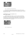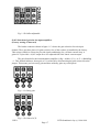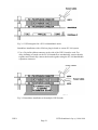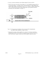
1
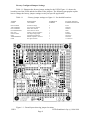
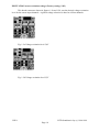
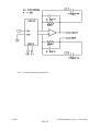
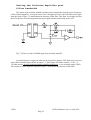
USF4 PC/104 Universal
Sensor Interface
User's Manual
Real Time Devices Scandinavia Oy
Real Time Devices Scandinavia Oy
Lepolantie 14
FIN-00660 Helsinki, Finland
Tel: (+358) 9 346 4538
Fax: (+358) 9 346 4539
Email: [email protected]
URL: www.rtdscandinavia.fi
USF4
RTD Scandinavia Oy (c) 1996-1999
IMPORTANT
Although the information contained in this manual has
been carefully verified, RTD Scandinavia Oy assumes no
responsibility for errors that might appear in this
manual, or for any damage to things or persons resulting
from improper use of this manual or from the related
software. RTD Scandinavia Oy reserves the right to
change the contents of this manual, as well as the
features and specifications of this product at any
time, without notice.
Published by
Real Time Devices Scandinavia Oy
Lepolantie 14
FIN-00660 Helsinki, Finland
Copyright © 1995-1999 by RTD Scandinavia Oy
All rights reserved
Printed in Finland
USF4
RTD Scandinavia Oy (c) 1996-1999
Page 1
Table of Contents
===============================================================
INTRODUCTION
Instrumentation input stage
Excitation
Mechanical description
Connector description
What comes with your board
Board accessories
Application software and drivers
Hardware accessories
Using this manual
When you need help
CHAPTER 1 - BOARD SETTINGS
Factory-Configured Jumper Settings
Sensor excitation voltage
A/D channel selection
D/A channel selection
PGA reference source selection
Excitation type jumper
Input configuration jumpers
Input amplifier reference selection
Gain selection for each channel
Ground connection jumper
CHAPTER 2 - BOARD INSTALLATION
Board installation
External I/O connections
Sensor interface connector
50-pin RTD expansion connector
5
5
6
6
6
6
7
7
9
10
11
11
12
13
14
16
17
18
20
23
CHAPTER 3 - SENSOR INTERFACING
General discussion
27
Problems with remote sensors
Grounding and shielding of your system
Shielding of sensor leads
Gain selection
Bridge measurements with voltage excitation (see Appendix B) 29
Measurement with current excitation
30
RTD temperature measurement 4-wire method
31
Thermocouple measurements
32
Current loop conditioning
33
35
µ A and µ V signal conditioning
USF4
RTD Scandinavia Oy (c) 1996-1999
Page 2
CHAPTER 4 - HARDWARE DESCRIPTION
Instrumentation input stage description
Programmable Gain Amplifier (PGA)
Onboard Filters
Galvanic isolation
Onboard Temperature Sensor
39
40
41
42
43
CHAPTER 5 - BOARD OPERATION AND PROGRAMMING
Port-C bits 0-1 channel selection
Port-C bit 2 calibration temprature/signals
Port-C bits 4-5 gain selection of PGA
Port-C bits 6-7 power down control
45
45
45
46
CHAPTER 6 - CALIBRATION AND TESTING
Voltage excitation calibration
Amplifier post filter gain adjustment
PGA-reference post filter gain adjustment
Temperature sensor calibration
48
49
50
50
CHAPTER 7 - CUSTOMIZING THE PERFORMANCE OF YOUR USF4
Changing the loop sensing resistor
52
Setting the input instrumentation amplifier bandwidth
52
Setting the global instrumentation amplifier filter bandwidth 52
AC-coupling the PGA
52
Setting the PGA bandwidth
53
Setting the Isolation amplifier post filter bandwidth
55
APPENDIX A - PT100 LOOKUP TABLE
USF4
RTD Scandinavia Oy (c) 1996-1999
Page 3
List of illustrations
1-1
1-2a
1-2b
1-3
1-4
1-5
1-6a
1-6b
1-7
1-8
1-9
1-10
1-11
1-12a
1-12b
1-13a
1-13b
1-14
Board layout showing jumper locations
Voltage excitation level 5,0V
Voltage excitation level 2,5V
Analog Digital converter input channel
Offset D/A-converter channel selection
PGA reference selection
Excitation type jumper selection jumper selects voltage
Excitation type jumper selection jumper selects 100µ A
Input configuration: Inputs grounded
Input configuration: Current loop sensing fully differential
Input configuration: Thermocouple input
Input configuration: Fully differential input
Input configuration: Ground referenced single ended inputs
Grounded reference
Offset adjustable
Unity gain
Gain of 6,70
Analog and digital ground connection
9
10
10
11
11
12
13
13
14
14
15
15
16
16
17
17
17
18
2-1
2-2
2-3
2-4a
2-4b
2-5
USF4 integrated with a PC/104 stack
Standalone installation with multiple USF4 boards
19" rack installation
Sensor interface using the spring loaded connector
Sensor interface using the 50-pin header connector
50-pin expansion interface connector pinout
21
21
22
23
24
25
3-1
3-2
3-3
3-4
3-5
3-6
3-7
3-8
3-9
4-wire Whetstone bridge with 5,00V voltage excitation
Single element strain gauge driven by 100µ A current excitation
RTD measurement using four wire measurement and current exc.
Thermocouple interfacing
Current loop conditioning
Offset adjustment trimpot locations
µ V signal conditioning
Input resistor locations
µ A signal interfacing using onboard 75 Ω resistor
30
31
32
33
34
35
36
36
37
4-1
4-2
4-3
Single ended ground referenced input for an instrumentation amp
Fully differential input configuration for an instrumentation amp
Isolation amplifier Block Diagram
39
39
43
6-1
6-2a
6-2b
Calibration trimpot for 5.00V excitation level
Gain adjustment trimpot location on PCB
Gain adjustment trimpot location on PCB
48
49
50
7-1
7-2
7-3
7-4
Internal structure of the PGA
Filter to remove the 500 kHz ripple from isolation amplifier
Jumper location of optional lowpass filter
Circuit diagram of multiplexer and filter
54
55
56
56
USF4
RTD Scandinavia Oy (c) 1996-1999
Page 4
This user's manual describes the operation of the USF4 Universal Sensor Interface
board. This board can be used with the Real Time Devices PC/104 compatible data acquisition
boards as well as all the RTD ISA-bus compatible analog data acquisition boards.
Some of the key features of the USF4 include:
* 4 channel, channel by channel configurable sensor inputs
* User selectable gain and programmable gain
* Galvanically isolated signal conditioning
* Current or voltage sensor excitation
* Onboard temperature sensor for precision calibration and CJC
* Onboard power supply for single +5V operation
* Power management
* Support for direct PC/104 interface with RTD dataModules
* PC/104 complianat
The following paragraphs briefly describe the major features of the USF4. A more detailed
discussion is included in Chapter 3 (Sensor Interfacing) , Chapter 4 (Hardware description) and in
Chapter 5 (Board operation and programming. The board setup is described in Chapter 1 (Board
Settings). Study Chapter 7 for some fine tuning hints for the USF4.
Instrumentation input stage
The USF4 universal sensor interface board has a true differential input amplifier stage for
each input channel. The input amplifier is specially designed for interfacing to many real world
signals. A high gain can be achieved with good noise rejection. The user can define the amplification
(Gain) for each channel separately with 3 jumper configurable resistors. This low noise, high
performance input amplifier can deliver a gain of 8.000 to a low level sensor signal.
Excitation
All passive sensors require either a voltage or current drive to output a signal that can be
measured by the input instrumentation amplifier. The USF4 can supply either a stabilized voltage or
current to drive the sensors. Each channel can be individually operated with the desired excitation.
There is a standard 100 µ A current excitation available for resistance or platinum temperature sensor
excitation. Voltage excitation has two options: +2,50V or +5,00V. These voltages can be used to
drive resistive bridge sensors or strain gauges.
Mechanical description
The USF4 is designed on a PC/104 form factor. An easy mechanical interface to both ISA-bus
and PC/104 systems can be achieved. Stack your PC/104 compatible computer directly on the USF4
using the onboard mounting holes. A dataModule or an ISA-bus board can be connected directly to
the USF4 with the 50-pin expansion connector. USF4 boards can be supplien in the RTD IDAN
modular aluminium framed enclosure together with a data acquisition board.
USF4
RTD Scandinavia Oy (c) 1996-1999
Page 5
Connector description
There is a 50-pin analog/digital interface connectors on the USF4 to directly interface
to the A/D-board. The signal definition of this connector is compatible with all the PC/104, ISAbus and Eurocard front-end and A/D-boards.
Input sensor signals are connected to the USF4 by either a spring loaded discrete wire
connector of with a 50-pin flat ribbon cable header connector. Use this type of interface connector
with a TB50 screw terminal block. Please consult the factory for more details on different connector
options.
What comes with your board
You receive the following items in your USF4 package:
* USF4 sensor interface board
* Software and diagnostics diskette with CalTest for Windows
* User's manual
If any item is missing or damaged, please call Real Time Devices Scandinavia Customer
service department at (+358) 0 346 4538.
Board accessories
In addition to the items included in your USF4 delivery several software and hardware
accessories are available. Call your distributor for more information on these accessories and for
help in choosing the best items to support your instrumentation system.
* Application software and drivers
* Hardware accessories
Real Time Devices can supply a complete set of accessories to your USF4 sensor
interface card. These include enclosures, power supplies, terminal boards (TB50)
and other interconnection systems such as IDAN aluminium enclosures.
USF4
RTD Scandinavia Oy (c) 1996-1999
Page 6
Using this manual
This manual is intended to help you install your new USF4 card and get it running
quickly, while also providing enough detail about the board and it's functions so that you can
enjoy maximum use of it's features even in the most demanding applications. We assume you
already have an understanding of data acquisition principles and sensor technology.
When you need help
This manual and CalTest for Windows will provide you with enough information to
fully utilize all the features on this board. If you have any problems installing or using this board,
contact our Technical Support Department (+358) 9 346 4538 during European business hours,
or send a FAX requesting assistance to (+358) 9 346 4539. When sending a FAX request, please
include your company's name and address, your name, your telephone number, and a brief
description of the problem.
USF4
RTD Scandinavia Oy (c) 1996-1999
Page 7
CHAPTER 1 - BOARD SETTINGS
===============================================================
The USF4 Universal Sensor Interface board has jumper settings you can change to
suit your application and sensor input configuration. The USF4 is factory configured with
a grounded input configuration. The factory settings are listed and shown in the diagram in
the beginning of this chapter.
Please observe, that each input channel has two free locations for user selectable
gain resistors. Place resistors in these locations to select a specific gain for each channel.
USF4
RTD Scandinavia Oy (c) 1996-1999
Page 8
Factory-Configured Jumper Settings
Table 1-1 illustrates the factory jumper setting for the USF4. Figure 1-1 shows the
board layout of the USF4 and the locations of the jumpers. The following paragraphs explain
how to change the factory jumper settings to suit your specific application.
Table 1-1
- Factory jumper settings see figure 1-1 for detailed locations
JUMPER
NAME
DESCRIPTION
OF JUMPER
NUMBER OF
JUMPERS
FACTORY SETTING
JUMPERS INSTALLED
EXCITATION
A/D-CHANNEL
D/A-CHANNEL
PGA REFERENCE
EXC-type
INPUT CONF.
GND
AMPLIFIER REF.
GAIN
Excitation voltage
A/D-converter channel
Offset D/A-channel
PGA reference source
Voltage/ Current excitation
INA input setup jumper
Agnd-Dgnd connection
INSTR. amplifier reference
INA gain selection
2
8
1
1
1
2
1
1
3
2,50V
Channel 1
Channel 1
GND
Voltage
Grounded
Connected
Grounded
1 Connected
Figure 1-1 - Board layout showing jumper locations
USF4
RTD Scandinavia Oy (c) 1996-1999
Page 9
EXCITATION sensor excitation voltage (Factory setting: 5,0V)
This header connector shown in figures 1-2a and 1-2b, sets the desired voltage excitation
level for the sensor input channels. A global voltage selection is done for all four channels.
Fig. 1-2a Voltage excitation level 5,0V
Fig. 1-2b Voltage excitation level 2,5V
USF4
RTD Scandinavia Oy (c) 1996-1999
Page 10
A/D-CHANNEL Analog to Digital converter input channel
(Factory setting: Channel 1)
This header connector shown in figure 1-3, connects the output of the USF4 board to an
A/D input channel on the data acquisition board. If you are using multiple USF4 front end boards,
make sure each board is connected to a different A/D-channel on the data acquisition board.
Fig. 1-3 Analog Digital converter input channel selection jumpers
D/A-CHANNEL Offset Digital to Analog converter channel
(Factory setting: Channel 1)
This header connector shown in figure 1-4, sets the D/A-converter channel on the data
acquisition board to drive the reference input of the onboard programmable gain amplifier (PGA).
This feature can be used to dynamically under software control adjust and zero the output of the
USF4 front end board. Use this to calibrate or to adjust the input of the gain amplifier before
the signal is amplified. If your data acquisition card does not feature a D/A-converter, this jumper
has no functionality.
Fig. 1-4 Offset D/A-converter channel selection
USF4
RTD Scandinavia Oy (c) 1996-1999
Page 11
PGA REFERENCE Programmable Gain Amplifier reference selection
(Factory setting: GND)
This header connector shown in figure 1-5 selects the source for the reference pin of the
Programmable Gain Amplifier (PGA). Connecting this jumper to ground (GND) for a ground
referenced amplifier connection. If software adjustable offset adjustment is desired, connect this
jumper to the D/A-converter output and set the correct D/A converter channel (See figure 1-4).
The reference based offset adjustment zeroes the output of the amplifier. This maximizes the
dynamic range of the amplifier to the analog to digital converter of the data acquisition board.
Fig. 1-5 PGA reference selection
USF4
RTD Scandinavia Oy (c) 1996-1999
Page 12
EXC-type Selection of either voltage or current excitation for each input channel
(Factory setting: Voltage)
This header connectors shown in figures 1-6a and 1-6b select the type of excitation for
each channel. Select the general excitation type from either a voltage or a current. There is a
stabilized 100µ A current excitation available.
If you choose to use voltage excitation for a specific channel you have the following
options: 2,50V or 5,00V . (See figures 1-1 for more information on voltage settings)
Fig. 1-6a Excitation type selection jumper selects voltage (One jumper for each channel)
Fig. 1-6b Excitation type selection jumper selects 100µ A (One jumper for each channel)
USF4
RTD Scandinavia Oy (c) 1996-1999
Page 13
INPUT CONF. Input configuration jumpers
(Factory setting: Grounded, see below)
These header connectors shown in figures 1-7 to 1-11 select the input for different sensor
signals. A detailed description of all possible input configurations is illustrated in the figures below.
Fig. 1-7 Inputs grounded
Figure 1-7 illustrates a grounded input configuration. this must be used for all unused
amplifier input channels. This is also the factory setting of the USF4 board.
Fig. 1-8 Current loop sensing , fully differential
Figure 1-8 illustrates a current loop sensing setup. In this mode the current loop is sensed
by an onboard resistor with a 75Ω resistor. The loop current is terminated at the loop power
supply ground. This measurement method provides a fully differential measurement of the
current output of the sensor without affecting sensitive measurements on other channels.
The loop supply does not need to share a common ground with the USF4 analog ground.
This model is ideal regarding noise rejection and offsets especially if other low noise sensor signals
are connected to other input channels.
USF4
RTD Scandinavia Oy (c) 1996-1999
Page 14
Fig. 1-9 Thermocouple input
The USF4 supports a thermocouple (J or K ) input for any of the eight channels on the
board. If the thermocouple is not remotely grounded, then the ground connection must be done
on the USF4 with a 1 MΩ resistor. This connection assures that common mode voltages induces
in the thermocouple loop are not converted to normal mode voltages and amplified. The onboard
LM35 temperature sensor can be used to measure the temperature of the front plate for Cold
Junction Compensation (CJC). To maintain good compensation performance the thermocouples
must be directly terminated to the USF4 with discrete connectors through the front plate. If this
is not an attractive choice, terminate your thermocouples on a TB50 termination board with a
temperature sensor onboard.
Fig. 1-10 Fully differential input
Use the fully differential input configuration to connect bridge type sensors or Resistive
Temperature Devices (RTD's) to your USF4 board. The fully differential input provides the best
Common Mode Voltage Rejection (CMR) and highest amplifier performance.
USF4
RTD Scandinavia Oy (c) 1996-1999
Page 15
Fig. 1-11 Ground referenced single ended inputs
The ground referenced single ended input configuration is used to interface to single
ended signals that share the ground with the USF4 board. This configuration is used for instance in
three-wire measurement schemes. The inverting input of the instrumentation amplifier is connected
to ground with a 1MΩ resistor.
AMPLIFIER REF. Instrumentation amplifier reference
(Factory setting: Grounded)
The header connector shown in figure 1-12 selects the reference for instrumentation
input amplifier. Each channel can be selected separately. If a ground referenced system with no
offset adjustment is desired connect this jumper according to figure 1-12a. To adjust the offset or
zero the output of the instrumentation input stage select the jumper position indicated in figure
1-12b. Now the output voltage level can be adjusted manually from the calibration trimpots on
the board. Each channel has it's own adjustment.
Fig. 1-12a Grounded reference
USF4
RTD Scandinavia Oy (c) 1996-1999
Page 16
Fig. 1-12b Offset adjustable
GAIN Selection of gain for the input amplifiers
(Factory setting: Connected)
The header connector shown in figure 1-13 shows the gain selection for each input
channel. There are three places for gain resistors. One of the resistors is installed by the factory.
This resistor (8K66) is selected to provide signal conditioning for a 4-20mA current loop. A
gain of 6.70 provides a 10,0V output for a zero adjusted full scale 20mA current output.
The gain formula for the instrumentation amplifier is Rg = 49400 / (G-1), or G = (49400/Rg)
+ 1. This formula indicates, that a gain of 1 is achieved by disconnecting the gain resistor selection
jumper. This means you have unity gain and three arbitrary gains at your disposal.
Fig. 1-13a Unity gain
Fig. 1-13b Gain of 6,70
USF4
RTD Scandinavia Oy (c) 1996-1999
Page 17
GND Analog and digital ground connection
(Factory setting: Disconnected)
The header connector shown in figure 1-14 is the single point connection for the
analog and digital grounds on the non-isolated side of the USF4. It is desirable to connect
the analog ground to a digital ground in one point near the A/D-converter. This jumper can be
used connect the grounds together when calibrating the board with a precision voltmeter with
no A/D converter board connected.
Fig. 1-14 Analog and digital ground connection
USF4
RTD Scandinavia Oy (c) 1996-1999
Page 18
CHAPTER 2 - BOARD INSTALLATION
===============================================================
The USF4 Universal Sensor Interface board is very easy to connect to your data
acquisition board. Easy interface to PC/104 systems as well as ISA-bus plug-in boards is
provided. This chapter tells you step-by-step how to install your USF4 to your data acquisition
hardware. After completing the installation use CalTest for Windows to fully verify that
your board and sensor connection is working as intended.
USF4
RTD Scandinavia Oy (c) 1996-1999
Page 19
Board installation
Keep your board in its antistatic bag until you are ready to install it to your system!
When removing it from the bag, hold the board at the edges and do not touch the components
or connectors. Please handle the board in an antistatic environment and use a grounded
workbench for testing and handling of your hardware.
Before installing the board in your computer, check the jumper settings. Chapter 1
reviews the factory settings and how to change them. If you need to change any settings, refer
to the appropriate instructions in Chapter 1. Note that incompatible jumper settings can result
in unpredictable board operation and erratic response.
General installation guidelines:
1. Turn OFF the power to your computer
2. Touch the grounded metal housing of your computer to discharge any
antistatic buildup and then remove the board from its antistatic bag.
3. Hold the board by it's edges and install it in an
enclosure or place it on the table on an antistatic surface.
4. Connect the board to the data acquisition board using the twisted pair
50-pin flat cable. Make sure the polarity of the cable is correct.
Installation integrated with a PC/104 module stack:
* Secure the four PC/104 installation holes with standoffs.
* Connect the 50-pin expansion connector of the dataModule
to the corresponding connector of the USF4. It is desirable
to mount the data acquisition module next to the USF4 board
to provide maximum distance to EMI-radiation from a VGAcontroller or a CPU-module.
USF4
RTD Scandinavia Oy (c) 1996-1999
Page 20
Fig. 2-1 USF4 integrated in a PC/104 dataModule stack.
Standalone installation with a ISA-bus plug-in board or remote PC/104 system.
* Use a 50-pin flat ribbon connector at the side of the USF4 interface card. For
daisy-chaining of boards use the PC/104 standoffs to mechanically connect boards
together and electrically connect the boards together using the PC/104 dataModule
expansion connector.
Fig. 2-2 Standalone installation with multiple USF4 boards.
USF4
RTD Scandinavia Oy (c) 1996-1999
Page 21
3U rack or enclosure installation with a EUROCARD CPU with one USF4.
* The PC/104 system can easily be inserted into a 19" rack installation using the CPU as
a "form factor adapter". Assemble your PC/104 data modules on a RTD single board
EUROCARD computer and install the system in a 19" enclosure. Multiple USF4 boards
can be connected to this system by daisy-chaining the 50-pin expansion connector
interfacing to the data-Module. See figure 2-3.
Fig. 2-3 19" Eurocard rack installation with an integrated PC/104 dataModule
and EUROCARD cpuModule computer system.
* Separating the sensitive analog amplifiers in a separate 19" enclosures maximum
shielding against EMI. If you construct an integrated system with the PC/104 CPU,
make sure the power supply is kept away from the amplifiers inputs and cables.
USF4
RTD Scandinavia Oy (c) 1996-1999
Page 22
External I/O connections
Figure 2-4 shows the sensor interface connector layout of the USF4. This connector
is located toward the front plate. Refer to this picture when making sensor connections. This
connector is galvanically isolated from the main system.
Figure 2-4a shows the terminal block connector pinout and Figure 2-4b shows the
50-pin flat cable header connector option pinout.
ALL SIGNALS ARE ISOLATED
#1
#2
#3
+12V
-12V
ANALOG GROUND
ANALOG SUPPLY
#4
#5
#6
#7
#8
EXCITATION CH1
+INPUT
-INPUT
ANALOG GROUND
ANALOG GROUND (SHIELD)
CHANNEL 1
#9
#10
#11
#12
#13
EXCITATION CH2
+INPUT
-INPUT
ANALOG GROUND
ANALOG GROUND (SHIELD)
CHANNEL 2
#14
#15
#16
#17
#18
EXCITATION CH3
+INPUT
-INPUT
ANALOG GROUND
ANALOG GROUND (SHIELD)
CHANNEL 3
#19
#20
#21
#22
#23
EXCITATION CH4
+INPUT
-INPUT
ANALOG GROUND
ANALOG GROUND (SHIELD)
CHANNEL 4
#24
#25
EXCITATION SUPPLY (+12V)
ANALOG GROUND
EXCITATION
Fig. 2-4a Sensor interface using a terminal block connector
USF4
RTD Scandinavia Oy (c) 1996-1999
Page 23
ALL SIGNALS ARE ISOLATED
#1,#2
#3,#4
#5,#6
+12V
-12V
ANALOG GROUND
ANALOG SUPPLY
#7,#8
#9,#10
#11,#12
#13,#14
#15,#16
EXCITATION CH1
+INPUT
-INPUT
ANALOG GROUND
ANALOG GROUND (SHIELD)
CHANNEL 1
#17,#18
#19,#20
#21,#22
#23,#24
#25,#26
EXCITATION CH2
+INPUT
-INPUT
ANALOG GROUND
ANALOG GROUND (SHIELD)
CHANNEL 2
#27,#28
#29,#30
#31,#32
#33,#34
#35,#36
EXCITATION CH3
+INPUT
-INPUT
ANALOG GROUND
ANALOG GROUND (SHIELD)
CHANNEL 3
#37,#38
#39,#40
#41,#42
#43,#44
#45,#46
EXCITATION CH4
+INPUT
-INPUT
ANALOG GROUND
ANALOG GROUND (SHIELD)
CHANNEL 4
#47,#48
#49,#50
EXCITATION SUPPLY (+12V)
ANALOG GROUND
EXCITATION
Fig. 2-4b Sensor interface using 50-pin header connector
USF4
RTD Scandinavia Oy (c) 1996-1999
Page 24
NOTE:
Observe that pin 24 (or pins 47,48 ) carry the isolated +12V that can be used as a
supply for sensors like 4-20 mA pressure transmitters. This power output is derived
from the excitation power supplies for sensor. Care must be taken not to exceed the
maximum load current (I max). The maximum available current should be calculated
with the following formula.
60mA - Σ(vex_gx RLx) − n × 100µA = I max
Where:
vex_gx
- voltage excitation level
RLn
- load of specific channel using voltage excitation.
n
- number of channels using 100 µ A excitation
Example :
Excitation setting for is 2,50V. Channel 1 load cell with nominal resistance 350Ω ,
Channel 2 load cell with nominal resistance 1000Ω . Channels 3 and 4 connected to
a PT100 temperature sensor using current excitation.
60mA - (2,5V/350Ω +2,5V/1000µ )- 2 × 100µ A = I max
Evaluation of this formula yields: 60mA - 7,14mA - 2,5mA - 0,2mA = 50,16mA
Figure 2-5 shows the 50-pin expansion interface connector layout of the USF4. This
connector is used to interface to the A/D-board and is non-isolated.
AIN1
AIN2
AIN3
AIN4
AIN5
AIN6
AIN7
AIN8
AOUT1
AOUT2
AGND
PA7
PA6
PA5
PA4
PA3
PA2
PA1
PA0
TRIGGER IN
EXT GATE 1
TRIGGER OUT
EXT CLOCK
+12V (VCC)
-12V (VSS)
*1
*3
*5
*7
*9
*11
*13
*15
*17
*19
*21
*23
*25
*27
*29
*31
*33
*35
*37
*39
*41
*43
*45
*47
*49
*2
*4
*6
*8
*10
*12
*14
*16
*18
*20
*22
*24
*26
*28
*30
*32
*34
*36
*38
*40
*42
*44
*46
*48
*50
AIN9
AIN10
AIN11
AIN12
AIN13
AIN14
AIN15
AIN16
AGND
AGND
AGND
PC7
PC6
PC5
PC4
PC3
PC2
PC1
PC0
DGND
T/C OUT 1
T/C OUT 2
EXT GATE 2
+5V
DGND
Fig. 2-5 50-pin expansion interface connector layout
USF4
RTD Scandinavia Oy (c) 1996-1999
Page 25
CHAPTER 3 - SENSOR INTERFACING
===============================================================
Chapter 3 - Sensor Interfacing will provide you with a hands-on feeling on general
design guidelines and engineering questions regarding the most commonly used sensor types.
The USF4 provides a reliable and flexible connection to your "real-world" - measurements.
USF4
RTD Scandinavia Oy (c) 1996-1999
Page 26
General Discussion
In most cases the performance of your analog sensor measurement system is limited by
the performance of your sensor interface amplifiers. The quality of the acquired signal is also
affected by shielding, grounding, and mechanical sensor installation questions.
The USF4 has been designed to be a high precision, low noise, high gain instrumentation
board for industrial and laboratory sensor interfacing. Galvanic isolation between the sensors
and the computer system improve reliability in harsh measurement environments. Isolation will
protect your data acquisition system against noise spikes and large common mode voltages. It
enables you to drive your sensors from a remote power supply and it will prevent ground loops
through the computer's ground.
* Problems with remote sensors
A cable as short a few centimeters will act as an antenna picking up noise from the outside
environment. This noise can be either radio frequency noise (RF-noise) or electromagnetic noise
(EM-noise). Signal degrading will occur if shielding is neglected. Shielding is not enough though,
it is necessary to ground the shield properly. Failure to do so may cause the amplifiers to operate
unpredictably. A floating shield will capacitively couple electromagnetic noise energy to the
sensitive signal leads inside the shield and might cause the amplifiers to oscillate.
* Grounding and shielding of your system
Improper grounding is one of the most common cause of performance degrading of analog
instrumentation systems. Typical errors resulting from improper grounding is offset voltages and
ground coupled noise. With correct grounding of your instrumentation system you can reduce noise
coupling.
EMI-suceptibility can be reduced by using metallic enclosures for your analog
instrumentation subsystem. For the shielding to be effective make sure you ground the enclosure
at a single point near the power supply entry point. Failure to do so may degrade the performance
of your analog circuitry. If you integrate your data acquisition and power supply into a common
enclosure make sure you separate the switching power supply as far as possible from your amplifier
subsection. To improve shielding , place a metal plate in the enclosure between the switching power
supply and the analog amplifier cards and single point ground it at the power supply ground.
LCD-panel inverters are sources of high frequency radiated switching noise. Place these
components far from the analog amplifier subsection and shield them with a grounded metal cover.
It is also important to make sure the inverter does not draw it's operating voltage from the same
location as the rest of the system. Use separate power supply and ground return leads to the power
supply to minimize interference.
USF4
RTD Scandinavia Oy (c) 1996-1999
Page 27
* Shielding of sensor leads
It is important to shield the high impedance input signal lines from coupled noise. Passive
sensors like strain gauges, RTD's etc. have high impedance signal lines. The instrumentation
amplifier input has a good common mode voltage rejection capability, but induced noise currents
in the high impedance leads will cause errors. Keep the resistance of the shield low, therefore it is
strongly advised to use copper braided fine mesh shield sensor cables.
Grounding of the shield is extremely important. Also the point of grounding the shield
must be chosen correctly. Here are some guidelines to sensor shielding:
Rule 1. Always ground the shield
An ungrounded shield will couple noise capacitively to
the sensitive sensor leads.
Rule 2. Never ground the shield at both ends
This will cause noise currents to flow in the shield
and noise will be induced to the amplifier inputs.
Rule 3. Always ground the shield at the amplifier end
This will cause the shield to be in the same potential
as the analog amplifier reducing noise pickup.
The best performance can be achieved by connecting the shielded sensor leads directly
through the metal front plate of the USF4 with metal connectors.
If you are using a terminal board, you should use a shielded twisted pair flat cable to
connect the terminal board to the USF4.
A 100nF capacitor at the inputs of the instrumentation amplifier reduces input coupled
noise but also limits the input bandwidth. This capacitance and the resistance of the sensor limit
the bandwidth according to the formula
1
f(3dB) = -----------------------Example: 1 kΩ bridge load
(2 × π × R × 1 exp-7)
sensor has a bw. of 1,6 kHz
where R is the nominal resistance of the sensor.
USF4
RTD Scandinavia Oy (c) 1996-1999
Page 28
* Gain selection
There are two gain stages on the USF4. Each of the 4 input instrumentation amplifiers are
connected to a programmable gain amplifier (PGA). Care must be when determining the gain if
each stage. Two cases will be considered.
1) High level signal ( for example a current loop transmitter ) with low gain
Use the instrumentation amplifier to fine-tune the span of each channel. Perform
scaling with the PGA. Example: how to achieve a gain of 8,9 ? Select the resistor
configurable input amplifier gain to 4,45 and use the PGA for 8,9 and 13,35.
2) Low level signal (Strain gauge sensor ) with high gain typically 5000.
Use the instrumentation amplifier to achieve a gain of 5000. Program the PGA for
unity gain.
Consider the following case for a low level signal amplified by two gain stages. The high
presision instrumentation amplifier will yield a good noise rejection at high gains. Output noise
of the instrumentation amplifier is more or less the same regardless of the gain. Let us say the
output noise is 10mV. If you use 5000 gain on the instrumentation amplifier and unity gain for
the PGA the total noise will be ∼ 10mV. If you use 625 gain on the instrumentation amplifier
and a gain of 8 for the PGA the total gain is 5000 , but the noise is ∼ 80mV ! The PGA will
amplify the noise from the first gain stage.
Bridge measurements with voltage excitation
Voltage excitation is required for most load cells and pressure sensors with no internal
signal conditioning. The sensitivity of the specified sensor is rated typically as mV output / V
of excitation on full scale load or pressure. Typical sensitivity values range from 2-4 mV/V.
The excitation voltage level directly correlates to the output signal level. It is desirable
to use a high excitation voltage to give a stronger signal. A high level of excitation has it's
drawbacks. Firstly it your system will consume more power especially if the sensor resistance
is low and secondly the self-heating effects of the sensing elements will increase warmup
stabilizing times and may result in decreased accuracy.
The USF4 provides "tare-weight"-compenstation for every input channel. Use the offset
adjustment trimpot to offset your amplifier to zero to provide maximum signal input span.
Figure 3-1 shoes a measurement arrangement using voltage excitation. This example
shows a 4-wire Whetstone bridge type sensor that is driven with a 5,00V excitation. Pin numbers
are selected for Channel 1.
USF4
RTD Scandinavia Oy (c) 1996-1999
Page 29
Fig. 3-1 4-wire Whetstone bridge with 5,00V voltage excitation in Channel 1
Measurement with current excitation
Current excitation is typically used when a resistance change in a sensor element
relates to the measurement unit. These sensor types include for example Resistive Temperature
Devices (RTD's). Load cells that measure absolute change of resistance in the sensing element
should also be driven by a current reference.
USF4
RTD Scandinavia Oy (c) 1996-1999
Page 30
Fig. 3-2 Single element strain gauge driven by 100µ A current excitation.
RTD temperature measurement 4-wire method
Platinum Resistive Temperature Devices provide linear and high precision temperature
sensing. These devices come in typical nominal resistances of 100Ω , 500Ω and 1000Ω .
The nominal resistance is specified in 0 Centigrade. The resistance of the sensing element
varies depending on the temperature.
Since the RTD type temperature sensors temperature output is referred to an absolute
resistance value rather than a change in resistance it must be excited with a current source. To
maintain precision in temperature measurement we must minimize the self-heating of the
sensor by keeping the excitation current low. The USF4 provides a stable 100µ A reference
voltage, that is used with RTD's.
Four wire measurement will make the measurement immune to voltage drops is
long signal leads and will reject common mode noise. Two wires are used for the excitation
current and two wires are used for sensing the voltage over the RTD - type temperature element.
The inputs of the amplifier have a very high input impedance and therefore no current flows in
the sensing leads. Thus lead resistance errors do not affect the measurement.
USF4
RTD Scandinavia Oy (c) 1996-1999
Page 31
Fig. 3-3 RTD-measurement using four wire measurement and current excitation.
Temperature ranges can be selcted by choosing the approproate gain resistor to match
the input range of the A/D-board. Let us examine the following example: We wish to use a PT100
sensor and our temperature span shall be 0-100 Centigrade. A PT100 will have a nominal resistance
of 100Ω at 0 Centigrade and 138,50 Ω at 100 degrees Centigrade. Thus the resistance change of
38,50Ω will yield a 3,85mV change when using a 100µ A exitation current. If we wish to use a
0-10V input span on the A/D-board we must use a gain of 2.597. This gain will be achieved by
using a gain resistor of 19Ω . NOTE! the offset voltage at 0 degrees Centigrade (2,597V) must
be adjusted to zero using the dedicated offset adjustment trimpots.
Thermocouple measurements
Thermocouples are a very inexpensive sensors for temperature measurement. They are
more economic than RTD-type sensors, but they are not linear in response and require
"cold-junction compensation" for correct output readings.
The USF4 can interface to thermocouples directly. There is a 1MΩ resistor to ground
for non grounded thermocouples. Cold junction compensation and linearization can be performed
in software. If you are connecting the thermocouples directly to the USF4 the onboard temperature
sensor can be used to measure the temperature of the termination point of the thermocouples. It is
also possible to use a special terminal board with a flat cable connection to the USF4. This terminal
board has an onboard temperature sensor to provide the temperature of the terminal blocks on the
screw terminal board. All thermocouple types can be interfaced by the USF4.
The onboard gain circuitry can be trimmed to obtain the desired temperature sensitivity.
No excitation is needed for thermocouples since they are active type sensors.
USF4
RTD Scandinavia Oy (c) 1996-1999
Page 32
Figure 3-4 shows a connection of a grounded thermocouple. Cold junction temperature
measurement can be performed with the onboard LM35 temperature sensor.
Fig. 3-4 Thermocouple interfacing
Current loop conditioning
Current loop output sensors are very commonly used in the world of process industry.
Current loop outputs provide a good method of transmitting signals over long distances and
in noisy environments.
Typical standard current loop outputs are 4 - 20mA and 0 - 20mA. The output of current
loop sensors is converted to a voltage over a resistor on the USF4.
The maximum loop resistor value can be estimated with the formula:
-
U(loop) - 10V
R(loop) = -----------------0.02A
This shows, that with a 12 V automotive loop supply the maximum loop sensing resistor
can be 100 Ohms. Typically current loop transmitters operate from a loop supply in the range
of 10 - 30 V. The USF4 has a 75 Ω loop termination resistor available for each channel. Make
sure you close the two terminal loop termination jumper. See Figure 1-8 for more details.
The current loop sensing on the USF4 is fully differential giving outstanding noise rejection.
The input capacitor also bypasses all high frequency noise over the loop sensing resistor. Figure 3-5
illustrates the connection of a differential current loop measurement.
You may wish to use the onboard power outputs to drive the current transmitters. If you
wish to do so no external isolated loop supply is needed. See Chapter 2 EXTERNAL I/O
connections on more information on the isolated +12V outputs.
USF4
RTD Scandinavia Oy (c) 1996-1999
Page 33
Offset adjustment
Interfacing to a current loop with a resistor is very simple and often considered that a
resistor is all you need. The output offset caused by the 4 mA zero scale current can be zeroed to
provide a maximum dynamic range. The USF4 has four offset adjustment trimpots,one for each
channel. The input stage is designed to condition a current loop transmitter signal with maximum
precision. The offset adjustment trimpots are illustrated in Figure 3-6.
Fig. 3-5 Current loop conditioning
USF4
RTD Scandinavia Oy (c) 1996-1999
Page 34
Fig. 3-6 Offset Adjustment Channel 1 at the top, 4 at the bottom
µV
and µ A signal conditioning
Single ended low level signals can be conditioned by the USF4. These signals can be
connected directly to the non inverting input of the instrumentation amplifier.
µ V signal conditioning
Connect the single-ended voltage signal to the noninverting input of the instrumentation
amplifier. The inverting input must be grounded for correct operation. The 100nF input capacitor
will efficiently decouple any high frequency noise to ground at the amplifier inputs.
Set the amplifier gain with the gain resistor and zero any DC-offsets with the calibration
trimpots.
USF4
RTD Scandinavia Oy (c) 1996-1999
Page 35
Fig.3-7 µ V signal conditioning
µ A signal conditioning
A µ A-level current must be converted to a voltage over a resistor before it can be
conditioned by the instrumentation amplifier. Use the onboard 75Ω resistor to do this. If the
input impedance is too small for the signal source replace the input resistor with a suitable value.
The input resistor is located on the component side of the PCB. See figure 3-7 for the locations
for channels 1-4.
The input capacitor is connected in parallel with the input resistor. This capacitor will
decouple noise over the input resistor.
Set the amplifier gain with the gain resistor and zero any DC-offsets with the calibration
trimpots.
Fig. 3-8 Input resistor locations
USF4
RTD Scandinavia Oy (c) 1996-1999
Page 36
Fig. 3-9 A Signal interfacing using the onboard 75Ω input resistor
USF4
RTD Scandinavia Oy (c) 1996-1999
Page 37
CHAPTER 4 - HARDWARE DESCRIPTION
===============================================================
This chapter on the hardware of the USF4 explains and describes some of the key
parts of the board. These include a general description on the instrumentation input stage,
galvanic isolation of signals, the programmable gain amplifier, signal filtering and power
management of the USF4. In this chapter are some hints on fully utilizing the properties
of this design.
USF4
RTD Scandinavia Oy (c) 1996-1999
Page 38
Instrumentation input stage description
The USF4 features eight independent signal conditioning amplifiers, one for each channel.
This configuration enables each channel to be configured for a different sensor type, and different
trimmed gains and offsets for each channel.
The input instrumentation amplifier stage can use either the single ended ground referenced
input configuration or a fully differential input configuration. It is preferable to use the differential
input configuration whenever possible. This mode of operation provides the best noise rejection
characteristics for your sensitive instrumentation system. The following illustrations demonstrate
the difference between these two configurations using a 4-20mA current loop as an example.
Fig. 4-1 Single ended ground referenced input for an instrumentation amplifier.
Fig. 4-2 Fully differential input configuration for an instrumentation amplifier.
USF4
RTD Scandinavia Oy (c) 1996-1999
Page 39
The input amplifiers of the USF4 each have 3 different user selectable jumper
configurable gain setting resistors. These resistors set the gain (amplification) of the input
instrumentation amplifier. It is essential to use high quality low temperature coefficient precision
resistors for this purpose. The following formula helps you choose a custom resistor gain for
your system:
49400
Gain = ------- + 1
Rg
Disconnecting the gain resistor (removing the jumper) will yield a unity gain factor.
Programmable Gain Amplifier (PGA)
The output of the instrumentation amplifier can be scaled with a programmable gain
amplifier under software control. The onboard Programmable Gain Amplifier (PGA) provides
two important functions for the user:
1.
Software configurable gain selection
Available gains are 1,2,4 and 8 (or optionally 1,10,100 and 1000). These gain values
cannot be adjusted by the user. The software configurable gain can be set with the digital I/O
port "C" with bits 4 and 5. (See discussion in chapter 5.)
2.
Software configurable offset adjustment
The reference pin of the PGA can be driven by a Digital to Analog (D/A) converter
channel on the data acquisition board. The appropriate reference pin selection jumper must be
set (see jumper description PGA REFERENCE , Fig 1-5 ). Adjusting the voltage on the reference
pin will give the system designer the choice to adjust the gain stage offset from software. This is
especially useful for auto-zeroing software calibration or expansion of the dynamic signal span.
The bandwidth of the programmable gain amplifier is set by default to 10 kHz by the
factory. The large signal settling time is 0,1msec. See the section on Customizing the Performace
of your USF4 for more details on adjusting the bandwidth of your PGA.
USF4
RTD Scandinavia Oy (c) 1996-1999
Page 40
Onboard filters
The USF4 features three filter stages from the input amplifiers to the A/D - converter.
The following discussions describes each filter stage.
1.
Input amplifier post filter
This filter is located between the input 4:1 multplexer and the Programmable Gain
Amplifier (PGA). This filter is a single pole passive RC - filter and reduces the input noise to
the second gain stage. Removing this filter will increase the scanning frequency of the USF4
channels since the settling time of the MUX output will decrease.
2.
Isolation amplifier post filter
This filter is located immediately after the isolation amplifier. The purpose of this
active two pole filter is to remove all the unwanted high frequency noise generated by the
isolation amplifier.
3.
Post Low Pass filter
This post filter is located before the A/D converter at the output of the USF4. The
bandwidth of this filter can be with jumpers to two frequencies or disabled. Disabling this
filter will increase the scanning frequency of the USF4 channels since the settling time of the
MUX output will decrease.
USF4
RTD Scandinavia Oy (c) 1996-1999
Page 41
Galvanic isolation
The USF4 is a fully galvanically isolated analog amplifier board. Analog signals from
the board to the A/D converter are isolated using an isolation amplifier. The D/A converter
output driving the reference pin of the PGA is also similarly galvanically isolated.
The onboard precision isolation amplifiers use a duty-cycle modulation - demodulation
technique. The signal is transferred over the isolation barrier digitally over a small internal capacitor.
With digital demodulation the barrier characteristics do not affect the signal integrity, resulting in
excellent reliability and good high frequency transient immunity over the isolation barrier.
The isolation stage of the analog signal is carefully designed not to deteriorate the
overall performance of the system. The 500 kHz high frequency ripple from the modulationdemodulation of the isolation amplifier is efficiently filtered with an active two-pole analog
filter. An optional post filter can be used to filter unwanted high frequency components from
the signal before feeding it to the A/D board. See Chapter 7 for more details.
Digital signals control the channel selection at the multiplexer and the gain of the PGA.
Optoisolators are used to isolate the onboard digital control signals from the computer side.
Power supply isolation is performed by isolated DC/DC converters. The power supply
of the isolated analog amplifier circuitry as well as the sensor excitation is isolated from the
computer power supply. There is no ground connection between the amplifier grounds an the
computer ground.
It must be reminded that the separate input channels are all in the same voltage potential.
There is no isolation between onboard analog channels. If your system has sensor groups in different
potentials you must use several USF4 boards. In this case each board can be in a different potential.
Figure 4-3 shows the internal structure of the isolation amplifier used on the USF4.
USF4
RTD Scandinavia Oy (c) 1996-1999
Page 42
Fig. 4-3 Isolation amplifier Block Diagram
Onboard Temperature Sensor
An onboard temperature sensor circuitry can be used to measure the ambient temperature
of the board. An LM35 temperature transmitter is used to convert temperature to voltage. The
output of the LM35 is a linear 10mV / C. Temperatures are indicated in Centigrade. The
measurement range is from -55 to +150 Celsius.
The onboard temperature sensor can be used for several purposes:
1. Cold junction temperature sensing
When interfacing to thermocouples the cold junction temperature of the USF4 can be
read and the linearization and cold junction compensation can be performed in software.
2. Temperature dependent calibration
For precision measurement over an broad operating temperature range the gain and
offsets may change. The system designer can choose to calibrate the USF4 characteristics
against temperature variations and perform the necessary correction in software. Use the
onboard temperature sensor to monitor the ambient temperature of the sensitive amplifier section.
3. Temperature control of your instrument
It may be useful to monitor the internal temperature of your computer system and control
the climatization of the enclosure.
USF4
RTD Scandinavia Oy (c) 1996-1999
Page 43
CHAPTER 5 - BOARD OPERATION AND PROGRAMMING
===============================================================
This chapter on the programming of the USF4 explains and describes how to operate
your USF4 from software. It provides a complete description of the functions of the bits
used by the USF4. Use CalTest for Windows to test and adjust your USF4. The program
installation disks are includes in your shipment.
USF4
RTD Scandinavia Oy (c) 1996-1999
Page 44
The USF4 uses the 8 bit digital I/O port "C" for controlling the onboard circuitry.
MSB PC7 PC6 PC5
PWR EXC G1
PC4
G0
PC3 PC2
MX2 RES
PC1
Ch1
PC0
Ch0
LSB
Port-C bits 0-1 (Ch0-2)
The input multiplexer on the USF4 is controlled by bits 0-1.
Truth table:
PC1
0
0
1
1
PC0
0
1
0
1
Channel 1
Channel 2
Channel 3
Channel 4
Port-C bit 2 (RES) Reserved
Port-C bit 3 (MX2)
The secondary multiplexer selects either the 4 amplifiers
or the onboard temperature sensor to the selected analog
input channel of the A/D board.
Truth table:
PC3
0
1
Temperature sensor connected to A/D
Amplifiers connected to A/D
Port-C bits 4-5 (G0-1)
The onboard programmable gain amplifier (PGA203) gain is set by
bits 4 and 5 in the following manner.
Truth table:
PC5
0
0
1
1
PC4
0
1
0
1
Gain of 1
Gain of 2
Gain of 4
Gain of 8
Optional gains available 1,10,100 and 1000. Please consult the factory for details.
(PGA202 used instead of the PGA203)
USF4
RTD Scandinavia Oy (c) 1996-1999
Page 45
Port-C bit 6 (EXC)
This bit controls the power transistor that supplies exciation power to the
sensors. This bit must be cleared to "0" for exciation to operate. This line is
pulled high with a 10 kOhm resistor and is normally inactive after the computer
reset. Use this bit to optimize the power consumpltion while maintaining presision
of measurement by keeping the amplifiers "warm". Important notice: Make sure
the amplifiers are powered up before the excitation powers up the sensors. Failure
to do so may cause permanent damage or degrading of performance of the input
amplifiers.
Port-C bit 7 (PWR)
This bit controls the power transistor that supplies +5V to the USF4 amplifiers.
This bit must be cleared to "0" for the board amplifiers to operate. This line is
pulled high with a 10 kOhm resistor and is normally inactive after the computer
reset. Important notice: Make sure the amplifiers are powered up before the excitation powers up the sensors. Failure to do so may cause permanent damage or
degrading of performance of the input amplifiers.
USF4
RTD Scandinavia Oy (c) 1996-1999
Page 46
CHAPTER 6 - CALIBRATION AND TESTING
===============================================================
This chapter on the calibration and testing of the USF4 explains and describes how
to test, adjust and calibrate your board. You may use CalTest for Windows to perform this task.
USF4
RTD Scandinavia Oy (c) 1996-1999
Page 47
Voltage excitation calibration
The user selectable excitation voltages can be adjusted separately for both sensor groups.
The two factory settings include 2.50V and 5.00V. This voltage is regulated to remain fixed
regardless of load. Small changes may occur due to voltage drops on board traces or resistance
in connectors. Voltage drops may also occur in sensor leads especially if low resistance sensors,
long ribbon cables or remote terminal blocks are used. In many cases sensor sensitivity is calibrated
against the excitation voltage present at the end of the sensor cable installed by the sensor
manufacturer. Thus you must calibrate the excitation voltage accordingly.
Figure 6-1 illustrates the calibration trimpot for 5.00V excitation level.
Fig. 6-1 Calibration trimpot for 5.00V excitation level.
USF4
RTD Scandinavia Oy (c) 1996-1999
Page 48
Amplifier post filter gain adjustment
The isolation amplifier two pole post filter gain is set to 1. The circuit diagram of this
filter is shown in Figure 7-2 in Chapter 7. The resistor marked as R8 can be adjusted with
a trimpot to obtain unity gain. This location of this trimpot is illustrated in figure 6-2a below.
To adjust the gain of the system perform the following steps:
1.
2.
3.
4.
5.
6.
7.
Apply a reference voltage to channel 1 in single ended ground referenced
mode. See figure 1-11.
Disconnect the gain jumper of the Instrumentation amplifier for channel 1.
See figure 1-13a.
Connect the Instrumentation amplifier reference jumper to ground. See figure 1-12a.
Connect the PGA Reference jumper to ground. See figure 1-5.
Disconnect the AGND-DGND jumper as shown in figure 1-14.
Run CalTest on your PC and set the PGA-gain for channel 1 to "1".
Adjust the trimpot until CalTest shows the applied input voltage for channel 1.
Fig. 6-2a Gain adjustment trimpot location on the PCB
USF4
RTD Scandinavia Oy (c) 1996-1999
Page 49
PGA-reference post filter gain adjustment
The isolation amplifier two pole post filter gain is set to 1. The circuit diagram of this
filter is shown in Figure 7-2 in Chapter 7. The resistor marked as R8 can be adjusted with
a trimpot to obtain unity gain. This location of this trimpot is illustrated in figure 6-2b below.
This adjustment only applies for systema that feature a D/A converter on the data aquisition
board. If your system has no D/A make sure the PGA-reference jumper remains in GND. See figure
1-5 for details.
To adjust the gain of the PGA - reference filter perform the following steps:
1.
2.
3.
4.
5.
6.
7.
8.
Connect the D/A channel jumper to the D/A channel available.
Apply a voltage from the D/A converter to the USF4.
Ground the inputs of input Channel 1. See figure 1-7.
Ground the reference of input Channel 1. See figure 1-12a.
Connect the PGA - reference jumper to D/A control. See figure 1-5,
connect the jumper on pins 2 and 3 .
Disconnect the AGND-DGND jumper as shown in figure 1-14.
Run CalTest on your PC and set the PGA-gain for input channel 1 to "1".
Adjust the trimpot until CalTest shows the applied D/A voltage on channel 1.
Fig. 6-2b Gain adjustment trimpot location on PCB
Temperature sensor calibration
The LM35 temperature sensor sensitivity is trimmed by the sensor manufacturer.
It does not need calibration.
USF4
RTD Scandinavia Oy (c) 1996-1999
Page 50
CHAPTER 7 - CUSTOMIZING THE PERFORMANCE OF YOUR USF4
===================================================================
This chapter on the customizing the performance of the USF4 explains and describes
how to tune your USF4 and optimize it for your specific needs. The most important part of
this section covers filtering and bandwidth considerations.
USF4
RTD Scandinavia Oy (c) 1996-1999
Page 51
Changing the loop sensing resistor
The onboard loop sensing resistor is selected to interface to industry standard loop
transmitter sensors. These sensors have a maximum loop resistor value that depends on the
loop supply voltage. The loop supply voltages that are commonly used cover the range from
10V to 30V. If you wish to interface to small small currents it may be desirable to select a higher
nominal resistance. The factory installed 75Ω resistors are located on the component side of the
USF4 next to the sensor interface connector.
Setting the instrumentation amplifier bandwidth
The USF4 is delivered with a 100nF bypass capacitor across the inputs. This effectively
filters high frequency input noise, but also limits the input bandwidth. You may remove these
capacitors if your signal source bandwidth needs to be increased. The capacitors are located on
the solder side of the board next to the sensor interface connector.
Setting the global instrumentation amplifier
filter bandwidth
There is a passive single pole filter at the output of the instrumentation amplifier
output multiplexer. It is preset to 10kHz. This lowpass filter consists of the "ON" resistance of
the analog multiplexer ( approximately 200Ω ) a series resistor 120Ω and a 47pF capacitor to
ground. This filter will affect the settling time of the multiplexer output. If you interfacing to
moderate speed signals and you wish to scan signals at a higher speed adjust the output filter.
The "ON" resistance of the switch can nort be affected. The series resistor is located under the
508 multiplexer marked on the silkscreen of the solder side with the reference designator R78.
The filter capacitor is maked next to the resistor by C35.
The formula for calculating the 3dB frequency of this filter is the following:
F(3dB) = 1 [2 × π(200 + Rx)Cx]
Using the factory installed values will yield:
F(3dB) = 1 [2 × π × 320 × 47 exp−9] = 10.587 Hz
AC-coupling the PGA
In some cases only the AC-component of the signal should be amplified by the PGA.
In such cases you may replace the series resistor R27 with a capacitor and remove C22 and
replace it with a resistor. If you use a series capacitor of 1µ F and a 1MΩ resistor to ground,
you have a single ended non invering AC-coupled PGA that will amplify frequencies over
0,16Hz. Observe that this connection will inevitably AC-couple all the input channels to the PGA.
USF4
RTD Scandinavia Oy (c) 1996-1999
Page 52
Setting the PGA bandwidth
External capacitors may be added in parallel with the internal feedback capacitors of the
programmable gain amplifier (PGA). These external capacitors must have the same nominal value.
The PGA has a 1 µ s settling time with no external components. Adding external capacitors will
limit the bandwidth and increase the settling time of the amplifier.
The cutoff frequency of the PGA may be determined from table 7-1.
Cutoff Frequency
C23 and C17
1 Mhz
100 kHz
10 kHz
none
47pF
524pF
Table 7-1 PGA Cutoff Frequency versus Filter Capacitors
Figure 7-1 shows the internal structure of the PGA. The 30K resistors and the 5,3pF
capacitors are internal to the PGA and have a +-20% tolerance. The capacitors C17 and C23
may be changed by the user according to table 7-1. The factory preinstalled capacitors are 47pF.
USF4
RTD Scandinavia Oy (c) 1996-1999
Page 53
Fig. 7-1 Internal Structure of the PGA
USF4
RTD Scandinavia Oy (c) 1996-1999
Page 54
Setting the Isolation Amplifier post
filter bandwidth
The output of the isolation amplifier includes noise components from the carrier frequency
of the isolation amplifier. A two pole active filter is designed to remove the 500 KHz carrier ripple
from the signal. Figure 7-2 demonstrates the structure of this filter. This filter is inverting, but since
the PGA operates in an inverting mode the input signal remains noninvering to the A/D.
Fig. 7-2 Filter to remove 500kHz ripple from isolation amplifier
An optional passive single pole filter can be selected by jumpers. This filter can be selected
with a three terminal jumper shown in figure 7-3. This jumper will either connect a 1.15kΩ or
150 Ohm resistor in series with tempertature/amplifier multiplexer. A two terminal jumper (X45)
will connect a 100nF capacitor to ground. Figure 7-4 illustrates the structure of this filter.
USF4
RTD Scandinavia Oy (c) 1996-1999
Page 55
Fig. 7-3 Jumper location of optional lowpass filter
Fig. 7-4 Circuit diagram of multiplexer and filter
The user may customize this filter to optimize to the operating bandwidth of the system.
If you have a USF4 with an onboard temperature sensor you must make sure to include the "ON"
series resistance of the analog multipexer into your bandwidth calculations. The nominal "ON"
resistance is approximately 35Ω .
USF4
RTD Scandinavia Oy (c) 1996-1999
Page 56
The Last Page
This manual has been compiled to comply with the performance and operation of the
USF4 Isolated Sensor Interface. If you find mistakes or you have suggestions for improvement
of the board or manual please do not hesitate to contact us. We have enjoyed designing this
board for you and we hope you get your new USF4 board up and running smoothly.
It took me over 86 cups of black coffee to complete this manual. Good Luck!
Tomi Hänninen
RTD Scandinavia Oy
(C) RTD Scandinavia Oy 1995-1999 DOC: USF4_MAN
USF4
RTD Scandinavia Oy (c) 1996-1999
Page 57
APPENDIX A - PT100 LOOKUP table
18.49
22.80
27.08
31.32
35.53
39.71
43.87
48.00
52.11
56.19
-200
-190
-180
-170
-160
-150
-140
-130
-120
-110
60.25
64.30
68.33
72.33
76.33
80.31
84.27
88.22
92.16
96.09
-100
-90
-80
-70
-60
-50
-40
-30
-20
-10
100.00
103.90
107.79
111.67
115.54
119.40
123.24
127.07
130.89
134.70
0
10
20
30
40
50
60
70
80
90
138.50
142.29
146.06
149.82
153.58
157.31
161.04
164.76
168.46
172.16
100
110
120
130
140
150
160
170
180
190
175.84
179.51
183.17
186.82
190.45
194.07
197.69
201.29
204.88
208.45
200
210
220
230
240
250
260
270
280
290
212.02
215.57
219.12
222.65
226.17
229.67
233.17
236.65
240.13
243.59
300
310
320
330
340
350
360
370
380
390
247.04
250.48
253.90
257.32
260.72
264.11
267.49
270.86
274.22
277.56
280.90
400
410
420
430
440
450
460
470
480
490
500
Resistance vs. Temperature
Units: Ohms , degrees C
USF4
RTD Scandinavia Oy (c) 1996-1999
Page 58