1
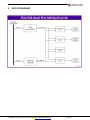
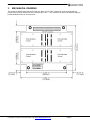
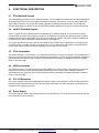
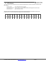
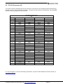
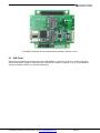
E104-MPE-04
PCI/104-Express Quad PCIe MiniCard Carrier
User Manual
Revision A.00
Revision
Date
Comment
A.00
3/30/15
Initial Release
FOR TECHNICAL SUPPORT
PLEASE CONTACT:
[email protected]
March 2015
Copyright 2015
Diamond Systems Corporation
555 Ellis Street
Mountain View, CA 94043 USA
Tel 1-650-810-2500
Fax 1-650-810-2525
www.diamondsystems.com
CONTENTS
Important Safe-Handling Information .....................................................................................................................3
1. Description ........................................................................................................................................................4
1.1 Features .........................................................................................................................................................4
1.2 Environmental / Mechanical ..........................................................................................................................4
2. Block Diagram ...................................................................................................................................................5
3. Mechanical Drawing .........................................................................................................................................6
4. Functional Description .....................................................................................................................................7
4.1 PCIe MiniCard Sockets .................................................................................................................................7
4.2 mSATA Flashdisk Support ............................................................................................................................7
4.3 PCIe Connections ..........................................................................................................................................7
4.4 USB Connections ..........................................................................................................................................7
4.5 PCI-104 Expansion ........................................................................................................................................7
4.6 Power Supply.................................................................................................................................................7
4.7 LED Indicators ...............................................................................................................................................8
5. Connectors and Jumpers ................................................................................................................................9
5.1 Connector and Jumper Lists..........................................................................................................................9
5.1.1
I/O Connectors ......................................................................................................................................9
5.1.2
Configuration Jumpers ..........................................................................................................................9
5.1.3
SIM Card Connectors ...........................................................................................................................9
5.2 Connector and Jumper Locations............................................................................................................... 10
5.3 PCIe/104 OneBank Connector (J2) ............................................................................................................ 11
5.4 SIM Connector (J3, J4) ............................................................................................................................... 12
5.5 PCIe/104 MiniCard Sockets (J5, J6, J7, J8) ............................................................................................... 13
5.6 PCI/104 Connector (J9) .............................................................................................................................. 14
5.7 Wireless Disable Jumper Block (JP1) ........................................................................................................ 15
6. Installing Modules.......................................................................................................................................... 15
6.1 Full Size PCIe MiniCards and mSATA Modules ........................................................................................ 15
6.2 Half Size PCIe MiniCards ........................................................................................................................... 15
6.3 SIM Cards ................................................................................................................................................... 16
7. Specifications................................................................................................................................................. 17
7.1 PCI/104-Express PCIe MiniCard Carrier .................................................................................................... 17
E104-MPE-04 Module User Manual Rev A.00 www.diamondsystems.com
Page 2
IMPORTANT SAFE-HANDLING INFORMATION
WARNING: ESD-Sensitive Electronic Equipment!
Observe ESD-safe handling procedures when working with this product.
Always use this product in a properly grounded work area and wear
appropriate ESD-preventive clothing and/or accessories.
Always store this product in ESD-protective packaging when not in use.
Safe Handling Precautions
This module contains numerous I/O connectors that connect to sensitive electronic components. This creates
many opportunities for accidental damage during handling, installation and connection to other equipment. The
list here describes common causes of failure found on boards returned to Diamond Systems for repair. This
information is provided as a source of advice to help you prevent damaging your Diamond (or any vendor’s)
embedded computer boards.
ESD damage – This type of damage is almost impossible to detect, because there is no visual sign of failure or
damage. The symptom is that the board simply stops working, because some component becomes defective.
Usually the failure can be identified and the chip can be replaced.
To prevent ESD damage, always follow proper ESD-prevention practices when handling computer boards.
Damage during handling or storage – On some boards we have noticed physical damage from mishandling. A
common observation is that a screwdriver slipped while installing the board, causing a gouge in the PCB surface
and cutting signal traces or damaging components.
Another common observation is damaged board corners, indicating the board was dropped. This may or may not
cause damage to the circuitry, depending on what is near the corner. Most of our boards are designed with at
least 25 mils clearance between the board edge and any component pad, and ground / power planes are at least
20 mils from the edge to avoid possible shorting from this type of damage. However these design rules are not
sufficient to prevent damage in all situations.
A third cause of failure is when a metal screwdriver tip slips, or a screw drops onto the board while it is powered
on, causing a short between a power pin and a signal pin on a component. This can cause overvoltage / power
supply problems described below. To avoid this type of failure, only perform assembly operations when the
system is powered off.
Sometimes boards are stored in racks with slots that grip the edge of the board. This is a common practice for
board manufacturers. However our boards are generally very dense, and if the board has components very close
to the board edge, they can be damaged or even knocked off the board when the board tilts back in the rack.
Diamond recommends that all our boards be stored only in individual ESD-safe packaging. If multiple boards are
stored together, they should be contained in bins with dividers between boards. Do not pile boards on top of each
other or cram too many boards into a small location. This can cause damage to connector pins or fragile
components.
Power supply wired backwards – Our power supplies and boards are not designed to withstand a reverse
power supply connection. This will destroy each IC that is connected to the power supply. In this case the board
will most likely will be unrepairable and must be replaced. A chip destroyed by reverse power or by excessive
power will often have a visible hole on the top or show some deformation on the top surface due to vaporization
inside the package. Check twice before applying power!
Bent connector pins – This type of problem is often only a cosmetic issue and is easily fixed by bending the pins
back to their proper shape one at a time with needle-nose pliers. This situation can occur when pulling a ribbon
cable off of a pin header. Note: If the pins are bent too severely, bending them back can cause them to weaken
unacceptably or even break, and the connector must be replaced.
E104-MPE-04 Module User Manual Rev A.00 www.diamondsystems.com
Page 3
1.
DESCRIPTION
The E104-MPE-04 PCI/104-Express PCIe MiniCard carrier module allows the use of up to four PCIe MiniCard I/O
TM
expansion modules in systems that provide PCI/104-Express expansion stack locations.
This module is a PCI/104-Express compatible carrier module that provides a socket and host connectivity for four
PCIe MiniCard modules using either PCIe or USB interfaces. The module utilizes 1:4 switch and hub components
to provide full support to all sockets while consuming only a single lane of host SBC resources. SIM card support
is provided for two sockets. All power is derived from the PCIe/104 connector +5V power tab. The PCI-104
connector is provided for pass-through connection but is not used by the module.
1.1
Features
Sockets
4 or 2 PCIe MiniCard sockets with PCIe x1 and USB 2.0 interfaces
Module support:
Full size modules supported in all four sockets
Half size modules supported in two sockets
SIM cards supported in two sockets
mSATA flashdisk supported in one socket
LEDs provided for all 4 sockets
Wireless disable function for each socket via jumpers
Bus expansion
1.2
PCIe 1:4 switch for PCIe x1 links to 4 sockets
USB 1:4 hub for USB links to 4 sockets
PCIe to SATA converter for mSATA module support in 1 socket
Environmental / Mechanical
Form factor
PCI/104 Express with wings (4.500” W x 3.775” H)
Host interface
PCIe/104 OneBank connector with PCIe and USB connections
PCI-104 stackthrough connector installed for pass-through purposes
Power
+5VDC in via +5V power tab on PCIe/104 connector
Operating temp
-40°C to +85°C at outer surface of heat spreader
Weight
2.5oz (70.9g)
Ruggedization
Board may be conformally coated
As a customization option, jumpers may be replaced with 0 ohm resistors for
hardwired configuration
TM
Environmental
Shock:
Compatible with MIL-STD-202G, Method 213-B, Table 213-1 Condition A, 50G /
11ms half sine, non-operational
Vibration:
Compatible with MIL-STD-202G, Method 214A, Table 214-1, Condition D,
11.95G random vibration, 15 minutes per axis, operational
PC/104™ and PC/104-Plus ™ and PCI-104™ are trademarks of the PC/104 Embedded Consortium. All other trademarks are the property of
their respective owners.
E104-MPE-04 Module User Manual Rev A.00 www.diamondsystems.com
Page 4
2.
BLOCK DIAGRAM
E104-MPE-04 Module User Manual Rev A.00 www.diamondsystems.com
Page 5
3.
MECHANICAL DRAWING
The module is slightly larger than the PC/104 form factor. It has 0.475” extensions on left and right sides to
provide more room for circuitry and I/O connectors plus .100” - .125” extensions on the top and bottom edges to
provide additional room for I/O connectors.
E104-MPE-04 Module User Manual Rev A.00 www.diamondsystems.com
Page 6
4.
FUNCTIONAL DESCRIPTION
4.1
PCIe MiniCard Sockets
The E104-MPE-04 provides four PCIe MiniCard sockets. The E104-MPE-02 provides two PCIe MiniCard sockets.
All sockets support full size (51mm length) PCIe MiniCard modules. Two sockets, J5 and J8, also support halfsize modules; however, only the full size mounting spacers are installed on these sockets. The module also
provides SIM support for sockets J5 and J8 and mSATA flashdisk supported in socket J6 for solid state storage.
4.2
mSATA Flashdisk Support
Socket 1 (upper left corner) also supports the installation of an mSATA flashdisk. An onboard PCIe to SATA
converter chip provides the SATA signals needed for the flashdisk. The socket auto-detects the type of module
installed and provides the appropriate serial interface to support the module. The module must be installed prior
to system boot in order for the BIOS to detect the device and support it.
The socket auto-detects the type of the module installed using CLKREQ (pin7) signal which is coming from the
mini PCIe module. In default case the pin is pulled up to 3.3V. Pin status will be high when connecting mSATA
device to the socket. It will be low when connecting to mPCIe device to the socket.
4.3
PCIe Connections
The module includes a 1:4 PCIe Gen 1 or 2 hub that provides PCIe x1 links to all 4 sockets. The upstream link is
tied to the PCIe/104 connector per the PCI/104-Express specification. An on-board signal multiplexor selects the
appropriate link from either the top or bottom PCIe/104 connector depending on whether the board is installed
below or above the SBC.
4.4
USB Connections
The module includes a 1:4 USB 2.0 hub that provides USB ports to all four sockets. The upstream port is tied to
the PCIe/104 connector per the PCI/104-Express specification. An on-board signal multiplexor selects the
appropriate port from either the top or bottom PCIe/104 connector depending on whether the board is installed
below or above the SBC.
4.5
PCI-104 Expansion
The module includes a PCI-104 passthrough connector to enable it to be installed in a PCI/104-Express stack in
between the processor module and a PCI-104 I/O module. Other than +5V power and ground connectivity, this
connector is not used by the module.
4.6
Power Supply
The module requires +5VDC input voltage per the PC/104 specification. The 5V and ground are derived from the
PCIe/104 and PCI-104 connectors.
E104-MPE-04 Module User Manual Rev A.00 www.diamondsystems.com
Page 7
4.7 LED Indicators
The module provides LED indicators for each socket as described below. All LEDs are labeled in silkscreen with
their function.
5V Power input:
green LED when 5VDC is applied
PCIe MiniCard socket: 3 green LEDs to support WWAN, WPAN, WLAN signals from each socket
SATA0 & SATA1:
green LEDs when active
E104-MPE-04 Module User Manual Rev A.00 www.diamondsystems.com
Page 8
5V
PAN J8
LAN J8
WAN J8
PAN J7
LAN J7
WAN J7
PAN J6
LAN J6
WAN J6
PAN J5
LAN J5
WAN J5
SATA1
SATA0
The bank of LEDs is located at the bottom of the board at the right of the PCIe/104 OneBank connector and
jumper block JP1. The LED indicators are arranged in the order shown below.
5.
CONNECTORS AND JUMPERS
5.1
Connector and Jumper Lists
5.1.1
I/O Connectors
Connector
5.1.2
5.1.3
Function
J1
PCIe/104 bottom connector
J2
PCIe/104 top connector
J5
mPCIe socket 1 (available in both quad & dual models)
J6
mPCIe socket 2 (available in both quad & dual models)
J7
mPCIe socket 3 (available in both quad & dual models)
J8
mPCIe socket 4 (available in both quad & dual models)
J9
PCI/104 connector
Configuration Jumpers
Jumper
Description
JP1(1)
W_Disable1#
JP1(2)
W_Disable2#
JP1(3)
W_Disable3#
JP1(4)
W_Disable4#
SIM Card Connectors
There are two SIM card connectors on PCIe/104 MiniCard carrier board. These are connected to MiniCard
sockets 1 and 4.
Connector
Description
J3
SIM card connector for MiniCard 4
J4
SIM card connector for MiniCard 1
E104-MPE-04 Module User Manual Rev A.00 www.diamondsystems.com
Page 9
5.2
Connector and Jumper Locations
J9
Socket 1 (J5, upper right):
Full size PCIe MiniCard
Half size PCIe MiniCard
SIM card socket on back
Socket 2 (J6, upper left):
Full size PCIe MiniCard
mSATA
Socket 4 (J8, lower right):
Full size PCIe MiniCard
Half size PCIe MiniCard
SIM card socket on back
(Available only in
E104-MPE-04 model)
Socket 3 (J7, lower left):
Full size PCIe MiniCard
(Available only in
E104-MPE-04 model)
J2
JP1
LEDs
E104-MPE-04 Top Side
J4
(Available only in
E104-MPE-04 model)
J3
J1
E104-MPE-04 Bottom Side
E104-MPE-04 Module User Manual Rev A.00 www.diamondsystems.com
Page 10
5.3
PCIe/104 OneBank Connector (J2)
The PCIe/104 OneBank connector conforms to the PCIe/104 specification and allows the E104-MPE-04 module
to be placed in any PCI/104-Express stack. The pinout for this connector is shown below.
USB-OC+3.3V
USB 5+
USB 5Gnd
PCIe 4 T+
PCIe 4 TGnd
Gnd
PCIe 1 R+
PCIe 1 RGnd
Gnd
PCIe 4 Clk+
PCIe 4 Clk+5V_SB
Gnd
SMB Data
SMB Clk
SMB Alert-
1
3
5
7
9
11
13
15
17
19
21
23
25
27
29
31
33
35
37
39
41
43
45
47
49
51
+
5
V
T
A
B
2
4
6
8
10
12
14
16
18
20
22
24
26
28
30
32
34
36
38
40
42
44
46
48
50
52
PCIe Reset+3.3V
USB 6+
USB 6Gnd
PCIe 1 T+
PCIe 1 TGnd
Gnd
PCIe 0 R+
PCIe 0 RGnd
Gnd
PCIe 1 Clk+
PCIe 1 Clk+5V_SB
E104-MPE-04 Module User Manual Rev A.00 www.diamondsystems.com
Page 11
5.4
SIM Connector (J3, J4)
Connectors J3 and J4 on the bottom side of the E104-MPE-04 allow a SIM module to be inserted into the system
instead of a PCIe MiniCard module. Only one or the other is allowed. This is an industry standard connector.
Connector
Description
J3
SIM card connector for MiniCard socket 4
J4
SIM card connector for MiniCard socket 1
VCC
Reset
Clock
1
2
3
4
5
6
GND
NC
I/O Data
SIM Connector Pinout
SIM Connector:
SF7W006S1BE1000
E104-MPE-04 Module User Manual Rev A.00 www.diamondsystems.com
Page 12
5.5
PCIe/104 MiniCard Sockets (J5, J6, J7, J8)
The E104-MPE-04 PCIe MiniCard carrier has the following MiniCard sockets:
PCIe-104 MiniCard socket 1 (J5, upper right)
PCIe-104/mSATA MiniCard socket 2 (J6, upper left)
PCIe-104 MiniCard socket 3 (J7, lower left)
PCIe-104 MiniCard socket 4 (J8, lower right)
The E104-MPE-02 PCIe MiniCard carrier has the following two sockets:
PCIe-104 MiniCard socket 1 (J5, upper right)
PCIe-104/mSATA MiniCard socket 2 (J6, upper left)
The MiniCard sockets have the pin out shown below. MiniCard socket 1 (upper right) and MiniCard socket 4
(lower right) are identical and have the SIM interface pinout. MiniCard socket 2 (upper left) supports both mPCIe
and mSATA interfaces.
PCIe MiniCard
mSATA / MiniCard
With SIM Interface
+3.3V
Gnd
+1.5V
UIM_PWR
UIM_DATA
UIM_CLK
UIM_RESET
ClkreqGnd
PCIe ClkPCIe Clk+
Gnd
Gnd
Gnd
17
19
21
18
20
22
Gnd
W_Disable#
PCIe Reset#-
Gnd
W_Disable#
PCIe Reset#-
PCIe RXPCIe RX+
Gnd
Gnd
PCIe TXPCIe TX+
Gnd
Gnd
+3.3V
+3.3V
Ground
SATA RXSATA RX+
Gnd
Gnd
SATA TXSATA TX+
Gnd
Gnd
+3.3V
+3.3V
Ground
Pull-up to +3.3V
Pull-up to +3.3V
23
25
27
29
31
33
35
37
39
41
43
45
47
49
51
24
26
28
30
32
34
36
38
40
42
44
46
48
50
52
+3.3V
Gnd
+1.5V
SMB Clk
SMB Data
Gnd
USB USB +
Gnd
WWAN LED#WLAN LED#
WPAN LED#
+1.5V
Gnd
+3.3V
+3.3V
Gnd
+1.5V
SMB Clk
SMB Data
Gnd
USB USB +
Gnd
WWAN LED#WLAN LED#
WPAN LED#
+1.5V
Gnd
+3.3V
ClkreqGnd
PCIe ClkPCIe Clk+
Gnd
2
4
6
8
10
12
14
16
Without SIM Interface
+3.3V
Gnd
+1.5V
1
3
5
7
9
11
13
15
KEY
Connector:
JAE MM60-52B1-E1-R650 mSATA / PCIe MiniCard socket
E104-MPE-04 Module User Manual Rev A.00 www.diamondsystems.com
Page 13
5.6
PCI/104 Connector (J9)
The module contains a stackthrough PCI-104 connector on the top side in the standard position as described by
the latest version of the PC/104-Plus specification. The pinout for this connector is shown below. The E104-MPE04 does not use any signals from this connector.
Pin
1
2
3
4
5
6
7
8
9
10
11
12
13
14
15
16
17
18
19
20
21
22
23
24
25
26
27
28
29
30
PCI/104 Connector Pinout
J9
B
A
2
GND/5.0V KEY
VI/O
AD05
C/BE0*
GND
AD11
AD14
+3.3V
SERR*
GND
STOP*
+3.3V
FRAME*
GND
AD18
AD21
+3.3V
IDSEL0
AD24
GND
AD29
+5V
REQ0*
GND
GNT1*
+5V
CLK2
GND
+12V
-12V
Reserved
AD02
GND
AD07
AD09
VI/O
AD13
C/BE1*
GND
PERR*
+3.3V
TRDY*
GND
AD16
+3.3V
AD20
AD23
GND
C/BE3*
AD26
+5V
AD30
GND
REQ2*
VI/O
CLK0
+5V
INTD*
INTA*
Reserved
C
D
+5
AD01
AD04
GND
AD08
AD10
GND
AD15
SB0*
+3.3V
LOCK*
GND
IRDY*
+3.3V
AD17
GND
AD22
IDSEL1
VI/O
AD25
AD28
GND
REQ1*
+5V
GNT2*
GND
CLK3
+5V
INTB*
Reserved
AD00
+5V
AD03
AD06
GND
M66EN
AD12
+3.3V
PAR
SDONE
GND
DEVSEL*
+3.3V
C/BE2*
GND
AD19
+3.3V
IDSEL2
IDSEL3
GND
AD27
AD31
VI/O
GNT0*
GND
CLK1
GND
RST*
INTC*
2
GND/3.3V KEY
For more information on the PCI/104-Express specification, visit the PC/104 Embedded Consortium website, at
http://www.pc104.org.
E104-MPE-04 Module User Manual Rev A.00 www.diamondsystems.com
Page 14
5.7
Wireless Disable Jumper Block (JP1)
The wireless disable signal on each of the PCIe MiniCard sockets is connected to jumper block JP1. The pin pair
labeled 1 corresponds to Socket 1 and so on.
The default configuration of JP1 is no jumpers installed so wireless functionality is enabled on all four sockets.
Insertion of a jumper in one of the jumper locations disables wireless functionality for that particular socket.
JP1
O
O
O
O
O
O
O
O
1
2
3
4
Socket 1
Socket 2
Socket 3
Socket 4
6. INSTALLING MODULES
6.1
Full Size PCIe MiniCards and mSATA Modules
To install a full size PCIe MiniCard into any socket, or mSATA module into Socket 2:
1. Orient the module so the edge fingers line up with the connector. Note that the card may only be inserted
one way.
2. Holding the card at a 45 degree angle up from horizontal, slowly insert the edge fingers into the socket.
3. Once the board is fully inserted, push it downward flat onto the standoffs on the carrier board.
4. Using two screws from the hardware kit, secure the module to the carrier by inserting the two screws into
the two holes at the end of the module away from the connector and tighten.
Note that when a full size PCIe MiniCard is installed in connector J3 or J4, a PCIe MiniCard cannot be installed in
Socket 1 or Socket 4 respectively.
6.2
Half Size PCIe MiniCards
To install a half size PCIe MiniCard into Socket 1 or Socket 4:
1. Using one standoff and screw from the hardware kit, insert the screw from the bottom side of the carrier
board through the hole located between the connector and standoff and secure the standoff.
2. Repeat step 1 to secure the second standoff on the board.
3. Orient the half size PCIe MiniCard module so the edge fingers line up with the connector. Note that the
card may only be inserted one way.
4. Holding the card at a 45 degree angle up from horizontal, slowly insert the edge fingers into the socket.
5. Once the board is fully inserted, push it downward flat onto the standoffs on the carrier board.
6. Using two screws from the hardware kit, secure the module to the carrier by inserting the two screws into
the two holes at the end of the module away from the connector and tighten.
E104-MPE-04 Module User Manual Rev A.00 www.diamondsystems.com
Page 15
E104-MPE-04 with two full size PCIe MiniCards installed in Sockets 3 and 4
6.3
SIM Cards
SIM cards are installed on the bottom side of the E104-MPE-04 in connectors J3 and/or J4. Refer to the figure
shown at the bottom of page 10. Note that when a SIM card is installed in connector J3 or J4, a PCIe MiniCard
cannot be installed in Socket 1 or Socket 4 respectively.
E104-MPE-04 Module User Manual Rev A.00 www.diamondsystems.com
Page 16
7. SPECIFICATIONS
7.1
PCI/104-Express PCIe MiniCard Carrier
General
Number of PCIe MiniCard sockets
4
TM
Host Interface
PCIe/104 OneBank connector with PCIe
and USB connections
PCI-104 stackthrough connector installed for
pass-through purposes
Bus Expansion
PCIe 1:4 switch for PCIe x1 links to 4 sockets
USB 1:4 hub for USB links to 4 sockets
PCIe to SATA converter for mSATA module
support in 1 socket
MiniCard size
Full and half size cards supported
SIM support
2 sockets support SIM cards
Provided for all 4 sockets
LEDs
Mechanical/Environmental
Power Input
+5VDC ±5% via +5V power tab on PCIe/104 connector
Power consumption
Dimensions
PCI/104 Express form factor with wings
4.5” W x 3.775” H (114mm x 96mm)
Weight
2.5oz (70.9g)
Operating temperature
-40ºC to +85ºC (-40ºF to +185ºF)
Operating humidity
5% to 95% non-condensing
Shock
MIL-STD-202G compatible
Vibration
MIL-STD-202G compatible
RoHS
Compliant
E104-MPE-04 Module User Manual Rev A.00 www.diamondsystems.com
Page 17