1
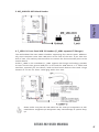
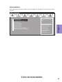
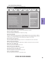
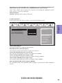
Chipset OverClocking Configuration
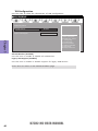
Scroll to this item to view the following screen:
Main
Advanced
Chipset
M.I.B III
Boot
Security
Exit
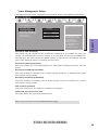
Memory Multiplier Configuration
Automatic
Memory Timing Configuration
CAS# Latency (tCL)
Row Precharge Time (tRP)
RAS# to CAS# Delay (tRCD)
RAS# Active Time (tRAS)
Write Recovery Time (tWR)
Row Refresh Cycle Time (tRFC)
Write to Read Delay (tWTR)
Active to Active Delay (tRRD)
Read CAS# Precharge (tRTP)
Four Active Window Delay (tFAW)
9
9
9
24
10
74
5
7
5
20
: Select Screen
/Click: Select Item
Enter/Dbl Click : Select
+/- : Change Opt.
F1: General Help
F2: Previous Values
F3: Optimized Defaults
F4: Save & Exit
ESC/Right Click: Exit
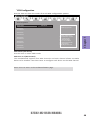
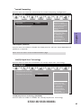
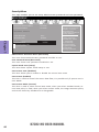
Intel Graphics Configuration
Graphics Core Ratio Limit
Graphics Voltage (1/256 V)
The selection of
Performance Memory
Profiles which impacts
memory sizing behavior.
Chapter 3
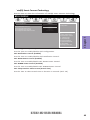
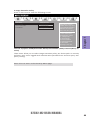
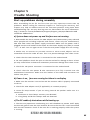
Performance Memory Profiles
22
0
Performance Memory Profiles (Automatic)
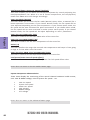
This item enables you to set the Performance Memory Profile.
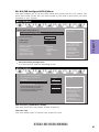
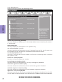
Memory Timing Configuration
This item shows the information of Memory Timing.
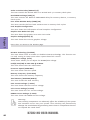
CAS Latency (tCL) (9)
This item determines the operation of DDR SDRAM memory CAS (column address
strobe). It is recommended that you leave this item at the default value. The 2T
setting requires faster memory that specifically supports this mode.
Row Precharge Time (tRP) (9)
This item specifies Row precharge to Active or Auto-Refresh of the same bank.
RAS# to CAS# Delay (tRCD) (9)
This item specifies the RAS# to CAS# delay to Rd/Wr command to the same bank.
RAS# Active Time (tRAS) (24)
This item specifies the RAS# active time.
Write Recovery Time (tWR) (10)
This item specifies the write recovery time.
Row Refresh Cycle Time (tRFC) (74)
This item specifies the row refresh cycle time.
Write to Read Delay (twTR) (5)
This item specifies the write to read delay time.
B75H2-M2 USER MANUAL
49