1
®
43B
Power Quality Analyzer
Service Manual
4822 872 05385
December 2001
© 2001 Fluke Corporation, All rights reserved. Printed in the Netherlands
All product names are trademarks of their respective companies.
SERVICE CENTERS
To locate an authorized service center, visit us on the World Wide Web:
http://www.fluke.com
or call Fluke using any of the phone numbers listed below:
+1-888-993-5853 in U.S.A. and Canada
+31-402-678-200 in Europe
+1-425-446-5500 from other countries
Table of Contents
Chapter
1
Title
Page
Safety Instructions ............................................................................. 1-1
1.1 Introduction.................................................................................................
1.2 Safety Precautions.......................................................................................
1.3 Caution and Warning Statements................................................................
1.4 Symbols.......................................................................................................
1.5 Impaired Safety ...........................................................................................
1.6 General Safety Information.........................................................................
2
Characteristics ................................................................................... 2-1
2.1 Introduction.................................................................................................
2.2 Safety Specifications...................................................................................
2.3 Function Specifications...............................................................................
2.3.1 Electrical functions ..............................................................................
2.3.2 Scope....................................................................................................
2.3.3 Meter....................................................................................................
2.3.4 Record..................................................................................................
2.4 Miscellaneous .............................................................................................
2.5 Current Probe ..............................................................................................
2.6 Environmental Conditions ..........................................................................
2.7 Electromagnetic Immunity..........................................................................
3
1-3
1-3
1-3
1-3
1-4
1-4
2-3
2-3
2-4
2-4
2-5
2-7
2-7
2-8
2-8
2-9
2-10
Circuit Descriptions ........................................................................... 3-1
3.1 Introduction.................................................................................................
3.2 Block Diagram ............................................................................................
3.2.1 Input 1 - Input 2 Measurement Circuits...............................................
3.2.2 Trigger Circuit .....................................................................................
3.2.3 Digital Circuit ......................................................................................
3.2.4 Power Circuit .......................................................................................
3.2.5 Start-up Sequence, Operating Modes ..................................................
3.3 Detailed Circuit Descriptions......................................................................
3.3.1 Power Circuit .......................................................................................
3.3.2 Input 1 - Input 2 Measurement Circuits...............................................
3.3.3 Trigger Circuit .....................................................................................
i
3-3
3-3
3-3
3-5
3-5
3-6
3-7
3-9
3-9
3-14
3-20
43B
Service Manual
3.3.4 Digital Circuit ...................................................................................... 3-24
4
Performance Verification ................................................................... 4-1
4.1 Introduction.................................................................................................
4.2 Equipment Required For Verification ........................................................
4.3 How To Verify ............................................................................................
4.4 Display and Backlight Test .........................................................................
4.5 Input 1 and Input 2 Tests in the SCOPE MODE. .......................................
4.5.1 Input 1 Trigger Sensitivity Test...........................................................
4.5.2 Input 1 Frequency Response Upper Transition Point Test..................
4.5.3 Input 1 Frequency Measurement Accuracy Test .................................
4.5.4 Input 2 Frequency Measurement Accuracy Test .................................
4.5.5 Input 2 Trigger Level and Trigger Slope Test .....................................
4.5.6 Input 2 Trigger sensitivity Test............................................................
4.5.7 Input 1 Trigger Level and Trigger Slope Test .....................................
4.5.8 Input 1 and 2 DC Voltage Accuracy Test............................................
4.5.9 Input 1 and 2 AC Voltage Accuracy Test............................................
4.5.10 Input 1 and 2 AC Input Coupling Test ..............................................
4.5.11 Input 1 and 2 Volts Peak Measurements Test ...................................
4.5.12 Input 1 and 2 Phase Measurements Test............................................
4.5.13 Input 1 and 2 High Voltage AC & DC Accuracy Test ......................
4.6 Ohms/Continuity/Capacitance. ...................................................................
4.6.1 Resistance Measurements Test............................................................
4.6.2 Diode Test Function Test ....................................................................
4.6.3 Continuity Function Test .....................................................................
4.6.4 Capacitance Measurements Test .........................................................
4.7 Inrush Current. ............................................................................................
4.8 Sags & Swells .............................................................................................
4.9 Harmonics. ..................................................................................................
4.10 VOLT/AMPS/HERTZ. .............................................................................
4.11 POWER.....................................................................................................
4.12 Transients..................................................................................................
5
Calibration Adjustment ...................................................................... 5-1
5.1 General ........................................................................................................
5.1.1 Introduction..........................................................................................
5.1.2 Calibration number and date................................................................
5.1.3 General Instructions.............................................................................
5.2 Equipment Required For Calibration..........................................................
5.3 Starting Calibration Adjustment .................................................................
5.4 Contrast Calibration Adjustment ................................................................
5.5 Warming Up & Pre-Calibration ..................................................................
5.6 Final Calibration .........................................................................................
5.6.1 HF Gain Input 1. ..................................................................................
5.6.2 Delta T Gain, Trigger Delay Time & Pulse Adjust Input 1.................
5.6.3 Gain DMM (Gain Volt) .......................................................................
5.6.4 Volt Zero..............................................................................................
5.6.5 Gain Ohm.............................................................................................
5.6.6 Capacitance Gain Low and High.........................................................
5.6.7 Capacitance Clamp & Zero..................................................................
5.6.8 Capacitance Gain .................................................................................
5.7 Save Calibration Data and Exit...................................................................
6
4-3
4-3
4-3
4-4
4-5
4-6
4-7
4-7
4-9
4-10
4-12
4-13
4-15
4-17
4-19
4-20
4-21
4-22
4-25
4-25
4-26
4-26
4-27
4-28
4-29
4-30
4-30
4-31
4-32
5-3
5-3
5-3
5-4
5-4
5-4
5-6
5-7
5-7
5-8
5-9
5-10
5-12
5-12
5-13
5-14
5-14
5-15
Disassembling .................................................................................... 6-1
ii
Contents (continued)
6.1. Introduction................................................................................................
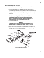
6.2. Disassembling Procedures .........................................................................
6.1.1 Required Tools ....................................................................................
6.2.2 Removing the Battery Pack .................................................................
6.2.3 Removing the Bail ...............................................................................
6.2.4 Opening the Test Tool .........................................................................
6.2.5 Removing the Main PCA Unit.............................................................
6.2.6 Removing the Display Assembly.........................................................
6.2.7 Removing the Keypad and Keypad Foil..............................................
6.3 Disassembling the Main PCA Unit .............................................................
6.4 Reassembling the Main PCA Unit ..............................................................
6.5 Reassembling the Test Tool........................................................................
7
Corrective Maintenance ..................................................................... 7-1
7.1 Introduction.................................................................................................
7.2 Starting Fault Finding. ................................................................................
7.3 Charger Circuit............................................................................................
7.4 Starting with a Dead Test Tool ...................................................................
7.4.1 Test Tool Completely Dead.................................................................
7.4.2 Test Tool Software Does not Run. ......................................................
7.4.3 Software Runs, Test Tool not Operative .............................................
7.5 Miscellaneous Functions.............................................................................
7.5.1 Display and Back Light .......................................................................
7.5.2 Fly Back Converter..............................................................................
7.5.3 Slow ADC............................................................................................
7.5.4 Keyboard..............................................................................................
7.5.5 Optical Port (Serial RS232 Interface)..................................................
7.5.6 Input Channel 1 and 2 Voltage Measurements....................................
7.5.7 Ohms and Capacitance Measurements ................................................
7.5.8 Trigger Functions.................................................................................
7.5.9 Reference Voltages..............................................................................
7.5.10 Buzzer Circuit ....................................................................................
7.5.11 Reset ROM Line (ROMRST)............................................................
7.5.12 RAM Test ..........................................................................................
7.5.13 Power ON/OFF ..................................................................................
7.5.14 PWM Circuit......................................................................................
7.5.15 Randomize Circuit .............................................................................
8
7-3
7-4
7-4
7-6
7-6
7-7
7-7
7-7
7-7
7-8
7-9
7-10
7-11
7-11
7-12
7-13
7-14
7-14
7-14
7-14
7-15
7-15
7-15
List of Replaceable Parts................................................................... 8-1
8.1 Introduction.................................................................................................
8.2 How to Obtain Parts....................................................................................
8.3 Final Assembly Parts ..................................................................................
8.4 Main PCA Unit Parts ..................................................................................
8.5 Main PCA Parts ..........................................................................................
8.6 Accessory Replacement Parts .....................................................................
9
6-3
6-3
6-3
6-3
6-3
6-3
6-5
6-6
6-6
6-6
6-8
6-8
8-3
8-3
8-4
8-6
8-7
8-23
Circuit Diagrams................................................................................. 9-1
9.1 Introduction................................................................................................. 9-3
9.2 Schematic Diagrams.................................................................................... 9-3
10
Modifications ...................................................................................... 10-1
10.1 Software modifications ............................................................................. 10-3
10.2 Hardware modifications............................................................................ 10-3
iii
List of Tables
Table
1-1.
2-1.
2-2.
2-3.
3-1.
3-2.
3-3.
3-4.
3-5.
3-6.
4-1.
4-2.
4-3.
4-4.
4-5.
4-6.
4-7.
4-8.
4-9.
4-10.
4-11.
5-1.
5-2.
5-3.
5-4.
7-1.
8-1.
8-2.
8-3.
9-1.
9-2.
Title
Page
Symbols .................................................................................................................
No Visible Disturbance .........................................................................................
Disturbance < 1 % .................................................................................................
Disturbance < 10 % ...............................................................................................
Fluke 43B Main Blocks.........................................................................................
Fluke 43B Operating Modes .................................................................................
Input 1 Voltage Ranges And Trace Sensitivity .....................................................
Ohms Ranges, Trace Sensitivity, and Current ......................................................
Capacitance Ranges, Current, and Pulse Width....................................................
D-ASIC PWM Signals...........................................................................................
Input 1 Frequency Measurement Accuracy Test...................................................
Volts DC Measurement Verification Points .........................................................
Volts AC Measurement Verification Points .........................................................
Input 1 and 2 AC Input Coupling Verification Points...........................................
Volts Peak Measurement Verification Points .......................................................
Phase Measurement Verification Points ...............................................................
V DC and V AC High Voltage Verification Tests................................................
Resistance Measurement Verification Points........................................................
Capacitance Measurement Verification Points .....................................................
Volts/AMPS/HERZ verification points ................................................................
Power Measurement Verification points...............................................................
HF Gain Calibration Points Fast ...........................................................................
HF Gain Calibration Points Slow..........................................................................
Volt Gain Calibration Points <300V.....................................................................
Ohm Gain Calibration Points ................................................................................
Starting Fault Finding............................................................................................
Final Assembly Parts.............................................................................................
Main PCA Unit......................................................................................................
Main PCA..............................................................................................................
Parts Location Main PCA Side 1 ..........................................................................
Parts Location Main PCA Side 2 ..........................................................................
v
1-3
2-10
2-10
2-10
3-3
3-8
3-17
3-18
3-19
3-27
4-8
4-17
4-19
4-20
4-21
4-22
4-25
4-26
4-27
4-31
4-31
5-9
5-9
5-11
5-13
7-4
8-4
8-6
8-7
9-4
9-5
List of Figures
Figure
2-1.
3-1.
3-2.
3-3.
3-4.
3-5.
3-6.
3-7.
3-8.
3-9.
3-10.
3-11.
3-12.
3-13.
4-1.
4-2.
4-3.
4-4.
4-5.
4-6.
4-7.
4-8.
4-9.
4-10.
4-11.
4-12.
5-1.
5-2.
5-3.
5-4.
5-5.
5-6.
5-7.
5-8.
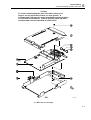
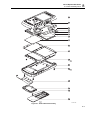
6-1.
Title
Page
Max. Input Voltage vs. Frequency ........................................................................
Fluke 43 Block Diagram........................................................................................
Fluke 43 Start-up Sequence, Operating Modes.....................................................
Power Supply Block Diagram ...............................................................................
CHAGATE Control Voltage .................................................................................
Fly-Back Converter Current and Control Voltage ................................................
Fly-Back Converter Block Diagram......................................................................
Back Light Converter Voltages .............................................................................
C-ASIC Block Diagram.........................................................................................
Capacitance Measurement.....................................................................................
T-ASIC Trigger Section Block Diagram...............................................................
Random Repetitive Sampling Mode .....................................................................
Reference Voltage Section ....................................................................................
LCD Control..........................................................................................................
Display Pixel Test Pattern .....................................................................................
Test Tool Input 1 to 5500A Scope Output 50Ω ....................................................
Test Tool Input 2 to 5500A NORMAL output......................................................
Test Tool Input 1 to 5500A Normal Output..........................................................
Test Tool Input 1-2 to 5500A Normal Output.......................................................
Test Tool Input 1-2 to 5500A Normal Output for >300V.....................................
Test Tool Input 1 to 5500A Normal Output 4-Wire .............................................
Test Tool Input 2 to 5500A NORMAL output......................................................
Test Tool Input 1 & 2 5500A Normal Output.......................................................
Bargraph Harmonics Volt .....................................................................................
Bargraph Harmonics Ampere................................................................................
Test Tool Input 1 to 5500A Normal Output..........................................................
Version & Calibration Screen ...............................................................................
Display Test Pattern ..............................................................................................
HF Gain Calibration Input Connections................................................................
5500A Scope Output to Input 1.............................................................................
Volt Gain Calibration Input Connections <300V .................................................
Volt Gain Calibration Input Connections 500V....................................................
Four-wire Ohms calibration connections ..............................................................
Capacitance Gain Calibration Input Connections .................................................
Fluke 43 Main Assembly.......................................................................................
vii
2-4
3-2
3-8
3-9
3-11
3-12
3-13
3-14
3-15
3-19
3-20
3-22
3-23
3-26
4-4
4-6
4-9
4-13
4-15
4-23
4-25
4-28
4-29
4-30
4-30
4-32
5-3
5-7
5-8
5-10
5-11
5-12
5-13
5-14
6-4
43B
Service Manual
6-2.
6-3.
6-4.
6-5.
7-1.
8-1.
8-2.
9-1.
9-2.
9-3.
9-4.
9-5.
9-6.
9-7.
9-8.
Flex Cable Connectors ..........................................................................................
Main PCA Unit Assembly.....................................................................................
Mounting the display shielding bracket ................................................................
Battery pack installation........................................................................................
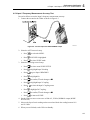
Operative Test Tool without Case.........................................................................
Fluke 43 Final Assembly.......................................................................................
Main PCA Unit......................................................................................................
Circuit Diagram 1, Channel 1 Circuit ...................................................................
Circuit Diagram 2, Channel 2 Circuit ...................................................................
Circuit Diagram 3, Trigger Circuit........................................................................
Circuit Diagram 4, Digital Circuit.........................................................................
Circuit Diagram 4 (cont), Digital Circuit Keyboard .............................................
Circuit Diagram 5, Power Circuit..........................................................................
Main PCA side 1, PCB version 3 ..........................................................................
Main PCA side 2, PCB version 3 ..........................................................................
viii
6-5
6-7
6-9
6-9
7-3
8-5
8-6
9-7
9-8
9-9
9-10
9-11
9-12
9-13
9-14
Chapter 1
Safety Instructions
Title
1.1 Introduction.................................................................................................
1.2 Safety Precautions.......................................................................................
1.3 Caution and Warning Statements................................................................
1.4 Symbols.......................................................................................................
1.5 Impaired Safety ...........................................................................................
1.6 General Safety Information.........................................................................
Page
1-3
1-3
1-3
1-3
1-4
1-4
1-1
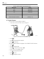
Safety Instructions
1.1 Introduction
1
1.1 Introduction
Read these pages carefully before beginning to install and use the instrument.
The following paragraphs contain information, cautions and warnings which must be
followed to ensure safe operation and to keep the instrument in a safe condition.
Warning
Servicing described in this manual is to be done only by
qualified service personnel. To avoid electrical shock, do not
service the instrument unless you are qualified to do so.
1.2 Safety Precautions
For the correct and safe use of this instrument it is essential that both operating and
service personnel follow generally accepted safety procedures in addition to the safety
precautions specified in this manual. Specific warning and caution statements, where
they apply, will be found throughout the manual. Where necessary, the warning and
caution statements and/or symbols are marked on the instrument.
1.3 Caution and Warning Statements
Caution
Used to indicate correct operating or maintenance procedures
to prevent damage to or destruction of the equipment or other
property.
Warning
Calls attention to a potential danger that requires correct
procedures or practices to prevent personal injury.
1.4 Symbols
Table 1-1 shows the symbols used on the test tool or in this manual.
Table 1-1. Symbols
Read the safety information in the Users
Manual
DOUBLE INSULATION (Protection Class)
Equal potential inputs, connected
internally
Static sensitive components
(black/yellow).
Live voltage
Recycling information
Earth
Disposal information
Conformité Européenne
1-3
43B
Service Manual
1.5 Impaired Safety
Whenever it is likely that safety has been impaired, the instrument must be turned off
and disconnected from line power. The matter should then be referred to qualified
technicians. Safety is likely to be impaired if, for example, the instrument fails to
perform the intended measurements or shows visible damage.
1.6 General Safety Information
Warning
Removing the instrument covers or removing parts, except
those to which access can be gained by hand, is likely to
expose live parts and accessible terminals which can be
dangerous to life.
The instrument shall be disconnected from all voltage sources before it is opened.
Capacitors inside the instrument can hold their charge even if the instrument has been
separated from all voltage sources.
Components which are important for the safety of the instrument may only be replaced
by components obtained through your local FLUKE organization. These parts are
indicated with an asterisk (*) in the List of Replaceable Parts, Chapter 8.
1-4
Chapter 2
Characteristics
Title
2.1 Introduction.................................................................................................
2.2 Safety Specifications...................................................................................
2.3 Function Specifications...............................................................................
2.3.1 Electrical functions ..............................................................................
2.3.2 Scope....................................................................................................
2.3.3 Meter....................................................................................................
2.3.4 Record..................................................................................................
2.4 Miscellaneous .............................................................................................
2.5 Current Probe ..............................................................................................
2.6 Environmental Conditions ..........................................................................
2.7 Electromagnetic Immunity..........................................................................
Page
2-3
2-3
2-4
2-4
2-5
2-7
2-7
2-8
2-8
2-9
2-10
2-1
Characteristics
2.1 Introduction
2
2.1 Introduction
Safety Characteristics
The Fluke 43B has been designed and tested in accordance with Standards ANSI/ISA
S82.01-1994, EN 61010.1 (1993) (IEC 1010-1), CAN/CSA-C22.2 No.1010.1-92
(including approval), UL3111-1 (including approval) Safety Requirements for
Electrical Equipment for Measurement, Control, and Laboratory Use.
This manual contains information and warnings that must be followed by the user to
ensure safe operation and to keep the instrument in a safe condition. Use of this
equipment in a manner not specified by the manufacturer may impair protection
provided by the equipment.
Performance Characteristics
FLUKE guarantees the properties expressed in numerical values with the stated
tolerance. Specified non-tolerance numerical values indicate those that could be
nominally expected from the mean of a range of identical ScopeMeter test tools.
Environmental Data
The environmental data mentioned in this manual are based on the results of the
manufacturer’s verification procedures.
2.2 Safety Specifications
Safety Characteristics
Designed and tested for measurements on 600 Vrms Category III, Pollution Degree 2
in accordance with:
•
•
•
•
EN 61010.1 (1993) (IEC 1010-1)
ANSI/ISA S82.01-1994
CAN/CSA-C22.2 No.1010.1-92 (including approval)
UL3111-1 (including approval)
Installation Category III refers to distribution level and fixed installation circuits
inside a building.
Maximum input voltage Input 1 and 2
Direct on inputs or with test leads TL24 ............................................... (see Figure 2-1)
0 to 66 kHz ................................................................................................. 600 Vrms
> 66 kHz ....................................................................................... derating to 5 Vrms
With Shielded Banana-to-BNC Adapter Plug BB120 ...........................(see Figure 2-1)
0 to 400 kHz ............................................................................................... 300 Vrms
> 400 kHz ..................................................................................... derating to 5 Vrms
2-3
43B
Service Manual
ST8571
Figure 2-1. Max. Input Voltage vs. Frequency
Maximum floating voltage
From any terminal to ground
0 to 400 Hz ................................................................................................. 600 Vrms
2.3 Function Specifications
The accuracy of all measurements is within ± (% of reading + number of counts) from
18 °C to 28 °C. For all specifications, probe specifications must be added.
2.3.1 Electrical functions
Specifications are valid for signals with a fundamental between 40 and 70 Hz.
Minimum input voltage ................................................................................. 4 V peak-peak
Minimum input current............................................................... 10 A peak-peak (1 mV/A)
Input bandwidth ................................................ DC to 15 kHz (unless specified otherwise)
Volts / Amps / Hertz
Readings ..................................................................... Vrms (ac+dc), Arms (ac+dc), Hz
Voltage ranges (auto) ....................................................... 5 V; 50 V; 500 V; 1250 V
minimum step.............................................................. 1 mV; 10 mV; 100 mV; 1 V
±(1 % + 10 counts)
Current ranges (auto)..................................................50.00 A to 500.0 kA, 1250 kA
minimum step........................................................10 mA; 0.1 A; 1 A; 100 A, 1 kA
±(1 % + 10 counts)
Frequency range ......................................................................... 10.0 Hz to 15.0 kHz
40.0 to 70.0 Hz......................................................................... ±(0.5 % + 2 counts)
resolution.................................................................... 0.1 Hz; 1 Hz; 10 Hz; 100 Hz
CF Crest Factor range....................................................1.0 to 10.0 ±(5 % + 1 count)
Power (1 and 3 phase / 3 conductor / balanced loads)
Readings ..........................................................................Watt, VA, VAR, PF, DPF, Hz
Watt, VA, VAR ranges (auto) ..................... 250 W to 250 MW, 625 MW, 1.56 GW
when selected: total ( %r):........................................................ ±(2 % + 6 counts)
when selected: fundamental ( %f):........................................... ±(4 % + 4 counts)
DPF.......................................................................................................... 0.00 to 1.00
0.00 to 0.25........................................................................................not specified
0.25 to 0.90.................................................................................................. ± 0.04
0.90 to 1.00.................................................................................................. ± 0.03
2-4
Characteristics
2.3 Function Specifications
2
PF............................................................................................................. 0.00 to 1.00
± 0.04
Frequency range ......................................................................... 10.0 Hz to 15.0 kHz
40.0 to 70.0 Hz ...................................................................... ±(0.5 % + 2 counts)
Harmonics
Number of harmonics ................................................................DC..21, DC..33, DC..51
Readings / Cursor readings
Vrms....fund. ±(3 % + 2 counts) ..... 31st ±(5 % + 3 counts)..... 51st ±(15 % + 5 counts)
Irms......fund. ±(3 % + 2 counts) ..... 31st ±(5 % + 3 counts)..... 51st ±(15 % + 5 counts)
Watt.....fund. ±(5 % + 10 counts) ... 31st ±(10 % + 10 counts) 51st ±(30 % + 5 counts)
Frequency of fundamental .......................................................................... ± 0.25 Hz
Phase........................................................................................fund. ±3° ... 51st ± 15°
K-factor (in Amp and Watt) ............................................................................± 10 %
Sags & Swells
Recording times (selectable) .............................. 4 minutes to 8 days, endless (16 days)
Readings / Cursor Readings
Vrms actual, Arms actual (cycle by cycle calculation) ............... ±(2 % + 10 counts)
Vrms max, Arms max (idem at cursor) ....................................... ±(2 % + 12 counts)
Vrms average, Arms average (only at cursor) ............................. ±(2 % + 10 counts)
Vrms min, Arms min (idem at cursor) ........................................ ±(2 % + 12 counts)
Transients
Detection of voltage transients ............................................................................ > 40 ns
Useful input bandwidth input 1 (with test leads TL24)..............................DC to 1 MHz
Reference signal ............................................................................................... Vrms, Hz
After START, the Vrms and frequency of the signal are measured.
From these data a pure sine wave is calculated.
Detection when transients exceed specified voltage level (selectable)
Voltage levels ................................... 20 %, 50 %, 100 %, 200 % of reference signal
Number of transient memories (temporary) ................................................................ 40
Cursor reading
Vpeak min, Vpeak max at cursor ..................................................± 5 % of full scale
Inrush
Graphic display
Current ranges (selectable).................. 1 A, 5 A, 10 A, 50 A, 100 A, 500 A, 1000 A
Inrush times (selectable)........................................... 1 s, 5 s, 10 s, 50 s, 100 s, 5 min
Cursor readings
A peak max at cursor 1 ..................................................................± 5 % of full scale
A peak max at cursor 2 ..................................................................± 5 % of full scale
Time between cursors.................................................................. ±(0.2 % + 2 pixels)
2.3.2 Scope
Input Impedance
Input 1............................................ 1 MΩ // 12 pF (± 2 pF). With BB120: 20 pF ± 3 pF
Input 2............................................ 1 MΩ // 10 pF (± 2 pF). With BB120: 18 pF ± 3 pF
Horizontal
Time base modes (selectable)......................................................... Normal, Single, Roll
Ranges (selectable within modes)
In Normal............................................................................................ 5 s to 20 ns/div
In Single shot ........................................................................................5 s to 1 µs/div
In Roll mode ......................................................................................... 60 s to 1 s/div
Time base error................................................................................< ±(0.4 % + 1 pixel)
2-5
43B
Service Manual
Maximum sampling rate
10 ms to 60 s....................................................................................................5 MS/s
20 ns to 10 ms................................................................................................25 MS/s
Trigger source (auto, ½ auto, manual)................................................. Input 1 or Input 2
Trigger
Mode .........................................................................................................auto triggering
Sources........................................ Input 1, Input 2, Automatic (not manually selectable)
Error for frequencies < 1 MHz
Voltage Level ............................................................................................... ± 0.5 div
at positive slope the top of the trigger symbol and at negative trigger the bottom of
the trigger symbol is the trigger point.
Time Delay Real Time sampling...............................................................± 1 sample
Time Delay Quasi Random sampling............................................................. ± 10 ns
Sensitivity input 1
@ 40 MHz ....................................................................................................... ≥ 4 div
@ 25 MHz .................................................................................................... ≥ 1.5 div
@ DC - 5 MHz................................................................................≥ 0.5 div or 5 mV
Sensitivity input 2
@ DC – 20 kHz ............................................................................................ ≥ 0.5 div
Slope Selection ....................................................................................Positive, negative
Level Control
Range Manual control .............................................> ± 4 div, within dynamic range
Delay ( horizontal move ) .......... -10 div - 0 div, used for horizontal move functionality
Vertical
Voltage ranges ............................................................................. 5 mV/div to 500 V/div
Trace accuracy................................................................................ ±(1 % + 2 pixels)
Bandwidth input 1 (voltage)
excluding test leads or probes ................................................ DC to 20 MHz (-3 dB)
with test leads TL24 ................................................................. DC to 1 MHz (-3 dB)
with 10:1 probe VPS100-R (optional).................................... DC to 20 MHz (-3 dB)
with shielded test leads STL120 (optional)......................... DC to 12.5 MHz (-3 dB)
DC to 20 MHz (-6 dB)
Lower transition point (ac coupling) .................................................... 10 Hz (-3 dB)
Bandwidth input 2 (current)
with Banana-to-BNC adapter ............................................................... DC to 15 kHz
Lower transition point (ac coupling) .................................................... 10 Hz (-3 dB)
Scope readings
The accuracy of all scope readings is valid from 18 °C to 28 °C with relative humidity
up to 90 % for a period of one year after calibration. Add 0.1 x (the specified
accuracy) for each °C below 18 °C or above 28 °C. More than one waveform period
must be visible on the screen.
V dc, A dc ........................................................................................ ±(0.5 % + 5 counts)
V ac and V ac+dc (True RMS) input 1
DC to 60 Hz................................................................................. ±(1 % + 10 counts)
60 Hz to 20 kHz........................................................................ ±(2.5 % + 15 counts)
20 kHz to 1 MHz ......................................................................... ±(5 % + 20 counts)
1 MHz to 5 MHz........................................................................ ±(10 % + 25 counts)
5 MHz to 20 MHz...................................................................... ±(30 % + 25 counts)
A ac and A ac+dc (True RMS) input 2
DC to 60 Hz................................................................................. ±(1 % + 10 counts)
60 Hz to 15 kHz......................................................................... ±(30 % + 25 counts)
Frequency (Hz), Pulse width, Duty cycle (2.0 % to 98.0 %)
2-6
Characteristics
2.3 Function Specifications
2
1 Hz to 1 MHz ............................................................................ ±(0.5 % + 2 counts)
1 MHz to 10 MHz.......................................................................... ±(1 % + 2 counts)
10 MHz to 30 MHz..................................................................... ±(2.5 % + 2 counts)
Phase (Input 1 to Input 2)
Up to 60 Hz............................................................................................................±2°
60 Hz to 400 Hz.....................................................................................................±5°
Peak voltage
Peak max, Peak min.......................................................................± 5 % of full scale
Peak-peak.....................................................................................± 10 % of full scale
Crest
Range ......................................................................................................... 1.0 to 10.0
±(5 % + 1 count)
2.3.3 Meter
Ohm
Ranges.........................................................................500.0 Ω to 5.000 MΩ, 30.00 MΩ
±(0.6 % + 5 counts)
Max. Measurement Current..................................................................................0.5 mA
Measurement Voltage at open circuit..................................................................... < 4 V
Diode
Accuracy.............................................................................................. ±(2 % +5 counts)
Max. Measurement Current..................................................................................0.5 mA
Measurement Voltage at open circuit..................................................................... < 4 V
Continuity
Beep ......................................................................................................... < 30 Ω (± 5 Ω)
Measurement Current ...........................................................................................0.5 mA
Detection of shorts.................................................................................................> 1 ms
Capacitance
Ranges.............................................................................................50.00 nF to 500.0 µF
±(2 % +10 counts)
Max. Measurement Current..................................................................................0.5 mA
Temperature
Ranges (°C or °F) ........................................-100.0 to +400.0 °C or -200.0 to +800.0 °F
±(0.5 % + 5 counts)
2.3.4 Record
Record times (selectable) ............................................... 4 min to 8 days, endless (16 days)
Number of readings ............................................................................1 or 2 simultaneously
Record is available for the functions:
• volts / amps / hertz
• power
• harmonics
• ohms / continuity / capacitance
• temperature
• scope
2-7
43B
Service Manual
2.4 Miscellaneous
Display
Useful screen area............................................................... 72 x 72 mm (2.83 x 2.83 in)
Resolution..............................................................................................240 x 240 pixels
Backlight...................................................................Cold Cathode Fluorescent (CCFL)
Power
External
Power Adapter ...............................................................................................PM8907
Input Voltage .........................................................................................10 to 21 V dc
Power ........................................................................................................5 W typical
Internal
Rechargeable Ni-Cd battery pack.....................................................................BP120
Voltage range.............................................................................................4 to 6 V dc
Operating Time............................................................................................... 4 hours
Charging Time.................................................................4 hours with Fluke 43B off
12 hours with Fluke 43B on
Refresh cycle ......................................................................................... 8 to 14 hours
Memory
Number of screen memories ........................................................................................ 20
Number of transient memories (temporary) ................................................................ 40
Mechanical
Height x width x depth ......................................... 232 x 115 x 50 mm (9.1 x 4.5 x 2 in)
Weight (including battery pack) ...............................................................1.1 kg (2.5 lb.)
Interface....................................................................................... RS232, optically isolated
Supported Printers ........................HP Deskjet®, Laserjet®, PostScript and Epson FX80
Serial via PM9080 (optically isolated RS232 Adapter/Cable).
Parallel via PAC91 (optically isolated Print Adapter Cable, optional).
To PC ........................................................................... Dump and load settings and data
Serial via PM9080 (optically isolated RS232 adapter/cable),
using SW43W (FlukeView® Power Quality Analyzer software).
2.5 Current Probe
Safety Characteristics
Designed for measurements on 600 Vrms Category III. Protection class II, double or
reinforced insulation requirements in accordance with:
• IEC 1010-1
• ANSI/ISA S82
• CSA-C22.2 No.1010.1-92
• UL1244
Electrical Specifications
Current range .........................................................................................1 A to 500 Arms
AC current over range limit..............................................................................700 Arms
Maximum 10 minutes, followed by removal from current carrying conductor
for 30 minutes.
Output Signal ............................................................................................. 1 mV ac/A ac
2-8
Characteristics
2.6 Environmental Conditions
2
Accuracy
5 to 10 Hz
1 to 500 A ............................................................................................-3 dB typically
10 to 20 Hz
1 to 300 A ..........................................................................................................± 5 %
300 to 400 A ....................................................................................................± 15 %
400 to 500 A ....................................................................................................± 25 %
20 to 45 Hz
1 to 500 A ..........................................................................................................± 5 %
45 to 65 Hz
1 to 20 A .............................................................................. ±5 % of reading + 0.3 A
20 to 100 A ........................................................................................±5 % of reading
± 3 ° phase shift
100 to 500 A ......................................................................................±2 % of reading
± 5 ° phase shift
65 Hz to 3 kHz
1 to 50 A ............................................................................................. ±(5 % + 0.4 A)
50 to 500 A ........................................................................................................± 5 %
Influence of temperature on accuracy ...................................<0.15 % per 10 °C (18 °F)
Altitude
During operation.................................................................................2.0 km (6560 feet)
While stored......................................................................................12 km (40 000 feet)
2.6 Environmental Conditions
Environmental ..................................................... MIL 28800E, Type 3, Class III, Style B
Temperature
During operation...................................................................... 0 to 50 °C (32 to 122 °F)
While stored...........................................................................-20 to 60 °C (-4 to 140 °F)
Humidity
During operation:
0 to 10 °C (32 to 50 °F) ................................................................... non-condensing
10 to 30 °C (50 to 86 °F) .........................................................................95 % ± 5 %
30 to 40 °C (86 to 104 °F) ........................................................................75 % ± 5 %
40 to 50 °C (104 to 122 °F) ......................................................................45 % ± 5 %
While stored:
-20 to 60 °C (-4 to 140 °F)................................................................. non-condensing
Altitude
During operation..............................................................................4.5 km (15 000 feet)
The maximum input and floating voltage is 600 Vrms up to 2 km.
Linearly derating from 600 down to 400 Vrms between 2 km to 4.5 km.
While stored......................................................................................12 km (40 000 feet)
Vibration.................................................................................................................max. 3 g
Shock.....................................................................................................................max. 30 g
Electromagnetic Compatibility (EMC)
Emission ............................................... EN 50081-1 (1992): EN55022 and EN60555-2
Immunity.................................................... EN 50082-2 (1992): IEC1000-4-2, -3, -4, -5
(See also Tables 2-1 to 2-3)
Enclosure Protection ............................................................................. IP51, ref.: IEC529
2-9
43B
Service Manual
2.7 Electromagnetic Immunity
The Fluke 43B, including standard accessories, conforms with the EEC directive 89/336
for EMC immunity, as defined by IEC1000-4-3, with the addition of the following tables.
Disturbance with test leads TL24 or Current Clamp 80i-500s
• Volts / amps / hertz
• Resistance, Capacitance
• Power
• Harmonics
Table 2-1. No Visible Disturbance
No visible disturbance
E = 3 V/m
E = 10 V/m
Frequency: 10 kHz - 27 MHz
(-)
(-)
Frequency: 27 MHz - 1 GHz
(-)
(-)
(-): no visible disturbance
Disturbance with test leads TL24 in scope mode
• V ac+dc (True RMS)
Table 2-2. Disturbance < 1 %
Disturbance less than 1 %
of full scale
E = 3 V/m
E = 10 V/m
Frequency: 10 kHz - 27 MHz
2 V/div - 500 V/div
10 V/div - 500 V/div
Frequency: 27 MHz - 200 MHz
500 mV/div - 500V/div
2 V/div - 500 V/div
Frequency: 200 MHz - 1 GHz
(-)
5 mV/div - 500 V/div
(-): no visible disturbance
Table 2-3. Disturbance < 10 %
Disturbance less than 10 %
of full scale
E = 3 V/m
E = 10 V/m
Frequency: 10 kHz - 27 MHz
1 V/div
5 V/div
Frequency: 27 MHz - 200 MHz
200 mV/div
1 V/div
Frequency: 200 MHz - 1 GHz
(-)
(-)
(-): no visible disturbance
Ranges not specified in Tables 2 and 3 may have a disturbance of more than 10 % of full
scale.
2-10
Chapter 3
Circuit Descriptions
Title
3.1 Introduction.................................................................................................
3.2 Block Diagram ............................................................................................
3.2.1 Input 1 - Input 2 Measurement Circuits...............................................
3.2.2 Trigger Circuit .....................................................................................
3.2.3 Digital Circuit ......................................................................................
3.2.4 Power Circuit .......................................................................................
3.2.5 Start-up Sequence, Operating Modes ..................................................
3.3 Detailed Circuit Descriptions......................................................................
3.3.1 Power Circuit .......................................................................................
3.3.2 Input 1 - Input 2 Measurement Circuits...............................................
3.3.3 Trigger Circuit .....................................................................................
3.3.4 Digital Circuit ......................................................................................
Page
3-3
3-3
3-3
3-5
3-5
3-6
3-7
3-9
3-9
3-15
3-20
3-24
3-1
43B
Service Manual
ST7965.EPS
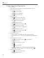
Figure 3-1. Fluke 43B Block Diagram
3-2
Circuit Descriptions
3.1 Introduction
3
3.1 Introduction
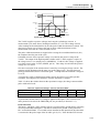
Section 3.2 describes the functional block diagram shown in Figure 3-1. It provides a
quick way to get familiar with the test tool basic build-up.
Section 3.3 describes the principle of operation of the test tool functions in detail, on the
basis of the circuit diagrams shown in Figures 9-1 to 9-5.
For all measurements, input signals are applied to the shielded input banana jackets.
Traces and readings are derived from the same input signal samples.
3.2 Block Diagram
In the block diagram Figure 3-1, the test tool is divided in five main blocks. Each block
represents a functional part, build up around an Application Specific Integrated Circuit
(ASIC). A detailed circuit diagram of each block is shown in Section 9.
Table 3-1 provides an overview of the blocks in which the test tool is broken down, the
main block function, the ASIC name, and the applicable circuit diagram.
Table 3-1. Fluke 43B Main Blocks
Block
INPUT 1
INPUT 2
TRIGGER
DIGITAL
POWER
Main Functions
Input 1 signal conditioning
Input 2 signal conditioning
Trigger selection and conditioning
Current source for resistance, capacitance,
continuity, and diode measurements
AC/DC input coupling and Ω/F relay control
Voltage reference source
Analog to Digital Conversion
Acquisition of ADC samples
Micro controller (µP-ROM-RAM)
Keyboard- and LCD control
Power supply, battery charger
LCD back light voltage converter
Optical interface input
ASIC
Circuit
Diagram
C(hannel)-ASIC OQ0258
C(hannel)-ASIC OQ0258
T(rigger)-ASIC OQ0257
Figure 9-1
Figure 9-2
Figure 9-3
D(igital)-ASIC MOT0002
Figure 9-4
P(ower)-ASIC OQ0256
Figure 9-5
All circuits, except the LCD unit and the KEYBOARD, are located on one Printed
Circuit Board (PCB), called the MAIN PCB.
The ASIC’s are referred to as C-ASIC (Channel ASIC), T-ASIC (Trigger ASIC), P-ASIC
(Power ASIC), and D-ASIC (Digital ASIC).
3.2.1 Input 1 - Input 2 Measurement Circuits
The basic input signal for the Input 1 and Input 2 circuits (hardware) is voltage. The
reading of Input 1 is in (milli)Volts. The reading of Input 2 is in Amperes. So the
voltage on Input 2 is assumed to be supplied by a current clamp. From the measured
voltage samples the readings are calculated by the instrument firmware. For example:
power readings are calculated from the Input 1 and Input 2 voltage samples.
3-3
43B
Service Manual
The Input 1 and Input 2 measurement circuits are partially identical. The differences are:
• Only Input 1 provides facilities for Ohms, Continuity, Diode, and Capacitance
measurements.
• The bandwidth of the Input 1 circuit is 20 MHz, the bandwidth of Input 2 is 15 kHz.
• Input 2 has an additional hum rejection circuit.
The circuit description below applies to the Input 1 and Input 2 circuit.
Input 1 and Input 2 measurement principle
An input voltage applied to Input 1 or Input 2 is supplied to the C-ASIC via the HF path
(Input 1 only) and the LF path. Depending on the actual measurement function the
Input-1 HF path in the C-ASIC is enabled or disabled. The HF DECade ATTenuator and
LF DECade ATTenuator are external components for the HF and LF path. The C-ASIC
converts (attenuates, amplifies) the input signal to a normalized output voltage
ADC-A/ADC-B, which is supplied to the Analog to Digital Converters (ADC-A and
ADC-B) on the DIGITAL part. The D-ASIC acquires the digital samples to build the
traces, and to calculate readings.
For the electrical functions the current Input 2 circuit is operating in low voltage ranges.
For example a current of 10A measured with a 1 mV/A current clamp generates 10 mV
(voltage range 10 mV/div). To minimize the influence of interference voltages, Input 2
has no HF path, and has an additional hum reject circuit.
The lowest Input 1 voltage range for electrical measurements is 4V/div, which is high in
comparison with the Input 2 range.
Ohms, Continuity, and Diode measurement function (Input 1 only)
The T-ASIC supplies a current via the Ω/F relays to the unknown resistance Rx or diode
connected to the Input 1 and the COM input jacket. The voltage drop across Rx or the
diode is measured according to the Input 1 measurement principle.
Capacitance measurement function (Input 1 only)
The T-ASIC supplies a current via the Ω/F relays to the unknown capacitance Cx,
connected to the Input 1 and the COM input jacket. Cx is charged and discharged by this
current. The C-ASIC converts the charging time and the discharging time into a pulse
width signal. This signal is supplied to the T-ASIC via the C-ASIC trigger output
TRIG-A. The T-ASIC shapes and levels the signal, and supplies the resulting pulse
width signal ALLTRIG to the D-ASIC. The D-ASIC counts the pulse width and
calculates the capacitance reading.
Scope measurement function
In the Scope measurements function the test tool shows the traces and readings derived
from the input signals. The Input 1 HF path is enabled, which results in a 20 MHz
bandwidth. The Input 2 bandwidth is 15 kHz.
Other measurement functions
Volts/Amperes/Hertz (LF), Power (LF), Harmonics (LF), Sags & Swells (LF),
Transients, Inrush Current (LF), and Temperature measurement results are calculated
from acquired input voltage samples. For functions with (LF), the HF path of Input 1 is
disabled, which results in a 15 kHz bandwidth for both Input channels.
Miscellaneous
Control of the C-ASIC, e.g. selecting the attenuation factor, is done by the D-ASIC via
the SDAT and SCLK serial communication lines.
3-4
Circuit Descriptions
3.2 Block Diagram
3
An offset compensation voltage and a trace position control voltage are provided by the
D-ASIC via the APWM bus.
The C-ASIC’s also provide conditioned input voltages on the TRIG-A/TRIG-B line. One
of these voltages will automatically be selected as trigger source by the T-ASIC.
3.2.2 Trigger Circuit
The T ASIC selects one of the possible trigger sources TRIG-A (Input 1) or TRIG-B
(Input 2). For triggering on transients the selected trigger source signal is processed via
the high pass Trigger Filter (TVOUT-TVSYNC lines). Two adjustable trigger levels are
supplied by the D-ASIC via the PWM FILTERS (TRIGLEV1 and TRIGLEV2 line).
Depending on the selected trigger conditions (- source, - level, - edge, - mode), the
T-ASIC generates the final trigger signal TRIGDT, which is supplied to the D-ASIC.
The TRIG-A input is also used for capacitance measurements (see Section 3.2.1).
The T-ASIC includes a constant current source for resistance and capacitance
measurements. The current is supplied via the GENOUT output and the Ω/F relays to
the unknown resistance Rx or capacitance Cx connected to Input 1. The SENSE signal
senses the voltage across Cx and controls a CLAMP circuit in the T-ASIC. This circuit
limits the voltage on Input 1 at capacitance measurements. The protection circuit
prevents the T-ASIC from being damaged by voltages supplied to the input during
resistance or capacitance measurements.
The T-ASIC contains opamps to derive reference voltages from a 1.23 V reference
source. The gain factors for these opamps are determined by resistors in the REF GAIN
circuit. The reference voltages are supplied to various circuits.
The T-ASIC also controls the Input 1/2 AC/DC input coupling relays, and the Ω/F relay.
Control data for the T-ASIC are provided by the D-ASIC via the SDAT and SCLK serial
communication lines.
3.2.3 Digital Circuit
The D-ASIC includes a micro processor, ADC sample acquisition logic, trigger logic,
display and keyboard control logic, I/O ports, and various other logic circuits.
The instrument software is stored in the 8M FlashROM; the 4M RAM is used for
temporary data storage.
For Voltage and Resistance measurements, the conditioned Input 1/2 voltages are
supplied to the ADC-A and ADC-B ADC. The voltages are sampled, and digitized by
the ADC’s. The output data of the ADC’s are acquired and processed by the D-ASIC.
For capacitance measurements the pulse width of the T-ASIC output signal ALLTRIG,
which is proportional to the unknown capacitance, is counted by the D-ASIC.
The DPWM-BUS (Digital Pulse Width Modulation) supplies square wave signals with a
variable duty cycle to the PWM FILTERS circuit (RC filters). The outgoing
APWM-BUS (Analog PWM) provides analog signals of which the amplitude is
controlled by the D-ASIC. These voltages are used to control e.g. the trace positions
(C-ASIC), the trigger levels (T-ASIC), and the battery charge current (P-ASIC).
In random sampling mode (Scope mode time base faster than 1 µs/d), a trace is built-up
from several acquisition cycles. During each acquisition, a number of trace samples are
placed as pixels in the LCD. The RANDOMIZE circuit takes care that the starting
moment of each acquisition cycle (trigger release signal HOLDOFF goes low) is random.
3-5
43B
Service Manual
This prevents that at each next acquisition the trace is sampled at the same time
positions, and that the displayed trace misses samples at some places on the LCD.
The D-ASIC supplies control data and display data to the LCD module. The LCD
module is connected to the main board via connector X453. It consists of the LCD, LCD
drivers, and a fluorescent back light lamp. As the module is not repairable, no detailed
description and diagrams are provided. The back light supply voltage is generated by the
back light converter on the POWER part.
The keys of the keyboard are arranged in a matrix. The D-ASIC drives the rows and
scans the matrix. The contact pads on the keyboard foil are connected to the main board
via connector X452. The ON-OFF key is not included in the matrix, but is sensed by a
logic circuit in the D-ASIC, that is active even when the test tool is turned off.
Via the PROBE-A and PROBE-B lines, connected to the Input 1 and Input 2 banana
shielding, the D-ASIC can detect if a probe is connected.
The D-ASIC sends commands to the C-ASICs and T-ASIC via the SCLK and SDAT
serial control lines, e.g. to select the required trigger source.
Various I/O lines are provided, e.g. to control the BUZZER and the Slow-ADC (via the
SADC bus).
3.2.4 Power Circuit
The test tool can be powered via the power adapter, or by the battery pack.
If the power adapter is connected, it powers the test tool and charges the battery via the
CHARGER-CONVERTER circuit. The battery charge current is sensed by sense
resistor Rs (signal IBAT). It is controlled by changing the output current of the
CHARGER-CONVERTER (control signal CHAGATE).
If no power adapter is connected, the battery pack supplies the VBAT voltage. The
VBAT voltage powers the P-ASIC, and is also supplied to the FLY BACK
CONVERTER (switched mode power supply).
If the test tool is turned on, the FLY BACK CONVERTER generates supply voltages for
various test tool circuits.
The +3V3GAR supply voltage powers the D-ASIC, RAM and ROM. If the test tool is
turned off, the battery supplies the +3V3GAR voltage via transistor V569. This
transistor is controlled by the P-ASIC. So when the test tool is turned off, the D-ASIC
can still control the battery charging process (CHARCURR signal), the real time clock,
the on/off key, and the serial RS232 interface (to turn the test tool on).
To monitor and control the battery charging process, the P-ASIC senses and buffers
battery signals as temperature (TEMP), voltage (BATVOLT), current (IBAT).
Via the SLOW ADC various analog signals can be measured by the D-ASIC. Involved
signals are: battery voltage (BATVOLT), battery type (IDENT), battery temperature
(TEMP), battery current (BATCUR) LCD temperature (LCDTEMP, from LCD unit),
and 3 test output pins of the C-ASIC’s, and the T-ASIC (DACTEST). The signals are
used for control and test purposes.
The BACK LIGHT CONVERTER generates the 400V ! supply voltage for the LCD
fluorescent back light lamp. If the lamp is defective a 1.5 kV voltage can be present for
0.2 second maximum. The brightness is controlled by the BACKBRIG signal supplied
by the D-ASIC.
Serial communication with a PC or printer is possible via the RS232 optically isolated
interface. The P-ASIC buffers the received data line (RXDA) and supplies the buffered
data (RXD) to the D-ASIC. The transmit data line TXD is directly connected to the
D-ASIC.
3-6
Circuit Descriptions
3.2 Block Diagram
3
3.2.5 Start-up Sequence, Operating Modes
The test tool sequences through the next steps when power is applied (see Figure 3-2):
1. The P-ASIC is directly powered by the battery or power adapter voltage VBAT.
Initially the Fly Back Converter is off, and the D-ASIC is powered by VBAT via
transistor V569 (+3V3GAR).
If the voltage +3V3GAR is below 3.05 V, the P-ASIC keeps its output signal
VGARVAL (supplied to the D-ASIC) low, and the D-ASIC will not start up. The
test tool is not working, and is in the Idle mode.
2. If the voltage +3V3GAR is above 3.05 V, the P-ASIC makes the line VGARVAL
high, and the D-ASIC will start up. The test tool is operative now. If it is powered
by batteries only, and not turned on, it is in the Off mode. In this mode the
D-ASIC is active: the real time clock runs, and the ON/OFF key is monitored to see
if the test tool will be turned on.
3. If the power adapter is connected (P-ASIC output MAINVAL high), and/or the
test tool is turned on, the embedded D-ASIC program, called mask software, starts
up. The mask software checks if valid instrument software is present in the Flash
ROM. If not, the test tool does not start up and the mask software continues running
until the test tool is turned off, or the power is removed. This is called the Mask
active mode. The mask active mode can also be entered by pressing the ^ and > key
when turning on the test tool.
If valid instrument software is present, one of the following modes becomes active:
Charge mode
The Charge mode is entered when the test tool is powered by the power adapter,
and is turned off. The FLY-BACK CONVERTER is off. The CHARGERCONVERTER charges the batteries (if installed).
Operational & Charge mode
The Operational & Charge mode is entered when the test tool is powered by the
power adapter, and is turned on. The FLY-BACK CONVERTER is on, the
CHARGER-CONVERTER supplies the primary current. If batteries are installed,
they will be charged. In this mode a battery refresh (see below) can be done.
Operational mode
The Operational mode is entered when the test tool is powered by batteries only,
and is turned on. The FLY-BACK CONVERTER is on, the batteries supply the
primary current. If the battery voltage (VBAT) drops below 4V when starting up the
fly back converter, the Off mode is entered.
Battery Refresh
Each 3 months the batteries need a deep discharge-full charge cycle, called a
“refresh”. This prevents battery capacity loss due to the memory effect. A refresh
cycle takes 16 hours maximum, depending on the battery status.
=>
=>
I=> INSTRUMENT
A refresh can be started via the keyboard (
SETUP
=> START BATTERY REFRESH
) if the test tool is on, and the
power adapter is connected. During a refresh, first the batteries are completely
discharged, and then they are completely charged again.
3-7
43B
Service Manual
VGARVAL=L
Idle mode
VGARVAL=H
Off mode
TURN ON or
MAINVAL=H
Flash ROM
NOT OK
Mask StartUp
OR
&
Flash ROM OK
Extern StartUp
Software
TURN ON & BATTVOLT > 4 & MAINVAL=L
Mask Active
mode
TURN OFF
& TURN ON
MAINVAL=L & (TURN OFF or BATTVOLT<4V)
TURN OFF&MAINVAL=H
TURN ON & MAINVAL=H
Operational
Mode
MAINVAL=H
MAINVAL=L
BATTVOLT < 4V
or
AutoShutDown
or
TURN OFF
Operational &
Charge Mode
TURN OFF
Charge Mode
TURN ON
MAINVAL=L
Battery refresh
Figure 3-2. Fluke 43B Start-up Sequence, Operating Modes
Table 3-2 shows an overview of the test tool operating modes.
Table 3-2. Fluke 43B Operating Modes
Mode
Idle mode
Off mode
Mask active mode
Charge mode
Operational &
Charge mode
Operational mode
3-8
Conditions
No power adapter and no battery
No power adapter connected, battery
installed, test tool off
No valid instrument software, or ^ and > key
pressed when turning on
Power adapter connected and test tool off
Power adapter connected and test tool on
No power adapter connected, battery
installed, and test tool on
Remark
no activity
P-ASIC & D-ASIC powered
(VBAT & +3V3GAR).
Mask software runs
Batteries will be charged
Test tool operational, and
batteries will be charged
Test tool operational, powered
by batteries
Circuit Descriptions
3.3 Detailed Circuit Descriptions
3
3.3 Detailed Circuit Descriptions
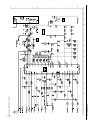
3.3.1 Power Circuit
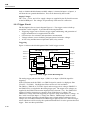
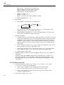
The description below refers to circuit diagram Figure 9-5.
Power Sources , Operating Modes
Figure 3-3 shows a simplified diagram of the power supply and battery charger circuit.
SUPPLY
FLY BACK
CONVERTER
+3V3GAR
V569
VBAT
VGARDRIVE
FROM POWER
ADAPTER
CHARGER/CONVERTER
V506
R503
VBATSUP
R513 VBATHIGH
R501
V503
C503
R512
R504
R506
R507
R514
R502
C502
60
69
66
64 VGARVAL
L501
R516
7
VBATT
3
TEMP
5
TEMPHI
4
IBATP
9
CHAGATE
16
CHASENSN
14
CHASENSP
15
IIMAXCHA
6
VCHDRIVE
19
VADALOW
8
VADAPTER
20
Vref
78 BATVOLT
Amplify
Level shift
79 BATTEMP
77 BATCUR
80 CHARCURR
CONTROL
COSC
43
100kHz
C553
12
linear regulator
V565
V566
MAINVAL
18 P7VCHA
C507
POWER ASIC
Figure 3-3. Power Supply Block Diagram
As described in Section 3.2.5, the test tool operating mode depends on the connected
power source.
The voltage VBAT is supplied either by the power adapter via V506/L501, or by the
battery pack. It powers a part of the P-ASIC via R503 to pin 60 (VBATSUP). If the test
tool is off, the Fly Back Converter is off, and VBAT powers the D-ASIC via transistor
V569 (+3V3GAR). This +3V3GAR voltage is controlled and sensed by the P-ASIC. If
it is NOT OK (<3.05V), the output VGARVAL (pin 64) is low. The VGARVAL line is
connected to the D-ASIC, and if the line is low, the D-ASIC is inactive: the test tool is in
the Idle mode. A low VGARVAL line operates as a reset for the D-ASIC.
If VGARVAL is high (+3V3GAR > 3.05V), the D-ASIC becomes active, and the Off
mode is entered. The D-ASIC monitors the P-ASIC output pin 12 MAINVAL, and the
test tool ON/OFF status. By pressing the ON/OFF key, a bit in the D-ASIC indicating
the test tool ON/OFF status is toggled. If no correct power adapter voltage is supplied
(MAINVAL is low), and the test tool is not turned on, the Off mode will be maintained.
If a correct power adapter voltage is supplied (MAINVAL high), or if the test tool is
turned on, the mask software starts up. The mask software checks if valid instrument
software is present. If not, e.g. no instrument firmware is loaded, the mask software will
3-9
43B
Service Manual
keep running, and the test tool is not operative: the test tool is in the Mask active state.
For test purposes the mask active mode can also be entered by pressing the ^ and > key
when the test tool is turned on.
If valid software is present, one of the three modes Operational, Operational &
Charge or Charge will become active. The Charger/Converter circuit is active in the
Operational & Charge and in the Charge mode. The Fly back converter is active in the
Operational and in the Operational & Charge mode.
Charger/Converter (See also Figure 3-3.)
The power adapter powers the Charge Control circuit in the P-ASIC via an internal linear
regulator. The power adapter voltage is applied to R501. The Charger/Converter circuit
controls the battery charge current. If a charged battery pack is installed VBAT is
approximately +4.8V. If no battery pack is installed VBAT is approximately +15V. The
voltage VBAT is supplied to the battery pack, to the P-ASIC, to the Fly Back Converter,
and to transistor V569. The FET control signal CHAGATE is a 100 kHz square wave
voltage with a variable duty cycle, supplied by the P-ASIC Control circuit. The duty
cycle determines the amount of energy loaded into L501/C503. By controlling the
voltage VBAT, the battery charge current can be controlled. The various test tool
circuits are supplied by the Fly Back Converter and/or V569.
Required power adapter voltage
The P-ASIC supplies a current to reference resistor R516 (VADALOW pin 8). It
compares the voltage on R516 to the power adapter voltage VADAPTER on pin 20
(supplied via R502, and attenuated in the P-ASIC). If the power adapter voltage is below
10V, the P-ASIC output pin 12, and the line MAINVAL, are low. This signal on pin 12
is also supplied to the P-ASIC internal control circuit, which then makes the CHAGATE
signal high. As a result FET V506 becomes non-conductive, and the Charger/Converter
is off.
Battery charge current control
The actual charge current is sensed via resistors R504-R506-507, and filter R509-C509,
on pin 9 of the P-ASIC (IBATP). The sense voltage is supplied to the control circuit.
The required charge current information is supplied by the D-ASIC via the CHARCUR
line and filter R534-C534 to pin 80. A control loop in the control circuit adjusts the
actual charge current to the required value.
The filtered CHARCUR voltage range on pin 80 is 0... 2.7V for a charge current from
0.5A to zero. A voltage of 0V complies to 0.5A (fast charge), 1.5V to 0.2A (top off
charge), 2.3V to 0.06A (trickle charge), and 2.7V to 0A (no charge). If the voltage is > 3
Volt, the charger converter is off (V506 permanently non-conductive).
The D-ASIC derives the required charge current value from the battery voltage VBAT.
The P-ASIC converts this voltage to an appropriate level and supplies it to output pin 78
(BATVOLT). The D-ASIC measures this voltage via the Slow ADC. The momentary
value, and the voltage change as a function of time (-dV/dt), are used as control
parameters.
Charging process
If the battery voltage drops below 5.2V, and the battery temperature is between 10 and
45°C, the charge current is set to 0.5A (fast charge). From the battery voltage change dV/dt the D-ASIC can see when the battery is fully charged, and stop fast charge.
Additionally a timer in the D-ASIC limits the fast charge time to 6 hours. After fast
charge, a 0.2A top off charge current is supplied for 2 hours. Then a 0.06A trickle
3-10
Circuit Descriptions
3.3 Detailed Circuit Descriptions
3
charge current is applied for 48 hours maximum. If the battery temperature becomes
higher than 50°C, the charge current is set to zero.
Battery temperature monitoring
The P-ASIC supplies a current to a NTC resistor in the battery pack (TEMP pin 5). It
conditions the voltage on pin 5 and supplies it to output pin 79 BATTEMP. The D-ASIC
measures this voltage via the slow ADC. It uses the BATTEMP voltage to decide if fast
charge is allowed (10-45°C), or no charge is allowed at all (<10°C, >50°C).
Additionally the temperature is monitored by the P-ASIC. The P-ASIC supplies a
current to reference resistor R512 (TEMPHI pin 4), and compares the resulting TEMPHI
voltage to the voltage on pin 5 (TEMP). If the battery temperature is too high, the
P-ASIC Control circuit sets the charge current to zero, in case the D-ASIC fails to do
this.
If the battery temperature monitoring system fails, a bimetal switch in the battery pack
interrupts the battery current if the temperature becomes higher then 70 °C.
Maximum VBAT
The P-ASIC supplies a current to reference resistor R513 (VBATHIGH pin 7). It
compares the voltage on R513 to the battery voltage VBAT on pin 3 (after being
attenuated in the P-ASIC). The P-ASIC limits the voltage VBAT to 7.4V via its internal
Control circuit. This happens if no battery or a defective battery (open) is present.
Charger/Converter input current
This input current is sensed by R501. The P-ASIC supplies a reference current to R514.
The P-ASIC compares the voltage drop on R501 (P-ASIC pin 14 and 15) to the voltage
on R514 (IMAXCHA pin 6). It limits the input current (e.g. when loading C503/C555
just after connecting the power adapter) via its internal Control circuit.
CHAGATE control signal
To make the FET conductive its Vgs (gate-source voltage) must be negative. For that
purpose, the CHAGATE voltage must be negative with respect to VCHDRIVE. The
P-ASIC voltage VCHDRIVE also limits the swing of the CHAGATE signal to 13V.
VCHDRIVE
V506 “OFF”
VCHDRIVE -13V
V506 “ON”
10 µs
Figure 3-4. CHAGATE Control Voltage
+3V3GAR Voltage
When the test tool is not turned on, the Fly Back Converter does not run. In this
situation, the +3V3GAR voltage for the D-ASIC, the FlashROM, and the RAM is
supplied via transistor V569. The voltage is controlled by the VGARDRV signal
supplied by the P-ASIC (pin 69). The current sense voltage across R580 is supplied to
pin 70 (VGARCURR). The voltage +3V3GAR is sensed on pin 66 for regulation. The
internal regulator in the P-ASIC regulates the +3V3GAR voltage, and limits the current.
3-11
43B
Service Manual
Fly Back Converter
When the test tool is turned on, the D-ASIC makes the PWRONOFF line (P-ASIC pin
62) high. Then the self oscillating Fly Back Converter becomes active. It is started up
by the internal 100 kHz oscillator that is also used for the Charger/Converter circuit.
First the FLYGATE signal turns FET V554 on (see Figure 3-5), and an increasing
current flows in the primary transformer winding to ground, via sense resistor R551. If
the voltage FLYSENSP across this resistor exceeds a certain value, the P-ASIC turns
FET V554 off. Then a decreasing current flows in the secondary windings to ground. If
the windings are “empty” (all energy transferred), the voltage VCOIL sensed by the
P-ASIC (pin 52) is zero, and the FLYGATE signal will turn FET V554 on again.
Primary current
Secondary current
V554 “ON”
FLYGATE SIGNAL
V554 “OFF”
Figure 3-5. Fly-Back Converter Current and Control Voltage
The output voltage is regulated by feeding back a part of the +3V3A output voltage via
R552-R553-R554 to pin 54 (VSENS). This voltage is referred to a 1.23 V reference
voltage. Any deviation of the +3V3A voltage from the required 3.3V changes the
current level at which current FET V554 will be switched off. If the output voltage
increases, the current level at which V554 is switched off will become lower, and less
energy is transferred to the secondary winding. As a result the output voltage will
become lower.
An internal current source supplies a current to R559. The resulting voltage is a
reference for the maximum allowable primary current (IMAXFLY). The voltage across
the sense resistor (FLYSENSP) is compared to the IMAXFLY voltage. If the current
exceeds the set limit, FET V554 will be turned off.
Another internal current source supplies a current to R558. This resulting voltage is a
reference for the maximum allowable output voltage (VOUTHI). The -3V3A output
voltage (M3V3A) is attenuated and level shifted in the P-ASIC, and then compared to
the VOUTHI voltage. If the -3V3A voltage exceeds the set limit, FET V554 will be
turned off.
The FREQPS control signal is converted to appropriate voltage levels for the FET switch
V554 by the BOOST circuit. The voltage VBAT supplies the BOOST circuit power via
V553 and R561. The FREQPS signal is also supplied to the D-ASIC, in order to detect
if the Fly Back converter is running well.
V551 and C552 limit the voltage on the primary winding of T552 when the FET V554 is
turned of. The signal SNUB increases the FLYGATE high level to decreases
ON-resistance of V554 (less power dissipation in V554).
3-12
Circuit Descriptions
3.3 Detailed Circuit Descriptions
VBAT
3
+5VA
V561
V553
+3V3A
T552
V562
R561
FLYBOOST
SNUB
-3V3A
C552
C551
V551
V563
-30VD
48
47
49
FLYGATE
V554
63
FREQPS
R551
55
FLYSENSP
57
IMAXFLY
44
52
VCOIL
58
-3V3A
51
VOUTHI
54
VSENS
62
PWRONOFF
72
REFP (1.23V)
BOOST
CONTROL
COSC
43
C553
R559
V564
R570
R558
R552
R554
R553
POWER ASIC
Figure 3-6. Fly-Back Converter Block Diagram
Slow ADC
The Slow ADC enables the D-ASIC to measure the following signals:
BATCUR, BATVOLT, BATTEMP, BATIDENT (Battery current, - voltage, temperature, - type ), DACTEST-A, DACTEST-B, and DACTEST-T (test output of the
C-ASIC’s and the T-ASIC).
De-multiplexer D531 supplies one of these signals to its output, and to the input of
comparator N531 TP536). The D-ASIC supplies the selection control signals
SELMUX0-2. The Slow ADC works according to the successive approximation
principle. The D-ASIC changes the SADCLEV signal level, and thus the voltage level
on pin 3 of the comparator step wise, by changing the duty cycle of the PWM signal
SADCLEVD. The comparator output SLOWADC is monitored by the D-ASIC, who
knows now if the previous input voltage step caused the comparator output to switch. By
increasing the voltage steps, the voltage level can be approximated within the smallest
possible step of the SADCLEV voltage. From its set SADCLEVD duty cycle, the DASIC knows voltage level of the selected input.
RS232
The optical interface enables serial communication (RS232) between the test tool and a
PC or printer.
The received data line RXDA (P-ASIC pin 75) is connected to ground via a 20 kΩ
resistor in the P-ASIC.
If no light is received by the light sensitive diode H522, the RXDA line is +200 mV,
which corresponds to a “1” (+3V) on the RXD (P-ASIC output pin 76) line.
If light is received, the light sensitive diode will conduct, and the RXDA line goes low
(0...-0.6V), which corresponds to a “0” on the RXD line.
The level on the RXDA line is compared by a comparator in the P-ASIC to a 100 mV
level. The comparator output is the RXD line, which is supplied to the D-ASIC for
communication, and for external triggering.
3-13
43B
Service Manual
The D-ASIC controls the transmit data line TXD. If the line is low, diode H521 will
emit light.
The supply voltage for the optical interface receive circuit (RXDA), is the +3V3SADC
voltage. The +3V3SADC voltage is present if the test tool is turned on, or if the Power
Adapter is connected (or both). So if the Power Adapter is present, serial
communication is always possible, even when the test tool is off.
Backlight Converter
The LCD back light is provided by a ∅2.4 mm fluorescent lamp in LCD unit. The back
light converter generates the 300-400 Vpp ! supply voltage. The circuit consist of:
•
A pulse width modulated (PWM) buck regulator to generate a variable, regulated
voltage (V600, V602, L600, C602).
•
A zero voltage switched (ZVS) resonant push-pull converter to transform the
variable, regulated voltage into a high voltage AC output (V601, T600).
The PWM buck regulator consists of FET V600, V602, L600, C602, and a control circuit
in N600. FET V600 is turned on and off by a square wave voltage on the COUT output
of N600 pin 14). By changing the duty cycle of this signal, the output on C602 provides
a variable, regulated voltage. The turn on edge of the COUT signal is synchronized with
each zero detect.
Outputs AOUT and BOUT of N600 provide complementary drive signals for the pushpull FETs V601a/b (dual FET). If V601a conducts, the circuit consisting of the primary
winding of transformer T600 and C608, will start oscillating at its resonance frequency.
After half a cycle, a zero voltage is detected on pin 9 (ZD) of N600, V601a will be
turned off, and V601b is turned on. This process goes on each time a zero is detected.
The secondary current is sensed by R600/R604, and fed back to N600 pin 7 and pin 4 for
regulation of the PWM buck regulator output voltage. The BACKBRIG signal supplied
by the D-ASIC provides a pulse width modulated (variable duty cycle) square wave. By
changing the duty cycle of this signal, the average on-resistance of V604 can be changed.
This will change the secondary current, and thus the back light intensity. The voltage on
the “cold” side of the lamp is limited by V605 and V603. This limits the emission of
electrical interference.
R605 and R606 provide a more reliable start-up of the backlight (PCB version 3 up
only).
Voltage at T600 pin 4
Voltage AOUT
Voltage BOUT
Voltage COUT
zero
detect
zero
detect
Figure 3-7. Back Light Converter Voltages
3-14
Circuit Descriptions
3.3 Detailed Circuit Descriptions
3
3.3.2 Input 1 - Input 2 Measurement Circuits
The description below refers to circuit diagrams Figure 9-1 and Figure 9-2.
The Input 1 and Input 2 circuits are partly identical. Both circuits condition input
voltages. See section 3.2.1 for a description of the differences between Input 1 and 2.
The Input 1/2 circuitry is built-up around a C-ASIC OQ0258. The C-ASIC is placed
directly behind the input connector and transforms the input signal to levels that are
suitable for the ADC and trigger circuits.
The C-ASIC
Figure 3-8 shows the simplified C-ASIC block diagram. The C-ASIC consists of
separate paths for HF and LF signals, an output stage that delivers signals to the trigger
and ADC circuits and a control block that allows software control of all modes and
adjustments. The transition frequency from the LF-path to the HF-path is approximately
20 kHz, but there is a large overlap.
CHANNEL ASIC OQ 0258
C
HF IN
R
ADC
HF-PATH
OUTPUT
STAGE
AC
LF IN
LF-PATH
CONTROL
INPUT
TRIGGER
SUPPLY
DC
GROUND
PROTECT
CAL
POS
BUS
SUPPLY
Figure 3-8. C-ASIC Block Diagram
LF input
The LF-input (pin 42) is connected to a LF decade attenuator in voltage mode, or to a
high impedance buffer for resistance and capacitance measurements. The LF decade
attenuator consists of an amplifier with switchable external feedback resistors R131 to
R136. Depending on the selected range the LF attenuation factor which will be set to 110-100-1000-10,000. The C-ASIC includes a LF pre-amplifier with switchable gain
factors for the 1-2-5 steps.
HF input (not used for Input 2)
The HF component of the input signal is supplied to four external HF capacitive
attenuators via C104. Depending on the required range, the C-ASIC selects and buffers
one of the attenuator outputs :1 (HF0), :10 (HF1), :100 (HF2), or :1000 (HF3). By
attenuating the HF3 input internally by a factor 10, the C-ASIC can also create a :10000
attenuation factor. Inputs of not selected input buffers are internally shorted. To control
the DC bias of the buffers inputs, their output voltage is fed back via an internal feed
back resistor and external resistors R115, R111/R120, R112, R113, and-R114. The
internal feed back resistor and filter R110/C105 will eliminate HF feed back, to obtain a
3-15
43B
Service Manual
large HF gain. The C-ASIC includes a HF pre-amplifier with switchable gain factors for
the 1-2-5 steps. The C-ASIC also includes circuitry to adjust the gain, and pulse
response.
ADC output pin 27
The combined conditioned HF/LF signal is supplied to the ADC output (pin 27) via an
internal ADC buffer. The output voltage is 150 mV/d. The MIDADC signal (pin 28),
supplied by the ADC, matches the middle of the C-ASIC output voltage swing to the
middle of the ADC input voltage swing.
TRIGGER output pin 29
The combined conditioned HF/LF signal is also supplied to the trigger output (pin 29)
via an internal trigger buffer. The output voltage is 100 mV/d. This signal (TRIG-A) is
supplied to the TRIGGER ASIC for triggering, and for capacitance measurements.
For capacitance measurements the ADC output is not used, but the TRIG-A output pulse
length indicates the measured capacitance, see “Capacitance measurements” below.
GPROT input pin 2
PTC (Positive Temperature Coefficient) resistors (R106-R206) are provided between the
Input 1 and Input 2 shield ground, and the COM input (instrument ground). This
prevents damage to the test tool if the various ground inputs are connected to different
voltage levels. The voltage across the PTC resistor is supplied via the GPROT input pin
2 to an input buffer. If this voltage exceeds ±200 mV, the ground protect circuit in the
C-ASIC makes the DACTEST output (pin 24) high. The DACTEST line output level is
read by the D-ASIC via the slow ADC (See 3.3.2 “Power”). The test tool will give a
ground error warning.
Because of ground loops, a LF interference voltage can arise across PTC resistor R106
(mainly mains interference when the power adapter is connected). To eliminate this LF
interference voltage, it is buffered (also via input GPROT, pin 2), and subtracted from
the input signal. Pin 43B (PROTGND) is the ground reference of the input buffer.
CALSIG input pin 36
The reference circuit on the TRIGGER part supplies an accurate +1.23 V DC voltage to
the CALSIG input pin 36 via R141. This voltage is used for internal calibration of the
gain, and the capacitance measurement threshold levels. A reference current Ical is
supplied by the T-ASIC via R144 for calibration of the resistance and capacitance
measurement function. For ICAL see also Section 3.3.3.
POS input pin 1
The PWM circuit on the Digital part provides an adjustable voltage (0 to 3.3 V) to the
POS input via R151. The voltage level is used to move the input signal trace on the
LCD. The REFN line provides a negative bias voltage via R152, to create the correct
voltage swing level on the C-ASIC POS input.
OFFSET input pin 44
The PWM circuit on the Digital part supplies an adjustable voltage (0 to +3.3 V) to the
OFFSET input via R153. The voltage level is used to compensate the offset in the LF
path of the C-ASIC. The REFN line provides a negative bias voltage via R152, to create
the correct voltage swing level on the C-ASIC POS input.
3-16
Circuit Descriptions
3.3 Detailed Circuit Descriptions
3
DACTEST output pin 24
As described above, the DACTEST output is used for signaling a ground protect error. It
can also be used for testing purposes. Furthermore the DACTEST output provides a CASIC reset output signal (+1.75V) after a power on.
ADDRESS output pin 23
The output provides a replica of the input voltage to the SENSE line via R165. In
capacitance mode, the sense signal controls the CLAMP function in the T-ASIC (See
Section 3.3.3).
TRACEROT input pin 31
The TRACEROT signal is supplied by the T-ASIC. It is a triangle sawtooth voltage.
SDAT, SCLK
Control information for the C-ASIC, e.g. selection of the attenuation factor, is sent by the
D-ASIC via the SDA data line. The SCL line provides the synchronization clock signal.
Input 1 Voltage Measurements
The input voltage is applied to the HF attenuator inputs of the C-ASIC via C104, and to
the LF input of the C-ASIC via R101/R102, AC/DC input coupling relay K171, and
R104. The C-ASIC conditions the input voltage to an output voltage of 50 mV/d. This
voltage is supplied to the ADC on the Digital part. The ADC output data is read and
processed by the D-ASIC, and represented as a numerical reading, and as a graphical
trace.
Table 3-3. shows the relation between the Input 1 reading range (V) and the trace
sensitivity (V/d.) in the Scope mode. The selected trace sensitivity determines the
C-ASIC attenuation/gain factor. The reading range is only a readout function, it does not
change the hardware range or the wave form display.
Table 3-3. Input 1 Voltage Ranges And Trace Sensitivity
range
trace ../div
50 mV
5 mV
50 mV
10 mV
50 mV
20 mV
500 mV
50 mV
500 mV
100 mV
500 mV
200 mV
5V
500 mV
5V
1V
range
trace ../div
5V
2V
50V
5V
50V
10V
50V
20V
500V
50V
500V
100V
500V
200V
1250V
500V
During measuring, input voltage measurements, gain measurements, and zero
measurements are done. As a result, the voltage supplied to the ADC is a multiplexed
(zero, + reference, -reference, input voltage) signal. In ROLL mode however, no gain
and zero measurements are done. Now the ADC input voltage includes only the
conditioned input voltage.
The input voltage is connected to Input 1. The shield of the input is connected to system
ground (⊥
⊥) via a PTC ground protection resistor. If a voltage is applied between the
Input 1 and Input 2 ground shield, or between one of these ground shields and the black
COM input, the PTC resistor will limit the resulting current. The voltage across the PTC
resistor is supplied to the C-ASIC GPROT input, and causes a ground error warning
(high voltage level) on output pin 24 (DACTEST).
Input 2 Voltage Measurements
The Input 2 circuit has no HF path. The principle of operation is the same as for the
Input 1 LF path. The input ground is connected via PTC resistor R201 to the
3-17
43B
Service Manual
measurement ground. Any voltage across the PTC resistor will be added to the input
signal, and cause a mis-reading. This influences Input 2 in particular as this input
operates mostly in the lowest voltage ranges (see section 3.2.1). For this reason a hum
rejection circuit is added for Input 2. The voltage across the PTC is supplied to the
inverting X1 amplifier N202. Then the AC part of the N202 output signal is subtracted
from the input sigal on the C-ASIC LF input (pin 42).
Resistance Measurements (Input 1 only)
The unknown resistance Rx is connected to Input 1, and the black COM input. The
T-ASIC supplies a constant current to Rx via relay contacts K173, and the PTC resistor
R172. The voltage across Rx is supplied to a high impedance input buffer in the C-ASIC
via the LF input pin 42. The C-ASIC conditions the voltage across Rx to an output
voltage of 50 mV/d. This voltage is supplied to the ADC on the Digital part. The ADC
data is read and processed by the D-ASIC, and represented as a numerical reading, and a
bar graph.
Table 3-4 shows the relation between the reading range (Ω), the trace sensitivity (Ω/d.),
and the current in Rx,
Table 3-4. Ohms Ranges, Trace Sensitivity, and Current
Range
Sensitivity ../div
Current in Rx
50Ω
20Ω
500 µA
500Ω
200Ω
500 µA
5kΩ
2 kΩ
50 µA
50 kΩ
20 kΩ
5 µA
500 kΩ
200 kΩ
500 nA
5 MΩ
2 MΩ
50 nA
30 MΩ
10 MΩ
50 nA
To protect the current source from being damaged by a voltage applied to the input, a
PTC resistor R172 and a protection circuit are provided (See Section 3.3.3 “Current
Source”).
During measuring, input voltage measurements, gain measurements, and zero
measurements are done. As a result, the voltage supplied to the ADC is a multiplexed
(zero, + reference, -reference, input voltage) signal.
Capacitance Measurements (Input 1 only)
The capacitance measurement is based on the equation: C x dV = I x dt. The unknown
capacitor Cx is charged with a constant known current. The voltage across Cx increases,
and the time lapse between two different known threshold crossings is measured. Thus
dV, I and dt are known and the capacitance can be calculated.
The unknown capacitance Cx is connected to the red Input 1 safety banana socket, and
the black COM input. The T-ASIC supplies a constant current to Cx via relay contacts
K173, and protection PTC resistor R172. The voltage on Cx is supplied to two
comparators in the C-ASIC via the LF input. The threshold levels th1 and th2of the
comparators are fixed (see Figure 3-9). The time lapse between the first and the second
threshold crossing depends on the value of Cx. The resulting pulse is supplied to the
TRIGGER output pin 29, which is connected to the analog trigger input of the T-ASIC
(TRIG-A signal). The T-ASIC adjusts the pulse to an appropriate level, and supplies it
to the D-ASIC via its ALLTRIG output. The pulse width is measured and processed by
the D-ASIC, and represented on the LCD as numerical reading. There will be no trace
displayed.
3-18
Circuit Descriptions
3.3 Detailed Circuit Descriptions
3
+Iref
0
I-Cx
-Iref
pos. clamp active
ref clamp
th2
th1
U-Cx
0
neg. clamp active
neg. clamp active
TRIG-A
Figure 3-9. Capacitance Measurement
The T-ASIC supplies a positive (charge) and a negative (discharge) current. A
measurement cycle starts from a discharged situation (U CX=0) with a charge current.
After reaching the first threshold level (th1) the pulse width measurement is started. The
dead zone between start of charge and start of pulse width measurement avoids
measurement errors due to a series resistance of Cx.
The pulse width measurement is stopped after crossing the second threshold level (th2 ),
the completes the first part of the cycle.
Unlimited increase of the capacitor voltage is avoided by the positive clamp in the
T-ASIC. The output of the high impedance buffer in the C-ASIC supplies a replica of
the voltage across Cx to output pin 23 (ADDRESS). Via R165, this voltage is supplied
to a clamp circuit in the T-ASIC (SENSE, pin 59). This clamp circuit limits the positive
voltage on Cx to 0.45V.
Now the second part of the measurement is started by reversing the charge current. The
capacitor will be discharged in the same way as the charge cycle. The time between
passing both threshold levels is measured again. A clamp limits the minimum voltage on
Cx to 0V.
Averaging the results of both measurements cancels the effect of a possible parallel
resistance, and suppresses the influence of mains interference voltages.
Table 3-5 shows the relation between the capacitance ranges, the charge current and the
pulse width at full scale.
Table 3-5. Capacitance Ranges, Current, and Pulse Width
Range
Current µA
Pulse width at Full Scale
50 nF
0.5 µA
25 ms
500 nF
5 µA
25 ms
5000 nF
50 µA
25 ms
50 µF
500 µA
25 ms
500 µF
500 µA
250 ms
To protect the current source if a voltage is applied to the input, a PTC resistor R172,
and a protection circuit on the TRIGGER part, are provided (see Section 3.3.3).
Probe Detection
The Input 1 and Input 2 safety banana jacks are provided with a ground shield, consisting
of two separated half round parts. One half is connected to ground via the protection
PTC resistor R106/R206. Via a 220K resistor installed on the input block, the other half
is connected to the probe input of the D-ASIC (pin 54, 55). If the shielded STL120 test
3-19
43B
Service Manual
lead, or a BB120 shielded banana-to-BNC adapter, is inserted in Input 1 or Input 2, it
will short the two ground shield halves This can be detected by the D-ASIC.
Supply Voltages
The +5VA, +3V3A, and -3V3A supply voltages are supplied by the Fly Back Converter
on the POWER part. The voltages are present only if the test tool is turned on.
3.3.3 Trigger Circuit
The description refers to circuit diagram Figure 9-3. The trigger section is built up
around the T-ASIC OQ0257. It provides the following functions:
•
•
•
•
Triggering: trigger source selection, trigger signal conditioning, and generation of
trigger information to be supplied to the D-ASIC.
Current source for resistance and capacitance measurements.
Voltage reference source: buffering and generation of reference voltages.
AC/DC relay and Resistance/Capacitance (Ω/F) relay control.
Triggering
Figure 3-10 shows the block diagram of the T-ASIC trigger section.
TRIGLEV1
TRIGLEV2
TRIG A
TRIG B
TRIGGER ASIC OQ0257 trigger section
10
35
42
11
13
ALLTRIG
15
analog
DUALTRIG
trigger path
select
logic
synchronize
delta-t
38
16
TVSYNC
12
High pass
filter
TRIGQUAL
34 TRIGDT
39
freq.
detect
ALLTRIG
29
HOLDOFF
SMPCLK
DACTEST
TVOUT
Figure 3-10. T-ASIC Trigger Section Block Diagram
The analog trigger path uses the Input 1 (TRIG A) or Input 2 (TRIG B) signal for
triggering.
In the Transients mode the TRIG A or TRIG B signal is routed via a high pass filter
(TVOUT - TVSYNC). The High Pass Filter consists of C395 and R399.
The TRIG-A, TRIG-B, or TVSYNC signal, and two trigger level voltages TRIGLEV1
and TRIGLEV2, are supplied to the analog trigger part. The trigger level voltages are,
supplied by the PWM section on the Digital part (See Section 3.3.4). The TRIGLEV1
voltage is used for triggering on a negative slope of the Input 1/2 voltage. The
TRIGLEV2 voltage is used for triggering on a positive slope of the Input 1/2 voltage. As
the C-ASIC inverts the Input 1/2 voltage, the TRIGA, TRIGB slopes on the T-ASIC
input are inverted! From the selected trigger source signal and the used trigger level
voltages, the ALLTRIG and the DUALTRIG trigger signal are derived. The select logic
selects which one will be used by the synchronization/delta-T circuit to generate the final
trigger. There are three possibilities:
3-20
Circuit Descriptions
3.3 Detailed Circuit Descriptions
3
1. Single shot triggering.
The DUALTRIG signal is supplied to the synchronization/delta-T circuit. The
trigger levels TRIGLEV1 and TRIGLEV2 are set just above and below the DC level
of the input signal. A trigger is generated when the signal crosses the trigger levels.
A trigger will occur on both a positive or a negative glitch. This mode ensures
triggering, when the polarity of an expected glitch is not known.
2. Qualified triggering .
The ALLTRIG signal is supplied to T-ASIC output pin 35, which is connected to the
D-ASIC input pin 21. The D-ASIC derives a qualified trigger signal TRIGQUAL
from ALLTRIG, e.g. on each 10th ALLTRIG pulse a TRIGQUAL pulse is given.
The TRIGQUAL is supplied to the synchronize/delta-T circuit via the select logic.
3. Normal triggering.
The ALLTRIG signal is supplied to the synchronization/delta-T circuit.
The ALLTRIG signal includes all triggers. It is used by the D-ASIC for signal analysis
during AUTOSET.
Traditionally a small trigger gap is applied for each the trigger level. In noisy signals,
this small-gap-triggering would lead to unstable displaying of the wave form, if the noise
is larger than the gap. The result is that the system will trigger randomly. This problem
is solved by increasing the trigger gap (TRIGLEV1 - TRIGLEV2) automatically to 80%
(10 to 90%) of the input signal peak-to-peak value. This 80% gap is used in AUTOSET.
Note
The ALLTRIG signal is also used for capacitance measurements (S. 3.3.2).
The Synchronize/Delta-t part provides an output pulse TRIGDT. The front edge of this
pulse is the real trigger moment. The pulse width is a measure for the time between the
trigger moment, and the moment of the first sample after the trigger. This pulse width
information is required in random repetitive sampling mode (see below). The
HOLDOFF signal, supplied by the D-ASIC, releases the trigger system. The sample
clock SMPCLK, also provided by the D-ASIC, is used for synchronization.
Real time sampling TRIGDT signal
For time base settings of 1 µs/d and slower, the pixel distance on the LCD is ≥40 ns (1
division is 25 pixels). As the maximum sample rate is 25 MHz, a sample is taken each
40 ns. So the first sample after a trigger can be assigned to the first pixel, and successive
samples to each next pixel. A trace can be built-up from a single period of the input
signal.
Random repetitive (equivalent) sampling TRIGDT signal
For time base settings below 1 µs/d, the time between two successive pixels on the
screen is smaller than the time between two successive samples. For example at 20 ns/d,
the time between two pixels is 20:25=0.8 ns, and the sample distance is 40 ns (sample
rate 25 MHz). A number of sweeps must be taken to reconstruct the original signal, see
Figure 3-11. As the samples are taken randomly with respect to the trigger moment, the
time dt must be known to position the samples on the correct LCD pixel. The TRIGDT
signal is a measure for the time between the trigger and the sample moment dt. The
pulse duration of the TRIGDT signal is approximately 4 µs...20 µs.
3-21
43B
Service Manual
TRIGGER
dt1
3
13
SAMPLES SWEEP 1
dt2
4
14
SAMPLES SWEEP 2
PIXEL
1
2
3
4
5
6
7
8
9
10 11 12 13 14 15 16
Figure 3-11. Random Repetitive Sampling Mode
DACTEST output
A frequency detector in the T-ASIC monitors the ALLTRIG signal frequency. If the
frequency is too high to obtain a reliable transmission to the D-ASIC, the DACTEST
output pin 29 will become high. The DACTEST signal is read by the D-ASIC via the
slow ADC on the Power part. It and indicates that the D-ASIC cannot use the ALLTRIG
signal (e.g. for qualified triggering).
Current Source
A current source in the T-ASIC supplies a DC current to the GENOUT output pin 1. The
current is used for resistance and capacitance measurements. It is adjustable in decades
between 50 nA and 500 µA depending on the measurement range, and is derived from an
external reference current. This reference current is supplied by the REFP reference
voltage via R323 and R324 to input REFOHMIN (pin 6).
The SENSE input signal is the buffered voltage on Input 1. For capacitance
measurements it is supplied to a clamp circuit in the T-ASIC (pin 59). The clamp circuit
limits the positive voltage on the unknown capacitance to 0.45V.
The protection circuit prevents the T-ASIC from being damaged by a voltage applied to
Input 1 during resistance or capacitance measurements. If a voltage is applied, a current
will flow via PTC resistor R172 (on the Input 1 part), V358/V359, V353, V354 to
ground. The resulting voltage across the diodes is approximately -2V or +15V.
R354/R356, and V356/V357 limit the voltage on the T-ASIC GENOUT output (pin 1).
The BOOTSTRAP output signal on pin 3 is the buffered GENOUT signal on pin 1, or
the buffered SENSE signal on pin 59. It is supplied to the protection diodes via R352,
R353, and to protection transistor V356, to minimize leakage currents.
On the ICAL-output of the T-ASIC (pin 5) a copy of the output current on GENOUT is
available. The current is supplied to the Input 1 C-ASIC via R144. As ICAL shows the
same time/temperature drift as the GENOUT measurement current, it can be used for
internal calibration of the resistance and capacitance measurement function.
Capacitor C356 is used for hum/noise suppression.
3-22
Circuit Descriptions
3.3 Detailed Circuit Descriptions
3
Reference Voltage Circuit
This circuit derives several reference voltages from the 1.23 V main reference source.
REFPWM2
+3.3V
+1.23V
73
REFP
72
V301
71
REFP
R309
R311
R312
R308
-1.23V
+
-
1.23V
+3.3V
P-ASIC
OQ0256
R307
62
+
GAINPWM
56
REFPWM1
55
GNDREF
57
GAINREFN 63
-
+
-
REFN
64
+
GAINADCB 54
-
3
R303
REFADCB
53
+
+1.6V
2
R306
R310
+0.1V
1
T-ASIC
OQ0257
R302
GAINADCT 52
R301
R305
REFADCT
51
REFATT
8
-
4
Figure 3-12. Reference Voltage Section
The output of an amplifier in the P-ASIC supplies a current to the +1.23 V reference
source V301 via R307. The +3.3 V REFPWM2 voltage is used as reference for the
PWMB outputs of the D-ASIC on the Digital part.
The +1.23 V REFP voltage is used as main reference source for the reference circuit.
This circuit consists of four amplifiers in the T-ASIC, external gain resistors, and filter
capacitors.
Amplifier 1 and connected resistors supply the REFPWM1 reference voltage. This
voltage is a reference for the PWMA outputs of the D-ASIC on the Digital section. It is
also used as reference voltage for the LCD supply on the LCD unit.
Amplifier 2 and connected resistors supply the -1.23 V REFN reference voltage, used for
the trigger level voltages TRIGLEV1&2, the C-ASIC POS-A and POS-B voltages, and
the C-ASIC OFFSET-A and OFFSET-B voltages. REFN is also the input reference for
amplifiers 3 and 4.
3-23
43B
Service Manual
Amplifier 3 and 4 and connected resistors supply the REFADCT and REFADCB
reference voltages for the ADC’s. Both voltages directly influence the gain accuracy of
the ADC’s.
The T-ASIC can select some of the reference voltages to be output to pin 8 (REFATT).
The REFATT voltage is used for internal calibration of the Input 1 and B overall gain.
Tracerot Signal
The T-ASIC generates the TRACEROT signal, used by the C-ASIC’s. Control signals
TROTRST and TROTCLK are provided by the D-ASIC.
AC/DC Relay and Ω/F Relay Control
The Input 1/2 AC/DC relays K171/K271, and the Input 1 Ω/F relay K173 are controlled
by the T-ASIC output signals ACDCA (pin 22), ACDCB (pin 23) and OHMA (pin 24).
SCLK, SDAT Signals
T-ASIC control data, e.g. for trigger source/mode/edge selection and relay control, are
provided by the D-ASIC via the SCLK and SDAT serial control lines..
3.3.4 Digital Circuit
See the Fluke 43B block diagram Figure 3-1, and circuit diagram Figure 9-4.
The Digital part is built up around the D-ASIC MOT0002. It provides the following
functions:
•
Analog to Digital Conversion of the conditioned Input 1 and Input 2 signals
•
ADC data acquisition for traces and numerical readings
•
Trigger processing
•
Pulse width measurements, e.g. for capacitance measurement function
•
Microprocessor, Flash EPROM and RAM control
•
Display control
•
Keyboard control, ON/OFF control
•
Miscellaneous functions, as PWM signal generation, SDA-SCL serial data control,
Slow ADC control, serial RS232 interface control, buzzer control, etcetera.
The D-ASIC is permanently powered by the +3V3GAR voltage. The P-ASIC indicates
the status of the +3V3GAR voltage via the VGARVAL line connected to D-ASIC pin
89. If +3V3GAR is correct VGARVAL is high, the D-ASIC will start-up, and the
D-ASIC functions are operative regardless of the test tool is ON/OFF status.
Analog to Digital Conversion
For voltage and resistance measurements, the Input 1/2 (2 for voltage only) signal is
conditioned by the C-ASIC to 150 mV/d. Zero and gain measurements are done to
eliminate offset and gain errors. The C-ASIC output voltage is supplied to the Input 1/2
ADC (D401/D451 pin 5). The ADC samples the analog voltage, and converts it into an
8-bit data byte (D0-D7). The data are read and processed by the D-ASIC, see below
“ADC data Acquisition”.
The sample rate depends on the sample clock supplied to pin 24. The sample rate is 5
MHz or 25 MHz, depending on the instrument mode. The ADC input signal is sampled
3-24
Circuit Descriptions
3.3 Detailed Circuit Descriptions
3
on the rising edge of the sample clock. The digital equivalent of this sample is available
on the outputs D0-D7 with a delay of 6 sample clock cycles.
The reference voltages REFADCT and REFADCB determine the input voltage swing
that corresponds to an output data swing of 00000000 to 11111111 (D0-D7). The
reference voltages are supplied by the reference circuit on the Trigger part. The ADC
output voltages MIDADC-A/B are supplied to the C-ASIC’s (input pin 28), and are
added to the conditioned input signal. The MIDADC voltage matches the middle of the
C-ASIC output swing to the middle of the ADC input swing.
Current IREF is supplied to pin 7 of the ADC’s via R403/R453 for biasing internal ADC
circuits.
ADC data acquisition for traces and numerical readings
During an acquisition cycle, ADC samples are acquired for (Scope) traces and numerical
readings.
The test tool software starts an acquisition cycle. The D-ASIC acquires data from the
ADC, and stores them internally in a cyclic Fast Acquisition Memory (FAM). The
D-ASIC also makes the HOLDOFF line low, to enable the T-ASIC to generate the
trigger signal TRIGDT. The acquisition cycle is stopped if the required number of
samples is acquired. From the FAM the ADC data are moved to the RAM D475. The
ADC data stored in the RAM are processed and represented as traces and readings.
Triggering (HOLDOFF, TRIGDT, Randomize)
To start a new trace, the D-ASIC makes the HOLDOFF signal low. Now the T-ASIC
can generate the trigger signal TRIGDT. For signal frequencies higher than the system
clock frequency, and in the random repetitive sampling mode, no fixed time relation
between the HOLDOFF signal and the system clock is allowed. The RANDOMIZE
circuit desynchronizes the HOLDOFF from the clock, by phase modulation with a LF
ramp signal.
Trigger qualifying (ALLTRIG, TRIGQUAL)
The ALLTRIG signal supplied by the T-ASIC contains all possible triggers. For normal
triggering the T-ASIC uses ALLTRIG to generate the final trigger TRIGDT. For
qualified triggering the D-ASIC returns a qualified, e.g. each nth , trigger pulse to the
T-ASIC (TRIGQUAL). Now the T-ASIC derives the final trigger TRIGDT from the
qualified trigger signal TRIGQUAL.
Capacitance measurements (ALLTRIG)
As described in Section 3.3.2, capacitance measurements are based on measuring the
capacitor charging time using a known current. The ALLTRIG pulse signal represents
the charging time. The time is counted by the D-ASIC.
Microprocessor, ROM and RAM control, mask ROM
The D-ASIC includes a microprocessor with a 16 bit data bus. The instrument software
is loaded in Flash ROM D472.
Measurement data and instrument settings are stored in RAM D475. All RAM data will
be lost if all power sources (battery and power adapter) are removed.
The D-ASIC has on-chip mask ROM. If no valid Flash ROM software is present when
the test tool is turned on, the mask ROM software will become activate. The test tool
can be forced to stay in the mask ROM software by pressing the ^ and > key, and then
turning the test tool on. When active, the mask ROM software generates a 100 kHz
square wave on pin 59 of the D-ASIC.
3-25
43B
Service Manual
The circuit D480 and related parts create a delay for the ROMWRITE enable signal.
This prevents the ROM write proces being disabled before all data have been written
(PCB version 3 up only).
Display Control
The LCD unit includes the LCD, the LCD drivers, and the fluorescent back light lamp.
It is connected to the main board via connector X453. The LCD is built up of 240
columns of 240 pixels each (240x240 matrix). The D-ASIC supplies the data and
control signals for the LCD drivers on the LCD unit (Figure 3-13).
FRAME
Common Driver
LnCl
M
Column
Driver
Din
DCl
LnCl
Do Di
Common Driver
LnCl
M
X1..80
Do Di
X81..160
Common Driver
LnCl
M
X161..240
TOP
Y1..80
M
Carry
Column
Driver
Din
DCl
LnCl
LEFT
Y81..160
FRONTVIEW
M
LCD
Carry
LCDAT0-3
Column
Driver
Din
DATACLK0
DCl
LINECLK
M
LnCl
M
Y161..240
PIXEL (0,0)
Figure 3-13. LCD Control
Each 14 ms the LCD picture is refreshed during a frame. The frame pulse (FRAME)
indicates that the concurrent LINECLK pulse is for the first column. The column drivers
must have been filled with data for the first column. Data nibbles (4 bit) are supplied via
lines LCDAT0-LCDAT3. During 20 data clock pulses (DATACLK0) the driver for
Y161..240 is filled. When it is full, it generates a carry to enable the driver above it,
which is filled now. When a column is full, the LINECLK signal transfers the data to the
column driver outputs. Via the common drivers the LINECLK also selects the next
column to be filled. So after 240 column clocks a full screen image is built up.
The LCD unit generates various voltage levels for the LCD drivers outputs to drive the
LCD. The various levels are supplied to the driver outputs, depending on the supplied
data and the M(ultiplex) signal. The M signal (back plane modulation) is used by the
LCD drivers to supply the various DC voltages in such an order, that the average voltage
does not contain a DC component. A DC component in the LCD drive voltage may
cause memory effects in the LCD.
The LCD contrast is controlled by the CONTRAST voltage. This voltage is controlled
by the D-ASIC, which supplies a PWM signal (pin 37 CONTR-D) to PWM filter
R436/C436. The voltage REFPWM1 is used as bias voltage for the contrast adjustment
circuit on the LCD unit. To compensate for contrast variations due to temperature
3-26
Circuit Descriptions
3.3 Detailed Circuit Descriptions
3
variations, a temperature dependent resistor is mounted in the LCD unit. It is connected
to the LCDTEMP1 line. The resistance change, which represents the LCD temperature,
is measured by the D-ASIC via the S-ADC on the POWER part.
The back light lamp is located at the left side of the LCD, so this side becomes warmer
than the right side. As a result the contrast changes from left to right. To eliminate this
unwanted effect, the CONTRAST control voltage is increased during building up a
screen image. A FRAME pulse starts the new screen image. The FRAME pulse is also
used to discharge C404. After the FRAME pulse, the voltage on C404 increases during
building up a screen image.
Keyboard Control, ON/OFF Control
The keys are arranged in a 6 rows x 6 columns matrix. If a key is pressed, the D-ASIC
drives the rows, and senses the columns. The ON/OFF key is not included in the matrix.
This key toggles a flip-flop in the D-ASIC via the ONKEY line (D-ASIC pin 72). As the
D-ASIC is permanently powered, the flip-flop can signal the test tool on/off status.
PWM Signals
The D-ASIC generates various pulse signals, by switching a reference voltage
(REFPWM1 or REFPWM2), with software controllable duty cycle (PWMA, PWMB
pins 26-40). By filtering the pulses in low pass filters (RC), software controlled DC
voltages are generated. The voltages are used for various control purposes, as shown in
Table 3-6.
Table 3-6. D-ASIC PWM Signals
PWM signal
Function
Destination
Reference
HO-RNDM
TRGLEV1D,
TRIGLEV2D
POS-AD, POS-BD
OFFSETAD,
OFFSETBD
BACKBRIG
CONTR-D
SADCLEVD
CHARCURD
HOLDOFF randomize control
Trigger level control
R487 of RANDOMIZE circuit
T-ASIC
REFPWM1
REFPWM1
Input 1,B position control
Input 1,B offset control
C-ASIC
C-ASIC
REFPWM1
REFPWM1
Back light brightness control
Display contrast control
S ADC comparator voltage
Battery charge current control
Back light converter (POWER part)
LCD unit
SLOW ADC (POWER part)
P-ASIC
REFPWM1
REFPWM1
REFPWM2
REFPWM2
SDA-SCL Serial Bus
The unidirectional SDA-SCL serial bus (pin 56, 57) is used to send control data to the CASIC’s (e.g. change attenuation factor), and the T-ASIC (e.g. select other trigger source).
The SDA line transmits the data bursts, the SCL line transmits the synchronization clock
(1.25 MHz).
Probe Detection
Via the probe detection inputs PROBE-A and PROBE-B (pin 54, 55), the D-ASIC
detects if the Input 1 and 2 probes have been connected/disconnected. The SUPPRDET
signal (pin 99) can suppress the probe detection. If this signal is low, The PROBE-A and
PROBE-B lines are permanently low (via R471, R472), regardless of a probe is
connected or not connected. This function is used in all appropriate modes except the
SCOPE mode.
TXD, RXD Serial Interface (Optical Port)
3-27
43B
Service Manual
The optical interface output is directly connected to the TXD line (pin 86). The optical
input line is buffered by the P-ASIC on the power part. The buffered line is supplied to
the RXD input (pin 87). The serial data communication (RS232) is controlled by the
D-ASIC.
Slow ADC Control, SADC Bus
The SELMUX0-2 (pins 96-98) and SLOWADC (pin 100) lines are used for
measurements of various analog signals, as described in Section 3.3.1. “SLOW ADC”.
BATIDENT
The BATTIDENT line (pin 90) is connected to R508 on the Power part, and to a resistor
in the battery pack. If the battery is removed, this is signaled to the D-ASIC
(BATTIDENT line goes high).
MAINVAL, FREQPS
The MAINVAL signal (pin91) is supplied by the P-ASIC, and indicates the presence of
the power adapter voltage (high = present).
The FREQPS signal (pin 93) is also supplied by the P-ASIC. It is the same signal that
controls the Fly Back Converter control voltage FLYGATE. The D-ASIC measures the
frequency in order to detect if the Fly Back Converter is running within specified
frequency limits.
D-ASIC Clocks
A 25 MHz crystal (B403) controls the D-ASIC system clock. For the real time clock,
counting the time and date, an additional 32.768 kHz crystal (B401) is provided. When
the test tool is turned on, a 16MHz microprocessor clock (derived from B402) becomes
active.
Buzzer
The Buzzer is directly driven by a 4 kHz square wave from the D-ASIC (pin 101) via
FET V522. If the test tool is on, the -30VD supply from the Fly Back converter is
present, and the buzzer sounds loudly. If the -30VD is not present, the buzzer sounds
weak, e.g. when the Mask Active mode is entered.
3-28
Chapter 4
Performance Verification
Title
4.1 Introduction .................................................................................................
4.2 Equipment Required For Verification.........................................................
4.3 How To Verify ............................................................................................
4.4 Display and Backlight Test .........................................................................
4.5 Input 1 and Input 2 Tests in the SCOPE MODE.........................................
4.5.1 Input 1 Trigger Sensitivity Test ...........................................................
4.5.2 Input 1 Frequency Response Upper Transition Point Test ..................
4.5.3 Input 1 Frequency Measurement Accuracy Test .................................
4.5.4 Input 2 Frequency Measurement Accuracy Test .................................
4.5.5 Input 2 Trigger Level and Trigger Slope Test .....................................
4.5.6 Input 2 Trigger sensitivity Test............................................................
4.5.7 Input 1 Trigger Level and Trigger Slope Test .....................................
4.5.8 Input 1 and 2 DC Voltage Accuracy Test............................................
4.5.9 Input 1 and 2 AC Voltage Accuracy Test ............................................
4.5.10 Input 1 and 2 AC Input Coupling Test...............................................
4.5.11 Input 1 and 2 Volts Peak Measurements Test....................................
4.5.12 Input 1 and 2 Phase Measurements Test............................................
4.5.13 Input 1 and 2 High Voltage AC & DC Accuracy Test ......................
4.6 Ohms/Continuity/Capacitance. ...................................................................
4.6.1 Resistance Measurements Test. ...........................................................
4.6.2 Diode Test Function Test.....................................................................
4.6.3 Continuity Function Test .....................................................................
4.6.4 Capacitance Measurements Test..........................................................
4.7 Inrush Current. ............................................................................................
4.8 Sags & Swells .............................................................................................
4.9 Harmonics. ..................................................................................................
4.10 VOLT/AMPS/HERTZ. .............................................................................
4.11 POWER.....................................................................................................
4.12 Transients. .................................................................................................
Page
4-3
4-3
4-3
4-4
4-5
4-6
4-7
4-7
4-9
4-10
4-12
4-13
4-15
4-17
4-19
4-20
4-21
4-22
4-25
4-25
4-26
4-27
4-27
4-28
4-29
4-30
4-31
4-31
4-32
4-1
Performance Verification
4.1 Introduction
4
4.1 Introduction
Warning
Procedures in this chapter should be performed by qualified
service personnel only. To avoid electrical shock, do not
perform any servicing unless you are qualified to do so.
The test tool should be calibrated and in operating condition when you receive it.
The following performance tests are provided to ensure that the test tool is in a proper
operating condition. If the test tool fails any of the performance tests, calibration
adjustment (see Chapter 5) and/or repair (see Chapter 7) is necessary.
The Performance Verification Procedure is based on the specifications, listed in Chapter
2 of this Service Manual. The values given here are valid for ambient temperatures
between 18 °C and 28 °C.
The Performance Verification Procedure is a quick way to check most of the test tool’s
specifications. Because of the highly integrated design of the test tool, it is not always
necessary to check all features separately. For example: the duty cycle, pulse width, and
frequency measurement are based on the same measurement principles; so only one of
these functions needs to be verified.
4.2 Equipment Required For Verification
The primary source instrument used in the verification procedures is the Fluke 5500A. If
a 5500A is not available, you can substitute another calibrator as long as it meets the
minimum test requirements.
Power Quality Option 5520A-PQ is not strictly necessary for the tests in this chapter, but
it offers useful test signals to test modes such as Harmonics and Sags & Swells.
•
Fluke 5500A Multi Product Calibrator, including 5500A-SC Oscilloscope Calibration
Option.
•
Stackable Test Leads (4x), supplied with the 5500A.
•
50Ω Coax Cables (2x), Fluke PM9091 (1.5m) or PM9092 (0.5m).
•
50Ω feed through termination’s (2x), Fluke PM9585.
•
Fluke BB120 Shielded Banana to Female BNC adapters (2x), supplied with the Fluke
43B.
•
Dual Banana Plug to Female BNC Adapter (1x), Fluke PM9081/001.
•
Dual Banana Jack to Male BNC Adapter (1x), Fluke PM9082/001.
4.3 How To Verify
Verification procedures for the display function and measure functions follow. For each
procedure the test requirements are listed. If the result of the test does not meet the
requirements, the test tool should be recalibrated or repaired if necessary.
Follow these general instructions for all tests:
•
For all tests, power the test tool with the PM8907 power adapter. The battery pack
must be installed.
•
Allow the 5500A to satisfy its specified warm-up period.
•
For each test point , wait for the 5500A to settle.
•
Allow the test tool a minimum of 20 minutes to warm up.
4-3
43B
Service Manual
4.4 Display and Backlight Test
Before doing the tests, you must reset the test tool to put it in a defined state.
Proceed as follows to reset the test tool:
•
Press
•
Press and hold
•
Press and release
to turn the test tool off.
.
to turn the test tool on.
Wait until the test tool has beeped twice, and then release
beeped twice, the RESET was successful.
When the test tool has
Proceed as follows to test the display and the backlight:
1. Press
to turn the test tool on.
2. Remove the adapter power, and verify that the backlight is dimmed.
3. Apply the adapter power and verify that the backlight brightness is set to maximum.
4. Press
to leave the STARTUP screen.
5. Press and hold
6. Press and release
.
.
7. Release
The test tool shows the calibration menu in the bottom of the display.
Do not press
and start at 4.
now! If you did, press
twice to turn the test tool off and on,
8. Press
(PREV) three times.
The test tool shows Contrast (CL 0100):MANUAL
9. Press
(CAL) .
The test tool shows a dark display; the test pattern as shown in Figure 4-1 may not be
visible or hardly visible.
Observe the display closely, and verify that no light pixels are shown.
Figure 4-1. Display Pixel Test Pattern
4-4
Performance Verification
4.5 Input 1 and Input 2 Tests in the SCOPE MODE.
4
11. Press
.
The test pattern is removed; the test tool shows Contrast (CL 0110):MANUAL
12. Press
(CAL) .
The test tool shows the display test pattern shown in Figure 4-1, at default contrast.
Observe the test pattern closely, and verify that the no pixels with abnormal contrast
are present in the display pattern squares. Also verify that the contrast of the upper
left and upper right square of the test pattern are equal.
.
13. Press
The test pattern is removed; the test tool shows Contrast (CL 0120):MANUAL
14. Press
(CAL) .
The test tool shows a light display; the test pattern as shown in Figure 4-1 may not be
visible or hardly visible.
Observe the display closely, and verify that no dark pixels are shown.
twice to turn the test tool OFF and ON to exit the calibration menu and to
15. Press
return to the normal operating mode.
4.5 Input 1 and Input 2 Tests in the SCOPE MODE.
Before performing the Input 1 and Input 2 tests, the test tool must be set in a defined
state, by performing a RESET.
Proceed as follows to reset the test tool:
•
Press
•
Press and hold
•
Press and release
to turn the test tool off.
.
to turn the test tool on.
Wait until the test tool has beeped twice, and then release
beeped twice, the RESET was successful.
When the test tool has
Now you must select the SCOPE MODE.
•
Press
to leave the STARTUP screen.
•
Press
.
•
Press up-down
•
Press
till SCOPE is highlighted.
to select SCOPE mode.
4-5
43B
Service Manual
4.5.1 Input 1 Trigger Sensitivity Test
Proceed as follows to test the Input 1 trigger sensitivity:
1. Connect the test tool to the 5500A as shown in Figure 4-2.
ST8004.WMF
Figure 4-2. Test Tool Input 1 to 5500A Scope Output 50Ω
Ω
2. Select the AUTO test tool setup:
•
Press
to select the MENU.
•
Press
till SCOPE is highlighted.
•
Press
to select SCOPE mode.
3. Select timebase of 100 ns/d.
•
Press
•
Press
to select RANGE.
to select 100 ns/d.
4. Select sensitivity of 200 mV/d.
•
Press
to select 200 mV/d.
5. Set the 5500A to source a 5 MHz leveled sine wave of 100 mV peak-to-peak
(SCOPE output, MODE levsine).
6. Verify that the signal is well triggered , if necessary adjust the trigger level (see 7).
7. Adjusting trigger level.
•
Press
to highlight TRIGGER, then press
to adjust the trigger level.
8. Set the 5500A to source a 25 MHz leveled sine wave of 400 mV peak-to-peak.
9. Select timebase of 20 ns/d.
•
Press
•
Press
to select RANGE.
to select 20 ns/d.
10. Verify that the signal is well triggered , if necessary adjust the trigger level (see 7).
11. Set the 5500A to source a 40 MHz leveled sine wave of 1.8V peak-to-peak.
12. Verify that the signal is well triggered, if necessary adjust the trigger level (see 7).
13. When you are finished, set the 5500A to Standby.
4-6
Performance Verification
4.5 Input 1 and Input 2 Tests in the SCOPE MODE.
4
4.5.2 Input 1 Frequency Response Upper Transition Point Test
Proceed as follows to test the Input 1 frequency response upper transition point:
1. Connect the test tool to the 5500A as for the previous test (see Figure 4-2).
2. Select the AUTO test tool setup:
•
Press
to select the MENU.
•
Press
till SCOPE is highlighted.
•
Press
to select SCOPE mode
3. Select the following test tool setup:
•
Press
•
Press
•
Press
•
Press
•
Press
•
Press
•
Press
•
Press
•
Press
to confirm; mark changes to ■.
•
Press
to return to SCOPE.
to select menu SCOPE SETUP.
to highlight Input 1 Reading
to go to Input 1 READING.
to highlight AC + DCrms.
to confirm; mark changes to ■
to highlight Input 1 Coupling.
to select the Input 1 Coupling menu.
to highlight DC Coupling.
4. Set the 5500A to source a leveled sine wave of 1.2V peak-to-peak, 50 kHz (SCOPE
output, MODE levsine).
5. Adjust the amplitude of the sine wave to a reading of 424 mV ± 8 mV.
6. Set the 5500A to 20 MHz, without changing the amplitude.
7. Observe the Input 1 trace and check the reading is ≥ 297 mV.
8. When you are finished, set the 5500A to Standby.
Note
The lower transition point is tested in Section 4.5.9.
4.5.3 Input 1 Frequency Measurement Accuracy Test
Proceed as follows to test the Input 1 frequency measurement accuracy:
1. Connect the test tool to the 5500A as for the previous test (see Figure 4-2).
2. Select the AUTO test tool setup:
•
Press
to select the MENU.
•
Press
till SCOPE is highlighted
•
Press
to select SCOPE mode.
4-7
43B
Service Manual
3. Select the following test tool setup:
•
Press
•
Press
•
Press
•
Press
•
Press
•
Press
•
Press
•
Press
•
Press
to confirm; mark changes to ■.
•
Press
to return to SCOPE.
to select menu SCOPE SETUP.
to highlight Input 1 coupling.
to select the Input 1 coupling menu.
to highlight DC Coupling.
to confirm; mark changes to ■
to highlight Input 1 Reading
to go to Input 1 READING.
to highlight Hz.
4. Set the 5500A to source a leveled sine wave of 600 mV peak-to-peak (SCOPE
output, MODE levsine).
5. Set the 5500A frequency according to the first test point in Table 4-1.
6. Observe the Input 1 Reading on the test tool and check to see if it is within the range
shown under the appropriate column.
7. Continue through the test points.
8. When you are finished, set the 5500A to Standby.
Table 4-1. Input 1 Frequency Measurement Accuracy Test
5500A output, 600 mVpp
Input 1 Reading
1 MHz
0.98 to 1.03 MHz
10 MHz
09.7 to 10.3 MHz
40 MHz
38.8 to 41.2 MHz
Note
Duty Cycle and Pulse Width measurements are based on the same
principles as Frequency measurements. Therefore the Duty Cycle and
Pulse Width measurement function will not be verified separately.
4-8
Performance Verification
4.5 Input 1 and Input 2 Tests in the SCOPE MODE.
4
4.5.4 Input 2 Frequency Measurement Accuracy Test
Proceed as follows to test the Input 2 frequency measurement accuracy:
1. Connect the test tool to the 5500A as shown in Figure 4-3.
ST8588.wmf
Figure 4-3. Test Tool Input 2 to 5500A NORMAL output
2. Select the AUTO test tool setup:
•
Press
to select the MENU.
•
Press
till SCOPE is highlighted.
•
Press
to select SCOPE mode
3. Select the following test tool setup:
•
Press
•
Press
•
Press
•
Press
•
Press
•
Press
•
Press
•
Press
•
Press
to confirm; mark changes to ■
•
Press
to return to SCOPE.
to select menu SCOPE SETUP.
to highlight Input 2 Reading
to go to Input 2 READING.
to highlight Hz.
to confirm; mark changes to ■.
to highlight Input 2 Coupling.
to select the Input 2 Coupling menu.
to
highlight DC Coupling.
4. Set the 5500A to source a sine wave of 600 mV, 15 kHz (NORMAL output, MODE
WAVE sine).
5. Observe the Input 2 main reading on the test tool and check the reading between 14.8
and 15.2 kHz.
6. When you are finished, set the 5500A to Standby.
4-9
43B
Service Manual
4.5.5 Input 2 Trigger Level and Trigger Slope Test
Proceed as follows:
1. Connect the test tool to the 5500A as for the previous test shown in Figure 4-3.
2. Select the AUTO test tool setup:
•
Press
to select the MENU.
•
Press
till SCOPE is highlighted.
•
Press
to select SCOPE mode
3. Make Input 2 active:
•
Press
to select menu SCOPE SETUP.
•
Press
to highlight the Input 2 READING.
•
Press
•
Press
•
Press
•
Press
•
Press
•
Press
•
Press
to confirm; mark changes to ■.
•
Press
to return to SCOPE.
to select Input 2 READING.
to highlight AC+DCrms.
to confirm; mark changes to ■.
to highlight Input 2 Coupling.
to select the Input 2 Coupling menu.
to highlight DC Coupling.
4. Select trigger on channel 2.
•
Short-circuit Input 1 with a BB120 and a 50Ω feed through terminator.
•
Set the 5500A to source 1V, 50 Hz sine wave (NORMAL output, MODE WAVE
sine).
5. Select the following test tool setup:
•
Press
•
Press
to select 1 kA/d.
•
Press
to select a timebase of 10 ms/d.
•
Press
.
•
Press
•
set the trigger level to +2 divisions from the screen center. For
Using
positive slope triggering, the trigger level is the top of the trigger icon ( ).
to select RANGE, then press
to select TRIGGER.
6. Set the 5500A to source 0.4V DC.
4-10
•
Press
•
Press
to select RANGE 2.
to select menu SCOPE SETUP.
to highlight Time base.
Performance Verification
4.5 Input 1 and Input 2 Tests in the SCOPE MODE.
•
Press
•
Press
•
Press
•
Press
•
Press
•
Press
to highlight positive trigger ( ).
•
Press
to confirm; changes to ■.
•
Press
to return to SCOPE.
4
.to select the TIME BASE menu.
to select SINGLE.
to confirm; mark changes to ■.
to highlight Trigger slope.
to select the TRIGGER SLOPE menu.
7. Verify that no trace is shown on the test tool display, and that at the upper right
corner of the display HOLD is not shown. If the display shows HOLD then press
. Hold should disappear and the test tool is re-armed for a trigger.
8. Increase the 5500A voltage slowly in 0.1V steps, using the 5500A EDIT FIELD
function, until the test tool is triggered, and the traces are shown.
9. Verify that the 5500A voltage is between +1.5V and +2.5V when the test tool is
triggered.
To repeat the test set the 5500A to 0.4V and start at step 5.
10. Set the 5500A to Standby.
to clear the display.
11. Press
12. Select negative TRIGGER SLOPE.
•
Press
•
Press
•
Press
•
Press
•
Press
to confirm; mark changes to ■.
•
Press
to return to SCOPE.
to select menu SCOPE SETUP.
to highlight Trigger slope.
to select the TRIGGER SLOPE menu.
to highlight negative trigger ( ).
13. Set the trigger level to +2 divisions from the screen center. For negative slope
triggering, the trigger level is the bottom of the trigger icon ( ).
•
Press
•
Using
to select TRIGGER.
set the trigger level to +2 divisions from the screen center.
14. Set the 5500A to source +3V DC.
15. Verify that no trace is shown on the test tool display, and that at the upper right
corner of the display HOLD is not shown. If the display shows HOLD then press
. Hold should disappear and the test tool is re-armed for a trigger.
16. Decrease the 5500A voltage slowly in 0.1V steps, using the 5500A EDIT FIELD
function, until the test tool is triggered, and the traces are shown.
4-11
43B
Service Manual
17. Verify that the 5500A voltage is between +1.5V and +2.5V when the test tool is
triggered.
To repeat the test, start at step 12.
18. When you are finished, set the 5500A to Standby.
4.5.6 Input 2 Trigger sensitivity Test.
Proceed as follows to test the Input 2 trigger sensitivity:
1. Connect the test tool to the 5500A as for the previous test shown in Figure 4-3.
2. Select the AUTO test tool setup:
•
Press
to select the MENU.
•
Press
till SCOPE is highlighted.
•
Press
to select SCOPE mode.
3. Make Input 2 active:
•
Press
to select menu SCOPE SETUP.
•
Press
to select Input 2 READING.
•
Press
•
Press
•
Press
•
Press
•
Press
•
Press
to confirm; mark changes to ■.
•
Press
to return to SCOPE.
to highlight AC+DCrms.
to confirm; mark changes to ■.
to highlight Input 2 Coupling.
to select the Input 2 Coupling menu.
to highlight DC Coupling.
4. Select trigger on channel 2.
•
Short-circuit Input 1 with a BB120 and a 50Ω feed through piece.
•
Set the 5500A to source a 5 kHz leveled sine wave of 100 mVpp (NORMAL
output, MODE wave sine). If necessary readjust signal amplitude to 0.5 div.
5. Select the following test tool setup:
•
Press
•
Press
to select 200A/d.
•
Press
to select a timebase of 50 µs/d.
and select RANGE 2.
6. Verify that the signal is well triggered , if necessary adjust the trigger level (see 7).
7. Adjusting trigger level.
4-12
•
Press
.
•
Press
to highlight TRIGGER.
•
Press
to adjust.
Performance Verification
4.5 Input 1 and Input 2 Tests in the SCOPE MODE.
4
8. Select timebase of 10 µs/d.
•
Press
•
Press
to select RANGE.
to select 10 µs/d.
9. Set the 5500A to source a 20 kHz leveled sine wave of 100 mV peak-to-peak (if
necessary adjust the 5500A to half a division peak-to-peak on the display).
10. Verify that the signal is well triggered , if necessary adjust the trigger level (see 7).
11. When you are finished, set the 5500A to Standby.
4.5.7 Input 1 Trigger Level and Trigger Slope Test
Proceed as follows:
1. Connect the test tool to the 5500A as shown in Figure 4-4.
ST8586.WMF
Figure 4-4. Test Tool Input 1 to 5500A Normal Output
2. Select the AUTO test tool setup:
•
Press
to select the MENU.
•
Press
till SCOPE is highlighted.
•
Press
to select SCOPE mode
3. Select the following test tool setup:
•
Press
to select menu SCOPE SETUP.
•
Press
to select Input 1 READING.
•
Press
•
Press
•
Press
•
Press
•
Press
•
Press
to confirm; mark changes to ■.
•
Press
to return to SCOPE.
to highlight AC+DCrms.
to confirm; mark changes to ■.
to highlight Input 1 Coupling.
to select the Input 1 Coupling menu.
to highlight DC Coupling.
4-13
43B
Service Manual
•
Press
•
Press
to select 1V/d.
•
Press
to select a timebase of 10 ms/d.
•
Press
to leave RANGE 1.
•
Press
to select TRIGGER.
•
set the trigger level to +2 divisions from the screen center. For
Using
positive slope triggering, the trigger level is the top of the trigger icon ( ).
to select Input 1 RANGE.
4. Set the 5500A to source 0.4V DC.
•
Press
•
Press
•
Press
•
Press
•
Press
•
Press
•
Press
•
Press
to highlight positive trigger ( ).
•
Press
to confirm; changes to ■.
•
Press
to return to SCOPE.
to select menu SCOPE SETUP.
to highlight Time base.
.to select the TIME BASE menu.
to select SINGLE.
to confirm; mark changes to ■.
to highlight Trigger slope.
to select the TRIGGER SLOPE menu.
5. Verify that no trace is shown on the test tool display, and that at the upper right
corner of the display HOLD is not shown. If the display shows HOLD then press
. Hold should disappear and the test tool is re-armed for a trigger.
6. Increase the 5500A voltage slowly in 0.1V steps, using the 5500A EDIT FIELD
function, until the test tool is triggered, and the traces are shown.
7. Verify that the 5500A voltage is between +1.5V and +2.5V when the test tool is
triggered.
To repeat the test set the 5500A to .4V and start at step 5.
8. Set the 5500A to Standby.
9. Press
to clear the display.
10. Select negative TRIGGER SLOPE.
4-14
•
Press
•
Press
•
Press
•
Press
•
Press
to confirm; mark changes to ■.
•
Press
to return to SCOPE.
to select menu SCOPE SETUP.
to highlight Trigger slope.
to select the TRIGGER SLOPE menu.
to highlight negative trigger ( ).
Performance Verification
4.5 Input 1 and Input 2 Tests in the SCOPE MODE.
4
11. Set the 5500A to source +3V DC.
12. Set the trigger level to +2 divisions from the screen center. For negative slope
triggering, the trigger level is the bottom of the trigger icon ( ).
•
Press
•
Using
to select TRIGGER.
set the trigger level to +2 divisions from the screen center.
13. Verify that no trace is shown on the test tool display, and that at the upper right
corner of the display HOLD is not shown. If the display shows HOLD then press
. Hold should disappear and the test tool is re-armed for a trigger.
14. Decrease the 5500A voltage slowly in 0.1V steps, using the 5500A EDIT FIELD
function, until the test tool is triggered, and the traces are shown.
15. Verify that the 5500A voltage is between +1.5V and +2.5V when the test tool is
triggered.
To repeat the test, start at step 12.
16. When you are finished, set the 5500A to Standby.
4.5.8 Input 1 and 2 DC Voltage Accuracy Test.
WARNING
Dangerous voltages will be present on the calibration source
and connecting cables during the following steps. Ensure that
the calibrator is in standby mode before making any connection
between the calibrator and the test tool.
Proceed as follows:
1. Connect the test tool to the 5500A in Figure 4-5.
ST8001.WMF
Figure 4-5. Test Tool Input 1-2 to 5500A Normal Output
2. Select the AUTO test tool setup:
•
Press
to select the MENU.
•
Press
till SCOPE is highlighted.
•
Press
to select SCOPE mode.
4-15
43B
Service Manual
3. Select DC coupling & reading for Input 1 and 2.
•
Press
to select menu SCOPE SETUP.
•
Press
to select Input 1 READING.
•
Press
•
Press
•
Press
•
Press
•
Press
•
Press
•
Press
•
Press
•
Press
•
Press
•
Press
•
Press
•
Press
•
Press
to confirm; mark changes to ■.
•
Press
to return to SCOPE.
to highlight DC.
to confirm; mark changes to ■.
to highlight Input 1 Coupling.
to select the Input 1 Coupling menu.
to
highlight DC Coupling.
to confirm; mark changes to ■.
to select Input 2 READING.
to select the Input 2 READING
to highlight DC.
to confirm; mark changes to ■.
to highlight Input 2 Coupling.
to select the Input 2 COUPLING.
to highlight DC Coupling.
4. Set the 5500A to source the appropriate DC voltage from table 4-2.
5. Observe the main reading and check to see if it is within the range shown under the
appropriate column.
6. Select the appropriate sensitivity for the test tool:
•
Press
to select RANGE 1 or RANGE 2.
•
Press
to select RANGE 1 or press
•
Press
to select RANGE 2.
to select the ranges mentioned in the table.
7. Continue through the test points.
8. When you are finished, set the 5500A to 0 (zero) Volt, and to Standby.
4-16
Performance Verification
4.5 Input 1 and Input 2 Tests in the SCOPE MODE.
4
Table 4-2. Volts DC Measurement Verification Points
Sensitivity
5500A output,
V DC
DC Reading
Input 1
Input 2
Input 1
[mV or V/div]
Input 2
[A or kA/div]
5 mV/div
5 A/div
15 mV
14.4 to 15.6
2)
14.88 to 15.13
2)
10 mV/div
10 A/div
30 mV
29.3 to 30.7
2)
29.80 to 30.20
2)
20 mV/div
20 A/div
60 mV
59.2 to 60.8
50 mV/div
50 mV/div
150 mV
148.7 to 151.3
100 mV/div
100 A/div
300 mV
298.0 to 302.0
298.0 to 302.0
200 mV/div
200 A/div
500 mV
497.0 to 503.0
497.0 to 503.0
-500 mV
-497.0 to -503.0
-497.0 to -503.0
0 mV
-0.5 to + 0.5
-0.5 to + 0.5
59.65 to 60.35
148.7 to 151.3
500 mV/div
500 A/div
1.5V
1.487 to 1.513
1.487 to 1.513
1 V/div
1 kA/div
3V
2.980 to 3.020
2.980 to 3.020
2 V/div
2 kA/div
5V
4.970 to 5.030
4.970 to 5.030
-5V
-4.970 to -5.030
-4.970 to -5.030
0V
-0.005 to +0.005
-0.005 to +0.005
5 V/div
5 kA/div
15V
14.87 to 15.13
14.87 to 15.13
10 V/div
10 kA/div
30V
29.80 to 30.20
29.80 to 30.20
20 V/div
20 kA/div
50V
49.70 to 50.30
49.70 to 50.30
-50V
-49.70 to -50.30
-49.70 to -50.30
0V
-0.05 to + 0.05
-0.05 to +0.05
50 V/div
50 kA/div
150V
148.7 to 151.3
148.7 to 151.3
100 V/div
100 kA/div
300V
298.0 to 302.0
298.0 to 302.0
1)
The 500V and 1250V range will be tested in Section 4.5.13
2)
Due to calibrator noise, occasionally OL (overload) can be shown.
4.5.9 Input 1 and 2 AC Voltage Accuracy Test
Warning
Dangerous voltages will be present on the calibration source
and connecting cables during the following steps. Ensure that
the calibrator is in standby mode before making any connection
between the calibrator and the test tool.
Proceed as follows to test the Input 1 and 2 AC Voltage accuracy:
1. Connect the test tool to the 5500A as for the previous test (see Figure 4-5).
4-17
43B
Service Manual
2. Select the AUTO test tool setup:
•
Press
to select the MENU.
•
Press
till SCOPE is highlighted.
•
Press
to select SCOPE mode
3. Select DC coupling & reading for Input 1 and 2.
•
Press
to select menu SCOPE SETUP.
•
Press
to select Input 1 READING.
•
Press
•
Press
•
Press
•
Press
•
Press
•
Press
•
Press
•
Press
•
Press
•
Press
•
Press
•
Press
•
Press
•
Press
to confirm; mark changes to ■.
•
Press
to return to SCOPE.
to highlight ACrms.
to confirm; mark changes to ■.
to highlight Input 1 Coupling.
to select the Input 1 Coupling menu.
to highlight AC Coupling.
to confirm; mark changes to ■.
to select Input 2 READING.
to select the Input 2 READING
to highlight ACrms.
to confirm; mark changes to ■.
to highlight Input 2 Coupling.
to select the Input 2 COUPLING.
to highlight AC Coupling.
4. Select the appropriate sensitivity for the test tool:
•
Press
to select RANGE 1 or RANGE 2.
•
Press
to select RANGE 1 or press
•
Press
to select RANGE 2.
to select the ranges mentioned in the table.
5. Select the appropriate timebase setting for the test tool
•
Press
•
Press
when RANGE, RANGE 1, or RANGE 2 is not highlighted.
to select
6. Set the 5500A to source the appropriate AC voltage.
7. Observe the Input 1 and Input 2 main reading and check to see if it is within the
range shown under the appropriate column.
8. Continue through the test points.
9. When you are finished, set the 5500A to Standby.
4-18
4
Performance Verification
4.5 Input 1 and Input 2 Tests in the SCOPE MODE.
Table 4-3. Volts AC Measurement Verification Points
Sensitivity
Input 1
Input 2
200 mV/div
200A/div
2V/div
2kA/div
20V/div
1)
20kA/div
Time
base
5500A output
Volts rms
5500A
Frequency
Reading 1 & 2
Input 1
Input 2
494.0 to 506.0
10 ms/d
500 mV
60 Hz
494.0 to 506.0
20 µ/d
500 mV
20 kHz
486.0 to 514.0
20 µ/d
5V
20 kHz
4.860 to 5.140
10 ms/d
5V
60 Hz
4.940 to 5.060
4.940 to 5.060
10 ms/d
50V
60 Hz
49.40 to 50.60
49.40 to 50.60
20 µ/d
50V
20 kHz
48.60 to 51.40
The 500V and 1250V range will be tested in Section 4.5.14
4.5.10 Input 1 and 2 AC Input Coupling Test
Proceed as follows to test the Input 1 and 2 AC coupled input lower transition point:
1. Connect the test tool to the 5500A as for the previous test (see Figure 4-5).
2. Select the AUTO test tool setup:
•
Press
to select the MENU.
•
Press
till SCOPE is highlighted.
•
Press
to select SCOPE mode
3. Select AC coupling & reading for Input 1 and 2.
•
Press
to select menu SCOPE SETUP.
•
Press
to select Input 1 READING.
•
Press
•
Press
•
Press
•
Press
•
Press
•
Press
to confirm; mark changes to ■.
•
Press
select Input 2 READING.
•
Press
to select the Input 2 READING
•
Press
•
Press
•
Press
to highlight ACrms.
to confirm; mark changes to ■.
to highlight Input 1 Coupling.
to select the Input 1 Coupling menu.
to highlight AC Coupling.
to highlight ACrms.
to confirm; mark changes to ■.
to highlight Input 2 Coupling.
4-19
43B
Service Manual
•
Press
•
Press
•
Press
to confirm; mark changes to ■.
•
Press
to return to SCOPE.
to select the Input 2 COUPLING.
to highlight AC Coupling.
4. Set the 5500A to source an AC voltage, to the first test point in Table 4-4 (NORMAL
output, WAVE sine).
5. Observe the Input 1 and Input 2 main reading and check to see if it is within the
range shown under the appropriate column.
6. Continue through the test points.
7. When you are finished, set the 5500A to Standby.
Table 4-4. Input 1 and 2 AC Input Coupling Verification Points
5500A output, V rms
5500A Frequency
Reading 1
Reading 2
500.0 mV
10 Hz
> 344.0
> 344.0
500.0 mV
33 Hz
> 469.0
> 469.0
500.0 mV
60 Hz
> 486.5
> 486.0
4.5.11 Input 1 and 2 Volts Peak Measurements Test
WARNING
Dangerous voltages will be present on the calibration source
and connecting cables during the following steps. Ensure that
the calibrator is in standby mode before making any connection
between the calibrator and the test tool.
Proceed as follows to test the Volts Peak measurement function:
1. Connect the test tool to the 5500A as for the previous test (see Figure 4-5).
2. Select the AUTO test tool setup:
•
Press
to select the MENU.
•
Press
till SCOPE is highlighted.
•
Press
to select SCOPE mode
3. Select DC coupling & Peak m/m reading for Input 1 and 2.
4-20
•
Press
to select menu SCOPE SETUP.
•
Press
to select Input 1 READING.
•
Press
•
Press
•
Press
•
Press
to highlight Peak m/m.
to confirm; mark changes to ■.
to highlight Input 1 Coupling.
to select the Input 1 Coupling menu.
Performance Verification
4.5 Input 1 and Input 2 Tests in the SCOPE MODE.
•
Press
•
Press
•
Press
•
Press
•
Press
•
Press
•
Press
•
Press
•
Press
•
Press
to confirm; mark changes to ■.
•
Press
to return to SCOPE.
4
to highlight DC Coupling.
to confirm; mark changes to ■.
select Input 2 READING.
to select the Input 2 READING.
to highlight Peak m/m.
to confirm; mark changes to ■.
to highlight Input 2 Coupling.
to select the Input 2 COUPLING.
to highlight DC Coupling.
4. Set the 5500A to source a sine wave, to the first test point in Table 4-5 (NORMAL
output, WAVE sine).
5. Observe the Input 1 and Input 2 main reading and check to see if it is within the
range shown under the appropriate column.
6. Continue through the test points of table 4-5.
7. When you are finished, set the 5500A to Standby.
Table 4-5. Volts Peak Measurement Verification Points
5500A output, Vrms (sine)
5500A Frequency
1.768 (5V peak)
1 kHz
Reading 1
Reading 2
4.50 to 5.50
4.50 to 5.50
4.5.12 Input 1 and 2 Phase Measurements Test
Proceed as follows:
1. Connect the test tool to the 5500A as for the previous test (see Figure 4-5).
2. Select the AUTO test tool setup:
•
Press
to select the MENU.
•
Press
till SCOPE is highlighted.
•
Press
to select SCOPE mode
3. Select DC coupling for Input 1 and 2; Reading Phase for Input 2:
•
Press
•
Press
•
Press
•
Press
•
Press
to select menu SCOPE SETUP.
to highlight Input 1 Coupling.
to select the Input 1 Coupling menu.
to highlight DC Coupling.
to confirm; mark changes to ■.
4-21
43B
Service Manual
•
Press
•
Press
•
Press
•
Press
•
Press
•
Press
•
Press
•
Press
to confirm; mark changes to ■.
•
Press
to return to SCOPE.
to select Input 2 READING.
to select the Input 2 READING.
to highlight Phase.
to confirm; mark changes to ■.
to highlight Input 2 Coupling.
to select the Input 2 COUPLING.
to highlight DC Coupling.
4. Set the 5500A to source a sine wave, to the first test point in Table 4-6 (NORMAL
output, WAVE sine).
5. Observe the Input 1 and Input 2 main reading and check to see if it is within the
range shown under the appropriate column.
6. When you are finished, set the 5500A to Standby.
Table 4-6. Phase Measurement Verification Points
5500A output, Vrms (sine)
1.5V
5500A Frequency
400 Hz
Reading 1 & 2
-2 to +2 Deg
4.5.13 Input 1 and 2 High Voltage AC & DC Accuracy Test
Warning
Dangerous voltages will be present on the calibration source
and connecting cables during the following steps. Ensure that
the calibrator is in standby mode before making any connection
between the calibrator and the test tool.
Proceed as follows to test the Input 1 & 2 High Voltage DC Accuracy:
1. Connect the test tool to the 5500A as shown in Figure 4-6.
4-22
Performance Verification
4.5 Input 1 and Input 2 Tests in the SCOPE MODE.
4
ST8129.WMF
Figure 4-6. Test Tool Input 1-B to 5500A Normal Output for >300V
2. Select the AUTO test tool setup:
•
Press
to select the MENU.
•
Press
till SCOPE is highlighted.
•
Press
to select SCOPE mode
3. Select DC coupling & reading for Input 1 and 2.
•
Press
to select menu SCOPE SETUP.
•
Press
to select Input 1 READING.
•
Press
•
Press
•
Press
•
Press
•
Press
•
Press
•
Press
•
Press
•
Press
•
Press
•
Press
•
Press
•
Press
•
Press
to confirm; mark changes to ■.
•
Press
to return to SCOPE.
to highlight DC.
to confirm; mark changes to ■.
to highlight Input 1 Coupling.
to select the Input 1 Coupling menu.
to highlight DC Coupling.
to confirm; mark changes to ■.
to select Input 2 READING.
to select the Input 2 READING
to highlight DC.
to confirm; mark changes to ■.
to highlight Input 2 Coupling.
to select the Input 2 COUPLING.
to highlight DC Coupling.
4. Select the appropriate sensitivity for the test tool:
4-23
43B
Service Manual
•
Press
to select RANGE 1 or RANGE 2.
•
Press
to select RANGE 1 or
•
Press
to select RANGE 2.
•
Press
to select the ranges mentioned in the table.
5. Set the 5500A to source the appropriate DC voltage (NORMAL output, WAVE
sine).
6. Observe the Input 1 and 2 main reading (V DC) and check to see if it is within the
range shown under the appropriate column.
7. Continue through the test points of table 4-7.
8. Select DC coupling and ACrms reading for Input 1 and 2.
•
Press
to select menu SCOPE SETUP.
•
Press
to select Input 1 READING.
•
Press
•
Press
•
Press
•
Press
•
Press
•
Press
•
Press
•
Press
•
Press
•
Press
•
Press
•
Press
•
Press
•
Press
to confirm; mark changes to ■.
•
Press
to return to SCOPE.
to highlight ACrms.
to confirm; mark changes to ■.
to highlight Input 1 Coupling.
to select the Input 1 Coupling menu.
to
highlight DC Coupling.
to confirm; mark changes to ■.
to select Input 2 READING.
to select the Input 2 READING
to highlight ACrms.
to confirm; mark changes to ■.
to highlight Input 2 Coupling.
to select the Input 2 COUPLING.
to highlight DC Coupling.
9. Select the appropriate sensitivity for the test tool:
•
Press
to select RANGE 1 or RANGE 2.
•
Press
to select RANGE 1 or
•
Press
to select RANGE 2.
•
Press
to select the ranges mentioned in the second part of table 4-7.
10. Set the 5500A to source the appropriate AC voltage (NORMAL output, WAVE
sine).
4-24
4
Performance Verification
4.6 Ohms/Continuity/Capacitance.
11. Observe the Input 1 and 2 main reading (AC) and check to see if it is within the range
shown under the appropriate column.
12. Continue through the test points of table 4-7.
13. When you are finished, set the 5500A to Standby
Table 4-7. V DC and V AC High Voltage Verification Tests
Sensitivity
Input 1
Input 2
200V/d
200kA/d
500V/d
500kA/d
Time/
div.
5500A
output
Vrms
5500A
Frequency
Reading (DC)
Input 1 & 2
10 ms/d
0V
DC
-0.5 to +0.5
10 ms/d
+500V
DC
+497.0 to +503.0
10 ms/d
-500V
DC
-497.0 to -503.0
10 ms/d
+600V
DC
+0.592 to +0.608
10 ms/d
-600V
DC
-0.592 to -0.608
10 ms/d
0V
DC
-0.005 to +0.005
Reading (AC)
Input 1
Input 2
Continue at test point 8
500V/d
200V/d
500kA/d
200kA/d
50 µs/d
600V
10 kHz
0.570 to 0.630
10 ms/d
600V
60Hz
0.584 to 0.616
0.584 to 0.616
10 ms/d
500V
60Hz
494.0 to 506.0
494.0 to 506.0
50 µs/d
500V
10 kHz
486.0 to 514.0
4.6 Ohms/Continuity/Capacitance.
4.6.1 Resistance Measurements Test.
Proceed as follows:
1. Connect the test tool to the 5500A as shown in Figure 4-7.
ST8003.WMF
Figure 4-7. Test Tool Input 1 to 5500A Normal Output 4-Wire
4-25
43B
Service Manual
2. Select OHMS/CONTINUITY/CAPACITANCE:
•
Press
•
Press
•
Press
to select the main MENU.
to highlight OHMS/CONTINUITY/CAPACITANCE.
to select the item.
3. Set the 5500A to the first test point in Table 4-8.
Use the 5500A “COMP 2 wire” mode for the verifications up to and including 50 kΩ.
For the higher values, the 5500A will turn off the “COMP 2 wire” mode.
4. Observe the Input 1 main reading and check to see if it is within the range shown
under the appropriate column.
5. Continue through the test points.
6. When you are finished, set the 5500A to Standby.
Table 4-8. Resistance Measurement Verification Points
5500A output
Reading
0Ω
000.0 to 000.5
400Ω
397.1 to 402.9
4 kΩ
3.971 to 4.029
40 kΩ
39.71 to 40.29
400 kΩ
397.1 to 402.9
4 MΩ
3.971 to 4.029
30 MΩ
29.77 to 30.23
4.6.2 Diode Test Function Test
Proceed as follows to test the Diode Test function :
1. Connect the test tool to the 5500A as for the previous test (see Figure 4-7).
2. Select OHMS/CONTINUITY/CAPACITANCE:
•
Press
•
Press
•
Press
to select the item.
•
Press
to select DIODE.
to select the main MENU.
to highlight OHMS/CONTINUITY/CAPACITANCE.
3. Set the 5500A to 1 kΩ
Ω. Use the 5500A “COMP 2 wire” mode.
4. Observe the main reading and check to see if it is within 0.425 and 0.575V.
5. Set the 5500A to 1V DC.
6. Observe the main reading and check to see if it is within 0.975 and 1.025V.
7. When you are finished, set the 5500A to Standby.
4-26
Performance Verification
4.6 Ohms/Continuity/Capacitance.
4
4.6.3 Continuity Function Test
Proceed as follows:
1. Connect the test tool to the 5500A as for the previous test (see Figure 4-7).
2. Select OHMS/CONTINUITY/CAPACITANCE:
•
Press
•
Press
•
Press
to select the item.
•
Press
to select CONTINUITY.
to select the main MENU.
to highlight OHMS/CONTINUITY/CAPACITANCE.
3. Set the 5500A to 25Ω. Use the 5500A “COMP 2 wire” mode.
4. Listen to hear that the beeper sounds continuously.
5. Set the 5500A to 35Ω.
6. Listen to hear that the beeper does not sound.
7. When you are finished, set the 5500A to Standby.
4.6.4 Capacitance Measurements Test
Proceed as follows:
1. Connect the test tool to the 5500A as for the previous test (see Figure 4-7).
Ensure that the 5500A is in Standby.
2. Select OHMS/CONTINUITY/CAPACITANCE:
•
Press
•
Press
•
Press
to select the item.
•
Press
to select CAPACITANCE
to select the main MENU.
to highlight OHMS/CONTINUITY/CAPACITANCE.
3. Set the 5500A to the first test point in Table 4-9. Use the 5500A “COMP OFF”
mode.
4. Observe the Input 1 main reading and check to see if it is within the range shown
under the appropriate column.
5. Continue through the test points.
6. When you are finished, set the 5500A to Standby.
7. Remove all test leads from the test tool to check the zero point.
8. Observe the Input 1 reading and check to see if it is between 00.00 and 00.10 nF.
9. When you are finished, set the 5500A to Standby.
4-27
43B
Service Manual
Table 4-9. Capacitance Measurement Verification Points
5500A output
Reading
40 nF
39.10 to 40.90
300 nF
293.0 to 307.0
3 µF
2.930 to 3.070
30 µF
29.30 to 30.70
300 µF
293.0 to 307.0
0
(remove test tool input connections )
0.00 to 0.10
(see steps 7...10)
4.7 Inrush Current.
Proceed as follows to test the INRUSH CURRENT.
1. Connect the test tool to the 5500A as shown in Figure 4.8.
ST8588.wmf
Figure 4-8. Test Tool Input 2 to 5500A NORMAL output
2. Press
3. Press
4. Press
.
to highlight INRUSH CURRENT.
to enter mode.
Now the MAXIMUM CURRENT is highlighted. If the CURRENT IS NOT 1000A then:
1. Press
2. Press
3. Press
to highlight 1000A.
to confirm; mark changes to ■.
4. Set the 5500A to 0V (NORMAL output).
5. Press
6. Press
7. Press
4-28
to highlight INRUSH TIME.
to select.
to highlight 10 seconds.
Performance Verification
4.8 Sags & Swells
8. Press
9. Press
10. Press
4
to confirm; mark changes to ■.
to highlight START.
to start the measurement.
11. Set the 5500A to 1.5V DC.
Now the measurement should start and continue for 10s. The trigger point is after 2
you can move a cursor and with
you can toggle between the
divisions. With
cursors.
Checking the result:
1. Press
2. Press
3. Press
to move the left cursor to the fourth division.
to toggle to the right cursor.
to move the right cursor to the fifth division.
4. Observe the readings and verify that they are between 1.38 and 1.62 kA.
5. When you are finished, set the 5500A to Standby
4.8 Sags & Swells
Proceed as follows to test the sags & swells mode.
ST8001.WMF
Figure 4-9. Test Tool Input 1 & 2 5500A Normal Output
1. Connect the test tool to the 5500A as shown in Figure 4.9.
2. Press
3. Press
4. Press
.
to highlight SAGS & SWELLS.
to enter mode.
Now the RECORD TIME is highlighted. If the time is not 4 minutes then:
1. Press
2. Press
3. Press
to highlight 4 minutes.
to confirm; mark changes to ■.
4-29
43B
Service Manual
4. Set the 5500A to source a sine wave of 5V, 60Hz (NORMAL output, MODE wave
sine).
5. Press
to highlight START.
6. Press
7. After approximately 30 seconds press
8. Press
.
and move the cursor into the measured region.
9. Check the readings MAX, V
,MIN. of Input 1 is between 4.80 and 5.20.
10. Check the readings MAX, A
,MIN. of Input 2 is 4.80 and 5.20.
11. When you are finished, set the 5500A to Standby
4.9 Harmonics.
Proceed as follows to test HARMONICS:
1. Connect the test tool to the 5500A as for the previous test shown in Figure 4-9.
2. Press
.
3. Press
to highlight HARMONICS.
4. Press
to select HARMONICS.
5. Set the 5500A to source a square wave 2.5V, 60Hz (NORMAL output, WAVE
square).
6. Check the bargraphs of VOLTS look like the ones in Figure 4-10.
7. Press
to enter the AMPS mode.
8. Check the bar graph look like the one in Figure 4-11.
9. When you are finished, set the 5500A to Standby
Figure 4-10. Bargraph Harmonics Volt
4-30
Figure 4-11. Bargraph Harmonics Ampere
Performance Verification
4
4.10 VOLT/AMPS/HERTZ.
Proceed as follows to test VOLT/AMPS/HERTZ:
1. Connect the test tool to the 5500A as for the previous test shown in Figure 4-9.
2. Press
3. Press
to highlight VOLT/AMPS/HERTZ.
4. Press
to select VOLT/AMPS/HERTZ.
5. Set the 5500A to source the AC voltages in the table (NORMAL output, Wave sine)
and check the readings.
6. When you are finished, set the 5500A to Standby.
Table 4-10. Volts/AMPS/HERTZ verification points
5500A output
5500A Freq.
Reading1
Reading 2
Volt
Hertz
Kilo-Amperes
± 10 counts
0
5.5V
70Hz
4.5V
70Hz
± 10 counts
5.34 - 5.66
69.4 - 70.6
5.34 - 5.66
69.4 - 70.6
4.445 - 4.555
4.11 POWER.
Proceed as follows to test POWER:
1. Connect the test tool to the 5500A as for the previous test shown in Figure 4-9.
2. Press
3. Press
to highlight POWER.
4. Press
to select POWER.
5. Set the 5500A to source the AC voltages in the table (NORMAL output, Wave sine)
and check the readings.
6. When you are finished set the 5500A to Standby.
Table 4-11. Power Measurement Verification points
5500A output
Reading
Input 1
Input 2
kW
kVA
kVAR
PF
DPF
Hz
0
0
± 4 counts
± 4 counts
± 4 counts
4.472V/60Hz
4.472/60Hz
19.4-20.6
19.4-20.6
± 4 counts
0.96-1.00
0.97-1.00
59.5-60.5
5.916V/60Hz
5.916V/60Hz
34.3-35.7
34.3-35.7
± 4 counts
0.96-1.00
0.97-1.00
59.5-60.5
4-31
43B
Service Manual
4.12 Transients.
Proceed as follows to test the TRANSIENTS function:
1. Connect the test tool to the 5500A as show in Figure 4-12.
ST8586.WMF
Figure 4-12. Test Tool Input 1 to 5500A Normal Output
2. Press
3. Press
4. Press
.
to highlight TRANSIENTS.
to select the TRANSIENTS mode.
VOLTAGE CHANGE will be highlighted, continue with:
1. Press
2. Press
3. Press
4. Press
.
to select 20%.
to confirm; mark changes to ■.
to select START.
5. Set the 5500A to 20V, 60Hz (NORMAL output, WAVE sine).
6. Press
to start the test. No transients should be captured.
7. Set the 5500A to 22.5V.
8. Now transients should be captured. After 40 transients (maximum) the 40th transient
will be visible.
9. When you are finished, set the 5500A to Standby.
4-32
Chapter 5
Calibration Adjustment
Title
5.1 General ........................................................................................................
5.1.1 Introduction..........................................................................................
5.1.2 Calibration number and date................................................................
5.1.3 General Instructions.............................................................................
5.2 Equipment Required For Calibration..........................................................
5.3 Starting Calibration Adjustment .................................................................
5.4 Contrast Calibration Adjustment ................................................................
5.5 Warming Up & Pre-Calibration ..................................................................
5.6 Final Calibration .........................................................................................
5.6.1 HF Gain Input 1. ..................................................................................
5.6.2 Delta T Gain, Trigger Delay Time & Pulse Adjust Input 1.................
5.6.3 Gain DMM (Gain Volt) .......................................................................
5.6.4 Volt Zero..............................................................................................
5.6.5 Gain Ohm.............................................................................................
5.6.6 Capacitance Gain Low and High.........................................................
5.6.7 Capacitance Clamp & Zero..................................................................
5.6.8 Capacitance Gain .................................................................................
5.7 Save Calibration Data and Exit...................................................................
Page
5-3
5-3
5-3
5-4
5-4
5-4
5-6
5-7
5-7
5-8
5-9
5-10
5-12
5-12
5-13
5-14
5-14
5-15
5-1
Calibration Adjustment
5.1 General
5
5.1 General
5.1.1 Introduction
The following information, provides the complete Calibration Adjustment procedure for
the Fluke 43B test tool. The test tool allows closed-case calibration using known
reference sources. It measures the reference signals, calculates the correction factors,
and stores the correction factors in RAM. After completing the calibration, the
correction factors can be stored in FlashROM.
The test tool should be calibrated after repair, or if it fails the performance test. The test
tool has a normal calibration cycle of one year.
5.1.2 Calibration number and date
When storing valid calibration data in FlashROM after performing the calibration
adjustment procedure, the calibration date is set to the actual test tool date, and
calibration number is raised by one. To display the calibration date and - number:
1. Press
to switch on the Fluke 43B.
2. Press
to leave the startup screen.
3. Press
to go to the MENU screen.
4. Press
5. Press
6. Press
to highlight INSTRUMENT SETUP item.
to open the INSTRUMENT SETUP menu.
to highlight VERSION & CALIBRATION
7. Press
to open the VERSION & CALIBRATION menu.
8. Press
to return to the INSTRUMENT SETUP menu.
VERSION.BMP
Figure 5-1. Version & Calibration Screen
5-3
43B
Service Manual
5.1.3 General Instructions
Follow these general instructions for all calibration steps:
•
•
•
Allow the 5500A to satisfy its specified warm-up period. For each calibration point ,
wait for the 5500A to settle.
The required warm up period for the test tool is included in the WarmingUp &
PreCal calibration step.
Ensure that the test tool battery is charged sufficiently.
5.2 Equipment Required For Calibration
The primary source instrument used in the calibration procedures is the Fluke 5500A. If
a 5500A is not available, you can substitute another calibrator as long as it meets the
minimum test requirements.
•
•
•
•
•
•
•
Fluke 5500A Multi Product Calibrator, including 5500A-SC Oscilloscope
Calibration Option.
Stackable Test Leads (4x), supplied with the 5500A.
50Ω Coax Cables (2x), Fluke PM9091 or PM9092.
50Ω feed through termination (2x), Fluke PM9585.
Fluke BB120 Shielded Banana to Female BNC adapters (2x), supplied with the
Fluke 43B.
Dual Banana Plug to Female BNC Adapter (1x), Fluke PM9081/001.
Male BNC to Dual Female BNC Adapter (1x), Fluke PM9093/001.
5.3 Starting Calibration Adjustment
Follow the steps below to start calibration adjustments.
1. Power the test tool via the power adapter input, using the PM8907 power adapter.
2. Check the actual test tool date, and adjust the date if necessary:
•
Press
to switch on the Fluke 43B.
If the date on the startup screen is correct then continue at step 3.
•
Press
to leave the STARTUP screen.
•
Press
to go to MENU.
•
Press
•
Press
•
Press
•
Press
•
Adjust the date with
and
•
When ready, press
.
•
Press
to highlight INSTRUMENT SETUP item.
to open the INSTRUMENT SETUP menu.
to highlight DATE
to open the DATE menu.
to exit the INSTRUMENT SETUP menu.
3. Select the Maintenance mode.
5-4
if necessary.
Calibration Adjustment
5.3 Starting Calibration Adjustment
5
The Calibration Adjustment Procedure uses built-in calibration setups, that can be
accessed in the Maintenance mode.
To enter the Maintenance mode proceed as follows:
•
Press and hold
•
Press and release
•
Release
•
The display shows the Calibration Adjustment Screen.
.
.
.
The display shows the first calibration step Warming Up (CL 0200) , and the
calibration status :IDLE (valid) or :IDLE (invalid).
4. Continue with either a. or b. below:
a. To calibrate the display contrast adjustment range and the default contrast, go to
Section 5.4 Contrast Calibration Adjustment.
This calibration step is only required if the display cannot made dark or light
enough, or if the display after a test tool reset is too light or too dark
b. To calibrate the test tool without calibrating the contrast, go to Section 5.5
Warming Up & Pre-calibration
Explanation of screen messages and key functions.
When the test tool is in the Maintenance Mode, only the F1, F2, F3, and ENTER soft
keys, the ON/OFF key, and the backlight key can be operated, unless otherwise stated.
The calibration adjustment screen shows the actual calibration step (name and number)
and its status :
Cal Name (CL nnnn) :Status
Status
Calibration step nnnn
can be:
IDLE (valid)
After (re)entering this step, the calibration process is not started.
The calibration data of this step are valid. This means that the
last time this step was done, the calibration process was
successful. It does not necessarily mean that the unit meets the
specifications related to this step!
IDLE (invalid)
After (re)entering this step, the calibration process is not started.
The calibration data are invalid. This means that the unit will not
meet the specifications if the calibration data are saved.
BUSY aaa% bbb%
Calibration adjustment step in progress; progress % for Input 1
and Input 2.
READY
Calibration adjustment step finished.
Error :xxxx
Calibration adjustment failed, due to wrong input signal(s) or
because the test tool is defective. The error codes xxxx are
shown for production purposes only.
5-5
43B
Service Manual
Functions of the keys F1-ENTER are:
PREV select the previous step
NEXT select the next step
CAL
start the calibration adjustment of the actual step
EXIT
leave the Maintenance mode
Readings and traces
After completing a calibration step, readings and traces are shown using the new
calibration data.
5.4 Contrast Calibration Adjustment
After entering the Maintenance mode, the test tool display shows
Warming Up (CL 0200):IDLE (valid).
Do not press
now! If you did, turn the test tool off and on, and enter the
Maintenance mode again.
Proceed as follows to adjust the maximum display darkness (CL0100), the default
contrast (CL0110) , and the maximum display brightness (CL0120).
1.
Press
a three times to select the first calibration step. The display shows:
Contrast (CL 0100) :MANUAL
2. Press
CAL. The display will show a dark test pattern, see Figure 5-2
adjust the display to the maximum darkness, at which the test pattern is
3. Using
only just visible.
4.
Press
to select the default contrast calibration. The display shows:
Contrast (CL 0110) :MANUAL
5. Press
6. Using
7.
Press
CAL. The display shows the test pattern at default contrast.
set the display to optimal (becomes default) contrast.
to select maximum brightness calibration. The display shows:
Contrast (CL 0120) :MANUAL
8. Press
CAL. The display shows a bright test pattern.
adjust the display to the maximum brightness, at which the test pattern is
9. Using
only just visible.
10. You can now :
•
Exit, if only the Contrast had to be adjusted. Continue at Section 5.7.
OR
•
5-6
Do the complete calibration. Press
and continue at Section 5.5.
to select the next step (Warming Up),
Calibration Adjustment
5.5 Warming Up & Pre-Calibration
5
Figure 5-2. Display Test Pattern
5.5 Warming Up & Pre-Calibration
After entering the Warming-Up & Pre-Calibration state, the display shows:
WarmingUp (CL 0200):IDLE (valid) or (invalid).
You must always start the Warming Up & Pre Calibration at Warming Up (CL0200) .
Starting at another step will make the calibration invalid!
Proceed as follows:
1. Remove all input connections from the test tool.
to start the Warming-Up & Pre-Calibration.
2. Press
The display shows the calibration step in progress, and its status.
The first step is WarmingUp (CL0200) :BUSY 00:29:59 . The warming-up period is
counted down from 00:29:59 to 00:00:00. Then the other pre-calibration steps are
performed automatically. The procedure takes about 60 minutes.
3. Wait until the display shows End Precal :READY
4. Continue at Section 5.6.
5.6 Final Calibration
You must always start the Final Calibration at the first step of Section 5.6.1. Starting at
another step will make the calibration invalid!
If you proceeded to step N (for example step CL 0615), then return to a previous step
(for example step CL 0613), and then calibrate this step, the complete final calibration
becomes invalid. You must do the final calibration from the beginning (step CL 0600)
again.
You can repeat a step that shows the status :READY by pressing
again.
5-7
43B
Service Manual
5.6.1 HF Gain Input 1.
Proceed as follows to do the HF Gain Input 1&2 calibration:
1. Press
to select the first calibration step in Table 5-1 ( HFG & FI AB (CL 0600): )
2. Connect the test tool to the 5500A as shown in Figure 5-3. Do NOT use a 50Ω
termination!
ST8097.WMF
Figure 5-3. HF Gain Calibration Input Connections
3. Set the 5500A to source a 1 kHz fast rising edge square wave (Output SCOPE,
MODE edge) to the first calibration point in Table 5-1.
4. Set the 5500A in operate (OPR).
5. Press
to start the calibration.
6. Wait until the display shows calibration status READY .
to select the next calibration step, set the 5500A to the next calibration
7. Press
point, and start the calibration. Continue through all calibration points in Table 5-1.
8. Set the 5500A to source a 1 kHz square wave (Output SCOPE, MODE wavegen,
WAVE square), to the first calibration point in Table 5-2.
9. Press
to select the first step in Table 5-2.
10. Press
to start the calibration.
11. Wait until the display shows calibration status READY.
to select the next calibration step, set the 5500A to the next calibration
12. Press
point, and start the calibration. Continue through all calibration points Table 5-2.
13. When you are finished, set the 5500A to Standby.
14. Continue at Section 5.6.2.
5-8
Calibration Adjustment
5.6 Final Calibration
5
Table 5-1. HF Gain Calibration Points Fast
1)
Cal step
5500A Setting
(1 kHz, no 50 Ω!)
1)
Test Tool Input Signal Requirements
(1 kHz, trise<100 ns, flatness after rising
edge: <0.5% after 200 ns)
HFG & FI A(B) (CL 0600)
10 mV
20 mV
HFG & FI A(B) (CL 0601)
25 mV
50 mV
HFG & FI A(B) (CL 0602)
50 mV
100 mV
HFG & FI A(B) (CL 0603)
100 mV
200 mV
HFG & FI A(B) (CL 0604)
250 mV
500 mV
HFG & FI A(B) (CL 0605)
500 mV
1V
HFG & FI A(B) (CL 0606)
1V
2V
HFG & FI A(B) (CL 0607)
2)
[HFG & FI A (CL 0608)]
2.5 V
5V
1)
As the 5500A output is not terminated with 50Ω, its output voltage is two times its set voltage
2)
After starting the first step in this table cell, these steps are done automatically.
Table 5-2. HF Gain Calibration Points Slow
Cal step
5500A Setting
(1 kHz, MODE wavegen,
WAVE square)
Test Tool Input Signal Requirements
(1 kHz square, trise<2 µs,
flatness after rising edge: <0.5% after 4 µs)
HF-Gain A(B) (CL 0609)
25 V
25 V
HF-Gain A (CL 0612),
1)
[HF-Gain A (CL 0615)
50 V
50 V
1)
After starting the first step in this table cell, these steps are done automatically.
5.6.2 Delta T Gain, Trigger Delay Time & Pulse Adjust Input 1
Proceed as follows to do the calibrations:
1. Press
to select calibration step Delta T (CL 0700):IDLE
2. Connect the test tool to the 5500A as shown in Figure 5-4.
5-9
43B
Service Manual
ST8004.WMF
Figure 5-4. 5500A Scope Output to Input 1
3. Set the 5500A to source a 1V, 1 MHz fast rising (rise time ≤ 1 ns) square wave
(SCOPE output, MODE edge).
4. Set the 5500A to operate (OPR).
5. Press
to start the calibration.
The Delta T gain, Trigger Delay (CL0720), and Pulse Adjust Input 1 (CL0640) will
be calibrated.
6. Wait until the display shows Pulse Adj A (CL 0640):READY.
7. When you are finished, set the 5500A to Standby.
8. Continue at Section 5.6.3.
5.6.3 Gain DMM (Gain Volt)
Warning
Dangerous voltages will be present on the calibration source
and connection cables during the following steps. Ensure that
the calibrator is in standby mode before making any connection
between the calibrator and the test tool.
Proceed as follows to do the Gain DMM calibration.
1. Press
to select the first calibration step in Table 5-3.
2. Connect the test tool to the 5500A as shown in Figure 5-5.
5-10
Calibration Adjustment
5.6 Final Calibration
5
ST8001.WMF
Figure 5-5. Volt Gain Calibration Input Connections <300V
3. Set the 5500A to supply a DC voltage, to the first calibration point in Table 5-3.
4. Set the 5500A to operate (OPR).
5. Press
to start the calibration.
6. Wait until the display shows calibration status :READY.
7. Press
to select the next calibration step, set the 5500A to the next calibration
point, and start the calibration. Continue through all calibration points of Table 5-3
8. Set the 5500A to Standby, and continue with step 9.
Table 5-3. Volt Gain Calibration Points <300V
Cal step
9. Press
Input value
Gain DMM (CL0800)
12.5 mV
Gain DMM (CL0801)
25 mV
Gain DMM (CL0802)
50 mV
Gain DMM (CL0803)
125 mV
Gain DMM (CL0804)
250 mV
Gain DMM (CL0805)
500 mV
Gain DMM (CL0806)
1.25V
Gain DMM (CL0807)
2.5V
Gain DMM (CL0808)
5V
Gain DMM (CL0809)
12.5V
Gain DMM (CL0810)
25V
Gain DMM (CL0811)
50V
Gain DMM (CL0812)
125V
Gain DMM (CL0813)
250V
(set 5500A to OPR!)
to select calibration step Gain DMM (CL0814) :IDLE
5-11
43B
Service Manual
10. Connect the test tool to the 5500A as shown in Figure 5-6.
ST8129.WMF
Figure 5-6. Volt Gain Calibration Input Connections 500V
11. Set the 5500A to supply a DC voltage of 500V.
12. Set the 5500A to operate (OPR).
to start the calibration.
13. Press
Gain DMM (CL0814) and Gain DMM (CL0815) will be calibrated now.
14. Wait until the display shows calibration status Gain DMM (CL0815):READY.
15. Set the 5500A to 0V (zero) and to Standby.
16. Continue at Section 5.6.4.
5.6.4 Volt Zero
Proceed as follows to do the Volt Zero calibration:
1. Press
to select calibration adjustment step Volt Zero (CL 0820):IDLE.
2. Terminate Input 1 and Input 2 with the BB120 and a 50Ω or lower termination.
3. Press
to start the zero calibration of all mV/d settings (CL0820...CL0835)
4. Wait until the display shows Volt Zero (CL 0835):READY.
5. Remove the 50Ω termination from the inputs.
6. Continue at Section 5.6.5.
5.6.5 Gain Ohm
Proceed as follows to do the Gain Ohm calibration:
1. Press
to select calibration adjustment step Gain Ohm (CL 0860):IDLE
2. Connect the UUT to the 5500A as shown in Figure 5-7.
Notice that the sense leads must be connected directly to the test tool.
5-12
Calibration Adjustment
5.6 Final Calibration
5
ST8003.WMF
Figure 5-7. Four-wire Ohms calibration connections
3. Set the 5500A to the first test point in Table 5-4. Use the 5500A “COMP 2 wire”
mode for the calibration adjustments up to and including 100 kΩ. For the higher
values, the 5500A will turn off the “COMP 2 wire” mode.
4. Set the 5500A to operate (OPR).
5. Press
to start the calibration.
6. Wait until the display shows the calibration status :READY.
7. Press
to select the next calibration step, set the 5500A to the next calibration
point, and start the calibration. Continue through all calibration points.
8. When you are finished, set the 5500A to Standby.
9. Continue at Section 5.6.6.
Table 5-4. Ohm Gain Calibration Points
Cal Step
Input Value
Gain Ohm (CL 0860) [Cap. Pos. (CL 0920), Cap.Neg. (CL 0921)]
1)
100 Ω
Gain Ohm (CL 0861) [Cap. Pos. (CL 0922), Cap.Neg. (CL 0923)]
1)
1 kΩ
Gain Ohm (CL 0862) [Cap. Pos. (CL 0924), Cap.Neg. (CL 0925)]
1)
10 kΩ
Gain Ohm (CL 0863) [Cap. Pos. (CL 0926), Cap.Neg. (CL 0927)]
1)
100 kΩ
Gain Ohm (CL 0864)
1 MΩ
Gain Ohm (CL 0865) [Gain Ohm (CL 0866)]
1)
2)
2)
10 MΩ
The capacitance measurement current calibrations (Cap.Pos. and Cap.Neg) are done automatically after
the Gain Ohm calibration.
The Gain Ohm (CL0866) calibration step is done automatically after the Gain Ohm (CL0865) calibration.
5.6.6 Capacitance Gain Low and High
Proceed as follows to do the Capacitance Gain calibration:
1. Press
to select calibration adjustment step Cap. Low (CL 0900):IDLE
2. Connect the test tool to the 5500A as shown in Figure 5-8.
5-13
43B
Service Manual
ST8002.WMF
Figure 5-8. Capacitance Gain Calibration Input Connections
3. Set the 5500A to supply 250 mV DC.
4. Set the 5500A to operate (OPR).
5. Press
to start the calibration.
6. Wait until the display shows Cap. Low (CL 0900):READY.
7. Press
to select calibration adjustment step Cap. High (CL 0910):IDLE
8. Set the 5500A to supply 50 mV DC.
9. Press
to start the calibration.
10. Wait until the display shows Cap High (CL 910):READY.
11. Set the 5500A to Standby.
12. Continue at Section 5.6.7.
5.6.7 Capacitance Clamp & Zero
Proceed as follows to do the Capacitance Clamp Voltage & Zero calibration:
1. Press
to select calibration adjustment step Cap. Clamp (CL 0940):IDLE
2. Remove any input connection from the test tool (open inputs).
to start the calibration.
3. Press
The capacitance measurement clamp voltage Cap. Clamp (CL 0940), and the zero of
the capacitance ranges Cap. Zero (CL 0950)... Cap. Zero (CL 0953) will be calibrated
now.
4. Wait until the display shows Cap. Zero (CL 0953): READY.
5. Continue at Section 5.6.8.
5.6.8 Capacitance Gain
Proceed as follows to do the Capacitance Gain calibration:
1. Press
to select calibration adjustment step Cap. Gain (CL 0960):IDLE
2. Connect the test tool to the 5500A as shown in Figure 5-8.
3. Set the 5500A to 500 nF.
5-14
Calibration Adjustment
5.7 Save Calibration Data and Exit
5
4. Set the 5500A to operate (OPR).
5. Press
to start the calibration.
6. Wait until the display shows Cap. Gain (CL 0960):READY.
7. Continue at Section 5.7 to save the calibration data.
5.7 Save Calibration Data and Exit
Proceed as follows to save the calibration data, and to exit the Maintenance mode:
1. Remove all test leads from the test tool inputs.
2. Press
(EXIT). The test tool will display:
Calibration data are valid
Save data and EXIT maintenance?
Note
Calibration data valid indicates that the calibration adjustment procedure
is performed correctly. It does not indicate that the test tool meets the
characteristics listed in Chapter 2.
3. Press
(YES) to save and exit.
Notes
The calibration number and date will be updated only if the calibration
data have been changed and the data are valid.
The calibration data will change when a calibration adjustment has been
done. The data will not change when just entering and then leaving the
maintenance mode without doing a calibration adjustment.
The calibration number and date will NOT be updated if only the display
contrast has been adjusted.
Possible error messages.
Invalid calibration data:
WARNING.Calibration data NOT valid.
Save data and EXIT?
Proceed as follows:
•
To return to the Maintenance mode:
Press
NO.
Now press
until the display shows WarmingUp (CL 0200):IDLE, and calibrate the
test tool, starting at Section 5.5.
5-15
43B
Service Manual
•
To exit and save the INVALID calibration data:
Press
YES.
The test tool will show the message The test tool needs calibration. Please contact
your service center at power on. The calibration date and number will not be
updated. A complete recalibration must be done.
•
To exit and maintain the old calibration data:
Turn the test tool off.
No power adapter voltage
WARNING.No adapter present.
Calibration data will not be saved.
Exit maintenance mode?
•
To save the calibration data:
Press
NO
The test tool returns to the maintenance mode. Connect a correct power adapter,
and press
to exit and save.
•
To exit without saving the calibration data:
Press
5-16
YES
Chapter 6
Disassembling
Title
6.1. Introduction................................................................................................
6.2. Disassembling Procedures .........................................................................
6.1.1 Required Tools ....................................................................................
6.2.2 Removing the Battery Pack .................................................................
6.2.3 Removing the Bail ...............................................................................
6.2.4 Opening the Test Tool .........................................................................
6.2.5 Removing the Main PCA Unit.............................................................
6.2.6 Removing the Display Assembly.........................................................
6.2.7 Removing the Keypad and Keypad Foil..............................................
6.3 Disassembling the Main PCA Unit .............................................................
6.4 Reassembling the Main PCA Unit ..............................................................
6.5 Reassembling the Test Tool........................................................................
Page
6-3
6-3
6-3
6-3
6-3
6-3
6-5
6-6
6-6
6-6
6-8
6-8
6-1
Disassembling
6.1. Introduction
6
6.1. Introduction
This section provides the required disassembling procedures. The printed circuit board
removed from the test tool must be adequately protected against damage.
Warning
To avoid electric shock, disconnect test leads, probes and
power supply from any live source and from the test tool itself.
Always remove the battery pack before completely
disassembling the test tool. If repair of the disassembled test
tool under voltage is required, it shall be carried out only by
qualified personnel using customary precautions against
electric shock.
6.2. Disassembling Procedures
6.1.1 Required Tools
To access all the assemblies, you need the following:
•
Static-free work surface, and anti-static wrist wrap.
•
#8, and #10 Torx screwdrivers.
•
Cotton gloves (to avoid contaminating the lens, and the PCA).
6.2.2 Removing the Battery Pack
Referring to Figure 6-1, use the following procedure to remove the battery pack.
1. Loosen the M3 Torx screw (item 15) (do not remove it) from the battery door.
2. Lift the battery door at the screw edge to remove it.
3. Lift out the battery pack, and unplug the cable leading to the Main PCA (pull the
cable gently backwards).
6.2.3 Removing the Bail
Referring to Figure 6-1, use the following procedure to remove the bail (item 16).
1. Set the bail to a 45 degree position respective to the test tool bottom.
2. Holding the test tool tight, rotate the bail firmly sideways.
6.2.4 Opening the Test Tool
Referring to Figure 6-1, use the following procedure to open the test tool.
1. Remove the battery pack (see Section 6.2.2)
2. Unscrew the four M3 Torx screws (item 12) that secure the bottom case to the top
case.
3. Hold the test tool upside down, and lift off the bottom case.
6-3
43B
Service Manual
ST8562.EPS
Figure 6-1. Fluke 43B Main Assembly
6-4
Disassembling
6.2. Disassembling Procedures
6
6.2.5 Removing the Main PCA Unit
Referring to Figure 6-1, use the following procedure to remove the main PCA unit.
1. Open the test tool (see Section 6.2.4).
2. Disconnect the LCD flex cable, and the keypad foil flat cable, see Figure 6-2.
Unlock the cables by lifting the connector latch. The latch remains attached to the
connector body.
The keypad foil is provided with a shielding flap that covers the LCD flat cable. The
end of the flap is put under the main PCA unit shielding plate, and can be easily
pulled out.
Caution
To avoid contaminating the flex cable contacts with oil from
your fingers, do not touch the contacts (or wear gloves).
Contaminated contacts may not cause immediate instrument
failure in controlled environments. Failures typically show up
when contaminated units are operated in humid areas.
3. Unplug the backlight cable.
Warning
If the battery pack or the power adapter is connected, the LCD
backlight voltage on the wire cable is 400V ! (when the test tool
is on).
4. Remove the two screws (item 10) that secure the Main PCA unit to the top case.
5. Lift the screw end of the Main PCA unit and remove the unit by gently wiggling the
assembly from side to side as you pull backwards.
ST8035.EPS
Figure 6-2. Flex Cable Connectors
6-5
43B
Service Manual
6.2.6 Removing the Display Assembly
There are no serviceable parts in the display assembly. Referring to Figure 6-1, use the
following procedure to remove the display assembly.
1. Remove the main PCA unit (see Section 6.2.5).
2. The keypad pressure plate (item 9) is captivated by four plastic keeper tabs in the top
case. Press the plate down, carefully slide the plate to release it from the tabs, and
then remove it.
3. Remove the display assembly (item 6). To prevent finger contamination, wear
cotton gloves, or handle the display assembly by its edge.
After removing the display assembly, the shielding bracket (item 5) with the conductive
foam strip (item 4), the dust seal (item 3), and the shielding foil (item 2) can be removed.
6.2.7 Removing the Keypad and Keypad Foil
Referring to Figure 6-1, use the following procedure to remove the keypad and the
keypad foil.
1. Remove the display assembly (see Section 6.2.6).
2. Remove the keypad foil. Notice the four keypad foil positioning pins in the top case.
3. Remove the keypad.
Caution
To avoid contaminating the keypad contacts, and the keypad
foil contacts with oil from your fingers, do not touch the
contacts (or wear gloves). Contaminated contacts may not
cause immediate instrument failure in controlled environments.
Failures typically show up when contaminated units are
operated in humid areas.
6.3 Disassembling the Main PCA Unit
Referring to Figure 6-3, use the following procedure disassemble the main PCA unit.
1. Remove the M2.5 Torx screws (items 1 and 8) that secure the main shielding plate
(item 7) to the main PCA shielding box (item 5).
2. Pull the shielding plate away from the input banana jacks as you rotate the far end
upwards, and then remove it.
3. Remove the power input insulator (item 3), and the LED guide piece (item 6).
4. Remove the M2.5.Torx screws (item 2) that secure the PCA to the shielding box.
5. Lift the PCA at the screw end approximately 2 cm, and pull it away from the input
banana jack holes to remove it.
Note
Each input banana jacket is provided with a rubber sealing ring (Input 1,2
item 9, COM input item 10). Ensure that the rings are present when
reassembling the main PCA unit!
6-6
Disassembling
6.3 Disassembling the Main PCA Unit
6
Caution
To avoid contaminating the main PCA with oil from your
fingers, do not touch the contacts (or wear gloves). A
contaminated PCA may not cause immediate instrument failure
in controlled environments. Failures typically show up when
contaminated units are operated in humid areas.
ST8015.CGM
6-3. Main PCA Unit Assembly
6-7
43B
Service Manual
6.4 Reassembling the Main PCA Unit
Reassembling the main PCA is the reverse of disassembly. However you must follow
special precautions when reassembling the main PCA unit.
1. Ensure the input banana jacks have the rubber sealing ring in place (Input 1, 2 item
9, COM input item 10, see Figure 4-6).
2. Do not forget to install the power connector insulator (item 3) and the LED holder
(item 6).
3. Notice the correct position of the shielding box, main PCA (notice the shielding
plates on the PCA), and shielding plate, as shown in Figure 6-2. The tabs of the
shielding plate must be inside both shields.
6.5 Reassembling the Test Tool
Reassembling the test tool is the reverse of disassembly. However you must follow
special precautions when reassembling the test tool. Refer also to figure 6-1.
Reassembling procedure for a completely disassembled unit:
1. Clean the inside of the lens with a moist soft cloth if necessary. Keep the lens free
of dust and grease.
2. Install the keypad. Press the edge of the keypad into the sealing groove of the top
case. Ensure that the keypad lays flat in the top case, and that all keys are correctly
seated.
3. Install the shielding foil (item 2). Remove the protection foil from the shielding foil,
by pulling it off in one rapid movement! If you pull it off slowly, the protection foil
may crack. Keep the shielding foil free of dust and grease.
4. Install the dust seal (item 3).
5. Install the display shielding bracket (item 5) provided with the conductive foam strip
(item 4).
Note
Figure 6-4 shows how the shielding bracket (with conductive foam strip),
the shielding foil, the dust seal, and the display assembly (see step 7) are
clamped in the top cover edge.
6. Install the keypad foil. Align the positioning holes in the keypad foil to the
positioning pins in the top case.
7. Clean the display glass with a moist soft cloth if necessary. Install the display
assembly. Ensure that the display is secured correctly by the four alignment tabs in
the top case. It is secured correctly when it cannot be moved horizontally.
8. Install the keypad pressure plate. Press the plate firmly, and slide it under the four
plastic keeper tabs in the top case.
9. Install the main PCA unit, and re-attach the cables. Secure the flat cables in the
connectors with the connector latches. Twist the backlight wires to minimize
interference voltages! Insert the shielding flap below the main PCA shielding plate.
10. Put the bottom case and the top case together at the flat cable side, and hinge the
cases to each other. This ensures the keypad foil flat cable is folded correctly.
11. Install the battery pack, and the battery door, see figure 6-5.
6-8
Disassembling
6.5 Reassembling the Test Tool
6
ST8185.EPS
Figure 6-4. Mounting the display shielding bracket
ST78197.EPS
Figure 6-5. Battery pack installation
6-9
Chapter 7
Corrective Maintenance
Title
7.1 Introduction.................................................................................................
7.2 Starting Fault Finding. ................................................................................
7.3 Charger Circuit............................................................................................
7.4 Starting with a Dead Test Tool ...................................................................
7.4.1 Test Tool Completely Dead.................................................................
7.4.2 Test Tool Software Does not Run. ......................................................
7.4.3 Software Runs, Test Tool not Operative .............................................
7.5 Miscellaneous Functions.............................................................................
7.5.1 Display and Back Light .......................................................................
7.5.2 Fly Back Converter..............................................................................
7.5.3 Slow ADC............................................................................................
7.5.4 Keyboard..............................................................................................
7.5.5 Optical Port (Serial RS232 Interface)..................................................
7.5.6 Input Channel 1 and 2 Voltage Measurements....................................
7.5.7 Ohms and Capacitance Measurements ................................................
7.5.8 Trigger Functions.................................................................................
7.5.9 Reference Voltages..............................................................................
7.5.10 Buzzer Circuit ....................................................................................
7.5.11 Reset ROM Line (ROMRST)............................................................
7.5.12 RAM Test ..........................................................................................
7.5.13 Power ON/OFF ..................................................................................
7.5.14 PWM Circuit......................................................................................
7.5.15 Randomize Circuit .............................................................................
Page
7-3
7-4
7-4
7-6
7-6
7-7
7-7
7-7
7-7
7-8
7-9
7-10
7-11
7-11
7-12
7-13
7-14
7-14
7-14
7-14
7-15
7-15
7-15
7-1
Corrective Maintenance
7.1 Introduction
7
7.1 Introduction
This chapter describes troubleshooting procedures that can be used to isolate problems
with the test tool.
Warning
Opening the case may expose hazardous voltages. For example,
the voltage for the LCD back light fluorescent lamp is >400V!
Always disconnect the test tool from all voltage sources and
remove the batteries before opening the case. If repair of the
disassembled test tool under voltage is required, it shall be carried
out only by qualified personnel using customary precautions
against electric shock.
•
If the test tool fails, first verify that you are operating it correctly by reviewing the
operating instructions in the Users Manual.
•
When making measurements for fault finding, you can use the black COM input
banana jack, or the metal shielding on the Main PCA unit, as measurement ground.
•
To access the Main PCA for measurements, proceed as follows:
1. Remove the Main PCA unit, see 6.2.5.
2. Disassemble the Main PCA unit, see 6.3.
3. Connect the Display Assembly flat cable, the Backlight cable, and the Keypad
Foil flex cable to the Main PCA unit. Position the Keypad on the Keypad foil.
See Figure 7.1. The Test tool without the case is operative now.
4. Power the PCA via the Power Adapter and/or battery pack. Watch out for short
circuiting due to metal parts on your desk!!
REPAIR3.BMP
Figure 7-1. Operative Test Tool without Case
7-3
43B
Service Manual
7.2 Starting Fault Finding.
After each step, continue with the next step, unless stated otherwise.
Power the test tool by the battery pack only, then by the power adapter only.
1. The test tool operates with the power adapter, but not with the battery only:
install a charged battery (VBAT >4V), and check the connections between the
battery and the test tool (X503, R504, R506, R507).
2. The test tool operates with the battery pack, but not with the power adapter only, and
the battery pack is not charged by the test tool: continue at 7.3 Charger Circuit.
3. The test tool operates neither with the battery pack, nor with the power adapter:
continue at 7.4 Starting with a Dead Test Tool.
4. Particular functions are not correct: continue at 7.5 Miscellaneous Functions.
Table 7-1. Starting Fault Finding
Power adapter
Battery Pack
Check
1
OK
NOT OK
Battery pack, connector, sense resistors
2
NOT OK
OK
See 7.3 Charger Circuit
3
NOT OK
NOT OK
See 7.4 Starting with a Dead Test Tool
4
Partly OK
Partly OK
See 7.5 Miscellaneous Functions
7.3 Charger Circuit
1. Power the test tool by the power adapter only.
2. Check TP501 for ≅15...20V.
If not correct, check the power adapter input circuit (X501, Z501,V501, C501).
3. Check TP504 (VBAT) for about 7.5V.
If not correct, check R501, V504, V503, L501, C503.
Check TP502 for a 100 kHz, 13Vpp pulse signal; if not correct or low, check if
TP504 is shorted to ground, and check V506.
4. Install a charged battery. The voltage at TP504 will be now about 5V.
5. Check N501 pin 18 (P7VCHA) for ≅7V.
If not correct, check N501 pin 20 for ≅15V (supplied via R502). If 15V on pin 20 is
correct, check C507, replace N501.
P7VCHA is the supply voltage for the charger control circuit in N501. It is derived
from VADAPTER (pin20), by an internal linear supply in N501.
6. Check N501 pin 12 (NETVALID) for +2.7V, and TP529 (MAINVAL) for +3.3V.
The NETVALID and MAINVAL signals indicate to the P-ASIC and the D-ASIC that a
correct power adapter voltage is connected. The signals enable control of the PASIC CHARGE circuit (controls V506 by 100 kHz, 13Vpp square wave).
If correct continue at step 7.
7-4
Corrective Maintenance
7.3 Charger Circuit
7
If not correct, then:
a. Check TP571 (+3V3GAR) for +3V3V.
If not correct, possibly caused by V569, R580, TP571 short to ground, loose pins
of N501, N501 defective.
b. Check N501 pin 8 (VADALOW) for ≅ 1.1V
If not correct:
1. Check R516 and connections.
The P-ASIC supplies a current to R516. The current source uses REFPWM2
and IREF, see 2 and 3 below.
2. Check N501 pin 73 (REFPWM2) for +3V3. REFPWM2 is supplied by the
P-ASIC. Check TP307 (N501 pin 72, REFP) for 1.22V, check V301 and
R307.
3. Check N501 pin 74 (IREF) for 1.61V.
If not correct, possibly caused by R528, loose pin 74, or N501 defective.
c. Check +3V3SADC on N501 pin 65 for +3.3V.
7. Check TP531 (CHARCURR):
The CHARCURR signal controls the battery charge current.
If TP531 < 2.7V continue at step 7a.
If TP531 >2.7V continue at step 7b.
a. Check if charger FET V506 is controlled by a ≅100 kHz, 13 Vpp square wave on
TP502 (FET gate). If correct check/replace V506.
If not correct, check:
1. N501 pin 4 TEMPHI relative to X503 pin 3 (=N501 pin 9) for ≅ 200 mV. If
not correct, check R512 and connections.
2. N501 pin 5 TEMP relative to X503 pin 3 (=N501 pin 9) for ≅ 400...500 mV
at about 20 °C. If not correct check the NTC in the battery pack for ≅12 kΩ
at 20°C (X503 pins 3 and 5); check connections to N501.
3. N501 pin 6 (IMAXCHA) for ≅ 150 mV. If not correct check R514, and
connections to N501.
4. N501 pin 7 (VBATHIGH) for ≅ 1.2V. If not correct check R513, and
connections to N501.
Steps 1 to 4 verify that N501 supplies a 47 µA current to each of the resistors
R512, battery NTC, R514, and R513
5. Check N501 pin 9 for the same voltage as on X503 pin 3 (sense resistors
R504, R506, and R507).
6. If 1 to 5 above correct, then N501 is defective.
b. Connect TP531 for a short time (max. 1 minute) to ground, and see if the FET
gate TP502 now shows a 100 kHz pulse signal.
If it does not, continue at step 7d.
If it does, the CHARCURR control signal is not correct, continue at step 7c.
c. Check the CHARCURR control signal:
The CHARCURR voltage on TP531 is controlled by a pulse width modulated
voltage (CHARCUR) from the D-ASIC D471 (pin 40). The D-ASIC measures the
required signals needed for control, via the Slow ADC.
7-5
43B
Service Manual
1. Check the SLOW ADC, see 7.5.3.
2. Check VGARVAL (N501 pin 64), for +3.3V. If not correct, check if the line
is shorted to ground. If it is not, then replace N501.
3. Trace the CHARCURR signal path to R534, R 442 and D471 (D-ASIC)
output pin 40.
d. Check the following:
1. C506 and connections to N501.
2. Connections between V506 and N501 pin 16 (CHAGATE).
3. The voltage at TP501 (N501 pin 19, VCHDRIVE) for ≅ 15...20V.
4. The voltage at N501 pin 43 for a triangle waveform, 80...100 kHz, +1.6V to
+3.2V.
5. If 1 to 4 correct, then replace N501.
7.4 Starting with a Dead Test Tool
If the test tool cannot be turned on, when powered by a charged battery pack, or by the
power adapter, follow the stwmf below to locate the fault.
1. Connect a power adapter and a charged battery pack.
2. Turn the test tool on and listen if you hear a beep.
a. If you hear no beep, continue at 7.4.1 Test Tool Completely Dead.
b. If you hear a weak beep, continue at 7.4.2 Test Tool Software Does not Run.
c. If you hear a “normal” beep, the software runs, but obviously the test tool is not
operative. Continue at 7.4.3 Software Runs, Test Tool not Operative.
7.4.1 Test Tool Completely Dead
1. Turn the test tool off. Keep the
arrow keys pressed, and turn the test tool on
again. This will start up the mask software.
If you still hear no beep, continue at step 2.
If you hear a weak beep now, continue at 7.4.2.
2. Check the Keyboard ROW1 line (MS433 next to X452) for a 100 kHz square wave.
If not correct, continue at step 3.
If correct, the mask software runs, but the buzzer circuit does not function. Check
the buzzer function ( 7.5.10), and then continue at 7.4.2.
3. Check N501 pin 60 (VBATSUP) for >4.8V. If not correct check R503, and
connections to battery pack.
4. Check TP571 (+3V3GAR) for +3V3V.
If not correct, this is possibly caused by V569, R580, TP571 short to ground, loose
pins of N501, or N501 defective. Check the +VD supply voltage on D-ASIC D471.
Temporarily remove R470 to check for short circuit.
5. Check N501 pin 64 (VGARVAL) for +3.3V. If not correct:
a. Check if the line is shorted to ground.
b. Check N501 pin 73 (REFPWM2) for +3V3. REFPWM2 is supplied by N501,
and derived from REFP on the reference circuit on the Trigger part. Check
7-6
Corrective Maintenance
7.5 Miscellaneous Functions
7
TP307 (N501 pin 72, REFP) for 1.22V, check V301/R307. If no 1.22V, and
V301/R307 and connections are correct, then replace N501.
c. Check N501 pin 12 (NETVALID) for +2.6V. If not correct, proceed as
indicated in 7.3, step 6.
d. Check the Power ON/OFF function, see 7.5.13.
6. Check X-tal signals on TP473 (32 kHz), and TP476 (25 MHz); if not correct check
connections, replace X-tals, replace D471. The 16 MHz clock on TP474 runs only if
the test tool software runs. If the 16 MHz clock is present, then continue at 7.4.3.
7.4.2 Test Tool Software Does not Run.
1. Turn the test tool OFF and ON again.
2. Check D471 pin 59 (row1) for a 100 kHz square wave.
If no 100 kHz is not present, but you heard a weak beep, the test tool software runs,
but the buzzer circuit does not function correctly. Go to 7.5.10 to check the buzzer
circuit, then continue at 7.4.3 to see why the test tool cannot be operated.
If a 100 kHz square wave is present, the MASK software is running. Continue at 3.
3. Check TP487 (ROMRST) for >3V.
4. Load new software to see if the loaded software is corrupted. See 7.6.
5. Do the RAM test, see 7.5.12.
6. Check for bad soldered address/data lines and IC pins.
7. Replace FLASH-ROM D474 and RAM D475.
7.4.3 Software Runs, Test Tool not Operative
1. Check the Display and Backlight function, see 7.5.1
2. Check the Fly Back Converter, see 7.5.2
3. Check the Keyboard function, see 7.5.3
7.5 Miscellaneous Functions
7.5.1 Display and Back Light
Warning
The voltage for the LCD back light fluorescent lamp is >400V!
1. Connect another LCD unit to see if the problem is caused by the LCD unit. The unit
is not repairable.
2. Defective display
Check the LCD control signals on measure spots MS401...MS422 (near to X453).
Use a 10:1 probe with ground lead on the probe connected to the metal screening of
the UUT. Notice that MS407 is missing !
a. MS422:
LCDONOFF for +3.3V.
b. MS420:
DATACLK0 for 120 ns pulses
MS414-415: LCDAT0,1 for 250 ns pulses
7-7
43B
Service Manual
MS417-418: LCDAT2,3 for 250 ns pulses
MS412 LINECLK, for 120 ns pulses, ≅16 kHz
MS411 FRAME, for 250 ns pules, ≅66Hz
MS409 M, for a ≅625Hz square wave.
c. MS406 +5VA for +5V
MS405 +3V3D for +3.3V
MS401 -30VD for -30V (from Fly Back Converter).
d. MS404 REFPWM1 for +3.3V.
3. Bad contrast.
a. Check MS403 (CONTRAST), see Figure below:
≅ 0.8V
}≅ 50 mV
≅ 15 ms
If not correct check FRAME signal on V401 for 0...3V, 250 ns pulses, 66Hz;
check PWM circuit ( 7.5.14); check V401-V403.
b. Check MS408 (LCDTEMP1) for +1.6V at room temperature (to SLOW ADC).
If not correct, check R591 in SLOW ADC part.
4. Defective backlight:
a. Turn the test tool on, and monitor the voltage on T600 pin 3 or pin 5 for a 8 Vpp,
66 kHz, half rectified sine wave. If a half rectified sine wave, with an increasing
amplitude, is only seen for about 0.2 second directly after power on, then the
secondary circuit is defective. Install a new LCD unit. If this does not cure the
problem, check the resistance between T600 pin 10 and 11 for ≅300Ω, replace
V603, V605.
b. Check T600 pin 3 and pin 5 for a 8 Vpp, 66 kHz, half rectified sine wave. If it is
present on only pin 3 or pin 5, then replace V601.
c. Check TP601 and TP602 for a 7Vpp, 66 kHz, square wave. If not correct then
check TP604 (TLON) for +3V3. If TLON is correct, then replace N600.
d. Check (replace) V600, V602.
5. Backlight brightness control not correct (brightness increases if a power adapter is
connected):
Check the TP605 (BACKBRIG, supplied by D-ASIC D471) for a 25 kHz, 3.3 V
pulse signal. The duty cycle of the pulses controls the back light brightness. The
backlight brightness increases with an increasing length of the high pulse. Check
V604, R604.
7.5.2 Fly Back Converter
1. Check the voltages on TP572 (+5V), TP573 (+3.3V), TP574 (+3.3V), TP576
(-3.3V), TP577 (-30V) on the POWER part.
a. If one or more voltages are correct, then check the rectifier diodes
(V561...V564), and coils (L562...L567) of the incorrect voltage.
b. If none of the voltages is correct, then the fly back converter does not run
correctly, continue at step 2.
2. Check TP504 (VBATT) for >4.8V.
7-8
Corrective Maintenance
7.5 Miscellaneous Functions
7
3. Check TP552 (FLYGATE) for a square wave voltage of at least some volts (for a
correct Fly Back Converter 50...100 kHz, ≅10 Vpp).
a. If a square wave is present on TP552 (may be not the correct value), then:
1. Check the voltage on N501 pin 55 (FLYSENSP). For a correct converter
this is a saw tooth voltage of 50...100 kHz, 50...150 mVpp).
} 50...150 mV
a. If no sawtooth voltage is present on R501, no current, or a DC current
flows in FET V554. The primary coil or V554 may be defective (or
interrupted connections). Check R504, R506, R507 (battery current
sense resistors); these resistors may be fused due to a short in FET
V554.
b. If an incorrect sawtooth is present on R501 this can be caused by:
-overloaded outputs (Frequency low, e.g. <<50 kHz; 250 mVpp)
-underloaded outputs (Frequency high, e.g. >>100 kHz; <<100 mVpp)
-bad FET V554 (Sawtooth voltage is not linear).
2. Check V552 and V553, check R570 and VCOIL connections.
b. No FLYGATE square wave is present.
Check TP526 (FREQPS) for a 50...100 kHz, 3.3 Vpp square wave. If correct,
then check V552, and V553. If no square wave on TP526, then go to step 4.
4. Check TP528 (PWRONOFF) for +3V. If not correct, see 7.5.13 Power ON/OFF.
5. Check N501 pin 43 (COSC) for a triangle waveform, 50...100 kHz, +1.6V to +3.2V.
If not correct check C553 and connections; check IREF, see step 6. If all correct,
replace N501.
6. Check N501 pin 74 (IREF) for 1.6V. If not correct:
a. Check N501 pin 73 (REFPWM2) for +3V3. REFPWM2 is supplied by N501,
and derived from REFP on the reference circuit on the Trigger part. Check
TP307 (N501 pin 72, REFP) for 1.22V. If not correct, check V301/R307.
b. Check R528, loose pin 74, or N501 defective.
7. Check N501 pin 51 (VOUTHI) for <2.5V (nominal value 1.65V). If not correct
check R558 and connections to N501; check IREF, see step 6.
8. Check N501 pin 57 (IMAXFLY) for ≅250 mV. If not correct check R559 and
connections to N501; check IREF, see step 6.
7.5.3 Slow ADC
Check the following signals:
1. BATCUR (N501 pin 77), must be {1.63+(6.7 x IBATP)} Volt.
If not correct, replace N501.
Measure IBATP on X503 pin 3 (= N501 pin 9); IBATP senses the battery current.
2. BATVOLT (N501 pin 78), must be {0.67 x (VBAT-3.27)} Volt.
If not correct, replace N501.
Measure VBAT on TP504 (= N501 pin 3); VBAT senses battery the voltage.
3. BATTEMP (N501 pin 79), must be {TEMP - IBATP} Volt.
If not correct, replace N501.
7-9
43B
Service Manual
Measure TEMP on N501 pin 5 (=X503 pin 6); TEMP senses the battery temperature.
Measure IBATP on X503 pin 3 (= N501 pin 9); IBATP senses the battery current.
4. +3V3SADC must be +3.3V (supplied by N501 pin 65). If not correct, check if the
+3V3SADC line is shorted to ground. If it is not, then replace N501.
5. SELMUXn (TP591, TP592, TP593) supplied by the D-ASIC must show LF pulses
(0V to +3.3V, 0.5...3 seconds period).
6. Check TP536, TP537, and TP534 for signals shown below (typical examples,
measured signals may have different pulse amplitude and repetition rate).
TP536: if at a fixed level, replace D531.
TP537: if not correct, trace signal to PWM circuit on the Digital part.
TP534: if at a fixed level, replace N531.
≈+3V
TP536
TP537
TP534
≈+0.5V
0V
≈ 500 ms
7.5.4 Keyboard
Proceed as follows if one or more keys cannot be operated.
1. Replace the key pad, and the key pad foil to see if this cures the problem.
2. Press a key, and check ROW0...5 (measure spots MS432..MS437) for the signal
shown below :
+3.3V
0V
Press key
≈ 50 ms
500 µs pulses
Release key
If no key is pressed the ROW lines are low if a battery is installed; if the 43 is powered
by the the mains adapter only, the lines are alternating pulsing and low.
3. Check COL0...3 (measure spots MS438...MS441) for a +3.3V level. Then press and
hold a key, and check the matching COL line for the signal shown below:
+3.3V
0V
Press key
≈ 50 ms
500 µs pulses
Release key
If not correct, check the connections from X452 to D471; replace D471.
For the ON/OFF key see 7.5.13.
7-10
Corrective Maintenance
7.5 Miscellaneous Functions
7
7.5.5 Optical Port (Serial RS232 Interface)
Receive (RXD)
1. Check the voltage RXDA on TP522 for +200 mV, and the voltage RXD on TP527
(buffered and amplified RXDA voltage) for +3.3V.
2. Shine with a lamp in the optical port (H522).
Check the voltage RXDA on TP522 for 0...-0.6V, and RXD on TP527 for 0V.
Send (TXD).
1. Check the voltage TXD on TP521 for +3.3V.
2. Press
to start the test tool data output.
Check the voltage TXD on TP521 for a burst of pulses (pulses from +2V to +3.3V).
The length of the burst and the pulses depends on the selected baud rate.
7.5.6 Input Channel 1 and 2 Voltage Measurements
1. Reset the test tool (press
and
)
2. Select the Scope Roll mode for both input channels:
,
, highlight SCOPE and press
Press
Press
(SETUP), highlight INPUT 2 Coupling: OFF, press
, highlight
DC, press
, highlight Time Base: NORMAL, press
, highlight ROLL,
press
, press
BACK.
3. Apply a 1 kHz square wave to Input 1 and Input 2, and change the test tool
sensitivity (V/div) to make the complete square wave visible.
4. Check TP154 (ADC-A) and TP254 (ADC-B) for the signal shown below:
Input positive.
Input zero.
Input negative
0.3 to 1.4V
}
150 mV/div
A trace amplitude of 1 division results in an 150 mV voltage on TP154/255
Moving the trace position, with a zero input signal, results in a TP154/254 voltage of
about +0.3V (bottom) to +1.4V (top).
If the voltages are not correct, do stwmf 6 to 16; if these stwmf are correct, then
replace the C-ASIC.
If the voltages are correct, the error is most probably caused by the ADC, or ADC
control: continue at step 16.
5. Check TP156 (TRIGA) and TP256 (TRIGB). The TRIGA and TRIGB signals must
be the inverted input signals, with an amplitude of 50 mV per division trace
amplitude.
Moving the trace position, with a zero input signal, results in a TP156/256 voltage of
about +0.4V (bottom) to -0.4V (top).
If the voltages are not correct, do stwmf 6 to 16; if these stwmf are correct, then
replace the C-ASIC.
6. Check the supply voltages +3V3A (+3.3V), -3V3A (-3.3V), and +5VA (+5V).
If not correct trace to the Fly Back converter on the Power part.
7-11
43B
Service Manual
7. Check TP151 (POS-A) and TP251 (POS-B) for about +1.1V (trace at mid-screen),
+0.4V (trace at top of screen), +1.8V (trace at bottom of screen).
If not correct check the PWM circuit (in the Digital Circuit).
8. Check TP152 (OFFSET-A) and TP252 (OFFSET-B) for about +1.1V.
9. Check TP303 (REFN) for -1.2V.
10. Check TP153 (DACTESTA) and TP253 (DACTESTB) for 0V. If TP153 is +1.7V,
the C-ASIC is in the reset state (200 mV/div fixed sensitivity); check SDAT and
SCLK, see step 15.
11. Check TP155 (MIDADCA) and TP255 (MIDADCB) for about +0.9V.
12. Select the Scope Normal mode for both input channels:
, highlight SCOPE and press
, press
(SETUP), highlight INPUT
Press
2 Coupling: XXX, press
, highlight DC, press
, highlight Time Base:
XXX, press
, highlight NORMAL, press
, press
BACK.
Select a time base setting of 20 ms/d.
13. Check TP258 (TRACEROT supplied by T-ASIC N301) for the signals shown below
(typical example at 20 ms/div.).
+0.8V
-0.8V
≈100 ms
≈5 ms
If not correct check:
TP432 (RAMPCLK) for 3V, 200 ns pulses.
TP332 (RAMPCLK) for 0.6V, 200 ns pulses.
TP331 (RSTRAMP) for +3V pulses, with varying pulse with and repetition rate.
All pulses are supplied by D-ASIC-D471.
14. Check TP310 (REFATT) for alternating +1.2V and -1.2V pulses. The repetition
time depends on the time base, and is for example 9 s at 20 ms/div.
15. Check the SCLK and SDAT lines for +3.3V pulse bursts (C-ASIC pin 25 and 26).
16. Check TP437 (Sample clock) for a 5 MHz (time base ≥ 1 ms/div) or 25 MHz clock
signal (3.3V).
17. Check TP301 (REFADCT) for +1.62V, and TP302 (REFADCB) for +0.12V
18. Check the ADC supply voltages VDDAA ,VDDDA, VDDBB, VDDDB, and VDD0
for+3.3V
19. Check TP401 and TP451 for 0V.
7.5.7 Ohms and Capacitance Measurements
1. Press
and select OHMS/CONTINUITY/CAPACITANCE.
Press
(Ohms).
Connect a current meter between Input 1 and the COM input. Select the various
Ohms ranges, and verify that the current approximately matches the values listed in
7-12
Corrective Maintenance
7.5 Miscellaneous Functions
7
the table below.
If not correct, the protection circuit or the current source in the T-ASIC (N301) may
be defective.
If the current is correct, and the Volt function is correct (so ADC is correct), then the
Ohms part in the C-ASIC is defective: replace N101.
Range
Current
1)
1)
50Ω
500 µA
500Ω
500 µA
5 kΩ
50 µA
50 kΩ
5 µA
500 kΩ
0.5 µA
5 MΩ
50 nA
30 MΩ
50 nA
The 50Ω range is only available in the Continuity measurement function.
The current in the Diode measurement function must be 500 µA.
and select OHMS/CONTINUITY/CAPACITANCE.
2. Press
Press
(Capacitance).
Verify TP156 for +3.3 ... 0V pulses (repetition rate 100...200 ms):
Zero scale (open input):
pulse width approximately 30 µs.
Full scale (for example 500 nF):
pulse width approximately 25 ms.
If not correct, most probably the C-ASIC N101 is defective.
If correct continue at 7.5.8 Trigger functions (pulse width is measured via the
T-ASIC).
7.5.8 Trigger Functions
1. Select the Scope Normal mode for both input channels:
, highlight SCOPE and press
, press
(SETUP), highlight INPUT
Press
2 Coupling: XXX, press
, highlight DC, press
, highlight Time Base:
XXX, press
, highlight NORMAL, press
, press
BACK.
2. Supply a 1 kHz sine wave of +/- 3 divisions to Input 1, and Input 2.
3. Check:
a. TP156, TP256 for a 600 mV (6 div. x 100 mV/div), 1 kHz, sine wave; the DC
level depends on the trace position. The sine wave is interrupted now and then
to do a reference measurement.
If not correct, C-ASIC N101/N102 is probably defective.
b. TP321, TP322 for 1.1...1.9V DC (move the trigger level from top to bottom).
If not correct check the PWM circuit, see 7.5.8.
c. TP311for a 0...+3.3V, 1 kHz square wave when the trigger level is at the middle
of the trace). Change the trigger level, and verify that the duty cycle of the
square wave changes. If not correct T-ASIC N301 may be defective.
d. TP433 for 0...+3.3V pulses. Pulse width:
4...10 µs for time base 2 µs/div and faster;
>40 µs for time base 5 µs/div and slower; pulse width increases with time base.
e. TP336 for +0.6...0V pulses, TP436 for +3.3...0V pulses; the pulse width is about
40 µs...10 ms.
If not correct, check the RANDOMIZE circuit, see 7.5.15.
f.
TP437 (SMPCLK) for a 5 MHz (time base ≥ 10 ms/div) or 25 MHz (time base
< 1 ms/div) clock signal (3.3V). Check SMPCLK on both sides of R339.
7-13
43B
Service Manual
7.5.9 Reference Voltages
1. Check:
a. TP306 for +3.3V, TP307 for +1.23V
If not correct check/replace V301, R307, C3112, P-ASIC N501.
b. TP301 for +1.6V ; TP302 for +0.1V ;
TP304 for +3.3V ;
TP310, see figure below (in ROLL mode TP310 is zero).
If not correct, check/replace REFERENCE GAIN circuit and T-ASIC N301.
+1.2V
TP310
-1.2V
≈ 800 ms
7.5.10 Buzzer Circuit
1. Press
Press
and select OHMS/CONTINUITY/CAPACITANCE.
(Continuity).
2. Short circuit Input 1 to COM. The buzzer is activated now.
3. Check TP496 for a 4 kHz, 0...3V square wave during beeping (+3 V if not activated).
4. Check TP495 for a 4 kHz +3...-30V square wave during beeping (TP495 is +3V if
the beeper is not activated).
7.5.11 Reset ROM Line (ROMRST)
1. Check TP487 for +3V (supplied by D471).
7.5.12 RAM Test
You can use the Microsoft Windows Terminal program to test the RAM. Proceed as
follows:
1. Connect the Test Tool to a PC via the Optical Interface Cable PM9080.
2. Start the Terminal program, and select the following Settings:
Terminal Emulation
TTY (Generic)
Terminal Preferences
Terminal Modes
CR -> CR/LF
Inbound
Echo
Outbound
Communications
Baud Rate
Data Bits
Stop Bits
Parity
Flow Control
Connector
Line Wrap
Local
Sound
9600
8
1
None
Xon/Xoff
COMn
pressed, and turn the test tool on again.
3. Turn the test tool off. Keep the keys
This will start up the mask software. You will hear a very weak beep now.
7-14
Corrective Maintenance
7.5 Miscellaneous Functions
7
4. In the terminal program type capital characters X (no ENTER!). After a number of
characters the test tool mask software will respond with an acknowledge 0 (zero).
This indicates that the communication between the Terminal program and the test
tool is accomplished.
5. Type
ID
and press
[Enter]
The test tool will return an acknowledge 0 (zero), and the string
Universal Host Mask software; UHM V2.1
If it does not, check the Terminal program settings, the interface connection, and the
test tool Optical Port ( 7.5.5).
6. Type
EX10,#H400000,#H20000
and press
[Enter]
The test tool will return one of the following acknowledges:
0
the RAM is OK.
1
syntax error in the typed command
6
the RAM does not properly function.
Notice that the acknowledge overwites the first character of the message sent to the
test tool.
7.5.13 Power ON/OFF
1. Check TP528 for +3V at power on, and 0V at power off (supplied by D471).
If not correct, do the 7.4.1. tests first!
2. Check MS444 (ONKEY, D471) for +3V; when pressing the ON key the signal must
below for 100...150 ms.
7.5.14 PWM Circuit
1. Check the PWM control signals generated by D471. The signals must show 0...3V
pulses, with variable duty cycle, and a frequency of 100, 25, or 6 kHz:
a. CHARCURD, CONTR-D
≅ 100 kHz
b. SADCLEV, POS A-D, BACKBRIG, POS B-D,
TRIGLEV2D, TRIGLEV1D, HO-RNDM
≅ 25 kHz
c. OFFSETA-D, OFFSETB-D
≅ 6 kHz
2. If not correct, check:
a. TP306 (REFPWM2) for +3.3V (used for CHARCURD SADCLEV)
b. TP304 (REFPWM1) for +3.3V (used for other PWM signals).
If TP306 and TP304 are correct, D471 may be defective.
7.5.15 Randomize Circuit
1. Check TP483 for 0...+3V pulses, 25 kHz, variable duty cycle
2. Check TP482, for +3...0V pulses, variable frequency and duty cycle.
7-15
Chapter 8
List of Replaceable Parts
Title
8.1 Introduction.................................................................................................
8.2 How to Obtain Parts....................................................................................
8.3 Final Assembly Parts ..................................................................................
8.4 Main PCA Unit Parts ..................................................................................
8.5 Main PCA Parts ..........................................................................................
8.6 Accessory Replacement Parts .....................................................................
Page
8-3
8-3
8-4
8-6
8-7
8-23
8-1
List of Replaceable Parts
8.1 Introduction
8
8.1 Introduction
This chapter contains an illustrated list of replaceable parts for the model 43B
ScopeMeter test tool. Parts are listed by assembly; alphabetized by item number or
reference designator. Each assembly is accompanied by an illustration showing the
location of each part and its item number or reference designator. The parts list gives the
following information:
•
•
•
•
Item number or reference designator (for example, “R122”)
An indication if the part is subject to static discharge: the * symbol
Description
Ordering code
Caution
A * symbol indicates a device that may be damaged by static
discharge.
8.2 How to Obtain Parts
Contact an authorized Fluke service center.
To locate an authorized service center refer to the second page of this manual (back of the
title page).
In the event that the part ordered has been replaced by a new or improved part, the
replacement will be accompanied by an explanatory note and installation instructions, if
necessary.
To ensure prompt delivery of the correct part, include the following information when
you place an order:
•
•
•
•
•
Instrument model (Fluke 43B), 12 digit instrument code (9444 ... ....), and serial
number (DM.......). The items are printed on the type plate on the bottom cover.
Ordering code
Item number - Reference designator
Description
Quantity
8-3
43B
Service Manual
8.3 Final Assembly Parts
See Table 8-1 and Figure 8-1 for the Final Assembly parts.
Table 8-1. Final Assembly Parts
Item
Description
Ordering Code
1
top case assembly Fluke 43B
4022 244 98361
1
Window/decal Fluke 43B
4022 243 09841
2
shielding foil
5322 466 11434
3
dust seal
5322 466 11435
4
conductive foam strip
5322 466 11436
5
display shielding bracket
5322 402 10204
6
display assembly
5322 135 00029
7
keypad
5322 410 11952
8
keypad foil
5322 276 14006
9
keyboard pressure plate
5322 466 10963
10
combiscrew M3x10
5322 502 21507
11
bottom case
5322 442 00273
12
combiscrew M3x10
5322 502 21507
13
battery pack
BP120
14
battery door
5322 443 10237
15
combiscrew M3x10
5322 502 21507
16
bail
5322 466 10975
A
main PCA unit assembly. No firmware loaded!
Not calibrated!
5322 216 04605
Note
The test tool contains a Nickel Cadmium battery (item 13). Do not mix
with the solid wastestream. Spent batteries should be disposed of by a
qualified recycler or hazardous materials handler.
8-4
List of Replaceable Parts
8.3 Final Assembly Parts
8
ST8562.WMF
Figure 8-1. Fluke 43B Final Assembly
8-5
43B
Service Manual
8.4 Main PCA Unit Parts
See Table 8-2 and Figure 8-2 for the Main PCA Unit parts.
Table 8-2. Main PCA Unit
Item
Description
Ordering Code
1
screw M2.5x5
5322 502 21206
2
combiscrew M3x10
5322 502 21507
3
insulator for power input
5322 325 10163
5
main PCA shielding box
5322 466 10976
6
guide piece for optical gate LEDs
5322 256 10201
7
main PCA shielding plate
5322 466 10964
8
screw M2.5x16
5322 502 14132
9
O-ring ∅ 17 mm Input A,B
5322 530 10272
10
O-ring ∅ 12 mm COM input
5322 530 10273
Note
If the main PCA must be replaced, you must order the complete Main PCA Unit.
ST8015.WMF
Figure 8-2. Main PCA Unit
8-6
List of Replaceable Parts
8.5 Main PCA Parts
8
8.5 Main PCA Parts
See Figures 9-7 ... 9-10 at the end of Chapter 9 for the Main PCA drawings.
Table 8-3. Main PCA
Reference
Designator
Description
Ordering Code
1
Led Holder for H521 and H522
5322 255 41213
2
Screw for Input Banana Jack Assembly
5322 502 14362
3 ( X100 )
Input Banana Jack Assembly
- without Input A,B and COM O-rings, see Figure 8-2.
5322 264 10311
B401
QUARTZ CRYSTAL 32.768KHZ SEK
5322 242 10302
B402
QUARTZ CRYSTAL 16.0MHZ
KDK
5322 242 10573
B403
QUARTZ CRYSTAL 25.0MHZ
KDK
5322 242 10574
C101
MKC FILM CAP 630V 10% 22NF
5322 121 10616
C102
SUPPR CAPACIT0R 0.1 UF
5322 121 10527
C104
CER.CAP. 3.15KV +-5%
120PF
5322 126 14046
C105
ALCAP NICHICON 16V
10UF
5322 124 41979
C106
CER.CAP. 1KV -20+80% 4.7NF
5322 126 13825
C107
CER CHIP CAP 63V
5322 122 32268
C111
CER CAP 1 500V 0.25PF 4.7PF
5322 122 33082
C112
CER CAP 1 500V 0.25PF 4.7PF
5322 122 33082
C113
CER CAP 1 500V 0.25PF 4.7PF
5322 122 33082
C114
CER CAP 1 500V 0.25PF 4.7PF
5322 122 33082
C116
CER CAP 1 500V 0.25PF 4.7PF
5322 122 33082
C117
CER CAP 1 500V
4822 122 31195
C118
CER CAP 1 500V 0.25PF 4.7PF
5322 122 33082
C119
CER CAP 1 500V 0.25PF 4.7PF
5322 122 33082
C121
CER CAP 1 500V
4822 122 31202
C122
CER CAP 1 500V 0.25PF 4.7PF
5322 122 33082
C123
CER CAP 1 500V 0.25PF 4.7PF
5322 122 33082
C124
CER CAP 1 500V
4822 122 31202
C131
CER CHIP CAP 63V 0.25PF 0.82PF
5322 126 10786
C132
CER CHIP CAP 63V 0.25PF 4.7PF
5322 122 32287
5% 470PF
2% 10PF
2% 33PF
2% 33PF
8-7
43B
Service Manual
Reference
Designator
8-8
Description
Ordering Code
C133
CER CHIP CAP 63V
5% 47PF
5322 122 32452
C134
CER CHIP CAP 63V
5% 470PF
5322 122 32268
C136
CER CHIP CAP 63V
10% 4.7NF
5322 126 10223
C142
CHIPCAP NP0 0805 5% 1NF
5322 126 10511
C145
CHIPCAP NP0 0805 5% 1NF
5322 126 10511
C146
CHIPCAP NP0 0805 5% 1NF
5322 126 10511
C148
CHIPCAP X7R 0805 10% 10NF
5322 122 34098
C152
CERCAP X7R 0805 10% 15NF
4822 122 33128
C153
CHIPCAP X7B 0805 10% 22NF
5322 122 32654
C156
CHIPCAP NP0 0805 5% 1NF
5322 126 10511
C158
CER CHIP CAP 63V
5322 122 33538
C159
CHIPCAP NPO 0805 5% 100PF
5322 122 32531
C161
CER CHIPCAP 25V 20% 100NF
5322 126 13638
C162
CER CHIP CAP 63V 0.25PF 4.7PF
5322 122 32287
C181
ALCAP SANYO
5322 124 11837
C182
CER CHIPCAP 25V 20% 100NF
5322 126 13638
C183
ALCAP SANYO
5322 124 11837
C184
CER CHIPCAP 25V 20% 100NF
5322 126 13638
C186
CER CHIPCAP 25V 20% 100NF
5322 126 13638
C187
ALCAP SANYO
5322 124 11837
C188
CER CHIPCAP 25V 20% 100NF
5322 126 13638
C189
CER CHIPCAP 25V 20% 100NF
5322 126 13638
C190
CER CHIPCAP 25V 20% 100NF
5322 126 13638
C191
CER CHIPCAP 25V 20% 100NF
5322 126 13638
C199
CER CHIP CAP 63V
5322 122 32268
C201
MKC FILM CAP 630V 10% 22NF
5322 121 10616
C202
SUPPR CAPACIT0R 0.1 UF
5322 121 10527
C204
CER.CAP. 3.15KV +-5%
120PF
5322 126 14046
C206
CER.CAP. 1KV -20+80% 4.7NF
5322 126 13825
C207
CER CHIP CAP 63V
5322 122 32268
C211
CER CAP 1 500V 0.25PF 4.7PF
5322 122 33082
C231
CER CHIP CAP 63V 0.25PF 0.68PF
4822 126 12342
C232
CER CHIP CAP 63V 0.25PF 4.7PF
5322 122 32287
5% 150PF
10V 20% 22UF
10V 20% 22UF
10V 20% 22UF
5% 470PF
5% 470PF
List of Replaceable Parts
8.5 Main PCA Parts
Reference
Designator
Description
Ordering Code
C233
CER CHIP CAP 63V
5% 47PF
5322 122 32452
C234
CER CHIP CAP 63V
5% 470PF
5322 122 32268
C236
CER CHIP CAP 63V
10% 4.7NF
5322 126 10223
C242
CHIPCAP NP0 0805 5% 1NF
5322 126 10511
C246
CC 33NF 10% 0805 X7R 50V
5322 126 14486
C248
CHIPCAP X7R 0805 10% 10NF
5322 122 34098
C252
CERCAP X7R 0805 10% 15NF
4822 122 33128
C253
CHIPCAP X7B 0805 10% 22NF
5322 122 32654
C256
CHIPCAP NP0 0805 5% 1NF
5322 126 10511
C258
CER CHIP CAP 63V
5322 122 33538
C259
CHIPCAP NPO 0805 5% 100PF
5322 122 32531
C261
CER CHIPCAP 25V 20% 100NF
5322 126 13638
C262
CER CHIP CAP 63V 0.25PF 4.7PF
5322 122 32287
C281
ALCAP SANYO
5322 124 11837
C282
CER CHIPCAP 25V 20% 100NF
5322 126 13638
C283
ALCAP SANYO
5322 124 11837
C284
CER CHIPCAP 25V 20% 100NF
5322 126 13638
C286
CER CHIPCAP 25V 20% 100NF
5322 126 13638
C287
ALCAP SANYO
5322 124 11837
C288
CER CHIPCAP 25V 20% 100NF
5322 126 13638
C289
CER CHIPCAP 25V 20% 100NF
5322 126 13638
C290
CER CHIPCAP 25V 20% 100NF
5322 126 13638
C291
CER CHIPCAP 25V 20% 100NF
5322 126 13638
C292
CC 10NF 2% 1210 NP0 50V
5322 126 14483
C293
CC 10NF 2% 1210 NP0 50V
5322 126 14483
C294
CC 100 NF 20% 0805 X7R 25V
5322 126 14484
C295
CC 0.56 PF 45% 0805 NP0 50V
5322 126 14485
C296
CC 100 NF 20% 0805 X7R 25V
5322 126 14484
C297
CC 100 NF 20% 0805 X7R 25V
5322 126 14484
C298
CC 10NF 2% 1210 NP0 50V
5322 126 14483
C301
CER CHIPCAP 25V 20% 100NF
5322 126 13638
C303
CER CHIPCAP 25V 20% 100NF
5322 126 13638
C306
CER CHIPCAP 25V 20% 100NF
5322 126 13638
5% 150PF
10V 20% 22UF
10V 20% 22UF
10V 20% 22UF
8
8-9
43B
Service Manual
Reference
Designator
8-10
Description
Ordering Code
C311
CER CHIPCAP 25V 20% 100NF
5322 126 13638
C312
CER CHIPCAP 25V 20% 100NF
5322 126 13638
C313
ALCAP SANYO
25V 20% 10UF
5322 124 11838
C314
ALCAP SANYO
25V 20% 10UF
5322 124 11838
C317
ALCAP NICHICON 6.3V 20% 22UF
4822 124 80675
C321
CER CHIP CAP 63V
10% 1.5NF
5322 122 31865
C322
CER CHIP CAP 63V
10% 1.5NF
5322 122 31865
C331
CER CHIP CAP 63V 0.25PF 4.7PF
5322 122 32287
C332
CER CHIP CAP 63V
5322 122 32658
C333
CER CHIP CAP 63V 0.25PF
1PF
5322 122 32447
C337
CER CHIP CAP 63V 0.25PF 4.7PF
5322 122 32287
C339
CER CHIP CAP 63V 0.25PF
1PF
5322 122 32447
C342
CER CHIP CAP 63V 0.25PF
1PF
5322 122 32447
C344
CER CHIP CAP 63V
C356
MKPS FILM CAP 25V 10% 15NF
5322 121 10834
C357
CHIPCAP X7B 0805 10% 22NF
5322 122 32654
C376
CER CHIPCAP 25V 20% 100NF
5322 126 13638
C377
CER CHIPCAP 25V 20% 100NF
5322 126 13638
C378
CER CHIPCAP 25V 20% 100NF
5322 126 13638
C379
CER CHIPCAP 25V 20% 100NF
5322 126 13638
C381
CER CHIPCAP 25V 20% 100NF
5322 126 13638
C382
CER CHIPCAP 25V 20% 100NF
5322 126 13638
C391
CER CHIPCAP 25V 20% 100NF
5322 126 13638
C392
ALCAP NICHICON 16V
5322 124 41979
C393
CER CHIPCAP 25V 20% 100NF
5322 126 13638
C394
CER CHIPCAP 25V 20% 100NF
5322 126 13638
C395
CHIPCAP NP0 0805 5% 1NF
5322 126 10511
C396
CER CHIPCAP 25V 20% 100NF
5322 126 13638
C397
CER CHIPCAP 25V 20% 100NF
5322 126 13638
C398
CER CHIPCAP 25V 20% 100NF
5322 126 13638
C399
CER CHIPCAP 25V 20% 100NF
5322 126 13638
C400
CHIPCAP X7B 0805 10% 22NF
5322 122 32654
C401
CER CHIP CAP 63V 0.25PF 4.7PF
5322 122 32287
5% 22PF
5% 22PF
10UF
5322 122 32658
List of Replaceable Parts
8.5 Main PCA Parts
Reference
Designator
Description
Ordering Code
C402
CER CHIPCAP 25V 20% 100NF
5322 126 13638
C403
CER CHIPCAP 25V 20% 100NF
5322 126 13638
C404
CER CHIP CAP 63V
5322 122 32268
C407
CER CHIPCAP 25V 20% 100NF
5322 126 13638
C408
CER CHIPCAP 25V 20% 100NF
5322 126 13638
C409
CHIPCAP X7B 0805 10% 22NF
5322 122 32654
C416
CER CHIPCAP 25V 20% 100NF
5322 126 13638
C431
CER CHIPCAP 25V 20% 100NF
5322 126 13638
C432
CER CHIPCAP 25V 20% 100NF
5322 126 13638
C433
CHIPCAP X7B 0805 10% 22NF
5322 122 32654
C434
CHIPCAP X7B 0805 10% 22NF
5322 122 32654
C436
CER CAP X5R 1206 10% 1UF
5322 126 14089
C438
CER CHIP CAP 63V
10% 4.7NF
5322 126 10223
C439
CER CHIP CAP 63V
10% 4.7NF
5322 126 10223
C441
CHIPCAP X7B 0805 10% 22NF
5322 122 32654
C442
CHIPCAP X7B 0805 10% 22NF
5322 122 32654
C451
CER CHIP CAP 63V 0.25PF 4.7PF
5322 122 32287
C452
CER CHIPCAP 25V 20% 100NF
5322 126 13638
C453
CER CHIPCAP 25V 20% 100NF
5322 126 13638
C457
CER CHIPCAP 25V 20% 100NF
5322 126 13638
C458
CER CHIPCAP 25V 20% 100NF
5322 126 13638
C463
CER CHIPCAP 25V 20% 100NF
5322 126 13638
C464
CER CHIPCAP 25V 20% 100NF
5322 126 13638
C465
ALCAP NICHICON 16V
5322 124 41979
C466
CER CHIPCAP 25V 20% 100NF
5322 126 13638
C470
CER CHIP CAP 470 PF 5% 0805 NP0 50V
4022 301 60371
C471
CER CHIPCAP 25V 20% 100NF
5322 126 13638
C472
CER CHIPCAP 25V 20% 100NF
5322 126 13638
C473
CER CHIPCAP 25V 20% 100NF
5322 126 13638
C474
CER CHIPCAP 25V 20% 100NF
5322 126 13638
C475
CER CHIPCAP 25V 20% 100NF
5322 126 13638
C476
CER CHIPCAP 100NF 10% 0805 NP0 50V
4022 301 61331
C479
CER CHIP CAP 63V
5322 122 32658
C480
CER CHIPCAP 25V 20% 100NF
5% 470PF
10UF
5% 22PF
8
5322 126 13638
8-11
43B
Service Manual
Reference
Designator
8-12
Description
Ordering Code
C481
CER CHIP CAP 63V
5% 22PF
5322 122 32658
C482
CER CHIP CAP 63V
5% 22PF
5322 122 32658
C483
CER CHIP CAP 63V
5% 22PF
5322 122 32658
C484
CER CHIP CAP 63V
5% 22PF
5322 122 32658
C485
CER CHIP CAP 63V
5% 27PF
5322 122 31946
C486
CER CHIP CAP 63V
5% 27PF
5322 122 31946
C487
CHIPCAP NPO 0805 5% 100PF
5322 122 32531
C488
CHIPCAP NPO 0805 5% 100PF
5322 122 32531
C489
CHIPCAP X7B 0805 10% 22NF
5322 122 32654
C500
1UF CERCAP Y5V 1206 10%
5322 126 14086
C501
ELCAP 25V
5322 124 11843
C502
ALCAP NICHICON 25V 20% 10UF
5322 124 11839
C503
ELCAP 10V
5322 124 11844
C504
ALCAP NICHICON 16V
C505
CER CHIPCAP 25V 20% 100NF
5322 126 13638
C506
CER CHIP CAP 25V 20% 47NF
5322 126 14045
C507
CER CHIPCAP 25V 20% 100NF
5322 126 13638
C509
CER CAP X5R 1206 10% 1UF
5322 126 14089
C511
CER CHIPCAP 25V 20% 100NF
5322 126 13638
C512
CER CHIPCAP 25V 20% 100NF
5322 126 13638
C528
ALCAP NICHICON 6.3V 20% 22UF
4822 124 80675
C529
CER CHIPCAP 25V 20% 100NF
5322 126 13638
C531
CHIPCAP X7B 0805 10% 22NF
5322 122 32654
C532
CHIPCAP X7B 0805 10% 22NF
5322 122 32654
C534
CER CHIPCAP 25V 20% 100NF
5322 126 13638
C547
CHIPCAP X7B 0805 10% 22NF
5322 122 32654
C548
CHIPCAP X7B 0805 10% 22NF
5322 122 32654
C549
CHIPCAP X7B 0805 10% 22NF
5322 122 32654
C550
CER CHIP CAP 63V
5322 126 10223
C551
CER CHIPCAP 25V 20% 100NF
5322 126 13638
C552
CER CHIPCAP 25V 20% 100NF
5322 126 13638
C553
CER CHIP CAP 63V
5322 122 33538
C554
CER CAP X5R 1206 10% 1UF
20% 180UF
20% 390UF
10UF
10% 4.7NF
5% 150PF
5322 124 41979
5322 126 14089
List of Replaceable Parts
8.5 Main PCA Parts
Reference
Designator
Description
Ordering Code
C555
ELCAP 10V
20% 390UF
5322 124 11844
C561
ALCAP SANYO
6,3V 20% 150UF
5322 124 11841
C562
ALCAP SANYO
6,3V 20% 150UF
5322 124 11841
C563
ALCAP SANYO
6,3V 20% 150UF
5322 124 11841
C564
ALCAP SANYO
35V 20% 47UF
5322 124 11842
C565
ALCAP SANYO
6,3V 20% 150UF
5322 124 11841
C567
ALCAP SANYO
6,3V 20% 150UF
5322 124 11841
C568
ALCAP SANYO
6,3V 20% 150UF
5322 124 11841
C572
ALCAP SANYO
6,3V 20% 150UF
5322 124 11841
C573
ALCAP SANYO
6,3V 20% 150UF
5322 124 11841
C574
ALCAP SANYO
6,3V 20% 150UF
5322 124 11841
C576
ALCAP SANYO
6,3V 20% 150UF
5322 124 11841
C583
CER CHIPCAP 25V 20% 100NF
5322 126 13638
C591
CER CHIPCAP 25V 20% 100NF
5322 126 13638
C592
CER CHIPCAP 25V 20% 100NF
5322 126 13638
C593
CER CHIPCAP 25V 20% 100NF
5322 126 13638
C594
CER CHIPCAP 25V 20% 100NF
5322 126 13638
C602
CER CHIP CAP 25V 20% 47NF
5322 126 14045
C603
CER CHIPCAP 25V 20% 100NF
5322 126 13638
C604
CER CAP X5R 1206 10% 1UF
5322 126 14089
C605
CHIPCAP NP0 0805 5% 1NF
5322 126 10511
C606
CER CHIPCAP 25V 20% 100NF
5322 126 13638
C607
CHIPCAP X7R 0805 10% 10NF
5322 122 34098
C608
MKT FILM CAP
5322 121 42386
C609
CER.CAP.
C610
CER CAP X5R 1206 10% 1UF
5322 126 14089
D401 *
LOW VOLT ADC TDA8792M/C2/R1
5322 209 14837
D451 *
LOW VOLT ADC TDA8792M/C2/R1
5322 209 14837
D471 *
D-ASIC MOT0002
5322 209 13139
D474 *
8M FEPROM AM29LV800B-120EC
5322 209 15199
D475 *
K6T4008V16 (RAM 512 x 8)
4022 304 11601
63V 10% 100NF
2KV +-5%
33PF
8
5322 126 14047
8-13
43B
Service Manual
Reference
Designator
8-14
Description
Ordering Code
D480
4X2-INP OR 74LVC32APW
4022 304 10771
D531 *
8-INP MUX
9337 148 20653
H495
PE BUZZER PKM13EPP-4002 MUR
5322 280 10311
H521
IR LED
5322 130 61296
H522
PHOTODIODE OP906 OPT
5322 130 10777
K171
DPDT RELAY
ASL-1.5W-K-B05
5322 280 10309
K173
DPDT RELAY
DSP1-L-1,5V MAT
5322 280 10312
K271
DPDT RELAY
ASL-1.5W-K-B05
5322 280 10309
L181
CHIP INDUCT. 47UH 10% TDK
4822 157 70794
L182
CHIP INDUCT. 47UH 10% TDK
4822 157 70794
L183
CHIP INDUCT. 47UH 10% TDK
4822 157 70794
L281
CHIP INDUCT. 47UH 10% TDK
4822 157 70794
L282
CHIP INDUCT. 47UH 10% TDK
4822 157 70794
L283
CHIP INDUCT. 47UH 10% TDK
4822 157 70794
L481
CHIP INDUCT. 47UH 10% TDK
4822 157 70794
L501
CHOKE
5322 157 10994
L562
CHIP INDUCT. 47UH 10% TDK
4822 157 70794
L563
CHIP INDUCT. 47UH 10% TDK
4822 157 70794
L564
FIXED INDUCOR 68UH 10% TDK
5322 157 10995
L566
FIXED INDUCOR 68UH 10% TDK
5322 157 10995
L567
CHIP INDUCT. 47UH 10% TDK
4822 157 70794
L569
FIXED INDUCOR 68UH 10% TDK
5322 157 10995
L600
SHIELDED CHOKE 150UH
5322 157 10996
N101 *
C-ASIC OQ0258
5322 209 13141
N201 *
C-ASIC OQ0258
5322 209 13141
N202 *
LOW POW OPAMP LM7301IMX
5322 209 16799
74HC4051D PEL
SFH409-2
33UH
SIE
TDK
TDK
List of Replaceable Parts
8.5 Main PCA Parts
Reference
Designator
Description
Ordering Code
N301 *
T-ASIC OQ0257
5322 209 13142
N501 *
P-ASIC OQ0256
5322 209 13143
N531 *
LOW POW OPAMP LMC7101BIM5X NSC
5322 209 15144
N600 *
LAMP CONTROLLER UC3872DW
UNI
5322 209 14851
R1
MTL FILM RST MRS25 1% 220K 0.25W
4822 053 20224
R2
MTL FILM RST MRS25 1% 220K 0.25W
4822 053 20224
R101
MTL FILM RST MRS25 1% 487K
4822 050 24874
R102
MTL FILM RST MRS25 1% 487K
4822 050 24874
R103
RESISTOR CHIP RC12H 1%
4822 117 11948
R104
RESISTOR CHIP RC12H 1% 26K1
5322 117 12448
R105
RESISTOR CHIP RC12H 1% 511E
5322 117 12451
R106
PTC THERM DISC 600V 300-500E
5322 116 40274
R108
RESISTOR CHIP RC12H 1% 511E
5322 117 12451
R109
RESISTOR CHIP RC12H 1% 2K15
5322 117 12452
R110
RESISTOR CHIP RC12H 1% 2K15
5322 117 12452
R111
RESISTOR CHIP RC11 2% 10M
4822 051 20106
R112
RESISTOR CHIP RC11 2% 10M
4822 051 20106
R113
RESISTOR CHIP RC11 2% 10M
4822 051 20106
R114
RESISTOR CHIP RC11 2% 10M
4822 051 20106
R116
RESISTOR CHIP RC12H 1% 215E
5322 117 12453
R117
RESISTOR CHIP RC12H 1% 215E
5322 117 12453
R118
RESISTOR CHIP RC12H 1% 68E1
5322 117 12454
R119
RESISTOR CHIP RC12H 1% 464E
5322 117 12455
R120
RESISTOR CHIP RC11 2% 10M
4822 051 20106
R121
RESISTOR CHIP RC12H 1% 68E1
5322 117 12454
R125
RESISTOR CHIP RC12H 1% 68E1
5322 117 12454
R131
RESISTOR CHIP RC12G 1%
5322 117 12484
R132
RESISTOR CHIP RC12G 1% 100K
5322 117 12485
R133
RESISTOR CHIP RC12G 1% 10K
5322 117 12486
R134
RESISTOR CHIP RC12G 1%
5322 117 12487
R136
RESISTOR CHIP RC-02G 1% 100E
1M
1M
1K
8
4822 051 51001
8-15
43B
Service Manual
Reference
Designator
8-16
Description
Ordering Code
R137
RESISTOR CHIP RC-02H 1% 56K2
5322 117 10574
R138
RESISTOR CHIP RC-02H 1% 56K2
5322 117 10574
R139
RESISTOR CHIP RC-02H 1% 56K2
5322 117 10574
R140
RESISTOR CHIP RC-02H 1% 56K2
5322 117 10574
R141
RESISTOR CHIP RC12G 1% 215K
5322 117 12488
R142
RESISTOR CHIP RC12G 1% 147K
5322 117 12489
R143
RESISTOR CHIP RC12G 1% 909K
5322 117 12491
R144
RESISTOR CHIP RC12H 1% 348E
5322 117 12456
R146
RESISTOR CHIP RC12H 1% 215K
5322 117 12457
R151
RESISTOR CHIP RC12H 1% 100K
5322 117 12458
R152
RESISTOR CHIP RC12H 1% 100K
5322 117 12485
R153
RESISTOR CHIP RC12H 1% 681K
5322 117 12485
R154
RESISTOR CHIP RC12H 1% 681K
5322 117 12458
R155
RESISTOR CHIP RC12H 1% 178K
5322 117 12459
R156
RESISTOR CHIP RC12G 1% 100K
5322 117 12485
R157
RESISTOR CHIP RC12H 1% 348E
5322 117 12456
R158
RESISTOR CHIP RC12H 1% 287E
5322 117 12461
R159
RESISTOR CHIP RC12H 1% 100E
4822 117 11373
R160
RESISTOR CHIP RC12H 1% 51K1
5322 117 12462
R161
RESISTOR CHIP RC12G 1% 100K
5322 117 12485
R165
RESISTOR CHIP RC12H 1% 100E
4822 117 11373
R171
RESISTOR CHIP RC12H 1% 348E
5322 117 12456
R172
PTC THERM DISC 600V 300-500E
5322 116 40274
R173
RESISTOR CHIP RC12H 1% 348E
5322 117 12456
R182
RESISTOR CHIP RC12H 1% 10E
5322 117 12464
R184
RESISTOR CHIP RC12H 1% 10E
5322 117 12464
R186
RESISTOR CHIP RC12H 1% 10E
5322 117 12464
R188
RESISTOR CHIP RC12H 1% 10E
5322 117 12464
R189
RESISTOR CHIP RC12H 1% 10E
5322 117 12464
R201
MTL FILM RST MRS25 1% 487K
4822 050 24874
R202
MTL FILM RST MRS25 1% 487K
4822 050 24874
R203
RESISTOR CHIP RC12H 1%
4822 117 11948
R204
RESISTOR CHIP RC12H 1% 26K1
1M
5322 117 12448
List of Replaceable Parts
8.5 Main PCA Parts
Reference
Designator
Description
Ordering Code
R206
PTC THERM DISC 600V 300-500E
5322 116 40274
R209
RESISTOR CHIP RC12H 1% 2K15
5322 117 12452
R211
RESISTOR CHIP RC11 2% 10M
4822 051 20106
R212
RESISTOR CHIP RC11 2% 10M
4822 051 20106
R213
RESISTOR CHIP RC11 2% 10M
4822 051 20106
R214
RESISTOR CHIP RC11 2% 10M
4822 051 20106
R231
RESISTOR CHIP RC12G 1%
5322 117 12484
R232
RESISTOR CHIP RC12G 1% 100K
5322 117 12485
R233
RESISTOR CHIP RC12G 1% 10K
5322 117 12486
R234
RESISTOR CHIP RC12G 1%
5322 117 12487
R236
RESISTOR CHIP RC-02G 1% 100E
4822 051 51001
R237
SMDRES 261K 1% TC100 1206
5322 117 13485
R238
SMDRES 261K 1% TC100 1206
5322 117 13485
R239
SMDRES 261K 1% TC100 1206
5322 117 13485
R240
SMDRES 215K 1% TC100 1206
5322 117 13486
R241
RESISTOR CHIP RC12G 1% 215K
5322 117 12488
R242
RESISTOR CHIP RC12G 1% 147K
5322 117 12489
R243
RESISTOR CHIP RC12G 1% 909K
5322 117 12491
R246
SMDRES 1M 1% TC50 0805
5322 117 13487
R251
RESISTOR CHIP RC12H 1% 100K
5322 117 12485
R252
RESISTOR CHIP RC12H 1% 100K
5322 117 12485
R253
RESISTOR CHIP RC12H 1% 681K
5322 117 12458
R254
RESISTOR CHIP RC12H 1% 681K
5322 117 12458
R255
RESISTOR CHIP RC12H 1% 178K
5322 117 12459
R256
RESISTOR CHIP RC12G 1% 100K
5322 117 12485
R257
RESISTOR CHIP RC12H 1% 287E
5322 117 12461
R258
RESISTOR CHIP RC12H 1% 287E
5322 117 12461
R259
RESISTOR CHIP RC12H 1% 100E
4822 117 11373
R260
RESISTOR CHIP RC12H 1% 51K1
5322 117 12462
R261
RESISTOR CHIP RC12G 1% 100K
5322 117 12485
R271
RESISTOR CHIP RC12H 1% 348E
5322 117 12456
R282
RESISTOR CHIP RC12H 1% 10E
5322 117 12464
R284
RESISTOR CHIP RC12H 1% 10E
5322 117 12464
R286
RESISTOR CHIP RC12H 1% 10E
5322 117 12464
1M
1K
8
8-17
43B
Service Manual
Reference
Designator
8-18
Description
Ordering Code
R288
RESISTOR CHIP RC12H 1% 10E
5322 117 12464
R289
RESISTOR CHIP RC12H 1% 10E
5322 117 12464
R290
SMD RES 56K2 1% TC100 1206
5322 117 13488
R291
SMD RES 56K2 1% TC100 1206
5322 117 13488
R292
SMD RES 56K2 1% TC100 1206
5322 117 13488
R293
SMD RES 46K4 1% TC100 1206
5322 117 13489
R294
SMD RES 100K 1% TC50 0805
5322 117 13491
R295
SMD RES 215K 1% TC50 0805
5322 117 13492
R296
SMD RES 1M 1% TC50 0805
5322 117 13487
R297
SMD RES 10E 1% TC100 0805
5322 117 13493
R298
SMD RES 10E 1% TC100 0805
5322 117 13493
R301
RESISTOR CHIP RC12H 1% 3K16
5322 117 12465
R302
RESISTOR CHIP RC12H 1% 10K
4822 117 10833
R303
RESISTOR CHIP RC12H 1% 10K
4822 117 10833
R305
RESISTOR CHIP RC12H 1% 10K
4822 117 10833
R306
RESISTOR CHIP RC12G 1% 21K5
5322 117 12492
R307
RESISTOR CHIP RC12H 1% 10K
4822 117 10833
R308
RESISTOR CHIP RC12G 1% 21K5
5322 117 12492
R309
RESISTOR CHIP RC12H 1% 10K
4822 117 10833
R310
RESISTOR CHIP RC12H 1% 100K
4822 117 10837
R311
RESISTOR CHIP RC12H 1% 31K6
5322 117 12466
R312
RESISTOR CHIP RC12H 1% 34K8
5322 117 12467
R321
RESISTOR CHIP RC12H 1% 681K
5322 117 12458
R322
RESISTOR CHIP RC12H 1% 681K
5322 117 12458
R323
RESISTOR CHIP RC12H 1% 34K8
5322 117 12467
R324
RESISTOR CHIP RC12H 1% 215K
5322 117 12457
R326
RESISTOR CHIP RC12H 1% 562K
5322 117 12468
R327
RESISTOR CHIP RC12H 1% 562K
5322 117 12468
R331
RESISTOR CHIP RC12H 1% 10K
4822 117 10833
R333
RESISTOR CHIP RC12H 1% 10K
4822 117 10833
R337
RESISTOR CHIP RC12H 1% 10K
4822 117 10833
R339
RESISTOR CHIP RC12H 1% 10K
4822 117 10833
R342
RESISTOR CHIP RC12H 1% 10K
4822 117 10833
List of Replaceable Parts
8.5 Main PCA Parts
Reference
Designator
Description
Ordering Code
R352
RESISTOR CHIP RC12H 1% 5K11
5322 117 12469
R353
RESISTOR CHIP RC12H 1%
4822 117 11154
R354
RESISTOR CHIP RC-02H 1% 261E
4822 051 52611
R356
RESISTOR CHIP RC-02H 1% 261E
4822 051 52611
R369
RESISTOR CHIP RC12H 1% 26K1
5322 117 12448
R371
RESISTOR CHIP RC12H 1%
0E
5322 117 12471
R375
RESISTOR CHIP RC12H 1%
0E
5322 117 12471
R376
RESISTOR CHIP RC12H 1% 10E
5322 117 12464
R377
RESISTOR CHIP RC12H 1%
1E
5322 117 12472
R378
RESISTOR CHIP RC12H 1% 10E
5322 117 12464
R381
RESISTOR CHIP RC12H 1% 10E
5322 117 12464
R385
RESISTOR CHIP RC12H 1%
0E
5322 117 12471
R393
RESISTOR CHIP RC12H 1% 10E
5322 117 12464
R394
RESISTOR CHIP RC12H 1%
1E
5322 117 12472
R395
RESISTOR CHIP RC12H 1%
0E
5322 117 12471
R396
RESISTOR CHIP RC12H 1% 10E
5322 117 12464
R397
RESISTOR CHIP RC12H 1%
1E
5322 117 12472
R398
RESISTOR CHIP RC12H 1%
1E
5322 117 12472
R399
RESISTOR CHIP RC12H 1%
10K
4822 117 10833
R403
RESISTOR CHIP RC12H 1% 21K5
5322 117 12477
R404
RESISTOR CHIP RC12H 1%
1E
5322 117 12472
R405
RESISTOR CHIP RC12H 1%
1K
4822 117 11154
R406
RESISTOR CHIP RC12H 1% 511E
5322 117 12451
R407
RESISTOR CHIP RC12H 1% 3K16
5322 117 12465
R408
RESISTOR CHIP RC11 2% 10M
4822 051 20106
R409
RESISTOR CHIP RC12H 1% 26K1
5322 117 12448
R410
RESISTOR CHIP RC12H 1% 68E1
5322 117 12454
R416
RESISTOR CHIP RC12H 1%
1E
5322 117 12472
R417
RESISTOR CHIP RC12H 1%
1E
5322 117 12472
R431
RESISTOR CHIP RC12H 1% 21K5
5322 117 12477
R432
RESISTOR CHIP RC12H 1% 147K
5322 117 12478
R433
RESISTOR CHIP RC12H 1% 147K
5322 117 12478
R434
RESISTOR CHIP RC12H 1% 147K
5322 117 12478
1K
8
8-19
43B
Service Manual
Reference
Designator
8-20
Description
Ordering Code
R436
RESISTOR CHIP RC12H 1% 26K1
5322 117 12448
R438
RESISTOR CHIP RC12H 1% 147K
5322 117 12478
R439
RESISTOR CHIP RC12H 1% 21K5
5322 117 12477
R441
RESISTOR CHIP RC12H 1% 3K16
5322 117 12465
R442
RESISTOR CHIP RC12H 1% 1K47
5322 117 12479
R453
RESISTOR CHIP RC12H 1% 21K5
5322 117 12477
R454
RESISTOR CHIP RC12H 1%
1E
5322 117 12472
R466
RESISTOR CHIP RC12H 1%
1E
5322 117 12472
R467
RESISTOR CHIP RC12H 1%
1E
5322 117 12472
R469
RESISTOR CHIP RC12H 1% 100K
4822 117 10837
R470
RESISTOR CHIP RC12H 1%
0E
5322 117 12471
R471
RESISTOR CHIP RC12H 1%
1M
4822 117 11948
R472
RESISTOR CHIP RC12H 1%
1M
4822 117 11948
R473
RESISTOR CHIP RC12H 1% 100E
4822 117 11373
R474
RESISTOR CHIP RC12H 1% 100E
4822 117 11373
R478
RESISTOR CHIP RC12H 1% 10K
4822 117 10833
R479
RESISTOR CHIP RC12H 1% 51K1
5322 117 12462
R480
RESISTOR CHIP RC12H 1% 10K
4822 117 10833
R482
SMD RES 511E 1% TC100 0805
4022 301 21761
R483
SMD RES 51K1 1% TC100 0805
4022 301 22241
R485
RESISTOR CHIP RC12H 1% 10K
4822 117 10833
R486
RESISTOR CHIP RC12H 1% 10K
4822 117 10833
R489
RESISTOR CHIP RC12H 1%
5322 117 12471
R491
RESISTOR CHIP RC12H 1% 51K1
5322 117 12462
R495
RESISTOR CHIP RC12H 1% 3K16
5322 117 12465
R496
RESISTOR CHIP RC12H 1% 3K16
5322 117 12465
R497
RESISTOR CHIP RC12H 1%
5322 117 12471
R499
SMDRES 56K2 1% TC100 0805
5322 117 13494
R501
RESISTOR CHIP LRC01 5% 0E1
5322 117 11759
R502
RESISTOR CHIP RC12H 1% 10E
5322 117 12464
R503
RESISTOR CHIP RC12H 1% 10E
5322 117 12464
R504
RES FRC01 1206 5% 1E
4822 117 11151
R506
RES FRC01 1206 5% 1E
4822 117 11151
0E
0E
List of Replaceable Parts
8.5 Main PCA Parts
Reference
Designator
Description
8
Ordering Code
R507
RES FRC01 1206 5% 1E
4822 117 11151
R508
RESISTOR CHIP RC12H 1% 10K
4822 117 10833
R509
RESISTOR CHIP RC12H 1% 46E4
5322 117 12463
R512
RESISTOR CHIP RC12H 1% 2K87
5322 117 12608
R513
RESISTOR CHIP RC12H 1% 26K1
5322 117 12448
R514
RESISTOR CHIP RC12H 1% 3K16
5322 117 12465
R516
RESISTOR CHIP RC12H 1% 23K7
5322 117 12481
R524
RESISTOR CHIP RC12H 1% 100E
4822 117 11373
R527
RESISTOR CHIP RC12H 1% 147E
5322 117 12482
R528
RESISTOR CHIP RC12H 1% 34K8
5322 117 12467
R529
RESISTOR CHIP RC12H 1% 261K
5322 117 12617
R531
RESISTOR CHIP RC12H 1% 21K5
5322 117 12477
R532
RESISTOR CHIP RC12H 1% 100E
4822 117 11373
R534
RESISTOR CHIP RC12H 1% 1K47
5322 117 12479
R535
RESISTOR CHIP RC12H 1% 51K1
5322 117 12462
R550
RESISTOR CHIP RC12H 1% 348E
5322 117 12456
R551
RESISTOR CHIP LRC01 5% 0E1
5322 117 11759
R552
RESISTOR CHIP RC12H 1% 10K
4822 117 10833
R553
RESISTOR CHIP RC12H 1% 4K22
5322 117 12476
R554
RESISTOR CHIP RC12H 1% 26K1
5322 117 12448
R555
RESISTOR CHIP RC12H 1% 10K
4822 117 10833
R558
RESISTOR CHIP RC12H 1% 31K6
5322 117 12466
R559
RESISTOR CHIP RC12H 1% 5K11
5322 117 12469
R561
RESISTOR CHIP RC12H 1% 100E
4822 117 11373
R562
RESISTOR CHIP RC12H 1% 100E
4822 117 11373
R563
RESISTOR CHIP RC12H 1% 100K
4822 117 10837
R564
RESISTOR CHIP RC12H 1% 100K
4822 117 10837
R565
RESISTOR CHIP RC12H 1% 100K
4822 117 10837
R570
RESISTOR CHIP RC12H 1% 100K
4822 117 10837
R580
RESISTOR CHIP LRC01 5% 0E33
5322 117 11725
R591
RESISTOR CHIP RC12H 1% 2K15
5322 117 12452
R600
RESISTOR CHIP RC12H 1% 5K11
5322 117 12469
R602
RESISTOR CHIP RC12H 1% 10K
4822 117 10833
8-21
43B
Service Manual
Reference
Designator
8-22
Description
Ordering Code
R603
RESISTOR CHIP RC12H 1% 100K
4822 117 10837
R604
RESISTOR CHIP RC12H 1%
4822 117 11154
R605
SMD RES 10K 1% TC50 0805
4022 301 22071
R606
SMD RES 6K19 1% TC50 0805
4022 301 22021
T552
BACKLIGHT TRANSFORMER PT73458
5322 146 10447
T600
SMD TRANSFORMER 678XN-1081 TOK
5322 146 10634
V171 *
PNP/NPN TR.PAIR BCV65
5322 130 10762
V172 *
PNP/NPN TR.PAIR BCV65
5322 130 10762
V174 *
PNP/NPN TR.PAIR BCV65
5322 130 10762
V200
LF TRANSISTOR BC848C
PEL
5322 130 42136
V201
LF TRANSISTOR BC848C
PEL
5322 130 42136
V301 *
PREC.VOLT.REF. LM4041CIM-1.2 (2X4 PIN DIL PACK.)
5322 209 14852
V302*
PREC.VOLT.REF. LM4041CIM3X-1.2
4022 304 10571
V353 *
VOLT REG DIODE BZD27-C7V5 PEL
4822 130 82522
V354 *
VOLT REG DIODE BZD27-C7V5 PEL
4822 130 82522
V356 *
LF TRANSISTOR BC858C
4822 130 42513
V358 *
LF TRANSISTOR BC868
PEL
5322 130 61569
V359 *
LF TRANSISTOR BC868
PEL
5322 130 61569
V395 *
LF TRANSISTOR BC848C
V401 *
N-CHAN FET
V402 *
P-CHAN. MOSFET BSS84
V403 *
N-CHAN FET
V471*
SIL DIODE BAS85
V495 *
P-CHAN. MOSFET BSS84
V501 *
SCHOTTKY DIODE MBRS340T3 MOT
5322 130 10674
V503 *
SCHOTTKY DIODE MBRS340T3 MOT
5322 130 10674
V504 *
SCHOTTKY DIODE MBRS340T3 MOT
5322 130 10674
V506 *
POWER TMOS FET MTD5P06ET4 MOT
5322 130 10671
V550 *
RECT DIODE
5322 130 10763
BSN20
BSN20
BYD77A
1K
PEL
PEL
PEL
PEL
PEL
5322 130 42136
5322 130 63289
5322 130 10669
5322 130 63289
4822 130 82334
PEL
5322 130 10669
List of Replaceable Parts
Reference
Designator
Description
Ordering Code
V551 *
RECT DIODE
BYD77A
V554 *
N-CHAN MOSFET 2SK974STR HIT
5322 130 62921
V555 *
RECT DIODE
5322 130 10763
5322 130 10763
V561 *
SCHOTTKY DIODE MBRS340T3 MOT
5322 130 10674
V562 *
SCHOTTKY DIODE MBRS340T3 MOT
5322 130 10674
V563 *
SCHOTTKY DIODE MBRS340T3 MOT
5322 130 10674
V564 *
SCHOTTKY DIODE MBRS1100T3 MOT
5322 130 10675
V565 *
LF TRANSISTOR BC848C
PEL
5322 130 42136
V566 *
LF TRANSISTOR BC848C
PEL
5322 130 42136
V567 *
SCHOTTKY DIODE MBRS340T3 MOT
5322 130 10674
V569 *
LF TRANSISTOR BC869
4822 130 60142
V600 *
TMOS P-CH FET MMSF3P03HD MOT
5322 130 10672
V601 *
TMOS N-CH FET MMDF3N02HD MOT
5322 130 10673
V602 *
SCHOTTKY DIODE MBRS340T3 MOT
5322 130 10674
V603 *
SIL DIODE
5322 130 31928
V604 *
N-CHAN FET
V605 *
LF TRANSISTOR BC858C
X452
FLEX-PRINT CONNECTOR 15-P
FCN
5322 265 10725
X453
FLEX-PRINT CONNECTOR 21-P
FCN
5322 265 10726
X501
DC POWER JACK HEC0739-01-010
4822 267 30431
X503
MALE HEADER 2MM 6-P DBL RT.ANG
5322 267 10501
X601
MALE HEADER
5322 267 10502
Z501
EMI-FILTER 50V 10A
BYD77A
BAS16
8
PEL
PEL
BSN20
PEL
5322 130 63289
PEL
7-P SNG RT.ANG
MUR
4822 130 42513
5322 156 11139
8.6 Accessory Replacement Parts
Black ground lead for STL120
5322 320 11354
8-23
Circuit Diagrams
9.2 Schematic Diagrams
9
ST8554.WMF
Figure 9-1. Circuit Diagram 1, Channel 1 Circuit
9-7
43B
Service Manual
9-8
Figure 9-2. Circuit Diagram 2, Channel 2 Circuit
ST8555.WMF
V301*
V302*
V301 OR V302 is placed
See Ch. 10, Rev. 3.
Circuit Diagrams
9.2 Schematic Diagrams
ST8556-1
00-01-21
9
ST8556-1.WMF
Figure 9-3. Circuit Diagram 3, Trigger Circuit
9-9
43B
Service Manual
9-10
C476
100n
R485 - R486 for electronic,
R489 for visual mainboard
version detection.
470P
R497
0 Ohm
0 Ohm
open
V471
BAS85
+VD
Direct connection for PCB version < 3
R481
0E
OPTION
3
D480
74LVC32
1
128x8
256x8
512x8
R498
open
open
0 Ohm
R482
511E
C470
Delay circuit for PCB version 3
2
1
Figure 9-4. Circuit Diagram 4, Digital Circuit
R488 = 0 Ohm for
Intel 16M ROM
6
ROMWRITE
R483
51K1
D480
74LVC32
4
1
5
ST8557-1
000121
ST8557-1.WMF
Circuit Diagrams
9.2 Schematic Diagrams
9
ST8558.WMF
Figure 9-5. Circuit Diagram 4 (cont), Digital Circuit Keyboard
9-11
43B
Service Manual
9-12
1
2
3
4
5
6
7
8
BOUT
AOUT
VC
COMP
SS
N/C
INV
CT
BACKLIGHT CONVERTER
TP600
R605*
10K
R606*
6K19
16
15
14
13
12
11
10
9
TLON
GND
PGND
COUT
ENBL
VCC
REF
N/C
ZD
TP604
[4,D14]
*R605 & R606 not for PCB versions <3
C606
100n
Figure 9-6. Circuit Diagram 5, Power Circuit
ST8559-1
000124
ST8559-1.WMF
C104
C204
C113
C111
C114
C112
TP252
14
1
D480
8
7
Figure 9-7. Main PCA side 1, PCB version 3
V302
B402
B403
Circuit Diagrams
9.2 Schematic Diagrams
4022 245 0482.3
ST8561-1 / 991117
9
st8561-1.wmf
9-13
V471
C470
R483
R482
R605 R606
43B
Service Manual
9-14
Figure 9-8. Main PCA side 2, PCB version 3
C476
R498
ST8560-2 / 011130
st8560-2.wmf
Chapter 9
Circuit Diagrams
Title
Page
9.1 Introduction................................................................................................. 9-3
9.2 Schematic Diagrams.................................................................................... 9-3
9-1
Circuit Diagrams
9.1 Introduction
9
9.1 Introduction
This chapter contains all circuit diagrams and PCA drawings of the test tool. There are
no serviceable parts on the LCD unit. Therefore no circuit diagrams and drawings of the
LCD unit are provided.
Referring signals from one place to another in the circuit diagrams is done in the
following way:
1
2
3
4
5
A
1
2
3
4
5
A
B
SIGNAL
B
[5, C2]
C
C
[1,B3]
Figure 9.1 Circuit Diagram 1
SIGNAL
Figure 9.5 Circuit diagram 5
The line SIGNAL on circuit diagram 1, location B3 [1,B3], is connected
to the line SIGNAL on circuit diagram 5, location C2 [5,C2].
If the signal is referred to a location on the same circuit diagram, the
circuit diagram number is omitted.
9.2 Schematic Diagrams
The tables below show where to find the parts on the Main PCA circuit diagrams and
assembly drawings. Separate tables are created for the Main PCA side 1 and side 2
assembly drawing.
B402
C4
4, J10
indicates that part B402 can be found in:
location C4 on the Main PCA side 1 drawing
circuit diagram part 4, location J10.
9-3
43B
Service Manual
Table 9-1. Parts Location Main PCA Side 1
9-4
B402
B403
C4 4, J10
C4 4, J11
C101
C102
C104
C105
C106
C111
C112
C113
C114
C116
C117
C118
C119
C121
C122
C123
C124
C146
C181
C183
C187
C201
C202
C204
C205
C206
C211
C212
C213
C214
C216
C217
C218
C219
C221
C222
C223
C224
C246
C281
C283
C287
C303
C313
C314
C317
C321
C322
C333
C337
A2
A1
B2
B3
A2
B2
B2
B2
B2
B2
B2
B2
B2
B2
B2
B2
B3
A2
A3
B3
B3
C2
D1
C2
D3
D1
D2
D2
D2
D2
D2
D2
D2
D2
D2
D2
D2
D3
C2
C3
C3
D3
B3
D3
A3
C3
C3
C3
B3
B3
1, E3
1, E2
1, C2
1, B4
1, F3
1, B2
1, B3
1, B2
1, B3
1, B4
1, C3
1, C4
1, C4
1, D4
1, C4
1, C5
1, D5
1, F5
1, A9
1, C9
1, C8
2, E3
2, E2
2, C2
2, B3
2, E2
2, A2
2, A2
2, B2
2, B2
2, B3
2, C3
2, C3
2, C4
2, C3
2, C3
2, C4
2, C4
2, F5
2, A9
2, C9
2, B2
3, E6
3, D7
3, E6
3, G6
3, C7
3, C7
3, E11
3, G11
C339
C392
C395
C399
C465
C501
C502
C503
C504
C528
C553
C555
C561
C562
C563
C564
C565
C567
C568
C572
C573
C574
C576
C581
B3
D3
C3
C3
D3
D3
C4
D4
D4
D4
C5
C5
C5
B5
B5
A5
B5
B5
D5
C5
B5
A5
B5
A3
3, G11
3, G2
3, B10
3, A11
4, B12
5, E3
5, F6
5, E6
5, E6
5, H8
5, G10
5, C11
5, C13
5, C14
5, C14
5, D14
5, B14
5, B14
5, B15
5, B15
5, C15
5, C15
5, C15
5, B10
C608
C609
B5 5, J15
A4 5, J15
D401
D451
D471
D474
D475
B3
C3
B4
A4
B5
4, B4
4, J4
4, F11
4, B15
4, F15
H495 A3 4, I16
H521 D3 5, K9
H522 D3 5, K8
K171 A2 1, E4
3, D14
K173 A2 1,C2
3, C14
K271 C2 2, E4
3,E14
L501
L564
L566
L569
L600
D4
A5
B5
D5
A5
5, E5
5, C14
5, C14
5, B14
5, J13
N101 B2 1, D6
N201 C2 2, D6
N301 B3 3, D9
N501 D5 5, E5
R1
R2
R101
R102
R103
R104
R105
R106
R108
R172
R201
R202
R203
R204
R205
R206
R208
R306
R312
R321
R322
R323
R324
R327
R333
R339
R378
R381
R391
R392
B1
C1
B2
B2
A2
A2
B2
A1
B2
A2
C2
C2
C2
C2
D2
D1
D2
B3
C3
C3
C3
B3
B3
C3
B3
B3
C3
C3
C3
C3
1, E2
2, E1
1, E2
1, E3
1, E4
1, E4
1, B3
1, F2
1, B3
1, C2
2, E2
2, E2
2, E4
2, E4
2, A2
2, E2
2, B2
3, F6
3, G6
3, C6
3, B6
3, C8
3, C8
3, C7
3, E11
3, G11
3, F3
3, F3
3, A11
3, B11
T552
T600
C5 5, C12
A5 5, J14
V401 A4 4, G1
V402 A4 4, G2
V603 B4 5, J15
X452
X453
X501
X503
X601
A4
A3
D4
A5
A4
4, J8
4, B7
5, E1
5, C3
5, J15
Z501
D3 5, E2
Circuit Diagrams
9.2 Schematic Diagrams
9
Table 9-2. Parts Location Main PCA Side 2
B401
B4 4, J9
C107
C131
C132
C133
C134
C136
C142
C145
C148
C152
C153
C156
C158
C159
C161
C162
C182
C184
C186
C188
C189
C190
C191
C199
C207
C231
C232
C233
C234
C236
C242
C245
C248
C252
C253
C256
C258
C259
C261
C262
C282
C284
C286
C288
C289
C290
C291
C301
C306
C311
C312
D2
D2
D2
D2
D2
D2
C2
D2
C1
D2
D2
C3
C2
C2
D2
D3
C2
C2
D2
C2
D2
C2
C2
D3
B2
B2
B2
B2
B2
B2
A2
B2
B1
B2
B2
A3
B2
B2
B2
B3
A2
A2
B2
A2
B2
B2
A2
C3
D3
C3
C3
1, D5
1, D5
1, D5
1, D5
1, D5
1, E5
1, F4
1, F5
1, E2
1, C7
1, D7
1, D8
1, C7
1, F7
1, E10
1, F8
1, A7
1, B8
1, B7
1, B7
1, C8
1, C8
1, C8
1, C1
2, D4
2, C5
2, D5
2, D5
2, D5
2, E5
2, F4
2, E4
2, E2
2, C6
2, D6
2, D8
2, C7
2, E7
2, D9
2, E9
2, A7
2, A6
2, B7
2, B7
2, B8
2, C7
2, C8
3, D6
3, F7
3, G7
3, G8
C331
C332
C342
C344
C356
C357
C376
C377
C378
C379
C381
C382
C391
C393
C394
C396
C397
C398
C400
C401
C402
C403
C404
C407
C408
C409
C416
C431
C432
C433
C434
C436
C438
C439
C441
C442
C451
C452
C453
C457
C458
C463
C464
C466
C471
C472
C473
C474
C475
C476
C478
C479
C480
C3
C4
C3
C3
C3
C3
B3
B3
C3
C3
B3
B3
A3
B3
B3
C3
C3
B3
B4
C3
C3
C3
D4
D3
C3
D3
C3
B4
B4
B3
B4
C4
C4
C3
C3
C4
B3
B3
B3
B3
B3
B4
B4
B3
C4
C4
C4
B4
D4
D4
B5
C4
C4
3, E11
3, E10
3, G11
3, F9
3, A10
3, B10
3, F5
3, F4
3, F4
3, F4
3, F3
3, F4
3, G2
3, H5
3, H4
3, H4
3, H4
3, H3
4, ??
4, B2
4, B2
4, C2
4, G2
4, A4
4, A5
4, H2
4, A4
4, E1
4, F2
4, E2
4, F2
4, F3
4, F3
4, E3
4, F3
4, E3
4, J1
4, J2
4, J2
4, I5
4, I5
4, F6
4, G6
4, I4
4, B11
4, B11
4, B11
4, B12
4, C14
4, E16
4, G16
4, F4
4, F5
C481
C482
C483
C484
C485
C486
C487
C488
C500
C505
C506
C507
C509
C511
C512
C529
C531
C534
C547
C548
C549
C550
C551
C552
C554
C583
C591
C592
C593
C594
C602
C603
C604
C605
C606
C607
C610
B4
B4
B4
B4
B4
B4
B4
B3
A4
A4
A5
A5
A5
D5
D5
A4
C4
A4
A5
A5
A4
A5
A5
A5
D5
A4
B5
B5
B5
C4
D5
D4
D5
D5
C5
C5
C5
4, J11
4, J11
4, J10
4, J10
4, J9
4, J9
4, I8
4, I7
5, E2
5, E4
5, D6
5, F6
5, C5
5, B4
5, C5
5, H8
5, K5
5, G6
5, C7
5, C7
5, C7
5, D13
5, D11
5, D11
5, D4
5, J8
5, K3
5, K3
5, K3
5, K4
5, H13
5, K10
5, K11
5, K11
5, K10
5, K12
5, K15
D531 B4 5, J5
L181
L182
L183
L281
L282
L283
L481
L562
L563
L567
C3
D3
D3
A3
B3
B3
C4
C5
C5
C5
1, A9
1, A9
1, B9
2, A9
2, A9
2, B9
4, A16
5, B14
5, B14
5, C14
N531 B4 5, J6
N600 D5 5, J11
R109
R110
R111
R112
R113
R114
R116
R117
R118
R119
R120
R121
R125
R131
R132
R133
R134
R136
R137
R138
R139
R140
R141
R142
R143
R144
R146
R151
R152
R153
R154
R155
R156
R157
R158
R159
R160
R161
R165
R171
R173
R182
R184
R186
R188
R189
R209
R210
R211
R212
R213
R214
R216
D2
C2
C2
C2
C2
C2
C2
C2
C2
C3
C2
C2
C2
D2
D2
D2
D2
D2
D1
D1
D1
D1
C2
D2
D2
D2
D2
D2
D2
D2
D2
D2
C3
C3
C3
D3
C2
C3
D3
D3
D3
C3
C2
D2
C3
D2
B2
A2
A2
A2
A2
A2
A2
1, E5
1, A4
1, A4
1, A4
1, A5
1, A5
1, C3
1, B3
1, D4
1, C4
1, B4
1, D5
1, C4
1, D5
1, D5
1, D5
1, E5
1, E5
1, E3
1, E3
1, E4
1, E4
1, E3
1, F4
1, E4
1, F5
1, F5
1, C8
1, C8
1, D8
1, D8
1, D7
1, D8
1, D8
1, E7
1, F7
1, D7
1, D8
1, E8
3, D12
3, C12
1, A7
1, A9
1, B7
1, B7
1, B9
2, D4
2, A3
2, A3
2, A4
2, A4
2, A5
2, C3
9-5
43B
Service Manual
R217
R218
R219
R220
R221
R225
R231
R232
R233
R234
R236
R237
R238
R239
R240
R241
R242
R243
R246
R251
R252
R253
R254
R255
R256
R257
R258
R259
R260
R261
R271
R282
R284
R286
R288
R289
R301
R302
R303
R305
R307
R308
R309
R310
9-6
A2
A2
A3
A2
A2
A2
B2
B2
B2
B2
B2
A1
A1
A1
A1
A2
B2
B2
B2
B2
B2
B2
B2
B2
A3
A3
B3
B3
A2
A3
B3
A3
A2
B3
A3
B2
C3
C3
C3
C3
D4
D3
C3
C3
2, B3
2, D3
2, C4
2, B4
2, D4
2, C4
2, C5
2, D5
2, D5
2, D5
2, E5
2, E3
2, E3
2, E3
2, E4
2, E3
2, E3
2, E4
2, E5
2, C8
2, C8
2, D8
2, D8
2, D7
2, D8
2, D7
2, E7
2, E7
2, D7
2, D7
3, E12
2, A7
2, A8
2, B7
2, B7
2, B8
3, D6
3, E6
3, E6
3, D6
3, F8
3, F6
3, G6
3, E6
R311
R326
R331
R337
R342
R352
R353
R354
R356
R369
R371
R375
R376
R377
R385
R390
R393
R394
R395
R396
R398
R403
R404
R405
R406
R407
R408
R409
R410
R416
R417
R431
R432
R433
R434
R436
R438
R439
R441
R442
R453
R454
R466
R467
C3
B3
C3
C3
C3
D1
D1
D3
D3
B3
C3
B5
B3
B3
C4
B3
A3
A3
A3
A3
A3
C3
D3
D4
D4
D4
D3
C3
D3
C5
D3
C4
C3
C3
C4
B4
B4
B3
B4
B4
B3
B3
C5
B3
3, G6
3, C6
3, C7
3, F11
3, G11
3, B3
3, B3
3, A2
3, A2
3, C11
3, E3
3, E2
3, F3
3, F3
3, F2
3, B10
3, G3
3, G3
3, G2
3, G3
3, G3
4, A3
4, A11
4, G2
4, G2
4, G2
4, G2
4, F3
4, G3
4, A12
4, A11
4, D3
4, D3
4, E3
4, E3
4, F3
4, E3
4, E3
4, E3
4, E3
4, I3
4, A11
4, A12
4, B11
R469
R470
R471
R472
R473
R474
R478
R479
R480
R481
R482
R483
R491
R495
R496
R497
R501
R502
R503
R504
R506
R507
R508
R509
R512
R513
R514
R516
R524
R527
R528
R529
R531
R534
R535
R550
R551
R552
R553
R554
R558
R559
R563
R564
B4
B5
B4
B4
B3
B4
C4
C4
C4
C4
C4
C4
B4
D3
D3
C5
A4
A4
A5
C5
C5
C5
B4
A5
A5
A5
A5
A5
A5
A3
A4
A3
B4
A4
A4
A5
B5
A5
A5
A5
A5
A5
A5
A5
4, J12
4, B12
4, H7
4, H8
4, I8
4, I8
4, F5
4, F5
4, E5
4, E15
4, D16
4, E16
4, H14
4, I15
4, J15
4, G15
5, E3
5, F5
5, E6
5, C4
5, C4
5, C5
5, B4
5, C5
5, C5
5, G3
5, G3
5, G4
5, G15
5, J9
5, H7
5, J8
5, K6
5, G6
5, G8
5, D12
5, E12
5, E16
5, E16
5, E15
5, F10
5, F10
5, F15
5, F15
R565
R570
R580
R591
R600
R602
R603
R604
A5
B5
A4
C4
C5
C5
C4
C5
5, F14
5, C12
5, A8
5, K4
5, K15
5, K13
5, K15
5, K15
V171
V172
V174
V301
V353
V354
V356
V358
V359
V395
V403
V482
V495
V501
V503
V504
V506
V550
V551
V554
V555
V561
V562
V563
V564
V565
V566
V567
V569
V600
V601
V602
V604
V605
D3
B3
D3
C4
D1
D1
D3
D2
D2
B3
D4
C4
D3
A3
A4
A4
A4
A5
B5
B5
B5
B5
B5
C5
C5
A5
A5
B5
A5
D5
D5
D5
C5
C5
3, D13
3, E13
3, C13
3, G8
3, B2
3, B2
3, A3
3, B2
3, B2
3, B11
4, G2
4, D15
4, H15
5, E3
5, E5
5, E4
5, E4
5, C10
5, C11
5, D12
5, D12
5, C13
5, C13
5, C13
5, C13
5, F15
5, F15
5, A13
5, A9
5, J12
5, J13
5, J13
5, K15
5, J15
Chapter 10
Modifications
Title
Page
10.1 Software modifications ............................................................................. 10-3
10.2 Hardware modifications............................................................................ 10-3
10-1
10
Modifications
10.1 Software modifications
10.1 Software modifications
Changes and improvements made to the test tool software (firmware) are identified by
incrementing the software version number. These changes are documented on a
supplemental change/errata sheet which, when applicable, is included with the manual.
To display the software version, proceed as follows:
to open the MENU.
1. Press
2. Press
3. Press
to highlight INSTRUMENT SETUP.
to select INSTRUMENT SETUP.
4. Press
5. Press
to highlight VERSION & CALIBRATION.
to select VERSION & CALIBRATION.
6. Press
twice to return to your measuring mode or
to go to MENU.
The first software release of the Fluke 43B is V2.00.
10.2 Hardware modifications
Changes and improvements made to the test tool hardware are identified by incrementing
the revision number of the Main PCA. The revision number is printed on a sticker, see
the example below. The sticker is placed on D-ASIC D471, on the Main PCA.
This example of the Main PCA revision number
sticker indicates revision 3.
3
Revision 03
In the Fluke 43B Test Tool, version 3 of the Printed Circuit Board (PCB) is used for the
Main PCA. The version of the PCB is indicated by the last digit of the 12 digit number
on the PCB edge near N501. The new version 12 digit code is 4022 245 0482.3 (version
3).
See Chapter 9 for the drawings of both sides of the PCB.
10-3