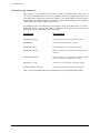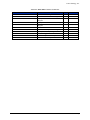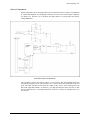
1
VM4016 ANALOG COMPARATOR USER’S MANUAL P/N: 82-0022-000 Released December 13th, 2010 VXI Technology, Inc. 2031 Main Street Irvine, CA 92614-6509 (949) 955-1894 bus 2 www.vxitech.com TABLE OF CONTENTS INTRODUCTION Table of Contents .....................................................................................................................................................3 Certification ..........................................................................................................................................................5 Warranty ...............................................................................................................................................................5 Limitation of Warranty..........................................................................................................................................5 Restricted Rights Legend ......................................................................................................................................5 Declaration of Conformity .......................................................................................................................................6 General Safety Instructions ......................................................................................................................................7 Terms and Symbols ...............................................................................................................................................7 Warnings ...............................................................................................................................................................7 Support Resources ...................................................................................................................................................9 SECTION 1.................................................................................................................................................................11 Introduction ............................................................................................................................................................11 Introduction .........................................................................................................................................................11 Description ..........................................................................................................................................................12 VM4016 General Specifications .........................................................................................................................14 SECTION 2.................................................................................................................................................................15 Preparation for Use ................................................................................................................................................15 Installation...........................................................................................................................................................15 Calculating System Power and Cooling Requirements .......................................................................................15 Setting the Chassis Backplane Jumpers...............................................................................................................16 Setting the Logical Address ................................................................................................................................16 Front Panel Interface Wiring ...............................................................................................................................16 SECTION 3.................................................................................................................................................................19 Programming..........................................................................................................................................................19 Examples of SCPI Commands ............................................................................................................................19 FETCH:CONDITIONED? ..............................................................................................................................19 FETCH:LATCHED? .......................................................................................................................................20 FETCH:RAW? ................................................................................................................................................21 INHOUSE:PSEUDO .......................................................................................................................................22 INHOUSE:REGINT ........................................................................................................................................23 INHOUSE:REG_ENABLE .............................................................................................................................24 INHOUSE:CLEAR_LATCH...........................................................................................................................25 INPUT:DEBOUNCE.......................................................................................................................................26 INPUT:MASK .................................................................................................................................................27 INPUT:MASK:INTERRUPT ..........................................................................................................................28 INPUT:OFFSET ..............................................................................................................................................29 INPUT:POLARITY.........................................................................................................................................30 INPUT:RANGE...............................................................................................................................................31 OUTPUT:POLARITY:EXTERNAL:INTERRUPT ........................................................................................32 OUTPUT:POLARITY:EXTERNAL:LATCHED ...........................................................................................33 Application Examples ............................................................................................................................................34 Single Channel Operation ...................................................................................................................................35 Bracketing a Voltage ...........................................................................................................................................38 Register Access Examples .....................................................................................................................................41 Pseudo Register Access.......................................................................................................................................43 VXIplug&play Driver Examples ...........................................................................................................................44 VM4016 Preface 3 VXI Technology, Inc. SECTION 4.................................................................................................................................................................49 Command Dictionary .............................................................................................................................................49 Introduction .........................................................................................................................................................49 Alphabetical Command Listing ...........................................................................................................................49 Command Dictionary ..........................................................................................................................................53 Common SCPI Commands ....................................................................................................................................54 *CLS ...................................................................................................................................................................54 *ESE ...................................................................................................................................................................55 *ESR? .................................................................................................................................................................56 *IDN? ..................................................................................................................................................................57 OPC .....................................................................................................................................................................58 *RST ...................................................................................................................................................................59 *SRE ...................................................................................................................................................................60 *STB? .................................................................................................................................................................61 *TRG...................................................................................................................................................................62 *TST?..................................................................................................................................................................63 *WAI...................................................................................................................................................................64 Instrument Specific SCPI Commands ....................................................................................................................65 FETCh:CONDitioned? ........................................................................................................................................65 FETCh:LATChed? ..............................................................................................................................................66 FETCh:RAW? .....................................................................................................................................................67 INHOUSE:CLEAR_LATCH ..............................................................................................................................68 INHOUSE:PSEUDO ..........................................................................................................................................69 INHOUSE:REGINT ...........................................................................................................................................70 INHOUSE:REG_ENABLE ................................................................................................................................71 INPut:DEBounce ................................................................................................................................................72 INPut:MASK ......................................................................................................................................................73 INPut:MASK:INTerrupt .....................................................................................................................................74 INPut:OFFSet......................................................................................................................................................75 INPut:POLarity ...................................................................................................................................................76 INPut:RANGe .....................................................................................................................................................77 OUTPut:POLarity:EXTernal:INTerrupt .............................................................................................................78 OUTPut:POLarity:EXTernal:LATChed .............................................................................................................79 Required SCPI Commands ....................................................................................................................................80 STATus:OPERation:CONDition? ......................................................................................................................80 STATus:OPERation:ENABle .............................................................................................................................81 STATus:OPERation[:EVENt]?...........................................................................................................................82 STATus:PRESet..................................................................................................................................................83 STATus:QUEStionable:CONDition? .................................................................................................................84 STATus:QUEStionable:ENABle ........................................................................................................................85 STATus:QUEStionable[:EVENt] .......................................................................................................................86 SYSTem:ERRor? ................................................................................................................................................87 SYSTem:VERSion? ............................................................................................................................................88 SECTION 5.................................................................................................................................................................89 Theory of Operation ...............................................................................................................................................89 Introduction .........................................................................................................................................................89 Input Range Control ............................................................................................................................................90 Signal Comparison ..............................................................................................................................................92 Interrupt Generation ............................................................................................................................................93 INDEX........................................................................................................................................................................95 4 VM4016 Preface www.vxitech.com CERTIFICATION VXI Technology, Inc. (VTI) certifies that this product met its published specifications at the time of shipment from the factory. VTI further certifies that its calibration measurements are traceable to the United States National Institute of Standards and Technology (formerly National Bureau of Standards), to the extent allowed by that organization’s calibration facility, and to the calibration facilities of other International Standards Organization members. WARRANTY The product referred to herein is warranted against defects in material and workmanship for a period of three years from the receipt date of the product at customer’s facility. The sole and exclusive remedy for breach of any warranty concerning these goods shall be repair or replacement of defective parts, or a refund of the purchase price, to be determined at the option of VTI. For warranty service or repair, this product must be returned to a VXI Technology authorized service center. The product shall be shipped prepaid to VTI and VTI shall prepay all returns of the product to the buyer. However, the buyer shall pay all shipping charges, duties, and taxes for products returned to VTI from another country. VTI warrants that its software and firmware designated by VTI for use with a product will execute its programming when properly installed on that product. VTI does not however warrant that the operation of the product, or software or firmware will be uninterrupted or error free. LIMITATION OF WARRANTY The warranty shall not apply to defects resulting from improper or inadequate maintenance by the buyer, buyersupplied products or interfacing, unauthorized modification or misuse, operation outside the environmental specifications for the product, or improper site preparation or maintenance. VXI Technology, Inc. shall not be liable for injury to property other than the goods themselves. Other than the limited warranty stated above, VXI Technology, Inc. makes no other warranties, express or implied, with respect to the quality of product beyond the description of the goods on the face of the contract. VTI specifically disclaims the implied warranties of merchantability and fitness for a particular purpose. RESTRICTED RIGHTS LEGEND Use, duplication, or disclosure by the Government is subject to restrictions as set forth in subdivision (b)(3)(ii) of the Rights in Technical Data and Computer Software clause in DFARS 252.227-7013. VXI Technology, Inc. 2031 Main Street Irvine, CA 92614-6509 U.S.A. VM4016 Preface 5 VXI Technology, Inc. DECLARATION OF CONFORMITY Declaration of Conformity According to ISO/IEC Guide 22 and EN 45014 MANUFACTURER’S NAME VXI Technology, Inc. MANUFACTURER’S ADDRESS 2031 Main Street Irvine, California 92614-6509 PRODUCT NAME Analog Comparator MODEL NUMBER(S) VM4016 PRODUCT OPTIONS All PRODUCT CONFIGURATIONS All VXI Technology, Inc. declares that the aforementioned product conforms to the requirements of the Low Voltage Directive 73/23/EEC and the EMC Directive 89/366/EEC (inclusive 93/68/EEC) and carries the “CE” mark accordingly. The product has been designed and manufactured according to the following specifications: SAFETY EN61010 (2001) EMC EN61326 (1997 w/A1:98) Class A CISPR 22 (1997) Class A ICES-003 Class A (ANSI C63.4 1992) AS/NZS 3548 (w/A1 & A2:97) Class A FCC Part 15 Subpart B Class A The product was installed into a C-size VXI mainframe chassis and tested in a typical configuration. I hereby declare that the aforementioned product has been designed to be in compliance with the relevant sections of the specifications listed above as well as complying with all essential requirements of the Low Voltage Directive. December 2003 Steve Mauga, QA Manager 6 VM4016 Preface www.vxitech.com GENERAL SAFETY INSTRUCTIONS Review the following safety precautions to avoid bodily injury and/or damage to the product. These precautions must be observed during all phases of operation or service of this product. Failure to comply with these precautions, or with specific warnings elsewhere in this manual, violates safety standards of design, manufacture, and intended use of the product. Service should only be performed by qualified personnel. TERMS AND SYMBOLS These terms may appear in this manual: WARNING Indicates that a procedure or condition may cause bodily injury or death. CAUTION Indicates that a procedure or condition could possibly cause damage to equipment or loss of data. These symbols may appear on the product: ATTENTION - Important safety instructions Frame or chassis ground Indicates that the product was manufactured after August 13, 2005. This mark is placed in accordance with EN 50419, Marking of electrical and electronic equipment in accordance with Article 11(2) of Directive 2002/96/EC (WEEE). End-of-life product can be returned to VTI by obtaining an RMA number. Fees for take-back and recycling will apply if not prohibited by national law. WARNINGS Follow these precautions to avoid injury or damage to the product: VM4016 Preface Use Proper Power Cord To avoid hazard, only use the power cord specified for this product. Use Proper Power Source To avoid electrical overload, electric shock, or fire hazard, do not use a power source that applies other than the specified voltage. 7 VXI Technology, Inc. WARNINGS (CONT.) Avoid Electric Shock To avoid electric shock or fire hazard, do not operate this product with the covers removed. Do not connect or disconnect any cable, probes, test leads, etc. while they are connected to a voltage source. Remove all power and unplug unit before performing any service. Service should only be performed by qualified personnel. Ground the Product This product is grounded through the grounding conductor of the power cord. To avoid electric shock, the grounding conductor must be connected to earth ground. Operating Conditions To avoid injury, electric shock or fire hazard: Do not operate in wet or damp conditions. Do not operate in an explosive atmosphere. Operate or store only in specified temperature range. Provide proper clearance for product ventilation to prevent overheating. DO NOT operate if you suspect there is any damage to this product. Product should be inspected or serviced only by qualified personnel. The operator of this instrument is advised that if equipment is used in a manner not specified in this manual, the protection provided by this equipment be may be impaired. Improper Use 8 VM4016 Preface www.vxitech.com SUPPORT RESOURCES Support resources for this product are available on the Internet and at VTI Instruments customer support centers. VTI Instruments Corp. World Headquarters VTI Instruments Corp. 2031 Main Street Irvine, CA 92614-6509 Phone: (949) 955-1894 Fax: (949) 955-3041 VTI Instruments Cleveland Instrument Division 5425 Warner Road Suite 13 Valley View, OH 44125 Phone: (216) 447-8950 Fax: (216) 447-8951 VTI Instruments Lake Stevens Instrument Division 3216 Wetmore Avenue, Suite 1 Everett, WA 98201 Phone: (949) 955-1894 Fax: (949) 955-3041 VTI Instruments, Pvt. Ltd. Bangalore Instrument Division 135, II & III Floors Infantry Road Bangalore – 560 001 India Phone: +91 80 4040 7900 Fax: +91 80 4170 0200 Technical Support Phone: (949) 955-1894 Fax: (949) 955-3041 E-mail: [email protected] Visit http://www.vtiinstruments.com for worldwide support sites and service plan information. VM4016 Preface 9 VXI Technology, Inc. 10 VM4016 Preface www.vxitech.com SECTION 1 INTRODUCTION INTRODUCTION The VM4016 is a high-performance Analog Comparator module which has been designed to monitor analog signals and cause VXIbus interrupts to occur when programmed input limits have been exceeded. The instrument uses the message-based word serial interface for programming and data movement, as well as supporting direct register access for very high-speed data retrieval. The VM4016 command set conforms to the SCPI standard for consistency and ease of programming. The VM4016 is a member of the VXI Technology VMIP (VXI Modular Instrumentation Platform) family and is available as a 16-, 32- or 48-channel, single-wide VXIbus instrument. In addition to these three standard configurations, the VM4016 may be combined with any of the other members of the VMIP family to form a customized and highly integrated instrument (see Figure 1-1). This allows the user to reduce system size and cost by combining the VM4016 with two other instrument functions in a single-wide C-size VXIbus module. Figure 1-2 shows the 48-channel version of the VM4016. The 32-channel version would not have J200 and its associated LEDs and nomenclature while the 16-channel version would also eliminate J202. VMIP INSTRUMENT MODULE #1 V X I B U S VMIP INTERFACE I N T E R N A L V M I P VMIP INSTRUMENT MODULE #2 B U S VMIP INSTRUMENT MODULE #3 FIGURE 1-1: VMIP™ PLATFORM VM4016 Introduction 11 VXI Technology, Inc. Regardless of whether the VM4016 is configured with other VM4016 modules or with other VMIP modules, each group of 16 channels is treated as an independent instrument in the VXIbus chassis and, as such, each group has its own FAIL and ACCESS light. ACC/ ERR FAIL The FAIL LED is a Power/Fault indicator. When normal power up conditions exist, the FAIL LED will illuminate green. When a power on fault condition occurs, the FAIL LED will illuminate red. The ACC/ERR LED indicates communication status. When a successful Access occurs, the LED will blink green during data transfer and command/query operations. In the event of an unrecognized command, or other data related error, the ACC/ERR LED will illuminate red. If there is no command/query activity, and no errors, the ACC/ERR LED will be extinguished. The normal state of the LEDs on a properly functioning idle instrument is for the FAIL LED to be green, and the ACC/ERR LED to be off. DESCRIPTION The VM4016 is a high-performance Analog Comparator module with 16 input channels per VMIP daughter module. Each input channel consists of a differential amplifier with a gain of 1 or 0.1 giving an input range of ±10 V or ±100 V. Each input is compared against a reference voltage derived from an independent 8-bit DAC. J200 ACC/ ERR FAIL Each input signal is digitally debounced for a programmed time ranging from approximately 10 µs to 0.5 s. This prevents input signal noise from causing undesired interrupts. After debounce, the signal may be programmatically inverted to select the input transition edge of interest (rising or falling edge) and masked to prevent unused channels from causing interrupts. All of the masked inputs are OR’d together to produce a single interrupt signal. This interrupt signal is used to generate a VXIbus interrupt as well as the front panel interrupt outputs. All active input is recorded as a “1”. Once the VXIbus interrupt is serviced by the slot 0 controller, the First Latched Register will be cleared. J201 ACC/ ERR FAIL The state of each channel’s debounced input and the inverted and masked status may be read directly in the user defined area of the VXIbus registers as can the First Latched register. This information may also be retrieved using the message-based word serial interface. The block diagram of Figure 1-3 shows the overall functionality of the VM4016 Analog Comparator instrument. J202 bus FIGURE 1-2: FRONT PANEL LAYOUT 12 VM4016 Introduction www.vxitech.com VXI MODULE PANEL CH1+ CH1- CHANNEL 1 OF DIFFERENTIAL AMPLIFIER X1 OR X0.1 COMPARATOR 8 BIT DAC TO VXIBUS COMPARE REGISTERS DEBOUNCE 10 uS TO 0.5 S INVERT REGISTER MASK REGISTER INTERRUPT AND FIRST LIMIT LOGIC +5V CHANNEL 16 OF VXIbus INTERRUPT FIRST LIMIT INVERT REGISTER IRQ INTERRUPT INVERT REGISTER FIRST LIMIT LATCH REGISTER TO VXIBUS FIRST LIMIT REGISTER +5V L IRQ FIGURE 1-3: VM4016 BLOCK DIAGRAM VM4016 Introduction 13 VXI Technology, Inc. VM4016 GENERAL SPECIFICATIONS GENERAL SPECIFICATIONS CHANNELS VM4016-1 VM4016-2 VM4016-3 INPUT RANGE 16 32 48 ±10.0 V, ±100 V INPUT THRESHOLD RESOLUTION 78 mV ±10.0 V ±100.0 V 780 mV INPUT THRESHOLD ACCURACY ±3% INPUT TYPE Differential, may be configured for single-ended by grounding the negative input INPUT IMPEDANCE 200 kΩ differential 100 kΩ single-ended INPUT POLARITY Rising or falling edge DEBOUNCE TIME 9.6 μs to 0.6291456 s, 9.6 μs resolution IRQ OUTPUT Open Collector Driver, 200 mA max. sink Internally pulled up to +5 V with 10 kΩ resistor LATCHED IRQ OUTPUT Open collector driver, 200 mA max. sink Internally pulled up to +5 V with 10 kΩ resistor VXI INTERFACE Message-based word serial interface Direct register access in the user defined area of the VXIbus register map LOGICAL ADDRESSING Static or dynamic configuration RAW DATA REGISTER Logical address + 20H MASKED DATA REGISTER Logical address + 28H FIRST LATCHED REGISTER Logical address + 30H POWER REQUIREMENTS +5 V @ 1.43 A, -5.2 V @ 0.17 A, +24 V @ 0.05 A, -24 V @ 0.05 A VM4016-1 VM4016-2 +5 V @ 2.12 A, -5.2 V @ 0.29 A, +24 V @ 0.10 A, -24 V @ 0.10 A VM4016-3 +5 V @ 2.81 A, -5.2 V @ 0.41 A, +24 V @ 0.15 A, -24 V @ 0.15 A COOLING REQUIREMENTS See Power Cooling Table VM4016-1 VM4016-2 See Power Cooling Table VM4016-3 See Power Cooling Table 14 VM4016 Introduction www.vxitech.com SECTION 2 PREPARATION FOR USE INSTALLATION When the VM4016 is unpacked from its shipping carton, the contents should include the following items: One VM4016 VXIbus module One VM4016 Analog Comparator Module User’s Manual (this manual) All components should be immediately inspected for damage upon receipt of the unit. Once the VM4016 is assessed to be in good condition, it may be installed into an appropriate C-size or D-size VXIbus chassis in any slot other than slot 0. The chassis should be checked to ensure that it is capable of providing adequate power and cooling for the VM4016. Once the chassis is found be adequate, the VM4016’s logical address and the chassis’ backplane jumpers should be configured prior to the VM4016’s installation. CALCULATING SYSTEM POWER AND COOLING REQUIREMENTS It is imperative that the chassis provide adequate power and cooling for this module. Referring to the chassis user’s manual, confirm that the power budget for the system (the chassis and all modules installed therein) is not exceeded and that the cooling system can provide adequate airflow at the specified backpressure. It should be noted that if the chassis cannot provide adequate power to the module, the instrument may not perform to specification or possibly not operate at all. In addition, if adequate cooling is not provided, the reliability of the instrument will be jeopardized and permanent damage may occur. Damage found to have occurred due to inadequate cooling would also void the warranty of the module. VM4016 Preparation for Use 15 VXI Technology, Inc. SETTING THE CHASSIS BACKPLANE JUMPERS Please refer to the chassis User’s Manual for further details on setting the backplane jumpers. SETTING THE LOGICAL ADDRESS The logical address of the VM4016 is set by a single 8-position DIP switch located near the module’s backplane connectors (this is the only switch on the module). The switch is labeled with positions 1 through 8 and with an ON position. A switch pushed toward the ON legend will signify a logic 1; switches pushed away from the ON legend will signify a logic 0. The switch located at position 1 is the least significant bit while the switch located at position 8 is the most significant bit. See Figure 2-1 for examples of setting the logical address switch. ON ON 1 2 3 4 5 6 7 8 1 2 3 4 5 6 7 8 SET TO 4 SET TO 8 ON ON 1 2 3 4 5 6 7 8 1 2 3 4 5 6 7 8 SET TO 168 SET TO 255 (Dynamic) Switch Position Switch Value 1 2 3 4 5 6 7 8 1 2 4 8 16 32 64 128 FIGURE 2-1: LOGICAL ADDRESS SWITCH SETTING EXAMPLES The VMIP may contain three separate instruments and will allocate logical addresses as required by the VXIbus specification (revisions 1.3 and 1.4). It is necessary that the address of the first instrument (the instrument closest to the top of the module) be set at an address which is divisible by 4 and not set to 0. Switch positions 0 and 1 must always be set to the OFF position. Therefore only addresses of 4, 8, 12, 16 ... 252 are allowed. The address switch should be set for one of these legal addresses and the address for the second instrument (the instrument in the center position) will automatically be set to the switch set address plus one; while the third instrument (the instrument in the lowest position) will automatically be set to the switch set address plus two. If dynamic address configuration is desired, the address switch should be set for a value of 255. Upon power-up, the slot 0 resource manager will assign logical addresses to each instrument in the VMIP module. FRONT PANEL INTERFACE WIRING The VM4016’s interface is made available on the front panel of the instrument. The 16-channel version (VM4016-1) will have J201 that contains all signals for this instrument. The 32-channel version (VM4016-2) will have J201 and J202 provided, while the 48-channel version (VM4016-3) will have J200, J201, and J202. The wiring for each of these connectors is identical and since each group of 16 channels is treated as a separate instrument, the module will have three Channel 1s, three Channel 2s, three Channel 3s, etc. 16 VM4016 Preparation for Use www.vxitech.com The connector used in the VM4016 is a commonly available 44-pin high density D-sub receptacle connector. A mating solder cup pin connector from AMP is included, crimp type connectors are available from a variety of sources. SIGNAL CHANNEL 1 + CHANNEL 1 GROUND CHANNEL 4 + CHANNEL 4 CHANNEL 7 + CHANNEL 7 GROUND CHANNEL 10 + CHANNEL 10 CHANNEL 13 + CHANNEL 13 GROUND IRQ OUTPUT GROUND CHANNEL 2 + CHANNEL 2 GROUND CHANNEL 5 + CHANNEL 5 CHANNEL 8 + CHANNEL 8 - PIN NUMBER 1 2 3 4 5 6 7 8 9 10 11 12 13 14 15 16 17 18 19 20 21 22 SIGNAL GROUND CHANNEL 11 + CHANNEL 11 CHANNEL 14 + CHANNEL 14 GROUND CHANNEL 16 + CHANNEL 16 CHANNEL 3 + CHANNEL 3 GROUND CHANNEL 6 + CHANNEL 6 CHANNEL 9 + CHANNEL 9 GROUND CHANNEL 12 + CHANNEL 12 CHANNEL 15 + CHANNEL 15 GROUND LATCHED IRQ OUT PIN # 23 24 25 26 27 28 29 30 31 32 33 34 35 36 37 38 39 40 41 42 43 44 TABLE 2-1: ANALOG COMPARATOR PIN OUTS The mating connector to J200, J201, or J202 is available from the following company: Assmann Electronic, Inc. P/N A-HDS44LL-TL-B-R Mating Connector The pin locations for J200, J201, and J202 are shown in Figure 2-2. 16 31 1 44 15 30 FIGURE 2-2: J200, J201, AND J202 PIN LOCATIONS VM4016 Preparation for Use 17 VXI Technology, Inc. 18 VM4016 Preparation for Use www.vxitech.com SECTION 3 PROGRAMMING EXAMPLES OF SCPI COMMANDS FETCH:CONDITIONED? The FETCh:CONDition query returns the 16-bit value that represents the current conditioned (masked and inverted) state of the inputs. It is important to note that this information is also available at the VXIbus register level at offset 0x28. FETCh:CONDitioned? No query parameters. EXAMPLES FETCh:CONDitioned? VM4016 Programming Returns the state of the conditioned 0 (masked and inverted) inputs. 19 VXI Technology, Inc. FETCH:LATCHED? The FETCh:LATChed query returns a 16-bit value that reports the active signals in the First Latched register. The First Latched register records the active signals when the first new input channel crossed its threshold. It is important to note that the above information is also available at the VXIbus register level at offset 0x30. FETch:LATChed? No query parameters EXAMPLES FETCh:LATChed? 1 FETC:LATC? 3 20 Returns the active signals in the First Latched register. Channel 1. Returns the active signals in the First Latched Register. Channels 1 and 2. VM4016 Programming www.vxitech.com FETCH:RAW? The FETCh:RAW query returns the 16-bit value that represents the current unconditioned (unmasked and non-inverted) state of the inputs. It is important to note that the above information is also available at the register level at offset 0x20. FETCH:RAW? No query parameters EXAMPLES FETch:RAW? 1 Returns the state of the unconditioned (unmasked and non-inverted) inputs Channel 1. FETC:RAW? 65535 All 16 channels crossed the programmed threshold. VM4016 Programming 21 VXI Technology, Inc. INHOUSE:PSEUDO The INHOUSE:PSEUDO command controls the use of the register interface. Pseudo set true specifies that pseudo register interface should be used. Pseudo set false specifies that the hardware register interface should be used. The value set takes effect next time the unit powers up [does not take effect immediately]. The pseudo register interface allows the use of REG_ENABLE and CLEAR_LATCH capability from the registers. Although the hardware register interface is much faster than the pseudo register interface, it lacks the above two features. It is important to note that when the module is shipped from the factory, pseudo is set to 1. It is also important to note that all letters of the command must be provided as there is no short form for this command. INHOUSE:PSEUDO <boolean> Where <boolean> is 0 | OFF | 1 | ON. EXAMPLES 22 INHOUSE:PSEUDO 1 Sets the pseudo register interface ON. (The unit must be powered for the change to take effect.) INHOUSE:PSEUDO? 1 Returns 1 which states that the register interface is set to pseudo. VM4016 Programming www.vxitech.com INHOUSE:REGINT The INHOUSE:REGINT command controls the type of module’s response to an interrupt acknowledge cycle [ack cycle]. When regint is set to false, the module uses reqt | reqf (request true | request false), provided the latched interrupt bit is set in the SRE. It is important to note that all the letters of the command must be provided as there is no short form for this command. INHOUSE:REGINT <boolean> Where <boolean> is 0 | OFF | 1 | ON. EXAMPLES INHOUSE:REGINT 1 Sets the type of module interrupt response to one backplane interrupts for every first latched event. INHOUSE:REGINT? 1 Returns the type of module interrupt response as 1. INHOUSE:REGINT 0 Sets the type of module interrupt response as two backplane interrupts for each latched event. INHOUSE:REGENT? 0 Returns the type of module interrupt response as 0. VM4016 Programming 23 VXI Technology, Inc. INHOUSE:REG_ENABLE The INHOUSE:REG_ENABLE command controls the masking for REGINT. REG_ENABLE 0 means that backplane interrupts cannot be generated. If the REG_ENABLE is 1, then backplane interrupts can be generated. If PSEUDO is set, then a write to the register at offset 0x38 also controls the masking. Enable or disable capabilities are provided in the pseudo register interface to allow a complete register interface. It is important to note that all letters of the command must be provided as there is no short form for this command. INHOUSE:REG_ENABLE <boolean> Where <boolean> is 0 | OFF | 1 | ON. EXAMPLES 24 INHOUSE:REG_ENABLE 1 Enables the REGINT type interrupt generation INHOUSE:REG_ENABLE? 1 Returns 1 to state that backplane interrupting is currently enabled. INHOUSE:REG_ENABLE 0 Disabling REGINT interrupt generation. INHOUSE:REG_ENABLE? 0 Returns 0 to state that backplane interrupting is currently disabled. VM4016 Programming www.vxitech.com INHOUSE:CLEAR_LATCH The INHOUSE:CLEAR_LATCH command determines whether the first latched information will be cleared when the information is read by word serial FETch:LATChed? Command or if pseudo is set and a register read of the first latched information occurs. The information will not be cleared if a hardware register read is used. When the first latched information is cleared, all the following reads will return a value of 0 until a new first latched event occurs. It is important to note that all letters in the command must be provided as there is no short form for this command. INHOUSE:CLEAR_LATCH <boolean> Where <boolean> is 0 | OFF | 1 | ON. EXAMPLES INHOUSE:CLEAR_LATCH 1 Clears the first latched information on a read. INHOUSE:CLEAR_LATCH? 1 Returns 1 stating that the first latched information will be cleared on a read. FETC:LATC? 1 Reading the first latched information. This also clears the latched information. FETC:LATC? 0 Reading the first latched information returns a value of 0 once the clearing of latch information was enabled (assuming no further latching occurred). VM4016 Programming 25 VXI Technology, Inc. INPUT:DEBOUNCE The INPut:DEBounce command sets the time period for the digital debounce circuitry. This command affects all the 16 channels of the instrument. It is important to note that the debounce resolution is 9.6 µs. INPut:DEBounce <value> Where <value> ranges from 9.6 µs, i.e., 0.0000096 s to 0.6291456 s. EXAMPLES 26 INPut:DEBounce 9.6e-6 Sets the input debounce time for all channels to 0.0000096 s. This will not allow a signal to generate an interrupt unless the input signal crosses the signal for more than 9.6 e-6 seconds. INP:DEB 0.6 Setting input debounce time to 0.6 s. INP:DEB? 0.6 Returns the input debounce time as 0.6 s. VM4016 Programming www.vxitech.com INPUT:MASK The INPut:MASK command enables or disables input channels from generating interrupts or recording data in the conditional register. If a channel is programmed to be ON or 1, then it is enabled to generate interrupts. If a channel is programmed to be OFF or 0, then it cannot generate VXIbus interrupts. INPut:MASK <state>, <channel_list> Where <state> is 0 | OFF | 1 | ON. Where <channel_list> is standard channel list format supporting channels 1 through 16. EXAMPLES INPut:MASK ON,(@1:8) Enables channels 1 through 8 to generate interrupts. INPut:MASK? 3 1 Reports that channel 3 is enabled for voltage comparison. INP:MASK? 9 0 Reports that channel 9 is not enabled for voltage comparison. VM4016 Programming 27 VXI Technology, Inc. INPUT:MASK:INTERRUPT The INPut:MASK:INTerrupt command enables or disables interrupt generation when changing MASK values. When set to 0 (the *RST state), interrupts are temporarily disabled whenever MASK values are changed. When set to 1, interrupts are generated even as MASK values are changed. INPut:MASK:INTerrupt <boolean> Where <boolean> is 0 | OFF | 1 | ON. EXAMPLES 28 INPut:MASK:INT 0 Disables interrupt generation INPut:MASK:INT? 0 Reports that interrupt generation is disabled VM4016 Programming www.vxitech.com INPUT:OFFSET The INPut:OFFSet command sets the input threshold for a channel or group of channels, over which the input signal must cross to cause an interrupt event. This command sets the value in the 8bit DAC to which the input signal is compared. It is important to note that the actual input offset value is affected by the INPut:RANGe command, as the response has been normalized to ±10 V range. The actual input offset for the allowable ranges are as follows: Range ±10.0 ±100.0 Entered Threshold x x INPut:OFFSet <voltage_level>,<channel_list> Actual Threshold 1.0x 10.0x Where <voltage_level> -10.00 V to +9.96 V. ranges from Where <channel_list> is the standard channel list format supporting Channels 1 through 16. EXAMPLES INPut:RANGe 100,(@5:10) Sets the input range for Channels 5 through 10 to ±100 V INPut:OFFSet -5.0,(@5:10) Sets the input offset for Channels 5 through 10 to -50 V INP:OFFS? 9 -5.000 Returns the normalized input offset of -50 V for Channel 9 INP:RANG 10,(@1:4) Sets the input range for Channels 1 through 4 to ±10 V INP:OFFS -5.0,(@1:4) Sets the input offset for Channels 1 through 4 to -5 V INP:OFFS? 3 -5.000 Returns the normalized input offset of -5 V for Channel 3 VM4016 Programming 29 VXI Technology, Inc. INPUT:POLARITY The input polarity command selects the input polarity for one or more channels. When a channel is programmed for normal polarity, an interrupt will be generated when the input voltage is greater than the programmed input offset for the channel. The invert polarity will cause an interrupt when the input voltage is less than the programmed input offset for the channel. INPut:POLarity <polarity>,<channel_list> Where <polarity> is either NORMal or INVerted Where <channel_list> is the standard channel list format supporting channels 1 through 16. EXAMPLES 30 INPut:POLarity NORM,(@3:5) Sets the input polarity for Channels 3 through 5 to NORMal. This will generate an interrupt when the input signal on Channels 3, 4, or 5 is greater than the input offset. INPut:POLarity? 5 NORM Returns the input polarity for Channel 5 as NORMal INP:POL INV,(@6) Sets input polarity for Channel 6 to invert. VM4016 Programming www.vxitech.com INPUT:RANGE The input range command selects the input range of one or more channels. The input range may be either set for ±10 V or ±100 V. It is important to note that the input offset is normalized to ±10 V range. The actual input offset in the 100 V range is ten times the set value. INPut:RANGe <range>,<channel_list> Where <range> is 10 V | 100 V. Where <channel_list> is the standard channel list format supporting channels 1 through 16. EXAMPLES INPut:RANGe 100,(@1:16) Sets the input range for Channels 1 through 16 to 100 V. INPut:RANGe? 7 100 Returns the input range for Channel 7 as 100 V. INP:RANG 10,(@4:6) Sets the input range for Channels 4 through 6 to 10 V. INP:RANG? 5 10 Returns the input range for Channel 5 as 10 V. VM4016 Programming 31 VXI Technology, Inc. OUTPUT:POLARITY:EXTERNAL:INTERRUPT The output polarity external interrupt command sets the polarity of the front panel interrupt output. When the polarity is set to normal, the output will be low when there is an interrupt event. When the polarity is set to invert, the output will be high when there is an interrupt event. OUTPut:POLarity:EXTernal:INTerrupt <polarity> Where <polarity> NORMal or INVert. is either EXAMPLES 32 OUTPut:POLarity:EXTernal:INTerrupt NORM Sets the external interrupt output polarity to a low pulse (NORMal), when an interrupt occurs. OUTPut:POLarity:EXTernal:INTerrupt? NORM Returns the external interrupt output polarity as NORMal. OUTP:POL:EXT:INT INV Sets the external interrupt output polarity to INVert. OUTP:POL:EXT:INT? INV Returns the polarity of the external interrupt output as INVert. VM4016 Programming www.vxitech.com OUTPUT:POLARITY:EXTERNAL:LATCHED The output polarity external latched command sets the polarity of the front panel latched interrupt output. When the polarity is set to normal, the output will be low when there is an interrupt event. When set to invert, the output will be high when there is an interrupt event. OUTPut:POLarity:EXTernal:LATChed <polarity> Where <polarity> is NORMal or INVerted. either EXAMPLES OUTPut:POLarity:EXTernal:LATChed NORM Sets the external latched output polarity to low when an interrupt occurs. OUTPut:POLarity:EXTernal:LATChed? NORM Returns the external latched output polarity as NORMal. OUTP:POL:EXT:LATC INV Sets the external latched output polarity to high when an interrupt occurs. OUTP:POL:EXT:LATC? INV Returns the external latched output polarity as INVert. VM4016 Programming 33 VXI Technology, Inc. APPLICATION EXAMPLES This section contains examples of using SCPI command strings for programming the VM4016 module. The code is functional and will contain a brief description about the operation. Example 1 In this example, the VM4016 sets the output interrupt polarity on the front panel and the debounce time period for the digital debounce circuitry. OUTPut:POLarity:EXTernal:INTerrupt NORM Sets the external interrupt output polarity to high pulse when an interrupt occurs. INPut:DEBounce 25e-6 Sets input debounce time for all channels to 25 µs. This will not allow a signal to generate an interrupt unless the channel is active for greater than 25 µs. Example 2 In this example, the VM4016 enables or disables the specified channels for interrupt generation, sets the offset, polarity and voltage range. It returns the value of First Latched register which records the first input channel to cross its threshold and queries the current state of inputs. INP:MASK 1,(@1,2) Enables Channels 1 and 2 for interrupt generation. INP:MASK 0,(@3:16) Disables Channels 3 through 16 from generating an interrupt. INP:RANG 10,(@1,2) Selects ±10 V as the input range for Channel 1 and 2. INP:OFFS +5.25,(@1,2) Selects +5.25 V as the offset voltage for Channels 1 and 2. INP:POL NORM,(@1,2) Selects both Channel 1 and 2 to generate an interrupt when Channels 1 and 2 are greater than the offset voltage. FETC:LATC? Returns the active signal in the First Latched Register. FETC:RAW? 65535 Returns the State of unconditioned (ummasked and non-inverted) inputs. FETC:COND? 3 34 Returns the state of masked and inverted inputs. VM4016 Programming www.vxitech.com SINGLE CHANNEL OPERATION This example is for controlling a device that can tolerate a maximum input voltage level at +35 V dc for a maximum time of 250 ms before damage will occur. The input power to this device is provided from a remote source that can be disabled. A low signal applied to the power source remote inhibit will disable its output. The controller will then be notified that an out-of- tolerance condition has occurred and the device was shut down. The following code is for monitoring a single input for voltage level that exceeds +35 V dc for longer than 250 ms. A low latched output is required to be generated upon detection of the interrupt that is used to inhibit the remote power source. COMMANDS DESCRIPTION INP:RANG 100,(@1) Selects ±100 V as the input range for Channel 1. INP:DEB 0.25 Sets the debounce time limit to 250 ms. INP:MASK 1,(@1) Enables Channel 1 to generate an interrupt. INP:MASK 0,(@2:16) Disables Channels 2 through 16 from generating an interrupt. INP:POL NORM,(@1) Selects Channel 1 to generate an interrupt when Channel 1 is greater than the offset voltage. INP:OFFS +3.5,(@1) Selects +35.0 V as the offset (reference) voltage. OUTP:POL:EXT:LATC INV Sets the external latched output to be active low. Table 3-1 and the explanation that follows illustrates what is occurring during this example. VM4016 Programming 35 VXI Technology, Inc. FIGURE 3-1: SINGLE CHANNEL OPERATION Due to the type of signal being monitored, input channel +CH1 is grounded. The command and data for the SCPI command INP:RANG is received by the control (U1) and data (U4) buffers and routed to the control FPGA (U3). The control FPGA converts the parallel data for the relay drivers into a serial data stream. This data (RELAYDATA) is synched to the 10 MHz (RELAYCLK) and written into the relay drivers when (RELAYENA*) goes low. The relay drivers will energize relay K9 selecting a gain of 0.1 for the differential amplifier U17A. 36 VM4016 Programming www.vxitech.com The command and data for the SCPI command INP:DEB is received by the control (U1) and data (U4) buffers and routed to the control FPGA (U3). The register for the debounce circuitry is contained internally in the control FPGA. The debounce register will be loaded with a value that corresponds to a 250 ms time delay. The commands and data for the SCPI commands INP:MASK are received by the control (U1) and data (U4) buffers and routed to the control FPGA (U3). The mask register circuitry is contained internally in the control FPGA. This register will be loaded so that Channels 2 through 16 are disabled or masked out. The command for the SCPI command INP:POL is received by the control (U1) and data (U4) buffers and routed to the control FPGA (U3). The mask register and debounce circuitry uses this command to determine whether the input signal is an active high or an active low. The input polarity has been programmed to NORM to cause U3 to treat the input signal as an active high. The commands and data for the SCPI command INP:OFFS are received by the control (U1) and data (U4) buffers and routed to the control FPGA (U3). The control FPGA will convert the parallel data for the DAC (U8) into a serial data stream. This data (DACDATA) is synched to the 10 MHz gated clock (DACCLK) and loaded into the DAC when the (DACLOAD) signal goes high. The command for the SCPI command OUTP:POL:EXT:LATC is received by the control (U1) and data (U4) buffers and routed to the control FPGA (U3). The latch register uses this command to determine whether the output signal should be an active high or an active low. This was programmed for INV to cause U3 to output an active low EXTLATIRQ signal to the front panel connector when an interrupt occurs. Now that the VM4016 is configured, it can be determined how this works. The output of the differential amplifier U17A (BUFCH1) is voltage divided by 4. Since the gain of U17A is 0.1, this makes BUFCH1 0.875 V when -CH1 reaches +35.0 V. BUFCH1 is compared with the output of U8 (TRIGLEV1) by comparator U13A. When BUFCH1 is greater than TRIGLEV1 the output of U13A (COMPCH1) goes low. COMPCH1 is routed to the debounce circuitry inside U3. The debounce circuitry will count down for 250 ms before clocking through COMPCH1. This circuitry is used to mask out transients from generating false interrupts. When the 250 ms time limit has expired, U3 clocks COMPCH1 into the mask register. The mask register will AND COMPCH1 with the mask value (0001). The mask register passes COMPCH1 to a 16 input OR’ing function that determines which Channel was first to cross its threshold. The output of this OR’ing then latches into the “First Latch Register”. This signal, arbitrarily called FIRSTLATCHED, clocks an internal latch that drives the base of Q34. Q34 conducts and drives a low out on the front panel connector signal EXTLATIRQ. When an interrupt condition is detected by U3 a VXI IRQ* is generated to the VMIP bus. VM4016 Programming 37 VXI Technology, Inc. BRACKETING A VOLTAGE In this example, an input voltage level will be bracketed for an over or under-voltage error condition. The input voltage of 5.0 V will be monitored for an over-voltage of 5.25 V and an under-voltage of 4.75 V. The error condition must be true for longer than 750 μs. An interrupt will be generated if either of these conditions occur. Channel 1 will use for an over-voltage and Channel 2 for an under-voltage. Channel 1 and Channel 2 positive (+) sides will be tied together externally. Channel 1 and Channel 2 negative (-) sides will be grounded. The output interrupt will not be latched but will be pulsed. COMMANDS DESCRIPTION INP:RANG 10,(@1,2) Selects ±10 V as the input range for Channel 1 and 2. INP:DEB 75e-5 Sets the debounce time limit to 750 µs. INP:MASK 1,(@1,2) Enables Channel 1or 2 to generate an interrupt. INP:MASK 0,(@3:16) Disables Channels 3 through 16 from generating an interrupt. INP:POL NORM,(@1) Selects Channel 1 to generate an interrupt when Channel 1 is greater than the offset voltage. INP:POL INV,(@2) Selects Channel 2 to generate an interrupt when Channel 2 is less than the offset voltage. INP:OFFS +5.25,(@1) Selects +5.25 Vas the offset (reference) voltage for Channel 1. INP:OFFS +4.75,(@2) Selects +4.75 V as the offset (reference) voltage for Channel 2. OUTP:POL:EXT:INT NORM Sets the external interrupt output to be active high. Figure 3-2 and the explanation that follows illustrates what is occurring during this example. 38 VM4016 Programming www.vxitech.com FIGURE 3-2: BRACKETING AN INPUT VOLTAGE The command and data for the SCPI command INP:RANG are received by the control (U1) and data (U4) buffers (not shown for clarity) and routed to the control FPGA (U3). The control FPGA converts the parallel data for the relay drivers into a serial data stream. This data (RELAYDATA) is synched to the 10 MHz (RELAYCLK) and written into the relay drivers when (RELAYENA*) goes low. The relay drivers de-energize relays K9 and K1 selecting a gain of 1.0 for the differential amplifiers at U17A and U17B. The command and data for the SCPI command INP:DEB are received by the control (U1) and data (U4) buffers and routed to the control FPGA (U3). The register for the debounce circuitry is contained internally in the control FPGA. The register will be loaded with a value that corresponds to a 750 μs time delay. VM4016 Programming 39 VXI Technology, Inc. The commands for the SCPI commands INP:MASK are received by the control (U1) and data (U4) buffers and routed to the control FPGA (U3). The mask register circuitry is contained internally in the control FPGA. This register will be loaded so that Channels 3 through 16 are disabled or masked out. The command for the SCPI command INP:POL is received by the control (U1) and data (U4) buffers and routed to the control FPGA (U3). Channel 1 has been programmed this to NORM so that the debounce and mask circuitry will treat as an active high. Channel 2 has been programmed as INV, causing the debounce and mask circuitry to treat Channel 2 as an active low. The command and data for the SCPI command INP:OFFS are received by the control (U1) and data (U4) buffers and routed to the control FPGA (U3). The control FPGA will convert the parallel data for the DAC (U8) into a serial data stream. This data (DACDATA) is synched to the 10 MHz gated clock (DACCLK) and loaded into the DAC when the (DACLOAD) signal goes high. The DAC output (TRIGLEV#) where # is equal to the Channel number. The DAC will output TRIGLEV1 for the comparator at U13A and TRIGLEV2 for the comparator at U13B. The commands for the SCPI command OUTP:POL:EXT:INT are received by the control (U1) and data (U4) buffers and routed to the control FPGA (U3). U3 uses this command to determine whether the external interrupt signal should be an active high or an active low. This has been programmed to NORM so as to cause U3 to output an active high EXTIRQ signal to the front panel connector when an interrupt occurs. This signal will be a pulse 500 ns wide. The output of the differential amplifier U17A (BUFCH1) is voltage divided by 4. Since the gain of U17A is 1.0, this makes BUFCH1 1.250 V when -CH1 reaches +5.0 V. BUFCH1 is compared with the output of U8 (TRIGLEV1) by comparator U13A. When BUFCH1 is greater than TRIGLEV1 the output of U13A (COMPCH1) goes low. COMPCH1 is routed to the debounce circuitry inside U3. The output of the differential amplifier U17B (BUFCH2) is voltage divided by 4. Since the gain of U17B is 1.0 this makes BUFCH2 1.250 V when -CH2 reaches +5.0 V. BUFCH2 is compared with the output of U8 (TRIGLEV2) by comparator U13B. When BUFCH2 is less than TRIGLEV2 the output of U13B (COMPCH2) goes high. COMPCH2 is routed to the debounce circuitry inside U3. Note that the only difference in the way these two circuits are working is the output of the comparator U13B is inverted from the output of U13A. This inversion will allow us to determine if an under-voltage has occurred. Assume that -CH2 has fallen below +4.75 V. The output of U13B is now high. The debounce circuitry will count down for 750 μs before clocking through COMPCH2. When the 750 µs time limit has expired, U3 clocks COMPCH2 into the mask register. The mask register will AND COMPCH2 with the mask value (0003). The mask register passes COMPCH2 to a 16 input OR’ing function that determines which channel was first to cross its threshold, in this case COMPCH2. The output of this OR’ing then latches into the “First Latch Register”. This signal, arbitrarily named FIRSTLATCHED, clocks a series of internal latches that will stretch the pulse to 500 ns. This pulse drives the base of Q33 low causing Q33 to shut off and the pull-up resistor provides a high on the front panel connector signal EXTIRQ. When an interrupt condition is detected by U3 a VXI IRQ* is generated to the VMIP bus. 40 VM4016 Programming www.vxitech.com REGISTER ACCESS EXAMPLES TABLE 3-1: REGISTER MAP 3E 3C 3A 38 36 34 32 30 2E 2C 2A 28 26 24 22 20 1E 1C 1A 18 16 14 12 10 E C A 8 6 4 2 0 VM4016 Programming Interrupt enable (write only, pseudo only) First latched (read only) Conditioned (read only) Raw (read only) 41 VXI Technology, Inc. The VM4016 module supports direct register access for very high-speed data retrieval. The register map is as specified in Table 3-1. In order to access the raw data using register access, the register at offset 0x20 must be read. Each bit in this register corresponds to the state of the 16 channel inputs (unmasked and non-inverted). Bit 1 corresponds to Channel 1, Bit 2 corresponds to Channel 2 and so on. This information can also be accessed using the Word Serial FETC:RAW? query. In order to access the conditioned data using register access, the register at offset 0x28 must be read. Each bit in this register corresponds to the state of the 16 channel inputs (masked and inverted). Bit 1 corresponds to Channel 1, Bit 2 corresponds to Channel 2 and so on. This information can also be accessed using the Word Serial FETC:COND? query. In order to access the first latched information using register access, the register at offset 0x30 must be read. Each bit in this register corresponds to the state of the 16 channel inputs. Bit 1 corresponds to Channel 1, Bit 2 corresponds to Channel 2 and so on. This information can also be accessed using the Word Serial FETC:LATC? query. For example: a) if a value of 0x8000 is read from the first latched register, then it means that Channel 16’s input has caused a latching. b) if a value of 0xF000 is read from the first latched register, then it means that Channels 13 through 16 have caused a latching. The Interrupt Enable register is a write-only register on which write operations take effect only in the Pseudo mode. In order to enable backplane interrupting, any non-zero value must be written to this register at offset 0x38. Writing a zero to this register will disable any backplane interrupting. It must be noted that in non-pseudo mode, any writes to this register will take no effect. Backplane interrupting can also be enabled/disabled using the Word Serial INHOUSE:REG_ENABLE command. 42 VM4016 Programming www.vxitech.com PSEUDO REGISTER ACCESS The VM4016 can be operated upon using (a) Word Serial Commands or (b) Register Access. The VM4016 allows two types of register accesses (a) Direct Register Access using Hardware registers (b) Pseudo Register Access. This can be configured using the INHOUSE:PSEUDO command. Direct Register Access is much faster than Pseudo Register Access. However, the former does not provide certain features provided by the latter. Using Pseudo Register Access (a) a register read of FIRST LATCHED data allow another FIRST LATCHED event to occur (b) allows for clearing of the first latched register upon register access rather than a Word Serial FETC:LATC? and (c) allows configuration of the type of backplane interrupting. The module can be enabled for backplane interrupts using the INHOUSE:REG_ENABLE command. It can also be done by writing a non-zero value to the Interrupt Enable Register at offset 0x38 provided the module has been configured for Pseudo register access. The module can be instructed to clear the first latched register on register access/WS read using the INHOUSE:CLEAR_LATCH command. When VXIbus backplane interrupting is enabled, the module will generate interrupts whenever latching of the first latched register takes place. If a Pseudo register access of the first latched register at offset 0x30 is performed or a Word Serial read (using FETC:LATC?) is performed, the latch register gets cleared allowing further latching to occur provided the module has been instructed to clear the first latched register. If the clearing of the first latched register is disabled, after the first latching takes place, the module cannot generate backplane interrupts. Using the Direct Register Access, backplane interrupts are generated when the latching takes place for the first time. For further interrupting to occur, the Word Serial FETC:LATC? query must be performed. Two types of backplane interrupts can be generated. They are (a) the reqt/reqf (in response to an IACK cycle) or (b) a single backplane interrupt. This can be configured using the INHOUSE:REGINT command. However, it must be noted that the module can be configured for only for mode at any given point of time. The former mode provides compatibility with the VXI standards and is the default mode. The latter allows for faster processing since it cuts down servicing of interrupts by 50% (since only 1 interrupt needs to be serviced for each latch event). VM4016 Programming 43 VXI Technology, Inc. VXIPLUG&PLAY DRIVER EXAMPLES /************************************************************************** Function: vtvm4016_setup_and_read_data Formal Parameters ViSession instr_hndl - A valid sessionandle to the instrument. ViInt16 channel_list[] - This parameter specifies the channels which are to be setup. Only the specified channels will be enabled, the rest will be disabled. Each channel number in the array has the range : vtvm4016_MIN_CHANNEL_NO (1) to vtvm4016_MAX_CHANNEL_NO (16) ViInt16 num_of_channels - This parameter specifies the number of channels in the channel list. Valid Range: vtvm4016_MIN_CHANNEL_NO (1) to vtvm4016_MAX_CHANNEL_NO (16) ViReal32 offset[], - This parameter specifies the offset voltage to be configured for the input channels. Valid Range: vtvm4016_MIN_VOLTAGE_LEVEL (-10.00 V) to vtvm4016_MAX_VOLTAGE_LEVEL (9.96 V) ViInt16 polarity[] 44 VM4016 Programming www.vxitech.com - This parameter specifies the polarity to be configured for the specified channels. Valid Range: vtvm4016_INVERTED_POLARITY (0) or vtvm4016_NORMAL_POLARITY (1) ViInt16 voltage_range[] - This parameter specifies the voltage range to be configured for the specified channels. Valid Range: vtvm4016_10VOLTS_RANGE (0) or vtvm4016_100VOLTS_RANGE (1) VM4016 Programming 45 VXI Technology, Inc. ViPInt16 first_latched_reg - This parameter returns the first input channel which crosses the programmed threshold voltage. ViPInt16 raw_data - This returns the 16 bit value that represents unconditioned [raw] state of the inputs. the current the current ViPInt16 conditioned_data - This returns the 16 bit value conditioned state of the inputs. that represents Return Values: Returns VI_SUCCESS if successful, else returns error value. Description This is an application function that shows how the user can use core functions to enable/disable the specified channels for interrupt generation and configure the specified channels’ various parameters such as offset, polarity and voltage-range. It returns the value of the First Latched register which records the first input channel to cross its threshold and queries the current state of the inputs. Note that this function resets the module to its default state. ***************************************************************************/ ViStatus_VI_FUNC vtvm4016_setup_and_read_data(ViSession instr_hndl, ViInt16 channel_list[],ViInt16 num_of_channels,ViReal32 offset[],ViInt16 polarity[],ViInt16 voltage_range[], ViPInt16 first_latched_reg,ViPInt16 raw_data, ViPInt16 conditioned_data) { /* Variable used to store return status of the function */ ViStatus status = VI_NULL; /* Reset to the default state */ 46 VM4016 Programming www.vxitech.com status = vtvm4016_reset(instr_hndl); if (status < VI_SUCCESS) return status; /* Function to enable the selected channels to cause interrupt */ status = vtvm4016_enable_disable_channels (instr_hndl, vtvm4016_ENABLE_CHANNEL, channel_list, num_of_channels); if (status < VI_SUCCESS) return vtvm4016_ERROR_MASK_OR_UNMASK_CHANNELS; VM4016 Programming 47 VXI Technology, Inc. /* Function to set the offset, polarity and voltage range to the channels */ status = vtvm4016_config_channels ( instr_hndl, channel_list, num_of_channels, offset, polarity, voltage_range); if (status < VI_SUCCESS) return vtvm4016_ERROR_SETTING_CHANNELS; /* Function to query the first latched register */ status = vtvm4016_query_latched_reg(instr_hndl, first_latched_reg); if (status < VI_SUCCESS) return vtvm4016_ERROR_QUERYING_LATCHED_REG; /* Function to query the Raw data */ status = vtvm4016_read_data (instr_hndl, vtvm4016_READ_RAW_DATA, raw_data); if (status < VI_SUCCESS) return vtvm4016_ERROR_READING_RAW_DATA; /* Function to query the Conditioned data */ status = vtvm4016_read_data (instr_hndl, vtvm4016_READ_CONDITIONED_DATA, conditioned_data); if (status < VI_SUCCESS) return vtvm4016_ERROR_READING_CONDITIONED_DATA; return VI_SUCCESS; 48 VM4016 Programming www.vxitech.com SECTION 4 COMMAND DICTIONARY INTRODUCTION This section presents the instrument command set. It begins with an alphabetical list of all the commands supported by the VM4016 divided into three sections: IEEE 488.2 commands, the instrument specific SCPI commands and the required SCPI commands. With each command is a brief description of its function, whether the command’s value is affected by the *RST command and its *RST value. The remainder of this section is devoted to describing each command, one per page, in detail. Every command entry describes the exact command and query syntax, the use and range of parameters and a complete description of the command’s purpose. ALPHABETICAL COMMAND LISTING The following tables provide an alphabetical listing of each command supported by the VM4016 along with a brief description. If an X is found in the column titled *RST, then the value or setting controlled by this command is possibly changed by the execution of the *RST command. If no X is found, then *RST has no effect. The default column gives the value of each command’s setting when the unit is powered up or when a *RST command is executed. VM4016 Command Dictionary 49 VXI Technology, Inc. TABLE 4-1: IEEE 488.2 COMMON COMMANDS Command *CLS *ESE *ESR? *IDN? *OPC *RST *SRE *STB? *TRG *TST? *WAI 50 Description Clears the Status Register Sets the Event Status Enable Register Query the Standard Event Status Register Query the module identification string Set the OPC bit in the Event Status Register Resets the module to a known state Set the service request enable register Query the Status Byte Register Causes a trigger event to occur Starts and reports a self-test procedure Halts execution and queries *RST X X RST Value N/A N/A N/A N/A X VM4016 Command Dictionary www.vxitech.com TABLE 4-2: INSTRUMENT SPECIFIC SCPI COMMANDS Command FETCh:CONDitioned? FETCh:LATChed? FETCh:RAW? INHOUSE:PSEUDO INHOUSE:REGINT INHOUSE:REG_ENABLE INHOUSE:CLEAR_LATCH INPut:DEBounce INPut:MASK INPut:MASK:INTerrupt INPut:OFFSet INPut:POLarity INPut:RANGe OUTPut:POLarity:EXTernal:INTerrupt OUTPut:POLarity:EXTernal:LATChed VM4016 Command Dictionary Description Reads back the 16-bit value that represents the current conditioned (masked and inverted) output state of the comparators in the group. Read back the 16-bit value that was latched when the first input(s) in the group caused an active edge. Reads back the 16-bit value that represents the current unconditioned (no masking or inversion) output state of the comparators in the group. Sets the type of register interface used. Controls type of interrupt response Interrupt masking Controls clearing of first latched information. This sets the debounce timing on a group of the analog comparators. Sets the masking for a group of channels Enable or disable interrupt generation when changing MASKs Sets the comparator threshold for a group of channels. Sets the polarity for a group of channels. Sets the range for a group of channels. Sets the polarity for the interrupt output on the front panel for one of the three groups. Sets the polarity for latched interrupt output on the front panel for one of the three groups. RST RST Value X X X 0 0 0 X 19.2 µs X 0 X 0 X 0.469 V X NORMAL X X 100 NORMAL X NORMAL 51 VXI Technology, Inc. TABLE 4-3: SCPI REQUIRED COMMANDS Command STATus:OPERation:CONDition? STATus:OPERation:ENABle STATus:OPERation[:EVENt]? STATus:PRESet STATus:QUEStionable:CONDition? STATus:QUEStionable:ENABle STATus:QUEStionable[:EVENt]? SYSTem:ERRor? SYSTem:VERsion? 52 Description *RST Queries the Operation Status Condition Register. Sets the Operation Status Enable Register. Queries the Operation Status Event Register. Presets the Status Register. Queries the Questionable Status Condition Register Sets the Questionable Status Enable Register. Queries the Questionable Status Event Register Queries the Error Queue Queries which version of the SCPI standard the module complies with X *RST Value X X X X X X X Clears Queue N/A VM4016 Command Dictionary www.vxitech.com COMMAND DICTIONARY The remainder of this section is devoted to the actual command dictionary. Each command is fully described on its own page. In defining how each command is used, the following items are described: Purpose Describes the purpose of the command. Type Describes the type of command such as an event or setting. Command Syntax Details the exact command format. Command Parameters Describes the parameters sent with the command and their legal range. Reset Value Describes the values assumed when the *RST command is sent. Query Syntax Details the exact query form of the command. Query Parameters Describes the parameters sent with the command and their legal range. The default parameter values are assumed the same as in the command form unless described otherwise. Query Response Describes the format of the query response and the valid range of output. Description Describes in detail what the command does and refers to additional sources. Examples Present the proper use of each command and its query (when available). Related Commands Lists commands that affect the use of this command or commands that are affected by this command. VM4016 Command Dictionary 53 VXI Technology, Inc. COMMON SCPI COMMANDS *CLS Purpose Clears all status and event registers Type IEEE 488.2 Common Command Command Syntax *CLS Command Parameters N/A *RST Value N/A Query Syntax N/A Query Parameters N/A Query Response N/A Description This command clears the Status Event Register, Operation Status Register, and the Questionable Data/Signal Register. It also clears the OPC flag and clears all queues (except the output queue). Examples Command / Query *CLS Related Commands N/A 54 Response / Descriptions (Clears all status and event registers) VM4016 Command Dictionary www.vxitech.com *ESE Purpose Sets the bits of the Event Status Enable Register Type IEEE 488.2 Common Command Command Syntax *ESE <mask> Command Parameters <mask> = numeric ASCII value *RST Value N/A, the parameter is required Query Syntax *ESE? Query Parameters N/A Query Response Numeric ASCII value from 0 to 255 Description The Event Status Enable (ESE) command is used to set the bits of the Event Status Enable Register. See ANSI/IEEE 488.2-1987 section 11.5.1 for a complete description of the ESE register. A value of 1 in a bit position of the ESE register enables generation of the Event Status Bit (ESB) in the Status Byte by the corresponding bit in the Event Status Register (ESR). If the ESB is set in the Service Request Enable (SRE) register, then an interrupt will be generated. See the *ESR? command for details regarding the individual bits. The ESE register layout is: Bit 0 - Operation Complete Bit 1 - Request Control Bit 2 - Query Error Bit 3 - Device Dependent Error Bit 4 - Execution Error Bit 5 - Command Error Bit 6 - User Request Bit 7 - Power On The Event Status Enable query reports the current contents of the Event Status Enable Register. Examples Related Commands Command / Query *ESE 36 Response (Description) *ESE? 36 (Returns the value of the event status enable register) *ESR? VM4016 Command Dictionary 55 VXI Technology, Inc. *ESR? Purpose Queries and clears the Standard Event Status Register Type IEEE 488.2 Common Command Command Syntax N/A Command Parameters N/A *RST Value N/A Query Syntax ESR? Query Parameters N/A Query Response Numeric ASCII value from 0 to 255 Description The Event Status Register (ESR) query queries and clears the contents of the Standard Event Status Register. This register is used in conjunction with the ESE register to generate the Event Status Bit (ESB) in the Status Byte. The layout of the ESR is: Bit 0 - Operation Complete Bit 1 - Request Control Bit 2 - Query Error Bit 3 - Device Dependent Error Bit 4 - Execution Error Bit 5 - Command Error Bit 6 - User Request Bit 7 - Power On The Operation Complete bit is set when it receives an *OPC command. The Query Error bit is set when data is over-written in the output queue. This could occur if one query is followed by another without reading the data from the first query. The Execution Error bit is set when an execution error is detected. Errors that range from -200 to -299 are execution errors. The Command Error bit is set when a command error is detected. Errors that range from -100 to -199 are command errors. The Power On bit is set when the module is first powered on or after it receives a reset via the VXI Control Register. Once the bit is cleared (by executing the *ESR? command) it will remain cleared. Examples Command / Query *ESR? Related Commands *ESE 56 Response (Description) 4 VM4016 Command Dictionary www.vxitech.com *IDN? Purpose Queries the module for its identification string Type IEEE 488.2 Common Command Command Syntax N/A Command Parameters N/A *RST Value N/A Query Syntax *IDN? Query Parameters N/A Query Response ASCII character string Description The Identification (IDN) query returns the identification string of the module. The response is divided into four fields separated by commas. The first field is the manufacturer’s name, the second field is the model number, the third field is an optional serial number and the fourth field is the firmware revision number. If a serial number is not supplied, the third field is set to 0 (zero). Examples Command / Query *IDN Related Commands N/A VM4016 Command Dictionary Response (Description) VXI Technology, Inc.,VM4016,0,1.0 (The revision listed here is for reference only; the response will always be the current revision of the instrument.) 57 VXI Technology, Inc. OPC Purpose Sets the OPC bit in the Event Status Register Type IEEE 488.2 Common Command Command Syntax *OPC Command Parameters N/A *RST Value N/A Query Syntax *OPC? Query Parameters N/A Query Response 1 Description The Operation Complete (OPC) command sets the OPC bit in the Event Status Register when all pending operations have completed. The OPC query will return a 1 to the output queue when all pending operations have completed. Examples Command / Query *OPC Response (Description) (Sets the OPC bit in the Event Status Register) *OPC? 1 (Returns the value of the Event Status Register) Related Commands 58 *WAI VM4016 Command Dictionary www.vxitech.com *RST Purpose Resets the module’s hardware and software to a known state Type IEEE 488.2 Common Command Command Syntax *RST Command Parameters N/A *RST Value N/A Query Syntax N/A Query Parameters N/A Query Response N/A Description The Reset (RST) command resets the module’s hardware and software to a known state. See the command index at the beginning of this chapter for the default parameter values used with this command. Examples Command / Query *RST Related Commands N/A VM4016 Command Dictionary Response (Description) (Resets the module) 59 VXI Technology, Inc. *SRE Purpose Sets the service request enable register Type IEEE 488.2 Common Command Command Syntax *SRE <mask> Command Parameters <mask> = Numeric ASCII value from 0 to 255 *RST Value None – Required Parameter Query Syntax *SRE? Query Parameters N/A Query Response Numeric ASCII value from 0 to 255 Description The Service Request Enable (SRE) mask is used to control which bits in the status byte generate back plane interrupts. If a bit is set in the mask that newly enables a bit set in the status byte and interrupts are enabled, the module will generate a REQUEST TRUE event via an interrupt. See the *STB? Command for the layout of bits. Note: Bit 6 is always internally cleared to zero as required by IEEE 488.2 section 11.3.2.3. The layout of the Service Request Enable Register is: Bit 0 – Unused Bit 1 – Unused Bit 2 – Error Queue Has Data Bit 3 – Questionable Status Summary (Not Used) Bit 4 – Message Available Bit 5 – Event Status Summary Bit 6 – 0 (per IEEE 488.2 section 11.3.2.3) Bit 7 – Operation Status Summary Examples Related Commands 60 Command / Query *SRE 4 Response (Description) (Sets the service request enable register) *SRE? 4 (Returns the value of the SRE register) N/A VM4016 Command Dictionary www.vxitech.com *STB? Purpose Queries the Status Byte Register Type IEEE 488.2 Common Command Command Syntax N/A Command Parameters N/A *RST Value N/A Query Syntax *STB? Query Parameters N/A Query Response Numeric ASCII value from 0 to 255 Description The Read Status Byte (STB) query fetches the current contents of the Status Byte Register. See the IEEE 488.2 specification for additional information regarding the Status byte Register and its use. The layout of the Status Register is: Bit 0 – Unused Bit 1 – Unused Bit 2 – Error Queue Has Data Bit 4 – Questionable Status Summary (not used) Bit 5 – Message Available Bit 6 – Master Summary Status Bit 7 – Operation Status Summary Examples Command / Query *STB? Related Commands N/A VM4016 Command Dictionary Response (Description) 16 (Queries the Status Byte Register) 61 VXI Technology, Inc. *TRG Purpose Causes a trigger event to occur Type IEEE 488.2 Common Command Command Syntax *TRG Command Parameters N/A *RST Value N/A Query Syntax N/A Query Parameters N/A Query Response N/A Description The Trigger command causes a trigger event to occur. Examples Command / Query *TRG Related Commands N/A 62 Response (Description) (Triggers an event) VM4016 Command Dictionary www.vxitech.com *TST? Purpose Causes a self-test procedure to occur and queries the results Type IEEE 488.2 Common Command Command Syntax N/A Command Parameters N/A *RST Value N/A Query Syntax *TST? Query Parameters N/A Query Response Numeric ASCII value from 0 to 143 Description The Self-Test query causes the VM4016 to run its self-test procedures and report on the results. Examples Command / Query *TST Related Commands N/A VM4016 Command Dictionary Response (Description) 0 (Begins the self-test procedure returns the result) 63 VXI Technology, Inc. *WAI Purpose Halts execution of additional commands and queries until the No Operation Pending message is true Type IEEE 488.2 Common Command Command Syntax *WAI Command Parameters N/A *RST Value N/A Query Syntax N/A Query Parameters N/A Query Response N/A Description The Wait to Continue command halts the execution of commands and queries until the No Operation Pending message is true. This command makes sure that all previous commands have been executed before proceeding. It provides a way of synchronizing the module with its commander. Examples Command / Query *WAI Related Commands *OPC 64 Response (Description) (Pauses the execution of additional commands until the No Operation Pending message is true.) VM4016 Command Dictionary www.vxitech.com INSTRUMENT SPECIFIC SCPI COMMANDS FETCh:CONDitioned? Purpose Returns the state of the conditioned (masked and inverted) inputs Type Query Command Syntax N/A Command Parameters N/A *RST Value N/A Query Syntax FETCh:CONDitioned? Query Parameters None Query Response Numeric ASCII in the range of 0 to 65535 Description The FETCh:CONDitioned query reports the 16-bit value that represents the current conditioned (masked and inverted) state of the inputs. This information is also available at the VXIbus register level at offset 0x28. Examples Command / Query FETC:COND? Related Commands FETch:RAW? VM4016 Command Dictionary Response (Description) 0 (Returns the current conditioned state of the inputs) 65 VXI Technology, Inc. FETCh:LATChed? Purpose Reports the active signals in the First Latched register Type Query Command Syntax N/A Command Parameters N/A *RST Value N/A Query Syntax FETCh:LATChed? Query Parameters N/A Query Response Numeric ASCII in the range 0 to 65535 Description The FETCh:LATChed query reports the active signals in the First Latched register. The First Latched register records the active signals when the first new input channel(s) crosses its threshold. This information is also available at the VXIbus register level at offset 0x30. Examples Command / Query FETC:LATC? Related Commands INHOUSE:CLEAR_LATCH 66 Response (Description) 1 (Returns the active signal in the First Latched register.) VM4016 Command Dictionary www.vxitech.com FETCh:RAW? Purpose Returns the state of the unconditioned (unmasked and non-inverted) inputs Type Query Command Syntax N/A Command Parameters N/A *RST Value N/A Query Syntax FETCh:RAW? Query Parameters N/A Query Response Numeric ASCII in the range 0 to 65535 Description The FETCh:RAW query reports the 16-bit value that represents the current unconditioned (unmasked and non-inverted) state of the inputs. This information is also available at the register level at offset 0x20. Examples Command / Query FETC:RAW? Related Commands FETch:CONDitioned? VM4016 Command Dictionary Response (Description) 1 (Returns the current unconditioned state of the inputs) 67 VXI Technology, Inc. INHOUSE:CLEAR_LATCH Purpose Controls whether the first latched information will be cleared when read by word serial or pseudo register access of the first latched register Type Setting Command Syntax INHOUSE:CLEAR_LATCH <boolean> Command Parameters <boolean> = 0 | 1 | OFF | ON *RST Value 0 Query Syntax INHOUSE:CLEAR_LATCH? Query Parameters N/A Query Response ASCII numeric 0 or 1 Description CLEAR_LATCH determines whether the first latched information will be cleared when the information is read. For some, this provides confidence that another interrupt has not occurred. The information is cleared with the word serial FETCh:LATChed? command. It is also cleared if PSEUDO is set and a register read of the first latched information occurs. The information is not cleared if a hardware register read is used. When the information is cleared, all following reads will return a value of 0 until a new first latched event occurs. Note: All letters of the command are required; there is no short form of the command. Examples Related Commands 68 Command / Query INHOUSE:CLEAR_LATCH 1 Response (Description) INHOUSE:CLEAR_LATCH? 1 INHOUSE:PSEUDO FETCh:LATChed? VM4016 Command Dictionary www.vxitech.com INHOUSE:PSEUDO Purpose Controls the use of the register interface Type Setting Command Syntax INHOUSE:PSEUDO <boolean> Command Parameters <boolean> = 0 | 1 | OFF | ON Factory Default = 1 *RST Value N/A Query Syntax INHOUSE:PSEUDO? Query Parameters N/A Query Response ASCII numeric 0 or 1 Description If INHOUSE:PSEUDO is set true (1 or ON), the instrument uses the pseudo register interface. If false (0 or OFF), the instrument uses the hardware register interface. The value set is implemented upon the next power cycle. This command does not take effect immediately. The pseudo register interface allows use of the REG_ENABLE capability as well as the CLEAR_LATCH capability from the registers. These capabilities are not available with the hardware register interface. The hardware register interface is much faster than the pseudo register interface (speeds are controller dependent but, as an example, with one controller a hardware register access takes about 0.5 μs while a pseudo register access takes about 25 μs). The hardware register, however, interface lacks the above two features. Pseudo registers are needed if the user wants to perform a register read or a word serial FETch:LATChed? of FIRST LATCHED data in order to allow another FIRST LATCHED to occur. If pseudo is not set, then the user can read registers at hardware register speed but a word serial read FETCh:LATChed? is required to allow another FIRST LATCHED to occur. If pseudo is set, then the user can read the registers at pseudo register speed but the read of the latched data will allow a new FIRST LATCHED to occur. Pseudo also allows a register write to control the masking of interrupts for REGINT. Note: All letters of the command are required; there is no short form of the command. Examples Related Commands Command / Query INHOUSE:PSEUDO 1 Response (Description) (Selects the PSEUDO register) INHOUSE:PSEUDO? 1 (Indicates that the PSEUDO register is selected) INHOUSE:REG_ENABLE INHOUSE:CLEAR_LATCH VM4016 Command Dictionary 69 VXI Technology, Inc. INHOUSE:REGINT Purpose Controls the module’s response type to an interrupt acknowledge cycle Type Setting Command Syntax INHOUSE:REGINT <boolean> Command Parameters <boolean> = 0 | 1 | OFF | ON *RST Value 0 Query Syntax INHOUSE:REGINT? Query Parameters N/A Query Response ASCII numeric 0 or 1 Description The INHOUSE:REGINT command controls the module’s response type to an interrupt acknowledge cycle. When REGINT is set to false, the module uses reqt/reqf (request true/request false), provided the latched interrupt bit is set tin the ‘SRE’. A reqt (upper 8 bits are 0x7D) is generated for every latched event and a reqf (upper 8 bits are 0x7C) is generated for every reading of the latched information using either pseudo register access or word serial FETch:LATChed? Command. When REGINT is set to true, only one interrupt is generated every time a latching occurs. The upper 8 bits of the 16-bit SRE register on (0x7B). Note: All letters of the command are required; there is no short form of the command. Examples Related Commands 70 Command / Query INHOUSE:REGINT 1 Response (Description) (Sets REGINT to true) INHOUSE:REGINT? 1 (Indicates that REGINT is set to true) INHOUSE:REG_ENABLE INHOUSE:PSEUDO VM4016 Command Dictionary www.vxitech.com INHOUSE:REG_ENABLE Purpose Controls the masking of REGINT Type Setting Command Syntax INHOUSE:REG_ENABLE <boolean> Command Parameters <boolean> = 0 | 1 | OFF | ON *RST Value 0 Query Syntax INHOUSE:REG_ENABLE? Query Parameters N/A Query Response ASCII numeric 0 or 1 Description REG_ENABLE controls the masking of REGINT. If REG_ENABLE is zero, then no backplane interrupt can be generated. If REG_ENABLE is a non-zero number, then a backplane interrupt can be generated. If PSEUDO is set to on, then a write to the register at offset 0x38 also controls the masking - zero disables, a non-zero enables. This command is included for completeness. Enable/disable capabilities are provided in the pseudo register interface to allow a complete register interface. This command just provides that same capability in the word serial interface. Note: All letters of the command are required; there is no short form of the command. Examples Related Commands Command / Query INHOUSE:REG_ENABLE 1 Response (Description) INHOUSE:REG_ENABLE? 1 INHOUSE:PSEUDO INHOUSE:REGINT VM4016 Command Dictionary 71 VXI Technology, Inc. INPut:DEBounce Purpose Sets the debounce time Type Setting Command Syntax INPut:DEBounce <value> Command Parameters <value> = 9.6 μs to 0.6291456 s *RST Value 19.2 μs Query Syntax INPut:DEBounce? Query Parameters N/A Query Response Numeric ASCII value from 0.0000096 to 0.6291456 Description The INPut:DEBounce command sets the time period for the digital debounce circuitry. By programming a debounce time of 1 ms, an input must exceed its threshold level for a period of 1 ms before it is recognized as a valid input. The debounce resolution is 9.6 μs. The debounce time set is applied to all channels. Examples Command / Query INP:DEB 9.6e-6 Response (Description) (Sets a digital debounce time of 9.6 μs) INP:DEB 0.0000096 (Indicates that the debounce time is set to 9.6 μs) Related Commands 72 None VM4016 Command Dictionary www.vxitech.com INPut:MASK Purpose Masks unused input channels Type Setting Command Syntax INPut:MASK <state>,<channel_list> Command Parameters <channel_list> = standard channel list syntax supporting channels 1 to 16 <state> = ON | 1 | OFF | 0 *RST Value 0 for all channels Query Syntax INPut:MASK? <channel> Query Parameters <channel> = 1 to 16 Query Response Numeric ASCII value of 1 or 0 Description The INPut:MASK command selects which channels are enabled for input voltage comparison. When a channel is programmed to be ON or 1 then it is enabled to generate interrupts. If a channel is programmed to be OFF or 0, then it cannot generate VXIbus interrupts. Examples Command / Query INP:MASK 0,(@1:8) Response (Description) (Makes Channels 1 – 8 incapable of generating VXIbus interrupts) INP:MASK? 3 0 (Indicates that Channel 3 is incapable of generating VXIbus interrupts.) Related Commands None VM4016 Command Dictionary 73 VXI Technology, Inc. INPut:MASK:INTerrupt Purpose Enable or disable interrupt generation when changing MASKs Type Setting Command Syntax INPut:MASK:INTerrupt <boolean> Command Parameters <boolean> = 0 | 1 | OFF | ON *RST Value 0 Query Syntax INPut:MASK:INTerrupt? Query Parameters N/A Query Response ASCII numeric 0 or 1 Description The INPut:MASK:INTerrupt command enables or disables interrupt generation when changing MASK values. When set to 0 (the *RST state), interrupts are temporarily disabled whenever MASK values are changed. When set to 1, interrupts are generated even as MASK values are changed. When a MASK is first enabled, an interrupt is generated if a channel is beyond its threshold. To create an interrupt when this occurs, set this command to 1. Example 1: If a channel is set for NORMal polarity and the channel’s input is higher than its threshold, an interrupt is generated. This interrupt will be ignored when INPut:MASK:INTerrupt is set to 0. Only when the channel’s input goes below its threshold, and then goes above the threshold for a period longer than the INPut:DEBounce time, will an interrupt be generated. Example 2: If a channel is set for NORMal polarity and the channel’s input is higher than its threshold, an interrupt is generated. This interrupt will be recognized when INPut:MASK:INTerrupt is set to 1. When the channel’s input goes below its threshold, and then goes above the threshold for a period longer than the INPut:DEBounce time, another interrupt will be generated. Examples Related Commands 74 Command / Query INP:MASK:INT 1 Response (Description) (Enables interrupt generation while changing mask values) INP:MASK:INT? 1 (Indicates that Input Mask Interrupt is enabled) All INPut commands VM4016 Command Dictionary www.vxitech.com INPut:OFFSet Purpose Sets the input threshold for a group of channels Type Setting Command Syntax INPut:OFFSet <voltage_level>,<channel_list> Command Parameters <voltage_level> = +9.96 V to -10.00 V. <channel_list> = standard channel list syntax supporting channels 1 to 16. *RST Value 0.496V for all channels Query Syntax INPut:OFFSet? <channel> Query Parameters <channel> = 1 to 16 Query Response ASCII numeric value from -10.00 to +9.96 Description The INPut:OFFSet command sets the input threshold for a channel or group of channels, over which the input signal must cross to cause an interrupt event. This command sets the value in the 8-bit DAC to which the input signal is compared. It is important to note that the actual input offset value is affected by the INPut:RANGe command, as the response has been normalized to ±10 V range. The actual input offset for the allowable ranges are as follows: Range ±10.0 ±100.0 Examples Related Commands Entered Threshold x x Actual Threshold 1.0x 10.0x Command / Query INP:RANG 100,(@9:16) Response (Description) (Selects an input range of ±100 V for Channels 9 16) INP:OFFS 2.5,(@9:16) (Selects an input threshold of 25 V for Channels 9 - 16) INP:OFFS? 11 2.500 (Returns the set input threshold for Channel 11 of 25 V) INP:RANG 10,(@1:8) (Selects an input range of ±10 V for Channels 1 8) INP:OFFS 2.5,(@1:8) (Selects an input threshold of 2.5 V for Channels 1 - 8) INP:OFFS? 5 2.500 (Returns the set input threshold for Channel 11 of 2.5 V) INPut:RANGe <range>,<channel_list> INPut:POLarity <polarity>,<channel_list> VM4016 Command Dictionary 75 VXI Technology, Inc. INPut:POLarity Purpose Sets the input polarity for one or more channels Type Setting Command Syntax INPut:POLarity <polarity>,<channel_list> Command Parameters <polarity> = NORMal | INVert <channel_list> = standard channel list syntax supporting channels 1 to 16 *RST Value NORMal for all channels Query Syntax INPut:POLarity? <channel> Query Parameters <channel> = 1 to 16 Query Response ASCII string = NORM | INV Description The INPut:POLarity command selects the input polarity for one or more channels. When a channel is programmed for normal polarity, an interrupt will occur when the input voltage is greater than the programmed input offset for the channel. The invert polarity will cause an interrupt when the input voltage is less than the programmed input offset for the channel. Examples Command / Query INP:POL INV,(@5:12) Response (Description) (Inverts the input polarity for Channels 5 - 12) INP:POL? 6 INV (Indicates the polarity for Channel 6 is inverted) Related Commands 76 INPut:OFFset INPut:RANGe VM4016 Command Dictionary www.vxitech.com INPut:RANGe Purpose Sets the input range for one or more channels Type Setting Command Syntax INPut:RANGe <range>,<channel_list> Command Parameters <range> = 10 | 100 <channel_list> = standard channel list syntax supporting channels 1 to 16 *RST Value 100 for all channels Query Syntax INPut:RANGe? <channel> Query Parameters <channel> = 1 to 16 Query Response Numeric ASCII value = 10 | 100 Description The Input Range command selects the input range of one or more channels. The input range may be set for ±10 V or ±100 V. Note: The input offset is normalized to the ±10 V range. The actual input offset in the 100 V range is ten times the set value. Examples Related Commands Command / Query INP:RANG 100,(@1,3,5,7) Response (Description) (Sets the input range for Channels 1, 3, 5, and 7 to 100 V) INP:RANG? 7 100 (Returns the set input range for Channel 7) INPut:OFFset <voltage_level>, <channel_list> VM4016 Command Dictionary 77 VXI Technology, Inc. OUTPut:POLarity:EXTernal:INTerrupt Purpose Sets the interrupt output polarity on the front panel Type Setting Command Syntax OUTPut:POLarity:EXTernal:INTerrupt <polarity> Command Parameters <polarity> = NORMal | INVert *RST Value NORMal Query Syntax OUTPut:POLarity:EXTernal:INTerrupt? Query Parameters N/A Query Response ASCII string = NORM INV Description The OUTput:POLarity:EXTernal:INTerrupt command sets the polarity of the front panel interrupt output. When the polarity is set for normal, the output will be high when there is an interrupt event. When set for invert, the output will be low when there is an interrupt event. Examples Command / Query OUTP:POL:EXT:INT NORM Response (Description) (Sets the front panel interrupt output polarity to normal) OUTP:POL:EXT:INT? NORM (Returns the set value for the front panel interrupt output polarity) Related Commands 78 None VM4016 Command Dictionary www.vxitech.com OUTPut:POLarity:EXTernal:LATChed Purpose Sets the latched interrupt output polarity on the front panel Type Setting Command Syntax OUTPut:POLarity:EXTernal:LATChed <polarity> Command Parameters <polarity> = NORMal | INVert *RST Value NORMal Query Syntax OUTPut:POLarity:EXTernal:LATChed? Query Parameters N/A Query Response ASCII string = NORM INV Description The OUTput:POLarity:EXTernal:LATChed command sets the polarity of the front panel latched interrupt output. When the polarity is set for normal, the output will be high when there is an interrupt event. When set for invert, the output will be low when there is an interrupt event. Examples Command / Query OUTP:POL:EXT:LATC INV Response (Description) (Sets the polarity of the front panel latched interrupt output to inverted) OUTP:POL:EXT:LATC? INV (Returns the value for the front panel latched interrupt output) Related Commands None VM4016 Command Dictionary 79 VXI Technology, Inc. REQUIRED SCPI COMMANDS STATus:OPERation:CONDition? Purpose Queries the Operation Status Condition Register Type Required SCPI command Command Syntax None – query only Command Parameters N/A *RST Value N/A Query Syntax STATus:OPERation:CONDition? Query Parameters None Query Response 0 Description The Operation Status Condition Register query is provided for SCPI compliance only. The VM4016 does not alter the state of any of the bits in this register and always reports a 0. Examples Command / Query STAT:OPER:COND? Related Commands None 80 Response (Description) 0 VM4016 Command Dictionary www.vxitech.com STATus:OPERation:ENABle Purpose Sets the Operation Status Enable Register Type Required SCPI command Command Syntax STATus:OPERation:ENABle <NRf> Command Parameters <NRf> = numeric ASCII value from 0 to 32767 *RST Value NRf must be specified Query Syntax STATus:OPERation:ENABle? Query Parameters None Query Response Numeric ASCII value from 0 to 32767 Description The Operation Status Enable Register is included for SCPI compatibility and the VM4016 does not alter any of the bits in this register. The register layout is as follows: Bit 0 - Calibrating Bit 1 - Setting Bit 2 - Ranging Bit 3 - Sweeping Bit 4 - Measuring Bit 5 - Waiting for trigger Bit 6 - Waiting for arm Bit 7 - Correcting Examples Command / Query STAT:OPER:ENAB 0 Related Commands None VM4016 Command Dictionary Response (Description) 0 81 VXI Technology, Inc. STATus:OPERation[:EVENt]? Purpose Queries the Operation Status Event Register Type Required SCPI command Command Syntax None – query only Command Parameters N/A *RST Value N/A Query Syntax STATus:OPERation [:EVENt]? Query Parameters None Query Response 0 Description The Status Operation Event Register query is included for SCPI compliance. The VM4016 does not alter any of the bits in this register and always reports a 0. Examples Command / Query STAT:OPER? Related Commands None 82 Response (Description) VM4016 Command Dictionary www.vxitech.com STATus:PRESet Purpose Presets the Status Registers Type Required SCPI command Command Syntax STATus:PRESet Command Parameters None *RST Value N/A Query Syntax None – command only Query Parameters N/A Query Response N/A Description The Status Preset command presets the Status Registers. The Operational Status Enable Register is set to 0 and the Questionable Status Enable Register is set to 0. This command is provided for SCPI compliance only. Examples Command / Query STAT:PRES Related Commands None VM4016 Command Dictionary Response (Description) (Presets the Status Registers) 83 VXI Technology, Inc. STATus:QUEStionable:CONDition? Purpose Queries the Questionable Status Condition Register Type Required SCPI command Command Syntax None – query only Command Parameters N/A *RST Value N/A Query Syntax STATus:QUEStionable:CONDition? Query Parameters None Query Response 0 Description The Questionable Status Condition Register query is provided for SCPI compliance only. The VM4016 does not alter any of the bits in this register and a query always reports a 0. Examples Command / Query STAT:QUES:COND? Related Commands None 84 Response (Description) 0 VM4016 Command Dictionary www.vxitech.com STATus:QUEStionable:ENABle Purpose Sets the Questionable Status Enable Register Type Required SCPI command Command Syntax STATus:QUEStionable:ENABle <NRf> Command Parameters <NRf> = numeric ASCII value from 0 to 32767 *RST Value NRf must be supplied Query Syntax STATus:QUEStionable:ENABle? Query Parameters None Query Response Numeric ASCII value from 0 to 32767 Description The Status Questionable Enable command sets the bits in the Questionable Status Enable Register. This command is provided only to comply with the SCPI standard. The Status Questionable Enable query reports the contents of the Questionable Status Enable Register. The VM4016 does not alter the bit settings of this register and will report the last programmed value. Examples Related Commands Command / Query STAT:QUES:ENAB 64 Response (Description) STAT:QUES:ENAB? 64 None VM4016 Command Dictionary 85 VXI Technology, Inc. STATus:QUEStionable[:EVENt] Purpose Queries the Questionable Status Event Register Type Required SCPI command Command Syntax None – Query Only Command Parameters N/A *RST Value N/A Query Syntax STATus:QUEStionable[:EVENt]? Query Parameters None Query Response 0 Description The Questionable Status Event Register is provided for SCPI compliance only. The VM4016 does not alter the bits in this register and queries always report a 0. Examples Command / Query STAT:QUES? Related Commands None 86 Response (Description) 0 VM4016 Command Dictionary www.vxitech.com SYSTem:ERRor? Purpose Queries the Error Queue Type Required SCPI command Command Syntax None – query only Command Parameters N/A *RST Value N/A Query Syntax SYSTem:ERRor? Query Parameters None Query Response ASCII string Description The System Error query is used to retrieve error messages from the error queue. The error queue will maintain the two error messages. If additional errors occur, the queue will overflow and the second and subsequent error messages will be lost. In the case of an overflow, an overflow message will replace the second error message. See the SCPI standard Volume 2: Command Reference for details on errors and reporting them. Refer to the “Error Messages” section of this manual for specific details regarding the reported errors. Examples Command / Query SYST:ERR? Related Commands None VM4016 Command Dictionary Response (Description) -350, “Queue overflow” 87 VXI Technology, Inc. SYSTem:VERSion? Purpose Queries the SCPI version number to which the VM4016 complies Type Required SCPI command Command Syntax None – query only Command Parameters N/A *RST Value N/A Query Syntax SYSTem:VERSion? Query Parameters None Query Response Numeric ASCII value Description The System Version query reports version of the SCPI standard to which the VM4016 complies. Examples Command / Query SYST:VERS? Related Commands None 88 Response (Description) 1994.0 VM4016 Command Dictionary www.vxitech.com SECTION 5 THEORY OF OPERATION INTRODUCTION The VM4016 is a high-performance Analog Comparator module with 16 input channels per VMIP daughter module. Each input channel consists of a differential amplifier with a gain of 1 or 0.1 giving an input range of ±10 V or ±100 V. Each input is compared against a reference voltage derived from an independent 8-bit DAC. The VM4016 has a resolution of 78 mV. Each input signal is digitally debounced for a programmed time ranging from approximately 10 µs to 0.5 s. This prevents input signal noise from causing undesired interrupts. After debounce, the signal may be programatically inverted to select the input transition edge of interest (rising or falling edge) and masked to prevent unused channels from causing interrupts. All the masked inputs are OR’ed together to produce a single interrupt signal. This interrupt signal is used to generate a VXIbus interrupt as well as the front panel interrupt outputs. Special logic will latch the first input to cross its threshold, into the First Latched Register. This records the originating input. The First Latched Register can be cleared by querying the Latched Register contents using the word serial command FETCh:LATched?, or by querying the data via Pseudo Register Access with the INHOUSE:CLEAR_LATCH set to 1 or ON. The state of each channel’s debounced input and the inverted and masked status may be read directly in the user-defined area of the VXIbus registers, as can the First Latched register. This information may also be retrieved using the message-based word serial interface. All channels on the VM4016 are identical in functionality, therefore, descriptions in this theory of operation will pertain to Channel 1 (CH1) only. VM4016 Theory of Operation 89 VXI Technology, Inc. INPUT RANGE CONTROL The Input Range or gain control for each of the sixteen channels is accomplished by U3, the control FPGA, the data and command buffers U4 and U1, the relay drivers, U15 and U16 and relays K1 through K16 (see Figure 5-1). The command to select the ±100 V range is latched into the data buffer at U4 and the control bits are latched into the command buffer at U1. The data out enable line is driven low transferring the data and control bits to the control FPGA, U3. The control FPGA decodes the control bits and drives the RELAYENA* signal low. This signal enables the relay drivers, U15 and U16 to receive the incoming data and control signals. U3 then converts the parallel data from the VMIP Bus to a 16-bit serial data word. This serial data word (RELAYDATA) is synched to the 10 MHz gated relay clock (RELAYCLK) and sent to the relay drivers. The relay drivers are cascaded so that the serial output from U15 feeds the serial input of U16. The parallel outputs from the relay drivers will drive either low or high thereby energizing or de-energizing the appropriate relays K1 through K16, in this case K9. The relay is divided into three (3) sections for ease of analysis. The reference designator K9:A is given to the relays coil, K9:B and K9:C are given to the relay's contacts. When energized the K9 relay selects a 10 kΩ resistor on both of the inputs to the differential amplifier. This provides for a gain of 0.1 thus allowing for input voltage range of ± 100 V. When the K9 relay is de-energized it will default to a 100 kΩ resistor that provides a gain of 1 thereby allowing ±10 V input voltage range. 90 VM4016 Theory of Operation www.vxitech.com FIGURE 5-1: INPUT RANGE SELECTION VM4016 Theory of Operation 91 VXI Technology, Inc. SIGNAL COMPARISON Signal comparison between the input signal and a user-defined reference voltage is accomplished by a differential amplifier, an 8-bit Digital to Analog Converter or DAC and a voltage comparator (see Figure 5-2). The DAC, U8, is loaded by the control FPGA, U3, and provides the reference voltage TRIGLEV1. FIGURE 5-2: SIGNAL COMPARISON The command to specify the reference voltage is received in the data and command buffers and subsequently transferred to the control FPGA at U3. U3 then converts the parallel data to an 8-bit serial data word DACDATA and synchs the output of this word to the 10 MHz gated clock DACCLK. Signal DACLOAD1, for Channel 1, goes high providing the control necessary to shift the serial data into DAC 1. The output TRIGLEV1 of the U8, is used by the comparator U13A as the reference. 92 VM4016 Theory of Operation www.vxitech.com The input voltage or signal is applied to the non-inverting input of the differential amplifier, U17A. The output voltage of U17A is divided by four (4) for compensation of the DAC’s full range output of ±3 V. Now that the flow of the circuitry has been established, it can be observed how the circuitry works during normal operation. For this example the signal -CH1 will be tied to ground. A +5 V dc digital supply line will be monitored for voltage surges in excess 0.25 V. The DAC is loaded with the binary serial data word, 01101000. This provides a trigger level that is 1.313 V. The +5 V input signal +CH1, is applied to U17A’s non-inverting input. The output, BUFCH1, of this amplifier is divided by 4, thus BUFCH1 is equal to +1.25 V. This is compared with the reference voltage, TRIGLEV1, of 1.313 V. Since TRIGLEV1 is higher than BUFCH1 the comparator’s output, COMPCH1, remains at +5 V. When the voltage on +CH1 exceeds +5.25 V BUFCH1 will then be higher than TRIGLEV1. This will drive the comparator to saturation and COMPCH1 will equal 0 V. INTERRUPT GENERATION All interrupt generation circuitry is contained within U3 the control FPGA. For the first part of the interrupt generation section, Channel 1 (COMPCH1) polarity is normal. The input channel signal inversion will be examined during the second part of this section. It will be assumed that Channel 1 is the only activated channel and all others are masked out. The command to specify the debounce time and input polarity is received in the data and command buffers and subsequently transferred to the control FPGA at U3. The input signal COMPCH1 has been compared with the reference voltage TRIGLEV1, as previously discussed, and is routed to the debounce circuitry inside U3 (see Figure 5-3). The debounce circuitry will not allow COMPCH1 to pass through, unless it is low, for longer than the specified amount of time. This circuitry is very useful in blocking out transients from generating false interrupt requests. When the specified time limit has elapsed, and COMPCH1 is still active, it will then be compared with the programmed value in the mask register. Since COMPCH1 is not masked out it is then OR’ed with the remaining unmasked channels. The first channel (COMPCH1) to pass through the debounce circuitry and mask register will latch into an internal register called “First Latch Register”. This register is available to the user for determination of the interrupting channel. COMPCH1 is used to clock an internal latch that in turn drives the “LATIRQOUT” signal on the front panel connector. COMPCH1 is also used in the pulse generation circuitry that generates the Interrupt Request (IRQOUT) pulse that is 500 ns wide. When signal inversion is selected the interrupt will be generated when COMPCH1 is less than the reference voltage TRIGLEV1. The debounce circuitry and the mask register use this signal INV to determine polarity (see Figure 5-3). INV determines whether COMPCH1 is treated as an active low for normal and active high for an inverted signal. VM4016 Theory of Operation 93 VXI Technology, Inc. VCC 10 kΩ LATIRQOUT COMPCH1 DEBOUNCE CIRCUITRY INV MASK REGISTER OR’ing FUNCTION (TO FRONT PANEL CONNECTOR) FIRST LATCHED REGISTER 4.7 kΩ 1 kΩ VCC 10 kΩ LATIRQOUT PULSE GENEARTION CIRCUITRY (TO FRONT PANEL CONNECTOR) 4.7 kΩ 1 kΩ CONTROL FPGA U3 FIGURE 5-3: INTERRUPT GENERATION 94 VM4016 Theory of Operation www.vxitech.com INDEX Symbols L *CLS ........................................................................................... 54 *ESE............................................................................................ 55 *ESR?.......................................................................................... 56 *IDN? .......................................................................................... 57 *OPC ........................................................................................... 58 *RST ..................................................................................... 52, 59 *SRE ........................................................................................... 60 *STB?.......................................................................................... 61 *TRG ........................................................................................... 62 *TST? .......................................................................................... 63 *WAI ........................................................................................... 64 latched register ............................................................................. 89 logical address ....................................................................... 15, 16 B backplane jumpers ................................................................. 15, 16 C CLS ............................................................................................. 50 Command Dictionary .................................................................. 53 cooling ......................................................................................... 15 D debounce circuitry ........................................................... 37, 39, 40 direct register access .............................................................. 42, 43 Direct Register Access................................................................. 41 E ESE ............................................................................................. 50 ESR?............................................................................................ 50 F FETCh:CONDitioned? .................................................... 19, 51, 65 FETch:LATChed? ....................................................................... 20 FETCh:LATChed? ................................................................ 51, 66 FETCh:RAW? ....................................................................... 51, 67 FETCH:RAW? ............................................................................ 21 I IDN? ............................................................................................ 50 INHOUSE:CLEAR_LATCH ........................................... 25, 51, 68 INHOUSE:PSEUDO ....................................................... 22, 51, 69 INHOUSE:REG_ENABLE ............................................. 24, 51, 71 INHOUSE:REGINT ........................................................ 23, 51, 70 Input Range ..................................................................... 77, 90, 91 input voltage ................................................................................ 93 INPut:DEBounce ............................................................. 26, 51, 72 INPut:MASK ................................................................... 27, 51, 73 INPut:MASK:INTerrupt .................................................. 28, 51, 74 INPut:OFFSet .................................................................. 29, 51, 75 INPut:POLarity................................................................ 30, 51, 76 INPut:RANGe ................................................................. 31, 51, 77 interrupt generation ..................................................................... 93 interrupts ..................................................................................... 89 VM4016 Index M mask register circuitry............................................................ 37, 40 O OPC ............................................................................................. 50 OUTPut:POLarity:EXTernal:INTerrupt ........................... 32, 51, 78 OUTPut:POLarity:EXTernal:INTerrupt NORM .......................... 34 OUTPut:POLarity:EXTernal:LATChed ........................... 33, 51, 79 P power ......................................................................... 15, 16, 35, 56 pseudo register access .................................................................. 43 R Register Access Examples ........................................................... 41 relay drivers ..................................................................... 36, 39, 90 RST ....................................................................................... 50, 51 S SCPI............................................................................................. 34 signal comparison ........................................................................ 92 SRE .............................................................................................. 50 STATus:OPERation:CONDition?.......................................... 52, 80 STATus:OPERation:ENABle ................................................ 52, 81 STATus:OPERation[:EVENt]?.............................................. 52, 82 STATus:PRESet .................................................................... 52, 83 STATus:QUEStionable: ............................................................... 52 STATus:QUEStionable:CONDition?........................................... 84 STATus:QUEStionable:ENABle ........................................... 52, 85 STATus:QUEStionable\[ EVENt] .................................................................................. 86 STATus:QUEStionable[:EVENt]? ............................................... 52 STB? ............................................................................................ 50 SYSTem:ERRor? ................................................................... 52, 87 SYSTem:VERsion? ..................................................................... 52 SYSTem:VERSion? ..................................................................... 88 T TST .............................................................................................. 50 V VMIP ....................................................... 11, 12, 16, 37, 40, 89, 90 VXIbus............................................... 11, 12, 15, 16, 65, 66, 73, 89 VXIplug&play Driver Examples .................................................. 44 W WAI ............................................................................................. 50 WEEE ............................................................................................ 7 95