1
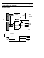
SA12 /F1N, /N1G, /S1G, /U1B
Super Audio CD Player
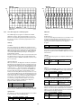
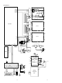
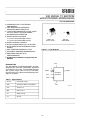
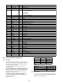
SUPER AUDIO CD PLAYER SA-12S1
VIDEO
OFF
DISPLAY
OFF
PLAY
D
STOP
PAUSE
FTS
PL
SOUND MODE
REPEAT
STANDBY
POWER
OPEN/CLOSE
TABLE OF CONTENTS
SECTION
PAGE
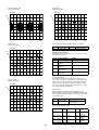
1. Technical specifications ................................................................................................................. 1
2. Warnings and laser safety............................................................................................................. 3
3. Service hints, Taking the disc out .................................................................................................. 5
4. Installing the software and entering version. ................................................................................. 8
5. Diagnostic software, Trouble shooting and test instructions........................................................ 10
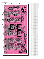
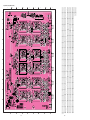
6. Wiring and block diagrams .......................................................................................................... 45
7. Schematic diagram and Parts location........................................................................................ 51
8. Exploded view and Parts list ..................................................................................................... 131
9. Circuit-, IC descriptions and list of abbreviations ...................................................................... 135
10. Electrical parts list ..................................................................................................................... 187
Please use this service manual with referring to the user guide ( D.F.U. ) without fail.
R
SA-12S1
413K855010 MIT
3120 785 22750
First Issue 2001.09
SA-12S1
Service
Manual
MARANTZ DESIGN AND SERVICE
Using superior design and selected high grade components, MARANTZ company has created the ultimate in stereo sound.
Only original MARANTZ parts can insure that your MARANTZ product will continue to perform to the specifications for which
it is famous.
Parts for your MARANTZ equipment are generally available to our National Marantz Subsidiary or Agent.
ORDERING PARTS :
Parts can be ordered either by mail or by Fax.. In both cases, the correct part number has to be specified.
The following information must be supplied to eliminate delays in processing your order :
1. Complete address
2. Complete part numbers and quantities required
3. Description of parts
4. Model number for which part is required
5. Way of shipment
6. Signature : any order form or Fax. must be signed, otherwise such part order will be considered as null and void.
USA
EUROPE / TRADING
AMERICAS
SUPERSCOPE TECHNOLOGIES, INC.
MARANTZ PROFESSIONAL PRODUCTS
2640 WHITE OAK CIRCLE, SUITE A
AURORA, ILLINOIS 60504 USA
PHONE : 630 - 820 - 4800
FAX
: 630 - 820 - 8103
AUSTRALIA
QualiFi Pty Ltd,
24 LIONEL ROAD,
MT. WAVERLEY VIC 3149
AUSTRALIA
PHONE : +61 - (0)3 - 9543 - 1522
FAX
: +61 - (0)3 - 9543 - 3677
NEW ZEALAND
WILDASH AUDIO SYSTEMS NZ
14 MALVERN ROAD MT ALBERT
AUCKLAND NEW ZEALAND
PHONE : +64 - 9 - 8451958
FAX
: +64 - 9 - 8463554
BRAZIL
MARANTZ EUROPE B.V.
P.O.BOX 80002, BUILDING SFF2
5600 JB EINDHOVEN
THE NETHERLANDS
PHONE : +31 - 40 - 2732241
FAX
: +31 - 40 - 2735578
MARANTZ AMERICA, INC.
INC
1100 MAPLEWOOD DRIVE
ITASCA, IL. 60143
USA
PHONE : 630 - 741 - 0300
FAX
: 630 - 741 - 0301
AUSTRALIA
TECHNICAL AUDIO GROUP PTY, LTD
558 DARLING STREET,
BALMAIN, NSW 2041,
AUSTRALIA
PHONE : 61 - 2 - 9810 - 5300
FAX
: 61 - 2 - 9810 - 5355
THAILAND
MRZ STANDARD CO.,LTD
746 - 754 MAHACHAI ROAD.,
WANGBURAPAPIROM, PHRANAKORN,
BANGKOK, 10200 THAILAND
PHONE : +66 - 2 - 222 9181
FAX
: +66 - 2 - 224 6795
TAIWAN
PAI- YUING CO., LTD.
6 TH FL NO, 148 SUNG KIANG ROAD,
TAIPEI, 10429, TAIWAN R.O.C.
PHONE : +886 - 2 - 25221304
FAX
: +886 - 2 - 25630415
JAPAN Technical
MARANTZ JAPAN, INC.
35- 1, 7- CHOME, SAGAMIONO
SAGAMIHARA - SHI, KANAGAWA
JAPAN 228-8505
PHONE : +81 42 748 1013
FAX
: +81 42 741 9190
PHILIPS DA AMAZONIA IND. ELET. ITDA
CENTRO DE INFORMACOES AO
CEP 04698-970
SAO PAULO, SP, BRAZIL
PHONE : 0800 - 123123(Discagem Direta Gratuita)
FAX
: +55 11 534. 8988
CANADA
LENBROOK INDUSTRIES LIMITED
633 GRANITE COURT,
PICKERING, ONTARIO L1W 3K1
CANADA
PHONE : 905 - 831 - 6333
FAX
: 905 - 831 - 6936
SINGAPORE
WO KEE HONG DISTRIBUTION PTE LTD
130 JOO SENG ROAD
#03-02 OLIVINE BUILDING
SINGAPORE 368357
PHONE : +65 858 5535 / +65 381 8621
FAX
: +65 858 6078
MALAYSIA
WO KEE HONG ELECTRONICS SDN. BHD.
SUITE 8.1, LEVEL 8, MENARA GENESIS,
NO. 33, JALAN SULTAN ISMAIL,
50250 KUALA LUMPUR, MALAYSIA
PHONE : +60 3 - 2457677
FAX
: +60 3 - 2458180
KOREA
MK ENTERPRISES LTD.
ROOM 604/605, ELECTRO-OFFICETEL, 16-58,
3GA, HANGANG-RO, YONGSAN-KU, SEOUL
KOREA
PHONE : +822 - 3232 - 155
FAX
: +822 - 3232 - 154
SHOCK, FIRE HAZARD SERVICE TEST :
CAUTION : After servicing this appliance and prior to returning to customer, measure the resistance between either primary AC
cord connector pins ( with unit NOT connected to AC mains and its Power switch ON ), and the face or Front Panel of product and
controls and chassis bottom.
Any resistance measurement less than 1 Megohms should cause unit to be repaired or corrected before AC power is applied, and
verified before it is return to the user/customer.
Ref. UL Standard No. 1492.
In case of difficulties, do not hesitate to contact the Technical
Department at above mentioned address.
010620MIT
1. Technical specifications
SACD/CD
Audio characteristics
Super Audio CD
CD
Channels
Frequency range
Frequency characteristics
6 channels (Max.)
2 Hz - 100 kHz
2 Hz - 50 kHz (-3 dB)
2 channels
2 Hz - 20 kHz
2 Hz - 20 kHz
Dynamic range
THD (1 kHz)
Analog output level
114 dB
0.0008 %
2.0 V
more than 100 dB
0.0013 %
2.0 V
Digital output
1 bit DSD
0.5 Vp-p (75 ohm)
-19 dBm
16 bit linear PCM
Output level (coaxial)
Output level (optical)
Format
Sampling frequency
Optical readout system
Laser type
2.8224 MHz
44.1 kHz
AlGaAs
AlGaAs
Wavelength
650 nm
780 nm
DVD/VCD
Video
Audio
Format
Horizontal
Format
Frequency characteristics
Dynamic range
THD (1 kHz)
Digital output
Video output
* Audio characteristics are for multi channel output.
MPEG1 (VCD) / MPEG2 (DVD)
resolution more than 500
PCM (16/20/24 bit, 48/96 kHz fs) / Dolby Digital / MPEG
2 Hz - 22 kHz (PCM 48 kHz), 2 Hz - 44 kHz (PCM 96 kHz)
114 dB (PCM 24 bit)
0.0013 % (PCM 24 bit)
PCM, Dolby Digital, DTS, MPEG (F, U version)
Composite / S / Components
Power Supply
N version.................................................................................................................................................AC 115/230 V, 60 Hz
S version .................................................................................................................................................AC 115/230 V, 60 Hz
F version ................................................................................................................................................... AC 100 V 50/60 Hz
U version........................................................................................................................................................ AC 120 V 60 Hz
Power consumption (N version) .......................................................................................................................................33 W
Power consumption (S, F, U version) ...............................................................................................................................30 W
Cabinet
Dimensions .......................................................................................................................... 458 (W) x 126 (H) x 379 (D) mm
Weight............................................................................................................................................................................. 11 kg
Operating temperatures ..................................................................................................................................+5 °C to +35 °C
Operating humidity............................................................................................................................. 5% - 90% (without dew)
Accessories
Remote control unit (RC-12SAS1).........................................................................................................................................1
Battery (AAA).........................................................................................................................................................................2
Stereo audio cable .................................................................................................................................................................3
Audio-Video cable ..................................................................................................................................................................1
Remote control cord...............................................................................................................................................................1
Users guide............................................................................................................................................................................1
AC power cord .......................................................................................................................................................................1
Registration card (N, F, U version) .........................................................................................................................................1
1
SCART CONNECTOR
SCART II (connected to TV)
Pin signals:
1 Output
Audio R
2 Input
Audio R
3 Output
Audio L
4
Audio GND
5
Blue/Chroma GND
6 Input
Audio L
7 Bi-dir
Blue out/Chroma in
8 Output
Function switch
9
10
11
12
13
14
15
Green GND
not connected
Output
Green
not connected
Red/Chroma GND
fast switch GND
Output
Red out/Chroma out
16
Output
17
18
19
20
21
Output
Input
fast switch RGB/CVBS or Y
Y/CVBS GND
fast switching GND
CVBS/Y/RGB sync
CVBS/Y
Shield
SCART I (connected to AUX)
Pin signals:
1 Output
Audio R
2 Input
Audio R
3 Output
Audio L
4
Audio GND
5
Blue/Chroma GND
6 Input
Audio L
7 Bi-dir
Blue in/Chroma out
8 Input
Function switch
9
Green GND
10 not connected
11 Input
Green
12 not connected
13
Red/Chroma GND
14
fast switch GND
15 Output
Red in/Chroma in
16 Input
fast switch RGB/CVBS or Y
17
CVBS GND
18
fast switching GND
19 Output
CVBS/Y/RGB sync
20 Input
CVBS/Y
21
Shield
1.8 Vrms
1.8 Vrms
0.7 Vpp +/- 0.1 V into 75 Ohm (*)
< 2 V = TV
> 4.5 V / < 7 V = asp. Ratio 16:9 DVD
> 9.5 V / < 12 V = asp. ratio 4:3 DVD
0.7 Vpp +/- 0.1 V into 75 Ohm (*)
0.7 Vpp +/- 0.1 V into 75 Ohm (*)
+/- 3 dB 0.3 Vpp Chroma (burst)
< 0.4 V into 75 Ohm = CVBS
> 1 V / < 3 V into 75 Ohm = RGB
1 Vpp +/- 0.1 V into 75 Ohm (*)
1.8 Vrms
1.8 Vrms
+/- 3 dB 0.3 Vpp Chroma (burst)
1 Vpp +/- 0.1 V into 75 Ohm (*)
(*) for 100% white
2
2.
Warnings and laser safety
2.1
Warning and laser safety
GB
WARNING
NL
All ICs and many other semi-conductors are
susceptible to electrostatic discharges (ESD).
Careless handling during repair can reduce
life drastically.
When repairing, make sure that you are
connected with the same potential as the
mass of the set via a wrist wrap with
resistance.
Keep components and tools also at this
potential.
F
WAARSCHUWING
Alle IC’s en vele andere halfgeleiders zijn
gevoelig voor elektrostatische ontladingen
(ESD).
Onzorgvuldig behandelen tijdens reparatie
kan de levensduur drastisch doen
verminderen.
Zorg ervoor dat u tijdens reparatie via een
polsband met weerstand verbonden bent met
hetzelfde potentiaal als de massa van het
apparaat.
Houd componenten en hulpmiddelen ook op
ditzelfde potentiaal.
D
ATTENTION
Tous les IC et beaucoup d’autres semiconducteurs sont sensibles aux décharges
statiques (ESD).
Leur longévité pourrait être considérablement
écourtée par le fait qu’aucune précaution
n’est prise a leur manipulation.
Lors de réparations, s’assurer de bien être
relié au même potentiel que la masse de
l’appareil et enfiler le bracelet serti d’une
résistance de sécurité.
Veiller a ce que les composants ainsi que les
outils que l’on utilise soient également a ce
potentiel.
WARNUNG
I
Alle IC und viele andere Halbleiter sind
empfindlich gegen elektrostatische
Entladungen (ESD).
Unsorgfältige Behandlung bei der Reparatur
kann die Lebensdauer drastisch vermindern.
Sorgen sie dafür, das Sie im Reparaturfall
über ein Pulsarmband mit Widerstand mit
dem Massepotential des Gerätes verbunden
sind.
Halten Sie Bauteile und Hilfsmittel ebenfalls
auf diesem Potential.
AVVERTIMENTO
Tutti IC e parecchi semi-conduttori sono
sensibili alle scariche statiche (ESD).
La loro longevita potrebbe essere fortemente
ridatta in caso di non osservazione della piu
grande cauzione alla loro manipolazione.
Durante le riparazioni occorre quindi essere
collegato allo stesso potenziale che quello
della massa dell’apparecchio tramite un
braccialetto a resistenza.
Assicurarsi che i componenti e anche gli
utensili con quali si lavora siano anche a
questo potenziale.
D
GB
Bei jeder Reparatur sind die geltenden Sicherheitsvorschriften zu beachten.
Der Originalzustand des Gerats darf nicht verandert werden.
Fur Reparaturen sind Original-Ersatzteile zu verwenden.
Safety regulations require that the set be restored to its original condition
and that parts which are identical with those specified be used.
NL
I
Veiligheidsbepalingen vereisen, dat het apparaat in zijn oorspronkelijke
toestand wordt terug gebracht en dat onderdelen, identiek aan de
gespecifieerde worden toegepast.
Le norme di sicurezza esigono che l’apparecchio venga rimesso nelle
condizioni originali e che siano utilizzati pezzi di ricambiago idetici a quelli
specificati.
F
Les normes de sécurité exigent que l’appareil soit remis a l’état d’origine et
que soient utilisées les pièces de rechange identiques à celles spécifiées.
SHOCK, FIRE HAZARD SERVICE TEST:
CAUTION: After servicing this appliance and prior to returning to customer, measure the resistance between
either primary AC cord connector pins (with unit NOT connected to AC mains and its Power switch ON), and the
face or Front Panel of product and controls and chassis bottom,
Any resistance measurement less than 1 Megohms should cause unit to be repaired or corrected before AC
power is applied, and verified before return to user/customer.
Ref.UL Standard NO.1492.
NOTE ON SAFETY:
Symbol : Fire or electrical shock hazard. Only original parts should be used to replace any part with symbol
Any other component substitution(other than original type), may increase risk or fire or electrical shock hazard.
“Pour votre sécurité, ces documents
doivent être utilisés par des
spécialistes agrées, seuls habilités à
réparer votre appareil en panne.”
3
2.2 LASER SAFETY
This unit employs a laser. Only a qualified service person should remove the cover or attempt to service this
device, due to possible eye injury.
LASER DEVICE UNIT
Type:
Wave length:
Output Power:
Beam divergence:
SemiconductorlaserGaAlAs
650 nm (DVD)
780 nm (VCD/CD)
7 mW (DVD)
10 mW (VCD/CD)
60 degree
USE OF CONTROLS OR ADJUSTMENTS OR PERFORMANCE OF PROCEDURE OTHER THAN THOSE
SPECIFIED HEREIN MAY RESULT IN HAZARDOUS RADIATION EXPOSURE.
AVOID DIRECT EXPOSURE T O BEAM
WARNING
The use of optical instruments with this product will increase eye hazard.
Repair handling should take place as much as possible with a disc loaded inside the player
WARNING LOCATION: INSIDE ON LASER COVERSHIELD
CAUTION VISIBLE AND INVISIBLE LASER RADIATI ON WHEN OPEN AVO ID EXPOSURE TO BEAM
ADVARSEL SYNLIG OG USYNLIG LASERSTRÅLING VED ÅBNING UNDGÅ UDSÆTTELSE FOR STRÅLING
ADVARSEL SYNLIG OG USYNLIG LASERSTRÅLING NÅR DEKSEL ÅPNES UNNGÅ EKSPONERING FOR STRÅLEN
VARNING SYNLIG OCH OSYNLIG LASERSTRÅLNING NÄR DENNA DEL ÄR ÖPPNAD BETRAKTA EJ STRÅLEN
VARO! AVATT AESSA OLET ALTTIINA NÄKYVÄLLE JA NÄKYMÄTT ÖMÄLLE LASER SÄTEILYLLE. ÄLÄ KAT SO SÄT EESEEN
VORSICHT SICHTBARE UND UNSICHTBARE LASERSTRAHLUNG WENN ABDECKUNG GEÖFFNET NICHT DEM STRAHL AUSSETSEN
DANGER VISIBLE AND INVISIBLE LASER RADIATI ON WHEN OPEN AVO ID DIRECT EXPOSURE TO BEAM
AT TENTION RAYO NNEMENT LASER VISIBLE ET INVISIBLE EN CAS D'OUVERTURE EXPOSITION DANGEREUSE AU FAISCEAU
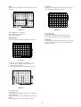
Warning for powersupply on position (PH16)
The primary side of the powersupply including the heatsink carries live mains voltage when the
player is connected to the mains even when the player is swiched off !
This primary area is not shielded so it is possible to touch copper tracks and/or components when
servicing the player. Service personnel have to take precautions to prevent touching this area or
components in this area .
The primary side of the powersupply has been indicated with a lightning stroke and a stripe-marked
printed on the printed wiring board
Note:
The screws on the mechanism of the ASD1 module (position 001M in on the exploded view drawing)
may never be touched removed or re-adjusted.
Handle the ASD1 module with care when the unit has to be exchanged!
The mechanism of the ASD1 module is very sensative for dropping or shocks.
4
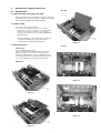
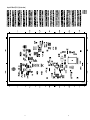
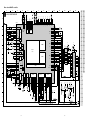
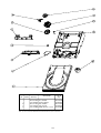
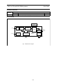
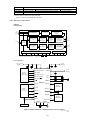
3.
Service hints, Taking the disc out
3.1
Service hints
DAC PCB
3.1.1 Switched Mode Power Supply Unit PZ03
This power supply unit is not repairable and must be exchanged
completely in case of failure. A new power supply can be ordered
with codenumber QW12922150 (3104 129 22150).
3.1.2 SACD module
This module can be repaired as follows:
1. The loader and DVD-M(echanism) is one assembly
(VAL6011) item 81. This assembly is a not repairable unit
and must be exchanged completely in case of failure.
A new unit can be ordered with codenumber QE02361104
(9305 023 61104).
2. The mono board has to be repaired down to component
level. Repair handling of the monoboard requires a
workshop with sophisticated desoldering tools.
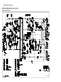
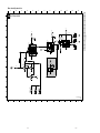
CL 06532152_004.eps
051200
Figure 3-3
3.1.3 Service positions
AV PCB
SACD module
See also dismantling instructions.
After demounting the DAC PCB PP16 and the dust bracket
023M, it is possible to connect the PC connection and to
demount the SACD module to service the MONO PCB. After
remounting the DAC PCB, the SACD module can be placed
on top of the DAC PCB, protected by an insulation plate.
MONO PCB
CL 06532152_005.eps
051200
Figure 3-4
CL 06532152_002.eps
051200
Figure 3-1
CL 06532152_006.eps
051200
Figure 3-5
CL 06532152_003.eps
051200
Figure 3-2
5
Display board PY16
⇒
12
5128
→
⇒
6
⇒
⇒
→
Dust Bracket 023M
⇒
5110
⇒
5128
⇒
⇒
⇒
⇒
⇒
⇒
⇒
⇒
5128
(mono board PZ01 → loader 001M)
Manually opening of tray
When it is not possible to open the tray with the open/ close button,
the tray can manually be opened.
When no disc is loaded, unlock the tray by moving the slide from the left
to the right and pull tray outwards.
Remove 4 screws to remove loader.
Transformer L001
⇒
5129 x 2 and 5126 x 2
→
⇒
Linear power supply PH16
⇒
⇒ Remove 2 screws 5128
(board → frame)
⇒ Remove 2 screws 5128
(mains inled → backplate)
⇒ Remove 2 screws 5128
(voltage selector → backplate)
⇒ Release the snaps of 2 spacers
012G(board → frame)
⇒ Demount the board
Switched mode power supply unit PZ03
⇒
⇒
→
5110 x 3 and 5128 x 2
⇒
Loader VAL6011/04 : 001M
⇒
(loader 001M frame 020M)
(dust cover on loader 001M)
SACD MODULE (001M + PZ01)
⇒
DAC PCB PP16
⇒
Side cover 006D
005D x 8 at top
009D x 8 at both side
Top cover
⇒ Remove 001D and
SACD Mono board PZ01
⇒
⇒
⇒
⇒
A/V board PN16
⇒
ON/OFF BOARD PY26
⇒
5128
→
Front assy(001B+PY16+PY26)
⇒ open the tray and remove the
tray front 046B
⇒
→
020M
⇒ remove 2 screws 005G
(front side Legs 004G)
DISMANTLING INSTRUCTIONS
3.1.4. Mechanical- and dismantling instructions
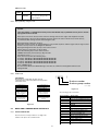
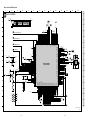
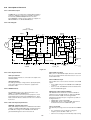
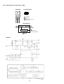
3.2 Taking the disc out.
1. Remove the top cover with 8 screws.
2. Remove the both side covers with 8 screws.
3. Remove the 8 screws of front panel and unfasten 2 screws of front legs.
4. Pull out the front panel.
5. Turn right the pulley by your finger or nail. (See fig.1)
6. Then the tray is moved a little. Pull the tray with your hand at this time.
Note: Take care of unhurt gear belt.
Gear pulley
7
4. Installing the software and entering version.
The kind of CD-ROM (software), and explanation
a) Key reassignment Disc (44444444.016) [Parts No. *SA12KEYCD]
b) Background (PAL) Disc (11111111.008) [Parts No. *SA12PALCD]
c) Background (NTSC) Disc (22222222.008) [Parts No. *SA12NTSCD]
Installing necessary CD-ROM for version.
For /N: Key reassignment Disc (44444444.016) and Background (PAL) Disc (11111111.008)
For /S: Key reassignment Disc (44444444.016) and Background (PAL) Disc (11111111.008)
For /U: Key reassignment Disc (44444444.016) and Background (NTSC) Disc (22222222.008)
For /F: Key reassignment Disc (44444444.016) and Background (NTSC) Disc (22222222.008)
How to installing the software
All software is installed from CD-ROM. These are supplied by another disc, respectively. When disc was put in the player,
software is installed automatically. And disc comes out of the player, after finished. The sequence to install is “Key
reassignment” first and, next, is “Background”.
Entering Version and region code
Caution: This information is confidential and may not be distributed. Only a qualified service person should reprogram the mono board.
Reprogramming is limited to 25 times.
When the counter reaches 25, reprogramming is not possible anymore and the region code change counter
must be reset by means of the Diagnostic Software.
Reprogramming will be done by way of the remote control.
Put the player in stop mode, no disc loaded.
Press the following keys on the remote control.
<PLAY> followed by numerical keys <2>, <7>, <4>
The display shows “-----------“
Press now successively the following keys
For /N: <0>, <0>, <1>, <0>, <0>, <0>, <0>, <0>, <0>, <0>, <0>
For /U: <0>, <0>, <2>, <0>, <0>, <0>, <0>, <0>, <0>, <0>, <0>
For /S: <0>, <0>, <3>, <0>, <0>, <0>, <0>, <0>, <0>, <0>, <0>
For /F: <0>, <0>, <4>, <0>, <0>, <0>, <0>, <0>, <0>, <0>, <0>
Press <PLAY> again.
The TV screen will become blue during a short time to confirm that the digital board has been reprogrammed.
How to confirm the software and the version.
11111111.008/ 22222222.008: Displayed on TV screen as background of marantz is OK, after entering version.
44444444.016:
Version:
If a power supply is turned on, with <STOP> and <NEXT> of a player pushed, a change of NTSC mode
and PAL mode can be performed.
Worked <DISPLAY OFF> or <VIDEO OFF> of the player is OK, After entered version.
Looked at “Audio language” or “Subtitle language” in “Personal preferences”.
The contents of “Audio language” or “Subtitle language” are as the following table.
8
/N
English
/U
English
/S
English
/F
Japanese
Español
Français
Português
Español
Français
Português
Español
Français
Português
English
Español
Français
Italiano
Deutsch
Italiano
Russian
Russian
Japanese
Português
Russian
Nederlands
Suomeksi
Dansk
Deutsch
Greek
Japanese
Korean
Chinese
Bahamas Indonesia
Korean
Chinese
Bahamas Indonesia
Norsk
Svenska
Russian
Korean
Chines
Quechua
Khmer
Bahamas Malayalam
Burmese
Khmer
Bahamas Malayalam
Burmese
Greek
TÜrkçe
Íslensk
Guarani
Nepal
Nepal
Aymara
Inupiaq
Thai
Vietnamese
Thai
Vietnamese
Tibetan
Tibetan
Català
Default setting
Reset of Personal preferences
Turned on power of the player, while depressing <PLAY> and <OPEN/CLOSE> button, reset of personal preferences can be
performed.
Setting of menu
TV mode
Black level shift
Remote control code
/N
PAL
ON
DVD1
/U
NTSC
ON
DVD1
/S
PAL
OFF
DVD1
/F
NTSC
OFF
DVD1
Black level shift is in “PICTURE” of “Personal Preferences”. It becomes ON if it resets.
How to change a remote control code is as follows. (CODE DVD1/ CODE DVD2)
By remote controller:
Press <DISPLAY> and <1> become code DVD1.
By player:
Press <DISPLAY> and <2> become code DVD2.
Turned on power of the player, while depressing <SOUND MODE> and <OPEN/CLOSE> button.
Position of switches
Filter (SD71)
RC-6 (SF51)
/N
/U
/S
Voltage Selector (SH02)
230V
115V
230V
Position 1
Position 1
Position 1
Internal
Internal
Internal
/F
115V
Position 1
Internal
9
5.
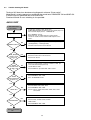
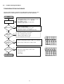
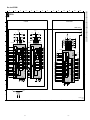
Diagnostic software, trouble shooting and test instructions
Due to the complexity of the SACD player, the time to find a
defect in the player can become long. To reduce this time, the
player has been equipped with Diagnostic and Service
software (DS). The DS offers functionality to diagnose the
SA-12S1 player hardware and tests the following:
• Interconnections between components
• Accessibility of components
• Functionality of the audio and video paths
This functionality can be accessed via several interfaces:
1. End user/Dealer script interface
2. Player script interface
3. Menu and command interface
5.1
END USER/DEALER SCRIPT INTERFACE
5.1.1
Description
Nucleus Nucleus name
number
Host Decoder SDRAM Write Read
Host Decoder I2C NVRAM
Front Panel Echo
Basic Engine Echo
Furore SDRAM Low Write Read
Furore SDRAM High Write Read
DAC Board I2C Test
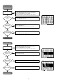
Switch player off.
Hold 2 keys
<OPEN/CLOSE> + <PAUSE>
simultaneously pressed and
switch player on.
During the test, the following display
is shown: the counter counts down
from the number of nuclei to be run
before the test finishes. Example:
SET O.K.?
Description
Structure of the Player Script
The player script consists of a set of nuclei testing the
hardware modules in the SACD player: the Display PWB, the
Digital PWB, the Basic Engine, the DAC PWB and the AV
PWB.
Nuclei run by the player test need some user interaction; in
the next table this interaction is described. The player test is
done in two phases:
Interactive tests: this part of the player test depends
strongly on user interaction and input to determine
nucleus results and to progress through the full test.
Reading the error log information can be useful to
determine any errors that occurred recently during
normal operation of the DVD player.
The loop test will perform the same nuclei as the dealer
test, but it will loop through the list of nuclei indefinitely.
The End use/Dealer script executes all diagnostic nuclei that
do not need any user interaction and are meaningful on a
standalone SACD player. The nuclei called in the End user/
Dealer script are the following:
104
123
500
601
1200
1201
1300
5.2.1
5.2.2
Contents
Display
Countdown
7
6
5
4
3
2
1
PLAYER SCRIPT INTERFACE
The Player script will give the opportunity to perform a test
that will determine which of the SACD player’s modules are
faulty, to read the error log and to perform an endurance loop
test. To successfully perform the tests, the SACD player
must be connected to a TV set, a multi-channel amplifier, a
set of 6 boxes and an external video source to check the
output of a number of nuclei.
To be able to check results of certain nuclei, the player script
expects some interaction of the user (i.e. to approve a test
picture or a test sound). Some nuclei (e.g. nuclei that test
functionality of the Basic Engine module) require that the
SACD player itself is opened, to enable the user to observe
moving parts and approve their movement visually.
Only tests within the scope of the diagnostic software will be
executed hence only faults within this scope can be detected.
The End user/Dealer script interface gives a diagnosis on a
stand alone SACD player; no other equipment is needed.
During this mode, a number of hardware tests (nuclei) are
automatically executed to check if the player is faulty. The
diagnosis is simply a "fail" or "pass" message. If the message
"FAIL" appears on the display, there is apparently a failure in
the player. If the message "PASS" appears, the nuclei in this
mode have been executed successfully. There can be still a
failure in the player because the nuclei in this mode don't
cover the complete functionality of the player.
5.1.2
5.2
NO
YES
To exit DEALER SCRIPT, switch player off.
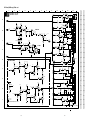
CL 06532152_007.eps
051200
Figure 5-1
10
Step Description
1
2
3
4
5
6
7
8
9
10
11
12
13
14
15
16
17
18
19
20
21
22
23
24
25
26
27
28
29
30
31
32
33
34
35
36
37
38
39
40
41
42
43
44
45
46
47
48
49
50
51
52
Executing
nucleus
Press OPEN/CLOSE and STOP, and turn on the player.
2
Display shows "FP SEGMENT". Press PLAY to execute this nucleus. Otherwise press NEXT and go to step 7. 502
Starbursts are visible. Press PLAY.
502
Horizontal bars are visible. Press PLAY.
502
Vertical bars are visible. Press PLAY.
502
All segments are visible. Press PLAY.
502
Display shows "FP LABEL". Press PLAY to execute this nucleus. Otherwise press NEXT and go to step 13. 503
Labels of the first grid are visible. Press PLAY.
503
Labels of the second grid are visible. Press PLAY.
503
Labels of the third grid are visible. Press PLAY.
503
All labels are visible. Press PLAY.
503
Standby LED is on. Press PLAY.
503
Display shows "FP DIMMER". Press PLAY to execute this nucleus. Otherwise press NEXT and go to step 15. 518
Display shows "DIMMING TEST". Wait until it is dimmed, and press than PLAY.
518
Display shows "FP KEYBOARD". Press PLAY to execute this nucleus. Otherwise press NEXT and go to step 505
17.
Display shows "LKB_0000 N 0". Press all keys at least one time. Press PLAY for a least one-second to exit 505
this nucleus.
Display shows "FP REMOTE C". Press PLAY to execute this nucleus. Otherwise press NEXT and go to step 506
19.
Display shows "RC C_ N_ 0". Press at least one key of the remote control. Press PLAY to exit this nucleus. 506
Display shows "SCART-SW DVD". Press PLAY to execute this nucleus. Otherwise press NEXT.
1408
Display shows "COLOUR SETUP". Press PLAY to execute this nucleus. Otherwise press NEXT.
1406
Display shows "COLOUR-B ON". Press PLAY to execute this nucleus. Otherwise press NEXT.
120
Display shows "PINKNOISE ON". Press PLAY to execute this nucleus. Otherwise press NEXT.
115
Display shows "COLOUR-B OFF". Press PLAY to execute this nucleus. Otherwise press NEXT.
121
Display shows "PINKNOIS OFF". Press PLAY to execute this nucleus. Otherwise press NEXT.
116
Display shows "SINE ON". Press PLAY to execute this nucleus. Otherwise press NEXT and go to step 27.
117
Display shows "BUSY". To stop this nucleus, press STOP.
117
Display shows "SCART-S PASS". Press PLAY to execute this nucleus. Otherwise press NEXT.
1409
Display shows "BE RESET". Press PLAY to execute this nucleus. Otherwise press NEXT.
603
Display shows "BE VERSION". Press PLAY to execute this nucleus. Otherwise press NEXT and go to step 31. 602
Display shows the version of the basic engine. To stop this nucleus, press PLAY.
602
Display shows "BE TRAY OPEN". Press PLAY to execute this nucleus. Otherwise press NEXT.
616
Display shows "BE TRAY CLOSE". Press PLAY to execute this nucleus. Otherwise press NEXT.
615
Display shows "BE DVD LASER". Press PLAY to execute this nucleus. Otherwise press NEXT.
635
Display shows "BE CD LASER". Press PLAY to execute this nucleus. Otherwise press NEXT.
636
Display shows "BE LASER OFF". Press PLAY to execute this nucleus. Otherwise press NEXT.
637
Display shows "BE FOCUS ON". Press PLAY to execute this nucleus. Otherwise press NEXT.
604
Display shows "BE FOCUS OFF". Press PLAY to execute this nucleus. Otherwise press NEXT.
605
Display shows "BE DISCM ON". Press PLAY to execute this nucleus. Otherwise press NEXT.
606
Display shows "BE DISCM OFF". Press PLAY to execute this nucleus. Otherwise press NEXT.
607
Display shows "BE RADIAL ON". Press PLAY to execute this nucleus. Otherwise press NEXT.
608
Display shows "BE RADIAL OF". Press PLAY to execute this nucleus. Otherwise press NEXT.
609
Display shows "BE SLEDG OUT". Press PLAY to execute this nucleus. Otherwise press NEXT.
611
Display shows "BE SLEDGE IN". Press PLAY to execute this nucleus. Otherwise press NEXT.
610
Display shows "BE GROOVE IN". Press PLAY to execute this nucleus. Otherwise press NEXT.
612
Display shows "BE GROOV MID". Press PLAY to execute this nucleus. Otherwise press NEXT.
613
Display shows "BE GROOV OUT". Press PLAY to execute this nucleus. Otherwise press NEXT.
614
Display shows "BE RESET". Press PLAY to execute this nucleus. Otherwise press NEXT.
603
Display shows "BE TRAY OPEN". Press PLAY to execute this nucleus. Otherwise press NEXT.
616
Display shows "BE TRAY CLOSE". Press PLAY to execute this nucleus. Otherwise press NEXT.
615
Display shows "ERRORLOG". Press PLAY to execute this nucleus. Otherwise press NEXT and go to step 52. 404
Display shows the error codes. With the keys NEXT and PREV it is possible to step through the error codes. 404
To stop this nucleus, press STOP.
Display shows "PASS", this means the Player Script is finished and the execution of the User Dealer Script is 1
started in an endless loop. The execution of the User Dealer Script will only stop, when an error occurs. The
Display shows the error code.
Remark
In case of failure, the display shows " FAIL 00000 ". The
description of the shown error code can be retrieved in the
survey of Nuclei Error Codes (paragraph 5.4). Once an error
occurs, it is not possible to continue the player script. Switch
off the set and restart the player script. By pressing the NEXT
key, it is possible to jump over the failure and to continue the
player script.
11
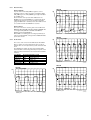
Figure 5-2
12
PRESS <PLAY> IF OK
PRESS <PREV> IF NOT OK
LED
PRESS <PLAY> IF OK
PRESS <NEXT> TO ABORT
PRESS <PLAY> IF OK
PRESS <NEXT> TO ABORT
<NEXT>
PRESS <PLAY>
TO START TEST
PRESS <PLAY> IF OK
PRESS <PREV> IF NOT OK
FRONT KEY NAME
PRESS <PLAY> IF OK
PRESS <PREV> IF NOT OK
PRESS <PLAY> IF OK
PRESS <NEXT> TO ABORT
PRESS <PLAY> IF OK
PRESS <NEXT> TO ABORT
PRESS <PLAY> IF OK
PRESS <NEXT> TO ABORT
PRESS <PLAY>
TO START TEST
PRESS <PLAY> IF OK
PRESS <NEXT> TO ABORT
<NEXT>
PRESS <PLAY> IF OK
PRESS <NEXT> TO ABORT
PRESS <PLAY>
TO START TEST
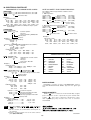
FRONTPANEL TEST
Hold 2 keys
<OPEN/CLOSE> + <STOP>
simultaneously pressed and
switch player on.
Switch player off.
<NEXT>
XX TIMES
PRESSED
TO EXIT TEST:
PRESS <PLAY> MORE THAN 1S IF TEST IS OK
PRESS <PREV> MORE THAN 1S IF TEST IS NOT OK
PRESS ALL KEYS AT LEAST ONCE
SEE TABLE FOR KEY CODES
HEXADECIMAL
KEY CODE
PRESS <PLAY>
TO START TEST
<NEXT>
PRESS <PLAY>
TO START TEST
XX TIMES
PRESSED
<NEXT>
PRESS AT LEAST ONE KEY
ON THE REMOTE CONTROL
SEE TABLE FOR RC KEY CODES
HEXADECIMAL
RC-KEY-CODE
TO EXIT TEST: PRESS ONE OF FOLLOWING KEYS
ON THE LOCAL KEYBOARD
PRESS <PLAY> IF TEST IS OK
PRESS <PREV> IS NOT OK
RC KEY NAME
RC KEY CODE
TV POWER
SACD POWER
STOP
SOUND MODE
PLAY
REVERSE
PAUSE
SLOW
FORWARD
PREVIOUS
RESUME
NEXT
MENU DISC
MENU SYSTEM
UP
LEFT
RIGHT
DOWN
RETURN
OK
ZOOM
ANGLE
0
1
2
3
4
5
6
7
8
9
T
C
FTS
SHUFFLE
SUBTITLE
AUDIO
DIM
DISPLAY
REPEAT A-B
SCAN
VOL +
VOL CH +
CH MUTE
ONLY FOR TV
0C
31
50
2C
29
30
22
28
21
D7
20
54
0F
58
5A
5B
59
83
5C
F7
85
00
01
02
03
04
05
06
07
08
09
C9
CA
FB
1C
4B
4E
13
48
3B
2A
ONLY FOR TV
ONLY FOR TV
ONLY FOR TV
ONLY FOR TV
ONLY FOR TV
PLAY
PAUSE
STOP
OPEN/CLOSE
SOUND MODE
REPEAT
PREV
NEXT
FRONT KEY CODE
0200
0400
0800
0008
1000
4000
0004
0002
DIGITAL BOARD
TEST
Figure 5-3
13
FRONTPANEL
TEST
press <PLAY> to execute
press <NEXT > to skip
press <STOP> to continue
press <PLAY> to execute
press <NEXT > to skip
press <PLAY> to execute
press <NEXT > to skip
press <PLAY> to execute
press <NEXT > to skip
press <PLAY> to execute
press <NEXT > to skip
press <PLAY> to execute
press <NEXT > to skip
press <PLAY> to execute
press <NEXT > to skip
press <PLAY> to execute
press <NEXT > to skip
DIGITAL BOARD
TEST
ENDLESS LOOP
<NEXT >
press <PLAY> to execute
press <NEXT > to skip
Switch player off to end test.
press <NEXT > to skip
press <PLAY> to execute
press <NEXT > to skip
BASIC ENGINE
TEST
ERROR
<PLAY>
PRESS <PREV>
TO STEP BACK
press <PLAY> to execute
press <NEXT > to skip
press <PLAY> to execute
press <NEXT > to skip
press <PLAY> to execute
press <NEXT > to skip
press <PLAY> to execute
press <NEXT > to skip
press <PLAY> to execute
press <NEXT > to skip
press <PLAY> to execute
press <NEXT > to skip
press <PLAY> to execute
press <NEXT > to skip
press <PLAY> to execute
press <NEXT > to skip
press <PLAY> to execute
PRESS <STOP> TO CONTINUE
PRESS <NEXT>
TO STEP UP
press <PLAY> to execute
press <NEXT > to skip
press <PLAY> to execute
press <NEXT > to skip
press <PLAY> to execute
press <NEXT > to skip
press <PLAY> to execute
press <NEXT > to skip
press <PLAY> to execute
press <NEXT > to skip
press <PLAY> to execute
press <NEXT > to skip
press <PLAY> to continue
press <PLAY> to execute
press <NEXT > to skip
press <PLAY> to execute
press <NEXT > to skip
press <PLAY> to execute
press <NEXT > to skip
press <PLAY> to execute
press <NEXT > to skip
5.2.3
Errorlog
Error
Error name
Number
0109
S2B_SBC_NO
T_FOUND
010A
S2B_TRAY
Explanation:
The application errors will be logged in the NVRAM. The
maximum number of error bytes that will be visible is 16. The
first word (4 digits) of the byte is the component identification;
the last word is the error code.
The diagnostics software will present a combination of this
component identification plus an error code on the local
display (and on the attached terminal). The last reported
error is shown as < 00000000, the oldest visible error as
00000000> and the errors in between as < 00000000 >.
The devices that may report errors are the serial controller
(UART), the basic engine (BE), the slave processor (SLPH),
the SACD Stream Manager (SSM) and the SACD Media
Access (SMA). The identification of these components is as
follows:
Component name
Serial controller (UART)
Engine (BE)
Slave Processor (SLPH)
SACD Stream Manager (SSM)
SACD Media Access (SMA)
Diagnostic software (DS)
010B
010C
010D
010E
01F0
Component identification
000A
0016
001A
001C
002E
Dxxx
01F1
01F2
01F3
The tables in the next chapters list the error code and
corresponding problem. The column ‘Explanation’ holds a
more elaborate description and the most likely reason for the
error.
01F4
Requested subcode item could
not be found.
Tray could not be opened or
closed completely.
S2B_TOC_RE TOC could not be read within
AD
timeout period.
S2B_JUMP
Requested seek could not be
performed.
S2B_NON_EX Attempt to access a non-existing
IST_SES
session.
S2B_NON_EX
IST_BCA
S2B_OVERR Too many bytes received over
UN
S2B
Reas on:
see
S2B_ILL_COMMAND error
S2B_COMM_ Not enough bytes are received
TO
over
S2B
Reason:
see
S2B_ILL_COMMAND error
S2B_PARITY Byte received with parity error.
Reason:
see
S2B_ILL_COMMAND error
S2B_ILL_PHA CMD IDC is not valid, transmisSE
sion out of sync. Reason: see
S2B_ILL_COMMAND error
S2B_ILL_NR_ Byte count has an illegal value.
OF_BYTES
Reason:
see
S2B_ILL_COMMAND error
SLPH error codes
Some examples:
002E0000 ( SMA reported a timeout error
0016010A ( Engine could not fully close or open the tray
D0010001 ( Flash checksum failed (for other DS errors, see
description of nucleui error codes in paragraph 5.4.
Error
Error name
Number
0000
COMMUNICATION
UART error codes
Error
Error
Explanation
Number name
0000
BUF_OVE To many characters were offered in
RFLOW
too little time. Reason: system was
too busy doing other jobs.
0001
COMMU- Usually a protocol error. Reason:
NICATION bad connection between engine
and processor.
0102
S2B_ILL_PAR
AM
0103
S2B_SLEDGE
0104
0105
S2B_FOCUS
S2B_MOTOR
0106
S2B_RADIAL
0107
S2B_PLL_LO
CK
SBC_HEADE
R_TO
0108
Explanation
Error in I2C communication.
Reason: bad connection between slave processor and main
processor.
SSM error codes
Error
Code
0006
BE errors
Error
Error name
Number
0101
S2B_ILL_CO
MMAND
Explanation
0007
Explanation
Parameter(s) not valid for this
command. Reason: some communication problem between
UART and engine.
Command not allowed in this
state or unknown. Reason: see
S2B_ILL_COMMAND error
Sledge could not be moved to
home position.
Focus failure
Motor could not reach speed
within timeout
Servo didn't get on track after
several retries.
PLL could not lock in Accessing
or Tracking state
Header timeout
0008
0009
000A
000B
14
Error name
SP_SYNCER
ROR
Explanation
System cannot get synchronised
with sectors coming from disc.
Reason: Usually a damaged
disc or the player was dropped/
pushed during operation. If not,
the engine is malfunctioning.
SP_EDCERR Data coming from disc is damOR
aged.
Reason:
see
SP_SYNCERROR
SP_CONTINU Sequence of sectors coming
ITYERROR
from disc is incorrect. Reason:
see SP_SYNCERROR
DMX_CONTI Sequence of sectors is incorrect.
NUITYERReason: problem with buffer
ROR
RAM
LLD_ERROR An illegal audio format was offered to the decoder. Reason:
unknown audio type on disc or
problem with buffer RAM
BCU_ERROR Internal problem in Furore chip
SMA error codes
Error
Error name
Number
0000
SMA_TIMEO
UTERROR
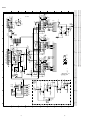
5.2.4
Explanation
Data coming from disc not in
time. Reason: damaged disc or
engine problem.
Reprogramming of region code
Caution
This information is confidential and may not be distributed. Only a qualified service person should
reprogram the mono board.
After repair of the mono board, all the customer settings and also the region code might be lost (P0).
Reprogramming of the mono board will put the player back in the state in which it has left the factory,
i.e. with the default settings and the allowed region code.
Reprogramming is limited to 25 times.
When the counter reaches 25, reprogramming is not possible anymore and the region code change counter
must be reset by means of the Diagnostic Software.
Reprogramming will be done by way of the remote control.
Put the player in stop mode, no disc loaded.
Press the following keys on the remote control:
<PLAY> followed by numerical keys <2> <7> <4>
The display shows: “- - - - - - - - - - -”
Press now successively the following keys :
for /N(P1): <0><0><1> <0><0><0><0><0><0><0><0><0>
for /U(P2): <0><0><2> <0><0><0><0><0><0><0><0><0>
for /S(P3): <0><0><3> <0><0><0><0><0><0><0><0><0>
for /F(P4): <0><0><4> <0><0><0><0><0><0><0><0><0>
Press <PLAY> again.
The TV screen will become BLUE during a short time to confirm that the digital board has been
reprogrammed.
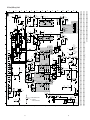
Figure 5-4
5.2.5
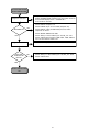
Trade mode
[ XX YY
]
TRADE MODE
When the player is in Trade Mode, the player cannot be
controlled by means of the front key buttons, but only by means
of the remote control.
IF TRADE MODE OFF
Nucleus number
Nucleus group number
IF TRADE MODE ON
CL 06532152_012.eps
051200
SWITCH PLAYER OFF
SWITCH PLAYER OFF
Figure 5-6
PRESS 2 KEYS
SIMULTANEOUSLY
PRESS 2 KEYS
SIMULTANEOUSLY
<PREV> + <OPEN/CLOSE>
The following groups are defined:
<PREV> + <OPEN/CLOSE>
SWITCH PLAYER ON
SWITCH PLAYER ON
PLAYER IS IN TRADE MODE
WHEN PRESSING FRONT
KEYS, THE PLAYER
DOESN'T RESPOND
PLAYER IS IN NORMAL MODE
WHEN PRESSING FRONT
KEYS, THE PLAYER WILL
RESPOND
Group number
0
1
2
3
4
5
6
7
8
9
10
11
12
13
14
CL 06532152_011.eps
051200
Figure 5-5
5.3
MENU AND COMMAND MODE INTERFACE
5.3.1
NUCLEI NUMERATION
Each nucleus has a unique number of four digits. This
number is the input of the command mode.
15
Group name
Basic / Scripts
Host decoder (Sti5505 and memory)
Audio / video encoder (DVDR only)
VSM (DVDR only)
NVRAM
Front Panel
Basic Engine
Analogue board (DVDR only)
DVIO (DVDR only)
Loop nuclei (DVDR only)
Library sub nuclei (I2C nuclei)
User interface
Furore (SACD only)
DAC (SACD only)
Miscellaneous
5.3.2
ERROR HANDLING
Host Decoder Tests [01]
Each nucleus returns an error code. This code contains six
numerals, which means:
[xx yy] Nuclei
Number
100
Checksum Flash Checks the FLASH checksum.
101
Flash Write Access 1 Checks whether the first
FLASH can be written. Check if Write enable pin
of flash is high. The set must be switched off to
restart DSW.
102
Flash Write Access 2 Checks whether the second FLASH can be written. Check if Write enable
pin of flash is high. The set must be switched off
to restart DSW.
103
Flash Write Read Checks whether we can write
to the FLASH. This test is non-destructive. However, this test should be used with great caution.
Potential danger exists when power loss occurs
when the test is being executed. The contents of
the NVRAM are changed during the test and are
restored after the test. However, power loss may
occur before the original contents are restored.
Therefore, this test is not included in scripts.
Check if Write enable pin of flash is high. The set
must be switched off to restart DSW.
104
SdRam Write Read The following three individual
memory tests will be executed: a data bus test,
an address bus test, and a device test. The first
two test for electrical wiring problems and improperly inserted chips, while the third is intended to detect missing chips and catastrophic
failures. As an unintended consequence, the device test will also uncover problems with the control bus wiring.
105
SdRam Write Read Fast The following two individual memory tests will be executed: a data bus
test, and an address bus test. The two test for
electrical wiring problems and improperly inserted chips.
106
Dram Write Read The following three individual
memory tests will be executed: a data bus test,
an address bus test, and a device test. The first
two test for electrical wiring problems and improperly inserted chips, while the third is intended to detect missing chips and catastrophic
failures. As an unintended consequence, the device test will also uncover problems with the control bus wiring. Because the DRAM is not
mounted in commercial sets, this test will result in
a failure.
107
Dram Write Read Fast The following two individual memory tests will be executed: a data bus
test, and an address bus test. The two test for
electrical wiring problems and improperly inserted chips. Because the DRAM is not mounted in
commercial sets, this test will result in a failure.
108
Version Displays the version number of the
Sti5505.
109
Mute On Switches the audio mute of the monoboard on.
110
Mute Off Switches the audio mute of the monoboard off.
111
De-Emphasis On Switches the audio de-emphasis filter in the Sti5505 on.
112
De-Emphasis Off Switches the audio de-emphasis filter in the Sti5505 off.
113
Centre-On-Stereo Pin On Sets the PIO-pin
Centre_on_stereo to '1'.
114
Centre-On-Stereo Pin Off Sets the PIO-pin
Centre_on_stereo to '0'.
[ XX YY ZZ ]
Error code
Nucleus number
Nucleus group number
CL 06532152_013.eps
051200
Figure 5-7
The nucleus group numbers and nucleus numbers are the
same as above.
5.3.3
COMMAND MODE INTERFACE
Set-up physical interface components
Hardware required:
• Service PC
• one free COM port on the Service PC
• special cable to connect DVD player to Service PC
The service PC must have a terminal emulation program
(e.g. OS2 WarpTerminal or Procomm) installed and must
have a free COM port (e.g. COM1). Activate the terminal
emulation program and check that the port settings for the
free COM port are: 19200 bps, 8 data bits, no parity, 1 stop
bit and no flow control. The free COM port must be connected
via a special cable to the RS232 port of the DVD player. This
special cable will also connect the test pin, which is available
on the connector, to ground (i.e. activate test pin).
Code number of PC interface cable: 3122 785 90017
Activation
Switch the player on and the following text will appear on the
screen of the terminal (program):
CL 06532152_014.eps
051200
Figure 5-8
The first line indicates that the Diagnostic software has been
activated and contains the version number. The next lines
are the successful result of the SDRAM interconnection test
and the basic SDRAM test. The last line allows the user to
choose between the three possible interface forms. If
pressing C has made a choice for Command Interface, the
prompt (“DD>”) will appear. The diagnostic software is now
ready to receive commands. The commands that can be
given are the numbers of the nuclei.
Command overview
The tables below give an overview of the commands.
Startup
[xx yy] Nuclei
Number
startup Test the UART of the host decoder by sending a
string to the UART.
16
[xx yy] Nuclei
Number
405
Line1 Lifetime Log Ends the lifetime log. The information is displayed on the local display and is
send to the serial port. The following statistics will
be read from the NVRAM: Power On Time. The
time in hours that the SACD player was turned on.
Playing Time CDDA and VCD. The time in hours
that the disc has been spinning summed up for
both playing CDDA and VCD discs. Playing Time
DVD. Like above but for DVD discs. Times Tray
Open. The total number of times the tray has
been opened. With the PREV and NEXT key it is
possible to step through the logging information
on the local display. The STOP key is used to exit
this nucleus at any time.
406
Line1 Application Version Reads the version of
the application software from a fixed location in
the NVRAM.
407
Line2 Error Log Reset Resets the error log.
408
Line2 Lifetime Log Reset Resets the lifetime log.
409
Line2 Region-Code Reset Resets the region code
change counter of the SACD player.
[xx yy] Nuclei
Number
115
Pink Noise On Generates internally on the
Sti5505 a pink noise audio signal that will be
passed to all the DACs were it is converted to an
analogue audio signal.
116
Pink Noise Off Switches off the pink noise audio
signal generated with DS_HostdPinkNoiseOn.
117
Sine On Generates a sine signal of 1 kHz on the
analogue output. The sine signal digital data are
stored in the audio buffer in SDRAM, passed
through the audio decoder and without any further processing to the audio DAC were it is converted to an analogue audio signal. To stop the
sine, press the STOP key on the local keyboard.
118
Sine Burst 1kHz Generates a sine signal of 1 kHz
on the analogue output that lasts about four seconds. The generation of the signal is the same as
in DS_HostdSineOn.
119
Sine Burst 12kHz Generates a sine signal of
12kHz on the analogue output that lasts about
four seconds. The generation of the signal is the
same as in DS_HostdSineOn.
120
Colour-bar On Enables colour bar in the DENC in
the Sti5505. To make the colourbar visible on the
TV screen via the SCART output, the following
commands must also be given: 1406: Colour
Setup Normal 1408: Scart Switch DVD
121
Colour-bar Off Disables colour bar in the DENC
in the Sti5505.
122
NvramWrR Checks the NVRAM by writing and
reading patterns to and from all locations. This
test is non-destructive. However, this test should
be used with great caution. Potential danger exists when power loss occurs when the test is being executed. The contents of the NVRAM are
changed during the test and are restored after
the test. However, power loss may occur before
the original contents are restored. Therefore, this
test is not used in script and menu mode.
123
NvramI2c Checks the interconnection between
the I2C controller on the STi5505 and the
NVRAM.
124 125 Pink Noise On Channel X Generates internally
126 127 on the Sti5505 a pink noise audio signal that will
128 129 be passed to the DACs on the DAC board where
it is converted to an analogue audio signal. Only
one channel at the time will generate a pink noise
audio signal. X indicates a channel number. It
can be turned off with the nucleus 116. 124 =
ch1, . . . . ,29 = ch6
Front Panel Tests [05]
[xx yy] Nuclei
Number
500
Echo Checks the interface between the SACD
Monoboard and the slave processor on the front
panel by sending an 'echo' command. The I2C
connection will be tested.
501
Version Returns the ROM software version and
internal ID of the slave processor of the front panel.
502
Segment Checks the local display by lighting four
test patterns. The following test patterns are:
Show a starburst Light all horizontal segments
Light all vertical segments Light all segments
User confirmation is necessary after each test
pattern.
503
Label Checks the local display and LED of the
front panel by lighting all labels and LED in five
steps: Light the first label grid. Light the second
label grid. Light the third label grid. Light all label
grids. Light the LED. User confirmation is necessary after each test pattern.
504
Led Switches the LED on. User confirmation is
necessary.
505
Keyboard Checks the local keyboard. The local
display gives feedback on the keys that are
pressed by showing their code: [LKB_xxxx N_yy].
[xxxx] Means the key-code and is hexadecimal.
[yy] means the number of times this key was
pressed. All keys must be tested. User confirmation is necessary at the end of the test. However,
the PLAY, PREV and NEXT keys are also part of
the keyboard test itself. Therefore it is needed to
press these keys for one second.
506
Remote-Control Checks the interface between
the remote control and the front panel. The local
display gives feedback on the remote key that is
pressed by showing its code: [RC C_xx N_yy].
[xx] Means the RC-key-code and is hexadecimal.
[yy] means the number of times a RC-key was
pressed. At least one key must be tested. User
confirmation is necessary. The PLAY key confirms that at least one RC-key is tested.
518
Dimmer Dimming test of Display
NVRAM Tests [04]
[xx yy] Nuclei
Number
400
Resets the NVRAM. After the reset of the
NVRAM, nucleus 404 will give error 40402:
"NVRAM error log is invalid". Introducing an error
can rectify this. (E.g. playing a disc upside down).
To reset the error log, it is recommended to use
nucleus 407.
404
Line1 Error Log Reads the error log from NVRAM.
The information is displayed on the local display
and is send to the serial port. With the PREV and
NEXT key it is possible to step through the logging information on the local display. The STOP
key is used to exit this nucleus at any time.
User confirmation is necessary during the front panel tests.
The following keys are used for user feedback:
17
PLAY for confirming that the test is correct. PREV when the
test is not ok. NEXT is pressed in order to abort to the
nucleus at any time; the nucleus is not tested successfully.
The confirmation can also be send through the serial port for
automated verification. Character ‘o’ means 'ok'; character ‘n'
means that this nucleus must be aborted; the nucleus is not
tested successfully. Any other key will fail the test.
[xx yy] Nuclei
Number
1202
Write Read Fast SDRam Low The following two
individual memory tests will be executed at the
lower FURORE SDRAM: a data bus test, and an
address bus test. The two test for electrical wiring
problems and improperly inserted chips.
1203
Write Read Fast SDRam High The following two
individual memory tests will be executed at the
higher FURORE SDRAM: a data bus test, and an
address bus test. The two test for electrical wiring
problems and improperly inserted chips.
1204
Id Gets the revision ID of the FURORE chip.
Basic Engine Tests [06]
[xx yy] Nuclei
Number
600
S2B Pass Switch the RS232 port and the S2B
port in pass-through mode. The only way to exit
this nucleus is via a power off of the player.
601
S2Bengine Checks the S2B interface with the
Basic Engine by sending an 'echo' command.
602
Version Returns the version number of the Basic
Engine. The version number will also be displayed on the local display. The PLAY key is
used to exit this nucleus.
603
Reset Resets the Basic Engine.
604
Focus On Puts the laser of the BE into focus (focus loop).
605
Focus Off Switches the focus loop off.
606
Disc Motor On Switches the disk motor (= spindle motor) on.
607
Disc Motor Off Switches the disk motor (= spindle motor) off.
608
Radial On Closes the radial loop.
609
Radial Off Opens the radial loop.
610
Sledge In Moves the sledge fully inwards.
611
Sledge Out Moves the sledge fully outwards.
612
Grooves In Lets the laser spot jump to the inside
limit the disc.
613
Grooves Mid Lets the laser spot jump to the middle of the disc.
614
Grooves Out Let's the laser spot jump to the outside of the disc.
615
Tray In Closes the disc tray.
616
Tray Out Opens the disc tray.
635
DVD Laser On Switches the DVD laser of the BE
on.
636
CD Laser On Switches the CD laser of the BE
on.
637
Lasers Off Switches the lasers off.
DAC Board Tests [13]
[xx yy] Nuclei
Number
1300
I2C Checks the interface between the I2C controller on the Hostdecoder and the DAC board.
1301
I2C Enable Enables the I2C interface.
1302
I2C Disable Disables the I2C interface.
1303
Reset Resets the DAC board.
1304
Filter SACD Selects the SACD output filters for
the DACs.
1305
Filter Non-SACD Selects the non-SACD output
filters for the DACs.
1306
Clock Internal Selects the internal clock of 384 *
Fs. (in 44.1kHz mode)
1307
Clock External Selects the external clock. (in non
44.1 kHz mode)
1308
Mute On Switches the mute of the DAC board on.
1309
Mute Off Switches the mute of the DAC board off.
1310
Mode CDDA Switches the DACs into CDDA
mode.
1311
Mode DVD48 Switches the DACs into DVD 48
kHz mode.
1312
Mode DVD96 Switches the DACs into DVD96
kHz mode.
1313
Mode DSD Switches the DACs into DSD mode.
1314
Clock Frequency SACD Selects the DAC master
clock MCLK for SACD = 384Fs
1315
Clock Frequency CDDA Selects the DAC master
clock MCLK for CDDA = 192Fs
Miscellaneous Tests [14]
[xx yy] Nuclei
Number
1400
Clock 11.289 MHz Switches clock A_CLK from
the microclock to 11.2896 MHz.
1401
Clock 12.288 MHz Switches clock A_CLK from
the microclock to 12.288 MHz.
1402
Clock 24.576 MHz Switches clock A_CLK from
the microclock to 24.576 MHz.
1403
Colour Setup I2C Checks the I2C interface with
the RGB video processor on the Audio/Video.
1404
Colour Setup High Sets the RGB setting to a high
value, changing the intensity.
1405
Colour Setup Low Sets the RGB setting to a low
value, changing the intensity.
1406
Colour Setup Normal Sets the RGB setting to a
normal value, changing the intensity.
1407
Scart Switch I2C Checks the I2C interface with
the scart switch on the Audio/Video board.
1408
Scart Switch Dvd Sets the switch IC on the Audio/
Video board to give DVD signal.
1409
Scart Switch Pass Sets the scart IC on the Audio/
Video board to pass-through the aux. scart input.
Furore Tests [12]
[xx yy] Nuclei
Number
1200
Write Read SDRam Low The following three individual memory tests will be executed at the lower
FURORE SDRAM: a data bus test, an address
bus test, and a device test. The first two test for
electrical wiring problems and improperly inserted chips, while the third is intended to detect
missing chips and catastrophic failures. As an
unintended consequence, the device test will
also uncover problems with the control bus wiring.
1201
Write Read SDRam High The following three individual memory tests will be executed at the
higher FURORE SDRAM: a data bus test, an address bus test, and a device test. The first two
test for electrical wiring problems and improperly
inserted chips, while the third is intended to detect missing chips and catastrophic failures. As
an unintended consequence, the device test will
also uncover problems with the control bus wiring.
18
[xx yy] Nuclei
Number
1410
Scart Low Steers pin 16 on the scart connector
with the value low (0 to 2 V).
1411
Scart Medium Steers pin 16 on the scart connector with the value medium (4.5 to 7 V).
5.3.4
MENU MODE INTERFACE
Activation
Switch the player on and the following text will appear on the
screen of the terminal (program):
CL 06532152_015.eps
181200
Figure 5-9
The first line indicates that the Diagnostic software has been
activated and contains the version number. The next lines
are the successful result of the SDRAM interconnection test
and the basic SDRAM test. The last line allows the user to
choose between the three possible interface forms. If
pressing M has made a choice for Menu Interface, the Main
Menu will appear.
Menu structure
The following menu structure is given after starting up the
SA-12S1 player in menu mode. The symbol
→ indicates that the current menu choice will invoke the
display of a submenu. The number between [ ] mean the
nucleus number. These numbers will not be shown on the
screen.
Main Menu
1. Basic Engine
2. Dac Board
3. Digital Board
4. Front panel
5. Log
6. Scripts
→
→
→
→
→
→
Basic Engine Menu
1. Disc Motor
2. Focus
3. Grooves
4. Laser
5. Radial
→
→
→
→
→
7.
8.
9.
10.
11.
Tray
Reset
S2B Pass
S2B Echo
Version
→
[603]
[600]
[601]
[602]
Disc Motor Menu
1. Motor On
2. Motor Off
[606]
[607]
Focus Menu
1. Focus On
2. Focus Off
[604]
[605]
19
Grooves Menu
1. Inside of the Disc
2. Middle of the Disc
3. Outside of the Disc
[612]
[613]
[614]
Laser Menu
1. DVD Laser On
2. CD Laser On
3. Lasers Off
[635]
[636]
[637]
Radial Menu
1. On
2. Off
[608]
[609]
Sledge Menu
1. Move Inwards
2. Move Outwards
[610]
[611]
Tray Menu
1. Open
2. Close
[616]
[615]
DAC Board Menu
1. Clock
2. DAC Mode
3. Filter SACD
4. I2C
5. Mute
6. Reset
→
→
→
→
→
[1303]
DAC Clock Menu
1. Clock Internal
2. Clock External
3. Clock Frequency SACD
4. Clock Frequency CDDA
[1306]
[1307]
[1314]
[1315]
DAC Mode Menu
1. Mode CDDA
2. Mode DVD48
3. Mode DVD96
4. Mode DSD
[1310]
[1311]
[1312]
[1313]
DAC Filter Menu
1. Filter SACD
2. Filter Non-SACD
[1304]
[1305]
DAC IIC Menu
1. I2C Test
2. I2C Enable Pin On
3. I2C Enable Pin Off
[1300]
[1301]
[1302]
DAC Mute Menu
1. Mute On
2. Mute Off
[1308]
[1309]
Digital Board Menu
1. Furore
2. Host Decoder
3. Miscellaneous
→
→
→
Furore Menu
1. SDRAM Write/Read High
2. SDRAM Write/Read Low
3. SDRAM Write/Read Fast High
4. SDRAM Write/Read Fast Low
5. Version
[1201]
[1200]
[1203]
[1202]
[1204]
Host Decoder Menu
1. Audio Mute
2. Centre On Stereo
3. Colourbar
4. De-Emphasis
→
→
→
→
5.
6.
7.
8.
9.
10.
11.
12.
13.
14.
15.
16.
17.
Pink Noise
Sine Generate
Digital Board Version
Flash Checksum
Flash1 Write Access
Flash2 Write Access
Flash Write/Read
Host SDRAM Write/Read
Host SDRAM Write/Read Fast
Host DRAM Write/Read
Host DRAM Write/Read Fast
NVRAM I2C
NVRAM Write/Read
→
→
[108]
[100]
[101]
[102]
[103]
[104]
[105]
[106]
[107]
[123]
[122]
Audio Mute Menu
1. Audio Mute On
2. Audio Mute Off
[109]
[110]
Centre On Stereo Menu
1. Centre-On-Stereo Pin On
2. Centre-On-Stereo Pin Off
[113]
[114]
Colourbar Menu
1. Colourbar On
2. Colourbar Off
[120]
[121]
De-Emphasis Menu
1. De-Emphasis On
2. De-Emphasis Off
[111]
[112]
Pink Noise Menu
1. Pink Noise On
2. Pink Noise On Channel 1
3. Pink Noise On Channel 2
4. Pink Noise On Channel 3
5. Pink Noise On Channel 4
6. Pink Noise On Channel 5
7. Pink Noise On Channel 6
8. Pink Noise Off
[115]
[124]
[125]
[126]
[127]
[128]
[129]
[116]
[117]
[118]
[119]
Miscellaneous Menu
1. Clock 11.289 MHz
2. Clock 12.288 MHz
3. Clock 24.576 MHz
4. Colour Setup I2C
5. Colour Setup High
6. Colour Setup Low
7. Colour Setup Normal
8. Scart Pin Low
9. Scart Pin Medium
10. Scart Switch I2C
11. Scart Switch DVD
12. Scart Switch Pass
[1400]
[1401]
[1402]
[1403]
[1404]
[1405]
[1406]
[1410]
[1411]
[1407]
[1408]
[1409]
Log Menu
1. Application Version Read
2. Error Log Read
3. Error Log Reset
4. Lifetime Log Read
Nuclei Error Codes
In the following tables the error description of the error codes
will be described.
5.4.1
Host Decoder Nuclei
Error code Error description
10000
Test succeeded.
10001
Test failed, checksum is wrong.
10100
10101
Test succeeded.
FLASH 1 Write access test failed.
10200
10201
Test succeeded.
FLASH 2 Write access test failed.
10300
10301
10302
10303
Test succeeded.
FLASH write test failed.
FLASH write command failed.
FLASH write test done max. number of times.
10400
10401
10402
Memory tests succeeded.
Memory databus test goes wrong at wire dy.
Memory addressbus test goes wrong at wire
ay.
Physical memory device test goes wrong at
address 0xYYYYYYYY.
10403
10500
10501
10502
10503
Sine Generate Menu
1. Sine On
2. Sine Burst 1kHz
3. Sine Burst 12kHz
Front Panel Menu
1. Dim Test
2. Echo
3. Light Labels
4. Led Test
5. Keyboard
6. Remote Control
7. Segment Test
8. Version
5.4
10600
10601
10602
10603
10700
10701
10702
10703
[618]
[500]
[503]
[504]
[506]
[506]
[502]
[501]
[406]
[404]
[407]
[405]
Script Menu
1. User/Dealer Script
2. Player Script
20
Memory tests succeeded.
Memory databus test goes wrong at wire dy.
Memory addressbus test goes wrong at wire
ay.
Physical memory device test goes wrong at
address 0xYYYYYYYY.
Memory tests succeeded.
Memory databus test goes wrong at wire dy.
Memory addressbus test goes wrong at wire
ay.
Physical memory device test goes wrong at
address 0xYYYYYYYY.
Memory tests succeeded.
Memory databus test goes wrong at wire dy.
Memory addressbus test goes wrong at wire
ay.
Physical memory device test goes wrong at
address 0xYYYYYYYY.
10800
Test succeeded.
10900
10901
Test succeeded.
Muting audio test failed.
11000
11001
Test succeeded.
Demuting audio test failed.
11100
Test succeeded.
11200
Test succeeded.
11300
Test succeeded.
11400
Test succeeded.
5.4.2
NVRAM Nuclei
Error code
11500
11501
11502
11504
Error description
Test succeeded.
Set-up of I2C failed.
The selection of the clock source failed.
The demute of the audio failed.
11600
11601
11602
Test succeeded.
Set-up of I2C failed.
The mute of the audio failed.
40100
40101
40102
Test succeeded.
I2C access failed.
Invalid input.
11700
11701
11702
11703
11704
11707
11708
Test succeeded.
Set-up of I2C failed.
The mute of the audio failed.
The demute of the audio failed.
The selection of the clock source failed.
Set-up of front panel failed.
Front panel keyboard access failed.
40200
40201
40202
Test succeeded.
I2C access failed.
Invalid input.
40400
40401
40402
40403
Test succeeded.
I2C access failed.
Errorlog in NVRAM is corrupt.
Front panel access failed.
11800
11801
11802
11803
11804
Test succeeded.
Set-up of I2C failed.
The mute of the audio failed.
The demute of the audio failed.
The selection of the clock source failed.
40500
40501
40502
Test succeeded.
I2C access failed.
Front panel access failed.
11900
11901
11902
11903
11904
Test succeeded.
Set-up of I2C failed.
The mute of the audio failed.
The demute of the audio failed.
The selection of the clock source failed.
40600
40601
Test succeeded.
I2C access failed.
40700
40701
Test succeeded.
I2C access failed.
12000
Test succeeded.
40800
40801
Test succeeded.
I2C access failed.
12100
Test succeeded.
40900
40901
Test succeeded.
I2C access failed.
12200
12201
12202
12203
12204
12205
Test succeeded.
I2C bus busy before start.
NVRAM I2C access time-out.
No NVRAM I2C access acknowledge.
NVRAM I2C access time-out.
NVRAM I2C Write/Read back failed.
12300
12301
12302
12303
12304
Test succeeded.
I2C bus busy before start.
NVRAM I2C read access time-out.
No NVRAM I2C read acknowledge.
NVRAM I2C read failed.
12400
12401
Test succeeded.
Test failed.
12500
12501
Test succeeded.
Test failed.
12600
12601
Test succeeded.
Test failed.
12700
12701
Test succeeded.
Test failed.
12800
12801
Test succeeded.
Test failed.
12900
12901
Test succeeded.
Test failed.
Error code Error description
40000
Test succeeded.
40001
I2C access failed.
5.4.3
21
Front Panel Nuclei
Error code
50000
50001
50002
50003
50004
50005
50006
50007
50008
Error description
Test succeeded.
I2C bus busy.
I2C read access time-out.
No I2C read acknowledges.
I2C read failed.
I2C write access time-out.
No I2C write acknowledges.
I2C write failed.
No echo response from front panel.
50100
50101
Test succeeded.
I2C connection failed.
50200
50201
50202
Test succeeded.
I2C connection failed.
Test failed.
50300
50301
50302
Test succeeded.
I2C connection failed.
Test failed.
50400
50401
50402
Test succeeded.
I2C connection failed.
Test failed.
50500
50501
Test succeeded.
I2C connection failed.
Error code Error description
Error code Error description
50502
Test failed.
50504
Not all keys were pressed.
5.4.4
50600
50601
50602
Test succeeded.
I2C connection failed.
Test failed.
51800
51806
51807
Test succeeded.
I2C connection failed.
Test failed.
Basic Engine Nuclei
Error code Error description
60000
Test succeeded.
60100
60101
60102
60103
60104
60105
60106
Test succeeded.
Basic Engine returned error number 0xXX.
Parity error from Basic Engine to Serial.
Communication time-out error.
Unexpected response from Basic Engine.
Echo loop could not be closed.
Wrong echo pattern received.
60200
60201
60202
60203
60204
Test succeeded.
Basic Engine returned error number 0xXX.
Parity error from Basic Engine to Serial.
Communication time-out error.
Unexpected response from Basic Engine.
60300
60301
Test succeeded.
Basic-Engine time-out error.
60400
60401
60402
60403
60404
60405
Test succeeded.
Basic Engine returned error number 0xXX.
Parity error from Basic Engine to Serial.
Communication time-out error.
Unexpected response from Basic Engine.
Focus loop could not be closed.
60500
60501
60502
60503
60504
Test succeeded.
Basic Engine returned error number 0xXX.
Parity error from Basic Engine to Serial.
Communication time-out error.
Unexpected response from Basic Engine.
60600
60601
60602
60603
60604
Test succeeded.
Basic Engine returned error number 0xXX.
Parity error from Basic Engine to Serial.
Communication time-out error.
Unexpected response from Basic Engine.
60700
60701
60702
60703
60704
Test succeeded.
Basic Engine returned error number 0xXX.
Parity error from Basic Engine to Serial.
Communication time-out error.
Unexpected response from Basic Engine.
60800
60801
60802
60803
60804
60805
Test succeeded.
Basic Engine returned error number 0xXX.
Parity error from Basic Engine to Serial.
Communication time-out error.
Unexpected response from Basic Engine.
Radial loop could not be closed.
22
60900
60901
60902
60903
60904
Test succeeded.
Basic Engine returned error number 0xXX.
Parity error from Basic Engine to Serial.
Communication time-out error.
Unexpected response from Basic Engine.
61000
61001
61002
61003
61004
Test succeeded.
Basic Engine returned error number 0xXX.
Parity error from Basic Engine to Serial.
Communication time-out error.
Unexpected response from Basic Engine.
61100
61101
61102
61103
61104
Test succeeded.
Basic Engine returned error number 0xXX.
Parity error from Basic Engine to Serial.
Communication time-out error.
Unexpected response from Basic Engine.
61200
61201
61202
61203
61204
Test succeeded.
Basic Engine returned error number 0xXX.
Parity error from Basic Engine to Serial.
Communication time-out error.
Unexpected response from Basic Engine.
61300
61301
61302
61303
61304
Test succeeded.
Basic Engine returned error number 0xXX.
Parity error from Basic Engine to Serial.
Communication time-out error.
Unexpected response from Basic Engine.
61400
61401
61402
61403
61404
Test succeeded.
Basic Engine returned error number 0xXX.
Parity error from Basic Engine to Serial.
Communication time-out error.
Unexpected response from Basic Engine.
61500
61501
61502
61503
61504
Test succeeded.
Basic Engine returned error number 0xXX.
Parity error from Basic Engine to Serial.
Communication time-out error.
Unexpected response from Basic Engine.
61600
61601
61602
61603
61604
Test succeeded.
Basic Engine returned error number 0xXX.
Parity error from Basic Engine to Serial.
Communication time-out error.
Unexpected response from Basic Engine.
63500
63501
63502
63503
63504
Test succeeded.
Basic Engine returned error number 0xXX.
Parity error from Basic Engine to Serial.
Communication time-out error.
Unexpected response from Basic Engine.
63600
63601
63602
63603
63604
Test succeeded.
Basic Engine returned error number 0xXX.
Parity error from Basic Engine to Serial.
Communication time-out error.
Unexpected response from Basic Engine.
63700
63701
63702
Test succeeded.
Basic Engine returned error number 0xXX.
Parity error from Basic Engine to Serial.
5.4.5
Error code Error description
63703
Communication time-out error.
63704
Unexpected response from Basic Engine.
Error code
130034
130035
Furore Nuclei
130036
Error code
120000
120001
120002
120003
120100
120101
120102
120103
120200
120201
120202
120203
120300
120301
120302
120303
120400
5.4.6
130037
130038
Error description
Test succeeded.
Memory databus test goes wrong at wire dy.
Memory addressbus test goes wrong at wire
ay.
Physical memory device test goes wrong at
address 0xYYYYYYYY.
130041
130042
Test succeeded.
DAC Nuclei
130021
130022
130023
130024
130025
130026
130027
130028
I2C DAC_LR device bus busy.
I2C DAC_LR device read access time-out.
I2C DAC_LR device no read acknowledge.
I2C DAC_LR device read failed.
I2C DAC_LR device write access time-out.
I2C DAC_LR device no write acknowledge.
I2C DAC_LR device write failed.
I2C DAC_LR device failed.
130031
130032
I2C DAC_LSRS device bus busy.
I2C DAC_LSRS device read access timeout.
I2C DAC_LSRS device no read acknowledge.
130033
Test succeeded.
130200
Test succeeded.
130300
130301
130302
Test succeeded.
I2C bus busy before start.
I2C access failed.
130400
130401
130402
Test succeeded.
I2C bus busy before start.
I2C access failed.
130500
130501
130502
Test succeeded.
I2C bus busy before start.
I2C access failed.
130600
130601
130602
Test succeeded.
I2C bus busy before start.
I2C access failed.
130700
130701
130702
Test succeeded.
I2C bus busy before start.
I2C access failed.
130800
130801
130802
Test succeeded.
I2C bus busy before start.
I2C access failed.
130900
130901
130902
Test succeeded.
I2C bus busy before start.
I2C access failed.
131000
131001
131002
Test succeeded.
I2C bus busy before start.
I2C access failed.
131100
131101
131102
Test succeeded.
I2C bus busy before start.
I2C access failed.
131200
131201
131202
Test succeeded.
I2C bus busy before start.
I2C access failed.
130046
Test succeeded.
Memory databus test goes wrong at wire dy.
Memory addressbus test goes wrong at wire
ay.
Physical memory device test goes wrong at
address 0xYYYYYYYY.
Error description
Test succeeded.
I2C bus busy before start.
I2C I/O expander bus busy.
I2C I/O expander read access time-out.
I2C I/O expander no read acknowledge.
I2C I/O expander read failed.
I2C I/O expander write access time-out.
I2C I/O expander no write acknowledge.
I2C I/O expander write failed.
I2C I/O expander failed.
130100
130044
130045
Test succeeded.
Memory databus test goes wrong at wire dy.
Memory addressbus test goes wrong at wire
ay.
Physical memory device test goes wrong at
address 0xYYYYYYYY.
Error code
130000
130001
130011
130012
130013
130014
130015
130016
130017
130018
130047
130048
I2C DAC_CLFE device bus busy.
I2C DAC_CLFE device read access timeout.
I2C DAC_CLFE device no read acknowledge.
I2C DAC_CLFE device read failed.
I2C DAC_CLFE device write access timeout.
I2C DAC_CLFE device no write acknowledge.
I2C DAC_CLFE device write failed.
I2C DAC_CLFE device failed.
130043
Test succeeded.
Memory databus test goes wrong at wire dy.
Memory addressbus test goes wrong at wire
ay.
Physical memory device test goes wrong at
address 0xYYYYYYYY.
23
Error description
I2C DAC_LSRS device read failed.
I2C DAC_LSRS device write access timeout.
I2C DAC_LSRS device no write acknowledge.
I2C DAC_LSRS device write failed.
I2C DAC_LSRS device failed.
5.4.7
Error code
131300
131301
131302
Error description
Test succeeded.
I2C bus busy before start.
I2C access failed.
131400
131401
131402
Test succeeded.
I2C bus busy before start.
I2C access failed.
131500
131501
131502
Test succeeded.
I2C bus busy before start.
I2C access failed.
5.5
Test instructions SACD mono board
5.5.1
General
Impedance of measuring-equipment should be > 1MΩ
Most tests have to be done by software commands.
Together with the software command you will find a Ref.#
nbr. This is the number of the diagnostic nucleus used for
this test. More detailed information can be found in the
description of the command mode interface.
Levels: Most measurements are digital measurements.
The high and low levels in this document got to have next
specification: low : < 0.3V (LVTTL) high : > 3.0V
(LVTTL) LOW : < 0.4V (TTL) HIGH: > 4.5V (TTL)
All voltages marked with “stby” have to stay on during
standby.
Because all clocks are derived from the SACD clock
(384FS_in) from the DAC board, this board should
always be connected to the mono board.
The linear power supply is switched on/off by the
STB_OUT signal from the mono board to the DAC board.
Miscellaneous Nuclei
Error code
140000
140001
Error description
Test succeeded.
I2C access failed.
140100
140101
Test succeeded.
I2C access failed.
140200
Test succeeded.
140300
140301
140302
140303
140304
Test succeeded.
I2C bus busy.
I2C device write access time-out.
I2C device no write acknowledge.
I2C device write failed.
140400
140401
140402
140403
Test succeeded.
I2C bus busy before start.
I2C access failed.
Setup of SCART switch failed.
140500
140501
140502
140503
Test succeeded.
I2C bus busy before start.
I2C access failed.
Setup of SCART switch failed.
140600
140601
140602
140603
Test succeeded.
I2C bus busy before start.
I2C access failed.
Setup of SCART switch failed.
140700
140701
140702
140703
140704
Test succeeded.
I2C bus busy.
I2C device read access time-out.
I2C device no read acknowledge.
I2C device read failed.
140800
140801
140802
Test succeeded.
Setup of ColourSetup chip failed.
I2C device write failed.
140900
140901
140902
140903
Test succeeded.
Setup of ColourSetup chip failed.
I2C device write failed.
I2C device read failed.
141000
Test succeeded.
141100
Test succeeded.
5.5.2
General start-up measurements
Supply check:
1. Measure the voltages on the pins of the connector 1600
with a multimeter.
2. Also check the following power supplies:
pin
1600-1
1600-2
1600-3
1600-4
1600-5
1600-6
1600-7
1600-8
1600-9
1600-10
1600-11
1600-12
1600-13
TP
F604
F604
F631
F614
F615
F623
F623
F623
F618
F634
F636
F623
F675
Signal_name
+3V3
+3V3
+5V
+5Vstby
+6Vstby
GND
GND
GND
-8Vstby
STB_CONT
+12Vstby
GND
PWR_FAIL
Voltage
+3V3
+3V3
+5V (0V during standby)
+5V
+6V
0V
0V
0V
-8V
0V (+5V during standby)
+12V
0V
+2.1V (1.4V during
standby)
Testpoint F608: +3V3 (5%. (Check IC7605 in case of failure)
Testpoint F632: +3V3 (5%. (Check IC7622 in case of failure)
Testpoint F101: +9V (5%. (Check IC7109 in case of failure)
1. Current at the input of the power supply
Check the supply currents to be sure that there are no major
failures on the board.
Measure the currents flowing toward the mono board using a
Tektronix AM503B current probe on the wires between the
switch mode power supply and the connector 1600.
pin
1600-1
1600-2
1600-3
1600-4
1600-5
1600-6
1600-7
1600-8
1600-9
1600-10
1600-11
1600-12
1600-13
24
TP
F605
F605
F631
F614
F615
F623
F623
F623
F618
F634
F636
F623
F675
Signal_name
+3V3
+3V3
+5V
+5Vstby
+6Vstby
GND
GND
GND
-8Vstby
STB_CONT
+12Vstby
GND
PWR_FAIL
measured
560 mA
510 mA
2 mA
< 1 mA
54 mA
90 mA
5.5.3
Reset circuitry
PM3394B
Reset of Sti5505:
In power down mode STB_CONT is high; the clock is
disabled in order to reduce the power consumption. When
STB_CONT goes low, STB_CONTD goes high and enables
the 27 MHz clock.
Check that this clock is present and stable before the
RESETn is de-asserted. RESETn is a signal, which allows
initialising the main processor. We check also that when
going from ON mode to stand-by mode, the 27 MHz is held
for a certain moment after RESETn is asserted.
ch1
1
Reset of Servo:
The reset for the Servo circuit is given on Power On to the
MACE IC 7207 with POR via C2215, R3234 and D6200. The
reset signals STB_DALAS for DALAS and PORN for
HD61are generated by MACE IC.
When POR is not working (due to a hang-up situation), an
extra reset signal RSTN, coming from the Sti5505 will wake
up the Servo circuit.
5.5.4
CH1 1.00 V~
ch1+
CL 06532152_017.eps
051200
PM3394B
ch1
The source clock comes from the DAC board. The SACD
CLK is a master clock from which all the other clocks are
derived. If this one is not present the system cannot start and
work.
The SACD power supply, the mono board and the DAC
board should be connected together. On power up the clocks
appear on the board. All clocks to be measured have a 0.02%
tolerance.
Test point
F911
F903
F503
F640
F211
MTB20.0ns
SACD CLK
Clock check
Clockname
384Fs_in
SACD_CLK
27M_CLK
PCMCLK_AV
MACE CLOCK
ch1: freq= 16.9MHz
ch1: freq= 27.0MHz
1
Frequency / level
16.9344 MHz / 3V3
16.9344 MHz / 5V
27MHz / 5V
12.288MHz / 3V3
8.46 MHz / 3V3
CH1 1.00 V~
MTB20.0ns
ch1+
CL 06532152_018.eps
051200
27M_CLK
PM3394B
PM3394B
ch1
ch1
ch1: freq= 16.9MHz
ch1: freq= 12.2MHz
1
1
CH1 1.00 V~
CH1 1.00 V~
384FS_IN
MTB20.0ns
PCM CLK_AV
ch1+
CL 06532152_016.eps
051200
25
MTB50.0ns
ch1+
CL 06532152_019.eps
051200
PM3394B
PM3394B
ch1
ch1: freq= 8.50MHz
ch1
1
1
CH1 1.00 V~
MTB50.0ns
CH1 1.00 V~
ch1+
MTB20.0ns
ch1+
ST_CLK
CL 06532152_020.eps
051200
MACE CLK
5.5.5
ch1: freq= 50.0MHz
CL 06532152_021.eps
051200
Tests with diagnostic software program
Memories
The SACD diagnostic program is included in the SACD
application software. This program permits to test a lot of
functions of the PCB. We group in this part the memory tests,
the general serial bus tests and the peripheral tests of the
mono board.
Flashes
Read flash test:
If you can start the diagnostic that means you are able to read
the flashes and the program is running. Then you can
normally use the diagnostic program. At this moment you can
launch the checksum calculation from the diagnostic
program.
Start up
Ref.#
100
Conditions
The units required are the SACD power supply, the mono
board and the DAC board. This is the minimum set up for the
diagnostic program, when testing memories and peripherals.
When using the Compair serial cable, pin 1602-2 is directly
connected to GND and after powering on, the diagnostic
program will be started.
The other end of the service cable is connected to a PC serial
port. On the PC you need to open an HyperTerminal and
configure it as follows: 19200 b/s, 8 bits data, no parity, 1 stop
bit, no control flow.
If you don’t encounter any problem during utilisation of the
diagnostic program means the Sti5505 is properly connected
to the flashes.
SDRAM
Use the diagnostic program for a complete software test of
the SDRAM.
Ref.#
104
Start the diagnostic
When you switch on, the diagnostic checks the serial port in
both directions, followed by few other commands. Those are
done automatically during power up. The following message
is displayed on the HyperTerminal: "SACD1000 Diagnostic
Software version ...". Then the program is waiting that you
select a mode. Getting this screen means the Sti5505 can
boot from flash. The program is running and the service
interface is functioning. Enter the mode you wish to use. You
can use either the Menu mode or the Command mode. In the
first mode, the main menu appears, you can navigate into the
menu system and you can select the individual command,
just type the corresponding number to launch it. In the
second mode, just type the Ref.# number to do the test.
When a Ref.# command is available in the diagnostic
program, it will be explained as follow :
Ref.#
Command Name
Command Name Remark
Checksum FLASH
Command Name Remark
SDRAM
Write Extensive test
Read
I2C bus test
EEprom
To access the EEPROM, the I2C bus is used. So writing and
reading back to the EEPROM check the chip and the bus.
Ref.#
123
Command Name Remark
NVRAM I2C
Quick test - Write and
read back
The complete EEPROM can also be checked but it takes a
lot of time to write and read back at all the locations.
Ref.#
122
Remark
Command Name Remark
NVRAM write read Extensive test - Write
and read-back
Display board
The mono board accesses to the display board through the
I2C bus. You can test this serial bus up to the connector
1501. So connect the display board to the mono board and
launch either the following command :
At the end of the test, the diagnostic program will return “OK”
if the test is passed. Otherwise an error message will appear.
System clock
ST_CLK is the system clock and is derived from the 27 MHz
by the internal PLL of the Sti5505 (pin137).
Ref.#
500
501
Name
Test point Frequency Level
ST_CLK F822
49.95 MHz TTL
26
Command Name Remark
Echo
Write and read back
version
Software version of the
slave processor rom
S2B bus
The S2B is the interface between the digital part and the front
end. This bus links the STi5505 and the MACE2. The S2B
echo command permits to check the communication
between those devices.
Ref.#
601
Command Name
S2b Echo
PM3394B
ch1
ch1: freq= 24.6MHz
Remark
Write and read back
Peripherals
1
Audio clock select
This clock is derived from the SACD CLOCK by the mono
board system clocks. The audio PCM_CLK can take 3
values. The Sti5505 PIO's permit to select 3 different
frequencies depending on the application. Check those
frequencies on F566
Ref.#
1400
1401
1402
Command
Name
Clock
11.289 MHz
Clock
12.288 MHz
Clock
24.576 MHz
Frequency SEL_AC
LK2
11.2896
0
MHz
12.288
1
MHz
24.576
1
MHz
SEL_AC
LK1
1
CH1 1.00 V~
Ref.#
1
109
110
Ref.#
113
114
MTB50.0ns
Ref.#
1301
1302
ch1+
PCM clk 11,298MHz
CL 06532152_022.eps
051200
MUTE_AV at F625
Remark
+4.8V
-8V
Audio Mute On
Audio Mute Off
Command Name
Centre-On-Stereo Pin On
Centre-On-Stereo Pin Off
Center on Remark
3.3V
Mono
0V
Stereo
Command Name
I2C enable
I2C disable
level
H = 5V
L = 0V
Slow blanking
An additional part of the video-path is the scart-switching or
slow blanking voltage.
This voltage can be 0V, 6V. Check at F620 the output voltage
with next commands:
PM3394B
ch1: freq= 12.3MHz
Ref.#
1410
1411
Command Name
Scart Low
Scart Medium
Remark
No picture
16/9 format
Level
0V ± 0.5V
6V ± 10%
PCM Audio on I2S bus
For this test connect the A/V board and the front panel to the
monoboard. Don't forget to power up the front panel. The I2S
audio signals are measured in 3 different situations: no
audio, sine wave is played, pink noise is played.
1
CH1 1.00 V~
Command
Name
Mute ON
Mute OFF
I2C DAC
Check whether you can enable or disable the I2C switch.
When driving the I2C_DAC signal measure the
corresponding level at F001.
1
ch1
CL 06532152_024.eps
051200
Center on/Mono
Check whether we can switch between the mono mode and
the stereo mode. Measure the level on F633.
ch1: freq= 11.4MHz
CH1 1.00 V~
ch1+
Audio mute
0
PM3394B
ch1
MTB50.0ns
PCM clk 24.576MHz
MTB50.0ns
PCM clk 12.288MHz
No audio
Switch ON the power supplies and check these signals
ch1+
CL 06532152_023.eps
051200
Signal
27
type
Level
SCLK_AV
Test
point
F637
Frequency
Clock
LRCLK_AV
F641
Clock
PCM_CLK_AV
PCMOUT_AV
F640
F638
No signal
No signal
LVTTL 2.82MHz
< 0.02%
LVTTL 44.1KHz
< 0.02%
LVTTL N/A
LVTTL N/A
Signal
Test
point
PCM_Ce_Lf_Fu F659
r
PCM_LsRs_Fur F504
SPDIF
F644
type
Level Frequency
Signal
No signal
LVTTL N/A
PCM_LsRs_Fur
Test
point
F504
No signal
Data
stream
LVTTL N/A
TTL
N/A
SPDIF
F644
type
Level Frequency
No
LVTTL N/A
signal
Data TTL
N/A
strea
m
Press “STOP” to switch off the sine wave.
PM3394B
ch1
PM3394B
ch1: freq= 2.79MHz
ch1
ch1: freq= 3.09MHz
1
1
CH1 1.00 V=
MTB 250ns
ch1+
SCLK_AV
CH1 2.00 V=
CL 06532152_025.eps
051200
MTB 200ns
ch1+
SCLK_AV 3.072MHz
CL 06532152_027.eps
051200
PM3394B
ch1
PM3394B
ch1: freq= 44.3kHz
ch1
ch1: freq= 48.1kHz
1
1
CH1 1.00 V=
MTB10.0us
ch1+
CH1 2.00 V=
CL 06532152_026.eps
051200
LRCLK_AV
ch1+
CL 06532152_028.eps
051200
LRCLK_AV 48kHz
Sine wave
Generate the sine wave with the following command
Ref.#
117
MTB10.0us
PM3394B
ch1
Command Name Remark
Sine ON
Play the sine wave at the audio outputs
ch1: freq= 12.2MHz
Then measure the following signals
Signal
type
Level Frequency
1
SCLK_AV
Test
point
F637
Clock
LRCLK_AV
F641
Clock
PCMCLK_AV
F640
Clock
PCMOUT_AV
F638
LVTTL 3.072MHz
< 0.02%
LVTTL 48 kHz
< 0.02%
LVTTL 12.288 MHz
< 0.02%
LVTTL N/A
PCM CLK_AV
PCM_Ce_Lf_Fur
F659
Data
strea
m
No
LVTTL N/A
signal
CH1 1.00 V~
MTB50.0ns
ch1+
CL 06532152_029.eps
051200
Pink noise
Generate the pink noise with the following command
28
Ref.#
115
Command
Remark
Name
Pink Noise ON Play the pink noise at the audio
outputs
PM3394B
ch1
Then measure the following signals
Signal
type
Level Frequency
SCLK_AV
Test
point
F637
Clock
LRCLK_AV
F641
Clock
PCM_CLK_AV
F640
Clock
PCMOUT_AV
F638
Data
stream
Data
stream
Data
stream
Data
stream
LVTTL 3.072MHz
< 0.02%
LVTTL 48 kHz
< 0.02%
LVTTL 12.288 MHz
< 0.02%
LVTTL N/A
PCM_Ce_Lf_Fur
F659
PCM_LsRs_Fur
F504
SPDIF
F644
1
CH1 200mV~
LVTTL N/A
ch1+
CL 06532152_031.eps
051200
Luminance Y-VID
Measured at F662
LVTTL N/A
TTL
MTB20.0us
CVBS
N/A
PM3394B
ch1
5.5.6
Video
From the diagnostic program, play the 8 colour bar pattern.
Ref.#
120
121
Command Name
Colour bar On
Colour bar Off
Remark
8-color bar pattern
Disable the pattern
1
Video Hsync
Measure this output at F656
Ref.#
120
Command
Remark Value
Name
Colour bar On
15.625 kHz ± 0.02%
Vpeak-peak > 3V
CH1 200mV~
Y_VID
PM3394B
ch1
1
CH1 2.00 V~
HSYNC
MTB20.0us
ch1+
CL 06532152_030.eps
051200
Video signals
CVBS
Measured at F657
29
MTB20.0us
ch1+
CL 06532152_032.eps
051200
Chrominance C_VID
Measured at F665
Blue B_VID
Measured at F653
PM3394B
PM3394B
ch1
ch1
1
CH1 200mV~
1
MTB20.0us
ch1+
C_VID
CH1 200mV~
MTB20.0us
B_VID
CL 06532152_033.eps
051200
Red R_VID
Measured at F646
ch1+
CL 06532152_036.eps
051200
Switch off the colour bar with the following command:
Ref.#
121
PM3394B
ch1
Command Name Remark Value
Colour bar Off
Disable the pattern
SACD Processor/Furore
With the following commands, the access of the Furore and
its SDRAM is checked.
Ref.#
1204
1200
1
1201
1202
1203
CH1 200mV~
MTB20.0us
ch1+
Command Name
DS_FURORE_Id
DS_FURORE_Sdram
WrRLow
DS_FURORE_Sdram
WrRHigh
DS_FURORE_Sdram
WrRLowFast
DS_FURORE_Sdram
WrRHighFast
Remark
Check Furore ID
Check full speed SDRAM
Check full speed SDRAM
Check full speed SDRAM
Check full speed SDRAM
CL 06532152_034.eps
051200
R_VID
RF signal amplitude
This signal is measured at F851 just at the input of the
Furore. When no disc is in the player, we measured 54 mV.
Then a disc is inserted and played, at this moment the RF
signal increases. We measured 1.05 V amplitude and the
level of this input should be between 0.2V and 1.5 V. Then
we can play normally a SACD disc.
Green G_VID
Measured at F649
PM3394B
ch1
DSD outputs
With the diagnostic software, we can partially test the
DSD_PCM bus toward the DAC board. When you play a pink
noise, digital bit stream is coming out of the Furore and is fed
to the DAC board.
1
Ref.#
115
Command Name Remark
Pink Noise ON
Play the pink noise at the
audio outputs
Measure the following signals
CH1 200mV~
G_VID
MTB20.0us
ch1+
Signal
Test
point
DSD_PCM(8) F002
CL 06532152_035.eps
051200
DSD_PCM(6) F003
DSD_PCM(7) F004
DSD_PCM(0) F005
30
type
Clock
Level Frequency
LVTTL 12.288 MHz
< 0.02%
Clock
LVTTL 3.072 MHz
< 0.02%
Clock
LVTTL 48 kHz
< 0.02%
Data stream LVTTL N/A
Signal
DSD_PCM(1)
DSD_PCM(4)
DSD_PCM(5)
DSD_PCM(2)
DSD_PCM(3)
Test
point
F006
F007
F008
F009
F010
type
Level Frequency
Signal : High
Data stream
Signal : High
Data stream
Signal : High
LVTTL
LVTTL
LVTTL
LVTTL
LVTTL
5.5.7
General start-up measurements:
N/A
N/A
N/A
N/A
N/A
Reset the Basic Engine part
Ref. # Command Name
603
BeReset
Remark
Reset Basic Engine
Check Vref
PM3394B
ch1
SERVO TESTS
ch1: freq= 12.3MHz
Name Testpoint
Vref
F188
Value
2.5V+/-0.3
Check I2S interface
Name
B_BCLK
CL1
B_WCLK
Stopclk
B_Sync
B_V4
1
CH1 2.00 V=
MTB 100ns
Testpoint
F347
F337
F343
F338
F344
F348
Value
6.0MHz +/-0.1
12.0MHz +/-0.2
HIGH
HIGH
HIGH
HIGH
ch1+
CL 06532152_037.eps
051200
DSD_PCM8
PM3394B
ch1
PM3394B
ch1
ch1: freq= 3.09MHz
1
1
CH1 2.00 V~
MTB50.0ns
ch1+
B_BCLK
CH1 2.00 V=
MTB 200ns
CL 06532152_040.eps
051200
ch1+
DSD_PCM6
CL 06532152_038.eps
051200
PM3394B
ch1
PM3394B
ch1
ch1: freq= 48.1kHz
1
1
CH1 2.00 V~
CL1
CH1 2.00 V=
DSD_PCM7
MTB10.0us
ch1+
CL 06532152_039.eps
051200
31
MTB50.0ns
ch1+
CL 06532152_041.eps
051200
Disc Motor:
Before switching on the disc motor, check the following test
points:
PM3394B
ch1
Name
Stby
Stby-out
Moto1
Testpoint
F357
F355
F361
Value
high
LOW
3V±0.3
1
Switch the Discmotor on/off with next commands:
Ref. # Command Name
606
BeDiscmotorOn
607
BeDiscmotorOff
Remark
Discmotor on
Discmotor off
Check the following signals when discmotor has been
switched on:
CH1 2.00 V~
MTB2.00ms
ch1+
CL 06532152_043.eps
051200
T1-T2-T3
Name
Stby
Stby-out
Moto1
A3
Pin nr.
F357
F355
F361
F350
A2
F352
A1
F353
Frequency
low
HIGH
2V±0.5V
see oscillogram
see oscillogram
see oscillogram
VH
H1+
H1H2+
H2H3+
H3-
F365
F354
F359
F364
F366
F367
F370
3V±0.5V
see oscillogram
see oscillogram
see oscillogram
see oscillogram
see oscillogram
see oscillogram
PM3394B
ch1
PM3394B
ch1
1
1
CH1 200mV~
MTB2.00ms
ch1+
H1-H2-H3
CH1 5.00 V~
A1-A2-A3
T1
T2
T3
MTB20.0ms
CL 06532152_044.eps
051200
ch1+
CL 06532152_042.eps
051200
Switch the discmotor off.
F280
see oscillogram
No testpoint present see oscillogram
F371
see oscillogram
Radial
Swith the radial control on/off with the following commands:
Ref. # Command Name Remark
608
BeRadialOn
Radial control on
609
BeRadialOff
Radial control off
Check the following signals:
Check for pulse density signal RA at testpoint F227
Name
Rad Rad +
32
Testpoint
F128
F121
Value
4.3V±0.5V
4.3V±0.5V
Ref. #
PM3394B
615
616
ch1
Command
Name
BeTrayIn
BeTrayOut
Remark
Tray in
Tray out
Measure the driver outputs of the BA5938FM for the tray
closed.
Name
Vo2 Vo2 +
1
Testpoint
F116
F111
Value
4.3V±2.0V
4.3V±2.0V
Measure again the driver outputs while the tray is opening.
Name
Vo2 Vo2 +
CH1 2.00 V~
MTB 500ns
Testpoint
F116
F111
Value
6.0V±1.0V
2.0V±1.0V
ch1+
RA
Measure again the driver outputs while the tray is closing
CL 06532152_045.eps
051200
Name
Vo2 Vo2 +
Check if laser is switched on (visual check of laserlight).
Switch the radial control off.
Testpoint
F116
F111
Value
2.0V±1.0V
6.0V±1.0V
Sledge
Use the following commands to move the sledge:
Focus
To switch the Focus motor on/off, use the following
commands:
Ref. # Command Name
610
BeSledgeIn
611
BeSledgeOut
Ref. #
604
605
Remark
Sledge inwards
Sledge outwards
Check pulse density signal SL at testpoint F221
Command Name Remark
BeFocusOn
Focus on
BefocusOff
Focus off
Measure the driver outputs of the BA5938FM for the Focus
off.
PM3394B
Name
foc foc +
ch1
Testpoint
F124
F127
Value
4.3V±0.5V
4.3V±0.5V
Switch the focus on
Measure again the driver outputs
Name
Foc - (sawtooth)
Foc + (sawtooth)
1
Testpoint
F124
F127
Value
1V±0.2V
1V±0.2V
PM3394B
ch1
CH1 2.00 V~
MTB 500ns
Name
Sl Sl +
ch1+
CL 06532152_046.eps
051200
SL
Testpoint
F039
F038
Value
4.5V±0.5V
4.5V±0.5V
1
Measure peak to peak signal on SL- and SL+ while moving
sledge outwards.
Name
Sl Sl +
Testpoint
F039
F038
Value
10Vptp +/-0.5
10Vptp +/-0.5
CH1 500mV~
FOC +
Measure input sledge control (sledge in home position)
Name
Sinph
Cosph
Testpoint
F182
F192
Value
1.5V±0.5V
1.5V±0.5V
MTB 500ms
ch1+
CL 06532152_047.eps
051200
Check for pulse density signal FO at testpoint F234
Tray:
To open and close the tray use the following commands:
33
PM3394B
V filament
Display
ch1
V filament
Buffer
Key-matrix
µProcessor
1
I2C
Supply:
+5Vstby
+12V
-40V
CH1 2.00 V~
MTB 500ns
RC-6
I/O
RC-Eye
ch1+
FO
CL 06532152_048.eps
051200
Figure 5-10
Check for laserlight.
Switch the focus off
Functionality description:
The essential component of the display PCB is the uP
(slave). This slave works on an 8MHz resonator and has a
reset circuit that is triggered by the +5Vstby. After the reset
pulse, the standby control line will release the reset of the
host uP. This host uP will then initialise the slave. In addition,
when going to stand-by, the slave will put the host uP in reset.
When the slave receives the right IR or key code to leave the
standby mode, the reset of the host uP will be released.
Other slave functions are:
Square signal generator to generate the filament voltage,
which is required for an AC FTD.
Generates the grid and segment scanning for the FTD.
Generates a scanning grid for the keys (separated from
display scanning).
Has inputs for RC (RC5 and RC6).
Hf path
Play DVD test disc.
Measure outputs of diodes A, B, C, D, E, F.
Name
A
B
C
D
E
F
Testpoint
F140
F141
F143
F144
F147
F148
Value
2.6V±0.2V
2.6V±0.2V
2.6V±0.2V
2.6V±0.2V
2.6V±0.2V
2.6V±0.2V
Measure DVDALAS outputs
Name
RFO DC
O1
O2
O3
O4
S1
S2
Testpoint
F146
F155
F158
F168
F165
F174
F175
Value
2.5V ± 0.2V, eyepattern 1Vptp
25mV±10mV
25mV±10mV
25mV±10mV
25mV±10mV
25mV±10mV
25mV±10Mv
5.6
Test instructions Display board
5.6.1
Display board
General
Oscilloscope measurements have been carried out using
a Philips PM3392A.
Impedance of measuring-equipment should be > 1MΩ.
To do correct measurements we recommend to use
supply 3122 427 21370, which is used in all "second
generation B" DVD-players. Make sure that the main
3.3V has a 0.7A load.
Introduction
These test instructions are written for all versions of the
display PCB.
The contents of the PCB can be split up into next blocks:
34
Reset
Check next reset timing with an oscilloscope at pin 10 of the
(processor.
Key-matrix
Connect a extra 10k( pull-up to pin 36 en 37 of the uP and
check next matrix scanning at these pins.
PM3392A
PM3392A
c
h2
ch1
c
ch1: low =-46.9mV
ch1: high= 5.09 V
h1
T
A
T1
B
2
1
1
CH1 2. 00 V=
CH2
2 V= BW L MTB 100 ms- 1.04d v ch2+
STOP
CH1 2.00 V=
MTB10.0ms
ch1CL 96532065_076.eps
130799
CL 96532065_073.eps
130799
Figure 5-11
Figure 5-14
Timing: 400msec < T1 > 700msec.
CH1: +5Vstby voltage at power on.
CH2: Voltage at pin 10.
Level A: 5.0V ± 7%
Level B: 0V ±200mV
Check matrix scanning from pin 26 until 33 of the uP.
The results should be the same as the diagram above.
Display steering
Check next timing and level for all grid-lines (G1 - G14).
I.R. receiver
Check at pin 23 of the (P if this line switches from low (< 0.3V)
to high (> 4.5V), while pressing a key on a Philips RC5 or
RC6 remote control.
PM3392A
ch1: low =-34.2 V
ch1: high= 3.98 V
ch1
A
1
T
B
STOP
CH1 10.0 V=
MTB 200us 2324us ch1+
CL 96532065_074.eps
130799
Figure 5-12
1.
2.
3.
4.
Check level A: +4V5 ±10% for grid lines 1 => 11
Check level A: +4V0 ±10% for grid lines 12 => 14
Check level B: -33V ±10%
Check timing and levels of segment-lines P1 - P10:
PM3392A
ch
1
A
1
T
B
CH1 10. 0 V=
BWL MTB 500u s- 1.04
dv ch1 +
CL 96532065_075.eps
130799
Figure 5-13
Level A:+4V5 ±10%
Level B:-33V ±10%
The data on these segment lines depend on the characters
that are displayed.
The characters can be set by sending I2C commands to the
display.
See the Slave URS how to send a display command.
35
5.7
Trouble shooting AV Board
Testing of A/V board can be done using diagnostic software “Player script”.
Mono board is used to generate a sound with the sound tests PINKNOISE ON and SINE ON.
A VIDEO signal is generated with COLOUR-B ON.
Functional control of scart switching is also possible.
AUDIO PART
DAC UDA1328T
& FILTERING
To put set in “Player script”, press keys
STOP+OPEN/CLOSE simultaneously and switch player on.
Proceed until display shows " PINKNOISE ON" .
Diagnostic Software
Press PLAY to execute.
During this test, an audio pink noise signal will be
sent to the audio cinches and the audio outputs of the
scarts..
NO
POWER SUPPLY?
Check supply voltages 3V3(IC 7400), +8Vaud(IC 7304),
-8Vstby(R3615), +12Vstby(T7333).
Check flex connection to mono board.
YES
PCM_OUT[0:2]
LRCLK, SCLK
PCM_CLK
?
NO
Check testpoints 7, 8, 9, 10, 12, 13.
Check flex connection to mono board
Check mono board
YES
AUDIO
AT OUTPUTS
OF DAC 7401
?
NO
Check for analog signal at outputs of DAC IC 7401: pin
1,2,4,5,28,29,31,32 (testpoint 14).
Check DAC IC 7401
Check VREFA on pin 30 of DAC 7401: 1.65V?
YES
Check OPAMPS 7403, 7408.
AUDIO
CINCH OUTPUTS
Testpoint 15?
NO
KILL: -8V DURING PLAY?
YES
Check ELCO'S 2456, 2462, 2475
NO
Check OPAMPS 7403, 7408.
Check resistors 3455, 3459, 3464, 3448, 3451, 3453
3479, 3475.
LEVEL OK?
YES
YES
DISTORTION?
Check DAC IC 7401
Check C2455, C2459, C2461, C2464.
NP0 TYPE?
Check OPAMPS 7403, 7408.
N0
DAC & FILTERING
OK
36
PM3392A
PM3392A
ch1
ch1
1
1
CH1
2 V~
MTB 500ns
ch1+
CH1!2.00 V~
PM3392A
MTB 500ns
ch1+
MTB 500ns
ch1+
MTB 500ns
MTB10.0ms
ch1+
ch1+
MTB 500ns
MTB10.0ms
MTB10.0ms
ch1+
ch1+
ch1+
PM3392A
ch1
ch1
1
1
CH1
2 V~
MTB10.0us
ch1+
CH1!2.00 V~
PM3392A
PM3392A
PM3392A
ch1
ch1
ch1
1
1
CH1
1
2 V~
MTB 100ns
CH1!2.00 V~
CH1! 200mV~
ch1+
PM3392A
PM3392A
PM3392A
PM3392A
ch1
ch1
ch1
ch1
1
1
CH1
1
2 V~
MTB 100ns
1
CH1!2.00 V~
CH1! 200mV~
CH1! 200mV~
ch1+
TP15: ANALOG OUT AUDIO CINCH(PINK NOISE)
CL 06532152_091.eps
131200
37
NO SOUND ON
AUDIO CINCH 1402
TV- & AUX SCART
To put set in “Player script”, press keys
STOP+OPEN/CLOSE simultaneously and switch on.
Proceed until display shows “ SINE ON ”.
Press PLAY to execute test. Display shows " BUSY ".
Diagnostic Software
PM3392A
ch1
HPR?
HPL?
NO
Check HPR and HPL at conn.1410-1,3 (testpoint 16)
Check OPAMP 7403-C,D
1
YES
CH1
AUDIO
CINCH 1402
?
NO
1 V~
MTB 500us
ch1+
TP 16 : ANALOG OUTPUT AUDIO HP_R & HP_L
Check SWITCH 7413
Check OPAMP 7414
Check KILL transistors 7415, 7416, 7419, 7420
YES
AUDIO
TV- & AUX-SCART
?
NO
Check SCART SWITCH IC 7305
Check KILL transistors 7336, 7337
YES
SOUND OK
NO DIGITAL OUTPUT
To put set in “Player script”, press keys
STOP+OPEN/CLOSE simultaneously and switch on.
Proceed until display shows “ SINE ON ”.
Press PLAY to execute test. Display shows " BUSY ".
Diagnostic Software
DIG_OUT
Testpoint 11?
NO
PM3392A
ch1
Check flex connection to mono board
1
Check mono board
YES
CH1
2 V~
MTB 100ns
ch1+
TP 11: DIG_OUT
NO
DIGITAL OUT
Testpoint 18?
Check digital trafo L5400
PM3392A
ch1
YES
1
OPTICAL OUT?
Check optical transmitter 6400
CH1
DIGITAL OUT OK
38
200mV~
MTB 200ns
ch1+
VIDEO PART
NO PICTURE
CVBS & Y/C OUT
To put set in “Player script”, press keys
STOP+OPEN/CLOSE simultaneously and switch mains on.
Proceed until display shows “ COLOUR-B ON ".
Press PLAY to execute.
Diagnostic Software
NO
Check supply voltages +8Vstby, –8Vstby, +12Vstby,
+6Vstby.
Check voltage regulator 7304
POWER SUPPLY?
Check safety resistors 3615, 3516
Check flex connection to mono board.
YES
Check testpoints 1-6
VIDEO
CONN. 1300
CONN. 1301
?
NO
Check flex connection to mono board
Check mono board
YES
VIDEO
CVBS CINCH
?
NO
Check testpoint 19.
Check CVBS VIDEO buffer transistors 7301, 7300, 7310.
YES
Check testpoints 20-21.
VIDEO
Y/C OUT
?
NO
Check SCART SWITCH IC 7305.
Check I2C (testpoints 22,23).
Check Y/C VIDEO buffer transistor 7302, 7303.
YES
VIDEO PART OK
39
PM3392A
PM3392A
ch1
ch1
1
1
CH1
200mV~
MTB20.0us
ch1+
CH1
TP 1 : video B
200mV~
MTB20.0us
ch1+
MTB20.0us
ch1+
TP 6 : Y_ENC
PM3392A
PM3392A
ch1
ch1
1
CH1
1
200mV~
MTB20.0us
ch1+
CH1
TP 2 : video G
500mV~
TP 19 : CVBS_OUT
PM3392A
PM3392A
ch1
ch1
1
CH1
1
200mV~
MTB20.0us
ch1+
CH1
50mV~
MTB20.0us
ch1+
TP 3 : video R
PM3392A
PM3392A
ch1
ch1
1
CH1
1
200mV~
MTB20.0us
ch1+
CH1
500mV~
TP 4 : CVBS
TP 21: C_OUT
PM3392A
PM3392A
MTB20.0us
ch1+
ch1
ch1
1
1
CH1
200mV~
TP 5 : C_ENC
MTB20.0us
ch1+
CH1!5.00 V~
TP24: HSYNC
40
MTB20.0us
ch1+
NO PICTURE SCART
SCART SWITCHING
To put set in “Player script”, press keys
STOP+OPEN/CLOSE simultaneously and switch mains on.
Proceed until display shows “ COLOUR-B ON ".
Press PLAY to execute.
Diagnostic Software
Check RGB at testpoints 1-3
NO
PICTURE TV?
Check HSYNC at pin 14 of IC 7316 (testpoint 24).
Check RGB at output of RGB video processor 7316
testpoints 25. 26. 27.
Check SCART SWITCH IC 7305
Check “SLB_TV: 10V, “FBOUT_TV: 5V, BC_TV: 1,2V
YES
Check video buffer transistors 7306, 7307, 7308, 7309 for
TV scart and 7325 for AUX scart.
Diagnostic Software
PICTURE
AUX/VCR IN
ON TV?
Proceed until display shows: " SCART-S PASS ".
NO
Check “SLB_TV = 0V, “FBOUT_TV = 0V, BC_TV: -0.3V.
Check video buffers.
YES
SCART SWITCHING
OK
41
5.8
Trouble shooting DAC Board
TROUBLESHOOTING DAC BOARD
Testing of DAC board can be done using diagnostic software “Player script”.
Mono board is used to generate a sound with the sound test SINE ON.
DAC''s
& Filters
To put set in “Player script”, press keys
STOP+OPEN/CLOSE simultaneously and switch player on.
Press NEXT until display shows " SINE ON "
Diagnostic Software
Press PLAY to execute.
During this test, an audio sine signal will be
sent to the audio cinches.
NO
POWER SUPPLY?
Check supply voltages 12VA, -12VA, +5VA, +3.3VD,
+12VR, +3.3VOSC (QD23)
Check connection to Linear power supply
Check flex connection to mono board.
Master Clock at pin2 of conn. JD01(16.9344 MHz)
YES
Check flex connection to mono board.
BCK, LRCK
SDT[3:1]
SEL[3:1]
?
NO
BCK = 3, 072MHz, LRCK = 48 kHz
SDT[3:1] = DATA, SEL[3:1] = High
PM3392A
See test instructions mono board.
ch1
YES
Check for analog signal at outputs of DAC's: see oscillogram
AUDIO
AT OUTPUTS
OF DAC's
?
1
NO
Check voltage on TP01 (pin 25 of DAC): 2.26V?
CH1
1 V~
MTB 500us
ch1+
ANALOG OUTPUT DAC
YES
PM3392A
Check for analog signal at cinch outputs: see oscillogram
AUDIO
CINCH OUTPUTS
?
YES
DAC & FILTERING
OK
ch1
NO
Check power supply voltages +12VA, -12VA
Check mute circuits
1
Check filters.
Check relays
CH1
1 V~
MTB 500us
ANALOG OUTPUT AUDIO CINCH
42
ch1+
Testing of I2C communication to DAC board can be done using diagnostic software.
DAC BOARD
I2C COMMUNICATION
See MENU MODE INTERFACE to put set in DSW mode
Diagnostic Software
Select 2: Dac Board menu
Clock Internal
Clock External
NO
Internal : CLK SEL = H
External: CLK SEL = L (0V)
Check QD21, QD04, QD03
YES
Clock Freq. SACD
Clock Freq. CDDA
NO
SACD: CLK FRQSEL = L
DDA: CLK FRQSEL = H
Check QD21, QD02, QD05
YES
DAC MODE
MENU
NO
In this menu, I2C Communication to DAC's is tested
Check DAC's QD41, QD51, QD61.
YES
Filter SACD: SACD ACT = H
DAC FILTER
MENU
NO
Filter Non-SACD: SACD ACT = L
Check QD21, filter control circuit FILT1, FILT2
YES
DAC MUTE
MENU
NO
Mute ON: AMUTE = H
Mute OFF: AMUTE = L
Check QD21, QD32, DAC's
YES
I2C OK
43
Personal notes:
44
6.
Wiring and block diagram
J643 J653 J623 J633 J603 J613
Wiring diagram
W642 W652 W622 W632 W602 W612
MAINS
W802
8001
1
2
1
2
1
2
1
2
1
2
1
2
,*
J642 J652 J622 J632 J602 J612
JH04
POWER SUPPLY
INPUT
W802
JD02
(PH16)
DAC PCB
MAINS TRAFO
1
2
3
4
5
6
7
8
9
10
11
12
13
1
2
3
4
5
6
7
8
9
10
11
12
13
14
+3V3
+3V3
+5V
+5Vstby
+6Vstby
GND
GND
GND
-8Vstby
STB_CONT
+12Vstby
GND
PWR_FAIL
(PP16)
8004
8003
LINEAR POWER SUPPLY
J802
J801
JD01
,
1
24
MUTE PCB
(PN16) N only
8003
1
WN92
3
1
JN91
1
4
4
7
1410
A/V PCB
(PZ02)
SWITCHED MODE
POWER SUPPLY UNIT
1300
1301
16
1 22
1
(PZ03)
8007
8006
8009
RC-6
(PF16)
12
1602
7
SERVICE
JF51
1
4
1
16
22
1604
1603
1
1
8001
1600
SACD MONO BOARD
1
1
WY04
0208
8005
(PZ01)
5 1501
8004
1
OPU
6
0205
12
1
24
1104
1
1
LOADER
1106
SLEDGE
JD01
1
2
3
4
5
6
7
8
9
10
11
12
13
14
15
16
17
18
19
20
21
22
23
24
1
2
3
4
5
6
7
8
9
10
11
12
13
14
15
16
17
18
19
20
21
22
23
24
DGND
384 Fs
DGND
SEL_PCM/DSD_LFE
DGND
DATA_CL/DSD_CENTER
DGND
SEL_PCM/DSD_Rs
DGND
DATA_LsRs/DSD_Ls
DGND
SEL_PCM/DSDRIGHT
DGND
DATALR/DSDLEFT
DGND
WORDCLK/SEL_DSD
DGND
BITCLK/DSDCLK
DGND
256Fs
DGND
SCL_DAC
SDA_DAC
STB_OUT
24
1
2
3
4
WY03
1
ON/OFF
1
WY03
1
DISPLAY BOARD
JY03
(PY26)
4
(PY16)
4
JY04
1
6
JY01
1
2
3
4
1
2
3
4
5
6
+12V
GND
+5Vstb
-40V
on/offA
on/offB
GND
HSYNC
GND
PCM_OUT2
GND
PCM_OUT1
NC
SCL
12Vstby
SDA
+6Vstby
NC
GND
Cr
GND
Y
WY04
11
1 1100 4
1001
SCL
GND
SDA
STB_CONT
N.C.
8005
1
2
3
4
5
6
7
8
9
10
11
12
13
14
15
16
P50
B
G
GND
R
CVBS
GND
0/6/12V
-8Vstby
+5V
+5V
KILL
GND
PCM_OUT0
LRCLK
SCLK
GND
PCM_CLK
CENTER
STEREO MUTE
DIG OUT
GND
TRAY
1
1
2
3
4
5
8007
8006
1
06
11 TM
T
8
1001
1
2
3
4
5
6
7
8
9
10
11
12
13
14
15
16
17
18
19
20
21
22
AGND
AGND
+12VA
-12VA
DAGND
+5VA
+3.3VD
GND
GND
RELAY
AMUTE
RGND
+12R
STANDBY
+5Vstb
GND
RC_IN
RC_OUT
WN92 (N only)
LED_A
LED_B
on/offA
on/offB
1
2
3
+12Vstb
+5V
kill
JY02
4 1
5
CL 06532152_052.eps
121200
45
46
POWER SUPPLY
General block diagram
LINEAR
POWER
SUPPLY
SMPS
MAINS
INPUT
12
SACD MAINBOARD
LOADER
1
CDM
OPU
7
3
MEMORY
CD-LASER
8
7102
7700
Header
Land
DVD-LASER
6
CD
6
4
+5 GND
RFP
DECODER
HD61
SAA7335HL/E/M2
I2C_DAC
AUDIO DSD - PCM
SACD_CLK
9
FURORE
SPDIF
LASER
CONTROLE
RADIAL
BA6856FP
SICL
SERIAL
INTERFACE
3
TACHO-OUT
1
SIDA
MOTO-IN
M
LEFT SURR
R REAR
RIGHT SURR
LFE
9
5
STB_CONTD
EMI
7503
TV
AD[0:7]
1106
PCS-PRE-AMPL
TRAY MOTOR
SERVO
MACE2
SAA7399
7104
LM833D
uP (8051 CORE)
AD[0:7]
6
S2B
7202
FLASH ROM
AD[0:7]
4
2
1603
FLEX 22P
CVBS
P50
VIDEO
FILTERS
AUDIO/VIDEO
PCB
STi5505
Y/C
Y/C VID
1604
FLEX 16P
CVBS
2
A[0:17]
4
END-SWITCH
REF
2
DRIVERS
BA5938FM
AD[0:7]
DIG
4
4
OPT
STEREO
DIGITAL
AUDIO
5
TXD_BE
RXT_BE
CFR
SUR
POR
SERVO OUTPUTS
TRAY-SWITCH
TRAY1
I2C
A[0:7]
74HCT573D
RADIAL
1100
R
RSTN
7201
SLEDGE
FOCUS
R
ADDRESS
LATCH
7103
2
4
V
VIDEO
L
DIG_OUT
SEEPROM
U
S-VIDEO
L
7505
PCS
A[8:15]
A[16:17]
Y
OR
AUX
I2 C
I2 C
TXD_BE
RXT_BE
CFR
SUR
AM29F002
PHI-INPUT
M
CONTROL BUS
CONTROL
LINES
ADC
DATA/ADDRESS BUS
HALL
7207
ANALOG
VIDEO
I2S
6 MHz
2
RGB
resetn
SLEDGE MOTOR
FLEX 8P
SUBWOOFER
CLOCK
GENERATOR
(PLL )
HALL-FEEDBACK
HALL
M
CENTER
6
DRIVE
FLEX 11P
RIGHT
L REAR
I2S
MOTOR-IC
1301
LEFT
AUDIO PCM
FLASH
27 MHz
B_V4
B_SYNC
B_FLAG
B_DATA
B_BCLK
B_WCLK
7304
SILD
L FRONT
R FRONT
C
FLASH
O_CENTRAL
FOCUS
DAC
PCB
6
7451
7401
FLEX 24P
I2C
STB_CONTD
TO DAC PCB
I2S
6
STB_DALAS
DISK MOTOR
STB_CONTD
4
7311
HF-IN
CALF_MACE
1001
STB_OUT
PCM CLK
4
10
1
AUDIO PCM
SPDIF
2
RFo
SERVO
SIGNALS
D1-D6
SERVO
CONTROLE
MUX
FLEX 24P
15
CONTROL
8
HPSW
ADDRESS
EQUALIZER
1104
SDRAM
7100-7106-7101
DATA
DVD
4
7110-7111
VAR GAIN
MUX
CY7C199-15C
DIODE
AMPLIFIERS
3V3
+5V
+5Vstby
+6Vstby
-8Vstby
+12Vstby
PWR_FAIL
STB_CONT
7800
S-RAM
132K
DVDALAS2+
TZA1033
1600
6
7310
2
7
7405
7404
S2B
SDRAM
4
SDRAM
TO SMPS
TRAY2
8.46 MHz
1
RESET
STB_CONT
7204
MC33464N
1501
5
RC-6
PCB
RC_6 OUT
RC_6 IN
FRONT PCB
47
48
Block diagram DAC PCB
AUDIO BLOCK
QD41 CS4397
BCK/BCK
LRCK/SEL_DSD
SDT_LR/DSDL
SEL_PCM/DSDR
SDT_LsRs/DSDLs
SEL_PCM/DSDRs
SDT_CL/DSDC
SEL_PCM/DSDLFE
24
11
12
13
14
IIC BUS
4
5
L
23
FILTER
FILTER
D/A Converter
FILT1
RELAY
MUTING
CKT
BCK/BCK
LRCK/SEL_DSD
SDT_LR/DSDL
SEL_PCM/DSDR
28 VREF
17 MUTE
1 RST
19
R
18
FILTER
FILTER
10 MCLK
QD51 CS4397
24
MONO BOARD
BCK/BCK
LRCK/SEL_DSD
SDT_LsRs/DSDLs
SEL_PCM/DSDRs
11
12
13
14
IIC BUS
4
5
Ls
23
D/A Converter
AUDIO BLOCK
28 VREF
17 MUTE
1 RST
19
Rs
18
10 MCLK
FILT2
RELAY
QD61 CS4397
24
BCK/BCK
LRCK/SEL_DSD
SDT_CL/DSDC
SEL_PCM/DSDLFE
CENTER
11
12
13
14
23
D/A Converter
SDA
SDL
IIC BUS
AUDIO BLOCK
4
5
28 VREF
256Fs
256Fs
384Fs
17 MUTE
QD02
1 RST
19
LFE
18
10 MCLK
192Fs
1/2
FILT2
RELAY
384Fs
384Fs
STANDBYN
CLKFRQSEL
CLKSEL
FILTER
CONTROL1
SACDACT
STDBYN
FILTER
CONTROL2
FILT1
FILT2
QD21
PCF8574T
1 SD71
2
Pos.1(normal)
3
Pos.2(L,R wide)
4
Pos.3(All wide)
5
AMUTE
GAIN
CONTROL
SACDACT
CLKSEL
CLKFREQSEL
GND
STDBYN
SCL, SDA
STBY
CONTROL BUS
AV BOARD
AMUTE
+12VA
-12VA
VOLTAGE FAILLING
DETECT
RELAY
L001
MUTING
CONTROL
SEC.
PRI.
LH02
+5VA
XY01
8MHz
+3.3VD
POWER SUPPLY
POWER INPUT
VOLTAGE REGULATOR
+12VR
IR
AIN12-13
AIN1-6
P04-7
+12VR
RC-BUS
INPUT
STDBYN
RC-BUS
OUTPUT
KEY SENS BUS
VY01
DISPLAY DRIVER, KEY SENS, IR SENS
INDICATOR
CONTROLL BUS
DISPLAY
CONTROL BUS
P1-P16
G1-G15
uCOM
+12VA, -12VA +5VA,+3.3VD
SWITCHING
SF51
SY40
ENT
POWER SUPPLY
INT
(SPSU)
ZY01
INDICATORES
KEYS
VIDEO OFF, DISPLAY OFF,
Dolby, etc
PLAY, STOP, etc
49
50
7. Schematic diagram and Parts loocation
Front Display and Power SW, RC-6, Mute (N only)
3
4
LLM
Front Display PCB
5
6
7
8
Mute PCB
(for N)
PY16
9
LMU PN16
RN92
1.5k
RN91
NC
(1k)
GND
DN92
4.7V
2
CN91
NC (1000/10)
4
3
2
1
GND
RY71
82k
VKK
2
GND
O/C
VI D_OFF
SY05
SY06
SY07
SY08
PLAY
PAUSE
STOP
S-MODE
SY10
REPEAT
DISP_OFF
2
2
RF54
10k
3
CY51
0.1
CY26
NC
1
+5Vstb
+5Vstb
RY55
10k
1
RY51
QY51
2SA1586
3
47k
2
2
3
1
CY22
0.033
RY54
3
10k
RY53
4.7k
GND
D
GND
3 SF51 6
2
5
1
4
EXT
INT/EXT SW
INT
QY52
2SC4116
E
1
Power SW PCB
LLM PY26
RY32 1k
RY33 1k
RY34 1k
GND
+5Vstb
GND
RY39
470
FIL2
CY03
47/50
1
GND
2
RY30
4.7k
WY03
1
2
3
4
QY40
2SA1586
F
GND
3
RED:STANDBY
DY40
3
330
CY32
22p
LED_A
LED_B
on/offA
on/offB
SY40
3
4
5
6
VKK
GND
QY30
2SC4116
POWER OFF
POWER ON
RY31
10k
CY34
22/50
CY04
0.1
GND
2
RY01
10k
1
QY01
NJM79L24
2 IN OUT 3
COM
QY32
2SB798
1
RY03
10k
DY02
8.2V
RY38
470
22/50
1
FIL1
GND
GNDGND
RY42
1
QY31
CY33 2SD999
CY01
47/16
1
3
GNDGND
FB
120
JY03
1
2
3
4
RY41
10k
2
LY01
RY35 1k
RY36 1k
RY37 1k
CY30
47/16
RY44
RY43
120
+5Vstb
CY31
0.033
2
+5Vstb
2
GND
1
GND
GND
1
2
3
GND
2
+5Vstby
CY02
0.1
GND
GND
+12V
CY06
22p
GND
GND
GND
CY23
1000p
+12V
CY05
22p
WY04
+5Vstb
GND
RC_IN
RC_OUT
QF51
2SC4116
RC-6 OUT
4
1k
3
CY21
1000p
JY04
1
2
3
4
+5Vstb
CF01
100/10
CF02
JF51
1
NC
2
3
GND
4
CF51
0.1
RC-6 IN
B
GND
F
RF51
22
RF53
2.2k
1
3
2
FB
RY23
QY20
2SC4116
RY20
100k
+5Vstb
RY52
100k
GND
ZY01
1
2
3
+5Vstb
RY50 330
RY56 330
RY57 330
RY45
10k
JF52
LF01
RF52 CF52
10k 470p
+5Vstby
GND
RY21
10k
DY20
DAN202U
+12V
GND
+5Vstb
-40V
on|offA
on|offB
DF01
DAN202U
+5Vstb
CY50
100/10
CY25
NC
+5Vstb
GNDGND
JY01
1
2
3
4
5
6
QF01
2SA1586
2
1
C
041L
3
+5Vstb
RY67
10k
GND
CY20
10/16
From PSU BOARD
CF03
10/16
GND
4.7K
GND
GND
RF03
100
RF02
47K
2
XY01
8MHz
H:video active
L: video off
CY28
NC
+5Vstb
PF16
RF01
RY28
4.7k
CY27
NC
RC-6 PCB
LRC
1
SY09
1
RY13
330
JY02
1
2
3
4
5
E
PREV.
2
2
H:display on
L: display off
3
2
SCL
GND
SDA
STBY control
NC
RY40
10
GND
GND
To MONO BOARD
G15
G14
G13
G12
G11
G10
G9
G8
G7
G6
G5
G4
G3
G2
G1
H: Dolby PL inactive
L: Dolby PL active
RY14
10k
GND
QY12
2SA1586
NEXT
RY66
4.7k
+5Vstb
RY10
+5Vstb
330
1
RY15
270
H: Dolby D inactive
L: Dolby D active
DISPLAY_OFF
DY10
+5Vstb
RY12
270
RY11
10k
3
RY65
4.7k
SY04
3
2
1
1
2
QY11
2SA1586
D
GND
+5Vstb
1
VI D_OFF
DY11
VKK
SCK1
SI1
GND
RY25 10
RY26 10
+5Vstb
TMP87CH74F
CY11
0.1
RY64
4.7k
3
VKK
CY12
0.1
QY10
RY27 10
2
RY83
330
VDD
VAREF
VASS
AI N13
AI N12
AI N11
AI N10
AI N7
AI N6
AI N5
AI N4
AI N3
AI N2
AI N1
AI N0
TC4
IN_P50
STBY_CTRL
IR
SCL
SDA
3
P12
P11
P10
P9
P8
P7
P6
P5
P4
P3
P2
P1
TEST1
STBLED
INT0
INT1
QY81
2SA1586
P13
P14
P15
P16
RY84
10k
GND
+5Vstb
40
39
38
37
36
35
34
33
32
31
30
29
28
27
26
25
RY63
4.7k
SY03
1
64
63
62
61
60
59
58
57
56
55
54
53
52
51
50
49
48
47
46
45
44
43
42
41
2
+5Vstb
1
RY85
270
RY81
10k
3
RY80
330
65
66
67
68
69
70
71
72
73
74
75
76
77
78
79
80
P12
P11
P10
P9
P8
P7
P6
P5
P4
P3
P2
P1
+5Vstb
RY82
270
QY80
2SA1586
C
VKK
RY62
4.7k
SY02
1
2
3
4
5
6
7
8
9
10
11
12
13
14
15
16
17
18
19
20
21
22
23
24
2
1
1
Dolby D
DY80
1
2
+5Vstb
RY61
4.7k
RY60
4.7k
SY01
2
V13
V14
V15
Dolby D
Dolby PL
DISPLED
VIDLED
VSS
XOUT
XI N
RESETIN
OUT_P50
+5Vstb
G12
G11
G10
G9
G8
G7
G6
G5
G4
G3
G2
G1
P13
P14
P15
P16
1
G15
RY72
82k
Dolby PL
DY81
B
+5Vstb
QY72
2SC4116
3
V15
JN91
(7
4)
From 1410 pin 4-7
(AV BOARD)
+5Vstb
B
DN93
DAN202U
GND
G11
G5
G10
G1
G2
G3
G4
G5
G6
G7
G8
G9
G10
G11
G12
G13
G14
G15
1
2
CY72
100p
CY70
100p
G14
RN93
10k
DN91
NC (1SS302)
VKK
P16
P15
P14
P13
P12
P11
P10
P9
P8
P7
P6
P5
P4
P3
P2
P1
QY71
2SC4116
3
V14
1
F12
F11
VKK
CY71
100p
2
1
20
19
18
17
16
15
14
13
12
11
10
9
8
7
6
5
P16
P15
P14
P13
P12
P11
P10
P9
P8
P7
P6
P5
P4
P3
P2
P1
1G
2G
3G
4G
5G
6G
7G
8G
9G
10G
11G
12G
13G
14G
15G
FIL1
2
49
48
FIL2
45
44
43
42
41
40
39
38
37
36
35
34
33
32
31
F21
F22
1
RY70
82k
+5Vstb
+12V
+5V
kill
(to AV BOARD)
G13
A
3
2
3
V13
WN92
1
2
3
3
2
QY70
2SC4116
QN91
2SA1586
2
1
1
VY01
+5Vstb
A
10
1
2
3
1
GND
GND
GND
DY01
10V
GND
GNDGND
G
G
2
1
2
3
51
4
5
6
7
8
9
10
52
CF01
CF02
CF03
CF51
CF52
CY01
CY02
CY03
CY04
CY05
CY06
CY11
CY12
CY20
CY21
CY22
CY23
CY25
CY26
CY27
CY28
CY30
CY31
CY32
CY33
CY34
CY50
CY51
CY70
CY71
CY72
DF01
DN91
DN92
DN93
DY01
DY01
DY02
DY10
DY20
DY40
DY80
DY81
JF51
JF52
JN91
JY01
JY02
JY03
JY04
LF01
LY01
QF01
QF51
QN91
QY01
QY10
QY11
QY12
QY20
QY30
QY31
QY32
QY40
QY51
QY52
QY70
QY71
QY72
QY80
QY81
RF01
RF02
RF03
RF51
RF52
RF53
RF54
RN91
RN92
RN93
RY01
RY03
RY11
RY12
RY13
RY14
RY15
RY20
RY21
RY23
RY25
RY26
RY27
RY28
RY30
RY31
RY32
RY33
RY34
RY35
RY36
RY37
RY38
RY39
D8
D8
C9
D10
D9
F3
G2
G3
G3
F2
F2
C5
C3
E2
E3
E3
E3
D3
D3
E2
E2
F4
F4
F5
F4
F4
D6
D6
B6
B6
B6
C9
B9
A9
A9
D1
G3
F3
D2
E2
F8
C2
C1
D8
D10
B9
F1
E1
F7
D7
D9
F2
C9
D9
A9
F3
C4
D2
D1
E3
F5
F5
F5
F7
D6
E7
A2
B2
B2
C2
C1
C9
C9
C9
D9
D9
D9
D9
A8
A8
A9
F3
F3
D2
D2
D2
D2
D1
E3
E3
E3
D4
D4
D4
E3
F5
F5
F5
F5
F5
F5
F5
F5
F4
F4
RY40
RY41
RY42
RY43
RY44
RY45
RY50
RY51
RY52
RY53
RY54
RY55
RY56
RY57
RY60
RY61
RY62
RY63
RY64
RY65
RY66
RY67
RY70
RY71
RY72
RY80
RY81
RY82
RY83
RY84
RY85
SF51
SY01
SY02
SY03
SY04
SY05
SY06
SY07
SY08
SY09
SY10
SY40
VY01
WN92
WY03
XY01
ZY01
D4
F6
F6
F7
F8
D5
D6
D6
D6
E6
E6
D7
D6
D6
B5
B6
B6
B6
B7
B7
B7
C6
A2
B2
B2
C2
C2
C2
C2
C2
C1
D10
B5
B6
B6
B7
C5
C6
C6
C6
C7
C7
F8
A3
A8
F8
D3
D6
Layout Front Display and Power SW, RC-6, Mute (N only) (bottom view)
CF01B
CF02
CF03
CF51
CF52
CN91
CY01
C21
C2
C2
C2
C2
C6
A8
CY02
CY03
CY04
CY05
CY06
CY11
CY12
A8
A8
A8
A8
A8
A4
A5
1
CY20
CY21
CY22
CY23
CY25
CY26
CY27
A7
A5
A5
A5
A5
A5
B1
CY28
CY30
CY31
CY32
CY33
CY34
CY50
B1
A7
A7
A7
A7
A7
A7
CY51
CY70
CY71
CY72
DF01
DN91
DN92
A7
A4
A4
A4
C2
C6
C6
DN93
DY01
DY02
DY10
DY11
DY20
DY40
2
C6
A8
A8
A2
A2
A5
C5
DY80
DY81
JF52
JN91
JN92
JY02
JY03
3
A3
A3
C2
C6
C6
B2
A1
JY04
LY01
QF01
QF51
QN91
QY01
QY10
B1
A8
C2
C2
C6
A8
A4
QY11
QY12
QY20
QY30
QY31
QY32
QY40
A2
A1
A5
A7
A7
A7
A1
QY51
QY52
QY70
QY71
QY72
QY81
RF01
4
A7
A7
A4
A4
A4
A3
C2
RF02
RF03
RF51
RF52
RF53
RF54
RN91
C2
C2
C2
C2
C2
C2
C6
5
RN92
RN93
RY01
RY03
RY10
RY11
RY12
C6
C6
A8
A8
A2
A2
A2
RY13
RY14
RY15
RY20
RY21
RY25
RY26
A1
A1
A1
A5
A5
B1
B2
6
RY27
RY28
RY30
RY31
RY32
RY33
RY34
B2
B2
A7
A7
A7
A7
A7
RY35
RY36
RY37
RY38
RY39
RY40
RY41
A7
A7
A7
A7
A7
A4
A1
RY42
RY43
RY44
RY45
RY50
RY51
RY52
A1
A1
C5
A4
A7
A7
A7
RY53
RY54
RY55
RY56
RY57
RY60
RY61
A7
A7
A7
A7
A7
A8
A9
7
RY62
RY63
RY64
RY65
RY65
RY67
RY70
8
A9
A8
A8
A1
A4
A5
A4
RY71
RY72
RY73
RY80
RY81
RY82
RY83
A4
A4
A4
A3
A3
A3
A3
RY84
RY85
SF51
SY01
SY02
SY03
SY04
A3
A3
C3
A9
A9
B8
A1
A8
A9
A9
A8
A8
A2
C4
VY01
WY03
XY01
ZY01
A6
C4
A5
A7
9
(QY01)
QY10
A
SY05
SY06
SY07
SY08
SY09
SY10
SY40
A
B
B
C
C
(N only)
1
2
3
53
4
5
6
7
8
54
9
Switched mode power supply
SWITCHED MODE POWER SUPPLY UNIT (PZ03)
FOR ORIENTATION ONLY
CL 06532152_058.eps
121200
55
56
Power supply
C801
C802
C803
C804
C805
C806
C814
D6
D6
D7
D7
D8
D7
D7
C815
C816
C817
C818
C821
C822
C823
D8
D8
D8
D8
B6
A6
B7
C824
C827
C828
C829
C830
C841
C842
A7
B7
B7
B8
A8
E6
E6
C843
C844
C845
C846
C851
C852
C853
1
E7
E7
E8
E8
E9
E9
E9
C854
CH01
CH02
CN01
CN02
CN03
CN21
E9
D2
D3
F6
F6
F6
C8
2
CN22
CN23
D801
D802
D803
D804
D821
C8
C9
D7
D7
D6
D6
B6
3
D822
D823
D824
D825
D826
D827
D828
B6
B6
A6
B7
B7
B7
B7
D841
D842
D843
D844
DH01
DN01
DN02
4
E7
E7
E6
E6
E2
F6
E7
DN03
DN03
DN04
DN06
DN07
DN08
DN20
E7
F6
E6
F6
F8
F8
C9
F801
F821
F822
F841
FH00
GH05
J801
D6
B6
A6
E6
D2
D2
D5
JH01
JH04
JH05
L001
L001
LD81
LH02
D1
D3
C3
C4
D4
B9
E2
5
Q801
Q811
Q812
Q821
Q822
Q841
QN01
D7
D7
D8
B8
A8
E7
F6
QN02
QN03
QN04
QN05
QN20
R801
R802
F8
F8
F8
F8
C7
D8
D8
R803
R804
R821
R822
R823
R824
R825
6
D8
D8
B7
A7
B7
A7
B7
R826
RN01
RN02
RN03
RN04
RN05
RN06
A7
F6
F6
F6
F6
F8
F8
7
RN07
RN08
RN09
RN10
RN21
RN22
RN23
F8
F8
F8
E9
C7
C7
C8
RN24
RN25
RN26
RN27
SH02
W001
C7
C8
C9
C9
D3
D1
8
9
LPS
A
A
+12VA
F822 T800mA L 250V
J823 J824
AC13.7V
16.7V
C822
NC
AGND
D824
11EQS10
D823
11EQS10
F821 T800mA L 250V
D822
11EQS10
J821 J822
R824
680
R826
1k 1W
for N,S
C828
100/25
C824
3300/25
D825
13V
D827
C827
100/25
C821
NC
D821
11EQS10
-11.2V
0
-16.7V
C829
1000/16ARA for U,F
470/25 ARS for N,S
-12VA
R823
680
R821
AC13.7V
C830
1000/16ARA for F,U
470/25 ARS for N,S
D828
D826
13V
R825
1k 1W
for N,S
C823
3300/25
11.2V
+12VR
+5VA
+12VA
+3.3VD
-12VA
0
AGND
B
Q822
2SD1415
R822
GND RGND
Q821
2SB1020
DAGND
J802
1
2
3
4
5
6
7
8
9
10
11
12
13
14
AGND
AGND
+12VA
-12VA
DAGND
+5VA
+3.3VD
GND
GND
RELAY
AMUTE
RGND
+12VR
STANDBY
B
AGND
AGND
LD81
QN20
TA7317P
LMU
SGND
GND
1
2
3
4
5
6
7
8
9
L001 for F
RN21
RN23
100k
CN21
4.7/50
3.3k RN22
3.3k
GND
C
PH16
10k
+5VA
J803 J804
AC8.7V
D803
D802
D801
C804
0.1
DAGND
115V
6
5
4
3
2
1
UH03
CH01
NC
GH05
L
0.01uF AC250V JH02 JH03
FH01
T2A 250V for F,U
LH02
1
5
T1A 250V for N,S
2
UH05
CH02
NC
NC
UH01
NC
4
3
2
1
AGND
UH04
C801
NC
DAGND
C814
0.1
F841 T400mA L 250V
UH02
NC
D842
C816
0.1
220/16RA2 for F,U
100/10 ARA for N,S
+12VR
Q841
78M12
16.1V
3 IN
11EQS10 11EQS10
RGND
3
D844
AC13.2V
D843
D841
C844
0.1
C843
1000/25
RGND
+3.3VD
Q812
BA033FP
3.3V
1 IN OUT 3
GND
C818
0.1 for F,U
C817
100/10 ARA for N,S
C815
DAGND
C842
NC
C805
220/16
ARA
R803
NC
5.0V
J841 J842
JH04
GND
5.5V
Q811
78M05
3 IN OUT 1
GND
DAGND
OUT 1
GND
2
230V
D
11EQS10 11EQS10
J 801
AC13VAP
1
0V
2
AC13VAN
3
AC6VP
4
5
AC6VN
6
AC13VRP
7
AC13VRN
C854
C853
12.0V
C845
220/16
DH01
11EQS10
RGND
C841
NC
D
100/10 RA2 for F,U
NC for N,S
C846
0.1
SGND
0.01
0.01
FG2
11EQS10 11EQS10
E
DAN202U
CN23
0.022
R801
1.2k F
R802
1.2k F
R804
2.2k F
2
SH02
4
DAGND
L001 for U,N,S
Q801
C803 C806
PQ15RW11
4700/16 4700/16 10.0V
1 IN OUT 2
GND ADJ
11EQS10 11EQS10
D804
3
C802
NC
JH01
N
RN26
RN27
100k
F801 T2A L 250V
JH05
W001
AC_CORD
C
DN20
2
LPT
GND
GND
RN24
RN25
CN22
47k
33k
0.47/50
C852
C851
RGND
0.01
0.01
E
SGND
FG1
RGND
GND
LMU
DN04
DN02
11EQS10 11EQS10
DN03
DN05
11EQS10
DN01
CN03
470/25
RN04
47k
GND
11EQS10 11EQS10
GND
RN01
RN02
F
RN05
10k
QN01
2SC4116
3.9M
1k
RN03
18k
QN03
2SC4116
15.5V
DN06
CN01
1/50
GND GND
RN06
2.2k
5.6V
2
3
57
4
5
6
RN09
4.7k
GND
RN07
QN02
2SC4116
10k
GND
7
DN07
DN08
5.6V
CN02
2.2/50
RN10
22k
RN08
4.7k
F
QN05
2SC4116
GND
GND
1
QN04
2SC1586
8
9
58
Layout Power supply Board
1
2
3
4
5
A
A
B
B
C
C
D
D
E
E
F
F
G
G
H
H
I
I
1
2
3
4
59
CN01
CN02
CN03
CN21
CN22
CN23
CH01
CH02
C801
C802
C803
C804
C805
C806
C814
C815
C816
C817
C818
C821
C822
C823
C824
C825
C826
C827
C828
C829
C830
C841
C842
C843
C844
C845
C846
C851
C852
C853
C854
DN01
DN02
DN03
DN04
DN05
DN06
DN07
DN08
DN20
DH01
D801
D802
D803
D804
D821
D822
D823
D824
D825
D826
D827
D828
D841
D842
D843
D844
FH01
F801
F821
F822
F841
GH05
JH01
JH02
JH03
JH04
JH05
J801
J802
J803
J804
J821
J822
J823
J824
J841
J842
LH01
LH02
LD81
QN01
QN02
QN03
QN04
QN05
QN20
Q801
Q811
Q812
Q821
Q822
Q841
F2
F3
F2
F5
F4
F4
H4
H3
D2
E2
D2
D3
D5
E3
E3
E4
E5
D5
D5
B2
B2
A2
C2
A3
C3
B4
C4
B5
C5
E2
E2
E3
E3
E4
E5
F5
F5
B5
A5
F2
F2
F2
F2
F2
F3
F3
F4
F4
G5
D2
D2
E2
E2
B2
B2
C2
C2
A4
C4
A4
C4
E2
E2
E2
E2
G3
D1
C1
B1
F1
H4
I4
G4
G3
G1
H4
B1
C5
D1
E1
C1
B2
B2
A1
E1
F1
H3
G4
D5
F3
F3
F3
F3
F3
F4
D4
E4
D4
B4
C4
E4
RN01
RN02
RN03
RN04
RN05
RN06
RN07
RN08
RN09
RN10
RN21
RN22
RN23
RN24
RN25
RN26
RN27
R801
R802
R803
R804
R821
R822
R823
R824
SH02
UH01
UH02
UH03
F2
F3
F3
F3
F3
F3
F3
F3
F3
F4
F5
F4
F5
F5
F4
F4
F4
D4
D4
D4
D4
A4
C4
A4
C4
I1
H2
I2
H1
5
60
AV Board (N:Europe) :Video control & SCART switch
1300-1 A1
1300-2 C1
1300-3 C1
1300-5 C1
1300-6 G1
1300-8 A1
1300-9 A1
1301-10 D1
1301-13 D1
2373 G14
2374 G3
2379 C5
2380 C6
2381 C7
2384 C3
2386 C9
2387 C3
2388 D9
2360 D10
2361 D11
2362 D11
2363 E15
2364 E15
2365 E15
2367 F12
2370 G3
2372 G13
1301-14 G1
1301-15 E1
1301-16 E1
1301-2 D1
1301-8 D1
1301-9 E1
2351 C12
2352 C13
2354 H3
1
2389 C3
2390 D4
2391 D3
2392 D9
2393 D4
2394 D9
2397 D4
2398 D3
2400 E4
2419 B3
3321 D10
3322 D10
3331 B8
3334 C8
3338 H13
3339 H13
3340 H14
3341 H14
2401 E9
2403 E9
2405 F6
2406 F7
2407 F8
2412 H4
2415 E1
2416 E11
2417 D15
2
3
3414 E4
3415 E4
3418 F6
3419 F6
3420 F8
3424 F4
3433 H4
3610 H6
3611 H6
3350 C7
3352 B5
3353 C5
3400 D3
3401 D3
3403 D3
3404 D3
3405 D3
3406 E3
4
3612 H7
3613 H6
3614 H7
3615 A3
3616 B2
3617 B1
3618 B2
3619 B2
3620 E3
3621 F2
3622 F1
3623 F2
3624 F1
3625 G1
3626 A2
3627 E2
3628 F2
3999 H9
5
7316 C4
7322 F4
7329 H6
7330 H7
7331 A2
7332 B2
7333 F2
7334 F2
7335 G1
4304 F13
4305 F13
4307 A8
4308 A8
4309 A8
6302 B1
6303 B1
7304 H3
7305 C11
6
7999 H10
F105 A1
F106 C1
F109 C1
F110 C1
F112 G2
F113 A1
F116 C13
F117 C12
7
F129 C15
F130 D1
F131 C10
F132 C15
F135 E1
F136 C15
F138 D1
F139 D11
F141 D11
F118 C12
F119 C13
F120 H4
F121 H5
F122 C13
F123 C14
F124 C14
F125 C14
F128 D1
8
F142 D1
F143 D15
F144 G1
F146 C15
F150 E1
F151 E11
F153 E11
F154 C15
F156 C15
9
F158 E11
F159 E15
F160 E11
F161 E15
F162 E11
F168 F13
F169 F13
F170 F12
F172 F12
F173 F12
F176 G13
F177 G14
F180 G14
F181 G13
F182 G3
F185 A10
F188 A10
F191 A10
10
F196 C5
F200 C5
F201 C5
F202 C6
F203 C6
F204 C7
F211 C4
F213 C9
F214 C4
F230 E4
F231 E9
F233 E9
F237 E6
F238 E7
F242 E7
F243 E8
F244 F4
F249 F4
F215 D9
F217 C4
F221 D4
F223 D4
F224 D9
F225 D4
F226 D9
F227 D4
F228 D4
11
F270 A3
F271 B2
F272 B2
F273 B2
F274 B1
F275 E2
F276 E3
F277 F2
F278 F1
F260 A1
F261 E15
F262 E2
F263 E11
F265 H7
F266 H7
F267 H7
F268 H6
F269 A2
12
13
F279 F2
F280 F2
F281 G1
F298 C14
F301 B1
14
15
P50
OPTIONAL
OPTIONAL
F269
52030 9
7331
BC337-25
F275 3620 F276 +12Vstby
7333
BC327-25
0.7V
2403 470n
F153
F244
2405
47p
3418
100R
28
27
SLB_VCR
220n
2406
47p
3419
100R
17
19
2407
330n
28
29
F158
F238
26
30
F263 2416 F162
31
32
3420
82K
YIN-AUX
VCCA
RCIN-AUX
59
58
57
BC_TV
LIN_TV
YCVBSIN_TV
F156
F154
D
100n
2417 F143
60
56
+8VSTBY
55
100n
YCVBSIN-TV
GNDV1
GIN-AUX
VREF
SLB-AUX
YCVBSIN-VCR
LIN-VCR
2363
52
F159
51
50 F161
49
YCVBSIN
2364
100u
10
E
2365
22n
33 34 35 36 37 38 39 40 41 42 43 44 45 46 47 48
F
BO
4304
4305
GO
RO
TP22
TP23
TP4
G
2370
TP6
2373
4u7
2372
4u7
2374
50
3340
100R
3341
10K
4K7
F267
F266 3612
0.7V
10K
DC_OFF
3999
7330
BC847B
10K
7329
BC847B
0.7V
3613
2412
+8Vstby
STEREO_R STEREO_L
0V
F265
3614
2
4K7
+8VAud
F268 3611
F121
2K7
OUT
IN
3610
8V
3433
3 F120
GND
2354
220n
3339
100R
+5V
7304
LF80C
1
+12Vstby
3338
10K
+6V
25
10.8V
F180
F181
F182
220n
H
7999
BC847B
V
ELECTRONIC
VOLTMETER
DC VOLTAGES MEASURED IN STOP MODE
PROCESS CHIPS
CL 06532152_061.eps
121200
SLB_VCR
2
62
61
LIN-TV
+8VSTBY
0.7V
SCL
52030 14
1
63
54 F261 BCTV
CIN-TV
53
SLB-VCR
BIN-AUX
RIN_TV
F129
F132
F136
F146
LOUT-TV
RIN-TV
Y_ENC
H
RCOUT-TV
GNDA
SLB-TV
50
C-ENC
YCVBSOUT-TV
YCVBSIN-AUX
10u 50
F144
F123
F124
F298
F125
F122
ROUT-CINCH
2367
100n
52030 6
1301-14
ROUT-AUX
LOUT-AUX
COUT-VCR
VCC12
SDA
F112 CVBS
F116
F119
AOUT-RF
GNDV3
VOUT-RF
VCCV3
FILTER
YCVBSOUT-VCR
F118
GNDV2
LOUT-CINCH
100n
7322
BC847B
COUT-AUX
ROUT-VCR
SDA
F172
1K5
1K5
3623
F279
7334
BC847B
22K
F237 27
9
CVBS
1300-6
25
SCL
C
64
F177
0V
10K
7335
BC847B
BUFFER CLAMP3 21
23
24
SLB_TV
F151
21
22
F176
3625 F281
0.16V
3628
10K
3622
3624 F280
OUTPUT
47p
+12Vstby
2401
F231
20
F233
SYNC
INPUT
TP24
3415
22K
3424 F249
HSYNC
11V
4K7
BO
LEAKAGE AND
CUT-OFF
CONTROL
F243
3414
4K7
1.6V
TP27
F242
10.8V
+6V_ON
220n
2361
F160
11.2 V
3621 F277
B
100R
2360
47p
2394 470n
SCL
+8VSTBY
52030 9
F
ADJUST
23
BUFFER CLAMP2
10n
14 SC
OPTIONAL
F278
B2
OUTPUT
I2C
3627
F135
4
BRIGHTNESS G
F226
SDA
10u
1301-9
G2
ADJUST
ADJUST
TP6
Y_ENC
52030 16
R2
3
CONTRAST
F141
ROUT-TV
CIN-VCR
75R
F230
2
SATURATION
F224
22
100R 3322
RIN-VCR
2400
3406 10n
F228
B-Y
GO
2392
1
GOUT-TV
BIN-ENC
75R
F227
TP26
R
2
BOUT-TV
LIN-ENC
10n
6
F139
3321
SOURCE
SWITCH
3
LOUT-VCR
GIN-ENC
3405 75R 2398
R-Y
4
ADD
RIN-ENC
10n
2397
Y
7
5
FBIN-ENC
RCIN-ENC
75R
3404
8
20
6
F169
F225
2393
3403 10n
75R
F142
F262
220n
FBIN-AUX
F168
SDA
F223
19
FBOUT-TV
7
8
LIN-STB
25
BUFFER CLAMP1
18
CIN-ENC
LIMITING
F131
RIN-STB
LIMITING
2386
2388 470n
YIN-ENC
OUTPUT
RIN-AUX
PEAK DRIVE
F173
F138
52030 15
1301-16 F150 2415
F213
24
PEAK BEAM
17
YCVBSIN-ENC
F221
F117
VCCV2
TP25
YCVBSOUT-AUX
7305
STV6410A 16 15 14 13 12 11 10 9
LIN-AUX
10n
ROUT_TV
GOUT_TV
BOUT_TV
3331
3334
F204
BCL
CPDL
F203
y|HUE
F200
12 B1
BLACK
GAMMA
2352
100n
F170
2390
75R 2391
3401
1301-15
FROM MONO PCB
ADAPTIVE
Y- MATRIX
3400
SCL
1K
16
F215
F130
52030 8
1301-10
DC_OFF
15
HSYNC
52030 13
E
11 G1
2351
100n
CVBSIN-STB
F128
52030 2
1301-8
+8VSTBY
+8VSTBY
VCCV1
470n
1301-2
26
RO
52030 2
52030 10
1301-13
G
10 R1
F202
F217
2389
B
18
GND
FROM MONO PCB
TP1
F106
1300-2
5
2381
100n
3350
10K
CPDST
470n
1
VCC
G
7316
TDA4780 13
F214
RGB1
2387
Y-CD/
TP2
52030 3
D
F211
2384
R
2380
100n
2379
100n
3353
1K
47u
C
+8VSTBY
COUT_AUX
470n
F109
B
+8VSTBY
52030 5
1300-3
F191
3352
5K6
-0.7V
F110 TP3
1300-5
BO
1K
7332
BC857B
10K
F196
-1.2V
BAS216 F274
BAS216
F273
3619
4309
A
+8VSTBY
F201
6302
6303
GO
F188
+8VSTBY
-0.16V
RGB2
0V
DC_OFF
4308
2362
4K7
F301
-8Vstby
4R7
{RO,BO,GO}
F185
-8.6V
F272 3618
B
10K
3617
3616 F271
3615 F270
47u
-9.5V
F113
RO
-9.2V
100n
0|6V
52030 8
1300-9
4307
3626
{RO,BO,GO}
F260
4K7
F105
4K3
1300-1
52030 1
1300-8
2419
A
FROM MONO PCB
VIDEO CONTROL & SCART SWITCH
3
4
61
5
6
7
8
9
10
11
12
13
62
14
15
AV Board (N:Europe) :Video out
2
3
4
5
6
7
8
9
10
11
VIDEO OUT
2353
2355
F115
50
2357
F127
KILL_SCART
BC857B
7300
3302 F102
7.4V
7301
BC847B
F103
100R
-1V
1.8V
1.1V
3347
470R
F107
F108
6306
1
F482
F481
RB501V-40
100R
D
F184
3439
RB501V-40
1V
7303
BC847B
1.8V F189 2418
2.5V
F264 3609
F187 3310
2308
75R
220p
0|6V
8K2
3306
470R
3303
75R
330n
1303
2337
220p
100R
3
5
4
7
2
TP21
+6Vstby
F166 3436
7308
BC847B
4V
150R+6Vstby
1.7V
F175
+8Vstby
+8Vstby
3343
75R
75R
2375
220p
F
3605 F207
F299
4K7
8V
7327
BC847B
-7.6V
0.7V
BC857B
7326
F198
3410
BOUT_TV
3603
100K
470R
0.8V
F193
3348
3606
560R
F209
3422 F210
4K7
3607
5K6
1.4V
470R
F205
F
1K
3366
47K
50
3416
33R
2385
-0.8V
F212
3394
1304-2
3423
56R
F220
3427
4K7
-7.7V
F216
3397
47K
50
Vref
AUX-SCART
470R
4u7
-8Vstby
3359
47K
3363
4u7
3417
470R
G
3349
47K
3351
50
7321
BC817-25
-7.7V
F195
4u7
2383
E
MT1MT2
1K
50
2382
7320
BC847B
F199 3411
75R
7328
BC847B
FBOUT_TV
4K7
2K2
0350808190
4u7
F194 3602
F197 3604 F297
0V
2378
50
F208
3601
4K7
1304-3
F183
10u
3600
4K7
21A
2371
220p
7309
BC847B F178 3336
2376
+8Vstby
D
20A
6
+8Vstby
17A
19A
3342
470R
+8Vstby
16A
F171
1V
B/C SWITCHING
15A
2369
220p
3335
470R
3438
C
18A
150R
3333
3.3V
F165
75R 2368
220p
3332
470R
12A
13A
14A
7307
BC847B F164 3330
1.3V
100R
E
11A
2413
100p
F163
3437 F167
TCS79
F192
3312
220R
Y/C OUT
1
F190
10A
F157
2366
220p
0.7V
TP20
9A
P50
75R +6Vstby
3435
100R
8A
390R
3329
470R
7302
BC847B
1.7V
F149
SLB_VCR
+6Vstby
100R
3440 F186
C_OUT
1.3V
6307
{C_OUT,Y_OUT}
+6Vstby
100R
F148 3313
BAT254
4301
7306
BC847B F155 3327
0.7V
F483
3309
150R
-8Vstby
F152
7417
BC857B
3515
100K
Y_OUT
3434
B
6A
7A
6305
SLB_TV
KILL_SCART
3308
680R
2314
100u
F145
OPTION
5.6V
6300
BZX384-C5V6
4A
+6Vstby
KILL
3307
4K7
F111
2A
3A
5A
1402-A
2 YKC21-3930
2377
220p
F137
3325
47K
50
CVBS-OUT
TP19
75R
1A
F140
7337
BC817-25
3323
470R
F133
4u7
BC847B
7310
F104 3345
3305
820R
3304
6K8
C
3368
2K7
F174
100R
B
1304-1
F134
3320
47K
+6Vstby
2359
A
TV-SCART
50
3300
150R
2
7336
BC817-25
1K
4u7
-0.3V
3367
2K7
2358
220p
3316
47K
50
KILL_SCART
EH-B
1
3319
+8Vstby
F100 3301 F101
1350
1K
3318
47K
A
+8Vstby
OPTION
F114 3314
4u7
3315
13
470R
4u7
CVBS
12
TO SCART DATA
FILTER PCB
1
F218
1B
F219
F300 0.8V
7324
BC817-25
F222
4B
2395
220p
-0.8V
2B
3B
G
5B
6B
3409
+8Vstby
6301
BAS216
F232
COUT_AUX
-0.8V
8V
-8Vstby
F245 3378
1K
3357
F236
4K7
8V
1.7V
BC857B
7312
F241
7313
BC847B
0V
I
50
3395 F253
4K7
3399
5K6
-7.7V
7314
BC817-25
F255
-7.7V
7315
BC817-25
3441
-0.8V
100R
15B
+6Vstby
3425
75R
1.7V
4K7
75R
2411
Vref
19B
F258
20B
2410
220p
F259
3432
75R
50
2
3
4
63
5
6
7
8
9
10
11
12
64
21B
2409
220p
10u
1
17B
18B
F257 3429
3431
470R
-8Vstby
16B
2408
220p
7325
BC847B
F256
1V
3402
Vref
DC VOLTAGES MEASURED IN STOP MODE
75R
F254
-0.8V
13B
14B
F247
50
1.7V
H
12B
2404
220p
10u
3364
56R
2.3V
2414
100p
220p
3408
F240
10B
11B
2402
3407
75R
3355
33R
9B
P50
F234
10u
2399
F252
ELECTRONIC
VOLTMETER
2396
3362
470R
3365
560R
3398
4K7
7311
BC847B
F235 3354
75R
3608
100K
-7.6V
F246
FBIN_AUX
V
2.3 V
3360
470R
3356
4K7
F239
8B
SLB_AUX
47K
F248
H
F229
3413
470R
Vref
+8Vstby
+8Vstby
Vref
3421
270R
7B
CL 06532152_062.eps
121200
13
I
1303 D6
1304-1 A13
1304-2 F13
1304-3 E13
1350 A13
1402-A B6
2308 D6
2314 C3
2337 D5
2353 A11
2355 A10
2357 A10
2358 A13
2359 B10
2366 C12
2368 C12
2369 C13
2371 D13
2375 E12
2376 E11
2377 B5
2378 E11
2382 F11
2383 F11
2385 F10
2395 G12
2396 H10
2399 H10
2402 H11
2404 H13
2408 I12
2409 I13
2410 I12
2411 I11
2413 C13
2414 H12
2418 D4
3300 A3
3301 B3
3302 B3
3303 D4
3304 B3
3305 B3
3306 D5
3307 C3
3308 C3
3309 C3
3310 D5
3312 D3
3313 B12
3314 A12
3315 A11
3316 A12
3318 A11
3319 A11
3320 A12
3323 B11
3325 B11
3327 C11
3329 C11
3330 C12
3332 D11
3333 D11
3335 D11
3336 E12
3342 E11
3343 D13
3345 B5
3347 B4
3348 E12
3349 F13
3351 F12
3354 H7
3355 H7
3356 H3
3357 H4
3359 F12
3360 H6
3362 H7
3363 F11
3364 I7
3365 I4
3366 F12
3367 A12
3368 A11
3378 I2
3394 F11
3395 I5
3397 G11
3398 I3
3399 I4
3402 I6
3407 H11
3408 H11
3409 G11
3410 F5
3411 F7
3413 H12
3416 F7
3417 F6
3421 H1
3422 F5
3423 G7
3425 I12
3427 G7
3429 I11
3431 I11
3432 I13
3434 B10
3435 C10
3436 D11
3437 D10
3438 D10
3439 C4
3440 D3
3441 I10
3515 C7
3600 E3
3601 F2
3602 F3
3603 F4
3604 F2
3605 F1
3606 F4
3607 F4
3608 H5
3609 D4
4301 C11
6300 C3
6301 H1
6305 B11
6306 B7
6307 C8
7300 B3
7301 B2
7302 C5
7303 D3
7306 B10
7307 C11
7308 D10
7309 D11
7310 B4
7311 H6
7312 H4
7313 I3
7314 I6
7315 I7
7320 F6
7321 F6
7324 G7
7325 I11
7326 F4
7327 F3
7328 F2
7336 A12
7337 B11
7417 C8
F100 B2
F101 B3
F102 B4
F103 B3
F104 B4
F107 B3
F108 B5
F111 C3
F114 A12
F115 A11
F127 A11
F133 B11
F134 A13
F137 A13
F140 B13
F145 B12
F148 B12
F149 B13
F152 B10
F155 C11
F157 C12
F163 C11
F164 C12
F165 C12
F166 D11
F167 D10
F171 D12
F174 D12
F175 D10
F178 E12
F183 E12
F184 C4
F186 D3
F187 D5
F189 D4
F190 D5
F192 D5
F193 E12
F194 F3
F195 F12
F197 F2
F198 F4
F199 F7
F205 F11
F207 F2
F208 F6
F209 F4
F210 F5
F212 F11
F216 G13
F218 G12
F219 G13
F220 G7
F222 G13
F229 H12
F232 H1
F234 H11
F235 H7
F236 H4
F239 H3
F240 H7
F241 H5
F245 I2
F246 I3
F247 I11
F248 I6
F252 I5
F253 I5
F254 I7
F255 I7
F256 I10
F257 I11
F258 I12
F259 I12
F264 D4
F297 F3
F299 F4
F300 G7
F481 B7
F482 B8
F483 C7
AV Board (N:Europe) : Audio
2
4
5
3
IN
3V3
F408
2K7
3518
3459
10K
DEEM0 25
3460
3472 F448
10K
TP14
2471
100n
3473
TP8
52030 15
1300-16
TP9
1.65V
TP14
3
47K
STEREO_MUTE
F478
52030 21
1300-22
0.6V
3489
5K6
220R
2466
3470 F438
KILL
2K7
F436
TP15
3469
7409 10K
BC817-25
6
8
6
7
22n
OPTIONAL
4401
3
KILL
3484 F457
2K7
HP_L
7410
BC817-25
F461
1 Y1
2478
1n
3483
10K
F462
3487
Z 15
Vss Vee E
8
TP15
2K7
7411
BC817-25
2482
1n
3490
10K
F477 9
3V
F475
TP15
3496
F476
KILL
-8Vstby
3497 F479
2K7
+6V
OPTIONAL
3523
Z 4
5
100u
2491
100u
F467
5.5V
5V
-8Vstby
F498
7416
BC817-25
F469
3514
2K7
G
F480
3520 F501
7422
BC557B
7420
BC817-25
2K7
2486
1n
3499
10K
6309
6308
BZX284-C5V1
RB501V-40
52030 12
100p
KILL
DIG_OUT
3522 F503
1K
0.7V
0V
DC VOLTAGES MEASURED IN STOP MODE
1
F487 10u
F600 3
2495
2
5400
7CHA
4
F488
3508
6
7
TP18
F490
OPTION
8
2494
3
4
65
5
6
7
8
9
10
11
3
100n
DIG_OUT
2
1
12
66
I
1405
YKC21-3416
2489
100n
2
OPT.
OUT
3
F489
68R
1
KILL: -5V DURING PLAY
+5V DURING STOP, NEXT, PREVIOUS
7423
BC847B
100n
6400
GP1F32T
DRIVER
100R
ELECTRONIC
VOLTMETER
2
F486
3505
3507
V
H
+5V
2488
1K
52030 11
1301-12
1
3494 F470
10K
2487
+6Vstby
STEREO_R
100R
100R
KILL
LEFT REAR
3492 F468
3524
7412
BC817-25
F485 4K7
+6V_ON
F
7414-B
LM833D
7 F465 2483 F466 3491
6
7
100R
5.5V
8
Vss Vee E
-8Vstby
RIGHT REAR
7419
BC817-25
4
3 Y1
9
F454
F500
TP13
4R7
3481
+8VAud
4400
220R
2485
7415
BC817-25
2K7
3502
3516
F453
6
S 9
7
E
22n
+5Va
5 Y0
1400-C
8
8 YKC21-4040
NOT USED IN SACD1000
7408-C
MC33079
F474 47u
8
HP_R
F447 STEREO_L
3477
100R
KILL
F458
ST_R
6
7
F446
3476
100R
3513
2K7
7413-C 16
HEF4053BT Vdd
220R
3488 F464
F445
100u
Vdd
S 10
2 Y0HEF4053BT
-8Vstby
4
F444 2476
-8Vstby
220R
2475
47u
TP16
7414-A
LM833D
1
2479
+5Va
TP15 F452
3480
5K6
F497
8
4
NOT USED IN SACD1000
F451
STEREO
OUT_R
5
STEREO_R
-8Vstby
D
1402-C
6 YKC21-3930
2470
CENTER
CENTER
F442
KILL
10
TP16
+8VAud
Vss Vee E
SUBW
4
2467
1n
STEREO
OUT_L
3
2
10K
2480
3498
F502 3521
I
F435 3466
7413-B 16
F450 47u
11
52030 6
1301-7
47u
100p
+12VAUD
100p
1402-B
4 YKC21-3930
Z 14
ST_L
2477
F441
-8Vstby
3493
3495
100K
52030 4
1301-5
52030 7
1301-11
4
2481
F472
TP12
C
STEREO_L
13 Y1
10K
2484
52030 1
1301-3
52030 5
1301-6
2
100p
7408-D
MC33079
F460
14
4
TP14
TP11
HP_L
+5Va
2.8VRMS
DIG_OUT
1301-1
52030 3
1301-4
7408-B
MC33079
7
11
52030 22
H
12
7421
BC817-25
47K
3527
52030 20
1300-21
F491
3509
7408-A
MC33079
1
4
3486 F463
13
100K
0V
52030 18
G
F459
CENTER
B
TP16
2474
47u
Vdd
2473
S 11 22n
12 Y0HEF4053BT
1400-B
YKC21-4040
5
2468
-8Vstby
3482
TP14
10K
3506
7403-D
MC33079
F413
14
11
3475
11
+12VAUD
TP10
F471 1300-19 CENTER_ON
52030 19
F473
1300-20
F449
3479
5K6
+5V
4
7413-A 16
10K
3478
100K
+5V
7
-8Vstby
47p
52030 17
1300-18
LEFT FRONT
+5V
-8Vstby
3V3
3525
52030 16
1300-17
5
2472
47u
10K
52030 14
1300-15
1
F440
6
52030 12
1300-13
TP7
RIGHT FRONT
13
2490
47u
11 22n
F443
52030 13
1300-14
2K7
+12VAUD
TP14
F434
+12VAUD
KILL
3
12
7405
BC817-25
F433
2465
22n
F601
F455
3447 F424
KILL
2457
1n
3445
10K
+12VStby
10K
2461
3468
100K
3V3A
7404
BC817-25
2K7
100p
VREFA
30 F437
4
3451
10K
VO4 2
3
3
+8VAud
+8VAud
2493
52030 11
1300-12
2469
HP_R
NOT USED IN SACD1000
TP15
F417
100R
NOT USED IN SACD1000
3446 F423
-8Vstby
3453
5K6
52030 10
1300-11
+5V
F439
22n
4R7
VSSA
3517 F416 3442
100R
22n
VO6 5
6
2456
100u
2458
VO2N 31
DAC’S
EH-B
-8Vstby
11
VO2P 32
VDDA
52030 7
1300-10
6
DS 26
4 VO5
1300-4
F418
TP14 3448
L3DATA 19
29 VO1N
1410
1
6
KILL
TST2 22
1 VO3
1400-A
YKC21-4040
2
F420
7403-B
MC33079
F421
7
4
10K
L3MODE 17
28 VO1P
52030 4
1300-7
5
100p
L3CLK 18
VOL/MUTE/DEEMPH
8
NC INTERPOL FILTER
15
NOISE SHAPER
FROM MONO PCB
NOT USED IN SACD1000
4R7
14 DI56
F415
3444
DEEM1 24
A
HP_R
TP16
11
5
3V3A
3458
7
10K
3511
STATIC 9
16 SYSCLK
D
9
2450
MUTE 23
27 TST1
F432
7403-C
MC33079
F400
8
4
2
3471
F430
C
2K7
2463
1n
3461
10K
7406
BC817-25
100p
+8VAud
2455
20
VSSD
CONTROL
INTERFACE
13 DI34
13
-8Vstby
3510
11 WS
3463 F411
KILL
7407
BC817-25
10
ST_L
DIGITAL
INTERFACE
10K
3512
F419
3462 F410
2K7
22n
F422
100R
10K
2464
5K6
12 DI12
12
HP_L
22n
7401
UDA1328T 21
VDDD
10 BCK
3457
100R
TP15
F406
3464
F412
3519
2460 F414
2462
100u
-8Vstby
7402
BC817-25
TP14
F428
11
+8VAud
3456 F405
KILL
10K
F499
3452
F425
10
11
3454
KILL
B
9
ST_R
7403-A
MC33079
1
F404
4
2
100p
3V3
F
3
10K
2459
2453
47u
1
F403
3455
GND
8V
8
F409
TP14
3V3
F401
2
OUT
2452
220n
A
7
+8VAud
7400
LD1117
+8VAud
E
6
TO HEADPHONE PCB
AUDIO
3
F456
1
CL 06532152_063.eps
121200
13
1300-10 E1
1300-11 E1
1300-12 E1
1300-13 E1
1300-14 F1
1300-15 F1
1300-16 F1
1300-17 F1
1300-18 G1
1300-19 G1
1300-20 G1
1300-21 G1
1300-22 G1
1300-4 D1
1300-7 E1
1301-1 H1
1301-11 I1
1301-12 I1
1301-3 H1
1301-4 H1
1301-5 H1
1301-6 I1
1301-7 I1
1400-A A11
1400-B D9
1400-C G9
1402-B D13
1402-C D13
1405 I13
1410 A13
2450 B6
2452 A2
2453 A3
2455 B4
2456 B7
2457 C10
2458 C6
2459 A4
2460 B2
2461 C6
2462 A7
2463 A10
2464 A6
2465 D6
2466 D7
2467 D8
2468 E6
2469 E2
2470 D11
2471 E2
2472 E3
2473 D10
2474 D11
2475 F6
2476 E12
2477 E6
2478 F8
2479 E11
2480 F5
2481 G6
2482 G8
2483 F11
2484 G5
2485 H6
2486 H8
2487 H5
2488 H13
2489 I12
2490 D7
2491 I2
2493 I8
2494 I11
2495 I9
3442 B7
3444 C4
3445 C10
3446 C7
3447 C8
3448 C4
3451 C4
3452 B2
3453 C6
3454 A4
3455 A4
3456 A7
3457 A8
3458 C3
3459 B4
3460 C3
3461 A10
3462 A7
3463 A8
3464 A6
3466 D7
3468 D4
3469 D8
3470 E7
3471 E5
3472 E1
3473 E2
3475 E6
3476 E12
3477 E13
3478 E4
3479 F4
3480 F7
3481 F13
3482 F5
3483 F8
3484 F7
3486 G4
3487 G7
3488 G7
3489 G4
3490 G8
3491 F12
3492 F13
3493 G5
3494 G13
3495 H4
3496 H7
3497 H7
3498 H5
3499 H8
3502 H5
3505 I8
3506 F3
3507 I8
3508 I10
3509 G2
3510 C6
3511 C1
3512 C1
3513 F12
3514 G12
3516 H2
3517 B7
3518 B3
3519 B3
3520 I2
3521 I3
3522 I2
3523 H3
3524 H13
3525 F1
3527 G2
4400 F10
4401 E10
5400 I9
6308 H12
6309 H11
6400 I13
7400 A2
7401 B2
7402 A3
7403-A A6
7403-B B6
7403-C A11
7403-D C11
7404 C7
7405 C8
7406 A9
7407 A7
7408-A E5
7408-B D6
7408-C G5
7408-D F5
7409 E7
7410 F7
7411 G7
7412 H7
7413-A D10
7413-B F9
7413-C G9
7414-A E11
7414-B F11
7415 E13
7416 G12
7419 F13
7420 G13
7421 G3
7422 I3
7423 I3
F400 A12
F401 A3
F403 A5
F404 A6
F405 A7
F406 A8
F408 A5
F409 A7
F410 A7
F411 A8
F412 B4
F413 C12
F414 B2
F415 B5
F416 B7
F417 B9
F418 B5
F419 B1
F420 B7
F421 B6
F422 B1
F423 C7
F424 C8
F425 C1
F428 C1
F430 C1
F432 C1
F433 C6
F434 D4
F435 D7
F436 D8
F437 D3
F438 D7
F439 E2
F440 D10
F441 E6
F442 E6
F443 E4
F444 E11
F445 E12
F446 E13
F447 E13
F448 E1
F449 E5
F450 F6
F451 F6
F452 F8
F453 E12
F454 F13
F455 E1
F456 E10
F457 F7
F458 F10
F459 F4
F460 F5
F461 F6
F462 F7
F463 G4
F464 G7
F465 F11
F466 F12
F467 F13
F468 F13
F469 G10
F470 G13
F471 G1
F472 G4
F473 G1
F474 H6
F475 H6
F476 H8
F477 H5
F478 G1
F479 H7
F480 G12
F485 I2
F486 I8
F487 I8
F488 I10
F489 I10
F490 I10
F491 G2
F497 H1
F498 G12
F499 A3
F500 H3
F501 I2
F502 I3
F503 I2
F600 I9
F601 E1
Layout AV Board (N:Europe) (top view)
CL 06532152_064.eps
121200
67
68
Layout AV Board (N:Europe) (bottom view)
CL 06532152_065.eps
121200
69
70
AV Board (F, S, U): Video
1
2
3
4
5
6
7
8
9
10
11
12
13
3013
4108
+5VVID
(Reserved)
F1 : AV PCB
4R7
7117
MC79M05
3012
F229
IN
1007
FMN
DC_OFF
DGND
6007
6008
3010
BAS216
4K7
I122
F218
H_SYNC
BAS216
2
B
I121
F219
22u
2006
2007
100u
4K7
10
(DIGTAL AUDIO)
DGND
PCM_OUT1
3039 I196
F222
22K
3040
15K
C
F223
SDA
3044
10
F224
+6Vstby
11
OPTION
-5V
10K
3080
F225
+3V3
12
F232
4R7
13
F226
VGND
C
14
F227
15
F228
I211
2029
47u
3047
6K8
Y
16
DGND
2
16
3077
75R
I215
7011
BC848B
2032
I208
C
3049
I219 470n
75R
D
6010
BZX284-C15
3052
680R
I232
3055
0R
6003
-5V
3046
3050
470R
VGND
I248
+5VVID
3048
820R
3051
4K7
-5V
2036
100u
1003
TCS79
I231
1
5
3
I246
3153
7019
BC848B
100R
6001
3150
I253
Y
1
I265
F
5005
DSS306
2
VGND
VGND
+5VVID
3135
16
2130
1K
3136
OPTION
10
22n
4
7116-B
8 AD 8073
1K
G
3137
3138
10R
1K5
9
11 2131
22n
3139
3140
3141
750R
2K2
1K
1006-B
4 YKC21-3930
I266
VGND
3154
Uout
-5V
R
4110
VGND
1
3
75R
VGND
CB
3
I267
G
5006
2 DSS306
220p
B
2128
VGND
-5V
G
3
VGND
-5V
2040
100u
BZX284-C15
3067
0R
1
220p
2K7
3158
2K2
3065
680R
1006-A
2 YKC21-3930
I264
75R
-5V
3064
4K7
Yout
BZX284-C15
I251
4109
VGND
2127
3063
2K2
2033
220p
3062
OPTION
3061
820R
E
2
+5VVID
7014
BC848B
I247
100R
75R
3060
6K8
7000
BC847B
(BC 848B)
3007
3059
100R I241
7013
BC848B
Y
F
I239
BC858B
7012
I245
6004
I242
DC_OFF
+5VVID
BZX284-C15
I126
3056
270R
3058
4
6
2123
220p
6005
4K7
4K7
3006
3005
3054
0R
+6Vstby
7
I238
I237
-5V
+5VVID
+5V
S-VIDEO
16
+5VVID
E
B
I2011
3
BZX284-C15
I221
D
7018
BC848B
2041
100u
3078
2K2
100R
(VIDEO)
VGND
BC858B
7009
I214
I198 3
1
I249
I209
I210
1002-A
I260 2 YKC21-3866
5004
DSS306
-5V
3043
270R
3045
3
2
+5VVID
6002
BZX284-C15
-5V
0R
7006
BC848B +5VVID
100R
7010
BC848B
C
DGND
3076
1
75R
3042
0R
7008
BC848B
I200
3075
680R
I244
VIDEO
OUT
5003
DSS306
I235
3072
I234
3073
2K2
3041
8K2
I189
7007
BC848B
+5VVID
SCL
9
3071
820R
3074
4K7
3038
22K
I191
0|6|12
6
7
7017
BC848B
+5VVID
3036
2K2
8
I229
I236
+5VVID
F221
CVBS
A
+5VVID
BC858B
7015
100R
7016
BC848B
3070
6K8
4
5
I220
3069 I225
I227
2008
100u (Reserved)
DGND
PCM_OUT2
F220
3068
270R
10
-5VA
4112
10
F231
3
3066
0R
2009 (Reserved)
100u
(BC858B)
BC857B
7002
1
+5VVID
-5V
I170
OUT
4R7
7001
BC817-25
I123
3011
4K7
3009
10K
3008
A
I124
GND
VGND
VGND
H
H
3142
1K
+5VVID
5
4
1K
3147
0R
1K2
7
3157
Vout
1
11
3144
3145
3148
560R
5K6
1K
1006-C
6 YKC21-3930
VGND
3
I269
CR
5
5007
2 DSS306
75R
6
-5v
B
I268
VGND
220p
I
3146
4111
OPTION
2129
G
AD 8073
7116-A
6006
3143
R
BZX284-C15
VGND
I
VGND
VGND
CL 06532152_103.eps
141200
1
2
3
4
71
5
6
7
8
9
10
11
12
72
13
1002-A B13
1003 D13
1006-A F13
1006-B G13
1006-C H13
1007 B1
2006 A5
2007 A6
2008 A6
2009 A7
2029 C2
2032 D8
2033 E12
2036 D7
2040 G5
2041 B10
2123 E12
2127 F11
2128 G11
2129 I11
2130 G9
2131 G9
3005 E1
3006 E1
3007 F1
3008 A3
3009 A4
3010 B4
3011 A4
3012 A5
3013 A5
3036 B6
3038 B5
3039 C5
3040 C5
3041 B7
3042 C6
3043 C6
3044 C4
3045 C6
3046 D7
3047 D6
3048 D6
3049 D8
3050 D7
3051 D6
3052 D6
3054 E5
3055 E6
3056 E4
3058 E4
3059 E6
3060 F4
3061 F5
3062 F7
3063 F6
3064 F4
3065 F5
3066 A10
3067 G5
3068 A9
3069 A9
3070 B9
3071 B10
3072 B11
3073 B11
3074 B9
3075 B10
3076 B10
3077 C12
3078 C11
3080 C2
3135 G8
3136 G8
3137 G8
3138 G8
3139 H8
3140 H8
3141 H9
3142 H9
3143 I9
3144 I8
3145 I9
3146 I8
3147 I9
3148 I9
3150 F11
3153 F9
3154 G11
3157 I11
3158 F9
4108 A4
4109 F11
4110 G11
4111 H11
4112 A6
5003 A13
5004 B12
5005 F12
5006 G12
5007 I12
6001 F7
6002 B11
6003 C12
6004 F11
6005 G11
6006 I11
6007 B3
6008 B3
6010 D8
7000 F2
7001 A5
7002 B4
7006 B6
7007 C5
7008 C5
7009 C6
7010 D6
7011 D7
7012 F5
7013 F4
7014 E6
7015 A10
7016 A9
7017 A11
7018 B11
7019 F9
7116-A I9
7116-B G10
7117 A5
F218 B1
F219 B1
F220 B1
F221 B1
F222 C1
F223 C1
F224 C1
F225 C1
F226 D1
F227 D1
F228 D1
F229 A3
F231 B1
F232 C1
I121 B3
I122 B4
I123 A4
I124 A5
I126 E2
I170 A6
I189 B6
I191 B6
I196 C5
I198 B13
I200 C4
I201 B13
I208 D8
I209 C6
I210 C6
I211 C5
I214 D7
I215 D7
I219 D7
I220 A10
I221 D6
I225 A9
I227 A9
I229 A10
I231 D13
I232 D7
I234 B11
I235 B12
I236 B9
I237 E12
I238 E12
I239 E5
I241 F4
I242 E4
I244 B10
I245 F5
I246 E6
I247 F7
I248 B12
I249 C12
I251 F4
I253 F5
I260 B13
I264 F13
I265 F13
I266 G13
I267 G13
I268 H13
I269 I13
AV Board (F, S, U): Audio
1
2
3
4
5
6
7
8
9
10
11
12
13
F2 : AV PCB
A
A
BAS216
KILL
6009
I115
+3V3
5000
4100
3000
2000
I101
100R
I102
10u
DGND
10K
0R
1
2
3
4
5
6
7
D
8
P50
F201
B
F202
G
F207
DGND
3057
+5VA
(SUPPLY)
F206
11
8
12
13
14
15
16
17
18
3109
KILL
4R7
2039
1000u
2108
DGND
DATA
F212
LRCLK
22n I167
4105
F213
SCLK
F233
DS 26
1
I163
DGND
10K
VO4 2
3106
D
22n
I145
3
7115-A
LM833D
1
8
10K
I157
3160
#
2103
I153
F
I154
100U
2
3159
100R
3112 I171
22n
2110
47u
3107
100R
I156
3110
10K
I155
42126
10K
KILL
3113
2104
1n
I263
KILL
2K7
2K7
7104
BC817-25
-5VA
3114
3014
10K
2106
+3V3
DIG_OUT
3108
F215
100p
RIGHT
3131
10K
3015 I143
2121
1n
2K7
3132 I223
7114
BC817-25
2K7
KILL
7004
BC817-25
*
2132
F
3115
DGND
7110
LF33CV
1
3
10u
2134
IN
GND
2
LEFT
+3V3
OUT
I174
2030
470n
I175
3116
5
8
10K
I181
I182
3120
100U
+5VA
10K
7115-B
LM833D
7
I176
6
#
2112
3118
3119
100U I177
100R
100R
4
10K
E
7
100R
2107
F216
9
I217
I127
100U
1002-C
8 YKC21-3866
I161
3130
100R
*
2133
I159
7105
BC817-25
KILL
4R7
21
3
2125
3105
19
22
DIG
OPT_OUT
DRIVER
100p
RIGHT
I165
100p
20
7020
2 GP1F32T
100n
+5VA
(DIGTAL AUDIO)
PCM_CLK
DGND
2101
I172
DGND
C
2124
100R
VREFA
30 I166
2109
100n
DGND
I120
3100
VO6 5
VDDA VSSA
3
6
3V3A
1
+5V
L3DATA 19
VO2N 31
4 VO5
+5VVID
F230
F211
DGND
DGND
VO2P 32
DAC’S
I262
B
DGND
L3CLK 18
NOISE SHAPER
1 VO3
F210
I140
DEEM0 25
VOL/MUTE/DEEMPH
INTERPOL FILTER
29 VO1N
DIG_OUT
DGND
L3MODE 17
28 VO1P
F208
F214
NC
1005
YKC21-3416
2
TST2 22
15
DGND
2038
100u
4R7
0|6|12
F209
I109
DGND
CVBS
F205
8
I110
3
DEEM1 24
7
R
F204
7
DGND
DGND
I106
6
STATIC 9
MUTE 23
16 SYSCLK
+5V
VGND
14 DI56
27 TST1
(VIDEO)
F203
13 DI34
9
10
E
F200
10K
C
12 DI12
3003 I108
0R
3117
1004
20
VSSD
11 WS
2002
47p
DGND
VDDD
10 BCK
I112
DGND
CONTROL
INTERFACE
3004
3103
DIGITAL
INTERFACE
3002
0R I105
I128
22n
7103
UDA1328T 21
3001
68R
1
3102
10K
I103
2001
DGND
4
2
2100
B
COIL 100u
3
47p
DIG_OUT
2004
3101
100n
4K7
I183
I178
3122
KILL
I180
3121
10K
3123 I179
1002-B
I261 5 YKC21-3866
2113
1n
KILL
-5VA
3124
G
2K7
2K7
7108
BC817-25
I162
7109
BC817-25
6
LEFT
G
I205 4
10K
2115
100p
3016
3126
100R
100R
I142
3127
10K
3017 I141
KILL
2K7
H
2119
1n KILL
3129 I207
2K7
7005
BC817-25
7112
BC817-25
H
*
LEFT/RIGHT SWAP FOR CUT 2.1 uP
#
NO SWAP FOR CUT 3.1
CL 06532152_066.eps
121200
1
2
3
4
73
5
6
7
8
9
10
12
11
74
13
1002-B G13
1002-C E13
1004 C1
1005 B12
1405 A12
2000 B7
2001 B11
2002 B7
2004 B11
2030 F2
2038 D2
2039 E2
2100 B4
2101 D6
2103 D9
2104 E11
2106 E8
2107 F6
2108 E4
2109 E5
2110 E5
2112 G9
2113 G11
2115 G8
2119 H11
2121 E11
2124 C12
2125 D8
2126 E8
2132 F8
2133 F8
2134 F2
2135 A11
2136 A12
3000 B7
3001 B9
3002 B3
3003 C3
3004 C3
3014 E9
3015 F9
3016 G9
3017 H9
3057 D2
3100 C10
3101 B6
3102 B6
3103 B3
3105 D6
3106 D6
3107 D9
3108 F2
3109 D2
3110 E11
3112 E9
3113 E10
3114 E8
3115 F6
3116 F6
3117 D3
3118 G9
3119 G10
3120 G6
3121 G11
3122 G9
3123 G10
3124 G8
3126 G10
3127 H11
3129 H11
3130 E10
3131 E10
3132 F11
3159 D10
3160 E6
3161 A10
3162 A10
4100 B4
4105 E4
5000 B8
6009 A5
7004 F9
7005 H10
7020 C12
7103 B4
7104 E9
7105 E10
7108 G9
7109 G10
7110 F2
7112 H12
7114 F12
7115-A D8
7115-B F8
F200 C1
F201 C1
F202 C1
F203 C1
F204 D1
F205 D1
F206 D1
F207 C1
F208 D1
F209 D1
F210 D1
F211 E1
F212 E1
F213 E1
F214 E1
F215 F1
F216 F1
F230 E1
F233 E1
I101 B7
I102 B8
I103 B8
I105 B3
I106 B10
I108 C3
I109 B10
I110 B8
I112 C3
I115 A6
I120 C11
I127 E10
I128 B4
I140 C5
I141 H9
I142 H10
I143 E9
I145 D7
I153 D8
I154 D9
I155 E10
I156 D11
I157 D7
I159 E10
I161 E12
I162 G12
I163 D5
I165 D5
I166 E5
I167 E4
I171 E9
I172 E4
I174 F5
I175 F7
I176 G8
I177 G9
I178 G9
I179 G10
I180 F11
I181 G5
I182 G7
I183 G10
I205 G12
I207 H11
I217 E12
I223 E11
I261 G12
I262 B12
I263 E12
I270 A12
I271 A12
Layout AV Board (F, S, U): (top view)
CL 06532152_105.eps
151200
75
76
Layout AV Board (F, S, U): (bottom view)
CL 06532152_104.eps
181200
77
78
SACD-DAC
1
2
3
4
5
6
7
8
9
10
VREF
+3.3VD
LDA
+12VA
+5VA
+12VR
-12VA
+3.3VD
PP16
LD41
CD40
JD02
1
AGND
2
AGND
3
+12VA
4
-12VA
5
DAGND
6
+5VA
7
+3.3VD
8
GND
9
GND
10
RELAY
11
AMUTE
12
RGND
13
+12VR
14
STANDBY
+3.3VOSC
DD23
QD23
BA033FP
1 IN OUT 3
GND
11.4V
11EQS10
2
A
CD23
220/16 ARA for F,U
ARS for N,S
3.3V
CD24
47/16
(Add 0)
RD41
0
ARA for F,U
ARS for N,S
SCL
SDA
RD42
0
DGND
DAGND
BCKO
LRCKO
SDT1O
SEL1O
RGND GND
RELAY
B
QD41
CS4397
+3.3VD
DGND
RD30
22k
+5VA
Audio
AUDI O1.sch
TP01
Vcm
2.75V (SACD)
1.65V (non SACD)
RD44 NC
RD45 NC
RD31
3.3 1/10W
AOUTLAOUTL+
5.5V (SACD)
3.3V (non SACD)
CD31
100/10
AOUTR+
AOUTR-
during STOP
AGND
VREF
AGND
FILT1
FILT1
RELAY
RELAY
QD35
2SA1586
RD32
10k
22k
QD36
2SC4116
RD36
4.7k
1k
(5.5V/3.3V)
QD37
2SC2878
RD37
1.15k F
RD35
1.5k
QD38
2SC4116
CD33
100/10
AGND
RD38
3.01k F
RD39
CD32
10/16
4.7k
VREF
RD29
RD18
RD17
RD16
RD15
RD14
RD13
RD12
RD11
SEL3
SDT3
SEL2
SDT2
SEL1
SDT1
LRCK
BCK
33
33
33
33
33
33
33
33
LD51
SEL3O
SDT3O
SEL2O
SDT2O
SEL1O
SDT1O
LRCKO
BCKO
C
DGND
QD03A
TC74VHC00FT
3
256Fs
2
DGND
8
1
AGND
CD08 TC7WHU04
20p
DGND
7
8
47
TC74VHC00FT
+3.3VD +3.3VCL
LD02
CD06
0.1
DGND
11
9 QD02C
8 384Fs
CD05
0.1
14
QD06B
TC7WHU04
5
3
12
E
RD08
22k
QD04
2SC4116
DGND
11
13
7
DGND
DGND
+3.3VD
RD07
CLKSEL
QD02D
TC74VHC00FT
RD34
4.7k
22k
QD32
2SC4116
H:internal
L:external
DGND
DGND
AMUTE
2 QD02A
CLKFRQSEL
1
2
3
4
5
6
7
8
9
10
11
12
13
14
SCL
SDA
RD62
0
DGND
RD33
BCKO
LRCKO
SDT3O
SEL3O
RST
VREF
M4
FILT+
M3
FILTM2
CMOUT
M0
AOUTLDGND AOUTL+
VD
VA
VD
AGND
DGND AOUTR+
MCLK AOUTRSCLK
AGND
LRCK MUTEC
SDATA
C/H
M1
MUTE
+5VA
CD65
5.5V
0.1
FILT2
FILT2
RELAY
RELAY
DGND
DGND
28
27
26
25
24
23
22
21
20
19
18
17
16
15
CD92 0.01
CD91 0.01
CD66
100/10 ARA for F,U
47/16 ARS for N,S
CD68
10/16 ARA for F,U
10/35 ARS for N,S
CD67
0.1
0.1
CD69
DGND
2.75V (SACD)
1.65V (non SACD)
RD64 NC
RD65 NC
AOUTLFE+
AOUTLFE-
032L
during STOP
AGND
031L
LAU
F
RD28
RD27
RD26
RD23
RD22
RD21
22k
22k
22k
22k
22k
22k
RD20 22k
DGND
+3.3VD
MUTE
SACDACT
SACD_GAIN
STANDARD (Pos.1)
CUSTOM (Pos.3 )
MUTE
SACDACT
SACD_GAIN
GND
A0
A1
A2
P0
P1
P2
P3
VSS
16
VDD
15
SDA
14
SCL
13
INT
12
P7
11
P6
10
P5
9
P4
CLKSEL
SDA
SCL
CLKFRQSEL
DAC_reset
SACD_GAIN
QD21
PCF8574
SACDACT
DAC_reset
CLKFRQSEL
CLKSEL
DAC_reset
CLKFRQSEL
CLKSEL
+12VR
+12VR
MUTE
CLKSEL
CLKFRQSEL
RESET
H:internal
L:external
H:384Fs
L:192Fs
H:nomal
L:reset
SACD_GAIN
H:SACD
L:CD
SACDACT
H:SACD
L:CD
AMUTE
RD75
22k
3.3V
1.8V
SACDACT
22k
H:SACD
L:CD
0.7V
0V
22k
0V
3.3V
RD73
22k
H:mute ON
L:mute OFF
220k
QD71
2SA1586
3.3V
RD71 0V RD72
DGND
QD72
2SC4116
RD74
0V
1.3V
RD78
12.0V
0V
QD75
2SA1586
3.3V
RD81 0V RD82
QD74
2SC4116
1k
22k
0.7V
0V
22k
0V
3.3V
100
RD83
22k
22k
RD79
22
DGND
220k
RD88
0V
1.3V
12.0V
0V
FILT2
QD78
2SC4116
1k
RD86
100
RD76
QD73
2SC4116
RD87
22k
RD90
RD85
22k
FILT1
RD77
22k
RD80
(for SACD)
GND
1
2
3
4
5
6
7
8
+3.3VD
+12VR
+12VR
+3.3VD
+3.3VD
+3.3VD
RGND GND DAGND AGND
DGND
1k
DGND
CD21
0.1
FGD1
AOUTCAOUTC+
RD66
TC74VHC00FT
FGD2
CD64
0.1 AGND
22k
3
FGD3
CD94 0.01
CD93 0.01
CD63
100/10 ARA for F,U
47/16 ARS for N,S
RD63
DGND
1
H:384Fs
L:192Fs
AGND
NC
QD61
CS4397
RESET
56k
AOUTRs+
AOUTRs-
during STOP
CD60
(Add 1)
+3.3VCL
AOUTLsAOUTLs+
22k
CD61
CD62
220/10 RA2 for F,U
0.1
47/16 ARS for N,S
RD61
22k
QD06C
TC7WHU04
DGND
2.75V (SACD)
1.65V (non SACD)
RD54 NC
RD55 NC
+3.3VD
LD61
QD03D
TC74VHC00FT
DGND
Audio
AUDI O2.sch
CD96 0.01
CD95 0.01
DGND
DGND
6 384Fs
CD56
100/10 ARA for F,U
47/16 ARS for N,S
CD58
10/16 ARA for F,U
10/35 ARS for N,S
CD57
0.1
0.1
CD59
VREF
47
10
28
27
26
25
24
23
22
21
20
19
18
17
16
15
1k
RD06
13
H:SACD
L:CD
CD53
100/10 ARA for F,U
47/16 ARS for N,S
RD53
RD56
10
0
12
CD09
0.1
DGND
RD05
8
RST
VREF
M4
FILT+
M3
FILTM2
CMOUT
M0
AOUTLDGND AOUTL+
VD
VA
VD
AGND
DGND AOUTR+
MCLK AOUTRSCLK
AGND
LRCK MUTEC
SDATA
C/H
M1
MUTE
QD51
CS4397
TC74VHC00FT
8
RD09
QD06A
47
7
12
4
SDT3
9 QD03C
RD03
DGND
QD05
TC7WH74FU
CD10
NC
CD04
22p
DGND
DGND
5
TC74VHC00FT
Q 3
CLRGND
RD02
1.2k
1M
CD03
22p
6
BCKO
LRCKO
SDT2O
SEL2O
14
XD01
16.9344MHz
SEL2
SEL3
QD01A
TC7WHU04
RD01
SEL1
4 QD02B
192Fs
7
SDT1
1
7
DGND
PR Vcc
Q 5
D
4
5
2
6
QD01B 3
TC7WHU04
QD03B
5 TC74VHC00FT
RD04
6
4
47
CD07
0.1
4
BCK
SCL
SDA
RD51
0
+3.3VD
SDA
SCL
1
2
3
4
5
6
7
8
9
10
11
12
13
14
(Add 2)
+3.3VOSC
SDT2
AGND
SACD_GAIN
CD54
0.1 AGND
NC
DGND
RD52
22k
CD02
0.1
LD01
QD01C
TC7WHU04
6
2
CD01
100/10 ARA for F,U
47/16 ARS for N,S
DGND
DGND
+5VA
CD55
5.5V
0.1
CD51
CD52
220/10 RA2 for F,U
0.1
47/16 ARS for N,S
CD50
1
LRCK
AGND
AGND
+3.3VD
DGND
D
CD46
100/10 ARA for F,U
47/16 ARS for N,S
CD48
10/16 ARA for F,U
10/35 ARS for N,S
CD47
0.1
0.1
CD49
AMUTE
22k
QD22
2SC4116
JD01
1
STDBYN
2
SDA
3
SCL
4
DGND
5
256Fs
6
DGND
7
BCK/BCK
8
DGND
9
LRCK/SEL_DSD
10
DGND
11
SDT_LR/DSDL
12
DGND
13
SEL_PCM/DSDR
14
DGND
15
SDTS/DSDLS
16
DGND
17
SEL_PCM/DSDRS
18
DGND
19
SDT_CL/DSDC
20
DGND
21
SEL_PCM/DSDLF
22
DGND
23
384Fs
24
DGND
28
27
26
25
24
23
22
21
20
19
18
17
16
15
RD43
RD46
DD21
DAN202U
CD11150p
CD12150p
CD17150p
CD18150p
STDBYN
H: normal
L: stand-by
RST
VREF
M4
FILT+
M3
FILTM2
CMOUT
M0
AOUTLDGND AOUTL+
VD
VA
VD
AGND
DGND AOUTR+
MCLK AOUTRSCLK
AGND
LRCK MUTEC
SDATA
C/H
M1
MUTE
CD43
100/10 ARA for F,U
47/16 ARS for N,S
CD44
0.1 AGND
NC
DGND
1
2
3
4
5
6
7
8
9
10
11
12
13
14
DGND
AGND
+5VA
CD45
5.5V
0.1
CD41
CD42
220/10 RA2 for F,U
0.1
4716ARS for N,S
DGND
RD84
QD76
2SC4116
QD77
2SC4116
22k
RD89
22
DGND
DGND
DGND
G
CD71
0.1
1
2
3
79
4
5
6
1 SD71
2
Pos.1 (STANDARD ALL)
3
Pos.2 (CUSTOM ST)
4
Pos.3 (CUSTOM ALL)
5
(for SACD)
CD72
0.1
DGND
DGND
7
8
9
80
10
CD01
CD02
CD03
CD04
CD05
CD06
CD07
CD08
CD09
A CD11
CD12
CD17
CD18
CD21
CD23
CD24
CD31
CD32
CD33
CD40
CD41
CD42
CD43
B
CD44
CD45
CD46
CD47
CD48
CD49
CD50
CD51
CD52
CD54
CD55
CD56
CD57
CD58
C
CD59
CD60
CD61
CD63
CD64
CD65
CD66
CD67
CD68
CD69
CD71
CD72
CD91
CD92
D
CD93
CD94
CD95
CD96
DD21
DD23
JD01
JD02
LD01
LD02
LD41
LD51
LD61
QD01A
E
QD01B
QD01C
QD02A
QD02B
QD02C
QD02D
QD03A
QD03B
QD03C
QD03D
QD04
QD05
QD06A
QD06B
F
QD06C
QD21
QD22
QD23
QD32
QD35
QD36
QD37
QD38
QD41
QD51
QD61
QD71
QD72
G
QD73
QD74
QD75
QD76
QD77
QD78
RD01
RD02
RD03
RD04
RD05
C2
C2
D2
D2
E2
D4
D3
E2
D2
C2
C2
C2
C2
F3
A2
A3
B8
B9
B10
A6
A6
A6
A6
A6
A6
A7
A6
A7
A6
C6
C6
C6
C6
C6
C7
C6
C7
C6
D6
D6
D6
D6
D6
E7
D6
E7
E6
G6
G7
D9
D9
D9
D9
D9
D9
B2
A2
D1
A1
C2
D4
A6
C6
D6
D2
D2
D2
E2
D3
D3
E2
C4
D4
D4
D4
E3
D3
E2
E2
E2
F3
B1
A3
E4
B9
B9
B9
B10
B6
C6
E6
F6
G6
G7
F7
F8
F8
F9
F9
D2
D2
D4
D4
D4
RD06
RD07
RD08
RD09
RD11
RD12
RD13
RD14
RD15
RD16
RD17
RD18
RD20
RD23
RD30
RD31
RD32
RD33
RD33
RD34
RD35
RD36
RD37
RD38
RD39
RD41
RD42
RD43
RD44
RD45
RD46
RD51
RD52
RD54
RD55
RD61
RD62
RD63
RD64
RD65
RD66
RD71
RD72
RD73
RD74
RD75
RD76
RD77
RD78
RD79
RD80
RD81
RD82
RD83
RD84
RD85
RD86
RD87
RD88
RD89
SD71
XD01
D4
E3
E3
E2
C2
C2
C2
C2
C2
C2
C2
C2
F2
B1
B2
A8
B8
E4
E4
E4
B8
B8
B8
B9
B8
A5
A5
B6
B6
B6
B6
C5
C5
C6
C6
D5
E5
E6
E6
E6
E6
F5
F5
G6
G6
F6
F6
F7
F7
G7
F7
F8
F8
G8
F8
F9
F9
F9
F9
G9
G7
D2
Audio1
C101
C102
C103
C105
C111
C112
C151
C152
C153
B5
B5
B5
B5
B7
B7
D5
D5
D5
C154
C155
C161
C162
C301
C302
C303
C317
C318
D6
D5
D7
D7
B1
B4
B3
B1
B1
C321
C322
C351
C352
C353
C367
C368
C371
C372
B4
B4
D2
D4
D3
D2
D2
D4
D4
1
C601
C602
C603
C604
C611
C612
C613
C614
D101
B8
B8
C9
C9
D8
D8
C9
C9
B6
D102
D103
D151
D152
D153
D301
D302
D303
D351
B6
B6
D6
D6
D6
B3
B3
B3
D3
2
D352
D353
D601
DN31
J601
J602
J603
J611
J612
D3
D3
C7
C8
B9
C9
C9
D9
C9
J613
L602
LN31
Q101
Q102
Q103
Q104
Q105
Q106
C9
C7
C9
B5
B6
B6
B7
B7
B7
3
Q107
Q151
Q152
Q153
Q154
Q155
Q156
Q157
Q301
B7
D5
D6
D6
D7
D7
D7
D7
B1
Q302
Q303
Q304
Q305
Q306
Q307
Q351
Q353
Q354
B3
B3
B4
B4
B4
B4
D2
D3
D4
4
Q355
Q356
Q357
R101
R102
R103
R104
R105
R106
D4
D4
D4
B5
B5
B5
B5
B6
B6
R107
R108
R109
R110
R111
R112
R113
R114
R151
B6
B7
B6
B6
B7
B6
B7
B7
D5
5
R152
R153
R154
R155
R156
R157
R158
R159
R160
D5
D5
D6
D6
D6
D6
D7
D6
D6
R161
R162
R163
R164
R301
R302
R303
R304
R305
D7
D6
D7
D7
B1
B1
B1
B1
B3
6
R306
R307
R308
R309
R310
R311
R312
R313
R314
B1
B3
B3
B3
B3
B4
B3
B4
B4
R315
R316
R317
R351
R352
R353
R354
R355
R356
B4
B1
B1
D2
D2
D2
D2
D3
D2
7
R357
R358
R359
R360
R361
R362
R363
R364
R365
D3
D3
D3
D3
D4
D3
D4
D4
D4
R366
R367
R601
R602
R603
R611
R612
R613
D2
D2
B8
C8
C8
D8
C8
C8
8
9
PP16
A
A
LFB
+12VA
Q306
2SK170 V
Q301
2SK389
GR,BL
B
Q304
2SA1312B
Q303
2SA1312B
R307
R316
R301
1.00k
1.00k
R302
2.61k
R308
AOUTL+
during STOP
2.75V (SACD)
1.65V (non SACD)
C317
560p
R317
R303
1.00k
6.65k
AGND AGND
AOUTL-
R309
33K
R306
68
C301,C302,C317
APS for F,U
nH for N,S
D301
C318
NC
Q302
2SC2873Y
R310
1k
R313
10.0
2.2
2.2
C301
560p
0V
Q305
2SC3324B
D303
1SS302
R312
100
C303
47p
AGND
Q307
2SJ74V
R102
C322
220/25
220/16
R108
R109
33K
C105
NC
D101
Q102
2SC2873Y
R110
1k
Q105
2SC3324B
D103
1SS302
R112
100
C104
47p
B
R113
10.0
2.2
2.2
1.00k
C103
470p
ARA for F,U
ARS for N,S
Q104
2SA1312B
Q103
2SA1312B
R107
R106
68
AGND
Q106
2SK170 V
R103
AGND
C111
220/25 ARA for F,U
220/16 ARS for N,S
D102
1SS302
R105
120
Q101
2SK389
GR,BL
1.00k
1.00k
C101
1800p
C102
AGND
1000p
APS for F,U
nH for N,S
R314
10.0
R311
1k
R101
R104
120
R114
10.0
R111
1k
LAU
C112
220/25 ARA for F,U
AGND 220/16 ARS for N,S
C601
R601
Q107
2SJ74V
33.2
-12VA
-12VA
220/16 ARS 220/16 ARS
R602
10k
AGND
1
5
4
3
L602
12
8
9
10
D601
ED2-12
FILT1
+12VA
031G
R354
120
D352
1SS302
R355
120
Q356
2SK170 V
Q351
2SK389
GR,BL
D
Q354
2SA1312B
Q353
2SA1312B
R351
1.00k
1.00k
R352
2.61k
AOUTR+
during STOP
2.75V (SACD)
1.65V (non SACD)
C367
560p
R367
R353
1.00k
6.65k
AGND AGND
AOUTR-
C351,C352,C367
APS for F,U
nH for N,S
R359
33K
C368
NC
R356
68
D351
Q352
2SC2873Y
R360
1k
0V
R363
10.0
2.2
2.2
C351
560p
C371
R365
220/25
220/16
10.0k
AGND
C352
150p
R358
R357
R366
Q355
2SC3324B
D353
1SS302
R362
100
C353
47p
R611
ARA for F,U
ARS for N,S
R151
1.00k
R154
120
D152
1SS302
R155
120
Q156
2SK170 V
Q151
2SK389
GR,BL
R152
1.00k
C151
1800p
APS for F,U
C152
nH for N,S AGND
1000p
R364
10.0
AGND
R159
33K
D151
R156
68
C372
220/25 ARA for F,U
220/16 ARS for N,S
Q357
2SJ74V
Q152
2SC2873Y
R160
1k
220/16 ARS 220/16 ARS
C
LMU
J 612 W612
2
1
AGND AGND AGND
C613
NC
C614
NC for F
100pfor U,N,S
R
J 613
NC
J 611
0V
Q155
2SC3324B
D153
1SS302
R162
100
C154
47p
D
R163
10.0
2.2
2.2
C155
NC
33.2
C161
AGND 220/25 ARA for F,U
220/16 ARS for N,S
C612
R613
100K
L
J 602 W602
R158
R157
1.00k
C153
470p
AGND
AGND
R612
10k
C611
J 603
1
2
Q154
2SA1312B
Q153
2SA1312B
R153
AGND
R361
1k
+12VA
032G
J 601
NC
AGND AGND AGND
AGND
LN31
ED2-12
RELAY
AGND
ANALOG OUT
0V
C603
NC
R603
100K
AGND
+12VR
+12VR
C
C604
NC for F
100pfor U,N,S
C602
3
4
5
D302
1SS302
R305
120
10
9
8
R304
120
+12VA
032G
C321
R315
220/25 ARA for F,U
220/16 ARS for N,S
10.0k
AGND
C302
150p
DN31
1
031G
12
LFC
R164
10.0
AGND
R161
1k
C162
220/25 ARA for F,U
220/16 ARS for N,S
Q157
2SJ74V
-12VA
-12VA
E
E
1
2
3
81
4
5
6
7
8
9
82
Audio2
Q401
2SK389
GR,BL
Q404
2SA1312B
Q403
2SA1312B
R407
R416
R401
1.00k
1.00k
R402
2.61k
R408
AOUTLs+
during STOP
2.75V (SACD)
1.65V (non SACD)
C417
560p
R417
R403
1.00k
6.65k
AGND AGND
AOUTLs-
R406
68
C401,C402,C417
APS for F,U
nH for N,S
B
R409
33K
D401
C418
NC
Q402
2SC2873Y
R410
1k
R413
10.0
2.2
2.2
C401
560p
0V
Q405
2SC3324B
D403
1SS302
R412
100
C403
47p
AGND
Q407
2SJ74V
C422
220/16
220/16
Q206
2SK170 V
Q201
2SK389
GR,BL
R202
1.00k
1.00k
C201
1800p
C202
AGND
1000p
APS for F,U
nH for N,S
R414
10.0
R411
1k
R201
R207
R208
R209
33K
C205
NC
R206
68
ARA for F,U
ARS for N,S
D201
Q202
2SC2873Y
R213
10.0
2.2
2.2
1.00k
C203
470p
A
AGND
Q204
2SA1312B
Q203
2SA1312B
R203
AGND
C211
220/25 ARA for F,U
220/16 ARS for N,S
D202
1SS302
R205
120
R210
1k
Q205
2SC3324B
D203
1SS302
R212
100
C204
47p
R214
10.0
R211
1k
C212
220/25 ARA for F,U
AGND 220/16 ARS for N,S
C621
R621
Q207
2SJ74V
33.2
-12VA
-12VA
220/16 ARS 220/16 ARS
R622
10k
AGND
1
5
4
3
L622
LFB
12
8
9
10
D621
ED2-12
FILT2
+12VA
032G
R631
C
R454
120
D452
1SS302
R455
120
Q456
2SK170 V
Q451
2SK389
GR,BL
Q454
2SA1312B
Q453
2SA1312B
R458
R457
R466
R451
1.00k
1.00k
R452
2.61k
AOUTRs+
during STOP
2.75V (SACD)
1.65V (non SACD)
C467
560p
R467
R453
1.00k
6.65k
AGND AGND
R456
68
C451,C452,C467
APS for F,U
nH for N,S
D
R459
33K
D451
C468
NC
Q452
2SC2873Y
R460
1k
0V
R463
10.0
2.2
2.2
C451
560p
AOUTRs-
C471
R465
220/25
220/16
10.0k
AGND
C452
150p
Q455
2SC3324B
D453
1SS302
R462
100
C453
47p
ARA for F,U
ARS for N,S
R251
1.00k
D252
1SS302
R255
120
R252
R257
1.00k
C253
470p
R256
68
C472
220/25 ARA for F,U
220/16 ARS for N,S
Q457
2SJ74V
D251
Q252
2SC2873Y
Q255
2SC3324B
R504
120
R260
1k
D253
1SS302
R262
100
C254
47p
AGND
R261
1k
C262
220/25 ARA for F,U
220/16 ARS for N,S
Q257
2SJ74V
Q501
2SK389
GR,BL
Q504
2SA1312B
Q503
2SA1312B
R507
R516
R501
1.00k
1.00k
R502
2.61k
R508
AOUTC+
E
during STOP
2.75V (SACD)
1.65V (non SACD)
C517
560p
R517
R503
1.00k
6.65k
AGND AGND
AOUTC-
R509
33K
R506
68
C501,C502,C517
APS for F,U
nH for N,S
D501
C518
NC
Q502
2SC2873Y
R510
1k
0V
R513
10.0
2.2
2.2
C501
560p
Q505
2SC3324B
D503
1SS302
R512
100
C503
47p
AGND
Q507
2SJ74V
R701
R704
120
R702
C522
220/25
220/16
Q706
2SK170 V
R707
R708
R709
33K
C705
NC
R706
68
ARA for F,U
ARS for N,S
D701
Q702
2SC2873Y
R713
10.0
2.2
2.2
1.00k
C703
470p
AGND
Q704
2SA1312B
Q703
2SA1312B
R703
AGND
C711
220/25 ARA for F,U
220/16 ARS for N,S
D702
1SS302
R705
120
Q701
2SK389
GR,BL
1.00k
1.00k
C701
1800p
C702
AGND
1000p
APS for F,U
nH for N,S
R514
10.0
R511
1k
D
+12VA
032G
C521
R515
220/25 ARA for F,U
220/16 ARS for N,S
10.0k
AGND
C502
150p
Q506
2SK170 V
R710
1k
Q705
2SC3324B
D703
1SS302
R712
100
C704
47p
E
R714
10.0
R711
1k
C712
220/25 ARA for F,U
AGND 220/16 ARS for N,S
C641
R641
Q707
2SJ74V
33.2
-12VA
-12VA
220/16 ARS 220/16 ARS
R642
10k
1
5
4
3
L642
8
9
10
12
D641
ED2-12
FILT2
AGND
+12VA
+12VA
032G
R651
R554
120
D552
1SS302
R555
120
Q556
2SK170 V
Q551
2SK389
GR,BL
Q554
2SA1312B
Q553
2SA1312B
R557
R566
R551
1.00k
1.00k
R552
2.61k
R558
AOUTLFE+
G
during STOP
2.75V (SACD)
1.65V (non SACD)
C567
560p
R567
R553
1.00k
6.65k
AOUTLFE-
R559
33K
C568
NC
R556
68
C551,C552,C567
APS for F,U
nH for N,S
D551
Q552
2SC2873Y
R560
1k
0V
R563
10.0
2.2
2.2
C551
560p
AGND AGND
C571
R565
220/25
220/16
10.0k
AGND
C552
150p
Q555
2SC3324B
D553
1SS302
R562
100
C553
47p
ARA for F,U
ARS for N,S
R751
1.00k
D752
1SS302
R755
120
Q756
2SK170 V
Q751
2SK389
GR,BL
R752
1.00k
C751
1800p
APS for F,U
C752
nH for N,S AGND
1000p
R564
10.0
R754
120
R757
1.00k
C753
470p
D751
R756
68
C572
220/25 ARA for F,U
220/16 ARS for N,S
Q557
2SJ74V
Q752
2SC2873Y
R760
1k
D753
1SS302
-12VA
1
2
3
83
Q755
2SC3324B
AGND
R561
1k
4
C652
220/16 ARS 220/16 ARS
R653
100K
LMU
AGND AGND AGND
F
J 652 W652
2
1
C653
NC
C654
NC for F
100pfor U,N,S
LFE
J 653
0V
NC
J 651
R763
10.0
2.2
R759
33K
C755
NC
AGND
C
J 642 W642
R758
2.2
AGND
33.2
C761
AGND 220/25 ARA for F,U
220/16 ARS for N,S
R652
10k
C651
J 643
Q754
2SA1312B
Q753
2SA1312B
R753
AGND
J 641
NC
1
2
AGND AGND AGND
AGND
LN33
ED2-12
RELAY
ANALOG OUT
0V
C643
NC
R643
100K
AGND
+12VR
+12VR
F
C644
NC for F
100pfor U,N,S
C642
AGND
031G
C
NC
J 631
0V
-12VA
+12VA
D502
1SS302
R505
120
Rs
J 633
R264
10.0
-12VA
031G
C634
NC for F
100pfor U,N,S
B
LAU
R263
10.0
2.2
R259
33K
AGND
R461
1k
J 632 W632
2
1
C633
NC
R633
100K
C632
Ls
J 622 W622
LMU
AGND AGND AGND
220/16 ARS 220/16 ARS
R258
2.2
C255
NC
AGND
LN32
ED2-12
AGND
R632
10k
C631
J 623
Q254
2SA1312B
Q253
2SA1312B
R253
AGND
33.2
C261
AGND 220/25 ARA for F,U
220/16 ARS for N,S
Q256
2SK170 V
Q251
2SK389
GR,BL
1.00k
C251
1800p
APS for F,U
C252
nH for N,S AGND
1000p
R464
10.0
R254
120
AGND
J 621
NC
1
2
AGND AGND AGND
RELAY
AGND
+12VA
031G
ANALOG OUT
0V
C623
NC
R623
100K
AGND
+12VR
+12VR
LFC
C624
NC for F
100pfor U,N,S
C622
3
4
5
Q406
2SK170 V
R204
120
10
9
8
D402
1SS302
R405
120
9
+12VA
032G
C421
R415
220/25 ARA for F,U
220/16 ARS for N,S
10.0k
AGND
C402
150p
8
3
4
5
R404
120
7
+12VA
031G
A
6
10
9
8
PP16
5
DN32
1
4
12
3
DN33
1
2
12
1
R762
100
C754
47p
G
R764
10.0
AGND
R761
1k
C762
220/25 ARA for F,U
220/16 ARS for N,S
Q757
2SJ74V
-12VA
5
6
7
8
9
84
C201
C202
C203
C204
C205
C211
C212
C251
C251
C252
C253
C254
C255
C261
C262
C401
C402
C403
C417
C418
C421
C422
C451
C452
C453
C467
C468
C471
C472
C501
C502
C503
C517
C522
C551
C552
C553
C567
C568
C571
C572
C621
C622
C623
C631
C632
C633
C634
C641
C642
C643
C644
C651
C652
C653
C654
C701
C702
C703
C704
C711
C712
C751
C752
C753
C754
C755
C761
C762
C924
D201
D202
D203
D251
D252
D253
D401
D402
D403
D451
D452
D453
D461
D502
D503
D551
D552
D553
D621
D701
D702
D703
D751
D752
D753
DN32
DN33
J621
J622
J623
J631
J632
J633
J641
J642
A5
B5
A5
B6
A5
A7
B7
C5
D4
D5
C5
D6
C5
C7
D7
A2
A4
B3
B1
B2
A4
B4
C2
C4
D3
D1
C2
C4
D4
E2
E4
E3
E1
E4
G2
G4
G3
G1
G2
G4
G4
B8
B8
B8
C8
C8
C8
C8
E8
E8
E8
E8
F8
F8
F8
F8
E5
E5
E5
E6
D7
E7
G5
G5
G5
G6
G5
G7
G7
B8
B6
A6
B6
D6
C6
D6
B3
A3
B3
D3
C3
D3
F7
E3
E3
G3
G3
G3
B7
E6
E6
E6
G6
G6
G6
B8
F8
B9
B9
B9
C9
C9
C9
E9
F9
J651
J652
J653
L462
L622
LN32
LN33
Q201
Q202
Q203
Q204
Q205
Q206
Q207
Q251
Q252
Q253
Q254
Q255
Q256
Q257
Q401
Q402
Q403
Q404
Q405
Q406
Q407
Q451
Q452
Q453
Q454
Q455
Q456
Q457
Q501
Q502
Q503
Q504
Q505
Q506
Q507
Q551
Q552
Q553
Q554
Q555
Q556
Q557
Q701
Q702
Q703
Q704
Q705
Q706
Q707
Q751
Q752
Q753
Q754
Q755
Q756
Q757
R201
R202
R203
R204
R205
R206
R207
R208
R209
R210
R211
R212
R213
R214
R251
R252
R253
R254
R255
R256
R257
R258
R259
R260
R261
R262
R263
R264
R401
R402
R403
R404
R405
R406
R407
R408
R409
R410
R411
R412
R413
R414
F9
F9
F9
F7
B7
B8
F8
A5
B5
A6
A6
B6
A7
B7
C5
D5
C6
C6
D6
C7
D7
A2
B2
A3
A3
B3
A4
B4
C2
D2
C3
C3
D3
C4
D4
E2
E2
E3
E3
E3
E4
E4
G2
G2
G3
G3
G3
G4
G4
E5
E5
E6
E6
E6
E7
E7
G5
G5
G6
G6
G6
G7
G7
A5
A5
A5
A5
A5
B5
A6
A6
A6
B6
B6
B6
A7
B7
C5
C5
C5
C5
C5
D5
C6
C6
C6
D6
D6
D6
C7
D7
A2
A2
B2
A2
A2
B2
A3
A3
B3
B3
B3
B3
A4
B4
R415
R415
R416
R417
R452
R453
R454
R455
R456
R457
R458
R459
R460
R461
R462
R463
R464
R465
R466
R467
R501
R502
R503
R504
R505
R506
R507
R508
R509
R510
R511
R512
R513
R514
R515
R516
R517
R551
R552
R553
R554
R555
R556
R557
R558
R559
R560
R561
R562
R563
R564
R565
R566
R567
R621
R622
R623
R631
R632
R633
R641
R642
R643
R651
R652
R653
R701
R702
R703
R704
R705
R706
R707
R708
R709
R710
R711
R712
R713
R714
R751
R752
R753
R754
R755
R756
R757
R758
R759
R760
R761
R762
R763
R764
A4
C2
A1
B1
C2
D2
C2
C2
D2
C3
C3
C3
D3
D3
D3
C4
D4
C4
C1
D1
E2
E2
E2
E2
E2
E2
E3
E3
E3
E3
E3
E3
E4
E4
E4
E1
E1
G2
G2
G2
G2
G2
G2
G3
G3
G3
G3
G3
G3
G4
G4
G4
G1
G1
B8
B8
B8
C8
C8
C8
E8
E8
E8
F8
F8
F8
E5
E5
E5
E5
E5
E5
E6
E6
E6
E6
E6
E6
E7
E7
G5
G5
G5
G5
G5
G5
G6
G6
G6
G6
G6
G6
G7
G7
Layout DAC board (top view)
1
2
3
4
5
6
7
8
9
A
A
B
B
C
C
D
D
E
E
F
F
G
G
H
H
I
I
J
J
1
2
3
4
85
5
6
7
8
9
CD01
CD02
CD03
CD04
CD05
CD06
CD07
CD08
CD09
CD10
CD11
CD12
CD17
CD18
CD21
CD23
CD24
CD31
CD32
CD33
CD40
CD41
CD42
CD43
CD44
CD45
CD46
CD47
CD48
CD49
CD50
CD51
CD52
CD53
CD54
CD55
CD56
CD57
CD58
CD59
CD60
CD61
CD62
CD63
CD64
CD65
CD66
CD67
CD68
CD69
CD71
CD72
CD91
CD92
CD93
CD94
CD95
CD96
C101
C102
C103
C104
C105
C111
C112
C151
C152
C153
C154
C155
C161
C162
C201
C202
C203
C204
C205
C211
C212
C251
C252
C253
C254
C255
C261
C262
C301
C302
C303
C317
C318
C321
C322
C351
C352
C353
C367
C368
C371
C372
C401
C402
C403
C417
C418
C421
C422
C451
C452
C453
C467
C468
C471
C472
C501
C502
C503
C517
C518
C521
C522
C551
C552
C553
C567
J9
J8
J8
J9
I9
G9
J9
I9
I8
J9
H9
I9
H8
I9
B9
J8
I8
A7
A8
B8
C8
B8
B8
C7
C8
C8
D8
C8
C7
C8
F8
E8
E8
F8
F8
F8
F8
F8
F8
F8
I8
H8
H8
H7
H8
I8
I8
I8
I7
I8
A2
A2
J9
J9
A8
A9
A5
A5
C5
D5
D5
C3
D4
D2
C2
B5
C5
C5
B3
C4
C2
B2
F5
G5
G5
F3
G4
G3
F2
E5
F5
F5
E3
E4
E2
E2
D7
D7
C6
C7
D7
D5
C5
B7
C7
B6
B7
C7
C5
B5
G7
G7
F6
F7
G7
G5
F5
E7
E7
E6
E8
E7
F5
E5
J7
J7
I6
I7
I7
J5
I5
H7
H7
G6
H7
C568
C571
C572
C601
C602
C603
C604
C611
C612
C613
C614
C621
C622
C623
C624
C631
C632
C633
C634
C641
C642
C643
C644
C651
C652
C653
C654
C701
C702
C703
C704
C705
C711
C712
C751
C752
C753
C754
C755
C761
C762
DD21
DD23
DN31
DN32
DN33
D101
D102
D103
D151
D152
D153
D201
D202
D203
D251
D252
D253
D301
D302
D303
D351
D352
D353
D401
D402
D403
D451
D452
D453
D501
D502
D503
D551
D552
D553
D601
D621
D641
D701
D702
D703
D751
D752
D753
JD01
JD02
J601
J602
J611
J612
J621
J622
J631
J632
J641
J642
J651
J652
LD01
LD02
LD41
LD51
LD61
LN31
LN32
LN33
L601
L602
L611
L621
L622
L631
L641
L642
L651
QD01
QD02
QD03
QD04
QD05
QD06
QD21
QD22
H7
H5
G5
D2
C2
C2
D2
B2
C2
B2
C1
G2
F2
F2
F2
E2
E2
E2
E2
J2
I2
I2
I2
H2
H2
H2
H2
I5
J5
J5
I3
I4
J3
I3
G5
H5
H5
G3
H4
H2
G2
B9
J8
C2
F2
H2
C4
C4
C4
B4
B4
B4
F3
F4
F4
E4
E4
E4
C6
C6
C6
B6
B6
B6
F6
F6
F6
E6
E6
E6
I6
I6
I6
G6
G6
G6
C2
F2
I2
I4
I4
I4
G4
G4
G4
I9
A3
D1
C2
C2
B2
G2
F2
E1
E2
J1
I2
H1
G2
J9
G9
B8
E8
H8
C2
F2
H2
D2
C3
B2
G2
F2
E2
I2
I3
H2
J8
I9
G9
G9
J9
I8
B9
B9
86
QD23
QD32
QD35
QD36
QD37
QD38
QD41
QD51
QD61
QD71
QD72
QD73
QD74
QD75
QD76
QD77
QD78
Q101
Q102
Q103
Q104
Q105
Q106
Q107
Q151
Q152
Q153
Q154
Q155
Q156
Q157
Q201
Q202
Q203
Q204
Q205
Q206
Q207
Q251
Q252
Q253
Q254
Q255
Q256
Q257
Q301
Q302
Q303
Q304
Q305
Q306
Q307
Q351
Q352
Q353
Q354
Q355
Q356
Q357
Q401
Q402
Q403
Q404
Q405
Q406
Q407
Q451
Q452
Q453
Q454
Q455
Q456
Q457
Q501
Q502
Q503
Q504
Q505
Q506
Q507
Q551
Q552
Q553
Q554
Q555
Q556
Q557
Q701
Q702
Q703
Q704
Q705
Q706
Q707
Q751
Q752
Q753
Q754
Q755
Q756
Q757
RD01
RD02
RD03
RD04
RD05
RD06
RD07
RD08
RD09
RD11
RD12
RD13
RD14
RD15
RD16
RD17
RD18
RD20
RD21
RD22
RD23
RD26
RD27
J8
B8
A8
A8
B7
B8
C8
F8
H8
A4
A4
A5
A5
A6
A6
A6
A6
D4
C4
D4
D4
D3
D3
C3
B4
B4
B3
B4
B3
C3
B3
F4
F4
F4
F4
G3
G3
F3
E4
E4
E4
E4
E3
E3
E3
D7
C7
D6
D6
D6
D5
C5
B7
B7
B6
B6
B6
C5
B5
F7
F7
G6
G6
G6
G5
F5
E7
E7
E6
E6
E6
F5
E5
I7
I7
I6
I6
I6
J5
I5
H7
H7
H6
H6
H6
H5
G5
I4
I4
I4
I4
I3
J3
I3
H4
H4
H4
H4
H3
H3
H3
J8
J9
I9
G9
G9
G9
G9
G9
I9
H9
H9
H9
H9
H9
H9
H9
H9
B9
B9
B9
B9
C9
C9
RD28
RD29
RD30
RD31
RD32
RD33
RD34
RD35
RD36
RD37
RD38
RD39
RD41
RD42
RD43
RD44
RD45
RD46
RD51
RD52
RD53
RD54
RD55
RD56
RD61
RD62
RD63
RD64
RD65
RD66
RD71
RD72
RD73
RD74
RD75
RD76
RD77
RD78
RD79
RD80
RD81
RD82
RD83
RD84
RD85
RD86
RD87
RD88
RD89
RD90
R101
R102
R103
R104
R105
R106
R107
R108
R109
R110
R111
R112
R113
R114
R151
R152
R153
R154
R155
R156
R157
R158
R159
R160
R161
R162
R163
R164
R201
R202
R203
R204
R205
R206
R207
R208
R209
R210
R211
R212
R213
R214
R251
R252
R253
R254
R255
R256
R257
R258
R259
R260
R261
R262
R263
R264
R301
R302
R303
R304
R305
R306
R307
R308
R309
R310
R311
R312
R313
R314
R315
R316
R317
R351
C9
B9
B9
A7
A8
B8
B8
A8
A8
B8
A8
B8
C9
C9
B8
D8
D8
C8
F9
F9
E8
F8
F8
E8
I9
I9
H8
I8
I8
H8
A4
A4
A4
A4
A4
A4
A5
A5
A5
A5
A6
A6
A6
A6
A6
A6
A6
A6
A6
A6
D5
D5
D5
D4
D4
C4
D4
D4
C4
C4
C3
D3
D3
D3
B5
B5
B5
B4
B4
B4
B4
B4
B4
B4
B3
B3
B3
B3
F5
F5
F5
F4
F4
F4
F4
F4
F4
F4
F3
F3
F3
F3
E5
E5
E5
E4
E4
E4
E4
E4
E4
E4
E3
E3
E3
E3
D7
D7
D7
D6
D6
C7
D6
D6
C6
C6
C6
D6
D5
D5
D7
C7
C7
B7
R352
R353
R354
R355
R356
R357
R358
R359
R360
R361
R362
R363
R364
R365
R366
R367
R401
R402
R403
R404
R405
R406
R407
R408
R409
R410
R411
R412
R413
R414
R415
R416
R417
R451
R452
R453
R454
R455
R456
R457
R458
R459
R460
R461
R462
R463
R464
R465
R466
R467
R501
R502
R503
R504
R505
R506
R507
R508
R509
R510
R511
R512
R513
R514
R515
R516
R517
R551
R552
R553
R554
R555
R556
R557
R558
R559
R560
R561
R562
R563
R564
R565
R566
R567
R601
R602
R603
R611
R612
R613
R621
R622
R623
R631
R632
R633
R641
R642
R643
R651
R652
R653
R701
R702
R703
R704
R705
R706
R707
R708
R709
R710
R711
R712
R713
R714
R751
R752
R753
R754
R755
R756
R757
R758
B7
B7
B6
B6
B7
B6
B6
B6
B6
B6
B6
B5
B5
C7
C7
C8
F7
G7
F7
F6
F6
F7
F6
F6
F6
F6
F6
F6
F5
F5
G7
F7
F7
E7
E7
E7
E6
E6
E7
E6
E6
E6
E6
E6
E6
E5
E5
E7
E7
E8
I7
I7
I7
I6
I6
I7
I6
I6
I6
I6
I6
I6
I5
I5
J7
I7
I7
H7
H7
H7
H6
H6
G7
H6
H6
H6
G6
H6
H6
H5
H5
H7
H7
H8
C2
D2
D2
C2
B2
C2
F2
F2
G2
E2
E2
E2
I2
I2
J2
H2
H2
H2
I5
I5
I5
I4
I4
I4
I4
I4
I4
I4
I3
I3
I3
I3
H5
H5
H5
H4
H4
G4
H4
H4
R759
R760
R761
R762
R763
R764
SD71
XD01
031L
032L
H4
G4
H3
H3
H3
H3
A2
J8
B2
J2
Layout DAC board (Bottom view)
9
8
7
6
5
4
3
2
1
A
A
B
B
C
C
D
D
E
E
F
F
G
G
H
H
I
I
J
J
9
8
7
6
87
5
4
3
2
1
CD01
CD02
CD03
CD04
CD05
CD06
CD07
CD08
CD09
CD10
CD11
CD12
CD17
CD18
CD21
CD23
CD24
CD31
CD32
CD33
CD40
CD41
CD42
CD43
CD44
CD45
CD46
CD47
CD48
CD49
CD50
CD51
CD52
CD53
CD54
CD55
CD56
CD57
CD58
CD59
CD60
CD61
CD62
CD63
CD64
CD65
CD66
CD67
CD68
CD69
CD71
CD72
CD91
CD92
CD93
CD94
CD95
CD96
C101
C102
C103
C104
C105
C111
C112
C151
C152
C153
C154
C155
C161
C162
C201
C202
C203
C204
C205
C211
C212
C251
C252
C253
C254
C255
C261
C262
C301
C302
C303
C317
C318
C321
C322
C351
C352
C353
C367
C368
C371
C372
C401
C402
C403
C417
C418
C421
C422
C451
C452
C453
C467
C468
C471
C472
C501
C502
C503
C517
C518
C521
C522
C551
C552
C553
C567
J9
J8
J8
J9
I9
G9
J9
I9
I8
J9
H9
I9
H8
I9
B9
J8
I8
A7
A8
B8
C8
B8
B8
C7
C8
C8
D8
C8
C7
C8
F8
E8
E8
F8
F8
F8
F8
F8
F8
F8
I8
H8
H8
H7
H8
I8
I8
I8
I7
I8
A2
A2
J9
J9
A8
A9
A5
A5
C5
D5
D5
C3
D4
D2
C2
B5
C5
C5
B3
C4
C2
B2
F5
G5
G5
F3
G4
G3
F2
E5
F5
F5
E3
E4
E2
E2
D7
D7
C6
C7
D7
D5
C5
B7
C7
B6
B7
C7
C5
B5
G7
G7
F6
F7
G7
G5
F5
E7
E7
E6
E8
E7
F5
E5
J7
J7
I6
I7
I7
J5
I5
H7
H7
G6
H7
C568
C571
C572
C601
C602
C603
C604
C611
C612
C613
C614
C621
C622
C623
C624
C631
C632
C633
C634
C641
C642
C643
C644
C651
C652
C653
C654
C701
C702
C703
C704
C705
C711
C712
C751
C752
C753
C754
C755
C761
C762
DD21
DD23
DN31
DN32
DN33
D101
D102
D103
D151
D152
D153
D201
D202
D203
D251
D252
D253
D301
D302
D303
D351
D352
D353
D401
D402
D403
D451
D452
D453
D501
D502
D503
D551
D552
D553
D601
D621
D641
D701
D702
D703
D751
D752
D753
JD01
JD02
J601
J602
J611
J612
J621
J622
J631
J632
J641
J642
J651
J652
LD01
LD02
LD41
LD51
LD61
LN31
LN32
LN33
L601
L602
L611
L621
L622
L631
L641
L642
L651
QD01
QD02
QD03
QD04
QD05
QD06
QD21
QD22
88
H7
H5
G5
D2
C2
C2
D2
B2
C2
B2
C1
G2
F2
F2
F2
E2
E2
E2
E2
J2
I2
I2
I2
H2
H2
H2
H2
I5
J5
J5
I3
I4
J3
I3
G5
H5
H5
G3
H4
H2
G2
B9
J8
C2
F2
H2
C4
C4
C4
B4
B4
B4
F3
F4
F4
E4
E4
E4
C6
C6
C6
B6
B6
B6
F6
F6
F6
E6
E6
E6
I6
I6
I6
G6
G6
G6
C2
F2
I2
I4
I4
I4
G4
G4
G4
I9
A3
D1
C2
C2
B2
G2
F2
E1
E2
J1
I2
H1
G2
J9
G9
B8
E8
H8
C2
F2
H2
D2
C3
B2
G2
F2
E2
I2
I3
H2
J8
I9
G9
G9
J9
I8
B9
B9
QD23
QD32
QD35
QD36
QD37
QD38
QD41
QD51
QD61
QD71
QD72
QD73
QD74
QD75
QD76
QD77
QD78
Q101
Q102
Q103
Q104
Q105
Q106
Q107
Q151
Q152
Q153
Q154
Q155
Q156
Q157
Q201
Q202
Q203
Q204
Q205
Q206
Q207
Q251
Q252
Q253
Q254
Q255
Q256
Q257
Q301
Q302
Q303
Q304
Q305
Q306
Q307
Q351
Q352
Q353
Q354
Q355
Q356
Q357
Q401
Q402
Q403
Q404
Q405
Q406
Q407
Q451
Q452
Q453
Q454
Q455
Q456
Q457
Q501
Q502
Q503
Q504
Q505
Q506
Q507
Q551
Q552
Q553
Q554
Q555
Q556
Q557
Q701
Q702
Q703
Q704
Q705
Q706
Q707
Q751
Q752
Q753
Q754
Q755
Q756
Q757
RD01
RD02
RD03
RD04
RD05
RD06
RD07
RD08
RD09
RD11
RD12
RD13
RD14
RD15
RD16
RD17
RD18
RD20
RD21
RD22
RD23
RD26
RD27
J8
B8
A8
A8
B7
B8
C8
F8
H8
A4
A4
A5
A5
A6
A6
A6
A6
D4
C4
D4
D4
D3
D3
C3
B4
B4
B3
B4
B3
C3
B3
F4
F4
F4
F4
G3
G3
F3
E4
E4
E4
E4
E3
E3
E3
D7
C7
D6
D6
D6
D5
C5
B7
B7
B6
B6
B6
C5
B5
F7
F7
G6
G6
G6
G5
F5
E7
E7
E6
E6
E6
F5
E5
I7
I7
I6
I6
I6
J5
I5
H7
H7
H6
H6
H6
H5
G5
I4
I4
I4
I4
I3
J3
I3
H4
H4
H4
H4
H3
H3
H3
J8
J9
I9
G9
G9
G9
G9
G9
I9
H9
H9
H9
H9
H9
H9
H9
H9
B9
B9
B9
B9
C9
C9
RD28
RD29
RD30
RD31
RD32
RD33
RD34
RD35
RD36
RD37
RD38
RD39
RD41
RD42
RD43
RD44
RD45
RD46
RD51
RD52
RD53
RD54
RD55
RD56
RD61
RD62
RD63
RD64
RD65
RD66
RD71
RD72
RD73
RD74
RD75
RD76
RD77
RD78
RD79
RD80
RD81
RD82
RD83
RD84
RD85
RD86
RD87
RD88
RD89
RD90
R101
R102
R103
R104
R105
R106
R107
R108
R109
R110
R111
R112
R113
R114
R151
R152
R153
R154
R155
R156
R157
R158
R159
R160
R161
R162
R163
R164
R201
R202
R203
R204
R205
R206
R207
R208
R209
R210
R211
R212
R213
R214
R251
R252
R253
R254
R255
R256
R257
R258
R259
R260
R261
R262
R263
R264
R301
R302
R303
R304
R305
R306
R307
R308
R309
R310
R311
R312
R313
R314
R315
R316
R317
R351
C9
B9
B9
A7
A8
B8
B8
A8
A8
B8
A8
B8
C9
C9
B8
D8
D8
C8
F9
F9
E8
F8
F8
E8
I9
I9
H8
I8
I8
H8
A4
A4
A4
A4
A4
A4
A5
A5
A5
A5
A6
A6
A6
A6
A6
A6
A6
A6
A6
A6
D5
D5
D5
D4
D4
C4
D4
D4
C4
C4
C3
D3
D3
D3
B5
B5
B5
B4
B4
B4
B4
B4
B4
B4
B3
B3
B3
B3
F5
F5
F5
F4
F4
F4
F4
F4
F4
F4
F3
F3
F3
F3
E5
E5
E5
E4
E4
E4
E4
E4
E4
E4
E3
E3
E3
E3
D7
D7
D7
D6
D6
C7
D6
D6
C6
C6
C6
D6
D5
D5
D7
C7
C7
B7
R352
R353
R354
R355
R356
R357
R358
R359
R360
R361
R362
R363
R364
R365
R366
R367
R401
R402
R403
R404
R405
R406
R407
R408
R409
R410
R411
R412
R413
R414
R415
R416
R417
R451
R452
R453
R454
R455
R456
R457
R458
R459
R460
R461
R462
R463
R464
R465
R466
R467
R501
R502
R503
R504
R505
R506
R507
R508
R509
R510
R511
R512
R513
R514
R515
R516
R517
R551
R552
R553
R554
R555
R556
R557
R558
R559
R560
R561
R562
R563
R564
R565
R566
R567
R601
R602
R603
R611
R612
R613
R621
R622
R623
R631
R632
R633
R641
R642
R643
R651
R652
R653
R701
R702
R703
R704
R705
R706
R707
R708
R709
R710
R711
R712
R713
R714
R751
R752
R753
R754
R755
R756
R757
R758
B7
B7
B6
B6
B7
B6
B6
B6
B6
B6
B6
B5
B5
C7
C7
C8
F7
G7
F7
F6
F6
F7
F6
F6
F6
F6
F6
F6
F5
F5
G7
F7
F7
E7
E7
E7
E6
E6
E7
E6
E6
E6
E6
E6
E6
E5
E5
E7
E7
E8
I7
I7
I7
I6
I6
I7
I6
I6
I6
I6
I6
I6
I5
I5
J7
I7
I7
H7
H7
H7
H6
H6
G7
H6
H6
H6
G6
H6
H6
H5
H5
H7
H7
H8
C2
D2
D2
C2
B2
C2
F2
F2
G2
E2
E2
E2
I2
I2
J2
H2
H2
H2
I5
I5
I5
I4
I4
I4
I4
I4
I4
I4
I3
I3
I3
I3
H5
H5
H5
H4
H4
G4
H4
H4
R759
R760
R761
R762
R763
R764
SD71
XD01
031L
032L
H4
G4
H3
H3
H3
H3
A2
J8
B2
J2
Mono board: DVD ALAS
1
2
3
4
5
6
7
8
9
10
11
12
13
+5V
7110
BST82
3118 F114
68p
390R
3119
VCC1
GND2
FWD
REV
VO3+
18
VO3-
17
14
X2
MT
29 30
3193
FO
+9V
C
F137
3130
GND3
28
3131 FOC+
2R2
2R2
3132
3133
2R2
2R2
2R2
MT1
100n
12K 3155 10K F166
3157
3159
F169
2R2
3182
1K
03
F
S2
+3V3S
39K
3166
2.0V
3174
F178
+5V
6K8
LPF-DPD1 38
V-REF
22n
100n
F197
2.5V
8 7105-A
MC34072
1
CALF_MACE
F198
2
4
100R
H
120R
100n
1.5V
SLSL+
VO2VO2+
V-REF
3168 F179
100n
2139
3
6
2123
F172
3165
68K
3177
15K
3176
10M
3181
F199
OPTION
G
2137
F047
100n
2.0V
OPTION
3186
2140
SILD
SICL
7105-B
MC34072
7
22R
2.5V
2138
100n
F194
F196
8
F163
3153
STB_DALAS
3194
3158
F191
560R
1R
+5Vx
5
4
1.5V
3185
22K
2119
3148
F189
ALPHA0
+3V3S
+5Vx
F157
FTC 33
+5V
3120
1K
S1
F049
F048
3173
100K
2142
10n
3183
100R
+5V
F174
F176
17 18 19 20 21 22 23 24 25 26 27 28 29 30 31 32
OPTION
A1_MACE
F175
LPF-DPD2 39
LAND
7113
BC847B
04
TDO 34
V-REF
F051
220R
NC6
NC7
NC8
VDDA3
RF-REF
NC5
100n
TD2 37
HEADER
E
7116
BC847B
4R7
F165
F168
+5V
3179
220R
2127
RADRAD+
FOCFOC+
330R
16 DVD-REF
7115
BC857B
+5V
3K9
3138
15 DVD-D
F188
MT2
OPTION
2117
F151
VSSA2
VDDA2
3199
22n
F186
FOC-
+5V
+5V
3143
3171 100R
F142
10K
12K
3152 OPTION
TD1 35
F195
REFCOS
X2
7112
7114
BC847B BC847B
F052
RFP
2118
Ax
3178
SL-
22K
F055
2129
14 DVD-C
1R
F039
F040
O2
180p
D
SIDA
3187
SL+
F159
S1 42
FTC-REF 36
3180
F038
10K3147
2128
F183
F185
4
22p
3127
19
D
180p
MUX
3169 100R
100R 3170
100K
2141
F158
NC4
13 DVD-B
12K
10K
OPTION
12K
3161
F046
3 BEAM
TRACKING
6
I
3137
F152
47R
12K
3140
2115
3142
F043
R-EXT
CD-LO
VDDL
CD-MI
DVD-LO
10 DVD-MI
12 DVD-A
O1
O-CENTRAL 40
DPD
PUSH PULL
OFFSET
COMPENS.
C
V-REF 100R
7104-B
LM833D
F192COSPH
7
9 VSSA1
F180
F156
S2 41
11 NC1
3167
+5V
8
20 F133
F054
3146
2124
8 VDDA1
F053
2125
B
1
5
100n
STB
22p
100R
VDDD5
3
+3V3S
3124
470R
VREF
VIN3
+5V
F155
VSSA4 43
MUTE
120K
4
100K
2130
7 CD-F
COO
3172
47R
3136
3135
2R2
+5V
F173
3175 2R2
F190
3162
2
2
H
7104-A
LM833D
1 F182 SINPH
CL 06532152_075.eps
141200
3195
27K
1
2
B
RA
3192
3122
27K
RFo
1105
3145
VDDA4 44
3184
F187
100R
MON2
4
5
F
O-C 46
SWAP
O-CENTRAL
8
7
6
6 CD-E
F146
3149
O-D 45
COM
3
X2
RAD+
470R
LOGIC
TRAY
F050
LAND/
GROOVE
DIODE
AMPLIFIERS
PROCESSING
COP
F184
5 CD-REF
22n
F171
3164
100n
24
23 F123
2111
100n
3198
470R
O-A 48
330p
TO LOADER
8
2122
3160
2113
100n
O-B 47
VSSD
G
100R
E
2126
F181
X2
13 VO2-
OPTION
F193
100n
4 CD-D
VDDD3
1106
52271-XX90
F170
3163
27K
12 VO2+
1.5V
100n
2147
F918
REFSIN
+5V
F177
3 CD-C
F167
2136
+3V3S
F164
3156 100R
2131
F919
4K7
4K7
2R2
100p
F045
MUX
7117
BC817-25
3216
100R 3154
LAND
2
3207
DVD_LDn
D
Ax
TM
3
F145
2114
VAR GAIN
NC3
6
2 CD-B
1 CD-A
NC2
7108
BC807-25
3115
2R2
RAD-
+ -
VOLTAGE
CONTROL
TRAY1
RFP
15p
7
C
2133
4
GND
+5V
F161
F162
15p
NC1
3150
3151 100R
15p
NC2
VCC2
3188
680R
6 NC2
3134
64 63 62 61 60 59 58 57 56 55 54 53 52 51 50 49
B
8
22n
5
IN
OPTION
+12Vstby
MC78L05
OUT
3109
2146
4100
OPTION
100n
F917 1
24
LD-DVD
100K
7107
23
7102
TZA1033
2135
F160
22
LD-DVD
15p
91R
21
3139 F056 2116
+5V
4R7 F153
F154 MON2
3144
F150
20
1R
+5V
3141
100n
F042
V-REF
F149
19
2134
220n
2132
2121
100n
E
+5V
330R
MON1
HEADER
F148
LDCD
RFP
F
RFN
F147
VSSA3
15
3114
F115 3121
VIN4
BIAS
-
MUTE
15 16 8
+5V
SICL
D
2R2
TRAY2
B
2R2
F144
3108
2R2
25
5 NC1
VO2+
100n
C
14
2120
VCC3
F109
2108
OPTION 1
4n7
47u
2104
2103
10K
3123
F126 7 MUTE
3196
F139
SIDA
13
F143
18
+3V3S
RAC-SW
F044
12
3107
+
9 NC3
SILD
TO / FROM LOADER
F125
+ -
4 VIN2
F120
26
VO4+
VIN5
Ax
F141
16
X2
F118 3191 F119 3 VIN1
SL
VO2-
F140
F108
27
VO4-
X2
X2
- +
3K9
LDCD
3129
F138
17
F
2 VOL+
OPTION
11
E
SL+
1n
MON1
8
10
X2
11 NC5
2112
F136
91R
A
21 10 22
47R
10K
9
D
1 VOL-
7111
BC847B
F134
3128
7
C
RAD-
+12Vstby
F132 3126
F135
SL-
3197
F128
F130
6
2101
100n
7103
BA5938FM
F129
FOC+
10K
F127
1n5
3
2109
FOC-
F131
F124
5
+9V
2
RAD+
2
4
47R F104
7106
BFS20
47R
F122
7101
BFS20
3110
F101
OUT
GND
GND1
F121
1
2110 2n2
1104
1K5
F041
OPTION
F113
3112
150R
2107
22p
F112
3111
7100
BFS20
3117
2106
180R
2145
220p
2105
22p
3104
390R
F106
VO2-
HPSW
B
3190
3K9
2144
220p
3103
3189
4
2143
220p
F102
390p
TRAYSW
VO2+
3116
F111
F116
IN
2100
330n
3106
3125
2
3
+12Vstby
47R
F107
F110
3113
1100-4
47p
F117
1100-2
1100-3
1
3101
1K5
F103
2102
8K2
F105
1100-1
10K
A
7109
L78M09
1
3
OPTION
3102
OPTION
3105
TO / FROM LOADER
+5V
4R7
3100
DVD ALAS
3
4
89
5
6
7
8
9
10
11
12
90
13
I
1100-1 A1
1100-2 A1
1100-3 A1
1100-4 A1
1104 B1
1105 D8
1106 G1
2100 A9
2101 A10
2102 A4
2103 A6
2104 A6
2105 A7
2106 B4
2107 B7
2108 B6
2109 B4
2110 C3
2111 B12
2112 C4
2113 D8
2114 D7
2115 E5
2116 E4
2117 E6
2118 G9
2119 G10
2120 D1
2121 D2
2122 F4
2123 H10
2124 F7
2125 G4
2126 G2
2127 I10
2128 G8
2129 G8
2130 H2
2131 H3
2132 H3
2133 H4
2134 H4
2135 H4
2136 H5
2137 G12
2138 H7
2139 I8
2140 I6
2141 I2
2142 F11
2143 B2
2144 B2
2145 B2
2146 F1
2147 G1
3100 A5
3101 A6
3102 A5
3103 A4
3104 A7
3105 A2
3106 A7
3107 A12
3108 A12
3109 F2
3110 A8
3111 A6
3112 A6
3113 B4
3114 B12
3115 B12
3116 B4
3117 B5
3118 B8
3119 B7
3120 F12
3121 B12
3122 B12
3123 B5
3124 B12
3125 C4
3126 C4
3127 C12
3128 C2
3129 C5
3130 C12
3131 C13
3132 D12
3133 D13
3134 D7
3135 D5
3136 D6
3137 D6
3138 G10
3139 E4
3140 E6
3141 E2
3142 E5
3143 G10
3144 E2
3145 E7
3146 E8
3147 E8
3148 G10
3149 E8
3150 E4
3151 E3
3152 E8
3153 H9
3154 F4
3155 F8
3156 F3
3157 F8
3158 H10
3159 F8
3160 F3
3161 F8
3162 F4
3163 G2
3164 F3
3165 I10
3166 G8
3167 G4
3168 I10
3169 G3
3170 G4
3171 G3
3172 G2
3173 F12
3174 G12
3175 H6
3176 H8
3177 H8
3178 I5
3179 E11
3180 I2
3181 I8
3182 F10
3183 F10
3184 I6
3185 I5
3186 I7
3187 I2
3188 A8
3189 A4
3190 A4
3191 B9
3192 B13
3193 C13
3194 H8
3195 I8
3196 B9
3197 C9
3198 D10
3199 E9
3207 F2
3216 F1
4100 F1
7100 A5
7101 A8
7102 E4
7103 A10
7104-A G2
7104-B H2
7105-A G12
7105-B G11
7106 A7
7107 E1
7108 F2
7109 A10
7110 C4
7111 C5
7112 E10
7113 E10
7114 E10
7115 E11
7116 E12
7117 F2
F038 I2
F039 I2
F040 I2
F041 B4
F042 E5
F043 E5
F044 D6
F045 D6
F046 F8
F047 G12
F048 H5
F049 H6
F050 E10
F051 E10
F052 E10
F053 F4
F054 E11
F055 E11
F056 E4
F101 A10
F102 A7
F103 A4
F104 A8
F105 A1
F106 A6
F107 A4
F108 A12
F109 A7
F110 A2
F111 A2
F112 A6
F113 A7
F114 A8
F115 B12
F116 A2
F117 B3
F118 B9
F119 B10
F120 B12
F121 B2
F122 B5
F123 B12
F124 B2
F125 B7
F126 B10
F127 B2
F128 C2
F129 C5
F130 C1
F131 C4
F132 C4
F133 C12
F134 C4
F135 C1
F136 C2
F137 C12
F138 C3
F139 C7
F140 C2
F141 D2
F142 D12
F143 D2
F144 D2
F145 D7
F146 D8
F147 D2
F148 D2
F149 E2
F150 E1
F151 E6
F152 D6
F153 E3
F154 E3
F155 E8
F156 E8
F157 G10
F158 E8
F159 E8
F160 E3
F161 E4
F162 E4
F163 H10
F164 F4
F165 F7
F166 F8
F167 F4
F168 F7
F169 F8
F170 F2
F171 F4
F172 H10
F173 F4
F174 F8
F175 F8
F176 G8
F177 G1
F178 G8
F179 I10
F180 G4
F181 G2
F182 G3
F183 G4
F184 G2
F185 G4
F186 G4
F187 G2
F188 G4
F189 G8
F190 H2
F191 H7
F192 H3
F193 H6
F194 I6
F195 I5
F196 I6
F197 G12
F198 H13
F199 I7
F917 E1
F918 F2
F919 F1
Mono board: MACE controller
4
5
6
7
CSTCC
+3A
2205
10K
125
F215
3206
REFCOS
100n
3243
OPTION
5200
100MHZ
22n
F202
VddDp1 57
VssDp1 56
VssDp2 95
VddDp2 96
2202
43
31
VssDp4
VssDp3
32
VddDp4
VddDp3 44
11
22n
2201
12
VssDp5
21
VssDc2
VssDp6 68
22
VddDc2
VddDp5
109
VssAs
VddDp6 69
110
VddAs
22n
2200
119
F203
120
MON_D 73
F214
H5
28
H4
27
SILD
SICL
B
F216
25
ACT_EMFN
H1|A17
24
F218
XDET
H0|A16
23
F219
F220
1
3208
22K
F221 72
SL
4K7
80
RP
F227 70
RA
F224
3209
F226
2207
1n+3V3S
4
Slegde
control
3210
3K9
F230
3211
81
Radial
control
TL_FTL
Port
ROM
2
4K7
F233
3214
D
F234 71
FO
Focus
control
3K9
2210
1n
+3V3S
p93-89
F236 93
3215
92
10K
DEFOn
FTCH
116
FTCL
8051
core
Defect
detector
DEFIn
115
79
E
OTD
Port
RAM
Track
counter
0
F250
F
F212
29
26
ACT_EMFP
2K7
2206
33n
+3V3S
FO
30
H6
TRAYSW
3240
10K
AM(17)
O1
106
D1|MIRN
O2
107
D2|TLN
03
108
D3|REN
04
111
D4|FEN
F258
112
S1
F261
113
S2
S1
3219
S2
10K
3221
A15
52
F222
AM(15)
A14
51
F223
AM(14)
A13
50
F225
AM(13)
A12
49
F228
AM(12)
A11
48
F229
AM(11)
A10
47
F231
AM(10)
A9
46
F232
AM(9)
A8
45
F235
AM(8)
AD7
65
F237
AMD(7)
64
F239
AMD(6)
AD5
63
F241
AD4
62
F243
AD3
61
F245
AD2
60
F247
AD1
59
F249
AD0
58
SFR
System
Signal
cond.
Dx
PSENn
EAn
interface
F252
AMD(5)
AMD(4)
1
3212
4R7
EN
Vcc
C1
GND
20
2208
10
F060 100n
19 F238
2
AMD(1)
3
18 F240
AMD(2)
4
17 F242
AMD(3)
5
16 F244
AMD(4)
6
15 F246
AMD(5)
7
14 F248
AMD(6)
8
13 F251
AMD(7)
9
AMD(2)
AMD(1)
AMD(0)
1D
12 F253
53 F255 3247 PSENn
55 F256 3239
DSDen
78
RSTI
98
CSI
10K
F257
F259
3220
PORN
OTD-HD61
ALE
F262
NC1
OPTION
3
NC3
36
NC4
37
NC6
100n
7202
AM(17:0)
M29F002 32
AM(0)
AM(0) 12
A0
AM(1)
AM(1) 11
A1
AM(2)
AM(2) 10
A2
13
DQ0
AM(3) 9
AM(3)
A3
14
DQ1
AM(4) 8
AM(4)
A4
15
DQ2
AM(5) 7
AM(5)
A5
17
DQ3
AM(6) 6
AM(6)
A6
18
DQ4
AM(7) 5
AM(7)
A7
19
DQ5
AM(8) 27
A8
20
DQ6
AM(9) 26
A9
21
DQ7
AM(10) 23
A10
AM(11) 25
A11
AM(12) 4
1
A12 RP_NC
AM(13) 28
A13
24
G_
AM(14) 29
A14
22
E_
AM(15) 3
A15
31
W_
AM(16) 2
A16
AM(17) 30
A17
3
4
91
5
6
+3V3S
14
F287
F284
6200
F286
2R2
3258
3235
100K
+5V
3227
4K7
AMD(4)
AMD(5)
AMD(6)
AMD(7)
+5VC
F
PSENn
F260
WE
G
F294
+5V
F281
H
3229
12K
F285
1201
RSTN
7204
MC33464N 1
O-CENTRAL
2
RESET_
5
IN
NC
GND
3
I
4
POR
HPSW
STB_DALAS
2214
22n
2216
1n BC857B
7203
3232
BAS316
3234
8K2
RFo
INT
{CFR,SUR,RXD_BE,TXD_BE}
8
9
E
AMD(3)
+3V3S +3V3S
+3V3S
F270 13
15
F266 17
F272 16
19
18
20
F068
TXD_BE
+3V3S
4K7
F293 3257
F271 34
F267 33
3252
3251
3238 10K
F069
p93-89
3228 10K
F290
SUR
3236
SIDA
F295
WRI
7
AMD(2)
NC8 101
CL 06532152_076.eps
141200
{ALE,PSENn,RDI,WRI,CSI,WE,OTD-HD61,POR,PORN,RSTN,INT,MOTO1,RFo}
2
AMD(1)
NC7 100
ATIP_IN
+3A
AMD(0)
16
2215
22u
WE
F296
RDI
CFR
F289
3255
F292
TRAY2
F291
TRAY1
T1
3256
p93-89
D
67
F067
3230
10K
RXD_BE
F268 35
3254
39
F269 38
41
40
OPTION
3231
10K
F283
F282
+5V
STBY
I
42
84
85
F277 86
F276 90
F275 91
F273
104
114
F066
F274 105
+5V
1
2209
F061
AMD(0:7)
INT2
INT3|ALEh
PXT2en
PXT2
PXT0
PXT1
WRNH
RDNH
RXD1
TXD1
INT0_PWD
INT1
RXD2
TXD2
RDN
WRN
TPWM
TEN
FOK
CLO
I2CSCL
I2CSDA
P6
IREFT
VRH
3226
10K
3225
200K
DVD_LDn
ALPHA0
+3V3S
LLP
ALPHAO
3224 2213
150R 100n
F279
2212
100n
NC2
+3V3S
3253
ATIP_IN
H
F264
F278 94
F265
10K
LDON
3237
4
+3A
Port 1
2
3213
4R7
+5VC
NC5
F065 97
F064
Port 3
Port 5
ATIPin
Uopb
77
OPC
OPC_INT
PW
87
124
88
CALF
F063
P6
F280
123
3250
ADC/
AGC
ref.
Laser
control
SRV_INT_LGR
A2
89
122
A1_MACE
CALF_MACE
G
A1
F062
Uopt
F263 121
3249
118
3248
OPTION
+5V
AMD(0)
AMD(3)
POR
117
3223
11K
7201
74HCT573
F254 ALE
54
10K
3222
11K
+5V
11
AD6
ALE
Ex
C
VSS
SL
RA
Port
H7
3244
RAD-
C
PCS
DEBUG
TEST
A
2203
100n
H3|CSBN
COSPHI
128
127
F298
+3A
2228
100n
H2|CSDN
126
3246
+3A
+3A
+3A
+3A
3233
22K
3242
2227
100n
+3A
+3A
F070
OPTION
CLOCK
GEN.
REFCOS
F217
3241
RAD+
9
3202
1R
F288
COSPH
10K
3201
1R
REFSIN
SINPHI
14
VCC
SINPH
13
1K
3205
12
AM(17:0)
B
100n
11
+3V3S
VssAop
F207
F209
MON_A 74
2204
REFSIN
3260
1R
VddAop
F210
F206
TS3 103
F201
3245
F200
F208
99
TS2 102
TS1
CLKOUT 76
RAC_SW
3259
1R
+3A
DEB_OUT 75
8
5
F213
6 F211
10
2226
100n
XXTLO
F299
XTLI
RAC-SW
7
7207
SAA7399HL
F297
1M
3204
330R
10
OPTION
3200
10K
SELPLL
F204
A
9
+3V3S
MACE CONTROLLER
1205
3203
8
+3V3S
+3V3S
VssDc1 82
3
VddDc1 83
2
F205
1
10
11
12
92
13
14
1201 H13
1205 A4
2200 A7
2201 A8
2202 A9
2203 A10
2204 B2
2205 B2
2206 C1
2207 D1
2208 D13
2209 D14
2210 D1
2212 H3
2213 H4
2214 H13
2215 H11
2216 H12
2226 A4
2227 A6
2228 A7
3200 A4
3201 A6
3202 A7
3203 A4
3204 A4
3205 B2
3206 B2
3208 C2
3209 C2
3210 C2
3211 D2
3212 D13
3213 D14
3214 D2
3215 D2
3219 F1
3220 F10
3221 F2
3222 F1
3223 F1
3224 H3
3225 H5
3226 H4
3227 H13
3228 I8
3229 H13
3230 H8
3231 H6
3232 H12
3233 H13
3234 I11
3235 I12
3236 H10
3237 H2
3238 I8
3239 F10
3240 B10
3241 B1
3242 C1
3243 C2
3244 C2
3245 A5
3246 C2
3247 F10
3248 G2
3249 G2
3250 G2
3251 H8
3252 H8
3253 H5
3254 H8
3255 I7
3256 I7
3257 I8
3258 I12
3259 A6
3260 A7
5200 A9
6200 H12
7201 D12
7202 D13
7203 H12
7204 I13
7207 A3
F060 D13
F061 D14
F062 G2
F063 G2
F064 G2
F065 H4
F066 H5
F067 H8
F068 I8
F069 I8
F070 I13
F200 A5
F201 A5
F202 A9
F203 A6
F204 A4
F205 A7
F206 A5
F207 A6
F208 A5
F209 A6
F210 A5
F211 A4
F212 B10
F213 B2
F214 B10
F215 B2
F216 B10
F217 B2
F218 C10
F219 C10
F220 C2
F221 C2
F222 C11
F223 C11
F224 C2
F225 C11
F226 C1
F227 C2
F228 C11
F229 D11
F230 D2
F231 D11
F232 D11
F233 D1
F234 D2
F235 D11
F236 D2
F237 D10
F238 D13
F239 D10
F240 D13
F241 E10
F242 E13
F243 E10
F244 E13
F245 E10
F246 E13
F247 E10
F248 E13
F249 E10
F250 E2
F251 E13
F252 E10
F253 E13
F254 F10
F255 F10
F256 F10
F257 F11
F258 F2
F259 F11
F260 F14
F261 F2
F262 F10
F263 G2
F264 H4
F265 H3
F266 H9
F267 H8
F268 H8
F269 H7
F270 H9
F271 H8
F272 H9
F273 H5
F274 H5
F275 H5
F276 H6
F277 H6
F278 H4
F279 H4
F280 H6
F281 H14
F282 H7
F283 H7
F284 H8
F285 H13
F286 H12
F287 H11
F288 H12
F289 I7
F290 I7
F291 I6
F292 I6
F293 I8
F294 I12
F295 I7
F296 I7
F297 A4
F298 A10
F299 B2
Mono board: CD - DVD decoder
1
2
3
4
5
6
7
8
9
10
11
12
13
14
F301
+5VB
5300
+5VA
+5V
1300
+5V
VSSD9
VSSD8
VDDD9
VSSD7
VDDD8
VSSD6
VDDD7
VDDD6
VSSD5
VDDD5
VSSD4
VSSD3
VSSD2
VDDD3
VSSD1
VDDD1
RDA1
RDA2
3K3
RDA3
25 NC3
2305
3332
RFo
C
OTD-HD61
RDA4
2304 F314 3 REFLO
3305
2K7
22n
22n
ANALOG
DATA
CAPTURE
5 VREF
3K3
6 HFIN
2319
3309 F319 2 IREF
BIT
DETECTOR
RDA6
DEMOD
RDA7
RAD0
10K
27p
RDA5
F316 4 REFHI
12 OTD
DETECTOR
F336 3331
120p
3339 F322 8 AGCOUT
AMD(7:0)
AMD(0)
43 DA0
AMD(1)
41 DA1
AMD(2)
40 DA2
AMD(3)
39 DA3
AMD(4)
37 DA4
AMD(5)
35 DA5
RAD1
RAD2
RAD3
RAD4
RAD5
RAD6
D
RAD7
AMD(6)
34 DA6
AMD(7)
33 DA7
SUB-CPU
INTERFACE
RAD8
RAD9
RAD10
46 WRI
RDI
47 RDI
ALE
48 ALE
20
A
OE_
RAMDA31 19
I|O7
RAMDA41 18
I|O6
RAMDA51 17
I|O5
RAMDA61 16
I|O4
RAMDA71 15
I|O3
RAMDA21 13
I|O2
RAMDA11 12 I|O1
RAMDA01 11
B
I|O0
RAMAD51 10 A14
RAMAD61 9
A13
RAMAD71
8
RAMAD81
7
RAMAD91
6
A12
A11
A10
RAMAD101 5 A9
RAMAD111 4
74 F320 RAMAD01
75 F321 RAMAD11
76 F323 RAMAD21
77 F324 RAMAD31
78 F325 RAMAD41
79 F326 RAMAD51
80 F327 RAMAD61
83 F328 RAMAD71
84 F329 RAMAD81
85 F330 RAMAD91
87 F331 RAMAD101
C
A8
RAMAD121 3 A7
RAMAD131 2
A6
RAMAD141 1 A5
RAMAD41 26
A4
RAMAD31 25 A3
RAMAD21 24
D
A2
RAMAD11 23 A1
RAMAD01 21
A0 GND
14
RAD12 89 F333 RAMAD121
RAD13 90 F334 RAMAD131
E
NC10
CFLG
NC9
WCLK
BCLK
FLAG
DATA
RAD14 91 F335 RAMAD141
SYNC
EBUOUT
V4
SERIAL OUT
INTERFACE
STOPCLK
T2
T1
TACHO
BLOCK
NC8
MOTO2|T3
MOTO1
NC7
MEAS1
CL1
NC6
NC5
INT
36 NC4
SCL
49 CSI
22K
MOTOR
INTERFACE
SDA
3310
+5V
61 F305 RAMRW
71 F307 RAMDA01
70 F308 RAMDA11
68 F310 RAMDA21
67 F311 RAMDA31
66 F313 RAMDA41
65 F315 RAMDA51
64 F317 RAMDA61
63 F318 RAMDA71
WE_ CE_
RAD11 88 F332 RAMAD111
BCAIN
E
WRI
27
22n
2320
22n
2317
22n
2316
F302
94 10 11 19 20 31 32 44 45 59 60 72 73 81 82 92 93 98 99
VDDD2
22n
2308
F304
95
22 TEST2
2318
VCC
22
CLOCK
GENERATION
CONTROL
21 TEST1
F309
2K7
2307
22n
7
100n
4R7 28
7310
CY7C199
+5VB
+5VB
+5VB
RRW
23 PORE
+5VA
2306
10u
100n
+5VB
RDA0
22K
3304
9
NC2
24 MUXSW
F306
3302
220R
CRIN
NC1
16
VSSA1
14
3301
+5VB
1M
VSSA2
CROUT
7311
SAA7335HL
100 1
VDDA2
+5VA
2303
47u
VDDA1
F303
+5VA
2302
100n
3330
+5VB
+5VB
3300 F300 2300
+5V
RAMRW
100MHZ
5301
A
B
100MHZ
+5VB
+5V
VDDD4
CD - DVD DECODER
CSTCC
2301
F342
3306
100R
F
CFLG
100R
B_WCLK 3338 33R F343
B_BCLK 3337 33R F347
B_DATA 3336 100R F346
B_FLAG 3335 100R F345
F344
100R
100R
3303
3333
B_V4
T1
T2
T3
+5V
MOTO1
+5V
100n
INT
CSI
2309
B_SYNC 3334
3311
22K
F348
F338
F312
3313
4K7
F341
3312
4K7
F337
F340
F
F339
38 27 28 29 30 42 26 97 51 13 15 62 17 18 50 52 53 54 55 56 57 58 69 96 86
+5V
MEAS1
2310
3316
1R
6303
6301
6302
S1D
S1D
S1D
+12Vstby
+5V
3317 F351
1R
28 RNF
27
26
7304
BA6856FB
100n
VCC
VM2
DRIVER
GAIN
CONTROL
VM1
3
A2
5
A1
7
NC1
1
NC2
2
H1+
9
H1-
10
NC3
4
H
F357
STBY
24
REV
F355
23
PS
F361
22
EC
21
+
ECR -
20
CNF
4K7
3318
- +
F358
3320
4K7
7315
BC847B
F360
3340
F362
2314
100n
MOTO1
3322
4K7
3323
4K7
F363
3324
100K
2315
100n
+5V
T1
T1
T1
18
FG1
FG2
16
FG3
F371
T3
VH
F368 17
T2
I
19
+
-
REV
+
-
PS
+
+
-
H BIAS
1301
A3
11
F352
10
F353
2311
100n
2312
100n
2313
100n
8
6
H2+
11
H2-
12
NC5
15
H3+
13
H3-
14
F354
3319 F356 6
F359
+
-
MT2
MT1
GND
30
29
8
5
47R
3321
6K8
3
F364
F366
F367
6K8
3327
6K8
F373
2
1
3326
47R
F370
3328 F372
22K
I
7312
BC857B
+5V
1
2
3
4
93
5
6
7
8
9
10
11
12
94
52271-1190
3329
22K
+5V
{ALE,PSENn,RDI,WRI,CSI,OTD-HD61,POR,PORN,CFR,SUR,TXD_BE,RXD_BE,RSTN,INT,RFo,WE}
H
4
3325
+
-
9
NOT MOUNTED
7
NC4
G
F350
TO LOADER
F349
F369
G
F365
25
{MOTO1,T1,T2,T3}
13
CL 06532152_077.eps
141200
14
1300 A7
1301 G14
2300 A12
2301 A9
2302 A6
2303 A6
2304 B6
2305 C6
2306 C3
2307 C3
2308 A7
2309 F7
2310 G11
2311 H12
2312 H13
2313 H13
2314 H8
2315 I10
2316 A8
2317 A8
2318 B4
2319 C5
2320 A9
3300 A11
3301 A7
3302 A7
3303 F7
3304 B3
3305 C4
3306 F10
3309 C6
3310 E6
3311 F8
3312 F6
3313 F7
3316 G10
3317 G10
3318 H8
3319 H13
3320 H7
3321 H13
3322 H9
3323 H9
3324 I9
3325 I13
3326 I14
3327 I13
3328 I13
3329 I13
3330 B5
3331 B5
3332 C5
3333 F8
3334 F9
3335 F9
3336 F9
3337 F9
3338 F9
3339 C6
3340 H9
5300 A8
5301 A5
6301 G9
6302 G9
6303 G8
7304 G12
7310 A11
7311 A6
7312 I13
7315 H8
F300 A11
F301 A9
F302 A7
F303 A5
F304 A7
F305 B10
F306 B6
F307 B10
F308 B10
F309 B5
F310 B10
F311 B10
F312 F8
F313 B10
F314 B6
F315 C10
F316 C6
F317 C10
F318 C10
F319 C6
F320 C10
F321 C10
F322 C6
F323 C10
F324 D10
F325 D10
F326 D10
F327 D10
F328 D10
F329 D10
F330 D10
F331 E10
F332 E10
F333 E10
F334 E10
F335 E10
F336 B4
F337 F7
F338 F8
F339 F6
F340 F7
F341 F7
F342 F10
F343 F9
F344 F9
F345 F9
F346 F9
F347 F9
F348 F8
F349 G10
F350 G12
F351 G10
F352 G13
F353 G13
F354 H13
F355 H10
F356 H14
F357 H7
F358 H7
F359 H13
F360 H8
F361 H10
F362 H8
F363 H10
F364 H13
F365 I13
F366 I13
F367 I13
F368 I10
F369 I13
F370 I13
F371 I10
F372 I13
F373 I12
Mono board: Program memories
1
2
3
4
5
6
7
8
9
10
11
12
13
14
PROGRAM MEMORIES
SYSTEM DATA Bus
A
SYSTEM ADDRESS Bus
A
{RAS1ND,RWN,BE0n_Fur,BE1n_Fur,CAS0ND,CAS1ND,CSL_Fur,CSH_Fur,CE_ROMN,RAS0ND,OEND}
RAM/ROM Interface
VDD_DRAM
2450
2405
2452
100n
100n
18
8
D
7
6
5
4
3
2
1
E
48
17
16
9
F463 26
CE_ROM1N
28
FLASH_OEN
11
F
12
VDD_MEM
47
A2
DQ2
A3
DQ3
A4
DQ4
A5
DQ5
A6
DQ6
A7
DQ7
A8
DQ8
33
22
35
21
38
20
40
19
42
18
44
8
30
7
A9
32
DQ9
A10
DQ10
A11
DQ11
A12
DQ12
A13
DQ13
A14
DQ14
A15
DQ15|A-1
6
34
5
36
4
39
3
41
2
43
1
45
48
A16
A17
RY|BY_
F451
15
17
16
A18
9
A19
NC1
10
CE_
13
NC2
OE_
NC3
4450
OPTION
F462
26
CE_ROM2N
28
FLASH_OEN
14
11
WE_
RESET_
BYTE_
12
VDD_MEM
47
A2
DQ2
A3
DQ3
A4
DQ4
A5
DQ5
A6
DQ6
A7
DQ7
A8
DQ8
A9
DQ9
A10
DQ10
A11
DQ11
A12
DQ12
A13
DQ13
A14
DQ14
A15
DQ15|A-1
29
17
31
18
33
19
35
20
38
23
40
24
42
25
44
26
30
27
32
28
34
16
36
15
RY|BY_
A1
I|O0
I|O1
A2
I|O2
A3
I|O3
A4
I|O4
A5
I|O5
A6
I|O6
A7
I|O7
A8
I|O8
A9
I|O9
A10
I|O10
A11
I|O11
39
I|O12
41
11
43
12
45
32
A16
A17
A0
VCC3
DQ1
VCC2
DQ0
A1
VCC1
23
VCC
A0
15
NC1
I|O13
NC2
I|O14
NC3
I|O15
F452
RAS_
LCAS_
A18
UCAS_
A19
NC1
CE_
NC2
OE_
NC3
10
13
14
WE_
VSS3
19
DQ1
24
31
VSS1
20
A1
29
OE_
2
3
C
4
5
7
8
9
10
33
D
34
35
36
38
39
40
F450
41
14
F464
31
F465
30
F466
13
F467
29
F468
E
22 37 42
WE_
RESET_
BYTE_
27 46
F
VSS2
21
DQ0
10K
22
25
VCC
3450
23
7450
GM71V18163CJ
1 6 21
37
VSS2
C
A0
VSS1
24
100n
7451
AM29LV160DT
37
25
100n
2453
VSS2
7401
AM29LV160DT
B
100n
2451
VDD_MEM
VDD_MEM
VSS1
B
OPTION
27 46
VDD_STI
7
470n
4454
5451
F455
2461
VDD_DRAM
+3V3
100MHZ
2456
470n
VCC_LVC00
3456
F460
22K
22K
3459
10u
100n
7455
BC857B
3458
STB_CONTD
3455
F469 12
CE_ROM2N
VDD_MEM
4K7
100MHZ
6
5
11
F419
5402
2414
3460
14
10K
100u
I
7400-B
74LVC00AD
4
14
OPTION
2418
7400-D
74LVC00AD
13
7454
BC847B
2457
3457
STB_CONT
100n
F458
VCC_LVC00
100n
H
VDD_STI
7453
BC847B
10K
F457
2455
F461
F471
F456
F470
100u
OPTION
4452
3453
2460
7
VDD_STI
VDD_STI
2K2
CE_ROM1N
10
H
3451
OPTION
1u
14
8
7452
BC847B
22K
3454
3
2
4453
RESETn
3452
4
3
VCC_LVC00
100MHZ
2459
10K
3461
OPTION
7400-C
74LVC00AD
9
14
G
F459
F453
2454
F454
5450
VCC_LVC00
7400-A
74LVC00AD
1
1
RESET_
5
IN
NC
GND
I
470n
2
VDD_STI
2458
OPTION
22K
VCC_LVC00
22K
7402
MC33464N
4451
G
100K
VDD_STI
7
7
CL 06532152_078.eps
141200
1
2
3
4
95
5
6
7
8
9
10
11
12
96
13
14
2405 B3
2414 I4
2418 I6
2450 B11
2451 B11
2452 B7
2453 B11
2454 G13
2455 G13
2456 H6
2457 I10
2458 I13
2459 H7
2460 H9
2461 H9
3450 F5
3451 G12
3452 G12
3453 H11
3454 H10
3455 I12
3456 H10
3457 I9
3458 I12
3459 I11
3460 I9
3461 G2
4450 F4
4451 G4
4452 H13
4453 H1
4454 H2
5402 I6
5450 G6
5451 H6
7400-A G2
7400-B I3
7400-C H3
7400-D I2
7401 C3
7402 G9
7450 C10
7451 C6
7452 G13
7453 H11
7454 I10
7455 I13
F419 I7
F450 E13
F451 E4
F452 E7
F453 G12
F454 G7
F455 H7
F456 H11
F457 I9
F458 I12
F459 G14
F460 I14
F461 H13
F462 F5
F463 F2
F464 E12
F465 E12
F466 E12
F467 F12
F468 F12
F469 I2
F470 H10
F471 H11
1
2
3
4
97
5
6
7
8
9
10
VDD_STI
2u2
11
5501
2u2
27M_CLK
12
98
F587
F590
I_REF_DAC_RGB
59
DECODER
Video
ENCODER
VSSA_PCM
50
VREF_PCM
49
SCLK
PCM_OUTO
PCM_CLK
LRCLK
SPDIF_OUT
VIDEO
R_OUT
G_OUT
B_OUT
C_OUT
CVBS_OUT
Y_OUT
F503
13
43
44
45
46
47
F569
Audio
57
56
55
63
64
62
F507
F573
F574
F576
3520
10K
3K3
3K3
3523
3517
F541 3522
10K
F537
3521
10K
100p
F522
2504
F517
22n
10K
2505
F513
3509
68R
3508
10K
3503
100R
10K
3505
3504 10K
P50
3548
F501
SERVICE
RXD_SER
13
F559
100n
2507
48
10u
2506
25
IRQ1
VDDA_PCM
560R
AUDIO
24
330p
IRQ
PCM-OUT1
3507
DATA2
DATA1
DATA0
2509
23
IRQ0
TEST5
30
31
32
F556
33
41
F525
F528
3553
MUTE
SCART0
12
F506 3524
100R
F558
3525
2508
10K
3n3
R_OUT
G_OUT
B_OUT
C_OUT
CVBS_OUT
Y_OUT
Subpicture
decoder
14
{SCLKo,PCM_OUTO,LRCLKo,SPDIF_OUT,R_OUT,G_OUT,B_OUT,C_OUT,CVBS_OUT,Y_OUT}
15K
I_REF_DAC_YCC
66
MPEG1/2
3535
V_REF_DAC_RGB
58
LPCM
F588
F589
V_REF_DAC_YCC
OSD_ACTIVE
65
DECODER
117
AC3
3538
51
TEST1
TEST2
TEST3
TEST4
188 TCK
186 ST_TDI
189 TDO
187 TMS
190 TRST
VDD_STI
680R
HSYNCn
52
HSYNC
MPEG
10K
ODD_OR_EVEN
61
TEST
330R
VSSA2
54
TRSTn
TDO
TMS
TCK
TDI
4507
VDD_STI
3534
VSSA1
60
CE3n
CSn
RAS0n_OR_CE4n
OEn
PIXCLK_27MHz
VDDA2
53
F585
F586
uP ST20cpu
118
VDDA1
200
F521
SCART1
centre_on
11
3537
27M_CLK
GND17
208
JTAG
VDD_STI
VDD17
185
PORT 4 I/O
VSYNC
GND16
184
F534
F533
F532
3551 100R
I2C_DAC
SEL_ACLK2
10
100n
VDD16
172
F531
F530
RESET_I2C
SEL_ACLK1 3550 100R
kar_by_pass
4501
OPTION
100n
GND15
171
191
192
193
194
195
196
197
14
10K
2526
100n
VDD15
160
PIO-4|0
PIO-4|1
PIO-4|2
PIO-4|3
PIO-4|4
PIO-4|5
PIO-4|6
PIO-4|7
4504
OPTION
4500
OPTION
RTS_SER
CTS_SER
10K
VDD_STI
GND14
159
F524
OSLINKIN
OSLINKOUT
CPUreset
CPUanalyse
ErrorOUT
F519
SERVICE
TXD_SER
3513
2525
100n
VDD14
150
207
2
VDD_STI
RSTN
CFR
SUR
TXD_BE
RXD_BE
SDA
SCL
VDD_STI
VDD_STI
GND13
149
PORT 3 I/O
2524
100n
2523
100n
VDD13
140
4K7
47R
3542 47R
3541
MUTE
9
VDD_STI
VDD_STI
GND12
139
F544
F545
F546
F547
F548
F549
3540
10K
3506
2522
100n
VDD12
131
201
202
203
204
205
206
PIO-3|0
PIO-3|1
PIO-3|2
PIO-3|3
PIO-3|4
PIO-3|5
PIO-3|6
PIO-3|7
10K
F542
OPTION
3568
OPTION
F514
FLASH_OEN
SEL_ACLK1
3502
VDD_STI
2521
100n
GND11
130
Subpicture
VDD_STI
VDD11
120
PORT 2 I/O
2520
100n
GND10
3519
F554
3564
4503
F508
F509
F520
F553
PCM_LsRs_Fur
centre_on
kar_by_pass
SEL_ACLK2
8
VDD_STI
2519
100n
SDRAM CONTROLLER
DATA
VDD10
PORT 1 I/O
119
3
5
6
7
8
PIO-2|0
PIO-2|3
PIO-2|4
PIO-2|5
PIO-2|7
F504 3546
4506 100R
OPTION
F529
F552
F526 3563 OPTION
F543 F527 3562 OPTION
FLASH_OEN
BASIC ENGINE INTERFACE Bus
VDD_STI
F599
F593
F592
CLK
DQML
DQMU
demultiplexer
F502
OPTION
CPU & MPEG DECODER
SDCASn
SDRASn
SDWEn
MEMCLKIN
MEMCLKOUT
DQML
DQMU
A/V/Sub
PORT 0 I/O
SDCS0n
SDCS1n
SYSTEM USE
3566
VDD_STI
9
10
198
199
11
12
13
15
16
17
20
21
22
4502
VDD_STI
OPTION
RESETn
WAIT
ST_CLK
+5Vstby
PIO-1|0
PIO-1|2
PIO-1|3
PIO-1|4
PIO-1|5
PIO-1|6
PIO-1|7
PIO-0|0
PIO-0|3
PIO-0|4
PIO-0|5
PCM-OUT2|PIO-0|6
PIO-0|7
3K3
3514
F518
10K
3515
10K
3516
VDD_STI
10K
100n
84
85
89
88
90
104
76
91
105
ADDRESS
F538
F539
F536
AUXCLK
+5Vstby
F596
F598
F594
F595
F597
MEMORY interface
3512
3K3
3511
I2C Bus
CSN1
CSN2
CASN
RASN
WEN
D
F540
OS_BOOT
4505 F555
3547
3K3
7
2530
4u7
2531
4u7
2528
SDRAM Interface
6
DQ10
DQ11
DQ12
DQ13
DQ14
DQ15
2
OPTION
5
DQ0
DQ1
DQ2
DQ3
DQ4
DQ5
DQ6
DQ7
DQ8
DQ9
IS
28
27
26
29
116
136
137
134
138
SYSTEM ADDRESS Bus
BRM2
BRM1_OR_BOOTFROMROM
BRM0_OR_OSLINK_SEL
RSTn
AUXCLK
READY
PPC_CLK
DMAXFER
PPCn_MODE
OPTION
AD3
AD4
AD5
AD6
AD7
AD8
AD9
AD10
AD11
F535
SCL
92
93
94
97
98
99
100
101
106
107
108
109
112
113
114
115
GND9
111
ADR14
ADR15
ADR16
ADR17
ADR18
ADR19
ADR20
ADR21
A(11)
A(12)
A(13)
A(14)
A(15)
A(16)
A(17)
A(18)
A(19)
A(20)
A(21)
SCL
DQ0
DQ1
DQ2
DQ3
DQ4
DQ5
DQ6
DQ7
DQ8
DQ9
DQ10
DQ11
DQ12
DQ13
DQ14
DQ15
VDD9
110
173
174
175
176
177
178
179
180
181
182
183
SCL
AD0
AD1
AD2
GND8
103
ADR11
ADR12
ADR13
SDA
78
79
80
81
69
70
71
72
73
74
82
83
VDD8
102
SDA
AD0
AD1
AD2
AD3
AD4
AD5
AD6
AD7
AD8
AD9
AD10
AD11
GND7
96
VDD_STI
2518
100n
2517
100n
VDD7
95
3K3
3500
4
VDD_STI
VDD_STI
GND6
87
B_V4
3K3
+5Vstby
2516
100n
F583
ADR4
ADR5
ADR6
ADR7
ADR8
ADR9
ADR10
A(1)
A(2)
A(3)
A(4)
A(5)
A(6)
A(7)
A(8)
A(9)
A(10)
SYSTEM DATA Bus
2515
100n
VDD6
86
B_DATA
B_WCLK
B_BCLK
B_FLAG
B_SYNC
SDA
VDD_STI
GND5
77
H
RAS1n_OR_HOLDREQ
R|W_|DMAACK
WE0n
WE1n
CAS0n_OR_HOLDACK
CAS1n_OR_DMAREQn
CE1n
CE2n
3501
4
VDD_STI
RAM/ROM Interface
161
162
163
164
165
166
167
168
169
170
7503
STi5505
ADR1
ADR2
ADR3
P50
5
2514
100n
F582
VDD5
F581
36
40
37
38
39
42
75
F580
128
133
121
122
129
132
124
125
126
135
127
123
VSS
VDD_STI
F578
GND4
F579
68
FRONT END
VDD4
RAS0ND
OEND
67
F568
DATA7
DATA6
DATA5
DATA4
DATA3
VCC
2513
100n
F
2500
VDD_STI
RAS1ND
RWN
BE0n_Fur
BE1n_Fur
CAS0ND
CAS1ND
CSL_Fur
CSH_Fur
CE_ROMN
148
147
146
145
144
143
142
141
SDA
Interface
E
D(7)
D(6)
D(5)
D(4)
D(3)
D(2)
D(1)
D(0)
GND3
F516
35
5
8
2512
100n
D(8)
D(9)
D(10)
D(11)
D(12)
D(13)
D(14)
D(15)
4 2535
STB_CONT
VDD3
B_DATA
B_WCLK
B_BCLK
B_FLAG
B_SYNC
B_V4
68R
34
68R
VDD_STI
1n
F515
3572
7505
M24C32
1
E0
2
E1
3
E2
6
SCL
7
WC_
151
152
153
154
155
156
157
158
3 2534
3571
DATA8
DATA9
DATA10
DATA11
DATA12
DATA13
DATA14
DATA15
1n
5504
FRONT-END
47p
GND2
F512
VDD2
1501-5
2
19
2532
GND1
1501-4
5503
3
2529
I
1501-3
F511
18
G
1501-2
1
VDD1
47p
4
C
2533
1
1501-1
2
2511
100n
2510
100n
1
VDD_STI
VDD_STI
A
3526
10K
B
TO/FROM DISPLAY
Mono board: CPU & MPEG decoder
14
VDD_STI
A
TCK
ST_TDI
TMS
TDO
TRST
B
EMI_IRQn
C
F505
F557
PCM_CeLf_Fur
220R
3545 VDD_STI
3570 SPDIF_OUT
LRCLKo
5502
27M_CLK
CL 06532152_079.eps
141200
D
F560
E
SCLKo
F562
F564 PCM_OUTO
F566
F567
PCM_CLK_ST
OPTION
100R
F
G
H
I
1501-1 A1
1501-2 B1
1501-3 B1
1501-4 B1
1501-5 B1
2500 A3
2504 C11
2505 B12
2506 D14
2507 D14
2508 E14
2509 E14
2510 H3
2511 H3
2512 H4
2513 H4
2514 H4
2515 H4
2516 H5
2517 H5
2518 H5
2519 H9
2520 H9
2521 H9
2522 H10
2523 H10
2524 H10
2525 H11
2526 H11
2528 I11
2529 I11
2530 I11
2531 I11
2532 A1
2533 A1
2534 B1
2535 B1
3500 B4
3501 B4
3502 B9
3503 B11
3504 A11
3505 A11
3506 B9
3507 F14
3508 B11
3509 B11
3511 C6
3512 C6
3513 A10
3514 C6
3515 C6
3516 C6
3517 C12
3519 C9
3520 C11
3521 C12
3522 C12
3523 C12
3524 D14
3525 E14
3526 F2
3534 I12
3535 I13
3537 I12
3538 I13
3540 C9
3541 B7
3542 B8
3545 D14
3546 C7
3547 B6
3548 A10
3550 B10
3551 B10
3553 A11
3562 C7
3563 C7
3564 C8
3566 C7
3568 C8
3570 F14
3571 A2
3572 B2
4500 A9
4501 A9
4502 B7
4503 C8
4504 C10
4505 C6
4506 C7
4507 B10
5501 I11
5502 I12
5503 A1
5504 B1
7503 D2
7505 A3
F501 A11
F502 C7
F503 I13
F504 C7
F505 C12
F506 D14
F507 F14
F508 C7
F509 C8
F511 A1
F512 B1
F513 B11
F514 B8
F515 B1
F516 B1
F517 B11
F518 B6
F519 A9
F520 C8
F521 C10
F522 C11
F524 C10
F525 C11
F526 C7
F527 C7
F528 C11
F529 C8
F530 C10
F531 C10
F532 C10
F533 C10
F534 C10
F535 C5
F536 C6
F537 C11
F538 C6
F539 C7
F540 C6
F541 C12
F542 C9
F543 C7
F544 C9
F545 C9
F546 C9
F547 C9
F548 C9
F549 C9
F552 C7
F553 C8
F554 C8
F555 C6
F556 C12
F557 C12
F558 D14
F559 E14
F560 E14
F562 E14
F564 E14
F566 F14
F567 F14
F568 F2
F569 F13
F573 F14
F574 G14
F576 G14
F578 G2
F579 G2
F580 G2
F581 G2
F582 G2
F583 G2
F585 H11
F586 H11
F587 H13
F588 H12
F589 H12
F590 H13
F592 I8
F593 I8
F594 I8
F595 I8
F596 I8
F597 I8
F598 I8
F599 I8
Mono board: Power supply & output interfaces
3
4
5
6
7
8
9
10
11
PWR SUPPLY + OUTPUT INTERFACES
12
13
5600
SERVICE
1602-7
+5V
F600 F921 7
+5V
SERIAL PC INTERFACE
2600
220R
47K
4K7
1n5
2602
10K
3617
22
17
PCMOUT_AV
3667 33R
LRCLK_Fur
OPTION
F639
3625
33R
F628
F641
LRCLK
15
2615
47p
2614
3631
430R
22p
2645
2644
2610
4
22p
7612
BC847B
15u
2
18
21
F643
F646
+5V
1603-7
1603-12
1603-22
1603-17
-Vvid
1603-4
1
F647
VDD_STI
5604
F648
430R
47p
3664
2617
47p
2616
430R
3633
R_OUT
1603-1
1603-16
1603-14
1603-18
1603-15
1603-21
2
CVBS
-Vvid
E
OPTION
B_VID
F649
3663
+5V
1603-19
3
7613
BC847B
15u
1603-20
G_VID
1K
D
1603-13
R_VID
5
3626
3
100u
14
F644
100MHZ
5
F627
1603-10
1
16
F638
F640
22R
+5V
7611
74HCT1G125
SPDIF_AV
33R
3665
LRCLK_AV
100n
100n
2639
PWR_FAIL
5610
SCLK
2643
SPDIF_Fur
5601
F
F637
PCMCLK_AV
22p
4604
19
F635
22p
SPDIF_OUT
20
2642
4603
TO/FROM PC INTERFACE
2601
1n5
6K8
3635
3607
100K
12
F633
3624
2641
LRCLKo
33R
5602
2611
3616
3629 F622 3606
3622
100u
100u
2606
3623
22p
STB_CONT
100n
2638
100n
2637
100u
2607
+5V
+5V
SCLK_AV
PCM_LeRi_Fur
F675
100MHZ
BLM31
1603-9
7
2640
47R
+12Vstby
4602
+5V
+3V3
10
C
1603-11
9
+5V
F625
MUTE_AV
FMN
1603-8
11
OPTION
SCLK_Fur
PCM_OUTO
B
6
F630
3676
13
+5V
-8Vstby
-8Vstby
OPTION
430R
F636
F623
+5Vstby
F669 3K3
3691
33R
47p
-8Vstby
3672 F634
F670
12
0_6_12V
13
3632
F618
11
E
F926
8
3637
10K
3674
7610
BC847B
F629
4
1602-5
1602-6
F616
4
8
10
100u
2632
22K
100n
2636
100u
2604
47u
+5V
SCLKo
9
10K
STB_MUTE
100n
7
3619
7608
BC857B
3615
F626
VCC5V
+6Vstby
2635
F615
7609
BC857B
1602-4
F925
-8Vstby
+5Vstby
100n
5
2634
F614
6
100MHZ
F631
4
2609
FROM SUPPLY
D
P50
5611
22K
3618
1
2
F624
1602-3
A
5
3611
9
1
F924 3
F611
F620
VDD_STI
centre_on
3
7600-D
74HCT14D 14
8
F619
6600
1PS76SB10
kar_by_pass
1600
F613
+5Vstby
MUTE
10u
2608
100n
2650
1
+5V
7
100R
+3V3S
GND
7
0_6_12V
2633
OUT
F608
2
100R
3636
470R
-8Vstby 3621
F612
4
10K
F923
F607
3610
5
22n
3630
F621
F605
IN
3608
3627
3628
10K
7605
LD1117
C
14
3
CTS_SER
3614
SCART0
3
470R
F610
7607
BC847B
2605
3642
1
10u
2646
100n
2649
RTS_SER
VCC3V3
GND
F606
7
+5V
7
7
10K
F632
2
+5V
7600-B
74HCT14D
F617
OUT
11
VDD_STI
10K
IN
13
+5V
7600-C
74HCT14D 14
6
RXD_SER
7604
BC847B
10K
7622
LD1117
3
F609
3613
SCART1
+5V
7600-E
74HCT14D 14
10
100K
+3V3
+12Vstby
10K
F604
100MHZ
BLM31
2603
100n
B
3612
VDD_STI
7600-A
74HCT14D
3620
100R
3609
+5V
7600-F
74HCT14D 14
12
F603
2
7
F922 2
1602-1
F602
6K8
1
TXD_SER
100K
A
5609
1602-2
F601
22n
14
TO AUDIO / VIDEO MUX. BOARD
2
22p
1
6
1K
1603-5
F
1603-3
1603-2
1603-6
G_OUT
F652
7614
BC847B
430R
47p
3661
2621
47p
CFLG
2620
1605
3647
F927
430R
15u
1606
3662
+5V
B_FLAG
F929
1608
5606
F654
CVBS_OUT
F655
H
F656
HSYNC
3660
-Vvid
F659
F674
22p
2648
7617
BC847B
3656
SDA
3659
+5V
1K
7
8
9
10
11
12
+3V3
F662
F665
C_VID
14
15
3658
-Vvid
1K
{SCLKo,PCM_OUTO,LRCLKo,SPDIF_OUT,R_OUT,G_OUT,B_OUT,C_OUT,CVBS_OUT,Y_OUT}
+6Vstby
-Vvid
7618
BC847B
430R
47p
3655
47p
3654
430R
2626
-8Vstby
+12Vstby
6
13
F664
15u
22K
430R
47p
2625
5608
F663
Y_OUT
47p
2624
3651
3689
2627
4K7
430R
7621
BC817-25
F672
I
F661
15u
OPTION
F673
3690
3688
5607
F660
C_OUT
7620
BC857B
22K
2647
22K
3686
-8Vstby
SCL
F671
3687
47p
PCM_CeLf_Fur
+5V
4
5
1K
-Vvid
FMN
2
3
F657
F658
430R
47p
3657
2623
47p
2622
430R
3648
15u
1604
1
7615
BC847B
MEAS1
+5V
-Vvid
1K
F928
1607
G
F653
TO AUDIO/VIDEO MUX. BOARD
5605
F651
B_OUT
G
Y_VID
16
CL 06532152_080.eps
141200
1
2
3
4
99
5
6
7
8
9
10
11
12
100
13
H
I
1600 C1
1602-1 A13
1602-2 A13
1602-3 A13
1602-4 B13
1602-5 B13
1602-6 B13
1602-7 A13
1603-1 E13
1603-10 C13
1603-11 C13
1603-12 D13
1603-13 D13
1603-14 E13
1603-15 E13
1603-16 E13
1603-17 D13
1603-18 E13
1603-19 E13
1603-2 F13
1603-20 D13
1603-21 E13
1603-22 D13
1603-3 F13
1603-4 D13
1603-5 F13
1603-6 G13
1603-7 D13
1603-8 C13
1603-9 C13
1604 G13
1605 G1
1606 G1
1607 G1
1608 H1
2600 A11
2601 A12
2602 B12
2603 B1
2604 D3
2605 C8
2606 C9
2607 E2
2608 C3
2609 D1
2610 E7
2611 G2
2614 F9
2615 F9
2616 G9
2617 G9
2620 G9
2621 G9
2622 H8
2623 H9
2624 I8
2625 I9
2626 I8
2627 I9
2632 C8
2633 C8
2634 D2
2635 D2
2636 D3
2637 E2
2638 E3
2639 E4
2640 F11
2641 F11
2642 F12
2643 F12
2644 F12
2645 F13
2646 B3
2647 H11
2648 H12
2649 B2
2650 C2
3606 C10
3607 A12
3608 B11
3609 B12
3610 A12
3611 B12
3612 B6
3613 B6
3614 C6
3615 C10
3616 D12
3617 D11
3618 D8
3619 D9
3620 A12
3621 B12
3622 C9
3623 E10
3624 E10
3625 E11
3626 F10
3627 B7
3628 B7
3629 C10
3630 B7
3631 F9
3632 F10
3633 G8
3635 A12
3636 B12
3637 C11
3642 B6
3647 G8
3648 H8
3651 I8
3654 I8
3655 I9
3656 I9
3657 H9
3658 I10
3659 I10
3660 H10
3661 G9
3662 G10
3663 G10
3664 G10
3665 E10
3667 E10
3672 E3
3674 D10
3676 E7
3686 H1
3687 I1
3688 I2
3689 I3
3690 I3
3691 D5
4602 E5
4603 E5
4604 E5
5600 A12
5601 E6
5602 F9
5604 F9
5605 G9
5606 H9
5607 I9
5608 I9
5609 B2
5610 F2
5611 D3
6600 C9
7600-A A11
7600-B B11
7600-C A11
7600-D B11
7600-E A9
7600-F A8
7604 B7
7605 C2
7607 B6
7608 C10
7609 C10
7610 D10
7611 F6
7612 F10
7613 F10
7614 G10
7615 H10
7617 I10
7618 I9
7620 H2
7621 I3
7622 B2
F600 A13
F601 A13
F602 A13
F603 A12
F604 B3
F605 C1
F606 A12
F607 A13
F608 C3
F609 B6
F610 B7
F611 B13
F612 B12
F613 B12
F614 D2
F615 D2
F616 B13
F617 B7
F618 E2
F619 C10
F620 C12
F621 C6
F622 C10
F623 E2
F624 C9
F625 C12
F626 D10
F627 F3
F628 E7
F629 D9
F630 D12
F631 D2
F632 B3
F633 E12
F634 E3
F635 E11
F636 E2
F637 E11
F638 E11
F639 E8
F640 E11
F641 E11
F643 F10
F644 E11
F646 F11
F647 F9
F648 F10
F649 F11
F651 G9
F652 G9
F653 G11
F654 H8
F655 H9
F656 H13
F657 H11
F658 H13
F659 H13
F660 I8
F661 I9
F662 I10
F663 I8
F664 I9
F665 I12
F669 C11
F670 E2
F671 I1
F672 I2
F673 I2
F674 I3
F675 F2
F921 A13
F922 A13
F923 A13
F924 A13
F925 B13
F926 B13
F927 G2
F928 G2
F929 H2
Mono board: SD RAM’s
1
2
3
4
5
6
7
8
9
10
11
12
13
14
SDRAMs
A
A
FURORE SDRAM
ST SDRAM
B
B
SDRAM Interface
VDD_MEM2
VDD_MEM2
Fur_AD(13:0)
2401
2402
2403
2404
100n
100n
100n
100n
2406
2407
2408
2409
100n
100n
100n
100n
2410
2411
2412
2413
100n
100n
100n
100n
VCC3V3
5700
F703
C
2707
47u
2700
VDD
D
19 BA
AD11
7405
MT48LC1M16A1TG
BOTTOM
13 38 44
1
VDDQ
25
7
VDD
AD11
BANK
SELECT
19 BA
TOP
13 38 44
31 A8
AD9
32 A9
AD10
20 A10
G
34 CKE
ROW DECODER
COL. BUFFER
LRAS
35 CLK
RASN
17 RAS_
CASN
16 CAS_
WEN
15 WE_
DQMU
36 DQMH
DQML
14 DQML
LCBR
LQDM
VSSQ
4
DQ6 11
AD4
27 A4
DQ7 12
AD5
28 A5
DQ8 39
AD6
29 A6
DQ9 40
AD7
30 A7
DQ10 42
AD8
31 A8
DQ11 43
AD9
32 A9
DQ12 45
AD10
20 A10
CLK
3404
DQ15 49
LWE
26 50
24 A3
LCKE
LWCBR
VSS
AD3
DQ14 48
PROGRAMMING
REGISTER
LRAS
10K F415 18 CS_
CSN1
LCBR
LCKE
CLK
VDD_MEM2 3403
DQ5 9
DQ13 46
LATENCY &
BURST LENGTH
LCAS
F
COLUMN
DECODER
23 A2
35 CLK
34 CKE
10K F41618
VDD_MEM2
CSN2
33
17
RASN
NC 37
16
CASN
15
WEN
36
DQML
14
DQMU
RAS_
CAS_
WE_
DQMH
DQML
LCBR
LDQM
512Kx16
DQ4 8
LATENCY &
BURST LENGTH
F700
37 CKE
F701
38 CLK
Fur_CKE
Fur_CLK
DQ6 11
COLUMN
DECODER
DQ7 12
3702
F702 19 CS_
1K
16 WE_
Fur_WEn
DQ8 39
17 CAS_
Fur_CASn
DQ9 40
18 RAS_
Fur_RASn
DQ10 42
20 BA0
DQ12 45
21 BA1
DQ13 46
23 A0
DQ14 48
24 A1
DQ15 49
25 A2
26 A3
LWE
33
29 A4
NC 37
30 A5
31 A6
32 A7
LQDM
10 41 47
VSSQ
26 50
4
D
9
43 49
VDDQ
DQML 15
DQMH 39
ROW
ADDR
MUX
BANK
CTRL
LOGIC
DQML DQMH
I/O GATING
DQM DATA LOGIC
READ DATA LATCH
WRITE DRIVERS
E
DQ1 4
DQ2 5
DQ3 7
DQ4 8
DQ5 10
F
DQ6 11
DQ7 13
DQ8 42
COLUMN
ADDR
COUNTER/
LATCH
DQ9 44
COLUMN
DEDCODER
34 A9
10 41 47
Fur_DQML
Fur_DQMH
DQ0 2
BANK0
MEMORY
ARRAY
(4,096x256x16)
SENSE AMPLIFIERS
33 A8
VSS
3
BANK0
ROWADDR
LATCH &
DECODER
CTRL
LOGIC
MODE REG
DQ11 43
LWCBR
14 27
VDD
DQ5 9
512Kx16
1
DQ3 6
PROGRAMMING
REGISTER
LRAS
CS_
7700
MT48LC4M16A2TG
DQ2 5
OUTPUT BUFFER
AD8
512Kx16
AD2
I/O CONTROL
30 A7
DQ4 8
LWE
SENSE AMP
29 A6
AD7
REGISTER
ROW DECODER
AD6
512Kx16
22 A1
COL. BUFFER
28 A5
AD1
ROW BUFFER
REFRESH COUNTER
AD5
DQ3 6
LCBR
27 A4
DATA INPUT
LCAS
AD4
21 A0
ADDRESS REGISTER
24 A3
AD0
LRAS
AD3
LDQM
100n
2706
100n
DQ1 3
DQ2 5
TIMING REGISTER
23 A2
OUTPUT BUFFER
AD2
I/O CONTROL
REGISTER
LWE
SENSE AMP
22 A1
ROW BUFFER
REFRESH COUNTER
AD1
ADDRESS REGISTER
DATA INPUT
TIMING REGISTER
E
21 A0
100n
DQ0 2
DQ1 3
AD0
100n
2705
VDDQ
BANK
SELECT
DQ0 2
100n
2703
100n
2704
DATA INPUT REGISTER
7
REFRESH
COUNTER
25
COMMAND
DECODE
1
ADDRESS REGISTER
7404
MT48LC1M16A1TG
2701
100n
2702
DATA OUTPUT REGISTER
C
100MHZ
Fur_DQ(15:0)
22 A10
DQ10 45
DQ11 47
DQ12 48
G
DQ13 50
DQ14 51
DQ15 53
35 A11
VSSQ
6
12 46 52
VSS
NC
28 41 54
36 40
H
H
5403
F420
VDD_MEM2
47u
2420
47u
100MHZ
2419
+3V3
I
I
CL 06532152_081.eps
141200
1
2
3
4
101
5
6
7
8
9
10
11
12
102
13
14
2401 C2
2402 C3
2403 C5
2404 C6
2406 C2
2407 C3
2408 C5
2409 C6
2410 C2
2411 C3
2412 C5
2413 C6
2419 I2
2420 I3
2700 C11
2701 C13
2702 D11
2703 D13
2704 D11
2705 D13
2706 D13
2707 C12
3403 F1
3404 F4
3702 E10
5403 I2
5700 C12
7404 D2
7405 D5
7700 D11
F415 F1
F416 F4
F420 I3
F700 E10
F701 E10
F702 E10
F703 C11
Mono board: SACD decoder
1
2
3
4
5
6
7
8
9
10
11
12
13
14
SACD DECODER
5800
VCC3V3
F829
VCC_Fur
SACD
RAM/ROM Interface
D(13)
D(12)
VCC_Fur
D(11)
D(10)
D(9)
D(8)
D(7)
D(6)
D(5)
D(4)
FRONT END
D
VCC_Fur
F827
D(3)
D(2)
D(1)
D(0)
F822
3801
ST_CLK
VCC_Fur
33R
F828
F813
F814
F841
GP_in_pin(2) F842
F815
VCC_Fur
3802 F920 2833
F816
F817
F818
F819
10n
3806
15K
F848
VDDA_AGC
F820
F835
F851
2827
VCC_Fur
3K3
3811
I
SCLK_AV
F809
Pll_lock
A(10)
A(11)
A(12)
A(13)
A(14)
A(15)
A(16)
A(17)
A(18)
A(19)
A(20)
A(21)
VCC_Fur
VCC_Fur
Prog_clk384
Prog_clksys
F810
F811
F836
F837
F838
F839
GP_out_pin(0)
GP_out_pin(3)
GP_out_pin(2)
GP_out_pin(1)
4801
D
27M_CLK
VCC_Fur
VCC3V3
SPDIF_AV
SPDIF_Fur
4802
2834
OPTION
VCC_Fur
PCMCLK_AV
Fur_CKE
RESETn
F852
3815
560R
7802
74HC1GU04
100n
5
PCM_CLK_Fur
2
OPTION
4
LRCLK_AV
GP_in_pin(3)
VCC_Fur
3K3
F812
VCC_Fur
DSD_PCM(8)
DSD_PCM(7)
DSD_PCM(6)
DSD_PCM(5)
DSD_PCM(4)
VCC_Fur
3
DSD_CLK
DSD_str1
DSD_str0
NC
1
4803
F
DSD_PCM(3)
DSD_PCM(2)
DSD_PCM(1)
DSD_PCM(0)
VCC_Fur
Fur_AD(13)
Fur_AD(12)
Fur_DQ(15)
Fur_DQ(14)
Fur_DQ(13)
DSD_PCM(8:0)
VCC_Fur
Fur_DQ(12)
Fur_DQ(11)
Fur_DQ(10)
Fur_DQ(9)
Fur_DQ(8)
G
VCC_Fur
VCC_Fur
VCC_Fur
VCC_Fur
F830
F831
F832
F833
F834
Fur_DQ(15:0)
Fur_DQMH
Fur_DQML
Fur_WEn
Fur_CASn
Fur_RASn
I
Fur_AD(13:0)
CL 06532152_082.eps
141200
1
2
3
4
103
E
PCMOUT_AV
H
Fur_DQ(5)
Fur_DQ(6)
Fur_DQ(7)
GP_in_pin(2)
Fur_DQ(0)
3K3
3810
VCC_Fur
Fur_DQ(1)
Fur_DQ(2)
Fur_DQ(3)
Fur_DQ(4)
GP_in_pin(1)
VCC_Fur
Fur_AD(10)
Fur_AD(11)
GP_in_pin(0)
3K3
3809
2830
100n
3808
2829
100n
VDDA_ADC
Fur_AD(0)
Fur_AD(1)
Fur_AD(2)
Fur_AD(3)
F821
H
VCC_Fur
156
155
154
153
152
151
150
149
148
147
146
145
144
143
142
141
140
139
138
137
136
135
134
133
132
131
130
129
128
127
126
125
124
123
122
121
120
119
118
117
116
115
114
113
112
111
110
109
108
107
106
105
53
54
55
56
57
58
59
60
61
62
63
64
65
66
67
68
69
70
71
72
73
74
75
76
77
78
79
80
81
82
83
84
85
86
87
88
89
90
91
92
93
94
95
96
97
98
99
100
101
102
103
104
56p
6K8
3807 F849 2828
33R
OPTION
3814
3816
100R
10n
VCC_Fur
Fur_CLK
G
Fur_AD(6)
Fur_AD(7)
Fur_AD(8)
Fur_AD(9)
47R
3805
3K9
3813
330R
GP_in_pin(3)
Fur_AD(4)
Fur_AD(5)
2n2
B_V4
B_SYNC
B_FLAG
B_BCLK
B_WCLK
B_DATA
GP_in_pin(0)F840
GP_in_pin(1)
PROG-CLK384
PROG-CLKSYS
GP-OUT-PIN3
GP-OUT-PIN2
GP-OUT-PIN1
GP-OUT-PIN0
GND-IO11
CLK
VCC-IO10
IEC958-OUT
IEC958-IN
PCM-MUTE-IN
GND-CORE6
VCC-CORE6
PCM-CLK-OUT
D-CKE
RESET_
FS-256-DVD
MUTE-TOT
FS-256-SACD
PCM-WCLK-OUT
PCM-LERI-OUT
GND-IO10
DSD-CLK
VCC-IO9
DSD-STR1
DSD-STR0
DSD-PCM8
DSD-PCM7
DSD-PCM6
DSD-PCM5
DSD-PCM4
GND-IO9
VCC-IO8
DSD-PCM3
DSD-PCM2
DSD-PCM1
DSD-PCM0
GND-CORE5
VCC-CORE5
D-ADDR13
D-ADDR12
D-DQ15
D-DQ14
D-DQ13
GND-IO8
VCC-IO7
D-DQ12
D-DQ11
D-DQ10
D-DQ9
D-DQ8
FURORE
VCC_Fur
7801
BFS20
F823
F824
F825
F826
F843
F855
2832
RFP
GP_in_pin(3:0)
3812
F
3K9
+5V
WAIT
RWN
CSL_Fur
CSH_Fur
BE1n_Fur
BE0n_Fur
100n
2825
100MHz
10u
2826
VDDA_ADC
2831
100n
5802
VCC3V3
PCM_LeRi_Fur
PCM_CeLf_Fur
PCM_LsRs_Fur
LRCLK_Fur
SCLK_Fur
10u
2824
2823
100n
VDDA_AGC
100MHz
C
H-DQ13
H-DQ12
VCC-IO1
GND-IO1
H-DQ11
H-DQ10
H-DQ9
H-DQ8
H-DQ7
H-DQ6
H-DQ5
H-DQ4
VCC-CORE1
GND-CORE1
H-DQ3
H-DQ2
H-DQ1
H-DQ0
VCC-IO2
H-PROCCLOCK
GND-IO2
H-WAIT
H-RW_
H-CSL_
H-CSH_
H-BEN0
H-BEN1
B-V4
B-SYNC
B-FLAG
B-BCLK
B-WCLK
B-DATA
GP-IN-PIN0
GP-IN-PIN1
AD6
AD5
AD4
VCC-CORE2
GND-CORE2
AD3
AD2
AD1
AD0
GP-IN-PIN2
BIASIN
VDDAAGC
AGCADCTSTP
AGCCAPP
AGCINP
AGCINN
AGCCAPN
F845
F846
F847
5801
VCC3V3
1
2
3
4
5
6
7
8
9
10
11
12
13
14
15
16
17
18
19
20
21
22
23
24
25
26
27
28
29
30
31
32
33
34
35
36
37
38
39
40
41
42
43
44
45
46
47
48
49
50
51
52
VCC_Fur
A(1)
A(2)
A(3)
A(4)
A(5)
A(6)
A(7)
A(8)
A(9)
7800
H-DQ14
H-DQ15
VSS-IO12
H-A1
H-A2
H-A3
H-A4
H-A5
H-A6
H-A7
H-A8
H-A9
GND-CORE8
VCC-CORE8
H-A10
H-A11
H-A12
H-A13
H-A14
H-A15
H-A16
H-A17
H-A18
H-A19
H-A20
H-A21
H-A22
H-IRQ_
GND-IO13
TRST
TDO
TCK
TMS
TDI
TST0
TST1
PCM-DCLK-OUT
GND-CORE7
VCC-CORE7
DO-GRAB
FADE-BUSY
MUTE-DET
PLAY
LLD-MUTE
SSM-ACT
75HZ-PULSE
PSP-ENABLE
PLL-SYNC
GND-IO12
CLK-384
VCC-IO11
PLL-LOCK
C
208
207
206
205
204
203
202
201
200
199
198
197
196
195
194
193
192
191
190
189
188
187
186
185
184
183
182
181
180
179
178
177
176
175
174
173
172
171
170
169
168
167
166
165
164
163
162
161
160
159
158
157
VCC_Fur
SYSTEM DATA Bus
AGCADCTSTN
VSSAAGCADC
VDDAADC
ADCREFH
ADCREFM
ADCREFL
VSSREFADC
PCM-LERI-IN
PCM-CELF-IN
PCM-LSRS-IN
PCM-WCLK-IN
PCM-DCLK-IN
VCC-CORE3
GND-CORE3
GP-IN-PIN3
D-ADDR4
D-ADDR5
GND-IO3
D-ADDR6
D-ADDR7
D-ADDR8
D-ADDR9
VCC-IO3
D-CLK
GND-IO4
D-ADDR0
D-ADDR1
D-ADDR2
D-ADDR3
VCC-IO4
GND-IO5
D-ADDR10
D-ADDR11
GND-IO6
DRAS_
D-CAS_
D-WEN
D-LDQM
VCC-CORE4
GND-CORE4
D-UDQM
D-DQ0
VCC-IO5
D-DQ1
D-DQ2
D-DQ3
D-DQ4
VCC-IO6
GND-IO7
D-DQ5
D-DQ6
D-DQ7
D(15:0)
B
Do_grab
Fade_busy
mute_det
Play
Lld_mute
Ssm_act
75Hz_pulse
Psp_enable
Pll_sync
47R
SYSTEM ADDRESS Bus
A(21:1)
E
F850
3800
F800
F801
F802
F803
F804
F805
F806
F807
F808
B
SACD_CLK
Fur_TRST
ST_TDI
TCK
Fur_TMS
Fur_TDI
EMI_IRQn
100n 2821
A
100n 2822
100n 2820
100n 2819
100n 2818
100n 2817
100n 2815
100n 2816
100n 2813
100n 2814
100n 2812
100n 2810
100n 2811
100n 2809
100n 2808
100n 2807
100n 2806
100n 2804
100n 2805
100n 2803
10u
100n 2802
2800
A
10u
2801
100MHz
5
6
7
8
9
10
11
12
104
13
14
2800 A2
2801 A2
2802 A2
2803 A3
2804 A3
2805 A3
2806 A3
2807 A3
2808 A3
2809 A3
2810 A4
2811 A4
2812 A4
2813 A4
2814 A4
2815 A4
2816 A4
2817 A5
2818 A5
2819 A5
2820 A5
2821 A5
2822 A5
2823 E2
2824 E2
2825 E2
2826 E2
2827 G5
2828 G4
2829 H7
2830 H7
2831 I7
2832 F1
2833 F5
2834 E14
3800 B8
3801 E5
3802 F4
3805 G2
3806 G4
3807 H4
3808 H2
3809 I2
3810 I2
3811 I2
3812 F2
3813 G2
3814 G2
3815 E11
3816 H2
4801 D12
4802 D11
4803 F13
5800 A2
5801 E2
5802 E2
7800 C6
7801 F2
7802 E13
F800 B9
F801 B9
F802 B9
F803 B9
F804 B10
F805 B10
F806 B10
F807 B10
F808 B10
F809 B10
F810 D11
F811 D11
F812 E11
F813 F5
F814 F5
F815 F6
F816 F6
F817 G6
F818 G6
F819 G6
F820 G6
F821 H7
F822 E5
F823 E4
F824 E4
F825 E4
F826 E4
F827 E2
F828 E2
F829 A5
F830 I10
F831 I10
F832 I10
F833 I10
F834 I10
F835 G3
F836 D11
F837 D11
F838 D11
F839 D11
F840 F3
F841 F3
F842 F3
F843 H8
F845 H7
F846 H7
F847 H7
F848 G6
F849 G4
F850 B8
F851 G5
F852 E11
F855 F2
F920 F4
Mono board: System clocks
1
2
3
4
5
6
7
8
9
10
11
12
13
SYSTEM CLOCKS
A
A
VCC5V
5900
5901
10 S3
D
6 X2 OSC
OUTP
BUFFER
CHARGE
PUMP
8 X1
REF
DIV
CLK 5
8 ICLK
CRISTAL
OSC.
33R
REFO 13
DIVIDE
LOGIC AND
OUTPUT
BUFFER
7 PDTS_
STB_CONTD
22p
REF 4
10K
10K
3901
3902
1 X1
33R
8 X2
OPTION
2906
2
VDD
F900
CLK SYNTHESIS
AND CTRL CIRC.
OUTPUT CLK 5
BUFFER
CRYSTAL
OSC
OUTPUT 27M 4
BUFFER
F901
PLL
GND
OPTION
3907
22p
PCM_CLK_Fur
C
56R
3908
27M_CLK
47R
2907
3
22p
OPTION
GND1 GND2
1
REFEN 2
PHASE
COMP
VDD
3K3
PLL
CLK
SYNTH.
AND CTRL
CIRC.
7905
MK2703S
6 S1
SEL_ACLK2
4900
CLK 1
OUTP
BUFFER
LOOP
FILTER
3903
F904
2
OUTPUT
BUFFER
OTP
ROM
WITH PLL
DIVIDER
VALUES
3
VCO
VCO
DIV
3910
56R
7 S0
SEL_ACLK1
3909
9 S2
6 DC
4
3900
F912
5902
100MHz
F915
7 S1
2908
2901
PCM_CLK_ST
VDD
ROM BASED
MULTIPLIERS
11 S0
F909
10n
100n
7902
ICS302M-38
7903
ICS601M-01 5
B
OPTION
2902
2903
100n
C
100MHz
VCC5V
100MHz
B
VCC5V
D
3
OE 12
GND
14 15 16
5903
VCC5V
4902
5904
OPTION
F916
2905
7900-A
74HCT04D
3904
14
F911
1
384Fs_in
33R
7900-B
74HCT04D
100n
7904
FXO-31FT 4
VDD
1
TS
OSC
14
2
3
4
7
100MHZ
E
OPTION
100MHZ
4901
VCC5V
7
E
2904
100n
OUT
3
GND
2
F
F
7900-E
74HCT04D
14
11
3906
10
F903
SACD_CLK
33R
7
G
G
7900-C
74HCT04D
7900-D
74HCT04D
14
9
5
7
H
7900-F
74HCT04D
14
8
14
6
12
13
7
H
7
CL 06532152_083.eps
141200
1
2
3
4
105
5
6
7
8
9
10
11
12
13
106
2901 B11
2902 C9
2903 C5
2904 E8
2905 E4
2906 C12
2907 D12
2908 B12
3900 C10
3901 C10
3902 C10
3903 D6
3904 F2
3906 F5
3907 C12
3908 C12
3909 D10
3910 C12
4900 C9
4901 E3
4902 E4
5900 B11
5901 B8
5902 B5
5903 E3
5904 E8
7900-A E3
7900-B E4
7900-C H5
7900-D H4
7900-E F4
7900-F H6
7902 C7
7903 C4
7904 E8
7905 C10
F900 C12
F901 C12
F903 F5
F904 C10
F909 B11
F911 F3
F912 C8
F915 C5
F916 E4
Mono board: DAC interface
1
2
3
4
5
6
7
8
9
10
11
12
DAC INTERFACE
VDD_STI
+5Vstby
2013
4004
Fur_TRST
1
3027
10K
2
3025
B
10K
1000-4
7005
BC847B
2K2
1000-1
1000-3
4
BSCAN OR DCU
PWR_FAI L
TRST
1000-2
10K
3024 F023
7004
BC847B
IF DCU MOUNT POS. 4001 AND REMOVE POS. 4000
STB_MUTE
7007
BC847B
3K3
F022
3031
B
4006
7006
BC847B
4K7
F036
3030
F035
3029
TDO
3
F011
10K
VCC_Fur
1000-6
1000-5
3003
4000
TDI
5
6
Fur_TDI
4001
ST_TDI
OPTION
C
A
IF BSCAN MOUNT POS. 4000 AND REMOVE POS. 4001
F099
F034
4K7
3022
VCC5V
10K
3023
VCC5V
3028
1u
10K
A
TMS
+12Vstby
VCC5V
1000-8
1000-7
8
4005
C
Fur_TMS
7
3026
VCC_Fur
10K
100n
2010
BAS316
6000
100n
2012
6002
3017
12
1000-9
JTAG
1000-12
4K7
10K
10
F017
10K
7003
BC847B
STB_CONT
3021
3019
F024
3016
1000-10
OPTION
7002
BC847B
3K3
BAS316
F020
3015
7001
BC857B
10K
F021
D
4K7
3012
F019 3014 F018
10K
100n
3013
2011
10K
TCK
9
1000-11
DCU
D
RESETn
11
OPTION
OPTION
E
E
STB_OUT
SDA_DAC
SCL_DAC
F012
OPTION
F015
F025
+5Vstby
2009
SCL
3011
33R
7000-C
74HCT4066D
8
14
2
13
14
100n
9
F028
6
3010
G
F027
VCC5V
7
7
47K
+5Vstby
F001
7000-B
74HCT4066D
4
33R
7000-D
74HCT4066D
11
14
3
5
3018
VCC5V
H
7
F014
1K
SDA
3020
3033
1003
F016
1002
10
7
22p
33R
2002
16
3004
22p
15
33R
2003
33R
2004
3006
22p
33R
2005
F032
+5Vstby
F033
4003
3002
F030
12
47K
2001
22p
F031
DSD_PCM(8:0)
19
22p
33R
3005
14
256Fs
3001
F029
I2C_DAC
EMC Holes
F003
3007
22p
33R
2006
3008
22p
33R
2007
18
F004
F005
DATA_LsRs / DSD_Ls
SEL_PCM / DSD_Rs
H
7
DATA_CL / DSD_CENTRE
6
F010
G
SEL_PCM / DSD_RIGHT
9
8
F009
DATA_LR / DSD_LEFT
11
10
F008
WORD_CLK / SEL_DSD
13
12
F007
BIT_CLK / DSD_CLK
17
14
F006
F
21
20
2000
F037
F026
7000-A
74HCT4066D
1
F002
3000
33R
4002
23
22
OPTION
F
STANDBYn
24
5
3009
22p
33R
2008
4
22p
3
SEL_PCM / DSD_LFE
OPTION
384Fs
2
384FS_in
1
1001
I
I
CL 06532152_084.eps
141200
1
2
3
4
107
5
6
7
8
9
10
11
12
108
1000-1 B8
1000-10 D8
1000-11 D8
1000-12 D8
1000-2 B8
1000-3 B8
1000-4 B8
1000-5 C8
1000-6 C8
1000-7 C8
1000-8 C8
1000-9 D8
1001 I10
1002 H1
1003 H1
2000 F9
2001 F9
2002 G9
2003 G9
2004 G9
2005 H9
2006 H9
2007 H9
2008 H9
2009 G6
2010 D6
2011 D2
2012 D6
2013 A5
3000 F8
3001 F8
3002 G8
3003 C10
3004 G8
3005 G8
3006 G8
3007 H8
3008 H8
3009 H8
3010 G4
3011 G2
3012 D4
3013 D2
3014 D4
3015 D3
3016 D1
3017 D5
3018 H4
3019 D4
3020 H2
3021 E2
3022 B2
3023 B1
3024 B2
3025 B10
3026 C10
3027 A6
3028 A4
3029 B5
3030 B3
3031 B4
3033 H5
4000 C9
4001 C9
4002 F3
4003 H3
4004 B9
4005 C9
4006 A6
6000 D5
6002 D5
7000-A G3
7000-B H3
7000-C G5
7000-D H5
7001 D5
7002 D4
7003 D2
7004 B3
7005 B2
7006 B6
7007 B4
F001 G2
F002 F10
F003 F10
F004 G10
F005 G10
F006 G10
F007 G10
F008 H10
F009 H10
F010 H10
F011 C10
F012 F4
F014 H3
F015 F3
F016 H3
F017 D5
F018 D5
F019 D4
F020 D4
F021 D2
F022 B2
F023 B2
F024 D2
F025 F8
F026 F8
F027 G8
F028 G8
F029 G8
F030 G8
F031 H8
F032 H8
F033 H8
F034 B5
F035 B5
F036 B4
F037 F6
F099 A6
Layout Mono board: (overview top side)
PART 1
CL 06532152_85a.eps
PART 2
CL 06532152_85b.eps
PART 3
CL 06532152_85c.eps
CL 06532152_085.eps
141200
109
110
Layout Mono board: (Part 1 top side)
CL 06532152_85a.eps
121200
111
112
Layout Mono board: (Part 2 top side)
Cl 06532152_85b.eps
121200
113
114
Layout Mono board: (Part 3 top side)
CL 06532152_85c.eps
121200
115
116
Layout Mono board: (overview bottom side)
PART 1
CL 06532152_86a.eps
PART2
CL 06532152_86b.eps
PART3
CL 06532152_86c.eps
CL 06532152_086.eps
141200
117
118
Layout Mono board: (Part 1 bottom side)
CL 06532152_86a.eps
121200
119
120
Layout Mono board: (Part 2 bottom side)
CL 06532152_86b.eps
121200
121
122
Layout Mono board: (Part 3 bottom side)
CL 06532152_86c.eps
121200
123
124
Layout Mono board: (overview testpoints)
PART 1
CL 06532152_87a.eps
PART 2
CL 06532152_87b.eps
CL 06532152_087.eps
141200
125
126
Layout Mono board: (Part 1 Test points)
PART 1
+12VSTBY
H3GND
-8VSTBY
+5V
VH
+5VSTBY +6VSTBY
T3
STB_CONT
MOTO 1
H3-
H1+
A3
H1-
STB-OUT
SINPH
COSPH
H2+
H2-
SL+
A1
SL-
FO
RA
STBY
A2
SL
G_VID
R_VID
CVBS
T1
CL1
+9V
FOC-
MACE CLK
RAD+
RADO4 O3 O2 O1
STOPCLK
RFO
B_WCLK
FOC+
S1
B_V4
B_SYNC
B_BCLK
CENTER_ON
S2
B
A
D
C
E
F
SCLK_AV
SPDIF
LRCLK_AV
PCMOUT_AV PCMCLK_AV
C_VID
HSYNC
MUTE_AV
+3V3
PCM_Ce_Lf_Fur
+2.5V
Y_VID
0_6_12V
+3V3
PCM_Ls_Rs_Fur
PCM_CLK
VO2B_VID
VO2+
CL 06532152_087a.eps
141200
127
128
Layout Mono board: (Part 2 Test points)
PART 2
27M_CLK
ST_CLK
RFP
DSD_PCM8
PWR_FAIL
DSD_PCM6
DSD_PCM7
DSD_PCM0
DSD_PCM1
DSD_PCM4
DSD_PCM5
DSD_PCM2
DSD_PCM3
SACD_CLK
384Fs_IN
I2C_DAC
+3V3
CL 06532152_087b.eps
141200
129
130
8. Exploded view and Parts list
5110
3 X 6 ( M)
W001
5405
3 ( M)
0 0 5 Dx 8
001D
0 1 0 Dx 7
5127
3 X 8 ( M)
072G
0 0 2 Dx 8
PF16
023M
L OA DE R A S S Y .
001M
920G
5128
3 X 8 ( M)
x4
5192
1 . 7 X 9 (U)
x2
094G
N, S ONL Y
042G
0 7 6 Gx 2
J654
J623
J633
J603
J613
901G
012D
U ONL Y
042G
J643
5127
3 X 8 (M)
x2
5110
3 X 8 ( M)
x3
5128
4 X8 ( M
x2
5110
3 X 6 ( M)
x2
0 3 1 Gx 6
0 3 2 Gx 6
046B
PP1 6
S UP
022M
ER
A U DI
5127
3 X8 ( M
x2
064G
O CD
5128
3 X 8 ( M)
x2
060G
030B
5129
3 X 8 ( M)
0 0 9 Dx 4
090G
S U PE
R A
UD
IO
P H1 6
PZ01
CD
5128
3 X 8 ( M)
019L, 020L, 021L
PZ02
5128
3 X 8 ( M)
x4
L016
006D
0 6 6 Gx 4
P N1 6
5127
3 X 8 ( M)
023L, 024K
002G
092G
5110
3 X 6 ( M)
x3
5127
3 X 8 ( M)
021M
020M
062G
N, S ONL Y
086G
0 1 2 Gx 2
T100
0 7 4 Bx 2
062B
5128
3 X 8 ( M)
PY2 6 x 2
5128
3 X 6 ( M)
052B
( 0 0 6 B)
084B
VY0 1
040B
040G
F OR US A
078B
072B
5126
3 X 6 ( M)
076B
5127
3 X 8 ( M)
x4
( 0 0 5 B)
x2
073B
010B
5128
3 X 6 ( M)
080G
078G
N, S ONL Y
013G
5128
3 X 5 ( M)
x4
0 2 4 Bx 3
5128
3 X 8 ( M)
x3
131
034B
5128
3 X 8 ( M)
x1
0 0 4 Gx 4
5402
3 ( U)
x4
001B
F RONT P A NE L
ASSY.
0 0 9 Dx 4
MARK MAT ER I AL / F I N I S H
0 0 5 Gx 4
( U) ST EEL / BL ACK
( A) ST EEL / CHROMATE
U ONL Y
013G
N, S ONL Y
041G
038B
( 5128)
3 X 6 ( M)
x2
( 0 0 3 B)
0 5 8 Bx 2
U ONL Y
041G
5128
3 X 8 ( M)
x3
0 2 0 Bx 3
0 2 6 Bx 2
( 0 0 2 B)
006D
( M) ST EEL / COPPER
5128
3 X 5 ( M)
x6
5128
3 X 6 ( M)
0 2 8 Bx 4
050B
0 3 5 Gx 5
5404
5 ( A)
0 5 0 Gx 2
5128
3 X 8 ( M)
054B
5104
3 X 8 ( M)
x4
PZ03
064B
0 2 8 Bx 2
026B
5128
3 X 8 ( M)
x 12
L001
5129
3 X 8 ( M)
x2
080B
082B
( 0 0 3 B)
008B
084G
040G
F OR N, S
5110
3 X 6 ( M)
x5
5110
3 X 6 ( M)
x2
PY1 6
086B
5128
3 X 8 ( M)
044B
x2
( 5128)
3 X 6 ( M)
x2
5128
3 X 8 ( M)
010G
5126
3 X 6 ( M)
x2
5129
3 X 8 ( M)
x2
SYMBOL
ST YL E
PART S NAME
5104
+ F . H. M. S CREW
5110
+ B. H. M. SCREW
5125
+ B . H. T A P T I TE
SC RE W( P T YP E)
5126
+ B . H. T A P T I TE
SC RE W W/ W AS HER
5127
+ B. H. T AP T I T E SCREW( W/ )
5128
+ B. H. T AP T I T E SCREW( B TYP E)
5129
+ B . H. T A P T I TE
5150
+ F . H. T AP T I T E SCREW( B T YP E)
5192
+ P . H. T A P T I TE
5402
F L A T WAS HE RS
5404
S P RI N G W AS HERS
132
SC RE W( W / T. L. WASHER)
SC RE W( MI NUT E)
POS.
NO
002B
002B
002B
003B
VERS.
COLOR
F
N, S
U
GOLD
003B BLACK
005B
006B
008B GOLD
008B BLACK
010B GOLD
010B BLACK
020B
020B
024B
024B
026B
GOLD
BLACK
GOLD
BLACK
GOLD
026B BLACK
028B GOLD
028B BLACK
030B
034B GOLD
034B BLACK
038B
038B
040B
040B
044B
044B
046B
046B
076B
076B
GOLD
BLACK
GOLD
BLACK
GOLD
BLACK
GOLD
BLACK
GOLD
BLACK
001D
001D
005D
005D
006D
006D
009D
009D
010D
004G
005G
GOLD
BLACK
GOLD
BLACK
GOLD
BLACK
GOLD
BLACK
001M
022M
J603
J613
J623
J633
J643
J653
PART NO.
(FOR PCS)
DESCRIPTION
FRONT PANEL GOLD HAIR
9965 000 10828 FRONT PANEL GOLD BLAST
FRONT PANEL BLACK BLAST
9965 000 10825 ESCUTCHEON
SIDE CORNER GOLD
ESCUTCHEON
SIDE CORNER BLACK
4822 381 11893 LENS FOR LED
9965 000 10823 LENS FOR STANDBY
9965 000 01554 MARANTZ BADGE GOLD
9965 000 01553 MARANTZ BADGE BLACK
9965 000 10829 FRONT PANEL
SUB PANEL AL GL
FRONT PANEL
SUB PANEL AL BL
9965 000 10832 BUSHING PLAY BUTTON GL
BUSHING BUTTON BL
9965 000 10835 BUTTON PLAY GL
BUTTON PLAY BL
BUSHING
NEXT/PREV. BUTTON GL
BUSHING
NEXT/PREV. BUTTON BL
9965 000 10837 BUTTON NEXT/PREV.GL
BUTTON NEXT/PREV.BL
9965 000 06862 ESCUTCHEON (SACD LOGO)
9965 000 10833 BUSHING
OPEN/CLOSE BUTTON GL
BUSHING
OPEN/CLOSE BUTTON BL
9965 000 10836 BUTTON OPEN/CLOSE GL
BUTTON OPEN/CLOSE BL
9965 000 10834 BUSHING POWER GL
BUSHING POWER BL
4822 410 11276 BUTTON POWER GL
4822 410 11275 BUTTON POWER BL
9965 000 10826 TRAY ESCUTCHEON GL
TRAY ESCUTCHEON BL
9965 000 10827 WINDOW FOR GL
WINDOW FOR BL
PART NO.
(MJI)
413K248120
413K248110
413K248010
413K063110
POS.
NO
VERS.
COLOR
L001 F
L001 N, S, U
L011
L012
413K063010
L013
269J355010
230K355010
313J251110
313J251010
413K248130
L014
L015
L016
413K248030
413K259110
413K259010
413K270110
413K270010
413K259130
413K259030
413K270130
413K270030
392K063160
413K259120
PZ03
0025
001T
001T
001T
001T
F
N
S
U
T100
W001 F
413K259020
W001 N
413K270120
413K270020
413K259140
413K259040
176J270150
176J270050
413K063120
413K063020
413K158110
413K158010
9965 000 10831 TOP LID GOLD
TOP LID BLACK
4822 502 14462 SCR.THINHEAD 3X5NI
4822 502 14461 SCR.THINHEAD 3X4BL
9965 000 10830 SIDE PANEL GOLD
SIDE PANEL BLACK
4822 502 14425 SCR.THINHED 3X8NI
4822 502 21693 SCR.THINHED 3X7BL
INSULATOR FOR TOP LID
4822 462 11116 LEG GOLD BLAST
9965 000 10824 SCREW FOR LEG
413K257110
413K257010
318K010020
318K010030
413K249110
413K249010
323S010020
323S010030
256J120010
163J057410
413K010010
9305 023 61104 VAL6011/04
LOADER COMPLETE
3104 126 25210 DUST CAP
QE02361104
9965 000 10849 TERMINAL EW-2560T-LH-W
L-CH
9965 000 10848 TERMINAL EW-2560T-LH-R
R-CH
9965 000 10849 TERMINAL EW-2560T-LH-W
LS-CH
9965 000 10848 TERMINAL EW-2560T-LH-R
RS-CH
9965 000 10850 TERMINAL EW-2560T-LH-B
C-CH
9965 000 10850 TERMINAL EW-2560T-LH-B
LEE-CH
YT02011290
W001 S
W001 U
PART NO.
(FOR PCS)
DESCRIPTION
PART NO.
(MJI)
MAINS TRANSF. 100V 50/60Hz
3104 128 70230 MAINS TRANSF. 115/230V
9965 000 10839 FERRITE CORE
TRCN-16-8-13 FOR JH05-SPSU
9965 000 10840 FERRITE CORE
USB-4 FOR L001PRI.
4822 526 10691 FERRITE CORE
TFCK-16-8-13 FOR L001 SEC.
4822 526 10691 FERRITE CORE
TFCK-1608013 CN202 MONO
9965 000 06824 FERRITE CORE
HF70SH28X2X10 FOR FFC
4822 526 10691 FERRITE CORE
TFCK16-8-13 FOR WY04
TS58001020
TS58001010
FC50160040
3104 129 22150 POWER SUPPLY UNIT
8204 056 06810 FUSE 2A GMD-2
FOR POWER SUPPLY UNIT
QW12922150
QC05606810
PACKING
USER GUIDE
9965 000 10838 USER GUIDE
USER GUIDE
USER GUIDE
9965 000 10851 REMOTE CONTROLLER
RC-12S1SA
4822 321 11337 MAINS CORD
MITY DC-302-J 125V 12A
4822 321 11033 MAINS CORD
2P 10A 250V CLASS2
MAINS CORD
250V 10A FOR UK
MAINS CORD
10A 125V UL/CSA
FC50270040
FC50160030
FC50160030
FC90280010
FC50160030
413K851110
413K851310
413K851350
413K851250
ZK413K0010
ZC01802080
ZC01803080
ZC01804100
ZC01803100
QW12625210
YT02011280
YT02011290
YT02011280
YT02011300
YT02011300
001S
002S
008S
NOTE : "nsp" PART IS LISTED FOR REFERENCE ONLY, MARANTZ WILL NOT SUPPLY THESE PARTS.
133
NOT STANDARD
SPEAR PARTS
PACKING CASE
CUSHION
ACCESSORY BOX
413K801010
413K809010
413K801210
001M
VERS.
COLOR
POS.
NO
001M
PART NO.
(FOR PCS)
DESCRIPTION
9305 023 61104 VAL6011/04
LOADER COMPLETE
1
nsp
2
3
4
5
6
7
nsp
3139 194 00710
3139 194 00710
3139 194 00620
3139 194 00620
3139 197 60060
MECH. UNIT,
GENEVA LP LOADER ASSY
VAM6001/01
SUSPENSION (YELLOW)
SUSPENSION (YELLOW)
SUSPENSION (BLUE)
SUSPENSION (BLUE)
CLAMPER ASSY
PART NO.
(MJI)
QE02361104
nsp
nsp
QT19400710
QT19400710
QT19400620
QT19400620
QT19760060
NOTE : "nsp" PART IS LISTED FOR REFERENCE ONLY, MARANTZ WILL NOT SUPPLY THESE PARTS.
134
POS.
NO
4
9
10
11
12
VERS.
COLOR
PART NO.
(FOR PCS)
4822 358 10266
3139 198 80010
4822 532 13097
3139 194 00270
3139 197 50060
PART NO.
(MJI)
DESCRIPTION
BELT, DRIVING
SWITCH, OTHERS
RING, RUBBER
TRAY, PLASTIC
MOTOR ASSY DC <=37.5W
QP35810266
QT19880010
QP53213097
QT19400270
QT19750060
NOTE : "nsp" PART IS LISTED FOR REFERENCE ONLY, MARANTZ WILL NOT SUPPLY THESE PARTS.
135
9.
Circuit-, IC descriptions and list of abbreviations
9.1
SAA7399 (MACE2) General.
•
Mace2 is a name used for the successor of the ACE1 IC. The
term MACE (mini-ACE) is used because MACE2 does not
have a decoder on board. Application area's: Mainly CDR(W) and prototyping of DVD(-ROM) or high speed CDROM.
Functions implemented on-board of MACE2:
A further improved digital servo module. Derived from the
ACE1 servo module, but with improvements (make the input
switchable between diode signal and error signal processing,
improved brake).
The 80C51 micro-controller with external ROM.
The OPC. Optimum Power calibration, used for CDR.
The PCS. Position Control Sledge. A way to speed up sledge
movement using hall sensors.
9.3
Sledge stepper motor support.
The Digital Servo block.
In a CD system, there are some 12 control loops active.
About six of them are needed to adjust the servo error
signals, that is once per disc rotation offsets, signal
amplitudes and loop gains (AGC's) are adjusted to enlarge
system robustness and to avoid expensive potentiometer
adjustments in production. The other six loops determine the
laser spot position on the disc in the radial, axial (focus) and
tangential directions. The servo in MACE2 takes care of
these controls.
The servo inside Mace2 also has to take care that the spot
accesses a required position as fast as possible. This access
system consists of two parts, namely the actuator and the
sled, which are within a certain range, mechanically and
electrically independent. So during an access the servo has
to control as well the actuator as the sled.
9.4
Functional description servo
Figure 9-1 Overall block diagram MACE2.
9.2
Features
•
•
•
•
•
•
•
•
•
•
•
•
•
•
•
•
•
•
Focus and Radial servo loop.
Built-in access procedure.
Selectable servo error or servo diode inputs.
Focus noise performance equivalent to DSICS
Automatic closed loop gain control available for focus
and radial loops
High speed track crossing velocity measurement > 350
kHz.
Fast Radial Brake circuitry.
Sledge motor servo loop, with pulsed sledge support and
PCS
Incorporated micro-controller equivalent to 80C51
--> 66MHz.
Programmable wait state controller.
Two embedded RAM's of 416 bytes and 1.5 kB res.
Optimum Power Calibration Hardware support up to
write at N=8.
Debug facilities.
Memory mapped interface to sub-modules.
Programmable clock multiplier.
8 Multipurpose I/O lines.
5 external interrupt lines.
External Flash ROM support.
Figure 9-2 Mace2 servo block diagram.
The following functions can be distinguished:
– A to D conversion: a direct AD-conversion of the diode/
error currents.
– Pulse density D to A conversion: Noise shaper output
stages.
– Control unit: Provides mainly the communication and on/
off functions.
– Focus normaliser: A partial division of focus and sum
signal. Special saturating provisions are included when
dividing through very small numbers.
– Initialisation control: Includes the radial normaliser,
automatic radial offset compensation and level
initialisation for the Track Position Indicator (TPI) for both
diode and error input signals.
– TPI/TL generation and adaptive debounce: Generates
Track loss (TL) which is protected against disc defects.
The TL is made out of the unprotected TPI signal. The
debouncer (with improved debounce times) minimises
the disturbing effect of HF on the TL and Rp crossovers
for the track count circuitry.
136
–
–
–
–
–
–
9.5
Defect detector: Holds the focus and/or radial control
signal on disc dropouts.
Speed control: Used during access. With radial actuator
feed forward.
Focus control: PID controller with wide range adjustable
characteristics.
Radial control: PID controller with wide range adjustable
characteristics.
Sledge control: PID controller with wide range adjustable
characteristics and a pulsed sledge controller.
Laser Low Power: Switches the laser from write back to
read power whenever the device tends to go off-track.
correct the loop gain. Since this decreases the optimal
performance, the gain control should only activated shortly
(for instance when starting a new disc).
9.7
The MACE2 digital controller includes the following radial
servo functions:
9.7.1
Five out of six of the MACE2 servo inputs can be switched
between diode current inputs (for audio and data application)
and error signal inputs (for recordable applications).
The analogue signals from the diode pre processor are
converted into a digital representation using A/D converters.
Focus control.
9.6.1
Focus start-up.
9.7.2
9.7.3
Sledge home:
Sledge moves to reference position at the inner side of the
disc with user defined voltage.
Tracking control:
The actuator is controlled using a PID loop filter with user
defined coefficients.
Access:
In Mace2 there are two fundamentally different ways to
perform an access:
Focus Position Control loop.
Using the PCS
A more detailed description of this access method is given in
an other section.
Using the servo controlled access:
The way it was done in the predecessors of Mace2.This
access procedure is divided into 3 different modes,
depending on the requested jump size:
access type size access speed
Actuator jump decreasing velocity
Sledge jump maximum power to sledge 1
Controlled sl. jump controlled brake power
The access procedure makes use of a track counting
mechanism, a velocity signal based upon the number of
tracks passed within a fixed time interval, a velocity setpoint
calculated from the number of tracks to go and a user
programmable parameter indicating the maximum sledge
performance.
If the number of tracks to jump is too large, then the Sledge
jump mode is activated, else the actuator jump is performed.
The requested jump size together with the required sledge
braking distance at maximum access speed defines the
value of the maximum numbers of tracks.
During the actuator jump mode, velocity control with a PI
controller is used for the actuator. The sledge is then
continuously controlled using the filtered value of the
integrator contents of the actuator. All filter parameters (for
actuator and sledge) are user programmable.
Dropout detection.
This detector can be influenced by one parameter. The FOK
signal will become false and the integrator of the PID will hold
if the CA signal drops below this programmable absolute CA
level. When the FOK signal becomes false, it is assumed as
caused by a black dot in the first place.
9.6.4
Focus Loss detection and Fast restart.
Whenever FOK is false longer than about 2 ms, it is assumed
that the focus point is lost. A fast restart procedure is initiated
which is capable of restarting the focus loop within 200 to 300
ms depending on the uP-programmed coefficients.
9.6.5
TPI level generation:
The accuracy of the initialisation procedure is such that the
duty cycle range of TPI becomes 0.4 < duty cycle < 0.6.
The focus control loop contains a digital PID controller that
has 5 parameters available to the user. These coefficients
influence the integrating, proportional and differential action
of this PID and a digital low pass filter following the PID. The
fifth coefficient influences the loop gain.
9.6.3
Automatic gain adjustment:
Because of this initialisation the amplitude of the RE signal is
adjusted within _10% around the nominal RE amplitude.
Offset adjustment: The additional offset in RE due to the
limited accuracy of the start-up procedure is less than +/50nm.
To bring the actuator in focus position a triangular shaped
voltage is applied to the actuator to perform a search
movement. When the lens moves from or to the disc, CA
(central aperture) is monitored to reach a certain
programmable absolute level. When this value is CA level is
reached, the FOK signal becomes true and FEn is passed to
the FEn level detector.
At the moment this FEn level is reached the wait for the focus
mode is entered and the focus control loop is enabled to
detect a sign inversion in the FEn signal.
When this zero crossing in this FEn signal is detected, the
loop is closed to function as PID controlled loop and is
switched to the PID mode.
During focus start-up a dither signal is added to the output
signal of the integrator. It prevents the actuator from hitting its
natural resonance. With this technique quantisation, effects
are compensated for during start-up.
9.6.2
Level initialisation:
During start-up an automatic adjustment procedure is
activated to set the values of the radial error gain, offset and
satellite sum/MIRN signal gain for TPI level generation. The
initialisation procedure runs in a radial open loop situation
and is < 200 ms. This start-up time period may coincide with
the last part of the turntable motor start-up time period.
Input circuits servo
9.6
Radial control.
Focus Automatic Gain Control loop.
The loop gain of the focus control loop can be corrected
automatically to eliminate tolerances in the focus loop. This
gain control injects a signal into the loop that is used to
137
In the sledge jump mode maximum power (user
programmable) is applied to the sledge in the correct
direction, while the actuator becomes idle.
measured before the injection point. The injected signal is
shaped by H/1+H . This measured signal is multiplied by a
phase shifted version of the injected signal. The result of the
multiplication is low pass filtered and integrated. (The
integrator is started at the nominal gain of the control loop).
The result of the integration is fed to the adjustable loop gain.
This principle, synchronous detection, is also known as
'wobble method'.
Radial Automatic Gain Control loop:
The loop gain of the radial control loop can be corrected
automatically to eliminate tolerances in the radial loop. This
gain control injects a signal into the loop which is used to
correct the loop gain. Since this decreases the optimal
performance the gain control should only be activated shortly
(for instance when starting a new disc). This gain control
differs from the earlier mentioned level initialisation. This
level initialisation should be done first. The level initialisation
without the gain control reduces tolerances from the frontend only.
9.8
9.11 The Fast brake.
The fast brake is an aid to speed up radial capture after a
high-speed jump. It is a separate radial control with a much
higher bandwidth. The radial control output can be switched
between fast brake mode and original radial control mode.
The fast brake helps the radial actuator at the end of a jump
to "stick" to the right track. In fast brake mode, the actuator
starts to follow the track movements. It's a bit like jumping on
a moving train. If you run as fast as the train, you can just step
in. After a radial open loop jump the tracks are moving (as a
result of eccentricity) at a very high speed underneath the
radial actuator. This speed is too high for a normal radial
control loop to do radial capture. When the radial control is
switched over to fast brake mode for a short term, this moving
of the tracks underneath the actuator becomes much slower,
(because the actuator follows the track movement), so when
you switch back to original radial control, it's much easier to
do radial capture.
The radial PID.
Since we are dealing with a big variety of applications and
drives, the servo controllers in MACE2 should be adjustable
within a large frequency range.
In order to read out the track properly -a track consists of
sequential ordered data pit's which hold audio, video or ROM
data - the focus and radial position controls must follow the
moving track within some tenths of a micrometer, despite of
disc imperfections and external disturbances.
For instance, a rotating disc causes, due to track eccentricity,
track unroundness, or disc skew, track movements up to
some millimetres. The control loop reduces this to about one
tenth of a micrometer.
9.9
9.12 The Defect Detector.
Initialisation control.
Because of the possible earlier mentioned defects
(fingerprints, etc) a defect detection circuit is incorporated
into the MACE2 servo. If a defect is detected, the radial and
focus error signals may be zeroed, resulting in better
playability.
Due to optical, electrical and mechanical tolerances in CD
players, properties of the servo signals such as offset and
gain can vary. In general, without proper signal processing, a
simple PID controller function cannot cope with this relatively
large offset and gain spreads. Therefore, gain and offset
adjustments during manufacture or active control, to
compensate for these signal imperfections, become
inevitable.
Adjustment procedures in the factory are expensive. So,
automatic adjustment procedures have been implemented in
order to avoid most of the potentiometer adjustments. In the
MACE2 servo automatic adjustments are applied to the
radial error signal only.
9.12.1 Operation:
The defect detector prevents the light spot from going out of
focus and going off track due to disc dropout excitations. The
defect detector can be switched on and off under software
control and can be applied to the focus control only, or both
to the focus and radial control.
Whenever this circuit detects a defect, it will hold all radial
and focus controls.
The hold signal is generated whenever the reflected light
intensity drops rapidly (< 1:5 ms) down to roughly 75% of the
actual intensity level. In that case the output of the
comparator becomes active and controls the focus and radial
signal switch.
This circuit improves the playability of the application (black
dot performance, etc) and is programmable to optimise it for
specific disc defects. The actions of this circuit can be
monitored on the DEFO pin (active high).
An external defect detection circuit can be added by
removing the connection between DEFO and DEFI (normal
operation) and inserting the external circuitry.
These signals are afflicted with some uncertainties caused
by:
– Disc defects like scratches and fingerprints
– The HF information on the disc, which is considered as
noise by the detector signals.
9.10 The AGC.
The Automatic Gain Control is used in the MACE2 digital
servo to adjust the radial and focus bandwidths to a nominal
value. Injecting a signal in the loop and measuring the phase
of its resulting signal (wobble method) does this.
Principle of the Automatic Gain Control.
The principle of the Automatic Gain Control (AGC) circuit, as
used in MACE2, is drawn in the next figure.
9.13 Laser Drive On.
The LDON pin is used to switch the laser drive off and on. It
is an open drain output. In case the laser is on, the output has
a high impedance. The pin will be automatically driven if the
focus control loop is switched on.
Figure 9-3 Principle of the automatic gain control.
A sine wave signal with a certain frequency is injected in the
control loop at the summation point. The resulting signal is
138
9.14 Laser Low Power (LLP).
The LLP output can be used by write-able systems to switch
the laser back to read power when the light spot goes offtrack while writing discs. To prevent that the neighbour tracks
are damaged when the spot goes off-track the laser has to be
switched very fast to the safe read power. The laser is not
switched off (like LDON does), so the system can carry on
reading.
The tracking (radial) and focus error signals are used to
disable the laser write power. This is done through the LLPn,
active low Laser Low Power, signal. Note that LLPn is a servo
output, which is inverted before it is output via the LLP pin, so
the LLP pin is active high.
So, if any of the following conditions is true, the laser write
power is disabled by the MACE2 servo.
– Off Track, more than a quarter off a track away from the
correct one
– ORD, radial error signal too large. Larger than the given
setpoint, which should be chosen at a critical write failure
level. An adjustable band pass filter first processes the
radial error signal.
– OFD, focus error signal too large. Larger than the given
setpoint, which should also be chosen with care. An
adjustable band pass filter also first processes the focus
error signal. All settings of the focus and radial part are
independent.
– OTR, prot stat flag which becomes active if ORD
becomes active during an actual laser write ( LWR)
action. This flag is reset only by a status read ( RSTAT)
command. So until then LLPN stays active.
– OFO, prot stat flag that becomes active if OFD becomes
active during an actual laser write action. Same idea as
OTR.
This error detection circuit can be switched off (apart from the
Off Track detection) by raising the setpoint levels to its
maximum value.
Figure 9-4 Definition of the A1, A2 and CALF signals.
9.16 Definition of terms.
The asymmetry ( and modulation index m of the EFM signal
are calculated from the analogue inputs:
A1- A2
A1+A2
m
A1+ A2
A1+CALF
9.17 Rough description of the OPC procedure
Basically the OPC procedure tries to find out the optimum
laser power to be used on a specific disc. The OPC
procedure uses about 15 ATIP frames. These frames are
located in the "PCA" area. This is a special part of the disc
used only for power calibration. The drive first checks
whether there are 15 frames "empty" in the PCA. Next the
OPC is performed in these 15 frames.
The OPC operation consists of two stages: A "write" and a
"read" stage. First 15 ATIP frames are written (during which
the OPC block stores Pw samples), and then the same 15
ATIP frames are read back again, (during which the OPC
block stores A1, A2 and CALF samples). During the write
stage, random EFMis written in a test area located on the
inner side of the disc. During this recording the write power is
increased stepwise from a low to a high power level.
9.15 The OPC.
The OPC block in Mace2 is used for the following functions:
During write actions, it stores Pw samples, which can be
evaluated by the microprocessor.
During OPC read actions, it stores A1, A2 and CALF
samples, which are used for calculating the asymmetry
and the modulation index.
The OPC block is used for EFM detection.
During reading of a disc, it stores A1 and CALF samples,
which can be monitored.
Although the OPC block is used for multiple functions, it got
it's name from the OPC procedure, which is it's main task.
The OPC (Optimum Power Calibration) procedure is used in
CD-R/CD-RW/DVD-RAM applications. It is used to
"calibrate" the laser write power in writable systems.
It reads in 3 analogue signals from an analogue preprocessor like AEGER-2 (A1, A2, and CALF) and the actual
write power (Pw) from the laser controller and feeds an
analogue output signal Alpha0 back to AEGER-2. A1, A2 and
CALF represent the max, min and average value of the EFM
signal respectively. Alpha0 controls the laser write power. All
analogue signals are converted to an 8 bit digital signal.
Conversion frequency at 16.9MHz base clock is 88kHz (each
channel).
Figure 9-5 Figure 5: OPC write profile.
First during 3 ATIP frames the power is increased in rather
big steps (rough OPC). During this action Pw samples are
stored into memory. During the rough OPC, the OPC makes
7 steps per ATIP frame. This gives 21 samples into the OPC
memory. From these samples, the microprocessor can
calculate what's roughly the best alpha0 setting for this
typical disc.
After 2 frames of calculations, another 10 ATIP frames are
written using smaller steps (fine OPC) around the alpha0
setting, which gave the best result during the rough OPC.
The second stage of the OPC procedure is the "read" phase
139
in which the pattern recorded in the previous stage is read
back.
During this read phase the OPC block stores A1, A2 and
CALF samples from exact the same location where during
the OPC write phase the Pw samples where stored. The
samples for A1, A2, CALF and Pw are listed side by side into
memory. After the read back phase the processor calculates
at which setting of alpha0 the least jitter is encountered.
This setting will be used to write the disc with.
the input LPF's, the OPC pre-processor and the EFM
detector.
The sequencer controls the timing of all the hardware actions
in the OPC hardware. The sequencer is started either by an
external ATIP sync or an internally generated sync
(programmable).
All data acquisition and alpha0 settings change synchronised
to this sync signal (rising edge of the ATIP sync). An
exception on this is the switching of the ATIP input itself,
which is immediately changed whenever the bit in the OPC
ctrl register is changed. When this was latched on the ATIP
source itself, it would create a deadlock when there was no
ATIPin from CDR-60.
9.18 The OPC top level.
The OPC block as a whole has 5 possible modes:
– Recording mode: This can be either OPC writing (writing
EFM test patterns to disc and Alpha0 stepping) or
standard write mode (i.e. alpha0 is constant).
– OPC reading: Reading back OPC test patterns from disc.
– Normal read mode: detects the presence of EFM.
– DVD read mode: used for DVD-RAM experiments.
– EFMD only mode: no data being written to the AUX RAM,
but the EFM detector and the PW monitor still running.
Contents of the QUX RAM remain unchanged.
All actions in the OPC hardware are synchronised to the
ATIP frame sync, which can be either generated internally or
received from the encoder/decoder during writing. The
microprocessor writes data asynchronously to the OPC
hardware. The OPC block synchronises this data to the sync
either internally generated, or obtained from CDR60.
9.23 The Pw monitor
The Pw monitor is used during the "OPC write" and normal
write mode. The comparator compares the incoming Pw with
two programmable thresholds PW MAX and PW MIN. Both
these thresholds can be programmed via the OPC PW
register, which contains 4 bits for each threshold.
Internally both 4-bit thresholds PW MAX and PW MIN are
extended to 8 bit values. The compare function performs an
unsigned compare.
The first threshold is used to detect fingerprints. The second
is used to check the correct operation of the laser driver.
9.19 The Analogue to Digital converter.
The analogue to digital converter of the OPC is shared with
the ADC required by the PCS.
9.20 The digital input filters.
The combined ADC for the OPC and the PCS delivers a
multiplexed stream of 8 bit words. A sequential low-pass filter
filters this multiplexed stream. The 4 analogue multiplexed
input signals from the OPC (A1, A2, CALF and Pw) are
filtered by 4 identical LPF's. (One for each channel). This
filters can be adapted to various speeds by changing the
subsampling factor (i.e. the sample rate of the filter), the cut
off frequency scales with the sample frequency. The sample
frequency of the filter is equivalent to the OPC timebase
frequency, which is the output of the pre-scaler.
Figure 9-6 OPC PW monitor.
9.21 OPC demux.
The OPC demux block demultiplexes the stream supplied by
the LPF. This same block also changes the format of the
digital data from signed (representation inside the filter) to
unsigned (representation in the rest of the OPC). The
demultiplexing process introduces one baseclock delay.
9.22 The sequencer.
The OPC sequencer controls the timing of all the hardware
actions in the OPC hardware. It generates the OPC timebase
and locks it to the ATIP pulse. A programmable pre-scaler
generates the OPC timebase.
Dividing the ADC sample clock by 8 derives the input clock of
this pre-scaler. (= Identical to the sample rate per channel).
The pre-scaler can divide this clock by a number in the range
from 1-16. The division factor can be programmed via the
OPC ctrl register. The OPC timebase is locked to the
selected ATIP source, which can be either an external
ATI P sync or an internally generated sync. (Programmable).
The OPC timebase clock supplies the sample frequency for
140
DVDALAS2plus Advanced Analogue
DVD Signal Processor and Laser Supply
TZA1033
GENERAL DESCRIPTION
FEATURES
DVD-RAM Land-Groove servo polarity switching
The DVDALAS2 is an analogue preprocessor and laser
supply circuit for DVD / CD read only players. The device
contains data amplifiers, several options for radial tracking
and focus control. The preamplifier forms a versatile,
programmable interface between dual, voltage output
CD/DVD mechanisms to Philips' digital signal processor
family for CD and DVD (Gecko, HDR65, Iguano, etc..)
3 different tracking servo strategies:
Conventional 3 beam tracking for CD
Differential Phase Detection (DPD) for DVD-ROM
(including option to emulate traditional drop out
detection; drop out concealment)
Advanced Push Pull with dynamic offset compensation
for DVD-RAM (recorded and unrecorded areas)
The device contains serval options for radial tracking:
Conventional 3 beam tracking for CD;
Differential Phase Detector (DPD) for DVD;
Push Pull for DVD-RAM with flexible L/R weighing to
compensate dynamic offsets e.g. beamlanding offset.
A radial error signal is generated to allow fast track count
(FTC) during track jumps.
Radial error signal for fast track counting (FTC)
2 different strategies to read header data:
- Full bandwidth Push Pull signal
- Left and Right side signal
The dynamic range of this preamp/processor combination
can be optimized for the LF servo and RF data paths. The
gain in both channels can be programmed separately. This
will guarantee an optimal playability for all kind of discs.
Universal photo diode IC interface using internal
conversion resistors and offset cancelation
Several functions are included to allow playback of
DVD-RAM(C) discs:
Operates with DVD-ROM,DVD-RAM, DVD+RW,
DVD-RW, CD-ROM and CD-RW media
Operates up to 64x CD-ROM and 8x DVD-ROM
Support for Dual Light pen DVD systems (DVD/CDRW)
DVD-RAM (C) playback capability
The header information can be read via the data output
path (RF)
Flexible adaption to different light pen configurations
Input buffer amplifiers with low-pass filtering
RF data amplifier with wide (programmable) bandwidth
equivalent to 64xCD / 8x DVD when using equaliser
function
DC offset compensation techniques provide a fast
settling after disc errors.
Built-in equalisers cover CAV inner-outer disc range at
highest speed.
two settings for focus offset correction for land and
groove
Programmable RF gain for DVD-ROM / DVD-RAM /
CD-RW / CDROM applications(approx 50dB range)
Balanced RF-Data signal transfer (single ended still
supported)
Fully automatic laser control including stabilization and
an ON/OFF switch, plus a separate supplypin for power
efficiency
Automatic monitor diode polarity selection.
Radial servo Polarity switch for land/groove
The device can accommodate astigmatic, single foucault
and double foucault detectors and can be used with P-type
lasers with N- or P-sub monitor diodes. After an initial
adjustment, the circuit will maintain control over the laser
diode current. With an on-chip reference voltage
generator, a constant and stabilized output power is
ensured independent of ageing. A separate power supply
connection allows the internal power dissipation to be
reduced by connecting a low voltage supply.
3 and 5 V compatible digital interface
Enhanced signal conditioning in DPD circuit for optimal
tracking performance under noisy conditions.
ORDERING INFORMATION
PACKAGE
TYPE
NUMBER
NAME
TZA1023
LQFP64
DESCRIPTION
Plastic low profile QFP64; body 10 x 10 x 1.4 mm
141
VERSION
SOT314-2
DVDALAS2plus Advanced Analogue DVD
Signal Processor and Laser Supply
TZA1033
DEVICE BLOCK DIAGRAM
Var Gain
MUX
Diode
Ampli?ers
Processing
DVD
Balanced
HF
Data & header
OPU
Interface
Header
Land
MUX
DPD
CD
Push Pull
Servo
Signals
D1-D6
Land/Groove
Swap
Mute
Offset
compensations
3 Beam
Tracking
FTC
V & I references
Rext
Dual Laser
Supply
FTC comp.
Laser#1
Serial
I/Face
Laser#2
142
Control
Interface
DVDALAS2plus Advanced Analogue DVD
Signal Processor and Laser Supply
TZA1033
PINNING
Name
Pin
Description
CD-A
1
CD pick up input A
CD-B
2
CD pick up input B
CD-C
3
CD pick up input C
CD-D
4
CD pick up input D
CD-REF
5
CD pick up reference voltage
CD-E
6
CD pick up input E
CD-F
7
CD pick up input F
DVD-A
12
DVD pick up input A
DVD-B
13
DVD pick up input B
DVD-C
14
DVD pick up input C
DVD-D
15
DVD pick up input D
DVD-ref
16
DVD pick up reference voltage
O-A
48
Servo current output for Focus-A
O-B
47
Servo current output for Focus-B
O-C
46
Servo current output for Focus-C
O-D
45
Servo current output for Focus-D
O-central
40
Testpin for offset cancelation
TD2
37
Internally connected
FTC-ref
36
Servo output voltage reference input
S1
42
Servo current output for radial tracking
S2
41
Servo current output for radial tracking
TD1
35
Internally connected
FTC
33
Fast track count voltage output
RFP
55
pos. RF output signal
RFN
56
neg. RF output signal
RF-REF
54
DC Reference signal input RF
LPF-DPD1
38
DPD Low pass bandwidth capacitor, channel pos
LPF-DPD2
39
DPD Low passbandwidth capacitor, channel neg
Land
20
Land/groove toggle input
HEADER
21
Header detector window input
CD-MI
62
CD laser monitor input
DVD-MI
10
DVD laser monitor input
CD-LO
61
CD laser output
DVD-LO
64
DVD laser output
COP
27
Positive inputFTC comparator
COM
28
Inverting inputFTC comparator
COO
29
FTC comparator output
143
DVDALAS2plus Advanced Analogue DVD
Signal Processor and Laser Supply
TZA1033
Name
Pin
Description
SIDA
23
Serial host interface data input
SICL
24
Serial host interface clock input
SILD
25
Serial host interface load
VDDA1
8
Analog Supply voltage 1 (RF input)
VDDA2
59
Analog Supply voltage 2 (RF internal)
VDDA3
53
Analog Supply voltage 3 (RF output stage)
VDDA4
44
Analog Supply voltage 4 (Servo)
VDDD5
30
Digital Supply voltage (5V dig core)
VDDD3
22
Digital Supply voltage (3V I/O pads and FTC comp.)
VDDL
63
Supply voltage for laser
VSSA1
9
Analog Ground 1
VSSA2
58
Analog Ground 2
VSSA3
57
Analog Ground 3
VSSA4
43
Analog Ground 4
VSSD
26
Digital ground
Rext
60
Reference current input (Connect 12k1 to VSSA4)
STB
31
Standby input
TM
19
Testmode input
TDO
34
test data out
144
DVDALAS2plus Advanced Analogue DVD
Signal Processor and Laser Supply
TZA1033
DVD-LO
VDDL
CD-MI
CD-LO
R-EXT
VDDA2
VSSA2
VSSA3
RFN
RFP
RF-REF
VDDA3
-
-
-
-
63
62
61
60
59
58
57
56
55
54
53
52
51
50
49
handbook, full pagewidth
64
PINNING
1
48
O-A
CD-B
2
47
O-B
CD-C
3
46
O-C
CD-D
4
45
O-D
CD-REF
5
44
VDDA4
CD-E
6
43
VSSA4
CD-F
7
42
S1
VDDA1
8
41
S2
TZA1023
CD-A
XXX
VSSA1
9
40
O-CENTRAL
DVD-MI
10
39
LPF-DPD2
28
29
30
31
32
COM
COO
VDDD5
STB
-
26
SILD
VSSD
COP
25
27
24
SICL
FTC
SIDA
TDO
33
23
34
16
22
15
VDDD3
DVD-D
DVD-REF
HEADER
TD1
21
FTC-REF
35
20
36
14
19
13
DVD-C
TM
DVD-B
LAND
TD2
18
LPF-DPD1
37
17
38
12
-
11
-
DVD-A
Fig.2 Pin configuration.
145
NEW
MXXxxx
BA6856FP: 3 PHASE MOTOR DRIVER FOR DVD PLAYERS
Features
/3-phase, full-wave pseudo linear driving system
built-in power save
built-in therma shut down circuit
built-in current limit circuit
built in Hall bias circuit
built in FG-output (3-phase parallel output)
with switching function of regular/ reverse rotations
blockdiagram
28
27
26
25
RNF
BA6856FB
VCC
VM2
DRIVER
GAIN
CONTROL
VM1
A3
3
A2
5
A1
7
NC1
1
NC2
2
H1+
9
H1-
10
NC3
4
NC4
6
H2+
11
H2-
12
NC5
15
H3+
13
H3-
14
- +
24
23
REV
PS
REV
EC
21
+
ECR -
20
CNF
VH
18
FG1
17
FG2
16
FG3
MT2
30
+
-
PS
22
19
+
-
+
+
-
H BIAS
+
+
MT1
29
GND
8
146
RNF
VM1
VM2
VCC
REV
PS
EC
ECR
CNF
VH
FG1
FG2
FG3
N.C.
GND
H1+
H1H2+
H2H3+
H3-
DESCRIPTION
Not connected
Not connected
Output 3 for motor
Not connected
Output 2 for motor
Not connected
Output 1 for motor
Ground
Hall input Amp1. positive input
Hall input Amp1. negative input
Hall input Amp2. positive input
Hall input Amp2. negative input
Hall input Amp3. positive input
Hall input Amp3. negative input
Not connected
FG3 signal output terminal
FG2 signal output terminal
FG1 signal output terminal
Hall Bias
Capacitor connection pin for phase compensation
Torque control standard voltage input terminal
Torque control voltage input terminal
POWER SAVE switch
Reverse terminal
Power supply for sinal division
Power supply 2 for driver
Power supply 2 for driver
Power supply for driver division
GND
N.C.
N.C.
A3
N.C.
A2
N.C.
A1
pin description
PIN No PIN NAME
1
N.C.
2
N.C.
3
A3
4
N.C.
5
A2
6
N.C.
7
A1
8
GND
+
9
H1
10
H1
+
11
H2
12
H2
+
13
H3
14
H3
15
N.C.
16
FG3
17
FG2
18
FG1
19
VH
20
CNF
21
ECR
22
EC
23
PS
24
REV
25
VCC
26
VM2
27
VM1
28
RNF
FIN
FIN
Terminal lay-out
147
SAA7335
DSP for CD and DVD-ROM systems
FEATURES
Compatibility with CD-I, CD-ROM, MPEG-video
DVD-ROM and DVD-video applications
Designed for very high playback speeds
Typical CD-ROM operation up to n = 12, DVD-ROM to
n = 1.9, maximum rates (tbf)
Matched filtering, quad-pass error correction
(C1-C2-C1-C2), overspeed audio playback function
included (up to 3 kbytes buffer)
In DVD modes double-pass C1-C2 error correction is used
which is capable of correcting up to 5 C1 frame errors and
16 C2 frame errors.
Lock-to-disc playback, Constant Angular Velocity
(CAV), pseudo-Constant Linear Velocity (CLV) and CLV
motor control loops
The SAA7335 contains all the functions required to
decode an EFM or EFM+ HF signal directly from the laser
pre-amplifier, including analog front-end, PLL data
recovery, demodulation and error correction. The spindle
motor interface provides both motor control signals from
the demodulator and, in addition, contains a tachometer
loop that accepts tachometer pulses from the motor unit.
Interface to 32 kbytes SRAM for DVD error correction
and de-interleave
Sub-code/ header processing for DVD and CD formats
Programmable HF equalizer
In DVD mode it is still compatible with Philips block
decoders
Sub-CPU interface can be parallel or fast I2C-bus
On-chip clock multiplier.
GENERAL DESCRIPTION
This device is a high-end combined Compact Disc (CD)
and Digital Versatile Disc (DVD) compatible decoding
device. The device operates with an external 32 kbytes
S-RAM memory for de-interleaving operations. The device
provides quad-pass error correction for CD-ROM
applications (C1-C2-C1-C2) and operates in lock-to-disk,
CAV, pseudo CLV and CLV modes.
The SAA7335 has two independent microcontroller
interfaces. The first is a serial I2C-bus and the second is a
standard 8-bit multiplexed parallel interface. Both of these
interfaces provide access to a total of 32 x 8-bit registers
for control and status.
This data sheet contains an descriptive overview of the
device together with electrical and timing characteristics.
For a detailed description of the device refer to the user
guide “SAU/UM96018”.
Supply of this CD/DVD IC does not convey an implied
license under any patent right to use this IC in any CD or
DVD application.
QUICK REFERENCE DATA
SYMBOL
PARAMETER
MIN.
TYP.
MAX.
5.0
5.5
V
digital supply current
4.5
−
70
300
mA
VDDA
analog supply voltage
4.5
5.0
5.5
V
IDDA
analog supply current
70
300
mA
fxtal
crystal input frequency
−
4
MHz
operating ambient temperature
-20
25
−
tbt
Tamb
+70
Tstg
storage temperature
-55
−
+125
ºC
ºC
VDDD
digital supply voltage
IDDD
148
UNIT
SAA7335
DSP for CD and DVD-ROM systems
ORDERING INFORMATION
PACKAGE
TYPE
NUMBER
NAME
DESCRIPTION
VERSION
SAA7335GP
LQFP100
plastic low profile quad flat package; 100 leads; body 14 x 14 x 1.4 mm
SOT407-1
BLOCK DIAGRAM
handbook, full pagewidth
HF input
SRAM
32 KBYTES
ADC
PLL BIT
DETECTOR
DEMODULATOR
EFM/EFM
DECODER
clock input
CLOCK
GENERATOR
SPINDLE
MOTOR CONTROL
SAA7335
I2S-BUS
OUTPUT
INTERFACE
block
decoder
output
SUB-CPU
INTERFACE
MGK242
motor control
Fig.1 Simplified block diagram.
149
SAA7335
DSP for CD and DVD-ROM systems
PINNING
SYMBOL
PIN
TYPE
DESCRIPTION
VSSA1
1
supply
Iref
2
I
analog current reference input for ADC
REFLo
3
I
analog low reference input for ADC
REFHi
4
I
analog high reference input for ADC
VREF
5
I
analog negative input
HFIN
6
I
analog positive input
VSSA2
7
supply
AGCOUT
8
O
analog ground 1
analog ground 2
analog test pin output
VDDA2
9
supply
analog supply voltage 2
VDDD1
10
supply
digital supply voltage 1
VSSD1
11
supply
OTD
12
I
off track detect input
MOTO1
13
O
3-state motor control output
n.c.
14
−
MOTO2/T3
15
I/O
n.c.
16
−
not connected, reserved
T1
17
I
tachometer 1 input
T2
18
I
VDDD2
19
supply
VSSD2
20
supply
TEST1
21
I
test input 1
TEST2
22
I
test input 2
POR
23
I
power-on reset input
MUXSWICH
24
I
use clock multiplier input
n.c.
25
−
not connected, reserved
CL1
26
O
divided clock output
BCAIN
27
I
BCA input
SDA
28
I/O
SCL
29
I
sub-CPU I2C-bus serial clock input
INT
30
O
sub-CPU interrupt output (open-drain)
VDDD3
31
supply
VSSD3
32
supply
da7
33
I/O
sub-CPU data bus bit 7 input/output (parallel)
da6
34
I/O
sub-CPU data bus bit 6 input/output (parallel)
da5
35
I/O
sub-CPU data bus bit 5 input/output (parallel)
n.c.
36
−
da4
37
I/O
n.c.
38
−
da3
39
I/O
sub-CPU data bus bit 3 input/output (parallel)
da2
40
I/O
sub-CPU data bus bit 2 input/output (parallel)
digital ground 1
not connected, reserved
motor control output/tachometer 3 input
tachometer 2 input
digital supply voltage 2
digital ground 2
sub-CPU I2C-bus serial data input/output
digital supply voltage 3
digital ground 3
not connected, reserved
sub-CPU data bus bit 4 input/output (parallel)
not connected, reserved
150
SAA7335
DSP for CD and DVD-ROM systems
PIN
TYPE
da1
SYMBOL
41
I/O
n.c.
42
−
da0
43
I/O
DESCRIPTION
sub-CPU data bus bit 1 input/output (parallel)
not connected, reserved
sub-CPU data bus bit 0 input/output (parallel)
VDDD4
44
supply
VSSD4
45
supply
WRi
46
I
sub-CPU write enable input (active LOW)
RDi
47
I
sub-CPU read enable input (active LOW)
ALE
48
I
sub-CPU address latch enable input
CSi
49
I
sub-CPU chip select input (active HIGH)
STOPCLOCK
50
O
stop clock output
n.c.
51
−
not connected, reserved
V4
52
O
serial subcode output (for CD)
EBUOUT
53
O
digital audio output
SYNC
54
O
I2S-bus sector sync output
FLAG
55
O
I2S-bus correction ?ag output
DATA
56
O
I2S-bus serial data output
BCLK
57
I/O
I2S-bus bit serial clock input/output
WCLK
58
I/O
I2S-bus word clock input/output
digital supply voltage 4
digital ground 4
VDDD5
59
supply
VSSD5
60
supply
RAMRW
61
O
n.c.
62
−
RAMDA7
63
I/O
RAM data bus bit 7 input/output
RAMDA6
64
I/O
RAM data bus bit 6 input/output
RAMDA5
65
I/O
RAM data bus bit 5 input/output
RAMDA4
66
I/O
RAM data bus bit 4 input/output
RAMDA3
67
I/O
RAM data bus bit 3 input/output
RAMDA2
68
I/O
RAM data bus bit 2 input/output
n.c.
69
−
RAMDA1
70
I/O
digital supply voltage 5
digital ground 5
RAM read/write control output
not connected, reserved
not connected, reserved
RAM data bus bit 1 input/output
RAMDA0
71
I/O
VDDD6
72
supply
RAM data bus bit 0 input/output
VSSD6
73
supply
RAMAD0
74
O
RAM address bit 0 output
RAMAD1
75
O
RAM address bit 1 output
RAMAD2
76
O
RAM address bit 2 output
RAMAD3
77
O
RAM address bit 3 output
RAMAD4
78
O
RAM address bit 4 output
RAMAD5
79
O
RAM address bit 5 output
RAMAD6
80
O
RAM address bit 6 output
VDDD7
81
supply
digital supply voltage 6
digital ground 6
digital supply voltage 7
151
SAA7335
DSP for CD and DVD-ROM systems
PIN
TYPE
VSSD7
SYMBOL
82
supply
DESCRIPTION
RAMAD7
83
O
RAM address bit 7 output
RAMAD8
84
O
RAM address bit 8 output
RAMAD9
85
O
RAM address bit 9 output
n.c.
86
−
not connected, reserved
RAMAD10
87
O
RAM address bit 10 output
RAMAD11
88
O
RAM address bit 11 output
RAMAD12
89
O
RAM address bit 12 output
RAMAD13
90
O
RAM address bit 13 output
RAMAD14
91
O
RAM address bit 14 output
VDDD8
92
supply
VSSD8
93
supply
CRIN
94
I
analog crystal input
CROUT
95
O
analog crystal output
CFLG
96
O
correction statistics output
MEAS1
97
O
front-end telemetry output
VDDD9
98
supply
digital supply voltage 9
VSSD9
99
supply
digital ground 9
VDDA1
100
supply
analog supply voltage 1
digital ground 7
digital supply voltage 8
digital ground 8
152
SAA7335
76 RAMAD2
77 RAMAD3
78 RAMAD4
79 RAMAD5
80 RAMAD6
82 VSSD7
81 VDDD7
83 RAMAD7
84 RAMAD8
85 RAMAD9
86 n.c.
87 RAMAD10
88 RAMAD11
89 RAMAD12
90 RAMAD13
93 VSSD8
92 VDDD8
94 CRIN
95 CROUT
96 CFLG
97 MEAS1
99 VSSD9
98 VDDD9
100 VDDA1
handbook, full pagewidth
91 RAMAD14
DSP for CD and DVD-ROM systems
VSSA1
1
75 RAMAD1
Iref
2
74 RAMAD0
REFLo
3
73 VSSD6
REFHi
4
72 VDDD6
VREF
5
71 RAMDA0
HFIN
6
70 RAMDA1
VSSA2
7
69 n.c.
AGCOUT
8
68 RAMDA2
VDDA2
9
67 RAMDA3
VDDD1 10
66 RAMDA4
VSSD1 11
65 RAMDA5
OTD 12
64 RAMDA6
SAA7335
MOTO1 13
63 RAMDA7
n.c. 14
62 n.c.
MOTO2/T3 15
61 RAMRW
n.c. 16
60 VSSD5
T1 17
59 VDDD5
T2 18
58 WCLK
VDDD2 19
VSSD2 20
57 BCLK
56 DATA
TEST1 21
55 FLAG
TEST2 22
54 SYNC
53 EBUOUT
POR 23
MUXSWICH 24
52 V4
51 n.c.
Fig.2 Pin configuration.
153
STOPCLOCK 50
CSi 49
ALE 48
RDi 47
WRi 46
VSSD4 45
VDDD4 44
da0 43
n.c. 42
da1 41
da2 40
da3 39
n.c. 38
da4 37
n.c. 36
da5 35
da6 34
da7 33
VSSD3 32
VDDD3 31
INT 30
SCL 29
SDA 28
CL1 26
BCAIN 27
n.c. 25
MGK241
SAA7335
DSP for CD and DVD-ROM systems
FUNCTIONAL DESCRIPTION
Analog front-end
This block converts the HF input to the digital domain using
an 8-bit ADC proceeded by an AGC circuit to obtain the
optimum performance from the convertor. This block is
clocked by ADCCLK which is set by the external crystal
frequency plus a flexible clock multiplier and divider block.
PLL and bit detector
This subsystem recovers the data from the channel
stream. The block corrects asymmetry, performs noise
filtering and equalisation and finally recovers the bit clock
and data from the channel using a digital PLL.
1. The coincidence counter: this is used to detect the
coincidence of successive syncs. It generates a sync
coincidence signal if 2 syncs are 588 ±1 EFM clocks
apart.
2. The main counter: this is used to partition the EFM
signal into 17-bit words. This counter is reset when:
a) A sync coincidence is generated
b) A sync is found within ±6 EFM clocks of its
expected position.
The sync coincidence signal is also used to generate the
lock signal which will go active HIGH when 1 sync
coincidence is found. It will reset to LOW when, during
61 consecutive frames, no sync coincidence is found.
The equalizer and the data slicer are programmable.
FRAME SYNC PROTECTION DVD MODE
Digital logic
This circuit detects the frame synchronization signals.
Two synchronization counters are used in the SAA7335:
All the digital system logic is clocked from the master ADC
clock (ADCCLK) described above.
Advanced bit detector
The advanced bit detector offers improved data recovery
for multi-layer discs and contains two extra detection
circuits to increase the margins in the bit recovery block:
1. Adaptive slicer: adds a second stage slicer with higher
bandwidth
2. Run length 2 push-back: all T2 run lengths are pushed
back to T3, thereby automatically determining the
erroneous edge and shifting the transitions on that
edge.
1. The coincidence counter: this is used to detect the
coincidence of successive syncs. It generates a sync
coincidence signal if 2 syncs are 1488 ±3 EFM+
clocks apart.
2. The main counter: this is used to partition the EFM+
signal into 16-bit words. This counter is reset when:
a) A sync coincidence is generated
b) A sync is found within ±10 EFM+ clocks of its
expected position.
The sync coincidence signal is also used to generate the
lock signal which will go active HIGH when 1 sync
coincidence is found. It will reset to LOW when, during
61 consecutive frames, no sync coincidence is found.
Demodulator
EFM/EFM+ demodulation
FRAME SYNC PROTECTION CD MODE
This circuit detects the frame synchronization signals.
Two synchronization counters are used in the SAA7335:
The 14-bit EFM (16-bit EFM+) data and subcode words
are decoded into 8-bit symbols.
154
SAA7335
DSP for CD and DVD-ROM systems
Microcontroller interface
The SAA7335 has two microcontroller interfaces, one
serial I2C-bus and one parallel (8051 microcontroller
compatible).
The sequence for a write data command (1 data byte) is as
follows:
Send START condition
Send address 3EH (write)
The two communication modes may be operated at the
same time, the modes are described below:
Write command address byte
1. Parallel mode: protocol compatible with 8052
multiplexed bus:
Send STOP condition.
a) da0 to da7 = address/data bus
Write data byte
The sequence for a read data command (that reads 1 data
byte) is as follows:
b) ALE = Address Latch Enable, latches the address
information on the bus
Send START condition
c) WRi = active LOW write signal for write to
SAA7335
Write status address byte
Send address 3EH (write)
d) RDi = active LOW read signal for read from
SAA7335
Send STOP condition
e) CSi = active HIGH Chip Select signal (this signal
gates the RDi and WRi signals).
Send address 3FH (read)
2. I2C-bus mode: I2C-bus protocol where SAA7335
behaves as slave device where:
Send START condition
Read data byte
Send STOP condition.
a) SDA = I2C-bus data
READING AND WRITING DATA TO THE SAA7335
b) SCL = I2C-bus clock
The SAA7335 has 32 x 8-bit configuration and status
registers as shown in Table 1. Not all locations are
currently defined and some remain reserved for future
upgrades. These can be written to or read from via the
microcontroller interface using either the serial or parallel
control bus.
c) I2C-bus slave address (write mode) = 3EH
d) I2C-bus slave address (read mode) = 3FH
e) Maximum data transfer rate = 400 kbits/s.
MICROCONTROLLER INTERFACE (I2C-BUS MODE)
Bytes are transferred over the interface in single bytes of
which there are two types; write data commands and read
data commands.
155
Am29LV160BT/Am29LV160BB
16 Megabit (2 M x 8-Bit/1 M x 16-Bit)
CMOS 3.0 Volt-only Sector Erase Flash Memory
DISTINCTIVE CHARACTERISTICS
Single power supply operation
Top or bottom boot block configurations
available
— Full voltage range: 2.7 to 3.6 volt read and write
operations for battery-powered applications
Embedded Algorithms
— Regulated voltage range: 3.0 to 3.6 volt read
and write operations and for compatibility with
high performance 3.3 volt microprocessors
— Embedded Erase algorithm automatically
preprograms and erases the entire chip or any
combination of designated sectors
Manufactured on 0.35 m process technology
— Embedded Program algorithm automatically
writes and verifies data at specified addresses
Supports Common Flash Memory Interface
(CFI)
High performance
Minimum 100,000 write cycle guarantee per
sector
— Full voltage range: access times as fast as 90 ns
Package option
— Regulated voltage range: access times as fast
as 80 ns
— 48-ball FBGA
Ultra low power consumption (typical values at
5 MHz)
— 48-pin TSOP
— 48-ball BGA
— 44-pin SO
— 200 nA Automatic Sleep mode current
Compatibility with JEDEC standards
— 200 nA standby mode current
— 10 mA read current
— Pinout and software compatible with singlepower supply Flash
— 20 mA program/erase current
— Superior inadvertent write protection
Flexible sector architecture
Data# Polling and toggle bits
— One 16 Kbyte, two 8 Kbyte, one 32 Kbyte, and
thirty-one 64 Kbyte sectors (byte mode)
— Provides a software method of detecting
program or erase operation completion
— One 8 Kword, two 4 Kword, one 16 Kword, and
thirty-one 32 Kword sectors (word mode)
Ready/Busy# pin (RY/BY#)
— Provides a hardware method of detecting
program or erase cycle completion (not
available on 44-pin SO)
— Supports full chip erase
— Sector Protection features:
A hardware method of locking a sector to
prevent any program or erase operations within
that sector
Erase Suspend/Erase Resume
— Suspends an erase operation to read data from,
or program data to, a sector that is not being
erased, then resumes the erase operation
Sectors can be locked in-system or via
programming equipment
Hardware reset pin (RESET#)
Temporary Sector Unprotect feature allows code
changes in previously locked sectors
— Hardware method to reset the device to reading
array data
156
GENERAL DESCRIPTION
The Am29LV160B is a 16 Mbit, 3.0 Volt-only Flash
memory organized as 2,097,152 bytes or 1,048,576
words. The device is offered in 48-ball FBGA, 48-ball
BGA, 44-pin SO, and 48-pin TSOP packages. The
word-wide data (x16) appears on DQ15–DQ0; the bytewide (x8) data appears on DQ7–DQ0. This device is
designed to be programmed in-system with the standard
system 3.0 volt VCC supply. A 12.0 V VPP or 5.0 VCC are
not required for write or erase operations. The device can
also be programmed in standard EPROM programmers.
The host system can detect whether a program or
erase operation is complete by observing the RY/BY#
pin, or by reading the DQ7 (Data# Polling) and DQ6
(toggle) status bits. After a program or erase cycle
has been completed, the device is ready to read array
data or accept another command.
The sector erase architecture allows memory sectors
to be erased and reprogrammed without affecting the
data contents of other sectors. The device is fully
erased when shipped from the factory.
The device offers access times of 80, 90, and 120 ns,
allowing high speed microprocessors to operate
without wait states. To eliminate bus contention the
device has separate chip enable (CE#), write enable
(WE#) and output enable (OE#) controls.
Hardware data protection measures include a low VCC
detector that automatically inhibits write operations during power transitions. The hardware sector protection
feature disables both program and erase operations in
any combination of the sectors of memory. This can be
achieved in-system or via programming equipment.
The device requires only a single 3.0 volt power supply for both read and write functions. Internally generated and regulated voltages are provided for the
program and erase operations.
The Erase Suspend/Erase Resume feature enables
the user to put erase on hold for any period of time to
read data from, or program data to, any sector that is
not selected for erasure. True background erase can
thus be achieved.
The Am29LV160B is entirely command set compatible
with the JEDEC single-power-supply Flash standard. Commands are written to the command register
using standard microprocessor write timings. Register
contents serve as input to an internal state-machine
that controls the erase and programming circuitry.
Write cycles also internally latch addresses and data
needed for the programming and erase operations.
Reading data out of the device is similar to reading
from other Flash or EPROM devices.
The hardware RESET# pin terminates any operation
in progress and resets the internal state machine to
reading array data. The RESET# pin may be tied to the
system reset circuitry. A system reset would thus also
reset the device, enabling the system microprocessor
to read the boot-up firmware from the Flash memory.
The device offers two power-saving features. When
addresses have been stable for a specified amount of
time, the device enters the automatic sleep mode.
The system can also place the device into the standby
mode. Power consumption is greatly reduced in both
these modes.
Device programming occurs by executing the program
command sequence. This initiates the Embedded
Program algorithm—an internal algorithm that automatically times the program pulse widths and verifies
proper cell margin. The Unlock Bypass mode facilitates faster programming times by requiring only two
write cycles to program data instead of four.
AMD's Flash technology combines years of Flash memory
manufacturing experience to produce the highest levels of
quality, reliability and cost effectiveness. The device electrically erases all bits within a sector simultaneously
via Fowler-Nordheim tunneling. The data is programmed
using hot electron injection.
Device erasure occurs by executing the erase command sequence. This initiates the Embedded Erase
algorithm—an internal algorithm that automatically preprograms the array (if it is not already programmed) before executing the erase operation. During erase, the
device automatically times the erase pulse widths and
verifies proper cell margin.
157
PRODUCT SELECTOR GUIDE
Family Part Number
Ordering Part Number:
Am29LV160B
VCC =3.0–3.6 V
V
CC
80R
= 2.7–3.6 V
90
120
Max access time, ns (tACC)
80
90
120
Max CE# access time, ns (tCE)
80
90
120
Max OE# access time, ns (tOE)
30
35
50
Note: See “AC Characteristics” for full specifications.
BLOCK DIAGRAM
DQ0–DQ15 (A-1)
RY/BY#
VCC
Sector Switches
VSS
Erase Voltage
Generator
RESET#
WE#
BYTE#
Input/Output
Buffers
State
Control
Command
Register
PGM Voltage
Generator
Chip Enable
Output Enable
Logic
CE#
OE#
VCC Detector
Address Latch
STB
Timer
A0–A19
STB
Data
Latch
Y-Decoder
Y-Gating
X-Decoder
Cell Matrix
21358C-1
158
CONNECTION DIAGRAMS
A15
A14
A13
A12
A11
A10
A9
A8
A19
NC
WE#
RESET#
NC
NC
RY/BY#
A18
A17
A7
A6
A5
A4
A3
A2
A1
A16
BYTE#
VSS
DQ15/A-1
DQ7
DQ14
DQ6
DQ13
DQ5
DQ12
DQ4
VCC
DQ11
DQ3
DQ10
DQ2
DQ9
DQ1
DQ8
DQ0
OE#
VSS
CE#
A0
1
2
3
4
5
6
7
8
9
10
11
12
13
14
15
16
17
18
19
20
21
22
23
24
1
2
3
4
5
6
7
8
9
10
11
12
13
14
15
16
17
18
19
20
21
22
23
24
Standard TSOP
Reverse TSOP
48
47
46
45
44
43
42
41
40
39
38
37
36
35
34
33
32
31
30
29
28
27
26
25
48
47
46
45
44
43
42
41
40
39
38
37
36
35
34
33
32
31
30
29
28
27
26
25
A16
BYTE#
VSS
DQ15/A-1
DQ7
DQ14
DQ6
DQ13
DQ5
DQ12
DQ4
VCC
DQ11
DQ3
DQ10
DQ2
DQ9
DQ1
DQ8
DQ0
OE#
VSS
CE#
A0
A15
A14
A13
A12
A11
A10
A9
A8
A19
NC
WE#
RESET#
NC
NC
RY/BY#
A18
A17
A7
A6
A5
A4
A3
A2
A1
21358C-2
159
SYNCHRONOUS
DRAM
MT48LC1M16A1 S - 512K x 16 x 2 banks
FEATURES
PIN ASSIGNMENT (Top View)
50-Pin TSOP
• PC100 functionality
• Fully synchronous; all signals registered on positive
edge of system clock
• Internal pipelined operation; column address can be
changed every clock cycle
• Internal banks for hiding row access/precharge
1 Meg x 16 - 512K x 16 x 2 banks architecture with
11 row, 8 column addresses per bank
• Programmable burst lengths: 1, 2, 4, 8 or full page
• Auto Precharge Mode, includes CONCURRENT
AUTO PRECHARGE
• Self Refresh and Adaptable Auto Refresh Modes
- 32ms, 2,048-cycle refresh or
- 64ms, 2,048-cycle refresh or
- 64ms, 4,096-cycle refresh
• LVTTL-compatible inputs and outputs
• Single +3.3V ±0.3V power supply
• Supports CAS latency of 1, 2 and 3
OPTIONS
MARKING
• Configuration
1 Meg x 16 (512K x 16 x 2 banks)
1M16A1
• Plastic Package - OCPL*
50-pin TSOP (400 mil)
TG
• Timing (Cycle Time)
6ns (166 MHz)
7ns (143 MHz)
8ns (125 MHz)
-6
-7
-8A
• Refresh
2K or 4K with Self Refresh Mode at 64ms
Note: The # symbol indicates signal is active LOW.
16Mb (x16) SDRAM PART NUMBER
S
• Part Number Example: MT48LC1M16A1TG-7S
MT48LC1M16A1TG S
KEY TIMING PARAMETERS
-6
-7
-8A
166 MHz
143 MHz
125 MHz
*Off-center parting line
**CL = CAS (READ) latency
5.5ns
5.5ns
6ns
Vss
DQ15
DQ14
VssQ
DQ13
DQ12
VDDQ
DQ11
DQ10
VssQ
DQ9
DQ8
VDDQ
NC
DQMH
CLK
CKE
NC
A9
A8
A7
A6
A5
A4
Vss
VDD
DQ0
DQ1
VssQ
DQ2
DQ3
VDDQ
DQ4
DQ5
VssQ
DQ6
DQ7
VDDQ
DQML
WE#
CAS#
RAS#
CS#
BA
A10
A0
A1
A2
A3
VDD
1 Meg x 16
GENERAL DESCRIPTION
2ns
2ns
2ns
1ns
1ns
1ns
The 16Mb SDRAM is a high-speed CMOS, dynamic
random-access memory containing 16,777,216 bits. It is
internally configured as a dual 512K x 16 DRAM with a
synchronous interface (all signals are registered on the
positive edge of the clock signal, CLK). Each of the 512K x
16-bit banks is organized as 2,048 rows by 256 columns by
16 bits. Read and write accesses to the SDRAM are burst
oriented; accesses start at a selected location and continue
for a programmed number of locations in a programmed
160
16Mb: x16
SDRAM
GENERAL DESCRIPTION (continued)
sequence. Accesses begin with the registration of an ACTIVE command, which is then followed by a READ or
WRITE command. The address bits registered coincident
with the ACTIVE command are used to select the bank and
row to be accessed (BA selects the bank, A0-A10 select the
row). The address bits registered coincident with the READ
or WRITE command are used to select the starting column
location for the burst access.
The SDRAM provides for programmable READ or
WRITE burst lengths of 1, 2, 4 or 8 locations, or the full page,
with a burst terminate option. An AUTO PRECHARGE
function may be enabled to provide a self-timed row
precharge that is initiated at the end of the burst sequence.
The 1 Meg x 16 SDRAM uses an internal pipelined
architecture to achieve high-speed operation. This architecture is compatible with the 2 n rule of prefetch architectures,
161
but it also allows the column address to be changed on every
clock cycle to achieve a high-speed, fully random access.
Precharging one bank while accessing the alternate bank
will hide the PRECHARGE cycles and provide seamless,
high-speed, random-access operation.
The 1 Meg x 16 SDRAM is designed to operate in 3.3V,
low-power memory systems. An auto refresh mode is
provided, along with a power-saving, power-down mode.
All inputs and outputs are LVTTL-compatible.
SDRAMs offer substantial advances in DRAM operating performance, including the ability to synchronously
burst data at a high data rate with automatic columnaddress generation, the ability to interleave between internal banks in order to hide precharge time, and the capability
to randomly change column addresses on each clock cycle
during a burst access.
16Mb: x16
SDRAM
ROWADDRESS
LATCH
11
11
ROW
DECODER
FUNCTIONAL BLOCK DIAGRAM
1 Meg x 16 SDRAM
2,048
BANK0
MEMORY
ARRAY
(2,048 x 256 x 16)
CKE
CLK
DQML,
DQMH
COMMAND
DECODE
CS#
WE#
CAS#
RAS#
256 (x16)
CONTROL
LOGIC
SENSE AMPLIFIERS
I/O GATING
DQM MASK LOGIC
MODE REGISTER
COLUMNADDRESS BUFFER
BURST COUNTER
8
COLUMNADDRESS LATCH
12
8
COLUMN
DECODER
REFRESH
CONTROLLER
ADDRESS
REGISTER
REFRESH
COUNTER
SENSE AMPLIFIERS
I/O GATING
DQM MASK LOGIC
11
ROWADDRESS
MUX
256 (x16)
11
11
ROWADDRESS
LATCH
11
ROW
DECODER
12
DATA
OUTPUT
REGISTER
16
16
DATA
INPUT8
REGISTER
256
A0-A10, BA
16
256
2,048
162
BANK1
MEMORY
ARRAY
(2,048 x 256 x 16)
DQ0DQ15
16Mb: x16
SDRAM
PIN DESCRIPTIONS
35
CLK
Input
Clock: CLK is driven by the system clock. All SDRAM input signals are
sampled on the positive edge of CLK. CLK also increments the internal burst
counter and controls the output registers.
34
CKE
Input
Clock Enable: CKE activates (HIGH) and deactivates (LOW) the CLK signal.
Deactivating the clock provides PRECHARGE POWER-DOWN and SELF
REFRESH operations (all banks idle), ACTIVE POWER-DOWN (row ACTIVE
in either bank) or CLOCK SUSPEND operation (burst/access in progress).
CKE is synchronous except after the device enters power-down and self
refresh modes, where CKE becomes asynchronous until after exiting the
same mode. The input buffers, including CLK, are disabled during powerdown and self refresh modes, providing low standby power. CKE may be tied
HIGH.
18
CS#
Input
Chip Select: CS# enables (registered LOW) and disables (registered HIGH)
the command decoder. All commands are masked when CS# is registered
HIGH. CS# provides for external bank selection on systems with multiple
banks. CS# is considered part of the command code.
15, 16, 17
WE#, CAS#,
RAS#
Input
Command Inputs: RAS#, CAS# and WE# (along with CS#) define the
command being entered.
14, 36
DQML,
DQMH
Input
Input/Output Mask: DQM is an input mask signal for write accesses and an
output enable signal for read accesses. Input data is masked when DQM is
sampled HIGH during a WRITE cycle. The output buffers are placed in a
High-Z state (two-clock latency) when DQM is sampled HIGH during a READ
cycle. DQML corresponds to DQ0-DQ7; DQMH corresponds to DQ8-DQ15.
DQML and DQMH are considered same state when referenced as DQM.
19
BA
Input
Bank Address Inputs: BA defines to which bank the ACTIVE, READ, WRITE
or PRECHARGE command is being applied. BA is also used to program the
twelfth bit of the Mode Register.
21-24, 27-32, 20
A0-A10
Input
Address Inputs: A0-A10 are sampled during the ACTIVE command (rowaddress A0-A10) and READ/WRITE command (column-address A0-A7, with
A10 defining AUTO PRECHARGE) to select one location out of the 512K
available in the respective bank. A10 is sampled during a PRECHARGE
command to determine if all banks are to be precharged (A10 HIGH). The
address inputs also provide the op-code during a LOAD MODE REGISTER
command.
2, 3, 5, 6, 8, 9,
11, 12, 39, 40, 42,
43, 45, 46, 48, 49
33, 37
DQ0DQ15
7, 13, 38, 44
4, 10, 41, 47
VDDQ
VSSQ
1, 25
VDD
Supply Power Supply: +3.3V ±0.3V.
26, 50
VSS
Supply Ground.
NC
Input/ Data I/Os: Data bus.
Output
–
No Connect: These pins should be left unconnected.
Supply DQ Power: Provide isolated power to DQs for improved noise immunity.
Supply DQ Ground: Provide isolated ground to DQs for improved noise immunity.
163
STi5505 (Rev. Ax)
DVD BACKEND DECODER
WITH INTEGRATED HOST PROCESSOR
.
..
.
.
.
.
INTEGRATED 32-BIT RISC HOST CPU
- 2KBYTES INSTRUCTION CACHE, 2KBYTES
DATA CACHE/SRAM
- 50K DHRYSTONES/SEC (2.1) - 50MHz
VIDEO DECODER
- FULLY SUPPORTS MPEG-2 MP@ML
- MEMORY REDUCTION - PAL IN 12MBITS
SUBPICTURE DECODER
HIGH PERFORMANCE ON-SCREEN DISPLAY
AUDIO DECODER
- 5.1 CHANNEL DOLBY AC-3® / MULTI
CHANNEL MPEG-2 DECODING
- DOWNMIX TO STEREO OR TO DOLBY
PRO-LOGIC COMPATIBLE OUTPUTS FOR
MPEG-2 AND AC-3
- IEC6958 - IEC61937 COMPATIBLE OUTPUT
- LPCM (DVD) MODE SUPPORTED
- 6 CHANNELS OUTPUT
PAL/NTSC ENCODER
- MACROVISIONTM 7.01/6.1 COMPATIBLE
- TELETEXT, AND CLOSED CAPTION
HIGH PERFORMANCE SDRAM INTERFACE
PROGRAMMABLE MEMORY INTERFACE
FOR DRAM, ROM, PERIPHERALS ETC.
DESCRIPTION
The STi5505 provides a very highly integrated backend solution for DVD and combo DVD-DVB (Set
Top Box) applications. The STi5505 incorporates a
host CPU which handles both general application
(DVD navigation, CD-DA, VCD, DVB) and drivers
of the different embedded periphals (audio/video,
subpicture decoders, OSD, PAL/NTSC encoder...).
The STi5505 offers one of the best cost-effective
(memory savings, internal peripherals availability) solution to DVD-DVB applications with rapid time to market (Reference design, DVD-DVB Software Toolkit).
Figure 1 : General Block Diagram
DMA CHANNELS
ARBITOR
FRONT-END
INTERFACE
(SECTOR
PROCESSOR
& DVD
DECRYPTION)
ST20 CPU
.
.
..
.
PRODUCT PREVIEW
FRONT-END CHANNEL IC INTERFACE
- DVD, VCD AND CD-DA COMPATIBLE
- DSS - DVB BISTREAMS
- SERIAL AND PARALLEL INTERFACES
- HARDWARE SECTOR FILTERING
- INTEGRATED CSS DECRYPTION AND
TRACK BUFFER
INTEGRATED PERIPHERALS
- 2 UARTS, 1 I2C CONTROLLER, 3 PWM OUTPUTS, 3 TIMERS, 3 CAPTURE TIMERS,
SMART CARD
- 34 BITS OF PROGRAMMABLE I/O
- OS LINK
PROFESSIONAL TOOLSET SUPPORT
- ANSI C COMPILER AND LIBRARIES
- OPERATING SYSTEMS SUPPORT
- ADVANCED DEBUGGING TOOLS
208 PIN PQFP PACKAGE
2K
INSTRUC.
CACHE
EXTERNAL
MEMORY
INTERFACE
MPEG2/AC3
AUDIO
5.1 CHANNEL
MPEG2 VIDEO
SUBPICTURE
OSD
2K DATA
CACHE AND
2K SRAM
OS LINK 2 UART
1 I2C
PIO
3 PWM
SMART CARD
DIAGNOSTICS
CONTROLLER
AND SYSTEM
SERVICES
PAL/NTSC
TELETEXT
INTERFACE
PQFP208 (Plastic Quad Flat Pack)
ORDER CODE : STi5505ACV
164
STi5505 (Rev. Ax)
I - GENERAL DESCRIPTION
The performance offered by the ST20 CPU and its
associated hardware (decoders, encoder, peripherals...) allows an integrated and unified DVD or
DVD-DVB software solution.
All the following operations are performed inside
the STi5505 :
- application management (DVD Navigation, VCD,
CD-DA, DVB-Program Guide ...),
- device data retrieval drivers (demultiplex, stream
buffer management ...),
- device presentation drivers (video decoder, subpicture decoder, on-screen display, audio decoder, PAL/NTSC encoder ...),
- embedded peripherals drivers (UART, I2C, Programmable I/O, Smart Card ...).
I.1 - ST20 32-bit CPU
The ST20 micro-core family has been developped
by SGS-THOMSON Microelectronics to provide
the tools and building blocks to enable the development of highly integrated application-specific 32bits device at the lowest cost and fastest time to
market.
The STi5505 integrates a ST20 C2 core with the
following characteristics :
- 50K Dhrystones/s at 50MHz,
- 8/16 bits instructions (32 most common instructions in 8 bits),
- instruction cache 2Kbytes - write back replacement policy,
- internal SRAM 2Kbytes to ensure fast access to
critical code, data, interrupt handler ...
- data cache 2 Kbytes - write back replacement policy,
The STi5505's ST20 is provided with advanced
debugging tools :
- on-chip real-time emulation,
- debugging with minimal impact on software and
performance,
- non intrusive attachment to the host via JTAG
(IEEE1149.1),
- no intrusion into the performance of the CPU core,
- no intrusion into user code space by a debug kernel,
- only 40bytes used for breakpoint handler.
I.2 - Video Decoder
The video decoder implemented in the STi5505
uses a patented memory reduction/bandwith reduction scheme to offer the user the best band-
width/memory size compromise.
The algorithm is lossless and uses "on-the-fly"
decoding to reduce the memory requirements to
two frame buffers in memory reduction mode.
In this mode, PAL decoding is contained in 12Mbits.
When used in bandwith reduction mode, the memory usage is the normal three buffers but the bandwith required by the decoder is significantly
reduced compared to a classical implementation.
In summary, the features of the decoder are :
- MPEG-2 Main Profile/Main Level (MP@ML) support,
- MPEG-2 program streams, Packet Elementary
streams and MPEG-1 system streams support,
- memory reduction architecture allowing sharing
of single 16 Mbits SDRAM between MPEG decoding, micro and transport functions - memory
expandable to 32 Mbits of SDRAM,
- letter box (16:9) filter,
- pan-scan, horizontal and vertical image resizing,
- automatic error concealment.
I.3 - Subpicture Decoder
The STi5505 has a hardware DVD compliant subpicture decoder. Subpicture units are copied by
DMA into subpicture bit buffer.
The subpicture decoder can decode complete subpicture units without any interaction from the ST20.
The main subpicture decoder features are :
- up to 720x480 or 720x576 subpicture area,
- internal LUTs for Sub Picture, Highlight and PCI
(4 bits color and contrast outputs),
- internal color LUT (4 bits from SP, HL, PCI to 24 Y,Cr,Cb
bits) for SP color inputs to MPEG, OSD, SP mixer.
I.4 - Audio Decoder
The audio decoder cell is a fully compatible Dolby
AC-3 / MPEG-1/MPEG-2 decoder capable of
decoding both 5.1 and 2 channel streams compatible with the DVD standard.
Downmix from 5.1 channels is supported for both
Dolby and MPEG-2 streams. The output can be
sent directly to external DACs or formatted for
transmission in accordance with the IE6958 standard.
The decoder can also handle linear PCM in accordance with the DVD standard. An integrated downsampler is provided for conversion from 96 kHz to
48kHz.
165
STi5505 (Rev. Ax)
I - GENERAL DESCRIPTION (continued)
The main features of the decoder core are :
- Decodes 5.1 Dolby AC-3 Digital surround,
- Output to 6 channels. Downmix modes : 1, 2, 3
or 4 channels for MPEG and AC-3 streams,
- Karaoke mode for DVD. MPEG-2 capable, AC-3
capable,
- MPEG-1, 2-channel audio decoder layers 1 and 2,
- MPEG-2, 6-channel audio decoder layer 2,
- PCM : transparent. downsampling 96 to 48 kHz,
- Accepts MPEG-2 PES stream format for : MPEG2, MPEG-1, Dolby AC-3 and Linear PCM,
- IEC6958 Output Interface,
- CD-DA PCM format (subcode output in IEC6958
user data),
- Downmix for Dolby Pro Logic compatible outputs
for AC-3 and MPEG-2 (Pro Logic encoder),
- Pro Logic decoder,
- PLL for Internal 44.1 and 48kHz PCM clock
generation,
- On chip pink noise generator.
I.5 - High Performance On-Screen Display
The graphics performance of the STi5505 supports the new requirements for intelligent program
guides and interactive applications.
The display interface supports up to 256 colors for
each OSD region and a transparency feature allows mixing of video with the OSD. Fast access
graphics and many other additional features are
available and are supported by a graphics library.
Very high system performance is obtained by
closely coupling the ST20 RISC processor and
cache with the MPEG audio/video core and display
memory.
Low latency RISC access and DMA engines allow
rapid construction of bit maps.
I.6 - PAL/NTSC Encoder
The STi5505 integrates a PAL/NTSC encoder. It
converts the digital MPEG/Sub Picture/OSD
stream into a standard analog baseband
PAL/NTSC signal and into RGB analog components. Six analog output pins are available on
which it is possible to output CVBS, S-VHS (Y/C)
and RGB formats.
The encoder handles interlaced and non-interlaced
mode.
It can perform Closed Captions, CGMS or Teletext
encoding and allows Macrovision 7.01/6.1 copy
protection.
The encoder supports both master and slave
modes for synchronization.
I.7 - Memory Interfaces
The STi5505 has been designed to minimize system costs by enabling various memory savings.
Two kinds of memory interfaces are used on the
STi5505 : a programmable External Memory Interface (EMI) and a high performance SDRAM interface.
The External Memory Interface supports several
address ranges (memory banks). In each bank, a
set of signals are entirely programmable and can
be used to map 8/16 bits peripherals such as Front
End channel ICs in DVD applications.
The EMI contains a zero glue logic DRAM and a
low-cost EPROM interface.
This interface can be programmed to interface very
easily peripherals.
The SDRAM memory interface supports gluelessly
125 MHz SDRAMs providing the adequate bandwiths to achieve MPEG decoding and display, OSD
drawing and display, and general system use.
Memory savings can be realized on ROM requirements too : the ST20 VL-RISC micro-core has the
highest code density of any 32 bit CPU, leading to
the lowest cost program ROM.
I.8 - Front-End Interface
The STi5505 's front end interface accepts :
- DVD, VCD and CD-DA sectors,
- DVB-DSS transport stream.
In DVD mode, DVD, VCD and CD-DA information
can be input into STi5505 through a serial interface
or a generic parallel interface.
In serial mode, data are captured and filtered from
I2S and V4 interfaces by an internal sector processor. V4 interface is used to capture VCD and CDDA subcode information. In parallel mode, sector
processor is bypassed.
166
STi5505 (Rev. Ax)
I - GENERAL DESCRIPTION (continued)
The main features of the DVD interface are :
- DVD, VCD and CD-DA compatible,
- hardware sector filtering,
- subcode error correction for CD-DA,
- integrated CSS decryption,
- integrated track buffer support,
- DMA engine to ST20 memory.
In DVB-DSS mode, DVB-DSS transport stream is
input through a serial interface. The STi5505 extracts and descrambles Packet Elementary
Streams belonging to one user selected program
to be decoded and presented.
The main features of the DVB-DSS interface are :
- descrambling (transport packet and packet elementary streams in DVB mode, transport packet
in DSS mode ; up to 32 streams descrambling),
- PID and section filtering,
- clock recovery,
- DMA engine.
In DVB-DSS mode, a high speed digital interface
allows to transfer packets between the Set Top Box
and external units, either for recording or playback
purposes. This interface provides also full support
for an external IEEE1394 connection.
I.9 - Integrated Peripherals
Several peripherals generally used in DVD players
or DVD-DVB combos have been integrated into the
STi5505.
They are :
- two UARTs to interface remote control receivers,
DVD front end, modem ...,
- one I2C controller to interface serial memories,
remote control receivers, microcontrollers...,
- 2 SmartCard interfaces (ISO7816-3) for DVBDSS conditionnal access, pay per view ...,
- PWM/timer module for control of system clock,
- 34 programmable I/O pins,
- OS Link interface,
- JTAG with boundary scan for debug.
167
STi5505 (Rev. Ax)
II - PIN DESCRIPTION
VDD
PIO3[6]
PIO3[5]
PIO3[4]
PIO3[3]
PIO3[2]
PIO3[1]
PIO3[0]
GND
PIO1[4]
PIO1[3]
PIO4[6]
PIO4[5]
PIO4[4]
PIO4[3]
PIO4[2]
PIO4[1]
PIO4[0]
TRST
TDO
TCK
TMS
TDI
GND
VDD
ADR[21]
ADR[20]
ADR[19]
ADR[18]
ADR[17]
ADR[16]
ADR[15]
ADR[14]
ADR[13]
ADR[12]
ADR[11]
GND
VDD
ADR[10]
ADR[9]
ADR[8]
ADR[7]
ADR[6]
ADR[5]
ADR[4]
ADR[3]
ADR[2]
ADR[1]
GND
VDD
DATA[15]
DATA[14]
208
207
206
205
204
203
202
201
200
199
198
197
196
195
194
193
192
191
190
189
188
187
186
185
184
183
182
181
180
179
178
177
176
175
174
173
172
171
170
169
168
167
166
165
164
163
162
161
160
159
158
157
II.1 - Pin Connections
VDD
1
156
DATA[13]
PIO3[7]
2
155
DATA[12]
PIO2[0]
3
154
DATA[11]
GND
4
153
DATA[10]
PIO2[3]
5
152
DATA[9]
PIO2[4]
6
151
DATA[8]
PIO2[5]
7
150
GND
PIO2[7]
8
149
VDD
PIO1[0]
9
148
DATA[7]
PIO1[2]
10
147
DATA[6]
PIO1[5]
11
146
DATA[5]
PIO1[6]
12
145
DATA[4]
PIO1[7]
13
144
DATA[3]
PIO4[7]
14
143
DATA[2]
PIO0[0]
15
142
DATA[1]
PIO0[3]
16
141
DATA[0]
PIO0[4]
17
140
GND
VDD
18
139
VDD
GND
19
138
PPC_MODE
137
PROCCLK
136
WAIT/READY
135
CS
134
DMAXFER
PIO0[5]
20
PIO0[6]/PCM_OUT2
21
PIO0[7]
22
IRQ[0]
23
PCM_OUT1
24
133
R/W/DMAACK
STi5505
IRQ[1]
25
132
CAS1/DMAREQ
PWM0/OSLINK_SEL
26
131
GND
PWM1/BOOTFROMROM
27
130
VDD
PWM2
28
129
CAS0/HOLDACK
RST
29
128
RAS1
TEST1
30
127
RAS0/CE[0]
TEST2
31
126
CE[3]
TEST3
32
125
CE[2]
TEST4
33
124
CE[1]
VDD
34
123
OE
GND
35
122
BE[1]
B_DATA
36
121
BE[0]
B_BCLK
37
120
GND
PQFP208
(Top View)
B_FLAG
38
119
VDD
B_SYNC
39
118
PIXCLK_27MHz
B_WCLK
40
117
OSD_ACTIVE
TEST5
41
116
AUXCLK
B_V4
42
115
DQ[15]
SCLK
43
114
DQ[14]
PCM_OUT0
44
113
DQ[13]
PCM_CLK
45
112
DQ[12]
77
78
79
80
81
82
83
84
85
86
87
88
89
90
91
92
93
94
95
96
97
98
99
100
101
102
103
104
AD[0]
AD[1]
AD[2]
AD[3]
AD[10]
AD[11]
SDCS[0]
SDCS[1]
VDD
GND
SDRAS
SDCAS
SDWE
DQML
DQ[0]
DQ[1]
DQ[2]
VDD
GND
DQ[3]
DQ[4]
DQ[5]
DQ[6]
DQ[7]
VDD
GND
MEMCLKIN
74
AD[9]
GND
73
AD[8]
76
72
AD[7]
75
71
AD[6]
VDD
70
AD[5]
MEMCLKOUT
69
AD[4]
66
I_REF_DAC_YCC
68
65
V_REF_DAC_YCC
67
64
CV_OUT
VDD
63
GND
62
Y_OUT
VDDA
C_OUT
DQMU
61
DQ[8]
105
VSSA
106
52
60
51
59
DQ[9]
HSYNC
ODD/EVEN
VDDA
107
I_REF_DAC_RGB
50
58
DQ[10]
VSSA_PCM
57
108
V_REF_DAC_RGB
49
R_OUT
DQ[11]
V_REF_PCM
56
109
G_OUT
48
55
VDD
VDDA_PCM
54
GND
110
53
111
47
VSSA
46
B_OUT
LRCLK
SPDIF_OUT
168
STi5505 (Rev. Ax)
II - PIN DESCRIPTION (continued)
II.2 - Pin List
Pin
Name
Type
Function
1, 18, 34, 67, 75, 86, 95,
102, 110, 119, 130, 139,
149, 159, 171, 184, 208
4, 19, 35, 68, 77, 87, 96,
103, 111, 120, 131, 140,
150, 160, 172, 185, 200
53, 60
54, 61
48
49
50
VDD
Power Supply
GND
Ground
VDDA
VSSA
Analog Power Supply for DENC D/A Converters
Analog Ground for DENC D/A Converters
Analog Power Supply for PLL PCM
Analog Reference for PLL PCM
Analog Ground for PLL PCM
SUPPLIES
VDDA_PCM
V_REF_PCM
VSSA_PCM
FRONT-END INTERFACE
I2S Data (DVD) or PARA_DATA[2] (DVD//) or Link Data
(DVB/DSS)
I2S Word Clock or PAR A_DATA[6] (DVD//) or
NRSS_CLK (DVB/DSS)
I2S Bit Clock (DVD) or PARA_DATA[3] (DVD//) or Link
Bit Clock (DVB/DSS)
Error Flag (DVD) or PARA_DATA [4] (DVD//) or Link
Sync (DVB/DSS)
Sector / Abs Time Sync (DVD) or PARA_DATA[5]
(DVD//) or Link Not Valid (DVB/DSS)
Versatile Input Pin (Subcode Input) or PARA_DATA[7]
(DVD//) or NRSS_IN (DVB/DSS)
36
B_DATA
I
40
B_WCLK
I/O
37
B_BCLK
I
38
B_FLAG
I
39
B_SYNC
I
42
B_V4
I
R_OUT
G_OUT
B_OUT
C_OUT
CV_OUT
Y_OUT
I_REF_DAC_RGB
I_REF_DAC_YCC
V_REF_DAC_RGB
V_REF_DAC_YCC
OSD_ACTIVE
PIXCLK_27MHz
HSYNC
ODD/EVEN
O
O
O
O
O
O
I
I
I
I
I/O
I
I/O
I/O
Red Output
Green Output
Blue Output
Chroma Output
Composite Video Output
Luma Output
DAC Current Reference
DAC Current Reference
DAC Voltage Reference
DAC Voltage Reference
OSD Active
System Clock Input
Horizontal Sync
Vertical Sync
O
O
O
O
I/O
O
O
Serial Bit Clock
Audio Serial Output Data 0
Audio Serial Output Data 1
Audio Serial Output Data 2
PCM Clock In or Out
Left/Right Clock
SPDIF Output
VIDEO OUTPUT INTERFACE
57
56
55
63
64
62
59
66
58
65
117
118
51
52
AC-3/MPEG1-2 AUDIO OUTPUT INTERFACE
43
44
24
21
45
46
47
SCLK
PCM_OUT0
PCM_OUT1
PCM_OUT2
PCM_CLK
LRCLK
SPDIF_OUT
169
STi5505 (Rev. Ax)
II - PIN DESCRIPTION (continued)
II.2 - Pin List (continued)
Pin
Name
Type
IRQ[0:1]
I
Function
EXTERNAL INTERRUPTS
23, 25
External Interrupts
PROGRAMMABLE I/O AND ALTERNATE FUNCTION (see Device Configuration Chapter)
15
PIO0 [0]
I/O
16
PIO0 [3]
I/O
17
PIO0 [4]
I/O
20
PIO0 [5]
I/O
21
22
PIO0 [6]
PIO0 [7]
I/O
I/O
9
10
198, 199
11
12
13
3
5
6
7
PIO1 [0]
PIO1 [2]
PIO1 [3:4]
PIO1 [5]
PIO1 [6]
PIO1 [7]
PIO2 [0]
PIO2 [3]
PIO2 [4]
PIO2 [5]
I/O
I/O
I/O
I/O
I/O
I/O
I/O
I/O
I/O
I/O
8
201
202
203
204
205
206, 207, 2
191-197
14
PIO2 [7]
PIO3 [0]
PIO3 [1]
PIO3 [2]
PIO3 [3]
PIO3 [4]
PIO3 [5:7]
PIO4 [0:6]
PIO4 [7]
I/O
I/O
I/O
I/O
I/O
I/O
I/O
I/O
I/O
General Purpose I/O or PARA_SYNC (DVD//Front End)
or Sc1Data (Smart Card 1 Data I/O)
General Purpose I/O or PARA_REQ (DVD//Front End)
or Sc1Clk (Smart Card 1 Clock)
General Purpose I/O or PARA_STR (DVD//Front End)
or Sc1RST (Smart Card 1 Reset)
General Purpose I/O or PARA_DATA[0] (DVD//Front End)
or Sc1Cmd VCC (Smart Card 1 Voltage Enable)
General Purpose IO or Sc1DataDir (Smart Card 1 Dir)
General Purpose I/O or PARA_DATA[1] (DVD//Front End)
or Sc1Detect(Smart Card 1 Detect)
General Purpose I/O or I2C Data
General Purpose I/O or I2C Clock
General Purpose IO
General Purpose IO or ASC1 TXD
General Purpose IO or ASC1 RXD
General Purpose IO or ASC3 TXD
General Purpose I/O or Sc0Data (Smart Card 0 Data I/O)
General Purpose I/O or Sc0Clk (Smart Card 0 Clock)
General Purpose I/O or Sc0RST (Smart Card 0 Reset)
General Purpose I/O or Sc0CmdVCC (Smart Card 0
Voltage Enable)
General Purpose I/O or Sc0Detect (Smart Card 0 Detect)
General Purpose IO or OSLink In
General Purpose IO or OSLink Out
General Purpose IO or CPUReset
General Purpose IO or CPU Analyse
General Purpose IO or ErrorOut
General Purpose IO
General Purpose IO
General Purpose IO or ASC3 RXD
TCK
TDI
TDO
TMS
TRST
I
I
O
I
I
Test Clock
Test Data Input
Test Data Input
Test Mode Select
Test Reset
PWM2
PWM1/BOOTFROMROM
PWM0/OSLINK_SEL
RST
AUXCLK
O
O/I
O/I
I
O
PWM2 Output
PWM1 Output or Configuration Oslink Pins
PWM0 Output or Boot from ROM during Reset
Reset
Auxilary Clock for Any Purpose
JTAG INTERFACE
188
186
189
187
190
SYSTEM USE
28
27
26
29
116
170
STi5505 (Rev. Ax)
II - PIN DESCRIPTION (continued)
II.2 - Pin List (continued)
Pin
Name
Type
Function
AD[0:11]
DQ[0:15]
O
I/O
SDRAM Address Bus
SDRAM Data (Lower Byte)
SDCS[0:1]
SDCAS
SDRAS
SDWE
MEMCLKIN
MEMCLKOUT
DQML
DQMU
O
O
O
O
I
O
O
O
SDRAM Chip Selects
SDRAM CAS
SDRAM RAS
SDRAM Write Enable
SDRAM Memory Clock Input
SDRAM Memory Clock Output
DQ Mask Enable (Lower)
DQ Mask Enable (Upper)
ADR[1:21]
DATA[0:15]
RAS1/HOLDREQ
WAIT/READY
R/W/DMAACK
BE[0:1]
CAS0/HOLDACK
CAS1/DMAREQ
CE[1:3]
CS
PROCCLK
RAS0/CE0
DMAXFER
PPC_MODE
OE
I/O
I/O
O
I/O
I/O
O
O/I
O
O
I
I/O
O
I
I
I/O
External Memory Address Bus
External Memory Data Bus
DRAM RAS or reserved
External Wait States or Reserved
DRAM R/W Strobe or Reserved
Byte enable
DRAM CAS or Reserved
DRAM CAS or Reserved
Chip Select for Banks 1 - 3
Reserved
ST20 Clock or Reserved
DRAM RAS or Chip Select for Bank 0
Reserved
Reserved
Output Enable or Reserved
30
TEST1
I/O
31
TEST2
I/O
32
TEST3
I/O
DATA_RX/STROBE_TX (SDAV Mode) or SDAV_CLK
(P1394 Mode)
ST R O BE _ R X/ D AT A _ TX ( SD A V M od e) o r
DATA_IN/DATA_OUT (P1394 Mode)
Direction (SDAV Mode) or DATA_VALID In/Out (P1394
Mode)
TEST5
O
SDRAM INTERFACE
78-81, 69, 70-74, 82, 83
92-94, 97-101, 106-109,
112-115
84, 85
89
88
90
104
76
91
105
EXTERNAL MEMORY INTERFACE
161-170, 173-183
141-148, 151-158
128
136
133
121, 122
129
132
124-126
135
137
127
134
138
123
SDAV/P1394 INTERFACE
MISCELLANEOUS
41
NRSS_OUT (DVB/DSS)
171
STi5505 (Rev. Ax)
III - FUNCTIONAL DESCRIPTION
III.1 - Functional Modules
Figure 1 shows the subsystem modules that make
up the STi5505. These modules are outlined below.
III.1 - CPU
The Central Processing Unit (CPU) on the STi5505
is the ST20-C2 32-bit processor core. It contains
instruction processing logic, instruction and data
pointers and an operand register. It directly accesses the high speed on-chip SRAM memory,
which can store data or programs, and uses the
Caches to reduce access time to off chip program
and data memory.
The processor can access memory via the general
purpose External Memory Interface (EMI) or via the
SDRAM EMI which is shared with the MPEG decoder.
III.2 - Memory Subsystem
The STi5505 on-chip SRAM memory system provides
160 Mbytes/s internal data bandwidth, supporting pipelined 2 cycles internal memory access at 25ns cycle
times. The STi5505 memory system consists of 2
Kbytes of SRAM, 2Kbytes of instruction cache, a
2Kbytes data cache that can be programmed to be
SRAM, and an external memory interface (EMI).
The STi5505 product has 2 Kbytes of on-chip
SRAM. The advantage of this is the ability to store
time critical code on chip, for instance interrupt
routines, software kernels or device drivers, and
even frequently used data without these being
flushed from the caches.
The instruction and data caches are direct mapped with
a write-back system for the data cache and support
burst accesses to the external memories for refill and
write-back which are effective for increasing performance with page-mode and SDRAM memories.
The STi5505 EMI controls access to the external
memory and peripherals while the SDRAM EMI
provides access to the SDRAM buffer for the
MPEG decoders, ST20 and DMA peripherals.
The STi5505 EMI can access a 16 Mbytes (or
greater if DRAM is used) physical address space
in each of the four general purpose memory banks,
and provides sustained transfer rates of up to 80
Mbytes/s. Peripherals that support an asynchronous data acknowledge are supported as is an
external Power PC which can share the bus with
the STi5505 and access the SDRAM buffer through
the device.
High memory bandwidths up to 200 Mbytes/s can
be supported by the SDRAM EMI.
The STi5505 internal memory interconnect provides buffering and arbitration of memory access
requests to sustain very high throughput of memory
accesses.
III.3 - Syste m Services Module
The STi5505 system services module includes :
- Phase locked loop (PLL) - accepts 27MHz input
and generates all the internal high frequency
clocks needed for the CPU and the OS-Link.
- test access port - JTAG compatible.
- Diagnostics controller accessed via the JTAG
port providing :
- Bootstrapping during development
- Hardware breakpoint and watchpoint
- Real time trace
- External LSA triggering support.
III.4 - Serial Communications
To facilitate the connection of this system the front
end device and other peripherals, two UARTs
(ASCs) are included in the device. The UARTs
provide an asynchronous serial interface.
The UART can be programmed to support a range
of baud rates and data formats, for example, data
size, stop bits and parity. Two synchronous serial
communications (SSC) interfaces are provided on
the device. These can be used for a remote control
device for example via an I2C or SPI bus.
III.5 - Interrupt Subsystem
The STi5505 interrupt subsystem supports eight
prioritized interrupt levels. Two external interrupt
pins are provided. Level assignment logic allows
any of the internal or external interrupts to be
assigned and, if necessary, share any interrupt
level.
III.6 - Front End Interf ace & DVD Decryption
The front end interface accepts sectors in the case
of DVD, MPEG-1 system stream in the case of VCD
and PCM data for CD-DA applications on an I2S
interface. In the case of VCD and CD-DA disks the
subcode information is input via a simple asynchronous serial interface similar to a UART.
The bitstream and subcode stream then pass
through a "sector processor" block which handles
sector filtering in the case of DVD and sectorizing
using the subcode stream for VCD and CD-DA
systems.
172
STi5505 (Rev. Ax)
III - FUNCTIONAL DESCRIPTION (continued)
The block also handles overspeed processing for
all systems. The capturing of CD-DA sectors is
based on a flywheel tiner to improve robusters by
concealing erros in the subcode stream. For DVD
the data, having had sector headers removed, then
passes through a DVD conformant de-cryption
stage and is written into any of the system memories using a programmable DMA engine. When a
subcode stream is present it is locally buffered, by
subcode block and can be read by the CPU for
subsequent processing, if required.
III.7 - PWM and counter module
This unit includes three separate pulse width
modulator (PWM) generators using a shared
counter, and three timer compare and capture
channels sharing a second counter.
The counters can be clocked from a pre-scaled
internal clock or from a pre-scaled external clock
via the capture clock input and the event on which
the timer value is captured is also programmable.
The PWM counters are 8-bit with 8-bit registers to
set the output high time. The capture/compare
counter and the compare and capture registers are
32-bit.
and allows MacrovisionTM 7.01/6.1 copy protection.
III.11 - MPEG-2 Audio / Dolby AC-3 Decoder
The audio decoder is a Dolby AC-3 decoder capable
of decoding both 5.1 and 2 channel DVD comformant bitstreams. The decoder also handles MPEG1 (layers 1 & 2) and MPEG-2 layer 2 (6 channels).
Downmix to 2 channels is possible for Dolby and
MPEG standards with optional pro-logic encoding.
The decoder directly accepts MPEG-2 PES streams
as input. The decoder is capable of supporting
IEC6958-IEC61937 formatted outputs for AC-3 and
MPEG audio, linear PCM (left & right,16, 18, 20 &
24 bits), zero output (Mute mode) and PCM audio.
III.8 - Parallel Programmable IO module
40 bits of parallel I/O are provided. 34 of then are
connected to actual PIO pins. Each bit is programmable as an output or an input. The output can be
configured as a totem pole or open drain driver. Input
compare logic is provided which can generate an
interrupt on any change on any input bit.
Many pins of the STi5505 device are multi-function
and can either be configured as PIO or connected
to an internal peripheral signal.
III.9 - MPEG Video decoder
The video decoder is a real-time video compression processor supporting the MPEG-1 and MPEG2 standards at video rates up to 720 x 480 x 60 Hz
and 720 x 576 x 50 Hz. Picture format conversion
for display is performed by vertical and horizontal
filters. User-defined bitmaps may be superimposed
on the display picture through use of the on-screen
display function.
III.10 - PAL/NTSC encoder
The digital encoder which is integrated in the STi5505
converts a multiplexed 4:2:2 YUV stream into a
standard analog baseband PAL/NTSC signal and
into RGB analog components. The encoder can also
perform closed-caption, CGMS or teletext encoding
173
ST24E32
ST25E32
32K SERIAL I2C EEPROM
with EXTENDED ADDRESSING
NOT FOR NEW DESIGN
2
COMPATIBLE with I C EXTENDED
ADDRESSING
TWO WIRE SERIAL INTERFACE,
SUPPORTS 400kHz PROTOCOL
1 MILLION ERASE/WRITE CYCLES, OVER
the FULL SUPPLY VOLTAGE RANGE
40 YEARS DATA RETENTION
SINGLE SUPPLY VOLTAGE
± 4.5V to 5.5V for ST24E32 version
± 2.5V to 5.5V for ST25E32 version
WRITE CONTROL FEATURE
BYTE and PAGE WRITE (up to 32 BYTES)
BYTE, RANDOM and SEQUENTIAL READ
MODES
SELF TIMED PROGRAMING CYCLE
AUTOMATIC ADDRESS INCREMENTING
ENHANCED ESD/LATCH UP
PERFORMANCES
ST24E32 and ST25E32 are replaced by the
M24C32
8
8
1
1
PSDIP8 (B)
0.25mm Frame
SO8 (M)
200mil Width
Figure 1. Logic Diagram
VCC
DESCRIPTION
The ST24/25E32 are 32K bit electrically erasable
programmable memories (EEPROM), organized
as 8 blocks of 512 x 8 bits. The ST25E32 operates
with a power supply value as low as 2.5V. Both
Plastic Dual-in-Line and Plastic Small Outline packages are available.
3
E0-E2
SCL
SDA
ST24E32
ST25E32
WC
Table 1. Signal Names
E0 - E2
Chip Enable Inputs
SDA
Serial Data Address Input/Output
SCL
Serial Clock
WC
Write Control
VCC
Supply Voltage
VSS
Ground
VSS
AI01201B
174
ST24E32, ST25E32
Figure 2A. DIP Pin Connections
Figure 2B. SO Pin Connections
ST24E32
ST25E32
ST24E32
ST25E32
E0
E1
E2
VSS
1
2
3
4
8
7
6
5
E0
E1
E2
VCC
WC
SCL
SDA
VSS
AI01202B
1
2
3
4
8
7
6
5
VCC
WC
SCL
SDA
AI01203C
Table 2. Absolute Maximum Ratings (1)
Symbol
Value
Unit
Ambient Operating Temperature
±40 to 125
°C
TSTG
Storage Temperature
±65 to 150
°C
TLEAD
Lead Temperature, Soldering
215
260
°C
TA
Parameter
(SO8)
(PSDIP8)
40 sec
10 sec
VIO
Input or Output Voltages
±0.6 to 6.5
V
VCC
Supply Voltage
±0.3 to 6.5
V
VESD
Electrostatic Discharge Voltage (Human Body model)
Electrostatic Discharge Voltage (Machine model) (3)
(2)
4000
V
500
V
Notes: 1. Except for the rating "Operating Temperature Range", stresses above those listed in the Table "Absolute Maximum Ratings"
may cause permanent damage to the device. These are stress ratings only and operation of the device at these or any other
conditions above those indicated in the Operating sections of this specification is not implied. Exposure to Absolute Maximum
Rating conditions for extended periods may affect device reliability. Refer also to the SGS-THOMSON SURE Program and
other relevant quality documents.
2. 100pF through 1500 ; MIL-STD-883C, 3015.7
3. 200pF through 0 ; EIAJ IC-121 (condition C)
DESCRIPTION (cont'd)
Each memory is compatible with the I2C extended
addressing standard, two wire serial interface
which uses a bi-directional data bus and serial
clock. The ST24/25E32carry a built-in 4 bit, unique
device identification code (1010) corresponding to
the I2C bus definition. The ST24/25E32 behave as
slave devices in the I 2C protocol with all memory
operations synchronized by the serial clock. Read
and write operations are initiated by a START
conditiongenerated by the bus master. The START
condition is followed by a stream of 4 bits (identification code 1010), 3 bit Chip Enable input to form
a 7 bit Device Select, plus one read/write bit and
terminated by an acknowledge bit.
175
9.24 Description of Furore IC
9.24.1 General Description
FURORE-IC is a one-chip design containing all the hardware
required for SACD processing. It is intended to interface to
the Sti family (Sti5505/Sti5508) DVD video decoders.
The FURORE-IC contains a memory interface to support one
4M*16 SDRAM or one 1M*16 SDRAM device.
9.24.2 Blockdiagram
To Host
(ST5505 or ST5508)
ad(6:0)
HF
AGC
8 bits
AD
gp_out
Host interface
Key
DSD_str
S
e
l.
6 channel
mix
S
e
l.
IEC958
gen
IEC958
PI-bus
Control
Decryption
/
Sector
Processor
I2S
Register
Host
interface
Memory
manager
PSP-key
decoder
BEI/F
IEC958
from Sti
gp_in
DSD to
PCM
conversion
Demux
3
dsd_mute
I2S-LR +
mute
S
e
l.
5
PCM data
4
SACD
Audio
interface
PI-Bus
Control
2 -5 -6 ch
LossLess
decoder
L/R/C
clk_gen
3
6 channel
6
fade
6
SDRAM
interface
sys_clk
to 16 Mbit
SDRAM
switch
matrix 9
384 * fs
Post processing
LLD
SSM
6 * DSD
384 * fs
sys_clk
clk_256_sacd
clk_256_dvd
6
to
DSD/PCM
DAC
5
PCM from Sti
5505
CL 06532152_098.eps
131200
Figure 9-7
Stereo DSD only output.
DSD_stereo: 2 channel DSD output, with stereo down mix in
the case of 5 and 6 channel and normal stereo in case of 2
channel DSD mode.
9.24.3 Basic Engine Interface
Data input interface.
The Basic Engine Interface is connected to the output of the
SAA7335 (HD61)
Stereo PCM data output.
Two possible stereo sources can be selected as stereo PCM
output:
– Stereo PCM coming from the Sti5505 via the PCM input
on Furore.
– Stereo or down mix PCM derived via a decimation filter
from the SACD-DSD signal.
Analogue HF input
The analogue HF input, coming from the optical pickup unit,
is also fed to the Furore IC to extract the copyprotection
information "PSP".
9.24.4 SDRAM Interface
Digital audio output interface (IEC958)
The IEC958 format is intended to connect the SA12S1 to
a digital receiver. No DSD signals are defined for IEC958
therefore the DSD-->PCM converted signal will be
transmitted. Following two types of signals are possible on
the digital interface:
– IEC958 data coming from Sti5505.
– IEC958 data, Stereo or down mix PCM, derived via a
decimation filter from the SACD-DSD signal.
The SDRAM interface forms a glueless interface to one
16Mbit or one 64 Mbit SDRAM device.
The interface takes care for the power-up sequence, mode
programming and refreshing of the SDRAM devices. This is
hard coded in the interface and doesn't have to be controlled
by the host.
9.24.5 Audio data input/output Interface
DSD/PCM combined data output.
DSD_PCM : Output intended for a combined 6 channel DSD
( SACD ) and PCM ( DVD-CDDA) DAC. Switching between
the PCM data coming from the Sti5505 and the internal
generated DSD signals is done in the Furore IC.
Clock + reset input.
Two different processing clocks are needed in the FUROREIC:
– Sys_clk: System clock for data processing part,
frequency can be 27 MHz or 768 * Fs.
– 384 * Fs: Processing clock for LLD and postprocessing.
176
RESETn is an asynchronous reset and should be low for at
least 1 period of DSD_CLK.
9.24.6 Pin description
General-purpose in/outputs.
Four general purpose input and output signals are available.
IC-Pin_no Name
Type
Function
1
H_DQ[13]
I/O5
Data bus
2
H_DQ[12]
I/O5
Data bus
3
VCC_IO
IN
3.3V power supply IO
4
GND_IO
IN
Ground
5
H_DQ[11]
I/O5
Data bus
6
H_DQ[10]
I/O5
Data bus
7
H_DQ[9]
I/O5
Data bus
8
H_DQ[8]
I/O5
Data bus
9
H_DQ[7]
I/O5
Data bus
10
H_DQ[6]
I/O5
Data bus
11
H_DQ[5]
I/O5
Data bus
12
H_DQ[4]
I/O5
Data bus
13
VCC_CORE
IN
3.3V power supply Core
14
GND_CORE
IN
Ground(core)
15
H_DQ[3]
I/O5
Data bus
16
H_DQ[2]
I/O5
Data bus
17
H_DQ[1]
I/O5
Data bus
18
H_DQ[0]
I/O5
Data bus
19
VCC_IO
IN
3.3V power supply IO
20
H_procclock
IN
Host processor EMI interface clock
21
GND_IO
IN
Ground
22
H_WAIT
O5
Wait signal
23
H_RWn
IN
READ=1,Write=0
24
H_CSLn
IN
Chip Select, active low
25
H_CSHn
IN
Chip select
26
H_ben(1)
IN
Byte Enable 1
27
H_ben(0)
IN
Byte Enable 0
28
B_V4
IN
Versatile Input Pin (contains Subcode), not used
29
B_SYNC
IN
Sector sync / Absolute time sync
30
B_FLAG
IN
I2S flag (EDC flag)
31
B_BCLK
IN
I2S Bit ClocK
32
B_WCLK
IN
I2S Word CLock
33
B_DATA
IN
I2S Data
34
GP_in_pin(0)
IN
General purpose in
35
GP_in_pin(1)
IN
General purpose in
36
AD[6]
I/O5
37
AD[5]
I/O5
38
AD[4]
I/O5
39
VCC_CORE
IN
3.3V power supply Core
40
GND_CORE
IN
Ground(core)
41
AD[3]
I/O5
42
AD[2]
I/O5
43
AD[1]
I/O5
44
AD[0]
I/O5
Digital out of AD OR digital in for PLL
45
GP_in_pin (2)
IN
General purpose in
46
biasin
APIO
Current input. connect via 15K to VSS
47
vddaagc
VDDCO VDD of AGC ( + 3.3V)
48
Agcadctstp
APIO
AGC Positive channel test pin
49
vssaagc
VSSCO Analog ground for AGC.
50
agcinp
APIO
AGC positive input signal, HF in.
51
VCC_IO
IN
3.3V power supply IO
52
GND_IO
In
Ground
53
agcadctstn
APIO
AGC Negative channel test pin
54
vssaadc
VSSCO VSS of AGC & ADC connected to substrate
55
vddaadc
VDDCO VDD of ADC ( +3.3V)
56
adcrefh
APIO
ADC decoupling high . (via 100nF to VSS)
57
Adcrefm
APIO
ADC decoupling middle . (via 100nF to VSS)
177
IC-Pin_no
Name
Type
Function
58
adcrefl
APIO
ADC decoupling low. (via 100nF to VSS)
59
vssrefadc
VSSCO
VSS of Reference Ladder of ADC ( not to the substrate)
60
PCM_LeRi_in
IN
PCM data Left/Right
61
PCM_CeLf_in
IN
PCM data Centre/LFE
62
PCM_LsRs_in
IN
PCM data lift/Right surround
63
PCM_wclk_in
IN
PCM word clock
64
PCM_dclk_in
IN
PCM data clock
65
VCC_CORE
IN
3.3V power supply Core
66
GND_CORE
IN
Ground(core)
67
GP_in_pin (3)
IN
General purpose in
68
D_ADDR[4]
O5
SDRAM Address bus
69
D_ADDR[5]
O5
SDRAM Address bus
70
GND_IO
IN
Ground
71
D_ADDR[6]
O5
SDRAM Address bus
72
D_ADDR[7]
O5
SDRAM Address bus
73
D_ADDR[8]
O5
SDRAM Address bus
74
D_ADDR[9]
O5
SDRAM Address bus
75
VCC_IO
IN
3.3V power supply IO
76
D_clk
O5
Clock signal needed for SDRAM.
77
GND_IO
IN
Ground
78
D_ADDR[0]
O5
SDRAM Address bus
79
D_ADDR[1]
O5
SDRAM Address bus
80
D_ADDR[2]
O5
SDRAM Address bus
81
D_ADDR[3]
O5
SDRAM Address bus
82
VCC_IO
IN
3.3V power supply IO
83
GND_IO
IN
Ground
84
D_ADDR[10]
O5
SDRAM Address bus
85
D_ADDR[11]
O5
SDRAM Address bus
86
GND_IO
-
Ground.
87
D_RASn
O5
Row Address Select
88
D_CASn
O5
Column Address Select
89
D_Wen
O5
Read/Write
90
D_LDQM
O5
DQ mask enable (lower)
91
VCC_CORE
IN
3.3V power supply Core
92
GND_CORE
IN
Ground(core)
93
D_UDQM
O5
DQ mask enable (Upper)
94
D_DQ[0]
I/O5
Data bus
95
VCC_IO
IN
3.3V power supply IO
96
D_DQ[1]
I/O5
Data bus
97
D_DQ[2]
I/O5
Data bus
98
D_DQ[3]
I/O5
Data bus
99
D_DQ[4]
I/O5
Data bus
100
VCC_IO
IN
3.3V power supply IO
101
GND_IO
IN
Ground
102
D_DQ[5]
I/O5
Data bus
103
D_DQ[6]
I/O5
Data bus
104
D_DQ[7]
I/O5
Data bus
105
D_DQ[8]
I/O5
Data bus
106
D_DQ[9]
I/O5
Data bus
107
D_DQ[10]
I/O5
Data bus
108
D_DQ[11]
I/O5
Data bus
109
D_DQ[12]
I/O5
Data bus
110
VCC_IO
IN
3.3V power supply IO
111
GND_IO
IN
Ground
112
D_DQ[13]
I/O5
Data bus
113
D_DQ[14]
I/O5
Data bus
114
D_DQ[15]
I/O5
Data bus
115
D_ADDR[12]
O5
SDRAM Address bus
116
D_ADDR[13]
O5
SDRAM Address bus
117
VCC_CORE
IN
3.3V power supply Core
118
GND_CORE
IN
Ground(core)
178
IC-Pin_no
Name
Type
Function
119
DSD_PCM_0
O10
DSD data output signal. On 64 * Fs
Stereo
: Left channel (channel 0)
MCA5/6 : front left ( channel 0) OR From PCM switch matrix
120
DSD_PCM_1
O10
Stereo
: right channel (channel 1)
MCA 5/6 : front right ( channel 1)
OR From PCM switch matrix
121
DSD_PCM_2
O10
Stereo
: mute sequence
MCA 5/6 : front centre ( channel 2) OR From PCM switch matrix
122
DSD_PCM_3
O10
stereo
MCA-5
MCA-6
123
VCC_IO
IN
3.3V power supply IO
124
GND_IO
IN
Ground
125
DSD_PCM_4
O10
Stereo
MCA-5
MCA-6
: mute sequence
: left surround (channel 3)
: left surround (channel 4) OR From PCM switch matrix
126
DSD_PCM_5
O10
Stereo
MCA-5
MCA-6
: mute sequence
: right surround (channel 4)
: right surround (channel 5) OR From PCM switch matrix
127
DSD_PCM_6
O5
DSD clock signal. OR From PCM switch matrix
128
DSD_PCM_7
O5
DSD stereo or down mix Left OR From PCM switch matrix
129
DSD_PCM_8
O5
DSD stereo or down mix Right OR From PCM switch matrix
130
DSD_str(0)
O10
DSD stereo or downmix on DSD.
131
DSD_str(1)
O10
DSD stereo or downmix on DSD.
132
dsd_clk
O5
DSD clock for DSD stereo signal.
133
VCC_IO
IN
3.3V power supply IO
134
GND_IO
IN
Ground
135
PCM_LeRi_Out
O10
PCM data Left/Right to AV PCB
136
PCM_wclk_Out
O5
PCM word clock
137
fs_256_sacd
IN
256 * Fs audio clock generated for SACD ( Fs=44.1k Hz)
138
mute_tot
O10
Selectable mute signal from PCM source or internal SACD source.
139
fs_256_dvd
IN
256 * Fs audio clock generated for DVD (Fs=48 kHz)
140
RESETn
IN
Asynchronous Reset
141
D_cke
O5
Clock enable output to SDRAM to enable the power down mode.
142
PCM_clk_Out
O5
256 * fs O10put./384 * Fs O10
143
VCC_CORE
IN
3.3V power supply Core
144
GND_CORE
IN
Ground(core)
145
PCM_mute_in
IN
PCM mute signal.
146
IEC958_in
IN
IEC958 input from Sti5505
147
IEC958_Out
O10
IEC958 O10put
148
VCC_IO
IN
3.3V power supply IO
149
CLK
IN
system Clock 27 MHz
150
GND_IO
IN
Ground
151
GP_out_pin (0)
O10
General purpose out
152
GP_out_pin (1)
O10
General purpose out
153
GP_out_pin (2)
O10
General purpose out
154
GP_out_pin (3)
O10
General purpose out
155
Prog_clk_sys
O10
Clock divide from system clock.
156
Prog_clk_384
O10
Clock divided from 384 * Fs LLD clock.
157
Pll_lock
O10
Indication that PLL is in lock
158
VCC_IO
IN
3.3V power supply IO
159
clk_384
IN
DSD system clock 384*Fs = 16.934400Hz
160
GND_IO
IN
Ground
161
Pll_sync
O10
Sector sync found.
162
Psp_enable
O10
If '1' PSP circuit is active
163
75hz_pulse
O10
75 Hz pulse to audio interface
164
Ssm_act
O10
Indication new frame is being transmitted
165
Lld_mute
O10
If '1' mute indication from audio interface
166
Play
O10
If '1' Fade circuit is in LLD mode
167
mute_det
O10
Mute 0x69 for all channels detection
168
Fade_busy
O10
Indication that fade in/out is busy
169
Do_grab
O10
Active data out of LLD.
170
VCC_CORE
IN
3.3V power supply Core
: mute sequence
: mute sequence
: LFE channel. (channel 3) OR From PCM switch matrix
179
IC-Pin_no
Name
Type
Function
171
GND_CORE
IN
Ground(core)
172
PCM_dclk_Out
O5
PCM data clock
173
Tst(1)
IN
internal pull up for both test pins
174
Tst(0)
IN
IC testpins tst(1:0)
11 : Functional behaviour
10 : RAM test
01 : scan shift
00 : scan normal
175
TDI
IN
Boundary scan Data Input.
176
TMS
IN
Boundary scan Mode select
177
TCK
IN
Boundary scan Clock
178
TDO
O10
O10put
179
TRST
IN
Boundary scan Reset.
180
GND_IO
IN
Ground
181
H_IRQn
O5
Interrupt Request, active low
182
H_A22
IN
Data Strobe, active low
183
H_A[21]
IN
Address bus
184
H_A[20]
IN
Address bus
185
H_A[19]
IN
Address bus
186
H_A[18]
IN
Address bus
187
H_A[17]
IN
Address bus
188
H_A[16]
IN
Address bus
189
H_A[15]
IN
Address bus
190
H_A[14]
IN
Address bus
191
H_A[13]
IN
Address bus
192
H_A[12]
IN
Address bus
193
H_A[11]
IN
Address bus
194
H_A[10]
IN
Address bus
195
VCC_CORE
IN
3.3V power supply Core
196
GND_CORE
IN
Ground(core)
197
H_A[9]
IN
Address bus
198
H_A[8]
IN
Address bus
199
H_A[7]
IN
Address bus
200
H_A[6]
IN
Address bus
201
H_A[5]
IN
Address bus
202
H_A[4]
IN
Address bus
203
H_A[3]
IN
Address bus
204
H_A[2]
IN
Address bus
205
H_A[1]
IN
Address bus
206
VCC_IO
IN
3.3V power supply IO
207
H_DQ[15]
I/O5
Data bus
208
H_DQ[14]
I/O5
Data bus
9.25 Circuit description of DAC board
9.25.1 Description
The DAC board has 6 high performance audio outputs. It
consists of 3 D/A converters and their appropriate filters, the
clock generator part, the filter-control part and the mutingcontrol part (See block diagram).
Key components are D/A converter CS4397 and I2C
controller PCF8574.
The DAC board supports DSD and PCM. The digital data are
sent from the MONO board to the DAC's QD41,QD51 and
QD61 via a flex and connector JD01. The audio signals are
sent to the cinches via a 2 or 1 filter stage. In these filter
stages discrete opamp's are used.
The DAC board is I2C controlled via the I2C bus from the
mono board to the DAC's and I2C controller QD21.
The differences between DSD mode and PCM mode are
shown in the table below:
Digital audio data
Pin number
PCM mode
11
BCK
DSD mode
BCK
12
LRCK
SEL_DSD
13
SDT
DSD_L
14
SEL_PCM
DSD_R
MCLK
AUDIO SIGNAL
MCLK
DSD(SACD)
192Fs(8.4672 MHz)
PCM audio (Fs = 44.1 kHz) (CD) 384Fs(16.9344 MHz)
PCM audio (Fs = 32,4896 kHz) 256Fs
9.25.2 Filter setting
The user can select 3 filter settings using switch SD71 at the
rear of the set. This is only effective during the playback of
SACD discs. See the table below.
180
DISCS
Filter switch position
Position 1
SACD (DSD)
position 2
position 3
All channels: Normal* L and R: Custom* Other channels: Normal
CD (PCM)
All channels: Custom
All channels : Custom
* Normal: output via 1 filter stage (3rd order filter)
Custom: output via 2 filter stage (6th order filter)
9.25.3 Description of DAC CS4397
CS4397
Block Diagram
SCLK
SERIAL INTERFACE
AND FORMAT SELECT
LRCK
DE-EMPHASIS
FILTER
SOFT MUTE
SDATA
INTERPOLATION
FILTER
MULTI-BIT
DS
MODULATOR
DYNAMIC
ELEMENT
MATCHING
LOGIC
SWITCHED
CAPACITOR-DAC
AND FILTER
AOUTL+
INTERPOLATION
FILTER
MULTI-BIT
DS
MODULATOR
DYNAMIC
ELEMENT
MATCHING
LOGIC
SWITCHED
CAPACITOR-DAC
AND FILTER
AOUTR+
AOUTL-
CLOCK
DIVIDER
MCLK
HARDWARE MODE CONTROL
(CONTROL PORT)
M3
M2
M4
(AD0/CS) (AD1/CDIN) (SCL/CCLK)
M1
AOUTR-
VOLTAGE REFERENCE
M0
RESET
(SDA/CDOUT)
MUTEC MUTE
FILT+
VREF
FILT-
CMOUT
Pin Configuration
+5 to +3 V
Digital
+
+
5
M ode
S elect
(Contro l P o rt)
14
4
3
2
16
12
11
A u dio
D ata
P ro cessor
7
8
VD
VD
M 0 (S D A /C DO U T )
+5 V
A na lo g
22
VA
V RE F
+5V
An alog
28
M 1 (G N D)
M 2 (S CL/C C LK )
F ILT +
27
+
M 3 (A D1/C DIN)
FILT - 26
M 4 (AD 0/CS )
C /H
CM O U T
CS 4397
LR CK
A O UT L -
25
+
24
An alog
C ond itio nin g
SCLK
A O UT L+ 23
13
15
1
10
S D AT A
MUTE
M U T E C 17
A O UT R-
19
An alog
C ond itio nin g
RST
M CL K
D G ND
9
6
A O U T R+ 20
A G ND
21
18
E xternal C lo ck
Typical Connection Diagram - Hardware Mode (Control Port Mode)
CL 06532152_099.eps
131200
181
Pin Function
No.
1
2
3
4
5
6
7
8
9
10
11
12
13
14
15
16
17
18
19
20
21
22
23
24
25
26
27
28
Pin Name
RST
M4(AD0/CS)
M3(AD1/CDIN)
M2(SCL/CCLK))
M0(SDA/CDOUT)
DGND
VD
VD
DGND
MCLK
I/O
I
I
I
I
I/O
I
SCLK
LRCK(PCM)
CLKMODE(DSD)
SDATA(PCM)
DSD_L(DSD)
I
I
I
I
M1(PCM)
DSD_R(DSD)
MUTE
C/H
MUTEC
AGND
AOUTRAOUTR+
AND
VA
AOUTL+
AOUTLCMOUT
FILTFILT+
VREF
I
I
I
O
O
O
O
O
O
I
O
Description
Reset input (Low active)
Chip address bit0 for I2C
Chip address bit1 for I2C
Serial clock for I2C
Serial data for I2C
Digital ground
Digital power supply +3.3V
Digital power supply +3.3V
Digital ground
Master clock
PCM mode:256Fs
DSD mode:192Fs (8.4672MHz)
Serial data clock
PCM mode:Left/Right channel clock
DSD mode:Select MCLK to DSD data rate clock rations
PCM mode:Serial audio data
DSD mode:Direct Stream Digital audio data (Left)
PCM mode:(Low)
DSD mode:Direct Stream Digital audio data (Right)
Mute input (Low active)
Control port (H) /Hardware (L) mode select
Mute control (Low active)
Analog ground
Right channel negative Analog out
Right channel positive Analog out
Analog ground
Analog power supply +5.5V
Left channel positive Analog out
Left channel negative Analog out
Common mode voltage
Reference ground
Reference filter
Voltage reference input
CL 06532152_100.eps
131200
182
9.25.4 Description of I2C controller PC8574
PC8574
Block Diagram
13
INT
Pin Configuration
INTERRUPT
LOGIC
2
A1
4
3
A2
5
6
14
SCL
15
SDA
I 2 C BUS
CONTROL
INPUT
FILTER
7
SHIFT
REGISTER
8 BIT
I/O
PORT
9
10
11
12
8
V SS
16 VDD
A1
2
15
SDA
A2
3
14
SCL
P0
4
13
INT
P1
5
12
P7
P2
6
11 P6
P3
7
10
P5
VSS
8
9
P4
P0
P1
P2
P3
PCF8574
P4
P5
P6
P7
WRITE pulse
16
VDD
1
PCF8574
1
A0
A0
LP FILTER
READ pulse
POWER-ON
RESET
Pin Function
PIN
SYMBOL
DESCRIPTION
DIP16; SO16
SSOP20
A0
1
6
address input 0
A1
2
7
address input 1
A2
3
9
address input 2
P0
4
10
quasi-bidirectional I/O 0
P1
5
11
quasi-bidirectional I/O 1
P2
6
12
quasi-bidirectional I/O 2
P3
7
14
quasi-bidirectional I/O 3
VSS
8
15
supply ground
P4
9
16
quasi-bidirectional I/O 4
P5
10
17
quasi-bidirectional I/O 5
P6
11
19
quasi-bidirectional I/O 6
P7
12
20
quasi-bidirectional I/O 7
INT
13
1
interrupt output (active LOW)
SCL
14
2
serial clock line
SDA
15
4
serial data line
VDD
16
5
supply voltage
n.c.
-
3
not connected
n.c.
-
8
not connected
n.c.
-
13
not connected
n.c.
-
18
not connected
CL 06532152_101.eps
131200
183
9.26 IC description of Linear power supply
PQ15RW11
Pin Configuration
1
2
3 4
PQ15RW11
1
2
3
4
DC input(Vin)
DC output(Vo)
GND
Output voltage adjustment
terminal(Vadj)
Block Diagram
1
2
Input
Output
4
Specific IC
Output voltage
adjustment terminal
3
GND
TA7317P
CL 06532152_102.eps
131200
184
9.27 List of abbreviations
+12VSTBY
+3A
+3V3
+3V3S
+5V
+5VA
+5VB
+5VC
+5VSTBY
+5VX
+6VSTBY
+9V
0_6_12V
1.5V
2.0V
2.5V
27M_CLK
384FS_IN
75HZ_PULSE
-8VSTBY
A[20:1]
A1_MACE
AD[11:0]
ALE
ALPHA0
AM[7:0]
AM[17:8]
AMD[7:0]
Ax
B
B_BCLK
B_DATA
B_FLAG
B_OUT
B_SYNC
B_V4
B_VID
B_WCLK
BE1N_FUR
BE0N_FUR
C
C_OUT
C_VID
CALF_MACE
CAS[1:0]ND
CASN
CE_ROM1N
CE_ROM2N
CE_ROMN
+12V power supply present during
standby
Filtered 3V3 power supply to
IC7207(MACE servo processor)
3V3 power supply
Stabilised 3V3 power supply from
IC7605 to MACE (IC7207) circuit
+5V power supply
Filtered +5V: analog power supply
for IC7311(HD61 decoder)
Filtered +5V: digital power supply for
IC7311(HD61 decoder)
+5V power supply for IC7202(servo
flash eprom)
+5V power supply present during
standby
+5V power supply for
IC7105(opamp)
+6V power supply present during
standby
Stabilised +9V power supply from
IC7109 to IC7103 (Servo power
driver)
Scart switch control signal to A/V
board. 0V : loop through (AUX to
TV), 6V : play 16:9 format, 12V : play
4:3 format
1.5V reference voltage for IC7102
(DVDALAS)
2V reference voltage for IC7102
(DVDALAS)
2.5V reference voltage for IC7102
(DVDALAS)
27MHz clock out of the PLL-Master
clock for the main processor
(IC7503)
SACD clock from DAC PCB
75Hz pulse to audio interface
indication output
-8V power supply present during
standby
System address bus (EMI)
Amplitude of the "land" reflection
relative to the average EFM
SDRAM address bus
Address latch enable (servo
processor)
Generic name for the setpoint of the
laser power absorption control
Latched low address bus to servo
flash
High address bus to servo flash
Multiplexed address data bus to
servo flash
Central photodiode signal
Central photodiode signal
Basic engine I2S bit clock
Basic engine I2S data
Basic engine error flag
Video output blue from Sti5505
Basic engine sector /abs time sync
Basic engine versatile input pin
Buffered video output Blue to A/V
board
Basic engine I2S word clock
Upper byte enable of the Furore
Lower byte enable of the Furore
Central photodiode signal
Chrominance output from Sti5505
Buffered Chrominance output to A/V
board
CENTRE_ON
CFLG
CFR
CLK
COSPH
CPUANALYSE
CPURESET
CSH_FUR
CSI
CSL_FUR
CSN[2:1]
CTS_SER
CVBS
CVBS_OUT
D
D[15:0]
DO_GRAB
DQ[15:0]
DQML
DQMU
DSD
DSD_CLK
DSD_PCM[8:0]
DSD_STR[1:0]
DST
DVD_LDN
E
EMI_IRQN
ERROROUT
F
FADE_BUSY
FLASH_OEN
FO
FOCFOC+
FUR_AD[13:0]
FUR_CASN
FUR_CKE
FUR_CLK
FUR_DQ[15:0]
FUR_DQMH
FUR_DQML
FUR_RASN
FUR_TDI
FUR_TMS
FUR_TRST
FUR_WEN
G_OUT
G_VID
GND
GP_IN_PIN[3:0]
GP_OUT_PIN[3:0]
185
Central aperture low frequency
control signal to MACE
DRAM column address strobe
SDRAM column address strobe
Chip enable flash eprom IC7401
Chip enable flash eprom IC7451
Chip enable ROM memory (flash
access)
Control signal from Sti5505 to AV
board to switch STEREO OUTPUT
cinch to mono.
Correction flag output
Control processor ready to accept
data (S2B)
Clock for SDRAM memory
Position Control Sledge in
Control port P3 I/O from Sti5505
Control port P3 I/O to Sti5505
FURORE chip select the upper bank
Chip select input of HD61 (servo)
FURORE chip select the lower bank
SDRAM chip select
Clear to send control signal of
service serial interface
Buffered composite video output to
A/V board
Composite video output from
Sti5505
Central photodiode signal
System data bus (EMI)
Active data out of LLD (LossLess
Decoder). Indication output
SDRAM data bus
SDRAM data mask enable (Lower)
SDRAM data mask enable (Upper)
Direct Stream Digital
DSD clock for DSD stereo signal
DSD data
DSD stereo or downmix on DSD
Direct Stream Transfer
Control signal from MACE to loader
supply IC7107
Satellite photodiode signal
Interrupt request, active low
Control port P3 I/O from Sti5505
Satellite photodiode signal
Indication that fade in/out is busy
FLASH output enable control signal
Focus actuator output
Focus actuator negative connection
Focus actuator positive connection
FURORE SDRAM address bus
Furore SDRAM column address
strobe
Furore SDRAM clock enable
Furore SDRAM clock
FURORE SDRAM data bus
FURORE SDRAM data mask
enable (Upper)
FURORE SDRAM data mask
enable (Lower)
Furore SDRAM row address strobe
Boundary scan test data input
FURORE
Boundary scan test mode select
FURORE
Boundary scan test port reset
FURORE
Furore SDRAM write enable
Video output green from Sti5505
Buffered video output Green to A/V
board
Ground
Furore general purpose input port
Furore general purpose output port
HPSW
HSYNC
I2C_DAC
INT
KAR_BY_PASS
LD-CD
LD-DVD
LLD_MUTE
LRCLK
LRCLK_AV
LRCLK_FUR
LRCLKO
MON1
MON2
MOTO1
MUTE
MUTE_AV
MUTE_DET
O[4:1]
O-CENTRAL
OEND
OSLINKIN
OSLINKOUT
OTD-HD61
P50
PCM_CELF_FUR
PCM_CLK_FUR
PCM_CLK_ST
PCM_LERI_FUR
PCM_LSRS_FUR
PCM_OUT0
PCMCLK_AV
PCMOUT_AV
PLAY
PLL_LOCK
PLL_SYNC
POR
PORN
PROG_CLK384
PROG_CLKSYS
PSENn
PSP
PSP_ENABLE
PWR_FAIL
R_OUT
R_VID
RA
RAC-SW
RADRAD+
RAMAD[14:0]
RAMDA[7:0]
RAMRW
RAS[1:0]ND
Control signal to swith HF signal
path
Horizontal synchronization output
Control signal to enable/disable the
I2C bus to the DAC PCB
Interrupt request
Karaoke bypass control signal from
Sti5505 to AV board.
CD laser out
DVD laser out
LossLess Decoder Mute, if "1" mute
indication from audio interface
PCM Left/Right clock (word clock) to
AV board
PCM Left/Right clock (word clock) to
AV board
PCM Left/Right clock (word clock) to
the FURORE
PCM Left/Right clock (word clock)
output from STI5505
CD laser monitor
DVD laser monitor
Motor control signal
Mute control signal
Mute control signal to AV board
Mute detection, mute 0x69 for all
channels detection
Servo current outputs for focus
control
Testpin for offset cancelation
DRAM output enable
Control port P3 I/O to Sti5505
Control port P3 I/O from Sti5505
Off track detection
Bi-directional interface used for
communication between video
equipment
I2S center/subwoofer serial data line
Audio system clock to FURORE
Audio system clock to STI5505
I2S left right data line to the
FURORE
I2S left/right surround serial data line
I2S audio serial data out of the
STI5505
I2S audio system clock to A/V PCB
I2S audio serial output data to A/V
PCB
If "1" Fade circuit is in LLD mode,
indication output
Indication that PLL is in lock
Sector sync found indication
Power on reset
Power on reset active low
Clock divided from 384*Fs =
16.9344 Hz
Clock divide from system clock
Program strobe enable (Servo)
Pit Signal Processing
If "1" PSP circuit is active, indication
output
Power fail control signal from PSU
Video output Red from Sti5505
Buffered video output Red to A/V
board
Radial actuator control signal from
servo processor to power driver
Radial control switch
Radial actuator negative connection
Radial actuator positive connection
RAM memory address bus (Servo)
RAM memory data bus (Servo)
RAM memory read/write control
signal (Servo)
DRAM row address strobe
RASN
RDI
REFCOS
REFSIN
RESET_I2C
Rfo
RFP
RSTN
RTS_SER
RWN
RXD_BE
RXD_SER
S[2:1]
SACD_CLK
SCART[1:0]
SCL
SCL_DAC
SCLK
SCLK_AV
SCLK_FUR
SCLKo
SDA
SDA_DAC
SEL_ACLK1
SEL_ACLK2
SERVICE
SICL
SIDA
SILD
SINPH
SL
SLSL+
SPDIF_AV
SPDIF_FUR
SPDIF_OUT
SSM_ACT
ST_CLK
ST_TDI
STB_CONT
STB_CONTD
STB_MUTE
STB_OUT
STBY
SUR
T[3:1]
TCK
TDI
TDO
TMS
TRAY1
186
SDRAM row address strobe
Read enable input of HD61
Position Control Sledge external
cosine offset compensation/stepper
motor cosine output
Position Control Sledge external
sine offset compensation/stepper
motor sine output
Reset I2C
Amplified HF signal to HD61
Amplified HF signal for PSP
recognition
System reset
Ready to send control signal of
service serial interface
Read/Write control signal (EMI)
Receive data of basic engine serial
interface (S2B)
Receive data of service serial
interface
Servo current outputs for radial
tracking
SACD clock 16.394 MHz, CLK
source of the system
Scart control signals: slow blanking
I2C bus clock
I2C bus clock to DAC PCB
PCM I2S serial bit clock
PCM I2S serial bit clock to A/V PCB
PCM I2S serial bit clock to the
FURORE
PCM I2S serial bit clock output from
Sti5505
I2C bus data
I2C bus data to DAC PCB
Select audio clock 1
Select audio clock 2
Control signal of service serial
interface
Serial interface clock input
Serial interface data input
Serial interface load
Position control sledge in
Sledge actuator control signal from
servo processor to power driver
Sledge actuator negative
connection to sledge motor
Sledge actuator positive connection
to sledge motor
Digital audio to the A/V PCB
Digital audio to the FURORE
Digital output from STI5505
Indication new frame is being
transmitted
STI5505 system clock
Boundary scan test data input to
STI5505
Standby control signal to power
supply
Delayed standby control signal enable or disable the clocks
Standby control signal mute
Standby control signal to DAC PCB
Standby
Servo Unit Ready to accept data
(S2B0
Tacho control signals from HD61 to
turntable motor driver
Boundary scan test clock
Boundary scan test data input
Boundary scan test data output
Boundary scan test mode select
Tray motor control signal 1 from
servo processor to power driver
TRAY2
TRAYSW
TRST
TXD_BE
TXD_SER
VCC_FUR
VCC_LVC00
VCC3V3
VCC5V
VDD_DRAM
VDD_MEM
VDD_MEM2
VDD_STI
VDDA_ADC
VDDA_AGC
VO2VO2+
V-REF
VSYNC
-VVID
WAIT
WE
WEN
WRI
Y_OUT
Y_VID
Tray motor control signal 2 from
servo processor to power driver
Tray switch control signal to servo
processor
Boundary scan test port reset
Transmitted data basic engine serial
interface (S2B)
Transmitted data service serial
interface
Filtered power supply 3V3 to
FURORE IC
Filtered power supply 3V3 to IC7400
Power supply 3V3
Power supply 5V to system clocks
Power supply for DRAM 7450
(option)
Power supply for flashes 7401 and
7451
Power supply for SDRAM
Power supply for ST5505
ADC power supply voltage 3V3 for
FURORE
AGC power supply voltage 3V3 for
FURORE
Tray motor negative connection
Tray motor positive connection
Reference voltage
Vertical synchronisation
Negative reference voltage to video
buffers
Wait state request
Servo flash Write Enable
Write enable control signal to
SDRAM
Write enable input of HD61 (Servo)
Luminance output from Sti5505
Buffered luminance output to A/V
board
187
10. ELECTRICAL PARTS LIST
CAPACITORS
C
: CERAMIC CAP.
3) DD1 × × × × 370,
{
Ceramic capacitor
Disc type
Temp.coeff.P350 N1000, 50V
Capacity value
Tolerance
➁ ➂
Examples ;
➁ Tolerance (Capacity deviation)
±0.25 pF .... 0
±0.5 pF .... 1
±5% .... 5
Tolerance of COMMON PARTS handled here are as follows :
0.5 pF
5 pF .... ±0.25 pF
6 pF
10 pF .... ±0.5 pF
12 pF 560 pF .... ±5%
➂ Capacity value
0.5 pF .... 005
3 pF .... 030 100 pF .... 101
1 pF .... 010 10 pF .... 100 220 pF .... 221
1.5 pF .... 015 47 pF .... 470 560 pF .... 561
: CERAMIC CAP.
4) DK16 × × × 300,
{
C
➃
Resistance value
2. Matsushita Electronic Components Co., Ltd
Part No. (MJI)
Type No. (MEC)
Description
NF05 × × × 140
ERD-2FCJ × × ×
(±5% 1/4W)
RF05 × × × 140
NF02 × × × 140
ERD-2FCG × × ×
(±2% 1/4W)
RF02 × × × 140
Resistance value
Resistance value
Examples ;
Resistance value
0.1 Ω .... 001
10 Ω .... 100
1 kΩ .... 102 100 kΩ .... 104
0.5 Ω .... 005
18 Ω .... 180 2.7 kΩ .... 272 680 kΩ .... 684
1 Ω .... 010 100 Ω .... 101 10 kΩ .... 103
1 MΩ .... 105
6.8 Ω .... 068 390 Ω .... 391 22 kΩ .... 223 4.7 MΩ .... 475
ABBREVIATION AND MARKS
High dielectric constant ceramic
capacitor
Disc type
Temp.chara. 2B4, 50V
Capacity value
ANT.
CAP.
Examples ;
➃ Capacity value
100 pF .... 101 1000 pF .... 102 10000 pF .... 103
470 pF .... 471 2200 pF .... 222
: 5) ELECTROLY CAP. (
), 6) FILM CAP. (
)
5) EA × × × × × × 10, Electrolytic capacitor
One-way lead type, Tolerance ±20%
: ANTENNA
: CAPACITOR
BATT.
CER.
: BATTERY
: CERAMIC
CONN. : CONNECTING
HP
: HEADPHONE
DIG.
MIC.
: DIGITAL
: MICROPHONE
µ-PRO
RES.
SW
: MICROPROCESSOR
: RESISTOR
: SWITCH
REC.
: RECORDING
SPK
: SPEAKER
TRANSF. : TRANSFORMER
TRIM.
VAR.
: TRIMMING
: VARIABLE
TRS.
X’TAL
: TRANSISTOR
: CRYSTAL
{
{
C
Resistance value
(0.1 Ω − 10 kΩ)
{
Resistance value
{
➀
Examples ;
➀ Resistance value
0.1 Ω .... 001
10 Ω .... 100
1 kΩ .... 102 100 kΩ .... 104
0.5 Ω .... 005
18 Ω .... 180 2.7 kΩ .... 272 680 kΩ .... 684
1 Ω .... 010 100 Ω .... 101 10 kΩ .... 103
1 MΩ .... 105
6.8 Ω .... 068 390 Ω .... 391 22 kΩ .... 223 4.7 MΩ .... 475
Note : Please distinguish 1/4W from 1/6W by the shape of parts
used actually.
The suppliers and their type numbers of fusible resistors
are as follows;
1. KOA Corporation
Part No. (MJI)
Type No. (KOA)
Description
NH05 × × × 140
RF25S × × × × ΩJ
(±5% 1/4W)
NH05 × × × 120
RF50S × × × × ΩJ
(±5% 1/2W)
NH85 × × × 110
RF73B2A × × × × ΩJ
(±5% 1/10W)
NH95 × × × 140
RF73B2E × × × × ΩJ
(±5% 1/4W)
{
: 1) GD05 × × × 140, Carbon film fixed resistor, ±5% 1/4W
: 2) GD05 × × × 160, Carbon film fixed resistor, ±5% 1/6W
{
R
R
NOTE ON SAFETY FOR FUSIBLE RESISTOR :
{
ASSIGNMENT OF COMMON PARTS CODES.
RESISTORS
➄
➅
Examples ;
➄ Capacity value
0.1 µF .... 104
0.33 µF .... 334
1 µF .... 105
➅ Working voltage
6.3V .... 006
10V .... 010
16V .... 016
{
6) DF15 × × × 350
DF15 × × × 310
DF16 × × × 310
➆
Working voltage
Capacity value
4.7 µF .... 475
10 µF .... 106
22 µF .... 226
100 µF ....107
330 µF ....337
1100 µF ....118
2200 µF ....228
25V .... 025
35V .... 035
50V .... 050
Plastic film capacitor
One-way type, Mylar ±5% 50V
Plastic film capacitor
One-way type, Mylar ±10% 50V
Capacity value
Examples ;
➆ Capacity value
0.001 µF (1000 pF) ....... 102
0.1 µF .... 104
0.0018 µF ........................ 182
0.56 µF .... 564
0.01 µF ........................ 103
1 µF .... 105
0.015 µF ........................ 153
NOTE ON FUSE :
Regarding to all parts of parts code FS20xxx2xx, replace
only with Wickmann-Werke GmbH, Type 372 non glass type
fuse.
NOTE ON SAFETY :
Symbol
Fire or electrical shock hazard. Only original
parts should be used to replaced any part marked with
symbol
. Any other component substitution (other
than original type), may increase risk of fire or electrical
shock hazard.
,R
,C
,C
and
NOTE : 1) The above CODES ( R
C
) are omitted on the schematic diagram in some
case.
2) On the occasion, be confirmed the common parts on
the parts list.
3) Refer to “Common Parts List” for the other common
parts (RI05, DD4, DK4).
010728MIT
188
POS.
NO
2009
2010
2011
2012
2013
2100
2101
2103
2104
2105
2107
2108
2109
2110
2111
2112
2113
2114
2115
2116
2117
2118
2119
2120
2121
2122
2123
2124
2125
2126
2127
2128
2129
2130
2131
2136
2137
2138
2139
2140
2141
2142
2143
2144
2145
2146
2147
2200
2201
2202
2203
2204
2205
2206
2207
2208
2209
2210
2212
2213
2214
2215
2216
2226
2227
2228
2300
VERS.
COLOR
PART NO.
(FOR PCS)
4822 126 14305
4822 126 14305
4822 126 14305
4822 126 14305
4822 126 14043
2222 780 15656
4822 126 14305
4822 124 80151
4822 126 13193
4822 122 33761
4822 126 13956
4822 126 14315
2020 552 95697
2222 861 15222
4822 126 14305
5322 126 11578
4822 126 14305
4822 122 31765
4822 126 14305
4822 126 14305
4822 126 14305
3198 017 42230
3198 017 42230
4822 126 14305
4822 126 13879
3198 017 42230
4822 126 14305
4822 126 14305
4822 126 14305
4822 126 14305
4822 126 14305
4822 126 14508
4822 126 14508
4822 122 33761
4822 126 14494
4822 126 14305
4822 126 14305
4822 126 14305
4822 126 14305
4822 126 14241
4822 122 33761
5322 126 11583
4822 126 13883
4822 126 13883
4822 126 13883
4822 126 14305
4822 126 14305
4822 126 14494
4822 126 14494
4822 126 14494
4822 126 14305
4822 126 14305
4822 126 14305
4822 126 14549
5322 126 11578
4822 126 14305
4822 126 14305
5322 126 11578
4822 126 14305
4822 126 14305
3198 017 42230
4822 124 23237
5322 126 11578
4822 126 14305
4822 126 14305
4822 126 14305
4822 126 14305
DESCRIPTION
MONO (PZ01)
CIRCUIT BOARD
MONO-CAPACITORS
100nF 10% X7R 16V 0603 CER
100nF 10% X7R 16V 0603 CER
100nF 10% X7R 16V 0603 CER
100nF 10% X7R 16V 0603 CER
1µF +80-20% Y5V 16V 0805
330n16V 0805 X7R CER
100nF 10% X7R 16V 0603 CER
47µF 16V
4.7nF 10% X7R 63V
22pF 5%NP0 50V
68pF 5% NP0 63V CASE 0603
390pF 5% NP0 50V 0603
2n2 63V CER 0805 NP0 PM5
100nF 10% X7R 16V 0603 CER
1nF 10% X7R 50V 0603
100nF 10% X7R 16V 0603 CER
100pF 2% NP0 63V
100nF 10% X7R 16V 0603 CER
100nF 10% X7R 16V 0603 CER
100nF 10% X7R 16V 0603 CER
22n 50V CER 0603 Y5VCOL
22n 50V CER 0603 Y5VCOL
100nF 10% X7R 16V 0603 CER
220nF +80-20% 16V
22n 50V CER 0603 Y5VCOL
100nF 10% X7R 16V 0603 CER
100nF 10% X7R 16V 0603 CER
100nF 10% X7R 16V 0603 CER
100nF 10% X7R 16V 0603 CER
100nF 10% X7R 16V 0603 CER
180pF 5% 50V 0603 NP0
180pF 5% 50V 0603 NP0
22pF 5%NP0 50V
22nF 10% X7R 25V 0603
100nF 10% X7R 16V 0603 CER
100nF 10% X7R 16V 0603 CER
100nF 10% X7R 16V 0603 CER
100nF 10% X7R 16V 0603 CER
330p 50V 0603 NPO CER
22pF 5%NP0 50V
10nF 10% X7R 50V 0603 CER
220pF 5% 50V
220pF 5% 50V
220pF 5% 50V
100nF 10% X7R 16V 0603 CER
100nF 10% X7R 16V 0603 CER
22nF 10% X7R 25V 0603
22nF 10% X7R 25V 0603
22nF 10% X7R 25V 0603
100nF 10% X7R 16V 0603 CER
100nF 10% X7R 16V 0603 CER
100nF 10% X7R 16V 0603 CER
33N 16V X7R O6O3
1nF 10% X7R 50V 0603
100nF 10% X7R 16V 0603 CER
100nF 10% X7R 16V 0603 CER
1nF 10% X7R 50V 0603
100nF 10% X7R 16V 0603 CER
100nF 10% X7R 16V 0603 CER
22n 50V CER 0603 Y5VCOL
22µF 6.3V
1nF 10% X7R 50V 0603
100nF 10% X7R 16V 0603 CER
100nF 10% X7R 16V 0603 CER
100nF 10% X7R 16V 0603 CER
100nF 10% X7R 16V 0603 CER
POS.
NO
PART NO.
(MJI)
2301
2302
2303
2304
2305
2306
2307
2308
2309
2310
2314
2315
2316
2317
2318
2319
2320
2401
2402
2403
2404
2405
2406
2407
2408
2409
2410
2411
2412
2413
2414
2418
2419
2420
2452
2454
2455
2457
2458
2459
2500
2504
2505
2506
2507
2508
2509
2510
2511
2512
2513
2514
2515
2516
2517
2518
2519
2520
2521
2522
2523
2524
2525
2526
2528
2529
2530
2531
2532
2533
QP12614305
QP12614305
QP12614305
QP12614305
QP12614043
QL78015656
QP12614305
QP12480151
QP12613193
QP12233761
QP12613956
QP12614315
QV55295697
QL86115222
QP12614305
QQ12611578
QP12614305
QP12231765
QP12614305
QP12614305
QP12614305
QG01742230
QG01742230
QP12614305
QP12613879
QG01742230
QP12614305
QP12614305
QP12614305
QP12614305
QP12614305
QP12614508
QP12614508
QP12233761
QP12614494
QP12614305
QP12614305
QP12614305
QP12614305
QP12614241
QP12233761
QQ12611583
QP12613883
QP12613883
QP12613883
QP12614305
QP12614305
QP12614494
QP12614494
QP12614494
QP12614305
QP12614305
QP12614305
QP12614549
QQ12611578
QP12614305
QP12614305
QQ12611578
QP12614305
QP12614305
QG01742230
QP12423237
QQ12611578
QP12614305
QP12614305
QP12614305
QP12614305
NOTE : "nsp" PART IS LISTED FOR REFERENCE ONLY, MARANTZ WILL NOT SUPPLY THESE PARTS.
189
VERS.
COLOR
PART NO.
(FOR PCS)
DESCRIPTION
PART NO.
(MJI)
4822 126 14305
4822 126 14305
4822 124 80349
3198 017 42230
3198 017 42230
4822 124 23002
3198 017 42230
4822 126 14494
4822 126 14305
4822 126 14305
4822 126 14305
4822 126 14305
4822 126 14494
4822 126 14494
5322 122 33861
4822 126 11669
4822 126 14494
4822 126 14305
4822 126 14305
4822 126 14305
4822 126 14305
4822 126 14305
4822 126 14305
4822 126 14305
4822 126 14305
4822 126 14305
4822 126 14305
4822 126 14305
4822 126 14305
4822 126 14305
4822 126 14305
4822 124 12095
4822 124 80349
4822 124 80349
4822 126 14305
4822 126 14305
4822 126 14305
4822 124 23002
4822 126 14583
4822 126 14043
4822 126 14305
4822 122 31765
4822 126 14494
4822 124 23002
4822 126 14305
5322 126 11579
4822 126 14241
4822 126 14305
4822 126 14305
4822 126 14305
4822 126 14305
4822 126 14305
4822 126 14305
4822 126 14305
4822 126 14305
4822 126 14305
4822 126 14305
4822 126 14305
4822 126 14305
4822 126 14305
4822 126 14305
4822 126 14305
4822 126 14305
4822 126 14305
4822 126 14305
4822 126 14305
3198 030 74780
3198 030 74780
4822 122 33777
4822 122 33777
100nF 10% X7R 16V 0603 CER
100nF 10% X7R 16V 0603 CER
47µF 20% 6.3V
22n 50V CER 0603 Y5VCOL
22n 50V CER 0603 Y5VCOL
10µF 16V
22n 50V CER 0603 Y5VCOL
22nF 10% X7R 25V 0603
100nF 10% X7R 16V 0603 CER
100nF 10% X7R 16V 0603 CER
100nF 10% X7R 16V 0603 CER
100nF 10% X7R 16V 0603 CER
22nF 10% X7R 25V 0603
22nF 10% X7R 25V 0603
120pF10% 50V
27pF
22nF 10% X7R 25V 0603
100nF 10% X7R 16V 0603 CER
100nF 10% X7R 16V 0603 CER
100nF 10% X7R 16V 0603 CER
100nF 10% X7R 16V 0603 CER
100nF 10% X7R 16V 0603 CER
100nF 10% X7R 16V 0603 CER
100nF 10% X7R 16V 0603 CER
100nF 10% X7R 16V 0603 CER
100nF 10% X7R 16V 0603 CER
100nF 10% X7R 16V 0603 CER
100nF 10% X7R 16V 0603 CER
100nF 10% X7R 16V 0603 CER
100nF 10% X7R 16V 0603 CER
100nF 10% X7R 16V 0603 CER
100µF 20% 16V
47µF 20% 6.3V
47µF 20% 6.3V
100nF 10% X7R 16V 0603 CER
100nF 10% X7R 16V 0603 CER
100nF 10% X7R 16V 0603 CER
10µF 16V
470nF 10% 16V XTR 0805
1µF +80-20% Y5V 16V 0805
100nF 10% X7R 16V 0603 CER
100pF 2%NP0 63V
22nF 10% X7R 25V 0603
10µF 16V
100nF 10% X7R 16V 0603 CER
3,3nF 10%X7R 63V
330p 50V 0603 NPO CER
100nF 10% X7R 16V 0603 CER
100nF 10% X7R 16V 0603 CER
100nF 10% X7R 16V 0603 CER
100nF 10% X7R 16V 0603 CER
100nF 10% X7R 16V 0603 CER
100nF 10% X7R 16V 0603 CER
100nF 10% X7R 16V 0603 CER
100nF 10% X7R 16V 0603 CER
100nF 10% X7R 16V 0603 CER
100nF 10% X7R 16V 0603 CER
100nF 10% X7R 16V 0603 CER
100nF 10% X7R 16V 0603 CER
100nF 10% X7R 16V 0603 CER
100nF 10% X7R 16V 0603 CER
100nF 10% X7R 16V 0603 CER
100nF 10% X7R 16V 0603 CER
100nF 10% X7R 16V 0603 CER
100nF 10% X7R 16V 0603 CER
100nF 10% X7R 16V 0603 CER
4µ7 35V ELCAP SMPM20
4µ7 35V ELCAP SMPM20
47pF 5%NP0 63V
47pF 5%NP0 63V
QP12614305
QP12614305
QP12480349
QG01742230
QG01742230
QP12423002
QG01742230
QP12614494
QP12614305
QP12614305
QP12614305
QP12614305
QP12614494
QP12614494
QQ12233861
QP12611669
QP12614494
QP12614305
QP12614305
QP12614305
QP12614305
QP12614305
QP12614305
QP12614305
QP12614305
QP12614305
QP12614305
QP12614305
QP12614305
QP12614305
QP12614305
QP12412095
QP12480349
QP12480349
QP12614305
QP12614305
QP12614305
QP12423002
QP12614583
QP12614043
QP12614305
QP12231765
QP12614494
QP12423002
QP12614305
QQ12611579
QP12614241
QP12614305
QP12614305
QP12614305
QP12614305
QP12614305
QP12614305
QP12614305
QP12614305
QP12614305
QP12614305
QP12614305
QP12614305
QP12614305
QP12614305
QP12614305
QP12614305
QP12614305
QP12614305
QP12614305
QG03074780
QG03074780
QP12233777
QP12233777
POS.
NO
2534
2535
2600
2601
2602
2603
2604
2605
2606
2607
2608
2609
2610
2611
2614
2615
2616
2617
2620
2621
2622
2623
2624
2625
2626
2627
2632
2633
2634
2635
2636
2637
2638
2639
2646
2647
2648
2649
2650
2700
2701
2702
2703
2704
2705
2706
2707
2800
2801
2802
2803
2804
2805
2806
2807
2808
2809
2810
2811
2812
2813
2814
2815
2816
2817
2818
2819
2820
2821
VERS.
COLOR
PART NO.
(FOR PCS)
5322 126 11578
5322 126 11578
4822 126 14494
4822 126 14247
4822 126 14247
4822 126 14305
4822 124 12095
4822 126 14494
4822 124 12095
4822 124 12095
4822 124 23002
4822 124 80151
4822 126 14305
4822 124 12095
4822 122 33777
4822 122 33777
4822 122 33777
4822 122 33777
4822 122 33777
4822 122 33777
4822 122 33777
4822 122 33777
4822 122 33777
4822 122 33777
4822 122 33777
4822 122 33777
4822 124 12095
4822 124 12095
4822 126 14305
4822 126 14305
4822 126 14305
4822 126 14305
4822 126 14305
4822 126 14305
4822 124 23002
4822 122 33777
4822 122 33761
4822 126 14305
4822 126 14305
4822 126 14305
4822 126 14305
4822 126 14305
4822 126 14305
4822 126 14305
4822 126 14305
4822 126 14305
4822 124 80349
4822 124 23002
4822 124 23002
4822 126 14305
4822 126 14305
4822 126 14305
4822 126 14305
4822 126 14305
4822 126 14305
4822 126 14305
4822 126 14305
4822 126 14305
4822 126 14305
4822 126 14305
4822 126 14305
4822 126 14305
4822 126 14305
4822 126 14305
4822 126 14305
4822 126 14305
4822 126 14305
4822 126 14305
4822 126 14305
DESCRIPTION
MONO-CAPACITORS
1nF 10% X7R 50V 0603
1nF 10% X7R 50V 0603
22nF 10% X7R 25V 0603
1n5 50V 0603 X7R COL R CER
1n5 50V 0603 X7R COL R CER
100nF 10% X7R 16V 0603 CER
100µF 20% 16V
22nF 10% X7R 25V 0603
100µF 20% 16V
100µF 20% 16V
10µF 16V
47µF 16V
100nF 10% X7R 16V 0603 CER
100µF 20% 16V
47pF 5%NP0 63V
47pF 5%NP0 63V
47pF 5%NP0 63V
47pF 5%NP0 63V
47pF 5%NP0 63V
47pF 5%NP0 63V
47pF 5%NP0 63V
47pF 5%NP0 63V
47pF 5%NP0 63V
47pF 5%NP0 63V
47pF 5%NP0 63V
47pF 5%NP0 63V
100µF 20% 16V
100µF 20% 16V
100nF 10% X7R 16V 0603 CER
100nF 10% X7R 16V 0603 CER
100nF 10% X7R 16V 0603 CER
100nF 10% X7R 16V 0603 CER
100nF 10% X7R 16V 0603 CER
100nF 10% X7R 16V 0603 CER
10µF 16V
47pF 5%NP0 63V
22pF 5%NP0 50V
100nF 10% X7R 16V 0603 CER
100nF 10% X7R 16V 0603 CER
100nF 10% X7R 16V 0603 CER
100nF 10% X7R 16V 0603 CER
100nF 10% X7R 16V 0603 CER
100nF 10% X7R 16V 0603 CER
100nF 10% X7R 16V 0603 CER
100nF 10% X7R 16V 0603 CER
100nF 10% X7R 16V 0603 CER
47µF 20% 6.3V
10µF 16V
10µF 16V
100nF 10% X7R 16V 0603 CER
100nF 10% X7R 16V 0603 CER
100nF 10% X7R 16V 0603 CER
100nF 10% X7R 16V 0603 CER
100nF 10% X7R 16V 0603 CER
100nF 10% X7R 16V 0603 CER
100nF 10% X7R 16V 0603 CER
100nF 10% X7R 16V 0603 CER
100nF 10% X7R 16V 0603 CER
100nF 10% X7R 16V 0603 CER
100nF 10% X7R 16V 0603 CER
100nF 10% X7R 16V 0603 CER
100nF 10% X7R 16V 0603 CER
100nF 10% X7R 16V 0603 CER
100nF 10% X7R 16V 0603 CER
100nF 10% X7R 16V 0603 CER
100nF 10% X7R 16V 0603 CER
100nF 10% X7R 16V 0603 CER
100nF 10% X7R 16V 0603 CER
100nF 10% X7R 16V 0603 CER
QQ12611578
QQ12611578
QP12614494
QP12614247
QP12614247
QP12614305
QP12412095
QP12614494
QP12412095
QP12412095
QP12423002
QP12480151
QP12614305
QP12412095
QP12233777
QP12233777
QP12233777
QP12233777
QP12233777
QP12233777
QP12233777
QP12233777
QP12233777
QP12233777
QP12233777
QP12233777
QP12412095
QP12412095
QP12614305
QP12614305
QP12614305
QP12614305
QP12614305
QP12614305
QP12423002
QP12233777
QP12233761
QP12614305
QP12614305
QP12614305
QP12614305
QP12614305
QP12614305
QP12614305
QP12614305
QP12614305
QP12480349
QP12423002
QP12423002
QP12614305
QP12614305
QP12614305
QP12614305
QP12614305
QP12614305
QP12614305
QP12614305
QP12614305
QP12614305
QP12614305
QP12614305
QP12614305
QP12614305
QP12614305
QP12614305
QP12614305
QP12614305
QP12614305
QP12614305
NOTE : "nsp" PART IS LISTED FOR REFERENCE ONLY, MARANTZ WILL NOT SUPPLY THESE PARTS.
190
VERS.
COLOR
PART NO.
(FOR PCS)
DESCRIPTION
PART NO.
(MJI)
2822
2823
2824
2825
2826
2827
2829
2830
2831
2832
2833
2901
2902
2903
2905
2910
4822 126 14305
4822 124 23002
4822 126 14305
4822 124 23002
4822 126 14305
5322 126 11583
4822 126 14305
4822 126 14305
4822 126 14305
4822 126 14238
5322 126 11583
5322 126 11583
4822 126 14305
4822 126 14305
4822 126 14305
4822 124 12397
100nF 10% X7R 16V 0603 CER
10µF 16V
100nF 10% X7R 16V 0603 CER
10µF 16V
100nF 10% X7R 16V 0603 CER
10nF 10% X7R 50V 0603 CER
100nF 10% X7R 16V 0603 CER
100nF 10% X7R 16V 0603 CER
100nF 10% X7R 16V 0603 CER
2n2 50V 0603 X7R COL R CER
10nF 10% X7R 50V 0603 CER
10nF 10% X7R 50V 0603 CER
100nF 10% X7R 16V 0603 CER
100nF 10% X7R 16V 0603 CER
100nF 10% X7R 16V 0603 CER
330µF 20% 6.3V
QP12614305
QP12423002
QP12614305
QP12423002
QP12614305
QQ12611583
QP12614305
QP12614305
QP12614305
QP12614238
QQ12611583
QQ12611583
QP12614305
QP12614305
QP12614305
QP12412397
3000
3001
3002
3003
3004
3005
3006
3007
3008
3009
3010
3011
3012
3013
3014
3015
3016
3017
3018
3019
3020
3021
3025
3026
3027
3028
3029
3030
3031
3033
3100
3102
3103
3104
3105
3106
3107
3108
3109
3110
3111
3112
3114
3115
3116
3117
3118
3119
3120
3121
3122
3123
4822 051 30339
4822 051 30339
4822 051 30339
4822 051 30103
4822 051 30339
4822 051 30339
4822 051 30339
4822 051 30339
4822 051 30339
4822 051 30339
4822 117 12925
4822 051 30339
4822 051 30472
4822 051 30103
4822 051 30103
4822 051 30103
4822 051 30103
4822 051 30103
4822 117 12925
4822 051 30103
4822 051 30339
4822 051 30472
4822 051 30103
4822 051 30103
4822 051 30103
4822 051 30103
4822 051 30472
4822 051 30103
4822 051 30103
4822 051 30102
4822 117 11152
5322 117 13034
5322 117 13034
5322 117 13062
4822 051 30103
4822 051 30479
4822 051 20228
4822 051 20228
4822 117 13632
4822 051 30479
5322 117 13058
5322 117 13021
4822 051 20228
4822 051 20228
5322 117 13042
4822 051 30181
4822 051 30681
5322 117 13062
4822 051 30102
4822 051 30273
4822 051 30471
4822 051 30103
MONO-RESISTORS
33R00 5% 0.062W
33R00 5% 0.062W
33R00 5% 0.062W
10k00 5% 0.062W
33R00 5% 0.062W
33R00 5% 0.062W
33R00 5% 0.062W
33R00 5% 0.062W
33R00 5% 0.062W
33R00 5% 0.062W
47k 1% 0.063W 0603
33R00 5% 0.062W
4k70 5% 0.062W
10k00 5% 0.062W
10k00 5% 0.062W
10k00 5% 0.062W
10k00 5% 0.062W
10k00 5% 0.062W
47k 1% 0.063W 0603
10k00 5% 0.062W
33R00 5% 0.062W
4k70 5% 0.062W
10k00 5% 0.062W
10k00 5% 0.062W
10k00 5% 0.062W
10k00 5% 0.062W
4k70 5% 0.062W
10k00 5% 0.062W
10k00 5% 0.062W
1k00 5% 0.062W
4R7 5%
1k5 1% 0.063W 0603 RC22H
1k5 1% 0.063W 0603 RC22H
390R 1% 0.063W 0603 RC22H
10k00 5% 0.062W
47R00 5% 0.062W
2R20 5% 0.1W
2R20 5% 0.1W
100k 1% 0603 0.62W
47R00 5% 0.062W
150R 1% 0.063W 0603 RC22H
47R 1% 0.063W 0603 RC22H
2R20 5% 0.1W
2R20 5% 0.1W
3k9 1% 0.063W 0603 RC22H
180R00 5% 0.062W
680R00 5% 0.062W
390R 1% 0.063W 0603 RC22H
1k00 5% 0.062W
27k00 5% 0.062W
470R00 5% 0.062W
10k00 5% 0.062W
QP05130339
QP05130339
QP05130339
QP05130103
QP05130339
QP05130339
QP05130339
QP05130339
QP05130339
QP05130339
QP11712925
QP05130339
QP05130472
QP05130103
QP05130103
QP05130103
QP05130103
QP05130103
QP11712925
QP05130103
QP05130339
QP05130472
QP05130103
QP05130103
QP05130103
QP05130103
QP05130472
QP05130103
QP05130103
QP05130102
QP11711152
QQ11713034
QQ11713034
QQ11713062
QP05130103
QP05130479
QP05120228
QP05120228
QP11713632
QP05130479
QQ11713058
QQ11713021
QP05120228
QP05120228
QQ11713042
QP05130181
QP05130681
QQ11713062
QP05130102
QP05130273
QP05130471
QP05130103
POS.
NO
PART NO.
(MJI)
POS.
NO
3124
3125
3126
3127
3128
3129
3130
3131
3132
3133
3134
3135
3137
3138
3139
3140
3141
3142
3143
3144
3146
3147
3148
3153
3155
3157
3158
3160
3161
3162
3163
3164
3165
3166
3167
3168
3169
3170
3171
3172
3173
3174
3175
3176
3178
3179
3180
3181
3182
3183
3184
3185
3187
3189
3190
3191
3192
3193
3194
3195
3197
3198
3199
3200
3201
3202
3203
3204
3205
VERS.
COLOR
PART NO.
(FOR PCS)
4822 051 30471
4822 051 30103
4822 051 30103
4822 051 30223
2322 704 69109
4822 051 30392
4822 051 20228
4822 051 20228
4822 051 20228
4822 051 20228
5322 117 13047
4822 117 13613
4822 117 13613
5322 117 13053
4822 117 12917
4822 051 30479
4822 117 11152
5322 117 13028
5322 117 13043
2322 704 69109
4822 051 30103
4822 051 30103
5322 117 13022
4822 117 12139
4822 051 30103
4822 051 30103
5322 117 13017
4822 051 30101
4822 117 13613
4822 051 30101
4822 051 30273
4822 117 13613
5322 117 13063
4822 051 30393
4822 051 30101
5322 117 13047
4822 051 30101
4822 051 30101
4822 051 30101
4822 117 13632
4822 117 13632
4822 117 11152
4822 117 13613
4822 051 30153
4822 117 11151
4822 051 30221
4822 117 13632
4822 051 30561
5322 117 13018
5322 117 13017
2322 704 61204
4822 117 11151
4822 051 30273
4822 051 30008
4822 051 30008
4822 051 30008
4822 051 30008
4822 051 30008
4822 051 30008
4822 051 30008
4822 051 30008
5322 117 13049
5322 117 13042
4822 051 30103
4822 117 11151
4822 117 11151
4822 051 30105
4822 051 30331
4822 051 30103
DESCRIPTION
MONO-RESISTORS
470R00 5% 0.062W
10k00 5% 0.062W
10k00 5% 0.062W
22k00 5% 0.062W
3k9 5% 0.063W 0603
2R20 5% 0.1W
2R20 5% 0.1W
2R20 5% 0.1W
2R20 5% 0.1W
330R 1% 0.063W 0603 RC22H
2R2 5% 0603
2R2 5% 0603
6k8 1% 0.063W 0603 RC22H
1R 5% 0.062W CASE0603
47R00 5% 0.062W
4R7 5%
12k 1% 0.063W 0603 RC22H
220R 1% 0.063W 0603 RC22H
10k00 5% 0.062W
10k00 5% 0.062W
22k 1% 0.063W 0603 RC22H
22R 5% 0.062W
10k00 5% 0.062W
10k00 5% 0.062W
100R 1% 0.063W 0603 RC22H
100R00 5% 0.062W
2R2 5% 0603
100R00 5% 0.062W
27k00 5% 0.062W
2R2 5% 0603
120R 1% 0.063W 0603 RC22H
39k00 5% 0.062W
100R00 5% 0.062W
330R 1% 0.063W 0603 RC22H
100R00 5% 0.062W
100R00 5% 0.062W
100R00 5% 0.062W
100k 1% 0603 0.62W
100k 1% 0603 0.62W
4R7 5%
2R2 5% 0603
15K00 5% 0.062W
1R 5%
220R00 5% 0.062W
100k 1% 0603 0.62W
560R00 5% 0.062W
1k0 1% 0.063W 0603 RC22H
100R 1% 0.063W 0603 RC22H
1R 5%
27k00 5% 0.062W
0R00 JUMPER
0R00 JUMPER
0R00 JUMPER
0R00 JUMPER
0R00 JUMPER
0R00 JUMPER
0R00 JUMPER
0R00 JUMPER
470R 1% 0.063W 0603 RC22H
3k9 1% 0.063W 0603 RC22H
10k00 5% 0.062W
1R 5%
1R 5%
1M00 5% 0.062W
330R00 5% 0.062W
10k00 5% 0.062W
POS.
NO
PART NO.
(MJI)
QP05130471
QP05130103
QP05130103
QP05130223
QH70469109
QP05130392
QP05120228
QP05120228
QP05120228
QP05120228
QQ11713047
QP11713613
QP11713613
QQ11713053
QP11712917
QP05130479
QP11711152
QQ11713028
QQ11713043
QH70469109
QP05130103
QP05130103
QQ11713022
QP11712139
QP05130103
QP05130103
QQ11713017
QP05130101
QP11713613
QP05130101
QP05130273
QP11713613
QQ11713063
QP05130393
QP05130101
QQ11713047
QP05130101
QP05130101
QP05130101
QP11713632
QP11713632
QP11711152
QP11713613
QP05130153
QP11711151
QP05130221
QP11713632
QP05130561
QQ11713018
QQ11713017
QH70461204
QP11711151
QP05130273
QP05130008
QP05130008
QP05130008
QP05130008
QP05130008
QP05130008
QP05130008
QP05130008
QQ11713049
QQ11713042
QP05130103
QP11711151
QP11711151
QP05130105
QP05130331
QP05130103
NOTE : "nsp" PART IS LISTED FOR REFERENCE ONLY, MARANTZ WILL NOT SUPPLY THESE PARTS.
191
3206
3207
3208
3209
3210
3211
3212
3213
3214
3215
3216
3219
3220
3221
3224
3225
3226
3227
3229
3230
3231
3232
3233
3234
3235
3236
3237
3238
3239
3240
3242
3243
3246
3247
3249
3250
3251
3252
3253
3254
3255
3256
3257
3258
3259
3260
3300
3301
3302
3303
3304
3305
3306
3309
3310
3311
3312
3313
3316
3317
3318
3319
3320
3321
3322
3323
3324
3325
3326
3327
VERS.
COLOR
PART NO.
(FOR PCS)
4822 051 30103
4822 051 30472
4822 051 30272
4822 051 30472
4822 051 30392
4822 051 30472
4822 117 11152
4822 117 11152
4822 051 30392
4822 051 30103
4822 051 30472
4822 051 30103
4822 051 30103
4822 051 30103
4822 051 30151
2322 704 62004
4822 051 30103
4822 051 30472
4822 051 30123
4822 051 30103
4822 051 30103
4822 117 13613
4822 051 30102
4822 117 12902
4822 117 13632
4822 051 30472
4822 051 30103
4822 051 30103
4822 051 30008
4822 051 30103
4822 051 30008
4822 051 30008
4822 051 30008
4822 051 30008
4822 051 30008
4822 051 30008
4822 051 30008
4822 051 30008
4822 051 30008
4822 051 30008
4822 051 30008
4822 051 30008
4822 051 30008
4822 051 30008
4822 117 11151
4822 117 11151
4822 117 11152
4822 051 30105
4822 051 30221
4822 051 30101
4822 051 30272
4822 051 30272
4822 051 30101
4822 051 30103
4822 051 30223
4822 051 30223
4822 051 30472
4822 051 30472
4822 051 20108
4822 051 20108
4822 051 30472
4822 051 30479
4822 051 30472
4822 051 30682
5322 117 13026
5322 117 13026
4822 117 13632
4822 051 30682
4822 051 30479
4822 051 30682
DESCRIPTION
10k00 5% 0.062W
4k70 5% 0.062W
2k70 5% 0.062W
4k70 5% 0.062W
3k9 5% 0.063W 0603
4k70 5% 0.062W
4R7 5%
4R7 5%
3k9 5% 0.063W 0603
10k00 5% 0.062W
4k70 5% 0.062W
10k00 5% 0.062W
10k00 5% 0.062W
10k00 5% 0.062W
150R00 5% 0.062W
10k00 5% 0.062W
4k70 5% 0.062W
12k00 5% 0.062W
10k00 5% 0.062W
10k00 5% 0.062W
2R2 5% 0603
1k00 5% 0.062W
8K2 1% 0.063W 0603
100k 1% 0603 0.62W
4k70 5% 0.062W
10k00 5% 0.062W
10k00 5% 0.062W
0R00 JUMPER
10k00 5% 0.062W
0R00 JUMPER
0R00 JUMPER
0R00 JUMPER
0R00 JUMPER
0R00 JUMPER
0R00 JUMPER
0R00 JUMPER
0R00 JUMPER
0R00 JUMPER
0R00 JUMPER
0R00 JUMPER
0R00 JUMPER
0R00 JUMPER
0R00 JUMPER
1R 5%
1R 5%
4R7 5%
1M00 5% 0.062W
220R00 5% 0.062W
100R00 5% 0.062W
2k70 5% 0.062W
2k70 5% 0.062W
100R00 5% 0.062W
10k00 5% 0.062W
22k00 5% 0.062W
22k00 5% 0.062W
4k70 5% 0.062W
4k70 5% 0.062W
1R00 5% 0.1W
1R00 5% 0.1W
4k70 5% 0.062W
47R00 5% 0.062W
4k70 5% 0.062W
6k80 5% 0.062W
4k7 1% 0.063W 0603 RC22H
4k7 1% 0.063W 0603 RC22H
100k 1% 0603 0.62W
6k80 5% 0.062W
47R00 5% 0.062W
6k80 5% 0.062W
PART NO.
(MJI)
QP05130103
QP05130472
QP05130272
QP05130472
QP05130392
QP05130472
QP11711152
QP11711152
QP05130392
QP05130103
QP05130472
QP05130103
QP05130103
QP05130103
QP05130151
QH70462004
QP05130103
QP05130472
QP05130123
QP05130103
QP05130103
QP11713613
QP05130102
QP11712902
QP11713632
QP05130472
QP05130103
QP05130103
QP05130008
QP05130103
QP05130008
QP05130008
QP05130008
QP05130008
QP05130008
QP05130008
QP05130008
QP05130008
QP05130008
QP05130008
QP05130008
QP05130008
QP05130008
QP05130008
QP11711151
QP11711151
QP11711152
QP05130105
QP05130221
QP05130101
QP05130272
QP05130272
QP05130101
QP05130103
QP05130223
QP05130223
QP05130472
QP05130472
QP05120108
QP05120108
QP05130472
QP05130479
QP05130472
QP05130682
QQ11713026
QQ11713026
QP11713632
QP05130682
QP05130479
QP05130682
POS.
NO
3328
3329
3330
3331
3332
3333
3334
3335
3336
3337
3338
3339
3340
3403
3404
3450
3451
3452
3453
3454
3455
3456
3457
3458
3459
3460
3462
3500
3501
3502
3503
3504
3505
3506
3508
3509
3511
3512
3513
3514
3515
3516
3517
3519
3520
3521
3522
3523
3524
3525
3526
3534
3535
3537
3538
3541
3542
3545
3546
3548
3550
3551
3564
3570
3571
3572
3606
3607
3608
VERS.
COLOR
PART NO.
(FOR PCS)
4822 051 30223
4822 051 30223
4822 051 30223
4822 051 30332
4822 051 30332
4822 051 30101
4822 051 30101
4822 051 30101
4822 051 30339
4822 051 30339
4822 051 30101
4822 051 30008
4822 051 30008
4822 051 30103
4822 051 30103
4822 051 30103
4822 117 13632
4822 051 30223
4822 051 30222
4822 051 30223
4822 051 30223
4822 051 30103
4822 051 30103
4822 051 30223
4822 051 30223
4822 051 30472
4822 051 30101
4822 051 30332
4822 051 30332
4822 051 30103
4822 051 30103
4822 051 30103
4822 051 30103
4822 051 30103
4822 051 30689
4822 051 30103
4822 051 30332
4822 051 30332
4822 051 30103
4822 051 30103
4822 051 30103
4822 051 30103
4822 051 30332
4822 051 30103
4822 051 30103
4822 051 30103
4822 051 30103
4822 051 30332
4822 051 30101
4822 051 30103
4822 051 30103
4822 051 30103
4822 051 30153
4822 051 30331
4822 051 30681
4822 051 30479
4822 051 30479
4822 051 30221
4822 051 30101
4822 051 30008
4822 051 30101
4822 051 30101
4822 051 30008
4822 051 30101
4822 051 30689
4822 051 30689
4822 117 12925
4822 117 13632
4822 117 13632
DESCRIPTION
MONO-RESISTORS
22k00 5% 0.062W
22k00 5% 0.062W
22k00 5% 0.062W
3k30 5% 0.062W
3k30 5% 0.062W
100R00 5% 0.062W
100R00 5% 0.062W
100R00 5% 0.062W
33R00 5% 0.062W
33R00 5% 0.062W
100R00 5% 0.062W
0R00 JUMPER
0R00 JUMPER
10k00 5% 0.062W
10k00 5% 0.062W
10k00 5% 0.062W
100k 1% 0603 0.62W
22k00 5% 0.062W
2k20 5% 0.062W
22k00 5% 0.062W
22k00 5% 0.062W
10k00 5% 0.062W
10k00 5% 0.062W
22k00 5% 0.062W
22k00 5% 0.062W
4k70 5% 0.062W
100R00 5% 0.062W
3k30 5% 0.062W
3k30 5% 0.062W
10k00 5% 0.062W
10k00 5% 0.062W
10k00 5% 0.062W
10k00 5% 0.062W
10k00 5% 0.062W
68R 5% 0.063W 0603 RC21
10k00 5% 0.062W
3k30 5% 0.062W
3k30 5% 0.062W
10k00 5% 0.062W
10k00 5% 0.062W
10k00 5% 0.062W
10k00 5% 0.062W
3k30 5% 0.062W
10k00 5% 0.062W
10k00 5% 0.062W
10k00 5% 0.062W
10k00 5% 0.062W
3k30 5% 0.062W
100R00 5% 0.062W
10k00 5% 0.062W
10k00 5% 0.062W
10k00 5% 0.062W
15K00 5% 0.062W
330R00 5% 0.062W
680R00 5% 0.062W
47R00 5% 0.062W
47R00 5% 0.062W
220R00 5% 0.062W
100R00 5% 0.062W
0R00 JUMPER
100R00 5% 0.062W
100R00 5% 0.062W
0R00 JUMPER
100R00 5% 0.062W
68R 5% 0.063W 0603 RC21
68R 5% 0.063W 0603 RC21
47k 1% 0.063W 0603
100k 1% 0603 0.62W
100k 1% 0603 0.62W
POS.
NO
PART NO.
(MJI)
QP05130223
QP05130223
QP05130223
QP05130332
QP05130332
QP05130101
QP05130101
QP05130101
QP05130339
QP05130339
QP05130101
QP05130008
QP05130008
QP05130103
QP05130103
QP05130103
QP11713632
QP05130223
QP05130222
QP05130223
QP05130223
QP05130103
QP05130103
QP05130223
QP05130223
QP05130472
QP05130101
QP05130332
QP05130332
QP05130103
QP05130103
QP05130103
QP05130103
QP05130103
QP05130689
QP05130103
QP05130332
QP05130332
QP05130103
QP05130103
QP05130103
QP05130103
QP05130332
QP05130103
QP05130103
QP05130103
QP05130103
QP05130332
QP05130101
QP05130103
QP05130103
QP05130103
QP05130153
QP05130331
QP05130681
QP05130479
QP05130479
QP05130221
QP05130101
QP05130008
QP05130101
QP05130101
QP05130008
QP05130101
QP05130689
QP05130689
QP11712925
QP11713632
QP11713632
NOTE : "nsp" PART IS LISTED FOR REFERENCE ONLY, MARANTZ WILL NOT SUPPLY THESE PARTS.
192
3609
3610
3611
3612
3613
3614
3615
3616
3618
3619
3620
3621
3622
3623
3624
3625
3626
3627
3628
3629
3630
3631
3632
3633
3635
3636
3637
3642
3647
3648
3651
3654
3655
3656
3657
3658
3659
3660
3661
3662
3663
3664
3665
3667
3672
3686
3687
3688
3689
3691
3702
3800
3801
3802
3805
3806
3808
3809
3810
3811
3812
3813
3814
3815
3816
3900
3901
3902
3903
3904
VERS.
COLOR
PART NO.
(FOR PCS)
4822 117 13632
4822 051 30103
4822 051 30103
4822 051 30103
4822 051 30103
4822 051 30103
4822 051 30103
4822 051 30103
4822 051 30223
4822 051 30223
4822 051 30101
4822 051 30101
4822 051 30101
4822 051 30339
4822 051 30339
4822 051 30339
4822 051 30102
4822 051 30471
4822 051 30471
4822 051 30472
4822 051 30221
2322 704 64301
2322 704 64301
2322 704 64301
4822 051 30682
4822 051 30682
4822 051 30332
4822 051 30103
2322 704 64301
2322 704 64301
2322 704 64301
2322 704 64301
2322 704 64301
2322 704 64301
2322 704 64301
4822 051 30102
4822 051 30102
4822 051 30102
2322 704 64301
4822 051 30102
4822 051 30102
2322 704 64301
4822 117 12139
4822 051 30339
4822 051 30479
4822 051 30223
4822 051 30223
4822 051 30472
4822 051 30223
4822 051 30339
4822 051 30102
4822 051 30479
4822 051 30339
4822 051 30331
4822 051 30479
4822 051 30153
4822 051 30332
4822 051 30332
4822 051 30332
4822 051 30332
5322 117 13042
5322 117 13042
4822 051 30339
4822 051 30561
4822 051 30101
4822 051 30103
4822 051 30103
4822 051 30339
4822 051 30339
4822 051 30339
DESCRIPTION
100k 1% 0603 0.62W
10k00 5% 0.062W
10k00 5% 0.062W
10k00 5% 0.062W
10k00 5% 0.062W
10k00 5% 0.062W
10k00 5% 0.062W
10k00 5% 0.062W
22k00 5% 0.062W
22k00 5% 0.062W
100R00 5% 0.062W
100R00 5% 0.062W
100R00 5% 0.062W
33R00 5% 0.062W
33R00 5% 0.062W
33R00 5% 0.062W
1k00 5% 0.062W
470R00 5% 0.062W
470R00 5% 0.062W
4k70 5% 0.062W
220R00 5% 0.062W
0603 RC22H 430R PM1 R
0603 RC22H 430R PM1 R
0603 RC22H 430R PM1 R
6k80 5% 0.062W
6k80 5% 0.062W
3k30 5% 0.062W
10k00 5% 0.062W
0603 RC22H 430R PM1 R
0603 RC22H 430R PM1 R
0603 RC22H 430R PM1 R
0603 RC22H 430R PM1 R
0603 RC22H 430R PM1 R
0603 RC22H 430R PM1 R
0603 RC22H 430R PM1 R
1k00 5% 0.062W
1k00 5% 0.062W
1k00 5% 0.062W
0603 RC22H 430R PM1 R
1k00 5% 0.062W
1k00 5% 0.062W
0603 RC22H 430R PM1 R
22R 5% 0.062W
33R00 5% 0.062W
47R00 5% 0.062W
22k00 5% 0.062W
22k00 5% 0.062W
4k70 5% 0.062W
22k00 5% 0.062W
33R00 5% 0.062W
1k00 5% 0.062W
47R00 5% 0.062W
33R00 5% 0.062W
330R00 5% 0.062W
47R00 5% 0.062W
15K00 5% 0.062W
3k30 5% 0.062W
3k30 5% 0.062W
3k30 5% 0.062W
3k30 5% 0.062W
3k9 1% 0.063W 0603 RC22H
3k9 1% 0.063W 0603 RC22H
33R00 5% 0.062W
560R00 5% 0.062W
100R00 5% 0.062W
10k00 5% 0.062W
10k00 5% 0.062W
33R00 5% 0.062W
33R00 5% 0.062W
33R00 5% 0.062W
PART NO.
(MJI)
QP11713632
QP05130103
QP05130103
QP05130103
QP05130103
QP05130103
QP05130103
QP05130103
QP05130223
QP05130223
QP05130101
QP05130101
QP05130101
QP05130339
QP05130339
QP05130339
QP05130102
QP05130471
QP05130471
QP05130472
QP05130221
QH70464301
QH70464301
QH70464301
QP05130682
QP05130682
QP05130332
QP05130103
QH70464301
QH70464301
QH70464301
QH70464301
QH70464301
QH70464301
QH70464301
QP05130102
QP05130102
QP05130102
QH70464301
QP05130102
QP05130102
QH70464301
QP11712139
QP05130339
QP05130479
QP05130223
QP05130223
QP05130472
QP05130223
QP05130339
QP05130102
QP05130479
QP05130339
QP05130331
QP05130479
QP05130153
QP05130332
QP05130332
QP05130332
QP05130332
QQ11713042
QQ11713042
QP05130339
QP05130561
QP05130101
QP05130103
QP05130103
QP05130339
QP05130339
QP05130339
POS.
NO
VERS.
COLOR
PART NO.
(FOR PCS)
DESCRIPTION
POS.
NO
PART NO.
(MJI)
3906
3907
3908
3909
3910
4822 051 30339
2322 704 65609
4822 051 30479
4822 051 30332
2322 704 65609
MONO-RESISTORS
33R00 5% 0.062W
0603 RC22H 56R PM1 R
47R00 5% 0.062W
3k30 5% 0.062W
0603 RC22H 56R PM1 R
QP05130339
QH70465609
QP05130479
QP05130332
QH70465609
4000
4004
4005
4006
4452
4453
4500
4503
4507
4602
4603
4604
4801
4802
4803
4902
4822 051 30008
4822 051 30008
4822 051 30008
4822 051 30008
4822 051 30008
4822 051 30008
4822 051 30008
4822 051 30008
4822 051 30008
4822 051 30008
4822 051 30008
4822 051 30008
4822 051 30008
4822 051 30008
4822 051 30008
4822 051 30008
0R00 JUMPER
0R00 JUMPER
0R00 JUMPER
0R00 JUMPER
0R00 JUMPER
0R00 JUMPER
0R00 JUMPER
0R00 JUMPER
0R00 JUMPER
0R00 JUMPER
0R00 JUMPER
0R00 JUMPER
0R00 JUMPER
0R00 JUMPER
0R00 JUMPER
0R00 JUMPER
QP05130008
QP05130008
QP05130008
QP05130008
QP05130008
QP05130008
QP05130008
QP05130008
QP05130008
QP05130008
QP05130008
QP05130008
QP05130008
QP05130008
QP05130008
QP05130008
6200
6301
6302
6303
6600
4822 130 11397
9322 128 69685
9322 128 69685
9322 128 69685
4822 130 11528
MONO-SEMICONDUCTORS
DIODE BAS316
DIODE S1D
DIODE S1D
DIODE S1D
DIODE 1PS76SB10
QP13011397
QA12869685
QA12869685
QA12869685
QP13011528
7000
7001
7002
7003
7006
7007
7100
7101
7102
7103
7104
7105
7106
7107
7108
7109
7110
7111
7112
7113
7114
7115
7116
7117
7201
7202
7203
7204
7207
7304
7310
7311
7312
7315
7400
7402
7404
7405
7452
9337 144 60118
4822 130 60373
4822 130 60511
4822 130 60511
4822 130 60511
4822 130 60511
5322 130 42718
5322 130 42718
9352 637 37518
4822 209 17229
4822 209 30095
4822 209 32073
5322 130 42718
4822 209 33411
5322 130 60845
4822 209 15083
5322 130 60803
4822 130 60511
4822 130 60511
4822 130 60511
4822 130 60511
4822 130 60373
4822 130 60511
4822 130 42804
9351 869 80118
3104 123 85860
4822 130 60373
9322 139 67685
4822 209 17231
4822 209 16877
4822 209 15899
9352 622 13557
4822 130 60373
4822 130 60511
9352 499 60118
4822 209 16318
9322 144 59668
9322 144 59668
4822 130 60511
IC SM 74HCT4066D (PHSE) R
BC856B
BC847B
BC847B
BC847B
BC847B
BFS20
BFS20
IC TZA1033HL
BA5938FM
IC LM833D
IC MC34072D
BFS20
IC MC78L05ACD
BC807-25
IC AN78M09
BST72A
BC847B
BC847B
BC847B
BC847B
BC856B
BC847B
BC817-25
IC DISPLAY, LCD
IC AM29F002T/5.1.14
BC856B
IC SM MC33464N-45A
IC SAA7399HL
BA6856FP
IC CY7C199-15C
IC SAA7335HL
BC856B
BC847B
IC SM 74LVC00AD
IC MC33464N-30A
IC SM MT48LC1M16A1TG-7S
IC SM MT48LC1M16A1TG-7S
BC847B
QN14460118
QP13060373
QP13060511
QP13060511
QP13060511
QP13060511
QQ13042718
QQ13042718
QB63737518
QP20917229
QP20930095
QP20932073
QQ13042718
QP20933411
QQ13060845
QP20915083
QQ13060803
QP13060511
QP13060511
QP13060511
QP13060511
QP13060373
QP13060511
QP13042804
*D86980118
QW12385860
QP13060373
QA13967685
QP20917231
QP20916877
QP20915899
QB62213557
QP13060373
QP13060511
QB49960118
QP20916318
QA14459668
QA14459668
QP13060511
NOTE : "nsp" PART IS LISTED FOR REFERENCE ONLY, MARANTZ WILL NOT SUPPLY THESE PARTS.
193
VERS.
COLOR
PART NO.
(FOR PCS)
DESCRIPTION
7453
7454
7455
7503
7505
7600
7604
7605
7607
7608
7609
7610
7611
7612
7613
7614
7615
7617
7618
7620
7621
7622
7700
7800
7801
7900
7902
7903
7905
4822 130 60511
4822 130 60511
4822 130 60373
9322 151 16671
9322 156 81668
5322 209 71568
4822 130 60511
4822 209 17398
4822 130 60511
4822 130 60373
4822 130 60373
4822 130 60511
9352 456 80115
4822 130 60511
4822 130 60511
4822 130 60511
4822 130 60511
4822 130 60511
4822 130 60511
4822 130 60373
4822 130 42804
4822 209 17398
9322 144 96668
9352 680 19557
5322 130 42718
4822 209 90752
9322 153 36668
9322 151 72668
9322 151 71668
3104 128 07940
BC847B
BC847B
BC856B
IC STI5505AVC
IC M24C32-WMN6TNKSA
IC PC74HCT14T
BC847B
IC LD1117DT33
BC847B
BC856B
BC856B
BC847B
1001
1104
1106
1205
2422 025 16957
2422 025 15963
2422 025 16158
2422 540 98428
1300
2422 540 98426
1301
1603
1604
4822 267 51454
2422 025 16389
2422 025 16388
MONO -MISCELLANEOUS
FFC CON BM V 24P F 1.00 0.3
FFC CON BM H 24P F 0.50
FFC CON BM H 8P F 1.00 0.3
RES CER 8M467
CSTCC8.46MG
RES CER 6MHZ
CSTCC6.00MG
CONN. 11P FEMALE
FFC CON BM V 22P F 1.00 0.3
FFC CON BM V 16P F 1.00 0.3
5200
5300
5301
5402
5403
5450
5501
5502
5503
5504
5600
5601
5602
5604
5605
5606
5607
5608
5609
5610
5611
5700
5800
5801
5802
5900
5901
4822 157 11717
4822 157 11717
4822 157 11717
4822 157 11717
4822 157 11499
4822 157 11717
4822 157 70299
4822 157 70299
4822 157 71206
4822 157 71206
4822 157 71206
4822 157 11499
4822 157 70298
4822 157 70298
4822 157 70298
4822 157 70298
4822 157 70298
4822 157 70298
4822 157 11717
4822 157 11717
4822 157 11717
4822 157 11717
4822 157 11717
4822 157 11717
4822 157 11717
4822 157 11717
4822 157 11717
BLM31P500SPT
BLM31P500SPT
BLM31P500SPT
BLM31P500SPT
BLM11P600SPT
BLM31P500SPT
2.2µH (NL322522T-2R2J)
2.2µH (NL322522T-2R2J)
BLM21A601SPT
BLM21A601SPT
BLM21A601SPT
BLM11P600SPT
15µH (NL322522T-150J)
15µH (NL322522T-150J)
15µH (NL322522T-150J)
15µH (NL322522T-150J)
15µH (NL322522T-150J)
15µH (NL322522T-150J)
BLM31P500SPT
BLM31P500SPT
BLM31P500SPT
BLM31P500SPT
BLM31P500SPT
BLM31P500SPT
BLM31P500SPT
BLM31P500SPT
BLM31P500SPT
BC847B
BC847B
BC847B
BC847B
BC847B
BC847B
BC856B
BC817-25
IC LD1117DT33
IC SM MT48LC4M16A2TG-8E
IC SAA7331HL/M1
BFS20
IC 74HCT04D
IC ICS302M-3
IC ICS601M-01T
IC MK2703STR
PART NO.
(MJI)
QP13060511
QP13060511
QP13060373
QA15116671
QA15681668
QQ20971568
QP13060511
QP20917398
QP13060511
QP13060373
QP13060373
QP13060511
QB45680115
QP13060511
QP13060511
QP13060511
QP13060511
QP13060511
QP13060511
QP13060373
QP13042804
QP20917398
QA14496668
QB68019557
QQ13042718
QP20990752
QA15336668
QA15172668
QA15171668
QW12807940
QU02516957
QU02515963
QU02516158
QU54098428
QU54098426
QP26751454
QU02516389
QU02516388
QP15711717
QP15711717
QP15711717
QP15711717
QP15711499
QP15711717
QP15770299
QP15770299
QP15771206
QP15771206
QP15771206
QP15711499
QP15770298
QP15770298
QP15770298
QP15770298
QP15770298
QP15770298
QP15711717
QP15711717
QP15711717
QP15711717
QP15711717
QP15711717
QP15711717
QP15711717
QP15711717
POS.
NO
VERS.
COLOR
5902
5903
2308
2314
2337
2351
2352
2353
2354
2355
2357
2358
2359
2360
2361
2362
2363
2364
2365
2366
2367
2368
2369
2370
2371
2372
2373
2374
2375
2376
2377
2378
2379
2380
2381
2382
2383
2384
2385
2386
2387
2388
2389
2390
2391
2392
2393
2394
2395
2396
2397
2398
2399
2400
2401
2402
2403
2404
2405
2406
2407
2408
2409
2410
2411
2412
PART NO.
(FOR PCS)
DESCRIPTION
4822 157 11717 BLM31P500SPT
4822 157 11717 BLM31P500SPT
N
N
N
N
N
N
N
N
N
N
N
N
N
N
N
N
N
N
N
N
N
N
N
N
N
N
N
N
N
N
N
N
N
N
N
N
N
N
N
N
N
N
N
N
N
N
N
N
N
N
N
N
N
N
N
N
N
N
N
N
N
N
N
N
4822 122 33575
4822 124 41584
4822 122 33575
4822 126 14585
4822 126 14585
4822 124 40769
4822 126 14076
4822 124 40769
4822 124 40769
4822 122 33575
4822 124 40769
4822 126 13692
4822 126 13692
4822 126 14585
4822 126 14585
4822 124 41584
5322 122 32654
4822 122 33575
4822 126 14585
4822 122 33575
4822 122 33575
4822 124 40248
4822 122 33575
4822 124 40769
4822 124 40769
4822 126 14076
4822 122 33575
4822 124 40248
4822 122 33575
4822 124 40769
4822 126 14585
4822 126 14585
4822 126 14585
4822 124 40769
4822 124 40769
4822 126 14583
4822 124 40769
4822 126 14583
4822 126 14583
4822 126 14076
4822 126 14583
4822 122 33177
4822 122 33177
4822 126 14583
4822 122 33177
4822 126 14076
4822 122 33575
4822 124 40248
4822 122 33177
4822 122 33177
4822 124 40248
4822 122 33177
4822 126 14583
4822 122 33575
4822 126 14076
4822 122 33575
4822 126 13692
4822 126 13692
2222 780 15656
4822 122 33575
4822 122 33575
4822 122 33575
4822 124 40248
4822 124 40433
AV (PZ02) CIRCUIT BOARD
[ N Only ]
AV-CAPACITORS
220pF 5% NP0 63V CASE 0805
100µF 20% 10V
220pF 5% NP0 63V CASE 0805
100nF 10% X7R 0805 50V
100nF 10% X7R 0805 50V
4.7µF 20% 100V
220N 25V. P8020
4.7µF 20% 100V
4.7µF 20% 100V
220pF 5% NP0 63V CASE 0805
4.7µF 20% 100V
47pF 1% NP0 63V
47pF 1% NP0 63V
100nF 10% X7R 0805 50V
100nF 10% X7R 0805 50V
100µF 20% 10V
22n 63V 0805 X7R CER
220pF 5% NP0 63V CASE 0805
100nF 10% X7R 0805 50V
220pF 5% NP0 63V CASE 0805
220pF 5% NP0 63V CASE 0805
10µF 20% 63V
220pF 5% NP0 63V CASE 0805
4.7µF 20% 100V
4.7µF 20% 100V
220N 25V. P8020
220pF 5% NP0 63V CASE 0805
10µF 20% 63V
220pF 5% NP0 63V CASE 0805
4.7µF 20% 100V
100nF 10% X7R 0805 50V
100nF 10% X7R 0805 50V
100nF 10% X7R 0805 50V
4.7µF 20% 100V
4.7µF 20% 100V
470nF 10% 16V XTR 0805
4.7µF 20% 100V
470nF 10% 16V XTR 0805
470nF 10% 16V XTR 0805
220N 25V. P8020
470nF 10% 16V XTR 0805
10nF 20% X7R 50V
10nF 20% X7R 50V
470nF 10% 16V XTR 0805
10nF 20% X7R 50V
220N 25V. P8020
220pF 5% NP0 63V CASE 0805
10µF 20% 63V
10nF 20% X7R 50V
10nF 20% X7R 50V
10µF 20% 63V
10nF 20% X7R 50V
470nF 10% 16V XTR 0805
220pF 5% NP0 63V CASE 0805
220N 25V. P8020
220pF 5% NP0 63V CASE 0805
47pF 1% NP0 63V
47pF 1% NP0 63V
330N 16V 0805 X7R CER
220pF 5% NP0 63V CASE 0805
220pF 5% NP0 63V CASE 0805
220pF 5% NP0 63V CASE 0805
10µF 20% 63V
47µF 20% 25V
POS.
NO
PART NO.
(MJI)
QP15711717
QP15711717
QP12233575
QP12441584
QP12233575
QP12614585
QP12614585
QP12440769
QP12614076
QP12440769
QP12440769
QP12233575
QP12440769
QP12613692
QP12613692
QP12614585
QP12614585
QP12441584
QQ12232654
QP12233575
QP12614585
QP12233575
QP12233575
QP12440248
QP12233575
QP12440769
QP12440769
QP12614076
QP12233575
QP12440248
QP12233575
QP12440769
QP12614585
QP12614585
QP12614585
QP12440769
QP12440769
QP12614583
QP12440769
QP12614583
QP12614583
QP12614076
QP12614583
QP12233177
QP12233177
QP12614583
QP12233177
QP12614076
QP12233575
QP12440248
QP12233177
QP12233177
QP12440248
QP12233177
QP12614583
QP12233575
QP12614076
QP12233575
QP12613692
QP12613692
QL78015656
QP12233575
QP12233575
QP12233575
QP12440248
QP12440433
NOTE : "nsp" PART IS LISTED FOR REFERENCE ONLY, MARANTZ WILL NOT SUPPLY THESE PARTS.
194
VERS.
COLOR
PART NO.
(FOR PCS)
DESCRIPTION
PART NO.
(MJI)
2413
2414
2415
2416
2417
2418
2419
2450
2452
2453
2455
2456
2457
2458
2459
2460
2461
2462
2463
2464
2465
2468
2469
2470
2471
2472
2473
2474
2475
2476
2479
2480
2483
2488
2489
2490
2491
2493
2495
N
N
N
N
N
N
N
N
N
N
N
N
N
N
N
N
N
N
N
N
N
N
N
N
N
N
N
N
N
N
N
N
N
N
N
N
N
N
N
5322 122 32531
5322 122 32531
4822 124 40248
4822 126 14585
4822 126 14585
2222 780 15656
4822 124 40433
5322 122 32654
4822 126 14076
4822 124 40433
5322 122 32531
4822 124 22339
5322 126 10511
5322 122 32654
5322 122 32531
5322 122 32654
5322 122 32531
4822 124 22339
5322 126 10511
5322 122 32531
5322 122 32654
5322 122 32654
5322 122 32654
5322 122 32654
4822 126 14585
4822 124 40433
5322 122 32654
4822 124 40433
4822 124 40433
4822 124 22339
5322 122 32654
5322 122 32531
4822 124 22339
4822 126 14585
4822 126 14585
4822 124 40433
4822 124 41584
4822 126 13692
4822 124 40248
100pF 5%NP0 50V
100pF 5%NP0 50V
10µF 20% 63V
100nF 10% X7R 0805 50V
100nF 10% X7R 0805 50V
330N 16V 0805 X7R CER
47µF 20% 25V
22n 63V 0805 X7R CER
220N 25V. P8020
47µF 20% 25V
100pF 5%NP0 50V
100µF 16V
1nF 5%NP0 50V
22n 63V 0805 X7R CER
100pF 5%NP0 50V
22n 63V 0805 X7R CER
100pF 5%NP0 50V
100µF 16V
1nF 5%NP0 50V
100pF 5%NP0 50V
22n 63V 0805 X7R CER
22n 63V 0805 X7R CER
22n 63V 0805 X7R CER
22n 63V 0805 X7R CER
100nF 10% X7R 0805 50V
47µF 20% 25V
22n 63V 0805 X7R CER
47µF 20% 25V
47µF 20% 25V
100µF 16V
22n 63V 0805 X7R CER
100pF 5% NP0 50V
100µF 16V
100nF 10% X7R 0805 50V
100nF 10% X7R 0805 50V
47µF 20% 25V
100µF 20% 10V
47pF 1% NP0 63V
10µF 20% 63V
QQ12232531
QQ12232531
QP12440248
QP12614585
QP12614585
QL78015656
QP12440433
QQ12232654
QP12614076
QP12440433
QQ12232531
QP12422339
QQ12610511
QQ12232654
QQ12232531
QQ12232654
QQ12232531
QP12422339
QQ12610511
QQ12232531
QQ12232654
QQ12232654
QQ12232654
QQ12232654
QP12614585
QP12440433
QQ12232654
QP12440433
QP12440433
QP12422339
QQ12232654
QQ12232531
QP12422339
QP12614585
QP12614585
QP12440433
QP12441584
QP12613692
QP12440248
3300
3301
3302
3303
3304
3305
3306
3307
3308
3309
3310
3312
3313
3314
3315
3316
3318
3319
3320
3321
3322
3323
3325
3327
3329
3330
3331
3332
3333
N
N
N
N
N
N
N
N
N
N
N
N
N
N
N
N
N
N
N
N
N
N
N
N
N
N
N
N
N
4822 117 10353
4822 117 11373
4822 117 11373
4822 117 11927
4822 117 11507
4822 117 11454
4822 051 20471
4822 051 20472
4822 117 10361
4822 117 10353
4822 117 11927
4822 117 11503
4822 051 20391
4822 051 10102
4822 051 20471
4822 117 10834
4822 117 10834
4822 051 10102
4822 117 10834
4822 117 11373
4822 117 11373
4822 051 20471
4822 117 10834
4822 117 11927
4822 051 20471
4822 117 11927
4822 117 11145
4822 051 20471
4822 117 10353
AV-RESISTORS
150R 1% 0.1W
100R 1% RC12H 0805
100R 1% RC12H 0805
75R 1% 0.1W
6k8 1% 0.1W
820R 1% 0.1W
470R00 5% 0.1W
4k70 5% 0.1W
680R 1% 0.1W
150R 1% 0.1W
75R 1% 0.1W
220R 1% 0.1W
390R00 5% 0.1W
1k00 2% 0.25W
470R00 5% 0.1W
47k 1% 0.1W
47k 1% 0.1W
1k00 2% 0.25W
47k 1% 0.1W
100R 1% RC12H 0805
100R 1% RC12H 0805
470R00 5% 0.1W
47k 1% 0.1W
75R 1% 0.1W
470R00 5% 0.1W
75R 1% 0.1W
4k70 1% 0.1W
470R00 5% 0.1W
150R 1% 0.1W
QP11710353
QP11711373
QP11711373
QP11711927
QP11711507
QP11711454
QP05120471
QP05120472
QP11710361
QP11710353
QP11711927
QP11711503
QP05120391
QP05110102
QP05120471
QP11710834
QP11710834
QP05110102
QP11710834
QP11711373
QP11711373
QP05120471
QP11710834
QP11711927
QP05120471
QP11711927
QP11711145
QP05120471
QP11710353
POS.
NO
3334
3335
3336
3338
3339
3340
3341
3342
3343
3345
3347
3348
3349
3350
3351
3352
3353
3354
3355
3356
3357
3359
3360
3362
3363
3364
3365
3366
3367
3368
3378
3394
3395
3397
3398
3399
3400
3401
3402
3403
3404
3405
3406
3407
3408
3409
3410
3411
3413
3414
3415
3416
3417
3418
3419
3420
3421
3422
3423
3424
3425
3427
3429
3431
3432
3433
3434
3435
3436
VERS.
COLOR
N
N
N
N
N
N
N
N
N
N
N
N
N
N
N
N
N
N
N
N
N
N
N
N
N
N
N
N
N
N
N
N
N
N
N
N
N
N
N
N
N
N
N
N
N
N
N
N
N
N
N
N
N
N
N
N
N
N
N
N
N
N
N
N
N
N
N
N
N
PART NO.
(FOR PCS)
4822 117 10357
4822 051 20471
4822 117 11927
4822 117 10833
4822 117 11373
4822 117 11373
4822 117 10833
4822 051 20471
4822 117 11927
4822 117 11927
4822 051 20471
4822 051 10102
4822 117 10834
4822 117 10833
4822 051 20471
4822 051 20562
4822 051 10102
4822 117 11927
4822 051 20339
4822 051 20472
4822 051 20472
4822 117 10834
4822 051 20471
4822 051 20471
4822 051 10102
2322 734 65609
4822 051 20561
4822 117 10834
4822 117 12955
4822 117 12955
4822 051 10102
4822 051 20471
4822 051 20472
4822 117 10834
4822 051 20472
4822 051 20562
4822 117 11927
4822 117 11927
4822 051 20472
4822 117 11927
4822 117 11927
4822 117 11927
4822 117 11927
4822 117 11927
4822 117 11927
4822 051 20471
4822 051 20471
4822 117 11927
4822 117 10834
4822 051 20472
4822 051 20223
4822 051 20339
4822 051 20471
4822 117 11373
4822 117 11373
4822 117 11149
4822 117 11504
4822 051 20472
2322 734 65609
4822 051 20223
4822 117 11927
4822 051 20472
4822 117 11927
4822 051 20471
4822 117 11927
4822 051 20008
4822 117 11373
4822 117 11373
4822 117 10353
DESCRIPTION
AV-RESISTORS
4K3 1% 0.2W
470R00 5% 0.1W
75R 1% 0.1W
10k 1% 0.1W
100R 1% RC12H 0805
100R 1% RC12H 0805
10k 1% 0.1W
470R00 5% 0.1W
75R 1% 0.1W
75R 1% 0.1W
470R00 5% 0.1W
1k00 2% 0.25W
47k 1% 0.1W
10k 1% 0.1W
470R00 5% 0.1W
5K6 5% 0.1W 0805
1k00 2% 0.25W
75R 1% 0.1W
33R00 5% 0.1W
4k70 5% 0.1W
4k70 5% 0.1W
47k 1% 0.1W
470R00 5% 0.1W
470R00 5% 0.1W
1k00 2% 0.25W
56R 0805 RC12H PM1 R
560R00 5% 0.1W
47k 1% 0.1W
2k7 1% 0.1W 0805
2k7 1% 0.1W 0805
1k00 2% 0.25W
470R00 5% 0.1W
4k70 5% 0.1W
47k 1% 0.1W
4k70 5% 0.1W
5K6 5% 0.1W 0805
75R 1% 0.1W
75R 1% 0.1W
4k70 5% 0.1W
75R 1% 0.1W
75R 1% 0.1W
75R 1% 0.1W
75R 1% 0.1W
75R 1% 0.1W
75R 1% 0.1W
470R00 5% 0.1W
470R00 5% 0.1W
75R 1% 0.1W
47k 1% 0.1W
4k70 5% 0.1W
22k00 5% 0.1W
33R00 5% 0.1W
470R00 5% 0.1W
100R 1% RC12H 0805
100R 1% RC12H 0805
82k 1% 0.1W
270R 1% 0.1W
4k70 5% 0.1W
0805 RC12H 56R PM1 R
22k00 5% 0.1W
75R 1% 0.1W
4k70 5% 0.1W
75R 1% 0.1W
470R00 5% 0.1W
75R 1% 0.1W
0R00 JUMP. (0805)
100R 1% RC12H 0805
100R 1% RC12H 0805
150R 1% 0.1W
POS.
NO
PART NO.
(MJI)
QP11710357
QP05120471
QP11711927
QP11710833
QP11711373
QP11711373
QP11710833
QP05120471
QP11711927
QP11711927
QP05120471
QP05110102
QP11710834
QP11710833
QP05120471
QP05120562
QP05110102
QP11711927
QP05120339
QP05120472
QP05120472
QP11710834
QP05120471
QP05120471
QP05110102
QH73465609
QP05120561
QP11710834
QP11712955
QP11712955
QP05110102
QP05120471
QP05120472
QP11710834
QP05120472
QP05120562
QP11711927
QP11711927
QP05120472
QP11711927
QP11711927
QP11711927
QP11711927
QP11711927
QP11711927
QP05120471
QP05120471
QP11711927
QP11710834
QP05120472
QP05120223
QP05120339
QP05120471
QP11711373
QP11711373
QP11711149
QP11711504
QP05120472
QH73465609
QP05120223
QP11711927
QP05120472
QP11711927
QP05120471
QP11711927
QP05120008
QP11711373
QP11711373
QP11710353
NOTE : "nsp" PART IS LISTED FOR REFERENCE ONLY, MARANTZ WILL NOT SUPPLY THESE PARTS.
195
3437
3438
3439
3440
3441
3442
3444
3445
3448
3451
3452
3453
3454
3455
3456
3457
3458
3459
3460
3461
3464
3468
3471
3472
3473
3476
3477
3478
3479
3481
3482
3486
3489
3491
3492
3494
3495
3498
3505
3506
3507
3508
3509
3510
3513
3514
3515
3516
3517
3518
3519
3520
3521
3522
3524
3525
3527
3600
3601
3602
3603
3604
3605
3606
3607
3608
3609
3610
3611
3612
VERS.
COLOR
N
N
N
N
N
N
N
N
N
N
N
N
N
N
N
N
N
N
N
N
N
N
N
N
N
N
N
N
N
N
N
N
N
N
N
N
N
N
N
N
N
N
N
N
N
N
N
N
N
N
N
N
N
N
N
N
N
N
N
N
N
N
N
N
N
N
N
N
N
N
PART NO.
(FOR PCS)
4822 117 11373
4822 117 11373
4822 117 11373
4822 117 11373
4822 117 11373
4822 117 11373
4822 117 10833
4822 117 10833
4822 117 10833
4822 117 10833
4822 051 20008
4822 117 10833
4822 117 10833
4822 117 10833
4822 117 11373
4822 117 11373
4822 051 20008
4822 117 10833
4822 051 20008
4822 117 10833
4822 117 10833
4822 117 10837
4822 051 20562
4822 117 11152
4822 051 20008
4822 117 11373
4822 117 11373
4822 117 10837
4822 117 13085
4822 117 12955
4822 117 10833
4822 117 10837
4822 051 20562
4822 117 11373
4822 117 11373
4822 117 12955
4822 117 10837
4822 051 20562
4822 117 11373
4822 117 10833
4822 117 11373
4822 117 12521
4822 117 10834
4822 117 11152
4822 117 12955
4822 117 12955
4822 117 10837
4822 117 11152
4822 117 11373
4822 117 12955
4822 051 20562
4822 051 20472
4822 051 10102
4822 051 10102
4822 051 20008
4822 117 10833
4822 117 10834
4822 051 20472
4822 051 20472
4822 051 20472
4822 117 10837
4822 117 11449
4822 051 20472
4822 051 20561
4822 051 20562
4822 117 10837
4822 051 20822
4822 051 20472
4822 051 20472
4822 117 10833
DESCRIPTION
100R 1% RC12H 0805
100R 1% RC12H 0805
100R 1% RC12H 0805
100R 1% RC12H 0805
100R 1% RC12H 0805
100R 1% RC12H 0805
10k 1% 0.1W
10k 1% 0.1W
10k 1% 0.1W
10k 1% 0.1W
0R00 JUMP. (0805)
10k 1% 0.1W
10k 1% 0.1W
10k 1% 0.1W
100R 1% RC12H 0805
100R 1% RC12H 0805
0R00 JUMP. (0805)
10k 1% 0.1W
0R00 JUMP. (0805)
10k 1% 0.1W
10k 1% 0.1W
100k 1% 0.1W
5K6 5% 0.1W 0805
4R7 5%
0R00 JUMP. (0805)
100R 1% RC12H 0805
100R 1% RC12H 0805
100k 1% 0.1W
5K6 1% RC12H 0.1W 0805
2k7 1% 0.1W 0805
10k 1% 0.1W
100k 1% 0.1W
5K6 5% 0.1W 0805
100R 1% RC12H 0805
100R 1% RC12H 0805
2k7 1% 0.1W 0805
100k 1% 0.1W
5K6 5% 0.1W 0805
100R 1% RC12H 0805
10k 1% 0.1W
100R 1% RC12H 0805
68R 1% 0.1W
47k 1% 0.1W
4R7 5%
2k7 1% 0.1W 0805
2k7 1% 0.1W 0805
100k 1% 0.1W
4R7 5%
100R 1% RC12H 0805
2k7 1% 0.1W 0805
5K6 5% 0.1W 0805
4k70 5% 0.1W
1k00 2% 0.25W
1k00 2% 0.25W
0R00 JUMP. (0805)
10k 1% 0.1W
47k 1% 0.1W
4k70 5% 0.1W
4k70 5% 0.1W
4k70 5% 0.1W
100k 1% 0.1W
2k2 5% 0.1W 0805
4k70 5% 0.1W
560R00 5% 0.1W
5K6 5% 0.1W 0805
100k 1% 0.1W
8K20 5% 0.1W
4k70 5% 0.1W
4k70 5% 0.1W
10k 1% 0.1W
PART NO.
(MJI)
QP11711373
QP11711373
QP11711373
QP11711373
QP11711373
QP11711373
QP11710833
QP11710833
QP11710833
QP11710833
QP05120008
QP11710833
QP11710833
QP11710833
QP11711373
QP11711373
QP05120008
QP11710833
QP05120008
QP11710833
QP11710833
QP11710837
QP05120562
QP11711152
QP05120008
QP11711373
QP11711373
QP11710837
QP11713085
QP11712955
QP11710833
QP11710837
QP05120562
QP11711373
QP11711373
QP11712955
QP11710837
QP05120562
QP11711373
QP11710833
QP11711373
QP11712521
QP11710834
QP11711152
QP11712955
QP11712955
QP11710837
QP11711152
QP11711373
QP11712955
QP05120562
QP05120472
QP05110102
QP05110102
QP05120008
QP11710833
QP11710834
QP05120472
QP05120472
QP05120472
QP11710837
QP11711449
QP05120472
QP05120561
QP05120562
QP11710837
QP05120822
QP05120472
QP05120472
QP11710833
POS.
NO
3613
3614
3615
3616
3617
3618
3619
3620
3621
3622
3623
3624
3625
3628
3999
VERS.
COLOR
N
N
N
N
N
N
N
N
N
N
N
N
N
N
N
PART NO.
(FOR PCS)
4822 117 12955
4822 117 10833
4822 117 11152
4822 051 20472
4822 117 10833
4822 117 10361
4822 117 10833
4822 051 10008
4822 051 20472
4822 117 10833
4822 117 11139
4822 117 10833
4822 051 10102
4822 117 11139
4822 117 12842
DESCRIPTION
AV-RESISTORS
2k7 1% 0.1W 0805
10k 1% 0.1W
4R7 5%
4k70 5% 0.1W
10k 1% 0.1W
680R 1% 0.1W
10k 1% 0.1W
0R00 5% 0.25W
4k70 5% 0.1W
10k 1% 0.1W
1k5 1% 0.1W
10k 1% 0.1W
1k00 2% 0.25W
1k5 1% 0.1W
POS.
NO
PART NO.
(MJI)
QP11712955
QP11710833
QP11711152
QP05120472
QP11710833
QP11710361
QP11710833
QP05110008
QP05120472
QP11710833
QP11711139
QP11710833
QP05110102
QP11711139
QP11712842
4301 N
4304 N
4305 N
4822 051 20008 0R00 JUMP. (0805)
4822 051 20008 0R00 JUMP. (0805)
4822 051 20008 0R00 JUMP. (0805)
QP05120008
QP05120008
QP05120008
6300
6301
6302
6303
6306
6307
6308
6309
6400
6400
N
N
N
N
N
N
N
N
N
N
3198 020 55680
4822 130 83757
4822 130 83757
4822 130 83757
9322 154 46685
9322 154 46685
9322 154 46685
4822 130 11383
4822 130 10845
9322 155 28667
AV-SEMICONDUCTORS
DIODE REG SM BZX384-C5V6
DIODE BAS216
DIODE BAS216
DIODE BAS216
DIODE REC SM RB501V-40
DIODE REC SM RB501V-40
DIODE REC SM RB501V-40
DIODE BZX284-C5V1
OPT FIB CON GP1F32T
OPT FIB CON GP1FA550TZ
QG02055680
QP13083757
QP13083757
QP13083757
QA15446685
QA15446685
QA15446685
QP13011383
QP13010845
QA15528667
7300
7301
7302
7303
7304
7305
7306
7307
7308
7309
7310
7311
7312
7313
7314
7315
7316
7320
7321
7322
7324
7325
7326
7327
7328
7329
7330
7331
7332
7333
7334
7335
7336
7337
7400
7401
7402
N
N
N
N
N
N
N
N
N
N
N
N
N
N
N
N
N
N
N
N
N
N
N
N
N
N
N
N
N
N
N
N
N
N
N
N
N
4822 130 60373
4822 130 60511
4822 130 60511
4822 130 60511
9322 134 86668
9322 135 58671
4822 130 60511
4822 130 60511
4822 130 60511
4822 130 60511
4822 130 60511
4822 130 60511
4822 130 60373
4822 130 60511
4822 130 42804
4822 130 42804
4822 209 16256
4822 130 60511
4822 130 42804
4822 130 60511
4822 130 42804
4822 130 60511
4822 130 60373
4822 130 60511
4822 130 60511
4822 130 60511
4822 130 60511
4822 130 40981
4822 130 60373
4822 130 41246
4822 130 60511
4822 130 60511
4822 130 42804
4822 130 42804
4822 209 17398
4822 209 17423
4822 130 42804
BC856B
BC847B
BC847B
BC847B
IC LF80C
IC SM STV6410AD (ST00) Y
BC847B
BC847B
BC847B
BC847B
BC847B
BC847B
BC856B
BC847B
BC817-25
BC817-25
IC TDA4780/V4
BC847B
BC817-25
BC847B
BC817-25
BC847B
BC856B
BC847B
BC847B
BC847B
BC847B
BC337-25
BC856B
BC327-25
BC847B
BC847B
BC817-25
BC817-25
IC LD1117DT33
IC UAD1328T
BC817-25
QP13060373
QP13060511
QP13060511
QP13060511
QA13486668
QA13558671
QP13060511
QP13060511
QP13060511
QP13060511
QP13060511
QP13060511
QP13060373
QP13060511
QP13042804
QP13042804
QP20916256
QP13060511
QP13042804
QP13060511
QP13042804
QP13060511
QP13060373
QP13060511
QP13060511
QP13060511
QP13060511
QP13040981
QP13060373
QP13041246
QP13060511
QP13060511
QP13042804
QP13042804
QP20917398
QP20917423
QP13042804
VERS.
COLOR
7403
7408
7413
7414
7415
7416
7417
7419
7420
7421
7422
7423
N
N
N
N
N
N
N
N
N
N
N
N
4822 209 32071
4822 209 32071
5322 209 14481
4822 209 30095
4822 130 42804
4822 130 42804
4822 130 60373
4822 130 42804
4822 130 42804
4822 130 42804
4822 130 44568
4822 130 60511
1300
1301
1303
1304
N
N
N
N
4822 265 11154
4822 265 11103
4822 267 10994
2422 033 00334
1402 N
1405 N
5400 N
NOTE : "nsp" PART IS LISTED FOR REFERENCE ONLY, MARANTZ WILL NOT SUPPLY THESE PARTS.
196
PART NO.
(FOR PCS)
DESCRIPTION
IC MC33079D
IC MC33079D
IC HEF4053BT
IC LM833D
BC817-25
BC817-25
BC856B
BC817-25
BC817-25
BC817-25
BC557B
BC847B
AV-MISCELLANEOUS
52030-2210 (22P)
52030-1610 (16P)
4P, MDIN
CON BM EURO H 42P
F BK GRND-L
2422 026 05089 CON BM CINCH H 3P
F RDWHYE B
4822 267 31626
4822 157 70601 100µH (920927085A)
2000
2001
2002
2004
2006
2007
2029
2030
2032
2033
2036
2038
2039
2040
2041
2100
2101
2103
2104
2106
2107
2108
2109
2110
2112
2113
2115
2119
2121
2123
2124
2125
2126
2130
2131
2134
F,U,S
F,U,S
F,U,S
F,U,S
F,U,S
F,U,S
F,U,S
F,U,S
F,U,S
F,U,S
F,U,S
F,U,S
F,U,S
F,U,S
F,U,S
F,U,S
F,U,S
F,U,S
F,U,S
F,U,S
F,U,S
F,U,S
F,U,S
F,U,S
F,U,S
F,U,S
F,U,S
F,U,S
F,U,S
F,U,S
F,U,S
F,U,S
F,U,S
F,U,S
F,U,S
F,U,S
3198 028 41090
4822 126 14585
4822 126 13692
4822 126 13692
4822 124 41796
4822 124 23432
4822 124 81286
4822 126 13482
4822 126 13482
4822 122 33575
4822 124 40207
4822 124 41584
4822 124 40184
4822 124 40207
4822 124 41643
5322 122 32654
5322 122 32531
4822 124 22339
5322 122 31647
5322 122 32531
5322 122 32531
5322 122 32654
4822 126 14585
4822 124 81286
4822 124 22339
5322 122 31647
5322 122 32531
5322 122 31647
5322 122 31647
4822 122 33575
4822 126 14585
5322 122 32654
5322 122 32654
5322 122 32654
5322 122 32654
4822 124 11947
AV (PZ02) CIRCUIT BOARD
[ F, S, U Only ]
AV-CAPACITORS
10µF 20% 35V
100nF 10% X7R 0805 50V
47pF 1% NP0 63V
47pF 1% NP0 63V
22µF 20% 16V
100µF 20% 10V
47µF 20% 16V
470nF +80%-20% 16V
470nF +80%-20% 16V
220pF 5% NP0 63V CASE 0805
100µF 20% 25V
100µF 20% 10V
1000µF 20% 10V
100µF 20% 25V
100µF 20% 16V DIM:6,3X11MM
22n 63V 0805 X7R CER
100pF 5%NP0 50V
100µF 16V
1nF 10%X7R 63V
100pF 5%NP0 50V
100pF 5%NP0 50V
22n 63V 0805 X7R CER
100nF 10% X7R 0805 50V
47µF 20% 16V
100µF 16V
1nF 10%X7R 63V
100pF 5%NP0 50V
1nF 10%X7R 63V
1nF 10%X7R 63V
220pF 5% NP0 63V CASE 0805
100nF 10% X7R 0805 50V
22n 63V 0805 X7R CER
22n 63V 0805 X7R CER
22n 63V 0805 X7R CER
22n 63V 0805 X7R CER
10µF 20% 16V
3000
3001
3002
3003
3004
F,U,S
F,U,S
F,U,S
F,U,S
F,U,S
4822 117 11373
4822 117 12521
4822 051 20008
4822 051 20008
4822 051 20008
AV-RESISTORS
100R 1% RC12H 0805
68R 1% 0.1W
0R00 JUMP. (0805)
0R00 JUMP. (0805)
0R00 JUMP. (0805)
PART NO.
(MJI)
QP20932071
QP20932071
QQ20914481
QP20930095
QP13042804
QP13042804
QP13060373
QP13042804
QP13042804
QP13042804
QP13044568
QP13060511
QP26511154
QP26511103
QP26710994
QU03300334
QU02605089
QP26731626
QP15770601
QG02841090
QP12614585
QP12613692
QP12613692
QP12441796
QP12423432
QP12481286
QP12613482
QP12613482
QP12233575
QP12440207
QP12441584
QP12440184
QP12440207
QP12441643
QQ12232654
QQ12232531
QP12422339
QQ12231647
QQ12232531
QQ12232531
QQ12232654
QP12614585
QP12481286
QP12422339
QQ12231647
QQ12232531
QQ12231647
QQ12231647
QP12233575
QP12614585
QQ12232654
QQ12232654
QQ12232654
QQ12232654
QP12411947
QP11711373
QP11712521
QP05120008
QP05120008
QP05120008
POS.
NO
3005
3006
3007
3008
3009
3010
3011
3012
3014
3015
3016
3017
3036
3038
3039
3040
3041
3042
3043
3044
3045
3046
3047
3048
3049
3050
3051
3052
3054
3055
3056
3057
3058
3059
3060
3061
3062
3063
3064
3065
3066
3067
3068
3069
3070
3071
3072
3073
3074
3075
3076
3077
3078
3100
3101
3102
3103
3105
3106
3107
3108
3109
3110
3112
3113
3114
3115
3116
3117
VERS.
COLOR
F,U,S
F,U,S
F,U,S
F,U,S
F,U,S
F,U,S
F,U,S
F,U,S
F,U,S
F,U,S
F,U,S
F,U,S
F,U,S
F,U,S
F,U,S
F,U,S
F,U,S
F,U,S
F,U,S
F,U,S
F,U,S
F,U,S
F,U,S
F,U,S
F,U,S
F,U,S
F,U,S
F,U,S
F,U,S
F,U,S
F,U,S
F,U,S
F,U,S
F,U,S
F,U,S
F,U,S
F,U,S
F,U,S
F,U,S
F,U,S
F,U,S
F,U,S
F,U,S
F,U,S
F,U,S
F,U,S
F,U,S
F,U,S
F,U,S
F,U,S
F,U,S
F,U,S
F,U,S
F,U,S
F,U,S
F,U,S
F,U,S
F,U,S
F,U,S
F,U,S
F,U,S
F,U,S
F,U,S
F,U,S
F,U,S
F,U,S
F,U,S
F,U,S
F,U,S
PART NO.
(FOR PCS)
4822 051 20472
4822 051 20472
4822 117 12955
4822 117 10833
4822 051 20472
4822 051 20472
4822 051 20472
4822 117 11152
4822 117 11373
4822 117 12955
4822 117 11373
4822 117 12955
4822 117 11449
4822 051 20223
4822 051 20223
4822 116 83933
4822 051 20822
4822 051 20008
4822 117 11504
4822 117 10833
4822 117 11373
4822 117 11373
4822 117 11507
4822 117 11454
4822 117 11927
4822 051 20471
4822 051 20472
4822 117 10361
4822 051 20008
4822 051 20008
4822 117 11504
4822 117 11152
4822 117 11373
4822 117 11373
4822 117 11507
4822 117 11454
4822 117 11927
4822 117 11449
4822 051 20472
4822 117 10361
4822 051 20008
4822 051 20008
4822 117 11504
4822 117 11373
4822 117 11507
4822 117 11454
4822 117 11927
4822 117 11449
4822 051 20472
4822 117 10361
4822 051 20008
4822 117 11927
4822 117 11449
4822 117 11373
4822 051 20472
4822 117 10833
4822 117 10833
4822 117 10833
4822 117 10833
4822 117 11373
4822 117 11152
4822 117 11152
4822 117 10833
4822 117 12955
4822 117 12955
4822 117 10833
4822 117 10833
4822 117 10833
4822 117 10833
DESCRIPTION
AV-RESISTORS
4k70 5% 0.1W
4k70 5% 0.1W
2k7 1% 0.1W 0805
10k 1% 0.1W
4k70 5% 0.1W
4k70 5% 0.1W
4k70 5% 0.1W
4R7 5%
100R 1% RC12H 0805
2k7 1% 0.1W 0805
100R 1% RC12H 0805
2k7 1% 0.1W 0805
2k2 5% 0.1W 0805
22k00 5% 0.1W
22k00 5% 0.1W
15K 1% 0.1W
8K20 5% 0.1W
0R00 JUMP. (0805)
270R 1% 0.1W
10k 1% 0.1W
100R 1% RC12H 0805
100R 1% RC12H 0805
6k8 1% 0.1W
820R 1% 0.1W
75R 1% 0.1W
470R00 5% 0.1W
4k70 5% 0.1W
680R 1% 0.1W
0R00 JUMP. (0805)
0R00 JUMP. (0805)
270R 1% 0.1W
4R7 5%
100R 1% RC12H 0805
100R 1% RC12H 0805
6k8 1% 0.1W
820R 1% 0.1W
75R 1% 0.1W
2k2 5% 0.1W 0805
4k70 5% 0.1W
680R 1% 0.1W
0R00 JUMP. (0805)
0R00 JUMP. (0805)
270R 1% 0.1W
100R 1% RC12H 0805
6k8 1% 0.1W
820R 1% 0.1W
75R 1% 0.1W
2k2 5% 0.1W 0805
4k70 5% 0.1W
680R 1% 0.1W
0R00 JUMP. (0805)
75R 1% 0.1W
2k2 5% 0.1W 0805
100R 1% RC12H 0805
4k70 5% 0.1W
10k 1% 0.1W
10k 1% 0.1W
10k 1% 0.1W
10k 1% 0.1W
100R 1% RC12H 0805
4R7 5%
4R7 5%
10k 1% 0.1W
2k7 1% 0.1W 0805
2k7 1% 0.1W 0805
10k 1% 0.1W
10k 1% 0.1W
10k 1% 0.1W
10k 1% 0.1W
POS.
NO
PART NO.
(MJI)
QP05120472
QP05120472
QP11712955
QP11710833
QP05120472
QP05120472
QP05120472
QP11711152
QP11711373
QP11712955
QP11711373
QP11712955
QP11711449
QP05120223
QP05120223
QP11683933
QP05120822
QP05120008
QP11711504
QP11710833
QP11711373
QP11711373
QP11711507
QP11711454
QP11711927
QP05120471
QP05120472
QP11710361
QP05120008
QP05120008
QP11711504
QP11711152
QP11711373
QP11711373
QP11711507
QP11711454
QP11711927
QP11711449
QP05120472
QP11710361
QP05120008
QP05120008
QP11711504
QP11711373
QP11711507
QP11711454
QP11711927
QP11711449
QP05120472
QP11710361
QP05120008
QP11711927
QP11711449
QP11711373
QP05120472
QP11710833
QP11710833
QP11710833
QP11710833
QP11711373
QP11711152
QP11711152
QP11710833
QP11712955
QP11712955
QP11710833
QP11710833
QP11710833
QP11710833
NOTE : "nsp" PART IS LISTED FOR REFERENCE ONLY, MARANTZ WILL NOT SUPPLY THESE PARTS.
197
3118
3119
3120
3121
3122
3123
3124
3126
3127
3129
3130
3131
3132
3135
3136
3137
3138
3139
3140
3141
3142
3143
3144
3145
3146
3147
3148
3150
3153
3154
3157
3158
3159
3160
VERS.
COLOR
F,U,S
F,U,S
F,U,S
F,U,S
F,U,S
F,U,S
F,U,S
F,U,S
F,U,S
F,U,S
F,U,S
F,U,S
F,U,S
F,U,S
F,U,S
F,U,S
F,U,S
F,U,S
F,U,S
F,U,S
F,U,S
F,U,S
F,U,S
F,U,S
F,U,S
F,U,S
F,U,S
F,U,S
F,U,S
F,U,S
F,U,S
F,U,S
F,U,S
F,U,S
PART NO.
(FOR PCS)
4822 117 11373
4822 117 11373
4822 117 10833
4822 117 10833
4822 117 12955
4822 117 12955
4822 117 10833
4822 117 11373
4822 117 10833
4822 117 12955
4822 117 11373
4822 117 10833
4822 117 12955
5322 117 12487
5322 117 12487
4822 117 12635
4822 117 11139
4822 117 11931
2120 108 92619
5322 117 12487
5322 117 12487
5322 117 12487
4822 117 11953
2120 108 92625
4822 051 20008
2120 108 92616
5322 117 12487
4822 117 11927
4822 117 11373
4822 117 11927
4822 117 11927
4822 117 11449
4822 117 11373
4822 117 10833
DESCRIPTION
100R 1% RC12H 0805
100R 1% RC12H 0805
10k 1% 0.1W
10k 1% 0.1W
2k7 1% 0.1W 0805
2k7 1% 0.1W 0805
10k 1% 0.1W
100R 1% RC12H 0805
10k 1% 0.1W
2k7 1% 0.1W 0805
100R 1% RC12H 0805
10k 1% 0.1W
2k7 1% 0.1W 0805
1k RC12G 1% 0.125W
1k RC12G 1% 0.125W
10R 1% 0.125W
1k5 1% 0.1W
750R 1% 0.1W
2k2 SM0805 ERJ6EN PM1
1k RC12G 1% 0.125W
1k RC12G 1% 0.125W
1k RC12G 1% 0.125W
560R 1% 0.1W
5K6 0805 ERJ6EN PM1
0R00 JUMP. (0805)
1k2 0805 ERJ6EN PM1
1k RC12G 1% 0.125W
75R 1% 0.1W
100R 1% RC12H 0805
75R 1% 0.1W
75R 1% 0.1W
2k2 5% 0.1W 0805
100R 1% RC12H 0805
10k 1% 0.1W
PART NO.
(MJI)
QP11711373
QP11711373
QP11710833
QP11710833
QP11712955
QP11712955
QP11710833
QP11711373
QP11710833
QP11712955
QP11711373
QP11710833
QP11712955
QQ11712487
QQ11712487
QP11712635
QP11711139
QP11711931
*E10892619
QQ11712487
QQ11712487
QQ11712487
QP11711953
*E10892625
QP05120008
*E10892616
QQ11712487
QP11711927
QP11711373
QP11711927
QP11711927
QP11711449
QP11711373
QP11710833
4100 F,U,S
4105 F,U,S
4112 F,U,S
4822 051 20008 0R00 JUMP. (0805)
4822 051 20008 0R00 JUMP. (0805)
4822 051 20008 0R00 JUMP. (0805)
QP05120008
QP05120008
QP05120008
6001
6002
6003
6004
6005
6006
6007
6008
6009
6010
F,U,S
F,U,S
F,U,S
F,U,S
F,U,S
F,U,S
F,U,S
F,U,S
F,U,S
F,U,S
4822 130 11087
4822 130 11087
4822 130 11087
4822 130 11087
4822 130 11087
4822 130 11087
4822 130 83757
4822 130 83757
4822 130 83757
4822 130 11087
AV-SEMICONDUCTORS
DIODE BZX284-C15
DIODE BZX284-C15
DIODE BZX284-C15
DIODE BZX284-C15
DIODE BZX284-C15
DIODE BZX284-C15
DIODE BAS216
DIODE BAS216
DIODE BAS216
DIODE BZX284-C15
QP13011087
QP13011087
QP13011087
QP13011087
QP13011087
QP13011087
QP13083757
QP13083757
QP13083757
QP13011087
7000
7001
7002
7004
7005
7006
7007
7008
7009
7010
7011
7012
7013
7014
7015
7016
7017
7018
7019
F,U,S
F,U,S
F,U,S
F,U,S
F,U,S
F,U,S
F,U,S
F,U,S
F,U,S
F,U,S
F,U,S
F,U,S
F,U,S
F,U,S
F,U,S
F,U,S
F,U,S
F,U,S
F,U,S
4822 130 60511
4822 130 42804
4822 130 60373
4822 130 42804
4822 130 42804
4822 130 60511
4822 130 60511
4822 130 60511
4822 130 60373
4822 130 60511
4822 130 60511
4822 130 60373
4822 130 60511
4822 130 60511
4822 130 60373
4822 130 60511
4822 130 60511
4822 130 60511
4822 130 60511
BC847B
BC817-25
BC856B
BC817-25
BC817-25
BC847B
BC847B
BC847B
BC856B
BC847B
BC847B
BC856B
BC847B
BC847B
BC856B
BC847B
BC847B
BC847B
BC847B
QP13060511
QP13042804
QP13060373
QP13042804
QP13042804
QP13060511
QP13060511
QP13060511
QP13060373
QP13060511
QP13060511
QP13060373
QP13060511
QP13060511
QP13060373
QP13060511
QP13060511
QP13060511
QP13060511
POS.
NO
7020
7103
7104
7105
7108
7109
7110
7112
7114
7115
7116
7117
VERS.
COLOR
F,U,S
F,U,S
F,U,S
F,U,S
F,U,S
F,U,S
F,U,S
F,U,S
F,U,S
F,U,S
F,U,S
F,U,S
1002 F,U,S
1003 F,U,S
1004 F,U,S
1005 F,U,S
1006 F,U,S
1007
5000
5003
5004
5005
5006
5007
PZ03
F,U,S
F,U,S
F,U,S
F,U,S
F,U,S
F,U,S
F,U,S
PART NO.
(FOR PCS)
9322 155 28667
4822 209 17423
4822 130 42804
4822 130 42804
4822 130 42804
4822 130 42804
4822 209 16978
4822 130 42804
4822 130 42804
4822 209 30095
9322 141 80668
4822 209 72684
DESCRIPTION
AV-SEMICONDUCTORS
OPT FIB CON GP1FA550TZ
IC UAD1328T
BC817-25
BC817-25
BC817-25
BC817-25
IC LF33CV
BC817-25
BC817-25
IC LM833D
IC AD8073JR
IC L7905CV
AV-MISCELLANEOUS
2422 026 05202 SOC CINCH H 6P F RDWHYE B
2422 026 05188 CON BM MDIN H 3P
F TCS7927 B
4822 265 11154 52030-2210 (22P)
4822 267 31626
2422 026 05191 CON BM CINCH H 3P
F RDBUGN B
2422 025 16525 FFC CON BM V 16P F 1.00 0.3
4822 157 70601 100µH (920927085A)
4822 242 10756 DSS306-92Y5S221M100
4822 242 10756 DSS306-92Y5S221M100
4822 242 10756 DSS306-92Y5S221M100
4822 242 10756 DSS306-92Y5S221M100
4822 242 10756 DSS306-92Y5S221M100
PART NO.
(MJI)
QA15528667
QP20917423
QP13042804
QP13042804
QP13042804
QP13042804
QP20916978
QP13042804
QP13042804
QP20930095
QA14180668
QP20972684
QU02605202
QU02605188
QP26511154
QP26731626
QU02605191
QU02516525
QP15770601
QP24210756
QP24210756
QP24210756
QP24210756
QP24210756
SWITCHED MODE
POWER SUPPLY UNIT (PZ03)
3104 129 22150 POWER SUPPLY UNIT
QW12922150
NOTE : "nsp" PART IS LISTED FOR REFERENCE ONLY, MARANTZ WILL NOT SUPPLY THESE PARTS.
198
POS.
NO
VERS.
COLOR
PART NO.
(FOR PCS)
DESCRIPTION
POS.
NO
PART NO.
(MJI)
CF01
CF03
CF51
CF52
4822 124 90353
4822 124 90352
4822 126 11687
4822 126 11568
PF16-RC-6 IN / OUT
CIRCUIT BOARD
PF16-CAPACITORS
ELECT. 100µF M 10V RA-2
ELECT. 10µF M 16V RA-2
CER. 0.1µF GRM39F104Z16
CER. 470pF GR39
RF01
RF02
RF03
RF51
RF52
RF53
RF54
4822 051 30472
4822 117 12925
4822 051 30101
4822 117 12139
4822 051 30103
4822 051 30222
4822 051 30103
PF16-RESISTORS
CHIP 4.7k
±5% 1/16W
CHIP 47k
±5% 1/16W
CHIP 100
±5% 1/16W
CHIP
22
±5% 1/16W
CHIP 10k
±5% 1/16W
CHIP 2.2k
±5% 1/16W
CHIP 10k
±5% 1/16W
DF01
QF01
QF51
PF16-SEMICONDUCTORS
4822 130 83715 CHIP DIODE 1SS301 DAN202U HZ21005000
4822 130 61554 CHIP TRS. 2SA1586 Y G
HX115862B0
4822 130 61541 CHIP TRS. 2SC4116
HX341162B0
JF52
LF01
SF51
PF16-SEMICONDUCTORS
4822 267 41009 TERMINAL 2P RCA PIN JACK YT02020890
4822 157 10416 BLM11B102S 1608 EMI FILTER FN31010030
4822 277 21559 SLIDE SW. INT/EXT
SS02021150
C803
C805
C806
C815
C815
C815
C815
C817
C817
C818
C818
C823
C824
C827
C828
C829
C829
C829
C829
C830
C830
C830
C830
C843
C845
C851
C852
C853
C854
CN01
CN02
CN03
CN21
CN22
CN23
R801
R802
R804
F
N
S
U
F
U
N
S
F
N
S
U
F
N
S
U
4822 124 41458
4822 124 22039
4822 124 41458
4822 124 12404
9965 000 01567
9965 000 01567
4822 124 12404
4822 124 90353
4822 124 90353
9965 000 01567
9965 000 01567
9965 000 00605
9965 000 00605
4822 124 41535
4822 124 41535
4822 124 11574
9965 000 10843
9965 000 10843
4822 124 11574
4822 124 11574
9965 000 10843
9965 000 10843
4822 124 11574
4822 124 22723
4822 124 12404
4822 126 11703
4822 126 11703
4822 126 11703
4822 126 11703
4822 124 41543
4822 124 40763
4822 124 23649
4822 124 80067
4822 124 22273
5322 122 32654
PH16-POWER SUPPLY
CIRCUIT BOARD
PH16-CAPACITORS
ELECT. 4700µF 16V RA2
ELECT. 220µF 16V ARA
ELECT. 4700µF 16V RA2
ELECT. 220µF M 16V RA-2
ELECT. 100µF 10V ARA
ELECT. 100µF 10V ARA
ELECT. 220µF M 16V RA-2
ELECT. 100µF M 10V RA-2
ELECT. 100µF M 10V RA-2
ELECT. 100µF 10V ARA
ELECT. 100µF 10V ARA
ELECT. 3300µF 25V ±20% HIFI
ELECT. 3300µF 25V ±20% HIFI
ELECT. 100µF M 25V RA-2
ELECT. 100µF M 25V RA-2
ELECT. 1000µF M 16V ARA
ELECT. 470µF 25V ARS
ELECT. 470µF 25V ARS
ELECT. 1000µF M 16V ARA
ELECT. 1000µF M 16V ARA
ELECT. 470µF 25V ARS
ELECT. 470µF 25V ARS
ELECT. 1000µF M 16V ARA
ELECT. 1000µF M 25V RA-2
ELECT. 220µF M 16V RA-2
CER. 0.01µF
CER. 0.01µF
CER. 0.01µF
CER. 0.01µF
ELECT. 1µF M 50V RA-2
ELECT. 2.2µF M 50V RA-2
ELECT. 470µF 25V M RA-2
ELECT. 4.7µF M 50V RA-2
ELECT. 0.47µF M 50V RA-2
CER. 0.022µF ±10% XTR 16V
PH16-RESISTORS
9965 000 06703 CHIP 1.2k ±1% 1/10W
9965 000 06703 CHIP 1.2k ±1% 1/10W
9965 000 06704 CHIP 2.2k
±1% 1/10W
OA10701020
OA10601620
DK98104200
DK96471300
NN05472610
NN05473610
NN05101610
NN05220610
NN05103610
NN05222610
NN05103610
R823
R824
R825
R825
R826
R826
RN01
RN02
RN03
RN04
RN05
RN06
RN07
RN08
RN09
RN10
RN21
RN22
RN23
RN24
RN25
RN26
RN27
VERS.
COLOR
N
S
N
S
PART NO.
(FOR PCS)
9965 000 10842
9965 000 10842
9965 000 10842
9965 000 10842
4822 051 30102
9965 000 06699
4822 116 83819
4822 117 12925
4822 051 30103
4822 051 30222
4822 051 30103
4822 051 30472
4822 051 30472
4822 051 30223
4822 051 30332
4822 051 30332
4822 117 13632
4822 117 12925
4822 051 30333
4822 051 30103
4822 117 13632
DESCRIPTION
RES. 680
±5% 1/6W
RES. 680
±5% 1/6W
METAL
1k
±5% 1W
METAL
1k
±5% 1W
METAL
1k
±5% 1W
METAL
1k
±5% 1W
CHIP
1k
±5% 1/16W
CHIP 3.9M
±5% 1/16W
CHIP 18k
±5% 1/16W
CHIP 47k
±5% 1/16W
CHIP 10k
±5% 1/16W
CHIP 2.2k
±5% 1/16W
CHIP 10k
±5% 1/16W
CHIP 4.7k
±5% 1/16W
CHIP 4.7k
±5% 1/16W
CHIP 22k
±5% 1/16W
CHIP 3.3k
±5% 1/16W
CHIP 3.3k
±5% 1/16W
CHIP 100k
±5% 1/16W
CHIP 47k
±5% 1/16W
CHIP 33k
±5% 1/16W
CHIP 10k
±5% 1/16W
CHIP 100k
±5% 1/16W
PART NO.
(MJI)
GD05681160
GD05681160
NK05102010
NK05102010
NK05102010
NK05102010
NN05102610
NN05395610
NN05183610
NN05473610
NN05103610
NN05222610
NN05103610
NN05472610
NN05472610
NN05223610
NN05332610
NN05332610
NN05104610
NN05473610
NN05333610
NN05103610
NN05104610
PH16-SEMICONDUCTORS
D801
OA47801620
OA22701650
OA47801620
OA22701620
OA10701050
OA10701050
OA22701620
OA10701020
OA10701020
OA10701050
OA10701050
OB33802510
OB33802510
OA10702520
OA10702520
OA10801650
OA47702540
OA47702540
OA10801650
OA10801650
OA47702540
OA47702540
OA10801650
OA10802520
OA22701620
DK98103300
DK98103300
DK98103300
DK98103300
OA10505020
OA22505020
OA47702520
OA47505020
OA47405020
DK96223200
D804
D821
D823
D824
D825
D826
D827
D828
NOTE : "nsp" PART IS LISTED FOR REFERENCE ONLY, MARANTZ WILL NOT SUPPLY THESE PARTS.
199
HD20055100
9965 000 09763 DIODE SHOTTKY
11EQS10 1A 100V
4822 130 80623 ZENER DIODE 13V
4822 130 80623 ZENER DIODE 13V
4822 130 32362 DIODE 1SS176 MA165 1SS254
30V 0.1A
4822 130 32362 DIODE 1SS176 MA165 1SS254
30V 0.1A
HD20055100
HD31301000
HD31301000
HD20002000
HD20002000
D841
D844
DH01
9965 000 09763 DIODE SHOTTKY
11EQS10 1A 100V
9965 000 09763 DIODE SHOTTKY
11EQS10 1A 100V
HD20055100
HD20055100
DN01
DN05
DN06
DN07
DN08
DN20
Q801
Q811
Q812
Q821
Q822
Q841
QN01
QN02
QN03
QN04
QN05
QN20
F801
F821
NI01122110
NI01122110
NI01222110
9965 000 09763 DIODE SHOTTKY
11EQS10 1A 100V
9965 000 09763 DIODE SHOTTKY
11EQS10 1A 100V
4822 130 32362 DIODE 1SS176 MA165 1SS254
30V 0.1A
4822 130 32362 DIODE 1SS176 MA165 1SS254
30V 0.1A
4822 130 33948 ZENER DIODE 5.6V
4822 130 83715 CHIP DIODE 1SS301 DAN202U
9965 000 06702 IC PQ15RW11 3.0 15V
VARIABLE
4822 209 73096 IC NJM78M05FA
9965 000 03397 IC BA033FP 3.3V 1A PD=1W
4822 130 11604 TRS. 2SB1020
4822 130 11605 TRS. 2SD1415
4822 209 82828 IC NJM78M12FA
4822 130 61541 CHIP TRS. 2SC4116
4822 130 61541 CHIP TRS. 2SC4116
4822 130 61541 CHIP TRS. 2SC4116
4822 130 61554 CHIP TRS. 2SA1586 Y G
4822 130 61541 CHIP TRS. 2SC4116
4822 209 83312 IC TA7317P
PH16-MISCELLANEOUS
4822 070 32001 FUSE T2A 250V BS LISTED
4822 070 38001 FUSE T800mA 250V
BS LISTED
HD20055100
HD20002000
HD20002000
HD30561000
HZ21005000
HC38915320
HC38505090
HC96J33210
HT21020100
HT41415100
HC38512090
HX341162B0
HX341162B0
HX341162B0
HX115862B0
HX341162B0
HC10042050
FS10200850
FS10080850
POS.
NO
VERS.
COLOR
F822
PART NO.
(FOR PCS)
DESCRIPTION
POS.
NO
PART NO.
(MJI)
SH02
4822 070 38001 FUSE T800mA 250V
BS LISTED
4822 070 34001 FUSE T400MA 250V
BS LISTED
4822 070 32001 FUSE T2A 250V BS LISTED
9965 000 06705 FUSE T1A H 250V
BUSS MANN S505
9965 000 06705 FUSE T1A H 250V
BUSS MANN S505
4822 070 32001 FUSE T2A 250V BS LISTED
4822 121 43732 FILM CAP. 0.01µF M 250V AC
9965 000 06707 JACK 2P AC INLET M1818-A
PLUG 4PIN B4P7-VH
4822 265 20359 PLUG CONNECTOR 2P
4822 280 80754 RELAY
VS-12MB.TV-5 UL/CSA/SEMKO
4822 277 21825 SLIDE SW. SDKGA4 SEMKO
DN92
DN93
QN91
RN92
RN93
PN16-MUTE CIRCUIT BOARD
[ N Only ]
CHIP DIODE MA8047-M 4.7V
CHIP DIODE 1SS301 DAN202U
CHIP TRS. 2SA1586 Y G
CHIP 1.5kΩ ±5% 1/16W
CHIP 10kΩ ±5% 1/16W
HZ30471000
HZ21005000
HX115862B0
NN05152610
NN05103610
PP16-DAC CIRCUIT BOARD
PP16-CAPACITORS
FILM 1800pF 100V PP APSV
FILM 1800pF J 100V NH
FILM 1800pF J 100V NH
FILM 1800pF 100V PP APSV
FILM 1000pF J 100V APSV
FILM 470pF 100V PP APSV
ELECT. 220µF M 25 V ARA
ELECT. 220µF 16V ARS
ELECT. 220µF 16V ARS
ELECT. 220µF M 25 V ARA
ELECT. 220µF M 25 V ARA
ELECT. 220µF 16V ARS
ELECT. 220µF 16V ARS
ELECT. 220µF M 25 V ARA
FILM 1800pF 100V PP APSV
FILM 1800pF J 100V NH
FILM 1800pF J 100V NH
FILM 1800pF 100V PP APSV
FILM 1000pF J 100V APSV
FILM 470pF 100V PP APSV
ELECT. 220µF M 25 V ARA
ELECT. 220µF 16V ARS
ELECT. 220µF 16V ARS
ELECT. 220µF M 25 V ARA
ELECT. 220µF M 25 V ARA
ELECT. 220µF 16V ARS
ELECT. 220µF 16V ARS
ELECT. 220µF M 25 V ARA
OF15182540
OF15182550
OF15182550
OF15182540
OF15102540
OF15471540
OA22702550
OA22701640
OA22701640
OA22702550
OA22702550
OA22701640
OA22701640
OA22702550
OF15182540
OF15182550
OF15182550
OF15182540
OF15102540
OF15471540
OA22702550
OA22701640
OA22701640
OA22702550
OA22702550
OA22701640
OA22701640
OA22702550
FILM 1800pF 100V PP APSV
FILM 1800pF J 100V NH
FILM 1800pF J 100V NH
FILM 1800pF 100V PP APSV
FILM 1000pF J 100V APSV
FILM 470pF 100V PP APSV
ELECT. 220µF M 25 V ARA
ELECT. 220µF 16V ARS
ELECT. 220µF 16V ARS
ELECT. 220µF M 25 V ARA
ELECT. 220µF M 25 V ARA
ELECT. 220µF 16V ARS
ELECT. 220µF 16V ARS
OF15182540
OF15182550
OF15182550
OF15182540
OF15102540
OF15471540
OA22702550
OA22701640
OA22701640
OA22702550
OA22702550
OA22701640
OA22701640
F841
FH01 F
FH01 N
FH01 S
FH01 U
GH05
JH01
JH04
JH05
LH02
N
N
N
N
N
C101
C101
C101
C101
C102
C103
C111
C111
C111
C111
C112
C112
C112
C112
C151
C151
C151
C151
C152
C153
C161
C161
C161
C161
C162
C162
C162
C162
F
N
S
U
C201
C201
C201
C201
C202
C203
C211
C211
C211
C211
C212
C212
C212
F
N
S
U
F
N
S
U
F
N
S
U
F
N
S
U
F
N
S
U
F
N
S
U
F
N
S
U
F
N
S
5322 130 11288
4822 130 83715
4822 130 61554
4822 051 30152
4822 051 30103
9965 000 10845
9965 000 10845
4822 121 70437
9965 000 05891
4822 124 90051
4822 124 80123
4822 124 80123
4822 124 90051
4822 124 90051
4822 124 80123
4822 124 80123
4822 124 90051
9965 000 10845
9965 000 10845
4822 121 70437
9965 000 05891
4822 124 90051
4822 124 80123
4822 124 80123
4822 124 90051
4822 124 90051
4822 124 80123
4822 124 80123
4822 124 90051
9965 000 10845
9965 000 10845
4822 121 70437
9965 000 05891
4822 124 90051
4822 124 80123
4822 124 80123
4822 124 90051
4822 124 90051
4822 124 80123
4822 124 80123
FS10080850
VERS.
COLOR
FS10200850
DF77103500
YJ04002510
YP04000930
YP04000760
LY10120380
C212
C251
C251
C251
C251
C252
C253
C261
C261
C261
C261
C262
C262
C262
C262
SS02021510
C301 F
FS10040850
FS10200850
FS10100950
FS10100950
NOTE : "nsp" PART IS LISTED FOR REFERENCE ONLY, MARANTZ WILL NOT SUPPLY THESE PARTS.
200
U
F
N
S
U
F
N
S
U
F
N
S
U
C301 N
C301 S
C301 U
PART NO.
(FOR PCS)
4822 124 90051 ELECT. 220µF M 25 V ARA
FILM 1800pF 100V PP APSV
9965 000 10845 FILM 1800pF J 100V NH
9965 000 10845 FILM 1800pF J 100V NH
FILM 1800pF 100V PP APSV
4822 121 70437 FILM 1000pF J 100V APSV
9965 000 05891 FILM 470pF 100V PP APSV
4822 124 90051 ELECT. 220µF M 25 V ARA
4822 124 80123 ELECT. 220µF 16V ARS
4822 124 80123 ELECT. 220µF 16V ARS
4822 124 90051 ELECT. 220µF M 25 V ARA
4822 124 90051 ELECT. 220µF M 25 V ARA
4822 124 80123 ELECT. 220µF 16V ARS
4822 124 80123 ELECT. 220µF 16V ARS
4822 124 90051 ELECT. 220µF M 25 V ARA
9965 000 10846
9965 000 10846
C302 F
C302 N
C302 S
C302 U
9965 000 10844
9965 000 10844
C317 F
C317 N
C317 S
C317 U
9965 000 10846
9965 000 10846
C321
C321
C321
C321
C322
C322
C322
C322
C351
F
N
S
U
F
N
S
U
F
4822 124 90051
4822 124 80123
4822 124 80123
4822 124 90051
4822 124 90051
4822 124 80123
4822 124 80123
4822 124 90051
C351 N
C351 S
C351 U
9965 000 10846
9965 000 10846
C352 F
C352 N
C352 S
C352 U
9965 000 10844
9965 000 10844
C367 F
C367 N
C367 S
C367 U
9965 000 10846
9965 000 10846
C371
C371
C371
C371
C372
C372
C372
C372
4822 124 90051
4822 124 80123
4822 124 80123
4822 124 90051
4822 124 90051
4822 124 80123
4822 124 80123
4822 124 90051
F
N
S
U
F
N
S
U
DESCRIPTION
FILM 560pF ±5% 100V
OFC LEAD APF
FILM 560pF J 100V NH
FILM 560pF J 100V NH
FILM 560pF ±5% 100V
OFC LEAD APF
FILM 150pF ±5% 100V
OFC LEAD APF
FILM 150pF J 100V NH
FILM 150pF J 100V NH
FILM 150pF ±5% 100V
OFC LEAD APF
FILM 560pF ±5% 100V
OFC LEAD APF
FILM 560pF J 100V NH
FILM 560pF J 100V NH
FILM 560pF ±5% 100V
OFC LEAD APF
ELECT. 220µF M 25 V ARA
ELECT. 220µF 16V ARS
ELECT. 220µF 16V ARS
ELECT. 220µF M 25 V ARA
ELECT. 220µF M 25 V ARA
ELECT. 220µF 16V ARS
ELECT. 220µF 16V ARS
ELECT. 220µF M 25 V ARA
FILM 560pF ±5% 100V
OFC LEAD
FILM 560pF J 100V NH
FILM 560pF J 100V NH
FILM 560pF ±5% 100V
OFC LEAD APF
FILM 150pF ±5% 100V
OFC LEAD APF
FILM 150pF J 100V NH
FILM 150pF J 100V NH
FILM 150pF ±5% 100V
OFC LEAD APF
FILM 560pF ±5% 100V
OFC LEAD APF
FILM 560pF J 100V NH
FILM 560pF J 100V NH
FILM 560pF ±5% 100V
OFC LEAD APF
ELECT. 220µF M 25 V ARA
ELECT. 220µF 16V ARS
ELECT. 220µF 16V ARS
ELECT. 220µF M 25 V ARA
ELECT. 220µF M 25 V ARA
ELECT. 220µF 16V ARS
ELECT. 220µF 16V ARS
ELECT. 220µF M 25 V ARA
PART NO.
(MJI)
OA22702550
OF15182540
OF15182550
OF15182550
OF15182540
OF15102540
OF15471540
OA22702550
OA22701640
OA22701640
OA22702550
OA22702550
OA22701640
OA22701640
OA22702550
OF55561540
OF15561550
OF15561550
OF55561540
OF55151540
OF15151550
OF15151550
OF55151540
OF55561540
OF15561550
OF15561550
OF55561540
OA22702550
OA22701640
OA22701640
OA22702550
OA22702550
OA22701640
OA22701640
OA22702550
OF55561540
OF15561550
OF15561550
OF55561540
OF55151540
OF15151550
OF15151550
OF55151540
OF55561540
OF15561550
OF15561550
OF55561540
OA22702550
OA22701640
OA22701640
OA22702550
OA22702550
OA22701640
OA22701640
OA22702550
POS.
NO
VERS.
COLOR
PART NO.
(FOR PCS)
C401 F
C401 N
C401 S
C401 U
9965 000 10846
9965 000 10846
C402 F
C402 N
C402 S
C402 U
9965 000 10844
9965 000 10844
C417 F
C417 N
C417 S
C417 U
9965 000 10846
9965 000 10846
C421
C421
C421
C421
C422
C422
C422
C422
C451
F
N
S
U
F
N
S
U
F
4822 124 90051
4822 124 80123
4822 124 80123
4822 124 90051
4822 124 90051
4822 124 80123
4822 124 80123
4822 124 90051
C451 N
C451 S
C451 U
9965 000 10846
9965 000 10846
C452 F
C452 N
C452 S
C452 U
9965 000 10844
9965 000 10844
C467 F
C467 N
C467 S
C467 U
9965 000 10846
9965 000 10846
C471
C471
C471
C471
C472
C472
C472
C472
4822 124 90051
4822 124 80123
4822 124 80123
4822 124 90051
4822 124 90051
4822 124 80123
4822 124 80123
4822 124 90051
F
N
S
U
F
N
S
U
C501 F
C501 N
C501 S
C501 U
9965 000 10846
9965 000 10846
C502 F
C502 N
C502 S
C502 U
9965 000 10844
9965 000 10844
C517 F
C517 N
C517 S
C517 U
9965 000 10846
9965 000 10846
DESCRIPTION
FILM 560pF ±5% 100V
OFC LEAD APF
FILM 560pF J 100V NH
FILM 560pF J 100V NH
FILM 560pF ±5% 100V
OFC LEAD APF
FILM 150pF ±5% 100V
OFC LEAD APF
FILM 150pF J 100V NH
FILM 150pF J 100V NH
FILM 150pF ±5% 100V
OFC LEAD APF
FILM 560pF ±5% 100V
OFC LEAD APF
FILM 560pF J 100V NH
FILM 560pF J 100V NH
FILM 560pF ±5% 100V
OFC LEAD APF
ELECT. 220µF M 25V ARA
ELECT. 220µF 16V ARS
ELECT. 220µF 16V ARS
ELECT. 220µF M 25 V ARA
ELECT. 220µF M 25 V ARA
ELECT. 220µF 16V ARS
ELECT. 220µF 16V ARS
ELECT. 220µF M 25 V ARA
FILM 560pF ±5% 100V
OFC LEAD APF
FILM 560pF J 100V NH
FILM 560pF J 100V NH
FILM 560pF ±5% 100V
OFC LEAD APF
FILM 150pF ±5% 100V
OFC LEAD APF
FILM 150pF J 100V NH
FILM 150pF J 100V NH
FILM 150pF ±5% 100V
OFC LEAD APF
FILM 560pF ±5% 100V
OFC LEAD APF
FILM 560pF J 100V NH
FILM 560pF J 100V NH
FILM 560pF ±5% 100V
OFC LEAD APF
ELECT. 220µF M 25 V ARA
ELECT. 220µF 16V ARS
ELECT. 220µF 16V ARS
ELECT. 220µF M 25 V ARA
ELECT. 220µF M 25 V ARA
ELECT. 220µF 16V ARS
ELECT. 220µF 16V ARS
ELECT. 220µF M 25 V ARA
FILM 560pF ±5% 100V
OFC LEAD APF
FILM 560pF J 100V NH
FILM 560pF J 100V NH
FILM 560pF ±5% 100V
OFC LEAD APF
FILM 150pF ±5% 100V
OFC LEAD APF
FILM 150pF J 100V NH
FILM 150pF J 100V NH
FILM 150pF ±5% 100V
OFC LEAD APF
FILM 560pF ±5% 100V
OFC LEAD APF
FILM 560pF J 100V NH
FILM 560pF J 100V NH
FILM 560pF ±5% 100V
POS.
NO
PART NO.
(MJI)
VERS.
COLOR
PART NO.
(FOR PCS)
OF55561540
C567 N
C567 S
C567 U
9965 000 10846
9965 000 10846
C571
C571
C571
C571
C572
C572
C572
C572
4822 124 90051
4822 124 80123
4822 124 80123
4822 124 90051
4822 124 90051
4822 124 80123
4822 124 80123
4822 124 90051
OFC LEAD APF
ELECT. 220µF M 25 V ARA
ELECT. 220µF 16V ARS
ELECT. 220µF 16V ARS
ELECT. 220µF M 25 V ARA
ELECT. 220µF M 25 V ARA
ELECT. 220µF 16V ARS
ELECT. 220µF 16V ARS
ELECT. 220µF M 25 V ARA
FILM 560pF ±5% 100V
OFC LEAD APF
FILM 560pF J 100V NH
FILM 560pF J 100V NH
FILM 560pF ±5% 100V
OFC LEAD APF
FILM 150pF ±5% 100V
OFC LEAD APF
FILM 150pF J 100V NH
FILM 150pF J 100V NH
FILM 150pF ±5% 100V
OFC LEAD APF
FILM 560pF ±5% 100V
OFC LEAD APF
FILM 560pF J 100V NH
FILM 560pF J 100V NH
FILM 560pF ±5% 100V
OFC LEAD APF
ELECT. 220µF M 25 V ARA
ELECT. 220µF 16V ARS
ELECT. 220µF 16V ARS
ELECT. 220µF M 25 V ARA
ELECT. 220µF M 25 V ARA
ELECT. 220µF 16V ARS
ELECT. 220µF 16V ARS
ELECT. 220µF M 25 V ARA
4822 124 80123
4822 124 80123
8220 200 62290
8220 200 62290
9965 000 01344
4822 124 80123
4822 124 80123
8220 200 62290
8220 200 62290
9965 000 01344
4822 124 80123
4822 124 80123
8220 200 62290
8220 200 62290
9965 000 01344
4822 124 80123
4822 124 80123
8220 200 62290
8220 200 62290
9965 000 01344
4822 124 80123
4822 124 80123
8220 200 62290
8220 200 62290
9965 000 01344
4822 124 80123
4822 124 80123
8220 200 62290
8220 200 62290
9965 000 01344
ELECT. 220µF 16V ARS
ELECT. 220µF 16V ARS
FILM 100pF J 100V
FILM 100pF J 100V
FILM 100pF J 100V APSV
ELECT. 220µF 16V ARS
ELECT. 220µF 16V ARS
FILM 100pF J 100V
FILM 100pF J 100V
FILM 100pF J 100V APSV
ELECT. 220µF 16V ARS
ELECT. 220µF 16V ARS
FILM 100pF J 100V
FILM 100pF J 100V
FILM 100pF J 100V APSV
ELECT. 220µF 16V ARS
ELECT. 220µF 16V ARS
FILM 100pF J 100V
FILM 100pF J 100V
FILM 100pF J 100V APSV
ELECT. 220µF 16V ARS
ELECT. 220µF 16V ARS
FILM 100pF J 100V
FILM 100pF J 100V
FILM 100pF J 100V APSV
ELECT. 220µF 16V ARS
ELECT. 220µF 16V ARS
FILM 100pF J 100V
FILM 100pF J 100V
FILM 100pF J 100V APSV
F
N
S
U
F
N
S
U
F
4822 124 90051
4822 124 80123
4822 124 80123
4822 124 90051
4822 124 90051
4822 124 80123
4822 124 80123
4822 124 90051
OF55561540
C551 N
C551 S
C551 U
9965 000 10846
9965 000 10846
OF15561550
OF15561550
OF55561540
C552 F
OF15561550
OF15561550
OF55561540
OF55151540
OF15151550
OF15151550
OF55151540
OA22702550
OA22701640
OA22701640
OA22702550
OA22702550
OA22701640
OA22701640
OA22702550
OF55561540
OF15561550
OF15561550
OF55561540
OF55151540
OF15151550
OF15151550
OF55151540
C521
C521
C521
C521
C522
C522
C522
C522
C551
C552 N
C552 S
C552 U
F
N
S
U
F
N
S
U
OF55561540
OF15561550
OF15561550
OF55561540
C701 F
C701 N
C701 S
OF15561550
OF15561550
OF55561540
OA22702550
OA22701640
OA22701640
OA22702550
OA22702550
OA22701640
OA22701640
OA22702550
OF55561540
OF15561550
OF15561550
OF55561540
OF55151540
OF15151550
OF15151550
OF55151540
NOTE : "nsp" PART IS LISTED FOR REFERENCE ONLY, MARANTZ WILL NOT SUPPLY THESE PARTS.
201
9965 000 10844
9965 000 10844
C567 F
C601
C602
C604
C604
C604
C611
C612
C614
C614
C614
C621
C622
C624
C624
C624
C631
C632
C634
C634
C634
C641
C642
C644
C644
C644
C651
C652
C654
C654
C654
OF55561540
DESCRIPTION
N
S
U
N
S
U
N
S
U
N
S
U
N
S
U
N
S
U
FILM 1800pF 100V PP APSV
9965 000 10845 FILM 1800pF J 100V NH
9965 000 10845 FILM 1800pF J 100V NH
PART NO.
(MJI)
OA22702550
OA22701640
OA22701640
OA22702550
OA22702550
OA22701640
OA22701640
OA22702550
OF55561540
OF15561550
OF15561550
OF55561540
OF55151540
OF15151550
OF15151550
OF55151540
OF55561540
OF15561550
OF15561550
OF55561540
OA22702550
OA22701640
OA22701640
OA22702550
OA22702550
OA22701640
OA22701640
OA22702550
OA22701640
OA22701640
OF15101550
OF15101550
OF15101540
OA22701640
OA22701640
OF15101550
OF15101550
OF15101540
OA22701640
OA22701640
OF15101550
OF15101550
OF15101540
OA22701640
OA22701640
OF15101550
OF15101550
OF15101540
OA22701640
OA22701640
OF15101550
OF15101550
OF15101540
OA22701640
OA22701640
OF15101550
OF15101550
OF15101540
OF15182540
OF15182550
OF15182550
POS.
NO
VERS.
COLOR
C701
C702
C703
C711
C711
C711
C711
C712
C712
C712
C712
C751
C751
C751
C751
C752
C753
C761
C761
C761
C761
C762
C762
C762
C762
U
CD01
CD01
CD01
CD01
CD02
CD03
CD04
CD05
CD06
CD07
CD08
CD09
CD11
CD12
CD17
CD18
CD21
CD23
CD23
CD23
CD23
CD24
CD24
CD24
CD24
F
N
S
U
CD31
CD32
CD33
CD41
CD41
CD41
CD41
CD42
CD43
CD43
CD43
CD43
CD44
CD45
CD46
CD46
CD46
CD46
F
N
S
U
F
N
S
U
F
N
S
U
F
N
S
U
F
N
S
U
F
N
S
U
F
N
S
U
F
N
S
U
F
N
S
U
F
N
S
U
PART NO.
(FOR PCS)
DESCRIPTION
POS.
NO
PART NO.
(MJI)
4822 121 70437
9965 000 05891
4822 124 90051
4822 124 80123
4822 124 80123
4822 124 90051
4822 124 90051
4822 124 80123
4822 124 80123
4822 124 90051
FILM 1800pF 100V PP APSV
FILM 1000pF J 100V APSV
FILM 470pF 100V PP APSV
ELECT. 220µF M 25 V ARA
ELECT. 220µF 16V ARS
ELECT. 220µF 16V ARS
ELECT. 220µF M 25 V ARA
ELECT. 220µF M 25 V ARA
ELECT. 220µF 16V ARS
ELECT. 220µF 16V ARS
ELECT. 220µF M 25 V ARA
FILM 1800pF 100V PP APSV
FILM 1800pF J 100V NH
FILM 1800pF J 100V NH
FILM 1800pF 100V PP APSV
FILM 1000pF J 100V APSV
FILM 470pF 100V PP APSV
ELECT. 220µF M 25 V ARA
ELECT. 220µF 16V ARS
ELECT. 220µF 16V ARS
ELECT. 220µF M 25 V ARA
ELECT. 220µF M 25 V ARA
ELECT. 220µF 16V ARS
ELECT. 220µF 16V ARS
ELECT. 220µF M 25 V ARA
OF15182540
OF15102540
OF15471540
OA22702550
OA22701640
OA22701640
OA22702550
OA22702550
OA22701640
OA22701640
OA22702550
OF15182540
OF15182550
OF15182550
OF15182540
OF15102540
OF15471540
OA22702550
OA22701640
OA22701640
OA22702550
OA22702550
OA22701640
OA22701640
OA22702550
9965 000 01567
4822 124 40433
4822 124 40433
9965 000 01567
4822 126 11687
9965 000 05913
9965 000 05913
4822 126 11687
4822 126 11687
4822 126 11687
9965 000 06692
4822 126 11687
4822 122 33753
4822 122 33753
4822 122 33753
4822 122 33753
4822 126 11687
4822 124 22039
4822 124 80123
4822 124 80123
4822 124 22039
4822 124 22241
4822 124 40433
4822 124 40433
4822 124 22241
ELECT. 100µF 10V ARA
ELECT. 47µF M 16V ARS
ELECT. 47µF M 16V ARS
ELECT. 100µF 10V ARA
CER. 0.1µF GRM39F104Z16
CER. 22pF ±2.0% 50V
CER. 22pF ±2.0% 50V
CER. 0.1µF GRM39F104Z16
CER. 0.1µF GRM39F104Z16
CER. 0.1µF GRM39F104Z16
CER. 20pF CH
CER. 0.1µF GRM39F104Z16
CER. 150pF ±5% CG 50V GR39
CER. 150pF ±5% CG 50V GR39
CER. 150pF ±5% CG 50V GR39
CER. 150pF ±5% CG 50V GR39
CER. 0.1µF GRM39F104Z16
ELECT. 220µF 16V ARA
ELECT. 220µF 16V ARS
ELECT. 220µF 16V ARS
ELECT. 220µF 16V ARA
ELECT. 47µF 16V ARA
ELECT. 47µF M 16V ARS
ELECT. 47µF M 16V ARS
ELECT. 47µF 16V ARA
OA10701050
OA47601640
OA47601640
OA10701050
DK98104200
DD942203A0
DD942203A0
DK98104200
DK98104200
DK98104200
DD95200300
DK98104200
DD95151300
DD95151300
DD95151300
DD95151300
DK98104200
OA22701650
OA22701640
OA22701640
OA22701650
OA47601650
OA47601640
OA47601640
OA47601650
4822 124 90353
4822 124 90352
4822 124 90353
9965 000 01318
4822 124 40433
4822 124 40433
9965 000 01318
4822 126 11687
9965 000 01567
4822 124 40433
4822 124 40433
9965 000 01567
4822 126 11687
4822 126 11687
9965 000 01567
4822 124 40433
4822 124 40433
9965 000 01567
ELECT. 100µF M 10V RA-2
ELECT. 10µF M 16V RA-2
ELECT. 100µF M 10V RA-2
ELECT. 220µF M 10V RA-2
ELECT. 47µF M 16V ARS
ELECT. 47µF M 16V ARS
ELECT. 220µF M 10V RA-2
CER. 0.1µF GRM39F104Z16
ELECT. 100µF 10V ARA
ELECT. 47µF M 16V ARS
ELECT. 47µF M 16V ARS
ELECT. 100µF 10V ARA
CER. 0.1µF GRM39F104Z16
CER. 0.1µF GRM39F104Z16
ELECT. 100µF 10V ARA
ELECT. 47µF M 16V ARS
ELECT. 47µF M 16V ARS
ELECT. 100µF 10V ARA
OA10701020
OA10601620
OA10701020
OA22701020
OA47601640
OA47601640
OA22701020
DK98104200
OA10701050
OA47601640
OA47601640
OA10701050
DK98104200
DK98104200
OA10701050
OA47601640
OA47601640
OA10701050
4822 121 70437
9965 000 05891
4822 124 90051
4822 124 80123
4822 124 80123
4822 124 90051
4822 124 90051
4822 124 80123
4822 124 80123
4822 124 90051
9965 000 10845
9965 000 10845
NOTE : "nsp" PART IS LISTED FOR REFERENCE ONLY, MARANTZ WILL NOT SUPPLY THESE PARTS.
202
CD47
CD48
CD48
CD48
CD48
CD49
CD51
CD51
CD51
CD51
CD52
CD53
CD53
CD53
CD53
CD54
CD55
CD56
CD56
CD56
CD56
CD57
CD58
CD58
CD58
CD58
CD59
CD61
CD61
CD61
CD61
CD62
CD63
CD63
CD63
CD63
CD64
CD65
CD66
CD66
CD66
CD66
CD67
CD68
CD68
CD68
CD68
CD69
CD71
CD72
CD91
VERS.
COLOR
F
N
S
U
F
N
S
U
F
N
S
U
F
N
S
U
F
N
S
U
F
N
S
U
F
N
S
U
F
N
S
U
F
N
S
U
PART NO.
(FOR PCS)
DESCRIPTION
PART NO.
(MJI)
4822 126 11687
4822 124 22237
4822 124 80543
4822 124 80543
4822 124 22237
4822 126 11687
CER. 0.1µF GRM39F104Z16
ELECT. 10µF 16V ARA
ELECT. 10µF 35V ARS
ELECT. 10µF 35V ARS
ELECT. 10µF 16V ARA
CER. 0.1µF GRM39F104Z16
DK98104200
OA10601650
OA10603540
OA10603540
OA10601650
DK98104200
9965 000 01318
4822 124 40433
4822 124 40433
9965 000 01318
4822 126 11687
9965 000 01567
4822 124 40433
4822 124 40433
9965 000 01567
4822 126 11687
4822 126 11687
9965 000 01567
4822 124 40433
4822 124 40433
9965 000 01567
4822 126 11687
4822 124 22237
4822 124 80543
4822 124 80543
4822 124 22237
4822 126 11687
9965 000 01318
4822 124 40433
4822 124 40433
9965 000 01318
4822 126 11687
9965 000 01567
4822 124 40433
4822 124 40433
9965 000 01567
4822 126 11687
4822 126 11687
9965 000 01567
4822 124 40433
4822 124 40433
9965 000 01567
4822 126 11687
4822 124 22237
4822 124 80543
4822 124 80543
4822 124 22237
4822 126 11687
4822 126 11687
4822 126 11687
ELECT. 220µF M 10V RA-2
ELECT. 47µF M 16V ARS
ELECT. 47µF M 16V ARS
ELECT. 220µF M 10V RA-2
CER. 0.1µF GRM39F104Z16
ELECT. 100µF 10V ARA
ELECT. 47µF M 16V ARS
ELECT. 47µF M 16V ARS
ELECT. 100µF 10V ARA
CER. 0.1µF GRM39F104Z16
CER. 0.1µF GRM39F104Z16
ELECT. 100µF 10V ARA
ELECT. 47µF M 16V ARS
ELECT. 47µF M 16V ARS
ELECT. 100µF 10V ARA
CER. 0.1µF GRM39F104Z16
ELECT. 10µF 16V ARA
ELECT. 10µF 35V ARS
ELECT. 10µF 35V ARS
ELECT. 10µF 16V ARA
CER. 0.1µF GRM39F104Z16
ELECT. 220µF M 10V RA-2
ELECT. 47µF M 16V ARS
ELECT. 47µF M 16V ARS
ELECT. 220µF M 10V RA-2
CER. 0.1µF GRM39F104Z16
ELECT. 100µF 10V ARA
ELECT. 47µF M 16V ARS
ELECT. 47µF M 16V ARS
ELECT. 100µF 10V ARA
CER. 0.1µF GRM39F104Z16
CER. 0.1µF GRM39F104Z16
ELECT. 100µF 10V ARA
ELECT. 47µF M 16V ARS
ELECT. 47µF M 16V ARS
ELECT. 100µF 10V ARA
CER. 0.1µF GRM39F104Z16
ELECT. 10µF 16V ARA
ELECT. 10µF 35V ARS
ELECT. 10µF 35V ARS
ELECT. 10µF 16V ARA
CER. 0.1µF GRM39F104Z16
CER. 0.1µF GRM39F104Z16
CER. 0.1µF GRM39F104Z16
OA22701020
OA47601640
OA47601640
OA22701020
DK98104200
OA10701050
OA47601640
OA47601640
OA10701050
DK98104200
DK98104200
OA10701050
OA47601640
OA47601640
OA10701050
DK98104200
OA10601650
OA10603540
OA10603540
OA10601650
DK98104200
OA22701020
OA47601640
OA47601640
OA22701020
DK98104200
OA10701050
OA47601640
OA47601640
OA10701050
DK98104200
DK98104200
OA10701050
OA47601640
OA47601640
OA10701050
DK98104200
OA10601650
OA10603540
OA10603540
OA10601650
DK98104200
DK98104200
DK98104200
CER. 0.01µF
DK98103300
PP16-RESISTORS
CHIP 120Ω ±5% 1/10W
CHIP 120Ω ±5% 1/10W
CHIP
68Ω ±5% 1/10W
CHIP 2.2Ω ±5% 1/10W
CHIP 2.2Ω ±5% 1/10W
CHIP 33kΩ ±1% 1/10W
CHIP
1kΩ ±5% 1/10W
CHIP
1kΩ ±5% 1/10W
CHIP 100Ω ±5% 1/10W
CHIP 120Ω ±5% 1/10W
CHIP 120Ω ±5% 1/10W
CHIP
68Ω ±5% 1/10W
CHIP 2.2Ω ±5% 1/10W
CHIP 2.2Ω ±5% 1/10W
NI05121110
NI05121110
NI05680110
NI05022110
NI05022110
NI01333110
NI05102110
NI05102110
NI05101110
NI05121110
NI05121110
NI05680110
NI05022110
NI05022110
CD96
R104
R105
R106
R107
R108
R109
R110
R111
R112
R154
R155
R156
R157
R158
4822 051 20121
4822 051 20121
4822 117 12521
4822 051 20228
4822 051 20228
4822 117 12367
4822 051 20102
4822 051 20102
4822 051 20101
4822 051 20121
4822 051 20121
4822 117 12521
4822 051 20228
4822 051 20228
POS.
NO
VERS.
COLOR
PART NO.
(FOR PCS)
DESCRIPTION
POS.
NO
PART NO.
(MJI)
R159
R160
R161
R162
4822 117 12367
4822 051 20102
4822 051 20102
4822 051 20101
CHIP
CHIP
CHIP
CHIP
33kΩ ±1% 1/10W
1kΩ ±5% 1/10W
1kΩ ±5% 1/10W
100Ω ±5% 1/10W
NI01333110
NI05102110
NI05102110
NI05101110
R204
R205
R206
R207
R208
R209
R210
R211
R212
R254
R255
R256
R257
R258
R259
R260
R261
R262
4822 051 20121
4822 051 20121
4822 117 12521
4822 051 20228
4822 051 20228
4822 117 12367
4822 051 20102
4822 051 20102
4822 051 20101
4822 051 20121
4822 051 20121
4822 117 12521
4822 051 20228
4822 051 20228
4822 117 12367
4822 051 20102
4822 051 20102
4822 051 20101
CHIP
CHIP
CHIP
CHIP
CHIP
CHIP
CHIP
CHIP
CHIP
CHIP
CHIP
CHIP
CHIP
CHIP
CHIP
CHIP
CHIP
CHIP
120Ω
120Ω
68Ω
2.2Ω
2.2Ω
33kΩ
1kΩ
1kΩ
100Ω
120Ω
120Ω
68Ω
2.2Ω
2.2Ω
33kΩ
1kΩ
1kΩ
100Ω
±5% 1/10W
±5% 1/10W
±5% 1/10W
±5% 1/10W
±5% 1/10W
±1% 1/10W
±5% 1/10W
±5% 1/10W
±5% 1/10W
±5% 1/10W
±5% 1/10W
±5% 1/10W
±5% 1/10W
±5% 1/10W
±1% 1/10W
±5% 1/10W
±5% 1/10W
±5% 1/10W
NI05121110
NI05121110
NI05680110
NI05022110
NI05022110
NI01333110
NI05102110
NI05102110
NI05101110
NI05121110
NI05121110
NI05680110
NI05022110
NI05022110
NI01333110
NI05102110
NI05102110
NI05101110
R304
R305
R306
R307
R308
R309
R310
R311
R312
R354
R355
R356
R357
R358
R359
R360
R361
R362
4822 051 20121
4822 051 20121
4822 117 12521
4822 051 20228
4822 051 20228
4822 117 12367
4822 051 20102
4822 051 20102
4822 051 20101
4822 051 20121
4822 051 20121
4822 117 12521
4822 051 20228
4822 051 20228
4822 117 12367
4822 051 20102
4822 051 20102
4822 051 20101
CHIP
CHIP
CHIP
CHIP
CHIP
CHIP
CHIP
CHIP
CHIP
CHIP
CHIP
CHIP
CHIP
CHIP
CHIP
CHIP
CHIP
CHIP
120Ω
120Ω
68Ω
2.2Ω
2.2Ω
33kΩ
1kΩ
1kΩ
100Ω
120Ω
120Ω
68Ω
2.2Ω
2.2Ω
33kΩ
1kΩ
1kΩ
100Ω
±5% 1/10W
±5% 1/10W
±5% 1/10W
±5% 1/10W
±5% 1/10W
±1% 1/10W
±5% 1/10W
±5% 1/10W
±5% 1/10W
±5% 1/10W
±5% 1/10W
±5% 1/10W
±5% 1/10W
±5% 1/10W
±1% 1/10W
±5% 1/10W
±5% 1/10W
±5% 1/10W
R404
R405
R406
R407
R408
R409
R410
R411
R412
R454
R455
R456
R457
R458
R459
R460
R461
R462
4822 051 20121
4822 051 20121
4822 117 12521
4822 051 20228
4822 051 20228
4822 117 12367
4822 051 20102
4822 051 20102
4822 051 20101
4822 051 20121
4822 051 20121
4822 117 12521
4822 051 20228
4822 051 20228
4822 117 12367
4822 051 20102
4822 051 20102
4822 051 20101
CHIP
CHIP
CHIP
CHIP
CHIP
CHIP
CHIP
CHIP
CHIP
CHIP
CHIP
CHIP
CHIP
CHIP
CHIP
CHIP
CHIP
CHIP
120Ω
120Ω
68Ω
2.2Ω
2.2Ω
33kΩ
1kΩ
1kΩ
100Ω
120Ω
120Ω
68Ω
2.2Ω
2.2Ω
33kΩ
1kΩ
1kΩ
100Ω
R504
R505
R506
R507
R508
R509
R510
R511
4822 051 20121
4822 051 20121
4822 117 12521
4822 051 20228
4822 051 20228
4822 117 12367
4822 051 20102
4822 051 20102
CHIP
CHIP
CHIP
CHIP
CHIP
CHIP
CHIP
CHIP
120Ω
120Ω
68Ω
2.2Ω
2.2Ω
33kΩ
1kΩ
1kΩ
VERS.
COLOR
PART NO.
(FOR PCS)
DESCRIPTION
PART NO.
(MJI)
R512
R554
R555
R556
R557
R558
R559
R560
R561
R562
4822 051 20101
4822 051 20121
4822 051 20121
4822 117 12521
4822 051 20228
4822 051 20228
4822 117 12367
4822 051 20102
4822 051 20102
4822 051 20101
CHIP
CHIP
CHIP
CHIP
CHIP
CHIP
CHIP
CHIP
CHIP
CHIP
100Ω
120Ω
120Ω
68Ω
2.2Ω
2.2Ω
33kΩ
1kΩ
1kΩ
100Ω
±5% 1/10W
±5% 1/10W
±5% 1/10W
±5% 1/10W
±5% 1/10W
±5% 1/10W
±1% 1/10W
±5% 1/10W
±5% 1/10W
±5% 1/10W
NI05101110
NI05121110
NI05121110
NI05680110
NI05022110
NI05022110
NI01333110
NI05102110
NI05102110
NI05101110
R602
R603
R612
R613
R622
R623
R632
R633
R642
R643
R652
R653
4822 117 10833
4822 111 90896
4822 117 10833
4822 111 90896
4822 117 10833
4822 111 90896
4822 117 10833
4822 111 90896
4822 117 10833
4822 111 90896
4822 117 10833
4822 111 90896
CHIP 10kΩ
CHIP 100kΩ
CHIP 10kΩ
CHIP 100kΩ
CHIP 10kΩ
CHIP 100kΩ
CHIP 10kΩ
CHIP 100kΩ
CHIP 10kΩ
CHIP 100kΩ
CHIP 10kΩ
CHIP 100kΩ
±5% 1/10W
±5% 1/10W
±5% 1/10W
±5% 1/10W
±5% 1/10W
±5% 1/10W
±5% 1/10W
±5% 1/10W
±5% 1/10W
±5% 1/10W
±5% 1/10W
±5% 1/10W
NI05103110
NI05104110
NI05103110
NI05104110
NI05103110
NI05104110
NI05103110
NI05104110
NI05103110
NI05104110
NI05103110
NI05104110
NI05121110
NI05121110
NI05680110
NI05022110
NI05022110
NI01333110
NI05102110
NI05102110
NI05101110
NI05121110
NI05121110
NI05680110
NI05022110
NI05022110
NI01333110
NI05102110
NI05102110
NI05101110
R704
R705
R706
R707
R708
R709
R710
R711
R712
R754
R755
R756
R757
R758
R759
R760
R761
R762
4822 051 20121
4822 051 20121
4822 117 12521
4822 051 20228
4822 051 20228
4822 117 12367
4822 051 20102
4822 051 20102
4822 051 20101
4822 051 20121
4822 051 20121
4822 117 12521
4822 051 20228
4822 051 20228
4822 117 12367
4822 051 20102
4822 051 20102
4822 051 20101
CHIP
CHIP
CHIP
CHIP
CHIP
CHIP
CHIP
CHIP
CHIP
CHIP
CHIP
CHIP
CHIP
CHIP
CHIP
CHIP
CHIP
CHIP
120Ω
120Ω
68Ω
2.2Ω
2.2Ω
33kΩ
1kΩ
1kΩ
100Ω
120Ω
120Ω
68Ω
2.2Ω
2.2Ω
33kΩ
1kΩ
1kΩ
100Ω
±5% 1/10W
±5% 1/10W
±5% 1/10W
±5% 1/10W
±5% 1/10W
±1% 1/10W
±5% 1/10W
±5% 1/10W
±5% 1/10W
±5% 1/10W
±5% 1/10W
±5% 1/10W
±5% 1/10W
±5% 1/10W
±1% 1/10W
±5% 1/10W
±5% 1/10W
±5% 1/10W
NI05121110
NI05121110
NI05680110
NI05022110
NI05022110
NI01333110
NI05102110
NI05102110
NI05101110
NI05121110
NI05121110
NI05680110
NI05022110
NI05022110
NI01333110
NI05102110
NI05102110
NI05101110
±5% 1/10W
±5% 1/10W
±5% 1/10W
±5% 1/10W
±5% 1/10W
±1% 1/10W
±5% 1/10W
±5% 1/10W
±5% 1/10W
±5% 1/10W
±5% 1/10W
±5% 1/10W
±5% 1/10W
±5% 1/10W
±1% 1/10W
±5% 1/10W
±5% 1/10W
±5% 1/10W
NI05121110
NI05121110
NI05680110
NI05022110
NI05022110
NI01333110
NI05102110
NI05102110
NI05101110
NI05121110
NI05121110
NI05680110
NI05022110
NI05022110
NI01333110
NI05102110
NI05102110
NI05101110
RD01
RD02
RD03
RD04
RD05
RD06
RD07
RD08
RD09
RD11
4822 051 30105
4822 051 30221
4822 116 82487
4822 051 30479
4822 051 30479
4822 051 30479
4822 051 30223
4822 051 30223
4822 051 30479
CHIP
CHIP
CHIP
CHIP
CHIP
CHIP
CHIP
CHIP
CHIP
1MΩ
220Ω
0Ω
47Ω
47Ω
47Ω
22kΩ
22kΩ
47Ω
±5% 1/16W
±5% 1/16W
±5% 1/16W
±5% 1/16W
±5% 1/16W
±5% 1/16W
±5% 1/16W
±5% 1/16W
±5% 1/16W
NN05105610
NN05221610
NN05000610
NN05470610
NN05470610
NN05470610
NN05223610
NN05223610
NN05470610
4822 051 30339 CHIP
33Ω
±5% 1/16W
NN05330610
4822 051 30223 CHIP
22kΩ
±5% 1/16W
NN05223610
±5% 1/10W
±5% 1/10W
±5% 1/10W
±5% 1/10W
±5% 1/10W
±1% 1/10W
±5% 1/10W
±5% 1/10W
NI05121110
NI05121110
NI05680110
NI05022110
NI05022110
NI01333110
NI05102110
NI05102110
FUSIBLE 3.3Ω ±5% 1/10W
CHIP 10kΩ ±5% 1/16W
CHIP 56kΩ ±5% 1/16W
CHIP 4.7kΩ ±5% 1/16W
CHIP 1.5kΩ ±5% 1/16W
CHIP 4.7kΩ ±5% 1/16W
CHIP 4.7kΩ ±5% 1/16W
CHIP
0Ω ±5% 1/16W
CHIP
0Ω ±5% 1/16W
CHIP 22kΩ ±5% 1/16W
CHIP
1kΩ ±5% 1/16W
CHIP
0Ω ±5% 1/16W
NH85033110
NN05103610
NN05563610
NN05472610
NN05152610
NN05472610
NN05472610
NN05000610
NN05000610
NN05223610
NN05102610
NN05000610
RD18
RD20
RD30
RD31
RD32
RD33
RD34
RD35
RD36
RD39
RD41
RD42
RD43
RD46
RD51
NOTE : "nsp" PART IS LISTED FOR REFERENCE ONLY, MARANTZ WILL NOT SUPPLY THESE PARTS.
203
4822 051 20338
4822 051 30103
4822 051 30563
4822 051 30472
4822 051 30152
4822 051 30472
4822 051 30472
4822 116 82487
4822 116 82487
4822 051 30223
4822 051 30102
4822 116 82487
POS.
NO
RD52
RD53
RD56
RD61
RD62
RD63
RD66
RD71
RD75
RD76
RD77
RD78
RD79
RD80
RD81
VERS.
COLOR
PART NO.
(FOR PCS)
4822 051 30223
4822 051 30223
4822 051 30102
4822 051 30223
4822 116 82487
4822 051 30223
4822 051 30102
DESCRIPTION
CHIP
CHIP
CHIP
CHIP
CHIP
CHIP
CHIP
22kΩ
22kΩ
1kΩ
22kΩ
0Ω
22kΩ
1kΩ
±5% 1/16W
±5% 1/16W
±5% 1/16W
±5% 1/16W
±5% 1/16W
±5% 1/16W
±5% 1/16W
NN05223610
NN05223610
NN05102610
NN05223610
NN05000610
NN05223610
NN05102610
D641
4822 051 30223 CHIP
22kΩ
±5% 1/16W
NN05223610
CHIP 100Ω
CHIP 22kΩ
CHIP
1kΩ
CHIP
22Ω
CHIP 220kΩ
±5% 1/16W
±5% 1/16W
±5% 1/16W
±5% 1/16W
±5% 1/16W
NN05101610
NN05223610
NN05102610
NN05220610
NN05224610
D752
D753
DD21
DD23
22kΩ
±5% 1/16W
NN05223610
CHIP 100Ω
CHIP 22kΩ
CHIP
1kΩ
CHIP
22Ω
CHIP 220kΩ
±5% 1/16W
±5% 1/16W
±5% 1/16W
±5% 1/16W
±5% 1/16W
NN05101610
NN05223610
NN05102610
NN05220610
NN05224610
4822 051 30101
4822 051 30223
4822 051 30102
4822 117 12139
4822 117 12891
D101
D102
D103
D151
D152
D153
D201
D202
D203
D251
D252
D253
D301
D302
D303
D351
D352
D353
D401
D402
D403
D451
D452
D453
D501
D502
D503
D551
D552
D553
D601
D621
PP16-SEMICONDUCTORS
4822 130 32362 DIODE 1SS176 MA165 1SS254
30V 0.1A
4822 130 81324 CHIP DIODE 1SS302
4822 130 81324 CHIP DIODE 1SS302
4822 130 32362 DIODE 1SS176 MA165 1SS254
30V 0.1A
4822 130 81324 CHIP DIODE 1SS302
4822 130 81324 CHIP DIODE 1SS302
4822 130 32362 DIODE 1SS176 MA165 1SS254
30V 0.1A
4822 130 81324 CHIP DIODE 1SS302
4822 130 81324 CHIP DIODE 1SS302
4822 130 32362 DIODE 1SS176 MA165 1SS254
30V 0.1A
4822 130 81324 CHIP DIODE 1SS302
4822 130 81324 CHIP DIODE 1SS302
4822 130 32362 DIODE 1SS176 MA165 1SS254
30V 0.1A
4822 130 81324 CHIP DIODE 1SS302
4822 130 81324 CHIP DIODE 1SS302
4822 130 32362 DIODE 1SS176 MA165 1SS254
30V 0.1A
4822 130 81324 CHIP DIODE 1SS302
4822 130 81324 CHIP DIODE 1SS302
4822 130 32362 DIODE 1SS176 MA165 1SS254
30V 0.1A
4822 130 81324 CHIP DIODE 1SS302
4822 130 81324 CHIP DIODE 1SS302
4822 130 32362 DIODE 1SS176 MA165 1SS254
30V 0.1A
4822 130 81324 CHIP DIODE 1SS302
4822 130 81324 CHIP DIODE 1SS302
4822 130 32362 DIODE 1SS176 MA165 1SS254
30V 0.1A
4822 130 81324 CHIP DIODE 1SS302
4822 130 81324 CHIP DIODE 1SS302
4822 130 32362 DIODE 1SS176 MA165 1SS254
30V 0.1A
4822 130 81324 CHIP DIODE 1SS302
4822 130 81324 CHIP DIODE 1SS302
4822 130 32362 DIODE 1SS176 MA165 1SS254
30V 0.1A
4822 130 32362 DIODE 1SS176 MA165 1SS254
30V 0.1A
HD20002000
HZ20018050
HZ20018050
HD20002000
HZ20018050
HZ20018050
HD20002000
HZ20018050
HZ20018050
HD20002000
HZ20018050
HZ20018050
HD20002000
HZ20018050
HZ20018050
HD20002000
HZ20018050
HZ20018050
HD20002000
HZ20018050
HZ20018050
HD20002000
HZ20018050
HZ20018050
HD20002000
HZ20018050
HZ20018050
HD20002000
HZ20018050
HZ20018050
HD20002000
HD20002000
NOTE : "nsp" PART IS LISTED FOR REFERENCE ONLY, MARANTZ WILL NOT SUPPLY THESE PARTS.
204
PART NO.
(FOR PCS)
DESCRIPTION
PART NO.
(MJI)
HD20002000
Q101
Q102
Q103
Q104
Q105
Q106
Q107
Q151
Q152
Q153
Q154
Q155
Q156
Q157
4822 130 42843
4822 130 61425
4822 130 63928
4822 130 63928
4822 130 63929
5322 130 41844
4822 130 62649
4822 130 42843
4822 130 61425
4822 130 63928
4822 130 63928
4822 130 63929
5322 130 41844
4822 130 62649
F.E.T. 2SK389 GR OR BL
CHIP TRS. 2SC2873 Y
CHIP TRS. 2SA1312 B
CHIP TRS. 2SA1312 B
CHIP TRS. 2SC3324 B
F.E.T. 2SK170 V LANK
F.E.T. 2SJ74 V LANK
F.E.T. 2SK389 GR OR BL
CHIP TRS. 2SC2873 Y
CHIP TRS. 2SA1312 B
CHIP TRS. 2SA1312 B
CHIP TRS. 2SC3324 B
F.E.T. 2SK170 V LANK
F.E.T. 2SJ74 V LANK
HF203892A0
HX328731B0
HX113121B0
HX113121B0
HX333241B0
HF201701H0
HF100741H0
HF203892A0
HX328731B0
HX113121B0
HX113121B0
HX333241B0
HF201701H0
HF100741H0
Q201
Q202
Q203
Q204
Q205
Q206
Q207
Q251
Q252
Q253
Q254
Q255
Q256
Q257
4822 130 42843
4822 130 61425
4822 130 63928
4822 130 63928
4822 130 63929
5322 130 41844
4822 130 62649
4822 130 42843
4822 130 61425
4822 130 63928
4822 130 63928
4822 130 63929
5322 130 41844
4822 130 62649
F.E.T. 2SK389 GR OR BL
CHIP TRS. 2SC2873 Y
CHIP TRS. 2SA1312 B
CHIP TRS. 2SA1312 B
CHIP TRS. 2SC3324 B
F.E.T. 2SK170 V LANK
F.E.T. 2SJ74 V LANK
F.E.T. 2SK389 GR OR BL
CHIP TRS. 2SC2873 Y
CHIP TRS. 2SA1312 B
CHIP TRS. 2SA1312 B
CHIP TRS. 2SC3324 B
F.E.T. 2SK170 V LANK
F.E.T. 2SJ74 V LANK
HF203892A0
HX328731B0
HX113121B0
HX113121B0
HX333241B0
HF201701H0
HF100741H0
HF203892A0
HX328731B0
HX113121B0
HX113121B0
HX333241B0
HF201701H0
HF100741H0
Q301
Q302
Q303
Q304
Q305
Q306
Q307
Q351
Q352
Q353
Q354
Q355
Q356
Q357
4822 130 42843
4822 130 61425
4822 130 63928
4822 130 63928
4822 130 63929
5322 130 41844
4822 130 62649
4822 130 42843
4822 130 61425
4822 130 63928
4822 130 63928
4822 130 63929
5322 130 41844
4822 130 62649
F.E.T. 2SK389 GR OR BL
CHIP TRS. 2SC2873 Y
CHIP TRS. 2SA1312 B
CHIP TRS. 2SA1312 B
CHIP TRS. 2SC3324 B
F.E.T. 2SK170 V LANK
F.E.T. 2SJ74 V LANK
F.E.T. 2SK389 GR OR BL
CHIP TRS. 2SC2873 Y
CHIP TRS. 2SA1312 B
CHIP TRS. 2SA1312 B
CHIP TRS. 2SC3324 B
F.E.T. 2SK170 V LANK
F.E.T. 2SJ74 V LANK
HF203892A0
HX328731B0
HX113121B0
HX113121B0
HX333241B0
HF201701H0
HF100741H0
HF203892A0
HX328731B0
HX113121B0
HX113121B0
HX333241B0
HF201701H0
HF100741H0
Q401
Q402
Q403
Q404
Q405
4822 130 42843
4822 130 61425
4822 130 63928
4822 130 63928
4822 130 63929
F.E.T. 2SK389 GR OR BL
CHIP TRS. 2SC2873 Y
CHIP TRS. 2SA1312 B
CHIP TRS. 2SA1312 B
CHIP TRS. 2SC3324 B
HF203892A0
HX328731B0
HX113121B0
HX113121B0
HX333241B0
D701
D702
D703
D751
DN31
DN33
4822 051 30101
4822 051 30223
4822 051 30102
4822 117 12139
4822 117 12891
VERS.
COLOR
4822 130 32362 DIODE 1SS176 MA165 1SS254
30V 0.1A
4822 130 32362 DIODE 1SS176 MA165 1SS254
30V 0.1A
4822 130 81324 CHIP DIODE 1SS302
4822 130 81324 CHIP DIODE 1SS302
4822 130 32362 DIODE 1SS176 MA165 1SS254
30V 0.1A
4822 130 81324 CHIP DIODE 1SS302
4822 130 81324 CHIP DIODE 1SS302
4822 130 83715 CHIP DIODE 1SS301 DAN202U
9965 000 09763 DIODE SHOTTKY
11EQS10 1A 100V
4822 130 32362 DIODE 1SS176 MA165 1SS254
30V 0.1A
4822 130 32362 DIODE 1SS176 MA165 1SS254
30V 0.1A
4822 130 32362 DIODE 1SS176 MA165 1SS254
30V 0.1A
DN32
4822 051 30223 CHIP
RD85
RD86
RD87
RD88
RD89
RD90
POS.
NO
PART NO.
(MJI)
HD20002000
HZ20018050
HZ20018050
HD20002000
HZ20018050
HZ20018050
HZ21005000
HD20055100
HD20002000
HD20002000
HD20002000
POS.
NO
VERS.
COLOR
PART NO.
(FOR PCS)
DESCRIPTION
POS.
NO
PART NO.
(MJI)
Q406
Q407
Q451
Q452
Q453
Q454
Q455
Q456
Q457
5322 130 41844
4822 130 62649
4822 130 42843
4822 130 61425
4822 130 63928
4822 130 63928
4822 130 63929
5322 130 41844
4822 130 62649
F.E.T. 2SK170 V LANK
F.E.T. 2SJ74 V LANK
F.E.T. 2SK389 GR OR BL
CHIP TRS. 2SC2873 Y
CHIP TRS. 2SA1312 B
CHIP TRS. 2SA1312 B
CHIP TRS. 2SC3324 B
F.E.T. 2SK170 V LANK
F.E.T. 2SJ74 V LANK
HF201701H0
HF100741H0
HF203892A0
HX328731B0
HX113121B0
HX113121B0
HX333241B0
HF201701H0
HF100741H0
Q501
Q502
Q503
Q504
Q505
Q506
Q507
Q551
Q552
Q553
Q554
Q555
Q556
Q557
4822 130 42843
4822 130 61425
4822 130 63928
4822 130 63928
4822 130 63929
5322 130 41844
4822 130 62649
4822 130 42843
4822 130 61425
4822 130 63928
4822 130 63928
4822 130 63929
5322 130 41844
4822 130 62649
F.E.T. 2SK389 GR OR BL
CHIP TRS. 2SC2873 Y
CHIP TRS. 2SA1312 B
CHIP TRS. 2SA1312 B
CHIP TRS. 2SC3324 B
F.E.T. 2SK170 V LANK
F.E.T. 2SJ74 V LANK
F.E.T. 2SK389 GR OR BL
CHIP TRS. 2SC2873 Y
CHIP TRS. 2SA1312 B
CHIP TRS. 2SA1312 B
CHIP TRS. 2SC3324 B
F.E.T. 2SK170 V LANK
F.E.T. 2SJ74 V LANK
HF203892A0
HX328731B0
HX113121B0
HX113121B0
HX333241B0
HF201701H0
HF100741H0
HF203892A0
HX328731B0
HX113121B0
HX113121B0
HX333241B0
HF201701H0
HF100741H0
Q701
Q702
Q703
Q704
Q705
Q706
Q707
Q751
Q752
Q753
Q754
Q755
Q756
Q757
4822 130 42843
4822 130 61425
4822 130 63928
4822 130 63928
4822 130 63929
5322 130 41844
4822 130 62649
4822 130 42843
4822 130 61425
4822 130 63928
4822 130 63928
4822 130 63929
5322 130 41844
4822 130 62649
F.E.T. 2SK389 GR OR BL
CHIP TRS. 2SC2873 Y
CHIP TRS. 2SA1312 B
CHIP TRS. 2SA1312 B
CHIP TRS. 2SC3324 B
F.E.T. 2SK170 V LANK
F.E.T. 2SJ74 V LANK
F.E.T. 2SK389 GR OR BL
CHIP TRS. 2SC2873 Y
CHIP TRS. 2SA1312 B
CHIP TRS. 2SA1312 B
CHIP TRS. 2SC3324 B
F.E.T. 2SK170 V LANK
F.E.T. 2SJ74 V LANK
HF203892A0
HX328731B0
HX113121B0
HX113121B0
HX333241B0
HF201701H0
HF100741H0
HF203892A0
HX328731B0
HX113121B0
HX113121B0
HX333241B0
HF201701H0
HF100741H0
QD01
QD02
QD03
QD04
QD05
QD06
9965 000 06673
9965 000 04632
9965 000 04632
4822 130 61541
9965 000 06674
9965 000 06673
HC008005K0
HC005105K0
HC005105K0
HX341162B0
HC007905K0
HC008005K0
QD21
QD22
QD23
QD32
QD35
QD36
QD37
QD38
QD41
QD51
QD61
QD71
QD72
QD73
QD74
QD75
QD76
QD77
QD78
5322 209 11578
4822 130 61541
9965 000 03397
4822 130 61541
4822 130 61554
4822 130 61541
4822 130 43818
4822 130 61541
9965 000 06675
9965 000 06675
9965 000 06675
4822 130 61554
4822 130 61541
4822 130 61541
4822 130 61541
4822 130 61554
4822 130 61541
4822 130 61541
4822 130 61541
IC TC7WHU04FU
IC TC74VHC00FS
IC TC74VHC00FS
CHIP TRS. 2SC4116
IC TC7WH74FU
IC TC7WHU04FU
TRIPLE INVERTER
IC PCF8574T I/O EXPANDER
CHIP TRS. 2SC4116
IC BA033FP 3.3V 1A PD=1W
CHIP TRS. 2SC4116
CHIP TRS. 2SA1586 Y G
CHIP TRS. 2SC4116
TRS. 2SC2878 A OR B RANK
CHIP TRS. 2SC4116
IC CS4397 24BIT 192kHz DAC
IC CS4397 24BIT 192kHz DAC
IC CS4397 24BIT 192kHz DAC
CHIP TRS. 2SA1586 Y G
CHIP TRS. 2SC4116
CHIP TRS. 2SC4116
CHIP TRS. 2SC4116
CHIP TRS. 2SA1586 Y G
CHIP TRS. 2SC4116
CHIP TRS. 2SC4116
CHIP TRS. 2SC4116
L602
L622
PP16-MISCELLANEOUS
9965 000 06669 RELAY ED2-12NU
9965 000 06669 RELAY ED2-12NU
L642
LD01
LD02
LD41
LD51
LD61
HC10068490
HX341162B0
HC96J33210
HX341162B0
HX115862B0
HX341162B0
HT328782A0
HX341162B0
HC10008880
HC10008880
HC10008880
HX115862B0
HX341162B0
HX341162B0
HX341162B0
HX115862B0
HX341162B0
HX341162B0
HX341162B0
LY20120620
LY20120620
NOTE : "nsp" PART IS LISTED FOR REFERENCE ONLY, MARANTZ WILL NOT SUPPLY THESE PARTS.
205
LN31
LN32
LN33
SD71
XD01
VERS.
COLOR
PART NO.
(FOR PCS)
DESCRIPTION
9965 000 06669 RELAY ED2-12NU
4822 158 60654 FERRITE CORE BLM31A02
CHIP INDUCTOR
4822 158 60654 FERRITE CORE BLM31A02
CHIP INDUCTOR
9965 000 03109 FERRITE CORE
FB M J2125HM330-T
9965 000 03109 FERRITE CORE
FB M J2125HM330-T
9965 000 03109 FERRITE CORE
FB M J2125HM330-T
9965 000 06669 RELAY ED2-12NU
9965 000 06669 RELAY ED2-12NU
9965 000 06669 RELAY ED2-12NU
9965 000 06676 SLIDE SW. SSSF113-S06N1
9965 000 06677 CRYSTAL 16.9344MHz UM-5
CY01
CY02
CY03
CY04
CY05
CY06
CY11
CY12
CY20
CY21
CY22
CY23
CY30
CY31
CY32
CY33
CY34
CY50
CY51
CY70
CY71
CY72
4822 124 41539
9965 000 08352
4822 124 22276
9965 000 08352
4822 122 33761
4822 122 33761
4822 126 11687
9965 000 08352
4822 124 90352
5322 126 11578
4822 126 12105
5322 126 11578
4822 124 41539
4822 126 12105
4822 122 33761
4822 124 90362
4822 124 90362
4822 124 90353
4822 126 11687
4822 122 31765
4822 122 31765
4822 122 31765
PY16-FRONT CIRCUIT BOARD
PY16-CAPACITORS
ELECT. 47µF M 16V RA-2
CER. 0.1µF 50V F
ELECT. 47µF M 50V RA-2
CER. 0.1µF 50V F
CER. 22pF ±5% CG 50V GR39
CER. 22pF ±5% CG 50V GR39
CER. 0.1µF GRM39F104Z16
CER. 0.1µF 50V F
ELECT. 10µF M 16V RA-2
CER. 1000pF ±10% B 50V
CER. 0.033µF ± 10%
CER. 1000pF ±10% B 50V
ELECT. 47µF M 16V RA-2
CER. 0.033µF ± 10%
CER. 22pF ±5% CG 50V GR39
ELECT. 22µF M 50V RA-2
ELECT. 22µF M 50V RA-2
ELECT. 100µF M 10V RA-2
CER. 0.1µF GRM39F104Z16
CER. 100pF ±5% CG 50V GR39
CER. 100pF ±5% CG 50V GR39
CER. 100pF ±5% CG 50V GR39
RY01
RY03
RY10
RY11
RY12
RY13
RY14
RY15
RY20
RY21
RY23
RY25
RY26
RY27
RY28
RY30
RY31
RY32
4822 051 30103
4822 051 30103
4822 051 30331
4822 051 30103
4822 116 83829
4822 051 30331
4822 051 30103
4822 116 83829
4822 117 13632
4822 051 30103
4822 051 30102
4822 051 30109
4822 051 30109
4822 051 30109
4822 051 30472
4822 051 30472
4822 051 30103
PY16-RESISTORS
CHIP 10kΩ ±5% 1/16W
CHIP 10kΩ ±5% 1/16W
CHIP 330Ω ±5% 1/16W
CHIP 10kΩ ±5% 1/16W
CHIP 270Ω ±5% 1/16W
CHIP 330Ω ±5% 1/16W
CHIP 10kΩ ±5% 1/16W
CHIP 270Ω ±5% 1/16W
CHIP 100kΩ ±5% 1/16W
CHIP 10kΩ ±5% 1/16W
CHIP
1kΩ ±5% 1/16W
CHIP
10Ω ±5% 1/16W
CHIP
10Ω ±5% 1/16W
CHIP
10Ω ±5% 1/16W
CHIP 4.7kΩ ±5% 1/16W
CHIP 4.7kΩ ±5% 1/16W
CHIP 10kΩ ±5% 1/16W
4822 051 30102 CHIP
RY37
RY38
RY39
RY40
RY41
RY42
RY43
RY45
4822 051 30471
4822 051 30471
4822 051 30109
4822 051 30103
4822 051 30331
4822 051 30121
4822 051 30103
CHIP
CHIP
CHIP
CHIP
CHIP
CHIP
CHIP
PART NO.
(MJI)
LY20120620
FC90030070
FC90030070
FC90020100
FC90020100
FC90020100
LY20120620
LY20120620
LY20120620
SS01030300
JX16001270
OA47601620
DK98104300
OA47605020
DK98104300
DD95220300
DD95220300
DK98104200
DK98104300
OA10601620
DK96102300
DK96333200
DK96102300
OA47601620
DK96333200
DD95220300
OA22605020
OA22605020
OA10701020
DK98104200
DD95101300
DD95101300
DD95101300
NN05103610
NN05103610
NN05331610
NN05103610
NN05271610
NN05331610
NN05103610
NN05271610
NN05104610
NN05103610
NN05102610
NN05100610
NN05100610
NN05100610
NN05472610
NN05472610
NN05103610
1kΩ
±5% 1/16W
NN05102610
470Ω
470Ω
10Ω
10kΩ
330Ω
120Ω
10kΩ
±5% 1/16W
±5% 1/16W
±5% 1/16W
±5% 1/16W
±5% 1/16W
±5% 1/16W
±5% 1/16W
NN05471610
NN05471610
NN05100610
NN05103610
NN05331610
NN05121610
NN05103610
POS.
NO
RY50
RY51
RY52
RY53
RY54
RY55
RY56
RY57
RY60
VERS.
COLOR
PART NO.
(FOR PCS)
4822 051 30331
4822 117 12925
4822 117 13632
4822 051 30472
4822 051 30103
4822 051 30103
4822 051 30331
4822 051 30331
DESCRIPTION
CHIP 330Ω
CHIP 47kΩ
CHIP 100kΩ
CHIP 4.7kΩ
CHIP 10kΩ
CHIP 10kΩ
CHIP 330Ω
CHIP 330Ω
4822 051 30472 CHIP 4.7kΩ
RY66
RY67
RY70
RY71
RY72
RY80
RY81
RY82
RY83
RY84
RY85
DY01
DY02
DY10
DY11
DY20
DY80
DY81
QY01
QY10
QY11
QY12
QY20
QY30
QY31
QY32
QY40
QY51
QY52
QY70
QY71
QY72
QY80
QY81
LY01
4822 051 30103
4822 117 12864
4822 117 12864
4822 117 12864
4822 051 30331
4822 051 30103
4822 116 83829
4822 051 30331
4822 051 30103
4822 116 83829
CHIP
CHIP
CHIP
CHIP
CHIP
CHIP
CHIP
CHIP
CHIP
CHIP
10kΩ
82kΩ
82kΩ
82kΩ
330Ω
10kΩ
270Ω
330Ω
10kΩ
270Ω
PART NO.
(MJI)
±5% 1/16W
±5% 1/16W
±5% 1/16W
±5% 1/16W
±5% 1/16W
±5% 1/16W
±5% 1/16W
±5% 1/16W
NN05331610
NN05473610
NN05104610
NN05472610
NN05103610
NN05103610
NN05331610
NN05331610
±5% 1/16W
NN05472610
±5% 1/16W
±5% 1/16W
±5% 1/16W
±5% 1/16W
±5% 1/16W
±5% 1/16W
±5% 1/16W
±5% 1/16W
±5% 1/16W
±5% 1/16W
PY16-SEMICONDUCTORS
9965 000 07640 CHIP DIODE UDZ-10B
9965 000 01598 CHIP DIODE
UDZS8.2B MA8082-M
4822 130 80326 L.E.D. LT3D8B RED 3O
4822 130 80326 L.E.D. LT3D8B RED 3O
4822 130 83715 CHIP DIODE 1SS301 DAN202U
4822 130 80326 L.E.D. LT3D8B RED 3O
4822 130 80326 L.E.D. LT3D8B RED 3O
9965 000 04975 IC NJM79L24A:0.1A-24V
9965 000 10841 MICROPROCESSOR
TMP87CH74F FL DRIVER
4822 130 61554 CHIP TRS. 2SA1586 Y G
4822 130 61554 CHIP TRS. 2SA1586 Y G
4822 130 61541 CHIP TRS. 2SC4116
4822 130 61541 CHIP TRS. 2SC4116
4822 130 43954 CHIP TR.(2SD) 2SD999
4822 130 42734 CHIP TR.(2SB) 2SB798 DL DK
4822 130 61554 CHIP TRS. 2SA1586 Y G
4822 130 61554 CHIP TRS. 2SA1586 Y G
4822 130 61541 CHIP TRS. 2SC4116
4822 130 61541 CHIP TRS. 2SC4116
4822 130 61541 CHIP TRS. 2SC4116
4822 130 61541 CHIP TRS. 2SC4116
4822 130 61554 CHIP TRS. 2SA1586 Y G
4822 130 61554 CHIP TRS. 2SA1586 Y G
PY16-MISCELLANEOUS
9965 000 03109 FERRITE CORE
FB M J2125HM330-T
NN05103610
NN05823610
NN05823610
NN05823610
NN05331610
NN05103610
NN05271610
NN05331610
NN05103610
NN05271610
HZ30009210
HZ30821000
HI10062320
HI10062320
HZ21005000
HI10062320
HI10062320
HC39124090
HU413KT000
HX115862B0
HX115862B0
HX341162B0
HX341162B0
HX409992A0
HX207982A0
HX115862B0
HX115862B0
HX341162B0
HX341162B0
HX341162B0
HX341162B0
HX115862B0
HX115862B0
FC90020100
SY01
ZY01
4822 276 13408 PUSH SW.
SKHVBF 260GF RED
2722 171 07718 DISPLAY UNIT
FTD 15-MT-67GNK
2422 540 98518 CER. VIB.
CSTS MG 8MHz 15pF
9965 000 06833 PHOTO UNIT RPM6936-H4
DY40
RY44
SY40
PY26-POWER SW.
CIRCUIT BOARD
4822 130 80326 L.E.D. LT3D8B RED 3O
4822 051 30121 CHIP 120Ω ±5% 1/16W
9965 000 10847 PUSH SW. SPPH430100
SY10
VY01
XY01
SP01012030
HQ31209410
FQ08004060
HW10008210
HI10062320
NN05121610
SP02022310
NOTE : "nsp" PART IS LISTED FOR REFERENCE ONLY, MARANTZ WILL NOT SUPPLY THESE PARTS.
206