1
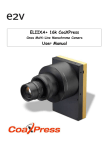
ELIIXA+ 8k/4k
Cmos Multi-Line Monochrome Camera
User Manual
ELIIXA+® 8k/4k CL
Cmos Multi-Line Camera
Summary
1
CAMERA OVERVIEW............................................................................. 5
1.1
1.2
1.3
1.4
Features.................................................................................................................................................... 5
Key Specifications.................................................................................................................................. 5
Description ............................................................................................................................................... 6
Typical Applications................................................................................................................................... 6
CAMERA PERFORMANCES ........................................................................... 7
1.5
1.6
1.7
1.8
1.8.1
1.8.2
2
2.2.1
2.2.2
2.2.3
CE Conformity........................................................................................................................................ 15
FCC Conformity ..................................................................................................................................... 15
RoHs Conformity................................................................................................................................... 15
Out of the box ...................................................................................................................................... 17
Setting up in the system..................................................................................................................... 17
CAMERA SOFTWARE INTERFACE ........................................................... 18
5.1
5.2
5.2.1
5.2.2
5.2.3
5.3
5.3.1
5.3.2
5.3.3
5.3.4
5.3.5
2
Power Connector ........................................................................................................................................................13
Status LED Behaviour...............................................................................................................................................14
CameraLink Output Configuration...........................................................................................................................14
GETTING STARTED ........................................................................... 17
4.1
4.2
5
Mechanical Drawings............................................................................................................................ 11
Input/output Connectors and LED ................................................................................................... 12
STANDARD CONFORMITY.................................................................... 15
3.1
3.2
3.3
4
Quantum Efficiency ....................................................................................................................................................9
Spectral Response.......................................................................................................................................................9
CAMERA HARDWARE INTERFACE ........................................................... 11
2.1
2.2
3
Camera Characterization ...................................................................................................................... 7
Image Sensor........................................................................................................................................... 8
Sensor modes........................................................................................................................................... 8
Response & QE curves ........................................................................................................................... 9
Control and Interface ......................................................................................................................... 18
Serial Protocol and Command Format .............................................................................................. 19
Syntax .........................................................................................................................................................................19
Command Processing .................................................................................................................................................19
GenICam ready ..........................................................................................................................................................19
Camera Commands ................................................................................................................................ 20
Information ............................................................................................................................................................... 20
Image Format ........................................................................................................................................................... 23
Acquisition Control ................................................................................................................................................... 29
Gain and Offset .........................................................................................................................................................31
Flat Field Correction................................................................................................................................................ 34
UM ELIIXA+ 8k/4k CL – REVD – 06/13
e2v semiconductors SAS 2013
ELIIXA+® 8k/4k CL
Cmos Multi-Line Camera
5.3.5.1
Activation and Auto-Adjust ...................................................................................................................... 36
5.3.5.2
Automatic Calibration ................................................................................................................................ 37
5.3.5.3
Manual Flat Field Correction..................................................................................................................... 38
5.3.5.4
FFC User Bank Management...................................................................................................................... 39
5.3.6 Look Up Table ........................................................................................................................................................... 40
5.3.7 Statistics and Line Profile ...................................................................................................................................... 42
5.3.8 Privilege Level ........................................................................................................................................................... 43
5.3.9 Save & Restore Settings ......................................................................................................................................... 44
6
APPENDIX A: Test Patterns .................................................................. 45
6.1
6.2
Test Pattern 1: Vertical wave ............................................................................................................ 45
Test Pattern 2: Fixed Horizontal Ramps ........................................................................................ 45
6.2.1
6.2.2
6.2.3
7
APPENDIX B: Timing Diagrams ............................................................... 48
7.1
7.2
7.3
8
Synchronization Modes with Variable Exposure Time................................................................. 48
Synchronisation Modes with Maximum Exposure Time............................................................... 49
Timing Values ......................................................................................................................................... 50
APPENDIX C: CameraLink Data Cables....................................................... 51
8.1
8.2
9
Choosing the Cable ............................................................................................................................... 51
Choosing the Data Rate....................................................................................................................... 52
APPENDIX D: Lens Mounts.................................................................... 53
9.1
9.2
10
F-Mount................................................................................................................................................... 53
T2 & M42x1 Mounts ............................................................................................................................. 54
APPENDIX E: TROUBLESHOOTING....................................................... 55
10.1
10.2
11
Camera..................................................................................................................................................... 55
CommCam Connection........................................................................................................................... 55
APPENDIX F: Revision History ............................................................. 56
11.1
11.2
11.3
11.4
11.5
11.6
11.7
11.8
11.9
11.10
3
8192 Pixels in 8 bits format ................................................................................................................................... 45
4096 Pixels in 8 bits format................................................................................................................................... 46
2048 Pixels in 8 bits format................................................................................................................................... 47
Device Control ....................................................................................................................................... 56
Image Format ........................................................................................................................................ 56
Synchro and Acquisition...................................................................................................................... 57
Gain & Offset ........................................................................................................................................ 58
Flat Field Correction............................................................................................................................ 58
LUT........................................................................................................................................................... 59
Save and Restore .................................................................................................................................. 59
CAMERA STATUS................................................................................................................................ 60
Communication ....................................................................................................................................... 60
Line Profile Average......................................................................................................................... 60
UM ELIIXA+ 8k/4k CL – REVD – 06/13
e2v semiconductors SAS 2013
ELIIXA+® 8k/4k CL
Cmos Multi-Line Camera
12
4
APPENDIX G: Revision History ............................................................. 62
UM ELIIXA+ 8k/4k CL – REVD – 06/13
e2v semiconductors SAS 2013
ELIIXA+® 8k/4k CL
1
1.1
CAMERA OVERVIEW
Features
1.2
Cmos Sensor 4x 8192 Pixels, 5 x 5µm
Multi-Line structure and Multi-Definition using Binning :
o 8192 pixels, 5x5µm in 1, 2 or 4 lines summation
o 4096 pixels, 10x10µm in 1 or 2 lines summation
o 2048 pixels, 20x20µm
Interface : CameraLink®
o BA0 version : Base or Medium, 85MHz down to 60MHz
o BA1 version : Base, Medium, Full or Deca, 85MHz down to 60MHz
Line Rate : Up to 100000 l/s
Data Rate : Up to 850 MB/s
Bit Depth : 8, 10 and 12bits
Flat Field Correction
Look up Table
Low Power Consumption : < 7,5W
Compliant with Standard Lenses of the Market (F, T2, M42 Mounts)
Full Exposure Control, even in 4S “TDE” mode
Key Specifications
Note : All values in LSB are given in 12 bits format
Characteristics
Typical Value
Unit
Sensor Characteristics at Maximum Pixel Rate
4 x 8192
Resolution
pixel size (square)
Pixels
5x5
µm
Max Line Rate (BA0/BA1 versions, 8 or 12bits)
CameraLink Base 2 x 85MHz : 8k/4k
20/40
kHz
CameraLink Medium 4 x 85MHz: 8k/4k
40/80
kHz
Max Line Rate (BA1 version only, 8 bits)
CameraLink Full 8 x 85MHz: 8k/4k
80/100
kHz
CameraLink Deca 10 x 85MHz: 8k/4k
100/100
kHz
Radiometric Performance at Maximum Pixel Rate and minimum camera gain
Bit depth
8, 10 and 12
Response (broadband)
Full Well Capacity
Response non linearity
PRNU HF Max
Dynamic range (1S / 2S / 4S mode)
5
UM ELIIXA+ 8k/4k CL – REVD – 06/13
450
27300
(in 2S or 4S mode and MultiGain at 1/2)
Bits
LSB/(nJ/cm²)
electrons
0,3
%
3
%
67,6 / 70,7 / 68,7
dB
e2v semiconductors SAS 2013
ELIIXA+® 8k/4k CL
Functionality (Programmable via Control Interface)
Sensor modes : Multi-definition,
Multi-sensitivity
Analog Gain
Offset
Trigger Mode
8k Pixels 5µ m : Multi-Lines 1, 2 or 4
4k Pixels 10µm : Binning 1 or 2 Lines
2k Pixels 20µm : Binning 4x4, 1 line
Up to 12 (x4)
dB
-4096 to +4096
LSB
Timed (Free run) and triggered (Ext Trig, Ext ITC) modes
Mechanical and Electrical Interface
Size (w x h x l)
Weight
Lens Mount
Sensor alignment ( see chapter 2.1 )
Sensor flatness
Power supply
Power dissipation - CameraLink
General Features
Operating temperature
Storage temperature
Regulatory
1.3
125 x 60 x 35
mm
360
g
F-Mount, T2 and M42x1
-
±100
µm
50
µm
Single 12 DC to 24 DC
V
< 7,5
W
0 to 55 (front face) or 70 (Internal)
-40 to 70
°C
°C
CE, FCC and RoHS compliant
Description
e2v’s next generation of line scan cameras are setting new, high standards for line rate and image quality.
Thanks to e2v’s recently developed multi-line CMOS technology, the camera provides an unmatched 100,000
lines/s and combines high response with an extremely low noise level; this delivers high signal to noise ratio
even when short integration times are required or when illumination is limited. The 5µm pixel size is arranged
in four active lines, ensuring optimal spatial resolution in both scanning and sensor directions with standard
F-mount lenses. Vertical and horizontal binning functions allow the camera to be operated in a 8,192 pixels,
5µm x 5µm pixel pitch, 4 active CMOS lines mode or 4,096 pixels, 10µm x 10 µm pixel pitch, 2 active CMOS
lines mode depending on the user settings. This versatile feature sets new standard for next generation
machine vision systems
1.4
Typical Applications
•
•
•
•
•
•
•
•
6
Raw material surface inspection
General inspection
Flat panel display inspection
PCB inspection
Solar cell inspection
Parcel and postal sorting
High resolution document scanning
Print and paper inspection
UM ELIIXA+ 8k/4k CL – REVD – 06/13
e2v semiconductors SAS 2013
ELIIXA+® 8k/4k CL
CAMERA PERFORMANCES
1.5
Camera Characterization
Unit
Mode 1S (0dB
Mode 2S (0dB)
Mode 4S (0dB)
Mode 1SB
Mode 2SB
Mode 4SB
(0dB)
(0dB)
(0dB)
Typ.
Max
Typ.
Max
Typ.
Max
Typ.
Max
Typ.
Max
Typ.
Max
Dark Noise RMS
LSB
1,7
2,2
2,4
3,1
3
4
tbd
tbd
tbd
tbd
tbd
tbd
Dynamic Range
-
2394:1
-
3412:1(*)
-
2730:1(*)
-
tbd
-
tbd
-
tbd
-
Readout Noise
e-
5,7
-
8
-
10
-
tbd
-
tbd
-
tbd
-
Full Well Capacity
e-
13650
-
27300
-
27300
-
54600
-
54600
-
109200
-
SNR
dB
40
-
43(*)
-
43(*)
-
tbd
-
tbd
-
tbd
-
Peak Response
(660nm)
(nJ/cm2)
137
-
274
-
547
-
550
-
1100
-
2200
-
Non Linearity
%
0,3
-
0,3
-
0,3
-
0,3
-
0,3
-
0,3
-
tbd
LSB/
Without Flat Field Correction :
tbd
tbd
tbd
tbd
tbd
tbd
tbd
tbd
tbd
tbd
tbd
tbd
tbd
0,1
tbd
tbd
tbd
tbd
tbd
tbd
tbd
0,8
tbd
tbd
tbd
tbd
tbd
tbd
tbd
FPN rms
LSB
0,4
1,5
0,7
1,5
0,8
FPN pk-pk
LSB
3,2
15
5
15
5,6
PRNU hf (3/4 Sat)
%
0,13
0,25
0,1
0,25
PRNU pk-pk (3/4
Sat)
%
1
3
0,8
3
Test conditions :
Figures in LSB are for a 12bits format.
Measured at exposure time = 50µs and line period = 50µs in Ext Trig Mode (Max Exposure Time)
Maximum data rate
Stabilized temperature 30/40/55 °C (Room/Front Face/Internal)
SNR Calculated at 75% Vsat with minimum Gain.
(*) In mode 2S/4S, only with the use of the Multi-Line Gain
7
UM ELIIXA+ 8k/4k CL – REVD – 06/13
e2v semiconductors SAS 2013
ELIIXA+® 8k/4k CL
1.6
Image Sensor
The Eliixa+ 8k sensor is composed of two
pairs of sensitive lines. Each pair of lines use
the same Analog to Digital Column converter
(ADC Column). An appropriate (embedded)
Time delay in the exposure between each line
allows combining two successive exposures in
order to double the sensitivity of a single
line.
1.7
ADC Column
Memory Node
Pixel Line A
Pixel Line B
This Time Delay Exposure is used only in the
4S multi-line modes (4 Lines) and also in the
three binning modes, as described below.
Pixel Line C
The 8192 Pixels of the whole sensor are
divided in 2 blocks of 4096 pixels.
Memory Node
Pixel Line D
ADC Column
Sensor modes
8K Pixels Output
Mode 1S = B
Mode 2S = B+C (FPGA)
Mode 4S = (A.B)+(C.D)
Note : (A.B) = summation in the sensor
a
b
c
d
a
b
c
d
B
B
C
a
b
c
d
A
B
C
D
4k Pixels Output
Mode 1SB = A
Mode 2SB = (A+B)
8
UM ELIIXA+ 8k/4k CL – REVD – 06/13
a
b
c
d
A
a
b A
c
d B
e2v semiconductors SAS 2013
ELIIXA+® 8k/4k CL
2k Pixels Output
a
b
c
d
Mode 4SB = A
1.8
A
Response & QE curves
1.8.1 Quantum Efficiency
Quantum Efficiency (%)
0.6
0.5
0.4
0.3
0.2
0.1
99
0
10
20
10
50
10
80
96
0
93
0
90
0
87
0
84
0
81
0
78
0
75
0
72
0
69
0
66
0
63
0
60
0
57
0
54
0
51
0
48
0
45
0
42
0
39
0
36
0
0
1.8.2 Spectral Response
Response in 8k Pixels 5µm
4S
2S
1S
LSB12bits/(nJ/cm2))
600
500
400
300
200
100
9
UM ELIIXA+ 8k/4k CL – REVD – 06/13
10
80
10
50
10
20
99
0
96
0
93
0
90
0
87
0
84
0
81
0
78
0
75
0
72
0
69
0
66
0
63
0
60
0
57
0
54
0
51
0
48
0
45
0
42
0
39
0
36
0
0
nm
e2v semiconductors SAS 2013
ELIIXA+® 8k/4k CL
Response in 4k Pixels 10µm
1SB
2SB
LSB12bits/(nJ/cm 2))
1200
1100
1000
900
800
700
600
500
400
300
200
100
84
0
87
0
90
0
93
0
96
0
99
0
10
20
10
50
10
80
nm
84
0
87
0
90
0
93
0
96
0
99
0
10
20
10
50
10
80
81
0
78
0
75
0
72
0
69
0
66
0
63
0
60
0
57
0
54
0
51
0
48
0
45
0
42
0
36
0
39
0
0
nm
Response in 2k Pixels 20µm
4SB
LSB12bits/(nJ/cm2))
10
81
0
78
0
75
0
72
0
69
0
66
0
63
0
60
0
57
0
54
0
51
0
45
0
UM ELIIXA+ 8k/4k CL – REVD – 06/13
48
0
42
0
39
0
36
0
2400
2300
2200
2100
2000
1900
1800
1700
1600
1500
1400
1300
1200
1100
1000
900
800
700
600
500
400
300
200
100
0
e2v semiconductors SAS 2013
ELIIXA+® 8k/4k CL
2
2.1
CAMERA HARDWARE INTERFACE
Mechanical Drawings
Z
The Step file is available
on the web :
www.e2v.com/cameras
X
Y
11
UM ELIIXA+ 8k/4k CL – REVD – 06/13
e2v semiconductors SAS 2013
ELIIXA+® 8k/4k CL
Sensor alignment
Z = -10.3 mm
X = 9.5 mm
Y = 62.5mm
Flatness
Rotation (X,Y plan)
Tilt (versus lens mounting plane)
2.2
±100µm
±100 µm
±100 µm
50 µm
±0,15°
50µm
Input/output Connectors and LED
USB Connector
For Firmware
upgrade
Power Connector :
12-24V DC
Multi-Colored
LED for Status
and diagnostic
CameraLink
Connector CL2
12
UM ELIIXA+ 8k/4k CL – REVD – 06/13
CameraLink
Connector CL1
e2v semiconductors SAS 2013
ELIIXA+® 8k/4k CL
2.2.1 Power Connector
Camera connector type: Hirose HR10A-7R-6PB (male)
Cable connector type: Hirose HR10A-7P-6S (female)
Signal
Pin
Signal
Pin
PWR
PWR
PWR
1
2
3
GND
GND
GND
4
5
6
Power supply from 12 to 24v
Power 7,5W max with an typical inrush current
peak of 1A during power up
Camera side description
Typical current/Power during the grab (possible variation : +/- 5%)
Camera supply
Supply 12V
Supply 24V
(Line Period Minimum)
I(mA)
P(W)
I(mA)
P(W)
Full 8Taps
Deca 10Taps
Base 2Taps
Medium 4Taps
605
7.26
303
7.272
613
7.356
308
7.392
589
7.068
298
7.152
598
7.176
302
7.248
Power Time : Max 40s (Green Light)
Current Establishment time and level
Inrush Current Peak
24V
12V
13
UM ELIIXA+ 8k/4k CL – REVD – 06/13
e2v semiconductors SAS 2013
ELIIXA+® 8k/4k CL
2.2.2 Status LED Behaviour
After less than 2 seconds of power establishment, the LED first lights up in ORANGE. Then after a Maximum
of 40 seconds, the LED must turn in a following colour :
Colour and state
Green and continuous
Green and blinking slowly
Red and continuous
Meaning
OK
Waiting for Ext Trig (Trig1 and/or Trig2)
Camera out of order : Internal firmware error
2.2.3 CameraLink Output Configuration
Versions BA0/BA1
Base : 2 Channels 8/10/12bits
Medium : 4 Channels 8/10/12bits
Version BA1 (only)
Full : 8 Channels 8bits
Deca : 10 Channels 8bits
14
UM ELIIXA+ 8k/4k CL – REVD – 06/13
Adjacent Channels
Pixels per Channel
2 x 85MHz (80/75/70/65/60MHz)
4 x 85MHz (80/75/70/65/60MHz)
2 x 4096
4 x 2048
8 x 85MHz (80/75/70/65/60MHz)
10 x 85MHz (80/75/70/65/60MHz)
8 x 1024
10 x 819
e2v semiconductors SAS 2013
ELIIXA+® 8k/4k CL
3
STANDARD CONFORMITY
The ELIIXA+ cameras have been tested using the following equipment:
• A shielded power supply cable
• A Camera Link data transfer cable ref. MVC-1-1-5-2M from CEI (Component Express, Inc.)
e2v recommends using the same configuration to ensure the compliance with the following standards.
3.1
CE Conformity
The ELIIXA+ cameras comply with the requirements of the EMC (European) directive
2004/108/CE (EN50081-2, EN 61000-6-2).
3.2
FCC Conformity
The ELIIXA+ cameras further comply with Part 15 of the FCC rules, which states that: Operation is
subject to the following two conditions:
• This device may not cause harmful interference, and
• This device must accept any interference received, including interference that may cause
undesired operation
This equipment has been tested and found to comply with the limits for Class A digital device, pursuant to
part 15 of the FCC rules. These limits are designed to provide reasonable protection against harmful
interference when the equipment is operated in a commercial environment. This equipment generates, uses
and can radiate radio frequency energy and, if not installed and used in accordance with the
instruction manual, may cause harmful interference to radio communications. Operation of this equipment in
a residential area is likely to cause harmful interference in which case the user will be required to correct
the interference at his own expense.
Warning: Changes or modifications to this unit not expressly approved by the party responsible for
compliance could void the user's authority to operate this equipment.
3.3
RoHs Conformity
ELIIXA+ cameras comply with the requirements of the RoHS directive 2002/95/EC.
15
UM ELIIXA+ 8k/4k CL – REVD – 06/13
e2v semiconductors SAS 2013
ELIIXA+® 8k/4k CL
16
UM ELIIXA+ 8k/4k CL – REVD – 06/13
e2v semiconductors SAS 2013
ELIIXA+® 8k/4k CL
4 GETTING STARTED
4.1
Out of the box
The contains of the Camera box is the following :
-
One Camera ELIIXA+
Power connector (Hirose HR10A-7P-6S -female)
There is no CDROM delivered with the Camera : Both User Manual (this document) and CommCam
control software have to be downloaded from the web site : This ensure you to have an up-todate version.
Main Camera page : www.e2v.com/cameras
On the appropriate Camera Page (ELIIXA+ 8k/4k) you’ll find a download link
first version of CommCam compliant is indicated in the last Chapter
CommCam download requires a login/password :
Login : commcam
Password : chartreuse
4.2
Setting up in the system
Web
Direction
First
Pixel
w
Sensor Plan
f
Focal Plan
Readout
Direction
L
s
FOV
w
FOV
=
f
L
The Compliant Lenses Mounts are detailed in Appendix D
17
UM ELIIXA+ 8k/4k CL – REVD – 06/13
e2v semiconductors SAS 2013
ELIIXA+® 8k/4k CL
5
5.1
CAMERA SOFTWARE INTERFACE
Control and Interface
As all the e2v Cameras, the ELIIXA+ CL is delivered with the friendly interface control software
COMMCAM.UCL (as “Ultimate Camera Link”) which is based on the GenICam standard
COMMCAM recognizes and detects automatically all the UCL Cameras connected on any transport layers
(Camera Link or COM ports) of your system.
Once connected to the Camera you have an easy access to all its features. The visibility of these features can
be associated to three types of users: Beginner, Expert or Guru. Then you can make life easy for simple users.
Minimum version of CommCam is 2.1.4 in order to recognize the ELIIXA+ 8k/4k Camera (both versions)
18
UM ELIIXA+ 8k/4k CL – REVD – 06/13
e2v semiconductors SAS 2013
ELIIXA+® 8k/4k CL
5.2
Serial Protocol and Command Format
The Camera Link interface provides two LVDS signal pairs for communication between the camera and
the frame grabber. This is an asynchronous serial communication based on RS-232 protocol.
The serial line configuration is:
Full duplex/without handshaking
9600 bauds (default), 8-bit data, no parity bit, 1 stop bit. The baud rate can be set up to 115200
5.2.1 Syntax
Internal camera configurations are activated by write or readout commands.
The command syntax for write operation is:
w <command_name> <command_parameters><CR>
The command syntax for readout operation is:
r <command_name><CR>
5.2.2 Command Processing
Each command received by the camera is processed:
The setting is implemented (if valid)
The camera returns “>”<return code><CR>
The camera return code has to be received before sending a new command.
The camera return code has to be received before sending a new command. Some commands are
longer than the others : Waiting for the return code ensure a good treatment of all the commands
Without saturating the buffer of the camera
Table 5-1. Camera Returned Code
Returned code
meaning
>3
(or “>OK”) : All right, the command will be implemented
Error Bad CRC (for write command only)
>16
Invalid Command ID (Command not recognized or doesn't exist)
>33
>34
Invalid Access (the receipt of the last command has failed).
Parameter out of range (the parameter of the last command sent is out of range).
>35
Access Failure (bad communication between two internal devices).
>0
5.2.3 GenICam ready
The CameraLink Standard is not yet compliant with GenICam Standard, but as much as possible, each
command of the ELIIXA+ will have its correspondence with the Standard Feature Naming Convention of the
GenIcam Standard.
This correspondence is given in parenthesis for each feature/command as the following example :
• Vendor name (DeviceVendorName) : “e2v”
19
UM ELIIXA+ 8k/4k CL – REVD – 06/13
e2v semiconductors SAS 2013
ELIIXA+® 8k/4k CL
5.3
Camera Commands
5.3.1 Information
These values allow to indentify the Camera. They can be accessed in CommCam software in the “Info” section
•
20
All these values are fixed in factory and can’t be changed (shaded) except the Camera User ID which can be
fixed by the Customer :
Vendor name (DeviceVendorName) : “e2v”
Read function : “r vdnm”;
Returned by the camera : “e2v”, string of 32 bytes (including “/0”)
Can not be written
•
Model Name (DeviceModelName) : Internal name for GenICam :
Read function : “r mdnm”;
Returned by the camera : String of 32 bytes (including “/0”) :
Can not be written
•
Device Manufacturer Info (DeviceManufacturerInfo) : Get Camera ID
Read function : “r idnb”;
Returned by the camera : String of 128 bytes (including “/0”)
Can not be written
•
Device Version (DeviceVersion) : Get Camera Hardware version
Read function : “r dhwv”;
Returned by the camera : String of 32 bytes (including “/0”)
Can not be written
•
Device Firmware Version (DeviceFirmwareVersion): Get camera synthetic firmware
Read function : “r dfwv”;
Returned by the camera : String of 16 bytes (including “/0”)
Can not be written
•
Device SFNC Version : 1.5.0
These Parameters (Major, Minor, Sub Minor) are only virtual ones in order to give the SFNC compliance of
the Camera.
•
Device ID (DeviceID) : Camera Factory identifier ID
Read function : “r cust”;
Returned by the camera : String of 128 bytes (including “/0”)
Write function : “w cust <idstr>”
•
Device User ID (DeviceUserID) : Camera user identifier ID
Read function : “r cust”;
Returned by the camera : String of 128 bytes (including “/0”)
Write function : “w cust <idstr>”
UM ELIIXA+ 8k/4k CL – REVD – 06/13
e2v semiconductors SAS 2013
ELIIXA+® 8k/4k CL
•
Electronic board ID (ElectronicBoardID) : Get PcB Board ID
Read function : “r boid”;
Returned by the camera : String of 32 bytes (including “/0”)
Can not be written
•
Device Temperature Selector (DeviceTemperatureSelector) : MainBoard
Can not be written
•
Device Temperature (DeviceTemperature) : Get Main Board Temperature
Read function : “r temp”;
Return by the camera : Temperature in Q10.2 format (8 bits signed + 2 bits below comma). Value is
between -512 to 511 in °C.
•
Device Serial Port Selection : Indicates the Serial Port on which the Camera is connected.
•
Device Serial Port Baud Rate (ComBaudRate): Set the Camera BaudRate
Read function : “r baud”;
Returned by the camera : Value of the Baud Rate
Write function : “w baud” <index> with the index as follows :
1 : 9600 Bauds (default value at power up)
2 : 19200Bauds
6 : 57600Bauds
12 : 115200Bauds
•
Standby Mode (Standby) : Activation of the Standby mode of the Camera
Read function : “r stby”;
Returned by the camera : Boolean.
0 : Disable Standby mode (False)
1 : Enable stanby mode (True)
Write function : “w stby <val>”; <val> is 0 or 1.
Internal Temperature
A standby mode, what for ?
°C
75
The Standby mode stops all activity on the
sensor level. The power dissipation drops
down to about 6W. During the standby
mode, the grab is stopped
Standby Off
70
65
60
55
50
Once the Standby mode turned off, the
Camera recovers in less than 1ms to send
images again from the sensor.
45
40
Standby On
35
30
80
90
10
0
11
0
12
0
13
0
14
0
60
70
40
50
30
20
7
10
0
5
25
Time (mn)
21
UM ELIIXA+ 8k/4k CL – REVD – 06/13
e2v semiconductors SAS 2013
ELIIXA+® 8k/4k CL
•
Camera status : Get the Camera status register (32bits Integer)
Read function : “r stat”;
Returned by the camera : 32bits integer :
22
Bit 0 : (StatusWaitForTrigger) : True if no trig received from more than 1sec
Bit 1 : (StatusTriggerTooFast) : Missing triggers. Trig signal too fast
Bit 2 : (StatusSensorConnection) : True is the Sensor pattern is checked as failed.
Bit 3, 4, 5, 6, 7 : Reserved
Bit 8 : (StatusWarningOverflow) : True is an overflow occurs during FFC or Tap balance processing.
Bit 9 : (StatusWarningUnderflow) : True is an underflow occurs during FFC or Tap balance processing
Bits 10 : Reserved
Bits 11 : Scrolling Direction : 0 = Forward, 1 = Reverse. Updated only by external CC3 (CameraLink)
Bits, 12, 13, 14, 15 : Reserved
Bit 16 : (StatusErrorHardware) : True if hardware error detected
Bits 17 to 31 : Reserved
UM ELIIXA+ 8k/4k CL – REVD – 06/13
e2v semiconductors SAS 2013
ELIIXA+® 8k/4k CL
5.3.2 Image Format
•
Sensor Width (SensorWidth) : Get the physical width of the Sensor. This value is available in the CommCam
“Image Format Control” section :
Read function : “r snsw”;
Return by the sensor : Integer 8192.
Can not be written;
•
Sensor Height (SensorHeight) : Get the physical height of the Sensor. This value is available in the
CommCam “Image Format Control” section :
No Access. Virtual command in xml”; Value always = 1
•
Width Max (WidthMax) : Get the Maximum Width of the Sensor. This value is available in the CommCam
“Image Format Control” section :
No Access. The value is mapped on “SensorWidth”
•
Height Max (HeigthMax) : Get the Maximum height of the Sensor. This value is available in the CommCam
“Image Format Control” section :
No Access. Virtual command in xml”; Value always = 1
•
Output mode (OutputMode) : Set the CameraLink Output mode (refer also to Chap 3. : CameraLink Output
Configuration). This command is available in the CommCam “Image Format Control” section :
Read function : “r mode”;
Returned by the camera : Output mode from 0 to 3 (see table below).
Write function : “w mode” <value> :
detailed in the table below :
Modes
Base 2 Channels 8 Bits
Base 2 Channels 10bits
Base 2 Channels 12 Bits
Medium 4 Channels 8bits
Medium 4 Channels 10 bits
Medium 4 Channels 12bits
Full 8 Channels 8bits (BA1 Version Only)
Full+ 10 Channels 8bits (BA1 Version Only)
23
UM ELIIXA+ 8k/4k CL – REVD – 06/13
Connector CL1
Connector CL2
2 x 8 bits
2 x 10 bits
2x 12 bits
4 x 8 bits
4 x 10 bits
4 x 12 bits
8 x 8 bits
10 x 8 bits
Mode value
5
6
7
0
4
1
2
3
e2v semiconductors SAS 2013
ELIIXA+® 8k/4k CL
Structure of the Camera Link Channels for interfacing
Base Mode : 2 Channels Separate, outputted from Left to Right.
2x4096 pixels each Channel (No Binning)
2x2048 pixels in Binning Mode 1SB or 2SB,
2x512 pixels in Binning mode 4SB.
Ch 1
Ch 2
Output direction
Medium Mode : 4 Taps Separate, outputted from Left to Right
4x2048 pixels each Channel (No Binning)
4x1024 pixels in Binning Mode 1SB or 2SB,
4x512 pixels in Binning mode 4SB.
Ch 1
Ch 2
Ch 3
Ch 4
Output direction
FULL Mode : 8 Taps Separate, outputted from Left to Right. Available only on BA1 versions.
8x1024 pixels each Channel (No Binning)
8x512 pixels in Binning Mode 1SB or 2SB,
8x256 pixels in Binning mode 4SB.
Ch 1 Ch 2 Ch 3 Ch 4 Ch 5 Ch 6 Ch 7 Ch 8
Output direction
FULL+ (Deca) Mode : 10 Taps Separate, outputted from Left to Right. Available only on BA1 versions.
10x819 pixels each Channel (No Binning)
10x409 pixels in Binning Mode 1SB or 2SB,
10x204 pixels in Binning mode 4SB.
Ch 1 Ch 2 Ch 3 Ch 4 Ch 5 Ch 6 Ch 7 Ch 8 Ch 9 Ch 10
Output direction
24
UM ELIIXA+ 8k/4k CL – REVD – 06/13
e2v semiconductors SAS 2013
ELIIXA+® 8k/4k CL
•
Output Frequency (OutputFrequency) : Set the CameraLink Data Output Frequency. This value is available in
the CommCam “Image Format Control” section :
Read function : “r clfq”;
Return by the Camera : Frequency from 0 to 5
Write Function : “w clfq <value>”
“0” : 85MHz (default).
“1” : 60MHz.
“2” : 65MHz.
“3” : 70MHz.
“4” : 75MHz.
“5” : 80MHz.
Data Output Frequency Reduction
The Purpose of this feature is to optimize (increase) the Length of the Cable when highest
Line Rate is not required. Each decreasing of the Data Frequency will increase the minimum
Line Period possible, this depending also on the Binning mode (number of pixels outputted from
8192 to 2048
Structure of the Sensor
FPGA
Web Direction
ADC
In 2S Mode, the summation of the
two lines is done in the FPGA :
B+C
In 4S Mode, the summation of the
two double lines is done in the
FPGA : (AB )+ (BC)
This mode works in “Time delay
exposure” for the summation of
each double line in the sensor.
25
UM ELIIXA+ 8k/4k CL – REVD – 06/13
Memory Node
Pixel Line A
Exposure
delays
1S
Pixel Line B
2S 4S
Pixel Line C
Pixel Line D
Memory Node
ADC
e2v semiconductors SAS 2013
ELIIXA+® 8k/4k CL
•
Sensor Mode (SensorMode) : Defines the number of Line used on the Sensor. This command is available in
the CommCam “Image Format Control” section :
Read function : “r smod”;
Returned by the camera : Integer from 0 to 5
Write function : “w smod” <value> :
“0” : “1S” mode or Single Line.
“1” : “2S” mode or Dual Lines.
“2” : “4S” mode or Four Lines.
“3” : “1SB” mode : Binning mode (2x2) which outputs on line of 4k pixels in 10µmx10µm.
“4” : “2SB” mode : Binning mode 2 x (2x2) which outputs the summation of 2 lines of 4k pixels in 10µmx10µm.
“5” : “4SB” mode : Binning mode (4x4) which outputs 1 line of 2k pixels in 20µmx20µm.
Full Exposure Control
As the « 4S » mode is performing an internal Time delay exposure on the lines A & B and C &
D, normally, the variation of the Exposure time should not be possible in this sensor mode.
Thanks to an e2v licensed solution, two of the Exposure controlled mode (Ext Trig with
internal or External exposure control) are still available in 4S sensor TDE mode.
Binning modes
Web Direction
The two binning modes 1SB and
2SB give an output of 4k pixels
10x10µm.
As for the 2SB mode, the
sensor manages the delay
between the two exposures
necessary for a “good match”
acquisition.
The 4SB is a binning 4x4 with
an output of 2K pixels
20x20µm
26
UM ELIIXA+ 8k/4k CL – REVD – 06/13
ADC
Memory Node
Pixel Line A
1SB
Exposure
Delay
1SB/2SB
2SB
Pixel Line B
4SB
2SB
Pixel Line C
Pixel Line D
Memory Node
ADC
e2v semiconductors SAS 2013
ELIIXA+® 8k/4k CL
•
Multi-Line Gain (MultiLineGain) : Enables the MultiLine Gain of x0,5 . This value is available in the CommCam
“Image Format Control” section :
Read function : “r mlig”;
Return by the sensor : “0” if disabled (Gain x1 by default); “1” if Gain x0,5 activated.
Write Function : “w mlig <value>”
“0” : Default Gain x1 is active.
“1” : Gain x0,5 is enabled (only when the 2S mode of the sensor is enabled)
Why Using a Multi-Line Gain of x0,5 ?
Web Direction
When the Light source is enough to use
the “1S” mode of the Sensor (one single
line), the best is to use 2 lines (“2S”
mode) and then to divide the result by
two by using the Multi-Line Gain set at
“x0,5” :
In this case, the Full Well capacity is
multiplied by x2 (two output registers
are used) but the noise divided by √2
therefore the SNR is improved by a
factor of √2.
•
27
ADC
Memory Node
Pixel Line A
Exposure
delays
1S
Pixel Line B
2S
Pixel Line C
Pixel Line D
Memory Node
ADC
Reverse Reading (X) (ReverseReading) : Allows to output the line in the Reverse-X direction. This value is
available in the CommCam “Image Format Control” section :
Read function : “r revr”;
Return by the Camera : 0 or 1 (enabled/disabled)
Write function : “w revr <value>”;
“0” : Disabled.
“1” : Enables the reverse reading out (see below for “normal” direction)
UM ELIIXA+ 8k/4k CL – REVD – 06/13
e2v semiconductors SAS 2013
ELIIXA+® 8k/4k CL
•
Scan Direction (ScanDirection) : Set the scan direction for the sensor. This value is available in the
CommCam “Image Format Control” section :
Read function : “r scdi”;
Return by the Camera : 0, 1 or 2 (Forward/reverse/external)
Write function : “w scdi <value>”;
“0” : Forward.
“1” : Reverse
“2” : Externally controlled (by CC3 of the
CameraLink Sync signals)
Forward/reverse information has to be set correctly as soon as the Mode “2S”, “4S” or 2SB of the sensor
are set : In these modes, the sensor/Camera need to know what is the real order of the lines for the
exposure delays.
The Forward direction is defined as detailed beside :
Note : The minimum delay for the Camera to take in
account a change in the ScanDirection value is :
- Using CC3 signal : 100ms.
- Using serial command(*) : 120ms
(*)
After reception of the Command on the camera side
If the Camera is in 4S Sensor mode, after changing of the
scanning direction, the 5 first following triggers will be
ignored in order to reinitialize the “Full Exposure Control”
mode. Then the 3 following lines acquired will be more or
less black because in 4S, 4 lines are required for a
complete exposure.
Web
Direction
First
Pixel
Readout
Direction
In 2S or 2SB Sensor modes, no Trigger will be lost after
the change of scanning direction but the first line acquired
will be more or less black as in 2S, 2 lines are required for
a complete exposure.
In 1S, 1SB or 4SB modes, nothing is lost an all lines
received after the delay are correct.
This positioning takes also in account that the mode “Reverse X” is “Off” (Normal readout direction)
28
UM ELIIXA+ 8k/4k CL – REVD – 06/13
e2v semiconductors SAS 2013
ELIIXA+® 8k/4k CL
•
Test Image Selector (TestImageSelector) : Defines if the data comes from the Sensor or the FPGA (test
Pattern). This command is available in the CommCam “Image Format” section :
Read function : “r srce”;
Returned by the camera : “0” if Source from the Sensor and “1 to 5” if test pattern active
Write function : “w srce” <value> :
“0” : To switch to CCD sensor image
“1” : Grey Horizontal Ramp (Fixed) : See AppendixA
“2” : White Pattern (Uniform white image : 255 in 8Bits or 4095 in 12bits)
“3” : Grey Pattern (Uniform middle Grey : 128 in 8bits or 2048 in 12 bits)
“4” : Black Pattern (Uniform black : 0 in both 8 and 12 bits)
“5” : Grey vertical Ramp (moving)
The test pattern is generated in the FPGA : It’s used to point out any interface problem with the Frame
Grabber.
When any of the Test pattern is enabled, the whole processing chain of the FPGA is disabled.
5.3.3 Acquisition Control
This section deals with all the Exposure, Line period and synchronisation modes
•
Synchronisation Mode (TriggerPreset) : Timed or Triggered, it defines how the grabbing is synchronized.
This command is available in the CommCam “Acquisition Control” section :
Read function : “r sync”;
Returned by the camera :
• “0” : Internal Line Trigger with Exposure time Internally Controlled (Free Run). Not available when
Sensor mode is set in “4S” (whatever the firmware version)
•
“1” : External Trigger with Exposure Time Internally Controlled. Available also when Sensor mode is
set in “4S”.
•
•
•
“2” : External Trigger with maximum Exposure time
“3” : One External with Exposure Time Externally Controlled. The same Trigger signal defines the line
period and its low level defines the exposure time. Available also when Sensor mode is set in “4S”
“4” : Two External Triggers with Exposure Time Externally Controlled : CC2 defines the start of the
exposure (and also the start Line) and CC1 defines the Stop of the exposure. Not available when
Sensor mode is set in “4S”
• “5” : Internal Line Trigger with maximum Exposure Time
Write function : “w sync” <value>
The Timing diagrams associated to each Synchronization mode and the Timing values associated
are detailed in the APPENDIX B of this document.
29
UM ELIIXA+ 8k/4k CL – REVD – 06/13
e2v semiconductors SAS 2013
ELIIXA+® 8k/4k CL
•
Exposure time (ExposureTime): Defines the exposure time when set in the Camera. This command is available
in the CommCam “Acquisition Control” section :
Read function : “r tint”;
Returned by the camera : Integer from 15 to 65535 (=1,5µs to 6553,5µs by step o 0,1µs)
Write function : “w tint” <value> ;
This value of exposure time is taken in account only when the synchronisation mode is “free run” (0) or
“Ext Trig with Exposure time set” (1). Otherwise it’s ignored.
Due to the limitation of the timing pixel inside the sensor, the Exposure time has to be set by
taking in account the limitation detailed in the APPENDIX B of this document.
The Minimum exposure time which can be set is 1,5µs
•
Line Period (LinePeriod) : Defines the Line Period of the Camera in Timed mode. This command is available in
the CommCam “Acquisition Control” section :
Read function : “r tper”;
Returned by the camera : Integer from 1 to 65536 (=0,1µs to 6553,6µs by step o 100ns)
Write function : “w tper” <value> ;
The line period is active only in Free Run modes. It’s also disabled if in this mode, the Integration time is
set higher than the Line Period.
The Tables of the minimum Line Period (Max Line Rate) versus the Data rate and the output
mode chosen are given in Appendix C (Chap. 9.2) of this document.
30
UM ELIIXA+ 8k/4k CL – REVD – 06/13
e2v semiconductors SAS 2013
ELIIXA+® 8k/4k CL
5.3.4 Gain and Offset
Sensor FPGA
Preamp
Gain
Pixel
FFC
Offset Gain
+
X
X
Action on whole line
Action per pixel
Action per Sensor’s Quarter
FFC
Adjust
Amp
Gain
ROI
Gain
X
X
X
Quarter
(Tap)
Gains
LUT or
Contrast Exp.
Offset
+
X
Gain
X
(Not available on BA0 models)
Analog Gain in the ADC
The only analog Gain available in the ELIIXA+ is located at the sensor level, in the ADC converter.
This “Preamp Gain” is in fact a variation of the ramp of the comparator of the ADC.
Then 3 Values are available : x1, x2 and x4. A gain x1 in a 12 bits conversion is equivalent to x4 in 10 bits.
electrons
FWC
x1
Comparator Ramps
at different Gains
or Format
x1
x2
x2
x4
x4
LSB
Clamp (Black Ref)
Setting
•
1024
(10bits conversion)
4096
(12bits conversion)
Preamp Gain : (Gain with GainSelector= AnalogAll)
Set the Pre-amplification Gain. This command is available in the CommCam “Gain & Offset” section.
Read function : “r pamp”;
Returned by the camera : Integer corresponding to one of the 3 different step values :
• 0 : x1 (0dB)
• 1 : x2 (6dB)
• 2 : x4 (12dB)
Write function : “w pamp” <int> ;
31
UM ELIIXA+ 8k/4k CL – REVD – 06/13
e2v semiconductors SAS 2013
OUT
ELIIXA+® 8k/4k CL
•
Gain: (Gain with GainSelector= GainAll)
Set the Amplification Gain. This command is available in the CommCam “Gain & Offset” section :
Read function : “r gain”;
Returned by the camera : Value from 0 to 6193 corresponding to a Gain range of 0dB to +8dB calculated
as following : Gain(dB) = 20.log(1+ Gain/4096).
Write function : “w gain” <int> ;
•
Tap Gain (Gain with GainSelector=TapX) :
Read function : “r fga<tap>”; <tap> is 1 or 2
Returns the Gain value for the tap. Ex : “r fga1” returns Gain value Tap1.
Write function : “w fga<tap> <value>”
<tap> : 1 or 2
<value> : from -128 to +127 by step of 1 (0,0021dB each step)
•
Digital Gain (Gain with GainSelector=DigitalAll) : Set the global Digital Gain. This command is available in the
CommCam “Gain & Offset” section :
Read function : “r gdig”;
Returned by the camera : Integer value from 0 to 255. The corresponding Gain is calculated as
20log(1+val/64) in dB
Write function : “w gdig” <int> ;
•
Digital Offset (BlackLevelRaw with BlackLevelSelector=All) : Set the global Digital Offset. This command is
available in the CommCam “Gain & Offset” section :
Read function : “r offs”;
Returned by the camera : Value from –4096 to +4095 in LSB
Write function : “w offs” <int> ;
The Contrast Expansion (both Digital Gain & Offset) will be automatically disabled if the LUT is
enabled..
32
•
Tap Balance Gains Enable Switch (TapBalanceGainEnable) :
Read function : “r fgae”;
Returns the Gain value for the tap. Ex : “r fga1” returns Gain value Tap1.
Write function : “w fgae <val>” with <val> : 0 or 1
0 : Disables the Tap Balance Gains
1 : Enables the Tap Balance Gains
•
ROI Gain () : Set the Gain for the ROI Gain feature.
Read function : “r roig”;
Returned by the camera : Value from 0 to 2047 (U1.9) corresponding to a Gain range from x1 to
x1,999 and calculated as following : (1+ Gain/1024).
Write function : “w roig” <value> ;
UM ELIIXA+ 8k/4k CL – REVD – 06/13
e2v semiconductors SAS 2013
ELIIXA+® 8k/4k CL
•
ROI Set () : Set the ROI and apply the Gain for ROI Gain Feature.
Read function : “r rois”;
Returns the ROI set for the last ROI gain command
Write function : “w rois <val>” with <val> : Hexadecimal combination of Start and Stop address for
the ROI (both on 16bits) : 0xStartAdr0xStopAdr
Start address : from 0 to 8190 (0x000 to 0x1FFE)
Stop address : from 1 to 8191 (0x001 to 0x1FFF)
ROI Gain : How does it works
The ROI Gain feature comes in addition with the FFC (it’s applied and calculated after).
The maximum complementary Gain ix x2.
It can be applied in 2 commands :
- First, set the ROI Gain value
- Second, set the ROI (Region of Interest).
This second command applies the Gain on the ROI in memory and this is immediately
activated.
The ROI Gain is a “live” feature that can be overlapped but can’t be saved in memory.
Here is an example to apply a complementary gain of x1,5 (512) between the pixels #3051
(0x0BEB) and #4102 (0x1006), pixels included. The two commands are :
- “w roig 512”
- “w rois 0x0BEB1006”
Result with FFC activated :
ROI gain
x1.5
FFC
FFC
3051
4102
Pi xels
Result with FFC not activated :
ROI gain
x1.5
3051
33
UM ELIIXA+ 8k/4k CL – REVD – 06/13
4102
Pi xels
e2v semiconductors SAS 2013
ELIIXA+® 8k/4k CL
5.3.5 Flat Field Correction
How is performed the Flat Field Correction ?
What is the Flat Field correction (FFC) ?
The Flat Field Correction is a digital correction on each pixel which allows :
To correct the Pixel PRNU (Pixel Response Non Uniformity) and DSNU (Dark Signal Non Uniformity)
To Correct the shading due to the lens
To correct the Light source non uniformity
Before
After
How is calculated / Applied the FFC ?
The FFC is a digital correction on the pixel level for both Gain and Offset.
Each Pixel is corrected with :
o An Offset on 8 bits (Signed Int 5.3). They cover a dynamic of ±16LSB in 12bits with a
resolution of 1/8 LSB 12bits.
o A Gain on 14 bits (Unsigned Int 14) with a max gain value of x5(*)
The calculation of the new pixel value is : P’ = ( P + Off).(1 + Gain/1024(*))
The FFC processing can be completed with an automatic adjustment to a global target. This function is
designed as “FFC Adjust”. This adjustment to a User target is done by an internal hidden gain which is recalculated each time the FFC is processed while the FFC adjust function is enabled.
The FFC is always processed with the max pixel value of the line as reference. If enabled, the FFC adjust
module (located at the output of the FFC module) calculates the adjustment gain to reach the target
defined by the User.
When the FFC result is saved in memory, the adjust gain and target are saved in the same time in order to
associate this gain value with the FFC result.
(*) : Up to the firmware version 1.0.1 (BA0) or 1.0.3A (BA1), the Gain resolution was : 1 + Gain/8192 with a range limited at x3
34
UM ELIIXA+ 8k/4k CL – REVD – 06/13
e2v semiconductors SAS 2013
ELIIXA+® 8k/4k CL
User Target value
Adjustment gain
3020
Standard FFC computed on
the max of the line
Pi xels
How to perform the Flat Field Correction ?
FPN/DSNU Calibration
Cover the lens
Launch the FPN Calibration : Grab and calculation is performed in few seconds
PRNU Calibration
The User must propose a white/gray uniform target to the Camera (not a fixed paper).
The Gain/Light conditions must give a non saturated image in any Line.
The Camera must be set in the final conditions of Light/ Gain and in the final position in the System.
I f required, set a user target for the FFC adjust and enable it.
White uniform (moving) target
Launch the FFC
Enable the FFC
You can save the FFC result (both FPN+PRNU in the same time) in one of the 4 x FFC User Banks.
The user target and Gain are saved with the associated FFC in the same memory.
Advices
The ELIIXA+ Cameras have 4 x FFC Banks to save 4 x different FFC calibrations. You can use this feature
if your system needs some different conditions of lightning and/or Gain because of the inspection of
different objects : You can perform one FFC per condition of Gain/setting of the Camera ( 4 Max) and
recall one of the four global settings (Camera Configuration + FFC + Line Balance) when required.
35
UM ELIIXA+ 8k/4k CL – REVD – 06/13
e2v semiconductors SAS 2013
ELIIXA+® 8k/4k CL
5.3.5.1
•
Activation and Auto-Adjust
FFC Activation (FFCEnable) : Enable/disable the Flat Field Correction. This command is available in the
CommCam “Flat Field Correction” section :
Read function : “r ffcp” : Returns the FFC Status (0 if disabled, 1 if enabled)
Write function :
“w ffcp 1” : Enable the FFC.
“w ffcp 0” : Disabled the FFC
•
FFC Adjust Function : This Feature is available in the CommCam “Flat Field Correction/ Automatic
Calibration” section :
o
Gains adjust (FFCAdjust): Enable/Disable the function
Read function : “r ffad”. Returns the status of the function (0 if disabled)
Write function :
“w ffad 0” : Disable the FFC Adjust function.
“w ffad 1” : Enable the FFC Adjust function.
o
Auto Adjust Target Level (FFCAutoTargetLevel): set the value for the User Target.
Read function : “r tfad”. Returns the Target value (from 0 to 4095)
Write function : “w tfad <value>” : Set the Target Value (in 12bits)
FFC Adjust : A good usage.
When there are several Cameras to set up in a system on a single line, the most difficult is to have a
uniform lightning whole along the line.
If each Camera performs its own Flat field correction, relative to the max of each pixel line, the result
will be a succession of Camera lines at different levels.
=> The FFC Adjust function allows to set the same target value for all the Cameras in the system and
then to get a perfect uniform line whole along the system with a precision of 1 LSB to the Target.
The Maximum correction is x2 the highest value of the line.
The reasonable value for the User Target is not more than around 20% of the max value of the line.
36
UM ELIIXA+ 8k/4k CL – REVD – 06/13
e2v semiconductors SAS 2013
ELIIXA+® 8k/4k CL
5.3.5.2
Automatic Calibration
•
FPN/DSNU Calibration :
o
o
FPN Calibration Control (FPNCalibrationCtrl) : Launch or abort of the FPN process for the Offsets
calculation. These commands are available in the CommCam “Flat Field Correction / Automatic
Calibration ” section :
Read function : “r calo” : Returns the FPN Calculation Process Status (0 if finished, 1 if
processing)
Write function :
“w calo 1” : Launch the FPN Calibration Process.
“w calo 0” : Abort the FPN Calibration Process.
FPN Coefficient Reset (FPNReset) : Reset the FPN (Offsets) coefficient in Memory. This command
is available in the CommCam “Flat Field Correction / Manual Calibration ” section :
Write function : “w rsto 0” : Reset (set to 0) the FPN coefficients in memory. This doesn’t affect
the FFC User Memory Bank but only the active coefficients in Memory.
•
PRNU Calibration :
o PRNU Calibration Control (FFCCalibrationCtrl) : Launch or abort of the PRNU process for the Gains
calculation. This command is available in the CommCam “Flat Field Correction / Automatic Calibration ”
section :
Read function : “r calg” : Returns the PRNU Calculation Process Status (0 if finished, 1 if
processing)
Write function :
“w calg 1” : Launch the PRNU Calibration Process.
“w calg 0” : Abort the PRNU Calibration Process.
o
PRNU coefficient Reset (PRNUReset) : Reset the PRNU (Gains) coefficient in Memory. This
command is available in the CommCam “Flat Field Correction / Manual Calibration ” section :
Write function : “w rstg 0” : Reset (set to “x1”) the PRNU coefficients in memory. This doesn’t
affect the FFC User Memory Bank but only the active coefficients in Memory.
Some Warnings can be issued from the PRNU/FPN Calibration Process as “pixel Overflow” of “Pixel
Underflow” because some pixels have been detected as too high or too low in the source image to be
corrected efficiently.
The Calculation result will be proposed anyway as it’s just a warning message.
The Status Register is the changed and displayed in CommCam “Status” section :
Register status is detailed chap §6.3.3.
37
UM ELIIXA+ 8k/4k CL – REVD – 06/13
e2v semiconductors SAS 2013
ELIIXA+® 8k/4k CL
5.3.5.3
Manual Flat Field Correction
The FFC Coefficients can also be processed outside of the Camera or changed manually by accessing directly
their values in the Camera : This is the “Manual” FFC.
In CommCam, the User can access to a specific interface by clicking on “click for extended control” in both
“Manual FFC calibration” and “Manual FPN calibration sections” :
This will allow the user to upload/download out/in the Camera the FFC coefficients in/from a binary or text
file that can be processed externally.
It is recommended to setup the baud rate at the maximum value possible (115000 for example)
otherwise the transfer can take a long time.
•
FPN coefficients modification : Direct access to the FPN coefficients for reading or writing.
The FPN coefficients are read packets of x128 coefficients :
Read function : “r ffco <addr>” : Read 128 consecutive FPN user coefficients starting from <addr>
address. Returned value is in hexadecimal, without space between values (one unsigned short per
coefficient).
Write function :” w ffco <addr><val> : Write 128 consecutive FPN user coefficients starting from
the <addr> address. <val> is the concatenation of individual FPN values, without space between the
values (one unsigned short per coefficient).
•
PRNU coefficients modification : Direct access to the PRNU coefficients for reading or writing.
The PRNU coefficients are read packets of x128 coefficients :
Read function : “r ffcg <addr>” : Read 128 consecutive PRNU user coefficients starting from <addr>
address. Returned value is in hexadecimal, without space between values (one unsigned short per
coefficient).
Write function :” w ffcg <addr><val> : Write 128 consecutive PRNU user coefficients starting from
the <addr> address. <val> is the concatenation of individual PRNU values, without space between the
values (one unsigned short per coefficient).
38
UM ELIIXA+ 8k/4k CL – REVD – 06/13
e2v semiconductors SAS 2013
ELIIXA+® 8k/4k CL
5.3.5.4
FFC User Bank Management
The new-processed FFC values can be saved or restored in/from 4 x User banks.
Both Gains and Offsets in the same time but also the FFC Adjust User target and associated gain.
These functions are available in the Flat Field correction/Save & Restore FFC section :
Restore FFC from Bank (RestoreFFCFromBank) : Restore the FFC from a Bank in the current FFC.
Read function : “r rffc” : Get the current FFC Bank used
Returned by the camera : 0 for Factory bank or 1 to 4 for User banks
Write function : “w rffc <val>” : Bank <val> 1 to 4 for User banks
Note : Factory means neutral FFC (no correction).
Save FFC in User Bank (SaveFFCToBank) : Save current FFC in User Bank
Can not de read
Write function : “w sffc <val>” : User bank <val> if from 1 to 4.
FFC User Bank Usage
At the power up :
- Last User Bank used is
loaded in RAM
User
Save
User1
User2
Load
Ram Memory
User3
User4
Reset FPN
39
UM ELIIXA+ 8k/4k CL – REVD – 06/13
Reset a User bank :
- Reset the RAM
(FPN/PRNU individually)
- Save in the bank to
reset
Reset PRNU
e2v semiconductors SAS 2013
ELIIXA+® 8k/4k CL
5.3.6 Look Up Table
The User can define an upload a LUT in the Camera that can be used at the end of the processing.
The LUT is defined as a correspondence between each of the 4096 gray levels (in 12 bits) with another
outputted value. For example, a “negative” or “reverse” LUT is the following equivalence :
Real value
Output value
0
4095
1
4094
2
4093
…
Then the size of each value is 12bits but the exchanges with the Application/PC are done on 16 bits :
For 4096 gray levels (from 0 to 4095) the total file size for a LUT is 8Ko.
If this LUT is enables, the “Contrast Expansion” feature (digital Gain and Offset) will be disabled
LUT Enable (LUTEnable) : Enable the LUT and sizable the Digital Gain / Offset
This function is available in the LUT section :.
Read function : “r lute” : Get the LUT status
Returned by the camera : 0 is LUT disabled, 1 if enabled
Write function : “w lute <val>” : <val> is 0 for disable, 1 for enable
•
40
Upload / Download the LUT coefficients : Direct access to the LUT coefficients for reading or writing.
In CommCam, the User can access to a specific interface by clicking on “click for extended control” in the
LUT section :
UM ELIIXA+ 8k/4k CL – REVD – 06/13
e2v semiconductors SAS 2013
ELIIXA+® 8k/4k CL
Read function : “r lutc <addr>” : Read 128 LUT coefficients starting from address <addr> from 0 to
4095-128. Returned value is the concatenation in hexadecimal of individual LUT values, without space
between values. (one unsigned short per coefficient)
Write function :” w lutc <addr><val> : Write 128 LUT coefficients starting from address <addr>
form 0 to 4095-128. <val> is the concatenation in hexadecimal of individual LUT values, without space
between values. (one unsigned short per coefficient)
•
Save & Restore LUT in User Banks : The LUT loaded in RAM memory can be saved or restored in/from 4
User banks.
These functions are available in the LUT/Save & Restore LUT Settings section :
o
Restore LUT from Bank (RestoreLUTFromBank) : Restore the LUT from a User Bank in the current
RAM Memory.
Read function : “r rlut” : Get the current LUT Bank used
Returned by the camera : 1 to 4 for User banks
Write function : “w rlut <val>” : Bank <val> 1 to 4 for User banks
o
Save LUT in User Bank (SaveLUTToBank) : Save current LUT in User Bank
Can not de read
Write function : “w slut <val>” : User bank <val> if from 1 to 4.
The bank number <val> is given in (LUTSetSelector)
LUT User Bank Usage
Upload/load from/to a Txt file
User
Save
User1
User2
Load
Ram Memory
User3
User4
At the power up :
- Last User Bank used is loaded in RAM
41
UM ELIIXA+ 8k/4k CL – REVD – 06/13
e2v semiconductors SAS 2013
ELIIXA+® 8k/4k CL
5.3.7 Statistics and Line Profile
This function allows the User to get some statistics on a pre-defined ROI. On request, the Camera acquires
and then calculates some key values as the min, the max, the average or the standard deviation in this Region
of Interest.
The grab and calculation command and also the collection of the results is not performed in real time as it is
done through the serial connection.
This function and the results are available in CommCam in the “Line Profile Average” Section :
Line Profile average measurement (LineAverageProfile) : Control the grab and computation of the statistics.
Read function : “r pixs” : Get the status of the calculation
Returned by the camera : 0 : finished, 1: running
Write function :
“w pixs 1” : Start the accumulation and then the computing
“w pixs 0” : Abort the computing.
The Calculated values are detailed as following :
o Pixel average Value (PixelROIMean) : Average gray level value calculated on whole Region of interest
Read function : “r pavr” : Get the average value
Returned by the camera : Unsigned format value : U12.4
o Pixel Standard deviation (PixelROIStandardDeviation) : standard deviation of all the pixel gray level
values of Region of interest
Read function : “r pstd” : Get the standard deviation
Returned by the camera : Unsigned format value : U12.4
o Pixel Min value (PixelROIMin) : Minimum gray level pixel value on the whole region of interest.
Read function : “r pmin” : Get the Minimum value
Returned by the camera : Unsigned format value : U12.4
o Pixel Max Value (PixelROIMax) : Maximum gray level pixel value on the whole region of interest
Read function : “r pmax” : Get the maximum value
Returned by the camera : Unsigned format value : U12.4
42
Pixel access Line number (PixelAccessLineNumer) : Set the number of lines to accumulate.
Read function : “r pixl” : Get the number of line
Returned by the camera : 1, 256, 512 or 1024
Write function : “w pixl <val>” : Set the number of lines. <val> is 1, 256, 512 or 1024.
Pixel ROI Start (PixelRoiStart) : Set the Region of Interest start position.
Read function : “r prod” : Get the starting pixel
Returned by the camera : value between 0 and 16383
Write function : “w prod <val>” : Set the starting pixel. <val> is between 0 and 16383
. Pixel ROI Width (PixelRoiWidth) : Set the Width of the Region of Interest.
Read function : “r prow” : Get the width in pixel
Returned by the camera : value between 1 and 16384
Write function : “w prow <val>” : Set the ROI width in pixels. <val> is between 1 and 16384
UM ELIIXA+ 8k/4k CL – REVD – 06/13
e2v semiconductors SAS 2013
ELIIXA+® 8k/4k CL
After performing a line profile measurement, all the values computed which are described below are
not refreshed automatically in CommCam : You have to right-click on each value and ask for an
individual refresh.
5.3.8 Privilege Level
There are 3 privilege levels for the camera :
Factory (0) : Reserved for the Factory
Integrator (1) : Reserved for system integrators
User (2) : For all Users.
The Cameras are delivered in Integrator mode. They can be locked in User mode and a specific password is
required to switch back the Camera in Integrator mode. This password can be generated with a specific tool
available from the hotline ([email protected])
This function is available in the Privilege section :
43
Privilege level Management (PrivilegeLevel) : Get the current Camera privilege level..
Read function : “r lock” : Get the current privilege
Returned by the camera : 0 to 2
Write function : “w lock <val>” : <val> is as follow
2 : Lock the Camera in Integrator or “privilege User”
<computed value> : Unlock the Camera back in Integrator mode
UM ELIIXA+ 8k/4k CL – REVD – 06/13
e2v semiconductors SAS 2013
ELIIXA+® 8k/4k CL
5.3.9 Save & Restore Settings
The settings (or Main configuration) of the Camera can be saved in 4 different User banks and one
Integrator bank. This setting includes also the FFC and LUT enable
This function is available in the Save & Restore Settings section :
•
Load settings from Bank : Allows to restore the Camera settings.
Read function : “r rcfg” : Get the current Tap Bank in use
Write function : “w rcfg <val>” : Load settings from bank <val> (0: Factory , 1 to 4 for Users, 5 for
Integrator)
Save settings to Bank : Allows to save the Camera settings in User or Integrator Bank
Write function : “w scfg <val>” : Save the current settings in the User bank <val> (1 to 4 for User, 5
for Integrator)
The integrator bank (User Set5) can be written only if the Camera is set in integrator mode
(Privilege level = 1). This integrator bank can be used as a « Factory default » by a system
integrator.
Configuration Bank Usage
User
User1
Save
User2
Load
Ram Memory
Factory
Load
User3
Integrator
User4
Save
At the power up : Last User Bank used is loaded in RAM
“Integrator” Bank (5) can be locked by switching the Camera in “User” mode (cf : Privilege feature).
Then it can’t be saved any more without switching back the Camera in “Integrator” Mode.
44
UM ELIIXA+ 8k/4k CL – REVD – 06/13
e2v semiconductors SAS 2013
ELIIXA+® 8k/4k CL
6
6.1
APPENDIX A: Test Patterns
Test Pattern 1: Vertical wave
The Test pattern 1 is a vertical moving wave : each new line will increment of 1 gray level in regards with the
previous one.
In 12 bits the level reaches 4095 before switching down to 0
In 10 bits the level reaches 1023 before switching down to 0
In 8 bits the level reaches 255 before switching down to 0
6.2
Test Pattern 2: Fixed Horizontal Ramps
6.2.1 8192 Pixels in 8 bits format
Starting at 0, an increment of 1 LSB is made every 16
pixels. When it reaches 255, turns back to 0 and starts
again.
45
UM ELIIXA+ 8k/4k CL – REVD – 06/13
e2v semiconductors SAS 2013
ELIIXA+® 8k/4k CL
6.2.2 4096 Pixels in 8 bits format
Starting at 32, an increment of 1 LSB is made every 16
pixels.
When reaches 63, jump to 96 then carry on increasing
When reaches 127, jump to 160 then carry on increasing.
When reaches 191, jump to 224 then carry on increasing.
When it reaches 255, turns back to 32 and starts again.
46
UM ELIIXA+ 8k/4k CL – REVD – 06/13
e2v semiconductors SAS 2013
ELIIXA+® 8k/4k CL
6.2.3 2048 Pixels in 8 bits format
Starting at 48, an increment of 1 LSB is made every 16
pixels.
When reaches 63, jump to 112 then carry on increasing
When reaches 127, jump to 176 then carry on increasing.
When reaches 191, jump to 240 then carry on increasing.
When it reaches 255, turns back to 48 and starts again.
47
UM ELIIXA+ 8k/4k CL – REVD – 06/13
e2v semiconductors SAS 2013
ELIIXA+® 8k/4k CL
7 APPENDIX B: Timing Diagrams
7.1
Synchronization Modes with Variable Exposure Time
Td
Synchro
Mode
Th
Tper
Line Trigger
Sync = 0
Sync = 1
CC1 or Internal
Tint
(Exposure Time)
ITC Trigger
Exposure Time
Programmed
Exposure Time
Programmed
Tht
TintProg
Sync = 3
CC1
Line Triggers
CC1
Sync = 4
CC2
Exposure Time
Tintreal
Internal
In the
Camera /
sensor
Tx
Tpix
Digital Conversion
No Exposure start before this point
Tpix : Timing Pixel. During this uncompressible period, the pixel and its black reference are read out to the
Digital converter. During the first half of this timing pixel (read out of the black reference), we can consider
that the exposure is still active.
Digital Conversion : During the conversion, the analog Gain is applied by the gradient of the counting ramp
(see next chapter : Gain & Offset). The conversion time depends on the pixel format :
- 8 or 10 bits : 6µs
- 12 bits : 24µs
This conversion is done in masked time, eventually during the next exposure period.
Td : Delay between the Start exposure required and the real start of the exposure.
48
UM ELIIXA+ 8k/4k CL – REVD – 06/13
e2v semiconductors SAS 2013
ELIIXA+® 8k/4k CL
If Tper is the Line Period (internal or external coming from the Trigger line), in order to respect
this line Period, the Exposure Time as to be set by respecting : Tint + Tpix <= Tper
Then, the real exposure time is : Tintreal = Tint + Tx - Td.
In the same way, The high level period of the Trig signal in sync=3 mode, Tht >= Tpix
For a Line Period of LinePer, the maximum exposure time possible without reduction of line rate
is : Tintmax = Tper-Tpix (Tpix is defined above) but the effective Exposure Time will be about
Tintreal = Tint + Tx. - Td.
7.2
Synchronisation Modes with Maximum Exposure Time
Td
Synchro
Mode
Th
Line Trigger
Sync = 2
Sync = 5
CC1 or Internal
Tper = Tint
Tintreal
Exposure Time
In the
Camera /
sensor
Internal
Tx
Tx
Tpix
Tpix
Digital Conversion
Digital Conversion
In these modes, the rising edge of the Trigger (internal or External) starts the readout process (Tpix) of the
previous integration. The Real exposure time (Tintreal) is finally equal to the Line Period (Tper ) even if it’s delayed
from (Tx + Td ) from the rising edge of the incoming Line Trigger.
49
UM ELIIXA+ 8k/4k CL – REVD – 06/13
e2v semiconductors SAS 2013
ELIIXA+® 8k/4k CL
7.3
Timing Values
Label
Min
Unit
Tpix
5
µs
Tx
3,1
µs
Th
0,120
µs
Tht
Tpix
µsec
Td
1.1
µs
Tper min
Tint real
20µs
17µs
2,5µs
1,5µs
50
UM ELIIXA+ 8k/4k CL – REVD – 06/13
15µs
Tintprog
e2v semiconductors SAS 2013
ELIIXA+® 8k/4k CL
8 APPENDIX C: CameraLink Data Cables
8.1
Choosing the Cable
You may check the compliance of your CameraLink cables with the transportation of the 85MHz data rate.
The main parameter to be checked in the cable specification is the skew (in picoseconds)
This parameter is given for a dedicated maximum value per meter of cable (as max : 50ps/m)
The CameraLink Standards defines the maximum total skew possible for each data rate :
420
Skew (ps)
400
380
360
340
320
300
280
260
240
220
200
180
160
140
120
100
80
60
40
20
0
0
5
10
15
20
25
30
35
40
45
50
55
60
65
70
75
80
85
90
Data rate (MHz)
Here is a following example of cable and the cable length limitation in accordance with the standard :
51
UM ELIIXA+ 8k/4k CL – REVD – 06/13
DataRate
Skew
Cable Length
40Mhz
66MHz
70MHz
80MHz
85MHz
390ps
290ps
270ps
218ps
190ps
7,8m
5,8m
5,4m
4,36m
3,8m
e2v semiconductors SAS 2013
ELIIXA+® 8k/4k CL
8.2
Choosing the Data Rate
Maximum Line Rates tables versus Data rate and Pixel Format
Data Frequency : 85MHz
Sensor Mode
Base 8-10/12bits
1S, 2S, 4S (8K 5µm)
1SB, 2SB (4K 10µm)
4SB
(2K 20µm)
Tper Min (µs)
Line Rate
Max (kHz)
Tper Min
(µs)
Line Rate
Max (kHz)
Tper Min
(µs)
20/20
40/40
80/40
50/50
25.0/25.0
12.5/25.0
40/40
80/40
100/40
25.0/25.0
12.5/25.0
10.0/25.0
80
100
100
12.5
10.0
10.0
100
100
100
10
10
10
Tper Min
(µs)
Line Rate Max
(kHz)
18.8/18.8
37.6/37.6
75.1/40
53.2/53.2
26.6/26.6
13.3/25.0
37.6/37.6
75.1/40
100/40
52
Full + 10 tap 8bits
Tper Min (µs)
Tper Min
(µs)
Line Rate
Max (kHz)
Tper Min
(µs)
26.6/26.6
13,3/25.0
10.0/25.0
75.1
100
100
13,3
10.0
10.0
93.5
100
100
10.7
10
10
Medium 8-10/12bits
Full 8 tap 8bits
Full + 10 tap 8bits
Tper Min
(µs)
Line Rate Max
(kHz)
Tper Min (µs)
Line Rate
Max (kHz)
Tper Min
(µs)
Line Rate
Max (kHz)
Tper Min
(µs)
17.8/17.8
35.5/35.5
70.4/40
56.4/56.4
28.2/28.2
14.2/25.0
35.5/35.5
70.4/40
100/40
28.2/28.2
14.2/25
10.0/25.0
70.4
100
100
14.2
10.0
10.0
87.7
100
100
11.4
10
10
Medium 8-10/12bits
Line Rate Max
(kHz)
Tper Min
(µs)
Line Rate Max
(kHz)
16.6/16.6
33.1/33.1
66.2/40
60.4/60.4
30.2/30.2
15.1/25.0
33.1/33.1
66.2/40
100/40
Full 8 tap 8bits
Full + 10 tap 8bits
Tper Min (µs)
Line Rate
Max (kHz)
Tper Min
(µs)
Line Rate
Max (kHz)
Tper Min
(µs)
30.2/30.2
15.1/25
10.0/25.0
66.2
100
100
15.1
10.0
10.0
82.6
100
100
12.1
10
10
Medium 8-10/12bits
Full 8 tap 8bits
Full + 10 tap 8bits
Line Rate Max
(kHz)
Tper Min
(µs)
Line Rate Max
(kHz)
Tper Min (µs)
Line Rate
Max (kHz)
Tper Min
(µs)
Line Rate
Max (kHz)
Tper Min
(µs)
15.5/15.5
30.9/30.9
61.7/40
64.8/64.8
32.4/32.4
16.2/25.0
30.9/30.9
61.7/40
100/40
32.4/32.4
16.2/25.0
10.0/25.0
61.7
100
100
16.2
10.0
10.0
76.9
100
100
13
10
10
Data Frequency : 60MHz
Sensor Mode
Base 8-10/12bits
1S, 2S, 4S (8K 5µm)
1SB, 2SB (4K 10µm)
4SB
(2K 20µm)
Full 8 tap 8bits
Line Rate
Max (kHz)
Line Rate Max
(kHz)
Data Frequency : 65MHz
Sensor Mode
Base 8-10/12bits
1S, 2S, 4S (8K 5µm)
1SB, 2SB (4K 10µm)
4SB
(2K 20µm)
Medium 8-10/12bits
Line Rate Max
(kHz)
Data Frequency : 70MHz
Sensor Mode
Base 8-10/12bits
1S, 2S, 4S (8K 5µm)
1SB, 2SB (4K 10µm)
4SB
(2K 20µm)
Full + 10 tap 8bits
Line Rate Max
(kHz)
Data Frequency : 75MHz
Sensor Mode
Base 8-10/12bits
1S, 2S, 4S (8K 5µm)
1SB, 2SB (4K 10µm)
4SB
(2K 20µm)
Full 8 tap 8bits
Tper Min
(µs)
Data Frequency : 80MHz
Sensor Mode
Base 8-10/12bits
1S, 2S, 4S (8K 5µm)
1SB, 2SB (4K 10µm)
4SB
(2K 20µm)
Medium 8-10/12bits
Line Rate Max
(kHz)
Medium 8-10/12bits
Line Rate Max
(kHz)
Tper Min
(µs)
Line Rate Max
(kHz)
14.5/14.5
28.9/28.9
57.8/40
69.2/69.2
34.6/34.6
17.3/25
28.9/28.9
57.8/40
100/40
UM ELIIXA+ 8k/4k CL – REVD – 06/13
Full 8 tap 8bits
Full + 10 tap 8bits
Tper Min (µs)
Line Rate
Max (kHz)
Tper Min
(µs)
Line Rate
Max (kHz)
Tper Min
(µs)
34.6/34.6
17.3/25
10.0/25.0
57.8
100
100
17.3
10.0
10.0
71.9
100
100
13.9
10
10
e2v semiconductors SAS 2013
ELIIXA+® 8k/4k CL
9 APPENDIX D: Lens Mounts
9.1
F-Mount
F Mount : Kit10 (Part number EV71KFPAVIVA-ABA)
53
UM ELIIXA+ 8k/4k CL – REVD – 06/13
e2v semiconductors SAS 2013
ELIIXA+® 8k/4k CL
9.2
T2 & M42x1 Mounts
M42x0,75 (T2 Mount) : Kit30 (Part number AT71KFPAVIVA-AKA)
M42x1 Mount : Kit40 (Part number AT71KFPAVIVA-ADA)
54
UM ELIIXA+ 8k/4k CL – REVD – 06/13
e2v semiconductors SAS 2013
ELIIXA+® 8k/4k CL
10 APPENDIX E: TROUBLESHOOTING
10.1 Camera
Camera
Power up
43s
Red
No LED
If CommCam
connection possible :
then the LED is HS,
else :
Check power supply
And its characteristics
Contact Hotline
Fixed
Orange
LED Color
Fixed
Green
Blinking
Green
Camera waits
for Trigger or
Trigger too fast
Camera ready
Hardware failure
or Firmware loading
defect.
Contact Hotline for
RMA
10.2 CommCam Connection
Refer to CommCam software Help for the connection issues.
55
UM ELIIXA+ 8k/4k CL – REVD – 06/13
e2v semiconductors SAS 2013
ELIIXA+® 8k/4k CL
11 APPENDIX F: Revision History
11.1 Device Control
Feature
CL Command
Description
DeviceVendorName
DeviceModelName
DeviceFirmwareVersion
r vdnm
r mdnm
r dfwv
DeviceVersion
r dhwv
Get camera vendor name as a string (32 bytes long including ‘\0’)
Get camera model name as a string (32 bytes long including ‘\0’)
Get camera synthetic firmware version (PKG version) as a string (32
bytes long including ‘\0’)
Get camera version as a string (hardware version) (32 bytes long
including ‘\0’)
DeviceManufacturerInfo
DeviceUserID
r idnb
r cust
w cust <idstr>
r deid
r boid
Xml Virtual
Xml Virtual
Xml Virtual
DeviceID
ElectronicBoardID
DeviceSFNCVersionMajor
DeviceSFNCVersionMinor
DeviceSFNCVersionSubMinor
Get camera ID as a string (48 bytes long including ‘\0’)
Get device user identifier as a string (16 bytes long including '\0')
Set camera identifier to <idstr>
Read Serial Nb
Read Electronic Board ID
11.2 Image Format
Feature
Command
Description
SensorWidth
SensorHeight
WidthMax
HeightMax
Height
Width
SensorMode
r snsw
Xml virtual
Map on SensorWidth
Xml virtual
Xml virtual
Xml virtual
r smod
Get sensor physical width.
w smod 0
Set sensor mode to DualLine “1S
w smod 1
Set sensor mode to MultiLine “2S
w smod 2
Set sensor mode to QuadriLine “4S”
w smod 3
Set sensor mode to MonoLine “1SB
w smod 4
Set sensor mode to DualLine “2SB”
MultiLineGain
ScanDirection
ReverseReading
56
UM ELIIXA+ 8k/4k CL – REVD – 06/13
Depends on (OuputRegion, OuputRegionWidth) and SensorWidth
Get sensor mode
w smod 5
Set sensor mode to DualLine “4SB”
r mlig
Get MultiLine gain
w mlig 0
Set MultiLine gain to “x1”
w mlig 1
r scdi
Set MultiLine gain to “x1/2” (not available if SensorMode = 0 or = 5
(“1S”/”4S” modes)
Get scan direction
w scdi 0
Set scan direction to “forward”
w scdi 1
Set scan direction to “reverse”
w scdi 2
r revr
Set scan direction to “Externally controlled direction via CC3
Camera Link (CC3=0 forward, CC3=1 reverse)”
Get reverse reading value
w revr 0
Set reverse reading to “disable”
w revr 1
Set reverse reading to “enable”
e2v semiconductors SAS 2013
ELIIXA+® 8k/4k CL
Feature
Command
Description
OutputMode
r mode
Get output mode (CameraLink configuration and CMOS sensor
resolution)
Set output mode to “Medium4Outputs8bits”
Set output mode to “Medium4Outputs12bits”
Set output mode to “Full8Outputs8bits”
Set output mode to “FullPlus10Outputs8bits”
Get Camera Link frequency
Set Camera Link frequency to 85MHz
Set Camera Link frequency to 60MHz (available only for 8k sensor)
Set Camera Link frequency to 65MHz (available only for 8k sensor)
Set Camera Link frequency to 70MHz (available only for 8k sensor)
Set Camera Link frequency to 75MHz (available only for 8k sensor)
Set Camera Link frequency to 80MHz (available only for 8k sensor)
Get test (output FPGA) image pattern
Set test (output FPGA) image pattern to “Off”, processing chaine
activated
Set test (output FPGA) image pattern to “GreyHorizontalRamp”,
processing chaine desactivated
Set test (output FPGA) image pattern to “White pattern”,
processing chaine desactivated
Set test (output FPGA) image pattern to “gray pattern”, processing
chaine desactivated
Set test (output FPGA) image pattern to “Black pattern”, processing
chaine desactivated
Set test (output FPGA) image pattern to “GreyVerticalRampMoving”,
processing chaine desactivated
OutputFrequency
TestImageSelector
w mode 0
w mode 1
w mode 2
w mode 3
r clfq
w clfq 0
w clfq 1
w clfq 2
w clfq 3
w clfq 4
w clfq 5
r srce
w srce 0
w srce 1
w srce 2
w srce 3
w srce 4
w srce 5
11.3 Synchro and Acquisition
Feature
Commands
Description
LinePeriod
r tper
w tper <val>
LinePeriodMin
AcquisitionLineRate
ExposureTimeAbs
r tpmi
Xml Virtual
r tint
w tint <val>
TriggerPreset
r sync
w sync 0
Get current line period
Set line period, from from 1 (0,1µs) to 65535 (6553,5µs), step 1
(0,1µs)
Get current line period min (0..65535 step 0,1µs)
= 1 / LinePeriod en Hertz
Get exposure time
Set exposure time, from 1 (0,1µs) to 65535 (6553,5µs), step 1
(0,1µs)
Get trigger preset mode
Set trigger preset mode to Freerun timed mode, with exposure time
and line period programmable
Set trigger preset mode to Triggered mode with exposure time
settings
Set trigger preset mode to Triggered mode with maximum exposure
time
Set trigger preset mode to Triggered mode with exposure time
controlled by one signal
Set trigger preset mode to Triggered mode with exposure time
controlled by two signals
Set trigger preset mode to Freerun mode, with max exposure time
and programmable line period
w sync 1
w sync 2
w sync 3
w sync 4
w sync 5
57
UM ELIIXA+ 8k/4k CL – REVD – 06/13
e2v semiconductors SAS 2013
ELIIXA+® 8k/4k CL
11.4 Gain & Offset
Feature
Commands
Description
GainAbs
GainSelector= AnalogAll
r pamp
w pamp <val>
GainAbs
GainSelector= gainAll
r gain
w gain <val>
r gdig
w gdig <val>
Get the current pre-amp gain
Set pre amplifier gain to: 0 (-12dB), 1 (-6dB), 2 (0dB) (analog gain)
Change balances and compensation
Get current digital gain
Set gain from 0dB(0) to +8 dB (6193)
Get contrast expansion digital gain
Set contrast expansion digital gain from 0 (0 dB) to 255 (+14 dB),
step 1 (TBD dB)
Get common black level.
Set common black from -4096 to 4095, step 1
Get tap<j> digital gain. Dynamically updated on AnalogAll gain
changes
Set tap<j> digital gain from -128 to 127 by step 1 (0.0021dB).
Dynamically updated on AnalogAll gain changes
Read the last ROI gain set
Set the Value for the ROI Gain : <val> from 0 to 2047 : U1.11
(1+coeff/1024) => x1..x1.999877 step 1/1024
Read the last ROI set
Set the ROI and applies the ROI Gain on it.
<val> is a combination of Start and Stop Addresses for ROI.
- Start Address : From 0 to 8190 (0x0000 to 0x1FFE)
- Stop Address : From 1 to 8191 (0x0001 to 0x1FFF)
Gain Abs
GainSelector=DigitalAll
BlackLevelRaw
BlackLevelSelector=All
GainAbs
GainSelector=DigitalTap<j>
r offs
w offs <val>
r fga<j> <val>
w fga<j> <val>
ROI Gain Set
r roig
w roig <val>
ROI Set
r rois
w rois <val>
11.5 Flat Field Correction
Feature
FFCEnable
FPNReset
PRNUReset
No direct feature
Commands
r ffcp
w ffcp 0
w ffcp 1
w rsto 0
w rstg 0
r ffco <addr>
w ffco <addr> <val>
No direct feature
r ffcg <addr>
w ffcg <addr> <val>
FFCCalibrationCtrl
r calg
w calg 0
w calg 1
PrnuCalibrationCtrl
58
UM ELIIXA+ 8k/4k CL – REVD – 06/13
r calo
w calo 0
Description
Get Flat Field Correction processing status
Disable Flat Field Correction (“False”)
Enable Flat Field Correction (“True”)
Reset FPN coefficients
Reset PRNU coefficients
Read 128 Fpn coefficients starting from address <addr>. Return
value is in hexadecimal, without space between values (one unsigned
short per coef).
Format: S9.1 => -256..+255.5 step 1/2
Write 128 Fpn coefficients (straight to FPGA) starting from
address <addr>. <val> is the concatenation of individual Fpnvalue,
without space between values.
Read 128 Prnu coefficients (straight from FPGA) starting from
address <addr>. Return value is in hexadecimal, without space
between values. (one unsigned short per coef)
U1.13 (1+coeff/8192) => x1..x2.999877 step 1/8192
Write 128 Prnu coefficients (straight to FPGA) starting from
address <addr>. <val> is the concatenation of individual PRNUvalue,
without space between values.
Get the PRNU calibration status
Abort PRNU calibration by setting it to “Off” (no effect if already
stopped)
Launch PRNU calibration by setting it to “Once” (no effect if
already launched)
Get the fpn calibration status
Abort fpn calibration by setting it to “Off” (no effect if already
stopped)
e2v semiconductors SAS 2013
ELIIXA+® 8k/4k CL
Feature
Commands
w calo 1
FFCAdjust
r ffad
w ffad 0
w ffad 1
r tfad
W tfad <val>
FFCAutoTargetLevel
Description
Launch fpn calibration by setting it to “Once” (no effect if already
launched)
Get ffc adjust state
Disable ffc adjust
Enable ffc adjust
Get the FFC target adjust level
Set FFC target adjust level, from 0 to 4095, step 1
11.6 LUT
Feature
Commands
Description
LUTEnable
r lute
w lute 0
w lute 1
r lutc <addr>
Get LUT status
Disable LUT (“False”)
Enable LUT (“True”)
Read 128 LUT coefficients starting from address <addr> from 0 to
4095-128. Return value is in hexadecimal, without space between
values. (one unsigned char per coef)
Write 128 LUT coefficients starting from address <addr> from 0 to
4095-128. <val> is the concatenation of individual LUTvalue, without
space between values.
No direct feature
w lutc <addr> <val>
11.7 Save and Restore
Feature
Commands
Description
UserSetLoad
r rcfg
w rcfg <val>
UserSetSave
w scfg <val>
Get the current user configuration bank (saved or restored)
Restore current UserSet from UserSet bank number <val>, from 0
to 5; <val> comes from UserSetSelector.
Save current UserSet to UserSet bank number <val>, from 1 to 5;
<val> comes from UserSetSelector. 0 cannot be saved. 5
(Integrator) can’t be saved in User mode
UserSetControl
RestoreLUTFromBank
Xml virtual
r rlut
w rlut <val>
SaveLUTToBank
w slut <val>
RestoreFFCFromBank
r rffc
w rffc <val>
SaveFFCToBank
w sffc <val>
59
UM ELIIXA+ 8k/4k CL – REVD – 06/13
Get the current LUT bank (saved or restore)
Restore current LUT from LUT bank number <val>, from 1 to 4; <val>
comes from LUTSetSelector.
Save current LUT to LUT FFC bank number <val>, from 1 to 4; <val>
comes from LUTSetSelector.
Get the current FFC bank (save or restore)
Restore current FFC (including FPN and FFCGain) from FFC bank
number <val>, from 1 to 4; <val> comes from UserFFCSelector (XML
feature).
Save current FFC (including FPN and FFCGain) to FFC bank number
<val>, from 1 to 4; <val> comes from FFCSelector (XML feature).
e2v semiconductors SAS 2013
ELIIXA+® 8k/4k CL
11.8 CAMERA STATUS
Feature
Commands
Description
PrivilegeLevel
r lock
ChangePrivilegeLevel
DeviceTemperature
w lock 1
w lock 2
w lock <val>
r temp
Get camera running privilege level
0 = Privilege Factory
1 = Privilege Advanced User
2 = Privilege User
Lock camera privilege to “Advanced User”
Lock camera privilege to “User”
Unlock camera privilege depending on <val> (min=256; max=232-1)
Read Mainboard internal temperature (format signed Q10.2 = signed 8
bits, plus 2 bits below comma. Value from -512 to +511) in °C
DeviceTemperatureSelector
Xml Virtual
Standby
r stby
w stby 0
w stby 1
r stat
StatusWaitForTrigger
Satus trigger too fast
StatusWarningOverflow
StatusWarningUnderflow
Cc3 Scrolling direction
StatusErrorHardware
Read Standby state (CMOS sensor)
Disable standby mode (“False”)
Enable standby mode (“True”), no more video available but save power
and temperature
Get camera status (see below for details)
Bit 0: true if camera waits for a trigger during more than 1s
Bit 1: true if camera trigger is too fast
Bit 8: true if a an overflow occurs during FFC calibration or Tap balance
(available only for integrator/user mode)
Bit 9: true if a an underflow occurs during FFC calibration or Tap
balance (available only for integrator/user mode)
Bit 11: 0 : forward, 1: reverse
Bit 16 : true if hardware error detected
11.9 Communication
Feature
ComBaudRate
Commands
r baud
w baud 1
w baud 2
w baud 6
w baud 12
Description
Get current baud rate (This feature is not saved in camera)
Set baud rate to “9600Bds”
Set baud rate to “19200Bds”
Set baud rate to “57600Bds”
Set baud rate to “115200Bds”
11.10 Line Profile Average
Feature
Commands
Description
LineAverageProfile
r pixs
w pixs 0
Get the line Line Average Profile status
1 : running
0 : finished
Abort the Line Average Profile
w pixs 1
Run the Line Average Profile
PixelAccessLineNumer
No direct feature
60
UM ELIIXA+ 8k/4k CL – REVD – 06/13
r pixl
Get the number of line for average
w pixl <val>
Set the number of line to accumulate
- <val> : 1,256,512,1024
Read 128 pixel values starting from address <addr>, from SensorWidth-128-1.
Return value is in hexadecimal, without space between values. (one unsigned
short per coef)
r pixv <addr>
e2v semiconductors SAS 2013
ELIIXA+® 8k/4k CL
Feature
Commands
Description
PixelRoiStart
r prod
Get Roi start
w prod <val>
Set Roi start for pixel statistic computing (0 to SensorWidth -1-1)
r prow
Get Roi width
PixelRoiWidth
W prow <val>
Set Roi width for pixel statistic computing (1 to SensorWidth)
PixelROIMean
r pavr
Get ROI Mean (format U12.4)
PixelROIStandardDeviation
r pstd
Get ROI Stand deviation (format U12.4)
PixelROIMin
r pmin
Get ROI Min (format U12.4)
PixelROIMax
r pmax
Get ROI Max (format U12.4)
61
UM ELIIXA+ 8k/4k CL – REVD – 06/13
e2v semiconductors SAS 2013
ELIIXA+® 8k/4k CL
12 APPENDIX G: Revision History
Manual Comments / Details
Revision
Rev A
Rev B
Rev C
Rev D
62
First release (Base Mode and Quarter Balance not available)
Version BA0
Version BA1
- Base mode
- Tap Gains Balance
Version BA0
Version BA1
- ROI Gain and New FFC
- Correction of the STB Full Exposure Control Mode
Version BA0
Version BA1
- Characterization and improvement of the Forward /
Reverse feature
Version BA0
Version BA1
UM ELIIXA+ 8k/4k CL – REVD – 06/13
Firmware version
1st CommCam
compliant
Version
1.0.0B
1.0.1A
2.1.4
1.0.1
1.0.3A
1.0.2
1.0.4A
1.0.3
1.0.6
2.1.5
2.1.7
2.1.7
e2v semiconductors SAS 2013
ELIIXA+® 8k/4k CL
Whilst e2v has taken care to ensure the accuracy of the information contained herein it accepts no responsibility for the consequences of any use thereof
and also reserves the right to change the specification of goods without notice. e2v accepts no liability beyond that set out in its standard conditions of sale
in respect of infringement of third party patents arising from the use of tubes or other devices in accordance with information contained herein.
63
UM ELIIXA+ 8k/4k CL – REVD – 06/13
e2v semiconductors SAS 2013