1
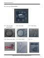
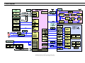
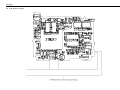
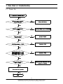
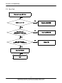
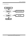
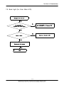
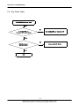
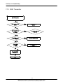
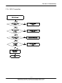
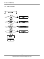
UMTS TELEPHONE
SGH-Z540
FRQWHQWV
XPWV WHOHSKRQH
1.
Specification
2.
Circuit Description
3.
Exploded Views and Parts List
4.
Electrical Parts List
5.
Block Diagrams
6.
PCB Diagrams
7.
Flow Chart of Troubleshooting
ⓒ Samsung Electronics Co.,Ltd. March. 2006
This Service Manual is a property of Samsung Electronics Co.,Ltd.
Any unauthorized use of Manual can be punished under applicable
Printed in Korea.
International and/or domestic law.
Code No.: GH68-09641A
BASIC.
1. Specification
1-1. GSM General Specification
EG SM9 00
DCS1800
PCS1900
W-CDMA
Fr eq.
Band[MHz]
Uplin k/Down link
8 90~915
9 35~960
17 10~178 5
18 05~188 0
18 50~191 0
19 30~199 0
192 0~1980
211 0~2170
ARF CN ra nge
0~ 124 &
97 5~1023
5 12~885
5 12~810
UL:96 12~988 8
DL:105 62~108 38
T x/Rx spacing
45MHz
95MHz
80MHz
1 90MHz
Mo d. Bit r ate/
Bit Period
270 .833kb ps
3 .692u s
270 .833kb ps
3 .692u s
270 .833kb ps
3 .692u s
3.8 4Mcps
Ti me Slo t
Pe rio d/Fr am e
Per iod
5 76.9u s
4. 615ms
5 76.9u s
4. 615ms
5 76.9u s
4. 615ms
Fr ame len gth : 10ms
Modula tion
0 .3G M SK
0 .3G MSK
0 .3G M SK
Q PS K
HQPSK
MS Power
33d Bm~5dBm
30d Bm~0dBm
30d Bm~0dBm
24 dBm ~ - 50dBm
Powe r Class
4
(max +33dBm)
1
(max +30dBm)
1
(max +30dBm)
3
(max + 24dBm)
Se nsitivity
-10 2dBm
-10 0dBm
-10 0dBm
-1 06.7d Bm
TDMA Mu x
8
8
8
Cell Radiu s
35Km
2Km
2Km
1-1
SAMSUNG Proprietary-Contents may change without notice
This Document can not be used without Samsung's authorization
2Km
Specification
1-2. GSM TX power class
TX Power
control level
GSM900
TX Power
control level
DCS1800
TX Power
control level
PCS1800
5
33±2 dBm
0
30±3 dBm
0
30±3 dBm
6
31±2 dBm
1
28±3 dBm
1
28±3 dBm
7
29±2 dBm
2
26±3 dBm
2
26±3 dBm
8
27±2 dBm
3
24±3 dBm
3
24±3 dBm
9
25±2 dBm
4
22±3 dBm
4
22±3 dBm
10
23±2 dBm
5
20±3 dBm
5
20±3 dBm
11
21±2 dBm
6
18±3 dBm
6
18±3 dBm
12
19±2 dBm
7
16±3 dBm
7
16±3 dBm
13
17±2 dBm
8
14±3 dBm
8
14±3 dBm
14
15±2 dBm
9
12±4 dBm
9
12±4 dBm
15
13±2 dBm
10
10±4 dBm
10
10±4 dBm
16
11±3 dBm
11
8±4dBm
11
8±4dBm
17
9±3dBm
12
6±4 dBm
12
6±4 dBm
18
7±3 dBm
13
4±4 dBm
13
4±4 dBm
19
5±3 dBm
14
2±5 dBm
14
2±5 dBm
15
0±5 dBm
15
0±5 dBm
1-2
SAMSUNG Proprietary-Contents may change without notice
This Document can not be used without Samsung's authorization
2. Circuit Description
2-1. SGH-Z540 RF Circuit Description
1. Antenna Switch Module (U702)
The antenna switch module allows multiple operating bands and modes to share the same antenna. A common
antenna connects to one of five paths: 1) UMTS-2100 Rx/Tx, 2) EGSM-900 Rx, 3) EGSM-900 Tx, 4) DCS-1800
Rx, and 5) DCS-1800 Tx. 6) PCS-1900 Tx, 7) PCS-1900 Rx, UMTS operation requires simultaneous reception
and transmission.
2. Filter
To convert Electromagnetic Field Wave to Acoustic Wave and then pass the specific frequency band.
- GSM Rx FILTER (F702) → For filtering the frequency band between 925 ~ 960 MHz.
- DCS Rx FILTER (F701) → For filtering the frequency band 1805 and 1880 MHz.
- PCS Rx FILTER (F700) → For filtering the frequency band 1930 and 1990 MHz.
- WCDMA Rx FILTER (F800) → For filtering the frequency band 2110 and 2170 MHz.
- WCDMA Tx FILTER (F802) → For filtering the frequency band 1920 and 1980 MHz.
3. VCTCXO
To generate the 19.2MHz reference clock to drive the logic and RF.
4. Duplexer (TCX800)
A duplexer splits a single operating band into receive and transmit paths.
5. UMTS PAM (U800)
This is a key component in the transmitter chain and must complement the RTR6250 IC precisely; jointly they
dominate the UMTS transmitter performance characteristics. Parameters such as gain, output power level, ACLR,
harmonics, Rx-band noise, and power supply current are critical.
6. GSM/DCS/PCS PAM (U701)
The PAM is a key component in any transmitter chain and must complement the rest of the transmitter precisely.
For GSM,DCS,PCS operation, the closed-loop transmit power control functions add even more requirements
relative to the UMTS PA. In addition to gain control and switching requirements, the usual RF parameters such
as gain, output power level, several output spectrum requirements, and power supply current are critical.
7. GSM/DCS/PCS l Tx VCO (OSC700)
The Tx VCO outputs for EGSM, DCS, PCS drive a resistive network that splits the active signal into two signals:
1) the input to the active PAM – this is the low loss path, and 2) the OPLL feedback signal.
8. RF VCO
The single-band UHF VCO is a key component within its phase-locked loop; VCO performance directly impacts
PLL and transceiver performance. UMTS Rx LO signal is generated from this
VCO's output.
2-1
SAMSUNG Proprietary-Contents may change without notice
This Document can not be used without Samsung's authorization
Circuit Description
9. RFR6250 (U801)
The RFR6250 provides the Zero-IF receiver signal path, from RF to analog baseband, for UMTS-2100
applications. The RFR6250 accepts its UMTS input signal from the handset RF front-end design. The UMTS input
is configured differentially to optimize second-order inter-modulation and common mode rejection performance, and
implements MSM-controlled gain adjustments to extend the receiver dynamic range.
10. RTR6250 (UCD700)
The RTR6250 supports multi-band, multi-mode phones with two receiver signal paths and three transmitter signal
paths:
1) Receiver paths
- EGSM-900
- DCS-1800
- PCS-1900
2) Transmitter paths
- EGSM-900 (using OPLL technique)
- DCS-1800 (using OPLL technique)
- PCS-1900
- UMTS-2100
Numerous secondary functions are integrated on-chip as well:
3) Phase-locked loop circuits
- PLL#1 and an on-chip VCO supports UMTS Tx
- PLL#2 and an external VCO supports EGSM Rx and Tx, DCS Rx and Tx, and UMTS Rx
4) Transceiver LO generation and distribution circuits
- EGSM-900 Rx and Tx
- DCS-1800 Rx and Tx
- UMTS-2100 Tx
2-2
SAMSUNG Proprietary-Contents may change without notice
This Document can not be used without Samsung's authorization
Circuit Description
2-2. SGH-Z540 Baseband Circuit description
1. PM6650-2 (PAM200)
1.1. Power Management
Ten low-dropout regulators designed specifically for GSM applications power the terminal and help ensure optimal
system performance and long battery life. It provides LDOs support for 1.375V, 1.8V, 2.6V, 2.85V, 3.3V.
IC-level interfaces include the three-line serial bus interface(SBI) used by the MSM6250 device to control
and status the PM6650-2 IC.
1.2. Keypad Backlight
The Keypad backlight driver output is at pin 23 (KEY_EL_DRV) and is designed to drive EL on KEY FPCB. Its
output current level is SBI-programmable and meets the performance specified below.
Input parameters are not specified since they are internal.
1.3. TCXO Controller and Buffers
The PM6650-2 IC includes circuits for controlling the TCXO warm-up and buffering its signal for distribution
throughout the handset. Performance specifications are presented below.
2. Connector
2-1. LCD Connector
LCD is consisted of main LCD(color 262K TFT LCD) and small LCD(color 65K TFT LCD). Chip select signals in
the HDC400, MAIN_LCD_CS can enable main LCD and SUB_EL_CS can enable small LCD. nRESET_LCD
signal initiates the reset process of the main LCD and sub LCD. 16-bit data lines(D2(0)~D(15)) transfers data and
commands to LCD.
Power signals for LCD are "VBATT_LCD". "EAR1O_P,N" and "SPK_R,K" from UCP100 are used for audio
speaker. And "VCC_MOTOR_3.3V" from U402 enables the motor.
2-2. Key
This is consisted of key interface pins among UCP100, KEYSENSE_N(0:3). These signals compose the matrix.
Result of matrix informs the key status to key interface in the UCP100. Power on/off key is seperated from the
matrix. The EL key PAD use the "VREG_MSMP_2.6V" voltage.
"HALL_SW" informs the status of folder (open or
closed) to the. This uses the hall effect IC, EM-1681-FT
2-3. EMI ESD Filter
This system uses the EMI ESD filter, ECLAMP2378P to protect noise from IF CONNECTOR part.
2-3
SAMSUNG Proprietary-Contents may change without notice
This Document can not be used without Samsung's authorization
Circuit Description
2-4. IF connetor
It is 20-pin connector. They are designed to use VBATT, UART1_TX, UART1_RX, EARMIC_P/N, EAR_R/L,
EAR_SW, JACK_INT, ADC_BOOTSW, JIG_ON, USB_D+/-. They connected to power supply IC, microprocessor
and signal processor IC.
3. Audio
EAR1O_P and EAR1O_N from UCP100 are connected to the main speaker. AUXO_P and AUXO_N are
connected to the Digital AMP. MIC1_P and MIC1_N are connected to the main MIC. And MIC2_P and MIC2_N
are connected to the Earphone.
YMU765 has a built-in amplifier, and thus, is an ideal device for outputting sounds that are used by mobile
phones in addition to game sounds and ringing melodies that are replayed by a synthesizer.
The synthesizer section adopts "stereophonic hybrid synthesizer system" that are given advantages of both FM
synthesizers and Wave Table synthesizers to allow simultaneous generation of up to 32 FM voices and 32 Wave
Table voices. Furthermore, YMU765 has a built-in hardware sequencer that helps to realize complex play without
heavily loading the host CPU. And this device also has a built-in circuit for controlling vibrators and LEDs
synchronizing with play of music. The consumed electric current can be stopped to the minimum by power down
mode when not operating.
The hardware sequence built in this device allows playing of the complex music without giving excessive load to
the CPU of the portable telephones. Moreover, the registers of the FM synthesizer can be operated directly for
real time sound generation, allowing, for example, utilization of various sound effects when using the game
software installed in the portable telephone.
4. Memory (UME300)
The signals in the MSM6250 enable two memories. They use VREG_MSME_1.8V and VREG_MSMP_2.6V from
the PM6650. This system uses SEC's memory, KBE00S005M-D411. It is consisted of 2G bits flash NAND
memory and 512M bits SDRAM memory. It has 16 bit data line, D1[0~15] which is connected to MSM6250.
It has 22 bit address lines, A[1~22]. SDRAM_CS and NANDFLASH_CS signals is chip select.
5. Camera
The camera module consists of 1.3 Mega pixel and VGA pixel. The 1.3 Mega camera is a highly integrated
CMOS color image sensor implemented by Micron COMS sensor process realizing high sensitivity and wide
dynamic range.
Total active pixel is 1280H x 1024V. The VGA camera is a highly integrated CMOS color image
sensor implemented by Micron COMS sensor process realizing high sensitivity and wide dynamic range. Total
active pixel is 656H x 488V.
2-4
SAMSUNG Proprietary-Contents may change without notice
This Document can not be used without Samsung's authorization
3. Exploded View and Parts List
3-1. Exploded View
QVO01
QFR01
QCW01
QIF01
QCK01
QWD01
QFU01
QKP01
QKP02
QME02
QLB02
QSH01
QCA01
QCA02
QLC01
QMP01
QME06
QCB01
QAR01
QME04
QBM01
QMO01
QAN02
QCR12
QFL01
QHI01
QSC14
QCR12
QRE01
QCR12
QSC13
QRF01
QAN06
QSC01
QCR04
QSC13
QMW04
QBA01
QBA00
3-1
SAMSUNG Proprietary-Contents may change without notice
This Document can not be used without Samsung's authorization
Exploded view and Part List
3-2. Parts List
Location NO.
QAN02
QAN06
QAR01
QBA00
QBA01
QCA01
QCA02
QCB01
QCR04
QCR12
QCW01
QKP01
QLB02
QLC01
QME02
QME06
QMO01
QMP01
QMW04
QRE01
QRF01
QWD01
QSC01
QSC13
QSC14
QSH01
QBM01
QFU01
QFL01
QFR01
QME04
QKP02
QHI01
QCK01
QIF01
QVO01
Description
INTENNA-SGHZ540
MEC-CASE INTENNA FOLDER
AUDIO-RECEIVER
PMO-CASE BATTERY FOLDER
BATTERY-880MAH,BLK,MAIN
UNIT-MEGA CAMERA
UNIT-VGA CAMERA
CBF COAXIAL CABLE
SCREW-MACHINE
SCREW-MACHINE
PCT-COVER CAMERA WINDOW
MEC-KEYPAD(OMN/BLK)
NDC-BRACKET MP3 KEY
LCD-SGHZ540 MODULE
UNIT-KEY PAD
UNIT-SPK FPCB
MOTOR DC-SGHZ540
PBA MAIN-SGHZ540
MEC-COVER MAIN WIN(VODA)
MEC-REAR COVER
MPR-TAPE RF HOLE
PCT-COVER SUB WINDOW
RMO-CAP FOLDER TOP
RMO-COVER REAR
RMO-COVER FOLDER BOT
MEC-BRACKET SHIELD
ELA ETC-Z540 BLUETOOTH MODUL
UNIT-BTFPCB
MEC-FOLDER UPPER
MEC-KEY FOLD(MP3)
MEC-FOLDER LOWER
MEC-HINGE
MEC-CASE FRONT FOLDER
PMO-CAMERA KEY
PMO-COVER IF
PMO-VOLUME KEY
3-2
SAMSUNG Proprietary-Contents may change without notice
This Document can not be used without Samsung's authorization
SEC CODE
GH42-00723A
GH75-08620A
3009-001173
GH72-26922A
GH43-02253A
GH59-02709A
GH59-02710A
GH39-00403A
6001-001479
6001-001530
GH72-28463A
GH75-09169A
GH71-05913A
GH07-00822A
GH59-02667A
GH59-02671A
GH31-00218A
GH92-02496A
GH75-09036A
GH75-08621A
GH74-20208A
GH72-28461A
GH73-05894A
GH73-05901A
GH73-05895A
GH75-09118A
GH96-02136A
GH59-02750A
GH75-08617A
GH75-09034A
GH75-08618A
GH75-04334D
GH75-08619A
GH72-26932A
GH72-26917A
GH72-26931A
Exploded view and Part List
Description
BAG PE
BAG PE
CBF INTERFACE-DATA LINK CABLE
ADAPTOR-SGHD800 TA(EU)
S/W CD-PC STUDIO
UNIT-EARPHONE
SPRING ETC-BATT LOCKER
LABEL(P)-IMEI
LABEL(P)-WATER SOAK
LABEL(R)-MAIN(EU)
MANUAL USERS-VODA ITALIAN
BOX(P)-UNIT(EU NEW)
BOX(P)-SLIP CASE(EU)
CUSHION-CASE(1-2)
MPR-BOHO VINYL LCD CONN
MPR-TAPE MAIN WINDOW
MPR-TAPE LCD MASKING 1
MPR-TAPE LCD MASKING 2
MPR-TAPE INTENNA CABLE
MPR-TAPE FPCB BLUE
CONE
MPR-VINYL BOHO LCD MAIN
MPR-VINYL BOHO F/L(S)
MPR-VINYL BOHO LCD SUB
MPR-VINYL BOHO MP3 KEY
MPR-VINYL BOHO MP3 KEY
MPR-TAPE BLUE SHIELD
MPR-CUSHION MP3 KEY
MPR-CUSHION MOTOR
MPR-TAPE MIC MASK
MPR-VINYL BOHO SIDE KEY
MPR-SPONGE UPPER
MEC-HANGER(BLK)
3-3
SAMSUNG Proprietary-Contents may change without notice
This Document can not be used without Samsung's authorization
SEC CODE
6902-000378
6902-000634
GH39-00444A
GH44-01060A
GH46-00198A
GH59-02499A
GH61-00120A
GH68-01335D
GH68-02026A
GH68-08783A
GH68-08843A
GH69-02908A
GH69-03488A
GH69-03556A
GH74-15350A
GH74-20193A
GH74-20203A
GH74-20204A
GH74-20205A
GH74-20434A
GH74-20459A
GH74-20460A
GH74-20460B
GH74-20461B
GH74-20790A
GH74-20790A
GH74-20844A
GH74-21083A
GH74-21084A
GH74-21217A
GH74-21328A
GH74-21434A
GH75-08867E
Exploded view and Part List
3-3. Disassembling Manual
2
1
Remove B/T MODULE from th
e BT connector.
1) After remove screw cap with tweezers, Unscrew.
1) Remove B/T MODULE from the BT connector.
2) Remove REAR and INTENNA COVER.
2) Remove B/T MODULE from attached to Front with
3) Unscrew from the INTENNA.
tweezers.
1) When you use tweezers, Be careful a damage of
1) When you remove the B/T MODULE, Be careful crack
component.
and damage of the BT MODULE.
3
4
1) Remove LCD Connector and INTENNA Connector from
1) Remove INTENNA WIRE Tape with tweezers.
the PBA.
2) Remove INTENNA and INTENNA WIRE.
2) Remove PBA from the FRONT ASS'Y.
1) Pay attention to tear of the FPCB.
1) When you remove the tape, pay attention to damage
2) Pay attention to damage of the wire.
of the INTENNA WIRE.
2) Be careful handling INTENNA. (Don't touch intenna pattern.)
3-4
SAMSUNG Proprietary-Contents may change without notice
This Document can not be used without Samsung's authorization
Exploded view and Part List
6
5
1) Remove conduction Tape and Rubber from the FOLDER
1) Remove SHIELD CAN and KEY PAD from the FOLDER ASS"Y.
ASS'Y with tweezers.
1) Disjoint KEYPAD and SHIELD CAN together.
8
7
1) Using a disassemble stick, Disjoint the Folder like the Photo.
1) After remove screw cap with tweezers, Unscrew.
1) When you disjoint the Folder, pay attention to damage
1) When you use a screwdriver, Be careful a damage
of the LCD F-PCB.
of component.
2) When you use a disassemble stick, Be careful a damage
of component.
9
10
1) Disjoint the Folder of the Bottom with tweezers.
2) Using a disassemble stick, disjoint the Folder of the Side.
1) When disjointing UPPER, pay attention to damage of
the wire.
1) Romove the LCD PROTECTION TAPE with tweezers
1) Pay attention to a finger mark and dust of the LCD.
2) When you use tweezers, Be careful a damage of
component.
3-5
SAMSUNG Proprietary-Contents may change without notice
This Document can not be used without Samsung's authorization
Exploded view and Part List
11
12
Lift BRAKET
with tweezers
1) Take off the SPK and the RECEIVER from the LOWER with
tweezers.
2) Open the ACTUATOR around the SPK ASS'Y connector.
3) After lifting BRAKET with tweezers,remove the SPK
ASS'Y.
1) Take off the MOTOR from the LOWER with tweezers.
2) Open the ACTUATOR around the CAMERA connector.
1) When you take off the SPK and the RECEIVER, pay attention
1) When you take off MOTOR, pay attention to damage of
to damage of the SPK and the RECEIVER.
LCD F-PCB and MOTOR WIRE.
2) When disjointing SPK ASS'Y, pay attention to
2) pay attention to damage of CAMERA F-PCB .
damage of the F-PCB.
13
1) Take off the LCD from the LOWER .
2) Take off the MEGA CAMERA from the LOWER.
1) When you remove the LCD, pay attention to damage of LCD F-PCB,LCD component, finger mark, dust.
2) When you remove the CAMERA, pay attention to damage of CAMERA F-PCB and CAMERA.
3-6
SAMSUNG Proprietary-Contents may change without notice
This Document can not be used without Samsung's authorization
Exploded view and Part List
3-4. Assembling Manual
1
2
1) Solder the MOTOR WIRE after positioning it on the MOTOR PAD.
1) Insert MEGA CAMERA F-PCB in the Connector.
2) Insert SUB CAMERA F-PCB in the Connector.
1) Insert CAMERA F-PCB in the Connector.
(By Silk Base Line)
2) Be careful F-PCB CRACK.
1) Take care of soldering correct.
2) Don't touch the LCD component and LCD DATA LINE with a
hot iron carefully.
3
1) Take off SPK ASS'Y's tape, .
2) Press the SPK ASS'Y의 KEY DOME with a hand.
3) Attach the sponge on the MP3 KEY DOME correctly.
1) Attach KEY PCB on the a rising correctly.
2) Be careful the sponge of dust.
After bonding, handling the dust
4
direction
1) Insert SPK ASS'Y F-PCB F-PCB in the Connector.
2) Bond the solder part with receiver wire of the end.
1) Insert SPK ASS'Y F-PCB in the Connector. (By Silk Base Line)
2) Do not bond too much and control the amount of bond not to be high.
3-7
SAMSUNG Proprietary-Contents may change without notice
This Document can not be used without Samsung's authorization
Exploded view and Part List
Insert the Blue marked
5
part of the SHIELD CAN
under the Red marked of
the FRONT HOOK.
가.Insert the top of the SHIELD CAN obliquely.( 45°)
→ When inserting, check the condition of the KEY PAD Basefilm .
나.Combine the bottom hole of the SHIELD CAN and FRONT SCREW boss.
다.After Combining, check the KEY GAP of the PAD.
1) After Combining FRONT and SHIELD CAN, open the FOLDER and check the KEY PAD of the GAP.
6
1) Adhere the Mic insulation TAPE to SHIELD CAN along metallized SHIELD CAN.
2) After put the ANT on the FRONT, screw ANT.
3) Put the ANT CABLE through the passage of FRONT.
4) Don't keep being shown the Ant Cable after adhering Ant TAPE.
1) Attach tape by Guide line.
3-8
SAMSUNG Proprietary-Contents may change without notice
This Document can not be used without Samsung's authorization
Exploded view and Part List
7
1) Connect ANT cover with FRONT
2) Screw down
3) Insert Screw cap at two points
1) Take care so that ANT cover do not interfere with Ant wire.
2) On screwing down, be careful not to scratch
8
⑤ CAMERA
④ F-PCB insert
insert
③ MOTOR insert
① LCD insert
1) Insert LCD and SPK ASS'Y bracket.
2) Twist twice MOTOR wire and insert MOTOR.
3) insert LCD FPCB into F/LOWER hole.
② Bracket insert
4) Insert VGA CAMERA.
5) Attach a semocircular Poron sponge on the MOTOR with a
pinset.
1) On inserting LCD, be careful for foreign substance.
2) Take care that MOTOR wire do not interfere with screw boss.
3) Notice that FPCB should not be cracked on inserting CAMERA.
3-9
SAMSUNG Proprietary-Contents may change without notice
This Document can not be used without Samsung's authorization
Exploded view and Part List
9
1) Attach a black insulation tape on LCD upper covering parts
2) Push and insert a receiver into LOWER receiver inserting
position rightly.
3) Insert SPK into LOWER SPK position.
4) Attach a black insulation tape on LCD lower covering parts.
5) Push a receiver wire for wire to avoid putting on F-PCB.
1) Attach insulation tapes covering parts perfectly at the right position.
→Check tape position with red lines.
10
1) Firstly, connect UPPER end hook with LOWER end hook.
2) Be care for foreign substance and connect Lower hooks.
3) Connect side hooks.
1) Notice that foreign substances do not go in.
3-10
SAMSUNG Proprietary-Contents may change without notice
This Document can not be used without Samsung's authorization
Exploded view and Part List
11
1) Screw down at four points.
2) Insert screw cap at four points.
12
Insert pushing hinge with wooden pinset
or hand
1) Insert FOLDER into FRONT passing hole.
2) After inserting hinge dummy, assemble pushing hinge on the other part with wooden pinset or hand.
3) Check folder connection by repeating open and close two or three times.
3-11
SAMSUNG Proprietary-Contents may change without notice
This Document can not be used without Samsung's authorization
Exploded view and Part List
14
13
1) Insert PBA into FRONT ASS'Y.
1) Connect LCD F-PCB connector.
2) When inserting PBA, put ANT wire at PBA hole
2) Connect B/T Module.
near the screw boss hole and connect with
connector.
1) Be careful not to damage ANT wire.
2) Ensure space so that ANT Wire can not be damaged when connecting FRONT with REAR.
15
16
1) After aligning REAR upper hook part with FRONT upper
1) Screw down 4 points.
hook part, cover REAR and assemble.
→ Check the hook connection by pushing the upper part
of REAR
3-12
SAMSUNG Proprietary-Contents may change without notice
This Document can not be used without Samsung's authorization
Exploded view and Part List
3-5. LCD KIT assembling Manual
1
1) Attach the black insulation tape on the LCD upper to cover parts completely.
→ Attach tape according to red lines.
Discription
SEC CODE
SEC Design
quantity
TAPE LCD MASKING 1
GH74-20203A
39.7 x 31.6 x 0.08T
1
-
-
-
-
2
1) Attach the black insulation tape on the LCD
lower to cover parts completely.
→ Attach tape according to red lines.
Discription
SEC CODE
SEC Design
quantity
TAPE LCD MASKING 2
GH74-20204A
39.7 x 11.62 x 0.08T
1
-
-
-
-
3-13
SAMSUNG Proprietary-Contents may change without notice
This Document can not be used without Samsung's authorization
Exploded view and Part List
3-6. Test Jig (GH80-03308A)
3-6-1. RF Test Cable
(GH39-00397A)
3-6-2. Test Cable
3-6-3. Serial Cable
3-6-4. Power Supply Cable
3-6-5. DATA CABLE
3-6-6. TA
3-14
SAMSUNG Proprietary-Contents may change without notice
This Document can not be used without Samsung's authorization
4. Electrical Parts List
DESIGN LOC
DESCRIPTION
SEC CODE
STATUS
AN1
ANT700
BAT201
BTC501
C100
C101
C102
C103
C104
C105
C106
C107
C108
C109
C110
C111
C112
C113
C114
C116
C117
C118
C119
C120
C121
C122
C123
C124
C125
C127
C128
C129
C130
C131
C132
C133
C134
C135
C136
C137
C138
C139
C140
C141
C142
C143
C144
C145
C146
C147
ANTENNA-CHIP
CONNECTOR-COAXIAL
BATTERY-LI(2ND)
CONNECTOR-BATTERY
C-CER,CHIP
C-CER,CHIP
C-CER,CHIP
C-CER,CHIP
C-CER,CHIP
C-CER,CHIP
C-CER,CHIP
C-CER,CHIP
C-CER,CHIP
C-CER,CHIP
C-CER,CHIP
C-CER,CHIP
C-CER,CHIP
C-CER,CHIP
C-CER,CHIP
C-CER,CHIP
C-CER,CHIP
C-CER,CHIP
C-CER,CHIP
C-CER,CHIP
C-CER,CHIP
C-CER,CHIP
C-CER,CHIP
C-CER,CHIP
C-CER,CHIP
C-CER,CHIP
C-CER,CHIP
C-CER,CHIP
C-CER,CHIP
C-CER,CHIP
C-CER,CHIP
C-CER,CHIP
C-CER,CHIP
C-CER,CHIP
C-CER,CHIP
C-CER,CHIP
C-CER,CHIP
C-CER,CHIP
C-CER,CHIP
C-CER,CHIP
C-CER,CHIP
C-CER,CHIP
C-CER,CHIP
C-CER,CHIP
C-CER,CHIP
C-CER,CHIP
701
4202-001101
3705-001358
4302-001130
3711-006003
2203-006423
2203-006423
2203-006423
2203-006423
2203-006423
2203-006423
2203-006423
2203-006423
2203-006423
2203-006423
2203-006423
2203-006423
2203-006423
2203-006423
2203-006562
2203-006423
2203-006423
2203-006423
2203-006423
2203-006423
2203-006423
2203-006423
2203-006423
2203-006423
2203-006423
2203-006423
2203-006423
2203-006423
2203-006423
2203-006423
2203-006423
2203-006423
2203-005725
2203-005725
2203-006668
2203-005682
2203-006194
2203-006423
2203-006047
2203-006194
2203-006423
2203-006423
2203-006617
2203-006423
2203-006423
2203-006617
SA
SA
SA
SA
SA
SA
SA
SA
SA
SA
SA
SA
SA
SA
SA
SA
SA
SA
SA
SA
SA
SA
SA
SA
SA
SA
SA
SA
SA
SA
SA
SA
SA
SA
SA
SA
SA
SA
SA
SA
SA
SA
SA
SA
SA
SA
SA
SA
SA
SA
SAMSUNG Proprietary-Contents may change without notice
This Document can not be used without Samsung's authorization
Electrical Parts List
DESIGN LOC
DESCRIPTION
SEC CODE
STATUS
C148
C148
C149
C158
C159
C160
C168
C170
C200
C201
C202
C203
C204
C205
C206
C207
C208
C209
C210
C211
C212
C213
C214
C215
C216
C217
C218
C219
C220
C221
C223
C224
C225
C226
C227
C228
C229
C232
C234
C235
C236
C237
C238
C239
C240
C241
C242
C243
C244
C248
C-CER,CHIP
C-CER,CHIP
C-CER,CHIP
C-CER,CHIP
C-CER,CHIP
C-CER,CHIP
C-CER,CHIP
C-CER,CHIP
C-CER,CHIP
C-CER,CHIP
C-CER,CHIP
C-CER,CHIP
C-CER,CHIP
C-CER,CHIP
C-CER,CHIP
C-CER,CHIP
C-CER,CHIP
C-CER,CHIP
C-CER,CHIP
C-CER,CHIP
C-CER,CHIP
C-CER,CHIP
C-CER,CHIP
C-CER,CHIP
C-CER,CHIP
C-CER,CHIP
C-CER,CHIP
C-CER,CHIP
C-CER,CHIP
C-CER,CHIP
C-CER,CHIP
C-CER,CHIP
C-CER,CHIP
C-CER,CHIP
C-CER,CHIP
C-CER,CHIP
C-CER,CHIP
C-CER,CHIP
C-CER,CHIP
C-CER,CHIP
C-CER,CHIP
C-CER,CHIP
C-CER,CHIP
C-CER,CHIP
C-CER,CHIP
C-CER,CHIP
C-CER,CHIP
C-CER,CHIP
C-CER,CHIP
C-CER,CHIP
2203-006423
2203-006838
2203-006838
2203-006838
2203-006562
2203-000438
2203-000995
2203-000995
2203-006324
2203-005138
2203-005138
2203-006562
2203-006324
2203-006423
2203-005736
2203-005736
2203-006423
2203-006305
2203-006562
2203-006305
2203-006208
2203-006305
2203-006838
2203-006305
2203-006838
2203-006208
2203-006838
2203-006305
2203-006208
2203-006838
2203-006562
2203-006838
2203-005806
2203-006208
2203-005806
2203-005731
2203-005731
2203-006423
2203-001153
2203-005682
2203-005682
2203-006708
2203-006708
2203-006708
2203-006423
2203-006423
2203-006423
2203-006423
2203-006423
2203-006562
SA
SA
SA
SA
SA
SA
SA
SA
SA
SA
SA
SA
SA
SA
SA
SA
SA
SA
SA
SA
SA
SA
SA
SA
SA
SA
SA
SA
SA
SA
SA
SA
SA
SA
SA
SA
SA
SA
SA
SA
SA
SA
SA
SA
SA
SA
SA
SA
SA
SA
702
SAMSUNG Proprietary-Contents may change without notice
This Document can not be used without Samsung's authorization
Electrical Parts List
DESIGN LOC
DESCRIPTION
SEC CODE
STATUS
C249
C250
C251
C252
C253
C254
C255
C300
C301
C302
C303
C304
C305
C306
C307
C308
C309
C400
C402
C403
C405
C406
C407
C408
C409
C410
C411
C412
C413
C414
C415
C416
C419
C420
C422
C423
C424
C425
C426
C500
C501
C502
C506
C507
C508
C510
C600
C601
C602
C603
C-CER,CHIP
C-CER,CHIP
C-CER,CHIP
C-CER,CHIP
C-CER,CHIP
C-CER,CHIP
C-CER,CHIP
C-CER,CHIP
C-CER,CHIP
C-CER,CHIP
C-CER,CHIP
C-CER,CHIP
C-CER,CHIP
C-CER,CHIP
C-CER,CHIP
C-CER,CHIP
C-CER,CHIP
C-CER,CHIP
C-CER,CHIP
C-CER,CHIP
C-CER,CHIP
C-CER,CHIP
C-CER,CHIP
C-CER,CHIP
C-CER,CHIP
C-CER,CHIP
C-CER,CHIP
C-CER,CHIP
C-CER,CHIP
C-CER,CHIP
C-CER,CHIP
C-CER,CHIP
C-CER,CHIP
C-CER,CHIP
C-CER,CHIP
C-CER,CHIP
C-CER,CHIP
C-CER,CHIP
C-CER,CHIP
C-CER,CHIP
C-CER,CHIP
C-CER,CHIP
C-CER,CHIP
C-CER,CHIP
C-CER,CHIP
C-CER,CHIP
C-CER,CHIP
C-CER,CHIP
C-CER,CHIP
C-CER,CHIP
2203-006562
2203-006562
2203-006562
2203-006562
2203-006562
2203-006562
2203-006562
2203-006423
2203-006423
2203-006423
2203-006423
2203-006423
2203-006423
2203-006423
2203-006423
2203-006562
2203-006423
2203-005482
2203-006562
2203-006423
2203-005682
2203-005682
2203-005682
2203-005682
2203-005682
2203-005682
2203-005682
2203-005682
2203-005682
2203-005682
2203-005682
2203-005682
2203-005682
2203-005482
2203-005682
2203-002709
2203-006838
2203-005682
2203-005682
2203-006423
2203-006556
2203-006423
2203-000812
2203-006361
2203-000812
2203-006423
2203-006305
2203-005682
2203-006208
2203-005482
SA
SA
SA
SA
SA
SA
SA
SA
SA
SA
SA
SA
SA
SA
SA
SA
SA
SA
SA
SA
SA
SA
SA
SA
SA
SA
SA
SA
SA
SA
SA
SA
SA
SA
SA
SA
SA
SA
SA
SA
SA
SA
SA
SA
SA
SA
SA
SA
SA
SA
703
SAMSUNG Proprietary-Contents may change without notice
This Document can not be used without Samsung's authorization
Electrical Parts List
DESIGN LOC
C604
C607
C608
C611
C615
C616
C617
C618
C619
C620
C621
C622
C623
C624
C625
C626
C627
C628
C629
C630
C631
C632
C634
C635
C637
C638
C640
C641
C642
C643
C644
C645
C646
C702
C703
C704
C705
C706
C707
C708
C709
C710
C711
C712
C713
C714
C715
C716
C717
C718
DESCRIPTION
C-CER,CHIP
C-CER,CHIP
C-CER,CHIP
C-CER,CHIP
C-CER,CHIP
C-CER,CHIP
C-CER,CHIP
C-CER,CHIP
C-CER,CHIP
C-CER,CHIP
C-CER,CHIP
C-CER,CHIP
C-CER,CHIP
C-CER,CHIP
C-CER,CHIP
C-CER,CHIP
C-CER,CHIP
C-CER,CHIP
C-CER,CHIP
C-CER,CHIP
C-CER,CHIP
C-CER,CHIP
C-CER,CHIP
C-CER,CHIP
C-CER,CHIP
C-CER,CHIP
C-CER,CHIP
C-CER,CHIP
C-CER,CHIP
C-CER,CHIP
C-CER,CHIP
C-CER,CHIP
C-CER,CHIP
C-CER,CHIP
C-CER,CHIP
C-CER,CHIP
C-CER,CHIP
C-CER,CHIP
C-CER,CHIP
C-CER,CHIP
C-CER,CHIP
C-CER,CHIP
C-CER,CHIP
C-FILM,SMD-PPS
C-CER,CHIP
C-CER,CHIP
C-CER,CHIP
C-CER,CHIP
C-CER,CHIP
C-CER,CHIP
704
SEC CODE
STATUS
2203-006562
2203-006648
2203-003054
2203-000386
2203-003054
2203-003054
2203-003054
2203-006648
2203-006562
2203-006562
2203-000386
2203-005682
2203-005682
2203-005482
2203-005482
2203-000438
2203-006208
2203-006562
2203-006562
2203-006562
2203-000812
2203-006648
2203-006208
2203-001259
2203-006324
2203-003054
2203-006648
2203-000812
2203-006562
2203-005683
2203-006423
2203-005682
2203-005682
2203-001072
2203-000885
2203-006562
2203-005806
2203-005682
2203-005736
2203-006562
2203-005682
2203-005736
2203-005736
2301-001512
2203-006423
2203-000836
2203-005725
2203-006423
2203-006423
2203-005682
SA
SA
SA
SA
SA
SA
SA
SA
SA
SA
SA
SA
SA
SA
SA
SA
SA
SA
SA
SA
SA
SA
SA
SA
SA
SA
SA
SA
SA
SA
SA
SA
SA
SA
SA
SA
SA
SA
SA
SA
SA
SA
SA
SA
SA
SA
SA
SA
SA
SA
SAMSUNG Proprietary-Contents may change without notice
This Document can not be used without Samsung's authorization
Electrical Parts List
DESIGN LOC
DESCRIPTION
SEC CODE
STATUS
C719
C720
C721
C722
C723
C724
C725
C726
C727
C728
C729
C730
C731
C732
C733
C734
C735
C736
C737
C740
C741
C742
C743
C745
C746
C747
C748
C749
C750
C751
C752
C753
C754
C755
C756
C757
C758
C759
C760
C801
C803
C805
C806
C807
C809
C810
C812
C816
C817
C818
C-CER,CHIP
C-CER,CHIP
C-CER,CHIP
C-CER,CHIP
C-CER,CHIP
C-CER,CHIP
C-CER,CHIP
C-CER,CHIP
C-CER,CHIP
C-CER,CHIP
C-CER,CHIP
C-CER,CHIP
C-CER,CHIP
C-CER,CHIP
C-CER,CHIP
C-CER,CHIP
C-CER,CHIP
C-CER,CHIP
C-CER,CHIP
C-CER,CHIP
C-CER,CHIP
C-CER,CHIP
C-CER,CHIP
C-CER,CHIP
C-CER,CHIP
C-CER,CHIP
C-CER,CHIP
C-CER,CHIP
C-CER,CHIP
C-CER,CHIP
C-CER,CHIP
C-CER,CHIP
C-CER,CHIP
C-CER,CHIP
C-FILM,SMD
C-CER,CHIP
C-CER,CHIP
C-CER,CHIP
C-CER,CHIP
C-CER,CHIP
C-CER,CHIP
C-CER,CHIP
C-CER,CHIP
R-CHIP
C-CER,CHIP
C-CER,CHIP
C-CER,CHIP
C-CER,CHIP
C-CER,CHIP
C-CER,CHIP
2203-005682
2203-006423
2203-000438
2203-000233
2203-000233
2203-000233
2203-000233
2203-006562
2203-000330
2203-006423
2203-005682
2203-006562
2203-000995
2203-005682
2203-000854
2203-006562
2203-000854
2203-006194
2203-006423
2203-000359
2203-000359
2203-000359
2203-000359
2203-006556
2203-005736
2203-005503
2203-002443
2203-005234
2203-006423
2203-006423
2203-005806
2203-006208
2203-005736
2203-000311
2301-001736
2203-006137
2203-000812
2203-005682
2203-005682
2203-000330
2203-005806
2203-000330
2203-000330
2007-000171
2203-000330
2203-000995
2203-001383
2203-006423
2203-005736
2203-000254
SA
SA
SA
SA
SA
SA
SA
SA
SA
SA
SA
SA
SA
SA
SA
SA
SA
SA
SA
SA
SA
SA
SA
SA
SA
SA
SA
SA
SA
SA
SA
SA
SA
SA
SA
SA
SA
SA
SA
SA
SA
SA
SA
SA
SA
SA
SA
SA
SA
SA
705
SAMSUNG Proprietary-Contents may change without notice
This Document can not be used without Samsung's authorization
Electrical Parts List
DESIGN LOC
DESCRIPTION
SEC CODE
STATUS
C819
C820
C821
C822
C823
C825
C826
C827
C828
C829
C831
C832
C833
C834
C835
C836
C837
C838
C839
C840
C841
C847
C848
C849
C850
C851
CON
D1
D5
D500
D501
D7
DUF801
F400
F401
F500
F700
F701
F702
F800
F802
F803
F804
F805
HDC1
HDC400
HDC401
HDC702
IFC500
L200
C-CER,CHIP
C-CER,CHIP
C-CER,CHIP
C-CER,CHIP
C-CER,CHIP
C-CER,CHIP
C-CER,CHIP
C-CER,CHIP
C-CER,CHIP
C-CER,CHIP
C-CER,CHIP
C-CER,CHIP
C-CER,CHIP
C-CER,CHIP
C-CER,CHIP
C-CER,CHIP
C-CER,CHIP
C-CER,CHIP
C-CER,CHIP
C-CER,CHIP
C-CER,CHIP
C-CER,CHIP
C-CER,CHIP
C-CER,CHIP
C-CER,CHIP
C-CER,CHIP
SOCKET-BOARD TO BOARD
DIODE-ARRAY
DIODE-ZENER
DIODE-ZENER
DIODE-ZENER
DIODE-ARRAY
DUPLEXER-SAW
FILTER-EMI/ESD
FILTER-EMI/ESD
BEAD-SMD
FILTER-SAW
FILTER-SAW
FILTER-SAW
FILTER-SAW
FILTER-SAW
FILTER-EMI/ESD
FILTER-EMI/ESD
BEAD-SMD
HEADER-BOARD TO BOARD
HEADER-BOARD TO BOARD
HEADER-BOARD TO BOARD
HEADER-BOARD TO BOARD
SOCKET-INTERFACE
INDUCTOR-SMD
706
2203-005736
2203-006423
2203-005777
2203-005806
2203-006423
2203-006194
2203-000725
2203-005736
2203-006121
2203-005777
2203-005806
2203-006423
2203-005736
2203-005736
2203-006423
2203-005736
2203-006423
2203-006194
2203-006838
2203-006423
2203-005806
2203-006423
2203-006423
2203-006423
2203-006423
2203-005057
3710-002285
0407-001002
0403-001427
0403-001427
0403-001547
0407-001002
2910-000010
2901-001348
2901-001348
3301-001534
2904-001571
2904-001570
2904-001550
2904-001623
2904-001438
2901-001320
2901-001320
3301-001534
3711-005550
3711-005367
3711-005456
3711-005976
3710-002306
2703-002840
SA
SA
SA
SA
SA
SA
SA
SA
SA
SA
SA
SA
SA
SA
SA
SA
SA
SA
SA
SA
SA
SA
SA
SA
SA
SA
SA
SA
SA
SA
SA
SA
SA
SA
SA
SA
SA
SA
SA
SA
SA
SA
SA
SA
SA
SA
SA
SA
SA
SA
SAMSUNG Proprietary-Contents may change without notice
This Document can not be used without Samsung's authorization
Electrical Parts List
DESIGN LOC
DESCRIPTION
SEC CODE
STATUS
L201
L400
L401
L402
L403
L700
L701
L702
L703
L704
L705
L706
L707
L708
L709
L710
L711
L712
L713
L714
L715
L716
L800
L801
L802
L803
L804
L805
L806
L807
L808
OSC100
OSC200
OSC700
PAM200
Q800
R100
R101
R102
R103
R104
R105
R108
R109
R110
R111
R112
R113
R121
R122
INDUCTOR-SMD
BEAD-SMD
BEAD-SMD
BEAD-SMD
BEAD-SMD
BEAD-SMD
INDUCTOR-SMD
INDUCTOR-SMD
INDUCTOR-SMD
INDUCTOR-SMD
INDUCTOR-SMD
INDUCTOR-SMD
INDUCTOR-SMD
INDUCTOR-SMD
INDUCTOR-SMD
INDUCTOR-SMD
INDUCTOR-SMD
INDUCTOR-SMD
INDUCTOR-SMD
INDUCTOR-SMD
INDUCTOR-SMD
INDUCTOR-SMD
INDUCTOR-SMD
INDUCTOR-SMD
R-CHIP
INDUCTOR-SMD
INDUCTOR-SMD
INDUCTOR-SMD
INDUCTOR-SMD
INDUCTOR-SMD
INDUCTOR-SMD
RESONATOR-CERAMIC
CRYSTAL-SMD
OSCILLATOR-VCO
IC-POWER SUPERVISOR
TR-DIGITAL
R-CHIP
R-CHIP
R-CHIP
R-CHIP
R-CHIP
R-CHIP
R-CHIP
R-CHIP
R-CHIP
R-CHIP
R-CHIP
R-CHIP
R-CHIP
R-CHIP
707
2703-002840
3301-001158
3301-001534
3301-001534
3301-001534
3301-001534
2703-002201
2703-002870
2703-002314
2703-002207
2703-002198
2703-002207
2703-002203
2703-002207
2703-002870
2703-002268
2703-002207
2703-002198
2703-002208
2703-002203
2703-002208
2703-002203
2703-001737
2703-001747
2007-000171
2703-002870
2703-001729
2703-001729
2703-002870
2703-002313
2703-002870
2802-001182
2801-004339
2806-001360
1203-003877
0504-001151
2007-008542
2007-008542
2007-008542
2007-000171
2007-008542
2007-008542
2007-008419
2007-008049
2007-008419
2007-009112
2007-008055
2007-007314
2007-008516
2007-009170
SA
SA
SA
SA
SA
SA
SA
SA
SA
SA
SA
SA
SA
SA
SA
SA
SA
SA
SA
SA
SA
SA
SA
SA
SA
SA
SA
SA
SA
SA
SA
SA
SA
SA
SA
SA
SA
SA
SA
SA
SA
SA
SA
SA
SA
SNA
SA
SA
SA
SA
SAMSUNG Proprietary-Contents may change without notice
This Document can not be used without Samsung's authorization
Electrical Parts List
DESIGN LOC
DESCRIPTION
SEC CODE
STATUS
R123
R124
R126
R127
R127
R129
R130
R131
R200
R201
R202
R203
R204
R205
R206
R210
R211
R212
R213
R214
R215
R216
R217
R219
R220
R221
R222
R225
R226
R227
R231
R233
R300
R301
R302
R303
R438
R500
R501
R503
R504
R506
R507
R600
R601
R602
R603
R604
R605
R607
R-CHIP
R-CHIP
R-CHIP
R-CHIP
C-CER,CHIP
R-CHIP
R-CHIP
R-CHIP
R-CHIP
R-CHIP
R-CHIP
R-CHIP
R-CHIP
R-CHIP
R-CHIP
R-CHIP
R-CHIP
R-CHIP
R-CHIP
R-CHIP
R-CHIP
R-CHIP
R-CHIP
R-CHIP
R-CHIP
R-CHIP
R-CHIP
R-CHIP
R-CHIP
R-CHIP
R-CHIP
R-CHIP
R-CHIP
R-CHIP
R-CHIP
R-CHIP
R-CHIP
R-CHIP
R-CHIP
R-CHIP
R-CHIP
R-CHIP
R-CHIP
R-CHIP
R-CHIP
R-CHIP
R-CHIP
R-CHIP
R-CHIP
R-CHIP
2007-009170
2007-008516
2007-008548
2007-008516
2203-002677
2007-009170
2007-007741
2007-008542
2007-003015
2007-003015
2007-008516
2007-008483
2007-008806
2007-007468
2007-008542
2007-009157
2007-007314
2007-008055
2007-008055
2007-008055
2007-008055
2007-008055
2007-007586
2007-008542
2007-008051
2007-008419
2007-001320
2007-008542
2007-008542
2007-008542
2007-000168
2007-000168
2007-008542
2007-008542
2007-008516
2007-008542
2007-008055
2007-008516
2007-008419
2007-008419
2007-008419
2007-008419
2007-008419
2007-000171
2007-007318
2007-008542
2007-001319
2007-000171
2007-008542
2007-001325
SA
SA
SA
SA
SA
SA
SA
SA
SA
SA
SA
SA
SA
SA
SA
SA
SA
SA
SA
SA
SA
SA
SA
SA
SA
SA
SA
SA
SA
SA
SA
SA
SA
SA
SA
SA
SA
SA
SA
SA
SA
SA
SA
SA
SA
SA
SA
SA
SA
SA
708
SAMSUNG Proprietary-Contents may change without notice
This Document can not be used without Samsung's authorization
Electrical Parts List
DESIGN LOC
DESCRIPTION
SEC CODE
STATUS
R608
R609
R610
R611
R612
R613
R614
R615
R616
R617
R618
R619
R700
R701
R702
R703
R704
R705
R706
R707
R708
R709
R710
R711
R712
R713
R714
R715
R716
R717
R718
R719
R720
R721
R722
R723
R724
R725
R726
R727
R728
R729
R730
R731
R732
R800
R801
R802
R803
R804
R-CHIP
R-CHIP
R-CHIP
C-CER,CHIP
C-CER,CHIP
R-CHIP
R-CHIP
C-CER,CHIP
R-CHIP
R-CHIP
R-CHIP
R-CHIP
R-CHIP
R-CHIP
R-CHIP
R-CHIP
R-CHIP
R-CHIP
R-CHIP
R-CHIP
R-CHIP
R-CHIP
R-CHIP
R-CHIP
R-CHIP
R-CHIP
R-CHIP
R-CHIP
R-CHIP
R-CHIP
R-CHIP
R-CHIP
R-CHIP
R-CHIP
R-CHIP
R-CHIP
R-CHIP
R-CHIP
R-CHIP
R-CHIP
R-CHIP
R-CHIP
R-CHIP
R-CHIP
R-CHIP
R-CHIP
R-CHIP
R-CHIP
R-CHIP
R-CHIP
2007-000171
2007-001319
2007-007318
2203-005482
2203-005482
2007-007318
2007-001319
2203-000812
2007-000162
2007-007317
2007-007107
2007-007107
2007-000171
2007-000140
2007-001325
2007-008045
2007-000145
2007-000171
2007-001325
2007-001325
2007-001325
2007-000171
2007-007798
2007-007798
2007-007491
2007-000171
2007-000171
2007-007142
2007-000147
2007-007142
2007-001291
2007-001217
2007-001291
2007-001295
2007-008057
2007-008044
2007-001307
2007-001307
2007-001307
2007-001307
2007-008045
2007-000138
2007-008045
2007-001217
2007-001217
2007-008045
2007-000171
2007-007491
2007-007316
2007-008213
SA
SA
SA
SA
SA
SA
SA
SA
SA
SA
SA
SA
SA
SA
SA
SA
SA
SA
SA
SA
SA
SA
SA
SA
SA
SA
SA
SA
SA
SA
SA
SA
SA
SA
SA
SA
SA
SA
SA
SA
SA
SA
SA
SA
SA
SA
SA
SA
SA
SA
709
SAMSUNG Proprietary-Contents may change without notice
This Document can not be used without Samsung's authorization
Electrical Parts List
DESIGN LOC
DESCRIPTION
SEC CODE
STATUS
R807
R809
R810
R815
R816
R817
R830
RFS701
SIM200
TA115
TA126
TA245
TA246
TA401
TA404
TA509
TA744
TA804
TA807
TA808
TAC1
TAC2
TAC3
TCX800
TH100
TR200
TR201
TR809
U103
U201
U202
U203
U204
U400
U401
U402
U500
U501
U600
U601
U602
U701
U702
U800
U801
U810
U813
U814
U815
UCD700
R-CHIP
R-CHIP
R-CHIP
R-CHIP
R-CHIP
R-CHIP
R-CHIP
CONNECTOR-COAXIAL
CONNECTOR-CARD EDGE
C-TA,CHIP
C-TA,CHIP
C-TA,CHIP
C-TA,CHIP
C-TA,CHIP
C-TA,CHIP
C-TA,CHIP
C-TA,CHIP
C-TA,CHIP
C-TA,CHIP
C-TA,CHIP
SWITCH-TACT
SWITCH-TACT
SWITCH-TACT
OSCILLATOR-VCTCXO
THERMISTOR-NTC
TR-DIGITAL
TR-DIGITAL
FET-SILICON
BLUETOOTH MODULE
IC-POSI.FIXED REG.
IC-VOL. DETECTOR
IC-BATTERY
DIODE-ARRAY
IC-ANALOG SWITCH
IC-ANALOG SWITCH
IC-POSI.FIXED REG.
IC-HALL EFFECT S/W
IC-SWITCH
IC-MELODY
IC-AUDIO AMP
IC-POSI.FIXED REG.
IC-POWER AMP
IC-SWITCH
IC-POWER AMP
IC-RECEIVER
IC-SWITCH
C-CER,CHIP
C-CER,CHIP
C-CER,CHIP
IC-TRANSCEIVER
7010
2007-008045
2007-008055
2007-008516
2007-000151
2007-000151
2007-008542
2007-001307
3705-001225
3709-001358
2404-001381
2404-001381
2404-001381
2404-001339
2404-001381
2404-001381
2404-001381
2404-001411
2404-001381
2404-001339
2404-001339
3404-001152
3404-001152
3404-001152
2809-001280
1404-001224
0504-000168
0504-000168
0505-002078
4709-001363
1203-003064
1203-003728
1203-003823
0407-001038
1001-001265
1001-001265
1203-003754
1009-001020
1205-002784
1204-002138
1201-002195
1203-003208
1201-002218
1205-002724
1201-002305
1205-002781
1205-002874
2203-006423
2203-006423
2203-005683
1205-002645
SA
SA
SA
SA
SA
SA
SA
SA
SA
SA
SA
SA
SA
SA
SA
SA
SA
SA
SA
SA
SA
SA
SA
SA
SA
SA
SA
SA
SA
SA
SA
SA
SA
SA
SA
SA
SA
SA
SA
SA
SA
SA
SA
SA
SA
SNA
SA
SA
SA
SA
SAMSUNG Proprietary-Contents may change without notice
This Document can not be used without Samsung's authorization
Electrical Parts List
DESIGN LOC
DESCRIPTION
SEC CODE
STATUS
UCP100
UME300
ZD401
ZD402
ZD403
ZD501
ZD502
ZD503
ZD504
ZD505
ZD506
IC-MODEM
IC-MCP
DIODE-TVS
DIODE-TVS
DIODE-TVS
DIODE-TVS
DIODE-TVS
DIODE-ZENER
DIODE-TVS
DIODE-TVS
DIODE-TVS
1205-002780
1108-000032
0406-001208
0406-001208
0406-001203
0406-001208
0406-001208
0403-001547
0406-001203
0406-001203
0406-001203
SA
SNA
SA
SA
SA
SA
SA
SA
SA
SA
SA
7011
SAMSUNG Proprietary-Contents may change without notice
This Document can not be used without Samsung's authorization
Electrical Parts List
7012
SAMSUNG Proprietary-Contents may change without notice
This Document can not be used without Samsung's authorization
5. Block Diagrams
5-1
SAMSUNG Proprietary-Contents may change without notice
This Document can not be used without Samsung's authorization
6. PCB Diagrams
6-1. PCB Top Diagram
6-1
SAMSUNG Proprietary-Contents may change without notice
This Document can not be used without Samsung's authorization
PCB Diagrams
6-2. PCB Bottom Diagram
6-2
SAMSUNG Proprietary-Contents may change without notice
This Document can not be used without Samsung's authorization
7. Flow Chart of Troubleshooting
7-1. Power On
' Power On ' does not work
Yes
Check the Battery Voltage
is more than 3.3V
No
Change the Battery
Yes
PAM200 pin57(PS_HOLD)
= 2.6V?
No
Check the PMIC related to PS_HOLD
Yes
Check the Clock at
OSC200=32KHZ
No
Resolder OSC200
Yes
No
Check the PMIC
C237(VREG_MSMC) = 1.25V?
Yes
C224(VREG_MSME)
C220(VREG_MSMP)
C217(VREG_MSMA)
C210(VREG_TCXO)
=
=
=
=
1.8V?
2.6V?
2.6V?
2.8V?
No
Check the PMIC
Yes
Check for the clock at
C207= 19.2MHz
No
Check the clock generation circuit
(related to OSC700)
Yes
Check the initial operation
Yes
END
7-1
SAMSUNG Proprietary-Contents may change without notice
This Document can not be used without Samsung's authorization
POS
MMC_DATA
NEG
BAT201
R209
C232
1
2
3
4
C228
C206
VREG_MSMP_2.6V
VREG_USIM_3.0V
R229
2
1
8
7
6
5
G G G G
12 11 10 9
C233
1
2
3
4
SIM200
C229
R211
8
7
6
5
C234
R207
C235
SIM_RST
SIM_CLK
SIM_IO
R230
R228
R208
C231
R203
PS_HOLD
PMIC_SBDT
PMIC_SBCK
PMIC_SBST
PM_INT_N
MSM_SIM_RST
MSM_SIM_CLK
JIG_ON_SW
PON_RESET_N
MSM_SIM_IO
USB_D_P
USB_D_M
PHONE_ON
USB_OE_MSM
USB_DAT_MSM
USB_SEO_MSM
ADC_BOOTSW
AMUX_OUT
SLEEP_CLK
TCXO
TCXO_EN
C203
VBUS_5V_SW
ADC_BOOTSW
C236
MMC_CMD
MMC_CLK
C230
BUFF_TCXO
R206
VREG_MSMP_2.6V
REF_OUT
OSC200
R202
EXT_5V_SW
1
2
D1
3
C207
TP201
TP200
R204
C204
R212
C205
V_IN
13
17
19
11
18
20
24
57
66
68
9
30
26
34
38
40
43
47
49
51
59
1
44
46
45
58
55
53
70
72
82
80
2
16
3
5
4
15
6
60
7
48
USB_OE_N
USB_DAT
USB_SE0
USB_ID
USB_D_P
USB_D_M
KPDPWR_N
PS_HOLD
CBL1PWR_N
CBL0PWR_N
PON_RESET_N
RUIM_M_IO
RUIM_IO
RUIM_M_CLK
RUIM_CLK
RUIM_M_RST
RUIM_RST
SBDT
SBCK
SBST
MSM_INT_N
ADC_BYP
XTAL_IN
XTAL_OUT
SLEEP_CLK
TCXO_IN
TCXO_EN
TCXO_OUT
AMUX_IN1
AMUX_IN2
AMUX_OUT
REF_OUT
VCHG
USB_VBUS
ISNS_P
ISNS_M
CHG_CTL_N
USB_CTL_N
VBAT
VCOIN
BAT_FET_N
VBACKUP
C200
VDD_PA
VDD_MSMC
VDD_MSME
VDD_RUIM
VDD_MSM
VDD_ANA
VDD_WLAN
VDD_RF
VDD_MAIN
FLSH_DRV_N
GP1_DRV_N
LCD_DRV_N
KPD_DRV_N
VIB_DRV_N
SPKR_IN_P
SPKR_IN_M
SPKR_OUT_P
SPKR_OUT_M
SPKR_BYP
VDD_SPKR
VSW_5V
VREG_5V
VSW_PA
VREG_PA
VSW_MSMC
VREG_MSMC
VSW_MSME
VREG_MSME
VREG_USB
VREG_MMC
VREG_RUIM
VREG_MSMP
VREG_MSMA
VREG_WLAN
VREG_RFRX2
VREG_RFRX1
VREG_RFTX
VREG_SYNT
VREG_TCXO
REF_ISET
REF_BYP
REF_GND
29
33
35
41
52
54
65
71
83
8
21
22
23
25
76
78
75
79
74
77
14
12
27
28
31
32
37
36
10
39
42
50
56
64
67
69
73
81
84
R205
61
63 C208
62
PAM200
C237
L201
L200
R201
R200
C238
C209
C239
C210
C202
C201
C240
C211
C212
C244
C213
C241
C214
C242
C215
C243
V_IN
C216
VREG_RFTX_2.8V
VREG_RFRX_2.8V
C217
R225
C218
VREG_BT_2.8V
VREG_MSMA_2.6V
C219
C220
R226
C221
C223
C224
R227
C225
C226
C227
VREG_TCXO_2.8V
VREG_SYNT_2.8V
VREG_MSMC_1.25V
VREG_MSME_1.8V
VREG_USIM_3.0V
VREG_USB_3.3V
VREG_MSMP_2.6V
Flow Chart of Troubleshooting
Power On
NC
87
NC
86
GND
85
7-2
SAMSUNG Proprietary-Contents may change without notice
This Document can not be used without Samsung's authorization
Flow Chart of Troubleshooting
VREG_RFTX_2.8V
C752
C753
OSC700
OUT1
2
4
C755
G
G
G
MOD_CP
14
G
G
G
G
R719
10
VC
OUT2
SW1
1
SW2
5
8
VB1
VB2
12
R721
C756
3 6 7 9 11 13
C757
R728
R730
C759
DCS_VCO_EN_N
GSM_VCO_EN_N
C760
7-3
SAMSUNG Proprietary-Contents may change without notice
This Document can not be used without Samsung's authorization
Flow Chart of Troubleshooting
7-2. Initial
Initial Failure
Yes
No
TP 201 or TP "RST"
(PON_RESET_N) ="H"?
Check the PMIC
Yes
No
Is HDC400 pin 11, 25
(LCD RESET) OK?
Check the LCD RESET Circuit
Yes
END
7-4
SAMSUNG Proprietary-Contents may change without notice
This Document can not be used without Samsung's authorization
Flow Chart of Troubleshooting
D2(0)
D2(1)
D2(2)
D7
11
2
TA404
KYPD_5
SLCD_RESET
MAIN_LCD_CS
A2(2)
nRESET_LCD
MLCD_DIM
VCC_MOTOR_3.3V
C403
VREG_MSMP_2.6V
C400
TA401
10
12
14
16
18
20
22
24
26
28
30
32
34
36
38
40
42
44
46
48
50
52
54
56
58
60
2
4
6
HDC400
2
4
6
8
10
12
14
16
18
20
22
24
26
28
30
32
34
36
38
40
42
44
46
48
50
52
54
56
58
60
C847
C848
F805
EAR1O_P
EAR1O_N
SPK_R
SPK_L
CAM_PWR_ON
CAMIF_HSYNC
CAMIF_PCLK
CAMIF_MCLK
CAM_MEGA_EN
CAM_VGA_EN
F400
OUT
9
OUT
10
OUT
11
OUT
12
OUT
13
OUT
14
OUT
15
OUT
16
17
10 9
IN
IN
IN
IN
8
7
6
5
D2(4)
D2(5)
D2(6)
D2(8)
D2(7)
D2(9)
D2(10)
D2(11)
OUT3 6
CAMIF_DATA(3)
CAMIF_DATA(2)
1
2
3
IN 4
IN
IN
IN
OUT2 7
CAMIF_DATA(1)
CAMIF_DATA(0)
3 IN3
OUT1 8
GND GND
OUT4 5
4 IN4
2 IN2
L401
L402
L400
OUT2 7
OUT3 6
CAMIF_DATA(7)
CAMIF_DATA(6)
CAMIF_DATA(5)
CAMIF_DATA(4)
1 IN1
F803
10 9
3 IN3
OUT1 8
GND GND
OUT4 5
4 IN4
2 IN2
SAMSUNG Proprietary-Contents may change without notice
This Document can not be used without Samsung's authorization
VBATT_LCD
C402
1
1
3
3
5
5
78
7
9
9
11
13
15
17
19
21
23
25
27
29
31
33
35
37
39
41
43
45
47
49
51
53
55
57
59
11
13
15
17
19
21
23
25
27
29
31
33
35
37
39
41
43
45
47
49
51
53
55
57
59
GND
9
10
3
OUT
GND
OUT
F401
IN
16
OUT
15
OUT
14
OUT
13
OUT
12
OUT
IN
IN
1
IN
2
IN
3
IN
4 IN
5
6
7
8
OUT
17
IN
1
D2(3)
D2(12)
D2(13)
D2(14)
D2(15)
I2C_SCL
AMP_ON
KEYSENSE(4)
WE2_N
KYPD_7
SUB_EL_CS
KYPD_9
I2C_SDA
CAM_RESET
C410
C406
C407
C408
C409
C422
C413
C414
C415
C416
C419
LCD & CAM CONNECTOR (60PIN)
F804
1 IN1
7-5
C425
C411
C426
C405
C412
Flow Chart of Troubleshooting
BAT201
POS
NEG
MMC_DATA
1
2
R229
1
2
3
4
C228
C206
VREG_MSMP_2.6V
R209
VREG_USIM_3.0V
C232
C229
SIM200
8
1
7
2
6
3
5
4
G G G G
12 11 10 9
C233
8
7
6
5
OSC200
REF_OUT
R207
C234
EXT_5V_SW
R202
C231
C236
MMC_CMD
MMC_CLK
C230
BUFF_TCXO
R206
R208
R228
R230
SIM_IO
SIM_CLK
SIM_RST
C235
VREG_MSMP_2.6V
R211
VBUS_5V_SW
C203
R203
SLEEP_CLK
TCXO
TCXO_EN
ADC_BOOTSW
AMUX_OUT
USB_OE_MSM
USB_DAT_MSM
USB_SEO_MSM
USB_D_P
USB_D_M
PHONE_ON
JIG_ON_SW
PON_RESET_N
MSM_SIM_IO
MSM_SIM_RST
MSM_SIM_CLK
PMIC_SBDT
PMIC_SBCK
PMIC_SBST
PM_INT_N
PS_HOLD
ADC_BOOTSW
C204
D1
3
C207
TP201
TP200
R204
2
1
V_IN
C205
R212
USB_OE_N
USB_DAT
USB_SE0
USB_ID
USB_D_P
USB_D_M
KPDPWR_N
PS_HOLD
CBL1PWR_N
CBL0PWR_N
PON_RESET_N
RUIM_M_IO
RUIM_IO
RUIM_M_CLK
RUIM_CLK
RUIM_M_RST
RUIM_RST
SBDT
SBCK
SBST
MSM_INT_N
ADC_BYP
XTAL_IN
XTAL_OUT
SLEEP_CLK
TCXO_IN
TCXO_EN
TCXO_OUT
AMUX_IN1
AMUX_IN2
AMUX_OUT
REF_OUT
VCHG
USB_VBUS
ISNS_P
ISNS_M
CHG_CTL_N
USB_CTL_N
VBAT
VCOIN
BAT_FET_N
VBACKUP
C200
2
16
3
5
4
15
6
60
7
48
1
44
46
45
58
55
53
70
72
82
80
13
17
19
11
18
20
24
57
66
68
9
30
26
34
38
40
43
47
49
51
59
29
33
35
41
52
54
65
71
83
8
21
22
23
25
76
78
75
79
74
77
14
12
27
28
31
32
37
36
10
39
42
50
56
64
67
69
73
81
84
R205
61
63 C208
62
PAM200
VSW_5V
VREG_5V
VSW_PA
VREG_PA
VSW_MSMC
VREG_MSMC
VSW_MSME
VREG_MSME
VREG_USB
VREG_MMC
VREG_RUIM
VREG_MSMP
VREG_MSMA
VREG_WLAN
VREG_RFRX2
VREG_RFRX1
VREG_RFTX
VREG_SYNT
VREG_TCXO
REF_ISET
REF_BYP
REF_GND
FLSH_DRV_N
GP1_DRV_N
LCD_DRV_N
KPD_DRV_N
VIB_DRV_N
SPKR_IN_P
SPKR_IN_M
SPKR_OUT_P
SPKR_OUT_M
SPKR_BYP
VDD_SPKR
VDD_PA
VDD_MSMC
VDD_MSME
VDD_RUIM
VDD_MSM
VDD_ANA
VDD_WLAN
VDD_RF
VDD_MAIN
R200
R201
L201
L200
C237
C201
C239
C210
C202
C209
C238
C211
C240
C212
C241
C214
C242
C215
C243
V_IN
C216
VREG_RFTX_2.8V
VREG_RFRX_2.8V
C213
C244
VREG_MSMA_2.6V
C218
VREG_BT_2.8V
R225
C217
R226
C220
C221
R227
C224
C225
C226
C227
VREG_TCXO_2.8V
VREG_SYNT_2.8V
VREG_MSMC_1.25V
VREG_MSME_1.8V
C223
VREG_USIM_3.0V
VREG_USB_3.3V
VREG_MSMP_2.6V
C219
7-6
SAMSUNG Proprietary-Contents may change without notice
This Document can not be used without Samsung's authorization
GND
85
NC
87
NC
86
Flow Chart of Troubleshooting
7-7
SAMSUNG Proprietary-Contents may change without notice
This Document can not be used without Samsung's authorization
Flow Chart of Troubleshooting
7-3. Sim Part
Phone can't access SIM Card
Yes
No
SIM200 pin 6 = "H"?
Check the SIM POWER
Yes
No
After Power ON,
Check SIM_CLK Signal on
SIM200 pin3 in a few second
Check the 32KHz OSC
Yes
No
After SIM card insert,
SIM 200 pin 2 = "H(SIM_RST)"?
Replace PBA
Yes
Check the SIM Card
Yes
END
7-8
SAMSUNG Proprietary-Contents may change without notice
This Document can not be used without Samsung's authorization
MMC_DATA
NEG
BAT201
POS
R209
C232
1
2
3
4
C228
C206
VREG_MSMP_2.6V
VREG_USIM_3.0V
R229
2
1
C233
8
1
7
2
6
3
5
4
G G G G
12 11 10 9
SIM200
C229
R211
8
7
6
5
C234
R207
C235
SIM_RST
SIM_CLK
SIM_IO
R230
R228
R208
C231
R203
PS_HOLD
PMIC_SBDT
PMIC_SBCK
PMIC_SBST
PM_INT_N
MSM_SIM_RST
MSM_SIM_CLK
JIG_ON_SW
PON_RESET_N
MSM_SIM_IO
USB_D_P
USB_D_M
PHONE_ON
USB_OE_MSM
USB_DAT_MSM
USB_SEO_MSM
ADC_BOOTSW
AMUX_OUT
SLEEP_CLK
TCXO
TCXO_EN
C203
VBUS_5V_SW
ADC_BOOTSW
C236
MMC_CMD
MMC_CLK
C230
BUFF_TCXO
R206
VREG_MSMP_2.6V
REF_OUT
OSC200
R202
EXT_5V_SW
1
2
D1
3
C207
TP201
TP200
R204
C204
R212
C205
V_IN
13
17
19
11
18
20
24
57
66
68
9
30
26
34
38
40
43
47
49
51
59
1
44
46
45
58
55
53
70
72
82
80
2
16
3
5
4
15
6
60
7
48
USB_OE_N
USB_DAT
USB_SE0
USB_ID
USB_D_P
USB_D_M
KPDPWR_N
PS_HOLD
CBL1PWR_N
CBL0PWR_N
PON_RESET_N
RUIM_M_IO
RUIM_IO
RUIM_M_CLK
RUIM_CLK
RUIM_M_RST
RUIM_RST
SBDT
SBCK
SBST
MSM_INT_N
ADC_BYP
XTAL_IN
XTAL_OUT
SLEEP_CLK
TCXO_IN
TCXO_EN
TCXO_OUT
AMUX_IN1
AMUX_IN2
AMUX_OUT
REF_OUT
VCHG
USB_VBUS
ISNS_P
ISNS_M
CHG_CTL_N
USB_CTL_N
VBAT
VCOIN
BAT_FET_N
VBACKUP
C200
VDD_PA
VDD_MSMC
VDD_MSME
VDD_RUIM
VDD_MSM
VDD_ANA
VDD_WLAN
VDD_RF
VDD_MAIN
FLSH_DRV_N
GP1_DRV_N
LCD_DRV_N
KPD_DRV_N
VIB_DRV_N
SPKR_IN_P
SPKR_IN_M
SPKR_OUT_P
SPKR_OUT_M
SPKR_BYP
VDD_SPKR
VSW_5V
VREG_5V
VSW_PA
VREG_PA
VSW_MSMC
VREG_MSMC
VSW_MSME
VREG_MSME
VREG_USB
VREG_MMC
VREG_RUIM
VREG_MSMP
VREG_MSMA
VREG_WLAN
VREG_RFRX2
VREG_RFRX1
VREG_RFTX
VREG_SYNT
VREG_TCXO
REF_ISET
REF_BYP
REF_GND
29
33
35
41
52
54
65
71
83
8
21
22
23
25
76
78
75
79
74
77
14
12
27
28
31
32
37
36
10
39
42
50
56
64
67
69
73
81
84
R205
61
63 C208
62
PAM200
C237
L201
L200
R201
R200
C238
C209
C239
C210
C202
C201
C240
C211
C212
C244
C213
C241
C214
C242
C215
C243
V_IN
C216
VREG_RFTX_2.8V
VREG_RFRX_2.8V
C217
R225
C218
VREG_BT_2.8V
VREG_MSMA_2.6V
C219
C220
R226
C221
C223
C224
R227
C225
C226
C227
VREG_TCXO_2.8V
VREG_SYNT_2.8V
VREG_MSMC_1.25V
VREG_MSME_1.8V
VREG_USIM_3.0V
VREG_USB_3.3V
VREG_MSMP_2.6V
Flow Chart of Troubleshooting
NC
87
NC
86
GND
85
7-9
SAMSUNG Proprietary-Contents may change without notice
This Document can not be used without Samsung's authorization
Flow Chart of Troubleshooting
7-10
SAMSUNG Proprietary-Contents may change without notice
This Document can not be used without Samsung's authorization
Flow Chart of Troubleshooting
7-4. Speaker Part(Melody)
Speaker does not work
Yes
No
U600 pin7,32 = 2.7V?
Resolder or replace U401
Yes
No
Check the Clock signal
at Pin 1 of U600
(13.5MHz)
Check the clock generation circuit
(related to U401 and U600)
Yes
No
U600 pin 4 ≒ 2.7V?
(When u100 operate)
Resolder u100
Yes
No
Is Speaker working?
Change the Speaker
Yes
END
7-11
SAMSUNG Proprietary-Contents may change without notice
This Document can not be used without Samsung's authorization
Flow Chart of Troubleshooting
Speaker
YMU_VDD_2.7V
OE2_N
A2(1)
MELODY_CS
WE2_N
D2(0)
D2(1)
R600
33
25
G
26
27
D0
D1
29
28
30
/CS
A0
/RD
32
34
G
/WR
D2
D3
/IRQ
D4
/RST
D5
D6
PLLC
D7
17
G
SPVSS
SPVDD
15
16
14
13
EQ3
EQ2
EQ1
12
10
SPOUT1
36
C624
35
G
C625
C626
11
HPOUT-R
SPOUT2
VREF
D2(7)
18
MTR
HPOUT-L/MONO
98
VSS
D2(6)
19
7
VDD
R607
D2(5)
20
6
NC
D2(4)
21
U600
5
MELODY_RESET
D2(3)
22
4
MELODY_IRQ
D2(2)
23
3
LED
24
2
CLKI
IOVDD
1
BUFF_TCXO
31
C602
C603
C627
R611
HPOUT_L
R612
HPOUT_R
R809
VREG_MSMP_2.6V
U401
6
5
KYPD_MEMO
4
S
B1
GND
VCC
B0
A
1
EAR_SW
2
3
KEYSENSE(4)
7-12
SAMSUNG Proprietary-Contents may change without notice
This Document can not be used without Samsung's authorization
Flow Chart of Troubleshooting
7-5. Microphone Part
Microphone does not work
Yes
No
Check the connection
from MIC
Resolder MIC
Yes
No
Resolder the
Check the circuit
from UCP100 to MIC
R601,R603,R609,R610,C604,C611,C616
and C621
Yes
Check the MIC
Replace the MIC
Yes
END
7-13
SAMSUNG Proprietary-Contents may change without notice
This Document can not be used without Samsung's authorization
Flow Chart of Troubleshooting
Microphone
7-14
SAMSUNG Proprietary-Contents may change without notice
This Document can not be used without Samsung's authorization
Flow Chart of Troubleshooting
7-6. Key Data Input
Check Initial Operation
Yes
No
When one of the keys is
pushed,
is it displayed on LCD?
Check the Dome sheet & Key Pad
Yes
No
When one of the keys is
pushed,
KEY_IO signal is OK?
Replace the PBA
Yes
END
7-15
SAMSUNG Proprietary-Contents may change without notice
This Document can not be used without Samsung's authorization
Flow Chart of Troubleshooting
7-7. Receiver Part
Receiver does not work
Yes
Check soldering of the
HDC400 pin4, pin6
No
Replace UCP100
Yes
Check the soldering of the
RCV wire
No
Modify the RCV wire soldering
Yes
No
Is Receiver working?
Replace the Receiver
Yes
END
7-16
SAMSUNG Proprietary-Contents may change without notice
This Document can not be used without Samsung's authorization
IN
IN
IN
IN
17
I2C_SCL
KYPD_9
C403
VBATT_LCD
C402
VREG_MSMP_2.6V
2
4
6
8
10
12
14
16
18
20
22
24
26
28
30
32
34
36
38
40
42
44
46
48
50
52
54
56
58
60
10
12
14
16
18
20
22
24
26
28
30
32
34
36
38
40
42
44
46
48
50
52
54
56
58
60
2
4
6
HDC400
TA401
C847
C848
C419
C415
C416
L400
C414
C422
C413
L402
C409
C408
L401
C406
C407
C410
F805
CAM_PWR_ON
EAR1O_P
EAR1O_N
SPK_R
SPK_L
CAMIF_HSYNC
CAMIF_PCLK
CAMIF_MCLK
CAM_MEGA_EN
CAM_VGA_EN
LCD & CAM CONNECTOR (60PIN)
1
1
3
3
5
5
78
7
9
9
11 11
13 13
15 15
17 17
19 19
21 21
23 23
25 25
27 27
29 29
31 31
33 33
35 35
37 37
39 39
41 41
43 43
45 45
47 47
49 49
51 51
53 53
55 55
57 57
59 59
C400
9
OUT
OUT
OUT
10 9
17
OUT2 7
OUT1 8
2 IN2
1 IN1
C405
C412
C426
C411
C425
GND
7-17
SAMSUNG Proprietary-Contents may change without notice
This Document can not be used without Samsung's authorization
CAMIF_DATA(6)
CAMIF_DATA(7)
OUT2 7
OUT1 8
2 IN2
1 IN1
F804
CAMIF_DATA(5)
OUT3 6
CAMIF_DATA(4)
CAMIF_DATA(3)
CAMIF_DATA(2)
CAMIF_DATA(1)
CAMIF_DATA(0)
D2(11)
D2(10)
D2(9)
D2(8)
D2(7)
D2(6)
D2(5)
D2(4)
3 IN3
GND GND
OUT4 5
4 IN4
10 9
OUT3 6
3 IN3
F803
5
6
7
8
IN 4
IN
3
IN
2
IN
1
IN
IN
IN
IN
GND GND
OUT4 5
4 IN4
OUT
13
OUT
14
OUT
15
OUT
16
12
11
10
F400
OUT
GND
I2C_SDA
CAM_RESET
KYPD_5
TA404
SLCD_RESET
MAIN_LCD_CS
A2(2)
nRESET_LCD
MLCD_DIM
AMP_ON
KEYSENSE(4)
WE2_N
KYPD_7
SUB_EL_CS
2
8
7
6
5
16
15
OUT
14
OUT
13
OUT
12
OUT
11
OUT
10
OUT
9
OUT
OUT
3
D2(15)
D2(14)
D2(13)
D2(12)
IN
IN
IN
4 IN
3
2
1
1
D2(3)
D2(2)
D2(1)
D2(0)
F401
D7
VCC_MOTOR_3.3V
Flow Chart of Troubleshooting
Flow Chart of Troubleshooting
7-18
SAMSUNG Proprietary-Contents may change without notice
This Document can not be used without Samsung's authorization
Flow Chart of Troubleshooting
7-8. Back Light (for Color Main LCD)
Backlight does not work
Yes
No
Is BACKLIGHT set
"15second ON" in the Menu?
Set BACKLIGHT on "15second ON"
Yes
No
Replace or Resolder L400
L400 >= 3.3V?
Yes
Replace the LCD Module
Yes
END
7-19
SAMSUNG Proprietary-Contents may change without notice
This Document can not be used without Samsung's authorization
Flow Chart of Troubleshooting
D2(0)
D2(1)
D2(2)
IN
OUT
OUT
OUT
GND
IN
F401
IN
OUT
D7
3
2
9
TA404
KYPD_5
SLCD_RESET
MAIN_LCD_CS
A2(2)
nRESET_LCD
MLCD_DIM
AMP_ON
KEYSENSE(4)
WE2_N
KYPD_7
SUB_EL_CS
10
11
16
OUT
15
OUT
14
OUT
13
OUT
12
IN
1
IN
2
IN
3
IN
4 IN
5
6
7
8
1
D2(3)
D2(12)
D2(13)
D2(14)
D2(15)
17
VBATT_LCD
C400
TA401
C847
C848
F805
EAR1O_P
EAR1O_N
SPK_R
SPK_L
CAM_PWR_ON
CAMIF_HSYNC
CAMIF_PCLK
CAMIF_MCLK
CAM_MEGA_EN
CAM_VGA_EN
F400
OUT
9
OUT
10
OUT
11
OUT
12
OUT
13
OUT
14
OUT
15
OUT
16
17
10 9
IN
IN
IN
IN
8
7
6
5
D2(4)
D2(5)
D2(6)
D2(7)
D2(9)
D2(8)
D2(11)
D2(10)
OUT3 6
CAMIF_DATA(3)
CAMIF_DATA(2)
1
2
3
IN 4
IN
IN
IN
OUT2 7
CAMIF_DATA(1)
CAMIF_DATA(0)
3 IN3
OUT1 8
GND GND
OUT4 5
4 IN4
2 IN2
C410
L401
C407
C406
L402
C408
C409
C422
L400
C413
C414
C415
C416
C419
OUT3 6
CAMIF_DATA(7)
CAMIF_DATA(6)
CAMIF_DATA(5)
This Document can not be used without Samsung's authorization
VREG_MSMP_2.6V
C402
10
12
14
16
18
20
22
24
26
28
30
32
34
36
38
40
42
44
46
48
50
52
54
56
58
60
2
4
6
HDC400
2
4
6
8
10
12
14
16
18
20
22
24
26
28
30
32
34
36
38
40
42
44
46
48
50
52
54
56
58
60
F803
OUT2 7
CAMIF_DATA(4)
1 IN1
10 9
3 IN3
OUT1 8
GND GND
OUT4 5
4 IN4
2 IN2
SAMSUNG Proprietary-Contents may change without notice
VCC_MOTOR_3.3V
C403
1
1
3
3
5
5
78
7
9
9
11
13
15
17
19
21
23
25
27
29
31
33
35
37
39
41
43
45
47
49
51
53
55
57
59
11
13
15
17
19
21
23
25
27
29
31
33
35
37
39
41
43
45
47
49
51
53
55
57
59
GND
I2C_SCL
KYPD_9
I2C_SDA
CAM_RESET
LCD & CAM CONNECTOR (60PIN)
F804
1 IN1
7-20
C425
C426
C405
C411
C412
Flow Chart of Troubleshooting
7-21
SAMSUNG Proprietary-Contents may change without notice
This Document can not be used without Samsung's authorization
Flow Chart of Troubleshooting
7-9. Key Back Light
Key Backlight does not work
Yes
No
Is BACKLIGHT set
"15second ON" in the Menu?
Set BACKLIGHT on "15second ON"
Yes
No
HDC401 pin 15
Vpin15 >= 3.3V ?
Replace KeyPCB Module
Yes
END
7-22
SAMSUNG Proprietary-Contents may change without notice
This Document can not be used without Samsung's authorization
Flow Chart of Troubleshooting
1
3
2
5
6
ZD402
uClamp0505A
L403
6
5
C420
4
4
1
ZD401
2
3
VREG_MSMP_2.6V
HDC401
1
3
5
7
9
11
13
15
17
19
PHONE_ON
KYPD_9
KYPD_13
KYPD_17
KEYSENSE(0)
KEYSENSE(2)
KEY_EL_DRV
1
3
5
7
9
11
13
15
17
19
2
4
6
8
10
12
14
16
18
20
2
4
6
8
10
12
14
16
18
20
KYPD_MEMO
KYPD_11
KYPD_15
KEYSENSE(1)
KEYSENSE(3)
MIC+
MIC-
ZD403
KEY CONNECTOR
7-23
SAMSUNG Proprietary-Contents may change without notice
This Document can not be used without Samsung's authorization
Flow Chart of Troubleshooting
7-10. Camera part
"Camera" function does not work
Yes
No
Check the Camera
connector on LCD module
Connect the camera module
Yes
No
J7pin21,J8pin13 = 1.8V?
J7pin1,pin12 = 2.8V?
J8pin7,pin16 = 2.8V?
Check the voltage of U3
Yes
No
HDC400pin56 = 25MHz?
Replace UCP100
Yes
Is there another problem?
Yes
Replace the camera
module
END
7-24
SAMSUNG Proprietary-Contents may change without notice
This Document can not be used without Samsung's authorization
Flow Chart of Troubleshooting
7-25
SAMSUNG Proprietary-Contents may change without notice
This Document can not be used without Samsung's authorization
Flow Chart of Troubleshooting
7-11. GSM Receiver
RX ON
RF input : CH center freq +67.7kHz
Amp : -50dBm
Yes
C735
>= -60dBm
No
Resolder U702
Yes
L713
>= -65dBm
No
Resolder F702
(GSM SAW)
Yes
Resolder U700
(RTR6250)
Yes
END
7-26
SAMSUNG Proprietary-Contents may change without notice
This Document can not be used without Samsung's authorization
Flow Chart of Troubleshooting
U702
NC
NC
7
8
NC
6
NC
1
GND
GND
GND
91
0
12
L704
F700
C727
1
OUT
IN
L707
3
GG OUT 4
2
PCS_RXM
F701
IN
L712
L708
OUT
3
GG OUT 4
2
1
L716
IN
DCS_RXP
L711
L710
5
F702
C735
L705
5
C733
1
PCS_RXP
L706
3
OUT
OUT 4
GG
2 5
7-27
SAMSUNG Proprietary-Contents may change without notice
This Document can not be used without Samsung's authorization
DCS_RXM
L713
GSM_RXP
L715
L714
GSM_RXM
Flow Chart of Troubleshooting
7-12. GSM Transmitter
TX ON (5Level)
Yes
U701(PAM) Pin20
>= 1V
No
Resolder U701
(PAM)
Yes
OSC700(TXVCO)
pin1
>= 2dBm
No
Resolder OSC700
(TXVCO)
Yes
U701(PAM) pin11
>= 20dBm
No
Resolder U701(PAM)
Yes
No
U702(ASM)
pin22
>= 25dBm
Resolder U702
(ASM)
Yes
Check UCP100
(MSM6250A)
END
7-28
SAMSUNG Proprietary-Contents may change without notice
This Document can not be used without Samsung's authorization
Flow Chart of Troubleshooting
GSM_PAM
R713
R714
C738
C739
VBATT
C745
TA744
U701
GND
BS
VCC1A DCS/PCSOUT
GND
DCS/PCSIN
GND
GSMIN
GND
GND
GSMOUT
VCC1B
16 15 14 13 12 11
17
18
19
20
21
GSM_PA_PWR_SV
VBATT
ENABLE
RSVD
VAPC
GND
C746
GND 10
GND 9
GND 8
GND 7
TXVCO
1 2 3 4 5 6
R716
R715
GSM_PA_PWR_CTL
C749
VREG_RFTX_2.8V
R717
C750
C751
C747
C748
VREG_RFTX_2.8V
GSM_BAND
C752
C753
OSC700
VB2
12
R722
R725
R726
10
VC
OUT2
2
R724
8
4
3 6 7 9 11 13
R719
MOD_CP
14
C755
G
G
G
G
1
SW1
R720
OUT1
SW2
5
G
G
G
R718
VB1
C754
R721
R723
R727
C757
R728
C758
R729
R730
TXVCO
C759
R732
R731
ANT_SWITCH
R708
28
29
30
31
32
C722
C723
C724
15
NC
14
NC
NC
16
NC7
NC
GND
GND
ANT
17
VDD
CTL-A
U702
CTL-B
GND
12
CTL-C
NC
GND
NC
GND
1
C725
6
7
8
NC
27
18
NC
26
R707
19
NC
GSM_ANT_SEL2_N
25
R706
21
NC
GSM_ANT_SEL1_N
R705
22
ANT
GND
VREG_RFRX_2.8V
GSM_ANT_SEL0_N
23
GND
GND
24
GND
UMTS_ANT
91
0
7-29
SAMSUNG Proprietary-Contents may change without notice
This Document can not be used without Samsung's authorization
C760
DCS_VCO_EN_N
GSM_VCO_EN_N
C756
Flow Chart of Troubleshooting
7-13. DCS Receiver
RX ON
RF input : CH center freq +67.7kHz
Amp : -50dBm
Yes
No
C733
>= -60dBm
Resolder U702(ASM)
Yes
No
L708
>= -65dBm
Resolder F701
(DCS SAW)
Yes
Resolder U700
(RTR6250)
Yes
END
U702
NC
NC
7
8
NC
6
NC
1
GND
GND
GND
91
0
12
L704
F700
C727
1
OUT
IN
L707
3
GG OUT 4
2
IN
L712
L708
OUT
3
GG OUT 4
2
1
L716
IN
DCS_RXP
L711
L710
5
F702
C735
L705
PCS_RXM
F701
C733
1
PCS_RXP
L706
5
3
OUT
OUT 4
GG
2 5
7-30
SAMSUNG Proprietary-Contents may change without notice
This Document can not be used without Samsung's authorization
DCS_RXM
L713
GSM_RXP
L715
L714
GSM_RXM
Flow Chart of Troubleshooting
7-14. DCS Transmitter
TX ON (0Level)
Yes
U701(PAM) Pin20
>= 1V
No
Resolder U701
(PAM)
No
Resolder OSC700
(TXVCO)
Yes
OSC700(TXVCO)
pin5
>= 2dBm
Yes
U701(PAM) pin15
>= 15dBm
No
Resolder U701(PAM)
Yes
No
U702(ASM)
pin22
>= 20dBm
Resolder U702
(ASM)
Yes
Check U100
(MSM6250)
END
7-31
SAMSUNG Proprietary-Contents may change without notice
This Document can not be used without Samsung's authorization
Flow Chart of Troubleshooting
GSM_PAM
R713
R714
C738
C739
VBATT
C745
TA744
U701
GND
BS
VCC1A DCS/PCSOUT
GND
DCS/PCSIN
GND
GSMIN
GND
GND
GSMOUT
VCC1B
16 15 14 13 12 11
17
18
19
20
21
GSM_PA_PWR_SV
VBATT
ENABLE
RSVD
VAPC
GND
C746
GND 10
GND 9
GND 8
GND 7
TXVCO
1 2 3 4 5 6
R716
R715
GSM_PA_PWR_CTL
C749
VREG_RFTX_2.8V
R717
C750
C751
C747
C748
VREG_RFTX_2.8V
GSM_BAND
C752
C753
OSC700
VB2
12
R722
R725
R726
10
VC
OUT2
2
R724
8
4
3 6 7 9 11 13
R719
MOD_CP
14
C755
G
G
G
G
1
SW1
R720
OUT1
SW2
5
G
G
G
R718
VB1
C754
R721
R723
R727
C757
R728
C758
R729
R730
TXVCO
C759
R732
R731
ANT_SWITCH
R708
28
29
30
31
32
C722
C723
C724
15
NC
14
NC
NC
16
NC7
NC
GND
GND
ANT
17
VDD
CTL-A
U702
CTL-B
GND
12
CTL-C
NC
GND
NC
GND
1
C725
6
7
8
NC
27
18
NC
26
R707
19
NC
GSM_ANT_SEL2_N
25
R706
21
NC
GSM_ANT_SEL1_N
R705
22
ANT
GND
VREG_RFRX_2.8V
GSM_ANT_SEL0_N
23
GND
GND
24
GND
UMTS_ANT
91
0
7-32
SAMSUNG Proprietary-Contents may change without notice
This Document can not be used without Samsung's authorization
C760
DCS_VCO_EN_N
GSM_VCO_EN_N
C756
Flow Chart of Troubleshooting
7-15. PCS Receiver
RX ON
RF input : CH center freq +67.7kHz
Amp : -50dBm
Yes
No
C727
>= -60dBm
Resolder U702(ASM)
Yes
No
L704
>= -65dBm
Resolder F700
(PCS SAW)
Yes
Resolder U700
(RTR6250)
Yes
END
U702
NC
NC
7
8
NC
6
NC
1
GND
GND
GND
91
0
12
L704
F700
C727
1
OUT
IN
L707
3
GG OUT 4
2
PCS_RXM
F701
IN
L712
L708
OUT
3
GG OUT 4
2
1
L716
IN
DCS_RXP
L711
L710
5
F702
C735
L705
5
C733
1
PCS_RXP
L706
3
OUT
OUT 4
GG
2 5
7-33
SAMSUNG Proprietary-Contents may change without notice
This Document can not be used without Samsung's authorization
DCS_RXM
L713
GSM_RXP
L715
L714
GSM_RXM
Flow Chart of Troubleshooting
7-16. PCS Transmitter
TX ON (0Level)
Yes
U701(PAM) Pin20
>= 1V
No
Resolder U701
(PAM)
No
Resolder OSC700
(TXVCO)
Yes
OSC700(TXVCO)
pin5
>= 2dBm
Yes
U701(PAM) pin15
>= 15dBm
No
Resolder U701(PAM)
Yes
No
U702(ASM)
pin22
>= 20dBm
Resolder U702
(ASM)
Yes
Check U100
(MSM6250)
END
7-34
SAMSUNG Proprietary-Contents may change without notice
This Document can not be used without Samsung's authorization
Flow Chart of Troubleshooting
GSM_PAM
R713
R714
C738
C739
VBATT
C745
TA744
U701
GND
BS
VCC1A DCS/PCSOUT
GND
DCS/PCSIN
GND
GSMIN
GND
GND
GSMOUT
VCC1B
16 15 14 13 12 11
17
18
19
20
21
GSM_PA_PWR_SV
VBATT
ENABLE
RSVD
VAPC
GND
C746
GND 10
GND 9
GND 8
GND 7
TXVCO
1 2 3 4 5 6
R716
R715
GSM_PA_PWR_CTL
C749
VREG_RFTX_2.8V
R717
C750
C751
C747
C748
VREG_RFTX_2.8V
GSM_BAND
C752
C753
OSC700
VB2
12
R722
R725
R726
10
VC
OUT2
2
R724
8
4
3 6 7 9 11 13
R719
MOD_CP
14
C755
G
G
G
G
1
SW1
R720
OUT1
SW2
5
G
G
G
R718
VB1
C754
R721
R723
R727
C757
R728
C758
R729
R730
TXVCO
C759
R732
R731
ANT_SWITCH
R708
28
29
30
31
32
C722
C723
C724
15
NC
14
NC
NC
16
NC7
NC
GND
GND
ANT
17
VDD
CTL-A
U702
CTL-B
GND
12
CTL-C
NC
GND
NC
GND
1
C725
6
7
8
NC
27
18
NC
26
R707
19
NC
GSM_ANT_SEL2_N
25
R706
21
NC
GSM_ANT_SEL1_N
R705
22
ANT
GND
VREG_RFRX_2.8V
GSM_ANT_SEL0_N
23
GND
GND
24
GND
UMTS_ANT
91
0
7-35
SAMSUNG Proprietary-Contents may change without notice
This Document can not be used without Samsung's authorization
C760
DCS_VCO_EN_N
GSM_VCO_EN_N
C756
Flow Chart of Troubleshooting
7-17. WCDMA Receiver
RX ON
RF input : CH center freq
Amp : -50dBm
Yes
No
C801
>= -60dBm
Check & Resolder U702
(ASM)
Yes
No
C807
>= -65dBm
Resolder F801
(DPLX)
Yes
No
C821
>= -60dBm
Resolder F800
(WRX SAW)
Yes
Resolder U801
(RFR6250)
Yes
END
7-36
SAMSUNG Proprietary-Contents may change without notice
This Document can not be used without Samsung's authorization
Flow Chart of Troubleshooting
7-18. WCDMA Transmitter
TX ON (PDM for 23dBm)
Yes
C809
>= -5Bm
No
Check & Resolder U700
(RTR6250)
No
Resolder F802
(WTX SAW)
Yes
C810
>= -5dBm
Yes
U800(WPAM) pin8
>= 20dBm
No
Check & Resolder U800
(WPAM)
Yes
C801
>= 20dBm
No
Resolder F203
(DPLX)
Yes
C702
>= 20dBm
No
Check & Resolder U702
(ASM)
Yes
END
7-37
SAMSUNG Proprietary-Contents may change without notice
This Document can not be used without Samsung's authorization
Flow Chart of Troubleshooting
WCDMA RX PART
C800
UMTS_ANT
C801
C802
F800
8
ANT
C811
C812
0.5PF
C805
L800
C807
L802
OUT
1
RX 5
IN
GG
2
ULNA_OUT
ULNA_IN
G1
G2
G3
G4
G5
G6
G7
G8
G9
G10
11 TX
DUF801
C813
UMTS_RXP
3
OUT 4
L801
C806
UMTS_RXM
5
1 23 46 79 10 1213
SFXG50KC701
R800
SBST
SBDT
SBCK
VREG_MSMP_2.6V
C817
R802
C816
L803
VREG_RFRX_2.8V
C819
12
37
GRX_QM
40
38
39
GRX_IP
GRX_IM
41
42
SBDT
SBCK
VDDM
46
45
44
43
SBST
VDDA8
R_BIAS
GLNA_IN
50
49
48
47
GLNA_BIAS
NC1
NC2
GRX_QP
VDDA5
FAQ
VDDA1
CP_OUT
IMIXM
CP_DUMP
IMIXP
LO_OUT
PMIXM
PMIXP
VDDRF3
13
UMTS_RXP
VDDA4
PLNA_IN
11
GMIXP
ILNA_BIAS
L805
C829
U801
GMIXM
ILNA_IN
19
VDDRF2
20
RX_IP
21
RX_IM
22
RX_QP
23
RX_QM
24
VDDA2
9
TCXO
17
8
10
VDDA6
VDDA3
UMTS_TUNE
36
35
34
33
C822
TCXO
32
R803
31
30
C825
29
C826
28
R804
27
C828
26
25
18
7
VDDA7
GPS_TUNE
GND1
PLNA_BIAS
6
VDDRF1
16
5
BLANK
15
L804
C823
GLNA_OUT
PLNA_OUT
3
ILNA_OUT
2
4
14
1
C821
UMTS_RXM
GND2
51
C820
C831
L806
L807
VREG_RFRX_2.8V
C834
C835
C836
C837
ULNA_OUT
ULNA_IN
VREG_TCXO_2.8V
RX_IP
RX_IM
RX_QP
RX_QM
L808
C832
C833
7-38
SAMSUNG Proprietary-Contents may change without notice
This Document can not be used without Samsung's authorization
Flow Chart of Troubleshooting
WCDMA TX Part
C800
UMTS_ANT
C801
C802
VBATT
C803
TA804
U800
F802
C809
1
IN
OUT
GND1
GND2
2 RFIN
GND 9
3 GND
RFOUT 8
4 VMODE
2
5 VREF
GND
C814
34
GND
GND
C806
11 TX
7
C811
6
11
C815
R801
C818
PA_RANGE0
UMTS_TXRF
C810
VCC 10
VCC
PA_ON
C827
3 C2
E2 4
2 B1
B2 5
1 E1
VREG_RFTX_2.8V
C1 6
Q800
7-39
SAMSUNG Proprietary-Contents may change without notice
This Document can not be used without Samsung's authorization
C812
0.5PF
8
ANT
DUF801
RX 5
G1
G2
G3
G4
G5
G6
G7
G8
G9
G10
1
1 23 46 79 10 1213
SFXG50KC701
Flow Chart of Troubleshooting
7-40
SAMSUNG Proprietary-Contents may change without notice
This Document can not be used without Samsung's authorization