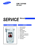
1
CDMA TELEPHONE
SPH-A900
CONTENTS
CDMA TELEPHONE
1.
General Introduction
2.
Circuit Description
3.
Installation
4.
NAM Programming
5.
Product Support Tools
6.
Test Procedure
7.
Flow Chart of Troubleshooting
8.
Exploded Views and Parts List
9.
Block Diagram
10.
Electrical Parts List
11.
PCB Diagrams
ⓒ Samsung Electronics Co.,Ltd. December. 2005
Printed in Korea.
This Service Manual is a property of Samsung Electronics Co.,Ltd.
Any unauthorized use of Manual can be punished under applicable
International and/or domestic law.
Code No.: GH68-08836A
BASIC.
1. General Introduction
1-1. General Instruction
The SPH-A900 enables mobile users to communicate 3G CDMA2000 1X service into a single handset.
For CDMA/PCS mode, The SPH-A900 supports Release A of the CDMA2000 1X standard.
The SPH-A900 also features EV-DO high-speed data, Bluetooth as well as a swiveling 1.3 megapixel
digital camera.
This stylish clamshell phone supports dual color displays, Bluetooth, MMS, voice dialing, airplane mode
and EV-DO services.
1-1
SAMSUNG Proprietary-Contents may change without notice
This Document can not be used without Samsung's authorization
General Introduction
1-2
SAMSUNG Proprietary-Contents may change without notice
This Document can not be used without Samsung's authorization
2. Circuit Description
2-1. Logic Section
2-1-1. Power Supply
Press "END" key to turn on the phone and then the V_BAT and ON_SW signals will be connected. This
turns on the inner regulators(V_MSMCORE, V_MSMC, VPD, VPA) of u200(MAX1526).
The V_BAT applied to ON_SW will change ON_SW_SENSE signal from HIGH to LOW.
MSM6500(UCP102) sends out PS_HOLD(logical HIGH) to keep the inner regulators on even after the
"END" key is released. V_RFRX can be turned on/off by the RX_CTRL signal. V_TCXO can be turned
on/off by the TCXO_CTRL signal. The other regulators(VDD2.6, V_SYNTH, V_RFTX, MOTOR_EN) will be
in the ON/OFF state by I2C-compatible 2 wire serial interface.
The regulated Voltage(u200, V_MSMCORE) are used in the core of MSM.
The regulated Voltage(u200, V_MSMC) are used in the digital part of MSM.
The regulated Voltage(u200, VPD) are used in the digital part and memory of MSM.
The regulated Voltage(u200, VPA) is used in the analog part of MSM.
The regulated Voltage(u200, V_RFTX) is used in the Tx RF part.
The regulated Voltage(u200, V_RFRX) is used in the Rx RF part.
The regulated Voltage(u200, V_TCXO) is used in the TCXO.
The regulated Voltage(u200, V_SYNTH) is used in the PLL part.
The regulated Voltage(u200, VDD2.6) is used in the voltage of camera .
The regulated Voltage(u200, MOTOR_EN) is used in the MOTOR.
2-1-2. Inner Charging Circuit Part
The most important function of the charger shall be done in the PMIC(Power Management Circuit u200).
When the phone with a battery is connected with a travel charging adapter, the inner charging circuit of
the PMIC(u200) will charge the battery by constant fast charge mode.
When battery reaches regulation voltage of 4.2V (default charging voltage for Li+mode), the charge
current drops quickly to 0mA
-
Input voltage range : 4.25~6.5V
- Charging Temperature : 0°C~40°C
- Charging Method : Constant Voltage/Current -Charging Current : Normal 550mA
- Charging Time : Standard (800mAh) 2.5 ~ 3 Hrs
- Charging Mode : ① Charging ② Completion
2-1
SAMSUNG Proprietary-Contents may change without notice
This Document can not be used without Samsung's authorization
Circuit Description
- Charging Battery Regulation Voltage
① Min 4.158V, Typical 4.2V, Max 4.242V(at TA : 0°C to +85°C)
② Min 4.137V, Typical 4.2V, Max 4.263V(at TA : -40°C to +85°C)
Universal Serial Bus Interface
SPH-A900 supports a Universal Serial Bus(USB) interface by the MSM6500, to provide an efficient
interconnection between the mobile phone and a Personal Computer(PC).
The MSM6500's USB interface is designed to comply with the Universal Serial Bus Specification,
Revision 2.0. An external USB transceiver(u200) is required to implement the USB interface.
2-1-3. Logic Part
The logic part consists of MSM, MEMORY,EL Keypad, LCD, CAMERA and other input and output
peripherals.
MOBILE SYSTEM MODEM(ucp102:MSM6500)
Industry standard ARM926EJ-S microprocessor is embedded. The MSM6500 chipset integrates
CDMA2000 1x and 1xEVDO service. The 1xEVDO solution can support High-speed peak data rates of
2.4Mbps on forward link and 153kbps on reverse link.
The MSM6500 device is offered in a 409 ball, 0.5mm pitch, CSP production package. Subsystems within
the MSM6500 device include a CDMA processor, a QDSP for voice compression, an ARM9TDMI
microprocessor. Also integrated in the MSM6500 device are analog functions such as an audio voice
codec, PLL, transmit DACS, ADCS, memories, USB controller, peripheral interfaces, and an enhanced
clock. It is one of the most important components of the CDMA cellular phone.
The interface circuitry consists of reset circuit, dual address/data bus and memory controls. The TCXO
clock of 19.2Mhz is used as the main clock of SPH-A900 model.
MCP : NAND FLASH and SDRAM (UME100(KBE00F003A))
MCP is consist of two 512Mbit(64M*8) NAND FLASH and two 256Mbit(4M*16*4Banks) Mobile SDRAM.
NAND FLASH is used to store the Font data and program. EFS area is used to store ESN, NAM
information, telephone directory, SMS messages and other important information of the phone, and also
to store application programs and downloaded stuffs such as BREW applications and MP3. MCP is also
used to excute the DMSS(Dual Mode Subscriber system) software.
Using the down-loading program, the program can be changed even after the terminal is fully assembled.
2-2
SAMSUNG Proprietary-Contents may change without notice
This Document can not be used without Samsung's authorization
Circuit Description
EL Keypad
For key recognition, key matrix is operated by using SCAN(0:6) and KEYSENCE(0:3) of the input ports
of MSM. EL(Electro Luminescence) is included in the keypad for easy operation in the dark.
LCD Module
LCD is composed of a Transmissive with Micro Reflective(TMR) type Main TFT-LCD Panel,
Transflective
type Sub TFT-LCD Panel, a driver circuit and a back-light unit.
The resolution of a 2.22" Main LCD contains 240 * 320 pixels, the resolution of a 1.07" Sub
LCD(Transflective) contains 96 * 96 pixels.
Clock
CPU clock
: 19.2MHz. Clock signal from the TCXO
Sleep clock : 32.768KHz. Clock signal for sleep.
TCXO/N
: 19.2/N MHz. This clock source is used by various blocks of the MSM6500 device, such
as the ARM9CORE, UARTs, general-purpose PDMs and TCXO is also used by the
MSM6500 device to produce CHIPX8.
USB clock
: 48MHz. Clock signal for the USB interface
CAMERA
The camera module consists of 1/4 CIS type 1.3 Mega (1310K) Pixels CMOS sensor. The camera
module provides Auto IRIS, and Auto White-Balance functionality.
Bluetooth module
Bluetooth module is a BluetoothTM 1.1 and 1.2 compliant, stand-alone baseband processor with an
integrated 2.4GHz transceiver. Bluetooth module supports any voice and/or data application that requires
the Bluetooth SIG standard Host Controller Interface (HCI) via UART and PCM audio interfaces.
Operation Clock: 26MHz
Low-Power Clock: 32.768KHz
2-3
SAMSUNG Proprietary-Contents may change without notice
This Document can not be used without Samsung's authorization
Circuit Description
2-1-4. RF Interface Part
CDMA Data Interface
- TX_Q_P, TX_Q_N, TX_I_P, TX_I_N (U402) : Tx analog signal used during CDMA
- RX_I_P, RX_Q_P, RX_I_N, RX_Q_N (U301) : RX analog signal used during CDMA
RF Interface
- TX : TX_AGC_ADJ(ucp102) is used to control the TX power,
PA_ON_PCS(ucp102) is used to control the PCS power amplifier and
PA_ON_CELL(ucp102) is used to control the CDMA power amplifier.
- RX : TRK_LO_ADJ(ucp102) is used to adjust the TCXO module.
2-1-5. Audio Part
The MSM6500 device integrates a stereo wideband voice/audio CODEC into the Mobile Station Modem.
The integrated CODEC contains all of the required conversion and amplification stages for the
audio front end.
The CODEC operates as a 13bit linear CODEC with the transmit(TX) and receive(RX) filters designed
to meet ITU-T G.712 requirements. The CODEC contains the software controlled amplifier for both the
receiving and transmitting sections. Also, the vocoding schemes used will be 13kbps QCELP and 8Kbps
EVRC. The QCELP vocoder is based in the MSM internally.
2-1-6. Tx Audio Path
The voice signal from the microphone is filtered and amplified by the internal OP-AMP and is converted
to PCM data by the internal CODEC in the MSM. And then these signals are applied to the the
MSM(ucp102)'s internal vocoder.
2-1-7. Rx Audio Path
The PCM data from the MSM(ucp102) is inputted to the internal CODEC and the data will be decoded
by the internal DAC. Audio levels are adjusted by the amplifier. And then audio is sent to the receiver.
2-4
SAMSUNG Proprietary-Contents may change without notice
This Document can not be used without Samsung's authorization
Circuit Description
2-1-8. Speaker Path
When the MSM(ucp102) receives the data, its internal CMX generates bell and melody. The CMX bell
and melody generated in MSM6500 are sent to SAPA1D2.
The SAPA1D2 (stereo class - D audio power amplifier) is a high quality audio power conversion chip
generating 2.5W RMS output directly from the V_BAT supply. It is a high efficiency audio amplifier for
mobile applications. The gain of amplifier in SPH-A900 set to 4(V/V) . The output generated in SAPA1D2
is intended to drive two speakers.
2-1-9. Key Tone Generator
The CODEC data out from the MSM6500 is converted to DTMF signal by TONE generator of internal
CODEC, which is then amplified by the internal audio amplifier to be sent to the speaker units.
2-2. PCS Section
2-2-1. Receiver
LOW NOISE AMPLIFIER (U300)
The low noise amplifier(It is included in RFL6000 : U300) amplifies a weak signal received from the base
station to obtain the optimum signal level.
RF BAND PASS FILTER (F300)
The RF BPF(F300) passes only a specific frequency(1960±30 MHz) from the signal received from the
mobile station. The bandwidth is 60 MHz.
VOLTAGE CONTROLLED OSCILLATOR(VCO300)
The VCO(VCO300) generates the signal having 1715 ~ 1788MHz frequency range.
The VCO's output frequency is changed by control voltage. The PLL in S1M8690X generates this control
signal and this signal is changed into DC control voltage by R-C Loop filter.
2-5
SAMSUNG Proprietary-Contents may change without notice
This Document can not be used without Samsung's authorization
Circuit Description
Frequency Synthesizer Circuit
The PLL(Phased Locked Loop) block consists of VC-TCXO(TCK301), PLL in S1M8690X and
VCO(VCO300). Input reference frequency is generated at VC-TCXO(TCK301) and the RF local signal is
generated at VCO. PLL compares the two signals and generates the desired signal with a
preprogrammed counter which controls voltage.
VOLTAGE CONTROLLED TEMPERATURE COMPENSATED CRYSTAL OSCILLATOR (TCK301)
The VC-TCXO (TCK301) is a reference source of the frequency synthesizer. It provides 19.2MHz
reference frequency to PLL-IC. It is a voltage controlled temperature compensated crystal
oscillator having 19.2MHz ±2.5ppm frequency stability over all useful temperature range.
A correct frequency tuning is made by the control voltage.
2-2-2. Transmitter
Intenna
Intenna sends signal to the base station and receives the signal from the base station.
It is a tri-band Intenna and covers PCS band, CDMA band and GPS band.
RF Switch
It(U401:TQP4M3018) is used to switch the PCS path and CDMA path and the GPS
path.
The RF signal passes through PCS path when PCS_MODE is high(2.6V). The RF signal
passes through CDMA path when CELL_MODE is high(2.6V).
The RF signal passes through
GPS path when GPS_MODE is high(2.6V). PCS_MODE, CELL_MODE and GPS_MODE are
digital signals from MSM6500 GPIO.
Duplexer
Duplexer(DUF400) allows to transmit only the signals within acceptable Tx frequency range
(1880 ± 30 MHz) through the Intenna.
It provides the appropriate attenuation of transmitted signal at the receiver input and the appropriate
rejection of the transmit-generated noise in the Receiver band.
Power Amp
Power amplifier module(PAM400:WS1413) amplifiers signal to be sent to the base station
through the antenna.
2-6
SAMSUNG Proprietary-Contents may change without notice
This Document can not be used without Samsung's authorization
Circuit Description
Driver Amp
The driver amp(U402 ; included in S1M8690X) allows the signal to be inputted to the power
amp(PAM400) as a specified level.
Up-converter(Mixer)
The up-converter(U402 ; also included in S1M8690X) receives the local signal FTx * 0.7999
and signal controlled by TX AGC amp(in S1M8690X) to generate Tx RF signal 1880±30MHz
which signal comes out from the mixer output by adding FTx * 0.7999 local signal.
FTx means TX RF signal Frequency.
Automatic Gain Control Amp
The TX IF AGC amp (in S1M8690X) controls gain of AGC to deliver power level needed at
driver amp. Its control voltage varies from 0.2V to 2.5V.
2-3. CDMA Section
2-3-1. Receiver
Low Noise Amplifier(LNA)
The low noise amplifier(It is included RFL6000 : U300) amplifies a weak signal received from
the base station to obtain the optimum signal level.
RF Band Pass Filter(Rx RF SAW Filter)
The RF BPF in F300 passes only a specific frequency(881.49±12.5 MHz) from the signal
received from the mobile station. The bandwidth is 25 MHz.
Voltage Controlled Oscillator
The VCO(VCO300) generates the signal having 1715 ~ 1788MHz frequency range.
The VCO's output frequency is changed by control voltage. The PLL in S1M8690X generates this control
signal and this signal is changed into DC control voltage by R-C Loop filter.
2-7
SAMSUNG Proprietary-Contents may change without notice
This Document can not be used without Samsung's authorization
Circuit Description
Frequency Synthesizer Circuit
The PLL(Phased Locked Loop) block consists of VC-TCXO(TCK301), PLL in S1M8690X and
VCO(VCO300). Input reference frequency is generated at VC-TCXO(TCK301) and the RF
local signal is generated at VCO. PLL compares the two signals and generates the desired
signal with a preprogrammed counter which controls voltage.
VC-TCXO
The VC-TCXO (TCK301) is a reference source of the frequency synthesizer. It provides 19.2MHz
reference frequency to PLL-IC. It is a voltage controlled temperature compensated crystal
oscillator having 19.2MHz ±2.5ppm frequency stability over all useful temperature range.
A correct frequency tuning is made by the control voltage.
2-3-2. Transmitter
Intenna
Intenna sends signal to the base station and receives the signal from the base station.
It is a tri-band Intenna and covers PCS band, CDMA band and GPS band.
RF Switch
It(U401:TQP4M3018) is used to switch the PCS path and CDMA path and the GPS
path.
The RF signal passes through PCS path when PCS_MODE is high(2.6V). The RF signal
passes through CDMA path when CELL_MODE is high(2.6V).
The RF signal passes through
GPS path when GPS_MODE is high(2.6V). PCS_MODE, CELL_MODE and GPS_MODE are
digital signals from MSM6500 GPIO.
Duplexer
Duplexer(DUF402) passes the RF signal of Rx frequency range(881.49 ±12.5 MHz) and Tx frequency
range
(836.49 ±12.5 MHz). It provides appropriate attenuation of transmitted signal at the receiver input and
appropriate rejection of the transmit-generated noise in the Receiver band.
It also matches LNA input in receiving part and PAM(PAM400:WS1102) output in transmitting part with
the Intenna.
2-8
SAMSUNG Proprietary-Contents may change without notice
This Document can not be used without Samsung's authorization
Circuit Description
Power Amp
Power amplifier module(PAM400:WS1102 amplifiers signal to be sent to the base station
through the antenna.
RF Band Pass Filter(Tx RF SAW Filter)
The RF BPF(F403) passes only specific frequency(836.49 ±12.5MHz) to send it to power
amp(PAM400:WS1102).
Driver Amp
The driver amp(U402 ; It is included in S1M8690X) allows the signal to be inputted to the
power amp(PAM400) as a specified level.
Up-Converter(Mixer)
The up-converter(U402 ; It is also included in S1M8690X) receives the local signal FTx * 1.6666
and the signal controlled by TX AGC amp(in S1M8690X) to generate Tx RF signal
836.49±12.5MHz signal comes out from the mixer output by adding FTx * 1.6666 local signal.
FTx means TX RF signal Frequency.
Automatic Gain Control Amp
The TX IF AGC amp in S1M8690X controls gain of AGC to deliver power level to be needed
at Driver amp. Its control voltage varies from 0.2V to 2.5V.
2-9
SAMSUNG Proprietary-Contents may change without notice
This Document can not be used without Samsung's authorization
Circuit Description
2-4. GPS Section
Intenna
Intenna receives a signal from GPS satellites.
It is a tri-band Intenna and covers PCS band, CDMA band and GPS band.
RF Switch
It(U401:TQP4M3018) is used to switch the PCS path and CDMA path and the GPS
path.
The RF signal passes through PCS path when PCS_MODE is high(2.6V). The RF signal
passes through CDMA path when CELL_MODE is high(2.6V).
The RF signal passes through
GPS path when GPS_MODE is high(2.6V). PCS_MODE, CELL_MODE and GPS_MODE are
digital signals from MSM6500 GPIO.
Low Noise Amplifier Module(LNA)
The low noise amplifier(U302:ALM1106) amplifies a weak signal received from artificial satellite to
obtain the optimum signal level.
RF Band Pass Filter(Rx RF SAW Filter)
The RF BPF(U404:B9000)
passes only a specific frequency(1575.42±1MHz) from the signal received
from the satellite. The bandwidth is 2 MHz.
2-10
SAMSUNG Proprietary-Contents may change without notice
This Document can not be used without Samsung's authorization
3. Installation
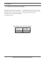
3-1 Installing and Removing the Battery
To install, open the battery cover and insert the
To remove, make sure the power is off. Push the
battery into the phone. Put on the battery cover.
battery cover latch release up completely. Pull and
Make sure the cover on the back are inserted into
lift the battery away from the phone.
the matching slots in the phone. Press down until
the latchsnaps into place.
Specifications using TA (Travel Adapter)
Battery Type
Standard Battery
(Li-ion, 800mAh)
Charging
< 3 hours
SEC Code
GH43-02101A
3-1
SAMSUNG Proprietary-Contents may change without notice
This Document can not be used without Samsung's authorization
Installation
3-2
SAMSUNG Proprietary-Contents may change without notice
This Document can not be used without Samsung's authorization
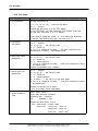
4. NAM Programming
NAM program can be changed as following table:
Notes:
- In the NAM program mode, each item show you the currently stored data. you can modify the data
by entering a new data.
- You can move to next window by pressing "OK" key.
- When you press a wrong number, press "BACK" key to delete the last number or press and hold
"BACK " key to delete all number
- You can move to menu screen by pressing "MENU" key.
- You can change some selection option keys by pressing "Left" or "Right" navigation.
4-1. Single NAM
4-1-1. General Setup
LCD Display
Enter
##MSL#
Key in
##222222#
Funtion
Enter the NAM Mode. Enter random 6-digit code (MSL) and
222222 is a default value.
SVC Menu
1: View
2: Edit
1
View Phone Number and MSID
3: Done
Phone Number
1234567890
MSID
1234567890
Right key or Down
key
MENU or BACK
Phone number is displayed
Mobile ID is displayed
SVC Menu
1: View
2: Edit
2
Choose 'Edit' to change Phone Number and MSID
3: Done
Phone Number
1234567890
- Phone number setup
OK
- To change phone number, enter phone #
- Store it
- Mobile ID setup
MSID
1234567890
OK
- To change phone number, enter phone #
- Store it
SVC Menu
1: View
2: Edit
3
Choose 'Done' to exit the NAM mode
3: Done
4-1
SAMSUNG Proprietary-Contents may change without notice
This Document can not be used without Samsung's authorization
NAM Programming
4-1-2. NAM Mode Display
LCD Display
Key in
Funtion
#,#,3,2,8,2,#
Enter the Data Program screen
5
Display the 3G Data program.
3G Data Prog
1. User Name
2: Browser
3: IOTA Prog.
4: Camera URL
5: Advanced
6: Multimedia
7: Restore
Enter Service Code
??????
222222
Enter random 6-digit code (MSL)
- 222222 is a default value
Advanced
1: View
1
Choose "VIEW" to dispaly the Advanced NAM Information
2: Edit
ESN
Right key or Down
B0000000
key
Right key or Down
CERT
key
P_REV
Right key or Down
6
VOCODER SVCOPT
EVRC
SCM
key
Right key or Down
key
Right key or Down
01101010
Lock Code
key
Right key or Down
0016
Slot Mode
key
Right key or Down
YES
Slot Index
key
Right key or Down
2
HOME SID
key
Right key or Down
4139
HOME NID
key
Right key or Down
65535
MCC
key
Right key or Down
310
MNC
key
Right key or Down
00
ACCOLC
key
Right key or Down
6
key
Electronic Serial Number of the phone is displayed
Java security - Dormant
Certificate Wakeup(On), and
Sleep(off) status is displayed
Common Air Interface version is displayed
13K or EVRC
Station Class Mark displays the power class,
transmission, slotted class, dual mode.
Lock code, current status is displayed
Slot mode. 'Yes' indicates the slot mode.
Slot mode index. The high number means longer
sleeping time
SID written in the list,current status is displayed.
NID written in the list,current status is displayed.
ImsI Mobile Country Code, current code is displayed.
ImsI Mobile Network Code, current code is displayed.
CDMA Access Overload Class, current status is displayed
4-2
SAMSUNG Proprietary-Contents may change without notice
This Document can not be used without Samsung's authorization
NAM Programming
NAM CDMA
Home Sys Reg
Right key or Down
key
Yes
NAM CDMA
Right key or Down
FSID Reg
key
Yes
CDMA Home system ID, current status is displayed
CDMA foreign SID, current status is displayed.
NAM CDMA
FNID Reg
MENU or BACK
CDMA foreign NID,current status is displayed.
Yes
4-1-3. NAM Mode Setup
LCD Display
Key in
#,#,3,2,8,2,#
Funtion
Enter the Data Program screen ('##DATA')
3G Data Prog
1. User Name
2: Browser
3: IOTA Prog.
4: Camera URL
5
Display the 3G dara program.
5: Advanced
6: Multimedia
7: Restore
Enter Service Code
??????
222222
Enter random 6-digit code (MSL) - 222222 is a default
value
Advanced
1: View
2
Choose "EDIT" to change the Advanced NAM information
2: Edit
ESN
Right key or Down
B0000000
key
Right key or Down
CERT
key
P_REV
Right key or Down
6
VOCODER SVC OPT
EVRC
SCM
key
Right key or Down
key
Right key or Down
01101010
Lock Code
0016
Slot Mode
key
4-digit Code
OK
Left or Right key
YES
OK
Electronic Serial Number of the phone is displayed
Java security - Dormant
Certificate Wakeup(On), and
Sleep(off)
Common Air Interface version is displayed
Origination Service Option is displayed
- Change Service Option
- Store it
Station Class Mark displays the power class,
transmission, slotted class, dual mode.
Lock code, current status is displayed
- To change Lock Code, enter a new code
- Store it
Slot mode. 'Yes' indicates the slot mode.
- Change status
- Store it
4-3
SAMSUNG Proprietary-Contents may change without notice
This Document can not be used without Samsung's authorization
NAM Programming
Slot mode index. The high number means longer sleeping
Slot Index
0 ~ 7
2
OK
time
- To change Slot Index, enter new one
- Store it
HOME SID
4139
HOME NID
65535
MCC
number
OK
number
OK
number
310
MNC
OK
number
00
ACCOLC
OK
class number
6
NAM CDMA
Home Sys Reg
Yes
NAM CDMA
FSID Reg
Yes
NAM CDMA
FNID Reg
Yes
OK
Left or Right key
OK
Left or Right key
OK
Left or Right key
OK
SID written in the list,current status is displayed.
- Enter new one to change code
- Store it
NID written in the list,current status is displayed.
- Enter new one to change code
- Store it
ImsI Mobile Country Code, current code is displayed.
- Enter new one to change code
- Store it
ImsI Mobile Network Code, current code is displayed.
- Enter new one to change code
- Store it
CDMA Access Overload Class, current status is displayed
- Enter new one to change code
- Store it
CDMA Home system ID, current status is displayed
- Change status
- Store it
CDMA foreign SID, current status is displayed.
- Change status
- Store it
CDMA foreign NID,current status is displayed.
- Change status
- Store it
4-4
SAMSUNG Proprietary-Contents may change without notice
This Document can not be used without Samsung's authorization
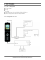
6. Test Procedure
6-1 List of Equipment
● DC Power Supply
● Test Jig
● Test Cable
● CDMA Mobile Station Test Set HP8285A, HP8960, CMD-80, etc
● Spectrum Analyzer(include CDMA Test Mode) HP8596E,
6-2 Configuration of Test
6-1
SAMSUNG Proprietary-Contents may change without notice
This Document can not be used without Samsung's authorization
Test Procedure
6-3 TEST CABLE CONNECTIONS
6-3-1 TEST CABLE
6-3-2 TEST CABLE CONNECTIONS
1
MHC 172
2
RF CABLE (1.4dB Loss for CDMA, 2.1dB Loss for PCS, 1.8dB Loss for GPS)
3
BNC CONNECTOR (RF)
4
DATA CABLE
5
Plug Connect to SPH-A900
6
Dsub 25PIN CONNECTOR (DATA)
6-2
SAMSUNG Proprietary-Contents may change without notice
This Document can not be used without Samsung's authorization
Test Procedure
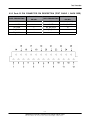
6-3-3 Dsub 25 PIN CONNECTOR PIN DESCRIPTION (TEST CABLE 1, BACK SIDE)
DATA DESCRIPTION
Dsub CONN.
PIN NO.
DATA DESCRIPTION
Dsub CONN.
PIN NO.
GND
13
GND
24,25 (SHORT)
VBATT
4
VBATT
5,6 (SHORT)
HP_PWR
7
DP_RX_DATA
21
RX_AUDIO
12
DP_TX_DATA
22
TX_AUDIO
10
6-3
SAMSUNG Proprietary-Contents may change without notice
This Document can not be used without Samsung's authorization
Test Procedure
6-3-4 CONVERSION TABLE OF FREQUENCY vs CHANNEL
- CDMA/PCS
T Y P E
CHANNEL
CONVERSION EQUATION
TX
FREQUENCY
990 ≤N≤1023
1 ≤N≤779
F=0.03 × (N-1023) + 825.00
F=0.03 × N + 825.00
RX
FREQUENCY
990 ≤N≤1023
1 ≤N≤779
F=0.03 × (N-1023) + 875.00
F=0.03 × N + 875.00
TX
FREQUENCY
0 ≤N≤ 1199
RX
FREQUENCY
0 ≤N≤ 1199
F=0.05 × N + 1850.00
REMARK
N ; CH NUMBER
F ; FREQUENCY
(CDMA)
N ; CH NUMBER
F ; FREQUENCY
F=0.05 × N + 1930.00
(PCS)
6-4
SAMSUNG Proprietary-Contents may change without notice
This Document can not be used without Samsung's authorization
Test Procedure
6-4 Test Procedure
6-4-1 CDMA/PCS mode
- Change the test mode
A. To change the phone's state from Normal Mode to Test Mode, You should enter the following keys.
: Press [ 4 7 * 8 6 9 # 1 2 3 5 ]
B. The command "0 0 1" is Suspend.
C. The command "0 2 2" is mode and channel change.
"2 0 3 6 3"
Channel number
Mode:CDMA
"3 0 6 0 0"
Channel number
Mode:PCS
and press enter key from the soft key board to save mode/channel value..
D. The command "0 0 1" is Suspend.
E. To finish the Test Mode, You should enter the command "0 0 2".
- Channel selection and Tx power output level control
CDMA
A. Enter to Test Mode [ 4 7 * 8 6 9 # 1 2 3 5 ]
B. "0 0 1" : Suspend.
C. The command "0 2 2" is mode and channel change
"2 0 3 6 3"
Channel number
Mode:CDMA
Push the [OK] key to save.
6-5
SAMSUNG Proprietary-Contents may change without notice
This Document can not be used without Samsung's authorization
Test Procedure
D. To finish the Test Mode, You should enter the command "0 0 2".
E. Enter to Test Mode [ 4 7 * 8 6 9 # 1 2 3 5 ]
F. "0 0 1" : Suspend.
G. "0 1 1" : Carrier_On.
H. "0 1 4" : CDATA.
I. "0 1 0" : PA_R1(0:LOW GAIN MODE, 1:HIGH GAIN MODE)
J. "0 1 9" : Adjust RF power level.
PCS
A. Enter to Test Mode [ 4 7 * 8 6 9 # 1 2 3 5 ]
B. "0 0 1" : Suspend.
C. The command "022" is mode and channel change
"3 0 6 0 0"
Channel number
Mode:PCS
Push the [enter] key to save.
D. To finish the Test Mode, You should enter the command "0 0 2".
E. Enter to Test Mode [ 4 7 * 8 6 9 # 1 2 3 5 ]
F. "0 0 1" : Suspend.
G. "0 1 1" : Carrier_On.
H. "0 1 4" : CDATA.
I. "0 1 0" : PA_R1(0:LOW GAIN MODE, 1:HIGH GAIN MODE)
J. "0 1 9" : Adjust RF power level.
6-6
SAMSUNG Proprietary-Contents may change without notice
This Document can not be used without Samsung's authorization
Test Procedure
- CDMA Test items
TEST ITEMS
1. PREPARANCE
PROCEDURE
Set test equipments up.
[ 4 7 * 8 6 9 # 1 2 3 5 ] : Enter the Test Mode
"0 0 1" : Suspend
Confirm that the phone is in the "CDMA Mode".
(If not CDMA Mode, Use Test Command "022""2XXXX" and Push
the "
" Key to "OK", and enter "0 0 2" to restart)
If you select a wrong key, press " # ", then enter new command.
To exit the Test Mode at any time, just press [0 0 2].
2. FREQUENCY
ACCURACY
3. OCCUPIED CDMA
BANDWIDTH
4. LIMITATIONS ON
EMISSIONS
5. GATED POWER &
TIME
"0 0 1" : Suspend.
"0 1 3 0 3 6 3 * " : Set channel to 363.
"0 1 1" : Carrier On.
"0 1 9 X X X ' END[Push and Hold] ' " : Set AGC Code(XXX) level.
Measure the TX frequency : 835.89MHz±300Hz.
"0
"0
"0
"0
"0
0
1
1
1
1
1" : Suspend.
3 0 3 6 3 * " : Set channel to 363.
1" : Carrier On.
4" : Spread spectrum.
9 X X X ' END[Push and Hold] ' " : Enter AGC Code(XXX) to adjust
RF Output Power.
Measure the bandwidth (spec: 1.23MHz).
"0
"0
"0
"0
"0
"0
0
1
1
1
1
1
1" : Suspend.
3 0 3 6 3 * " : Set channel to 363.
1" : Carrier On.
4" : Spread spectrum.
0 Select 1 *" :Set PA_R1 to High Gain Mode
9 X X X ' END[Push and Hold] ' " : Enter AGC Code(XXX) to adjust
RF Output Power.
Measure the spurious at FC±900kHz, FC±1.98MHz, 2FC, 3FC, 1/2FC.
spec: FC±900kHz below 42dBc/30kHz
FC±1.98MHz below 54dBc/30kHz
Outside Receive Band 43+10log (PY)
PY: Mean Output Power in watts
Set the service option 2.
Set the data rate Eighth (1200bps).
Registering: HHP → HP8924C.
Call
: HP8924C → HHP.
Measure the Gated Power & Time.
spec : Gated Power - at least 20dB
Gated Time - Rising Time : below 6㎲
Falling Time : below 6㎲
Burst Time : below 1.25㎳
6-7
SAMSUNG Proprietary-Contents may change without notice
This Document can not be used without Samsung's authorization
Test Procedure
- PCS Test items
TEST ITEMS
1. PREPARANCE
PROCEDURE
Set test equipments up.
[ 4 7 * 8 6 9 # 1 2 3 5 ] : Enter the Test Mode
"0 0 1" : Suspend
Confirm that the phone is in the "PCS Mode".
(If not PCS Mode, Use Test Command "022""3XXXX" and Push
the [OK] Key, and enter "0 0 2" to restart)
If you select a wrong key, press " # ", then enter new command.
To exit the Test Mode at any time, just press [0 0 2].
2. FREQUENCY
ACCURACY
3. OCCUPIED CDMA
BANDWIDTH
4. LIMITATIONS ON
EMISSIONS
"0 0 1" : Suspend.
"0 1 3 0 6 0 0 * " : Set channel to 600.
"0 1 1" : Carrier On.
"0 1 9 X X X ' END[Push and Hold] ' " : Set AGC Code(XXX) level.
Measure the TX frequency : 1880.00MHz±300Hz.
"0
"0
"0
"0
"0
0 1" : Suspend.
1 3 0 6 0 0 * " : Set channel to 600.
1 1" : Carrier On.
1 4" : Spread spectrum.
1 9 X X X ' END[Push and Hold] ' " : Enter AGC Code(XXX) to adjust
RF Output Power.
Measure the bandwidth (spec: 1.23MHz).
"0
"0
"0
"0
0
1
1
1
1" : Suspend.
3 0 6 0 0 * " : Set channel to 600.
1" : Carrier On.
4" : Spread spectrum.
"0 1 0 Select 1 *" :Set PA_R1 to High Gain Mode
"0 1 9 X X X ' END[Push and Hold] ' " : Enter AGC Code(XXX) to adjust
RF Output Power.
Measure the spurious at FC±1.25MHz
spec: FC±1.25MHz below 42dBc/30kHz
5. GATED POWER &
TIME
Set the service option 2.
Set the data rate Eighth (1200bps).
Registering: HHP → HP8924C.
Call
: HP8924C → HHP.
Measure the Gated Power & Time.
spec : Gated Power - at least 20dB
Gated Time
- Rising Time : below 6㎲
Falling Time : below 6㎲
Burst Time
: below 1.247㎳
6-8
SAMSUNG Proprietary-Contents may change without notice
This Document can not be used without Samsung's authorization
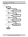
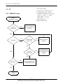
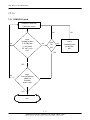
7. Flow Chart of TroubleShooting
7-1 Logic Section
7-1-1 Power On
Insert Power
power on
properly?
Check Phone power on section
NO
YES
U200
pin41=high?
Check IFC201 and it's
neighboring circuits
NO
YES
Check
C216 =
2.7V?
C217,C218,C219,C220,C221 and
NO
U200's neighboring circuits
YES
C122
Check TCK301,U101 and it's
19.2MHz?
neighboring circuits
NO
YES
END
7-1
SAMSUNG Proprietary-Contents may change without notice
This Document can not be used without Samsung's authorization
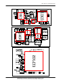
Flow Chart of Troubleshooting
S3.6
DC_VOLT
V_BAT
C200
C201
TA204
C202
C203
TA205
ZD200
TDZ5.6
C206
ZD201
VPD
U200
VPD
36
ON_SW_SENSE
ON_SW
HP_PWR
PS_HOLD
R205
HRESET
SDA_PM
SCL_PM
EAR_REF
EAR_DET
EAR_MIC+
SEND_END
USB_OE_N
USB_SUSPEND
USB_DATA
USB_VPO
USB_VMO
C226
C227
C215
VL
LX1
37
PGND1
38 VICHG
FB1
_AC_OK
2
LX2
46 _ONO
PGND2
26 PWR_ON
FB2
41 HP_PWR
PWR_HOLD
_RESET
42
OUT1
25 _HRESET
OUT2
40 DATA
CLK
OUT3
11
INV1
RX_EN
12
OUT4
15 COMP1
INV2
14
COMP2
OUT5
TCXO_EN
16
OUT6
17 _OE
OUT7
20 SUSPEND
OUT8
21 RCV
VP
OUT9
22
VM
GND
NC
NC
GND
C225
R200
C207
REFBP
DD+
VTRM
VUSB
VICHG
DC_SENS
BATT
IN1
IN2
IN3
C208
R201
CHG_IN
35 34 30 9 4
D200
45
31
32
33
L200
V_MSMCORE
R202
R203
29
28
27
C210
C211
C212
V_MSMC
L201
R204
R206
48
10
8
C209
RESETIN_N
VPD
VPA
13
43
7
V_RFRX
RX_CTRL
VDD_LCD_2.85
1
39
V_TCXO
TCXO_CTRL
47
3
5
6
V_SYNTH
V_RFTX
VDD2.6
MOTOR_EN
49
50
51
44 23241918
C216 C217C218 C219 C220 C221 C222 C223 C224
D201
V_BUS
VPULL
D+_IN
D-_IN
C228
7-2
SAMSUNG Proprietary-Contents may change without notice
This Document can not be used without Samsung's authorization
Flow Chart of Troubleshooting
7-3
SAMSUNG Proprietary-Contents may change without notice
This Document can not be used without Samsung's authorization
Flow Chart of Troubleshooting
7-1-2 LCD Working
Insert Power
Check pulse
Main LCD Back
Check HDC500 and it's
of HDC500's
-light On?
No
pin18
neighboring circuits
No
Yes
Yes
Change LCD
Check HDC500,
LCD Display
OK?
No
F502, F503
Yes
Replace HDC500,
F504,F505 and
F502, F503 F504,F505and
it's Short=?
it's neighboring circuits
Yes
No
Change LCD
END
7-4
SAMSUNG Proprietary-Contents may change without notice
This Document can not be used without Samsung's authorization
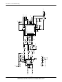
Flow Chart of Troubleshooting
VDD_LCD_2.85
VPD
R502
ED2(14)
ED2(12)
ED2(10)
ED2(8)
ED2(6)
ED2(4)
ED2(2)
ED2(0)
VR500
VR502
C510
C511
C509
C508
C529
C506
SCAN2
VR501
C517
C512
C515
C516
C514
SCAN4
FLASH_STROBE
LCD_BACKLIGHT
REED_SW
SUB_LCD_CS
MAIN_LCD_CS
RE2_N
C528
VR505
VR506
VR504
VR503
C513
KEYSENSE3
SCAN3
ALERT_LED_R
HPH_R
RCVAUDIO_EN
ALERT_LED_G
C507
ED2(15)
ED2(13)
ED2(11)
ED2(9)
ED2(7)
ED2(5)
ED2(3)
ED2(1)
R504
2
2
4
4
6
6
8
10
10
12
12
14
14
16
16
18
18
20
20
22
22
24
24
26
26
28
28
30
30
32
32
34
34
36
36
38
38
40
40
42
42
44
44
46
46
48
48
50
50
C505
R503
LCD_RESET
1
3
5
78
9
11
13
15
17
19
21
23
25
27
29
31
33
35
37
39
41
43
45
47
49
C504
KEYSENSE2
FLASH_EN
M_DIM
LRS
WE2_N
RESOUT_N
HDC500
1
3
5
7
9
11
13
15
17
19
21
23
25
27
29
31
33
35
37
39
41
43
45
47
49
HPH_L
RCV+
26K_EN
MOTOR_EN
C500
C526
R500
C527
R501
S3.6
C501
50 PIN LCD CONNECTER
F503
5
6
7
8
4
3
2
1
9
F502
F504
10
ED2(1)
ED2(3)
ED2(5)
ED2(7)
D2(1)
D2(3)
D2(5)
D2(7)
ED2(9)
ED2(11)
ED2(13)
ED2(15)
5
6
7
8
10
F505
10
4
3
2
1
ED2(0)
ED2(2)
ED2(4)
ED2(6)
D2(9)
D2(11)
D2(13)
D2(15)
5
6
7
8
4
3
2
1
D2(0)
D2(2)
D2(4)
D2(6)
9
9
7-5
SAMSUNG Proprietary-Contents may change without notice
This Document can not be used without Samsung's authorization
ED2(8)
ED2(10)
ED2(12)
ED2(14)
5
6
7
8
10
9
4
3
2
1
D2(8)
D2(10)
D2(12)
D2(14)
Flow Chart of Troubleshooting
7-6
SAMSUNG Proprietary-Contents may change without notice
This Document can not be used without Samsung's authorization
Flow Chart of Troubleshooting
7-1-3 Speaker, Receiver and Mic Checking
Insert Power
YES
Check HDC500
Speaker is
pin3(HPH_L),
OK?
pin4(HPH_R)
NO
Check U4 on
LCD and
NO
signal OK?
Speaker
YES
Check TP25,26,30 and 39(SPK_R,
SPK_L) on LCD signal OK?
YES
Check LCD
FPCB
NO
YES
Replace Speaker
Check HDC500
Receiver is
OK?
Check HDC500
pin 5, 6
NO
NO
signal OK?
and Receiver
YES
YES
Replace receiver
MIC is OK?
NO
Check
Check mic path from
HDC502 pin8
HDC502 to UCP102
signal on?
NO
and it's neighboring
circuits.
YES
YES
Check KEY FPCB
END
7-7
SAMSUNG Proprietary-Contents may change without notice
This Document can not be used without Samsung's authorization
Flow Chart of Troubleshooting
VDD_LCD_2.85
VPD
ED2(14)
ED2(12)
ED2(10)
ED2(8)
ED2(6)
ED2(4)
ED2(2)
ED2(0)
VR500
VR502
C510
C509
C529
C511
SCAN2
VR501
C517
C512
C515
C516
C514
R502
C528
VR505
VR506
VR504
VR503
C513
KEYSENSE3
SCAN3
SCAN4
FLASH_STROBE
LCD_BACKLIGHT
REED_SW
SUB_LCD_CS
MAIN_LCD_CS
RE2_N
C508
ED2(15)
ED2(13)
ED2(11)
ED2(9)
ED2(7)
ED2(5)
ED2(3)
ED2(1)
R504
ALERT_LED_R
HPH_R
RCVAUDIO_EN
ALERT_LED_G
C506
R503
LCD_RESET
2
2
4
4
6
6
8
10
10
12
12
14
14
16
16
18
18
20
20
22
22
24
24
26
26
28
28
30
30
32
32
34
34
36
36
38
38
40
40
42
42
44
44
46
46
48
48
50
50
C507
KEYSENSE2
FLASH_EN
M_DIM
LRS
WE2_N
RESOUT_N
1
3
5
78
9
11
13
15
17
19
21
23
25
27
29
31
33
35
37
39
41
43
45
47
49
C505
1
3
5
7
9
11
13
15
17
19
21
23
25
27
29
31
33
35
37
39
41
43
45
47
49
HPH_L
RCV+
26K_EN
MOTOR_EN
C500
C526
HDC500
C504
C527
R500
C501
R501
S3.6
50 PIN LCD CONNECTER
F503
5
6
7
8
4
3
2
1
F502
F504
10
ED2(1)
ED2(3)
ED2(5)
ED2(7)
5
6
7
8
ED2(9)
ED2(11)
ED2(13)
ED2(15)
D2(1)
D2(3)
D2(5)
D2(7)
10
5
6
7
8
ED2(0)
ED2(2)
ED2(4)
ED2(6)
D2(9)
D2(11)
D2(13)
D2(15)
4
3
2
1
D2(0)
D2(2)
D2(4)
D2(6)
5
6
7
8
ED2(8)
ED2(10)
ED2(12)
ED2(14)
9
9
9
F505
10
4
3
2
1
10
4
3
2
1
D2(8)
D2(10)
D2(12)
D2(14)
9
20PIN KEYPAD CONNECTER
F506
9
8
7
6
5
S3.6
F507
9
KEYSENSE0
KEYSENSE1
KEYSENSE2
KEYSENSE3
1
2
3
45
2
4
6
8
10
12
14
16
18
20
8
7
6
10
HDC502
1
2
3
4
5
6
7
8
9
10
11
12
13
14
15
16
17
18
19
20
1
2
3
4
SCAN0
SCAN1
SCAN2
SCAN3
10
1
3
5
7
9
11
13
15
17
19
F508
9
1
2
3
4
8
7
6
5
MIC+
SCAN4
SCAN5
SCAN6
EL_EN
10
VR507
VR508
R510
ON_SW
VR509
7-8
SAMSUNG Proprietary-Contents may change without notice
This Document can not be used without Samsung's authorization
Flow Chart of Troubleshooting
7-9
SAMSUNG Proprietary-Contents may change without notice
This Document can not be used without Samsung's authorization
Flow Chart of Troubleshooting
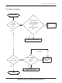
1. visual check! (soldering)
7-2. RX
2. S/W Mode Check : CDMA Mode Check
3. VCTCXO(TCK301) Check : 19.2MHz
7-2-1 CDMA/PCS mode
4. VCO(OSC301) voltage/frequence level check
Frequence : 1715MHz < f < 1788MHz
START
CDMA/PCS mode
Supply Voltage:
2.75 ± 0.1V
Control Voltage:
0.4 ~ 2.3V
5. U300 LNA gain check
6. PAM400, PAM403 Check
SVC &
NO
Check CDMA/PCS
Rx Path
ROAM OK?
YES
NO
Call OK?
DVGA value
NO
Check OK?
Adjust DVGA by
program
YES
S1M8690X(U402)
Tx Path
YES
Check OK?
NO
Check Adjust TX by
program
YES
NO
FER OK?
Check RFR6000(U301),
MSM6500(UCP102)
YES
End
7-10
SAMSUNG Proprietary-Contents may change without notice
This Document can not be used without Samsung's authorization
Flow Chart of Troubleshooting
1. visual check! (soldering)
7-2-2 GPS Mode
2. S/W Test Mode Check : GPS Mode
3. VCTCXO(TCK301) Check : 19.2MHz
START GPS
U401 Logic Check
pin1 pin6 pin9
GPS RF
NO
GPS
H
L
L
Path Check
U404 Check
OK?
YES
GPS_NV_ITEM
NO
Adjust by program
Check OK?
YES
End
7-11
SAMSUNG Proprietary-Contents may change without notice
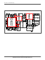
This Document can not be used without Samsung's authorization
C316
L308
7
SBCK
R314
SBST
IN
GG
G
GPS_MODE
2 35
OUT 1
L315
C318
L317
11
10
9
8
7
6
5
4
3
C327
GND6
12
GPS_INM
GND5
PCS_INM
GND4
PCS_INP
GND3
VDDA11
GND2
GND7
15
39
38
16
17
18
36
R302
37
U301
C334
C326
13 14
VDDA21
7-12
This Document can not be used without Samsung's authorization
SAMSUNG Proprietary-Contents may change without notice
C338
R308
C322
4
U404
B9000
L311
L309
40
LO_INM
TCK301
GND
7
C321
C315
C314
GND1
CELL_INP
2
1
46 45 44 43 42 41
C312
L305
C310
C309
L304
LO_INP
VCON GND
1
2
TCXO
L316
L312
V_RFRX
VDD 6
2 RFIN
5
RFOUT
3
VSD 4
NC
1 NC
4
U302
OUT
5
5
C307
VDDA22
4
3
VCC OUT
C325
GPS_RX
L313
GG
2
3
2
3
OUT 4
OUT
F300
856302
GG
CELL_INM
C324
R307
C320
SBI_DT
SBI_ST
SBI_CK
IN
OUT
IN
33
GND8
VDDM
SBST
SBCK
SBDT
VDDA3
TCXO
VDDA14
RX_IM
RX_IP
32
21
22
23
24
25
26
27
28
29
30
31
VCO300
C332
1 : GPS_DISABLE
0 : GPS_ENABLE
TA330
C329
2 4 6 8
C339
RX_I_N
RX_I_P
RX_Q_N
RX_Q_P
(2.6V)
7
VCC
3
ENABLE
CONTROL 5
G GGG
R311
R309
VPD
R303
V_TCXO
R305
1 OUT
SBI_ST
SBI_CK
SBI_DT
TCXO
C302
V_RFRX
C328
C323
R306
C313
C303
UHF_LO_BUFF
C333
V_TCXO
R310
GVCO_TUNE
20
C331
19
34
35
LO_OUT
C337
VPD
8
1
F301
1
VDDA4
TRK_LO_ADJ
GND
C336
6
L307
C525
C308
C306
RX_QM
C335
R312
5
11
VDDM 9
SBDT 10
PLNA_OUT
CLNA_OUT
V_TCXO
C317
PLNA_IN
PLNA_BIAS
CLNA_BIAS
GND
3
VDDA
R_BIAS
GND
GND
GND
GND
4
12
L303
C305
GND11
GND12
GND13
GND14
NC3
NC4
2
GND
13
L302
R_BIAS
L310
21 NC
22 NC
1
CLNA_IN
14
L301
R301
NC1
NC2
L314
L306
20 19 18 17 16 15
U300
RFL6000
R304
C304
R300
RX_QP
GND10
C319
C311
C301
GND9
PCS_RX
CELL_RX
C300
L300
V_RFRX
R313
CP_RX
EXT_VCO_EN
Flow Chart of Troubleshooting
VDDA13
VDDA12
GPS_INP
FM_STEP
Flow Chart of Troubleshooting
7-13
SAMSUNG Proprietary-Contents may change without notice
This Document can not be used without Samsung's authorization
Flow Chart of Troubleshooting
7-3 Tx
7-3-1 CDMA/PCS mode
CDMA/PCS Abnormal
Transmitter section
NO
NO
NO
Check
S1M8690X(U402)
P_OUTB(L408)
C_OUT(C432)
RF OUT Level
OK?
NO
Check
PLL
Check
NO
S1M8690X(U402)
pin30(R403)
OK?
OK?
YES
YES
NO
Check
PCS:PA(PAM400)
CDMA:PA
(PAM403)
Output Level
YES
End
7-14
SAMSUNG Proprietary-Contents may change without notice
This Document can not be used without Samsung's authorization
Flow Chart of Troubleshooting
VPD
R404
TX_Q_P
TX_Q_N
TX_I_P
TX_I_N
C411
C401
C404
C412
R405
1
43 42 41
39
R400
40
38
35
34
33
32
31
30
29
28
C403
C432
R403
C428
1
1
OUT
3
V_RFTX
GND2
F401
IN
24
GND1
OUT
3
TX_AGC_ADJ
4
GND2
F403
IN
2
GND1
6
TR400
1
2
3
R401
1
2
3
4
5
PA_ON_PCS
C400
C421
11
GND
RFOUT
GND
GND
GND
VREF
GND
VCC2
VCONT
RFIN
WS1413
VCC1
C418 C419
VCC2 8
6
7
8
9
10
L407
C434
L404
11
L502
TX
V_BAT
C433
L400
C406
RX
5
DUF402
L503
C422
8
ANT
G9
G8
G7
G6
G5
G4
G3
G2
G1
1 23 46 79 1012
PCS_MODE
GPS_RX
GPS_MODE
CELL_RX
C429
C430
3 NC
2 RF3
1 V3
C425 C426
4
5
U401
6
NC
V1
RF1
GND
NC
NC
ANT
NC
NC
151413 12 11 10
7
9
8
C408
1
TX
4
GND
ANT
3
CDMA_MODE
C407
2
DUF400
RX
C413
C409
PCS_RX
ANT401
L406
C444
L405
RFS400
C423
L403
SAMSUNG Proprietary-Contents may change without notice
5
4
C445
PA_R1
C417
RFOUT 7
C420
1 VCC1
PAM403
2 RFIN
3 VCONT GND 6
GND 5
4 VREF
GND 9
VDDA39
VDDA40
BIAS
I_IP
PA_ON_CELL
This Document can not be used without Samsung's authorization
V_RFTX
C402
L408
C435
1
2
RF2
27
26
25
24
23
22
21
TR401
4
VDDA32
NC
6
3
G
GND
VCNTL
VDDA31
VDDA28
VDDA26
P_OUTB
C_OUT
VDDA22
V_RFTX
5
4
V2
I_QP
20
CP_RX
NC
I_QN
19
C439
C440
100nF
G
36
18
C438
R408
A
37
17
U402
I_IN
SBCK
PA_ON
VDDM
SBDT
SBST
LOCK
16
VDDA14
VDDA13
RX_LO
VDDA16
VDDA17
RX_CP
NC
NC
P_OUTA
15
VDDA7
14
VDDA24
TX_CP
NC
12
NC
C441
TCXO
13
IREF
11
10
9
8
7
6
5
4
3
2
GND
GND
GND
C431
AUX_SBI_ST
AUX_SBI_DT
AUX_SBI_CK
TX_ON
C410
V_SYNTH
DAC_REF
TCXO
C437
V_SYNTH
R407
C442
C
R402
C424
SYNTH_LOCK
C436
R406
C443
7-15
VDDA12
UHF_LO_BUFF
3
3
2
2
1
1
ANT
3
1
2
Flow Chart of Troubleshooting
7-16
SAMSUNG Proprietary-Contents may change without notice
This Document can not be used without Samsung's authorization
Flow Chart of Troubleshooting
7-4 Camera checking
Insert Power
YES
Check HDC501,
V_CAM_1.5(L500),
Camera
Preview is
OK?
V_CAM_2.8IO(L501)
Check U200 and
and
NO
NO
VDD2.6(C521,C522)
U206
OK?
YES
YES
Replace Camera module
Try again
Check TP21,22
Camera
Flash is OK?
YES
Replace LCD
on LCD
NO
OK?
NO
YES
Replace Flash FPCB
END
7-17
SAMSUNG Proprietary-Contents may change without notice
This Document can not be used without Samsung's authorization
FPCB
Flow Chart of Troubleshooting
F500
L500
V_CAM_1.5
1 IN
OUT 5
2 IN
OUT 6
3 IN
OUT 7
IN
OUT 8
4
GG
9
C502
R509 R508
24
22
20
18
16
14
12
10
8
6
4
2
HREF
STBY
SENSOR_RESET
TCXO_CLK
PCLK
VSYNC
SDA_CAM
SCL_CAM
26 25
NC NC
24
23
22
21
20
19
18
17
16
15
14
13
12
11
10
9
8
7
6
5
4
3
2
1
Y(7)
Y(6)
Y(5)
Y(4)
10
F501
C503
23
21
19
17
15
13
11
9
7
5
3
1
1 IN
OUT 5
2 IN
OUT 6
3 IN
OUT 7
IN
OUT 8
4
GG
9
Y(3)
Y(2)
Y(1)
Y(0)
10
V_CAM_2.8IO
L501
C519 C518
HDC501
C520
VDD2.6
C521 C522
V_CAM_1.5
S3.6
V_CAM_2.8IO
U206
CAM_EN
1 VIN
VOUT1 10
2 EN
VOUT2 9
3 BYP
C254
C255
POR 8
DRV 7
5 SET
GND 6
GND
GND
GND
GND
GND
GND
4 SW
R234
C249
C248
C256
C250
1112131415 16
C247
7-18
SAMSUNG Proprietary-Contents may change without notice
This Document can not be used without Samsung's authorization
C257
C258
C259
Flow Chart of Troubleshooting
S3.6
DC_VOLT
V_BAT
C200
C201
TA204
C202
C203
TA205
ZD200
C206
ZD201
VPD
U200
VPD
36
ON_SW_SENSE
ON_SW
HP_PWR
PS_HOLD
R205
HRESET
SDA_PM
SCL_PM
EAR_REF
EAR_DET
EAR_MIC+
SEND_END
USB_OE_N
USB_SUSPEND
USB_DATA
USB_VPO
USB_VMO
C226
C227
C215
VL
LX1
37
PGND1
38 VICHG
FB1
_AC_OK
2
LX2
46 _ONO
PGND2
26 PWR_ON
FB2
41 HP_PWR
PWR_HOLD
_RESET
42
OUT1
25 _HRESET
OUT2
40 DATA
CLK
OUT3
11
RX_EN
12 INV1
OUT4
15 COMP1
14 INV2
OUT5
COMP2
TCXO_EN
16
OUT6
_OE
17
OUT7
20 SUSPEND
OUT8
21 RCV
OUT9
22 VP
VM
GND
NC
NC
GND
C225
REFBP
DD+
VTRM
VUSB
VICHG
DC_SENS
BATT
IN1
IN2
IN3
C208
R201
CHG_IN
35 34 30 9 4
D200
SDS511Q
44 23241918
R200
C207
45
31
32
33
29
28
27
L200
V_MSMCORE
R202
R203
76.8K
R204
C210
C211
C212
V_MSMC
L201
R206
48
10
8
C209
RESETIN_N
VPD
VPA
13
43
7
V_RFRX
RX_CTRL
VDD_LCD_2.85
1
39
V_TCXO
TCXO_CTRL
47
3
5
6
V_SYNTH
V_RFTX
VDD2.6
MOTOR_EN
49
50
51
C216 C217C218 C219 C220 C221 C222 C223 C224
D201
V_BUS
VPULL
D+_IN
D-_IN
C228
7-19
SAMSUNG Proprietary-Contents may change without notice
This Document can not be used without Samsung's authorization
Flow Chart of Troubleshooting
7-20
SAMSUNG Proprietary-Contents may change without notice
This Document can not be used without Samsung's authorization
Flow Chart of Troubleshooting
7-5 Bluetooth checking
Insert Power
Enter Test Mode
(4,7,*8,6,9,#,1,2,3,5)
BT RF On (001→027)
YES
Sleep Xtal
(R135) OK?
Replace Sleep Xtal OSC101
NO
YES
Check
Check PMIC
2.6DV_BT(R116)
NO
OK?
U200
YES
BT module
(pin 28) OK?
NO
Replace U104
YES
END
7-21
SAMSUNG Proprietary-Contents may change without notice
This Document can not be used without Samsung's authorization
BT_RESET
AUX_PCM_SYNC_BT
Flow Chart of Troubleshooting
ANT100
VPD
2.6DV_BT
V_MSMC
C137
C136
32
1.8DV_BT
R117
R116
1
C524
C138
C139
19
21
2.6DV_BT
18
GND
17
GND
16
TM0_HIG H
U104
PCM_OU T
BT_WAK E
32
UART_RTS_N
13
PCM_IN
EEPROM_DATA|GPIO_6
34
10
BT_CLK_EN
GND
R515
C165
C164
C163
9
VDD_IO
REQ_CTRL
7
8
5
6
USB_DP
C154
BT_TXD
4
USB_DN
VDD_USB
PCM_BCLK
2
3
GND
UART_RXD
XTAL_PD|COEX_1
1
C162
C160
C161
11
USB_DETACH|GPIO_7
GND
R135
SLEEP_XTAL_OUT
R149
BT_TXD
AUX_PCM_CLK_BT
C168
R136
C167
C158
R106
LPO_IN
EEPROM_CLK|COEX_3
VDD_COR E
C159
R129
12
UART_TX D
35
C155
BT_WAKE
HOST_WAKE
HOST_WAKE
33
37
15
14
36
C156
20
22
VDD_RF
RESET_N
23
24
25
UART_CTS_N
31
TM1|2_HIGH
GND
30
BT_RTS
AUX_PCM_DIN_BT
BT_CTS
AUX_PCM_DOUT_BT
BT_RXD
TM3_LOW
29
1.8DV_BT
TX_PU_TDD_N
27
ANT
GND
GND
GND
PCM_SYNC
28
26
L101
7-22
SAMSUNG Proprietary-Contents may change without notice
This Document can not be used without Samsung's authorization
Flow Chart of Troubleshooting
7-23
SAMSUNG Proprietary-Contents may change without notice
This Document can not be used without Samsung's authorization
Flow Chart of Troubleshooting
7-24
SAMSUNG Proprietary-Contents may change without notice
This Document can not be used without Samsung's authorization
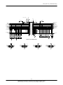
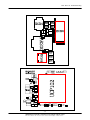
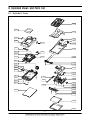
8. Exploded Views and Parts List
8-1. Exploded Views
QKP01
QWD02
QME01
QV001
QHI01
QHI03
QFU01
QCK01
QCR03
QVO02
QME04
QFR01
QME03
QVK01
QLC01
QCA02
QPC01
QSP02
QAN02
QCA01
QCR06
QMO01
QSP01
QSH01
QAU01
QME08
QMP01
QSC14
QIF01
QFL01
QCR12
QRE01
QCB03
QRF03
QSC12
QRF01
QCR03
QSC13
QMI03
QMW01
QRE03
QCR03
QSC13
QBA01
QBA00
8-1
SAMSUNG Proprietary-Contents may change without notice
This Document can not be used without Samsung's authorization
Exploded views and Parts List
8-2. Parts List
QAN02
QBA00
QBA01
QCA01
QCA02
QCB03
QCK01
QCR03
QCR03
QCR06
QCR12
QCW02
QFL01
QFL01
QFR01
QFR01
QFU01
QFU01
QHI01
QHI03
QKP01
QME01
QME03
QME04
QME08
QMI03
QMP01
QMW01
QPC01
QRE03
QRF01
QSC12
QSC13
QSC13
QSC14
QSH01
QSP02
QVK01
QVO01
QVO02
QWD02
QRE01
QSP01
QLC01
QRF03
QIF01
QAU01
QMO01
QLC02
INTENNA-SPHA900
ASSY MEC-COVER BATTERY V2
INNER BATTERY PACK-800MAH,BLK,
UNIT-CAMERA
UNIT-CAMERA KEY
ASSY MEC-CABLE COVER
PMO-CAMERA KEY
SCREW-MACHINE
SCREW-MACHINE
SCREW-MACHINE
SCREW-MACHINE
ASSY MEC-FLASH WINDOW
NDC-CASE LOWER FOLDER
MEA-LOWER(SVC)
NDC-FRONT COVER
MEA-FRONT(SVC)
NDC-CASE UPPER FOLDER
MEA-UPPER(SVC)
ASSY MEC-HINGE
NDC-HINGE DUMMY
ASSY MEC-KEYPAD(XAR/ZKS)
UNIT-EL KEYPAD
UNIT-CON TO CON ASSY
UNIT-FLASH FPCB
UNIT-BT ANT DUMMY FPCB
RMO-RUBBER MIC
PBA MAIN-SPHA900 PLUS
ASSY-COVER-MAIN WINDOW(PLUS)
CBF COAXIAL CABLE
ASSY MEC-COVER REAR INT V2
MPR-TAPE RF SWITCH
ASSY MEC-FOLDER SCREW COVER
RMO-REAR SCREW CAP1
RMO-REAR SCREW CAP1
PMO-FOLDER SCREW CAP
ASSY MEC-SHIELD COVER
UNIT-SPK MOT FPCB
UNIT-VOLUME KEY
PMO-VOLUME KEY
ASSY MEC-VOD KEY
PCT-SUB WINDOW
ASSY MEC-REAR TOP COVER
PMO-EAR COVER
PMO-IF COVER
SPEAKER
AUDIO-RECEIVER
MOTOR DC-SGHZ130
LCD-LCD MODULE
AS-LCD SUB
GH42-00716A
GH75-09081A
GH43-02101A
GH59-02668A
GH59-02173A
GH75-07382B
GH72-22531B
6001-001811
6001-001811
6001-001155
6001-001530
GH75-07219A
GH71-05928A
GH97-05855A
GH71-05692A
GH97-05858A
GH71-05927A
GH97-05854A
GH75-07205A
GH71-05105A
GH75-08316A
GH59-02664A
GH59-02175A
GH59-02176A
GH59-02681A
GH73-04934A
GH92-02721A
GH98-01078A
GH39-00440A
GH75-09082A
GH74-18895A
GH75-07381A
GH73-04824B
GH73-04824B
GH72-23132B
GH75-07882A
GH59-02202A
GH59-02172A
GH72-22530B
GH75-07220B
GH72-25511A
GH75-07880A
GH72-25508A
GH72-25509A
3001-001784
3009-001127
GH31-00154C
GH07-00806A
GH81-01816A
8-2
SAMSUNG Proprietary-Contents may change without notice
This Document can not be used without Samsung's authorization
Exploded views and Parts List
BAG PE
BAG PE
BAG PE
CBF SIGNAL-SPHA940 DANPLA
ADAPTOR-SGHD500 BLK
UNIT-EARPHONE
LABEL(P)-GUIDE(SPRINT)
LABEL(P)-WATER SOAK
MANUAL USERS-NOA ENGLISH
MANUAL USERS-NOA ENGLISH
BOX-UNIT(PLUS)
CUSHION-CASE(NEW)
ICT-MAGNETIC
ICT-RECEIVER GRILL
ICT-LCD GUIDE
NPR-HINGE CONTACT
RMO-SPK BLOCK R
RMO-SPK BLOCK L
RMO-SPONGE SPEAKER
RMO-RUBBER FRONT
MPR-VOL KEY BOHO VINYL
MPR-TAPE SUB PBA BACK
MPR-TAPE MAGNETIC
MPR-TAPE FRONT SUPPORT B
MPR-TAPE FRONT SUPPORT C
MPR-NON WOVEN MIC
MPR-SPONGE LCD CONN SUPP
MPR-TAPE MAIN WINDOW
MPR-TAPE RECEIVER GRILL
MPR-TAPE SUB WINDOW
MPR-TAPE SPK GRILL
MPR-SPONGE SUB WINDOW
MPR-BOHO VINYL LCD CONN
MPR-TAPE HINGE DUST
MPR-SHEET FRONT COVER
MPR-TAPE FOLDER KEY
MPR-TAPE HINGE DUMMY
MPR-TAPE CONNECTOR SOUND
MPR-TAPE LCD LEFT
MPR-TAPE LCD RIGHT
MPR-TAPE CONN BASE 1
MPR-TAPE CONNECTOR UPPER
MPR-BOHO VINYL SUB WIN
MPR-TAPE MAGNETIC UPPER
MPR-TAPE FRONT ANTI SHOR
MPR-BOHO VINYL SUB WIN
MPR-TAPE MAIN PCB SIDE
MPR-SPONGE HINGE DUMMY
MPR-TAPE J TAG
MPR-NON WOVEN RECEIVER
MPR-GASKET CAMERA HINGE
MPR-BOHO VINYL F-PCB FIX
6902-000297
6902-000378
6902-000461
GH39-00466A
GH44-00955A
GH59-02482A
GH68-02023A
GH68-02026A
GH68-09872A
GH68-11503A
GH69-03154C
GH69-03396A
GH70-00571A
GH70-00574A
GH70-00954A
GH71-05182A
GH73-05123A
GH73-05124A
GH73-05125A
GH73-05907A
GH74-07312A
GH74-12934A
GH74-15173A
GH74-15175A
GH74-15176A
GH74-15177A
GH74-15234A
GH74-15239A
GH74-15240A
GH74-15243A
GH74-15244A
GH74-15246A
GH74-15350A
GH74-15575A
GH74-15576B
GH74-15646A
GH74-15647A
GH74-15648A
GH74-15650A
GH74-15651A
GH74-15652A
GH74-15654A
GH74-15655A
GH74-15659A
GH74-15660A
GH74-16263A
GH74-16372A
GH74-16467A
GH74-16475A
GH74-16549A
GH74-16636A
GH74-17063A
8-3
SAMSUNG Proprietary-Contents may change without notice
This Document can not be used without Samsung's authorization
Exploded views and Parts List
MPR-TAPE IF HOLDER
GH74-17165A
MPR-TAPE APS
GH74-17967A
MPR-GASKET IF JACK
GH74-18874A
MPR-TAPE KEYPAD
GH74-19159A
MPR-BOHO VINYL VIEW
GH74-19308A
MPR-TAPE LCD CON
GH74-19321A
MPR-TAPE BATT INSULATION
GH74-19386A
MPR-GASKET SUB LCD
GH74-19762A
MPR-GASKET FOLDER UPPER
GH74-19763A
MPR-TAPE SUB LCD
GH74-19764A
MPR-TAPE SUPPORT MIC
GH74-20107A
MPR-TAPE FPCB INSUL
GH74-21393A
MPR-TAPE 1 (FPCB)
GH74-23612A
MPR-TAPE 2 (FPCB)
GH74-23613A
MPR-TAPE 3 (FPCB)
GH74-23614A
MPR-TAPE BOSS
GH74-24257A
MPR-SPONGE VOLUME KEY
GH74-26019A
AS-MAIN LCD
GH81-02629A
AS-MOD KEY DOME SHEET
GH81-03951A
MEA FRONT-COVERUNIT_EL KEYPA
GH97-05502A
MEA-UPPER(SVC R)
GH97-05854B
MEA-LOWER(SVC R)
GH97-05855B
MEA-FRONT(SVC R)
GH97-05858B
8-4
SAMSUNG Proprietary-Contents may change without notice
This Document can not be used without Samsung's authorization
Exploded views and Parts List
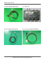
8-3 DM Cable(GH39-00129A)
8-5 RF Cable(GH39-00397A)
8-4 Test JIG
8-6 Test Jig Cable(GH39-00399A)
8-5
SAMSUNG Proprietary-Contents may change without notice
This Document can not be used without Samsung's authorization
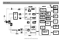
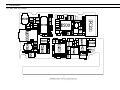
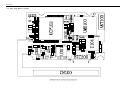
9. Block Diagrams
ANT
MSM6500
BLUETOOT
H MODULE
GPS LNA
CDMA
CDMA PA
SIM8690X
9-1
SAMSUNG Proprietary-Contents may change without notice
This Document can not be used without Samsung's authorization
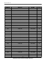
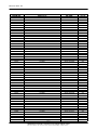
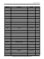
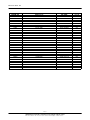
10. Electrical Parts List
Design LOC
Description
SEC CODE
STATUS
ANT401
BTC200
C100
C101
C102
C103
C104
C105
C106
C107
C108
C109
C110
C111
C112
C113
C114
C115
C117
C118
C119
C120
C121
C122
C123
C124
C125
C126
C127
C128
C129
C130
C131
C132
C133
C134
C135
C136
C137
C138
C139
C140
C141
C143
C144
C145
C146
C147
C148
C149
C150
C151
C152
C153
C154
C155
C156
CONNECTOR-COAXIAL
CONNECTOR-BATTERY
C-CER,CHIP
C-CER,CHIP
C-CER,CHIP
C-CER,CHIP
C-CER,CHIP
C-CER,CHIP
C-CER,CHIP
C-CER,CHIP
C-CER,CHIP
C-CER,CHIP
C-CER,CHIP
C-CER,CHIP
C-CER,CHIP
C-CER,CHIP
C-CER,CHIP
C-CER,CHIP
C-CER,CHIP
C-CER,CHIP
C-CER,CHIP
C-CER,CHIP
C-CER,CHIP
C-CER,CHIP
C-CER,CHIP
C-CER,CHIP
C-CER,CHIP
C-CER,CHIP
C-CER,CHIP
C-CER,CHIP
C-CER,CHIP
C-CER,CHIP
C-CER,CHIP
C-CER,CHIP
C-CER,CHIP
C-CER,CHIP
C-CER,CHIP
C-CER,CHIP
C-CER,CHIP
C-CER,CHIP
C-CER,CHIP
C-CER,CHIP
C-CER,CHIP
C-CER,CHIP
C-CER,CHIP
C-CER,CHIP
C-CER,CHIP
C-CER,CHIP
C-CER,CHIP
C-CER,CHIP
C-CER,CHIP
C-CER,CHIP
C-CER,CHIP
C-CER,CHIP
C-CER,CHIP
C-CER,CHIP
C-CER,CHIP
10-1
3705-001225
3711-006003
2203-005393
2203-005393
2203-006423
2203-006093
2203-005682
2203-005682
2203-006423
2203-006194
2203-006423
2203-006194
2203-006423
2203-006423
2203-006194
2203-006423
2203-006194
2203-006423
2203-001072
2203-006194
2203-006423
2203-006194
2203-006423
2203-000438
2203-006194
2203-001437
2203-005736
2203-006194
2203-006194
2203-006194
2203-006194
2203-006423
2203-000254
2203-005717
2203-005717
2203-006093
2203-005061
2203-005682
2203-005682
2203-006208
2203-006201
2203-001405
2203-001405
2203-001405
2203-001405
2203-006423
2203-006423
2203-006091
2203-006091
2203-006423
2203-006423
2203-006423
2203-006423
2203-006423
2203-006093
2203-006208
2203-006201
SA
SA
SA
SA
SA
SA
SA
SA
SA
SA
SA
SA
SA
SA
SA
SA
SA
SA
SA
SA
SA
SA
SA
SA
SA
SA
SA
SA
SA
SA
SA
SA
SA
SA
SA
SA
SA
SA
SA
SA
SA
SA
SA
SA
SA
SA
SA
SA
SA
SA
SA
SA
SA
SA
SA
SA
SA
SAMSUNG Proprietary-Contents may change without notice
This Document can not be used without Samsung's authorization
Electrical Parts List
Design LOC
Description
SEC CODE
STATUS
C157
C158
C159
C160
C161
C162
C163
C164
C165
C166
C167
C168
C169
C170
C171
C172
C173
C174
C175
C200
C201
C202
C203
C206
C207
C208
C209
C210
C211
C212
C213
C214
C215
C216
C217
C218
C219
C220
C221
C222
C223
C224
C225
C226
C228
C230
C233
C234
C235
C236
C238
C240
C241
C242
C245
C246
C247
C-CER,CHIP
C-CER,CHIP
C-CER,CHIP
C-CER,CHIP
C-CER,CHIP
C-CER,CHIP
C-CER,CHIP
C-CER,CHIP
C-CER,CHIP
C-CER,CHIP
C-CER,CHIP
C-CER,CHIP
C-CER,CHIP
C-CER,CHIP
C-CER,CHIP
C-CER,CHIP
C-CER,CHIP
C-CER,CHIP
C-CER,CHIP
C-CER,CHIP
C-CER,CHIP
C-CER,CHIP
C-CER,CHIP
C-CER,CHIP
C-CER,CHIP
C-CER,CHIP
C-CER,CHIP
C-CER,CHIP
C-CER,CHIP
C-CER,CHIP
C-CER,CHIP
C-CER,CHIP
C-CER,CHIP
C-CER,CHIP
C-CER,CHIP
C-CER,CHIP
C-CER,CHIP
C-CER,CHIP
C-CER,CHIP
C-CER,CHIP
C-CER,CHIP
C-CER,CHIP
C-CER,CHIP
C-CER,CHIP
C-CER,CHIP
C-CER,CHIP
C-CER,CHIP
C-CER,CHIP
C-CER,CHIP
C-CER,CHIP
C-CER,CHIP
C-CER,CHIP
C-CER,CHIP
C-CER,CHIP
C-CER,CHIP
C-CER,CHIP
C-CER,CHIP
2203-006423
2203-005682
2203-005682
2203-005682
2203-005682
2203-005682
2203-005682
2203-005682
2203-005682
2203-006423
2203-005682
2203-005682
2203-005736
2203-006194
2203-006194
2203-006438
2203-006194
2203-006348
2203-005682
2203-005664
2203-006201
2203-006201
2203-006201
2203-005061
2203-000254
2203-001652
2203-006120
2203-006201
2203-006120
2203-006201
2203-006194
2203-006423
2203-006423
2203-005664
2203-005664
2203-006201
2203-006053
2203-006053
2203-006201
2203-006201
2203-006201
2203-006201
2203-006423
2203-006423
2203-006053
2203-005682
2203-006423
2203-005682
2203-005682
2203-005682
2203-006423
2203-005682
2203-005736
2203-005736
2203-005682
2203-005682
2203-006093
SA
SA
SA
SA
SA
SA
SA
SA
SA
SA
SA
SA
SA
SA
SA
SA
SA
SA
SA
SA
SA
SA
SA
SA
SA
SA
SA
SA
SA
SA
SA
SA
SA
SA
SA
SA
SA
SA
SA
SA
SA
SA
SA
SA
SA
SA
SA
SA
SA
SA
SA
SA
SA
SA
SA
SA
SA
10-2
SAMSUNG Proprietary-Contents may change without notice
This Document can not be used without Samsung's authorization
Electrical Parts List
Design LOC
Description
SEC CODE
STATUS
C248
C249
C250
C251
C252
C253
C254
C255
C256
C257
C258
C259
C300
C301
C302
C303
C304
C306
C307
C308
C309
C310
C311
C312
C313
C314
C315
C316
C317
C318
C319
C320
C321
C323
C324
C325
C326
C327
C328
C329
C331
C332
C333
C334
C335
C336
C337
C338
C339
C400
C401
C402
C403
C404
C406
C408
C409
C-CER,CHIP
C-CER,CHIP
C-CER,CHIP
C-CER,CHIP
C-CER,CHIP
C-CER,CHIP
R-CHIP
R-CHIP
C-CER,CHIP
C-CER,CHIP
C-CER,CHIP
C-CER,CHIP
C-CER,CHIP
C-CER,CHIP
C-CER,CHIP
C-CER,CHIP
C-CER,CHIP
C-CER,CHIP
C-CER,CHIP
C-CER,CHIP
C-CER,CHIP
C-CER,CHIP
C-CER,CHIP
C-CER,CHIP
C-CER,CHIP
C-CER,CHIP
C-CER,CHIP
C-CER,CHIP
C-CER,CHIP
C-CER,CHIP
C-CER,CHIP
C-CER,CHIP
C-CER,CHIP
C-CER,CHIP
C-CER,CHIP
C-CER,CHIP
C-CER,CHIP
C-CER,CHIP
C-CER,CHIP
C-CER,CHIP
C-CER,CHIP
C-CER,CHIP
C-CER,CHIP
C-CER,CHIP
C-CER,CHIP
C-CER,CHIP
C-CER,CHIP
C-CER,CHIP
C-CER,CHIP
C-CER,CHIP
C-CER,CHIP
C-CER,CHIP
C-CER,CHIP
C-CER,CHIP
C-CER,CHIP
C-CER,CHIP
C-CER,CHIP
2203-006093
2203-001072
2203-006194
2203-005061
2203-005061
2203-005061
2007-008542
2007-008516
2203-006194
2203-006423
2203-006093
2203-006423
2203-006201
2203-006423
2203-006201
2203-000995
2203-005736
2203-005736
2203-001178
2203-000386
2203-006423
2203-001178
2203-000438
2203-005446
2203-005806
2203-006423
2203-005056
2203-000233
2203-000233
2203-005446
2203-000438
2203-000233
2203-000233
2203-006423
2203-006423
2203-005736
2203-000995
2203-005736
2203-006423
2203-000995
2203-006423
2203-006423
2203-000995
2203-000995
2203-006093
2203-006423
2203-005736
2203-006194
2203-006423
2203-005729
2203-000585
2203-000995
2203-006423
2203-000585
2203-002677
2203-006194
2203-005740
SA
SA
SA
SA
SA
SA
SA
SA
SA
SA
SA
SA
SA
SA
SA
SA
SA
SA
SA
SA
SA
SA
SA
SA
SA
SA
SA
SA
SA
SA
SA
SA
SA
SA
SA
SA
SA
SA
SA
SA
SA
SA
SA
SA
SA
SA
SA
SA
SA
SA
SA
SA
SA
SA
SA
SA
SA
10-3
SAMSUNG Proprietary-Contents may change without notice
This Document can not be used without Samsung's authorization
Electrical Parts List
Design LOC
Description
SEC CODE
STATUS
C410
C411
C412
C413
C417
C418
C419
C420
C421
C422
C423
C424
C425
C426
C428
C429
C430
C431
C432
C434
C435
C436
C437
C438
C439
C440
C441
C442
C443
C444
C445
C500
C501
C502
C503
C504
C505
C506
C507
C508
C509
C510
C511
C512
C513
C514
C515
C516
C517
C518
C519
C520
C521
C522
C524
C525
C526
C-CER,CHIP
C-CER,CHIP
C-CER,CHIP
C-CER,CHIP
C-CER,CHIP
C-CER,CHIP
C-CER,CHIP
C-CER,CHIP
C-CER,CHIP
C-CER,CHIP
C-CER,CHIP
C-CER,CHIP
C-CER,CHIP
C-CER,CHIP
C-CER,CHIP
C-CER,CHIP
C-CER,CHIP
C-CER,CHIP
C-CER,CHIP
C-CER,CHIP
C-CER,CHIP
C-CER,CHIP
C-CER,CHIP
C-CER,CHIP
C-CER,CHIP
C-CER,CHIP
C-CER,CHIP
C-CER,CHIP
C-CER,CHIP
C-CER,CHIP
C-CER,CHIP
C-CER,CHIP
C-CER,CHIP
C-CER,CHIP
C-CER,CHIP
C-CER,CHIP
C-CER,CHIP
C-CER,CHIP
C-CER,CHIP
C-CER,CHIP
C-CER,CHIP
C-CER,CHIP
C-CER,CHIP
C-CER,CHIP
C-CER,CHIP
C-CER,CHIP
C-CER,CHIP
C-CER,CHIP
C-CER,CHIP
C-CER,CHIP
C-CER,CHIP
C-CER,CHIP
C-CER,CHIP
C-CER,CHIP
C-CER,CHIP
C-CER,CHIP
C-CER,CHIP
2203-000995
2203-006423
2203-006201
2203-000233
2203-000425
2203-000885
2203-006201
2203-000585
2203-000885
2203-000233
2203-000233
2203-006423
2203-006194
2203-005740
2203-006379
2203-006194
2203-005740
2203-005806
2203-001259
2203-002668
2203-005736
2203-002687
2203-006194
2203-006190
2203-005480
2203-006423
2203-006423
2203-006201
2203-006423
2203-006674
2203-005281
2203-001072
2203-001072
2203-006053
2203-005482
2203-006556
2203-006556
2203-006556
2203-005717
2203-006556
2203-006556
2203-006556
2203-006556
2203-005717
2203-006556
2203-006556
2203-006556
2203-006556
2203-006556
2203-006093
2203-006053
2203-006190
2203-006053
2203-006093
2203-000233
2203-000233
2203-006556
SA
SA
SA
SA
SA
SA
SA
SA
SA
SA
SA
SA
SA
SA
SA
SA
SA
SA
SA
SA
SA
SA
SA
SA
SA
SA
SA
SA
SA
SNA
SA
SA
SA
SA
SA
SA
SA
SA
SA
SA
SA
SA
SA
SA
SA
SA
SA
SA
SA
SA
SA
SA
SA
SA
SA
SA
SA
10-4
SAMSUNG Proprietary-Contents may change without notice
This Document can not be used without Samsung's authorization
Electrical Parts List
Design LOC
Description
SEC CODE
STATUS
C527
C528
C529
D200
D201
D205
DUF400
DUF402
EAR200
F300
F301
F302
F303
F401
F403
F500
F501
F502
F503
F504
F505
F506
F507
F508
HDC500
HDC501
HDC502
IFC201
L100
L101
L200
L201
L202
L300
L301
L302
L303
L304
L305
L306
L307
L308
L309
L310
L311
L312
L313
L314
L315
L400
L403
L404
L405
L406
L407
L408
L409
C-CER,CHIP
C-CER,CHIP
C-CER,CHIP
DIODE-SWITCHING
DIODE-SWITCHING
DIODE-SWITCHING
DUPLEXER-FBAR
DUPLEXER-SAW
JACK-EAR PHONE
FILTER-SAW
FILTER-SAW
VARISTOR
VARISTOR
FILTER-SAW
FILTER-SAW
FILTER-EMI SMD
FILTER-EMI SMD
FILTER-EMI/ESD
FILTER-EMI/ESD
FILTER-EMI/ESD
FILTER-EMI/ESD
VARISTOR
VARISTOR
VARISTOR
HEADER-BOARD TO BOARD
HEADER-BOARD TO BOARD
HEADER-BOARD TO BOARD
CONNECTOR-INTERFACE
BEAD-SMD
INDUCTOR-SMD
INDUCTOR-SMD
INDUCTOR-SMD
BEAD-SMD
INDUCTOR-SMD
INDUCTOR-SMD
INDUCTOR-SMD
INDUCTOR-SMD
INDUCTOR-SMD
INDUCTOR-SMD
INDUCTOR-SMD
INDUCTOR-SMD
INDUCTOR-SMD
INDUCTOR-SMD
INDUCTOR-SMD
INDUCTOR-SMD
INDUCTOR-SMD
INDUCTOR-SMD
INDUCTOR-SMD
INDUCTOR-SMD
INDUCTOR-SMD
INDUCTOR-SMD
BEAD-SMD
INDUCTOR-SMD
INDUCTOR-SMD
INDUCTOR-SMD
INDUCTOR-SMD
INDUCTOR-SMD
10-5
2203-006556
2203-006556
2203-006556
0401-001110
0401-001110
0401-001086
2910-000009
2909-001244
3722-002315
2904-001533
2904-001519
1405-001119
1405-001119
2904-001499
2904-001474
2901-001268
2901-001268
2901-001362
2901-001362
2901-001362
2901-001362
1405-001158
1405-001158
1405-001158
3711-005490
3711-005643
3711-005456
3710-001611
3301-001342
2703-002207
2703-002775
2703-002775
3301-001342
2703-001723
2703-002198
2703-002204
2703-002268
2703-002170
2703-002170
2703-002208
2703-002369
2703-002314
2703-002208
2703-002200
2703-002208
2703-002200
2703-002208
2703-001729
2703-002281
2703-001749
2703-002206
3301-001120
2703-002206
2703-002207
2703-002281
2703-002207
2703-002207
SA
SA
SA
SA
SA
SA
SA
SA
SA
SA
SA
SA
SA
SA
SA
SA
SA
SA
SA
SA
SA
SA
SA
SA
SA
SA
SA
SA
SA
SA
SA
SA
SA
SA
SA
SA
SA
SA
SA
SA
SA
SA
SA
SA
SA
SA
SA
SA
SA
SA
SA
SA
SA
SA
SA
SA
SA
SAMSUNG Proprietary-Contents may change without notice
This Document can not be used without Samsung's authorization
Electrical Parts List
Design LOC
Description
SEC CODE
STATUS
L500
L501
L503
OSC100
OSC101
PAM400
PAM403
R100
R101
R102
R105
R106
R107
R109
R110
R111
R113
R114
R115
R116
R120
R121
R122
R123
R124
R127
R128
R129
R131
R132
R133
R134
R135
R136
R137
R138
R139
R140
R141
R142
R143
R144
R147
R200
R201
R202
R203
R204
R205
R206
R207
R208
R209
R213
R219
R220
R222
BEAD-SMD
BEAD-SMD
INDUCTOR-SMD
RESONATOR-CERAMIC
CRYSTAL-SMD
IC-POWER AMP
IC-POWER AMP
R-CHIP
R-CHIP
R-CHIP
R-CHIP
R-CHIP
R-CHIP
R-CHIP
R-CHIP
R-CHIP
R-CHIP
R-CHIP
R-CHIP
R-CHIP
R-CHIP
R-CHIP
R-CHIP
R-CHIP
R-CHIP
R-CHIP
R-CHIP
R-CHIP
R-CHIP
R-CHIP
R-CHIP
R-CHIP
R-CHIP
R-CHIP
R-CHIP
R-CHIP
R-CHIP
R-CHIP
R-CHIP
R-CHIP
R-CHIP
R-CHIP
R-CHIP
R-CHIP
R-CHIP
R-CHIP
R-CHIP
R-CHIP
R-CHIP
R-CHIP
R-CHIP
R-CHIP
R-CHIP
R-CHIP
R-CHIP
R-CHIP
R-CHIP
10-6
3301-001729
3301-001729
2703-002204
2802-001182
2801-003856
1201-002268
1201-002259
2007-001313
2007-000171
2007-000171
2007-000171
2007-008542
2007-000171
2007-008052
2007-008531
2007-008542
2007-000171
2007-008055
2007-000141
2007-000171
2007-000140
2007-001319
2007-001339
2007-008516
2007-000169
2007-008516
2007-001339
2007-000171
2007-008419
2007-000156
2007-008516
2007-002796
2007-000165
2007-000169
2007-007529
2007-007107
2007-007313
2007-000775
2007-008052
2007-008516
2007-008419
2007-001308
2007-008806
2007-000162
2007-000148
2007-007107
2007-007488
2007-007107
2007-008516
2007-007139
2007-007309
2007-007137
2007-007107
2007-003006
2007-008419
2007-008419
2007-003006
SA
SA
SA
SA
SA
SA
SA
SA
SA
SA
SA
SA
SA
SA
SA
SA
SA
SA
SA
SA
SA
SA
SA
SA
SA
SA
SA
SA
SA
SA
SA
SA
SA
SA
SA
SA
SA
SA
SA
SA
SA
SA
SA
SA
SA
SA
SA
SA
SA
SA
SA
SA
SA
SA
SA
SA
SA
SAMSUNG Proprietary-Contents may change without notice
This Document can not be used without Samsung's authorization
Electrical Parts List
Design LOC
Description
SEC CODE
STATUS
R228
R229
R230
R231
R232
R233
R234
R300
R301
R302
R303
R304
R305
R306
R307
R308
R309
R310
R311
R312
R313
R314
R400
R401
R402
R403
R404
R405
R406
R407
R408
R500
R502
R503
R508
R509
R510
R512
R513
R514
R515
RFS400
TA204
TA205
TA231
TA232
TA330
TA406
TCK301
TH100
TR100
TR400
TR401
U101
U103
U104
U200
R-CHIP
R-CHIP
R-CHIP
R-CHIP
R-CHIP
R-CHIP
R-CHIP
R-CHIP
R-CHIP
R-CHIP
R-CHIP
R-CHIP
R-CHIP
R-CHIP
R-CHIP
R-CHIP
R-CHIP
R-CHIP
R-CHIP
R-CHIP
R-CHIP
R-CHIP
R-CHIP
R-CHIP
R-CHIP
R-CHIP
R-CHIP
R-CHIP
R-CHIP
R-CHIP
R-CHIP
R-CHIP
R-CHIP
R-CHIP
R-CHIP
R-CHIP
R-CHIP
R-CHIP
R-CHIP
R-CHIP
R-CHIP
CONNECTOR-COAXIAL
C-TA,CHIP
C-TA,CHIP
C-TA,CHIP
C-TA,CHIP
C-TA,CHIP
C-TA,CHIP
OSCILLATOR-VCTCXO
THERMISTOR-NTC
FET-SILICON
TR-DIGITAL
TR-DIGITAL
IC-CMOS LOGIC
IC-VOL. DETECTOR
BLUETOOTH MODULE
IC-POWER SUPERVISOR
10-7
2007-000140
2007-000148
2007-000242
2007-000758
2007-001313
2007-001313
2007-000156
2007-009115
2007-009115
2007-007491
2007-007314
2007-007314
2007-007314
2007-008045
2007-008045
2007-008542
2007-008531
2007-000171
2007-008531
2007-008806
2007-008419
2007-000138
2007-007309
2007-001325
2007-008531
2007-000140
2007-008516
2007-008419
2007-008478
2007-008531
2007-008587
2007-008542
2007-008542
2007-008542
2007-008052
2007-008052
2007-008483
2007-003010
2007-003010
2007-003010
2007-008542
3705-001358
2404-001268
2404-001268
2404-001151
2404-001151
2404-001268
2404-001105
2809-001277
1404-001165
0505-001889
0504-001176
0504-001176
0801-002345
1203-003408
4709-001410
1203-003495
SA
SA
SA
SA
SA
SA
SA
SA
SA
SA
SA
SA
SA
SA
SA
SA
SA
SA
SA
SA
SA
SA
SA
SA
SA
SA
SA
SA
SA
SA
SA
SA
SA
SA
SA
SA
SA
SA
SA
SA
SA
SA
SA
SA
SA
SA
SA
SA
SA
SA
SA
SA
SA
SA
SA
SA
SA
SAMSUNG Proprietary-Contents may change without notice
This Document can not be used without Samsung's authorization
Electrical Parts List
Design LOC
Description
SEC CODE
STATUS
U201
U203
U204
U205
U206
U300
U301
U302
U401
U402
U404
U405
UCP102
UME100
VCO300
VR100
VR200
VR500
VR501
VR502
VR503
VR504
VR505
VR506
VR507
VR508
VR509
ZD200
ZD201
ZD202
ZD204
ZD206
IC-CMOS LOGIC
DIODE-ARRAY
IC-ANALOG MULTIPLEX
IC-ANALOG MULTIPLEX
IC-MULTI REG.
IC-RF AMP
IC-RECEIVER
IC-RF AMP
IC-ANALOG SWITCH
IC-TRANSMITTER
FILTER-SAW
C-CER,CHIP
IC-MODEM
IC-MCP
OSCILLATOR-VCO
VARISTOR
VARISTOR
VARISTOR
VARISTOR
VARISTOR
VARISTOR
VARISTOR
VARISTOR
VARISTOR
VARISTOR
VARISTOR
VARISTOR
DIODE-ZENER
DIODE-ZENER
DIODE-TVS
DIODE-ZENER
DIODE-TVS
0801-002661
0407-001038
1001-001215
1001-001215
1203-003517
1201-001964
1205-002265
1201-002291
1001-001303
1205-002497
2904-001414
2203-005682
1205-002521
1108-000044
2806-001335
1405-001110
1405-001110
1405-001138
1405-001138
1405-001138
1405-001138
1405-001138
1405-001138
1405-001138
1405-001110
1405-001110
1405-001110
0403-001547
0403-001427
0406-001208
0403-001339
0406-001208
SA
SA
SA
SA
SA
SA
SA
SA
SA
SA
SA
SA
SA
SNA
SA
SA
SA
SA
SA
SA
SA
SA
SA
SA
SA
SA
SA
SA
SA
SA
SA
SA
10-8
SAMSUNG Proprietary-Contents may change without notice
This Document can not be used without Samsung's authorization
11. PCB Diagrams
11-1. Main PCB Top Diagram
11-1
SAMSUNG Proprietary-Contents may change without notice
This Document can not be used without Samsung's authorization
PCB Diagrams
11-2. Main PCB Bottom Diagram
11-2
SAMSUNG Proprietary-Contents may change without notice
This Document can not be used without Samsung's authorization