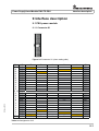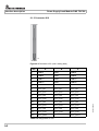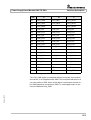
1
USER MANUAL
Power Supply/Load Module
R&S®TS-PSU
User Manual
for ROHDE & SCHWARZ Power Supply/Load Module R&S TS-PSU
1st Issue / 04.06 / GB 1504.4560.12
All rights, also translation into foreign languages, are reserved. No part of this manual is permitted
to be reproduced in any form (print, photocopy or any other method), also not for the preparation
of lectures, or processed, reproduced or made available using electronic systems without written
permission from ROHDE & SCHWARZ.
® The passing on to third parties and the reproduction of this documentation, utilisation and communication of its contents is not permitted unless specifically approved. Infringements will incur
claims for damages. All rights reserved in the case of the award of a patent or registration of a
design.
R&S® is a registered trademark of ROHDE & SCHWARZ GmbH & Co. KG.
We draw to your attention that the names of software and hardware used in the Service Manual,
and the brand names of the respective companies are, in general, the subject of protection as
trademarks, or under proprietary rights, or patent law.
ROHDE & SCHWARZ GmbH & Co. KG
Corporate Headquarters
Mühldorfstr. 15
D-81671 München
Telephone:
Fax:
...49 (0)89/4129-13774
...49 (0)89/4129-13777
Printed in the Federal Republic of Germany. Errors excepted, subject to technical change without notice.
Safety Instructions
Attention!
Electrostatic
sensitive devices require
special care
Support Center
Telephone Europe:
+49 180 512 42 42
Telephone worldwide: +49 89 4129 13774
Fax:
+49 89 4129 13777
e-mail: [email protected]
If you have any technical queries about this Rohde &
Schwarz equipment, our Hotline at the Support Center of
Rohde & Schwarz Sales-GmbH will be glad to help.
Our team will discuss your queries and look for solutions to
your problems.
The Hotline is open Mondays to Fridays from 08.00 to 17.00
hrs.
For queries outside office hours, you can leave a message
or send a note via fax or email. We will then get back to you
as soon as possible.
Power Supply/Load Module R&S TS-PSU
Contents
Contents
1
Usage
1.1
General
1-1
1.2
Description of product
1-1
1.3
Scope of delivery
1-2
1.4
Characteristics
1-3
1.5
Safety instructions
1-4
2
View
2-1
3
Block Diagram
3-1
4
Layout
4-1
4.1
Overview
4-1
4.2
PSU power module
4-2
4.2.1
Mechanical layout
4-2
4.2.2
Display elements
4-3
4.3
4.4
5
1. Ausgabe 04.06
1-1
PSU RIO module
4-4
4.3.1
Mechanical layout
4-4
4.3.2
Display elements
4-5
PSU AC/DC converter
4-6
4.4.1
Mechanical layout
4-6
4.4.2
Display and control elements
4-6
Function Description
5-1
5.1
General
5-1
5.2
Power supply/load unit
5-2
5.2.1
Characteristic diagram
5-3
5.2.2
5.2.2.1
5.2.2.2
Reverse polarity in load case
Weak external source (current remains below the maximum current)
Strong external source (able to provide a high current)
5-4
5-5
5-5
5.2.3
Inductive loads
5-5
5.2.4
External sensing
5-6
5.2.5
Current limiting when using matrix relays in the output path
5-6
5.2.6
Power dissipation and settling time
5-7
5.2.7
Wiring channels in series (cascading)
5-8
5.2.8
Connecting channels in parallel
5-9
5.2.9
Electronic on/off and PWM
5-9
1
5.3
5.4
5.5
6
7
2
5.2.10
Dynamic Operation
5-10
5.2.11
Protective mechanisms
5-11
Measurement unit
5-13
5.3.1
Measurement options, resolution
5-13
5.3.2
Sampling
5-13
5.3.3
Monitor output
5-14
Relay matrix
5-15
5.4.1
Matrix and front relay
5-16
5.4.2
Coupling Relay
5-16
5.4.3
Ground relay
5-17
Trigger unit
5-18
5.5.1
Trigger outputs
5-18
5.5.2
Trigger inputs
5-18
Commissioning
6-1
6.1
Installation of the PSU power module
6-1
6.2
Installation of the PSU RIO module
6-2
6.3
Connecting the PSU AC/DC converter
6-3
6.4
Switching on sequence
6-3
6.5
Safety instructions
6-4
6.5.1
General
6-4
6.5.2
Replacing the R&S TS-PSU
6-4
6.5.3
Instructions for operation with voltages dangerous to the touch
6-5
Software
7-1
7.1
Driver software
7-1
7.2
Softpanel
7-2
7.3
8
Power Supply/Load Module R&S TS-PSU
7.2.1
Configuration of sources
7-3
7.2.2
Configuration of measurement units
7-3
Sample programmes
7-4
7.3.1
Programming with GTSL libraries
7-4
7.3.2
Programming with device drivers
7-6
Self-Test
8-1
8.1
LED test
8-1
8.2
Power on test
8-2
8.3
TSVP self-test
8-3
1. Ausgabe 04.06
Contents
Power Supply/Load Module R&S TS-PSU
9
Contents
Interface description
9-1
9.1
PSU power module
9-1
9.1.1
Connector X1
9-1
9.1.2
Connector X10
9-2
9.1.3
Connector X20
9-4
9.1.4
Connector X30
9-5
9.2
9.3
PSU RIO module
9-6
9.2.1
Connector X5
9-6
9.2.2
Connector X20
9-7
PSU AC/DC converter
9-8
9.3.1
9-8
10-1
1. Ausgabe 04.06
10 Specifications
Connector X5
3
Power Supply/Load Module R&S TS-PSU
1. Ausgabe 04.06
Contents
4
Power Supply/Load Module R&S TS-PSU
Figures
Figures
PSU power module view ...................................................................2-1
Figure 2-2
PSU RIO module view .......................................................................2-2
Figure 2-3
PSU AC/DC converter view...............................................................2-3
Figure 3-1
Functional block diagram R&S TS-PSU ..........................................3-2
Figure 3-2
Block diagram R&S TS-PSU .............................................................3-3
Figure 4-1
Components of order item R&S TS-PSU .........................................4-1
Figure 4-2
Arrangement of connectors and PSU power module LEDs ..........4-2
Figure 4-3
Arrangement of the LEDs on the PSU power module.................... 4-3
Figure 4-4
Arrangement of plug-in connectors and PSU RIO module LEDs .4-5
Figure 5-1
Block diagram of channels ...............................................................5-1
Figure 5-2
Current/voltage characteristic diagram...........................................5-4
Figure 5-3
Signal connection............................................................................5-15
Figure 6-1
Permissible voltages on analog bus lines ......................................6-5
Figure 7-1
Softpanel R&S TS-PSU......................................................................7-2
Figure 7-2
Configuration of sources ..................................................................7-3
Figure 7-3
Configuration of measurement units...............................................7-3
Figure 9-1
Connector X1 (view: mating side) ....................................................9-1
Figure 9-2
Connector X10 (view: mating side) ..................................................9-2
Figure 9-3
Connector X20 (view: mating side) ..................................................9-4
Figure 9-4
Connector X30 (view: mating side) ..................................................9-5
Figure 9-5
Connector X5 (view: mating side) ....................................................9-6
Figure 9-6
Connector X20 (view: mating side) ..................................................9-7
Figure 9-7
Connector X5 (view: mating side) ....................................................9-8
1. Ausgabe 04.06
Figure 2-1
5
Power Supply/Load Module R&S TS-PSU
1. Ausgabe 04.06
Figures
6
Power Supply/Load Module R&S TS-PSU
Tables
Tables
Characteristics R&S TS-PSU ............................................................1-3
Table 4-1
PSU power module connectors........................................................4-2
Table 4-2
Display elements on the PSU power module..................................4-3
Table 4-4
Display elements on the PSU RIO module ......................................4-5
Table 4-3
PSU RIO module connectors............................................................4-5
Table 5-1
Voltages and value range of monitor outputs ..............................5-14
Table 7-1
Driver installation R&S TS-PSU........................................................7-1
Table 8-1
Observations about the LED test .....................................................8-1
Table 8-2
Observations about the power on test ............................................8-2
Table 9-1
Assignment of X1 ..............................................................................9-1
Table 9-2
Assignment of X10 ............................................................................9-2
Table 9-3
Assignment of X20 ............................................................................9-4
Table 9-4
Assignment of X30 ............................................................................9-5
Table 9-5
Assignment of X5 ..............................................................................9-6
Table 9-6
Assignment of X20 ............................................................................9-7
Table 9-7
Assignment of X5 ..............................................................................9-8
1. Ausgabe 04.06
Table 1-1
7
Power Supply/Load Module R&S TS-PSU
1. Ausgabe 04.06
Tables
8
Power Supply/Load Module R&S TS-PSU
Usage
1 Usage
1.1 General
These operating instructions provide all the information required for installation, programming, and operation of the
Power Supply/Load Module R&S TS-PSU on the R&S CompactTSVP/
R&S PowerTSVP production platform. They also include detailed information on the special features of the R&S TS-PSU, specifications,
block diagrams, and pin assignment of the connector. All processes described in the manual assume the reader is familiar with personal computers, the Windows2000/Windows XP operating system and the basic
principles of electrical measurement systems in the form of modules
(CompactPCI or PXI modules).
1.2 Description of product
1st Issue 04.06
The Power Supply/Load Module R&S TS-PSU is a module based on
CompactPCI developed for use on the ROHDE & SCHWARZ R&S
CompactTSVP and R&S PowerTSVP production platform. It has a
width of only one slot and a height of four units. It has two floating Channels that are completely independent of each other with a maximum
power of 50 W each, a voltage range of +/-50 V and a maximum current
of 3 A. The currents and voltages can be programmed in both the positive and negative range. Thanks to this 4-quadrant capability of the
module, it can also be operated in applications as a load (sink).
The measurement units integrated into the module for each channel
make it possible to read back the current and voltage of any given
channel. Using the multiplexer included in the module, it is also possible with the R&S TS-PSU to measure external voltages over time directly on the test object. The functionality of the module also includes
extensive options for controlling individual channels via trigger lines
and generating trigger signals. As with all modules available from
ROHDE & SCHWARZ, the R&S TS-PSU also has access to existing
analog measurement buses in the R&S CompactTSVP and R&S PowerTSVP with both channels. This measurement bus makes it possible
to switch outputs without any extra wiring to other measurement and
switching cards present in the R&S CompactTSVP / R&S PowerTSVP.
1-1
Usage
Power Supply/Load Module R&S TS-PSU
The CAN bus (Controller Area Network) present in the R&S CompactTSVP and R&S PowerTSVP is used to control the R&S TS-PSU
(see R&S CompactTSVP Operating Instructions - Chapter 3.3.6).
1.3 Scope of delivery
The scope of delivery for the Power Supply/Load Module R&S TS-PSU
includes the following components:
•
PSU power module (CompactPCI module, for use in a front slot)
•
PSU-RIO module to connect the PSU AC/DC converter to the PSU
power module (RIO = rear input/output, for use in the corresponding slot on the back)
•
PSU-AC/DC converter for external power supply of the
R&S TS-PSU
1st Issue 04.06
Please open the package carefully and check to ensure the hardware
inside has been delivered in perfect condition. If the modules included
in the delivery show any signs of damage that would interfere with their
intended purpose, please contact ROHDE & SCHWARZ Customer
Support.
1-2
Power Supply/Load Module R&S TS-PSU
Usage
1.4 Characteristics
Characteristics R&S TS-PSU
Two fully independent, floating power supply units with up to ± 50 V /
0…3 A / 50 W
Source and sink operation with separate sensing (four-quadrant operation)
Electronic load with up to 20 W continuous dissipated power
Integrated voltage and current measurement
Two integrated voltage measurement units for external use
Recording of voltage or current values as they change over time
External trigger of source and measurement via PXI trigger signals
Over voltage, over current, over temperature and short circuit protection
4:1 Relay multiplexer (force and sense) per channel for panel test
Access to analog measurement bus
Self-test capability
Softpanel for direct operation
LabWindows/CVI driver support
GTSL (generic test software library) in DLL format
1st Issue 04.06
Table 1-1 Characteristics R&S TS-PSU
1-3
Usage
Power Supply/Load Module R&S TS-PSU
1.5 Safety instructions
WARNING!
The R&S CompactTSVP/ R&S PowerTSVP production platform
and the Power Supply/Load Module R&S TS-PSU are designed
so that users can operate at volatages up to 125 V. The requirements according to EN61010-1 for operation with “hazardous
live” voltages must be observed.
1st Issue 04.06
For additional details see Chapter 6.5.3 and the leaflet entitled “Safety
Instructions” in the operating instructions for the R&S CompactTSVP/
R&S PowerTSVP production platform.
1-4
Power Supply/Load Module R&S TS-PSU
View
2 View
Figure 2-1 to Figure 2-3 show views of the three modules of
Power Supply/Load Module R&S TS-PSU.
1st Issue 04.06
Figure 2-1 PSU power module view
2-1
View
Power Supply/Load Module R&S TS-PSU
1st Issue 04.06
Figure 2-2 PSU RIO module view
2-2
Power Supply/Load Module R&S TS-PSU
View
1st Issue 04.06
Figure 2-3 PSU AC/DC converter view
2-3
Power Supply/Load Module R&S TS-PSU
1st Issue 04.06
View
2-4
Power Supply/Load Module R&S TS-PSU
Block Diagram
3 Block Diagram
Figure 3-1 shows a simplified functional block diagram of the
Power Supply/Load Module R&S TS-PSU. This functional block diagram represents the three modules of the R&S TS-PSU.
•
PSU power module
•
PSU RIO module
•
PSU AC/DC converter
1st Issue 04.06
Figure 3-2 shows a block diagram of the Power Supply/Load Module
R&S TS-PSU (PSU power module and PSU RIO module).
3-1
3-2
1st Issue 04.06
Force
Multiplexer
Sense/Measure
Multiplexer
Sense/Measure
Multiplexer
Force
Multiplexer
CHANNEL 2
CHANNEL 1
Analog
Bus
Voltage
Voltage
PXI-Trigger
Logic
Figure 3-1 Functional block diagram R&S TS-PSU
DC CH2
DC CH1
DC CH2
DC CH1
PSU RIO Module
PSU AC/DC Converter
Backplane
AC
85...
230 V
Block Diagram
Power Supply/Load Module R&S TS-PSU
1st Issue 04.06
8...55V
1MB RAM
CAN
Interface
CPLD
CPLD
CPLD
ADC
DAC
DAC
U Soll
ADC
DAC
DAC
U Soll
CH2_MLO
CH1_MHI
CH1_MLO
CH2_HI4
CH2_LO4
CH2_HI3
CH2_LO3
CH2_HI2
CH2_LO2
CH2_HI1
CH2_LO1
CH2_SHI1
CH2_SLO1
CH2_SHI2
CH2_SLO2
CH2_SHI3
CH2_SLO3
CH2_SHI4
CH2_SLO4
CH1_SHI1
CH1_SLO1
CH1_SHI2
CH1_SLO2
CH1_SHI3
CH1_SLO3
CH1_SHI4
CH1_SLO4
CH1_HI4
CH1_LO4
CH1_HI3
CH1_LO3
CH1_HI2
CH1_LO2
CH1_HI1
CH1_LO1
LABC1
LABC2
LABD1
LABD2
LED
Power Supply/Load Module R&S TS-PSU
Block Diagram
Figure 3-2 Block diagram R&S TS-PSU
3-3
ABA1
ABA2
ABB1
ABB2
ABC1
ABC2
ABD1
ABD2
Power Supply/Load Module R&S TS-PSU
1st Issue 04.06
Block Diagram
3-4
Power Supply/Load Module R&S TS-PSU
Layout
4 Layout
4.1 Overview
The Power Supply/Load Module R&S TS-PSU is an option for integration into the R&S CompactTSVP production platform or
R&S PowerTSVP production platform. It consists of the following three
modules:
•
PSU power module (CompactPCI module, for use in a front slot)
•
PSU RIO module to connect the PSU AC/DC converter to the PSU
power module (for use in the corresponding slot on the back)
•
PSU AC/DC converter for external power supply of the
R&S TS-PSU
The PSU AC/DC converter provides the power required by the test object and the power module. It does not represent a load on the R&S
CompactTSVP power supply.
Ordering Part TS-PSU
1504.4530.02
TS-PAC 1504.4553.02
PSU Power Module
1504.4701.02
PSU RIO
Module
PSU AC/DC Converter
1st Issue 04.06
Figure 4-1 Components of order item R&S TS-PSU
4-1
Layout
Power Supply/Load Module R&S TS-PSU
4.2 PSU power module
4.2.1 Mechanical layout
The PSU power module is designed as a long plug-in card for front side
insertion in the R&S CompactTSVP production platform or in the R&S
PowerTSVP production platform. The front side connector X10 is used
to connect the test object. Connector X30 connects the module with the
analog bus backplane in the R&S CompactTSVP. Connectors X20/X1
connect the module with the cPCI backplane/PXI control backplane.
7
X30
COM
PWR
CH1
CH2
1
1
X20
X10
1
X1
32
1
Figure 4-2 Arrangement of connectors and PSU power module LEDs
Use
X1
cPCI Connector
X10
Front Connector
X20
cPCI Connector
X30
Analog Bus Connector
Table 4-1 PSU power module connectors
4-2
1st Issue 04.06
Abbreviation
Power Supply/Load Module R&S TS-PSU
Layout
4.2.2 Display elements
Communication
1
ERR
COM
PWR
CH1
CH2
7
LED
X30
1
1
X20
X10
1
X1
32
1
Figure 4-3 Arrangement of the LEDs on the PSU power module
There are five light emitting diodes (LEDs) on the front panel of the PSU
power module. They indicate the current status of the module. The
meaning of the LEDs is as follows:
1st Issue 04.06
LED
Description
ERR (red)
Error status:
Lit or flashing if an error occurs during the power on
test on the R&S TS-PSU module after the power supply is turned on. This means there is a hardware problem in the module.
(See also Section 8:Self-Test)
COM
(yellow)
Communication:
Lit when data is being transferred via the interface.
Table 4-2 Display elements on the PSU power module
4-3
Layout
Power Supply/Load Module R&S TS-PSU
LED
Description
PWR
(green)
Power supply OK:
Lit when all necessary power supply voltages are
present
CH1
(yellow)
Continuously lit:
Channel 1 is working with constant current
Flashing:
The protective mechanism for Channel 1 has engaged
(see also Section 5.2.11)
CH2
(yellow)
Continuously lit:
Channel 2 is working with constant current
Flashing:
The protective mechanism for Channel 2 has engaged
(see also Section 5.2.11)
Table 4-2 Display elements on the PSU power module
4.3 PSU RIO module
4.3.1 Mechanical layout
CAUTION!
The PSU RIO module must only be used in combination with the
PSU power module. Using it with other modules (for example cPCI/PXI standard modules) may damage the modules.
4-4
1st Issue 04.06
The PSU RIO module has been specially developed for operation of
the R&S TS-PSU. It is used on the back of the R&S CompactTSVP production platform or R&S PowerTSVP. The height of the board is 3 HE
(134 mm). The module is fastened in place by two fastening screws.
X20 connects the PSU RIO module with the backplane in the R&S
CompactTSVP / R&S PowerTSVP. The PSU RIO module must always
be used in the corresponding rear IO slot (R&S CompactTSVP / R&S
PowerTSVP) of the inserted PSU power module. The external PSU
AC/DC converter is connected on connector X5 to the PSU RIO module.
Power Supply/Load Module R&S TS-PSU
Layout
X20
X5
Figure 4-4 Arrangement of plug-in connectors and PSU RIO module LEDs
Abbreviation
Use
X5
PSU AC/DC converter
X20
Extension (rear I/O)
Table 4-3 PSU RIO module connectors
4.3.2 Display elements
(see Figure 4-4)
There are four light diodes (LEDs) on the front of the PSU RIO module.
They indicate the current status of the power supply voltages generated by the PSU AC/DC converter. The meaning of the individual LEDs
is as follows:
1st Issue 04.06
LED
Description
5 V (green)
+5 V DC (CH1) present
8-55 V (green)
+8..55 V DC (CH1) present
5 V (green)
+5 V DC (CH2) present
8-55 V (green)
+8..55 V DC (CH2) present
Table 4-4 Display elements on the PSU RIO module
4-5
Layout
Power Supply/Load Module R&S TS-PSU
4.4 PSU AC/DC converter
4.4.1 Mechanical layout
The external PSU AC/DC converter is connected via connector X5 to
the PSU RIO module. Connection to the power supply voltage (mains
power) is via the power plug
4.4.2 Display and control elements
1st Issue 04.06
There is an On/Off switch on the PSU AC/DC converter. When the power supply voltages are present (mains power) and the PSU AC/DC converter is turned on, the On/Off switch is lit.
4-6
Power Supply/Load Module R&S TS-PSU
Function Description
5 Function Description
5.1 General
The Power Supply/Load Module R&S TS-PSU contains two identically
structured, floating analog channels. Unless otherwise noted, the following description applies to both channels. Figure 5-1 shows a block
diagram of one channels.
U-DAC
CPLD
Sense
Measure Mux
ADC
Sense
1st Issue 04.06
Figure 5-1 Block diagram of channels
5-1
Function Description
Power Supply/Load Module R&S TS-PSU
5.2 Power supply/load unit
The Power Supply/Load Module R&S TS-PSU is designed as a 4quadrant source consisting of a 2-quadrant output stage followed by a
polarity switch. The output stage consists of a linear regulator with current and voltage feedback. The linear regulator receives its power
through the PSU-AC/DC converter.
The settings for output voltage and maximum current are used to configure the output stage. Users can select between two voltage and
three current ranges.
The following voltage ranges are available:
•
50 V
•
15 V
The following current ranges are available:
•
10 mA
•
100 mA
•
3A
For a summary of the possible combinations of voltages and currents,
see the characteristic diagram in Section 5.2.1.
The setting of current and voltage range determines the resolution of
the module. Because of this, the smallest possible range appropriate
for any given application should be used. The resolution of voltage setting is 16 bits plus a positive/negative sign. For current, 16 bits represent the quantity only; no positive or negative sign can be selected.
Below the maximum current set, the output stage works as a constant
voltage source, otherwise as a constant current source, or switches off
(depending on the configuration). Please also refer to Section 5.2.11,
item 5.
In sink mode, current is also regulated. In addition, the voltage is programmed to less than the externally applied voltage, to force current
flow from the test object to the R&S TS-PSU. This may increase the
voltage at the output to rise to the level of the external source, but not
beyond the range (15 V, 50 V).
Over-Voltage-Protection (OVP) should be adjusted appropriately to
protect the output stage, especially if the voltage of the external source
is higher than the range.
5-2
1st Issue 04.06
Switching between source mode (Source) and load mode (Sink) is
done automatically.
Power Supply/Load Module R&S TS-PSU
Function Description
Behaviour when the maximum current is exceeded can be defined by
calling function rspsu_Attr_Current_Limit_Behaviour().
When „Regulate“ (basic state) is selected, the output current is limited;
with “Trip” the output is turned off.
Example of sink operation:
Purpose: Discharging an accumulator with an output voltage of 8 V to
6 V with a maximum discharge current of 1 A. The internal resistance
of the accumulator is 1 Ω.
Setting R&S TS-PSU: U = 6 V, I = 1 A
The charged accumulator with U = 8 V is connected to the
R&S TS-PSU. The R&S TS-PSU controls discharging of the accumulator based on the specified setting so that the current flows at a maximum of I = 1 A. Thus with an internal resistance of 1 Ω and a maximum
current of 1 A, the voltage difference between the output voltage of the
R&S TS-PSU and the voltage of the accumulator must not exceed 1 V.
It follows that at the beginning of discharge on the output of the
R&S TS-PSU, a voltage of 7 V is present, which slowly drops to a value
of 6 V as the accumulator discharges. Once the voltage of the
R&S TS-PSU has reached 6 V, that value is maintained. As soon as
the accumulator voltage has also fallen to 6 V, no more current will flow
and discharging is complete.
5.2.1 Characteristic diagram
1st Issue 04.06
The maximum voltage or current values are determined by the characteristic data of the R&S TS-PSU. In addition to the absolute limits 50 V
and 3 A, a maximum output power (CURRENT_LIMIT *
VOLTAGE_LEVEL) of 50 W must not be exceeded in source operation
and 20 W in sink mode (continuous operation). This results in the characteristic diagram for Source and Sink mode shown here (Figure 5-2).
Special cases must be taken into consideration for low voltages.
5-3
Function Description
Power Supply/Load Module R&S TS-PSU
1V
SRC
50 W
Voltage in V
SRC
50 W
2V
Figure 5-2 Current/voltage characteristic diagram
5.2.2 Reverse polarity in load case
1st Issue 04.06
If an external source is connected to the R&S TS-PSU that has the opposite polarity to the output voltage set, the R&S TS-PSU will attempt
to impose the polarity set by the user. This must not cause the maximum current set to be exceeded, however. External behaviour depends on the external source and its ability to provide current.
5-4
Power Supply/Load Module R&S TS-PSU
Function Description
5.2.2.1 Weak external source (current remains below the
maximum current)
When weak external sources are connected, the R&S TS-PSU forces
the polarity set on its pins.
CAUTION!
This reverses the polarity of the external source, which could be
damaged under some circumstances!
5.2.2.2 Strong external source (able to provide a high current)
When a strong external source is connected, the R&S TS-PSU detects
this and remains in the externally applied quadrant, even though according to specification it should be working in a different quadrant. The
R&S TS-PSU sinks the maximum current set. After discharge (voltage
on the pins is approximately < 0.8 V) of the external source, the
R&S TS-PSU switches to the desired polarity and from then on changes the external source with reverse polarity.
CAUTION!
This reverses the polarity of the external source, which could be
damaged under some circumstances!
5.2.3 Inductive loads
Turning off inductive loads suddenly can generate very high voltage
spikes. Freewheeling diodes should therefore be used to protect the
output stage of the R&S TS-PSU.
1st Issue 04.06
If it is not possible to use freewheeling diodes, proceed as follows when
switching off inductive loads:
1.
Set the output voltage = 0 V
2.
Wait until the current drops to close to 0 A
3.
Turn off R&S TS-PSU electronically
4.
Open the relay(s)
5-5
Function Description
Power Supply/Load Module R&S TS-PSU
5.2.4 External sensing
To compensate for voltage drops in the line to the external load or
source, the R&S TS-PSU can be set to external sensing. Then two additional lines directly to the test object are required. The measured voltage difference on these lines is automatically regulated to the target
voltage by the R&S TS-PSU.
If the R&S TS-PSU is operated with external sensing, the sense lines
must be connected to corresponding input pins on the front connector
and switched through the relay matrix to the sense inputs. Otherwise
an incorrect voltage will be assumed for regulation of the output voltage, causing an incorrect output voltage to be generated. For reasons
of safety, however, the error voltage of the output stage is limited to a
difference of approximately 4 - 5 V. This limit also applies if the sense
lines are accidentally shorted or connected with reverse polarity. This
determines a maximum correctable error voltage based on maximum
line resistances of 4 - 5 V.
Since the pins for external sensing are also used for external voltage
measurement, no additional external voltage can be measured in "external sensing" mode.
5.2.5 Current limiting when using matrix relays in the output
path
Reed relays are used as matrix relays (see Section 5.4.1) in the
R&S TS-PSU with a current load capacity of 1 A. Because of this, when
a matrix relay from the output path to the analog bus is closed by the
software, automatically a current limit of 1 A is turned on. If current limiting was previously set to a lower value, the lower value will be used.
This function can be disabled. In this case, the relays will remained unprotected.
1st Issue 04.06
Default setting: „Function enabled“
5-6
Power Supply/Load Module R&S TS-PSU
Function Description
NOTE:
This protective mechanism is subject to some restrictions. Since
current regulation involves a certain delay, peak currents that
could cause damage to the relay contacts may nevertheless occur. To prevent such damage, the relay contacts should normally
be switched to a no-current state. For this the R&S TS-PSU offers
a command to switch (inhibit) outputs on and off electronically
by software.
5.2.6 Power dissipation and settling time
The linear controller in the PSU power module is supplied with power
by an external PSU-AC/DC converter. To perform the controlling functions correctly, the linear controller always requires a supply voltage
that is at least approx. 5 V above the respective output voltage.
To check the output voltage of the PSU-AC/DC converter, the user has
three different options:
•
Mode 1 : automatic preselection through the firmware
•
Mode 2 : Control via the PSU output voltage
•
Mode 3 : Manual setting via the internal D/A converter
1st Issue 04.06
In Mode 1 (“automatic preselection through the firmware”), the firmware
selects mode 2 or mode 3 as the optimum operating mode, depending
on the current setting. Basically, at a current setting below 400 mA
(50 V range) or 1.3 A (15 V range), the PSU-AC/DC converter voltage
is set to a fixed value (55 V or 20 V), since the maximum dissipation
loss cannot be exceeded in this case (Mode 3) . In all the other cases,
the PSU-AC/DC converter voltage is controlled through the PSU output
voltage (Mode 2).
Mode 2 (“control via the PSU output voltage”) ensures that the output
stage is always supplied with the minimum voltage required, which
keeps the dissipation loss to a minimum too. A disadvantage is that the
settling time may be considerably higher with an increase in the nominal output voltage, since the setting speed of the PSU-AC/DC converter output voltage is limited. Approx. 3.5 A are available for the rising
edge, which - apart from the output voltage - also have to charge the
capacities in the PSU-AC/DC converter and in the PSU power module.
In Mode 3 (“manual setting via D/A converter”), an increase in the PSU
output voltage can be achieved at a maximum speed within the range
5-7
Function Description
Power Supply/Load Module R&S TS-PSU
of from 0 V up to the set supply voltage of - 5 V. Excessively high supply voltage in combination with high current values results in high dissipation loss of the output stage and thus, after a certain delay, in thermal cut-out. The static dissipation loss limit is at approx. 22 W, i.e. at
3 A at approx. 7 V of overvoltage.
As a rule, the PSU-AC/DC converter output voltate is aways increased
at the maximum possible speed. The speed is limited only by the available re-charging current (approx. 3.5 A) and the given capacities on the
PSU-AC/DC converter and the PSU power module (together approx.
300 µF).
A decrease in the PSU-AC/DC converter output voltage is effected at
different speeds depending on the respective power consumption (the
more power, the faster). The time constant without any current flow is
approx. 100 ms.
5.2.7 Wiring channels in series (cascading)
Serial wiring of the two output channels of the R&S TS-PSU is possible
using external wiring. To do this, current limiting of the two channels
should be set to approximately the same value (difference about 1% of
range). We urgently recommend that you remain in constant voltage mode. Otherwise the module may be destroyed at high currents. If the current exceeds the value set, one channel will first regulate the voltage to a lower value; the second channel will follow somewhat later. The difference is determined by the amplification and offset
error of the current regulator.
CAUTION!
Each separate GND relay must be set specifically! Both GND relays must never be closed together. Doing so would cause a internal short circuit.
Connecting the outputs of the channels in series (cascading)
makes it possible to generate voltages dangerous to the touch of
up to 100 V!
Floating channels must never exceed a voltage of 125 V against
ground. This applies to each individual connection pin. It is especially
important to observe this requirement when both sources are cascaded, for example when they are switched together in the adapter. For
5-8
1st Issue 04.06
WARNING!
Power Supply/Load Module R&S TS-PSU
Function Description
more information, see Section 6.5.
5.2.8 Connecting channels in parallel
The R&S TS-PSU is not designed for parallel wiring of outputs and the
possible resulting currents of up to 6 A . Because of this, the outputs
must not be wired in parallel. Because of the 4-quadrant capability,
equalisation currents could flow between the two channels (with one
source working in source mode, the other in sink mode).
5.2.9 Electronic on/off and PWM
The R&S TS-PSU has an electronic switch for rapid On / Off switching
of the output path. For reasons of safety, the module is automatically
switched to “Off” after initialisation.
1st Issue 04.06
The R&S TS-PSU also offers an option for quickly switching back and
forth between 0 V and the programmed value with the pulse width modulator (PWM) integrated into the module. This makes it possible, depending on the voltage setting, to generate pulses with a width of at
least 50 µs and a maximum frequency of approximately 10 kHz.
5-9
Function Description
Power Supply/Load Module R&S TS-PSU
5.2.10 Dynamic Operation
Dynamic opeation refers to the operation with changing current and/or
voltage. It can be achieved as follows:
•
Frequent and rapid (<100 ms) reprogramming of the voltage
and/or current setting
•
Frequent and rapid change of the polarity
•
Frequent and rapid change of the load
•
PWM Operation
•
Output of an “arbitrary waveform”
•
Triggered output with frequent and rapid programming of a new
voltage and/or current value
•
“gated” Operation
With dynamic operation, the descriptions in Section 5.2.6 must be
heeded by all means with respect to settling time and dissipation loss.
Especially with high currents (above 400 mA in the 50 V range, 1.3 A
in the 15 V range), the setting of the supply voltage of the output stage
is important.
An example in this context: Output short-circuited or loded with low resistance, switched on, current = 0 A, voltage does not matter (e.g. 5 V).
With Mode1 (“automatic preselection through the firmware”), the PSU
supply voltage is set to 55 V. If the current limit is now set to 3 A, the
firmware will switch to “Control via the PSU output voltage”. Since the
output voltage is almost 0, the voltage of the PSU-AC/DC converter is
reduced, which, however, takes some time. At first, up to a noticeable
reduction, the output stage must process up to 3 A x 55 V = 165 W,
which results in thermal cut-out with an already heated output stage
(due to any previous currents).
5-10
1st Issue 04.06
As a rule, this supply voltage cannot be set at any desired speed. Thus,
if this voltage is controlled via the mode “Control via the PSU output
voltage”, the maximum dissipation loss may still be exceeded, sine the
supply voltage decreases gradually on the trailing edge of the PSU output voltage, which results in the maximum dissipation loss being exceeded.
Power Supply/Load Module R&S TS-PSU
Function Description
5.2.11 Protective mechanisms
A series of protective mechanisms are integrated into the output stage
to prevent damage to the R&S TS-PSU and externally connected devices. When necessary, these protective mechanisms turn off the linear
regulator of the appropriate channel and open the relays of the force
lines. The LEDs assigned to the channel (CH1 or CH2) begin to flash.
The channel cannot be connected and activated again until the user
has confirmed that the protective mechanism has engaged. Driver
function rspsu_ResetOutputProtection is used for this purpose.
It can also be implicitly called by resetting the module (rspsu_reset).
The module software can also be used to query whether a channel is
in voltage or current mode, and whether a protective mechanism has
been triggered.
1.
Over-voltage protection
If the voltage at the force pins exceeds the programmed threshold
value, the protective mechanism will respond. To ensure effective
operation, the value must be far enough above normal operation
so that minor deviations do not cause triggering.
2.
Current monitoring
High currents may flow if regulation fails or in the event of overload. To prevent damage, overcurrent protection engages at approximately 120 % of the current range. Example: With a the current range of 3 A, overcurent protection engages at 3.6 A.
1st Issue 04.06
3.
Excess temperature protection
Several temperature sensors are built into the R&S TS-PSU to
protect the linear regulator. One of these temperature sensors
continuously monitors the temperature on the heat sink of the PSU
power module. If the limit value of 70°C is exceeded, the protective
mechanism for the linear regulator engages. In some applications,
however, (for example PWM mode at high frequency and high current), it is possible that only the linear controller will heat up very
quickly, without the temperature of the heat sink coming close to
the limit temperature of 70°C. A temperature sensor integrated
into the linear controller monitors its temperature in addition and
switches off the linear controller when necessary to prevent it from
being destroyed by excess heat. This condition is also detected by
the R&S TS-PSU and results in the affected channel being turned
off.
5-11
Function Description
Power Supply/Load Module R&S TS-PSU
4.
Monitoring power supply voltages
If one of the power supply voltages is not correctly applied (for example PSU AC/DC converter not turned on), this will cause the
protective mechanism to engage and the yellow LED for that channel will begin to flash.
5.
Current limiting
1st Issue 04.06
The behaviour of the current limiting function can be configured.
With the “regulate” setting, the set current is controlled (default),
with the “trip” setting, the system is switched off in the case of a
current flow above the set current value.
5-12
Power Supply/Load Module R&S TS-PSU
Function Description
5.3 Measurement unit
The integrated measurement unit of the Power Supply/Load Module
R&S TS-PSU consist of 16-bit ADC with a sampling rate of 10 kHz and
a front end multiplexer for selecting different sources or measurement
points. The measurement unit is closely connected to the output stage
of the associated channel and works on the same internal measurement reference point.
5.3.1 Measurement options, resolution
The R&S TS-PSU offers the following measurement options:
1.
Measurement of output voltage on the force pins
2.
Measurement of voltage on the sense pins
3.
Measurement of currents via internal shunt
When the output stage is switched to “internal sense” mode, any external voltage can be measured on the sense pins. Without additional wiring only differential measurement is possible, since the R&S TS-PSU
cannot switch an internal ground connection to CHx_SHI or CHx_SLO.
Due to an external wiring from CHx_LO to CHx_SLO and closing of the
ground relay, “single ended” measurement is also feasible. The difference in voltage may be up to ±50 V. The maximum voltage of each individual signal must not exceed ±50 V against CHx_LO.
The voltage measurement range (measurement option 1 and 2) is always ±50 V.
The current measurement range (measurement option 3) is specified
by the setting of the R&S TS-PSU. For example, if the range is set to
10 mA, the range of the measurement unit will also be ±10 mA.
1st Issue 04.06
5.3.2 Sampling
The measurement unit implemented on the R&S TS-PSU makes it possible to record individual values, average values, or entire diagrams. To
record transient processes or current and voltage values over time, the
R&S TS-PSU is able to record the selected source at a sampling rate
of up to 10 kHz and save measurement values. The available memory
depth is designed for up to 10000 measurement values. The sampling
rate, duration of recording, start delay, and triggering can be freely selected. At the maximum sampling frequency, an interval of one second
can still be measured. Correspondingly longer recording is possible at
lower sampling frequencies. The measurement can be started via inter-
5-13
Function Description
Power Supply/Load Module R&S TS-PSU
nal or external triggers. It is also possible to start the measurement in
the background and retrieve the measurement values later.
5.3.3 Monitor output
The R&S TS-PSU has two pins on the X10 front connector that pass
the input voltage of the ADC to the output through a buffer. In this way,
the selected measurement source can be recorded using an external
oscilloscope or digitizer. The voltages and value range on these monitor outputs (CHx_MHI and CHx_MLO) are as follow:
Selected source
Source signal for 2.50V
Conversion factor
full scale of monitor voltage
Force voltage
52.7 V
Source signal in V = 21.08 * monitor voltage in V
Sense voltage
52.7 V
Source signal in V = 21.08 * monitor voltage in V
Current 10 mA
25.4 mA
Source current in mA = 10.16 * monitor voltage in V
Current 100 mA
243 mA
Source current in mA = 97.2 * monitor voltage in V
Current 3 A
7.55 A
Source current in A = 3.02 * monitor voltage in V
Table 5-1 Voltages and value range of monitor outputs
The monitor output signal must be measured differentially at high impedance. 10 kΩ is built in internally before CHx_MHI and CHx_MLO
each as a protective mechanism against short-circuits.
CAUTION!
1st Issue 04.06
Signals CHx_MHI / CHx_MLO must be measured floating against
the force or sense potential. Depending on the quadrant of the
source, the potential against CHx_MLO approximates CHx_LO
(output voltage positive) or CHx_HI (output voltage negative).
This means the common mode voltage on CHx_MLO against
CHx_LO is approximately 0 V to approximately -50 V.
5-14
Power Supply/Load Module R&S TS-PSU
Function Description
5.4 Relay matrix
The relay matrix implemented in the Power Supply/Load Module
R&S TS-PSU is used for flexible connection and simple wiring of test
objects. Its layout is as follows:
A1 A2 B1 B2
Local Analog Bus
LABC1
LABC2
LABD1
LABD2
CH1_HI1
CH1_HI2
Sense
CH1_HI3
CH1_HI4
CH1_SLO1
CH1_SLO2
CH1_SLO3
CH1_SLO4
CH2_SLO1
CH2_SLO2
CH2_SLO3
CH2_SLO4
CH2_HI1
1st Issue 04.06
CH2_HI2
Sense
CH2_HI3
CH2_HI4
Figure 5-3 Signal connection
5-15
Function Description
Power Supply/Load Module R&S TS-PSU
5.4.1 Matrix and front relay
The front lines can be switched via the front relays (currents up to 3 A)
to four outputs on the front connector.
The Pins on the front connector are designed for a current load of max.
1 A per pin, i.e. with higher currents, several pins must be used to prevent that the plug-type connector is destroyed due to overload.
Four sense or measurement imputs (two-pin) can also be directed via
the sense lines with a maximum current of 1 A to the source or measurement unit.
All lines have access to the local analog bus through the matrix relay
and via the coupling relay to the analog bus in the R&S CompactTSVP.
All matrix relays and coupling relays can switch a maximum of 1 A. For
safety reasons, current limiting is automatically reduced to 1 A when a
matrix relay is in use, although this mechanism offers only limited, additional protection (see Section 5.2.5).
To prevent the relay contacts from being destroyed, the relays should
only be switched if no current is flowing through them. Before a contact
is activated, the channel should be turned off electronically.
The following function should be available to operate these relays:
–
rspsu_Connect
–
rspsu_Disconnect
–
rspsu_DisconnectAll
The function rspsu_DisconnectAll can be used to break all connections that were set up with rspsu_Connect with a function call.
rspsu_DisconnectAll has no effect on the configuration of the coupling relay or ground relay.
The coupling relays connect the local analog bus on the module with
the analog bus in the R&S CompactTSVP. The function
rspsu_ConfigureCoupling defines the status of the coupling relays. Please consider that the function rspsu_DisconnectAll does
not open these relays.
5-16
1st Issue 04.06
5.4.2 Coupling Relay
Power Supply/Load Module R&S TS-PSU
Function Description
5.4.3 Ground relay
Each channel of the R&S TS-PSU has its own ground relay that can be
used to connect the CHx_LO signal to ground. PSU channels are operated ground free in their basic state. The function
rspsu_ConfigureGround is used to determine whether a channel is
being operated with ground reference or ground free. Also note that
rspsu_DisconnectAll does not affect the ground relay!
NOTE:
1st Issue 04.06
For technical reasons, a non-switched PSU channel (all matrix
and front relays of a channel are opened) is automatically
grounded with the ground relay. It is automatically opened again
before another connection is made if the channel is configured
ground-free.
5-17
Function Description
Power Supply/Load Module R&S TS-PSU
5.5 Trigger unit
5.5.1 Trigger outputs
The Power Supply/Load Module R&S TS-PSU can generate trigger
signals on lines PXI_TRIGn (X20) and XTOn (X10). The polarity of the
trigger signal can be adjusted. The following events may cause a
change in the level on trigger lines:
•
Call to function rspsu_InitiateTrigger. This function generates a “General Purpose” trigger (trigger pulse approximately 1 µs
long) if trigger source “GP” has been configured to one or more
trigger outputs by rspsu_ConfigureTriggerOutput.
•
Switching a channel on or off if trigger source “CH1” or “CH2” has
been configured to one or more trigger outputs by
rspsu_ConfigureTriggerOutput.
5.5.2 Trigger inputs
1st Issue 04.06
Trigger signals on trigger inputs PXI_TRIGn (X20) and XTIn (X10) can
start a measurement value recording (voltage or current) in the measurement unit or set the output voltage and current limiting of the source
to a new value. The two channels can be triggered synchronously.
5-18
Power Supply/Load Module R&S TS-PSU
Commissioning
6 Commissioning
6.1 Installation of the PSU power module
To install the PSU power module, follow these steps:
•
Shut down and turn off the R&S CompactTSVP / R&S
PowerTSVP.
•
Select a suitable front side slot.
CAUTION!
To facilitate optimal heat dissipation, if multiple R&S TS-PSU
modules are used, they should be installed distributed in the
R&S CompactTSVP / R&S PowerTSVP housing.
•
Remove the appropriate front plate section on the R&S
CompactTSVP / R&S PowerTSVP housing by loosening the two
screws.
CAUTION!
Check the backplane connectors for bent pins! Any pins that are
bent must be straightened!
Failure to observe this instruction may result in permanent damage to the backplane!
•
Press in the PSU power module applying moderate pressure.
•
The upper catch pin of the PSU power module must be guided into
the right hole, while the lower catch pin is guided into the left hole
of the R&S CompactTSVP / R&S PowerTSVP housing.
1st Issue 04.06
CAUTION!
When the PSU power module is connected, it must be guided
with both hands and carefully pressed into the backplane connector. When the PSU power module is correctly inserted, you
will feel it reach a definite mechanical limit
•
Tighten the upper and lower screws on the front plate of the PSU
power module.
6-1
Commissioning
Power Supply/Load Module R&S TS-PSU
NOTE:
Install the PSU RIO module as described in Section 6.2.
6.2 Installation of the PSU RIO module
NOTE:
Before the PSU RIO module can be installed, the PSU power
module must be installed first (see Section 6.1)
To install the PSU RIO module, follow these steps:
•
Select the appropriate rear I/O slot for the PSU power module.
•
Remove the appropriate rear plate section on the R&S CompactTSVP / R&S PowerTSVP housing by loosening the two
screws.
CAUTION!
Check the backplane connectors for bent pins! Any pins that are
bent must be straightened!
Failure to observe this instruction may result in permanent damage to the backplane!
•
Press in the PSU RIO module applying moderate pressure.
CAUTION!
•
6-2
Tighten the upper and lower screws on the front plate of the PSU
RIO module.
1st Issue 04.06
When the PSU RIO module is connected, it must be guided with
both hands and carefully pressed into the backplane connector.
When the PSU RIO module is correctly inserted, you will feel it
reach a definite mechanical limit
Power Supply/Load Module R&S TS-PSU
Commissioning
6.3 Connecting the PSU AC/DC converter
To connect the PSU AC/DC converter, follow these steps:
•
Attach the connection cable to the appropriate plug (X5) on the
PSU RIO module and tighten.
•
Connect the plug of the PSU AC/DC converter with the power supply socket.
6.4 Switching on sequence
1st Issue 04.06
After the module is installed in a R&S CompactTSVP or R&S PowerTSVP, there is no switching on or switching off sequence that needs
to be observed for use of the PSU AC/DC converter and the corresponding TSVP. If the PSU AC/DC converter is turned on after the R&S
CompactTSVP / R&S PowerTSVP, the two yellow LEDs for Channels
1 and 2 continue to flash until the module is accessed by the software
and the protection mechanism is thereby turned off.
6-3
Commissioning
Power Supply/Load Module R&S TS-PSU
6.5 Safety instructions
6.5.1 General
WARNING!
The R&S CompactTSVP/ R&S PowerTSVP production platform
and the Power Supply/Load Module R&S TS-PSU are designed
so that users can operate at volatages up to 125 V. The requirements according to EN61010-1 for operation with “hazardous
live” voltages must be observed.
CAUTION!
If signals with voltages dangerous to the touch are being transferred via the analog bus, all modules involved, including PXI-external modules, must be specified for the relevant voltage.
6.5.2 Replacing the R&S TS-PSU
WARNING!
Before replacing the R&S TS-PSU, the R&S CompactTSVP/ R&S
PowerTSVP must always be turned off or the power plug must be
disconnected. All connections to external test objects must be
disconnected.
Before the PSU power module is removed from the R&S CompactTSVP / R&S PowerTSVP housing, make certain the module
has had sufficient time to cool off. The cooling body of the PSU
power module may heat up during operation under full load, etc..
In order to avoid possible injury (for example burns) to the user,
the PSU power module should be cooled off before it is removed.
The cooling-off process can be sped up if the PSU AC/DC converter is turned off or the output stage is disconnected via the relay while the R&S CompactTSVP / R&S PowerTSVP and its fans
continue to run.
6-4
1st Issue 04.06
WARNING!
Power Supply/Load Module R&S TS-PSU
Commissioning
6.5.3 Instructions for operation with voltages dangerous to
the touch
In conformity with EN 61010-1, the following voltage limit values are
considered „Hazardous live“.
•
70 V DC
•
33 V AC eff
•
46.7 V AC peak
WARNING!
When operating the Power Supply/Load Module R&S TS-PSU
above these voltage limit values, the requirements of EN61010-1
must be observed.
The Power Supply/Load Module R&S TS-PSU and Test System
Versatile Platform R&S CompactTSVP / R&S PowerTSVP are
designed for a maximum voltage of 125 V between ground-free
measurement devices, analog buses, and GND. Care must be taken to
ensure that this limit is not exceeded at any time, even as the sum of
voltages, and thus not as a results of alternating signals.
Figure 6-1 shows a typical permissible voltage configuration between
analog buses and ground.
0...125 V
Analog
bus
0...125 V
- 125 V
5V
125 V
125 V max
125 V max
125 V max
floating
125 V max!!
125 V max!!
0...125 V
125 V max!!
120 V
125 V max!!
125 V
GND referenced
signals
Figure 6-1 Permissible voltages on analog bus lines
1st Issue 04.06
For reasons of fire prevention in conformity with EN 61010-1, we recommend limiting the current or output for DC sources to 150 VA.
6-5
Power Supply/Load Module R&S TS-PSU
1st Issue 04.06
Commissioning
6-6
Power Supply/Load Module R&S TS-PSU
Software
7 Software
7.1 Driver software
A LabWindows IVI driver is available to control the
Power Supply/Load Module R&S TS-PSU that supports classes IVI
DCPWR and IVI SWTCH. All other functions of the hardware are supported by specific extensions of the driver. The driver is a component
of the ROHDE & SCHWARZ GTSL software. All functions of the driver
are documented extensively in online Help and in the LabWindows/CVI
Function Panels.
The following software modules are installed during driver installation:
Module
Path
Note
rspsu.dll
<GTSL directory>\Bin
Driver
rspsu.hlp
<GTSL directory>\Bin
Help file
rspsu.fp
<GTSL directory>\Bin
LabWindows CVI Function Panel File,
Function Panels for CVI Development Environment
rspsu.sub
<GTSL directory>\Bin
LabWindows CVI attribute file. This file is
required by several „Function Panels“.
rspsu.lib
<GTSL directory>\Bin
Import library
rspsu.h
<GTSL directory>\Include
Header file for driver
Table 7-1 Driver installation R&S TS-PSU
NOTE:
1st Issue 04.06
The IVI and VISA library of National Instruments are required to
operate the driver.
7-1
Software
Power Supply/Load Module R&S TS-PSU
7.2 Softpanel
A "Soft-Panel" is included with the software package for R&S TS-PSU
(see Figure 7-1). The Soft-Panel requires the support of the IVI driver.
It makes it possible to operate the module interactively pointing on the
screen and clicking with the mouse.
Figure 7-1 Softpanel R&S TS-PSU
NOTE:
1st Issue 04.06
The operation of the Softpanel is described in Chapter 12 of the
“GTSL Software Description”.
7-2
Power Supply/Load Module R&S TS-PSU
Software
7.2.1 Configuration of sources
Activating the Setting button from the “Source” area calls the dialogue
for configuring sources.
Figure 7-2 Configuration of sources
7.2.2 Configuration of measurement units
1st Issue 04.06
Activating the Setting button from the “Meter” area calls the dialogue
for configuring measurement units.
Figure 7-3 Configuration of measurement units
7-3
Software
Power Supply/Load Module R&S TS-PSU
7.3 Sample programmes
7.3.1 Programming with GTSL libraries
/*
This example connects channel 1 to the front connector, configures
current limit and voltage, switches the source on and measures the
output current.
Error handling is not considered in this sample in order to
keep it easy to read. The return status should be checked for
"errorOccured" after each library call.
The following configuration files are used in this example:
physical.ini
-----------[device->psu]
Type
=
ResourceDesc =
DriverDll
=
DriverPrefix =
DriverOption =
PSU
CAN0::0::1::12
rspsu.dll
rspsu
"Simulate=0"
PsuApplication.ini
-----------------[bench->dcpwr]
; configure the TS-PSU as power supply
DcPwrSupply1 = device->psu
DcPwrChannelTable = io_channel->dcpwr
; configure the TS-PSU as switch device
SwitchDevice1 = device->psu
AppChannelTable = io_channel->switch
; configure the DC power channels
[io_channel->dcpwr]
CH1 = psu!CH1
CH2 = psu!CH2
; configure the switch channels
[io_channel->switch]
CH1
= psu!CH1
CH1_1 = psu!CH1_1
*/
int main (int argc, char *argv[])
{
long residDcpwr; /* resource ID for DC power supply library */
long residSwmgr; /* resource ID for switch manager library */
short errorOccurred = 0;
long errorCode = 0;
char errorMessage [GTSL_ERROR_BUFFER_SIZE] = "";
double result = 0.0;
/* load the physical and application configuration
7-4
files */
1st Issue 04.06
#include "resmgr.h"
#include "dcpwr.h"
#include "swmgr.h"
Power Supply/Load Module R&S TS-PSU
Software
RESMGR_Setup ( 0, "physical.ini", "PSUApplication.ini",
&errorOccurred, &errorCode, errorMessage);
/* initialize the DC power supply library */
DCPWR_Setup ( 0, "bench->dcpwr", &residDcpwr,
&errorOccurred, &errorCode, errorMessage);
/* initialize the switch manager library */
SWMGR_Setup ( 0, "bench->dcpwr", &residSwmgr,
&errorOccurred, &errorCode, errorMessage);
/* configure channel 1 earth tied */
DCPWR_Conf_Ground_Relay ( 0, residDcpwr, "CH1", 1,
&errorOccurred, &errorCode, errorMessage);
/* connect channel 1 to front connector */
SWMGR_Connect ( 0, residSwmgr, "CH1", "CH1_1",
&errorOccurred, &errorCode, errorMessage);
/* set current limit range for channel 1 to 100.0 mA */
DCPWR_Conf_Output_Range ( 0, residDcpwr, "CH1", DCPWR_VAL_CURRENT, 100.0e-3,
&errorOccurred, &errorCode, errorMessage);
/* set current limit for channel 1 to 10 mA; current limit behavior is regulate */
DCPWR_Conf_Current_Limit ( 0, residDcpwr, "CH1", DCPWR_VAL_REGULATE, 10.0e-3,
&errorOccurred, &errorCode, errorMessage);
/* select voltage range 15 V*/
DCPWR_Conf_Output_Range ( 0, residDcpwr, "CH1", DCPWR_VAL_VOLTAGE, 15.0,
&errorOccurred, &errorCode, errorMessage);
/* set voltage to 10 V */
DCPWR_Conf_Voltage_Level ( 0, residDcpwr, "CH1", 10.0,
&errorOccurred, &errorCode, errorMessage);
/* wait until relays have settled; timeout 500
SWMGR_WaitForDebounce ( 0, residSwmgr, 500,
&errorOccurred, &errorCode, errorMessage);
ms */
/* switch on channel 1 */
DCPWR_Conf_Output_Enabled ( 0, residDcpwr, "CH1", 1,
&errorOccurred, &errorCode, errorMessage);
/* configure the measurement: Sample Count 40,
DCPWR_Conf_Measurement ( 0, residDcpwr, "CH1",
&errorOccurred, &errorCode, errorMessage);
Sample Interval 1 ms, Delay 0.0 */
40, 1.0e-3, 0.0,
/* measure the output current */
DCPWR_Measure ( 0, residDcpwr, "CH1", DCPWR_VAL_CURRENT, &result,
&errorOccurred, &errorCode, errorMessage);
1st Issue 04.06
/* switch off channel 1 */
DCPWR_Conf_Output_Enabled ( 0, residDcpwr, "CH1", 0,
&errorOccurred, &errorCode, errorMessage);
/* disconnect all */
SWMGR_DisconnectAll ( 0, residSwmgr,
&errorOccurred, &errorCode, errorMessage);
/* configure channel 1 earth free again */
DCPWR_Conf_Ground_Relay ( 0, residDcpwr, "CH1", 0,
&errorOccurred, &errorCode, errorMessage);
/* close the libraries */
SWMGR_Cleanup ( 0, residSwmgr,
&errorOccurred, &errorCode, errorMessage);
7-5
Software
Power Supply/Load Module R&S TS-PSU
DCPWR_Cleanup ( 0, residDcpwr,
&errorOccurred, &errorCode, errorMessage);
RESMGR_Cleanup ( 0, &errorOccurred, &errorCode,
errorMessage);
return 0;
}
7.3.2 Programming with device drivers
/*
This example connects channel 1 to the front connector, configures
current limit and voltage, switches the source on and measures the
output current.
Error handling is not considered in this sample in order to
keep it easy to read. The return status should be checked for
VI_SUCCESS after each driver call.
*/
#include "rspsu.h"
int main (int argc, char *argv[])
{
ViSession vi;
ViStatus status;
ViReal64 result;
/*
open a session to the device driver. The resource descriptor
depends on the slot number of the module and must be adapted
to the target system.
*/
status = rspsu_InitWithOptions ("CAN0::0::2::5::INSTR",
VI_TRUE,
VI_TRUE,
"Simulate=0,RangeCheck=1",
&vi);
/* configure channel 1 earth tied */
status = rspsu_ConfigureGround (vi, "CH1", VI_TRUE);
/* connect channel 1 to front connector */
status = rspsu_Connect (vi, "CH1", "CH1_1");
/* set current limit range for channel 1 to 100.0 mA */
status = rspsu_ConfigureOutputRange (vi, "CH1", RSPSU_VAL_RANGE_CURRENT, 100.0E-3);
/* set current limit for channel 1 to 10 mA; current limit behavior is regulate */
status = rspsu_ConfigureCurrentLimit (vi, "CH1", RSPSU_VAL_CURRENT_REGULATE, 10.0E-3);
/* select voltage range 15 V*/
status = rspsu_ConfigureOutputRange (vi, "CH1",
/* set voltage to 10 V */
status = rspsu_ConfigureVoltageLevel (vi, "CH1",
/* wait until relays have settled; timeout 500
status = rspsu_WaitForDebounce (vi, 500);
10.0);
ms */
/* switch on channel 1 */
status = rspsu_ConfigureOutputEnabled (vi, "CH1",
VI_TRUE);
/* configure the measurement: Sample Count 40, Sample Interval 1 ms, Delay 0.0 */
status = rspsu_ConfigureMeasurement (vi, "CH1", 40, 0.001, 0.0);
7-6
1st Issue 04.06
RSPSU_VAL_RANGE_VOLTAGE, 15.0);
Power Supply/Load Module R&S TS-PSU
Software
/* measure the output current */
status = rspsu_Measure (vi, "CH1", RSPSU_VAL_MEASURE_CURRENT, & result);
/* switch off channel 1 */
status = rspsu_ConfigureOutputEnabled (vi, "CH1",
VI_FALSE);
/* disconnect all */
status = rspsu_DisconnectAll(vi);
/* configure channel 1 earth free again */
status = rspsu_ConfigureGround (vi, "CH1", VI_FALSE);
/* close the driver session */
status = rspsu_close (vi);
1st Issue 04.06
return 0;
}
7-7
Power Supply/Load Module R&S TS-PSU
1st Issue 04.06
Software
7-8
Power Supply/Load Module R&S TS-PSU
Self-Test
8 Self-Test
The Power Supply/Load Module R&S TS-PSU has an integrated capability for self-test. The following tests are possible:
•
LED test
•
Power on test
•
TSVP self-test
8.1 LED test
After the system is turned on, all five LEDs are lit for about three seconds. This indicates that the required power supply has been applied
and all LEDs are in proper order. The following observations may be
made about different display states:
LED
Description
One individual LED is
not lit
–
–
All LEDs are not lit
+5 V power supply voltage missing
Hardware problem in the module
LED faulty
1st Issue 04.06
Table 8-1 Observations about the LED test
8-1
Self-Test
Power Supply/Load Module R&S TS-PSU
8.2 Power on test
The power on test runs in parallel to the LED test. The following observations may be made about the different display states of the LEDs:
LED
Description
PWR LED (green) on
All power supply voltages are present
PWR LED (green) off
At least one power supply voltage is missing
ERR LED (red) off
No error is present
ERR LED (red) Is lit or
flashing
Hardware error is present (processor is not starting)
CH1 LED (yellow) off
No error is present
CH1 LED (yellow) flashing*
Channel has been deactivated because of an error (the PSU-AC/DC
converter is possibly not be turned on).
CH2 LED (yellow) off
No error is present
CH2 LED (yellow) flashing*
Channel has been deactivated because of an error (the PSU-AC/DC
converter may not be turned on).
Table 8-2 Observations about the power on test
NOTE * :
1st Issue 04.06
If you forget to turn on the PSU-AC/DC converter, it can also be
turned on later. Following that, the R&S TS-PSU module may be
reset with the aid of the Softpanel (see Chapter 7.2).
8-2
Power Supply/Load Module R&S TS-PSU
Self-Test
8.3 TSVP self-test
As part of the TSVP self test, an extensive test of the R&S TS-PSU
module is performed and an exhaustive protocol is generated. This is
done with the “Self-Test Support Library”.
The R&S TS-PSAM analog stimulus and measurement module is used
as a measurement unit in the TSVP self-test. The functionality of the
modules in the system is ensured by measurements via the analog
bus.
First the global analog bus and then the local analog bus are tested for
valid voltages. These voltages could possibly come from an outside
source, for example through sources that are connected. After an isolation measurement between the buses, all the relays (coupling, matrix,
multiplexer, sense relays) are tested. The voltage and current measurements of the sources and PSU-AC/DC converter are made. The
voltage and current section are tested for the measurement unit. Finally
triggering via PXI lines is tested.
NOTE:
1st Issue 04.06
You can find information about starting the self-test and the order of required work steps as well as a detailed description of parameters and sequences that are tested in the R&S CompactTSVP / R&S Power TSVP Service Manual.
8-3
Power Supply/Load Module R&S TS-PSU
1st Issue 04.06
Self-Test
8-4
Power Supply/Load Module R&S TS-PSU
Interface description
9 Interface description
9.1 PSU power module
9.1.1 Connector X1
25
F E D C BAZ
1st Issue 04.06
Figure 9-1 Connector X1 (view: mating side)
Pin
25
24
23
22
21
20
19
18
17
16
15
12..14
11
10
9
8
7
6
5
4
3
2
1
Pin
F
GND
GND
GND
GND
GND
GND
GND
GND
GND
GND
GND
GND
GND
GND
GND
GND
GND
GND
GND
GND
GND
GND
F
E
D
C
B
+5V
A
+5V
+5V
+5V
GND
GND
GND
GND
GND
GND
GND
GND
GND
GND
GND
GND
GND
GND
GND
+5V
+5V
+5V
E
+5V
D
C
B
A
Z
GND
GND
GND
GND
GND
GND
GND
GND
GND
GND
GND
GND
GND
GND
GND
GND
GND
GND
GND
GND
GND
GND
Z
Table 9-1 Assignment of X1
9-1
Interface description
Power Supply/Load Module R&S TS-PSU
9.1.2 Connector X10
1
32
A BC
Figure 9-2 Connector X10 (view: mating side)
Pin
A
B
C
1
LABA1
GND
LABA2
2
LABB1
GND
LABB2
3
LABC1
GND
LABC2
4
LABD1
GND
LABD2
6
CH1_HI1
CH1_HI1
CH1_HI1
7
CH1_LO1
CH1_LO1
CH1_LO1
8
CH1_HI2
CH1_HI2
CH1_HI2
9
CH1_LO2
CH1_LO2
CH1_LO2
10
CH1_HI3
CH1_HI3
CH1_HI3
11
CH1_LO3
CH1_LO3
CH1_LO3
12
CH1_HI4
CH1_HI4
CH1_HI4
13
CH1_LO4
CH1_LO4
CH1_LO4
14
CH1_SHI1
Table 9-2 Assignment of X10
9-2
CH1_SLO1
1st Issue 04.06
5
Power Supply/Load Module R&S TS-PSU
Pin
Interface description
A
B
C
15
CH1_SHI2
CH1_MHI
CH1_SLO2
16
CH1_SHI3
CH1_MLO
CH1_SLO3
17
CH1_SHI4
18
CH2_HI1
CH2_HI1
CH2_HI1
19
CH2_LO1
CH2_LO1
CH2_LO1
20
CH2_HI2
CH2_HI2
CH2_HI2
21
CH2_LO2
CH2_LO2
CH2_LO2
22
CH2_HI3
CH2_HI3
CH2_HI3
23
CH2_LO3
CH2_LO3
CH2_LO3
24
CH2_HI4
CH2_HI4
CH2_HI4
25
CH2_LO4
CH2_LO4
CH2_LO4
26
CH2_SHI1
27
CH2_SHI2
CH2_MHI
CH2_SLO2
28
CH2_SHI3
CH2_MLO
CH2_SLO3
29
CH2_SHI4
CH1_SLO4
CH2_SLO1
CH2_SLO4
30
31
XTI1
XTI2
GND
32
XTO1
XTO2
CHA_GND
Table 9-2 Assignment of X10
1st Issue 04.06
The CHA_GND signal is connected with the front plate of the module
and via two 10 nF capacitors with GND. The front plate itself has no direct connection to GND. When a test object is connected, the test object GND should be connected to GND. To avoid ripple loops, do not
connect GND and CHA_GND.
9-3
Interface description
Power Supply/Load Module R&S TS-PSU
9.1.3 Connector X20
22
F E D C BAZ
Figure 9-3 Connector X20 (view: mating side)
NP = not populated
F
E
D
C
B
A
GA0
GA1
GA2
GA3
GA4
+5V (PWA)
GND
+5V (PWA)
GA5
+5V (PWA)
GND
PXI_TRIG5
PXI_TRIG4
PXI_TRIG3
GND
PXI_TRIG2
GND
PXI_TRIG0
PXI_TRIG1
+5V (PWA)
GND
PXI_TRIG6 CAN_EN in PCA3 V4.0
PXI_CLK10
PXI_TRIG7
NP
NP
PGND1
PACCTL_CH1
+5VRIO_CH1
PGND2
PACCTL_CH2
+5VRIO_CH2
PGND1
PGND1
PGND1
PGND2
PGND2
PGND2
RRST#
+VPA_CH2
F
NP
NP
+VPA_CH2
+VPA_CH2
+VPA_CH2
+VPA_CH1
+VPA_CH1
GND
RSDI
RSDO
RSCLK
+5V (PWA)
CAN_L
CAN_H
GND
RCS#
E
D
C
B
A
Table 9-3 Assignment of X20
9-4
Z
Z
1st Issue 04.06
Pin
22
21
20
19
18
17
16
15
14
13
12
11
10
9
8
7
6
5
4
3
2
1
Pin
Power Supply/Load Module R&S TS-PSU
Interface description
9.1.4 Connector X30
Figure 9-4 Connector X30 (view: mating side)
Pin
E
D
C
B
A
7
6
5
GND
ABC1
4
3
ABB1
ABC2
2
1
ABA1
ABB2
ABA2
ABD2
ABD1
1st Issue 04.06
Table 9-4 Assignment of X30
9-5
Interface description
Power Supply/Load Module R&S TS-PSU
9.2 PSU RIO module
10 11 12 13 14 15
A1
8
1
9
2
3
4
5
6
7
A2
9.2.1 Connector X5
Figure 9-5 Connector X5 (view: mating side)
Signal
1
PACCTRL CH2
2
8-55V CH1
3
8-55V CH2
4
COM CH1
5
COM CH2
6
Uh CH1 (voltage for 5 V Step-Down)
7
Uh CH2 (voltage for 5 V Step-Down)
8
PACCTRL CH1
9
8-55V CH1
10
8-55V CH2
11
COM CH1
12
COM CH2
13
NC
14
CTR-COM CH2
15
CTR-COM CH1
Table 9-5 Assignment of X5
9-6
1st Issue 04.06
Pin
Power Supply/Load Module R&S TS-PSU
Interface description
9.2.2 Connector X20
22
ZAB C D E F
Figure 9-6 Connector X20 (view: mating side)
1st Issue 04.06
NP = not populated
Pin
22
21
20
19
18
17
16
15
14
13
12
11
10
9
8
7
6
5
4
3
2
1
Pin
Z
A
B
C
D
E
GA4
GA3
GA2
GA1
GA0
+5V (PWA)
GND
+5V (PWA)
F
GA5
NP
NP
GND
+5V (PWA)
PXI_TRIG3
PXI_TRIG4
PXI_TRIG5
PXI_TRIG2
GND
PXI_TRIG1
PXI_TRIG0
GND
GND
+5V (PWA)
PXI_CLK10
PXI_TRIG7
+VPA_CH2
+5VRIO_CH1
PACCTL_CH1
PGND1
+VPA_CH2
+5VRIO_CH2
PACCTL_CH2
PGND2
PGND1
PGND1
PGND1
PGND2
PGND2
PGND2
+VPA_CH2
+VPA_CH2
+VPA_CH1
+VPA_CH1
RSDO
GND
NP
NP
RRST#
RSCLK
Z
CAN_EN in PCA3 V4.0 PXI_TRIG6
RSDI
RCS#
GND
CAN_H
CAN_L
+5V (PWA)
A
B
C
D
E
F
Table 9-6 Assignment of X20
9-7
Interface description
Power Supply/Load Module R&S TS-PSU
9.3 PSU AC/DC converter
10 11 12 13 14 15
A1
8
1
9
2
3
4
5
6
7
A2
9.3.1 Connector X5
Figure 9-7 Connector X5 (view: mating side)
Signal
1
PACCTRL CH2
2
8-55V CH1
3
8-55V CH2
4
COM CH1
5
COM CH2
6
Uh CH1 (voltage for 5 V Step-Down)
7
Uh CH2 (voltage for 5 V Step-Down)
8
PACCTRL CH1
9
8-55V CH1
10
8-55V CH2
11
COM CH1
12
COM CH2
13
NC
14
CTR-COM CH2
15
CTR-COM CH1
Table 9-7 Assignment of X5
9-8
1st Issue 04.06
Pin
Power Supply/Load Module R&S TS-PSU
Specifications
10 Specifications
NOTE:
The technical data of the Power Supply/Load Module R&S TS-PSU
are shown in the corresponding data sheets.
In the event of any discrepancies between date in this user manual
and technical data in the data sheet, the data sheet takes precedence.
Ordering Information:
Type
Order No.
Power Supply/Load Module
R&S TS-PSU
1504.4530.02
Plattform R&S CompactTSVP
R&S TS-PCA3
1152.2518.02
1st Issue 04.06
Designation
10-1