1
RXV11
user's manual
EK-RXVI1-0P-002
RXV11
user's manual
digital equipment corporation • maynard, massachusetts
1st Edition, December 1975
2nd Edition, May 1976
3rd Printing (Rev), December 1976
Copyright © 1975, 1976 by Digital Equipment Corporation
The material in this manual is for informational
purposes and is subject to change without notice.
Digital Equipment Corporation assumes no respon·
sibility for any errors which may appear in this
manual.
Printed in U.S.A.
This document was set on DIGITAL's DECset·8000
computerized typesetting system.
The following are trademarks of Digital Equipment
Corporation, Maynard, Massachusetts:
DEC
DECCOMM
DECsystem·IO
DECSYSTEM·20
DECtape.
DECUS
DIGITAL
MASSBUS
PDP
RSTS
TYPESET·8
TYPESET· I I
UNIBUS
CONTENTS
Page
CHAPTER 1
GENERAL INFORMATION
l.1
l.2
l.3
1.4
1.4.1
1.4.2
1.5
1.6
1.7
INTRODUCTION . . . . .
REFERENCES
..... .
PHYSICAL DESCRIPTION
FLOPPY DISK TECHNOLOGY
The Media . . . .
Recording Scheme . . .
Recording Format . . .
Header Description
Data Field Description
Track Usage ..
CRC Capability
CONFIGURATION
OPTIONS
SPECIFICATIONS
CHAPTER 2
INSTALLATION AND OPERATION
2.1
2.2
GENERAL
SITE PREPARATION
Space
Cabling
AC Power . . .
Fire and Safety Precautions
ENVIRONMENTAL CONSIDERATIONS
General
Temperature, Relative Humidity
Heat Dissipation . .
Radiated Emissions
Cleanliness .
INSTALLATION
General
Tools
RXO 1 Unpacking, Inspection, and Installation
RXVl1 Interface Module Installation
OPERATION . . . . . . . . .
Operator Control
Bootstrapping the RXV 11
General
..... .
Booting the System Using the REVII-A or REVII-C
Booting the System Via the Console Device . . . . .
1.4.3
1.4.3.1
1.4.3.2
1.4.3.3
1.4.3.4
2.2.1
2.2.2
2.2.3
2.2.4
2.3
2.3.1
2.3.2
2.3.3
2.3.4
2.3.5
2.4
2.4.1
2.4.2
2.4.3
2.4.4
2.5
2.5.1
2.5.2
2.5.2.1
2.5.2.2
2.5.2.3
iii
1-1
1-1
1-1
1-2
1-2
1-3
1-4
1-5
1-5
1-5
1-5
1-6
1-6
1-6
2-1
2-1
2-1
2-1
2-2
2-3
2-3
2-3
2-4
2-4
2-4
2-4
2-4
2-4
2-5
2-5
2-6
2-9
2-9
2-11
2-11
2-11
2-12
CONTENTS (Cont)
Page
2.6
2.6.1
2.6.2
2.6.3
DISKETTE HANDLING PRACTICES AND PRECAUTIONS
General
Diskette Storage .
Shipping Diskettes
CHAPTER 3
PROGRAMMING THE RXVll
3.1
3.2
3.3
3.3.1
3.3.2
3.3.2.1
3.3.2.2
3.3.2.3
3.7
GENERAL
.............. .
REGISTER AND VECTOR ADDRESSES
REGISTER DESCRIPTION . . . . . . .
RXCS - Command and Status (177170)
RXDB - Data Buffer Register (177172)
RXDB - RX Data Buffer .
RXT A - RX Track Address .
RXSA - RX Sector Address
RXES - RX Error and Status
RXER - RX Error
FUNCTION CODES . . .
Fill Buffer (000) . .
Empty Buffer (001)
Write Sector (010)
Read Sector (011) .
Read Status (101) .
Write Sector with Deleted Data (110)
Read Error Register Function ( Ill)
Power Fail . . . . . . . .
PROGRAMMING EXAMPLES
Read Data/Write Data .
Empty Buffer Function .
Fill Buffer Function .. .
RESTRICTIONS AND PROGRAMMING PITFALLS
ERROR RECOVERY . . . .
CHAPTER 4
TECHNICAL DESCRIPTION
4.1
4.2
4.3
4.4
4.4.1
4.4.2
4.4.3
4.4.4
GENERAL
RXVll SYSTEM BLOCK DIAGRAM
RXOl/M7946 INTERFACE SIGNALS
INTERFACE MODULE LOGIC FUNCTIONS
General
Address Decoding Logic. . . . .
I/O Control Logic . . . . . . . .
RX Data Buffer (RXDB) Register
~.3.2.4
3.3.2.5
3.4
3.4.1
3.4.2
3.4.3
3.4.4
3.4.5
3.4.6
3.4.7
3.4.8
3.5
3.5.l
3.5.2
3.5.3
3.6
iv
2-13
2-13
2-14
2-14
3-1
3-2
3-2
3-3
3-3
3-3
3-4
3-4
3-4
3-5
3-5
3-6
3-6
3-7
3-7
3-8
3-8
3-8
3-8
3-9
3-9
3-9
3-9
3-12
3-13
4-1
4-1
4-2
4-3
4-3
4-3
4-3
4-3
CONTENTS (Cont)
Page
4.4.5
4.4.6
4.4.7
4.4.8
RX Command/Status (RXCS) Register
RXO 1 Status and Control Signal Interface Logic
Interrupt Control Logic
Initialize Logic
4-5
4-5
4-5
4-5
ILLUSTRATIONS
Figure No.
1-1
1-2
1-3
1-4
1-5
1-6
2-1
2-2
2-3
2-4
2-5
2-6
2-7
2-8
2-9
3-1
3-2
3-3
3-4
3-5
3-6
3-7
3-8
3-9
3-10
4-1
4-2
Title
RXVll Floppy Disk System Components
Floppy Disk Drive (Front View)
Diskette Media
Flux Reversal Patterns . . .
Track Format (Each Track)
Sector Format (Each Sector)
RXO 1 Overall Dimensions
Power Harness Installation
RXOI Unpacking
RXO 1 Cabinet Mounting Details
RXO 1 Cable Connections
Device Register and Interrupt Vector Addressing
RXVII Device Register and Interrupt Vector Jumper Locations
Track/Head Position Components .
Diskette Insertion . . . . . . . . .
RXV 11 System Register Functions
RXCS Format
RXDB Format
RXTA Format
RXSA Format
RXES Format
RXER Format
Write/Write Deleted Data/Read Example
Empty Buffer Example
Fill Buffer Example
RXVII System Block Diagram
RXVII Interface Module (M7946) Logic Block Diagram
v
Page
1-2
1-2
1-3
1-4
1-4
1-4
2-2
2-3
2-5
2-6
2-7
2-8
2-9
2-10
2-11
3-1
3-2
3-3
3-4
3-4
3-4
3-6
3-10
3-11
3-12
4-1
4-4
CHAPTER 1
GENERAL INFORMATION
1.1 INTRODUCTION
This manual contains installation, operation, and programming instructions for the RXVII Floppy
Disk System. Chapter 2 (Installation) contains unpacking, installation and operation information.
Chapter 2 also provides information on the proper care of the floppy disk media and should be read
carefully.
The RXV II Floppy Disk System consists of an RXO I floppy disk drive, interconnecting cable, and an
RXVII interface for an LSI-II or PDP-I 1/03 system.
The RXO I is a low cost, random access, mass memory device that stores data in fixed length blocks on
a preformatted, IBM-compatible, flexible diskette. Each drive can store and retrieve up to 256K 8-bit
bytes of data. The RXOI consists of one or two flexible disk drives, a single read/write electronics
module, a microprogrammed controller module, and a power supply, contained in a rack-mountable
enclosure. A cable is included for connection to the RXVII interface module.
The RXOI performs implied seeks. Given an absolute sector address, the RXOI locates the desired
sector and performs the indicated function, including automatic head position verification and hardware calculation and verification of the Cyclic Redundancy Check (CRC) character. The CRC character that is read and generated is compatible with IBM 3740 equipment.
The RXOI connects to the M7946 RXVII interface module, which converts the RXOI I/O bus to the
LSI-II I/O bus structure. It controls interrupts to the processor initiated by the RXOI, decodes device
addresses for register selection, and handles data interchange between the RXOI and the processor.
The RXV II interface module receives dc operating power from the backplane in which it is installed.
1.2 REFERENCES
This manual should be used in conjunction with one or more of the following manuals:
LSI-II, PDP-I 1/03 Processor Handbook
LSI-II, PDP-I 1/03 User's Manual
LSI -11 , PDP-II /03 Configuration and Installation Guide
RXOl/RX8/RXII Floppy Disk System Maintenance Manual
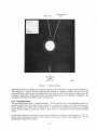
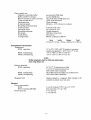
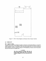
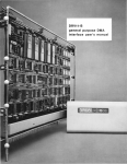
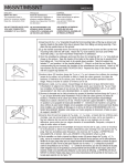
1.3 PHYSICAL DESCRIPTION
Each RXVII Floppy Disk System consists of the following components:
RXO 1 Floppy Disk Drive
M7946 RXVII Interface Module
BC05L-15 Interface Cable
System components are shown in Figure I-I.
I-I
M7946
RXVII
INTERFACE
MODULE
BC05L-15
INTERFACE
JI (
CABLE)
RXOI
FLOPPY
DISK
DRIVE
11 - 349 1
Figure I-I
RXV II Floppy Disk System Components
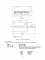
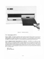
All RXOI subsystem components are housed in a 10-1 / 2 in. rack-mountable box. The box includes a
power sup pl y for all RXOI circuits and an appropriate ac power cable and plug. Interface between the
RXO I floppy disk drive and the RXVII interface module is provided by the standard length (15 ft) 40conductor BC05L-15 interface cable. Figure 1-2 is a front view of an RXOI dual floppy disk drive.
7408·1
Figure 1-2
Floppy Disk Drive (Front View)
A detailed description of the RXO I floppy disk drive is contained in the RXOI / RX8 / RXll Floppy Disk
System Maintenance Manual.
The RXV II interface circuits are contained on the M7946 module. This module measures 8-1 / 2 in. X
5 in. and requires one device location on the LSI-II I/ O bus.
1.4
FLOPPY DISK TECHNOLOGY
1.4.1 The Media
The media used for floppy disk data storage and retrieval is an industry-compatible "diskette" (floppy
disk) shown in Figure 1-3.
1-2
INDEX HOLE
REGISTRATION
HOLE
READ/WRITE
HEAD
APERTURE
Figure 1-3
7408-2
Diskette Media
The diskette media was designed by applying magnetic tape technology to magnetic disk architecture.
This resulted in a flexible oxide-on-mylar surface encased in a plastic envelope with a hole for the
read/ write head, a hole for the drive spindle hub, and a hole for the "hard" (physical) index mark. The
envelope is lined with a fiber material that cleans the diskette surface. The diskette is supplied to the
customer preformatted (in IBM format) and pretested.
1.4.2 Recording Scheme
The recording scheme used is "double frequency." In this method, data is recorded between bits of a
constant clock stream. The clock stream consists of a continuous pattern of one flux reversal every
four J.LS (Figure 1-4). A data "one" is indicated by an additional reversal between clocks (i.e., doubling
the bit stream frequency; hence the name) . A data "zero" is indicated by no flux reversal between
clocks.
A continuous stream of ones, shown in the bottom waveform in the figure, would appear as a "2F" bit
stream, and a continuous stream of zeros, shown in the top waveform, would appear as a "I F" or
fundamental frequency bit stream.
1-3
ALL ZEROS
PATTERN
0
0
0
0
0
0
0
0
0
0
0
0
0
CHANGING
PATTERN
0
0
0
0
0
0
0
ALL ONES
PATTERN
I
I
I
I
I
I
~ 41'sec
l.-
CF'-150&
I
Figure 1-4
Flux Reversal Patterns
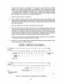
1.4.3 Recording Format
The recording format of the RXVll Floppy Disk System is industry-compatible. Data is recorded on
only one side of the diskette. This surface is divided into 77 concentric circles or "tracks" numbered
0-76. Each track is divided into 26 sectors numbered 1-26 (Figure 1-5). Each sector contains two
major fields: the header field and the data field (Figure 1-6).
LL,E,D, TRANSDUCER OUTPUT
r--H':":A-=R~D'---1
1
I'~I- - - . . . I
'~2~~
PRE-INDEX
SECTOR
GAP
.26 fo320BYTES
. . --------------~II
.,
SECTOR
SECTOR
.2
SECTOR
.3
SECTOR
.4
II
J
T
CP~leC7
SOFT INDEX MARK
1 BYTE
_
ROTATION
Figure 1-5
Track Format (Each Track)
HEADER FIELD
DATA FIELD
~
~
I
i:0
l>l>
-H
Ill'
ADDRESS
MARK
SYNC
FI ELD
ALL "O'S"
33 BYTES
-<!='
-<l>
"'0
0
ill
UI
UI
1--,
~'
L
-<l>
-<(')
"'''l>
0
0
:u
"
UI
UI
:u
...j
--<
1ll:U
l>
i:
\
I
\
-
~~
.
-<UI
'"
-
-UI
III
Ill'"
-<(')
-<eI
"':u
l>
0
0
:u
~~
•
.
-< 0_
-<UI
'"
HEADER
CRC
2 BYTES
DATA MARK
SYNC FIELD
ALL "o's"
17 BYTES
'"
'"
UI
UI
BYTE
11 BYTES-+I.O-----I_I
-0
Ill:u
-<
-<0
",m
r
-<
0
0
l>
-<
l>
12B,0 BYTES
OF DATA
'"
'"
DATA
CRC
2 BYTES
j.-6 BYTES
~
WRITE GATE TURN OFF
FOR WRITE OF PRECEED1NG
DATA FIELD
WR ITE GATE TURN ON
lFORWRITE OF NEXT
DATA FIELD
-
Figure 1-6
ROTATION
Sector Format (Each Sector)
1-4
CP-1508
1.4.3.1 Header Description - The header field is broken into seven bytes (eight bits/byte) of inform ation and is preceded by a field of zeros for synchronization.
1.
Byte No.1: ID Address Mark - This is a unique stream of flux reversals (not a string of
data bits) that is decoded by the controller to identify the beginning of the header field.
2.
Byte No.2: Track Address - This is the absolute (0-1148) binary track address. Each
sector contains track address information to identify its location on 1 of the 77 tracks.
3.
Byte No.3 - Zeros (one byte)
4.
Byte No.4: Sector Address - This is the absolute binary sector address (1-328). Each
sector contains sector address information to identify its circumferential position on a track.
5.
Byte Nos. 6 and 7: CRC - This is the Cyclic Redundancy Check character that is calculated for each sector from the first five header bytes using a polynomial division algorithm
designed to detect the types of failures most likely to occur with "double frequency" recorded data and the floppy media.
1.4.3.2 Data Field Description - The data field is broken into 131 bytes of information and is preceded by a field of zeros for synchronization and the header field (Figure 1-6).
1.
Byte No.1: Data or Deleted Data Address Mark - This is a unique string of flux reversals
(not a string of data bits) that is decoded by the controller to identify the beginning of the
data field. The deleted data mark is not used during normal operation, but the RX01 can
identify and write deleted data marks under program control, as required. The deleted data
mark is only included in the RXVII system to be IBM-compatible. One or the other data
address marks precedes each data field.
2.
Byte Nos. 2-129 - These bytes comprise the data field used to store 128 8-bit bytes of
information.
NOTE
Partial data fields are not recorded.
3.
Byte Nos. 130 and 131 - These bytes comprise the C RC character that is calculated for each
sector from the first 129 data field bytes, using the industry-standard polynomial division
algorithm designed to detect the types of failures most likely to occur in double-frequency
recording on the floppy media.
1.4.3.3 Track Usage - The RXOI is capable of recording any system structure through the use of
special systems programs, but normal operation will make use of all the available tracks as data tracks.
Any special file structures must be accomplished through user software.
1.4.3.4 CRC Capability - Each sector has a two-byte header CRC character and a two-byte data
CRC character to ensure data integrity. The CRC characters are generated by the hardware during a
write operation and checked to ensure that all bits were read correctly during a read operation. The
CRC character is the same as that used in the IBM 3740 series of equipment. A complete description of
CRC generation and checking is presented in the RXOI / RX8/ RXll Floppy Disk System Maintenance
Manual.
1-5
1.5 CONFIGURATION
Option number designations are as follows:
RXVII-AA Single Drive System, liS V/60 Hz
RXVII-AC Single Drive System, 115 V/50 Hz
RXVII-AD Single Drive System, 230 V/50 Hz
RXVII-BA Dual Drive System, liS V/60 Hz
RXVII-BC Dual Drive System, liS V/50 Hz
RXVII-BD Dual Drive System, 230 V/50 Hz
NOTE
50 Hz versions are available in voltages of 105, 115,
220, and 240 Vac by field-pluggable conversion.
Refer to the RX01/RX8/RX11 Floppy Disk System
Maintenance Manual for complete input power modification details.
1.6 OPTIONS
Additional diskettes can be ordered using the following option numbers:
RXOIK-5 - Five formatted blank diskettes
RXOIK- 10 - Ten formatted blank diskettes
1.7
SPECIFICATIONS
System Reliability
Minimum number of revolutions per track
Seek error rate
Soft read error rate
Hard read error rate
I
I
I
I
million/media (head-loaded)
in 106 seeks
in 109 bits read
in 10 12 bits read
NOTE
The above error rates only apply to media that is
properly cared for. Seek error and soft read errors
are usually attributable to random effects in the
head/media interface, such as electrical noise, dirt,
or dust. Both are called "soft" errors if the error is
recoverable in ten additional tries or less. "Hard"
errors cannot be recovered. Seek error retries should
be preceded by an Initialize.
Drive Performance
Capacity (8-bit bytes)
Per diskette
Per track
Per sector
256,256 bytes
3,328 bytes
128 bytes
1-6
Data transfer rate
Diskette to controller buffer
Buffer to RXVII interface
RXVII interface to LSI-II I/O bus
Track-to-track-move
Head settle time
Rotational speed
Recording surfaces per disk
Tracks per disk
Sectors per track
Recording technique
Bit density
Track density
A verage access
4lLs/data bit (250K bps)
2lLs/bit (500K bps)
18ILs/8-bit byte «50K bytes/sec)
10 ms/track maximum
20 ms maximum
360 rpm -;- 2.5%; 166 ms/rev nominal
1
77 (0-76) or (0-1148)
26 (1-26) or (0-328)
Double frequency
3200 bpi at inner track
48 tracks/in.
488 ms, computed as follows:
Seek
Settle
Rotate
Total
(77 tks/2) X 10 ms + 20 ms + (166 ms/2) = 488 ms
Environmental Characteristics
Temperature
RXOl, operating
RXO 1, nonoperating
Media, nonoperating
15° to 32° C (59° to 90° F) ambient; maximum
temperature gradient = 20° F /hr (-6.7° C/hr)
-35° to +60° C (_30° to + 140° F)
-35° to +52° C (-30° to + 125° F)
NOTE
Media temperature must be within operating temperature range before use.
Relative humidity
RXOl, operating
RXO 1, nonoperating
Media, nonoperating
Magnetic field
Electrical
Power consumption
RXOI
RXVl1 interface (M7946)
Power input (ac)
25° C (77° F) maximum wet bulb
2° C (36° F) minimum dew point
20% to 80% relative humidity
5% to 98% relative humidity (no condensation)
10% to 80% relative humidity
Media exposed to a magnetic field strength of 50
oersteds or greater may lose data.
3 A at 24 V (dual), 75 W; 5 A at 5 V, 25 W
Not more than 1.5 A at 5 Vdc
4 A at 115 Vac
2 A at 230Vac
1-7
CHAPTER 2
INSTALLATION AND OPERATION
2.1 GENERAL
This chapter provides information on installing and operating the RXV11 Floppy Disk System. This
information includes:
Site Preparation - The planning required to make the installation site suitable for operation of the
floppy disk system, including space, cabling, power requirements, and fire and safety precautions.
Environmental Considerations - The specific environmental characteristics of the floppy disk system, including temperature, relative humidity, air conditioning and/or heat dissipation, and
cleanliness.
Installation - The actual step-by-step process of installing the floppy disk system from unpacking
through the preliminary installation checks, power conversion techniques, and acceptance
testing.
Operation - The recommended practices for using the floppy disk system, handling the media,
and shipping and storing the diskettes.
2.2
SITE PREPARATION
2.2.1 Space
The RX01 is a cabinet-mountable unit that may be installed in a standard Digital Equipment Corporation cabinet. This rack-mountable version is approximately 10-1/2 in. (28 cm) high, 19 in. (48 cm)
wide, and 16-1/2 in. (42 cm) deep (Figure 2-1).
Provision should be made for service clearances of approximately 22 in. (56 cm) at the front and rear of
the cabinet.
2.2.2 Cabling
The standard BC05L-15 interface cable provided with the RXVll is 15 ft (4.6 m) in length, therefore,
the positioning of the RX01 in relation to the backplane in which the RXV11 interface is to be installed
should be considered. The RX01 should be placed near the console terminal so that the operator will
have easy access to load or unload disks. The ac power cord is approximately 9 ft (2.7 m) long.
2-1
1
10.5"
11"1111 I ~I I ~llllllllllllllljli IIIIIIIIIIII! 1IIIIIIIIili
I·
19"
(48.:3 em)
J,ml
·1
(FRON T VI EW)
17.0"
(4:3.2 em)
r-~
--
~
---
~
L
(FRONT)
0
~
III
V S E E NOTE
~
---
~
~
~
(INSIDE TRACK
=
is)
~
26.5"
•
(66.:3 em)
SIDE VIEW)
NOTE
Dust cover attached to cabinet
not RXO 1.
Figure 2-1
CP-1611
RXOI Overall Dimensions
2.2.3 AC Power
The RXVII Floppy Disk System is available in three ac voltage/model configurations:
Models
RXVII-AA, -BA
RXVII-AC, -BC
RXVII-AD, -BD
Voltage /Frequency
100 - 132 Vac, 60 Hz
100 - 132 Vac, 50 Hz
180 - 264 Vac, 0 Hz, in one of two voltage ranges. The actual
voltage range is user-selected by installing the appropriate power harness during system installation, as follows:
Voltage
Range
180-240
200-264
2-2
Power Harness
Part Number
70-10696-04
70-10696-03
When installing the 180-264 Vac models, the user must select and install the proper power harness for
the power line voltage available, as listed above. The harness part number is stamped on jumper
connector PI. Install the selected power harness after unpacking the RXOl, but before installing it in a
cabinet. Proper power harness installation is shown in Figure 2-2. The longer set of wires from PI
terminate in P3; the shorter set of wires from PI terminate in P2.
Application of primary ac power is controlled by the system in which the RXO I is installed. The line
cord must normally be plugged into a "switched ac" receptacle which is part of the system's ac power
distribution system.
Figure 2-2
Power Harness Installation
2.2.4 Fire and Safety Precautions
The RXVII Floppy Disk System presents no additional fire or safety hazards to an existing computer
system. Wiring should be carefully checked, however, to ensure that the capacity is adequate for the
added load and for any contemplated expansion.
2.3
ENVIRONMENTAL CONSIDERATIONS
2.3.1 General
The RXVl1 is capable of efficient operation in computer environments; however, the parameters of
the operating environment must be determined by the most restrictive facets of the system, which in
this case are the diskettes.
2-3
2.3.2 Temperature, Relative Humidity
The operating ambient temperature range of the diskette is 59° to 90° F (15° to 32° C) with a maximum temperature gradient of 20° F /hr (-6.7° C/hr).
The diskette nonoperating temperature range (storage) is increased to _30° to 125° F (-34.4° to 51.6°
C);
CAUTION
Care must be taken to ensure that the diskette temperature has stabilized within the operating temperature range before use. This range will ensure that
the diskette will not be operated above its absolute
temperature limit of 125 degrees F.
The RXOI is designed to operate efficiently within a relative humidity range of 20 to 80 percent, with a
maximum wet bulb temperature of 77° F (25° C) and a maximum dew point of 36° F (2° C).
2.3.3. Heat Dissipation
The heat dissipation factor for the RXOI floppy disk drive is less than 225 Btu/hr.
2.3.4 Radiated Emissions
Sources of radiation, such as FM, vehicle ignitions, and radar transmitters located close to the computer system, may affect the performance of the RXVII Floppy Disk System because of the possible
adverse effects magnetic fields can have on diskettes. A magnetic field with an intensity of 50 oersteds
or greater might destroy all or some of the information recorded on the diskette.
2.3.5 Cleanliness
Although cleanliness is important in all facets of a computer system, it is particularly important in the
case of moving magnetic media, such as the diskettes used in the RXO 1. Diskettes are not a sealed unit
and are vulnerable to dirt. Minute obstructions, such as dust specks or fingerprint smudges, may cause
data errors. Hence, the RXOI should not be located in an unusually contaminated atmosphere, especially one with abrasive particles. (Refer to Paragraph 2.6.2.)
NOTE
Removable media involve use, handling, and maintenance which are beyond DIGITAL's direct control.
DIGIT AL disclaims responsibility for performance
of the equipment when operated with media not
meeting DIGITAL specifications or with media not
maintained in accordance with procedures approved
by DIGITAL. DIGITAL shall not be liable for damages to the equipment or to media resulting from
such operation.
2.4
INSTALLATION
2.4.1 General
The RXVl1 Floppy Disk System can be shipped installed in a cabinet as an integral part of a system,
or as a separate option packed in a separate container. If the RXO 1 is shipped in a cabinet, position the
cabinet in the final installation location and proceed with operation (Paragraph 2.5). The following
paragraphs contain detailed information for installing the RXV11 when it is received as a separate
option.
2-4
2.4.2 Tools
Installation of an RXVII Floppy Disk System requires no special tools or equipment. Normal hand
tools are all that are necessary.
2.4.3.
1.
RXOI Unpacking, Inspection, and Installation
Open the carton (Figure 2-3) and remove the corrugated packing pieces. Carefully store the
two diskettes (Paragraph 2.6.2) for use after installation. The RXVII interface module
(M7946) installation is described in Paragraph 2.4.4; carefully store the module until it is
installed.
SLIDES
ONE PIECE
FOLDER
PLYWOOD HOLD ING
FIXTURE RT. 51 DE
ONE PIECE
FOLDER
PLYWOOD HOLDING
FIX TURE LT. 5 I DE
FLAT WASHER (8)
RXOI
@:::=-
DUST
COVER
LOCK WASHER (8)
" S C R E W (8)
SCORED
SHEET
9905713
SLOTTED
SHIPPING
CARTON
II - 3917
Figure 2-3 RXO 1 Unpacking
2-5
2.
Lift the RX01 out of the carton.
3.
Remove the shipping fixtures from both sides of the RX01 and inspect for shipping damage.
NOTE
If any shipping damage is found, the customer should
notify the carrier of the damage.
4.
Attach the inside tracks of the chassis slides (Figure 2-1) to the RXOl.
5.
Locate the proper holes in the cabinet rails in which the RX01 is to be installed (Figure 2-4).
Attach the outside tracks to the cabinet rails.
o
o
COVER
SCREWS,
CHASS IS SLIDES
CP-1594
Figure 2-4
RX01 Cabinet Mounting Details
6.
Place the tracks attached to the RXO 1 inside the extended cabinet tracks and slide the unit' in
until the tracks lock in the extended position.
7.
Install the RX01 cover above the RX01 and secure it to the cabinet rails.
2.4.4
RXVll Interface Module Installation
l.
Loosen the screws securing the upper module (M7726) in the RXOI and swing it up on the
hinge.
2.
Inspect the wiring and connectors for proper routing and ensure that they are seated correctly (Figure 2-5). The BC05L-15 cable is secured to the RX01 by a clamp on the rear of the
unit. The red edge of the cable should be located on the left end of the connector at the
M7726, as shown in the figure.
2-6
.,
.
l
' Jj
•
"
~
.
I
te I
,
III
I•
"
IJ
I ! I ' I ~ '. .
'I
"'
4
.'
_
t
M7726
P
BC05L ·15
M7727
7436· 18
Figure 2-5
RXOI Cable Connections
3.
Route the BCOSL-IS cable to the backplane in which the RXVll interface module is to be
installed . Connect the cable to Jl on the interface module with the red stripe toward the
center of the module (pin A end of J 1).
4.
All RXVll interface modules are shipped with factory installed jumpers for the following
device register addresses:
RXCS = 177170
RXDB = 177172
2-7
Interrupt vector jumpers are installed for vector address = 264. The factory configured
jumpers will normally be used. However, in applications which require more than one
RXVll option, assign appropriate device register and interrupt vector addresses and install
or remove jumpers to configure the addresses as shown in Figure 2-6. Jumpers are located
on the M7946 as shown in Figure 2-7. A second RXV 11 option would normally be assigned
device addresses 177174 and 177176, and vector address 270.
.
5.
Ensure that system power is turned off.
6.
Insert the RXVl1 interface module into the desired option location in the backplane. Note
that the option location determines device priority, and that all option locations between the
M7946 module and the processor module must be occupied in order to maintain daisy-chain
grant signal continuity.
7.
Connect the RXOI ac power cord to a switched ac power source.
8.
Turn the system power on. Head movement occurs on the drives during the power up
initialize phase. The heads should move ten tracks toward the center and back to track O.
This motion can be heard in most (normal) sound environments. If desired, the motion can
be viewed. A pointer and scale for track/head position for each drive is located under the
M7727 module in the RXOI. The pointers are attached to the head load arm for each drive
(Figure 2-8), and the track scale for each pointer is located below the pointer.
The motion can be observed by raising the M7726 module to the position shown in Figure 25 and viewing from the rear edge of the M7727 module.
If the RXVll system is being initially operated (after installation), execute the RXVl1 diagnostic programs in the order listed below:
9.
MAINDEC-II-DZRXB RXll Interface Diagnostic
MAINDEC-I1-DZRXA RXl1 System Reliability Test
DEVICE
ADDRESS
JUMPER ON
M7946 MODULE _W17
I
FACTORYCONFIGURED _
ADDRESS
R
R
R
R
I
I
R
R
R
R
I
RXCS' 177170
RXDB' 177172
I
DAL BITS_15
VECTOR
ADDRESS
0
(IJ(IJ
07
I
0
:
0
:
0
I
0
:
0
:
0
I
0
JUMPER ON _
M7946 MODULE
NOTE:
I ' Jumper inslalled' Logical (IJ
R' Jumper removed' Logical 1
X, Don'l care
FACTORY-CONFIGURED _
VECTOR ADDRESS'264
0
:
I
I
W6
R
I
W5
I
I
I
W4
I
R
I
W3
I
R
I
W2
I
I
:
0
I
I
WI
I
R
11-3493
Figure 2-6
Device Register and Interrupt Vector Addressing
2-8
BC~!sL
INTERFACE
CABLE
~
I
J1
1
"---"Wl
-w.
_W2
.. ----4W3
.. ---4W4
_W1
_we
"'---"W6
"--~W9
"---"W10
"---"Wl1
"'---W12
"---"Wl!S
W13 ............... ---.. W16
W14"---", . . ---.. W17
Figure 2-7
2.5
RXV 11 Device Register and Interrupt Vector Jumper Locations
OPERA TION
2.5.1 Operator Control
The simplicity of the RXOI precludes the necessity of operator controls and indicators. A convenient
method of opening the unit for diskette insertion and removal is provided. On each drive there is a
simple pushbutton, which is compressed to allow the spring-loaded front cover to open. The diskette
may be inserted or removed, as shown in Figure 2-9, with the label up. The front cover will automatically lock when the bar is pushed down.
CAUTION
The drive(s) should not be opened while they are
being accessed because data may be incorrectly
recorded, resulting in a CRC error when the sector is
read.
2-9
TRACK/HEAD
POSITION POINTER
AND SCALE
7408-7
Figure 2-8
Track / Head Position Components
2-10
7408·6
Figure 2-9
2.5.2
Diskette Insertion
Bootstrapping the RXV 11
2.5.2.1
General - The RXVII bootstrap loader program loads the system monitor from disk into
system memory. No system operation can occur until the monitor is contained in system memory.
Bootstrapping ("booting") the system can be accomplished via a hardware-implemented bootstrap in
the REVII-A or REVII-C option, or it can be entered and executed via the console device .
2.5.2.2
Booting the System Using the REVll-A or REVll-C - The REVII-A or REVII-C implements the RXVII bootstrap (and other bootstrap programs) in four preprogrammed ROM chips.
When system power is applied, and LSI-II processor Mode 2 power-up sequence is configured on the
processor module, the system responds with a dollar sign ($) on a new line. The operator then responds
by typing the device to be bootstrapped. DX (or DXO) is disk drive 0; DX I is disk drive I in dual-drive
RXV II systems. A normal sequence of operations from power up through booting DXO (containing
RT-II) is shown below .
$DX <CR>
RT-IISJ V02C-XX
2-11
After executing the DXO bootstrap, the system responds by displaying the RT -11 (or other software
system) monitor in use (RT-11SJ or RT-IIFB) and the particular version in use (V02C-XX); the
version is changed as RT -II software changes are implemented. Finally, a dot is displayed on the next
line, indicating that the RT -11 Keyboard Monitor is ready to accept a command. The system is correctly booted and RT-II programs can be executed as desired. Diskettes containing system software
other than RT-11 are also booted using this procedure (e.g., RXDP diagnostic software).
2.5.2.3 Booting the System Via the Console I.>evice - When the REVII-A or REVII-C option is not
included in the system, the operator must enter a bootstrap program via the console device. Place the
processor in the Halt mode and proceed as shown below; observe that underlined characters are
printed by the processor and non-underlined characters are entered by the operator:
Abbreviated Version
(DRIVE 0 ONLY):
@1000/.Q.QQQQQ 5000 <LF>
~/QQQQQQ 12701 <LF>
~/QQQQQQ 177170 <LF>
QQ.1.Q.Q§/QQQQQQ 105711 <LF>
QQ1.Q.!Q/.QQQQQQ 177 6 < LF>
QQ.1.Q.1P.QQQQQQ 12711 <LF>
QQ.l.Q.ll/.QQQQQQ 3 <LF>
001016/0000005711 <LF>
22.!...QLOIQQQ.QQ9 177 6 < LF >
~/.QQQQQQ 100405 < LF>
001024/000000105711 <LF>
001026/QQQQQQ 100004 <LF>
~/~ 116120 <LF>
QQ.!...QE/QQQ.QQQ 2 <LF>
QQ1.Q~./.QQQQQQ 770 < LF >
~/.Q.QQ.QQQ 0 <LF>
QQ1.QiQ/QQQQQQ 5007 <CR>
Full Length Version
(DRIVE 0 or DRIVE 1):
..@:1000/Q.QQQQQ 12702 < LF>
~/QQ.QQQQ 1002n7 <LF> *
.Q.Q1..Q..Q.MlllOgQO 12701 < LF >
QQ.1.Q.Q§IQQQQQg 1771 70 < LF>
QQlQl.Q/QQ.QQQQ 130211 <LF>
QQ.1Q.1POOOOOO 1776 <LF>
~/QQ.QQQQ 112703 <LF>
.Q.Q.1.Q..!.!i/..QQQQQQ
7
< LF>
----
~/.Q2QQQQ
10100 <LF>
~/QQQQQ9 10220 <LF>
001024/000000402 <LF>
001026/00000012710 <LF>
00103010000001 <LF>
~2/..QQQQQQ 6203 <LF>
~/OOOOOO 103402 <LF>
~/.QQQQQQ 112711 <LF>
.QQ.1..Qi91000000 111023 <LF>
~/OOOOOO 30211 <LF>
~/2Q2Q.QQ 1776 <LF>
~/~ 100756 <LF>
0010501000000103766 <LF>
~/222QQ9 105711 <LF>
~/QQQQQ.Q 100771 < LF>
~/~ 5000 <LF>
001060100000022710 <LF>
----
-----
----
• n = 4 for Unit 0
n = 6 for Unit 1
< LF> = Line Feed
<CR> = Carriage Return
Starting address = 1000
----
~/~240<LF>
~/OOOOOO
1347 <LF>
Q.Q.1.Q.E§1000000 122702 < LF>
0010701000000247 <LF>
--QQ.1.Qll/QQ.QQQQ 5500 < LF>
QQ~/QQQQQQ 5007 <CR>
2-12
The bootstrap program can be started at location 1000. Enable the Run mode by placing the
HALT /ENABLE switch (on the PDP-li/03 panel, or an equivalent LSI-ll switch) in the ENABLE
position. Start the program using the Go command, as follows:
@lOOOG
After a few seconds the R T -11 (or other software system) monitor will be loaded in system memory.
The monitor will identify itself on the console device by typing a message, as previously described.
2.6 DISKETTE HANDLING PRACTICES AND PRECAUTIONS
2.6.1 General
To prolong diskette life and to prevent errors when recording or reading, reasonable care should be
taken when handling the media. The following handling recommendations should be followed to
prevent unnecessary loss of data or interruptions of system operation.
1.
Do not write on the envelope containing the diskette. Write any information on a label prior
to affixing it to the diskette.
2.
Paper clips should not be used on the diskette.
3.
Do not use writing instruments that leave flakes, such as lead or grease pencils, on the jacket
of the media.
4.
Do not touch the disk surface exposed in the diskette slot or index hole.
5.
Do not clean the disk in any manner.
6.
Keep the diskette away from magnets or tools that may have become magnetized. Any disk
exposed to a magnetic field may lose information.
7.
Do not expose the diskette to a heat source or sunlight.
8.
Always return the diskette to the envelope supplied with it to protect the disk from dust and
dirt. Diskettes not being used should be stored in a file box (user-supplied) if possible.
9.
When the diskette is in use, protect the empty envelope from liquids, dust, and metallic
materials.
10. Do not place heavy items on the diskette.
11. Do not store diskettes on top of computer cabinets or in places where dirt can be blown by
fans into the diskette interior.
12. If a diskette has been exposed to temperatures outside the operating range, allow five minutes for thermal stabilization before use. (The diskette must be removed from its shipping
container during this time.)
2-13
2.6.2 Diskette Storage
Store diskettes in their envelopes in horizontal stacks of ten diskettes or less. If vertical storage is
necessary, the diskettes should be supported so that they do not lean or sag, but should not be subjected to compressive forces. Permanent deformation may result from improper storage. Store diskettes in an environment similar to that of the operating system, within the operating environment
range specified in Paragraph 1.7. When diskettes do not need to be available for immediate use, they
should be stored within the specified nonoperating environment range of the media.
2.6.3 Shipping Diskettes
Diskettes (not originally packed with the RXOI) can be safely shipped in their original cartons. In
general, the diskettes must be protected from magnetic fields and excessive temperatures during shipment. Good protection from magnetic fields is provided by physical separation from the possible
source. If the original shipping carton is not used, pack diskettes with at least three inches of packing
material (or spacers) on both sides and along all edges. This separation will make special magnetic
shielding unnecessary.
A void exposure of the diskettes to excessive temperatures. Label the packages with the following
statement:
DO NOT EXPOSE TO PROLONGED HEAT OR SUNLIGHT
When received, the diskette carton should be examined for damage. Deformation of the carton may
indicate possible damage of the diskette(s). The shipping carton should be retained (if it is intact) for
diskette storage or for future shipping.
2-14
CHAPTER 3
PROGRAMMING THE RXVll
3.1 GENERAL
All software control of the RXVII is performed by means of two device registers: the RXVII Command and Status register (RXCS) and a multipurpose RXVII Data Buffer register (RXDB). These
registers can be read or loaded by programs using instructions referring to their device addresses. The
RXO 1 contains a read/write data buffer that can contain one full sector (128 8-bit bytes) of diskette
data. This buffer and other RXVll registers are located as shown in Figure 3-1. The program has
direct access to the RXCS and RXCB registers only. Access to registers and the read/write buffer in
the RXOI is via the RXDB.
Read and write data transfers always require two steps. When writing data, the program first fills the
buffer with write data via program transfers with the RXDB. Once the buffer is filled, the program
issues a write sector command via the RXCS and the buffer's contents are written onto the diskette.
During a read operation, the diskette data is first read into the buffer. The program then reads the data
via the RXDB.
RXOI FLOPPY DISK DRIVE
{
RXVII INTERFACE
FUNCTION
CODE
~
SELECTS
READ /
WRITE
FUNCTION
AND
REGISTER
OR
BUFFER
- 1+------+1
'I
H
(/)
...J
11-3923
Figure 3-1
RXVl1 System Register Functions
3-1
3.2 REGISTER AND VECTOR ADDRESSES
The RXCS register is normally assigned device address 177170, and the RXDB register is assigned
device address 177172. The vector address is 264.
REGISTER DESCRIPTION
3.3
3.3.1 RXCS - Command and Status (177170)
Loading this register while the RXO 1 is not busy and with bit 0 = 1 will initiate a function as described
below and indicated in Figure 3-2. Bits 0-4 are write-only bits.
15
14
13
II!
ERROR
12
10
II
09
08
~SED
'------N-OT"""'·
07
06
INT
ENB
INIT
04
DONE
TR
RX
05
03
02
01
FUNCTION
UNIT
SEL
~
000
001
010
011
100
101
110
111
00
GO
FILL BUFFER
EMPTY BUFFER
WRITE SECTOR
READ SECTOR
NOT USED
READ STATUS
WRITE DELETED
DATA SECTOR
READ ERROR
REGISTER
CP- 2248
Figure
~-2
RXCS Format
Bit No.
Description
o
Go - Initiates a command to RXO 1. This is a write-only bit.
1-3
Function Select - These bits code one of the eight possible functions described in Paragraph 3.4. These are write-only bits.
4
Unit Select - This bit selects one of the two possible disks for execution of the desired
function. This is a write-only bit.
5
Done - This bit indicates the completion of a function. Done will generate an interrupt
when asserted if Interrupt Enable (RXCS bit 6) is set. This is a read-only bit.
6
Interrupt Enable - This bit is set by the program to enable an interrupt when the RXOI
has completed an operation (Done). The condition of this bit is normally determined at
the time a function is initiated. This bit is cleared by the LSI-II bus initialize (BINIT L)
signal, but it is not cleared by the RXVII Initialize bit (RXCS bit 14). This is a
read/write bit.
7
Transfer Request - This bit signifies that the RXV11 needs data or has data available.
This is a read-only bit.
8-13
Unused
3-2
Bit No.
Description
14
RXVII Initialize - This bit is set by the program to initialize the RXVl1 without
initializing all of the devices on the LSI-ll Bus. This is a write-only bit.
CAUTION
1.
Loading the lower byte of the RXCS will also
load the upper byte of the RXCS.
2.
Setting this bit (BIS instruction) will not clear
the interrupt enable bit (RXCS bit 06).
Upon setting this bit in the RXCS, the RXV11 will negate Done and move the head
position mechanism of drive 1 (if two are available) to track O. Upon completion of a
successful Initialize, the RXOI will zero the Error and Status register, set Initialize
Done, and set RXES bit 7 (DRV RDY) if unit 0 is ready. It will also read sector 1 of
track 1 on drive O.
15
Error - This bit is set by the RXOI to indicate that an error has occurred during an
attempt to execute a command. This read-only bit is cleared by the initiation of a new
command or by setting the Initialize bit. When an error is detected, the RXES is automatically read into the RXDB.
3.3.2 RXDB - Data Buffer Register (177172)
This RXOI interface register serves as a general purpose data path between the RXOI and the interface.
It may represent one of five RXOI registers according to the protocol of the command function in
progress (Paragraph 3.4). The RXOI registers include RXDB, RXTA, RXSA, RXES, and RXER.
This register is read/write if the RXOI is not in the process of executing a c,ommand; that is, it may be
manipulated without affecting the RXOI subsystem. If the RXOI is actively executing a command, this
register will only accept data if RXCS bit 7 (TR) is set. In addition, valid data can only be read when
TR is set.
CAUTION
Violation of protocol· in manipulation of this register
may cause permanent data loss.
3.3.2.1 RXDB - RX Data Buffer (Figure 3-3) - All information transferred to and from the floppy
media passes through this register and is addressable only under the protocol of the function in
progress.
15
14
13
11
12
10
09
07
08
06
05
I
J\
V
04
03
02
01
00
v
READ/WRITE DATA
NOT USED
CP-2247
Figure 3-3
RXDB Format
3-3
3.3.2.2 RXTA - RX Track Address (Figure 3-4) - This register is loaded to indicate on which of the
1148 tracks a given function is to operate. It can be addressed only under the protocol of the function in
progress. Bits 8 through 15 are unused and are ignored by the control.
15
14
13
11
12
10
09
07
08
06
05
04
03
02
01
00
0
I
J
~
~
0-1148
NOT USED
CP-1510
Figure 3-4
RXT A Format
3.3.2.3 RXSA - RX Sector Address (Figure 3-5) - This register is loaded to indicate on which of the
328 sectors a given function is to operate. I t can be addressed only under the protocol of the function in
progress. Bits 8 through 15 are unused and are ignored by the control.
15
14
13
12
11
10
09
08
07
06
05
0
I I
0
I
J
0
04
03
02
01
00
~
1-32 8
NOT USED
CP-151l
Figure 3-5
RXSA Format
3.3.2.4 RXES - RX Error and Status (Figure 3-6) - This register contains the current error and status
conditions of the drive selected by bit 4 (Unit Select) of the RXCS. This read-only register can be
addressed only under the protocol of the function in progress. The RXES is located in the RXD B upon
completion of a function.
15
14
13
12
11
10
09
07
06
DRV
ROY
DO
08
I
05
\
04
I
NOT USED
03
I
02
01
ID
PAR
00
I
CRC
I
j
NOT USED
CP -1513
Figure 3-6
RXES Format
3-4
RXES bit assignments are:
Bit No.
o
Description
CRC Error - A cyclic redundancy check error was detected as information was retrieved from a data field of the diskette. The RXES is moved to the RXDB, and Error and
Done are asserted.
Parity Error - A parity error was detected on command or on address information
being transferred to the RXOI from the LSI-II Bus interface. A parity error indication
means that there is a problem in the interface cable between the RXOI and the interface. Upon detection of a parity error, the current function is terminated; the RXES is
moved to the RXDB, and Error and Done are asserted.
2
Initialize Done - This bit is asserted in the RXES to indicate completion of the
Initialize routine, which can be caused by RXOI power failure, system power failure, or
programmable or LSI-ll Bus Initialize.
3-5
Unused
6
Deleted Data Detected - During data recovery, the identification mark preceding the
data field was decoded as a deleted data mark (Paragraph 1.4.3).
7
Drive Ready - This bit is asserted if the unit currently selected exists, is properly supplied with power, has a diskette installed correctly, has its door closed, and has a
diskette up to speed.
NOTE 1
The Drive Ready bit is only valid when retrieved via a
Read Status function or at completion of Initialize
when it indicates status of drive O.
NOTE 2
If the Error bit was set in the RX CS but Error bits
are not set in the RXES, then specific error conditions contained in the RXER can be accessed from
the RXDB via a Read Error Register function (Paragraph 3.4.7)
3.3.2.5 RXER - RX Error (Figure 3-7) - This register is located in the RXOI and contains specific
RXOI error information. This information is normally accessed when the RXCS error bit 15 is set but
RXES error bits 0 and 1 are not set. This is a read-only register.
3.4 FUNCTION CODES
Data storage and recovery on the RXVII system is accomplished by careful manipulation of the
RXCS and RXDB registers according to the strict protocol of individual functions. The penalty for
violation of protocol can be permanent data loss. Each of the functions are encoded and written into
RXCS bits 1-3, as shown in Figure 3-1. Programming protocol for each function is described below.
3-5
15
14
13
12
11
10
09
07
08
06
05
04
I
03
02
01
00
I
Jl
~------------~v~--------------~
NOT USED
V
I
CP-2246
/~------------------------------------------~
Octal Code
Error Code Meaning
0010
0020
0030
Drive 0 failed to see home on Initialize.
Drive 1 failed to see home on Initialize.
Found home when stepping out 10 tracks for INIT.
Tried to access a track greater than 77.
Home was found before desired track was reached.
Se1f-diagnostic error.
Desired sector could not be found after looking at 52 headers (2 revolutions).
More than 40 J1.S and no SEP clock seen.
A preamble could not be found.
Preamble found but no I/O mark found within allowable time span.
eRe error on what we thought was a header.
The header track address of a good header does not compare with the desired track.
Too many tries for an lOAM (identifies header).
Data AM not found in allotted time.
eRe error on reading the sector from the disk. No code appears in the ERREG.
All parity errors.
0040
0050
0060
0070
0110
0120
0130
0140
0150
0160
0170
0200
0210
Figure 3-7
RXER Format
3.4.1 Fill Buffer (000)
This function is used to fill the RXOI buffer with 128 8-bit bytes of data from the host processor. Fill
Buffer is a complete function in itself; the function ends when the buffer has been filled. The contents
of the buffer can be written onto the diskette by means of a subsequent Write Sector function, or the
contents can be returned to the host processor by an Empty Buffer function.
RXCS bit 4 (Unit Select) does not affect this function, since no diskette drive is involved. When the
command has been loaded, RXCS bit 5 (Done) is negated. When the TR bit is asserted, the first byte of
data may be loaded into the data buffer. The same TR cycle will occur as each byte of data is loaded.
The RXOI counts the bytes transferred; it will not accept less than 128 bytes and will ignore those,in
excess. Any read of the RXDB during the cycle of 128 transfers results in invalid read data.
3.4.2 Empty ButTer (001)
This function is used to empty the internal buffer of the 128 data bytes loaded from a previous Read
Sector or Fill Buffer command. This function will ignore RXCS bit 4 (U nit Select) and negate Done.
When TR sets, the program may unload the first of 128 data bytes from the RXDB. Then the RXVll
again negates TR. When TR resets, the second byte of data may be unloaded from the RXDB, which
again negates TR. Alternate checks on TR and data transfers from the RXDB continue until 128 bytes
of data have been moved from the RXDB. Done sets, ending the operation and initiating an interrupt
if RXCS bit 6 (Interrupt Enable) is set. RXES contents are moved to the RXDB where they can be
read.
NOTE
The Empty Buffer function does not destroy the contents of the sector buffer.
3-6
3.4.3 Write Sector (010)
This function is used to locate a desired track and sector and write the sector with the contents of the
internal sector buffer. The initiation of this function clears bits 0, 1, and 6 of RXES (CRC Error, Parity
Error, and Deleted Data Detected) and negates Done.
When TR is asserted, the program must first move the desired sector address into the RXDB, which
will negate TR. When TR is again asserted, the program must move the desired track address into the
RXDB, which will negate TR. If the desired track is not found, the RXVII will abort the operation,
move the contents of the RXES to the RXD B, set RXCS bit 15 (Error), assert Done, and initiate an
interrupt if RXCS bit 6 (Interrupt Enable) is set.
TR will remain negated while the RXOI attempts to locate the desired sector. If the RXOI is unable to
locate the desired sector within two diskette revolutions, the RXVII will abort the operation, move the
contents of the RXES to the RXDB, set RXCS bit 15 (Error), assert Done, and initiate an interrupt if
RXCS bit 6 (Interrupt Enable) is set.
If the desired sector is successfully located, the RXVII will write the 128 bytes stored in the internal
buffer followed by a 16-bit CRC character that is automatically calculated by the RXOI. The RXVII
ends the operation by asserting Done and initiating an interrupt if RXCS bit 6 (Interrupt Enable) is
set.
NOTE I
The contents of the sector buffer are not valid data
after a power loss has been detected by the RXOI.
The Write Sector function, however, will be accepted
as a valid function, and the random contents of the
buffer will be written, followed by a valid CRC.
NOTE 2
The Write Sector function does not destroy the contents of the sector buffer.
3.4.4 Read Sector (011)
This function is used to locate a desired track and sector and transfer the contents of the data field to
the ~CPU controller sector buffer. The initiation of this function clears bits 0, 1, and 6 of RXES (CRC
Error, Parity Error, Deleted Data Detected) and negates Done.
When TR is asserted, the program must first move the desired sector address into the RXDB, which
will negate TR. When TR is again asserted, the program must move the desired track address into the
RXD B, which will negate TR.
If the desired track is not found, the RXVII will abort the operation, move the contents of the RXES
to the RXDB, set RXCS bit 15 (Error), assert Done, and initiate an interrupt if RXCS bit 6 (Interrupt
Enable) is set.
TR and Done will remain negated while the RXOI attempts to locate the desired track and sector. If
the RXOI is unable to locate the desired sector within two diskette revolutions after locating the
presumably correct track, the RXVII will abort the operation, move the contents of the RXES to the
RXDB, set RXCS bit 15 (Error), assert Done, and initiate an interrupt if RXCS bit 6 (Interrupt
Enable) is set.
If the desired sector is successfully located, the control will attempt to locate a standard data address
mark or a deleted data address mark. If either mark is properly located, the control will read data from
the sector into the sector buffer.
3-7
If the deleted data address mark was detected, the control will assert RXES bit 6 (DD). As data enters
the sector buffer, a CRC is computed, based on the data field and CRC bytes previously recorded. A
non-zero residue indicates that a CRC error has occurred. The control sets RXES bit 0 (CRC Error)
and RXCS bit 15 (Error). The RXVl1 ends the operation by moving the contents of the RXES to the
RXDB, sets Done, and initiates an interrupt if RXCS bit 6 (Interrupt Enable) is set.
3.4.5 Read Status (101)
The RXVII will negate RXCS bit 5 (Done) and begin to assemble the current contents of the RXES
into the RXDB. RXES bit 7 (Drive Ready) will reflect the status of the drive selected by RXCS bit 4
(Unit Select) at the time the function was given. All other RXES bits will reflect the conditions created
by the last command. RXES may be sampled when RXCS bit 5 (Done) is again asserted. An interrupt
will occur if RXCS bit 6 (Interrupt Enable) is set. RXES bits are defined in Paragraph 3.3.2.4.
NOTE
The average time for this function is 250 ms. Excessive use of this function will result in substantially
reduced throughput.
3.4.6 Write Sector with Deleted Data (110)
This operation is identical to function 010 (Write Sector) with the exception that a deleted data address
mark precedes the data field instead of a standard data address mark (Paragraph 1.4.3.2).
3.4.7 Read Error Register Function (111)
The Read Error Register function can be used to retrieve explicit error information contained in the
RXER when the RXCS error bit 15 is set. The function is initiated, and bits 0-6 of the RXES are
cleared. Out is asserted and Done is negated. The controller then generates the appropriate number of
shift pulses to transfer the specific error code from the RXER to the Interface register and completes
the function by asserting Done. The RXD B program can then read the error code to determine the
type of failure that occurred (Figure 3-6).
NOTE
Care should be exercised in use the of this function
since, under certain conditions, erroneous error
information may result (Paragraph 3.6).
3.4.8 Power Fail
There is no actual function code associated with Power Fail. When the RXOI senses a loss of power, it
will unload the head and abort all controller action. All status signals are invalid while power is low.
When the RXOI senses the return of power, it will remove Done and begin a sequence to:
1.
Move drive 0 head position mechanism to track O.
2.
Clear any active error bits.
3.
Read sector 1 of track 1 of drive 0 into the sector buffer.
4.
Set RXES bit 2 (Initialize Done) (Paragraph 3.3.2.4) after which Done is again asserted.
5.
Set Drive Ready of the RXES according to the status of drive O.
3-8
There is no guarantee that information being written at the time of a power failure will be retrievable.
However, all other information on the diskette will remain unaltered.
A method of aborting a function is through the use of RXCS bit 14 (RXVII Initialize); however, this
will not clear the interrupt enable bit (RXCS bit 06). Another method is through the use of the system
Initialize signal that is generated by the PDP-II RESET instruction, the console ODT Go command,
or system power failure.
3.5 PROGRAMMING EXAMPLES
3.5.1 Read Data/Write Data
Figure 3-8 presents a program for implementing a Write, Write Deleted Data, or a Read function,
depending on the function code that is used. The first instructions set up the error retry counters,
PTRY, CTRY, and STRY. The instruction RETRY moves the command word for a Write, Write
Deleted Data, or Read into the RXCS.
The set of three instructions beginning at the label 1$ moves the sector address to the RXVl1 after
Transfer Request (TR), which is bit 7, has been set. The three instructions beginning at the label 2$
move the track address to the RXVII after TR has been set. The group of instructions beginning at the
label 3$ looks for the Done flag to set and checks for errors.
An error condition, indicated by bit 15 setting, is checked beginning at ERFLAG. If bit 0 is set, a CRC
error has occurred, and a branch is made to CRCER. If bit 1 is set, a parity error has occurred, and a
branch is made to PARER. If neither of the above bits is set, a seek error is assumed to have occurred
and a branch is made to SEEKER, where the system is initialized. In the case of a Write function, the
sector buffer is refilled by a JMP to FILLBUF. In the case of a Read function, a JMP is made to
EMPBUFF.
In each of the PAR, CRC, and SEEK routines, the command sequence is retried ten times by decrementing the respective retry counter. If an error persists after ten tries, it is a hard error. The retry
counters can be set up to retry as many times as desired.
NOTE
A Fill ButTer function is performed before a Write
function, and an Empty ButTer function is performed
after a Read function.
3.5.2 Empty ButTer Function
Figure 3-9 shows a program for implementing an Empty Buffer function. The first instruction sets the
number of error retries to ten. The address of the memory buffer is placed in register RO, and the
Empty Buffer command is placed in the RXCS. Existence of a parity error is checked starting at
instruction 3$. If a parity error is detected, the Empty Buffer command is loaded again. If an error
persists for ten retries, the error is considered hard.
If no error is indicated, the program looks for the Transfer Request (TR) flag to set. The Error flag is
retested if TR is not set. Once TR sets, a byte is moved from the RXVII sector buffer to the core
locations of BUFFER. The process continues until the sector buffer is empty and the Done bit is set.
3.5.3 Fill ButTer Function
Figure 3-10 presents a program to implement a Fill Buffer function. It is very similar to the Empty
Buffer example.
3-9
,ASS
,PROGRAMMING EXAMPLES FOR THE NXl1/RXI1 FLEXlBlt DISKETTE
1
,
,
2
3
ITHE FOLLOWING~ IS THE NX11 STANDARD DEVICE ADDRESS AND VECTON ADDRESS
4
5
177111
177172
177112
11111,
111112
6
7
8
9
1.
11
12
13
14
15
16
17
18
4'41
42
43
44
45
46
47
48
49
5.
51
52
54
55
56
57
58
59
68
61
62
63
64
65
66
118.,.
".106
•••• 14
UZ767
112767
U2767
17777.
17777.
177773
I.nz.
1"U4
111318
'-18.
.~~~0=N2~2C~~H~EmmTl
; mln,:~T;MmTER
, lEEK RETNY COUNTER
HOV
pTRV
MOV '-1'. CTRV
MOV
STRV
'-1.1.
,WRITE. WRITE DELETED DATA. oR RUD
I
,, II TI 4
,
,
,
,
, alT 4
I
THRU 1 0' PROGRAM ~oCA TI ON COMMAND OONT AI N THE 'UNCTI ON
1 MtANS UNIT
~1
<
I
•
MUNI UNIT "
, IITS 3 THRU 1 II THE COMMAND < 4 - WRITE. 14 - WRITE OELETED DATA. 6 - READ,
181122
016767
J.n86
17714,
RETRY I
MOV COMHAND. RXCS
UNIT. <WRITE. WRITE oELETlD DATA. OR READ)
I
,WAIT FOR THE TRANSFER REQUEST FLAC THEN TRANSFER THE tECTOR ADoNElI
'8113'
011134
111136
ln767
081 77'
116767
lSI
177U4
DJI214
117126
TSTI AXCS
lEO lS
Mova SECTOR. RXU
I
,
,
,WAIT rOR THE TRANSFtN REQUEST FLAC THEN TRANSrER THE TRACK ADOREII
ItlI44
115767
117120
.. II,.
81 •• 52
'8171,
116761
0.1262
211
111112
TSTI RXCS
BEQ 21
MOVI TRACK. RxTA
'THE SECTOR AND TRACK ADDRESSES HAVE IEEN TRANSFERRED TO THE RIll
I
,
,WSAIT rOR THE DoNE r~Aa AND CHECK FoR UY ERRoRS
,
,IF THE FUNCTION HAS COMPLETED .UCCEs"ULLY INc ERROR FLA;) THEN HALT
In.68
032167
11 •• 66
391714
8 •• 114
185761
081801
UII01
.,.11.
.,.116
117182
177174
3$1
mU~~1L T~~E DmEF~~~c .m
alT
IEQ
TST
INE
'OoNtilT. RXCS
3S
RXCS
ERFLAQ
HA~ T
ITHE ERROR r~AQ IS S[T
T
TEST rOR TWE ERROR 'LAC
INE I' AN ERROR HA' OCcUNEO
OK • COMPLETED
,
ITHE CONTENTS 0' THE RXES IS THE ERROR STATUI
; Ir THE RXES IITS 1 AND I I I THEN SOME TYPE OF SEEK ERROR oCCUREO
IIr THE RXES BIT. - 1 THEN A CRC ERNON HAl OCCUREO
Ilr THE RXES BIT 1 • 1 THEN A 'ARITV ENROR HAS oCCURED
n8118
n'116
13'11'
'88116
BlZ767
111414
'32767
8814'4
•• 8103
177.64
0"8'2
177"4
TEST FOR CRC AND PAR lTv EUORS
NOT A 'ARITV OR CRC CMUITl BE A lEEK
TEST rOR PAR lTV ERROR
NOT A 'ARITY ERRO·R tMUlTl IE A CRC
I
,IA PARI TV ERROR HAS oCCUREO
,
,
,
,INCREMENT AND TEIT THE PARITY ERROR RETRV COUNTER PROGRAM LOCATlDN " pTAY "
69
11
lAND RETRV THE· COMMAND "
UNTI~
THE PAR lTV ERROR NECOVER&
,
'OR UNTIL THE pTRV COUNTER OVU'LOWS To
"'12.
11.124
.,8126
un67
111336
......
~'82'2
INC pTRV
INE RETRV
HA~ T
RETRV THE COMMA NO
HARO PARITV tRRDR
,
,
; A CRC ERROR HAS OCCUNED
79
8.
81
82
83
84
85
86
87
88
89
START I
I
61
68
71
72
13
74
75
16
17
78
,
:~~E w~m?W~~1TlSD:Lt~~~R~~~!~G o~X:~:~E
,
A9'
OF mGRAM
'LOCATION lECTOR)
OF TRACK "T" ITME CONTENTS or 'NOGRAM LOCATION TUCK'
..
19
21
21
22
23
24
25
26
27
28
29
31
31
32
33
34
35
36
37
38
39
COMMA NO STATUS RUIITER
DATA IUFru REGIITER
lECTOR ADDNtsS RU I ITER
I TRAC~ ADDRESS REGISTER
ERROR ,TATUI REGISTER
RXCS-l111"
.RXDa1171111
RXSAll1111.
RxUll11111
RXEhl1111.
'INCREMENT AND TEIT THE CRC ERROR RETRY COUNTER PROGRAM LOCATI oN • CTRV "
,AND RETRV THE COMMAND UNTIL THE CRC UROR RECOVERI
I
'OR UNTIl. THE CTRV COUNTER OVERFLOWI To •
I
18'13'
011134
"'136
,nZ67
0U332
'IIIDI
CRC.
INC cnv
aNt RETRV
HA~ T
I THE ERROR rLAG IS SET
•• ,174
RETRV THE COMMAND
J!AG CRC E_ROR
92
93
94
95
96
,
,
,
97
, <STATE OF RXCS BITS I ANO 1 ARE
8)
SEEK'
INITIALIIE
91
98
99
18'
111
112
103
,THE ERROR IS tNoll A PARITY UROR AND II tNOTl A CRC ERROR
'THEREFORE IT MUSTSE
,
"114'
012767
'48"0
187
1,8
1.9
MOV 'INlT. Rxas
I
,
,
IINCREMENT AND TEST THE SEEK ERROR RETRY COUNTER PRoaRAM ~OCATION • STRV "
'AND RETRY THE COMMAND UNTI L THE SEEK ERNoR RECoVERS
184
185
106
177122
SEEK ERROR
: DR UNTIL THE CTRV COUNTER OVUF~OWI TO •
eal146
"'152
"'154
•• 5267
,.1323
18811.
.8816.
INC STRV
INE RETRY
HA~ T
RtTRY THE OOMMAND
HARD lEEK ERROR
Figure 3-8 Write/Write Deleted Data/Read Example
3-10
;THE
16~
I EMpTY
163
164
165
166
167
168
169
170
171
172
173
174
175
176
177
178
179
180
181
182
183
184
185
186
187
188
189
190
191
192
193
194
195
196
197
198
199
200
21111
202
203
204
206
207
208
209
210
11100242
0U2S0
000254
J12767
31270~
~16767
or
0~J0H2
176706
or
tXAMP~t
REQUIRED TO
P~OTOCO~
128 8-BIT BYTES
J
177770
0~0054
IS A PROGRA~MING
SECTOR BUrrER
T~E
e TRYS TO EMpTY THE lECTOR BUF'F'£R
PROHGRAMS OATA BUF'F't~
ISSUE THE COMMANC
EENTRYI MOV .-10, pTRY
ESETUP I MOV .aurF'ER, RI1I
MOV COMMAND, Rxes
I
;WAIT rOR A
,
TRANS~ER
REgUEST
BErORE TRANSrERRING DATA TO THE PROGRAMS
r~AG
10ATA BUrF'tR rRoN THE RX0l SECTOR BurrER
,
IWAIT rOR A DONE
TO INDICATE THE
r~AG
0' THE EMPTY BUrrER COMMAND
eoMp~ETloN
J
JPRIOR TO TESTIN G THE ERROR
J
000262
000266
~00270
0~0276
BIT .DONESIT, RXCS
BEQ
JTHE DONE
,
E~OOP
r~AG
IS SET
;TEST roR ANY [RRORS
00"67
001001
000000
TEST rOR T~ANS,ER REQUEST r~'G
INE I, TRA~srER REQUEST r~AG IS SET
TEST rCR DONE ,~4G
aEO UNTI~ THE DONE '.AG lETS
BNt EMPTy
176672
I
000300
000304
000306
r~AG
TSTB Rxes
E~OOPI
10"67
001014
032767
001771
(ON~Y
ERROR
HA~T
I INcrEMENT AND TEST THE PARITY
J
lAND RETRY THE CoMMANU
UNTI~
E~ROR RET~Y
lOR
~~0316
UNTI~
;
1$:
00'267
001355
000000
THE prRY CUNTER
P.OGRAM
"
~OCATION
TO
OVERr~ows
INC PTRY
SNE ESE:!UP
RETRY TO E~PTY THE
PARI TV ERROR
J
r~AG
"
m
BurrER
SECTO~
~ARC
HA~T
;THE TRANsrER REaUEST
~TRY
THE ERROR RECoVERS
I
0003U
000314
IS A PARITY ERROR)
POSSIB~E
TST RXCS
BNE 1$
176664
I
Is sET
I
JTRANsrER DATA TO THE PHOGRAM
,
116730
000756
176646
EMPTY I
ITHE
000000
~00330
0~0000
000332
030000
rD~~OWING
J
PROGRAM
CTRy;
STRY:
J
~OCATION
JPROGRAM
J
~OCATIONS
ARt
JWRITE (4), WRITE
" COMMAND" CONTAINS
DE~ETEO
J
CATA (14),
; 4,
COMMAND I
J
JPROGRAM
,
I
JPROGRAM
,
T~E
T~E
JPROGRAM
E.ROR RETRY COUNTERS
O~
COMMAND TO BE ISSUED VIA TME
~EAD
(6),
OR
EMPTY
BurrER
(2)
14, 6, OR 2 • (GO BIT 1 • 1)
• SECTOR" CONTAINS THE SECTOR AOORESS (1 TO 32
~OCATION
• TRACK" CONTAINS
OCTA~)
; 1 TO 32 OCTA~
T~E
TRACK ADDRESS (I TO 114
111
J
000040
040000
000342
000542
000001
TME RXll SECTOR BurrER
~OCATION
SECTOR: 111
,
r~OM
; PARITY ERROR RETRY COUNTER
; CRe ERROR ~ETRy COUNTER
; SEEK E~ROR RETRY COUNTER
~TRy:
TRACK I
DATA BUrrER
MOve RxDS, '(RI1I).
SR E~OOP
J
000326
211
212
213
214
215
216
217
218
219
220
221
222
223
224
225
226
227
228
229
230
231
232
rO~~OWING
,
161
162
EaUIVA~ENTS
DONEBI,"40
INIT.402U
BUrrER- •
•• BurrER+ZI1l0
.ENO
Figure 3-9
Empty Buffer Example
3-11
OCTA~)
~co
lOT
;THE
111
112
113
114
115
119
12e
121
;
08~156
~12767
aee164
00J170
01270e
016767
117773
000342
~00140
eJe142
176712
;WAIT 'O~ A DONE fLAT To INDICATE THE COMPLETioN
e00176
0011202
001204
0311212
10,767
001414
"~2767
001771
0~0040
LOO~I
1767'6
TSTB Rxes
BEQ riLL
BIT #DONEBIT. RXCS
BEQ
THE rlL~ BVrrER COMMAND
TEST FOR T'ANsrER REQUEST rLAG
IEQ ,r TRANSFER REQUEST FLAG SET
TtST FOR TWE OON~ r~AG
ItQ UNTIL THE DONE 'LAC StTS
~OOP
I
ITEST foR ANY [RRORS
~00214
000221
01111222
00,767
116150
(ON~Y
ERRoR POSSIBLE IS A pARITY ERROR)
I
TST Rxes
aNt 1$
HALT
0Ulllllll
1111111111110111
; NO ERRORS - OK -
COM~LETE
IINCREMENT AND TEST THE PARITY ERROR RETRY PROGRAM
~OCATION
I
I
.
lAND RETRY THE COMMANO
lOR
UNTI~
UNTI~
THE PTRY CoUNTER
•
~TRY
"
TME ERRoR RECOVERS
OVERf~OWS
To I
I
0111111224
00111239
11101232
0111'267
0013"
00011100
111111011176
lS:
152
I
154
I
INC PTRY
BNt SETUP
HALT
; RETRV TO 'I~~ THE SECTOR BUrfER
; WARD PARITY ERROR
ITHE TRANsrER REQUEST
153
r~AG
IS SET
ITRANSFER DATA FROM THE PROGRAMS DATA BurrER TO THE RXIIl1 SECTOR BUrrER
155
157
158
or
ITHE DONE rLAG IS SET
146
147
156
THE PROGRAMS
I
176766
143
144
145
150
151
r~oM
;
137
138
148
IErOR[ TRANSfERRING DATA
I
136
149
'~AG
:PRIOR To TESTING THE ERROR fLAG
134
135
141
REQUIRED TO
;OATA BurrER To THE RX01 SECTOR BurrER
126
142
T~E PRoToeo~
I
127
128
139
14e
or
TRVS TO rl~~ THE SECTOR BurrER
; 'ROGRAMS DATA BurrER
; ISSUE THE COMMAND
IWAIT 'OR A TRANSfER REQUEST
123
124
125
13e
131
132
133
EXAM~~E
; e
'ENTRY: MOV #-le. PTRY
SETUP I MOV #BufrER. R0
MOV COMMAND. RXCS
I
122
129
IS A ~HOGRA~MING
THE SECTOR aUfftR WITH 12. a-sIT BVTES
I NOTE: THE DATA To rl~~ THE SteTo~ Bur'ER CAN BE ASSEMB~[O IN CORE IN TWE
I
EVEN AOORtSSES SVTES or 1~8 WO~D' OR IN BOTH BVTES or 64 WORDS
116
117
118
fO~~OWING
I
Ifl~L
I
001234
1II11H124 III
113067
000756
116732
I
,ILL:
MOva '(R0) •• Rxoa
BR LOOP
Figure 3-10
;
PROGRA~S
DATA au,r.R IS 64 WORDS IN LENGTH
Fill Buffer Example
3.6 RESTRICTIONS AND PROGRAMMING PITFALLS
A set of restrictions and programming pitfalls for the RXVII is presented below.
1.
Depending on how much data handling is done by the program between sectors, the minimum interleave of two sectors may be used, but to be safe a three-sector interleave is
recommended.
2.
If an error occurs and the program executes a Read Error Register function (111), a parity
error may occur for that command. The error status would not be for the error in which the
Read Error Register function was originally required.
3.
The DRV SEL RDY bit is present only at the time of a Read Status function (101) for both
drives, and after an Initialize, depending on the status of drive O.
4.
It is not required to load the Drive Select bit into the RXCS when the command is Fill
Buffer (000) or Empty Buffer (010).
5.
Sector Addressing: 1-26 (No sector 0)
Track Addressing: 0-76
3-12
6.
A power failure causing the recalibration of the drives will result in a Done condition, the
same as finishing the reading of a sector. However, during a power failure, RXES bit 2
(Initialize Done) will set. Checking this bit will indicate a power fail condition.
7.
Excessive usage of the Read Status function (l01) will result in drastically decreased
throughput, because a Read Status function requires between one and two diskette revolutions or about 250 ms to complete.
3.7 ERROR RECOVERY
There are two error indications given by the RXVII system. The Read Status function (Paragraph
3.4.5) will assemble the current contents of the RXES (Paragraph 3.3.2.4), which can be sampled to
determine errors. The Read Error Register function (Paragraph 3.4.7) can also be used to retrieve
explicit error information from the RXER.
A list of error codes associated with the RXER is shown in Figure 3-7.
NOTE
A Read Status function is not necessary ifthe DRV
RDY bit is not going to be interrogated, because the
RXES is in the Interface register at the completion
of every function.
3-13
CHAPTER 4
TECHNICAL DESCRIPTION
4.1 GENERAL
This chapter contains a description of the hardware comprising the RXVII Floppy Disk System. An
overall system block description covers all hardware components in the RXVl1 option. A detailed
description is included for the RXVl1 interface module only. Refer to the RXOI / RX8 / RXll Floppy
Disk System Maintenance Manual for detailed descriptions of hardware contained in the RXOI floppy
disk drive.
4.2 RXVll SYSTEM BLOCK DIAGRAM
The RXVl1 Floppy Disk System consists of four elements (Figure 4-1):
1.
Drive mechanics, which includes actuators and transducers (up to two per controller).
2.
Read/write electronics, which interfaces drive mechanics to the ILCPU controller.
3.
ILCPU controller, which includes all control logic.
4.
RXVll interface, which interfaces the LSI-II I/O bus to the RXOI.
I~--------------~-I
RX01 FLOPPY DISK DRIVE
I
I
I
I
I
I
DRIVE
READ/WRITE
ELECTRON ICS
DISK DRIVE
INTERFACE
BC05L-15
INTERFACE
CABLE
j£CPU
CONTROLLER
RXVII
INTERFACE
(M7946)
l
I
_ _ _ _ _ _ _ _ _ _ _ _ _ _ _ _ _ ,-1
11-3812
Figure 4-1
RXVII System Block Diagram
4-1
There are three levels of data transmission in the floppy disk system (Figure 4-1):
1.
The LSI-ll I/O bus for data transmission between the RXVll interface module and the
LSI-II processor module.
2.
The RXOI data bus for data transmission between the RXOI JLCPU controller and the
RXVll interface module (BC05L-15 interface cable).
3.
The disk drive interface for data and control information transmission between the
read/write electronics and the RXOI JLCPU controller.
In addition to the data transmission signals, analog signals between the read/write electronics and
mechanical drive control head motion and sense diskette speed and position.
4.3 RXOl/M7946 INTERFACE SIGNALS
Connector Jl on the RXVII interface module (M7946) provides the interface for the following RXOI
signals:
RX INIT L
The RXOI responds to RX INIT L by negating DONE L and moving the head position mechanism of
both drives (if two are available) to track zero. The RXOI will also read sector 1 of track one of drive
zero and then assert RX DONE L (without error) to indicate successful completion of the Initialize
function.
RX DONE L
The RXOI asserts RX DONE L to indicate that no RXOI function is in progress. Initiating any
function will cause RX DONE L to go false for the duration of that function. Attempting to initiate
any function other than Initialize while RX DONE L is false is illegal and may result in an error.
RX RUN L
The RXVII interface asserts RX RUN L to initiate command or data transfers between the interface
module and the RXOI JLCPU controller. If asserted when RX DONE L is asserted, the byte transferred
from the RXVII interface module to the RXOI is treated as a command. If asserted while RX DONE
L is negated, a command is being executed and the byte transferred is considered to be read or write
data, sector or track address, or error and status information.
RX OUT L
The RXOI JLCPU controller controls this signal to inform the RXVl1 interface module of the direction
in which it is prepared to transfer a byte. When asserted (low), the direction of serial data transmission
is from the RXOI to the RXVII interface module. When not asserted (high), serial data transmissio·n is
from the RXVll interface module to the RXOI. RX OUT L is never asserted when RX DONE L is
asserted; when RX DONE L is asserted, the transfer is a command byte from the RXVII interface
module to the RXOI. RX INIT L, when asserted, causes RX OUT L to become negated.
RX TRANS REQ L
RX TRANS REQ L, used with RX RUN Land RX OUT L signals, comprise the basic control signal
interface between the RXOI and the RXVll interface module. The RXOI asserts this signal after
receiving a new command to indicate that it is ready to receive an address or data byte, or it i~ ready to
output an error status byte or data to the RXVll interface. Note that this signal is not asserted to
initiate a command byte; it is asserted by the RXOI to request transfer of each non-command byte
during the execution of a command.
4-2
RX DATA L
RX DATA L is the bidirectional serial data line over which all command and data bytes are
transferred.
RX SHIFf L
RX SHIFT L is a series of pulses generated by the RXOI which serially shift commands and data into
or out of the RXVII interface module. Pulse width is 200 ns (nominal); pulses occur at I J.LS intervals
(nominal).
RX ERROR L
The RXOI asserts this signal when an error is detected. An error results in the RXOI sending RXES
information to the RXVII interface and aborting the present operation; RX DONE L is then asserted.
This signal is cleared either by the RXVII interface asserting RX INIT L or by sending a new command to the RXOl.
8/12 BITS L
Not used in RXVII systems; terminated in RXOl.
4.4
INTERFACE MODULE LOGIC FUNCTIONS
4.4.1 General
RXVII Interface logic functions are contained on a single 5 X 8.5 X 0.5 in. module. The module can
be installed in any option location in the LSI-II bus-structured backplane. All command and data
transfers between the LSI-II processor and the RXVII are executed under program control via this
module. Figure 4-2 is a block diagram illustrating the logic functions which comprise the M7946
module.
The M7946 interfaces with the LSI-II bus via bus receivers, bus drivers, and bus transceivers.
4.4.2 Address Decoding Logic
Address decoding occurs on the leading edge of BSYNC L assertion. SYNC H clocks address decoding logic to produce an active or passive ME H signal. The ME H signal is a result of comparing DAL
REC 2-12 H bits to the address configured on address jumpers W7-W17 at SYNC H time. When the
RXVll's address is decoded, ME H goes active, enabling an RXVII/LSI-li bus data or command
transfer. Note that address bit DAL REC 1 H is applied to I/O control logic; this bit is used in
selecting either Command/Status (CS) or Data Buffer (DB) data transfers.
4.4.3 I/O Control Logic
I/O control logic circuits control the actual command, status, or read/write data transfer between the
LSI-II Bus and the addressed RXVII register. Control signals CS H and DB H are generated by this
logic function in response to address bit DAL REC 1 H to select either the RXCS or RXDB register.
The actual signal sequence for LSI-II Bus cycle operations involving this function are as described in
the LSI-ll, PDP-ll /03 User's Manual, Chapter 3.
4.4.4 RX Data Buffer (RXDB) Register
The RXDB is the main command/data interface function on the M7946 module. It is an 8-bit parallel
load, parallel read shift register. Parallel load occurs during DATa bus cycle execution; RX BUSY H
loads command or write data bits present on DAL REC 0-7 H into the shift register. BSHIFT L pulses
then serially shift the command or data byte bits out of RXD B bit D07 L, and into the serial bus
interface and parity logic. Serial command/data and parity bits are then shifted to the RXOI via the
bidirectional RX DATA L signal.
4-3
BDALO L
DAL REC 0-7 H
BDAL 1 L
BDAL2 L
C
l>
ENABLE DAL L
r
/1.----------1 ::0
T DAL 0-7H
,,..__________
-1
BDAL4 L
IT!
0
1---.....,
1-__.....,
R X DATA
BUFFER
REGISTER
(RXDB)
N
BDAL5 L
~
BDAL6 L
:I:
BDAL7 L
ADDRESS
JUMPERS
W7-W17
BOALS L
BDAL9 L
SYNC
H
Jl
ADDRESS
JUMPERS
Wl-W6
ADDRESS
DECODING
LOGIC
BDAL10 L
BDAL 11 L
DAL RECS-12H
BDAL 12 L
BS7 REC H
BBS7 L
BSYNC L
SYNC H
CS H
DB H
DATO H
~~----------------~-'MEH
ERROR
H
DIN H
'~~~~~~~--~D~A~L~RE~C~ILH~____________~DALREC
BRPL Y L
...
6 H
BWTBT L
VECTOR H.
VECTOR L
DONE H
I/O
CONTROL
LOGIC
AE2
BDOUT L
AH2
BDIN L
BV2
BDAL1 5 L
BIRQ L
BIAKO L
AL2
BIRQ L
AM2
BIAKI L
AN2
BIAKO L
INTERRUPT CONTROL
LOGIC
~
BOA L 14 L
INT ENB
(1) H
TO/FROM
RXOI
FLOPPY
DISK
DRIVE
____________________________________________~R~X~I~N~IT~L~__-+~~N
B j....!::.BU~2=--____---<0I
BDMGIL~
BDMGOL~
+5
GND
D
D
AA2. BA2
II
+5V
AC2. AJ1. AM1.ATI
BC2. BJI. BMI. BTl
11-3826
Figure 4-2 RXV 11 Interface Module
(M7946) Logic Block Diagram
4-4
During a data read operation, the process is reversed. RXOI serial data bits are received via the RX
DATA L signal, serial bus interface and parity logic, and shifted into the RXDB via SER DATA H.
Once the data byte is available, aDATI bus cycle can be initiated. Parallel read data bits DO-7 L are
gated through input data select logic and routed over TDAL 0-7 H to bus transceivers which place the
read data onto BDAL 0-7 L.
4.4.5 RX Command/Status (RXCS) Register
The RXCS function is actually not a register. It is a group of command/status bits which are programaccessible via a register address. Only ten of the sixteen RXCS bits are used. Six are write-only bits,
three are read-only bits, and one is a read/write bit. During a RXCS read operation, CS H and READ
CS H go high, enabling the status of ERROR H, TR, INT ENB (1) H, and DONE bits onto BDAL 15
L, BDAL 7 L, BDAL 6 L, and BDAL 5 L, respectively. Note that input data select logic routes bits 5,
6, and 7 as during the RXDB read operation.
During a RXCS write operation, either a command (contained in RXCS bits 1-3) is being transmitted
to the RX01, interrupts are being enabled or disabled (RXCS bit 6 set or reset), or the RXVII is being
initialized (RXCS bit 14 is set). RXCS bit 0 (Go bit) is a logical 1 during a RXCS write operation when
a command transfer is being executed. This causes the RXDB to parallel-load the command byte and
serially transmit it to the RX01, as previously described for a data write operation. When RXCS bit 0
is a logical 0 during a RXCS write operation, the command bits are not transmitted to the RXOI.
Instead, the RXV11 is either being initialized (RXCS bit 14 = 1) or the INT ENB (RXCS bit 6) bit is
being set or reset.
4.4.6 RXOI Status and Control Signal Interface Logic
RXOI status and control signal interface logic is the control interface between the RXOI and the
RXVII interface logic. All control and timing signals required for command or status transfers
between the RXVII interface and the RXOI directly involve this logic function. TR, DONE, and
ERROR RXCS signals are produced by this logic function.
4.4.7 Interrupt Control Logic
The interrupt control logic function contains the Interrupt Enable flip-flop (RXCS bit 6). When set,
the circuit requests interrupt service when the DONE H signal goes active. The interrupt sequence is
initiated by the logic when it asserts BIRQ L. The processor responds by asserting BIAKI Land BDIN
L, causing VECTOR H and VECTOR L to go to their respective active states. VECTOR Hand
VECTOR L cause input data select logic to enable the vector address, configured by jumpers WI-W6,
onto the BDAL bus. The actual sequence of operations for interrupt operation is described in the LSI11, PDP-11/03 User's Manual, Chapter 3.
4.4.8 Initialize Logic
Initialize logic is activated whenever a DATO cycle is executed with the RXCS and BDAL 14 L is
asserted. This is equivalent to writing a logical 1 into RXCS bit 14. The logic responds by generating
an active RX INIT L signal (pulse) which initializes the RXOI floppy disk drive. RX INIT L only
remains active for the duration of the bus cycle.
4-5
I
I
I
I
I
I
I
I
I
Reader's Comments
RXVll USER'S MANUAL
EK-RXVII-0P-002
Your comments and suggestions will help us in our continuous effort to improve the quality and usefulness of
our publications.
What is your general reaction to this manual? In your judgment is it complete, accurate, well organized, well
written, etc.? Is it easy to use?
What features are most useful?
-----------------------------------------
I..LJ
I~
What faults do you find with the manual?
lI-
I~o
I~
rI
;:J
I
I
I
I
I
I
Does this manual satisfy the need you think it was intended to satisfy?
Does it satisfy your needs? _ _ _ _ _ _ _ _ __
Why'! ________________'--_________
Would you please indicate any factual errors you have found.
Pkase describe your position.
N"m~
Organization
Street _ _ _ _ _ _ _ _ _ _ _ _ _ _ _ _ _ _ Department
City _ _ _ _ _ _ _ _ __
State _ _ _ _ _ _ _ _ _ _ __
Zip or Country
-
-
-
-
-
-
-
-
-- -- -- -
-
-
-
-
-
-
-
Fold Here -
-
-
Do NotTear-Fold Here and Staple -
-
-
-
-
-
-
-
-
-
-
-
-- ---
FIRST CLASS
PERMIT NO. 33
MAYNARD, MASS.
BUSINESS REPLY MAIL
NO POSTAGE STAMP NECESSARY IF MAILED IN THE UNITED STATES
l'uNlage will be paid by:
Digital Equipmcnt Corporation
Technical DOCUIlll'ntatioll Department
146 Main StH'C!
M:lynard. MasS:lchusetts 01754
-