1
EK -DHQ 11-UG.002
DHQ11
User Guide
Prepared by Educational Services
of
Digital Equipment Corporation
Second Edition, July 1987
Copyright © 1987 by Digital Equipment Corporation
All Rights Reserved
Printed in U.S.A.
The information in this document is subject to change without
notice. Digital Equipment Corporation assumes no
responsibility for any errors herein.
The following
Corporation:
mmDDmr
are
trademarks
of
Digital
Equipment
M
DEC
DECmate
DECsystem-IO
DECSYSTEM-20
DECUS
DECwriter
DIBOL
FALCON
MASSBUS
PDP
RT-l1
UNIBUS
PIOS
VAX
VAXBI
Professional
Rainbow
RSTS
RSX
VMS
VT
Work Processor
CONTENTS
PREFACE
CHAPTER 1
INTRODUCTION
1.1
1.2
1.2.1
1.2.1.1
1.2.1.2
1.2.1.3
1.2.1.4
1.2.2
1.2.2.1
1.2.2.2
1.2.3
1.2.4
1.2.5
1.3
1.3.1
1.3.2
1.3.2.1
1.3.3
1.3.3.1
1.3.3.2
1.4
1.4.1
1.4.2
1.4.3
1.4.4
1.5
1.5.1
1.5.2
1.5.3
1.5.4
SCOPE.................................................................
OVERVIEW ...........................................................
General Description ................................................
Modem Control Facility .......................................
Self-Test Facility ..............................................
Diagnostic Programs ..........................................
Preventing Data Loss .........................................
Physical Description ...............................................
On-Board Switchpacks ........................................
Communications Standard .....................................
Versions Of The DHQl1 ...........................................
Configurations ......
Connections .......................................................
SPECIFICATIONS ............................................ ... . . . . . . .
Environmental Conditions ..........................................
Electrical Requirements ............. ~.. . . . . . . ..... . . . . . . .. . .. . . . .. .
Q-bus Loads..................................................
Performance .......................................................
Data Rates ...................................................
Throughput ...................................................
SERIAL INTERFACES................................................
Interface Standards ................................................
Line Receivers .....................................................
Line Transmitters ..................................................
Speed And Distance Considerations .............. . . . . . . . . . . . . . . . . . .
FUNCTIONAL DESCRIPTION.. . . . . . . . . . . . . . .. . .. . . . . . . . . . . . . . . . . . . . .
General ............................................................
Main Functions ....................................................
Control Chip ......................................................
OCTART Chip ....................................................
CHAPTER 2
INSTALLATION
2.1
2.2
2.3
2.3.1
2.3.2
2.3.3
SCOPE.................................................................
UNPACKING AND INSPECTION ....................................
PREPARING THE DHQll MODULE ........ ..... ....................
Address And Vector Assignment....................................
Setting The Address Switches.......................................
Setting The Vector Switches ..... "..................................
DHVl1 Or DHUl1 Programming Mode Selection ..................
BUS CONTINUITY ...... . . . . . . . . . . . . . . . . . . . . . . . . . . . . . . . . . . . . . . . . . . . . .
Bus Grant Continuity Jumpers .....................................
2.3.4
2.4
2.4.1
Ie. •
•
•• •• •
iii
•
•
•
•
•
•
•
•
•
•
•
•
•
•
•
•
•
•
•
•
•
•
•
•
•
•
•
•
•
•
•
•
•
•
•
•
•
•
1-1
1-1
1-1
1-2
1-2
1-2
1-2
1-2
1-3
1-3
1-4
1-5
1-7
1-8
1-8
1-9
1-9
1-9
1-9
1-9
1-10
1-10
1-11
1-11
1-11
1-13
1-13
1-13
1-13
1-14
2-1
2-1
2-3
2-3
2-3
2-5
2-6
2-6
2-7
2.5
2.5.1
2.5.2
2.5.3
2.6
2.6.1
2.6.2
2.6.3
2.6.4
2.7
2.7.1
2.7.2
2.8
2.9
2.9.1
2.9.2
2.9.3
2.10
PRIORITY SELECTION ...............................................
DMA Request Priority .............................................
Interrupt Request Priority ......... "................................
Recommendations .................................................
INSTALLING THE DHQI 1 ............................................
Installing The M3 107 Module ......................................
Distribution Panels .................................................
Installing The EIA-232-D Distribution Panels .......................
Installing The DEC423 Distribution Panels .........................
INSTALLATION TESTING ............................................
Installation Tests On MicroPDP-l1 Systems .........................
Testing In Micro VAX II Systems ...................................
H3101 LOOPBACK CONNECTOR ....................................
CABLES AND CONNECTORS - EIA-232-D ..........................
Distribution Panel .................................................
Null Modem Cables....... .... .............................. .......
Full Modem Cables ................................................
CABLES AND CONNECTORS - DEC423 ............................
CHAPTER 3
PROGRAMMING
3.1
3.2
3.2.1
3.2.2
3.2.2.1
3.2.2.2
3.2.2.3
3.2.2.4
3.2.2.5
3.2.2.6
3.2.2.7
3.2.2.8
3.2.2.9
3.2.2.10
3.2.2.11
3.2.2.12
3.3
3.3.1
3.3.2
3.3.3
3.3.3.1
3.3.3.2
3.3.3.3
3.3.4
3.3.5
3.3.6
3.3.6.1
3.3.6.2
3.3.6.3
3.3.6.4
3.3.7
SCOPE.................................................................
REGISTERS.................................... ........................
Register Access ..................................... .. . . . . . . . . . . . . . .
Register Bit Definitions ............................................
Control And Status Register (CSR) ............................
Receive Buffer (RBUF) ........................................
Transmit Character Register (TXCHAR) .......................
Receive Timer Register (RXTIMER), DHU11 Mode Only ......
Line-Parameter Register (LPR) .................. , ....... ,.....
Line-Status Register (STAT) ............ ,......................
FIFO Size Register (FIFOSIZE), DHUll Mode Only ..........
FIFO Data Register (FIFODATA), DHUll Mode Only ........
Line-Control Register (LNCTRL) ..... ,.......................
Transmit Buffer Address Register Number 1 (TBUFFAD1) ,....
Transmit Buffer Address Register Number 2 (TBUFFAD2) .....
Transmit DMA Buffer Counter (TBUFFCT) .,.,...............
PROGRAMMING FEATURES .. , ............ ,........................
Initialization ., ........................ , ........ , .......... , .. ,.....
Configuration .................. , .................... ,..............
Transmitting ................ , ..... , ........ ,.......................
DMA Transfers ...............................................
Programmed I/O (DHV11 Mode) ..............................
Programmed I/O (DHU11 Mode) ..............................
Receiving ..........................................................
Interrupt Control ............ , ... , ........ , .......... ,.............
Auto XON And XOFF ............................................
IAUTO ...................... , ....... ,., ... , ..... ,............
FORCE.XOFF ........ '.' . , . . . . . . . . . . . . . . . . . . . . . . . . . . . . . . . . . . .
OAUTO ..................... , .......... ............... .......
DISAB.XRPT ........................ , ... , ..... ,.............
Error Indication .............................. "."................
iv
2-8
2-8
2-8
2-8
2-8
2-8
2-11
2-11
2-11
2-12
2-12
2-13
2-13
2-15
2-15
2-18
2-19
2-20
3-1
3-1
3-1
3-3
3-3
3-6
3-8
3-8
3-9
3-12
3-14
3-14
3-15
3-19
3-19
3-20
3-22
3-22
3-23
3-23
3-23
3-24
3-24
3-24
3-25
3-25
3-26
3-26
3-26
3-27
3-27
3.3.8
3.3.9
3.3.10
3.3.10.1
3.3.10.2
3.3.10.3
3.3.10.4
3.4
3.4.1
3.4.2
3.4.3
3.4.3.1
3.4.3.2
3.4.3.3
3.4.3.4
3.4.4
3.4.5
3.4.6
Modem Control ...................................................
Maintenance Programming .........................................
Diagnostic Codes ..................................................
Self-Test Diagnostic Codes .....................................
Interpretation Of Self-Test Codes' ..............................
Skipping Self-Test .............................................
Background Monitor Program (BMP) ..........................
PROGRAMMING EXAMPLES......................... ...............
Resetting The DHQ11 .......................... ~...................
.Configuration ......................................................
Transmitting ....................
Single-Character Programmed Transfer (DHU11 Mode) ........
Single-Character Programmed Transfer (DHV11 Mode) .........
DMA Transfer................................................
Aborting A Transmission ......................
Receiving ...
Auto XON And XOFF ....................................
Checking Diagnostic Codes ....
CHAPTER 4
TROUBLESHOOTING
4.1
4.2
4.3
4.4
4.4.1
4.4.2
4.5
4.5.1
4.5.1.1
4.6
4.6.1
4.7
SCOPE.................................................................
PREVENTIVE MAINTENANCE ......................
TROUBLESHOOTING PROCEDURES .................
o.
INTERNAL DIAGNOSTICS ......
Self-Test ......................................
Background Monitor Program (BMP) ...
MicroPDP-ll DIAGNOSTICS .....
User-Mode Diagnostics .......................... 0.................
Running User-Mode Tests .....................................
MicroVAX II DIAGNOSTICS ..........................................
User-Mode Tests .....................................
FIELD-REPLACEABLE UNITS (FRUs) ...............................
APPENDIX A
MODEM CONTROL
A.1
A.2
A.2.1
SCOPE ....... o.........................................................
MODEM CONTROL ..................................................
Example Of Auto-Answer Modem Control For The PSTN ..........
APPENDIX B
FLOATING ADDRESSES
B.1
B.2
FLOATING DEVICE ADDRESSES ....................................
FLOATING VECTORS ................................................
APPENDIX C
AUTOMATIC FLOW CONTROL
C.I
C.2
C.3
C.3.1
C.3.2
OVERVIEW ...........................................................
CONTROL OF TRANSMITIED DATA................................
CONTROL OF RECEIVED DATA .....................................
Flow Control By The Level Of The Receive FIFO ..................
Flow Control By Program Initiation ................................
0
••••
0
••••••••
0
••••••
0
•••••••••••••
0
0
•••••••••••••••
0
•••••••••••••
0
0
••
0.............
••
0
••••••••••
0
0
••••••••
0
••••••••••••
0
0
0
v
•••••••••••••••••
•••••••••
:
•
..
••
0
•
..
0
•
•
•
..
•••••••••••••
•••
0
0
0
0
••••
0
••••
0
o.
••••••••••••
•
0
•••••••
0
0
•
•
•
•
•
•
•
0
••
0
••••••••
0
0
•
•
•
•
•
•
•
0
•
•
•
•
•
•
•
•
•
•
•
•
•
•
•
•
•
•
•
•
•
•
•
•
•
•
0
•
•
•
•
•
•
•
•
•
•
•
•
•
•
•
•
•
•
•
•
•
•
•
•
•
•
0
•
•
•
•
•
•
•
•
•
•
•
•
•
3-27
3-28
3-28
3-28
3-28
3-29
3-30
3-31
3-31
3-32
3-33
3-33
3-34
3-35
3-36
3-37
3-39
3-41
4-1
4-1
4-1
4-2
4-2
4-3
4-3
4-3
4-3
4-3
4-4
4-5
A-I
A-I
A-2
B-1
B-3
C-l
C-l
C-2
C-2
C-4
C.3.3
Mixing The Two Types Of Received-Data Flow Control
APPENDIX D
GLOSSARY OF TERMS
D.l
D.2
SCOPE.................................................................
GLOSSARY ...........................................................
APPENDIX E
DHQII Q-BUS CONNECTIONS
C-5
D-l
D-I
FIGURES
Figure No.
Title
Page
1-1
1-2
1-3
1-4
1-5
2-1
2-2
2-3
2-4
2-5
2-6
2-7
2-8
2-9
2-10
2-11
3-1
4-1
C-I
C-2
C-3
Layout of the DHQIl Module ..........................................
Example of a DHQII Configuration.....................................
DHQll Connections (EIA-232-D) .......................................
DHQII Connections (DEC423) .........................................
DHQII Functional Block Diagram......................................
Location of Switchpacks ................................................
Setting the Device Address ..............................................
Setting the Vector Address ..............................................
Bus Grant Continuity ...................................................
Installing the DHQII (EIA-232-D) ......................................
Installing the DHQIl (DEC423) .........................................
I/O Insert Panels and Adapter Plate (EIA-232-D) ........................
I/O Insert Panel (DEC423) ..............................................
H31 01 Loopback Connector ............................................
H3173-A Circuit Diagram ...............................................
Null Modem Cable Connections.........................................
Register Coding ........................................................
Troubleshooting DEC423 Installations ...................................
Transmitted Data Flow Control .........................................
Receive FIFO-Level Flow Control .......................................
Program-Initiated Flow Control .........................................
1-4
1-6
1-7
1-8
1-15
2-4
2-5
2-6
2-7
2-10
2-10
2-11
2-12
2-14
2-16
2-19
3-3
4-2
C-2
C-3
C-4
TABLES
Table No.
Title
Page
I-I
EIA/CCIIT Signal Relationships ........................................
Maximum Distance Guidelines for DHQ 11 ..............................
DHQ II Options ........................................................
H3I73-A Connections ...................................................
Serial-Line Connections for the 36-Pin Connector ........................
DHQl1 Registers in DRVll Mode......................................
DHQl1 Registers in DRU11 Mode ......................................
Data Rates .............................................................
DHQ II Self-Test Error Codes ...........................................
Modem Control Leads ..................................................
Floating Device Address Assignments .... . .. . . . . . . . . . .. . . . . . . . . . . . . . . . . .
Floating Vector Address Assignments ....................................
DHQII Q-Bus Connections .............................................
1-10
1-12
2-2
2-17
2-20
3-2
3-2
3-11
3-28
A-I
B-1
B-3
E-l
1-2
2-1
2-2
2-3
3-1
3-2
3-3
3-4
A-I
B-1
B-2
E-I
vi
PREFACE
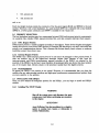
The DHQ 11 User Guide provides reference information on physical layout, system configuration,
installation and testing, programming characteristics, and maintenance. There is a glossary of technical
terms generally used in DIGITAL technical manuals. The manual is divided into four chapters as
follows:
CHAPTER 1 INTRODUCTION. This chapter gives a physical description of the DHQII, explains
how it can be configured, and explains how it interfaces with the system bus and serial data lines.
CHAPTER 2 INSTALLATION. Chapter 2 describes how to install a DHQII option, with detailed
information on device and vector address selection, backplane positioning, cables and connectors, and
testing after installation.
CHAPTER 3 PROGRAMMING. This chapter describes the DHQll registers. Some programming
examples are also included.
CHAPTER 4 TROUBLESHOOTING. Chapter 4 explains maintenance strategy, and how to use
diagnostic programs to locate a faulty module.
APPENDICES. These include additional information on topics discussed in this manual:
APPENDIX
APPENDIX
APPENDIX
APPENDIX
APPENDIX
A
B
C
D
E
MODEM CONTROL
FLOATING ADDRESSES
AUTOMATIC FLOW CONTROL
GLOSSARY OF TERMS
DHQll BUS CONNECTIONS
This revision of the manual contains new information. The DHQ 11 can operate in two different modes,
making it compatible with software drivers written for either the DHVII or the DHUll. Revision -001
of this manual contained information on DHVII mode of operation only.
vii
CHAPTER 1
INTRODUCTION
1.1 SCOPE
This chapter gives an overview of the DHQ 11 asynchronous multiplexer, describes the features that it
offers, and defines its physical parameters and electrical requirements.
1.2
OVERVIEW
1.2.1 General Description
The DHQII option is a serial-line interface which provides eight full-duplex serial data channels on
Q-bus systems. The DHQ 11 option consists of a single Q-bus module, and one of two groups of cabinet
kits, depending on the communication standard supported. The cabinet kits contain the cabinet
bulkhead panels and connecting cables.
The main application of the DHQll is for interactive terminal handling; it can also be used for data
concentration and real-time processing. It has two programming modes, DHVII and DHUII. The
register sets in these modes are compatible with those of the DHVII and DHUII respectively. The
preferred mode of operation is DHU 11 mode. The main features of the DHQ 11 are:
•
Eight full-duplex asynchronous data channels
•
For transmission: DMA transfers; or for each line, program transfers to a I-character
transmit buffer in DHVll mode, or to a 64-character transmit FIFO in DHUII mode
•
F or receive: a 256-entry FIFO buffer for received characters, dataset status changes, and
diagnostic information
•
It supports EIA-232-D/V.28 or DEC423, with the appropriate cabinet kit.
NOTE
DEC423 is a term used in this manual to indicate a
data-Ieads-ooly implementation of the RS-423-A
electrical standard. DEC423 uses MMJ connectors
instead of the 37-way connectors specified by R8-449.
•
It is compatible with all DIGITAL DHVll and DHUII device drivers
•
It can auto-answer on a switched line
•
The transmit and receive baud rates for each line can be individually programmed
•
It has a total module throughput of 60,000 characters per second, using 8-bit characters, with
all channels operating at 38.4 kbaud for both character reception and transmission
1-1
•
The DHQll supports 16-, 18-, or 22-bit addressing, including block-mode data transfer with
suitable memories
•
The DHQ11 can be programmed to filter XONjXOFF characters from the received data flow
•
Self-test and background monitor testing
•
Dual-height module, M3107
•
Switchpacks for selecting the Q-bus base address, vecto.r address and DHVl1 or DHUll
programming mode.
All other functions are selected by program.
1.2.1.1 Modem Control Facility - All eight channels have sufficient modem control to allow
auto-answer dial-up operation over the public switched telephone network using suitable modems, such
as DIGITAL's DF124, or Bell models 103, 113,212. Equivalent modems from other manufacturers can
also be used. The DHQl1 is designed to minimize software requirements for modem link control.
Appendix A gives further information on modem control. Modem control can be used for driving
modems over both public and private lines. Please note. that, in some countries, modems must be
approved by the PIT for that country for connection to the public network.
1.2.1.2 Self-Test Facility - The DHQII incorporates self-test sequencers which operate
independently of the host. The resu.lt of the self-test is provided to the host system through the receive
FIFO buffer. A green LED indicates GOINO-GO status for the device. More details are given in Section
4.3.
1.2.1.3 Diagnostic Programs - A full range of diagnostic programs is available. These run under the
MicroPDP-ll diagnostic supervisor or MicroVAX II maintenance system. Loopback test connectors
are not needed when running the user-mode diagnostics. Service-mode diagnostics and loopback
connectors are available from DIGITAL.
1.2.1.4 Preventing Data Loss - The DHQII can be programmed for automatic XON and XOFF
operation, to prevent the loss of data at high throughput. The reporting of received XONjXOFF
characters to the software driver can be enabled or disabled.
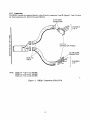
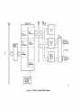
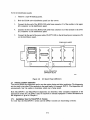
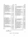
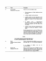
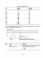
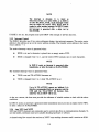
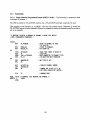
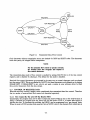
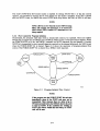
1.2.2 Physical Description
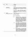
The DHQl1 is an M3107 dual-height Q-bus module. It is 21.6 em (8.51 inches) long and 13.2 em (5.19
inches) wide. Figure 1-1 shows the layout. Connectors A and B are for the Q-bus, while connectors JI
and 12 interface to the communications lines via BC05L-xx cables and distribution panels. Two
distribution panels are supplied with an EIA-232-D option, and a single panel is supplied with a
DEC423 option. Connector 13 provides power to the active distribution panel supplied with DEC423
options. This connector is not used with EIA-232-D options. Mixed use, that is, one EIA-232-D and one
DEC423 panel connected to a single module, is not supported by DIGITAL.
1-2
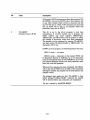
1.2.2.1 On-Board Switchpacks - The DHQ11 has two on-board switchpacks to select the following
functions.
•
Switchpack E-19 (10-position)
Switch 1 selects DHVII programming mode when closed, or DHUll programming mode
when open.
Switches 2 to 10 select the device address.
•
Switchpack E-l1 (8-position)
Switch 1 enables the on-board oscillator. This is a manufacturing test switch, and is closed for
normal operation.
Switch 2 selects manufacturing self-test mode. This is a manufacturing test switch, and is open
for normal operation.
Switches 3 to 8 select the device vector address.
Chapter 2 gives further information about these switchpacks.
1.2.2.2 Communications Standard - The serial drivers on the M3107 module are compatible with
EIA-232-D. However, the CK-DHQII-W cabinet kits provide level conversion for DEC423.
1-3
J2 CONNECTOR
POWER
CONNECTOR
CHANNELS 4 - 7
FUSE
J1 CONNECTOR
CHANNELS 0 - 3
ADDRESS
II
10 POSITION
SWITCH PACK
CONTROL
CHIP
VECTOR
8 POSITION
SWITCH PACK
RE3200
Figure I-I
Layout of the DHQII Module
1.2.3 Versions Of The DHQl1
The DHQII-M option consists of the M3107 Q-bus module and the User Guide. It can be used with one
of six cabinet kits. The choice of kit depends on the type of system cabinet, and on whether a EIA-232-D
or a DEC423 communication interface is needed.
The cabinet kits available for use with the DHQII-M are:
1-4
EIA-232-D
•
CK-DHQll-AA for BA123/BAI1-M boxes
•
CK-DHQI1-AB for BA23 boxes
•
CK-DHQI1-AF for H9642 cabinets
DEC423
•
CK-DHQII-WA for BAI23/BA11-M boxes
•
CK-DHQII-WB for BA23 boxes
•
CK-DHQII-WF for H9642 cabinets
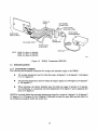
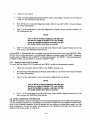
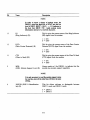
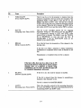
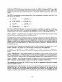
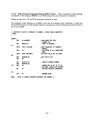
1.2.4 Configurations
The DHQl1 can be used in many different system configurations. Figure 1-2 shows a typical EIA-232-D
application.
1-5
DEVICE
HOST
PROCESSOR
DEVICE
Q-BUS
LOCAL
EQUIPMENT
DHQ11
LOCAL
TERMINAL-
EIGHT
DATA
CHANNELS
MODEM
MODEM
MODEM
MODEM
MODEM
MODEM
TELEPHONE
OR DATA COMMS
LINES
ANY
14--" ASYNCHRONOUS
DEVICE
EIGHT
REMOTE
EQUIPMENT
REMOTE
TERMINAL
DATA CHANNELS,--_---I.... REMOTE
TERMINAL
REMOTE
DHQ11 OR
DHV11
Q-BUS
~--------------------------------------------------~
REMOTE
PROCESSOR
RE1703
Figure 1-2
Example of a DHQll Configuration
1-6
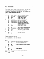
1.2.5 Connections
The DHQll module is connected directly to the Q-bus by connectors A and B. Figures 1-3 and 1-4 show
the interconnections for EIA-232-D and DEC423.
}
CHANNELS
OTO 3
H3173-A
DISTRIBUTION PANELS
CHANNELS
4TO 7
NOTE:
BC05L-01 = 30 em (12 INCHES)
BC05L-1 K = 53 em (21 INCHES)
BC05L-03 = 92 em (36 INCHES)
RE3
Figure 1-3
DHQl1 Connections (EIA-232-D)
1-7
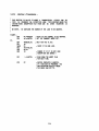
H3100 ACTIVE
BULKHEAD PANEL
BACKPLANE
(Q22/LSI BUS)
COLOURED STRIP
\
POWER CABLE
70-2277S-XX
NOTE:
BCOSL-01 = 30cm (12 INCHES)
BCOSL-1 K=S3cm (21 INCHES)
BCOSL-03=92cm (36 INCHES)
RE320'
Figure 1-4
1.3
DHQII Connections (DEC423)
SPECIFICATIONS
1.3.1 Environmental Conditions
The following environmental constraints for storage and operation apply to the DHQ 11.
•
The storage temperature must be within the range -40 degrees C to 66 degrees C (-40 degrees
F to 151 degrees F).
•
The operating temperature must be within the range 5 degrees C to 60 degrees C (41 degrees F
to 140 degrees F).
•
When operating, the relative humidity must be within the range 10 percent to 95 percent,
non-condensing, at a maximum wet-bulb temperature of 32 degrees C and a minimum dew
point of 2 degrees C.
DIGITAL nonnally defines the operating temperature range for a system as 5 degrees C to 50 degrees C
(41 degrees F to 122 degrees F); the 10 degrees C difference between the upper limits quoted allows for
the temperature gradient within the system box.
1-8
The maximum operating temperatures must be derated by 1.8 degrees C/I000 m above sea level (1
degree F/IOOO ft) for operation at high-altitude sites.
1.3.2 Electrical Requirements
The DHQl1 needs the following electrical supplies.
•
For EIA-232-D options: 5 volts dc plus or minus 5 percent at 1.7 A maximum current, 1.4 A
typical
•
For DEC423 options: 5 volts dc plus or minus 5 percent at 2.2 A maximum current, 1.9 A
typical
•
For EIA-232-D and DEC423 options: 12 volts dc plus or minus 5 percent at 300 mA
maximum, 230 rnA typical
An on-board switched-mode power supply generates a -10 V supply for the serial-line drivers.
1.3.2.1
Q-bus Loads - The loads applied to the Q-bus are:
•
3.2 ac loads
•
0.5 dc.loads
1.3.3
Performance
1.3.3.1 Data Rates - Each channel can be separately programmed to operate at one of 16 speeds (in
bits/s):
50
75
110
134.5
150
300
600
1200
1800
2000
2400
4800
7200
9600
19200
38400
NOTE
See also Section
1.4.4 (Speed and Distance
Considerations).
Chapter 3 contains further information on data rates for EIA-232-D.
1.3.3.2 Throughput - Each channel is capable of full-duplex operation at the maximum data rate. The
following maximum throughput is obtainable:
•
•
At 7 bits per character, with 1 start bit, 1 stop bit, and 1 parity bit, the throughput is 61440
characters per second.
At 5 bits per character, with 1 start bit, 1 stop bit, and no parity, the throughput is 87771
characters per second.
1-9
This throughput may be limited by your driver software.
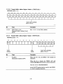
1.4 SERIAL INTERFACES
1.4.1 Interface Standards
The DHQII provides modem control signals which conform to EIAjCCITT standard EIA-232-DjV.24.
The electrical characteristics of the data signal lines confonn either to EIA-232-DfV.24 or to
RS-423-A/V.28, depending on which cabinet kit is fitted. The interface. is compatible with X.26jV.lO
standards. The slew-rate requirements for RS-423-AfV.28 are different from the slew-rate requirements
for X.26jV.I0.
Connections to external equipment are made via 25-pin male subminiature D-type connectors, as
specified for EIA-232-D, or 6-pin MMJ connectors for DEC423.
NOTE
The H3173-A distribution panel does not support
separate transmit and receive grounds.
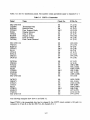
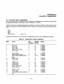
Table I-I shows how the signals in EIA-232-D, V.24, and RS-449 are related, and lists the pin
connections for male subminiature D-type connectors.
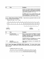
Table 1-1
EIA/CCITT Signal Relationships
Signal Name
Signal Ground
D-type
Pin
EIA-232-D
Circuit
CCITI
V.24
Circuit
RS-449
7
AB
102
SG
*
RC
102B
(SIG
GND)
RS-423-A Receive Common
Transmitted Data
(TXD)
2
BA
103
SD
Received Data
(RXD)
3
BB
104
RD
Request To Send
(RTS)
4
CA
105
RS
Clear To Send
(CTS)
5
CB
106
CS
Data Set Ready
(DSR)
6
CC
107
DM
Data Terminal Ready
(DTR)
20
CD
108/2
TR
Data Carrier Detect
(DCD)
8
CF
109
RR
Ring Indicator
(RI)
22
CE
125
IC
*
Not Connected
1-10
1.4.2 Line Receivers
The DHQll uses octal serial-line receivers which convert line input signals to TIL levels for the
OCTART. Signals are inverted by the receivers.
1.4.3 Line Transmitters
The DHQll uses EIA transmitters which convert TTL level signals from the OCTART and modem
latches to line levels on the data and modem lines.
1.4.4 Speed And Distance Considerations
As of December 1985, the Electronics Industries Association (EIA) have replaced the "RS-" identifier
for RS-232-C with "EIA". Therefore RS-232-C has been replaced by EIA-232-D. These two standards
are compatible with each other. This manual uses EIA-232-D.
The RS-232-CjCCITI V.28 standard was originally designed to specify the connection between a local
interface and a modem. It was not intended to be used for connecting to terminals over long distances.
The maximum specified cable length is 50 feet (15 metres). Shielded cable must be used in order to meet
the requirements of FCC and VDE Radio Frequency Interference (RFI) regulations.
Although cable lengths greater than 50 feet can be used with reasonable success, cable capacitance, noise
and ground potential difference restrict the line speed as the distances increase. Consequently, the
performance of long-distance communications to a terminal using EIA-232-D often does not meet
today's requirements for terminal wiring.
DEC423 is a data-leads-only implementation of the RS-423-AjCCITT V.IO standard. RS-423-A has a
different grounding and signal return path arrangement fliom EIA-232-D.
DEC423 uses line driver and receiver chips which have better filtering and tighter level tolerances than
those specified by RS-423-A. In addition, DEC423 devices include transient suppressors for electrical
overstress (EOS) and electrostatic discharge (ESD) protection. DEC423 devices may also be connected
with unshielded cable.
The features provided by DEC423 devices are reliable data communication over increased distances,
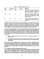
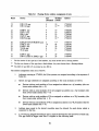
typically 1000 feet (300 metres) at 9600 baud. See Table 1-2 for maximum-distance guidelines.
1-11
Table 1-2
Maximum Distance Guidelines for DHQ 11
Up to
4.8 Kb
9.6 Kb
19.2 Kb
38.4 Kb
DEC423 to DEC423
1000 ft
300 m
1000 ft
300 m
1000 ft
300 m
500 ft
150 m
DEC423 to EIA-232-D
250 ft
75 m
200 ft
60 m
The DEC423 standard is for data-leads-only connections to terminal equipment, and is not suitable for
connection to modems or other Wide Area Network equipment. The standard also specifies the use of a
6-pin Modified Modular Jack (MMJ) connector, instead of the much larger 37-pin D-type connector
used with RS-423-A.
DEC423 is signal-compatible with the EIA-232-D standard when used for data-leads-only
interconnection, in that interconnection between devices using the different standards is possible.
However, the restrictions on the speed and distance of EIA-232-D will still apply.
DEC423 should always be used in preference to EIA-232-D for direct terminal connection over
extended distances.
.
NOTE
An H3105 active terminal adapter is necessary when
using an EIA-232-D terminal with a DEC 423
interface if the longer cable lengths obtainable with
DEC423 are required.
The recommended cable for DEC423 is BC16E-XX, which is available with 6-pin MMJ plugs at each
end, in lengths up to 100 feet. This cable is also available without MMJ connectors in 1000-foot reels,
DIGITAL part number H8220. Unshielded four-twisted-pair cable can also be used. This is available in
1000-foot reels, DIGITAL part number H8245-A.
NOTE
DEC423 to EIA-232-D. is intended for local
communication. In general, communication devices
can become non-operational or be damaged if the
total cable length exceeds 300 metres (1000 feet) for
DEC423 devices. The cable should not be run outside
the building, and the low-voltage data wiring must be
separated from ac power. wiring. The installation or
sites may require additional devices to correct
problems in communication.
NOTE
Under ideal conditions, DEC423 devices can drive
cables considerably longer than the lOOO-foot
maximum stated above. However, differences in
1-12
ground potential, pick-up from mains ac power
cabling, and risk of induced interference limit the
maximum distance for reliable communications in
most practical situations.
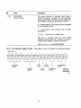
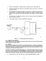
1.5 FUNCTIONAL DESCRIPTION
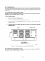
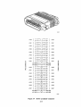
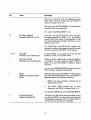
1.5.1 General
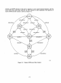
The DHQll functional blocks are shown in Figure 1-5. Most of the functions are provided by two chips:
the control chip and the OCTART chip.
Q-bus buffering uses six DC021 bidirectional buffers. Serial-line interface buffering uses five octal line
receivers (5180) and three octal line transmitters (5170), used for data and modem signals.
A 2k x 8 static RAM chip (20 18D-45) provides the memory requirements. Switchpacks provide vector
address and module address selection.
1.5.2 Main Functions
The main functions of the DHQll are:
•
Transmission - Single characters (DHV11 mode) or multiple characters (DHUll mode) can
be transmitted using programmed transfers. Characters can also be transferred by DMA.
•
Reception - Received characters are deserialized by the OCTART and transferred to a
four-character area in the RAM (one such area per line) by the control chip's OCTART
sequencer, following an interrupt from the OCTART. The control chip's OCTARTsequencer
later removes characters from the bottom of the 4-character FIFO, and places them in the 256
x 16 receive FIFO, which can be read by the host.
•
Modem Control - The modem control latches are external to the control chip. Data is
written to the latches from RAM by the OCTART interface sequencer. The sequencer also
samples modem status lines every 10 milliseconds and reports on changes via the STAT
register (and also via the receive FIFO, if programmed to do so).
1.5.3 Control Chip
The control chip contains the following functional blocks.
•
Q-bus Interface - Matches addresses, generates vector addresses, and handles interrupts. It
also interfaces the Q-bus signals to other functional blocks
•
Data I/O Sequencer -
•
OCTART Sequencers - Transfers data between the OCTART and RAM, and handles flow
control
•
Self-Test/Power-Up Sequencer - This section powers-up the module to a fixed set of initial
conditions, such as 9600 baud rate on all lines; it also handles self-test
•
DMA Sequencer -
Initiates and manages all DMA data transfers to the module
•
RAM Arbitrator -
Provides RAM and OCTART bus access to the
Controls host access to device registers
1-13
~arious
sequencers.
1.5.4 OCTART Chip
This chip contains eight UARTs, which perform parallel-to-serial and serial-to-parallel data
conversions. It interfaces with the control chip through eight registers. Four are read-only and four are
write-only. An index register is used to access individual lines. The OCTART chip shares the RAM bus
with the control chip, and the RAM itself. The OCTART chip also includes:
•
Receive and transmit control blocks
•
Interrupt logic for interfacing with the control chip
•
A 16-output baud-rate generator
•
All necessary line-parameter registers
•
Diagnostic loopback logic
•
Modem status multiplexers.
-
1-14
CONTROL CHIP
Q·BUS
RAM
RAM
DATA
ADDRESS
2K x 8
---DMA
SEQUENCER
____
BIDIRECTIONAL
BUFFERS
r---
-I
VI
DATA
~~QUENCER
II
-III
100-
RAM
RAM
ARBITRATOR
LINE
BUFFERS
____
j~~T:R;
LINE DATA
AND MODEM
SIGNALS OUT
-
SEQUENCER
----
---8 CHANNELS
--- Q-BUS
INTERFACE
----
II
-- --
MODEM
CONTROL
LATCHES
OTO 7
LINE DATA
AND MODEM
SIGNALS IN
SELF·TEST
SEQUENCERS
-----
SWITCH PACKS
AND SHIFT
REGISTERS
RE31n
Figure 1-5
DHQIl Functional Block Diagram
CHAPTER 2
INSTALLATION
2.1 SCOPE
This chapter describes the preparation and installation of the DHQ 11 option. It contains the following
sections.
•
Unpacking
•
Preparation
•
Installation
•
Testing
2.2 UNPACKING AND INSPECTION
If ordered as part of a system, the DHQll will already be installed, and you should refer to the
instructions for unpacking the system.
If ordered as an add-on option to an existing system, a DHQII-M (Q-bus module) will be supplied
together with a cabinet kit, distribution panels, and interconnecting cables. The choice of cabinet kit
depends on the type of system and on whether EIA-232-D or DEC423 connection standards apply
(Table 2-1 gives details of these options).
NOTE
DEC423 is a term used in this manual to indicate a
data-Ieads-only implementation of the RS-423-A
electrical interface standard.
If the equipment is to be installed by DIGITAL Field Service, the customer should not open the
packages.
If the DHQ11 was ordered as an add-on option, find the carton marked OPEN FIRST and carefully
unpack it. There is a shipping list inside the carton.
Undo each package and examine the contents for physical damage. Check that the contents of each
package are complete. Report any damaged or missing items to the shipping agent and to the DIGITAL
representative. Do not dispose of the packing material until the unit has been installed and is
operational.
2-1
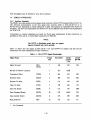
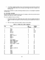
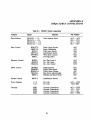
Table 2-1
DHQI1-M
DHQ11 Options
M3107 module + DHQll User Guide (EK-DHQII-UG)
(Base Option)
EIA-232-D Cabinet Kits
CK-DHQII-AA
CK-DHQII-AB
CK-DHQII-AF
BA123 boxes
BA23 boxes
H9624 cabinets - - - - - - - ,
Contents
H3173A
BC05L-IK
BC05L-Ol
BC05L-03
4-line 25-way distribution panel
40-way ribbon cable, 21 inch
40-way ribbon cable, 12 inch
40-way ribbon cable, 36 inch
2
2
2
2
2
2
DEC423 Cabinet Kits
CK-DHQII-WA
CK-DHQII-WB
CK-DHQII-WF
BA123 boxes
BA23 boxes
H9624 cabinets - - - - - - - .
Contents
H3100
BC05L-IK
BC05L-Ol
BC05L-03
70-22775-IK
70-22775-01
70-22775-03
H3104
BC16C-25
H3101
Active bulkhead panel
Ribbon cable - 2 inch
Ribbon cable - 12 inch
Ribbon cable - 36 inch
Bulkhead power cable
Bulkhead power cable
Bulkhead power cable
Cable concentrator
Multiway cable
Multiway cable loopback
2-2
1
1
2
2
2
1
1
1
I
I
1
1
1
1
1
1
1
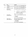
2.3 PREPARING THE DHQll MODULE
Please check that your system has sufficient power and bus load capacity before installing additional
modules; see your system manual. Before installing the DHQ11, you must define three parameters by
selecting them on the DHQII on-board switchpacks. The parameters are:
•
Module address
•
Interrupt vector
•
DHVII or DHUII programming mode.
NOTE
Ensure that you are wearing an antistatic wriststrap,
part number 29-11762-00.
2.3.1 Address And Vector Assignment
The DHQ11 has a floating device address and vector. It is shipped from the factory with a device address
of 177604408 and a vector of 3008• These assignments are determined by the floating address and vector
rules. The factory settings are only correct if no other floating address option is installed in the system.
Otherwise, the proper rules for address assignment must be applied; these are given in Appendix C.
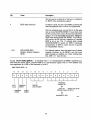
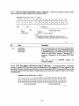
2.3.2 Setting The Address Switches
The device address for the DHQll is set on the 10-position switchpack E19; the location of this
switchpack is shown in Figure 2-1. Switch 1 on the switchpack is used to setup the module in DHUll or
DHV11 programming mode.
2-3
W1
c=J
E19
E11
10 POSITION
SWITCH PACK
(ADDRESS)
I
8 POSITION
SWITCH PACK
(VECTOR)
RE4503
Figure 2-1
Location of Switchpacks
Figure 2-2 shows how to set the device address on the switchpack. The example shown is for the
factory-set address of 177604408.
2-4
DHU/DHV MODE SELECTION
(DHU MODE SELECTED)
PART OF SWITCH PACK E19
DEVICE ADDRESS SELECTION
PART OF SWITCH PACK E19
LEGEND
o
I
= SWITCH OFF (BINARY 0)
OPEN
= SWITCH ON (BINARY 1)
CLOSED
2
3
4
5
6
7
8
9
10
DODDIOOIO
EXAMPLE
SETTING
=17760440
_-----INTERPRETED _ _ _ _..;
AS ALL ONES
DECODED
BY DEVICE
•
SEE NOTE
BIT NO.
21
20
19
18
17
16
15
14
13
12
11
10
09
08
07
06
05
0
0
0
0
1
1
1
1
0
0
1
1
0
0
1
1
0
1
0
1
0
1
0
1
=0
04
03
02
01
00
DEVICE
ADDRESS
[l]=6=
NOTE:
1
USE THE BLANK ROW TO
PENCIL-IN THE ADDRESS
PATTERN YOU NEED
Figure 2-2
7
=1
=2
=3
=4
=5
=6
=7
Setting the Device Address
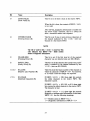
2.3.3 Setting The Vector Switches
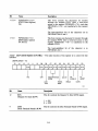
The six Qigh-order bits of the interrupt are set on the eight-position switchpack Ell. Figure 2-1 shows
the location of this switchpack. Figure 2-3 shows (J.n example of these switches set to the factory setting
of 300 (octal). Switches 1 and 2 are used during manufacture, SW-1 must be set ON (closed), and SW-2
must be set OFF (open) for correct operation of the DHQ1l.
2-5
MANUFACTURING TEST SWITCHES SWl MUST BE ON - CLOSED
SW2 MUST BE OFF - OPEN
PART OF SWITCH PACK Ell
LEGEND
0
I
SWITCH OFF
(BINARY 0) OPEN
SWITCH ON
(BINARY 1) CLOSED
VECTOR ADDRESS SELECTION
PART OF SWITCH PACK El 1
~ [ill
oi i 0~~~!:~E
I
I
I
INTERPRETED
AS ALL ZEROES
,I
•I
DECODED
BY DEVICE
..
SEE NOTE
BIT NO.
15
14
~~A
VECTOR
ADDRESS:
0
__
13
~
o
12
__
11
~~
10
__
~
o
09
__
08
~
__
07
~
06
04
05
03
_ _- A_ _ _ _ _ _
\
01
__
00
v-~
o
I
\
02
~~
I
BOTH GRpUPS It;>ENTICAL
\
/
\
NOTE:
/
,...-_.A
X _ _ _ ""\
USE THE BLANK ROW TO
PENCIL-IN THE ADDRESS
PATTERN YOU NEED
0
0
0
0
0
0
0
1
1
0
1
0
0
0
1
1
1
1
,
1
1
0
1
1
=0
=1
=2
=3
=4
=5
=6
=7
RE3224
Figure 2-3
Setting the Vector Address
2.3.4 DHVII Or DHUll Programming Mode Selection
The DHQ II offers two separate program interfaces, DHVII mode or DJ-IUII mode. Select the mode
appropriate to the device driver within the system, by setting switch I of the on-board switchpack EI9
(see Figures 2-1 and 2-2).
Modules prior to revision CI have a jumper installed (WI), which locks the module in DHVII mode.
See figure 2-1 for the position of the jumper. Remove WI to enable selection ofDHVl1 or DHUII mode
by the switch.
NOTE
DHUll programming mode generally gives better
performance, because of reduced CPU overhead in
transferring characters to and from the device. The
Software Product Description states whether the
operating system supports DHUll programming
mode. .
2.4 BUS CONTINUITY
Bus grant continuity jumper cards (M9047) are used in vacant backplane slots to provide bus continuity
(see Figure 2-4).
2-6
NOTE
To find out the type of backplane on your system,
consult your system manual.
Q/Q
A
I
BACKPLANE
B
I
C
o/CD BACKPLANE
I
D
PROCESSOR
PROCESSOR
2
3
4
, f
, f
,,
5
6
7
II
11
10
11
--
....
~
-
--- --
1
-- -- - -
--
~
12
13
~
4
I
I
I
I
t
I
I
I
I
-
I
3
I
6
II
II
~
I
I
5
I
I
~
-
8
9
--
2
7
I
8
I
9
TERMINATOR
I
II
II
I
_I
~
AE3202
Figure 2-4
Bus Grant Continuity
2.4.1 Bus Grant Continuity Jumpers
Backplanes suitable for DHQII fall into two groups.
Q/CD
Q-bus on A and B connectors, user-defined
signals on C and D
Q/Q
Q-bus on A and B, and C and D connectors.
In Q/CD backplanes, bus grant signals pass through each installed module via the A and C connectors
of each bus slot.
Q/Q backplanes are designed so that two dual-height options can be installed in a quad-height bus slot.
The Q-bus lines are routed as follows.
1.
AB, first slot
2.
CD, first slot
2-7
3.
CD, second slot
4.
AB, second slot
and so on.
Each dual-height module extends the continuity of the bus grant signals BIAK and BDMG to the next
module. Therefore, with a Q/Q backplane, if a quad module (DRVII) is :replaced with a dual module
(DHQl1), a Q-busgrant continuity card M9047 is needed for the vacant slot.
2.5 PRIORITY SELECTION
The bus (backplane) position may be a compromise between DMA and intf:!rrupt priority requirements.
As a general rule, consider DMA request priorities first, and then consider interrupt (bus) requests.
2.5.1 DMA Request Priority
DMA request priority is usually assigned according to throughput. Faster devices (higher throughput)
usually have priority over slower DMA devices; for example, disk has priority over tape, which itself has
priority over communications devices. This is because fast devices usually reach overrun or underrun
conditions sooner than slower ones.
2.5.2 Interrupt Request Priority
The DHQll has a fixed interrupt priority level of 4, and cannot be chang,:!d to other priority levels. It
does not monitor any of the higher-level interrupt request lines. Because of this, both the
interrupt-request and DMA (non-processor request) priorities of the I)HQll are selected by the
position of the DHQll on the bus; it must therefore be positioned after any device that does monitor
any of the request lines. Devices closest to the processor module have the highest priority.
2.5.3 Recommendations
In general the DHQIl bus position is not critical. However, it is recommended that you place the
module after any mass-storage interfaces and high-speed synchronous cornmunications options; these
are more sensitive to bus position.
2.6 INSTALLING THE DHQll
Once you have defined the backplane position for the DHQll, you can begin to install the DHQll
module.
2.6.1
Installing The M3107 Module
WARNING
Shut off the system power and disconnect the main
system power cord before performing any procedure
in this chapter.
ATTENTION
Avant d'effectuer I'une des procedures de ce chapitre,
mettez Ie systeme hors tension et debranchez Ie
cordon d'aIimentation.
2-8
VORSICHT!
Schalten Sie das System ab, und ziehen Sie das
Netzkabel, bevor Sie die in diesem Kapitel
beschriebenen Anweisungen ausfiihren.
ATENCION
Apague el sistema y desconecte el cable principal de
alimentacion antes de realizar ningUn procedimiento
de este capitulo.
1
3
2
R£2848
1.
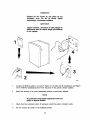
Connect the BC05L cables to Jl and J2. Figure 2··5 for EIA-232-D installations and Figure
2-6 for DEC423 installations show how the parts of the option connect together.
2.
Install the module in its correct backplane position as previously defined.
NOTE
Be careful not to snag module components on the card
guides or adjacent modules.
3.
Check that bus continuity exists. If necessary, install bus grant continuity cards.
4.
Do not connect the cables to the bulkhead panels.
2-9
l~ CHANNELS
I OTO 3
.,I
(jj
::>
CD
2w
;CD
H3173·A
DISTRIBUTION
PANEL
~'----=--
/
RED LINE
TOA
REO LINE
25 PIN 0-1YPE
~CONNEr::rORS
~:~ ~~~N,NELS
}
BC05L-01 = 30.48 CM (12 INCHES)
BC05L-' K = 53.34 CM (21 INCHES)
BC05L-03 = 91.44 CM (36 INCHES)
NOTE:
RES
Figure 2-5
o
0
o
0
0
0
o
o
u..
w
o
u
CD
Installing the DHQII (EIA-232-D)
<
70·22775·XX
~
BACKPLANE
(022/LSI BUS)
COLOURED STRIP
\
POWER CABLE
70·22775·XX
NOTE: BC05L-01 .. 3Ocm (12 INCHES)
BC05L·1K=53cm (21 INCHES)
BC05L·03-92cm (36 INCHES)
RE3203
Figure 2-6
Installing the DHQ 11 (DEC423)
2-10
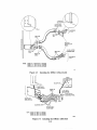
2.6.2 Distribution Panels
The rear I/O distribution panel has six cutouts: two type-A cutouts and four type-B cutouts. In addition,
a removable bracket between the third and fourth cutout allows you to install three more type-A insert
panels by mounting an adapter plate. Figure 2-7 shows typical type-A and type-B insert panels, and the
adapter plate.
2.6.3 Installing The EIA..232-D Distribution Panels
The DHQ 11 has two type-B distribution panels. Figure 2-7 shows bow these are installed in a BA23 box.
Installation in BAI23 and H9642 cabinets is similar.
To fit the distribution panels:
1.
Remove the two type-B blanking panels.
2.
Bolt the two H3I73-A distribution panels into the cutouts.
3.
Connect the free end of the BCOSL-XX cable from connector Jl of the module"to the first
distribution panel.
4.
Connect the free end of the BCOSL-XX cable from connector J2 of the module to the second
distribution panel.
TYPE B
PANELS
REMOVABLE INSERT
o
o
o
50-PIN CONNECTOR
EXPANSION SLOTS· TYPE A
RE32O&
Figure 2-7
I/O Insert Panels and Adapter Plate (EIA-232..D)
2.6.4 Installing The DEC423 Distribution Panels
The DHQll has one type-B distribution panel. Figure 2-8 shows how this is installed in a BA23 box.
Installation in BA123 and H9642 cabinets is similar.
2-11
To fit the distribution panels:
I.
Remove a type-B blanking panel.
2.
Bolt the H3100 active distribution panel into the cutout.
3.
Connect the free end of the BC05L-XX cable from connector Jl of the module to the upper
(J2) connector on the distribution panel.
4.
Connect the free end of the BC05L-XX cable from connector J2 of the module to the lower
(JI) connector on the distribution panel.
5.
Connect the free end of the power cable (70-22775-XX) to the left-hand power connector (J5)
on the distribution panel.
REMOVABLE INSERT
o
o
50-PIN CONNECTOR
EXPANSION SLOTS
11£3205
Figure 2-8
I/O Insert Panel (DEC423)
2.7 INSTALLATION TESTING
This section details the diagnostics used to test the option during and after installation. The diagnostics
are also used to test other Q-bus modules in the same family, for example, I)HVII. The diagnostics will
automatically 'size' the option to determine which one is being tested.
Both MicroPDP-ll and MicroVAX II diagnostics are described. After successful completion of the
appropriate system test, the DHQll may be connected to external equipment. Further information on
the diagnostics is given in Chapter 4.
2.7.1 Installation Tests On MicroPDP-ll Systems
To verify that the MicroPDP-ll system and the DHQl1 module are functioning correctly:
2-12
1.
Switch on the system.
2.
After 2 seconds, check that the green self-test LED on the DHQII module is on. Ifit does not
come on, call DIGITAL Field Service.
3.
Boot the Micro-II Customer Diagnostic media. Refer to your MicroPDP-ll System Manual
for further information.
4.
Type 'I' at the main menu to allow the diagnostics to identify the new module, and add it to
the configuration file.
NOTE
Look at the list of devices displayed, and make sure
that the new module is included. If it is not included,
repeat the installation sequence, and make sure that
the module switches have been set correctly.
5.
Type 'T' at the main menu to run the system tests. These should complete without error; if an
error occurs, call DIGITAL Field Service.
A MicroPDP-II Maintenance Kit is available, and may be ordered from your local DIGITAL office.
This kit allows traiued personnel to run individual diagnostic programs under the XXDP + diagnostic
monitor, and to configure and run OECXIl system test programs. The XXOP + functional diagnostic
is VHQA**.BIN, and the OEeXlI module is XDHV**.OBJ.
2.7.2 Testing In MicroVAX n Systems
To verify that the MicroVAX II system and the OHQIl module are functioning correctly:
1.
Check that the green self-test LED on the DHQII module is on.
2.
Boot the Micro VAX Maintenance System media. Refer to your Micro VAX II System Manual
for further information.
3.
Type '2' at the main menu to show the system configuration and devices.
NOTE
Look at the list of devices displayed, and make sure
that the new module is included. If it is not included,
repeat the installation sequence, and make sure that
the module switches have been set correctly.
4.
Type' I' at the main menu to run the system tests. These should complete without error; if an
error occurs, call DIGITAL Field Service.
2.8 H3101 LOOPBACK CONNECTOR
The H3IOIloopback connector (see Figure 2-9) is used during diagnostic tests for DEC423 installations.
It is two loopback connectors in one package, and consists of a female 36-way loopback connector and a
male 36-way loopback connector. It can be inserted into the cabling at the distribution panel, or at the
cable concentrator. To test the cables, type characters at the keyboard and make sure that they are
echoed to the screen (refer to Chapter 4).
2-13
RE2~39
a:
0
Tx+
Ax +
LINE 1
Tx+
Ax+
LINE 2
Tx+
Ax +
LINE 3
Tx+
Ax+
LINE 4
TX+:=J 9 C
Ax +
10
Tx+
Ax +
LINE 4
LINE 5
Tx +
Ax +
11 C
12
Tx +
Ax +
LINE 5
LINE 6
TX+:=J 13 C
Ax +
14
Tx+
Ax +
LINE 6
LINE 7
Tx + : = J 15 C
Ax+
16
Tx +
Ax+
LINE 7
t-
0
3 C TX+
4
Ax +
LINE 1
5 C TX+
6
Ax +
LINE 2
7 C TX+
8
Ax +
LINE 3
Tx- : = J 19 C
Ax20
LINE 0
~
<t
:E
LINE 0
NOT USED : = J 17 C
NOT USED
18
w
z
z
w
:=J
'CTX+
Ax +
2
a:
0
l(,)
(,)
(,)
:=J
:=J
:=J
:=J
LlNEO
w
NOT USED
NOT USED
TxAx-
Z
Z
0
(,)
LINE 0
Tx- : = J 21 C
Ax22
TxAx-
LINE 1
LINE 2
Tx- : = J 23 C
Ax24
TxAx-
LINE 2
LINE 3
TxAx-
25 C
26
TxAx-
LINE 3
LINE 4
Tx- : = J 27 C
A~28
TxAx-
LINE 4
LINE 5
Tx- : = J 29 C
Ax 30
TxAx-
LINE 5
LINE 6
Tx- : = J 31 C
Ax32
TxRx-
LINE 6
LINE 7
Tx- : = J 33 C
Rx 34
TxRx-
LINE 7
NOT USED : = J 35 C
NOT USED
36
~
~
LINE 1
:=J
w
<t
w
&.I.
NOT USED
NOT USED
A£2~38
Figure 2-9
H3101 Loopback Connector
2-14
•
2.9
CABLES AND CONNECTORS - EIA-232-D
2.9.1 Distribution Panel
Each H3I73-A distribution panel adapts one of the DHQ 11 Berg connectors to four subminiature
D-type EIA-232-D connectors. Noise filtering is provided on each pin of the EIA-232-D connectors.
This reduces electromagnetic radiation from the cables and also provides the logic with some protection
against static discharge.
Figure 2-13 shows the circuit of the H3I73-A. There is no CCITT equivalent of EIA circuit AA
(Protective Ground). To implement this circuit, a ground strap must be installed between the H3173-A
and the system cabinet. The O-ohm link WI (not installed at the factory) can then be installed to connect
this circuit, and removed to disconnect it, as needed.
2-15
J5
J1
r---
~
-
SIGNAL GROUND
C
~
B
TRANSM IT DATA 0/4
.-
-
RECEIVE DATA 0/4
Q
-
DATA TERMINAL READY 0/4
.5-
-
RING INDICATOR 0/4
.E.
-
CLEAR TO SEND 0/4
~
-J
REQUEST TO SEND 0/4
•JS
-
DATA SET READY 0/4
.-
1-
--
DATA CARRIER DETECT 0/4
--1
----
- J3
J5
,...""'"'-
1
2
---3
-.1
Y
DATA CARRIER DETECT 2/6
~
-
DATA SET REA.DY 2/6
.-
~
REQUEST TO SEND 2/6
4
.-
~
~
CLEAR TO SEN D 2/6
4
----
~D
RING INDICATOR 2/6
22
-
~
DATA TERMINAL READY 2/6
20
6
FF
RECEIVE DATA 2/6
.-
-
--
HH
--
TRANSMIT DATA 2/6
--
SIGNAL GROUND
--Z
.-
~
6
-
AA
22
•
-
2J
--
--
-
-
--8
JJ
--5
.-
--3
-
--~7
--
'---
J4
-J2
~
~
1
-N
-
SIGNAL GROUND
"1
TRANSMIT DATA 1/5
-
RECEIVE DATA 1/5
~
-
DATA SET READY 3/7
20
-MM
---
-
REQUEST TO SEND 3/7
i
~
P
~
-
!!
.-
--
'2<
-1:!-
2
.-
------
DATA TERMINAL READY 1/5
•
--8
.--6
DATA CARRIER: DETECT 3/7
~
RING INDICATOR 1/5
22
NlJ
I
CLEAR TO SEND 1/5
~
~
.-
•
'!!
~
-
REQUEST TO SEND 1/5
~
-
CLEAR TO SEND 3/7
RR
.-
-
RING INDICATOR 3/7
21
~S
-TT
DATA TERMINAL READY 3/7
2..f>
--
RECEIVE DATA 3/7
UU
.-
-
TRANSMIT DATA 3/7
V_V
---
SIGNAL GROUND
.-
-
-~
-
V
--~
6
DATA SET READY 1/5
DATA CARRIER DETECT 1/5
1
-
.-
,..............-,
-
-5
-
--3
.-
2
7
-
-
...- ...
W1
~
-=- PROTECTIVE GROUND
1101147
Figure 2-10
H3173-A Circuit Diagram
2-16
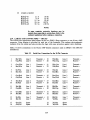
Table 2·2 is for two distribution panels. The numbers within parentheses apply to channels 4 to 7.
Table 2-2
H3173-A Connections
Signal
Name
Circuit No.
J5 Pin No.
SIG GND 0(4)
TXDO(4)
RXDO(4)
DTRO(4)
RIO(4)
CTSO(4)
RTSO(4)
DSRO(4)
DCDO(4)
Transmitted Data
Received Data
Data Terminal Ready
Ringing Indicator
Clear to Send
Request to Send
Data Set Ready
Data Carrier Detected
102
103
104
108/2
125
106
105
107
109
I-A (2-A)
I-B (2-B)
l-C (2-C)
I-D (2-D)
l-E (2-E)
I-F (2-F)
I-H (2-H)
l-K (2-K)
l-L (2-L)
SIG GND 1(5)
TXD1(5)
RXDl(5)
DTRl(5)
RI1(5)
CTSl(5)
RTSl(5)
DSR1(5)
DCDl(5)
102
103
104
108/2
125
106
105
107
109
I-M (2-M)
I-N (2-N)
1-P (2-P)
1-R (2-R)
I-S (2-S)
I-T (2·T)
l-U (2-U)
l-W (2-W)
I-X (2-X)
DCD2(6)
DSR2(6)
RTS2(6)
CTS2(6)
RI2(6)
DTR2(6)
RXD2(6)
TXD2(6)
SIG GND 2(6)
109
107
105
106
125
108/2
104
103
102
l-Y (2-Y)
l-Z (2-Z)
I-BB (2-BB)
l-CC (2-CC)
I-DD (2-DD)
l-EE (2-EE)
1-FF (2-FF)
I-HH (2-HH)
I-JJ (2-JJ)
DCD3(7)
DSR3(7)
RTS3(7)
CTS3(7)
RI3(7)
DTR3(7)
RXD3(7)
TXD3(7)
SIG GND 3(7)
109
107
105
106
125
108/2
104
103
102
1-KK (2-KK)
1-LL (2-LL)
l-NN (2-NN)
I-PP (2-PP)
l-RR (2-RR)
I-SS (2-SS)
I-TT (2-TT)
l-UU (2-UU)
I-VV (2-VV)
The following examples show how to use Table 2-2.
Signal TXDO is the transmitted data line for channel 0; the CCITI circuit number is 103 and it is
connected to J5 pin B on the first H3173-A for channels 0 to 3.
.
2-17
Signal TXD4 is the transmitted data line for channel 4; the CCITT circuit number is 103 and it is
connected to J5 pin B on the second H3I73-A for channels 4 to 7.
2.9.2 Null Modem Cables
Null modem cables are used for local EIA-232-D connection, when a modern is not used. Because of
Federal Communications Commission (FCC) regulations, the cable specifications for the United States
and Canada are different from those for non-FCC countries. Other countries may also have similar
electromagnetic interference (EMI) control regulations. EMCjRFI shielded cabinets are now available
for systems which conform to FCC requirements.·
Recommended null modem cables are as follows.
1.
BC22D· (for EMCjRFI shielded cabinets)
•
Rounded 6-conductor fully shielded cable to FCC specification
•
Subminiature 25-pin D-type female connector moulded on each end
•
Lengths available:
BC220-IO
BC220-25
BC220-35
BC220-50
BC220-75
BC220-AO
BC220-B5
2.
(10 ft)
(25 ft)
(35 ft)
(50 ft)
(75 ft)
(100 ft)
(250 ft)
BC03M
•
Round 6-conductor (three twisted pairs), each pair shielded
•
Cables over 30.5 m (100 ft) have a 25-pin subminiature D-type: female connector at one
end. The other end is unterminated, for passing through the conduit
•
Cables 30.5 m (100 ft) and less have a similar connector at each end
•
Lengths available:
BC03M-25
BC03M-AO
BC03M-B5
BC03M-EO
BC03M-LO
3.
3.1 m
7.6 m
10.7 m
15.2 m
22.9m
30.5 m
76.2 m
7.6 m
30.5 m
76.2m
152.4 m
304.8 m
(25 ft)
(100 ft)
(250 ft)
(500 ft)
(1000 ft)
Be22A
•
Round 6-conductor cable
•
Subminiature 25-pin D-type female connector moulded at each end
2-18
•
Lengths available:
BC22A-I0
BC22A-25
3.1 m
7.6 m
(10 ft)
(25 ft)
Cables of groups 1, 2, and 3 are all connected as in Figure 2-11. The cables are not polarized. They can
be connected either way round.
.
PIN
NUMBERS
PIN
NUMBERS
1 0
20
30
7 0
6 0
20 0
PROTECTIVE GROUND
PROTECTIVE GROUND
TRANSMITTED DATA
RECEIVED DATA
TRANSMITTED DATA
RECEIVED DATA
SIGNAL GROUND
SIGNAL GROUND
DATA SET READY
DATA TERMINAL READY
DATA TERMINAL READY
DATA SET READY
o
1
03
o 2
o
7
020
06
11011 so
Figure 2-11
Null Modem Cable Connections
2.9.3 Full Modem Cables
Recommended full modem cables are as follows:
1.
BC22F (for EMC/RFI-shielded cabinets)
•
Rounded 25-conductor fully shielded cable
•
Subminiature 25-pin D-type female connector on one end, male connector on the other
•
Lengths available:
BC22F-I0
BC22F-25
BC22F-35
BC22F-50
BC22F-75
2.
3.1 m
7.6m
10.7 m
15.2 m
22.9 m
(10 ft)
(25 ft)
(35 ft)
(50 ft)
(75 ft)
BC05D
•
Round 25-conductor cable
•
Subminiature 25-pin D-type, female connector on one end, male connector on the other
2-19
•
Lengths available:
BC05D-IO
BC05D-25
BC05D-50
BC05D-60
BC05D-AO
3.1 m
7.6 m
15.2 m
18.6 m
30.5 m
(10 ft)
(25 ft)
(50 ft)
(60 ft)
(100 ft)
NOTE
In some countries, protective hardware may be
needed when connecting to certain lines. Refer to the
national regulations before making a connection.
2.10 CABLES AND CONNECTORS - DEC423
The H3100 active distribution panel adapts the the two DHQl1 Berg conn~~ctors to one 36-way AMP
connector. Noise filtering is provided on each pin of the connector. This reduces electromagnetic
radiation from the cables and also provides the logic with some protection against static discharge.
Table 2-3 shows connections to the 36-pin AMP filtered connectors used on DHQ11 with DEC423
installations.
Table 2-3
Serial-Line Connections for the 36-Pin Connector
1
2
Blu/Wht
Org/Wht
Line 0
Line 0
Transmit +
Receive +
19
20
Wht/Blu
Wht/Org
Line 0
Line 0
Transmit Receive -
3
4
GmfWht
BmfWht
Line 1
Line 1
Transmit +
Receive +
21
22
Wht/Gm
Wht/Bm
Line I
Line I
Transmit Receive -
5
6
SltfWht
Biu/Red
Line 2
Line 2
Transmit +
Receive +
23
24
Wht/Slt
Red/BIu
Line 2
Line 2
Transmit Receive -
7
8
Org/Red
Gm/Red
Line 3
Line 3
Transmit +
Receive +
25
26
Red/Org
Red/Gm
Line 3
Line 3
Transmit Receive -
9
10
Bm/Red
Sit/Red
Line 4
Line 4
Transmit +
Receive +
27
28
Red/Bm
Red/SIt
Line 4
Line 4
Transmit Receive -
11
12
Blu/Blk
Org/Blk
Line 5
Line 5
Transmit +
Receive +
29
30
Blk/Blu
Blk/Org
Line 5
Line 5
Transmit Receive -
13
14
Gm/Blk
Bm/Blk
Line 6
Line 6
Transmit +
Receive +
31
32
Blk/Gm
Blk/Bm
Line 6
Line 6
Transmit Receive -
15
16
Slt/Blk
Blu/Yel
Line 7
Line 7
Transmit +
Receive +
33
34
Blk/Slt
Yel/Blu
Line 7
Line 7
Transmit Receive -
17
18
OrgjYel
GmjYel
Spare
Spare
35
36
Yel/Org
Yel/Gm
Spare
Spare
2-20
CHAPTER 3
PROGRAMMING
3.1 SCOPE
This chapter describes the device registers, and how they are used to control and monitor the DHQll.
The chapter covers:
•
The bit functions and fonnat of each register
.•
Programming features available to the host.
Some programming examples are also included.
NOTE
DHUll programming mode is the preferred mode of
operation for the DHQll. The development of user
drivers that use the DHQll in DHVll programming
mode is not recommended.
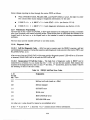
3.2 REGISTERS
The host system controls and monitors the DHQ 11 module through several Q-bus-addressable registers.
Command words or bytes written to the registers are interpreted and executed by the module. Status
reports and data are also transferred through the registers.
3.2.1 Register Access
The DHQl1 registers occupy 8 words (16 bytes) of Q-bus memory-mapped I/O space.
The base physical address of the eight DHQl1 registers is selected by using switches on the module. The
address selected is in the peripheral I/O space. The term 'base' means the lowest I/O address on the
module; that is to say, when the four low-order address bits = O.
Table 3-1 and 3-2 list the DHQll registers and their addresses in DHVII and DHUll mode: The suffix
(I) means that there are eight of these registers, one for each channel. When an (I) register is accessed, the
contents of CSR < 3:0> select which of the eight registers at that address is actually accessed.
NOTE
CSR < 3:0 > allows up to 16 channels to be
addressed. However, only the lower eight channels are
used. Therefore CSR bit 3 must always be O.
'
3-1
Table 3-1
DHQ11 Registers in DHVll Mode
Register
Control and Status Register
Receive Buffer
Transmit Character
Line-Parameter Register
Line Status
Line Control
Transmit Buffer Address 1
Transmit Buffer Address 2
Transmit Buffer Count
Table 3-2
(CSR)
(RBUF)
(TXCHAR)
(LPR)
(STAT)
(LNCTRL)
(TBUFFAD1)
(TBUFFAD2)
(TBUFFCT)
Addres:s
(Octal)
Type
Base
Base + 2
Base + 2(1)
Base + 4(1)
Base + 6(1)
Base + 10(1)
Base + 12(1)
Base + 14(1)
Base + 16(1)
Read/Write
Read Only
Write Only
Read/Write
Read Only
ReadjWrite
ReadjWrite
ReadjWrite
Read/Write
DHQl1 Registers in DHU11 Mode
Register
Control and Status Register
Receive Buffer
Rece~ve Timer*
Line-Parameter Register
FIFO Data
FIFO Size
Line Status
Line Control
Transmit Buffer Address 1
Transmit Buffer Address 2
Transmit Buffer Count
(CSR)
(RBUFF)
(RXTIMER)
(LPR)
(FIFODATA)
(FIFOSIZE)
(STAT)
(LNCTRL)
(TBUFFAD1)
(TBUFFAD2)
(TBUFFCT)
Address
(Octal}
Type
Base
Base + 2
Base + 2
Base + 4(1)
Base + 6(1)
Base + 6(1)
Base + 7(1)
Base + 10(1)
Base + 12(1)
Base + 14(1)
Base + 16(1)
Read/Write
Read
Write (byte)
Read/Write
Write
Read (byte)
Read (byte)
ReadjWrite
ReadjWrite
ReadjWrite
ReadjWrite
* Only accessible when CSR3:0> = 0000
NOTE
It is possible to write to the line-status register.
However, the host should Dot write to this register..
There are eight line-parameter registers, only one of which is accessed at anyone time. The register
which is accessed is associated with the line selected using CSR < 3:0> .
For example, to read the line-parameter register of channel 3, the following I/O commands would be
executed:
HOVB -CHAN,aBASE
HOVB -BASE+·4, RO
iWRITE CHANNEL NUMBER (SEE BELOW) TO CSR
;READ THE LINE PARAMETER REGISTER
In the above example, CHAN = OerOOO 11 (binary)
Where:
3-2
e
=
r
=
0011
=
the RXIE bit of the CSR
the MASTER. RESET bit (which would be 0)
channel number 3
NOTE
1.
Not all register bits are used. In a write action,
all unused bits must be written as Os. In a read
action, unused bits are undefined.
2.
Read-modify-write instructions may be used on
aU registers except CSR and RBUF.
3.2.2 Register Bit Definitions
Registers. which are modified by reset sequences are coded as shown in Figure 3-1.
D
D
D
=
CLEARED BY MASTER RESET
=
SET BY MASTER RESET
=
CLEARED BY BINIT
BUT NOT BY MASTER RESET
R02249
Figure 3-1
3.2.2.1
Register Coding
Control And Status Register (CSR) -
eSR (BASE)
I
14
15
R
JRIW]
13
R
12
11
10
9
8
R
R
R
R
R
I I I I I
r IRIW]RlWIRIW]RlWIRlWIRlWIRIWI
7
6
ACTION
DIAGNOSTICS
FAILURE
TRANSMIT
INT. ENABLE TRANSMIT
DMA ERROR
4
3
2
0
R
I
TX
5
RCVE
INT.
ENABLE
(RXIE)
TRANSMIT
LINE NUMBER
RCVE DATA
AVAILABLE
I
SKIP
INDIRECT ADDRESS REG POINTER
(CHANNEL NO.)
MASTER
RESET
*DHU11 MODE ONLY
UNUSED IN DHV11 MODE
RE10
3-3
Bit
Name
Description
15
TX.ACTION
(Transmitter Action) (R)
This bit is set by the DHQII when:
1.
The last character of a DMA buffer has left the
OCTART.
2.
A DMA transfer has been aborted.
3.
A DMA transfer has been terminated by the
DHQ 11 because nODl-existent memory has been
addressed, or because of a host memory parity
error.
4.
In
DHVII
mode:
a
single-character
programmed output has been accepted; that is
to say, the character has been taken from
TX.CHAR.
5.
In DHUII mode, following a programmed data
transfer, the modulc~ has emptied a transmit
FIFO.
The bit is cleared if the hlOst reads the CSR after the
TX.ACTION FIFO has become empty. To avoid
losing TX.ACTION reports, the host must not let
more than 16 reports acc:umulate. It is advisable to
read the CSR until TX.ACTION becomes clear.
NOTE
TX.ACTION reports may be lost if the upper byte of
the CSR is discarded following a read of the CSR.
14
TXIE
(Transmit Interrupt Enable)
When set, this bit allows the DHQ 11 to interrupt the
host when CSR < 15> (TX.ACTION) becomes set.
(RfW)
I t is cleared by
MASTER. RESET.
13
DIAG.FAIL
(Diagnostic Fail) (R)
BINIT,
but
not
by
When set, this bit indicatc~s that the DHQl1 internal
diagnostics have detected an err~r. The error may
have been detected by the self-test sequencer or by
the background monitor program (BMP).
3-4
Bit
Name
Description
This bit is associated with the diagnostic-passed
LED. When it is set, the LED will be off. When it is
cleared, the LED will be on.
The bit is set by MASTER.RESET. It is cleared after
the self-test has run successfully.
Not valid if MASTER. RESET is set.
12
TX.DMA.ERROR
(Transmit DMA Error) (R)
If this bit is set and TX.ACTION is also set, either
the channel indicated by CSR < 11:8> has failed to
transfer DMA data within 10 microseconds of the
bus request being acknowledged, OR there is a host
memory parity error.
The TBUFFADI and TBUFFAD2 registers will
contain the address of the memory location at which
the error occurred. TBUFFCT will be cleared.
< 11:8>
TX.LINE
(Transmit Line Number) (R)
If TX.ACTION is set, these bits hold the line
number to which TX.ACTION refers.
7
RX.DATA.AVAIL
(Received Data Available) (R)
When set~ this bit indicates that a received character
is available. It is clear when the receive FIFO is
empty. It is used with RXIE to request a receive
interrupt.
It is set after MASTER. RESET because the receive
FIFO contains diagnostic information.
6
RXIE
(Receiver Interrupt Enable)
(RfW)
When set, this bit allows the DHQll to interrupt the
host when RX.DATA.AVAIL is set. An interrupt is
generated under the following conditions.
1.
RXIE is set and a character is placed into an
empty receive FIFO.
2.
The receive FIFO contains one or more
characters, and RXIE is changed from 0 to 1.
It is cleared by BINIT but not by MASTER. RESET.
5
MASTER.RESET
(Master Reset) (RfW)
This bit is set by the host to reset the module. It stays
set while the DHQl1 runs the self-test and performs
an initialization sequence. The bit is the~ cleared to
tell the host that the process is complete.
3-5
Bit
Name
Description
This bit can be set directly by the host, or indirectly
by BINIT (bus initialization signal).
4
SKIP (Skip Self-Test)
"In DHUII mode, this bit :lS used (RW) to shorten the
reset/initialization time to about 30 milliseconds.
The host program must only set this bit at the same
time as it sets MASTER. RESET. It must then clear
the bit, but must wait at least 20 microseconds before
doing so. It is recommended that the host always set
SKIP when setting MASTER. RESET. The DHQIl
will execute the full self-test, regardless of whether
SKIP is set or not. The 1.7 seconds delay during
MASTER. RESET is purely for DHUII hardware
compatibility. In DHVII mode, this bit is ignored
for compatibility reasons"
<3:0>
IND.ADDR.REG
(Indirect Address Register)
(RfW)
F or indexed registers, these bits select one of sixteen
channels. However, on the DHQ II only the lower
eight channels are defined. So, when ~riting these
bits, CSR < 3 > must be zero.
3.2.2.2 Receive Buffer (RBUF) - A read from 'base + 2' is interpreted by the DHQl1 hardware as a
read from the receive FIFO. Therefore RBUF is a 256-character register with a I-word address. The
least-significant bit (LSB) of the character is in bit o.
RBUF (READ BASE
15
rI
R
DATA
VALID
14
13
R
R
+ 2)
I
12
11
R
R
FRAMING
ERROR
OVERRUN
ERROR
10
9
I I I
R
R
8
7
R
~
5
4
:3
R
R
I~
o
2
I
R
R
I
RECEIVED
CHARACTER
RECEIVE
LINE NUMBER
J
9R
DATA
SI~T
(FROM HIGH BYTE
STATUS FLAGS OF STAT)
PARITY
ERROR
I
OR
I
DIAGNOSTIC INFO
RE2723
3-6
Bit
Name
Description
15
DATA.VALID
(Data Valid) (R)
This bit is set if there is data in the receive FIFO.
When this bit is clear, the contents of RBUF < 14:0 >
is not valid.
After self-test, diagnostic infonnation is loaded into
the receive FIFO. Therefore, this bit is always set
after a successful master reset sequence.
14
OVERRUN.ERR
(Overrun Error) (R)
This bit is set if one or more previous characters of
the channel indicated by bits < 11 :8 > were lost
because of a full receive FIFO.
NOTE
The 'all Is' code for bits < 14:12> is reserved. This
code indicates that RBUF<7:0> holds modem
status or diagnostic information.
13
FRAME.ERR
(Framing Error) (R)
This bit is set if the first stop bit of the received
character was not detected (also see RX.CHAR).
12
PARITY.ERR
(Parity Error) (R)
This bit is set if this character has a parity error, and if
parity is enabled for the channel indicated by bits
< 11:8> (also see RX.CHAR).
< 11:8>
RX.LINE
(Receive Line Number) (R)
These bits hold the binary number of the channel on
which the character of RBUF < 7:0 > was received,
or on which a data-set change was reported .
<7:0>
RX.CHAR
(Received Character) (R)
. If RBUF < 14: 12 > = 000, these eight bits contain
the oldest character in the receive FIFO. The
character is good.
If RBUF< 14:12> = 001, 010, or 011, these eight
bits contain the oldest character in the receive FIFO.
The character is bad.
If RBUF < 14: 12 > = 111, these eight bits contain
diagnostic or modem status information. In this case,
RBUF < 0 > has the following meanings.
o=
Modem status in RBUF < 7: 1 >
1 = Diagnostic information in RBUF < 7: 1 >
3-7
Bit
Name
Description
If there is an overrun condition, the four-character
UART receive buffer for that channel will be'cleared.
This data will be lost. A llull character is placed in the
receive FIFO, and RB1JF< 14> is set.
The DHQll-does not ha.ve a break-detect bit. A line
break is indicated to the program as a null character
with FRAME. ERR set, and overrun is clear.
3.2.2.3 Transmit Character Register (TXCHAR) - Single-character programmed transfers are made
through the transmit character register.
TXCHAR (WRITE BASE + 2 ,OHV11 MODE)
1S
14
13
12
11
10
9
8
W
7
6
S
4
3
2
W
W
W
W
W
W
o
W
W
I
TRANSMIT
DATA VALID
TRANSMIT
CHABACTER
FlE2749
Bit
Name
Description
15
TX.DATA.VALID
(Transmit Data Valid) (W)
When set, this bit instructs the DHQll to transmit
the character held in bits < 7:0> . The bit is sensed by
the DHQ 11, which then transfers the character, clears
the bit, and sets TX.ACTION.
TX.DATA.VALID and TX.CHAR can be written
together, or by separate 1v10VB instructions.
<7:0>
TX.CHAR
(Transmit Character) (W)
This contains the character to be transmitted. The
LSB is bit O.
3.2.2.4 Receive Timer Register (RXTIMER), DHUll Mode Only - The indirect address register
(CSR < 3:0» must = 0000 in order to access the receive timer. The host can use the timer to delay the
receive interrupt.
Rx TIMER (WRITE BASE+2,OHU11 MODE)
15
[I
14
13
12
11
10
09
08
07
06
05
04
03
02
01
00
IwJwJwJwJwJwJwJwl
FlE2750
3-8
:Bit
<7:0>
Name
Description
RX.TIMER
(Receive timer)
The receive interrupt is normally raised when a
received character is loaded into the previously
empty receive FIFO. The binary number loaded into
RX. TIMER modifies this procedure as follows.
o=
Infinite timeout. This timeout will be overridden
by the conditions below.
1 = No timeout. The interrupt will be raised
immediately.
2 to 255 = Timer delay in milliseconds.
The timer is overriden when the receive FIFO
becomes three-quarters full (critical) or when a
modem status change is written to the FIFO.
This bit is set to 1 by MASTER. RESET.
3.2.2.5 Line-Parameter Register (LPR) - This register is used to configure its associated channel.
LPR (BASE
15
14
+ 4)
13
12
11
10
9
8
7
6
5
4
3
2
0
[RAN [RIW IRANI RAN [RAN [RIWI RANIRAN IRAN] RIW] RANIRAN [RAN IRIW] RAN] RAN]
Y
I III I
STOP
CODE
TRANSMIT
SPEED
PARITY
ENABLE
EVEN
PARITY
RECEIVE
SPEED
CHARACTER
LENGTH
DIAGNOSTIC
CODE
DISABLE
XON/xOFF
REPORTING
RE3239
3-9
Bit
Name
< 15: 12 >
TX.SPEED
This bit is set to 1101 by MASTER. RESET (9600
(Transmitted Data Rate) (RfW) bits/s). It defines the transmit data rate (Table ~-2).
< 11:8>
RX.SPEED
(Received Data Rate) (RfW)
This bit is set to 1101 by MASTER.RESET (9600
bits/s). It defines the receive data rate (Table 3-2).
7
STOP. CODE
(Stop Code) (RjW)
This bit defines the length of the transmitted stop bit.
Description
o=
I
=
1 stop bit for 5-, 6-, 7-, or 8-bit characters
2 stop bits for 6-, 7-, or 8-bit characters, or 1.5
stop bits for 5·,bit characters
The bit is cleared by MA.STER.RESET.
6
EVEN. PARITY
(Even Parity) (RjW)
If LPR < 5 > is set, this bit defines the type of parity.
I
=
o=
Even parity
Odd parity
The bit is cleared by
5
PARITY.ENAB
(Parity Enable) (RfW)
MJ~STER.RESET.
This bit causes a parity bit to be generated on transmit,
and checked and stripped on receive.
I = Parity enabled
Parity disabled
o=
The bit is cleared by Mi\STER.RESET.
3-10
Bit
Name
Description
<4:3>
CHAR.LGTH
Character Length) (RfW)
These two bits define the length of characters. The
length does not include start, stop, and parity bits.
00 = 5
01 = 6
10 = 7
11 = 8
bits
bits
bits
bits
They are set to 11 by MASTER. RESET.
<2:1>
DIAG
(Diagnostic Code) (RjW)
Diagnostic control codes are are used by the host as
follows.
00
=
Normal operation
01
=
Cau.ses the background monitor program
(BMP) to report the DHQll status through
the receive FIFO.
Other codes are reserved.
<0>
DISAB.XRPT
(Disable XONjXOFF
Reporting) (RjW) .
o=
XON and XOFF characters are reported on
all channels.
1 =
If LNCTRL<4> is also set for a particular
channel, these characters are filtered from the
received data stream, to relieve the host of the
need to do so.
On initialization, this bit is cleared. In order to read or
write to this bit, CSR < 3:0> must equal zero.
NOTE
An XON code = 218 = DC
= CTRL/Q. An XOFF
code = 238 = DC3 = CTRL/S. No other codes are
specified for the interface.
Table 3-3
Code
0000
0001
0010
Data Rates
Data Rate
(Bits/s)
Maximum
Error (0/0)
0.01
0.01
0.08
50
75
110
3-11
Table 3-3
Code
Data Rate
(Bits/s)
0011
134.5
Data Rates (Cont.)
Ma"imum
Error (%)
0.07
0100
0101
0110
0111
150
300
600
1200
0.01
0.01
0.01
0.01
1000
1001
1010
1011
1800
2000
2400
4800
0.01
0.19
0.01
0.01
1100
1101
1110
1111
7200
9600
19200
38400
0.01
0.01
0.01
0.01
3.2.2.6 Line-Status Register (STAT) - The high byte of this register holds modem status information.
In DHVl1 mode, the low byte is undefined.
STAT (READ BASE+6
15
14
13
DSR
12
11
10
9
7
6
5
4
3
2
o
I
DCD
RI
(RING
INDICATOR)
8
DHUID
SET TO 0, DHV11 MODE
CTS
MDL
MODEM SUPPORT PROVIDED FOR THIS LINE
1 = MODEM SUPPORT NOT PROVIDED FOR THIS LINE
o=
RE2722
Bit
Name
Description
15
DSR
(Data Set Ready) (R)
This bit gives the present status of the Data Set
Ready (DSR) signal from the modem.
1 = ON
o=
3-12
OFF
Bit
Name
Description
NOTE
In order to report a change of modem status, the
DHQll writes the high byte of STAT into the low
byte of RBUF. RBUF< 14:12> = 111 indicates to
the host that RBUF<7:0> holds modem status
information instead of a received character.
13
RI
(Ring Indicator) (R)
This bit gives the present status of the Ring Indicator
(RI) signal from the modem.
1 = ON
o=
12
DCD
(Data Carrier Detected) (R)
OFF
This bit gives the present status of the Data Carrier
Detected (DCD) signal from the modem.
1 = ON
o=
11
CTS
(Clear to Send) (R)
OFF
This bit gives the present status of the Clear To Send
(CTS) signal from the modem.
1 = ON
o=
9
MDL
(MDL Modem Support Low) (R)
OFF
Always reads as 0 for DHQll, to indicate that the
module has modem support capability.
NOTE.
It is only necessary to read the modem support status
for one line, since all the other lines will have the same
setting.
8
DHUID (DHUll Identification
bit) (R)
This bit allows software to distinguish between
DHVll mode and DHUll mode.
o=
1
DHVll
= DHUl1
3-13
3.2.2.7 FIFO Size Register (FIFOSIZE), DHUll Mode Only - This low-byte register holds a number
which indicates the space available in the transmit FIFO.
FIFOSIZE (READ BASE+6,DHU11 MODE)
15
14
I
~
13
12
11
R
I I
R
I
R
10
09
08
07
06
05
04
03
02
01
R
R
R
R
R
R
R
R
R
I I II IJJJJJ
I
DSR
00
R]
I
OCD
ALWAYS 0
l____________~------------~
RI
CTS
(RING
INDICATOR)
FI FO SIZE () TO 64
DHUID
SET TO 1, DHU11 MODE
MOL
a = MODEM SUPPORT PROVIDED FOR THIS LINE
1 = MODEM SUPPORT NOT PROVIDED FOR THIS LINE
RE4184
Bit
Name
Description
<7:0>
FIFOSIZE
(FIFO Size)
(R BYTE)
This byte indicates the (in characters) available space
in the transmit FIFO. The range is 00000000 (binary)
to 01000000 (binary) (0 to 64 (decimal». This register
should be read beforc~ sending a character, or a
sequence of characters, to the transmit FIFO data
register.
The byte is set
MASTER. RESET .
to
01000000
(binary)
by
3.2.2.8 FIFO Data Register (FIFODATA), DHUll Mode Only - To s(~nd a character or characters
through a transmit FIFO, the host writes the character(s) to the transmlit FIFO, data register of the
appropriate channel. To make sure that there is room in the transmit FIFO, the host should first read the
associated transmit FIFO size register. If single characters are sent, they mlust be written to the low byte
of FIFODATA.
FIFODATA (WRITE BASE+6,DHU 11 MODE)
15
[w
14
13
12
11
10
09
08
07
06
05
04
o:~
02
01
00
Jw Jw Jw Jw JwJw Jw Jw Jw Jw Jw JwJ w JwJw J
A
TX DATA CHARACTER
T
'
TX DATA CHARACTER
RE2720
3-14
Bit
Name
Description
<15:0>
FIFODATA<15:0>
(FIFO Data Register)
This word contains two characters for transfer
through the transmit FIFO. After a write-word
action to this register, FIFODATA < 7:0> and then
FIFODATA < 15:8> are transferred to the transmit
FIFO.
(W)
The least-significant bits of the characters are In
FIFODATA bits 0 and 8.
<7:0>
FIFODATA < 7:0 >
(FIFO Data register)
(W BYTE)
This byte contains one character for transfer through
the transmit FIFO. After a write-byte action to this
register, FIFODATA < 7:0 > is transferred to the
transmit FIFO.
The least··significant bit of the character is In
FIFODATA bit o.
3.2.2.9 Line-Control Register (LNCTRL) - The main function of this register is to control the line
interface.
LNCTRL (BASE
15
14
+ 10)
13
12
11
10
09
08
07
06
05
04
03
02
01
00
y
RTS
DTR
MAINTENANCE
MODE
OAUTO
FORCE.
XOFF
LINK
TYPE
RX
TX
ENABLE
BREAK
ABORT
IAUTO
RE2442
Bit
Name
Description
12
RTS
(Request To Send) (RfW)
This bit controls the Request To Send (RTS) signal.
1 =
o=
9
DTR
(Data Terminal Ready) (RfW)
ON
OFF
This bit controls the Data Terminal Ready (DTR) signal.
3-15
Bit
Name
Description
1
=
ON
o = OFF
8
LINK.TYPE
(Link Type) (RjW)
This bit must be set if the channel is to be connected to a
modem. When the bit is set, any change in modem status
will be reported through th~: receive FIFO as well as the
STAT register.
If this bit is cleared, this channel becomes a
'data-leads-only' channel. ~10dem status information is
loaded in the high byte of STAT, but is not placed in the
receive FIFO.
<7:6>
MAINT
(Maintenance Mode) (RjW)
These bits can be written by the driver or test programs, in
order to test the channel.
The coding is as follows:
00 =
Normal operation
01 =
Automatic echo mode - Received data is
looped back to the terminal (regardless of the
state of TX.ENA) at the data rate selected for
the receiver. The received characters are
processed normally and placed in the receive
FIFO. Any data that the host attempts to
transmit on this channel will be discarded by
the OCTART. The RX.ENA bit must be set
when operating in this mode.
10 =
Local loopback -- Data transmitted by the
host is looped back to the receive buffer. Data
received from the terminal is ignored, and the
transmit data line to the terminal is held in the
mark condition. The data rate selected for the
transmitter is used for both transmission and
reception. The TX.ENA bit still controls
transmission in this mode. The RX.ENA bit is
ignored.
11 =
Remote loop back In this mode, data
received from the terminal is looped back to the
terminal at a clock rate equal to the received
clock rate. The data is not placed in the receive
FIFO. The state of TX.ENA is ignored. The
RX.ENA bit must be set on this channel.
3-16
Bit
Name
Description
5
FORCE.XOFF
(Force XOFF) (RfW)
This bit can be set by the program to indicate that this
channel is congested at the host system (for example, if the
typeahead buffer is full). When it sees this bit set, the
DHQII will send an XOFF code. Until the bit is cleared,
XOFFs will be sent after every alternate character received
on this channel. When the bit is cleared, an XON will be
sent unless IA UTO is set and the receive FIFO is critical.
4
OAUTO
(Outgoing Auto Flow) (RfW)
This bit is the auto-flow control bit for outgoing
characters. When set, if RX.ENA is also set, the DHQ II
will automatically respond to XON and XOFF codes
received from a channel. The DHQ II uses the TX.ENA
bit in TBUFFAD2 to stop and start the flow. If
DISAB.XRPT is also set, XONjXOFF codes are not
entered in the receive FIFO.
3
BREAK
(Break Control) (RfW)
If set, this bit forces the transmitter of this channel to the
spacing state.
If this bit is set while a character is being transmitted,
transmission is completed before break is asserted on the
line.
Transmission is re-enabled when the bit is cleared.
NOTE
H the line is idle, there may be a delay of up to 170
microseconds between writing the bit and the channel
changing state. If a character is already being
transmitted by the OCTART, the BREAK signal will
be transmitted immediately afterwards.
2
RX.ENA
(Receiver Enable) (RfW)
If this bit is set, this receiver channel is enabled.
If this bit is cleared when this channel is assembling a
character, that character is lost.
The bit is cleared by MASTER. RESET.
IAUTO
(Incoming Auto Flow) (RfW)
This is the auto-flow control bit for incoming characters.
Ifit is set, the DHQII will control incoming characters by
transmitting XON and XOFF codes.
3-17
Bit
Name
Description
If the receive FIFO becomes nlore than three-quarters full,
the D H Q 11 will send an XO FF code to that channel, and
to any other channel which receives a character and has
the IAUTO bit set. When F][FO becomes less than half
full, an XON will be sent to all channels which had
previously been sent an XOFF.
o
TX.ABORT
(Transmit Abort) (R/W)
This bit is set by the driver program to halt data
transmission. If a DMA tra.nsfer was in progress, the
DMA address and count registers (TBUFFADl,
TBUFFAD2, and TBUFFCT) will be updated to reflect
the number of characters which have been transmitted.
The transfer can be continue~d by clearing TX.ABORT,
and then setting TX.DMA.START in TBUFFAD2. No
characters will be lost.
IfDMA is not in progress, the following actions will occur
DHVll mode - no action
DHUll mode - characters in the transmit FIFO will
be discarded. Because of bufrering, up to two characters
could be transmitted after the: TX.ABORT bit is set. The
host cannot determine exactly how many characters have
been lost with this operation.
When an abort sequence has been completed, the DHQll
will set the TX.ACTION bit ill the CSR. If the transmitter
interrupt is enabled, the program will be interrupted at the
transmit vector.
The program must make sure that TX.ABORT is clear
before setting TX.DMA.STA.RT, otherwise the transfer
will be· aborted before any characters are transmitted.
The bit is cleared by MASTER. RESET.
3-18
3.2.2.10 Transmit Buffer Address Register Number 1 (TBUFFAD1) TBUFFAD1 (BASE + 12)
15
I
14
13
12
11
10
9
JR/WJ J JwWJ JR/WJ
RIW
RIW RIW
RIW
I
8
7
5
6
4
J J J J
J J JR/WJ J
RIW RIW RIW RIW RIW RIW RIW
I
I
a
2
3
RIW
1 .1
I
TXMIT DMA ADDRESS
(BITS 0 TO 15)
Bit
Name
Description
< 15:0>
TBUFFAD< 15:0>
(Transmit Buffer Address [Low])
Bits < 15:0> of the DMA address.
(RjW)
3.2.2.11
Transmit Buffer Address Register Number 2 (TBUFFAD2) -
TBUFFAD2 (BASE
15
14
13
+ 14)
12
11
10
9
8
7
6
5
4
3
2
o
I I I I I I
TXMIT
ENABLE
DMA
START
TXMIT DMA ADDRESS
(BITS 16 TO 21)
AD' '79
Bit
Name
Description
15
TX.ENA
(Transmitter Enable) (R/W)
When this bit is set, the DHQll will transmit all
characters.
When this bit is cleared, the DHQl1 will only
transmit internally generated,flow-control characters.
The bit is set by MASTER. RESET.
In the OAIJTO mode, this bit is used by the DHQII
to control outgoing characters.
3-19
Bit
Name
Description
7
TX.DMA.START
(Transmit DMA Start) (RfW)
This bit is set by the host to start a DMA transfer.
The DHQll will clear the bit before returning
TX.ACTION.
The bit is cleared by M,ASTER.RESET.
NOTE
After setting this bit, the host must not write to
TBUFFCT, TBUFFAD1, or TBUFFAD2" <7:()i>
until the TX.ACTION report has been returned.
<5:0>
Bits <21:16> of the Dl~A address. Before a DMA
transfer, TBUFFAD 1 and the low byte of
TBUFF AD2 are loaded with the start address of the
DMA buffer. This address will be continuously
changing during a D JMA transfer and has no
meaning. Once TX.ACTION has been returned, the
register contains the final DMA transfer address.
TBUFFAD<21:16>
(Transmit Buffer Address [High])
(RfW)
3.2.2.12 Transmit DMA Buffer Counter (fBUFFCT) TBUFFCT (BASE
15
14
+
13
16)
12
11
10
9
7
8
6
5
4
3
2
o
DMA CHARACTER COUNT
(WHEN VALID HOLDS NO. OF CHARS STILL TO BE SENT)
RO,,79
Bit
Name
Description
< 15:0>
TX.CHAR.CT
This word is loaded with the number of characters to
(Transmit Character Count) (RfW) be transferred by DMA.,
The number of characters is specified as a 16-bit
unsigned integer.
3-20
Bit
Name
Description
After a DMA transfer has been aborted, this location
will hold the number of characters still to be
transferred.
See also the previous NOTE.
3-21
3.3 PROGRAMMING FEATURES
3.3.1 Initialization
The DHQII is initialized by its on-board sequencers.
Initialization takes place after a bus reset sequence, or when the host sets CSR < 5 >
(MASTER. RESET).
Before starting initialization, the on-board sequencers perform a self-test. The results of this test are
reported by eight diagnostic bytes in the receive FIFO.
The DHQ11 state, after a successful self-test, is as follows.
1.
Eight diagnostic codes are placed in the receive FIFO
2.
The diagnostic fail bit (CSR < 13» is clear
3.
All channels are set for:
a.
Send and receive 9600 bits/s
b.
Eight data bits
c.
One stop bit
d.
No parity
e.
Parity odd
f.
Auto-flow off
g.
Receive disabled
h.
Transmit enabled
1.
No break on line
J.
No loopback
k.
Link type set to data-leads-only
1.
DTR and RTS off
m.
DMA character counter zero
n.
DMA start address registers zero
o.
TX.DMA.START cleared
p.
TX.ABORT cleared
q.
Auto-flow reports enabled
3-22
The DHQII clears the MASTER. RESET bit (CSR < 5» when initialization and self-test are complete.
3.3.2 Configuration
After DHQII self-initialization, the driver program can configure the DHQII as needed. This is done
through the LPR and LNCTRL registers.
The line characteristics for a channel can be set up by writing to the LPR and LNCTRL registers
associated with this channel. These are:
•
Transmit speed
•
Receive speed
•
Number of stop bits
•
Parity type or parity disabled
•
Character length
•
Flow-control characteristics
•
Normal or maintenance mode
•
Receiver enable/disable
•
Modem or data-leads-only
NOTE
If RX.ENA is reset while a received character is being
assembled, that character will be lost.
3.3.3 Transmitting
Each DHQll channel can be set up to transfer the characters by DMA or under program control.
3.3.3.1 DMA Transfers - Before setting up the transfer of a DMA buffer, the program should make
sure that TX.DMA.START is not set. TBUFFCT, TBUFFADl, and TBUFFAD2 should not be
written unless TX.DMA.START is clear.
Transmission will start when the program sets TX.DMA.START. The size of the DMA buffer, and its
start address, can be written to TBUFFCT, TBUFFADl, and TBUFFAD2 in any order, provided that
the TX.DMA start bit (TBUFFAD2 < 7 > ) is not set. However, TBUFFAD2 contains TX.ENA and
TX.DMA.START, so it is probably simpler to write TBUFFAD21ast. By using byte operations on this
register, TX.ENA and TX.DMA.START can be separated.
The DHQll will perform the transfer, and set TX.ACTION when it is complete. If TXIE is set, the
program will be interrupted at the transmit vector. Otherwise, TX.ACTION must be polled.
TX.ACTION is not returned until the UART has completely transmitted the last character of the DMA
buffer.
3-23
To abort a DMA transfer, the program must set TX.ABORT. The DHQll will stop transmission, and
update TBUFFCT, TBUFFAD1, and TBUFFAD2<7:0> to reflect the number of characters which
have been transmitted. TX.DMA.STARTwill be cleared. IfTXIE is set, TX.ACTION will interrupt the
program at the transmit vector. If the program clears TX.ABORT and sets TX.DMA.START, the
transfer can be continued without loss of characters.
If a DMA transfer fails because of a host memory error, the transrnission will be terminated.
TBUFF AD 1 and TBUFFAD2 will point to the failing location. TBUFFCT will be cleared.
3.3.3.2 Programmed 1/0 (DHVll Mode) - Single characters are transferred through the channel
TX.CHAR register. The character and the DATA.VALID bit must be written as defined in Section
3.2.2.3. Note that the character and the DATA.VALID bit can be written by separate MOVB
instructions.
When the DHQll removes the character from TX.CHAR, it returns TX.ACTION. This will generate
an interrupt if TXIE is set.
NOTE
In single-character' mode, TX.ACTION is returilled
when the DHQll accepts the character, not whelll it
has been transmitted. Each channel can buffer up to
three characters. Therefore, if line parameters nre
changed immediately after the last TX.ACTION of a
message, the end of the message could be lost unlc~
three null characters are added to the end of ealch
single-character programmed transfer message.
3.3.3.3 Programmed 1/0 (DHUll Mode) - Before writing a character or sequence of characters to
the FIFODATA register, the program should read the FIFOSIZE register to check that there is space in
the transmit FIFO.
If there is enough space, characters can be written as bytes (one character) or words (two characters) to
FIFODATA. After a low-byte write, FIFODATA < 7:0> is transferred to the FIFO. After a word
write, FIFODATA < 7:0> is transferred to the FIFO, followed by FIFOPATA < 15:0>. High-byte
writes to FIFODATA are not allowed.
The DHQll returns TX.ACTION when the transmit FIFO becomes empty. An interrupt will also be
generated if TXIE is set. As distinct from DMA mode, in programmed I/O mode TX.ACTION is
returned when the DHQll transfers the last character from the transmit FIFO to the OCTART, not
when it has been transmitted. Thus, if line parameters are changed immediately after the last
TX.ACTION of a message, the end of the message could be lost. The program can avoid this loss by
adding two null characters to the end of each programmed transfer FIFO message.
3.3.4 Receiving
Received characters, tagged with the channel number, error information and DATA.VALID, are placed
in the receive FIFO. RX.DATA.AVAIL is clear when the receive FIFO is enlpty. When a character is put
into the empty receive FIFO, the DHQll sets RX.DATA.AVAIL. A recdve interrupt is generated if
RXIE is set. RX.DATA.AVAIL stays set while there is valid data in the receive FIFO. It is recommended
that the receive character routine continues to read characters frolD the receive FIFO until
DATA.VALID is clear.
3-24
NOTE
The interrupt is dynamic. It is raised as
RX.DATA.AVAIL is set after RXIE, or as RXIE is
set after RX.DATA.AVAIL. If the interrupt routine
does not empty the receive FIFO, RXIE must be
toggled to raise another interrupt. In DHUll mode,
the interrupt is generated after a delay (set by
RX.TlMER).
.
If RXIE is not set, the program must poll RBUF often enough to prevent data loss.
3.3.5 Interrupt Control
The DHQ II provides one of two vector addresses during a bus interrupt sequence. The receive vector
address is the address set up on the vector address switches. The transmit vector address is the receive
vector address + 4.
The receive interrupt vector is generated when:
•
RXIE is set and a character is placed into an empty receive FIFO
•
RXIE is changed from 0 to 1, and the receive FIFO contains one or more characters.
NOTE
In DHUll mode an interrupt is generated either
immediately, or after the delay set by RX.TIMER.
The transmit interrupt vector is generated when:
•
TXIE is set and TX.ACTION becomes set
•
TXIE is changed from 0 to 1 while TX.ACTION is set
NOTE
Up to 16 TX.ACTION reports are buffered. It is
therefore recommended that your program reads the
CSR until the TX.ACTION bit becomes clear,
otherwise TX.ACTION will be lost.
At the two vectors, the host must provide the addresses of suitable routines to deal with the above
conditions.
In DHUII mode, an interrupt is generated either immediately data is put into an empty receive FIFO,
or after a delay set by RX. TIMER.
3.3.6 Auto XON And XOFF
XON and XOFF characters are commonly used to control data flow on communications channels. To
use this facility, interfaces must have suitable decoding hardware or software.
A channel using flow control that receives an XOFF stops sending characters until it receives an XON.
3-25
If the receive FIFO becomes more than three-quarters full, the DHQ 11 will send an XOFF code to that
channel, and to any other channel which receives a character and has the IA UTO bit set. When FIFO
becomes less than half full, an XON will be sent to all channels which had previously been sent an
XOFF.
The DHQIl automatically controls character flow when programmed accordingly (auto-flow). Four
bits control this function:
•
IAUTO
LNCTRL<l>
•
FORCE.XOFF
LNCTRL<5>
•
OAUTO
LNCTRL<4>
•
DISAB.XRPT
LPR<O>
IAUTO and FORCE.XOFF both control incoming characters. IAUTO is an enable bit which allows
the level of the receive FIFO to control the generation of XOFF and XON characters. The
FORCE.XOFF bit is a direct command from the program to control the incomimg data stream.
3.3.6.1 IAUTO - The DHQll hardware recognizes when the receive FIFO is three-quarters full and
half full. The logic uses these states for auto-flow control.
Each channel has a separate IAUTO bit. If there are 191 or more characters in the receive FIFO, and a
character is received on a channel with IAUTO set, an XOFF character is sent. If the channel does not
respond to the XOFF, the DHQll will send another XOFF in response to every alternate character
received. An XON will be sent when the receive FIFO contains less than. 128 characters, unless the
FORCE.XOFF bit for that channel is set. XONs are only sent to channl~ls to which an XOFF has
previously been sent.
By inserting XON and XOFF characters into the data stream, the prograrn can perform flow control
directly. However, if the DHQll is in IAUTO mode, the results will be unpredictable.
In IA UTO mode, if RX.ENA is set, XON and XOFF characters will be transmitted even if TX.ENA is
cleared.
3.3.6.2 FORCE.XOFF - When FORCE.XOFF is set, the DHQ11 sends an XOFF and then acts as if
IA UTO is set and the receive FIFO is critical (was three-quarters full, and is not yet less than half full).
When FORCE.XOFF is reset, an XON will be sent unless the receive FIFO its critical and IAUTO is set.
3.3.6.3 OAUTO - If the program sets OAUTO, the DHQ II will automatically respond to XON and
XOFF characters from the channel. It does this by clearing or setting the: TX.ENA bit.
The program may also control the TX.ENA bit, so in this case it is important to keep track of received
XON and XOFF characters.
Received XON and XOFF characters will always be reported through the receive FIFO, unless the
DISAB.XRPT bit is set. It is possible, during read-modify-write operatio:ns by the program, for the
DHQ11 to change the TX.ENA bit between the read and the write actions. For this reason, if DMA
transfers are started while OA UTO is set, it is advisable to write to the low byte of TBUFFAD2 only.
3-26
3.3.6.4 DISAB.XRPT - If DISAB.XRPT is clear, XON and XOFF characters will be processed as
normal characters and are entered into the receive FIFO. DISAB.XRPT allows the individual line
OA UTO bits to control whether XON or XOFF characters received on that channel are discarded.
When DISAB.XRPT is set and OAUTO is set, this filtering is enabled.
NOTES
1.
When checking for fiow-control characters, the
DHQII only checks characters which do not
contain transmission errors. The parity bit is
stripped, and the remaining bits are checked for
XON (218) and XOFF (238) codes.
2.
Auto fiow-control does not absolutely guarantee
that overrun errors will not occur. These errors
may still occur if the transmitting devices do not
respond to the XOFF immediately.
3.3.7 Error Indication
Four bits inform the program of transmission and reception errors.
CSR < 12> .
•
TX.DMA.ERR
•
PARITY.ERR
RBUF<12>.
•
FRAME. ERR
RBUF<13>.
•
OVERRUN.ERR -
RBUF<14>.
RBUF < 14: 12 > also identify a diagnostic or modem status code.
3.3.8 Modem Control
Each channel of the module provides modem control bits for RTS and DTR. Also on each channel are
modem status inputs CTS, DSR, RI, and OeD. See Section 3.2.2.6 for a description of each of these
signals.
CTS, DSR, and DCD are sampled every 10 ms. Therefore, for a change to be detected, these bits must
stay steady for at least 10 ms. RI is also sampled every 10 ms, but a change is not reported unless the new
state is held for three consecutive samples. Modem signals must be coordinated under program control;
there is no hardware modem control logic. Modem status change reports are placed in the receive FIFO
only if LINK. TYPE is set, but any changes are updated in STAT irrespective of the state of
LINK.TYPE.
Appendix A gives more details of modem control.
By clearing LINK.TYPE, a channel is selected as a 'data-lines only' channel. Modem control and status
bits can still be managed by the program, but status bits must be polled at the line-status register.
Changes of modem status will not be reported to the program.
3-27
Status change reporting is done through the receive FIFO as follows.
•
When OVERRUN.ERR, FRAME. ERR, and PARITY.ERR are all set, the eight low-order
bits contain either status change or diagnostic information. In this case:
•
If RBUF<O> = 0, RBUF<7:1 > holds STAT < 15:9> (see Section 3.2.2.6)
•
If RBUF<O>
=
1, RBUF<7:1 > holds diagnostic information (see Section 3.3.10).
3.3.9 Maintenance Programmi.ng
The host can set bits 7 and 6 of LNCTRL to allow each channel to be configured in normal, automatic
echo, local loop back, and remote loopback modes. These modes allow an individual data channel to be
looped back to the host, or to be looped back to the terminal to assist in isolating communication
problems.
The host must provide suitable software to use these modes.
3.3.10
Diagnostic Codes
3.3.10.1 Self-Test Diagnostic Codes - After bus reset or master reset, thf: DHQ11 executes a self-test
and initialization sequence. During the sequence, eight diagnostic codes are put in the receive FIFO, and
RX.DATA.AVAIL is set.
After an error-free test, DIAG.FAIL will be reset and the 'diagnostic passed' LED will be on. Ifan error
is detected, DIAG.FAIL will be set and the LED will be off.
3.3.10.2 Interpretation Of SeH-Test Codes - The high byte of diagnostic codes in RBUF can be
interpreted as in Section 3.2.2.2, except that bits < 11:8> are not the linc~ number. They indicate the
sequence of the diagnostic byte, that is to say, 0 = first byte, 1 = second byte, and so on. Table 3-3 shows
the meaning of each of the error codes.
Table 3-4
C~\de
DHQll Self-Test Error Codes
Explanation
(O;:'tal)
bits ::7:0>
201
Self-test null code (used as a filler)
203
Self-test skipped
211
OCTART error
225
RAM errol'
231
RTS-CTS-DCD error
235
DTR-RI-DSR error
All other errcr codes should be treated as an undefined error.
If bit 7 = 0 and bit 0 = 1, then bits < 5:2> contain circuit revision inftDnnation.
3-28
Table 3-4
Code
(Octal)
bits < 7:0>
DHQll SeH-Test Error Codes (Cont.)
Explanation
Bit 6 always reads I for the DHQ 11, and indicates that the circuit contains control and OeTART
chips.
Bit 1 indicates to which chip the information refers: 0 = Control, 1 = OCTART.
After self-test, the eight FIFO codes consist of six diagnostic codes and two circuit revision codes. If
there are less than six errors to report, null codes (201(octal» fill the unused places.
After an error-free test, six null codes and two circuit revision codes will be returned.
Self-test may be 'skipped' to shorten the initialization cycle (see Section 3.3.10.3).
The module is still tested, even if self-test is skipped. The reset delay is much shorter, but test coverage is
not affected; therefore skipping self-test is advantageous.
After 'skip self-test' self-test, the eight FIFO codes consist of six diagnostic codes and two circuit
revision codes. If there are less than six errors to report, 203(octal) codes fill the unused places.
After an error-free test, six 203(octal) codes and two circuit revision codes will be returned.
3.3.10.3 Skipping SeH-Test - In DHUIl mode only, the method is to set SKIP (CSR bit 4) and
MASTER. RESET (CSR bit 5) simultaneously, that is, write 60(octal) to the base CSR. SKIP must not
be cleared until at least 20 microseconds after it was set. SKIP must be cleared by the host so that the
master reset sequence can complete.
In DHVll mode (this also works in DHUll mode, but the previous method is preferred) the following
method is used:
1.
The program resets the DHQll.
2.
The program waits 10 ms (± 1 ms) after issuing reset, and then attempts to write 052525 8 to
any of the control registers, except the CSR, within the next 4 ms.
3.
Following self-test, the DHQl1 hardware checks whether an attempt was made to write the
skip code to the registers during the 4 ms window after reset (see step 2 above). If an attempt
was made, the MASTER. RESET bit is cleared at 30 ms after issuing a reset instead of 1.2 s.
The 1.2 s reset time was retained for compatibility with the DHVII.
NOTE
The program must not write to the CSR, or to the
control registers, during the period starting 15 ms
after reset, and ending when the MASTER.RESET
bit is cleared. Writing during this period could cause a
diagnostic fail condition.
3-29
3.3.10.4 Background Monitor Program (BMP) - The DHQll BMP logic perfonns background
self-tests by checking for OCTART interrupts. One of two codes is returned to the receive FIFO:
1.
305(octal) - DHQIl running
307(octal) - DHQll defective (also LED off)
A single diagnostic word is returned to the receive FIFO. The low byte contains the diagnostic code. In
the high byte, OVERRUN. ERR, FRAME. ERR, and PARITY.ERR are all set to indicate that
bits < 7:0 > do not hold a normal character. The line number (RBUF < 11:8» = O.
BMP normally only reports when it finds an error. However, the program can get a BMP report at any
time to check the DHQll. This is done by setting DIAG (LPR < 2:1» of any channel to Ol.The line
number returned is that of the LPR used to request the report.
On completing the check, BMP clears this 01 code. The host should not write to the LPR of that channel
until LPR < 2: 1 > becomes 00.
3-30
3.4 PROGRAMMING EXAMPLES
These programs are not presented as the only way of driving the option, and are neither guaranteed nor
supported.
3.4.1 Resetting The DHQll
In the following example:
•
DIAGC is a routine to check the diagnostic codes. It returns with CARRY set ifit detects an
error code.
•
The loop at 1$ takes 1.2 seconds, so the programmer could poll through a timer or poll at
interrupt level zero.
A ROUTINE TO RESET THE DHG11 AND CHECK THAT IT IS fUNCTIONING
CORRECTLY.
DHGRES: :
HOV
#40,#DHGCSR
SET HASTER.RESET AND
CLEAR INTERRUPT ENABLES.
i WAIT fOR HASTER.RESET TO
i CLEAR.
i CHECK THE DIAGNOSTICS
; fAIL BIT.
NOTE: TEST INSTRUCTION IS
i OK BECAUSE THERE ARE
; NO TRANSHIT.ACTS PENDING.
i SET UP A COUNT.
i
i
1$:
2$:
BIT
BNE
BIT
BNE
#40,#DHGCSR
1$
#20000,#DHGCSR
DIAGER
HOV
#S. ,R5
HOV
JSR
BCS
#RBUff,RO
PC,DIAG
DIAGER
SOB
R5,2$
GET NEXT DIAGNOSTIC CODE.
PROCESS IT.
i CARRY SET - MUST HAVE
i BEEN AN ERROR.
i GO BACK fOR NEXT CODE.
RTS
PC
i
i
i
RETURN - CARD IS RESET.
i
i
DHQ11 HAS fAILED TO RESET PROPERLY, SO HALT AND WAIT fOR
; THE fIELD SERVICE ENGINEER.
DIAGER: HALT
BR
DIAGER
3-31
3.4.2 Configuration
This routine.sets the characteristics of channell as follows:
1.
Transmit and receive at 300 bits/s
2.
Seven data bits with even parity and one stop bit
3.
Transmitters and receivers enabled
4.
No modem control
5.
No automatic flow control.
SETUP: :
HOV
a1,aDHQCSR
HOV
a052560,aLPR
HOV
HOVB
a4,aLNCTRL
a200,aTBFAD2+1
RTS
PC
; LOAD INDEX REG
; WITH CHANNEL NO.
; DATA RATE, STOP BITS,
; PARITY AND LENGTH.
; ENABLE THE RECEIVER.
; ENABLE THE TRANSMITTER.
; RETURN - CHANNEL 1 DONE.
3-32
3.4.3 Transmitting
3.4.3.1 Single-Character Programmed Transfer (DHUll Mode) - The following is a program to send
a message on channell.
The CSR is polled for TX.ACTION reports, but a TX.ACTION interrupt could also be used.
This program would function on a DHQ11 with only this channel active. Otherwise it would lose
TX.ACTION reports of other channels. However, a program to control all channels would be too big to
use as an example.
;
; A ROUTINE TO WRITE A MESSAGE TO CHANNEL 1 USING FIFO OUTPUT
; MODE (PROGRAMMED TRANSFERS).
FIFOUT: :
MOV
1f:
2$:
al,aDHDCSR
MOV
MOV
aMESG,RO
MESIZE,Rl
; POINT TO CHANNEL WE WISH
; TO TALK TO.
; POINT TO MESSAGE.
; PUT COUNT IN.
TSTB
BED
MOVB
SOB
aFIFOSIZE
1$
(RO)+,aFIFODATA
Rl,l$
; CHECK THAT THERE IS SPACE IN
; THE FIFO.
; MOVE CHARACTER TO TRANSMIT FIfO
; GO BACK FOR NEXT CHARACTER.
MOV
BPL
aDHDCSR,R2
2$
; WAIT FOR TX.ACT.
BIC
CMP
BNE
a170377,R2
aOOO400,R2
2$
; ISOLATE CHANNEL NUMBER.
RTS
PC
; MESSAGE SENT.
; IGNORE THE TX.ACT IF IT IS
; NOT OURS (SHOULD NOT HAPPEN).
HESG: .ASCII IA TRANSMIT FIFO HESSAGE FOR CHANNEL 11
MESIZE = .-MESG
. EVEN
3-33
3.4.3.2 Single-Character Programmed Transfer (DHVl1 Mode) - This is a program to send a message
on channell. The message (MESG) is an ASCII string with a null character as tenninator.
Polling is used, but a TX.ACTION interrupt could also be used.
This program would function on a DHQll with only this channel active. Otherwise it would lose
TX.ACTION reports of other channels. However, a program to control all channels would be too big to
.
use as an example.
A ROUTINE TO WRITE A HESSAGE TO CHANNEL 1 USING SINGLE-CHARACTER
HODE.
SINGOT: :
HOV
1$:
2$:
TXI
#l,#DHQCSR
; LOAD INDEX REG WITH
; CHANNEL NO.
; POINT TO MESSAGE.
HOV
#MESG,RO
MOVB
(RO)+,#TXCHAR
BEQ
3$
HOVB
#200,#TXCHAR+l
HOV
BPL
#DHQCSR,Rl
2$
BIC
CHP
BNE
#174377,Rl
aOOO400,Rl
2$
BR
1$
IGNORE THE TX.ACT IF IT IS
NOT OURS (SHOULD NOT HAPPEN).
GO BACK FOR NEXT CHARACTER.
RTS
PC
HESSAGE SENT .
; HOVE CHARACTER TO TRANSHIT
; BUFFER.
; GO RETURN IF ALL CHARACTERS
; GONE.
SET DATA VALID BIT TO START.
; WAIT FOR TX.ACT
ISOLATE CHANNEL NUHBER.
3$:
HESG:
. ASCIZ IA SINGLE-CHARACTER MESSAGE FOR CHANNEL
3-34
11
3.4.3.3
DMA Transfer -
;
; THIS PROGRAM SENDS A MESSAGE OUT ON EACH LINE OF THE DHD11 AND
; HALTS THE MACHINE WHEN ALL TRANSHISSIONS HAVE COHPLETED.
;
; THE HESSAGES ARE TRANSMITTED USING DHA HODE, AND INTERRUPTS ARE
; USED TO SIGNAL TRANSHISSION COHPLETION.
DHAINT: :
1$:
2$:
3$:
HOV
HOV
HOV
CLR
HOVB
HOV
HOV
HOV
, aTXINT, aTXVECT ; SET UP THE INTERRUPT VECTORS.
a200,aTXPSW
; INTERRUPT PRIORITY FOUR.
as. ,RO
i EIGHT LINES TO START.
R1
i START AT LINE ZERO.
INC
SOB
R1,aDHDCSR
; SELECT THE REGISTER BANK.
aDMASIZ,aTBFCNT i SET LENGTH OF HESSAGE.
aDMAMES,aTBFAD1 i SET LOWER 16 ADDRESS BITS.
a100200,aTBFAD2 i START DHA WITH TRANSHITTER
i ENABLED (ASSUHE UPPER ADDRESS
i BITS ARE ZERO).
R1
iPOINT TO NEXT CHANNEL.
RO,1$
i REPEAT FOR ALL LINES.
CLR
HOVB
RS
a100,aDHDCSR+1
CHP
BNE
as. ,R5
2$
HALT
BR
3$
i
i
RS IS USED BY INTERRUPT ROUTINE.
ENABLE TRANSHITTER INTERRUPTS.
i
WAIT FOR ALL LINES TO "FINISH.
i
ALL DONE, SO STOP.
;
i
TRANSHITTER INTERRUPT ROUTINE.
;
i
R5 IS INCREMENTED AS EACH LINE COHPLETES.
TXINT: :
4$:
S$:
HOV
BIT
BED
aDHOCSR,RO ; GET LINE NUMBER OF FINISHED LINE.
a100000,RO ; CHECK FOR (ANOTHER) TX.ACTION.
4$
i IF NOT, GO RETURN AND WAIT.
INC
BR
R5
TXINT
i
FLAG THAT ANOTHER LINE HAS FINISHED.
i
HEHORY PROBLEH
RTI
HALT
BR
5$
DHAMES: .ASCII (15)(12)(7)(7)(7)/SYSTEH CLOSING DOWN NOWI
DHASIZ =
.-DHAHES
.EVEN
3-35
3.4.3.4 Aborting A Transmission i
i
THIS ROUTINE IS CALLED TO ABORT A TRANSMISSION (EITHER DMA OR
; FIFO) IN PROGRESS ON A SPECIFIED LINE. THIS ROUTINE MAKES THE
; (RATHER RASH) ASSUMPTION THAT THERE ARE NO OTHER TRANSFERS IN
; PROGRESS.
;
; ON ENTRY, RO CONTAINS THE NUMBER OF THE LINE TO BE ABORTED.
TXABRT: :
1$:
MOV
BIS
RO,#DHQCSR
#1,#LNCTRL
i POINT TO THE CHANNEL TO BE ABORTED.
; SET THE TRANSMIT ABORT BIT.
MOV
BPL
SWAB
BIC
CMP
BNE
#DHQCSR,R1
1$
R1
#177760,Rl
RO,Rl
1$
; WAIT FOR THE TX.ACT.
BIC
1,#LNCTRL
RTS
PC
; CHECK IT IS OUR LINE.
; IGNORE IT IF IT IS NOT (OUR
; ASSUMPTION WAS WRONG!)
; CLEAR DOWN THE ABORT FLAG
; FOR NEXT TIME.
;
;
;
;
BUFFER COMPLETELY ABORTED.
IF A DHA WAS IN PROGRESS, THE
DHA REGISTERS REFLECT WHERE
THE DHQ11 HAD GOT TO.
3-36
3.4.4 Receiving
i
;
;
;
;
THIS ROUTINE PROCESSES RECEIVED CHARACTERS UNDER INTERRUPT
CONTROL. IF AN XOFF IS RECEIVED, THE TRANSHITTER FOR THAT
CHANNEL IS TURNED OFF. IF AN XON IS RECEIVED, THE TRANSHITTER
IS TURNED BACK ON. ALL OTHER CHARACTERS ARE IGNORED.
;
; THIS IS JUST AN EXAHPLE. A BETTER WAY TO PERFORH Fl.OW CONTROL IS
; TO USE THE AUTOMATIC CAPABILITIES OF THE DHQ11.
RXAUTO: :
1$:
HOV
HOV
HOV
CLR
aRXINT,aRXVECT j SET UP THE INTERRUPT VECTORS.
a200,.RXPSW
; INTERRUPT PRIORITY FOUR.
as. ,RO
j ENABLE ALL THE RECEIVERS,
; STARTING AT CHANNEL ZERO,
Rl
HOVB
BIS
INC
SOB
Rl,.DHQCSR
a4,aLNCTRL
R1
RO,l$
i SELECT THE LINE.
; ENABLE THIS RECEIVER.
; SET POINTER TO NEXT CHANNEL.
HOVB
al00,aDHQCSR
; ENABLE THE RECEIVER INTERRUPTS.
RTS
PC
j
RETURN - INTERRUPTS DO THE RESET.
3-37
INTERRUPT ROUTINE TO DO THE HAIN TASK.
RXINT: :
RXNXTC:
1$:
RXIEND:
HOV
RO,-(SP)
HOV
BPL
HOV
BIC
BNE
aRBUFF,RO
; GET THE CHARACTER.
RXIEND
; IF NO DATA VALID, WE HAVE FINISHED.
RO,-(SP)
; CHECK FOR ERRORS, HOD EM AND
a107777,(SP)+ ; DIAGNOSTICS CODES.
- JUST IGNORE THEH (BAD PRACTICE).
RXNXTC
i
BIC
SWAB
BIS
MOVB
SWAB
CMPB
BNE
a170200,RO
RO
a100,RO
RO,aDHQCSR
RO
a21,RO
1$
BISB
BR
a200,aTBFAD2+1 ; ENABLE THE TRANSMITTER.
GO CHECK FOR HORE CHARACTERS.
RXNXTC
CMPB
BNE
a23,RO
RXNXTC
BICB
BR
a200,aTBFAD2+1 ; DISABLE THE TRANSHITTER.
RXNXTC
; GO CHECK FOR HORE CHARACTERS.
HOV
RTI
(SP)+,RO
; SAVE CALLER'S REGISTERS.
i REMOVE UNNECESSARY BITS.
; POINT TO THIS CHARACTER'S LINE.
i (ADD THE INTERRUPT ENABLE BIT.>
; PUT CHARACTER BACK IN LOWER BYTE.
; WAS IT AN aXONe?
; NO - GO CHECK FOR AN -XOFF-
; WAS IT AN -XOFF-?
; NO - GO CHECK FOR MORE CHARACTERS.
; RESTORE THE DESTROYED REGISTER.
3-38
3.4.5
Auto XON And XOFF
;
; THIS PROGRAH SENDS A HESSAGE OUT ON EACH LINE OF THE DHQll AND
; HALTS THE MACHINE WHEN ALL TRANSHISSIONS HAVE COHPLETED.
;
; THE HESSAGES ARE TRANSHITTED USING DHA HODE, AND INTERRUPTS ARE
; USED TO SIGNAL TRANSHISSION COHPLETION.
;
; AUTOHATIC FLOW CONTROL IS ENABLED ON THE OUTGOING DATA.
TXAUTO: :
1$:
HOV
HOV
HOV
CLR
• ATOINT,.TXVECT
.200,.TXPSW
.S. ,RO
Rl
HOVE
BIS
Rl,.DHQCSR
.2.f.,.LNCTRL
INC
SOB
; SELECT THE REGISTER BANK.
; ENABLE AUTOHATIC FLOW CONTROL
; ON THE TRANSHITTED DATA .
• AUTOSZ,.TBFCNT ; SET LENGTH OF HESSAGE.
.AUTOHS,.TBFADl ; SET LOWER 16 ADDRESS BITS.
.100200,.TBFAD2 ; START DHA WITH TRANSHITTER
; ENABLED (ASSUHE UPPER ADDRESS
; BITS ARE ZERO).
; POINT TO NEXT CHANNEL.
Rl
RO,l$
; REPEAT FOR ALL LINES.
CLR
HOVB
; R5 IS USED BY INTERRUPT ROUTINE.
R5
• 100,.DHQCSR+l ; ENABLE TRANSHITTER INTERRUPTS .
CHP
BNE
-S.,R5
2$
HALT
BR
3$
HOV
HOV
HOV
2$:
; SET UP THE INTERRUPT VECTORS .
; INTERRUPT PRIORITY FOUR.
; EIGHT LINES TO START.
; START AT LINE ZERO.
; WAIT FOR ALL LINES TO FINISH.
3$:
; ALL DONE, SO STOP.
3-39
;
; TRANSMITTER INTERRUPT ROUTINE.
;
; R5 IS INCREHENTED AS EACH LINE COHPLETES.
ATOINT: :
HOV
#DHQCSR,RO
; GET LINE NUHBER OF FINISHED LINE.
BIT
BNE
#10000,RO
4$
; CHECK FOR DHA FAILURE.
; GO HALT - HEHORY PROBLEH.
INC
R5
; FLAG THAT ANOTHER LINE HAS FINISHED.
2$:
4$:
RTI
HALT
BR
AUTOHS: .ASCII
AUTOSZ =
. EVEN
4$
; HEHORY PROBLEH
(15)(12>{7){7)(7)/SYSTEH CLOSING DOWN NOWI
.-AUTOHS
3-40
3.4.6 Checking Diagnostic Codes
;
;
;
;
;
THIS ROUTINE CHECKS THE DIAGNOSTICS CODES RETURNED FROH THE
DHQll. ON ENTRY, RO CONTAINS THE CHARACTER RECEIVED FROH THE
DHQll. ON EXIT, THE CARRY BIT WILL BE CLEAR FOR SUCCESS, SET
FOR FAILURE.
DIAG: :
DIAGEX:
DIAGXX:
HOV
RO,-(SP)
BIC
CHP
BNE
-107776,RO
-070001,RO
DIAGEX
HOV
(SP) ,RO
; GET THE CODE BACK.
BITB
BEQ
CHPB
BEQ
CHPB
BEQ
-200,RO
DIAGEX
-201,RO
DIAGEX
-203,RO
DIAGEX
; CHECK FOR CHIP VERSION NUHBER.
; SELF-TEST NULL CODE.
CHPB
BEQ
-305,RO
DIAGEX
; DHQ RUNNING CODE.
SEC
BR
DIAGXX
CHECK THAT IT IS A DIAG. CODE.
IF NOT, JUST EXIT NORHALLY.
; SELF-TEST SKIPPED CODE.
; ALL THE REST ARE ERROR CODES.
; AN ERROR CODE WAS RECEIVED, SO
; SET THE CARRY FLAG.
; EVERYTHING OK, SO CLEAR CARRY.
CLC
HOV
RTS
; SAVE THE CODE FOR LATER.
(SP)+,RO
PC
; RESTORE THE CHARACTER/INFO.
3-41
CHAPTER 4
TROUBLESHOOTING
4.1 SCOPE
This chapter explains how to isolate the cause of a communications problem between the DHQll and
the equipment to which it is connected.
4.2 PREVENTIVE MAINTENANCE
No preventive maintenance is needed for this option. However, you should always ensure that all cables
are clear of danger, and that all the connectors are secure.
Make sure that all cables are clearly labelled, so that you can easily identify which channel number and
which DHQll module are associated with each terminal.
4.3 TROUBLESHOOTING PROCEDURES
Troubleshooting procedures are to identify whether the problem is caused by:
•
The module
•
A terminal
•
The cabling and distribution panels.
First decide whether the problem is associated with one channel, a group of four channels, or all eight
channels.
If all channels are faulty, run the user diagnostics to test the module. Also check whether your software
has a driver for the DHQll.
If a group of four channels are faulty, check the BC05L-xx cable connected to the module.
For single-channel problems (EIA-232-D):
1.
Check for loose cables and connectors.
2.
Verify that the terminal is working correctly. If necessary, swap it with another one.
3.
When a modem line is suspect, check that the modem is correctly configured for modem
signals supported by the DHQll. Also check that the software driver has the correct
baud-rate setting and that modem support is enabled for that line.
4.
If the problem cannot be solved, call DIGITAL Field Service.
For single-channel problems (DEC423)
1.
Check for loose cables and connectors.
4-1
2.
Verify that the terminal is working correctly. If necessary, swap it with another one.
3.
Disconnect the BCI6C-XX cable from the distribution panel, a.nd connect it to the H3101
loopback connector.
4.
Type characters at the terminal connected to the suspect line. If characters are echoed back
when the H31 0 1 is connected, the cables and terminal are working. If characters are not
echoed back, the fault lies with the cable connection to the terminal, or with the terminal
itself.
5.
Rectify the cable or terminal fault, if there is one. If not, make SlLlre that the user diagnostics
for the module run correctly.
6.
If the problem cannot be solved, call DIGITAL Field Service.
H3101 LOOPBACK
CONNECTOR
n-.~;.--..
U----J
H3104
TO TERMINALS
BC16C-XX
RE3206
Figure 4-1
Troubleshooting DEC423 Installations
4.4 INTERNAL DIAGNOSTICS
Internal diagnostics run without intervention from the operator. There are two tests: the self-test and the
background monitor program (BMP).
4.4.1 SeH-Test
The self-test starts immediately after the Q-bus or module has been reset. It performs a comprehensive
internal logic test but does not test the Q-bus interface. The DIAG.FAIL bit and the 'diagnostics passed'
LED on the module give an indication of a successful self-test. The self-test also reports error or status
information to the host via the receive FIFO.
The self-test has completed successfully if the LED is on 1.7 seconds after the self-test has been initiated.
The self-test is started by setting the MASTER. RESET bit in the CSR, either by resetting the module
through the program interface or by a Q-bus initialisation sequence. The LED is turned off when the
self-test starts, and the test completes after 3Oms. The self-test then finishes in one of three ways:
•
If skip self-test was used, the LED turns on and the
4-2
MASTEF~.RESET
is cleared
•
If the board is in DHVII mode, the LED flickers, and the end of self-test is delayed for 1.2
seconds to maintain compatibility with DHV11. At the end of the delay period the LED turns
on and the MASTER. RESET is cleared
•
If the board is in DHUll mode, the LED flickers, and the end of self-test is delayed for 1.7
seconds to maintain compatibility with DHUll. At the end of the delay period the LED turns
on and the MASTER. RESET is cleared.
In all three cases, if the self-test encounters a failure, the LED will be off after the self-test (and delay) has
completed.
NOTE
The DIAG.FAIL bit controls the LED; when the
DIAG.FAIL bit is set, the LED is off, and when it is
clear, the LED is off.
Self-test provides a high level of confidence that the majority of the module logic is working. The user
diagnostics must also be used to test the Q-bus interface and verify that the switch settings on the module
switchpacks are correct.
4.4.2 Background Monitor Program (BMP)
When the DHQl1 is not doing other tasks, the BMP carries out tests on the module. If an error is
detected, the BMP reports to the host via the FIFO, and also switches OFF the 'diagnostics passed'
LED.
By writing codes to the line-parameter register, the host can cause the BMP to report the status of the
device, even if an error has not been detected. This facility is used if the host suspects that the option is
faulty. More information on the self-test and BMP diagnostics is given in Chapter 3 of this manual.
4.5
MicroPDP-ll DIAGNOSTICS
4.5.1 User-Mode Diagnostics
These tests can be used by an untrained operator to verify the basic operation of the option. User-mode
tests do not cause any disruption to data networks or devices to which the DHQ 11 may be connected.
Such networks and devices do not have to be disconnected from the DHQ11 during the tests. The
MicroPDP-ll system manuals describe how to load and run these diagnostics.
4.5.1.1 Running User-Mode Tests - All user-mode tests are run by selection from the test menu
displayed when the user diagnostics are booted. See Chapter 2 for more details.
A MicroPDP-ll Maintenance Kit is available, which allows trained personnel to run individual
diagnostic programs under the XXDP + diagnostic monitor, and to configure and run DECX11 system
test programs. The XXDP+ functional diagnostic is VHQA**.BIN, and the DECXll module is
XDHV**.OBJ.
4.6 MicroVAX II DIAGNOSTICS
Diagnostics for MicroVAX II systems all run under the MicroVAX Maintenance System (MMS). The
MicroVAX II system manuals describe how to load the MMS into the MicroVAX II, and how to run
MMS diagnostics. All the tests can be run by selection from the test menus displayed when MMS is
booted.
4-3
4.6.1 User-Mode Tests
These tests can be used by an untrained operator to verify the basic operation of the option. User-mode
tests do not cause any disruption to data networks or devices to which the I)HQII may be connected.
Such networks and devices do not have to be disconnected from the DHQll during the tests. See
Chapter 2 for more details.
4.7 FIELD-REPLACEABLE UNITS (FRUs)
The FRUs are:
Reference No.
Item
M3107
Dual-height DHQll module
BCOSL-xx
Flat cable, 40
conduc~or
For EIA-232-D Installations
H3173-A
Distribution panel
For DEC423 Installations
H3100
Active distribution panel
BC16C-25
Multiway cable
H3104
Cable concentrator
70-2277S-XX
Power cable
4-5
APPENDIX A
MODEM CONTROL
A.I SCOPE
This appendix contains information useful to both the programmer and the engineer. It defines control
signals, describes typical modem control methods, and warns against likely network faults. A detailed
example of auto-answer operation is included.
A.2 MODEM CONTROL
The DHQl1 supports sufficient modem control to permit full-duplex operation over the public switched
telephone network (PSTN) and over private telephone lines. Table A-I lists the control leads supported
by the DHQll, together with an explanation of their use and purpose. In this appendix, the terms
modem and dataset have the same meaning. They refer to the device which is used to modulate and
demodulate the signals transmitted over the communications circuits.
Table A-I
Modem Control Leads
Name
EIA-232-D
V.24
25-Pin
Definition
GND
AB
102
7
Signal Ground. This is a reference level
for the data and control signals used at the
line interface.
TXD
BA
103
2
From DHQ 11 to modem. This signal
contains the serial bit stream to be
transmitted to the remote station.
RXD
BB
104
3
From .modem to DHQll. This signal is
the serial bit stream received by the
modem from the remote station.
RTS
CA
105
4
From DHQl1- to modem. Causes the
modem's carrier to be placed on the line.
CTS
CB
106
5
From modem to DHQll. Indicates that
the modem has successfully placed its
carrier on the line, and that data presented
on circuit BA will be transmitted to the
communication channel.
DSR
cc
107
6
From modem to DHQl1. Indicates that
the modem has completed all call
IS
establishment
functions
and
successfully
connected
to
a
communications channel.
A-I
Table A-I
Modem Control Leads (Cont.)
Name
EIA-232-D
V.24
25-Pin
Definition
DTR
C.D
108/2
20
From DHQII to modem. Indicates to the
modem that the DHQll is powered up
and ready to answer an incoming call.
DeD
CF
109
8
From modem to :DHQIl. Indicates to the
DHQII that the remote station's carrier
signal has been detected and is within
appropriate limits.
RI
CE
125
22
From modem to JDHQll. Indicates that a
new incoming call is being received by the
modem.
The DHQll modem control i~terface can be used in many applications. These include control of serial
line printers, tenninal cluster controllers, and industrial I/O equipment, in addition to the more usual
applications in telephone networks. The use of the control leads described ill Table A-I is therefore
completely dependent on the application, although there are international standards which telephone
network applications should obey. There are no hardware interlocks between the modem control logic
and the transmitter and receiver logic. Program control manages these actions, as necessary.
A subset of the leads listed in Table A-I could be used to establish a communications link using modems
connected to the switched telephone network. Ring Indicator (RI), Data Tenninal Ready (DTR), and
Data Carrier Detected (DeD) are the absolute minimum requirements. In some countries Dataset
. Ready (DSR) is also needed. It is usually desirable, however, to implement modem control protocols
which will operate over most telephone systems in the world. Also, some protec:tion should be included
to guard against network faults, particularly in applications such as dial-up tinlesharing systems. Such
faults include:
•
Making a channel permanently busy (hung) because of a misdialed connection from a
non-data station
•
Connecting a new incoming call on an in-use channel. This fault might occur, for example,
after a temporary carrier loss, if the host system assumed that the carrier was reasserted by the
original caller.
Modem control with some protection against common faults, and which is compatible with the
telephone networks in most geographic areas, can be implemented by using all the signals listed in Table
A-I, in the way described by the CCITT V.24 recommendations. Section A.2.I describes a method of
implementing a full-duplex auto-answer communications link through modenls over the PSTN. It is
provided here only to show the operation and interaction of DHQ 11 modem control leads in a typical
application.
A.2.I Example Of Auto-Answer Modem Control For The PSTN
The system operator determines which DHQ II channels should be configured for either local or remote
operation. Local operation implies control of data-leads-only, while remote operation implies that
modem control will be supported. The host software will assert DTR and RTS. together with the
LINK.TYPE bit in the LNCTRL register for all DHQII channels configured for remote operation.
DTR informs the modem that the DHQ 1I is powered up and ready to acknowledge control signals from
A-2
the modem. RTS is asserted for the full-duplex mode of operation, and causes the modem to place its
carrier on the telephone line when the modem answers a call. Link Type (LNCTRL < 8 » enables
modem status infonnation to be placed in the receive character FIFO, where it will be handled by an
interrupt service routine. Modem status changes are always reported in the STAT register regardless of
the state of LN CTRL < 8 >. The modem is now prepared to auto-answer an incoming call.
Dialing the modem's number causes RI to be asserted at the line interface. This informs the DHQII that
a new call is being received. RI has to be in a stable state for at least 30 ms, or the change will not be
reported by the DHQIl. Since DTR is already asserted, the modem will auto-answer the incoming call
and start its handshaking sequence with the calling station. The time needed to complete the
handshaking sequence can be in the order of tens of seconds if fallback-mode speed selection and
satellite links are involved. The modem will assert DSR to indicate to the DHQII that the call has been
successfully answered and a connection established.
NOTE
On some older types of modem used on the PSTN,
the opposite effect is also true. The RI signal may be
very short, or it may not even occur if DTR was
previously asserted. When this type of modem
answers an incoming call, it asserts DSR almost
immediately and deasserts RI at the line interface.
Programs must therefore expect RI or DSR or DeD
as the first dataset status change received from the
modem when establishing a connection.
As RTS was previously asserted, the modem's carrier will be placed on the line when DSR is asserted.
When the modem has successfully placed its carrier on the line it will assert CTS. This indicates to the
DHQ 11 that it can start to transmit data. If the incoming call is the result of a misdialed number, a
carrier signal may never be received. To guard against this, the host starts a timer when it detects RI or
DSR. This is usually in the range 15 to 40 seconds, within which time the carrier must be detected. When
the modem detects the remote modem's carrier signal on the line, it will assert DCD. This indicates to
the DHQll that data is valid on the RXD line.
The modem can now exchange data between the DHQll and the calling station for as long as DCD,
DSR, and CTS stay asserted. If any of these three signals disappears, or if RI is detected during normal
transmission, a fault condition is indicated. A change of state of any of these signals causes an interrupt
through the receive FIFO.
The handling of the fault conditions now becomes country-specific, since some telephone systems
tolerate a transient carrier loss, while others do not. In the USA it is usual to proceed with a call if carrier
resumes within two seconds. In non-USA areas it is possible for telephone supervisory signals, such as
dial-tone, to be misinterpreted by the modem as a resumption of carrier. In this case the host program
would assume that the connection had been re-established to the original caller and would cause a
'hung' channel. To prevent this, DTR should be deasserted immediately after the loss ofDCD, CTS, or
DSR, to abort the connection. DTR should stay deasserted for at least two seconds, after which time a
new call could be answered.
A-3
APPENDIX B
FLOATING ADDRESSES
B.l FLOATING DEVICE ADDRESSES
On Q-bus systems a block of addresses in the top 4K words of address space is reserved for options with
floating device addresses. This range is from 177600108 to 177637768•
Options which can be assigned floating device addresses are listed in Table B-1. This table gives the
sequence of addresses for both UNIBUS and Q-bus options. For example, the address sequences could
be:
DJll
DR11
DQ11
DU11jDUVII
and so on.
Having one list allows us to use one set of configuration rules and one configuration program.
Table B-1
Floating Device Address Assignments
Rank
Device
Size
(Decimal)
Modulus
(Octal)
Address
1
2
3
4
5
DJll gap
DR1! gap
DQ11 gap
DUll, OUVII gap
DUPll gap
4
8
4
4
4
10
20
10
10
10
17760010
17760020
17760030
17760040
17760050
6
7
4
4
4
10
10
10 ***
17760060
17760070
17760100
10
LKIIA gap
DMC11jDMRli gap
DZl1jDZVlljDZS11jDZ32
gap
KMC11 gap
LPP11 gap
4
4
10
10
17760110
17760120
11
12
13
14
15
VMV21 gap
VMV31 gap
DWR70 gap
RLll, RLVl1 gap
LPAII-K gap
4
8
4
4
8
10
20
10
10 *
20 *
17760130
17760140
17760150
17760160
17760200
16
17
18
KWI1-C gap
VSV21 gap
RXlljRX211jRXVl1jRXV21
gap
4
4
4
10
10
10 *
17760210
17760220
17760230
8
9
B-1
Table B-1
Floating Device Address Assignments (Cont.)
Rank
Device
Size
(Decimal)
Modulus
(Octal)
Address
19
20
DRII-W gap
DRII-B gap
4
4
10
10 **
17760240
17760250
21
22
23
24
25
DMPll gap
DPVl1 gap
ISBll gap
DMVl1 gap
DEUNA gap
4
4
4
8
4
10
10
10
20
10 *
17760260
17760270
17760300
17760320
17760330
26
27
28
29
30
KDA50jUDA50jRQDX3 gap
DMF32 gap
KMSll gap
VSIOO gap
TU81 gap
2
16
6
8
2
4 *
40
20
20
4
17760334
17760340
17760360
17760400
17760404
31
32
KMVll gap
DHVl1jDHUlljDHQll gap
8
8
20
20
17760420
17760440
*
The first device of this type has a fixed address. Any extra devices have a floating address.
** The first two devices of this type have a fixed address. Any extra devices hav,e a floating address.
*** The DZII-E and DZII-F are treated as two DZlls.
The address assignment rules are as follows.
1.
Addresses, starting at 177600108 for Q-bus systems, are assigned according to the sequence of
Table B-1.
2.
Option and gap addresses are assigned according to the octal modulus as follows.
•
Devices with an octal modulus of 4 are assigned an address on a 4s boundary (the two
lowest-order address bits = 0)
•
Devices with an octal modulus of 10 are assigned an address on a 108 boundary (the
three lowest-order address bits = 0)
•
Devices with an octal modulus of 20 are assigned an address on a 20s) boundary (the
four lowest-order address bits = 0)
•
Devices with 'an octal modulus of 40 are assigned an address on a 40s boundary (the five
lowest-order address bits = 0)
3.
Address space equal to the device's modulus must be allowed for each device which is
connected to the bus.
4.
A I-word gap, assigned according to rule 2, must be allowed after tJl1e last device of each type.
This gap could be bigger when rule 2 is applied to the following rank.
B-2
5.
A I-word gap, assigned according to rule 2, must be allowed for each unused rank on the list if
a device with a higher address is used. This gap could be bigger when rule 2 is applied to the
following rank.
If extra devices are added to a system, the floating addresses may have to be reassigned in agreement
with these rules.
B.2 FLOATING VECTORS
Each device needs two 16-bit locations for each vector. For example, a device with one receive and one
transmit vector needs four words of vector space.
The vector assignment rules are as follows:
1.
Each device occupies vector address space equal to 'Size' words. For example, the DLVll-J
occupies 16 words of vector space. If its vector were 3008, the next available vector would be at
34°8·
2.
There are no gaps, except those needed to align an octal modulus.
Table B-2
Rank
Device
2
DCl1
TU58
KLl1
.DLII-A
DLII-B
2
2
3
4
5
DLVII-J
DLVll, DLVII-F
DPll
DMII-A
DN11
1
1
2
2
Floating Vector Address Assignments
Size
(Decimal)
Modulus
(Octal)
4
4
4
4
4
10
10
10
10
10
16
4
4
4
2
10
10
10
10
4
6
7
8
9
10
DMII-BB/BA
DRll modem control
DRI1-A, DRVII-B
DRII-C, DRV11
PA611 (reader + punch)
2
2
4
4
8
4
4
10
10
10
II
12
13
14
15
LPDII
DT07
DXl1
DLI1-C to DLVll-E
DJ11
4
4
4
4
4
10
10
10
10
10
16
17
17
18
DH11
VT40
VSVll
LPSII
4
8
8
12
10
10
10
10
B-3
**
**
**
Table B-2
.~~.
Floating Vector Address Assignments (CI[)ot.)
Rank
Device
19
DQll
4
10
20
21
22
23
24
KWII-W, KWVl1
DUll, DUVl1
DUPll
DVII + modem control
LKll-A
4
4
4
6
4
10
10
10
10
10
25
26
27
28
29
DWUN
DMClljDMRl1
DZlljDZSlljDZVll, DZ32
KMCll
LPPII
4
4
4
4
4
10
10
10
10
10
30
31
32
33
34
VMV21
VMV31
VTVOI
DWR70
RLlljRLVll
4
4
4
4
2
10
10
10
10
4*
35
36
37
38
39
TSll, TU80
LPAII-K
IPl1jIP300
KWll-C
RXlljRX211 RXVl1jRXV21
2
4
2
4
2
4*
10
4*
10
4*
40
41
42
43
44
DRII-W
DRI1-B
DMPll
DPVll
MLll
2
2
4
4
2
4
4*
10
10
4 ***
45
46
47
48
49
ISBll
DMVll
DEUNA
KDA50jRQDX3
DMF32
4
4
2
2
16
10
10
4*
4*
4
50
51
52
53
54
KMSl1
PCLII-B
VSIOO
TU81
KMVll
6
4
2
2
4
10
10
4
4
10
55
56
57
KCT32
lEX
DHVl1jDHUl1jDHQII
4
4
4
10
10
10
Size
(Decimal)
Modulus
(Octal)
",,',
~
~
~,
B-4
" - _
_
_
_
_
_
_
_ 1_
_
_-
-
-
-
'
.
-
-
-
-
-
-
-
-
-
-
-
-_
_
I_ _ _ _ _ _.II_......IIIIUIlll[. . . . .a:u...- __
...
_
Table B-2
Floating Vector Address Assignments (Cont.)
Rank
Device
Size
(Decimal)
58
59
DMZ32jCPI32(async)
CPI32(sync)
12
12
4
4
60
QNA
QVSS
VS31
LNVl1
QPSS
QTA
DSV11
12
4
10
61
62
63
64
65
66
2
2
2
2
2
* The first device of this type has a fixed vector. Any extra devices have a floating vector.
** If a KLII or DLII is used as the console, it has a fixed vector.
*** MLII is a MASSBUS device which can connect to UNIBUS via a bus adapter.
B-5
Modulus
(Octal)
4
4
4
4
4
4
APPENDIX C
AUTOMATIC FLOW CONTROL
C.l OVERVIEW
Flow control is the control of the flow of data along a communications line, to prevent an overspill of
queues or buffers, or to prevent the loss of data which the receiver is unable to accept.
The method of flow control adopted for the DHQll is datastream-embedded ASCII control characters.
The control characters used are XOFF (octal 023) and XON (octal 021). XOFF stops transmission and
XON starts transmission. The codes are transmitted in the opposite direction to that of the data they
control.
The DHQll has one mode of operation for transmitted data (received flow-control characters) and two
modes of operation for received data (transmitted flow-control characters). Each mode can be enabled
on a 'per channel' basis. Each direction of flow is discussed separately within this appendix.
C.2 CONTROL OF TRANSMI'ITED DATA
The transmitted-data mode of flow control is the simplest of the three flow-control modes of the
DHQll.
When the DHQ11 receives an XOFF character for a particular channel, the TX.ENA bit for that
channel is cleared. When this bit is clear, the DHQll will not transmit any data on that channel;
however, internally generated flow-control characters will still be transmitted. When an XON character
is received, the TX.ENA bit for that channel is set. Figure C-l illustrates the operation of the
transmitted data flow control.
C-I
OAUTO=O
R022S'
Figure C-I
Transmitted Data Flow Control
Only characters without transmission errors are checked for XON and XOFF codes. The characters
have their parity bit stripped before comparison.
NOTE
For the automatic flow control to operate correcth~,
the terminal must also recognize and respond to
flow-control characters.
The transmitted-data mode of flow control is enabled by setting OAUTO (bit 4 of the line control
register), and is disabled by clearing it. The default for this mode is disablc~d.
Received flow-control characters are processed in the same way as normal characters, and are placed
into the receive FIFO. This is not affected by OAUTO, but these characters can be filtered out by setting
DISAB.XRPT. If DISAB.XRPT is set, you do not need a routine in your software driver to filler
flow-control characters from the data stream.
C.3 CONTROL OF RECEIVED DATA
Received-data flow control is slightly more complicated than transmitted-data flow control. Therefore
the two modes of received-data flow control are described separately.
C.3.1 Flow Control By The Level Of The Receive FIFO
Occasionally, the program may not be able to empty the receive FIFO as fast as the received data is
filling it. Because the program does not know how full the receive FIFO is, it cannot take action to
prevent data loss. To overcome this problem, the DHQ II can be programmed on a 'per channel' basis.
When the receive FIFO becomes three-quarters full, an XOFF is sent to the channels from which data is
C-2
· received. An XOFF character is then sent in response to every second received character, until the
receive FIFO level drops below half full. An XON character is then transmitted. The operation of
receive FIFO-level flow control is shown in Figure C-2.
FIFO.CRIT=T
IAUTO=1
R02252
Figure C-2
Receive FIFO-Level Flow Control
C-3
The receive FIFO-level flow-control mode is enabled by setting IAUTO (bit I of the line control
register), and disabled by clearing the bit. The default for this mode is disabled. If IAUTO is cleared
after an XOFF is sent, but before the receive FIFO level drops below half full, an XON is still sent.
NOTE
FIFO.CRIT is set (T) when the receive FIFO is being
filled, and contains 192 characters. It is cleared (F)
when receive FIFO reaches 127 characters as it is
being emptied.
C.3.2 Flow Control By Program Initiation
Occasionally, the program itself may need to invoke flow control, for ~~xample, when host buffers
become full. To allow this, the DHQII has a FORCE.XOFF bit (bit 5 oftht: line control register). When
the FORCE.XOFF bit is set, the DHQl1 transmits an XOFF character for that channel. A further
XOFF bit is transmitted for every second character received on the channel afterwards. An XON is sent
when the FORCE.XOFF bit is cleared. Figure C-3 shows the operation of program-initiated flow
control. The FORCE.XOFF bit is cleared by a DHQ 11 reset sequence.
RD2253
Figure C-3
Program-Initiated Flow Control
NOTE
If the program sets the FORCE.XOFF bit and tben
immediately clears it, the XOFF code may not be
transmitted. This is because there is a delay of up to
350 microseconds before the DHQll detects the nE~
to send an XOFF. If the conditions for sending an
XOFF clear before within this time delay, no XO:FF
code will be sent.
C-4
C.3.3 Mixing The Two Types Of Received-Data Flow Control
To calculate the effect of using the two modes, they should be logically ORed together; an XON will not
be sent until both sources are inactive. An XOFF will be sent when FORCE.XOFF is set, even if
FIFO-critical mode is active and an XOFF has already been sent on that channel. If the receive FIFO
critical mode becomes active whilst FORCE.XOFF is set, then another XOFF is sent in response to the
next received character.
C-5
APPENDIXD
GLOSSARY OF TERMS
D.I SCOPE
This appendix contains a glossary of terms used in this manual and in other DIGITAL technical
manuals in this series. The terms are in alphabetical order for easy reference.
D.2 GLOSSARY
Asynchronous. A method of serial transmission in which data is preceded by a start bit and followed
by a stop bit. The receiver provides the intermediate timing to identify the data bits.
Auto-answer. A facility of a modem or terminal to answer a call automaticallly.
Auto-flow. Automatic flow control. A method by which the DHQll controls the flow of data by
means of special characters within the data stream.
Backward channel. A channel which transmits in the opposite direction to the usual data flow.
Normally used for supervisory or control signals.
Base address. The Q-bus address of the first (lowest) device register (CSR).
BMP. Background Monitor Program.
CCI1T. Comite Consultatif International de Telephonie et de Telegraphie. An international
standards committee for telephone, telegraph, and data communications networks.
Dataset. See modem.
DMA. Direct Memory Access. A method which allows a bus master to transfer data to or from system
memory without using the host CPU.
Duplex. A method of transmitting and receiving on the same channel at the same time.
E1A. Electrical Industries Association. An American organization with the same function as the
ccrrr.
FCC. Federal Communications Commission. An American organization which regulates and licenses
communications equipment.
FIFO. First In First Out. The term describes a register or memory from which the oldest data is
removed first.
Floating address. An address assigned to an option which does not have a fixed address allocated. The
address is dependent on other :floating address devices connected to the bus.
Floating vector. An interrupt vector assigned to an option which does not have a fixed vector allocated.
The vector is dependent on other floating vector devices connected to the bus.
D-l
FRU. Field-Replaceable Unit.
IC. Integrated Circuit.
1/0. Input/Output.
LSB. Least-Significant Bit.
MMJ. Modified Modular Jack.
Modem. The word is a contraction of MOdulator DEModulator. A modenl interfaces a terminal to
a transmission line. A modem is sometimes called a dataset.
MSB. Most Significant Bit.
Multiplexer. A device which allows a number of inputs to share one COlDlnon output.
Null modem. A cable which allows two terminals which use modem control signals to be connected
together directly. It is only possible over short distances.
OCTART. A single IC containing eight UARTs.
PCB. Printed Circuit Board.
Protocol. A set of rules which define the control and flow of data in a conununications system.
PSTN. Public Switched Telephone Network.
Q-bus. A global term for a specific DIGITAL bus
OD·
which the address :and data are multiplexed.
RAM. Random Access Memory.
RFI. Radio Frequency Interference.
ROM. Read Only Memory.
Split-speed. A facility of a data communications channel which can transmit data at a different speed
from the received data.
UART. Universal Asynchronous Receiver Transmitter. A device which converts between serial and
parallel data, used for transmission and reception of serial asynchronous data on a channel.
XOFF. A control code (238) used to disable a transmitter. Special hardware or software is needed for
this function.
XON. A control code (21s) used to enable a transmitter which has been disabled by an XOFF code.
D-2
APPENDIX E
DHQll Q-BUS CONNECTIONS
Table E-I
Category
Signal
DatalAddress
BDALO.L - I.L
BDAL2.L - IS.L
BDALI6.L - 17.L
BDALI8.L - 21.L
DHQII Q-Bus Connections
Function
Pin Number
DatalAddress Lines
AU2-AV2
BE2 - BV2
ACI-ADI
BCI - BFl
Data Control
BDOUT.L
BRPLY.L
BDIN.L
BSYNC.L
BWTBT.L
BBS7.L
Data Output Strobe
Reply Handshake
Data Input Strobe
Synchronize Strobe
Write Byte Control
I/O Page Select
AE2
AF2
AH2
AJ2
AK2
AP2
Interrupt Control
BIRQ.L
BIAKl.L
BIAKO.L
Int. Req. Level 4
Int. Ack. Input
Int. Ack. Output
AL2
AM2
AN2
DMA Request
DMA Grant Input
DMA Grant Output
Bus Grant Acknowledge
Refresh and Block Mode
ANI
AR2
AS2
BNl
ARl
Initialization Strobe
AT2
DMA Control
BDMR.L
BDMGI.L
BDMGO.L
BSACK.L
BREF.L
System Control
BINIT.L
Power Supplies
+SV
+12 V
Dc volts
Dc volts
Grounds
GND
GND
GND
GND
Ground
Ground
Ground
Ground
E-l
AA2-DA2
AD2, BD2
Connections
Connections
Connections
Connections
AC2-DC2
ATI-DTI
AJI- BJI
AMI-BMI
INDEX
A
Address, device, 2-3, B-1
vector, 2-3, 2-5, B-3
Interface, serial, 1-9
Interrupt request, 2-8
B
Background monitor program, 3-30, 4-2, 4-3
BC05L cables, 1-2, 1-6, 1-7, 2-2, 4-1
BC16C cables, 4-2
L
Line driver, 1-10
receiver, 1-10
Loopback connector, H3101, 2-2, 2-17, 4-2
I
M
C
Cable concentrator, H3104, 2-2, 2-17
Cables, BC05L, 1-2, 1-6, 1-7, 2-2, 4-1
BC16e, 4-2
full modem, 2-21
null modem, 2-20
D
Data rates, 1-8, 3-11
DEC423, 1-1, 1-2, 1-6, 1-7, 1-8, 1-9, 1-10, 1-11,
1-12, 2-2, 2-9, 2-10, 2-11, 2-13, 2-22, 4-1
Device address, 2-3, B-1
DHU11 Mode, 1-1, 1-3, 2-5, 2-6, 3-1, 3-13, 3-24
DHV11 Mode, 1-1, 1-3, 2-5, 2-6, 3-1, 3-13, 3-24
Diagnostics, 2-13, 3-4, 3-11, 3-41
MicroPDP-11, 4-3
MicroVAX n, 4-3
Distribution panel, panel, 2-11, 2-17
H3100, 2-22
H3173A, 2-2, 2-20
DMA, 3-20, 3-23, 3-35
.
request, 2-8
Driver, line, 1-10
E
EIA-232-D, 1-1, 1-2, 1-6, 1-7, 1-8, 1-9, 1-10,
1-11, 2·2, 2-9, 2-10, 2-11, 2-13, 2-17, 2-20,
4-1, A-I
MicroPDP-11 diagnostics, 4-3 .
MicroVAX n diagnostics, 4-3
Mode,
DHU11, 1-1, 1-3, 2-5, 2-6, 3-1, 3-13, 3-24
DHV11, 1-1, 1-3, 2-5, 2-6, 3-1, 3-13, 3-24
Modem control, 1-2, 1-12, 3-27, A-I
signals, 1-9, 2-19, 3-12, 3-13, A-I
full, cables, 2-21
null, cables, 2-20
signals, 2-21
:Monitor, background, program, 3-30, 4-2, 4-3
N
Null modem cables, 2-20
signals, 2-21
OCTART, 1-16
P
Panel, distribution, 2-11, 2-17
H3100 distribution, 2-22
H3173A distribution, 2-2, 2-20
PSTN, A-2, A-3
Q
Q-bus, 1-2, 1-8, 1-12, 2-7
R
F
Full modem cables, 2-21
H
o
Receiver, line, 1-10
Request, DMA, 2-8
interrupt, 2-8
HSIOO distribution panel, 2-22
H3101loopback connector, 2-2, 2-17, 4-2
H3104 cable concentrator, 2-2, 2-17
H3173A distribution panel, 2-2, 2-20
INDEX-1
S
Self-test, 3-28, 4-2
Serial interface, 1-9
Signals, modem control, 1-9, 2-19, 3-12, 3-13,
A-I
null modem, 2-21
Switchpacks, 1-2, 1-3, 2-3, 2-4, 2-5, 2-6
v
V.10, 1-9
V.24, 1-9, A-I
V.28, 1-9
Vector address, 2-3, 2-5, B-3
x
X.26, 1-9
Xoff, 1-2, 3-25, 3-26, 3-39, C-1, C-2, C-3, C-4,
C-5
Xon, 1-2, 3-25, 3-26, 3-39, C-1, C-2, C-3, C-4,
C-5
INDEX-2