1
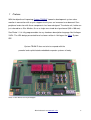
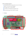
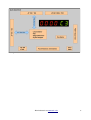
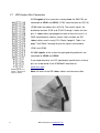
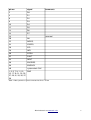
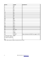
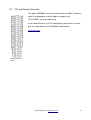
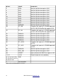
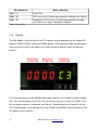
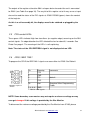
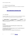
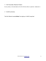
PRODUCT BRIEF SelfAssembly Kit Z80 Bus Monitor & Cycle Stepper User Manual Please read carefully before power up ! Doc. Version 201310281 Author: Mario Blunk Firmware Version: V1.1 Hardware Version: V1.1 Blunk electronic at www.trainz.de Table of Contents 1 Preface...............................................................................................................................3 2 Hardware............................................................................................................................4 2.1 Z80System Bus Connectors......................................................................................6 2.2 PIO and Debug Connector.........................................................................................9 2.3 Switches and PushButtons......................................................................................11 2.4 Display.......................................................................................................................12 2.5 CPU control LEDs.....................................................................................................13 2.6 JTAG / IEEE 1149.1...................................................................................................13 2.7 Schematics and Assembly Drawings........................................................................14 2.8 Power Supply............................................................................................................14 3 Self Assembly Shipment Option.......................................................................................15 4 RoHS conformity..............................................................................................................15 5 Useful Links......................................................................................................................16 6 Disclaimer.........................................................................................................................17 1 Preface With the objective of improving System TRAINZ toward a development system a bus monitor in connection with a cycle stepper circuitry was an immanent user demand. So a peripheral extension with these components has been designed. The whole unit, further on just referred to as Bus Monitor, fits on a single euro sized fourlayer board (160 x 100 mm). See Photo 1. It is fully programmable via any hardware description language like Verilog or VHDL. The HDLdesign presented here has been written in Verilog on the Xilinx System ISE. System TRAINZ does not aim to compete with the powerful and sophisticated embedded computer systems of today. Photo 1: Bus Monitor and Cycle Stepper Blunk electronic at www.trainz.de 3 What is the Bus Monitor good for ? Single Step Z80 mnemonics execution (Please have the listfile handy.) Address, Data and Control signal Debugging PIO mode to control user specific hardware LevelShifter from 5V Z80 world to 3,3V peripheral world Direct mounting on top of System TRAINZ via standoffs. 2 Hardware PIO & DEBUG 3,3V Bus Signals CPU control LEDs 3,3V Bus Signals JTAG PushButtons & Mode Switch Photo 2: Bus Monitor Top View 4 Blunk electronic at www.trainz.de 3,3V power in Drawing 1: Bus Monitor Block Schematic Blunk electronic at www.trainz.de 5 2.1 Z80System Bus Connectors All 5Vsignals of the system bus coming from the Z80 CPU are connected to JP101 and JP103. JP101 holds the data bus D[7..0], JP103 holds the address bus A[15..0]. The control signals are distributed on both JP101 and JP103. Drawing 2 shows the their pins. If ribbon cables get plugged on both of them the result is a GND signal between two bus signals. Most suitable are IDE ribbon cables used in many PCs (Photo 3 page 6). Table 1 on page 7 and Table 2 on page 8 give the signals connected to JP101 and JP103. All 3,3Vsignals of the system bus going to the peripherals are connected to JP102 and JP104. If not noted otherwise, the DC input/output specifications of these pins are to be found in the XC95288XL datasheet at Drawing 2: pins of JP101 / JP102 and JP103 / JP104 www.xilinx.com. Note: All wires of the IDEribbon cables must be accessible. Photo 3: 40 pin IDE connector 6 Blunk electronic at www.trainz.de pin no. signal 2 D0 4 D1 6 D2 8 D3 10 D4 12 D5 14 D6 16 D7 comments 18 reserved 20 /M1 22 /MREQ 24 /IOREQ 26 /RD 28 /WR 30 /RFSH 32 /HALT 34 /WAIT 36 /BUSREQ 38 /BUSACK 40 system clock CLK 1, 3, 5, 7, 9, 11, 13, GND 15, 17, 19, 21, 23, 25, 27, 29, 31, 33, 35, 37, 39 Table 1: Z80 system bus signals connected to JP101 / JP102 Blunk electronic at www.trainz.de 7 pin no. signal 2 A0 4 A1 6 A2 8 A3 10 A4 12 A5 14 A6 16 A7 18 A8 20 A9 22 A10 24 A11 26 A12 28 A13 30 A14 32 A15 34 EXT IEI 36 /INT 38 /NMI 40 /RESET comments Open collector with 300 Ohms against 3,3V 1, 3, 5, 7, 9, 11, 13, GND 15, 17, 19, 21, 23, 25, 27, 29, 31, 33, 35, 37, 39 Table 2: Z80 system bus signals connected to JP103 / JP104 8 Blunk electronic at www.trainz.de 2.2 PIO and Debug Connector The eight 3,3V PIO channels are to be found at JP601. Furtheron signals for debugging, schmitttrigger in/outputs and /CPU_RESET are accessible there. If not noted otherwise, the DC input/output specifications of these pins are to be found in the XC95288XL datasheet at www.xilinx.com. Drawing 3: pins of JP601 Blunk electronic at www.trainz.de 9 pin no. signal comments 2 PIO0 10k PullUpResistor against 3,3V 4 PIO1 10k PullUpResistor against 3,3V 6 PIO2 10k PullUpResistor against 3,3V 8 PIO3 10k PullUpResistor against 3,3V 10 PIO4 10k PullUpResistor against 3,3V 12 PIO5 10k PullUpResistor against 3,3V 14 PIO6 10k PullUpResistor against 3,3V 16 PIO7 10k PullUpResistor against 3,3V 18 DEBUG0 10k PullUpResistor against 3,3V 20 ST_IN0 Complies with specs of a CD4093 operated at 3,3V, 10k PullUpResistor against 3,3V 22 ST_IN1 Complies with specs of a CD4093 operated at 3,3V, 10k PullUpResistor against 3,3V 24 DEBUG1 10k PullUpResistor against 3,3V 26 DEBUG2 10k PullUpResistor against 3,3V 28 DEBUG3 10k PullUpResistor against 3,3V 30 DEBUG4 10k PullUpResistor against 3,3V 32 ST_OUT0 Complies with specs of a CD4093 operated at 3,3V 34 ST_OUT1 Complies with specs of a CD4093 operated at 3,3V 36 DEBUG5 10k PullUpResistor against 3,3V 38 RSV_100 10k PullUpResistor against 3,3V 40 /RESET Open collector with 300 Ohms against 3,3V 1, 3, 5 +3,3V Output to operate user periphery 9, 11, 13, 15, 17, 19, GND 21, 23, 25, 27, 29, 31, 33, 35, 37, 39 7 no connection Table 3: PIO and Debug Signals at JP601 10 Blunk electronic at www.trainz.de 2.3 Switches and PushButtons The operating mode of the Bus Monitor is to be set via the 8fold DILSwitch S602 / S4. Table 4 gives the operating modes available. Switch # state Mode / Meaning 1 off single step execution 1 on CPU free run 2 Parallel to PushButton S603 / S2 3 on CPU Reset active 3 off CPU Reset inactive 4 Parallel to signal DEBUG0 5 Parallel to signal DEBUG1 6 Parallel to signal DEBUG2 7 off display shows PIO state 7 on display shows bus address and data (in CPU free run or single step mode) 8 Parallel to signal RSV_GCK2 Table 4: DILSwitch S602 / S4 Blunk electronic at www.trainz.de 11 PushButton # Mode / Meaning S601 / S1 Reset CPU S603 / S2 CPU next cycle (if single step execution selected (see Table 4) S604 / S3 Temporarily CPU free run (if single step execution selected (see Table 4) as long as being pushed down Table 5: PushButtons 2.4 Display The Z80 Address and Data Bus or the PIO content may be displayed via the 6 digit LED displays DIS302, DIS301 (red) and DIS303 (green). In Bus Monitor mode the red displays show the current state of the address bus while the green display shows the data bus content. Adr[15:8] or I/O Adr. 52h Adr[7:0] or I/O Adr. 51h Data[7:0] or I/O Adr. 50h Photo 4: Display Readout on CPU Reset In PIO mode there are three eight bit wide output registers at I/O addresses 50h through 52h. They can be written at by CPU OUT commands any time. If switch 7 of S602 / S4 is off, the register content is displayed (see Table 4). Reading from these locations via the CPU IN commands is also possible any time. DIS302 and DIS301 show the content of the I/O addresses 51h and 52h. 12 Blunk electronic at www.trainz.de The output of the register at location 50h is of opendrain characteristic and is connected to JP601 (see Table 3 on page 10). The very bit of this register set to H may serve as input channel to read the status of the PIO signals at JP601. DIS303 (green) shows the content of that register. As this is a selfassembly kit, the displays need to be soldered or plugged by the user. 2.5 CPU control LEDs These green LEDs indicate HighLow transitions (or negative edges) occurring on the Z80 control signals. On edge detection the LED affected flashes for about 0,1 seconds. See Photo 2 on page 4. The meaning of the LEDs is self explaining. Note: The status of the CPU REFRESH signal is not displayed via an LED. 2.6 JTAG / IEEE 1149.1 To program the CPLD the IEEE1149.1 signals are accessible via JP105 .SeeTable 6. Drawing 4: pins of JP105 Pin Meaning 1 TCK 3 TMS 5 TDI 7 TDO 10 Vref 2, 4, 6, 8 GND comments default Required Xilinx Programming Cable Table 6: JTAG signals NOTE: Some boundary scan masters may not require a reference voltage or may even get damaged if this voltage is provided by the Bus Monitor. To disconnect the reference voltage provided by the Bus Monitor from JP105, please Blunk electronic at www.trainz.de 13 remove the jumper from JP106. 2.7 Schematics and Assembly Drawings As these drawings are updated from time to time they are not included in this document. Please find them at: http://www.trainz.de/trainz/hw 2.8 Power Supply The operating voltage of +3,3V into X101. Please refer to the assembly drawing for labeling of X101. The green LED D101 displays the presence of the operating voltage. operating voltage +3,3V current consumption max. 400 mA comments all LEDs on Table 7: power consumption MMU Warning: The board does NOT provide any protection against overvoltage or wrong connecting of the power lines ! The tolerance of the +3,3V operating voltage must meet the specifications given in the Xilinx XC95288XL datasheet ! Beyond this limits malfunctions or damage of the board may occur. 14 Blunk electronic at www.trainz.de 3 Self Assembly Shipment Option You may order just the bare boards of the Bus Monitor without any devices soldered on it. 4 RoHS conformity The Bus Monitor board without the displays is RoHS compliant. Blunk electronic at www.trainz.de 15 5 Useful Links Debug your hardware with the Logic Scanner at http://www.trainz.de/logic_scanner/Logic_Scanner_UM.pdf 16 Blunk electronic at www.trainz.de A complete embedded Z80 system can be found at http://www.trainz.de/trainz The Free and Open Productivity Suite LibreOffice at http://www.libreoffice.org Z80 Verilog and VHDL Cores at http://www.castinc.com and http://opencores.org Z80 Application Notes at http://www.trainz.de/trainz/index.html EAGLE an affordable and very efficient schematics and layout tool at http://www.cadsoftusa.com/ 6 Disclaimer This manual is believed to be accurate and reliable. I do not assume responsibility for any errors which may appear in this document. I reserve the right to change devices or specifications detailed herein at any time without notice, and do not make any commitment to update the information contained herein. I do not assume responsibility for any design errors which may appear in the hardware nor in the software of this product nor for modifications made by the user. This product is not authorized for use as critical component in life support devices or systems. Specifications mentioned in this manual are subject to change without notice. My Boss is a Jewish Carpenter Blunk electronic / Oolder Mario Blunk / Buchfinkenweg 5 / 99097 Erfurt / Germany +49 (0) 176 2904 5855 / http://www.trainz.de © 2013 Mario Blunk Printed in Germany Blunk electronic at www.trainz.de 17