1
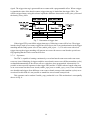
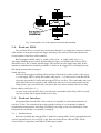
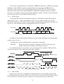
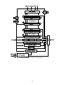
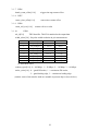
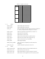
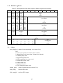
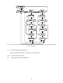
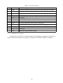
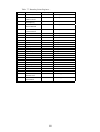
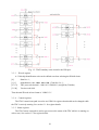
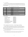
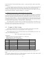
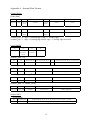
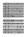
AMT-1
(ATLAS Muon TDC version 1)
User's Manual
Yasuo Arai
KEK, National High Energy Accelerator Research Organization
1-1 Oho, Tsukuba, Ibaraki 305, Japan
[email protected], http://atlas.kek.jp/~araiy/
Tel : +81-298-64-5366
Fax : +81-298-64-2580
ES Chip produced on Mar, 2000
Rev. 0.71 Jan. 11, 2001.
1
Contents
0.
BUGS AND FUTURE CHANGES......................................................................................................... 4
0.1.
0.2.
B UGS........................................................................................................................................... 4
F UTURE C HANGES ......................................................................................................................... 4
1.
INTRODUCTION................................................................................................................................ 5
2.
CIRCUIT DESCRIPTION.................................................................................................................... 6
2.1.
2.2.
2.3.
2.4.
2.5.
2.6.
2.7.
2.7.1.
2.7.2.
2.7.3.
2.7.4.
2.7.5.
2.7.6.
2.8.
2.9.
2.9.1.
2.9.2.
2.9.3.
2.10.
3.
F INE TIME MEASUREMENT .............................................................................................................. 7
C OARSE C OUNTER ......................................................................................................................... 8
C HANNEL B UFFER.......................................................................................................................... 9
ENCODER ..................................................................................................................................... 9
L1 B UFFER. .................................................................................................................................10
TRIGGER MATCHING. ....................................................................................................................10
TRIGGER INTERFACE. .....................................................................................................................12
Encoded trigger and resets.....................................................................................................12
Event count reset ..................................................................................................................13
Bunch count reset. ................................................................................................................13
Global reset.........................................................................................................................13
Trigger ...............................................................................................................................13
Separators...........................................................................................................................14
R EAD-OUT FIFO...........................................................................................................................15
R EAD-OUT INTERFACE. ..................................................................................................................15
Parallel read-out ..................................................................................................................15
Serial read-out .....................................................................................................................16
Packet format.......................................................................................................................16
ERROR MONITORING. .................................................................................................................18
CSR REGISTERS & JTAG ACCESS ..................................................................................................18
3.1.
C ONTROL REGISTERS .....................................................................................................................20
3.1.1.
CSR0..................................................................................................................................21
3.1.2.
CSR1..................................................................................................................................21
3.1.3.
CSR2..................................................................................................................................21
3.1.4.
CSR3..................................................................................................................................21
3.1.5.
CSR4..................................................................................................................................21
3.1.6.
CSR5..................................................................................................................................21
3.1.7.
CSR6..................................................................................................................................22
3.1.8.
CSR7..................................................................................................................................22
3.1.9.
CSR8..................................................................................................................................22
3.1.10.
CSR9..............................................................................................................................22
3.1.11.
CSR10............................................................................................................................23
3.1.12.
CSR11............................................................................................................................23
3.1.13.
CSR12............................................................................................................................24
3.1.14.
CSR13, 14.......................................................................................................................24
3.2.
S TATUS REGISTERS ........................................................................................................................25
3.2.1.
CSR16................................................................................................................................25
3.2.2.
CSR17................................................................................................................................26
3.2.3.
CSR18................................................................................................................................26
3.2.4.
CSR19................................................................................................................................26
3.2.5.
CSR20................................................................................................................................26
3.2.6.
CSR21................................................................................................................................26
3.3.
JTAG P ORT. ................................................................................................................................26
3.3.1.
JTAG controller and instructions ............................................................................................27
3.3.2.
Boundary scan registers.........................................................................................................28
3.3.3.
ID code register....................................................................................................................30
3.3.4.
Control registers..................................................................................................................30
3.3.5.
Status registers ....................................................................................................................30
3.3.6.
Core registers......................................................................................................................31
2
4.
4.1.
TIME ALIGNMENT BETWEEN HITS, CLOCK AND TRIGGER MATCHING ...................................31
EXAMPLE OF OFFSET S ETTING .........................................................................................................33
3
0 . Bugs and Future Changes
0 . 1 . Bugs
Following bugs are found in AMT-1 and will be fixed in AMT-2.
* Control Parity Error :
'Control Parity Error' (error_flags[7]) bit is prepared to indicate whether SEU (Single
Event Upset) is occured or not in the control registers.
When you set a value to the control register, control parity error may occur in 50%
probability. This occurs only if the JTAG tck cycle is longer than two clock cycle (50ns). In
the case when you write the CSR register through CIO lines, this error will occur if the CS
(chip Select) signlal width is longer than two clock cycle.
* Serial transmitter:
In some serial mode, strobe signal is not stable. See Table. 4.
0 . 2 . Future Changes
Following changes are planned in AMT-2.
* Reset Inputs :
This inputs are changed from LVDS signal to CMOS signal inputs.
pin 1 : RESETM --> RESETB (negative logic),
pin 2 : RESETP --> not defined yet.
* LVDS receiver :
Design of LVDS recever is changed to low-power version.
4
1 . Introduction
The ATLAS Muon TDC version 1 (AMT-1) is a Time to Digital Converter (TDC) designed for
the Monitored Drift Tubes (MDT) of the ATLAS muon detector. It is processed in Toshiba 0.3 µm
CMOS Sea-of-Gate Technology (TC220G).
Basic requirements on the AMT chip were summarized in ATLAS note (MUON-NO-179, May
1997) by J. Christiansen and Y. Arai. Then AMT-0 [1] was designed in a 0.7 µm full custom
CMOS process based on the 32 channel TDC for the quick test of front-end electronics and MDT
chambers.
On the other hand, it was decided to use a Toshiba's 0.3 µm CMOS process for a final
production. To develop and test many critical elements in the 0.3 µm process, a TEG (Test Element
Group) chip (AMT-TEG, [2])was designed, fabricated and tested successfully at KEK. The
AMT-TEG was processed in a new 0.3 µm process which will be used in final mass production.
The present AMT-1 design is based on the AMT-0, but many modifications are done since the
technology is different and many experience was obtained.
A time bin size (~0.78 ns) is obtained using the basic gate delay as the base for the time
measurement. This scheme prevents the use of very high speed clocks in the circuit and results in a
low power device (~20 mW/channel). The gate delay of CMOS devices normally have very large
variations as function of process, voltage, and temperature. In this TDC, a phase locked loop (PLL)
circuit is implemented to stabilize the gate delay. Oscillation frequency of the internal ring oscillator
is multiplied by two with the PLL, thus generate 80 MHz clock. This oscillator has 16 taps, and time
difference of two taps are exactly 1/16 of the clock period. When a hit enters, state of these 16 taps
are latched and generate a fine time. The fine time measurement is extended by a 13 bit coarse
counter.
Although the PLL clock is 80 MHz, most of the logic runs at 40MHz which is same as that of
the LHC clock.
Each channel can buffer 4 measurements until they can be written into a common 256 words
deep level 1 buffer. The individual channel buffers works as small derandomizer buffers before the
merging of hit measurements into the common L1 buffer. A trigger matching function can select
events related to a trigger. The trigger information consisting of a trigger time tag and an event ID
can be stored temporarily in an eight words deep trigger FIFO. Measurements matched to the trigger
are passed to a 64 words deep read-out FIFO, or
A time window of programmable size is available for the trigger matching to accommodate the
time spread of hits related to the same event. Optionally channels with hits in a time window before
the trigger can be flagged. The trigger time tag can optionally be subtracted from the measurements
so only time measurements relative to the trigger needs to be read out. Accepted data can be read out
in a direct parallel format or be serialized at a programmable frequency.
5
Fig. 1. Block diagram of the AMT-1
2 . Circuit Description
Fig. 1 shows a block diagram of the AMT-1 chip. There are 24 channels of inputs. Table. 1
summarizes the main features of the AMT-1 chip.
6
Table. 1 AMT-1 MAIN FEATURES
(System Clock Frequency is 40 MHz otherwise noted)
• Least Time Count
• Dynamic range
• Integral Non Linearity
• Differential Non Linearity
• Difference between channels
• Stability
• Input Clock Frequency
• PLL mode
• Internal System Clock
• No. of Channels
0.78 ns/bit (rising edge)
0.78-100ns/bit (falling edge)
RMS = 300 ps (rising edge) ?
RMS = 300ps ~ 29ns (falling edges)
13 + 4 = 17 bit (102.4 µsec)
Max = +/-80 ps ?
Max = +/- 80 ps ?
Maximum one time bin
< 0.1 LSB ? (3.0 - 3.6 V. 0 - 70 ˚C)
10 - 70 MHz (@ x2 mode)
x1, x2, x4 or x8
Input Clock x (PLL mode) / 2
24 Channels
• Level 1Buffer
• Read-out Buffer
• Trigger Buffer
256 words
64 words
8 words
• Double Hit Resolution
• Max. recommended Hit rate
• Hit Input Level
<10 ns
500 kHz per channel
Low Voltage Differential Signaling (LVDS)
Internal 100 Ohm termination.
3.3+-0.3V (< 200 mA)
0 - 85 Deg. Cent
0.3 µm CMOS Sea-of-Gate (Toshiba TC220G)
die size: 6 mm x 6 mm
0.5 mm lead pitch, 144 pin plastic QFP
• Time Resolution
• Supply Voltage
• Temperature range
• Process
• Package
2.1.
Fine Time Measurement
The original idea of the TDC, which use internal gate delay as a fine time element and stabilize the
element with a feedback circuit, was born in 1986 [3]. The chip was called TMC (Time Memory
Cell) chip. Initial TMC chip use a DLL (Delay Locked Circuit) technique and then PLL (Phase
Locked Loop) technique has been used in recent chips.
In the PLL version, we have been using a new kind of voltage controlled ring oscillator,
asymmetric ring oscillator (Fig. 2). To obtain <1 ns timing resolution, 16 taps are extracted from the
oscillator. Fig. 2 shows a simplified schematics and its timing diagram of the asymmetric ring
oscillator. Fig. 2 only shows 8 stages but the actual chip implements 16 stages. The asymmetric ring
oscillator was creates equally spaced even number (16) of timing signals.
The PLL circuit comprises a phase frequency detector (PFD), a charge pump, a loop filter
(LPF), and a voltage-controlled oscillator (VCO; asymmetric ring oscillator in this case). An
external capacitor (Cvg) is required in the loop filter. The PLL has "divide by 2, 4, and 8" counter ,
thus the frequency of the VCO can be either the same or the “multiplied by 2, 4, or 8 ” of the input
frequency.
The propagation delay of the delay elements that determine the oscillation frequency of the
7
VCO is controlled through a control voltage (VGN).
When a hit occurs, the state of the 16 taps (and coarse counter) are latched into a hit register.
Fig. 2 (a) Asymmetric ring oscillator, (b) extracted timing signal.
2.2.
Coarse Counter
The dynamic range of the fine time measurement, extracted from the state of the VCO, is
expanded by storing the state of a clock synchronous counter. The hit signal may though arrive
asynchronously to the clocking and the coarse counter may be in the middle of changing its value
when the hit arrives. To circumvent this problem two count values, 1/2 a clock cycle out of phase,
are stored when the hit arrives (Fig. 3). Based on the fine time measurement from the PLL one of the
two count values will be selected, such that a correct coarse count value is always obtained.
The coarse counter has 13 bits and is loaded with a programmable coarse time offset (the LSB
is always 0) at reset. The coarse counter of the TDC will in ATLAS be clocked by the two times
higher frequency than the bunch crossing signal thereby the upper 12 bit of the coarse counter
becoming a bunch count ID of the measurement. The bunch structure of LHC is not compatible with
8
the natural binary roll over of the 12 bit coarse time counter. The bunch counter can therefore be
reset separately by the bunch count reset signal and the counter can be programmed to roll-over to
zero at a programmed value. The programmed value of this roll-over is also used in the trigger
matching to match triggers and hits across LHC machine cycles.
Fig. 3 Phase shifted coarse counters loaded at hit.
2 . 3 . Channel Buffer.
Each channel can store 4 TDC measurements before being written into the common L1 buffer.
The channel buffer is implemented as a FIFO controlled by an asynchronous channel controller. The
channel controller can be programmed to digitize individual leading and/or trailing edges of the hit
signal. Alternatively the channel controller can produce paired measurements consisting of one
leading edge and the corresponding trailing edge.
If the channel buffer is full when a new hit arrives it will be ignored (rejected), but the
information of the rejected hit is transferred with next valid hit. If the enable_rejected bit in CSR10 is
set, the information of the rejected hit is transferred as soon as the channel buffer is available.
For the hits stored in the channel buffers to be written into the clock synchronous L1 buffer a
synchronization of the status signals from the channel buffers is performed. Double synchronizers
are used to prevent any metastable state to propagate to the rest of the chip running synchronously at
40 MHz. When paired measurements of a leading and a trailing edge is performed the two
measurements are taken off the channel buffer as one combined measurement.
2.4.
Encoder
When a hit has been detected on a channel the corresponding channel buffer is selected, the
time measurement done with the ring oscillator is encoded into binary form (vernier time), the
correct coarse count value is selected and the complete time measurement is written into the L1
buffer together with a channel identifier.
Although the ring oscillator and the coarse counter runs at 80 MHz, the base LHC clock is 40
MHz and bunch number is counted at 40 MHz. Most of logics in the AMT1 are designed to run at 40
MHz. To shift from 80 MHz to 40MHz regime, we would like to define different name to measured
9
time. We call the upper 12 bit of the coarse counter as a ‘coarse time’, and the LSB of the coarse
counter plus the vernier time as a ‘fine time’. Thus the coarse time will be equivalent to the bunch
count.
Fig. 4. Definition of coarse time and fine time.
In case a paired measurement of leading and trailing edge has been performed the complete time
measurement of the leading edge plus a 8 bit pulse width is written into the L1 buffer. The 8 bit
pulse width is extracted from the leading and trailing edge measurement taking into account the
programmed roll-over value. The resolution of the width measurement is programmable. In case the
pulse width is larger than what can be represented with a 8 bit number the width will be forced to a
value of $FF (Hex).
When several hits are waiting in the channel buffers an arbitration between pending requests is
performed. New hits are only allowed to enter into the active request queue when all pending
requests in the queue have been serviced. Arbitration between channels in the active request queue is
done with a simple hardwired priority (channel 0 highest priority, channel 23 lowest priority).
The fact that new requests only are accepted in the active request queue when the queue is
empty enables all channels to get fair access to the L1 buffer.
2.5.
L1 Buffer.
The L1 buffer is 256 hits deep and is written into like a circular buffer. Reading from the buffer
is random access such that the trigger matching can search for data belonging to the received
triggers. If the L1 buffer runs full the latest written hit will be marked with a special full flag. When
the buffer recovers from being full the first arriving hit will be marked with a full recover flag.
These flags are used by the following trigger matching to identify events which may have lost
hits because of the buffer being full.
2.6.
Trigger Matching.
Trigger matching is performed as a time match between a trigger time tag and the time
measurements them selves. The trigger time tag is taken from the trigger FIFO and the time
measurements are taken from the L1 buffer. Hits matching the trigger are passed to the read-out
FIFO. Optionally the trigger time tag can be subtracted from the measurements (enable_relative = 1)
such that all time measurements read out are referenced to the time (bunch crossing) when the event
of interest occurred.
10
Fig. 5. Trigger latency and trigger window related to hits on channels. There are 3 time counters ;
coarse time, trigger time and reject time counters.
A match between the trigger and a hit is detected within a programmable time window (Fig. 5)
if enable_match is set. The trigger is defined as the coarse time count (bunch count ID) when the
event of interest occurred. All hits from this trigger time until the trigger time plus the matching
window will be considered as matching the trigger. The trigger matching being based on the coarse
time means that the “resolution” of the trigger matching is one clock cycle (40MHz) and that the
trigger matching window is also specified in steps of clock cycles. The maximum trigger latency
which can be accommodated by this scheme equals half the maximum coarse time count = 2 1 2 /2 =
2048 clock cycles = 51 us. The trigger matching function is capable of working across roll-over in
all its internal time counters. For a paired measurement the trigger matching is performed on the
leading edge of the input pulse.
The search for hits matching a trigger is performed within an extended search window to
guarantee that all matching hits are found even when the hits have not been written into the L1 buffer
in strict temporal order. For normal applications it is sufficient to make the search window ~8 larger
than the match window. The search window should be extended for applications with very high hit
rates or in case paired measurements of wide pulses are performed (a paired measurement is not
written into the L1 buffer before both leading and trailing edge have been measured).
To prevent buffer overflow and to speed up the search time an automatic reject function can
reject hits older than a specified limit when no triggers are waiting in the trigger FIFO and
enable_auto_reject bit is set. A separate reject counter runs with a programmable offset to detect hits
to reject.
The trigger matching can optionally search a time window before the trigger for hits which may
have masked hits in the match window if enable_mask bit is set. A channel having a hit within the
specified mask window will set its mask flag. The mask flags for all channels are in the end of the
trigger matching process written into the read-out FIFO if one or more mask flags have been set.
In case an error condition (L1 buffer overflow, Trigger FIFO overflow, memory parity error,
etc.) has been detected during the trigger matching a special word with error flags is generated if
enable_errmark and corresponding enable_error bits are set.
All data belonging to an event is written into the read-out FIFO with a header and a trailer if
enable_header and enable_trailer bits are set respectively. The header contains an event id and a
bunch id. The event trailer contains the same event id plus a word count.
The trigger matching function may also be completely disabled (enable_matching = 0) whereby
all data from the L1 buffer is passed directly to the read-out FIFO. In this mode the TDC have an
11
effective FIFO buffering capability of 256 + 64 = 320 measurements.
An example of setting is shown in 4.1.
2.7.
Trigger Interface.
The trigger interface takes care of receiving the trigger signal and generate the required trigger
time tag to load into the trigger FIFO. In addition it takes care of generating and distributing all
signals required to keep the TDC running correctly during data taking.
The TDC needs to receive a global reset signal that initializes and clears all buffers in the chip
before data taking. A bunch count reset and event count reset is required to correctly identify the
event ID and the bunch ID of accepted events. These signals can either be generated separately or be
coded on a single serial line at 40 MHz.
2.7.1. Encoded trigger and resets
Four basic signals are encoded using three clock periods (Table 1). The simple coding scheme
is restricted to only distribute one command in each period of three clock periods. A command is
signaled with a start bit followed by two bits determining the command. When using encoded
trigger and resets an additional latency of three clock periods is introduced by the decoding
compared to the use of the direct individual trigger and resets.
Selection between the encoded signals and the direct signals are schematically shown in Fig.
6.
Table 1 Encoded signal bit pattern.
Meaning
bit
210
Trigger
100
Bunch count reset
110
Global reset
101
Event count reset
111
12
Fig. 6. Simplified diagram of the clock, reset and trigger signals.
2.7.2. Event count reset
An event count reset loads the programmed event_count_offset into the event ID counter. In
addition a separator can be injected into the L1 buffer and the trigger FIFO if enable_sepa_evrst is
set.
2.7.3. Bunch count reset.
The bunch count reset loads the programmed offsets into the coarse time counter, the trigger
time tag (bunch id) counter and the reject counter. In addition a separator can be injected into the L1
buffer and the trigger FIFO if enable_sepa_bcrst is set.
From a bunch count reset is given to the TDC until this is seen in the hit measurements
themselves, a latency of the order of 2 clock cycles is introduced by internal pipelining of the coarse
time counter. The definition of time 0 in relation to the bunch count reset is described in more detail
in section 4.
2.7.4. Global reset.
The global reset generate master_reset signal if enable_mreset_code is set (see Fig. 6). The
master_reset clears all buffers in the TDC and initializes all internal state machines to their initial
state. Before data taking an event count reset and a bunch count reset must also have been issued. As
shown in Fig. 6, decoder circuit, CSR, JTAG contrioller and PLL circuit are not reset by the
master_reset.
2.7.5. Trigger
The basis for the trigger matching is a trigger time tag locating in time where hits belong to an
event of interest. The first level trigger decision must be given as a constant latency yes/no trigger
13
signal. The trigger time tag is generated from a counter with a programmable offset. When a trigger
is signaled the value of the bunch counter (trigger time tag) is loaded into the trigger FIFO. The
effective trigger latency using this scheme equals the difference between the coarse_time_offset and
the bunch_count_offset.
Fig. 7. Generation of trigger data.
If the trigger FIFO runs full the trigger time tags of following events will be lost. The trigger
interface keeps track of how many triggers have been lost so the event synchronization in the trigger
matching and the DAQ system is never lost (enable_trfull_reject = 1). For each event with a lost
trigger time tag the trigger matching will generate an event with correct event id and a special error
flag signaling that the whole event has been lost.
2.7.6. Separators
The TDC is capable of running continuously even when bunch count resets and event count
resets are issued. Matching of triggers and hits across bunch count resets (different machine cycles)
are handled automatically if the correct roll-over value have been programmed. Alternatively it is
possible to insert special separators in the trigger FIFO and the L1 buffer when a bunch count reset
or an event count reset have been issued (enable_sepa_bcrst or enable_sepa_evrst). These will make
sure that hits and triggers from different event count or bunch count periods (machine cycles) never
are mixed. In this mode it is not possible to match hits across bunch count periods.
This separator can be readout if enable_sepa_readout bit is set. This mechanism is conceptually
shown in Fig. 8.
14
Fig. 8 Conceptual view of the separator insertion and matching.
2.8.
Read-out FIFO.
The read-out FIFO is 64 words deep and its main function is to enable one event to be read out
while another is being processed in the trigger matching. If the read-out FIFO runs full there are
several options of how this will be handled.
Back propagate (enable_rofull =0, enable_l1full_reject = 0, enable_trfull_reject = 0 ):
The trigger matching process will be blocked until new space is available in the read-out FIFO.
When this occurs, the L1 buffer and the trigger FIFO will be forced to buffer more data. If this
situation is maintained for extended periods the L1 buffer or the trigger FIFO will finally become
full and the measurement is stopped.
Nearly full reject:
In this mode the trigger matching will be blocked if either the L1 buffer (enable_l1full_reject =
1) or the trigger FIFO is nearly full (enable_trfull_reject = 1). If this occurs event data will be
rejected to prevent the L1 buffer and the trigger FIFO to overflow. The event header and event
trailer data will never be rejected as this would mean the loss of event synchronization in the
DAQ system. Any event which have lost data in this way will be marked with an error flag.
Reject (enable_rofull_reject =1 ):
As soon as the read-out FIFO full, event data (not event headers and trailers) will be rejected.
Any loss of data will be signaled with an error flag.
2.9.
Read-out Interface.
All accepted data from the TDC can be read out via a parallel or serial read-out interface in
words of 32 bits. The event data from a chip typically consists of a event header (if enabled),
accepted time measurements, mask flags (if enabled), error flags (if any error detected for event
being read out) and finally a event trailer (if enabled).
2.9.1. Parallel read-out
Read out of parallel data from the TDC is enabled by setting enable_serial=0 and performed via
a clock synchronous bus. Several TDC’s may share one read-out bus, and each TDC will be
selected with CS (chip select) and DSPACE (data space) signals.
15
The read out of individual hits are controlled by a DREADY (data ready) / GETDATA (get data)
handshake. If the GETDATA signal is constantly held active (independent of DREADY) it is
interpreted as the read-out can be performed at the full speed of the TDC. The effective read-out
speed can be slowed down by using the DREADY / GETDATA handshake protocol to introduce
wait cycles. The number of clock periods that the GETDATA signal is asserted is used to determine
the word count for the event available in the global trailer.
2.9.2. Serial read-out
The accepted TDC data can be transmitted serially over twisted pairs using LVDS signals by
setting enable_serial = 1. Data is transmitted in words of 32 bits with a start bit set to one and
followed by a parity bit and a stop bit. When no data is transmitted the serial data and clock lines are
kept at zero. The serialization speed is programmable from 80 to 10 Mbits/s.
Serial clock
Serial data
start
bit 31
bit 30
bit 1
bit 0
parity
stop
Fig. 9 :Serial frame format with start bit and parity bit
In addition to the serialized data an LVDS pair can carry strobe information in a programmable
format as shown in Fig. 9.
Leading Strobe: Direct serializing clock to strobe data on rising edge.
DS Strobe :
DS strobe format as specified for transputer serial links. DS strobe only
changes value when no change of serial data is observed.
For each format, there are two modes , one is continuous strobe regardless of data existance,
another mode generate strobe signal only when data is available.
Fig. 9. Different strobe types.
2.9.3. Packet format
Data read out of the TDC is contained in 32 bits data packets. For the parallel read-out mode
one complete packet (word) can be read out in each clock cycle. In the serial read-out mode a packet
is sent out bit by bit. The first four bits of a packet are used to define the type of data packet.
16
The following 4 bits are used to identify the ID of the TDC chip (programmable) generating the
data. Only 7 out of the possible 16 packet types are defined for TDC data. The remaining 9 packet
types are available for data packets added by higher levels of the DAQ system.
TDC header: Event header from TDC
31 30 29 28 27 26 25 24 23 22 21 20 19 18 17 16 15 14 13 12 11 10 9 8 7 6 5 4 3 2 1 0
1 0 1 0
TDC ID
Event ID
Bunch ID
TDC: Programmed ID of TDC.
Event ID: Event ID from event counter.
Bunch ID: Bunch ID of trigger (trigger time tag).
TDC trailer: Event trailer from TDC
31 30 29 28 27 26 25 24 23 22 21 20 19 18 17 16 15 14 13 12 11 10 9 8 7 6 5 4 3 2 1 0
1 1 0 0
TDC ID
Event ID
Word Count
Word count: Number of words from TDC (incl. headers and trailers).
Mask flags: Channel flags for channels having hits with in mask window
31 30 29 28 27 26 25 24 23 22 21 20 19 18 17 16 15 14 13 12 11 10 9
0 0 1 0
TDC ID
Mask flags
8 7 6 5 4
3 2 1 0
Mask flags: Channels flagged as having hits with in mask window.
Single measurement: Single edge time measurement
31 30 29 28 27 26 25 24 23 22 21 20 19 18 17 16 15 14 13 12 11 10 9 8 7 6 5 4 3 2 1 0
0 0 1 1
TDC ID
Channel
T E
Coarse Time
Fine Time
Channel: TDC channel number.
Coarse Time: Coarse time measurement (in bins of 25ns).
Fine Time: Fine time measurement from PLL (in bins of 25ns/32).
T: Edge type: 1 = leading edge, 0 = trailing edge.
E: Hit error. An error has been detected in the hit measurement (a coarse error, a channel select
error, or a l1 buffer error)
Combined measurement: Combined measurement of leading and trailing edge
31 30 29 28 27 26 25 24 23 22 21 20 19 18 17 16 15 14 13 12 11 10 9 8 7 6 5
0 1 0 0
TDC ID
Channel
Width
Coarse Time
4 3 2 1 0
Fine Time
Width: Width of pulse in programmed time resolution (CSR9 width_select). If the pulse width
excees the width range, the width will be $FF.
Coarse Time: Coarse time measurement of leading edge relative to trigger (in bins of 25ns).
Fine Time: Fine time measurement of leading edge (in bins of 25ns/32).
Errors: Error flags sent if an error condition have been detected
31 30 29 28 27 26 25 24 23 22 21 20 19 18 17 16 15 14 13 12 11 10 9
0 1 1 0
TDC ID
-
8 7 6 5 4 3 2 1 0
Error flags
Error flags: see Table. 2 and CSR16.
Debugging data: Additional information for system debugging
Separator
31 30 29 28 27 26 25 24 23 22 21 20 19 18 17 16 15 14 13 12 11 10 9
0 1 1 1
TDC ID
0 0 0 0
-
8 7 6 5 4
Bunch ID
3 2 1 0
Bunch ID: Trigger time tag counter when separator was generated.
Buffer Occupancy
31 30 29 28 27 26 25 24 23 22 21 20 19 18 17 16 15 14 13 12 11 10 9 8 7 6 5 4 3 2 1 0
0 1 1 1
TDC ID
0 0 0 1
R
L1 Occupancy
L1 occupancy: L1 buffer occupancy.
17
R: Read-out FIFO full.
2.10.
Error monitoring.
All functional blocks in the TDC are continuously monitored for error conditions. Memories
are continuously checked with parity on all data. All internal state machines have been implemented
with a “one hot” encoding scheme and is checked continuously for any illegal state.
The JTAG instruction register have a parity check to detect if any of the bits have been
corrupted during down load. The CSR control registers also have a parity check to detect if any of
the bits have been corrupted by a Single Event Upset (SEU). The error status of the individual parts
can be accessed via the CSR status registers.
Table. 2. Description of Errors Flags
Error
bit#
Description
Coarse error
0
A parity error in the coarse count has been detected in a channel buffer.
Channel select error
1
A synchronization error has been detected in the priority logic used to select the
channel being written into the L1 buffer.
L1 buffer error
2
Parity error detected in L1 buffer.
Trigger FIFO error
3
Parity error detected on trigger FIFO.
Matching state error
4
Illegal state detected in trigger matching logic.
Read-out FIFO error
5
Parity error detected in read-out FIFO.
Read-out state error
6
Illegal state detected in read-out logic.
Control parity error
7
Parity error detected in control registers.
JTAG error
8
Parity error in JTAG instruction.
Any detected error condition in the TDC sets its corresponding error status bit. The error bits
are reset by a global reset or error_reset (CSR0[10]). The error bits are also reset by bunch count
reset or event count reset if enable_errrst_bcrevr is set. All the available error flags are OR-ed
together with individual programmable mask bits to generate an ERROR signal. When the ERROR
signal becomes active the TDC can respond following ways:
Ignore:
No special action will be performed
Mark events: All events being generated after the error has been detected will be marked with a
special error flag.
3 . CSR Registers & JTAG access
There are two kinds of 12 bits registers, "CONTROL" and "STATUS" registers. The
"CONTROL" registers are readable and writable registers which control the chip functionality. The
"STATUS" registers are read only registers which shows chip statuses.
There are 15 Control registers (CSR0-14) and 6 Status registers (CSR16-21). These registers
are accessible from 12 bit bus (DIO[11:0]) or through JTAG interface.
18
Fig. 10. Structure of JTAG - CSR registers.
19
3 . 1 . Control registers
Table. 3. Bit assignment of the control registers.
11
10
9
8
CSR0 global_r error_ disable_ enable_
eset
reset encode errrst_
(0)
(0)
(0)
bcrevr
{11}
{10}
{9}
(0) {8}
CSR1
CSR2
CSR3
CSR4
CSR5
CSR6
CSR7
CSR8
CSR9
BIT
7
6
5
4
3
2
1
0
test_
test_ enable_ disable_ clkout_mode
pll_multi
mode invert direct ringosc
(0)
(0)
(0)
(0)
(0)
(0)
{7}
{6}
{5}
{4}
{3:2}
{1:0}
mask_window (0)
{23:12}
search_window (0)
{35:24}
match_window (0)
{47:36}
reject_count_offset (0)
{59:48}
event_count_offset (0)
{71:60}
bunch_count_offset (0)
{83:72}
coarse_time_offset (0)
{95:84}
count_roll_over (FFF)
{107:96}
width_select
tdc_id
(0)
(0)
(0)
{:115:113}
{112}
{111:108}
enable_ enable_ enable_ enable_ enable_ enable_ enable_ enable_
relative serial header trailer rejected pair trailing leading
strobe_select
readout_speed
(1)
(0)
{119:118}
{117:116}
CSR10 enable_ enable_ enable_ enable_
auto_ l1occup match mask
reject _readout
(1)
(0)
(1)
(0)
(0)
(0)
(0)
(0)
(0)
{131} {130} {129} {128} {127} {126} {125} {124} {123}
CSR11 enable_ enable_ enable_ enable_ enable_ enable_ enable_ enable_ enable_
rofull_ l1full_ trfull_ errmark mark_ ermark_ errmark l1ovr mreset_
reject
reject
reject
rejected rejected _ovr _detect code
(0)
(0)
(0)
(0)
(0)
(0)
(0)
(0)
(0)
{143} {142} {141} {140} {139} {138} {137} {136} {135}
CSR12 enable_ enable_ enable_
enable_
sepa_ sepa_ sepa_
error
readout bcrst
evrst
(0)
(0)
(0)
(1FF)
{155} {154} {153}
{152:144}
CSR13
enable_channel[11:0]
(FFF)
{167:156}
CSR14
enable_channel[23:12]
(FFF)
{179:168}
CSR15
(not used)
() -- initial value at reset. {} – JTAG bit No.
20
(0)
{122}
enable_
resetcb_
sepa
(0)
{134}
(0)
{121}
enable_
mreset_
evrst
(0)
{133}
(1)
{120}
enable_
setcount
_bcrst
(0)
{132}
3.1.1. CSR0
pll_multi[1:0] : The frequency ration between the external clock and the internal ring oscillator
frequency is determined by these bits as shown below.
pll_multi[1]
pll_multi[0]
Input frequency : Synthesized frequency
0
0
1:2
0
1
1:4
1
0
1:8
1
1
1:1
clkout_mode[1:0] : CLKOUT pin mode.
0 -- Start_Sync : Synchronized output of the START signal.
1 -- 40MHz clk : PLL clock / 2 output. This is the system clock used in most of logics.
2 -- 80 MHz clk : PLL clock outpuut.
3 -- Coarse Counter Carry. : Carry outout of the Coarse Counter. This can be used to extend
the time range.
disable_ringosc : Stop the oscillation of the ring oscillator and disable charge pump circuit of
the PLL.
enable_direct : enable direct input pins.
0 --- trigger/reset signals are came from encoded input (encontp/enccontm),
1 --- trigger/reset signals are came from direct input pins (trigp/trigm, bunchrstp/bunchrstm,
eventrstp/eventrstm).
test_invert : automatic inversion of test pattern in test mode.
test_mode : enable test mode.
enable_errrst_bcrevr : enable error reset when bunch count reset or event count reset is came.
disable_encode : disable fine time encoder and output 111.
error_reset : clear error bits in CSR16[8:0].
global_reset : Global reset of the TDC.
3.1.2. CSR1
mask_window[11:0]
mask window in number of clock cycles
3.1.3. CSR2
search_window[11:0]
search window in number of clock cycles
3.1.4. CSR3
match_window[11:0]
matching window in number of clock cycles
3.1.5. CSR4
reject_count_offset[11:0]
rejection counter offset
3.1.6. CSR5
event_count_offset[11:0]
event number offset
21
3.1.7. CSR6
bunch_count_offset[11:0]
trigger time tag counter offset
3.1.8. CSR7
coarse_time_offset[11:0]
coarse time counter offset
3.1.9. CSR8
count_roll_over[11:0]
3.1.10.
counter roll over value
CSR9
tdc_id[3:0]
TDC identifier. This ID is attached to the output data.
width_select[2:0] : Set pulse width resolution in pair measurement.
width select
width output
resolution(*)
max. width(*)
0
full_width[7:0]
0.78125 ns
200 ns
1
full_width[8:1]
1.5625 ns
400 ns
2
full_width[9:2]
3.125 ns
800 ns
3
full_width[10:3]
6.25 ns
1.6 µs
4
full_width[11:4]
12.5 ns
3.2 µs
5
full_width[12:5]
25 ns
6.4 µs
6
full_width[13:6]
50 ns
12.8 µs
7
full_width[14:7]
100 ns
25.6 µs
(*) at 40 MHz clock.
readout_speed[1:0] : 0 -- 40 Mbps, 1 -- 20 Mbps, 2 -- 10 Mbps, 3 -- 80 Mbps.
strobe_select[1:0] : 0 -- gated DS strobe, 1 -- continuous DS strobe,
2 -- gated leading edge, 3 -- continuous leading edge.
(caution: some of the transfer mode are unstable in present chip as show below.)
22
Table. 4. Unstable serial modes.
strobe
speed
comments
0
0
1
2
3
0
1
2
3
0
1
2
3
0
1
2
3
OK
OK
OK
OK (2 stop bits)
OK
OK
OK
unstable
strobe 1 cycle ahead
strobe 1/2 cycle ahead
strobe 1/4 cycle ahead
strobe none
strobe unstable
strobe unstable
strobe unstable
OK
1
2
3
3.1.11.
CSR10
enable_leading
enable leading edge measurement.
enable_trailing
enable trailing edge measurement
enable_pair
enable pair (leading and trailing edge) measurement. If this bit is
set, enable_leading and enable_trailing bits are masked.
enable_rejected
enable force generation of rejected hit. (see section 2.3)
enable_trailer
enable trailer in read-out data.
enable_header
enable header in read-out data.
enable_serial
enable serial read-out (otherwise parallel read-out)
enable_relative
enable read-out of relative time to trigger time tag
enable_mask
enable search and read-out of mask flags
enable_match
enable trigger matching
enable_l1occup_readout
enable read-out of l1 occupancy for each event (use for
debugging)
enable_auto_reject
enable of automatic rejection (see section 2.6)
3.1.12.
CSR11
enable_setcount_bcrst
enable all time counters to be reset on bunch count reset
enable_mreset_evrst
enable master reset on event reset
enable_resetcb_sepa
enable channel buffer reset when a separator is inserted
enable_mreset_code
enable master reset from global reset of the encoded_control
23
enable_l1ovr_detect
enable l1 buffer overflow detection
enable_errmark_ovr
enable error marking events with overflow
enable_errmark_rejected
enable error mark event if rejected seen during matching
enable_mark_rejected
enable special marker word for rejected hits
enable_errmark
mark all events with error word if internal error exists.
enable_trfull_reject
enable event data rejection if trigger FIFO nearly full
(see section 2.8)
enable_l1full_reject
enable event data rejection if L1 buffer nearly full
(see section 2.8)
enable_rofull_reject
enable event data rejection when read-out FIFO full
(see section 2.8)
3.1.13.
CSR12
enable_error[8:0]
ERROR signal is asserted if corresponding enable_error bit is
set.
enable_sepa_evrst
enable generate separator on event reset
enable_sepa_bcrst
enable generate separator on bunch count reset
enable_sepa_readout
enable read-out of internal separators (debugging)
3.1.14.
CSR13, 14
enable_channel[23:0]
enable individual channel inputs
24
3 . 2 . Status registers
Table. 5. Bit assignment of the status registers (all these registers are read only).
CSR16
CSR17
CSR18
11
rfifo_
empty
(1)
{11}
l1_
empty
(1)
{23}
tfifo_
empty
(1)
{35}
CSR19 coarse_
counter
[0]
(0) {47}
CSR20
CSR21
10
rfifo_
full
(0)
{10}
l1_
nearly_
full
(0)
{22}
tfifo_
nearly_
full
(0)
{34}
9
8
control_
parity
(1)
{9}
l1_
l1_
over_
over
recover flow
(1)
(0)
{21}
{20}
tfifo_ running
full
7
6
5
4
error_
flags
(0)
{8:0}
3
2
l1_
write_address
(0)
{19:12}
l1_
read_address
(0)
(0)
{33}
{32}
tfifo_
occupancy
(0)
{46:44}
(0)
{31:24}
l1_
start_address
(0)
{43:36}
0
0
0
0
0
(0)
{71}
(0)
{70}
(0)
{69}
(0)
{68}
(0)
{67}
coarse_counter[12:1]
(0)
{59:48}
0
(0)
{66}
() -- initial value at reset. {} --- JTAG bit No.
3.2.1. CSR16
error_flags[8:0] : status of error monitoring. (see section 2.10)
bit #
0: coarse error (parity error in the coarse counter)
1: channel select error (more than 1 channel are selected)
2: l1 buffer parity error
3: trigger FIFO parity error
4: trigger matching error (state error)
5: readout FIFO parity error
6: readout state error
7: control parity error
8: JTAG instruction parity error
control_parity
parity of control data (see section 2.10)
rfifo_full[0]
read-out FIFO full
rfifo_empty[0]
read-out FIFO empty
25
rfifo_
occupancy[5:0}
(0)
{65:60}
1
0
3.2.2. CSR17
l1_write_address[7:0] L1 buffer write address.
l1_overflow
L1 buffer overflow bit
l1_over_recover
L1 buffer overflow recover bit
l1_nearly_full
L1 buffer nearly full bit
l1_empty
L1 buffer empty bit
3.2.3. CSR18
l1_read_address[7:0]
L1 buffer read address
running
status of START signal
tfifo_full
trigger FIFO full bit
tfifo_nearly_full
trigger FIFO nearly full bit
trigger_fifo_empty
trigger FIFO empty bit
3.2.4. CSR19
l1_start_address L1 buffer start address
tfiffo_occupancy trigger FIFO occupancy (number of word in trigger FIFO)
coarse_counter Coarse counter bit 0
3.2.5. CSR20
coarse_counter[12:1]
Coarse counter bit [12:1]
3.2.6. CSR21
rfifo_occupancy[5:0]
Read-out FIFO occupancy (number of word in read-out FIFO)
3 . 3 . JTAG Port.
JTAG (Joint Test Action Group, IEEE 1149.1 standard) boundary scan is supported to be
capable of performing extensive testing of TDC modules while located in the system. Testing the
functionality of the chip itself is also supported by the JTAG INTEST and BIST capability. In
addition special JTAG registers have been included in the data path of the chip to be capable of
performing effective testing of registers and embedded memory structures. Furthermore, it is also
possible to access the CSR registers from the JTAG port.
JTAG TAP (Test Access Port) state diagram is shown in Fig. 11.
26
Fig. 11 JTAG TAP controller state diagram. Numbers in each states shown are state variable of the
TAP controller.
3.3.1. JTAG controller and instructions
The JTAG instruction register is 4 bits long plus a parity bit:
[3:0] ins[3:0] JTAG instruction
[4]
parity[0] parity of JTAG instruction
27
Table. 6. JTAG Instructions.
Parity Instruction:
Name Description
0
0000:
EXTEST. Boundary scan for test of inter-chip connections on module.
1
0001:
IDCODE. Scan out of chip identification code.
1
0010:
SAMPLE. Sample of all chip pins via boundary scan registers.
0
0011:
INTEST. Using boundary scan registers to test chip itself.
-
0100 - 0111: (not used)
1
1000:
CONTROL. Read/Write of control data.
0
1001:
(not used)
0
1010:
STATUS. Read out of status register information.
1
1011:
CORETEST. Read/Write internal registers for debugging.
0
1100:
BIST. Built In Self Test for Memories.
-
1101 - 1110: (not used)
0
1111
BYPASS. Select BYPASS register.
3.3.2. Boundary scan registers.
All signal pins of the TDC are passed through JTAG boundary scan registers. All JTAG test
modes related to the boundary scan registers are supported (EXTEST, INTEST, SAMPLE).
28
Table. 7. Boundary Scan Registers.
BSR #
0
1
2:25
26
27
28
29
30
31
32
:
53
54
55:74
75
76
77
78
79
80:84
85
86
87
88
89
Pin name
RESETP, RESETM
ENCCONTP,
ENCCONTM
HITP[0:23],
HITM[0:23]
BUNCHRSTP,
BUNCHRSTM
EVENTRSTP,
EVENTRSTM
TRIGP, TRIGM
CLKP, CLKM
DIOEN
do[0]
di[0]
:
do[11]
di[11]
do[12: 31]
GETDATA
START
DSPACE
WR
CS
RA[0:4]
CLKOUT
DREADY
ERROR
SERIOUTP,
SERIOUTM
STROBEP,
STROBEM
Input/Output
I
I
Comment
LVDS input
LVDS input
I
LVDS input
I
LVDS input
I
LVDS input
I
I
I
O
I
:
O
I
O
I
I
I
I
I
I
O
O
O
O
LVDS input
LVDS input
O
LVDS output
see Fig. 12
see Fig. 12
see Fig. 12
see Fig. 12
see Fig. 12
LVDS output
29
Fig. 12. JTAG boundary scan circuit for the DIO port.
3.3.3. ID code register
A 32 bit chip identification code can be shifted out when selecting the ID shift chain.
[0]
[11:1]
[27:12]
[31:28]
Start bit = 1,
manufacturer code =✣✣✣✤✔✣✣✤✤✔✣✣✣✔✜✻os❉❊❃❂✔✰o.✢,
TDC part code decimal = 1000 1011 1000 0011 (assignd by Toshiba)
Version code 0001
Thus the total ID code in hex format is '18B83131'.
3.3.4. Control registers
The JTAG control scan path is used to set CSR0-14 registers that should not be changed while
the TDC is actively running. See section 3.1 for register details.
3.3.5. Status registers
The JTAG status scan path is used to get access to the status of the TDC while it is running (or
after a run). See section 3.2 for register details.
30
3.3.6. Core registers
The JTAG core register scan path is used to perform extended testing of the TDC chip. This
scan path gives direct access to the interface between the channel buffers and first level buffer logic.
It is used in connection with the test_mode bits and is only intended for verification and production
tests of the TDC chip.
Table. 8. Bit assignment of the core registers.
JTAG bit #
name
R/W
comments
[10:0]
matching_state[10:0]
R
monitoring of trigger matching state
[37:11]
trigger_data[26:0]
R
monitoring of active trigger data (*)
[38]
trigger_ready
R
monitoring of active trigger
[74:39]
l1_data[35:0]
R
monitoring of hit data to trigger matching (*)
[75]
l1_empty
R
monitoring of l1_empty flag
[76]
[168:77]
l1_data_ready
hit_data[91:0]
R
R/W
monitoring of l1_data_redy flag
monitoring/generation of hit_data (*)
[173:169]
[174]
hit_channel[4:0]
hit_select_error
R/W
R/W
monitoring/generation of hit_channel
monitoring/generation of hit_select_errort
[175]
hit_load
R/W
monitoring/generation of hit_load
(*) see Appendix A for internal format.
matching_state[10:0] :
state_waiting
state_write_event_header
state_write_occupancy
state_active
state_write_mask_flags
state_write_error
state_write_event_trailer
state_generating_lost_event_header
state_generating_lost_event_trailer
state_waiting_for_separator
state_write_separator
00000000001
00000000010
00000000100
00000001000
00000010000
00000100000
00001000000
00010000000
00100000000
01000000000
10000000000
4 . Time alignment between hits, clock and trigger matching
The TDC contains many programmable setups which have effects on the performed time
measurements and their trigger matching. The main time reference of the TDC is the clock and the
bunch reset which defines the T0 time. The time alignment can basically be divided into three
different areas as shown in the figure below.
A: Time relationship between the hits, clock and the bunch count reset generating the basic
timing measurements of the TDC.
B: Time relationship between the performed time measurements and the trigger time tag.
C: Time relationship between the time measurements and the automatic reject.
31
Fig. 12 :Time alignment between hits, trigger and automatic reject
A. Basic time measurement.
As previously stated the basic time reference of the TDC measurements is the rising edges of
the clock. The bunch count reset defines the T0 reference time where the coarse time count is loaded
with its offset value. The TDC also contains internal delay paths of the clock and its channel inputs
which influences the actual time measurement obtained. These effects can be considered as a time
shift in relation to the ideal measurement. The time shifts of individual channels may be slightly
different but care has been taken to insure that the channel differences are below the bin size (~1 ns)
of the TDC. The time shift of the measurements also have some variation from chip to chip and
variations with supply voltage and temperature. These variations have also been kept below the bin
size of the TDC by balancing the delay paths of the clock and the channels.
In Fig. 13, a hit signal is defined such that the time measurement equals zero
(coarse_time_offset = 0). The delay from the rising edge of the clock where the bunch reset signal
was asserted to the rising edge of the hit signal is for a typical chip 5 5 n s (two clock periods plus
5 n s).
Fig. 13 Definition of reference time measurement.
B. Alignment between coarse time count and trigger time tag.
To perform an exact trigger matching the basic time measurement must be aligned with the
positive trigger signal taking into account the actual latency of the trigger decision. The effective
trigger latency in number of clock cycles equals the difference between the coarse time offset and the
32
bunch count offset. The exact relation ship is: latency = (coarse_time_offset - bunch_count_offset)
modulus (21 2 ).
A simple example is given to illustrate this: A coarse_time_offset of 100 Hex (decimal 256) and
a bunch_count_offset of 000 Hex gives an effective trigger latency of 100 Hex (decimal 256).
Normally it is preferable to have a coarse time offset of zero and in this case the trigger count offset
must be chosen to (000 Hex - 100 Hex) modulus (21 2 ) = F00 Hex.
C. Alignment between trigger time tag and reject count offset.
The workings of the reject counter is very similar to the trigger time tag counter. The difference
between the course time counter offset and the reject counter offset is used to detect when an event
has become older than a specified reject limit. The rejection limit expression is (coarse_time_offset reject_count_offset) modulus (21 2 ). The rejection limit should be set equal to the trigger latency plus
a small safety margin. In case the extraction of masking hit flags are required the reject limit should
be set larger than the trigger latency + masking window + safety margin.
For a trigger latency of 100 Hex (same as in example in the section above) a reject limit of 108
Hex can be considered a good choice (no mask detection). This transforms into a reject count offset
of EF8 Hex when a coarse time offset of zero is used.
4.1.
Example of Offset Setting
In the LHC experiments there are 3564 clock cycles (88.924 usec/24.9501 ns) in a beam
revolution. Thus the count_roll_over (csr8) should be set 3563 ( 'deb' in hex).
For the trigger latency of 3 usec (120 clock), bunch_count_offset should be set to 3564 - 120 =
3444. This is summarized in Table. 9.
Table. 9 An example of register value setting.
Assumptions:
number of clock cycles per beam revolution (CC) = 3564 cycles
trigger latency (TL) = 120 cycles (3 µsec)
maximum drift time (DT) = 32 cycles (800 ns)
register
name
equation
value
csr1
mask_window
>= DT
32 ($20)
csr2
search_window
>= match_window + 8
40 ($28)
csr3
match_window
>= DT
32 ($20)
csr4
reject_count_offset
<= CC -TL -8
csr5
event_count_offset
csr6
bunch_count_offset
csr7
coarse_time_offset
csr8
count_roll_over (*)
3400 ($D48)
0
= CC - TL
3444 ($D74)
0
= CC -1
3563 ($DEB)
(*) At present design, count_roll_over must be greater than ($800+search_window). If the bunch
count reset signal is applied in each cycle, you can assume larger value for CC, such as CC =
4096.
' xxx_window' indicates window size, so all these parameter is positive value. 0x001 means 1 clock
tick window and 0xFFF means 4095 clock tick window.
33
' xxx_offset' indicates relative time between each counters. These offset is loaded into respective
counters when bunch count reset is asserted.
All counters are roll over at value ' count_roll_over'. Thus larger value than ' count_roll_over' has
no meaning for the window size and the offsets.
34
Appendix A : Internal Data Format
Channel Buffer
[first data]
45
44
43
42 41 40
rejected
edge
coarse2
parity
...
32 31 3 0
29
coarse2
coarse1
parity
...
75
28 27 26
...
18 17 1 6
15 14 13
coarse1
...
3210
vernier
[second data]
91
90
89
88 87 86
rejected
edge
coarse2
parity
74 75 7 6
coarse2
74 73 72
coarse1
parity
...
60 61 6 2 61 60 59
coarse1
...
44 45 4 6
vernier
if enable_pair = 0 : edge = 0 (trailing edge), edge = 1 (leading edge),
if enable_pair = 1 : edge = 0 (trailing edge found), edge = 1 (trailing edge not found)
Level 1 Buffer
35
34
33
32
parity
make_
separator_
stored
buffer_
overflow
overflow
[enable_pair = 0]
31
30
29 28 27 26 2 5
24 23 22 21 20 19 1 8
17
16 15 14 13 12 11 10 9 8 7 6 5 4 3 2 1 0
hit_error
reject_out
channel
0
edge
edge time
[enable_pair =1, normal data]
31
30
29 28 27 26 2 5
24 23 22 21 20 19 18 1 7
16 15 14 13 12 11 10 9 8 7 6 5 4 3 2 1 0
hit_error
reject_out
channel
width
leading edge time
[enable_pair =1, over_flow]
31
30
29 28 27 26 2 5
24 23 22 21 20 19 18 1 7
16 15 14 13 12 11 10 9 8 7 6 5 4 3 2 1 0
hit_error
reject_out
channel
11111111
leading edge time
[enable_pair =1, under_flow]
31
30
29 28 27 26 2 5
24 23 22 21 20 19 18 1 7
16 15 14 13 12 11 10 9 8 7 6 5 4 3 2 1 0
hit_error
reject_out
channel
00000000
leading edge time
Readout FIFO
Event Header
28
27 26 25 24
23 22 21 20 19 18 17 16 15 14 13 12 11 10 9 8 7 6 5 4 3 2 1 0
parity
1 0 1 0
trigger_data[23:0]
35
Lost Event Header
28
27 26 25 24
23 22 21 20 19 18 17 16 15 14 13 12
11 10 9 8 7 6 5 4 3 2 1 0
parity
1 0 1 0
lost_trigger[11:0]
trigger_data[11:0]
Event Trailer
28
27 26 25 24
23 22 21 20 19 18 17 16 15 14 13 12 11 10 9 8 7 6 5 4 3 2 1 0
parity
1 1 0 0
trigger_data[23:0]
Lost Event Trailer
28
27 26 25 24
23 22 21 20 19 18 17 16 15 14 13 12
11 10 9 8 7 6 5 4 3 2 1 0
parity
1 1 0 0
lost_trigger[11:0]
0
Error
28
27 26 25 24
23 22 21 20 19 18 17 16 15 14 13 12 11 10 9 8 7
6543210
parity
0 1 1 0
0
error_data
Mask Flags
28
27 26 25 24
23 22 21 20 19 18 17 16 15 14 13 12 11 10 9 8 7 6 5 4 3 2 1 0
parity
0 0 1 0
mask_flags[23:0]
Single Measurement (enable_relative =0)
28
27 26 25 24
23 22 21 20 19
18
17
16 15 14 13 12 11 10 9 8 7 6 5 4 3 2 1 0
parity
0 0 1 1
0
T
E
l1_data[16:0]
E : Hit Error = l1_data[31] | l1_data[30]
T : Edge Type = l1_data[17]
Single Measurement (enable_relative =1)
28
27 26 25 24
23 22 21 20 19
18
17
16 15 14 13 12 11 10 9 8 7 6 5
43210
parity
0 0 1 1
l1_data[29:25]
T
E
coarse_relative[11:0]
l1_data[4:0]
Combined Measurement (enable_relative=0)
28
27 26 25 24
23 22 21 20 19 18 17 16 15 14 13 12 11
10 9 8 7 6 5 4 3 2 1 0
parity
0 1 0 0
l1_data[29:17]
l1_data[10:0]
Combined Measurement (enable_relative=1)
28
27 26 25 24
23 22 21 20 19 18 17 16 15 14 13 12 11
10 9 8 7 6 5
43210
parity
0 1 0 0
l1_data[29:17]
corase_
relative[5:0]
l1_data[4:0]
Separator
28
27 26 25 24
23 22 21 20 19 18 17 16 15 14 13 12
11 10 9 8 7 6 5 4 3 2 1 0
parity
0 1 1 1
0
trigger_data[11:0]
Buffer Occupancy
28
27 26 25 24
23 22 21 20
19 18 17 16 15 14 13 12 11 10 9
8
76543210
parity
0 1 1 1
0 0 0 1
0
R
l1_occupancy[7:0]
R : Readout FIFO full
36
Trigger FIFO
26
25
parity trigger lost
24
23 22 21 20 19 18 17 16 15 14 13 12
11 10 9 8 7 6 5 4 3 2 1 0
separator
event id
bunch id
References
[1] AMT-0 manual. http://pcvlsi5.cern.ch:80/MicDig/amt.htm
[2] AMT-TEG. http://atlas.kek.jp/~araiy/amtteg/
[3] Y. Arai and T. Ohsugi; "An Idea of Deadtimeless Readout System by Using Time Memory
Cell", Proceedings of the Summer Study on the Physics of the Superconductiong
Supercollider, Snowmass, 1986, p.455-457.
37