1
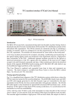
Vertex Detector Electronics:
ODE Pre-Prototype
User Manual
Issue:
Revision:
2
3
Reference:
Created:
Last modified:
IPHE 2000-008, LHCb 2001-057 VELO
28 February 2000
1 March 2002
Prepared By:
Yuri Ermoline
Vertex Detector Electronics: ODE Pre-Prototype
User Manual
Abstract
Ref: IPHE 2000-008, LHCb 2001-057 VELO
Issue: 2 Revision: 3
Date: 1 March 2002
Abstract
This document is a user manual for the ODE pre-prototype module (ODEPP, also frequently
referred as Read-out Board number 2, RB2). The module is under development and new
features are implemented in every new version.
Document Status Sheet
Table 1 Document Status Sheet
1. Document Title: Vertex Detector Electronics: ODE Pre-Prototype
2. Document Reference Number: IPHE 2000-008, LHCb 2001-057 VELO
3. Issue
page ii
4. Revision
5. Date
6. Implemented features
1
0
2 Mar 2000
VME slave interface A24/D32, CSR0, CSR1, FIFO,
VME trigger, PDU control, MODE=“00” implemented
(continuous data capture, starting on trigger)
1
1
22 Mar 2000
VME reset, TTC trigger, added 24-bit trigger counter
1
2
31 Mar 2000
Changed CSR1 format, added 12-bit FIFO counter,
trigger counter reduced to 12 bits
1
3
6 Jun 2000
Added IPHE reference number
CSR1(3..1)=”001” (module status)
Added Appendix A (Useful TTCvi commands)
Added Appendix B (FADC card dimensions)
2
0
10 Aug 2000
VME reset VRST(0) and VME TTCrx reset VRST(1)
Version & Revision, pseudo digital bit limits (CSR0)
TTCrx status CSR1(1), FADC card connector update,
new MODE=”01” implemented (event data capture,
starting on trigger and event header)
2
1
2 May 2001
VME TTCrx reset modified, OSI card description
added, new MODE=”10” implemented (event data
capture, starting on event header)
2
2
16 Oct 2001
FIFO counter modified (decrement on FIFO read), new
MODE=”11” implemented (event data capture, starting
on trigger)
2
3
1 Mar 2002
Trigger control modified (module is not triggered when
FIFO is full), external trigger disable bit CSR1(2) and
external trigger delay CSR0(7..5), FIFO VME interface
modified, write to CSR0/1 allowed when module is
busy, FIFO counter us modified, user manual updated
Vertex Detector Electronics: ODE Pre-Prototype
User Manual
Table of Contents
Ref: IPHE 2000-008, LHCb 2001-057 VELO
Issue: 2 Revision: 3
Date: 1 March 2002
Table of Contents
1 General description .
1.1
1.2
1.3
1.4
1.5
1.6
1.7
.
.
.
.
.
.
.
.
.
Module reset and TTCrx reset . . . . . . . .
Module clock . . . . . . . . . . . . . .
Module triggering . . . . . . . . . . . .
VME slave interface . . . . . . . . . . . .
ODEPP clock and trigger (TTCrx board and OSI card)
FADC card . . . . . . . . . . . . . . .
FADC clock phase adjustment . . . . . . . .
2 Module operation .
2.1
2.2
2.3
2.4
.
.
.
.
.
.
.
.
.
.
.
.
.
.
.
.
.
.
.
.
.
. .
. .
. .
. .
. .
. .
. .
.
.
.
.
. .
. .
. .
. .
. .
. .
. .
.
.
.
. .
. .
. .
. .
. .
. .
. .
.
MODE = “00” - continuous data capture, starting on trigger . . . .
MODE = “01” - event data capture, starting on trigger and event header
MODE = “10” - event data capture, starting on event header . . . .
MODE = “11” - event data capture, starting on trigger . . . . . .
3 References .
.
.
.
.
.
.
.
.
.
. .3
. .3
. .3
. .4
. .6
. .7
. .7
.
. 8
. . .9
. . .9
. . .9
. . 10
.
.
.
.
.
.
.
11
Appendix A. Useful TTCvi commands (from [7]). .
.
.
.
.
.
.
.
12
Appendix B. FADC card dimensions.
.
.
.
.
.
.
.
13
Appendix C. FADC card 50-pin DIN 41651 connector layout. .
.
.
.
14
.
.
. 1
.
.
.
.
.
.
page iii
Vertex Detector Electronics: ODE Pre-Prototype
User Manual
Glossary
Glossary
page iv
FADC
Flash Analog to Digital Converter
FIFO
First-In First-Out
FPGA
Field Programmable Gate Array
ODE
Off-Detector Electronics
TTC
Timing, Trigger and Control
Ref: IPHE 2000-008, LHCb 2001-057 VELO
Issue: 2 Revision: 3
Date: 1 March 2002
Vertex Detector Electronics: ODE Pre-Prototype
User Manual
1 General description
Ref: IPHE 2000-008, LHCb 2001-057 VELO
Issue: 2 Revision: 3
Date: 1 March 2002
1 General description
Vertex detector ODE pre-prototype module (ODEPP, also frequently referred as Read-out
Board number 2, RB2) is designed for the read-out of up to 4 analog links with multiplexed
signals from the vertex detector front-end chip(s) at 40 MHz. ODEPP is a 6U VME module,
2-unit wide. It consists of a main VME board and 3 daughter cards as shown on the Figure 1.
Config
ch3
FADC
ch2
8
8
FPGA
FLEX10K50
D32
VMEbus
A24
Buffers
TTCrx
32
ch1
FADC
ch0
8
8
32
FIFO
2K*32
5
PDU
Clock
Figure 1
The main VME board provides (see also Figure 2):
•
Altera FLEX PFGA EPF10K50RC240-3 (2880 logic elements and 10 embedded array
blocks of RAM, 2K bit each [1]), connector for FPGA configuration via down-load
cable and socket for the configuration EPROM (EPC1PC8).
•
Data buffers, address comparators and Base address rotary switches for the VMEbus
slave interface (A24/D32) which is used as a control and monitoring interface to the
module.
•
2K*32 bit of FIFO (4 SyncFIFO chips Cypress CY7C4231, 15 ns access time [2]).
•
40 MHz internal clock oscillator, programmable delay unit for FADC clock delay
(PDU15F-1 from Data Delay Devices [3]), LEMO connector for the BUSY output
signal (TTL open collector, active low), the Reset button and the green LED.
•
Connectors to a TTCrx board carrying a TTCrx chip [4] - the receiver chip of the
Timing, Trigger and Control (TTC) system, CERN microelectronics group design.
•
2 connectors for FADC cards (2-channels, 8-bit, 40 MHz, based on AD9059 from
Analog Devices [5]) and voltage regulators for FADC cards analog power.
One of the FADC cards can be replaced by the ECS interface prototype or the level-1 trigger
pre-processor interface prototype.
page 1
Vertex Detector Electronics: ODE Pre-Prototype
User Manual
1 General description
TTCrx board connectors
Ref: IPHE 2000-008, LHCb 2001-057 VELO
Issue: 2 Revision: 3
Date: 1 March 2002
Jumper Osc Conf EPROM FPGA PDU
LED
Rotary
switches
FIFOs
SW2 SW3
BUSY
SW4 SW5
Reset
TTCrx
board
VMEbus
Ch #1
Ch #0
FADC
card
FADC card connectors
Figure 2
page 2
Analog power
Vertex Detector Electronics: ODE Pre-Prototype
User Manual
1 General description
Ref: IPHE 2000-008, LHCb 2001-057 VELO
Issue: 2 Revision: 3
Date: 1 March 2002
1.1 Module reset and TTCrx reset
The ODEPP module are reset on power-on (sets to zero the module registers, counters and
FIFO read/write pointers) and can be reset by pressing push-button “Reset” on the front
panel or writing ‘1’ into bit 0 of the VMERESET register (see 1.4).
The TTCrx chip reset signal may be generated by writing ‘1’ and then ‘0’ into bit 1 of the
VMERESET register. The TTCrx chip reset procedure takes some times and during this time
the ODEPP module is not operational. TTCrx status (‘1’ = TTCrx is ready) can be read from bit
1 of the CSR1 register. The ODEPP module has to be reset after resetting the TTCrx chip as
internal registers may be in undefined states.
1.2 Module clock
The ODEPP module can be driven by internal clock from the 40 MHz clock oscillator or by
external clock, the clock source can be chosen by the jumper on the ODEPP module (see
Figure 2):
•
jumper inserted - internal 40 MHz clock from the oscillator,
•
jumper removed - external clock.
The external the clock may be generated (see 1.5):
•
by the TTC system (40 MHz clock) and delivered to the ODEPP board via optical
fibre to the TTCrx chip located on the TTCrx board,
•
by external clock generator (e.g. SEQSI module) and delivered to the ODEPP board
via coaxial cable to the OSI card; this clock may have frequency other than 40 MHz
(e.g. for test purposes).
Clocks for the FADC card connectors may be delayed in the range of (0-24) ns relatively to the
ODEPP module clock by the programmable delay unit (see 1.4 and 1.7). This feature may be
used to perform the input analog data scan (with certain scan range restrictions).
The whole ODEPP module clock can be delayed in the TTCrx chip in steps of 104 ps relatively
to the TTC transmitter. The TTCrx chip is controlled from the TTCvi module (see 1.5). This
feature may be used to perform a full range input analog data scan.
1.3 Module triggering
The ODEPP module can be triggered (if the module is not BUSY and the FIFO is not full):
•
from the VMEbus by writing ‘1’ into bit 1 of the CSR1 register (see 1.4).
•
from the external trigger system via TTCrx chip (using TTC system) or OSI card.
External trigger can be disabled by writing ‘1’ into bit 2 of the CSR1 and delayed in the range
of 0 to 7 clock cycles (see 1.4). The triggers (from VMEbus or external) are counted by the 12-bit
TRIGCNTR counter, which can be read from CSR1, bits 4 to 15.
page 3
Vertex Detector Electronics: ODE Pre-Prototype
User Manual
1 General description
Ref: IPHE 2000-008, LHCb 2001-057 VELO
Issue: 2 Revision: 3
Date: 1 March 2002
1.4 VME slave interface
The ODEPP module uses the P1 and P2 VMEbus connectors and works in A24/D32 mode.
Block Transfer mode is not implemented. The recognized Address Modifier codes are 3E, 3D,
3A, 39 (standard access).
The modules’s 16-bit Base Address (VME address bits A24..A08) can be selected by 4 internal
rotary switches (see Figure 2) in the range (0000-FFFF) hex:
•
SW2: VME address bits A23..A20
•
SW3:VME address bits A19..A16
•
SW4:VME address bits A15..A12
•
SW5:VME address bits A11..A08
The address map of the ODEPP module is shown below:
VME address bits A07..A00
Register
“00” hex
CSR0
“04” hex
CSR1
“08” hex
VRST
“10” hex
FIFO
Control/Status Register 0 (CSR0) - $00
Data Bit(s)
Write
Read
Comments
D4..D0
PDUDLY
PDUDLY
FADC cards clock delay
D7..D5
TRIGDLY
TRIGDLY
External trigger delay
D9..D8
MODE
MODE
Operation modes
D11..D10
No action
“00”
D13..D12
No action
REVISION
ODEPP module design revision
D15..D14
No action
VERSION
ODEPP module design version
D23..D16
PDBLL control
PDBLL status
Pseudo-Digital Bit Low Limit
D31..D24
PDBHL control
PDBHL status
Pseudo-Digital Bit High Limit
CSR0 provides storage for the static parameters of the ODEPP module:
page 4
•
PDUDLY - programmable delay unit control value for the FADC cards clock delay in
the range of (0-24) ns relatively to the ODEPP module clock (see 1.7),
•
TRIGDLY - external trigger delay in the range of 0 to 7 clock cycles,
•
MODE - the module operation mode (see 2)
•
PDBLL and PDBHL - the FADC data processing parameters (see 2.2).
Vertex Detector Electronics: ODE Pre-Prototype
User Manual
1 General description
Ref: IPHE 2000-008, LHCb 2001-057 VELO
Issue: 2 Revision: 3
Date: 1 March 2002
Control/Status Register 1 (CSR1) - $04
Data Bit(s)
Write
Read
Comments
D0
VMETRIG
MODBUSY
Start data acquisition from VMEbus
D1
No action
TTCREADY
TTCrx receiver chip ready
D2
TRIGDIS
TRIGDIS
External trigger disable
D3
No action
‘0’
D15..D4
No action
TRIGCNTR
12-bit TRIGGER up counter
D16
No action
FIFO Full
if ‘1’ - FIFO is full
D17
No action
FIFO Empty
if ‘1’ - FIFO is empty
D19..D18
No action
“00”
D31..D20
No action
FIFOCNTR
12-bit FIFO up counter
CSR1 is used to control and monitor the ODEPP module operation:
•
VMETRIG - module triggering from the VMEbus, starts data acquisition (see 2),
MODBUSY - set to ‘1’ according to the MODE of operation during data acquisition,
•
TTCREADY - status of the TTCrx receiver chip,
•
TRIGDIS - disable external trigger when set to ‘1’,
•
TRIGCNTR - 12-bit counter of triggers from VMEbus or external, reset by VMERESET
from VMEbus
•
FIFO status bits (Full and Empty), FIFO is empty after VMERESET,
•
FIFOCNTR - the FIFO counter; it is incremented by every write into the FIFO until
FIFO is full and is decremented by every read from the FIFO until FIFO is empty; it is
reset by VMERESET and by every new trigger.
VMERESET Register (VRST) - $08
Data Bit(s)
Write
Read
Comments
D0
VMERESET
‘0’
Reset from VMEbus
D1
TTCRESET
TTCRESET
Writing ‘1’ and then ‘0’ resets TTCrx
D31..D2
No action
“00..00”
Writing to bit 0 (VMERESET) generates ODEPP module reset (see 1.1). Writing ‘1’ and then ‘0’
into bit 1 (TTCRESET) generates TTCrx reset.
FIFO - $10
FIFO can be accessed (read/write) from VMEbus for test purposes.
Data Bit(s)
Write
Read
Comments
D31..D0
VME data
FIFO data
FIFO test
page 5
Vertex Detector Electronics: ODE Pre-Prototype
User Manual
1 General description
Ref: IPHE 2000-008, LHCb 2001-057 VELO
Issue: 2 Revision: 3
Date: 1 March 2002
After data acquisition FADC data can be read from the FIFO via VMEbus.
Data Bit(s)
Write
Read
Comments
D7..D0
FADC ch 0
FIFO data
FADC data after data acquisition
D15..D8
FADC ch 1
FIFO data
-”-
D23..D16
FADC ch 2
FIFO data
-”-
D31..D24
FADC ch 3
FIFO data
-”-
1.5 ODEPP clock and trigger (TTCrx board and OSI card)
The ODEPP module receives external clock and trigger signals via TTCrx board or OSI cards.
The TTCrx board contains the TTCrx chip (non radhard ES2 version [4]), the optical connector
with an integrated detector/preamplifier and some other components. The input optical
signal from the TTC transmitter carries 40 MHz clock and trigger signals. TTCrx receiver chip
can be reset by writing ‘1’ into bit 0 of the VMERESET register. The TTCrx status
(TTCREADY) can be read from bit 1 of the CSR1.
TTCvi
TTCvx
ODEPP
Clock
ECL
Clock
Clock
optical
TTCrx
Trigger
Ch A
NIM
or
ECL
Trigger
Ch B
VME (Reset, commands)
Figure 3
In order to operate the TTCrx board the TTC transmitter (TTCvx [6]) and the TTC control
module (TTCvi [7]) are necessary, as shown on the Figure 3. The 40.00 MHz clock signal (ECL
levels) and the Trigger signal (NIM or ECL levels) are provided by the external logic (e.g.
SEQSI module). Some useful TTCvi VMEbus commands are shown in Appendix A.
The OSI (ODE to SEQSI Interface) card is a simple electrical replacement of the TTCrx board.
Card has two LEMO00C connectors for Clock and Trigger input NIM signals and can be
driven directly by the external logic (e.g. SEQSI module) without need for the TTCvi and
TTCvx modules. OSI card provides clock and trigger signals to the ODEPP module and
doesn’t need a reset.
page 6
Vertex Detector Electronics: ODE Pre-Prototype
User Manual
1 General description
Ref: IPHE 2000-008, LHCb 2001-057 VELO
Issue: 2 Revision: 3
Date: 1 March 2002
1.6 FADC card
The 2 channels FADC card (drawing in Appendix B) contain input link receivers, amplifiers,
analog-to-digital converter AD9059 (dual 8-bit, 60 MSPS A/D converter) and output buffers.
The input signals from the LEMO connectors (EPG.0B.302.HLN) are differential in the range
from 0 to 1 Volts. The upper LEMO connector on the upper FADC card corresponds to FADC
channel #3 and the lower LEMO connector on the lower FADC card - to FADC channel #0.
The 50-pin DIN 41651 connector provides the digital and analog power, FADC clock and data
enable signals for the FADC card from the ODEPP module and the 2*8-bit output data from
the FADC card output buffers to the ODEPP module. The connector layout is shown in
Appendix C.
1.7 FADC clock phase adjustment
The clock for both FADC cards can be delayed n the range of (0-24) ns relatively to the ODEPP
module clock by the programmable delay unit (PDU15F-1, 5-bit digitally programmable
delay line) on the ODEPP module. The delay between the input clock of the PDU (clock on the
ODEPP module) and the output clock to the FADC cards depends on the PDU control code bits 0 to 4 of the CSR0:
Delay (ns) = Inherent Delay (ns) + Increment Delay (ns) * Control Code (hex)
where Inherent Delay = 9 ns, Increment Delay = 1 ns. The FADC AD9059 has aperture time of
about 3 ns. Therefore, the real measurement time, relatively to the ODEPP module clock, is
additionally delayed by 3 ns. The measuring time for different codes are given in the table
below:
Code
Time
Code
Time
Code
Time
0D
0
16
9
06
18
0E
1
17
10
07
19
0F
2
18
11
08
20
10
3
00
12
09
21
11
4
01
13
0A
22
12
5
02
14
0B
23
13
6
03
15
0C
24
14
7
04
16
15
8
05
17
The control codes 19 to 1F are equal to control codes 00 to 06 (clock delay of 25 ns is equal to
zero clock delay). The control codes from 10 to 16 shall not be used as the FADC data are not
guaranteed to be stable relatively to the ODEPP module clock. The PDU control code is set to
zero after power on and reset.
To perform a full range input analog data scan, the whole ODEPP module clock can be
delayed in the TTCrx chip in steps of 104 ps from the TTCvi module [7].
page 7
Vertex Detector Electronics: ODE Pre-Prototype
User Manual
2 Module operation
Ref: IPHE 2000-008, LHCb 2001-057 VELO
Issue: 2 Revision: 3
Date: 1 March 2002
2 Module operation
Module FIFO (2K*32-bit) can be tested by writing and reading from VME. Number of written
words are counted by the 12-bit FIFO counter, it is incremented by every write into the FIFO
until FIFO is full and is decremented by every read from the FIFO until FIFO is empty; it is
reset by VMERESET.
Before starting data acquisition cycle, the module has to be reset and the following parameters
may be set (default values are zeroes):
•
PDU control code PDUDLY - CSR0(4..0) - defines the FADC card connector clock
delay relatively to the module clock,
•
TRIGDLY - external trigger delay in the range of 0 to 7 clock cycles,
•
ODEPP operation mode - CSR0(9..8). The following modes are valid:
•
•
MODE = ”00” - continuous data capture, starting on trigger,
•
MODE = ”01” - event data capture, starting on trigger and event header,
•
MODE = “10” - event data capture, starting on event header,
•
MODE = “11” - event data capture, starting on trigger.
PDBLL and PDBHL - the FADC data processing parameters (see 2.2).
The module can be triggered from VME or external logic (see 1.3) while in modes “00”, “01”
or “11” and the module is not BUSY and the FIFO is not full. The triggers are counted by the
12-bit TRIGGER Counter, which can be read from CSR1(15..4). The trigger signal also resets
the 12-bit FIFO counter.
During the data acquisition the ODEPP module is busy (see next paragraphs) and:
•
MODBUSY is asserted and can be checked by reading CSR1(0),
•
BUSY output signal (TTL open collector, active low) on the front panel LEMO
connector is asserted,
•
CSR0, CSR1 and VMERESET registers can be read and witten from the VMEbus,
•
FIFO read and write is disabled while ODEPP module is busy (see next paragraphs),
due to the asynchronous VMEbus cycles this can be transparent, if not generates
VMEbus time out,
•
12-bit FIFO counter counts the number of data words, written into FIFO and can be
read via CSR1(31..20).
The status of the ODEPP module (MODBUSY) and the FIFO (FIFO full, FIFO empty and FIFO
counter) can be checked via CSR1 during and after data acquisition. The FADC data can be
read from the FIFO via the VMEbus interface after data acquisition.
page 8
Vertex Detector Electronics: ODE Pre-Prototype
User Manual
2 Module operation
Ref: IPHE 2000-008, LHCb 2001-057 VELO
Issue: 2 Revision: 3
Date: 1 March 2002
2.1 MODE = “00” - continuous data capture, starting on trigger
During this mode, after receiving the trigger, the output data from the FADC cards are written
into the FIFO every clock cycle until the FIFO is full (after 2K clock cycles or 51.2 µs). During
this time the ODEPP module is busy and FIFO read/write via VME is disabled.
The FIFO counter is reset by the trigger and then is incremented by every write into the FIFO
during data capture. The FIFO counter is decremented by every read from the FIFO via
VMEbus until FIFO is empty.
A position of the first event data word in the FIFO depends on the delay between the trigger
and the arrival of the data from the front-end chip (defined by external logic and cabling). The
trigger signal may be delayed inside the ODEPP module which results in the shifting of the
position of the first event data word in the FIFO towards beginning if the FIFO.
External triggers may be disabled in order to prevent next event data to be written to the FIFO
before FIFO is read via VMEbus.
2.2 MODE = “01” - event data capture, starting on trigger and event header
During this mode, after receiving the trigger, the synchronization logic in the module starts to
search for the event data header - pseudo digital “0101” in the analog signal package from the
SCTA128 chip [8].
The upper limit for the pseudo digital bit low level (PDBLL) and the lower limit for the
pseudo digital bit high level (PDBLL) are stored in the CSR0 (see 1.4). They are used by the
synchronization logic to define the windows for the digitized SCTA128 data during the
header search.
Upon detecting the header, the 12-bit TRIGCNTR counter value is written into the FIFO
followed by the SCTA128 event data (144 8-bit words). Up to 14 events can be stored in the
FIFO until the FIFO is full (last event may not be completely written into the FIFO if there is
no enough space left). During event data write into the FIFO (145 words, TRIGCNTR plus
event data) the ODEPP module is busy and FIFO read/write via VME is disabled.
The FIFO counter is incremented by every write into the FIFO. It is reset by every new trigger
and therefore contains the number of word written into the FIFO for the last event. The FIFO
counter is decremented by every read from the FIFO via VMEbus until FIFO is empty.
As in the MODE = “00”, external trigger may be delayed and disabled.
2.3 MODE = “10” - event data capture, starting on event header
Module operation in this mode is similar to the MODE=”01” with the exception that the
synchronization logic in the module starts to search for the event data header without waiting
for the trigger. During event data write into the FIFO (145 words, TRIGCNTR plus event data)
the ODEPP module is busy and FIFO read/write via VME is disabled.
page 9
Vertex Detector Electronics: ODE Pre-Prototype
User Manual
2 Module operation
Ref: IPHE 2000-008, LHCb 2001-057 VELO
Issue: 2 Revision: 3
Date: 1 March 2002
The FIFO counter is incremented by every write into the FIFO and contains the total number
of word written into the FIFO for all events. The FIFO counter is decremented by every read
from the FIFO via VMEbus until FIFO is empty.
The status of the FIFO (FIFO full, FIFO empty and FIFO counter) can be checked via CSR1
during data acquisition. The event data can be read from the FIFO via the VMEbus when
module is not busy.
2.4 MODE = “11” - event data capture, starting on trigger
Module operation in this mode is similar to the continuous data capture, starting on trigger
(MODE=”00”) with the exception that the number of word, written to the FIFO is limited per
event to 256. Therefore, up to 8 event may be stored in the FIFO until the FIFO is full.
During event data write into the FIFO (256 words) the ODEPP module is busy and FIFO
read/write via VME is disabled.
The FIFO counter is incremented by every write into the FIFO. It is reset by every new trigger
and therefore contains the number of word written into the FIFO for the last event. The FIFO
counter is decremented by every read from the FIFO via VMEbus until FIFO is empty.
As in the MODE = “00”, external trigger may be delayed and disabled.
page 10
Vertex Detector Electronics: ODE Pre-Prototype
User Manual
3 References
Ref: IPHE 2000-008, LHCb 2001-057 VELO
Issue: 2 Revision: 3
Date: 1 March 2002
3 References
[1]
FLEX 10K Embedded Programmable Logic Family Data Sheet, ver. 4.01, June 1999.
http://www.altera.com/document/ds/dsf10k.pdf
[2]
CYPRESS, CY7C4231 2Kx9 Sync FIFO.
http://www.cypress.com/cypress/prodgate/fifo/cy7c4231.html
[3]
5-Bit Programmable Delay Line.
http://www.datadelay.com/pdu15f.pdf
[4]
TTCrx Reference Manual. J.Christiansen, A.Marchioro and P.Moreira, Version 2.2.
http://pcvlsi5.cern.ch:80/MicDig/ttc/MANUAL22.PDF
[5]
Analog Devices. Products & Datasheets. Selection Guides.
http://www.analog.com/support/standard_linear/selection_guides/adc_high.html
[6]
TTCvx. Technical description and users manual. P.Gallno, Draft, May 21, 1999.
http://www.cern.ch/TTC/TTCvxManual1a.pdf
[7]
TTCvi. TTC-VMEbus INTERFACE, Ph.Farthouat, P.Gallno, Rev. 1.5.
http://www.cern.ch/TTC/TTCviSpec.pdf
[8]
SCTA128LC & SCTA128HC version 0.0, 13/02/98
page 11
Vertex Detector Electronics: ODE Pre-Prototype
User Manual
Appendix A. Useful TTCvi commands (from [7]).
Ref: IPHE 2000-008, LHCb 2001-057 VELO
Issue: 2 Revision: 3
Date: 1 March 2002
Appendix A. Useful TTCvi commands (from [7]).
The TTCvi module is A24, A16 / D32, D16 and responds to the following Address Modifiers:
39, 3A, 3D, 3E (standard), 29, 2D (short), 0F, 0B, 3B, 3F (block), 09, 0A, 0D, 0E (extended).
Four rotary switches are used to set the base address (A23 to A8).
The TTCvi module is normally driven by a clock from the TTC transmitter (e.g. TTCvx).
TTCvi provides four trigger inputs on the front panel (0 - ECL, 1,2,3 - NIM), trigger by a
VMEbus command and internal random trigger generator. The trigger source is selected by
setting CSR1(2..0). The selected trigger is made available as two front panel NIM outputs. An
internal 24-bit trigger counter (which can be read and written through VMEbus) counts the
number of triggers sent.
$84 - VMEbus module reset generation (Write, A24/D16)
Write access to this address generates module reset.
$80 - CSR1 - Input selection and timing (Read/Write, A24/D16) - trigger selection
CSR(2..0) = 0 (ECL front panel), 1, 2, 3 (NIM front panel), 4 (VMEbus command), 5 (random).
$86 - VMEbus trigger generation (Write, A24/D16)
Write access to this address generates trigger (if CSR(2..0) = 4) which is sent to the TTCrx chip.
$88 / $8A - Trigger counter (Read/Write, A24/D16)
$88(7..0) = Trigger Counter (23..16), $8A(15..0) = Trigger Counter (15..0)
The TTCvi module may be used to control the delay of the output clock of the TTCrx chip
relatively to the TTCrx input clock from the TTCvx module [7].
page 12
Vertex Detector Electronics: ODE Pre-Prototype
User Manual
Appendix B. FADC card dimensions.
Ref: IPHE 2000-008, LHCb 2001-057 VELO
Issue: 2 Revision: 3
Date: 1 March 2002
Appendix B. FADC card dimensions.
3.00 R
4.00
71.00
Top Side
5.00
4.00
1.50 R
2
50-pin DIN 41651 connector
1
49 50
4.00
12.54
117.00
page 13
Vertex Detector Electronics: ODE Pre-Prototype
User Manual
Appendix C. FADC card 50-pin DIN 41651 connector layout.
Ref: IPHE 2000-008, LHCb 2001-057 VELO
Issue: 2 Revision: 3
Date: 1 March 2002
Appendix C. FADC card 50-pin DIN 41651 connector layout.
Signal
Pin #
Pin #
Signal
-5V_ANALOG
1
2
-5V_ANALOG
CND_ANALOG
3
4
GND_ANALOG
+5V_ANALOG
5
6
+5V_ANALOG
FADC_CLOCK
7
8
-
ENABLE_B
9
10
FADC_B(7)
FADC_B(6)
11
12
FADC_B(5)
FADC_B(4)
13
14
FADC_B(3)
FADC_B(2)
15
16
FADC_B(1)
FADC1_B0)
17
18
-
SDA(I2C_1)*
19
20
SCL(I2C_1)*
SDA(I2S_2)*
21
22
SCL(I2C_2)*
-
23
24
-
-
25
26
-
POWER_DOWN
27
28
TDI*
TCKO*
29
30
TMS*
TDO*
31
32
TRST*
ENABLE_A
33
34
FADC_A(0)
FADC_A(1)
35
36
FADC_A(2)
FADC_A(3)
37
38
FADC_A(4)
FADC_A(5)
39
40
FADC_A(6)
FADC0_A7)
41
42
-
-
43
44
-
GND_DIGITAL
45
46
GND_DIGITAL
-
47
48
-
+5V_DIGITAL
49
50
+5V_DIGITAL
(*) - reserved for the ECS interface prototype card.
page 14