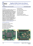
1
TE0720 User Manual
Authors:
Antti Lukats, Thorsten Trenz, Sven-Ole Voigt
Revision:
0.2
Date:
23-Mar-2015 14:07
TE0720 User Manual
Revision: 0.2
Table of Contents
Overview: TE0720 GigaZee Zynq SoM _____________________________________________________ 6
Features ___________________________________________________________________________ 6
Document Change History _____________________________________________________________ 7
Overview _____________________________________________________________________________ 8
Overview ___________________________________________________________________________ 8
Sample Applications __________________________________________________________________ 8
Key Features ________________________________________________________________________ 9
Embedded Development Suite __________________________________________________________ 9
Getting Started _______________________________________________________________________ 10
Preloaded (Factory default) SPI Flash Image ______________________________________________ 10
Boot Procedure _____________________________________________________________________ 12
FSBL (First Stage Bootloader) ______________________________________________________ 12
SSBL (Second Stage Bootloader) ____________________________________________________ 13
Boot Modes ________________________________________________________________________ 13
QSPI Boot Mode _________________________________________________________________ 14
Update the SPI Flash from an SD Card ___________________________________________ 14
Update the SPI Flash from a network ____________________________________________ 14
SD Card Boot Mode ______________________________________________________________ 16
Programming the FPGA with new Configurations ___________________________________________ 16
Configuring the FPGA via JTAG _____________________________________________________ 16
Configuring the FPGA by the Processing System (PS) ___________________________________ 16
Configuring the FPGA with U-Boot ___________________________________________________ 16
Configuring the FPGA in Linux ______________________________________________________ 17
Detailed Description ___________________________________________________________________ 18
Overview __________________________________________________________________________ 18
System Management, Power Supply & Resets _____________________________________________ 19
System Management Controller (SC) _________________________________________________ 20
Overview: System Management Controller (SC) ____________________________________ 20
Custom SC Programming _____________________________________________________ 20
SC B2B Pins _______________________________________________________________ 20
NOSEQ Pin ____________________________________________________________ 20
No Sequencing mode _______________________________________________ 21
Normal mode ______________________________________________________ 21
Normal mode with user function on NOSEQ ______________________________ 21
SC pins to the FPGA _________________________________________________________ 21
Default Mode _______________________________________________________________ 21
LED Control Status __________________________________________________________ 22
SC Demystified _____________________________________________________________ 24
SC Firmware ver 0.02 ________________________________________________________ 25
Version check __________________________________________________________ 25
Reading MAC Address ___________________________________________________ 26
SC Registers ___________________________________________________________ 26
Copyright © 2015 Trenz Electronic
GmbH
Page 2 of 88
http://www.trenz-electronic.de
TE0720 User Manual
Revision: 0.2
SC Update _________________________________________________________________ 28
SC Update on TE0703 ___________________________________________________ 28
SC Update on Custom Carrier Board ________________________________________ 29
Power Supply ___________________________________________________________________ 31
Power Supply Specifications ___________________________________________________ 31
Power Sequencer and System Management _______________________________________ 31
Power Rails ________________________________________________________________ 31
I/O Voltages ________________________________________________________________ 32
Example Application Diagrams _________________________________________________ 32
Dual Supply Application __________________________________________________ 32
3.3V Single Supply with no Power Sequencing ________________________________ 33
XADC Power _______________________________________________________________ 33
Backup Battery ______________________________________________________________ 34
Operating with a power supply of less than 3.1V ____________________________________ 34
AC & DC Characteristics ______________________________________________________ 35
AC Characteristic _______________________________________________________ 35
DC Characteristic _______________________________________________________ 35
Ethernet PHY Power-down ________________________________________________ 35
USB PHY Power-down ___________________________________________________ 36
Resets _________________________________________________________________________ 37
Software forced Resets _______________________________________________________ 37
Peripheral Resets ____________________________________________________________ 37
Board-level Components ______________________________________________________________ 38
DDR3 SDRAM ___________________________________________________________________ 39
Configuration _______________________________________________________________ 39
Manufacturer Documentation ___________________________________________________ 39
eMMC _________________________________________________________________________ 40
Format internal eMMC Card (Linux) ______________________________________________ 40
Ethernet ________________________________________________________________________ 42
Overview: Ethernet ___________________________________________________________ 42
Cable Diagnostic and VCT _____________________________________________________ 42
Media Autodetect ____________________________________________________________ 42
Advanced PHY Features ______________________________________________________ 42
Temperature sensor _____________________________________________________ 42
PHY Connections ____________________________________________________________ 43
SGMII/Fiber ____________________________________________________________ 44
PHY LED Control ____________________________________________________________ 45
Default behavior ________________________________________________________ 45
PHY LED Demo Design __________________________________________________ 45
Testing of the LED's _____________________________________________________ 46
On-board LEDs __________________________________________________________________ 48
Overview: On-board LEDs _____________________________________________________ 48
LED1 GREEN ______________________________________________________________ 48
LED2 RED _________________________________________________________________ 48
LED3 GREEN (FPGA Done) ___________________________________________________ 48
LED Status Codes ___________________________________________________________ 48
Copyright © 2015 Trenz Electronic
GmbH
Page 3 of 88
http://www.trenz-electronic.de
TE0720 User Manual
Revision: 0.2
TODO: MEMS ___________________________________________________________________ 50
RTC ___________________________________________________________________________ 51
USB ___________________________________________________________________________ 52
SPI Flash _______________________________________________________________________ 53
Programming _______________________________________________________________ 53
__________________________________________________________________________ 53
Board-level Interfaces ________________________________________________________________ 54
Zynq SoM: I/O Assignments ________________________________________________________ 55
MIO Bank 0 Usage ___________________________________________________________ 55
Compatibility with TE07xx series ________________________________________________ 56
I2C Peripherals __________________________________________________________________ 57
I2C Testing with U-Boot _______________________________________________________ 57
High-Speed I/O __________________________________________________________________ 58
Board-to-Board Connectors ________________________________________________________ 59
Mechanical Ratings: __________________________________________________________ 59
Manufacturer Documentation: __________________________________________________ 59
Pinout _____________________________________________________________________ 61
Connector left __________________________________________________________ 61
Connector top __________________________________________________________ 62
Connector bottom _______________________________________________________ 66
Technical Specifications ________________________________________________________________ 70
TE0720 Board Dimensions & Attributes __________________________________________________ 71
Dimensions _____________________________________________________________________ 71
Power Supplies __________________________________________________________________ 73
Temperature Ranges _____________________________________________________________ 73
Weight _________________________________________________________________________ 73
TE0720 Schematic __________________________________________________________________ 74
Carrier Boards for TE0720 ______________________________________________________________ 75
TE0701 Carrier Board ________________________________________________________________ 75
Configuring FMC Power Supply Voltage on TE0701 via I2C (CPLD Firmware Rev 0.1) __________ 75
Reading I2C-to-GPIO Status Register on TE0701 CPLD (CPLD Firmware Rev 0.1) _____________ 76
HDMI Interface of TE0720 on TE0701 Carrier Board _____________________________________ 78
TE0720 with TE0603 Carrier ___________________________________________________________ 79
______________________________________________________________________________ 79
Functions available with TE0603 _____________________________________________________ 79
UART Console __________________________________________________________________ 80
Carrier Board Checklist _______________________________________________________________ 81
Schematic Checklist ______________________________________________________________ 81
PCB Checklist ___________________________________________________________________ 81
Visual Check of Module placement ______________________________________________ 81
Handling and usage precautions _________________________________________________________ 83
General ___________________________________________________________________________ 83
Removal Instructions _________________________________________________________________ 83
Winbond 32MByte SPI Flash in 2013.4 ____________________________________________________ 85
Problem description: _________________________________________________________________ 85
Recovery Instructions: ________________________________________________________________ 86
Copyright © 2015 Trenz Electronic
GmbH
Page 4 of 88
http://www.trenz-electronic.de
TE0720 User Manual
Revision: 0.2
Disclaimer ___________________________________________________________________________ 87
Document Warranty __________________________________________________________________ 87
Limitation of Liability _________________________________________________________________ 87
Copyright Notice ____________________________________________________________________ 87
Technology Licenses _________________________________________________________________ 87
Environmental protection ______________________________________________________________ 87
REACH (Registration, Evaluation, Authorisation and Restriction of Chemicals) compliance statement _
88
RoHS (Restriction of Hazardous Substances) compliance statement ________________________ 88
WEEE (Waste Electrical and Electronic Equipment) ______________________________________ 88
Copyright © 2015 Trenz Electronic
GmbH
Page 5 of 88
http://www.trenz-electronic.de
TE0720 User Manual
Revision: 0.2
Overview: TE0720 GigaZee Zynq SoM
Figure 1: TE0720 GigaZee Zynq SoM (REV 01).
Features
1. 1.5A, 4MHz PowerSoC DC-DC Step-Down Converter with Integrated Inductor ( Enpirion EP53F8QI)
for 1.8V Power Supply
2. System Controller CPLD (Lattice LCMXO2-1200HC): 1,200 Macrocell CPLD with Block RAM, Flash
and PLL
3. User LED 1 (Green)
4. User LED 2 (Red)
5. 32 Mbyte Quad SPI Flash memory (Winbond W25Q256FV)
6. MEMS sensor (ST Microelectronics LSM303DTR): 3-axis accelerometer and 3-axis magnetometer
(Not populated!)
7. Real Time Clock with Embedded Crystal (Intersil ISL12020M): ±5ppm Accuracy
8. 1Gbyte = 2x 256Mbitx16 (32-bit wide) DDR3 Memory (Memphis MEM4G16D3EABG-125I)
9. e·MMC NAND Flash (Micron MTFC4GMVEA-4M, may also be different manufacturer due to
availability) usually 4 GByte, depends on assembly option
10. Xilinx Zynq-7000 System-on-Module (Xilinx XC7Z020) - Processing System: Dual ARM Cortex-A9,
unified 512Kbyte L2 Cache, 256Kbyte on-chip Memory, 54 Multiplexed I/O Pins (MIOs);
Programmable Logic: Artix-7 FPGA, 85K Logic Cells, 560 Kbyte extensible Block RAM (140x 36 Kbit
BRAM Blocks), 220 programmable DSP Slices, Dual 12bit 1Msps Analog-to-Digital Converter, 200 I
/O Pins (SelectIO Interfaces)
11. User LED 3 / FPGA Done (Green)
Copyright © 2015 Trenz Electronic
GmbH
Page 6 of 88
http://www.trenz-electronic.de
TE0720 User Manual
Revision: 0.2
12. 4A High-Efficiency Power SoC DC-DC Step-Down Converter with Integrated Inductor (Enpirion
EN6347) for 1.0V Power Supply
13. 1.5A, 4MHz PowerSoC DC-DC Step-Down Converter with Integrated Inductor ( Enpirion EP53F8QI)
for 1.5V Power Supply
14. Trenz 4x5 Module Socket Connector (3x Samtec LSHM Series Connectors)
15. Gigabit Ethernet Transceiver PHY (Marvell 88E1512)
16. Highly Integrated Full Featured Hi-Speed USB 2.0 ULPI Transceiver (Microchip USB3320C-EZK)
Document Change History
date
revision
authors
description
2014-02-10
0.2
Sven-Ole Voigt
Work in progress
2013-04-17
0.1
Antti Lukats, Thorsten Trenz
Initial release
All
Antti Lukats, Thorsten Trenz, Sven-Ole Voigt
Copyright © 2015 Trenz Electronic
GmbH
Page 7 of 88
http://www.trenz-electronic.de
TE0720 User Manual
Revision: 0.2
Overview
Overview
Trenz Electronic TE0720s are industrial-grade SoC modules integrating a Xilinx Zynq-7000 SoC, a gigabit
Ethernet transceiver, 1 gigabyte DDR3 SDRAM with 32-bit width, 32 megabyte Flash memory for
conguration and operation, a USB ULPI transceiver, and powerful switch-mode power supplies for all onboard voltages. A large number of congurable I/Os is provided via rugged high-speed stacking strips. All
modules in 4 x 5 cm form factor are mechanically compatible.
All this on a tiny footprint, smaller than a credit card, at the most competitive price.
Sample Applications
Cryptographic hardware module
Digital signal processing
Embedded industrial OEM platform
Embedded system design
Emulation platforms
FPGA graphics
FPGA video processing
Image processing
IP (intellectual property) cores
Parallel processing
Rapid prototyping
Reconfigurable computing
System-on-Chip (SoC) development
Copyright © 2015 Trenz Electronic
GmbH
Page 8 of 88
http://www.trenz-electronic.de
TE0720 User Manual
Revision: 0.2
Key Features
Industrial-grade Xilinx Zynq-7000 (Z-7020) SoM (system on module), supported by the free Xilinx
Vivado WebPACK tool
Rugged for shock and high vibration
ARM dual-core Cortex-A9
10/100/1000 tri-speed gigabit Ethernet transceiver (PHY) with SGMII
MAC Address EEPROM
32-Bit-wide 1 GByte DDR3 SDRAM
32 MByte QSPI Flash memory (with XiP support)
4 GByte eMMC (up to 64 GB)
Plug-on module with 2 × 100-pin and 1 × 60-pin high-speed hermaphroditic strips
152 FPGA I/Os (75 LVDS pairs possible) and 14 PS-MIO available on board-to-board connectors
USB 2.0 high-speed ULPI transceiver
On-board high-efficiency DC-DC converters
4.0 A x 1.0 V power rail
1.5 A x 1.5 V power rail
1.5 A x 1.8 V power rail
System management and power sequencing
eFUSE bit-stream encryption
AES bit-stream encryption
SHA-256 authentication chip with unique serial number
Temperature compensated RTC (real-time clock)
3 user LED's
Optional MEMS sensor (3D accelerometer and 3D magnetometer)
Evenly-spread supply pins for good signal integrity
Assembly options for cost or performance optimization available upon request.
Embedded Development Suite
A hardware development platform is available.
Latest documentation, design support files and reference designs with source files are available for
download free of charge.
Copyright © 2015 Trenz Electronic
GmbH
Page 9 of 88
http://www.trenz-electronic.de
TE0720 User Manual
Revision: 0.2
Getting Started
Preloaded (Factory default) SPI Flash Image
The TE0720 module comes with the SPI Flash preloaded with a default bootloader, U-Boot and Linux are
setup to run automatically if SPI flash boot mode is selected (Red LED fast blinking after power up). U-Boot
is configured with a standard 3 second delay to allow the U-Boot interactive console to be used. The
console is connected to PS UART0, mapped to MIO14 (UART0_RX) and MIO15 (UART0_TX), and has a
baud rate of 115200. The MIO14 and MIO15 signals are routed to the CPLD on the TE0701 Carrier Board
which, in turn, connects these PS UART0 RX and TX signals to the onboard FTDI USB to Multipurpose
UART/FIFO IC (FTDI FT2232H). Hence, the console output view can be easily accomplished (e.g., in SDK
"Terminal" window or in HTerm) by attaching it to the corresponding virtual COM port (the COM port number
may differ):
Please consult TE0701 Carrier Board User Manual | Connecting FTDI USB-to-UART/FIFO
Interface for more details on the required VCOM configuration!
Figure 1: Booting Linux Kernel (by default from SPI Flash) - SDK "Terminal" window
Copyright © 2015 Trenz Electronic
GmbH
Page 10 of 88
http://www.trenz-electronic.de
TE0720 User Manual
Revision: 0.2
Figure 2: Booting Linux Kernel (by default from SPI Flash) - Another (optional) console output, e.g., in
HTerm
After sucessfully starting the kernel on Xilinx Zynq, the following Linux prompt appears:
Copyright © 2015 Trenz Electronic
GmbH
Page 11 of 88
http://www.trenz-electronic.de
TE0720 User Manual
Revision: 0.2
Congratulations! You have been successfully booting up the preloaded SPI Flash image on the TE07020
GigaZee Zynq SoM.
The preloaded images provided are to demonstrate the board's capability. It is expected that the
customer will replace them with their own images.
Boot Procedure
FSBL (First Stage Bootloader)
The primary boot source for the TE0720 is the on-board SPI Flash. After power on the Zynq PS boot ROM
fetches the FSBL from the SPI Flash and executes it. Then the FSBL code takes over and initializes the
Zynq PS peripherals as well as the DDR3 memory controller. Finally the FSBL proceeds to load the PS
object code or FPGA configuration data. Primary factory FSBL for the TE0720 only loads SSBL (Second
Stage Bootloader) from SPI Flash and executes it. This way it is possible to boot the O/S (Linux) with or
without configuring the FPGA Fabric. Boot configuration can select the order of the images to be loaded. It
is possible that the SSBL loads the FPGA only, loads the FPGA and then loads and executes application (O
/S) code, or loads the user application without configuring the FPGA fabric.
FPGA images and application code can reside in on-board SPI Flash, in on-board eMMC or on an external
SD card.
Note: an FSBL image can not be loaded from eMMC. FSBL is fetched from SPI Flash or from an
external SD card.
Copyright © 2015 Trenz Electronic
GmbH
Page 12 of 88
http://www.trenz-electronic.de
TE0720 User Manual
Revision: 0.2
Note: Xilinx wizard generated FSBL does not properly initialize the SD card detect multiplexer
values. By default MIO0 remains selected. If writing your own FSBL it is necessary to initialize it
properly. TE0720 standard FSBL selects the EMIO63 pin for SD card detect and WP inputs (this
forces the card detect to succeed).
SD0_WP_CD_SEL = 0x003F003F;
SD1_WP_CD_SEL = 0x003F003F;
Pseudo code to initialize the CD and WP selection bit to point to EMIO63 (tied low if not connected in user
logic).
SSBL (Second Stage Bootloader)
Second stage bootloader is usually fetched from SPI flash. By default a customized U-Boot is used which is
responsible for loading the O/S. If U-Boot functionality is not needed then the user application could be
implemented as SSBL image.
Boot Modes
The Zynq-7000 generally supports several boot modes that can be selected by five boot mode pins
BOOT_MODE[4:0], where BOOT_MODE[4] / MIO[6] enables the PLLs. The other boot mode pins select the
boot source in the following way (see Xilinx Zynq-7000 AP SoC Technical Reference Manual, UG585 v1.
6.1, Table 6-2 on page 147):
BOOT_MODE[0]
MIO[5]
BOOT_MODE[2]
MIO[4]
BOOT_MODE[1]
MIO[3]
BOOT_MODE[3]
MIO[2]
Cascaded JTAG
0
Independent JTAG
1
JTAG
0
0
0
Quad-SPI
1
0
0
SD Card
1
1
0
0
Table 1: Zynq-7000 AP SoC Boot_Mode MIO Pins (Extract)
As it can be seen in Table 1 the only difference between Quad-SPI and SD Card boot mode is
BOOT_MODE[2] / MIO[4]. This is exactly the only signal which is controlled by the MODE output of the
TE0701 on-board CPLD. The BOOT_MODE[0] / MIO[5] and BOOT_MODE[1] / MIO[3] input pins are
tightend correspondingly, e.g., on the TE0720 Zynq SoC Module to pull-up (i.e., SPI-DQ3/M3 = PS_MIO5 =
1) and pull-down (i.e., SPI_DQ1/M1 = PS_MIO3 = 0) resistors.
Copyright © 2015 Trenz Electronic
GmbH
Page 13 of 88
http://www.trenz-electronic.de
TE0720 User Manual
Revision: 0.2
The TE0720 Zynq SoC Module on the TE0701 Carrier Boards supports two different boot modes:
QSPI and SD Card booting. For more information on configuring the boot mode please refer to "
TE0701 Carrier Board User Manual | Configuring Boot Mode".
QSPI Boot Mode
Xilinx Answer record AR47023
Currently writing to the SPI Flash is only possible from Vivado SDK starting from 2013.4 version.
Writing from Impact (any version) is not supported.
U-Boot functions can be used to update SPI Flash.
Xilinx Answer record AR57744 need to be followed, currently the system controller firmware does not
provide this safety function.
Update the SPI Flash from an SD Card
To update SPI Flash contents from files stored on an SD card use the U-Boot commands "fatload" and "sf".
Example:
Read boot.bin from SD Card to memory address 0x1000000
fatload mmc 0 0x1000000 boot.bin
Initialize SPI Interface
sf probe 0 0 0
Write 0x450000 bytes from address 0x1000000 to offset 0 in SPI Flash
sf update 0x1000000 0 0x450000
The default U-Boot environment has predefined command sequences to update SD Flash from an SD card.
This update contain files used for Linux boot (boot.bin, uImage, uramdisk.image.gz and tevicetree.dtb).
run sdfetch
run reflash_all
Update the SPI Flash from a network
To update SPI Flash via Ethernet the U-Boot commands "tftp" and "sf" can be used.
Copyright © 2015 Trenz Electronic
GmbH
Page 14 of 88
http://www.trenz-electronic.de
TE0720 User Manual
Revision: 0.2
Host PC network interface should have IP address 192.168.42.2. Direct connection from a host PC to the
board is recommended. It is possible to change the IP address of the board from U-Boot, but there could be
other issues when the connection goes via a corporate network.
TFTP server software should be installed on the host PC to provide file access via the TFTP protocol. A
TFTP server is no longer provided by Microsoft as part of the Windows O/S, so third-party software must be
used.
Example of TFTP server configuration
Download OpenTFTPServer from http://sourceforge.net/projects/tftp-server/
Install OpenTFTPServer
Run Open TFTP Server -> Configure from Start menu
Edit configuration file.
[LISTEN-ON]
192.168.42.2
[HOME]
c:\firmware\
[LOGGING]
All
[ALLOWED-CLIENTS]
[TFTP-OPTIONS]
Run Open TFTP Server -> Run Stand Alone
After configuration files in C:\firmware can be downloded via TFTP.
Example:
Download boot.bin from host PC to memory address 0x1000000
tftp 0x1000000 boot.bin
Initialize SPI Interface
sf probe 0 0 0
Write 0x450000 bytes from address 0x1000000 to offset 0 in SPI Flash
sf update 0x1000000 0 0x450000
Copyright © 2015 Trenz Electronic
GmbH
Page 15 of 88
http://www.trenz-electronic.de
TE0720 User Manual
Revision: 0.2
SD Card Boot Mode
TE0720 can also boot directly from an SD card. In this mode SPI Flash is not used (all code starting from
the FSBL is loaded from the SD card).
SDIO0 Bootable slot MIO pins have a 1.8V fixed I/O voltage so the SD card must be connected via
a level shifter on the carrier board.
Programming the FPGA with new Configurations
Configuring the FPGA via JTAG
Either Xilinx Impact or ChipScope can be used to load bitstreams over JTAG.
Configuring the FPGA by the Processing System (PS)
Files that can be used for FPGA configuration using the PS DEVCFG interface have to be binary bitstreams
with the preamble stripped and the bytes swapped within 32-bit words. The Xilinx bitgen tool can produce
files with a BIN extension and a stripped header, but the generated files do not have the correct byte swap.
Example for "promgen" parameters to convert bitstream "top.bit" to byte-swapped binary file "top.bin":
promgen.exe -w -b -p bin -o top.bin -u 0 top.bit -data_width 32
Bitstreams that do include PS instantiation have to be generated with CCLK as the startup clock.
Configuring the FPGA with U-Boot
The FPGA can be configured or reconfigured from the U-Boot prompt:
zynq-uboot> nm 0xf8007080
f8007080: 00000010 ? 0
f8007080: 00000000 ? x
zynq-uboot> nm 0xf8007080
f8007080: 00000000 ? x
zynq-uboot> fatload mmc 0 0x100000 top.bin
reading top.bin
4045564 bytes read in 628 ms (6.1 MiB/s)
zynq-uboot> fpga load 0 0x100000 0x3dbafc
Copyright © 2015 Trenz Electronic
GmbH
Page 16 of 88
http://www.trenz-electronic.de
TE0720 User Manual
Revision: 0.2
Writing 0 to address 0xF8007080 is a temporary fix for the first revision of the FSBL shipped. It is
required to make the FPGA configuration correctly both in U-Boot and in Linux. An explanation has
been given by a Xilinx employee on the Xilinx User Community Forums.
Configuring the FPGA in Linux
The FPGA can also be configured within Linux:
zynq> mkdir /tmp/sd
zynq> mount /dev/mmcblk1p1 /tmp/sd
zynq> cd /tmp/sd
zynq> cat top.bin > /dev/xdevcfg
You must apply the write to address 0xF8008070 in U-Boot before booting Linux, otherwise the
FPGA load will fail.
Copyright © 2015 Trenz Electronic
GmbH
Page 17 of 88
http://www.trenz-electronic.de
TE0720 User Manual
Revision: 0.2
Detailed Description
Overview
Figure 2: TE0720 GigaZee Zynq SoM Block Diagram
Copyright © 2015 Trenz Electronic
GmbH
Page 18 of 88
http://www.trenz-electronic.de
TE0720 User Manual
Revision: 0.2
System Management, Power Supply & Resets
Figure 3: Overview: TE0720 System Management, Power Supply & Resets
1
Note: The DDR3 SDRAM size depends on assembly option.
2
1.0V and 1.8V TE0720 power supply circuits are not shown to create a better overview (see TE0720 User Manual | Power
Supply for more details).
3
Four independent VCCIO voltages (VCCIO13, VCCIO33, VCCIO34, VCCIO35) are fully customizable (1.5V, 1.8V, 2.5V, 3.3V)
and can be chosen application-specifically (on a user defined "Carrier Board"). For example, on our "TE0701-03 Carrier Board"
the VCCIO voltages have been chosen on the one hand for VCCIO33 and VCCIO34 to be 2.5V by default (or alternatively 3.3V)
and on the other hand for VCCIO13 and VCCIO35 to be the user-programmable FMC_VADJ voltage via I2C (see TE0720 User
Manual | Carrier Boards for TE0720 - Configuring FMC Power Supply Voltage ) by default (or alternatively 2.5V and 3.3V,
respectively).
Copyright © 2015 Trenz Electronic
GmbH
Page 19 of 88
http://www.trenz-electronic.de
TE0720 User Manual
Revision: 0.2
System Management Controller (SC)
Overview: System Management Controller (SC)
A Lattice XO2-1200 CPLD is used as a System Management Controller (referred to as SC in the manual).
The SC is responsible for power sequencing, reset generation and Zynq initial configuration (mode pin
strapping). Moreover, some on-board ICs are connected to the SC that provides level shifting.
It is possible for the default SC functions and pin functions to be changed. This can be done as a request to
Trenz Electronic or it is possible for the user to generate their own designs. Please contact us for details.
The SC wakes up when the 3.3V input power rises above 2.1V (VIN voltage is not needed). The SC can
turn on or off all of the other supplies on the module (except in no power sequencing mode when the 1.0V
and 1.8 V supplies are forced to start immediately when power is applied to the module).
Custom SC Programming
SC customization is available either by requesting new features or with special agreement by using the
users own code. SC code can be updated in the system using the I2C interface. Please contact us for
details.
SC B2B Pins
SC is connected directly to the following B2B Pins.
Name
Mode
Default function
Alternative
Description
EN1
input, weak
pull-up
Power Enable
IO
High enables the DC-DC converters and on-board supplies. Not used if
NOSEQ=1
PGOOD
output, open
drain
Power good
SCL or IO
Forced low until all on-board power supplies are working properly.
MODE
input, weak
pull-up
Boot mode
SDA or IO
Force low for boot from the SD Card. Latched at power on only, not on
soft reset!
RESIN
input, weak
pull-up
Reset input
IO
Active Low Reset input, default mapping forces POR_B reset to Zynq PS
NOSEQ
input, weak
pull-down
Power
sequencing
Control
Output
Forces the 1.0V and 1.8V DC-DC converters always ON when high. Can
be used as an I/O after boot.
NOSEQ Pin
This is a dedicated input that forces the module's 1.0V and 1.8V supplies to be enabled if high. This pin has
a weak pull-down on the module. If left open the module will power up in normal power sequencing enabled
mode. This pin is 3.3V tolerant. This pin is also connected to the System Management Controller. The SC
can read the status of this pin (that is it can detect if the module is in power sequencing enabled mode). The
SC can also use this pin as output after normal power on sequence. Please check the SC description for the
function. SC rev 0.02 maps Ethernet PHY LED0 to NOSEQ by default (the mapping can be changed by
software after boot).
Copyright © 2015 Trenz Electronic
GmbH
Page 20 of 88
http://www.trenz-electronic.de
TE0720 User Manual
Revision: 0.2
No Sequencing mode
If the module is powered from a single 3.3V supply and power sequencing is disabled, then NOSEQ pin
should be powered from the main 3.3V input. That is VIN, 3.3Vin and NOSEQ should all be tied together to
the input 3.3V power rail. Sequencing mode should not be used if VIN is not 3.3V.
Normal mode
For normal operation leave NOSEQ open or pull down with a resistor.
Normal mode with user function on NOSEQ
NOSEQ can be used as an output after boot. NOSEQ must be low when 3.3V power is applied to the
module. Common usage is an LED connected between NOSEQ and GND.
SC pins to the FPGA
Schematic net name
Default function
Direction
SC pin
FPGA pin
XCLK
ETH PHY Clock to FPGA
to FPGA
K1
K19
X1
I2C Clock from FPGA
from FPGA
F1
L16
SCL from EMIO I2Cx
X7
I2C Data from FPGA
from FPGA
M1
N22
SDA from EMIO I2Cx
X5
I2C Data to FPGA
to FPGA
J1
P22
SDA to EMIO I2Cx
X2
ETH PHY LED1
to FPGA
C2
M15
X4
ETH PHY LED2
to FPGA
D1
P16
X3
Interrupt
to FPGA
B1
N15
RTC, MEMS Interrupt or PHY LED3
-
-
not used on TE0720-02
K16
normally not used tied to fixed level by SC
X0
PUDC
Description
It is recommended to use Vivado IP Core available for 2014.2 and later versions.
Default Mode
At power up the System Management Controller starts with default settings.
Pin/Function
Used as/Mapped to
ETH PHY LED0
XIO to FPGA
ETH PHY LED1
XIO to FPGA
ETH PHY LED2
Not used
ETH PHY CONFIG
Tied logic low
ETH CLK125MHz
Pass through FPGA B34 SRCC pin
ETH Clock Enable
Tied logic high
ETH PHY Reset
Internal RESET
MIO7
LED1
MEMS/RTC I2C
XIO to FPGA
Copyright © 2015 Trenz Electronic
GmbH
Notes
PHY Address set to 0
Page 21 of 88
http://www.trenz-electronic.de
TE0720 User Manual
Pin/Function
Used as/Mapped to
RTC Interrupt
-
MEMS Interrupt 1
-
MEMS Interrupt 2
-
eMMC Reset
Internal RESET
USB PHY Reset
Internal RESET
FPGA PUDC
Tied logic low
FPGA PROG_B
Tied logic high
Zynq Cascaded JTAG
Enabled (pulled low)
Zynq boot mode
SPI or SD, depending on bootmode pin
Zynq SRST
Tied logic high
Zynq POR
Internal POR/Reset
PLL
Not used
LED2
System Status LED
LED1
MIO7
NOSEQ Input
NOSEQ at power, LED out after boot
Revision: 0.2
Notes
Power Good 1.5V
Power Good VTT
MODE Input
I2C Address
Function
0x20
Status reg 1
0x21
Status reg 2
LED Control Status
The TE0720 on-board LED devices can be remapped to different functions.
Input port bit
Mapped to
0
Ethernet PHY LED0 output
1
Ethernet PHY LED1 output
2
Ethernet PHY LED2 output
3
PS MIO7
4
Returns RESIN pin level
5
Returns EN1 pin level
6
Returns NOSEQ pin level
Copyright © 2015 Trenz Electronic
GmbH
Page 22 of 88
http://www.trenz-electronic.de
TE0720 User Manual
Input port bit
Mapped to
7
Returns MODE pin level
Revision: 0.2
LED1 and LED2 function can be changed from the default behaviour using output port bits (3..0)
D3
D2
D1
D0
LED1 function as
0
0
0
0
Default (MIO7)
0
0
0
1
ETH PHY LED0
0
0
1
0
ETH PHY LED1
0
0
1
1
ETH PHY LED2
0
1
0
0
MIO7
0
1
0
1
Undefined
0
1
1
0
OFF
0
1
1
1
ON
1
x
x
x
Undefined
Copyright © 2015 Trenz Electronic
GmbH
Page 23 of 88
http://www.trenz-electronic.de
TE0720 User Manual
Revision: 0.2
SC Demystified
System Controller (SC for short) was designed to allow ZYNQ PS system to access module special
functions as early as possible without reducing the number of MIO pins that are fully user configurable.
This early communication channel is done using MIO52 and MIO53 pins that are used also as Ethernet
PHY management interface for the on-board Gigabit PHY.
In order to simplify the boot process and reduce the number of time the PS peripherals need to be
configured or re-initialized SC uses the same protocol on MIO52/MIO53 as the Gigabit PHY itself. This
means that FSBL Configures all peripherals to their final function, allocating MIO52 as MIO52 as Ethernet
MDIO Interface.
SC Controller appears as "Virtual Ethernet PHY" on the MDIO bus of PS Ethernet 0 Interface. This interface
is already available when Zynq PL Fabric is not configured.
It would have been possible to use I2C Protocol on MIO52/MIO53 but in such case some multiplexing would
be be needed to choose between two protocols, also it would be needed to change the Peripheral mapping
after first init by the FSBL.
For use cases where Ethernet PHY on TE0720 is not used at all, it is still possible to configure SC with
design that implements I2C Protocol on MIO52/MIO53 pins.
For most use cases the only need to use this interface is access to MAC Address info, this is normally done
by u-boot loader that fetches the MAC Address bytes and sets its environment variables accordingly. Linux
image will then also be started so that the MAC Address from EEPROM is used for Ethernet 0 Physical
interface.
Copyright © 2015 Trenz Electronic
GmbH
Page 24 of 88
http://www.trenz-electronic.de
TE0720 User Manual
Revision: 0.2
SC Firmware ver 0.02
This is the initial version of the System Controller with only a very limited function set implemented.
System Controller can be accessed as PHY with address 0x1A on the ETH0 Management bus (MIO pins
52, 53). Communication can be established anytime when ETH0 and management interface are enabled
also before FPGA PL Fabric is configured. Xilinx default FSBL and standard u-boot do not enable the
management interface. It can be done manually in u-boot
zynq-uboot> mm e000b000
e000b000: 00000010 ? 10
e000b004: 00080000 ? x
zynq-uboot>
The above command enables the management interface on ETH0. TE0720 FSBL does this already so
there is no need to do it manually. This command is needed when standard Xilinx wizard generated FSBL is
used with plain standard u-boot, TE0720 u-boot does this initialization also. Note: It seems the problem is in
the current u-boot for Zynq, where mii_init function is not defined and not invoked.
Version check
System Controller Firmware version and some other version info can be read with u-boot command mii info
:
zynq-uboot> mii info
PHY 0x00: OUI = 0x5043, Model = 0x1D, Rev = 0x01, 100baseT, FDX
PHY 0x1A: OUI = 0x7201, Model = 0x01, Rev = 0x00,
10baseT, HDX
zynq-uboot>
PHY at address 0x00 is the ETH0 onboard ethernet PHY Marvell 88E1512.
PHY at address 0x1A is the System Controller. OUI 0x7201 should be decoded as Model TE0720-01.
Model 0x01 is Assembly option. Rev 0x00 is the firmware major revision for the System Controller (Rev 0 is
the initial version).
Bit Decoding
Reg Addr
Bits
u-boot ENV Variable
Description
2
15:0
board
upper bits of SoM Model
3
15:10
board
lower bits of SoM Model
3
9:4
-
Assembly Variant
3
3:0
scver
SC Firmware Revision Major number
4
15:14
board
FPGA Speed Grade
4
13:12
board
FPGA Temperature Range (0=Commercial, 1=Extended, 2=Industrial)
4
7:0
scver
SC Firmware Revision Minor number
Copyright © 2015 Trenz Electronic
GmbH
Page 25 of 88
http://www.trenz-electronic.de
TE0720 User Manual
Revision: 0.2
Customized u-boot reads and decodes the model and assembly variant information and stores in readable
format in environment variables.
zynq-uboot> printenv board
board=TE0720-01-2IF
zynq-uboot>
Reading MAC Address
With u-boot command mii read:
zynq-uboot> mii read 1a 9-b
addr=1a reg=09 data=0004
addr=1a reg=0a data=A3AC
addr=1a reg=0b data=3911
zynq-uboot>
This command will read MAC Address from the System Controller. Note: This only works if the ETH0
interface is enabled and if FSBL has enabled MII Management console on ETH0 Interface. 0004A3 is OUI
part, AC3911 is the serialized part (lower bits of MAC address).
Customized u-boot does read MAC Address and stores it in environment variables as required, as a result,
proper MAC address is used both in u-boot as also in Linux. Setting up MAC Address for Linux involves
dynamic rewrite of FDT, this is done with u-boot script that starts Linux.
SC Registers
Most registers and functions are available via ETH PHY Management interface (MIO pins 52 and 53).
Addr
R/W
Descripion
0
RO
1
RO
2
RO
ID1
Identifier Register 1
3
RO
ID2
Identifier Register 2
4
RO
ID3
Identifier Register 3
5
RW
CR1
Control Register 1: LED's
6
RW
CR2
Control Register 2; XIO Control
7
RW
CR3
Control Register 3; Reset, Interrupt
8
RO
SR1
Status Register
9
RO
MAChi
Highest bytes of primary MAC Address
0xA
RO
MACmi
Middle bytes of primary MAC Address
0xB
RO
MAClo
Lowest bytes of primary MAC Address
0xC
-
0xD
RW
reserved do not use
MMD_CR
MMD Control Register
Copyright © 2015 Trenz Electronic
GmbH
Page 26 of 88
http://www.trenz-electronic.de
TE0720 User Manual
Addr
R/W
0xE
RW
0xF
-
reserved do no use
other
-
reserved do not use
Revision: 0.2
Descripion
MMD_AD
MMD Address/Data
System Controller version 0.02 does not support extended address space - registers 0xD and 0xE are readwrite accessible but do not have any function. In feature revision extended address will be used to control
SC PLL and other features.
Bit
Description
0
enable INT1
1
enable INT2
2
enable RTC_INT
3
enable PHY_LED2
CR3 bit description
Interrupt can be selected instead of PHY_LED2 on XIO6 pin, by setting CR2 bits 11 downto 8 to "0111"
Copyright © 2015 Trenz Electronic
GmbH
Page 27 of 88
http://www.trenz-electronic.de
TE0720 User Manual
Revision: 0.2
SC Update
Update files are here: http://www.trenz-electronic.de/de/download/d0/Trenz_Electronic/d1/TE0720-GigaZee
/d2/SystemController/d3/SC_0.03.html
System Controller Firmware can be updated on TE0720-02. The requirement for this is user control for pin
90 in JM1 connector.
Base board
SC Update supported
Notes
TE0701-05
No
JM1.90 is fixed GND and update mode can not be enabled
TE0703-03
YES
Requires TE0703 CPLD update to be done first, then TE0720-02 SC update is possible
TE0704-01
YES
TE0704 is dedicated base for TE0711, but it can be used to update TE0702-02 SC
Attention: Lattice Diamond or Lattice standalone Programmer has to be used to actually program
the CPLD's, ToolZ is used only for verification of current state.
SC Update on TE0703
TE0703 as delivered does not have the module SC update function enabled, as first step the TE0703 has to
be reprogrammed to enable module SC update. Download file...
S2.3 = OFF, JTAG to TE0703 on board CPLD is selected, USERCODE reads CC03xxxx, this indicates that
it is possible to update the CPLD on TE0703.
Copyright © 2015 Trenz Electronic
GmbH
Page 28 of 88
http://www.trenz-electronic.de
TE0720 User Manual
Revision: 0.2
S2.3 ON, S2.2 OFF this combination enables access to the system controller on TE0720, USERCODE is
read as E720xxxx
If the usercode E720xxxx is not displayed then the TE0703 CPLD has to be updated. If E720xxxx is
displayed then it is possible to update the CPLD on TE0720.
S2.3 = ON, S2.2 = ON, JTAG is connected the FPGA on TE0720, normal JTAG operation mode is restored.
SC Update on Custom Carrier Board
Pin 90 in JB1 on CARRIER (pin 89 in module schematic) (located between signal MI00 and MIO9) should
be pulled to high logic level (4.7K pullup to 3.3Vin power rail). This multiplexes the JTAG chain in the
TE0720 so that SC JTAG appears in the main JTAG chain.
Now Lattice Diamond or Lattice standalone Programmer can be used to update the SC.
Copyright © 2015 Trenz Electronic
GmbH
Page 29 of 88
http://www.trenz-electronic.de
TE0720 User Manual
Revision: 0.2
Note: PGOOD output during update process is not defined.
Copyright © 2015 Trenz Electronic
GmbH
Page 30 of 88
http://www.trenz-electronic.de
TE0720 User Manual
Revision: 0.2
Power Supply
Power Supply Specifications
High-performance DC-DC converters from Enpirion are used for most of the power rails.
Power Sequencer and System Management
Xilinx ZYNQ devices require special power sequencing. The voltage difference between 1.8V VCCAUX and
any I/O Voltage must not be higher than 2.65V for a combined duration of 800 ms for each power on-off
cycle (or 500 ms at higher temperatures). If TE0720 is operating in "no power sequencing" mode this period
time of 800 ms (and 500 ms, respectively) will never be violated in normal use. TE0720 can also be used in
power sequencing mode where the 3.3V voltage plane is supplied from 3.3Vin (CPLD power supply) by a
dedicated power FET switch (that is, in turn, controlled via an enable signal by the CPLD SC) after the 1.0V
and 1.8V supplies have stabilized. However, in power sequencing mode user circuitry must also comply to
power-up sequencing rules; VCCIO voltages that are over 2.5V must be turned off when TE0720 has not
turned on the core supplies.
Simplified Power Good signal generation.
Power Rails
Rail
Input/Output
Powered
from
V
I Rating
Monitored
UVLO
Vin
Input
External
3.3 - 5.5
8A
Connector
>2.2V (indirect by DCDC)
2.2V
Vin 3.3V
Input
External
3.3
2A
Connector
>2.5V (indirect by SC)
3.3V
Output *1
Vin 3.3V
3.3
2A
Connector
>= 3.05V
1.0V
Internal
Vin
1.0
4A DCDC
+-10%
2.3V
Yes (internal)
1.8V
Internal / Output
Vin
1.8
1.5A DCDC
+-10%
2.2V
Yes (internal)
1.5V
Internal / Output
Vin
1.5
1.5A DCDC
+-10%
2.2V
Yes (internal)
VTT
Internal
1.5V
0.75
+-2A LDO
+-20%
2.3V
indirect via
VTTREF
VTTREF
Internal
1.5V
0.75
+-10mA LDO
+-20 (indirect tracks VTT)
2.3V
Yes (Channel 0)
Copyright © 2015 Trenz Electronic
GmbH
Page 31 of 88
XADC
http://www.trenz-electronic.de
TE0720 User Manual
Rail
Input/Output
Powered
from
V
I Rating
Monitored
VCCIO_34
Input
External *2
1.5 - 3.3
2A
Connector
>= 1.25V
VCCIO_13
Input
External *2
1.2 - 3.3
2A
Connector
not monitored
VCCIO_33
Input
External *2
1.2 - 3.3
1A
Connector
not monitored
VCCIO_35
Input
External *2
1.2 - 3.3
2A
Connector
not monitored
Revision: 0.2
UVLO
XADC
*1 When used in 3.3V single power supply mode with no sequencing this pin can be connected to Vin 3.3V
*2 PL I/O Bank VCCIO Inputs can be connected to the module's 3.3V output (for 3.3V I/O Voltage Banks).
I/O Voltages
I/O Bank
Voltage
Notes
PS MIO Bank 0
3.3
SPI Flash, 8 MIO pins on B2B connector
PS MIO Bank 1
1.8
USB PHY, Ethernet PHY, eMMC, 6 MIO pins on B2B connector
PL Bank 0
3.3
PL Bank 34
1.5 - 3.3
PL Bank 13
1.2 - 3.3
PL Bank 33
1.2 - 3.3
PL Bank 35
1.2 - 3.3
Ethernet PHY
1.8
USB PHY
1.8
eMMC
1.8
When Bank 34 VCCIO is below 1.25, ZYNQ is held in POR reset state
Example Application Diagrams
Dual Supply Application
Copyright © 2015 Trenz Electronic
GmbH
Page 32 of 88
http://www.trenz-electronic.de
TE0720 User Manual
Revision: 0.2
Example power connections. On-board DC-DC converters are supplied separately from 3.3V circuits. All
VCCIO Bank Voltages should be derived either from the 3.3V output or controlled by the Power Good
signal.
For single supply mode with power sequencing enabled, use the same configuration with Vin powered from
3.3V.
3.3V Single Supply with no Power Sequencing
This is simplest application where all power is derived from single a single 3.3V supply with no power
sequencing. All FPGA I/O Banks should be powered from the same 3.3V supply either directly or using a
LDO/DC-DC supply. This configuration is used for backwards compatibly with motherboards designed for
the TE0600 module. EN1 pin in this configuration does not turn off any of the on-board power supplies.
Holding EN1 pin low will assert the POR (power on reset) to the ZYNQ. EN1 can be left floating, pulled up
or connected to 3.3V.
XADC Power
For best noise performance XADC is powered from a separate on-board, low power, 1.8V LDO. The LDO
provides an Analog power supply for the ZYNQ XADC circuits and also for an on-board 1.25V reference IC.
Those components are placed within 3 mm of the BGA package balls on the PCB bottom side.
Copyright © 2015 Trenz Electronic
GmbH
Page 33 of 88
http://www.trenz-electronic.de
TE0720 User Manual
Revision: 0.2
Backup Battery
The RTC IC is powered from a backup battery which should have a nominal voltage of 3.2V to 3.3V. The
ZYNQ internal AES security RAM is also powered from the same VBATT pin as the RTC chip. The backup
supply pin on the ZYNQ is connected to VBATT via an ultra-low power LDO.
Operating with a power supply of less than 3.1V
The TE0720 System Managment Controller normally prevents the ZYNQ device from booting if the power is
less than 3.05V. In certain cases it is possible to allow the TE0720 module to be operated from a single 2.5
V to 2.7V supply. At these voltages the SPI flash boot option is not available and the on-board eMMC is not
usable. Boot is only possible via JTAG, or optionally from external SD Card supporting low-voltage
operating modes. This option is only considered on special request.
Copyright © 2015 Trenz Electronic
GmbH
Page 34 of 88
http://www.trenz-electronic.de
TE0720 User Manual
Revision: 0.2
AC & DC Characteristics
AC Characteristic
-3
-2
-1
ARM CPU Max
800
733
667
PS DDR3
1066
1066
1066
Logic F/F Toggle
1412
1286
1098
Block RAM
509.68
460.83
388.20
DSP48E1
628.93
550.66
464.25
Global Clock Tree and BUFH
628.0
628.0
464.4
I/O Clock Tree
680
680
600
Regional Clock
420
375
315
MMCM/PLL input or output
800
800
800
Max AC performance in MHz per ZYNQ speed grade. The above table shows some maximum clock
frequencies for the PS and PL subsystems of the ZYNQ SoC. Please consult Xilinx datasheets for detailed
performance information.
DC Characteristic
Power input pin
Max current
VIN
3.3Vin
300mA
VBATT
Lowest on-board consumption is achieved when powering the module from single 3.3V supply. When using
split 3.3V/5V supplies the power consumption (and heat dissipation) will rise, this is due to the DC/DC
converter efficiency (it decreases when VIN/VOUT ratio rises).
Typical power consumption is between 2-3W.
Ethernet PHY Power-down
If on-board ethernet PHY is not used it can be forced into full powerdown, it requires 3 different setting in
PHY registers that force the Copper Interface power-down, RGMII power-down and disable the CLK125
output as well.
Write 0x0800 to register 0 page 0, and 0x0003 to register 16 page 2.
Power saving about 60mW from the PHY power-down, this is only from the PHY IC, Zynq ETH Interface is
still in used and clocked, so additional power saving could be achieved by disabling PS ETH as well.
Ethernet PHY clock oscillator can be forced into standby, additional 10mW savings.
Copyright © 2015 Trenz Electronic
GmbH
Page 35 of 88
http://www.trenz-electronic.de
TE0720 User Manual
Revision: 0.2
USB PHY Power-down
USB PHY can be forced into power down by setting the USB PHY Reset active.
Copyright © 2015 Trenz Electronic
GmbH
Page 36 of 88
http://www.trenz-electronic.de
TE0720 User Manual
Revision: 0.2
Resets
The system pin called RESIN is mapped to the Zynq POR Reset pin as default. The function of this pin can
be changed during the boot process.
Note: If TE0720 is used with a full O/S like linaro/ubuntu, and the internal eMMC or external SD card is
mounted as a Linux live file system, then it is not recommended to reset the system by asserting RESIN.
RESIN pin function can be changed from POR reset to an interrupt, enabling the O/S to do a proper shut
down. Please check System Management Controller section.
Active (RESET ASSERTED) Level is LOW, when RESIN is pulled low then TE0720 is held in Reset.
Software forced Resets
The SC starts the Zynq with a cascaded JTAG chain bootstrap option after initial power on. If an
independent JTAG option is desired then the Zynq should be restarted (force POR), which latches the new
bootstrap options. The SC can do this under software control.
Function not available with SC version 0.2
Peripheral Resets
Some on-board peripherals have separate reset inputs. Those are normally asserted by the SC during initial
power-up sequence. After the boot process those reset pins can be controlled via the SC.
Copyright © 2015 Trenz Electronic
GmbH
Page 37 of 88
http://www.trenz-electronic.de
TE0720 User Manual
Revision: 0.2
Board-level Components
Figure 4: Overview: TE0720 Board-level Components
1
Note: The DDR3 SDRAM size depends on assembly option.
Copyright © 2015 Trenz Electronic
GmbH
Page 38 of 88
http://www.trenz-electronic.de
TE0720 User Manual
Revision: 0.2
DDR3 SDRAM
Memphis MEM4G16D3EABG-125I DDR3 SDRAM is used which is fully compatible to Micron
MT41J256M16. Two RAM devices are used in a fly-by topology configuration with a 32-bit data width.
Different DDR3 devices may be used on different module derivatives.
Configuration
Setting the DDR3 configuration for the TE0720 is straightforward.
Select "Memory Part" as shown in the diagram.
Select "Effective DRAM Bus Width" as 32-bit.
Ensure that "Internal Vref" is disabled.
Set all delays to 0.
Optimal delays are not zero, so it is recommended to load the board initialization file were correct delays are
pre-defined.
Manufacturer Documentation
Name
Version
Date
DDR3-settings.jpg
1
2013-06-28 10:21
MEM4G16D3EABG_10.pdf
1
2013-04-06 15:51
Copyright © 2015 Trenz Electronic
GmbH
Page 39 of 88
http://www.trenz-electronic.de
TE0720 User Manual
Revision: 0.2
eMMC
Managed NAND - eMMC is supported by Xilinx FSBL directly as secondary boot media when FSBL itself is
fetched from QSPI Flash.
A special compile flag must be set to enable e·MMC support in FSBL. This flag is not needed for
e·MMC support in Linux or U-Boot.
FSBL
Version
Notes
ISE >= 14.6?
eMMC supported as secondary media
U-Boot
supported but can not format blank media
Linux
fully supported
The eMMC reset input is connected to the SC and is set normally high (not in reset).
The eMMC reset input is NOT enabled in eMMC after power is applied. So forcing eMMC reset
low has no effect unless special eMMC command to enable reset is sent.
Format internal eMMC Card (Linux)
Full equipped TE0720-01-*F modules have onboard 4G eMMC card. By default this card not have partitions
and not formatted. Below you can see sample eMMC configuration (One primary partition, Linux EXT2
filesystem)
Connect to the board using ssh connection or serial console via J5 mini-USB connector
Execute linux commands to create partition
zynq> fdisk /dev/mmcblk0
The number of cylinders for this disk is set to 117248.
There is nothing wrong with that, but this is larger than 1024,
and could in certain setups cause problems with:
1) software that runs at boot time (e.g., old versions of LILO)
2) booting and partitioning software from other OSs
(e.g., DOS FDISK, OS/2 FDISK)
Command (m for help): n
In command menu press 'n' to create new partition and then Enter.
Copyright © 2015 Trenz Electronic
GmbH
Page 40 of 88
http://www.trenz-electronic.de
TE0720 User Manual
Revision: 0.2
Command action
e extended
p primary partition (1-4)
Press 'p' to create primary partition and then Enter.
Partition number (1-4): 1
Press '1' for first partition and then Enter.
First cylinder (1-117248, default 1):
Press Enter to select default value.
Last cylinder or +size or +sizeM or +sizeK (1-117248, default 117248):
Press Enter to select default value.
Command (m for help):
Press 'w' to save changes and exit.
Execute linux command to format partition. To EXT2
zynq> mke2fs /dev/mmcblk0p1
To FAT
zynq> mkdosfs /dev/mmcblk0p1
After formatting eMMC drive is ready to use and will be mounted after next reboot.
To mount it immediately
zynq> mount /mnt/mmc
Copyright © 2015 Trenz Electronic
GmbH
Page 41 of 88
http://www.trenz-electronic.de
TE0720 User Manual
Revision: 0.2
Ethernet
Overview: Ethernet
TE0720 uses a Marvell Alaska 88E1512 Gigabit Ethernet PHY. PHY Datasheets and documentation if
needed are available from Marvell (an NDA is required). The Zedboard uses the same PHY with the only
difference being the package. The 88E1512 device is the only Marvell PHY from the 88E15xx series
supporting an industrial temperature range and a 1.8V I/O Voltage.
The Ethernet PHY RGMII Interface is connected to the Zynq Ethernet0 PS GEM0 (MIO Pins MIO16..
MIO27), I/O Voltage is fixed at 1.8V for HSTL signalling.
The internal regulators of the PHY are not used and all power for the device is supplied from the TE0720
DC-DC supplies.
Cable Diagnostic and VCT
Marvell Alaska PHY devices include a built-in Cable Diagnostic Feature and VCT (Virtual Cable Tester).
These functions are available over the MDI interface. More information can be found in the Marvell
documentation.
Media Autodetect
Power up defaults enable fiber-copper auto-detection, with fiber being the preferred media. If this setting is
not changed the PHY will always transmit on SGMII TX pins, also if link is in copper mode. To disable fiber
/SGMII
zynq-uboot> mii write 0 0x16 0x12
zynq-uboot> mii write 0 0x14 0x8210
zynq-uboot> mii write 0 0x16 0
The above writes select page 20, then disable the auto media detect with PHY reset and then select Page 0
again.
Advanced PHY Features
Marvell Alaska PHY devices include support for PTP and SyncE. In these modes LED and CONFIG will be
mapped to different hardware functions. TE0720 System Controller can map those pins to the Zynq PL I/O
pins so that all operational modes of the PHY can be utilized.
Temperature sensor
Example how to read temperature with u-boot
zynq-uboot> mii write 0 0x16 6
zynq-uboot> mii read 0 0x1b
0C54
zynq-uboot>
Copyright © 2015 Trenz Electronic
GmbH
Page 42 of 88
http://www.trenz-electronic.de
TE0720 User Manual
Revision: 0.2
Write to register 22 selects page 6, read from register 26_6 returns temperature value in lower 8 bits.
Temperature in Celsius = R26_6[7:0] - 25
PHY Connections
Because the Zynq PS has limited pins (MIO Pins) only RGMII and MDI pins from the PHY are connected
directly to the Zynq device. The remaining pins are connected to the SC that provides logic level conversion
and interface translation. When the PL is configured those LED pins can optionally forwarded to the PL
Fabric. It is also possible to assign the PHY LEDs to the TE0720 on board LED*s.
PHY PIN
Alternate Function
ZYNQ PS
ZYNQ PL
SC
B2B Connector
MDC
-
MIO52
-
yes
-
MDIO
-
MIO53
-
yes
-
LED1
-
XIO
yes
*
LED2
-
XIO
yes
*
-
-
yes
*
-
-
yes
-
LED3
Interrupt
CONFIG
RST
-
-
-
yes
-
RGMII
-
MIO16..MIO27
-
no
-
SGMII
-
-
-
yes
Copper
-
-
-
yes
By default the PHY Address is strapped to 0x00. SC is capable of changing it to 0x01 if needed.
Copyright © 2015 Trenz Electronic
GmbH
Page 43 of 88
http://www.trenz-electronic.de
TE0720 User Manual
Revision: 0.2
SGMII/Fiber
SGMII signal EYE captured using SFP2SMA and 1.5m long SMA cables.
Marvell PHY is most likely be left in auto-detect mode after system boot, in such case if copper
media is not detected SGMII output is enabled and transmitting. If this is not desired the PHY
should be programmed to disable SGMII autodetection.
.
Copyright © 2015 Trenz Electronic
GmbH
Page 44 of 88
http://www.trenz-electronic.de
TE0720 User Manual
Revision: 0.2
PHY LED Control
The Ethernet PHY LEDs are not directly available on the B2B Connectors.
The SC can however remap the PHY LED signals.
By default the NOSEQ pin is converted to an output pin after the boot process and PHY LED0 is mapped to
this B2B pin. During the boot process it is also possible to change this behaviour.
PHY LED0, LED1 and LED2 are also made available to be used in the FPGA fabric where they can be
routed to any free FPGA pins.
Signal
Name
B2B
/FPGA
LED
#
NOSEQ
JM1.
LED0
PHY default function
After boot process PHY LED0 is mapped to
NOSEQ
XIO4
M15
LED0
1G/100M: ON=Link, Blink=Activity, OFF=No
Link
XIO5
N15
LED1
XIO6
P16
LED2
100M/10M: ON=Link, Blink=Activity, OFF=No
Link
Note: must be enabled in software
SC rev 0.2 default mapping of Ethernet LED's to B2B and or FPGA Pins
Marvell PHY LED pins are multipurpose pins with shared and configurable functions.
Default behavior
If Marvell PHY LED control register is not changed during boot process then PHY power up default LED
settings apply. Please consult Marvell datasheet for exact features.
PHY LED Demo Design
This demo is for TE0701, for other carrier or custom base board please change user LED mappings as
needed.
library IEEE;
use IEEE.STD_LOGIC_1164.ALL;
entity PHY_LED_TEST is Port (
PHY_LED0_IN : in STD_LOGIC; -- forwarded signal from PHY LED[0] output
PHY_LED1_IN : in STD_LOGIC; -- forwarded signal from PHY LED[1] output
PHY_LED2_IN : in STD_LOGIC; -- forwarded signal from PHY LED[1] output
PHY_LED0_OUT : out STD_LOGIC; -- USER I/O Signal in PMOD J5
Copyright © 2015 Trenz Electronic
GmbH
Page 45 of 88
http://www.trenz-electronic.de
TE0720 User Manual
Revision: 0.2
PHY_LED1_OUT : out STD_LOGIC; -- USER I/O Signal in PMOD J5
PHY_LED2_OUT : out STD_LOGIC); -- USER I/O Signal in PMOD J5
end PHY_LED_TEST;
architecture Behavioral of PHY_LED_TEST is
begin
PHY_LED0_OUT <= PHY_LED0_IN; -- just route LED signal from phy led out to I/O in PMOD
PHY_LED1_OUT <= PHY_LED1_IN; -- just route LED signal from phy led out to I/O in PMOD
PHY_LED2_OUT <= PHY_LED2_IN; -- just route LED signal from phy led out to I/O in PMOD
end Behavioral;
Complete code for PHY LED Demo
NET "PHY_LED0_IN" IOSTANDARD = LVCMOS33;
NET "PHY_LED0_OUT" IOSTANDARD = LVCMOS33;
NET "PHY_LED2_IN" IOSTANDARD = LVCMOS33;
NET "PHY_LED2_OUT" IOSTANDARD = LVCMOS33;
NET "PHY_LED1_IN" IOSTANDARD = LVCMOS33;
NET "PHY_LED1_OUT" IOSTANDARD = LVCMOS33;
NET "PHY_LED0_IN" LOC = M15;
NET "PHY_LED1_IN" LOC = N15;
NET "PHY_LED2_IN" LOC = P16;
NET "PHY_LED0_OUT" LOC = AA19;
NET "PHY_LED1_OUT" LOC = Y18;
NET "PHY_LED2_OUT" LOC = AA18;
Constraint file for TE0720 when used with TE0701 with 3 LED's inserted into into J5 PMOD
Testing of the LED's
Boot normally and break into u-boot, then use impact or other tool to configure FPGA with the LED Demo .
bit file. Now you can configure the PHY LED functions and monitor the effects.
zynq-uboot>mii write 0x1A 5 0x0010
enable LED2 forwarding to FPGA fabric
zynq-uboot>mii write 0 0x16 3
select Page 3 for Marvell PHY
zynq-uboot>mii write 0 0x10 0x1bbb
This will make all 3 LED's to blink
zynq-uboot>mii write 0 0x10 0x1888
Copyright © 2015 Trenz Electronic
GmbH
Page 46 of 88
http://www.trenz-electronic.de
TE0720 User Manual
Revision: 0.2
This forces all LED's to OFF state
zynq-uboot>mii write 0 0x10 0x1999
This forces all LED's to ON state
zynq-uboot>mii write 0 0x10 0x1730
This configures LED0 as LINK, LED1 as Activity and LED2 as 10Mbit
LED polarity is programmable, default is low(0)=> LED ON
zynq-uboot>mii write 0 0x11 0x4415
to change polarity of all LEDs
Design files and ready to use bit file (for TE0701-J5) are available from the download area.
Copyright © 2015 Trenz Electronic
GmbH
Page 47 of 88
http://www.trenz-electronic.de
TE0720 User Manual
Revision: 0.2
On-board LEDs
Overview: On-board LEDs
There are 3 on-board LEDs, with two of them connected to the System Management Controller and one to
the Zynq PL (Done pin).
Name
Color
Connected to:
Default mapping:
LED1
Green
SC
PL MIO[7]
LED2
Red
SC
System Controller Status LED
LED3
Green
Zynq PL
FPGA Done - active low
LED1 GREEN
Is mapped to MIO7 after power up. After the Zynq PS has booted it can change the mapping of this LED. If
SC can not enable power to the Zynq then this LED will remain under SC control. It is available to the user
only after the power supplies have stabilized and the POR reset to the Zynq is released.
LED2 RED
Is used by the SC as global status LED. The SC can show status information on this LED. Vin power is not
required.
LED3 GREEN (FPGA Done)
This green LED is connected to the FPGA Done pin which has an active low state. As soon as the Zynq is
powered and the 3.3V I/O voltage is enabled, this LED will illuminate. This indicates that the Zynq PL is not
configured. Once the Zynq PL has been configured the LED will go off.
During normal operation when the Zynq PL has been configured, the LED can be controlled from the FPGA
fabric. Control of the LED in a user design requires the use of Xilinx startup primitive rather than a normal I
/O primitive. If the startup primitive is not used then the LED will go off after configuration and remain off
irrespectively of the user design. This LED can not be controlled by the SC.
This LED will not operate if the SC can not power on the 3.3V output rail that also powers the 3.3V
circuitry on the module.
LED Status Codes
GLED1
RLED2
GLED3
OFF
OFF
ON
Description
Fatal error
on carrier
board
Copyright © 2015 Trenz Electronic
GmbH
This combination after power up is only possible in no sequencing compatibility mode
were 3.3Vout is supplied externally. The 1.0V and 1.8V DC-DC supplies are forced on
(NOSEQ=1), and the SC is not able to start (3.3Vin below 2.1V). This should never
happen if the external power supplies are OK.
Page 48 of 88
http://www.trenz-electronic.de
TE0720 User Manual
Revision: 0.2
GLED1
RLED2
GLED3
Description
OFF
ON
OFF
VIN
missing
3.3Vin is present, but the DC-DC supplies are not powered or 3.3Vin is below 3.05V. If
the LEDs stay on in this state then 3.3Vout is not turned on, and the Zynq is kept in the
POR state.
OFF
1/2 Blink
Fast 4 Hz
ON
OK
Zynq boot from SPI Flash has started.
OFF
1/2 Blink
Slow 1
Hz
ON
OK
Zynq boot from SD Card has started.
MIO7 or
user
controlled
function
Blink or
user
controlled
function
OFF
OK
LED3 goes off when the FPGA is configured. NOTE: The FPGA design can control this
LED too, so it may remain ON or be flashing when the FPGA is configured.
ON
Slow
blink 0.5
Hz, 1/8
on, 7/8
off
OFF
Powerdown
EN1 input to the module is low. If sequencing is enabled in this mode, then all power
supplies on the module are OFF.
ON
ON
ON
Reset
Powered, RESIN input is active low or Bank B34 Supply Voltage is missing.
If green LED3 does not light up at least for short time at power then there is major problem with power
supplies, FPGA core and aux voltages may be missing.
Copyright © 2015 Trenz Electronic
GmbH
Page 49 of 88
http://www.trenz-electronic.de
TE0720 User Manual
Revision: 0.2
TODO: MEMS
In linux MEMS data can be read using device files
cat /sys/bus/i2c/devices/2-001e/iio\:device1/in_magn_x_raw
current magnetometer X value
cat /sys/bus/i2c/devices/3-0018/iio\:device0/in_accel_x_raw
current accelerometer X value
Copyright © 2015 Trenz Electronic
GmbH
Page 50 of 88
http://www.trenz-electronic.de
TE0720 User Manual
Revision: 0.2
RTC
An Intersil temperature compensated real time clock IC ISL1202M is used for timekeeping. Battery voltage
must be supplied to the module from the main board.
Battery backed registers are accessed at I2C slave address 1101111x
General purpose RAM is accessed at I2C slave address 1010111x
This RTC IC is supported in Linux so it can be used as hwclock device.
RTC data also can be read using device file
cat /sys/bus/i2c/devices/2-006f/rtc/rtc0/time
Copyright © 2015 Trenz Electronic
GmbH
Page 51 of 88
http://www.trenz-electronic.de
TE0720 User Manual
Revision: 0.2
USB
USB HS PHY, USB3320 from Microchip (previously SMSC) is used on the TE0720 module. This is the
recommended USB PHY for Zynq devices. SMSC offers a design review service for customer schematic
and PCB layouts after registration on their website. Note: This design check service does not list USB PHY
devices (only LAN Devices), but the SMSC team will consider and reply to design review requests for USB
PHY devices too.
ZYNQ
Pins
PHY Pins
B2B Name
Notes
MIO30..39
ULPI
-
Zynq USB0 MIO pins are connected to the PHY
REFCLK
-
52MHz from MEMS oscillator
REFSEL
-
000 GND, select 52MHz reference Clock
RESETB
-
Connected to SC
CLKOUT
-
Connected to 1.8V selects reference clock operation mode
DP,DM
OTG-D_N, OTG-
USB Data lines
[0..2]
D_N
USB0_OC
CPEN
VBUS_V_EN
External USB power switch active high enable signal
VBUS
USB-VBUS
Connect to USB VBUS via a series resistor. Check reference schematic
SPK_L
-
Connected to SC
SPK_R
-
Connected to SC
-
-
Over current detection from external power switch. If desired it can be muxed to an MIO or
FPGA I/O pin via EMIO
The schematic for the USB connector and required components is different depending on the USB usage.
USB standard A or B connectors can be used for Host or Device modes. A Mini USB connector can be used
for USB Device mode. A USB Micro connector can be used for Device mode, OTG Mode or Host Mode.
The same schematic can not support all possible modes and be fully USB Specification Compliant.
Copyright © 2015 Trenz Electronic
GmbH
Page 52 of 88
http://www.trenz-electronic.de
TE0720 User Manual
Revision: 0.2
SPI Flash
Programming
TE0720-02 uses Spansion S25FL256S0 Flash that is fully supported by all Xilinx Tools.
Copyright © 2015 Trenz Electronic
GmbH
Page 53 of 88
http://www.trenz-electronic.de
TE0720 User Manual
Revision: 0.2
Board-level Interfaces
Figure 5: Overview: TE0720 Board-level Interfaces
1
Note: The DDR3 SDRAM size depends on assembly option.
Copyright © 2015 Trenz Electronic
GmbH
Page 54 of 88
http://www.trenz-electronic.de
TE0720 User Manual
Revision: 0.2
Zynq SoM: I/O Assignments
Bank
B2B I/O (LVDS Pairs)
VCC I/O Bank
I/O Bank VREF
MIO 0
8
3.3V Fixed
n/a
MIO 1
6
1.8V Fixed
0.9V Fixed
B13
50 (24)
1.2 - 3.3V User Adj.
If a user I/O is used as a Vref pin then the pins available will be reduced.
B33
18 (9)
1.2 - 3.3V User Adj.
User supplied, extra pin
B34
36 (18)
1.5 - 3.3V User Adj.
User supplied, extra pin
B35
48 (24)
1.2 - 3.3V User Adj.
If used need supply to regular I/O pins, reduces I/O count
Total
166 (75)
-
-
MIO Bank 1 pins are used by the SDIO0 core which is required for the SD card boot. A bootable SD card
must be connected to these pins.
MIO Bank 1 pins are powered from 1.8V. So if using a normal SD card then an external level
shifter is required.
MIO Bank 0 Usage
There are 8 PS MIO pins from Bank 0 available. They can be configured to be connected to different Zynq
PS Peripherals.
MIO0
MIO9
MIO10
MIO11
MIO12
MIO13
MIO14
MIO15
Comment
GPIO
GPIO
I2C0 SCL
I2C0 SDA
UART1
UART1
UART0
UART0
2x UART + I2C (Recommended configuration)
GPIO
GPIO
TDI
TDO
TCK
TMS
UART0
UART0
ARM Debug with UART
GPIO
GPIO
I2C0 SCL
I2C0 SDA
CAN1
CAN1
UART0
UART0
UART + CAN + I2C
GPIO
GPIO
CAN0
CAN0
UART1
UART1
UART0
UART0
2x UART + CAN
GPIO
GPIO
CAN0
CAN0
CAN1
CAN1
UART0
UART0
UART + 2x CAN
GPIO
GPIO
I2C0
I2C0
I2C1
I2C1
UART0
UART0
UART + 2x I2C
GPIO
GPIO
GPIO
GPIO
GPIO
GPIO
GPIO
GPIO
8 bit GPIO
GPIO
GPIO
SDIO1
SDIO1
SDIO1
SDIO1
SDIO1
SDIO1
SD/SDIO (not bootable)
GPIO
GPIO
SD
SD
SD
GPIO
UART0
UART0
SD/MMC in 1 bit mode with UART
GPIO
GPIO
SPI1
SPI1
SPI1
SPI
UART0
UART0
SPI and UART
QSPI1
QSPI
QSPI1
QSPI1
QSPI1
QSPI1
UART0
UART0
Quad SPI and UART
Example MIO configuration for Bank 0 User I/O. When a PS peripheral is not mapped to a MIO pin it can be
used via the Zynq FPGA PL Fabric by using the EMIO interface (Quad SPI is not available via EMIO).
Copyright © 2015 Trenz Electronic
GmbH
Page 55 of 88
http://www.trenz-electronic.de
TE0720 User Manual
Revision: 0.2
Compatibility with TE07xx series
To be compatible with TE0770 and other TE07xx series modules that have gigabit transceivers, the B34
pins that are dedicated pins on those modules should not be used.
Copyright © 2015 Trenz Electronic
GmbH
Page 56 of 88
http://www.trenz-electronic.de
TE0720 User Manual
Revision: 0.2
I2C Peripherals
All on-board I2C devices are on a shared bus connected to the System Management Controller. This bus is
not available directly to the Zynq PS when the PL is not configured.
It is recommended to map PS I2C1 via EMIO to this I2C bus.
Binary
Hex
HEX >> 1
Device
Notes
1101111x
DE
6F
RTC Registers
1010111x
A0
57
Battery backup RAM
in RTC IC
0011110x
3C
1E
Magnetometer
MEMS IC
0011000x
30
18
Accelerometer
MEMS IC
0100001x
42
20
System Controller
Emulated I2C GPIO Extender
21
System Controller
Emulated I2C GPIO Extender
22
Carrier Controller
on TE0701
23
Carrier Controller
on TE0701
0111001x
72
39
ADV7511 Registers
on TE0701
0111000x
70
38
ADV7511 Packet Memory
on TE0701, can be changed
0111111x
7E
3F
ADV7511 EDID Memory
on TE0701, can be changed
0111100x
78
3C
ADV7511 CEC Memory
on TE0701, can be changed
I2C Testing with U-Boot
U-Boot can be used as simple I2C test tool.
zynq-uboot> i2c probe 0 7f
Valid chip addresses: 1E 20 21 22 38 39 3C 3E 3F 57 6F
Example I2C address scan, RTC, MEMS, ADV7513, System Controller and Carried Controller addresses
are detected.
Copyright © 2015 Trenz Electronic
GmbH
Page 57 of 88
http://www.trenz-electronic.de
TE0720 User Manual
Revision: 0.2
High-Speed I/O
TE0720 module is based on the Zynq 7020 which doesn't have any Gigabit transceivers. However in many
cases it is possible to use serial links up to 1.25 GBit/s using FPGA I/O resources. Those serial interfaces
can be implemented in any FPGA I/O bank when paying attention to the clocking requirements (clock
regions).
SGMII (1.25 Gbit/s) can be implemented with FPGA I/O pins as described in Xilinx XAPP523.
High-speed serial interface ADC converters can be used as described in Xilinx XAPP524.
SGMII (SFP copper or fiber) can be used directly with the Ethernet PHY, as the SGMII pins are available in
JM3.
Copyright © 2015 Trenz Electronic
GmbH
Page 58 of 88
http://www.trenz-electronic.de
TE0720 User Manual
Revision: 0.2
Board-to-Board Connectors
These connectors are hermaphroditic. Odd pin numbers on the module are connected to even pin
numbers on the baseboard and vice versa.
GigaZee uses three Samtec Razor Beam LSHM connectors (TOP, BOTTOM and LEFT) on the bottom side.
Top and Bottom:LSHM-150-04.0-L-DV-A-S-K-TR (100 pins, "50" per row)
Left: LSHM-130-04.0-L-DV-A-S-K-TR (60 pins, "30" per row)
When using the same type on baseboard the mating height is 8mm. Other mating heights are possible by
using connectors with a different height:
Connector on baseboard
Mating height
LSHM-1x0-02.5-L-DV-A-S-K-TR
6.5 mm
LSHM-1x0-03.0-L-DV-A-S-K-TR
7.0 mm
LSHM-1x0-04.0-L-DV-A-S-K-TR
8.0 mm
LSHM-1x0-06.0-L-DV-A-S-K-TR
10.0mm
Other connectors can be assembled on the module on request.
The LSHM connector speed rating depends on the stacking height; please see the following table:
Stacking height
Speed rating
12 mm, Single-Ended
7.5 GHz / 15 Gbps
12 mm, Differential
6.5 GHz / 13 Gbps
5 mm, Single-Ended
11.5 GHz / 23 Gbps
5 mm, Differential
7.9 GHz / 14 Gbps
Mechanical Ratings:
Shock: 100G, 6 ms Sine
Vibration: 7.5G random, 3 hours 3 axis
Manufacturer Documentation:
Name
Version
Date
LSHM-1XX-XX.X-X-DV-A-X-X-TR-FOOTPRINT(1).pdf
1
2013-11-28 16:54
LSHM-1XX-XX.X-XX-DV-A-X-X-TR-MKT.pdf
1
2013-11-28 16:56
TC0923--2523_report_Rev_2_qua.pdf
1
2013-11-28 16:55
Copyright © 2015 Trenz Electronic
GmbH
Page 59 of 88
http://www.trenz-electronic.de
TE0720 User Manual
Name
Version
Date
hsc-report_lshm-lshm-05mm_web.pdf
1
2013-11-28 16:56
lshm_dv.pdf
1
2013-11-28 16:56
tc0929--2611_qua(1).pdf
1
2013-11-28 16:55
Copyright © 2015 Trenz Electronic
GmbH
Page 60 of 88
Revision: 0.2
http://www.trenz-electronic.de
TE0720 User Manual
Revision: 0.2
Pinout
Connector left
Edit Document
Pin
Net
Type
Bank
FPGA
1
SOUT_N
SGMII_TX
3
SOUT_P
SGMII_TX
5
GND
7
B34_L7_P
DIFFIO
34
J18
9
B34_L7_N
DIFFIO
34
K18
11
GND
13
B34_L2_P
DIFFIO
34
J16
15
B34_L2_N
DIFFIO
34
J17
17
GND
19
B34_L4_P
DIFFIO
34
L17
21
B34_L4_N
DIFFIO
34
M17
23
GND
25
B34_L5_P
DIFFIO
34
N17
27
B34_L5_N
DIFFIO
34
N18
29
GND
31
B34_L12_P
DIFFIO_CC
34
L18
33
B34_L12_N
DIFFIO_CC
34
L19
35
GND
37
B34_L8_P
DIFFIO
34
J21
39
B34_L8_N
DIFFIO
34
J22
41
B34_L9_P
DIFFIO
34
J20
43
B34_L9_N
DIFFIO
34
K21
45
GND
47
OTG D+
DIFFIO
49
OTG D-
DIFFIO
51
OTG ID
I
53
VBUS_V_EN
O
55
USB_VBUS
I
57
B34_L22_P
DIFFIO
34
R19
Copyright © 2015 Trenz Electronic
GmbH
Page 61 of 88
http://www.trenz-electronic.de
TE0720 User Manual
59
B34_L22_N
DIFFIO
34
T19
2
SIN_N
SGMII_RX
4
SIN_P
SGMII_RX
6
GND
8
B34_L1_P
DIFFIO
34
J15
10
B34_L1_N
DIFFIO
34
K15
12
GND
14
B34_L18_P
DIFFIO
34
P20
16
B34_L18_N
DIFFIO
34
P21
18
GND
20
B34_L20_P
DIFFIO_CC
34
P17
22
B34_L20_N
DIFFIO_CC
34
P18
24
GND
26
B34_L10_P
DIFFIO
34
L21
28
B34_L10_N
DIFFIO
34
L22
30
GND
32
B34_L13_P
DIFFIO_CC
34
M19
34
B34_L13_N
DIFFIO_CC
34
M20
36
GND
38
B34_L21_P
DIFFIO
34
T16
40
B34_L21_N
DIFFIO
34
T17
42
B34_L15_P
DIFFIO
34
M21
44
B34_L15_N
DIFFIO
34
M22
46
GND
48
B34_L17_P
DIFFIO
34
R20
50
B34_L17_N
DIFFIO
34
R21
52
B34_L23_P
DIFFIO
34
R18
54
B34_L23_N
DIFFIO
34
T18
56
B34_VREF
IO_VREF
34
M16/P15
58
B34_L14_P
DIFFIO_CC
34
N19
60
B34_L14_N
DIFFIO_CC
34
N20
Revision: 0.2
Connector top
Edit Document
Copyright © 2015 Trenz Electronic
GmbH
Page 62 of 88
http://www.trenz-electronic.de
TE0720 User Manual
Pin
Net
Type
Bank
1
VCCIO34
I/O Supply
34
3
VCCIO34
I/O Supply
34
5
VCCIO33
I/O Supply
33
7
VCCIO13
I/O Supply
13
9
VCCIO13
I/O Supply
13
11
B33_L7_P
DIFFIO
33
AA22
13
B33_L7_N
DIFFIO
33
AB22
15
B33_L8_P
DIFFIO
33
AA21
17
B33_L8_N
DIFFIO
33
AB21
19
1.5V
O
21
B33_L11_P
DIFFIO_CC
33
Y19
23
B33_L11_N
DIFFIO_CC
33
AA19
25
B33_L12_P
DIFFIO_CC
33
Y18
27
B33_L12_N
DIFFIO_CC
33
AA18
29
B33_VREF
IO_VREF
33
V19/V15
31
B33_L17_P
DIFFIO
33
AA17
33
B33_L17_N
DIFFIO
33
AB17
35
B33_L18_P
DIFFIO
33
AA16
37
B33_L18_N
DIFFIO
33
AB16
39
GND
41
B13_L7_P
DIFFIO
13
AA12
43
B13_L7_N
DIFFIO
13
AB12
45
B13_L8_P
DIFFIO
13
AA11
47
B13_L8_N
DIFFIO
13
AB11
49
GND
51
B13_L11_P
DIFFIO_CC
13
AA9
53
B13_L11_N
DIFFIO_CC
13
AA8
55
B13_L9_P
DIFFIO
13
AB10
57
B13_L9_N
DIFFIO
13
AB9
59
GND
61
B13_L20_P
DIFFIO
13
T4
63
B13_L20_N
DIFFIO
13
U4
65
B13_L17_P
DIFFIO
13
AB7
Copyright © 2015 Trenz Electronic
GmbH
Revision: 0.2
FPGA
Page 63 of 88
http://www.trenz-electronic.de
TE0720 User Manual
67
B13_L17_N
DIFFIO
13
AB6
69
GND
71
B13_L16_P
DIFFIO
13
AB5
73
B13_L16_N
DIFFIO
13
AB4
75
B13_L18_P
DIFFIO
13
Y4
77
B13_L18_N
DIFFIO
13
AA4
79
GND
81
B13_L15_P
DIFFIO
13
AB2
83
B13_L15_N
DIFFIO
13
AB1
85
B13_L21_P
DIFFIO
13
V5
87
B13_L21_N
DIFFIO
13
V4
89
B13_IO25
IO
13
U7
91
VREF_JTAG
O 3.3V
93
TMS
JTAG
0
95
TDI
JTAG
0
97
TDO
JTAG
0
99
TCK
JTAG
0
2
VIN
Power input
4
VIN
Power input
6
VIN
Power input
8
VIN
Power input
10
3.3V
O
12
3.3V
O
14
B33_L4_P
DIFFIO
33
W20
16
B33_L4_N
DIFFIO
33
W21
18
RESIN
Reset input
20
GND
22
B33_L13_P
DIFFIO_CC
33
W17
24
B33_L13_N
DIFFIO_CC
33
W18
26
B33_L14_P
DIFFIO_CC
33
W16
28
B33_L14_N
DIFFIO_CC
33
Y16
30
GND
32
B13_L5_P
DIFFIO
13
U12
34
B13_L5_N
DIFFIO
13
U11
Copyright © 2015 Trenz Electronic
GmbH
Page 64 of 88
Revision: 0.2
http://www.trenz-electronic.de
TE0720 User Manual
36
B13_L6_P
DIFFIO
13
U10
38
B13_L6_N
DIFFIO
13
U9
40
GND
42
B13_L1_P
DIFFIO
13
V10
44
B13_L1_N
DIFFIO
13
V9
46
B13_L12_P
DIFFIO_CC
13
Y9
48
B13_L12_N
DIFFIO_CC
13
Y8
50
GND
52
B13_L14_P
DIFFIO_CC
13
AA7
54
B13_L14_N
DIFFIO_CC
13
AA6
56
B13_L13_P
DIFFIO_CC
13
Y6
58
B13_L13_N
DIFFIO_CC
13
Y5
60
GND
62
B13_L4_P
DIFFIO
13
V12
64
B13_L4_N
DIFFIO
13
W12
66
B13_L3_P
DIFFIO
13
W11
68
B13_L3_N
DIFFIO
13
W10
70
GND
72
B13_L10_P
DIFFIO
13
Y11
74
B13_L10_N
DIFFIO
13
Y10
76
B13_L2_P
DIFFIO
13
V8
78
B13_L2_N
DIFFIO
13
W8
80
GND
82
B13_L23_P
DIFFIO
13
V7
84
B13_L23_N
DIFFIO
13
W7
86
B13_L24_P
DIFFIO
13
W6
88
B13_L24_N
DIFFIO
13
W5
90
GND
92
B13_L19_P
DIFFIO
13
R6
94
B13_L19_N
DIFFIO
13
T6
96
B13_L22_P
DIFFIO
13
U6
98
B13_L22_N
DIFFIO
13
U5
100
B13_IO0
IO
13
R7
Copyright © 2015 Trenz Electronic
GmbH
Page 65 of 88
Revision: 0.2
http://www.trenz-electronic.de
TE0720 User Manual
Revision: 0.2
Connector bottom
Edit Document
Pin
Net
Type
Bank
FPGA
1
VIN
Power input
3
VIN
Power input
5
VIN
Power input
7
NOSEQ
input
9
VCCIO35
I/O Supply
11
VCCIO35
I/O Supply
13
3.3VIN
Power input
15
3.3VIN
Power input
17
MIO45
MIO
501
B9
19
MIO44
MIO
501
E13
21
MIO43
MIO
501
B11
23
MIO42
MIO
501
D8
25
MIO41
MIO
501
C8
27
MIO40
MIO
501
E14
29
GND
31
B35_L16_N
DIFFIO
35
C22
33
B35_L16_P
DIFFIO
35
D22
35
B35_L24_N
DIFFIO_ADC
35
G22
37
B35_L24_P
DIFFIO_ADC
35
H22
39
1.8V
O
41
B35_L18_N
DIFFIO_ADC
35
B22
43
B35_L18_P
DIFFIO_ADC
35
B21
45
B35_L15_N
DIFFIO_ADC
35
A22
47
B35_L15_P
DIFFIO_ADC
35
A21
49
B35_L22_N
DIFFIO_ADC
35
G21
51
B35_L22_P
DIFFIO_ADC
35
G20
53
GND
55
B35_L17_N
DIFFIO_ADC
35
D21
57
B35_L17_P
DIFFIO_ADC
35
E21
59
B35_L13_N
DIFFIO_CC
35
B20
61
B35_L13_P
DIFFIO_CC
35
B19
Copyright © 2015 Trenz Electronic
GmbH
Page 66 of 88
http://www.trenz-electronic.de
TE0720 User Manual
63
GND
65
B35_L14_N
DIFFIO_CC
35
C20
67
B35_L14_P
DIFFIO_CC
35
D20
69
B35_L4_N
DIFFIO
35
G16
71
B35_L4_P
DIFFIO
35
G15
73
GND
75
B35_L12_N
DIFFIO_CC
35
C19
77
B35_L12_P
DIFFIO_CC
35
D18
79
VBAT
VBAT input
81
B35_L20_N
DIFFIO_ADC
35
F19
83
B35_L20_P
DIFFIO_ADC
35
G19
85
MIO15
MIO
500
E6
87
MIO0
MIO
500
G6
89
GND
91
MIO9
MIO
500
C4
93
MIO11
MIO
500
B4
95
MIO10
MIO
500
G7
97
MIO13
MIO
500
A6
99
MIO12
MIO
500
C5
2
GND
4
PHY_MDI0_P
DIFFIO
6
PHY_MDI0_N
DIFFIO
8
GND
10
PHY_MDI1_P
DIFFIO
12
PHY_MDI1_N
DIFFIO
14
NC
16
PHY_MDI2_P
DIFFIO
18
PHY_MDI2_N
DIFFIO
20
GND
22
PHY_MDI3_P
DIFFIO
24
PHY_MDI3_N
DIFFIO
26
GND
28
EN1
I
30
PGOOD
O
Copyright © 2015 Trenz Electronic
GmbH
Page 67 of 88
Revision: 0.2
http://www.trenz-electronic.de
TE0720 User Manual
32
MODE
34
GND
36
B35_L10_N
DIFFIO_ADC
35
A19
38
B35_L10_P
DIFFIO_ADC
35
A18
40
B35_L9_N
DIFFIO_ADC
35
A17
42
B35_L9_P
DIFFIO_ADC
35
A16
44
GND
46
B35_L7_N
DIFFIO_ADC
35
B15
48
B35_L7_P
DIFFIO_ADC
35
C15
50
B35_L2_N
DIFFIO_ADC
35
D17
52
B35_L2_P
DIFFIO_ADC
35
D16
54
GND
56
B35_L8_N
DIFFIO_ADC
35
B17
58
B35_L8_P
DIFFIO_ADC
35
B16
60
B35_L21_N
DIFFIO_ADC
35
E20
62
B35_L21_P
DIFFIO_ADC
35
E19
64
GND
66
B35_L11_N
DIFFIO_CC
35
C18
68
B35_L11_P
DIFFIO_CC
35
C17
70
B35_L23_N
DIFFIO
35
F22
72
B35_L23_P
DIFFIO
35
F21
74
GND
76
B35_L5_N
DIFFIO_ADC
35
E18
78
B35_L5_P
DIFFIO_ADC
35
F18
80
B35_L3_N
DIFFIO_ADC
35
D15
82
B35_L3_P
DIFFIO_ADC
35
E15
84
GND
86
B35_L6_N
DIFFIO
35
F17
88
B35_L6_P
DIFFIO
35
G17
90
GND
92
MIO14
MIO
500
B6
94
B35_L1_N
DIFFIO_ADC
35
E16
96
B35_L1_P
DIFFIO_ADC
35
F16
98
B35_L19_N
DIFFIO
35
H20
IO
Copyright © 2015 Trenz Electronic
GmbH
Revision: 0.2
Page 68 of 88
http://www.trenz-electronic.de
TE0720 User Manual
100
B35_L19_P
DIFFIO
35
Copyright © 2015 Trenz Electronic
GmbH
Revision: 0.2
H19
Page 69 of 88
http://www.trenz-electronic.de
TE0720 User Manual
Revision: 0.2
Technical Specifications
Copyright © 2015 Trenz Electronic
GmbH
Page 70 of 88
http://www.trenz-electronic.de
TE0720 User Manual
Revision: 0.2
TE0720 Board Dimensions & Attributes
Dimensions
Module size: 50 mm × 40 mm
Mating height with standard connectors: 8mm
PCB thinkness: 1.6mm
highest part on PCB: approx. 2.5mm. Please download the step model for more exact numbers.
All dimensions are shown in mm.
Copyright © 2015 Trenz Electronic
GmbH
Page 71 of 88
http://www.trenz-electronic.de
TE0720 User Manual
Revision: 0.2
B2B numbers when looking from top onto carrier board will have odd and even pin numbers
swapped.
Copyright © 2015 Trenz Electronic
GmbH
Page 72 of 88
http://www.trenz-electronic.de
TE0720 User Manual
Revision: 0.2
Power Supplies
Input
Voltage range +/-10%
Connector current rating
Vin
3.3 V to 5.5 V
max. 8 A
Vin 3.3V
3.3 V
max. 2 A
Vin and Vin 3.3V can be connected to the same source (3.3 V).
Temperature Ranges
Commercial grade modules
0 °C to +70 °C
Industrial grade modules
-40 °C to +85 °C
Depending on the customer design, additional cooling might be required.
Weight
16.2 g
without bolts
22.4
with bolts screwed to the module
Copyright © 2015 Trenz Electronic
GmbH
Page 73 of 88
http://www.trenz-electronic.de
TE0720 User Manual
Revision: 0.2
TE0720 Schematic
The schematic is available for download here: TE0720 (GigaZee) Schematic
Copyright © 2015 Trenz Electronic
GmbH
Page 74 of 88
http://www.trenz-electronic.de
TE0720 User Manual
Revision: 0.2
Carrier Boards for TE0720
TE0701 Carrier Board
The documentation on the TE0701 Carrier Board can be found in the TE0701 Carrier Board User Manual.
Moreover, in the following sections is described how the TE0701 Carrier Board can be customized by the
Zynq FPGA via the onboard I2C bus and how the interfacing of the TE0701 peripherals is accomplished
from the TE0720's point of view.
Configuring FMC Power Supply Voltage on TE0701 via I2C (CPLD
Firmware Rev 0.1)
The FMC power supply on the TE0701 Carrier Board (i.e., FMC_VADJ) is user programmable via I2C. More
precisely, the three output voltage select lines VS0 to VS2 of the Enpirion EN5335QI DC-DC converter with
3-pin programmable voltage output are mapped to the CPLD's "I2C-to-GPIO Port Expander"
(VID0=GPIO_output[4] => VS0, VID1=GPIO_output[5] => VS1, VID2=GPIO_output[6] => VS2) 8-bit control
register, which can be programmed via the dedicated board-to-board I2C bus (HDMI_SCL, HDMI_SDA) on
the I2C slave address 0x22:
Bit
Mapping
Description for Output/Write
Default
0
PHY_LED2
Enable(=1) / disable(=0) yellow LED of PHY on TE0701
0b0
1
reserved
0b0
2
reserved
0b0
3
PG_C2M
signal to FMC connector
0b0
4
VID0
= VS0
0b0
5
VID1
= VS1
0b0
6
VID2
= VS2
0b0
7
EN_FMC
Enable(=1) / disable(=0) FMC_VADJ voltage
0b0
Table 2: Pin assignments of the 8-bit "I2C-to-GPIO Port Expander" Control Register
VID [2:0]
FMC_VADJ Value
0 (000)
3.3V
1 (001)
2.5V
2 (010)
1.8V
3 (011)
1.5V
4 (100)
1.25V
5 (101)
1.2V
6 (110)
0.8V
Copyright © 2015 Trenz Electronic
GmbH
Page 75 of 88
http://www.trenz-electronic.de
TE0720 User Manual
VID [2:0]
FMC_VADJ Value
7 (111)
reserved
Revision: 0.2
Table 3: VID is the digitally programmable value for the FMC_VADJ
Example: To enable (EN_FMC=1) and set FMC_VADJ to 3.3V (VID[2:0]=000) write 0x80 to I2C address
0x22.
The most significant bit of the 8-bit GPIO register (see Table 2) is directly routed to the enable
input of the Enpirion EN5335QI DC-DC converter, which is disabled by default.
Reading I2C-to-GPIO Status Register on TE0701 CPLD (CPLD Firmware
Rev 0.1)
The CPLD's 8-bit "I2C-to-GPIO Port Expander" status register can be read via I2C bus (HDMI_SCL,
HDMI_SDA) on the I2C slave address 0x22:
In U-Boot a simple I2C test tool can be used (see TE0720 User Manual | I2C Addresses for more
details):
The I2C command "i2c command" can be used to show all devices on the I2C bus.
To read, e.g., register 0 from I2C device on address 0x22, the command "i2c md 0x22 0" is
used. Note: Only one 8-bit status register is available on the TE0720 CPLD
Copyright © 2015 Trenz Electronic
GmbH
Page 76 of 88
http://www.trenz-electronic.de
TE0720 User Manual
Revision: 0.2
Example: Corresponding to the following mapping of the TE0701 CPLD's status register, the returned
register content (0x19=0b00011001) can be interpreted as follows (from LSb upwards): no FMC module
inserted (FMC_RSNT#=1), power ok signal due to disabled FMC power supply off (POK_FMC=0), SD card
is inserted (SD_DETECT#=0), SD card write protection is enabled (SD_WP=1) and the output load on the
USB port has not been exceeded (USB_OC#=1).
Bit
Mapping
Description for Output/Write
0
FMC_RSNT#
FMC module inserted? yes=0, no=1
1
POK_FMC
"Power ok" signal from the Enpirion EN5335QI DC-DC converter (see TE0720 User Manual | Carrier Boards for
TE0720 for more details)
2
SD_DETECT#
SD Card inserted? yes=0, no=1
3
SD_WP
Write protection on SD Card enabled? yes=1, no=0
4
USB_OC#
Over current (OC) output of the TPS2051 that limits the output current of the Micro USB port and is pulled low, when
the output load exceeds the current-limit threshold (see TE0701 Carrier Board User Manual | Configuring Power
Supply of the Micro USB Connector for more details).
5
reserved
6
reserved
7
reserved
Copyright © 2015 Trenz Electronic
GmbH
Page 77 of 88
http://www.trenz-electronic.de
TE0720 User Manual
Revision: 0.2
HDMI Interface of TE0720 on TE0701 Carrier Board
Zynq FPGA I/O Pins
Notes
HDMI_CLK
N20
HDMI_DE
N19
HDMI_VS
T19
HDMI_HS
R19
HDMI_D0
T18
HDMI_D1
R18
HDMI_D2
R21
HDMI_D3
R20
HDMI_D4
M22
HDMI_D5
K21
HDMI_D6
M21
HDMI_D7
J20
HDMI_D8
T17
HDMI_D9
J22
HDMI_D10
T16
HDMI_D11
J21
SDA
W21
SCL
W20
Interrupt
AA17
CEC_CLK
AB16
FPGA should emit some suitable clock on this pin if CEC feature is needed
CT_HPD
AB17
Drive high for normal operation
LS_OE
AA16
Drive high for normal operation
Copyright © 2015 Trenz Electronic
GmbH
Page 78 of 88
http://www.trenz-electronic.de
TE0720 User Manual
Revision: 0.2
TE0720 with TE0603 Carrier
TE0603 was not designed for the TE07xx series, so many new functions are not available. TE0720 will be in
"no power sequencing mode" when inserted into a TE0603 baseboard. For proper operation VCCIO must
be 3.3V and supplied by the TE0603. To enable this place a jumper to short pins 1 and 2 in pin header J2.
TE0603 before Revision -03 please remove R13 or TE0720 will not boot at all. TE0603-03 do not
need a fix.
Normal boot procedure; all LEDs are on as long as reset is active. At reset deactivation; green LED2 goes
off and very quickly after that green LED3 goes off indicating that the FSBL has loaded the FPGA bitstream
(DONE=1). Red LED1 is blinking fast; this is status indication that QSPI boot mode is selected.
Functions available with TE0603
TE0720
Function
TE0603
Description and notes
USB
no
Missing 3rd connector on TE0603
ETH
yes, RJ45
There are extra 50 ohm resistors not needed for TE0720
JTAG
Yes, J5 or
J6
With external JTAG Adapter
SD Boot
no
Missing pins and SD card level shifter
UART0 MIO14,
15
yes
With external logic level USB UART adapter, pins J3 Pin 37 and 24 - default bootloader and Linux
console
-
microSD
Not connected to usable pins on the TE0720
SDIO
J11
Possible via EMIO only with PMOD-SD adapter not connected to MIO pins
MIO0 pins
pin header
yes, J3
FPGA PL I/O
LEDs
EMIO or FPGA controlled
MIO1 pins
yes, J4
4 pins available in J14 (1.8V VCCIO), 2 pins connected to RJ45 LEDs
Ethernet will not work in 1000M mode with long brand X cable. Use either a short good quality
cable or remove 8 termination resistors for the ETH PHY on the TE0603. Please be aware that
TE0600 modules require those terminations, so this modification is only for TE0720 usage.
This video shows how LED1 and LED2 can be connected (using the System Controller) to the Ethernet
PHY, and how the indicated status changes when swapping from a "bad" cable to a "good" cable.
Copyright © 2015 Trenz Electronic
GmbH
Page 79 of 88
http://www.trenz-electronic.de
TE0720 User Manual
Revision: 0.2
UART Console
TE0720 standard flash image uses UART0 for console, baudrate 115200, mapped to MIO pins 14, 15.
Those pins are available at J3 pins 24, 37.
Digilent PmodUSBUART connected to TE0603 for MIO14,MIO15.
Copyright © 2015 Trenz Electronic
GmbH
Page 80 of 88
http://www.trenz-electronic.de
TE0720 User Manual
Revision: 0.2
Carrier Board Checklist
Schematic Checklist
1
Are B2B pin numbers on the connectors mirrored
compared to the module pin numbers?
As B2B connectors are "unisex" type the do mirror pin numbers when
connecting. That is pin1 connects to pin2, and pin2 to pin1, etc.
2
Are B2B connectors named JB1, JB2, JB3?
This is not a hard requirement, but it helps to use the same identifiers.
3
Are all GND pins connected to a common ground
net?
4
Are all VIN pins connected together?
5
Is JB2 pin 92 pin used as VREF for the JTAG
interface?
for future compatibility only, currently all modules have 3.3V JTAG
6
Are external circuits/buffers connecting to MIO bank
1 pins powered from JB1 pin 40?
JB1 pins 18, 20, 22, 24, 26, 28 use voltage at pin 40 as VCCIO. Currently it is 1.8
V for all released modules.
PCB Checklist
1
Are mounting
holes placed
properly?
Four Mounting holes should always be used. They are required for mounting screws and for module extraction. The
mounting holes will also help in dissipating some heat from the module to the carried board PCB. Four holes with a 3.2
mm diameter should be placed exactly at the corners of a 37mm by 47mm rectangle.
2
Are B2B
headers
properly
placed?
B2B headers must be placed and aligned very precisely or the module will not align correctly (in the worst case module
insertion could destroy the connectors or the PCB). The B2B headers should be locked on the PCB, and it is
recommended that the position and placement be checked against placement dimensions before submitting the PCB
files.
3
Are B2B
headers
rotated
properly?
As B2B header pin numbers differ from module to the carrier (swap of odd and even numbers), it is recommended that
that the rotation is checked in the PCB design.
4
Height
clearance
below
module
Components can be placed below the module but height clearance rules must be obeyed.
5
Power
dissipation of
components
below
module
It is not recommended to place any components with high power dissipation below the module, as there will be almost
no airflow below the module.
Visual Check of Module placement
It is highly recommended to use the Base board Template designs as a starting point for new PCB designs.
If that is not possible, then adding linear dimensions in the design helps to check that all connectors and
mounting holes are properly placed.
Copyright © 2015 Trenz Electronic
GmbH
Page 81 of 88
http://www.trenz-electronic.de
TE0720 User Manual
Revision: 0.2
This placement is same for all 4x5 Modules!
Top view of the Carrier Board.
Connector numbers as on base! (pin JB1.1 on base would mate to pin JM1.2 on module).
Copyright © 2015 Trenz Electronic
GmbH
Page 82 of 88
http://www.trenz-electronic.de
TE0720 User Manual
Revision: 0.2
Handling and usage precautions
General
Unpack and handle the module in an ESD safe workplace only.
Keep the module away from moisture and dust.
Remove power completely before plugging the module onto or unplugging it from a carrier board.
Do not apply any voltage to any pin, when the module is not powered.
Do not apply any voltage to any I/O pin, when the Power Good signal of the module is not active.
Removal Instructions
Samtec LSHM connectors are shock-proof and vibrations resistant, and have therefore high mating forces.
It is recommended to remove the module via the mounting holes. When mounted with distance holders,
unscrew the screws on the baseboard bottom about 2 mm, then press the baseboard equally (e.g. on a
desktop) to lift the module. Repeat this until the module is unplugged [see Video below]. If this is not
possible, you have to use a soft lever.
Important: start by pulling corners 3 and 4, then pull corners 1 and 2!
Take a soft lever, like a plastic pen, and start lifting the module at position 1 about 1 mm, then proceed with
position 2.
You must lift positions 1 and 2 at least 1-1.5 mm before proceeding to lift positions 3 and 4.
Lift positions 3 and 4 a few millimeters. Repeat with positions 1 and 2 until the module is unplugged.
Copyright © 2015 Trenz Electronic
GmbH
Page 83 of 88
http://www.trenz-electronic.de
TE0720 User Manual
Revision: 0.2
Failure to follow this procedure will very likely cause the left connector to break on the base board, as it is
very hard to apply a controlled pull force by hand.
Copyright © 2015 Trenz Electronic
GmbH
Page 84 of 88
http://www.trenz-electronic.de
TE0720 User Manual
Revision: 0.2
Winbond 32MByte SPI Flash in 2013.4
TE0720 on-board flash can be programmed directly only with SDK Flash Programmer starting from Vivado
2013.4 version. Previous versions can not access the flash properly. Please notice that ISE/Impact 14.7 do
not support Winbond 32MB, only SDK 2013.4 does!
FSBL generated with SDK 2013.4 may not boot if some error is detected, in such cases it forces
bootrom fall-back in a way that may make the Zynq device to appear as "broken"!
This is not related to any hardware issues, TE0720 is alive, ZYNQ is alive, and correct operation
can be recovered.
Problem description:
If SPI flash is programmed with 2013.4 version of FSBL, and if this FSBL detects some error conditions,
then following happens: After POR Reset, ARM DAP TAP "disappears" from the chain. JTAG chain will look
like it has only one device, that returns ZYNQ FPGA IDCODE on JTAG discovery.
JTAG Command IDCODE will return garbage. JTAG boundary scan functions are not available either. As
long as this condition persists ZYNQ is completely not accessible from JTAG.
After some time (more than 10 seconds, this may however depend on the SPI flash contents) - ZYNQ
bootrom gives up, and both JTAG TAPS re-appear in the JTAG Chain again. JTAG IDCODE command
works now again, JTAG boundary scan is accessible, and ARM DAP is accessible as well. FPGA
Configuration interface is however DISABLED, internal INIT is not released, and Impact or any other
download tool can not Configure the FPGA Fabric over JTAG.
Copyright © 2015 Trenz Electronic
GmbH
Page 85 of 88
http://www.trenz-electronic.de
TE0720 User Manual
Revision: 0.2
This is how BOOTROM locked device looks (after the bootrom timeout), INIT_B is set as output driving 0
from the ZYNQ device (both CONTROLR and OUTPUT3 bits are 0).
Boundary scan still works, in the screen-shot above "EF401900" is the JEDEC ID from the SPI Flash on
TE0720 read using boundary scan (while ZYNQ is in bootrom locked error state).
Recovery Instructions:
On TE0701 insert SD Card, power-up, remove SD-Card, press Reset button, then reprogram Flash with
known good image using SDK 2013.4 Flash Programmer.
If only available boot mode is SPI Flash boot then after the bootrom timeout (when 2 devices are back in
JTAG chain) SDK Flash Programmer can reprogram the Flash.
Copyright © 2015 Trenz Electronic
GmbH
Page 86 of 88
http://www.trenz-electronic.de
TE0720 User Manual
Revision: 0.2
Disclaimer
Document Warranty
The material contained in this document is provided “as is” and is subject to being changed at any time
without notice. Trenz Electronic does not warrant the accuracy and completeness of the materials in this
document. Further, to the maximum extent permitted by applicable law, Trenz Electronic disclaims all
warranties, either express or implied, with regard to this document and any information contained herein,
including but not limited to the implied warranties of merchantability, fitness for a particular purpose or non
infringement of intellectual property. Trenz Electronic shall not be liable for errors or for incidental or
consequential damages in connection with the furnishing, use, or performance of this document or of any
information contained herein.
Limitation of Liability
In no event will Trenz Electronic, its suppliers, or other third parties mentioned in this document be liable for
any damages whatsoever (including, without limitation, those resulting from lost profits, lost data or business
interruption) arising out of the use, inability to use, or the results of use of this document, any documents
linked to this document, or the materials or information contained at any or all such documents. If your use
of the materials or information from this document results in the need for servicing, repair or correction of
equipment or data, you assume all costs thereof.
Copyright Notice
No part of this manual may be reproduced in any form or by any means (including electronic storage and
retrieval or translation into a foreign language) without prior agreement and written consent from Trenz
Electronic.
Technology Licenses
The hardware / firmware / software described in this document are furnished under a license and may be
used /modified / copied only in accordance with the terms of such license.
Environmental protection
To confront directly with the responsibility toward the environment, the global community and eventually
also oneself. Such a resolution should be integral part not only of everybody's life. Also enterprises shall be
conscious of their social responsibility and contribute to the preservation of our common living space. That
is why Trenz Electronic invests in the protection of our Environment.
Copyright © 2015 Trenz Electronic
GmbH
Page 87 of 88
http://www.trenz-electronic.de
TE0720 User Manual
Revision: 0.2
REACH (Registration, Evaluation, Authorisation and Restriction of
Chemicals) compliance statement
Trenz Electronic is a manufacturer and a distributor of electronic products. It is therefore a so called
downstream user in the sense of REACH. The products we supply to you are solely non-chemical products
(goods). Moreover and under normal and reasonably foreseeable circumstances of application, the goods
supplied to you shall not release any substance. For that, Trenz Electronic is obliged to neither register nor
to provide safety data sheet.
According to present knowledge and to best of our knowledge, no SVHC (Substances of Very High
Concern) on the Candidate List are contained in our products.
Furthermore, we will immediately and unsolicited inform our customers in compliance with REACH - Article
33 if any substance present in our goods (above a concentration of 0,1 % weight by weight) will be
classified as SVHC by the European Chemicals Agency (ECHA).
RoHS (Restriction of Hazardous Substances) compliance statement
Trenz Electronic GmbH herewith declares that all its products are developed, manufactured and distributed
RoHS compliant.
WEEE (Waste Electrical and Electronic Equipment)
Information for users within the European Union in accordance with Directive 2002/96/EC of the European
Parliament and of the Council of 27 January 2003 on waste electrical and electronic equipment (WEEE).
Users of electrical and electronic equipment in private households are required not to dispose of waste
electrical and electronic equipment as unsorted municipal waste and to collect such waste electrical and
electronic equipment separately. By the 13 August 2005, Member States shall have ensured that systems
are set up allowing final holders and distributors to return waste electrical and electronic equipment at least
free of charge. Member States shall ensure the availability and accessibility of the necessary collection
facilities. Separate collection is the precondition to ensure specific treatment and recycling of waste
electrical and electronic equipment and is necessary to achieve the chosen level of protection of human
health and the environment in the European Union. Consumers have to actively contribute to the success of
such collection and the return of waste electrical and electronic equipment.
Presence of hazardous substances in electrical and electronic equipment results in potential effects on the
environment and human health. The symbol consisting of the crossed-out wheeled bin indicates separate
collection for waste electrical and electronic equipment.
Trenz Electronic is registered under WEEE-Reg.-Nr. DE97922676.
Copyright © 2015 Trenz Electronic
GmbH
Page 88 of 88
http://www.trenz-electronic.de