1
MAl Basic Four®
5·1/4 Inch Fixed Media Disk Drive
(Machine Types 4171/4120/4326)
Service Manual
APRIL, 1986
008083·010
M8083A
H8083
PAGE STATUS
Page No.
Effective Date
Title Page
i/ii
April 1986
Page Status
iii/iv
April 1986
Table of Contents
v through viii
October 1985
Preface
ix
April 1986
Section I
x through 1-8
April 1986
Section II
2-1 through 2-8
October 1985
Section III
3-1 through 3-29/30
October 1985
Section IV
4-1 through 4-2
October 1985
Section V
5-1 through 5-13/14
October 1985
Section VI
6-1 through 6-7/8
October
Section VII
7-1 through 7-11/12
October 1985
iii/iv
985
MBOB3
TABLE OF CONTENTS
Page
SECTION I
INTRODUCTION
1.1
1.1.1.1
1.1.1.2
1.1.1.3
1.1.1.4
1.1.1.5
1.1.2
1.1.3
1.2
General Description • • • • • • • • • • • • • • • • • •
Mechanical Assembly . . . . . . . . . . . . . . . . . . .
Printed Circuit Board Assembly (PCBA) . . . . . . . . .
Head Posi tioning Assembly • • • • • • • • • • • • •
Spindle Motor Assembly . . . . . . . . . . . . . . . .
Heads and Disks • • • • • • • • • • • • • • • • • •
Air Filtration System. • • • • • • • • • • • • • •
Read/Write and Control Electronics . . . . . . . . . .
Power Supply • • • • • • • • • • • • • • • • • • • •
Disk Drive Specifications • • • • • • • • .. • • • • • ..
SECTION II
INSTALLATION
2.1
2.2
2.3
2.4
2.5
2.6
2.6.1
2.6.2
2.7
2.7.1
2.7.2
2.7.3
2.B.1
2.B.2
2.9
Introduction • • • • • . . .. • • • • .
Unpacking Instructions • • .. • • • • •
Space Requirements • • • • • • • • • •
Mounting • • .. .. • • • • • • • • • • •
Power Requirments • • • • • • • • • • •
Interconnecting Cable Connections • • •
DC Power Connector • • • • • • .. • ..
Frame Ground Connector • • .. .. • •.•
Connectors • • • • • • • • • • • • • •
Interface Connectors •• • • • • • •
Control Cable Termination • • • • • •
Factory Installed Jumper Settings • •
Options • • • • • • • • • • • • .. • • •
Drive Address Selection Option • • •
Write Protection Option • • • • • • •
Ventilation • • • • • • • • • • • • • •
SECTION III
FUNCTIONAL DESCRIPTION
3.1
3.2
3.2.1
3.2.1.1
3.2.1.2
3.2.2
3.2.2.1
3.2.2.2
3.2.3
3.2.3.1
3.2.3.2
3.2.4
3.2.5
3.3
3.3.1
Introduction •• • • • • • • •
Operational Description • • • •
Spindle Motor Operation • • •
Start Mode • .. • • • • .. •
Run Mode • • • • •
.. •
Servo System Operation • • •
Servo Circuitry • • • • • •
Servo Pattern • .. • .. • • •
Read/Write Channel Operation
Write Function •• . • • •
Read Func tion • .. .. .. .. .. •
Power-Up Sequencing .. • • • •
Power Down Operation • • • ..
Interface Description • • • • •
Control Signal Interface • •
1. 1. 1
2.B
..
v
•
•
•
•
•
•
•
..
•
•
•
•
•
•
•
•
•
•
•
..
•
•
•
•
•
•
•
•
•
..
•
•
•
•
•
•
.
•
•
..
•
..
•
.
•
•
• • • • • • •
• • • • • • •
.. • • .. • • •
• .. • • • • •
• • • • • .. •
• • • • • • •
• • • • • • •
•••••••
• • • • • • •
• • • • • • •
.. .. • • • .. •
• • • • • • •
• • • • .. • •
• • • • • • •
• ~ • • • • •
..
• • • • •
2-1
2-1
2-1
2-2
2-4
2-4
2-5
2-5
2-5
2-5
2-7
2-7
2-7
2-7
2-7
2-7
•
•
•
•
•
•
•
•
3-1
3-1
3-1
3-3
3-4
3-4
3-6
3-7
. .
•
•
•
•
•
•
•
..
1-1
1-1
1-1
1-1
1-3
1-3
1-4
1-4
1-5
1-5
•
•
•
•
•
•
•
•
•
..
..
•
..
..
•
•
•
..
•
•
•
•
•
•
•
•
•
•
•
•
•
•
•
•
•
•
•
•
•
•
•
•
•
•
•
•
..
•
· • • . . . . . . • . • 3-9
• •
•
..
..
..
•
•
•
•
•
•
·• •
..
•
•
•
•
..
..
•
•
• • •
•
•
•
•
•
•
•
..
•
•
•
..
•
•
•
•
•
..
•
•
..
•
•
•
•
•
..
•
..
•
•
•
•
•
•
•
..
•
•
•
•
•
•
3-11
3-11
3-14
3-15
3-15
3-16
M8083
TABLE OF CONTENTS
Page
SECTION III
FUNCTIONAL DESCRIPTION (continued)
3.3.1.1
3.3.1.2
3.3.2
3.3.2.1
3.3.2.2
3.3.2.3
3.4
3.4.1
3.4.2
3.4.3
3.4.4
Control Input Signals • • • • • • • • • • • • • ••
Control Output Signals • • • • • • • • • • • • • • •
Data Interface • • • • • • • • • • • • • • • • • • •
General Description • • • • • • • • • • • • • • • •
MFM Write Data • • • • • • • • • • • • • • • • • •
MFM Read Data • • • • • • • • • • • • • • • • • • •
Format Description and Examples • • • • • • • • • • • •
ST506/412 Format • • .• • • • • • • • • • • • • • • •
Address Marks • • • • • • • • • • • • • • • • • • • •
Gap Length Calculation • • • • • • • • • • • • • • •
Sector Interleaving • • • • • • • • • • • • • • • • •
SECTION IV
MAINTENANCE
4.1
4.2
Introduction • • • • • • • • • • • • • • • • • • • • • 4-1
Preventive Maintenance
4-1
SECTION V
REMOVAL/REPLACEMENT PROCEDURES
5.1
5.2
5.3
5.4
5.4.1
5.4.2
.5.4.3
5.5
5.6
In troduc tion •• • • • • • • • • • • • • • • • • • • •
Disk Drive Removal/Replacement
Series 2000 Systems ••
Second Disk Drive Installation
Series 2000 Systems ••
Disk Drive Removal/Replacement
Series 7000 Systems. •
General Procedures. • • • • • • • • • • • • • • • • •
Removal/Replacement of Disk 0 or Disk 1 • • • • • • •
Removal/Replacement of Disk 2 or Disk 3 • • • • • • •
Disk Drive Installation - Series 7000 Systems • • • • •
Removal/Replacement of Disk Drive PCBA • • • • • • • • •
3-19
3-22
3-24
3-24
3-26
3-27
3-27
3-27
3-28
3-29
3-29
. . . . . . . . . . . . . . .i .
5-1
5-1
5-3
5-6
5-6
5-8
5-9
5-11
5-13/14
SECTION VI
ILLUSTRATED PARTS LISTS
6.1
6.2
Introduction • • • • • • • • • • • • • • • • • • • • • 6-1
Index of Assemblies • • • • • • • • • • • • • • • • • • 6-1
SECTION VII
SCHEMATICS
7.1
Introduction
• • • • • • • • • • • • • • • • • • • • • 7-1
vi
M8083
LIST OF FIGURES
FIGURE
1-1
1-2
1-3
1-4
2-1
2-2
2-3
2-4
2-5
2-6
2-7
3-1
3-2
3-3
3-4
3-5
3-6
3-7
3-8
3-9
3-10
3-11
3-12
3-13
3-14
3-15
3-16
3-17
3-18
3-19
3-20
3-21
3-22
3-23
4-1
5-1
5-2
5-3
5-4
6-1
7-1
PAGE
5-1/4 Inch Fixed Media Disk Drive • • • • • • • • • • •
Disk Drive PCBA • • • • • • • • • • • • • • • • • • • •
Head Posi tioning Sys tem • • • • • • • • • • • • • • • •
Ai r Fi I tra tion Sys tem • • • • • • • • • • • • • •. • • •
Disk Drive Mechanical Dimensions • • • • • • • • • • •
Disk Drive Mounting Dimensions • • • • • • • • • • • •
Motor Start Current Requirements • • • • • • • • • • •
DC Power Connector (J3) Pin -Locations and Pin
Assignments • • • • • • • • • • • • • • • • • • • • •
Connector Jl Dimensions • • • • • •.• • • • • • • • • •
Connector J2 Dimensions • • • • • • • • • • • • • • • •
Drive Select Jumper Options • • • • • • • • • • • • • •
Spindle Motor Control Block Diagram • • • • • • • • • •
Spindle Motor Hall Sensors Relationships • • • • • • •
Spindle Motor Current Profile • • • • • • • • • • • • •
Servo System Block Diagram • • • • • • • • • • • • ••
Servo Pattern • • • • • • • • • • • • • • • • • • • • •
Read Function Timing Diagram • • • • • • • • • • • • •
Read Function Block Diagram • • • • • • • • • • • • • •
Write Function Block Diagram • • • • • • • • • • • • •
Read/Write Circuits (Pre-Amp) • • • • • • • • • • • • •
Power-Up Sequencing • • • • • • • • • • • • • • • • • •
Interface Connectors Locations • • • • • • • • • • • •
Control Signal Driver/Receiver Combination • • • • • •
Jl/Pl Connector Pin Assignments • • • • • • • • • • • •
General Step Timing • • • • • • • • • • • • • • • • • •
Step Pulse Timing • • • • • • • • • • • • • • • • • • •
Index Timing • • • • • • • • • • • • • • • • • • • • •
General Timing Requirements • • • • • • • • • • • • • •
Data Line Driver/Receiver Combination • • • • • • • • •
J2/P2 Connector Pin Assignments • • • • • • • • • • • •
MFM Write Data Timing • • • • • • • • • • • • • • • • •
MFM Read Data Timing • • • • • • • • • • • • • • • • •
ST506/412 Format • • • • • • • • • • • • • • • • • • •
"AI" Address Mark Byte • • • • • • • • • • • • • • • •
Cleaning the Disk Drive • • • • • • • • • • • • • • • •
Disk Drive Removal/Replacement/Installation,
Series 2000 Systems • • • • • • • • • • • • • • • • •
Removal of Front, Top, and Side Panels,
Series 7000 Systems • • • • • • • • • • • • • • • • •
Disk Drive Removal/Replacement/Installation,
Series 7000 Systems • • • • • • • • • • • • • • • • •
MTCS Removal/Replacement. • • • • • • • • • • • • • • •
Printed Circuit Board Assembly (P/N 59055) • • • • • •
Disk Drive Schematics • • • • • • • • • • • • • • • • •
vii
x
1-2
1-3
1-5
2-2
2-3
2-4
2-5
2-6
2-6
2-8
3-2
3-2
3-3
3-5
3-8
3-9
3-10
3-12
3-13
3-15
3-16
3-17
3-18
3-20
3-21
3-23
3-24
3-25
3-25
3-26
3-27
3-28
3-28
4-2
5-2
5-7
5-8
5-10
6-2
7-2
M8083
LIST OF TABLES
PAGE
TABLE
1-1
2-1
3-1
3-2
3-3
6-1
6-2
Specifications, 5-1/4 Inch Fixed Media Disk Drive • • • •
DC Power Requirements • • • • • • • • • • • • • • • • • •
Control Signals (Daisy Chained) • • • • • • • • • • • • •
Seek Performance Vs Step Time • • • • • • • • • • • • • •
Data Signals (Radial) • • • • • • • • • • • • • • • • • •
Printed Circuit Board Assembly (PiN 59055) • • • • • • •
Mechanical Kit (PiN 50461) • • • • • • • • • • • • • • •
NOTICE
MAl Basic Four® equipment is designed to meet the
safety requirements of Underwriters Laboratories
(UL), the emission requirements of the Federal
Communications Commission (FCC) and Verbandes
Deutcher Elektrotechniker (VDE), as well as certain requirements of other safety or regulatory
agencies. Compliance with the recommendations and
standards of these agencies o~ organizations may
require the use of specific interconnecting cables,
which have been determined to meet the applicable
criteria. Use of cables not meeting these requirements could result in violation of local Building
Codes or other regulations, and result in damages.
MAl Basic Four, Incorporated, shall have no reponsibility for any results whatsoever that arise from
any use of any cables not supplied or installed by
MAl Basic Four, Incorporated, or our authorized
representative.
viii
1-6
2-4
3-19
3-21
3-26
6-3
6-7
M8083
PREFACE
This manual contains service information for the 5-1/4 Inch Fixed Media Disk
Drive, Machine Types 4171 (71 MB), 4120 (120 MB), and 4326 (127 MB). The
information is presented as a field-service aid and supports the installation,
operation, and maintenance of the subject Disk Drive.
The Disk Drive is used on the MAl Basic Four® Series 2000 and Series 7000 computer systems, and differs only in the formatted storage capacity provided by
each system. On Series 2000 systems, the Disk Drive is formatted for 71 MB
(Machine Type 4171) or 120 MB (Machine Type 4120); on Series 7000 systems, the
Disk Drive is formatted for 127 MB (Machine Type 4326).
The major topics covered in this manual are:
Section I
Introduction
Section II
Installation
Section III
Functional Description
Section IV
Maintenance
Section V
Removal/Replacement
Section VI
Illustrated Parts Lists
Section VII
Schematics
WARNING
This equipment generates, uses, and can radiate
radio frequency energy and, if not installed and
used in accordance with the instructions manual,
may cause interference to radio communications,
as temporarily permitted by regulation. It has
not been tested for compliance with the limits
for Class A Computing Devices pursuant to Subpart
J of Part 15 of FCC rules, which are designed to
provide reasonable protection against such interference. Operation of this equipment in a
residential area is likely to cause interference,
in which case the User at his own expense will be
required to take whatever measures that may be
required to correct the interference.
ix
M8D83
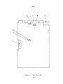
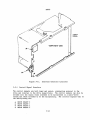
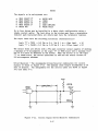
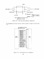
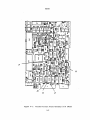
Figure 1-1.
5-1/4 Inch Fixed Media Disk Drive
x
M8083
SECTION I
INTRODUCTION
1.1
GENERAL DESCRIPTION
The 5-1/4 Inch Fixed Media Disk Drive, used on MAl Basic Four® Series 2000
(Machine Types 4171 and 4120) and Series 7000 computer systems (Machine Types
4326), is a microprocessor controlled servo disk drive system (see figure 1-1).
The Machine Type 4171 Disk Drive uses eight data heads, one servo head, and
five non-removable 5-1/4 inch disks as storage media. Machine Type 4171 Disk
Drive data surfaces employ one moveable head to access 1,024 cylinders for a
total of 8,192 tracks. The Machine Types 4120 and 4326 use 15 data heads, one
servo head, and eight non-removable 5-1/4 inch disks as storage media. Each
data surface employs one moveable head to access 918 cylinders for a total of
13,770 tracks.
The disk drive unit consists of the following major components:
o
Mechanical Assembly
o
Read/Write and Control Electronics
o
Power Supply
1.1.1
Mechanical Assembly
The disk drive consists of a single printed circuit board, a frame for mounting
the drive, and a head disk assembly (HDA). The components· inside the HDA are:
disks, spindle motor, head positioning assembly, heads, actuator arm assembly,
and air filter. Shock mounts are provided to minimize the transmission of
vibration from the frame to the HDA.
1.1.1.1
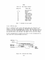
Printed Circuit Board Assembly (PCBA)
The PCBA, figure 1-2, is a multilayer board with the internal planes being
primarily used for voltage and ground only. The circuitry contained on the
PCBA is used to control the spindle motor, actuator positioning system,
actuator latch, and read/write circuitry.
1.1.1.2
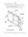
Head Arm Assembly
The read/write heads are mounted on a head arm assembly which is then mounted
to a ball-bearing supported shaft. The voice coil, an integral part of the
head arm assembly, lies inside the magnet housing when installed in the drive.
See figure 1-3.
1-1
M8083
,...
J
Figure 1-2.
Disk Drive PCBA
1-2
M8083
READ/WRITE HeADS
VOICE COIL
MAc!JNIET
MA6N£r
HOUSJNG
Figure 1-3.
Head Positioning System
Current from the power amplifier, controlled by the servo system, causes a
magnetic field in the voice coil which interacts with the field around the
permanent magnets. This reaction causes the voice coil to move within the
magnetic field. Since the head arms are mounted to the voice coil, the voice
coil movement is translated through the pivot point directly to the heads and
achieves positioning over the desired cylinder.
Actuator movement is controlled by the servo feedback signal from the servo
head. The servo head is located on the lower surface of the bottom disk where
servo information is prewritten at the factory. This servo information is used
as a control signal for the actuator to provide track-crossing signals during
on-cylinder seek operation, and timing information such as index and servo
clock.
1.1~1.3
Spindle Motor Assembly
The spindle drive is a brushless dc drive motor contained within the spindle
hub itself. The rotational speed of spindle is 3600 rpm. The motor and
spindle are dynamically balanced to insure a low vibration level during operation. Dynamic braking is used to quickly stop the spindle motor when power is
removed.
1-3
M8083
1.1.1.4
Reads and Disks
The heads utilized in the Disk Drive are composite manganese-zinc ferrite head
sliders and flexures. These heads are used to record and read information on
the thin film metal disks. The thin film metal disks provide a highly abrasion-resistant surface decreasing the potential for damage caused by shipping
shock and vibration.
1.1.1.5
Air Filtration System
The disks and read/write heads are assembled in a clean-air environment and
then sealed within the RDA. The RDA contains a 0.3 micron absolute filter
mounted inside the casting to provide constant internal air filtration. A
second 0.3 micron filter, located on the RDA top cover, permits pressure
equalization between internal air and ambient air. See figure 1-4.
1.1.2
Read/Write and Control Electronics
The read/write and control electronics are packaged on the PCBA. This PCBA,
which includes two microprocessors, performs the following functions:
•
Read/write of data
•
Index detection
•
Read positioning
•
Head selection
•
Drive selection
•
Fault detection
•
Voice coil actuator drive circuitry
•
Track 0 detection
•
Recalibration to track 0 on power-up
•
Track position counter
•
Power and speed control for spindle drive motor
•
Braking for the spindle drive motor
•
Drive up-to-speed indication circuit
•
Reduced write current on the inner tracks
•
Monitor write fault conditions
•
Control of all internal timing
•
Generation of seek complete signals
1-4
M8083
RECIRCULATING FIJ.:TeR.
AIR FLOW PATH
Figure 1-4.
1.1.3
Air Filtration System
Power Supply
The Disk Drive requires only dc power for operation. DC power is supplied from
an external power supply with outputs of +12 Vdc (+5%) at 4.5A maximum, and +5
Vdc (+5%) at 1.9A maximum. Typical current drawn from the +12 Vdc source
during operation is 1.57A and from the +5 Vdc source is l.7A. DC power is fed
to the disk drive via a 4-pin connector on the component side of the PCBA.
1.2
DISK DRIVE SPECIFICATIONS
Table 1-1 lists the specifications for the 5-1/4 Inch Fixed Media Disk Drive.
1-5
M8083
Table 1-1.
Specifications, 5-1/4 Inch Fixed Media Disk Drive
PHYSICAL
Height:
Width:
Depth:
Weight:
ENVIRONMENTAL (continued)
3.4
5.9
8.2
6.3
in (8.6 em)
in (15.0 em)
in (20.8 em)
lbs (2.9 kg)
Non-Operating Shock
°G s
2
t
(1 /2 sine -11 ID s )
POWER
ENVIRONMENTAL
DC Voltage
Ambient Temperature
Operating: 50 to 113 OF
(10 to 45°C)
Non-Operating: -40 to 140 OF
(-40 to 60 °C)
Control: +12V +5%, 1.57A Typical,
4.5A Max (at-power on)
Logic: +5V +5%, 1.7A Typical,
1.9A Max -
Maximum Temperature Gradient
Maximum Ripple (Included in
Tolerance): +5 = 5OmV,
+12 = 120mV
Operating: 18 °F/hr (10 °C/hr)
Non-Operating: Below Condensation
Power Dissipation: 57W, high;
9W, low
Relative Humidity (non-condensing)
Heat Dissipation: 25W, Typical,
28W Max
Operating: 8 to 80%
Non-Operating: 8 to 95%
GENERAL
Capacity (Unformatted)
Maximum Elevation
Operating: 10,000 ft
Non-Operating:
-1,000 ft to 40,000 ft
Machine Type 4171:
Per Drive:
Per Surface:
Per Track:
Vibration
Machine Types 4120:
Per Drive:
143.55 MB
Per Surface:
9.57 MB
Per Track:
10.42 KB
Operating: 5-25 Hz, 0.006 in P-P
25-500 Hz, 0.25G peak
acceleration
Operating Shock
With retries: 2 GiS (1/2 sine -11 IDS)
Without retries: 10 GiS (1/2 sine
-11 IDS)
85.32 MB
10.60 MB
10.42 KB
Machine Types 4326:
Per Drive:
143.55 MB
Per Surface:
9.57 MB
Per Track:
10.42 KB
1-6
M8083
Table 1-1.
Specifications, 5-1/4 Inch Fixed Media Disk Drive (continued)
GENERAL (continued)
GENERAL (continued)
Capacity (Formatted)
NOTE
Machine Type 4171:
(Series 2000 Systems)
Per Drive:
71.32 MB
Per Surface:
8.40 MB
Per Track:
8.20 KB
Per Sector:
512 Bytes
The disk drive is provided
with an error map showing
the location of media defects. The defective areas
are identified by cylinder
number, head number, and
bytes from index.
Machine Type 4120
(Series 2000 Systems)
Per Drive:
119.85 MB
Per Surface:
7.99 MB
Per Track:
8.20 KB
Per Sector:
512 Bytes
The disk drive is guaranteed
to be error free on cylinder
000. Additionally there will
be no more than an average
of 10 defects per surface.
The maximum number of
defects is 128.
Machine Type 4326:
(Series 7000 Systems)
Per Drive:
126.90 MB
Per Surface:
8.46 MB
Per Track:
8.20 KB
Per Sector:
1,024 Bytes
No surface shall have more
than 20 defects. No track
shall have more than 5
defects.
Mean Time Between Failures:
8,000 POH, Typical
Access Time (Includes Settling
Time)
Component Design Life: 5 years
Rotational Speed: 3,600 rpm
Machine Type 4171:
Average:
28 msec
4 msec
Track-to-Track:
Full Stroke:
49 msec
Recording Density: 9,875 bits
per inch
Track Density: 1,000
Machine Types 4120 and 4326:
Average:
27 msec
Track-to-Track:
4 msec
46 msec
Full Stroke:
Cylinders (Machine Type 4171):
1,024
Cylinders (Machine Types 4120
and 4326): 918
Error Rates
Soft Read:
Hard Read*:
Seek:
Tracks
Machine Type 4171: 8,192
Machine Types 4120 and 4326:
13,770
1 per lOll bits read
1 per 1013 bits read
1 per 10 7 seeks
*Not Recoverable within 16 retries
1-7
M8083
Table 1-1.
Specifications, 5-1/4 Inch Fixed Media Disk Drive (continued)
GENERAL (continued)
Sectors: 440,640
Data Heads (Machine Type 4171): 8
Data Heads (Machine Types 4120
and 4326): 15
Servo Heads: 1
Disks (Machine Type 4171): 5
Disks (Machine Types 4120 and
4326): 8
DC Power Connector (P3): 4-pin AMP
P/NI-480424-0 (using AMP pins
PIN 350078-4) (strip) or
PIN 61173-4 (loose piece)
DC Power Connector (J3, on PCBA):
4-pin AMP MATE-N-LOCK connector
PIN 350543-1
Frame Ground Connector (J4):
AMP PIN 61761-2 (Faston Type)
Frame Ground Connector (J4):
AMP PIN 62187-1 (Recommended)
1-8
M8083
SECTION II
INSTALLATION
2.1
INTRODUCTION
This section contains general procedures/requirements for Disk Drive installation. Specific procedures for removal/replacement and installation of the Disk
Drive on the Series 2000 and Series 7000 systems may "be found in section V.
NOTE
Further information on disk drive installation and
configuration may be found in the Series 2000 System
Installation Manual, M8086, or in the Series 7000/8000
System Installation Manual, M8089.
2.2
2.3
UNPACKING INSTRUCTIONS
1.
Open the shipping container.
2.
Carefully remove the top half of the inner foam insert.
3.
Remove the drive from the container and remove the conductive plastic
covering. Inspect the drive for physical damage.
4.
Remove the defect map from the top of the drive. Use the information
on the map for defect management. Copy the map and file a copy for
use in the event the original is lost or misplaced.
5.
The Drive is now ready for operation.
locks.
6.
After unpacking the drive, store the packing materials for possible
future use.
There are no external shipping
SPACE REQUIREMENTS
The Disk Drive is shipped mounted in a frame assembly with a face plate installed. Figure 2-1 shows the external dimensions of the drive.
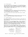
2-1
M8083
•19
~
~
•
REF~l'87 J~
REF
~
3.12
REF~
Figure 2-1.
Disk Drive Mechanical Dimensions
2.4 MOUNTING
The Disk Drive may be mounted in any orientation. The Disk Drive has mounting
holes on three sides of the frame for ease of mounting. Figure 2-2 shows the.
location of the mounting holes.
The casting is very close to the frame mounting holes
in some locations. Mounting screw lengths must be
chosen such that no more than 0.125" of the screw is
available to enter the frame mounting hole. The torque
applied to the mounting screws should be at least 9 inchpounds but to avoid stripping the threads, the maximum
torque applied shall not exceed 12 inch-pounds.
2-2
M8083
.06
%
.01
+
T
--~I
3.25
-
- -
%
.01
t
I
3.38
~ .01
LL'
+
~-~~-~-~-~--~~~~~~~~~~~~~
I.
- - - - - - - - - -
.19 •. 01-1 !:1.87 •. 02-........
' •....-- 3.12 % .02
~
8.00
-------\r-----~I
.86
%
.02
;.AOVl.Jn~ ~
HOLES 40N B:JTroM) Co ON EACH SIDE -
~OTE: MOUNTJ 115 $Cl<EWS
SHALL NaT BE TOR~UED
70 ~Et:lTER. THAN /2 IN. lb.
PR7TRVS1()N OF
~CR.EWS
THROUG·H
~._ SlD~!:!.C}LE~ IS LIMITEr> TO .12 IN.
---------
..
+00
5.75 - .02
5.88
±
.01
5.50
.02
%
I..
3.12 % .02
ALL DJIfIENSIONj
Figure 2-2.
IN JWCH£.S
Disk Drive Mounting Dimensions
2-3
"
M8083
2.5
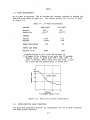
POWER REQUIREMENTS
No ac power is required. The dc voltages and currents required to operate the
Disk Drive are shown in table 2-1. The current profile for 12 volts is shown
in figure 2-3.
Table 2-1.
VOLTAGE
Nominal
Regulation
DC Power Requirements
HIGH LIMIT
LOW LIMIT
+12V
+O.6V*
+5V
+O.25V
CURRENT
1.7A
1.9A
1.57A
4.5A**
Typical
Maximum
POWER DISSIPATION
9W
57W
RIPPLE AND NOISE
120mV
Maximum (P-P)
50mV
*
Regulation may be +1.2 volts during power up
** At power ON for a period of not more than 10 seconds.
Maximum current is drawn until RPM's reach 1000. If
after 10 seconds, RPM is still less than 1000, a timeout occurs and the spindie motor is turned OFF.
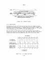
S.f)
405
~
~
...,
~
4.0
~
2
3.0
III
a:
§
~
2.0
o
5
10
IS
SECONDS
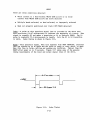
fl2 V CUR.R..EHT POWER. UP CYCL.E
Figure 2-3.
2.6
Motor Start Current Requirements
INTERCONNECTING CABLE CONNECTORS
The following paragraphs describe the requirements for the dc power connector
and frame ground connector.
2-4
M8083
2.6.1
DC Power Connector
The dc power connector (J3) is the equivalent of a 4-pin AMP MATE-N-LOCK connector PIN 350543-1 mounted on the component side of the PCBA. The recommended
mating connector (P3) is AMP pIN 1-480424-0 utilizing AMP pins pIN 350078-4
(strip) or pIN 61173-4, (loose piece). DC power connector J3 pin locations and
voltage assignments are shown in figure 2-4.
2.6.2
Frame Ground Connector
The frame ground connector (J4) is a Faston type connector, AMP pIN 61761-2.
The recommended mating connector is AMP pIN 62187-1. If wire is used, the hole
in J4 will accommodate a wire size of 18AWG maximum.
Frame and logic ground are NOT connected together when the drive is shipped.
2.7
CONNECTORS
The following paragraphs describe the Interface Connectors, Control Cable Termination, and Jumper Settings required to operate the disk drive.
2.7.1
Interface Connectors
Two interface connections are required by the disk drive: a control cable (J1)
and a data cable (J2). Details of the control and data signals required can be
found in section III.
Connection to J1 is via a 34-pin PCBA edge connector. Connector dimensions are
shown in figure 2-5. The pins are numbered 1 through 34 with the even pins
located on the component side of the PCBA and the odd pins located on the
solder side. Pin 2 is located on the end of the connector closest to the power
connector J3. A key slot is provided between pins 4 and 6. The recommended
mating connector for PI is AMP ribbon connector pIN 88373-3.
Connection to J2 is via a 20-pin PCBA edge connector. Connector dimensions are
shown in figure 2-6. The pins are numbered 1 through 20 with the even pins
located on the component side of the PCBA. The recommended mating connector is
an AMP ribbon connector pIN 88373-6. A key slot is provided between pins 4 and
6.
PIAJ 4
+5" VOt..TS DC= SOlo
PIN 3
+ 5 VOL. T RE:TUR.N
PIN!
+ 12 VOLTS
PIN 2
(PC-SA ~COMPONENT~/DE.)
Figure 2-4.
+ 12.
oc= S"'Q
VOLT Rt=ilJRN
DC Power Connector (J3) Pin Locations and Pin Assignments
2-5
M8G83
I3O~Rf) THICkNE~
.062=.007
141-----/,,175=.010
Figur~
2-5.
----~
ALL DIMEN510N.5
IN
INCMe~
Connector J1 Dimensions
-:1".036 -.004
1~
.iOO •• 010
'''"IT
'.
,....
,.... ,....
>
80ARD THICkNES5
()
tiS
____
1 _'---.......w_!
~~.~=.
.062=.007
I
II I
l
l/
I
OIQ
-i
......----/·075-.010
Figure 2-6.
I
I
I
.100-.010
AU. DINfEN510N.5
IN
Connector J2 Dimensions
2-6
INCJff~
MBOB3
2.7.2
Control Cable Termination
If the Disk Drive is the last drive at the
220/330 ohm termination resistor pack must
nector J1. The terminator must be removed
string of drives. The part number for the
2.7.3
end of the control signal cable, a
be installed on the PCBA near conif the drive is not at the end of a
terminator pack is 4210r.
Factory Installed Jumper Settings
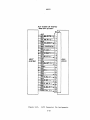
The following jumpers are located on the Disk Drive PCBA and are installed at
the factory. The jumper locations are shown in figure 1-2. Jumper JA provides
for different track per inch (tpi) settings. Jumper JC enables off-track
detection to create a WRITE FAULT if off-track is detected during a write operation. Jumper JD is a factory aid used to disable the UNSAFE signal from the
RDA.
2.B
OPTIONS
The Disk Drive has two options available to the operator or user by means of
jumper settings, drive address selection (J7) and write protect switch connection (JB). Figure 1-2 shows the location of these jumpers. The installer must
set the drive address jumper to the appropriate position to allow the system to
address the drive. If Write Protect is to be used, a switch must be connected
to terminals located on the drive PCBA.
2.B.1
Drive Address Selection Option
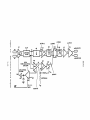
In mUltiple drive configurations it is necessary to configure each drive (maximum of four per host controller) with an unique address. This is accomplished
by locating the jumper plug over the correct pins as shown in figure 2-7. The
standard drive is shipped addressed as Drive l/Drive 0 (actual address designation is dependent upon the numbering system used).
2.B.2
Write Protect Option
A write
invoked
located
ease of
2.9
protect option is incorporated into the Disk Drive. The' option can be
by attaching a shorting plug or attaching a switch across two test pins
near IC U63 on the PCBA. These pins are on 0.100" centers to allow
installing a switch connector.
VENTILATION
The Disk Drive operates with a minimum of air circulation. Air circulation of
3 cfm around the drive is adequate provided the temperature of the ambient air
does not exceed 122 of (SO °C). Enclosures should be designed or chosen such
that this minimal air circulation is provided and that the maximum temperature
is not exceeded.
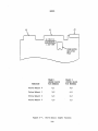
2-7
M8083
J3
Jl
J2
4'C j 2 C 1
'1000000
I
1 2:r 456'
TERMI~ATOR
RESISTOR
PACK
FUNCTION
PHASE 1
JUMPER BLOCK
PIN NUMBERS
PHASE 2
JUMPER BLOCK
PIN NUMBERS
Drive Select 0
C,1
5,6
Drive Select 1
2,C
4,5
Drive Select 2
C,3
2,3
Drive Select 3
4,C
1,2
Figure 2-7.
Drive Select Jumper Options
2-8
M8083
SECTION III
FUNCTIONAL DESCRIPTION
3.1
INTRODUCTION
This section contains the functional description of the Disk Drive on the
following levels:
•
Operational description of the various tasks
performed by the system
•
Interface description
•
Format description and examples of formats
3.2
OPERATIONAL DESCRIPTION
The Disk Drive consists of read/write and control electronics, read/write
heads, head positioning actuator, disks, and air filtration system. These
components interpret and generate control signals, position the heads over the
desired track, read and write data, and provide a contamination-free environment.
3.2.1
Spindle Motor Operation
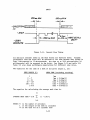
The Disk Drive uses a Z8 microprocessor for spindle motor control. The timers
within the microprocessor are used to time a revolution within 3.6 microseconds. The timers are crystal controlled to ensure the accuracy of the measurement. With this measurement the microprocessor develops an error signal relative to the deviation from 3600 rpm and assures that the rotational speed is
within +3.6 microseconds of 3600 rpm. This results in a +0.1% speed control.
An adaptive offset loop (figure 3-1) provides error correction to lock the
spindle motor exactly on 3600 rpm.
The input to the microprocessor is a square wave developed by the switching of
the hall sensors in the brushless dc motor. Physical position of the spindle
relative to the hall sensors provides rotational information to the microprocessor, figure 3-2. As the motor rotates the microprocessor in effect rotates
the commutation so that the motor speed is exactly in sync with the hall
sensors.
Spindle rotation is controlled with two modes of operation: start mode and run
mode. A description of each mode follows.
3-1
M8D83
ADAPT/VE.
OI'F.5rr
LOOP
-
COM/.1urE~-t
TA~Le.
-
HALL
SUf~ORS
~
OC.~I
I
I
-
JNTEt;AATt;/l.,..
I"
~
DC-rei
FDf<AGr
If} 19 c,ol)NTS
&IJW FAST
f
)
R£F. 10 (,()(JlJrs
RPM
10.'7 ,I.Ifl£~/COIINT
10 aOIJ/lT5 • 3/,00
Figure 3-1.
Spindle Motor Control Block Diagram
100
I2.COMMVTCS!REV
Figure 3-2.
Spindle Motor Hall Sensors Relationships
3-2
M8083
3.2.1.1
Start Mode
The start mode starts the spindle motor rotating and causes the heads to fly as
soon as possible to minimize the headwear. To achieve this, a high torque is
required due to the mass of the disks and the drag caused by the non-flying
heads. The heads nominally start to fly off of the disk at approximately 1000
rpm which takes about 3·seconds. Because of system and/or power supply
constraints, this initial torque is limited by limiting the +12 volt current to
4 amps. This current limiting is accomplished via analog circuitry on the PCBA
assembly.
The spindle is allowed to run at 4 amps for approximately 3 seconds which is
the time it takes to get the disks rotating to at least 1000 rpm and the heads
flying. After the 3 second current limit, the motor rotational speed increases, increasing the back electromagnetic force (emf) and decreasing the
motor current, figure 3-3. As figure 3-3 shows, the current decreases
exponentially as the spindle speed approaches 3600 rpm. This operation
consumes approximately 18 seconds. At this point', the current is approximately
1 amp which is where the second mode of operation begins.
Another feature of the start mode is the time-out condition which occurs in the
event that the spindle is not up to 1000 rpm in 10 seconds. This feature
protects the heads from excessive wear if there is a problem, and also protects
the spindle drivers if too much current is required to get the spindle up in
the appropriate amount of time. If the time-out condition exists, the spindle
motor is turned off and the only way to start the spindle up again is to remove
power from the drive and then reapply power to the drive. It should be noted
at this time that if the drive is power cycled at a rate faster than 30
seconds, and there is a problem in the RDA, that is physically restraining the
spindle from turning, the spindle drivers could overheat and be damaged in the
process.
AMPS
4"'-~~-~~--""--
START CURRENT
'SeNSE.
AV(Y.
LOCX-ON
(fi) 3~OO RPM
I
5
Figure 3-3.
SECONOS
10
t
Spindle Motor Current Profile
3-3
M8083
.2.1.2
Run Mode
n the run mode the drive uses pulse width modulation to control· the speed.
'his method of analog control also reduces noise. Since the drive to the
pindle does not have to be a full ON and full OFF condition, no audible noise
s generated. Pulse width modulation causes the driving hexfets to operate in
heir linear region. This reduces the large surge of ON and OFF currents which
ould result in an audible 720 Hz noise. Figure 3-3 shows that at the 3600 rpm
ock, the current drops from 2 amps to approximately 1.2 amps. This is due to
he analog control taking effect in which the hexfets now are run in their
inear region requiring less current and resulting in less heat dissipation.
ue to the switching of the hexfets and the internal inductance of the motor,
arge induced current spikes are generated that need to be suppressed. These
arge currents are produced in part because of the delta configuration of the
pindle motor. The delta hookup has circulating currents when switching from
,ne phase to another. Small capacitors are added to the spindle drive hexfets
:0 minimize these spikes that would otherwise be on the +12 volt power bus.
head arm assembly is driven to the landing zone and latched when power is
'emoved from the disk drive. This is accomplished by using energy stored in a
:apacitor during ·normal operation. A capacitor is charged from the +12 volt
tower supply. When power is lost, the capacitor's charge is applied to the
lctuator to move the heads into the landing zone and become latched. After the
leads are latched and in the landing zone, the drive goes into the dynamic
Iraking mode. During dynamic braking, there is still voltage available due to
:he back emf of the spindle motor. The spindle motor is now used as a generLtor to cause all the motor windings to be shorted via the hexfets which are
:till enabled by the residual emf. The large short circuit current acts in
tpposition to spindle motion, causing heavy breaking action.
~he
1.2.2
Servo System Operation
servo system in the disk drive utilizes a di-bit pattern on the lower sur:ace of the lower disk in the HDA assembly. The servo head, servo pattern,
:ervo circuitry on the main PCBA, and the actuator mechanism are the main comtonents that make up a closed loop servo system in the drive. This servo
:ystem allows precision track following which compensates for variations in
:rack location caused by thermal conditions. See figure 3-4.
~he
3-4
SERVO REAO SIGNAL
ADJU5TED PE.S
I'1'j
t-J.
OQ
~ HEAD
AMPliFIER
s::~
C'D
~f
w
I
.po.
•
CIl
rJ)NJPEAJ ~
-SATOR. ~
DerMODU PfS
-LA7l)R
+
•
A·GC
~~~~~~
I I I
NISM
ICUBRENTI
C'D
~
~
<:
w
I
VI
o
CIl
'<
CIl
M'
C'D
GUARD -
SYNC
TR.I<O -
Der£c,r ....-1--1
INOCX -:
CfRClJ/7'
~
o
()
~
t::::I
t-J.
III
OQ
~
III
S
CURREJJT
§
CDWTROL
OFF5t:.T
r
'DEC
S
OJ
~
I
+sYNC
DEMOD
It
,SAMPLeY
CON1'ROl- .....- - _......
CIRCUIT
,
1.
.sEM\lO
ClJNmOL
(,uP =RE6ISTEI< )
~
00
o
00
w
M8083
3.2.2.1
Servo Circuitry
The output of the servo head must be proportional to the distance off track for
any given head position with respect to the servo track. Since each head has a
slightly different width, and output is a function of width, the gain for each
head must be compensated for in the electronics. This guarantees that the
output in volts per inch of track offset is identical for any servo head so
that the circuitry will perform smooth and accurate track following.
The head output signal is fed to the servo read amplifier. The output of this
amplifier is of constant amplitude due to the Automatic Gain Control (AGe)
signal. The amplitude of the sync pulses in the di-bit pattern is about 4.4
volts peak-to-peak at the Servo Read Signal (figure 3-4) which is between the
servo read amplifier and the demodulator.
The demodulator, under control of the demod control circuits, samples A and B
or C and D pulses and uses the difference in amplitude to generate a position
error signal (PES). The discharge signal is used to discharge the peak detector circuit in the demodulator prior to the next sample period.
The demodulator output, PES, is applied to a summing mode along with the DAC
output from the microprocessor to generate ADJUSTED PES. This DAC output
signal is only used during seeks or to force off track conditions for analysis.
ADJUSTED PES feeds the compensator which takes a position signal and generates
an acceleration command. This acceleration command must be smooth and orderly
to obtain a well behaved servo loop. The compensator output is fed to the
actuator mechanism through an actuator current control circuit. The output is
0.25 amp for each volt of input from the compensator. This current through the
actuator coil causes the actuator mechanism to move the heads over the disk
surface.
The actuator mechanism contains a coil with a dc resistance of approximately
4.5 ohms and a shorted turn to allow the fast rise times required to obtain
fast access times. The coil and the shorted turn act as a transformer with a
turns ratio of 136:1. The low impedance of the shorted turn (secondary) is
reflected into the voice coil (primary), allowing the fast rise time.
The microprocessor is essentially not used during the track following mode except to monitor that the servo system is operating properly. The processor is
required to get the servo system started when power is applied or after a malfunction and for performing seeks.
The sync detect circuit detects guard bands, track 0, and index pulses. Guard
bands are written outside track 0 and inside the innermost data track. The
purpose of the guard band is to allow the servo circuitry to sense that the
heads are not over a known data area. The guard bands are written in such a
manner as to cause the actuator to move in the proper direction to get back
over the data area. The index pulse is used to signify the beginning of a
track. The track 0 pulse indicates that the actuator is positioned at cylinder
O.
3-6
M8083
3.2.2.2
Servo Pattern
The servo pattern is basically a di-bit pattern. The servo circuitry along
with this pattern has been designed to be tolerant of small disk defects.
Since the patterns are timing related, fake sync pulses can be inserted if
sync is not detected in signals read from the servo track.
The pattern contains eleven bits of information and is repeated 625 times per
track. See figure 3-5. The information that can be contained in the pattern
is: sync, 4 bits of information; track 000; guard band; index; and 4 bits of
track center information A, B, C, and D.
The sync, track 0000, guard band, and index signals are written 10 time units
apart. The track information is written 20 time units from the sync bits and
20 time units from each other.
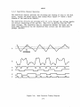
The track information is repeated every four tracks (figure 3-5). These pulses
are monitored for track following. In figure 3-5, the example shows the head
path such that the amplitudes of pulses A and B will be equal and half amplitude when the head is following the track center. Pulse C will have no amplitude and pulse D will have full amplitude.
Since pulses A and B are only known by their time relationship, one additional
piece of information is required. This information will allow the servo system
to know the proper direction to drive the actuator when an off-track condition
exists. For example, if the A pulse is larger than the B pulse, the error is
in a different direction on track 0 than it is on track 2. The drive does not
know which of the 918 tracks the heads are on, however, it does know which
track of any given set of four that it is looking at. In this way the circuitry applies correction in the proper direction. The microprocessor keeps track
of which track the heads are on by monitoring the increments and decrements to
track count on the data bus, under the direction of the direction in signal.
If the least significant bit (LSB) is a 0, the A and B pulses are monitored for
track posi tion. If the least significant bi t is aI, the C and D pulses are
monitored. The most significant bit of the counter (direction in) controls the
direction of correction applied for an offset between an"y pulse pair.
The sync pattern is written starting with a pair of pulses. Following this
pair are time slots for track 0, guard band, and index pulses, if required.
These are then followed by another pair of sync pulses. The A, B, C, and D
pulses for track location are as shown in figure 3-5. The guard band track
center pulses, however, are somewhat different. The outer guard bands, outside
of track 0, are written with only A and C pulses. This will cause correction
to always be applied to move the heads inward toward track O. Likewise, the
inner guard bands, inside the innermost track, are written with only Band D
pulses, thus causing correction outward toward the data tracks.
The index pulse is repeated twice for redundancy.
pulse is not detected, the other should be and the
an index pulse once per revolution. If one of the
ed, the width of the index pulse will be halved to
index pulse width is 53.4 microseconds.
3-7
Therefore, if one index
drive will always generate
index pulses is not detect26.7 microseconds. Normal
PATTERN l\EPEATS 62STIME.S
PER RfiVOL.unoN
~-S-E-RV-O-P-O-S-In-O-N-D-A-r~
,.,,--
~~
X>
ceNTeR';
OF
~
t"%j
~.
OQ
~
0A14
~ TRACKS I
c
...
HI!AD
~
PATH
~~
~
CI)
..,
g;,~
-
_u-__
=~===
"REPEATS
I
\JI
I
<Xl
~
FO~C.KS~
~~
r - ,
A"
-
e
C
......
-- ---- -~ -
-lr --]-___
u..
0
;#~
~~
~o
~
)C
tt
..
:z.
~O
-~
~:
0
~
~UARO
X)-
~
~
o~
A
B
II
I:~~~ ---~~I~-~~U~~~J~:~i
.J..J_ - - - .ll_ - ' 1- LL-_ - - - I
L.._,, _____ - - -(P:. <:'L
___ " __ 1..~.:~2.-
-==~[~==_:~=_U_
- - -
___
-~~~ -===[~=]------
6-
•
w
PATTERN R~PEATS EVERY
U-
n;l~
><:1:>-
4
(D
w
• --
6UARD
~
(C.D
I
___ - - J._
_ __ ~.:.A)_
(D.C)
~
<Xl
o
CIl
<Xl
(D
W
t1
<
o
'"d
III
rt
rt
(1)
t1
~
READS'&NAL
OFF--t}
TRACk
O()WN
EVEW TRACKS
ODDTRACKS
r--------~---------l
I
,
I
(~S'nVE)
(mWARD SPlWbLE )
CENTER
I
I
------------------~
P051110N tNFORMAnoN
'S OE.RIVE 0 FROM TH£Se.
PUL.'E~.
M8083
3.2.3
Read/Write Channel Operation
The read/write channel performs the recording and reading of data to the disk
drive. Figure 3-6 shows typical read timing while figure 3-7 shows a block
diagram of the read/write channel.
The read/write circuits are provided with +11 volts through the voltag~ regulator circuit consisting of U31 and Q15. This +11v is derived from the +12F
input voltage. The read/write data is transmitted between the heads and the
drive PCBA electronics via the read/write flex circuit and the associated
preamps (SS1104).
A
B
c J.J
D
E
-.J
F
J1
,
r
U
U
U
U
n
Figure 3-6,
n
n
I
n n-
,
J
n
n
Read Function Timing Diagram
3-9
U
U
I
,
I
n
U
I
I
I
U
t'%j
U2.3PIN2.
~
O'Q
~
Ii
('I)
U1
w
A
I
-.....I
•
~
III
p..
W
I
.....
o
Oy
::l
TRAHCONCUCTAt-4C~
~
()
,u,S'"
AM PlIfiE.R
rt
~.
o
GAIN CONTROl.. \
::l
VDLTAGe.
.....
\J
)av
o
?;"
"NF
--
~.
III
O'Q
Ii
\Altr
0
~\
f
UZ,S PlN1
()
t:::l
UI5
u"
-MFM RC DAT"
UI.
t;d
I
LT Ie I ~
FILTER
C8ATiD
III
o-+-
- - . 1 80N'
LOW PA:aS
t'%j
S
U2.3
Ul5
L7)L8
HYSTERf~ts
U87
I QII,r2,13
GATE
UJ' Plt-I
to
::s::
00
o
00
w
M8G83
3.2.3.1
Write Function
The write function is shown in block diagram form in figure 3-8. The two
signals HDSEL22 and HDSEL23 are fed to the decoder U29 selecting one of the set
of four preamps within the HDA. Actual writing of data happens if, and only
if, the four signals to the decode chip are true, namely safe condition from
the HDA preamp, drive selected, seek complete, and write gate true. The MFM
WRITE DATA signal received by the differential receiver will then be written on
the disk. As each transition is received by the write data receiver U11, it
goes through a resistor level translator U21. As long as WRITE GATE is active,
flip-flop U23 will toggle for each transition. If any of the conditions for
the write function are not true, flip-flop U23 will be held reset forcing the Q
output to be a logic 1 level. This forces the Q output to be a logic 1 thus
disallowing any current to flow through the Read/Write preamps. The two diodes
at the Dx Dy HDA outputs are back biased.
When the decode U29 is satisfied, the write select and write current control
signals are at +8.5 and +1 volt levels respectively. This indicates that a
write function is in process. When the decode U29 is not satisfied, the write
select and write current controls are at +5 and +4.3 volts. This indicates
that a read function is in process. During the write operation, U37B, a transistor package, is turned off. This causes the voltage controlled current sink
to allow current to flow from the preamps. When U19B is on, it is a non-write
function. The voltage controlled current sink is forced to sink current from
the +5 volt supply.
A block diagram-of the read/write preamps used on the Disk Drive is shown in
figure 3-9. Each preamp supports four heads.
3.2.3.2
Read Function
The read function is shown in block diagram form in figure 3-7.
analog signal that can be seen at the differential inputs Dx and
figure 3-6, Read Function Timing Diagram. This analog signal is
AGC amplifier and then to a low pass filter. At this point, the
has two directions.
The typical
Dy is shown in
fed into the
signal path
The first direction is the AGe loop which is the direction going towards the
bottom of the page. The analog signal is now processed through a buffer
amplifier which branches again in two directions. The AGC loop is the direction that goes toward the GATED TRANSCONDUCTANCE AMPLIFIER. This amplifier is
gated with WRITE GATE to inhibit the AGC loop during WRITE operations. This
gating inhibits saturation of the read amplifiers due to the very high amplitude write signals.
The transconductance amplifier is referenced to a fixed reference voltage
(Vref). If the average input voltage is above Vref, the output of the amplifier is increased, thereby reducing the. gain of the AGC amplifier. Conversely,
if the average input signal is below Vref, the amplifiers output is decreased,
which causes the AGC amplifier gain to be increased.
3-11
MSOS3
+1 _••
--1
•
~~T
.........
·IIV_~
( v
)
FI
:,.ec
Q.1S'" U31
~u'
-U$
-~50
MD5ILt1
-e~'
-
~2.
-C$3
+ ..... WU~T.A
DX
DY
- ..... WItT I)A,.A
~I
+t2V -e.S~T)
4SoO(iililb)
ws
REG
QZ3
+5V
we
HY'P-+--I
uo....w
eweR
Q\&
WLTAGE eo)l1'ROl.LED
eUAAIitn' SIN I(
O-IA/V
Figure 3-S.
Write Function Block Diagram
3-12
M8083
w.:t'n CtrRlU!Mi •
SS'~4
~ MA
Net. UP("751 a
r-- - - -.--- - --- - - ..... - - - - - - - - - - - - - - -------.,
we •
-'*
•
'we
.
......
•
I
,
---- ,,
WI
.
I~
~TE
-
Ru
It
-
St~C'T
,
'-"
/
~eAC
AMP
•
I•
Y
I
~f!
N
I
I
I
eE •
Q41P
E~Le
I-
-
•
...
t
HS2. '
ws£Y
.I
-
~
""
V.U$
±-
I
WI~
...
...
HEAD 0
A"
u
III
..J
fit
Q
~
..J
~.r
Hoa
I
I
~.)
o.rr
I
I
I
I
I
I
./
HEAD I
~
•
HEAD,
%
"'
~
HEAC3
~~~-
- ,
~I
I
-'f
I
,•I
Nt!
~,
1
...j
"YHz?:
I
I
f
I
I
I
I
./
~
PRE-
I
"
~P
.~
'-J
•H
y.mI
f
I
DR'
W~9
I
~
,
Read/Write Circuits (Pre-Amp)
3-13
H31
""'Ii
I
I
I
.... ______________________________________ -___ .J
Figure 3-9.
HIl.
I
~IT
I
I
L.-~_
I
'"
N
I
,
I
I
I
.I~
I
.:r:
-
!"" •
I
<~tt.....1f/p
c£I ,
~Sl
-
WRI~>
DD...o
./'
-~
--
"'"
~
AA~
v
UHSAF£
I
I
Ru
...
-
Tv\AP6
UNS"'FE
I
~
-:;:Ru
..
•
WRJ1"!,
I-
I
V. -"CT:c
--
M8083
The AGC amplifier is used to cause a constant average amplitude with varying
head outputs. This compensates for output variations from head to head and for
the signal reduction that occurs as the heads are moved from cylinder 000 to
cylinder 917. This reduction of signal with cylinder position is due to
increased bit density and decreased wavelength.
The other output of the buf~ered amplifier is a 2V p-p signal which is fed
through a hysteresis loop. This loop compensates for bit patterns that on high
resolution media will cause the signal to cross through the hysteresis levels
again. High resolution can cause a phenomenon called shouldering. Shouldering
is a portion of the signal waveform that has 'zero slope other than at the
peaks. These areas of zero slope can be mistaken for peaks if not properly
recognized and processed. The hysteresis loop causes these potential pulses to
be ignored as the analog signal is converted to digital as shown on signal D of
figure 3-6. This signal is fed into the D input of flip-flop U23.
The second path for the signal is through the low pass filter. The filter output is fed into a differential amplifier. The output of this amplifier is
signal A. The other path of the low pass filter output is through the differentiator and pulse shaper. The output of the pulse shaping circuit is designated as signal C. This signal is fed into the clock of flip-flop U23 and
along with the signal on the D input, generates the signal E. This signal E is
then processed by a bi-directional circuit to generate a MFM read signal. This
MFM signal is translated from ECL levels to TTL levels, buffered, and presented
differentially to the interface as +MFM READ DATA and -MFM READ DATA.
3.2.4
Power-Up Sequencing
DC power (+5V and +12V) may be applied to the drive in any order, but +12 volt
is required to start the spindle motor. When the spindle reaches full rotational speed, the actuator lock automatically disengages and the heads then.
recalibrate to track 000. Step pulses received during the recalibration, Track
000, READY, and SEEK COMPLETE status signals will be true. The drive will not
perform any read, write, or seek operations until READY is true. If 1000 rpm
spindle speed is not reached within 10 seconds of power application, an automatic shutdown procedure is initiated: power to the spindle motor is removed
and the drive will not come ready. Figure 3-10 shows the timing for power up
sequencing.
NOTE
During power-up and recalibration, the drive
will emit a variety of audible sounds. This
is caused by the actuator voice coil and is
perfectly normal.
3-14
M8083
DC
R)WER
ON
----..
AUTO~LI~
Ir--------------------------~--....
(SE.EKTOm4CKODO~
-.;....--;------....1
2.2$CCMAl(--1
.:~:
:
1
...._ _ _ _ __
I
'
2O.seetNtX=:J_ _ _ _ _ _
-i!i-_________
-REAOY
C,-......(UP1OSPEED)
____________________________
~~~S~MAA
SeEk~~~
NOM"'-L. TIME.
I~
_
______________
.ENAB'-S Ai:AOY 'TRACk CQ:)
~NO ~ COMPl...ETE
"n) I N1"f.RFAC£
Figure 3-10.
3.2.5
Power-Up Sequencing
Power-Down Operation
Upon removal of either or both of the dc voltages from the drive, the drive
circuitry causes the actuator to be retracted to a shipping and landing zone
located at the inner diameter of the disks. The actuator is latched in this
position by the actuator latch until power is again applied and the spindle
motor is up to speed. The spindle motor 1s also dynamically braked, by back
emf, to decrease the stopping time when the heads are in contact with the
disks. The disks will stop rotating in approximately 9 seconds.
3.3
INTERFACE DESCRIPTION
The Disk Drive has two interface connectors: one for control signals (J1) and
one for data transfer signals (J2). The control signals are TTL while the data
signals are differential. The following paragraphs describe the signals, timing requirements, and pin assignments associated with these two interface connectors. The driver/receiver pair used on the drive is also discussed. The
location of these two connectors is shown in figure 3-11.
3-15
M8083
l~ONT
PANEL
t
COMPONENT SIDE
t
&14
Figure 3-11.
3.3.1
Interface Connector Locations
Control Signal Interface
The control signals are both input and output, originating external to the
drive and internal to the drive respectively. The control signals can also be
divided into two types: those intended to be multiplexed in a multi-drive
system and those intended to do the multiplexing. The controls signals that do
the multiplexing are:
•
•
•
•
DRIVE
DRIVE
DRIVE
DRIVE
SELECT
SELECT
SELECT
SELECT
0
1
2
3
3-16
M8083
The signals to be multiplexed are:
•
•
•
•
•
HEAD SELECT
HEAD SELECT
HEAD SELECT
HEAD SELECT
TRACK 000
20
21
22
23
•
•
•
•
•
WRITE GATE
INDEX
READY
SEEK COMPLETE
WRITE FAULT
Up to four drives may be installed in a daisy chain configuration using a
single control cable. The last drive in the string must have a termination
resistor pack installed while all others must have the terminator removed.
The input lines have the following electrical characteristics:
Logic "0" = TRUE
Logic "I" = FALSE
= 0.0
= 2.5
Vdc to 0.4 Vdc @ 1 in
Vdc to 5.25 Vdc @ 1 in
= 40ma (max) = LO
= 250ua (open) = HI
The output lines are driven with a TTL open collector output capable of sinking
a maximum of 40 millamperes at the Logic "0" or TRUE state with a maximum voltage of 0.4 volts dc measured at the driver. When the driver is in the Logic
"1" or FALSE state, the driver transistor is OFF and the source current is
250 microamperes maximum.
Driver/Receiver - The recommended driver/receiver combination for control
signals is shown in figure 3-12. The maximum cable length recommended is 20
feet (6 meters). Pin assignments for the control cable are shown in figure
3-13 and table 3-1.
+5V
74~8
"'--2.0Fr:(MAXJ-~
eroll
74LSI
330$1.
Figure 3-12.
Control Signal Driver/Receiver Combination
3-17
M8083
~LAT RIBBON OR TWISTED
PAIR MAX Z() FcET
PI
(!,Nt)
/tiD SEt. SIT3
r&ND
ND .5EJ. SIT 2 -
r
-
GND
_ .gEE-I< COMPLETESND
-
TRAC~ 000-
N/C
(wo
SYS7CM
HD
sa
GND
_
9
IS
-
.
BIT 1-
8
l2.
GND
HOST
7
II
WRITE~T-
aND
,
10
GlYO
HD $£L 8ITO-
3
5
14I~'T£ ~A'TE. -
. L-.
I
2
4
/llJ1"J
-
')1
-
INDEX
GNO
14
15
/)ISk
"
DRIVE
17
18
"
z.o
21
2.e.
_ REAOY-
J.7ND
5rEP-
-
GINO
23
24-
z5
2.h
&iD
2.7
DRIVE $EL 1- ....
2B
GlJD
t,9
DRIVE. 5EL 2.. DRIVE SEt. 0 -
GND
-
DRlYE. $£1.. .3 -
....
GNO
C>lRECTJON IN -
Figure 3-13.
~
:;/
3z..
33
- .34-
J1/P1 Connector Pin Assignments
3-18
M8083
Table 3-1.
Control Signals (Daisy Chained)
GND RTN PIN
1
2 Hd Sel Bit 3
4 Hd Sel Bit 2 6 Write Gate
8 Seek Complete 10 Track 000 12 Write Fault 14 Hd Sel Bit 0 16 N/C
18 Hd Sel Bit 1
20 Index
22 Ready24 Step26 Drive Sel 0 28 Drive Sel 1 30 Drive Sel 2 32 Drive Sel 3 34 Direction In -
3
5
7
9
11
13
15
17
19
21
23
25
27
29
31
33
Note:
3.3.1.1
SIGNAL PIN AND NAME
"-"
indicates low true signal
Control Input Signals
The following paragraphs describe the control input signals.
Head Select Lines - The following head select lines allow selection of each
individual read/write head in a binary coded sequence:
0
2 , 21 , 22, and 2 3
Head select 20 is the least significant select line. The heads are numbered 0 through 15. When all head select lines are high (inactive), head 0 will
be selected. A 220/330 ohm resistor pack provides line termination.
Write Gate - The active state of this signal, or LO level, enables write data
to be written on the disk. The inactive state of this signal, or HI level,
enables data to be read from the drive. A 220/330 ohm resistor pack provides
line termination.
Step - This interface line is a control signal which causes the read/write
heads to move in the direction defined by the DIRECTION IN line. The access
motion is initiated at the high to low level transition or leading edge of the
signal pulse. Any change in the DIRECTION IN line must be made at least 100
nanoseconds before the leading edge of the STEP pulse. The DIRECTION IN line
must not change for at least 100 nanoseconds after the trailing edge of the
last STEP pulse. See figure 3-14 for General Step Timing. A 220/330 ohm
resistor pack provides line termination.
3-19
M8083
/OO7t:5MIN
~t----
100')15 MIN
~
f..
I I
,I
-DIRECTION :1Z:/~f4:-~:~2=;h:II:~·~~1_______ ,at. ;1&1T'!/~·" '0L i~"/!. . :. Oj~J/~i" "Z~.-.-...
·;-?
; ....
~'~--£'
IN
I
I
..;..1
u«
-3~P----~UI
,
.. ,
I
t~ SOO n.s MAX
Ul~---.8.1ms I
l.,.:MIN .1 HEAD SentI:I
I
~AY
I ,
-SEE.K
COMPl-ETE ----------'~I~------------~------_I
Figure 3-14.
___
General Step Timing
All multiple cylinder seeks in the Disk Drives are buffered seeks. Optimum
performance from the drive will be achieved if the time between step pulses is
from 1 microsecond to 13 microseconds. Any time up to 3100 microseconds (3.1
milliseconds) will be accepted by the drive. See figure 3-15 and table 3-2.
Table 3-2 also shows performance expectations for different step rates.
The equations for the time of a seek of any given length L, are:
SEEK LENGTH (L)
2
8
32
128
1
~
SEEK TIME (including settling)
5ms
5ms
8ms
Ilms
15ms
23ms
7
31
127
511
512
+
+
+
+
+
0.43ms(L)
0.22ms(L)
O.llms(L)
0.053ms(L)
0.027ms(L)
The equation for calculating the average seek time is:
M
AVERAGE SEEK TIME = 2/M
L
(1 - L/M)tL
L=1
WHERE: M is the number of cylinders
L is the length of the seek in cylinders
tL is the time for an L cylinder seek
3-20
M8083
sao 7tsec MIN
-STEP
104--
2-"Sec
MfN.-----J
3'00 ~ec MAX.
Figure 3-15.
Table 3-2.
Step Pulse Timing
Seek Performance Vs Step Time
STEP
TIME
(usee)
AVERAGE
ACCESS TIME
(msec)
1-13
14-26
30
35
40
30
34
42
43
45
45
50
46
60
47
70
80
52
90
57
100
150
59
71
83
110
140
170
200
230
260
290
320
200
300
400
500
600
700
800
900
1000
MAXIMUM
ACCESS TIME
(msec)
48
78
85
92
92
92
92
105
112
115
122
126
164
210
296
383
44
55
474
564
653
744
835
926
Time between step pulses cannot exceed 3.1 msec.
All seek times include settling and begin upon reception of
the first step pulse.
3-21
M8083
Direction In - This signal defines the direction of motion of the read/write
heads when the STEP line is pulsed. An open circuit or HI level defines the
direction as "out" and when the STEP line is pulsed. the read/write heads will
move away from the center of the disk and toward cylinder 000 (the outermost
cylinder). If this line is at a LO level, the direction of motion will be
defined as "in" and the read/write heads will move toward the center of the
disk. Any changes in the level of the DIRECTION IN line must conform to the
timing restrictions shown in figure 3-14. A 220/330 ohm resistor pack provides
line termination.
Drive Select - DRIVE SELECT, when LO, connects the drive interface to the
control lines. Positioning the DRIVE SELECT jumper between two appropriate
pins on the PCB determines the address to which the drive will respond. The
location of the DRIVE SELECT jumpers is shown in figure 2-7. The following
table indicates which drive will be selected for each jumper position.
3.3.1.2
Control Output Signals
The following paragraphs describe the control output signals.
See figure 3-13.
Seek Complete - This signal. when LO or true. indicates that the read/write
heads have settled at the destination cylinder and that another seek, a read,
or a write may be initiated.
Track 000 - This interface signal, when LO or true, indicates that the read/write heads are positioned at cylinder zero (the outermost data cylinder).
Write Fault - When LO or true, this signal indicates that a condition exists in
the drive that may cause improper writing on the disk. Further writing is
inhibited in the drive until the improper condition is cleared. WRITE FAULT
can be cleared by deselecting the drive or by cycling power OFF and ON.
NOTE
This signal should be edge detected by the
controller.
3-22
M8083
There are three conditions detected:
•
Write current in a head without WRITE GATE active or no write
current with WRITE GATE active and drive selected
•
Multiple heads selected, no head selected, or improperly selected
•
Head not properly positioned over track (OFF-TRACK detected)
Index - A pulse on this interface signal line is provided by the drive once
each revolution (16.67 millseconds) to indicate the beginning of a track. This
signal is normally HI and makes a transition to LO to indicate INDEX. The LO
pulse is nominally 53.4 microseconds in length. Only the HI to LO transition
is valid. Index timing is shown in figure 3-16.
Ready - This interface signal, when true together with SEEK COMPLETE, indicates
that the spindle is up to speed and the drive is ready to read, write, or seek.
When this line is false, writing and seeking are inhibited. Typical time for
READY after power on is 15 seconds. Figure 3-17 shows some of the general
timing requirements of the input and output signal lines of the drive.
1/60'7",5
NOM,
-INDEX
-----.1 I
---..J
110--1
I--sa.4~ec TYP
Figure 3-16.
Index Timing
3-23
M8083
DC. POWER. ON
.-J
:....- 20 SEC MAX
-.
I
-RUcDI(
(IF ~L.ECT~)
-~TEP
~I
I
_________________________________________________
~
1--5££ F'&UA~$ 131,14-
~~--.--------------------------------
I
---4za$S'W(
-S~l!IC
~:
L-il~------~I~--------------------------------~
~2M5EO~
CQMPIJTC
-l
-TRACK 000
-----"
I
I
____~I
I
I
IfEAD DATA
VAL.ID
- ()R.IVE ~'T
HeAD .$w/TCHeD
I¥NJ 04TA VALID
~I-------------------------------
--------------------______~Il~--------------------~ ~8,.....s !f4AK
------------------------------t....ll ~1OO,.,.wAX
,I
,
--t
I
I
~a~ MA.l(
I
--t i4-tfCD..-BMN<
WAITE
O~TA
----------------------------_----~II~_____
Figure 3-17.
3.3.2
General Timing Requirements
Data Interface
The following paragraphs describe the data interface.
3.3.2.1
General Description
The lines associated with data transfer between the drive and the controller
are differential in nature and may not be multiplexed. These lines t MFM READ
DATA and MFM WRITE DATA t are provided at the J2/P2 connector on all drives.
The driver/receiver combination used for these lines is shown in figure 3-18.
A third signal is available at J2/P2. That signal is DRIVE SELECTED which
indicates the selection status of the drive. This line is an open collector
TTL output.
3-24
M8D83
HIGH
1RUE-~
>----HIGH TRUE
/00
4MD 26LS3e
NOMINAL "_" LINE
LOr;/~ LOGIC i
Z=I05.n
•
NOMINA'- "-" LINE
FLAT RIBBON OR TWISTCD PAIR
MAX/1\.1UM
Figure 3-18.
20 FEET
Data Line Driver/Receiver Combination
Pin assignments and line titles for J2/P2 are shown in figure 3-19 and table
3-3.
f:LAT RIB80N OR TVV/STED
PAIR MAX 2.0 F~E.T
P2 J2.
-
[)RJV£ SELECTED-
RESERV£D
RESERVED
RE.5ERVf:D
~E,eRvED
RESeRVED
t:..ES£RYW
RESER.VED
RE5ERVEV
HOST
SYSTEM
I
i,
I
t
i
I
I
I
I
I
!
I
,
ReSERVE!)
GROUIJO
CABLE; PR.E5£NT+M;:M WRITe MTA
-Mf!"M WR../i£ Cl4TA
.sIGNAl.. GND
SIGNAl.- GNP
:__ +M!=M Re.AO DATA
i _ -MI!M ~€AD DATA
tI
,s1(;N4t... (J,tJ()
"sIGNAL GND
I
2
'::<
...J
4-
S'
~
7
DISK
DRIVE
B
9
/0
1/
12
13
14
I
I
i
IS' :
I
16 i
/7
18
19
2.0
I
I
1
1
I
I
I
I
I
!
!
I
!
;
:
i
I
Figure 3-19.
i
I
J2/P2 Connector Pin Assignments
3-25
M8083
Table 3-3.
Data Signals (Radial)
SIGNAL NAME
SIGNAL PIN
Drive Selected Reserved
Ground
Cable Present + MFM Write Data
- MFM Write Data
Signal Ground
Signal Ground
+ MFM Read Da ta
- MFM Read Da ta
Signal Ground
Signal Ground
1
2 - 10
11
12
13
14
15
16
17
18
19
20
Note: "_" indicates low true signal
3.3.2.2
MFM Write Data
This is a differential pair of data lines which define the transitions to be
written on the disk. The transition of + MFM WRITE DATA will cause a flux
reversal on the disk provided WRITE GATE is active. This signal must be driven
to an inactive state (+ MFM WRITE DATA more negative than - MFM WRITE DATA) by
the controller when in the read mode. See figure 3-20 for write data timing.
No write precompensation is required by the drive; if write precompensation is
used, some loss in read performance may result.
-DRIV~
SEt. - - - - ,
-HD 5£L--..,
---i
+MI=M VALID
READ MTA
-WRITE
\.-- 8p4 MAX (HEAD SWITCH/IVa]
-..f 't-- 25715 M/N)/507t..IIIA'iIMUM
I
---j t.--2tJ07t.S TVP.
arreELL
-..l"
I
~TE ------~~;.::.::.::........---.'"-_ _---Jr-I--~--
READ/
WRITE.
ReCOVERY
Figure 3-20.
MFM Write Data Timing
3-26
M8083
3.3.2.3
MFM Read Data
Data recovered by reading prerecorded information from the disk is transmitted
to the controller by the differential pair of MFM READ DATA lines. The transition of the + MFM READ DATA going more positive than the - MFM READ DATA. line
represents a flux reversal detection from the disk under the selected head.
See figure 3-21 for MFM READ DATA timing.
3.4
FORMAT DESCRIPTION AND EXAMPLES
The purpose of a format is to organize a data track into small blocks of data
called sectors. Each sector has a unique address in its header or ID field.
3.4.1
STS06/412 Format
The format shown below in figure 3-22, the STS06/412 format, is a format commonly used on lower performance disk drives. Its efficiency of 81% (unformatted capacity/formatted capacity) is typical; however other efficiencies can
be obtained by varying the number of sectors per track. The STS06/412 format
is a soft sectored format which means that the beginning of each sector is defined by an Address Mark and a prewritten identification (ID) field which contains the physical sector address plus cylinder and head information. The ID
field is then followed by a user supplied data field.
The STS06/412 format is a slightly modified version of the IBM System 34 double
density format which is commonly used on floppy disk drives. The encoding is
Modified Frequency Modulation (MFM).
-DRJVE
~EL
-HD ,jeL
j.--- 8 ...us MAX (HEAD $WITCHI NG)
+MF'M VAL.ID
READ DATA
. - WRITE 6141£
I
---i J--eS"M MIN) IS'O?t.s
----t
~2007&$ 7Yp.
_ _ _ _ _ _--=8;.;.IT--=:;CE=..;L:;;.:I.~_.,
WRITE DATA
I
,,-__~I
400,.,s
-I- IttF
--I
M4XIMUM
r.- MAX.
8.1"'5
---l If4-~--i~SO-J$()X5
j..~
______________
eMf BE.
~nunun--------
--1 I-- 200,... 7YP.
BIT' CELL.
Figure 3-21.
MFM Read Data Timing
3-27
___
REA D/
WRITE.
RECOVE.R,Y
0 TO
e.oo?f.,
M8083
NarES: I. },J~RL TR.ACJ< CAPACITY a 1fH.16 8l"7ES UNFIJIlM ~T"rEO
t. TDTAL ~7A
S.,'E.$
Figure 3-22.
3.4.2
TAACJ(- 2S'X~2·8.J92.
ST506/412 Format
Address Marks
The beginning of both the ID field and the data field are flagged by unique
characters called Address Marks. An Address Mark is two bytes in length. The
first byte is an "AI" data pattern. This is followed by either an "FE" pattern
for an ID address mark, or an "F8" for the data address mark.
The "AI" pattern is made tmique by violating the encoding rules of MFM by
omitting one clock bit. See figure 3-23. This makes the Address Mark pattern
unique to any other serial bit combination that could occur on the track.
BIT
~ITlON
0
I
2
,
4
5
6
1
co
CO
CD
CO
CD
CD
CD
CD
nAI t DArA BITS
I
0
I
0
0
0
0
"AI" CLOCK BITS
0
0
0
0
I
0
I
-
r--
r--
I
0
-
r--
ENCODED PATTERN
WITH DROPPED CLOCk
NORMAL ENCODED
PATTeRN Wfn40UT
DROPPeD CLOCk
1-._
'--
-
-
D
D
-
-
~
c
C· CLOCk BIT
D· OATA BIT
Figure 3-23.
"AI" Address Mark Byte
3-28
,....-
~
c
c
--
M8083
3.4.3
Gap Length Calculation
Gaps surrounding the ID and data fields establish physical and timing relationships between these fields.
Gap 1 '- provides for variations in index detection. This gap must be at least
12 bytes long. Gap 1 is immediately followed by a sync field preceding the
first ID field.
Gap 2 - follows the CRC or ECC bytes of the ID field, and continues to the Data
Address Mark. It provides a known area for the data field write splice to
occur. The latter portion of this gap serves as the sync up area for the data
field Address Mark. Gap 2 is normally 16 bytes long, however, its minimum
length is determined by the "lock up" performance of the phase-Iock-Ioop in the
data separator, which is part of the host control unit.
Gap 3 - follows each data field to allow for spindle speed variations. This
allows for the situation where a track has been formatted while the disk is
running slower than nominal, then write updated with the disk running faster
than normal. Without this gap, or if it is too small, the sync bytes or ID
field of the next field could be overwritten. The minimum gap is 8 bytes for· a
sector size of 256 oytes.
Gap 4 - is a speed tolerance gap for the entire track, which is applicable in
full track formatting operations to avoid overflow into the index area. The
format operation which writes ID fields begins with the first encountered index
and continues to the next index. The actual bytes in Gap 4 depend on the exact
rotational speed during the format operation.
3.4.4
Sector Interleaving
The ST506/412 format normally uses an interleave factor of 4: That is, sequentially sectored ID numbers are 0, 4, 8, 12, ••••••• , 1, 5, 9, 13, etc. This
allows sufficient system turnaround time to process multiple sectors during a
single revolution, thus enhancing through-put of typical file read/write operations. Other interleave factors can be used.
3-29/30
M8083
SECTION IV
MAINTENANCE
4.1
INTRODUCTION
This section contains the information required by the technician for the maintenance of the Disk Drive.
4.2
PREVENTIVE MAINTENANCE
Other than a visual inspection to insure that dust accumulation has not
restricted air flow, preventive maintenance is limited to general cleaning,
which should be accomplished along with scheduled maintenance of the host
system.
Cleaning of the Disk Drive is done in the following manner (see figure 4-1):
1.
Use a soft bristle brush to clean dust from electrical surfaces.
Do not use abrasive cleaners and chemical
cleaning agents that contain acetone, toluene,
xylene, or benzene. These cleaners may cause
equipment damage that requires major rpair.
2.
Use a lint-free cloth dampened with a solution of 90 percent
isopropyl alcohol to clean non-electrical surfaces.
3.
Clean away any dust accumulation which could cause speed fluctuations.
4-1
M8083
TBD
Figure 4-1.
Cleaning the Disk Drive
4-2
MBOB3
SECTION V
REMOVAL/REPLACEMENT PROCEDURES
5.1
INTRODUCTION
This section contains removal/replacement procedures for the Disk Drive and
the Disk Drive PCBA as installed on MAl Basic Four® Series 2000 and Series
7000 systems. Also included are procedures for installing additional disk
drives.
NOTE
Whenever a Disk Drive must be replaced, retain the
packing material from the replacement unit for use
in repacking and returning the defective unit.
5.2
DISK DRIVE REMOVAL/RELACEMENT - SERIES 2000 SYSTEMS
Remove/replace a disk drive in the Series 2000 Base Unit as follows:
1.
Shut down the system and turn off the Base Unit power.
2.
Unplug the Base Unit power cord from the ac outlet.
3.
Unplug all connections to the Base Unit, including all attached peripherals.
4.
Insert a screwdriver, or similar device, into the slot at the bottom
right-hand side of the Base Unit cover, and push in to disengage the
latch. Repeat with the left-hand side, and remove the cover.
5.
If necessary, remove the required controller PCBAs to gain access to
the cable connectors on the disk drive controller.
6.
Unplug the bus and radial ribbon cables from connectors J1 and J2 on
the disk drivels (see figure 5-1).
7.
Unplug the power cable from connector J3 on the disk drivels (figure
5-1).
B.
Remove the front and rear facias by pulling up slightly on each plastic
card holder until the corresponding facia is disengaged from the card
holder.
9.
Using a screwdriver, or similar tool, push back the two (2) plastic
latches at the bottom rear of the disk drive chassis, while lifting the
back of the drive to clear the latches (see figure 5-1).
5-1
M8083
~
.-.----
---- - - ----- ----
~~~-
r-..::- .::::-_
I
- ---__
----..::::..--_
I
I
I
.;' /"'-
--:::"::..~-:....-_
-----=:-.::~
_"./
---
~
/"
LATCHES
//
---~
~~~_
I
I
LIGHTLY TWIST
SCREW DRIVER
TO SPRING
LATCH BACK
I
I
I
I
I
LIFT PLATE \
(ONE SIDE
AT A TIME)
DRIVE
MOUNTI~G
PLATE
PLATE RESTS
AND HINGES
HERE
DRIVE MOUNTING
LATCHES (TYPICAL)
POWER
CABLE
PA2
POWER
CABLE
PAl
DRIVE 0 RADIAL CABLE
PIN 907604-001
o
o
DRIVE 1 RADIAL CABLE
PIN 907604-002
Figure 5-1.
SINGLE DRIVE BUS CABLE
PIN 907605-001
OR
DUAL DRIVE DAISY CHAIN BUS CABLE
PIN 907606-001
Disk Drive Removal/Replacement/Installation, Series 2000 Systems
5-2
M8083
10.
Push the drive slightly toward the rear of the CMB so that the flange
at the front of the drive clears the slot in the Base Unit bottom
panel; lift the disk drive assembly from the Base Unit.
11.
Before installing the replacement drive, observe the following:
a.
If replacing the drive on a single-drive system, be sure that the
terminator resistor pack is installed and that the address select
jumper plug is installed on the correct pins for Drive Select 0
(see figure 2-7).
b.
If replacing Drive 0 on a two-drive system, be sure that its
terminator resistor pack is removed and that the address select
jumper plug is installed on the correct pins for Drive Select 0
(figure 2-7).
c.
If replacing Drive 1 on a two-drive system, be sure that its
terminator resistor pack is installed and that the address select
jumper plug is installed on the correct pins for Drive Select 1
(figure 2-7).
Use care not to damage CMB components when replacing disk drives.- Do not apply pressure to the top
of the drives when installing same in the Base Unit.
Using a screwdriver to press on the flange of the
drive mounting plate will prevent damage to the CMB.
12.
5.3
Install the replacement drive by following steps 1 thru 10 in reverse
order
SECOND DISK DRIVE INSTALLATION - SERIES 2000 SYSTEMS
The Series 2000 Base Unit may have one or two disk drives installed; i.e.,
either Drive 0 or Drive 0 and Drive 1. The last drive in the system must have
a terminator resistor pack installed. When a second drive (Drive 1) is added,
the terminator must be removed from the Drive 0 PCBA and installed on Drive 1.
The second drive must also be configured for the proper address (i.e., Drive
Select 1). In addition, the "superblock" for the second drive must be modified
and a filesystem must be installed.
Remove the floppy disk drive and install a second fixed disk drive in the
Series 2000 Base Unit as follows:
1.
Perform steps 1 thru 6, and step 8, of paragraph 5.2.
2
Unplug the power cable (PA2) from the rear of the floppy drive.
5-3
MBOB3
3.
Using a screwdriver, or similar tool, push back the two (2) plastic
latches at the bottom rear of the floppy drive chassis, while lifting
the back of the drive to clear the latches (see figure 5-1).
4.
Push the floppy drive slightly toward the rear of the CMB so that the
flange at the front of the drive clears the slot in the Base Unit
bottom panel.
5.
Raise the floppy drive, unplug the ribbon cable from the CMB, and
lift the floppy drive assembly from the Base Unit.
6.
Repeat steps 3 and 4 to remove Drive O.
7.
Remove the terminator resistor pack from Drive 0 and verify that the
terminator is installed on Drive 1 (the new drive).
B.
Configure Drive 1 for the proper address (Drive Select 1) by installing
the address select jumper plug over the correct pins (see figure 2-7).
Use care not to damage the CMB components when
installing the second fixed disk drive. On some
CMBs, R31, near the left-front shock mount, may
require bending to clear the chassis of the second
drive. Do not apply downward pressure on a drive
when installing same in the Base Unit. Using a
screwdriver to press on the flange of the drive
mounting plate will prevent damage to the CMB.
9.
Reverse steps 3 and 4 to reinstall Drive 0 and to install Drive 1.
10.
Connect radial cable pIN 907604-001 to connector J4 on disk drive
controller and to connector J2 on Drive 0 (see figure 5-1).
11.
Connect radial cable pIN 907604-002 to connector J5 on disk drive
controller and to connector J2 on Drive 1 (figure 5-1).
12.
Connect daisychain bus cable pIN 907606-001 to connector J3 on disk
drive controller, connector J1 on Drive 0, and connector J1 on Drive 1
(figure 5-1).
13.
Connect power cable PAl to connector J3 on Drive 0, and power cable
PA2 to connector J3 on Drive 1 (figure 5-1).
14.
Reassemble the Base Unit and connect power cord to ac outlet.
nect peripherals and power-up the system.
5-4
Con-
M8083
15.
Change the Drive 1 superblock to reflect two partitions and install a
filesystem on Drive 1 as follows:
a.
Log on to the system administrstor:
ADMIN> usb /dev/rwdl -get desc=driv-el
Note that "drivel" is an arbitrary name assigned to a file, used
in this example to store the contents of the superblock in the
second disk drive.
b.
Ved (edit) the file, /etc/diskdesc/drivel.
that the last two lines read:
Modify the file so
**partition # : starting block : length in blocks
1: 0: - 1
You should only have to add the last line.
with the new edits.
c.
Save the file with
Update the superblock on Drive 1 wi th the parameters described
in etc/diskdesc/drive1:
ADMIN> usb /dev/rwdl -save -set type=drive1
d.
Create the unbuffered raw device and the buffered device with
the following commands:
ADMIN>makedev /dev/rdrivel
U 14 33
ADMIN>makedev /dev/drivel
B 14 33
The device names used in this example are rdrivel and drivel,
but can be defined using other names. To follow convention,
the unbuffered raw device should begin with the Ie tter "r,"
which stands for raw device.
e.
Once the device is defined, create a filesystem using the
makefs command:
ADMIN>makefs /dev/rdrivel
f.
Verify that the second drive is correctly partitioned by using
the "space" command:
ADMIN) space /dev/rdrivel
The number of blocks returned should reflect the size of the
disk drive installed.
5-5
M8083
g.
To access the second disk drive. the device must be mounted to a
directory on Drive O. The /mnt directory is not recommended for
this purpose. Instead use the makedir command to create a new
directory for use as the mount point for the second drive (for
example, /mntwdl):
ADMIN>makedir /mntwdl
h.
So that the user may access the second drive each time the
system is loaded, ved the /etc/sinit file and add the following
line at the end of the file:
mount /dev/drivel /mntwdl
i.
Save the edited file. Each time the system is loaded the file
is executed and drivel will be mounted to /mntwdl. Again, note
that "drivel," as well as tlmntwdltl are arbitrary names.
NOTE
Path names must be prefixed with /mntwdl (arbitrary
name) for the user to access Drive 1.
j.
5.4
Add devices /dev/drivel and /dev/rdrivel to the boot partition.
This is accomplished by booting to the boot and using the makedev
commands as described in this procedure (step d). Refer to the
Commands Manual section of the User's Guide for further details
on all commands used in this procedure.
DISK DRIVE REMOVAL/RELACEMENT - SERIES 7000 SYSTEMS
The Series 7000 Primary Mainframe and Add-on Disk Modules may receive from one
to four disk drives. The disk drives in each Mainframe or Add-on Module are
numbered in a logical sequence from (Disk) a to (Disk) 3. When replacing the
only or last drive in the Mainframe or Add-on Module, be sure that the drive's
terminator resistor pack is installed. When not replacing the last drive, be
sure that the terminator is removed. All replacement drives must have their
address select jumper plug installed on the correct pins (i.e., for Drive
Select 0, 1, 2, or 3).
Remove/replace a disk drive in the Series 7000 Primary Mainframe or Add-on Disk
Module as follows:
5.4.1
General Procedures
1.
Shut down the system and switch off the circuit breaker on the ACDU/s.
2.
Unplug the Mainframe/Add-on Module power cable/s from the ac outlet.
3.
Remove the Mainframe/Add-on Module front and top panels as shown in
figure 5-2. Remove left or right side panels as required.
5-6
M8083
USE SLOT-HEAD
SCREWDRIV£R TO
PR£~S AND LlF"I TOP
PANEL
FILLER
/
/~.
f(
@~
\
I
I
I
QUARTER TuRN
EACH ~I 0 E 11-\ E N
T1LT FORWARD
AND LIFT ClUT
Figure 5-2.
Removal of Front, Top, and Side Panels, Series 7000 Systems
5-7
M8083
5.4.2
Removal/Replacem~nt
of Disk 0 or Disk 1
Remove/replace Disk 0 or Disk 1 on right-hand mounting plate as follows:
1.
Disconnect power cables from connector J3 on Disk 0 and Disk 1 (see
figure 5-3). Tag power cable for Disk O.
2.
Disconnect Disk 1 power supply (figure 5-3) from disk ACDU.
PLATE r-IlUNTI NG
SCREWS (UPPER)
DISK 1 (DISK 2
ON LE FT -HAND
fi«)UNTING PLATE)
TO
ctl
REMOVE
o
J3
POWER
SUPPLY
(DISK 1)
L---H---,-= ~:
PLATE f«lUNTING '---------~~
SCREWS (LOWER)
DISK 0 (DISK 3
ON LEFT-HAND
t«lUNTI NG PLATE)
NOTE: ORIENTATION OF DRIVE CONNECTORS
JI-J3 IS INVERTED ON DISKS 2 &3
Figure 5-3.
Disk Drive Removal/Replacement/Installation, Series 7000 Systems
5-8
MBOB3
3.
Disconnect the daisychain bus cable from connector Jl and radial cables
from connector J2 on Disk 0 and Disk O. Identify cables for Disk O.
4.
Loosen the upper and lower plate-mounting screws with a 1/4-inch nut
driver. Do NOT remove. The screw holes in the plate are slotted.
5.
Grasp the plate firmly and slide it toward the rear of the unit.
6.
Lift the plate out of the unit and lay it on a level, secure surface,
drive side up. Be careful; the plate is heavy.
7.
Carefully position the plate so that the disk drive to be removed
extends over the edge of the level surface. This provides easy access
for removal of the screws •.
B.
While holding the disk drive to be removed with your hand, remove the
four screws and washers from the underside of the panel and the plastic
spacers from the upper side of the panel at each of the four locations.
9
Lift the drive off the plate.
10.
11.
5.4.3
Before installing the replacement drive, observe the following:
a.
If replacing the only or last drive in a module, be sure that the
terminator resistor pack is installed and that the address select
jumper plug is installed on the correct pins for Drive Select 0, 1,
2, or 3 (see figure 2-7).
b.
If not replacing the last drive in a module, be sure that the terminator resistor pack is removed and that the address select jumper
plug is installed on the correct pins for Drive Select 0, 1, or 2
(see figure 2-7).
Install the replacement drive by following steps 1 through 9 in
reverse order. Insert the screw connected to the ground mount first.
Removal/Replacement of Disk 2 or Disk 3
Remove/replace Disk 2 or Disk 3 on left-hand mounting plate as follows:
1.
To access the lower-left plate-mounting screw, remove the Magnetic Tape
Cartridge Streamer (MTCS) drive as follows:
a.
Remove cartridge from the MTCS drive.
b.
Disconnect power cable from MTCS connector P2 and bus cable from
MTCS connector PI (see figure 5-4).
c.
Remove the four hex-head screws on the bottom of the MTCS using a
1/4-inch nut driver.
d.
Remove MTCS drive from Mainframe/Disk Module.
5-9
M8G83
P2
/'
II
I
I
•
Figure 5-4.
REMOVE 4 SCREWS TO'
REMOVE MTCS.
MTCS Removal/Replacement
5-10
M8083
5 •. 5
2.
Perform steps 1 through 11 of paragraph 5.4.2 to. remove/replace Disk 2
or Disk 3.
3.
Replace the MTCS as follows:
a.
Position MTCS drive and insert the four hex-head mpounting screws.
Finger tighten the screws.
b.
Replace the front cover and bring the MTCS drive flush with the
opening in the front cover. This can be accomplished by using
one of three methods:
•
When inserting the MTCS, slide it as far forward as the slotted screw holes allow. Replace the front cover and allow it
to push the MTCS into the proper position. Tighten the screws
under the MTCS by working through the open side panel; or by
carefully removing the front panel, tightening the MTCS
screws, and replacing the front panel.
•
If the side panel(s) of the unit are removed, replace the
front cover and carefully reach through the side opening and
slide the drive forward until it is flush with the front
cover. Tighten the screws under the MTCS by working through
the open side panel. Replace the side panel(s).
•
Replace the front cover and pull the MTCS forward by inserting
your finger in the cartridge space and pulling the MTCS forward. Tighten the screws under the MTCS.
DISK DRIVE INSTALLATION - SERIES 7000 SYSTEMS
The Series 7000 Primary Mainframe and Add-on Disk Modules may receive from one
to four disk drives. The disk drives in each Mainframe or Add-on Module are
numbered in a logical sequence from (Disk) 0 to (Disk) 3. When installing an
additional drive in the Mainframe or Add-on Module (i.e., the last drive in the
sequence), be sure that the drive's terminator resistor pack is installed. The
preceding drive must have its terminator removed. All drives added to a Mainframe or Add-on Module must have their address select jumper plug installed on
the correct pins (i.e., for Drive Select 0, 1, 2, or 3).
Install a second, third, or fourth disk drive in the Series 7000 Primary Mainframe or Add-on Disk Module as follows:
1.
Perform steps 1 thru 3 of paragraph 5.4.1.
2.
If adding Disk 1, proceed as follows:
a.
Perform applicable procedures in steps 1 thru 7 of paragraph 5.4.2
to remove right-hand disk mounting plate.
b.
Remove screws that secure cover for Disk 1 Power Supply (see
figure 5-3).
5-11
M8083
c.
Install Power Supply PiN 400446-002 on mounting plate using
hardware supplied.
d.
Connect two-conductor ac power cable PiN 907747-001 to connector P3
on Power Supply.
e.
Install address select jumper plug over correct pins on Disk Drive
PCBA for Drive Select 1 (see figure 2-7).
f.
If Disk 1 is to be last drive in sequence, be sure that terminator
resistor pack is installed on Disk Drive PCBA.
g.
Install drive on mounting plate (above Disk 0) using hardware
supplied.
h.
Connect hard-wired power cable from Disk 1 Power Supply to connector J3 on Disk 0 (see figure 5-3).
i.
Install cover on Power Supply using screws removed in step 2b.
j.
Remove Disk 0 from mounting plate as instructed in steps 8 and 9
of paragraph 5.4.2.
k.
Remove terminator resistor pack from Disk 0 and reinstall drive on
mounting plate.
1.
Reinstall right-hand mounting plate within Mainframe or Add-on
Module.
m.
Connect two-conductor ac power cable (from Disk 1 Power Supply)
to ACDU.
n.
Attach connector PB on daisychain bus cable (existing cable) to
connector Jl on Disk O. Attach connector PC to connector Jl on
Disk 1.
o.
Attach radial cable from Micro-Peripheral Controller (MPC) PCBA,
connector Jl, to connector J2 on Disk O. Attach radial cable from
J2 on MPC PCBA to J2 on Disk 1.
3.
Plug the Mainframe/Add-on Module power cable/s into the ac outlet.
4.
Power-up the Series 7000 and load the operating system.
5.
Refer to section 5 of the MAl BOSS/VS Utilities User Guide, MSI02, for
procedures on adding disks to the family of system drives.
6.
If adding Disk 2 and/or Disk 3, proceed as follows:
a.
Using supplied left-hand disk mounting plate, disk drivels, power
supply, cables, and attaching hardware, perform step 1 and steps 2c
thru 2m for Disk 2 and/or Disk 3.
5-12
M8083
5.6
b.
Attach connector PD on daisychain bus cable (existing cable) to
connector Jl on Disk 2. Attach connector PE to connector Jl on
Disk 3.
c.
Attach radial cable from Micro-Peripheral Controller (MPC) PCBA,
connec tor J3, to connector J2 on Disk 2. At tach radial cable from
J4 on MPC PCBA to J2 on Disk 3.
d.
Perform steps 3 thru 5.
REMOVAL/REPLACEMENT OF DISK DRIVE PCBA
Removal of the Disk Drive PCBA is accomplished with the Disk Drive removed from
the mounting plate. Refer to paragraph 5.4.2 or 5.4.3 for Disk Drive removal
procedures.
To remove the PCBA perform the following steps:
1.
Remove the grounding lug J4 from the frame assembly.
2.
Remove the three "E" clip retainers for the shock mounts.
3.
Lift the frame off the drive.
LED cable and its connector.
2.
Remove the PCBA.
Use care not to damage the front panel
To replace the Disk Drive PCBA, repeat the above steps in reverse order.
5-13/14
M8083
SECTION VI
ILLUSTRATED PARTS LISTS
6.1
INTRODUCTION
This section provides the parts list information for the Printed Circuit Board
Assembly and the Disk Drive Mechanical Kit.
6.2
INDEX OF ASSEMBLIES
The following is an index of the assemblies covered in this section (the RDA
is a sealed unit and not repairable):
ASSEMBLY
Printed Circuit Board Assembly (P/N 59055)
Mechanical Kit (P/N 50461)
RDA (P/N 50454)
6-1
FIGURE
TABLE
6-1
N/A
N/A
6-1
6-2
N/A
M8083
JA
JD
JC
Figure 6-1.
J7
Printed Circuit Board Assembly (PIN 59055)
6-2
M8083
Table 6-1.- Printed Circuit Board Assembly (P/N 59055).
PART
NUMBER
30091
30104
30108
40109
40114
40119
47015
48010
50487
59056
59058
REFERENCE
DESIGNATION
DESCRIPTION
Adhesive, Tak Pack
Adhesive Accelerator
Shrink Tubing PVC 3/8 ID
Plug, Shorting
Pin, IC
Post, Feedthru
MCU, Z-8 4K, 1ZMhz
Crystal, 1ZMhz, HC-18
La. bel, PCB Asm
Fabrication, PCB
Schematic, Control Module
U43
Y1
CAPACITORS
43000
43004
43006
43008
43010
43012
43014
43018
43030
43300
43301
Capac,
Capac,
Capac,
Capac,
Capac,
Capac,
Capac,
Capac,
Capac,
Capac,
Capac,
43552
Capac, 10. OUF, 25V, Bulk
43560
43562
43600
Capac, 2200UF, 16V
Capac, 220UF Elect, 16V Min
Capac, O.OOIUF, 10% X 7R, 50V
43608
43612
43614
43618
43624
Capac,
Capac,
Capac,
Capac,
Capac,
10.0PF, 5% (NPO) , 50V
22.0PF, 5% (NPO) , 50V
33.0PF, 5% (NPO) , 50V
47.0PF, 5% (NPO) , 50V
68.0PF, 5% (NPO), 50V
100PF, 5% (NPO), 50V
150PF, 5% (NPO), 50V
330PF, 5% (NPO), 50V
3900pf, 5%, NPO 50V
O.OlUF, +80/-20%, 50V
0.10UF, +80/-20%, 50V
0.0047UF, 10% X 7R, 50V
O.OlUF, 10% X 7R, 50V
0.015UF, 10% X 7R, 50V
0.033UF, 10% X 7R, 50V
O.lUF, 10% (NPO) , 50V
6-3
C1
C40, 84, 85
C11
C37
C128
C42, 88, 91
C12, 43
C44, 45, 46, 51, 52
C67, 68
C6, 7, 13, 14, 17, 19, 22,
C2, 3, 18, 23, 26, 34, 48,
49, 66, 71, 72, 73, 81, 86,
87, 89, 90, 93, 94, 100,
102, 103, 104, 107, 108,
109, 110, 111, 113, 116,
117, 118, 120, 121, 122,
123, 124, 125, 126, 127
C55, 70, 76, 82, 96, 97,
98, 105
C29, 83
C25, 30
C20, 21, 24, 27, 50, 59,
62, 64, 65, 79, 99, 114
C32, 33, 35, 36, 53, 54
C39, 41, 92, 106
C61, 69
C10
C4, 5, 8, 9, 15, 16, 28,
31, 47, 60, 63, 75, 78, 115
M8083
Table 6-1.
Printed Circuit Board Assembly (P/N 59055) continued
PART
~UMBER
REFERENCE
DESIGNATION
DESCRIPTION
CONNECTORS
40104
40120
40123
J4
J5
J3
Conn, 28 Contact, Fem
Conn, 24 Contact, Fem
Conn 4 Contact, Fem
DIODES
46001
Diodes Switching, 1N914
46002
46004
46005
46007
Diodes Schottky, 1N6263
Diodes, 1N4001, Pwr, 50V (DD-41)
Diodes, 80SQ030, Scottky Pwr
Diodes, 1N5818
CR1, 2, 5, 6, 7, 8, 10, 12,
13, 15, 17, 18, 19, 20, 25
CR16
CR3, 4, 14 , 22
CR23
CR9, 21, 24
INTEGRATED CIRCUITS
44010
44011
44051
44053
44058
44062
44067
44202
44203
44251
44300
44301
44302
45001
45003
45005
45007
45008
45009
45013
45014
45052
45054
45056
45060
47011
47013
IC, 26LS31 QD, Hgh Spd Ln Drvr
IC, 26LS32 QD, Diff Ln Recv
SOIC14, 74LSOOD QD, 2-In ND Gate
SOIC14, 74LS74AD, DL-D TP ET F-F
SOIC20, 74LS240D OCT INV BUF 3S
SOIC14, 74LS04D, Hex Inverter
SOIC14, 74LS02D, QD 2-in NOR GA
IC, QD 7438, 2-in NAND Buf (OC)
IC, 7445 BCD, DECI/DECD DR (OC)
SOIC14, 7406D, HX INV Buf/Dr (OC)
IC, Quad, Ex-Dr ECL, 10107
IC, 10131 ECL Dual D F-F
IC, Triple Rec ECL, 10114
IC, LM318N, Hi Speed OP-AMP
IC, Ref 2.5V, LM336BZ-2.5
IC, OP-AMP, LF356
IC, MC1350PIF AMP
IC, DAC0832 88TuP, D-Buf D-A Con
IC, Volt Reg Low P. 8V, 78L08
IC, LF347, WD BDWTH QD JFT OP-AM
IC, TBA810P, 7W Audio Amp
SOICI4, LM324D, 6-P S-S OP-M1P
SOICI4, LM339D, QD Volt Comparat
SOICI4, NE592D, Video Amplifier
SOIC14, HEF4066B, QDRUF Bilt Swt
IC, Z8-2K, MCU 8Mhz 40-Pin DIP
IC, Gate Array, Servo Control
6-4
U4
U11
U33
U41
U32
U39
U36
U35, 38
U29, 30
U27, 34, 46, 47
U15
U23
U17
Ul
CRII
U22
U3, 7
U42
Ql
U14
U9, 10
U6, 12, 18, 31
U5, 20, 40 48
U2, 8, 16
U13, 19, 28
U45
U44
M8083
Table 6-1.
PART
NUMBER
Printed Circuit Board Assembly (PiN 59055) continued
REFERENCE
DESIGNATION
DESCRIPTION
RESISTORS
41001
41009
41025
41027
41028
41032
41033
41035
41037
41038
41041
41043
41044
41046
41047
41049
Resis,
Resis,
Resis,
Resis,
Resis,
Resis,
Resis,
Resis,
Resis,
Resis,
Resis,
Resis,
Resis,
Resis,
Resis,
Resis,
10.0 Ohms, 1%, 0.25W
21.5 Ohms, 1%, 0.25W
100.0 Ohms, 1%, 0.25W
121.0 Ohms, 1%, 0.25W
133.0 Ohms, 1%, 0.25W
196.0 Ohms, 1%, 0.25W
215.0 Ohms, 1%, 0.25W
261.0 Ohms, 1%, 0.25W
316.0 Ohms, 1%, 0.25W
348.0 Ohms, 1%, 0.25W
464.0 Ohms, 1%, 0.25W
562.0 Ohms, 1%, 0.25W
619.0 Ohms, 1%, 0.25W
750.0 Ohms, 1%, 0.25W
825.0 Ohms, 1%, 0.25W
1K Ohm, 1%, 0.25W
41052
41056
41061
41062
41063
41066
41067
41068
41069
41071
41073
Resis,
Resis,
Resis,
Resis,
Resis,
Resis,
Resis,
Resis,
Resis,
Resis,
Resis,
1.33K Ohms, 1%, 0.25W
1.96K Ohms, 1%, 0.25W
3.16K Ohms, 1%, 0.25W
3.48K Ohms, 1%, 0.25W
3.83K Ohms, 1%, 0.25W
5.11K Ohms, 1%, 0.25W
5.62K Ohms, 1%, 0.25W
6.19K Ohms, 1%, 0.25W
6.81K Ohms, 1%, 0.25W
8.25K Ohms, 1%, 0.25W
10K Ohms, 1%, 0.25W
41075
41076
41079
41080
41084
41089
41090
41093
41097
41100
41106
41108
41125
41211
Resis,
Resis,
Resis,
Resis,
Resis,
Resis,
Resis,
Resis,
Resis,
Resis,
Resis,
Resis,
Resis,
Resis,
12.1K Ohms, 1%, 0.25W
16.2K Ohms, 1%, 0.25W
17.8K Ohms, 1%, 0.25W
19.6K Ohms, 1%, 0.25W
28.7 Ohms, 1%, 0.25W
46.4K Ohms, 1%, 0.25W
51.1K Ohms, 1%, 0.25W
68.1K Ohms, 1%, 0.25W
lOOK Ohms, 1%, 0.25W
133K Ohms, 1%, 0.25W
237K Ohms, 1%, 0.25W
287K Ohms, 1%, 0.25W
76.8K Ohms, 1%, 0.25W
27.4 Ohms, 1%, 0.25W
6-5
R116
R109
R2, 43, 55, 59, 66, 76, 78
R98
R7, 8
R9, 10, 103, 106
R69
R86
RS, 6, 45, 68, 79, 80, 95,
R99
R23, 24, 96, 96, 124
R11, 12, 13, 56
Rl19
R29
R62
R14, 15, 16, 19, 50, 51,
61, 64, 65, 83, 100, 105,
108,117,128,135,143
R44
Rl14
R1, 3, 4," 49, 52, 63, 115
R17, 18, 21, 22
Rl18
R92, 107
R130
R73, 93
R48
R38
R20, 33, 42, 47, 58, 77,
85, 94, 101, 104, Ill, 120,
123, 125, 138, 139, 142
R60
R131
R54, 75
R57
R133, 134
R81
R88
R129
R132, 140
R34, 90
Rll0
R122
R76
R25, 28
M8083
Table 6-1.
PART
NUMBER
Printed Circuit Board Assembly (P/N 59055) continued
REFERENCE
DESIGNATION
DESCRIPTION
RESISTORS
41260
41284
41291
41292
41557
41560
41563
41564
41566
41572
41573
41574
41575
42000
42007
42010
42016
42045
42046
42100
42101
42102
42106
42109
42111
42117
42121
42131
42152
42157
Resis, 3.01K Ohms, 1%, 0.25W
Resis, 30.1K Ohms, 1%, 0.25W
Resis, 59.0K Ohms, 1%, 0.25W
Resis, 64.9K"Ohms, 1%, 0.25W
Resis, 18.2K Ohms, 1%, 0.25W
Resis, 4.99K Ohms, 1%, 0.25W
Resis, 10.OM Ohms, 1%, 0.25W
Resis, 26.7K Ohms, 1%, 0.25W
Resis, 10.7K Ohms, 1%, 0.25W
Resis, 13.7K Ohms, 1%, 0.25W
Resis, 57.6K Ohms, 1%, 0.25W
Resis, 143K Ohms, 1%, 0.25W
Resis, 19.1K Ohms, 1%, 0.25W
Resis, 0.1 Ohms, 3%, 2W
Resis, 1.00 Ohm, 5%, 0.25W
Resis, 0.5 Ohm, 1%, 1W
Resis, 1.00M Ohm, 5%, 0.25W
Resis, 309K Ohms, 5%, 0.25W
Resis, 200 Ohms, 5%, 0.50W
Resis, DIP TTL-ECL Xlator Network
Resis, DIP 14-Pin, 220/330
Resis, Network, 470 Ohms, DIP
Resis, SIP, 1.0K, 6-Pin Ind.
Resis, SIP, 10K, 6-Pin IND
Resis, SIP, 68K, 6-Pin IND
Resis, SIP, 680, 6-Pin COM
Resis, SIP, 10K, 6-Pin COM
Resis, SIP, 2.2K, 8-Pin COM
Resis Netw, 180 Ohms, SIP, 8-Pin-4R
Resis, SIP, 10K, 2%, 8-Pin IND
R30
R70, 71, 72, 136
R36, 37
R102, 126
R74
R35, 82
Rl12
R46
R53
R39, 40
R89
R91
R84
R87
R26, 27
R31, 32
R113, 141
R41
R121
U21
U25
U24
RP5
RPl, 2, 7,12
RP8
RPII
RP6, 9, 10
RP14
RP3
RP4, 13
TRANSISTORS
46102
46103
46107
46108
46110
46111
46112
46151
46152
46153
Tran,
Tran,
Tran,
Tran,
Tran,
Tran,
Tran,
Tran,
Tran,
Tran,
2N3906
Quad 2NPN/2PNP 6700
IRFD123 N Ch Fet 4-Pin DIP
IRFD9123 P Ch Fet 4-Pin DIP
PN4393, N-CH JFET, TO-92
IRF521 , N-CH HEXFET TD220
IRF9521, P-CH HEXFET, T0220
2N3904, NPN SOT-23
2N3906, PNP SOT-23
SOT-23, NPN 2222A
6-6
Q20
U26, 37
Q8, 18
Q15, 19
Q9
Q5, 6, 7
Q2, 3, 4
QI0, 22
Q14, 23
Ql1, 12, 13, 16, 17
M8083
Table 6-2.
PART
NUMBER
Mechanical Kit (P/N 50461)
REFERENCE
DESIGNATION
DESCRIPTION
RESISTORS
41266
41267
41268
41269
41279
41280
41281
41282
41283
41284
4128S
41SSS
41SS6
41SS7
41SS8
41S60
41S7S
41S76
41S77
41S78
Resis,
Resis,
Resis,
Resis,
Resis,
Resis,
Resis,
Resis,
Resis,
Resis,
Resis,
Resis,
Resis,
Resis,
Resis,
Resis,
Resis,
Resis,
Resis,
Resis,
S.36K
S.90K
6.49K
7.1SK
18.7K
20.5K
22.6K
24.9K
27.4K
30.1K
33.2K
17.4K
22.1K
18.2K
20. OK
4.99K
19.1K
6.34K
6.6SK
6.98K
Ohms,
Ohms,
Ohms,
Ohms,
Ohms,
Ohms,
Ohms,
Ohms,
Ohms,
Ohms,
Ohms,
Ohms,
Ohms,
Ohms,
Ohms,
Ohms,
Ohms,
Ohms,
Ohms,
Ohms,
1%,
1%,
1%,
1%,
1%,
1%,
1%,
1%,
1%,
1%,
1%,
1%,
1%,
1%,
1%,
1%,
1%,
1%,
1%,
1%,
O.2SW
0.2SW
0.25W
O".2SW
O.2SW
0.2SW
0.2SW
0.2SW
0.2SW
0.2SW
0.2SW
0.2SW
0.2SW
0.2SW
0.2SW
0.25W
0.2SW
0.25W
0.2SW
0.2SW
MISCELLANEOUS
30033
30073
30078
30088
30110
30144
30147
30148
40106
S0091
S0284
S0288
S04S8
S0463
S0468
50475
SCR 4-40 X 0.2S PAN PHIL
E-Ring
Washer, Lock Split #6 Set
Thread Locking Compound
Screw, Socket Head, 6-32 X 0.18
4-40 X 3/16 Flthd Rlvd Phillips
Washer, FIt Sm Pattern
Washer, Lock Ext Tooth
Ground Lug
ASM Face Plate
Label Warranty
Washer
ASM Chassis (SC2)
Label, Ser No.
PCB Insulator
Disk Drive ASM-Tab
6-7/8
R2
R2
R2
R2
Rl
R1
R1
R1
R1
R1
R1
R1
R1
R1
R1
R2
R1
R2
R2
R2
M8D83
SECTION VII
SCHEMATICS
7.1
INTRODUCTION
The schematic diagrams for the 5-1/4 Inch Fixed Media Disk Drive are located in
figure 7-1.
7-1
o ---.·~~.~l~.~_==!===]
___._.._:._~~~~~_~~~~.=[ ~ ~=.===~.~=.=.~ :'1 ~.~_==--=~~.=: ~_~=_==I_-·_.
.__=r=__ ~_==---T
3
P12S
"5~'
t'1j
D
"5t'~
~
.
IlW
fn
:
-
4
2
ze
~r"
•
N
oo""d
I'P.
--H - < t ""
22l'1flUF'
3~
P20
P21
P22
P30
3"
33
5
_
(4C 1'1 213
(SDI \ 08
C
'10~~~~~1<
3
Eo
-=.!.Jf.'!'.~i#ULTI'
I
RP10
"SU
'O::r
XTAL
P 13
181
Pll
24
22
40
P36
vee
In-=
'
-
t1 CD
I
N
fn
CI)
CI)
l0
(66
"~
n
0
t1 t j
~
t1 t1
n
~
~
Q)
B
S
"::r
CI)
CI)
fu
a-.
-
tD
fn
R112
10N
3
D
S
1
8
1
.
F.:
PH4393
"
EDGE DETECTOR
./
L504
1.139
0
:
RP7
10K
-i ~lJ.~i
RPI6
______ ... _____ - '.' _____ ,01.
-1"- - -.:,----._-[-- -.-.-
--'-1 ---.- - - - ._- "._------
---- ...-.--.
-.-.
--... ..----. -'-"
l.
.
I
.,~
I
D
~
'"
ell
IC
11
12
~
RP8
5
G
00
I
I--
It' :~14
IN 4001
.. C76
1'1o
•
.
2J.1
TP16
,
4A MTRGRD
NOTES;
I
l_.
1,'1
___ . _ ,, __
~-=.~.~: !~ - =.. : ~~. ] ...~ ___ .. <1
·_~~.~.~r===--=}l~==
1"'
8
all (9CS)
...-
1. SOURSCE REFERENCE = 59858 REV/H
2. SIGHAL DESIGNI\TIONS IHCLUDE SHEET
LOCI\TION DI\~ (IN PI\REHTHESES)
3. RESISTOR VALUES IN OHHS AND
CI\PAACITANCE VI\LUES IH HICROA
FARADS. UNI,ESS OTIIER"I SE
SPECIFIED
4. FOR DC PO"ER CIRCUITS AHD
CONHECTIONS (I HCLlJD I HG GROUHD)
REFER TO SHEET ?
1=-~~=
___?__
o
00
tAl
R87
4
1 ~.I_,,
10
_
""
+ I I . f; IJ
~- F~;~---"l (~3
__ "
al
.,/
'"''''
J5
r.t
. ___ .______ . ___ l' e __'",____ .~ _~PS. __
(QC5) _~~_-.!!I!':?J;'!!
.
TP 1 5
lllq14
..-- •
~
0.001
6 681<
CPS
.
IRF
c~
C.64
0.001
~--l----'
111
... 1
04
l!, 9521
l-f{----+
~ ~~
----i~~ol_;:_·-·+t- ?- 1.~.1_~·~~::4-· _L ("0
~
1
RP7
10K
4-
G
D
j~1I
_":~,~2_
P38
<; 8 25K
95'21
•
~
C
S
L~
1S96 2
IRF521
10V.
ov.
6
13
.4;
: RP9
PP5
1\
D
'.
05
+
l
03
<4C8)
f8Ce)
"ll'6V
D
"51)
-:
101<
'"
131
3
___
41
1
)
8621
s: '
-~s
: .~ ..?
PO"ER HON 11lJR
+'3
GJ
I
q
I-t\
1
.
-.---~-t.:~.~ 3 1
0
-
2
c-_--t-_ _ _ _ _ _ _ _ _ _
L...
)<=QI0
4
I
~"""---l'"
-!-~--l
•
.;.~
~N3904
09
e.'_'~', '
c
LS06
46
RP6
101<.
c:~
~OQ
4
U46
If'''''''-.2
l/,··
---;!:~
1
nQ)
_0:..
Q2
RP6
L<;AF.
11{":"lfil
0.0131
. /./'>0" =-------I---------.J
3['-.'>--4-----
+ 1 1 .60
S
G
---'.
PP9
LS06
L
r=1IEJ
(.1
".!.I.£>V
RP'"
'"
let<
C62
-",---
..:.. ;.::
I
1
I"'I~
____._
5[ '·,>-=-6_ _
o S
n Q)
.
pp,
U46
~
GND
U_45
V'1.=·f't6
~s
26
1
_~r~~
21
23
PIS
11
"51)_1_1,~.~
o n
~~
2
'.
22t<lOUF
14
P23
PI0
PI2
P 14
£>..
n
2
(P,l
2~W~1
,2.1 _2__
24.H}_ _ .
-----IT
~:-;·--·-rt-:-.~-------
'
:
_
J6
I
......
;~~-;-
101)-
READY;
SPINDI,E H01lJR DRIVES (4 AHP)
B1358138e
'.,1'/
1
:.
3
......
t1C/l
l..L~8:
<
RPlfiI!
t1
~txJ
n >
- ------
:.. .•• .......
~
101<
-""'=1
._--_._-----
H~'P
(781 )~-.-,--
1
I - .__1=---_~
._-
..
+5l1
8 -
--....-- ...
---, ..
196--·'
..,.
oq
I'zj'
ID
'3(,
~
.......
I
l-
•
,
~:.._- ~0e_l_ c~~
U .. __
:
e
(P10
.......
I
w
..,.
(')
t1
..,.t::l
o
~59
f.3C~
R81)
I
li·r:'f-.?
.F::.~.
'.. ~t3
r.h2
i
1
. --
I~
(41
tIE r;
-!
21 f'lft
"St.:?
.r::I.,'
/_.1.
61
:::8l~c,1§_'~f5
4
11
r::
_
~
0
0047
PIE>
II<
C:'3.7
PP3
1
180
,
2
C33
(I
1---,·I":['-~--O-'C!::-4-74
···H-----Ji-· ,.---," '0 I
.
L9
1:
r.,
09 I
BOns PULSE SUA PER
•
1
6
'1_. ,'U
..... 7
e 14l UII;,/
, ______ .'.. _
e 047
__
q
< ~ RIS !
f 1 11< +
(5A8)
.~..................! ..-I ... I.!.S
4
U204
V1I5
j
•
1....~................. . 1 i
479
_-.1
TRAHS<:OH.UC11
'
To
I H3 J"
,':
__
816
--
I
3:':W
:' PP I 1
.~4". ~r'~'··'
Q I 'I
--M--
CRI5
F
1"':;14
...
~
"PI IS
(1)
(1)
" '!
_I~
r1'
N
I
&~
.,_~
t
1'".~.--
...I - - -
P
t
;, 680
".114
'j'.1
.
___ 9
AHI'
'-'
1
I
]==~-=.' :
"/
r:
i.
F'P I I
•
- -----
o
00
w
0
1
C?
. I
',/
B
:::16
6:3('1
TF':3
rit--·
1--.... ____:1~5
" ...• .'..7-1/ 4 - -I' ::.
. 'I.:,
I7
·----------~(5A8)
. T.
--_._. - -------------------- . - - - - - - - ( ] I ] . 0; B8)
'.
:1, '.
jO,
~
: I
8
;;
e
00
LM32.
-I ----, "
H~~R~:::
A
---
~~
,..''1
r ;1'I~J-"·
-_. -- -.,-, ',. ..~ J
-,
II
Hl
,I)
J.-r
c'
-- . - - -.
P
,PPII
j~
o
I
<, f'
~
l.lf'llf.70e
;:P I I
• 680
TP.
• AHCE AHP
I .;:-----~- - -:L~',
@l"
R
OAI '!'.lE. JRErlJ
______
-
on
'i 6
C
r----~ ~11J37
«~ATE)))
~
._--'-J;: . -"
'- ~"
r ------I
--.1 ._.
5A8)
04
12.J.
lR14 ..
<1 ~
.... ' f
5,+
1:'3
!:------J
47PF
o
10114
Ie 114'
--.,,,,- -- - ----
---.--
CO,"
+111J_R,\I':_
>'.
180
::1'
o
tl,(~;
I '.r,
~-
I
3~ !r1"I-~-?f
•~
.".
u,~
E~ '.' · .~:~l7.'~:-~f ~------At.::_-l ;~:~:2 r~-k~~~~~2 ~'ti:~~";2 '-~'K. 5~
CI)
I-
TPI
,,--.
~·-PF' 't
------. --- --_. ------- -'---- -----------------...._---.. .---- -_. - ----._--_._---
u,"
180
r1' ,.-...
CI)
r':'t''1
..
Ifl ... H
+11.6V
10
RP3
nsu
g..,. ~
P58
t\:l.eK
RUFFER AHP
,,)
..,.oq
t1 t1
L7
__
.. ~L
J '~~,;"'l~
n e
J:
DEFFEREHTI AlUR I
..::.L- - - - 1 - -
C
r1'
CI)
P<;7
l",P.Pf
(1)
CI)
PASS FI f.TER
_.J·"1-"-1L...-~
(') asu
(1)
I.n~
l:r~l- '~~'f
(t
'r.12B
o (')
o
.. .
.-~~~[:=.=~-i :~~:.:~.~~=-J-==.~': _.~ ~ _._.n.l=~~._?-~ __ ·__1_ _--.
.>
111'011 4
L:.!.iU
'"d::1'
t1
..
;t; ~~ J::~:~'] ,"
Me
It:, -...
n
en
AHP
WRTSEL'_.'L~_
O:I< I )r-:t3"-.-- -.,
1''1"".,E.t<:
. .
N
00l-d
t1
-···11;0pf
'jJ;~ [IX fjc-n._1 __ _
(1)
~~
AGC
(3e I ;'fEIJ-~-'-
t1
(')
t.g~
(3Dt\~~
~
f.
• I 11.1
+51J_!.?
I
.,
.
·l .... ___ ._..l~
--.---RIO
.. --.[-.. _.---
":-.: -·t :
·17Ll
. i';
.
f.
A
10
1174
._,
..
"r-
··-·----3 --·:.:.·~_=·~·I==~
__ __-_I
~._.
1
..--------_.- ---',-----_.-8 .... ---- ~ r=-=~:~ ~ ?~~ =~=-~]
:
(SlIl
)[ID.
?I~PPL.X! !,,~.I~_T_< ___ .
.- .
.: ~~~.::": :_:. L _.'.'
Jt
~
(JQ
~
<4
18
(b
14
1'1
......
~··:~·~·"·T"··:;·~~+T4"·1
HEADSH8 1'~
: . - lS~5
1;' L22°1
/
~~lOliiish4;
2:"4
:
21
D
.!If;:ii,';EiTT-- -..
.!'-E..ti~:;U.C~·
.• ~ -.
,
..
'.IPITIO
I
6
~
~('.£ITE
_.-
/
•
~>
1'100
o ()
- ____
----'"~;. -
-
2'~2
I
~
(~
18
0
1'1 t::I
r,
10
P6?
~(JQ
~ ~IP
'i.e
-.F.
B
1
_'
JlS
r1' _
IJJ: DATA
___ __
: '
•
_ __
~q'. '_ _ _'___ '_""'.
1>'21
c
6
:~f.·----·-l
T'
5
:5' --'-'
_!~.30 4
---.
-1
DP':,EL
(4B<;;,
L ..
:
11:
,,-Jt 2<L5n
;
;>:
-
2
7.
,
~<;;I"'~If;
.
.
_~J513'
-'-"-8~_
74-4<:;
A
-
14
t
4t16R-09S
_?
I
5 "
37
__
-- 8
C
7.-
E.'~
: '.
[I
1J2'3 <. "
~--,-.-.-
1
--- - - - -
HI
m
A
I 18
c
CRI
+121J~·
;
.~ ____,1-:
'-RI"!
I II' I 4
"',~ :~"-"_
F.
014
WR I TE SELECT
+5A
464
RI08
RI06
11<.
7406
C79
196
~
.UC'·>:!0
1I=t4
--
r-~
I
--0 001
~
121
~')\-n
_ _3.....
_~
~RTSEL
~
(2Ca)
J4
~
I 27
CURP._~!l..!
1<;;
,--····----7-------···,
__
_-
- - - R--' - - - - - _._-_._..._._ ..
.•.. _-. - _.
- ..
-
..
,_ _
_ _
····--·····f.
B
~PT
BEAD
,,-
_ _
_ ___
00
IN91 ..
I
G
...
o
w
IlIl (2Ce)
I~r 3}'!Pl--:;~;4-.r:l;"'~;6- ---------1.,~~,,~--~-.r,;,~,~~[~;lt~~~~~~~~=~;~~= ~-5- :-~-~-~-1~2~3- ~-~-~- ~-E.-HG-~-~; !~: ~...
~
~
00
+5U
1
-_.
DY
5
+ I 1 II
'P97
.7
0
HEADSEL 2
D14I!] (2D8)
21
4f.4
IHS818
: ')":8
112
p6~OI tl~~1
RIgS
096
1
'. Plas
rr
:
1
HEADSEL
,.
"
P
048K
lH914
"!;f~l
.
B
a
2/1~
,.
1J'~3
--"-'-
1
41 I hP-
.,..
CH I !:,.§E L 0/
CH1PSEL
CR2
--'.
;
t'·n· :
10
PI7
3
__•I~··"···"""··"
~;. •.
IJ21
sr,;'
1;
1 T~
c:: 1:' :: u;'
;
CHIPSEL 1/
D
'v",,"
"t--tt.
- ---~I;.!?--'Q-.
~.
3 0481<
- - - - - . -------.
I~-
:
21
~?2
-~ '-'3'~~W
i
CHlf~,EL
3/
481<
PI8
1I3:?
: ;"''-.:
.
1:: < •
11
SEI.F.CT :.
'DRcnDE
J
W
3
[I"'t.'~.-~10I~P'··r--·-.,(CR~---1
.'
:::!:...f.(lI'~I:ET~_/ 12
J--'-'
~"k'~c~-f~---"-- . ----- ----~=.--- . .==-=-===-~====----*.----.--.J
....
:~>lI')OO-,~o~~.!.,.t:. ___ .
r1'
;;.--
~
1.
(I3DI
(b
?
~SI.J
U21'; 4 6
-~-__9t .
_.__. r
~
o III
0
, . ,.
Po
A
.....___________ L?}_._
WRITE DATA
•• "
1
J4
._------
J
_____ ~_.~-
7445
"·,7
eIl~
~
.
1
;..~Sl.I
Jl~
en en
::r
(b
d
330
c
ell ()
() III
11'14 1'.'4 :,1_.2:_
U32
r1'
1'1 1'1
21,'2 C t 2A? 2 .... 1~_
- I - - - f . - + - - 5 : __ 3
() III
(b
1S
.!..I_
'"d::r
1'1 (b
o S
......
1 ',' 1 -~-.
1 :': 2
2:.4:.
,~ -~ .L-L-.
------ . -. - -- _. --.-•. --.. .t.~._. ___ ...
~bj
()
..
LS~·~0_.
I AI
A2
21<
<
N
00"'0
0
o..
1~-: :-~'n
.~,LA~
:~~t·-·
--,'
=
1-:...... ___ J .___. L~
.-J. . -- 3:-17~ :.~ T. ~:~ ~ .:.; ;:.~-:"--1 i~f:
-
__
:_~ ~_~T~=~~~ ~~~~ ~-_.~
HEAD/CHIP SELRCT
fr;1J
I'1j
:'-.
. J ._~-=~~~~~~
s
,.
---
!.
1
.• - -
.-~'~"]-
:1
A
;;~~
------- ---
P1l6
--
~ .. r.~. ~_~ ~_'~~':t"
>
~'.-~-=~=I:
____
.2_ _ .1
_-=-1_ _..-J
-__ _____ .-: =_~~] -
----~_=.-- n=~==~-- r===~ --:-,_~~_~==~ J~-_-=~ ~ (~
UPITf
(7C I
...
~
)'~: I t-IP.!."£!:;:~-
- - - - - - -----D-O-·· D7
~
en
J~
.02
.!!.3
114
DS
_ 116
117
LATCH/
N
oo""d
C"l
~
!-,R ITE
__ IIRITUf:!~/
c
o n
t1
...
s::
8J...
P34
~~,-,
__2LP20
_______
-C-,U
_
:n,
______
i4CfC-
APPAY
45
-22
SEEI. CO.1PLETE,'
TRAct~o-----
4~joYFS>
4~~oFrs-/-----
48
r1' -..
,qDIiI
en en
::r
en
en
r1'
54-i.rnt:.:
_1:-87
---r==- f~l
.,··r·-., \'.
(7A
-::(1.
I ")7
I·OIl--~~:f_.--- ---
I
----~~-
___=--=~___~~_~___~·-l~==~_~~-?~=~-:
~~--.!~'i._tl,."C
~~-~~ _fo'/C
'.'
8
DAC
II
o~~
-I 1 ",,,(6D7)
.
c
l0.1
6MHZ
LS7...
'
!
If
2
=
Q
I
VI
9
l,.)
8
~.C84
P
J22 f
'8(,8:>
ct;D8)
",D8'
;"Bs::"\
B
CRI9
14
+ 121,1
'I;IHI'
• ~.1:8)
"-.A,
TP
TP
P' 31;
~I" _1:~!.C_H___ X3f-'-'4.L.
_-.<tl U:: I'l G
14
•
e
+ C82
U47
+12U
2871<
•
IN'H4
•
I
I
10
QI9
S IRFD
9113/9123
D
+LATCH
-L'ATCH
d
J5
.1
.. ____F,.?F
'.:.
._J _
...
-.-. --. -J ___ =:_~~-~~~~ --=_~_~_-~--=:J:=-. ___2 _ _
2
17
'3
19
A
"',,,"
------
- ..-~_-~-~_ r _
o
[191(1 C8)
12. 0MHZ
~?_ ~1I~ ___ tl"C
~L_ 1H1 _.11/1:
{.
~
00
CLOCK
00
li
T
lSVSTEM
U41
D
-.--~ TF
E:7- PD,i,; -~
--.--- - -.----- tel
__
4,1
J:_ ~ __
I
IK
-~~-~-~ ~~H:~~~-. =~==--l'EJ: ~~;:;,:
+1:"'"
A
DAC8832
13 I D 17
7 1 _____ .. __
RI9
S1-s':'lifij:\' ~:------.-- f !;.AB'
52 SAiirjj:::~;-'----n-F' ,~iZf~- -s;;;iiCI"---:L,.LJ( ~,1~8 •
(:~I;
L4"
D0
CI03
(3P.~)
I
D
+SU
P135
IK
?'~_
~
f
LOIIGi. HI/
-49--» I ;';-jiiiiE:- S E P 1.11) ,-,50-» Fil :'l-;~F;GE/-- -- -
I-t'I
Q L 6
PI6
PIS
.~0 -stf:_E;~_,!, COUBI__ t//c
..112~f:~!,.. COt1F' LE '!.f_ H/C
..1_~~'i.2E_T/
u/c
44
B
.
. ---I-.~+--------____.
t~_
seL
o
r--
1
19
20
25 CT9
____ 21
66 GIJARIV
~~3
~SEiH/I) TRAcKe,·'
::0,
;~'.l,,(.----- - - - - - - 3 0
U44
GATE
R~
LU...I( 918 )
.
(TS
26
25 p .
22 (13----------------;:4
~
- - . - - - - - - - - - - - - - - - - - _ - r,
23 CT2
:.::3 P'
2rCT4
-:=--
~
L.s
38
20
S
o
-.-
n",
foUC
H,..C
19_~~!~
I
~
.-
___________
P371~
U41
1
1"27
_LL_~~I!2::,,~::..:.. _________ 27
1"26
_H__~!_!t:~;.:.L:...~!.'> F'2S
11-.l.!:.1~·~~~~/
____ 35 1"24
1 ~.-£.LA~,? I"..
2,:!_ 1"2:3
!.L'£!!.'-~~!l·/!
12 P32
1 I; .fl~ ..!.N!?!'
3~ f"! 1
1 L~!!~...:.::E!:.!5-fI~!!f~LEg:::.. ___2
p,
.!.i_I.T"
______ 28 F'17
33
34
35
36
37
3~
39
...
n SU
L_
L .. tl~''!Jl_ _
.!..!._'~:~!~.'i..S5/
C"lSU
... oq
t1 t1
• ______}
H:=-:::.:.:.j__________ .--------- ---------~_~!'i~£L
DATA PULSE,...
68
<7CI '.rruf-------=R-::E~A·DU --27
(1111
------[IIFiE:CTJOU IN
29
(8A I
-------.-----,STEF'/
:,;:0
(SAl
-,-,,-'c-'::n";:o-"
61
tI/c t1J
6;
"'d::r
t1 en
o S
n SU
en r1'
en ...
en n
o
- __ - - - - - __ - ____ - - __ - _._ - ____ . ___ ._ -
~--
~_ _ _:::;.
.-
I
---~
~_
•
V1
~i!:p~::=.~.:
L...-,-.2.'L
I
......
611H::': ',.'r,nl1 eLI
-
~tl:
.. --------------- -----.. ----------
g..
......
t1 00
L~,74
.~---Q
+511_
-::~~-~==~_===-----]
t1
---~=--- 2
___ ~
____,f.!' _!~~' - 2 T!;~_.!; QI:" IT , ~ ____ .__
D
~
...n ~
DAC/
--·~_===:=.:===-w~:j5:E:j!i:!EBL:_==~-
OFF
______[
--. -----s _-~=:~=_~~ J~ ~-~-~_~~~:,i -- .~_~=~ J=--=~=~
1
_-~==--=~-=r~_~=--=-~?~~=--=~_]:=-~ ~= == ~.=-=:=J~~-_~.~~:-:~_ -.-'~.= ~~: r~~ =~~: 4~~ :···-~~=J=---3.---C-----?:______
1
l·nJ4F.R HflHllllR
"12 1,'
RI29
I"%j
!
+11
~~3~' t-
D
1-'0
~
t1
(\)
5 E.2r
....,
+
+-____
n
t1 CIl
o
J. . , RI34
28. 7K
16.2~
J2
c
~?-..
"/
Icr~~llOutV
--
I
14
0\
en
o
~.
+2p.SRCR~CS7
•
'LtI3~IGl.· 13
'
2 5..
LM
R83
11<
01
I
R82
49_q,,'
_ ....
I"
,~
~
I
S
1._ _
CR210
----~-
nlU
-.....
I-'oOQ
;
.lII]t--------
.,
•
+SR
C
l001
RP12
10K
3
'/
CR282
IN'l14
8
~
00
RI33
28.71<
QI4
lRF09123
3(>:;>---..;4'---_
__4.r-~=-08_\ 17~~19
- -~-~~~
COHVERTERS
00
w
2871<
7406
en en
o
RIl4
PO... ER FAULT LATCH
PUPF· JL:...!Tc-_-;;:-.:;;.........;;;;;;nc;;--_ _ _ _ _ _ _ _ _ _ _ _ _ _ __
( 4A I
~ 7
C66
2
B
1-'0
1
+12l~'~.~------------------------__,
.f;.04
1°1
CS~9
1
O.01
'.-------1
4
9
1-'0
TP~
RP12
6 101< (;
(;
..
v'.
U[[](ICS)
+ I I .6U
R33
101<
t1 t:::1
R232
s
G
+C75N
I
D
196
I 1
CR203
1I~'l1 4
- 10
J6
LATCU
r2t
B
LATCH/ I 4
...
Uo49
A/D
~
TPS
ItI
10
(\)
"V1
ECIA/TI1...
o
1m
ClDt- _.L
t-h
....o
---------
LM
n
grt __~
>-.. -/ ~~.'l
+2 5P ___
339
"1-'0
t1 t1
-1[ll0
D
________________________~S~~U--PPLYFAULT/
339
-
IHI94
n
::r
o S
n IU
(\)
en
f'
-.-~ t~t :';-'--,--~--.... -
I "Kit:
C-;;S-'
. ,--
W914
CR25
"0
t1 (\)
....,
~
8/
I------!I1. . -------]
.
RI40
.-
4
.
9+"
U49
':> 14
+SU
RI31
:Xtd
1-'0>
I 32
<,
_
n
+t"",1""''
,
U40
----. ./ LM
12 339
....
N
OOI"d
P 141
=,J
I
•
rl22
-~~\:1
1
6 ),.-
(201) E · : : - - - - - - - - - - - ·
~1__
1IS
4 » UIS')12
;---//
f
_
A
~
q
:~:
J _
_
t- '-~2?_ I t--1---.- ~ _J
.I.! .. (E
3_
---'.::!.:;.p(
1
I1
• • • • • • ,'"
I
I2
•
-
-_. -
-
-
-
-
-
-
-
-
-------------[Zi]<2A8)
-
-
_.
-
-
-
•
-
-
-
-
-
-
-
-
_.
-(
•
-
-
_.
-
-
-
-
--
--
--
J2
--c11..
r
-
-
_0
-
-
-
-
-
-
I
----~/
13.F
-- -(,"
U4
-
",
-
r
I 4 10-/
26L532
9
...,.
II
-MFM RD IlATA.rte1
10
+HFM RO DATAl 17
.
o4126LS31
A
18
-".
-
_.
-
-
-
-
'<~--l
.i:--:-:_:_.~.- ... -~::_~..-~-:_:----.-:,. _:_:_::_-:_::-:-:~._:_:_:_:_:_:_-:_:.:__--~.::_:_:_:_:_::_:_:_:_~ .... -:_~~ :.~
'SA I
ORSEL
'/
---- -. ----'---1-- -- ---- ------·-1-·-··
. ·---·- .------- -. r . .
7
"
------------------ -
---.-._- -.- --------_._-------
.
fi
r-==-?
DP-SEL
----------_.. --------.-
)(]!}----------------.----.-----------------
!~
~ _~~
r-:~~_:=_=~ :-:-~~=~~~_r~ =-~_~_=>__.::_
-~=-=r~
1._ _-----1
_
--_=-_~ =~.--I=~-~~~_?~:~_~=
LS~b
___ -r-=-~~-_-~.~~~~=.:J~.~~U~~:H~~~--=' '~~'~-J-~- ~~:~4~:~= :~_-=~~r~=_._~·~=~-=-r.___
2
1----,
PF.s nFFSF.T MC
(4BS)~ ~'!fFS_I_'{~'.>~2
~
.....
~
11
U34
D
D
(D
.......
I
....
-IHSTALL JHP A
FOR 10ee TPI
•
PES
N
001"d
C)
11
rm
(12A8
788)
DF.HODULAIDR
~bj
.....
>
()
t--
c
C
til
o ()
00 ::T
....
(D
()
Q)
(D
rt
.....
+12F R99
121
o S
.......
I
.......
CIl
R99
en ()
o
11
X AHD V SAHPLE
3"8
+SR
18
RPI3
RPI3
10K
b
t--
10K
2
,7
t:1
.....
C)Q)
..... OQ
11 11
()
~
.....
Q)
B
B
S
rt ,....
CIl en
::T
(D
(D
~~
rt
t--
0. I
b
0\
f:::-..-~.M 3 2 4
2~
o
~/
(7C8)
I-ti
....
o
A
R72
30.1
......" K
'-'"
.
--·A--·--··-I-----·-,· '., - ---.. -- -'1'
- - - .__
.
_........
_
... -_.
_._ ... ---_._.
_ ...
-.--- ..
H
••
- - ..
(
. ... _. __ .,... 1' .
~.
I
........ , ..._l ._
_ _ .....____~
H
•
_ . ___
'
••
A
HW ADI
<49
Ie
~=.-=~=-I-----~~'---I
3
____ __ .. __ ._ ..2_. __.__
--r
-..1__
J5
~".':::=:lT"
.& ..!JI
7
1
~
00
O·
00
W
__I111
-~---C----=-~.?~~===~I -===~ ~~:-.--:'_~:=~~~_[~~=~~--~~'-'. ~ =-~.~]_~ ~_~~ ~ '_-4-===-=-=~1==
8
I-xj
ID
I.ITI__
"
133
~
14
H-':-,
€I
---.
5
0.1
......
I
00
n
~~
n
11 til
o n
"0 ::r
11 CD
o S
n ~
CD I"t
CI) .....
CI) n
6l
IC
+2!5P
1"48
q 1K
o . '.,
n~
..... oq
T 1
7 RP 1
. I 10K
&V'-
18
J
.
(6CJ)rI$J
• 4A I .. [E]
I,~~
3
I~.I':
4
5
E,
. ,
.
16K
CD
+
+ 2 5_R__
0
---t~.>:=~
:33.,
2.5 1 .1
IA
'vi'
--C' (l
I)
--j'-II
.-
-( RP 12
( let:
I
"
-:- 7'
7
TP I I
Uti
5
T
DATA PULSE;
r6t1(4C8)
c
f
R61
II<
OFF
LIS
+
./
.-
fa
+2 '5R
. -4
. -'. J ry
1'1
+
U?"'
. . . .,
5
--
./
-1'---
2
TRACK ....
~
00
CD
o
00
w
(4DS)
~--------------~H~V~P~--[!I](IDS,3A8)
+ 1 I . 6V-.-.---,
1:'+I~:'>
.
'
_[.~E·:I
~..,.
---..-.. r"
- . _..
."
---~-
T
f·--.(73
J.
- ... -- ---
I)
_.."
<'
~~!~4
I_'~~ __ j
f.
.
13
"'"
t
.
-L~21'
~
+SR
- -
-..
.
1< R20
leK
/~
1G1
__--~_--~B~S~F---r311
(4AS)
B
LM
12 339
TP7
-I-~'5~1
;
~
,
D
I
>
:/./~
t_clf~-I~~ql
~
.. - ............
IK
Lt1339
Ie~.-'
_~.
3\
~ "
----.
324
R66
100
.~
""-
---- --- --r------·-__ . .--.. . ----.
. '-J
_-
----_._._- -o.. - -- -- - .....
-.
IE.~
.....!)
~'18'?::~;-----1-;r.-f,---
41
CRII
H'\
P2
l
,
5
r"Mn (688)
,/
,
R82
......
1013
PES
+6R
LIS
-
RPI2
R~~
I>
+7.SR
3
~]f(
I
'LM318
+
UI
v
S
I~~~
,~-
*
RSa
) IK
~
~
O 01
'
pr;2
RI20
1I~914
J
1--
.'-_/
CR7
61)
1
TP,"
I
"?FK_~-'~M339? ~!~3
' v ' "
P 150
R49
3 .
'v'
.,
2
1
.7
CI;
pr; 1
1°
RPI +7.SR
II>K
< RI>2
I~' 1'12'5
~
PES
.
I
+S\J
lel27
U6
'- 1 4
12,."./
+11
.
0
., -'
OFF TRACK DETECIDR
+SR
3
(I:;
,.[7--lL.---v~
10''''
J 12
":'7'
_____1.
2
I"t
.....
1-
ADJUSTED
SlIPf'L'>' FAULT;
::r
CD
-,-'0 01
C17
·0 01
LM~24
RPI
~9~
CI)
€I
C7
/.
-.,......
I"t .......
0
'-'
+
3
"
.....
CI)
181.1H
R47
10K
v'
1
IIE'532
0
-.......
1: ~}~6 JI: ~3161<' f-4 'Ju~rJ~~0A~13
T'l?f'f
TP13
0
11 c:;:,
g~
.....
RP2
32 t0 1<
C18
0
11 11
('110'8
5
~"~R4 'I~'-'
J:'
16~ --
.
RI:311;
<,
1
(11
1100 P F'
2
R P 2 .
<.. leK
U6
1
"
Lel2
,·r--C'V---::f/ ,
PP2
4 10 )(
'I;CI'(]2]--'-+SR
N
oo"'tl
_.
_J-rn~_._. __ --1 ,
AGC
•
J
MCI36e
I~
,
......
.....I
{ ' " 2 .__
4
......
I
U 3 ' ->
~
SEF/I)O };3 f :116-&--1---'_6 -;.1?--~f~ 15~:f
+8.3V
11
CD
J __._. ___._2_ _
m:~~'T RF~D ;:"'F'F.R .G+ Il~I'l~:;·JJ:,._t;;TII:R ._:~ ~il;-+:;~_.]+12F --~t1\~":;R .. ,J-·~:f~~·'
.14
.....
~
3 --:-- __
POI;'
0'.
I I
r: ..
A I
'1 ~~43
~ ~·;~·--'~- .._8_-l..'_~~_1
HI
//
-.- -.'.'-- .LI1324
~
• P"'1
f'.
-
P94
l1i0~
131'
~OWER
•
SUPPLY
l
Q15
II"FD HIlI)
--r·
S
D ~ 123
I
-
-~~~:18
J4
2
+ 11 V
.
'311
~
C72
e
I
AIJLT DETF.CmRSv'
~.
~-~:. ~"4-'-
_"~_~_: I.'~ ~.==-~·~~~_-=-~~=C=-~-=-
2=:=___
I
1
A
---=r_______-7--=-=~:~-~I," -i -~=~-&
~:=_~_~~~~[-=~==~s- ~~=~=-[-=-~_~~~~~_~:-=~==[: --- 3 - ----I~ ___?________ _
1
8
1
F: 188
I-zj
.....
J~~,i'_
[iJ
2
~
Til.
(7Cl>~
'
('D
+ 1 II)
"I
J4
~
•
<SAO
1,-
--
-&'
(ID1'1]j]
C"l
11 til
_
.,'
-<L_ -,-
1Tj;l -=:1~lI19
11~e R~~
1,,~~_
teEMPQ,/__ -_
•
9
C3L
1
R .. 7
___
3
''',
L
__
_
..
E'
~
P.62
r- _L
__
II.
TSERVO POSITIOH
1J33 \:,3
-{,
NO\.lRT
--
P93
Jl
"I
\0
M
CIl
CIl
.....
(')
o
(4B5
TRACKe
TRACK81
RI36
30.IK
l0
f6
~ E~.L----
LS38
.------....
t
I
2
"l ~i~
1-l2~
• '-~-..
L?
3
3
SEE" COMPL ETE
M
Jl
.
--#""'E
HRME ,
~·6
A~:.!'-_ ~IA!1E
00
----,E NAME
o
2_ DJ;:I'.JE
30 - - -
H'I
32 }'_R._I VE
A
3
C--~--I~'
('I
"E 4 .
HR.___
~~C TI ~'"
____
STEP/
2 44tDi
--
6
__
,_
11>---2
S
READYI
~ ~~6
SK COMPLETEI'
I
2
___
LS38
T
v
14.:
-------__======--
!t>-
r---- _--.,
{~
<. j\ :~. _
",L
,',~~'11.
.:!i-*r
-~:
8 :__
~_
:
,
:-,
:
-
_
"
IB
J2
J5
__
1.1~'
1: LseJJ~
q"f-,
'1132
___~__
START(-LED)
+LED
+5\)~
DRSE_~_._
U32
I '"
'0:-----:
+5"_, __ ,
1 ,
no i t '1 _
--------
18
DR SELECT~
\, I I
IS"'"
13{"---,...:;.3
.. - -
R69
316
'22
LS2.,
" "
. •
+5"
, •• 1>1]1J--=" DRIIIE SELECT
('D
'-"
I
--t--
I~
IS
R86.261
8
__ ~i '0-L 1._._·~_.~.,I:~---.-'
____ _
----------S~T~E_P-"---~(4C8)
=:. -In 18 _
._____DRS~( 3BS) I
><_•. __
~<'
DIRECTJ~(4CS)
_
II
- _. -.-
_______ . ___ - _ _ _8__ {-~:>o
LS04
...
..,.
._'!____ __ ~I~- _=__=_~ ~ _~.?. ~= .:~~~_-.~ ~-[=~. -_-~_:- . i ~ .------~_=_=] ~ _-_:- ~ ~__ ~ -!~~.~ -~-~_~ __-
r.
..
___COMPLETF~(3A8)
_
SEEK
1J·'l "l
4
---~ -~-~-]
..
::s::
00
0
00
W
Lse4
MOl C1l
~
+2.SR
CI20
B
'>
I
LS92
~
.'V'~
~ a
.....
o
•
LsaR
>[[!]
(SD1)~UPPLY FAULTI
.....
(') III
2
+11.6 ....
11 t1
C"llll
..... oq
11 11
::-1 ell I I
INDEX
~
o a
112
DRSEL
('D
('D
\.IRITE FAULTI
c
(4AS)lm
(') III
"I{." SEEK
'.
"L' 316
c
o (')
(3BS)
J7
~.'
II<
"O:J'"
11
D
I I .-----"
----
READ ... I
::s::~
..... >
LS~
\,6
N
001-0
(')
I,S~l'
S>2
- , -"6139 c S ---v __---,-__ .
t
t
IrL~SA[EI
,."
JR
___
OFF
REM I-lP T
--. - '7<'
(3Bt:.('i'g}--J I-lRT,~
11
L~~..
J ~ L 1~1 13;-·)-l.L-·~[/: . '>rJ-_ , J----'~L-,~~
3.- 6-\ 1~ f.J-'.~,1---'
- ;-'l~'.)-;[__
D-__~*f2
>~~t TP~!=_~PPO!.~~_
'
ID
oq
F'142~':
. ,IfH
;l
=~= ==L________3____ _
1
A
.=r___~_ ~_]-~.==~=~=~. ~-_~-=]= =====~::-.~=~==~l. ~~= ~~:=.~ ~. =-_-==··==_r=-~
9
I
3
2
1
+ I t . "' ....
eR3
rr=o
D
~
~
.,.
JS ,
".
ro.o
AD'
4: 99K
vv-
()Q
,
eG9
'V~--f(
•• ,
46 41<
o
~
~
.....,
SUPPLY
14
lN914
I
CURRENT CONTROL
001
1 fJ
T 109 ~.///
"4
.'."v
.....
•
•
"'0
n
.....,
.....I
0
"'n
t1
t;j
0
•
f
"
1.19
4
~vv'"..
r
t -l'r--------....:...---------~~~n!~ll-.J
I
>-12.
220
+11.6U
4Eo4
(7Al)
.
13.
I
·v
U19
4066
le.1
5
C33
--[0.13847
R30
3.011<
. 28 11
;t-C90
220
~v,,·
,
~
2
nib
Ie
-UC(FIHISH>'" 127
28
P29
R26
1
750
LJJI I
R27
1
le.
J01
R37
59K
591<
26
'CllS
i.
4'13.081
1.
(6DI)~ CURRENT OFFSET~
R36
1251
I
C2S
~
I
\2 7
Ie
n31 +2. (; FAULT
,,
C24
7 _",-~.----101<
"]
RP4
J4
• ..... ' .... ART) -
•
14
6
"24
2
::r
~
~
,
C
o S
n Ib
~
~
_.~
5 10K
19K
+C25
--r--
4Eo4
D
1125
27 4
R31
n
t1 en
o n
t1
R~:__
~6
r
~7 0.1
+2.SU
~txI
~>
'"d
C92
RP4.
R42
N
ex>
--rl-~~---lf--,
o 01 I
P43
~"'24
>.!!.
t1
-1114001
. " .• v
AC11IAmR
C32
RP4
_""
0047
I I
.L C31
l0.1
10K
~()Q
t1 t1
n
~
~
S
"'::r
~
B
B
Ib
~
~
~
COHPEHSA1UR
,.4B5)~->6
"'
LO~
:E
GAIN/
?~
/
U24
4066
U34
\0
R34
o
1 q 31'
H'I
.....
A
A
o
"-"
-jjjM"'ER--ji
P8'3
_
57 61<
II
FO~:
-.,,~
8'113 TPI
PI HI. 237t
L--_--a-----·~L·~=~=_::i·-·=_.I===·(; ~-=·=~~-r--·---~--
)
)
'....
-
)
-._ -]- : . ==~~-~ _.<. -~_~~~: [~-.:. --__~___=~=-_=r____._~
.)
_c)
"4'J
tIj
~
1
.J J
~
ex>
0
ex>
w
~---I- _!__
o
~-----
J3
~
I I r=--E
t
~
~
+C97
19
C99
01
T0
CI90
(1)
....I
•
•
+SA
D
0
.., ....
J5
91
+SIJ
001"d
n
~b:j
-.-- e
C
I
N
::r
(1)
o(') a
Q)
"0
t1
(1)
+ I 21.1
, ... I 2U •
o (')
......
......
..........
......
rn
••
,
,
rt
( I B1
t - - - - f 23
J3
1==iI]
>170 t~~U!!UIID
',,/
tj
~
~oq
t1 t1
(') Q)
CARTRIDGE
B
a
I I
....o
13
15
17
19
o
Hl
I
I _I
C34
0. I
c ..... n
1:3
1
_____[+
L-,...----1
CRI~--0
HI6263
I
L---LT.
CR3
, HI4001
, CP53
_
C4
--0 01
1
, 1"'""'-.._
lEo
19
20
21
A
7
+-
4
6
9
11
12
7
9
(1)
rt
10:;
3
2 ~~.~.~~~-.~.=-------~.~--
3
5
::r
(1)
J2
-,
Jl
Glw
en en
~
IN
Ul M~~ULE IN
~ _
rt
....o
~-,--3~)
J4~
fiT i
+9.31)
nQ)
~
I
+12F
en ~
en (')
0
t1
l~
C123
~>
......
DEVICE
24
I
•
t1 CIl
23
2
3
r
1c126
1
+5 1,1
··v'
N
(')
1
U34. 36. 62
US5
U39
U49.49
U39.37.42
U47.56
U30,31
U23.51
U39
U45
U29
U59
U52.53.54
U46,50
~g75
U40
~?240
U61
~?374
74LS333
U33
26LS31
Ull
1J16
~S32
UlE)
~_L~7
10114
U7
U6,21
10131
U20
LM318
UI9.24.27
LM324
rup"4
UI3
r-;'-,---:::'.L
LlB39
U26.59
U41
fl'1€: 5 0:;
i-fF347
UI7
tlCI3se
U8.9
U65
~~32
4Oe.E.
U25
fTFA1310P
U:34
fHEe:;92
~1 . 2,14
~~:G------- 1J12.29
~~~~--- i:iE.3
U';4
<:8. 41~
4i I €-2-908 1J22
~359·
. U:3
47eOHI1
UIS
-J.1
.
-J....
r·~jLG"·8-4
"'".~ .
27
REF. DESIG.
74LS00
74LS02
74LS04
7496
74LS08
38
7445
7:4LS74
74LSeE.
74LSti2
74129
74LSl0:;7
LS 1 1;1
PAt16~ U43
23
25
,
9
T!I~.-117~'_1_2_-I_ _~
T01
......
•
1
(108-IILI13.
~
t1
2
7
BYPASS f;APS
oq
3
J4
+51.1
r
+SV_-f~~
(lEAD
4
D
==-____L__-- 6~~-==r==_-~-_~~=~==~_=l~==4--__=~_=J~
EiliT2~~'; _~
C-WI;
U44
U6Q
ij~:l
+5
+II +11.6
+l2F GHD
14
14
14
14
14
14
16
14
14
16
16
16
16
16
2O
20
14
12. 16
16
L 16
L 16
L 16
7
?
7
7
7
7
8
?
?
8
c
8
8,15
8
8
7
4
10,19
10
7
8
8.12
8
8
8
4
~
00
o
00
w
11
11
12
1
4
I1
3.7
19.20 10
7
9
5
14
7
1I
II
I
I
16
4
3
8
14
19
8
3.7
2
16
10
10
10
7
20
29
20
14
---
A
-
-----
29
31
33
..../
o
-I_;--___!_=~_=__=r__=_===_~~~==_~~~~ I~_==~=!~-~~-~~~~~~[
4 _____ .~~~ ~=I·
_________~ _-~=_~~_=r=___
B
2
1