1
Virtex-II Pro™
Platform FPGA
User Guide
UG012 (v2.5) 2 February, 2004
R
R
"Xilinx" and the Xilinx logo shown above are registered trademarks of Xilinx, Inc. Any rights not expressly granted herein are reserved.
CoolRunner, RocketChips, Rocket IP, Spartan, StateBENCH, StateCAD, Virtex, XACT, XC2064, XC3090, XC4005, and XC5210 are
registered trademarks of Xilinx, Inc.
The shadow X shown above is a trademark of Xilinx, Inc.
ACE Controller, ACE Flash, A.K.A. Speed, Alliance Series, AllianceCORE, Bencher, ChipScope, Configurable Logic Cell, CORE
Generator, CoreLINX, Dual Block, EZTag, Fast CLK, Fast CONNECT, Fast FLASH, FastMap, Fast Zero Power, Foundation, Gigabit
Speeds...and Beyond!, HardWire, HDL Bencher, IRL, J Drive, JBits, LCA, LogiBLOX, Logic Cell, LogiCORE, LogicProfessor, MicroBlaze,
MicroVia, MultiLINX, NanoBlaze, PicoBlaze, PLUSASM, PowerGuide, PowerMaze, QPro, Real-PCI, RocketIO, SelectIO, SelectRAM,
SelectRAM+, Silicon Xpresso, Smartguide, Smart-IP, SmartSearch, SMARTswitch, System ACE, Testbench In A Minute, TrueMap, UIM,
VectorMaze, VersaBlock, VersaRing, Virtex-II Pro, Virtex-II EasyPath, Wave Table, WebFITTER, WebPACK, WebPOWERED, XABEL,
XACT-Floorplanner, XACT-Performance, XACTstep Advanced, XACTstep Foundry, XAM, XAPP, X-BLOX +, XC designated products,
XChecker, XDM, XEPLD, Xilinx Foundation Series, Xilinx XDTV, Xinfo, XSI, XtremeDSP and ZERO+ are trademarks of Xilinx, Inc.
The Programmable Logic Company is a service mark of Xilinx, Inc.
All other trademarks are the property of their respective owners.
Xilinx, Inc. does not assume any liability arising out of the application or use of any product described or shown herein; nor does it convey
any license under its patents, copyrights, or maskwork rights or any rights of others. Xilinx, Inc. reserves the right to make changes, at any
time, in order to improve reliability, function or design and to supply the best product possible. Xilinx, Inc. will not assume responsibility for
the use of any circuitry described herein other than circuitry entirely embodied in its products. Xilinx provides any design, code, or
information shown or described herein "as is." By providing the design, code, or information as one possible implementation of a feature,
application, or standard, Xilinx makes no representation that such implementation is free from any claims of infringement. You are
responsible for obtaining any rights you may require for your implementation. Xilinx expressly disclaims any warranty whatsoever with
respect to the adequacy of any such implementation, including but not limited to any warranties or representations that the implementation
is free from claims of infringement, as well as any implied warranties of merchantability or fitness for a particular purpose. Xilinx, Inc. devices
and products are protected under U.S. Patents. Other U.S. and foreign patents pending. Xilinx, Inc. does not represent that devices shown
or products described herein are free from patent infringement or from any other third party right. Xilinx, Inc. assumes no obligation to
correct any errors contained herein or to advise any user of this text of any correction if such be made. Xilinx, Inc. will not assume any
liability for the accuracy or correctness of any engineering or software support or assistance provided to a user.
Xilinx products are not intended for use in life support appliances, devices, or systems. Use of a Xilinx product in such applications without
the written consent of the appropriate Xilinx officer is prohibited.
The contents of this manual are owned and copyrighted by Xilinx. Copyright 1994-2004 Xilinx, Inc. All Rights Reserved. Except as stated
herein, none of the material may be copied, reproduced, distributed, republished, downloaded, displayed, posted, or transmitted in any form
or by any means including, but not limited to, electronic, mechanical, photocopying, recording, or otherwise, without the prior written consent
of Xilinx. Any unauthorized use of any material contained in this manual may violate copyright laws, trademark laws, the laws of privacy and
publicity, and communications regulations and statutes.
Virtex-II Pro™ Platform FPGA User Guide
www.xilinx.com
1-800-255-7778
UG012 (v2.5) 2 February, 2004
Virtex-II Pro™ Platform FPGA User Guide
UG012 (v2.5) 2 February, 2004
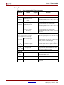
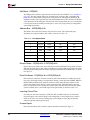
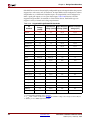
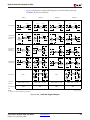
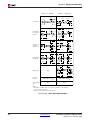
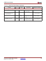
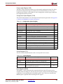
The following table shows the revision history for this document. All revision publications are electronic only (PDF)
unless otherwise noted.
Version
Revision
01/31/02
1.0
(Print Edition.) Initial Xilinx release.
10/14/02
2.0
(Print Edition.) Updated and reprinted. New Virtex-II Pro family members and
packages. Revised I/O support information.
12/04/02
2.1
Added full support for 3.3V I/O standards PCI-X, LVTTL, and LVCMOS33.
01/23/03
2.2
• Added wire-bond package FG676 for XC2VP20, 30, and 40. New package diagram
(Figure 5-62) and pinout diagrams (Figure 5-11 through Figure 5-15). Revised
Table 5-6.
• Removed pinout diagrams and other references for XC2VP40FF1517.
• Revised material in, and added Figure 4-4 to, section “Mixed Voltage Environments,”
page 292.
• Clariified explanation of banks 4/5 VCCO settings for configuration vs. operation in
section “Special VCCO Requirements during Configuration and Readback,” page
293.
04/11/03
2.3
• Table 3-38, Table 3-39: Corrected package type FG672 to FF672, and added package
type FG676.
• Deleted (former) Table 3-3, Power-Up Timing Characteristics, and replaced it with a
hyperlink to Data Sheet Module 3.
• Deleted (former) Table 1-5, Multiplier Switching Characteristics, and replaced it with
a hyperlink to Data Sheet Module 3.
• Changed attribute CLOCK_FEEDBACK to CLK_FEEDBACK.
• Clarifying text added to section “Phase Shift Enable - PSEN” in Chapter 3.
• Additional implementation rule added to section “DCI in Virtex-II Pro Hardware” in
Chapter 3.
• Corrections made in command line, key file, and key file command line equivalent in
section “Creating Keys” in Chapter 3.
• Added device-specific parameters to step 15 of “Single Device Configuration
Sequence” in Chapter 4.
• Section “Data Loading” in Chapter 4: Corrected maximum frequency for SelectMAP
configuration without BUSY handshaking to 5 MHz.
• Table 4-8: Corrected maximum SelectMAP frequency (FCC_SELECTMAP ) to 50 MHz.
• Appendix A, “BitGen and PROMGen Switches and Options”: Updated all commandline options to correlate with development tools and their documentation.
• Table 3-59: Added numerous LVDS primitives to this table, including new differential
termination primitives.
• Added new section “LVDS Input HDL Examples.”
• Changed Figure 3-120 to show internal rather than external differential input
termination.
• Various minor edits.
UG012 (v2.5) 2 February, 2004
www.xilinx.com
1-800-255-7778
Virtex-II Pro™ Platform FPGA User Guide
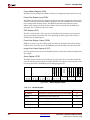
Version
Revision
06/30/03
2.4
• Corrected Location Constraints syntax, multiple instances.
• Added Figure 3-23, page 87 and associated explanatory text.
• Added HDL code for resetting the DCM after configuration in section “External
Feedback,” page 89.
• Modified Banking Rules in section “DCI in Virtex-II Pro Hardware,” page 231.
• Added reference to Answer Record 13012 in section “SSTL2_ I_DCI, SSTL2_II_DCI,”
page 232.
• Corrected command-line equivalent statements for bitstream encryption key files in
section “Creating Keys,” page 263.
• Added new section “SelectMAP Abort Sequence,” page 310, to section “Master
SelectMAP Programming Mode”.
• Corrected shading property of GND pin in symbol key, all diagrams, section “Pinout
Diagrams,” page 359.
• Numerous additional minor edits.
02/02/04
2.5
• Figure 3-61, page 153: Added missing connection between second LUT of Slice 3 and
first LUT of Slice 2.
• Figure 3-73, page 176: Corrected bit numbers on inputs to adder.
• Section “Routing with BlockRAM,” page 180 added.
• Table 3-37, page 198: Added SSO parameters for HSTL18 I/O standards.
• Figure 3-92, page 210: Correct VREF from 0.75V to 0.9V.
• Section “DCI I/O Buffer Library Components,” page 226, added IBUFG_LVDS
components to list.
• Section “Location Constraints,” page 244: Added constraint on locating a DDR
register next to an SDR register using a different clock.
• Appendix C, “Choosing the Battery for VBATT” added, with linked reference in
section “VBATT,” page 265.
• Page 286: added paragraph at end of Introduction to Configuration chapter specifying
a fixed voltage tie for mode pins M0-M2, and warning not to toggle these pins during
or after configuration.
• Table 4-2, page 286: Reduced configuration bitstream lengths for all devices by 64 bits.
• Section “Configuration Pins,” page 290: Added warning and constraints regarding
application of 3.3V signals to dedicated configuration pins.
• Table 4-3, page 291: Corrected directionality of BUSY/DOUT to Output, INIT_B to
Input/Output. Updated with data from XAPP659.
• Former Table 4-6, Master/Slave Serial Mode Programming Switching, and former
Table 4-8, SelectMAP Write Timing Characteristics, removed. See the Virtex-II Pro
Platform FPGA Data Sheet, DC and Switching Characteristics for these and all other
timing parameter specifications.
• Table 4-6, page 302: Corrected FCC_SERIAL from 66 MHz to 50 MHz.
• Added footnote to Figure 4-12, page 302, and Figure 4-14, page 304, clarifying that
DOUT transitions on the falling edge of CCLK.
• Second paragraph below Figure 4-16, page 306: Corrected maximum no-handshake
SelectMAP configuration speed from 5 MHz to 50 MHz.
• Section “Data Loading,” page 306: Changed wording to emphasize that if RDWR_B is
toggled while CS_B is still asserted, a configuration abort will occur.
• Section “Express-Style Loading,” page 308: Added new text to clarify the sequencing
of signals before, during, and after data loading.
Virtex-II Pro™ Platform FPGA User Guide
www.xilinx.com
1-800-255-7778
UG012 (v2.5) 2 February, 2004
02/02/04
(cont’d)
Version
Revision
2.5
(cont’d)
• Page 314: added text to TDO paragraph indicating that pin is open-drain and should
be pulled up externally.
• Table 4-14, page 331: Updated “Total No. of Bits” column with new numbers.
• Figure 5-50, page 417; Figure 5-51, page 418; Figure 5-52, page 419; and Figure 5-53,
page 420: Corrected banking assignments for pins AB12 and AB31. Now shows these
pins in Banks 2 and 7 respectively.
• Table 5-3, page 441: Changed Theta-JC to 0.5°C/Watt for all FF packages.
• Section “Crosstalk,” page 448: Clarified wording of PCB trace routing guidelines to
minimize crosstalk onto VREF lines.
UG012 (v2.5) 2 February, 2004
www.xilinx.com
1-800-255-7778
Virtex-II Pro™ Platform FPGA User Guide
Virtex-II Pro™ Platform FPGA User Guide
www.xilinx.com
1-800-255-7778
UG012 (v2.5) 2 February, 2004
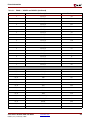
Table of Contents
Preface: About This Guide
Guide Contents . . . . . . . . . . . . . . . . . . . . . . . . . . . . . . . . . . . . . . . . . . . . . . . . . . . . . . . . . . . . . 15
Additional Resources . . . . . . . . . . . . . . . . . . . . . . . . . . . . . . . . . . . . . . . . . . . . . . . . . . . . . . . 16
Conventions . . . . . . . . . . . . . . . . . . . . . . . . . . . . . . . . . . . . . . . . . . . . . . . . . . . . . . . . . . . . . . . . 16
Typographical . . . . . . . . . . . . . . . . . . . . . . . . . . . . . . . . . . . . . . . . . . . . . . . . . . . . . . . . . . . . 16
Online Document . . . . . . . . . . . . . . . . . . . . . . . . . . . . . . . . . . . . . . . . . . . . . . . . . . . . . . . . . 17
Chapter 1: Introduction to the Virtex-II Pro™ FPGA Family
The Next Logical Revolution . . . . . . . . . . . . . . . . . . . . . . . . . . . . . . . . . . . . . . . . . . . . . . . .
Built for Bandwidth . . . . . . . . . . . . . . . . . . . . . . . . . . . . . . . . . . . . . . . . . . . . . . . . . . . . . . . . .
Legacy of Leadership . . . . . . . . . . . . . . . . . . . . . . . . . . . . . . . . . . . . . . . . . . . . . . . . . . . . . . . .
Packets Everywhere . . . . . . . . . . . . . . . . . . . . . . . . . . . . . . . . . . . . . . . . . . . . . . . . . . . . . . . . .
Bridge, Anyone? . . . . . . . . . . . . . . . . . . . . . . . . . . . . . . . . . . . . . . . . . . . . . . . . . . . . . . . . . . . .
Simplifying Complexity . . . . . . . . . . . . . . . . . . . . . . . . . . . . . . . . . . . . . . . . . . . . . . . . . . . . .
Time Is Money . . . . . . . . . . . . . . . . . . . . . . . . . . . . . . . . . . . . . . . . . . . . . . . . . . . . . . . . . . . . . .
Flexibility Is Money . . . . . . . . . . . . . . . . . . . . . . . . . . . . . . . . . . . . . . . . . . . . . . . . . . . . . . . . .
Not Being Discrete . . . . . . . . . . . . . . . . . . . . . . . . . . . . . . . . . . . . . . . . . . . . . . . . . . . . . . . . . .
19
19
20
21
21
21
22
23
23
Chapter 2: Timing Models
Summary . . . . . . . . . . . . . . . . . . . . . . . . . . . . . . . . . . . . . . . . . . . . . . . . . . . . . . . . . . . . . . . . . . . 25
Introduction . . . . . . . . . . . . . . . . . . . . . . . . . . . . . . . . . . . . . . . . . . . . . . . . . . . . . . . . . . . . . . . . 25
CLB / Slice Timing Models . . . . . . . . . . . . . . . . . . . . . . . . . . . . . . . . . . . . . . . . . . . . . . . . . . 26
General Slice Timing Model and Parameters . . . . . . . . . . . . . . . . . . . . . . . . . . . . . . . . . 26
Slice Distributed RAM Timing Model and Parameters . . . . . . . . . . . . . . . . . . . . . . . . . 29
Slice SRL Timing Model and Parameters . . . . . . . . . . . . . . . . . . . . . . . . . . . . . . . . . . . . . 32
Block SelectRAM Timing Model . . . . . . . . . . . . . . . . . . . . . . . . . . . . . . . . . . . . . . . . . . . . 34
Embedded Multiplier Timing Model . . . . . . . . . . . . . . . . . . . . . . . . . . . . . . . . . . . . . . . . 38
IOB Timing Models . . . . . . . . . . . . . . . . . . . . . . . . . . . . . . . . . . . . . . . . . . . . . . . . . . . . . . . . . 40
IOB Input Timing Model and Parameters . . . . . . . . . . . . . . . . . . . . . . . . . . . . . . . . . . . . 41
IOB Output Timing Model and Parameters. . . . . . . . . . . . . . . . . . . . . . . . . . . . . . . . . . . 45
IOB 3-State Timing Model and Parameters . . . . . . . . . . . . . . . . . . . . . . . . . . . . . . . . . . . 48
Pin-to-Pin Timing Models . . . . . . . . . . . . . . . . . . . . . . . . . . . . . . . . . . . . . . . . . . . . . . . . . . . 52
Global Clock Input to Output . . . . . . . . . . . . . . . . . . . . . . . . . . . . . . . . . . . . . . . . . . . . . . 53
Global Clock Setup and Hold. . . . . . . . . . . . . . . . . . . . . . . . . . . . . . . . . . . . . . . . . . . . . . . 55
Digital Clock Manager Timing Model . . . . . . . . . . . . . . . . . . . . . . . . . . . . . . . . . . . . . . . 57
Operating Frequency Ranges . . . . . . . . . . . . . . . . . . . . . . . . . . . . . . . . . . . . . . . . . . . . . . .
Input Clock Tolerances . . . . . . . . . . . . . . . . . . . . . . . . . . . . . . . . . . . . . . . . . . . . . . . . . . . .
Output Clock Precision . . . . . . . . . . . . . . . . . . . . . . . . . . . . . . . . . . . . . . . . . . . . . . . . . . . .
Miscellaneous DCM Timing Parameters . . . . . . . . . . . . . . . . . . . . . . . . . . . . . . . . . . . . .
57
59
60
60
Additional Timing Models in Other Publications:
PPC405 Processor Block and RocketIO Transceiver . . . . . . . . . . . . . . . . . . . . . . . . 62
Virtex-II Pro™ Platform FPGA User Guide
UG012 (v2.5) 2 February, 2004
www.xilinx.com
1-800-255-7778
7
R
IBM PPC405 Processor Block Timing Models . . . . . . . . . . . . . . . . . . . . . . . . . . . . . . . . . 62
RocketIO Transceiver Timing Models . . . . . . . . . . . . . . . . . . . . . . . . . . . . . . . . . . . . . . . 62
Chapter 3: Design Considerations
Summary . . . . . . . . . . . . . . . . . . . . . . . . . . . . . . . . . . . . . . . . . . . . . . . . . . . . . . . . . . . . . . . . . . .
Introduction . . . . . . . . . . . . . . . . . . . . . . . . . . . . . . . . . . . . . . . . . . . . . . . . . . . . . . . . . . . . . . . .
RocketIO Transceiver . . . . . . . . . . . . . . . . . . . . . . . . . . . . . . . . . . . . . . . . . . . . . . . . . . . . . . .
Processor Block . . . . . . . . . . . . . . . . . . . . . . . . . . . . . . . . . . . . . . . . . . . . . . . . . . . . . . . . . . . . .
Global Clock Networks . . . . . . . . . . . . . . . . . . . . . . . . . . . . . . . . . . . . . . . . . . . . . . . . . . . . .
Introduction . . . . . . . . . . . . . . . . . . . . . . . . . . . . . . . . . . . . . . . . . . . . . . . . . . . . . . . . . . . . .
Clock Distribution Resources . . . . . . . . . . . . . . . . . . . . . . . . . . . . . . . . . . . . . . . . . . . . . . .
Power Consumption . . . . . . . . . . . . . . . . . . . . . . . . . . . . . . . . . . . . . . . . . . . . . . . . . . . . . .
Library Primitives and Submodules . . . . . . . . . . . . . . . . . . . . . . . . . . . . . . . . . . . . . . . . .
Characteristics . . . . . . . . . . . . . . . . . . . . . . . . . . . . . . . . . . . . . . . . . . . . . . . . . . . . . . . . . . .
Location Constraints . . . . . . . . . . . . . . . . . . . . . . . . . . . . . . . . . . . . . . . . . . . . . . . . . . . . . .
Secondary Clock Network . . . . . . . . . . . . . . . . . . . . . . . . . . . . . . . . . . . . . . . . . . . . . . . . .
VHDL and Verilog Instantiation . . . . . . . . . . . . . . . . . . . . . . . . . . . . . . . . . . . . . . . . . . . .
63
63
64
64
64
64
65
74
75
79
80
80
80
Digital Clock Managers (DCMs) . . . . . . . . . . . . . . . . . . . . . . . . . . . . . . . . . . . . . . . . . . . . . 85
Overview . . . . . . . . . . . . . . . . . . . . . . . . . . . . . . . . . . . . . . . . . . . . . . . . . . . . . . . . . . . . . . . . 85
Clock De-Skew . . . . . . . . . . . . . . . . . . . . . . . . . . . . . . . . . . . . . . . . . . . . . . . . . . . . . . . . . . . 86
Legacy Support . . . . . . . . . . . . . . . . . . . . . . . . . . . . . . . . . . . . . . . . . . . . . . . . . . . . . . . . . . . 92
Frequency Synthesis . . . . . . . . . . . . . . . . . . . . . . . . . . . . . . . . . . . . . . . . . . . . . . . . . . . . . . 95
Phase Shifting . . . . . . . . . . . . . . . . . . . . . . . . . . . . . . . . . . . . . . . . . . . . . . . . . . . . . . . . . . . . 99
DCM Waveforms . . . . . . . . . . . . . . . . . . . . . . . . . . . . . . . . . . . . . . . . . . . . . . . . . . . . . . . . 115
Block SelectRAM™ Memory . . . . . . . . . . . . . . . . . . . . . . . . . . . . . . . . . . . . . . . . . . . . . . . 119
Introduction . . . . . . . . . . . . . . . . . . . . . . . . . . . . . . . . . . . . . . . . . . . . . . . . . . . . . . . . . . . .
Synchronous Dual-Port and Single-Port RAM . . . . . . . . . . . . . . . . . . . . . . . . . . . . . . .
Characteristics . . . . . . . . . . . . . . . . . . . . . . . . . . . . . . . . . . . . . . . . . . . . . . . . . . . . . . . . . .
Library Primitives . . . . . . . . . . . . . . . . . . . . . . . . . . . . . . . . . . . . . . . . . . . . . . . . . . . . . . .
VHDL and Verilog Instantiation . . . . . . . . . . . . . . . . . . . . . . . . . . . . . . . . . . . . . . . . . . .
Port Signals . . . . . . . . . . . . . . . . . . . . . . . . . . . . . . . . . . . . . . . . . . . . . . . . . . . . . . . . . . . . .
Address Mapping . . . . . . . . . . . . . . . . . . . . . . . . . . . . . . . . . . . . . . . . . . . . . . . . . . . . . . .
Attributes. . . . . . . . . . . . . . . . . . . . . . . . . . . . . . . . . . . . . . . . . . . . . . . . . . . . . . . . . . . . . . .
Initialization in VHDL or Verilog Codes . . . . . . . . . . . . . . . . . . . . . . . . . . . . . . . . . . . .
Location Constraints . . . . . . . . . . . . . . . . . . . . . . . . . . . . . . . . . . . . . . . . . . . . . . . . . . . . .
Applications . . . . . . . . . . . . . . . . . . . . . . . . . . . . . . . . . . . . . . . . . . . . . . . . . . . . . . . . . . . .
VHDL and Verilog Templates . . . . . . . . . . . . . . . . . . . . . . . . . . . . . . . . . . . . . . . . . . . . .
119
119
123
123
125
125
127
127
129
129
129
130
Distributed SelectRAM Memory . . . . . . . . . . . . . . . . . . . . . . . . . . . . . . . . . . . . . . . . . . . 136
Introduction . . . . . . . . . . . . . . . . . . . . . . . . . . . . . . . . . . . . . . . . . . . . . . . . . . . . . . . . . . . .
Characteristics . . . . . . . . . . . . . . . . . . . . . . . . . . . . . . . . . . . . . . . . . . . . . . . . . . . . . . . . . .
Library Primitives . . . . . . . . . . . . . . . . . . . . . . . . . . . . . . . . . . . . . . . . . . . . . . . . . . . . . . .
VHDL and Verilog Instantiation . . . . . . . . . . . . . . . . . . . . . . . . . . . . . . . . . . . . . . . . . . .
Ports Signals . . . . . . . . . . . . . . . . . . . . . . . . . . . . . . . . . . . . . . . . . . . . . . . . . . . . . . . . . . . .
Attributes. . . . . . . . . . . . . . . . . . . . . . . . . . . . . . . . . . . . . . . . . . . . . . . . . . . . . . . . . . . . . . .
Initialization in VHDL or Verilog Codes . . . . . . . . . . . . . . . . . . . . . . . . . . . . . . . . . . . .
Location Constraints . . . . . . . . . . . . . . . . . . . . . . . . . . . . . . . . . . . . . . . . . . . . . . . . . . . . .
Applications . . . . . . . . . . . . . . . . . . . . . . . . . . . . . . . . . . . . . . . . . . . . . . . . . . . . . . . . . . . .
VHDL and Verilog Templates . . . . . . . . . . . . . . . . . . . . . . . . . . . . . . . . . . . . . . . . . . . . .
136
138
138
139
140
140
141
141
143
144
Look-Up Tables as Shift Registers (SRLs) . . . . . . . . . . . . . . . . . . . . . . . . . . . . . . . . . . . 146
Introduction . . . . . . . . . . . . . . . . . . . . . . . . . . . . . . . . . . . . . . . . . . . . . . . . . . . . . . . . . . . . 146
Shift Register Operations . . . . . . . . . . . . . . . . . . . . . . . . . . . . . . . . . . . . . . . . . . . . . . . . . 146
8
www.xilinx.com
1-800-255-7778
Virtex-II Pro™ Platform FPGA User Guide
UG012 (v2.5) 2 February, 2004
R
Characteristics . . . . . . . . . . . . . . . . . . . . . . . . . . . . . . . . . . . . . . . . . . . . . . . . . . . . . . . . . .
Library Primitives and Submodules . . . . . . . . . . . . . . . . . . . . . . . . . . . . . . . . . . . . . . . .
Initialization in VHDL and Verilog Code . . . . . . . . . . . . . . . . . . . . . . . . . . . . . . . . . . .
Port Signals . . . . . . . . . . . . . . . . . . . . . . . . . . . . . . . . . . . . . . . . . . . . . . . . . . . . . . . . . . . . .
Attributes. . . . . . . . . . . . . . . . . . . . . . . . . . . . . . . . . . . . . . . . . . . . . . . . . . . . . . . . . . . . . . .
Location Constraints . . . . . . . . . . . . . . . . . . . . . . . . . . . . . . . . . . . . . . . . . . . . . . . . . . . . .
Fully Synchronous Shift Registers . . . . . . . . . . . . . . . . . . . . . . . . . . . . . . . . . . . . . . . . . .
Static-Length Shift Registers . . . . . . . . . . . . . . . . . . . . . . . . . . . . . . . . . . . . . . . . . . . . . . .
VHDL and Verilog Instantiation . . . . . . . . . . . . . . . . . . . . . . . . . . . . . . . . . . . . . . . . . . .
148
148
151
151
152
152
153
154
155
Large Multiplexers . . . . . . . . . . . . . . . . . . . . . . . . . . . . . . . . . . . . . . . . . . . . . . . . . . . . . . . . . 157
Introduction . . . . . . . . . . . . . . . . . . . . . . . . . . . . . . . . . . . . . . . . . . . . . . . . . . . . . . . . . . . .
Virtex-II Pro CLB Resources . . . . . . . . . . . . . . . . . . . . . . . . . . . . . . . . . . . . . . . . . . . . . . .
Wide-Input Multiplexers . . . . . . . . . . . . . . . . . . . . . . . . . . . . . . . . . . . . . . . . . . . . . . . . .
Characteristics . . . . . . . . . . . . . . . . . . . . . . . . . . . . . . . . . . . . . . . . . . . . . . . . . . . . . . . . . .
Library Primitives and Submodules . . . . . . . . . . . . . . . . . . . . . . . . . . . . . . . . . . . . . . . .
Port Signals . . . . . . . . . . . . . . . . . . . . . . . . . . . . . . . . . . . . . . . . . . . . . . . . . . . . . . . . . . . . .
Applications . . . . . . . . . . . . . . . . . . . . . . . . . . . . . . . . . . . . . . . . . . . . . . . . . . . . . . . . . . . .
VHDL and Verilog Instantiation . . . . . . . . . . . . . . . . . . . . . . . . . . . . . . . . . . . . . . . . . . .
157
157
162
162
163
163
164
164
Sum of Products (SOP) Logic . . . . . . . . . . . . . . . . . . . . . . . . . . . . . . . . . . . . . . . . . . . . . . . 168
Introduction . . . . . . . . . . . . . . . . . . . . . . . . . . . . . . . . . . . . . . . . . . . . . . . . . . . . . . . . . . . .
Virtex-II Pro CLB Resources . . . . . . . . . . . . . . . . . . . . . . . . . . . . . . . . . . . . . . . . . . . . . . .
VHDL Parameters . . . . . . . . . . . . . . . . . . . . . . . . . . . . . . . . . . . . . . . . . . . . . . . . . . . . . . .
Applications . . . . . . . . . . . . . . . . . . . . . . . . . . . . . . . . . . . . . . . . . . . . . . . . . . . . . . . . . . . .
VHDL and Verilog Instantiation . . . . . . . . . . . . . . . . . . . . . . . . . . . . . . . . . . . . . . . . . . .
168
168
169
170
170
Embedded Multipliers . . . . . . . . . . . . . . . . . . . . . . . . . . . . . . . . . . . . . . . . . . . . . . . . . . . . . 174
Introduction . . . . . . . . . . . . . . . . . . . . . . . . . . . . . . . . . . . . . . . . . . . . . . . . . . . . . . . . . . . .
Two’s-Complement Signed Multiplier . . . . . . . . . . . . . . . . . . . . . . . . . . . . . . . . . . . . . .
Library Primitives and Submodules . . . . . . . . . . . . . . . . . . . . . . . . . . . . . . . . . . . . . . . .
Two Multipliers in a Single Primitive . . . . . . . . . . . . . . . . . . . . . . . . . . . . . . . . . . . . . . .
VHDL and Verilog Instantiation . . . . . . . . . . . . . . . . . . . . . . . . . . . . . . . . . . . . . . . . . . .
Port Signals . . . . . . . . . . . . . . . . . . . . . . . . . . . . . . . . . . . . . . . . . . . . . . . . . . . . . . . . . . . . .
Location Constraints . . . . . . . . . . . . . . . . . . . . . . . . . . . . . . . . . . . . . . . . . . . . . . . . . . . . .
Routing with BlockRAM . . . . . . . . . . . . . . . . . . . . . . . . . . . . . . . . . . . . . . . . . . . . . . . . . .
VHDL and Verilog Templates . . . . . . . . . . . . . . . . . . . . . . . . . . . . . . . . . . . . . . . . . . . . .
174
175
175
178
179
180
180
180
181
Single-Ended SelectIO™-Ultra Resources . . . . . . . . . . . . . . . . . . . . . . . . . . . . . . . . . . 183
Summary . . . . . . . . . . . . . . . . . . . . . . . . . . . . . . . . . . . . . . . . . . . . . . . . . . . . . . . . . . . . . . .
Introduction . . . . . . . . . . . . . . . . . . . . . . . . . . . . . . . . . . . . . . . . . . . . . . . . . . . . . . . . . . . .
Fundamentals . . . . . . . . . . . . . . . . . . . . . . . . . . . . . . . . . . . . . . . . . . . . . . . . . . . . . . . . . . .
Overview of Supported I/O Standards . . . . . . . . . . . . . . . . . . . . . . . . . . . . . . . . . . . . .
Library Symbols . . . . . . . . . . . . . . . . . . . . . . . . . . . . . . . . . . . . . . . . . . . . . . . . . . . . . . . . .
Design Considerations . . . . . . . . . . . . . . . . . . . . . . . . . . . . . . . . . . . . . . . . . . . . . . . . . . .
Application Examples . . . . . . . . . . . . . . . . . . . . . . . . . . . . . . . . . . . . . . . . . . . . . . . . . . . .
183
183
183
184
186
195
202
Digitally Controlled Impedance (DCI) . . . . . . . . . . . . . . . . . . . . . . . . . . . . . . . . . . . . . . 219
Introduction . . . . . . . . . . . . . . . . . . . . . . . . . . . . . . . . . . . . . . . . . . . . . . . . . . . . . . . . . . . .
Xilinx DCI . . . . . . . . . . . . . . . . . . . . . . . . . . . . . . . . . . . . . . . . . . . . . . . . . . . . . . . . . . . . . .
Software Support . . . . . . . . . . . . . . . . . . . . . . . . . . . . . . . . . . . . . . . . . . . . . . . . . . . . . . . .
DCI in Virtex-II Pro Hardware . . . . . . . . . . . . . . . . . . . . . . . . . . . . . . . . . . . . . . . . . . . .
219
219
226
231
Double-Data-Rate (DDR) I/O . . . . . . . . . . . . . . . . . . . . . . . . . . . . . . . . . . . . . . . . . . . . . . . 235
Introduction . . . . . . . . . . . . . . . . . . . . . . . . . . . . . . . . . . . . . . . . . . . . . . . . . . . . . . . . . . . .
Data Flow . . . . . . . . . . . . . . . . . . . . . . . . . . . . . . . . . . . . . . . . . . . . . . . . . . . . . . . . . . . . . .
Characteristics . . . . . . . . . . . . . . . . . . . . . . . . . . . . . . . . . . . . . . . . . . . . . . . . . . . . . . . . . .
Library Primitives . . . . . . . . . . . . . . . . . . . . . . . . . . . . . . . . . . . . . . . . . . . . . . . . . . . . . . .
Virtex-II Pro™ Platform FPGA User Guide
UG012 (v2.5) 2 February, 2004
www.xilinx.com
1-800-255-7778
235
236
242
242
9
R
VHDL and Verilog Instantiation . . . . . . . . . . . . . . . . . . . . . . . . . . . . . . . . . . . . . . . . . . .
Port Signals . . . . . . . . . . . . . . . . . . . . . . . . . . . . . . . . . . . . . . . . . . . . . . . . . . . . . . . . . . . . .
Initialization in VHDL or Verilog . . . . . . . . . . . . . . . . . . . . . . . . . . . . . . . . . . . . . . . . . .
Location Constraints . . . . . . . . . . . . . . . . . . . . . . . . . . . . . . . . . . . . . . . . . . . . . . . . . . . . .
Applications . . . . . . . . . . . . . . . . . . . . . . . . . . . . . . . . . . . . . . . . . . . . . . . . . . . . . . . . . . . .
VHDL and Verilog Templates . . . . . . . . . . . . . . . . . . . . . . . . . . . . . . . . . . . . . . . . . . . . .
243
243
244
244
244
245
LVDS I/O . . . . . . . . . . . . . . . . . . . . . . . . . . . . . . . . . . . . . . . . . . . . . . . . . . . . . . . . . . . . . . . . . . 251
Introduction . . . . . . . . . . . . . . . . . . . . . . . . . . . . . . . . . . . . . . . . . . . . . . . . . . . . . . . . . . . .
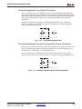
Creating an LVDS Input/Clock Buffer . . . . . . . . . . . . . . . . . . . . . . . . . . . . . . . . . . . . . .
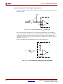
Creating an LVDS Output Buffer . . . . . . . . . . . . . . . . . . . . . . . . . . . . . . . . . . . . . . . . . .
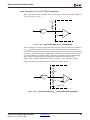
Creating an LVDS Output 3-State Buffer . . . . . . . . . . . . . . . . . . . . . . . . . . . . . . . . . . . .
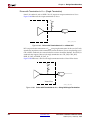
Creating a Bidirectional LVDS Buffer . . . . . . . . . . . . . . . . . . . . . . . . . . . . . . . . . . . . . . .
LDT. . . . . . . . . . . . . . . . . . . . . . . . . . . . . . . . . . . . . . . . . . . . . . . . . . . . . . . . . . . . . . . . . . . .
LDT Implementation . . . . . . . . . . . . . . . . . . . . . . . . . . . . . . . . . . . . . . . . . . . . . . . . . . . . .
251
252
254
255
257
258
258
LVPECL I/O. . . . . . . . . . . . . . . . . . . . . . . . . . . . . . . . . . . . . . . . . . . . . . . . . . . . . . . . . . . . . . . . 259
Introduction . . . . . . . . . . . . . . . . . . . . . . . . . . . . . . . . . . . . . . . . . . . . . . . . . . . . . . . . . . . . 259
Creating an LVPECL Input/Clock Buffer . . . . . . . . . . . . . . . . . . . . . . . . . . . . . . . . . . . 259
Creating an LVPECL Output Buffer . . . . . . . . . . . . . . . . . . . . . . . . . . . . . . . . . . . . . . . . 260
Bitstream Encryption . . . . . . . . . . . . . . . . . . . . . . . . . . . . . . . . . . . . . . . . . . . . . . . . . . . . . . . 262
What DES Is . . . . . . . . . . . . . . . . . . . . . . . . . . . . . . . . . . . . . . . . . . . . . . . . . . . . . . . . . . . .
How Triple DES is Different. . . . . . . . . . . . . . . . . . . . . . . . . . . . . . . . . . . . . . . . . . . . . . .
Classification and Export Considerations . . . . . . . . . . . . . . . . . . . . . . . . . . . . . . . . . . .
Creating Keys . . . . . . . . . . . . . . . . . . . . . . . . . . . . . . . . . . . . . . . . . . . . . . . . . . . . . . . . . . .
Loading Keys . . . . . . . . . . . . . . . . . . . . . . . . . . . . . . . . . . . . . . . . . . . . . . . . . . . . . . . . . . .
Loading Encrypted Bitstreams . . . . . . . . . . . . . . . . . . . . . . . . . . . . . . . . . . . . . . . . . . . . .
VBATT . . . . . . . . . . . . . . . . . . . . . . . . . . . . . . . . . . . . . . . . . . . . . . . . . . . . . . . . . . . . . . . . . .
262
262
263
263
265
265
265
CORE Generator System . . . . . . . . . . . . . . . . . . . . . . . . . . . . . . . . . . . . . . . . . . . . . . . . . . . 265
Introduction . . . . . . . . . . . . . . . . . . . . . . . . . . . . . . . . . . . . . . . . . . . . . . . . . . . . . . . . . . . .
The CORE Generator System . . . . . . . . . . . . . . . . . . . . . . . . . . . . . . . . . . . . . . . . . . . . . .
CORE Generator Design Flow . . . . . . . . . . . . . . . . . . . . . . . . . . . . . . . . . . . . . . . . . . . . .
Core Types . . . . . . . . . . . . . . . . . . . . . . . . . . . . . . . . . . . . . . . . . . . . . . . . . . . . . . . . . . . . .
Xilinx IP Solutions and the IP Center . . . . . . . . . . . . . . . . . . . . . . . . . . . . . . . . . . . . . . .
CORE Generator Summary . . . . . . . . . . . . . . . . . . . . . . . . . . . . . . . . . . . . . . . . . . . . . . .
Virtex-II Pro IP Cores Support . . . . . . . . . . . . . . . . . . . . . . . . . . . . . . . . . . . . . . . . . . . . .
265
266
267
268
270
272
273
Chapter 4: Configuration
Summary . . . . . . . . . . . . . . . . . . . . . . . . . . . . . . . . . . . . . . . . . . . . . . . . . . . . . . . . . . . . . . . . . . 285
Introduction . . . . . . . . . . . . . . . . . . . . . . . . . . . . . . . . . . . . . . . . . . . . . . . . . . . . . . . . . . . . . . . 285
Configuration Modes . . . . . . . . . . . . . . . . . . . . . . . . . . . . . . . . . . . . . . . . . . . . . . . . . . . .
Configuration Process and Flow . . . . . . . . . . . . . . . . . . . . . . . . . . . . . . . . . . . . . . . . . . .
Configuration Pins . . . . . . . . . . . . . . . . . . . . . . . . . . . . . . . . . . . . . . . . . . . . . . . . . . . . . . .
Mixed Voltage Environments . . . . . . . . . . . . . . . . . . . . . . . . . . . . . . . . . . . . . . . . . . . . .
286
287
290
292
Configuration Solutions . . . . . . . . . . . . . . . . . . . . . . . . . . . . . . . . . . . . . . . . . . . . . . . . . . . . 293
System Advanced Configuration Environment (System ACE™) Series . . . . . . . . . .
Configuration PROMs . . . . . . . . . . . . . . . . . . . . . . . . . . . . . . . . . . . . . . . . . . . . . . . . . . . .
Flash PROMs With a CPLD Configuration Controller. . . . . . . . . . . . . . . . . . . . . . . . .
Embedded Solutions . . . . . . . . . . . . . . . . . . . . . . . . . . . . . . . . . . . . . . . . . . . . . . . . . . . . .
PROM and System ACE Selection Guide . . . . . . . . . . . . . . . . . . . . . . . . . . . . . . . . . . . .
293
297
298
299
299
Software Support and Data Files . . . . . . . . . . . . . . . . . . . . . . . . . . . . . . . . . . . . . . . . . . . 301
iMPACT . . . . . . . . . . . . . . . . . . . . . . . . . . . . . . . . . . . . . . . . . . . . . . . . . . . . . . . . . . . . . . . . 301
Programming Cables . . . . . . . . . . . . . . . . . . . . . . . . . . . . . . . . . . . . . . . . . . . . . . . . . . . . . 301
10
www.xilinx.com
1-800-255-7778
Virtex-II Pro™ Platform FPGA User Guide
UG012 (v2.5) 2 February, 2004
R
Boundary Scan Interconnect Testing for Virtex-II Pro Devices. . . . . . . . . . . . . . . . . . 301
Master Serial Programming Mode . . . . . . . . . . . . . . . . . . . . . . . . . . . . . . . . . . . . . . . . . . 302
Slave Serial Programming Mode . . . . . . . . . . . . . . . . . . . . . . . . . . . . . . . . . . . . . . . . . . . 303
Daisy-Chain Configuration . . . . . . . . . . . . . . . . . . . . . . . . . . . . . . . . . . . . . . . . . . . . . . . 303
Master SelectMAP Programming Mode . . . . . . . . . . . . . . . . . . . . . . . . . . . . . . . . . . . . . 305
DATA Pins (D[0:7]) . . . . . . . . . . . . . . . . . . . . . . . . . . . . . . . . . . . . . . . . . . . . . . . . . . . . . .
RDWR_B . . . . . . . . . . . . . . . . . . . . . . . . . . . . . . . . . . . . . . . . . . . . . . . . . . . . . . . . . . . . . . .
CS_B . . . . . . . . . . . . . . . . . . . . . . . . . . . . . . . . . . . . . . . . . . . . . . . . . . . . . . . . . . . . . . . . . . .
CCLK . . . . . . . . . . . . . . . . . . . . . . . . . . . . . . . . . . . . . . . . . . . . . . . . . . . . . . . . . . . . . . . . . .
Data Loading . . . . . . . . . . . . . . . . . . . . . . . . . . . . . . . . . . . . . . . . . . . . . . . . . . . . . . . . . . .
305
305
305
306
306
Slave SelectMAP Programming Mode . . . . . . . . . . . . . . . . . . . . . . . . . . . . . . . . . . . . . . 307
DATA Pins (D[0:7]) . . . . . . . . . . . . . . . . . . . . . . . . . . . . . . . . . . . . . . . . . . . . . . . . . . . . . .
RDWR_B . . . . . . . . . . . . . . . . . . . . . . . . . . . . . . . . . . . . . . . . . . . . . . . . . . . . . . . . . . . . . . .
CS_B . . . . . . . . . . . . . . . . . . . . . . . . . . . . . . . . . . . . . . . . . . . . . . . . . . . . . . . . . . . . . . . . . . .
BUSY . . . . . . . . . . . . . . . . . . . . . . . . . . . . . . . . . . . . . . . . . . . . . . . . . . . . . . . . . . . . . . . . . .
CCLK . . . . . . . . . . . . . . . . . . . . . . . . . . . . . . . . . . . . . . . . . . . . . . . . . . . . . . . . . . . . . . . . . .
307
308
308
308
308
SelectMAP Abort Sequence . . . . . . . . . . . . . . . . . . . . . . . . . . . . . . . . . . . . . . . . . . . . . . . . 310
ABORT Sequence Description . . . . . . . . . . . . . . . . . . . . . . . . . . . . . . . . . . . . . . . . . . . . . 310
ABORT Status Word . . . . . . . . . . . . . . . . . . . . . . . . . . . . . . . . . . . . . . . . . . . . . . . . . . . . . 312
Resuming Configuration . . . . . . . . . . . . . . . . . . . . . . . . . . . . . . . . . . . . . . . . . . . . . . . . . . 312
JTAG/ Boundary Scan Programming Mode . . . . . . . . . . . . . . . . . . . . . . . . . . . . . . . . . 312
Introduction . . . . . . . . . . . . . . . . . . . . . . . . . . . . . . . . . . . . . . . . . . . . . . . . . . . . . . . . . . . .
Boundary-Scan for Virtex-II Pro Devices Using IEEE Standard 1149.1 . . . . . . . . . . .
Boundary-Scan Register . . . . . . . . . . . . . . . . . . . . . . . . . . . . . . . . . . . . . . . . . . . . . . . . . .
Bit Sequence . . . . . . . . . . . . . . . . . . . . . . . . . . . . . . . . . . . . . . . . . . . . . . . . . . . . . . . . . . . .
Using Boundary Scan in Virtex-II Pro Devices . . . . . . . . . . . . . . . . . . . . . . . . . . . . . . .
Boundary-Scan for Virtex-II Pro Devices Using IEEE Standard 1532 . . . . . . . . . . . .
Configuration Flows Using JTAG . . . . . . . . . . . . . . . . . . . . . . . . . . . . . . . . . . . . . . . . . .
312
313
316
317
320
327
329
Configuration Details . . . . . . . . . . . . . . . . . . . . . . . . . . . . . . . . . . . . . . . . . . . . . . . . . . . . . . 331
Readback . . . . . . . . . . . . . . . . . . . . . . . . . . . . . . . . . . . . . . . . . . . . . . . . . . . . . . . . . . . . . . . . . . 341
Readback Verification and Capture . . . . . . . . . . . . . . . . . . . . . . . . . . . . . . . . . . . . . . . .
Preparing for Readback in Design Entry . . . . . . . . . . . . . . . . . . . . . . . . . . . . . . . . . . . .
Enabling Readback in the Software . . . . . . . . . . . . . . . . . . . . . . . . . . . . . . . . . . . . . . . . .
Readback When Using Boundary Scan . . . . . . . . . . . . . . . . . . . . . . . . . . . . . . . . . . . . .
Using ChipScope Pro . . . . . . . . . . . . . . . . . . . . . . . . . . . . . . . . . . . . . . . . . . . . . . . . . . . . .
341
341
342
343
345
Chapter 5: PCB Design Considerations
Summary . . . . . . . . . . . . . . . . . . . . . . . . . . . . . . . . . . . . . . . . . . . . . . . . . . . . . . . . . . . . . . . . . . 347
Pinout Information . . . . . . . . . . . . . . . . . . . . . . . . . . . . . . . . . . . . . . . . . . . . . . . . . . . . . . . . . 347
Introduction . . . . . . . . . . . . . . . . . . . . . . . . . . . . . . . . . . . . . . . . . . . . . . . . . . . . . . . . . . . . 347
Pin Definitions . . . . . . . . . . . . . . . . . . . . . . . . . . . . . . . . . . . . . . . . . . . . . . . . . . . . . . . . . . 348
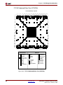
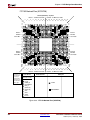
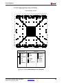
FG256 Fine-Pitch BGA Package . . . . . . . . . . . . . . . . . . . . . . . . . . . . . . . . . . . . . . . . . . . . 350
Pinout Diagrams . . . . . . . . . . . . . . . . . . . . . . . . . . . . . . . . . . . . . . . . . . . . . . . . . . . . . . . . . . . 359
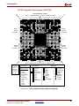
FG256 Fine-Pitch BGA Pinout Diagrams . . . . . . . . . . . . . . . . . . . . . . . . . . . . . . . . . . . .
FG456 Fine-Pitch BGA Pinout Diagrams . . . . . . . . . . . . . . . . . . . . . . . . . . . . . . . . . . . .
FG676 Fine-Pitch BGA Pinout Diagrams . . . . . . . . . . . . . . . . . . . . . . . . . . . . . . . . . . . .
FF672 Flip-Chip Fine-Pitch BGA Pinout Diagrams . . . . . . . . . . . . . . . . . . . . . . . . . . .
FF896 Flip-Chip Fine-Pitch BGA Pinout Diagrams . . . . . . . . . . . . . . . . . . . . . . . . . . .
FF1152 Flip-Chip Fine-Pitch BGA Pinout Diagrams . . . . . . . . . . . . . . . . . . . . . . . . . .
FF1148 Flip-Chip Fine-Pitch BGA Pinout Diagrams . . . . . . . . . . . . . . . . . . . . . . . . . .
Virtex-II Pro™ Platform FPGA User Guide
UG012 (v2.5) 2 February, 2004
www.xilinx.com
1-800-255-7778
361
365
373
379
387
393
405
11
R
FF1517 Flip-Chip Fine-Pitch BGA Pinout Diagrams . . . . . . . . . . . . . . . . . . . . . . . . . . 411
FF1704 Flip-Chip Fine-Pitch BGA Pinout Diagrams . . . . . . . . . . . . . . . . . . . . . . . . . . 417
FF1696 Flip-Chip Fine-Pitch BGA Pinout Diagrams . . . . . . . . . . . . . . . . . . . . . . . . . . 423
Package Specifications . . . . . . . . . . . . . . . . . . . . . . . . . . . . . . . . . . . . . . . . . . . . . . . . . . . . . 429
FG256 Fine-Pitch BGA Package (1.00 mm Pitch) . . . . . . . . . . . . . . . . . . . . . . . . . . . . .
FG456 Fine-Pitch BGA Package (1.00 mm Pitch) . . . . . . . . . . . . . . . . . . . . . . . . . . . . .
FG676 Fine-Pitch BGA Package Specifications (1.00mm pitch) . . . . . . . . . . . . . . . . .
FF672 Flip-Chip Fine-Pitch BGA Package (1.00 mm Pitch) . . . . . . . . . . . . . . . . . . . . .
FF896 Flip-Chip Fine-Pitch BGA Package (1.00 mm Pitch) . . . . . . . . . . . . . . . . . . . . .
FF1152 Flip-Chip Fine-Pitch BGA Package (1.00 mm Pitch) . . . . . . . . . . . . . . . . . . . .
FF1148 Flip-Chip Fine-Pitch BGA Package (1.00 mm Pitch) . . . . . . . . . . . . . . . . . . . .
FF1517 Flip-Chip Fine-Pitch BGA Package (1.00 mm Pitch) . . . . . . . . . . . . . . . . . . . .
FF1704 Flip-Chip Fine-Pitch BGA Package (1.00 mm Pitch) . . . . . . . . . . . . . . . . . . . .
FF1696 Flip-Chip Fine-Pitch BGA Package (1.00 mm Pitch) . . . . . . . . . . . . . . . . . . . .
430
431
432
433
434
435
436
437
438
439
Flip-Chip Packages . . . . . . . . . . . . . . . . . . . . . . . . . . . . . . . . . . . . . . . . . . . . . . . . . . . . . . . . . 440
Advantages of Flip-Chip Technology . . . . . . . . . . . . . . . . . . . . . . . . . . . . . . . . . . . . . . . 440
Thermal Data . . . . . . . . . . . . . . . . . . . . . . . . . . . . . . . . . . . . . . . . . . . . . . . . . . . . . . . . . . . . . . 440
Thermal Considerations . . . . . . . . . . . . . . . . . . . . . . . . . . . . . . . . . . . . . . . . . . . . . . . . . . 440
Thermal Management Options . . . . . . . . . . . . . . . . . . . . . . . . . . . . . . . . . . . . . . . . . . . . 442
Printed Circuit Board Considerations . . . . . . . . . . . . . . . . . . . . . . . . . . . . . . . . . . . . . . . 443
Layout Considerations . . . . . . . . . . . . . . . . . . . . . . . . . . . . . . . . . . . . . . . . . . . . . . . . . . . 443
VCC Decoupling . . . . . . . . . . . . . . . . . . . . . . . . . . . . . . . . . . . . . . . . . . . . . . . . . . . . . . . . . 443
Board Routability Guidelines . . . . . . . . . . . . . . . . . . . . . . . . . . . . . . . . . . . . . . . . . . . . . . 449
Board-Level BGA Routing Challenges . . . . . . . . . . . . . . . . . . . . . . . . . . . . . . . . . . . . . . 449
Board Routing Strategy . . . . . . . . . . . . . . . . . . . . . . . . . . . . . . . . . . . . . . . . . . . . . . . . . . . 450
XPower . . . . . . . . . . . . . . . . . . . . . . . . . . . . . . . . . . . . . . . . . . . . . . . . . . . . . . . . . . . . . . . . . . . . 455
IBIS Models . . . . . . . . . . . . . . . . . . . . . . . . . . . . . . . . . . . . . . . . . . . . . . . . . . . . . . . . . . . . . . . 455
Using IBIS Models . . . . . . . . . . . . . . . . . . . . . . . . . . . . . . . . . . . . . . . . . . . . . . . . . . . . . . .
IBIS Generation. . . . . . . . . . . . . . . . . . . . . . . . . . . . . . . . . . . . . . . . . . . . . . . . . . . . . . . . . .
Advantages of IBIS . . . . . . . . . . . . . . . . . . . . . . . . . . . . . . . . . . . . . . . . . . . . . . . . . . . . . .
IBIS File Structure . . . . . . . . . . . . . . . . . . . . . . . . . . . . . . . . . . . . . . . . . . . . . . . . . . . . . . .
IBIS I/V and dV/dt Curves . . . . . . . . . . . . . . . . . . . . . . . . . . . . . . . . . . . . . . . . . . . . . . .
Ramp and dV/dt Curves . . . . . . . . . . . . . . . . . . . . . . . . . . . . . . . . . . . . . . . . . . . . . . . . .
Xilinx IBIS Package Parasitic Modelling . . . . . . . . . . . . . . . . . . . . . . . . . . . . . . . . . . . . .
IBIS Simulations . . . . . . . . . . . . . . . . . . . . . . . . . . . . . . . . . . . . . . . . . . . . . . . . . . . . . . . . .
IBIS Simulators . . . . . . . . . . . . . . . . . . . . . . . . . . . . . . . . . . . . . . . . . . . . . . . . . . . . . . . . . .
Xilinx IBIS Advantages . . . . . . . . . . . . . . . . . . . . . . . . . . . . . . . . . . . . . . . . . . . . . . . . . . .
ANSI/EIA IBIS Official Website . . . . . . . . . . . . . . . . . . . . . . . . . . . . . . . . . . . . . . . . . . .
456
456
456
456
457
457
458
458
459
460
460
BSDL and Boundary Scan Models . . . . . . . . . . . . . . . . . . . . . . . . . . . . . . . . . . . . . . . . . . 460
BSDL Files . . . . . . . . . . . . . . . . . . . . . . . . . . . . . . . . . . . . . . . . . . . . . . . . . . . . . . . . . . . . . . 460
Appendix A: BitGen and PROMGen Switches and Options
Using BitGen . . . . . . . . . . . . . . . . . . . . . . . . . . . . . . . . . . . . . . . . . . . . . . . . . . . . . . . . . . . . . . 461
BitGen Syntax . . . . . . . . . . . . . . . . . . . . . . . . . . . . . . . . . . . . . . . . . . . . . . . . . . . . . . . . . . . 462
BitGen Files . . . . . . . . . . . . . . . . . . . . . . . . . . . . . . . . . . . . . . . . . . . . . . . . . . . . . . . . . . . . . 462
BitGen Options . . . . . . . . . . . . . . . . . . . . . . . . . . . . . . . . . . . . . . . . . . . . . . . . . . . . . . . . . . 463
Using PROMGen . . . . . . . . . . . . . . . . . . . . . . . . . . . . . . . . . . . . . . . . . . . . . . . . . . . . . . . . . . 469
PROMGen Syntax . . . . . . . . . . . . . . . . . . . . . . . . . . . . . . . . . . . . . . . . . . . . . . . . . . . . . . .
PROMGen Files . . . . . . . . . . . . . . . . . . . . . . . . . . . . . . . . . . . . . . . . . . . . . . . . . . . . . . . . .
PROMGen Options . . . . . . . . . . . . . . . . . . . . . . . . . . . . . . . . . . . . . . . . . . . . . . . . . . . . . .
Examples . . . . . . . . . . . . . . . . . . . . . . . . . . . . . . . . . . . . . . . . . . . . . . . . . . . . . . . . . . . . . . .
12
www.xilinx.com
1-800-255-7778
470
470
471
474
Virtex-II Pro™ Platform FPGA User Guide
UG012 (v2.5) 2 February, 2004
R
Appendix B: XC18V00 Series PROMs
PROM Package Specifications . . . . . . . . . . . . . . . . . . . . . . . . . . . . . . . . . . . . . . . . . . . . . . 475
PC20-84 Specification . . . . . . . . . . . . . . . . . . . . . . . . . . . . . . . . . . . . . . . . . . . . . . . . . . . . 476
SO20 Specification . . . . . . . . . . . . . . . . . . . . . . . . . . . . . . . . . . . . . . . . . . . . . . . . . . . . . . . 477
VQ44 Specification . . . . . . . . . . . . . . . . . . . . . . . . . . . . . . . . . . . . . . . . . . . . . . . . . . . . . . . 478
XC18V00 Series In-System Programmable Configuration PROMs
Features . . . . . . . . . . . . . . . . . . . . . . . . . . . . . . . . . . . . . . . . . . . . . . . . . . . . . . . . . . . . . . . . . . . .
Description . . . . . . . . . . . . . . . . . . . . . . . . . . . . . . . . . . . . . . . . . . . . . . . . . . . . . . . . . . . . . . . .
Pinout and Pin Description . . . . . . . . . . . . . . . . . . . . . . . . . . . . . . . . . . . . . . . . . . . . . . . . .
Pinout Diagrams . . . . . . . . . . . . . . . . . . . . . . . . . . . . . . . . . . . . . . . . . . . . . . . . . . . . . . . . . . .
Xilinx FPGAs and Compatible PROMs . . . . . . . . . . . . . . . . . . . . . . . . . . . . . . . . . . . . .
Capacity . . . . . . . . . . . . . . . . . . . . . . . . . . . . . . . . . . . . . . . . . . . . . . . . . . . . . . . . . . . . . . . . . . .
In-System Programming . . . . . . . . . . . . . . . . . . . . . . . . . . . . . . . . . . . . . . . . . . . . . . . . . . .
479
479
480
482
483
484
484
OE/RESET . . . . . . . . . . . . . . . . . . . . . . . . . . . . . . . . . . . . . . . . . . . . . . . . . . . . . . . . . . . . . 484
External Programming . . . . . . . . . . . . . . . . . . . . . . . . . . . . . . . . . . . . . . . . . . . . . . . . . . . . .
Reliability and Endurance . . . . . . . . . . . . . . . . . . . . . . . . . . . . . . . . . . . . . . . . . . . . . . . . . .
Design Security . . . . . . . . . . . . . . . . . . . . . . . . . . . . . . . . . . . . . . . . . . . . . . . . . . . . . . . . . . . .
IEEE 1149.1 Boundary-Scan (JTAG) . . . . . . . . . . . . . . . . . . . . . . . . . . . . . . . . . . . . . . . . .
Instruction Register . . . . . . . . . . . . . . . . . . . . . . . . . . . . . . . . . . . . . . . . . . . . . . . . . . . . . . . .
484
484
484
485
485
Boundary Scan Register . . . . . . . . . . . . . . . . . . . . . . . . . . . . . . . . . . . . . . . . . . . . . . . . . . 485
Identification Registers . . . . . . . . . . . . . . . . . . . . . . . . . . . . . . . . . . . . . . . . . . . . . . . . . . . 485
XC18V00 TAP Characteristics. . . . . . . . . . . . . . . . . . . . . . . . . . . . . . . . . . . . . . . . . . . . . . .
TAP Timing. . . . . . . . . . . . . . . . . . . . . . . . . . . . . . . . . . . . . . . . . . . . . . . . . . . . . . . . . . . . . . . .
TAP AC Parameters . . . . . . . . . . . . . . . . . . . . . . . . . . . . . . . . . . . . . . . . . . . . . . . . . . . . . . . .
Connecting Configuration PROMs . . . . . . . . . . . . . . . . . . . . . . . . . . . . . . . . . . . . . . . . .
486
486
486
487
Initiating FPGA Configuration . . . . . . . . . . . . . . . . . . . . . . . . . . . . . . . . . . . . . . . . . . . . 487
Selecting Configuration Modes . . . . . . . . . . . . . . . . . . . . . . . . . . . . . . . . . . . . . . . . . . . . 487
Master Serial Mode Summary . . . . . . . . . . . . . . . . . . . . . . . . . . . . . . . . . . . . . . . . . . . . . . 487
Cascading Configuration PROMs . . . . . . . . . . . . . . . . . . . . . . . . . . . . . . . . . . . . . . . . . . 487
Reset Activation. . . . . . . . . . . . . . . . . . . . . . . . . . . . . . . . . . . . . . . . . . . . . . . . . . . . . . . . . . . . 490
Standby Mode . . . . . . . . . . . . . . . . . . . . . . . . . . . . . . . . . . . . . . . . . . . . . . . . . . . . . . . . . . . . . 490
5V Tolerant I/Os . . . . . . . . . . . . . . . . . . . . . . . . . . . . . . . . . . . . . . . . . . . . . . . . . . . . . . . . . . . 490
Customer Control Bits . . . . . . . . . . . . . . . . . . . . . . . . . . . . . . . . . . . . . . . . . . . . . . . . . . . . . . 490
Absolute Maximum Ratings (1,2) . . . . . . . . . . . . . . . . . . . . . . . . . . . . . . . . . . . . . . . . . . . . 491
Recommended Operating Conditions . . . . . . . . . . . . . . . . . . . . . . . . . . . . . . . . . . . . . . 491
Quality and Reliability Characteristics . . . . . . . . . . . . . . . . . . . . . . . . . . . . . . . . . . . . . 491
DC Characteristics Over Operating Conditions . . . . . . . . . . . . . . . . . . . . . . . . . . . . . 492
AC Characteristics Over Operating Conditions for XC18V04 and XC18V02 . . 493
AC Characteristics Over Operating Conditions for XC18V01 and XC18V512 . 494
AC Characteristics Over Operating Conditions When Cascading for XC18V04 and
XC18V02 . . . . . . . . . . . . . . . . . . . . . . . . . . . . . . . . . . . . . . . . . . . . . . . . . . . . . . . . . . . . . . . . . 495
AC Characteristics Over Operating Conditions When Cascading for XC18V01 and
XC18V512 . . . . . . . . . . . . . . . . . . . . . . . . . . . . . . . . . . . . . . . . . . . . . . . . . . . . . . . . . . . . . . . . 496
Ordering Information . . . . . . . . . . . . . . . . . . . . . . . . . . . . . . . . . . . . . . . . . . . . . . . . . . . . . . 497
Virtex-II Pro™ Platform FPGA User Guide
UG012 (v2.5) 2 February, 2004
www.xilinx.com
1-800-255-7778
13
R
Valid Ordering Combinations . . . . . . . . . . . . . . . . . . . . . . . . . . . . . . . . . . . . . . . . . . . . . . 497
Marking Information. . . . . . . . . . . . . . . . . . . . . . . . . . . . . . . . . . . . . . . . . . . . . . . . . . . . . . . 497
Revision History . . . . . . . . . . . . . . . . . . . . . . . . . . . . . . . . . . . . . . . . . . . . . . . . . . . . . . . . . . . 498
Appendix C: Choosing the Battery for VBATT
Battery Types and Chemistry Choices . . . . . . . . . . . . . . . . . . . . . . . . . . . . . . . . . . . . . . 501
Primary or Secondary . . . . . . . . . . . . . . . . . . . . . . . . . . . . . . . . . . . . . . . . . . . . . . . . . . . . 501
Battery Cost and Care . . . . . . . . . . . . . . . . . . . . . . . . . . . . . . . . . . . . . . . . . . . . . . . . . . . . 502
Battery Summary . . . . . . . . . . . . . . . . . . . . . . . . . . . . . . . . . . . . . . . . . . . . . . . . . . . . . . . . 502
Design Examples . . . . . . . . . . . . . . . . . . . . . . . . . . . . . . . . . . . . . . . . . . . . . . . . . . . . . . . . . . . 503
Case #1:
Case #2:
Case #3:
Case #4:
14
................................................................
................................................................
................................................................
................................................................
503
503
503
504
Glossary. . . . . . . . . . . . . . . . . . . . . . . . . . . . . . . . . . . . . . . . . . . . . . . . . . . . . . . . . . . . . . . . . . . . . . .
505
Index . . . . . . . . . . . . . . . . . . . . . . . . . . . . . . . . . . . . . . . . . . . . . . . . . . . . . . . . . . . . . . . . . . . . . . . . . . .
537
www.xilinx.com
1-800-255-7778
Virtex-II Pro™ Platform FPGA User Guide
UG012 (v2.5) 2 February, 2004
R
Preface
About This Guide
This document, the Virtex-II Pro Platform FPGA User Guide, describes the function and
operation of Virtex-II Pro devices, and also includes information on FPGA configuration
techniques and PCB design considerations. It comprises the following main sections:
Guide Contents
•
Chapter 1, “Introduction to the Virtex-II Pro™ FPGA Family”
•
Chapter 2, “Timing Models”
•
Chapter 3, “Design Considerations”
•
Chapter 4, “Configuration”
•
Chapter 5, “PCB Design Considerations”
•
Appendix A, “BitGen and PROMGen Switches and Options”
•
Appendix B, “XC18V00 Series PROMs”
For Virtex-II Pro device specifications, refer to the Virtex-II Pro Data Sheet modules:
•
Virtex-II Pro™ Platform FPGAs: Introduction and Overview (Module 1)
•
Virtex-II Pro™ Platform FPGAs: Functional Description (Module 2)
•
Virtex-II Pro™ Platform FPGAs: DC and Switching Characteristics (Module 3)
•
Virtex-II Pro™ Platform FPGAs: Pinout Tables (Module 4)
The following documents offer in-depth technical design information about the RocketIO
multi-gigabit transceiver and PowerPC 405 processor, which are not covered in this User
Guide:
•
RocketIO Transceiver User Guide
•
PowerPC Processor Reference Guide
•
PowerPC 405 Processor Block Reference Guide
Virtex-II Pro™ Platform FPGA User Guide
UG012 (v2.5) 2 February, 2004
www.xilinx.com
1-800-255-7778
15
R
Preface: About This Guide
Additional Resources
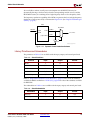
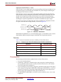
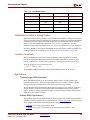
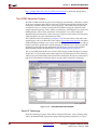
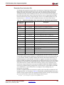
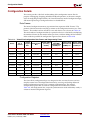
For additional information, go to http://support.xilinx.com. The following table lists
some of the resources you can access from this website. You can also directly access these
resources using the provided URLs.
Resource
Description/URL
Data Sheets
Xilinx data sheets describe device-specific operating characteristics,
architecture, and pinouts/packaging.
http://www.xilinx.com/xlnx/xweb/xil_publications_index.jsp
User Guides
Xilinx user guides contain detailed, device-specific operating theory
and generic design examples for various device functions.
http://www.xilinx.com/xlnx/xweb/xil_publications_index.jsp?categor
y=User+Guides
Application
Notes
Xilinx application notes describe design techniques and approaches to
general design as well as specific applications. Many application notes
feature complete reference designs including source code.
http://www.xilinx.com/xlnx/xweb/xil_publications_index.jsp?categor
y=Application+Notes
Xcell Journals
This site contains quarterly journals for Xilinx programmable logic users.
http://www.xilinx.com/xcell/xcell.htm
Tech Tips
See this site for the latest news, design tips, and patch information on the
Xilinx design environment.
http://www.xilinx.com/support/techsup/journals/index.htm
Answers
Database
This database provides a current listing of solution records for Xilinx
software tools. Search this database using the search function at:
http://www.xilinx.com/support/searchtd.htm
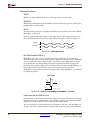
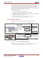
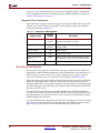
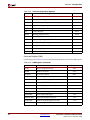
Conventions
This document uses the following conventions. An example illustrates each convention.
Typographical
The following typographical conventions are used in this document:
Convention
Example
Courier font
Messages, prompts, and
program files that the system
displays
speed grade: - 100
Courier bold
Literal commands that you
enter in a syntactical statement
ngdbuild design_name
Commands that you select
from a menu
File → Open
Keyboard shortcuts
Ctrl+C
Helvetica bold
16
Meaning or Use
www.xilinx.com
1-800-255-7778
Virtex-II Pro™ Platform FPGA User Guide
UG012 (v2.5) 2 February, 2004
R
Conventions
Convention
Meaning or Use
Example
Variables in a syntax
statement for which you must
supply values. (In angle
brackets.)
ngdbuild <design_name>
References to other manuals
See the Development System
Reference Guide for more
information.
Emphasis in text
If a wire is drawn so that it
overlaps the pin of a symbol,
the two nets are not connected.
An optional entry or
parameter. However, in bus
specifications, such as
bus[7:0], they are required.
ngdbuild [option_name]
design_name
A list of items from which you
must choose one or more
lowpwr ={on|off}
Separates items in a list of
choices
lowpwr ={on|off}
Vertical ellipsis
.
.
.
Repetitive material that has
been omitted
IOB #1: Name = QOUT’
IOB #2: Name = CLKIN’
.
.
.
Horizontal ellipsis . . .
Repetitive material that has
been omitted
allow block block_name
loc1 loc2 ... locn;
Italic font
Square brackets
[ ]
Braces { }
Vertical bar
|
Online Document
The following conventions are used in this document:
Convention
Meaning or Use
Example
See the section “Additional
Resources” for details.
Blue text
Cross-reference link to a
location in the current
document
Red text
Cross-reference link to a
location in another document
See Figure 2-5 in the Virtex-II
Handbook.
Blue, underlined text
Hyperlink to a website (URL)
Go to http://www.xilinx.com
for the latest speed files.
Virtex-II Pro™ Platform FPGA User Guide
UG012 (v2.5) 2 February, 2004
www.xilinx.com
1-800-255-7778
Refer to “Title Formats” in
Chapter 1 for details.
17
R
18
Preface: About This Guide
www.xilinx.com
1-800-255-7778
Virtex-II Pro™ Platform FPGA User Guide
UG012 (v2.5) 2 February, 2004
R
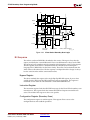
Chapter 1
Introduction to the Virtex-II Pro™
FPGA Family
The Next Logical Revolution
The Virtex-II Pro Platform FPGA solution is the most technically sophisticated silicon and
software product development in the history of the programmable logic industry. The goal
was to revolutionize system architecture "from the ground up." To achieve that objective,
the best circuit engineers and system architects from IBM, Mindspeed, and Xilinx
co-developed the world's most advanced Platform FPGA silicon product. Leading teams
from top embedded systems companies worked together with Xilinx software teams to
develop the systems software and IP solutions that enabled this new system architecture
paradigm. The result is the first Platform FPGA solution capable of implementing high
performance system-on-a-chip designs previously the exclusive domain of custom ASICs,
yet with the flexibility and low development cost of programmable logic. The Virtex-II Pro
family marks the first paradigm change from programmable logic to programmable
systems, with profound implications for leading-edge system architectures in networking
applications, deeply embedded systems, and digital signal processing systems. It allows
custom user-defined system architectures to be synthesized, next-generation connectivity
standards to be seamlessly bridged, and complex hardware and software systems to be
co-developed rapidly with in-system debug at system speeds. Together, these capabilities
usher in the next programmable logic revolution.
Built for Bandwidth
The Virtex-II Pro family consists of ten members, each with four to twenty-four
RocketIO™ multi-gigabit transceivers based on the Mindspeed SkyRail™ technology.
Each Xilinx RocketIO transceiver block contains a complete set of user-configurable
supporting circuitry that address real-life, system-level challenges. These include standard
8B/10B encode/decode, programmable signal integrity adjustments for varying PCB trace
lengths and materials, support for synchronization of multiple channels, and
programmable support for channel control commands. In addition, the RocketIO blocks
are the first FPGA-embedded transceivers to reach a baud rate of 3.125 Gbps. Four
RocketIO transceivers, employing 16 PCB traces, can be used to support a full-duplex
10 Gbps channel by way of the RocketIO channel-bonding feature. This is equivalent to 256
traces of typical LVTTL buses, or 68 traces of a high-speed, source-synchronous parallel
LVDS bus. It allows a PCB trace reduction of up to 16X over conventional parallel buses,
resulting in significant reductions in PCB complexity and EMI system noise. The RocketIO
technology fulfills higher bandwidth system requirements than currently possible, with
cost savings coming from faster time-to-market, reduced printed circuit board (PCB)
complexity, and lower component count.
Virtex-II Pro™ Platform FPGA User Guide
UG012 (v2.5) 2 February, 2004
www.xilinx.com
1-800-255-7778
19
R
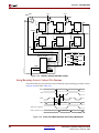
Chapter 1: Introduction to the Virtex-II Pro™ FPGA Family
The Virtex-II Pro members also incorporate small yet powerful IBM® PowerPC™
processor cores. Each of the larger Virtex-II Pro devices incorporates one to four
PowerPC 405 processor cores, each capable of more than 300 MHz clock frequency and 420
Dhrystone MIPS. While the processor cores occupy a small area of the die, they provide
tremendous system flexibility where they are used. The PowerPC 405 cores are fully
embedded within the FPGA fabric, where all processor nodes are controlled by the FPGA
routing resources. This provides the utmost architectural capability, where complex
applications may be efficiently divided between high-speed logic implementation and
high-flexibility software implementations. For example, a packet processing application
using only the FPGA logic today for high-speed packet routing may be augmented to
include a slave high-performance processor for exception handling or in-system statistics
monitoring. In contrast, using a separate processor externally requires hundreds of
additional interface pins, which degrades system performance and significantly increases
FPGA I/O requirements and overall board costs.
The Virtex-II Pro products are based on the most advanced FPGA fabric available: the
Virtex-II architecture with IP-Immersion™ technology, which was developed to offer
significant improvements in engineering productivity, silicon efficiency, and system
flexibility. Unique features common in the Virtex-II Series—consisting of the Virtex-II and
Virtex-II Pro families—include powerful SystemIO™ system connectivity solutions,
digitally controlled impedance (DCI) technology, comprehensive clocking solutions, highspeed Active Interconnect™ routing architecture, and bitstream encryption. These features
together constitute the most complete Platform FPGA solution available, optimized for
high performance system-level applications. The upward compatibility of the Virtex Series
of products ensures benefits in engineering productivity, performance, design longevity,
and continuing cost reduction.
Legacy of Leadership
Each of the Virtex families of FPGAs has been the most successful programmable product
family in its class, starting with the introduction of the original Virtex family in 1998. The
Virtex and Virtex-E families were recognized by the industry as the highest technology
products available when they were first introduced. The Virtex-II family, which again
achieved technology leadership in density, performance, and features, ushered in the era of
Platform FPGAs—programmable devices with the system-level capability and
performance to implement systems functionality. The Virtex-II Pro family continues the
tradition of technology leadership as the most sophisticated Platform FPGA yet, again
breaking the technology barrier for the benefit of leading-edge system architects.
The Virtex-II Pro family is the first FPGA family to incorporate both serial transceiver
technology and a hard processor core within a general-purpose FPGA device. This is
significant for new high-bandwidth embedded processing applications such as packet
processing, where both high device I/O bandwidth and high performance processor cores
are needed together.
The Virtex-II Pro devices are the industry's first FPGAs in a 0.13-micron process. The IBM
nine-layer metal, all-copper, low-k process technology is among the most advanced in the
semiconductor industry. The combination of advanced Active Interconnect™ architecture
and advanced process technology makes the Virtex-II Pro family the highest performance
FPGA in the world.
The RocketIO multi-gigabit transceiver (MGT), based on industry-leading SkyRail™
technology, is the highest performance, most complete embedded serial transceiver
available. It is user-configurable for up to 3.125 Gbps baud rate per channel, which is over
twice the performance of other embedded transceivers at 1.25 Gbps. Each RocketIO
20
www.xilinx.com
1-800-255-7778
Virtex-II Pro™ Platform FPGA User Guide
UG012 (v2.5) 2 February, 2004
R
Packets Everywhere
transceiver provides a complete set of common functionality available in standard SerDes
transceivers. In contrast, "programmable ASSP" products with clock/data recovery (CDR)
provide only the most basic transceiver capability.
The IBM PowerPC 405 processor core used in the Virtex-II Pro family is the highest
performance embedded core available in FPGAs. The PowerPC architecture is used in
many markets including communications, industrial control, test and measurement
systems, and other performance-oriented markets. It is currently the most popular
processor architecture in embedded applications.
Packets Everywhere
The Virtex-II Pro family provides a powerful new paradigm for network processing where
low latency is required, such as storage area networks, wireless infrastructure, and
voice-over-IP networks. The digital convergence phenomenon drives the need for packet
routing based on type and priority. For example, live voice and video data packets require
significantly lower latency than data file packets. New data networking applications must
now handle higher bandwidth traffic as well as more complex types of prioritized packets.
In many cases, Virtex-II Pro devices can offer higher overall performance than other
solutions, including specialized network processors (NPs). Using the Virtex-II Pro
architecture, the most common packets may be quickly read and routed using FPGA logic,
without incurring the lengthy software run-time needed by NPs. The FPGA logic
interrupts the PowerPC processor core only when processor instructions are needed for
special packet types. For example, packets may be stored into a 16 KB dual-port memory
area accessible by both the FPGA logic and the PowerPC 405 on-chip memory (OCM) port,
allowing rapid change of control and packet disposition. By using the FPGA logic to
process the most common packet types while the processor core handles the more
specialized ones as a slave to the logic, the Virtex-II Pro architecture can provide higher
overall performance than NPs, as well as more sophisticated processing capabilities than
FPGA logic alone.
Bridge, Anyone?
Powerful protocol bridges for tying together disparate data stream formats are well-suited
for the Virtex-II Pro solution. New interface standards and protocols include 3GIO,
Infiniband, Gigabit Ethernet, XAUI/10 Gigabit Ethernet, RapidIO, and HyperTransport.
These must interface seamlessly to one another, as well as to other standards such as PCI,
Fibre Channel, POS Phy Level 4, Flexbus 4, and others. This presents a significant
challenge to system developers because of changing standards, scarcity of off-the-shelf
interface components, and the inflexibility of available solutions. System designers have
had to assemble their own blend of FPGAs, discrete physical transceivers, and discrete
communications processors to solve their complex system challenges. Even newer
"programmable ASSPs" (application-specific standard products) with built-in serial
transceivers fall short, because they frequently require companion FPGAs to supplement
their logic capacity. The Virtex-II Pro solution, using the powerful Xilinx SystemIO™
capability to fully integrate silicon, software, and IP capabilities, provides the most flexible
pre-engineered protocol bridge solutions available for fast time-to-market and low
development cost.
Simplifying Complexity
The Virtex-II Pro solution offers a powerful paradigm for complex embedded systems
found in signal processing, industrial control, image processing, networking,
Virtex-II Pro™ Platform FPGA User Guide
UG012 (v2.5) 2 February, 2004
www.xilinx.com
1-800-255-7778
21
R
Chapter 1: Introduction to the Virtex-II Pro™ FPGA Family
communications, and aeronautic applications. For the first time, complex embedded
systems traditionally involving sophisticated hardware and software may be developed
concurrently, emulated in actual hardware at speed, debugged in-system, and
re-architected for performance within weeks, rather than months or years. In addition, full
systems can be remotely upgraded as easily as software-only upgrades are performed
today, using Compact Flash, CDROM, Internet, wireless transmission, or other flexible
means. Hardware design is simplified using powerful development software and a large
soft IP library to assemble logic- and processor-based platforms. Software development
may be started earlier using the actual device in preconfigured sample platforms, without
waiting for the new system board to be developed. In many cases, higher density
Virtex-II Pro components may be used for early system development, whereby extra
resources (including additional PowerPC processor cores) may be used to easily emulate
board-level components yet to be developed. This flexibility, obviously unavailable in
custom ASICs or ASSPs, allows systems to be emulated at speed, rather than simulated
using software simulators at 100 or 1000 times slower. In-system debugging is further
enhanced by the Xilinx ChipScope Pro tool, which provides comprehensive logic
analysis—from probing internal nodes to full bus analysis with bus protocol adherence
checks using an external logic analyzer via the IEEE 1149.1 (JTAG) test access port. Using
ChipScope Pro can result in orders of magnitude of improvement in engineering
productivity.
Complex systems can be optimally repartitioned between FPGA logic and processor cores,
allowing a continuum of possible trade-offs between the speed of logic and the flexibility
of software code. For example, a first implementation of an echo cancellation algorithm
might be all-software in compiled C code running on a PowerPC core, in order to allow the
system software development to start. As the system is further optimized, part of the DSP
algorithm could be retargeted using Matlab Simulink into FPGA logic to achieve a
significantly faster but functionally identical system for production release. In another
example, an encryption application might implement the Diffie-Hellman key exchange
algorithm, whereby exponentiation and message management could be optimally
partitioned into FPGA logic and an embedded processor, respectively. In this way, the
programmable systems paradigm offers tremendous flexibility to allow system designers
and architects to optimize the trade-offs in development time, system performance, and
system costs.
It is significant that the embedded systems enabled by Virtex-II Pro solutions are "all-soft,"
in that both logic and software code are controlled by a soft data file. Because of this, the
low cost of design maintenance and degree of design reuse is greatly enhanced. Whole
system upgrades, including both hardware and software, can now be accomplished with
one unified soft file using System ACE™ configuration solutions, offering the same low
cost and ease of use as software-only upgrades.
Time Is Money
The Virtex-II Series, comprising both the Virtex-II and Virtex-II Pro families, offers
significantly faster time-to-market and lower development costs than ASICs. Compared to
a full-custom ASIC, the Virtex-II Pro solution eliminates the need for exhaustive
verification during development, and allows hardware-software debug at system speeds
rather than at slow software simulation speeds. In addition, the Virtex-II Pro features of
signal integrity, pre-engineered clocking capabilities, and an abundance of soft IP cores,
significantly reduce development time.
The Virtex-II Series offers significantly lower development costs than ASICs, due to lower
tool costs, lower third-party IP costs, and absence of NRE costs. The Virtex-II Series also
increases engineering productivity by accelerating hardware availability for software
22
www.xilinx.com
1-800-255-7778
Virtex-II Pro™ Platform FPGA User Guide
UG012 (v2.5) 2 February, 2004
R
Flexibility Is Money
development and increasing software debug speed. In addition, the availability of
powerful development tools enables straightforward retargeting of other embedded
processors into the PowerPC platform. Compared to other processor architectures, the
PowerPC 405 core in most cases allows higher performance and more powerful
capabilities, and thus can be used to accelerate preproduction of performance-sensitive
applications.
Flexibility Is Money
The flexibility inherent in the Virtex-II Series allows system architects to fine-tune their
architectural partitioning after the initial prototype is developed. That is, each subsystem
function can be freely implemented as hardware only, software only, or any combination
within the hardware-software continuum, depending on the trade-off between
performance and complexity. For example, a wireless infrastructure system might initially
implement a rake filter function in hardware, and then change to a firmware
implementation as more software control is necessary during later development. This
repartitioning would be impossible in custom ASICs without significant time and cost
penalties.
The Virtex-II Series offers significantly more flexibility than fixed chip sets and ASSPs,
allowing end user product differentiation and future-proofing. For a design requirement
that can generally be met either by ASSPs or by Virtex-II Platform FPGAs, the initial design
investment for an FPGA implementation may be higher. However, the advantages for
Platform FPGA implementations include customizing of functionality, ease of design
reuse, ability to fix design bugs, differentiation of user end products, and ownership and
control of the entire system. These are important advantages in highly competitive markets
where ASSPs have standing errata lists and unpredictable future availability. In contrast,
properly developed Platform FPGA designs are soft designs that may be readily
maintained and reused as needed. Therefore, FPGA methodologies can provide system
manufacturers with greater competitive advantage in the short term, and greater
ownership and control over their products in the long term.
Not Being Discrete
Many high-bandwidth systems today use large FPGAs together with discrete SerDes
transceivers, discrete communications processors, or other discrete components. The
Virtex-II Pro family can eliminate the need for many of these external components,
enhancing time-to-market and performance, even providing system cost benefits in many
cases. Multi-chip solutions using FPGAs typically require over a hundred I/O pins to
interface to each discrete quad 3.125 Gbps SerDes transceiver or discrete microprocessor.
The result is increased PCB complexity to accommodate the hundreds of traces, reduced
system performance due to on-chip/off-chip connections, and higher overall system costs.
In some cases, the increased FPGA pin-count requirement may force a higher-density
FPGA to be used, again increasing the overall cost. In these cases, the Virtex-II Pro devices
can integrate the discrete components to achieve faster system development, higher
system performance, and lower costs.
Virtex-II Pro™ Platform FPGA User Guide
UG012 (v2.5) 2 February, 2004
www.xilinx.com
1-800-255-7778
23
R
24
Chapter 1: Introduction to the Virtex-II Pro™ FPGA Family
www.xilinx.com
1-800-255-7778
Virtex-II Pro™ Platform FPGA User Guide
UG012 (v2.5) 2 February, 2004
R
Chapter 2
Timing Models
Summary
The following topics are covered in this chapter:
•
CLB / Slice Timing Models
•
Block SelectRAM Timing Model
•
Embedded Multiplier Timing Model
•
IOB Timing Models
•
Pin-to-Pin Timing Models
•
Digital Clock Manager Timing Model
•
Additional Timing Models in Other Publications: PPC405 Processor Block and
RocketIO Transceiver
Introduction
Due to the large size and complexity of Virtex-II Pro FPGAs, understanding the timing
associated with the various paths and functional elements has become a difficult and
important problem. Although it is not necessary to understand the various timing
parameters in order to implement most designs using Xilinx software, a thorough timing
model can assist advanced users in analyzing critical paths or planning speed-sensitive
designs.
The Timing Model chapter is broken up into sections consisting of three basic components:
•
Functional Element Diagram - basic architectural schematic illustrating pins and
connections.
•
Timing Parameters - Virtex-II Pro Platform FPGA Data Sheet timing parameter
definitions.
•
Timing Diagram - illustrates functional element timing parameters relative to each
other.
This chapter was written with the Xilinx Timing Analyzer software (TRCE) in mind. All
pin names, parameter names, and paths are consistent with Post Route Timing and PreRoute Static Timing reports. Use the models in this chapter in conjunction with both the
Timing Analyzer software and the section on switching characteristics in the Virtex-II Pro
Platform FPGA Data Sheet. Most of the timing parameters found in the section on
switching characteristics are described in this chapter.
Virtex-II Pro™ Platform FPGA User Guide
UG012 (v2.5) 2 February, 2004
www.xilinx.com
1-800-255-7778
25
R
Chapter 2: Timing Models
CLB / Slice Timing Models
The three sections below describe all timing parameters reported in the Virtex-II Pro Data
Sheet that are associated with slices and Configurable Logic Blocks (CLBs). The sections
correspond to their respective (switching characteristics) sections in the data sheet:
•
“General Slice Timing Model and Parameters” (CLB Switching Characteristics)
•
“Slice Distributed RAM Timing Model and Parameters” (CLB Distributed RAM
Switching Characteristics)
•
“Slice SRL Timing Model and Parameters” (CLB SRL Switching Characteristics)
General Slice Timing Model and Parameters
Figure 2-1 illustrates the details of a Virtex-II Pro slice.
Note: Some elements of the Virtex-II Pro slice have been omitted for clarity. Only the elements
relevant to the timing paths described in this section are shown.
FX
FXINA
MUXFX
FXINB
Y
DY
D
LUT
G
inputs
Q
YQ
FF/LAT
CE
D
CLK
SR REV
BY
F5
MUXF5
X
LUT
F
inputs
DX
D
D
Q
XQ
FF/LAT
CE
CLK
SR REV
BX
CE
CLK
SR
UG002_C3_017_030703
Figure 2-1:
26
Virtex-II Pro General Slice
www.xilinx.com
1-800-255-7778
Virtex-II Pro™ Platform FPGA User Guide
UG012 (v2.5) 2 February, 2004
R
CLB / Slice Timing Models
Timing Parameters
Table 2-1: General Slice Timing Parameters
Parameter
Function
Control
Signal
Description
Combinatorial Delays
TILO
F/G inputs to
X/Y outputs
Propagation delay from the F/G inputs of the
slice, through the look-up tables (LUTs), to the
X/Y outputs of the slice.
TIF5
F/G inputs to F5
output
Propagation delay from the F/G inputs of the
slice, through the LUTs and MUXF5 to the F5
output of the slice.
TIF5X
F/G inputs to X
output
Propagation delay from the F/G inputs of the
slice, through the LUTs and MUXF5 to the X
output of the slice.
TIFXY
FXINA/FXINB
inputs to Y
output
Propagation delay from the FXINA/FXINB
inputs, through MUXFX to the Y output of the
slice.
TIFNCTL
Transparent
Latch input to
XQ/YQ outputs
Incremental delay through a transparent latch
to XQ/YQ outputs.
Sequential Delays
TCKO
FF Clock (CLK)
to XQ/YQ
outputs
Time after the clock that data is stable at the
XQ/YQ outputs of the slice sequential
elements (configured as a flip-flop).
TCKLO
Latch Clock
(CLK) to
XQ/YQ outputs
Time after the clock that data is stable at the
XQ/YQ outputs of the slice sequential
elements (configured as a latch).
Setup and Hold for Slice Sequential Elements
TxxCK = Setup time (before clock edge)
TCKxx = Hold time (after clock edge)
TDICK/TCKDI
TDYCK/TCKDY
TDXCK/TCKDX
TCECK/TCKCE
Virtex-II Pro™ Platform FPGA User Guide
UG012 (v2.5) 2 February, 2004
The following descriptions are for setup times only.
BX/BY inputs
Time before Clock (CLK) that data from the BX
or BY inputs of the slice must be stable at the
D-input of the slice sequential elements
(configured as a flip-flop).
DY input
Time before Clock (CLK) that data from the DY
input of the slice must be stable at the D-input
of the slice sequential elements (configured as
a flip-flop).
DX input
Time before Clock (CLK) that data from the DX
input of the slice must be stable at the D-input
of the slice sequential elements (configured as
a flip-flop).
CE input
Time before Clock (CLK) that the CE (Clock
Enable) input of the slice must be stable at the
CE-input of the slice sequential elements
(configured as a flip-flop).
www.xilinx.com
1-800-255-7778
27
R
Chapter 2: Timing Models
Table 2-1: General Slice Timing Parameters (Continued)
Parameter
TRCK/TCKR
Control
Signal
Function
Description
Time before CLK that the SR (Set/Reset) and
the BY (Rev) inputs of the slice must be stable
at the SR/Rev-inputs of the slice sequential
elements (configured as a flip-flop).
Synchronous set/reset only.
SR/BY inputs
Clock CLK
TCH
Minimum Pulse Width, High.
TCL
Minimum Pulse Width, Low.
Set/Reset
Minimum Pulse Width for the SR (Set/Reset)
and BY (Rev) pins.
TRPW
TRQ
Propagation delay for an asynchronous
Set/Reset of the slice sequential elements.
From SR/BY inputs to XQ/YQ outputs.
FTOG
Toggle Frequency - Maximum Frequency that
a CLB flip-flop can be clocked:
1/(TCH+TCL)
Timing Characteristics
Figure 2-2 illustrates general timing characteristics of a Virtex-II Pro slice.
1
2
3
CLK
TCECK
CE
TDYCK
DY
(DATA)
TRCK
SR
(RESET)
TCKO
TCKO
YQ
(OUT)
UG002_C3_018_101600
Figure 2-2: General Slice Timing Characteristics
•
At time TCECK before Clock Event 1, the Clock-Enable signal becomes valid-high at
the CE input of the slice register.
•
At time TDYCK before Clock Event 1, data from the DY input becomes valid-high at
the D input of the slice register and is reflected on the YQ pin at time TCKO after Clock
Event 1*.
•
At time TRCK before Clock Event 3, the SR signal (configured as synchronous reset in
this case) becomes valid-high, resetting the slice register, and this is reflected on the
YQ pin at time TCKO after Clock Event 3.
Note: In most cases software uses the DX/DY inputs to route data to the slice registers when at
all possible. This is the fastest path to the slice registers and saves other slice routing resources.
28
www.xilinx.com
1-800-255-7778
Virtex-II Pro™ Platform FPGA User Guide
UG012 (v2.5) 2 February, 2004
R
CLB / Slice Timing Models
Slice Distributed RAM Timing Model and Parameters
Figure 2-3 illustrates the details of distributed RAM implemented in a Virtex-II Pro slice.
Note: Some elements of the Virtex-II Pro slice have been omitted for clarity. Only the elements
relevant to the timing paths described in this section are shown.
MUXFX
FXINA
FX
FXINB
ADDRESS
RAM
G4
G3
G2
G1
D
WS
Y
DI
BY
DATA_IN or
Address
SLICEWE[2:0]
WSGEN
WE
CK
MUXF5
F5
WS
ADDRESS
DI
RAM
G4
G3
G2
G1
D
X
BX
DATA_IN or
Address
CLK
SR
(Write Enable)
UG002_C3_019_1204 00
Figure 2-3:
Virtex-II Pro™ Platform FPGA User Guide
UG012 (v2.5) 2 February, 2004
Virtex-II Pro Slice Distributed RAM
www.xilinx.com
1-800-255-7778
29
R
Chapter 2: Timing Models
Timing Parameters
Table 2-2: Slice Distributed RAM Timing Parameters
Parameter
Function
Control
Signal
Description
Sequential Delays for Slice LUT Configured as RAM (Distributed RAM)
TSHCKO16
CLK to X/Y outputs
(WE active) in 16x1
mode
Time after the Clock (CLK) of a WRITE
operation that the data written to the
distributed RAM (in 16x1 mode) is stable on
the X/Y outputs of the slice.
TSHCKO32
CLK to X/Y outputs
(WE active) in 32x1
mode
Time after the Clock (CLK) of a WRITE
operation that the data written to the
distributed RAM (in 32x1 mode) is stable on
the X/Y outputs of the slice.
TSHCKOF5
CLK to F5 output
(WE active)
Time after the Clock (CLK) of a WRITE
operation that the data written to the
distributed RAM is stable on the F5 output of
the slice.
Setup and Hold for Slice LUT Configured as RAM (Distributed RAM)
TxS = Setup time (before clock edge)
TxH = Hold time (after clock edge)
The following descriptions are for setup times only.
TDS/TDH
BX/BY Data inputs
(DI)
Time before the clock that data must be stable
at the DI input of the slice LUT (configured as
RAM), via the slice BX/BY inputs.
TAS/TAH
F/G Address inputs
Time before the clock that address signals
must be stable at the F/G inputs of the slice
LUT (configured as RAM).
TWES/TWEH
WE input (SR)
Time before the clock that the Write Enable
signal must be stable at the WE input of the
slice LUT (configured as RAM).
Clock CLK
30
TWPH
Minimum Pulse Width, High (for a
Distributed RAM clock).
TWPL
Minimum Pulse Width, Low (for a
Distributed RAM clock).
TWC
Minimum clock period to meet address write
cycle time.
www.xilinx.com
1-800-255-7778
Virtex-II Pro™ Platform FPGA User Guide
UG012 (v2.5) 2 February, 2004
R
CLB / Slice Timing Models
Timing Characteristics
Figure 2-4 illustrates the timing characteristics of a 16-bit distributed RAM implemented in
a Virtex-II Pro slice (LUT configured as RAM).
1
TWC
2
3
4
5
6
7
TWPH
TWPL
CLK
TAS
2
ADDR
F
3
4
0
1
5
E
TDS
DATA_IN
1
X
TWES
WE
X
0
TILO
TILO
TSHCK016
DATA_OUT
(X/Y Output)
1
WRITE
MEM(F)
READ
0
1
0
WRITE
WRITE
WRITE
MEM(E)
READ
UG002_C3_020_031301
Figure 2-4: Slice Distributed RAM Timing Characteristics
Clock Event 1: WRITE Operation
During a WRITE operation, the contents of the memory at the address on the ADDR inputs
is changed. The data written to this memory location is reflected on the X/Y outputs
synchronously.
•
At time TWES before Clock Event 1, the Write Enable signal (WE) becomes valid-high,
enabling the RAM for the following WRITE operation.
•
At time TAS before Clock Event 1, the address (2) becomes valid at the F/G inputs of
the RAM.
•
At time TDS before Clock Event 1, the DATA becomes valid (1) at the DI input of the
RAM and is reflected on the X/Y output at time TSHCKO16 after Clock Event 1.
Clock Event 2: READ Operation
All READ operations are asynchronous in distributed RAM. As long as write-enable (WE)
is Low, the address bus can be asserted at any time, and the contents of the RAM at that
address are reflected on the X/Y outputs after a delay of length TILO (propagation delay
through a LUT). Note that the Address (F) is asserted after Clock Event 2, and that the
contents of the RAM at that location are reflected on the output after a delay of length TILO.
Virtex-II Pro™ Platform FPGA User Guide
UG012 (v2.5) 2 February, 2004
www.xilinx.com
1-800-255-7778
31
R
Chapter 2: Timing Models
Slice SRL Timing Model and Parameters
Figure 2-5 illustrates shift register implementation in a Virtex-II Pro slice.
Note: Note: Some elements of the Virtex-II Pro slice have been omitted for clarity. Only the
elements relevant to the timing paths described in this section are shown.
Shift_In
MUXFX
FXINA
FX
FXINB
Y
YB
ADDRESS
SRL
G3
G2
G1
G0
D
MC15
WS
DI
BY
(DATA_IN or
ADDRESS)
WSGEN
WE
CK
MUXF5
Shift_In
F5
WS
X
DI
ADDRESS
F3
F2
F1
F0
SRL
D
XB
MC15
SR
CLK
BX
(DATA_IN or
ADDRESS)
Shift_Out
UG002_C3_021_113000
Figure 2-5: Virtex-II Pro Slice SLR
32
www.xilinx.com
1-800-255-7778
Virtex-II Pro™ Platform FPGA User Guide
UG012 (v2.5) 2 February, 2004
R
CLB / Slice Timing Models
Timing Parameters
Table 2-3: Slice SRL Timing Parameters
Parameter
Control
Signal
Function
Description
Sequential Delays for Slice LUT Configured as SRL (Select Shift Register)
TREG
CLK to
X/Y outputs
Time after the Clock (CLK) of a WRITE operation
that the data written to the SRL is stable on the
X/Y outputs of the slice.
TCKSH
CLK to Shiftout
Time after the Clock (CLK) of a WRITE operation
that the data written to the SRL is stable on the
Shiftout or XB/YB outputs of the slice.
TREGF5
CLK to F5 output
Time after the Clock (CLK) of a WRITE operation
that the data written to the SRL is stable on the F5
output of the slice.
Setup/Hold for Slice LUT Configured as SRL (Select Shift Register)
TxxS = Setup time (before clock edge)
TxxH= Hold time (after clock edge)
The following descriptions are for setup times only.
TSRLDS/
TSRLDH
BX/BY Data
inputs (DI)
Time before the clock that data must be stable at
the DI input of the slice LUT (configured as SRL),
via the slice BX/BY inputs.
TWSS/TWSH
CE input (WE)
Time before the clock that the Write Enable signal
must be stable at the WE input of the slice LUT
(configured as SRL).
Clock CLK
TSRPH
Minimum Pulse Width, High (for SRL clock).
TSRPL
Minimum Pulse Width, Low (for SRL clock).
Timing Characteristics
Figure 2-6 illustrates the timing characteristics of a 16-bit shift register implemented in a
Virtex-II Pro slice (LUT configured as SRL).
1 TSRPH TSRPL 2
3
4
5
6
CLK
TWSS
Write Enable
(SR)
TSRLDS
Shift_In (DI)
0
Address
1
1
0
0
0
2
1
TILO
TREG
Data Out (D)
1
X
0
1
X
X
X
1
0
TILO
1
1
0
1
16
TREGXB
MSB (MC15)
X
X
X
X
0
UG002_C3_022_102700
Figure 2-6: Slice SLR Timing Characteristics
Virtex-II Pro™ Platform FPGA User Guide
UG012 (v2.5) 2 February, 2004
www.xilinx.com
1-800-255-7778
33
R
Chapter 2: Timing Models
Clock Event 1: Shift_In
During a WRITE (Shift_In) operation, the single-bit content of the register at the address on
the ADDR inputs is changed, as data is shifted through the SRL. The data written to this
register is reflected on the X/Y outputs synchronously, if the address is unchanged during
the clock event. If the ADDR inputs are changed during a clock event, the value of the data
at the addressable output (D) is invalid.
•
At time TWSS before Clock Event 1, the Write Enable signal (SR) becomes valid-high,
enabling the SRL for the WRITE operation that follows.
•
At time TSRLDS before Clock Event 1 the data becomes valid (0) at the DI input of the SRL
and is reflected on the X/Y output after a delay of length TREG after Clock Event 1*.
Note: Since the address 0 is specified at Clock Event 1, the data on the DI input is reflected at
the D output, because it is written to Register 0.
Clock Event 2: Shift_In
•
At time TSRLDS before Clock Event 2, the data becomes valid (1) at the DI input of the
SRL and is reflected on the X/Y output after a delay of length TREG after Clock Event 2*.
Note: Since the address 0 is still specified at Clock Event 2, the data on the DI input is reflected
at the D output, because it is written to Register 0.
Clock Event 3: Shift_In / Addressable (Asynchronous) READ
All READ operations are asynchronous. If the address is changed (between clock events),
the contents of the register at that address are reflected at the addressable output (X/Y
outputs) after a delay of length TILO (propagation delay through a LUT).
•
At time TSRLDS before Clock Event 3 the Data becomes valid (1) at the DI input of the
SRL, and is reflected on the X/Y output TREG time after Clock Event 3.
•
Notice that the address is changed (from 0 to 2) some time after Clock Event 3. The
value stored in Register 2 at this time is a 0 (in this example, this was the first data
shifted in), and it is reflected on the X/Y output after a delay of length TILO.
Clock Event 16: MSB (Most Significant Bit) Changes
•
At time TREGXB after Clock Event 16, the first bit shifted into the SRL becomes valid
(logical 0 in this case) on the XB output of the slice via the MC15 output of the LUT
(SRL).
Block SelectRAM Timing Model
Introduction
This section describes the timing parameters associated with the block SelectRAM
(illustrated in Figure 2-7) in Virtex-II Pro FPGA devices. This section is intended to be used
with the section on switching characteristics in the Virtex-II Pro Platform FPGA Data Sheet
and the Timing Analyzer (TRCE) report from Xilinx software. For specific timing
parameter values, refer to the switching characteristics section in the Virtex-II Pro Platform
FPGA Data Sheet.
34
www.xilinx.com
1-800-255-7778
Virtex-II Pro™ Platform FPGA User Guide
UG012 (v2.5) 2 February, 2004
R
Block SelectRAM Timing Model
18-Kbit Block SelectRAM
DI
DIP
ADDR
WE
EN
SSR
DO
DOP
CLK
DS031_10_102000
Figure 2-7: Block SelectRAM Block Diagram
Timing Parameters
Table 2-4: Block SelectRAM Timing Parameters
Parameter
Function
Control
Signal
Description
Setup and Hold Relative to Clock (CLK)
TBxCK = Setup time (before clock edge) TBCKx =
Hold time (after clock edge)
The following descriptions are for setup times only.
TBACK/TBCKA
Address inputs
ADDR
Time before the clock that address signals must
be stable at the ADDR inputs of the block RAM.
TBDCK/TBCKD
Data inputs
DI
Time before the clock that data must be stable at
the DI inputs of the block RAM.
TBECK/TBCKE
Enable
EN
Time before the clock that the enable signal must
be stable at the EN input of the block RAM.
TBRCK/TBCKR
Synchronous
Set/Reset
SSR
Time before the clock that the synchronous
set/reset signal must be stable at the SSR input of
the block RAM.
TBWCK/TBCKW
Write Enable
WE
Time before the clock that the write enable signal
must be stable at the WE input of the block RAM.
Clock to
Output
CLK to
DO
Time after the clock that the output data is stable
at the DO outputs of the block RAM.
TBPWH
Clock
CLK
Minimum pulse width, high.
TBPWL
Clock
CLK
Minimum pulse width, low.
Clock to Out
TBCKO
Clock
Virtex-II Pro™ Platform FPGA User Guide
UG012 (v2.5) 2 February, 2004
www.xilinx.com
1-800-255-7778
35
R
Chapter 2: Timing Models
Timing Characteristics
The timing diagram in Figure 2-8 describes a single-port block RAM in Write-First mode.
The timing for Read-First and No-Change modes are similar (see Chapter 3, “Design
Considerations”).
1
2
3
TBPWH
4
5
TBPWL
CLK
TBACK
00
TBDCK
ADDR
DI
DDDD
TBCKO
0F
7E
8F
20
CCCC
BBBB
AAAA
0000
CCCC*
MEM (00)
DO
MEM (7E)
0101**
TBECK
EN
TBRCK
SSR
TBWCK
WE
Disabled
Read
Write
Read
Reset
Disabled
* Write Mode = "WRITE_FIRST"
** SRVAL = 0101
ug002_c3_002_100300
Figure 2-8:
Block SelectRAM Timing Characteristics
At time 0, the block RAM is disabled; EN (enable) is low.
Clock Event 1: READ Operation
During a read operation, the contents of the memory at the address on the ADDR inputs
are unchanged.
•
TBACK before Clock Event 1, address 00 becomes valid at the ADDR inputs of the
block RAM.
•
At time TBECK before Clock Event 1, Enable goes High at the EN input of the block
RAM, enabling the memory for the READ operation that follows.
•
At time TBCKO after Clock Event 1, the contents of the memory at address 00 become
stable at the DO pins of the block RAM.
Clock Event 2: WRITE Operation
During a write operation, the content of the memory at the location specified by the
address on the ADDR inputs is replaced by the value on the DI pins and is immediately
reflected on the output latches (in WRITE-FIRST mode); EN (enable) is high.
36
•
At time TBACK before Clock Event 2, address 0F becomes valid at the ADDR inputs of
the block RAM.
•
At time TBDCK before Clock Event 2, data CCCC becomes valid at the DI inputs of the
block RAM.
•
At time TBWCK before Clock Event 2, Write Enable becomes valid at the WE following
the block RAM.
•
At time TBCKO after Clock Event 2, data CCCC becomes valid at the DO outputs of the
block RAM.
www.xilinx.com
1-800-255-7778
Virtex-II Pro™ Platform FPGA User Guide
UG012 (v2.5) 2 February, 2004
R
Block SelectRAM Timing Model
Clock Event 4: SSR (Synchronous Set/Reset) Operation
During an SSR operation, initialization parameter value SRVAL is loaded into the output
latches of the block SelectRAM. The SSR operation does NOT change the contents of the
memory and is independent of the ADDR and DI inputs.
•
At time TBRCK before Clock Event 4, the synchronous set/reset signal becomes valid
(High) at the SSR input of the block RAM.
•
At time TBCKO after Clock Event 4, the SRVAL 0101 becomes valid at the DO outputs
of the block RAM.
Clock Event 5: Disable Operation
De-asserting the enable signal EN disables any write, read or SSR operation. The disable
operation does NOT change the contents of the memory or the values of the output latches.
•
At time TBECK before Clock Event 5, the enable signal becomes valid (Low) at the EN
input of the block RAM.
•
After Clock Event 5, the data on the DO outputs of the block RAM is unchanged.
Timing Model
Figure 2-9 illustrates the delay paths associated with the implementation of block
SelectRAM. This example takes the simplest paths on and off chip (these paths can vary
greatly depending on the design). This timing model demonstrates how and where the
block SelectRAM timing parameters are used.
FPGA
Block SelectRAM
Data
Address
Write Enable
Enable
Synchronous
Set/Reset
[TIOPI + NET] + TBDCK
[TIOPI + NET] + TBACK
[TIOPI + NET*] + TBWCK
[TIOPI + NET] + TBECK
[TIOPI + NET] + TBRCK
DI
ADDR
WE
EN
SSR
CLK
DO
TBCKO + [NET + TIOOP]
Data
[TGI0O + NET]
BUFGMUX
Clock
[TIOPI + NET]
ug002_c3_003_121701
Figure 2-9: Block SelectRAM Timing Model
NET = Varying interconnect delays
TIOPI = Pad to I-output of IOB delay
TIOOP = O-input of IOB to pad delay
TGI0O = BUFGMUX delay
Virtex-II Pro™ Platform FPGA User Guide
UG012 (v2.5) 2 February, 2004
www.xilinx.com
1-800-255-7778
37
R
Chapter 2: Timing Models
Embedded Multiplier Timing Model
Introduction
This section explains all timing parameters associated with the use of embedded
18-bit x 18-bit multipliers in Virtex-II Pro FPGAs (see Figure 2-10). The propagation delays
through the embedded multiplier differ based on the size of the multiplier function
implemented. The longest delay through the multiplier is to the highest order bit output
(P35). Therefore, if an 18-bit x 18-bit signed multiplier is implemented, the worst-case
delay for this function is the longest delay associated with the embedded multiplier block.
If smaller (LSB) multipliers are used, shorter delays can be realized.
This section is intended to be used in conjunction with the section on switching
characteristics in the Virtex-II Pro Platform FPGA Data Sheet and the Timing Analyzer
(TRCE) report from Xilinx software. For specific timing parameter values, refer to the
Virtex-II Pro Platform FPGA Data Sheet.
Multiplier Block
A[17:0]
MULT 18 x 18
P[35:0]
B[17:0]
DS031_40_100400
Figure 2-10:
Embedded 18-bit x 18-bit Multiplier Block
Timing Parameters
Worst-Case Propagation Delays
The TMULT timing parameter is reported by the Timing Analyzer software. These values
correspond to the propagation delay through the multiplier to a specific output pin of the
multiplier block. The shortest delay is to pin 0, the longest to pin 35. These parameters can
be found in the table entitled “Multiplier Switching Characteristics” in Module 3 of the
Virtex-II Pro Platform FPGA Data Sheet. The delay-to-pin ratio is essentially linear (see
Figure 2-11). This implies that smaller multiply functions are faster than larger ones. This is
true as long as the LSB inputs are used.
Pin 35
Pin 0
Delay
Figure 2-11:
38
UG002_C3_023_092500
Pin-to-Delay Ratio Curve
www.xilinx.com
1-800-255-7778
Virtex-II Pro™ Platform FPGA User Guide
UG012 (v2.5) 2 February, 2004
R
Embedded Multiplier Timing Model
Timing Characteristics
Figure 2-12 illustrates the result (outputs) of a 4-bit x 4-bit unsigned multiply implemented
in an embedded multiplier block.
Time 0
input
[3..0]
1111
input
[3..0]
1111
TMULT (P0)
P0
X
1
TMULT (P1)
P1
X
0
TMULT (P2)
P2
0
X
TMULT (P3)
P3
0
X
TMULT (P4)
P4
0
X
TMULT (P5)
P5
1
X
TMULT (P6)
P6
1
X
TMULT (P7)
P7
1
X
UG002_C3_024_101300
Figure 2-12: Embedded Multiplier Block Timing Diagram
At time 0 the two 4-bit numbers to be multiplied become valid at the A[0..3], B[0..3] inputs
to the embedded multiplier. The result appears on the output pins P[0..7] in a staggered
fashion. First, P0 becomes valid at time TMULT(P0), followed by each subsequent output
pin, until P7 becomes valid at time TMULT (P7). In this case, the delay for this multiply
function should correspond to that of Pin 7. In other words, the result is not valid until all
output pins become valid.
Virtex-II Pro™ Platform FPGA User Guide
UG012 (v2.5) 2 February, 2004
www.xilinx.com
1-800-255-7778
39
R
Chapter 2: Timing Models
IOB Timing Models
The following three sections describe all timing parameters associated with the
Virtex-II Pro IOB. These three sections are:
•
“IOB Input Timing Model and Parameters”
•
“IOB Output Timing Model and Parameters”
•
“IOB 3-State Timing Model and Parameters”
These sections are intended to be used in conjunction with the section on switching
characteristics in the Virtex-II Pro Platform FPGA Data Sheet and the Timing Analyzer
(TRCE) report from Xilinx software. For specific timing parameter values, refer to the
Virtex-II Pro Platform FPGA Data Sheet.
A Note on I/O Standard Adjustments:
The "IOB Input and Output Switching Characteristics Standard Adjustments" tables in
Module 3 of the Virtex-II Pro Platform FPGA Data Sheet are delay adders (+/-) to be added
to all timing parameter values associated with the IOB and the Global Clock (see “Pin-toPin Timing Models,” page 52), if an I/O standard other than LVCMOS_25 12 mA is used.
All values specified in the Virtex-II Pro Platform FPGA Data Sheet for the parameters
covered in this section are specified for LVCMOS_25 12 mA. If another I/O standard is
used, these delays change. However, there are several exceptions. The following
parameters associated with the pad going to high-impedance (3-State buffer OFF) should
NOT be adjusted:
40
•
TIOTHZ
•
TIOTLPHZ
•
TGTS
•
TIOCKHZ
•
TIOSRHZ
www.xilinx.com
1-800-255-7778
Virtex-II Pro™ Platform FPGA User Guide
UG012 (v2.5) 2 February, 2004
R
IOB Timing Models
IOB Input Timing Model and Parameters
Figure 2-13 illustrates IOB inputs.
PAD
I
FF
LATCH
D1
IQ1
Q1
CE
ICLK1
SR
REV
ICE
FF
LATCH
D2
Q2
IQ2
CE
ICLK2
SR
REV
SR
REV
UG002_C3_004_101300
Figure 2-13: Virtex-II Pro IOB Inputs
Timing Parameters
Table 2-5: IOB Input Timing Parameters
Parameter
Function
Control
Signal
Description
Propagation Delays
TIOPI
Propagation delay from the pad to I
output of the IOB with no delay adder.
TIOPID
Propagation delay from the pad to I
output of the IOB with the delay adder.
TIOPLI
Propagation delay from the pad to IQ
output of the IOB via transparent latch
with no delay adder.
TIOPLID
Propagation delay from the pad to IQ
output of the IOB via transparent latch
with the delay adder.
Virtex-II Pro™ Platform FPGA User Guide
UG012 (v2.5) 2 February, 2004
www.xilinx.com
1-800-255-7778
41
R
Chapter 2: Timing Models
Table 2-5: IOB Input Timing Parameters
Parameter
Function
Control
Signal
Description
Setup and Hold With Respect to Clock at IOB Input Register
TxxCK = Setup time (before clock edge)
TxxCKxx = Hold time (after clock edge)
The following descriptions are for setup times
only.
TIOPICK/TIOICKP
ID input with NO
delay
Time before the clock that the input signal
from the pad must be stable at the ID
input of the IOB Input Register, with no
delay.
TIOPICKD/TIOICKPD
ID input with
delay
Time before the clock that the input signal
from the pad must be stable at the ID
input of the IOB Input Register, with
delay.
TIOICECK/TIOCKICE
ICE input
TIOSRCKI
SR input (IFF,
synchronous)
Time before the clock that the Set/Reset
signal must be stable at the SR input of the
IOB Input Register.
Clock (CLK) to
(IQ) output
Time after the clock that the output data is
stable at the IQ output of the IOB Input
Register.
TIOSRIQ
SR Input to IQ
(asynchronous)
Time after the Set/Reset signal of the IOB
is toggled that the output of the IOB input
register (IQ) reflects the signal.
TGSRQ
GSR to output IQ
Time after the Global Set/Reset is toggled
that the output of the IOB input register
(IQ) reflects the set or reset.
Time before the clock that the Clock
Enable signal must be stable at the ICE
input of the IOB Input Register.
Clock to Out
TIOCKIQ
Set/Reset Delays
42
www.xilinx.com
1-800-255-7778
Virtex-II Pro™ Platform FPGA User Guide
UG012 (v2.5) 2 February, 2004
R
IOB Timing Models
Timing Characteristics
Figure 2-14 illustrates IOB input register timing.
1
2
3
4
5
CLK
TIOPICK
I
TIOICECK
ICE
TIOSRCKI
SR
(reset)
TIOCKIQ
TIOCKIQ
IQ
UG002_c3_005_112700
Figure 2-14:
IOB Input Register Timing Characteristics
Clock Event 1
•
At time TIOICECK before Clock Event 1, the input clock enable signal becomes validhigh at the ICE input of the input register, enabling the input register for incoming
data.
•
At time TIOPICK before Clock Event 1, the input signal becomes valid-high at the I
input of the input register and is reflected on the IQ output of the input register at
time TIOCKIQ after Clock Event 1.
Clock Event 4
•
At time TIOSRCKI before Clock Event 4, the SR signal (configured as synchronous reset
in this case) becomes valid-high resetting the input register and reflected at the IQ
output of the IOB at time TIOCKIQ after Clock Event 4.
Virtex-II Pro™ Platform FPGA User Guide
UG012 (v2.5) 2 February, 2004
www.xilinx.com
1-800-255-7778
43
R
Chapter 2: Timing Models
Timing Characteristics, DDR
Figure 2-15 illustrates IOB DDR input register timing.
1
2
3
4
5
6
7
8
9
10
11
ICLK1
ICLK2
TIOPICK
I
TIOPICK
TIOICECK
ICE
TIOSRCK
SR
(reset)
TIOCKIQ
IQ1
TIOCKIQ
TIOCKIQ
TIOCKIQ
IQ2
UG002_c3_006_112700
Figure 2-15: IOB DDR Input Register Timing Characteristics
Clock Event 1
•
At time TIOICECK before Clock Event 1 the input clock enable signal becomes validhigh at the ICE input of both of the DDR input registers, enabling them for incoming
data. Since the ICE and I signals are common to both DDR registers, care must be
taken to toggle these signals between the rising edges of ICLK1 and ICLK2 as well as
meeting the register setup-time relative to both clocks.
•
At time TIOPICK before Clock Event 1 (rising edge of ICLK1) the input signal becomes
valid-high at the I input of both registers and is reflected on the IQ1 output of inputregister 1 at time TIOCKIQ after Clock Event 1.
Clock Event 2
At time TIOPICK before Clock Event 2 (rising edge of ICLK2) the input signal becomes
valid-low at the I input of both registers and is reflected on the IQ2 output of input-register
2 at time TIOCKIQ after Clock Event 2 (no change in this case).
Clock Event 9
At time TIOSRCKI before Clock Event 9 the SR signal (configured as synchronous reset in
this case) becomes valid-high resetting input-register 1 (IQ1) at time TIOCKIQ after Clock
Event 9, and input-register 2 (IQ2) at time TIOCKIQ after Clock Event 10.
44
www.xilinx.com
1-800-255-7778
Virtex-II Pro™ Platform FPGA User Guide
UG012 (v2.5) 2 February, 2004
R
IOB Timing Models
IOB Output Timing Model and Parameters
Figure 2-16 illustrates IOB outputs.
O1
FF
LATCH
OCE
OTCLK1
Q1
D1
Attribute INIT1
INIT0
SRHIGH
SRLOW
CE
CK1
SR REV
SR
Shared
by all
registers REV
3-State
Control
FF1
DDR MUX
FF2
OQ
PAD
FF
LATCH
D2
OTCLK2
Q2
CE
CK2
SR REV
Attribute INIT1
INIT0
SRHIGH
SRLOW
Reset Type
SYNC
ASYNC
O2
UG002_C3_007_101300
Figure 2-16:
Virtex-II Pro IOB Output
Timing Parameters
Table 2-6: IOB Output Timing Parameters
Parameter
Function
Control
Signal
Description
Propagation Delays
TIOOP
Propagation delay from the O input of the
IOB to the pad.
TIOOLP
Propagation delay from the O input of the
IOB to the pad via transparent latch.
Setup and Hold With Respect to Clock at IOB Output Register
TxxCK = Setup time (before clock edge)
TxxCKxx = Hold time (after clock edge)
The following descriptions are for setup
times only.
TIOOCK/TIOCKO
O input
Time before the clock that data must be
stable at the O input of the IOB Output
Register.
TIOOCECK/TIOCKOCE
OCE input
Time before the clock that the Clock
Enable signal must be stable at the OCE
input of the IOB Output Register.
Virtex-II Pro™ Platform FPGA User Guide
UG012 (v2.5) 2 February, 2004
www.xilinx.com
1-800-255-7778
45
R
Chapter 2: Timing Models
Table 2-6: IOB Output Timing Parameters
Control
Signal
Parameter
Function
TIOSRCKO/TIOCKOSR
SR input (OFF)
Time before the clock that the Set/Reset
signal must be stable at the SR input of the
IOB Output Register.
Clock (CLK) to
pad
Time after the clock that the output data is
stable at the pad.
TIOSRP
SR Input to pad
(asynchronous)
Time after the Set/Reset input of the IOB
is toggled that the pad reflects the set or
reset.
TIOGSRQ
GSR to pad
Time after the Global Set/Reset is toggled
that the pad reflects the set or reset.
Description
Clock to Out
TIOCKP
Set/Reset Delays
Timing Characteristics
Figure 2-17 illustrates IOB output register timing.
1
2
3
4
5
CLK
TIOOCK
O
TIOOCECK
OCE
TIOSRCKO
SR
(reset)
TIOCKP
PAD
UG002_C3_008_112700
Figure 2-17: IOB Output Register Timing Characteristics
Clock Event 1
46
•
At time TIOOCECK before Clock Event 1, the output clock enable signal becomes validhigh at the OCE input of the output register, enabling the output register for incoming
data.
•
At time TIOOCK before Clock Event 1, the output signal becomes valid-high at the O
input of the output register and is reflected on the pad at time TIOCKP after Clock
Event 1.
www.xilinx.com
1-800-255-7778
Virtex-II Pro™ Platform FPGA User Guide
UG012 (v2.5) 2 February, 2004
R
IOB Timing Models
Clock Event 4
At time TIOSRCKO before Clock Event 4, the SR signal (configured as synchronous reset in
this case) becomes valid-high, resetting the output register and reflected on the pad at time
TIOCKP after Clock Event 4.
Timing Characteristics, DDR
Figure 2-18 illustrates IOB DDR output register timing.
1
2
3
4
5
6
7
8
9
10
11
OTCLK1
OTCLK2
TIOOCK
O1
TIOOCK
O2
TIOOCECK
OCE
TIOSRCKO
SR
TIOCKP
TIOCKP
PAD
UG002_c3_009_112700
Figure 2-18:
IOB DDR Output Register Timing Characteristics
Clock Event 1
•
At time TIOOCECK before Clock Event 1, the output clock enable signal becomes validhigh at the OCE input of both of the DDR output registers, enabling them for
incoming data. Since the OCE signal is common to both DDR registers, care must be
taken to toggle this signal between the rising edges of OTCLK1 and OTCLK2 as well
as meeting the register setup-time relative to both clocks.
•
At time TIOOCK before Clock Event 1 (rising edge of OTCLK1), the output signal O1
becomes valid-high at the O1 input of output register 1 and is reflected on the pad at
time TIOCKP after Clock Event 1.
Clock Event 2*
At time TIOOCK before Clock Event 2 (rising edge of OTCLK2), the output signal O2
becomes valid-high at the O2 input of output register 2 and is reflected on the pad at time
TIOCKP after Clock Event 2 (no change on the pad in this case).
Clock Event 9
At time TIOSRCKO before Clock Event 9, the SR signal (configured as synchronous reset in
this case) becomes valid-high, resetting output-register 1 (reflected on the pad at time
Virtex-II Pro™ Platform FPGA User Guide
UG012 (v2.5) 2 February, 2004
www.xilinx.com
1-800-255-7778
47
R
Chapter 2: Timing Models
TIOCKP after Clock Event 9) (no change in this case) and output-register 2 (reflected on the
pad at time TIOCKP after Clock Event 10) (no change in this case).
IOB 3-State Timing Model and Parameters
Figure 2-19 illustrates IOB 3-state timing
T1
FF
LATCH
TCE
OTCLK1
Q1
D1
Attribute INIT1
INIT0
SRHIGH
SRLOW
CE
CK1
SR REV
SR
Shared
by all
registers REV
FF1
DDR MUX
FF2
TQ
PAD
FF
LATCH
D2
Q2
CE
OTCLK2
CK2
SR REV
Attribute INIT1
INIT0
SRHIGH
SRLOW
Reset Type
SYNC
ASYNC
T2
UG002_C3_010_120600
Figure 2-19: Virtex-II Pro IOB 3-State
Timing Parameters
Table 2-7: IOB 3-State Timing Parameters
Parameter
Function
Control
Signal
Description
Propagation Delays
48
TIOTHZ
Time after T input of the IOB
is toggled that the pad goes to
high-impedance.
TIOTON
Time after the T input of the
IOB is toggled that the pad
goes from high-impedance to
valid data.
TIOTLPHZ
Time after the T input of the
IOB via transparent latch is
toggled that the pad goes to
high-impedance.
www.xilinx.com
1-800-255-7778
Virtex-II Pro™ Platform FPGA User Guide
UG012 (v2.5) 2 February, 2004
R
IOB Timing Models
Table 2-7: IOB 3-State Timing Parameters (Continued)
Parameter
Function
Control
Signal
Description
TIOTLPON
Time after the T input of the
IOB via transparent latch is
toggled that the pad goes
from high-impedance to valid
data.
TGTS
Time after the Global 3-state
signal is asserted that the pad
goes to high-impedance.
Setup and Hold With Respect to Clock at IOB 3-State Register
TxxCK = Setup time (before clock edge)
TxxCKxx = Hold time (after clock edge)
The following descriptions
are for setup times only.
T input
Time before the clock that the
signal must be stable at the T
input of the IOB 3-state
Register.
TIOTCECK/TIOCKTCE
TCE input
Time before the clock that the
clock enable signal must be
stable at the TCE input of the
IOB 3-state Register.
TIOSRCKT/TIOCKTSR
SR input (TFF)
Time before the clock that the
set/reset signal.
TIOCKHZ
Clock (CLK) to pad High-Z
Time after clock that the pad
goes to high-impedance.
TIOCKON
Clock (CLK) to valid data on
pad
Time after clock that the pad
goes from high-impedance to
valid data.
TIOSRHZ
SR Input to pad High-Z
(asynchronous)
Time after the SR signal is
toggled that the pad goes to
high-impedance.
TIOSRON
SR Input to valid data on pad
(asynchronous)
Time after the SR signal is
toggled that the pad goes
from high-impedance to valid
data.
TIOTCK/TIOCKT
Clock to Out
Set/Reset Delays
Virtex-II Pro™ Platform FPGA User Guide
UG012 (v2.5) 2 February, 2004
www.xilinx.com
1-800-255-7778
49
R
Chapter 2: Timing Models
Timing Characteristics
Figure 2-20 illustrates IOB 3-state register timing.
1
2
3
4
5
CLK
TIOTCK
T
TIOTCECK
TCE
TIOSRCKT
SR
TIOCKHZ
PAD
DATA
TIOCKON
Z
DATA
Z
DATA
UG002_c3_011_101300
Figure 2-20: IOB 3-State Register Timing Characteristics
Clock Event 1
•
At time TIOTCECK before Clock Event 1, the 3-state clock enable signal becomes validhigh at the TCE input of the 3-state register, enabling the 3-state register for incoming
data.
•
At time TIOTCK before Clock Event 1 the 3-state signal becomes valid-high at the T
input of the 3-state register, returning the pad to high-impedance at time TIOCKHZ
after Clock Event 1.
Clock Event 2
At time TIOSRCKT before Clock Event 2, the SR signal (configured as synchronous reset in
this case) becomes valid-high, resetting the 3-state register and returning the pad to valid
data at time TIOSRON after Clock Event 2.
50
www.xilinx.com
1-800-255-7778
Virtex-II Pro™ Platform FPGA User Guide
UG012 (v2.5) 2 February, 2004
R
IOB Timing Models
Timing Characteristics, DDR
Figure 2-21 illustrates IOB DDR 3-state register timing.
1
2
3
4
5
6
7
8
9
10
11
OTCLK1
OTCLK2
TIOTCK
T1
TIOTCK
T2
TIOTCECK
TCE
TIOSRCKT
SR
PAD
TIOSRON
TIOCKON
TIOCKHZ
DATA
Z
DATA
Z
DATA
Z
UG002_c3_012_101300
Figure 2-21: IOB DDR 3-State Register Timing Characteristics
Clock Event 1
At time TIOTCECK before Clock Event 1, the 3-state clock enable signal becomes valid-high
at the TCE input of both of the DDR 3-state registers, enabling them for incoming data.
Since the TCE signal is common to both DDR registers, care must be taken to toggle this
signal between the rising edges of OTCLK1 and OTCLK2 as well as meeting the register
setup-time relative to both clocks.
Clock Event 2
At time TIOTCK before Clock Event 2 (rising edge of OTCLK2), the 3-state signal T2
becomes valid-high at the T2 input of 3-state register 2, switching the pad to highimpedance at time TIOCKHZ after Clock Event 2.
Clock Event 3
At time TIOTCK before Clock Event 3 (rising edge of OTCLK1), the 3-state signal T1
becomes valid-high at the T1 input of 3-state register 1, keeping the pad at high-impedance
for another half clock cycle (half the period of OTCLK1 or 2).
Clock Event 4
At time TIOTCK before Clock Event 4 (rising edge of OTCLK2), the 3-state signal T2
becomes valid-low at the T2 input of 3-state register 2, switching the pad to valid data at
time TIOCKON after Clock Event 4. This is repeated for 3-state signal T1 at the following
clock event (5) maintaining valid data on the pad until Clock Event 8.
Virtex-II Pro™ Platform FPGA User Guide
UG012 (v2.5) 2 February, 2004
www.xilinx.com
1-800-255-7778
51
R
Chapter 2: Timing Models
Clock Event 8
At time TIOTCK before Clock Event 8 (rising edge of OTCLK2), the 3-state signal T2
becomes valid-high at the T2 input of 3-state register 2, switching the pad to highimpedance at time TIOCKHZ after Clock Event 8.
Clock Event 9
At time TIOSRCKT before Clock Event 9 (rising edge of OTCLK1), the SR signal (configured
as synchronous reset in this case) becomes valid-high at the SR input of 3-state Register 1,
returning the pad to valid data at time TIOSRON after Clock Event 9.
Pin-to-Pin Timing Models
This section explains the delays and timing parameters associated with the use of the
Global Clock network and the DCM. These delays are true pin-to-pin delays relative to the
Global Clock pin and an output or input pin with or without the DCM.
This section consists of two parts:
•
“Global Clock Input to Output”
•
“Global Clock Setup and Hold”
The former describes the delay from the Global Clock pin (with and without the DCM) to
an output pin via an Output flip-flop. The latter describes the set-up time for an Input flipflop from an input pin relative to the Global Clock pin (with and without the DCM).
The values reported in the switching characteristics section of the Virtex-II Pro Platform
FPGA Data Sheet are for LVCMOS_25 12 mA I/O standards. For different I/O standards,
adjust these values with those shown in the "IOB Switching Characteristics Standard
Adjustments" tables.
This section is intended to be used in conjunction with the section on switching
characteristics in the Virtex-II Pro Platform FPGA Data Sheet and the Timing Analyzer
(TRCE) report from Xilinx software. For specific timing parameter values, refer to the
Virtex-II Pro Platform FPGA Data Sheet.
52
www.xilinx.com
1-800-255-7778
Virtex-II Pro™ Platform FPGA User Guide
UG012 (v2.5) 2 February, 2004
R
Pin-to-Pin Timing Models
Global Clock Input to Output
Figure 2-22 illustrates the paths associated with the timing parameters defined in this
section. Note that they differ only in their use of the DCM.
Global Clock Pin
IOB Output
Register
BUFGMUX
Data
D
Output
Pin
Q
IOB Output
Register
Output
Pin
Q
D
Data
DCM
BUFGMUX
Global Clock Pin
UG002_C3_013_101300
Figure 2-22: Global Clock Input to Output Model
Timing Parameters
Table 2-8: Global Clock Input to Output Timing Parameters
Parameter
Description
TICKOFDLL
Time after the Global Clock (pin), using the DCM, that the output data
from an IOB Output flip-flop is stable at the output pin.
TICKOF
Time after the Global Clock (pin), without the DCM, that the output data
from an IOB Output flip-flop is stable at the output pin.
Virtex-II Pro™ Platform FPGA User Guide
UG012 (v2.5) 2 February, 2004
www.xilinx.com
1-800-255-7778
53
R
Chapter 2: Timing Models
Timing Characteristics
The waveforms depicted in Figure 2-23 demonstrate the relation of the Global Clock pin,
the output data, and the use of the timing parameters.
Global Clock Pin
(No DCM)
D-input of IOB
Output Register
TICKOF
Output Pin
Global Clock Pin
(With DCM)
D-input of IOB
Output Register
TICKOFDLL
Output Pin
UG002_C3_015_101300
Figure 2-23:
54
Global Clock Input to Output Timing Characteristics
www.xilinx.com
1-800-255-7778
Virtex-II Pro™ Platform FPGA User Guide
UG012 (v2.5) 2 February, 2004
R
Pin-to-Pin Timing Models
Global Clock Setup and Hold
Figure 2-24 illustrates the paths associated with the timing parameters defined in this
section. Note, they differ only in their use of the DCM.
Global Clock Pin
IOB
BUFGMUX
Q
Input
Pin
D
IOB
Input
Pin
D
Q
DCM
BUFGMUX
Global Clock Pin
UG002_C3_014_101300
Figure 2-24:
Global Clock Setup and Hold Model
Timing Parameters
Setup and Hold for Input Registers Relative to the Global Clock (pin):
•
TPSDLL / TPHDLL - Time before the Global Clock (pin), with DCM, that the input
signal must be stable at the D-input of the IOB input register.
•
TPSFD / TPHFD - Time before the Global Clock (pin), without DCM, that the input
signal must be stable at the D-input of the IOB input register.
Note: TPSFD = Setup time (before clock edge) and TPHFD = Hold time (after clock edge). The
previous descriptions are for setup times only.
Virtex-II Pro™ Platform FPGA User Guide
UG012 (v2.5) 2 February, 2004
www.xilinx.com
1-800-255-7778
55
R
Chapter 2: Timing Models
Timing Characteristics
The waveforms depicted in Figure 2-25 demonstrate the relation of the Global Clock pin,
the input data, and the use of the timing parameters.
Global Clock Pin
(No DCM)
Input Pin
TPSFD
TPHFD
Global Clock Pin
(With DCM)
Input Pin
TPSDLL
TPHDLL
UG002_C3_016_101300
Figure 2-25:
56
Global Clock Setup and Hold Timing Characteristics
www.xilinx.com
1-800-255-7778
Virtex-II Pro™ Platform FPGA User Guide
UG012 (v2.5) 2 February, 2004
R
Digital Clock Manager Timing Model
Digital Clock Manager Timing Model
This section describes the timing parameters associated with the Digital Clock Manager
(DCM), which are reported in the Virtex-II Pro Platform FPGA Data Sheet. Note that these
parameters are not used by the Timing Analyzer software in the production of timing
reports; they are all measured values and are fully characterized in silicon. For specific
timing parameter values, refer to the Virtex-II Pro Platform FPGA Data Sheet. This section
discusses the following:
•
Operating Frequency Ranges: The minimum and maximum frequencies supported
by the DCM for all clock inputs and outputs.
•
Input Clock Tolerances: Input clock period (pulse widths), jitter, and drift
requirements for proper function of the DCM for all clock inputs.
•
Output Clock Precision: Output clock period jitter, phase offsets, and duty cycle for
all clock outputs of the DCM (worst case).
•
Miscellaneous Timing Parameters: DCM lock times, Tap delay and shifting range.
For a detailed description of input clock tolerance, jitter, and phase offset see the
waveforms at the end of this section.
Operating Frequency Ranges
Figure 2-26 illustrates the DCM functional block and corresponding timing parameters for
all clock inputs and outputs.
DCM
CLK0 - CLKOUT_FREQ_1X_(LF & HF)
CLK90 - CLKOUT_FREQ_1X_LF
CLK180 - CLKOUT_FREQ_1X_(LF & HF)
CLK270 - CLKOUT_FREQ_1X_LF
CLK2X - CLKOUT_FREQ_2X_LF
CLK2X180 - CLKOUT_FREQ_2X_LF
CLKDV - CLKOUT_FREQ_DV_(LF & HF)
CLKIN
(CLKIN_FREQ_(DLL & FX)_(LF & HF))
CLKFB
CLKFX - CLKOUT_FREQ_FX_(LF & HF)
CLKFX180 - CLKOUT_FREQ_FX_(LF & HF)
PSINCDEC
PSEN
PSCLK_FREQ_(LF & HF)
PSDONE
DSSEN
LOCKED
STATUS
RST
ug002_c1_004_112800
Figure 2-26: DCM Functional Block: Operating Frequency Ranges
Virtex-II Pro™ Platform FPGA User Guide
UG012 (v2.5) 2 February, 2004
www.xilinx.com
1-800-255-7778
57
R
Chapter 2: Timing Models
Timing Parameters
Table 2-9: Operating Frequency Range Parameters
Parameter
Description
Low Frequency Mode
CLKOUT_FREQ_1X_LF
The minimum and maximum frequency for the CLK0,
CLK90, CLK180, CLK270 outputs of the DCM in lowfrequency mode.
CLKOUT_FREQ_2X_LF
The minimum and maximum frequency for the CLK2X and
CLK2X180 outputs of the DCM in low-frequency mode.
CLKOUT_FREQ_DV_LF
The minimum and maximum frequency for the CLKDV
output of the DCM in low-frequency mode.
CLKOUT_FREQ_FX_LF
The minimum and maximum frequency for the CLKFX and
CLKFX180 outputs of the DCM in low-frequency mode.
CLKIN_FREQ_DLL_LF (1)
The minimum and maximum frequency for the CLKIN
input to the DCM in low-frequency mode when using the
delay-locked loop (DLL) outputs.
CLKIN_FREQ_FX_LF (2)
The minimum and maximum frequency for the CLKIN
input to the DCM in low-frequency mode when using the
FX outputs.
PSCLK_FREQ_LF
The minimum and maximum frequency for the PSCLK
input to the DCM in low-frequency mode.
High Frequency Mode
CLKOUT_FREQ_1X_HF
The minimum and maximum frequency for the CLK0,
CLK180 outputs of the DCM in high-frequency mode.
CLKOUT_FREQ_DV_HF
The minimum and maximum frequency for the CLKDV
output of the DCM in high-frequency mode.
CLKOUT_FREQ_FX_HF
The minimum and maximum frequency for the CLKFX and
CLKFX180 outputs of the DCM in high-frequency mode.
CLKIN_FREQ_DLL_HF
The minimum and maximum frequency for the CLKIN
input to the DCM in high-frequency mode when using the
DLL outputs.
CLKIN_FREQ_FX_HF
The minimum and maximum frequency for the CLKIN
input to the DCM in high-frequency mode when using the
FX outputs.
PSCLK_FREQ_HF
The minimum and maximum frequency for the PSCLK
input to the DCM in high-frequency mode.
Notes:
1. Delay-locked loop (DLL) outputs include: CLK0, CLK90, CLK180, CLK270, CLK2X, CLK2X180, and
CLKDV.
2. FX outputs include: CLKFX and CLKFX180
58
www.xilinx.com
1-800-255-7778
Virtex-II Pro™ Platform FPGA User Guide
UG012 (v2.5) 2 February, 2004
R
Digital Clock Manager Timing Model
Input Clock Tolerances
Timing Parameters
Table 2-10:
Input Clock Tolerance Parameters
Parameter
Description
PSCLK_PULSE (1)
The minimum pulse width (HIGH and LOW) that the
PSCLK input to the DCM can have over a range of
frequencies.
CLKIN_PULSE
The minimum pulse width (HIGH and LOW) that the
CLKIN input to the DCM can have over a range of
frequencies. Also applies to PSCLK.
CLKFB_DELAY_VAR_EXT
The maximum allowed variation in delay (across
environmental changes) of the feedback clock path when
routed externally for board-level de-skew.
Low Frequency Mode
CLKIN_CYC_JITT_DLL_LF
The maximum cycle-to-cycle jitter the CLKIN input to the
DCM can have when using the DLL outputs in lowfrequency mode.
CLKIN_CYC_JITT_FX_LF
The maximum cycle-to-cycle jitter the CLKIN input to the
DCM can have when using the FX outputs in lowfrequency mode.
CLKIN_PER_JITT_DLL_LF
The maximum period jitter the CLKIN input to the DCM
can have when using the DLL outputs in low-frequency
mode.
CLKIN_PER_JITT_FX_LF
The maximum period jitter the CLKIN input to the DCM
can have when using the FX outputs in low-frequency
mode.
High Frequency Mode
CLKIN_CYC_JITT_DLL_HF
The maximum cycle-to-cycle jitter the CLKIN input to the
DCM can have when using the DLL outputs in highfrequency mode.
CLKIN_CYC_JITT_FX_HF
The maximum cycle-to-cycle jitter the CLKIN input to the
DCM can have when using the FX outputs in highfrequency mode.
CLKIN_PER_JITT_DLL_HF
The maximum period jitter the CLKIN input to the DCM
can have when using the DLL outputs in high-frequency
mode.
CLKIN_PER_JITT_FX_HF
The maximum period jitter the CLKIN input to the DCM
can have when using the FX outputs in high-frequency
mode.
Notes:
1. The frequencies applicable to CLKIN_PULSE range from 1 to >400 MHz. These frequencies also apply
to PSCLK_PULSE. Since PSCLK can be less than 1 MHz, the pulse width under this condition is
specified for PSCLK only.
Virtex-II Pro™ Platform FPGA User Guide
UG012 (v2.5) 2 February, 2004
www.xilinx.com
1-800-255-7778
59
R
Chapter 2: Timing Models
Output Clock Precision
Timing Parameters
Table 2-11: Output Clock Precision Parameters
Parameter
Description
CLKOUT_PER_JITT_0
The maximum period jitter of the CLK0 output clock from
the DCM (worst case).
CLKOUT_PER_JITT_90
The maximum period jitter of the CLK90 output clock from
the DCM (worst case).
CLKOUT_PER_JITT_180
The maximum period jitter of the CLK180 output clock
from the DCM (worst case).
CLKOUT_PER_JITT_270
The maximum period jitter of the CLK270 output clock
from the DCM (worst case).
CLKOUT_PER_JITT_2X
The maximum period jitter of the CLK2X and CLK2X180
output clocks from the DCM (worst case).
CLKOUT_PER_JITT_DV1
The maximum period jitter of the CLKDV (integer division)
output clock from the DCM (worst case).
CLKOUT_PER_JITT_DV2
The maximum period jitter of the CLKDV (non-integer
division) output clock from the DCM (worst case).
CLKOUT_PER_JITT_FX
The maximum period jitter of the FX output clocks from the
DCM (worst case).
CLKIN_CLKFB_PHASE
Maximum phase offset between the CLKIN and CLKFB
inputs to the DCM.
CLKOUT_PHASE
Maximum phase offset between any DCM clock outputs.
CLKOUT_DUTY_CYCLE_DLL
The duty-cycle precision for all DLL outputs.
CLKOUT_DUTY_CYCLE_FX
The duty-cycle precision for the FX outputs.
Miscellaneous DCM Timing Parameters
Table 2-12:
Miscellaneous DCM Timing Parameters
Parameter
60
Description
LOCK_DLL
Time required for DCM to lock over a range of clock
frequencies when using the DLL outputs.
LOCK_FX
Time required for DCM to lock when using the FX outputs.
LOCK_DLL_FINE_SHIFT
Additional lock time when performing fine phase shifting.
FINE_SHIFT_RANGE
Absolute range for fine phase shifting.
DCM_TAP
Resolution of delay line.
www.xilinx.com
1-800-255-7778
Virtex-II Pro™ Platform FPGA User Guide
UG012 (v2.5) 2 February, 2004
R
Digital Clock Manager Timing Model
The waveforms in Figure 2-27 demonstrate the relationship between clock tolerance, jitter,
and phase.
Period Tolerance: the allowed input clock period change in nanoseconds.
TCLKIN +_ Input
Clock
Jitter
TCLKIN
Output Jitter: the difference between an ideal
reference clock edge and the actual design.
Phase Offset and Maximum Phase Difference
Ideal Period
Actual Period
+ Jitter
+/- Jitter
+ Maximum Phase Difference
+ Phase Offset
ds022_24_112800
Figure 2-27: DCM Jitter, Phase, and Tolerance Timing Waveforms
Output jitter is period jitter measured on the DLL output clocks, excluding input clock
jitter.
Phase offset between CLKIN and CLKFB is the worst-case fixed time difference between
rising edges of CLKIN and CLKFB, excluding output jitter and input clock jitter.
Phase offset between clock outputs on the DLL is the worst-case fixed time difference
between rising edges of any two DLL outputs, excluding output jitter and input clock jitter.
Maximum phase difference between CLKIN an CLKFB is the sum of output jitter and
phase offset between CLKIN and CLKFB, or the greatest difference between CLKIN and
CLKFB rising edges due to DLL alone (excluding input clock jitter).
Maximum phase difference between clock outputs on the DLL is the sum of output jitter
and phase offset between any DLL clock outputs, or the greatest difference between any
two DLL output rising edges due to DLL alone (excluding input clock jitter).
Virtex-II Pro™ Platform FPGA User Guide
UG012 (v2.5) 2 February, 2004
www.xilinx.com
1-800-255-7778
61
R
Chapter 2: Timing Models
Additional Timing Models in Other Publications:
PPC405 Processor Block and RocketIO Transceiver
Due to their length and complexity, timing models for the IBM PPC405 Processor Block
and the RocketIO Multi-Gigabit Transceiver are not included in this User Guide. They can
be found in the publications described below, which cover in detail the operation and
implementation of these Virtex-II Pro components:
IBM PPC405 Processor Block Timing Models
Timing models for the IBM PPC405 Processor Block can be found in PowerPC 405 Processor
Block Reference Guide. The most current version of this guide is available on the website at
www.xilinx.com/xlnx/xweb/xil_publications_index.jsp?category=User+Guides. It is
intended to be used in conjunction with Module 3 of the Virtex-II Pro Platform FPGA Data
Sheet and the Timing Analyzer (TRCE) report from Xilinx software. For specific timing
parameter values, refer to the data sheet.
RocketIO Transceiver Timing Models
Timing models for the RocketIO Transceiver can be found in the RocketIO Transceiver User
Guide, UG024. The most current version of this volume is available on the Xilinx website at
www.xilinx.com/xlnx/xweb/xil_publications_index.jsp?category=User+Guides.
62
www.xilinx.com
1-800-255-7778
Virtex-II Pro™ Platform FPGA User Guide
UG012 (v2.5) 2 February, 2004
R
Chapter 3
Design Considerations
Summary
This chapter covers the following topics:
•
RocketIO Transceiver
•
Processor Block
•
Global Clock Networks
•
Digital Clock Managers (DCMs)
•
Block SelectRAM™ Memory
•
Distributed SelectRAM Memory
•
Look-Up Tables as Shift Registers (SRLs)
•
Large Multiplexers
•
Sum of Products (SOP) Logic
•
Embedded Multipliers
•
Single-Ended SelectIO™-Ultra Resources
•
Digitally Controlled Impedance (DCI)
•
Double-Data-Rate (DDR) I/O
•
LVDS I/O
•
LVPECL I/O
•
Bitstream Encryption
•
CORE Generator System
Introduction
This chapter describes how to take advantage of the many special features of Virtex-II Pro
architecture to achieve maximum density and performance. In many cases, the functions
described can be automatically generated using the Xilinx CORE Generator™ tool. This is
noted throughout the chapter, in the following sections specifically:
•
Block SelectRAM™ Memory
•
Distributed SelectRAM Memory
•
Look-Up Tables as Shift Registers (SRLs)
•
Large Multiplexers
•
Embedded Multipliers
Virtex-II Pro™ Platform FPGA User Guide
UG012 (v2.5) 2 February, 2004
www.xilinx.com
1-800-255-7778
63
R
Chapter 3: Design Considerations
RocketIO Transceiver
Virtex-II Pro devices provide up to twenty-four multi-gigabit transceivers capable of
various high-speed serial standards such as Gigabit Ethernet, FiberChannel, Infiniband,
and XAUI. In addition, the channel-bonding feature aggregates multiple channels
allowing for even higher data transfer rate.
For the most up-to-date information on RocketIO transceiver features, design examples,
power considerations, and board layout suggestions, refer to the most current revision of
RocketIO Transceiver User Guide on the Xilinx website at
www.xilinx.com/xlnx/xweb/xil_publications_index.jsp?category=User+Guides.
Processor Block
Two additional user manuals detail the hardware and software design aspects of the
processor block. The PowerPC 405 Processor Block Reference Guide provides information on
input/output signals, timing relationships between signals, and the mechanisms software
can use to control the interface operation. The PowerPC Processor User Manual serves as a
stand-alone reference for application and system programmers of the PPC405 processor
core.
For the most up-to-date information on the PPC405 processor core, refer to the current
revisions of these manuals on the Xilinx website at
www.xilinx.com/xlnx/xweb/xil_publications_index.jsp?category=User+Guides.
Global Clock Networks
Introduction
Virtex-II Pro devices support very high frequency designs and thus require low-skew
advanced clock distribution. With device density up to 10 million system gates, numerous
global clocks are necessary in most designs. Therefore, to provide a uniform and portable
solution (soft-IP), all Virtex-II Pro devices from XC2VP2 to XC2VP125 have 16 global clock
buffers and support 16 global clock domains. Up to eight of these clocks can be used in any
quadrant of the device by the synchronous logic elements (that is, registers, 18Kb block
RAM, pipeline multipliers) and the IOBs. The software tools place and route these global
clocks automatically.
If the design uses between 8 and 16 clocks, it must be partitioned into quadrants, with up
to 8 clocks per quadrant. If more than 16 clocks are required, the backbone (24 horizontal
and vertical long lines routing resources) can be used as additional clock network.
In addition to clock distribution, the 16 clock buffers are also “glitch-free” synchronous 2:1
multiplexers. These multiplexers are capable of switching between two asynchronous (or
synchronous) clocks at any time. No particular phase relations between the two clocks are
needed. The clock multiplexers can also be configured as a global clock buffer with a clock
enable. The clock can be stopped High or Low at the clock buffer output.
64
www.xilinx.com
1-800-255-7778
Virtex-II Pro™ Platform FPGA User Guide
UG012 (v2.5) 2 February, 2004
R
Global Clock Networks
Clock Distribution Resources
The various resources available to manage and distribute the clocks include:
•
Sixteen clock pads that can be used as regular user I/Os if not used as clock inputs.
The sixteen clock pads can be configured for any I/O standard, including differential
standards (for example, LVDS).
•
Sixteen “IBUFG” elements that represent the clock inputs in a VHDL or Verilog
design.
•
Eight “IBUFGDS” elements (that is, attributes LVPECL_25, LVDS_25, LDT_25, or
ULVDS_25) that represent the differential clock input pairs in a VHDL or Verilog
design. Each IBUFGDS replaces two IBUFG elements.
•
Four to twelve Digital Clock Managers (DCMs), depending on the device size, to deskew and generate the clocks. For more information on DCMs, see “Digital Clock
Managers (DCMs),” page 85.
•
Sixteen “BUFGMUX” elements that can consist of up to sixteen global clock buffers
(BUFG), global clock buffers with a clock enable (BUFGCE), or global clock
multiplexers (BUFGMUX).
Figure 3-1 illustrates the placement of these clock resources in Virtex-II Pro devices (the
XC2VP20 through the XC2VP70) that have eight DCMs.
8 GCLK Pads
User I/Os
User I/Os
IBUFG
IBUFG
8 BUFGMUX
DCM
BRAM
Multiplier
CLB
DCM
DCM
DCM
BRAM
Multiplier
BRAM
Multiplier
CLB
BRAM
Multiplier
BRAM
Multiplier
CLB
BRAM
Multiplier
16 Clock
Domains
BRAM
Multiplier
DCM
CLB
BRAM
Multiplier
DCM
DCM
DCM
8 BUFGMUX
IBUFG
IBUFG
User I/Os
User I/Os
8 GCLK Pads
UG002_C2_092_120100
Figure 3-1: Clock Resources in Virtex-II Pro Devices
Virtex-II Pro™ Platform FPGA User Guide
UG012 (v2.5) 2 February, 2004
www.xilinx.com
1-800-255-7778
65
R
Chapter 3: Design Considerations
The simple scheme to distribute an external clock in the device is to implement a clock pad
with an IBUFG input buffer connected to a BUFG global buffer, as shown in Figure 3-2 and
Figure 3-3. The primary (GCLKP) and secondary (GCLKS) clock pads have no relationship
with the P-side and N-side of differential clock inputs. In banks 0 and 1, the GCLKP
corresponds to the N-side, and the GCLKS corresponds to the P-side of a differential clock
input. In banks 4 and 5, this correspondence is reversed.
IBUFG
GCLK
I
O
I
PAD
BUFG
O
Clock Distribution
Clock Input
IBUFGDS
GCLKS
P
I
GCLKP
N
IB
BUFG
I
O
Clock Distribution
(Bank 0 and 1 Scheme)
UG002_C2_105_080601
O
Differential Clock
Input
Figure 3-2:
Simple Clock Distribution (Bank 0 and 1 Scheme)
IBUFG
GCLK
PAD
O
I
BUFG
I
O
Clock Distribution
Clock Input
IBUFGDS
GCLKP
P
I
GCLKS
N
IB
O
Differential Clock
Input
Figure 3-3:
BUFG
I
O
Clock Distribution
(Bank 4 and 5 Scheme)
UG002_C2_084_080601
Simple Clock Distribution (Bank 4 and 5 Scheme)
.
Major synthesis tools automatically infer the IBUFG and BUFG when the corresponding
input signal is used as a clock in the VHDL or Verilog code.
A high frequency or adapted (frequency, phase, and so forth) clock distribution with low
skew is implemented by using a DCM between the output of the IBUFG and the input of
the BUFG, as shown in Figure 3-4. “Digital Clock Managers (DCMs),” page 85 provides
details about DCMs and their use.
66
www.xilinx.com
1-800-255-7778
Virtex-II Pro™ Platform FPGA User Guide
UG012 (v2.5) 2 February, 2004
R
Global Clock Networks
DCM
IBUFG
GCLK
Pad
I
BUFG
O
CLKIN
I
CLK0
O
Clock Distribution
CLKFB
UG002_C2_085_050503
Figure 3-4: Clock Distribution with DCM
Clock distribution from internal sources is also possible with a BUFG only or with a DCM,
as shown in Figure 3-5.
BUFG
Logic
I
O
Clock Distribution
DCM
BUFG
Logic
CLKIN
CLKO
I
O
Clock Distribution
CLKFB
UG002_C2_086_050503
Figure 3-5:
Internal Logic Driving Clock Distribution
Global Clock Inputs
The clock buffer inputs are fed either by one of the 16 clock pads (refer to the Virtex-II Pro
Data Sheet), by the outputs of the DCM, or by local interconnect. Each clock buffer can be
a synchronous “glitch-free” 2:1 multiplexer with two clock inputs and one select input.
Internal logic (or alternatively a regular IOB) can feed the clock inputs. Any internal or
external signal can drive the select input or clock enable input.
The possible inputs driving a global clock buffer or multiplexer are summarized in
Table 3-1.
Virtex-II Pro™ Platform FPGA User Guide
UG012 (v2.5) 2 February, 2004
www.xilinx.com
1-800-255-7778
67
R
Chapter 3: Design Considerations
Table 3-1: Inputs Driving Global Clock Buffers or DCMs
Destination
Source
BUFG(I) or
BUFGCE(I)
BUFGCE
(CE)
BUFGMUX
(I0 or I1)
BUFGMUX
(S)
DCM
(CLKIN)
External Clock via IBUFG(O)
Dedicated in same
quadrant(1)
NA
Dedicated in same
quadrant(1)
NA
Same edge
DCM Clock Outputs
Same edge (top or
bottom)(2)
NA
Same edge (top or
bottom)(2)
NA
General
interconnect(3)
Internal Logic
General
interconnect
General
interconnect
General
interconnect
General
interconnect
General
interconnect(3)
User I/O Pad via IBUF(O)
(not IBUFG)
General
interconnect
General
interconnect
General
interconnect
General
interconnect
General
interconnect(3)
NA
NA
NA
NA
Global clock net
NA
NA
General
interconnect
NA
Global clock net
BUFG(O)
BUFGMUX(O)
Notes:
1. Not all IBUFGs in the quadrant have a dedicated connection to a specific BUFG. Others would require general interconnect to be
hooked up.
2. Same edge (top or bottom) enables use of dedicated routing resources.
3. Pad to DCM input skew is not compensated.
All BUFG (BUFGCE, BUFGMUX) outputs are available at the quadrant boundaries.
The output of the global clock buffer can be routed to non-clock pins.
Primary and Secondary Global Multiplexers
Each global clock buffer is a self-synchronizing circuit called a clock multiplexer.
The 16 global clock buffers or multiplexers are divided as follows:
•
Eight primary clock multiplexers
•
Eight secondary clock multiplexers
No hardware difference exists between a primary and a secondary clock multiplexer.
However, some restrictions apply to primary/secondary multiplexers, because they share
input connections, as well as access to a quadrant.
Each Virtex-II Pro device is divided into four quadrants: North-West, South-West, NorthEast, and South-East. Each quadrant has two primary and two secondary clock
multiplexers. The clock multiplexers are indexed 0 to 7, with one primary and one
secondary for each index, alternating on the top and on the bottom (i.e., clock multiplexer
“0P” at the bottom is facing clock multiplexer “0S” at the top).
In each device, the eight top/bottom clock multiplexers are divided into four primary and
four secondary, indexed 0 to 7, as shown in Figure 3-6.
68
www.xilinx.com
1-800-255-7778
Virtex-II Pro™ Platform FPGA User Guide
UG012 (v2.5) 2 February, 2004
R
Global Clock Networks
7P
6S
7S
5P
4S
3P
2S
NW
NE
SW
SE
6P
5S
4P
3S
2P
1P
0S
1S
0P
BUFGMUX
BUFGMUX
UG002_C2_087_113000
Figure 3-6: Primary and Secondary Clock Multiplexer Locations
Primary/Secondary: Rule 1
Considering two “facing” clock multiplexers (BUFG#P and BUFG#S), one or the other of
these clock outputs can enter any quadrant of the chip to drive a clock within that
quadrant, as shown in Figure 3-7. Note that the clock multiplexers “xP” and “xS” compete
for quadrant access. For example, BUFG0P output cannot be used in the same quadrant as
BUFG0S.
1P
0S
NW
NE
SW
SE
1S
0P
UG002_C2_088_113000
Figure 3-7: Facing BUFG#P and BUFG#S Connections
Virtex-II Pro™ Platform FPGA User Guide
UG012 (v2.5) 2 February, 2004
www.xilinx.com
1-800-255-7778
69
R
Chapter 3: Design Considerations
Primary/Secondary: Rule 2
In a BUFGCE or BUFGMUX configuration, shared inputs have to be considered. Any two
adjacent clock multiplexers share two inputs, as shown in Figure 3-8. The clock
multiplexer “1P” and “0S” have common I0/I1 and I1/I0 inputs.
I1
I0
BUFGMUX
1P
S
I1
I0
BUFGMUX
0S
S
O
O
UG002_C2_089_113000
Figure 3-8: Clock Multiplexer Pair Sharing Clock Multiplexer Inputs
Table 3-2 lists the clock multiplexer pairs in any Virtex-II Pro device. The primary
multiplexer inputs I1/I0 are common with the corresponding secondary multiplexer
inputs I0/I1 (i.e., Primary I1 input is common with secondary I0 input, and primary I0
input is common with secondary I1 input).
Table 3-2: Top Clock Multiplexer Pairs
Primary I1/I0
1P
3P
5P
7P
Secondary I0/I1
0S
2S
4S
6S
Table 3-3: Bottom Clock Multiplexer Pairs
Primary I1/I0
0P
2P
4P
6P
Secondary I0/I1
1S
3S
5S
7S
Primary/Secondary Usage
For up to eight global clocks, it is safe to use the eight primary global multiplexers (1P, 3P,
5P, 7P on the top and 0P, 2P, 4P, 6P on the bottom). Because of the shared inputs, a
maximum of eight independent global clock multiplexers can be used in a design, as
shown in Figure 3-9.
70
www.xilinx.com
1-800-255-7778
Virtex-II Pro™ Platform FPGA User Guide
UG012 (v2.5) 2 February, 2004
R
Global Clock Networks
GCLK5P
GCLK7P
GCLK1P
GCLK3P
IBUFG/IBUFGDS
7P
5P
3P
1P
NW
NE
8 clocks
8 clocks
8
8
8 clocks
8
8
8 clocks
8 clocks
SW
SE
6P
4P
2P
0P
IBUFG/IBUFGDS
GCLK4P
GCLK6P
GCLK2P
GCLK0P
UG002_C2_090_113000
Figure 3-9: Eight Global Clocks Design
DCM Clocks
The four clock pins (IBUFG) in a quadrant can feed all DCMs on the same edge of the device.
The clock-to-out and setup times are identical for all DCMs. Up to four clock outputs per DCM
can be used to drive any clock multiplexer on the same edge (top or bottom), as shown in
Figure 3-10.
BUFG Exclusivity
Each DCM has a restriction on the number of BUFGs it can drive on its (top or bottom)
edge. Pairs of buffers with shared dedicated routing resources exist such that only one
buffer from each dedicated pair can be driven by a single DCM. The exclusive pairs for
each edge are: 1:5, 2:6, 3:7, and 4:8.
Virtex-II Pro™ Platform FPGA User Guide
UG012 (v2.5) 2 February, 2004
www.xilinx.com
1-800-255-7778
71
R
Chapter 3: Design Considerations
GCLK7P
GCLK6S
GCLK5P
GCLK4S
GCLK3P
GCLK2S
GCLK1P
GCLK0S
IBUFG
DCM
4
DCM
4
IBUFG
DCM
DCM
4
4
8
BUFGMUX
DCM
7P
4
DCM
4
8
6S
5P
4S
3P
2S
1P
0S
BUFGMUX
UG002_C2_091_080601
Figure 3-10: DCM Clocks
Clock Output
The clock distribution is based on eight clock trees per quadrant. Each clock multiplexer
output is driving one global clock net. The Virtex-II Pro device has eight dedicated lowskew clock nets. The device is divided into four quadrants (NW, NE, SW and SE) with
eight global clocks available per quadrant.
Eight clock buffers are in the middle of the top edge and eight are in the middle of the
bottom edge. Any of these 16 clock buffer outputs can be used in any quadrant, up to a
maximum of eight clocks per quadrant, as illustrated in Figure 3-11, provided there is not
a primary vs. secondary conflict.
8 BUFGMUX
NE
NW
NW
8 BUFGMUX
NE
8
8
8 max
16 Clocks
16 Clocks
8
SW
8 BUFGMUX
SE
8
SE
SW
8 BUFGMUX
Figure 3-11:
72
DS031_45_120200
Clock Buffer Outputs per Quadrant
www.xilinx.com
1-800-255-7778
Virtex-II Pro™ Platform FPGA User Guide
UG012 (v2.5) 2 February, 2004
R
Global Clock Networks
Designs with more than eight clocks must be floorplanned manually or automatically,
distributing the clocks in each quadrant. As an example, a design with 16 clocks can be
floorplanned as shown in Figure 3-12.
CLK_ A
B
C
D
E
F
G
H
NW
NE
7S
7P
5P
0S
CLK_I
CLK_A
CLK_H
CLK_C
6S
2P
6S
CLK_B
3P
CLK_B
CLK_N
CLK_E
2S
CLK_F
4S
0P
5S CLK_D
CLK_P
5 clocks
CLK_K
1S
8 clocks
CLK_O
16 Clocks
1P
7P
CLK_A
0S
CLK_H
7P
CLK_G
3S
CLK_M
CLK_A
5P
6P
CLK_C
CLK_J
0P
4P
CLK_L
CLK_P
2P
CLK_N
7 clocks
3 clocks
SW
SE
CLK_ I
J
K
L
M
N
O
P
UG002_C2_079_120200
Figure 3-12: 16-Clock Floorplan
Virtex-II Pro™ Platform FPGA User Guide
UG012 (v2.5) 2 February, 2004
www.xilinx.com
1-800-255-7778
73
R
Chapter 3: Design Considerations
The clock nets and clock buffers in this example are associated as shown in Table 3-4.
Table 3-4: Clock Net Association With Clock Buffers
Clock Net (top edge)
CLK_A
CLK_B
CLK_C
CLK_D
CLK_E
CLK_F
CLK_G
CLK_H
7P
6S
5P
4S
3P
2S
1P
0S
CLK_I
CLK_J
CLK_K
CLK_L
CLK_M
CLK_N
CLK_O
CLK_P
7S
6P
5S
4P
3S
2P
1S
0P
Quadrant NW
CLK_A
CLK_B
CLK_C
–
–
CLK_F
–
CLK_P
Quadrant SW
CLK_A
–
CLK_C
CLK_L
CLK_M
CLK_N
CLK_G
CLK_H
Quadrant NE
CLK_I
CLK_B
CLK_K
CLK_D
CLK_E
CLK_N
CLK_O
CLK_H
Quadrant SE
CLK_A
CLK_J
–
–
–
–
–
CLK_P
BUFG
Clock Net (bottom edge)
BUFG
CLK_A is used in three quadrants, and the other clocks are used in one or two quadrants,
regardless of the position of the clock buffers (multiplexers), as long as they are not
competing to access the same quadrant. That is, CLK_A (BUFG7P) cannot be used in the
same quadrant with CLK_I (BUFG7S). Refer to “Primary/Secondary: Rule 1,” page 69.) In
other words, two buffers with the same index (0 to 7) cannot be used in the same quadrant.
Each register, block RAM, registered multiplier, or DDR register (IOB) can be connected to
any of the eight clock nets available in a particular quadrant.
Note that if a global clock (primary buffer) is used in four quadrants, the corresponding
secondary buffer is not available.
Power Consumption
Clock trees have been designed for low skew and low-power operation. Any unused
branch is disconnected, as shown in Figure 3-13.
8 BUFGMUX
6
NW
6
2
2
2
2
4
16 Clocks
1
2
SE
SW
8 BUFGMUX
ug002_c2_093_113000
Figure 3-13: Low-Power Clock Network
74
www.xilinx.com
1-800-255-7778
Virtex-II Pro™ Platform FPGA User Guide
UG012 (v2.5) 2 February, 2004
R
Global Clock Networks
Also available to reduce overall power consumption are the BUFGCE feature, for
dynamically driving a clock tree only when the corresponding module is used, and the
BUFGMUX feature, for switching from a high-frequency clock to a low-frequency clock.
The frequency synthesizer capability of the DCM can generate the low (or high) frequency
clock from a single source clock, as illustrated in Figure 3-14. (See “Digital Clock Managers
(DCMs),” page 85.)
DCM
BUFGMUX
250 MHz
CLKIN
CLK0
250 MHz
I0
CLKFB
Clock Tree
(÷10) CLKDV
25 MHz
I1
S
BUFG
UG002_C2_094_121101
Figure 3-14:
Dynamic Power Reduction Scheme
Library Primitives and Submodules
The primitives in Table 3-5 are available with the input, output, and control pins listed.
Table 3-5: Clock Primitives
Primitive
Input
Output
Control
I
O
–
I, IB
O
–
I
O
–
BUFGMUX
I0, I1
O
S
BUFGMUX_1
I0, I1
O
S
IBUFG
IBUFGDS
BUFG
Refer to “Single-Ended SelectIO™-Ultra Resources,” page 183 for a list of the attributes
available for IBUFG and Refer to “LVDS I/O,” page 251 for a list of the attributes available
for IBUFGDS.
The submodules in Table 3-6 are available with the input, output, and control pins listed.
Table 3-6: Clock Submodules
Submodule
Input
Output
Control
BUFGCE
I
O
CE
BUFGCE_1
I
O
CE
Virtex-II Pro™ Platform FPGA User Guide
UG012 (v2.5) 2 February, 2004
www.xilinx.com
1-800-255-7778
75
R
Chapter 3: Design Considerations
Primitive Functions
IBUFG
IBUFG is an input clock buffer with one clock input and one clock output.
IBUFGDS
IBUFGDS is a differential input clock buffer with two clock inputs (positive and negative
polarity) and one clock output.
BUFG
All Virtex-II Pro devices have 16 global clock buffers (each of which can be used as BUFG,
BUFGMUX, or BUFGCE).
BUFG is a global clock buffer with one clock input and one clock output, driving a lowskew clock distribution network. The output follows the input, as shown in Figure 3-15.
BUFG(I)
BUFG(O)
UG002_C2_099_120100
Figure 3-15: BUFG Waveforms
BUFGMUX and BUFGMUX_1
BUFGMUX (see Figure 3-16) can switch between two unrelated, even asynchronous
clocks. Basically, a Low on S selects the I0 input, a High on S selects the I1 input. Switching
from one clock to the other is done in such a way that the output High and Low time is
never shorter than the shortest High or Low time of either input clock. As long as the
presently selected clock is High, any level change of S has no effect. (For BUFGMUX_1, as
long as the presently selected clock is Low, any level change of S has no effect.)
BUFGMUX is the preferred circuit for rising edge clocks, while BUFGMUX_1 is preferred
for falling edge clocks.
BUFGMUX
I0
I1
O
S
DS083-2_63_121701
Figure 3-16: Virtex-II Pro BUFGMUX or BUFGMUX_1 Function
Operation of the BUFGMUX Circuit
If the presently selected clock is Low while S changes, or if it goes Low after S has changed,
the output is kept Low until the other ("to-be-selected") clock has made a transition from
High to Low. At that instant, the new clock starts driving the output.
The two clock inputs can be asynchronous with regard to each other, and the S input can
change at any time, except for a short setup time prior to the rising edge of the presently
76
www.xilinx.com
1-800-255-7778
Virtex-II Pro™ Platform FPGA User Guide
UG012 (v2.5) 2 February, 2004
R
Global Clock Networks
selected clock; that is, prior to the rising edge of the BUFGMUX output O. Violating this
setup time requirement can result in an undefined runt pulse output.
Figure 3-17 shows a switch-over from CLK0 to CLK1.
Wait for Low
S
CLK 0
Switch
CLK1
Out
DS083-2_46_121701
Figure 3-17:
BUFGMUX Waveform Diagram
•
The current clock is CLK0.
•
S is activated High.
•
If CLK0 is currently High, the multiplexer waits for CLK0 to go Low.
•
Once CLK0 is Low, the multiplexer output stays Low until CLK1 transitions High to
Low.
•
When CLK1 transitions from High to Low, the output switches to CLK1.
•
No glitches or short pulses can appear on the output.
Operation of the BUFGMUX_1 Circuit
If the presently selected clock is High while S changes, or if it goes High after S has
changed, the output is kept High until the other ("to-be-selected") clock has made a
transition from Low to High. At that instant, the new clock starts driving the output.
The two clock inputs can be asynchronous with regard to each other, and the S input can
change at any time, except for a short setup time prior to the falling edge of the presently
selected clock; that is, prior to the falling edge of the BUFGMUX output O. Violating this
setup time requirement can result in an undefined runt pulse output.
Figure 3-18 shows a switch-over from CLK0 to CLK1.
Wait for High
S
CLK0
CLK1
Out
DS083-2_46a_121701
Figure 3-18: BUFGMUX_1 Waveform Diagram
Virtex-II Pro™ Platform FPGA User Guide
UG012 (v2.5) 2 February, 2004
www.xilinx.com
1-800-255-7778
77
R
Chapter 3: Design Considerations
•
The current clock is CLK0.
•
S is activated High.
•
If CLK0 is currently Low, the multiplexer waits for CLK0 to go High.
•
Once CLK0 is High, the multiplexer output stays High until CLK1 transitions Low to
High.
•
When CLK1 transitions from Low to High, the output switches to CLK1.
•
No glitches or short pulses can appear on the output.
Submodules
BUFGCE and BUFGCE_1
BUFGCE and BUFGCE_1 are submodules based on BUFGMUX and BUFGMUX_1,
respectively. BUFGCE and BUFGCE_1 are global clock buffers incorporating a smart
enable function that avoids output glitches or runt pulses. The select signal must meet the
setup time for the clock.
BUFGCE is the preferred circuit for clocking on the rising edge, while BUFGCE_1 is
preferred when clocking on the falling edge.
Operation of the BUFGCE Circuit
If the CE input (see Figure 3-19) is active (High) prior to the incoming rising clock edge,
this Low-to-High-to-Low clock pulse passes through the clock buffer. Any level change of
CE during the incoming clock High time has no effect.
BUFGCE
I
O
CE
DS031_62_101200
Figure 3-19:
Virtex-II Pro BUFGCE or BUFGCE_1 Function
If the CE input is inactive (Low) prior to the incoming rising clock edge, the following clock
pulse does not pass through the clock buffer, and the output stays Low. Any level change
of CE during the incoming clock High time has no effect. CE must not change during a
short setup window just prior to the rising clock edge on the BUFGCE_1 input I. Violating
this setup time requirement can result in an undefined runt pulse output.
This means the output stays Low when the clock is disabled, but it completes the clockHigh pulse when the clock is being disabled, as shown in Figure 3-20.
BUFGCE(I)
BUFGCE(CE)
Wait Low
BUFGCE(O)
Clock Stops Low
UG002_C2_100_120100
Figure 3-20: BUFGCE Waveforms
78
www.xilinx.com
1-800-255-7778
Virtex-II Pro™ Platform FPGA User Guide
UG012 (v2.5) 2 February, 2004
R
Global Clock Networks
Operation of the BUFGCE_1 Circuit
If the CE input is active (High) prior to the incoming falling clock edge, this High-to-Lowto-High clock pulse passes through the clock buffer. Any level change of CE during the
incoming clock Low time has no effect.
If the CE input is inactive (Low) prior to the incoming falling clock edge, the following
clock pulse does not pass through the clock buffer, and the output stays High. Any level
change of CE during the incoming clock Low time has no effect. CE must not change
during a short setup window just prior to the falling clock edge on the BUFGCE input I.
Violating this setup time requirement can result in an undefined runt pulse output.
This means the output stays High when the clock is disabled, but it completes the clockLow pulse when the clock is being disabled, as shown in Figure 3-21.
BUFGCE_1(I)
BUFGCE_1(CE)
BUFGCE_1(O)
Switch High
Figure 3-21:
Clock Stops High
UG002_C2_101_120100
BUFGCE_1 Waveforms
When BUFGCE (or BUFGCE_1) is used with DCM outputs, a second BUFG can be used for
clock feedback. Buffer sharing the inputs with BUFGCE is the preferred solution.
Summary
Table 3-7 shows the maximum resources available per Virtex-II Pro device.
Table 3-7: Resources per Virtex-II Pro Device (from XC2VP2 to XC2VP125)
Resource
Maximum Number
Single-ended IBUFG (pads)
16
Differential IBUFGDS (pairs)
8
BUFG (Global Clock Buffer)
16
BUFGCE (or BUFGCE_1)
8
BUFGMUX (or BUFGMUX_1)
8
Characteristics
The following are characteristics of global clocks in Virtex-II Pro devices:
•
Low-skew clock distribution.
•
Synchronous “glitch-free” multiplexer that avoids runt pulses. Switching between
two asynchronous clock sources is usually considered unsafe, but it is safe with the
Virtex-II Pro global clock multiplexer.
•
Any level change on S must meet a setup time requirement with respect to the signal
on the output O (rising edge for BUFGMUX, falling edge for BUFGMUX_1). Any level
change on CE must meet a setup time requirement with respect to the signal on the
Input I (rising edge for BUFGCE, falling edge for BUFGCE_1).
•
Two BUFGMUX (or BUFGMUX_1) resources can be cascaded to create a 3 to 1 clock
multiplexer.
Virtex-II Pro™ Platform FPGA User Guide
UG012 (v2.5) 2 February, 2004
www.xilinx.com
1-800-255-7778
79
R
Chapter 3: Design Considerations
Location Constraints
BUFGMUX and BUFGMUX_1 (primitives) and IBUFG (IBUFGDS) instances can have
LOC properties attached to them to constrain placement. The LOC properties use the
following form to constrain a clock net:
INST
“clock_buffer_instance_name” LOC=”BUFGMUX#P/S”;
Each clock pad (or IBUFG) has a direct connection with a specific global clock multiplexer
(input I0). A placement that does not conform to this rule causes the software to send a
warning.
If the clock pad (or IBUFG) has LOC properties attached, the DCM allows place and route
software maximum flexibility, as compared to a direct connection to the global clock buffer
(BUFG).
Secondary Clock Network
If more clocks are required, the 24 horizontal and vertical long lines in Virtex-II Pro devices
can be used to route additional clock nets. Skew is minimized by the place and route
software, if the USELOWSKEWLINES constraint is attached to the net.
VHDL and Verilog Instantiation
VHDL and Verilog instantiation templates are available in the Libraries Guide for all
submodules.
In VHDL, each template has a component declaration section and an architecture section.
Each part of the template should be inserted within the VHDL design file. The port map of
the architecture section should include the design signal names.
The following are templates for primitives:
•
BUFGMUX_INST
•
BUFGMUX_1_INST
The following are templates for submodules:
•
BUFGCE_SUBM
•
BUFGCE_1_SUBM
As examples, the BUFGMUX_INST.vhd, BUFGMUX_1_INST.vhd, BUFGCE_SUBM.vhd,
and BUFGCE_1_SUBM.vhd VHDL templates are shown. In addition, the
BUFGMUX_INST.v, BUFGMUX_1_INST.v, BUFGCE_1_SUBM.v, and BUFGCE_SUBM.v
Verilog templates are shown.
VHDL Template
-- Module: BUFGMUX_INST
-- Description: VHDL instantiation template
-- Global Clock Multiplexer (Switch Low)
-- Device: Virtex-II Pro Family
---------------------------------------------------------------------- Component Declarations:
-component BUFGMUX
port (
I0
: in std_logic;
I1
: in std_logic;
80
www.xilinx.com
1-800-255-7778
Virtex-II Pro™ Platform FPGA User Guide
UG012 (v2.5) 2 February, 2004
R
Global Clock Networks
S
O
: in std_logic;
: out std_logic
);
end component;
--- Architecture section:
--- Global Clock Buffer Instantiation
U_BUFGMUX: BUFGMUX
port map (
I0
=> , -- insert clock input used when select (S) is Low
I1
=> , -- insert clock input used when select (S) is High
S
=> , -- insert Mux-Select input
O
=>
-- insert clock output
);
----------------------------------------------------------------------- Module: BUFGMUX_1_INST
-- Description: VHDL instantiation template
-- Global Clock Multiplexer (Switch High)
--- Device: Virtex-II Pro Family
---------------------------------------------------------------------- Component Declarations:
component BUFGMUX_1
port (
I0
: in std_logic;
I1
: in std_logic;
S
: in std_logic;
O
: out std_logic
);
end component;
--- Architecture section:
--- Global Clock Buffer Instantiation
U_BUFGMUX_1: BUFGMUX_1
port map (
I0
=> , -- insert clock input used when select (S) is Low
I1
=> , -- insert clock input used when select (S) is High
S
=> , -- insert Mux-Select input
O
=>
-- insert clock output
);
----------------------------------------------------------------------- Module: BUFGCE_SUBM
-- Description: VHDL instantiation template
-- Global Clock Buffer with Clock Enable:
-- Input Clock Buffer to BUFGMUX - Clock disabled = Low
-- Device: Virtex-II Pro Family
--------------------------------------------------------------------library IEEE;
use IEEE.std_logic_1164.all;
--- pragma translate_off
library UNISIM;
use UNISIM.VCOMPONENTS.ALL;
-- pragma translate_on
--
Virtex-II Pro™ Platform FPGA User Guide
UG012 (v2.5) 2 February, 2004
www.xilinx.com
1-800-255-7778
81
R
Chapter 3: Design Considerations
entity BUFGCE_SUBM is
port (
I: in std_logic;
CE: in std_logic;
O: out std_logic
);
end BUFGCE_SUBM;
-architecture BUFGCE_SUBM_arch of BUFGCE_SUBM is
--- Component Declarations:
component BUFGMUX
port (
I0
: in std_logic;
I1
: in std_logic;
S
: in std_logic;
O
: out std_logic
);
end component;
--- signal declarations
signal GND : std_logic;
signal CE_B : std_logic;
-begin
GND <= '0';
-CE_B <= not CE;
--- Global Clock Buffer Instantiation
U_BUFGMUX: BUFGMUX
port map (
I0
=> I,
I1
=> GND,
S
=> CE_B,
O
=> O
);
-end BUFGCE_SUBM_arch;
---------------------------------------------------------------------- Module: BUFGCE_1_SUBM
-- Description: VHDL instantiation template
-- Global Clock Buffer with Clock Enable:
-- Input Clock Buffer to BUFGMUX_1 - Clock disabled = High
-- Device: Virtex-II Pro Family
--------------------------------------------------------------------library IEEE;
use IEEE.std_logic_1164.all;
--- pragma translate_off
library UNISIM;
use UNISIM.VCOMPONENTS.ALL;
-- pragma translate_on
-entity BUFGCE_1_SUBM is
port (
I: in std_logic;
CE: in std_logic;
O: out std_logic
82
www.xilinx.com
1-800-255-7778
Virtex-II Pro™ Platform FPGA User Guide
UG012 (v2.5) 2 February, 2004
R
Global Clock Networks
);
end BUFGCE_1_SUBM;
-architecture BUFGCE_1_SUBM_arch of BUFGCE_1_SUBM is
--- Component Declarations:
component BUFGMUX_1
port (
I0
: in std_logic;
I1
: in std_logic;
S
: in std_logic;
O
: out std_logic
);
end component;
--- signal declarations
signal VCC : std_logic;
-signal CE_B : std_logic;
-begin
VCC <= '1';
-CE_B <= not CE;
--- Global Clock Buffer Instantiation
U_BUFGMUX_1: BUFGMUX_1
port map (
I0
=> I,
I1
=> VCC,
S
=> CE_B,
O
=> O
);
-end BUFGCE_1_SUBM_arch;
Verilog Template
//------------------------------------------------------------------// Module:
BUFGMUX_INST
// Description: Verilog Instantiation Template
// Global Clock Multiplexer (Switch Low)
//
//
// Device: Virtex-II Pro Family
//------------------------------------------------------------------//
//BUFGMUX Instantiation
BUFGMUX U_BUFGMUX
(.I0(), // insert clock input used when select(S) is Low
.I1(), // insert clock input used when select(S) is High
.S(),
// insert Mux-Select input
.O()
// insert clock output
);
//------------------------------------------------------------------// Module:
BUFGMUX_1_INST
// Description: Verilog Instantiation Template
// Global Clock Multiplexer (Switch High)
//
Virtex-II Pro™ Platform FPGA User Guide
UG012 (v2.5) 2 February, 2004
www.xilinx.com
1-800-255-7778
83
R
Chapter 3: Design Considerations
//
// Device: Virtex-II Pro Family
//------------------------------------------------------------------//
//BUFGMUX_1 Instantiation
BUFGMUX_1 U_BUFGMUX_1
(.I0(), // insert clock input used when select(S) is Low
.I1(), // insert clock input used when select(S) is High
.S(),
// insert Mux-Select input
.O()
// insert clock output
);
//------------------------------------------------------------------// Module:
BUFGCE_SUBM
// Description: Verilog Submodule
// Global Clock Buffer with Clock Enable:
// Input Clock Buffer to BUFGMUX - Clock disabled = Low
//
// Device: Virtex-II Pro Family
//------------------------------------------------------------------module BUFGCE_SUBM (I,
CE,
O);
input
I,
CE;
output
O;
wire GND;
assign GND = 1'b0;
BUFGMUX U_BUFGMUX
(.I0(I),
.I1(GND),
.S(~CE),
.O(O)
);
//
endmodule
//------------------------------------------------------------------// Module: BUFGCE_1_SUBM
// Description: Verilog Submodule
// Global Clock Buffer with Clock Enable:
// Input Clock Buffer to BUFGMUX_1 - Clock disabled = High
//
// Device: Virtex-II Pro Family
//------------------------------------------------------------------module BUFGCE_1_SUBM (I,
CE,
O);
input
I,
CE;
output
O;
wire VCC;
assign VCC = 1'b1;
84
www.xilinx.com
1-800-255-7778
Virtex-II Pro™ Platform FPGA User Guide
UG012 (v2.5) 2 February, 2004
R
Digital Clock Managers (DCMs)
BUFGMUX_1 U_BUFGMUX_1
(.I0(I),
.I1(VCC),
.S(~CE),
.O(O)
);
//
endmodule
Digital Clock Managers (DCMs)
Overview
Virtex-II Pro devices have four to twelve DCMs, and each DCM provides a wide range of
powerful clock management features:
•
Clock De-Skew: The DCM contains a delay-locked loop (DLL) that can completely
eliminate clock distribution delays, hence deskewing the DCM’s output clocks with
respect to the input clock. The DLL contains delay elements (individual small buffers)
and control logic. The incoming clock drives a chain of delay elements, thus the
output of every delay element represents a version of the incoming clock delayed at a
different point.
The control logic contains a phase detector and a delay line selector. The phase
detector compares the incoming clock signal(CLKIN) against a feedback input
(CLKFB) and steers the delay line selector, essentially adding delay to the output of
DCM until the CLKIN and CLKFB coincide.
•
Frequency Synthesis: Separate outputs provide a doubled frequency (CLK2X and
CLK2X180). Another output (CLKDV) provides a frequency that is a specified fraction
of the input frequency (÷1.5, ÷2, ÷2.5, and so forth, up to ÷15 and ÷16.)
Two other outputs (CLKFX and CLKFX180) provide an output frequency that is
derived from the input clock by simultaneous frequency division and multiplication.
The user can specify any integer multiplier (M) and divisor (D) within the range
specified in the DCM Timing Parameters section of the Virtex-II Pro Data Sheet. An
internal calculator figures out the appropriate tap selection, so that the output edge
coincides with the input clock whenever that is mathematically possible. For example,
M=9 and D=5, multiply the frequency by 1.8, and the output rising edge is coincident
with the input rising edge every 5 input periods = every 9 output periods.
•
Phase Shifting: Three outputs drive the same frequency as CLK0 but are delayed by
1/4, 1/2, and 3/4 of a clock period. An additional control optionally shifts all nine
clock outputs by a fixed fraction of the clock period (defined during configuration,
and described in multiples of the clock period divided by 256).
The user can also dynamically and repetitively move the phase forwards or backwards
by one unit of the clock period divided by 256. Note that any such phase shift is always
invoked as a specific fraction of the clock period, but is always implemented by
moving delay taps with a resolution of DCM_TAP (see the DCM Timing Parameters
section in the Virtex-II Pro Data Sheet).
•
General Control Signals: The input is an asynchronous reset; when High, it resets the
entire DCM (all clock outputs, LOCKED, and STATUS signals are brought LOW). The
LOCKED output is High when all enabled DCM circuits have locked. The active High
STATUS outputs indicate the following:
Virtex-II Pro™ Platform FPGA User Guide
UG012 (v2.5) 2 February, 2004
www.xilinx.com
1-800-255-7778
85
R
Chapter 3: Design Considerations
♦
Phase Shift Overflow (STATUS[0])
♦
CLKIN Stopped (STATUS[1])
♦
CLKFX Stopped (STATUS[2])
When using DCMs it is important to observe the VCCAUX recommended operating noise
specification in the Virtex-II Pro Data Sheet. Power distribution design details are available
in Xilinx Application Note XAPP623.
Clock De-Skew
The Virtex-II Pro Digital Clock Manager (DCM) offers a fully digital, dedicated on-chip deskew circuit providing zero propagation delay, low clock skew between output clock
signals distributed throughout the device, and advanced clock domain control. These
features can be used to implement several circuits that improve and simplify system level
design.
Any four of the nine outputs of the DCM can be used to drive a global clock network. All
DCM outputs can drive general interconnect at the same time; for example, DCM output
can be used to generate board-level clocks. The well-buffered global clock distribution
network minimizes clock skew caused by loading differences. By monitoring a sample of
the output clock (CLK0 or CLK2X), the de-skew circuit compensates for the delay on the
routing network, effectively eliminating the delay from the external input port to the
individual clock loads within the device.
Figure 3-22 shows all of the inputs and outputs relevant to the DCM de-skew feature.
DCM
CLKIN
CLKFB
CLK0
RST
LOCKED
STATUS[7:0]
clock signal
control signal
DS031_67a_101101
Figure 3-22: Clock De-Skew Outputs
The de-skew feature can also act as a clock mirror. By driving the CLK0 or CLK2X output
off-chip and then back in again, the de-skew feature can be used to de-skew a board-level
clock serving multiple devices. Figure 3-23 shows an example.
86
www.xilinx.com
1-800-255-7778
Virtex-II Pro™ Platform FPGA User Guide
UG012 (v2.5) 2 February, 2004
R
Digital Clock Managers (DCMs)
Virtex-II Pro Device
IBUFG
OBUF
DCM
CLKIN
CLK0
CLK90
CLK180
CLK270
CLKFB
IBUFG
CLK2X
CLKDV
RST
LOCKED
BUFG
DCM
CLKIN
CLKFB
CLK0
CLK90
CLK180
CLK270
CLK2X
CLKDV
RST
LOCKED
Non-Virtex-II Pro Chip
Non-Virtex-II Pro Chip
Other Non-Virtex-II Pro Chips
x132_10_062003
Figure 3-23: Using De-Skew as a Clock Mirror
By taking advantage of the de-skew circuit to remove on-chip clock delay, the designer can
greatly simplify and improve system level design involving high-fanout, highperformance clocks.
Operation
A de-skew circuit in its simplest form consists of variable delay line and control logic. The
delay line produces a delayed version of the input clock (CLKIN). The clock distribution
network routes the clock to all internal registers and to the clock feedback CLKFB pin. The
control logic samples the input clock, as well as the feedback clock, and adjusts the delay
line.
For optimum performance, the Virtex-II Pro DCM uses a discrete digital delay line, which
is a series of buffer elements each with an intrinsic delay of less than DCM_TAP (see AC
Characteristics in the Virtex-II Pro Data Sheet).
A de-skew circuit works by inserting delay between the input clock and the feedback clock
until the two rising edges align, putting the two clocks 360 degrees out of phase, which
means they are in phase. When the edges from the input clock line up with the edges from
the feedback clock, the DCM achieves “lock.” The two clocks have no discernible
Virtex-II Pro™ Platform FPGA User Guide
UG012 (v2.5) 2 February, 2004
www.xilinx.com
1-800-255-7778
87
R
Chapter 3: Design Considerations
difference. Thus, the DCM output clock compensates for the delay in the clock distribution
network, effectively removing the delay between the source clock and its loads.
Input Clock Requirements
The clock input of the DCM can be driven either by an IBUFG, an IBUF, or a BUFGMUX.
An LVDS clock can also be used as input.
The output clock signal of a DCM, essentially a delayed version of the input clock signal,
reflects any instability on the input clock in the output waveform. A DCM cannot improve
the input jitter. The DCM input clock requirements are specified in the Virtex-II Pro Data
Sheet.
Once locked, the DCM can tolerate input clock period variations of up to the value
specified by CLKIN_PER_JITT_DLL_HF (at high frequencies) or
CLKIN_PER_JITT_DLL_LF (at low frequencies). Larger frequency changes can cause the
DCM to lose lock, which is indicated by the LOCKED output going low. The user must
then reset the DCM. The cycle-to-cycle input jitter must be kept to less than
CLKIN_CYC_JITT_DLL_LF in the low frequencies and CLKIN_CYC_JITT_DLL_HF for
the high frequencies.
Input Clock Changes
Changing the period of the input clock beyond the maximum input period jitter
specification requires a manual reset of the DCM. Failure to reset the DCM produces an
unreliable lock signal and output clock.
While the DCM is in the locking process, no input clock edge can be missing. Once locked,
it is possible to temporarily stop the input clock with little impact to the de-skew circuit, as
long as CLKFX or CLKFX180 is not used.
If the input clock is stopped and CLKFX or CLKFX180 is used, the CLKFX or CLKFX180
outputs might stop toggling, and STATUS[2] ("CLKFX Stopped") is asserted. The DCM
must be reset to recover from this event.
CLKFX or CLKFX180 stops within D cycles of CLKIN or when CLKFX is concurrent to
CLKIN. STATUS[2] is asserted within 1 to D CLKIN + 1 CLKFX cycles of CLKFX or when
CLKFX180 output stops. (D is the CLKFX_DIVIDE value.)
In any other cases, the clock should not be stopped for more than 100 ms to minimize the
effect of device cooling; otherwise, the tap delays might change. The clock should be
stopped during a Low or a High phase, and must be restored with the same input clock
period/frequency. During this time, LOCKED stays High and remains High when the
clock is restored. Thus, a High on LOCKED does not necessarily mean that a valid clock is
available.
When the input clock is being stopped (CLKIN remains High or Low for more than 1 clock
cycle), one to eight more output clock cycles are still generated as the delay line is flushed.
When the output clock stops, the CLKIN stopped (STATUS(1)) signal is asserted. When the
clock is restarted, the output clock cycles are not generated for one to eight clocks while the
delay line is filled. Similarly, the STATUS(1) signal is deasserted once the output clock is
generated. The most common case is two or three clocks. In a similar manner, a phase shift
of the input clock is possible. For example, the input clock can be stopped for 12 ns to
achieve a 12 ns phase shift at the output. The phase shift propagates one to eight clocks to
the output after the original shift, with no disruption to the DCM control. The STATUS(1)
is forced Low whenever LOCKED is Low. .
88
www.xilinx.com
1-800-255-7778
Virtex-II Pro™ Platform FPGA User Guide
UG012 (v2.5) 2 February, 2004
R
Digital Clock Managers (DCMs)
Output Clocks
Some restrictions apply regarding the connectivity of the output pins. The DCM clock
outputs can each drive an OBUF, a global clock buffer BUFGMUX, or they can route
directly to the clock input of a synchronous element. To use the dedicated routing, the
DCM clock outputs should drive BUFGMUXs that are on the same edge (top or bottom) of
the device. If the DCM and BUFGMUX are not on the same edge, local routing is used and
the DCM might not deskew properly.
Do not use the DCM output clock signals until after activation of the LOCKED signal. Prior
to the activation of the LOCKED signal, the DCM output clocks are not valid and can
exhibit glitches, spikes, or other spurious movement.
External Feedback
To ensure consistent locking, if a DCM is configured with external feedback, applying a
reset after configuration is strongly recommended.
For an optimum locking process, a DCM configured with external feedback requires both
CLKIN and CLK0 to be present and stable when the DCM begins to lock. During
configuration with external feedback, it is not possible to provide CLKFB in the beginning
of the locking process. At the end of configuration, the DCM begins to lock once the device
enters the startup sequence. Because a global 3-state signal (GTS) is still asserted during
this time, the output I/O pins remain in a 3-state condition, effectively putting the CLKFB
signal into a 3-state condition.
When CLKFB eventually appears (after the GTS is deasserted), the DCM proceeds with the
lock. However, it might not lock at the optimal point and can introduce slightly more jitter
(as well as greater clock cycle latency) through the DCM.
In addition, if CLKFB is coupling with another signal when it is put into a 3-state condition
(a PCB signal integrity issue), the DCM might sense this invalid clock as CLKFB and use it
to proceed with a lock. This second possibility can cause the DCM to not lock properly
once the GTS deasserts and the true CLKFB signal is present.
Use of reset after configuration guarantees that the locking process starts with a valid
CLKIN and CLKFB signal and ensures consistent locking.
Notes:
1. The default value is -g LCK_cycle:NoWait and -g GTS_cycle:5. When these settings are used, the
startup sequence does not wait for the DCM to lock.
2. If the startup sequence is altered (for example, using the BitGen option), the LCK_cycle (wait for DCM
to lock) must not be placed before the GTS_cycle (de-assert GTS); otherwise, the DCM never locks and
configuration does not complete.
3. HDL example code to reset the DCM after configuration are shown below. This example requires that
GTS_cycle be set before GWE_cycle in the BitGen options (the default). This ensures that the DCM is
reset after the I/O pins are activated.
Verilog Example:
// DCM instantiation to show the reset connection
DCM u_dcm1 (.CLKIN(clkin),
.CLKFB(clkfb),
.CLK0(clk0),
.RST(rstin),
.LOCKED(locked));
// rstin connects to RST pin of DCM
assign rstin = (user_reset || config_rst);
Virtex-II Pro™ Platform FPGA User Guide
UG012 (v2.5) 2 February, 2004
www.xilinx.com
1-800-255-7778
89
R
Chapter 3: Design Considerations
// This is the actual reset circuit that outputs
config_rst. It is a four-cycle shift register.
FDS flop1 (.D(1'b0), .C(clkin), .Q(out1), .S(1'b0));
FD flop2 (.D(out1), .C(clkin), .Q(out2));
FD flop3 (.D(out2), .C(clkin), .Q(out3));
FD flop4 (.D(out3), .C(clkin), .Q(out4));
//config_rst will be asserted for 3 clock cycles.
assign config_rst = (out2 | out3 | out4);
VHDL Example:
-- DCM instantiation to show the reset connection
u_dcm1: DCM port map (
CLKIN => clkin,
CLKFB => clkfb,
CLK0 => clk0,
RST => rstin,
LOCKED => locked);
-- rstin connects to RST pin of DCM
rstin <= user_reset or config_rst;
-- This is the actual reset circuit that outputs
config_rst. It is a four-cycle shift register.
flop1: FDS port map (D => '0', C => clkin, Q =>
out1, S => '0');
flop2: FD port map (D => out1, C => clkin, Q => out2);
flop3: FD port map (D => out2, C => clkin, Q => out3);
flop4: FD port map (D => out3, C => clkin, Q => out4);
-- config_rst will be asserted for 3 clock cycles.
config_rst <= out2 or out3 or out4;
Characteristics of the De-Skew Circuit
90
•
Can eliminate clock distribution delay by effectively adding one clock period delay.
Clocks are de-skewed to within CLKOUT_PHASE, specified in the Virtex-II Pro Data
Sheet.
•
Can be used to eliminate on-chip as well as off-chip clock delay.
•
Has no restrictions on the delay in the feedback clock path.
•
Requires a continuously running input clock.
•
Adapts to a wide range of frequencies. However, once locked to a frequency, cannot
tolerate large variations of the input frequency.
•
De-skew circuit is part of the DCM, which also includes phase adjustment, frequency
synthesis, and spread spectrum techniques that are described in this document.
•
Does not eliminate jitter. The de-skew circuit output jitter is the sum of input jitter and
some jitter value that the de-skew circuit might add.
•
The completion of configuration can be delayed until after DCM locks to guarantee
the system clock is established prior to initiating the device.
www.xilinx.com
1-800-255-7778
Virtex-II Pro™ Platform FPGA User Guide
UG012 (v2.5) 2 February, 2004
R
Digital Clock Managers (DCMs)
Port Signals
Source Clock Input — CLKIN
The CLKIN pin provides the user source clock (the clock signal on which the de-skew
circuit operates) to the DCM. The CLKIN frequency must fall in the ranges specified in the
Virtex-II Pro Data Sheet. The clock input signal can be provided by one of the following:
IBUF
— Input buffer
IBUFG — Global clock input buffer on the same edge of the device (top or bottom)
BUFGMUX — Internal global clock buffer
Note: When IBUF is used as the clock input, the PAD to DCM input skew is not compensated.
Refer to Table 3-1, page 68 for more information.
Feedback Clock Input — CLKFB
A reference or feedback signal is required to delay-compensate the output. Connect only
the CLK0 or CLK2X DCM outputs to the feedback clock input (CLKFB) pin to provide the
necessary feedback to the DCM. The feedback clock input signal can be driven by an
internal global clock buffer (BUFGMUX), one of the global clock input buffers (IBUFG) on
the same edge of the device (top or bottom), or IBUF (the input buffer.) Note that when
IBUF is used, the PAD to DCM input skew is not compensated.)
If an IBUFG sources the CLKFB pin of a DCM pin, the following special rules apply:
1.
The CLK0 or CLK2X of the DCM must directly drive an OBUF or a BUFG-to-DDR
configuration to forward the clock.
2.
External to the FPGA, the same forwarded clock signal must be connected to the
IBUFG (GCLK pin) that drives the CLKFB of the DCM.
Reset Input — RST
When the reset pin is activated, the LOCKED signal deactivates within four source clock
cycles. The RST pin, active High, must be connected to a dynamic signal or tied to ground.
For all designs that use the feedback feature of the DCM, applying a reset signal after
configuration is strongly recommended for both production and ES device in order to
ensure consistent locking. As the DCM delay taps reset to zero, glitches can occur on the
DCM clock output pins. Activation of the RST pin can also severely affect the duty cycle of
the clock output pins. Furthermore, the DCM output clocks no longer de-skew with
respect to one another and are eventually stopped Low if Status signals are deactivated
(brought to Low). For these reasons, use the reset pin only when reconfiguring the device
or changing the input frequency. The reset input signal is asynchronous and should be
held High for at least three clock cycles. The time it takes for the DCM to achieve lock is
specified as LOCK_DLL (for DLL output) and LOCK_FX (for DFS output). The DCM locks
faster at higher frequencies. See the LOCK_DLL timing parameter in the Virtex-II Pro Data
Sheet.
Locked Output — LOCKED
In order to achieve lock, the DCM may need to sample several thousand clock cycles. After
the DCM achieves lock, the LOCKED signal goes High. The DCM timing parameters
section of the Virtex-II Pro Data Sheet provides estimates for locking times.
To guarantee that the system clock is established prior to the device “waking up,” the
DCM can delay the completion of the device configuration process until after the DCM
locks. The STARTUP_WAIT attribute activates this feature.
Virtex-II Pro™ Platform FPGA User Guide
UG012 (v2.5) 2 February, 2004
www.xilinx.com
1-800-255-7778
91
R
Chapter 3: Design Considerations
Until the LOCKED signal activates, the DCM output clocks are not valid and can exhibit
glitches, spikes, or other spurious movement. In particular, the CLK2X output appears as a
1x clock with a 25/75 duty cycle.
Status - STATUS
The STATUS output is an 8-bit output, of which STATUS[1] reveals the loss of the input
clock, CLKIN to the DCM.
Attributes
The following attributes provide access to some of the Virtex-II Pro series de-skew
features, (for example, clock division and duty cycle correction).
Frequency Mode
The de-skew feature of the DCM is achieved with a delay-locked loop (DLL). This attribute
specifies either the high or low-frequency mode of the DLL. The default is low-frequency
mode. In high-frequency mode, the only outputs available from the DLL are the CLK0,
CLK180, CLKDV, and LOCKED. (CLK90, CLK270, CLK2X, and CLK2X180 are not
available in high-frequency mode.) The frequency ranges for both frequency modes are
specified in the Virtex-II Pro Data Sheet. To set the DLL to high-frequency mode, attach the
DLL_FREQUENCY_MODE=HIGH attribute in the source code or schematic.
Feedback Input
This attribute specifies the feedback input to the DCM (CLK0, or CLK2x). CLK0 is the
default feedback. When both the CLK0 and the CLK2x outputs are used internally or
externally to the device, the feedback input can be either the CLK0 or CLK2x. In order to set
the feedback to CLK2X, attach the CLK_FEEDBACK=2X attribute in the source code or
schematic.
Duty Cycle Correction
The 1x clock outputs, CLK0, CLK90, CLK180, and CLK270, use the duty cycle corrected
default such that they exhibit a 50/50 duty cycle. The DUTY_CYCLE_CORRECTION
attribute (by default TRUE) controls this feature.
Setting DUTY_CYCLE_CORRECTION=FALSE dectivates duty cycle correction for the
DCM outputs listed above. It is strongly recommended to always set the
DUTY_CYCLE_CORRECTION attribute to TRUE (default value). Note that setting this
attribute to FALSE does not necessarily produce output clocks with the same duty cycle as
the source clock.
Startup Delay
The default value of the STARTUP_WAIT attribute is FALSE. When STARTUP_WAIT is
set to TRUE, and the LCK_cycle BitGen option is used, then the configuration startup
sequence waits in the specified cycle until the DCM locks. For details, see Chapter 4,
“Configuration” and Appendix A, “BitGen and PROMGen Switches and Options.”
Legacy Support
The Virtex/Virtex-E library primitives/sub modules are supported in Virtex-II Pro for
legacy purposes. The following are supported primitives/submodules:
•
92
CLKDLL
www.xilinx.com
1-800-255-7778
Virtex-II Pro™ Platform FPGA User Guide
UG012 (v2.5) 2 February, 2004
R
Digital Clock Managers (DCMs)
•
CLKDLLE
•
CLKDLLHF
•
BUFGDLL
Library Primitive
Only a single library primitive is available for the DLL, a part of the DCM. It is labeled the
'DCM' primitive.
Submodules
BUFGMUX
clk_in
CLKIN
CLK0
clko_w
DCM
clk1x
IO
“1”
CLKFB
UG002_C2_061_112800
Figure 3-24:
BUFG_CLK0_SUBM
BUFGMUX
clk_in
CLKIN
CLK2X
DCM
clk2x_w
clk2x
IO
“1”
CLKFB
UG002_C2_062_112800
Figure 3-25:
Virtex-II Pro™ Platform FPGA User Guide
UG012 (v2.5) 2 February, 2004
www.xilinx.com
1-800-255-7778
BUFG_CLK2X_SUBM
93
R
Chapter 3: Design Considerations
clk_in
clk_in_w
CLKIN
CLK0
clk1x_ext
DCM0_ext
clkfb
clkfb_w
CLKFB
clko_int_w
CLKIN
clk1x_int_w
IO
CLK0
DCM1_int
"1"
CLKFB
UG002_C2_063_100901
Figure 3-26: BUFG_CLK0_FB_SUBM
clk_in
clk_in_w
CLKIN
CLK2X
clk2x_ext
DCM_ext
clkfb
clkfb_w
CLKFB
clk2x_int_w
CLKIN
CLK2X
IO
clk2x_int
DCM_int
CLKFB
"1"
UG002_C2_064_100901
Figure 3-27: BUFG_CLK2X_FB_SUBM
94
www.xilinx.com
1-800-255-7778
Virtex-II Pro™ Platform FPGA User Guide
UG012 (v2.5) 2 February, 2004
R
Digital Clock Managers (DCMs)
BUFGMUX
clk_in
CLKIN
clk1x
clk0_w
CLK0
IO
CLKDV
"1"
DCM
clkdiv_w
IO
clk_div
CLKFB
"1"
UG002_C2_065_110700
Figure 3-28: BUFG_CLKDV_SUBM
Frequency Synthesis
The DCM provides several flexible methods for generating new clock frequencies. Each
method has a different operating frequency range and different AC characteristics. The
CLK2X and CLK2X180 outputs double the clock frequency. The CLKDV output provides
divided output clocks with division options of 1.5, 2, 2.5, 3, 3.5, 4, 4.5, 5, 5.5, 6, 6.5, 7, 7.5, 8,
9, 10, 11, 12, 13, 14, 15, and 16.
The DCM also offers a fully digital, dedicated Frequency Synthesizer output (CLKFX) and
its opposite phase (CLKFX180). The output frequency can be any function of the input
clock frequency described by M ÷ D, where M is the multiplier (numerator) and D is the
divisor (denominator).
The two counter-phase frequency synthesized outputs can drive global clock routing
networks within the device. The well-buffered global clock distribution network
minimizes clock skew due to differences in distance or loading. See Figure 3-29.
DCM
CLKIN
CLKFB
RST
CLK2X
CLK2X180
CLKDV
CLKFX
CLKFX180
LOCKED
STATUS[7:0]
clock signal
control signal
Figure 3-29:
Virtex-II Pro™ Platform FPGA User Guide
UG012 (v2.5) 2 February, 2004
ug002__c2_081_101101
Frequency Synthesis Outputs
www.xilinx.com
1-800-255-7778
95
R
Chapter 3: Design Considerations
Operation
The DCM clock output CLKFX is any M/D product of the clock input to the DCM.
Specifications for M and D, as well as input and output frequency ranges for the frequency
synthesizer, are provided in the Virtex-II Pro Data Sheet. The frequency synthesizer output
is phase aligned to the clock output, CLK0, only if feedback is provided to the CLKFB
input of the DCM.
The internal operation of the frequency synthesizer is complex and beyond the scope of
this document. The frequency synthesizer multiplies the incoming frequencies by the precalculated quotient M/D and generates the correct output frequencies as long as it is
within the range specified in the Virtex-II Pro Data Sheet.
For example, assume input frequency = 50 MHz, M = 25, and D = 8 (note that M and D
values have no common factors and hence cannot be reduced). The output frequency is
correctly 156.25 MHz, although 25 x 50 MHz = 1.25 GHz and 50 MHz / 8 = 6.25 MHz, and
both of these values are far outside the range of the input frequency.
Frequency Synthesizer Characteristics
•
The frequency synthesizer provides an output frequency equal to the input frequency
multiplied by M and divided by D.
•
The outputs CLKFX and CLKFX180 always have a 50/50 duty-cycle.
•
Smaller M and D values achieve faster lock times. The user should divide M and D by
the largest common factor.
•
The outputs are phase aligned with CLK0 when CLKFB is connected.
Port Signals
Source Clock Input — CLKIN
The CLKIN pin provides the user source clock to the DCM. The CLKIN frequency must fall
in the ranges specified in the Virtex-II Pro Data Sheet. The clock input signal can be
provided by one of the following:
•
IBUF
•
IBUFG — Global clock input buffer
•
BUFGMUX — Internal global clock buffer
— Input buffer
Note: When IBUF is used as the clock input, the PAD to DCM input skew is not compensated.
Refer to Table 3-1, page 68 for more information.
2x Clock Output — CLK2X
The CLK2X output provides a frequency-doubled clock with an automatic 50/50 dutycycle correction. This output is not available in high-frequency mode.
Until the DCM has achieved lock, the CLK2X output appears as a 1x version of the input
clock with a 25/75 duty cycle. This behavior allows the DCM to lock on the correct edge
with respect to source clock.
Clock Divide Output — CLKDV
The clock divide output pin CLKDV provides a lower frequency version of the source
clock. The CLKDV_DIVIDE property controls CLKDV such that the source clock is
divided by N where N is either 1.5, 2, 2.5, 3, 3.5, 4, 4.5, 5, 5.5, 6, 6.5, 7, 7.5, 8, 9, 10, 11, 12, 13,
14, 15, or 16.
96
www.xilinx.com
1-800-255-7778
Virtex-II Pro™ Platform FPGA User Guide
UG012 (v2.5) 2 February, 2004
R
Digital Clock Managers (DCMs)
This feature provides automatic duty cycle correction such that the CLKDV output pin has
a 50/50 duty cycle always in low-frequency mode, as well as for all integer values of the
division factor N in high-frequency mode.
Frequency Synthesized Clock Output - CLKFX
The CLKFX output provides a frequency-synthesized clock (M/D * CLKIN) with a 50/50
duty cycle. For the CLKFX output to be phase-aligned with CLKIN, the clock feedback
(CLK0) must be provided at the CLKFB input. With M and D adjusted such that they have
no common factor, the alignment occurs only once every D input clock cycles.
Frequency Synthesized Clock Output 180° Phase Shifted - CLKFX180
The CLKFX180 output is a 180° phase shifted version of the CLKFX clock output, also with
a 50/50 duty cycle.
Locked Output — LOCKED
The LOCKED signal is activated after the DCM has achieved the parameter values set by
the user parameters. To guarantee that the system clock is established prior to the device
“waking up,” the DCM can delay the completion of the device configuration process until
after the DCM locks. The STARTUP_WAIT attribute activates this feature. Until the
LOCKED signal activates, the DCM output clocks are not valid and can exhibit glitches,
spikes, or other spurious signals.
Reset Input — RST
When the reset pin activates, the LOCKED signal deactivates within four source clock
cycles. The M and D values at configuration are maintained after the reset. The RST pin,
active High, must either connect to a dynamic signal or be tied to ground. Activation of the
RST pin can also severely affect the duty cycle of the clock output pins. For this reason,
activate the reset pin only when reconfiguring the device or changing the input frequency.
The reset input signal is asynchronous and should be held High for at least 2 ns.
Status - STATUS
The STATUS output is an 8-bit output:
•
STATUS[1] indicates the loss of the input clock, CLKIN, only when CLKFB is connected.
•
STATUS[2] indicates loss of CLKFX and CLKFX180 even though LOCKED might still be
High. Note that this “CLKFX stopped” status functions only when CLKIN is present.
Attributes
The following attributes provide access to some of the Virtex-II Pro series frequency
synthesis features, (for example, clock multiplication, clock division).
Clock Divide
The CLKDV_DIVIDE attribute specifies how the signal on the CLKDV pin is frequency
divided with respect to the CLK0 pin. The values allowed for this attribute are 1.5, 2, 2.5, 3,
3.5, 4, 4.5, 5, 5.5, 6, 6.5, 7, 7.5, 8, 9, 10, 11, 12, 13, 14, 15, or 16; the default value is 2.
Frequency Mode for Frequency Synthesis
This attribute specifies either the high or low-frequency mode of the frequency synthesizer.
The default is low-frequency mode. The frequency ranges for both frequency modes are
specified in the Virtex-II Pro Data Sheet.
Virtex-II Pro™ Platform FPGA User Guide
UG012 (v2.5) 2 February, 2004
www.xilinx.com
1-800-255-7778
97
R
Chapter 3: Design Considerations
To set the frequency synthesizer to high-frequency mode, attach the
DFS_FREQUENCY_MODE=HIGH attribute in the source code or schematic.
Multiply/Divide Attribute
The M and D values can be set using the CLKFX_MULTIPLY and the CLKFX_DIVIDE
attributes. The default settings are M = 4 and D = 1.
Startup Delay
The default value of the STARTUP_WAIT attribute is FALSE. When STARTUP_WAIT is
set to TRUE, and the LCK_cycle BitGen option is used, then the configuration startup
sequence waits in the specified cycle until the DCM locks. For details, see Chapter 4,
“Configuration” and Appendix A, “BitGen and PROMGen Switches and Options.”
Submodules
clk_in
CLKIN
rst
clkfx
clkfx_w
CLKFX
RST
DCM
"1"
CLKFX180
clkfx180
clkfx180_w
LOCKED
lock
"1"
Figure 3-30:
clk_in
CLKIN
BUFG_DFS_SUBM
clk1x
clk1x_w
CLK0
UG002_C2_074_110800
"1"
CLKFB
clkfx
clkfx_w
CLKFX
DCM
"1"
rst
RST CLKFX180
clkfx180
clkfx180_w
"1"
lock
LOCKED
UG002_C2_075_110800
Figure 3-31: BUFG_DFS_FB_SUBM
98
www.xilinx.com
1-800-255-7778
Virtex-II Pro™ Platform FPGA User Guide
UG012 (v2.5) 2 February, 2004
R
Digital Clock Managers (DCMs)
Phase Shifting
The DCM can also provide coarse and fine-grained phase shifting. The CLK0, CLK90,
CLK180, and CLK270 outputs are each phase shifted by ¼ of the input clock period relative
to each other, providing coarse phase control. Note that CLK90 and CLK270 are not
available in high-frequency mode.
Operation
Figure 3-32 shows a block diagram of the DCM and all of the outputs affected by the
circuitry of the phase shift feature.
DCM
CLKIN
CLKFB
CLK0
CLK90
CLK180
CLK270
CLK2X
CLK2X180
CLKDV
CLKFX
CLKFX180
PSINCDEC
LOCKED
PSEN
PSCLK STATUS[7:0]
PSDONE
ug002_c2_082_101201
Figure 3-32: Phase Shift Outputs
Fine-phase adjustment affects all nine DCM output clocks. When activated, the phase shift
between the rising edges of CLKIN and CLKFB is a specified fraction of the input clock
period.
In variable mode, the PHASE_SHIFT value can also be dynamically incremented or
decremented as determined by PSINCDEC synchronously to PSCLK, when the PSEN
input is active. Figure 3-33 illustrates the effects of fine-phase shifting.
Virtex-II Pro™ Platform FPGA User Guide
UG012 (v2.5) 2 February, 2004
www.xilinx.com
1-800-255-7778
99
R
Chapter 3: Design Considerations
CLKIN
CLKOUT_PHASE_SHIFT
CLKFB
= NONE
CLKIN
CLKOUT_PHASE_SHIFT
CLKFB
= FIXED
(PS/256) x PERIODCLKIN
(PS/256) x PERIODCLKIN
(PS negative)
(PS positive)
CLKIN
CLKOUT_PHASE_SHIFT
= VARIABLE
CLKFB
(PS/256) x PERIODCLKIN
(PS negative)
(PS/256) x PERIODCLKIN
(PS positive)
DS031_48_101201
Figure 3-33: Phase Shift Effects
Two separate components of the phase shift range must be understood:
•
PHASE_SHIFT attribute range
•
FINE_SHIFT_RANGE DCM timing parameter range
The PHASE_SHIFT attribute is the numerator in the following equation:
Phase Shift (ns) = (PHASE_SHIFT/256) * PERIODCLKIN
The full range of this attribute is always -255 to +255, but its practical range varies with
CLKIN frequency, as constrained by the FINE_SHIFT_RANGE component, which
represents the total delay achievable by the phase shift delay line. Total delay is a function
of the number of delay taps used in the circuit. Across process, voltage, and temperature,
this absolute range is guaranteed to be as specified in the DCM Timing Parameters section
of the Virtex-II Pro Data Sheet.
Absolute range (fixed mode) = ± FINE_SHIFT_RANGE
Absolute range (variable mode) = ± FINE_SHIFT_RANGE/2
The reason for the difference between fixed and variable modes is as follows. For variable
mode to allow symmetric, dynamic sweeps from -255/256 to +255/256, the DCM sets the
"zero phase skew" point as the middle of the delay line, thus dividing the total delay line
range in half. In fixed mode, since the PHASE_SHIFT value never changes after
configuration, the entire delay line is available for insertion into either the CLKIN or
CLKFB path (to create either positive or negative skew).
Taking both of these components into consideration, the following are some usage
examples:
100
•
If PERIODCLKIN = two times FINE_SHIFT_RANGE, then PHASE_SHIFT in fixed mode is
limited to ± 128, and in variable mode it is limited to ± 64.
•
If PERIODCLKIN = FINE_SHIFT_RANGE, then PHASE_SHIFT in fixed mode is limited to
± 255, and in variable mode it is limited to ± 128.
•
If PERIODCLKIN ≤ half of the FINE_SHIFT_RANGE, then PHASE_SHIFT is limited to
± 255 in either mode.
www.xilinx.com
1-800-255-7778
Virtex-II Pro™ Platform FPGA User Guide
UG012 (v2.5) 2 February, 2004
R
Digital Clock Managers (DCMs)
In variable mode, the phase factor can be changed by activating PSEN for one period of
PSCLK. Increments or decrements to the phase factor can be made by setting the
PSINCDEC pin to a High or Low, respectively. When the de-skew circuit has completed an
increment or decrement operation, the signal PSDONE goes High for a single PSCLK cycle.
This indicates to the user that the next change may be made.
The user interface and the physical implementation are different. The user interface
describes the phase shift as a fraction of the clock period (N/256). The physical
implementation adds the appropriate number of buffer stages (each DCM_TAP) to the
clock delay. The DCM_TAP granularity limits the phase resolution at higher clock
frequencies.
Phase Shift Characteristics
•
Offers fine-phase adjustment with a resolution of ±1/256 of the clock period (or ± one
DCM_TAP, whichever is greater) by configuration and also dynamically under user
control.
•
The phase shift settings affect all nine DCM outputs.
•
VCC and temperature do not affect the phase shift.
Fixed-Mode Phase Shifting
The use of negative, fixed-mode phase shifting with a Virtex-II DCM requires a minor
modification to the clock muxing. Specifically, CLKIN must be used to drive CLKFB while
the DCM is in reset (when the RST signal is held High or during the startup sequence after
configuration). Figure 3-34 and the example Verilog and VHDL code below illustrate the
implementation of this simple modification. This modification is NOT required for any
positive phase shifting or for any variable-mode phase shifting.
Note that this requirement applies to any DCM using fixed-mode phase shifting,
regardless of whether the RST of the DCM is connected to a user signal. RST must be held
High for at least three clock cycles.
Solution 1: Clock-Muxing Modification
Figure 3-34 illustrates the clock-muxing modification.
Virtex-II Pro™ Platform FPGA User Guide
UG012 (v2.5) 2 February, 2004
www.xilinx.com
1-800-255-7778
101
R
Chapter 3: Design Considerations
DCM
RST
RST
CLKIN
CLKIN
CLK0_NEW
CLK0
CLKFB
CLK0
BUFGMUX
I0
I1
S
RST
ug002_c2_106_102802
Figure 3-34:
Clock Muxing for Negative PHASE_SHIFT Value
Note: PAR might report a warning that the IBUFG (CLKIN)-to-BUFGMUX connection is not an
optimal connection and so does not use the fast connection between the two components. This
warning can be safely ignored; in this case, a dedicated connection is not necessary for the
IBUFG-BUFGMUX connection.
Verilog Example:
//DCM instantiation
DCM U_DCM ( .CLKIN(clkin), .CLKFB(clk0_new), .RST(rst), .CLK0(clk0),
.LOCKED(locked) );
//BUFGMUX instantiation
BUFGMUX U_BUFGMUX ( .O(clk0_new), .I0(clk0), .I1(clkin), .S(rst) );
VHDL Example:
-- DCM instantiation -U_DCM: DCM port map ( CLKIN => clkin,
CLKFB => clk0_new,
DSSEN => '0',
PSCLK => '0',
PSINCDEC => '0',
RST => rst,
CLK0 => clk0,
LOCKED => locked);
-- BUFGMUX instantiation -U_BUFGMUX: BUFGMUX( I0 => clk0
I1 => clkin,
O => clk0_new);
102
www.xilinx.com
1-800-255-7778
Virtex-II Pro™ Platform FPGA User Guide
UG012 (v2.5) 2 February, 2004
R
Digital Clock Managers (DCMs)
Solution 2: Alternative Workaround Using Positive Phase Shift
This problem can also be resolved by using an equivalent positive PHASE_SHIFT value.
Given the current data sheet specification of FINE_SHIFT_RANGE = 10 ns, this restriction
begins to have an effect for input frequencies below 100 MHz (input periods larger than
10 ns).
Given the equation:
Phase shift = (PS/256) * PeriodCLKIN
For a 10 ns input clock period:
Variable mode: -128 <= PS <= 128
Fixed mode: 0 <= PS <= 255 (full range)
For a 20 ns input clock period:
Variable mode: -64 <= PS <= 64
Fixed mode: 0 <= PS <= 128
For a 40 ns input clock period:
Variable mode: -32 <= PS <= 32
Fixed mode: 0 <= PS <= 64
In either fixed or variable mode, the range can be extended by choosing CLK90, CLK180, or
CLK270, rather than CLK0, choosing CLK2X180 rather than CLK2X, or choosing
CLKFX180 rather than CLKFX. Even at 25 MHz (40 ns period), the fixed mode coupled
with these CLK* phases allows shifting throughout the entire input clock period range. See
Figure 3-35.
Furthermore, the phase-shifting (DPS) function in the DCM requires the CLKFB for delay
adjustment.
Because CLKFB must be from CLK0 or CLK2X, the DLL output is used. Hence the
minimum CLKIN frequency for the DPS function is 24 MHz.
Virtex-II Pro™ Platform FPGA User Guide
UG012 (v2.5) 2 February, 2004
www.xilinx.com
1-800-255-7778
103
R
Chapter 3: Design Considerations
10 ns
For frequency >= 100 MHz (period <=10 ns),
CLK0 PHASE_SHIFT = 0 - 255 covers the
whole range of period.
10 ns
10 ns
10 ns
CLK0(100Mhz)
For frequency between 50 - 100 MHz
(period 10-20 ns). At 50 MHz, use
CLK0 PHASE_SHIFT= 0 - 127 for the
first 10 ns.
CLK0(50Mhz)
Use CLK180 with PHASE_SHIFT= 0 - 127
for the next 10 ns.
For frequency between 25 - 50 MHz
(period 20-40 ns). At 25 MHz, use
CLK0 PHASE_SHIFT= 0 - 63 for the
first 10 ns.
CLK180(50Mhz)
CLK0(25Mhz)
Use CLK90 with PHASE_SHIFT= 0 - 63
for the next 10 ns.
CLK90(25Mhz)
Use CLK180 with PHASE_SHIFT= 0 - 63
for the next 10 ns.
CLK180(25Mhz)
Use CLK270 with PHASE_SHIFT= 0 - 63
for the last 10 ns.
CLK270(25Mhz)
ug002_c2_107_102802
Figure 3-35:
Fixed Phase Shift Example
Solution 3: Alternative Workaround Using Variable Phase Shift
Configure the DCM with variable phase shifting, as follows:
1.
Set the CLK_OUT_PHASE_SHIFT attribute to VARIABLE.
2.
Set the PHASE_SHIFT attribute to the required value (a negative value is acceptable).
3.
Connect PSCLK to a clock signal.
4.
Connect PSEN to Ground if incrementing or decrementing the phase shift is not
intended.
5.
Connect PSINCDEC to a signal, GND, or VCC.
Port Signals
1x Clock Outputs — CLK[0|90|180|270]
The 1x clock output pin CLK0 represents a delay-compensated version of the source clock
(CLKIN) signal. In low-frequency mode, the DCM provides three phase-shifted versions of
the CLK0 signal (CLK90, CLK180, and CLK270), whereas in high-frequency mode, only
the 180 phase-shifted version is provided. All four (including CLK0) of the phase shifted
outputs can be used simultaneously in low-frequency mode. The relationship between
104
www.xilinx.com
1-800-255-7778
Virtex-II Pro™ Platform FPGA User Guide
UG012 (v2.5) 2 February, 2004
R
Digital Clock Managers (DCMs)
phase shift and the corresponding period shift appears in Table 3-8. The timing diagrams
in Figure 3-36 illustrate the DLL clock output characteristics.
Table 3-8: Relationship of Phase-Shifted Output Clock to Period Shift
Phase (degrees)
% Period Shift
0
0%
90
25%
180
50%
270
75%
By default, the DCM provides a 50/50 duty cycle correction on all 1x clock outputs. The
DUTY_CYCLE_CORRECTION attribute (TRUE by default), controls this feature. Attach
the DUTY_CYCLE_CORRECTION=FALSE property to the DCM symbol in order to
deactivate the DCM duty cycle correction. With duty cycle correction deactivated, the
output clocks have the same duty cycle as the source clock.
The DCM clock outputs can drive an OBUF, a BUFGMUX, or they can route directly to the
clock input of a synchronous element.
0
90 180 270
0
90 180 270
t
CLKIN
CLK2X
CLKDV_DIVIDE=2
CLKDV
DUTY_CYCLE_CORRECTION=FALSE
CLK0
CLK90
CLK180
CLK270
DUTY_CYCLE_CORRECTION=TRUE
CLK0
CLK90
CLK180
CLK270
x132_07_092599
Figure 3-36:
Virtex-II Pro™ Platform FPGA User Guide
UG012 (v2.5) 2 February, 2004
DLL Output Characteristics
www.xilinx.com
1-800-255-7778
105
R
Chapter 3: Design Considerations
Source Clock Input — CLKIN
The CLKIN pin provides the user source clock to the DCM. The CLKIN frequency must fall
in the ranges specified in the Virtex-II Pro Data Sheet. The clock input signal can be
provided by one of the following:
•
IBUF
•
IBUFG — Global clock input buffer
•
BUFGMUX — Internal global clock buffer
— Input buffer
Note: When IBUF is used as the clock input, the PAD to DCM input skew is not compensated.
Refer to Table 3-1, page 68 for more information.
Feedback Clock Input — CLKFB
A DCM requires a reference or feedback signal to provide delay-compensated output.
Connect only the CLK0 or CLK2X DCM outputs to the feedback clock input (CLKFB) pin
to provide the necessary feedback to the DCM. The feedback clock input signal can be
driven by an internal global clock buffer (BUFGMUX), one of the global clock input buffers
(IBUFG) on the same edge of the device (top or bottom), or IBUF (the input buffer.)
If an IBUFG sources the CLKFB pin, the following special rules apply:
1.
The CLK0 or CLK2X of the DCM must directly drive an OBUF or a BUFG-to-DDR
configuration to forward the clock.
2.
External to the FPGA, the same forwarded clock signal must be connected to the
IBUFG (GCLK pin) that drives the CLKFB of the DCM.
Phase Shift Clock - PSCLK
The PSCLK input can be sourced by the CLKIN signal to the DCM, or it can be a lower or
higher frequency signal provided from any clock source (external or internal). The
frequency range of PSCLK is defined by PSCLK_FREQ_LF/HF (see the Virtex-II Pro Data
Sheet). This input has to be tied to ground when the CLKOUT_PHASE_SHIFT attribute is
set to NONE or FIXED.
Phase Shift Increment/Decrement - PSINCDEC
The PSINCDEC signal is synchronous to PSCLK and is used to increment or decrement the
phase shift factor. In order to increment or decrement the phase shift by 1/256 of clock
period, the PSINCDEC signal must be High for increment or Low for decrement. This
input has to be tied to ground when the CLKOUT_PHASE_SHIFT attribute is set to NONE
or FIXED.
Phase Shift Enable - PSEN
To initiate a variable phase-shift operation, the PSEN input must be activated for one
period of PSCLK. The phase change becomes effective after up to 100 CLKIN pulse cycles
plus three PSCLK cycles, and is indicated by a High pulse on PSDONE. During the phase
transition there are no sporadic changes or glitches on any output. From the time when
PSEN is enabled until PSDONE is flagged, the DCM output clock will slide bit-by-bit from
its original phase shift to the incremented phase shift. The increment/decrement will be
ready by PSDONE. PSEN must be tied to ground when the CLKOUT_PHASE_SHIFT
attribute is set to NONE or FIXED.
106
www.xilinx.com
1-800-255-7778
Virtex-II Pro™ Platform FPGA User Guide
UG012 (v2.5) 2 February, 2004
R
Digital Clock Managers (DCMs)
Reset Input — RST
When the reset pin is activated, the LOCKED signal deactivates within four source clock
cycles. After reset, the phase shift value is set to its value at configuration in both the fixed
and variable modes. The RST pin, active High, must either connect to a dynamic signal or
be tied to ground. Activation of the RST pin can also severely affect the duty cycle of the
clock output pins. For this reason, activate the reset pin only when reconfiguring the
device or changing the input frequency. The reset input signal is asynchronous and should
be held High for at least 2 ns.
Locked Output — LOCKED
The LOCKED signal activates after the DCM has achieved lock. To guarantee that the
system clock is established prior to the device “waking up,” the DCM can delay the
completion of the device configuration process until after the DCM locks. The
STARTUP_WAIT attribute activates this feature. Until the LOCKED signal activates, the
DCM output clocks are not valid and can exhibit glitches, spikes, or other spurious
movement. For details, refer to Chapter 4, “Configuration.”
Phase Shift DONE - PSDONE
The PSDONE signal is synchronous to PSCLK and it indicates, by pulsing High for one
period of PSCLK, that the requested phase shift was achieved. This signal also indicates to
the user that a new change to the phase shift numerator can be made. This output signal is
not valid if the phase shift feature is not being used or is in fixed mode.
Status - STATUS
STATUS[0] indicates the overflow of the phase shift numerator (when DCM is phase
shifted beyond +255 or -255) and that the absolute delay range of the phase shift delay line
is exceeded.
Attributes
The following attributes provide access to the Virtex-II Pro fine-phase adjustment
capability.
Clock Out Phase Shift
The CLKOUT_PHASE_SHIFT attribute controls the use of the PHASE_SHIFT value. It can
be set to NONE, FIXED, or VARIABLE. By default, this attribute is set to NONE, indicating
that the phase shift feature is not being used. When this attribute is set to NONE, the
PHASE_SHIFT value has no effect on the DCM outputs. If the CLKOUT_PHASE_SHIFT
attribute is set to FIXED or NONE, then the PSEN, PSINCDEC, and the PSCLK inputs
must be tied to ground. The effects of the CLKOUT_PHASE_SHIFT attribute are shown in
Figure 3-33.
PHASE_SHIFT
This attribute specifies the phase shift numerator as any value from -255 to 255. This
attribute can be used with both fixed and variable phase shift mode. If used with variable
mode, the attribute sets the starting phase shift. .
Virtex-II Pro™ Platform FPGA User Guide
UG012 (v2.5) 2 February, 2004
www.xilinx.com
1-800-255-7778
107
R
Chapter 3: Design Considerations
Submodules
DCM
clk_in
CLKIN
CLK0
clk0_w
IO
CLKFB
"1"
rst
RST
CLKFX
clkfx
clkfx_w
IO
"1"
psindec
PSINCDEC
CLKFX180
clkfx180_w
clkfx180
IO
"1"
psen
PSEN
LOCKED
lock
PSCLK
PSDONE
psdone
ioUG002_C2_076_112900
Figure 3-37: BUFG_PHASE_CLKFX_FB_SUBM
DCM
clk_in
CLK0
CLKFB
rst
psindec
psen
RST
clk1x
clk0_w
CLKIN
"1"
LOCKED
lock
PSINCDEC
PSEN
PSCLK PSDONE
psdone
UG002_C2_071_101201
Figure 3-38: BUFG_PHASE_CLK0_SUBM
108
www.xilinx.com
1-800-255-7778
Virtex-II Pro™ Platform FPGA User Guide
UG012 (v2.5) 2 February, 2004
R
Digital Clock Managers (DCMs)
DCM
clk_in
CLKIN
clk2x_w
CLKFB
rst
psindec
psen
clk2x
CLK2X
"1"
lock
LOCKED
RST
PSINCDEC
PSEN
psdone
PSCLK PSDONE
UG002_C2_072_101201
Figure 3-39: BUFG_PHASE_CLK2X_SUBM
DCM
clk_in
CLKIN
clk0_w
CLKFB
rst
psindec
psen
RST
clk1x
CLK0
"1"
CLKDV
clk_div
PSINCDEC
PSEN
LOCKED
PSCLK PSDONE
lock
psdone
UG002_C2_073_101201
Figure 3-40: BUFG_PHASE_CLKDV_SUBM
Virtex-II Pro™ Platform FPGA User Guide
UG012 (v2.5) 2 February, 2004
www.xilinx.com
1-800-255-7778
109
R
Chapter 3: Design Considerations
Summary of All DCM Attributes
A handful of DCM attributes govern the functionality of DCM features. Below is a
collection of all DCM attributes. Table 3-9 summarizes all attributes applicable to DCMs.
Table 3-9: DCM Attributes
DCM Attribute Name
CLKDV_DIVIDE
Description
Value
This attribute controls CLKDV
such that the source clock is
divided by N.
This feature provides
automatic duty cycle correction
such that the CLKDV output
pin has a 50/50 duty cycle
always in low-frequency mode,
as well as for all integer values
of the division factor N in highfrequency mode.
Default Value
2.0
Real:
1.5 <= N+0.5 <=8,
8< N+1 < 16
CLKFX_DIVIDE
Integer: 1 to 32
1
CLKFX_MULTIPLY
Integer: 2 to 32
4
CLKIN_PERIOD
This specifies the source clock
period to help DCM adjust for
optimum CLKFX/CLKFX180
outputs.
Real in ns
0.0
CLKIN_DIVIDE_BY_2
This attribute allows for the
input clock frequency to be
divided in half when such a
reduction is necessary to meet
the DCM input clock frequency
requirements. This is
characterized to work up to
1.15 GHz at room temperature.
Boolean: FALSE or TRUE
FALSE
CLKOUT_PHASE_SHIFT
This controls the use of the
PHASE_SHIFT value.
String: “NONE” or ”FIXED” or
”VARIABLE”
NONE
CLK_FEEDBACK
This attribute specifies the
feedback input to the DCM
(CLK0, or CLK2X).
String: “1X” or ”2X”
1X
DESKEW_ADJUST
This affects the amount of
delay in the feedback path, and
should be used for sourcesynchronous interfaces. [See
the “Clock De-Skew” section.]
String:
“SYSTEM_SYNCHRONOUS” or
“SOURCE_SYNCHRONOUS” or
“0 to 15”
SYSTEM_SYNCHRONOUS
DFS_FREQUENCY_MODE
This specifies the frequency
mode of the frequency
synthesizer.
String: “LOW” or ”HIGH”
LOW
DLL_FREQUENCY_MODE
This specifies the DLL’s
frequency mode. CLK90,
CLK270, CLK2X, and
CLK2X180 are not available in
high-frequency mode.
String: “LOW” or ”HIGH”
LOW
DUTY_CYCLE_CORRECTION
This controls the DCM of 1X
outputs (CLK0, CLK90,
CLK180, and CLK270), such
that they exhibit a 50/50 duty
cycle. Leave this attribute set at
the default value (TRUE).
Boolean: TRUE or FALSE
TRUE
110
www.xilinx.com
1-800-255-7778
Virtex-II Pro™ Platform FPGA User Guide
UG012 (v2.5) 2 February, 2004
R
Digital Clock Managers (DCMs)
Table 3-9: DCM Attributes (Continued)
DCM Attribute Name
Description
Value
Default Value
DSS_MODE
Unsupported feature. Leave
the value at default.
String
NONE
FACTORY_JF
This attribute is fixed unless
recommended otherwise.
Bit_vector
XC080
PHASE_SHIFT
This specifies the phase shift
numerator.
Integer: -255 to 255
0
STARTUP_WAIT
When this attribute is set to
TRUE, the configuration
startup sequence waits in the
specified cycle until the DCM
locks.
Boolean: FALSE or TRUE
FALSE
For more information on applying these attributes in UCF, VHDL, or Verilog code, refer to
the Constraints Guide at: http://toolbox.xilinx.com/docsan/xilinx4/manuals.htm.
VHDL and Verilog Instantiation
VHDL and Verilog instantiation templates are available in the Libraries Guide for all
submodules.
In VHDL, each template has a component declaration section and an architecture section.
Each part of the template should be inserted within the VHDL design file. The port map of
the architecture section should include the design signal names.
VHDL and Verilog Templates
The following submodules described in this section are available:
•
BUFG_CLK0_SUBM
•
BUFG_CLK2X_SUBM
•
BUFG_CLK0_FB_SUBM
•
BUFG_CLK2X_FB_SUBM
•
BUFG_CLKDV_SUBM
•
BUFG_DFS_SUBM
•
BUFG_DFS_FB_SUBM
•
BUFG_PHASE_CLKFX_FB_SUBM
•
BUFG_PHASE_CLK0_SUBM
•
BUFG_PHASE_CLK2X_SUBM
•
BUFG_PHASE_CLKDV_SUBM
The corresponding submodules must be synthesized with the design. The
BUFG_CLK0_SUBM submodule is provided in VHDL and Verilog as an example.
VHDL Template
-- Module: BUFG_CLK0_SUBM
-- Description: VHDL submodule
-- DCM with CLK0 deskew
-- Device: Virtex-II Pro Family
--------------------------------------------------------------------library IEEE;
Virtex-II Pro™ Platform FPGA User Guide
UG012 (v2.5) 2 February, 2004
www.xilinx.com
1-800-255-7778
111
R
Chapter 3: Design Considerations
use IEEE.std_logic_1164.all;
--- pragma translate_off
library UNISIM;
use UNISIM.VCOMPONENTS.ALL;
-- pragma translate_on
-entity BUFG_CLK0_SUBM is
port (
CLK_IN : in std_logic;
RST
: in std_logic;
CLK1X : out std_logic;
LOCK
: out std_logic
);
end BUFG_CLK0_SUBM;
-architecture BUFG_CLK0_SUBM_arch of BUFG_CLK0_SUBM is
-- Components Declarations:
component BUFG
port (
I : in std_logic;
O : out std_logic
);
end component;
component DCM
-- pragma translate_off
generic (
DLL_FREQUENCY_MODE : string := "LOW";
DUTY_CYCLE_CORRECTION : boolean := TRUE;
STARTUP_WAIT : boolean := FALSE
);
-- pragma translate_on
port ( CLKIN
: in std_logic;
CLKFB
: in std_logic;
DSSEN
: in std_logic;
PSINCDEC : in std_logic;
PSEN
: in std_logic;
PSCLK
: in std_logic;
RST
: in std_logic;
CLK0
: out std_logic;
CLK90
: out std_logic;
CLK180
: out std_logic;
CLK270
: out std_logic;
CLK2X
: out std_logic;
CLK2X180 : out std_logic;
CLKDV
: out std_logic;
CLKFX
: out std_logic;
CLKFX180 : out std_logic;
LOCKED
: out std_logic;
PSDONE
: out std_logic;
STATUS
: out std_logic_vector(7 downto 0)
);
end component;
-- Attributes
attribute DLL_FREQUENCY_MODE : string;
attribute DUTY_CYCLE_CORRECTION : string;
attribute STARTUP_WAIT : string;
attribute DLL_FREQUENCY_MODE of U_DCM: label is "LOW";
attribute DUTY_CYCLE_CORRECTION of U_DCM: label is "TRUE";
112
www.xilinx.com
1-800-255-7778
Virtex-II Pro™ Platform FPGA User Guide
UG012 (v2.5) 2 February, 2004
R
Digital Clock Managers (DCMs)
attribute STARTUP_WAIT of U_DCM: label is "FALSE";
-- Signal Declarations:
signal GND : std_logic;
signal CLK0_W: std_logic;
signal CLK1X_W: std_logic;
begin
GND <= '0';
CLK1X <= CLK1X_W;
-- DCM Instantiation
U_DCM: DCM
port map (
CLKIN =>
CLK_IN,
CLKFB =>
CLK1X_W,
DSSEN =>
GND,
PSINCDEC => GND,
PSEN =>
GND,
PSCLK =>
GND,
RST =>
RST,
CLK0 =>
CLK0_W,
LOCKED =>
LOCK
);
-- BUFG Instantiation
U_BUFG: BUFG
port map (
I => CLK0_W,
O => CLK1X_W
);
end BUFG_CLK0_SUBM_arch;
Verilog Template
// Module:
BUFG_CLK0_SUBM
// Description: Verilog Submodule
// DCM with CLK0 deskew
//
// Device: Virtex-II Pro Family
//------------------------------------------------------------------module BUFG_CKL0_SUBM (
CLK_IN,
RST,
CLK1X,
LOCK
);
input CLK_IN;
input RST;
output CLK1X;
output LOCK;
wire CLK0_W;
wire GND;
assign GND = 1'b0;
//BUFG Instantiation
//
BUFG U_BUFG
Virtex-II Pro™ Platform FPGA User Guide
UG012 (v2.5) 2 February, 2004
www.xilinx.com
1-800-255-7778
113
R
Chapter 3: Design Considerations
(.I(CLK0_W),
.O(CLK1X)
);
// Attributes for functional simulation//
// synopsys translate_off
defparam U_DCM.DLL_FREQUENCY_MODE = "LOW";
defparam U_DCM.DUTY_CYCLE_CORRECTION = "TRUE";
defparam U_DCM.STARTUP_WAIT = "FALSE";
// synopsys translate_on
// Instantiate the DCM primitive//
DCM U_DCM (
.CLKFB(CLK1X),
.CLKIN(CLK_IN),
.DSSEN(GND),
.PSCLK(GND),
.PSEN(GND),
.PSINCDEC(GND),
.RST(RST),
.CLK0(CLK0_W),
.LOCKED(LOCK)
);
// synthesis attribute declarations
/* synopsys attribute
DLL_FREQUENCY_MODE "LOW"
DUTY_CYCLE_CORRECTION "TRUE"
STARTUP_WAIT "FALSE"
*/
endmodule
114
www.xilinx.com
1-800-255-7778
Virtex-II Pro™ Platform FPGA User Guide
UG012 (v2.5) 2 February, 2004
R
Digital Clock Managers (DCMs)
DCM Waveforms
The DCM waveforms shown below are the results of functional simulation using Model
Technology's ModelSim EE/Plus 5.3a_p1 simulator. Note that the time scale for these
simulations were set to 1ns/1ps. It is important to set the unused inputs of the DCM to
logic 0 and to set the attribute values to the correct data types. For example, the
PHASE_SHIFT, CLKFX_DIVIDE, and CLKFX_MULTIPLY attributes are integers and
should be set to values as shown.
defparam U_DCM.DFS_FREQUENCY_MODE = “LOW”;
defparam U_DCM.CLKFX_DIVIDE = 1; (this value’s range is specified under
Frequency Synthesis in the Virtex-II Pro Data Sheet)
defparam U_DCM.CLKFX_MULTIPLY = 4; (this value’s range is specified
under Frequency Synthesis in the Virtex-II Pro Data Sheet)
defparam U_DCM.CLKOUT_PHASE_SHIFT = “FIXED”;
defparam U_DCM.PHASE_SHIFT = 150;
(Any value from 1 to 255)
defparam U_DCM.STARTUP_WAIT = “FALSE”;
The input clock, 'clk_in' (CLKIN input of DCM) in all these waveforms is 50 MHz. The
DCM_DLL waveforms in Figure 3-41 shows four DCM outputs, namely, clk1x (CLK0
output of DCM), clk2x (CLK2X output of DCM), clk90 (CLK90 output of DCM), and clk180
(CLK180 output of DCM).
ug002_c2_095_113000
Figure 3-41: DCM_DLL Waveforms
Virtex-II Pro™ Platform FPGA User Guide
UG012 (v2.5) 2 February, 2004
www.xilinx.com
1-800-255-7778
115
R
Chapter 3: Design Considerations
The DCM_DFS Waveforms in Figure 3-42 shows four DCM outputs namely, clk1x (CLK0
output of DCM), clk2x (CLK2X output of DCM), clkfx (CLKFX output of DCM), and
clkfx180 (CLKFX180 output of DCM). In this case the attributes, CLKFX_DIVIDE = 1, and
the CLKFX_MULTIPLY = 3.
ug002_c2_096_113000
Figure 3-42: DCM_DFS Waveforms
116
www.xilinx.com
1-800-255-7778
Virtex-II Pro™ Platform FPGA User Guide
UG012 (v2.5) 2 February, 2004
R
Digital Clock Managers (DCMs)
The DCM_DPS waveforms in Figure 3-43 shows four DCM outputs, namely, clk1x (CLK0
output of DCM), clk2x (CLK2X output of DCM), clk90 (CLK90 output of DCM), and clk180
(CLK180 output of DCM). In this case, the attribute PHASE_SHIFT = 150 which translates
to a phase shift of (150 x 20 ns)/256 = 11.719 ns, where 20 ns is the clock period.
ug002_c2_097_113000
Figure 3-43:
Virtex-II Pro™ Platform FPGA User Guide
UG012 (v2.5) 2 February, 2004
DCM_DPS Waveforms
www.xilinx.com
1-800-255-7778
117
R
Chapter 3: Design Considerations
The DCM_DPS_DFS waveforms in Figure 3-44 shows four DCM outputs namely, clk1x
(CLK0 output of DCM), clk90 (CLK90 output of DCM), clkfx (CLKFX output of DCM), and
clkfx180 (CLKFX180 output of DCM). In this case, the attributes, CLKFX_DIVIDE = 1, and
the CLKFX_MULTIPLY = 4. The attribute, PHASE_SHIFT = 150 which translates to a
phase shift of (150 x 20 ns)/256 = 11.719 ns, where 20 ns is the clock period..
ug002_c2_098_113000
Figure 3-44:
118
DCM_DPS_DFS Waveforms
www.xilinx.com
1-800-255-7778
Virtex-II Pro™ Platform FPGA User Guide
UG012 (v2.5) 2 February, 2004
R
Block SelectRAM™ Memory
Block SelectRAM™ Memory
Introduction
In addition to distributed SelectRAM memory, Virtex-II Pro devices feature a large
number of 18 Kb block SelectRAM memories. The block SelectRAM memory is a True
Dual-Port™ RAM, offering fast, discrete, and large blocks of memory in the device. The
memory is organized in columns, and the total amount of block SelectRAM memory
depends on the size of the Virtex-II Pro device. The 18 Kb blocks are cascadable to enable
a deeper and wider memory implementation, with a minimal timing penalty incurred
through specialized routing resources.
Embedded dual- or single-port RAM modules, ROM modules, synchronous FIFOs, and
data width converters are easily implemented using the Xilinx CORE Generator “Block
Memory” modules. Asynchronous FIFOs can be generated using the CORE Generator
Asynchronous FIFO and "Block Memory" module. Starting with IP Update #3, the designer
can also generate synchronous FIFOs using Block Memory.
Synchronous Dual-Port and Single-Port RAM
Data Flow
The 18Kb block SelectRAM dual-port memory consists of an 18 Kb storage area and two
completely independent access ports, A and B. The structure is fully symmetrical, and both
ports are interchangeable.
Data can be written to either port and can be read from the same or the other port. Each
port is synchronous, with its own clock, clock enable, and write enable. Note that the read
operation is also synchronous and requires a clock edge.
18-Kbit Block SelectRAM
DIA
DIPA
ADDRA
Port A
WEA
ENA
SSRA
DOA
DOPA
CLKA
18 Kb
Memory
Array
DIB
DIPB
ADDRB
WEB
ENB
SSRB
DOB
DOPB
Port B
CLKB
ug002_c2_080_111300
Figure 3-45: Dual-Port Data Flows
Virtex-II Pro™ Platform FPGA User Guide
UG012 (v2.5) 2 February, 2004
www.xilinx.com
1-800-255-7778
119
R
Chapter 3: Design Considerations
As described below, there are three options for the behavior of the data output during a
write operation on its port. There is no dedicated monitor to arbitrate the result of identical
addresses on both ports. It is up to the user to time the two clocks appropriately. However,
conflicting simultaneous writes to the same location never cause any physical damage.
Operating Modes
To maximize utilization of the True Dual-Port memory at each clock edge, the block
SelectRAM memory supports three different write modes for each port. The “read during
write” mode offers the flexibility of using the data output bus during a write operation on
the same port. Output behavior is determined by the configuration. This choice increases
the efficiency of block SelectRAM memory at each clock cycle and allows designs that use
maximum bandwidth.
Read Operation
The read operation uses one clock edge. The read address is registered on the read port,
and the stored data is loaded into the output latches after the RAM access interval passes.
Write Operations
A write operation is a single clock-edge operation. The write address is registered on the
write port, and the data input is stored in memory.
Three different modes are used to determine data available on the output latches after a
write clock edge.
WRITE_FIRST or Transparent Mode (Default)
In WRITE_FIRST mode, the input data is simultaneously written into memory and stored
in the data output (transparent write), as shown in Figure 3-46.
CLK
WE
Data_in
XXXX
Address
aa
Data_out
0000
MEM(aa)
1111
2222
bb
cc
1111
XXXX
dd
2222
MEM(dd)
ENABLE
DISABLED
READ
WRITE
MEM(bb)=1111
WRITE
MEM(cc)=2222
READ
DS031_19_040400
Figure 3-46:
120
WRITE_FIRST Mode Waveforms
www.xilinx.com
1-800-255-7778
Virtex-II Pro™ Platform FPGA User Guide
UG012 (v2.5) 2 February, 2004
R
Block SelectRAM™ Memory
READ_FIRST or Read-Before-Write Mode
In READ_FIRST mode, data previously stored at the write address appears on the output
latches, while the input data is being stored in memory (read before write). See Figure 3-47.
CLK
WE
Data_in
XXXX
Address
aa
Data_out
0000
1111
2222
bb
cc
MEM(aa)
old MEM(bb)
XXXX
dd
old MEM(cc)
MEM(dd)
ENABLE
DISABLED
READ
WRITE
MEM(bb)=1111
WRITE
MEM(cc)=2222
READ
DS031_18_040400
Figure 3-47: READ_FIRST Mode Waveforms
NO_CHANGE Mode
In NO_CHANGE mode, the output latches remain unchanged during a write operation.
As shown in Figure 3-48, data output is still the last read data and is unaffected by a write
operation on the same port.
Mode selection is set by configuration. One of these three modes is set individually for
each port by an attribute. The default mode is WRITE_FIRST.
CLK
WE
Data_in
XXXX
Address
aa
Data_out
0000
1111
2222
bb
cc
MEM(aa)
XXXX
dd
MEM(dd)
ENABLE
DISABLED
READ
WRITE
MEM(bb)=1111
WRITE
MEM(cc)=2222
READ
DS031_17_040400
Figure 3-48:
NO_CHANGE Mode Waveforms
Conflict Resolution
Virtex-II Pro block SelectRAM memory is a True Dual-Port RAM that allows both ports to
simultaneously access the same memory cell. When one port writes to a given memory
cell, the other port must not address that memory cell (for a write or a read) within the
clock-to-clock setup window. Figure 3-49 describes this asynchronous operation.
Virtex-II Pro™ Platform FPGA User Guide
UG012 (v2.5) 2 February, 2004
www.xilinx.com
1-800-255-7778
121
R
Chapter 3: Design Considerations
B A
B
A
READ Port
CLK_A
Address_A
aa
bb
WE_A
Data_out_A
UNKNOWN
4444
WRITE Port
CLK_B
Data_in_B
3333
Address_B
aa
WE_B
MEM(aa)=
3333
4444
2222
bb
cc
MEM(bb)=
4444
MEM(cc)=
2222
Clock-to-clock
setup violation
Figure 3-49:
UG002_C2_026_081800
READ-WRITE Conditions
If port A and port B are configured with different widths, only the overlapping bits are
invalid when conflicts occur.
Asynchronous Clocks
The first CLK_A clock edge violates the clock-to-clock setup parameter, because it occurs
too soon after the last CLK_B clock edge. The write operation on port B is valid, and the read
operation on port A is invalid.
At the second rising edge of the CLK_B pin, the write operation is valid. The memory
location (bb) contains 4444. The second rising edge of CLK_A reads the new data at the
same location (bb), which now contains 4444.
The clock-to-clock setup timing parameter is specified together with other block
SelectRAM switching characteristics in the Virtex-II Pro Data Sheet.
Synchronous Clocks
When both clocks are synchronous or identical, the result of simultaneous accesses from
both ports to the same memory cell is best described in words:
•
If both ports read simultaneously from the same memory cell:
Both Data_out ports will have the same data.
•
If both ports write simultaneously into the same memory cell:
The data stored in that cell becomes invalid (unless both ports write identical data).
•
If one port writes and the other port reads from the same memory cell:
The write operation succeeds, and the data to be read out from the read port will be
determined by the read output mode (write_first, read_first, or no_change).
If the write port is in read_first mode, the read port's Data_out represents the previous
content of the memory cell. If the write port is in write_first mode or in no_change
mode, the read port's Data_out becomes invalid. Obviously, the read port's mode
setting does not affect this operation.
122
www.xilinx.com
1-800-255-7778
Virtex-II Pro™ Platform FPGA User Guide
UG012 (v2.5) 2 February, 2004
R
Block SelectRAM™ Memory
Characteristics
•
A write operation requires only one clock edge.
•
A read operation requires only one clock edge.
•
All inputs are registered with the port clock and have a setup-to-clock timing
specification.
•
All outputs have a read-through function or one of three read-during-write functions,
depending on the state of the WE pin. The outputs relative to the port clock are
available after the clock-to-out timing interval.
•
Block SelectRAM cells are true synchronous RAM memories and do not have a
combinatorial path from the address to the output.
•
The ports are completely independent of each other (that is, clocking, control, address,
read/write functions, initialization, and data width) without arbitration.
•
Output ports are latched with a self-timed circuit, guaranteeing glitch-free reads. The
state of the output port does not change until the port executes another read or write
operation.
•
Data input and output signals are always buses; that is, in a 1-bit width configuration,
the data input signal is DI[0] and the data output signal is DO[0].
Library Primitives
The input and output data buses are represented by two buses for 9-bit width (8+1), 18-bit
width (16+2), and 36-bit width (32+4) configurations. The ninth bit associated with each
byte can store parity or error correction bits. No specific function is performed on this bit.
The separate bus for parity bits facilitates some designs. However, other designs safely use
a 9-bit, 18-bit, or 36-bit bus by merging the regular data bus with the parity bus.
Read/write and storage operations are identical for all bits, including the parity bits.
Figure 3-50 shows the generic dual-port block RAM primitive. DIA, DIPA, ADDRA, DOA,
DOPA, and the corresponding signals on port B are buses.
RAMB16_S#_S#
DIA[#:0]
DIPA[#:0]
ADDRA[#:0]
WEA
ENA
SSRA
CLKA
DOA[#:0]
DOPA[#:0]
DIB[#:0]
DIPB[#:0]
ADDRB[#:0]
WEB
ENB
SSRB
CLKB
DOB[#:0]
DOPB[#:0]
DS031_20_040500
Figure 3-50:
Virtex-II Pro™ Platform FPGA User Guide
UG012 (v2.5) 2 February, 2004
Dual-Port Block RAM Primitive
www.xilinx.com
1-800-255-7778
123
R
Chapter 3: Design Considerations
Table 3-10 lists the available dual-port primitives for synthesis and simulation.
Table 3-10:
Dual-Port Block RAM Primitives
Primitive
Port A Width
Port B Width
1
1
RAMB16_S1_S1
RAMB16_S1_S2
2
RAMB16_S1_S4
4
RAMB16_S1_S9
(8+1)
RAMB16_S1_S18
(16+2)
RAMB16_S1_S36
(32+4)
RAMB16_S2_S2
2
2
RAMB16_S2_S4
4
RAMB16_S2_S9
(8+1)
RAMB16_S2_S18
(16+2)
RAMB16_S2_S36
(32+4)
RAMB16_S4_S4
4
4
RAMB16_S4_S9
(8+1)
RAMB16_S4_S18
(16+2)
RAMB16_S4_S36
(32+4)
RAMB16_S9_S9
(8+1)
(8+1)
RAMB16_S9_S18
(16+2)
RAMB16_S9_S36
(32+4)
RAMB16_S18_S18
(16+2)
(16+2)
RAMB16_S18_S36
(32+4)
RAMB16_S36_S36
(32+4)
(32+4)
Figure 3-51 shows the generic single-port block RAM primitive. DI, DIP, ADDR, DO, and
DOP are buses.
RAMB16_S#
DI[#:0]
DIP[#:0]
ADDR[#:0]
WE
EN
SSR
CLK
DO[#:0]
DOP[#:0]
DS031_21_040500
Figure 3-51: Single-Port Block RAM Primitive
124
www.xilinx.com
1-800-255-7778
Virtex-II Pro™ Platform FPGA User Guide
UG012 (v2.5) 2 February, 2004
R
Block SelectRAM™ Memory
Table 3-11 lists all of the available single-port primitives for synthesis and simulation.
Table 3-11: Single-Port Block RAM Primitives
Primitive
Port Width
RAMB16_S1
1
RAMB16_S2
2
RAMB16_S4
4
RAMB16_S9
(8+1)
RAMB16_S18
(16+2)
RAMB16_S36
(32+4)
VHDL and Verilog Instantiation
VHDL and Verilog instantiation templates are available as examples (“VHDL and Verilog
Templates,” page 130).
In VHDL, each template has a component declaration section and an architecture section.
Each part of the template should be inserted within the VHDL design file. The port map of
the architecture section should include the design signal names.
The SelectRAM_Ax templates (with x = 1, 2, 4, 9, 18, or 36) are single-port modules and
instantiate the corresponding RAMB16_Sx module.
SelectRAM_Ax_By templates (with x = 1, 2, 4, 9, 18, or 36 and y = = 1, 2, 4, 9, 18, or 36) are
dual-port modules and instantiate the corresponding RAMB16_Sx_Sy module.
Port Signals
Each block SelectRAM port operates independently of the other while accessing the same
set of 18K-bit memory cells.
Clock - CLK[A|B]
Each port is fully synchronous with independent clock pins. All port input pins have setup
time referenced to the port CLK pin. The data bus has a clock-to-out time referenced to the
CLK pin. Clock polarity is configurable (rising edge by default).
Enable - EN[A|B]
The enable pin affects the read, write, and set/reset functionality of the port. Ports with an
inactive enable pin keep the output pins in the previous state and do not write data to the
memory cells. Enable polarity is configurable (active High by default).
Write Enable - WE[A|B]
Both EN and WE are active when the contents of the data input bus is written to memory
at the address pointed to by the address bus. The output latches are loaded or not loaded
according to the write configuration (WRITE_FIRST, READ_FIRST, NO_CHANGE).
When inactive, a read operation occurs, and the contents of the memory cells referenced by
the address bus reflect on the data-out bus, regardless of the write mode attribute. Write
enable polarity is configurable (active High by default).
Virtex-II Pro™ Platform FPGA User Guide
UG012 (v2.5) 2 February, 2004
www.xilinx.com
1-800-255-7778
125
R
Chapter 3: Design Considerations
Set/Reset - SSR[A|B]
The SSR pin forces the data output latches to contain the value “SRVAL” (see “Attributes,”
page 127). The data output latches are synchronously asserted to 0 or 1, including the
parity bit. In a 36-bit width configuration, each port has an independent SRVAL[A|B]
attribute of 36 bits. This operation does not affect RAM memory cells and does not disturb
write operations on the other port. Like the read and write operation, the set/reset function
is active only when the enable pin of the port is active. Set/reset polarity is configurable
(active High by default).
Address Bus - ADDR[A|B]<#:0>
The address bus selects the memory cells for read or write. The width of the port
determines the required address bus width, as shown in Table 3-12.
Table 3-12:
Port Aspect Ratio
Port Data Width
Depth
ADDR Bus
DI Bus / DO Bus
DIP Bus / DOP Bus
1
16,384
<13:0>
<0>
NA
2
8,192
<12:0>
<1:0>
NA
4
4,096
<11:0>
<3:0>
NA
9
2,048
<10:0>
<7:0>
<0>
18
1,024
<9:0>
<15:0>
<1:0>
36
512
<8:0>
<31:0>
<3:0>
Data-In Buses - DI[A|B]<#:0> & DIP[A|B]<#:0>
Data-in buses provide the new data value to be written into RAM. The regular data-in bus
(DI) and the parity data-in bus (when available) have a total width equal to the port width.
For example the 36-bit port data width is represented by DI<31:0> and DIP<3:0>, as shown
in Table 3-12
Data-Out Buses - DO[A|B]<#:0> & DOP[A|B]<#:0>
Data-out buses reflect the contents of memory cells referenced by the address bus at the
last active clock edge during a read operation. During a write operation (WRITE_FIRST or
READ_FIRST configuration), the data-out buses reflect either the data-in buses or the
stored value before write. During a write operation in NO_CHANGE mode, data-out
buses are not affected. The regular data-out bus (DO) and the parity data-out bus (DOP)
(when available) have a total width equal to the port width, as shown in Table 3-12.
Inverting Control Pins
For each port, the four control pins (CLK, EN, WE, and SSR) each have an individual
inversion option. Any control signal can be configured as active High or Low, and the
clock can be active on a rising or falling edge (active High on rising edge by default)
without requiring other logic resources.
Unused Inputs
Non-connected Data and/or address inputs should be connected to logic “1”.
126
www.xilinx.com
1-800-255-7778
Virtex-II Pro™ Platform FPGA User Guide
UG012 (v2.5) 2 February, 2004
R
Block SelectRAM™ Memory
GSR
The global set/reset (GSR) signal of a Virtex-II Pro device is an asynchronous global signal
that is active at the end of device configuration. The GSR can also restore the initial
Virtex-II Pro state at any time. The GSR signal initializes the output latches to the INIT, or
to the INIT_A and INIT_B value (see “Attributes”). A GSR signal has no impact on internal
memory contents. Because it is a global signal, the GSR has no input pin at the functional
level (block SelectRAM primitive).
Address Mapping
Each port accesses the same set of 18,432 memory cells using an addressing scheme
dependent on the width of the port. The physical RAM locations addressed for a particular
width are determined using the following formula (of interest only when the two ports use
different aspect ratios):
END = ((ADDR + 1) * Width) -1 START= ADDR * Width
Table 3-13 shows low-order address mapping for each port width.
Table 3-13: Port Address Mapping
Port
Parity
Width Locations
1
N.A.
31 30
2
16 + 2
32 + 4
29
15
4
8+1
Data Locations
28
27 26
14
13
7
3 2 1
1
25
24
23 22
12
11
20
17
9
16
8
5
3
0
19 18
10
6
0
21
4
15 14 13
7
12
6
11
10 9 8 7 6 5 4 3 2 1 0
5
3
2
4
2
1
1
3
2
1
1
0
0
0
0
0
0
Attributes
Content Initialization - INIT_xx
INIT_xx attributes define the initial memory contents. By default block SelectRAM
memory is initialized with all zeros during the device configuration sequence. The 64
initialization attributes from INIT_00 through INIT_3F represent the regular memory
contents. Each INIT_xx is a 64-digit hex-encoded bit vector. The memory contents can be
partially initialized and are automatically completed with zeros.
The following formula is used for determining the bit positions for each INIT_xx attribute.
Given yy = conversion hex-encoded to decimal (xx), INIT_xx corresponds to the memory
cells as follows:
•
from [(yy + 1) * 256] -1
•
to (yy) * 256
For example, for the attribute INIT_1F, the conversion is as follows:
•
yy = conversion hex-encoded to decimal X”1F” = 31
•
from [(31+1) * 256] -1 = 8191
•
to 31 * 256 = 7936
Virtex-II Pro™ Platform FPGA User Guide
UG012 (v2.5) 2 February, 2004
www.xilinx.com
1-800-255-7778
127
R
Chapter 3: Design Considerations
More examples are given in Table 3-14.
Table 3-14:
Block SelectRAM Initialization Attributes
Memory Cell
Attribute
from
to
INIT_00
255
0
INIT_01
511
256
INIT_02
767
512
…
…
…
INIT_0E
3839
3584
INIT_0F
4095
3840
INIT_10
4351
4096
…
…
…
INIT_1F
8191
7936
INIT_20
8447
8192
…
…
…
INIT_2F
12287
12032
INIT_30
12543
12288
..
…
…
INIT_3F
16383
16128
Content Initialization - INITP_xx
INITP_xx attributes define the initial contents of the memory cells corresponding to
DIP/DOP buses (parity bits). By default these memory cells are also initialized to all zeros.
The eight initialization attributes from INITP_00 through INITP_07 represent the memory
contents of parity bits. Each INITP_xx is a 64-digit hex-encoded bit vector and behaves like
a regular INIT_xx attribute. The same formula can be used to calculate the bit positions
initialized by a particular INITP_xx attribute.
Output Latches Initialization - INIT (INIT_A & INIT_B)
The INIT (single-port) or INIT_A and INIT_B (dual-port) attributes define the output
latches values after configuration. The width of the INIT (INIT_A & INIT_B) attribute is
the port width, as shown in Table 3-15. These attributes are hex-encoded bit vectors and
the default value is 0.
Output Latches Synchronous Set/Reset - SRVAL (SRVAL_A & SRVAL_B)
The SRVAL (single-port) or SRVAL_A and SRVAL_B (dual-port) attributes define output
latch values when the SSR input is asserted. The width of the SRVAL (SRVAL_A and
SRVAL_B) attribute is the port width, as shown in Table 3-15. These attributes are hexencoded bit vectors and the default value is 0.
128
www.xilinx.com
1-800-255-7778
Virtex-II Pro™ Platform FPGA User Guide
UG012 (v2.5) 2 February, 2004
R
Block SelectRAM™ Memory
Table 3-15:
Port Width Values
Port Data Width
DOP Bus
DO Bus
INIT / SRVAL
1
NA
<0>
1
2
NA
<1:0>
2
4
NA
<3:0>
4
9
<0>
<7:0>
(1+8) = 9
18
<1:0>
<15:0>
(2+16) = 18
36
<3:0>
<31:0>
(4 + 32) = 36
Initialization in VHDL or Verilog Codes
Block SelectRAM memory structures can be initialized in VHDL or Verilog code for both
synthesis and simulation. For synthesis, the attributes are attached to the block SelectRAM
instantiation and are copied in the EDIF output file to be compiled by Xilinx Alliance
Series™ tools. The VHDL code simulation uses a generic parameter to pass the
attributes. The Verilog code simulation uses a defparam parameter to pass the attributes.
The XC2V_RAMB_1_PORT block SelectRAM instantiation code examples (in VHDL and
Verilog) illustrate these techniques (see “VHDL and Verilog Templates,” page 130).
Location Constraints
Block SelectRAM instances can have LOC properties attached to them to constrain
placement. Block SelectRAM placement locations differ from the convention used for
naming CLB locations, allowing LOC properties to transfer easily from array to array.
The LOC properties use the following form:
LOC = RAMB16_X#Y#
The RAMB16_X0Y0 is the bottom-left block SelectRAM location on the device.
Applications
Creating Larger RAM Structures
Block SelectRAM columns have specialized routing to allow cascading blocks with
minimal routing delays. Wider or deeper RAM structures are achieved with a smaller
timing penalty than is encountered when using normal routing resources.
The CORE Generator program offers the designer a painless way to generate wider and
deeper memory structures using multiple block SelectRAM instances. This program
outputs VHDL or Verilog instantiation templates and simulation models, along with an
EDIF file for inclusion in a design.
Multiple RAM Organizations
The flexibility of block SelectRAM memories allows designs with various types of RAM in
addition to regular configurations. Application notes at www.xilinx.com describe some of
these designs, with VHDL and Verilog reference designs included:
•
XAPP258, FIFOs Using Virtex-II Block RAM
•
XAPP260, Using Virtex-II Block RAM for High Performance Read/Write CAMs
Virtex-II Pro™ Platform FPGA User Guide
UG012 (v2.5) 2 February, 2004
www.xilinx.com
1-800-255-7778
129
R
Chapter 3: Design Considerations
VHDL and Verilog Templates
VHDL and Verilog templates are available in the Libraries Guide for all single-port and
dual-port primitives. The A and B numbers indicate the width of the ports.
The following are single-port templates:
•
SelectRAM_A1
•
SelectRAM_A2
•
SelectRAM_A4
•
SelectRAM_A9
•
SelectRAM_A18
•
SelectRAM_A36
The following are dual-port templates:
•
SelectRAM_A1_B1
•
SelectRAM_A1_B2
•
SelectRAM_A1_B4
•
SelectRAM_A1_B9
•
SelectRAM_A1_B18
•
SelectRAM_A1_B36
•
SelectRAM_A2_B2
•
SelectRAM_A2_B4
•
SelectRAM_A2_B9
•
SelectRAM_A2_B18
•
SelectRAM_A2_B36
•
SelectRAM_A4_B4
•
SelectRAM_A4_B9
•
SelectRAM_A4_B18
•
SelectRAM_A4_B36
•
SelectRAM_A9_B9
•
SelectRAM_A9_B18
•
SelectRAM_A9_B36
•
SelectRAM_A18_B18
•
SelectRAM_A18_B36
•
SelectRAM_A36_B36
VHDL Template
As an example, the XC2V_RAMB_1_PORT.vhd file uses the SelectRAM_A36 template:
-- Module: XC2V_RAMB_1_PORT
-- Description: 18Kb Block SelectRAM example
-- Single Port 512 x 36 bits
-- Use template “SelectRAM_A36.vhd"
--- Device: Virtex-II Pro Family
--------------------------------------------------------------------library IEEE;
use IEEE.std_logic_1164.all;
130
www.xilinx.com
1-800-255-7778
Virtex-II Pro™ Platform FPGA User Guide
UG012 (v2.5) 2 February, 2004
R
Block SelectRAM™ Memory
--- Syntax for Synopsys FPGA Express
-- pragma translate_off
library UNISIM;
use UNISIM.VCOMPONENTS.ALL;
-- pragma translate_on
-entity XC2V_RAMB_1_PORT is
port (
DATA_IN : in std_logic_vector (35 downto 0);
ADDRESS
: in std_logic_vector (8 downto 0);
ENABLE: in std_logic;
WRITE_EN
: in std_logic;
SET_RESET
: in std_logic;
CLK
: in std_logic;
DATA_OUT
: out std_logic_vector (35 downto 0)
);
end XC2V_RAMB_1_PORT;
-architecture XC2V_RAMB_1_PORT_arch of XC2V_RAMB_1_PORT is
--- Components Declarations:
-component BUFG
port (
I : in std_logic;
O : out std_logic
);
end component;
--- Syntax for Synopsys FPGA Express
component RAMB16_S36
-- pragma translate_off
generic (
-- "Read during Write" attribute for functional simulation
WRITE_MODE : string := "READ_FIRST" ; -- WRITE_FIRST(default)/
READ_FIRST/ NO_CHANGE
-- Output value after configuration
INIT : bit_vector(35 downto 0) := X"000000000";
-- Output value if SSR active
SRVAL : bit_vector(35 downto 0) := X"012345678";
-- Plus bits initial content
INITP_00 : bit_vector(255 downto 0) :=
X"000000000000000000000000000000000000000000000000FEDCBA9876543210";
INITP_01 : bit_vector(255 downto 0) :=
X"0000000000000000000000000000000000000000000000000000000000000000";
INITP_02 : bit_vector(255 downto 0) :=
X"0000000000000000000000000000000000000000000000000000000000000000";
INITP_03 : bit_vector(255 downto 0) :=
X"0000000000000000000000000000000000000000000000000000000000000000";
INITP_04 : bit_vector(255 downto 0) :=
X"0000000000000000000000000000000000000000000000000000000000000000";
INITP_05 : bit_vector(255 downto 0) :=
X"0000000000000000000000000000000000000000000000000000000000000000";
INITP_06 : bit_vector(255 downto 0) :=
X"0000000000000000000000000000000000000000000000000000000000000000";
INITP_07 : bit_vector(255 downto 0) :=
X"0000000000000000000000000000000000000000000000000000000000000000";
-- Regular bits initial content
Virtex-II Pro™ Platform FPGA User Guide
UG012 (v2.5) 2 February, 2004
www.xilinx.com
1-800-255-7778
131
R
Chapter 3: Design Considerations
INIT_00 : bit_vector(255 downto 0) :=
X"000000000000000000000000000000000000000000000000FEDCBA9876543210";
INIT_01 : bit_vector(255 downto 0) :=
X"0000000000000000000000000000000000000000000000000000000000000000";
INIT_02 : bit_vector(255 downto 0) :=
X"0000000000000000000000000000000000000000000000000000000000000000";
... (cut)
INIT_3E : bit_vector(255 downto 0) :=
X"0000000000000000000000000000000000000000000000000000000000000000";
INIT_3F : bit_vector(255 downto 0) :=
X"0000000000000000000000000000000000000000000000000000000000000000"
);
-- pragma translate_on
port (
DI
: in std_logic_vector (31 downto 0);
DIP
: in std_logic_vector (3 downto 0);
ADDR
: in std_logic_vector (8 downto 0);
EN
: in STD_LOGIC;
WE
: in STD_LOGIC;
SSR
: in STD_LOGIC;
CLK
: in STD_LOGIC;
DO
: out std_logic_vector (31 downto 0);
DOP
: out std_logic_vector (3 downto 0)
);
end component;
--- Attribute Declarations:
attribute WRITE_MODE : string;
attribute INIT: string;
attribute SRVAL: string;
-attribute INITP_00: string;
attribute INITP_01: string;
attribute INITP_02: string;
attribute INITP_03: string;
attribute INITP_04: string;
attribute INITP_05: string;
attribute INITP_06: string;
attribute INITP_07: string;
-attribute INIT_00: string;
attribute INIT_01: string;
attribute INIT_02: string;
… (cut)
attribute INIT_3E: string;
attribute INIT_3F: string;
--- Attribute "Read during Write mode" = WRITE_FIRST(default)/
READ_FIRST/ NO_CHANGE
attribute WRITE_MODE of U_RAMB16_S36: label is "READ_FIRST";
attribute INIT of U_RAMB16_S36: label is "000000000";
attribute SRVAL of U_RAMB16_S36: label is "012345678";
--- RAMB16 memory initialization for Alliance
-- Default value is "0" / Partial initialization strings are padded
-- with zeros to the left
attribute INITP_00 of U_RAMB16_S36: label is
"000000000000000000000000000000000000000000000000FEDCBA9876543210";
132
www.xilinx.com
1-800-255-7778
Virtex-II Pro™ Platform FPGA User Guide
UG012 (v2.5) 2 February, 2004
R
Block SelectRAM™ Memory
attribute INITP_01 of U_RAMB16_S36: label is
"0000000000000000000000000000000000000000000000000000000000000000";
attribute INITP_02 of U_RAMB16_S36: label is
"0000000000000000000000000000000000000000000000000000000000000000";
attribute INITP_03 of U_RAMB16_S36: label is
"0000000000000000000000000000000000000000000000000000000000000000";
attribute INITP_04 of U_RAMB16_S36: label is
"0000000000000000000000000000000000000000000000000000000000000000";
attribute INITP_05 of U_RAMB16_S36: label is
"0000000000000000000000000000000000000000000000000000000000000000";
attribute INITP_06 of U_RAMB16_S36: label is
"0000000000000000000000000000000000000000000000000000000000000000";
attribute INITP_07 of U_RAMB16_S36: label is
"0000000000000000000000000000000000000000000000000000000000000000";
-attribute INIT_00 of U_RAMB16_S36: label is
"000000000000000000000000000000000000000000000000FEDCBA9876543210";
attribute INIT_01 of U_RAMB16_S36: label is
"0000000000000000000000000000000000000000000000000000000000000000";
attribute INIT_02 of U_RAMB16_S36: label is
"0000000000000000000000000000000000000000000000000000000000000000";
... (cut)
attribute INIT_3E of U_RAMB16_S36: label is
"0000000000000000000000000000000000000000000000000000000000000000";
attribute INIT_3F of U_RAMB16_S36: label is
"0000000000000000000000000000000000000000000000000000000000000000";
---- Signal Declarations:
--- signal VCC : std_logic;
-- signal GND : std_logic;
signal CLK_BUFG: std_logic;
signal INV_SET_RESET : std_logic;
-begin
-- VCC <= '1';
-- GND <= '0';
--- Instantiate the clock Buffer
U_BUFG: BUFG
port map (
I => CLK,
O => CLK_BUFG
);
--- Use of the free inverter on SSR pin
INV_SET_RESET <= NOT SET_RESET;
-- Block SelectRAM Instantiation
U_RAMB16_S36: RAMB16_S36
port map (
DI
=> DATA_IN (31 downto 0), -- insert 32 bits data-in bus
(<31 downto 0>)
DIP
=> DATA_IN (35 downto 32), -- insert 4 bits parity datain bus (or <35 downto 32>)
ADDR => ADDRESS (8 downto 0), -- insert 9 bits address bus
EN
=> ENABLE, -- insert enable signal
WE
=> WRITE_EN, -- insert write enable signal
Virtex-II Pro™ Platform FPGA User Guide
UG012 (v2.5) 2 February, 2004
www.xilinx.com
1-800-255-7778
133
R
Chapter 3: Design Considerations
SSR
=> INV_SET_RESET, -- insert set/reset signal
CLK
=> CLK_BUFG, -- insert clock signal
DO
=> DATA_OUT (31 downto 0), -- insert 32 bits data-out bus
(<31 downto 0>)
DOP
=> DATA_OUT (35 downto 32) -- insert 4 bits parity dataout bus (or <35 downto 32>)
);
-end XC2V_RAMB_1_PORT_arch;
---------------------------------------------------------------------
Verilog Template
// Module: XC2V_RAMB_1_PORT
// Description: 18Kb Block SelectRAM-II example
// Single Port 512 x 36 bits
// Use template "SelectRAM_A36.v"
//
// Device: Virtex-II Pro Family
//------------------------------------------------------------------module XC2V_RAMB_1_PORT (CLK, SET_RESET, ENABLE, WRITE_EN, ADDRESS,
DATA_IN, DATA_OUT);
input CLK, SET_RESET, ENABLE, WRITE_EN;
input [35:0] DATA_IN;
input [8:0] ADDRESS;
output [35:0] DATA_OUT;
wire CLK_BUFG, INV_SET_RESET;
//Use of the free inverter on SSR pin
assign INV_SET_RESET = ~SET_RESET;
// initialize block ram for simulation
// synopsys translate_off
defparam
//”Read during Write” attribute for functional simulation
U_RAMB16_S36.WRITE_MODE = “READ_FIRST”,
//WRITE_FIRST(default)/
READ_FIRST/ NO_CHANGE
//Output value after configuration
U_RAMB16_S36.INIT = 36'h000000000,
//Output value if SSR active
U_RAMB16_S36.SRVAL = 36'h012345678,
//Plus bits initial content
U_RAMB16_S36.INITP_00 =
256'h0123456789ABCDEF000000000000000000000000000000000000000000000000,
U_RAMB16_S36.INITP_01 =
256'h0000000000000000000000000000000000000000000000000000000000000000,
U_RAMB16_S36.INITP_02 =
256'h0000000000000000000000000000000000000000000000000000000000000000,
U_RAMB16_S36.INITP_03 =
256'h0000000000000000000000000000000000000000000000000000000000000000,
U_RAMB16_S36.INITP_04 =
256'h0000000000000000000000000000000000000000000000000000000000000000,
134
www.xilinx.com
1-800-255-7778
Virtex-II Pro™ Platform FPGA User Guide
UG012 (v2.5) 2 February, 2004
R
Block SelectRAM™ Memory
U_RAMB16_S36.INITP_05 =
256'h0000000000000000000000000000000000000000000000000000000000000000,
U_RAMB16_S36.INITP_06 =
256'h0000000000000000000000000000000000000000000000000000000000000000,
U_RAMB16_S36.INITP_07 =
256'h0000000000000000000000000000000000000000000000000000000000000000,
//Regular bits initial content
U_RAMB16_S36.INIT_00 =
256'h0123456789ABCDEF000000000000000000000000000000000000000000000000,
U_RAMB16_S36.INIT_01 =
256'h0000000000000000000000000000000000000000000000000000000000000000,
U_RAMB16_S36.INIT_02 =
256'h0000000000000000000000000000000000000000000000000000000000000000,
...<cut>
U_RAMB16_S36.INIT_3E =
256'h0000000000000000000000000000000000000000000000000000000000000000,
U_RAMB16_S36.INIT_3F =
256'h0000000000000000000000000000000000000000000000000000000000000000;
// synopsys translate_on
//Instantiate the clock Buffer
BUFG U_BUFG ( .I(CLK), .O(CLK_BUFG));
//Block SelectRAM Instantiation
RAMB16_S36 U_RAMB16_S36 (
.DI(DATA_IN[31:0]),
.DIP(DATA_IN-PARITY[35:32]),
.ADDR(ADDRESS),
.EN(ENABLE),
.WE(WRITE_EN),
.SSR(INV_SET_RESET),
.CLK(CLK_BUFG),
.DO(DATA_OUT[31:0]),
.DOP(DATA_OUT-PARITY[35:32]));
// synthesis attribute declarations
/* synopsys attribute
WRITE_MODE "READ_FIRST"
INIT "000000000"
SRVAL "012345678"
INITP_00
"0123456789ABCDEF000000000000000000000000000000000000000000000000"
INITP_01
"0000000000000000000000000000000000000000000000000000000000000000"
INITP_02
"0000000000000000000000000000000000000000000000000000000000000000"
INITP_03
"0000000000000000000000000000000000000000000000000000000000000000"
INITP_04
"0000000000000000000000000000000000000000000000000000000000000000"
INITP_05
"0000000000000000000000000000000000000000000000000000000000000000"
INITP_06
"0000000000000000000000000000000000000000000000000000000000000000"
INITP_07
"0000000000000000000000000000000000000000000000000000000000000000"
Virtex-II Pro™ Platform FPGA User Guide
UG012 (v2.5) 2 February, 2004
www.xilinx.com
1-800-255-7778
135
R
Chapter 3: Design Considerations
INIT_00
"0123456789ABCDEF000000000000000000000000000000000000000000000000"
INIT_01
"0000000000000000000000000000000000000000000000000000000000000000"
INIT_02
"0000000000000000000000000000000000000000000000000000000000000000"
...<cut>
INIT_3E
"0000000000000000000000000000000000000000000000000000000000000000"
INIT_3F
"0000000000000000000000000000000000000000000000000000000000000000"
*/
endmodule
Distributed SelectRAM Memory
Introduction
In addition to 18Kb SelectRAM blocks, Virtex-II Pro devices feature distributed
SelectRAM modules. Each function generator or LUT of a CLB resource can implement a
16 x 1-bit synchronous RAM resource. Distributed SelectRAM memory writes
synchronously and reads asynchronously. However, a synchronous read can be
implemented using the register that is available in the same slice. This 16 x 1-bit RAM is
cascadable for a deeper and/or wider memory implementation, with a minimal timing
penalty incurred through specialized logic resources.
Distributed SelectRAM modules up to a size of 128 x 1 are available as primitives. Two
16 x 1 RAM resources can be combined to form a dual-port 16 x 1 RAM with one dedicated
read/write port and a second read-only port. One port writes into both 16 x1 RAMs
simultaneously, but the second port reads independently.
This section provides generic VHDL and Verilog reference code examples implementing
n-bit-wide single-port and dual-port distributed SelectRAM memory.
Distributed SelectRAM memory enables many high-speed applications that require
relatively small embedded RAM blocks, such as FIFOs, which are close to the logic that
uses them.
Virtex-II Pro Distributed SelectRAM memories can be generated using the CORE
Generator Distributed Memory module (V2.0 or later). The user can also generate
Distributed RAM-based Asynchronous and Synchronous FIFOs using the CORE
Generator.
Single-Port and Dual-Port RAM
Data Flow
Distributed SelectRAM memory supports the following:
136
•
Single-port RAM with synchronous write and asynchronous read
•
Dual-port RAM with one synchronous write and two asynchronous read ports
www.xilinx.com
1-800-255-7778
Virtex-II Pro™ Platform FPGA User Guide
UG012 (v2.5) 2 February, 2004
R
Distributed SelectRAM Memory
As illustrated in the Figure 3-52, the dual port has one read/write port and an independent
read port.
Single-Port RAM
D
R/W Port
Address
Write
Dual-Port RAM
D
O
R/W Port
Address
SPO
Read Write
Read
WCLK
WCLK
Read Port
Address
DPO
Read
ug002_c2_001_061400
Figure 3-52: Single-Port and Dual-Port Distributed SelectRAM
Any read/write operation can occur simultaneously with and independently of a read
operation on the other port.
Write Operations
The write operation is a single clock-edge operation, with a write enable that is active High
by default. When the write enable is Low, no data is written into the RAM. When the write
enable is High, the clock edge latches the write address and writes the data on D into the
RAM.
Read Operation
The read operation is a combinatorial operation. The address port (single or dual port) is
asynchronous with an access time equivalent to the logic delay.
Read During Write
When new data is synchronously written, the output reflects the data in the memory cell
addressed (transparent mode). The timing diagram in Figure 3-53 illustrates a write
operation, with the previous data read on the output port, before the clock edge and then
the new data.
Virtex-II Pro™ Platform FPGA User Guide
UG012 (v2.5) 2 February, 2004
www.xilinx.com
1-800-255-7778
137
R
Chapter 3: Design Considerations
WCLK
DATA_IN
d
ADDRESS
aa
WRITE_EN
twrite
tread
DATA_OUT
tread
MEM(aa)
d
Previous
Data
New
Data
DS031_27_041300
Figure 3-53:
Write Timing Diagram
Characteristics
•
A write operation requires only one clock edge.
•
A read operation requires only the logic access time.
•
Outputs are asynchronous and dependent only on the logic delay.
•
Data and address inputs are latched with the write clock and have a setup-to-clock
timing specification. There is no hold time requirement.
•
For dual-port RAM, one address is the write and read address, the other address is an
independent read address.
Library Primitives
Seven library primitives from 16 x 1-bit to 128 x 1-bit are available. Four primitives are
single-port RAM and three primitives are True Dual-Port RAM, as shown in Table 3-16.
Table 3-16:
Single-Port and Dual-Port Distributed SelectRAM
Primitive
RAM Size
Type
Address Inputs
RAM16X1S
16 bits
single-port
A3, A2, A1, A0
RAM32X1S
32 bits
single-port
A4, A3, A2, A1, A0
RAM64X1S
64 bits
single-port
A5, A4, A3, A2, A1, A0
RAM128X1S
128 bits
single-port
A6, A5, A4, A3, A2, A1, A0
RAM16X1D
16 bits
dual-port
A3, A2, A1, A0
RAM32X1D
32 bits
dual-port
A4, A3, A2, A1, A0
RAM64X1D
64 bits
dual-port
A5, A4, A3, A2, A1, A0
The input and output data are 1-bit wide. However, several distributed SelectRAM
memories can be used to implement wide memory blocks.
138
www.xilinx.com
1-800-255-7778
Virtex-II Pro™ Platform FPGA User Guide
UG012 (v2.5) 2 February, 2004
R
Distributed SelectRAM Memory
Figure 3-54 shows generic single-port and dual-port distributed SelectRAM primitives.
The A and DPRA signals are address buses.
RAMyX1S
RAMyX1D
D
D
O
WE
WCLK
SPO
WE
WCLK
R/W Port
A[#:0]
A[#:0]
DPO
RAMyX8S
DPRA[#:0]
Read Port
D[7:0]
O[7:0]
WE
WCLK
A[..]+
ug002_c2_003_101600
Figure 3-54: Single-Port and Dual-Port Distributed SelectRAM Primitive
As shown in Table 3-17, wider library primitives are available for 2-bit, 4-bit, and 8-bit RAM.
Table 3-17:
Wider Library Primitives
Primitive
RAM Size
Data Inputs
Address Inputs
Data Outputs
RAM16x2S
16 x 2-bit
D1, D0
A3, A2, A1, A0
O1, O0
RAM32X2S
32 x 2-bit
D1, D0
A4, A3, A2, A1, A0
O1, O0
RAM64X2S
64 x 2-bit
D1, D0
A5, A4, A3, A2, A1, A0
O1, O0
RAM16X4S
16 x 4-bit
D3, D2, D1, D0
A3, A2, A1, A0
O3, O2, O1, O0
RAM32X4S
32 x 4-bit
D3, D2, D1, D0
A4,A3, A2, A1, A0
O3, O2, O1, O0
RAM16X8S
16 x 8-bit
D <7:0>
A3, A2, A1, A0
O <7:0>
RAM32X8S
32 x 8-bit
D <7:0>
A4,A3, A2, A1, A0
O <7:0>
VHDL and Verilog Instantiation
VHDL and Verilog instantiations templates are available as examples (see “VHDL and
Verilog Templates,” page 144).
In VHDL, each template has a component declaration section and an architecture section.
Each part of the template should be inserted within the VHDL design file. The port map of
the architecture section should include the design signal names.
The SelectRAM_xS templates (with x = 16, 32, 64, or 128) are single-port modules and
instantiate the corresponding RAMxX1S primitive.
SelectRAM_xD templates (with x = 16, 32, or 64) are dual-port modules and instantiate the
corresponding RAMxX1D primitive.
Virtex-II Pro™ Platform FPGA User Guide
UG012 (v2.5) 2 February, 2004
www.xilinx.com
1-800-255-7778
139
R
Chapter 3: Design Considerations
Ports Signals
Each distributed SelectRAM port operates independently of the other while reading the
same set of memory cells.
Clock - WCLK
The clock is used for the synchronous write. The data and the address input pins have
setup time referenced to the WCLK pin.
Enable - WE
The enable pin affects the write functionality of the port. An inactive Write Enable prevents
any writing to memory cells. An active Write Enable causes the clock edge to write the data
input signal to the memory location pointed to by the address inputs.
Address - A0, A1, A2, A3 (A4, A5, A6)
The address inputs select the memory cells for read or write. The width of the port
determines the required address inputs. Note that the address inputs are not a bus in
VHDL or Verilog instantiations.
Data In - D
The data input provides the new data value to be written into the RAM.
Data Out - O, SPO, and DPO
The data out O (Single-Port or SPO) and DPO (Dual-Port) reflects the contents of the
memory cells referenced by the address inputs. Following an active write clock edge, the
data out (O or SPO) reflects the newly written data.
Inverting Control Pins
The two control pins (WCLK and WE) each have an individual inversion option. Any
control signal, including the clock, can be active at 0 (negative edge for the clock) or at 1
(positive edge for the clock) without requiring other logic resources.
GSR
The global set/reset (GSR) signal does not affect distributed SelectRAM modules.
Attributes
Content Initialization - INIT
With the INIT attributes, users can define the initial memory contents after configuration.
By default distributed SelectRAM memory is initialized with all zeros during the device
configuration sequence. The initialization attribute INIT represents the specified memory
contents. Each INIT is a hex-encoded bit vector. Table 3-18 shows the length of the INIT
attribute for each primitive.
140
www.xilinx.com
1-800-255-7778
Virtex-II Pro™ Platform FPGA User Guide
UG012 (v2.5) 2 February, 2004
R
Distributed SelectRAM Memory
Table 3-18:
INIT Attributes Length
Primitive
Template
INIT Attribute Length
RAM16X1S
SelectRAM_16S
4 digits
RAM32X1S
SelectRAM_32S
8 digits
RAM64X1S
SelectRAM_64S
16 digits
RAM128X1S
SelectRAM_128S
32 digits
RAM16X1D
SelectRAM_16S
4 digits
RAM32X1D
SelectRAM_32S
8 digits
RAM64X1D
SelectRAM_64S
16 digits
Initialization in VHDL or Verilog Codes
Distributed SelectRAM memory structures can be initialized in VHDL or Verilog code for
both synthesis and simulation. For synthesis, the attributes are attached to the distributed
SelectRAM instantiation and are copied in the EDIF output file to be compiled by Xilinx
Alliance Series™ tools. The VHDL code simulation uses a generic parameter to pass the
attributes. The Verilog code simulation uses a defparam parameter to pass the
attributes.
The distributed SelectRAM instantiation templates (in VHDL and Verilog) illustrate these
techniques (see “VHDL and Verilog Templates,” page 144).
Location Constraints
The CLB has four slices S0, S1, S2 and S3. As an example, in the bottom left CLB, the slices
have the coordinates shown below:
Slice S3
Slice S2
Slice S1
Slice S0
X1Y1
X1Y0
X0Y1
X0Y0
Distributed SelectRAM instances can have LOC properties attached to them to constrain
placement. The RAM16X1S primitive fits in any LUT of slices S0 or S1.
For example, the instance U_RAM16 is placed in slice X0Y0 with the following LOC
properties:
INST "U_RAM16" LOC = "SLICE_X0Y0";
The RAM16X1D primitive occupies half of two slices, as shown in Figure 3-55. The first
slice (output SPO) implements the read/write port with the same address A[3:0] for read
and write. The second slice implements the second read port with the address DPRA[3:0]
and is written simultaneously with the first slice to the address A[3:0].
Virtex-II Pro™ Platform FPGA User Guide
UG012 (v2.5) 2 February, 2004
www.xilinx.com
1-800-255-7778
141
R
Chapter 3: Design Considerations
RAM16X1D
D
SPO
DPO
DPRA[3:0]
Reg
Reg
A[3:0]
Reg
Reg
Slice S2 (or S3)
Slice S0 (or S1)
ug002_c2_004_011002
Figure 3-55: RAM16X1D Placement
In the same CLB module, the dual-port RAM16X1D either occupies half of slices S0 (X0Y0)
and S2 (X1Y0), or half of slices S1 (X0Y1) and S3 (X1Y1).
If a dual-port 16 x 2-bit module is built, the two RAM16X1D primitives occupy two slices,
as long as they share the same clock and write enable, as illustrated in Figure 3-56.
RAM16X1D Bit 0
D[0]
SPO[0]
D[1]
SPO[1]
DPO[0]
Reg
DPO[1]
Reg
Slice S0
Reg
Reg
Slice S2
RAM16X1D Bit 1
ug002_c2_005_011002
Figure 3-56: Two RAM16X1D Placement
142
www.xilinx.com
1-800-255-7778
Virtex-II Pro™ Platform FPGA User Guide
UG012 (v2.5) 2 February, 2004
R
Distributed SelectRAM Memory
A RAM32X1S primitive fits in one slice, as shown in Figure 3-57.
Virtex-II Slice
D
Reg
F5
A[3:0]
A4
O
Reg
ug002_c2_006_061300
Figure 3-57: RAM32X1S Placement
Following the same rules, a RAM32X1D primitive fits in two slices, with one slice
implementing the read/write port and the second slice implementing the second read
port.
The RAM64X1S primitive occupies two slices and the RAM64X1D primitive occupies four
slices (one CLB element), with two slices implementing the read/write port and two other
slices implementing the second read port. The RAM64X1S read path is built on the MUXF5
and MUXF6 multiplexers.
The RAM128X1S primitive occupies four slices, equivalent to one CLB element.
Distributed SelectRAM placement locations use the slice location naming convention,
allowing LOC properties to transfer easily from array to array.
Applications
Creating Larger RAM Structures
The memory compiler program generates wider and/or deeper memory structures using
distributed SelectRAM instances. Along with an EDIF file for inclusion in a design, this
program produces VHDL and Verilog instantiation templates and simulation models.
Table 3-19 shows the generic VHDL and Verilog distributed SelectRAM examples
provided to implement n-bit-wide memories.
Table 3-19:
VHDL and Verilog Submodules
Submodules
Primitive
Size
Type
XC2V_RAM16XN_S_SUBM
RAM16X1S
16 words x n-bit
single-port
XC2V_RAM32XN_S_SUBM
RAM32X1S
32 words x n-bit
single-port
XC2V_RAM64XN_S_SUBM
RAM64X1S
64 words x n-bit
single-port
XC2V_RAM128XN_S_SUBM
RAM128X1S
128 words x n-bit
single-port
XC2V_RAM16XN_D_SUBM
RAM16X1D
16 words x n-bit
dual-port
XC2V_RAM32XN_D_SUBM
RAM32X1D
32 words x n-bit
dual-port
XC2V_RAM64XN_D_SUBM
RAM64X1D
64 words x n-bit
dual-port
Virtex-II Pro™ Platform FPGA User Guide
UG012 (v2.5) 2 February, 2004
www.xilinx.com
1-800-255-7778
143
R
Chapter 3: Design Considerations
By using the read/write port for the write address and the second read port for the read
address, a FIFO that can read and write simultaneously is easily generated. Simultaneous
access doubles the effective throughput of the memory.
VHDL and Verilog Templates
VHDL and Verilog templates are available in the Libraries Guide for all single-port and
dual-port primitives. The number in each template indicates the number of bits (for
example, SelectRAM_16S is the template for the 16 x 1-bit RAM); S indicates single-port,
and D indicates dual-port.
In VHDL, each template has a component declaration section and an architecture section.
Each part of the template should be inserted within the VHDL design file. The port map of
the architecture section should include the design signal names.
The following are single-port templates:
- SelectRAM_16S
- SelectRAM_32S
- SelectRAM_64S
- SelectRAM_128S
The following are dual-port templates:
- SelectRAM_16D
- SelectRAM_32D
- SelectRAM_64D
Templates for the SelectRAM_16S module are provided in VHDL and Verilog code as
examples.
VHDL Template
-- Module: SelectRAM_16S
--- Description: VHDL instantiation template
-Distributed SelectRAM
-Single Port 16 x 1
-can be used also for RAM16X1S_1
--- Device: Virtex-II Pro Family
------------------------------------------------------------------------ Components Declarations:
-component RAM16X1S
-- pragma translate_off
generic (
-- RAM initialization (“0” by default) for functional simulation:
INIT : bit_vector := X"0000"
);
-- pragma translate_on
port (
D
: in std_logic;
WE
: in std_logic;
WCLK : in std_logic;
A0
: in std_logic;
A1
: in std_logic;
144
www.xilinx.com
1-800-255-7778
Virtex-II Pro™ Platform FPGA User Guide
UG012 (v2.5) 2 February, 2004
R
Distributed SelectRAM Memory
A2
: in std_logic;
A3
: in std_logic;
O
: out std_logic
);
end component;
------------------------------------------------------------------------ Architecture section:
--- Attributes for RAM initialization ("0" by default):
attribute INIT: string;
-attribute INIT of U_RAM16X1S: label is "0000";
--- Distributed SelectRAM Instantiation
U_RAM16X1S: RAM16X1S
port map (
D
=> , -- insert input signal
WE
=> , -- insert Write Enable signal
WCLK
=> , -- insert Write Clock signal
A0
=> , -- insert Address 0 signal
A1
=> , -- insert Address 1 signal
A2
=> , -- insert Address 2 signal
A3
=> , -- insert Address 3 signal
O
=>
-- insert output signal
);
----------------------------------------------------------------------
Verilog Template
//
// Module: SelectRAM_16S
//
// Description: Verilog instantiation template
//
Distributed SelectRAM
//
Single Port 16 x 1
//
can be used also for RAM16X1S_1
//
// Device: Virtex-II Pro Family
//
//------------------------------------------------------------------//
//
// Syntax for Synopsys FPGA Express
// synopsys translate_off
defparam
//RAM initialization (“0” by default) for functional simulation:
U_RAM16X1S.INIT = 16'h0000;
// synopsys translate_on
//Distributed SelectRAM Instantiation
RAM16X1S U_RAM16X1S ( .D(),
// insert input signal
.WE(),
// insert Write Enable signal
Virtex-II Pro™ Platform FPGA User Guide
UG012 (v2.5) 2 February, 2004
www.xilinx.com
1-800-255-7778
145
R
Chapter 3: Design Considerations
.WCLK(),
.A0(),
.A1(),
.A2(),
.A3(),
.O()
);
// insert Write Clock signal
// insert Address 0 signal
// insert Address 1 signal
// insert Address 2 signal
// insert Address 3 signal
// insert output signal
// synthesis attribute declarations
/* synopsys attribute
INIT "0000"
*/
Look-Up Tables as Shift Registers (SRLs)
Introduction
Virtex-II Pro can configure any look-up table (LUT) as a 16-bit shift register without using
the flip-flops available in each slice. Shift-in operations are synchronous with the clock,
and output length is dynamically selectable. A separate dedicated output allows the
cascading of any number of 16-bit shift registers to create whatever size shift register is
needed. Each CLB resource can be configured using the 8 LUTs as a 128-bit shift register.
This section provides generic VHDL and Verilog submodules and reference code
examples for implementing from 16-bit up to 128-bit shift registers. These submodules are
built from 16-bit shift-register primitives and from dedicated MUXF5, MUXF6, MUXF7,
and MUXF8 multiplexers.
These shift registers enable the development of efficient designs for applications that
require delay or latency compensation. Shift registers are also useful in synchronous FIFO
and content-addressable memory (CAM) designs. To quickly generate a Virtex-II Pro shift
register without using flip-flops (i.e., using the SRL16 element(s)), use the CORE Generator
RAM-based Shift Register module.
Shift Register Operations
Data Flow
Each shift register (SRL16 primitive) supports:
•
Synchronous shift-in
•
Asynchronous 1-bit output when the address is changed dynamically
•
Synchronous shift-out when the address is fixed
In addition, cascadable shift registers (SRLC16) support synchronous shift-out output of
the last (16th) bit. This output has a dedicated connection to the input of the next SRLC16
inside the CLB resource. Two primitives are illustrated in Figure 3-58.
146
www.xilinx.com
1-800-255-7778
Virtex-II Pro™ Platform FPGA User Guide
UG012 (v2.5) 2 February, 2004
R
Look-Up Tables as Shift Registers (SRLs)
SRLC16E
D
Q
Address
SRL16E
CE
Q15
CLK
D
Q
Address
SRLC16E
CE
CLK
D
Q
Address
CE
CLK
Q15
UG002_C2_007_061400
Figure 3-58: Shift Register and Cascadable Shift Register
Shift Operation
The shift operation is a single clock-edge operation, with an active High clock enable
feature. When enable is High, the input (D) is loaded into the first bit of the shift register,
and each bit is shifted to the next highest bit position. In a cascadable shift register
configuration (such as SRLC16), the last bit is shifted out on the Q15 output.
The bit selected by the 4-bit address appears on the Q output.
Dynamic Read Operation
The Q output is determined by the 4-bit address. Each time a new address is applied to the
4-input address pins, the new bit position value is available on the Q output after the time
delay to access the LUT. This operation is asynchronous and independent of the clock and
clock enable signals.
Figure 3-59 illustrates the shift and dynamic read operations.
Virtex-II Pro™ Platform FPGA User Guide
UG012 (v2.5) 2 February, 2004
www.xilinx.com
1-800-255-7778
147
R
Chapter 3: Design Considerations
CLK
CE
D
tshift
Q
Q15
Shift Timing Diagram
7
Address
Q
10
Position (7)
taccess
Position (10)
taccess
Dynamic Length Timing Diagram
UG002_C2_011_061300
Figure 3-59: Shift- and Dynamic-Length Timing Diagrams
Static Read Operation
If the 4-bit address is fixed, the Q output always uses the same bit position. This mode
implements any shift register length up 1 to 16 bits in one LUT. Shift register length is
(N+1) where N is the input address.
The Q output changes synchronously with each shift operation. The previous bit is shifted
to the next position and appears on the Q output.
Characteristics
•
A shift operation requires one clock edge.
•
Dynamic-length read operations are asynchronous (Q output).
•
Static-length read operations are synchronous (Q output).
•
The data input has a setup-to-clock timing specification.
•
In a cascadable configuration, the Q15 output always contains the last bit value.
•
The Q15 output changes synchronously after each shift operation.
Library Primitives and Submodules
Eight library primitives are available that offer optional clock enable (CE), inverted clock
(CLK) and cascadable output (Q15) combinations.
148
www.xilinx.com
1-800-255-7778
Virtex-II Pro™ Platform FPGA User Guide
UG012 (v2.5) 2 February, 2004
R
Look-Up Tables as Shift Registers (SRLs)
Table 3-20 lists all of the available primitives for synthesis and simulation.
Table 3-20:
Shift Register Primitives
Primitive
Length
Control
Address Inputs
Output
SRL16
16 bits
CLK
A3,A2,A1,A0
Q
SRL16E
16 bits
CLK, CE
A3,A2,A1,A0
Q
SRL16_1
16 bits
CLK
A3,A2,A1,A0
Q
SRL16E_1
16 bits
CLK, CE
A3,A2,A1,A0
Q
SRLC16
16 bits
CLK
A3,A2,A1,A0
Q, Q15
SRLC16E
16 bits
CLK, CE
A3,A2,A1,A0
Q, Q15
SRLC16_1
16 bits
CLK
A3,A2,A1,A0
Q, Q15
SRLC16E_1
16 bits
CLK, CE
A3,A2,A1,A0
Q, Q15
In addition to the 16-bit primitives, three submodules that implement 32-bit, 64-bit, and
128-bit cascadable shift registers are provided in VHDL and Verilog code. Table 3-21 lists
available submodules.
Table 3-21:
Shift Register Submodules
Submodule
Length
Control
Address Inputs
Output
SRLC32E_SUBM
32 bits
CLK, CE
A4,A3,A2,A1,A0
Q, Q31
SRLC64E_SUBM
64 bits
CLK, CE
A5, A4, A3,A2,A1,A0
Q, Q63
SRLC128E_SUBM
128 bits
CLK, CE
A6, A5, A4, A3,A2,A1,A0
Q, Q127
The submodules are based on SRLC16E primitives, which are associated with dedicated
multiplexers (MUXF5, MUXF6, and so forth). This implementation allows a fast static- and
dynamic-length mode, even for very large shift registers.
Figure 3-60 represents the cascadable shift registers (32-bit and 64-bit) implemented by the
submodules in Table 3-21.
Virtex-II Pro™ Platform FPGA User Guide
UG012 (v2.5) 2 February, 2004
www.xilinx.com
1-800-255-7778
149
R
Chapter 3: Design Considerations
A4
Add.
A5, A4
5
Add.
A3, A2, A1, A0
D
A3, A2, A1, A0
D
4
A5
6
D
Q
D
4
A[3:0]
A4
Q
A[3:0]
CE
CE
Q15
Q15
SRLC16E
SRLC16E
Q
MUXF5
D
4
MUXF5
Q
D
4
A[3:0]
CE
Q
A[3:0]
CE
Q31
Q15
Q15
SRLC16E
SRLC16E
Q
32-bit Shift Register
MUXF6
D
4
Q
A[3:0]
CE
Q15
SRLC16E
MUXF5
D
4
Q
A[3:0]
CE
Q15
Q63
SRLC16E
64-bit Shift Register
UG002_C2_008_061300
Figure 3-60:
150
Shift-Register Submodules (32-bit, 64-bit)
www.xilinx.com
1-800-255-7778
Virtex-II Pro™ Platform FPGA User Guide
UG012 (v2.5) 2 February, 2004
R
Look-Up Tables as Shift Registers (SRLs)
A 128-bit shift register is built on the same scheme and uses MUXF7 (address input A6).
All clock enable (CE) and clock (CLK) inputs are connected to one global clock enable and
one clock signal per submodule. If a global static- or dynamic-length mode is not required,
the SRLC16E primitive can be cascaded without multiplexers.
Initialization in VHDL and Verilog Code
A shift register can be initialized in VHDL or Verilog code for both synthesis and
simulation. For synthesis, the attribute is attached to the 16-bit shift register instantiation
and is copied in the EDIF output file to be compiled by Xilinx Alliance Series tools. The
VHDL code simulation uses a generic parameter to pass the attributes. The Verilog
code simulation uses a defparam parameter to pass the attributes.
The V2_SRL16E shift register instantiation code examples (in VHDL and Verilog) illustrate
these techniques (“VHDL and Verilog Templates,” page 155). V2_SRL16E .vhd and .v files
are not a part of the documentation.
Port Signals
Clock - CLK
Either the rising edge or the falling edge of the clock is used for the synchronous shift-in.
The data and clock enable input pins have set-up times referenced to the chosen edge of
CLK.
Data In - D
The data input provides new data (one bit) to be shifted into the shift register.
Clock Enable - CE (optional)
The clock enable pin affects shift functionality. An inactive clock enable pin does not shift
data into the shift register and does not write new data. Activating the clock enable allows
the data in (D) to be written to the first location and all data to be shifted by one location.
When available, new data appears on output pins (Q) and the cascadable output pin (Q15).
Address - A0, A1, A2, A3
Address inputs select the bit (range 0 to 15) to be read. The nth bit is available on the output
pin (Q). Address inputs have no effect on the cascadable output pin (Q15), which is always
the last bit of the shift register (bit 15).
Data Out - Q
The data output Q provides the data value (1 bit) selected by the address inputs.
Data Out - Q15 (optional)
The data output Q15 provides the last bit value of the 16-bit shift register. New data
becomes available after each shift-in operation.
Virtex-II Pro™ Platform FPGA User Guide
UG012 (v2.5) 2 February, 2004
www.xilinx.com
1-800-255-7778
151
R
Chapter 3: Design Considerations
Inverting Control Pins
The two control pins (CLK, CE) have an individual inversion option. The default is the
rising clock edge and active High clock enable.
GSR
The global set/reset (GSR) signal has no impact on shift registers.
Attributes
Content Initialization - INIT
The INIT attribute defines the initial shift register contents. The INIT attribute is a hexencoded bit vector with four digits (0000).The left-most hexadecimal digit is the most
significant bit. By default the shift register is initialized with all zeros during the device
configuration sequence, but any other configuration value can be specified.
Location Constraints
Each CLB resource has four slices: S0, S1, S2, and S3. As an example, in the bottom left CLB
resource, each slice has the coordinates shown in Table 3-22.
Table 3-22:
Slice Coordinates in the Bottom-Left CLB Resource
Slice S3
Slice S2
Slice S1
Slice S0
X1Y1
X1Y0
X0Y1
X0Y0
To constrain placement, shift register instances can have LOC properties attached to them.
Each 16-bit shift register fits in one LUT.
A 32-bit shift register in static or dynamic address mode fits in one slice (two LUTs and one
MUXF5). This shift register can be placed in any slice.
A 64-bit shift register in static or dynamic address mode fits in two slices. These slices are
either S0 and S1, or S2 and S3. Figure 3-61 illustrates the position of the four slices in a CLB
resource.
The dedicated CLB shift chain runs from the top slice to the bottom slice. The data input
pin must either be in slice S1 or in S3. The address selected as the output pin (Q) is the
MUXF6 output.
A 128-bit shift register in static or dynamic address mode fits in a four-slice CLB resource.
The data input pin has to be in slice S3. The address selected as the output pin (Q) is the
MUXF7 output.
152
www.xilinx.com
1-800-255-7778
Virtex-II Pro™ Platform FPGA User Guide
UG012 (v2.5) 2 February, 2004
R
Look-Up Tables as Shift Registers (SRLs)
F8
D
LUT
F5
LUT
Slice S3
b
F6
LUT
F5
LUT
Slice S2
b
a
F7
(output SRLC128E when
2 F6 outputs are connected)
LUT
F5
LUT
Slice S1
a
(output SRLC64E)
F6
LUT
F5
LUT
SRLC64E
Q63
Slice S0
CLB
UG002_C2_009_012604
Figure 3-61:
Shift Register Placement
Fully Synchronous Shift Registers
All shift-register primitives and submodules do not use the register(s) available in the
same slice(s). To implement a fully synchronous read and write shift register, output pin Q
must be connected to a flip-flop. Both the shift register and the flip-flop share the same
clock, as shown in Figure 3-62.
Virtex-II Pro™ Platform FPGA User Guide
UG012 (v2.5) 2 February, 2004
www.xilinx.com
1-800-255-7778
153
R
Chapter 3: Design Considerations
FF
D
Q
SRLC16E
D
Synchronous
Output
Q
Address
CE
(Write Enable)
Q15
CLK
UG002_C2_010_101600
Figure 3-62:
Fully Synchronous Shift Register
This configuration provides a better timing solution and simplifies the design. Because the
flip-flop must be considered to be the last register in the shift-register chain, the static or
dynamic address should point to the desired length minus one. If needed, the cascadable
output can also be registered in a flip-flop.
Static-Length Shift Registers
The cascadable16-bit shift register implements any static length mode shift register
without the dedicated multiplexers (MUXF5, MUXF6,…). Figure 3-63 illustrates a 40-bit
shift register. Only the last SRLC16E primitive needs to have its address inputs tied to
“0111”. Alternatively, shift register length can be limited to 39 bits (address tied to “0110”)
and a flip-flop can be used as the last register. (In an SRLC16E primitive, the shift register
length is the address input + 1.)
D
D
D
D
LUT
LUT
Q15
SRLC16
Q15
SRLC16
D
D
LUT
LUT
Q15
SRLC16
Q15
SRLC16
FF
"0111" 4
D
Q
A[3:0]
LUT
Q15
SRLC16
OUT
(40-bit SRL) "0110"
D
Q
A[3:0]
LUT
D
Q
OUT
(40-bit SRL)
Q15
SRLC16
UG002_C2_012_032901
Figure 3-63: 40-bit Static-Length Shift Register
154
www.xilinx.com
1-800-255-7778
Virtex-II Pro™ Platform FPGA User Guide
UG012 (v2.5) 2 February, 2004
R
Look-Up Tables as Shift Registers (SRLs)
VHDL and Verilog Instantiation
VHDL and Verilog instantiation templates are available in the Libraries Guide for all
primitives and submodules.
In VHDL, each template has a component declaration section and an architecture section.
Each part of the template should be inserted within the VHDL design file. The port map of
the architecture section should include the design signal names.
The ShiftRegister_C_x (with x = 16, 32, 64, 128, or 256) templates are cascadable modules
and instantiate the corresponding SRLCxE primitive (16) or submodule (32, 64, 128, or 256).
The ShiftRegister_16 template can be used to instantiate an SRL16 primitive.
VHDL and Verilog Templates
In template names, the number indicates the number of bits (for example,
SHIFT_REGISTER_16 is the template for the 16-bit shift register) and the “C” extension
means the template is cascadable.
The following are templates for primitives:
•
SHIFT_REGISTER_16
•
SHIFT_REGISTER_16_C
The following are templates for submodules:
•
SHIFT_REGISTER_32_C (submodule: SRLC32E_SUBM)
•
SHIFT_REGISTER_64_C (submodule: SRLC64E_SUBM)
•
SHIFT_REGISTER_128_C (submodule: SRLC128E_SUBM)
The corresponding submodules have to be synthesized with the design.
Templates for the SHIFT_REGISTER_16_C module are provided in VHDL and Verilog
code as an example.
VHDL Template:
-- Module: SHIFT_REGISTER_C_16
-- Description: VHDL instantiation template
-- CASCADABLE 16-bit shift register with enable (SRLC16E)
-- Device: Virtex-II Pro Family
---------------------------------------------------------------------- Components Declarations:
-component SRLC16E
-- pragma translate_off
generic (
-- Shift Register initialization ("0" by default) for functional
simulation:
INIT : bit_vector := X"0000"
);
-- pragma translate_on
port (
D : in std_logic;
CE
: in std_logic;
CLK : in std_logic;
A0
: in std_logic;
A1
: in std_logic;
A2
: in std_logic;
A3
: in std_logic;
Virtex-II Pro™ Platform FPGA User Guide
UG012 (v2.5) 2 February, 2004
www.xilinx.com
1-800-255-7778
155
R
Chapter 3: Design Considerations
Q
Q15
: out std_logic;
: out std_logic
);
end component;
-- Architecture Section:
--- Attributes for Shift Register initialization (“0” by default):
attribute INIT: string;
-attribute INIT of U_SRLC16E: label is “0000”;
--- ShiftRegister Instantiation
U_SRLC16E: SRLC16E
port map (
D
=> , -- insert input signal
CE
=> , -- insert Clock Enable signal (optional)
CLK
=> , -- insert Clock signal
A0
=> , -- insert Address 0 signal
A1
=> , -- insert Address 1 signal
A2
=> , -- insert Address 2 signal
A3
=> , -- insert Address 3 signal
Q
=> , -- insert output signal
Q15
=>
-- insert cascadable output signal
);
Verilog Template:
// Module: SHIFT_REGISTER_16
// Description: Verilog instantiation template
// Cascadable 16-bit Shift Register with Clock Enable (SRLC16E)
// Device: Virtex-II Pro Family
//------------------------------------------------------------------// Syntax for Synopsys FPGA Express
// synopsys translate_off
defparam
//Shift Register initialization ("0" by default) for functional
simulation:
U_SRLC16E.INIT = 16'h0000;
// synopsys translate_on
//SelectShiftRegister-II Instantiation
SRLC16E U_SRLC16E
( .D(),
.A0(),
.A1(),
.A2(),
.A3(),
.CLK(),
.CE(),
.Q(),
.Q15()
);
// synthesis attribute declarations
/* synopsys attribute
INIT "0000"
*/
156
www.xilinx.com
1-800-255-7778
Virtex-II Pro™ Platform FPGA User Guide
UG012 (v2.5) 2 February, 2004
R
Large Multiplexers
Large Multiplexers
Introduction
Virtex-II Pro slices contain dedicated two-input multiplexers (one MUXF5 and one
MUXFX per slice). These multiplexers combine the 4-input LUT outputs or the outputs of
other multiplexers. Using the multiplexers MUXF5, MUXF6, MUXF7 and MUXF8 allows
to combine 2, 4, 8 and 16 LUTs. Specific routing resources are associated with these 2-input
multiplexers to guarantee a fast implementation of any combinatorial function built upon
LUTs and MUXFX.
The combination of the LUTs and the MUXFX offers an unique solution to the design of
wide-input functions. This section illustrates the implementation of large multiplexers up
to 32:1. Any Virtex-II Pro slice can implement a 4:1 multiplexer, any CLB can implement a
16:1 multiplexer, and 2 CLBs can implement a 32:1 multiplexer. Such multiplexers are just
one example of wide-input combinatorial function taking advantage of the MUXFX
feature. Many other logic functions can be mapped in the LUT and MUXFX features.
This section provides generic VHDL and Verilog reference code implementing
multiplexers. These submodules are built from LUTs and the dedicated MUXF5, MUXF6,
MUXF7, and MUXF8 multiplexers. To automatically generate large multiplexers using
these dedicated elements, use the CORE Generator Bit Multiplexer and Bus Multiplexer
modules.
For applications like comparators, encoder-decoders or “case” statement in VHDL or
Verilog, these resources offer an optimal solution.
Virtex-II Pro CLB Resources
Slice Multiplexers
Each Virtex-II Pro slice has a MUXF5 to combine the outputs of the 2 LUTs and an extra
MUXFX. Figure 3-64 illustrates any single combinatorial function with up to 5 inputs, or in
some functions up to 9 inputs, within one slice.
MUXFX
4
LUT
Reg
OUT_F5
MUXF5
4
LUT
Reg
S_F5
Any Slice
UG002_C2_016_081500
Figure 3-64:
Virtex-II Pro™ Platform FPGA User Guide
UG012 (v2.5) 2 February, 2004
LUTs and MUXF5 in a Slice
www.xilinx.com
1-800-255-7778
157
R
Chapter 3: Design Considerations
Each Virtex-II Pro CLB contains 4 slices. The second MUXFX implements a MUXF6,
MUXF7 or MUXF8 according to the position of the slice in the CLB. These MUXFX are
designed to allow LUTs combination up to 16 LUTs in two adjacent CLBs.
Figure 3-65 shows the relative position of the slices in the CLB.
MUXF8
Slice S3
MUXF6
Slice S2
MUXF7
Slice S1
MUXF6
Slice S0
CLB
UG002_C2_017_081600
Figure 3-65: Slice Positions in a CLB
158
www.xilinx.com
1-800-255-7778
Virtex-II Pro™ Platform FPGA User Guide
UG012 (v2.5) 2 February, 2004
R
Large Multiplexers
Slices S0 and S2 have a MUXF6, designed to combine the outputs of two MUXF5 resources.
Figure 3-66 illustrates any single combinatorial function up to 6 inputs, or in some
functions up to 18 inputs, in slices S0 and S1, or in slices S2 and S3.
Slice S1 (or S3)
MUXFX
4
LUT
Reg
MUXF5
4
LUT
Reg
S_F6
OUT_F6
MUXF6
4
LUT
Reg
MUXF5
4
LUT
Reg
S_F5
Slice S0 (or S2)
UG002_C2_018_081800
Figure 3-66: LUTs and (MUXF5 and MUXF6) in Two Slices
Virtex-II Pro™ Platform FPGA User Guide
UG012 (v2.5) 2 February, 2004
www.xilinx.com
1-800-255-7778
159
R
Chapter 3: Design Considerations
The slice S1 has a MUXF7, designed to combine the outputs of two MUXF6. Figure 3-67
illustrates any single combinatorial function up to 7 inputs, or in some functions up to 35
inputs, in a Virtex-II CLB.
Slice S3
MUXF8
4
LUT
Reg
MUXF5
4
LUT
Reg
S_F5
S_F6
Slice S2
MUXF6
4
LUT
Reg
MUXF5
4
LUT
Reg
S_F5
S_F7
Slice S1
OUT_F
MUXF7
4
LUT
Reg
MUXF5
4
LUT
Reg
S_F5
S_F6
Slice S0
MUXF6
4
LUT
Reg
MUXF5
4
LUT
Reg
S_F5
UG002_C2_019_081600
Figure 3-67: LUTs and (MUXF5, MUXF6, and MUXF7) in One CLB
160
www.xilinx.com
1-800-255-7778
Virtex-II Pro™ Platform FPGA User Guide
UG012 (v2.5) 2 February, 2004
R
Large Multiplexers
The slice S3 of each CLB has a MUXF8. Any single combinatorial functions of up to 8
inputs, or some functions up to 68 inputs, fit in two CLBs as shown in Figure 3-68. The
outputs of two MUXF7 are combined through dedicated routing resources between two
adjacent CLBs in a column.
MUXF8
Slice S3
MUXF6
Slice S2
MUXF7
Slice S1
MUXF6
Slice S0
CLB
MUXF8
OUT_F8
Slice S3
MUXF6
Slice S2
MUXF7
Slice S1
MUXF6
Slice S0
CLB
UG002_C2_020_081600
Figure 3-68: MUXF8 Combining Two Adjacent CLBs
Virtex-II Pro™ Platform FPGA User Guide
UG012 (v2.5) 2 February, 2004
www.xilinx.com
1-800-255-7778
161
R
Chapter 3: Design Considerations
Wide-Input Multiplexers
Each LUT can implement a 2:1 multiplexer. In each slice, the MUXF5 and two LUTs can
implement a 4:1 multiplexer. As shown in Figure 3-69, the MUXF6 and two slices can
implement a 8:1 multiplexer. The MUFXF7 and the four slices of any CLB can implement a
16:1 and the MUXF8 and two CLBs can implement a 32:1 multiplexer.
DATA[0]
DATA[1]
LUT
8:1
(S2 & S3)
DATA[7:0]
F5
DATA[2]
DATA[3]
LUT
16:1 output
S1
8:1 Output
DATA[4]
DATA[5]
F7
F6
LUT
F5
8:1
(S0 & S1)
DATA[15:8]
DATA[6]
DATA[7]
LUT
S0
SELECT[0]
SELECT[1]
SELECT[2:0]
SELECT[2]
SELECT[3]
CLB
8:1 MUX
16:1 MUX
UG002_C2_015_081800
Figure 3-69: 8:1 and 16:1 Multiplexers
Characteristics
162
•
Implementation in one level of logic (LUT) and dedicated MUXFX
•
Full combinatorial path
www.xilinx.com
1-800-255-7778
Virtex-II Pro™ Platform FPGA User Guide
UG012 (v2.5) 2 February, 2004
R
Large Multiplexers
Library Primitives and Submodules
Four library primitives are available that offer access to the dedicated MUXFX in each slice.
In the example shown in Table 3-23, MUXF7 is available only in slice S1.
Table 3-23:
MUXFX Resources
Primitive
Slice
Control
Input
Output
MUXF5
S0, S1, S2, S3
S
I0, I1
O
MUXF6
S0, S2
S
I0, I1
O
MUXF7
S1
S
I0, I1
O
MUXF8
S3
S
I0, I1
O
In addition to the primitives, five submodules that implement multiplexers from 2:1 to 32:1
are provided in VHDL and Verilog code. Synthesis tools can automatically infer the above
primitives (MUXF5, MUXF6, MUXF7, and MUXF8); however, the submodules described
in this section used instantiation of the new MUXFX to guarantee an optimized result.
Table 3-24 lists available submodules:
Table 3-24:
Available Submodules
Submodule
Multiplexer
Control
Input
Output
MUX_2_1_SUBM
2:1
SELECT_I
DATA_I[1:0]
DATA_O
MUX_4_1_SUBM
4:1
SELECT_I[1:0]
DATA_I[3:0]
DATA_O
MUX_8_1_SUBM
8:1
SELECT_I[2:0]
DATA_I[8:0]
DATA_O
MUX_16_1_SUBM
16:1
SELECT_I[3:0]
DATA_I[15:0]
DATA_O
MUX_32_1_SUBM
32:1
SELECT_I[4:0]
DATA_I[31:0]
DATA_O
Port Signals
Data In - DATA_I
The data input provides the data to be selected by the SELECT_I signal(s).
Control In - SELECT_I
The select input signal or bus determines the DATA_I signal to be connected to the output
DATA_O. For example, the MUX_4_1_SUBM multiplexer has a 2-bit SELECT_I bus and a
4-bit DATA_I bus. Table 3-25 shows the DATA_I selected for each SELECT_I value.
Table 3-25:
Selected Inputs
SELECT_I[1:0]
DATA_O
00
DATA_I[0]
01
DATA_I[1]
10
DATA_I[2]
11
DATA_I[3]
Virtex-II Pro™ Platform FPGA User Guide
UG012 (v2.5) 2 February, 2004
www.xilinx.com
1-800-255-7778
163
R
Chapter 3: Design Considerations
Data Out - DATA_O
The data output O provides the data value (1 bit) selected by the control inputs.
Applications
Multiplexers are used in various applications. These are often inferred by synthesis tools
when a “case” statement is used (see the example below). Comparators, encoder-decoders
and wide-input combinatorial functions are optimized when they are based on one level of
LUTs and dedicated MUXFX resources of the Virtex-II Pro CLBs.
VHDL and Verilog Instantiation
The primitives (MUXF5, MUXF6, and so forth) can be instantiated in VHDL or Verilog
code, to design wide-input functions.
The submodules (MUX_2_1_SUBM, MUX_4_1_SUBM, and so forth) can be instantiated in
VHDL or Verilog code to implement multiplexers. However the corresponding
submodule must be added to the design directory as hierarchical submodule. For example,
if a module is using the MUX_16_1_SUBM, the MUX_16_1_SUBM.vhd file (VHDL code) or
MUX_16_1_SUBM.v file (Verilog code) must be compiled with the design source code. The
submodule code can also be “cut and pasted” into the designer source code.
VHDL and Verilog Submodules
VHDL and Verilog submodules are available to implement multiplexers up to 32:1. They
illustrate how to design with the MUXFX resources. When synthesis infers the
corresponding MUXFX resource(s), the VHDL or Verilog code is behavioral code (“case”
statement). Otherwise, the equivalent “case” statement is provided in comments and the
correct MUXFX are instantiated. However, most synthesis tools support the inference of all
of the MUXFX. The following examples can be used as guidelines for designing other
wide-input functions.
The following submodules are available:
•
MUX_2_1_SUBM (behavioral code)
•
MUX_4_1_SUBM
•
MUX_8_1_SUBM
•
MUX_16_1_SUBM
•
MUX_32_1_SUBM
The corresponding submodules have to be synthesized with the design
The submodule MUX_16_1_SUBM in VHDL and Verilog are provided as example.
VHDL Template
-- Module: MUX_16_1_SUBM
-- Description: Multiplexer 16:1
--- Device: Virtex-II Pro Family
--------------------------------------------------------------------library IEEE;
use IEEE.std_logic_1164.all;
-- Syntax for Synopsys FPGA Express
164
www.xilinx.com
1-800-255-7778
Virtex-II Pro™ Platform FPGA User Guide
UG012 (v2.5) 2 February, 2004
R
Large Multiplexers
-- pragma translate_off
library UNISIM;
use UNISIM.VCOMPONENTS.ALL;
-- pragma translate_on
entity MUX_16_1_SUBM is
port (
DATA_I: in std_logic_vector (15 downto 0);
SELECT_I: in std_logic_vector (3 downto 0);
DATA_O: out std_logic
);
end MUX_16_1_SUBM;
architecture MUX_16_1_SUBM_arch of MUX_16_1_SUBM is
-- Component Declarations:
component MUXF7
port (
I0: in std_logic;
I1: in std_logic;
S: in std_logic;
O: out std_logic
);
end component;
--- Signal Declarations:
signal DATA_MSB : std_logic;
signal DATA_LSB : std_logic;
-begin
--- If synthesis tools support MUXF7 :
--SELECT_PROCESS: process (SELECT_I, DATA_I)
--begin
--case SELECT_I is
-- when "0000" => DATA_O <= DATA_I (0);
-- when "0001" => DATA_O <= DATA_I (1);
-- when "0010" => DATA_O <= DATA_I (2);
-- when "0011" => DATA_O <= DATA_I (3);
-- when "0100" => DATA_O <= DATA_I (4);
-- when "0101" => DATA_O <= DATA_I (5);
-- when "0110" => DATA_O <= DATA_I (6);
-- when "0111" => DATA_O <= DATA_I (7);
-- when "1000" => DATA_O <= DATA_I (8);
-- when "1001" => DATA_O <= DATA_I (9);
-- when "1010" => DATA_O <= DATA_I (10);
-- when "1011" => DATA_O <= DATA_I (11);
-- when "1100" => DATA_O <= DATA_I (12);
-- when "1101" => DATA_O <= DATA_I (13);
-- when "1110" => DATA_O <= DATA_I (14);
-- when "1111" => DATA_O <= DATA_I (15);
-- when others => DATA_O <= 'X';
--end case;
--end process SELECT_PROCESS;
--- If synthesis tools DO NOT support MUXF7 :
SELECT_PROCESS_LSB: process (SELECT_I, DATA_I)
begin
case SELECT_I (2 downto 0) is
when "000" => DATA_LSB <= DATA_I (0);
Virtex-II Pro™ Platform FPGA User Guide
UG012 (v2.5) 2 February, 2004
www.xilinx.com
1-800-255-7778
165
R
Chapter 3: Design Considerations
when "001" => DATA_LSB <= DATA_I (1);
when "010" => DATA_LSB <= DATA_I (2);
when "011" => DATA_LSB <= DATA_I (3);
when "100" => DATA_LSB <= DATA_I (4);
when "101" => DATA_LSB <= DATA_I (5);
when "110" => DATA_LSB <= DATA_I (6);
when "111" => DATA_LSB <= DATA_I (7);
when others => DATA_LSB <= 'X';
end case;
end process SELECT_PROCESS_LSB;
-SELECT_PROCESS_MSB: process (SELECT_I, DATA_I)
begin
case SELECT_I (2 downto 0) is
when "000" => DATA_MSB <= DATA_I (8);
when "001" => DATA_MSB <= DATA_I (9);
when "010" => DATA_MSB <= DATA_I (10);
when "011" => DATA_MSB <= DATA_I (11);
when "100" => DATA_MSB <= DATA_I (12);
when "101" => DATA_MSB <= DATA_I (13);
when "110" => DATA_MSB <= DATA_I (14);
when "111" => DATA_MSB <= DATA_I (15);
when others => DATA_MSB <= 'X';
end case;
end process SELECT_PROCESS_MSB;
--- MUXF7 instantiation
U_MUXF7: MUXF7
port map (
I0 => DATA_LSB,
I1 => DATA_MSB,
S => SELECT_I (3),
O => DATA_O
);
-end MUX_16_1_SUBM_arch;
--
Verilog Template
// Module: MUX_16_1_SUBM
//
// Description: Multiplexer 16:1
// Device: Virtex-II Pro Family
//------------------------------------------------------------------//
module MUX_16_1_SUBM (DATA_I, SELECT_I, DATA_O);
input [15:0]DATA_I;
input [3:0]SELECT_I;
output DATA_O;
wire [2:0]SELECT;
reg DATA_LSB;
reg DATA_MSB;
assign SELECT[2:0] = SELECT_I[2:0];
166
www.xilinx.com
1-800-255-7778
Virtex-II Pro™ Platform FPGA User Guide
UG012 (v2.5) 2 February, 2004
R
Large Multiplexers
/*
//If synthesis tools supports MUXF7 :
always @ (DATA_I or SELECT_I)
case (SELECT_I)
4'b0000 : DATA_O <=
4'b0001 : DATA_O <=
4'b0010 : DATA_O <=
4'b0011 : DATA_O <=
4'b0100 : DATA_O <=
4'b0101 : DATA_O <=
4'b0110 : DATA_O <=
4'b0111 : DATA_O <=
4'b1000 : DATA_O <=
4'b1001 : DATA_O <=
4'b1010 : DATA_O <=
4'b1011 : DATA_O <=
4'b1100 : DATA_O <=
4'b1101 : DATA_O <=
4'b1110 : DATA_O <=
4'b1111 : DATA_O <=
default : DATA_O <=
endcase
*/
DATA_I[0];
DATA_I[1];
DATA_I[2];
DATA_I[3];
DATA_I[4];
DATA_I[5];
DATA_I[6];
DATA_I[7];
DATA_I[8];
DATA_I[9];
DATA_I[10];
DATA_I[11];
DATA_I[12];
DATA_I[13];
DATA_I[14];
DATA_I[15];
1'bx;
always @ (SELECT or DATA_I)
case (SELECT)
3'b000 : DATA_LSB <= DATA_I[0];
3'b001 : DATA_LSB <= DATA_I[1];
3'b010 : DATA_LSB <= DATA_I[2];
3'b011 : DATA_LSB <= DATA_I[3];
3'b100 : DATA_LSB <= DATA_I[4];
3'b101 : DATA_LSB <= DATA_I[5];
3'b110 : DATA_LSB <= DATA_I[6];
3'b111 : DATA_LSB <= DATA_I[7];
default : DATA_LSB <= 1'bx;
endcase
always @ (SELECT or DATA_I)
case (SELECT)
3'b000 : DATA_MSB <= DATA_I[8];
3'b001 : DATA_MSB <= DATA_I[9];
3'b010 : DATA_MSB <= DATA_I[10];
3'b011 : DATA_MSB <= DATA_I[11];
3'b100 : DATA_MSB <= DATA_I[12];
3'b101 : DATA_MSB <= DATA_I[13];
3'b110 : DATA_MSB <= DATA_I[14];
3'b111 : DATA_MSB <= DATA_I[15];
default : DATA_MSB <= 1'bx;
endcase
// MUXF7 instantiation
MUXF7 U_MUXF7
(.I0(DATA_LSB),
.I1(DATA_MSB),
.S(SELECT_I[3]),
Virtex-II Pro™ Platform FPGA User Guide
UG012 (v2.5) 2 February, 2004
www.xilinx.com
1-800-255-7778
167
R
Chapter 3: Design Considerations
.O(DATA_O)
);
endmodule
//
*/
Sum of Products (SOP) Logic
Introduction
Virtex-II Pro slices contain a dedicated two-input multiplexer (MUXCY) and a two-input
OR gate (ORCY) to perform operations involving wide AND and OR gates. These combine
the four-input LUT outputs. These gates can be cascaded in a chain to provide the wide
AND functionality across slices. The output from the cascaded AND gates can then be
combined with the dedicated ORCY to produce the Sum of Products (SOP).
Virtex-II Pro CLB Resources
Each Virtex-II Pro slice has a MUXCY, which uses the output from the LUTs as a SELECT
signal. Depending on the width of data desired, several slices can be used to provide the
SOP output. Figure 3-70 illustrates the logic involved in designing a 16-input AND gate. It
utilizes the 4-input LUT to provide the necessary SELECT signal for the MUXCY. Only
when all of the input signals are High, can the VCC at the bottom reach the output. This use
of carry logic helps to perform AND functions at high speed and saves logic resources.
ORCY
4
MUXCY
0
1
LUT
Slice
4
MUXCY
LUT
0
4
1
MUXCY
0
1
LUT
Slice
4
MUXCY
LUT
0
1
VCC
UG002_c2_51_120400
Figure 3-70: Implementing a 16-bit Wide AND Gate Using MUXCY & ORCY
168
www.xilinx.com
1-800-255-7778
Virtex-II Pro™ Platform FPGA User Guide
UG012 (v2.5) 2 February, 2004
R
Sum of Products (SOP) Logic
The output from the chain of AND gates is passed as one of the inputs of the dedicated OR
gate, ORCY. To calculate the SOP, these AND chains can be cascaded vertically across
several CLBs, depending on the width of the input data. Figure 3-71 illustrates how the
AND outputs are then passed in through the ORCY gates in a horizontal cascade, the sum
of which is the Sum of Products.
ORCY
ORCY
SOP
4
LUT
4
MUXCY
LUT
Slice 3
4
LUT
MUXCY
4
LUT
MUXCY
Slice 3
4
LUT
MUXCY
4
LUT
MUXCY
Slice 2
4
LUT
4
LUT
Slice 2
4
MUXCY
Vcc
ORCY
ORCY
4
MUXCY
LUT
LUT
MUXCY
4
LUT
MUXCY
LUT
MUXCY
Vcc
Slice 1
4
LUT
MUXCY
4
LUT
MUXCY
Slice 0
4
LUT
MUXCY
Slice 1
4
MUXCY
Slice 0
4
MUXCY
LUT
MUXCY
CLB
Vcc
Vcc
CLB
UG002_c2_42_120400
Figure 3-71:
64-bit Input SOP Design
VHDL Parameters
AND_WIDTH Parameter
The width of each AND gate used in the cascade.
PROD_TERM Parameter
The number of AND gates used along each vertical cascade.
Virtex-II Pro™ Platform FPGA User Guide
UG012 (v2.5) 2 February, 2004
www.xilinx.com
1-800-255-7778
169
R
Chapter 3: Design Considerations
AND_IN Parameter
Data input to the AND gates. The total width of data is calculated from the product of
AND_WIDTH and PROD_TERM
SOP_OUT Parameter
The Sum of Products (SOP) output data from the cascade chain.
Applications
These logic gates can be used in various applications involving very wide AND gates and
Sum of Products (SOP) functions.
VHDL and Verilog Instantiation
To implement wide-input AND functions, MUXCY and ORCY primitives can be
instantiated in VHDL or Verilog code. The submodule code provided can be used to
implement wide-input AND gates for any width of input data.
VHDL and Verilog Submodules
VHDL and Verilog submodules are available to implement the cascade chain of wideinput AND gates and OR gates to calculate the Sum of Products (SOP). The VHDL module
provided uses a generic case, where the width of data and the product terms can be
specified in the case. The Verilog module provides a 64-bit input example, using four wide
AND chains, each of which handle 16 bits of data.
VHDL Templates
-- Module : AND_CHAIN
-- Description : 16 input AND gate
--- Device : Virtex-II Pro Family
--------------------------------------------------------------------library IEEE;
use IEEE.std_logic_1164.all;
--library UNISIM;
--use UNISIM.VCOMPONENTS.ALL;
entity AND_CHAIN is
generic (
input_width : integer); --must be a 4x value
port (
data_in : in std_logic_vector( input_width-1 downto 0);
carry_in : in std_logic;
out_andor_chain : out std_logic);
end AND_CHAIN;
architecture AND_CHAIN_arch of AND_CHAIN is
component ORCY
port( i : std_logic;
ci : in std_logic;
o : out std_logic);
end component;
170
www.xilinx.com
1-800-255-7778
Virtex-II Pro™ Platform FPGA User Guide
UG012 (v2.5) 2 February, 2004
R
Sum of Products (SOP) Logic
component AND_LOGIC
port( sel_data : in std_logic_vector(3 downto 0);
data_cin : in std_logic;
data_out : out std_logic);
end component;
signal VCC, GND : std_logic;
signal cout : std_logic_vector(input_width/4 downto 0);
signal out_and_chain : std_logic;
begin
VCC <= '1';
GND <= '0';
--initialization of first input for MUXCY
cout(0) <= VCC;
and_chain_x : for i in (input_width/4) - 1 downto 0 generate
AND_LOGIC_inst : AND_LOGIC
port map (
sel_data => data_in((4 * i + 3) downto (4 * i)),
data_cin => cout(i),
data_out => cout(i + 1));
end generate;
out_and_chain <= cout(input_width/4);
orcy_inst : ORCY
port map( i => out_and_chain,
ci => carry_in,
o => out_andor_chain);
end AND_CHAIN_arch;
---------------------------------------------------------------------- Module AND_LOGIC
-- Description : 4-input AND gate
--- Device : Virtex-II Pro Family
--------------------------------------------------------------------library IEEE;
use IEEE.std_logic_1164.all;
--library UNISIM;
--use UNISIM.VCOMPONENTS.ALL;
entity AND_LOGIC
port(
sel_data :
signal for MUXCY
data_cin :
data_out :
end AND_LOGIC;
is
in std_logic_vector(3 downto 0); -- data for select
from LUT
in std_logic; -- result from previous stage
out std_logic);
architecture AND_LOGIC_arch of AND_LOGIC is
component MUXCY
port(
Virtex-II Pro™ Platform FPGA User Guide
UG012 (v2.5) 2 February, 2004
www.xilinx.com
1-800-255-7778
171
R
Chapter 3: Design Considerations
DI : in std_logic;
CI : in std_logic;
s : in std_logic;
o : out std_logic);
end component;
signal GND : std_logic;
signal sel:std_logic;
begin
GND <= '0';
sel <= sel_data(0) and sel_data(1) and sel_data(2) and sel_data(3);
--Wide AND gate using MUXCY
MUX : MUXCY
port map (
DI => GND,
CI => data_cin,
s => sel,
o => data_out);
end AND_LOGIC_arch;
---------------------------------------------------------------------- Module : SOP_SUBM
-- Description : Implementing SOP using MUXCY and ORCY
--- Device : Virtex-II Pro Family
--------------------------------------------------------------------library ieee;
use ieee.std_logic_1164.all;
--library UNISIM;
--use UNISIM.VCOMPONENTS.ALL;
entity SOP_SUBM is
generic(
and_width : integer :=16 ;
prod_term : integer := 4 );
port(
and_in : in std_logic_vector(and_width * prod_term - 1 downto 0);
sop_out : out std_logic);
end SOP_SUBM;
architecture SOP_SUBM_arch of SOP_SUBM is
component AND_CHAIN
generic (
input_width : integer); --must be a 4x value
port (
data_in : in std_logic_vector( input_width-1 downto 0);
carry_in : in std_logic;
out_andor_chain : out std_logic);
end component;
signal VCC, GND : std_logic;
signal carry : std_logic_vector(prod_term downto 0);
begin
172
www.xilinx.com
1-800-255-7778
Virtex-II Pro™ Platform FPGA User Guide
UG012 (v2.5) 2 February, 2004
R
Sum of Products (SOP) Logic
VCC <= '1';
GND <= '0';
carry(0) <= GND;
andor_inst : for i in 0 to (prod_term - 1) generate
and_chainx : AND_CHAIN
generic map(
input_width => and_width)
port map(
data_in => and_in((and_width * i + (and_width -1)) downto
(and_width * i)),
carry_in => carry(i),
out_andor_chain => carry(i + 1));
end generate;
sop_out <= carry(prod_term);
end SOP_SUBM_arch;
Verilog Templates
// Module : AND_CHAIN
// Description : 16 input AND gate
//
// Device : Virtex-II Family
//------------------------------------------------------------------module AND_CHAIN(data_in, carry_in, out_andor_chain);
input [15:0] data_in;
input carry_in;
output out_andor_chain;
wire VCC = 1'b1;
wire out_and_chain;
wire dat_out1, data_out2, data_out3;
AND_LOGIC_OR u4(.sel_data(data_in[15:12]), .data_cin(data_out3),
.carry_in(carry_in), .data_out(out_andor_chain));
AND_LOGIC u3(.sel_data(data_in[11:8]), .data_cin(data_out2),
.data_out(data_out3));
AND_LOGIC u2(.sel_data(data_in[7:4]), .data_cin(data_out1),
.data_out(data_out2));
AND_LOGIC u1(.sel_data(data_in[3:0]), .data_cin(VCC),
.data_out(data_out1));
endmodule
//------------------------------------------------------------------// Module AND_LOGIC
// Description : 4-input AND gate
//
// Device : Virtex-II Family
//------------------------------------------------------------------// Module : init_and
//
module AND_LOGIC(sel_data, data_cin, data_out);
input[3:0] sel_data;
input data_cin;
output data_out;
wire GND = 1'b0;
wire VCC = 1'b1;
wire and_out;
Virtex-II Pro™ Platform FPGA User Guide
UG012 (v2.5) 2 February, 2004
www.xilinx.com
1-800-255-7778
173
R
Chapter 3: Design Considerations
assign and_out = sel_data[3] & sel_data[2] & sel_data[1] & sel_data[0];
MUXCY muxcy_inst (.DI(GND), .CI(data_cin), .S(and_out), .O(data_out));
endmodule
// Module AND_LOGIC + ORCY
module AND_LOGIC_OR(sel_data, data_cin, carry_in, data_out);
input[3:0] sel_data;
input data_cin;
input carry_in;
output data_out;
wire data_mux_out;
wire GND = 1'b0;
wire VCC = 1'b1;
wire and_out;
assign and_out = sel_data[3] & sel_data[2] & sel_data[1] & sel_data[0];
MUXCY muxcy_inst (.DI(GND), .CI(data_cin), .S(and_out),
.O(data_mux_out)) /* synthesis RLOC="x0y0" */;
ORCY u5(.I(carry_in), .CI(data_mux_out), .O(data_out)) /* synthesis
RLOC="x0y0" */;
endmodule
//------------------------------------------------------------------// Module : SOP_SUBM
// Description : Implementing SOP using MUXCY and ORCY
//
// Device : Virtex-II Family
//------------------------------------------------------------------module SOP_SUBM(and_in, sop_out);
input [63:0] and_in;
output sop_out;
wire out_andor_chain1, out_andor_chain2, out_andor_chain3;
wire GND = 1'b0;
AND_CHAIN u4(.data_in(and_in[63:48]), .carry_in(out_andor_chain3),
.out_andor_chain(sop_out));
AND_CHAIN u3(.data_in(and_in[47:32]), .carry_in(out_andor_chain2),
.out_andor_chain(out_andor_chain3));
AND_CHAIN u2(.data_in(and_in[31:16]), .carry_in(out_andor_chain1),
.out_andor_chain(out_andor_chain2));
AND_CHAIN u1(.data_in(and_in[15:0]), .carry_in(GND),
.out_andor_chain(out_andor_chain1));
endmodule
Embedded Multipliers
Introduction
Virtex-II Pro devices feature a large number of embedded 18-bit X 18-bit two’scomplement embedded multipliers. The embedded multipliers offer fast, efficient means
to create 18-bit signed by 18-bit signed multiplication products. The multiplier blocks
share routing resources with the Block SelectRAM memory, allowing for increased
efficiency for many applications. Cascading of multipliers can be implemented with
additional logic resources in local Virtex-II Pro slices.
Applications such as signed-signed, signed-unsigned, and unsigned-unsigned
multiplication, logical, arithmetic, and barrel shifters, two’s-complement and magnitude
return are easily implemented.
174
www.xilinx.com
1-800-255-7778
Virtex-II Pro™ Platform FPGA User Guide
UG012 (v2.5) 2 February, 2004
R
Embedded Multipliers
Using the CORE Generator, the designer can quickly generate multipliers that make use of
the embedded 18-bit x 18-bit two’s-complement multipliers (V2.0 or later) of the Multiplier
core for Virtex-II Pro devices.
Two’s-Complement Signed Multiplier
Data Flow
Each embedded multiplier block (MULT18X18 primitive) supports two independent
dynamic data input ports: 18-bit signed or 17-bit unsigned. The MULT18X18 primitive is
illustrated in Figure 3-72.
In addition, efficient cascading of multipliers up to 35-bit X 35-bit signed can be
accomplished by using 4 embedded multipliers, one 36-bit adder, and one 53-bit adder.
See Figure 3-73.
18
A
36
P
18
B
MULT18X18
UG002_C2_025_082100
Figure 3-72:
Embedded Multiplier
Library Primitives and Submodules
One library primitive (MULT18X18) is available. Table 3-26 lists the attributes of this
primitive.
Table 3-26:
Embedded Multiplier Primitive
Primitive
MULT18X18
A width
B width
P width
Signed/Unsigned
18
18
36
Signed
(2’s complement)
In addition to the primitive, 15 submodules that implement various widths of signed and
unsigned multipliers and two’s-complement return functions are provided in VHDL and
Verilog code. Multipliers using cascaded MULT18X18 primitives are included with
registers between stages causing three cycles of latency. Multipliers that make use of the
embedded Virtex-II Pro 18-bit by 18-bit two’s complement multipliers can be easily
generated using V2.0 of the CORE Generator Multiplier module. Table 3-27 lists cascaded
multiplier submodules.
Table 3-27:
Embedded Multiplier Submodules - Cascaded MULT18X18
Submodule
A Width
B Width
P Width
Signed/Unsigned
MULT35X35_S
35
35
70
Signed
MULT34X34_U
34
34
68
Unsigned
Virtex-II Pro™ Platform FPGA User Guide
UG012 (v2.5) 2 February, 2004
www.xilinx.com
1-800-255-7778
175
R
Chapter 3: Design Considerations
Figure 3-73 represents the cascaded scheme used to implement a 35-bit by 35-bit signed
multiplier utilizing four embedded multipliers and two adders.
A[34:17]
A
B[34:17]
B
P
36
36
MULT 18 x 18
36
0,A[16:0]
A
0,B[16:0]
B
P
34
34
34
69:34
33:0
MULT 18 x 18
70
+
A[34:17]
A
0,B[16:0]
B
P
36
36
MULT 18 x 18
36
+
0,A[16:0]
A
B[34:17]
B
P
70
69
•
•
52
51:17
16
•
•
0
0
•
•
0
36
36
0
•
•
0
MULT 18x18
UG002_C2_021_012604
Figure 3-73: MULT35X35_S Submodule
The fixed adder is 53 bits wide (17 LSBs are always 0 on one input).
The 34-bit by 34-bit unsigned submodule is constructed in a similar manner with the most
significant bit on each operand being tied to logic low.
Table 3-28 lists multipliers and two’s-complement return functions that utilize one
MULT18X18 primitive and are not registered.
Table 3-28:
Embedded Multiplier Submodules - Single MULT18X18
Submodule
176
A width
B width
P width
Signed/Unsigned
MULT17X17_U
17
17
34
Unsigned
MULT8X8_S
8
8
16
Signed
MULT8X8_U
8
8
16
Unsigned
MULT4X4_S
4
4
8
Signed
MULT4X4_U
4
4
8
Unsigned
MULT_6X6S_5X5U
6
5
6
5
12
10
Signed
Unsigned
MULT_5X5S_6X6U
5
6
5
6
10
12
Signed
Unsigned
MULT_5X5U_5X5U
5
5
5
5
10
10
Unsigned
Unsigned
www.xilinx.com
1-800-255-7778
Virtex-II Pro™ Platform FPGA User Guide
UG012 (v2.5) 2 February, 2004
R
Embedded Multipliers
Table 3-28:
Embedded Multiplier Submodules - Single MULT18X18 (Continued)
Submodule
A width
B width
P width
Signed/Unsigned
MULT_4X4S_7X7U
4
7
4
7
8
14
Signed
Unsigned
MULT_4X4S_3X3S
4
3
4
3
8
6
Signed
Signed
TWOS_CMP18
18
-
18
-
TWOS_CMP9
9
-
9
-
MAGNTD_18
18
-
17
-
Multipliers of form MULT_aXaS_bXbU use one embedded multiplier to implement two
multipliers with separate outputs. The submodules listed above use optimized pin
assignments to achieve shortest possible through-delay.
Figure 3-74 and Figure 3-75 represent 4-bit by 4-bit signed multiplier and 4-bit by 4-bit
unsigned multiplier implementations, respectively.
0
•
•
•
0
A3
A3
A3
A3
A[3:0]
17
•
•
•
8
7
6
A
5
4
[3:0]
35:8
P
0
•
•
•
0
B3
B3
B3
B3
B[3:0]
7:0
NC
P[7:0]
17
•
•
•
8
7
6
B
5
4
[3:0]
MULT 18 x 18
UG002_C2_022_012604
Figure 3-74: MULT4X4_S Submodule
Virtex-II Pro™ Platform FPGA User Guide
UG012 (v2.5) 2 February, 2004
www.xilinx.com
1-800-255-7778
177
R
Chapter 3: Design Considerations
0
•
•
•
0
A 3:0
17
•
•
•
4
A
3:0
P
0
•
•
•
0
B 3:0
17
•
•
•
4
35:8
7:0
NC
P 7:0
B
3:0
MULT 18 x 18
UG002_C2_023_012604
Figure 3-75: MULT4X4_U Submodule
Submodule MAGNTD_18 performs a magnitude return (i.e., absolute value) of a two’scomplement number. An incoming negative number returns with a positive number,
while an incoming positive number remains unchanged. Submodules TWOS_CMP18 and
TWOS_CMP9 perform a two’s-complement return function. The incoming number in
two’s-complement form (either signed or unsigned) is complemented when the
DO_COMP pin is asserted High. Additional slice logic can be used with these submodules
to efficiently convert sign-magnitude to two’s-complement or vice-versa. Figure 3-76
shows the connections to a MULT18X18 to create the submodule TWOS_CMP9.
X000
[17:9]
A [8:0]
[8:0]
A
NC
[35:9]
P
X000
[17:9]
X111
[8:0]
P [8:0]
[8:0]
B
MULT18X18
UG002_C2_027_081800
Figure 3-76:
TWOS_CMP9 Submodule
Two Multipliers in a Single Primitive
Two multipliers can be implemented in a single primitive. For simplified illustration
purposes, an assumption of two squares being implemented in the same MULT18X18
primitive is used. The following equation shows the form of the multiplication.
178
www.xilinx.com
1-800-255-7778
Virtex-II Pro™ Platform FPGA User Guide
UG012 (v2.5) 2 February, 2004
R
Embedded Multipliers
Two Multipliers per Primitive:
(X * 2n + Y)(X * 2n + Y) = (X2 * 22n) + (Y2) + (XY * 2n+1)
(X * 2n) is the input X appearing on the MSBs while Y appears on the LSBs to form the value
(X * 2n + Y). Two multipliers can coexist in one MULT18X18 primitive, if the conditions in
the following inequalities are met when neither X nor Y are 0.
Inequality Conditions for Two Multipliers per Primitive:
(X2 * 22n)min > (XY * 2n+1)max, (XY * 2n+1)min > (Y2)max
For values 0 on X or Y, the equation becomes:
X2 * 22n {Y=0}
Y2 {X=0}
0 {X=0, Y=0}
Figure 3-77 represents the MULT_6X6S_5X5U submodule.
A_6S
17:12
X00
11:5
A_5U
A
4:0
P
35:24
P_6S
23:10
NC
9:0
B_6S
P_5U
17:12
X00
11:5
B_5U
4:0
B
MULT 18 x 18
UG002_C2_024_081800
Figure 3-77: MULT_6X6S_5X5U -- Connections to a MULT18X18 Primitive
Table 3-29 shows values for X and Y where these conditions are met.
Table 3-29:
Two Multipliers per MULT18X18 Allowable Sizes
X*X
Y*Y
Signed Size
Unsigned Size
Signed Size
Unsigned Size
7X7
6X6
-
4X4
6X6
5X5
-
5X5
5X5
4X4
3X3
6X6
4X4
3X3
3X3
7X7
3X3
2X2
4X4
8X8
VHDL and Verilog Instantiation
VHDL and Verilog instantiation templates are available in the Libraries Guide for all
primitives and submodules.
Virtex-II Pro™ Platform FPGA User Guide
UG012 (v2.5) 2 February, 2004
www.xilinx.com
1-800-255-7778
179
R
Chapter 3: Design Considerations
In VHDL, each template has a component declaration section and an architecture section.
Each part of the template should be inserted within the VHDL design file. The port map of
the architecture section should include the design signals names.
Port Signals
Data In - A
The data input provides new data (up to 18 bits) to be used as one of the multiplication
operands.
Data In - B
The data input provides new data (up to 18 bits) to be used as one of the multiplication
operands.
Data Out - P
The data output bus P provides the data value (up to 36 bits) of two’s-complement
multiplication for operands A and B.
Location Constraints
Each embedded multiplier has location coordinates of the form XrowYcolumn. To
constrain placement, multiplier instances can have LOC properties attached to
MULT18X18 embedded multiplier instances can have LOC properties attached to them to
constrain placement. MULT18X18 placement locations differ from the convention used for
naming CLB locations, allowing LOC properties to transfer easily from array to array.
The LOC properties use the following form:
LOC = MULT18X18_X#Y#
For example, MULT18X18_X0Y0 is the bottom-left MULT18X18 location on the device.
Routing with BlockRAM
The following input pins are shared among adjacent BlockRAM and multiplier :
180
•
RAMB16 MULT18x18
•
DIA16 A0
•
DIA17 A1
•
DIA18 A2
•
DIA19 A3
•
DIA20 A4
•
DIA21 A5
•
DIA22 A6
•
DIA23 A7
•
DIA24 A8
•
DIA25 A9
•
DIA26 A10
www.xilinx.com
1-800-255-7778
Virtex-II Pro™ Platform FPGA User Guide
UG012 (v2.5) 2 February, 2004
R
Embedded Multipliers
•
DIA27 A11
•
DIA28 A12
•
DIA29 A13
•
DIA30 A14
•
DIA31 A15
•
DIB16 B0
•
DIB17 B1
•
DIB18 B2
•
DIB19 B3
•
DIB20 B4
•
DIB21 B5
•
DIB22 B6
•
DIB23 B7
•
DIB24 B8
•
DIB25 B9
•
DIB26 B10
•
DIB27 B11
•
DIB28 B12
•
DIB29 B13
•
DIB30 B14
•
DIB31 B15
If the above BlockRAM and multiplier pins do not have common source, the
implementation tools will not place the blocks adjacently.
VHDL and Verilog Templates
VHDL and Verilog templates are available for the primitive and submodules.
The following is a template for the primitive:
•
SIGNED_MULT_18X18 (primitive: MULT18X18)
The following are templates for submodules:
•
SIGNED_MULT_35X35 (submodule: MULT35X35_S)
•
UNSIGNED_MULT_34X34 (submodule: MULT34X34_U)
•
UNSIGNED_MULT_17X17 (submodule: MULT17X17_U)
•
SIGNED_MULT_8X8 (submodule: MULT8X8_S)
•
UNSIGNED_MULT_8X8 (submodule: MULT8X8_U)
•
SIGNED_MULT_4X4 (submodule: MULT4X4_S)
•
UNSIGNED_MULT_4X4 (submodule: MULT4X4_U)
•
DUAL_MULT_6X6S_5X5U (submodule: MULT_6X6S_5X5U)
•
DUAL_MULT_5X5S_6X6U (submodule: MULT_5X5S_6X6U)
•
DUAL_MULT_5X5U_5X5U (submodule: MULT_5X5U_5X5U)
•
DUAL_MULT_4X4S_7X7U (submodule: MULT_4X4S_7X7U)
Virtex-II Pro™ Platform FPGA User Guide
UG012 (v2.5) 2 February, 2004
www.xilinx.com
1-800-255-7778
181
R
Chapter 3: Design Considerations
•
DUAL_MULT_4X4S_3X3S (submodule: MULT_4X4S_3X3S)
•
TWOS_COMPLEMENTER_18BIT (submodule: TWOS_CMP18)
•
TWOS_COMPLEMENTER_9BIT (submodule: TWOS_CMP9)
•
MAGNITUDE_18BIT (submodule: MAGNTD_18)
The corresponding submodules have to be synthesized with the design.
Templates for the SIGNED_MULT_18X18 module are provided in VHDL and Verilog
code as an example.
VHDL Template:
-- Module: SIGNED_MULT_18X18
-- Description: VHDL instantiation template
-- 18-bit X 18-bit embedded signed multiplier (asynchronous)
--- Device: Virtex-II Pro Family
---------------------------------------------------------------------- Components Declarations
component MULT18X18
port(
A : in std_logic_vector (17 downto 0);
B : in std_logic_vector (17 downto 0);
P : out std_logic_vector (35 downto 0)
);
end component;
--- Architecture Section
-U_MULT18X18 : MULT18X18
port map (
A => , -- insert input signal #1
B => , -- insert input signal #2
P =>
-- insert output signal
);
Verilog Template:
// Module: SIGNED_MULT_18X18
// Description: Verilog instantiation template
// 18-bit X 18-bit embedded signed multiplier (asynchronous)
//
// Device: Virtex-II Pro Family
//------------------------------------------------------------------// Instantiation Section
//
MULT18X18 U_MULT18X18
(
.A () , // insert input signal #1
.B () , // insert input signal #2
.P ()
// insert output signal
);
182
www.xilinx.com
1-800-255-7778
Virtex-II Pro™ Platform FPGA User Guide
UG012 (v2.5) 2 February, 2004
R
Single-Ended SelectIO™-Ultra Resources
Single-Ended SelectIO™-Ultra Resources
Summary
The Virtex-II Pro FPGA Series includes a highly configurable, high-performance singleended SelectIO-Ultra resource that supports a wide variety of I/O standards. The
SelectIO-Ultra resource includes a robust set of features, including programmable control
of output drive strength, slew rate, and input delay and hold time. Taking advantage of the
flexibility of SelectIO-Ultra features and the design considerations described in this
document can improve and simplify system-level design.
Introduction
As FPGAs continue to grow in size and capacity, the larger and more complex systems
designed for them demand an increased variety of I/O standards. Furthermore, as system
clock speeds continue to increase, the need for high-performance I/O becomes more
important. Chip-to-chip delays have an increasingly substantial impact on overall system
speed. The task of achieving the desired system performance is becoming more difficult
with the proliferation of low-voltage I/O standards. SelectIO-Ultra resolves this potential
problem by providing a highly configurable, high-performance alternative to I/O
resources used in more conventional programmable devices.
Virtex-II Pro SelectIO-Ultra blocks can support up to 19 single-ended I/O standards.
Supporting such a variety of I/O standards allows support for a wide variety of
applications.
Each Input/Output Block (IOB) includes six registers, two each from the input, output,
and 3-state signals within the IOB. These registers are optionally configured as either a
D-type flip-flop or as a level-sensitive latch. The purpose of having six registers is to allow
designers to design double-data-rate (DDR) logic in the I/O blocks. Each pair of the flipflop (FF) has different clocks so that the flip-flops can be driven by two clocks with a 180degree phase shift to achieve DDR. All I/O flip-flops still share the same reset/preset line.
The input buffer has an optional delay element used to guarantee a zero hold time
requirement for input signals registered within the IOB.
Virtex-II Pro SelectIO-Ultra features also provide dedicated resources for input reference
voltage (VREF) and input output source voltage (VCCO), along with a convenient banking
system that simplifies board design. Virtex-II Pro CMOS inputs and outputs are powered
from VCCO. Differential amplifier inputs, such as GTL and SSTL, are powered from
VCCAUX.
Fundamentals
Modern bus applications, pioneered by the largest and most influential components in the
digital electronics industry, are commonly introduced with a new I/O standard tailored
specifically to the needs of that application. The bus I/O standards provide specifications
to other vendors who create products designed to interface with these applications. Each
standard often has its own specifications for current, voltage, I/O buffering, and
termination techniques.
The ability to provide the flexibility and time-to-market advantages of programmable logic
is increasingly dependent on the capability of the programmable logic device to support an
ever increasing variety of I/O standards.
Virtex-II Pro™ Platform FPGA User Guide
UG012 (v2.5) 2 February, 2004
www.xilinx.com
1-800-255-7778
183
R
Chapter 3: Design Considerations
SelectIO-Ultra resources feature highly configurable input and output buffers that provide
support for a wide variety of I/O standards. An input buffer can be configured as either a
simple buffer or as a differential amplifier input. An output buffer can be configured as
either a push-pull output or as an open drain output. Table 3-30 illustrates all of the
supported single-ended I/O standards in Virtex-II Pro devices. Each buffer type can
support a variety of current and voltage requirements.
Table 3-30:
I/O
Standard
Supported Single-Ended I/O Standards
Output Source
Input Source Input Reference Board Termination
Voltage
Voltage (VCCO) Voltage (VREF)
Voltage (VTT)
(VCCO)
LVTTL
3.3
3.3
N/A
N/A
LVCMOS33
3.3
3.3
N/A
N/A
LVCMOS25
2.5
2.5
N/A
N/A
LVCMOS18
1.8
1.8
N/A
N/A
LVCMOS15
1.5
1.5
N/A
N/A
PCI33_3
Note (1)
Note (1)
N/A
N/A
PCI66_3
Note (1)
Note (1)
N/A
N/A
PCI-X
Note (1)
Note (1)
N/A
N/A
GTL
Note (2)
Note (2)
0.8
1.2
GTLP
Note (2)
Note (2)
1.0
1.5
HSTL_I
1.5
N/A
0.75
0.75
HSTL_II
1.5
N/A
0.75
0.75
HSTL_III
1.5
N/A
0.9
1.5
HSTL_IV
1.5
N/A
0.9
1.5
HSTL_I_18
1.8
N/A
0.9
0.9
HSTL_II_18
1.8
N/A
0.9
0.9
HSTL_III _18
1.8
N/A
1.08
1.8
HSTL_IV_18
1.8
N/A
1.08
1.8
SSTL2_I
2.5
N/A
1.25
1.25
SSTL2_II
2.5
N/A
1.25
1.25
SSTL18_I (3)
1.8
N/A
0.9
0.9
SSTL18_II
1.8
N/A
0.9
0.9
Notes:
1. For PCI and PCI-X standards, refer to XAPP653.
2. VCCO of GTL or GTLP should not be lower than the termination voltage or the voltage seen at the I/O pad.
3. SSTL18_I is not a JEDEC-supported standard.
184
www.xilinx.com
1-800-255-7778
Virtex-II Pro™ Platform FPGA User Guide
UG012 (v2.5) 2 February, 2004
R
Single-Ended SelectIO™-Ultra Resources
Overview of Supported I/O Standards
This section provides a brief overview of I/O standards supported by all Virtex-II Pro
devices.
While most I/O standards specify a range of allowed voltages, this document records
typical voltage values only. Detailed information on each specification can be found on the
Electronic Industry Alliance JEDEC website at http://www.jedec.org.
LVTTL - Low-Voltage TTL
The low-voltage TTL, or LVTTL, standard is a general purpose EIA/JESDSA standard for
3.3V applications that use an LVTTL input buffer and a push-pull output buffer. This
standard requires a 3.3V input and output source voltage (VCCO), but does not require the
use of a reference voltage (VREF) or a termination voltage (VTT).
LVCMOS33 - 3.3-Volt Low-Voltage CMOS
This standard is an extension of the LVCMOS standard (JESD 8.-5). It is used in general
purpose 3.3V applications.The standard requires a 3.3V input/output source voltage
(VCCO), but does not require the use of a reference voltage (VREF) or a termination voltage
(VTT).
LVCMOS25 - 2.5-Volt Low-Voltage CMOS
This standard is an extension of the LVCMOS standard (JESD 8.-5). It is used in general
purpose 2.5 volts or lower applications. This standard requires a 2.5V input /output
source voltage (VCCO), but does not require the use of a reference voltage (VREF) or a board
termination voltage (VTT).
LVCMOS18 - 1.8-Volt Low-Voltage CMOS
This standard is an extension of the LVCMOS standard. It is used in general purpose 1.8V
applications. The use of a reference voltage (VREF) or board termination voltage (VTT) is
not required.
LVCMOS15 - 1.5-Volt Low-Voltage CMOS
This standard is an extension of the LVCMOS standard. It is used in general purpose 1.5V
applications. The use of a reference voltage (VREF) or a board termination voltage (VTT) is
not required.
PCI - Peripheral Component Interface
The PCI standard specifies support for 33 MHz, 66 MHz, and 133 MHz PCI bus
applications. It uses an LVTTL input buffer and a push-pull output buffer. This standard
does not require the use of a reference voltage (VREF) or a board termination voltage (VTT).
However, it does require 3.3V input/output source voltage (VCCO).
For further information on interfacing a Virtex-II Pro device to a PCI bus, see the following
Xilinx application notes. The information contained in both these application notes must
be taken into account when implementing PCI33_3 , PCI66_3, and PCI-X.
•
XAPP653, Virtex-II Pro 3.3V PCI Reference Design
•
XAPP646, Connecting Virtex-II Devices to a 3.3V/5V PCI Bus
Note: XAPP653 is recommended for PCI applications, as it is PCI-compliant and more
cost-effective than XAPP646.
Virtex-II Pro™ Platform FPGA User Guide
UG012 (v2.5) 2 February, 2004
www.xilinx.com
1-800-255-7778
185
R
Chapter 3: Design Considerations
GTL - Gunning Transceiver Logic Terminated
The GTL standard is a high-speed bus standard (JESD8.3) invented by Xerox. Xilinx has
implemented the terminated variation for this standard. This standard requires a
differential amplifier input buffer and a open Drain output buffer.
GTLP - Gunning Transceiver Logic Plus
The Gunning Transceiver Logic Plus, or GTLP standard is a high-speed bus standard
(JESD8.3) first used by the Pentium Pro Processor.
HSTL - High-Speed Transceiver Logic
The high-speed Transceiver Logic, or HSTL standard is a general purpose high-speed, 1.5V
bus standard sponsored by IBM (EIA/JESD8-6). This standard has four variations or
classes. Virtex-II Pro SelectIO-Ultra supports all four classes. This standard requires a
differential amplifier input buffer and a push-pull output buffer.
SSTL2 - Stub Series Terminated Logic for 2.5V
The Stub Series Terminated Logic for 2.5V, or SSTL2 standard is a general purpose 2.5V
memory bus standard also sponsored by Hitachi and IBM (JESD8-8). This standard has
two classes, I and II. Virtex-II Pro SelectIO-Ultra supports both classes for the SSTL2
standard. This standard requires a differential amplifier input buffer and a push-pull
output buffer.
SSTL18 - Stub Series Terminated Logic for 1.8V
The Stub Series Terminated Logic for 1.8V, or SSTL18 is a general purpose 1.8V memory
bus standard. Similar to SSTL2, it has two classes, I and II. (Only Class II is supported by
JESD8-15.) Virtex-II Pro SelectIO-Ultra supports both classes for the SSTL18 standard. This
standard requires a differential amplifier input buffer and a push-pull output buffer.
Library Symbols
The Xilinx library includes an extensive list of symbols designed to provide support for the
variety of SelectIO-Ultra features. Most of these symbols represent variations of the five
generic SelectIO-Ultra symbols.
•
IBUF (input buffer)
•
IBUFG (clock input buffer)
•
OBUF (output buffer)
•
OBUFT (3-state output buffer)
•
IOBUF (input/output buffer)
IBUF
Signals used as inputs to a Virtex-II Pro device must source an input buffer (IBUF) via an
external input port. The generic Virtex-II Pro IBUF symbol is shown in Figure 3-78. The
extension to the base name defines which I/O standard the IBUF uses. The assumed
standard is LVCMOS when the generic IBUF has no specified extension.
186
www.xilinx.com
1-800-255-7778
Virtex-II Pro™ Platform FPGA User Guide
UG012 (v2.5) 2 February, 2004
R
Single-Ended SelectIO™-Ultra Resources
IBUF
I
O
x133_01_111699
Figure 3-78:
Input Buffer (IBUF) Symbols
Table 3-31 details variations of the IBUF symbol for single-ended Virtex-II Pro I/O
standards:
Table 3-31:
Variations of the IBUF Symbol
IBUF
IBUF_GTL
IBUF_SSTL2_I
IBUF_LVCMOS15
IBUF_GTLP
IBUF_SSTL2_II
IBUF_LVCMOS18
IBUF_HSTL_I
IBUF_PCI33_3
IBUF_LVCMOS25
IBUF_HSTL_II
IBUF_PCI66_3
IBUF_LVCMOS33
IBUF_HSTL_III
IBUF_PCIX
IBUF_HSTL_IV
When the IBUF symbol supports an I/O standard that requires a differential amplifier
input, the IBUF is automatically configured as a differential amplifier input buffer. The
low-voltage I/O standards with a differential amplifier input require an external reference
voltage input VREF.
The voltage reference signal is “banked” within the Virtex-II Pro device on a half-edge
basis, such that, for all packages, there are eight independent VREF banks internally. For a
representation of the Virtex-II Pro I/O banks, see Figure 3-80.
Within each bank approximately one of every six I/O pins is automatically configured as
a VREF input. After placing a differential amplifier input signal within a given VREF bank,
the same external source must drive all I/O pins configured as a VREF input.
IBUF placement restrictions require that any differential amplifier input signals within a
bank be of the same standard. How to specify a specific location for the IBUF via the LOC
property is described below. Table 3-32 summarizes compatibility requirements of
Virtex-II Pro input standards.
An optional delay element in the input data path is associated with each IBUF. When the
IBUF drives a flip-flop within the IOB, the delay element is activated by default to ensure
a zero hold-time requirement at the device input pin. The IOBDELAY = NONE property
overrides this default, reducing the input set-up time, but risking a hold-time requirement.
When the IBUF does not drive a flip-flop within the IOB, the delay element is deactivated
by default to provide a shorter input set-up time. To delay the input signal, activate the
delay element with the IOBDELAY = BOTH property.
Virtex-II Pro™ Platform FPGA User Guide
UG012 (v2.5) 2 February, 2004
www.xilinx.com
1-800-255-7778
187
R
Chapter 3: Design Considerations
Bank 4
Bank 5
Bank 6
Bank 3
Bank 7
Bank 0
Bank 2
Bank 1
ds031_66_112900
Figure 3-79: Virtex-II Pro I/O Banks: Top View for Flip-Chip Packages (FF)
Bank 5
Bank 4
Bank 3
Bank 6
Bank 2
Bank 1
Bank 7
Bank 0
ug002_c2_014_112900
Figure 3-80:
Table 3-32:
Virtex-II Pro I/O Banks: Top View for Wire-Bond Package (FG)
Xilinx Input Standard Compatibility Requirements
Rule 1
Standards with the same VCCO, and VREF can be placed within the same bank.
Rule 2
Standards that don't require a VREF can be placed within the same bank with
the standards that have the same VCCO values
Each bank has its own VCCO and VREF voltage. Details on compatible input standards for
each VCCO / VREF voltage combination are available in the Virtex-II Pro Data Sheet.
188
www.xilinx.com
1-800-255-7778
Virtex-II Pro™ Platform FPGA User Guide
UG012 (v2.5) 2 February, 2004
R
Single-Ended SelectIO™-Ultra Resources
OBUF
An OBUF must drive outputs through an external output port. Figure 3-81 shows the
generic output buffer (OBUF) symbol.
OBUF
I
O
x133_04_111699
Figure 3-81: Virtex-II Pro Output Buffer (OBUF) Symbol
The extension to the base name defines which I/O standard the OBUF uses. With no
extension specified for the generic OBUF symbol, the assumed standard is slew rate
limited LVCMOS25 with 12mA drive strength.
The LVCMOS OBUFs can additionally support one of two slew rate modes to minimize
bus transients. By default, the slew rate for each output buffer is reduced to minimize
power bus transients, when switching non-critical signals.
LVCMOS output buffers have selectable drive strengths. The format for these OBUF
symbol names is as follows:
OBUF_<slew_rate>_<drive_strength>
<slew_rate> is either F (fast) or S (slow) and <drive_strength> is specified in
milliamperes. For LVCMOS25, the supported drive strengths are 2, 4, 6, 8, 12, 16, and 24.
For LVCMOS15 and LVCMOS18, the supported drive strengths are 2, 4, 6, 8, 12, and 16.
Table 3-33 details variations of the OBUF symbol.
Table 3-33:
Variations of the OBUF Symbol
OBUF
OBUF_LVCMOS18
OBUF_LVCMOS25_F_24
OBUF_S_2
OBUF_LVCMOS18_S_2
OBUF_LVCMOS33_S_4
OBUF_S_4
OBUF_LVCMOS18_S_4
OBUF_LVCMOS33_S_6
OBUF_S_6
OBUF_LVCMOS18_S_6
OBUF_LVCMOS33_S_8
OBUF_S_8
OBUF_LVCMOS18_S_8
OBUF_LVCMOS33_S_12
OBUF_S_12
OBUF_LVCMOS18_S_12
OBUF_LVCMOS33_S_16
OBUF_S_16
OBUF_LVCMOS18_S_16
OBUF_LVCMOS33_S_24
OBUF_S_24
OBUF_LVCMOS18_F_2
OBUF_LVCMOS33_F_2
OBUF_F_2
OBUF_LVCMOS18_F_4
OBUF_LVCMOS33_F_4
OBUF_F_4
OBUF_LVCMOS18_F_6
OBUF_LVCMOS33_F_6
OBUF_F_6
OBUF_LVCMOS18_F_8
OBUF_LVCMOS33_F_8
OBUF_F_8
OBUF_LVCMOS18_F_12
OBUF_LVCMOS33_F_12
OBUF_F_12
OBUF_LVCMOS18_F_16
OBUF_LVCMOS33_F_16
OBUF_F_16
OBUF_LVCMOS25
OBUF_LVCMOS33_F_24
OBUF_F_24
OBUF_LVCMOS25_S_2
OBUF_PCI33_3
Virtex-II Pro™ Platform FPGA User Guide
UG012 (v2.5) 2 February, 2004
www.xilinx.com
1-800-255-7778
189
R
Chapter 3: Design Considerations
Table 3-33:
Variations of the OBUF Symbol (Continued)
OBUF_LVCMOS15
OBUF_LVCMOS25_S_4
OBUF_PCI66-3
OBUF_LVCMOS15_S_2
OBUF_LVCMOS25_S_6
OBUF_PCIX
OBUF_LVCMOS15_S_4
OBUF_LVCMOS25_S_8
OBUF_GTL
OBUF_LVCMOS15_S_6
OBUF_LVCMOS25_S_12
OBUF_GTLP
OBUF_LVCMOS15_S_8
OBUF_LVCMOS25_S_16
OBUF_HSTL_I
OBUF_LVCMOS15_S_12
OBUF_LVCMOS25_S_24
OBUF_HSTL_II
OBUF_LVCMOS15_S_16
OBUF_LVCMOS25_F_2
OBUF_HSTL_III
OBUF_LVCMOS15_F_2
OBUF_LVCMOS25_F_4
OBUF_HSTL_IV
OBUF_LVCMOS15_F_4
OBUF_LVCMOS25_F_6
OBUF_SSTL18_I
OBUF_LVCMOS15_F_6
OBUF_LVCMOS25_F_8
OBUF_SSTL18_II
OBUF_LVCMOS15_F_8
OBUF_LVCMOS25_F_12
OBUF_SSTL2_I
OBUF_LVCMOS15_F_12
OBUF_LVCMOS25_F_16
OBUF_SSTL2_II
OBUF_LVCMOS15_F_16
OBUF placement restrictions require that within a given VCCO bank each OBUF share the
same output source drive voltage. Input buffers with the same VCCO and output buffers
that do not require VCCO can be placed within any VCCO bank. Table 3-34 summarizes
Virtex-II Pro output compatibility requirements. The LOC property can specify a location
for the OBUF.
Table 3-34:
Output Standards Compatibility Requirements
Rule 1
Only outputs with standards which share compatible VCCO can be used within
the same bank.
Rule 2
There are no placement restrictions for outputs with standards that do not
require a VCCO
Each bank has its own VCCO voltage. Details on compatible output standards for each
VCCO voltage combination are available in the Virtex-II Pro Data Sheet.
OBUFT
The generic 3-state output buffer OBUFT, shown in Figure 3-82, typically implements
3-state outputs or bidirectional I/O.
T
I
OBUFT
O
x133_05_111699
Figure 3-82: 3-State Output Buffer Symbol (OBUFT)
190
www.xilinx.com
1-800-255-7778
Virtex-II Pro™ Platform FPGA User Guide
UG012 (v2.5) 2 February, 2004
R
Single-Ended SelectIO™-Ultra Resources
The extension to the base name defines which I/O standard OBUFT uses. With no
extension specified for the generic OBUFT symbol, the assumed standard is slew rate
limited LVCMOS with 12mA drive strength.
The LVCMOS OBUFT additionally can support one of two slew rate modes to minimize
bus transients. By default, the slew rate for each output buffer is reduced to minimize
power bus transients, when switching non-critical signals.
LVCMOS 3-state buffers have selectable drive strengths. The format for these OBUFT
symbol names is as follows:
OBUFT_<slew_rate>_<drive_strength>
<slew_rate> is either F (fast) or S (slow) and <drive_strength> is specified in
milliamperes. For LVCMOS25, the supported drive strengths are 2, 4, 6, 8, 12, 16, and 24.
For LVCMOS15 and LVCMOS18, the supported drive strengths are 2, 4, 6, 8, 12, and 16.
Table 3-35 details variations of the OBUFT symbol.
Table 3-35:
Variations of the OBUFT Symbol
OBUFT
OBUFT_LVCMOS18
OBUFT_LVCMOS25_F_24
OBUFT_S_2
OBUFT_LVCMOS18_S_2
OBUFT_LVCMOS33
OBUFT_S_4
OBUFT_LVCMOS18_S_4
OBUFT_LVCMOS33_S_2
OBUFT_S_6
OBUFT_LVCMOS18_S_6
OBUFT_LVCMOS33_S_4
OBUFT_S_8
OBUFT_LVCMOS18_S_8
OBUFT_LVCMOS33_S_6
OBUFT_S_12
OBUFT_LVCMOS18_S_12
OBUFT_LVCMOS33_S_8
OBUFT_S_16
OBUFT_LVCMOS18_S_16
OBUFT_LVCMOS33_S_12
OBUFT_S_24
OBUFT_LVCMOS18_F_2
OBUFT_LVCMOS33_S_16
OBUFT_F_2
OBUFT_LVCMOS18_F_4
OBUFT_LVCMOS33_S_24
OBUFT_F_4
OBUFT_LVCMOS18_F_6
OBUFT_LVCMOS33_F_2
OBUFT_F_6
OBUFT_LVCMOS18_F_8
OBUFT_LVCMOS33_F_4
OBUFT_F_8
OBUFT_LVCMOS18F_12
OBUFT_LVCMOS33_F_6
OBUFT_F_12
OBUFT_LVCMOS18_F_16
OBUFT_LVCMOS33_F_8
OBUFT_F_16
OBUFT_LVCMOS25
OBUFT_LVCMOS33_F_12
OBUFT_F_24
OBUFT_LVCMOS25_S_2
OBUFT_LVCMOS33_F_16
OBUFT_LVCMOS15
OBUFT_LVCMOS25_S_4
OBUFT_LVCMOS33_F_24
OBUFT_LVCMOS15_S_2
OBUFT_LVCMOS25_S_6
OBUFT_PCI33_3
OBUFT_LVCMOS15_S_4
OBUFT_LVCMOS25_S_8
OBUFT_PCI66-3
OBUFT_LVCMOS15_S_6
OBUFT_LVCMOS25_S_12
OBUFT_PCIX
OBUFT_LVCMOS15_S_8
OBUFT_LVCMOS25_S_16
OBUFT_GTL
OBUFT_LVCMOS15_S_12
OBUFT_LVCMOS25_S_24
OBUFT_GTLP
OBUFT_LVCMOS15_S_16
OBUFT_LVCMOS25_F_2
OBUFT_HSTL_I
OBUFT_LVCMOS15_F_2
OBUFT_LVCMOS25_F_4
OBUFT_HSTL_II
Virtex-II Pro™ Platform FPGA User Guide
UG012 (v2.5) 2 February, 2004
www.xilinx.com
1-800-255-7778
191
R
Chapter 3: Design Considerations
Table 3-35:
Variations of the OBUFT Symbol (Continued)
OBUFT_LVCMOS15_F_4
OBUFT_LVCMOS25_F_6
OBUFT_HSTL_III
OBUFT_LVCMOS15_F_6
OBUFT_LVCMOS25_F_8
OBUFT_HSTL_IV
OBUFT_LVCMOS15_F_8
OBUFT_LVCMOS25_F_12
OBUFT_SSTL2_I
OBUFT_LVCMOS15_F_12
OBUFT_LVCMOS25_F_16
OBUFT_SSTL2_II
OBUFT_LVCMOS15_F_16
OBUFT placement restrictions require that within a given VCCO bank each OBUFT share
the same output source drive voltage. Input buffers with the same VCCO and output
buffers that do not require VCCO can be placed within any VCCO bank. The LOC property
can specify a location for the OBUFT.
3-state output buffers and bidirectional buffers can have either a weak pull-up resistor, a
weak pull-down resistor, or a weak “keeper” circuit. Control this feature by adding the
appropriate symbol to the output net of the OBUFT (PULLUP, PULLDOWN, or KEEPER).
The weak “keeper” circuit requires the input buffer within the IOB to sample the I/O
signal. Thus, OBUFTs programmed for an I/O standard that requires a VREF have
automatic placement of a VREF in the bank with an OBUFT configured with a weak
“keeper” typically implement a bidirectional I/O. In this case, the IBUF (and the
corresponding VREF) are placed explicitly.
IOBUF
Use the IOBUF symbol for bidirectional signals that require both an input buffer and a
3-state output buffer with an active High 3-state pin. Figure 3-83 shows the generic
input/output IOBUF buffer.
T
IOBUF
I
IO
O
x133_06_111699
Figure 3-83: Input/Output Buffer Symbol (IOBUF)
The extension to the base name defines which I/O standard the IOBUF uses. With no
extension specified for the generic IOBUF symbol, the assumed standard is LVCMOS
input buffer and slew rate limited LVCMOS with 12mA drive strength for the output
buffer.
The LVCMOS IOBUF can additionally support one of two slew rate modes to minimize
bus transients. By default, the slew rate for each output buffer is reduced to minimize
power bus transients, when switching non-critical signals.
LVCMOS output buffers have selectable drive strengths. The format for these IOBUF
symbol names is as follows:
IOBUF_<slew_rate>_<drive_strength>
192
www.xilinx.com
1-800-255-7778
Virtex-II Pro™ Platform FPGA User Guide
UG012 (v2.5) 2 February, 2004
R
Single-Ended SelectIO™-Ultra Resources
<slew_rate> is either F (fast) or S (slow) and <drive_strength> is specified in
milliamperes. For LVCMOS25, the supported drive strengths are 2, 4, 6, 8, 12, 16, and 24.
For LVCMOS15 and LVCMOS18, the supported drive strengths are 2, 4, 6, 8, 12, and 16.
Table 3-36 details variations of the IOBUF symbol.
Table 3-36:
Variations of the IOBUF Symbol
IOBUF
IOBUF_LVCMOS18
IOBUF_LVCMOS33
IOBUF_S_2
IOBUF_LVCMOS18_S_2
IOBUF_LVCMOS33_S_2
IOBUF_S_4
IOBUF_LVCMOS18_S_4
IOBUF_LVCMOS33_S_4
IOBUF_S_6
IOBUF_LVCMOS18_S_6
IOBUF_LVCMOS33_S_6
IOBUF_S_8
IOBUF_LVCMOS18_S_8
IOBUF_LVCMOS33_S_8
IOBUF_S_12
IOBUF_LVCMOS18_S_12
IOBUF_LVCMOS33_S_12
IOBUF_S_16
IOBUF_LVCMOS18_S_16
IOBUF_LVCMOS33_S_16
IOBUF_S_24
IOBUF_LVCMOS18_F_2
IOBUF_LVCMOS33_S_24
IOBUF_F_2
IOBUF_LVCMOS18_F_4
IOBUF_LVCMOS33_F_2
IOBUF_F_4
IOBUF_LVCMOS18_F_6
IOBUF_LVCMOS33_F_4
IOBUF_F_6
IOBUF_LVCMOS18_F_8
IOBUF_LVCMOS33_F_6
IOBUF_F_8
IOBUF_LVCMOS18F_12
IOBUF_LVCMOS33_F_8
IOBUF_F_12
IOBUF_LVCMOS18_F_16
IOBUF_LVCMOS33_F_12
IOBUF_F_16
IOBUF_LVCMOS25
IOBUF_LVCMOS33_F_16
IOBUF_F_24
IOBUF_LVCMOS25_S_2
IOBUF_LVCMOS33_F_24
IOBUF_LVCMOS15
IOBUF_LVCMOS25_S_4
IOBUF_PCI33_3
IOBUF_LVCMOS15_S_2
IOBUF_LVCMOS25_S_6
IOBUF_PCI66-3
IOBUF_LVCMOS15_S_4
IOBUF_LVCMOS25_S_8
IOBUF_PCIX
IOBUF_LVCMOS15_S_6
IOBUF_LVCMOS25_S_12
IOBUF_GTL
IOBUF_LVCMOS15_S_8
IOBUF_LVCMOS25_S_16
IOBUF_GTLP
IOBUF_LVCMOS15_S_12
IOBUF_LVCMOS25_S_24
IOBUF_HSTL_I
IOBUF_LVCMOS15_S_16
IOBUF_LVCMOS25_F_2
IOBUF_HSTL_II
IOBUF_LVCMOS15_F_2
IOBUF_LVCMOS25_F_4
IOBUF_HSTL_III
IOBUF_LVCMOS15_F_4
IOBUF_LVCMOS25_F_6
IOBUF_HSTL_IV
IOBUF_LVCMOS15_F_6
IOBUF_LVCMOS25_F_8
IOBUF_SSTL18_I
IOBUF_LVCMOS15_F_8
IOBUF_LVCMOS25_F_12
IOBUF_SSTL18_II
IOBUF_LVCMOS15_F_12
IOBUF_LVCMOS25_F_16
IOBUF_SSTL2_I
IOBUF_LVCMOS15_F_16
IOBUF_LVCMOS25_F_24
IOBUF_SSTL2_II
When the IOBUF symbol supports an I/O standard that requires a differential amplifier
input, IOBUF is automatically configured as a differential amplifier input buffer.
Virtex-II Pro™ Platform FPGA User Guide
UG012 (v2.5) 2 February, 2004
www.xilinx.com
1-800-255-7778
193
R
Chapter 3: Design Considerations
Low-voltage I/O standards with a differential amplifier input require an external
reference voltage input VREF.
The voltage reference signal is “banked” within the Virtex-II Pro device on a half-edge
basis, such that for all packages there are eight independent VREF banks internally. For a
representation of the Virtex-II Pro I/O banks, see Figure 3-80. Within each bank
approximately one of every twelve I/O pins is automatically configured as a VREF input.
After placing a differential amplifier input signal within a given VREF bank, the same
external source must drive all I/O pins configured as a VREF input.
IOBUF placement restrictions require any differential amplifier input signals within a bank
be of the same standard.
Additional restrictions on Virtex-II Pro SelectIO-Ultra IOBUF placement require that
within a given VCCO bank each IOBUF share the same output source drive voltage. Input
buffers with the same VCCO and output buffers that do not require VCCO can be placed
within any VCCO bank. The LOC property can specify a location for the IOBUF.
An optional delay element is associated with the input path in each IOBUF. When the
IOBUF drives an input flip-flop within the IOB, the delay element is activated by default to
ensure the zero hold-time requirement. Override this default with the
IOBDELAY = NONE property.
In the case when the IOBUF does not drive an input flip-flop within the IOB, the delay
element is deactivated by default to provide higher performance. To delay the input signal,
activate the delay element with the IOBDELAY = BOTH property.
3-state output buffers and bidirectional buffers can have a weak pull-up resistor, a weak
pull-down resistor, or a weak “keeper” circuit. Control this feature by adding the
appropriate symbol to the output net of the IOBUF (PULLUP, PULLDOWN, or KEEPER).
SelectIO-Ultra Properties
Access to some SelectIO-Ultra features (for example, location constraints, input delay,
output drive strength, and slew rate) is available through properties associated with these
features.
Input Delay Properties
An optional delay element is associated with the input path in each IBUF. When the IBUF
drives an input flip-flop within the IOB, the delay element activates by default to ensure
the zero hold-time requirement. Override this default with the IOBDELAY = NONE
property.
In the case when the IBUF does not drive an input flip-flop within the IOB, the delay
element is deactivated by default to provide higher performance. To delay the input signal,
activate the delay element with the IOBDELAY = BOTH property.
IOB Flip-Flop/Latch Properties
The Virtex-II Pro Series I/O block (IOB) includes two optional registers on the input path,
two optional registers on the output path, and two optional registers on the 3-state control
pin. The design implementation software automatically takes advantage of these registers
when the following option for the MAP program is specified.
Map -pr b <filename>
Alternatively, the IOB = TRUE property can be placed on a register to force the mapper to
place the register in an IOB.
194
www.xilinx.com
1-800-255-7778
Virtex-II Pro™ Platform FPGA User Guide
UG012 (v2.5) 2 February, 2004
R
Single-Ended SelectIO™-Ultra Resources
The two registers for each path makes designing double-data-rate (DDR) logic much
simpler. Each pair of the registers has separate clock inputs, which can be driven by either
the positive edge or the negative edge of the clock. Users can use both edges of the clocks
to clock data in and out from the IOB. For details on DDR, see “Double-Data-Rate (DDR)
I/O,” page 235.
Location Constraints
Specify the location of each SelectIO-Ultra symbol with the location constraint LOC
attached to the SelectIO-Ultra symbol. The external port identifier indicates the value of the
location constrain. The format of the port identifier depends on the package chosen for the
specified design.
The LOC properties use the following form:
•
LOC=A42;
•
LOC=P37;
Output Slew Rate Property
As mentioned above, a variety of symbol names provide the option of choosing the desired
slew rate for the output buffers. In the case of the LVCMOS output buffers (OBUF, OBUFT,
and IOBUF), slew rate control can be alternatively programmed with the
SLEW = property. By the default, the slew rate for each output buffer is reduced to
minimize power bus transients when switching non-critical signals. The SLEW = property
has one of the two following values:
•
SLEW = SLOW
•
SLEW = FAST
Output Drive Strength Property
The desired output drive strength can be additionally specified by choosing the
appropriate library symbol. The Xilinx library also provides an alternative method for
specifying this feature. For the LVCMOS output buffers (OBUF, OBUFT, and IOBUF), the
desired drive strength can be specified with the DRIVE = property. This property could
have one of the following values:
•
DRIVE = 2
•
DRIVE = 4
•
DRIVE = 6
•
DRIVE = 8
•
DRIVE = 12
•
DRIVE = 16
•
DRIVE = 24
Design Considerations
Reference Voltage (VREF) Pins
Low-voltage I/O standards with a differential amplifier input buffer require an input
reference voltage (VREF). Provide the VREF as an external signal to the device.
Virtex-II Pro™ Platform FPGA User Guide
UG012 (v2.5) 2 February, 2004
www.xilinx.com
1-800-255-7778
195
R
Chapter 3: Design Considerations
The voltage reference signal is “banked” within the Virtex-II Pro device on a half-edge
basis such that for all packages there are eight independent VREF banks internally. See
Figure 3-80 for a representation of the Virtex-II Pro I/O banks. Within each bank
approximately one of every twelve I/O pins is automatically configured as a VREF input.
After placing a differential amplifier input signal within a given VREF bank, the same
external source must drive all I/O pins configured as a VREF input.
Within each VREF bank, any input buffers that require a VREF signal must be of the same
type. Output buffers that have the same VCCO values as the input buffers can be placed
within the same VREF bank.
Output Drive Source Voltage (VCCO) Pins
Many of the low-voltage I/O standards supported by SelectIO-Ultra devices require a
different output drive source voltage (VCCO). As a result each device can often have to
support multiple output drive source voltages.
Output buffers within a given VCCO bank must share the same output drive source
voltage. Input buffers for LVTTL, LVCMOS15, LVCMOS18, LVCMOS25, LVCMOS33,
PCI33_3, PCI66_3, and PCI-X use the VCCO voltage for input VCCO voltage.
Transmission Line Effects
The delay of an electrical signal along a wire is dominated by the rise and fall times when
the signal travels a short distance. Transmission line delays vary with inductance and
capacitance. But a well-designed board can experience delays of approximately 180ps per
inch. Transmission line effects, or reflections, typically start at 1.5" for fast (1.5ns) rise and
fall times. Poor (or non-existent) termination or changes in the transmission line
impedance cause these reflections and can cause additional delay in longer traces. As a
system speeds continue to increase, the effect of I/O delays can become a limiting factor
and therefore transmission line termination becomes increasingly more important.
Termination Techniques
A variety of termination techniques reduce the impact of transmission line effects.
The following are output termination techniques:
•
None
•
Series
•
Parallel (Shunt)
•
Series and Parallel (Series-Shunt)
The following are input termination techniques:
196
•
None
•
Parallel (Shunt)
www.xilinx.com
1-800-255-7778
Virtex-II Pro™ Platform FPGA User Guide
UG012 (v2.5) 2 February, 2004
R
Single-Ended SelectIO™-Ultra Resources
These termination techniques can be applied in any combination. A generic example of
each combination of termination methods appears in Figure 3-84.
Double Parallel Terminated
Unterminated
VTT
VTT
Z=50
Z=50
VREF
Unterminated Output Driving
a Parallel Terminated Input
Series Terminated Output Driving
a Parallel Terminated Input
VTT
VTT
Z=50
Z=50
VREF
VREF
Series-Parallel Terminated Output
Driving a Parallel Terminated Input
Series Terminated Output
VTT
VTT
Z=50
Z=50
VREF
VREF
x133_07_111699
Figure 3-84: Overview of Standard Input and Output Termination Methods
Simultaneous Switching Guidelines
Ground bounce can occur with high-speed digital ICs when multiple outputs change
states simultaneously, causing undesired transient behavior on an output or in the internal
logic. This is also referred to as the Simultaneous Switching Output (SSO) problem.
Ground bounce is primarily due to current changes in the combined inductance of ground
pins, bond wires, and group metallization. The IC internal ground level deviates from the
external system ground level for a short duration (a few nanoseconds) after multiple
outputs change state simultaneously.
Ground bounce affects stable low outputs and all inputs because they interpret the
incoming signal by comparing it to the internal ground. If the ground bounce amplitude
exceeds the actual instantaneous noise margin, then a non-changing input can be
interpreted as changing. Table 3-37 provides the guidelines for the maximum number of
simultaneously switching outputs allowed per output power/ground pair to avoid the
effects of ground bounce. (See Note 1 at the end of the table for qualifications.) Refer to
Table 3-38 and Table 3-39 for the number of effective output power/ground pairs for each
Virtex-II Pro device and package combination.
Note on LVDCI Drivers
Table 3-37 shows LVDCI guidelines only for 50Ω impedance. For higher reference resistor
(RR) values, less drive strength is needed, and the SSO limit increases linearly. To calculate
the SSO limit for an LVDCI driver with different reference resistors, the following formula
is used:
New RR Value
New SSO Limit = ----------------------- × SSO Limit for 50Ω
50Ω
Virtex-II Pro™ Platform FPGA User Guide
UG012 (v2.5) 2 February, 2004
www.xilinx.com
1-800-255-7778
197
R
Chapter 3: Design Considerations
Example:
If using the LVDCI_18 driver with 65Ω reference resistors, the LVDCI_18 SSO limit for 50Ω
impedance is first taken from the table. The SSO limit for LVDCI_18 at 50Ω is 11 per
power/ground pin pair. Therefore, the SSO limit for LVDCI_18 at 65Ω is (65Ω / 50Ω) × 11
= 14 per power/ground pin pair.
Table 3-37: Guidelines for Maximum Number of Simultaneously
Switching Outputs per Power/Ground Pair (1)
Standard
198
Package: FG, FF
LVTTL2_slow
68
LVTTL4_slow
41
LVTTL6_slow
29
LVTTL8_slow
22
LVTTL12_slow
15
LVTTL16_slow
11
LVTTL24_slow
7
LVTTL2_fast
40
LVTTL4_fast
24
LVTTL6_fast
17
LVTTL8_fast
13
LVTTL12_fast
10
LVTTL16_fast
8
LVTTL24_fast
5
LVDCI_15 (50Ω impedance)
10
LVDCI_DV2_15 (25Ω impedance)
5
LVCMOS15_2_slow
51
LVCMOS15_4_slow
31
LVCMOS15_6_slow
22
LVCMOS15_8_slow
17
LVCMOS15_12_slow
11
LVCMOS15_16_slow
8
LVCMOS15_2_fast
30
LVCMOS15_4_fast
18
LVCMOS15_6_fast
13
LVCMOS15_8_fast
10
LVCMOS15_12_fast
8
LVCMOS15_16_fast
6
www.xilinx.com
1-800-255-7778
Virtex-II Pro™ Platform FPGA User Guide
UG012 (v2.5) 2 February, 2004
R
Single-Ended SelectIO™-Ultra Resources
Table 3-37: Guidelines for Maximum Number of Simultaneously
Switching Outputs per Power/Ground Pair (1) (Continued)
Standard
Package: FG, FF
LVDCI_18 (50Ω impedance)
11
LVDCI_DV2_18 (25Ω impedance)
5
LVCMOS18_2_slow
58
LVCMOS18_4_slow
35
LVCMOS18_6_slow
25
LVCMOS18_8_slow
19
LVCMOS18_12_slow
13
LVCMOS18_16_slow
10
LVCMOS18_2_fast
34
LVCMOS18_4_fast
20
LVCMOS18_6_fast
15
LVCMOS18_8_fast
11
LVCMOS18_12_fast
9
LVCMOS18_16_fast
7
LVDCI_25 50Ω impedance
13
LVDCI_DV2_25 25Ω impedance
6
LVCMOS25_2_slow
68
LVCMOS25_4_slow
41
LVCMOS25_6_slow
29
LVCMOS25_8_slow
22
LVCMOS25_12_slow
15
LVCMOS25_16_slow
11
LVCMOS25_24_slow
7
LVCMOS25_2_fast
40
LVCMOS25_4_fast
24
LVCMOS25_6_fast
17
LVCMOS25_8_fast
13
LVCMOS25_12_fast
10
LVCMOS25_16_fast
8
LVCMOS25_24_fast
5
LVDCI_33 (50Ω impedance)
13
LVDCI_DV2_33 (25Ω impedance)
6
Virtex-II Pro™ Platform FPGA User Guide
UG012 (v2.5) 2 February, 2004
www.xilinx.com
1-800-255-7778
199
R
Chapter 3: Design Considerations
Table 3-37: Guidelines for Maximum Number of Simultaneously
Switching Outputs per Power/Ground Pair (1) (Continued)
Standard
200
Package: FG, FF
LVCMOS33_2_slow
68
LVCMOS33_4_slow
41
LVCMOS33_6_slow
29
LVCMOS33_8_slow
22
LVCMOS33_12_slow
15
LVCMOS33_16_slow
11
LVCMOS33_24_slow
7
LVCMOS33_2_fast
40
LVCMOS33_4_fast
24
LVCMOS33_6_fast
17
LVCMOS33_8_fast
13
LVCMOS33_12_fast
10
LVCMOS33_16_fast
8
LVCMOS33_24_fast
5
PCI33/66/X
8
GTL
4
GTL_DCI
3
GTLP
4
GTLP_DCI
3
HSTLI
20
HSTLI_DCI
20
HSTLII
10
HSTLII_DCI
7
HSTLIII
8
HSTLIII_DCI
8
HSTLIV
4
HSTLIV_DCI
4
SSTL18_I
20
SSTL18_I_DCI
20
SSTL18_II
10
SSTL18_II_DCI
6
SSTL2_I
15
www.xilinx.com
1-800-255-7778
Virtex-II Pro™ Platform FPGA User Guide
UG012 (v2.5) 2 February, 2004
R
Single-Ended SelectIO™-Ultra Resources
Table 3-37: Guidelines for Maximum Number of Simultaneously
Switching Outputs per Power/Ground Pair (1) (Continued)
Standard
Package: FG, FF
SSTL2_I_DCI
15
SSTL2_II
10
SSTL2_II_DCI
5
HSTL18_I
17
HSTL18_I_DCI
13
HSTL18_I
8
HSTL18_II_DCI
6
HSTL18_III
6
HSTL18_III_DCI
6
HSTL18_IV
3
HSTL18_IV_DCI
3
Notes:
1. The maximum number of simultaneously switching outputs per
power/ground pair may be less than the number given in this table if the
external bypass capacitor solution has a high series inductance. This table
presumes the use of ultra-low inductance bypass capacitors. Refer to “VCC
Decoupling,” page 443.
Since some of the ground pins are shared inside the package, the effective power/ground
pairs per bank may be fewer than the physical power/ground pair pins. The following
tables show the number of equivalent power/ground pairs.
Table 3-38 shows the number of pairs in banks 0, 1, 4, and 5 (top and bottom edges of the
die), while Table 3-39 shows the numbers in banks 2, 3, 6, and 7. This is because MGTs
reside on the top and bottom edge only.
Table 3-38:
Virtex-II Pro Equivalent Pwr/Gnd Pairs per Bank, Top/Bottom
For Banks 0, 1, 4, and 5 (Top/Bottom Sides):
Package
2VP2
2VP4
FG256
2
2
FG456
3
3
2VP7
FF896
FF1152
4
4
2VP30
2VP40
5
5
5
9
9
9
9
2VP70
2VP100 2VP125
6
6
FF1148
FF1517
11
11
11
11
13
FF1704
15
15
FF1696
Virtex-II Pro™ Platform FPGA User Guide
UG012 (v2.5) 2 February, 2004
2VP50
3
FG676
FF672
2VP20
www.xilinx.com
1-800-255-7778
16
16
16
16
201
R
Chapter 3: Design Considerations
Table 3-39:
Virtex-II Pro Equivalent Pwr/Gnd Pairs per Bank, Left/Right
For Banks 2, 3, 6, and 7 (Left/Right Sides):
Package
2VP2
2VP4
FG256
2
2
FG456
2
4
2VP7
3
FF896
FF1152
6
2VP30
2VP40
5
5
5
11
11
11
11
2VP50
2VP70
2VP100 2VP125
4
FG676
FF672
2VP20
6
9
FF1148
FF1517
11
11
12
12
15
FF1704
15
16
FF1696
16
16
16
16
Application Examples
Creating a design with the SelectIO-Ultra feature requires either assignment of the
IOSTANDARD attribute in the constraint file or instantiation of the desired library symbol
within the design code.
To enter the IOSTANDARD attribute in the constraint file (UCF file), the following syntax
can be used:
NET <pad net name> IOSTANDARD=<the name of the standard>
For example, to enter LVCMOS25 standard, use
NET <pad net name> IOSTANDARD=LVCMOS25;
To instantiate a library symbol in the HDL code, use the proper input or output buffer
name, and follow the standard syntax of instantiation.
For example, to instantiate a GTL input buffer in VHDL, the following syntax can be used:
GTL_buffer : IBUF_GTL port map (I=>data_in, O=>data_gtl_in);
At the board level, designers need to know the termination techniques required for each
I/O standard.
This section describes some common application examples illustrating the termination
techniques recommended by each of the single-ended standard supported by the
SelectIO-Ultra features.
Termination Examples
Circuit examples involving typical termination techniques for each of the SelectIO-Ultra
standards follow. For a full range of accepted values for the DC voltage specifications for
each standard, refer to the table associated with each figure.
202
www.xilinx.com
1-800-255-7778
Virtex-II Pro™ Platform FPGA User Guide
UG012 (v2.5) 2 February, 2004
R
Single-Ended SelectIO™-Ultra Resources
The resistors used in each termination technique example and the transmission lines
depicted represent board level components and are not meant to represent components on
the device.
GTL
A sample circuit illustrating a valid termination technique for GTL is shown in Figure 3-85.
VCCO = N/A
VTT = 1.2V
VTT = 1.2V
50Ω
50Ω
Z = 50
VREF = 0.8V
UG012_C2_008_121101
Figure 3-85: GTL Terminated
Table 3-40 lists DC voltage specifications.
Table 3-40:
GTL Voltage Specifications
Parameter
Min
Typ
Max
-
N/A
-
VREF = N × VTT (1)
0.74
0.8
0.86
VTT
1.14
1.2
1.26
VIH ≥ VREF + 0.05
0.79
0.85
-
VIL ≤ VREF – 0.05
-
0.75
0.81
VOH
-
-
-
VOL
-
0.2
0.4
IOH at VOH (mA)
-
-
-
IOLat VOL (mA) at 0.4V
32
-
-
IOLat VOL (mA) at 0.2V
-
-
40
VCCO
Notes:
1. N must be greater than or equal to 0.653 and less than or equal to 0.68.
Virtex-II Pro™ Platform FPGA User Guide
UG012 (v2.5) 2 February, 2004
www.xilinx.com
1-800-255-7778
203
R
Chapter 3: Design Considerations
GTL +
Figure 3-86 shows a sample circuit illustrating a valid termination technique for GTLP.
VTT = 1.5V
VTT = 1.5V
50Ω
50Ω
VCCO = N/A
Z = 50
VREF = 1.0V
UG012_C2_009_121101
Figure 3-86: GTLP Terminated
Table 3-41 lists DC voltage specifications.
Table 3-41:
GTLP Voltage Specifications
Parameter
Min
Typ
Max
-
-
-
VREF = N × VTT (1)
0.88
1.0
1.12
VTT
1.35
1.5
1.65
VIH ≥ VREF + 0.1
0.98
1.1
-
VIL ≤ VREF – 0.1
-
0.9
1.02
VOH
-
-
-
VOL
0.3
0.45
0.6
-
-
-
IOLat VOL (mA) at 0.6V
36
-
-
IOLat VOL (mA) at 0.3V
-
-
48
VCCO
IOH at VOH (mA)
Notes:
1. N must be greater than or equal to 0.653 and less than or equal to 0.68.
204
www.xilinx.com
1-800-255-7778
Virtex-II Pro™ Platform FPGA User Guide
UG012 (v2.5) 2 February, 2004
R
Single-Ended SelectIO™-Ultra Resources
HSTL Class I
Figure 3-87 shows a sample circuit illustrating a valid termination technique for HSTL_I.
VTT = 0.75V
VCCO = 1.5V
50Ω
Z = 50
VREF = 0.75V
UG012_C2_010_121101
Figure 3-87:
Terminated HSTL Class I
Table 3-42 lists DC voltage specifications.
Table 3-42:
HSTL Class I Voltage Specification
Parameter
MIN
TYP
MAX
VCCO
1.40
1.50
1.60
VREF
0.68
0.75
0.90
VTT
-
VCCO × 0.5
-
VIH
VREF + 0.1
-
-
VIL
-
-
VREF – 0.1
VOH
VCCO – 0.4
-
-
VOL
-
-
0.4
IOH at VOH (mA)
−8
-
-
IOLat VOL (mA)
8
-
-
Virtex-II Pro™ Platform FPGA User Guide
UG012 (v2.5) 2 February, 2004
www.xilinx.com
1-800-255-7778
205
R
Chapter 3: Design Considerations
HSTL Class II
Figure 3-88 shows a sample circuit illustrating a valid termination technique for HSTL_II.
VCCO = 1.5V
VTT = 0.75V
VTT = 0.75V
50Ω
50Ω
Z = 50
VREF = 0.9V
UG012_C2_013a_020204
Figure 3-88:
Terminated HSTL Class II
Table 3-43 lists DC voltage specifications.
Table 3-43:
HSTL Class II Voltage Specification
Parameter
MIN
TYP
MAX
1.40
1.50
1.60
VREF (1)
-
0.75
-
VTT
-
VCCO × 0.5
-
VIH
VREF + 0.1
-
-
VIL
-
-
VREF – 0.1
VOH
VCCO – 0.4
-
-
VOL
-
-
0.4
IOH at VOH (mA)
−16
-
-
IOLat VOL (mA)
16
-
-
VCCO
Notes:
1. Per EIA/JESD8-6, “The value of VREF is to be selected by the user to provide optimum noise margin in
the use conditions specified by the user.”
206
www.xilinx.com
1-800-255-7778
Virtex-II Pro™ Platform FPGA User Guide
UG012 (v2.5) 2 February, 2004
R
Single-Ended SelectIO™-Ultra Resources
HSTL Class III
Figure 3-89 shows a sample circuit illustrating a valid termination technique for HSTL_III.
VTT = 1.5V
VCCO = 1.5V
50Ω
Z = 50
VREF = 0.9V
UG012_C2_011_121101
Figure 3-89: Terminated HSTL Class III
Table 3-44 lists DC voltage specifications.
Table 3-44:
HSTL Class III Voltage Specification
Parameter
MIN
TYP
MAX
1.40
1.50
1.60
VREF (1)
-
0.90
-
VTT
-
VCCO
-
VIH
VREF + 0.1
-
-
VIL
-
-
VREF – 0.1
VOH
VCCO – 0.4
-
-
VOL
-
-
0.4
IOH at VOH (mA)
−8
-
-
IOLat VOL (mA)
24
-
-
VCCO
Notes:
1. Per EIA/JESD8-6, “The value of VREF is to be selected by the user to provide optimum noise margin in
the use conditions specified by the user.”
Virtex-II Pro™ Platform FPGA User Guide
UG012 (v2.5) 2 February, 2004
www.xilinx.com
1-800-255-7778
207
R
Chapter 3: Design Considerations
HSTL Class IV
Figure 3-90 shows a sample circuit illustrating a valid termination technique for HSTL_IV.
VTT = 1.5V
VCCO = 1.5V
50Ω
VTT = 1.5V
50Ω
Z = 50
VREF = 0.9V
UG012_C2_012_121101
Figure 3-90: Terminated HSTL Class IV
Table 3-45 lists DC voltage specifications.
Table 3-45:
HSTL Class IV Voltage Specification
Parameter
MIN
TYP
MAX
VCCO
1.40
1.50
1.60
VREF
-
0.90
-
VTT
-
VCCO
-
VIH
VREF + 0.1
-
-
VIL
-
-
VREF – 0.1
VOH
VCCO – 0.4
-
-
VOL
-
-
0.4
IOH at VOH (mA)
−8
-
-
IOLat VOL (mA)
48
-
-
Notes:
1. Per EIA/JESD8-6, “The value of VREF is to be selected by the user to provide optimum noise margin in
the use conditions specified by the user.
208
www.xilinx.com
1-800-255-7778
Virtex-II Pro™ Platform FPGA User Guide
UG012 (v2.5) 2 February, 2004
R
Single-Ended SelectIO™-Ultra Resources
HSTL Class I (1.8V)
Figure 3-91 shows a sample circuit illustrating a valid termination technique for HSTL_I.
VTT = 0.9V
VCCO = 1.8V
50Ω
Z = 50
VREF = 0.9V
UG012_C2_010a_121101
Figure 3-91:
Terminated HSTL Class I (1.8V)
Table 3-46 lists DC voltage specifications.
Table 3-46:
HSTL Class I (1.8V) Voltage Specification
Parameter
MIN
TYP
MAX
VCCO
1.7
1.8
1.9
VREF
0.8
0.9
1.1
VTT
-
VCCO × 0.5
-
VIH
VREF + 0.1
-
-
VIL
-
-
VREF – 0.1
VOH
VCCO – 0.4
-
-
VOL
-
-
0.4
IOH at VOH (mA)
−8
-
-
IOLat VOL (mA)
8
-
-
Virtex-II Pro™ Platform FPGA User Guide
UG012 (v2.5) 2 February, 2004
www.xilinx.com
1-800-255-7778
209
R
Chapter 3: Design Considerations
HSTL Class II (1.8V)
Figure 3-92 shows a sample circuit illustrating a valid termination technique for HSTL_II.
VCCO = 1.5V
VTT = 0.75V
VTT = 0.75V
50Ω
50Ω
Z = 50
VREF = 0.9V
UG012_C2_013a_020204
Figure 3-92:
Terminated HSTL Class II (1.8V)
Table 3-47 lists DC voltage specifications.
Table 3-47:
HSTL Class II (1.8V) Voltage Specification
Parameter
MIN
TYP
MAX
1.7
1.8
1.9
VREF (1)
-
0.9
-
VTT
-
VCCO × 0.5
-
VIH
VREF + 0.1
-
-
VIL
-
-
VREF – 0.1
VOH
VCCO – 0.4
-
-
VOL
-
-
0.4
IOH at VOH (mA)
−16
-
-
IOLat VOL (mA)
16
-
-
VCCO
Notes:
1. Per EIA/JESD8-6, “The value of VREF is to be selected by the user to provide optimum noise margin in
the use conditions specified by the user.”
210
www.xilinx.com
1-800-255-7778
Virtex-II Pro™ Platform FPGA User Guide
UG012 (v2.5) 2 February, 2004
R
Single-Ended SelectIO™-Ultra Resources
HSTL Class III (1.8V)
Figure 3-93 shows a sample circuit illustrating a valid termination technique for HSTL_III.
VTT = 1.8V
VCCO = 1.8V
50Ω
Z = 50
VREF = 1.1V
UG012_C2_011a_121101
Figure 3-93: Terminated HSTL Class III (1.8V)
Table 3-48 lists DC voltage specifications.
Table 3-48:
HSTL Class III (1.8V) Voltage Specification
Parameter
MIN
TYP
MAX
1.7
1.8
1.9
VREF (1)
-
1.1
-
VTT
-
VCCO
-
VIH
VREF + 0.1
-
-
VIL
-
-
VREF – 0.1
VOH
VCCO – 0.4
-
-
VOL
-
-
0.4
IOH at VOH (mA)
−8
-
-
IOLat VOL (mA)
24
-
-
VCCO
Notes:
1. Per EIA/JESD8-6, “The value of VREF is to be selected by the user to provide optimum noise margin in
the use conditions specified by the user.”
Virtex-II Pro™ Platform FPGA User Guide
UG012 (v2.5) 2 February, 2004
www.xilinx.com
1-800-255-7778
211
R
Chapter 3: Design Considerations
HSTL Class IV (1.8V)
Figure 3-94 shows a sample circuit illustrating a valid termination technique for HSTL_IV.
VTT = 1.8V
VTT = 1.8V
50Ω
50Ω
VCCO = 1.8V
Z = 50
VREF = 1.1V
UG012_C2_012a_121101
Figure 3-94: Terminated HSTL Class IV (1.8V)
Table 3-49 lists DC voltage specifications.
Table 3-49:
HSTL Class IV (1.8V) Voltage Specification
Parameter
MIN
TYP
MAX
VCCO
1.7
1.8
1.9
VREF
-
1.1
-
VTT
-
VCCO
-
VIH
VREF + 0.1
-
-
VIL
-
-
VREF – 0.1
VOH
VCCO – 0.4
-
-
VOL
-
-
0.4
IOH at VOH (mA)
−8
-
-
IOLat VOL (mA)
48
-
-
Notes:
1. Per EIA/JESD8-6, “The value of VREF is to be selected by the user to provide optimum noise margin in
the use conditions specified by the user.
212
www.xilinx.com
1-800-255-7778
Virtex-II Pro™ Platform FPGA User Guide
UG012 (v2.5) 2 February, 2004
R
Single-Ended SelectIO™-Ultra Resources
SSTL2_I
Figure 3-95 shows a sample circuit illustrating a valid termination technique for SSTL2_I.
VTT = 1.25V
VCCO = 2.5V
50Ω
25Ω
Z = 50
VREF = 1.25V
UG012_C2_015_121101
Figure 3-95: Terminated SSTL2_I
Table 3-50 lists DC voltage specifications.
Table 3-50:
SSTL2_I Voltage Specifications
Parameter
Min
Typ
Max
VCCO
2.3
2.5
2.7
VREF = 0.5 × VCCO
1.13
1.25
1.38
VTT = VREF + N(1)
1.11
1.25
1.39
VIH ≥ VREF + 0.18
1.3
1.43
3.0(2)
VIL ≤ VREF – 0.18
−0.3(3)
1.07
1.2
VOH ≥ VREF + 0.61 (4)
1.74
1.84
1.99
VOL ≤ VREF – 0.61 (4)
0.52
0.66
0.77
IOH at VOH (mA)
−8.1
-
-
IOLat VOL (mA)
8.1
-
-
Notes:
1.
2.
3.
4.
N must be greater than or equal to -0.04 and less than or equal to 0.04.
VIH maximum is VCCO + 0.3.
VIL minimum does not conform to the formula.
VOH and VOL will be different for SSTL2_I_DCI, because it uses a controlled-impedance driver.
Virtex-II Pro™ Platform FPGA User Guide
UG012 (v2.5) 2 February, 2004
www.xilinx.com
1-800-255-7778
213
R
Chapter 3: Design Considerations
SSTL2_II
Figure 3-96 shows a sample circuit illustrating a valid termination technique for SSTL2_II.
VCCO = 2.5V
VTT = 1.25V
VTT = 1.25V
50Ω
50Ω
25Ω
Z = 50
VREF = 1.25V
UG012_C2_016_121101
Figure 3-96: Terminated SSTL2_II
Table 3-51 lists DC voltage specifications.
Table 3-51:
SSTL2_II Voltage Specifications
Parameter
Min
Typ
Max
VCCO
2.3
2.5
2.7
VREF = 0.5 × VCCO
1.13
1.25
1.38
VTT = VREF + N(1)
1.11
1.25
1.42
VIH ≥ VREF + 0.15
1.30
1.43
3.0(2)
VIL ≤ VREF – 0.15
−0.3(3)
1.07
1.2
VOH ≥ VREF + 0.8 (4)
1.93
2.06
-
VOL ≤ VREF – 0.8 (4)
-
0.44
0.55
IOH at VOH (mA)
−16.2
-
-
IOLat VOL (mA)
16.2
-
-
Notes:
1.
2.
3.
4.
214
N must be greater than or equal to −0.04 and less than or equal to 0.04.
VIH maximum is VCCO + 0.3.
VIL minimum does not conform to the formula.
VOH and VOL will be different for SSTL2_II_DCI, because it uses a controlled-impedance driver.
www.xilinx.com
1-800-255-7778
Virtex-II Pro™ Platform FPGA User Guide
UG012 (v2.5) 2 February, 2004
R
Single-Ended SelectIO™-Ultra Resources
SSTL18_II
Figure 3-97 shows a sample circuit illustrating a valid termination technique for SSTL18_II.
VCCO = 1.8V
VTT = 0.90V
50Ω
VTT = 0.90V
50Ω
20Ω
Z = 50
VREF = 0.90V
UG012_C2_017_100302
Figure 3-97: Terminated SSTL18_II
Table 3-52 lists DC voltage specifications.
Table 3-52:
SSTL18_II Voltage Specifications (JESD8-15)
Parameter
Min
Typ
Max
1.7
1.8
1.9
VREF = 0.5 × VCCO
0.833
0.9
0.969
VTT = VREF + N(1)
0.793
0.9
1.009
VIH ≥ VREF + 0.15
0.958
2.2
VIL ≤ VREF – 0.15
-0.3
0.844
VCCO
VOH ≥ VREF + 0.8 (4)
1.396
VOL ≤ VREF – 0.8 (4)
0.406
IOH at VOH (mA)
-13.4
IOLat VOL (mA)
13.4
Virtex-II Pro™ Platform FPGA User Guide
UG012 (v2.5) 2 February, 2004
www.xilinx.com
1-800-255-7778
215
R
Chapter 3: Design Considerations
PCI33_3, PCI66_3, and PCI-X
Table 3-53 lists DC voltage specifications.
Table 3-53:
PCI33_3, PCI66_3, and PCI-X Voltage Specifications
Parameter
Min
Typ
Max
VCCO
3.0
3.3
3.5
VREF
-
-
-
VTT
-
-
-
VIH = 0.5 × VCCO
1.5
1.65
VCCO + 0.5
VIL = 0.3 × VCCO
− 0.5
0.99
1.08
VOH = 0.9 × VCCO
2.7
-
-
VOL= 0.1 × VCCO
-
-
0.36
IOH at VOH (mA)
(Note 1)
-
-
IOLat VOL (mA)
(Note 1)
-
-
Notes:
1. Tested according to the relevant specification.
LVTTL
Table 3-54 lists DC voltage specifications.
Table 3-54:
LVTTL Voltage Specifications
Parameter
Min
Typ
Max
VCCO
3.0
3.3
3.6
VREF
-
-
-
VTT
-
-
-
VIH
2.0
-
3.6
VIL
−0.5
-
0.8
VOH
2.4
-
-
VOL
-
-
0.4
IOH at VOH (mA)
−24
-
-
IOLat VOL (mA)
24
-
-
Notes:
1. VOLand VOH for lower drive currents are sample tested.
216
www.xilinx.com
1-800-255-7778
Virtex-II Pro™ Platform FPGA User Guide
UG012 (v2.5) 2 February, 2004
R
Single-Ended SelectIO™-Ultra Resources
LVCMOS15
Table 3-55 lists DC voltage specifications.
Table 3-55:
LVCMOS15 Voltage Specifications
Parameter
Min
Typ
Max
VCCO
-
1.5
-
VREF
-
-
-
VTT
-
-
-
VIH = 0.7 × VCCO
1.05
-
1.65
VIL = 0.2 × VCCO
−0.5
-
0.3
VOH = VCCO - 0.45
-
1.05
-
VOL
-
-
0.4
IOH at VOH (mA)
−16
-
-
IOLat VOL (mA)
16
-
-
Min
Typ
Max
VCCO
1.7
1.8
1.9
VREF
-
-
-
VTT
-
-
-
VIH = 0.7 × VCCO
1.19
-
1.95
VIL = 0.2 × VCCO
−0.5
-
0.4
VOH = VCCO - 0.4
1.3
-
-
-
-
0.4
IOH at VOH (mA)
−16
-
-
IOLat VOL (mA)
16
-
-
LVCMOS18
Table 3-56 lists DC voltage specifications.
Table 3-56:
LVCMOS18 Voltage Specifications
Parameter
VOL
Virtex-II Pro™ Platform FPGA User Guide
UG012 (v2.5) 2 February, 2004
www.xilinx.com
1-800-255-7778
217
R
Chapter 3: Design Considerations
LVCMOS25
Table 3-57 lists DC voltage specifications.
Table 3-57:
LVCMOS25 Voltage Specifications
Parameter
Min
Typ
Max
VCCO
2.3
2.5
2.7
VREF
-
-
-
VTT
-
-
-
VIH
1.7
-
2.7
VIL
−0.5
-
0.7
VOH
1.9
-
-
VOL
-
-
0.4
IOH at VOH (mA)
−24
-
-
IOLat VOL (mA)
24
-
-
LVCMOS33
Table 3-58 lists DC voltage specifications.
Table 3-58:
LVCMOS33 Voltage Specifications
Parameter
218
Min
Typ
Max
VCCO
3.0
3.3
3.6
VREF
-
-
-
VTT
-
-
-
VIH
2.0
-
3.6
VIL
−0.5
-
0.8
VOH
2.6
-
-
VOL
-
-
0.4
IOH at VOH (mA)
−24
-
-
IOLat VOL (mA)
24
-
-
www.xilinx.com
1-800-255-7778
Virtex-II Pro™ Platform FPGA User Guide
UG012 (v2.5) 2 February, 2004
R
Digitally Controlled Impedance (DCI)
Digitally Controlled Impedance (DCI)
Introduction
As FPGAs get bigger and system clock speeds get faster, PC board design and
manufacturing becomes more difficult. With ever faster edge rates, maintaining signal
integrity becomes a critical issue. Designers must make sure that most PC board traces are
terminated properly to avoid reflections or ringing.
To terminate a trace, resistors are traditionally added to make the output and/or input
match the impedance of the receiver or driver to the impedance of the trace. However, due
to the increase in device I/O counts, adding resistors close to the device pins increases the
board area and component count, and in some cases might even be physically impossible.
To address these issues and to achieve better signal integrity, Xilinx developed a new I/O
technology for the Virtex-II and Virtex-II Pro device families, Digitally Controlled
Impedance (DCI).
DCI adjusts the output impedance or input termination to accurately match the
characteristic impedance of the transmission line. DCI actively adjusts the impedance of
the I/O to equal an external reference resistance. This compensates for changes in I/O
impedance due to process variation. It also continuously adjusts the impedance of the I/O
to compensate for variations of temperature and supply voltage fluctuations.
In the case of controlled impedance drivers, DCI controls the driver impedance to match
two reference resistors, or optionally, to match half the value of these reference resistors.
DCI eliminates the need for external series termination resistors.
DCI provides the parallel or series termination for transmitters or receivers. This eliminates
the need for termination resistors on the board, reduces board routing difficulties and
component count, and improves signal integrity by eliminating stub reflection. Stub
reflection occurs when termination resistors are located too far from the end of the
transmission line. With DCI, the termination resistors are as close as possible to the output
driver or the input buffer, thus, eliminating stub reflections.
Xilinx DCI
DCI uses two multi-purpose reference pins in each bank to control the impedance of the
driver or the parallel termination value for all of the I/Os of that bank. The N reference pin
(VRN) must be pulled up to VCCO by a reference resistor, and the P reference pin (VRP)
must be pulled down to ground by another reference resistor. The value of each reference
resistor should be equal to the characteristic impedance of the PC board traces, or should
be twice that value (configuration option).
When a DCI I/O standard is used on a particular bank, the two multi-purpose reference
pins cannot be used as regular I/Os. However, if DCI I/O standards are not used in the
bank, these pins are available as regular I/O pins. Check the Virtex-II Pro pinout for
detailed pin descriptions.
DCI adjusts the impedance of the I/O by selectively turning transistors in the I/Os on or
off. The impedance is adjusted to match the external reference resistors. The impedance
adjustment process has two phases. The first phase, which compensates for process
variations, is done during the device startup sequence. The second phase, which maintains
the impedance in response to temperature and supply voltage changes, begins
immediately after the first phase and continues indefinitely, even while the part is
operating. By default, the DONE pin does not go High until the first phase of the
impedance adjustment process has completed.
Virtex-II Pro™ Platform FPGA User Guide
UG012 (v2.5) 2 February, 2004
www.xilinx.com
1-800-255-7778
219
R
Chapter 3: Design Considerations
If users do not wish to have the second phase enabled, they should use the FreezeDCI
option in BitGen. If FreezeDCI is used, Phase One is the only impedance adjustment.
For controlled impedance output drivers, the impedance can be adjusted either to match
the reference resistors or half the resistance of the reference resistors. For on-chip
termination, the termination is always adjusted to match the reference resistors.
DCI can configure output drivers to be the following types:
1.
Controlled Impedance Driver (Source Termination)
2.
Controlled Impedance Driver with Half Impedance (Source Termination)
It can also configure inputs to have he following types of on-chip terminations:
1.
Input termination to VCCO (Single Termination)
2.
Input termination to VCCO/2 (Split Termination, Thevenin equivalent)
For bidirectional operation, both ends of the line can be DCI-terminated permanently:
1.
Driver with termination to VCCO (Single Termination)
2.
Driver with termination to VCCO/2 (Split Termination, Thevenin equivalent)
Alternatively, bidirectional point-to-point lines can use controlled-impedance drivers
(with 3-state buffers) on both ends.
220
www.xilinx.com
1-800-255-7778
Virtex-II Pro™ Platform FPGA User Guide
UG012 (v2.5) 2 February, 2004
R
Digitally Controlled Impedance (DCI)
Controlled Impedance Driver (Source Termination)
Some I/O standards, such as LVCMOS, must have a drive impedance that matches the
characteristic impedance of the driven line. DCI can provide controlled impedance output
drivers that eliminate reflections without an external source termination. The impedance is
set by the external reference resistors, whose resistance should be equal to the trace
impedance.
The DCI I/O standards that support Controlled Impedance Driver are: LVDCI_15,
LVDCI_18, LVDCI_25, and LVDCI_33. Figure 3-98 illustrates a controlled impedance
driver inside Virtex-II Pro device.
IOB
R
Z0
Virtex-II Pro DCI
UG012_C2_047_121101
Figure 3-98: Controlled Impedance Driver
Controlled Impedance Driver with Half Impedance (Source Termination)
DCI can also provide drivers with one half of the impedance of the reference resistors. The
DCI I/O standards that support controlled impedance driver with half-impedance are
LVDCI_DV2_15, LVDCI_DV2_18, and LVDCI_DV2_25.
Figure 3-99 illustrates a controlled driver with half impedance inside a Virtex-II Pro
device. Note that reference resistors R must be 2 · Z0 in order to match an impedance of Z0.
IOB
R/2
Z0
Virtex-II Pro DCI
UG012_C2_052_121101
Figure 3-99:
Virtex-II Pro™ Platform FPGA User Guide
UG012 (v2.5) 2 February, 2004
Controlled Impedance Driver with Half Impedance
www.xilinx.com
1-800-255-7778
221
R
Chapter 3: Design Considerations
Input Termination to VCCO (Single Termination)
Some I/O standards, such as HSTL Class III, IV, etc., require an input termination to VCCO.
See Figure 3-100.
VCCO
R
Z0
VREF
UG012_C2_053_121101
Figure 3-100:
Input Termination to VCCO without DCI
DCI can provide this termination to VCCO using single termination. The termination
resistance is set by the reference resistors. For GTL and HSTL standards, they should be
controlled by 50-ohm reference resistors. The DCI I/O standards that support single
termination are: GTL_DCI, GTLP_DCI, HSTL_III_DCI, HSTL_III_DCI_18, HSTL_IV_DCI.,
and HSTL_IV_DCI_18.
Figure 3-101 illustrates single termination inside a Virtex-II Pro device.
VCCO
R
Z0
VREF
Virtex-II Pro
UG012_C2_054_121101
Figure 3-101:
222
Input Termination Using DCI Single Termination
www.xilinx.com
1-800-255-7778
Virtex-II Pro™ Platform FPGA User Guide
UG012 (v2.5) 2 February, 2004
R
Digitally Controlled Impedance (DCI)
Input Termination to VCCO /2 (Split Termination)
Some I/O standards, such as HSTL Class I and II, require an input termination voltage of
VCCO /2. See Figure 3-102.
VCCO /2
R
Z0
VREF
UG012_C2_055_121101
Figure 3-102: Input Termination to VCCO /2 without DCI
This is equivalent to having a split termination composed of two resistors. One terminates
to VCCO, the other to ground. The resistor values are 2R. DCI provides termination to
VCCO/2 using split termination. The termination resistance is set by the external reference
resistors, i.e., the resistors to VCC and ground are each twice the reference resistor value. If
users are planning to use HSTL or SSTL standards, the reference resistors should be 50ohms. The DCI I/O standards that support split termination are: HSTL_I_DCI,
HSTL_I_DCI_18, HSTL_II_DCI, HSTL_II_DCI_18, SSTL2_I_DCI, and SSTL2_II_DCI.
Figure 3-103 illustrates split termination inside a Virtex-II Pro device.
VCCO
2R
Z0
2R
VREF
Virtex-II Pro
UG012_C2_056_121101
Figure 3-103:
Virtex-II Pro™ Platform FPGA User Guide
UG012 (v2.5) 2 February, 2004
Input Termination to VCCO /2 Using DCI Split Termination
www.xilinx.com
1-800-255-7778
223
R
Chapter 3: Design Considerations
Driver with Termination to VCCO (Single Termination)
Some I/O standards, such as HSTL Class IV, require an output termination to VCCO.
Figure 3-104 illustrates the output termination to VCCO.
VCCO
R
Z0
UG012_C2_057_121101
Figure 3-104:
Driver with Termination to VCCO without DCI
DCI can provide this termination to VCCO using single termination. In this case, DCI only
controls the impedance of the termination, but not the driver. If users are planning to use
GTL or HSTL standards, the external reference resistors should be 50-ohms. The DCI I/O
standards that support a driver with single termination are: GTL_DCI, GTLP_DCI,
HSTL_IV_DCI, and HSTL_IV_DCI_18.
Figure 3-105 illustrates a driver with single termination inside a Virtex-II Pro device
VCCO
R
Z0
Virtex-II Pro
UG012_C2_058_121101
Figure 3-105: Driver with Termination to VCCO Using DCI Single Termination
224
www.xilinx.com
1-800-255-7778
Virtex-II Pro™ Platform FPGA User Guide
UG012 (v2.5) 2 February, 2004
R
Digitally Controlled Impedance (DCI)
Driver with Termination to VCCO /2 (Split Termination)
Some I/O standards, such as HSTL Class II, require an output termination to VCCO/2. See
Figure 3-106.
VCCO /2
R
Z0
UG012_C2_059_121101
Figure 3-106:
Driver with Termination to VCCO /2 without DCI
DCI can provide this termination to VCCO/2 using split termination. It only controls the
impedance of the termination, but not the driver. For HSTL or SSTL standards, the external
reference resistors should be 50-ohms. The DCI I/O standards that support a Driver with
split termination are: HSTL_II_DCI, HSTL_II_DCI_18, and SSTL2_II_DCI.
Figure 3-107 illustrates a driver with split termination inside a Virtex-II Pro device.
VCCO
2R
Z0
2R
Virtex-II Pro
UG012_C2_060_121101
Figure 3-107:
Virtex-II Pro™ Platform FPGA User Guide
UG012 (v2.5) 2 February, 2004
Driver with Termination to VCCO /2 Using DCI Split Termination
www.xilinx.com
1-800-255-7778
225
R
Chapter 3: Design Considerations
Software Support
This section lists the valid DCI I/O buffer library components and describes how to use
DCI in the Xilinx software.
DCI I/O Buffer Library Components
The DCI input buffer library components, including global clock buffer, are the following:
•
•
•
•
•
•
•
•
•
•
•
•
•
•
•
•
•
•
•
•
•
•
•
•
•
•
•
•
•
•
•
•
•
•
•
•
•
•
226
IBUFGDS_LVDSEXT_25_DCI
IBUFGDS_LVDS_25_DCI
IBUFDS_LVDSEXT_25_DCI
IBUFDS_LVDS_25_DCI
IBUFG_LVDS_33_DCI
IBUFG_LVDS_25_DCI
IBUFG_LVDSEXT_33_DCI
IBUFG_LVDSEXT_25_DCI
IBUF_LVDS_33_DCI
IBUF_LVDS_25_DCI
IBUF_LVDSEXT_33_DCI
IBUF_LVDSEXT_25_DCI
IBUFG_GTLP_DCI
IBUFG_GTL_DCI
IBUFG_HSTL_I_DCI
IBUFG_HSTL_II_DCI
IBUFG_HSTL_III_DCI
IBUFG_HSTL_IV_DCI
IBUFG_HSTL_I_DCI_18
IBUFG_HSTL_II_DCI_18
IBUFG_HSTL_III_DCI_18
IBUFG_HSTL_IV_DCI_18
IBUFG_LVDCI_15
IBUFG_LVDCI_18
IBUFG_LVDCI_25
IBUFG_LVDCI_33
IBUFG_LVDCI_DV2_15
IBUFG_LVDCI_DV2_18
IBUFG_LVDCI_DV2_25
IBUFG_SSTL2_I_DCI
IBUFG_SSTL2_II_DCI
IBUF_GTLP_DCI
IBUF_GTL_DCI
IBUF_HSTL_I_DCI
IBUF_HSTL_II_DCI
IBUF_HSTL_III_DCI
IBUF_HSTL_IV_DCI
IBUF_LVDCI_15
www.xilinx.com
1-800-255-7778
Virtex-II Pro™ Platform FPGA User Guide
UG012 (v2.5) 2 February, 2004
R
Digitally Controlled Impedance (DCI)
•
•
•
•
•
•
•
•
IBUF_LVDCI_18
IBUF_LVDCI_25
IBUF_LVDCI_33
IBUF_LVDCI_DV2_15
IBUF_LVDCI_DV2_18
IBUF_LVDCI_DV2_25
IBUF_SSTL2_I_DCI
IBUF_SSTL2_II_DCI
The following are DCI output buffer library components:
•
•
•
•
•
•
•
•
•
•
•
•
•
•
•
•
•
•
•
OBUF_GTLP_DCI
OBUF_GTL_DCI
OBUF_HSTL_I_DCI
OBUF_HSTL_II_DCI
OBUF_HSTL_III_DCI
OBUF_HSTL_IV_DCI
OBUF_HSTL_I_DCI_18
OBUF_HSTL_II_DCI_18
OBUF_HSTL_III_DCI_18
OBUF_HSTL_IV_DCI_18
OBUF_LVDCI_15
OBUF_LVDCI_18
OBUF_LVDCI_25
OBUF_LVDCI_33
OBUF_LVDCI_DV2_15
OBUF_LVDCI_DV2_18
OBUF_LVDCI_DV2_25
OBUF_SSTL2_I_DCI
OBUF_SSTL2_II_DCI
The following are DCI 3-state output buffer library components:
•
•
•
•
•
•
•
•
•
•
•
•
OBUFT_GTLP_DCI
OBUFT_GTL_DCI
OBUFT_HSTL_I_DCI
OBUFT_HSTL_II_DCI
OBUFT_HSTL_III_DCI
OBUFT_HSTL_IV_DCI
OBUFT_HSTL_I_DCI_18
OBUFT_HSTL_II_DCI_18
OBUFT_HSTL_III_DCI_18
OBUFT_HSTL_IV_DCI_18
OBUFT_LVDCI_15
OBUFT_LVDCI_18
Virtex-II Pro™ Platform FPGA User Guide
UG012 (v2.5) 2 February, 2004
www.xilinx.com
1-800-255-7778
227
R
Chapter 3: Design Considerations
•
•
•
•
•
•
•
OBUFT_LVDCI_25
OBUFT_LVDCI_33
OBUFT_LVDCI_DV2_15
OBUFT_LVDCI_DV2_18
OBUFT_LVDCI_DV2_25
OBUFT_SSTL2_I_DCI
OBUFT_SSTL2_II_DCI
The following are DCI I/O buffer library components:
•
•
•
•
•
•
•
•
•
•
•
•
•
•
IOBUF_GTLP_DCI
IOBUF_GTL_DCI
IOBUF_HSTL_II_DCI
IOBUF_HSTL_IV_DCI
IOBUF_SSTL2_II_DCI
IOBUF_HSTL_II_DCI_18
IOBUF_HSTL_IV_DCI_18
IOBUF_LVDCI_15
IOBUF_LVDCI_18
IOBUF_LVDCI_25
IOBUF_LVDCI_33
IOBUF_LVDCI_DV2_15
IOBUF_LVDCI_DV2_18
IOBUF_LVDCI_DV2_25
How to Use DCI in the Software
There are two ways for users to use DCI for Virtex-II Pro devices:
1.
Use the IOSTANDARD attribute in the constraint file.
2.
Instantiate DCI input or output buffers in the HDL code.
IOSTANDARD Attribute
The IOSTANDARD attribute can be entered through the NCF or UCF file. The syntax is as
follows:
NET <net name> IOSTANDARD = LVDCI_25;
Where <net name> is the name between the IPAD and IBUF or OPAD or OBUF. For HDL
designs, this name is the same as the port name.
The following are valid DCI attributes for output drivers:
•
•
•
•
•
•
•
228
LVDCI_15
LVDCI_18
LVDCI_25
LVDCI_33
LVDCI_DV2_15
LVDCI_DV2_18
LVDCI_DV2_25
www.xilinx.com
1-800-255-7778
Virtex-II Pro™ Platform FPGA User Guide
UG012 (v2.5) 2 February, 2004
R
Digitally Controlled Impedance (DCI)
The following are valid DCI attributes for terminations:
•
•
•
•
•
•
•
•
•
•
•
•
GTL_DCI
GTLP_DCI
HSTL_I_DCI
HSTL_II_DCI
HSTL_III_DCI
HSTL_IV_DCI
HSTL_I_DCI_18
HSTL_II_DCI_18
HSTL_III_DCI_18
HSTL_IV_DCI_18
SSTL2_I_DCI
SSTL2_II_DCI
VHDL Example
Instantiating DCI input and output buffers is the same as instantiating any other I/O
buffers. Users must make sure that the correct I/O buffer names are used and follow the
standard syntax of instantiation.
For example, to instantiate a HSTL Class I output DCI buffer, the following syntax can be
used:
HSTL_DCI_buffer: OBUF_HSTL_I_DCI port map (I=>data_out, O=>data_out_DCI);
Below is an example VHDL code that instantiates four 2.5V LVDCI drivers and four HSTL
Class I outputs.
-- Module: DCI_TEST
--- Description: VHDL example for DCI SelectIO-Ultra
-- Device: Virtex-II Pro Family
--------------------------------------------------------------------library ieee;
use ieee.std_logic_1164.all;
use ieee.std_logic_unsigned.all;
entity dci_test is
port (clk, reset, ce, control : in std_logic;
A, B : in std_logic_vector (3 downto 0);
Dout : out std_logic_vector (3 downto 0);
muxout : out std_logic_vector (3 downto 0));
end dci_test;
architecture dci_arch of dci_test is
--DCI output buffer component declaration
component OBUF_LVDCI_25 port (I : in std_logic; O : out std_logic);
end component;
attribute syn_black_box : boolean;
attribute black_box_pad_pin : string;
attribute syn_black_box of OBUF_LVDCI_25 : component is true;
attribute black_box_pad_pin of OBUF_LVDCI_25 : component is "O";
--HSTL Class I DCI output buffer component declaration
Virtex-II Pro™ Platform FPGA User Guide
UG012 (v2.5) 2 February, 2004
www.xilinx.com
1-800-255-7778
229
R
Chapter 3: Design Considerations
component OBUF_HSTL_I_DCI port (I : in std_logic; O: out std_logic);
end component;
attribute syn_black_box of OBUF_HSTL_I_DCI : component is true;
attribute black_box_pad_pin of OBUF_HSTL_I_DCI : component is "O";
signal muxout_int : std_logic_vector (3 downto 0);
signal dout_int : std_logic_vector (3 downto 0);
begin
process (clk, reset)
begin
if (reset = '1') then
dout_int<="0000";
elsif (clk'event and clk='1') then
dout_int<=dout_int+1;
end if;
end process;
process (controls, A, B, DOUT_INT)
begin
if (control='1') then
muxout_int<=A and B;
else
muxout_int<=Dout_int;
end if;
end process;
U0 : OBUF_LVDCI_25 port map(
I=>dout_int(0),
O=>dout(0));
U1 : OBUF_LVDCI_25 port map(
I=>dout_int(1),
O=>dout(1));
U2 : OBUF_LVDCI_25 port map(
I=>dout_int(2),
O=>dout(2));
U3 : OBUF_LVDCI_25 port map(
I=>dout_int(3),
O=>dout(3));
K0 : OBUF_HSTL_I_DCI port map(
I=>muxout_int(0),
O=>muxout(0));
K1 : OBUF_HSTL_I_DCI port map(
I=>muxout_int(1),
O=>muxout(1));
K2 : OBUF_HSTL_I_DCI port map(
I=>muxout_int(2),
O=>muxout(2));
K3 : OBUF_HSTL_I_DCI port map(
I=>muxout_int(3),
O=>muxout(3));
end dci_arch;
230
www.xilinx.com
1-800-255-7778
Virtex-II Pro™ Platform FPGA User Guide
UG012 (v2.5) 2 February, 2004
R
Digitally Controlled Impedance (DCI)
DCI in Virtex-II Pro Hardware
DCI works with single-ended I/O standards and the 2.5V LVDS I/O standard. DCI
supports the following Virtex-II Pro standards:
LVDCI, LVDCI_DV2, GTL_DCI, GTLP_DCI, HSTL_I_DCI, HSTL_II_DCI, HSTL_III_DCI,
HSTL_IV_DCI, HSTL_I_DCI_18, HSTL_II_DCI_18, HSTL_III_DCI_18, HSTL_IV_DCI_18,
SSTL2_I_DCI, SSTL2_II_DCI, LVDS_25, and LVDSEXT_25.
To correctly use DCI in a Virtex-II Pro device, users must follow the following rules:
1.
VCCO pins must be connected to the appropriate VCCO voltage based on the
IOSTANDARDs in that bank.
2.
Correct DCI I/O buffers must be used in the software either by using IOSTANDARD
attributes or instantiations in the HDL code.
3.
External reference resistors must be connected to multipurpose pins (VRN and VRP) in
the bank. These two multipurpose pins cannot be used as regular user I/Os. Refer to
the Virtex-II Pro pinouts for the specific pin locations. Pin VRN must be pulled up to
VCCO by its reference resistor. Pin VRP must be pulled down to ground by its reference
resistor.
4.
The value of the external reference resistors should be selected to give the desired
output impedance. If using GTL_DCI, HSTL_DCI, or SSTL_DCI I/O standards, then
they should be 50Ω.
5.
The values of the reference resistors must be within the supported range (20Ω – 100Ω).
6.
Follow the DCI I/O banking rules:
a.
VREF must be compatible for all of the inputs in the same bank.
b.
VCCO must be compatible for all of the inputs and outputs in the same bank.
c.
No more than one DCI I/O standard using Single Termination type is allowed per
bank.
d. No more than one DCI I/O standard using Split Termination type is allowed per
bank.
e.
7.
Single Termination and Split Termination, Controlled Impedance Driver, and
Controlled Impedance Driver with Half Impedance can co-exist in the same bank.
Avoid the simultaneous occurrence of these three conditions:
a.
The D0-D7, INIT, or DOUT pins are used as I/O after configuration
b.
One (or more) of those pins is a DCI input or output
c.
The "DCIUpdateMode" option is set to "Quiet"
Otherwise, these I/Os will not function properly. In the case of an output, the I/O will
be put into a 3-state condition, or will not have the correct termination. In the case of an
input, the I/O will not have the correct termination.
This does not affect the RDWR_B and CS_B signals, which are also dual-purpose
configuration pins.
The behavior of DCI 3-state outputs is as follows:
If a LVDCI or LVDCI_DV2 driver is in 3-state, the driver is 3-stated. If a Driver with Single
or Split Termination is in 3-state, the driver is 3-stated but the termination resistor remains.
The following section lists any special care actions that must be taken for each DCI I/O
standard.
Virtex-II Pro™ Platform FPGA User Guide
UG012 (v2.5) 2 February, 2004
www.xilinx.com
1-800-255-7778
231
R
Chapter 3: Design Considerations
LVDCI_15, LVDCI_18, LVDCI_25, LVDCI_33
Using these buffers configures the outputs as controlled impedance drivers. The number
extension at the end indicates the VCCO voltage that should be used. For example, 15
means VCCO=1.5V, etc. There is no slew rate control or drive strength settings for LVDCI
drivers.
LVDCI_DV2_15, LVDCI_DV2_18, LVDCI_DV2_25
Using these buffers configures the outputs as controlled drivers with half impedance. The
number extension at the end indicates the VCCO voltage that should be used. For example,
15 means VCCO=1.5V, etc. There is no slew rate control or drive strength settings for
LVDCI_DV2 drivers.
GTL_DCI
GTL does not require a VCCO voltage. However, for GTL_DCI, VCCO must be connected to
1.2V. GTL_DCI provides single termination to VCCO for inputs or outputs.
GTLP_DCI
GTLP does not require a VCCO voltage. However, for GTLP_DCI, VCCO must be connected
to 1.5V. GTLP_DCI provides single termination to VCCO for inputs or outputs.
HSTL_ I_DCI, HSTL_ III_DCI, HSTL_ I_DCI_18, HSTL_ III_DCI_18
HSTL_I_DCI provides split termination to VCCO/2 for inputs. HSTL_III_DCI provides
single termination to VCCO for inputs.
HSTL_ II_DCI, HSTL_ IV_DCI, HSTL_ II_DCI_18, HSTL_ IV_DCI_18
HSTL_II_DCI provides split termination to VCCO/2 for inputs or outputs. HSTL_IV_ DCI
provides single termination to VCCO for inputs or outputs.
SSTL2_ I_DCI, SSTL2_II_DCI
SSTL2_I_DCI and SSTL2_II_DCI provide split termination to VCCO/2 for inputs. These
I/O standards provide SSTL compatibility. Note that SSTL2_I_DCI and SSTL2_II_DCI
have VOH and VOL levels that are different than non-DCI SSTL2_I and SSTL2_II levels.
Answer Record 13012, available at support.xilinx.com, provides additional information on
using DCI.
LVDS_25_DCI, LVDSEXT_25_DCI
LVDS_25_DCI and LVDSEXT_25_DCI provide split termination for the P and N inputs
only. VRP and VRN should connect to 50Ω resistors.
Equivalently, it provides 100Ω differential impedance between the LVDS inputs.
DCI Usage Examples
232
•
Figure 3-108 provides examples illustrating the use of the HSTL_I_DCI, HSTL_II_DCI,
HSTL_III_DCI, and HSTL_IV_DCI I/O standards.
•
Figure 3-109 provides examples illustrating the use of the SSTL2_I_DCI and
SSTL2_II_DCI I/O standards.
www.xilinx.com
1-800-255-7778
Virtex-II Pro™ Platform FPGA User Guide
UG012 (v2.5) 2 February, 2004
R
Digitally Controlled Impedance (DCI)
•
Figure 3-110 provides examples illustrating the use of the LVDS_25_DCI and
LVDSEXT_25_DCI I/O standards.
HSTL_I
HSTL_II
VCCO/2
VCCO/2
R
Conventional
VCCO
R
Z0
Virtex-II Pro
DCI
VCCO/2
VCCO
Conventional
Transmit
DCI Receive
2R
VCCO
R
R
VCCO
VCCO
R
R
Z0
2R
2R
VCCO
Virtex-II Pro
DCI
Virtex-II Pro
DCI
VCCO
2R
Z0
R
Z0
2R
2R
2R
Virtex-II Pro
DCI
R
Virtex-II Pro
DCI
VCCO
Virtex-II Pro
DCI
2R
2R
Reference
Resistor
Recommended
Z0
VCCO
R
R
Z0
N/A
Virtex-II Pro
DCI
Virtex-II Pro
DCI
Virtex-II Pro
DCI
VCCO
Z0
N/A
VCCO
R
Z0
2R
2R
VCCO
Z0
Virtex-II Pro
DCI
VCCO
Bidirectional
R
VCCO
2R
Virtex-II Pro
DCI
VCCO
Z0
Z0
Virtex-II Pro
DCI
2R
R
Z0
Virtex-II Pro
DCI
2R
Z0
VCCO
VCCO
VCCO
R
Virtex-II Pro
DCI
DCI Transmit
DCI Receive
VCCO
Virtex-II Pro
DCI
Virtex-II Pro
DCI
R
Z0
Z0
2R
VCCO
R
Z0
R
Z0
VCCO
R
VCCO/2
2R
HSTL_IV
VCCO
R
Z0
VCCO/2
DCI Transmit
Conventional
Receive
VCCO/2
R
Z0
HSTL_III
Virtex-II Pro
DCI
Virtex-II Pro
DCI
VRN = VRP = R = Z0
VRN = VRP = R = Z0
VRN = VRP = R = Z0
VRN = VRP = R = Z0
50Ω
50Ω
50Ω
50Ω
Notes:
1. Z0 is the recommended PCB trace impedance.
Figure 3-108:
Virtex-II Pro™ Platform FPGA User Guide
UG012 (v2.5) 2 February, 2004
DS083-2_65a_061603
HSTL DCI Usage Examples
www.xilinx.com
1-800-255-7778
233
R
Chapter 3: Design Considerations
SSTL2_I or SSTL18_I
SSTL2_II or SSTL18_II
VCCO/2
VCCO/2
R
VCCO/2
R
Conventional
R/2
Z0
R/2
VCCO/2
DCI Transmit
Conventional
Receive
25Ω(1)
R
Z0
VCCO
25Ω(1)
R
VCCO/2
R
2R
Z0
Z0
2R
Virtex-II Pro
DCI
Virtex-II Pro
DCI
Z0
Z0
R/2
2R
R
2R
Conventional
Transmit
DCI Receive
VCCO
VCCO/2
VCCO
R/2
2R
2R
Virtex-II Pro
DCI
VCCO
25Ω(1)
DCI Transmit
DCI Receive
Virtex-II Pro
DCI
2R
2R
2R
Z0
Z0
2R
Virtex-II Pro
DCI
VCCO
VCCO
25Ω(1)
Virtex-II Pro
DCI
2R
2R
Virtex-II Pro
DCI
Virtex-II Pro
DCI
VCCO
VCCO
25Ω(1)
2R
2R
Z0
Bidirectional
N/A
2R
2R
25Ω
Virtex-II Pro
DCI
Virtex-II Pro
DCI
Reference
Resistor
Recommended
Z0(2)
VRN = VRP = R = Z0
VRN = VRP = R = Z0
50Ω
50Ω
DS083-2_65b_011603
Notes:
1. The SSTL-compatible 25Ω series resistor is accounted for in the DCI buffer,
and it is not DCI controlled.
2. Z0 is the recommended PCB trace impedance.
Figure 3-109: SSTL DCI Usage Examples
234
www.xilinx.com
1-800-255-7778
Virtex-II Pro™ Platform FPGA User Guide
UG012 (v2.5) 2 February, 2004
R
Double-Data-Rate (DDR) I/O
LVDS_25_DCI and LVDSEXT_25_DCI Receiver
Z0
2R
Conventional
Z0
Virtex-II Pro
LVDS
VCCO
2R
Z0
2R
Conventional
Transmit
DCI Receive
VCCO
2R
Z0
2R
Virtex-II Pro
LVDS DCI
Reference
Resistor
VRN = VRP = R = Z0
Recommended
50 Ω
Z0
NOTE: Only LVDS25_DCI is supported (VCCO = 2.5V only
DS083-2_65c_022103
Figure 3-110: LVDS DCI Usage Examples
Double-Data-Rate (DDR) I/O
Introduction
Virtex-II Pro devices have dedicated registers in a single IOB to implement input, output,
and output with 3-state control Double-Data-Rate (DDR) registers. Input and output DDR
is directly accomplished by the two registers on each path, clocked by the rising edges (or
falling edges) from two different clock nets. The two clock signals are generated by the
DCM and must be 180 degrees out of phase. Output DDR with 3-state requires the use of
four registers in the IOB clocked in a similar fashion. Since the introduction of DLLs, Xilinx
devices can generate low-skew clock signals that are 180 degrees out of phase, with a 50/50
duty cycle. These clocks reach the DDR registers in the IOB via dedicated routing
resources.
Virtex-II Pro™ Platform FPGA User Guide
UG012 (v2.5) 2 February, 2004
www.xilinx.com
1-800-255-7778
235
R
Chapter 3: Design Considerations
Data Flow
Input DDR
Input DDR is accomplished via a single input signal driving two registers in the IOB. Both
registers are clocked on the rising edge of their respective clocks. With proper clock
forwarding, alternating bits from the input signal are clocked in on the rising edge of the
two clocks, which are 180 degrees out of phase. Figure 3-111 depicts the input DDR
registers and the signals involved.
D
Q
Q0
CE
CLK0
CK
DATA
SET/
PRESET
RESET/
CLR
CE
D
Q
Q1
CE
CK
CLK1
SET/
PRESET
RESET/
CLR
SET/PRE
RESET/CLR
UG002_C2_036_031301
Figure 3-111:
Input DDR
CLK0 and CLK1 are 180 degrees out of phase. Both registers share the SET/PRE and
RESET/CLR lines. As shown in Figure 3-112, alternating bits on the DATA line are clocked
in via Q0 and Q1 while CE is High. The clocks are shifted out of phase by the DCM (CLK0
and CLK180 outputs) or by the inverter available on the CLK1 clock input.
236
www.xilinx.com
1-800-255-7778
Virtex-II Pro™ Platform FPGA User Guide
UG012 (v2.5) 2 February, 2004
R
Double-Data-Rate (DDR) I/O
CLK0
CLK1
CE
DATA
OUTPUT
Q0
OUTPUT
Q1
D0A
D1A
D2A
D3A
D0A
D4A
D5A
D7A
D4A
D2A
D1A
D6A
D3A
D8A
D6A
D5A
UG002_C2_037_032201
Figure 3-112: Input DDR Timing Diagram
Virtex-II Pro™ Platform FPGA User Guide
UG012 (v2.5) 2 February, 2004
www.xilinx.com
1-800-255-7778
237
R
Chapter 3: Design Considerations
Output DDR
Output DDR registers are used to clock output from the chip at twice the throughput of a
single rising-edge clocking scheme. Clocking for output DDR is the same as input DDR.
The clocks driving both registers are 180 degrees out of phase. The DDR MUX selects the
register outputs. The output consists of alternating bits from DATA_1 and DATA_2.
Figure 3-113 depicts the output DDR registers and the signals involved.
DATA2
D
Q
Q2
CE
CLK2
CK
SET/
PRESET
RESET/
CLR
CE
DDR
MUX
DATA1
D
Q
OUT
Q1
CE
CLK1
CK
SET/
PRESET
RESET/
CLR
SET/PRE
RESET/CLR
UG002_C2_038_101300
Figure 3-113: Output DDR
238
www.xilinx.com
1-800-255-7778
Virtex-II Pro™ Platform FPGA User Guide
UG012 (v2.5) 2 February, 2004
R
Double-Data-Rate (DDR) I/O
Both registers share the SET/PRE and RESET/CLR line. Both registers share the CE line
which must be High for outputs to be seen on Q1 and Q2. Figure 3-114 shows the data
flow for the output DDR registers.
1
2
3
4
5
6
CLK1
CLK2
DATA_1
D1A
D1B
D1C
DATA_2
D2A
D2B
D2C
OUT
D1A
D2A
D1B
D2B
D1C
UG002_C2_039_101300
Figure 3-114:
Virtex-II Pro™ Platform FPGA User Guide
UG012 (v2.5) 2 February, 2004
Output DDR Timing Diagram
www.xilinx.com
1-800-255-7778
239
R
Chapter 3: Design Considerations
Output DDR With 3-State Control
The 3-state control allows the output to have one of two values, either the output from the
DDR MUX or high impedance. The Enable signal is driven by a second DDR MUX
(Figure 3-115). This application requires the instantiation of two output DDR primitives.
TRI2
D
Q
Q2
CE
CK
SET/
PRESET
RESET/
CLR
DDR
MUX
CET
TRI1
D
Q
Q1
CE
CK
SET/
PRESET
DATA1
D
RESET/
CLR
Q
Q2
CE
CLK1
CK
CLK2
SET/
PRESET
RESET/
CLR
DDR
MUX
OUT
CE
DATA2
D
Q
Q1
CE
CK
SET/
PRESET
RESET/
CLR
SET/PRE
RESET/CLR
UG012_C2_040_121101
Figure 3-115: Output DDR With 3-State Control
240
www.xilinx.com
1-800-255-7778
Virtex-II Pro™ Platform FPGA User Guide
UG012 (v2.5) 2 February, 2004
R
Double-Data-Rate (DDR) I/O
All four registers share the SET/PRESET and RESET/CLEAR lines. Two registers are
required to accomplish the DDR task and two registers are required for the 3-state control.
There are two Clock Enable signals, one for output DDRs performing the DDR function
and another for the output DDRs performing the 3-state control function. Two 180 degree
out of phase clocks are used. CLK1 clocks one of the DDR registers and a 3-state register.
CLK2 clocks the other DDR register and the other 3-state register.
The DDR registers and 3-state registers are associated by the clock that is driving them.
Therefore, the DDR register that is clocked by CLK1 is associated to the 3-state register
being clocked by CLK1. The remaining two registers are associated by CLK2. If both 3-state
registers are driving a logic High, the output sees a high impedance. If both 3-state
registers are driving a logic Low, the output sees the values from the DDR MUX see
Figure 3-116).
CLK1
CLK2
DATA_1
D1A
D1B
D1C
D1D
DATA_2
D2A
D2B
D2C
D2D
TRI 1
TRI 2
OUT
D1A
D2A
D1B
D2B
D1C
ZZZ
UG002_C2_041_101300
Figure 3-116:
Timing Diagram for Output DDR With 3-State Control
When the 3-state registers are not driving the same logic value, the 3-state register being
clocked by CLK1 is called TREG1. The other 3-state register TREG2 is clocked by CLK2.
Similarly, the DDR register being clocked by CLK1 is called DREG1, and the other DDR
register DREG2 is clocked by CLK2. If TREG1 is driving a logic High and TREG2 is driving
a logic Low, the output sees a high impedance when CLK1 is High and the value out of
DREG2 when CLK2 is High. If TREG2 is driving a logic High and TREG1 is driving a logic
Low, the output sees a high impedance when CLK2 is High and the value out of DREG1
when CLK1 is High.
Virtex-II Pro™ Platform FPGA User Guide
UG012 (v2.5) 2 February, 2004
www.xilinx.com
1-800-255-7778
241
R
Chapter 3: Design Considerations
Characteristics
•
All registers in an IOB share the same SET/PRE and RESET/CLR lines.
•
The 3-State and Output DDR registers have common clocks (OTCLK1 & OTCLK2).
•
All signals can be inverted (with no added delay) inside the IOB.
•
DDR MUXing is handled automatically within the IOB. There is no manual control of
the MUX-select. This control is generated from the clock.
•
When several clocks are used, and when using DDR registers, the floorplan of a
design should take into account that the input clock to an IOB is shared with a pair of
IOBs.
Library Primitives
Input DDR registers are inferred, and dedicated output DDR registers have been provided
as primitives for Virtex-II Pro designs. Input DDR registers consist of two inferred registers
that clock in a single data line on each edge. Generating 3-state output with DDR registers
is as simple as instantiating a primitive.
S
FDDRRSE
D0
Q
D1
CE
C0
C1
R
UG002_C2_034_032201
Figure 3-117: FDDRRSE Symbol: DDR Flip-Flop With Clock Enable and
Synchronous Reset and Set
PRE
FDDRCPE
D0
Q
D1
CE
C0
C1
CLR
UG002_C2_035_101300
Figure 3-118: FDDRCPE Symbol: DDR Flip-Flop With Clock Enable and
Asynchronous PRESET and CLR
242
www.xilinx.com
1-800-255-7778
Virtex-II Pro™ Platform FPGA User Guide
UG012 (v2.5) 2 February, 2004
R
Double-Data-Rate (DDR) I/O
VHDL and Verilog Instantiation
Examples are available in “VHDL and Verilog Templates,” page 245.
In VHDL, each template has a component declaration section and an architecture section.
Each part of the template should be inserted within the VHDL design file. The port map of
the architecture section should include the design signal names.
Constraints file syntax is provided where input registers need to be used. These settings
force the input DDR registers into the IOB. The output registers should be instantiated and
do not require any constraints file syntax to be pushed into the IOB.
Port Signals
FDDRRSE
Data Inputs - D0 and D1
D0 and D1 are the data inputs into the DDR flip-flop. Data on the D0 input is loaded into
the flip-flop when R and S are Low and CE is High during a Low-to-High C0 clock
transition. Data on the D1 input is loaded into the flip-flop when R and S are Low and CE
is High during a Low-to-High C1 clock transition.
Clock Enable - CE
The enable pin affects the loading of data into the DDR flip-flop. When Low, new data is
not loaded into the flip-flop. CE must be High to load new data into the flip-flop.
Clocks - C0 and C1
These two clocks are phase shifted 180 degrees (via the DLL) and allow selection of two
separate data inputs (D0 and D1).
Synchronous Set - S
Synchronous Reset - R
The Reset (R) input, when High, overrides all other inputs and resets the output Low
during any Low-to-High clock transition (C0 or C1). Reset has precedence over Set. When
the Set (S) input is High and R is Low, the flip-flop is set, output High, during a Low-toHigh clock transition (C0 or C1).
Data Output - Q
When power is applied, the flip-flop is asynchronously cleared and the output is Low.
During normal operation, The value of Q is either D0 or D1. The Data Inputs description
above states how the value of Q is chosen.
FDDRCPE
Data Inputs - D0 and D1
D0 and D1 are the data inputs into the DDR flip-flop. Data on the D0 input is loaded into
the flip-flop when PRE and CLR are Low and CE is High during a Low-to-High C0 clock
transition. Data on the D1 input is loaded into the flip-flop when PRE and CLR are Low
and CE is High during a Low-to-High C1 clock transition.
Virtex-II Pro™ Platform FPGA User Guide
UG012 (v2.5) 2 February, 2004
www.xilinx.com
1-800-255-7778
243
R
Chapter 3: Design Considerations
Clock Enable - CE
The enable pin affects the loading of data into the DDR flip-flop. When Low, clock
transitions are ignored and new data is not loaded into the flip-flop. CE must be High to
load new data into the flip-flop.
Clocks - C0 and C1
These two clocks are phase shifted 180 degrees (via the DLL) and allow selection of two
separate data inputs (D0 and D1).
Asynchronous Preset - PRE
Asynchronous Clear - CLR
The Preset (PRE) input, when High, sets the Q output High. When the Clear (CLR) input is
High, the output is reset to Low.
Data Output - Q
When power is applied, the flip-flop is asynchronously cleared and the output is Low.
During normal operation, The value of Q is either D0 or D1. The Data Inputs description
above states how the value of Q is chosen.
Initialization in VHDL or Verilog
Output DDR primitives can be initialized in VHDL or Verilog code for both synthesis and
simulation. For synthesis, the attributes are attached to the output DDR instantiation and
are copied in the EDIF output file to be compiled by Xilinx tools. The VHDL code
simulation uses a generic parameter to pass the attributes. The Verilog code simulation
uses the defparam parameter to pass the attributes.
The DDR code examples (in VHDL ad Verilog) illustrate the following techniques.
Location Constraints
DDR instances can have LOC properties attached to them to constrain pin placement.
The LOC constraint uses the following form.
NET <net_name> LOC=A8;
where “A8” is a valid I/O pin location.
This device has a shared routing resource connecting the ICLK and OTCLK pins on pairs
of IOBs. If two adjacent IOBs using DDR registers do not share the same clock signals on
their clock pins (ICLK1, ICLK2, OTCLK1, and OTCLK2), or a DDR register locates next to
a single data rate register that uses a different clock, one of the clock signals will be
unroutable.
The IOB pairing is identical to the LVDS IOB pairs. Hence, the package pin-out table can
also be used for pin assignment to avoid conflict.
Applications
DDR SDRAM
The DDR SDRAM is an enhancement to the Synchronous DRAM by effectively doubling
the data throughput of the memory device. Commands are registered at every positive
244
www.xilinx.com
1-800-255-7778
Virtex-II Pro™ Platform FPGA User Guide
UG012 (v2.5) 2 February, 2004
R
Double-Data-Rate (DDR) I/O
clock edge. Input data is registered on both edges of the data strobe, and output data is
referenced to both edges of the data strobe, as well as both edges of the clock.
Clock Forwarding
DDR can be used to forward a copy of the clock on the output. This can be useful for
propagating a clock along with double-data-rate data that has an identical delay. It is also
useful for multiple clock generation, where there is a unique clock driver for every clock
load.
VHDL and Verilog Templates
VHDL and Verilog templates are available for output, output with 3-state enable, and
input DDR registers.
Input DDR
To implement an Input DDR application, paste the following template in your code.
DDR_input.vhd
library IEEE;
use IEEE.STD_LOGIC_1164.ALL;
entity DDR_Input is
Port (
clk : in std_logic;
d : in std_logic;
rst : in std_logic;
q1 : out std_logic;
q2 : out std_logic
);
end DDR_Input;
--Describe input DDR registers (behaviorally) to be inferred
architecture behavioral of DDR_Input is
begin
q1reg : process (clk, d, rst)
begin
if rst='1' then --asynchronous reset, active high
q1 <= '0';
elsif clk'event and clk='1' then --Clock event - posedge
q1 <= d;
end if;
end process;
q2reg : process (clk, d, rst)
begin
if rst='1' then --asynchronous reset, active high
q2 <= '0';
Virtex-II Pro™ Platform FPGA User Guide
UG012 (v2.5) 2 February, 2004
www.xilinx.com
1-800-255-7778
245
R
Chapter 3: Design Considerations
elsif clk'event and clk='0' then
q2 <= d;
end if;
end process;
--Clock event - negedge
end behavioral;
------------
NOTE: You must include the following constraints in the .ucf
file when running back-end tools,
in order to ensure that IOB DDR registers are used:
INST "q2_reg" IOB=TRUE;
INST "q1_reg" IOB=TRUE;
Depending on the synthesis tools you use, it may be required to
check the edif file for modifications to
original net names...in this case, Synopsys changed the
names: q1 and q2 to q1_reg and q2_reg
DDR_input.v
module DDR_Input (data_in , q1, q2, clk, rst);
input data_in, clk, rst;
output q1, q2;
reg q1, q2;
//Describe input DDR registers (behaviorally) to be inferred
always @ (posedge clk or posedge rst) //rising-edge DDR reg. and
asynchronous reset
begin
if (rst)
q1 = 1'b0;
else
q1 = data_in;
end
always @ (negedge clk or posedge rst) //falling-edge DDR reg. and
asynchronous reset
begin
if (rst)
q2 = 1'b0;
else
q2 = data_in;
end
assign data_out = q1 & q2;
endmodule
246
www.xilinx.com
1-800-255-7778
Virtex-II Pro™ Platform FPGA User Guide
UG012 (v2.5) 2 February, 2004
R
Double-Data-Rate (DDR) I/O
/* NOTE: You must include the following constraints in the .ucf file
when running back-end tools, \
in order to ensure that IOB DDR registers are used:
INST "q2_reg" IOB=TRUE;
INST "q1_reg" IOB=TRUE;
Depending on the synthesis tools you use, it may be required to check
the edif file for modifications to
original net names...in this case, Synopsys changed the names: q1 and q2
to q1_reg and q2_reg
*/
Output DDR
To implement an Output DDR application, paste the following template in your code.
DDR_out.vhd
library IEEE;
use IEEE.STD_LOGIC_1164.ALL;
-- pragma translate_off
LIBRARY UNISIM;
use UNISIM.VCOMPONENTS.ALL;
--pragma translate_on
entity DDR_Output is
Port(
clk : in std_logic; --clk and clk180 can be outputs from the DCM or
clk180 can be the
clk180 : in std_logic; --logical inverse of clk (the inverter is
located in the IOB and will be inferred.
d0 : in std_logic; --data in to fddr
d1 : in std_logic; --data in to fddr
ce : in std_logic; --clock enable
rst : in std_logic; --reset
set : in std_logic; --set
q : out std_logic --DDR output
);
end DDR_Output;
architecture behavioral of DDR_Output is
component FDDRRSE
port(
Q : out std_logic;
D0 : in std_logic;
D1 : in std_logic;
C0 : in std_logic;
C1 : in std_logic;
CE : in std_logic;
R : in std_logic;
S : in std_logic
);
end component;
begin
Virtex-II Pro™ Platform FPGA User Guide
UG012 (v2.5) 2 February, 2004
www.xilinx.com
1-800-255-7778
247
R
Chapter 3: Design Considerations
U0: FDDRRSE
port map (
Q => q,
D0 => d0,
D1 => d1,
C0 => clk,
C1 => clk180,
CE => ce,
R => rst,
S => set
);
end behavioral;
DDR_out.v
module DDR_Output (d0 , d1, q, clk, clk180, rst, set, ce);
input d0, d1, clk, clk180, rst, set, ce;
output q;
//Synchronous Output DDR primitive instantiation
FDDRRSE U1
( .D0(d0),
.D1(d1),
.C0(clk),
.C1(clk180),
.CE(ce),
.R(rst),
.S(set),
.Q(q)
);
endmodule
Output DDR With 3-State Enable
To implement an Output DDR with 3-state Enable, paste the following template in your
code:
DDR_3state.vhd
library IEEE;
use IEEE.STD_LOGIC_1164.ALL;
-- pragma translate_off
LIBRARY UNISIM;
use UNISIM.VCOMPONENTS.ALL;
--pragma translate_on
entity DDR_3state is
Port(
clk : in std_logic; --clk and clk180 can be outputs from the DCM or
clk180 can be the
clk180 : in std_logic; --logical inverse of clk (the inverter is
located in the IOB and will be inferred.
d0 : in std_logic; --data in to fddr
248
www.xilinx.com
1-800-255-7778
Virtex-II Pro™ Platform FPGA User Guide
UG012 (v2.5) 2 February, 2004
R
Double-Data-Rate (DDR) I/O
d1 : in std_logic; --data in to fddr
ce : in std_logic; --clock enable
set : in std_logic; --set
rst : in std_logic; --reset
en0 : in std_logic; --enable signal
en1 : in std_logic; --enable signal
data_out : out std_logic --data seen at pad
);
end DDR_3state;
architecture behavioral of DDR_3state is
signal ddr_out, tri : std_logic;
component FDDRRSE
port (
Q : out std_logic;
D0 : in std_logic;
D1 : in std_logic;
C0 : in std_logic;
C1 : in std_logic;
CE : in std_logic;
R : in std_logic;
S : in std_logic
);
end component;
begin
--Instantiate Ouput DDR registers
U0: FDDRRSE port map(Q => tri,
D0 => en0,
D1 => en1,
C0 => clk,
C1 => clk180,
CE => ce,
R => rst,
S => set
);
--Instantiate three-state DDR registers
U1: FDDRRSE port map(
Q => ddr_out,
D0 => d0,
D1 => d1,
C0 => clk,
C1 => clk180,
CE => ce,
R => rst,
S => set
);
--inferr the 3-State buffer
process(tri, ddr_out)
begin
if tri = '1' then
data_out <= 'Z';
elsif tri = '0' then
Virtex-II Pro™ Platform FPGA User Guide
UG012 (v2.5) 2 February, 2004
www.xilinx.com
1-800-255-7778
249
R
Chapter 3: Design Considerations
data_out <= ddr_out;
end if;
end process;
end behavioral;
DDR_3state.v
module DDR_3state (d0 , d1, data_out, en_0, en_1, clk, clk180, rst, set,
ce);
input d0, d1, clk, clk180, rst, set, ce, en_0, en_1;
output data_out;
reg data_out;
wire q, q_tri;
//Synchronous Output DDR primitive instantiation
FDDRRSE U1
( .D0(d0),
.D1(d1),
.C0(clk),
.C1(clk180),
.CE(ce),
.R(rst),
.S(set),
.Q(q)
);
//Synchronous 3-State DDR primitive instantiation
FDDRRSE U2
( .D0(en_0),
.D1(en_1),
.C0(clk),
.C1(clk180),
.CE(ce),
.R(rst),
.S(set),
.Q(q_tri)
);
//3-State buffer description
always @ (q_tri or q)
begin
if (q_tri)
data_out = 1'bz;
else
data_out = q;
end
endmodule
250
www.xilinx.com
1-800-255-7778
Virtex-II Pro™ Platform FPGA User Guide
UG012 (v2.5) 2 February, 2004
R
LVDS I/O
LVDS I/O
Introduction
Low Voltage Differential Signaling (LVDS) is a very popular and powerful high-speed
interface in many system applications. Virtex-II Pro I/Os are designed to comply with the
EIA/TIA electrical specifications for LVDS to make system and board design easier. With
the addition of an LVDS current-mode driver in the IOBs, which eliminates the need for
external source termination in point-to-point applications, and with the choice of an
extended mode, Virtex-II Pro devices provide the most flexible solution for doing an LVDS
design in an FPGA.
Table 3-59 lists all LVDS primitives that are available for Virtex-II Pro devices.
Table 3-59: Available Virtex-II Pro LVDS Primitives
Input
Output
3-State
Clock
IBUFDS
OBUFDS
OBUFTDS
IBUFGDS
IBUFDS_LVDS_25
OBUFDS_LVDS_25
OBUFTDS_LVDS_25
IBUFGDS_LVDS_25
IBUFDS_LVDSEXT_25
OBUFDS_LVDSEXT_25
OBUFTDS_LVDSEXT_25
IBUFGDS_LVDSEXT_25
IBUFDS_LVDS_25_DCI
IBUFGDS_LVDS_25_DCI
IBUFDS_LVDSEXT_25_DCI
IBUFGDS_LVDSEXT_25_DCI
IBUFDS_BLVDS_25
OBUFDS_BLVDS_25
OBUFTDS_BLVDS_25
IBUFDS_LDT_25
OBUFDS_LDT_25
OBUFTDS_LDT_25
IBUFDS_LVPECL_25
OBUFDS_LVPECL_25
OBUFTDS_LVPECL_25
IBUFDS_ULVDS_25
OBUFDS_ULVDS_25
OBUFTDS_ULVDS_25
Bi-Directional
IOBUFDS
IOBUFDS_BLVDS_25
IBUFDS_LDT_25_DT
IBUFGDS_LDT_25_DT
IBUFDS_LVDSEXT_25_DT
IBUFGDS_LVDSEXT_25_DT
IBUFDS_LVDS_25_DT
IBUFGDS_LVDS_25_DT
IBUFDS_ULVDS_25_DT
IBUFGDS_ULVDS_25_DT
*DS_LVDSEXT* = Extended mode LVDS buffer
This buffer provides a higher drive capability and voltage swing (350 - 750 mV), which
makes it ideal for long-distance or cable LVDS links. The output AC characteristics of this
LVDS Extended Mode driver are not within the EIA/TIA specifications. This LVDS
Extended Mode driver is intended for situations that require higher drive capabilities in
order to produce an LVDS signal that is within EIA/TIA specification at the receiver.
Virtex-II Pro™ Platform FPGA User Guide
UG012 (v2.5) 2 February, 2004
www.xilinx.com
1-800-255-7778
251
R
Chapter 3: Design Considerations
Creating an LVDS Input/Clock Buffer
Figure 3-119 illustrates the LVDS input and clock buffer primitives shown in Table 3-60.
The pin names used are the same as those used in the HDL library primitives.
Table 3-60:
LVDS Input and Clock Buffer Primitives
LVDS Inputs
LVDS Clocks
IBUFDS
IBUFGDS
IBUFDS_LVDS_25
IBUFGDS_LVDS_25
IBUFDS_LVDSEXT_25
IBUFGDS_LVDSEXT_25
IBUFDS_LVDS_25_DCI
IBUFGDS_LVDS_25_DCI
IBUFDS_LVDSEXT_25_DCI
IBUFGDS_LVDSEXT_25_DCI
IBUFDS_BLVDS_25
IBUFDS_LDT_25
IBUFDS_LVPECL_25
IBUFDS_ULVDS_25
IBUFDS_LDT_25_DT
IBUFGDS_LDT_25_DT
IBUFDS_LVDSEXT_25_DT
IBUFGDS_LVDSEXT_25_DT
IBUFDS_LVDS_25_DT
IBUFGDS_LVDS_25_DT
IBUFDS_ULVDS_25_DT
IBUFGDS_ULVDS_25_DT
IBUFDS_LVDS*/IBUFGDS_LVDS*
I
+
IB
–
O
UG002_C2_031_100200
Figure 3-119:
LVDS Input and Clock Primitives
To create an LVDS input, instantiate the desired mode (2.5V or Extended) LVDS input
buffer. Notice that the P and N channels are included in the primitive (I = P, IB = N).
Software automatically uses the appropriate pin from an adjacent IOB for the N channel.
The same applies to LVDS clocks: Use IBUFGDS_LVDS*
LVDS Input HDL Examples
VHDL Instantiation
U1: IBUFDS_LVDS_25
port map (
I => data_in_P,
IB => data_in_N
O => data_in
);
252
www.xilinx.com
1-800-255-7778
Virtex-II Pro™ Platform FPGA User Guide
UG012 (v2.5) 2 February, 2004
R
LVDS I/O
Verilog Instantiation
IBUFDS_LVDS_25
U1
( .I(data_in_P),
.IB(data_in_N),
.O(data_in)
);
Port Signals
I = P-channel data input to the LVDS input buffer
IB = N-channel data input to the LVDS input buffer
O = Non-differential input data from LVDS input buffer
Location Constraints
NET "data_in_P" LOC= "<pin_location>";
LVDS Receiver Termination
Virtex-II Pro provides a true 100Ω differential termination (DT) across the input
differential receiver terminals. The LVDS_25_DT, LVDSEXT_25_DT, LDT_25_DT, and
ULVDS_25_DT standards support on-chip differential termination.
The on-chip input differential termination in Virtex-II Pro provides major advantages over
the external resistor or the DCI termination solution:
•
Eliminates the stub at the receiver completely and therefore greatly improve signal
integrity
•
Consumes less power than DCI termination
•
Supports LDT (not supported by DCI termination)
•
Frees up VRP/VRN pins
Figure 3-120 is an example of a typical termination for an LVDS receiver on a board with
50Ω transmission lines.
LVDS Line Driver
P
0
Z = 50Ω
Virtex-II Pro FPGA
+
100Ω
Data out
Z = 50Ω
0
N
–
Data in
IBUFDS_LVDS
UG012_C2_028_051603
Figure 3-120: LVDS Receiver Termination
Differential Termination LVDS Input HDL Examples
VHDL Instantiation
U1: IBUFDS_LVDS_25_DT
port map (
I => data_in_P,
IB => data_in_N
Virtex-II Pro™ Platform FPGA User Guide
UG012 (v2.5) 2 February, 2004
www.xilinx.com
1-800-255-7778
253
R
Chapter 3: Design Considerations
O => data_in
);
Verilog Instantiation
IBUFDS_LVDS_25_DT U1 (
.I(data_in_P),
.IB(data_in_N),
.O(data_in)
);
Creating an LVDS Output Buffer
Figure 3-121 illustrates the LVDS output buffer primitives:
•
OBUFDS_LVDS_25
•
OBUFDS_LVDSEXT_25
The pin names used are the same as those used in the HDL library primitives.
OBUFDS_LVDS*
I
+
O
–
OB
UG002_C2_032_100200
Figure 3-121: LVDS Output Buffer Primitives
To create an LVDS output, instantiate the desired mode (2.5 or Extended) LVDS output
buffer. Notice that the P and N channels are included in the primitive (O = P, OB = N).
Software automatically uses the appropriate pin from an adjacent IOB for the N channel.
LVDS Output HDL Examples
VHDL Instantiation
U1: OBUFDS_LVDS_25
port map (
I => data_out,
O => data_out_P,
OB => data_out_N
);
Verilog Instantiation
OBUFDS_LVDS_25 U1 ( .I(data_out),
.O(data_out_P),
.OB(data_out_N)
);
Port Signals
I = data input to the LVDS input buffer
O = P-channel data output
OB = N-channel data output
254
www.xilinx.com
1-800-255-7778
Virtex-II Pro™ Platform FPGA User Guide
UG012 (v2.5) 2 February, 2004
R
LVDS I/O
Location Constraints
NET "data_out_P" LOC= "<pin_location>";
LVDS Transmitter Termination
The Virtex-II Pro LVDS transmitter does not require any termination. Table 3-59, page 251
lists primitives that correspond to the Virtex-II Pro LVDS current-mode drivers.
Virtex-II Pro LVDS current-mode drivers are a true current source and produce the proper
(EIA/TIA compliant) LVDS signal. Figure 3-122 illustrates a Virtex-II Pro LVDS
transmitter on a board with 50Ω transmission lines.
Virtex-II Pro FPGA
Z0 = 50Ω
P
OUT
100Ω
Data out
+
-
Data in
Z 0 = 50Ω
OUTX
N
OBUFDS_LVDS
UG012_C2_029_121101
Figure 3-122:
LVDS Transmitter Termination
Creating an LVDS Output 3-State Buffer
Figure 3-123 illustrates the LVDS 3-state buffer primitives:
•
OBUFTDS_LVDS_25
•
OBUFTDS_LVDSEXT_25
The pin names used are the same as those used in the HDL library primitives.
OBUFTDS_LVDS*
T
I
+
O
–
OB
UG002_C2_033_100200
Figure 3-123: LVDS 3-State Primitives
To create an LVDS 3-State output, instantiate the desired mode (2.5V or Extended) LVDS
3-state buffer. Notice that the P and N channels are included in the primitive (O = P, OB =
N). Software automatically uses the appropriate pin from an adjacent IOB for the N
channel.
Virtex-II Pro™ Platform FPGA User Guide
UG012 (v2.5) 2 February, 2004
www.xilinx.com
1-800-255-7778
255
R
Chapter 3: Design Considerations
LVDS 3-State HDL Example
VHDL Instantiation
U1: OBUFTDS_LVDS_25
port map (
I => data_out,
T => tri,
O => data_out_P,
OB => data_out_N
);
Verilog Instantiation
OBUFTDS_LVDS_25
U1 (
.I(data_out),
.T(tri),
.O(data_out_P),
.OB(data_out_N)
);
Port Signals
I = data input to the 3-state output buffer
T = 3-State control signal
O = P-channel data output
OB = N-channel data output
Location Constraints
NET "data_out_P" LOC = "<pin_location>";
LVDS 3-State Termination
The Virtex-II Pro LVDS 3-state buffer does not require any termination. Table 3-59, page 251
lists primitives that correspond to Virtex-II Pro LVDS current-mode drivers. These drivers are
a true current source, and they produce the proper (EIA/TIA compliant) LVDS signal.
Figure 3-124 illustrates a simple redundant point-to-point LVDS solution with two LVDS
3-state transmitters sharing a bus with one LVDS receiver and the required termination for the
circuit.
256
www.xilinx.com
1-800-255-7778
Virtex-II Pro™ Platform FPGA User Guide
UG012 (v2.5) 2 February, 2004
R
LVDS I/O
Virtex-II Pro FPGA
Virtex-II Pro FPGA
+
+
-
-
100Ω
OBUFTDS_LVDS*
+
OBUFTDS_LVDS*
-
LVDS Receiver
Figure 3-124:
UG012_C2_030_121101
LVDS 3-State Termination
Creating a Bidirectional LVDS Buffer
Since LVDS is intended for point-to-point applications, BLVDS (Bus-LVDS) is not an
EIA/TIA standard implementation and requires careful adaptation of I/O and PCB layout
design rules. The primitive supplied in the software library for bi-directional LVDS does
not use the Virtex-II Pro LVDS current-mode driver. Therefore, source termination is
required. Refer to XAPP243 for examples of BLVDS termination.
The following are VHDL and Verilog instantiation examples of Virtex-II Pro BLVDS
primitives.
VHDL Instantiation
blvds_io: IOBUFDS_BLVDS_25
port map (
I => data_out,
O => data_in,
T => tri,
IO => data_IO_P,
IOB => data_IO_N
);
Verilog Instantiation
IOBUFDS_BLVDS_25
blvds_io
(
.I(data_out),
.O(data_in),
.T(tri),
.IO(data_IO_P),
.IOB(data_IO_N)
);
Port Signals
I = data output: internal logic to LVDS I/O buffer
T = 3-State control to LVDS I/O buffer
IO = P-channel data I/O to or from BLVDS pins
Virtex-II Pro™ Platform FPGA User Guide
UG012 (v2.5) 2 February, 2004
www.xilinx.com
1-800-255-7778
257
R
Chapter 3: Design Considerations
IOB = N-channel data I/O to or from BLVDS pins
O = Data input: off-chip data to LVDS I/O buffer
Location Constraints
Only the P or N channel must be constrained. Software automatically places the
corresponding channel of the pair on the appropriate pin.
LDT
Lightning Data Transport (LDT) is a high speed interface and protocol introduced by
Advanced Micro Devices. LDT is a differential signaling based interface that is very similar
to LVDS. Virtex-II Pro IOBs are equipped with LDT buffers. These buffers also have
corresponding software primitives as follows:
IBUFDS_LDT_25
IBUFGDS_LDT_25
OBUFDS_LDT_25
OBUFTDS_LDT_25
LDT Implementation
LDT implementation is the same as LVDS with DDR, so follow all of the rules and
guidelines set forth earlier in this chapter for LVDS-DDR, and replace the LVDS buffer
with the corresponding LDT buffer. For more information on Virtex-II Pro LDT electrical
specification, refer to the Virtex-II Pro Data Sheet.
258
www.xilinx.com
1-800-255-7778
Virtex-II Pro™ Platform FPGA User Guide
UG012 (v2.5) 2 February, 2004
R
LVPECL I/O
LVPECL I/O
Introduction
Low Voltage Positive Emitter-Coupled Logic (LVPECL) is a very popular and powerful
high-speed interface in many system applications. Virtex-II Pro I/Os are designed to
comply with the EIA/TIA electrical specifications for 2.5V LVPECL to make system and
board design easier.
Table 3-61 lists all LVPECL primitives that are available for Virtex-II Pro devices.
Table 3-61: Available Virtex-II Pro LVPECL Primitives
Input
Output
IBUFDS_LVPECL_25
3-State
OBUFDS_LVPECL_25
OBUFTDS_LVPECL_25
Clock
Bi-Directional
IBUFGDS_LVPECL_25
Creating an LVPECL Input/Clock Buffer
Figure 3-125 illustrates the LVPECL input and clock buffer primitives shown in Table 3-62.
The pin names used are the same as those used in the HDL library primitives.
Table 3-62:
LVPECL Input and Clock Buffer Primitives
LVPECL Inputs
LVPECL Clocks
IBUFDS_LVPECL_25
IBUFGDS_LVPECL_25
IBUFDS_LVPECL*/IBUFGDS_LVPECL*
I
+
IB
–
O
ug012_c2_067_082902
Figure 3-125: LVPECL Input and Clock Primitives
To create an LVPECL input, instantiate the 2.5V LVPECL input buffer. Notice that the P
and N channels are included in the primitive (I = P, IB = N). Software automatically uses
the appropriate pin from an adjacent IOB for the N channel. The same applies to LVPECL
clocks: Use IBUFGDS_LVPECL*.
LVPECL Input HDL Examples
VHDL Instantiation
U1: IBUFDS_LVPECL_25
port map (
I => data_in_P,
IB => data_in_N
O => data_in
);
Verilog Instantiation
IBUFDS_LVPECL_25 U1
Virtex-II Pro™ Platform FPGA User Guide
UG012 (v2.5) 2 February, 2004
( .I(data_in_P),
www.xilinx.com
1-800-255-7778
259
R
Chapter 3: Design Considerations
.IB(data_in_N),
.O(data_in)
);
Port Signals
I = P-channel data input to the LVPECL input buffer
IB = N-channel data input to the LVPECL input buffer
O = Non-differential input data from LVPECL input buffer
Location Constraints
NET "data_in_P" LOC= "<pin_location>";
LVPECL Receiver Termination
All LVPECL receivers require standard termination. Figure 3-126 is an example of a typical
termination for an LVPECL receiver on a board with 50Ω transmission lines.
LVPECL Line Driver
Z0 = 50Ω
P
Virtex-II Pro FPGA
IN
100Ω
Data out
Data in
Z 0 = 50Ω
INX
N
IBUFDS_LVPECL
UG012_C2_068_082902
Figure 3-126:
LVPECL Receiver Termination
Creating an LVPECL Output Buffer
Figure 3-127 illustrates the LVDS output buffer primitives:
•
OBUFDS_LVPECL_25
•
OBUFTDS_LVPECL_25
The pin names used are the same as those used in the HDL library primitives.
OBUFDS_LVPECL*
I
+
O
–
OB
ug012_c2_069_082902
Figure 3-127: LVPECL Output Buffer Primitives
To create an LVPECL output, instantiate the desired mode LVPECL output buffer. Notice
that the P and N channels are included in the primitive (O = P, OB = N). Software
automatically uses the appropriate pin from an adjacent IOB for the N channel.
260
www.xilinx.com
1-800-255-7778
Virtex-II Pro™ Platform FPGA User Guide
UG012 (v2.5) 2 February, 2004
R
LVPECL I/O
LVPECL Output HDL Examples
VHDL Instantiation
U1: OBUFDS_LVPECL_25
port map (
I => data_out,
O => data_out_P,
OB => data_out_N
);
Verilog Instantiation
OBUFDS_LVPECL_25U1 ( .I(data_out),
.O(data_out_P),
.OB(data_out_N)
);
Port Signals
I = data input to the LVPECL input buffer
O = P-channel data output
OB = N-channel data output
Location Constraints
NET "data_out_P" LOC= "<pin_location>";
LVPECL Transmitter Termination
The Virtex-II LVPECL transmitter requires the termination shown in Figure 3-128, which
illustrates a Virtex-II LVPECL transmitter on a board with 50Ω transmission lines.
Table 3-61 lists primitives that correspond to the Virtex-II LVPECL drivers.
Virtex-II Pro
Device
Q
2.5 V
RS
Z0 = 50Ω LVPECL_OUT
to LVPECL Receiver
70Ω
DATA
Transmit
RS
RDIV
187Ω
Z0 = 50Ω
to LVPECL Receiver
Q
70Ω
LVPECL_OUT
ug012_c2_66_082902
Figure 3-128: LVPECL Transmitter Termination
Virtex-II Pro™ Platform FPGA User Guide
UG012 (v2.5) 2 February, 2004
www.xilinx.com
1-800-255-7778
261
R
Chapter 3: Design Considerations
Bitstream Encryption
Virtex-II Pro devices have an on-chip decryptor that can be enabled to make the configuration
bitstream (and thus the whole logic design) secure. The user can encrypt the bitstream in the
Xilinx software, and the Virtex-II Pro chip then performs the reverse operation, decrypting
the incoming bitstream, and internally recreating the intended configuration.
This method provides a very high degree of design security. Without knowledge of the
encryption/decryption key or keys, potential pirates cannot use the externally intercepted
bitstream to analyze, or even to clone the design. System manufacturers can be sure that
their Virtex-II Pro implemented designs cannot be copied and reverse engineered. Also, IP
Virtex-II Pro chips that contain the correct decryption key.
The Virtex-II Pro devices store the internal decryption keys in a few hundred bits of
dedicated RAM, backed up by a small externally connected battery. At <100 nA load, the
endurance of the battery is only limited by its shelf life.
The method used to encrypt the data is Data Encryption Standard (DES). This is an official
standard supported by the National Institute of Standards and Technology (NIST) and the
U. S. Department of Commerce. DES is a symmetric encryption standard that utilizes a
56-bit key. Because of the increased sophistication and speed of today’s computing
hardware, single DES is no longer considered to be secure. However, the Triple Data
Encryption Algorithm (TDEA), otherwise known as triple DES, is authorized for use by U.
S. federal organizations to protect sensitive data and is used by many financial institutions
to protect their transactions. Triple DES has yet to be cracked. Both DES and triple DES are
available in Virtex-II Pro devices.
What DES Is
DES and triple DES are symmetric encryption algorithms. This means that the key to
encrypt and the key to decrypt are the same. The security of the data is kept by keeping the
key secret. This contrasts to a public key system, like RSA or PGP. One thing to note is that
Virtex-II Pro devices use DES in Cipher Block Chaining mode. This means that each block
is combined with the previous encrypted block for added security. DES uses a single 56-bit
key to encrypt 64-bit blocks one at a time.
How Triple DES is Different
Triple DES uses three keys (known as a key bundle or key set), and the encryption
algorithm is repeated for each of those keys. If EK(I) and DK(I) denote the encryption and
decryption of a data block I using key K, the Triple DES encryption algorithm is as follows
(known as E-D-E):
Outputencrypted = EK3(DK2(EK1(I)))
And the decryption algorithm is as follows (known as D-E-D):
Outputdecrypted = DK1(EK2(DK3(I)))
K1 = K2 = K3 gives the same result as single DES.
For a detailed description of the DES standard, refer to:
http://www.itl.nist.gov/fipspubs/fip46-2.htm
For a popular description of the origin and the basic concept of DES and many other older
and newer encryption schemes, see the recent best-seller:
The Code Book by Simon Singh, Doubleday 1999, ISBN 0-385-49531-5
262
www.xilinx.com
1-800-255-7778
Virtex-II Pro™ Platform FPGA User Guide
UG012 (v2.5) 2 February, 2004
R
Bitstream Encryption
Classification and Export Considerations
Virtex-II Pro FPGAs have been classified by the U. S. Department of Commerce as an
FPLD (3A001.a.7), which is the same classification as current FPGAs. Only the decryptor is
on-chip and can only be used to decrypt an incoming bitstream, so the classification has
not changed and no new paperwork is required. The software has been classified under
ECCN#:5D002 and can be exported globally under license exception ENC. No changes to
current export practices are necessary.
Creating Keys
For Virtex-II Pro, DES or triple DES (TDEA) can be used. DES uses a single 56-bit key,
where triple-DES always uses three such keys. All of the keys can be chosen by the BitGen
program at random, or can be explicitly specified by the user.
Virtex-II Pro devices can have six separate keys programmed into the device. A particular
Virtex-II Pro device can store two sets of triple-DES keys and can thus accept alternate
bitstreams from two competing IP vendors, without providing access to each other's
design. However, all of the keys must be programmed at once.
An encrypted bitstream is created by the BitGen program. Keys and key options can be
chosen in two ways: by command-line arguments to BitGen, or by specifying a KeyFile
(with the –g KeyFile command-line option). The BitGen options relevant to encryption are
listed in Table 3-63.
Table 3-63:
BitGen Encryption Options
Option
Description
Values (default first where
appropriate)
Encrypt
Whether to encrypt the bitstream
No, Yes
Key0
DES Key 0
pick, <hex string>
Key1
DES Key 1
pick, <hex string>
Key2
DES Key 2
pick, <hex string>
Key3
DES Key 3
pick, <hex string>
Key4
DES Key 4
pick, <hex string>
Key5
DES Key 5
pick, <hex string>
KeyFile
Location of separate key definition file
<string>
Keyseq0
Set the key sequence for key 0 (S =
single, F = first, M = middle, L = last)
S,F,M,L
Keyseq1
Set the key sequence for key 1
S,F,M,L
Keyseq2
Set the key sequence for key 2
S,F,M,L
Keyseq3
Set the key sequence for key 3
S,F,M,L
Keyseq4
Set the key sequence for key 4
S,F,M,L
Keyseq5
Set the key sequence for key 5
S,F,M,L
StartKey
Key number to start decryption
0,3
StartCBC
Constant Block Chaining start value
pick, <string>
Virtex-II Pro™ Platform FPGA User Guide
UG012 (v2.5) 2 February, 2004
www.xilinx.com
1-800-255-7778
263
R
Chapter 3: Design Considerations
The key sequence (Keyseq) is set to S for single key encryption, F for first key in multi-key
encryption, M for middle key in multi-key encryption, and L for last key in multi-key
encryption. When the KeyFile option is specified, BitGen looks in that file for all other DES
key options listed above. An example for the input KeyFile using triple DES is:
# Comment for key file
Key 0 0x9ac28ebeb2d83b;
Key 1 pick;
Key 2 string for my key;
Key 3 0x00000000000000;
Key 4 8774eb3ebb4f84;
Keyseq 0 F;
Keyseq 1 M;
Keyseq 2 L;
Keyseq 3 F;
Keyseq 4 M;
Keyseq 5 L;
Key StartCBC 503f2f655b1b2f82;
StartKey 0;
Every key is given in the output key file, with unused key locations set to
"0x0000000000000000.” The proper key sequence prefix is added for all used keys. The
prefix is preserved for unused keys, if the user specified a value. The output key file has the
same base file name as the .bit file, but with a .nky file extension.
The command line equivalent of the input key file above is as follows:
bitgen -g security:level1 -g Encrypt:Yes -g Key0: 0x9ac28ebeb2d83b -g
Key1:pick -g Key2:- string for my key- -g Key30x00000000000000 -g
Key4:8774eb3ebb4f84 -g Keyseq0:F, -g Keyseq1:M, -gKeyseq2:L -g
Keyseq3:F -g Keyseq4:M -g Keyseq5:L -g StartCBC:503f2f655b1b2f82 -g
StartKey:0 myinput.ncd
If the key file is used, the command line is as follows:
Bitgen -g security:level1 -g Encrypt:Yes -g KeyFile:mykeyfile
myinput.ncd
The output key file from either of the above inputs looks something like this:
Device 2VP4FG456;
Key 0 0x9ac28ebeb2d83b;
Key 1 0xdb1adb5f08b972;
Key 2 0x5452032773c286;
Key 3 0x00000000000000;
Key 4 0x8774eb3ebb4f84;
Key 5 0x00000000000000;
Keyseq 0 F;
Keyseq 1 M;
Keyseq 2 L;
Keyseq 3 F;
Keyseq 4 M;
Keyseq 5 L;
Key StartCBC 0x503f2f655b1b2f82;
StartKey 0;
In the case of the string for Key2, if the keyvalue is a character string, BitGen encodes the
string into a 56-bit hex string. The same character string gives the same 56-bit hex string
every time. This enables passwords or phrases to be used instead of hex strings.
264
www.xilinx.com
1-800-255-7778
Virtex-II Pro™ Platform FPGA User Guide
UG012 (v2.5) 2 February, 2004
R
CORE Generator System
The above keys are all specified as 64 bits each. The first 8 bits are used by Xilinx as header
information and the following 56 bits as the key. BitGen accepts 64 bit keys, but
automatically overrides the header, if necessary.
Because of security issues, the –g Compress option cannot be used with bitstream
encryption. Also, partial reconfiguration is not allowed.
Loading Keys
DES keys can only be loaded through JTAG. The iMPACT™ tools have the capability to
take a .nky file and program the device with the keys. In order to program the keys, a “keyaccess mode” is entered. When this mode is entered, all of the FPGA memory, including
the keys and configuration data, is cleared. Once the keys are programmed, they cannot be
reprogrammed without clearing the entire device. This “key access mode” is completely
transparent to most users.
Keys are programmed using the ISC_PROGRAM instruction, as detailed in the JTAG 1532
specification. SVF generation is also supported, if keys are to be programmed using a
different method, such as a microprocessor or JTAG test software.
Loading Encrypted Bitstreams
Once the device has been programmed with the correct keys, the device can be configured
with an encrypted bitstream. Non-encrypted bitstreams may also be used to configure the
device, and the stored keys are ignored. The method of configuration is not at all affected
by encryption. Any of the modes may be used, and the signaling does not change (see
Chapter 4, “Configuration”). However, all bitstreams must configure the entire device,
since partial reconfiguration is not permitted.
Once the device has been configured with an encrypted bitstream, it cannot be
reconfigured without toggling the PROG pin, cycling power, or performing the JTAG
JSTART instruction. All of these events fully clear the configuration memory, but none of
these events reset the keys as long as VBATT or VCCAUX are maintained.
VBATT
VBATT is a separate battery voltage to allow the keys to remain programmed in the
Virtex-II Pro device. VBATT draws very little current (on the order of nA) to keep the keys
programmed. A small watch battery is suitable. Refer to VBATT DC Characteristics in the
Virtex-II Pro Data Sheet and the battery’s specifications to estimate its lifetime. For a
detailed discussion of battery types suitable for use as a VBATT source, see Appendix C,
“Choosing the Battery for VBATT”.
While the auxiliary voltage (VCCAUX) is applied, VBATT does not draw any current, and the
battery can be removed or exchanged.
CORE Generator System
Introduction
This section on the Xilinx CORE Generator™ System and the Xilinx Intellectual Property
(IP) Core offerings is provided as an overview of products that facilitate the Virtex-II Pro
design process. For more detailed and complete information, consult the CORE Generator
Guide, which can be accessed online in the Xilinx software installation, as well as at the
Virtex-II Pro™ Platform FPGA User Guide
UG012 (v2.5) 2 February, 2004
www.xilinx.com
1-800-255-7778
265
R
Chapter 3: Design Considerations
http://toolbox.xilinx.com/docsan/xilinx4/manuals.htm site under the “Design Entry
Tools” heading.
The CORE Generator System
The Xilinx CORE Generator System is the cataloging, customization, and delivery vehicle
for IP cores targeted to Xilinx FPGAs. This tool is included with all Xilinx ISE BaseX, ISE
Foundation, and ISE Alliance Series software packages. The CORE Generator provides
centralized access to a catalog of ready-made IP functions ranging in complexity from
simple arithmetic operators, such as adders, accumulators, and multipliers, to system-level
building blocks, such as filters, transforms, and memories. Cores can be displayed
alphabetically, by function, by vendor, or by type. Each core comes with its own data sheet,
which documents the core’s functionality in detail.
The CORE Generator User Interface (see Figure 3-129) has direct links to key Xilinx web
support pages, such as the Xilinx IP Center website (www.xilinx.com/ipcenter) and Xilinx
Technical Support, making it very easy to access the latest Virtex-II Pro IP releases and get
helpful, up-to-date specifications and information on technical issues. Links to partner IP
providers are also built into the informational GUIs for the various partner-supplied
AllianceCORE products described under “AllianceCORE Program,” page 271.
The use of CORE Generator IP cores in Virtex-II Pro designs enables designers to shorten
design time, and it also helps them realize high levels of performance and area efficiency
without any special knowledge of the Virtex-II Pro architecture. The IP cores achieve these
high levels of performance and logic density by using Xilinx Smart-IP™ technology.
ug002_c2_068b_100901
Figure 3-129:
Core Generator User Interface
Smart-IP Technology
Smart-IP technology leverages Xilinx FPGA architectural features, such as look-up tables
(LUTs), distributed RAM, segmented routing and floorplanning information, as well as
266
www.xilinx.com
1-800-255-7778
Virtex-II Pro™ Platform FPGA User Guide
UG012 (v2.5) 2 February, 2004
R
CORE Generator System
relative location constraints and expert logic mapping to optimize the performance of
every core instance in a given Xilinx FPGA design. In the context of Virtex-II Pro cores,
Smart-IP technology includes the use of the special high-performance Virtex-II Pro
architectural features, such as embedded 18x18 multipliers, block memory, shift register
look-up tables (SRL16’s), and special wide mux elements.
Smart-IP technology delivers:
•
Physical layouts optimized for high performance
•
Predictable high performance and efficient resource utilization
•
Reduced power requirements through compact design and interconnect minimization
•
Performance independent of device size
•
Ability to use multiple cores without deterioration of performance
•
Reduced compile time over competing architectures
CORE Generator Design Flow
A block diagram of the CORE Generator design flow is shown in Figure 3-130.
Design Entry
Design Verification
HDL Wrapper
Symbol
CORE Generator System
HDLTemplate
CORE Generator
Output Files
User Design
(HDL or Schematic)
Functional
Simulation
Synthesis
(User design only)
Timing
Simulation
Netlist
Netlist
Place & Route
Netlist
Constraints
Design Implementation
ug002_c2_069_101001
Figure 3-130:
CORE Generator Design Flow
Notes:
1. The outputs produced by the CORE Generator consist of an implementation Netlist and optional
schematic symbol, HDL template files, and HDL simulation model wrapper files.
Virtex-II Pro™ Platform FPGA User Guide
UG012 (v2.5) 2 February, 2004
www.xilinx.com
1-800-255-7778
267
R
Chapter 3: Design Considerations
Core Types
Parameterized Cores
The CORE Generator System supplies a wide assortment of parameterized IP cores that
can be customized to meet specific Virtex-II Pro design needs and size constraints. See
Figure 3-131. For each parameterized core, the CORE Generator System supplies:
•
A customized EDIF implementation netlist (.EDN)
•
A parameterized Verilog or VHDL behavioral simulation model (.V, .VHD) and
corresponding wrapper file (also .V, .VHD)
•
Verilog or VHDL templates (.VEO, .VHO)
•
An ISE Foundation or Viewlogic® schematic symbol
The EDIF implementation netlist is used by the Xilinx tools to implement the core. The
other design files generated depend on the Design Entry settings specified (target CAE
vendor, and design flow type -- schematic or HDL). Schematic symbol files are generated
when a schematic design flow is specified for the project.
Parameterized HDL simulation models are provided in two separate HDL simulation
libraries, one for Verilog functional simulation support, and the other for VHDL functional
simulation support. The libraries, which are included as part of the Xilinx installation, are
in the following locations:
$XILINX/verilog/src/XilinxCoreLib
$XILINX/vhdl/src/XilinxCoreLib
ug002_c2_070a_100501
Figure 3-131: Core Customization Window for a Parameterized Core
268
www.xilinx.com
1-800-255-7778
Virtex-II Pro™ Platform FPGA User Guide
UG012 (v2.5) 2 February, 2004
R
CORE Generator System
If using a compiled simulator, these libraries must be precompiled before performing a
functional simulation of the cores. An analyze_order file describing the required compile
order of these models is included with each XilinxCoreLib library, one for Verilog
(verilog_analyze_order) and one for VHDL (vhdl_analyze_order).
For an HDL design flow, Verilog and VHDL templates (.VEO and .VHO files) are also
provided to facilitate the integration of the core into the design for the purposes of
functional simulation, synthesis, and implementation. The Verilog (.V) and VHDL (.VHD)
wrapper files are also generated. The wrapper files for a particular core are compiled like
normal simulation models. They convey custom parameter values to the corresponding
generic, parameterized behavioral model for that core in the XilinxCoreLib library. The
custom parameter values are used to tailor the behavior of the customized core.
The following is a sample VHO template:
component adder8
port (
a: IN std_logic_VECTOR(7 downto 0);
b: IN std_logic_VECTOR(7 downto 0);
c: IN std_logic;
ce: IN std_logic;
ci: IN std_logic;
clr: IN std_logic;
s: OUT std_logic_VECTOR(8 downto 0));
end component;
-- Synplicity black box declaration
attribute black_box : boolean;
attribute black_box of test: component is true;
-- COMP_TAG_END ------ End COMPONENT Declaration ------------- The following code must appear in the VHDL architecture
-- body. Substitute your own instance name and net names.
------------- Begin Cut here for INSTANTIATION Template ----- INST_TAG
your_instance_name : adder8
port map (
a => a,
b => b,
c => c,
ce => ce,
ci => ci,
clr => clr,
s => s);
------
INST_TAG_END ------ End INSTANTIATION Template -----------You must compile the wrapper file test.vhd when simulating
the core, test. When compiling the wrapper file, be sure to
reference the XilinxCoreLib VHDL simulation library. For detailed
instructions, please refer to the "Core Generator Guide".
Fixed Netlist Cores
The other type of Virtex-II Pro core provided by the CORE Generator is the fixed netlist
core. These are preset, non-parameterized designs that are shipped with the following:
•
A fixed EDIF implementation netlist (as opposed to one that is customized on the fly)
•
.VEO and .VHO templates
Virtex-II Pro™ Platform FPGA User Guide
UG012 (v2.5) 2 February, 2004
www.xilinx.com
1-800-255-7778
269
R
Chapter 3: Design Considerations
•
Non-parameterized .V and .VHD behavioral simulation models
•
Schematic symbol support
Examples include the fixed netlist Xilinx FFTs and most AllianceCORE products.
Since the HDL behavioral models for fixed netlist cores are not parameterized, the
corresponding .VEO and .VHO template files are correspondingly simple. They do not
need to pass customizing parameter values to a library behavioral model.
Xilinx IP Solutions and the IP Center
The CORE Generator works in conjunction with the Xilinx IP Center on the world wide
web to provide the latest IP and software upgrades. To make the most of this resource,
Xilinx highly recommends that whenever starting a design, first do a quick search of the
Xilinx IP Center (www.xilinx.com/ipcenter) to see whether a ready-made core solution is
already available.
A complete catalog of Xilinx cores and IP tools resides on the IP Center, including:
•
LogiCORE Products
•
AllianceCORE Products
•
Reference Designs
•
XPERTS Partner Consultants
•
Design Reuse Tools
When installing the CORE Generator software, the designer gains immediate access to
dozens of cores supplied by the LogiCORE Program. In addition, data sheets are available
for all AllianceCORE products, and additional, separately licensed, advanced function
LogiCORE products are also available. New and updated Virtex-II Pro IP for the CORE
Generator can be downloaded from the IP Center and added to the CORE Generator
catalog.
LogiCORE Program
LogiCORE products are designed, sold, licensed, and supported by Xilinx. LogiCORE
products include a wide selection of generic, parameterized functions, such as muxes,
adders, multipliers, and memory cores which are bundled with the Xilinx CORE Generator
software at no additional cost to licensed software customers. System-level cores, such as
PCI, Reed-Solomon, ADPCM, HDLC, POS-PHY, and Color Space Converters are also
available as optional, separately licensed products. Probably, the most common
application of the CORE Generator is to use it to quickly generate Virtex-II Pro block and
distributed memories. A more detailed listing of available Virtex-II Pro LogiCORE
products is available in Table 3-64 and on the Xilinx IP Center website
(www.xilinx.com/ipcenter).
Types of IP currently offered by the Xilinx LogiCORE program include:
270
•
Basic Elements: logic gates, registers, multiplexers, adders, multipliers
•
Communications and Networking: ADPCM modules, HDLC controllers, ATM
building blocks, forward error correction modules, and POS-PHY Interfaces
•
DSP and Video Image Processing: cores ranging from small building blocks (e.g.,
Time Skew Buffers) to larger system-level functions (e.g., FIR Filters and FFTs)
•
System Logic: accumulators, adders, subtracters, complementers, multipliers,
integrators, pipelined delay elements, single and dual-port distributed and block
RAM, ROM, and synchronous and asynchronous FIFOs
www.xilinx.com
1-800-255-7778
Virtex-II Pro™ Platform FPGA User Guide
UG012 (v2.5) 2 February, 2004
R
CORE Generator System
•
Standard Bus Interfaces: PCI 64/66 (64-bit, 66 MHz), 64/33 (64-bit, 33 MHz), and
32/33 (32-bit, 3 3MHz) Interfaces
AllianceCORE Program
The AllianceCORE program is a cooperative effort between Xilinx and third-party IP
developers to provide additional system-level IP cores optimized for Xilinx FPGAs. To
ensure a high level of quality, AllianceCORE products are implemented and verified in a
Xilinx device as part of the certification process.
Xilinx develops relationships with AllianceCORE partners who can complement the Xilinx
LogiCORE product offering. Where Xilinx does not offer a LogiCORE for a particular
function, Xilinx partners with an AllianceCORE partner to offer that function. A large
percentage of Xilinx AllianceCORE partners focus on data and telecommunication
applications, as well as processor and processor peripheral designs.
Together, Xilinx and the AllianceCORE partners are able to provide an extensive library of
cores to accelerate the design process. AllianceCORE products include customizable cores
which can be configured to exact needs, as well as fixed netlist cores targeted toward
specific applications. In many cases, partners can provide cores customized to meet the
specific design needs if the primary offerings do not fit the requirements. Additionally,
source code versions of the cores are often available from the partners at additional cost for
those who need maximum flexibility.
The library of Xilinx and AllianceCORE IP cores allows designers to leverage the expertise
of experienced designers who are well-versed in optimizing designs for Virtex-II Pro and
other Xilinx architectures. This enables designers to obtain high performance and density
in the target Virtex-II Pro device with a faster time to market.
Reference Designs
Xilinx offers two types of reference designs; application notes (XAPPs) developed by
Xilinx, and reference designs developed through the Xilinx Reference Design Alliance
Program. Both types are extremely valuable to customers looking for guidance when
designing systems. Reference designs can often be used as starting points for
implementing a broad spectrum of functions in Xilinx programmable logic.
Application notes developed by Xilinx usually include supporting design files. They are
supplied free of charge, without technical support or warranty. To see currently available
reference designs, visit the Xilinx website.
Reference designs developed through the Xilinx Reference Design Alliance Program are
developed, owned, and controlled by the partners in the program. The goal of the program
is to form strategic engineering and marketing partnerships with other semiconductor
manufacturers and design houses so as to assist in the development of high quality,
multicomponent reference designs that incorporate Xilinx devices and demonstrate how
they can operate at the system level with other specialized and general purpose
semiconductors.
The reference designs in the Xilinx Reference Design Alliance Program are fully functional
and applicable to a wide variety of digital electronic systems, including those used for
networking, communications, video imaging, and DSP applications. Visit the Xilinx
website to see a list of designs currently available through this program.
Virtex-II Pro™ Platform FPGA User Guide
UG012 (v2.5) 2 February, 2004
www.xilinx.com
1-800-255-7778
271
R
Chapter 3: Design Considerations
XPERTS Program
Xilinx established the XPERTS Program to provide customers with access to a worldwide
network of certified design consultants proficient with Xilinx Platform FPGAs, software,
and IP core integration. All XPERT members are certified and have extensive expertise and
experience with Xilinx technology in various vertical applications, such as
communications and networking, DSP, video and image processing, system I/O
interfaces, and home networking.
XPERTS partners are an integral part of Xilinx strategy to provide customers with costefficient design solutions, while accelerating time to market. For more information on
Xilinx XPERTS Program, visit the Xilinx website.
Design Reuse Tools
To facilitate the archiving and sharing of IP created by different individuals and
workgroups within a company, Xilinx offers the IP Capture Tool. The IP Capture Tool
helps to package design modules created by individual engineers in a standardized format
so that they can be cataloged and distributed using the Xilinx CORE Generator. A core can
take the form of synthesizable VHDL or Verilog code, or a fixed function netlist. Once it is
packaged by the IP Capture Tool and installed into the CORE Generator, the “captured”
core can be shared with other designers within a company through an internal network.
The IP Capture Tool is supplied as a separate utility through the Xilinx IP Center. For more
information, see the Xilinx website.
CORE Generator Summary
The CORE Generator delivers a complete catalog of IP including behavioral models,
synthesis templates, and netlists with performance guaranteed by Xilinx Smart-IP
technology. It is a repository for LogiCORE products from Xilinx, AllianceCORE products
from Xilinx partners, and it supports Design Reuse for internally developed IP. In addition,
LogiCORE products are continuously updated to add support for new Xilinx architectures,
such as Virtex-II Pro. The most current IP updates are available from the Xilinx IP Center.
Utilizing the CORE Generator library of parameterizable cores, designed by Xilinx for
Xilinx FPGAs, the designer can enjoy the advantages of design reuse, including faster time
to market and lower cost solutions. For more information, visit the Xilinx IP Center
www.xilinx.com/ipcenter website.
272
www.xilinx.com
1-800-255-7778
Virtex-II Pro™ Platform FPGA User Guide
UG012 (v2.5) 2 February, 2004
R
CORE Generator System
Virtex-II Pro IP Cores Support
Table 3-64 provides a partial listing of cores available for Virtex-II Pro designs. For a
complete catalog of Virtex-II Pro IP, visit the Xilinx IP Center www.xilinx.com/ipcenter
website.
Table 3-64: Virtex-II Pro IP Cores Support
Function
Vendor
Name
IP Type
Key Features
Application Examples
Software-Only IP:
Memory Tests utility
Xilinx
LogiCORE
Used to test Memory
Interfaces
VxWorks Integration / RTOS
Adaptation Layer
Xilinx
LogiCORE
Delivered with each
peripheral with the
Device Driver
Board Support Package (BSP)
Xilinx
LogiCORE
BSP for the Xilinx
development board
including PPC405 boot
code
Chip Support Package (CSP)
Xilinx
LogiCORE
Configurable BSP –
Delivered through
Platform Generator
OPB Arbiter
Xilinx
LogiCORE
Device driver included
PLB Arbiter
Xilinx
LogiCORE
Device driver included
PLB-OPB Bridge
Xilinx
LogiCORE
Device driver included
OPB-PLB Bridge
Xilinx
LogiCORE
Device driver included
IPIF-Slave Attachment
Xilinx
LogiCORE
Device driver included
IPIF-Master Attachment
Xilinx
LogiCORE
Device driver included
IPIF-Address Decode
Xilinx
LogiCORE
Device driver included
IPIF-Interrupt Control
Xilinx
LogiCORE
Device driver included
IPIF-Read Packet FIFOs
Xilinx
LogiCORE
Device driver included
IPIF-Write Packet FIFOs
Xilinx
LogiCORE
Device driver included
IPIF-DMA
Xilinx
LogiCORE
Device driver included
IPIF-Scatter Gather
Xilinx
LogiCORE
Device driver included
PLB External Memory
Controller
Xilinx
LogiCORE
SRAM & FLASH
interface including Flash
device driver
OPB External Memory
Controller
Xilinx
LogiCORE
SRAM & FLASH
interface including Flash
device driver
Bus Infrastructure:
OPB IPIF Modules:
Memory Interfaces:
Virtex-II Pro™ Platform FPGA User Guide
UG012 (v2.5) 2 February, 2004
www.xilinx.com
1-800-255-7778
273
R
Chapter 3: Design Considerations
Table 3-64: Virtex-II Pro IP Cores Support (Continued)
Function
Vendor
Name
IP Type
Key Features
Application Examples
Memory Interfaces (continued):
PLB DDR Controller
Xilinx
LogiCORE
DDR Memory
Controller
OPB BRAM Controller
Xilinx
LogiCORE
OPB BRAM Controller
OPB ZBT Controller
Xilinx
LogiCORE
ZBT Memory Controller
Interrupt Controller
Xilinx
LogiCORE
Device driver included
UART-16550
Xilinx
LogiCORE
Device driver included
UART-16450
Xilinx
LogiCORE
Device driver included
IIC Master & Slave
Xilinx
LogiCORE
Device driver included
SPI Master & Slave
Xilinx
LogiCORE
Device driver included
Ethernet 10/100 MAC
Xilinx
LogiCORE
Device driver included
ATM Utopia Level 2 Slave
Xilinx
LogiCORE
Device driver included
TimeBase/Watch Dog Timer
Xilinx
LogiCORE
Device driver included
Timer/Counter
Xilinx
LogiCORE
Device driver included
UART - Lite
Xilinx
LogiCORE
Device driver included
GPIO
Xilinx
LogiCORE
Device driver included
BUFE-based Multiplexer Slice
Xilinx
LogiCORE
1-256 bits wide
BUFT-based Multiplexer Slice
Xilinx
LogiCORE
1-256 bits wide
Binary Counter
Xilinx
LogiCORE
2-256 bits output width
Binary Decoder
Xilinx
LogiCORE
2-256 bits output width
Bit Bus Gate
Xilinx
LogiCORE
1-256 bits wide
Bit Gate
Xilinx
LogiCORE
1-256 bits wide
Bit Multiplexer
Xilinx
LogiCORE
1-256 bits wide
Bus Gate
Xilinx
LogiCORE
1-256 bits wide
Bus Multiplexer
Xilinx
LogiCORE
IO widths up to 256 bits
Comparator
Xilinx
LogiCORE
1-256 bits wide
FD-based Parallel Register
Xilinx
LogiCORE
1-256 bits wide
FD-based Shift Register
Xilinx
LogiCORE
1-64 bits wide
LD-based Parallel Latch
Xilinx
LogiCORE
1-256 bits wide
RAM-based Shift Register
Xilinx
LogiCORE
1-256 bits wide, 1024
words deep
Peripherals:
Basic Elements:
274
www.xilinx.com
1-800-255-7778
Virtex-II Pro™ Platform FPGA User Guide
UG012 (v2.5) 2 February, 2004
R
CORE Generator System
Table 3-64: Virtex-II Pro IP Cores Support (Continued)
Function
Vendor
Name
IP Type
Key Features
Application Examples
Communication & Networking:
3G FEC Package
Xilinx
LogiCORE
Viterbi Decoder, Turbo
Codec, Convolutional
Enc
3G Wireless
Infrastructure
3GPP Compliant Turbo
Convolutional Decoder
Xilinx
LogiCORE
3GPP specs, 2 Mb/s,
BER=10-6 for 1.5dB SNR
3G Wireless
Infrastructure
3GPP Compliant Turbo
Convolutional Encoder
Xilinx
LogiCORE
Compliant w/ 3GPP,
puncturing
3G Wireless
Infrastructure
3GPP Turbo Decoder
SysOn
Chip
AllianceC
ORE
3GPP/UMTS
compliant, IMT-2000,
2Mb/s data
Error correction,
wireless
8b/10b Decoder
Xilinx
LogiCORE
Industry std 8b/10b
en/decode for serial
data transmission
Physical layer of Fiber
Channel
8b/10b Encoder
Xilinx
LogiCORE
Industry std 8b/10b
en/decode for serial
data transmission
Physical layer of Fiber
Channel
ADPCM 1024 Channel
Amphi
on
AllianceC
ORE
G.721, 723, 726, 726a,
727, 727a, u-law, a-law
DECT, VOIP, cordless
telephony
ADPCM 256 Channel
Amphi
on
AllianceC
ORE
G.721, 723, 726, 726a,
727, 727a, u-law, a-law
DECT, VOIP, cordless
telephony
ADPCM 512 Channel
Amphi
on
AllianceC
ORE
ADPCM 768 Channel
Amphi
on
AllianceC
ORE
G.721, 723, 726, 726a,
727, 727a, u-law, a-law
DECT, VOIP, cordless
telephony
ADPCM Speech Codec, 32
Channel (DO-DI-ADPCM32)
Xilinx
LogiCORE
G.726, G.727, 32 duplex
channels
DECT, VOIP, Wireless
local loop, DSLAM, PBX
ADPCM Speech Codec, 64
Channel (DO-DI-ADPCM64)
Xilinx
LogiCORE
G.726, G.727, 64 duplex
channels
DECT, VOIP, wireless
local loop, DSLAM, PBX
BOOST LITE Bluetooth
Baseband Processor
NewLo
gic
AllianceC
ORE
Compliant to Bluetooth
v1.1, BQB qualified
software for L2CAP,
LHP, HC1, voice
support
Bluetooth applications
BOOST Lite Bluetooth
Baseband Processor
NewLo
gic
AllianceC
ORE
Compliant to Bluetooth
v1.1, BQB qualified
software for L2CAP,
LHP, HC1, voice
support
Bluetooth applications
Convolutional Encoder
Xilinx
LogiCORE
k from 3 to 9, puncturing
from 2/3 to 12/13
3G base stations,
broadcast, wireless
LAN, cable modem,
xDSL, satellite com,
uwave
Virtex-II Pro™ Platform FPGA User Guide
UG012 (v2.5) 2 February, 2004
www.xilinx.com
1-800-255-7778
275
R
Chapter 3: Design Considerations
Table 3-64: Virtex-II Pro IP Cores Support (Continued)
Function
Vendor
Name
IP Type
Key Features
Application Examples
Communication & Networking (continued):
276
DVB-RCS Turbo Decoder
iCODI
NG
AllianceC
ORE
DVB-RCS compliant,
9 Mb/s data rate,
switchable code rates
and frame sizes
Flexbus 4 Interface Core,
16-Channel (DO-DI-FLX4C16)
Xilinx
LogiCORE
Line card: terabit routers
& optical switches
Flexbus 4 Interface Core,
4-Channel (DO-DI-FLX4C4)
Xilinx
LogiCORE
Line card: terabit routers
& optical switches
Flexbus 4 Interface Core,
1-Channel (DO-DI-FLX4C1)
Xilinx
LogiCORE
Line card: terabit routers
& optical switches
HDLC Controller Core, 32
Channels
Xilinx
LogiCORE
32 full duplex, CRC16/32, 8/16-bit address
insertion/deletion
X.25, POS, cable
modems, frame relay
switches, video
conferencing over ISDN
HDLC Controller Core, Single
Channel
Xilinx
LogiCORE
16/32-bit frame seq,
8/16-bit addr
insert/delete,
flag/zerop insert/detect
X.25, POS, cable
modems, frame relay
switches, video conf.
over ISDN
Interleaver/De-interleaver
Xilinx
LogiCORE
Convolutional, width
up to 256 bits, 256
branches
Broadcast, wireless
LAN, cable modem,
xDSL, satellite
com,uwave nets, digital
TV
PE-MACMII Dual Speed
10/100 Mb/s Ethernet MAC
Alcatel
AllianceC
ORE
802.3 compliant,
Supports single &
multimode fiber optic
devices, M11 interfaces,
RMON and Etherstate
statistics
Networking,
Broadband, NIC,
SOHO, Home
networking, storage,
routers, switches,
printers
POS-PHY Level 3 Link Layer
Interface Core, 48 Channel
(DO-DI-POSL3LINK48A)
Xilinx
LogiCORE
POS-PHY L3 Link Layer
Interface, 16-Ch (DO-DIPOSL3LINK16)
Xilinx
LogiCORE
Line card: terabit routers
& optical switches
POS-PHY L3 Link Layer
Interface, 4-Ch (DO-DIPOSL3LINK4)
Xilinx
LogiCORE
Line card: terabit routers
& optical switches
POS-PHY L3 Link Layer
Interface, 2-Ch (DO-DIPOSL3LINK2)
Xilinx
LogiCORE
Line card: terabit routers
& optical switches
POS-PHY L3 Link Layer
Interface, Single Channel
Xilinx
LogiCORE
www.xilinx.com
1-800-255-7778
Error correction,
wireless, DVB, Satellite
data link
Virtex-II Pro™ Platform FPGA User Guide
UG012 (v2.5) 2 February, 2004
R
CORE Generator System
Table 3-64: Virtex-II Pro IP Cores Support (Continued)
Function
Vendor
Name
IP Type
Key Features
Application Examples
Communication & Networking (continued):
POS-PHY L4 Multi-Channel
Interface (DO-DI-POSL4MC)
Xilinx
LogiCORE
Reed-Solomon Decoder
Xilinx
LogiCORE
Std or custom coding, 312 bit symbol width, up
to 4095 symbols
Broadcast, wireless
LAN, digital TV, cable
modem, xDSL, satellite
com, uwave nets
Reed-Solomon Decoder
TILAB
AllianceC
ORE
parameterizable, RTL
available
Error correction,
wireless, DSL
Reed-Solomon Encoder
Xilinx
LogiCORE
Std or cust coding, 3-12
bit width, up to 4095
symbols with 256 check
symb.
Broadcast, wireless
LAN, digital TV, cable
modem, xDSL, satellite
com, uwave nets
SDLC Controller
CAST
AllianceC
ORE
Like Intel 8XC152
Global Serial Channel,
Serial Comm., HDLC
apps, telecom
Embedded systems,
professional audio,
video
SPEEDROUTER Network
Processor
IP
AllianceC
ORE
Solution requires
SPEEDAnalyzer ASIC,
2.5 Gb/s fdx wire speed;
net processor (NPV)
Networking, edge and
access, Switches and
routers
Turbo Decoder - 3GPP
SysOn
Chip
AllianceC
ORE
3GPP/UMTS
compliant, 2 Mb/s data
rate
Error correction,
wireless
Turbo Encoder
TILAB
AllianceC
ORE
3GPP/UMTS
compliant, upto 4
interleaver laws
Error correction,
wireless
TURBO_DEC Turbo Decoder
TILAB
AllianceC
ORE
3GPP/UMTS
compliant, >2 Mb/s
data rate
Error correction,
wireless
Viterbi Decoder
Xilinx
LogiCORE
Puncturing, serial &
parallel architecture,
3G base stations,
broadcast, wireless
LAN, cable modem,
xDSL, satellite com,
uwave
Viterbi Decoder, IEEE 802compatible
Xilinx
LogiCORE
Constraint length(k)=7,
G0=171, G1=133
L/MMDS, cable
modem, broadcast
equip, wireless LAN,
xDSL, sat com, uwave
nets
1024-Point Complex FFT IFFT
for Virtex-II
Xilinx
LogiCORE
16 bit complex data, 2’s
comp, forward and
inverse transform
16-Point Complex FFT IFFT for
Virtex-II
Xilinx
LogiCORE
16 bit complex data, 2’s
comp, forward and
inverse transform
Digital Signal Processing:
Virtex-II Pro™ Platform FPGA User Guide
UG012 (v2.5) 2 February, 2004
www.xilinx.com
1-800-255-7778
277
R
Chapter 3: Design Considerations
Table 3-64: Virtex-II Pro IP Cores Support (Continued)
Function
Vendor
Name
IP Type
Key Features
Application Examples
Digital Signal Processing (continued):
256-Point Complex FFT IFFT
for Virtex-II
Xilinx
LogiCORE
16 bit complex data, 2’s
comp, forward and
inverse transform
32 Point Complex FFT/IFFT
Xilinx
LogiCORE
64-Point Complex FFT IFFT for
Virtex-II
Xilinx
LogiCORE
16 bit complex data, 2’s
comp, forward and
inverse transform
Bit Correlator
Xilinx
LogiCORE
4096 taps, serial/parallel
input, 4096 bits width
Cascaded Integrator Comb
(CIC)
Xilinx
LogiCORE
32 bits data width, rate
change from 8 to 16384
Direct Digital Synthesizer
Xilinx
LogiCORE
8-65K samples, 32-bits
output precision, phase
dithering/offset
Distributed Arithmetic FIR
Filter
Xilinx
LogiCORE
32-bit input/coeff
width, 1024 taps, 1-8
chan, polyphase, online
coeff reload
GVA-300 Virtex-II DSP
Hardware Accelerator
GV
AllianceC
ORE
2 Virtex-II, Spartan-II
FPGAs, 1 CPLD, Matlab
I/F
LFSR, Linear Feedback Shift
Register
Xilinx
LogiCORE
168 input widths,
SRL16/register
implementation
Accumulator
Xilinx
LogiCORE
1-256s bit wide
Adder Subtracter
Xilinx
LogiCORE
1-256s bit wide
DFP2INT Floating Point to
Integer Converter
Digital
AllianceC
ORE
Full IEEE-754
compliance, 4 pipelines,
Single precision real
format support
DSP, Math, Arithmetic
apps
DFPADD Floating Point
Adder
Digital
AllianceC
ORE
Full IEEE-754
compliance, 4 pipelines,
Single precision real
format support
DSP, Math, Arithmetic
apps
DFPCOMP Floating Point
Comparator
Digital
AllianceC
ORE
Full IEEE-754
compliance, 4 pipelines,
Single precision real
format support
DSP, Math, Arithmetic
apps
DFPDIV Floating Point
Divider
Digital
AllianceC
ORE
Full IEEE-754
compliance, 15
pipelines, Single
precision real format
support
DSP, Math, Arithmetic
apps
DSP prototyping
Math Functions:
278
www.xilinx.com
1-800-255-7778
Virtex-II Pro™ Platform FPGA User Guide
UG012 (v2.5) 2 February, 2004
R
CORE Generator System
Table 3-64: Virtex-II Pro IP Cores Support (Continued)
Function
Vendor
Name
IP Type
Key Features
Application Examples
Math Functions (continued):
DFPMUL Floating Point
Multiplier
Digital
AllianceC
ORE
Full IEEE-754
compliance, 7
pipelines,32x32 mult,
Single precision real
format support
DSP, Math, Arithmetic
apps
DFPSQRT Floating Point
Square Root
Digital
AllianceC
ORE
Full IEEE-754
compliance, 4 pipelines,
Single precision real
format support
DSP, Math, Arithmetic
apps
DINT2FP Integer to Floating
Point Converter
Digital
AllianceC
ORE
Full IEEE-754
compliance, double
word input, 2 pipelines,
Single precision real
output
DSP, Math, Arithmetic
apps
Multiply Accumulator (MAC)
Xilinx
LogiCORE
Input width up to 32
bits, 65-bit accumulator,
truncation rounding
Multiply Generator
Xilinx
LogiCORE
64-bit input data width,
constant, reloadable or
variable inputs,
parallel/sequential
implementation
Pipelined Divider
Xilinx
LogiCORE
32-bit input data width,
multiple clock per
output
Sine Cosine Look Up Table
Xilinx
LogiCORE
3-10 bit in, 4-32 bit out,
distributed/block ROM
Twos Complementer
Xilinx
LogiCORE
Input width up to 256
bits
Asynchronous FIFO
Xilinx
LogiCORE
1-256 bits, 15-65535
words, DRAM or
BRAM, independent
I/O clock domains
Content Addressable Memory
(CAM)
Xilinx
LogiCORE
1-512 bits, 2-10K words,
SRL16
Distributed Memory
Xilinx
LogiCORE
1-1024 bit, 16-65536
word,
RAM/ROM/SRL16, opt
output regs and
pipelining
Dual-Port Block Memory
Xilinx
LogiCORE
1-256 bits, 2-13K words
Single-Port Block Memory
Xilinx
LogiCORE
1-256 bits, 2-128K words
Synchronous FIFO
Xilinx
LogiCORE
1-256 bits, 16-256 words,
distributed/block RAM
Memories & Storage Elements:
Virtex-II Pro™ Platform FPGA User Guide
UG012 (v2.5) 2 February, 2004
www.xilinx.com
1-800-255-7778
279
R
Chapter 3: Design Considerations
Table 3-64: Virtex-II Pro IP Cores Support (Continued)
Function
Vendor
Name
IP Type
Key Features
Application Examples
Microprocessors, Controllers & Peripherals:
280
10/100 Ethernet MAC
Xilinx
LogiCORE
Interfaces through OPB
to MicroBlaze™
Networking, comm.,
processor applications
AX1610 16-bit RISC Processor
Loarant
AllianceC
ORE
44 opcode, 64-K word
data, program, Harvard
arch.
Control functions, State
mach, Coprocessor
C165X MicroController
CAST
AllianceC
ORE
Microchip 16C5X PIC
like
Embedded systems,
telecom
C68000 Microprocessor
CAST
AllianceC
ORE
MC68000 Compatible
Embedded systems, pro
audio, video
CPU FPGA (Virtex-II)
MicroEngine Cards
NMI
AllianceC
ORE
Hitachi SH-3 CPU
Embedded systems
CZ80CPU Microprocessor
CAST
AllianceC
ORE
Zilog Z80 compatible, 8bit processor
Embedded systems,
Communications
DDR SDRAM Controller Core
Memec
-Core
AllianceC
ORE
DDR SDRAM burst
length support for 2,4,8
per access, supports
data 16,32, 64, 72.
Digital video,
embedded computing ,
networking
DFPIC125X Fast RISC
MicroController
Digital
AllianceC
ORE
PIC 12c4x like, 2X faster,
12-bit wide instruction
set, 33 instructions
Embedded systems,
telecom, audio and
video
DFPIC1655X Fast RISC
MicroController
Digital
AllianceC
ORE
S/W compatible with
PIC16C55X, 14-bit
instruction set, 35
instructions
Embedded systems,
telecom, audio and
video
DFPIC165X Fast RISC
MicroController
Digital
AllianceC
ORE
PIC 12c4x like, 2X faster,
12-bit wide instruction
set, 33 instructions
Embedded systems,
telecom, audio and
video
DI2CM I2C Bus Controller
Master
Digital
AllianceC
ORE
I2C-like, multi master,
fast/std. modes
Embedded systems
DI2CM I2C Bus Controller
Slave
Digital
AllianceC
ORE
I2C-like, Slave
Embedded
DI2CSB I2C Bus Controller
Slave Base
Digital
AllianceC
ORE
I2C-like, Slave
Embedded Systems
DR8051 RISC MicroController
Digital
AllianceC
ORE
80C31 instruction set,
RISC architecture 6.7X
faster than standard
8051
Embedded systems,
telecom, video
DR8051BASE RISC
MicroController
Digital
AllianceC
ORE
80C31 instruction set,
high speed multiplier,
RISC architecture 6.7X
faster than standard
8051
Embedded systems,
telecom, video
DR8052EX RISC
MicroController
Digital
AllianceC
ORE
80C31 instruction set,
high speed mult/div
,RISC 6.7X faster than
standard 8051
Embedded systems,
telecom, video
www.xilinx.com
1-800-255-7778
Virtex-II Pro™ Platform FPGA User Guide
UG012 (v2.5) 2 February, 2004
R
CORE Generator System
Table 3-64: Virtex-II Pro IP Cores Support (Continued)
Function
Vendor
Name
IP Type
Key Features
Application Examples
Microprocessors, Controllers & Peripherals (continued):
e8254 Programmable Interval
Timer/Counter
einfochi
ps
AllianceC
ORE
Three 8-bit parallel
ports, 24 programmable
IO lines, 8-bit bidi data
bus
Processor, I/O interface
e8255 Peripheral Interface
einfochi
ps
AllianceC
ORE
Three 8-bit parallel
ports, 24 programmable
IO lines, 8-bit bidi data
bus
Processor, I/O interface
Flip805x-PS Microprocessor
Dolphi
n
AllianceC
ORE
Avg 8X faster & code
compatible v. legacy
8051, verification bus
monitor, SFR IF, DSP
focused
DSP, Telecom,
industrial, high speed
control
IIC Master and Slave
Xilinx
LogiCORE
Interfaces through OPB
to MicroBlaze™
Networking, com,
processor applic
LavaCORE Configurable Java
Processor Core
Derivat
ion
AllianceC
ORE
32b data/address
optional DES
Internet appliance,
industrial control
LavaCORE Configurable Java
Processor Core
Derivat
ion
AllianceC
ORE
32b data/address
optional DES
Internet appliance,
industrial control
Lightfoot 32-bit Java Processor
Core
Digital
AllianceC
ORE
32bit data, 24 bit
address, 3 Stage
pipeline, Java/C dev.
tools
Internet appliance,
industrial control, HAVi
multimedia, set top
boxes
MicroBlaze™ Soft RISC
Processor
Xilinx
LogiCORE
Soft RISC Processor,
small footprint
Networking,
communications
OPB Arbiter
Xilinx
LogiCORE
Bundled in the
MicroBlaze
Development Kit
Processor applications
OPB GPIO
Xilinx
LogiCORE
Bundled in the
MicroBlaze
Development Kit
Processor applications
OPB Interrupt Controller
Xilinx
LogiCORE
Bundled in the
MicroBlaze
Development Kit
Processor applications
OPB Memory Interface (Flash,
SRAM)
Xilinx
LogiCORE
Bundled in the
MicroBlaze
Development Kit
Processor applications
OPB Timer/Counter
Xilinx
LogiCORE
Bundled in the
MicroBlaze
Development Kit
Processor applications
OPB UART (16450, 16550)
Xilinx
LogiCORE
Interfaces through OPB
to MicroBlaze
Processor applications
OPB UART Lite
Xilinx
LogiCORE
Bundled in the
MicroBlaze
Development Kit
Processor applications
Virtex-II Pro™ Platform FPGA User Guide
UG012 (v2.5) 2 February, 2004
www.xilinx.com
1-800-255-7778
281
R
Chapter 3: Design Considerations
Table 3-64: Virtex-II Pro IP Cores Support (Continued)
Function
Vendor
Name
IP Type
Key Features
Application Examples
Microprocessors, Controllers & Peripherals (continued):
OPB WDT
Xilinx
LogiCORE
Bundled in the
MicroBlaze
Development Kit
Processor applications
PF3100 PC/104-Plus
Reconfigurable Module
Derivat
ion
AllianceC
ORE
PC/104 & PC/104+
devlopment board
Internet appliance,
industrial control
SPI
Xilinx
LogiCORE
Interfaces through OPB
to MicroBlaze
Networking,
communications,
processor applications
MemecCore
AllianceCORE
PCI32 Virtex Interface Design
Kit (DO-DI-PCI32-DKT)
Xilinx
LogiCORE
Includes PCI32 board,
drive development kit,
and customer education
3-day training class
PCI32 Virtex Interface, IP Only
(DO-DI-PCI32-IP)
Xilinx
LogiCORE
v2.2 comp, assured PCI
timing, 3.3/5-V, 0waitstate, CPCI hot
swap friendly
PC add-in boards, CPCI,
Embedded
PCI64 & PCI32,
IP Only
(DO-DI-PCI-AL)
Xilinx
LogiCORE
v2.2 comp, assured PCI
timing, 3.3/5-V, 0waitstate, CPCI hot
swap friendly
PC boards, CPCI,
Embedded, hiperf
video, gb ethernet
PCI64 Virtex Interface Design
Kit (DO-DI-PCI64-DKT)
Xilinx
LogiCORE
v2.2 comp, assured PCI
timing, 3.3/5-V, 0waitstate, CPCI hot
swap friendly
PC boards, CPCI,
Embedded, hiperf
video, gb ethernet
PCI64 Virtex Interface, IP Only
(DO-DI-PCI64-IP)
Xilinx
LogiCORE
v2.2 comp, assured PCI
timing, 3.3/5-V, 0waitstate, CPCI hot
swap friendly
PC boards, CPCI,
Embedded, hiperf
video, gb ethernet
RapidIO 8-bit port LP-LVDS
Phy Layer (DO-DI-RIO8-PHY)
Xilinx
LogiCORE
RapidIO Interconnect
v1.1 compliant, verified
with Motorola’s
RapidIO bus functional
model v1.4
Routers, switches,
backplane, control
plane, data path,
embedded sys, high
speed interface to
memory and encryption
engines, high end video
USB 1.1 Device Controller
Memec
-Core
AllianceC
ORE
Compliant with USB1.1
spec., Supports VCI bus,
Performs CRC, Supports
1.5 Mb/s & 12 Mb/s
Scanners, Printers,
Handhelds, Mass
Storage
XF-UART Asynchronous
Communications Core
UART and baud rate
generator
Serial data communication
Standard Bus Interfaces:
282
www.xilinx.com
1-800-255-7778
Virtex-II Pro™ Platform FPGA User Guide
UG012 (v2.5) 2 February, 2004
R
CORE Generator System
Table 3-64: Virtex-II Pro IP Cores Support (Continued)
Function
Vendor
Name
IP Type
Key Features
Application Examples
Video & Image Processing:
1-D Discrete Cosine Transform
Xilinx
LogiCORE
2-D DCT/IDCT
Forward/Inverse Discrete
Cosine Transform
Xilinx
LogiCORE
FASTJPEG_BW Decoder
BARCO
-SILEX
AllianceC
ORE
Conforms to ISO/IEC
Baseline 10918-1, GrayScale
Video editing, digital
camera, scanners
FASTJPEG_C Decoder
BARCO
-SILEX
AllianceC
ORE
Conforms to ISO/IEC
Baseline 10918-1, color,
multi-scan, Gray-Scale
Video editing, digital
camera, scanners
Virtex-II Pro™ Platform FPGA User Guide
UG012 (v2.5) 2 February, 2004
8-24 bits for coeff &
input, 8-64 pts
image, video phone,
color laser printers
www.xilinx.com
1-800-255-7778
283
R
284
Chapter 3: Design Considerations
www.xilinx.com
1-800-255-7778
Virtex-II Pro™ Platform FPGA User Guide
UG012 (v2.5) 2 February, 2004
R
Chapter 4
Configuration
Summary
This chapter covers the following topics:
•
Introduction
•
Configuration Solutions
•
Master Serial Programming Mode
•
Slave Serial Programming Mode
•
Master SelectMAP Programming Mode
•
Slave SelectMAP Programming Mode
•
JTAG/ Boundary Scan Programming Mode
♦
Boundary-Scan for Virtex-II Pro Devices Using IEEE Standard 1149.1
♦
Boundary-Scan for Virtex-II Pro Devices Using IEEE Standard 1532
•
Configuration Details
•
Readback
Introduction
Virtex-II Pro devices are configured by loading application-specific configuration data into
internal memory. Configuration is carried out using a subset of the device pins, some of
which are dedicated, while others can be reused as general-purpose inputs and outputs
after configuration is complete.
Depending on the system design, several configuration modes are selectable via mode
pins. The mode pins M2, M1, and M0 are dedicated pins. An additional pin, HSWAP_EN,
is used in conjunction with the mode pins to select whether user I/O pins have pull-up
resistors during configuration. By default, HSWAP_EN is tied High (internal pull-up
resistor), which shuts off pull-up resistors on the user I/O pins during configuration.
When HSWAP_EN is tied Low, the pull-up resistors are on and therefore, the user I/Os
have pull-up resistors during configuration.
Other dedicated pins are:
•
CCLK - the configuration clock pin
•
DONE - configuration status pin
•
TDI, TDO, TMS, TCK - boundary-scan pins
•
PROG_B - configuration reset pin
Virtex-II Pro™ Platform FPGA User Guide
UG012 (v2.5) 2 February, 2004
www.xilinx.com
1-800-255-7778
285
R
Chapter 4: Configuration
Depending on the configuration mode selected, CCLK can be an output generated by the
Virtex-II Pro FPGA or an input accepting externally generated clock data. For correct
operation, these pins require a VCCAUX of 2.5V to permit LVCMOS operations.
All dual-function configuration pins are contained in banks 4 and 5. Bank 4 contains pins
used in serial configuration modes, banks 4 and 5 contain pins used for SelectMAP modes.
A persist option is available, which can be used to force pins to retain their configuration
function even after device configuration is complete. If the persist option is not selected,
then the configuration pins with the exception of CCLK, PROG_B, and DONE can be used
for user I/O in normal operation. The persist option does not apply to boundary-scan
related pins. The persist feature is valuable in applications that employ partial
reconfiguration, dynamic reconfiguration, or readback.
The M2, M1, and M0 mode pins are intended to be set at a constant DC voltage level, either
through pullup or pulldown resistors, or tied directly to ground or VCCAUX. The mode
pins are not to be toggled (changed) during and after configuration.
Configuration Modes
Virtex-II Pro supports the following configuration modes:
•
•
•
•
•
Master-Serial
Slave-Serial (default)
Master SelectMAP
Slave SelectMAP
Boundary-Scan (IEEE 1532 and IEEE 1149)
Table 4-1 shows Virtex-II Pro configuration mode pin settings.
Table 4-1: Virtex-II Pro Configuration Mode Pin Settings
Configuration Mode (1)
M2 M1 M0
CCLK Direction
Data Width
Serial Dout (2)
Master Serial
0
0
0
Out
1
Yes
Slave Serial
1
1
1
In
1
Yes
Master SelectMAP
0
1
1
Out
8
No
Slave SelectMAP
1
1
0
In
8
No
Boundary Scan
1
0
1
N/A
1
No
Notes:
1. The HSWAP_EN pin controls the pullups. Setting M2, M1, and M0 selects the configuration mode, while the
HSWAP_EN pin controls whether or not the pullups are used.
2. Daisy chaining is possible only in modes where Serial Dout is used. For example, in SelectMAP modes, the
first device does NOT support daisy chaining of downstream devices.
Table 4-2 lists the total number of bits required to configure each device:
Table 4-2: Virtex-II Pro Bitstream Lengths
286
Device
Total Number of
Configuration Bits
Device
Total Number of
Configuration Bits
XC2VP2
1,305,376
XC2VP40
15,868,192
XC2VP4
3,006,496
XC2VP50
19,021,344
XC2VP7
4,485,408
XC2VP70
26,098,976
XC2VP20
8,214,560
XC2VP100
34,292,768
XC2VP30
11,589,920
XC2VP125
43,602,720
www.xilinx.com
1-800-255-7778
Virtex-II Pro™ Platform FPGA User Guide
UG012 (v2.5) 2 February, 2004
R
Introduction
Configuration Process and Flow
The configuration process involves loading the configuration bitstream into the FPGA
using the selected mode. There are four major phases in the configuration process:
•
Clearing Configuration Memory
•
Initialization
•
Loading Configuration Data
•
Device Startup
Figure 4-1 illustrates the configuration process flow.
*Note: If power-up is
at room temperature,
VCCO-4 > or = 1.5V
is acceptable.
Power Up
VCCINT >1.2V
VCCAUX > 1.9V
VCCO (Bank 4) > 1.5V*
No
PROG_b = Low
Yes
Yes
Clear Configuration
Memory
No
INIT_ B = High?
Yes
Sample Mode Pins
Master Serial/
Master SelectMAP
CCLK Begins
Load Configuration
Data Frames
CRC
Correct?
No
Pull INIT_B Low
Abort Startup
Yes
Start-Up
Sequence
Operational
ug012_c3_01_111301
Figure 4-1: Configuration Process
Virtex-II Pro™ Platform FPGA User Guide
UG012 (v2.5) 2 February, 2004
www.xilinx.com
1-800-255-7778
287
R
Chapter 4: Configuration
Power Up
The VCCINT power pins must be supplied with a 1.5V source. (Refer to the Virtex-II Pro
Data Sheet for DC characteristics.) The IOB voltage input for Bank 4 (VCCO_4) and the
auxiliary voltage input (VCCAUX) are also used as a logic input to the Power-On-Reset
(POR) circuitry. Even if this bank is not being used, VCCO_4 must be connected to a 1.5V or
greater source.
Clearing Configuration Memory
In the memory clear phase, non-configuration I/O pins are 3-stated with optional pull-up
resistors. The INIT_B and DONE pins are driven Low by the FPGA, and the memory is
cleared. After PROG_B transitions High, memory is cleared twice and initialization can
begin.
The INIT_B pin transitions High when the clearing of configuration memory is complete.
A logic Low on the PROG_B input resets the configuration logic and holds the FPGA in the
clear configuration memory state. When PROG_B is released, the FPGA continues to hold
INIT_B Low until it has completed clearing all of the configuration memory. The minimum
Low pulse time for PROG_B is defined by the TPROGRAM timing parameter. There is no
maximum value. The power-up timing of configuration signals is shown in Figure 4-2.
Corresponding power-up timing characteristics are detailed in the Virtex-II Pro Data Sheet
(Module 3).
TPOR
Vcc
PROG_B
TPL
INIT_B
TICCK
CCLK OUTPUT or INPUT
M0, M1,
(Required)
VALID
ds022_020_022900
Figure 4-2: Power-Up Timing Configuration Signals
Initialization
For the initialization phase, the INIT_B pin is released, the mode pins are sampled, the
appropriate pins become active, and the configuration process begins. It is possible to
delay configuration by externally holding INIT_B Low.
Delaying Configuration
The INIT_B pin can also be held Low externally to delay configuration of the FPGA. The
FPGA samples its mode pins on the rising edge of INIT_B. After INIT_B transitions to
High, configuration can begin. No additional time-out or waiting periods are required, but
configuration does not need to commence immediately after the transition of INIT_B. The
288
www.xilinx.com
1-800-255-7778
Virtex-II Pro™ Platform FPGA User Guide
UG012 (v2.5) 2 February, 2004
R
Introduction
configuration logic does not begin processing data until the synchronization word from
the bitstream is loaded.
Loading Configuration Data
Once configuration begins, the target FPGA starts to receive data frames. Cyclic
Redundancy Checking (CRC) is performed before and after the last data frame. CRC is also
automatically checked after each block write to an internal data register (FDRI). If the CRC
checks prove valid, the device start-up phase can begin.
If the CRC values do not match, INIT_B is asserted Low to indicate that a CRC error has
occurred, startup is aborted, and the FPGA does not become active.
To reconfigure the device, the PROG_B pin should be asserted to reset the configuration
logic. Recycling power also resets the FPGA for configuration. For more information on
CRC calculation, see “Cyclic Redundancy Checking Algorithm,” page 340.
The details of loading configuration data in each of the five modes are discussed in the
following sections:
•
“Master Serial Programming Mode,” page 302
•
“Master SelectMAP Programming Mode,” page 305
•
“Slave Serial Programming Mode,” page 303
•
“Slave SelectMAP Programming Mode,” page 307
•
“JTAG/ Boundary Scan Programming Mode,” page 312
After the last data frame is loaded, the global set/reset (GSR) signal will be pulsed. It will
set/reset all registers in the device prior going to the startup sequence, which is the next
configuration phase.
Device Startup
Device startup is a transition phase from the configuration mode to normal programmed
device operation. Although the order of the start-up events are user programmable via
software, the default sequence of events is as follows:
Upon completion of the start-up sequence, the target FPGA is operational.
The Start-Up Sequencer is an 8-phase sequential state machine that counts from phase 0 to
phase 7. (See Figure 4-3.)
The Start-Up Sequencer performs the following tasks:
•
Release the DONE pin.
•
Negate GTS, activating all of the I/Os.
•
Assert GWE, allowing all RAMs and flip-flops to change state.
•
Assert EOS. The End-Of-Start-Up flag is always set in phase 7. This is an internal flag
that is not user accessible.
BitGen options control the order of the Start-Up Sequence. The default Start-Up Sequence
is the bold line in Figure 4-3. The Start-Up Sequence can also be stalled at any phase until
either DONE has been externally forced High, or a specified DCM or DCI has established
LOCK. For details, see Appendix A, “BitGen and PROMGen Switches and Options.”
At the cycle selected for the DONE to be released, the sequencer always waits in that state
until the DONE is externally released. However, this does not delay the GTS or GWE if
they are selected to be released prior to DONE. Therefore, DONE is selected first in the
sequence for default settings.
Virtex-II Pro™ Platform FPGA User Guide
UG012 (v2.5) 2 February, 2004
www.xilinx.com
1-800-255-7778
289
R
Chapter 4: Configuration
Default Cycles
Start-upCLK
Phase
0
1
2
3
4
5
6 7
DONE
GTS
GWE
Sync to DONE
Start-upCLK
Phase
0
1
2
3
4
5
6 7
DONE High
DONE
GTS
GWE
x138_01_071100
Figure 4-3:
Default Start-Up Sequence
Configuration Pins
Dedicated configuration pins (CCLK, PROG_B, DONE, M2, M1, and M0) are powered by
VCCAUX at 2.5V. They should not be exposed to 3.3V signals. However, in cases where they
must be connected to 3.3V, it is highly recommended that they connect through 100Ω series
resistors to 3.3V, or that no more than 3 mA of current be allowed to pass through these
pins at any time.
Dual-function pins (D0/DIN, D1:D7, CS_B, RDWR_B, BUSY/DOUT and INIT_B)
powered by VCCO are designated for configuration and other user functions after
configuration. Table 4-3 is the list of all dedicated, dual-function, and user pins.
Before and during configuration, all configuration I/O pins are set for the LVCMOS25
(12mA, fast slew rate) standard when VCCO is 2.5V. It becomes LVCMOS33 (16mA, fast
slew rate) when VCCO is 3.3V.
The configuration clock pin CCLK is set for the LVCMOS25 (12mA, slow slew rate).
290
www.xilinx.com
1-800-255-7778
Virtex-II Pro™ Platform FPGA User Guide
UG012 (v2.5) 2 February, 2004
R
Introduction
Table 4-3: Virtex-II Pro Pins and Bias Voltages
Direction
Bias
Voltage (V)
Comments
Input/Output
2.5
Pin is biased by VCCAUX. Input should not be driven by a 3.3V
signal unless a 100 Ω series resistor is used. Output is
LVCMOS25 and compatible with LVTTL.
Input
2.5
Pin is biased by VCCAUX (2.5V). It should not be pulled up to
3.3V unless a 100 Ω resistor is used.
Open-drain
output
2.5
Pin is biased by VCCAUX (2.5V). It should not be pulled up to
3.3V unless a 470 Ω pull-up resistor is used.
M2, M1, M0
Input
2.5
Pin is biased by VCCAUX (must be 2.5V). These pins should not
connect to 3.3V unless 100 Ω series resistors are used.
HSWAP_EN
Input
2.5
Pin is biased by VCCAUX (must be 2.5V). This pin should not
connect to 3.3V unless a 100 Ω series resistor is used.
TDI
Input
2.5/3.3
Powered by VCCAUX. Although pin is 3.3V tolerant.
TMS
Input
2.5/3.3
Powered by VCCAUX. Although pin is 3.3V tolerant.
TCK
Input
2.5/3.3
Powered by VCCAUX. Although pin is 3.3V tolerant.
TDO
Open-drain
Output
2.5/3.3
Pin is open-drain and can be pulled to 3.3V. The external pullup is recommended to be greater than 200 Ω. There is no
internal pull-up.
PWRDWN_B
Input
2.5
Pin is biased by VCCAUX (2.5V). It has an internal pull-up. Do
not pull up externally to 3.3V unless a 100 Ω series resistor is
used. This pin does not support the power-down feature.
DIN/D0-D7
Input/Output
2.5/3.3
Pins are biased by VCCO
CS_B
Input
2.5/3.3
Pins are biased by VCCO
RDWR_B
Input
2.5/3.3
Pins are biased by VCCO
BUSY/DOUT
Input
2.5/3.3
Pins are biased by VCCO
INIT_B
Input
2.5/3.3
Pins are biased by VCCO
VRP
Input
N/A
VRN
Input
2.5/3.3
Reference resistor must be pulled to VCCO
VREF
Input
2.5/3.3
Depends on the I/O standard used.
DXN, DXP
N/A
N/A
VBATT
Input
3.0
User I/O
Input/Output
Various
CCLK
Input/Output
2.5
Pin is biased by VCCAUX. Input should not be driven by a 3.3V
signal unless a 100Ω series resistor is used. Output is
LVCMOS25 and compatible with LVTTL.
Input
2.5
Pin is biased by VCCAUX (2.5V). It should not be pulled up to
3.3V unless a 100Ω resistor is used.
Pin Name
CCLK
PROG_B
DONE
PROG_B
Virtex-II Pro™ Platform FPGA User Guide
UG012 (v2.5) 2 February, 2004
Reference resistor pulled to GND
These are the cathode and anode of the temperature diode
Battery supply for the encryption keys
All regular user I/Os support the following 3.3V signaling
standards: LVTTL, LVCMOS, PCI33, PCI66, PCIX, LVDCI33
www.xilinx.com
1-800-255-7778
291
R
Chapter 4: Configuration
Mixed Voltage Environments
Virtex-II Pro devices have separate voltage sources. VCCINT (1.5V) powers the internal
circuitry. VCCAUX (2.5V) powers the input buffers and auxiliary circuitry. VCCO (1.5V, 1.8V,
2.5V, or 3.3V) powers the IOB circuitry. SelectIO-Ultra is separated into eight banks of I/O
groups. Each bank can be configured with one of several I/O standards. Refer to Chapter
3, “Design Considerations” for I/O banking rules and available I/O standards. Before and
during configuration, all I/O banks are set for the LVCMOS25 (12mA) standard.
All dedicated configuration pins are powered by VCCAUX. All dual-function configuration
pins are located within banks 4 and 5. As described under “Configuration Process and
Flow”, the VCCO_4 input voltage is used as a logic input to the power-on-reset (POR)
circuitry.
Figure 4-4 summarizes the configuration VCCO requirements discussed in the following
sections.
Table 4-4: Configuration Modes and VCCO Voltages
Configuration Mode
Pins Used
VCCO_4
VCCO_5
JTAG
Dedicated Pins
not a concern
not a concern
Serial
Dedicated Pins plus
DOUT, DIN, and
INIT
2.5V/3.3V
not a concern
SelectMAP
Dedicated Pins plus
dual-function pins
2.5V/3.3V
2.5V/3.3V
JTAG Configuration Mode
For JTAG configuration mode, JTAG inputs are independent of VCCO and work between
2.5V and 3.3V TTL levels (VIL max = .8V, VIH min = 2.0V). The JTAG input pins are 3.3V
tolerant. The JTAG output (TDO) is an open-drain output and must be pulled up to the
appropriate voltage level (typically 3.3V) through an external resistor. The value of the
external pullup resistor depends on the capacitive loading on the TDO pin and the
operating frequency. It is recommended that a resistor of 200Ω or higher be used. The
optimal TDO pullup value can be determined through IBIS simulation.
Serial Configuration Mode
For Serial configuration mode, all of the configuration pins are in bank 4. VCCO pins of
bank 4 can either be at 2.5V or 3.3V.
Xilinx recommends using the XC18V00 series of In-System Programmable Configuration
PROMs. This family provides 3.3V or 2.5V output capability. In Master serial mode, the
VCCO of the 18V00 PROM and the VCCO of the Virtex-II Pro FPGA should connect to the
same voltage level (2.5V/3.3V).
292
www.xilinx.com
1-800-255-7778
Virtex-II Pro™ Platform FPGA User Guide
UG012 (v2.5) 2 February, 2004
R
Configuration Solutions
The DO pin of the PROM is at LVCMOS25 levels, and the DIN pin of the Virtex-II Pro is at
LVTTL levels. Therefore, they are compatible. Figure 4-4 shows the Virtex-II Pro FPGA and
the XC18V00 PROM in master serial configuration.
VCCO= 2.5V
CLK
DO
XC18V00 CE
RESET/OE
VCCO = 3.3V
VCCAUX = 2.5V
CCLK
DIN
Virtex-II Pro
INIT_B
DONE
M0 M1 M2
GND
x659_07_010203
Figure 4-4: Virtex-II Pro and XC18V00 PROM in Master Serial Configuration
In Slave serial mode, the VCCO of the FPGA can be either 2.5V or 3.3V. However, make sure
the CCLK pin of the FPGA is not exposed to more than 2.5V, since this is a 2.5V pin
powered by VCCAUX .
SelectMAP Configuration Mode
For SelectMAP configuration mode, all of the configuration pins are in banks 4 and 5.
VCCO pins for these banks can either be 2.5V or 3.3V.
Special VCCO Requirements during Configuration and Readback
Serial or SelectMAP configuration modes require VCCO to be either 2.5 or 3.3V in banks 4
and 5. If the I/O standard used in operation requires a VCCO other than 2.5V or 3.3V, the
VCCO of these banks must be switched from 2.5V/3.3V to the voltage intended to be used.
For example, if a 1.5V standard such as HSTL is used in bank 4 and the device is configured
by serial configuration mode, VCCO must be switched from the 2.5V used during
configuration to 1.5V for normal operation.
Similary, before a readback is performed in SelectMAP mode during non-2.5V/3.3V I/O
operation, the VCCO of banks 4 and 5 should be switched to 2.5V/3.3V.
Configuration Solutions
Several configuration solutions are available to support Virtex-II Pro devices, each targeted
to specific application requirements. Guidance and support (application notes, reference
designs, and so forth) is also available for designers looking to develop and implement
their own configuration solution for Virtex FPGAs.
System Advanced Configuration Environment (System ACE™) Series
The System ACE series of configuration solutions offers a system-level configuration
manager for designers using multiple FPGAs or FPGAs requiring multiple bitstreams.
This solution combines standard industry Flash storage with Xilinx-designed
configuration control. Features common to the entire System ACE family include:
•
Support for multiple bitstreams
Virtex-II Pro™ Platform FPGA User Guide
UG012 (v2.5) 2 February, 2004
www.xilinx.com
1-800-255-7778
293
R
Chapter 4: Configuration
•
Built-in support for embedded processors in FPGAs
•
Support for reconfiguring, updating, or debugging systems over a network
•
Built-in system interface
•
Scalability (density) and reusability (across many designs)
•
Centralization of configuration control for reduced board space and simpler
debugging
•
Use of excess storage capacity for non-configuration, system storage
System ACE CF
System ACE CF (CompactFlash™) solution combines a standard CompactFlash
Association (CFA) Type-I or Type-II memory module (CompactFlash or 1" disk drive) with
a Xilinx-designed ACE Controller™ configuration control chip. See Figure 4-5.
[Microprocessor]
8/16-bit
Bus
ACE
CompactFlash
ATA Bus
Configuration 1
TDO
TCK
TMS
ACE TDI
Controller
Virtex-II Pro
INIT_B
PROG_B
Configuration 2
Configuration 3
Virtex-II Pro
TDI
TCK
TMS
TDO
TDO
TCK
TMS
TDI
INIT_B
PROG_B
INIT_B
PROG_B
JTAG
Test Port
UG012_C3_041_092002
Figure 4-5:
System ACE CompactFlash and Controller
The CompactFlash card stores an unlimited number of bitstreams and ranges in density
from 128 Mb to 3 Gb. This card is capable of storing one large bitstream or several smaller
bitstreams. If several bitstreams are used, the system can be set up so that individual
bitstreams are callable as needed, allowing for dynamic reconfiguration of the Virtex-II Pro
device and other Xilinx FPGAs in the JTAG chain.
The ACE Controller drives bits through the FPGA JTAG chain and has three other ports:
•
A port for interfacing with a microprocessor, a network, or a MultiLINX cable
•
A port for interfacing with the CompactFlash card
•
A port that provides access to the FPGA JTAG chain for FPGA testing or configuration
via automatic test equipment or via desktop or third-party programmers
For further information on any System ACE product, visit the www.xilinx.com/systemace
website.
294
www.xilinx.com
1-800-255-7778
Virtex-II Pro™ Platform FPGA User Guide
UG012 (v2.5) 2 February, 2004
R
Configuration Solutions
System ACE Multi-Package Module (MPM)
System ACE MPM is a multi-package module consisting of a packaged standard Flash
from AMD, a packaged FPGA, and a packaged configuration PROM, all in a 388-pin BGA
package. The Flash stores configuration and other data, while the FPGA acts as an
advanced configuration controller and is configured by the PROM. This solution provides
high density and high-speed configuration capability in a single package, helping to
simplify the design and manufacturing process. It is available in 16 Mb, 32 Mb, and 64 Mb
densities.
System ACE Soft Controller (SC)
System ACE SC is a downloadable version of the configuration controller found in System
ACE MPM; versions are provided that support various standard Flash interfaces. System
ACE SC provides all of the features of System MPM without the Single Package. It allows
designers to use the Flash memory already in their system to store configuration data. The
System ACE SC controller is available free of charge in the form of a PROM file that can be
downloaded from the System ACE website. This pre-engineered solution is implemented
by connecting up to four Flash chips on a board to an FPGA that will be used as a
configuration controller and then downloading the controller file into a PROM. Figure 4-6
describes the controller for both System ACE MPM and System ACE SC.
Up to 4 FPGAs
Boundary
Scan
JTAG
Decompressor
I/F
Configuration
Formatter
State
SelectMAP
Machine
Flash
Flash
FPGA
Farm
SlaveSerial
I/F
System ACE MPM/SC Controller
1, 2, 4, or 8
Chains of FPGAs
AMD
Flash
TSOP48
XCV50E
CS144
Controller
XC18V01
Controller
Bitstream
BG388 Multi-Package Module
UG002_C3_031_062901
Figure 4-6:
System ACE MPM/SC Controller
System ACE MPM and System ACE SC have these unique features:
•
High speed configuration up to 154 Mb/s
Virtex-II Pro™ Platform FPGA User Guide
UG012 (v2.5) 2 February, 2004
www.xilinx.com
1-800-255-7778
295
R
Chapter 4: Configuration
•
Support for both SelectMAP (8-bit) (see Figure 4-7) and Slave Serial (1-bit) (see
Figure 4-8) configuration
•
Configuration of multiple FPGAs in parallel
•
Bitstream compression for increased storage capability
•
Storage of up to 8 different bitstreams
VCC
4.7k
MPM
330
VCC
Virtex-II Pro
Virtex-II Pro
4.7k
BUSY
CFG_DATA[7:0]
CFG_MODE[2:0]
CFG_CCLK
CFG_INIT
CFG_DONE
CFG_PROG
CFG_WRITE
CFG_CS[0]
CFG_CS[1]
CFG_CS[2]
CFG_CS[3]
BUSY
D[7:0]
M[2:0]
CCLK
/INIT_B
/DONE
/PROG_B
/RDWR_B
/CS
BUSY
D[7:0]
M[2:0]
CCLK
/INIT_B
/DONE
/PROG_B
/RDWR_B
/CS
To
SelectMAP
FPGAs
UG012_C3_033_121201
Figure 4-7:
296
SelectMAP (8-bit) Configuration
www.xilinx.com
1-800-255-7778
Virtex-II Pro™ Platform FPGA User Guide
UG012 (v2.5) 2 February, 2004
R
Configuration Solutions
VCC
4.7k
VCC
330
VCC
System ACE
MPM
Virtex-II Pro
Virtex-II Pro
D0
DOUT
M2
M1
M0
CCLK
/INIT_B
/DONE
/PROG_B
D0
M2
M1
M0
DOUT
CCLK
/INIT_B
/DONE
/PROG_B
4.7k
CFG_DATA[0-7]
CFG_MODE[2]
CFG_MODE[1]
CFG_MODE[0]
CFG_CCLK
CFG_INIT
CFG_DONE
CFG_PROG
CFG_DATA[0]
To
Cascaded
FPGAs
CFG_DATA[1-7]
To Additional SlaveSerial FPGA Chains
UG012_C3_032_121201
Figure 4-8: Slave Serial (1-bit) Configuration
Configuration PROMs
Using XC18V00 PROMs
The XC18V00 family of Flash in-system programmable (ISP) configuration PROMs offers
the flexibility of re-programmability and multiple package offerings, combined with both
serial and SelectMAP FPGA configurability. This family is JTAG programmable and
ranges in density from 256 Kb to 4 Mb; these PROMs can also be cascaded to support larger
bitstreams.
The 18V00 family offers data throughput rates of up to 264 Mb/s. It is also capable of
triggering FPGA reconfiguration via a JTAG command. The parts can be JTAG
programmed via cable, HW-130, or standard third party programmers. The XC18V00
PROMs are available in SO20, PC20, VQ44, and PC44 packages. Refer to Appendix B,
“XC18V00 Series PROMs” for the latest version of the XC18V00 PROMs data sheet and
package diagrams for the entire PROM family. See Table 4-5 to determine which PROMs
go with which Virtex-II Pro FPGAs.
Using XC17V00 PROMs
The XC17V00 family of one-time programmable (OTP) PROMs provides a proven, lowcost, compact, and pre-engineered configuration solution. Ranging from 1 Mb to 16 Mb,
this family is also the PROM density leader; it can also be daisy-chained to support larger
bitstreams. This family supports serial configuration of Virtex-II Pro FPGAs; in addition,
the XC17V08 and XC17V16 support SelectMAP configuration modes.
The XC17V00 family can be used for stabilized designs that are in a high-volume
production flow and/or for designs requiring a low-cost solution. XC17V00 PROMs can be
programmed either by using the HW-130 or by using a variety of third-party
programmers. The XC17V00 PROMs are available in VO8, SO20, PC20, VQ44, and PC44
Virtex-II Pro™ Platform FPGA User Guide
UG012 (v2.5) 2 February, 2004
www.xilinx.com
1-800-255-7778
297
R
Chapter 4: Configuration
packages. Data sheets for PROMs are available at www.xilinx.com. See Table 4-5 to
determine which PROMs go with which Virtex-II Pro FPGAs and see Appendix B,
“XC18V00 Series PROMs” for package diagrams.
Flash PROMs With a CPLD Configuration Controller
Some designers prefer to leverage existing Flash memory in their system to store the
configuration bitstreams. A small CPLD-based configuration controller can provide the
mechanism to access the bitstreams in the FLASH and deliver them quickly to Virtex-II Pro
devices. The following application notes describe the details for a serial or SelectMAP
configuration architecture using FLASH memories and CPLDs:
•
XAPP079, Configuring Xilinx FPGAs Using an XC9500 CPLD and Parallel PROM
(www.xilinx.com/bvdocs/appnotes/xapp079.pdf) describes an architecture that
configures a chain of Virtex-II Pro devices using Master-Serial mode. See Figure 4-9
for an example of FPGA configuration using a CPLD and a parallel PROM.
EPROM
VCC
FPGA (Master)
FPGA (Slave)
INIT_B
INIT_B
CPLD
ADDRESS[18:0]
DATAOUT[7:0]
/CE
ADDRESS[18:0] INIT_B
DATAIN
DOUT
DIN
DOUT
CLKIN
CCLK
CCLK
DONE
DONE
PROG_B
PROG_B
DIN
/ROM_CS
LDC_DONE
/OE
VCC
VCC
Control Signal
X079_05_111300
Figure 4-9:
•
298
Configuring Virtex-II Pro Devices Using a CPLD and Parallel PROM
XAPP137, Configuring Virtex FPGAs From Parallel EPROMs With a CPLD
(www.xilinx.com/bvdocs/appnotes/xapp137.pdf) describes an architecture that
configures one or more Virtex-II Pro devices using the Slave SelectMAP mode. See
Figure 4-10 for an example of FPGA configuration using a CPLD and a parallel
EPROM.
www.xilinx.com
1-800-255-7778
Virtex-II Pro™ Platform FPGA User Guide
UG012 (v2.5) 2 February, 2004
R
Configuration Solutions
VPU
D[0:7]
EPROM
or
FLASH
D[0:7]
D[0:7]
DONE
DONE
INIT_B
INIT_B
BUSY
BUSY
Virtex-II Pro
Virtex-II Pro
CPLD
(1M X 8)
DONE0
CS0
DONE1
CE1
INIT
BUSY
A[0:19]
A[0:19]
OE/CE
OE/CE
CS_B
CS_B
WRITE
RDWR_B
RDWR_B
PROGRAM
PROG_B
PROG_B
CCLK
CCLK
CCLK
M2
M1
NC
NC
M0
M2
M1
NC
NC
M0
VPU
Control Signal
Oscillator
Figure 4-10:
UG012_C3_005_070903
Configuring Virtex-II Pro Devices from Parallel EPROMs
Embedded Solutions
Using an Embedded Microcontroller
XAPP058, Xilinx In-System Programming Using an Embedded Microcontroller
(www.xilinx.com/bvdocs/appnotes/xapp058.pdf) describes a compact and robust
process that (re)configures Virtex-II Pro devices directly from a microprocessor through
the JTAG test port of the Virtex-II Pro device. The process additionally supports
(re)configuration of XC18V00 ISP PROMs and CPLDs that reside on the JTAG scan chain.
Portable, reference C-code is provided with the application note for rapid implementation.
Using IEEE Standard 1532
Systems that implement an IEEE Standard 1532 player can configure Virtex-II Pro devices.
Users will require a 1532 BSDL file and a 1532 configuration data file. 1532 BSDL files for
Xilinx devices and information on the Xilinx JDRIVE 1532 configuration engine are
available here:
http://www.support.xilinx.com/xlnx/xil_prodcat_landingpage.jsp?title=Configuration+
Solutions
Choose the JDrive Engine entry from the selection menu on the left of the page.
PROM and System ACE Selection Guide
Use Table 4-5 to determine which PROM or System ACE device goes with which
Virtex-II Pro FPGA.
Virtex-II Pro™ Platform FPGA User Guide
UG012 (v2.5) 2 February, 2004
www.xilinx.com
1-800-255-7778
299
R
Chapter 4: Configuration
Table 4-5: PROM and System ACE Solutions for Virtex-II Pro Devices
PROM Solution
Virtex-II Pro
Device
System ACE Solution
Bitstream
Length (bits)
One-Time Programmable
(OTP)
In-System Programmable
(ISP)
Multi-Package
Module (MPM)
CompactFlash
(CF) (1)
XC2VP2
1,305,504
XC17V01
XC18V02
XCCACEM16
XCCACE128
XC2VP4
3,006,624
XC17V04
XC18V04
XCCACEM16
XCCACE128
XC2VP7
4,485,536
XC17V08
XC18V02 + XC18V04
XCCACEM16
XCCACE128
XC2VP20
8,214,688
XC17V08
2 x XC18V04
XCCACEM16
XCCACE128
XC2VP30
11,364,608
XC17V08 + XC17V04
3 x XC18V04
XCCACEM16
XCCACE128
XC2VP40
15,563,264
XC17V16
4 x XC18V04
XCCACEM16
XCCACE128
XC2VP50 (2)
19,021,472
XC17V16 + XC17V04
5 x XC18V04
XCCACEM32
XCCACE128
XC2VP70 (2)
25,604,096
XC17V16 + XC17V16
6 x XC18V04 + XC18V512
XCCACEM32
XCCACE128
XC2VP100 (2)
33,645,312
2 x XC17V16 + XC17V01
8 x XC18V04 + XC18V256
XCCACEM64
XCCACE128
XC2VP125 (2)
42,782,208
3 x XC17V16
10 x XC18V04 + XC18V01
XCCACEM64
XCCACE128
Notes:
1. Requires XCCACE-TQ144 CompactFlash Controller
2. Xilinx recommends the System ACE Configuration Solution for these larger density parts. Storing configuration data by cascading
multiple independent PROMs requires careful signal integrity and power supply planning.
300
www.xilinx.com
1-800-255-7778
Virtex-II Pro™ Platform FPGA User Guide
UG012 (v2.5) 2 February, 2004
R
Software Support and Data Files
Software Support and Data Files
This section provides information on Xilinx device programming software and
configuration-related data files.
iMPACT
To program Virtex-II Pro and other Xilinx devices with a personal computer, Xilinx
provides iMPACT as a part of the ISE software package. A free version of iMPACT is also
available through the WebPACK software suite. More information on WebPACK is
available at:
http://www.support.xilinx.com/xlnx/xil_prodcat_landingpage.jsp?title=ISE+WebPack
Programming Cables
iMPACT supports several Xilinx programming cables that are compatible with
Virtex-II Pro devices, including the Parallel-Cable III, Parallel-Cable IV, and MultiLINX
cables. For more information on these cables, or to order programming cables online,
please visit:
http://www.support.xilinx.com/xlnx/xil_prodcat_product.jsp?title=csd_cables
Boundary Scan Interconnect Testing for Virtex-II Pro Devices
Virtex-II Pro supports the EXTEST, INTEST, and SAMPLE/PRELOAD instructions that are
required for Boundary Scan interconnect tests. Xilinx does not provide direct support for
Boundary Scan software, although several third party suppliers offer Boundary Scan test
equipment that is compatible with Virtex-II Pro. A list of third-parties offering Boundary
Scan test equipment is available at:
http://www.support.xilinx.com/xlnx/xil_prodcat_landingpage.jsp?title=Configuration+
Solutions
Choose Third-Party Tools from the selection menu on the left of the page.
Virtex-II Pro™ Platform FPGA User Guide
UG012 (v2.5) 2 February, 2004
www.xilinx.com
1-800-255-7778
301
R
Chapter 4: Configuration
Master Serial Programming Mode
In serial configuration mode, the FPGA is configured by loading one bit per CCLK cycle. In
Master Serial mode, the FPGA drives the CCLK pin. In Slave Serial mode, the FPGAs
CCLK pin is driven by an external source. In both serial configuration modes, the MSB of
each data byte is always written to the DIN pin first.
The Master Serial mode is designed so the FPGA can be configured from a Serial PROM,
Figure 4-11. The speed of the CCLK is selectable by BitGen options, see “Appendix A,
“BitGen and PROMGen Switches and Options.” Be sure to select a CCLK speed supported
by the PROM.
Figure 4-11 shows a Master Serial FPGA configuring from a PROM.
M0
PROM
M1
M2
DATA
DIN
CLK
DOUT
CCLK
CE
Virtex-II Pro
Master
Serial
RESET/OE
(Low Reset Option Used)
Optional
Pull-up on
DONE(1)
PROG_B
DONE
INIT_B
PROG_B
UG012_C3_011_121201
Figure 4-11:
Master Serial Mode Circuit Diagram
Notes:
1. If the Virtex-II Pro device has not selected the DriveDONE option, then an external pull-up resistor of
330Ω should be added to the DONE pin. This pull-up resistor is not needed if DriveDONE = Yes.
PROG_B
INIT_B
Master CLK Begins Here(1)
CCLK
DIN
BIT 0
BIT 1
BIT n
DOUT
BIT n+1
BIT n-64
Data bits clocked in on rising edge of CCLK
Figure 4-12:
BIT n-63
ug012_c3_004a_070903
Master Serial Configuration Clocking Sequence
Notes:
1. For Master configurations, the CCLK does not transition until after initialization as indicated by arrow.
2. DOUT transitions on the falling edge of CCLK.
302
www.xilinx.com
1-800-255-7778
Virtex-II Pro™ Platform FPGA User Guide
UG012 (v2.5) 2 February, 2004
R
Slave Serial Programming Mode
Slave Serial Programming Mode
In serial configuration mode, the FPGA is configured by loading one bit per CCLK cycle. In
Slave Serial mode, the FPGAs CCLK pin is driven by an external source. In both serial
configuration modes, the MSB of each data byte is always written to the DIN pin first.
The Slave Serial configuration mode allows for FPGAs to be configured from other logic
devices, such as microprocessors, or in a daisy-chain fashion. Figure 4-13 shows a Master
Serial FPGA configuring from a PROM with a Slave Serial FPGA in a daisy chain with the
Master.
Daisy-Chain Configuration
Virtex-II Pro FPGAs can be used in a daisy-chain configuration only with XC4000X,
SpartanXL, Spartan-II, or other Virtex FPGAs. For serial daisy chains consisting of both
XC4000X and Virtex devices, Xilinx recommends that all Virtex-E/Virtex-II/Virtex-II Pro
devices be grouped at the beginning of the serial daisy chain, with the XC4000X/Spartan
devices following. For a serial daisy chain consisting only of Spartan-II/E and
Virtex/E/II/II Pro devices, there are no restrictions on the order of the devices in the chain.
However, there are restrictions on the total number of bits that an FPGA can pass to the
downstream FPGAs in the daisy chain. For the limits of each FPGA family, see Solution
Record 8985 on the Xilinx Support webpage at:
support.xilinx.com/xlnx/xil_ans_display.jsp?iLanguageID=1&iCountryID=1&getPagePa
th=8985
If a Virtex-II Pro FPGA is placed as the Master and a non-Virtex-II Pro FPGA is placed as a
slave, select a configuration CCLK speed supported by all devices in the chain.
The separate bitstreams for the FPGAs in a daisy chain must be combined into a single
PROM file, by using either iMPACT or the PROMGen utility (see Appendix A, “BitGen
and PROMGen Switches and Options”). Separate .bit files cannot be simply concatenated
together to form a daisy-chain bitstream.
M0
PROM
M1
M0
M2
DATA
DIN
CLK
DOUT
DIN
CCLK
CE
(Low Reset Option Used)
PROG_B
DONE
DOUT
CCLK
Virtex-II Pro
Master
Serial
RESET/OE
M1
M2
Note (1)
XC4000X,
Spartan,
Virtex
Slave
Optional
Pull-up
on DONE(1)
PROG_B
INIT_B
DONE
INIT_B
PROGRAM
UG012_C3_003_070903
Figure 4-13:
Virtex-II Pro™ Platform FPGA User Guide
UG012 (v2.5) 2 February, 2004
Master/Slave Serial Mode Circuit Diagram
www.xilinx.com
1-800-255-7778
303
R
Chapter 4: Configuration
Notes:
1. If none of the devices have been selected to DriveDONE, then an external pull-up resistor of 330Ω
should be added to the common DONE line. This pull-up resistor is not needed if DriveDONE = Yes. If
used, DriveDONE should be selected only for the last device in the configuration chain.
The first device in the chain is the first to be configured. No data is passed onto the DOUT
pin until all the data frames, start-up command, and CRC check have been loaded. CRC
checks only include the data for the current device, not for any others in the chain. After
finishing the first stream, data for the next device is loaded. The data for the downstream
device appears on DOUT typically about 80 CCLK cycles after being loaded into DIN. This
is due to internal packet processing. Each daisy-chained bitstream carries its own
synchronization word. Nothing of the first bitstream is passed to the next device in the
chain other than the daisy-chained configuration data.
The DONE_cycle must be set before GTS, or during the same cycle to guarantee each
Virtex-II Pro device to move to the operation state when all the DONE pins have been
released. When daisy-chaining multiple devices, either set the last device in the chain to
DriveDONE, or add external pull-up resistors to counteract the combined capacitive
loading on DONE. If non-Virtex devices are included in the daisy chain, it is important to
set their bitstreams to SyncToDONE with BitGen options. For more information on Virtex
BitGen options, see Appendix A, “BitGen and PROMGen Switches and Options.”
PROG_B
INIT_B
CCLK
DIN
BIT 0
BIT 1
BIT n
DOUT
BIT n+1
BIT n-64
BIT n-63
Data bits clocked in on rising edge of CCLK
ug012_c3_004b_091902
Figure 4-14: Serial Configuration Clocking Sequence
Notes:
1. For Slave configurations, a free running CCLK can be used, as shown in Figure 4-14.
2. DOUT transitions on the falling edge of CCLK.
304
www.xilinx.com
1-800-255-7778
Virtex-II Pro™ Platform FPGA User Guide
UG012 (v2.5) 2 February, 2004
R
Master SelectMAP Programming Mode
Master SelectMAP Programming Mode
The SelectMAP mode provides an 8-bit bidirectional data bus interface to the Virtex-II Pro
configuration logic that can be used for both configuration and readback. Virtex-II Pro
devices can not be serially daisy-chained when the SelectMAP interface is used. However,
they can be connected in a parallel-chain as shown in Figure 4-17. The DATA pins (D0:D7),
CCLK, RDWR_B, BUSY, PROG_B, DONE, and INIT_B can be connected in common
between all of the devices. CS_B inputs should be kept separate so each device can be
accessed individually. If all devices are to be configured with the same bitstream, readback
is not being used, and CCLK is less than FCC_SELECTMAP , the CS_B pins can be connected
to a common line so the devices are configured simultaneously.
Virtex-II
SelectMAP
Master
18V00
PROM
DATA[0:7]
D[0:7]
CCLK
CCLK
CF
PROG
CE
DONE
RESET/OE
INIT_B
RDWR_B
CS_B
ug002_13_031301
Figure 4-15:
Virtex-II Pro Device Interfaced With an 18V00 PROM
Notes:
1. If none of the Virtex-II Pro devices have been selected to DriveDONE, add an external 330 Ω pull-up
resistor to the common DONE line. This pull-up resistor is not needed if DriveDONE is selected. If
used, DriveDONE should be selected only for the last device in the configuration chain.
The following pins are involved in Master SelectMAP configuration mode:
DATA Pins (D[0:7])
The D0 through D7 pins function as a bidirectional data bus in the SelectMAP mode.
Configuration data is written to the bus, and readback data is read from the bus. The bus
direction is controlled by the RDWR_B signal. See “Configuration Details,” page 331. The
D0 pin is considered the MSB of each byte.
RDWR_B
When asserted Low, the RDWR_B signal indicates that data is being written to the data
bus. When High, the RDWR_B signal indicates that data is being read from the data bus.
CS_B
The Chip Select input (CS_B) enables the SelectMAP data bus. To write or read data onto or
from the bus, the CS_B signal must be asserted Low. When CS_B is High, Virtex-II Pro
devices do not drive onto or read from the bus.
Virtex-II Pro™ Platform FPGA User Guide
UG012 (v2.5) 2 February, 2004
www.xilinx.com
1-800-255-7778
305
R
Chapter 4: Configuration
CCLK
The CCLK pin is a clock output in the Master SelectMAP interface. It synchronizes all
loading and reading of the data bus for configuration and readback. The CCLK pin is
driven by the FPGA.
Data Loading
To load data in the Master SelectMAP mode, a data byte is loaded on every rising CCLK
edge as shown in Figure 4-16. If the CCLK frequency is less than FCC_SELECTMAP , this can
be done without handshaking. For frequencies above FCC_SELECTMAP , the BUSY signal
must be monitored. If BUSY is High, the current byte must be reloaded when BUSY is Low.
PROG_B
INIT_B
CCLK
CS_B
RDWR_B
DATA[0:7]
Byte 0
BUSY
Byte 1
Byte n
Byte n
Byte n+1
BUSY
Device
Ready
Byte 0
Loaded
Byte n
Ignored
Byte n
Loaded
x138_06_063003
Figure 4-16:
Data Loading in SelectMAP
The first byte can be loaded on the first rising CCLK edge that INIT_B is High, and when
both CS_B and RDWR_B are asserted Low. CS_B and RDWR_B can be asserted anytime
before or after INIT_B has gone High. However, the SelectMAP interface is not active until
after INIT_B has gone High. If RDWR_B toggles while CS_B is asserted, an abort will
occur.
Extra processing time is needed when the bitstream is encrypted. Because of this, BUSY
handshaking is required for encrypted bitstreams at a lower speed than for non-encrypted
bitstreams. The maximum speed at which a Virtex-II/Virtex-II Pro device can be
configured via SelectMAP without BUSY handshaking is 50 MHz.
306
www.xilinx.com
1-800-255-7778
Virtex-II Pro™ Platform FPGA User Guide
UG012 (v2.5) 2 February, 2004
R
Slave SelectMAP Programming Mode
Slave SelectMAP Programming Mode
The SelectMAP mode provides an 8-bit bidirectional data bus interface to the Virtex-II Pro
configuration logic that can be used for both configuration and readback. Virtex-II Pro
devices can not be serially daisy-chained when the SelectMAP interface is used. However,
they can be connected in a parallel-chain as shown in Figure 4-17. The DATA pins (D0:D7),
CCLK, RDWR_B, BUSY, PROG_B, DONE, and INIT_B can be connected in common
between all of the devices. CS_B inputs should be kept separate so each device can be
accessed individually. If all devices are to be configured with the same bitstream, readback
is not being used, and CCLK is less than FCC_SELECTMAP , the CS_B pins can be connected
to a common line so the devices are configured simultaneously.
Although Figure 4-17 does not show a control module for the SelectMAP interface, the
SelectMAP interface is typically driven by a processor, micro controller, or some other logic
device such as an FPGA or a CPLD.
DATA[0:7]
CCLK
RDWR_B
BUSY
VCC
VCC
M1
M2
M1
M0
M0
Virtex-II Pro
Slave
SelectMAP
Virtex-II Pro
Slave
SelectMAP
D[0:7]
D[0:7]
CCLK
CCLK
RDWR_B
RDWR_B
BUSY
CS_B(0)
BUSY
CS_B(1)
CS_B
PROG_B
Optional
Pull-up on
DONE(1)
M2
DONE
CS_B
PROG_B
INIT_B
DONE
INIT_B
DONE
INIT_B
PROG_B
UG012_C3_005a_121201
Figure 4-17:
Slave SelectMAP Mode Circuit Diagram
Notes:
1. If none of the Virtex-II Pro devices have been selected to DriveDONE, add an external 330 Ω pull-up
resistor to the common DONE line. This pull-up resistor is not needed if DriveDONE = Yes. If used,
DriveDONE should be selected only for the last device in the configuration chain.
The following pins are involved in Slave SelectMAP configuration mode:
DATA Pins (D[0:7])
The D0 through D7 pins function as a bidirectional data bus in the SelectMAP mode.
Configuration data is written to the bus, and readback data is read from the bus. The bus
direction is controlled by the RDWR_B signal. See “Configuration Details,” page 331. The
D0 pin is considered the MSB of each byte.
Virtex-II Pro™ Platform FPGA User Guide
UG012 (v2.5) 2 February, 2004
www.xilinx.com
1-800-255-7778
307
R
Chapter 4: Configuration
RDWR_B
When asserted Low, the RDWR_B signal indicates that data is being written to the data
bus. When asserted High, the RDWR_B signal indicates that data is being read from the
data bus.
CS_B
The Chip Select input (CS_B) enables the SelectMAP data bus. To write or read data onto or
from the bus, the CS_B signal must be asserted Low. When CS_B is High, Virtex-II Pro
devices do not drive onto or read from the bus.
BUSY
When CS_B is asserted, the BUSY output indicates when the FPGA can accept another
byte. If BUSY is Low, the FPGA reads the data bus on the next rising CCLK edge where
both CS_B and RDWR_B are asserted Low. If BUSY is High, the current byte is ignored and
must be reloaded on the next rising CCLK edge when BUSY is Low. When CS_B is not
asserted, BUSY is 3-stated.
BUSY is only necessary for CCLK frequencies above FCC_SELECTMAP . For frequencies at or
below FCC_SELECTMAP , BUSY is ignored, see “Data Loading,” page 306. For parallel chains,
as shown in Figure 4-17, where the same bitstream is to be loaded into multiple devices
simultaneously, BUSY should not be used. Thus, the maximum CCLK frequency for such
an application must be less than FCC_SELECTMAP .
CCLK
Unlike the Master SelectMAP mode of configuration, the CCLK pin is an input in the Slave
SelectMAP mode interface. The CCLK signal synchronizes all loading and reading of the
data bus for configuration and readback. Additionally, the CCLK drives internal
configuration circuitry. The CCLK can be driven either by a free running oscillator or an
externally-generated signal.
Several scenarios exist when configuring the FPGA in SelectMAP mode, depending on the
source of CCLK.
Free-Running CCLK
A free-running oscillator can be used to drive Virtex-II Pro CCLK pins. For applications
that can provide a continuous stream of configuration data, refer to the timing diagram
discussed in “Data Loading,” page 306. For applications that cannot provide a continuous
data stream, missing the clock edges, refer to the timing diagram discussed in “NonContiguous Data Strobe,” page 309. An alternative to a free-running CCLK is discussed in
“Controlled CCLK,” page 310.
Express-Style Loading
In express-style loading, a data byte is loaded on every rising CCLK edge as shown in
Figure 4-18. If the CCLK frequency is less than FCC_SELECTMAP , this can be done without
handshaking. For frequencies above FCC_SELECTMAP , the BUSY signal must be monitored.
If BUSY is High, the current byte must be reloaded when BUSY is Low.
The first byte can be loaded on the first rising CCLK edge after INIT_B goesHigh while
CS_B and RDWR_B are both asserted Low. CS_B and RDWR_B can be asserted at any time
308
www.xilinx.com
1-800-255-7778
Virtex-II Pro™ Platform FPGA User Guide
UG012 (v2.5) 2 February, 2004
R
Slave SelectMAP Programming Mode
before INIT_B goes High. However, the SelectMAP interface is not active until after
INIT_B goes High.
After INIT_B has gone High, RDWR_B should be asserted prior asserting CS_B, and must
remain asserted throughout configuration. If RDWR_B is de-asserted before all data has
been loaded, the FPGA aborts the operation. Refer to “SelectMAP Abort Sequence,” page
310 for more details.
For applications that need to de-assert RDWR_B between bytes, see “Controlled CCLK,”
page 310.
PROG_B
INIT_B
CCLK
CS_B
RDWR_B
DATA[0:7]
Byte 0
Byte 1
Byte n
BUSY
Byte n
Byte n+1
BUSY
Device
Ready
Byte 0
Loaded
Byte n
Ignored
Byte n
Loaded
x138_06_063003
Figure 4-18:
“Express Style” Continuous Data Loading in SelectMAP
PROG_B
INIT_B
CCLK
CS_B
RDWR_B
DATA[0:7]
Byte 0
BUSY
Byte 1
High-Z
Byte 0
Loaded
CCLK and
WRITE
Ignored
Byte n
High-Z
Byte 1
Loaded
High-Z
Byte n
Loaded
X138_07_070903
Figure 4-19: Separating Data Loads by Multiple CCLK Cycles Using CS_B
Non-Contiguous Data Strobe
In applications where multiple clock cycles might be required to access the configuration
data before each byte can be loaded into the SelectMAP interface, data might not be ready
for each consecutive CCLK edge. In such a case, the CS_B signal can be de-asserted until
Virtex-II Pro™ Platform FPGA User Guide
UG012 (v2.5) 2 February, 2004
www.xilinx.com
1-800-255-7778
309
R
Chapter 4: Configuration
the next data byte is valid on the DATA[0:7] pins. This is demonstrated in Figure 4-19.
While CS_B is High, the SelectMAP interface does not expect any data and ignores all
CCLK transitions. However, RDWR_B must continue to be asserted while CS_B is
asserted. If RDWR_B is High during a positive CCLK transition while CS_B is asserted, the
FPGA aborts the operation. For applications that need to de-assert the RDWR_B signal
without de-asserting CS_B, see “Controlled CCLK.”.
Controlled CCLK
Some applications require that RDWR_B be de-asserted between the loading of
configuration data bytes asynchronously from the CS_B. Typically, this would be due to
the RDWR_B signal being a common connection to other devices on the board, such as
memory storage elements. In such a case, driving CCLK as a controlled signal instead of a
free-running oscillator makes this type of operation possible. In Figure 4-20, the CCLK,
CS_B, and RDWR_B are asserted Low while a data byte becomes active. Once the CCLK
has gone High, the data is loaded. RDWR_B can be de-asserted and re-asserted as many
times as necessary, just as long as it is Low before the next rising CCLK edge. When
RDWR_B is de-asserted, regardless of CCLK, the data pins DATA[7:0] will be actively
driven.
CCLK
CS_B
RDWR_B
DATA[0:7]
Byte 0
Byte 1
Byte n
X138_08_070903
Figure 4-20: Controlling CCLK for RDWR_B De-Assertion
SelectMAP Abort Sequence
An ABORT is an interruption in the SelectMAP configuration or readback sequence which
occurs when the state of RDWR_B changes while CS_B is asserted. During a configuration
ABORT, an 8-bit status word is driven onto the D[0:7] pins over the next four CCLK cycles.
After the ABORT sequence finishes, the user may resynchronize the configuration logic
and resume configuration. For applications that need to de-assert RDWR_B between bytes,
see “Controlled CCLK,” page 310.
ABORT Sequence Description
An ABORT is signaled during configuration as follows:
310
1.
Configuration sequence begins normally.
2.
User pulls the RDWR_B pin High while CS_B is still asserted (while device is selected).
3.
BUSY will go High if CS_B remains asserted (Low). The FPGA will drive the status
word onto the data pins if RDWR_B remains set for read control (logic High).
4.
The ABORT ends when the CS_B signal is de-asserted.
www.xilinx.com
1-800-255-7778
Virtex-II Pro™ Platform FPGA User Guide
UG012 (v2.5) 2 February, 2004
R
SelectMAP Abort Sequence
CCLK
CS_B
RDWR_B
D0
FPGA
DATA[0:7]
D2
D1
BUSY
abort
ug012_c3_044_062703
Figure 4-21: Configuration Abort Sequence
An ABORT is signaled during readback as follows:
1.
Readback sequence begins normally.
2.
User pulls the RDWR_B pin Low while CS_B is still asserted (while device is selected).
3.
BUSY will go High if CS_B remains asserted (Low).
The ABORT ends when the CS_B signal is de-asserted.
CCLK
CS_B
RDWR_B
D0
FPGA
DATA[0:7]
D2
D1
BUSY
abort
Figure 4-22:
ug012_c3_045_062703
Readback Abort Sequence
Note that ABORTs during readback will not be followed by a status word, since the
RDWR_B signal is set for write control (logic Low).
Virtex-II Pro™ Platform FPGA User Guide
UG012 (v2.5) 2 February, 2004
www.xilinx.com
1-800-255-7778
311
R
Chapter 4: Configuration
ABORT Status Word
During the configuration ABORT sequence, the device drives a status word onto the D[0:7]
pins. The key for that status word is as follows:
Table 4-6: ABORT Status Word
Bit Number
Status Bit Name
Meaning
Configuration error (active Low)
D7
CFGERR_B
0 = A configuration error has occurred.
1 = No configuration error.
Sync word received (active High)
D6
DALIGN
D5
RIP
D4
IN_ABORT_B
D3-D0
1111
0= No sync word received.
1= Sync word received by interface logic.
Readback in progress (active High)
0 = No readback in progress.
1 = A readback is in progress.
ABORT in progress (active Low)
0 = Abort is in progress.
1 = No abort in progress.
The ABORT sequence lasts four CCLK cycles. During those cycles, the status word will
change to reflect data alignment and ABORT status. A typical sequence would be:
11011111
11001111
10001111
10011111
=>
=>
=>
=>
DALIGN
DALIGN
DALIGN
DALIGN
=
=
=
=
1,
1,
0,
0,
IN_ABORT_B
IN_ABORT_B
IN_ABORT_B
IN_ABORT_B
=
=
=
=
1
0
0
1
After the last cycle, the synchronization word can be reloaded to establish data alignment.
Resuming Configuration
After the ABORT is completed (by de-asserting CS_B), the device must be re-synchronized.
After resynchronizing, configuration may resume by sending the last configuration packet
that was in progress when the ABORT occurred, or configuration can be restarted from the
beginning.
JTAG/ Boundary Scan Programming Mode
Introduction
Virtex-II Pro devices support the new IEEE 1532 standard for In-System Configuration
(ISC), based on the IEEE 1149.1 standard. The IEEE 1149.1 Test Access Port and BoundaryScan Architecture is commonly referred to as JTAG. JTAG is an acronym for the Joint Test
Action Group, the technical subcommittee initially responsible for developing the
standard. This standard provides a means to assure the integrity of individual components
and the interconnections between them at the board level. With increasingly dense multi-
312
www.xilinx.com
1-800-255-7778
Virtex-II Pro™ Platform FPGA User Guide
UG012 (v2.5) 2 February, 2004
R
JTAG/ Boundary Scan Programming Mode
layer PC boards, and more sophisticated surface mounting techniques, boundary-scan
testing is becoming widely used as an important debugging standard.
Devices containing boundary-scan logic can send data out on I/O pins in order to test
connections between devices at the board level. The circuitry can also be used to send
signals internally to test the device specific behavior. These tests are commonly used to
detect opens and shorts at both the board and device level.
In addition to testing, boundary-scan offers the flexibility for a device to have its own set of
user-defined instructions. The added common vendor specific instructions, such as
configure and verify, have increased the popularity of boundary-scan testing and
functionality.
Boundary-Scan for Virtex-II Pro Devices Using IEEE Standard 1149.1
The Virtex-II Pro family is fully compliant with the IEEE Standard 1149.1 Test Access Port
and Boundary-Scan Architecture. The architecture includes all mandatory elements
defined in the IEEE 1149.1 Standard. These elements include the Test Access Port (TAP),
the TAP controller, the instruction register, the instruction decoder, the boundary-scan
register, and the bypass register. The Virtex-II Pro family also supports some optional
instructions; the 32-bit identification register, and a configuration register in full
compliance with the standard. Outlined in the following sections are the details of the
JTAG architecture for Virtex-II Pro devices.
Test Access Port
The Virtex-II Pro TAP contains four mandatory dedicated pins as specified by the protocol
(Table 4-7).
Table 4-7: Virtex-II Pro TAP Controller Pins
Pin
Description
TDI
Test Data In
TDO
Test Data Out
TMS
Test Mode Select
TCK
Test Clock
There are three input pins and one output pin to control the 1149.1 boundary-scan TAP
controller. There are optional control pins, such as TRST (Test Reset) and enable pins,
which might be found on devices from other manufacturers. It is important to be aware of
these optional signals when interfacing Xilinx devices with parts from different vendors,
because they might need to be driven.
The TAP controller is a 16-state state machine shown in Figure 4-23. The four mandatory
TAP pins are outlined below.
•
TMS - This pin determines the sequence of states through the TAP controller on the
rising edge of TCK. TMS has an internal resistive pull-up to provide a logic High if the
pin is not driven.
•
TCK - This pin is the JTAG test clock. It sequences the TAP controller and the JTAG
registers in the Virtex-II Pro devices.
•
TDI - This pin is the serial input to all JTAG instruction and data registers. The state of
the TAP controller and the current instruction held in the instruction register
Virtex-II Pro™ Platform FPGA User Guide
UG012 (v2.5) 2 February, 2004
www.xilinx.com
1-800-255-7778
313
R
Chapter 4: Configuration
determine which register is fed by the TDI pin for a specific operation. TDI has an
internal resistive pull-up to provide a logic High to the system if the pin is not driven.
TDI is applied into the JTAG registers on the rising edge of TCK.
•
TDO - This pin is the serial output for all JTAG instruction and data registers. The
state of the TAP controller and the current instruction held in the instruction register
determine which register (instruction or data) feeds TDO for a specific operation.
TDO changes state on the falling edge of TCK and is only active during the shifting of
instructions or data through the device. This pin is an open-drain output and should
be pulled up by an external resistor to the appropiate level (typically 3.3V).
Note: As specified by the IEEE Standard, the TMS and TDI pins all have internal pull-up
resistors. These internal pull-up resistors of 50-150 kΩ are active, regardless of the mode
selected.
For JTAG configuration mode, JTAG inputs are independent of VCCO and work between
2.5V and 3.3V TTL levels (VIL max = .8V, VIH min = 2.0V). The JTAG input pins are 3.3V
tolerant. The JTAG output (TDO) is an open-drain output and must be pulled up to the
appropriate voltage level (typically 3.3V) through an external resistor. The value of the
external pullup resistor depends on the capacitive loading on the TDO pin and the
operating frequency, but it should not be less than 200Ω. The optimal TDO pullup value
can be determined through IBIS simulation.
TAP Controller
Figure 4-23 diagrams a 16-state finite state machine. The four TAP pins control how data is
scanned into the various registers. The state of the TMS pin at the rising edge of TCK
determines the sequence of state transitions. There are two main sequences, one for
shifting data into the data register and the other for shifting an instruction into the
instruction register.
1
TEST-LOGIC-RESET
0
0
RUN-TEST/IDLE
1
SELECT-DR-SCAN
1
1
0
SELECT-IR-SCAN
1
CAPTURE-DR
0
CAPTURE-IR
0
0
0
SHIFT-DR
1
1
1
EXIT1-IR
0
0
PAUSE-DR
0
PAUSE-IR
0
1
1
0
EXIT2-DR
EXIT2-IR
1
1
UPDATE-DR
1
0
SHIFT-IR
1
EXIT1-DR
0
1
0
UPDATE-IR
1
0
NOTE: The value shown adjacent to each state transition in this figure
represents the signal present at TMS at the time of a rising edge at TCK.
x139_01_112399
Figure 4-23:
314
State Diagram for the TAP Controller
www.xilinx.com
1-800-255-7778
Virtex-II Pro™ Platform FPGA User Guide
UG012 (v2.5) 2 February, 2004
R
JTAG/ Boundary Scan Programming Mode
Boundary-Scan Instruction Set
To determine the operation to be invoked, an instruction is loaded into the Instruction
Register (IR). The length of the IR is device size specific. The IR is 10 bits wide on the
XC2VP2, XC2VP4, and XC2VP7; 14 bits wide on the XC2VP20, XC2VP30, XC2VP40,
XC2VP50, XC2VP70, and XC2VP100; and 22 bits wide on the XC2VP125. The bottom six
bits of the instruction codes are the same for all devices sizes, to support the new IEEE
Standard 1532 for In-System Configurable (ISC) devices. The additional IR bits for each
instruction are 1’s. Table 4-8 lists the available instructions for Virtex-II Pro devices.
Table 4-8: Virtex-II Pro Boundary Scan Instructions for XC2VP2 through XC2VP7
Boundary Scan
Command
Binary Code (9:0)
Description
EXTEST
1111000000
Enables boundary-scan EXTEST operation
SAMPLE
1111000001
Enables boundary-scan SAMPLE operation
USER1
1111000010
Access user-defined register 1
USER2
1111000011
Access user-defined register 2
CFG_OUT
1111000100
Access the configuration bus for readback
CFG_IN
1111000101
Access the configuration bus for configuration
INTEST
1111000111
Enables boundary-scan INTEST operation
USERCODE
1111001000
Enables shifting out user code
IDCODE
1111001001
Enables shifting out of ID code
HIGHZ
1111001010
3-states output pins while enabling the bypass register
JSTART
1111001100
Clocks the start-up sequence when StartClk is TCK
JSHUTDOWN
1111001101
Clocks the shutdown sequence
BYPASS
1111111111
Enables BYPASS
JPROG_B
1111001011
Equivalent to and has the same affect as PROG_B
RESERVED
All other codes
Xilinx reserved instructions
The mandatory IEEE 1149.1 commands are supported in Virtex-II Pro devices, as well as
several Xilinx vendor-specific commands. Virtex-II Pro devices have a powerful command
set. The EXTEST, INTEST, SAMPLE/PRELOAD, BYPASS, IDCODE, USERCODE, and
HIGHZ instructions are all included. The TAP also supports two internal user-defined
registers (USER1 and USER2) and configuration/readback of the device. The Virtex-II Pro
boundary-scan operations are independent of mode selection. The boundary-scan mode in
Virtex-II Pro devices overrides other mode selections. For this reason, boundary-scan
instructions using the boundary-scan register (SAMPLE/PRELOAD, INTEST, EXTEST)
must not be performed during configuration. All instructions except USER1 and USER2
are available before a Virtex-II Pro device is configured. After configuration, all
instructions are available.
JSTART and JSHUTDOWN are instructions specific to the Virtex-II Pro architecture and
configuration flow. As described in Table 4-8, the JSTART and JSHUTDOWN instructions
clock the startup sequence when the appropriate bitgen option is selected. The instruction
does not work correctly without the correct bitgen option selected.
bitgen -g startupclk:jtagclk designName.ncd
Virtex-II Pro™ Platform FPGA User Guide
UG012 (v2.5) 2 February, 2004
www.xilinx.com
1-800-255-7778
315
R
Chapter 4: Configuration
For details on the standard boundary-scan instructions EXTEST, INTEST, and BYPASS,
refer to the IEEE Standard. The user-defined registers (USER1/USER2) are described in
“USER1, USER2 Registers,” page 319.
Boundary-Scan Architecture
Virtex-II Pro device registers include all registers required by the IEEE 1149.1 Standard. In
addition to the standard registers, the family contains optional registers for simplified
testing and verification (Table 4-9).
Table 4-9: Virtex-II Pro JTAG Registers
Register Name
Register
Length
Description
Instruction register
Device
specific
Holds current instruction OPCODE and
captures internal device status.
Boundary scan register
3 bits
per I/O
Controls and observes input, output, and
output enable.
Bypass register
1 bit
Device bypass.
Identification register
32 bits
Captures device ID.
JTAG configuration
register
64 bits
Allows access to the configuration bus when
using the CFG_IN or CFG_OUT instructions.
USERCODE register
32 bits
Captures user-programmable code
Boundary-Scan Register
The test primary data register is the boundary-scan register. Boundary-scan operation is
independent of individual IOB configurations. Each IOB, bonded or un-bonded, starts as
bidirectional with 3-state control. Later, it can be configured to be an input, output, or
3-state only. Therefore, three data register bits are provided per IOB (Figure 4-24).
When conducting a data register (DR) operation, the DR captures data in a parallel fashion
during the CAPTURE-DR state. The data is then shifted out and replaced by new data
during the SHIFT-DR state. For each bit of the DR, an update latch is used to hold the input
data stable during the next SHIFT-DR state. The data is then latched during the UPDATEDR state when TCK is Low.
The update latch is opened each time the TAP Controller enters the UPDATE-DR state.
Care is necessary when exercising an INTEST or EXTEST to ensure that the proper data has
been latched before exercising the command. This is typically accomplished by using the
SAMPLE/PRELOAD instruction.
Consider internal pull-up and pull-down resistors when developing test vectors for testing
opens and shorts. The boundary-scan mode determines if the IOB has a pull-up resistor.
Figure 4-24 is a representation of Virtex-II Pro Boundary-Scan Architecture.
316
www.xilinx.com
1-800-255-7778
Virtex-II Pro™ Platform FPGA User Guide
UG012 (v2.5) 2 February, 2004
R
JTAG/ Boundary Scan Programming Mode
TDI
1x
01
00
D
Q
D
sd
Q
LE
INTEST
1
IOB.I
0
1x
01
00
sd
D
Q
D
Q
LE
1
0
IOB.O
IOB.T
0
1x
01
00
sd
D
Q
D
Q
1
LE
EXTEST
SHIFT
CLOCK DATA
REGISTER
TDO
UPDATE
INTEST is OR'd with EXTEST
ug012_c3_042
Figure 4-24: Virtex Series Boundary Scan Logic
Bit Sequence
The order in each non-TAP IOB is described in this section. The input is first, then the
output, and finally the 3-state IOB control. The 3-state IOB control is closest to the TDO.
The input-only pins contribute only the input bit to the boundary-scan I/O data register.
The bit sequence of the device is obtainable from the “Boundary-Scan Description
Language Files” (BSDL files) for the Virtex family. These files can be obtained from the
Xilinx software download area. The bit sequence is independent of the design. It always
has the same bit order and the same number of bits.
Bypass Register
The other standard data register is the single flip-flop BYPASS register. It passes data
serially from the TDI pin to the TDO pin during a bypass instruction. This register is
initialized to zero when the TAP controller is in the CAPTURE-DR state.
Instruction Register
The instruction register loads the OPCODE necessary for the Virtex-II Pro boundary-scan
instruction set. This register loads the current OPCODE and captures internal device
status. The width of this register is device size specific.
Configuration Register (Boundary-Scan)
The configuration register is a 64-bit register. This register allows access to the
configuration bus and readback operations.
Virtex-II Pro™ Platform FPGA User Guide
UG012 (v2.5) 2 February, 2004
www.xilinx.com
1-800-255-7778
317
R
Chapter 4: Configuration
Identification Register
Virtex devices have a 32-bit identification register, commonly referred to as the IDCODE
register. This register is based upon IEEE Standard 1149.1 and allows easy identification of
the part being tested or programmed via boundary scan.
Virtex-II Pro Identification Register
The Virtex-II Pro JTAG ID Code register has the following format.
3322 2222222 211111111 110000000000
1098 7654321 098765432 109876543210
vvvv:fffffff:aaaaaaaaa:ccccccccccc1
bit positions(00 to 31)
where
v is the revision code
f is the 7-bit family code, 0001001 for Virtex-II Pro
a is the number of array rows plus columns in the part, expressed in 9 bits:
XC2VP2 rows + columns
=
16 + 22
=
38
=
0x026
XC2VP4 rows + columns
=
40 + 22
=
62
=
0x03E
XC2VP7 rows + columns
=
40 + 34
=
74
=
0x04A
XC2VP20 rows + columns
=
56 + 46
=
102 =
0x066
XC2VP30 rows + columns
=
80 + 46
=
126 =
0x07E
XC2VP40 rows + columns
=
88 + 58
=
146 =
0x092
XC2VP50 rows + columns
=
88 + 70
=
158 =
0x09E
XC2VP70 rows + columns
=
104 + 82
=
186 =
0x0BA
XC2VP100 rows + columns =
120 + 94
=
214 =
0x0D6
XC2VP125 rows + columns =
136 + 106 =
242 =
0x0F2
c is the company code = 00001001001. Since the last bit of the JTAG IDCODE is
always one, the last three hex digits appear as 0x093.
Examples of how the binary digits translate into hex codes appear in Table 4-10.
Table 4-10:
XC2VP7
XC2VP40
XC2VP100
318
Example JTAG IDCODE Concatenation
vvvv
ffff
fffa
aaaa
aaaa
cccc
cccc
ccc1
bin
<vvvv>
0001
0010
0100
1010
0000
1001
0011
hex
<v>
1
2
4
A
0
9
3
bin
<vvvv>
0001
0010
1001
0010
0000
1001
0011
hex
<v>
1
2
9
2
0
9
3
bin
<vvvv>
0001
0010
1101
0110
0000
1001
0011
hex
<v>
1
2
D
6
0
9
3
www.xilinx.com
1-800-255-7778
Virtex-II Pro™ Platform FPGA User Guide
UG012 (v2.5) 2 February, 2004
R
JTAG/ Boundary Scan Programming Mode
ID Codes assigned to Virtex-II Pro FPGAs are shown in Table 4-11.
Table 4-11: Virtex-II Pro Device ID Codes
FPGA
IDCODE (1)
FPGA
IDCODE
XC2VP2
<v>1226093
XC2VP40
<v>1292093
XC2VP4
<v>123E093
XC2VP50
<v>129E093
XC2VP7
<v>124A093
XC2VP70
<v>12BA093
XC2VP20
<v>1266093
XC2VP100
<v>12D6093
XC2VP30
<v>127E093
XC2VP125
<v>12F2093
Notes:
1. The <v> in the IDCODE stands for the device’s revision code (in hex).
USERCODE Register
USERCODE is supported in the Virtex family as well. This register allows a user to specify
a design-specific identification code. The USERCODE can be programmed into the device
and read back for verification at a later time. The USERCODE is embedded into the
bitstream during bitstream generation (bitgen -g UserID option) and is valid only after
configuration.
USER1, USER2 Registers
The USER1 and USER2 registers are only valid after configuration. These two registers
must be defined by the user within the design. These registers can be accessed after they
are defined by the TAP pins.
The BSCAN_VIRTEX2 library macro is required when creating these registers. This symbol
is only required for driving internal scan chains (USER1 and USER2). The
BSCAN_VIRTEX2 macro provides two user pins (SEL1 and SEL2) for determining usage
of USER1 or USER2 instructions respectively. For these instructions, two corresponding
pins (TDO1 and TDO2) allow user scan data to be shifted out of TDO. In addition, there are
individual clock pins (DRCK1 and DRCK2) for each user register. There is a common input
pin (TDI) and shared output pins that represent the state of the TAP controller (RESET,
SHIFT, and UPDATE). Unlike earlier FPGA families that required the BSCAN macro to
dedicate TAP pins for boundary scan, Virtex-II Pro TAP pins are dedicated and do not
require the BSCAN_VIRTEX2 macro for normal boundary-scan instructions or operations.
Note that these are user-defined registers. The example (Figure 4-25) is one of many
implementations. For HDL, the BSCAN_VIRTEX2 macro needs to be instantiated in the
design.
Virtex-II Pro™ Platform FPGA User Guide
UG012 (v2.5) 2 February, 2004
www.xilinx.com
1-800-255-7778
319
R
Chapter 4: Configuration
cap0
SHIFT
TDI
cap1
cap2
0
0
1
1
D
0
1
D
Q
R
D
Q
Q
TDO1
R
R
DRCK1
RESET
D
D
Q
CE
D
Q
CE
R
Q
CE
R
R
SEL1
UPDATE
Internal Symbol Logic
CLOCKDR
DRCK1
SEL1
BSCAN_VIRTEX2
UPDATE
SHIFT
RESET
TDI
SEL1
DRCK1
SEL2
DRCK2
CAPTURE
TDO1
TDO2
Figure 4-25:
SEL2
DRCK2
BSCAN_VIRTEX2 (Example Usage)
Using Boundary Scan in Virtex-II Pro Devices
Characterization data for some of the most commonly requested timing parameters shown
in Figure 4-26 is listed in Table 4-12.
TMS
TDI
TTAPTCK TTCKTAP
TCK
TTCKTDO
TDO
Data Valid
Data to be captured
Data Valid
Data to be driven out
x139_05_020300
Figure 4-26: Virtex-II Pro Boundary Scan Port Timing Waveforms
320
www.xilinx.com
1-800-255-7778
Virtex-II Pro™ Platform FPGA User Guide
UG012 (v2.5) 2 February, 2004
R
JTAG/ Boundary Scan Programming Mode
Table 4-12:
Boundary-Scan Port Timing Specifications
Symbol
Parameter
Value
Units
TTAPTCK
TMS and TDI setup time before TCK
4.0
ns, min
TTCKTAP
TMS and TDI hold times after TCK
2.0
ns, min
TTCKTDO
TCK falling edge to TDO output valid
11.0
ns, min
FTCK
Maximum TCK clock frequency
33.0
MHz, max
For further information on the Startup sequence, bitstream, and internal configuration
registers referenced here, refer to “Readback,” page 341.
Configuring Through Boundary-Scan
One of the most common boundary-scan vendor-specific instructions is the configure
instruction. An individual Virtex-II Pro device is configured via JTAG on power-up using
TAP. If the Virtex-II Pro device is configured on power-up, it is advisable to tie the mode
pins to the boundary-scan configuration mode settings; 101 (M2 = 1, M1 = 0, M0 = 1).
Configuration flow for Virtex-II Pro device configuration with JTAG is shown in
Figure 4-27. The sections that follow describe how the Virtex-II Pro device can be
configured as a single device via boundary-scan or as part of a multiple-device scan chain.
A configured device can be reconfigured by toggling the TAP and entering a CFG_IN
instruction after pulsing the PROG_B pin or issuing the shut-down sequence. (Refer to
“Power Up,” page 288). For additional details on power-up or the start-up sequence in
Virtex-II Pro devices, see “Device Startup,” page 289.
Customers who wish to implement the Virtex-II Pro JTAG COnfiguration algorithm are
encouraged to use the SVF-based flow provided in Xilinx Application Note XAPP058.
Virtex-II Pro™ Platform FPGA User Guide
UG012 (v2.5) 2 February, 2004
www.xilinx.com
1-800-255-7778
321
R
Chapter 4: Configuration
Power Up
No
VCCI > 1.0 V
Yes
Yes
Keep Clearing
Configuration
Memory
PROG_B
Low?
Clear Configuration
Memory Once More
INIT_B = High?
No
Yes
Sample
Mode Pins
JTAG Available
Load
JShutdown
Instruction
Shutdown
Sequence
Load CFG_IN
Instruction
Load
Bitstream
CRC
Correct?
No
Abort Startup
Yes
Synchronous
TAP Reset
(Clock five 1's
on TMS)
Load JSTART
Instruction
Start-up
Sequence
Yes
Reconfigure?
Operational
No
Figure 4-27:
322
ug012_c3_043_092502
Device Configuration Flow Diagram
www.xilinx.com
1-800-255-7778
Virtex-II Pro™ Platform FPGA User Guide
UG012 (v2.5) 2 February, 2004
R
JTAG/ Boundary Scan Programming Mode
Single Device Configuration
Configure a Virtex-II Pro part as a single device via boundary-scan operations as follows.
Ensure that the bitstream is generated with the JTAG clock option:
bitgen -g startupclk:jtagclk <designName>.ncd
Also, when using iMPACT software, verify that the most current version is being used.
Table 4-13 describes the TAP controller commands required to configure a Virtex-II Pro
device. Refer to Figure 4-23 for TAP controller states. These TAP controller commands are
issued automatically if configuring the part with the iMPACT software.
Table 4-13:
Single Device Configuration Sequence
Set & Hold
TAP Controller Step and Description
# of Clocks
TDI
TM
S
TCK
On power-up, place a logic “one” on the TMS
and clock the TCK five times. This ensures
starting in the TLR (Test-Logic-Reset) state.
X
1
5
2.
Move into the RTI state.
X
0
1
3.
Move into the SELECT-IR state.
X
1
2
4.
Enter the SHIFT-IR state.
X
0
2
5.
Start loading the CFG_IN instruction, LSB
first:
111_000101
111_1111_000101
111_1111_1111_1111_000101
0
0
0
9
13
21
Load the MSB of CFG_IN instruction when
exiting SHIFT-IR, as defined in the IEEE
standard.
1
1
1
7.
Enter the SELECT-DR state.
X
1
2
8.
Enter the SHIFT-DR state.
X
0
2
9.
Shift in the Virtex-II Pro bitstream. Bitn (MSB)
is the first bit in the bitstream (1).
bit1 ... bitn
0
(bits in
bitstream)-1
10.
Shift in the last bit of the bitstream. Bit0 (LSB)
shifts on the transition to EXIT1-DR.
bit0
1
1
11. Enter UPDATE-DR state.
X
1
1
12.
Reset TAP by clocking five 1’s on TMS
X
1
5
13.
Enter the SELECT-IR state.
X
1
2
14.
Move to the SHIFT-IR state.
X
0
2
1.
XC2VP2 → XC2VP7:
XC2VP20 → XC2VP100:
XC2VP125:
6.
Virtex-II Pro™ Platform FPGA User Guide
UG012 (v2.5) 2 February, 2004
www.xilinx.com
1-800-255-7778
323
R
Table 4-13:
Chapter 4: Configuration
Single Device Configuration Sequence (Continued)
Set & Hold
TAP Controller Step and Description
TDI
15. Start loading the JSTART instruction. The
JSTART instruction initializes the startup
sequence.
XC2VP2 → XC2VP7:
XC2VP20 → XC2VP100:
XC2VP125:
# of Clocks
TM
S
TCK
0
5
111_01100
111_1111_01100
111_1111_1111_1111_01100
16.
Load the last bit of the JSTART instruction.
0
1
1
17.
Move to the UPDATE-IR state.
X
1
1
18.
Move to RTI and clock the STARTUP sequence
by applying a minimum of 12 clock cycles to
the TCK.
X
0
12
Move to the TLR state. The device is now
functional.
X
1
3
19.
Notes:
1. In the Configuration Register, data is shifted in from the right (TDI) to the left (TDO).
Multiple Device Configuration
It is possible to configure multiple Virtex-II Pro devices in a chain. The devices in the JTAG
chain are configured one at a time. The multiple device configuration steps can be applied
to any size chain. Ensure the bitstream is generated with the JTAG clock option:
bitgen -g startupclk:jtagclk <designName>.ncd
Refer to the State Diagram in Figure 4-23 for the following TAP controller steps.
324
1.
On power-up, place a logic “one” on the TMS and clock the TCK five times. This
ensures starting in the TLR (Test-Logic-Reset) state.
2.
Load the CFG_IN instruction into the target device (and BYPASS in all other
devices).Go through RTI (RUN-TEST/IDLE).
3.
Load in the configuration bitstream per step 7 through step 11 in Table 4-13.
4.
Repeat step 2 and step 3 for each device.
5.
Reset all TAPs by clocking five 1’s on TMS.
6.
Load the JSTART command into all devices.
7.
Go to RTI and clock TCK 12 times.
www.xilinx.com
1-800-255-7778
Virtex-II Pro™ Platform FPGA User Guide
UG012 (v2.5) 2 February, 2004
R
JTAG/ Boundary Scan Programming Mode
All devices are active at this point.
TDO
TDI
Virtex-II
FPGA
TDI TDO
Virtex-II
FPGA
TDI TDO
Virtex-II
FPGA
TDI TDO
TMS
TMS
TMS
TMS
TCK
TCK
TCK
TCK
PROG_B
PROG_B
PROG_B
Device 0
Device 1
Device 2
ug002_c3_026101300
Figure 4-28:
Boundary Scan Chain of Devices
Notes:
1. PROG_B pin should be deasserted during JTAG operation.
Reconfiguring Through Boundary Scan
The ability of Virtex-II Pro devices to perform partial reconfiguration is the reason that the
configuration memory is not cleared when reconfiguring the device. When reconfiguring a
chain of devices, refer to step 3 in Table 4-13. There are two methods to reconfigure
Virtex-II Pro devices without possible internal contention. The first method is to pulse the
PROG_B pin which resets the internal configuration memory. The alternate method is to
perform a shutdown sequence, placing the device in a safe state. The following shutdown
sequence includes using internal registers. (For details on internal registers, refer to
“Readback,” page 341.)
1.
Load the CFG_IN instruction.
2.
In SHIFT-DR state, load the synchronization word followed by the Reset CRC Register
(RCRC) command.
1111
1010
0011
0000
0000
0000
1111
1010
0000
0000
0000
0000
1111
1001
0000
0000
0000
0000
1111
1001
0000
0000
0000
0000
1111
0101
1000
0000
0000
0000
1111
0101
0000
0000
0000
0000
1111
0110
0000
0000
0000
0000
1111->
0110->
0001->
0111->
0000->
0000->
Dummy word
Synchronization word
Header: Write to CMD register
RCRC command
flush pipe
flush pipe
3.
Load JSHUTDOWN.
4.
Go to RTI and clock TCK at least 12 times to clock the shutdown sequence.
5.
Proceed to SHIFT-IR state and load the CFG_IN instruction again.
6.
Go to SHIFT-DR state and load the configuration bits. Make sure the configuration bits
contain AGHIGH command, which asserts the global signal GHIGH_B. This prevents
contention while writing configuration data.
0011 0000 0000 0000 1000 0000 0000 0001-> Header: Write to CMD
0000 0000 0000 0000 0000 0000 0000 1000-> AGHIGH command asserts
GHIGH_B
7.
When all configuration bits have been loaded, reset the TAP by clocking five 1’s on
TMS.
8.
Go to SHIFT-IR state and load the JSTART instruction.
Virtex-II Pro™ Platform FPGA User Guide
UG012 (v2.5) 2 February, 2004
www.xilinx.com
1-800-255-7778
325
R
Chapter 4: Configuration
9.
Go to RTI and clock TCK at least 12 times to clock the startup sequence.
10. Go to TLR state to complete the reconfiguration process.
Debugging Configuration
To verify successful configuration, there are several options. Some of the most helpful
verification steps include using TAP pins and the readback command. Using the
Virtex-II Pro TAP controller and status pins is discussed first.
When using TAP controller pins, TDO is driven only in the SHIFT-DR and SHIFT-IR state.
If the output of the TDO can be changed via an external pull-up resistor, the TAP is not in
SHIFT-IR or SHIFT-DR. If the TAP can be controlled precisely, use this to test the application.
In JTAG configuration, the status pin (DONE) functions the same as in the other
configuration modes. The DONE pin can be monitored to determine if a bitstream has been
completely loaded into the device. If DONE is Low, the entire bitstream has not been sent
or the start-up sequence is not finished. If DONE is High, the entire bitstream has been
received correctly. The INIT_B pin functions similar to a normal INIT_B but does not
indicate a configuration error in boundary-scan configuration.
In addition to external pin monitoring, an internal test can be conducted. The second
method includes the following steps to capture the internal device status register contents:
1.
Move the TAP to TLR state.
2.
Go to SHIFT-IR state and load in the CFG_IN instruction.
3.
Go to SHIFT-DR state and shift in the following 64-bit pattern with the MSB (left-most
bit), shifted in first.
1111
1010
0010
0000
0000
0000
1111
1010
1000
0000
0000
0000
1111
1001
0000
0000
0000
0000
1111
1001
0000
0000
0000
0000
1111
0101
1110
0000
0000
0000
1111
0101
0000
0000
0000
0000
1111
0110
0000
0000
0000
0000
1111->
0110->
0010->
0000->
0000->
0000->
Dummy word
Synchronization word
Read STATus Register 1)
flush pipe
flush pipe
flush pipe
Note: Since the JTAG readback shift register is 64-bit long, two 32-bit words are needed to
fill the shift register.
4.
After shifting in the pattern, load the CFG_OUT instruction in the SHIFT-IR state.
5.
Move to SHIFT-DR state and clock TCK 32 times while reading TDO. The data seen on
TDO is the content of the status register. The last bit out is a one if a CRC error
occurred. If successful, it should read as follows.
0000 0000 0000 0000 0001 1MMM 1110 11101(a,b)
Notes:
a.MMM is the mode pins value.
b.Assuming that the device is in normal operation mode.
Since the read status activity causes the crc_error status to be asserted, it is important
to clear the crc_error status to ensure normal device operation. This can be done by
writing the precalculated CRC value to the CRC register or writing an RCRC
command.
6.
Go to SHIFT-IR state and load the CFG_IN instruction again.
7.
Move to SHIFT-DR state and shift in the following bit pattern:
0011 0000 0000 0000 1000 0000 0000 0001-> Header: Write to CMD register
0000 0000 0000 0000 0000 0000 0000 0111-> RCRC command
0000 0000 0000 0000 0000 0000 0000 0000-> flush pipe
326
www.xilinx.com
1-800-255-7778
Virtex-II Pro™ Platform FPGA User Guide
UG012 (v2.5) 2 February, 2004
R
JTAG/ Boundary Scan Programming Mode
0000 0000 0000 0000 0000 0000 0000 0000-> flush pipe
8.
Put the TAP in TLR state when finished.
The device status register also gives the status of the DONE and INIT_B signals. For
information on the status register, refer to Figure 4-33.
Boundary-Scan for Virtex-II Pro Devices Using IEEE Standard 1532
ISC Modal States
ISC_ENABLE is executed
Unprogrammed
(0,0)
TLR & ISC_Done is clear
Any non-test inst.but
ISC_DISABLE loaded
and ISC_DONE is clear
ISC_Accessed
(1,X)
TLR and
ISC_Done is set
ISC_Done is clear
Power
UP
ISC_ENABLE executed
ISC_Done is set
Any non-test inst.
but ISC_ENABLE
executed
Any non-test inst.
but ISC_DISABLE
executed
Operational
(0,1)
ISC_DISABLE executed
Any non-test inst.
but ISC_ENABLE
executed
ISC Complete
(0,X)
Any non-test inst.but
ISC_DISABLE loaded and
ISC_DONE is set
ISC_DISABLE
loaded
(ISC_Enabled, ISC_Done)
UG002_01_082600
Figure 4-29: ISC Modal States
Once the device is powered up, it goes to an Unprogrammed state. The I/Os are all either
3-stated or pulled up. When ISC_ENABLE is successfully executed, the ISC_Enabled
signal is asserted, and the device moves to ISC_Accessed state. When the device moves to
ISC_Accessed state from Operational state, the shutdown sequence is executed. The I/Os
are all either 3-stated or pulled up.
The StartUp sequence is executed when in the ISC_Accessed state. At the end of the
StartUp Sequence, ISC_Enabled is cleared and the device moves to ISC_Complete. The
minimum clock cycle requirement is the number of clock cycles required to complete the
StartUp sequence. At the completion of the minimum required clock cycles, ISC_Enabled
is deasserted.
Whether the StartUp sequence is successful or not is determined by CRC or configuration
error status from the configuration processor. If the startup is completed, ISC_Done is
asserted; otherwise, ISC_Done stays Low. The I/Os are either 3-stated or pulled up.
Virtex-II Pro™ Platform FPGA User Guide
UG012 (v2.5) 2 February, 2004
www.xilinx.com
1-800-255-7778
327
R
Chapter 4: Configuration
When ISC_Done is set in ISC_Complete state, the device moves to the Operational state.
Otherwise, if ISC_Done is clear, the device moves to an Unprogrammed state. However, if
the TAP controller goes to TLR state while the device is in ISC_Accessed state and if
ISC_Done is set, then the device moves to the Operational state. However, the I/O is not
active yet because the Startup sequence has not been performed. The Startup sequence has
to be performed in the Operational state to bring the I/O active.
Clocking Startup and Shutdown Sequence (JTAG Version)
There are three clock sources for Startup and Shutdown sequence, CCLK, UserCLK, and
JTAGCLK. Clock selection is set by bitgen. The Startup sequence is executed in
ISC_Accessed state. When it is clocked by JTAGCLK, the Startup sequence receives the
JTAGCLK in TAP Run/Test Idle state while ISC_DISABLE is the current JTAG instruction.
The number of clock cycles in Run/Test Idle state for successful completion of
ISC_DISABLE is determined by the number of clock cycles needed to complete the Startup
sequence.
When UserCLK or CCLK is used to clock the Startup sequence, the user should know how
many JTAGCLK cycles should be spent in Run/Test Idle to successfully complete the
Startup sequence.
The Shutdown sequence is executed when the device transitions from an Operational to
ISC_Accessed state. Shutdown is done while executing the ISC_ENABLE instruction.
When the Shutdown sequence is clocked using JTAGCLK, the clock is supplied in the
Run/Test Idle state of the ISC_ENABLE instruction. The number of clock cycles in
Run/Test Idle is determined by the number of clock cycles needed to complete the
Shutdown sequence.
When the Shutdown sequence is clocked by CCLK or UserCLK, the user is responsible for
knowing how many JTAGCLK cycles in Run/Test Idle are needed to complete the
Shutdown sequence.
Notes:
1. It has been decided that when configuring the device through JTAG, the startup and shutdown clock
should come from TCK, regardless of the selection in bitgen.
2. In IEEE 1532 configuration mode, Startup and Shutdown clock source is always TCK.
328
www.xilinx.com
1-800-255-7778
Virtex-II Pro™ Platform FPGA User Guide
UG012 (v2.5) 2 February, 2004
R
JTAG/ Boundary Scan Programming Mode
Configuration Flows Using JTAG
Power Up
PROG_B
Vcc > ?
A
No
Load 64 bits of
bitstream data
Yes
PROG_B
Yes
RTI
1 TCK cycles
Keep clearing
Configuration memory
No
No
Clear Configuration
memory once more
End of
Data
Yes
No
CRC
correct
INIT_B = High?
Yes
No
Pull INIT_B Low
STOP
Yes
Sample mode
pins
Load ISC_DISABLE
RTI minimum
12 TCK cycles
Load ISC_ENABLE
Operational
Load 00000
RTI minimum
12 TCK cycles
Reconfigure
No
Yes
Load ISC_PROGRAM
A
UG002_c4_38_101300
Figure 4-30:
Virtex-II Pro™ Platform FPGA User Guide
UG012 (v2.5) 2 February, 2004
IEEE 1532 Configuration Flow
www.xilinx.com
1-800-255-7778
329
R
Chapter 4: Configuration
TAP Instr.
IDCODE
ISC_ENABLE
Anything but ISC_DISABLE
ISC_DISABLE
BYPASS
ISC_Accessed
ISC_Complete
Operational
ISC_Enabled
ISC_Done
End of Startup
Modal State
Unprog.
System
Output
Active
Disable (3-stated)
Start-up
UG002_C3_028_113000
Figure 4-31: Signal Diagram for Successful First Time ISC Configuration
TAP Instr.
IDCODE
ISC_ENABLE
Anything but ISC_DISABLE
ISC_DISABLE
BYPASS
ISC_Accessed
ISC_Complete
Operational
ISC_Enabled
ISC_Done
End of Startup
Modal State
System
Output
Operational
Active
Disabled
Start-up
UG002_C3_029_113000
Figure 4-32: Signal Diagram for Successful ISC Partial and Full Reconfiguration
330
www.xilinx.com
1-800-255-7778
Virtex-II Pro™ Platform FPGA User Guide
UG012 (v2.5) 2 February, 2004
R
Configuration Details
Configuration Details
This section provides a bit-level understanding of the configuration stream. For the
purpose of debugging, designing embedded readback operations, or otherwise complex
styles of configuring multiple FPGAs, the Virtex-II bitstream, internal configuration logic,
and internal processing of configuration data are described here.
Data Frames
The internal configuration memory is partitioned into segments called “Frames.” The
portions of the bitstream that actually get written to the configuration memory are “Data
Frames.” The number and size of frames varies with device size as shown in Table 4-14.
The total number of configuration bits for a particular device is calculated by multiplying
the number of frames by the number of bits per frame, and then adding the total number
of bits needed to perform the configuration register writes shown in Table 4-20.
Table 4-14: Virtex-II Pro Configuration Data Frames and Programming Times
Approx.
Approx. Serial Approx. JTAG
Total No. of Bits
SelectMAP
Download Time Download Time
(including
Download Time
(50 MHz) ms
(33 MHz) ms
Header)
(50 MHz) ms
Device
No. of
Frames
Frame
Length in
Bits
Configuration
Bits
XC2VP2
884
1,472
1,301,248
1,305,376
3.26
26.11
39.56
XC2VP4
884
3,392
2,998,528
3,006,496
7.52
60.13
91.11
XC2VP7
1,320
3,392
4,477,440
4,485,408
11.21
89.71
135.92
XC2VP20
1,756
4,672
8,204,032
8,214,560
20.54
164.29
248.93
XC2VP30
1,756
6,592
11,575,552
11,589,920
28.97
231.80
351.21
XC2VP40
2,192
7,232
15,852,544
15,868,192
39.67
317.37
480.86
XC2VP50
2,628
7,232
19,005,696
19,021,344
47.55
380.43
576.41
XC2VP70
3,064
8,512
26,080,768
26,098,976
65.24
521.98
790.88
XC2VP100
3,500
9,792
34,272,000
34,292,768
85.73
685.86
1,039.18
XC2VP125
3,936
11,072
43,579,392
43,602,720
109.00
872.06
1,321.30
Configuration Registers
The Virtex-II Pro configuration logic was designed so that an external source can have
complete control over all configuration functions by accessing and loading addressed
internal configuration registers over a common configuration bus. The internal
configuration registers that are used for configuration and readback are listed in
Table 4-15. All configuration data, except the synchronization word and dummy words, is
written to internal configuration registers.
Virtex-II Pro™ Platform FPGA User Guide
UG012 (v2.5) 2 February, 2004
www.xilinx.com
1-800-255-7778
331
R
Chapter 4: Configuration
Table 4-15:
Internal Configuration Registers
Symbol
Register Name
Address
CRC
CRC Register
00000
FAR
Frame Address Register
00001
FDRI
Frame Data Input Register (Write Configuration Data)
00010
FDRO
Frame Data Output Register (Readback Configuration Data)
00011
CMD
Command Register
00100
CTL
Control Register
00101
MASK
Masking Register for CTL
00110
STAT
Status Register
00111
LOUT
Legacy Output Register (DOUT for daisy chain)
01000
COR
Configuration Option Register
01001
MFWR
Multiple Frame Write
01010
FLR
Frame Length Register
01011
IDCODE
Product ID Code Register
01110
Command Register (CMD)
Commands shown in Table 4-16 are executed by loading the binary code into the CMD register.
Table 4-16:
CMD Register Commands
Symbol
332
Command
Binary Code
WCFG
Write Configuration Data
0001
MFWR
Multi-Frame Write
0010
DGHIGH
De-asserts GHIGH
0011
RCFG
Read Configuration Data
0100
START
Begin STARTUP Sequence
0101
RCAP
Reset CAPTURE (after Single-Shot Capture)
0110
RCRC
Reset CRC Register
0111
AGHIGH
Assert GHIGH
1000
SWITCH
Switch CCLK Frequency
1001
GRESTORE
Pulse GRESTORE Signal
1010
SHUTDOWN
Begin SHUTDOWN Sequence
1011
GCAPTURE
Pulse GCAPTURE Signal (one shot)
1100
DESYNCH
Forces realignment to 32 bits
1101
www.xilinx.com
1-800-255-7778
Virtex-II Pro™ Platform FPGA User Guide
UG012 (v2.5) 2 February, 2004
R
Configuration Details
Frame Length Register (FLR)
The FLR is used to indicate the frame size to the internal configuration logic. This allows
the internal configuration logic to be identical for all Virtex-II Pro devices. The value
loaded into this register is the number of actual configuration words that get loaded into
the configuration memory frames.
Configuration Option Register (COR)
The COR is loaded with the user selected options from bitstream generation. See Appendix
A, “BitGen and PROMGen Switches and Options.”
Table 4-17:
Configuration Option Register
Name
Description
Bits
CRC_BYPASS
Does not check against updated CRC value.
29
SHUT_RST_DCI
DCI resets if SHUTDOWN and AGHIGH are performed.
27
SHUT_RST_DCM
DCM resets if SHUTDOWN and AGHIGH are performed.
26
DONE_PIPE
Add pipeline stage to DONEIN.
25
DRIVE_DONE
DONE pin is an active driver, not open drain.
24
SINGLE
Readback capture is one shot.
23
OSCFSEL
Select CCLK frequency in Master Serial Mode.
22:17
SSCLKSRC
Select STARTUP block clock source.
16:15
DONE_CYCLE
Startup cycle when DONE is asserted/de-asserted.
14:12
MATCH_CYCLE
Stall in this Startup cycle until DCI match signals are asserted.
11:9
LOCK_CYCLE
Stall in this Startup cycle until DCM signals are asserted.
8:6
GTS_CYCLE
Startup cycle when GTS_CFG_B is de-asserted.
5:3
GWE_CYCLE
Startup cycle when GWE is asserted.
2:0
Control Register (CTL)
The CTL controls internal functions such as Security and Port Persistence.
Table 4-18:
Control Register
Name
Description
SBITS
Security level.
PERSIST
Configuration ports remain after configuration.
Reserved
For internal use.
GTS_USR_B
Active Low global 3-state I/Os. Turns off pullups if
GTS_CFG_B is also asserted.
Bits
4:5
3
2:1
0
Mask Register (MASK)
The MASK is a safety mechanism that controls which bits of the CTL register can be
reloaded. Prior to loading new data into the CTL register, each bit must be independently
enabled by its corresponding bit in the MASK register. Any CTL bit not selected by the
MASK register is ignored when reloading the CTL register.
Virtex-II Pro™ Platform FPGA User Guide
UG012 (v2.5) 2 February, 2004
www.xilinx.com
1-800-255-7778
333
R
Chapter 4: Configuration
Frame Address Register (FAR)
The FAR sets the starting frame address for the next configuration data input write cycle.
Frame Data Register Input (FDRI)
The FDRI is the input stage for configuration data frames to be stored in the configuration
memory. Starting with the frame address specified in the FAR, the FDRI writes its contents
to the configuration memory frames. The FDRI automatically increments the frame
address after writing each frame for the number of frames specified in the FDRI write
command. This is detailed in the next section.
CRC Register (CRC)
The CRC is loaded with a CRC value that is embedded in the bitstream and compared
against an internally calculated CRC value. Resetting the CRC register and circuitry is
controlled by the CMD register.
Frame Data Register Output (FDRO)
FDRO is an output stage for reading frame data from the configuration memory during
readback. This works the same as the FDRI but with data flowing in the other direction.
Legacy Data Output Register (LOUT)
LOUT is pipeline data to be sent out the DOUT pin for serially daisy-chained configuration
data output.
Status Register (STAT)
RESERVED
ID_ERROR
DONE
INIT_B
GHIGH_B
GWE
GTS_CFG_B
IN_ERROR
DCI_MATCH
DCM_LOCK
RESERVED
1
4
1 1
3 2
1
1
1
0
9
8
7
6
5
4
3
2
1 0
0 0 0 0 0 0 0 0 0 0 0 0 0 0 0 0
x
x
x
x
x
x
x
x
x
x
x
x
x
Table 4-19:
x
x
MODE
RESERVED
3 3 2 2 2 2 2 2 2 2 2 2 1 1 1 1 1
1 0 9 8 7 6 5 4 3 2 1 0 9 8 7 6 5
Figure 4-33:
x
Status Register Fields
Status Register
Name
334
CRC_ERROR
The STAT register contains bits that indicate the state of the device. Such bits include the
status of error pins, global signals, the DCM, and DCI. This register is read-only and can be
read using the JTAG or SelectMAP port for debugging purposes.
Description
Bit Location
ID_ERROR
IDCODE not validated while trying to write FDRI
13
DONE
DONEIN input form DONE pin
12
INIT_B
Value of CFG_RDY (INIT_B)
11
MODE
Value or MODE pins (M2, M1, M0)
GHIGH_B
Status of GHIGH
www.xilinx.com
1-800-255-7778
10:8
7
Virtex-II Pro™ Platform FPGA User Guide
UG012 (v2.5) 2 February, 2004
R
Configuration Details
Table 4-19:
Status Register (Continued)
Name
Description
Bit Location
GWE
Status of GWE
6
GTS_CFG_B
Status of GTS_CFG_B
5
IN_ERROR
Legacy input error
4
DCI_MATCH
DCI matched
3
DCM_LOCK
DCM matched
2
Reserved
For internal use
1
CRC_ERROR
CRC error
0
Configuration Data Processing Flow
The complete (standard) reconfiguration of a Virtex-II device follows the internal flow
shown in Figure 4-34. All associated configuration commands are listed in Table 4-20.
Initialize
Maximum of three
CCLK cycles.
Synchronize
Define 32-bit word
boundaries.
Reset CRC
Initialize CRC
calculation.
Set Frame Size
Internal use.
Set Options
Set start-up and
ConfigRate.
Set Control
Parameters
Internal use.
Set CCLK
Frequency
Master Serial CCLK
changes to optional
configuration.
Write Frames
Invoke Start-up
Load CRC
Finish
Data frames written to
configuration memory.
Start-up Sequence
commences after
CRC calculation.
If CRC fails, start-up is
aborted. Otherwise,
Start-up Sequence
commences.
FPGA is active.
X138_09_082599
Figure 4-34:
Virtex-II Pro™ Platform FPGA User Guide
UG012 (v2.5) 2 February, 2004
Internal Configuration Processing Flow
www.xilinx.com
1-800-255-7778
335
R
Chapter 4: Configuration
Table 4-20:
Configuration Register Writes
Type
Number of 32-bit Words
Command Set 1
Dummy words
1
Synchronization word
1
Write CMD (RCRC)
2
Write FLR
2
Write COR
2
Write ID
2
Write MASK
2
Write CMD (SWITCH)
2
Command Set 2
Write FAR
2
Write CMD (WCFG)
2
Write FDRI
part size dependent
Write CMD (DGHIGH)
2
Command Set 3
Write COR
2
Write CMD (START)
2
Write CTL
2
Write CRC
2
Write CMD (DESYNCH)
Dummy words
4
40
TOTAL
The first command set prepares the internal configuration logic for the loading of the data
frames. The internal configuration logic is first initialized with several CCLK cycles
represented by dummy words, then it is synchronized to recognize the 32-bit word
boundaries by the synchronization word. The CRC register and circuitry must then be
reset by writing the RCRC command to the CMD register. The frame length size for the
device being configured is then loaded into the FLR register. The configuration options are
loaded into the COR. The CCLK frequency selected is specified in the COR; however, to
switch to that frequency the SWITCH command must be loaded into the CMD register. The
ID register is written to ensure that the correct bitstream is being used. Now the data
frames can be loaded.
The second command set loads the configuration data frames. First, a WCFG (Write
Configuration) command is loaded into the CMD register activating the circuitry that
writes the data loaded into the FDRI into the configuration memory cells. To load a set of
data frames, the starting address for the first frame is first loaded to the FAR, followed by
a write command, and then by the data frames to the FDRI. The FDRI write command also
336
www.xilinx.com
1-800-255-7778
Virtex-II Pro™ Platform FPGA User Guide
UG012 (v2.5) 2 February, 2004
R
Configuration Details
specifies the amount of data that is to follow in terms of the number of 32-bit words that
comprise the data frames being written. When all but the last frame has been loaded, an
initial CRC checksum is loaded into the CRC register. The De-assert GHIGH (DGHIGH) is
loaded into the CMD register.
The third command set initializes the Start-Up Sequence and finishes CRC checking. After
all the data frames have been loaded, the START command is loaded into the CMD
register, followed by any internal control data to CTL, the final CRC value into the CRC
register, and the DESYNCH command to the CMD register. The four dummy words at the
end are flushed through the system to provide the finishing CCLK cycles to activate the
FPGA.
Standard Bitstream
Virtex-II Pro devices have the ability to be only partially re-configured or read back. The
standard bitstream, currently generated by BitGen, follows the format shown in Table 4-21,
Table 4-22, and Table 4-23. This format assumes D0 is considered the MSB. It is divided into
three tables to follow the three command sets described in the previous subsection.
Table 4-21 shows the first set of commands in the bitstream that prepare the configuration
logic for rewriting the memory frames. All commands are described as 32-bit words, since
configuration data is internally processed from a common 32-bit bus.
Table 4-21:
Bitstream Header and Configuration Options
Data Type
Dummy word
Synchronization word
Packet Header: Write to CMD register
Packet Data: RCRC
Packet Header: Write to FLR register
Packet Data: Frame Length
Packet Header: Write to COR
Packet Data: Configuration options (user defined)
Packet Header: Write to ID register
Packet Data: IDCODE
Packet Header: Write to CMD register
Packet Data: SWITCH
Packet Header: Write to CMD register
Packet Data: WCFG
From Table 4-21, the first dummy word pads the front of the bitstream to provide the clock
cycles necessary for initialization of the configuration logic. No actual processing takes
place until the synchronization word is loaded. Since the Virtex-II Pro configuration logic
processes data as 32-bit words, but can be configured from a serial or 8-bit source, the
synchronization word is used to define the 32-bit word boundaries. That is, the first bit
after the synchronization word is the first bit of the next 32-bit word, and so on.
Virtex-II Pro™ Platform FPGA User Guide
UG012 (v2.5) 2 February, 2004
www.xilinx.com
1-800-255-7778
337
R
Chapter 4: Configuration
After synchronization, all data (register writes and frame data) are encapsulated in packets.
There are two kinds of packets, Header and Data. A header packet has two types: Type 1
and Type 2. Type 1 Packet Headers are used for register writes. A combination of Type 1
and Type Packet Headers are used for frame data writes. A Type 1 Packet Header, shown
in Figure 4-35, is always a single 32-bit word that describes the header type, whether it is a
read/write function to a specific configuration register address (see Table 4-15) as the
destination, and how many 32-bit words are in the following Packet Data portion. A Type
1 Packet Data portion can contain anywhere from 0 to 2,047 32-bit data words.
Packet Header
Type
Bits[31:0]
31:29
Type 1
001
Operation
(Write/Read)
Register Address
(Destination)
Byte Address
Word Count
(32-bit Words)
28:27
26:13
12:11
10:0
10 / 01
XXXXXXXXXXXXXX
XX
XXXXXXXXXXXX
X138_10_082599
Figure 4-35:
Type 1 Packet Header
Packet Header
Type
Operation (Write/Read)
Bits[31:0]
31:29
28:27
Word Count (32-bit Words)
26:0
Type 2
010
10 / 01
XXXXXXXXXXXXXXXXXXXXXXXXXX
X138_11_082599
Figure 4-36:
Type 2 Packet Header
The first packet header in Table 4-21 is a Type 1 packet header that specifies writing one
data word to the CMD register. The following packet data is a data word specifying a reset
of the CRC register (compare the data field of Table 4-21 to the binary codes of Table 4-16).
The second packet header in Table 4-21 loads the frame size into the FLR.
The third packet header loads the configuration options into the COR register. The binary
description of this register is not documented. Following this is a similar write of the
SWITCH command to the CMD register which selects the CCLK frequency specified in the
COR. Finally, the WCFG command is loaded into the CMD register so that the loading of
frame data can commence.
The fourth packet header writes to the ID register. This ensures the correct bitstream for the
correct Virtex-II Pro family member.
Table 4-22 shows the packets that load all of the data frames, starting with a Type 1 packet
header to load the starting frame address, which is always 0h.
Table 4-22:
Bitstream Data Frames and CRC Sequence
Data Type
Packet Header: Write to FAR register
Packet Data: Starting frame address
Packet Header: Write to FDRI
Packet Header Type 2: Data words
Packet Data: Configuration data frames in 32-bit words. Total number of words specified in Type
2 Packet Header
Packet Data: CRC value
Packet Header: Write to CMD register
338
www.xilinx.com
1-800-255-7778
Virtex-II Pro™ Platform FPGA User Guide
UG012 (v2.5) 2 February, 2004
R
Configuration Details
Table 4-22:
Bitstream Data Frames and CRC Sequence (Continued)
Data Type
Packet Data: GRESTORE
Packet Header: Write to CMD register
Packet Data: DGHIGH
Packet Header: NO OP
Packet Data: one frame of NO OP
The loading of data frames requires a combination of Type 1 and Type 2 packet headers.
Type 2 packet headers must always be preceded by a Type 1 packet header. The Type 2
packet data can be up to 67,108,863 data words in size.
The Type 2 packet header, shown in Figure 4-36, differs slightly from a Type 1 packet
header in that there is no Register Address or Byte Address fields.
To write a set of data frames to the configuration memory, after the starting frame address
has been loaded into the FAR, a Type 1 packet header issues a write command to the FDRI,
followed by a Type 2 packet header specifying the number of data words to be loaded, and
then followed by the actual frame data as Type 2 packet data. Writing data frames might
require a Type 1/Type 2 packet header combination, or a Type 1 only. This depends on the
amount of data being written.
Table 4-23 shows the packets needed to issue the start-up operations and load the final
CRC check. The FPGA does not go active until after the final CRC is loaded. The number of
clock cycles required to complete the start-up sequence depends on the BitGen options
selected. Completion of the configuration process requires 8 to 16 clock cycles after the
DESYNCH command. The DESYNCH command forces realignment to 32-bit boundaries
and, therefore, a synchronization word is needed.
Table 4-23:
Bitstream Final CRC and Start-Up Sequence
Data Type
Packet Header: Write to CMD register
Packet Data: START
Packet Header: Write to MASK
Packet Data: CTL mask
Packet Header: Write to CTL
Packet Data: Control commands
Packet Header: Write to CRC
Packet Data: CRC value
Packet Header: Write to CMD
Packet Data: DESYNCH command
Dummy word
Dummy word
Dummy word
Dummy word
Virtex-II Pro™ Platform FPGA User Guide
UG012 (v2.5) 2 February, 2004
www.xilinx.com
1-800-255-7778
339
R
Chapter 4: Configuration
Typically, DONE is released within the first seven CCLK cycles after the final CRC value is
loaded, but the rest of the dummy data at the end of the stream should continue to be
loaded. The FPGA needs the additional clock cycles to finish internal processing, but this is
not a concern when a free-running oscillator is used for CCLK. In serial mode, this requires
only 16 bits (two bytes), but in SelectMAP mode, this requires 16 bytes of dummy words at
the end of the bitstream. Since the intended configuration mode to be used is unknown by
Bitgen, four 32-bit dummy words (16 bytes) are always placed at the end of the bitstream.
Cyclic Redundancy Checking Algorithm
Virtex-II Pro configuration uses a standard 16-bit CRC checksum algorithm to verify
bitstream integrity during configuration. The 16-bit CRC polynomial is shown below.
CRC-16 = X16 + X15 + X2 + 1
The algorithm is implemented by shifting the data stream into a 16-bit shift register, shown
in Figure 4-37. Register Bit(0) receives an XOR of the incoming data and the output of
Bit(15). Bit(2) receives an XOR of the input to Bit(0) and the output of Bit(1). Bit(15) receives
an XOR of the input to Bit(0) and the output of Bit(14).
CRC Calculation Register
15
2
0
3
1
4
5
6
7
9
8
10 11 12 13 14
CRC Data Input Register
Address
4
3
2
1
DATA_IN
32-bit Data Word
0
31 30 29 28 27 26
5
4
3
2
1
0
SHIFT
0000 0000 0000 0000
16-bit CRC
31:16
15:0
CRC Register [31:0]
x138_12_082300
Figure 4-37: Serial 16-bit CRC Circuitry
A CRC Reset resets all the CRC registers to zero. As data is shifted into the CRC circuitry,
a CRC calculation accumulates in the registers. When the CRC value is loaded into the
CRC calculation register, the ending CRC checksum is loaded into the CRC Register. The
value loaded into the CRC Register should be zero; otherwise, the configuration failed
CRC check.
Not all of the configuration stream is loaded into the CRC circuitry. Only data that is
written to one of the registers shown in Table 4-20 is included. For each 32-bit word that is
written to one of the registers (Table 4-20), the address code for the register and the 32-bit
data word is shifted LSB first into the CRC calculation circuitry, see Figure 4-37. When
multiple 32-bit words are written to the same register, the same address is loaded after each
word. All other data in the configuration stream is ignored and does not affect the CRC
checksum.
This description is a model that can be used to generate an identical CRC value. The actual
circuitry in the device is a slightly more complex Parallel CRC circuit that produces the
same result.
340
www.xilinx.com
1-800-255-7778
Virtex-II Pro™ Platform FPGA User Guide
UG012 (v2.5) 2 February, 2004
R
Readback
Readback
Readback is the process of reading all the data in the internal configuration memory. This
can be used to verify that the current configuration data is correct and to read the current
state of all internal CLB and IOB registers as well as the current LUT RAM and block RAM
values.
Readback is only available through the SelectMAP and Boundary Scan interfaces. This
discussion covers the use of the SelectMAP interface for performing readback. For
information on using the Boundary Scan interface for readback, see “Readback When
Using Boundary Scan,” page 343.
Readback Verification and Capture
Readback verification is used to verify the validity of the stored configuration data. This is
most commonly used in space-based applications where exposure to radiation might alter
the data stored in the configuration memory cells.
Readback capture is used to list the states of all the internal flip-flops. This can be used for
hardware debugging and functional verification. When Capture is initiated, the internal
register states are loaded into unused spaces in the configuration memory which can be
extracted after a readback of the configuration memory.
While both Verify and Capture can be performed in one readback, each require slightly
different preparation and post processing.
Preparing for Readback in Design Entry
If only a readback verification is to be performed, there are no additional steps at the time of
design entry. However, if readback capture is to be used, the Virtex-II Pro library primitive
CAPTURE_VIRTEX2 must be instantiated in the user design as shown in Figure 4-38.
The CAPTURE_VIRTEX2 component is used in the FPGA design to control when the logic
states of all the registers are captured into configuration memory. The CLK pin can be
driven by any clock source that would synchronize Capture to the changing logic states of
the registers. The CAP pin is an enable control. When CAP is asserted, the register states
are captured in memory on the next CLK rising edge.
Capture can be performed in two ways: single-shot or continuous. In continuous capture,
the CAP line is held High until the desired capture event occurs causing CAP to go Low.
See Figure 4-38. Continuous capture does not require a readback operation to reset the
CAPTURE block. In single-shot capture, the CAP line is pulsed once, and subsequent
pulses are ignored until a readback operation has been performed. Captured data is read
using the same process as a normal readback.
Virtex-II Pro™ Platform FPGA User Guide
UG012 (v2.5) 2 February, 2004
www.xilinx.com
1-800-255-7778
341
R
Chapter 4: Configuration
Trigger with
External or
Internal Signal.
CAPTURE_VIRTEX2
CAP
CLK
Synchronize
to External or
Internal Clock.
Figure 4-38:
ug002_c4_35_091900
Readback CAPTURE_VIRTEX2 Library Primitive
Enabling Readback in the Software
Since readback is performed through the SelectMAP interface after configuration, the
configuration ports must continue to be active by setting the persistence switch in BitGen.
Additionally, a readback bit file, which contains the commands to execute a readback and
a bitmap for data verification, can optionally be generated by setting the readback option
in BitGen. An example of the BitGen command line is shown below.
bitgen -w -l -m -g readback -g persist:yes ...
The -w option overwrites existing output. The -l option generates a Logic Allocation file.
The -m option generates a Mask file. The -g readback option generates a readback bit
file, and the -g persist:yes option keeps the SelectMAP interface active after
configuration. For more information on BitGen options, see Appendix A, “BitGen and
PROMGen Switches and Options.”
342
www.xilinx.com
1-800-255-7778
Virtex-II Pro™ Platform FPGA User Guide
UG012 (v2.5) 2 February, 2004
R
Readback
Readback When Using Boundary Scan
Regular Readback Flow
It is highly recommended to perform shutdown before reading back bitstream to ensure
normal operation. The Shutdown Sequence can be executed by loading the JSHUTDOWN
instruction and spending at least 12 TCK cycles in RTI TAP controller state. CRC_ERROR
status and configuration error (CFGERR) must be cleared after readback by issuing Reset
CRC bitstream command or writing the correct CRC value to CRC register.
START
Load JSHUTDWN
Load JSTART
RTI minimum
12 TCK cycle
RTI minimum
12 TCK cycle
Load CFG_IN
Go to Test-Logic-Reset
Load Readback
bitstream command
STOP
Load CFG_OUT
Shift out readback
data
Load CFG_IN
Load Reset CRC
bitstream command
UG002_c4_36_091900
Figure 4-39: Regular Readback Flow
IEEE 1532 Readback Flow
In IEEE 1532 readback mode, full chip shutdown is performed when ISC_ENABLE is
executed. At the end of readback, CRC Error status must be cleared by issuing Reset CRC
Virtex-II Pro™ Platform FPGA User Guide
UG012 (v2.5) 2 February, 2004
www.xilinx.com
1-800-255-7778
343
R
Chapter 4: Configuration
command or writing the correct CRC value to CRC register. ISC_DISABLE cannot be
executed correctly unless the CRC error status is cleared.
START
A
Load ISC_ENABLE
Load ISC_READ
Load 00000?
RTI
1 TCK cycles
RTI minimum
12 TCK cycles
Shift 69 bits of
readback data +
status
Load ISC_PROGRAM
No
Load 64 bits of
bitstream data
End of
Data
Yes
Load ISC_PROGRAM
RTI
1 TCK cycles
Load Reset CRC
command
No
End of
bitstream
Load ISC_DISABLE
Yes
A
RTI minimum
12 TCK cycles
Go to Test-Logic-Reset
STOP
UG002_c4_39_092100
Figure 4-40: IEEE 1532 Readback Flow
344
www.xilinx.com
1-800-255-7778
Virtex-II Pro™ Platform FPGA User Guide
UG012 (v2.5) 2 February, 2004
R
Readback
Using ChipScope Pro
The ChipScope Pro on-chip verification tool is sold separately through an authorized
Xilinx distributor or over the Xilinx web site. This program uses a combination of PC
software and instantiated soft cores to capture states of internal signals. Communication is
accomplished via the JTAG USER1 or USER2 scan chain using a Xilinx communication
cable. The initial release of ChipScope Pro supports only Virtex-II and Virtex-II Pro devices
and allows for internal debug of any internal user logic. ChipScope Pro also allows direct,
on-chip debug of the CoreConnect bus in Virtex-II Pro devices.
ChipScope Pro supports a high speed USB interface between a host computer and the
Virtex-II Pro device using the Xilinx MultiLINX cable on Windows 98/2000 platforms and
the RS232 connection using the Xilinx JTAG cable on Windows 98/2000/NT platforms.
Solaris 2.7 and 2.8 support is available for core generation and core insertion only. More
details are available on the www.xilinx.com/chipscope web site.
Virtex-II Pro™ Platform FPGA User Guide
UG012 (v2.5) 2 February, 2004
www.xilinx.com
1-800-255-7778
345
R
346
Chapter 4: Configuration
www.xilinx.com
1-800-255-7778
Virtex-II Pro™ Platform FPGA User Guide
UG012 (v2.5) 2 February, 2004
R
Chapter 5
PCB Design Considerations
Summary
This chapter covers the following topics:
•
Pinout Information
•
Pinout Diagrams
•
Package Specifications
•
Flip-Chip Packages
•
Thermal Data
•
Printed Circuit Board Considerations
•
Board Routability Guidelines
•
XPower
•
IBIS Models
•
BSDL and Boundary Scan Models
Pinout Information
Introduction
This section describes the pinouts for Virtex-II Pro devices in the following packages:
•
FG256, FG456, and FG676: wire-bond fine-pitch BGA of 1.00 mm pitch
•
FF672, FF896, FF1152, FF1148, FF1517, FF1704, and FF1696: flip-chip fine-pitch BGA of
1.00 mm pitch
All of the devices supported in a particular package are pinout compatible and are listed in
the same table (one table per package). Pins that are not available for the smaller devices
are listed in the "No Connects" column.
Each device is split into eight I/O banks to allow for flexibility in the choice of I/O
standards (see the Virtex-II Pro Data Sheet). Global pins, including JTAG, configuration,
and power/ground pins, are listed at the end of each table. Table 5-1 provides definitions
for all pin types.
The FG256 pinout (Table 5-2, page 350) is included as an example. All Virtex-II Pro pinout
tables are available on the distribution CD-ROM. To be assured of getting the very latest
updates and corrections, however, access the pinout tables in Module 4 of the online
Virtex-II Pro Data Sheet.
Virtex-II Pro™ Platform FPGA User Guide
UG012 (v2.5) 2 February, 2004
www.xilinx.com
1-800-255-7778
347
R
Chapter 5: PCB Design Considerations
Pin Definitions
Table 5-1 provides a description of each pin type listed in Virtex-II Pro pinout tables.
Table 5-1: Virtex-II Pro Pin Definitions
Pin Name
Direction
Description
Input/Output
All user I/O pins are capable of differential signalling and can implement
LVDS, ULVDS, BLVDS, LVPECL, or LDT pairs. Each user I/O is labeled
“IO_LXXY_#”, where:
User I/O Pins
IO_LXXY_#
IO indicates a user I/O pin.
LXXY indicates a differential pair, with XX a unique pair in the bank
and Y = [P|N] for the positive/negative sides of the differential pair.
# indicates the bank number (0 through 7)
Dual-Function Pins
IO_LXXY_#/ZZZ
The dual-function pins are labelled “IO_LXXY_#/ZZZ”, where ZZZ can
be one of the following pins:
Per Bank - VRP, VRN, or VREF
Globally - GCLKX(S/P), BUSY/DOUT, INIT_B, DIN/D0 – D7,
RDWR_B, or CS_B
With /ZZZ:
DIN / D0, D1, D2,
D3, D4, D5, D6, D7
Input/Output
In SelectMAP mode, D0 through D7 are configuration data pins. These
pins become user I/Os after configuration, unless the SelectMAP port is
retained.
In bit-serial modes, DIN (D0) is the single-data input. This pin becomes a
user I/O after configuration.
CS_B
Input
In SelectMAP mode, this is the active-low Chip Select signal. The pin
becomes a user I/O after configuration, unless the SelectMAP port is
retained.
RDWR_B
Input
In SelectMAP mode, this is the active-low Write Enable signal. The pin
becomes a user I/O after configuration, unless the SelectMAP port is
retained.
Output
In SelectMAP mode, BUSY controls the rate at which configuration data
is loaded. The pin becomes a user I/O after configuration, unless the
SelectMAP port is retained.
BUSY/DOUT
In bit-serial modes, DOUT provides preamble and configuration data to
downstream devices in a daisy-chain. The pin becomes a user I/O after
configuration.
INIT_B
GCLKx (S/P)
348
Bidirectional
(open-drain)
When Low, this pin indicates that the configuration memory is being
cleared. When held Low, the start of configuration is delayed. During
configuration, a Low on this output indicates that a configuration data
error has occurred. The pin becomes a user I/O after configuration.
Input
These are clock input pins that connect to Global Clock Buffers. These
pins become regular user I/Os when not needed for clocks.
www.xilinx.com
1-800-255-7778
Virtex-II Pro™ Platform FPGA User Guide
UG012 (v2.5) 2 February, 2004
R
Pinout Information
Table 5-1: Virtex-II Pro Pin Definitions (Continued)
Pin Name
Direction
Description
VRP
Input
This pin is for the DCI voltage reference resistor of P transistor (per bank,
to be pulled Low with reference resistor).
VRN
Input
This pin is for the DCI voltage reference resistor of N transistor (per bank,
to be pulled High with reference resistor).
VREF
Input
These are input threshold voltage pins. They become user I/Os when an
external threshold voltage is not needed (per bank).
Dedicated Pins(1)
CCLK
PROG_B
DONE
Input/Output
Configuration clock. Output in Master mode or Input in Slave mode.
Input
Active Low asynchronous reset to configuration logic. This pin has a
permanent weak pull-up resistor.
Input/Output
DONE is a bidirectional signal with an optional internal pull-up resistor.
As an output, this pin indicates completion of the configuration process.
As an input, a Low level on DONE can be configured to delay the startup sequence.
M2, M1, M0
Input
Configuration mode selection.
HSWAP_EN
Input
Enable I/O pullups during configuration.
TCK
Input
Boundary Scan Clock.
TDI
Input
Boundary Scan Data Input.
TDO
Output
(open-drain)
Boundary Scan Data Output.
TMS
Input
Boundary Scan Mode Select.
PWRDWN_B
Input
(unsupported)
Active Low power-down pin (unsupported). Driving this pin Low can
adversely affect device operation and configuration. PWRDWN_B is internally
pulled High, which is its default state. It does not require an external pullup.
Other Pins
DXN, DXP
N/A
Temperature-sensing diode pins (Anode: DXP, Cathode: DXN).
VBATT
Input
Decryptor key memory backup supply. (Do not connect if battery is not
used.)
RSVD
N/A
Reserved pin - do not connect.
VCCO
Input
Power-supply pins for the output drivers (per bank).
VCCAUX
Input
Power-supply pins for auxiliary circuits.
VCCINT
Input
Power-supply pins for the internal core logic.
GND
Input
Ground.
AVCCAUXRX#
Input
Analog power supply for receive circuitry of the multi gigabit transceiver
(2.5V).
Virtex-II Pro™ Platform FPGA User Guide
UG012 (v2.5) 2 February, 2004
www.xilinx.com
1-800-255-7778
349
R
Chapter 5: PCB Design Considerations
Table 5-1: Virtex-II Pro Pin Definitions (Continued)
Pin Name
Direction
Description
AVCCAUXTX#
Input
Analog power supply for transmit circuitry of the multi gigabit
transceiver (2.5V).
VTRXPAD#
Input
Receive termination supply for the multi gigabit transceiver (1.8V to
2.8V).
VTTXPAD#
Input
Transmit termination supply for the multi gigabit transceiver (1.8V to
2.8V).
GNDA#
Input
Ground for the analog circuitry of the multi gigabit transceiver.
RXPPAD#
Input
Positive differential receive port of the multi gigabit transceiver.
RXNPAD#
Input
Negative differential receive port of the multi gigabit transceiver.
TXPPAD#
Output
Positive differential transmit port of the multi gigabit transceiver.
TXNPAD#
Output
Negative differential transmit port of the multi gigabit transceiver.
Notes:
1. All dedicated pins (JTAG and configuration) are powered by VCCAUX (independent of the bank VCCO voltage).
FG256 Fine-Pitch BGA Package
As shown in Table 5-2, XC2VP2 and XC2VP4 Virtex-II Pro devices are available in the
FG256 fine-pitch BGA package. The pins in each of these devices are identical.
The FG256 pinout information (Table 5-2) is included as an example. All Virtex-II Pro
pinout tables are available on the distribution CD-ROM. To be assured of getting the very
latest updates and corrections, access the pinout tables in Module 4 of the online Virtex-II
Pro Data Sheet.
Table 5-2: FG256 — XC2VP2 and XC2VP4
350
Bank
Pin Description
Pin Number
0
IO_L01N_0/VRP_0
C2
0
IO_L01P_0/VRN_0
C3
0
IO_L02N_0
B3
0
IO_L02P_0
C4
0
IO_L03N_0
A2
0
IO_L03P_0/VREF_0
A3
0
IO_L06N_0
D5
0
IO_L06P_0
C5
0
IO_L07P_0
D6
0
IO_L09N_0
E6
0
IO_L09P_0/VREF_0
E7
0
IO_L69N_0
D7
0
IO_L69P_0/VREF_0
C7
www.xilinx.com
1-800-255-7778
Virtex-II Pro™ Platform FPGA User Guide
UG012 (v2.5) 2 February, 2004
R
Pinout Information
Table 5-2: FG256 — XC2VP2 and XC2VP4 (Continued)
Bank
Pin Description
Pin Number
0
IO_L74N_0/GCLK7P
D8
0
IO_L74P_0/GCLK6S
C8
0
IO_L75N_0/GCLK5P
B8
0
IO_L75P_0/GCLK4S
A8
1
IO_L75N_1/GCLK3P
A9
1
IO_L75P_1/GCLK2S
B9
1
IO_L74N_1/GCLK1P
C9
1
IO_L74P_1/GCLK0S
D9
1
IO_L69N_1/VREF_1
C10
1
IO_L69P_1
D10
1
IO_L09N_1/VREF_1
E10
1
IO_L09P_1
E11
1
IO_L07N_1
D11
1
IO_L06N_1
C12
1
IO_L06P_1
D12
1
IO_L03N_1/VREF_1
A14
1
IO_L03P_1
A15
1
IO_L02N_1
C13
1
IO_L02P_1
B14
1
IO_L01N_1/VRP_1
C14
1
IO_L01P_1/VRN_1
C15
2
IO_L01N_2/VRP_2
E14
2
IO_L01P_2/VRN_2
E15
2
IO_L02N_2
E13
2
IO_L02P_2
F12
2
IO_L03N_2
F13
2
IO_L03P_2
F14
2
IO_L04N_2/VREF_2
F15
2
IO_L04P_2
F16
2
IO_L06N_2
G13
2
IO_L06P_2
G14
2
IO_L85N_2
G15
2
IO_L85P_2
G16
Virtex-II Pro™ Platform FPGA User Guide
UG012 (v2.5) 2 February, 2004
www.xilinx.com
1-800-255-7778
351
R
Chapter 5: PCB Design Considerations
Table 5-2: FG256 — XC2VP2 and XC2VP4 (Continued)
352
Bank
Pin Description
Pin Number
2
IO_L86N_2
G12
2
IO_L86P_2
H13
2
IO_L88N_2/VREF_2
H14
2
IO_L88P_2
H15
2
IO_L90N_2
H16
2
IO_L90P_2
J16
3
IO_L90N_3
J15
3
IO_L90P_3
J14
3
IO_L89N_3
J13
3
IO_L89P_3
K12
3
IO_L87N_3/VREF_3
K16
3
IO_L87P_3
K15
3
IO_L85N_3
K14
3
IO_L85P_3
K13
3
IO_L06N_3
L16
3
IO_L06P_3
L15
3
IO_L05N_3
L14
3
IO_L05P_3
L13
3
IO_L03N_3/VREF_3
L12
3
IO_L03P_3
M13
3
IO_L02N_3
M16
3
IO_L02P_3
N16
3
IO_L01N_3/VRP_3
M15
3
IO_L01P_3/VRN_3
M14
4
IO_L01N_4/DOUT
P15
4
IO_L01P_4/INIT_B
P14
4
IO_L02N_4/D0
R14
4
IO_L02P_4/D1
P13
4
IO_L03N_4/D2
T15
4
IO_L03P_4/D3
T14
4
IO_L06N_4/VRP_4
N12
4
IO_L06P_4/VRN_4
P12
4
IO_L07P_4/VREF_4
N11
www.xilinx.com
1-800-255-7778
Virtex-II Pro™ Platform FPGA User Guide
UG012 (v2.5) 2 February, 2004
R
Pinout Information
Table 5-2: FG256 — XC2VP2 and XC2VP4 (Continued)
Bank
Pin Description
Pin Number
4
IO_L09N_4
M11
4
IO_L09P_4/VREF_4
M10
4
IO_L69N_4
N10
4
IO_L69P_4/VREF_4
P10
4
IO_L74N_4/GCLK3S
N9
4
IO_L74P_4/GCLK2P
P9
4
IO_L75N_4/GCLK1S
R9
4
IO_L75P_4/GCLK0P
T9
5
IO_L75N_5/GCLK7S
T8
5
IO_L75P_5/GCLK6P
R8
5
IO_L74N_5/GCLK5S
P8
5
IO_L74P_5/GCLK4P
N8
5
IO_L69N_5/VREF_5
P7
5
IO_L69P_5
N7
5
IO_L09N_5/VREF_5
M7
5
IO_L09P_5
M6
5
IO_L07N_5/VREF_5
N6
5
IO_L06N_5/VRP_5
P5
5
IO_L06P_5/VRN_5
N5
5
IO_L03N_5/D4
T3
5
IO_L03P_5/D5
T2
5
IO_L02N_5/D6
P4
5
IO_L02P_5/D7
R3
5
IO_L01N_5/RDWR_B
P3
5
IO_L01P_5/CS_B
P2
6
IO_L01P_6/VRN_6
M3
6
IO_L01N_6/VRP_6
M2
6
IO_L02P_6
N1
6
IO_L02N_6
M1
6
IO_L03P_6
M4
6
IO_L03N_6/VREF_6
L5
6
IO_L05P_6
L4
6
IO_L05N_6
L3
Virtex-II Pro™ Platform FPGA User Guide
UG012 (v2.5) 2 February, 2004
www.xilinx.com
1-800-255-7778
353
R
Chapter 5: PCB Design Considerations
Table 5-2: FG256 — XC2VP2 and XC2VP4 (Continued)
354
Bank
Pin Description
Pin Number
6
IO_L06P_6
L2
6
IO_L06N_6
L1
6
IO_L85P_6
K4
6
IO_L85N_6
K3
6
IO_L87P_6
K2
6
IO_L87N_6/VREF_6
K1
6
IO_L89P_6
K5
6
IO_L89N_6
J4
6
IO_L90P_6
J3
6
IO_L90N_6
J2
7
IO_L90P_7
J1
7
IO_L90N_7
H1
7
IO_L88P_7
H2
7
IO_L88N_7/VREF_7
H3
7
IO_L86P_7
H4
7
IO_L86N_7
G5
7
IO_L85P_7
G1
7
IO_L85N_7
G2
7
IO_L06P_7
G3
7
IO_L06N_7
G4
7
IO_L04P_7
F1
7
IO_L04N_7/VREF_7
F2
7
IO_L03P_7
F3
7
IO_L03N_7
F4
7
IO_L02P_7
F5
7
IO_L02N_7
E4
7
IO_L01P_7/VRN_7
E2
7
IO_L01N_7/VRP_7
E3
0
VCCO_0
F8
0
VCCO_0
F7
0
VCCO_0
E8
1
VCCO_1
F9
1
VCCO_1
F10
www.xilinx.com
1-800-255-7778
Virtex-II Pro™ Platform FPGA User Guide
UG012 (v2.5) 2 February, 2004
R
Pinout Information
Table 5-2: FG256 — XC2VP2 and XC2VP4 (Continued)
Bank
Pin Description
Pin Number
1
VCCO_1
E9
2
VCCO_2
H12
2
VCCO_2
H11
2
VCCO_2
G11
3
VCCO_3
K11
3
VCCO_3
J12
3
VCCO_3
J11
4
VCCO_4
M9
4
VCCO_4
L9
4
VCCO_4
L10
5
VCCO_5
M8
5
VCCO_5
L8
5
VCCO_5
L7
6
VCCO_6
K6
6
VCCO_6
J6
6
VCCO_6
J5
7
VCCO_7
H6
7
VCCO_7
H5
7
VCCO_7
G6
N/A
CCLK
N15
N/A
PROG_B
D1
N/A
DONE
P16
N/A
M0
N3
N/A
M1
N2
N/A
M2
P1
N/A
TCK
D16
N/A
TDI
E1
N/A
TDO
E16
N/A
TMS
C16
N/A
PWRDWN_B
N14
N/A
HSWAP_EN
C1
N/A
RSVD
D14
N/A
VBATT
D15
N/A
DXP
D2
Virtex-II Pro™ Platform FPGA User Guide
UG012 (v2.5) 2 February, 2004
www.xilinx.com
1-800-255-7778
355
R
Chapter 5: PCB Design Considerations
Table 5-2: FG256 — XC2VP2 and XC2VP4 (Continued)
356
Bank
Pin Description
Pin Number
N/A
DXN
D3
N/A
AVCCAUXTX6
B5
N/A
VTTXPAD6
B4
N/A
TXNPAD6
A4
N/A
TXPPAD6
A5
N/A
GNDA6
C6
N/A
GNDA6
C6
N/A
RXPPAD6
A6
N/A
RXNPAD6
A7
N/A
VTRXPAD6
B6
N/A
AVCCAUXRX6
B7
N/A
AVCCAUXTX7
B11
N/A
VTTXPAD7
B10
N/A
TXNPAD7
A10
N/A
TXPPAD7
A11
N/A
GNDA7
C11
N/A
GNDA7
C11
N/A
RXPPAD7
A12
N/A
RXNPAD7
A13
N/A
VTRXPAD7
B12
N/A
AVCCAUXRX7
B13
N/A
AVCCAUXRX18
R13
N/A
VTRXPAD18
R12
N/A
RXNPAD18
T13
N/A
RXPPAD18
T12
N/A
GNDA18
P11
N/A
GNDA18
P11
N/A
TXPPAD18
T11
N/A
TXNPAD18
T10
N/A
VTTXPAD18
R10
N/A
AVCCAUXTX18
R11
N/A
AVCCAUXRX19
R7
N/A
VTRXPAD19
R6
N/A
RXNPAD19
T7
N/A
RXPPAD19
T6
www.xilinx.com
1-800-255-7778
Virtex-II Pro™ Platform FPGA User Guide
UG012 (v2.5) 2 February, 2004
R
Pinout Information
Table 5-2: FG256 — XC2VP2 and XC2VP4 (Continued)
Bank
Pin Description
Pin Number
N/A
GNDA19
P6
N/A
GNDA19
P6
N/A
TXPPAD19
T5
N/A
TXNPAD19
T4
N/A
VTTXPAD19
R4
N/A
AVCCAUXTX19
R5
N/A
VCCINT
N4
N/A
VCCINT
N13
N/A
VCCINT
M5
N/A
VCCINT
M12
N/A
VCCINT
E5
N/A
VCCINT
E12
N/A
VCCINT
D4
N/A
VCCINT
D13
N/A
VCCAUX
R16
N/A
VCCAUX
R1
N/A
VCCAUX
B16
N/A
VCCAUX
B1
N/A
GND
T16
N/A
GND
T1
N/A
GND
R2
N/A
GND
R15
N/A
GND
L6
N/A
GND
L11
N/A
GND
K9
N/A
GND
K8
N/A
GND
K7
N/A
GND
K10
N/A
GND
J9
N/A
GND
J8
N/A
GND
J7
N/A
GND
J10
N/A
GND
H9
N/A
GND
H8
Virtex-II Pro™ Platform FPGA User Guide
UG012 (v2.5) 2 February, 2004
www.xilinx.com
1-800-255-7778
357
R
Chapter 5: PCB Design Considerations
Table 5-2: FG256 — XC2VP2 and XC2VP4 (Continued)
358
Bank
Pin Description
Pin Number
N/A
GND
H7
N/A
GND
H10
N/A
GND
G9
N/A
GND
G8
N/A
GND
G7
N/A
GND
G10
N/A
GND
F6
N/A
GND
F11
N/A
GND
B2
N/A
GND
B15
N/A
GND
A16
N/A
GND
A1
www.xilinx.com
1-800-255-7778
Virtex-II Pro™ Platform FPGA User Guide
UG012 (v2.5) 2 February, 2004
R
Pinout Diagrams
Pinout Diagrams
This section contains pinout diagrams for all Virtex-II Pro package/device combinations:
•
•
•
•
•
•
FG256 Fine-Pitch BGA Pinout Diagrams
♦
“FG256 Composite Pinout Diagram (XC2VP2, XC2VP4),” page 361
♦
“FG256 Banked Pins (XC2VP2, XC2VP4),” page 362
♦
“FG256 Dedicated/Other Pins (XC2VP2, XC2VP4),” page 363
FG456 Fine-Pitch BGA Pinout Diagrams
♦
“FG456 Composite Pinout Diagram (XC2VP7),” page 365
♦
“FG456 Dedicated/Other Pins (XC2VP7),” page 366
♦
“FG456 Composite Pinout Diagram (XC2VP4),” page 367
♦
“FG456 Banked Pins (XC2VP4, XC2VP7),” page 368
♦
“FG456 Composite Pinout Diagram (XC2VP2),” page 369
♦
“FG456 Banked Pins (XC2VP2),” page 370
♦
“FG456 Dedicated/Other Pins (XC2VP2, XC2VP4,” page 371
FG676 Fine-Pitch BGA Pinout Diagrams
♦
“FG676 Composite Pinout Diagram (XC2VP30, XC2VP40),” page 373
♦
“FG676 Banked Pins (XC2VP30, XC2VP40),” page 374
♦
“FG676 Composite Pinout Diagram (XC2VP20),” page 375
♦
“FG676 Banked Pins (XC2VP20),” page 376
♦
“FG676 Dedicated/Other Pins (XC2VP20, XC2VP30, XC2VP40),” page 377
FF672 Flip-Chip Fine-Pitch BGA Pinout Diagrams
♦
“FF672 Composite Pinout Diagram (XC2VP7),” page 379
♦
“FF672 Banked Pins (XC2VP7),” page 380
♦
“FF672 Dedicated/Other Pins (XC2VP7),” page 381
♦
“FF672 Composite Pinout Diagram (XC2VP4),” page 382
♦
“FF672 Banked Pins (XC2VP4),” page 383
♦
“FF672 Composite Pinout Diagram (XC2VP2),” page 384
♦
“FF672 Banked Pins (XC2VP2),” page 385
♦
“FF672 Dedicated/Other Pins (XC2VP2, XC2VP4),” page 386
FF896 Flip-Chip Fine-Pitch BGA Pinout Diagrams
♦
“FF896 Composite Pinout Diagram (XC2VP20, XC2VP30),” page 387
♦
“FF896 Banked Pins (XC2VP20, XC2VP30),” page 388
♦
“FF896 Composite Pinout Diagram (XC2VP7),” page 389
♦
“FF896 Banked Pins (XC2VP7),” page 390
♦
“FF896 Dedicated/Other Pins (XC2VP7, XC2VP20, XC2VP30),” page 391
FF1152 Flip-Chip Fine-Pitch BGA Pinout Diagrams
♦
“FF1152 Composite Pinout Diagram (XC2VP50),” page 393
♦
“FF1152 Dedicated/Other Pins (XC2VP50),” page 394
♦
“FF1152 Composite Pinout Diagram (XC2VP40),” page 395
♦
“FF1152 Banked Pins (XC2VP40, XC2VP50),” page 396
Virtex-II Pro™ Platform FPGA User Guide
UG012 (v2.5) 2 February, 2004
www.xilinx.com
1-800-255-7778
359
R
Chapter 5: PCB Design Considerations
•
•
•
•
360
♦
“FF1152 Dedicated/Other Pins (XC2VP40),” page 397
♦
“FF1152 Composite Pinout Diagram (XC2VP30),” page 398
♦
“FF1152 Banked Pins (XC2VP30),” page 399
♦
“FF1152 Dedicated/Other Pins (XC2VP30),” page 400
♦
“FF1152 Composite Pinout Diagram (XC2VP20),” page 401
♦
“FF1152 Banked Pins (XC2VP20),” page 402
♦
“FF1152 Dedicated/Other Pins (XC2VP20),” page 403
FF1148 Flip-Chip Fine-Pitch BGA Pinout Diagrams
♦
“FF1148 Composite Pinout Diagram (XC2VP50),” page 405
♦
“FF1148 Banked Pins (XC2VP50),” page 406
♦
“FF1148 Composite Pinout Diagram (XC2VP40),” page 407
♦
“FF1148 Banked Pins (XC2VP40),” page 408
♦
“FF1148 Dedicated/Other Pins (XC2VP40, XC2VP50),” page 409
FF1517 Flip-Chip Fine-Pitch BGA Pinout Diagrams
♦
“FF1517 Composite Pinout Diagram (XC2VP70),” page 411
♦
“FF1517 Banked Pins (XC2VP70),” page 412
♦
“FF1517 Composite Pinout Diagram (XC2VP50),” page 413
♦
“FF1517 Banked Pins (XC2VP50),” page 414
♦
“FF1517 Dedicated/Other Pins (XC2VP50, XC2VP70),” page 415
FF1704 Flip-Chip Fine-Pitch BGA Pinout Diagrams
♦
“FF1704 Composite Pinout Diagram (XC2VP100, XC2VP125),” page 417
♦
“FF1704 Banked Pins (XC2VP100, XC2VP125),” page 418
♦
“FF1704 Composite Pinout Diagram (XC2VP70),” page 419
♦
“FF1704 Banked Pins (XC2VP70),” page 420
♦
“FF1704 Dedicated/Other Pins (XC2VP70, XC2VP100, XC2VP125),” page 421
FF1696 Flip-Chip Fine-Pitch BGA Pinout Diagrams
♦
“FF1696 Composite Pinout Diagram (XC2VP125),” page 423
♦
“FF1696 Banked Pins (XC2VP125),” page 424
♦
“FF1696 Composite Pinout Diagram (XC2VP100),” page 425
♦
“FF1696 Banked Pins (XC2VP100),” page 426
♦
“FF1696 Dedicated/Other Pins (XC2VP100, XC2VP125),” page 427
www.xilinx.com
1-800-255-7778
Virtex-II Pro™ Platform FPGA User Guide
UG012 (v2.5) 2 February, 2004
R
Pinout Diagrams
FG256 Fine-Pitch BGA Pinout Diagrams
FG256 Composite Pinout Diagram (XC2VP2, XC2VP4)
FG256 (XC2VP2/4) - Top View
Bank 0 - 17 Max User I/Os* Bank 1 - 17 Max User I/Os*
1
Bank 7
18 Max
User I/Os*
Bank 6
18 Max
User I/Os*
A
B
C
D
E
F
G
H
J
K
L
M
N
P
R
T
2
3
H
P A N
I
4
5
6
7
8
9
Y T X S
Z
10
11
12
13
1
3
16
M
K
O
R
WC
4
5
6
7
D
Z
Y T X S
Z
Y T X S
2
15
Y T X S
Z
1 0
2
14
8
9
10
11
12
13
14
15
A
B
C
D
E
F
G
H
J
K
L
M
N
P
R
T
Bank 2
18 Max
User I/Os*
Bank 3
18 Max
User I/Os*
16
Bank 5 - 17 Max User I/Os* Bank 4 - 17 Max User I/Os*
* Callouts for
max number
of I/Os per
bank include
dual-purpose
pins shown in
table, right.
User I/O Pins
IO_LXXY_#
Dual-Purpose Pins:
DIN/D0-D7
CS_B
RDWR_B
BUSY/DOUT
INIT_B
GCLKx (P)
GCLKx (S)
VRP
VRN
VREF
No Pair
Dedicated Pins
C
P
D
2 1 0
H
K
I
O
M
W
CCLK
PROG_B
DONE
M2, M1, M0
HSWAP_EN
TCK
TDI
TDO
TMS
PWRDWN_B
Other Pins
N
A
R
n
DXN
DXP
VBATT
RSVD
VCCO
VCCAUX
VCCINT
GND
NO CONNECT
S
X
T
Y
Z
AVCCAUXRX
VTRXPAD
AVCCAUXTX
VTTXPAD
GNDA
RXNPAD
RXPPAD
TXPPAD
TXNPAD
ug012_c4_109a_090302
Figure 5-1:
FG256 Composite Pinout Diagram (XC2VP2, XC2VP4)
Virtex-II Pro™ Platform FPGA User Guide
UG012 (v2.5) 2 February, 2004
www.xilinx.com
1-800-255-7778
361
R
Chapter 5: PCB Design Considerations
FG256 Banked Pins (XC2VP2, XC2VP4)
FG256 (XC2VP2/4) - Top View
Bank 0 - 17 Max User I/Os* Bank 1 - 17 Max User I/Os*
1
Bank 7
18 Max
User I/Os*
Bank 6
18 Max
User I/Os*
2
3
4
5
6
7
8
9
10
A
B
C
D
E
F
G
H
J
K
L
M
N
P
R
T
11
12
13
14
15
16
A
B
C
D
E
F
G
H
J
K
L
M
N
P
R
T
Z
1
2
3
4
5
6
7
8
9
10
11
12
13
14
15
Bank 2
18 Max
User I/Os*
Bank 3
18 Max
User I/Os*
16
Bank 5 - 17 Max User I/Os* Bank 4 - 17 Max User I/Os*
* Callouts for
max number
of I/Os per
bank include
dual-purpose
pins shown in
table, right.
User I/O Pins
Dedicated Pins
Other Pins
IO_LXXY_#
Dual-Purpose Pins:
DIN/D0-D7
CS_B
RDWR_B
BUSY/DOUT
INIT_B
GCLKx (P)
GCLKx (S)
VRP
VRN
VREF
No Pair
VCCO
n
NO CONNECT
ug012_c4_109b_090302
Figure 5-2: FG256 Banked Pins (XC2VP2, XC2VP4)
362
www.xilinx.com
1-800-255-7778
Virtex-II Pro™ Platform FPGA User Guide
UG012 (v2.5) 2 February, 2004
R
Pinout Diagrams
FG256 Dedicated/Other Pins (XC2VP2, XC2VP4)
FG256 (XC2VP2/4) - Top View
1
A
B
C
D
E
F
G
H
J
K
L
M
N
P
R
T
2
3
H
P A N
I
4
6
5
7
8
9
10
Y T X S
Z
12
13
3
16
M
K
O
WC
D
4
6
5
7
Y T X S
8
9
10
Dedicated Pins
CCLK
PROG_B
DONE
M2, M1, M0
HSWAP_EN
TCK
TDI
TDO
TMS
PWRDWN_B
15
R
Z
Y T X S
2
14
Y T X S
Z
1 0
2
1
C
P
D
2 1 0
H
K
I
O
M
W
11
11
12
13
14
15
A
B
C
D
E
F
G
H
J
K
L
M
N
P
R
T
16
Other Pins
R
DXN
DXP
VBATT
RSVD
n
VCCAUX
VCCINT
GND
NO CONNECT
N
A
S
X
T
Y
Z
AVCCAUXRX
VTRXPAD
AVCCAUXTX
VTTXPAD
GNDA
RXNPAD
RXPPAD
TXPPAD
TXNPAD
ug012_c4_109c_082502
Figure 5-3:
FG256 Dedicated/Other Pins (XC2VP2, XC2VP4)
Virtex-II Pro™ Platform FPGA User Guide
UG012 (v2.5) 2 February, 2004
www.xilinx.com
1-800-255-7778
363
R
Chapter 5: PCB Design Considerations
This page intentionally left blank.
364
www.xilinx.com
1-800-255-7778
Virtex-II Pro™ Platform FPGA User Guide
UG012 (v2.5) 2 February, 2004
R
Pinout Diagrams
FG456 Fine-Pitch BGA Pinout Diagrams
FG456 Composite Pinout Diagram (XC2VP7)
FG456 (XC2VP7) - Top View
Bank 0 - 21 Max User I/Os* Bank 1 - 21 Max User I/Os*
Bank 7
40 Max
User I/Os*
Bank 6
42 Max
User I/Os*
2
4
6
1
3
5
H
A
Y T X S
B P
A N Z
C
I
D
E
F
G
H
J
K
L
M
N
P
R
T
U
V
1
W
0 2 Z
Y
Y T X S
AA
AB
2
4
6
1
3
5
7
8
9
10
11
12
13
14
15
16
17
18
19
20
21
22
M
Y T X S
Z
Y T X S Y T X S
Z
Z R
O
8
9
10
C
D
E
F
G
H
J
K
L
M
N
P
R
T
U
V
W
Y
AA
AB
C
Z
Z DW
Y T X S Y T X S
Z
Y T X S
7
A
K B
11
12
13
14
15
16
17
18
19
20
21
Bank 2
40 Max
User I/Os*
Bank 3
42 Max
User I/Os*
22
Bank 5 - 21 Max User I/Os* Bank 4 - 21 Max User I/Os*
* Callouts for
max number
of I/Os per
bank include
dual-purpose
pins shown in
table, right.
User I/O Pins
IO_LXXY_#
Dual-Purpose Pins:
DIN/D0-D7
CS_B
RDWR_B
BUSY/DOUT
INIT_B
GCLKx (P)
GCLKx (S)
VRP
VRN
VREF
No Pair
Dedicated Pins
C
P
D
2 1 0
H
K
I
O
M
W
CCLK
PROG_B
DONE
M2, M1, M0
HSWAP_EN
TCK
TDI
TDO
TMS
PWRDWN_B
Other Pins
N
A
R
n
DXN
DXP
VBATT
RSVD
VCCO
VCCAUX
VCCINT
GND
NO CONNECT
S
X
T
Y
Z
AVCCAUXRX
VTRXPAD
AVCCAUXTX
VTTXPAD
GNDA
RXNPAD
RXPPAD
TXPPAD
TXNPAD
ug012_c4_109a_090302
Figure 5-4: FG456 Composite Pinout Diagram (XC2VP7)
Virtex-II Pro™ Platform FPGA User Guide
UG012 (v2.5) 2 February, 2004
www.xilinx.com
1-800-255-7778
365
R
Chapter 5: PCB Design Considerations
FG456 Dedicated/Other Pins (XC2VP7)
FG456 (XC2VP7) - Top View
2
4
6
1
3
5
H
A
Y T X S
B P
A N Z
C
I
D
E
F
G
H
J
K
L
M
N
P
R
T
U
V
1
W
0 2 Z
Y
Y T X S
AA
AB
2
4
6
1
3
5
7
8
9
10
11
12
13
CCLK
PROG_B
DONE
M2, M1, M0
HSWAP_EN
TCK
TDI
TDO
TMS
PWRDWN_B
15
16
17
18
19
20
21
22
M
Y T X S
Z
Y T X S Y T X S
Z
Z R
O
7
8
9
10
A
K B
C
D
E
F
G
H
J
K
L
M
N
P
R
T
U
V
W
Y
AA
AB
C
Z
Z DW
Y T X S Y T X S
Z
Y T X S
11
12
13
Dedicated Pins
C
P
D
2 1 0
H
K
I
O
M
W
14
14
15
16
17
18
19
20
21
22
Other Pins
R
DXN
DXP
VBATT
RSVD
n
VCCAUX
VCCINT
GND
NO CONNECT
N
A
S
X
T
Y
Z
AVCCAUXRX
VTRXPAD
AVCCAUXTX
VTTXPAD
GNDA
RXNPAD
RXPPAD
TXPPAD
TXNPAD
ug012_c4_109c_082502
Figure 5-5:
366
FG456 Dedicated/Other Pins (XC2VP7)
www.xilinx.com
1-800-255-7778
Virtex-II Pro™ Platform FPGA User Guide
UG012 (v2.5) 2 February, 2004
R
Pinout Diagrams
FG456 Composite Pinout Diagram (XC2VP4)
FG456 (XC2VP4) - Top View
Bank 0 - 21 Max User I/Os* Bank 1 - 21 Max User I/Os*
Bank 7
40 Max
User I/Os*
Bank 6
42 Max
User I/Os*
2
4
6
1
3
5
H n n n n
A
n n n n
B P
A N n
C
I
D
E
F
G
H
J
K
L
M
N
P
R
T
U
V
1
W
0 2 n
Y
n n n n
AA
n n n n
AB
2
4
6
1
3
5
7
8
9
10
11
12
9
10
15
16
17
18
19
20
21
22
E
F
G
H
J
K
L
M
N
P
R
T
U
V
W
Y
AA
AB
C
n DW
Z
Y T X S n n n n
n n n n
Z
Y T X S
8
14
n n n n M
A
Y T X S n n n n
K B
n R
Z
C
O
D
Y T X S
Z
7
13
11
12
13
14
15
16
17
18
19
20
21
Bank 2
40 Max
User I/Os*
Bank 3
42 Max
User I/Os*
22
Bank 5 - 21 Max User I/Os* Bank 4 - 21 Max User I/Os*
* Callouts for
max number
of I/Os per
bank include
dual-purpose
pins shown in
table, right.
User I/O Pins
IO_LXXY_#
Dual-Purpose Pins:
DIN/D0-D7
CS_B
RDWR_B
BUSY/DOUT
INIT_B
GCLKx (P)
GCLKx (S)
VRP
VRN
VREF
No Pair
Dedicated Pins
C
P
D
2 1 0
H
K
I
O
M
W
CCLK
PROG_B
DONE
M2, M1, M0
HSWAP_EN
TCK
TDI
TDO
TMS
PWRDWN_B
Other Pins
N
A
R
n
DXN
DXP
VBATT
RSVD
VCCO
VCCAUX
VCCINT
GND
NO CONNECT
S
X
T
Y
Z
AVCCAUXRX
VTRXPAD
AVCCAUXTX
VTTXPAD
GNDA
RXNPAD
RXPPAD
TXPPAD
TXNPAD
ug012_c4_109d_090302
Figure 5-6: FG456 Composite Pinout Diagram (XC2VP4)
Virtex-II Pro™ Platform FPGA User Guide
UG012 (v2.5) 2 February, 2004
www.xilinx.com
1-800-255-7778
367
R
Chapter 5: PCB Design Considerations
FG456 Banked Pins (XC2VP4, XC2VP7)
FG456 (XC2VP4/7) - Top View
Bank 0 - 21 Max User I/Os* Bank 1 - 21 Max User I/Os*
1
Bank 7
40 Max
User I/Os*
Bank 6
42 Max
User I/Os*
2
3
4
5
6
7
8
9
10
11
12
13
14
15
16
17
18
19
20
21
22
A
B
C
D
E
F
G
H
J
K
L
M
N
P
R
T
U
V
W
Y
AA
AB
A
B
C
D
E
F
G
H
J
K
L
M
N
P
R
T
U
V
W
Y
AA
AB
1
2
3
4
5
6
7
8
9
10
11
12
13
14
15
16
17
18
19
20
21
Bank 2
40 Max
User I/Os*
Bank 3
42 Max
User I/Os*
22
Bank 5 - 21 Max User I/Os* Bank 4 - 21 Max User I/Os*
* Callouts for
max number
of I/Os per
bank include
dual-purpose
pins shown in
table, right.
User I/O Pins
Dedicated Pins
Other Pins
IO_LXXY_#
Dual-Purpose Pins:
DIN/D0-D7
CS_B
RDWR_B
BUSY/DOUT
INIT_B
GCLKx (P)
GCLKx (S)
VRP
VRN
VREF
No Pair
VCCO
n
NO CONNECT
ug012_c4_109e_090302
Figure 5-7: FG456 Banked Pins (XC2VP4, XC2VP7)
368
www.xilinx.com
1-800-255-7778
Virtex-II Pro™ Platform FPGA User Guide
UG012 (v2.5) 2 February, 2004
R
Pinout Diagrams
FG456 Composite Pinout Diagram (XC2VP2)
FG456 (XC2VP4) - Top View
Bank 0 - 21 Max User I/Os* Bank 1 - 21 Max User I/Os*
1
Bank 7
40 Max
User I/Os*
Bank 6
42 Max
User I/Os*
A
B
C
D
E
F
G
H
J
K
L
M
N
P
R
T
U
V
W
Y
AA
AB
2
3
4
5
6
7
8
9
10
11
12
H n n n n
n n n n Y T X S
P
A N n
Z
I
n
n
n
n
n
n
n n n n
n n n n
n n n n n
n n n
n
n
n
n
n
n
n
n
n
n
n
n
n
n
n
n
n
n
3
4
15
16
n
n n
n
n
n
5
6
7
8
9
10
17
18
19
20
21
22
n
n
n
n n
n
n
n n n
n n n
n n n
n n
n
n n
n
n
n
n
n
n
n
n
n
n
n
n
n
n
n
n
n
n
n
n
n
n
n
n
n
C
n DW
Z
Y T X S n n n n
n n n n
0 2 n
Z
n n n n Y T X S
n n n n
2
14
n n n n M
A
Y T X S n n n n
K B
n R
Z
C
O
D
1
1
13
11
12
13
14
15
16
17
18
19
20
21
E
F
G
H
J
K
L
M
N
P
R
T
U
V
W
Y
AA
AB
Bank 2
40 Max
User I/Os*
Bank 3
42 Max
User I/Os*
22
Bank 5 - 21 Max User I/Os* Bank 4 - 21 Max User I/Os*
* Callouts for
max number
of I/Os per
bank include
dual-purpose
pins shown in
table, right.
User I/O Pins
IO_LXXY_#
Dual-Purpose Pins:
DIN/D0-D7
CS_B
RDWR_B
BUSY/DOUT
INIT_B
GCLKx (P)
GCLKx (S)
VRP
VRN
VREF
No Pair
Dedicated Pins
C
P
D
2 1 0
H
K
I
O
M
W
CCLK
PROG_B
DONE
M2, M1, M0
HSWAP_EN
TCK
TDI
TDO
TMS
PWRDWN_B
Other Pins
N
A
R
n
DXN
DXP
VBATT
RSVD
VCCO
VCCAUX
VCCINT
GND
NO CONNECT
S
X
T
Y
Z
AVCCAUXRX
VTRXPAD
AVCCAUXTX
VTTXPAD
GNDA
RXNPAD
RXPPAD
TXPPAD
TXNPAD
ug012_c4_109g_090302
Figure 5-8: FG456 Composite Pinout Diagram (XC2VP2)
Virtex-II Pro™ Platform FPGA User Guide
UG012 (v2.5) 2 February, 2004
www.xilinx.com
1-800-255-7778
369
R
Chapter 5: PCB Design Considerations
FG456 Banked Pins (XC2VP2)
FG456 (XC2VP2) - Top View
Bank 0 - 21 Max User I/Os* Bank 1 - 21 Max User I/Os*
1
Bank 7
40 Max
User I/Os*
Bank 6
42 Max
User I/Os*
A
B
C
D
E
F
G
H
J
K
L
M
N
P
R
T
U
V
W
Y
AA
AB
2
3
4
5
6
n
n
n
n
n
n
n n n n
n n n n
n n n n n
n n n
n
n
n
n
n
n
n
n
1
2
n
n
n
n
n
3
n
n
n
n
n
4
7
8
9
10
11
12
13
14
15
16
n
n n
n
n
n
5
6
7
8
9
10
11
12
13
14
15
16
17
18
19
20
21
n
n
n
n n
n
n
n n n
n n n
n n n
n n
n
n n
n
n
n
n
n
n
n
n
17
18
19
n
n
n
n
n
20
n
n
n
n
21
22
n
n
n
n
n
n
n
n
A
B
C
D
E
F
G
H
J
K
L
M
N
P
R
T
U
V
W
Y
AA
AB
Bank 2
40 Max
User I/Os*
Bank 3
42 Max
User I/Os*
22
Bank 5 - 21 Max User I/Os* Bank 4 - 21 Max User I/Os*
* Callouts for
max number
of I/Os per
bank include
dual-purpose
pins shown in
table, right.
User I/O Pins
Dedicated Pins
Other Pins
IO_LXXY_#
Dual-Purpose Pins:
DIN/D0-D7
CS_B
RDWR_B
BUSY/DOUT
INIT_B
GCLKx (P)
GCLKx (S)
VRP
VRN
VREF
No Pair
VCCO
n
NO CONNECT
ug012_c4_109h _090302
Figure 5-9: FG456 Banked Pins (XC2VP2)
370
www.xilinx.com
1-800-255-7778
Virtex-II Pro™ Platform FPGA User Guide
UG012 (v2.5) 2 February, 2004
R
Pinout Diagrams
FG456 Dedicated/Other Pins (XC2VP2, XC2VP4
FG456 (XC2VP2/4) - Top View
2
4
6
1
3
5
H n n n n
A
n n n n
B P
A N n
C
I
D
E
F
G
H
J
K
L
M
N
P
R
T
U
V
1
W
0 2 n
Y
n n n n
AA
n n n n
AB
2
4
6
1
3
5
7
8
9
10
11
12
13
9
10
11
12
13
Dedicated Pins
C
P
D
2 1 0
H
K
I
O
M
W
CCLK
PROG_B
DONE
M2, M1, M0
HSWAP_EN
TCK
TDI
TDO
TMS
PWRDWN_B
16
17
18
19
20
21
22
E
F
G
H
J
K
L
M
N
P
R
T
U
V
W
Y
AA
AB
C
n DW
Z
Y T X S n n n n
n n n n
Z
Y T X S
8
15
n n n n M
A
Y T X S n n n n
K B
n R
Z
C
O
D
Y T X S
Z
7
14
14
15
16
17
18
19
20
21
22
Other Pins
R
DXN
DXP
VBATT
RSVD
n
VCCAUX
VCCINT
GND
NO CONNECT
N
A
S
X
T
Y
Z
AVCCAUXRX
VTRXPAD
AVCCAUXTX
VTTXPAD
GNDA
RXNPAD
RXPPAD
TXPPAD
TXNPAD
ug012_c4_109i_082502
Figure 5-10:
FG456 Dedicated/Other Pins (XC2VP2, XC2VP4
Virtex-II Pro™ Platform FPGA User Guide
UG012 (v2.5) 2 February, 2004
www.xilinx.com
1-800-255-7778
371
R
Chapter 5: PCB Design Considerations
This page intentionally left blank.
372
www.xilinx.com
1-800-255-7778
Virtex-II Pro™ Platform FPGA User Guide
UG012 (v2.5) 2 February, 2004
R
Pinout Diagrams
FG676 Fine-Pitch BGA Pinout Diagrams
FG676 Composite Pinout Diagram (XC2VP30, XC2VP40)
FG676 (XC2VP30/40) - Top View
Bank 0 - 43 Max User I/Os*
1
Bank 7
60 Max
User I/Os*
Bank 6
62 Max
User I/Os*
2
4
5
6
7
8
A
H Y T X S
Z
N
I
A
B P
C
D
E
F
G
H
J
K
L
M
N
P
R
T
U
V
W
Y
AA
AB
AC
AD
AE
AF
1
3
3
4
5
6
7
10
11
12
13
Bank 1 - 43 Max User I/Os*
14
User I/O Pins
IO_LXXY_#
Dual-Purpose Pins:
DIN/D0-D7
CS_B
RDWR_B
BUSY/DOUT
INIT_B
GCLKx (P)
GCLKx (S)
VRP
VRN
VREF
No Pair
16
17
18
19
Y T X S
Z
Z
Y T X S
20
21
22
23
24
25
8
9
10
11
12
13
14
15
16
17
18
26
K B
C
D
E
F
G
H
J
K
L
M
N
P
R
T
U
V
W
Y
AA
AB
AC
AD
AE
AF
Z
D
Y T X S C
W
19
20
21
22
23
24
25
Bank 2
60 Max
User I/Os*
Bank 3
62 Max
User I/Os*
26
Bank 4 - 43 Max User I/Os*
Dedicated Pins
C
P
D
2 1 0
H
K
I
O
M
W
Y T X SM
Z
R
O
Z
Y T X S
Bank 5 - 43 Max User I/Os*
* Callouts for
max number
of I/Os per
bank include
dual-purpose
pins shown in
table, right.
15
A
Y T X S
Z
Z
2
1 Y T X S
0
2
9
CCLK
PROG_B
DONE
M2, M1, M0
HSWAP_EN
TCK
TDI
TDO
TMS
PWRDWN_B
Other Pins
N
A
R
n
DXN
DXP
VBATT
RSVD
VCCO
VCCAUX
VCCINT
GND
NO CONNECT
S
X
T
Y
Z
AVCCAUXRX
VTRXPAD
AVCCAUXTX
VTTXPAD
GNDA
RXNPAD
RXPPAD
TXPPAD
TXNPAD
ug012_c4_126a_010903
Figure 5-11: FG676 Composite Pinout Diagram (XC2VP30, XC2VP40)
Virtex-II Pro™ Platform FPGA User Guide
UG012 (v2.5) 2 February, 2004
www.xilinx.com
1-800-255-7778
373
R
Chapter 5: PCB Design Considerations
FG676 Banked Pins (XC2VP30, XC2VP40)
FG676 (XC2VP30/40) - Top View
Bank 0 - 43 Max User I/Os*
1
Bank 7
60 Max
User I/Os*
Bank 6
62 Max
User I/Os*
2
3
4
5
6
7
8
9
10
11
12
13
Bank 1 - 43 Max User I/Os*
14
16
17
18
19
20
21
22
23
24
25
26
A
B
C
D
E
F
G
H
J
K
L
M
N
P
R
T
U
V
W
Y
AA
AB
AC
AD
AE
AF
A
B
C
D
E
F
G
H
J
K
L
M
N
P
R
T
U
V
W
Y
AA
AB
AC
AD
AE
AF
1
2
3
4
5
6
7
8
9
10
11
12
13
14
Bank 5 - 43 Max User I/Os*
* Callouts for
max number
of I/Os per
bank include
dual-purpose
pins shown in
table, right.
15
User I/O Pins
15
16
17
18
19
20
21
22
23
24
25
Bank 2
60 Max
User I/Os*
Bank 3
62 Max
User I/Os*
26
Bank 4 - 43 Max User I/Os*
Dedicated Pins
Other Pins
IO_LXXY_#
Dual-Purpose Pins:
DIN/D0-D7
CS_B
RDWR_B
BUSY/DOUT
INIT_B
GCLKx (P)
GCLKx (S)
VRP
VRN
VREF
No Pair
VCCO
n
NO CONNECT
ug012_c4_126b_010903
Figure 5-12: FG676 Banked Pins (XC2VP30, XC2VP40)
374
www.xilinx.com
1-800-255-7778
Virtex-II Pro™ Platform FPGA User Guide
UG012 (v2.5) 2 February, 2004
R
Pinout Diagrams
FG676 Composite Pinout Diagram (XC2VP20)
FG676 (XC2VP20) - Top View
Bank 0 - 43 Max User I/Os*
1
Bank 7
58 Max
User I/Os*
Bank 6
58 Max
User I/Os*
2
5
6
7
8
A
H Y T X S
Z
N
I
A
B P
C
D
E
F
G
H
J
K
L
M
N
P
R
T
U
V
W
Y
AA
AB
AC
AD
AE
AF
1
3
4
9
10
11
12
13
Bank 1 - 43 Max User I/Os*
14
16
17
18
19
20
21
22
Y T X S
Z
n
n
n
n
Z
2
1 Y T X S
0
4
User I/O Pins
IO_LXXY_#
Dual-Purpose Pins:
DIN/D0-D7
CS_B
RDWR_B
BUSY/DOUT
INIT_B
GCLKx (P)
GCLKx (S)
VRP
VRN
VREF
No Pair
25
26
K B
C
D
E
F
G
H
J
K
L
M
N
P
R
T
U
V
W
Y
AA
AB
AC
AD
AE
AF
n n
n n
3
24
Y T X SM
Z
R
O
n n
2
23
A
Y T X S
Z
5
6
7
Z
Y T X S
8
9
10
11
12
Z
Y T X S
13
14
Bank 5 - 43 Max User I/Os*
* Callouts for
max number
of I/Os per
bank include
dual-purpose
pins shown in
table, right.
15
15
16
17
18
Z
D
Y T X S C
W
19
20
21
22
23
24
25
Bank 3
58 Max
User I/Os*
26
Bank 4 - 43 Max User I/Os*
Dedicated Pins
C
P
D
2 1 0
H
K
I
O
M
W
n n
Bank 2
58 Max
User I/Os*
CCLK
PROG_B
DONE
M2, M1, M0
HSWAP_EN
TCK
TDI
TDO
TMS
PWRDWN_B
Other Pins
N
A
R
n
DXN
DXP
VBATT
RSVD
VCCO
VCCAUX
VCCINT
GND
NO CONNECT
S
X
T
Y
Z
AVCCAUXRX
VTRXPAD
AVCCAUXTX
VTTXPAD
GNDA
RXNPAD
RXPPAD
TXPPAD
TXNPAD
ug012_c4_126d_010903
Figure 5-13:
Virtex-II Pro™ Platform FPGA User Guide
UG012 (v2.5) 2 February, 2004
FG676 Composite Pinout Diagram (XC2VP20)
www.xilinx.com
1-800-255-7778
375
R
Chapter 5: PCB Design Considerations
FG676 Banked Pins (XC2VP20)
FG676 (XC2VP20) - Top View
Bank 0 - 43 Max User I/Os*
1
Bank 7
58 Max
User I/Os*
Bank 6
58 Max
User I/Os*
2
A
B
C
D
E
F
G
H
J
K
L
M
N
P
R
T
U
V
W
Y
AA
AB
AC
AD
AE
AF
3
4
5
6
7
8
9
10
11
12
13
Bank 1 - 43 Max User I/Os*
14
16
17
18
19
20
21
22
n n
2
3
4
n
n
5
6
n
n
7
8
9
10
11
12
13
14
Bank 5 - 43 Max User I/Os*
User I/O Pins
23
24
25
26
A
B
C
D
E
F
G
H
J
K
L
M
N
P
R
T
U
V
W
Y
AA
AB
AC
AD
AE
AF
n n
n n
1
* Callouts for
max number
of I/Os per
bank include
dual-purpose
pins shown in
table, right.
15
15
16
17
18
19
20
21
n n
22
23
24
25
Bank 2
58 Max
User I/Os*
Bank 3
58 Max
User I/Os*
26
Bank 4 - 43 Max User I/Os*
Dedicated Pins
Other Pins
IO_LXXY_#
Dual-Purpose Pins:
DIN/D0-D7
CS_B
RDWR_B
BUSY/DOUT
INIT_B
GCLKx (P)
GCLKx (S)
VRP
VRN
VREF
No Pair
VCCO
n
NO CONNECT
ug012_c4_126e_010903
Figure 5-14: FG676 Banked Pins (XC2VP20)
376
www.xilinx.com
1-800-255-7778
Virtex-II Pro™ Platform FPGA User Guide
UG012 (v2.5) 2 February, 2004
R
Pinout Diagrams
FG676 Dedicated/Other Pins (XC2VP20, XC2VP30, XC2VP40)
FG676 (XC2VP20/30/40) - Top View
1
2
4
5
6
7
8
A
H Y T X S
Z
N
I
A
B P
C
D
E
F
G
H
J
K
L
M
N
P
R
T
U
V
W
Y
AA
AB
AC
AD
AE
AF
1
3
3
4
5
6
7
10
11
12
13
14
15
17
18
19
20
22
21
23
24
8
Y T X S
Z
Y T X S
Z
Y T X SM
Z
R
O
Z
Y T X S
Z
Y T X S
Z
D
Y T X S C
W
9
10
11
12
13
14
15
Dedicated Pins
C
P
D
2 1 0
H
K
I
O
M
W
16
25
26
A
Z
2
1 Y T X S
0
2
9
CCLK
PROG_B
DONE
M2, M1, M0
HSWAP_EN
TCK
TDI
TDO
TMS
PWRDWN_B
16
17
18
19
20
21
22
23
24
K B
C
D
E
F
G
H
J
K
L
M
N
P
R
T
U
V
W
Y
AA
AB
AC
AD
AE
AF
25
26
Other Pins
R
DXN
DXP
VBATT
RSVD
n
VCCAUX
VCCINT
GND
NO CONNECT
N
A
S
X
T
Y
Z
AVCCAUXRX
VTRXPAD
AVCCAUXTX
VTTXPAD
GNDA
RXNPAD
RXPPAD
TXPPAD
TXNPAD
ug012_c4_126c_010903
Figure 5-15: FG676 Dedicated/Other Pins (XC2VP20, XC2VP30, XC2VP40)
Virtex-II Pro™ Platform FPGA User Guide
UG012 (v2.5) 2 February, 2004
www.xilinx.com
1-800-255-7778
377
R
Chapter 5: PCB Design Considerations
This page intentionally left blank.
378
www.xilinx.com
1-800-255-7778
Virtex-II Pro™ Platform FPGA User Guide
UG012 (v2.5) 2 February, 2004
R
Pinout Diagrams
FF672 Flip-Chip Fine-Pitch BGA Pinout Diagrams
FF672 Composite Pinout Diagram (XC2VP7)
FF672 (XC2VP7) - Top View
Bank 1 - 39 Max User I/Os*
2
Bank 2
60 Max
User I/Os*
Bank 3
60 Max
User I/Os*
4
1
3
A
S
B
C
D
E
n n n
F
G
H
J
K
L
M
N
P
R
T
U
V
W
Y
n n n
AA
AB n n
AC
AD
S
AE
AF
2
4
1
3
5
6
7
8
9
10
11
12
Bank 0 - 39 Max User I/Os*
13
14
User I/O Pins
IO_LXXY_#
Dual-Purpose Pins:
DIN/D0-D7
CS_B
RDWR_B
BUSY/DOUT
INIT_B
GCLKx (P)
GCLKx (S)
VRP
VRN
VREF
No Pair
16
17
18
19
20
21
22
23
24
25
26
A
B
C
D
E
n
F
M
G
N
K
O
H
I
J
K
L
M
N
P
R
T
U
V
1
W
C
Y
n
n n n n
AA
n n AB
2
D
0
AC
W
AD
Z
Z
Z
Z
AE
X T Y
S X T Y
S X T Y
S X T Y
AF
6
8
10 12 14 16 18 20 22 24 26
5
7
9
11 13 15 17 19 21 23 25
X T Y
Z
R
S X T Y
Z
Bank 4 - 39 Max User I/Os*
* Callouts for
max number
of I/Os per
bank include
dual-purpose
pins shown in
table, right.
15
S X T Y
Z
Bank 7
60 Max
User I/Os*
Bank 6
60 Max
User I/Os*
Bank 5 - 39 Max User I/Os*
Dedicated Pins
C
P
D
2 1 0
H
K
I
O
M
W
S X T Y
Z
P
H
n n n n
A
CCLK
PROG_B
DONE
M2, M1, M0
HSWAP_EN
TCK
TDI
TDO
TMS
PWRDWN_B
Other Pins
N
A
R
n
DXN
DXP
VBATT
RSVD
VCCO
VCCAUX
VCCINT
GND
NO CONNECT
S
X
T
Y
Z
AVCCAUXRX
VTRXPAD
AVCCAUXTX
VTTXPAD
GNDA
RXNPAD
RXPPAD
TXPPAD
TXNPAD
ug012_c4_110a_082502
Figure 5-16:
FF672 Flip-Chip Fine-Pitch BGA Composite Pinout Diagram
Virtex-II Pro™ Platform FPGA User Guide
UG012 (v2.5) 2 February, 2004
www.xilinx.com
1-800-255-7778
379
R
Chapter 5: PCB Design Considerations
FF672 Banked Pins (XC2VP7)
FF672 (XC2VP7) - Top View
Bank 1 - 39 Max User I/Os*
Bank 2
60 Max
User I/Os*
Bank 3
60 Max
User I/Os*
2
1
3
A
B
C
D
E
n n
F
G
H
J
K
L
M
N
P
R
T
U
V
W
Y
n n
AA
AB n n
AC
AD
AE
AF
2
1
3
4
5
6
7
8
9
10
11
12
Bank 0 - 39 Max User I/Os*
13
14
16
17
18
19
20
21
22
23
24
25
26
A
B
C
D
E
n n
n n n n
F
G
H
J
K
L
M
N
P
R
T
U
V
W
Y
n n
n n n n
AA
n n AB
AC
AD
AE
AF
4
6
8
10 12 14 16 18 20 22 24 26
5
7
9
11 13 15 17 19 21 23 25
Bank 4 - 39 Max User I/Os*
* Callouts for
max number
of I/Os per
bank include
dual-purpose
pins shown in
table, right.
15
User I/O Pins
Bank 7
60 Max
User I/Os*
Bank 6
60 Max
User I/Os*
Bank 5 - 39 Max User I/Os*
Dedicated Pins
Other Pins
IO_LXXY_#
Dual-Purpose Pins:
DIN/D0-D7
CS_B
RDWR_B
BUSY/DOUT
INIT_B
GCLKx (P)
GCLKx (S)
VRP
VRN
VREF
No Pair
VCCO
n
NO CONNECT
ug012_c4_110b_082502
Figure 5-17: FF672 Banked Pins (XC2VP7)
380
www.xilinx.com
1-800-255-7778
Virtex-II Pro™ Platform FPGA User Guide
UG012 (v2.5) 2 February, 2004
R
Pinout Diagrams
FF672 Dedicated/Other Pins (XC2VP7)
FF672 (XC2VP7) - Top View
2
1
3
A
B
C
D
E
F
G
H
J
K
L
M
N
P
R
T
U
V
W
Y
AA
AB
AC
AD
AE
AF
4
5
6
7
8
S X T Y
Z
R
9
10
11
12
13
14
S X T Y
Z
15
16
17
18
19
S X T Y
Z
O
I
C
1
4
5
6
7
Z
S X T Y
24
25
26
A
B
C
D
E
F
G
H
J
K
L
M
N
P
R
T
U
V
W
Y
AA
AB
AC
AD
AE
AF
8
9
10
11
12
CCLK
PROG_B
DONE
M2, M1, M0
HSWAP_EN
TCK
TDI
TDO
TMS
PWRDWN_B
0
Z
S X T Y
Z
S X T Y
13
14
15
Dedicated Pins
C
P
D
2 1 0
H
K
I
O
M
W
23
2
D
W
Z
S X T Y
3
22
N
K
2
21
S X T Y
Z
P
H
A
M
1
20
16
17
18
19
20
21
22
23
24
25
26
Other Pins
R
DXN
DXP
VBATT
RSVD
n
VCCAUX
VCCINT
GND
NO CONNECT
N
A
S
X
T
Y
Z
AVCCAUXRX
VTRXPAD
AVCCAUXTX
VTTXPAD
GNDA
RXNPAD
RXPPAD
TXPPAD
TXNPAD
ug012_c4_110c_082502
Figure 5-18: FF672 Dedicated Pins Diagram
Virtex-II Pro™ Platform FPGA User Guide
UG012 (v2.5) 2 February, 2004
www.xilinx.com
1-800-255-7778
381
R
Chapter 5: PCB Design Considerations
FF672 Composite Pinout Diagram (XC2VP4)
FF672 (XC2VP7) - Top View
Bank 1 - 39 Max User I/Os*
Bank 2
60 Max
User I/Os*
Bank 3
60 Max
User I/Os*
2
4
1
3
A
S
B
C
D
E
n n n
F
G
H
J
K
L
M
N
P
R
T
U
V
W
Y
n n n
AA
AB n n
AC
AD
S
AE
AF
2
4
1
3
5
6
7
8
9
10
11
12
Bank 0 - 39 Max User I/Os*
13
14
User I/O Pins
IO_LXXY_#
Dual-Purpose Pins:
DIN/D0-D7
CS_B
RDWR_B
BUSY/DOUT
INIT_B
GCLKx (P)
GCLKx (S)
VRP
VRN
VREF
No Pair
16
17
18
19
20
21
22
23
24
25
26
A
B
C
D
E
n
F
M
G
N
K
O
H
I
J
K
L
M
N
P
R
T
U
V
1
W
C
Y
n
n n n n
AA
n n AB
2
D
0
AC
W
AD
Z
Z
Z
Z
AE
X T Y
S X T Y
S X T Y
S X T Y
AF
6
8
10 12 14 16 18 20 22 24 26
5
7
9
11 13 15 17 19 21 23 25
X T Y
Z
R
S X T Y
Z
Bank 4 - 39 Max User I/Os*
* Callouts for
max number
of I/Os per
bank include
dual-purpose
pins shown in
table, right.
15
S X T Y
Z
Bank 7
60 Max
User I/Os*
Bank 6
60 Max
User I/Os*
Bank 5 - 39 Max User I/Os*
Dedicated Pins
C
P
D
2 1 0
H
K
I
O
M
W
S X T Y
Z
P
H
n n n n
A
CCLK
PROG_B
DONE
M2, M1, M0
HSWAP_EN
TCK
TDI
TDO
TMS
PWRDWN_B
Other Pins
N
A
R
n
DXN
DXP
VBATT
RSVD
VCCO
VCCAUX
VCCINT
GND
NO CONNECT
S
X
T
Y
Z
AVCCAUXRX
VTRXPAD
AVCCAUXTX
VTTXPAD
GNDA
RXNPAD
RXPPAD
TXPPAD
TXNPAD
ug012_c4_110d_082502
Figure 5-19:
382
FF672 Composite Pinout Diagram (XC2VP4)
www.xilinx.com
1-800-255-7778
Virtex-II Pro™ Platform FPGA User Guide
UG012 (v2.5) 2 February, 2004
R
Pinout Diagrams
FF672 Banked Pins (XC2VP4)
FF672 (XC2VP4) - Top View
Bank 1 - 27 Max User I/Os*
Bank 2
60 Max
User I/Os*
Bank 3
60 Max
User I/Os*
2
1
3
A
B
C
D
E
n n
F
G
H
J
K
L
M
N
P
R
T
U
V
W
Y
n n
AA
AB n n
AC
AD
AE
AF
2
1
3
4
6
8
9
10
11
12
Bank 0 - 27 Max User I/Os*
13
14
16
17
18
19
20
22
24
25
26
A
B
n
n
C
n n n
n n n
D
n n
n n
E
n n
n n
n n
n n n n
F
n n n
n n n
G
n
n
H
J
K
L
M
N
P
R
T
U
V
n
n
W
n n n
n n n
Y
n n
n n
n n
n n n n
AA
n n
n n
n n AB
n n n
n n n
AC
n
n
AD
AE
AF
4
6
8
10 12 14 16 18 20 22 24 26
5
7
9
11 13 15 17 19 21 23 25
Bank 4 - 27 Max User I/Os*
* Callouts for
max number
of I/Os per
bank include
dual-purpose
pins shown in
table, right.
15
User I/O Pins
Bank 7
60 Max
User I/Os*
Bank 6
60 Max
User I/Os*
Bank 5 - 27 Max User I/Os*
Dedicated Pins
Other Pins
IO_LXXY_#
Dual-Purpose Pins:
DIN/D0-D7
CS_B
RDWR_B
BUSY/DOUT
INIT_B
GCLKx (P)
GCLKx (S)
VRP
VRN
VREF
No Pair
VCCO
n
NO CONNECT
ug012_c4_110e_082502
Figure 5-20: FF672 Banked Pins (XC2VP4)
Virtex-II Pro™ Platform FPGA User Guide
UG012 (v2.5) 2 February, 2004
www.xilinx.com
1-800-255-7778
383
R
Chapter 5: PCB Design Considerations
FF672 Composite Pinout Diagram (XC2VP2)
FF672 (XC2VP2) - Top View
Bank 1 - 27 Max User I/Os*
1
Bank 2
24 Max
User I/Os*
Bank 3
24 Max
User I/Os*
A
B
C
D
E
F
G
H
J
K
L
M
N
P
R
T
U
V
W
Y
AA
AB
AC
AD
AE
AF
2
3
4
6
8
9
10
11
Bank 0 - 27 Max User I/Os*
12
13
14
n n n n
n n n n
n
R
n
n
n
n
n
n
n n
n
n n
n n
n
n n
n
n
n
n
n
n
n
n
n
n
n
n
n
n
n
n
n
n
n
n n
n
n n
n n
n
n n
n
n
n
n
n
n
n
n
n
n
n
n
n
1
2
3
n
n
n
n
n
n
n
n
n
n
D
W
n
n n n
n n n
4
5
6
S X T Y
n
Z
n n n
n n
n n
M
n n n
K
n
O
n
n
n n
n n
n
n
n n
n n
n
n
n
C
n n n
n n
n n
n n n
n
Z
n
S X T Y
n
7
8
9
10
11
12
User I/O Pins
IO_LXXY_#
Dual-Purpose Pins:
DIN/D0-D7
CS_B
RDWR_B
BUSY/DOUT
INIT_B
GCLKx (P)
GCLKx (S)
VRP
VRN
VREF
No Pair
16
S X
Z
n
n
n
n n
n
n
n n
n
n
n
Z
S X
13
14
Bank 4 - 27 Max User I/Os*
* Callouts for
max number
of I/Os per
bank include
dual-purpose
pins shown in
table, right.
15
15
16
17
18
T Y
n
n n
n
n
n
n
n
n
n n
n
T Y
17
18
20
22
n n n
n n n
n
P
H
n
A
n n
N
I n n
n n n
n n n
n n n n
n n
n
n
n n
n n n n
n n n
n n n
1 n n
n n
n
2
0
n
n n n
n n n
19
20
21
22
24
25
26
n
n
n
n
n
n
n
n
n
n
n
n
n
n
n n
n
n n
n n
n
n n
n
n
n
n
n
n
n
n
n
n
n
n
n n
n
n n
n n
n
n n
n n
n
n
23
24
25
A
B
C
D
E
F
G
H
J
K
L
M
N
P
R
T
U
V
W
Y
AA
AB
AC
AD
AE
AF
Bank 7
24 Max
User I/Os*
Bank 6
24 Max
User I/Os*
26
Bank 5 - 27 Max User I/Os*
Dedicated Pins
C
P
D
2 1 0
H
K
I
O
M
W
19
CCLK
PROG_B
DONE
M2, M1, M0
HSWAP_EN
TCK
TDI
TDO
TMS
PWRDWN_B
Other Pins
N
A
R
n
DXN
DXP
VBATT
RSVD
VCCO
VCCAUX
VCCINT
GND
NO CONNECT
S
X
T
Y
Z
AVCCAUXRX
VTRXPAD
AVCCAUXTX
VTTXPAD
GNDA
RXNPAD
RXPPAD
TXPPAD
TXNPAD
ug012_c4_110g_082502
Figure 5-21:
384
FF672 Composite Pinout Diagram (XC2VP2)
www.xilinx.com
1-800-255-7778
Virtex-II Pro™ Platform FPGA User Guide
UG012 (v2.5) 2 February, 2004
R
Pinout Diagrams
FF672 Banked Pins (XC2VP2)
FF672 (XC2VP2) - Top View
Bank 1 - 27 Max User I/Os*
1
Bank 2
24 Max
User I/Os*
Bank 3
24 Max
User I/Os*
A
B
C
D
E
F
G
H
J
K
L
M
N
P
R
T
U
V
W
Y
AA
AB
AC
AD
AE
AF
2
3
4
6
n
n
n
n
n
n
n n
n
n n
n n
n
n n
n
n
n
n
n
n
n
n
n
n
n
n
n
n
n
n
n
n
n
n n
n
n n
n n
n
n n
n
n
n
n
n
n
n
n
n
n
n
n
n
2
4
1
3
5
8
n
n
n n
n n
n n n
n n
n
n
n n
n n n
n n
n n
n
n
6
7
8
9
10
n
n n
n
n
n
n
n
n
n n
n
9
10
11
Bank 0 - 27 Max User I/Os*
12
13
14
n
n
n
n n
n
12
n
n n
n
n
n
13
14
Bank 4 - 27 Max User I/Os*
* Callouts for
max number
of I/Os per
bank include
dual-purpose
pins shown in
table, right.
User I/O Pins
16
n
n
n
n n
n
n
n n
n
n
n
11
15
15
16
17
18
n
n n
n
n
n
n
n
n
n n
n
17
18
19
20
22
n
n
n n
n n
n n n
n n
n
n
n n
n n n
n n
n n
n
n
19
20
21
24
25
26
n
n
n
n
n
n
n
n
n
n
n
n
n
n
n
n
n
n
n n
n
n n
n n
n
n n
n
n
n
n
n
n
n
n
n
n
n
n
n
n
n
n
n
n
n n
n
n n
n n
n
n n
n n
22
23
24
25
A
B
C
D
E
F
G
H
J
K
L
M
N
P
R
T
U
V
W
Y
AA
AB
AC
AD
AE
AF
Bank 7
24 Max
User I/Os*
Bank 6
24 Max
User I/Os*
26
Bank 5 - 27 Max User I/Os*
Dedicated Pins
Other Pins
IO_LXXY_#
Dual-Purpose Pins:
DIN/D0-D7
CS_B
RDWR_B
BUSY/DOUT
INIT_B
GCLKx (P)
GCLKx (S)
VRP
VRN
VREF
No Pair
VCCO
n
NO CONNECT
ug012_c4_110h_082502
Figure 5-22: FF672 Banked Pins (XC2VP2)
Virtex-II Pro™ Platform FPGA User Guide
UG012 (v2.5) 2 February, 2004
www.xilinx.com
1-800-255-7778
385
R
Chapter 5: PCB Design Considerations
FF672 Dedicated/Other Pins (XC2VP2, XC2VP4)
FF672 (XC2VP2/4) - Top View
1
2
3
4
6
8
n n n n
n n n n
n
R
A
B
C
D
E
F
G
H
J
K
L
M
N
P
R
T
U
V
W
Y
AA
AB
AC
AD
AE
AF
9
10
11
12
13
14
15
S X T Y
Z
16
17
18
19
S X T Y
Z
O
I
C
1
4
5
6
7
Z
S X T Y
26
A
B
C
D
E
F
G
H
J
K
L
M
N
P
R
T
U
V
W
Y
AA
AB
AC
AD
AE
AF
8
9
10
11
12
0
n
n n n n
n n n n
Z
S X T Y
13
14
15
Dedicated Pins
C
P
D
2 1 0
H
K
I
O
M
W
25
2
D
W
n
n n n n
n n n n
3
24
N
K
2
22
n n n n
n n n n
n
P
H
A
M
1
20
16
17
18
19
20
21
22
23
24
25
26
Other Pins
CCLK
PROG_B
DONE
M2, M1, M0
HSWAP_EN
TCK
TDI
TDO
TMS
PWRDWN_B
R
DXN
DXP
VBATT
RSVD
n
VCCAUX
VCCINT
GND
NO CONNECT
N
A
S
X
T
Y
Z
AVCCAUXRX
VTRXPAD
AVCCAUXTX
VTTXPAD
GNDA
RXNPAD
RXPPAD
TXPPAD
TXNPAD
ug012_c4_110i_082502
Figure 5-23:
386
FF672 Dedicated/Other Pins (XC2VP2)
www.xilinx.com
1-800-255-7778
Virtex-II Pro™ Platform FPGA User Guide
UG012 (v2.5) 2 February, 2004
R
Pinout Diagrams
FF896 Flip-Chip Fine-Pitch BGA Pinout Diagrams
FF896 Composite Pinout Diagram (XC2VP20, XC2VP30)
FF896 (XC2VP20/30) - Top View
Bank 1 - 55 Max User I/Os*
1
Bank 2
84 Max
User I/Os*
Bank 3
84 Max
User I/Os*
2
3
A
B
C
D
E
F
G
H
J
K
L
M
N
P
R
T
U
V
W
Y
AA
AB
AC
AD
AE
AF
AG
AH
AJ
AK
4
5
6
7
8
9
10
S X T Y
Z
R
11
12
13
15
16
S X T Y
Z
17
18
19
20
21
22
23
S X T Y
Z
24
25
Z
S X T Y
5
29
30
A
B
C
D
E
F
G
H
J
K
L
M
N
P
R
T
U
V
W
Y
AA
AB
AC
AD
AE
AF
AG
AH
AJ
AK
2 1
0
C D
W
4
28
P
H A
M
3
27
I
K
2
26
S X T Y
Z
N
O
1
6
7
Z
S X T Y
8
9
10
11
12
13
14
Bank 4 - 55 Max User I/Os*
* Callouts for
max number
of I/Os per
bank include
dual-purpose
pins shown in
table, right.
Bank 0 - 55 Max User I/Os*
14
User I/O Pins
IO_LXXY_#
Dual-Purpose Pins:
DIN/D0-D7
CS_B
RDWR_B
BUSY/DOUT
INIT_B
GCLKx (P)
GCLKx (S)
VRP
VRN
VREF
No Pair
Z
S X T Y
15
16
17
18
19
20
Z
S X T Y
21
23
24
25
26
27
28
29
Bank 6
84 Max
User I/Os*
30
Bank 5 - 55 Max User I/Os*
Dedicated Pins
C
P
D
2 1 0
H
K
I
O
M
W
22
Bank 7
84 Max
User I/Os*
CCLK
PROG_B
DONE
M2, M1, M0
HSWAP_EN
TCK
TDI
TDO
TMS
PWRDWN_B
Other Pins
N
A
R
n
DXN
DXP
VBATT
RSVD
VCCO
VCCAUX
VCCINT
GND
NO CONNECT
S
X
T
Y
Z
AVCCAUXRX
VTRXPAD
AVCCAUXTX
VTTXPAD
GNDA
RXNPAD
RXPPAD
TXPPAD
TXNPAD
ug012_c4_111a_090302
Figure 5-24:
FF896 Composite Pinout Diagram (XC2VP20, XC2VP30)
Virtex-II Pro™ Platform FPGA User Guide
UG012 (v2.5) 2 February, 2004
www.xilinx.com
1-800-255-7778
387
R
Chapter 5: PCB Design Considerations
FF896 Banked Pins (XC2VP20, XC2VP30)
FF896 (XC2VP20/30) - Top View
Bank 1 - 55 Max User I/Os*
1
Bank 2
84 Max
User I/Os*
Bank 3
84 Max
User I/Os*
2
3
4
5
6
7
8
9
10
11
12
13
14
15
16
17
18
19
20
21
22
23
24
25
26
27
28
29
30
A
B
C
D
E
F
G
H
J
K
L
M
N
P
R
T
U
V
W
Y
AA
AB
AC
AD
AE
AF
AG
AH
AJ
AK
A
B
C
D
E
F
G
H
J
K
L
M
N
P
R
T
U
V
W
Y
AA
AB
AC
AD
AE
AF
AG
AH
AJ
AK
1
2
3
4
5
6
7
8
9
10
11
12
13
14
Bank 4 - 55 Max User I/Os*
* Callouts for
max number
of I/Os per
bank include
dual-purpose
pins shown in
table, right.
Bank 0 - 55 Max User I/Os*
User I/O Pins
15
16
17
18
19
20
21
22
23
24
25
26
27
28
29
Bank 7
84 Max
User I/Os*
Bank 6
84 Max
User I/Os*
30
Bank 5 - 55 Max User I/Os*
Dedicated Pins
Other Pins
IO_LXXY_#
Dual-Purpose Pins:
DIN/D0-D7
CS_B
RDWR_B
BUSY/DOUT
INIT_B
GCLKx (P)
GCLKx (S)
VRP
VRN
VREF
No Pair
VCCO
n
NO CONNECT
ug012_c4_111b_090302
Figure 5-25:
388
FF896 Banked Pins (XC2VP20, XC2VP30)
www.xilinx.com
1-800-255-7778
Virtex-II Pro™ Platform FPGA User Guide
UG012 (v2.5) 2 February, 2004
R
Pinout Diagrams
FF896 Composite Pinout Diagram (XC2VP7)
FF896 (XC2VP7) - Top View
Bank 1 - 39 Max User I/Os*
1
Bank 2
60 Max
User I/Os*
Bank 3
60 Max
User I/Os*
A
B
C
D
E
F
G
H
J
K
L
M
N
P
R
T
U
V
W
Y
AA
AB
AC
AD
AE
AF
AG
AH
AJ
AK
n
n
n
n
2
3
n
n n
n n
n n
n
4
5
6
S X T
Z
R
n
n O
n
n n n
n n
12 14 16 18 20 22 24 26 28 30
11 13 15 17 19 21 23 25 27 29
n
n
n n S X T Y
Y
S X T Y n n
S X T Y
n n n Z
Z n n n
Z
n n
N
n n
n n
n n n n
n n
n
n
n n
I n n n n
n n
n n
n n n n
K
P
n n
n n
H A n n n n
M
n
n
n n
n n
n n
n n
n n
7
n
n
n n n
n n C
n n n n
W
n n n n n
n n n n
n
8
n
n
n
D
Z
S X T Y
1
2
3
4
5
6
7
8
9
10
A
B
C
D
E
F
G
H
J
K
L
M
N
P
R
T
U
V
W
n n
Y
n n
AA
n
n
n n n n
AB
n n
n n
2 1 n n
AC
n
n
n n n n AD
0
n n
n n
n n n n n AE
n n n
n n n
n
n n n n AF
n
n
n
n
AG
n n Z n
n Z n n
Z
AH
n S X T Y
S X T Y n
S X T Y
AJ
n
n
AK
10 12 14 16 18 20 22 24 26 28 30
9 11 13 15 17 19 21 23 25 27 29
Bank 4 - 39 Max User I/Os*
* Callouts for
max number
of I/Os per
bank include
dual-purpose
pins shown in
table, right.
Bank 0 - 39 Max User I/Os*
User I/O Pins
IO_LXXY_#
Dual-Purpose Pins:
DIN/D0-D7
CS_B
RDWR_B
BUSY/DOUT
INIT_B
GCLKx (P)
GCLKx (S)
VRP
VRN
VREF
No Pair
Bank 6
60 Max
User I/Os*
Bank 5 - 39 Max User I/Os*
Dedicated Pins
C
P
D
2 1 0
H
K
I
O
M
W
Bank 7
60 Max
User I/Os*
CCLK
PROG_B
DONE
M2, M1, M0
HSWAP_EN
TCK
TDI
TDO
TMS
PWRDWN_B
Other Pins
N
A
R
n
DXN
DXP
VBATT
RSVD
VCCO
VCCAUX
VCCINT
GND
NO CONNECT
S
X
T
Y
Z
AVCCAUXRX
VTRXPAD
AVCCAUXTX
VTTXPAD
GNDA
RXNPAD
RXPPAD
TXPPAD
TXNPAD
ug012_c4_111d_090302
Figure 5-26:
Virtex-II Pro™ Platform FPGA User Guide
UG012 (v2.5) 2 February, 2004
FF896 Composite Pinout Diagram (XC2VP7)
www.xilinx.com
1-800-255-7778
389
R
Chapter 5: PCB Design Considerations
FF896 Banked Pins (XC2VP7)
FF896 (XC2VP7) - Top View
Bank 1 - 39 Max User I/Os*
1
Bank 2
60 Max
User I/Os*
Bank 3
60 Max
User I/Os*
A
B
C
D
E
F
G
H
J
K
L
M
N
P
R
T
U
V
W
Y
AA
AB
AC
AD
AE
AF
AG
AH
AJ
AK
n
n
n
n
2
3
4
5
6
7
8
n
n n n
n n n
n n n
n n n n
n n
n n
n n
n n
n n
n n n n
n n
n n n n
n n n n n
n n n n
n
1
2
3
4
5
6
7
8
9
10
11
n
n n
n n n
12
13
14
User I/O Pins
15
16
22 24 26 28 30
21 23 25 27 29
n
n n
n n n
n n
n n
n n n n
n
n n
n n n n
n n
n n n n
n n
n n n n
n
n n
n n
n n
17
18
19
20
A
B
C
D
n n
E
n n
n
F
n n
G
n n
H
n
J
K
L
M
N
P
R
T
U
V
W
n n
Y
n n
AA
n
n
n n n n
AB
n n
n n
n n
AC
n
n
n n n n AD
n n
n n
n n n n n AE
n n n
n n n
n
n n n n AF
n
n
n
n
AG
n n
n
n
n n
AH
n
n
AJ
n
n
AK
10 12 14 16 18 20 22 24 26 28 30
9 11 13 15 17 19 21 23 25 27 29
Bank 4 - 39 Max User I/Os*
* Callouts for
max number
of I/Os per
bank include
dual-purpose
pins shown in
table, right.
Bank 0 - 39 Max User I/Os*
Bank 7
60 Max
User I/Os*
Bank 6
60 Max
User I/Os*
Bank 5 - 39 Max User I/Os*
Dedicated Pins
Other Pins
IO_LXXY_#
Dual-Purpose Pins:
DIN/D0-D7
CS_B
RDWR_B
BUSY/DOUT
INIT_B
GCLKx (P)
GCLKx (S)
VRP
VRN
VREF
No Pair
VCCO
n
NO CONNECT
ug012_c4_111e_090302
Figure 5-27: FF896 Banked Pins (XC2VP7)
390
www.xilinx.com
1-800-255-7778
Virtex-II Pro™ Platform FPGA User Guide
UG012 (v2.5) 2 February, 2004
R
Pinout Diagrams
FF896 Dedicated/Other Pins (XC2VP7, XC2VP20, XC2VP30)
FF896 (XC2VP7/20/30) - Top View
1
2
3
A
B
C
D
E
F
G
H
J
K
L
M
N
P
R
T
U
V
W
Y
AA
AB
AC
AD
AE
AF
AG
AH
AJ
AK
4
5
6
7
8
9
10
S X T Y
Z
R
11
12
13
14
15
16
17
S X T Y
Z
18
19
20
21
22
23
S X T Y
Z
24
25
M
P
H A
C D
W
2 1
0
Z
S X T Y
3
4
5
6
7
Z
S X T Y
8
9
10
11
12
13
14
Z
S X T Y
15
16
17
Dedicated Pins
C
P
D
2 1 0
H
K
I
O
M
W
28
29
30
A
B
C
D
E
F
G
H
J
K
L
M
N
P
R
T
U
V
W
Y
AA
AB
AC
AD
AE
AF
AG
AH
AJ
AK
I
K
2
27
S X T Y
Z
N
O
1
26
CCLK
PROG_B
DONE
M2, M1, M0
HSWAP_EN
TCK
TDI
TDO
TMS
PWRDWN_B
18
19
20
Z
S X T Y
21
22
23
24
25
26
27
28
29
30
Other Pins
N
A
n
DXN
DXP
VBATT
RSVD
VCCAUX
VCCINT
GND
NO CONNECT
S
X
T
Y
Z
AVCCAUXRX
VTRXPAD
AVCCAUXTX
VTTXPAD
GNDA
RXNPAD
RXPPAD
TXPPAD
TXNPAD
ug012_c4_111c _082502
Figure 5-28: FF896 Dedicated/Other Pins (XC2VP7, XC2VP20, XC2VP30)
Virtex-II Pro™ Platform FPGA User Guide
UG012 (v2.5) 2 February, 2004
www.xilinx.com
1-800-255-7778
391
R
Chapter 5: PCB Design Considerations
This page intentionally left blank.
392
www.xilinx.com
1-800-255-7778
Virtex-II Pro™ Platform FPGA User Guide
UG012 (v2.5) 2 February, 2004
R
Pinout Diagrams
FF1152 Flip-Chip Fine-Pitch BGA Pinout Diagrams
FF1152 Composite Pinout Diagram (XC2VP50)
FF1152 (XC2VP50) - Top View
Bank 1 - 69 Max User I/Os*
1
Bank 2
104 Max
User I/Os*
Bank 3
104 Max
User I/Os*
A
B
C
D
E
F
G
H
J
K
L
M
N
P
R
T
U
V
W
Y
AA
AB
AC
AD
AE
AF
AG
AH
AJ
AK
AL
AM
AN
AP
2
3
4
5
6
7
8
9
10
11
12
13
14
15
16
Bank 0 - 69 Max User I/Os*
17
18
20
21
22
23
24
25
26
27
28
29
30
31
32
33
34
A
B
C
D
E
F
G
H
J
K
L
M
N
P
R
T
U
V
W
Y
AA
AB
AC
AD
AE
AF
AG
AH
AJ
AK
AL
AM
AN
AP
S X T Y S X T Y S X T Y S X T Y S X T Y S X T Y S X T Y S X T Y
Z
Z
Z
Z
Z
Z
Z
Z
R
N
O
I
K
P
H A
M
2 1
0
C D
W
Z
Z
Z
Z
Z
Z
Z
Z
S X T Y S X T Y S X T Y S X T Y S X T Y S X T Y S X T Y S X T Y
1
2
3
4
5
6
7
9
8
10
11
12
13
14
15
16
17
18
Bank 4 - 69 Max User I/Os*
* Callouts for
max number
of I/Os per
bank include
dual-purpose
pins shown in
table, right.
19
User I/O Pins
19
20
21
C
P
D
2 1 0
H
K
I
O
M
W
Dual-Purpose Pins:
DIN/D0-D7
CS_B
RDWR_B
BUSY/DOUT
INIT_B
GCLKx (P)
GCLKx (S)
VRP
VRN
VREF
No Pair
CCLK
PROG_B
DONE
M2, M1, M0
HSWAP_EN
TCK
TDI
TDO
TMS
PWRDWN_B
23
24
25
26
27
28
29
30
31
32
33
Bank 6
104 Max
User I/Os*
34
Bank 5 - 69 Max User I/Os*
Dedicated Pins
IO_LXXY_#
22
Bank 7
104 Max
User I/Os*
Other Pins
N
A
R
n
DXN
DXP
VBATT
RSVD
VCCO
VCCAUX
VCCINT
GND
NO CONNECT
S
X
T
Y
Z
AVCCAUXRX
VTRXPAD
AVCCAUXTX
VTTXPAD
GNDA
RXNPAD
RXPPAD
TXPPAD
TXNPAD
ug012_c4_112a_082802
Figure 5-29:
FF1152 Composite Pinout Diagram (XC2VP50)
Virtex-II Pro™ Platform FPGA User Guide
UG012 (v2.5) 2 February, 2004
www.xilinx.com
1-800-255-7778
393
R
Chapter 5: PCB Design Considerations
FF1152 Dedicated/Other Pins (XC2VP50)
FF1152 (XC2VP50) - Top View
1
A
B
C
D
E
F
G
H
J
K
L
M
N
P
R
T
U
V
W
Y
AA
AB
AC
AD
AE
AF
AG
AH
AJ
AK
AL
AM
AN
AP
2
3
4
5
6
8
7
9
10
11
12
13
14
15
16
17
18
19
20
21
22
23
24
25
26
27
28
29
30
31
32
33
34
A
B
C
D
E
F
G
H
J
K
L
M
N
P
R
T
U
V
W
Y
AA
AB
AC
AD
AE
AF
AG
AH
AJ
AK
AL
AM
AN
AP
S X T Y S X T Y S X T Y S X T Y S X T Y S X T Y S X T Y S X T Y
Z
Z
Z
Z
Z
Z
Z
Z
R
N
O
I
K
M
P
H A
C D
W
2 1
0
Z
Z
Z
Z
Z
Z
Z
Z
S X T Y S X T Y S X T Y S X T Y S X T Y S X T Y S X T Y S X T Y
1
2
3
4
5
6
7
8
9
10
11
12
13
14
15
16
17
18
19
20
21
Dedicated Pins
C
P
D
2 1 0
H
K
I
O
M
W
CCLK
PROG_B
DONE
M2, M1, M0
HSWAP_EN
TCK
TDI
TDO
TMS
PWRDWN_B
22
23
24
25
26
27
28
29
30
31
32
33
34
Other Pins
R
DXN
DXP
VBATT
RSVD
n
VCCAUX
VCCINT
GND
NO CONNECT
N
A
S
X
T
Y
Z
AVCCAUXRX
VTRXPAD
AVCCAUXTX
VTTXPAD
GNDA
RXNPAD
RXPPAD
TXPPAD
TXNPAD
ug012_c4_112c_082302
Figure 5-30:
394
FF1152 Dedicated/Other Pins (XC2VP50)
www.xilinx.com
1-800-255-7778
Virtex-II Pro™ Platform FPGA User Guide
UG012 (v2.5) 2 February, 2004
R
Pinout Diagrams
FF1152 Composite Pinout Diagram (XC2VP40)
FF1152 (XC2VP40) - Top View
Bank 1 - 69 Max User I/Os*
1
Bank 2
104 Max
User I/Os*
Bank 3
104 Max
User I/Os*
2
3
4
5
6
7
8
9
10
11
12
13
14
15
16
Bank 0 - 69 Max User I/Os*
17
18
20
21
22
23
24
25
26
27
28
R
29
30
31
32
33
34
A
B
C
D
E
F
G
H
J
K
L
M
N
P
R
T
U
V
W
Y
AA
AB
AC
AD
AE
AF
AG
AH
AJ
AK
AL
AM
AN
AP
N
O
I
K
P
H A
M
2 1
0
C D
W
n
n
Z
Z
Z
Z
Z
Z
S X T Y S X T Y n n n n S X T Y S X T Y n n n n S X T Y S X T Y
n n n n
n n n n
1
2
3
4
5
6
7
9
8
10
11
12
13
14
15
16
17
18
Bank 4 - 69 Max User I/Os*
* Callouts for
max number
of I/Os per
bank include
dual-purpose
pins shown in
table, right.
19
n n n n
n n n n
S X T Y S X T Y n n n n S X T Y S X T Y n n n n S X T Y S X T Y
n
n
Z
Z
Z
Z
Z
Z
A
B
C
D
E
F
G
H
J
K
L
M
N
P
R
T
U
V
W
Y
AA
AB
AC
AD
AE
AF
AG
AH
AJ
AK
AL
AM
AN
AP
19
20
21
C
P
D
2 1 0
H
K
I
O
M
W
IO_LXXY_#
Dual-Purpose Pins:
DIN/D0-D7
CS_B
RDWR_B
BUSY/DOUT
INIT_B
GCLKx (P)
GCLKx (S)
VRP
VRN
VREF
No Pair
CCLK
PROG_B
DONE
M2, M1, M0
HSWAP_EN
TCK
TDI
TDO
TMS
PWRDWN_B
23
24
25
26
27
28
29
30
31
32
33
Bank 6
104 Max
User I/Os*
34
Bank 5 - 69 Max User I/Os*
Dedicated Pins
User I/O Pins
22
Bank 7
104 Max
User I/Os*
Other Pins
N
A
R
n
DXN
DXP
VBATT
RSVD
VCCO
VCCAUX
VCCINT
GND
NO CONNECT
S
X
T
Y
Z
AVCCAUXRX
VTRXPAD
AVCCAUXTX
VTTXPAD
GNDA
RXNPAD
RXPPAD
TXPPAD
TXNPAD
ug012_c4_112d_082802
Figure 5-31:
FF1152 Composite Pinout Diagram (XC2VP40)
Virtex-II Pro™ Platform FPGA User Guide
UG012 (v2.5) 2 February, 2004
www.xilinx.com
1-800-255-7778
395
R
Chapter 5: PCB Design Considerations
FF1152 Banked Pins (XC2VP40, XC2VP50)
FF1152 (XC2VP50) - Top View
Bank 1 - 69 Max User I/Os*
1
Bank 2
104 Max
User I/Os*
Bank 3
104 Max
User I/Os*
2
3
4
5
6
7
8
9
10
11
12
13
14
15
16
17
19
20
21
22
23
24
25
26
27
28
29
30
31
32
33
34
A
B
C
D
E
F
G
H
J
K
L
M
N
P
R
T
U
V
W
Y
AA
AB
AC
AD
AE
AF
AG
AH
AJ
AK
AL
AM
AN
AP
A
B
C
D
E
F
G
H
J
K
L
M
N
P
R
T
U
V
W
Y
AA
AB
AC
AD
AE
AF
AG
AH
AJ
AK
AL
AM
AN
AP
1
2
3
4
5
6
7
8
9
10
11
12
13
14
15
16
17
Bank 4 - 69 Max User I/Os*
* Callouts for
max number
of I/Os per
bank include
dual-purpose
pins shown in
table, right.
Bank 0 - 69 Max User I/Os*
18
User I/O Pins
18
19
20
21
22
23
24
25
26
27
28
29
30
31
32
33
Bank 7
104 Max
User I/Os*
Bank 6
104 Max
User I/Os*
34
Bank 5 - 69 Max User I/Os*
Dedicated Pins
Other Pins
IO_LXXY_#
Dual-Purpose Pins:
DIN/D0-D7
CS_B
RDWR_B
BUSY/DOUT
INIT_B
GCLKx (P)
GCLKx (S)
VRP
VRN
VREF
No Pair
VCCO
n
NO CONNECT
ug012_c4_112b_082802
Figure 5-32: FF1152 Banked Pins (XC2VP40, XC2VP50)
396
www.xilinx.com
1-800-255-7778
Virtex-II Pro™ Platform FPGA User Guide
UG012 (v2.5) 2 February, 2004
R
Pinout Diagrams
FF1152 Dedicated/Other Pins (XC2VP40)
FF1152 (XC2VP40) - Top View
1
2
3
4
5
6
7
8
9
10
11
12
13
14
15
16
17
18
19
20
21
22
23
24
25
26
27
28
29
30
31
32
33
34
n n n n
n n n n
S X T Y S X T Y n n n n S X T Y S X T Y n n n n S X T Y S X T Y
n
n
Z
Z
Z
Z
Z
Z
A
B
C
D
E
F
G
H
J
K
L
M
N
P
R
T
U
V
W
Y
AA
AB
AC
AD
AE
AF
AG
AH
AJ
AK
AL
AM
AN
AP
R
A
B
C
D
E
F
G
H
J
K
L
M
N
P
R
T
U
V
W
Y
AA
AB
AC
AD
AE
AF
AG
AH
AJ
AK
AL
AM
AN
AP
N
O
I
K
M
P
H A
C D
W
2 1
0
n
n
Z
Z
Z
Z
Z
Z
S X T Y S X T Y n n n n S X T Y S X T Y n n n n S X T Y S X T Y
n n n n
n n n n
1
2
3
4
5
6
7
8
9
10
11
12
13
14
15
16
17
18
19
Dedicated Pins
C
P
D
2 1 0
H
K
I
O
M
W
CCLK
PROG_B
DONE
M2, M1, M0
HSWAP_EN
TCK
TDI
TDO
TMS
PWRDWN_B
20
21
22
23
24
25
26
27
28
29
30
31
32
33
34
Other Pins
R
DXN
DXP
VBATT
RSVD
n
VCCAUX
VCCINT
GND
NO CONNECT
N
A
S
X
T
Y
Z
AVCCAUXRX
VTRXPAD
AVCCAUXTX
VTTXPAD
GNDA
RXNPAD
RXPPAD
TXPPAD
TXNPAD
ug012_c4_112f_082302
Figure 5-33:
Virtex-II Pro™ Platform FPGA User Guide
UG012 (v2.5) 2 February, 2004
FF1152 Dedicated/Other Pins (XC2VP40)
www.xilinx.com
1-800-255-7778
397
R
Chapter 5: PCB Design Considerations
FF1152 Composite Pinout Diagram (XC2VP30)
FF1152 (XC2VP30) - Top View
Bank 1 - 57 Max User I/Os*
1
Bank 2
104 Max
User I/Os*
Bank 3
104 Max
User I/Os*
2
3
4
5
6
7
8
9
10
11
12
n n n n
n n n
n n n n S X T Y n n n
n
n Z
n
n n
n
n
n n
n n
R
n
O
K
M
A
B
C
D
E
F
G
H
J
K
L
M
N
P
R
T
U
V
W
Y
AA
AB
AC
AD
AE
AF
AG
AH
AJ
AK
AL
AM
AN
AP
13
14
15
16
Bank 0 - 57 Max User I/Os*
17
18
20
21
22
n
n
C D
W
23
24
n
n
n
n n
n
25
2
3
4
5
6
7
8
9
10
11
12
n
n n
n
13
14
15
16
17
18
Bank 4 - 57 Max User I/Os*
User I/O Pins
IO_LXXY_#
Dual-Purpose Pins:
DIN/D0-D7
CS_B
RDWR_B
BUSY/DOUT
INIT_B
GCLKx (P)
GCLKx (S)
VRP
VRN
VREF
No Pair
19
20
21
27
CCLK
PROG_B
DONE
M2, M1, M0
HSWAP_EN
TCK
TDI
TDO
TMS
PWRDWN_B
22
23
28
29
30
31
32
33
34
n n n n
T Y n n n n
n
n
n
A
B
C
D
E
F
G
H
J
K
L
M
N
P
R
T
U
V
W
Y
AA
AB
AC
AD
AE
AF
AG
AH
AJ
AK
AL
AM
AN
AP
I
24
25
n
n
n
n Z
n
S X T Y n n n n
n n n n
26
27
28
29
30
31
32
33
Bank 7
104 Max
User I/Os*
Bank 6
104 Max
User I/Os*
34
Bank 5 - 57 Max User I/Os*
Dedicated Pins
C
P
D
2 1 0
H
K
I
O
M
W
26
2 1
0
n
n n
n
n n
n
n
n
n
Z n
Z
Z
n n n n S X T Y n n n n S X T Y S X T Y n n n n
n n n n
n n n n
n n n n
1
* Callouts for
max number
of I/Os per
bank include
dual-purpose
pins shown in
table, right.
19
n
n n n n
n S X T Y S X T Y n n n n S X
n
Z
Z
Z
n
n
n
n n
n n
N
n
n
n
P
n
n
H A
Other Pins
N
A
R
n
DXN
DXP
VBATT
RSVD
VCCO
VCCAUX
VCCINT
GND
NO CONNECT
S
X
T
Y
Z
AVCCAUXRX
VTRXPAD
AVCCAUXTX
VTTXPAD
GNDA
RXNPAD
RXPPAD
TXPPAD
TXNPAD
ug012_c4_112g_082802
Figure 5-34:
398
FF1152 Composite Pinout Diagram (XC2VP30)
www.xilinx.com
1-800-255-7778
Virtex-II Pro™ Platform FPGA User Guide
UG012 (v2.5) 2 February, 2004
R
Pinout Diagrams
FF1152 Banked Pins (XC2VP30)
FF1152 (XC2VP30) - Top View
Bank 1 - 57 Max User I/Os*
1
Bank 2
104 Max
User I/Os*
Bank 3
104 Max
User I/Os*
2
3
4
5
6
A
B
C
D
E
F
G
H
J
K
L
M
N
P
R
T
U
V
W
Y
AA
AB
AC
AD
AE
AF
AG
AH
AJ
AK
AL
AM
AN
AP
7
8
9
10
n
n n
n
11
12
13
14
15
16
17
19
20
21
22
n
n n
n n
n
2
3
4
5
6
7
8
9
10
12
n
n n
n
13
14
15
16
17
Bank 4 - 57 Max User I/Os*
User I/O Pins
25
26
27
28
29
30
31
32
33
34
A
B
C
D
E
F
G
H
J
K
L
M
N
P
R
T
U
V
W
Y
AA
AB
AC
AD
AE
AF
AG
AH
AJ
AK
AL
AM
AN
AP
n
n n
n
n
n
n
n n
n
11
24
n
n
n
n
n
n n
n n
n
23
n
n n
n n
n
n
n
1
* Callouts for
max number
of I/Os per
bank include
dual-purpose
pins shown in
table, right.
Bank 0 - 57 Max User I/Os*
18
18
19
20
21
22
23
24
n
n n
n n
n
25
26
27
28
29
30
31
32
33
Bank 7
104 Max
User I/Os*
Bank 6
104 Max
User I/Os*
34
Bank 5 - 57 Max User I/Os*
Dedicated Pins
Other Pins
IO_LXXY_#
Dual-Purpose Pins:
DIN/D0-D7
CS_B
RDWR_B
BUSY/DOUT
INIT_B
GCLKx (P)
GCLKx (S)
VRP
VRN
VREF
No Pair
VCCO
n
NO CONNECT
ug012_c4_112h_082802
Figure 5-35: FF1152 Banked Pins (XC2VP30)
Virtex-II Pro™ Platform FPGA User Guide
UG012 (v2.5) 2 February, 2004
www.xilinx.com
1-800-255-7778
399
R
Chapter 5: PCB Design Considerations
FF1152 Dedicated/Other Pins (XC2VP30)
FF1152 (XC2VP30) - Top View
1
2
3
4
5
6
8
7
9
10
11
12
13
14
15
16
17
18
19
20
21
22
23
24
25
26
27
28
29
30
31
32
33
34
n n n n
n n n n
n n n n
n n n n
n n n n S X T Y n n n n S X T Y S X T Y n n n n S X T Y n n n n
n
n
n
n
Z
Z
Z
Z
A
B
C
D
E
F
G
H
J
K
L
M
N
P
R
T
U
V
W
Y
AA
AB
AC
AD
AE
AF
AG
AH
AJ
AK
AL
AM
AN
AP
R
A
B
C
D
E
F
G
H
J
K
L
M
N
P
R
T
U
V
W
Y
AA
AB
AC
AD
AE
AF
AG
AH
AJ
AK
AL
AM
AN
AP
N
O
I
K
M
P
H A
C D
W
2 1
0
n
n
n
n
Z
Z
Z
Z
n n n n S X T Y n n n n S X T Y S X T Y n n n n S X T Y n n n n
n n n n
n n n n
n n n n
n n n n
1
2
3
4
5
6
7
8
9
10
11
12
13
14
15
16
17
18
19
20
21
Dedicated Pins
C
P
D
2 1 0
H
K
I
O
M
W
CCLK
PROG_B
DONE
M2, M1, M0
HSWAP_EN
TCK
TDI
TDO
TMS
PWRDWN_B
22
23
24
25
26
27
28
29
30
31
32
33
34
Other Pins
R
DXN
DXP
VBATT
RSVD
n
VCCAUX
VCCINT
GND
NO CONNECT
N
A
S
X
T
Y
Z
AVCCAUXRX
VTRXPAD
AVCCAUXTX
VTTXPAD
GNDA
RXNPAD
RXPPAD
TXPPAD
TXNPAD
ug012_c4_112i_082302
Figure 5-36:
400
FF1152 Dedicated/Other Pins (XC2VP30)
www.xilinx.com
1-800-255-7778
Virtex-II Pro™ Platform FPGA User Guide
UG012 (v2.5) 2 February, 2004
R
Pinout Diagrams
FF1152 Composite Pinout Diagram (XC2VP20)
FF1152 (XC2VP20) - Top View
Bank 1 - 57 Max User I/Os*
1
Bank 2
84 Max
User I/Os*
Bank 3
84 Max
User I/Os*
A
B
C
D
E
F
G
H
J
K
L
M
N
P
R
T
U
V
W
Y
AA
AB
AC
AD
AE
AF
AG
AH
AJ
AK
AL
AM
AN
AP
2
3
4
5
6
7
8
9
10
n n n n
n
n n n n S X T Y n
n
n Z
n n
n
n n
n n n n n n
R
n n n n O
n n n n
K
n n
M
n n
n
n n n
n n
n n
n n
n n
1
2
3
11
5
6
7
9
8
10
13
14
15
16
Bank 0 - 57 Max User I/Os*
17
18
User I/O Pins
20
21
11
n
n
n
n
n
n
Z
Z
n n S X T Y S X T Y n n
n n
n n
12
C
P
D
2 1 0
H
K
I
O
M
W
IO_LXXY_#
DIN/D0-D7
CS_B
RDWR_B
BUSY/DOUT
INIT_B
GCLKx (P)
GCLKx (S)
VRP
VRN
VREF
No Pair
23
n
n
13
14
15
16
17
18
19
20
21
24
25
26
27
CCLK
PROG_B
DONE
M2, M1, M0
HSWAP_EN
TCK
TDI
TDO
TMS
PWRDWN_B
22
23
28
29
30
31
25
26
27
33
34
n n
n n n n n n
I n n n n
n n n n
n
n n
2 1 n n
0 n n n n
n
n n n
n
n
n
n n
n n
n Z
n
n n S X T Y n n
n n
n n
24
32
n n n n
T Y n n n n
n
n
n
28
29
30
31
n
n n n
n n
n n
n n
n n
32
33
A
B
C
D
E
F
G
H
J
K
L
M
N
P
R
T
U
V
W
Y
AA
AB
AC
AD
AE
AF
AG
AH
AJ
AK
AL
AM
AN
AP
Bank 7
84 Max
User I/Os*
Bank 6
84 Max
User I/Os*
34
Bank 5 - 57 Max User I/Os*
Dedicated Pins
Dual-Purpose Pins:
22
n
n
Bank 4 - 57 Max User I/Os*
* Callouts for
max number
of I/Os per
bank include
dual-purpose
pins shown in
table, right.
19
n n n
n n n n
n n n S X T Y S X T Y n n n n S X
n
n
Z
Z
Z
n
n
n
n
n n
n n
n n
n n
N
n
n
n
n
P
n
n
HA n
n n
n n
n n C D
n n n nW
n n n
n
n
n
n
n n
n n
n
Z n
n n S X T Y n n
n n
n n
4
12
Other Pins
N
A
R
n
DXN
DXP
VBATT
RSVD
VCCO
VCCAUX
VCCINT
GND
NO CONNECT
S
X
T
Y
Z
AVCCAUXRX
VTRXPAD
AVCCAUXTX
VTTXPAD
GNDA
RXNPAD
RXPPAD
TXPPAD
TXNPAD
ug012_c4_112j_011603
Figure 5-37:
FF1152 Composite Pinout Diagram (XC2VP20)
Virtex-II Pro™ Platform FPGA User Guide
UG012 (v2.5) 2 February, 2004
www.xilinx.com
1-800-255-7778
401
R
Chapter 5: PCB Design Considerations
FF1152 Banked Pins (XC2VP20)
FF1152 (XC2VP20) - Top View
Bank 1 - 57 Max User I/Os*
1
Bank 2
84 Max
User I/Os*
Bank 3
84 Max
User I/Os*
A
B
C
D
E
F
G
H
J
K
L
M
N
P
R
T
U
V
W
Y
AA
AB
AC
AD
AE
AF
AG
AH
AJ
AK
AL
AM
AN
AP
2
3
4
5
6
7
8
9
10
n
n n
n
11
12
13
14
15
16
17
19
20
21
22
n
n n
n n
n
n n
n n n n n n
n n n n
n n n n
3
4
5
6
7
8
25
26
n n
11
12
29
30
31
32
33
34
n n
n n
10
28
n n
n n n n n n
n n n n
n n n n
n n
9
27
n
n n
n
n n
n
n
n n
n n n n
n
n n n n
n n
n n n n
n
n
n n
n n
n n
n n
n
13
14
15
16
17
Bank 4 - 57 Max User I/Os*
User I/O Pins
24
n
n
n n
n
n n n n
n
n n n n
n
n n n n
n n
n n
n
n
n n
n n
n n
n
2
23
n
n n
n n
n
n
n
n n
1
* Callouts for
max number
of I/Os per
bank include
dual-purpose
pins shown in
table, right.
Bank 0 - 57 Max User I/Os*
18
18
19
20
21
22
23
24
25
26
27
28
29
30
31
32
33
A
B
C
D
E
F
G
H
J
K
L
M
N
P
R
T
U
V
W
Y
AA
AB
AC
AD
AE
AF
AG
AH
AJ
AK
AL
AM
AN
AP
Bank 7
84 Max
User I/Os*
Bank 6
84 Max
User I/Os*
34
Bank 5 - 57 Max User I/Os*
Dedicated Pins
Other Pins
IO_LXXY_#
Dual-Purpose Pins:
DIN/D0-D7
CS_B
RDWR_B
BUSY/DOUT
INIT_B
GCLKx (P)
GCLKx (S)
VRP
VRN
VREF
No Pair
VCCO
n
NO CONNECT
ug012_c4_112k_011603
Figure 5-38: FF1152 Banked Pins (XC2VP20)
402
www.xilinx.com
1-800-255-7778
Virtex-II Pro™ Platform FPGA User Guide
UG012 (v2.5) 2 February, 2004
R
Pinout Diagrams
FF1152 Dedicated/Other Pins (XC2VP20)
FF1152 (XC2VP20) - Top View
1
2
3
4
5
6
7
8
9
10
11
12
13
14
15
16
17
18
19
20
21
22
23
24
25
26
27
28
29
30
31
32
33
34
n n n n
n n n n
n n n n
n n n n
n n n n S X T Y n n n n S X T Y S X T Y n n n n S X T Y n n n n
n
n
n
n
Z
Z
Z
Z
A
B
C
D
E
F
G
H
J
K
L
M
N
P
R
T
U
V
W
Y
AA
AB
AC
AD
AE
AF
AG
AH
AJ
AK
AL
AM
AN
AP
R
A
B
C
D
E
F
G
H
J
K
L
M
N
P
R
T
U
V
W
Y
AA
AB
AC
AD
AE
AF
AG
AH
AJ
AK
AL
AM
AN
AP
N
O
I
K
M
P
H A
C D
W
2 1
0
n
n
n
n
Z
Z
Z
Z
n n n n S X T Y n n n n S X T Y S X T Y n n n n S X T Y n n n n
n n n n
n n n n
n n n n
n n n n
1
2
3
4
5
6
7
8
9
10
11
12
13
14
15
16
17
18
19
Dedicated Pins
C
P
D
2 1 0
H
K
I
O
M
W
CCLK
PROG_B
DONE
M2, M1, M0
HSWAP_EN
TCK
TDI
TDO
TMS
PWRDWN_B
20
21
22
23
24
25
26
27
28
29
30
31
32
33
34
Other Pins
R
DXN
DXP
VBATT
RSVD
n
VCCAUX
VCCINT
GND
NO CONNECT
N
A
S
X
T
Y
Z
AVCCAUXRX
VTRXPAD
AVCCAUXTX
VTTXPAD
GNDA
RXNPAD
RXPPAD
TXPPAD
TXNPAD
ug012_c4_112l_082302
Figure 5-39:
Virtex-II Pro™ Platform FPGA User Guide
UG012 (v2.5) 2 February, 2004
FF1152 Dedicated/Other Pins (XC2VP20)
www.xilinx.com
1-800-255-7778
403
R
Chapter 5: PCB Design Considerations
This page intentionally left blank.
404
www.xilinx.com
1-800-255-7778
Virtex-II Pro™ Platform FPGA User Guide
UG012 (v2.5) 2 February, 2004
R
Pinout Diagrams
FF1148 Flip-Chip Fine-Pitch BGA Pinout Diagrams
FF1148 Composite Pinout Diagram (XC2VP50)
FF1148 (XC2VP50) - Top View
Bank 1 - 71 Max User I/Os*
1
Bank 2
132 Max
User I/Os*
Bank 3
132 Max
User I/Os*
2
3
4
5
6
7
8
A
B
C
D
E
F
G
H
J
K
L
M
N
P
R
T
U
V
W
Y
AA
AB
AC
AD
AE
AF
AG
AH
AJ
AK
AL
AM
AN
AP
9
10
11
12
13
14
15
16
Bank 0 - 71 Max User I/Os*
17
18
20
21
22
23
24
O
K
RM
2
3
4
5
6
7
8
9
10
11
12
13
14
15
16
17
18
19
20
21
22
C
P
D
2 1 0
H
K
I
O
M
W
Dual-Purpose Pins:
DIN/D0-D7
CS_B
RDWR_B
BUSY/DOUT
INIT_B
GCLKx (P)
GCLKx (S)
VRP
VRN
VREF
No Pair
27
28
29
30
31
32
33
34
A
B
C
D
E
F
G
H
J
K
L
M
N
P
R
T
U
V
W
Y
AA
AB
AC
AD
AE
AF
AG
AH
AJ
AK
AL
AM
AN
AP
23
24
25
26
27
28
29
30
31
32
33
Bank 7
132 Max
User I/Os*
Bank 6
132 Max
User I/Os*
34
Bank 5 - 71 Max User I/Os*
Dedicated Pins
IO_LXXY_#
26
2
0 1
Bank 4 - 71 Max User I/Os*
User I/O Pins
25
I
P
H N
A
D
CW
1
* Callouts for
max number
of I/Os per
bank include
dual-purpose
pins shown in
table, right.
19
CCLK
PROG_B
DONE
M2, M1, M0
HSWAP_EN
TCK
TDI
TDO
TMS
PWRDWN_B
Other Pins
N
A
R
n
DXN
DXP
VBATT
RSVD
VCCO
VCCAUX
VCCINT
GND
NO CONNECT
S
X
T
Y
Z
AVCCAUXRX
VTRXPAD
AVCCAUXTX
VTTXPAD
GNDA
RXNPAD
RXPPAD
TXPPAD
TXNPAD
ug012_c4_123a_082002
Figure 5-40:
FF1148 Composite Pinout Diagram (XC2VP50)
Virtex-II Pro™ Platform FPGA User Guide
UG012 (v2.5) 2 February, 2004
www.xilinx.com
1-800-255-7778
405
R
Chapter 5: PCB Design Considerations
FF1148 Banked Pins (XC2VP50)
FF1148 (XC2VP50) - Top View
Bank 1 - 71 Max User I/Os*
1
Bank 2
132 Max
User I/Os*
Bank 3
132 Max
User I/Os*
2
3
4
5
6
7
8
9
10
11
12
13
14
15
16
Bank 0 - 71 Max User I/Os*
17
18
19
20
21
22
23
24
25
26
27
28
29
30
31
32
33
34
A
B
C
D
E
F
G
H
J
K
L
M
N
P
R
T
U
V
W
Y
AA
AB
AC
AD
AE
AF
AG
AH
AJ
AK
AL
AM
AN
AP
A
B
C
D
E
F
G
H
J
K
L
M
N
P
R
T
U
V
W
Y
AA
AB
AC
AD
AE
AF
AG
AH
AJ
AK
AL
AM
AN
AP
1
2
3
4
5
6
7
8
9
10
11
12
13
14
15
16
17
18
Bank 4 - 71 Max User I/Os*
* Callouts for
max number
of I/Os per
bank include
dual-purpose
pins shown in
table, right.
User I/O Pins
19
20
21
22
23
24
25
26
27
28
29
30
31
32
33
Bank 7
132 Max
User I/Os*
Bank 6
132 Max
User I/Os*
34
Bank 5 - 71 Max User I/Os*
Dedicated Pins
Other Pins
IO_LXXY_#
Dual-Purpose Pins:
DIN/D0-D7
CS_B
RDWR_B
BUSY/DOUT
INIT_B
GCLKx (P)
GCLKx (S)
VRP
VRN
VREF
No Pair
VCCO
n
NO CONNECT
ug012_c4_123b_082002
Figure 5-41: FF1148 Banked Pins (XC2VP50)
406
www.xilinx.com
1-800-255-7778
Virtex-II Pro™ Platform FPGA User Guide
UG012 (v2.5) 2 February, 2004
R
Pinout Diagrams
FF1148 Composite Pinout Diagram (XC2VP40)
FF1148 (XC2VP40) - Top View
Bank 1 - 69 Max User I/Os*
1
Bank 2
132 Max
User I/Os*
Bank 3
132 Max
User I/Os*
2
3
4
5
6
7
8
A
B
C
D
E
F
G
H
J
K
L
M
N
P
R
T
U
V
W
Y
AA
AB
AC
AD
AE
AF
AG
AH
AJ
AK
AL
AM
AN
AP
9
10
11
12
13
14
15
16
Bank 0 - 69 Max User I/Os*
17
18
n
n
O
K
RM
20
21
22
23
24
n
n
3
4
5
6
7
8
9
10
11
12
13
14
15
16
17
18
19
20
21
22
C
P
D
2 1 0
H
K
I
O
M
W
Dual-Purpose Pins:
DIN/D0-D7
CS_B
RDWR_B
BUSY/DOUT
INIT_B
GCLKx (P)
GCLKx (S)
VRP
VRN
VREF
No Pair
28
29
30
31
32
33
34
A
B
C
D
E
F
G
H
J
K
L
M
N
P
R
T
U
V
W
Y
AA
AB
AC
AD
AE
AF
AG
AH
AJ
AK
AL
AM
AN
AP
23
24
25
26
27
28
29
30
31
32
33
Bank 7
132 Max
User I/Os*
Bank 6
132 Max
User I/Os*
34
Bank 5 - 69 Max User I/Os*
Dedicated Pins
IO_LXXY_#
27
n
n
Bank 4 - 69 Max User I/Os*
User I/O Pins
26
2
0 1
n
n
2
25
I
P
H N
A
D
CW
1
* Callouts for
max number
of I/Os per
bank include
dual-purpose
pins shown in
table, right.
19
CCLK
PROG_B
DONE
M2, M1, M0
HSWAP_EN
TCK
TDI
TDO
TMS
PWRDWN_B
Other Pins
N
A
R
n
DXN
DXP
VBATT
RSVD
VCCO
VCCAUX
VCCINT
GND
NO CONNECT
S
X
T
Y
Z
AVCCAUXRX
VTRXPAD
AVCCAUXTX
VTTXPAD
GNDA
RXNPAD
RXPPAD
TXPPAD
TXNPAD
ug012_c4_123d_082002
Figure 5-42:
FF1148 Composite Pinout Diagram (XC2VP40)
Virtex-II Pro™ Platform FPGA User Guide
UG012 (v2.5) 2 February, 2004
www.xilinx.com
1-800-255-7778
407
R
Chapter 5: PCB Design Considerations
FF1148 Banked Pins (XC2VP40)
FF1148 (XC2VP40) - Top View
Bank 1 - 69 Max User I/Os*
1
Bank 2
132 Max
User I/Os*
Bank 3
132 Max
User I/Os*
2
3
4
5
6
7
8
9
10
11
12
13
14
15
A
B
C
D
E
F
G
H
J
K
L
M
N
P
R
T
U
V
W
Y
AA
AB
AC
AD
AE
AF
AG
AH
AJ
AK
AL
AM
AN
AP
16
Bank 0 - 69 Max User I/Os*
17
18
n
n
2
3
4
5
6
7
8
9
10
11
12
13
14
15
16
User I/O Pins
21
22
23
24
25
26
27
28
29
30
31
32
33
34
A
B
C
D
E
F
G
H
J
K
L
M
N
P
R
T
U
V
W
Y
AA
AB
AC
AD
AE
AF
AG
AH
AJ
AK
AL
AM
AN
AP
n
n
17
18
Bank 4 - 69 Max User I/Os*
* Callouts for
max number
of I/Os per
bank include
dual-purpose
pins shown in
table, right.
20
n
n
n
n
1
19
19
20
21
22
23
24
25
26
27
28
29
30
31
32
33
Bank 7
132 Max
User I/Os*
Bank 6
132 Max
User I/Os*
34
Bank 5 - 69 Max User I/Os*
Dedicated Pins
Other Pins
IO_LXXY_#
Dual-Purpose Pins:
DIN/D0-D7
CS_B
RDWR_B
BUSY/DOUT
INIT_B
GCLKx (P)
GCLKx (S)
VRP
VRN
VREF
No Pair
VCCO
n
NO CONNECT
ug012_c4_123e_082002
Figure 5-43: FF1148 Banked Pins (XC2VP40)
408
www.xilinx.com
1-800-255-7778
Virtex-II Pro™ Platform FPGA User Guide
UG012 (v2.5) 2 February, 2004
R
Pinout Diagrams
FF1148 Dedicated/Other Pins (XC2VP40, XC2VP50)
FF1148 (XC2VP40/50) - Top View
1
2
3
4
5
6
7
8
A
B
C
D
E
F
G
H
J
K
L
M
N
P
R
T
U
V
W
Y
AA
AB
AC
AD
AE
AF
AG
AH
AJ
AK
AL
AM
AN
AP
1
2
3
4
5
6
7
8
9
10
11
12
13
14
15
16
17
18
19
20
21
23
24
25
26
O
K
RM
I
P
H N
A
D
CW
2
0 1
9
10
11
12
13
14
15
16
17
18
19
20
21
Dedicated Pins
C
P
D
2 1 0
H
K
I
O
M
W
22
CCLK
PROG_B
DONE
M2, M1, M0
HSWAP_EN
TCK
TDI
TDO
TMS
PWRDWN_B
22
23
24
25
26
27
28
29
30
31
32
33
34
A
B
C
D
E
F
G
H
J
K
L
M
N
P
R
T
U
V
W
Y
AA
AB
AC
AD
AE
AF
AG
AH
AJ
AK
AL
AM
AN
AP
27
28
29
30
31
32
33
34
Other Pins
R
DXN
DXP
VBATT
RSVD
n
VCCAUX
VCCINT
GND
NO CONNECT
N
A
S
X
T
Y
Z
AVCCAUXRX
VTRXPAD
AVCCAUXTX
VTTXPAD
GNDA
RXNPAD
RXPPAD
TXPPAD
TXNPAD
ug012_c4_123f_082002
Figure 5-44: FF1148 Dedicated/Other Pins (XC2VP40, XC2VP50)
Virtex-II Pro™ Platform FPGA User Guide
UG012 (v2.5) 2 February, 2004
www.xilinx.com
1-800-255-7778
409
R
Chapter 5: PCB Design Considerations
This page intentionally left blank.
410
www.xilinx.com
1-800-255-7778
Virtex-II Pro™ Platform FPGA User Guide
UG012 (v2.5) 2 February, 2004
R
Pinout Diagrams
FF1517 Flip-Chip Fine-Pitch BGA Pinout Diagrams
FF1517 Composite Pinout Diagram (XC2VP70)
FF1517 (XC2VP70) - Top View
Bank 1 - 93 Max User I/Os*
1
Bank 2
148 Max
User I/Os*
Bank 3
148 Max
User I/Os*
2
3
A
B
C
D
E
F
G
H
J
K
L
M
N
P
R
T
U
V
W
Y
AA
AB
AC
AD
AE
AF
AG
AH
AJ
AK
AL
AM
AN
AP
AR
AT
AU
AV
AW
4
5
6
7
8
9
10
11
12
13
14
15
16
17
18
19
Bank 0 - 93 Max User I/Os*
20
S X T Y S X T Y S X T Y S X T Y
Z
Z
Z
Z
R
K
M
21
22
23
24
25
26
27
28
29
30
O
A I
C D
2 1
3
4
5
6
7
8
9
33
34
35
36
37
38
39
A
B
C
D
E
F
G
Bank 7
H
J 148 Max
K User I/Os*
L
M
N
P
R
T
U
V
W
Y
AA
AB
AC
AD
AE
AF
AG
AH
AJ
AK
AL Bank 6
AM 148 Max
AN
User I/Os*
AP
AR
AT
AU
AV
AW
0
Z
Z
Z
Z
S X T Y S X T Y S X T Y S X T Y
2
32
S X T Y S X T Y S X T Y S X T Y
Z
Z
Z
Z
P
H
N
W
1
31
10
11
12
13
14
15
16
17
18
19
Z
Z
Z
Z
S X T Y S X T Y S X T Y S X T Y
20
21
22
23
24
25
26
27
28
29
30
31
32
33
34
35
36
37
38
39
Bank 4 - 93 Max User I/Os* Bank 5 - 93 Max User I/Os*
* Callouts for
max number
of I/Os per
bank include
dual-purpose
pins shown in
table, right.
User I/O Pins
IO_LXXY_#
Dual-Purpose Pins:
DIN/D0-D7
CS_B
RDWR_B
BUSY/DOUT
INIT_B
GCLKx (P)
GCLKx (S)
VRP
VRN
VREF
No Pair
Dedicated Pins
C CCLK
P PROG_B
D DONE
2 1 0 M2, M1, M0
H HSWAP_EN
K TCK
I TDI
O TDO
M TMS
W PWRDWN_B
N
A
R
DXN
DXP
VBATT
RSVD
VCCO
VCCAUX
VCCINT
GND
n
Other Pins
S
X
T
Y
Z
NO CONNECT
AVCCAUXRX
VTRXPAD
AVCCAUXTX
VTTXPAD
GNDA
RXNPAD
RXPPAD
TXPPAD
TXNPAD
ug012_c4_107a_082202
Figure 5-45: FF1517 Composite Pinout Diagram (XC2VP70)
Virtex-II Pro™ Platform FPGA User Guide
UG012 (v2.5) 2 February, 2004
www.xilinx.com
1-800-255-7778
411
R
Chapter 5: PCB Design Considerations
FF1517 Banked Pins (XC2VP70)
FF1517 (XC2VP70) - Top View
Bank 1 - 93 Max User I/Os*
1
Bank 2
148 Max
User I/Os*
Bank 3
148 Max
User I/Os*
2
3
4
5
6
7
8
9
10
11
12
13
14
15
16
17
18
19
Bank 0 - 93 Max User I/Os*
20
21
22
23
24
25
26
27
28
29
30
31
32
33
34
35
36
37
38
39
A
B
C
D
E
F
G
Bank 7
H
J 148 Max
K User I/Os*
L
M
N
P
R
T
U
V
W
Y
AA
AB
AC
AD
AE
AF
AG
AH
AJ
AK
AL Bank 6
AM 148 Max
AN
User I/Os*
AP
AR
AT
AU
AV
AW
A
B
C
D
E
F
G
H
J
K
L
M
N
P
R
T
U
V
W
Y
AA
AB
AC
AD
AE
AF
AG
AH
AJ
AK
AL
AM
AN
AP
AR
AT
AU
AV
AW
1
2
3
4
5
6
7
8
9
10
11
12
13
14
15
16
17
18
19
20
21
22
23
24
25
26
27
28
29
30
31
32
33
34
35
36
37
38
39
Bank 4 - 93 Max User I/Os* Bank 5 - 93 Max User I/Os*
* Callouts for
max number
of I/Os per
bank include
dual-purpose
pins shown in
table, right.
User I/O Pins
Dedicated Pins
Other Pins
IO_LXXY_#
Dual-Purpose Pins:
DIN/D0-D7
CS_B
RDWR_B
BUSY/DOUT
INIT_B
GCLKx (P)
GCLKx (S)
VRP
VRN
VREF
No Pair
VCCO
n
NO CONNECT
ug012_c4_107b_082202
Figure 5-46: FF1517 Banked Pins (XC2VP70)
412
www.xilinx.com
1-800-255-7778
Virtex-II Pro™ Platform FPGA User Guide
UG012 (v2.5) 2 February, 2004
R
Pinout Diagrams
FF1517 Composite Pinout Diagram (XC2VP50)
FF1517 (XC2VP50) - Top View
Bank 1 - 81 Max User I/Os*
1
Bank 2
132 Max
User I/Os*
Bank 3
132 Max
User I/Os*
A
B
C
D
E
F
G
H
J
K
L
M
N
P
R
T
U
V
W
Y
AA
AB
AC
AD
AE
AF
AG
AH
AJ
AK
AL
AM
AN
AP
AR
AT
AU
AV
AW
2
3
4
5
6
7
8
9
10
11
12
13
14
15
16
17
18
19
20
Bank 0 - 81 Max User I/Os*
21
22
23
24
25
26
27
28
29
30
31
32
33
34
35
36
37
38
39
A
S X T Y S X T Y S X T Y S X T Y
Z
Z
Z
Z
n n
n n
R
n n
n n
K
n n n n n
n
M
n n n n n n n
n
n
n
n
n
n n
O
n n n n n
n n n n n
n n
n n
n
n
S X
1
2
3
4
5
S X T Y S X T Y S X T Y S X T Y
B
Z
Z
Z
Z
C
n
n n D
P
n
n n
H
E
n
n n n n n F
N
n n
n n n n n n n G
Bank 7
n n
H
n n
J 132 Max
n
K User I/Os*
n n
A I
L
M
N
P
R
T
U
V
W
Y
AA
AB
AC
AD
AE
AF
AG
AH
n n
n n
2 1
C D
AJ
n
n
AK
n
n
n n
AL Bank 6
n
n n
AM 132 Max
n
n n
n n n n n AN
n
n
n n n n n AP User I/Os*
0
W
n n
n
n n
AR
n n
n
n
n n AT
Z
Z
Z
Z
Z
Z
Z
Z n
AU
T Y S X T Y S X T Y S X T Y
S X T Y S X T Y S X T Y S X T Y
AV
AW
7
9
11 13 15 17 19 21 23 25 27 29 31 33 35 37 39
6
8
10 12 14 16 18 20 22 24 26 28 30 32 34 36 38
Bank 4 - 81 Max User I/Os* Bank 5 - 81 Max User I/Os*
* Callouts for
max number
of I/Os per
bank include
dual-purpose
pins shown in
table, right.
User I/O Pins
IO_LXXY_#
Dual-Purpose Pins:
DIN/D0-D7
CS_B
RDWR_B
BUSY/DOUT
INIT_B
GCLKx (P)
GCLKx (S)
VRP
VRN
VREF
No Pair
Dedicated Pins
C CCLK
P PROG_B
D DONE
2 1 0 M2, M1, M0
H HSWAP_EN
K TCK
I TDI
O TDO
M TMS
W PWRDWN_B
N
A
R
DXN
DXP
VBATT
RSVD
VCCO
VCCAUX
VCCINT
GND
n
Other Pins
S
X
T
Y
Z
NO CONNECT
AVCCAUXRX
VTRXPAD
AVCCAUXTX
VTTXPAD
GNDA
RXNPAD
RXPPAD
TXPPAD
TXNPAD
ug012_c4_107d_082202
Figure 5-47: FF1517 Composite Pinout Diagram (XC2VP50)
Virtex-II Pro™ Platform FPGA User Guide
UG012 (v2.5) 2 February, 2004
www.xilinx.com
1-800-255-7778
413
R
Chapter 5: PCB Design Considerations
FF1517 Banked Pins (XC2VP50)
FF1517 (XC2VP50) - Top View
Bank 1 - 81 Max User I/Os*
1
Bank 2
132 Max
User I/Os*
Bank 3
132 Max
User I/Os*
A
B
C
D
E
F
G
H
J
K
L
M
N
P
R
T
U
V
W
Y
AA
AB
AC
AD
AE
AF
AG
AH
AJ
AK
AL
AM
AN
AP
AR
AT
AU
AV
AW
2
3
4
5
6
7
8
9
10
11
n n
n n
n n n n n
n n n n n n n
2
3
4
5
13
n n
n n
n
n
n
n
n n n n n
n n n n n
n n
n n
n
n
1
12
14
15
16
17
18
19
Bank 0 - 81 Max User I/Os*
20
21
22
23
24
25
26
7
8
9
10
11
12
29
30
31
32
n
n
n n
n n
n
n
n
n
n
n n
n
n n
n n
n n
33
34
n
n
15
16
17
18
19
20
21
22
23
24
25
26
27
36
37
n n n
n n n
n
n
n
n
14
35
38
39
A
B
C
D
E
F
G
Bank 7
H
J 132 Max
K User I/Os*
L
M
N
P
R
T
U
V
W
Y
AA
AB
AC
AD
AE
AF
AG
AH
AJ
AK
AL Bank 6
AM 132 Max
AN
User I/Os*
AP
AR
AT
AU
AV
AW
n n
n n
n n n n n
n n n n n n n
n
n n
n n
n n
n
n n
13
28
n
n
n
n n
n n
6
27
28
29
30
31
32
33
34
35
36
37
n n
n n
n
n n
38
39
Bank 4 - 81 Max User I/Os* Bank 5 - 81 Max User I/Os*
* Callouts for
max number
of I/Os per
bank include
dual-purpose
pins shown in
table, right.
User I/O Pins
Dedicated Pins
Other Pins
IO_LXXY_#
Dual-Purpose Pins:
DIN/D0-D7
CS_B
RDWR_B
BUSY/DOUT
INIT_B
GCLKx (P)
GCLKx (S)
VRP
VRN
VREF
No Pair
VCCO
n
NO CONNECT
ug012_c4_107e_082202
Figure 5-48: FF1517 Banked Pins (XC2VP50)
414
www.xilinx.com
1-800-255-7778
Virtex-II Pro™ Platform FPGA User Guide
UG012 (v2.5) 2 February, 2004
R
Pinout Diagrams
FF1517 Dedicated/Other Pins (XC2VP50, XC2VP70)
FF1517 (XC2VP50/70) - Top View
1
2
3
A
B
C
D
E
F
G
H
J
K
L
M
N
P
R
T
U
V
W
Y
AA
AB
AC
AD
AE
AF
AG
AH
AJ
AK
AL
AM
AN
AP
AR
AT
AU
AV
AW
4
5
6
7
8
9
10
11
12
13
14
15
16
17
18
19
20
S X T Y S X T Y S X T Y S X T Y
Z
Z
Z
Z
R
K
M
21
22
23
24
25
26
27
28
29
30
O
A I
C D
2 1
3
4
5
6
7
8
9
33
34
35
36
37
38
39
A
B
C
D
E
F
G
H
J
K
L
M
N
P
R
T
U
V
W
Y
AA
AB
AC
AD
AE
AF
AG
AH
AJ
AK
AL
AM
AN
AP
AR
AT
AU
AV
AW
0
Z
Z
Z
Z
S X T Y S X T Y S X T Y S X T Y
2
32
S X T Y S X T Y S X T Y S X T Y
Z
Z
Z
Z
P
H
N
W
1
31
10
11
12
13
14
15
Dedicated Pins
C CCLK
P PROG_B
D DONE
2 1 0 M2, M1, M0
H HSWAP_EN
K TCK
I TDI
O TDO
M TMS
W PWRDWN_B
16
17
18
N
A
R
19
Z
Z
Z
Z
S X T Y S X T Y S X T Y S X T Y
20
21
22
23
24
DXN
DXP
VBATT
RSVD
25
27
28
Other Pins
S
X
T
Y
Z
VCCAUX
VCCINT
GND
n
26
NO CONNECT
29
30
31
32
33
34
35
36
37
38
39
AVCCAUXRX
VTRXPAD
AVCCAUXTX
VTTXPAD
GNDA
RXNPAD
RXPPAD
TXPPAD
TXNPAD
ug012_c4_107c_082202
Figure 5-49:
FF1517 Dedicated/Other Pins (XC2VP50, XC2VP70)
Virtex-II Pro™ Platform FPGA User Guide
UG012 (v2.5) 2 February, 2004
www.xilinx.com
1-800-255-7778
415
R
Chapter 5: PCB Design Considerations
This page intentionally left blank.
416
www.xilinx.com
1-800-255-7778
Virtex-II Pro™ Platform FPGA User Guide
UG012 (v2.5) 2 February, 2004
R
Pinout Diagrams
FF1704 Flip-Chip Fine-Pitch BGA Pinout Diagrams
FF1704 Composite Pinout Diagram (XC2VP100, XC2VP125)
FF1704 (XC2VP100/125) - Top View
Bank 1 - 104 Max User I/Os*
1
A
B
C
D
E
F
G
H
Bank 2
156 Max
User I/Os*
Bank 3
156 Max
User I/Os*
2
3
4
5
6
7
8
9
10
11
12
13
14
15
16
17
18
19
Bank 0 - 104 Max User I/Os*
20
21
22
23
24
25
26
27
28
29
30
31
32
33
34
35
36 38 40 42
37 39 41
A
B
C
D
E
F
G
H
J Bank 7
K 156 Max
L
User I/Os*
M
N
P
R
T
U
V
W
Y
AA
AB
AC
AD
AE
AF
AG
AH
AJ
AK
AL
AM
Bank 6
AN
AP 156 Max
AR User I/Os*
AT
AU
AV
AW
AY
BA
BB
S X T Y S X T Y S X T Y S X T Y S X T Y S X T Y S X T Y S X T Y S X T Y S X T Y
O Z
Z
Z
Z
Z Z
Z
Z
Z I
Z
R
N
A
H
M
K
P
J
K
L
M
N
P
R
T
U
V
W
Y
AA
AB
AC
AD
AE
AF
AG
AH
AJ
AK
AL
AM
AN
AP
AR
AT
AU
AV
AW
AY
BA
BB
W
D
Z
Z
Z
Z Z
Z
Z
C Z
S X T Y S X T Y S X T Y S X T Y S X T Y S X T Y S X T Y S X T Y S
1
2
3
4
5
6
7
8
9
10
11
12
13
14
15
16
17
18
19
20
21
22
Bank 4 - 104 Max User I/Os*
* Callouts for
max number
of I/Os per
bank include
dual-purpose
pins shown in
table, right.
User I/O Pins
IO_LXXY_#
Dual-Purpose Pins:
DIN/D0-D7
CS_B
RDWR_B
BUSY/DOUT
INIT_B
GCLKx (P)
GCLKx (S)
VRP
VRN
VREF
No Pair
23
24
25
26
28
29
30
31
32
33
34
35
36
37
38
39
40
41
42
Bank 5 - 104 Max User I/Os*
Dedicated Pins
C
P
D
2 1 0
H
K
I
O
M
W
27
0
2
Z 1
Z
X T Y S X T Y
CCLK
PROG_B
DONE
M2, M1, M0
HSWAP_EN
TCK
TDI
TDO
TMS
PWRDWN_B
Other Pins
N
A
R
n
DXN
DXP
VBATT
RSVD
VCCO
VCCAUX
VCCINT
GND
NO CONNECT
S
X
T
Y
Z
AVCCAUXRX
VTRXPAD
AVCCAUXTX
VTTXPAD
GNDA
RXNPAD
RXPPAD
TXPPAD
TXNPAD
ug012_c4_124a_091703
Figure 5-50:
FF1704 Composite Pinout Diagram (XC2VP100, XC2VP125)
Virtex-II Pro™ Platform FPGA User Guide
UG012 (v2.5) 2 February, 2004
www.xilinx.com
1-800-255-7778
417
R
Chapter 5: PCB Design Considerations
FF1704 Banked Pins (XC2VP100, XC2VP125)
FF1704 (XC2VP100/125) - Top View
Bank 1 - 104 Max User I/Os*
1
2
3
4
5
6
7
8
9
10
11
12
13
14
15
16
17
18
19
Bank 0 - 104 Max User I/Os*
20
21
22
23
24
25
26
27
28
29
30
31
32
33
34
35
36 38 40 42
37 39 41
A
B
C
D
E
F
G
H
J Bank 7
K 156 Max
L
User I/Os*
M
N
P
R
T
U
V
W
Y
AA
AB
AC
AD
AE
AF
AG
AH
AJ
AK
AL
AM
Bank 6
AN
AP 156 Max
AR User I/Os*
AT
AU
AV
AW
AY
BA
BB
A
B
C
D
E
F
G
H
Bank 2
156 Max
User I/Os*
Bank 3
156 Max
User I/Os*
J
K
L
M
N
P
R
T
U
V
W
Y
AA
AB
AC
AD
AE
AF
AG
AH
AJ
AK
AL
AM
AN
AP
AR
AT
AU
AV
AW
AY
BA
BB
1
2
3
4
5
6
7
8
9
10
11
12
13
14
15
16
17
18
19
20
21
22
Bank 4 - 104 Max User I/Os*
* Callouts for
max number
of I/Os per
bank include
dual-purpose
pins shown in
table, right.
User I/O Pins
23
24
25
26
27
28
29
30
31
32
33
34
35
36
37
38
39
40
41
42
Bank 5 - 104 Max User I/Os*
Dedicated Pins
Other Pins
IO_LXXY_#
Dual-Purpose Pins:
DIN/D0-D7
CS_B
RDWR_B
BUSY/DOUT
INIT_B
GCLKx (P)
GCLKx (S)
VRP
VRN
VREF
No Pair
VCCO
n
NO CONNECT
ug012_c4_124b_091703
Figure 5-51: FF1704 Banked Pins (XC2VP100, XC2VP125)
418
www.xilinx.com
1-800-255-7778
Virtex-II Pro™ Platform FPGA User Guide
UG012 (v2.5) 2 February, 2004
R
Pinout Diagrams
FF1704 Composite Pinout Diagram (XC2VP70)
FF1704 (XC2VP70) - Top View
Bank 1 - 93 Max User I/Os*
1
A
B
C
D
E
F
G
H
Bank 2
156 Max
User I/Os*
Bank 3
156 Max
User I/Os*
2
3
4
5
6
7
8
9
10
11
12
13
14
15
16
17
18
19
Bank 0 - 93 Max User I/Os*
20
21
22
23
24
25
26
27
28
29
30
31
32
33
34
35
36 38 40 42
37 39 41
A
B
C
D
E
F
G
H
J Bank 7
K 156 Max
L
User I/Os*
M
N
P
R
T
U
V
W
Y
AA
AB
AC
AD
AE
AF
AG
AH
AJ
AK
AL
AM
Bank 6
AN
AP 156 Max
AR User I/Os*
AT
AU
AV
AW
AY
BA
BB
S X T Y S X T Y S X T Y S X T Y S X T Y S X T Y S X T Y S X T Y S X T Y S X T Y
O Z
Z
Z
Z
Z Z
Z
Z
Z I
Z
n
n
R
N
n
n
A
n
n
H
M
n
n
K
P
n n
n n
n
n
n n
n n
n n
n n
J
K
L
M
N
P
R
T
U
V
W
Y
AA
AB
AC
AD
AE
AF
AG
AH
AJ
AK
AL
AM
AN
AP
AR
AT
AU
AV
AW
AY
BA
BB
n n
n n
n
n n
n
n
n
n
n n
n n
n
n n
n
n
n
n
W
D
Z
Z
Z
Z Z
Z
Z
C Z
S X T Y S X T Y S X T Y S X T Y S X T Y S X T Y S X T Y S X T Y S
1
2
3
4
5
6
7
8
9
10
11
12
13
14
15
16
17
18
19
20
21
22
Bank 4 - 93 Max User I/Os*
* Callouts for
max number
of I/Os per
bank include
dual-purpose
pins shown in
table, right.
User I/O Pins
IO_LXXY_#
Dual-Purpose Pins:
DIN/D0-D7
CS_B
RDWR_B
BUSY/DOUT
INIT_B
GCLKx (P)
GCLKx (S)
VRP
VRN
VREF
No Pair
23
24
25
26
28
29
30
31
32
33
34
35
36
37
38
39
40
41
42
Bank 5 - 93 Max User I/Os*
Dedicated Pins
C
P
D
2 1 0
H
K
I
O
M
W
27
0
2
Z 1
Z
X T Y S X T Y
CCLK
PROG_B
DONE
M2, M1, M0
HSWAP_EN
TCK
TDI
TDO
TMS
PWRDWN_B
Other Pins
N
A
R
n
DXN
DXP
VBATT
RSVD
VCCO
VCCAUX
VCCINT
GND
NO CONNECT
S
X
T
Y
Z
AVCCAUXRX
VTRXPAD
AVCCAUXTX
VTTXPAD
GNDA
RXNPAD
RXPPAD
TXPPAD
TXNPAD
ug012_c4_124d_091703
Figure 5-52: FF1704 Composite Pinout Diagram (XC2VP70)
Virtex-II Pro™ Platform FPGA User Guide
UG012 (v2.5) 2 February, 2004
www.xilinx.com
1-800-255-7778
419
R
Chapter 5: PCB Design Considerations
FF1704 Banked Pins (XC2VP70)
FF1704 (XC2VP70) - Top View
Bank 1 - 93 Max User I/Os*
1
2
3
4
5
6
7
8
9
10
11
12
13
A
B
C
D
E
F
G
H
Bank 2
156 Max
User I/Os*
Bank 3
156 Max
User I/Os*
J
K
L
M
N
P
R
T
U
V
W
Y
AA
AB
AC
AD
AE
AF
AG
AH
AJ
AK
AL
AM
AN
AP
AR
AT
AU
AV
AW
AY
BA
BB
1
2
3
4
5
6
7
8
9
10
11
12
13
14
15
16
17
18
19
Bank 0 - 93 Max User I/Os*
20
21
22
User I/O Pins
24
25
26
27
28
29
n
n
n
n
n n
n
n n
n n
n
n
n
n
n n
n
n n
n n
n n
n n
n
n n
n
n
n
n
n n
n n
n
n n
n
n
n
n
14
15
16
17
18
19
20
21
22
Bank 4 - 93 Max User I/Os*
* Callouts for
max number
of I/Os per
bank include
dual-purpose
pins shown in
table, right.
23
23
24
25
26
27
28
29
30
31
32
33
34
35
36 38 40 42
37 39 41
A
B
C
D
E
F
G
H
J Bank 7
K 156 Max
L
User I/Os*
M
N
P
R
T
U
V
W
Y
AA
AB
AC
AD
AE
AF
AG
AH
AJ
AK
AL
AM
Bank 6
AN
AP 156 Max
AR User I/Os*
AT
AU
AV
AW
AY
BA
BB
30
31
32
33
34
35
36
37
38
39
40
41
42
Bank 5 - 93 Max User I/Os*
Dedicated Pins
Other Pins
IO_LXXY_#
Dual-Purpose Pins:
DIN/D0-D7
CS_B
RDWR_B
BUSY/DOUT
INIT_B
GCLKx (P)
GCLKx (S)
VRP
VRN
VREF
No Pair
VCCO
n
NO CONNECT
ug012_c4_124e_091703
Figure 5-53: FF1704 Banked Pins (XC2VP70)
420
www.xilinx.com
1-800-255-7778
Virtex-II Pro™ Platform FPGA User Guide
UG012 (v2.5) 2 February, 2004
R
Pinout Diagrams
FF1704 Dedicated/Other Pins (XC2VP70, XC2VP100, XC2VP125)
FF1704 (XC2VP70/100/125) - Top View
1
A
B
C
D
E
F
G
H
2
3
4
5
6
7
8
9
10
11
12
13
14
15
16
17
18
19
20
21
22
23
24
25
26
27
28
29
30
31
32
33
34
35
36 38 40 42
37 39 41
A
B
C
D
E
F
G
H
J
K
L
M
N
P
R
T
U
V
W
Y
AA
AB
AC
AD
AE
AF
AG
AH
AJ
AK
AL
AM
AN
AP
AR
AT
AU
AV
AW
AY
BA
BB
S X T Y S X T Y S X T Y S X T Y S X T Y S X T Y S X T Y S X T Y S X T Y S X T Y
O Z
Z
Z
Z
Z Z
Z
Z
Z I
Z
R
N
A
H
M
K
P
J
K
L
M
N
P
R
T
U
V
W
Y
AA
AB
AC
AD
AE
AF
AG
AH
AJ
AK
AL
AM
AN
AP
AR
AT
AU
AV
AW
AY
BA
BB
W
D
Z
Z
Z
Z Z
Z
Z
C Z
S X T Y S X T Y S X T Y S X T Y S X T Y S X T Y S X T Y S X T Y S
1
2
3
4
5
6
7
8
9
10
11
12
13
14
15
16
17
18
19
20
21
22
23
24
25
Dedicated Pins
C
P
D
2 1 0
H
K
I
O
M
W
CCLK
PROG_B
DONE
M2, M1, M0
HSWAP_EN
TCK
TDI
TDO
TMS
PWRDWN_B
26
27
28
29
30
31
32
33
34
0
2
Z 1
Z
X T Y S X T Y
35
36
37
38
39
40
41
42
Other Pins
R
DXN
DXP
VBATT
RSVD
n
VCCAUX
VCCINT
GND
NO CONNECT
N
A
S
X
T
Y
Z
AVCCAUXRX
VTRXPAD
AVCCAUXTX
VTTXPAD
GNDA
RXNPAD
RXPPAD
TXPPAD
TXNPAD
ug012_c4_124c_082302
Figure 5-54: FF1704 Dedicated/Other Pins (XC2VP70, XC2VP100, XC2VP125)
Virtex-II Pro™ Platform FPGA User Guide
UG012 (v2.5) 2 February, 2004
www.xilinx.com
1-800-255-7778
421
R
Chapter 5: PCB Design Considerations
This page intentionally left blank.
422
www.xilinx.com
1-800-255-7778
Virtex-II Pro™ Platform FPGA User Guide
UG012 (v2.5) 2 February, 2004
R
Pinout Diagrams
FF1696 Flip-Chip Fine-Pitch BGA Pinout Diagrams
FF1696 Composite Pinout Diagram (XC2VP125)
FF1696 (XC2VP125) - Top View
Bank 1 - 119 Max User I/Os* Bank 0 - 119 Max User I/Os*
1
2
3
4
5
6
7
8
9
10
11
12
13
14
15
16
17
18
19
20
21
22
23
24
25
26
27
28
29
30
31
32
33
34
35
36 38 40 42
37 39 41
A
B
C
D
E
F
G
H
Bank 2
180 Max
User I/Os*
Bank 3
180 Max
User I/Os*
R
K
M
J
K
L
M
N
P
R
T
U
V
W
Y
AA
AB
AC
AD
AE
AF
AG
AH
AJ
AK
AL
AM
AN
AP
AR
AT
AU
AV
AW
AY
BA
BB
P
H
N
A I
O
2
1
0
C
D
W
1
2
3
4
5
6
7
8
9
10
A
B
C
D
E
F
G
H
J Bank 7
K 180 Max
L
User I/Os*
M
N
P
R
T
U
V
W
Y
AA
AB
AC
AD
AE
AF
AG
AH
AJ
AK
AL
AM
Bank 6
AN
AP 180 Max
AR User I/Os*
AT
AU
AV
AW
AY
BA
BB
11
12
13
14
15
16
17
18
19
20
21
22
23
24
25
26
27
28
29
30
31
32
33
34
35
36
37
38
39
40
41
42
Bank 4 - 121 Max User I/Os* Bank 5 - 121 Max User I/Os*
* Callouts for
max number
of I/Os per
bank include
dual-purpose
pins shown in
table, right.
User I/O Pins
IO_LXXY_#
Dual-Purpose Pins:
DIN/D0-D7
CS_B
RDWR_B
BUSY/DOUT
INIT_B
GCLKx (P)
GCLKx (S)
VRP
VRN
VREF
No Pair
Dedicated Pins
C
P
D
2 1 0
H
K
I
O
M
W
CCLK
PROG_B
DONE
M2, M1, M0
HSWAP_EN
TCK
TDI
TDO
TMS
PWRDWN_B
Other Pins
N
A
R
n
DXN
DXP
VBATT
RSVD
VCCO
VCCAUX
VCCINT
GND
NO CONNECT
S
X
T
Y
Z
AVCCAUXRX
VTRXPAD
AVCCAUXTX
VTTXPAD
GNDA
RXNPAD
RXPPAD
TXPPAD
TXNPAD
ug012_c4_125a_082302
Figure 5-55: FF1696 Composite Pinout Diagram (XC2VP125)
Virtex-II Pro™ Platform FPGA User Guide
UG012 (v2.5) 2 February, 2004
www.xilinx.com
1-800-255-7778
423
R
Chapter 5: PCB Design Considerations
FF1696 Banked Pins (XC2VP125)
FF1696 (XC2VP125) - Top View
Bank 1 - 119 Max User I/Os* Bank 0 - 119 Max User I/Os*
1
2
3
4
5
6
7
8
9
10
11
12
13
14
15
16
17
18
19
20
21
22
23
24
25
26
27
28
29
30
31
32
33
34
35
36 38 40 42
37 39 41
A
B
C
D
E
F
G
H
J Bank 7
K 180 Max
L
User I/Os*
M
N
P
R
T
U
V
W
Y
AA
AB
AC
AD
AE
AF
AG
AH
AJ
AK
AL
AM
Bank 6
AN
AP 180 Max
AR User I/Os*
AT
AU
AV
AW
AY
BA
BB
A
B
C
D
E
F
G
H
Bank 2
180 Max
User I/Os*
Bank 3
180 Max
User I/Os*
J
K
L
M
N
P
R
T
U
V
W
Y
AA
AB
AC
AD
AE
AF
AG
AH
AJ
AK
AL
AM
AN
AP
AR
AT
AU
AV
AW
AY
BA
BB
1
2
3
4
5
6
7
8
9
10
11
12
13
14
15
16
17
18
19
20
21
22
23
24
25
26
27
28
29
30
31
32
33
34
35
36
37
38
39
40
41
42
Bank 4 - 121 Max User I/Os* Bank 5 - 121 Max User I/Os*
* Callouts for
max number
of I/Os per
bank include
dual-purpose
pins shown in
table, right.
User I/O Pins
Dedicated Pins
Other Pins
IO_LXXY_#
Dual-Purpose Pins:
DIN/D0-D7
CS_B
RDWR_B
BUSY/DOUT
INIT_B
GCLKx (P)
GCLKx (S)
VRP
VRN
VREF
No Pair
VCCO
n
NO CONNECT
ug012_c4_125b_082302
Figure 5-56:
424
FF1696 Banked Pins (XC2VP125)
www.xilinx.com
1-800-255-7778
Virtex-II Pro™ Platform FPGA User Guide
UG012 (v2.5) 2 February, 2004
R
Pinout Diagrams
FF1696 Composite Pinout Diagram (XC2VP100)
FF1696 (XC2VP100) - Top View
Bank 1 - 111 Max User I/Os* Bank 0 - 111 Max User I/Os*
1
2
3
4
5
6
7
8
9
10
11
12
13
14
15
Bank 3
180 Max
User I/Os*
17
18
19
20
21
22
23
24
25
n
n n
n
A
B
C
D
E
F
G
H
Bank 2
180 Max
User I/Os*
16
26
27
28
29
30
31
32
n
n
n n
n n
n n
n n
n
n
n n
n
n n
n
4
5
6
7
8
9
10
A
B
C
D
E
F
G
H
J Bank 7
K 180 Max
L
User I/Os*
M
N
P
R
T
U
V
W
Y
AA
AB
AC
AD
AE
AF
AG
AH
AJ
AK
AL
AM
Bank 6
AN
AP 180 Max
AR User I/Os*
AT
AU
AV
AW
AY
BA
BB
2
1
0
n
n
3
36 38 40 42
37 39 41
A I
C
D
W
2
35
P
H
N
O
1
34
n
n
R
K
M
J
K
L
M
N
P
R
T
U
V
W
Y
AA
AB
AC
AD
AE
AF
AG
AH
AJ
AK
AL
AM
AN
AP
AR
AT
AU
AV
AW
AY
BA
BB
33
n
n n
n
11
12
13
14
15
16
17
n n
n
n n
n
18
19
20
21
22
23
24
25
26
27
28
29
30
31
32
33
34
35
36
37
38
39
40
41
42
Bank 4 - 111 Max User I/Os* Bank 5 - 111 Max User I/Os*
* Callouts for
max number
of I/Os per
bank include
dual-purpose
pins shown in
table, right.
User I/O Pins
IO_LXXY_#
Dual-Purpose Pins:
DIN/D0-D7
CS_B
RDWR_B
BUSY/DOUT
INIT_B
GCLKx (P)
GCLKx (S)
VRP
VRN
VREF
No Pair
Dedicated Pins
C
P
D
2 1 0
H
K
I
O
M
W
CCLK
PROG_B
DONE
M2, M1, M0
HSWAP_EN
TCK
TDI
TDO
TMS
PWRDWN_B
Other Pins
N
A
R
n
DXN
DXP
VBATT
RSVD
VCCO
VCCAUX
VCCINT
GND
NO CONNECT
S
X
T
Y
Z
AVCCAUXRX
VTRXPAD
AVCCAUXTX
VTTXPAD
GNDA
RXNPAD
RXPPAD
TXPPAD
TXNPAD
ug012_c4_125d_082302
Figure 5-57: FF1696 Composite Pinout Diagram (XC2VP100)
Virtex-II Pro™ Platform FPGA User Guide
UG012 (v2.5) 2 February, 2004
www.xilinx.com
1-800-255-7778
425
R
Chapter 5: PCB Design Considerations
FF1696 Banked Pins (XC2VP100)
FF1696 (XC2VP100) - Top View
Bank 1 - 111 Max User I/Os* Bank 0 - 111 Max User I/Os*
1
2
3
4
5
6
7
8
9
10
11
12
13
14
15
Bank 3
180 Max
User I/Os*
17
18
19
20
21
22
23
24
25
n
n n
n
A
B
C
D
E
F
G
H
Bank 2
180 Max
User I/Os*
16
26
27
28
29
30
31
32
33
34
35
36 38 40 42
37 39 41
n
n n
n
n
n
A
B
C
D
E
F
G
H
J Bank 7
K 180 Max
L
User I/Os*
M
N
P
R
T
U
V
W
Y
AA
AB
AC
AD
AE
AF
AG
AH
AJ
AK
AL
AM
Bank 6
AN
AP 180 Max
AR User I/Os*
AT
AU
AV
AW
AY
BA
BB
n
n
J
K
L
M
N
P
R
T
U
V
W
Y
AA
AB
AC
AD
AE
AF
AG
AH
AJ
AK
AL
AM
AN
AP
AR
AT
AU
AV
AW
AY
BA
BB
n n
n n
n n
n n
n
n
n
n
n n
n
n n
n
1
2
3
4
5
6
7
8
9
10
11
12
13
14
15
16
17
n n
n
n n
n
18
19
20
21
22
23
24
25
26
27
28
29
30
31
32
33
34
35
36
37
38
39
40
41
42
Bank 4 - 111 Max User I/Os* Bank 5 - 111 Max User I/Os*
* Callouts for
max number
of I/Os per
bank include
dual-purpose
pins shown in
table, right.
User I/O Pins
Dedicated Pins
Other Pins
IO_LXXY_#
Dual-Purpose Pins:
DIN/D0-D7
CS_B
RDWR_B
BUSY/DOUT
INIT_B
GCLKx (P)
GCLKx (S)
VRP
VRN
VREF
No Pair
VCCO
n
NO CONNECT
ug012_c4_125e_082302
Figure 5-58:
426
FF1696 Banked Pins (XC2VP100)
www.xilinx.com
1-800-255-7778
Virtex-II Pro™ Platform FPGA User Guide
UG012 (v2.5) 2 February, 2004
R
Pinout Diagrams
FF1696 Dedicated/Other Pins (XC2VP100, XC2VP125)
FF1696 (XC2VP100/125) - Top View
1
2
3
4
5
6
7
8
9
10
11
12
13
14
15
16
17
18
19
20
21
22
23
24
25
26
27
28
29
30
31
32
33
34
35
36 38 40 42
37 39 41
A
B
C
D
E
F
G
H
J
K
L
M
N
P
R
T
U
V
W
Y
AA
AB
AC
AD
AE
AF
AG
AH
AJ
AK
AL
AM
AN
AP
AR
AT
AU
AV
AW
AY
BA
BB
A
B
C
D
E
F
G
H
R
K
M
J
K
L
M
N
P
R
T
U
V
W
Y
AA
AB
AC
AD
AE
AF
AG
AH
AJ
AK
AL
AM
AN
AP
AR
AT
AU
AV
AW
AY
BA
BB
P
H
N
A I
O
2
1
0
C
D
W
1
2
3
4
5
6
7
8
9
10
11
12
13
14
15
16
17
18
19
20
21
22
23
Dedicated Pins
C
P
D
2 1 0
H
K
I
O
M
W
CCLK
PROG_B
DONE
M2, M1, M0
HSWAP_EN
TCK
TDI
TDO
TMS
PWRDWN_B
24
25
26
27
28
29
30
31
32
33
34
35
36
37
38
39
40
41
42
Other Pins
R
DXN
DXP
VBATT
RSVD
n
VCCAUX
VCCINT
GND
NO CONNECT
N
A
S
X
T
Y
Z
AVCCAUXRX
VTRXPAD
AVCCAUXTX
VTTXPAD
GNDA
RXNPAD
RXPPAD
TXPPAD
TXNPAD
ug012_c4_125c_082302
Figure 5-59: FF1696 Dedicated/Other Pins (XC2VP100, XC2VP125)
Virtex-II Pro™ Platform FPGA User Guide
UG012 (v2.5) 2 February, 2004
www.xilinx.com
1-800-255-7778
427
R
Chapter 5: PCB Design Considerations
This page intentionally left blank.
428
www.xilinx.com
1-800-255-7778
Virtex-II Pro™ Platform FPGA User Guide
UG012 (v2.5) 2 February, 2004
R
Package Specifications
Package Specifications
This section contains specifications for the following Virtex-II Pro packages:
•
“FG256 Fine-Pitch BGA Package (1.00 mm Pitch),” page 430
•
“FG456 Fine-Pitch BGA Package (1.00 mm Pitch),” page 431
•
“FG676 Fine-Pitch BGA Package Specifications (1.00mm pitch),” page 432
•
“FF672 Flip-Chip Fine-Pitch BGA Package (1.00 mm Pitch),” page 433
•
“FF896 Flip-Chip Fine-Pitch BGA Package (1.00 mm Pitch),” page 434
•
“FF1152 Flip-Chip Fine-Pitch BGA Package (1.00 mm Pitch),” page 435
•
“FF1148 Flip-Chip Fine-Pitch BGA Package (1.00 mm Pitch),” page 436
•
“FF1517 Flip-Chip Fine-Pitch BGA Package (1.00 mm Pitch),” page 437
•
“FF1704 Flip-Chip Fine-Pitch BGA Package (1.00 mm Pitch),” page 438
•
“FF1696 Flip-Chip Fine-Pitch BGA Package (1.00 mm Pitch),” page 439
Virtex-II Pro™ Platform FPGA User Guide
UG012 (v2.5) 2 February, 2004
www.xilinx.com
1-800-255-7778
429
R
Chapter 5: PCB Design Considerations
FG256 Fine-Pitch BGA Package (1.00 mm Pitch)
Figure 5-60: FG256 Fine-Pitch BGA Package
430
www.xilinx.com
1-800-255-7778
Virtex-II Pro™ Platform FPGA User Guide
UG012 (v2.5) 2 February, 2004
R
Package Specifications
FG456 Fine-Pitch BGA Package (1.00 mm Pitch)
Figure 5-61: FG456 Fine-Pitch BGA Package
Virtex-II Pro™ Platform FPGA User Guide
UG012 (v2.5) 2 February, 2004
www.xilinx.com
1-800-255-7778
431
R
Chapter 5: PCB Design Considerations
FG676 Fine-Pitch BGA Package Specifications (1.00mm pitch)
Figure 5-62: FG676 Fine-Pitch BGA Package Specifications
432
www.xilinx.com
1-800-255-7778
Virtex-II Pro™ Platform FPGA User Guide
UG012 (v2.5) 2 February, 2004
R
Package Specifications
FF672 Flip-Chip Fine-Pitch BGA Package (1.00 mm Pitch)
Figure 5-63: FF672 Flip-Chip Fine-Pitch BGA Package
Virtex-II Pro™ Platform FPGA User Guide
UG012 (v2.5) 2 February, 2004
www.xilinx.com
1-800-255-7778
433
R
Chapter 5: PCB Design Considerations
FF896 Flip-Chip Fine-Pitch BGA Package (1.00 mm Pitch)
Figure 5-64: FF896 Flip-Chip Fine-Pitch BGA Package
434
www.xilinx.com
1-800-255-7778
Virtex-II Pro™ Platform FPGA User Guide
UG012 (v2.5) 2 February, 2004
R
Package Specifications
FF1152 Flip-Chip Fine-Pitch BGA Package (1.00 mm Pitch)
Figure 5-65: FF1152 Flip-Chip Fine-Pitch BGA Package
Virtex-II Pro™ Platform FPGA User Guide
UG012 (v2.5) 2 February, 2004
www.xilinx.com
1-800-255-7778
435
R
Chapter 5: PCB Design Considerations
FF1148 Flip-Chip Fine-Pitch BGA Package (1.00 mm Pitch)
Figure 5-66: FF1148 Flip-Chip Fine-Pitch BGA Package
436
www.xilinx.com
1-800-255-7778
Virtex-II Pro™ Platform FPGA User Guide
UG012 (v2.5) 2 February, 2004
R
Package Specifications
FF1517 Flip-Chip Fine-Pitch BGA Package (1.00 mm Pitch)
Figure 5-67:
Virtex-II Pro™ Platform FPGA User Guide
UG012 (v2.5) 2 February, 2004
FF1517 Flip-Chip Fine-Pitch BGA Package
www.xilinx.com
1-800-255-7778
437
R
Chapter 5: PCB Design Considerations
FF1704 Flip-Chip Fine-Pitch BGA Package (1.00 mm Pitch)
Figure 5-68:
438
FF1704 Flip-Chip Fine-Pitch BGA Package
www.xilinx.com
1-800-255-7778
Virtex-II Pro™ Platform FPGA User Guide
UG012 (v2.5) 2 February, 2004
R
Package Specifications
FF1696 Flip-Chip Fine-Pitch BGA Package (1.00 mm Pitch)
Figure 5-69:
Virtex-II Pro™ Platform FPGA User Guide
UG012 (v2.5) 2 February, 2004
FF1696 Flip-Chip Fine-Pitch BGA Package
www.xilinx.com
1-800-255-7778
439
R
Chapter 5: PCB Design Considerations
Flip-Chip Packages
As silicon devices become more integrated with smaller feature sizes as well as increased
functionality and performance, packaging technology is also evolving to take advantage of
these silicon advancements. Flip-chip packaging is the latest packaging option introduced
by Xilinx to meet the demand for high I/O count and high performance required by
today's advanced applications.
Flip-chip packaging interconnect technology replaces peripheral bond pads of traditional
wire-bond interconnect technology with area array interconnect at the die/substrate
interface.
The area array pads contain wettable metallization for solders (either eutectic or highlead), where a controlled amount of solder is deposited either by plating or screenprinting. These parts are then reflowed to yield bumped dies with relatively uniform
solder bumps spread over the surface of the device. Unlike traditional packaging in which
the die is attached to the substrate face up and the connection is made by using wire, the
bumped die in a flip-chip package is flipped over and placed face down, with the
conductive bumps connecting directly to the matching metal pads on the ceramic or
organic laminate substrate. The solder material at molten stage is self-aligning and
produces good joints even if the chip is placed offset on the substrate.
Flip-chip packages are assembled on high-density, multi-layer ceramic or organic laminate
substrates. Since flip-chip bump pads are in area array configuration, very fine lines and
geometry on the substrates are required to be able to successfully route the signals from the
die to the periphery of the substrates. Multi-layer build-up structures offer this layout
flexibility on flip-chip packages, and they provide improvements in power distribution
and signal transmission characteristics.
Advantages of Flip-Chip Technology
Flip-chip interconnections in combination with the advanced multi-layer laminated
substrates provide superior performance over traditional wire-bond packaging. Benefits
include:
•
Easy access to core power/ground and shorter interconnects, resulting in better
electrical performance
•
Better noise control since the inductance of flip-chip interconnect is lower
•
Excellent thermal performance due to direct heatsinking to backside of the die
•
Higher I/O density since bond pads are in area array format
•
Smaller size
Thermal Data
Thermal Considerations
The Virtex-II Pro device is a feature-rich FPGA product based on the high-performance
Virtex-II architecture. The product incorporates numerous features such as multiple
RocketIO™ Multi-Gigabit Transceivers (MGTs), one or more embedded IBM PowerPC
processors, high-speed SelectI/O™ technology supporting a variety of I/O standards, onboard digitally controlled impedance (DCI) technology, and much more. In fully
configured designs that engage all these features at high clock rates, power consumption
can add up quickly.
440
www.xilinx.com
1-800-255-7778
Virtex-II Pro™ Platform FPGA User Guide
UG012 (v2.5) 2 February, 2004
R
Thermal Data
Unlike the features of ASICs or even of microprocessors, the combination of Virtex-II Pro
features that will be utilized in an application are not known ahead of time. Therefore, as in
previous FPGA devices, it remains challenging to predict the power requirements and
resulting thermal management needs of a Virtex-II Pro device in a given package. These
devices, therefore, do not come with a preset thermal solution. The end user’s conditions
will determine what solutions will be most appropriate. In consideration of the high heatgenerating potential of the Virtex-II Pro devices, package offerings are tailored to include
medium and high power capable options that allow external thermal management to meet
the application’s requirements.
Table 5-3 shows thermal resistance parameters for Virtex-II Pro packages. Estimated
power consumption capability is given, as well. These values were derived using some
typical thermal management assumptions as stated in the table. Table 5-3 provides only an
example, and is not intended as a maximum power dissipation specification.
Table 5-3: Thermal Data for Virtex-II Pro Packages
Package
JunctionLead to-Ambient
Pitch
Theta-JA
(mm) Range, in Air
(°C/Watt)
Junction-to-Case Junction-to-Board
Theta-JC
Psi-JB ("Theta-JB")
Range, Cold Plate
Typical
(°C/Watt)
(°C/Watt)
Power With Heatsink
Max Power,
(Watts)
Bare Pkg
Theta-SA = 1.5 °C/Watt
(Watts)
Theta-CS = 0.1 °C/Watt
TA = 50 °C
TJMAX = 100 °C TA = 50° C, TJ = 100° C
FG256, 2-4L PCB, 17x17
1.0
24 - 28
3.0 - 5.0
14.0
1.7
N/A (1)
FG456, 4L PCB, 23x23
1.0
18 - 22
2.0 - 2.5
10.0
2.5
N/A (1)
FG676, 4L PCB, 26x26
1.0
16 - 18
2.0 - 2.5
7.6
3.0
N/A (1)
FF672, 27x27 Flip-Chip
1.0
14 -16
0.5
6.5
3.3
16
FF896, 31x31 Flip-Chip
1.0
10 - 12
0.5
3.7
4.5
21
FF1152, 35x35 Flip-Chip
1.0
10 - 12
0.5
3.7
4.5
21
FF1148, 35x35 Flip-Chip
1.0
10 - 12
0.5
3.7
4.5
21
FF1517, 40x40 Flip-Chip
1.0
10 - 12
0.5
3.7
4.5
21
FF1704, 42.5x42.5 Flip-Chip
1.0
10 - 12
0.5
3.7
4.5
21
FF1696, 42.5x42.5 Flip-Chip
1.0
10 - 12
0.5
3.7
4.5
21
θJA (Theta-JA): Thermal resistance, junction-to-ambient (Xilinx-supplied)
θJC (Theta-JC): Thermal resistance, junction-to-case (use with ratio of heat through the top)
ΨJB (Psi-JB, or "Theta-JB"): Thermal resistance in still air, junction-to-board
θSA (Theta-SA): Thermal resistance, heatsink (manufacturer-supplied)
θCS (Theta-CS): Thermal resistance, heatsink adhesive (manufacturer-supplied)
Notes:
1. The heat sink used in this example is not mechanically compatible with the FG256, FG456, and FG676 packages.
Virtex-II Pro packages can be grouped into three broad performance categories: low,
medium, and high, based on their power handling capabilities. All of the packages can use
external thermal enhancements, which can range from simple airflow to schemes that can
include passive as well as active heatsinks. This is particularly true for high-performance
flip-chip packages where system designers have the option to further enhance the
packages to handle in excess of 20 watts, with arrangements that take system physical
constraints into consideration. Table 5-4 shows simple but incremental power
management schemes that can be brought to bear on flip-chip packages.
Virtex-II Pro™ Platform FPGA User Guide
UG012 (v2.5) 2 February, 2004
www.xilinx.com
1-800-255-7778
441
R
Chapter 5: PCB Design Considerations
Table 5-4: Virtex-II Pro Flip-Chip Thermal Management
Power
Technique
Description
Low End
(1 - 6 watts)
Bare package with moderate air
8 - 12 °C/Watt
Bare package. Package can be
used with moderate airflow
within a system.
Mid Range
(4 - 10 watts)
Passive heatsink with air
5 - 10 °C/Watt
Package is used with various
forms of passive heatsinks and
heat spreader techniques.
High End
(8 - 25 watts)
Active heatsink
2 - 3 °C/Watt or better
Package is used with active
heatsinks, TEC, and boardlevel heat spreader techniques
Thermal Management Options
The following are thermal management options to consider:
•
For moderate power dissipation (2 to 6 watts), the use of passive heatsinks and
heatspreaders attached with thermally conductive double-sided tapes or retainers can
offer quick thermal solutions.
•
The use of lightweight finned external passive heatsinks can be effective for
dissipating up to 10 watts. The more efficient external heatsinks tend to be tall and
heavy. To help protect component joints from bulky heatsink-induced stresses, the use
of spring loaded pins or clips that transfer the mounting stress to a circuit board is
advisable. The diagonals of some of these heatsinks can be designed with extensions
to allow direct connections to the board.
•
Flip-chip packages: All flip-chip packages are thermally enhanced BGAs with die
facing down. They are offered with exposed metal heatsink at the top. These high-end
thermal packages lend themselves to the application of external heatsinks (passive or
active) for further heat removal efficiency. Again, precaution should be taken to
prevent component damage when a bulky heatsink is attached.
•
Active heatsinks can include a simple heatsink incorporating a mini fan or even a
Peltier Thermoelectric Cooler (TECs) with a fan to blow away any heat generated.
Any considerations to apply TEC in heat management should require consultation
with experts in using the device, since these devices can be reversed and cause
damage to the components. Also, condensation can be an issue.
•
Outside the package itself, the board on which the package sits can have a significant
impact on thermal performance. Board designs can be implemented to take advantage
of a board's ability to spread heat. The effect of the board is dependent on its size and
how it conducts heat. Board size, the level of copper traces on it, and the number of
buried copper planes all lower the junction-to-ambient thermal resistance for
packages mounted on the board.
The junction-to-board thermal resistance for Virtex-II Pro packages are given in
Table 5-3. A standard JEDEC type board was used for obtaining the data. Users need to
be aware that a direct heat path to the board from a component also exposes the
component to the effect of other heat sources - particularly if the board is not cooled
effectively. An otherwise cooler component might be heated by other heat contributing
components on the board.
442
www.xilinx.com
1-800-255-7778
Virtex-II Pro™ Platform FPGA User Guide
UG012 (v2.5) 2 February, 2004
R
Printed Circuit Board Considerations
Printed Circuit Board Considerations
Layout Considerations
The PC board is no longer just a means to hold ICs in place. At today’s high clock rates and
fast signal transitions, the PC board performs a vital function in feeding stable supply
voltages to the IC and in maintaining signal integrity between devices.
VCC and Ground Planes
Since CMOS power consumption is dynamic, it is a non-trivial task to assure stable supply
voltages at the device pins and to minimize ground differentials. A multi-layer PC board is
a must, with four layers for the simplest circuits, 6 to 12 layers for typical boards. Ground
and VCC must each be distributed in complete layers with few holes. Slots in these layers
would cause an unacceptable inductive voltage drop, when the supply current changes at
a rate of 1 A/ns, or even faster. Besides an uninterrupted ground plane, Virtex-II Pro
devices require one plane for VCCINT (1.5V) plus one plane for VCCAUX (2.5V). VCCO can be
distributed on wide sections of split plane layers. Note that signal traces on adjacent layers
should not be routed across these plane splits.
Beyond low resistance and inductance, ground and VCC planes combined can also provide
a small degree of VCC decoupling. The capacitance between two planes is ~180 pF/inch2 or
~28 pF/cm2, assuming 5mil (0.125 mm) spacing with FR4 epoxy.
VCC Decoupling
Fast changing ICC transitions must be supplied by local decoupling capacitors, placed very
closely to the VCC device pins or balls. These capacitors must have sufficient capacitance to
supply ICC for a few nanoseconds, and must have low intrinsic resistance and inductance.
X7R or NPO ceramic surface-mounted capacitors of 0.01 to 0.1 µF, one per VCC device pin,
are appropriate. 0.1 µF can supply 1A for 2 ns with a 20 mV voltage droop.
1A • 2 ns = 2 nanocoulomb = 100 nF • 0.02V
Low impedance at >100 MHz is important. Some capacitance variation with temperature
is acceptable. A series of values of decoupling capacitors are needed in order to supply
transient current to the device over all frequency ranges. The highest frequency capacitors
should be in the range of 300 pF to 1 nF. The smallest capacitors are the first-line source for
ICC, and they must be placed very close to the VCC pins. An inch of copper plane represents
an inductance of several nanohenries, defeating the purpose of the decoupling capacitor.
Therefore, the highest frequency (smallest value) capacitors should be mounted within 0.4
inches (1 cm) of the VCC and ground pin pair that it is decoupling. On large full-array BGA
packages like the FF1152 and FF1517, following the decoupling guidelines presents
implementation challenges. Note that the power and ground balls on these packages are
grouped in banks. A subset of the initial line of high-frequency decoupling capacitors
should be mounted directly opposite the component on the reverse side of the board and
within the apparent boundary of the component. At least one and typically two 0.1 µF
chipcaps per bank should be used. The balance of the high-frequency bypass requirements
can be implemented outside the periphery on these full-array packages. Backing up this
local decoupling is one tantalum capacitor of 10 µF to 100 µF, able to supply multiple
amperes for about 100 ns.
Finally, each board needs a power-supply decoupling electrolytic capacitor of 1000 µF to
10,000 µF, able to supply even more current for a portion of the supply switching period.
As described below, larger capacitors inevitably have higher series resistance and
Virtex-II Pro™ Platform FPGA User Guide
UG012 (v2.5) 2 February, 2004
www.xilinx.com
1-800-255-7778
443
R
Chapter 5: PCB Design Considerations
inductance, which is the reason for the above-mentioned hierarchy of supply decoupling.
As a general rule, multiple capacitors in parallel always offer lower resistance and
inductance than any single capacitor.
Bypass capacitors must have vias (at least two per pad) abutting the pads, or vias in the
pads, to provide the lowest inductance connection.
Decoupling Capacitors
The ideal decoupling capacitor would present a short circuit to ground for all AC signals.
A real capacitor combines a given amount of capacitance with unavoidable parasitics, a
small series resistance, and inductance. At low frequencies, the composite impedance is
capacitive: that is, it decreases with increasing frequency. At high frequencies, it is
inductive and increases with frequency, making the decoupling ineffective. In between,
there is the LC resonant frequency, where the capacitor looks like a small resistor. This is
the range where it is most effective.
Different technologies provide different trade-offs between desirable features like small
size and high capacitance, and undesirable features like series resistance and inductance.
Electrolytic and tantalum capacitors offer the largest capacitance in a given physical size,
but also have the highest inductance. This makes them useful for decoupling low
frequencies and storing large amounts of charge, but useless for high frequency
decoupling. Surface-mount ceramic capacitors, on the other hand, offer the lowest
inductance and the best high-frequency performance, but offer only a small amount of
capacitance, usually less than a microfarad.
Figure 5-70 shows the frequency-dependent impedance and resistance of a typical
electrolytic capacitor of 1500 µF, while Figure 5-71 and Figure 5-72 show the equivalent
data for ceramic bypass capacitors of 33,000 pF and 3,300 pF, respectively. Note that the
resonant frequency for the small ceramic bypass capacitor at 100 MHz is 10,000 times
higher than the resonance frequency of the large electrolytic capacitor at 10 KHz. For more
technical information on decoupling capacitors, see the manufacturers’ websites.
Impendance (Ohms)
100
10
1
0.1
0.01
0.01
0.1
10
1
Frequency kHz
100
1000
UG002_C4_014_111400
Figure 5-70: 1500 µF Electrolytic Capacitor Frequency Response Curve
444
www.xilinx.com
1-800-255-7778
Virtex-II Pro™ Platform FPGA User Guide
UG012 (v2.5) 2 February, 2004
R
Printed Circuit Board Considerations
10
Impedence (Ohms)
1
0.1
100
Frequency (MHz)
10
1000
UG002_C5_007_101100
Figure 5-71: 33000 pF X7R Component Frequency Response Curve
10
Impedence (Ohms)
1
0.1
10
100
Frequency (MHz)
1000
UG002_C5_011_101100
Figure 5-72:
3300 pF X7R Component Frequency Response Curve
Transmission Line Reflections and Terminations
A PC board trace must be analyzed as a transmission line. Its series resistance and parallel
conductance can generally be ignored, but series inductance and parallel capacitance per
unit length are important parameters. Any signal transition (rising or falling edge) travels
along the trace at a speed determined by the incremental inductance and capacitance.
Virtex-II Pro™ Platform FPGA User Guide
UG012 (v2.5) 2 February, 2004
www.xilinx.com
1-800-255-7778
445
R
Chapter 5: PCB Design Considerations
For an outer-layer trace (air on one side), the propagation delay is 140 ps/inch, or
55 ps/cm. For an inner-layer trace (FR4 with ε=4.5 on both sides), the propagation delay is
180 ps/inch, or 70 ps/cm.
The voltage-to-current ratio at any point along the transmission line is called the
characteristic impedance Z0. A field solver, which is available in most signal integrity
simulation software, may be used to determine the impedance of a given trace geometry.
As a first order approximation, it is determined by w/d, the ratio of trace width w to the
distance d above the ground or VCC plane.
For an outer layer trace (microstrip),
Z0 = 50Ω when w = 2d (e.g., w = 12 mil, d = 6 mil),
Z0 = 75Ω when w = d (e.g., both 6 mil = 0.15 mm).
For an inner layer trace between two ground or VCC planes (stripline),
Z0 = 50Ω when w = 0.6 • d (e.g., w = 5 mil, d = 8 mil),
Z0 = 75Ω when w = 0.25 • d (impractical).
Most signal traces fall into the range of 40Ω to 80Ω.
A slow transition treats a short narrow trace as a lumped capacitance of about 2 pF/inch
(0.8 pF/cm). However, if the trace is so long or the signal transition so fast that the
potential echo from the far end arrives after the end of the transition, then the trace must be
analyzed as a transmission line.
In this case, the driver sees the trace not as a lumped capacitance, but rather as a pure
resistance of Z0. The signal transition then travels along the trace at the speed mentioned
above. At any trace-impedance discontinuity all or part of the signal is reflected back to the
origin. If the far end is resistively terminated with R=Z0, then there is no reflection. If,
however, the end is open, or loaded with only a CMOS input, then the transition doubles
in amplitude, and this new wave travels back to the driver, where it may be reflected again,
resulting in ringing. Such ringing has a serious impact on signal integrity, reduces noise
margins, and can lead to malfunction, especially if an asynchronous signal or a clock signal
crosses the input threshold voltage unpredictably. Two alternate ways to avoid reflections
and ensure signal integrity are parallel termination and series termination.
Parallel Termination
Reflections from the far end of the transmission line are avoided if the far end is loaded
with a resistor equal to Z0. A popular variation uses two resistors, one to VCC, one to
ground, as the Thevenin equivalent of Z0. This reduces the load current for one signal
level, while increasing it for the other. Parallel termination inherently has some dc power
consumption. DCI on-chip termination may be used to realize parallel termination
schemes.
See Figure 5-73.
446
www.xilinx.com
1-800-255-7778
Virtex-II Pro™ Platform FPGA User Guide
UG012 (v2.5) 2 February, 2004
R
Printed Circuit Board Considerations
Vcc
R = Z0
Z0
Vcc
R= 2 x Z 0
Z0
R= 2 x Z 0
ug002_c4_043_111901
Figure 5-73:
Parallel Termination
Series Termination
While parallel termination eliminates reflections, series termination relies on the reflection
from the far end to achieve a full-amplitude signal. For series termination, the driver
impedance is adjusted to equal Z0, thus driving a half-amplitude signal onto the
transmission line. At the unterminated far end, the reflection creates a full-amplitude
signal, which then travels back to the driver where it is absorbed, since the output
impedance equals Z0. See Figure 5-74.
R = Z0
Z0
ug002_c4_44_111400
Figure 5-74: Series Termination
Series termination dissipates no dc power, but the half-amplitude round-trip delay signal
means that there must be no additional loads along the line. Series termination is ideal
(and only meaningful) for single-source-single-destination interconnects. DCI on-chip
termination may be used to realize series termination schemes through the use of
controlled impedance drivers.
DCI On-Chip Termination
Virtex-II Pro devices offer digitally controlled output impedance drivers and digitallycontrolled input termination, thus eliminating the need for any external termination
resistors. This feature is extremely valuable with high pin-count, high density packages.
These PC board considerations apply to all modern systems with fast current and voltage
transitions, irrespective of the actual clock frequency. The designer of relatively slow
systems is more likely caught off-guard by the inherent speed of modern CMOS ICs, where
di/dt is measured in A/ns, dV/dt is measured in V/ns, and input flip-flops can react to
1 ns pulses, that are invisible on mid-range oscilloscopes. Powerful tools like HyperLynx
and other signal integrity analysis tools can be used to analyze signal integrity on the PC
board and can often be amortized by one eliminated board respin.
Virtex-II Pro™ Platform FPGA User Guide
UG012 (v2.5) 2 February, 2004
www.xilinx.com
1-800-255-7778
447
R
Chapter 5: PCB Design Considerations
JTAG Configuration and Test Signals
Poor signal integrity and limitations of devices in a JTAG scan chain can reduce the
maximum JTAG test clock (TCK) rate and reliability of JTAG-based configuration and test
procedures. The JTAG TCK and test mode (TMS) signals must be buffered, distributed,
and routed with the same care as any clock signal especially for long JTAG scan chains. The
devices in a JTAG scan chain should be ordered such that the connections from the TDO of
one device to the TDI of the next device are minimized. When high-speed JTAG-based
configuration for the Virtex-II Pro devices is required, devices with lower-specified
maximum TCK rates should be placed in a separate JTAG scan chain.
Crosstalk
Crosstalk can happen when two signals are routed closely together. Current through one of
the traces creates a magnetic field that induces current on the neighboring trace, or the
voltage on the trace couples capacitively to its neighbor. Crosstalk can be accurately
modeled with signal integrity software. Two easy-to-remember rules of thumb are:
•
Crosstalk falls off with the square of increasing distance between the traces.
•
Crosstalk also falls off with the square of decreasing distance to a ground plane.
∆V
Peak Crosstalk Voltage = -----------------------------21 + ( D ⁄ H)
where
∆V is the voltage swing
D
is the distance between traces (center to center)
H is the spacing above the ground plane
Example:
3.3V swing, and two stripline traces 5 mils apart and 5 mils above the ground plane.
Peak Crosstalk Voltage = (3.3V)/(1 + (0.005/0.005)2 ) = 1.65V
This can cause a false transition on the neighboring trace. Separating the trace by an
additional 5 mils is significantly better:
Peak Crosstalk Voltage = (3.3V)/(1 + (0.01/0.005)2 ) = 0.66V
Decoupling of VREF Pins
VREF pins must each have a bypass capacitor to insure that no noise is coupled onto the
reference. Care should be taken to minimize crosstalk between signal traces and VREF
traces by using adequate inter-trace spacing and avoiding long parallel runs. Routing VREF
traces close to noisy buses (e.g., PCI) should be avoided if possible.
Signal Routing to and from Package Pins
Signal escaping (traces leaving the pin/ball area) can be quite difficult for the large FG and
flip-chip packages. The number of signal layers required to escape all the pins depends on
the PCB design rules. The thinner the traces, the more signals per layer can be routed, and
the fewer layers are needed. The thinner traces have higher characteristic impedance, so
choose an impedance plan that makes sense, and then be consistent. Traces from 40Ω to
80Ω are common.
448
www.xilinx.com
1-800-255-7778
Virtex-II Pro™ Platform FPGA User Guide
UG012 (v2.5) 2 February, 2004
R
Board Routability Guidelines
If only one signal can be escaped between two pads, only two rows of pins can be escaped
per layer. For FG packages (1.0mm pitch) one signal of width 5 mils (0.13mm) can be
escaped between two pads, assuming a space constraint equal to the trace width. For a
discussion of signal routing specific to Virtex-II Pro devices, see www.xilinx.com for
currently available application notes.
As packages are able to handle more I/Os with a minimum increase in size, the signal
integrity of those signals must be considered, regardless of clock frequency. Especially with
the largest packages, precise PCB layer stackup is required. Parameters such as board
material, trace width, pad type, and stackup must be defined based on simulation, and the
fabrication drawings must be marked “Precise Layer Stackup,” and the stackup must be
specified. A number of board-level signal integrity simulators exist. Careful attention to
PCB design rules creates a robust design with low EMI and high signal reliability.
Board Routability Guidelines
Board-Level BGA Routing Challenges
Xilinx ball grid array (BGA) wire-bond and flip-chip packages contain a matrix of solder
balls (see Figure 5-75). These packages are made of multilayer BT substrates. Signal balls
are in a perimeter format. Power and ground pins are grouped together appropriately.
Power
Ground
Figure 5-75: Fine-Pitch BGA Pin Assignments
The number of layers required for effective routing of these packages is dictated by the
layout of balls in each package. If several other technologies and components are already
present on the board, the system cost is factored with every added board layer. The intent
of a board designer is to optimize the number of layers required to route these packages,
considering both cost and performance. This section provides guidelines for minimizing
required board layers for routing BGA products using standard PCB technologies (5 mil
wide lines and spaces or 6 mil wide lines and spaces).
For high performance and other system needs, designers can use premium technologies
with finer lines/spaces on the board. The pin assignment and pin grouping scheme in BGA
packages enables efficient routing of the board with an optimum number of required
board layers.
Virtex-II Pro™ Platform FPGA User Guide
UG012 (v2.5) 2 February, 2004
www.xilinx.com
1-800-255-7778
449
R
Chapter 5: PCB Design Considerations
Board Routing Strategy
The diameter of a land pad on the component side is provided by Xilinx. This information
is required prior to the start of board layout when designing the board pads to match
component-side land geometry. Typical values for these land pads are described in
Figure 5-76 and summarized in Table 5-5.
VL
VH
W
D
L
M
Mask Opening Outside of Land
e
Non-Solder-Mask-Defined Land Patterns or
Land-Defined Land Patterns are recommended for all packages.
x157_02_120500
Figure 5-76:
Suggested Board Layout of Soldered Pads for BGA Packages
Table 5-5: Summary of Typical Land Pad Values (mm)
Land Pad Characteristics
FG256
FG456
FG676
FF672
FF896
Component Land Pad Diameter (SMD) (4)
0.45
0.45
0.45
0.48
0.48
0.48
0.48
0.48
0.48
0.48
Solder Land (L) Diameter
0.40
0.40
0.40
0.45
0.45
0.45
0.45
0.45
0.45
0.45
Opening in Solder Mask (M) Diameter
0.50
0.50
0.50
0.55
0.55
0.55
0.55
0.55
0.55
0.55
Solder (Ball) Land Pitch (e)
1.00
1.00
1.00
1.00
1.00
1.00
1.00
1.00
1.00
1.00
Line Width Between Via and Land (w)
0.130
0.130
0.130
0.130
0.130
0.130
0.130
0.130
0.130
0.130
Distance Between Via and Land (D)
0.70
0.70
0.70
0.70
0.70
0.70
0.70
0.70
0.70
0.70
Via Land (VL) Diameter
0.61
0.61
0.61
0.61
0.61
0.61
0.61
0.61
0.61
0.61
Through Hole (VH), Diameter
0.300
0.300
0.300
0.300
0.300
0.300
0.300
0.300
0.300
0.300
Pad Array
Full
Full
Full
Full
Full
Full
Full
Full
Full
Full
16 x 16
22 x 22
26 x 26
26 x 26
30 x 30
34 x 34
34 x 34
39 x 39
42 x 42
42 x 42
-
-
-
-
Matrix or External Row
Periphery Rows
-
7 (3)
FF1152 FF1148 FF1517 FF1704 FF1696
-
Notes:
1. Dimensions in millimeters.
1. 3 x 3 matrix for illustration only, one land pad shown with via connection.
1. FG456 package has solder balls in the center in addition to the periphery rows of balls.
1. Component land pad diameter refers to the pad opening on the component side (solder-mask defined).
450
www.xilinx.com
1-800-255-7778
Virtex-II Pro™ Platform FPGA User Guide
UG012 (v2.5) 2 February, 2004
R
Board Routability Guidelines
For Xilinx BGA packages, NSMD (Non Solder Mask Defined) pads on the board are
suggested. This allows a clearance between the land metal (diameter L) and the solder
mask opening (diameter M) as shown in Figure 5-76. The space between the NSMD pad
and the solder mask, and the actual signal trace widths depends on the capability of the
PCB vendor. The cost of the PCB is higher when the line width and spaces are smaller.
Selection of the pad types and pad sizes determines the available space between adjacent
balls for signal escape. Based on PCB capability, the number of lines that can share the
available space is described in Figure 5-77. Based on geometrical considerations, if one
signal escapes between adjacent balls, then two signal rows can be routed on a single metal
layer. This is illustrated in Figure 5-77, as routing with one line/channel, either at 6 mil
lines and spaces or 5 mil lines and spaces. The blocked nature of multi-gigabit transceiver
(MGT) at the top edge prevents a direct implementation of one line/channel arrangement
in layer 1. Using this suggested routing scheme, a minimum of eight PCB layers are
required to route up to 10 signal rows in a package.
These Virtex-II Pro BGA packages may incorporate up to 16 MGT channels per package.
The balls that make up these channels are grouped within the two outer rows of top and
bottom edges. This outer row arrangement allows easy escape and pairing of signals.
Accommodation of any filtering schemes off the chip can be accomplished in close
proximity as well.
A slightly lower trace width than that employed on the top and bottom external or
exposed traces can be used by the inner signal rows routed in internal layers. Depending
on the signal being handled, the practice of "necking down" a trace in the critical space
between the BGA balls is allowable. Changes in width over very short distances can cause
small impedance changes. Validate these issues with the board vendor and signal integrity
engineers responsible for design. It is also suggested to implement the MGT signals in
stripline arrangement.
Figure 5-77 describes a board-level layout strategy for a Xilinx 1.0 mm pitch FF672
package, which incorporates four MGT channels at the top edge. Detail A in Figure 5-77
describes the opening geometry for the land pad and the solder mask. Routing with 5 mil
lines/trace allows one signal per channel (between the balls). For successful routing, eightrow-deep signal traces require six to eight PCB layers. Figure 5-78 shows the suggested
schematic of layers for the eight-layer routing scheme. By using a premium board
technology such as Microvia Technology—allowing up to 4 mil lines and spaces—efficient
routing with a reduced number of board layers is made possible. A grouping scheme for
power, ground, control, and I/O pins may also enable efficient routing.
Figure 5-79 and Figure 5-80 show examples of suggested layer-by-layer board escape
routing strategy used to implement MGT and LVDS pairs for two of the Virtex-II Pro
packages, the wire-bond FG456 and the flip-chip FF672. These drawings assume a
standard PCB technology of 5 mil wide lines and spaces.
More details are contained in XAPP157, which is available on the web at
www.xilinx.com/bvdocs/appnotes/xapp157.pdf, as is a full-color (PDF) version of this
document.
Virtex-II Pro™ Platform FPGA User Guide
UG012 (v2.5) 2 February, 2004
www.xilinx.com
1-800-255-7778
451
R
Chapter 5: PCB Design Considerations
MGT Signal (Top Edge)
(L4)
1
2
3
4
5
6
7
PCB DESIGN RULE (1.0 mm BALL PITCH)
8
9
10
11
12
Trace
Width/Spacing (mils)
I/O
Rows
Lines Per
Channel
PCB
Layer
Ball
Pad
Via
Pad
5/5
8
1
8
.018"
.024"
A
MGT Signal
(L4)
B
1.0 mm
C
D
Detail "A"
E
9.3 mils
>5 mils
1.0 mm
5 mils
6 mils
8.8 mils
>5 mils
F
G
H
J
K
L
M
Signal
(L1)
Signal
(L3, L6, L8)
0.30 mm (0.012)
0.61 mm (0.024)
Detail "A"
0.55 mm (0.022)
0.45 mm (0.018)
PWR
Plane
GND
Plane
Legend:
1 Line/Channel
5 mils Line / 5 mils Spacing
(Standard Technology)
I/O
GND
PWR
VCCINT
1 Line/Channel
6 mils Line / 6 mils Spacing
(Standard Technology)
27 x 27 mm, 1.0 mm Fine Pitch BGA
V INT
UG012_C4_120_011002
Figure 5-77: FF672 PC Board Layout/Land Pattern
Signal (S1)
L-1
Power/Gnd
L-2
Signal (S2)
L-3
Signal (S3 – MGT)
L-4
Power/Gnd
L-5
Signal (S4)
L-6
Power/Gnd
L-7
Signal (S5)
L-8
ug012_c4_119_010302
Figure 5-78: Eight-Layer Routing Scheme
452
www.xilinx.com
1-800-255-7778
Virtex-II Pro™ Platform FPGA User Guide
UG012 (v2.5) 2 February, 2004
R
UG012_C4_122_101002
Board Routability Guidelines
Figure 5-79:
Virtex-II Pro™ Platform FPGA User Guide
UG012 (v2.5) 2 February, 2004
FG456 Routing with LVDS Pairs
www.xilinx.com
1-800-255-7778
453
R
UG012_C4_121_101002
Chapter 5: PCB Design Considerations
Figure 5-80:
454
FF672 Routing with LVDS Pairs
www.xilinx.com
1-800-255-7778
Virtex-II Pro™ Platform FPGA User Guide
UG012 (v2.5) 2 February, 2004
R
XPower
XPower
XPower is the first graphic power-analysis software available for programmable logic
design. Earlier than ever in the design flow you can analyze total device power, power per
net, routed, or partially routed or unrouted designs. You can also receive graphical or
ASCII-based reports, all driven from a comprehensive graphic interface, or use a
command-line driven batch-mode execution.
XPower supports Virtex-II Pro and Virtex-II advanced FPGA devices and the XPLA3
family of CPLD devices, offering the broadest device support available in programmable
power estimation.
XPower also supports the importing of simulation data from ModelSim™ VCD files,
greatly reducing the time spent setting up net activity, and increasing overall estimation
accuracy.
XPower uses device knowledge and design data to project device power and by-net power
utilization. This is a significant advance from the static estimation pages most logic
providers offer their customers, and it is a leap forward in providing logic designers with
accurate power dissipation information.
Features include:
•
Support for Virtex-II Pro, Virtex-II, Virtex-E, Virtex, and Spartan-II FPGAs in ISE 4.1i
•
XPLA3 device support through ISE WebPACK 4.1i
•
VCD simulation file import for ModelSim™
•
Windows 98 and NT, Windows ME and Windows 2000, and Solaris support
•
Graphic and/or ASCII report formats
•
Menu-driven or batch-mode execution
•
Device data read directly from Xilinx layout files
•
Save and recall setup data
•
Recognize small voltage variations on VCC
More details are available under the Xpower link on the www.xilinx.com website.
IBIS Models
The need for higher system performance leads to faster output transitions. Signals with
fast transitions cannot be considered purely digital. It is therefore important to understand
their analog behavior by signal integrity analysis.
To simulate the signal integrity of printed circuit boards (PCB) accurately and solve design
problems before the PCB is fabricated, models of the I/O characteristics are required.
SPICE models were traditionally used for this purpose, however, a manufacturer's SPICE
models contain proprietary circuit-level information. Therefore, there was a need for a
model type which does not give details of the circuit topology, or process parameters. One
such standard is the I/O Buffer Information Specification (IBIS) format originally
suggested by Intel.
In the early 1990's, the IBIS Open Forum was formed and the first IBIS specification was
written to promote tool independent I/O models for system signal integrity analysis. IBIS
is now the ANSI/EIA-656 and IEC 62014-1 standard. IBIS accurately describes the signal
behavior of the interconnections without disclosing the actual technology and circuitry
used to implement the I/O. The standard is basically a black-box approach to protect
proprietary information.
Virtex-II Pro™ Platform FPGA User Guide
UG012 (v2.5) 2 February, 2004
www.xilinx.com
1-800-255-7778
455
R
Chapter 5: PCB Design Considerations
Using IBIS Models
IBIS models can be used by designers for system-level analysis of signal integrity issues,
such as ringing, ground bounce, cross talk, and predicting RFI/EMI. Complete designs can
be simulated and evaluated before going through the expensive and time consuming
process of producing prototype PCBs. This type of pre-layout simulation can considerably
reduce the development cost and time to market, while increasing the reliability of the I/O
operation.
IBIS models consist of look-up tables that predict the I/V characteristics and dV/dt of
integrated circuit inputs and outputs when combined with PCB traces, cables and passive
components. The data is extracted for the typical case, minimum case (weak transistors,
low VCC, hot temperatures) and maximum case (strong transistors, high VCC, cold
temperatures).
IBIS models have a limitation in that they do not contain internal delays. IBIS models
contain package parasitic information for simulation of ground bounce. However, not all
simulators are able to use this data to simulate ground bounce. Simulation results may not
agree with measurement results due to package, die, PCB trace and ground plane
modeling inaccuracies. Similarly, because simultaneous switching outputs (SSOs) are also
difficult to model, only a first approximation is provided to the designer.
IBIS Generation
IBIS models are generated either from SPICE simulations or from actual device
measurements. A SPICE netlist of the I/O buffer is required to produce V/I and dV/dt
simulation curve data. The SPICE simulation data is then converted to an IBIS
format/syntax file.
IBIS models that are derived from measurement data do not have process corner
information, unlike IBIS models that are derived from SPICE simulation data. It is only
practical to measure a few parts, and it is therefore impossible to represent the extremes of
production by such a method.
Advantages of IBIS
Using IBIS models has a great advantage to the user in that simulation speed is
significantly increased over SPICE, while accuracy is only slightly decreased. Nonconvergence, which can be a problem with SPICE models and simulators, is eliminated in
IBIS simulation. Virtually all EDA vendors presently support IBIS models and ease of use
of these IBIS simulators is generally very good. IBIS models for most devices are freely
available over the Internet, making it easy to simulate several different manufacturers
devices on the same board.
IBIS File Structure
An IBIS file contains two sections, the header and the model data for each component. One
IBIS file can describe several devices. The following is the contents list in a typical IBIS file:
456
•
IBIS Version
•
File Name
•
File Revision
•
Component
•
Package R/L/C
•
Pin name, model, R/L/C
www.xilinx.com
1-800-255-7778
Virtex-II Pro™ Platform FPGA User Guide
UG012 (v2.5) 2 February, 2004
R
IBIS Models
•
Model (i.e., 3-state)
•
Temperature Range (typical, minimum, and maximum)
•
Voltage Range (typical, minimum, and maximum)
•
Pull-Up Reference
•
Pull-Down Reference
•
Power Clamp Reference
•
Ground Clamp Reference
•
I/V Tables for:
♦
Pull-Up
♦
Pull-Down
♦
Power Clamp
♦
Ground Clamp
•
Rise and Fall dV/dt for minimum, typical, and maximum conditions (driving 50Ω)
•
Package Model (optional) <package_number>.pkg with RLC sections.
IBIS I/V and dV/dt Curves
A digital buffer can be measured in receive (3-state) mode and drive mode. IBIS I/V curves
are based on the data of both these modes. The transition between modes is achieved by
phasing in/out the difference between the driver and the receiver models, while keeping
the receiver model constantly in the circuit.
The I/V curve range required by the IBIS specification is –VCC to (2xVCC). This wide
voltage range exists because the theoretical maximum overshoot due to a full reflection is
twice the signal swing. The ground clamp I/V curve must be specified over the range –
VCC to VCC, and the power clamp I/V curve must be specified from VCC to (2xVCC).
The three supported conditions for the IBIS buffer models are typical values (required),
minimum values (optional), and maximum values (optional). For CMOS buffers, the
minimum condition is defined as high temperature and low supply voltage, and the
maximum condition is defined as low temperature and high supply voltage.
An IBIS model of a digital buffer has four I/V curves:
•
The pull-down I/V curve contains the mode data for the driver driving low. The
origin of the curve is at 0V for CMOS buffers.
•
The pull-up I/V curve contains the mode data for the driver driving high. The origin
of the curve is at the supply voltage (VCC or VDD).
•
The ground clamp I/V curve contains receive (3-state) mode data, with the origin of
the curve at 0V for CMOS buffers.
•
The power clamp I/V curve contains receive (3-state) mode data, with the origin of
the curve at the supply voltage (VCC or VDD). For 3.3V buffers that are 5V tolerant, the
power clamp is referenced to 5V while the pull-up is referenced to 3.3V.
Ramp and dV/dt Curves
The Ramp keyword contains information on how fast the pull-up and pull-down
transistors turn on/off. The dV/dt curves give the same information, while including the
effects of die capacitance (C_comp). C_comp is the total die capacitance as seen at the die
pad, excluding the package capacitance.
Virtex-II Pro™ Platform FPGA User Guide
UG012 (v2.5) 2 February, 2004
www.xilinx.com
1-800-255-7778
457
R
Chapter 5: PCB Design Considerations
dV/dt curves describe the transient characteristics of a buffer more accurately than ramps.
A minimum of four dV/dt curves are required to describe a CMOS buffer: pull-down ON,
pull-up OFF, pull-down OFF, and pull-up ON. dV/dt curves incorporate the clock-to-out
delay, and the length of the dV/dt curve corresponds to the clock speed at which the buffer
is used. Each dV/dt curve has t = 0, where the pulse crosses the input threshold.
Xilinx IBIS Package Parasitic Modelling
Xilinx IBIS modeling previously used a simple RCL model for the pin and bond wire
parasitics. Due to the fast rise and fall times of many of the supported I/O standards, it was
deemed necessary to improve the package parasitic modeling. The latest IBIS 3.2
specification has a complex parasitic package model, which incorporates a transmission
line and lumped RCL model. Unfortunately, IBIS 3.2 is still not widely supported by
simulators.
For these reasons, the old lumped package parasitic parameters have been removed from
the latest models, and the user should now manually add an external transmission line.
A 65Ω ideal transmission line, with the delay set at 25 ps to 100 ps, is recommended. This
works in conjunction with a revised lumped model (included inside the IBIS model). For
critical applications, both extremes (25 ps and 100 ps) should be checked. However, for
most I/O applications this difference is very small.
IBIS Simulations
The circuit shown in Figure 5-81 models a Virtex-II Pro LVCMOS_18F driver and receiver,
connected by a 6-inch 50Ω circuit board trace. The rise and fall simulation results show that
there is a large amount of overshoot and undershoot, which is actually limited by the IOB
clamp diodes.
UG012_c4_114_111301
Figure 5-81: Unterminated Example
By adding a series termination resistor to the driver output, the overshoot and undershoot
can be effectively controlled. The simulation results in Figure 5-82 show that by adding a
25Ω termination there is minimal overshoot and undershoot.
458
www.xilinx.com
1-800-255-7778
Virtex-II Pro™ Platform FPGA User Guide
UG012 (v2.5) 2 February, 2004
R
IBIS Models
UG012_c4_115_111901
Figure 5-82: Series Termination Example
An alternative is to use a DCI source impedance controlled driver. The results shown in
Figure 5-83 show the waveforms from an LVDCI_18 driver, which has virtually no
overshoot or undershoot.
UG012_c4_116_111901
Figure 5-83:
DCI Driver Example
IBIS Simulators
Several different IBIS simulators are available today, and each simulator provides different
results. An overshoot or undershoot of ±10% of the measured result is tolerable.
Differences between the model and measurements occur because not all parameters are
modeled. Simulators for IBIS models are provided by Cadence, Avanti Corporation,
Hyperlynx, Mentor, Microsim, Intusoft, Veribest, and Viewlogic.
Virtex-II Pro™ Platform FPGA User Guide
UG012 (v2.5) 2 February, 2004
www.xilinx.com
1-800-255-7778
459
R
Chapter 5: PCB Design Considerations
Xilinx IBIS Advantages
Xilinx provides preliminary IBIS files before working silicon has been verified (before tape
out), as well as updated versions of IBIS files after the ICs are verified. Preliminary IBIS
files are generated from SPICE models before working silicon has been verified. After the
IC (device) is verified, appropriate changes are made to the existing IBIS files. These IBIS
files are available at the web site http://www.xilinx.com/support/sw_ibis.htm
ANSI/EIA IBIS Official Website
http://www.eigroup.org/ibis/ibis.htm
BSDL and Boundary Scan Models
Boundary scan is a technique that is used to improve the testability of ICs. With
Virtex-II Pro devices, registers are placed on I/Os that are connected together as a long
shift register. Each register can be used to either save or force the state of the I/O. There are
additional registers for accessing test modes.
The most common application for boundary scan is testing for continuity of the IC to the
board. Some packages make visual inspection of solder joints impossible, e.g. BGA. The
large number of I/Os available requires the use of such packages, and also increases the
importance of testing. A large number of I/Os also means a long scan chain.
Test software is available to support testing with boundary scan. The software requires a
description of the boundary scan implementation of the IC. The IEEE 1149.1 specification
provides a language description for Boundary Scan Description Language (BSDL).
Boundary scan test software accepts BSDL descriptions.
The IEEE 1149.1 spec also defines a 4 to 5 pin interface known as the JTAG interface. IEEE
1532 is a capability extension of IEEE 1149.1.
BSDL Files
Preliminary BSDL files are provided from the IC Design Process. Final BSDL files have
been verified by an external third party test and verification vendor. Table 5-6 lists the
Virtex-II Pro BSDL file names.
Table 5-6: Virtex-II Pro BSDL File Names
460
XC2VP2_FG256.BSD
XC2VP20_FG696.BSD
XC2VP50_FF1152.BSD
XC2VP2_FG456.BSD
XC2VP20_FF896.BSD
XC2VP50_FF1148.BSD
XC2VP2_FF672.BSD
XC2VP20_FF1152.BSD
XC2VP50_FF1517.BSD
XC2VP4_FG256.BSD
XC2VP30_FG696.BSD
XC2VP70_FF1517.BSD
XC2VP4_FG456.BSD
XC2VP30_FF896.BSD
XC2VP70_FF1704.BSD
XC2VP4_FF672.BSD
XC2VP30_FF1152.BSD
XC2VP100_FF1704.BSD
XC2VP7_FG456.BSD
XC2VP40_FG696.BSD
XC2VP100_FF1696.BSD
XC2VP7_FF672.BSD
XC2VP40_FF1152.BSD
XC2VP125_FF1704.BSD
XC2VP7_FF896.BSD
XC2VP40_FF1148.BSD
XC2VP125_FF1696.BSD
www.xilinx.com
1-800-255-7778
Virtex-II Pro™ Platform FPGA User Guide
UG012 (v2.5) 2 February, 2004
R
Appendix A
BitGen and PROMGen Switches and
Options
Using BitGen
BitGen produces a bitstream for Xilinx device configuration. After the design has been
completely routed, it is necessary to configure the device so that it can execute the desired
function. The Xilinx bitstream necessary to configure the device is generated with BitGen.
BitGen takes a fully routed NCD (Circuit Description) file as its input and produces a
configuration bitstream—a binary file with a .bit extension.
The BIT file contains all of the configuration information from the NCD file defining the
internal logic and interconnections of the FPGA, plus device-specific information from
other files associated with the target device. The binary data in the BIT file can then be
downloaded into the FPGA memory cells, or it can be used to create a PROM file (see
Figure A-1).
NCD
Circuit Description
(Placed/Routed)
LL
(Optional)
BGN
BitGen
MSK
(Optional)
DRC
BIT
RBT
PROMGen
Hardware Debugger
X9227
Figure A-1:
Virtex-II Pro™ Platform FPGA User Guide
UG012 (v2.5) 2 February, 2004
www.xilinx.com
1-800-255-7778
BitGen
461
R
Appendix A: BitGen and PROMGen Switches and Options
BitGen Syntax
The following syntax creates a bitstream from your NCD file.
bitgen [<options>] <infile[.ncd]> [<outfile>] [<pcf_file>]
options is one or more of the options listed in “BitGen Options,” page 463.
<infile> is the name of the NCD design for which you want to create the bitstream. You
can specify only one design file, and it must be the first file specified on the command line.
You do not have to use an extension. If you do not, .ncd is assumed. If you do use an
extension, it must be .ncd.
<outfile> is the name of the output file. If you do not specify an output file name, BitGen
creates one in the same directory as the input file. If you specify -l on the command line,
the extension is .ll (see -l command line option). If you specify -m (see -m command line
option), the extension is .msk. If you specify -b, the extension is .rbt. Otherwise, the
extension is .bit. If you do not specify an extension, BitGen appends one according to the
aforementioned rules. If you do include an extension, it must also conform to the rules.
<pcf_file> is the name of a physical constraints (.pcf) file. BitGen uses this file to
determine which nets in the design are critical for tiedown, which is not available for
Virtex families. BitGen automatically reads the .pcf file by default. If the physical
constraints file is the second file specified on the command line, it must have a .pcf
extension. If it is the third file specified, the extension is optional; .pcf is assumed. If a
.pcf file name is specified, it must exist, otherwise the input design name with a .pcf
extension is read if that file exists.
A report file containing all BitGen’s output is automatically created under the same
directory as the output file. The report file has the same root name as the output file with a
.bgn extension.
BitGen Files
This section describes input files that BitGen requires and output files that BitGen
generates.
Input Files
Input to BitGen consists of the following files.
•
NCD file—a physical description of the design mapped, placed and routed in the
target device. The NCD file must be fully routed.
•
PCF file—an optional user-modifiable ASCII Physical Constraints File. If you specify
a PCF file on the BitGen command line, BitGen uses this file to determine which nets
in the design are critical for tiedown (not used for Virtex families).
Output Files
Output from BitGen consists of the following files.
•
462
BIT file—a binary file with a .bit extension. The BIT file contains all of the
configuration information from the NCD file defining the internal logic and
interconnections of the FPGA, plus device-specific information from other files
associated with the target device. The binary data in the BIT file can then be
downloaded into the FPGA memory cells, or it can be used to create a PROM file (see
“Using PROMGen,” page 469).
www.xilinx.com
1-800-255-7778
Virtex-II Pro™ Platform FPGA User Guide
UG012 (v2.5) 2 February, 2004
R
Using BitGen
•
RBT file—an optional “rawbits” file with a .rbt extension. The rawbits file is ASCII
ones and zeros representing the data in the bitstream file. If you enter a -b option on
the BitGen command line, an RBT file is produced in addition to the binary BIT file
(see “-b (Create Rawbits File),” page 463).
•
LL file—an optional ASCII logic allocation file with a .ll extension. The logic
allocation file indicates the bitstream position of latches, flip-flops, and IOB inputs
and outputs. A .ll file is produced if you enter a -l option on the BitGen command
line (“-l (Create a Logic Allocation File),” page 469).
•
MSK file—an optional mask file with a .msk extension. This file is used to compare
relevant bit locations for executing a readback of configuration data contained in an
operating FPGA. A MSK file is produced if you enter a -m option on the BitGen
command line (see “-m (Generate a Mask File),” page 469).
•
BGN file—a report file containing information about the BitGen run.
•
DRC file—a Design Rule Check (DRC) file for the design. A DRC runs and the DRC
file is produced unless you enter a -d option on the BitGen command line (see “-d
(Do Not Run DRC),” page 463).
BitGen Options
Following is a description of command line options and how they affect BitGen behavior.
-b (Create Rawbits File)
Create a “rawbits” <file_name>.rbt file. The rawbits file consists of ASCII ones and
zeros representing the data in the bitstream file.
If you are using a microprocessor to configure a single FPGA, you can include the rawbits
file in the source code as a text file to represent the configuration data. The sequence of
characters in the rawbits file is the same as the sequence of bits written into the FPGA.
-d (Do Not Run DRC)
Do not run DRC (Design Rule Check). Without the -d option, BitGen runs a DRC and
saves the DRC results in two output files: the BitGen report file <file_name>.bgn and
the DRC file (<file_name>.drc). If you enter the -d option, no DRC information
appears in the report file and no DRC file is produced.
Running DRC before a bitstream is produced detects any errors that could cause the FPGA
to malfunction. If DRC does not detect any errors, BitGen produces a bitstream file (unless
you use the -j option described in the “-j (No BIT File),” page 469).
-f (Execute Commands File)
-f <command_file>
The -f option executes the command line arguments in the specified <command_file>.
-g (Set Configuration)
-g <option>:<setting>
The -g option specifies the startup timing and other bitstream options for Xilinx FPGAs.
The settings for the -g option depend on the design’s architecture. These options have the
following syntax:
Virtex-II Pro™ Platform FPGA User Guide
UG012 (v2.5) 2 February, 2004
www.xilinx.com
1-800-255-7778
463
R
Appendix A: BitGen and PROMGen Switches and Options
Binary
Creates a binary file with programming data only. Use this option to extract and view
programming data. Any changes to the header will not affect the extraction process.
Settings:
Default:
No, Yes
No
CclkPin
Adds an internal pull-up to the Cclk pin. The Pullnone setting disables the pullup.
Settings:
Default:
Pullnone, Pullup
Pullup
Compress
This option uses the multiple frame write feature in the bitstream to reduce the size of the
bitstream, not just the .bit file. Using the Compress option does not guarantee that the size
of the bitstream will shrink.
ConfigRate
Virtex-II Pro uses an internal oscillator to generate the configuration clock, CCLK, when
configuring in a master mode. Use the configuration rate option to select the rate for this
clock.
Settings:
Default:
4, 5, 7, 8, 9, 10, 13, 15, 20, 26, 30, 34, 41, 45, 51, 55, 60
4
DCMShutdown
When DCMShutdown is enabled, the DCM (Digital Clock Manager) resets if the
SHUTDOWN and AGHIGH commands are loaded into the configuration logic.
Settings:
Default:
Disable, Enable
Disable
DebugBitstream
If the device does not configure correctly, you can debug the bitstream using the
DebugBitstream option. A debug bitstream is significantly larger than a standard
bitstream. The values allowed for the DebugBitstream option are No and Yes.
Note: You should use this option only if your device is configured to use slave or master serial mode.
Values:
No, Yes
In addition to a standard bitstream, a debug bitstream offers the following features:
•
•
•
•
Writes 32 0s to the LOUT register after the synchronization word
Loads each frame individually
Performs a cyclical redundancy check (CRC) after each frame
Writes the frame address to the LOUT register after each frame
DisableBandgap
Disables bandgap generator for DCMs to save power.
Settings:
Default:
464
No, Yes
No
www.xilinx.com
1-800-255-7778
Virtex-II Pro™ Platform FPGA User Guide
UG012 (v2.5) 2 February, 2004
R
Using BitGen
DONE_cycle
Selects the Startup phase that activates the FPGA Done signal. Done is delayed when
DonePipe=Yes.
Settings:
Default:
1, 2, 3, 4, 5, 6
4
DonePin
Adds an internal pull-up to the DONE Pin pin. The Pullnone setting disables the pullup.
Use this option only if you are planning to connect an external pull-up resistor to this pin.
The internal pull-up resistor is automatically connected if you do not use this option.
Settings:
Default:
Pullup, Pullnone
Pullup
DonePipe
This option is intended for use with FPGAs being set up in a high-speed daisy chain
configuration. When set to Yes, the FPGA waits on the CFG_DONE (DONE) pin to go High
and then waits for the first clock edge before moving to the Done state.
Settings:
Default:
No, Yes
No
DriveDone
This option actively drives the DONE Pin high as opposed to using a pullup.
Settings:
Default:
No, Yes
No
Encrypt
Encrypts the bitstream. (For more information, see “Bitstream Encryption” in Chapter 3.)
Settings:
Default:
No, Yes
No
GTS_cycle
Selects the Startup phase that releases the internal 3-state control to the I/O buffers. The
Done setting releases GTS when the DoneIn signal is High. DoneIn is either the value of the
Done pin or a delayed version if DonePipe=Yes
Settings:
Default:
Done, 1, 2, 3, 4, 5, 6, Keep
5
GWE_cycle
Selects the Startup phase that asserts the internal write enable to flip-flops, LUT RAMs,
and shift registers. It also enables the BRAMs. Before the Startup phase both BRAM writing
and reading are disabled.The Done setting asserts GWE when the DoneIn signal is High.
DoneIn is either the value of the Done pin or a delayed version if DonePipe=Yes. The Keep
setting is used to keep the current value of the GWE signal
Settings:
Default:
Virtex-II Pro™ Platform FPGA User Guide
UG012 (v2.5) 2 February, 2004
Done, 1, 2, 3, 4, 5, 6, Keep
6
www.xilinx.com
1-800-255-7778
465
R
Appendix A: BitGen and PROMGen Switches and Options
Key0, Key1, Key2, Key3, Key4, Key5
Sets Keyx for bitstream encryption. The Pick option causes BitGen to select a random
number for the value. (For more information, see “Bitstream Encryption” in Chapter 3.)
Settings:
Default:
Pick, <hex_string>
Pick
KeyFile
Specifies the name of the input encryption file.
Settings:
<string>
Keyseq0, Keyseq1, Keyseq2, Keyseq3, Keyseq4, Keyseq5
Sets the key sequence for keyx. The settings are equal to the following:
•
•
•
•
S = single
F = first
M = middle
L = last
Settings:
Default:
S, F, M, L
S
LCK_cycle
Selects the Startup phase to wait until DLLs/DCMs lock. If NoWait is selected, the Startup
sequence does not wait for DLLs/DCMs.
Settings:
Default:
0, 1, 2, 3, 4, 5, 6, NoWait
NoWait
M0Pin
The M0 pin is used to determine the configuration mode. Adds an internal pull-up, pulldown or neither to the M0 pin. The following settings are available. The default is PullUp.
Select Pullnone to disable both the pull-up resistor and pull-down resistor on the M0 pin.
Settings:
Default:
Pullup, Pulldown, Pullnone
Pullup
M1Pin
The M1 pin is used to determine the configuration mode. Adds an internal pull-up, pulldown or neither to the M1 pin. The following settings are available. The default is PullUp.
Select Pullnone to disable both the pull-up resistor and pull-down resistor on the M1 pin.
Settings:
Default:
Pullup, Pulldown, Pullnone
Pullup
M2Pin
The M2 pin is used to determine the configuration mode. Adds an internal pull-up, pulldown or neither to the M2 pin. The default is PullUp. Select Pullnone to disable both the
pull-up resistor and pull-down resistor on the M2 pin.
Settings:
Default:
466
Pullup, Pulldown, Pullnone
Pullup
www.xilinx.com
1-800-255-7778
Virtex-II Pro™ Platform FPGA User Guide
UG012 (v2.5) 2 February, 2004
R
Using BitGen
Match_cycle
Specifies a stall in this Startup cycle until DCI (Digitally Controlled Impedance) match
signals are asserted.
Settings:
Default:
NoWait, 0, 1, 2, 3, 4, 5, 6
NoWait
Persist
This option is needed for Readback and Partial Reconfiguration using the SelectMAP
configuration pins. If Persist is set to Yes, the pins used for SelectMAP mode are prohibited
for use as user IO. Refer to the data sheet for a description of SelectMAP mode and the
associated pins.
Settings:
Default:
No, Yes
No
ProgPin
Adds an internal pull-up to the ProgPin pin. The Pullnone setting disables the pull-up. The
pull-up affects the pin after configuration.
Settings:
Default:
Pullup, Pullnone
Pullnone
ReadBack
This option allows you to perform Readback by the creating the necessary bitstream. When
specifying the -g Readback option, the .rba, .rbb, .rbd, and .msd file are created.
Security
Selecting Level1 disables Readback. Selecting Level2 disables Readback and Partial
Reconfiguration.
Settings:
Default:
None, Level1, Level2
None
StartCBC
Sets the starting CBC (Cipher Block Chaining) value. The pick option causes BitGen to
select a random number for the value.
Settings:
Default:
Pick, <hex_string>
Pick
StartKey
Sets the starting key number.
Settings:
Default:
0, 3
0
StartupClk
The startup sequence following the configuration of a device can be synchronized to either
Cclk, a User Clock, or the JTAG Clock. The default is Cclk.
•
Cclk
Enter Cclk to synchronize to an internal clock provided in the FPGA device.
Virtex-II Pro™ Platform FPGA User Guide
UG012 (v2.5) 2 February, 2004
www.xilinx.com
1-800-255-7778
467
R
Appendix A: BitGen and PROMGen Switches and Options
•
JTAG Clock
Enter JtagClk to synchronize to the clock provided by JTAG. This clock sequences the
TAP controller which provides the control logic for JTAG.
•
UserClk
Enter UserClk to synchronize to a user-defined signal connected to the CLK pin of the
STARTUP symbol.
Settings:
Default:
Cclk (pin—see Note), UserClk (user-supplied), JtagCLK
Cclk
Note: In modes where Cclk is an output, the pin is driven by an internal oscillator.
TckPin
Adds a pull-up, a pull-down or neither to the TCK pin, the JTAG test clock. Selecting one
setting enables it and disables the others. The Pullnone setting indicates there is no
connection to either the pull-up or the pull-down.
Settings:
Default:
Pullup, Pulldown, Pullnone
Pullup
TdiPin
Adds a pull-up, a pull-down, or neither to the TDI pin, the serial data input to all JTAG
instructions and JTAG registers. Selecting one setting enables it and disables the others.
The Pullnone setting indicates there is no connection to either the pull-up or the pulldown.
Settings:
Default:
Pullup, Pulldown, Pullnone
Pullup
TdoPin
Adds a pull-up, a pull-down, or neither to the TdoPin pin, the serial data output for all
JTAG instruction and data registers. Selecting one setting enables it and disables the others.
The Pullnone setting indicates there is no connection to either the pull-up or the pulldown.
Settings:
Default:
Pullup, Pulldown, Pullnone
Pullup
TmsPin
This option selects an internal pullup or pulldown on the TMS (JTAG Mode Select) pin.
Settings:
Default:
Pullnone, Pullup, Pulldown
Pullup
UnusedPin
Adds a pull-up, a pull-down, or neither to the UnusedPin, the serial data output for all
JTAG instruction and data registers. Selecting one setting enables it and disables the others.
The Pullnone setting indicates there is no connection to either the pull-up or the pulldown.
The following settings are available. The default is PullDown.
Settings:
Default:
468
Pullup, Pulldown, Pullnone
Pulldown
www.xilinx.com
1-800-255-7778
Virtex-II Pro™ Platform FPGA User Guide
UG012 (v2.5) 2 February, 2004
R
Using PROMGen
UserID
You can enter up to an 8-digit hexadecimal code in the User ID register. You can use the
register to identify implementation revisions.
-h or -help (Command Usage)
-h <architecture>
Displays a usage message for BitGen. The usage message displays all available options for
BitGen operating on the specified <architecture>.
-j (No BIT File)
Do not create a bitstream file (.bit file). This option is generally used when you want to
generate a report without producing a bitstream. For example, if you wanted to run DRC
without producing a bitstream file, you would use the -j option.
Note: The .msk or .rbt files might still be created.
-l (Create a Logic Allocation File)
This option creates an ASCII logic allocation file (<design>.ll) for the selected design.
The logic allocation file indicates the bitstream position of latches, flip-flops, and IOB
inputs and outputs.
In some applications, you may want to observe the contents of the FPGA internal registers
at different times. The file created by the -l option helps you identify which bits in the
current bitstream represent outputs of flip-flops and latches. Bits are referenced by frame
and bit number within the frame.
The Hardware Debugger uses the design.ll file to locate signal values inside a
readback bitstream.
-m (Generate a Mask File)
Creates a mask file. This file is used to compare relevant bit locations for executing a
readback of configuration data contained in an operating FPGA.
-w (Overwrite Existing Output File)
Enables you to overwrite an existing .bit, .ll, .msk, or .rbt output file.
Using PROMGen
The PROMGen program is compatible with the following families.
•
Virtex/Virtex-E/Virtex-II/Virtex-II Pro
PROMGen formats a BitGen-generated configuration bitstream (BIT) file into a PROM
format file (Figure A-2).
The PROM file contains configuration data for the FPGA device. PROMGen converts a BIT
file into one of three PROM formats: MCS-86 (Intel), EXORMAX (Motorola), or TEKHEX
(Tektronix). It can also generate a Hex file format.
Virtex-II Pro™ Platform FPGA User Guide
UG012 (v2.5) 2 February, 2004
www.xilinx.com
1-800-255-7778
469
R
Appendix A: BitGen and PROMGen Switches and Options
BIT
PRM
Memory Map
PROMGen
EXO
PROM File
MCS
PROM File
TEK
PROM File
HEX
Device Configuration
X9226
Figure A-2:
PROMGen
There are two functionally equivalent versions of PROMGen. There is a stand-alone
version you can access from an operating system prompt. You can also access an
interactive version, called the PROM File Formatter, from inside the Design Manager for
Alliance or the Project Manager in Foundation. This chapter describes the stand-alone
version; the interactive version is described in the PROM File Formatter Guide.
You can also use PROMGen to concatenate bitstream files to daisy-chain FPGAs.
Note: If the destination PROM is one of the Xilinx Serial PROMs, you are using a Xilinx PROM
Programmer, and the FPGAs are not being daisy-chained, it is not necessary to make a PROM
file. See the Hardware User Guide for more information about daisy-chained designs.
PROMGen Syntax
Use the following syntax to start PROMGen from the operating system prompt:
promgen [<options>]
[<options>] can be any number of the options listed in “PROMGen Options,” page 471.
Separate multiple options with spaces.
PROMGen Files
This section describes the PROMGen input and output files.
Input Files
The input to PROMGEN consists of BIT files— one or more bitstream files. BIT files contain
configuration data for an FPGA design.
Output Files
Output from PROMGEN consists of the following files.
470
www.xilinx.com
1-800-255-7778
Virtex-II Pro™ Platform FPGA User Guide
UG012 (v2.5) 2 February, 2004
R
Using PROMGen
•
PROM files—The file or files containing the PROM configuration information.
Depending on the PROM file format used by the PROM programmer, you can output
a TEK, MCS, or EXO file. If you are using a microprocessor to configure your devices,
you can output a HEX file, containing a hexadecimal representation of the bitstream.
•
PRM file—The PRM file is a PROM image file. It contains a memory map of the
output PROM file. The file has a .prm extension.
Bit Swapping in PROM Files
PROMGen produces a PROM file in which the bits within a byte are swapped compared to
the bits in the input BIT file. Bit swapping (also called “bit mirroring”) reverses the bits
within each byte, as shown in Figure A-3.
Original Data
Data in PROM File or HEX File
8
1000
A
1010
0101
5
0001
1
X8074
Figure A-3: Bit Swapping
In a bitstream contained in a BIT file, the Least Significant Bit (LSB) is always on the left
side of a byte. But when a PROM programmer or a microprocessor reads a data byte, it
identifies the LSB on the right side of the byte. In order for the PROM programmer or
microprocessor to read the bitstream correctly, the bits in each byte must first be swapped
so they are read in the correct order.
In this release of the Xilinx Development System, the bits are swapped for all of the PROM
formats: MCS, EXO, and TEK. For a HEX file output, bit swapping is on by default, but it
can be turned off by entering a -b PROMGen option that is available only for HEX file
format.
PROMGen Options
This section describes the options that are available for the PROMGen command.
-b (Disable Bit Swapping—HEX Format Only)
This option only applies if the -p option specifies a HEX file for the output of PROMGen.
By default (no -b option), bits in the HEX file are swapped compared to bits in the input
BIT files. If you enter a -b option, the bits are not swapped. Bit swapping is described in
“Bit Swapping in PROM Files,” page 471.
-c (Checksum)
promgen -c
Virtex-II Pro™ Platform FPGA User Guide
UG012 (v2.5) 2 February, 2004
www.xilinx.com
1-800-255-7778
471
R
Appendix A: BitGen and PROMGen Switches and Options
The -c option generates a checksum value appearing in the .prm file. This value should
match the checksum in the prom programmer. Use this option to verify that correct data
was programmed into the prom.
-d (Load Downward)
promgen -d <hexaddress0> <filename> <filename> ...
This option loads one or more BIT files from the starting address in a downward direction.
Specifying several files after this option causes the files to be concatenated in a daisy-chain.
You can specify multiple -d options to load files at different addresses. You must specify
this option immediately before the input bitstream file.
The multiple file syntax is as follows:
promgen -d <hexaddress0> <filename> <filename> ...
The multiple -d options syntax is as follows:
promgen -d <hexaddress1> <filename> -d <hexaddress2> <filename> ...
-f (Execute Commands File)
-f <command_file>
The -f option executes the command line arguments in the specified <command_file>.
-help (Command Help)
This option displays help that describes the PROMGen options.
-l option (Disable Length Count)
promgen -l
The -l option disables the length counter in the FPGA bitstream. It is valid only for
4000EX, 4000XL, 4000XLA, 4000XV, and SpartanXL Devices. Use this option when
chaining together bitstreams exceeding the 24-bit limit imposed by the length counter.
-n (Add BIT FIles)
-n <file1[.bit]> <file2[.bit]> ...
This option loads one or more BIT files up or down from the next available address
following the previous load. The first -n option must follow a -u or -d option because -n
does not establish a direction. Files specified with this option are not daisy-chained to
previous files. Files are loaded in the direction established by the nearest prior -u, -d, or
-n option.
The following syntax shows how to specify multiple files. When you specify multiple files,
PROMGen daisy-chains the files.
promgen -d <hexaddress> <file0> -n <file1> <file2> ...
The following syntax when using multiple -n options prevents the files from being daisychained:
promgen -d <hexaddress> <file0> -n <file1> -n <file2> ...
-o (Output File Name)
-o <file1>[.<ext>] <file2>[.<ext>] ...
472
www.xilinx.com
1-800-255-7778
Virtex-II Pro™ Platform FPGA User Guide
UG012 (v2.5) 2 February, 2004
R
Using PROMGen
This option specifies the output file name of a PROM if it is different from the default. If
you do not specify an output file name, the PROM file has the same name as the first BIT
file loaded.
.ext is the extension for the applicable PROM format.
Multiple file names may be specified to split the information into multiple files. If only one
name is supplied for split PROM files (by you or by default), the output PROM files are
named <file>_<#>.<ext>, where <file> is the base name, <#> is 0, 1, etc., and <ext>
is the extension for the applicable PROM format.
promgen -d <hexaddress> <file0> -o <filename>
-p (PROM Format)
-p {mcs | exo | tek | hex}
This option sets the PROM format to one of the following: MCS (Intel MCS86), EXO
(Motorola EXORMAX), TEK (Tektronix TEKHEX). The option may also produce a HEX
file, which is a hexadecimal representation of the configuration bitstream used for
microprocessor downloads. If specified, the -p option must precede any -u, -d, or -n
options. The default format is MCS.
-r (Load PROM File)
-r <promfile>
This option reads an existing PROM file as input instead of a BIT file. All of the PROMGen
output options may be used, so the -r option can be used for splitting an existing PROM
file into multiple PROM files or for converting an existing PROM file to another format.
-s (PROM Size)
-s <promsize1> <promsize2> ...
This option sets the PROM size in kilobytes. The PROM size must be a power of 2. The
default value is 64 kilobytes. The -s option must precede any -u, -d, or -n options.
Multiple <promsize> entries for the -s option indicates the PROM will be split into
multiple PROM files.
Note: PROMGen PROM sizes are specified in bytes. The Programmable Logic Data Book
specifies PROM sizes in bits for Xilinx serial PROMs (see -x option).
-u (Load Upward)
-u <hexaddress0> <filename1> <filename2> ...
This option loads one or more BIT files from the starting address in an upward direction.
When you specify several files after this option, PROMGen concatenates the files in a
daisy-chain. You can load files at different addresses by specifying multiple -u options.
This option must be specified immediately before the input bitstream file.
-x (Specify Xilinx PROM)
-x <xilinx_prom1> <xilinx_prom2> ...
The -x option specifies one or more Xilinx serial PROMs for which the PROM files are
targeted. Use this option instead of the -s option if you know the Xilinx PROMs to use.
Virtex-II Pro™ Platform FPGA User Guide
UG012 (v2.5) 2 February, 2004
www.xilinx.com
1-800-255-7778
473
R
Appendix A: BitGen and PROMGen Switches and Options
Multiple <xilinx_prom> entries for the -x option indicates the PROM will be split into
multiple PROM files.
Examples
To load the file test.bit up from address 0x0000 in MCS format, enter the following
information at the command line:
promgen -u 0 test
To daisy-chain the files test1.bit and test2.bit up from address 0x0000, and the
files test3.bit and test4.bit from address 0x4000, while using a 32K PROM and
the Motorola EXORmax format, enter the following information at the command line:
promgen -s 32 -p exo -u 00 test1 test2 -u 4000 test3 test4
To load the file test.bit into the PROM programmer in a downward direction starting at
address 0x400, using a Xilinx XC1718D PROM, enter the following information at the
command line:
promgen -x xc1718d -d 0x400 test
To specify a PROM file name that is different from the default file name, enter the
following information at the command line:
promgen [<options>] <filename> -o <newfilename>
474
www.xilinx.com
1-800-255-7778
Virtex-II Pro™ Platform FPGA User Guide
UG012 (v2.5) 2 February, 2004
R
Appendix B
XC18V00 Series PROMs
This appendix contains package specifications for the XC18V00 Series of In-System
Programmable Configuration PROMs, as well as the XC18V00 Series product specification
(DS026). The latest version of this information is available online (at www.xilinx.com).
PROM Package Specifications
This section contains specifications for the following Virtex-II packages:
•
PC20-84 Specification
•
SO20 Specification
•
VQ44 Specification
Virtex-II Pro™ Platform FPGA User Guide
UG012 (v2.5) 2 February, 2004
www.xilinx.com
1-800-255-7778
475
R
Appendix B: XC18V00 Series PROMs
PC20-84 Specification
UG002_app_01_111600
Figure B-1:
476
PC20-84 Specification
www.xilinx.com
1-800-255-7778
Virtex-II Pro™ Platform FPGA User Guide
UG012 (v2.5) 2 February, 2004
R
PROM Package Specifications
SO20 Specification
UG002_app_02_111600
Figure B-2: SO20 Specification
Virtex-II Pro™ Platform FPGA User Guide
UG012 (v2.5) 2 February, 2004
www.xilinx.com
1-800-255-7778
477
R
Appendix B: XC18V00 Series PROMs
VQ44 Specification
UG002_app_04_111600
Figure B-3: VQ44 Specification
478
www.xilinx.com
1-800-255-7778
Virtex-II Pro™ Platform FPGA User Guide
UG012 (v2.5) 2 February, 2004
0
XC18V00 Series In-System
Programmable Configuration
PROMs
R
DS026 (v4.1) December 15, 2003
0
0
Features
•
•
Dual configuration modes
-
In-system programmable 3.3V PROMs for
configuration of Xilinx FPGAs
- Endurance of 20,000 program/erase cycles
-
•
•
•
•
Product Specification
Program/erase over full commercial/industrial
voltage and temperature range (–40°C to +85°C)
IEEE Std 1149.1 boundary-scan (JTAG) support
Simple interface to the FPGA
Cascadable for storing longer or multiple bitstreams
Low-power advanced CMOS FLASH process
Description
Xilinx introduces the XC18V00 series of in-system programmable configuration PROMs (Figure 1). Devices in this 3.3V
family include a 4-megabit, a 2-megabit, a 1-megabit, and a
512-kilobit PROM that provide an easy-to-use, cost-effective method for re-programming and storing Xilinx FPGA
configuration bitstreams.
When the FPGA is in Master Serial mode, it generates a
configuration clock that drives the PROM. A short access
time after CE and OE are enabled, data is available on the
PROM DATA (D0) pin that is connected to the FPGA DIN
pin. New data is available a short access time after each rising clock edge. The FPGA generates the appropriate number of clock pulses to complete the configuration. When the
FPGA is in Slave Serial mode, the PROM and the FPGA
are clocked by an external clock.
•
•
•
•
•
- Parallel (up to 264 Mb/s at 33 MHz)
5V tolerant I/O pins accept 5V, 3.3V and 2.5V signals
3.3V or 2.5V output capability
Available in PC20, SO20, PC44, and VQ44 packages
Design support using the Xilinx Alliance and
Foundation series software packages.
JTAG command initiation of standard FPGA
configuration
When the FPGA is in Master-SelectMAP mode, the FPGA
generates a configuration clock that drives the PROM.
When the FPGA is in Slave-Parallel or Slave-SelectMAP
Mode, an external oscillator generates the configuration
clock that drives the PROM and the FPGA. After CE and
OE are enabled, data is available on the PROMs DATA
(D0-D7) pins. New data is available a short access time
after each rising clock edge. The data is clocked into the
FPGA on the following rising edge of the CCLK. A free-running oscillator can be used in the Slave-Parallel or
Slave-SelecMAP modes.
Multiple devices can be concatenated by using the CEO
output to drive the CE input of the following device. The
clock inputs and the DATA outputs of all PROMs in this
chain are interconnected. All devices are compatible and
can be cascaded with other members of the family or with
the XC17V00 one-time programmable Serial PROM family.
CLK CE
TCK
TMS
TDI
Control
and
JTAG
Interface
Serial Slow/Fast configuration (up to 33 MHz)
OE/Reset
Data
Memory
Address
Data
TDO
CEO
Serial
or
Parallel
Interface
D0 DATA
Serial or Parallel Mode
7
D[1:7]
Parallel Interface
CF
DS026_01_090502
Figure 1: XC18V00 Series Block Diagram
©2003 Xilinx, Inc. All rights reserved. All Xilinx trademarks, registered trademarks, patents, and further disclaimers are as listed at http://www.xilinx.com/legal.htm. All other
trademarks and registered trademarks are the property of their respective owners. All specifications are subject to change without notice.
NOTICE OF DISCLAIMER: Xilinx is providing this design, code, or information "as is." By providing the design, code, or information as one possible implementation of this feature, application, or standard, Xilinx makes no representation that this implementation is free from any claims of infringement. You are responsible for obtaining any rights you
may require for your implementation. Xilinx expressly disclaims any warranty whatsoever with respect to the adequacy of the implementation, including but not limited to any warranties or representations that this implementation is free from claims of infringement and any implied warranties of merchantability or fitness for a particular purpose.
DS026 (v4.1) December 15, 2003
Product Specification
www.xilinx.com
1-800-255-7778
479
R
XC18V00 Series In-System Programmable Configuration PROMs
Pinout and Pin Description
Table 1 provides a list of the pin names and descriptions for the 44-pin VQFP and PLCC and the 20-pin SOIC and PLCC
packages.
Table 1: Pin Names and Descriptions
Pin
Name
Boundary
Scan
Order
Function
Pin Description
D0
4
DATA OUT
3
OUTPUT
ENABLE
6
DATA OUT
5
OUTPUT
ENABLE
2
DATA OUT
1
OUTPUT
ENABLE
8
DATA OUT
7
OUTPUT
ENABLE
24
DATA OUT
23
OUTPUT
ENABLE
10
DATA OUT
9
OUTPUT
ENABLE
17
DATA OUT
16
OUTPUT
ENABLE
14
DATA OUT
13
OUTPUT
ENABLE
CLK
0
DATA IN
OE/
RESET
20
DATA IN
19
DATA OUT
18
OUTPUT
ENABLE
15
DATA IN
D1
D2
D3
D4
D5
D6
D7
CE
480
44-pin
VQFP
44-pin
PLCC
20-pin
SOIC &
PLCC
D0 is the DATA output pin to provide data
for configuring an FPGA in serial mode.
40
2
1
D0-D7 are the output pins to provide
parallel data for configuring a Xilinx
FPGA in Slave-Parallel/SelectMap mode.
D1-D7 remain in HIGHZ state when the
PROM operates in serial mode.
D1-D7 can be left unconnected when the
PROM is used in serial mode.
29
35
16
42
4
2
27
33
15
9
15
7(1)
25
31
14
14
20
9
19
25
12
Each rising edge on the CLK input
increments the internal address counter if
both CE is Low and OE/RESET is High.
43
5
3
When Low, this input holds the address
counter reset and the DATA output is in a
high-impedance state. This is a
bidirectional open-drain pin that is held
Low while the PROM is reset. Polarity is
NOT programmable.
13
19
8
When CE is High, the device is put into
low-power standby mode, the address
counter is reset, and the DATA pins are
put in a high-impedance state.
15
21
10
www.xilinx.com
1-800-255-7778
DS026 (v4.1) December 15, 2003
Product Specification
R
XC18V00 Series In-System Programmable Configuration PROMs
Table 1: Pin Names and Descriptions (Continued)
Pin
Name
Boundary
Scan
Order
Function
CF
22
DATA OUT
21
OUTPUT
ENABLE
12
DATA OUT
11
OUTPUT
ENABLE
CEO
GND
44-pin
VQFP
44-pin
PLCC
20-pin
SOIC &
PLCC
Allows JTAG CONFIG instruction to
initiate FPGA configuration without
powering down FPGA. This is an
open-drain output that is pulsed Low by
the JTAG CONFIG command.
10
16
7(1)
Chip Enable Output (CEO) is connected
to the CE input of the next PROM in the
chain. This output is Low when CE is Low
and OE/RESET input is High, AND the
internal address counter has been
incremented beyond its Terminal Count
(TC) value. CEO returns to High when
OE/RESET goes Low or CE goes High.
21
27
13
6, 18, 28 &
41
3, 12, 24
& 34
11
Pin Description
GND is the ground connection.
TMS
MODE
SELECT
The state of TMS on the rising edge of
TCK determines the state transitions at
the Test Access Port (TAP) controller.
TMS has an internal 50K ohm resistive
pull-up on it to provide a logic “1” to the
device if the pin is not driven.
5
11
5
TCK
CLOCK
This pin is the JTAG test clock. It
sequences the TAP controller and all the
JTAG test and programming electronics.
7
13
6
TDI
DATA IN
This pin is the serial input to all JTAG
instruction and data registers. TDI has an
internal 50K ohm resistive pull-up on it to
provide a logic “1” to the system if the pin
is not driven.
3
9
4
TDO
DATA OUT
This pin is the serial output for all JTAG
instruction and data registers. TDO has
an internal 50K ohm resistive pull-up on it
to provide a logic “1” to the system if the
pin is not driven.
31
37
17
Positive 3.3V supply voltage for internal
logic.
17, 35 &
38(3)
23, 41 &
44(3)
18 & 20(3)
Positive 3.3V or 2.5V supply voltage
connected to the input buffers(2) and
output voltage drivers.
8, 16, 26 &
36
14, 22, 32
& 42
19
No connects.
1, 2, 4,
11, 12, 20,
22, 23, 24,
30, 32, 33,
34, 37, 39,
44
1, 6, 7, 8,
10, 17, 18,
26, 28, 29,
30, 36, 38,
39, 40, 43
VCCINT
VCCO
NC
Notes:
1.
2.
3.
By default, pin 7 is the D4 pin in the 20-pin packages. However, CF --> D4 programming option can be set to override the default and route
the CF function to pin 7 in the Serial mode.
For devices with IDCODES 0502x093h, the input buffers are supplied by VCCINT.
For devices with IDCODES, 0503x093h, these VCCINT pins are no connects: pin 38 in 44-pin VQFP package, pin 44 in 44-pin PLCC
package and pin 20 in 20-pin SOIC and20-pin PLCC packages.
DS026 (v4.1) December 15, 2003
Product Specification
www.xilinx.com
1-800-255-7778
481
R
XC18V00 Series In-System Programmable Configuration PROMs
7
8
9
10
11
12
13
14
15
16
17
39
38
37
36
35
34
33
32
31
30
29
PC44
Top View
NC
NC
TDO
NC
D1
GND
D3
VCCO
D5
NC
NC
SO20
Top
View
20
19
18
17
16
15
14
13
12
11
*See pin descriptions.
VCCINT*
VCCO
VCCINT*
TDO
D1
D3
D5
CEO
D7
GND
DS026_14_060403
*See pin descriptions.
DS026_12_060403
TDI
TMS
TCK
D4/CF*
OE/RESET
4
5
6
7
8
18
PC20 17
Top View 16
15
14
9
10
11
12
13
NC
OE/RESET
D6
CE
VCCO
VCCINT*
GND
D7
NC
CEO
NC
3
2
1
20
19
18
19
20
21
22
23
24
25
26
27
28
NC
NC
TDI
NC
TMS
GND
TCK
VCCO
D4
CF
NC
1
2
3
4
5
6
7
8
9
10
DATA(D0)
D2
CLK
TDI
TMS
TCK
CF/D4*
OE/RESET
D6
CE
CLK
D2
D0
VCCINT*
VCCO
6
5
4
3
2
1
44
43
42
41
40
NC
CLK
D2
GND
D0
NC
VCCINT*
NC
VCCO
VCCINT*
NC
Pinout Diagrams
VCCINT*
TDO
D1
D3
D5
D6
CE
GND
D7
CEO
NC
CLK
D2
GND
D0
NC
VCCINT*
NC
VCCO
VCCINT*
NC
*See pin descriptions.
44
43
42
41
40
39
38
37
36
35
34
DS026_15_060403
1
2
3
4
5
6
7
8
9
10
11
33
32
31
30
29
28
27
26
25
24
23
VQ44
Top View
NC
NC
TDO
NC
D1
GND
D3
VCCO
D5
NC
NC
NC
OE/RESET
D6
CE
VCCO
VCCINT*
GND
D7
NC
CEO
NC
12
13
14
15
16
17
18
19
20
21
22
NC
NC
TDI
NC
TMS
GND
TCK
VCCO
D4
CF
NC
*See pin descriptions.
482
DS026_13_060403
www.xilinx.com
1-800-255-7778
DS026 (v4.1) December 15, 2003
Product Specification
R
XC18V00 Series In-System Programmable Configuration PROMs
Xilinx FPGAs and Compatible PROMs
Table 2 provides a list of Xilinx FPGAs and compatible
PROMs.
Table 2: Xilinx FPGAs and Compatible PROMs
Table 2: Xilinx FPGAs and Compatible PROMs
Device
Configuration
Bits
XC18V00
Solution
XC18V00
Solution
XCV800
4,715,616
Device
Configuration
Bits
XC18V04 +
XC18V512
XC2VP2
1,305,440
XC18V02
XCV1000
6,127,744
XC18V04 +
XC18V02
XC2VP4
3,006,560
XC18V04
XCV50E
630,048
XC18V01
XC2VP7
4,485,472
XC18V04 +
XC18V512
XCV100E
863,840
XC18V01
XC2VP20
8,214,624
2 of XC18V04
XCV200E
1,442,016
XC18V02
XC2VP30
11,364,608
3 of XC18V04
XCV300E
1,875,648
XC18V02
XC2VP40
15,563,264
4 of XC18V04
XCV400E
2,693,440
XC18V04
XC2VP50
19,021,472
5 of XC18V04
XCV405E
3,430,400
XC18V04
XC2VP70
25,604,096
6 of XC18V04 +
XC18V512
XCV600E
3,961,632
XC18V04
XCV812E
6,519,648
2 of XC18V04
XC2VP100
33,645,312
8 of XC18V04 +
XC18V512
XCV1000E
6,587,520
2 of XC18V04
XCV1600E
8,308,992
2 of XC18V04
XC2VP125
42,782,208
10 of XC18V04 +
XC18V01
XCV2000E
10,159,648
3 of XC18V04
XC2V40
360,096
XC18V512
XCV2600E
12,922,336
4 of XC18V04
XC2V80
635,296
XC18V01
XCV3200E
16,283,712
4 of XC18V04
XC2V250
1,697,184
XC18V02
XC2S15
197,696
XC18V512
XC2V500
2,761,888
XC18V04
XC2S30
336,768
XC18V512
XC2V1000
4,082,592
XC18V04
XC2S50
559,200
XC18V01
XC2V1500
5,659,296
XC18V04
+ XC18V02
XC2S100
781,216
XC18V01
XC2S150
1,040,096
XC18V01
XC2V2000
7,492,000
2 of XC18V04
XC2S200
1,335,840
XC18V02
XC2V3000
10,494,368
3 of XC18V04
XC2S50E
630,048
XC18V01
XC2V4000
15,659,936
4 of XC18V04
XC2S100E
863,840
XC18V01
XC2V6000
21,849,504
5 of XC18V04 +
XC18V02
XC2S150E
1,134,496
XC18V02
XC2S200E
1,442,016
XC18V02
XC2V8000
29,063,072
7 of XC18V04
XC2S300E
1,875,648
XC18V02
XCV50
559,200
XC18V01
XC2S400E
2,693,440
XC18V04
XCV100
781,216
XC18V01
XC2S600E
3,961,632
XC18V04
XCV150
1,040,096
XC18V01
XC3S50
439,264
XC18V512
XCV200
1,335,840
XC18V02
XC3S200
1,047,616
XC18V01
XCV300
1,751,808
XC18V02
XC3S400
1,699,136
XC18V02
XCV400
2,546,048
XC18V04
XC3S1000
3,223,488
XC18V04
XCV600
3,607,968
XC18V04
DS026 (v4.1) December 15, 2003
Product Specification
www.xilinx.com
1-800-255-7778
483
R
XC18V00 Series In-System Programmable Configuration PROMs
Table 2: Xilinx FPGAs and Compatible PROMs
Device
Configuration
Bits
XC18V00
Solution
XC3S1500
5,214,784
XC18V04 +
XC18V01
XC3S2000
7,673,024
2 of XC18V04
XC3S4000
11,316,864
3 of XC18V04
XC3S5000
13,271,936
3 of XC18V04 +
XC18V01
protocol as shown in Figure 2. In-system programming
offers quick and efficient design iterations and eliminates
unnecessary package handling or socketing of devices.
The Xilinx development system provides the programming
data sequence using either Xilinx iMPACT software and a
download cable, a third-party JTAG development system, a
JTAG-compatible board tester, or a simple microprocessor
interface that emulates the JTAG instruction sequence. The
iMPACT software also outputs serial vector format (SVF)
files for use with any tools that accept SVF format and with
automatic test equipment.
All outputs are held in a high-impedance state or held at
clamp levels during in-system programming.
Capacity
Devices
Configuration Bits
XC18V04
4,194,304
XC18V02
2,097,152
XC18V01
1,048,576
XC18V512
524,288
OE/RESET
The ISP programming algorithm requires issuance of a
reset that causes OE to go Low.
External Programming
In-System Programming
In-System Programmable PROMs can be programmed
individually, or two or more can be daisy-chained together
and programmed in-system via the standard 4-pin JTAG
Xilinx reprogrammable PROMs can also be programmed by
the Xilinx HW-130, Xilinx MultiPRO, or a third-party device
programmer. This provides the added flexibility of using
pre-programmed devices with an in-system programmable
option for future enhancements and design changes.
T
V CCIN
GND
(a)
(b)
DS026_02_06/1103
Figure 2: In-System Programming Operation (a) Solder Device to PCB and (b) Program Using Download Cable
Reliability and Endurance
Design Security
Xilinx in-system programmable products provide a guaranteed endurance level of 20,000 in-system program/erase
cycles and a minimum data retention of 20 years. Each
device meets all functional, performance, and data retention specifications within this endurance limit.
The Xilinx in-system programmable PROM devices incorporate advanced data security features to fully protect the
programming data against unauthorized reading via JTAG.
Table 3 shows the security setting available.
484
www.xilinx.com
1-800-255-7778
DS026 (v4.1) December 15, 2003
Product Specification
R
XC18V00 Series In-System Programmable Configuration PROMs
The read security bit can be set by the user to prevent the
internal programming pattern from being read or copied via
JTAG. When set, it allows device erase. Erasing the entire
device is the only way to reset the read security bit.
Table 3: Data Security Options
Default = Reset
Set
Read Allowed
Program/Erase Allowed
Verify Allowed
Read Inhibited via JTAG
Program/Erase Allowed
Verify Inhibited
IEEE 1149.1 Boundary-Scan (JTAG)
The XC18V00 family is fully compliant with the IEEE Std.
1149.1 Boundary-Scan, also known as JTAG. A Test
Access Port (TAP) and registers are provided to support all
required boundary scan instructions, as well as many of the
optional instructions specified by IEEE Std. 1149.1. In addition, the JTAG interface is used to implement in-system programming (ISP) to facilitate configuration, erasure, and
verification operations on the XC18V00 device.
Table 4 lists the required and optional boundary-scan
instructions supported in the XC18V00. Refer to the IEEE
Std. 1149.1 specification for a complete description of
boundary-scan architecture and the required and optional
instructions.
Table 4: Boundary Scan Instructions
Boundary-Scan
Command
Binary
Code [7:0]
Description
Required Instructions
BYPASS
11111111
Enables BYPASS
SAMPLE/
PRELOAD
00000001
Enables boundary-scan
SAMPLE/PRELOAD operation
EXTEST
00000000
Enables boundary-scan
EXTEST operation
CLAMP
11111010
Enables boundary-scan
CLAMP operation
HIGHZ
11111100
all outputs in high-impedance
state simultaneously
IDCODE
11111110
Enables shifting out
32-bit IDCODE
11111101
11101110
IR[4]
IR[3]
IR[2]
IR[1:0]
000
ISP
Status
Security
0
01
->TDO
Notes:
1. IR(1:0) = 01 is specified by IEEE Std. 1149.1
Figure 3: Instruction Register Values Loaded into IR as
Part of an Instruction Scan Sequence
Boundary Scan Register
The boundary-scan register is used to control and observe
the state of the device pins during the EXTEST, SAMPLE/PRELOAD, and CLAMP instructions. Each output pin
on the XC18V00 has two register stages that contribute to
the boundary-scan register, while each input pin only has
one register stage.
For each output pin, the register stage nearest to TDI controls and observes the output state, and the second stage
closest to TDO controls and observes the High-Z enable
state of the pin.
For each input pin, the register stage controls and observes
the input state of the pin.
The IDCODE is a fixed, vendor-assigned value that is used
to electrically identify the manufacturer and type of the
device being addressed. The IDCODE register is 32 bits
wide. The IDCODE register can be shifted out for examination by using the IDCODE instruction. The IDCODE is available to any other system component via JTAG.
vvvv:ffff:ffff:aaaa:aaaa:cccc:cccc:ccc1
Enables shifting out
32-bit USERCODE
where
Initiates FPGA configuration
by pulsing CF pin Low once
v = the die version number
f = the family code (50h for XC18V00 family)
a = the ISP PROM product ID (36h for the XC18V04)
Instruction Register
The Instruction Register (IR) for the XC18V00 is eight bits
wide and is connected between TDI and TDO during an
DS026 (v4.1) December 15, 2003
Product Specification
TDI->
IR[7:5]
The IDCODE register has the following binary format:
XC18V00 Specific Instructions
CONFIG
The ISP Status field, IR(4), contains logic “1” if the device is
currently in ISP mode; otherwise, it contains logic “0”. The
Security field, IR(3), contains logic “1” if the device has been
programmed with the security option turned on; otherwise, it
contains logic “0”.
Identification Registers
Optional Instructions
USERCODE
instruction scan sequence. In preparation for an instruction
scan sequence, the instruction register is parallel loaded
with a fixed instruction capture pattern. This pattern is
shifted out onto TDO (LSB first), while an instruction is
shifted into the instruction register from TDI. The detailed
composition of the instruction capture pattern is illustrated
in Figure 3.
c = the company code (49h for Xilinx)
Note: The LSB of the IDCODE register is always read as
logic “1” as defined by IEEE Std. 1149.1.
www.xilinx.com
1-800-255-7778
485
R
XC18V00 Series In-System Programmable Configuration PROMs
Table 5 lists the IDCODE register values for the XC18V00
devices.
the XC18V00 device. If the device is blank or was not
loaded during programming, the USERCODE register contains FFFFFFFFh.
Table 5: IDCODES Assigned to XC18V00 Devices
XC18V00 TAP Characteristics
ISP-PROM
IDCODE
XC18V01
05024093h or 05034093h
XC18V02
05025093h or 05035093h
XC18V04
05026093h or 05036093h
XC18V512
05023093h or 05033093h
The XC18V00 family performs both in-system programming
and IEEE 1149.1 boundary-scan (JTAG) testing via a single
4-wire Test Access Port (TAP). This simplifies system
designs and allows standard Automatic Test Equipment to
perform both functions. The AC characteristics of the
XC18V00 TAP are described as follows.
TAP Timing
The USERCODE instruction gives access to a 32-bit user
programmable scratch pad typically used to supply information about the device’s programmed contents. By using the
USERCODE instruction, a user-programmable identification code can be shifted out for examination. This code is
loaded into the USERCODE register during programming of
Figure 4 shows the timing relationships of the TAP signals.
These TAP timing characteristics are identical for both
boundary-scan and ISP operations.
TCKMIN1,2
TCK
TMSS
TMSH
TMS
TDIS
TDIH
TDI
TDOV
TDO
DS026_04_032702
Figure 4: Test Access Port Timing
TAP AC Parameters
Table 6 shows the timing parameters for the TAP waveforms shown in Figure 4.
Table 6: Test Access Port Timing Parameters
Symbol
486
Parameter
Min
Max
Units
TCKMIN1
TCK minimum clock period
100
-
ns
TCKMIN2
TCK minimum clock period, Bypass Mode
50
-
ns
TMSS
TMS setup time
10
-
ns
TMSH
TMS hold time
25
-
ns
TDIS
TDI setup time
10
-
ns
TDIH
TDI hold time
25
-
ns
TDOV
TDO valid delay
-
25
ns
www.xilinx.com
1-800-255-7778
DS026 (v4.1) December 15, 2003
Product Specification
R
XC18V00 Series In-System Programmable Configuration PROMs
Connecting Configuration PROMs
Connecting the FPGA device with the configuration PROM
(see Figure 5 and Figure 6).
•
•
•
•
•
•
The DATA output(s) of the PROM(s) drives the DIN
input of the lead FPGA device.
The Master FPGA CCLK output drives the CLK input(s)
of the PROM(s) (in Master-Serial and
Master-SelectMAP modes only).
The CEO output of a PROM drives the CE input of the
next PROM in a daisy chain (if any).
The OE/RESET pins of all PROMs are connected to
the INIT pins of all FPGA devices. This connection
assures that the PROM address counter is reset before
the start of any (re)configuration, even when a
reconfiguration is initiated by a VCCINT glitch.
The PROM CE input can be driven from the DONE pin.
The CE input of the first (or only) PROM can be driven
by the DONE output of all target FPGA devices,
provided that DONE is not permanently grounded. CE
can also be permanently tied Low, but this keeps the
DATA output active and causes an unnecessary supply
current of 10 mA maximum.
Slave-Parallel/SelectMap mode is similar to slave serial
mode. The DATA is clocked out of the PROM one byte
per CCLK instead of one bit per CCLK cycle. See FPGA
data sheets for special configuration requirements.
Initiating FPGA Configuration
The XC18V00 devices incorporate a pin named CF that is
controllable through the JTAG CONFIG instruction. Executing the CONFIG instruction through JTAG pulses the CF
low once for 300-500 ns, which resets the FPGA and initiates configuration.
The CF pin must be connected to the PROGRAM pin on the
FPGA(s) to use this feature.
The iMPACT software can also issue a JTAG CONFIG
command to initiate FPGA configuration through the “Load
FPGA” setting.
The 20-pin packages do not have a dedicated CF pin. For
20-pin packages, the CF --> D4 setting can be used to route
the CF pin function to pin 7 only if the parallel output mode
is not used.
Selecting Configuration Modes
The XC18V00 accommodates serial and parallel methods
of configuration. The configuration modes are selectable
DS026 (v4.1) December 15, 2003
Product Specification
through a user control register in the XC18V00 device. This
control register is accessible through JTAG, and is set using
the “Parallel mode” setting on the Xilinx iMPACT software.
Serial output is the default configuration mode.
Master Serial Mode Summary
The I/O and logic functions of the Configurable Logic Block
(CLB) and their associated interconnections are established by a configuration program. The program is loaded
either automatically upon power up, or on command,
depending on the state of the three FPGA mode pins. In
Master Serial mode, the FPGA automatically loads the configuration program from an external memory. Xilinx PROMs
are designed to accommodate the Master Serial mode.
Upon power-up or reconfiguration, an FPGA enters the Master Serial mode whenever all three of the FPGA mode-select
pins are Low (M0=0, M1=0, M2=0). Data is read from the
PROM sequentially on a single data line. Synchronization is
provided by the rising edge of the temporary signal CCLK,
which is generated by the FPGA during configuration.
Master Serial Mode provides a simple configuration interface. Only a serial data line, a clock line, and two control
lines are required to configure an FPGA. Data from the
PROM is read sequentially, accessed via the internal
address and bit counters which are incremented on every
valid rising edge of CCLK. If the user-programmable,
dual-function DIN pin on the FPGA is used only for configuration, it must still be held at a defined level during normal
operation. The Xilinx FPGA families take care of this automatically with an on-chip pull-up resistor.
Cascading Configuration PROMs
For multiple FPGAs configured as a serial daisy-chain, or a
single FPGA requiring larger configuration memories in a
serial or SelectMAP configuration mode, cascaded PROMs
provide additional memory (Figure 5). Multiple XC18V00
devices can be concatenated by using the CEO output to
drive the CE input of the downstream device. The clock
inputs and the data outputs of all XC18V00 devices in the
chain are interconnected. After the last data from the first
PROM is read, the next clock signal to the PROM asserts its
CEO output Low and drives its DATA line to a high-impedance state. The second PROM recognizes the Low level on
its CE input and enables its DATA output. See Figure 7.
After configuration is complete, address counters of all cascaded PROMs are reset if the PROM OE/RESET pin goes
Low or CE goes High.
www.xilinx.com
1-800-255-7778
487
R
XC18V00 Series In-System Programmable Configuration PROMs
VCCO
(See Note 2)
VCCO VCCINT
VCCO VCCINT
(See Note 2)
(See Note 2)
4.7K
MODE PINS
MODE PINS
(See Note 1)
DIN
VCCINT
VCCINT
D0
VCCO
J1
1
TDI
TMS
TCK
4
TDO
VCCO
4.7K
Master
Serial
(See
Note
1)
First
PROM
Xilinx
FPGA
Slave
Serial
CLK
CCLK
CCLK
TMS
CE
TMS
CE
DONE
DONE
TCK
CEO
TCK
CEO
TDI
2
3
Xilinx
FPGA
XC18V00
Cascaded
PROM
DIN
DOUT
D0
VCCO
XC18V00
(See Note 1)
CLK
TDI
OE/RESET
OE/RESET
CF
CF
TDO
GND
TDO
GND
INIT
INIT
PROGRAM
PROGRAM
TDI
TDI
TMS
TMS
TCK
TCK
TDO
TDO
Notes:
1For Mode pin connections and DONE pin pullup value, refer to appropriate FPGA data sheet.
2For compatible voltages, refer to the appropriate FPGA data sheet.
DS026_08_061003
Figure 5: Configuring Multiple Devices in Master/Slave Serial Mode
(2)
VCCO
(2)
(2)
VCCO VCCINT
VCCO VCCINT
4.7K
(1)
MODE PINS
MODE PINS
D[0:7] (3)
VCCINT
(3)
D[0:7]
VCCO
J1
TDI
TMS
TCK
TDO
1
2
3
4
D[0:7]
VCCINT
(3)
VCCO
XC18V00
XC18V00
Cascaded
PROM
First
PROM
(2)
VCCO
(1)
**D[0:7]
Xilinx
Virtex-II
FPGA
Xilinx
Virtex-II
FPGA
4.7K
Master
Serial/
SelectMAP
Slave
Serial/
SelectMAP
CLK
CCLK
CCLK
TMS
CE
TMS
CE
DONE
DONE
TCK
CEO
TCK
CEO
TDI
GND
CLK
TDI
OE/RESET
OE/RESET
CF
CF
TDO
GND
TDO
INIT
INIT
PROGRAM
PROGRAM
TDI
TDI
TMS
TMS
TCK
Notes:
1 For Mode pin connections and DONE pin pullup value, refer to the appropriate FPGA data sheet.
2 For compatible voltges, refer to the appropriate FPGA data sheet.
3 Master/Slave Serial Mode does not require D[1:7] to be connected.
TDO
TCK
TDO
DS026_09_051003
Figure 6: Configuring Multiple Virtex-II Devices with Identical Patterns in Master/Slave or Serial/SelectMAP Modes
488
www.xilinx.com
1-800-255-7778
DS026 (v4.1) December 15, 2003
Product Specification
R
XC18V00 Series In-System Programmable Configuration PROMs
OPTIONAL
Daisy-chained
FPGAs with
different
configurations
DOUT
FPGA
Vcco(2)
OPTIONAL
Slave FPGAs
with identical
configurations
VCCINT VCCO(2)
4.7K
Modes (1)
Vcco(2)
(2)
VCCINT VCCO
Vcco(2)
4.7K
VCCINT VCCO
VCCINT VCCO
DATA
First
CLK PROM
CEO
CE
DIN
CCLK
DONE
INIT
PROGRAM
DATA
CLK
Cascaded
PROM
CE
OE/RESET
OE/RESET
CF
CF
Notes:
1 For Mode pin connections and Done pullup value, refer to the appropriate FPGA data sheet.
2 For compatible voltages, refer to the appropriate FPGA data sheet.
(a) Master Serial Mode
I/O(1)
I/O (1)
Modes(2)
WRITE
1K
VIRTEX
Select MAP
NC
External
Osc (3)
CS
VCCINT VCCO
(4)
VCCINT VCCO
(4)
1K
(4)
Vcco
Vcco(4)
BUSY
VCCINT VCCO
4.7K
(2)
(4)
Vcco
XC18Vxx
4.7K
CLK
CCLK
8
PROGRAM D[0:7]
CEO
D[0:7]
CE
DONE
OE/RESET
INIT
VCCINT VCCO
XC18Vxx
CLK
D[0:7]
CE
CF
OE/RESET
CEO
CF
Notes:
1 CS and WRITE must be either driven Low or pulled down externally. One option is shown.
2 For Mode pin connections and Done pullup value, refer to the appropriate FPGA data sheet.
3 External oscillator required for Virtex/Virtex-E SelectMAP or Virtex-II/Virtex-II Pro Slave-SelectMAP modes.
4 For compatible voltages, refer to the appropriate FPGA data sheet.
(b) Virtex/Virtex-E/Virtex-II/Virtex-II Pro SelectMAP Mode
I/O(1)
I/O (1)
Modes(2)
WRITE
Spartan-II,
Spartan-IIE
NC
External
Osc (3)
CS
BUSY
1K
1K
Vcco(4)
Vcco (4)
PROGRAM D[0:7]
VCCINT VCCO
3.3K
(2)
CCLK
(4)
VCCINT VCCO
(4)
VCCINT
XC18Vxx
4.7K
CLK
8
DONE
INIT
D[0:7]
CE
OE/RESET
CF
Notes:
1 CS and WRITE must be pulled down to be used as I/O. One option is shown.
2 For Mode pin connections and Done pullup value and if Drive Done configuration option is not active, refer to
the appropriate FPGA data sheet.
3 External oscillator required for Spartan-II/Spartan-IIE Slave-Parallel modes.
4 For compatible voltages, refer to the appropriate FPGA data sheet.
(c) Spartan-II/Spartan-IIE Slave-Parallel Mode
DS026_05_060403
Figure 7: (a) Master Serial Mode (b) Virtex/Virtex-E/Virtex-II Pro SelectMAP Mode (c) Spartan-II/Spartan-IIE
Slave-Parallel Mode (dotted lines indicate optional connection)
DS026 (v4.1) December 15, 2003
Product Specification
www.xilinx.com
1-800-255-7778
489
R
XC18V00 Series In-System Programmable Configuration PROMs
Reset Activation
On power up, OE/RESET is held low until the XC18V00 is
active (1 ms). OE/RESET is connected to an external 4.7kΩ
resistor to pull OE/RESET HIGH releasing the FPGA INIT
and allowing configuration to begin. If the power drops
below 2.0V, the PROM resets. OE/RESET polarity is not
programmable. See Figure 8 for power-up requirements.
3.6V
Recommended Operating Range
3.0V
5V Tolerant I/Os
Volts
Recommended
VCCINT Rise
Time
0V
0ms 1ms
external pull-up resistor should be used. Typically a 330Ω
pull-up resistor is used, but refer to the appropriate FPGA
data sheet for the recommended DONE pin pull-up value. If
the DONE circuit is connected to an LED to indicate FPGA
configuration is complete, and also connected to the PROM
CE pin to enable low-power standby mode, then an external
buffer should be used to drive the LED circuit to ensure valid
transitions on the PROMs CE pin. If low-power standby
mode is not required for the PROM, then the CE pin should
be connected to ground.
50ms
Time (ms)
ds026_10_061103
Figure 8: VCCINT Power-Up Requirements
Standby Mode
The PROM enters a low-power standby mode whenever
CE is asserted High. The address is reset. The output
remains in a high-impedance state regardless of the state of
the OE input. JTAG pins TMS, TDI and TDO can be in a
high-impedance state or High. See Table 7.
When using the FPGA DONE signal to drive the PROM CE
pin High to reduce standby power after configuration, an
The I/Os on each re-programmable PROM are fully 5V tolerant even through the core power supply is 3.3V. This
allows 5V CMOS signals to connect directly to the PROM
inputs without damage. In addition, the 3.3V VCCINT power
supply can be applied before or after 5V signals are applied
to the I/Os. In mixed 5V/3.3V/2.5V systems, the user pins,
the core power supply (VCCINT), and the output power supply (VCCO) can have power applied in any order. This
makes the PROM devices immune to power supply
sequencing issues.
Customer Control Bits
The XC18V00 PROMs have various control bits accessible
by the customer. These can be set after the array has been
programmed using “Skip User Array” in Xilinx iMPACT software. The iMPACT software can set these bits to enable the
optional JTAG read security, parallel configuration mode, or
CF-->D4 pin function. See Table 7.
Table 7: Truth Table for PROM Control Inputs
Control Inputs
Outputs
OE/RESET
CE
Internal Address
DATA
CEO
ICC
High
Low
If address < TC(1): increment
If address > TC(1): don’t change
Active
High-Z
High
Low
Active
Reduced
Low
Low
Held reset
High-Z
High
Active
High
High
Held reset
High-Z
High
Standby
Low
High
Held reset
High-Z
High
Standby
Notes:
1. TC = Terminal Count = highest address value. TC + 1 = address 0.
490
www.xilinx.com
1-800-255-7778
DS026 (v4.1) December 15, 2003
Product Specification
R
XC18V00 Series In-System Programmable Configuration PROMs
Absolute Maximum Ratings (1,2)
Symbol
Description
Value
Units
Supply voltage relative to GND
–0.5 to +4.0
V
VIN
Input voltage with respect to GND
–0.5 to +5.5
V
VTS
Voltage applied to High-Z output
–0.5 to +5.5
V
TSTG
Storage temperature (ambient)
–65 to +150
°C
TSOL
Maximum soldering temperature (10s @ 1/16 in.)
+220
°C
Junction temperature
+125
°C
VCCINT/VCCO
TJ
Notes:
1. Maximum DC undershoot below GND must be limited to either 0.5V or 10 mA, whichever is easier to achieve. During transitions, the
device pins can undershoot to –2.0V or overshoot to +7.0V, provided this over- or undershoot lasts less then 10 ns and with the
forcing current being limited to 200 mA.
2. Stresses beyond those listed under Absolute Maximum Ratings might cause permanent damage to the device. These are stress
ratings only, and functional operation of the device at these or any other conditions beyond those listed under Operating Conditions
is not implied. Exposure to Absolute Maximum Ratings conditions for extended periods of time might affect device reliability.
Recommended Operating Conditions
Symbol
VCCINT
VCCO
Parameter
Min
Max
Units
Internal voltage supply
3.0
3.6
V
Supply voltage for output drivers for 3.3V operation
3.0
3.6
V
Supply voltage for output drivers for 2.5V operation
2.3
2.7
V
VIL
Low-level input voltage
0
0.8
V
VIH
High-level input voltage
2.0
5.5
V
VO
Output voltage
0
VCCO
V
VCCINT rise time from 0V to nominal voltage(1)
1
50
ms
–40°
85°
C
TVCC
TA
Operating ambient temperature
Notes:
1. At power up, the device requires the VCCINT power supply to monotonically rise from 0V to nominal voltage within the specified
VCCINT rise time. If the power supply cannot meet this requirement, then the device might not perform power-on-reset properly. See
Figure 8.
Quality and Reliability Characteristics
Symbol
Description
Min
Max
Units
20
-
Years
TDR
Data retention
NPE
Program/erase cycles (Endurance)
20,000
-
Cycles
VESD
Electrostatic discharge (ESD)
2,000
-
Volts
DS026 (v4.1) December 15, 2003
Product Specification
www.xilinx.com
1-800-255-7778
491
R
XC18V00 Series In-System Programmable Configuration PROMs
DC Characteristics Over Operating Conditions
Symbol
VOH
Parameter
Test Conditions
Min
Max
Units
2.4
-
V
90% VCCO
-
V
High-level output voltage for 3.3V outputs
IOH = –4 mA
High-level output voltage for 2.5V outputs
IOH = –500 µA
Low-level output voltage for 3.3V outputs
IOL = 8 mA
-
0.4
V
Low-level output voltage for 2.5V outputs
IOL = 500 µA
-
0.4
V
ICC
Supply current, active mode
25 MHz
-
25
mA
ICCS
Supply current, standby mode
-
10
mA
VOL
IILJ
JTAG pins TMS, TDI, and TDO pull-up
current
VCCINT = MAX
VIN = GND
-
100
µA
IIL
Input leakage current
VCCINT = Max
VIN = GND or
VCCINT
–10
10
µA
IIH
Input and output High-Z leakage current
VCCINT = Max
VIN = GND or
VCCINT
–10
10
µA
CIN
Input capacitance
VIN = GND
f = 1.0 MHz
-
8
pF
Output capacitance
VOUT = GND
f = 1.0 MHz
-
14
pF
COUT
Notes:
1. Internal pull-up resistors guarantee valid logic levels at unconnected input pins. These pull-up resistors do not guarantee valid logic
levels when input pins are connected to other circuits.
492
www.xilinx.com
1-800-255-7778
DS026 (v4.1) December 15, 2003
Product Specification
R
XC18V00 Series In-System Programmable Configuration PROMs
AC Characteristics Over Operating Conditions for XC18V04 and XC18V02
CE
TSCE
THCE
OE/RESET
THC
TLC
THOE
TCYC
CLK
TOE
TCE
TCAC
TDF
TOH
DATA
TOH
DS026_06_012000
Symbol
Description
Min
Max
Units
TOE
OE/RESET to data delay
-
10
ns
TCE
CE to data delay
-
20
ns
TCAC
CLK to data delay
-
20
ns
TOH
Data hold from CE, OE/RESET, or CLK
0
-
ns
TDF
CE or OE/RESET to data float delay(2)
-
25
ns
Clock periods
50
-
ns
TLC
CLK Low time(3)
10
-
ns
THC
CLK High
time(3)
10
-
ns
TSCE
CE setup time to CLK (guarantees proper counting)(3)
25
-
ns
THCE
CE High time (guarantees counters are reset)
250
-
ns
THOE
OE/RESET hold time (guarantees counters are reset)
250
-
ns
TCYC
Notes:
1. AC test load = 50 pF.
2. Float delays are measured with 5 pF AC loads. Transition is measured at ±200 mV from steady state active levels.
3. Guaranteed by design, not tested.
4. All AC parameters are measured with VIL = 0.0V and VIH = 3.0V.
5. If THCE High < 2 µs, TCE = 2 µs.
6. If THCE Low < 2 µs, TOE = 2 µs.
DS026 (v4.1) December 15, 2003
Product Specification
www.xilinx.com
1-800-255-7778
493
R
XC18V00 Series In-System Programmable Configuration PROMs
AC Characteristics Over Operating Conditions for XC18V01 and XC18V512
CE
TSCE
THCE
OE/RESET
THC
TLC
THOE
TCYC
CLK
TOE
TCE
TCAC
TDF
TOH
DATA
TOH
DS026_06_012000
Symbol
Description
Min
Max
Units
TOE
OE/RESET to data delay
-
10
ns
TCE
CE to data delay
-
15
ns
TCAC
CLK to data delay
-
15
ns
TOH
Data hold from CE, OE/RESET, or CLK
0
-
ns
TDF
CE or OE/RESET to data float delay(2)
-
25
ns
Clock periods
30
-
ns
TLC
CLK Low time(3)
10
-
ns
THC
CLK High time(3)
10
-
ns
TSCE
CE setup time to CLK (guarantees proper counting)(3)
20
-
ns
THCE
CE High time (guarantees counters are reset)
250
-
ns
THOE
OE/RESET hold time (guarantees counters are reset)
250
-
ns
TCYC
Notes:
1. AC test load = 50 pF.
2. Float delays are measured with 5 pF AC loads. Transition is measured at ±200 mV from steady state active levels.
3. Guaranteed by design, not tested.
4. All AC parameters are measured with VIL = 0.0V and VIH = 3.0V.
5. If THCE High < 2 µs, TCE = 2 µs.
6. If THOE High < 2 µs, TOE = 2 µs.
494
www.xilinx.com
1-800-255-7778
DS026 (v4.1) December 15, 2003
Product Specification
R
XC18V00 Series In-System Programmable Configuration PROMs
AC Characteristics Over Operating Conditions When Cascading for XC18V04 and
XC18V02
OE/RESET
CE
CLK
TCDF
TOCE
Last Bit
DATA
First Bit
TOCK
TOOE
CEO
DS026_07_020300
Symbol
TCDF
Description
CLK to data float delay(2,3)
delay(3)
TOCK
CLK to CEO
TOCE
CE to CEO delay(3)
TOOE
OE/RESET to CEO
delay(3)
Min
Max
Units
-
25
ns
-
20
ns
-
20
ns
-
20
ns
Notes:
1. AC test load = 50 pF.
2. Float delays are measured with 5 pF AC loads. Transition is measured at ±200 mV from steady state active levels.
3. Guaranteed by design, not tested.
4. All AC parameters are measured with VIL = 0.0V and VIH = 3.0V.
DS026 (v4.1) December 15, 2003
Product Specification
www.xilinx.com
1-800-255-7778
495
R
XC18V00 Series In-System Programmable Configuration PROMs
AC Characteristics Over Operating Conditions When Cascading for XC18V01 and
XC18V512
OE/RESET
CE
CLK
TCDF
TOCE
Last Bit
DATA
First Bit
TOCK
TOOE
CEO
DS026_07_020300
Symbol
Description
Min
Max
Units
TCDF
CLK to data float delay(2,3)
-
25
ns
TOCK
CLK to CEO delay(3)
-
20
ns
TOCE
CE to CEO delay(3)
-
20
ns
TOOE
OE/RESET to CEO delay(3)
-
20
ns
Notes:
1. AC test load = 50 pF.
2. Float delays are measured with 5 pF AC loads. Transition is measured at ±200 mV from steady state active levels.
3. Guaranteed by design, not tested.
4. All AC parameters are measured with VIL = 0.0V and VIH = 3.0V.
496
www.xilinx.com
1-800-255-7778
DS026 (v4.1) December 15, 2003
Product Specification
R
XC18V00 Series In-System Programmable Configuration PROMs
Ordering Information
XC18V04 VQ44 C
Device Number
XC18V04
XC18V02
XC18V01
XC18V512
Operating Range/Processing
C = (TA = –40°C to +85°C)
Package Type
VQ44 = 44-pin Plastic Quad Flat Package
PC44 = 44-pin Plastic Chip Carrier(1)
SO20 = 20-pin Small-Outline Package(2)
PC20 = 20-pin Plastic Leaded Chip Carrier(2)
Notes:
1. XC18V04 and XC18V02 only.
2. XC18V01 and XC18V512 only.
Valid Ordering Combinations
XC18V04VQ44C
XC18V02VQ44C
XC18V01VQ44C
XC18V512VQ44C
XC18V04PC44C
XC18V02PC44C
XC18V01PC20C
XC18V512PC20C
XC18V01SO20C
XC18V512SO20C
Marking Information
44-pin Package
XC18V04 VQ44
Device Number
XC18V04
XC18V02
XC18V01
XC18V512
Operating Range/Processing
C = (TA = –40°C to +85°C)
Package Type
VQ44 = 44-pin Plastic Quad Flat Package
PC44 = 44-pin Plastic Leaded Chip Carrier(1)
Notes:
1. XC18V02 and XC18V04 only.
20-pin Package(1)
Due to the small size of the serial PROM packages, the complete ordering part number cannot be marked on the
package. The XC prefix is deleted and the package code is simplified. Device marking is as follows:
18V01 S C
Device Number
18V01
18V512
Operating Range/Processing
C = (TA = –40°C to +85°C)
Package Type
S = 20-pin Small-Outline Package
J = 20-pin Plastic Leaded Chip Carrier
Notes:
1. XC18V01 and XC18V512 only.
DS026 (v4.1) December 15, 2003
Product Specification
www.xilinx.com
1-800-255-7778
497
R
XC18V00 Series In-System Programmable Configuration PROMs
Revision History
The following table shows the revision history for this document.
498
Date
Version
Revision
2/9/99
1.0
First publication of this early access specification
8/23/99
1.1
Edited text, changed marking, added CF and parallel load
9/1/99
1.2
Corrected JTAG order, Security and Endurance data.
9/16/99
1.3
Corrected SelectMAP diagram, control inputs, reset polarity. Added JTAG and CF
description, 256 Kbit and 128 Kbit devices.
01/20/00
2.0
Added Q44 Package, changed XC18xx to XC18Vxx
02/18/00
2.1
Updated JTAG configuration, AC and DC characteristics
04/04/00
2.2
Removed stand alone resistor on INIT pin in Figure 5. Added Virtex-E and EM parts to
FPGA table.
06/29/00
2.3
Removed XC18V128 and updated format. Added AC characteristics for XC18V01,
XC18V512, and XC18V256 densities.
11/13/00
2.4
Features: changed 264 MHz to 264 Mb/s at 33 MHz; AC Spec.: TSCE units to ns, THCE
CE High time units to µs. Removed Standby Mode statement: “The lower power standby
modes available on some XC18V00 devices are set by the user in the programming
software”. Changed 10,000 cycles endurance to 20,000 cycles.
01/15/01
2.5
Updated Figures 5 and 6, added 4.7 resistors. Identification registers: changes ISP
PROM product ID from 06h to 26h.
04/04/01
2.6
Updated Figure 6, Virtex SelectMAP mode; added XC2V products to Compatible PROM
table; changed Endurance from 10,000 cycles, 10 years to 20,000, 20 years;
04/30/01
2.7
Updated Figure 6: removed Virtex-E in Note 2, fixed SelectMAP mode connections.
Under AC Characteristics Over Operating Conditions for XC18V04 and XC18V02,
changed TSCE from 25 ms to 25 ns.
06/11/01
2.8
AC Characteristics Over Operating Conditions for XC18V01 and XC18V512.
Changed Min values for TSCE from 20 ms to 20 ns and for THCE from 2 ms to 2 µs.
09/28/01
2.9
Changed the boundary scan order for the CEO pin in Table 1, updated the configuration
bits values in the table under Xilinx FPGAs and Compatible PROMs, and added
information to the Recommended Operating Conditions table.
11/12/01
3.0
Updated for Spartan-IIE FPGA family.
12/06/01
3.1
Changed Figure 7(c).
02/27/02
3.2
Updated Table 2 and Figure 6 for the Virtex-II Pro family of devices.
03/15/02
3.3
Updated Xilinx software and modified Figure 6 and Figure 7.
03/27/02
3.4
Made changes to pages 1-3, 5, 7-11, 13, 14, and 18. Added new Figure 8 and Figure 9.
06/14/02
3.5
Made additions and changes to Table 2.
07/24/02
3.6
Changed last bullet under Connecting Configuration PROMs, page 487.
09/06/02
3.7
Multiple minor changes throughout, plus the addition of Pinout Diagrams, page 482 and
the deletion of Figure 9.
10/31/02
3.8
Made minor change on Figure 7 (b) and changed orientation of SO20 diagram on page 5.
11/18/02
3.9
Added XC2S400E and XC2S600E to Table 2.
www.xilinx.com
1-800-255-7778
DS026 (v4.1) December 15, 2003
Product Specification
R
XC18V00 Series In-System Programmable Configuration PROMs
04/17/03
3.10
Changes to Description, External Programming, and Table 2.
06/11/03
4.0
Added alternate IDCODES to Table 5, discontinued XC18V256 density, eliminated
industrial ordering combinations, extended commercial temperature range, and added
MultiPRO Desktop Tool support. Changed THOE and THCE to 250 ns in the tables on
page 493 and page 494. Made change in capacitance values DC Characteristics Over
Operating Conditions. Added Note 3 to Table 1. Other minor edits.
12/15/03
4.1
•
•
DS026 (v4.1) December 15, 2003
Product Specification
Added specification (4.7kΩ) for recommended pull-up resistor on OE/RESET pin to
section Reset Activation, page 490.
Added paragraph to section Standby Mode, page 490, concerning use of a pull-up
resistor and/or buffer on the DONE pin.
www.xilinx.com
1-800-255-7778
499
XC18V00 Series In-System Programmable Configuration PROMs
500
www.xilinx.com
1-800-255-7778
R
DS026 (v4.1) December 15, 2003
Product Specification
R
Appendix C
Choosing the Battery for VBATT
As noted in section “VBATT” in Chapter 3, the battery backed-up RAM (BBRAM) array in
the FPGA requires either VCCAUX or VBATT to keep the key programmed. Please reference
DC and Switching Characteristics datasheet for VBATT and IBATT specifications. Once the
Virtex-II Pro VCCAUX power is applied, the BBRAM is no longer powered from the VBATT
pin. However, the leakage specification (IBATT) still applies, as leakage results primarily
from secondary structures rather than from the BBRAM itself.
Depending on the application, the BBRAM may need to be powered from time of shipment
until used by a customer. This time period may be long, and involve storage at
temperature extremes that shorten battery life. In the case of a primary (non-rechargeable)
battery, it is safe to assume is that the battery must supply current to the system for the
entire product life.
Battery Types and Chemistry Choices
In the engineering of a battery back-up system, designers need to decide if the battery
system is to be primary (non-rechargeable) or secondary (rechargeable), and what cell
voltage and chemistry are appropriate.
In the primary battery category, there are alkaline, lithium, and silver-oxide batteries. Their
cell voltages are 1.5V, 3.0V, and 1.55V DC respectively at the beginning of service. Alkaline
batteries are a good choice for operation below 54°C (130°F), and above –4°C (–20°F).
Alkaline cells have a lifetime of less than one or two years without a load. Lithium batteries
that are designed for high and low temperature operation may be used up to 125°C and
down to –40°C. Lithium cells have a 15-year shelf or storage life, and if sized correctly may
exhibit the same life in a system. Silver oxide cells are designed to operate from –10°C to
+60°C, and have a less than 5% per year self-discharge rate at 21°C.
In the secondary battery category, there are nickel-cadmium, nickel metal hydride,
lithium, and lead-acid batteries. Their cell voltages are 1.2V, 1.2V, 3.6V, and 2.0V DC
respectively after charge under nominal load. The self-discharge rates of all of these
batteries are such that they will typically need to be recharged within 30 days. The
maximum number of deep (> 80%) charge/recharge cycles is usually less than 200 for
these types of batteries.
Primary or Secondary
Primary batteries simplify the design as they cannot be recharged, and therefore require no
extra circuitry. Secondary batteries require a method of charging, and can be damaged if
charging currents are not controlled. Primary batteries can last up to 15 years (shelf life)
which means that a battery could be placed in circuit, and forgotten about for the life of the
product. Secondary batteries can provide significant current for a month or more, but then
require recharging.
Virtex-II Pro™ Platform FPGA User Guide
UG012 (v2.5) 2 February, 2004
www.xilinx.com
1-800-255-7778
501
R
Appendix C: Choosing the Battery for VBATT
If the design goal is to configure the keys at the factory, and then ship the product, lithium
primary cells are the first choice, followed by silver oxide as a second choice. These two
examples will be detailed below.
If the design goal is to install keys in the field, through a system level secure key
management system, then rechargeable batteries should be considered as they may outlast
the product life as long as the product remains operational. A rechargeable example is also
given.
Battery Cost and Care
Lithium batteries cost from USD1.00 to USD2.00 for 50 mAh to 1000 mAh capacity. For the
rechargeable option, the battery cost is similar, but the extra cost of the charge controller IC
must be added (USD2.50 to USD5.00).
Nickel cadmium batteries must be disposed of properly due to the cadmium metal. Lead
acid batteries also have to be disposed of properly and silver is also considered a
hazardous waste. Most batteries contain highly corrosive base or acid electrolytes, and will
seriously damage or destroy electrical components if they leak. Batteries will leak if they
are overcharged, if a primary battery type is charged, or if the battery suffers physical
damage (dented or punctured).
Not all battery types are available throughout the world. Standard nickel cadmium
batteries are generally available, as are alkaline cells. If operation anywhere in the world is
needed, the standard AA alkaline cell may be obtained just about everywhere.
All batteries may have a risk of explosion or fire if they are shorted. The use of a small
1/ -watt surface mount resistor as a fuse is a necessary precaution.
8
Battery Summary
Table C-1:
Primary Cell Types and Characteristics
Nominal Voltage:
Temperature Range:
Lifetime:
Temperature Range:
Comments:
502
Alkaline
3.0V
1.55V
1.5V
–40°C to +150°C
–10°C to +60°C
–20°C to +54°C
> 15 years
> 10 years
> 1 year
• Used in medical systems
• Hazardous waste
• Inexpensive
• Safely disposable (except
Minnesota)
Secondary Cell Types and Characteristics
Nominal Voltage:
Lifetime:
Silver Oxide
• Best choice for long life
• Industrial grade
• Safely disposable
Comments:
Table C-2:
Lithium
Lead Acid
Nickel
Cadmium
Nickel Metal
Hydride
Lithium Ion
(Polymer)
2.0V
1.2V
1.2V
3.6V
0°C to +40°C
0°C to +45°C
0°C to +40°C
0°C to +45°C
> 5 years
> 5 years
> 5 years
> 2 years
• Low self-discharge
rate
• Hazardous waste
• High self-discharge
rate
• Safely disposable
• Heavy
• High current
• Hazardous waste
www.xilinx.com
1-800-255-7778
• Complex charger
circuit
• Lightweight
• Safely disposable
Virtex-II Pro™ Platform FPGA User Guide
UG012 (v2.5) 2 February, 2004
R
Design Examples
Design Examples
Case #1:
A 15-year operational life is desired, using a primary extended-temperature-range lithium
button or coin cell. The current required is for ten Virtex-II or Virtex-II Pro FPGAs, or 10 x
100 nA = 1 uA, continuous. Leakage currents from the printed circuit board (PCB) are
about 1 uA. Thus, total current = 2 µA.
The smallest coin cell from Panasonic is the BR1225A 48 mAh (milliampere hour), size
0.49" diameter by 0.1" height. The capacity in mAh divided by the current is the number of
hours to end-of-life voltage. In this case, the number of hours available is :
48mAh / .002 mA = 24,000 hours (~2.7 years)
To obtain 15 years, we need a larger-capacity battery.
Notice in this case that the PCB leakage is limiting battery life. If the PCB is specified with
lower leakage (which typically requires de-ionized water wash cycles), the smallest coin
cell is adequate for about 5 years of life.
If a 15-year life is required, a larger cell may be used. The cost of the larger-capacity battery
might be offset by eliminating the de-ionized PCB water wash.
End-of-life battery voltage is 2.0V DC. Start-of-life battery voltage is 3.0V DC, nominal.
There are no restrictions on disposal of this type of battery, so there is no need for hazard
labels.
If the application requires a lithium battery, use two 1N914 or 1N4148 diodes to drop the
voltage, as illustrated in Figure C-1. For one Virtex-II Pro device, the forward current
drawn by the BBRAM is more than enough to drop the voltage from 3.0V to 2.65V with two
diodes in series.
3.0V
VBATT (~2.65V)
ug012_a3_01_102803
Figure C-1: Using Diodes to Drop the Voltage of a 3.0V Lithium Cell
Case #2:
A Rayovac 675G is primary silver oxide cell, size 0.5" diameter by 0.2" thick. It provides
190 mAh starting at 1.55V and ending at 1.0V. In the previous case, where 1 uA operating
current plus 1 uA PCB leakage yielded a total current of 2 µA, a single cell would reach
only about 11 years of life rather than the 15 years required. Limiting the PCB leakage to
less current is one option to achieve longer battery life. Another option is to use two cells in
parallel to achieve the 15-year life requirement.
Because silver is considered a hazardous waste, there are restrictions on the disposal of a
silver oxide battery. Customer instructions and labels regarding battery disposal will add
to the cost of the system.
Case #3:
A system is designed to utilize a lithium polymer rechargeable battery. The batteries
require a sophisticated charge controller IC to prevent damage and optimize performance.
A National LM3621 charger IC is chosen to keep the cell charged, and requires only 1 µA
Virtex-II Pro™ Platform FPGA User Guide
UG012 (v2.5) 2 February, 2004
www.xilinx.com
1-800-255-7778
503
R
Appendix C: Choosing the Battery for VBATT
from the cell to function. The total requirement is now 3 µA. There is a 5% charge loss per
month, with no load utilizing a Battery Engineering 152-102-6.3 4000 mAh Polymer
Rechargeable Lithium Battery, so the shelf life after first charge is ~20 months. The life with
3 µA load is 21 years, much longer than the self discharge of 5% per month. If no other use
of the current is required, a smaller battery may be used to balance out the self-discharge
life. If a goal of one year is desired, the smallest cell from the catalog (86-54-3.5, 700 mAh)
may be used.
Start-of-cycle voltage may be as high as 4.6V, so it must be dropped to 3.6V for the Virtex-II
BBRAM power pin, or to 2.65V for Virtex-II Pro. Use of 1N914 or 1N4148 diodes in series is
suggested to drop the voltage, as illustrated in Figure C-1. End-of-cycle voltage will not go
below 3.0V. The voltage drop from the diodes reduces this to a lower number, but this is
still well above the 1.0V required by the VBATT pin.
In general, a 10 nA current is enough to drop the voltage 0.4 volts using two
1N914/1N4148 diodes. If the total current is less than the minimum forward current
specified for the diode, this guideline can be used to estimate how many diodes are
required in series to achieve a certain voltage drop. Double-check with the diode vendor
and with lab measurements to confirm.
There is no disposal restriction on the lithium polymer battery, but the charging
restrictions require a special integrated circuit, and there are many rules to be followed in
the proper use of a rechargeable lithium cell.
Case #4:
The cost and care required for the lithium battery in Case #3 were cause for rejection in the
design review process. The alternative is nickel metal hydride, which has no disposal
concerns, and can be charged with a simple series resistor. A Panasonic HHR55AAA/FT
(requiring a AAA cell holder) will provide 560 mAh capacity, more than enough for our
application. For charging, the self-discharge rate of the battery needs only to be offset.
Nickel Metal Hydride batteries lose ~1% capacity per day, so charging at C/100 (where C=
capacity in mAh) would just offset the self-discharge. Since it is safe to charge a nickel
metal hydride battery at C/20 forever, a good compromise choice would be C/50, or
11 mA.
If the local power supply is 3.3V and the terminal battery voltage when fully charged is
1.45V, a series diode is required to prevent the battery from discharging when the power is
turned off. Using a 1N914 diode, the drop is 0.7V, and 3.3 – 1.45 – 0.7 = 1.15V. For 11 mA,
the required resistor is therefore about 105Ω. A 110Ω 1/8-watt 5% resistor is all that is
needed.
In order to replace the battery (if needed), a capacitor is added in parallel to the battery to
hold the voltage for the time it takes to replace a battery.
For 2 µA, we solve for capacitance in I = C • dV/dt, or C = I • dt/dV. For a dV of 0.4 volts, a
dT of 100 seconds, and a current of 1 µA, the capacitance required is 250 µF. The next safe
standard value would be 470 µF. A high-quality, low-leakage aluminum electrolytic or
tantalum would be recommended.
504
www.xilinx.com
1-800-255-7778
Virtex-II Pro™ Platform FPGA User Guide
UG012 (v2.5) 2 February, 2004
R
Glossary
Click on a letter, or scroll down to view the entire glossary.
ABCDEFGHIJKLMNOPQRSTUVWXZ
A
AC Coupling
Method of interfacing drivers and receivers through a series capacitor.
Often used when the differential swing between drivers and receivers
is compatible, but common mode voltages of driver and receiver are
not. Requires that a minimum data frequency be established based on
the RC time constant, necessitating a run length limit.
Addressing Modes
Techniques used by software or hardware in calculating an address.
ALU (Arithmetic and Logic Unit)
The part of a processor that performs integer addition, subtraction,
multiplication, division and other Boolean logic instructions.
AQL (Acceptable Quality Level)
The relative number of devices, expressed in parts-per-million (ppm),
that might not meet specification or might be defective. Typical values
are around 10 ppm.
ASIC (Application-Specific Integrated Circuit)
An integrated circuit designed to perform a particular function by
defining the interconnection of a set of basic circuit building blocks
drawn from a library provided by the circuit manufacturer.
Assembler
A software development tool that translates assembly language
programs into machine instructions that the processor can decode and
execute.
Virtex-II Pro™ Platform FPGA User Guide
UG012 (v2.5) 2 February, 2004
www.xilinx.com
1-800-255-7778
505
R
Glossary
Assembly Language
A human-readable form of a processor's instruction set. Most
processor-specific functions are written in assembly language.
Asynchronous
Logic that is not synchronized by a clock. Asynchronous designs can
be faster than synchronous ones, but are more sensitive to parametric
changes, and are thus less robust.
ATM (Asynchronous Transfer Mode)
A very-high-speed (megahertz to gigahertz) connection-oriented bitserial protocol for transmitting data and real-time voice and video in
fixed-length packets (48-byte payload, 5-byte header).
Attenuation
Reduction in amplitude of a signal.
B
Back Annotation
Automatically attaching timing values to the entered design format
after the design has been placed and routed in a field-programmable
gate array (FPGA).
BER (Bit Error Rate)
A measurement of the number of errors detected at a receiver in a
given length of time, sometimes specified as a percentage of received
bits; sometimes specified in exponential form (10E-8 to indicate 1 bit
error in 10E-8 bits).
BERT (Bit Error Rate Test, Bit Error Rate Tester)
A test or an instrument used to determine the Bit Error Rate (BER) of
a device or system under test. It is generally made up of a test pattern
generator, receiver, and analyzer.
Big Endian
A representation of a multi-byte value that has the most significant
byte of any multi-byte data field stored at the lowest memory address.
Also see “Little Endian.”.
BIST (Built-In Self Test)
The technique of designing circuits with additional logic that can be
used to test proper operation of the primary (functional) logic.
506
www.xilinx.com
1-800-255-7778
Virtex-II Pro™ Platform FPGA User Guide
UG012 (v2.5) 2 February, 2004
R
Bitstream
The bitstream is a binary representation of an implemented FPGA
design. The bitstream is generated by Xilinx bit generation tools
(BitGen and Makebits) and is denoted with the .bit extension. For
information on creating BIT files, refer to the Hardware Debugger
Reference/User Guide.
Block RAM
An 18 Kb block of random access memory (RAM) inside the
Virtex-II Pro device. Dual-port and synchronous operation are
desirable.
Block SelectRAM
Fully-synchronous, dual-port memories in the Virtex-II Pro FPGAs.
Each of these memories contain 18 x 1024 (18,432) bits. The
organization of each memory is configurable. Block SelectRAM
resources complement smaller, distributed, LUT-based SelectRAM
resources.
Book “E”
A Motorola and IBM jointly written architectural definition and
instruction set for embedded PowerPC implementations.
Boot ROMs
The program used to bring up a computer or system that is stored in
Read Only Memory
Boundary Scan Interface
One of the configuration interfaces on the Virtex device. This is a bitserial interface. The Boundary Scan interface is also known as the
JTAG port. Also see “SelectMAP Interface.”
Breakpoint
A location in a program at which execution is to be stopped and
control of the processor switched to the debugger. Mechanisms for
creating and removing breakpoints are provided by most debugging
tools.
BSP (Board Support Package)
The purpose of the BSP is to isolate the user design from hardware
making it easier to write new applications and to port applications
from other environments.
BSP consists of a set of software modules that offer interface to
peripheral devices and low-level processor core functions for user
software or C library. For example, these functions include hardware
initialization, boot monitor access, drivers for all the available
resources and features on board.
Virtex-II Pro™ Platform FPGA User Guide
UG012 (v2.5) 2 February, 2004
www.xilinx.com
1-800-255-7778
507
R
Glossary
C
Cache
A small block of high-speed memory located between the processor
and main memory. Cache stores frequently used data and instructions.
Cache improves system performance by reducing the need to access
the system's slower main memory.
Cache Block
See “Cache Line”
Cache Line
A portion of a cache array that contains a copy of contiguous systemmemory addresses. Cache lines in PPC405 are 32 bytes long and
aligned on a 32 byte address.
Cache Set
See “Congruence Class.”
Capture Data
The flip-flop and pad data saved from the logic cells and I/O blocks
into the bitstream for readback. Use the CAPTURE_VIRTEX primitive
in your HDL code to specify the trigger and clock for the capture
operation.
CCLK (Configuration Clock)
During configuration, the configuration clock (CCLK) is an output in
Master modes or in the Asynchronous Peripheral mode but is an input
in Slave, Synchronous Peripheral, Express, and SelectMAP/Slave
Serial modes. After configuration, CCLK has a weak pull-up and can
be selected as the readback clock.
CDR (Clock/Data Recovery)
Feature of most high-speed serial transcievers. At the receiver, a clock
is generated based on the timing of data transitions. In this way, a
clock signal is derived from the data.
Channel Bonding
Feature of multi-channel high-speed transcievers. Allows multiple
channels to be sued together, offering a greater aggregate bandwidth.
Chirp
Bit sequence which is transmitted by a high-speed transciever when it
is not in use. The chirp is usually a repeating pattern of IDLE
characters. The purpose of the chirp is to keep clock recovery circuits
aligned and active while the link is not transmitting data.
508
www.xilinx.com
1-800-255-7778
Virtex-II Pro™ Platform FPGA User Guide
UG012 (v2.5) 2 February, 2004
R
CISC (Complex Instruction Set Computer)
The architecture of a processor family. CISC processors generally
feature variable-length instructions, multiple addressing formats, and
contain only a small number of general-purpose registers. Intel's
80x86 family is the quintessential example of CISC.
CLB (Configurable Logic Block)
Xilinx-specific name for a block of logic surrounded by routing
resources. The functional elements for constructing logic circuits. The
Virtex-II Pro CLB is made up of four slices, and each slice contains two
Logic Cells.
CML (Current Mode Logic)
A differential I/O standard used in high-speed serial channels.
Voltage swing is typically from 450 mV to 1200 mV.
Coherency
Coherency describes the ordering of reads from and writes to a single
memory location. A memory system is coherent when the value read
from a memory address is always the last value written to the address.
In a system where all devices read and write from a single, shared
system memory, memory is always coherent.
Comma
A comma is a “K” character used by the transceiver to align the serial
data on a byte/half-word boundary (depending on the protocol used),
so that the serial data is correctly decoded into parallel data.
Common Mode
The DC component of a signal. In differential channels, it is the
average voltage of the differential pair.
Compiler
Software that converts a higher-language description into a lowerlevel representation. For FPGAs, the complete partition, place, and
process.
Configuration Bitstream
Configuration commands with configuration data.
Configuration Commands
Instructions for the Virtex-II Pro device. There are two classes of
Configuration Command — Major and Minor. The Major Commands
read and write data to configuration registers in the Virtex-II Pro
device. The Minor commands instruct the Virtex-II Pro configuration
logic to perform specific functions.
Virtex-II Pro™ Platform FPGA User Guide
UG012 (v2.5) 2 February, 2004
www.xilinx.com
1-800-255-7778
509
R
Glossary
Configuration Data
Bits that directly define the state of programmable logic. These are
written to a Virtex-II Pro device in a configuration bitstream, and read
as readback data from a Virtex-II Pro device.
Configuration File
The internally stored file that controls the FPGA sot hat it performs the
desired logic function. Also, the act of loading an FPGA with that file.
That is, the process of programming Xilinx SRAM-based FPGAs with
a bitstream.
Configuration Frame
The configuration bits in a Virtex-II Pro device are organized in
columns. A column of CLBs with the I/O blocks above and below the
CLBs contain 48 frames of configuration bits. The smallest number of
bits that can be read or written through the configuration interfaces is
one frame.
Configuration Interface
A logical interface on the Virtex-II Pro device through which
configuration commands and data can be read and written. A
interface consists of one or more physical device pins.
Configuration Readback
The operation of reading configuration data (also known as readback
data) from a Virtex-II Pro device.
Congruence Class
A collection of cache lines with the same index.
Constraints
Performance requirements imposed on the design, usually in the form
of maximum allowable delay, or the required operating frequency.
Context Switch
The process of switching from one task to another in a multitasking
operating system. A context switch involves saving the context of the
running task and restoring the previously-saved context of the other.
CoreConnect™ Bus Architecture
An interconnection internal bus developed by IBM. It eases the
integration and reuse of processor, system, and peripheral cores
Elements of CoreConnect architecture include the processor local bus
(PLB), the on-chip peripheral bus (OPB), a bus bridge, and a device
control register (DCR) bus.
510
www.xilinx.com
1-800-255-7778
Virtex-II Pro™ Platform FPGA User Guide
UG012 (v2.5) 2 February, 2004
R
Cross Compiler
A compiler that runs on a particular processor architecture and
produces code for a different architecture.
Crosstalk
Undesirable signal coupling from noisy aggressor nets to victim nets.
May be eliminated by increasing the spacing between the nets or
reducing signal amplitude of the aggressor net.
CS Pin
The CS pin is the Chip Enable pin for Virtex-II Pro devices. It is used
only in SelectMAP mode. When CS is asserted (Low) the device
examines data on the Data bus. When CS is de-asserted (High), all
CCLK transitions are ignored.
D
DataFrame
A DataFrame is a block of configuration data. A configuration bitstream contains many such frames, each with a start bit and stop bits.
Also see “Configuration Frame.”
DC Balanced
A channel is said to be DC Balanced if it has an equal number of 1’s
and 0’s transmitted across it. Encoding schemes like 8B10B are
designed to ensure this.
DC Coupling
Method of interfacing drivers and receivers without the use of series
capacitors. A direct connection (through PCB trace) from driver to
receiver.
DCR (Device Control Register)
A CoreConnect bus. DCR is designed to transfer data between the
CPU’s general purpose registers (GPRs) and the DCR slave logic’s
device control registers (DCRs).
Debug Monitor
A piece of embedded software that has been designed specifically for
use as a debugging tool. It usually resides in ROM and communicates
with a debugger via a serial port or network connection. The debug
monitor provides a set of primitive commands to view and modify
memory locations and registers, create and remove breakpoints, and
execute your program. The debugger combines these primitives to
fulfill higher-level requests like program download and single-step.
Virtex-II Pro™ Platform FPGA User Guide
UG012 (v2.5) 2 February, 2004
www.xilinx.com
1-800-255-7778
511
R
Glossary
Debugger
A software development tool used to test and debug embedded
software. The debugger runs on a host computer and connects to the
target through a serial port or network connection. Using a debugger
you can download software to the target for immediate execution. You
can also set breakpoints and examine the contents of specific memory
locations and registers.
Deterministic Jitter
The component of jitter attributable to the data pattern in the channel.
Different digital patterns have different spectral contents. These
differing spectral contents give rise to varying amounts of signal jitter.
Device Pin
One of the electrical connections on the package containing the
Virtex-II Pro device.
Dhrystone MIPS
Dhrystone is a benchmark program for testing a system's integer
performance. The objective is to compare the performance of a
machine against the performance of a reference machine. The industry
has adopted the VAX 11/780 as the reference 1 MIPS (Million
Instruction Per Second) machine.
Differential Signaling
A signaling scheme which uses two complementary signals to
transmit data. Differential signaling offers faster data rates at reduced
signal swing with higher signal-to-noise ratio.
DIN Pin
During serial configuration, the DIN pin is the serial configuration
data input receiving data on the rising edge of CCLK. During parallel
configuration, DIN is the D0 input. After configuration, DIN is a userprogrammable I/O pin.
Dirty Bit
A bit in a memory cache or virtual memory page that has been
modified by the CPU but not yet written back to storage.
Dispersion
"Smearing" of a signal or waveform as a result of transmission through
a non-ideal transmission line. Through a non-ideal medium, signals
travel at different velocities according to their frequency. Dispersion of
the signal is the result. All cables and PCB transmission lines are nonideal.
512
www.xilinx.com
1-800-255-7778
Virtex-II Pro™ Platform FPGA User Guide
UG012 (v2.5) 2 February, 2004
R
DONE Pin
The DONE pin on a Xilinx FPGA is a bidirectional signal with an
optional internal pull-up resistor. As an output, it indicates the
completion of the configuration process. As an input, a low level on
DONE can be configured to delay the global logic initialization and
the enabling of outputs.
Double Word
Eight bytes or 64 bits.
DOUT Pin
During configuration in any mode except Express and SelectMAP, the
DOUT pin is the serial configuration data output that can drive the
DIN pin of daisy-chained slave FPGAs. DOUT data changes on the
rising edge of CCLK, one-and-a-half CCLK periods after it is received
at the DIN pin (in Master Serial Mode only).
DOUT/BUSY Pin
For Virtex-II Pro devices, the DOUT/BUSY pin has a dual purpose,
depending on device mode. When the device is in Serial mode, this
pin functions as DOUT. When the device is in SelectMAP/Slave
Parallel mode, this pin functions as a handshaking signal. If BUSY is
asserted (High) on a rising edge of CCLK, the data is not seen on the
data bus, and should be held until the data is accepted.
DRAM (Dynamic Random Access Memory)
A low-cost read-write memory where data is stored on capacitors and
must be refreshed periodically. DRAMs are usually addressed by a
sequence of two addresses, row address, and column address, which
makes them slower and more difficult to use than SRAMs. Also see
“SRAM.”
DSL (Digital Subscriber Line)
Sometimes referred to as a "last-mile technology" because it is used
only for connections from a telephone switching station to a home or
office, not between switching stations. DSL uses sophisticated
modulation schemes to pack data onto POTS (ordinary analog
telephone) wires. Downstream data rates of up to 32 Mb/s can be
achieved. The physical distance between the subscriber and the
switching station must be kept short, however, to attain the higher
speeds.
DSOCM (Data-Side On Chip Memory)
See “OCM (On-Chip Memory).”
DSP (Digital Signal Processing)
The manipulation of analog data that has been sampled and converted
into a digital representation. Examples are filtering, convolution, FastFourier-Transform, and so on.
Virtex-II Pro™ Platform FPGA User Guide
UG012 (v2.5) 2 February, 2004
www.xilinx.com
1-800-255-7778
513
R
Glossary
E
EDIF (Electronic Data Interchange Format)
Industry standard for specifying a logic design in text (ASCII) form.
EEMBC (Embedded Microprocessor Benchmark
Consortium)
It develops and certifies real-world benchmarks and benchmark
scores to help designers select embedded processors.
Effective Address
The un-translated memory address as seen by a program.
Emulator
Short for “ICE (In-Circuit Emulator).”
Endianness
See “Big Endian” and “Little Endian.”
Equalization
Amplification or attenuation of certain frequency components of a
signal. Used to counteract the effects of a non-ideal transmission
medium.
ESD (Electrostatic Discharge)
High-voltage discharge can rupture the input transistor gate oxide.
ESD-protection diodes divert the current to the supply leads.
Exception
An abnormal event or condition that requires the processor’s
attention. They can be caused by instruction execution or an external
device. The processor records the occurrence of an exception and they
often cause an interrupt to occur.
Eye Diagram
An eye diagram of a signal overlays the signal’s waveform over many
cycles. Each cycle’s waveform is aligned to a common timing
reference, typically a clock. An eye diagram provides a visual
indication of the voltage and timing uncertainty associated with the
signal. It can be generated by synchronizing an oscilloscope to a
timing reference.
The vertical thickness of the line bunches in an eye diagram indicate
the magnitude of AC voltage noise, whereas the horizontal thickness
of the bunches where they cross over is an indication of the AC timing
noise or jitter. Fixed DC voltage and timing offsets are indicated by the
position of the eye on the screen.
514
www.xilinx.com
1-800-255-7778
Virtex-II Pro™ Platform FPGA User Guide
UG012 (v2.5) 2 February, 2004
R
Eye Mask
The size of the eye opening in the center of an eye diagram indicates
the amount of voltage and timing margin available to sample this
signal. Thus, for a particular electrical interface, a fixed reticule or
window could be placed over the eye diagram showing how the
actual signal compares to minimum criteria window, know as the eye
mask. If a margin rectangle with width equal to the required timing
margin and height equal to the required voltage margin fits into the
opening, then the signal has adequate margins. Voltage margin can
often be traded of for timing margin.
F
Fall Time
The time it takes for a waveform to transition from the high logic state
to the low logic state. Fall time is usually measured from 90% of the
total signal swing to 10% of the signal swing.
FIFO (First-In First-Out)
FIFO memory where data is stored in the incoming sequence and is
read out in the same sequence. Input and output can be asynchronous
to each other. A FIFO needs no external addresses, although all
modern FIFOs are implemented internally with RAMs driven by
circular read and write counters.
FIT (Failure In Time)
Describes the number of device failures statistically expected for a
certain number of device-hours. Expressed as failures per one billion
(109) device hours. Device temperature must be specified. Mean time
between failure (MTBF) can be calculated from FIT. 10 FITs are good;
100 FITs are bad.
FIT (Fixed Interval Timer)
One of several user-accessible timers available in the Virtex-II Pro
FPGA’s PowerPC 405 core. The FIT provides timer interrupts having
a repeatable period. The FIT is functionally similar to an auto-reload
Programmable Interval Timer (PIT), except that only a smaller fixed
selection of interrupt periods is available.
Flash
Non-volatile programmable technology, and alternative to
electrically-erasable programmable read-only memory (EEPROM)
technology. The memory content can be erased by an electrical signal.
This allows in-system programmability and eliminates the need for
ultraviolet light and quartz windows in the package.
Virtex-II Pro™ Platform FPGA User Guide
UG012 (v2.5) 2 February, 2004
www.xilinx.com
1-800-255-7778
515
R
Glossary
Flip-Flop
Single-bit storage cell that samples its data input at the active (rising
or falling) clock edge, and then presents the new state on its Q output
after that clock edge, holding it there until after the next active clock
edge.
Flush
A cache or TLB operation that involves writing back a modified entry
to memory, followed by an invalidation of the entry.
FPGA (Field Programmable Gate Array)
An integrated circuit that contains configurable (programmable) logic
blocks and configurable interconnect between these blocks. Xilinx
FPGAs are SRAM- based programmable logic devices (PLDs).
FPU (Floating Point Unit)
Floating-point operations include any operations that involve
fractional numbers.
Frame
See “Configuration Frame.”
Function Generator
Also called a look-up table (LUT), with N inputs and one output. Can
implement any logic function of its N inputs. N can be between 3 and
6; 4-input function generators are most popular.
G
Gate
Smallest logic element with several inputs and one output. The AND
gate output is High when all inputs are High. The OR gate output is
High when at least one input is High. The NAND gate output is Low
when all inputs are High. A 2-input NAND gate is used as the
measurement unit for gate array complexity.
Gate Array
An ASIC where transistors are predefined, and only the interconnect
pattern is customized for the individual application.
GNU
A recursive acronym “GNU Not Unix” (pronounced “guh-NEW”).
The Free Software Foundation's GNU project was launched in 1984 to
develop a complete Unix-like operating system that is freely
distributed.
516
www.xilinx.com
1-800-255-7778
Virtex-II Pro™ Platform FPGA User Guide
UG012 (v2.5) 2 February, 2004
R
GUI (Graphical User Interface )
The way of representing the computer output on the screen as
graphics, pictures, icons, and windows. Pioneered by Xerox and the
Apple Macintosh, now universally adopted, e.g., by Windows95 and
others.
H
Halfword
Two bytes, or 16 bits.
HardWire
Xilinx name for a low-cost derivative of an FPGA, where the
configuration is fixed, but functionality and footprint are identical
with the original FPGA-based design.
Harvard Architecture
Harvard architecture has separate data bus and an instruction bus.
This allows instruction and data access in parallel making faster
execution than a Von-Neuman architecture possible. PPC405 core is
built on Harvard architecture.
HDC Pin
The High during configuration (HDC) pin is driven High until the
I/Os become active in the Startup sequence. It is available as a control
output indicating that configuration is not yet complete. After
configuration, HDC is a user-programmable I/O pin.
HDL (Hardware Description Language)
A kind of language used for the conceptual design of integrated
circuits. Examples are VHDL and Verilog.
Hierarchical Design
Design description in multiple layers, from the highest (overview) tot
he lowest (circuit details). An alternative is flat design, where
everything is described at the same level of detail.
Hit
An indication that requested information exists in the accessed cache
array, the associated fill buffer, or on the corresponding OCM
interface.
HyperTransport™
A high-performance bus solution developed by Advanced Micro
Devices and several partners to break the I/O bottleneck in 32- and 64bit systems. HyperTransport provides a scalable architecture that
provides better than an order of magnitude increase in bus transaction
Virtex-II Pro™ Platform FPGA User Guide
UG012 (v2.5) 2 February, 2004
www.xilinx.com
1-800-255-7778
517
R
Glossary
throughput over existing I/O bus architectures such as PCI, PCI-X and
AGP. Formerly called Lightning Data Transport (LDT).
I
ICE (In-Circuit Emulator)
A debugging tool that takes the place of (emulates) the processor on
the target board. Emulators frequently incorporate a special "bondout" version of the target processor that allows the user to observe and
record its internal state as the program is executing.
Idle Pattern
A data sequence transmitted by a high-speed transciever as a
placeholder or for link maintenance. The particular sequence of an
IDLE pattern is determined by the communication protocol, and is
usually a control character like K28.5.
Impedance (Characteristic Impedance)
Electrical characteristic of a transmission line, derived from the
capacitance and inductance per unit length.
Index Register
A special purpose register used by a processor when performing
indexed addressing. The value in the index register is usually the
reference location to which a displacement will be added.
INIT Pin
The INIT pin is a quadruple function signal. Before and during
configuration, INIT is a bidirectional signal. A 1 - 10 kΩ external pullup resistor is recommended. As an active-Low open-drain output,
INIT is held Low during power stabilization and internal clearing of
the configuration memory. As an active-Low input, it can be used to
hold the FPGA in the internal WAIT state before the start of
configuration. During configuration, a Low on this output indicates
that a configuration data error has occurred. After the I/O become
active in the Startup sequence, INIT becomes a user-programmable
I/O.
Instruction Set
Is referred to the set of instructions that the microprocessor can
execute. The instruction set specifies the types of instructions (such as
load/store, integer arithmetic, and branch instructions), the specific
instructions, and the encoding used for the instructions. The
instruction set definition also specifies the addressing modes used for
accessing memory.
518
www.xilinx.com
1-800-255-7778
Virtex-II Pro™ Platform FPGA User Guide
UG012 (v2.5) 2 February, 2004
R
Interrupt Latency
The amount of time between the assertion of an interrupt and the start
of the associated interrupt service routine.
Interrupt Service Routine
A section of code written to handle the tasks associated with an
interrupt request.
Interrupt Vector
A special code that identifies the circuit requesting an interrupt.
IP (Intellectual Property)
In the legal sense, patents, copyrights, and trade secrets. In integrated
circuits (ICs), predefined large functions, called “cores,” that help the
user complete a large design faster.
ISA (Instruction Set Architecture)
A term referring to a family of microprocessors with similar basic
design, for example the PowerPC architecture includes Motorola´s
PowerQUICC, PPC7440, 7410, IBM’s PPC 405, 440, and Xilinx
Virtex-II Pro.
ISI (Inter-Symbol Interference)
A form of data corruption or noise due to the effect that data has on
data-dependent channel characteristics.
ISOCM (Instruction-Side On Chip Memory)
See “OCM (On-Chip Memory).”
J
Jitter
The jitter of a periodic signal is the delay between the expected
transition of the signal and the actual transition. Jitter is a zero mean
random variable. When worst case analysis is undertaken the
maximum value of this random variable is used.
Jitter Tolerance
Jitter tolerance is defined as the peak-to-peak amplitude of sinusoidal
jitter applied on the input that causes a predefined, acceptable loss at
the output. For example jitter applied to the input of an OC-N
equipment interface that causes an equivalent 1dB optical power
penalty.
Virtex-II Pro™ Platform FPGA User Guide
UG012 (v2.5) 2 February, 2004
www.xilinx.com
1-800-255-7778
519
R
Glossary
Jitter Transfer
Jitter transfer is defined as the ratio of jitter on the output of a device
to the jitter applied on the input of the device, versus frequency. Jitter
transfer is important in applications where the system is utilized in a
loop-timed mode, where the recovered clock is used as the source of
the transmit clock.
JTAG (Joint Test Action Group)
Earlier name for IEEE 1149.1 boundary scan, a method for testing
boards and integrated circuits. Also see “Parallel Cable IV.”
K
Kernel
An essential part of any multitasking operating system software
which controls how the rest of the system can operate. The kernel is to
software what the CPU is to hardware.
L
LAN (Local Area Network)
A computer network that spans a relatively small area. Most LANs are
confined to a single building or group of buildings. However, one
LAN can be connected to other LANs over any distance via telephone
lines and radio waves. A system of LANs connected in this way is
called a WAN (Wide Area Network).
Latency
The time between when something happens and when its response is
generated. This is often critical in real-time applications
LC (Logic Cell)
Metric for FPGA density. The basic building block of the Virtex-II Pro
CLB. An LC includes a 4-input function generator, carry logic, and a
storage element.
LDC Pin
Low during configuration (LDC) is driven Low until the I/Os become
active in the Startup sequence. It is available as a control output
indicating that configuration isn’t complete. After configuration, LDC
is a user-programmable I/O pin.
LDT (Lightning Data Transport)
See “HyperTransport™.”
520
www.xilinx.com
1-800-255-7778
Virtex-II Pro™ Platform FPGA User Guide
UG012 (v2.5) 2 February, 2004
R
Linker
A software development tool that accepts one or more object files as
input and outputs a relocatable program. The linker is thus run after
all of the source files have been compiled or assembled.
Little Endian
A representation of a multi-byte value that has the least significant
byte of any multi-byte data field stored at the lowest memory address.
Also see “Big Endian.”
LogiBLOX
Library of logic modules, often with user-definable parameters, like
data width. Similar to LPM.
Logical Address
Synonym for effective address.
Loopback
Path in a high-speed transceiver which connects the output to the
input, on either the PMA or PCS side, for testing purposes.
LPM (Library of Parametrized Modules)
Library of logic modules, often with user-definable parameters, like
data width. Similar to LogiBLOX.
LUT (Look-Up Table)
Also called a function generator with N inputs and one output. Can
implement any logic function of its N inputs. N is between 3 and 6;
most popular are 4-input LUTs.
LUT SelectRAM
Shallow RAM structure implemented in CLB look-up tables (LUTs).
Also see “Block SelectRAM.”
LVDS (Low Voltage Differential Signaling)
A differential I/O standard commonly used for high-speed, lowswing signals.
M
Machine Language
A computer language that is directly executable by a computer
without the need for translation by a compiler or an assembler.
Although the computer works on binary patterns, the program can
usually be entered in octal or hexadecimal.
Virtex-II Pro™ Platform FPGA User Guide
UG012 (v2.5) 2 February, 2004
www.xilinx.com
1-800-255-7778
521
R
Glossary
MAN (Metropolitan Area Network)
A data network designed for a town or city. In terms of geographic
breadth, a MAN is larger than a LAN (Local Area Network), but
smaller than a WAN (Wide Area Network).
Mapping
Process of assigning portions of the logic design to the physical chip
resources (CLBs). With FPGAs, mapping is more demanding and
more important a process than with gate arrays. Also see “Synthesis.”
Masking
A process in which an operation can be performed on a single bit.
Memory Map
Documentation that lists or shows the function of each location in
memory.
Memory-Mapped I/O
A system of I/O in which each I/O location is treated as if it were
memory.
MicroBlaze
A 32-bit soft processor developed by Xilinx
Miss
An indication that requested information does not exist in the
accessed cache array, the associated fill buffer, or on the corresponding
OCM interface.
MMU (Memory Management Unit)
Performs address translation (logical to physical) and protection
functions. The MMU divides logical storage into pages.
Mnemonic
A easy to remember string representing a processor instruction. For
example, EIEIO is the mnemonic of the PPC405 instruction ‘Enforce In
Order Execution of I/O’.
MTBF (Mean Time Between Failures)
The statistically relevant up-time between equipment failures. Also
see “FIT (Failure In Time).”
Multilevel Signaling
System where multiple logic levels are utilized instead of just two
(High and Low). This enables the tranmission of multiple bits in a
single waveform.
See http://www.signalintegrity.com/Pubs/misc/mls.htm.
522
www.xilinx.com
1-800-255-7778
Virtex-II Pro™ Platform FPGA User Guide
UG012 (v2.5) 2 February, 2004
R
MultiLINX Cable
The MultiLINX cable provides many complex functions and can be
loaded with new firmware as it becomes available. It can be connected
to the host computer in two ways: via a Serial port or a USB port. The
MultiLINX cable is supported by the Hardware Debugger software
for Slave Serial and SelectMAP/Slave Parallel programming (as
appropriate), as well as readback/verify. It is also supported by the
iMPACT software for JTAG programming of both CPLDs and FPGAs.
Multiprocessing
The use of more than one processor in a single computer system. Socalled "multiprocessor systems" usually have a common memory
space through which the processors can communicate and share data.
In addition, some multiprocessor systems support parallel processing.
N
Netlist
Textual description of logic and interconnects. Also see “XNF File”
and “EDIF (Electronic Data Interchange Format).”
Non-maskable Interrupt (NMI)
An interrupt that cannot be turned off.
NRE (Non-Recurring Engineering) Charges
Start-up cost for the creation of an ASIC, gate array, or HardWire. Pays
for layout, masks, and test development. FPGAs and CPLD do not
require NRE.
O
Object Code
The form of software after it has been translated (compiled) from the
source code format a programmer writes into the machine format a
microprocessor can understand. A set of processor-readable opcodes
and data. The output of compilers, assemblers, linkers, and locators
are files containing object code.
OCM (On-Chip Memory)
Interface that supports the attachment of additional memory to the
instruction and data caches, and that can be accessed at performance
levels matching the cache arrays.
Virtex-II Pro™ Platform FPGA User Guide
UG012 (v2.5) 2 February, 2004
www.xilinx.com
1-800-255-7778
523
R
Glossary
On-Chip Debugger
It can be considered as advanced on-chip debug monitor. It usually
allows code download, memory/resource access, single stepping,
reset, status, etc.
OPB (On-chip Peripheral Bus)
A CoreConnect bus. OPB is architected to alleviate system
performance bottlenecks by reducing capacitive loading on the
Processor Local Bus (PLB). OPB is designed to support lowerperformance/speed peripherals such as IIC, UART, GPIO, USB,
External Bus Controller, etc
Optimization
Design change to improve performance. Also see “Synthesis.”
Overshoot
Phenomenon where a signal rises to a level greater than its steadystate voltage before settling to its steady-state voltage.
P
Pad
Pad bits are extra bits used to make the total number of bits in a frame
an integral multiple of 32, the number of bits in a configuration word.
A pad word is an extra word used at the end of a configuration frame
for pipelining. A pad frame is an extra configuration frame used at the
beginning of a configuration readback and at the end of a
configuration write for pipelining.
Parallel Cable IV
Xilinx Parallel Cable IV (PC IV) is a high-speed download cable that
configures or programs all Xilinx FPGA, CPLD, ISP PROM, and
System ACE MPM devices. The cable takes advantage of the IEEE
1284 ECP protocol and Xilinx iMPACT software to increase download
speeds over eight times faster than existing solutions.
Partitioning
In FPGAs, the process of dividing the logic into subfunctions that can
later be placed into individual CLBs. Partitioning precedes placement.
PCMCIA
Personal Computer Memory Card Interface Association. Physical and
electrical standard for small plug-in boards for portable computers.
PCS (Physical Coding Sublayer)
Part of the physical layer of the ISO/OSI reference stack model for
Gigabit Ethernet. The PCS encodes 8-bit data octets into 10-bit code
524
www.xilinx.com
1-800-255-7778
Virtex-II Pro™ Platform FPGA User Guide
UG012 (v2.5) 2 February, 2004
R
groups, which it passes down to the “PMA (Physical Media
Attachment).” In reverse direction, it also decodes 10-bit code groups
passed up from the PMA.
Peak-to-Peak
In the case of peak-to-peak voltage, a measure of a signal's total
amplitude. In the case of peak-to-peak jitter, a measure of the extremes
of excursion of the bit transition times.
PECL (Positive Emitter-Coupled Logic)
A differential I/O standard based on the ECL standard, but which
operates with a positive supply voltage. (ECL uses a negative supply
voltage.) PECL is used in clocking and high-speed data applications.
Peripheral Component Interface (PCI)
Synchronous bus standard characterized by short range, light loading,
low cost, and high performance. 66 MHz PCI can support data byte
transfers up to 528 megabytes per second (MB/s) on 64 parallel data
lines.
Physical Address
The actual address that is placed on the address bus when accessing a
physically implemented memory location or register. This address can
be translated from the effective address. When address translation is
not used, this address is equal to the effective address.
Pin-Locking
Rigidly defining and maintaining the functionality and timing
requirements of device pins while the internal logic is still being
designed or modified. Pin-locking has become important, since circuit
board fabrication times are longer than PLD design implementation
times.
PIP (Programmable Interconnect Point)
In Xilinx FPGAs, a point where two signal lines can be connected, as
determined by the device configuration.
Placement
In FPGAs, the process of assigning specific parts of the design to
specific locations (CLBs) on the chip. Usually done automatically. Also
see “Partitioning.”
PLB (Processor Local Bus)
A CoreConnect bus. PLB interconnects high-bandwidth devices such
as processor cores, external memory interfaces, PCI, and DMA
controllers. PLB offers 64- and 128-bit implementations
Virtex-II Pro™ Platform FPGA User Guide
UG012 (v2.5) 2 February, 2004
www.xilinx.com
1-800-255-7778
525
R
Glossary
PLD (Programmable Logic Device)
Generic name for all programmable logic: PALs, CPLDs, and FPGAs.
PLL (Phase-Locked Loop)
An electronic circuit that controls an oscillator so that it maintains a
constant phase angle relative to a reference signal.
PMA (Physical Media Attachment)
Part of the physical layer of the ISO/OSI reference stack model for
Gigabit Ethernet. Serializes code-grouped data passed to it from the
PCS (Physical Coding Sublayer), and deserializes data to be passed up
to the PCS.
Polling
A process in which the status of devices attached to a bus system is
periodically sampled.
PowerPC
A RISC-based computer architecture developed jointly by IBM, Apple
Computer, and Motorola corporation. The name PowerPC is derived
from IBM’s name for the POWER (Performance Optimization With
Enhanced RISC) architecture.
PRBS (Pseudo-Random Bit Sequence)
A pattern that appears to be random, but is actually a predictable and
repeatable sequence with a very long interval (i.e., billions of bits
before repeating), depending on the pattern.
Preamble
The Preamble is a 4-bit binary sentinel (“0010”b) used to indicate the
beginning of the LengthCount in the Header portion of the bitstream.
At the beginning of configuration, FPGAs ignore all data prior to the
preamble but counts the number of data bits preceding the preamble,
and the LengthCount counter increments for every rising CCLK edge,
even the ones proceeding the preamble.
Pre-emphasis
Pre-emphasis is magnitude boosting of high frequency spectral
components before launching the signal (wave) onto the Transmission
Line. Transmission Lines embedded in most standard PCB materials
(FR4, Rogers 43xx, Nelco and Rogers) suffer varying degrees of
dispersion and loss in the 1 gigahertz spectrum. This is mostly due to
conductance losses (leakage from the copper trace to any other
conducting structure) and Skin Effect. Dispersion is a phenomenon
whereby spectral components travel at different velocities. The
waveform looks smeared when it arrives at the receiver.
Both of these "characteristics" play into a diminished and poorly
received signal. By boosting the high freq. spectral components, the
526
www.xilinx.com
1-800-255-7778
Virtex-II Pro™ Platform FPGA User Guide
UG012 (v2.5) 2 February, 2004
R
magnitude of these components can be diminished as the wave travels
through the Transmission Line, but since it starts out larger than the
lower frequency components, the composite signal arrives at the
receiver looking the way it was intended.
Pre-emphasis is done by simply increasing the maximum amplitude
of the signal for one bit period. If the signal is 1 bit in duration, the
amplitude is allowed to rise to a value which is some percentage
greater in magnitude. At this point, if the signal is to stay at the same
logic state, the driver sends a decreased magnitude signal, or nominal
logic level. Every time a transition occurrs, the greater magnitude
level is used. For all times after this that the same level is to be
transmitted, the nominal magnitude is used.
Priority
the level of importance of an event. Most often, interrupts are assigned
priorities.
Privileged (or Supervisor) Mode
Privileged mode allows programs to access all registers and execute
all instructions supported by the processor. Normally, the operating
system and low-level device drivers operate in this mode.
Program Counter
A register that places addresses on the bus to retrieve information
stored within a program.
PROGRAM Pin
The PROGRAM pin is an active-Low input that forces clearing of the
FPGA configuration memory and is used to initiate a configuration
cycle. While PROGRAM is held Low, the FPGA drives INIT Low and
continues to clear the configuration memory. When PROGRAM goes
High, the FPGA finishes the current clear cycle, executes another
complete clear cycle, goes into a WAIT state, and releases INIT.
R
Random Jitter
Jitter caused by Power Supply noise, temperature variations and
crosstalk.
Readback
Initiating a readback causes the configuration memory to become
accessible to be serially clocked out and read from the device, or (bytewide in SelectMAP/Slave Parallel modes). The configuration memory
contains the configuration data, facilitating a Read-Verification of the
data. The configuration memory can also contain the CLB output logic
states facilitating a Read-Capture of the internal logic states.ReadVerification and Read-Capture are used by the Hardware Debugger
Virtex-II Pro™ Platform FPGA User Guide
UG012 (v2.5) 2 February, 2004
www.xilinx.com
1-800-255-7778
527
R
Glossary
for hardware verification. For information on the readback
specification and timing, refer to The Programmable Logic Data Book. For
information on using the readback component in a design, refer to the
Libraries Guide. For information on enabling the readback function in
the Implementation Software, refer to the Development System Reference
Guide. For information on using the Hardware Debugger refer to the
Hardware Debugger Reference/User Guide. For information on
connecting the XChecker cable for readback, refer to the Hardware
Users Guide.
Readback Data
Configuration data read from a Virtex-II Pro device. The data is
organized as configuration frames.
Real Address
Synonym for physical address.
Real Mode
In real mode, programs address physical memory directly.
Register
A memory location that is part of a processor or an I/O device. In
other words, it's not normal memory. Generally, each bit or set of bits
within the register controls some behavior of the larger device.
Relative Addressing
An addressing mode that calculates a new address based on the
position of an instruction within a program.
Ringing
Common name for the characterisitic waveform seen when a
transmission line ends at a high impedance discontinuity. The signal
first overshoots the target voltage, then sags below, then overshoots
again—and continues this oscillating pattern with decreasing swing
amplitude until finally settling at the target voltage.
RISC (Reduced Instruction Set Computer)
A type of microprocessor architecture that runs very fast by
simplifying the number of its commands. PPC405 is a RISC
microprocessor
Rise Time
The time it takes for a signal to rise from 10% of its total logic swing to
90% of its total logic swing.
528
www.xilinx.com
1-800-255-7778
Virtex-II Pro™ Platform FPGA User Guide
UG012 (v2.5) 2 February, 2004
R
ROM Emulator
A debugging tool that takes the place of-or emulates-the ROM on the
target board. A ROM emulator acts very much like a debug monitor,
except that it includes its own serial or network connection to the host.
ROM Monitor
A piece of debugging code which usually communicates via a serial
connection to a host computer or terminal. Also see “Debug Monitor.”
Routing
The interconnection or the process of creating the desired
interconnection of logic cells to make them perform the desired
function. Routing follows after partitioning and placement.
RTOS (Real Time Operating System)
Also called real-time multitasking kernel. Software which ensures that
time critical events are processed simultaneously and efficiently
within a predictable response time. In general, the use of an RTOS
simplifies the design process of a system by allowing the application
to be divided into multiple independent tasks.
S
SAN (Storage Area Network)
A high-speed subnetwork of shared storage devices. A storage device
is a machine that contains nothing but a disk or disks for storing data.
A SAN's architecture works in a way that makes all storage devices
available to all servers on a LAN (Local Area Network) or WAN (Wide
Area Network).
Schematic
Graphic representation of a logic design in the form of interconnected
gates, flip-flops, and larger blocks. Older and more visually intuitive
alternative to the increasingly more popular equation-based or highlevel language textual description of a logic design.
SelectMAP Interface
One of the configuration interfaces on the Virtex-II Pro device. This is
a byte-serial interface. The pins in the SelectMAP interface can be used
as user I/O after configuration has been completed or remain
configured as a configuration interface.
SelectRAM
Xilinx-specific name for RAM implemented in CLBs.
Virtex-II Pro™ Platform FPGA User Guide
UG012 (v2.5) 2 February, 2004
www.xilinx.com
1-800-255-7778
529
R
Glossary
SERDES (Serializer/Deserializer)
A common name for a high-speed transciever that performs both
parallel-to-serial and serial-to-parallel conversion.
Simulation
Computer modeling of logic and (sometimes) timing behavior of logic
driven by simulation inputs (stimuli or vectors).
Single-Ended
Method of signaling which, unlike differential signaling, only
transmits signals over one net.
Skin Effect Loss
Electrical loss in a non-ideal medium due to skin effect. Skin effect is
the tendancy for high-frequency signal components to travel close to
the surface of the medium.
Slice
A subdivision of the Virtex-II Pro CLB. There are four vertical slices in
each Virtex-II Pro CLB. Each slice contains two Logic Cells.
SNR (Signal-to-Noise Ratio)
A measure of signal strength relative to background noise. The ratio is
usually measured in decibels (dB). If the incoming signal strength in
microvolts is VS, and the noise level, also in microvolts, is VN, then the
signal-to-noise ratio, SNR, in decibels, is given by the formula:
SNR = 20 log10 ( V S ⁄ V N )
Soft IP
A synthesizable Intellectual Property which can be readily
incorporated into an FPGA. Soft IP solves many of the time-to-market
issues and also can simplify verification if a proper test bench is
included.
Software Interrupt
An interruption of a program that is initiated by a software
instruction. Software interrupts are commonly used to implement
breakpoints and operating system entry points. Unlike true interrupts,
they occur synchronously with respect to program execution.
SONET (Synchronous Optical NETwork)
A standard for connecting fiber-optic transmission systems. SONET
was proposed by Bellcore in the mid-1980s and is now an ANSI
standard.
530
www.xilinx.com
1-800-255-7778
Virtex-II Pro™ Platform FPGA User Guide
UG012 (v2.5) 2 February, 2004
R
SPECint95 and SPECfp95
Acronym for Standard Performance Evaluation Corporation, a
nonprofit corporation set up by many computer and microprocessor
vendors to create a standard set of benchmark tests. The most widely
used set of tests, known as SPEC95, results in two sets of
measurements, one for integer operations (SPECint95) and one for
floating-point operations (SPECfp95). The SPEC95 benchmark tests
are also called CPU95 tests.
SRAM
Static random access memory. Read-Write memory with data stored in
latches. Faster than DRAM and with simpler timing requirements, but
smaller in size and about four times more expensive than DRAM of
the same capacity.
Stack
An area of memory used to implement a data structure that follows
the last in, first out method of access. The stack is usually used by the
processor to keep track of subroutine calls and returns.
Stack Pointer
A special purpose register that tracks the location of the last entry in
the stack.
Static Timing
Detailed description of on-chip logic and interconnect delays.
Submicron
The smallest feature size is usually expressed in microns (µ = one
millionth of a meter, or a thousandth of a millimeter). The state of the
art is moving from 0.35µ to 0.25µ, and soon may reach 0.18µ. For
comparison purposes, the wavelength of visible light is 0.4µ to 0.8µ.
One thousandth of an inch, or 1 mil, is 25.4µ.
Sync Word
A 32-bit word with a value that is used to synchronize the
configuration logic.
Synchronous
Circuitry that changes state only in response to a common clock, as
opposed to asynchronous circuitry that responds to a multitude of
derived signals. Synchronous circuits are easier to design, debug,
modify, and better tolerate parameter changes and speed upgrades
than asynchronous circuits.
Virtex-II Pro™ Platform FPGA User Guide
UG012 (v2.5) 2 February, 2004
www.xilinx.com
1-800-255-7778
531
R
Glossary
Synthesis
Optimization process of adapting a logic design to the logic resources
available on the chip, like look-up tables, Longline, and dedicated
carry. Synthesis precedes mapping.
T
TBUFs
Buffers with a 3-state option, where the output can be made inactive.
Used for multiplexing different data sources onto a common bus. The
pulldown-only option can use the bus as a “wired AND” function.
Termination
Usually implemented with passive components, termination is used
to interface drivers, receivers, and traces that have differing
impedance values. Typically, device drivers and receivers do not
match the impedance of the PCB trace that connects them.
Termination resistors are employed to match the impedances of these
components, maximizing signal transmission and reducing noise.
Timing
Relating to delays, performance, or speed.
Timing Driven
A design or layout method that takes performance requirements into
consideration.
TLB (Translation Lookaside Buffer)
TLB is part of an MMU. It has a table used in a virtual memory system
keeping track of the physical address page number associated with
each virtual address page number. A TLB is used in conjunction with
a cache whose tags are based on virtual addresses.
Trace
A PPC405 feature which supports tracing of the instruction stream
being executed out of the instruction cache in real time.
Trap
1. A program interrupt, usually an interrupt caused by some
exceptional situation in the user program. In most cases, the OS
performs some action, then returns control to the program.
2. Internally generated exceptions that deal with such instances as
arithmetic overflow, divide by zero, and bound check failure.
532
www.xilinx.com
1-800-255-7778
Virtex-II Pro™ Platform FPGA User Guide
UG012 (v2.5) 2 February, 2004
R
U
UART (Universal Asynchronous Receiver/Transmitter)
An 8-bit parallel-to-serial and serial-to-parallel converter, combined
with parity and start-detect circuitry, and sometimes even FIFO
buffers. Used widely in asynchronous serial communications
interfaces, such as modems.
UI (Unit Interval)
Unit of time corresponding to one bit period. A unit interval is the
time it takes to send one bit.
USB (Universal Serial Bus)
A low-cost, low-speed, self-clocking bit-serial bus (1.5 MHz and 12
MHz) using four wires (VCC, ground, differential data) to daisy-chain
up to 128 devices.
User Mode
User mode restricts access to some registers and instructions.
Normally, application programs operate in this mode.
V
Virtual Address
An intermediate address used to translate an effective address into a
physical address. It consists of a process ID and the effective address.
It is only used when address translation is enabled.
Virtual Mode
In virtual mode, programs address virtual memory and virtualmemory addresses are translated by the processor into physicalmemory addresses. This allows programs to access much larger
address spaces than might be implemented in the system.
VME
Older bus standard, popular with MC68000-based industrial
computers.
Von-Neuman Architecture
Von-Neuman architecture has a shared bus for instruction and data
access. Therefore simultaneous instruction and data transfer is not
possible.
Virtex-II Pro™ Platform FPGA User Guide
UG012 (v2.5) 2 February, 2004
www.xilinx.com
1-800-255-7778
533
R
Glossary
W
WAN (Wide Area Network)
A computer network that spans a relatively large geographical area.
Typically, a WAN consists of two or more local-area networks (LANs).
Watchdog Timer
A hardware timer that is periodically reset by software. If the software
crashes or hangs, the watchdog timer will expire, and the entire
system will be reset automatically
WDM (Wavelength Division Multiplexing)
A type of multiplexing developed for use on optical fiber. WDM
modulates each of several data streams onto a different part of the
light spectrum.
Word
Four bytes, or 32 bits.
Write Back
A Cache write policy in which data written into the cache by the CPU
is not written into main memory until that data line in the cache is to
be replaced.
WRITE Pin
The WRITE pin is an input to Virtex-II Pro devices in the
SelectMAP/Slave Parallel mode, indicating to the device which
direction data is flowing on the Data bus. When WRITE is asserted
(Low), data is entering the device (configuration). When WRITE is deasserted (High), data is leaving the device (readback). If WRITE
changes state when the device isn’t expecting it, an abort occurs. For
more information on the WRITE pin, refer to The Programmable Logic
Data Book, and in this User Guide, “Design Considerations,” page 63.
Write Through
A Cache write policy. A technique for writing data from the CPU
simultaneously into the cache and into main memory to assure
coherency
X
XChecker Cable
The Xilinx XChecker Cable (model DLC4) is a serial download cable.
The XChecker uses a serial 9-pin interface to the communication port
of a host computer and two 8-pin headers for flying-wire connectors
to a target board. The XChecker cable is supported by the Hardware
Debugger software for performing Slave Serial configuration and
534
www.xilinx.com
1-800-255-7778
Virtex-II Pro™ Platform FPGA User Guide
UG012 (v2.5) 2 February, 2004
R
readback of FPGAs. The XChecker cable is also supported by the
iMPACT software for performing Slave Serial and Boundary Scan
configuration of FPGAs, and Boundary Scan programming of CPLDs.
For more information on using the XChecker cable refer to the
Hardware Users Guide and the Hardware Debugger Reference/Users Guide.
XNF File
Xilinx-proprietary description format for a logic design. Alternative is
EDIF.
Virtex-II Pro™ Platform FPGA User Guide
UG012 (v2.5) 2 February, 2004
www.xilinx.com
1-800-255-7778
535
R
536
Glossary
www.xilinx.com
1-800-255-7778
Virtex-II Pro™ Platform FPGA User Guide
UG012 (v2.5) 2 February, 2004
Index
Numerics
3-state output buffer 190
A
AC coupling
defined 505
address mapping 127
addressing modes
defined 505
addressing scheme 127
ALU
defined 505
ASIC
defined 505
Virtex-II Pro compared with 19–
23, 441
asynchronous
defined 506
ATM
defined 506
IP core for 270, 274
available products
XC1700D 497
B
BER 275
defined 506
BGN files 463
bidirectional LVDS 257
bidirectional signals 192
big endian
defined 506
BIT files
description 462
disabling 469
loading downward 472
loading up or down 472
loading upward 473
bit swapping
description 471
disabling 471
BitGen
-b option 463
-d option 463
description 461
disabling DRC 463
DRC file 463
encryption options 263
-g option 463–??
-h option 469
input files 462
-j option 469
-l option 469
-m option 469
options 463
output files 462
PCF files 462
persistence switch 342
readback option 342
standard bitstream 337
syntax 462
-w option 469
bitstream
defined 507
configuration 337
data frames 338
encryption 262–265
loading encrypted 265
standard 337
block SelectRAM 119–136
defined 507
timing model 34
timing parameters 35
board routability 449
board support package SeeBSP 507
boundary scan
instruction set 315
mode 286
models 460
Boundary Scan Description Language
(BSDL) 460
boundary scan interface
defined 507
and readback 341
BSDL files 460
BSP 273
defined 507
buffers
3-state output 190
bidirectional LVDS 257
global clock 65
LDT 258
output 189
BUFGCE 78
C
cache
defined 508
cache line
defined 508
capacitors
decoupling 444
cascadable shift registers 146
Virtex-II Pro™ Platform FPGA User Guide
UG012 (v2.5) 2 February, 2004
www.xilinx.com
1-800-255-7778
CCLK 285
defined 508
and configuration mode 286
and master serial programming
mode 302
CDR 21
defined 508
channel bonding
defined 508
characteristic impedance
See impedance
characteristics
land pads 450
checksum 472
ChipScope Pro 345
and CoreConnect 345
classification and export considerations
263
CLB
defined 509
clearing configuration memory 288
CLK 104
CLK2X 96
CLKDV 96
CLKFB 91
CLKIN 91
clock de-skew 85
clock networks 64–85
clocks 64
buffer input 67
distribution 64
forwarding 245
global buffers 65
global networks 64
multiplexer waveform 77
multiplexers 64
phase shifting 99
resources 65
coherency
defined 509
comma
defined 509
command register (CMD) 332
commands
file, executing 472
compiler
defined 509
memory 143
configuration 285
bitstream 331
defined 509
bitstream header 337
Boundary Scan mode 286
clearing memory 288
data frames 331
537
R
data processing flow 335
-g option 463–??
internal processing 331
JTAG 448
logic 331
Master SelectMAP mode 286
Master Serial mode 286
mode pins 285
modes 285, 286
option register (COR) 333
process 287
register writes 336
Slave SelectMAP mode 286
Slave Serial mode 286
configuration registers 331
CMD 332
COR 333
CRC 334
CTL 333
FAR 334
FDRI 334
FDRO 334
FLR 333
LOUT 334
MASK 333
STAT 334
writes 336
conflict resolution 121
constraining placement 152
content-addressable memory (CAM)
146
control register (CTL) 333
control signals 85
CORE Generator system 265–283
CoreConnect™ bus architecture
defined 510
and ChipScope Pro 345
CRC
16-bit polynomial 340
register 334
sequence 338
crosstalk 448
defined 511
CS pin
defined 511
cyclic redundancy check
See CRC
D
Data Encryption Standard (DES) 262
data frames 338
data sheets
XC18V00 Series PROMs 475
DC coupling
defined 511
DCI 219–235
I/O buffer library 226
538
software support 226
DCM 85, 85–118
clock de-skew 86
control signals 85
frequency synthesis 85, 95
legacy support 92
miscellaneous timing parameters
60
operating frequency ranges 57
overview 85
phase shifting 85, 99
port signals 91
timing model 57
waveforms 115
DCMs
clock de-skew 85
control signals 85
frequency synthesis 85
phase shifting 85, 99
port signals 91
waveforms 115
DCR
defined 511
and processor block timing model
62
DDR I/O 235–250
input 236
output 238
output with 3-state control 240
SDRAM 244
debugger
defined 512
hardware 469
debugging
using ChipScope Pro 345
decoupling capacitors 444
dedicated pins 285
diagrams 381, 394, 409, 415, 421,
427
DES 262
de-skew circuit 90
DESYNCH command 339
differential signaling 258
defined 512
Digital Clock Manager (DCM) 85
DIN pin
defined 512
distributed SelectRAM 136–146
DLLs
characteristics 90
source clock input 91
DONE pin
defined 513
DOUT pin
defined 513
DOUT/BUSY pin
defined 513
DRC
disabling for BitGen 463
www.xilinx.com
1-800-255-7778
DRC file 463
DSOCM
defined 513
See OCM: data side
DSP 22, 270, 271, 278
defined 513
dynamic read operations 147
E
EDIF 129, 141, 143, 151, 244, 268, 269
defined 514
effective address
defined 514
embedded multipliers 174
timing model 38
timing parameters 38
encryption
BitGen options 263
bitstream 262–265
ESD
defined 514
export considerations 263
F
fall time
defined 515
FDDRCPE 243
FDDRRSE 243
FF1152
bank information diagram 396,
406
composite pinout diagram 393,
405
dedicated pins diagram 394, 409
flip-chip fine-pitch BGA package
435, 436, 438, 439
FF1517
bank information diagram 412,
418, 424
composite pinout diagram 411,
417, 419, 423
dedicated pins diagram 415, 421,
427
flip-chip fine-pitch BGA package
437
FF672
bank information diagram 380
composite pinout diagram 379
dedicated pins diagram 381
fine-pitch BGA package 433
FF896
composite pinout diagram 387
fine-pitch BGA package 434
FG256
fine-pitch BGA package 430
Virtex-II Pro™ Platform FPGA User Guide
UG012 (v2.5) 2 February, 2004
R
pinouts 350
FG456
bank information diagram 368,
374
fine-pitch BGA package 431
FIFO 270
defined 515
application notes 129
generating async 119
sync and async using CORE Generator 136
fine phase adjustment 99
flip-chip advantages 440
flip-chip packages 440
frame address register (FAR) 334
Frame Data Register Input (FDRI) 334
Frame Data Register Output (FDRO)
334
frame length register (FLR) 333
frequency synthesis 85
fully synchronous shift registers 153
G
global clock buffers 65
global clock nets 64
global clocks
input to output timing parameters
53
setup and hold timing parameters
55
GTL 203
GTL+ 204
H
Hardware Debugger 469
Harvard architecture
defined 517
HDC pin
defined 517
HSTL_I 205, 209
HSTL_II 206, 210
HSTL_III 207, 211
HSTL_IV 208, 212
HyperTransport™
defined 517
See LDT
I
I/O banks 347
I/O Buffer Information Specification
See IBIS
I/O standards
single-ended 184
IBIS 455, 456
advantages 456
file structure 456
generation 456
I/V and dV/dt curves 457
ramp keyword 457
simulations 458
simulators 459
IEEE 1149.1 460
IEEE 1532 343, 460
impedance
defined 518
INIT pin
defined 518
input DDR 236
input files
BitGen 462
PROMGen 470
instruction set
defined 518
boundary scan 315
IOBs
3-state timing parameters 48
input timing parameters 41
output timing parameters 45
timing model 40
IOBUF 192
IOSTANDARD attribute 228
ISOCM
defined 519
See OCM: instruction side
J
jitter
defined 519
random
defined 527
JTAG 448
defined 520
K
keys 265
creating 263
L
land pad characteristics 450
land pads 450
LDC pin
defined 520
LDT 258
defined 520
buffers 258
implementation 258
Virtex-II Pro™ Platform FPGA User Guide
UG012 (v2.5) 2 February, 2004
www.xilinx.com
1-800-255-7778
software primitives 258
See also
HyperTransport
legacy data output register (LOUT) 334
legacy support 92
library primitives and submodules 75
Lightning Data Transport
See LDT
little endian
defined 521
LL files 463, 469
loading 265
locked output 91
logic
allocation file 469
logical address
See effective address
loopback
See RocketIO transceiver
loopback
low voltage differential signaling
(LVDS) 251
low voltage positive emitter-coupled
logic (LVPECL) 259
LUTs 146
defined 521
as shift registers 146–156
LVCMOS15 217
LVCMOS18 217
LVCMOS25 218
LVCMOS33 218
LVDS 251–258
defined 521
3-state buffer termination 256
bidirectional 257
primitives 251
transmitter termination 255
LVPECL 259–261
primitives 259
receiver termination 260
transmitter termination 261
LVTTL 216
M
mask file 469
MASK register (MASK) 333
Master SelectMAP mode 286
Master Serial mode 286
memory
clearing 288
memory compiler program 143
MicroBlaze™ 280, 281
defined 522
MMU
defined 522
modes
configuration 286
539
R
boundary scan 286
master SelectMAP 286
master serial 286, 302
slave SelectMAP 286
slave serial 286, 303
NO_CHANGE 121
programming
See modes: configuration
READ_FIRST 121
WRITE_FIRST 120
MSK files 463
MultiLINX cable
defined 523
Multiplexers 157–168
multiplexers 157
clocks 64
large 157
primary/secondary global 68
wide-input 162
multipliers
embedded 174
Multipliers, embedded 174–182
N
National Institute of Standards and
Technology (NIST) 262
NO_CHANGE mode 121
O
OBUF 189
OBUFT 190
OCM
defined 523
and processor block timing model
62
on-chip peripheral bus
See OPB
OPB
defined 524
and MicroBlaze™ 280
IP cores for 273
IP for 281
operating frequency ranges 57
optimization
defined 524
ordering information
XC1700D 497
output buffer (OBUF) 189
output DDR 238
with 3-state control 240
output drive strength 195
output files
BitGen 462
name, PROMGen 473
overwriting 469
540
PROMGen 470
output power/ground pairs 197
overshoot
defined 524
overview of user guide 15
P
package specifications 429
FF1152 435, 436, 438, 439
FF1517 437
FF672 433
FF896 434
FG256 430
FG456 431
packages
flip-chip 440
thermal considerations 440
packets 338
data 339
headers 339
pads 450
defined 524
Parallel Cable IV
defined 524
parallel termination 446
PC20-84 specification 476
PCB layout considerations 443
PCF files
BitGen 462
PCI
defined 525
PCI33_3 216
PCI66_3 216
persist option 286
phase shifting 85, 99
physical address
defined 525
pin-locking
defined 525
pinout diagrams 359
pinout information 347
pins 285
chip enable
See CS Pin 511
CS
defined 511
dedicated 285
DIN
defined 512
DONE
defined 513
DOUT
defined 513
DOUT/BUSY
defined 513
dual-function 286
HDC
www.xilinx.com
1-800-255-7778
defined 517
INIT
defined 518
LDC
defined 520
power 288
PROGRAM
defined 527
types 348
WRITE
defined 534
pin-to-pin timing model 52
placement
constraints 152
defined 525
PLB
defined 525
port addressing scheme 127
port signals 91
power analysis software 455
power pins 288
PowerPC 405 processor block
timing model 62
pre-emphasis
defined 526
primitives
LVDS 251, 259
PRM files 471
PROGRAM pin
defined 527
PROMGen
-b option 471
-c option 472
-d option 472
description 469, 470
examples 474
flow diagram 469
-help option 472
input files 470
-l option 472
-n option 472
-o option 473
options 471
output file name 473
output files 470
-p option 473
-r option 473
-s option 473
supported families 469
-u option 473
-x option 473
PROMs
bit swapping 471
data sheet 475
files, description 471
formats 473
loading files 473
multiple files 473
package specifications 475
Virtex-II Pro™ Platform FPGA User Guide
UG012 (v2.5) 2 February, 2004
R
sizes 473
R
rawbits file 463
RBT files 463
read operations
dynamic 147
static 148
READ_FIRST mode 121
readback 341
defined 527
capture 341
enabling in software 342
IEEE 1532 flow 343
regular flow 343
verification 341
with Boundary Scan 343
register
defined 528
registers
configuration 331
ringing
defined 528
on PC board signals 446
rise time
defined 528
RocketIO transceiver
loopback
defined 521
timing model 62
routability guidelines 449
routing
defined 529
challenges 449
strategy 450
RST 91
S
SelectIO-Ultra
single-ended resources 183–218
SelectMAP
See configuration modes
SERDES
defined 530
series termination 447
shift registers
cascadable 146
fully synchronous 153
operation 146
static length 154
signals
bidirectional 192
simulation 22, 115, 124
defined 530
simultaneous switching output (SSO)
197
single-ended
defined 530
I/O standards 184
SelectIO-Ultra resources 183–218
Slave SelectMAP mode 286
Slave Serial mode 286
slew rate 195
slices 168
defined 530
SO20 specification 477
solder balls 449
specifications
PC20-84 476
PROM packages 475
SO20 477
VQ44 478
SRL16 146
SRLC16 146
SSTL2_I 213
SSTL2_II 214, 215
standard bitstream 337
start-up sequence 339
STARTUP_WAIT attribute 91
static length shift registers 154
static read operations 148
status register (STAT) 334
Sum of Products (SOP) 168–174
synchronous
defined 531
synchronous DRAM 244
T
TBUFs
defined 532
termination
defined 532
parallel 446
series 447
techniques 196
thermal considerations 440
thermal management 442
Timing Analyzer 25
timing models 25
block SelectRAM 34
DCM 57
embedded multiplier 38
IOB 40
pin-to-pin 52
PPC405 62
RocketIO MGT 62
timing parameters
block SelectRAM 35
embedded multiplier 38
general slice 27
global clock input to output 53
Virtex-II Pro™ Platform FPGA User Guide
UG012 (v2.5) 2 February, 2004
www.xilinx.com
1-800-255-7778
global clock setup and hold 55
IOB 3-state 48
IOB input 41
IOB output 45
miscellaneous DCM 60
slice distributed RAM 30
slice SRL 33
TMULT 38
transmission line effects 196, 445
TRCE 25
Triple Data Encryption Algorithm
(TDEA) 262
Triple DES 262
V
VBATT 265
VCC decoupling 443
VCCO 196
verification
using ChipScope Pro 345
VHDL and Verilog templates 111, 130,
139, 144, 155, 164, 170, 181,
245
Virtex-II Pro
compared with ASIC 19–23, 441
DCI 219–235
DES 262
LUTs 146
multiplexers 157
package specifications 429
pinout diagrams 359
pinouts 347
slices 168
VQ44 specification 478
VREF 195
W
wide-input multiplexers 162
WRITE pin
defined 534
WRITE_FIRST mode 120
X
XC18V00 Series PROMs 475
541
R
542
www.xilinx.com
1-800-255-7778
Virtex-II Pro™ Platform FPGA User Guide
UG012 (v2.5) 2 February, 2004
R
Headquarters
2100 Logic Drive
San Jose, CA 95124
Tel: (408) 559-7778
Fax: (408) 559-7114
TWX: (510) 600-8750
North America
Madison, AL
Tel: (256) 722-4050
Fax: (256) 722-9912
Phoenix, AZ
Tel: (480) 753-4503
Fax: (480) 753-4504
Irvine, CA
Tel: (949) 727-0780
Fax: (949) 727-3128
San Diego, CA
Tel: (858) 558-5974
Fax: (858) 558-6418
Sunnyvale, CA
Tel: (408) 245-9850
Fax: (408) 245-9865
Greenwood Village, CO
Tel: (303) 220-7541
Fax: (303) 220-8641
Winter Park, FL
Tel: (407) 673-8661
Fax: (407) 673-8663
Schaumburg, IL
Tel: (847) 605-1972
Fax: (847) 605-1976
Xilinx Sales Offices
Ledgewood, NJ
Tel: (973) 584-7199
Fax: (973) 584-1390
Raleigh, NC
Tel: (919) 846-3922
Fax: (919) 846-8316
Brecksfield, OH
Tel: (330) 659-3131
Fax: (330) 659-9254
Portland, OR
Tel: (503) 293-9016
Fax: (503) 293-3858
West Chester, PA
Tel: (610) 430-3300
Fax: (610) 430-0470
Dallas, TX
Tel: (972) 960-1043
Fax: (972) 960-0927
Salt Lake City, UT
Tel: (801) 268-3434
Fax: (801) 266-9021
Bellevue, WA
Tel: (425) 451-7000
Fax: (425) 990-8989
Oakville, Ontario Canada
Tel: (905) 337-0894
Fax: (905) 337-3554
Kanata, Ontario Canada
Tel: (613) 271-5264
Fax: (613) 592-4256
European Headquarters
Benchmark House, 203 Brooklands Rd.
Weybridge Surrey KT13 0RH
United Kingdom
Tel: +44-1-870-7350-600
Fax: +44-1-870-7350-601
Benelux
Tel : +32-53-848310
Fax: +32-53-848311
France and Spain
Tel: +33-1-34-63-01-01
Fax: +33-1-34-63-01-09
Germany, Switzerland, and Austria
Tel: +49-89-93088-0
Fax: +49-89-93088-188
Italy
Tel: +39-02-487-12-101
Fax: +39-02-400-94-700
Sweden, Norway, Denmark, and Finland
Tel: +46-8-594-61-660
Fax: +46-8-594-61-661
United Kingdom and Ireland
Tel: +44-870-7350-603
Fax: +44-870-7350-604
Japan
Tel: +81-3-5321-7711
Fax: +81-3-5321-7765
Asia Pacific Headquarters
Tel: +852-2-424-5200
Fax: +852-2-494-7159
Deephaven, MN
Tel: (612) 473-4816
Fax: (612) 473-5060
Korea
Tel : +822-761-4277
Fax : +822-761-4278
Marriottsville, MD
Tel: (410) 442-9748
Fax: (410) 442-9749
Shanghai
Tel: +86-21-6886-2323, 2322
Fax: +86-21-6886-2333
Nashua, NH
Tel: (603) 891-1098
Fax: (603) 891-0890
Taiwan
Tel: +886-2-2174-1388
Fax: +886-2-2758-8367
For information on Xilinx North American Sales Representative offices, see
http://www.xilinx.com/company/sales/na_reps.htm
For information on Xilinx International Sales Representative offices, see
http://www.xilinx.com/company/sales/int_reps.htm