1
iMPACT User Guide
iMPACT User Guide — ISE 5
Printed in U.S.A.
iMPACT User Guide
R
“Xilinx” and the Xilinx logo shown above are registered trademarks of Xilinx, Inc. Any rights not expressly granted
herein are reserved.
CoolRunner, RocketChips, RocketIP, Spartan, StateBENCH, StateCAD, Virtex, XACT, XC2064, XC3090,
XC4005, and XC5210 are registered trademarks of Xilinx, Inc.
The shadow X shown above is a trademark of Xilinx, Inc.
ACE Controller, ACE Flash, A.K.A. Speed, Alliance Series, AllianceCORE, Bencher, ChipScope, Configurable
Logic Cell, CORE Generator, CoreLINX, Dual Block, EZTag, Fast CLK, Fast CONNECT, Fast FLASH, FastMap,
Fast Zero Power, Foundation, Gigabit Speeds...and Beyond!, HardWire, HDL Bencher, IRL, J Drive, JBits, LCA,
LogiBLOX, Logic Cell, LogiCORE, LogicProfessor, MicroBlaze, MicroVia, MultiLINX, NanoBlaze, PicoBlaze,
PLUSASM, PowerGuide, PowerMaze, QPro, Real-PCI, Rocket I/O, SelectI/O, SelectRAM, SelectRAM+, Silicon
Xpresso, Smartguide, Smart-IP, SmartSearch, SMARTswitch, System ACE, Testbench In A Minute, TrueMap,
UIM, VectorMaze, VersaBlock, VersaRing, Virtex-II Pro, Wave Table, WebFITTER, WebPACK, WebPOWERED,
XABEL, XACT-Floorplanner, XACT-Performance, XACTstep Advanced, XACTstep Foundry, XAM, XAPP, XBLOX +, XC designated products, XChecker, XDM, XEPLD, Xilinx Foundation Series, Xilinx XDTV, Xinfo, XSI,
XtremeDSP, and ZERO+ are trademarks of Xilinx, Inc.
The Programmable Logic Company is a service mark of Xilinx, Inc.
All other trademarks are the property of their respective owners.
Xilinx, Inc. does not assume any liability arising out of the application or use of any product described or shown
herein; nor does it convey any license under its patents, copyrights, or maskwork rights or any rights of others.
Xilinx, Inc. reserves the right to make changes, at any time, in order to improve reliability, function or design and
to supply the best product possible. Xilinx, Inc. will not assume responsibility for the use of any circuitry described
herein other than circuitry entirely embodied in its products. Xilinx provides any design, code, or information shown
or described herein "as is." By providing the design, code, or information as one possible implementation of a
feature, application, or standard, Xilinx makes no representation that such implementation is free from any claims
of infringement. You are responsible for obtaining any rights you may require for your implementation. Xilinx
expressly disclaims any warranty whatsoever with respect to the adequacy of any such implementation, including
but not limited to any warranties or representations that the implementation is free from claims of infringement, as
well as any implied warranties of merchantability or fitness for a particular purpose. Xilinx, Inc. devices and
products are protected under U.S. Patents. Other U.S. and foreign patents pending. Xilinx, Inc. does not represent
that devices shown or products described herein are free from patent infringement or from any other third party
right. Xilinx, Inc. assumes no obligation to correct any errors contained herein or to advise any user of this text of
any correction if such be made. Xilinx, Inc. will not assume any liability for the accuracy or correctness of any
engineering or software support or assistance provided to a user.
Xilinx products are not intended for use in life support appliances, devices, or systems. Use of a Xilinx product in
such applications without the written consent of the appropriate Xilinx officer is prohibited.
The contents of this manual are owned and copyrighted by Xilinx. © Copyright 1994-2002 Xilinx, Inc. All Rights
Reserved. Except as stated herein, none of the material may be copied, reproduced, distributed, republished,
downloaded, displayed, posted, or transmitted in any form or by any means including, but not limited to, electronic,
mechanical, photocopying, recording or otherwise, without the prior written consent of Xilinx. Any unauthorized
use of any material contained in this manual may violate copyright laws, trademark laws, the laws of privacy and
publicity, and communications regulations and statues.
ii
Xilinx Development System
About This Manual
This guide describes the iMPACT configuration tool, a command line
and GUI based tool that enables you to configure your PLD designs
using Boundary-Scan, Slave Serial, and SelectMAP configuration
modes, as well as the MultiPRO Desktop Programmer. You can also
generate programming files using iMPACT’s System ACE, PROM
Formatter, SVF, and STAPL file generation modes.
Manual Contents
This book contains the following chapters.
iMPACT User Guide
•
“Introduction”
•
“Cables”
•
“Designing Boundary-Scan and ISP Systems”
•
“Using iMPACT to Configure Devices”
•
“Using iMPACT to Generate Files”
•
“Troubleshooting for Boundary-Scan Chains”
•
“Glossary of Terms”
•
“Boundary-Scan Basics” appendix
•
“Parallel Cable III (DLC 5) Schematic” appendix
•
“Command Line and Batch Mode Commands” appendix
iii
iMPACT User Guide
Additional Resources
For additional information, go to http://support.xilinx.com. The
following table lists some of the resources you can access from this
Web site. You can also directly access these resources using the
provided URLs.
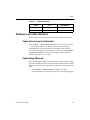
Resource
Description/URL
Tutorials
Tutorials covering Xilinx design flows, from design entry to verification
and debugging
http://support.xilinx.com/support/techsup/tutorials/index.htm
Answers
Database
Current listing of solution records for the Xilinx software tools
Search this database using the search function at
http://support.xilinx.com/support/searchtd.htm
Application
Notes
Descriptions of device-specific design techniques and approaches
http://support.xilinx.com/apps/appsweb.htm
Data Book
Pages from The Programmable Logic Data Book, which contains devicespecific information on Xilinx device characteristics, including readback,
Boundary-Scan, configuration, length count, and debugging
http://support.xilinx.com/partinfo/databook.htm
Xcell Journals
Quarterly journals for Xilinx programmable logic users
http://support.xilinx.com/xcell/xcell.htm
Technical Tips Latest news, design tips, and patch information for the Xilinx design
environment
http://support.xilinx.com/support/techsup/journals/index.htm
iv
Xilinx Development System
Conventions
This manual uses the following conventions. An example illustrates
most conventions.
Typographical
The following conventions are used for all documents.
•
Courier font indicates messages, prompts, and program files
that the system displays.
speed grade: - 100
•
Courier bold indicates literal commands that you enter in a
syntactical statement. However, braces “{ }” in Courier bold are
not literal and square brackets “[ ]” in Courier bold are literal
only in the case of bus specifications, such as bus [7:0].
rpt_del_net=
Courier bold also indicates commands that you select from a
menu.
File → Open
•
Italic font denotes the following items.
♦
Variables in a syntax statement for which you must supply
values
edif2ngd design_name
♦
References to other manuals
See the Development System Reference Guide for more
information.
iMPACT User Guide
v
iMPACT User Guide
♦
Emphasis in text
If a wire is drawn so that it overlaps the pin of a symbol, the
two nets are not connected.
•
Square brackets “[ ]” indicate an optional entry or parameter.
However, in bus specifications, such as bus [7:0], they are
required.
edif2ngd [option_name] design_name
•
Braces “{ }” enclose a list of items from which you must choose
one or more.
lowpwr ={on|off}
•
A vertical bar “|” separates items in a list of choices.
lowpwr ={on|off}
•
A vertical ellipsis indicates repetitive material that has been
omitted.
IOB #1: Name = QOUT’
IOB #2: Name = CLKIN’
.
.
.
•
A horizontal ellipsis “…” indicates that an item can be repeated
one or more times.
allow block block_name loc1 loc2 … locn;
Online Document
The following conventions are used for online documents.
vi
•
Blue text indicates cross-references within a book. Red text
indicates cross-references to other books. Click the colored text to
jump to the specified cross-reference.
•
Blue, underlined text indicates a Web site. Click the link to open
the specified Web site. You must have a Web browser and internet
connection to use this feature.
Xilinx Development System
Contents
About This Manual
Manual Contents ...........................................................................iii
Additional Resources ....................................................................iv
Conventions
Typographical ................................................................................v
Online Document ..........................................................................vi
Chapter 1
Introduction
Configuration Device Operations Available to Users ....................1-1
Non-Volatile Device Data Security ................................................1-2
Required Files ...............................................................................1-3
JEDEC Files .............................................................................1-3
BSDL Summary .......................................................................1-3
BIT Files ...................................................................................1-3
PROM Files ..............................................................................1-4
RBT Files .................................................................................1-4
Chain Description Files ............................................................1-4
iMPACT Features ..........................................................................1-4
User Feedback .........................................................................1-5
PROM Formatter ......................................................................1-5
Serial PROMs .....................................................................1-5
Parallel PROMs. .................................................................1-6
System ACE .............................................................................1-6
MultiPRO Desktop Programmer (MultiPRO) ............................1-6
iMPACT Platform Support .............................................................1-6
Starting iMPACT ...........................................................................1-7
From Project Navigator ............................................................1-7
From the Command Line .........................................................1-7
Exiting iMPACT ........................................................................1-7
Using the Interface ........................................................................1-7
Main Window ...........................................................................1-7
Title Bar ..............................................................................1-7
Menu Bar ............................................................................1-8
Toolbar ................................................................................1-8
Status Window ....................................................................1-10
iMPACT User Guide
vii
iMPACT User Guide
Commands and Dialog Boxes .................................................1-10
Common Fields ...................................................................1-11
Selection Dialog Boxes .......................................................1-11
Selecting Commands and Dialog Box Options ........................1-11
Using the Mouse .................................................................1-11
Using the Keyboard ............................................................1-12
Using Help .....................................................................................1-12
Help Menu ................................................................................1-12
Toolbar Help Button .................................................................1-13
F1 Key ......................................................................................1-13
Help Button in Dialog Boxes ....................................................1-13
Architecture Support .....................................................................1-13
Chapter 2
Cables
Download Cables ..........................................................................2-1
Cable Support ...............................................................................2-2
Cable Baud Rates ....................................................................2-2
Software and Cable Interface ........................................................2-3
Cable Auto Connect (Automatic) .............................................2-3
Cable Setup (Manual) ..............................................................2-3
Resetting the Cable .................................................................2-5
Disconnecting the Cable ..........................................................2-5
Target Board Requirements ..........................................................2-5
High Performance Ribbon Cable .............................................2-5
Flying Lead Connectors ...........................................................2-6
Flying Leads .......................................................................2-6
Mode Pin Connections for FPGAs Only .............................2-6
Parallel Cables ..............................................................................2-7
Parallel Cable IV ......................................................................2-7
Connecting to Host Computer ............................................2-8
Cable Power .......................................................................2-8
High Performance Ribbon Cable ........................................2-9
Target Board Header ..........................................................2-10
Parallel Cable III .......................................................................2-12
Connecting for System Operation .......................................2-13
Serial Configuration Connection .........................................2-15
MultiPRO Desktop Tool .................................................................2-17
Connecting to Host Computer ..................................................2-19
Cable Power ............................................................................2-19
High Performance Ribbon Cables ...........................................2-19
Desktop Programming .............................................................2-21
MultiLINX Cable ............................................................................2-24
MultiLINX Power Requirements ...............................................2-25
MultiLINX Cable and Flying Leads ...........................................2-25
MultiLINX Connection and Power Sequence ................................2-30
Connecting Cable to Target System ........................................2-30
Chapter 3
Designing Boundary-Scan and ISP Systems
Connecting Devices in a Boundary-Scan Chain ...........................3-1
viii
Xilinx Development System
Contents
FPGA Device Considerations .......................................................3-3
Bitstream Considerations .........................................................3-3
Virtex Considerations ...............................................................3-3
Device Behavior Notes ............................................................3-3
Selecting a Configuration Mode ....................................................3-4
FPGA Supported Modes ..........................................................3-5
JTAG or Boundary-Scan Mode ...........................................3-5
SelectMAP/Slave-Parallel Modes .......................................3-5
Master SelectMAP Mode ....................................................3-5
Master-Serial Mode ............................................................3-5
Slave-Serial Mode ..............................................................3-6
CPLD/PROM Supported Modes ..............................................3-6
Standalone Programmer Mode ...........................................3-6
JTAG or Boundary-Scan Mode ...........................................3-6
Programming and Configuring Options .........................................3-6
CPLD Programming Options ...................................................3-6
ATE/Embedded Solutions ...................................................3-7
MultiPRO Desktop Programmer .........................................3-7
Third Party Programmers ...................................................3-8
FPGA Configuration Flows ......................................................3-8
Embedded Solutions ...........................................................3-8
PROM .................................................................................3-9
PROMGen/PROM Formatter ..............................................3-9
Third Party Programmers ...................................................3-10
Xilinx Common Configuring and Programming Setups .................3-10
CPLD JTAG Chain Setup ........................................................3-10
Hardware Considerations ........................................................3-11
General JTAG Checklist ..........................................................3-12
XC9500/XL/XV Specific Checklist ............................................3-12
XPLA3 Specific Checklist .........................................................3-13
Software Implementation Considerations ................................3-13
Software Download Considerations .........................................3-13
Prototyping Environment ....................................................3-14
Production Environment .....................................................3-14
Virtex Series or Spartan-II Master Serial and Boundary-Scan (JTAG) Combination Setup ...............................................................................3-14
Hardware Considerations ........................................................3-16
Virtex Spartan-II Master Serial and Boundary-Scan (JTAG) Mode Connections ....................................................................................3-16
Software Implementation Considerations ................................3-17
Software Download Considerations .........................................3-18
Prototyping ..........................................................................3-18
Production ...........................................................................3-18
Configuration Checklist .................................................................3-18
Chapter 4
Using iMPACT to Configure Devices
Configuration Mode General Information ......................................4-1
Connecting to a Cable ...................................................................4-3
Boundary-Scan Configuration Mode .............................................4-5
iMPACT User Guide
ix
iMPACT User Guide
Automatically Creating the Chain .............................................4-5
Manually Creating the Chain ....................................................4-6
Assigning Configuration Files ..................................................4-7
Saving the Chain Description ...................................................4-9
Edit Preferences ......................................................................4-10
Available Boundary-Scan Operations ...........................................4-11
Performing Boundary-Scan Operations ........................................4-12
Slave Serial Configuration Mode ...................................................4-15
Adding a Device .......................................................................4-15
Programming the Device .........................................................4-18
Troubleshooting Slave Serial Configuration .............................4-19
SelectMAP Configuration Mode ....................................................4-21
Adding a Device .......................................................................4-21
Programming and Verifying a Device ......................................4-24
Troubleshooting SelectMAP Programming and Verify .............4-25
Desktop Configuration Mode .........................................................4-27
Automatically Identifying the Device ........................................4-27
Manually Identifying the Device ...............................................4-28
Assigning a Configuration File .................................................4-28
Setting Options ........................................................................4-28
Performing Device Operations .................................................4-30
Chapter 5
Using iMPACT to Generate Files
General File Mode Instructions .....................................................5-2
Creating System ACE Programming Files ....................................5-3
System ACE CF Settings .........................................................5-4
Size .....................................................................................5-4
Reserve Space ...................................................................5-4
System ACE CF Collection Name ......................................5-4
Location ..............................................................................5-4
Configuration Address ........................................................5-4
Design Name ......................................................................5-5
System ACE MPM Settings .....................................................5-5
Size (16,32,64, Generic) .....................................................5-5
System ACE MPM Name ...................................................5-5
Location ..............................................................................5-5
Target in: Slave Serial Mode or SelectMAP Mode ............5-5
Slave Serial Mode > Number Of Chains .............................5-5
SelectMAP Mode > Specify CS Pin to be used in this design 5-6
Configuration Address ........................................................5-6
File Generation > Compress File ........................................5-6
Adding Files to System ACE Devices ......................................5-6
System ACE CF .......................................................................5-7
System ACE CF Screen .....................................................5-7
Viewing Different Configuration Addresses ........................5-9
Adding More Devices After the Wizard Has Finished .........5-9
Assigning a Different File to a Device .................................5-9
Managing Multiple Collections ............................................5-9
Generating System ACE CF Files ...........................................5-10
x
Xilinx Development System
Contents
System ACE MPM ...................................................................5-11
System ACE MPM Screen ..................................................5-11
Viewing Different Configuration Addresses ........................5-14
Adding More Devices After the Wizard Has Finished .........5-14
Assigning a Different File to a Device .................................5-14
Generating System ACE MPM Files ...................................5-14
Creating PROM Formatter Programming Files .............................5-16
General PROM File Information ...............................................5-16
PROMs ...............................................................................5-16
PROM Formatter Files ........................................................5-16
BIT Swapping in PROM Files .............................................5-17
Implementing Your Applications .........................................5-18
Single Application PROM Files ...........................................5-19
Multiple Application PROM Files ........................................5-19
Configuration Setups ..........................................................5-20
XILINX PROM Part Names .................................................5-20
PROM Formatter Operations ...................................................5-20
Serial PROM Settings .........................................................5-20
Parallel PROM Settings ......................................................5-21
Adding Files to PROM Devices ..........................................5-22
Generating PROM Files ...........................................................5-23
Serial PROM File Creation .................................................5-23
Parallel PROM File Creation ...............................................5-25
Creating an SVF or STAPL File ....................................................5-27
Creating the chain ....................................................................5-27
Selecting the Programming File ...............................................5-27
Writing to an SVF or STAPL File .............................................5-28
Chapter 6
Troubleshooting for Boundary-Scan Chains
Communication .............................................................................6-1
Improper Connections ...................................................................6-2
Improper or Unstable Vcc .............................................................6-3
Boundary-Scan Chain Debug .......................................................6-3
System Noise ................................................................................6-5
Glossary of Terms
Appendix A Boundary-Scan Basics
Boundary-Scan/IEEE Standard 1149.1 .........................................A-1
What can it be used for? ..........................................................A-1
How does it work? ....................................................................A-2
The TAP Controller .............................................................A-2
The Instruction Register ......................................................A-2
The Data Registers .............................................................A-2
Impact Test Access Port .....................................................A-2
JTAG TAP Controller ...............................................................A-3
JTAG TAP Controller States ...............................................A-3
Mandatory Boundary-Scan Instructions ...................................A-5
Optional Boundary-Scan Instructions ......................................A-5
iMPACT User Guide
xi
iMPACT User Guide
Configuring the Parallel Download Cable .....................................A-5
Appendix B Parallel Cable III (DLC 5) Schematic
Appendix C Command Line and Batch Mode Commands
Difference Between Command Line and Batch Mode Operation .C-1
Command Line Usage ..................................................................C-2
Command Line Options ................................................................C-2
Batch Mode Commands ................................................................C-3
Batch Mode Definitions ............................................................C-4
General Commands .................................................................C-5
Configuration Mode Commands ...................................................C-6
General Configuration Mode Commands ................................C-6
Boundary-Scan Mode Specific Commands .............................C-8
File Generation Mode Commands ................................................C-9
PROM Formatter Specific Commands .....................................C-10
System ACE Specific Commands ............................................C-10
Example Batch Mode Command Sequences ...............................C-10
General Batch Command Sequence Format ...........................C-11
Command Sequence Example 1: Creating a Chain Using addDevice .....................................................................................C-11
Command Sequence Example 2: Chain Consisting of: XC18V04
(programmed), Third Party Device (bypassed) XC18v04 (programmed), XC18V04 (bypassed with .bsd file) ..................C-13
Command Sequence Example 3: Using JTAG to Automatically
Identify a Chain ...................................................................C-13
Command Sequence Example 4: Loading a .cdf File and Programming a Device .....................................................................C-14
JTAGPROG to iMPACT Script Migration ......................................C-14
Getting Started .........................................................................C-14
Determining the Part Name .....................................................C-14
Programming and Verifying a Device ......................................C-15
JTAGPROG ........................................................................C-15
iMPACT ..............................................................................C-16
iMPACT (XC18V00 Family) ................................................C-16
iMPACT (when assigning a BSDL file) ...............................C-16
Example: Programming a XC18v00 PROM .............................C-17
JTAGPROG ........................................................................C-17
iMPACT ..............................................................................C-17
iMPACT (SVF mode) ..........................................................C-17
Example: XC2v1000 Device (bypassed with a .bit file) in a Chain with
an XC18v04 Device (programmed) .........................................C-18
iMPACT ..............................................................................C-18
iMPACT (SVF mode) ..........................................................C-18
Example: XC2v1000 (programmed) in a Chain with a XC18v04 (bypassed with a BSDL file) ..........................................................C-19
JTAGPROG ........................................................................C-19
iMPACT ..............................................................................C-19
iMPACT (SVF mode) ..........................................................C-19
Example: Chain Consisting of XC18v04 (programmed), Third Party De-
xii
Xilinx Development System
Contents
vice (bypassed), XC18v04 (programmed), XC18v04 (bypassed with a
.bsd file) ...................................................................................C-20
JTAGPROG ........................................................................C-20
iMPACT ..............................................................................C-20
iMPACT (SVF mode) ..........................................................C-21
iMPACT User Guide
xiii
iMPACT User Guide
xiv
Xilinx Development System
Chapter 1
Introduction
This chapter introduces you to the basic concepts of the iMPACT
software and related Xilinx in-system programmable products. You
can use iMPACT to download, read back and verify design
configuration data as well as to create PROM, SVF, STAPL, System
ACE CF and System ACE MPM programming files. This chapter
contains the following sections:
•
“Configuration Device Operations Available to Users”
•
“Non-Volatile Device Data Security”
•
“Required Files”
•
“iMPACT Features”
•
“iMPACT Platform Support”
•
“Starting iMPACT”
•
“Using the Interface”
•
“Using Help”
•
“Architecture Support”
Configuration Device Operations Available to Users
Program. Downloads the contents of the JEDEC, BIT or PROM file to
the device.
Verify. Reads back the contents of the device configuration and
compares them with the JEDEC, BIT or PROM file.
Erase. Clears device configuration information.
Functional Test. Applies user-specified functional vectors from the
JEDEC file to the device using the JTAG INTEST instruction,
iMPACT User Guide
1-1
iMPACT User Guide
comparing results obtained against expected values. Reports any
differences to the user.
Blank Check. Checks whether a device is in a programmed or erased
state.
Readback. Reads back the contents of the device configuration and
creates a new JEDEC or PROM file with the results.
Program XPLA UES. This is a Coolrunner only option. Programs the
user electronic signature of the selected devices.
Get Device ID. Reads the contents of the JTAG IDCODE register.
Displays contents for the user.
Get Device Checksum. Reads back the contents of device configuration
registers and calculates a checksum for comparison against the
expected value specified in the JEDEC or PROM file.
Get Device Signature/Usercode. For FPGAs and CPLDs this value is
selected by the user during program file generation. The specified
value is translated to binary values in the JEDEC file. During device
programming these values are loaded into the JTAG USERCODE
register. This function reads the contents of the USERCODE register
and displays the result.
Get XPLA Device UES. This is a CoolRunner only option. Gets the user
electronic signature from the selected devices in the JTAG chain.
IDCODE Looping. Performs IDCODE operations a specified number
of times.
Non-Volatile Device Data Security
Any Xilinx XC9500 family device selected for programming can be
secured with the Write Protect or Read Protect or both. CoolRunner,
CoolRunner-II, and PROM devices can be secured with the Read
Protect only.
When enabled, Read Protect disables reading the programmed
contents of a device (the IDCODE, USERCODE and all BoundaryScan registers remain readable).
Write Protect enables only the reading of the programmed data. The
device contents cannot be altered or re-programmed.
1-2
Xilinx Development System
Introduction
When both Read Protect and Write Protect are enabled, the device
programmed data can be neither read nor re-programmed.
Required Files
For Boundary-Scan programming, you need to provide JEDEC files
for each CPLD family device, BIT files for each Xilinx FPGA device,
.mcs or .exo files for each PROM device, and BSDL files for the
remaining devices.
For Slave Serial programming, you must provide a single BITfile if
there is only one FPGA, or an .mcs/.exo file for Serial daisy chains
with multiple FPGAs.
For SelectMAP programming, you must provide a BITfile for each
target device.
JEDEC Files
JEDEC files are CPLD programming files generated by the Xilinx
fitter. They are ASCII text files containing programming information
that describes the desired functional implementation of the user’s
design. One JEDEC file is required for each CPLD device in the JTAG
programming chain.
BSDL Summary
The Boundary-Scan Description Language (BSDL) files use a subset
of VHDL to describe the Boundary-Scan features of a device.
iMPACT automatically extracts the length of the instruction register
from the BSDL file to place non-Xilinx devices in bypass mode. Xilinx
BSDL files are located automatically by iMPACT.
BIT Files
BIT files are Xilinx FPGA configuration files generated by the Xilinx
FPGA design software. They are proprietary format binary files
containing configuration information. One BIT file is required for
each Xilinx FPGA in a Boundary-Scan chain, for a single Slave Serial
connected device, or for each SelectMAP connected device.
iMPACT User Guide
1-3
iMPACT User Guide
PROM Files
PROM files are PROM programming files generated either by
iMPACT using the PROM Formatter tab in the File Generation mode,
or by the command line utility, PROMGen. The PROM files are ASCII
text files used to specify configuration data. PROM files are also used
to download a serial daisy chain of multiple FPGAs.
A Xilinx PROM file may consist of one or more data streams. In this
context, a data stream represents all the configuration data required
to implement a given application. Each data stream contains one or
more BIT files and once saved, has a separate preamble and length
count.
The PROM file can be formatted in one of three industry standard
formats: Intel MCS-86® (.mcs), Tektronix TEKHEX (.tek), and
Motorola EXOR-macs (.exo).
The PROM Formatter performs the same function as the PROMGen
program, which can be executed from the UNIX™ or PC command
line. Refer to the Development System Reference Guide for details about
PROMGen.
RBT Files
A Raw BIT File is an ASCII version of the BIT file. The only difference
is that the header information in a BIT File is removed from the Raw
BIT File. This is also created by BitGen and is used to program a
single FPGA.
Chain Description Files
A Chain Description file is used to save and restore information
about the composition of device configuration chains. It stores
information about the order of devices in the chain and the
configuration data file associated with each device.
iMPACT Features
You can use iMPACT to perform the following functions.
1-4
•
Configure one or more devices
•
Verify configuration data for single devices
Xilinx Development System
Introduction
•
Create PROM, SVF, STAPL, System ACE CF, and System ACE
MPM programming files.
For downloading, use any of the three configuration data file types
(BIT, JEDEC, or PROM) and any download cable.
For single device verification of Xilinx FPGAs, use a BIT file. In
addition, you will need to generate a MSK file. Be certain to include
the readback symbol in your design and optionally, the STARTUP
symbol. Verification ensures that a device’s configuration memory
contents match the source configuration file contents. It does not
ensure the device has started up and is functioning. Only actual
system verification can verify start up and overall function.
User Feedback
When using the graphical user interface, immediate feedback is
provided by a scrolling log file and alert boxes. Detailed information
regarding operation history and status is displayed in the status
window and collected in the iMPACT log file.
PROM Formatter
The PROM Formatter tab enables you to format BIT files into a
PROM file compatible with Xilinx and third-party PROM programmers. It is also used to concatenate multiple bitstreams into a single
PROM file for daisy chain applications. This feature also enables you
to take advantage of the Xilinx FPGA reconfiguration capability, as
you can store several applications in the same PROM file.
PROM files are also compatible with iMPACT’s configuration mode.
You can use iMPACT to download a PROM file to an XC18V00 series
PROM, a single FPGA, or a slave serial daisy chain of FPGA devices.
Serial PROMs
Serial PROMs are PROMs that are read one BIT at a time. In Serial
PROM mode, you can create files that:
iMPACT User Guide
•
Configure a single device with one or more PROM devices.
•
Configure daisy-chained devices with one or more PROM
devices.
1-5
iMPACT User Guide
Parallel PROMs.
A Parallel PROM is a PROM that is read one byte at a time. In Parallel
PROM mode, you can create files that:
•
Configure a single device with one or more applications.
•
Configure daisy-chained devices with one or more applications.
System ACE
System ACE is a Xilinx-developed configuration environment that
enables space-efficient, pre-engineered, high-density configuration
solutions for systems with multiple FPGAs. There are two versions of
System ACE; System ACE CF and System ACE MPM. See the “Using
iMPACT to Generate Files” chapter for more information.
MultiPRO Desktop Programmer (MultiPRO)
The MultiPRO download cable is a multi-function download cable
capable of facilitating socket based, single device configuration using
Boundary-Scan as well as standard device configuration using Slave
Serial, or SelectMAP interfaces.
•
The MultiPRO connects to your PC using an IEEE-1284 standard
parallel port.
•
The MultiPRO supports the CoolRunner-II CPLD family, and the
XC 18V00 Flash PROM family.
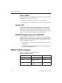
iMPACT Platform Support
iMPACT supports the following platforms.
Table 1-1 Platform Support
Cable
1-6
Platforms
Ports
MultiLINX
Sol/Win2000/ME/XP RS-232,USB
Parallel
WinNT/Win2000/
ME/XP
Parallel
MultiPRO
WinNT/Win2000/
ME/XP
Parallel
Xilinx Development System
Introduction
Starting iMPACT
This section explains how to start and exit iMPACT.
From Project Navigator
To start iMPACT from Project Navigator, follow these steps:
•
In the Processes for Current Source window, double click the
“Configure Device (iMPACT)” selection under the “Generate
Programming File” process.
From the Command Line
To start iMPACT from the UNIX® or DOS™ command prompt, enter
the following command:
impact
If you want to start iMPACT with a .bit, .cdf, or .jed extension,
or use iMPACT in batch mode, please see Appendix C for further
instructions.
Exiting iMPACT
To exit iMPACT, select File →Exit. If you have an open window,
you are prompted to save the data before quitting the application.
Using the Interface
This section describes the iMPACT interface.
Main Window
The main window is the background against which all other
windows are displayed.
Title Bar
The title bar displays the program name followed by the name of the
currently loaded design.
iMPACT User Guide
1-7
iMPACT User Guide
Menu Bar
The menu bar, located at the top of the window, includes the File,
Edit, Mode, Operations, Output, View, and Help menus. You can also
select menu commands by typing the letter underlined in the menu
name while holding down the Alt key.
Toolbar
The toolbar, located below the menu bar, consists of buttons that you
can use to execute commands. Place the mouse pointer over each
button to display the command associated with the button. The
command name appears as a “tool tip” and the status bar provides
more descriptive information.
Button
1-8
Name
Function
New
Removes all configuration descriptions from all tabs to let you start a
new configuration description.
Open
Open an existing CDF file.
Save
Saves the active chain file. Clicking
this button is the same as selecting
Save in the file menu.
Cut
Removes a selection from the
iMPACT main window and temporarily stores it on the clipboard.
Copy
Copies a device and temporarily
stores a copy of it on the clipboard.
Paste
Inserts data stored on the clipboard
into the iMPACT main window.
Xilinx Development System
Introduction
Button
Name
Function
Toggle
Mode
Switches iMPACT tabs between
Configuration and File Generation
modes.
Initialize
Chain
Automatically detects the number
and types of devices in a BoundaryScan chain.
Debug
Chain
Initiates rudimentary Boundary-Scan
TAP debug operations.
Select All
Selects all the devices in the chain.
Unselect All Unselects all the devices in the chain.
Add Xilinx
Device
Adds a new Xilinx device to the
chain.
Assign New Changes the current device configuConfigura- ration file selection.
tion File
iMPACT User Guide
Program
Configures the selected device or
devices.
Verify
Verifies the correct configuration has
been programmed to the device.
1-9
iMPACT User Guide
Button
Name
Function
Erase
Erases the contents of a programmed
device.
About
Displays the program information
and copyright.
Help
Invokes context-sensitive help. When
you click this button, the cursor
changes into a large question mark
with an arrow. You can then select an
object, such as a menu command or a
toolbar button, and receive help for
that object.
Status Window
The status window, located at the very bottom of the iMPACT
window, is broken into five individual display panes on the right
side, and general display section on the left. The status window
provides command and application state information. When you
select a menu command, a brief description of the command’s function appears on the left side status window. The five right side status
panes display (from left to right) the application operation mode, the
active sub mode, the cable being used, the cable port, and the cable
port speed.
Commands and Dialog Boxes
You communicate with iMPACT by selecting commands from the
menus and the toolbar.
1-10
Xilinx Development System
Introduction
Common Fields
The fields shown in the following table are common to most dialog
boxes.
Table 1-2 Common Dialog Box Fields
Dialog Box Field
Function
OK
Closes the dialog box and implements the
intended action according to the settings in the
dialog box
Help
Displays information on that particular dialog
box
Cancel
Closes the dialog box without affecting any
action
Cancel All
Cancels the current configuration setup
The standard file open and file save dialog boxes enable you to load a
project file or save a project file. This type of dialog box includes a file
browser.
Selection Dialog Boxes
Use Selection dialog boxes to specify specific values and selections.
Selecting Commands and Dialog Box Options
To choose a menu item, a toolbar button, or a dialog box option, you
can use the mouse or the keyboard.
Using the Mouse
iMPACT User Guide
1.
Move the mouse cursor over the object you want to select, and
click the left mouse button to select the object.
2.
To exit a dialog box without making a selection, click Cancel or
double-click the close box in the upper left corner of the dialog
box.
3.
To obtain help, click Help in the dialog box.
1-11
iMPACT User Guide
Using the Keyboard
You can use the keyboard to select objects on your screen, such as a
dialog box button or a menu option.
1.
To select a dialog box option, use the Tab key to position the
cursor on that object and highlight it. Press the Enter key to
process the selection.
To exit a dialog box without making a selection, press the Esc
key.
2.
To choose a menu and display its commands, press the Alt key
and the appropriate underlined letter key corresponding to the
menu you want. For example, press Alt F to select the File menu.
3.
Use the arrow keys to scroll down the list of commands in a
menu or the options in a list box. Press Enter when the selection
you want to use is highlighted or, in the case of a menu item,
press the underlined letter corresponding to the menu command.
For example, press the N key to select the New command of the
File menu.
Using Help
iMPACT includes both context-sensitive help and a Help menu. You
can obtain help on commands and procedures through the Help
menus or by selecting the Help toolbar button. In addition, the dialog
boxes associated with many commands have a Help button that you
can click to obtain context-sensitive help.
Help Menu
Use the following Help menu commands to get help.
1-12
•
The Help Topics command opens the online help and lists the
various topics available for iMPACT. From the Help Topics page,
you can jump to command information or step-by-step
instructions for using iMPACT. When you want to return to the
help topic list, click the Help Topics button.
•
The Online Documentation command provides access to the
online documentation.
Xilinx Development System
Introduction
•
The About iMPACT command displays a popup window that
shows the version number of the iMPACT software and a
copyright notice.
•
The Supported Devices command displays a list of devices
supported in iMPACT.
Toolbar Help Button
Click once with the left mouse button on the menu item or toolbar
button for which you want help. iMPACT displays help for the
selected command or option.
Note: You can also press Shift F1 to obtain context-sensitive help.
F1 Key
Pressing the F1 key on a dialog box displays help on that dialog box.
Pressing the F1 key is the same as selecting Help →Help Topics, if no
dialog boxes are displayed.
Help Button in Dialog Boxes
Many of the dialog boxes in iMPACT have a Help button that you can
click to get help on the dialog box options. You can also press Alt H
or F1 on your keyboard with the cursor positioned over the dialog
box to access the online help.
Architecture Support
The software supports the following architecture families in this
release.
iMPACT User Guide
•
Virtex-II Pro™
•
Virtex™/E/II
•
Spartan™II/IIE
•
CoolRunner™ XPLA3 /II
•
XC9500™ (Version 2 or greater)
•
XC9500XL/XV
•
XC18V00 PROMs
1-13
iMPACT User Guide
1-14
•
XC17V00 PROM’s -File Generation Only
•
System ACE CF
•
System ACE MPM
Xilinx Development System
Chapter 2
Cables
This chapter gives specific information about using cables to
download from the iMPACT Configuration Tool to devices in-system.
This chapter contains the following sections.
•
“Download Cables”
•
“Cable Support”
•
“Software and Cable Interface”
•
“Target Board Requirements”
•
“Parallel Cables”
•
“MultiPRO Desktop Tool”
•
“MultiLINX Cable”
•
“MultiLINX Connection and Power Sequence”
Download Cables
There are four cables available for use with the iMPACT
Configuration Tool. The first is the Parallel Download Cable III which
is connected to a PC’s parallel port. The second is the Parallel Cable
IV which is also parallel port connected and backward compatible to
the Parallel Cable III. The third is the MultiLINX cable which is
connected to a USB port or serial port. The fourth is the MultiPRO
desktop tool which can be used as a download cable or desktop
programmer. The USB port is used on Win2000/ME/XP. There are a
few options to be considered in selecting a cable:
•
iMPACT User Guide
The MultiLINX Cable connects to the serial port of both PCs and
workstations or the USB port on a PC.
2-1
iMPACT User Guide
•
The Parallel Cable IV is over 10 times faster than Parallel Cable III
and over 5 times faster than the MultiLINX cable.
•
All four cables are ChipScope ILA compatible.
Cable Support
iMPACT supports the following cables.
Table 2-1
Name
Cable Support
Platforms
Voltages
Modes
Notes
MultiLINX Cable PC,
2.5, 3.3, 5 Volt JTAG, Slave Serial, The USB port can
( Model: DLC6)
Workstation
SelectMAP
be used on
Win2000/ME/XP.
It cannot be used
on Win95 or
WinNT.
Parallel Cable IV
(Model: DLC7)
PC
1.5, 1.8, 2.5,
3.3, 5 Volt
JTAG, Slave Serial
Parallel Cable III
(Model: DLC5)
PC
2.5, 3.3, 5 Volt JTAG, Slave Serial Replaced by PC IV
in March 2002.
MultiPRO
PC
1.5 - 5 Volt
Desktop
Programmer,
JTAG, Slave Serial,
SelectMAP
Cable Baud Rates
The supported Baud Rates for the cables are shown in the following
table.
Table 2-2
Cable Baud Rates
Cable
2-2
PC
WorkStation
MultiLINX Cable
(USB)
1 M-12 M
USB is currently not
supported on WorkStation.
MultiLINX Cable
(RS-232)
9600, 19200, 38400,
and 57600
9600, 19200, and 38400
Parallel Cable III
Not Selectable
Not Applicable
Xilinx Development System
Cables
Table 2-2
Cable Baud Rates
Cable
PC
WorkStation
Parallel Cable IV
Not Selectable
Not Applicable
MultiPRO
Not Selectable
Not Applicable
Software and Cable Interface
iMPACT allows for both automatic and manual cable connections.
Cable Auto Connect (Automatic)
Select Output →Cable Auto Connect if you want the software
to scan for the presence of a cable and automatically establish
communication. Cable information is presented in the status bar.
If you select any operation that requires a cable, such as Program or
Initialize Chain, without first selecting a cable connection,
iMPACT attempts to auto connect.
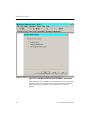
Cable Setup (Manual)
After connecting the cable to download and verify, power your target
board to enable the software to communicate with the cable and start
iMPACT. You then set the cable options manually with the following
steps:
1.
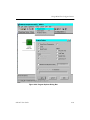
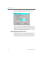
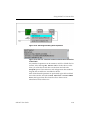
iMPACT User Guide
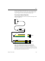
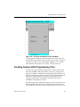
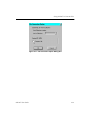
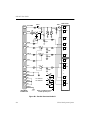
Select Output →Cable Setup to display the Cable
Communication Setup dialog box, shown in the following figure.
2-3
iMPACT User Guide
Figure 2-1 Cable Communication Setup Dialog Box
2.
In the Communication Mode field, select the cable type that you
installed for downloading. The Parallel Cable is supported for the
PC only.
3.
In the Port list box, select the port to use for downloading and
readback. If the port name you want is not listed, select the blank
name from the list box and type in the new port name. This list
box saves up to two user-specified port names.
The Port list box contains a list of valid ports for the
platform, as shown in the following table. If you selected the
MultiLINX Cable, the USB port is displayed. If you selected a
serial cable, the serial ports are displayed. If you selected a
parallel cable, the parallel ports are displayed.
Table 2-3
Platform
USB Ports
Serial Ports
Parallel Ports
Sol
none
/dev/ttya, /dev/ttyb not supported
PC
USB
com1, com2, com3,
com4
4.
2-4
USB, Serial, and Parallel Ports
lpt1, lpt2, lpt3,
lpt4
In the Baud Rate list box, select a communications baud rate
between the cable and the host system. You cannot specify the
baud rate for a parallel cable.
Xilinx Development System
Cables
Communication speed between the host system and the Cable
depends on host system capability. Refer to the “Valid Baud
Rates” table for a list of valid baud rates.
5.
Click OK to accept the selections.
iMPACT attempts to connect to the cable.
Resetting the Cable
To reset internal logic of the cable after a power glitch, select Output
→Cable Reset to reset the internal logic of the cable. The cable is
reinitialized and the proper baud rate is set.
Reset your cable if you experience a power failure to the target device
board.
Disconnecting the Cable
To disconnect the cable connection, select Output →Cable
Disconnect.
Note You need to disconnect the cable if you want to use the same
cable in a different configuration mode. For instance, if you start
using the parallel cable in Boundary-Scan mode, then wish to use it
for Slave Serial configuration, you first have to disconnect it in
Boundary-Scan and reconnect it in Slave Serial mode.
Target Board Requirements
The following are general target board requirements for all target
boards regardless of the type of cable being used. Specific cables and
configuration modes may have additional target board requirements.
High Performance Ribbon Cable
The Parallel Cable IV uses a high performance ribbon cable which
incorporates multiple signal-ground pairs. The cable has a single 14pin connector which requires a corresponding 14-pin board header
with 0.5mm square posts on 2mm centers.
When you lay out the printed circuit board for use with iMPACT insystem programming and testing, a few adjustments make the
process of connecting and downloading easier. Place pins or header
on the board so that flying leads or the high performance ribbon cable
iMPACT User Guide
2-5
iMPACT User Guide
can reach them. The length of our flying leads is either six inches
(Parallel Cable) or twelve inches (MultiLINX Cable). The ribbon cable
is recommended for all new designs in order to achieve the highest
configuration data throughput. When using the ribbon cable, you
must select Ribbon Cable in the Cable Leads section of the
Preferences dialog box.
Note The Ribbon Cable is available for the Parallel IV and MultiPRO
only. The high performance ribbon cable is 6” long.
Flying Lead Connectors
Some Xilinx cables use flying lead connectors that have individual
female connectors on one end that fit onto standard 0.025″ square
male pins on your target board. Each lead is labeled to identify the
proper pin connection.
Flying Leads
•
Provide pins on your printed circuit board for your desired
configuration mode. For example, Boundary-Scan configuration
would require Vcc, GND, TCK, TDO, TDI and TMS header pins.
•
These pins must be standard 0.025” square male pins that have
dedicated traces to the target device control pins. You connect to
these pins with the flying lead connector.
•
While pins may be a couple of inches apart, do not have any two
JTAG connector pins more than six inches apart.
Note When using flying leads, you must select Flying Leads in the
Cable Leads section of the Preferences dialog box to insure safe
operation of the cable. You also need to keep header pins on your
board a minimum of 0.10” apart.
Mode Pin Connections for FPGAs Only
When using download cables to configure a device or chain of
devices, you must set the appropriate device configuration mode.
You must set M0, M1, and M2 to the value specified in the device’s
databook for the desired mode. Refer to the Development System Guide
or The Programmable Logic Data Book for information on setting the
mode pins.
2-6
Xilinx Development System
Cables
Parallel Cables
If you are using a Parallel Download Cable proceed to the Parallel
Cable section.
If you have a MultiLINX Cable proceed to the MultiLINX Cable
section.
Parallel Cable IV
Parallel Cable IV
CONNECTOR SIGNALS
0.1 inch
2mm
Parallel Cable IV
Model DLC7
__
Power 5V --- 0.2A
Serial JG - 00052
Made in U.S.A.
JTAG
Vref
Gnd
SERIAL
Vref
Gnd
TCK
--TDO
TDI
CCLK
INIT
DONE
DIN
TMS
PROG
JTAG
--Vtst
TDI
TDO
TCK
TMS
Vref
Serial
INIT
Vtst
DIN
DONE
CCLK
PROG
Vref
STATUS
Gnd
Gnd
X9761
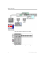
Figure 2-2 Top View of the Parallel Cable IV
The new Xilinx Parallel Cable IV (PC IV) is a high-speed download
cable that configures or programs all Xilinx FPGA, CPLD, ISP PROM,
and System ACE MPM devices. The cable takes advantage of the
IEEE 1284 ECP protocol and Xilinx iMPACT software to achieve
download speeds that are over 10 times faster than the PC III. The
cable automatically senses and adapts to target I/O voltages and is
able to accommodate a wide range of I/O standards from 1.5V to 5V.
PC IV supports the widely used industry standard IEEE 1149.1
Boundary-Scan (JTAG) specification using a four-wire interface. It
also supports the Xilinx Slave Serial mode for Xilinx FPGA devices. It
iMPACT User Guide
2-7
iMPACT User Guide
interfaces to target systems using a ribbon cable that features integral
alternating ground leads to reduce noise and increase signal integrity.
The cable is externally powered from either a power brick or by
interfacing to a standard PC mouse or keyboard connection. A
bi-color status LED indicates the presence of operating and target
reference voltages.
Connecting to Host Computer
The PC IV connects to any PC using Win2000, Win XP, or through the
standard IEEE 1284 DB25 parallel (printer) port connector. To fully
utilize the higher speeds of this cable, the host PC must have a
parallel port that supports extended capability port (ECP) mode. If
ECP mode is not enabled, the PC IV defaults to compatibility mode
and does not run at the optimum speeds listed.
Cable Power
The host interface cable (Figure 2-3) includes a short power jack for
connection to one of two possible +5V DC power sources: (1) an
external AC adapter or (2) the keyboard or mouse port of the host PC
(shown). The supplied power splitter cable is required when using
the second option. The splitter cable is installed between the mouse
cable and the standard 6-pin mini-DIN (PS2) connector on the host
PC. PC IV operating current is less than 100 mA. It draws
approximately 15 mA from the target board’s reference voltage
supply to power the JTAG/Slave Serial buffers.
2-8
Xilinx Development System
Cables
Par
al
lel
C
CO
Mod
N
able
0.1 NEC
Pow el DLC
JTAG
IV
inch TOR
SIG
Ser er 5V __7
Vref
SE
NA
--ial
R
Gnd
LS
JG
0.
Vref IAL
- 00 2A
2m
Gnd
m
052
TC
de
JTAG
in U.
K
Ma
S.A.
CC
--LK
TD
INIT
O
TD
DO
I
DIN NE
TM
S
PR
OG
---
Seria
Vtst
INIT
TD
Vtst
TD I
TC O D DIN
TM K C ONE
VrefS PRCLK
O
VrefG
l
STA
TU
S
Gnd
Gnd
X9762
Figure 2-3 Parallel Cable IV Parallel and PS2 Connection
High Performance Ribbon Cable
An insulation displacement (IDC) ribbon cable is supplied and
recommended for connection to target systems. This cable
incorporates multiple signal-ground pairs and facilitates error-free
connection. A very small footprint, keyed mating connector is all that
is required on the target system.
The Parallel Cable IV can also interface to target systems using flying
lead wires. However, these are not included with PC IV and can be
purchased separately. The ribbon cable is recommended for new
designs to attain optimal speeds.
iMPACT User Guide
2-9
iMPACT User Guide
6.0
Polarizing Key
Polarizing Key
pin#1 indicator stripe
2
4
6
8
10
12
14
1
3
5
7
9
11
13
2
4
6
8
10
12
14
1
3
5
7
9
11
13
X9760
Figure 2-4 High Performance Ribbon Cable
Note Ribbon Cable - 14 conductor 1.0mm centers Round Conductor
Flat Cable; 28 AWG (7x36) stranded copper conductors; gray PVC
with pin 1 edge marked.
Note 2mm Ribbon Female Polarized Connectors - IDC connection to
ribbon; contacts are beryllium copper plated; 30 micro inches gold
plating over 50 micro inches nickel; connectors mate to 0.5mm square
posts on 2mm centers.
Target Board Header
Slave Serial JTAG
INIT
NC
DIN
DONE
CCLK
PROG
Vref
NC 14
NC 12
TDI 10
TDO 8
TCK 6
TMS 4
Vref 2
0.0787" (2mm)
13
11
9
7
5
3
1
GND
GND
GND
GND
GND
GND
GND
0.020" (0.5mm) SQ. TYP.
X9776
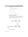
Figure 2-5 Target Interface Connector Signal Assignments
2-10
Xilinx Development System
Cables
Table 2-4 Mating Connectors for 2mm pitch, 14 Conductor
Ribbon Cable
Manufacturer
SMT. Vertical
SMT. Right
Angle
Through-Hole
Vertical
Through-Hole
Right Angle
Molex
87332-1420
N/A
87331-1420
87333-1420
FCI
95615-114
N/A
90309-114
95609-114
Comm Con
Connectors
2475-14G2
N/A
2422-14G2
N/A
iMPACT User Guide
2-11
iMPACT User Guide
Parallel Cable III
Parallel Cable III
Top View
JTAG Header
FPGA Header
Made in U.S.A
SENSITIVE
ELECTRONIC
DEVICE
VCC
GND
TCK
TDO
TDI
VCC
GND
CCLK
FPGA
JTAG
Parallel Cable III
CAUTION
Model DLC5
Power 5V 10mA Typ.
Serial JT - 1 2 3 4 5
D/P
DIN
PROG
TMS
Bottom View
X9759
Figure 2-6 Top and Bottom View of Parallel Download Cable III
The Parallel Download Cable III consists of a cable assembly
containing logic to protect your PC‘s parallel port and a set of headers
to connect to your target system. PC III was replaced by PC IV in
March 2002 with legacy support from iMPACT.
2-12
Xilinx Development System
Cables
Using the Parallel Download Cable requires a PC equipped with an
AT compatible parallel port interface with a DB25 standard printer
connector. Figure 2-6 shows the Parallel Download Cable.
Connecting for System Operation
Connect the parallel cable to the host system and your target system
as shown in Figure 2-3.
DB25 Plug Connector
Parallel Cable III
FPGA Flying Lead Connector
FPGA
VCC
GND
CCLK
D/P
PROG
DIN
PROG
Connections to
Target System
JTAG Flying Lead Connector
JTAG
VCC
GND
TCK
TDO
TDI
Connections to
Target System
TMS
X9475
Figure 2-7 Parallel Download Cable III and Accessories
The parallel download cable can download to a single device or
several devices connected in either a Boundary-Scan chain or a slaveserial daisy chain (FPGA only). The parallel cable can be used to read
back configuration and Boundary-Scan data.
iMPACT User Guide
2-13
iMPACT User Guide
The transmission speed of the Parallel Download Cable is
determined solely by the speed at which the host PC can transmit
data through its parallel port interface.
VCC
GND
TDO
TCK
JTAG
VCC
GND
TCK
TDO
TDI
TMS
TCK
TDI TDO
TDI
TMS
TCK
TDI TDO
TMS
TCK
TDI TDO
TMS
TMS
JTAG Flying Lead Connector
Target System
X8005
Figure 2-8 Parallel Download Cable Connection to JTAG
Boundary-Scan TAP
JTAG parallel cable schematic contains schematic diagrams of the
Parallel Download Cable.
Table 2-5 Parallel Cable Connections and Definitions
2-14
Name
Function
Connections
Vcc
Power – Supplies Vcc (5 V, To target system Vcc
3.3V, or 2.5V, 10 mA, typically) to the cable.
GND
Ground – Supplies ground To target system
reference to the cable.
ground
TCK
Connect to system TCK
Test Clock – this clock
drives the test logic for all pin.
devices on Boundary-Scan
chain.
Xilinx Development System
Cables
Table 2-5 Parallel Cable Connections and Definitions
Name
Function
Connections
TDO
Read Data – Read back
data from the target
system is read at this pin.
Connect to system
TDO pin.
TDI
Test Data In – this signal is Connect to system TDI
used to transmit serial test pin.
instructions and data.
TMS
Test Mode Select – this
signal is decoded by the
TAP controller to control
test operations.
Connect to system TMS
pin.
Serial Configuration Connection
VCC
GND
FPGA
VCC
GND
CCLK
D/P
DIN
PROG
CCLK
DONE
DIN
PROG
XC4000 FPGA in Slave Serial Mode
Parallel Cable III with FPGA Flying Leads
Target System
X8326
Figure 2-9 Parallel Cable III Connections
iMPACT User Guide
2-15
iMPACT User Guide
.
Table 2-6 Parallel Cable Connections and Definitions
2-16
Name
Function
Connections
Vcc
Power – Supplies Vcc (5 V, To target system Vcc
3.3V, or 2.5V, 10 mA, typically) to the cable.
GND
Ground – Supplies ground To target system
reference to the cable.
ground
CCLK
Configuration Clock --- is the Connect to system
CCLK pin.
configuration clock pin,
and the default clock for
readback operation.
DONE (D/P)
Done/Program --- Indicates Connect to system
that configuration loading DONE pin.
is complete, and that the
start-up sequence is in
progress.
DIN
Data In --- Provides config- Connect to system DIN
pin.
uration data to target
system during configuration and is tristated at all
other times.
PROG
Connect to system
Program --- A Low indicates the device is clearing PROG pin.
its configuration memory.
Active Low signal is used
to initiate the configuration process.
Xilinx Development System
Cables
MultiPRO Desktop Tool
Power Switch
0
1
INIT
NC
DIN
DONE
CCLK
PROG
Vref
SelectMAP
Parallel Port
Connector
IEEE-1284-C
Parallel Port
MultiPRO
Desktop Tool
Model DLC8
Power 5V
0.3A
Serial MP - 1 2 3 4 5
Made in U.S.A.
Adapter Port
STATUS
NC
NC
TDI
TDO
TCK
TMS
Vref
Gnd
Gnd
Gnd
Gnd
Gnd
Gnd
Gnd
CS0
CS1
CS2
PROG
INIT
DONE
BUSY
RDWR
CCLK
D0
D1
D2
D3
D4
D5
D6
D7
NC
NC
Gnd
Gnd
Gnd
Gnd
Gnd
Gnd
Gnd
Gnd
Gnd
Gnd
Gnd
Gnd
Gnd
Gnd
Gnd
JTAG
Serial
Power Jack
Power Port
S/JTAG
SMAP
14-pin 2mm
ribbon
connector
34-pin 2mm
ribbon
connector
STATUS
20-pin Adapter
Connector
Figure 2-10 MultiPRO Desktop Tool
The new Xilinx MultiPRO is a high-speed desktop download tool
that configures all Xilinx FPGA devices and programs all Xilinx
CPLD, ISP PROM, and System ACE MPM devices. The cable takes
advantage of the IEEE-1284 ECP protocol and Xilinx iMPACT
software to achieve download speeds similar to the Parallel Cable IV
and is over 10 times faster than the Parallel Cable III. MultiPRO
automatically senses and adapts to target I/O voltages and is able to
accommodate a wide range of I/O standards from 1.5V to 5V.
The MultiPRO can also function as a desktop programmer, similar to
the Xilinx HW-130 when the appropriate programming adapter is
connected to the MultiPRO’s 20-pin adapter port. Using these
iMPACT User Guide
2-17
iMPACT User Guide
adapters, MultiPRO supports desktop programming of the
CoolRunner-II CPLD family, the XC18V00 ISP PROM family. For
more information, see the “Desktop Programming” section of this
chapter.
MultiPRO supports the widely used industry standard IEEE 1149.1
Boundary-Scan (JTAG) specification using a four-wire interface. It
also supports the Xilinx Slave Serial mode and SelectMAP mode for
Xilinx FPGA devices. It interfaces to target systems using ribbon
cables that feature alternating ground leads to reduce noise and
increase signal integrity.
An IEEE-1284 parallel cable is supplied to interface between the
MultiPRO Desktop Tool and any PC with a parallel port (See Figure
2-11). The cable uses a standard DB25 male connector for the PC.
When attaching or disconnecting the parallel cable to the MultiPRO
Desktop Tool, squeeze the parallel cable’s connector to open the
locking tabs.
0
1
Serial
Power Port
S/JTAG
INIT
NC
DIN
DONE
CCLK
PROG
Vref
SelectMAP
IEEE-1284-C
Parallel Port
MultiPRO
Desktop Tool
Model DLC8
Power 5V
0.3A
Serial MP - 1 2 3 4 5
Made in U.S.A.
Adapter Port
IEEE-1284 PARALLEL CABLE
STATU
NC
NC
TDI
TDO
TCK
TMS
Vref
Gnd
Gnd
Gnd
Gnd
Gnd
Gnd
Gnd
CS0
CS1
CS2
PROG
INIT
DONE
BUSY
RDWR
CCLK
D0
D1
D2
D3
D4
D5
D6
D7
NC
NC
Gnd
Gnd
Gnd
Gnd
Gnd
Gnd
Gnd
Gnd
Gnd
Gnd
Gnd
Gnd
Gnd
Gnd
Gnd
JTAG
5V POWER SUPPLY
POWER CORD
SMAP
STATU
Figure 2-11 IEEE-1284 Parallel Cable and 5V Power Supply
MultiPRO is externally powered from a 5V universal power supply
that is included. The power supply’s 5.5x2.1mm DC plug is
connected to the MutliPRO’s power port jack. The power supply has
a detachable power cord that allows different style AC plugs to be
used.
Two bi-color status LEDs indicate the presence of operating and
target reference voltages. The LED labeled S/JTAG STATUS is
associated with the 14 conductor ribbon cable used with the Slave
Serial and JTAG modes of operation. The LED labeled SMAP STATUS
is associated with the 34 conductor ribbon cable used with the
SelectMAP mode of operation. Both STATUS indicators illuminate
amber color when the 5V supply is connected and the MultiPRO
power switch is turned on. The S/JTAG STATUS indicator will
change color to green when the target reference voltage from the 14
conductor ribbon cable is present (1.5V to 5V). The SMAP STATUS
2-18
Xilinx Development System
Cables
indicator will change color to green when the target reference voltage
from the 34 conductor ribbon cable is present (1.5V to 5V).
0
1
S/JTAG
STATUS
Gnd
Gnd
Gnd
Gnd
Gnd
Gnd
Gnd
CS0
CS1
CS2
PROG
INIT
DONE
BUSY
RDWR
CCLK
D0
D1
D2
D3
D4
D5
D6
D7
NC
NC
Gnd
Gnd
Gnd
Gnd
Gnd
Gnd
Gnd
Gnd
Gnd
Gnd
Gnd
Gnd
Gnd
Gnd
Gnd
SelectMAP
IEEE-1284-C
Parallel Port
MultiPRO
Desktop Tool
NC
NC
TDI
TDO
TCK
TMS
Vref
JTAG
Serial
Power Port
14 conductor ribbon cable with 2mm connectors
INIT
NC
DIN
DONE
CCLK
PROG
Vref
Model DLC8
Power 5V
0.3A
Serial MP - 1 2 3 4 5
Made in U.S.A.
Adapter Port
X9817
34 conductor ribbon cable with 2mm connectors
SMAP
STATUS
Figure 2-12 Ribbon Cables Connected to MultiPRO
Connecting to Host Computer
The MultiPRO Desktop Tool connects to any PC using Win2000 or
WinXP through the standard IEEE-1284 DB25 parallel (printer) port
connector. To fully utilize the higher speeds of this cable, the host PC
must have a parallel port that is enabled to support extended
capability port (ECP) mode. If ECP is not enabled, the MultiPRO will
default to compatibility mode and will not run at the optimum
speeds listed. While in compatibility mode, the MultiPRO will also
not support SelectMAP nor the programming adapters.
Compatibility mode simulates the operation of a Parallel Cable III
using only the Slave Serial/JTAG functions.
Cable Power
The universal 5V switching power supply, included with the
MultiPRO, can accept input voltages from 100 to 240VAC at 46 to 63
Hz. The MultiPRO takes less than 300mA from the 5V supply.
MultiPRO’s load on the target board’s reference voltage supply for
the Slave Serial/JTAG or SelectMAP connection is less than 1mA.
High Performance Ribbon Cables
Insulation displacement (IDC) ribbon cables are supplied and are the
only means of connection to the target system. The MultiPRO does
iMPACT User Guide
2-19
iMPACT User Guide
not support the use of Xilinx “flying lead” wires. These cables
incorporate multiple signal-ground pairs and facilitate error-free
connections. A small footprint, keyed mating connector is all that is
required on the target system.
The 14 conductor ribbon cable, used for MultiPRO’s Slave Serial &
JTAG connection, is identical to the one used with Parallel Cable IV.
The 34 conductor ribbon cable, used for MultiPRO’s SelectMAP
connection, is shown in Figure 2-13 below. See figure 2-14 for the
appropriate connector pin assignments and sample vendor part
number.
6.0 inches
Polarizing Key
Polarizing Key
pin#1 indicator stripe
2
4
6
8
10
12
14
16
18
20
22
24
26
28
30
32
34
1
3
5
7
9
11
13
15
17
19
21
23
25
27
29
31
33
2
4
6
8
10
12
14
16
18
20
22
24
26
28
30
32
34
1
3
5
7
9
11
13
15
17
19
21
23
25
27
29
31
33
NOTES:
1. RIBBON CABLE - 34 conductor
1.0mm Round Conductor Flat Cable
28AWG (7x36) stranded copper conductors
Gray PVC with pin #1 edge marked.
2. 2mm Ribbon Female Polarized Connectors
IDC connection to ribbon
Contacts are beryllium copper plated
30 micro inches Gold plating over 50 micro inches Nickel
Connectors mate to 0.5mm square posts on 2mm centers.
X9818
Figure 2-13 34 Conductor Ribbon Cable
2-20
Xilinx Development System
Cables
34
32
30
28
26
24
22
20
18
16
14
12
10
8
6
4
2
0.158"
CS0
CS1
CS2
PROG
INIT
DONE
BUSY
RDWR
CCLK
D0
D1
D2
D3
D4
D5
D6
D7
33 NC
31 NC
29 Gnd
27 Gnd
25 Gnd
23 Gnd
21 Gnd
19 Gnd
17 Gnd
15 Gnd
13 Gnd
11 Gnd
9 Gnd
7 Gnd
5 Gnd
3 Gnd
1 Gnd
1.569"
0.0787" (2mm)
SelectMAP
signals
0.020" (0.5mm)
2x17 (34 position) 2mm CONNECTOR
CommConn Part No. 2475-G2-34
Figure 2-14 Connector Pin Assignments for 34 Conductor
Ribbon Cable
Desktop Programming
The MultiPRO can be used as a desktop programmer, similar to the
Xilinx HW-130 Programmer, to program Xilinx CPLDs and ISP
PROMs. Optional adapters can be purchased separately and plugged
into the 20 pin Adapter Port connector of the MultiPRO (See Figure 215).
iMPACT User Guide
2-21
iMPACT User Guide
0
1
INIT
NC
DIN
DONE
CCLK
PROG
Vref
SelectMAP
IEEE-1284-C
Parallel Port
MultiPRO
Desktop Tool
Model DLC8
Power 5V
0.3A
Serial MP - 1 2 3 4 5
Made in U.S.A.
Adapter Port
Gnd
Gnd
Gnd
Gnd
Gnd
Gnd
Gnd
CS0
CS1
CS2
PROG
INIT
DONE
BUSY
RDWR
CCLK
D0
D1
D2
D3
D4
D5
D6
D7
NC
NC
Gnd
Gnd
Gnd
Gnd
Gnd
Gnd
Gnd
Gnd
Gnd
Gnd
Gnd
Gnd
Gnd
Gnd
Gnd
SMAP
HW-MP-PQ208
STATUS
NC
NC
TDI
TDO
TCK
TMS
Vref
JTAG
Serial
Power Port
S/JTAG
STATUS
ACTIVE
1
PIN
MultiPRO PQ208 Adapter
for CoolRunnerTM- II
X9820
Figure 2-15 MultiPRO Adapter
The MultiPRO programming adapters currently support the
CoolRunner-II CPLD family and the XC18V00 ISP PROM family (see
Table 2-7). The device adapters for the HW-130 and the MultiPRO are
physically incompatible.
The red LED labeled “ACTIVE” on the adapters is illuminated when
the device is busy being programmed. Do not remove a device from
2-22
Xilinx Development System
Cables
its socket nor unplug the adapter from MultiPRO when the
“ACTIVE” LED is illuminated.
Table 2-7 Available Adapters for MultiPRO
XC18V00 ISP PROM Family
Device
Package
Adapter Part Number
18V256, 18V512, 18V01
PC20
HW-MP-PC20
18V256,18V512,18V01
SO20
HW-MP-SO20
18V02,18V04
PC44
HW-MP-PC44-1
18V256,18V512,18V01
18V02,18V04
VQ44
HW-MP-VQ44-1
CoolRunner-II CPLD Family
Device
Package
Adapter Part Number
2C32, 2C64
PC44
HW-MP-PC44-2
2C32, 2C64
VQ44
HW-MP-VQ44-2
2C32, 2C64
CP56
HW-MP-CP56
2C64, 2C128, 2C256
VQ100
HW-MP-VQ100
2C128, 2C256
CP132
HW-MP-CP132
2C128, 2C256, 2C384
VQ144
HW-MP-VQ144
2C256, 2C384, 2C512
PQ208
HW-MP-PQ208
2C256, 2C384, 2C512
FT256
HW-MP-FT256
2C384, 2C512
FG324
HW-MP-FG324
iMPACT User Guide
2-23
iMPACT User Guide
MultiLINX Cable
Figure 2-16 shows the top and bottom view of the MultiLINX Cable.
Top View
RT
RT(TDO)
TRIG
R
TDI
TCK
TMS
CLK1-IN
CLK2-OUT
TM
CS0(CS)
CS1
CS2
CLK2-IN
CLK2-OUT
WS
RS(RDWR)
RDY/BUSY
PWR
GND
CCLK
DONE
DIN
PROG
INIT
RST
2 1 STATUS
43
D0
D1
D2
D3
D4
D5
D6
D7
Bottom View
CAUTION
R
RS-232
SENSITIVE
ELECTRONIC
DEVICE
TM
CE
Model: DLC6
Power: 2.5V
0.8A to 5V
Serial: UC-000074
Made in U.S.A
0.4A Typ.
USB
UNIVERSAL SERIAL BUS
X8927
Figure 2-16 MultiLINX Cable
You can use the MultiLINX Cable to download and verify all Xilinx
CPLDs and FPGAs. The MultiLINX Cable hardware communicates
with the host over the Universal Serial Bus (USB) or at variable baud
rates over an RS-232 interface at up to 57600 BITs/sec.
You can access the following application notes with descriptions of
device-specific design techniques and approaches from the support
page at (http://support.xilinx.com/support/searchtd.htm).
2-24
Xilinx Development System
Cables
“Getting Started with the MultiLINX Cable” application note #168 is
a quick reference to everything you need to know to use the
MultiLINX Cable, including using a USB device, Mixed Voltage
environments, and connections for all the supported Modes.
MultiLINX Power Requirements
The MultiLINX Cable gets its power from the User’s circuit board.
The cable power does not come from the USB port (nor the RS-232
port). The red (PWR) and black (GND) wires from Flying Wire Set #1
are connected to the Vcc (red wire) and Ground (black wire) lines of
the circuit board that is powering the Xilinx device.
The minimum input voltage to the cable is 2.5 V (.8 A). The maximum
input voltage is 5 V (.4 A).
MultiLINX Cable and Flying Leads
The MultiLINX Cable is shipped with four sets of flying lead wires. A
USB Cable and RS-232 Cable (with adapter) are also supplied.
Figure 2-17 shows the MultiLINX Cable hardware and flying lead
connection wires.
iMPACT User Guide
2-25
iMPACT User Guide
RT
RT(TDO)
TRIG
R
TDI
TCK
TMS
CLK1-IN
CLK2-OUT
TM
CS0(CS)
CS1
CS2
CLK2-IN
CLK2-OUT
WS
RS(RDWR)
RDY/BUSY
MultiLINX
TM
PWR
GND
CCLK
DONE
DIN
PROG
INIT
RST
2 1 STATUS
43
D0
D1
D2
D3
D4
D5
D6
D7
Flying Lead Connector Set #1
PWR
GND
CCLK
DONE(D/P)
DIN
PROG
INIT
RST
1
MultiLINX
TM
Flying Lead Connector Set #2
RT
RD(TDO)
TRIG
TDI
TCK
TMS
CLK1-IN
CLK1-OUT
2
MultiLINX
TM
Flying Lead Connector Set #3
D0
D1
D2
D3
D4
D5
D6
D7
3
MultiLINX
4
TM
Flying Lead Connector Set #4
CS0(CS)
CS1
CS2
CLK2-IN
CLK2-OUT
WS
RS(RDWR)
RDY/BUSY
X8926
Figure 2-17 MultiLINX Cable and Flying Lead Connectors
2-26
Xilinx Development System
Cables
The MultiLINX Flying wires are described in the following tables.
Table 2-8 MultiLINX Pin Descriptions (Flying Lead Set #1)
Signal Name
Function
PWR
Power - Supplies Vcc to cable
(Works at multiple voltages 5V,
3.3V, and 2.5V).
GND
Ground - Supplies ground reference to cable.
Table 2-9 MultiLINX Slave Serial Pin Descriptions
(Flying Lead Set #1)
iMPACT User Guide
Signal Name
Function
CCLK
Configuration Clock - is the configuration clock pin, and the default
clock for readback operation.
DONE (D/P)
Done/Program - Indicates that
configuration loading is
complete, and that the start-up
sequence is in progress.
DIN
Data In - Provides configuration
data to target system during
configuration and is tristated at
all other times.
PROG
Program - A Low indicates the
device is clearing its configuration memory.
Use the Active Low signal to
initiate the configuration process.
2-27
iMPACT User Guide
Table 2-9 MultiLINX Slave Serial Pin Descriptions
(Flying Lead Set #1)
Signal Name
Function
INIT
Initialize — Initialization
sequencing pin during configuration (indicates start of configuration).
A logical zero on this pin during
configuration indicates a data
error.
RST
Reset —Pin used to reset internal
FPGA logic. Connection to this
pin is optional during configuration.
Table 2-10 MultiLINX Boundary-Scan Pin Descriptions
(Flying Lead Set #2)
2-28
Signal Name
Function
RD (TDO)
Read Data — MultiLINX input.
iMPACT receives the readback
data through the RD pin after
readback is initiated.
Pin used to initiate a readback of
target FPGA. TDO is for JTAG
(Boundary-Scan).
TDI
TCK
TMS
These pins are used for JTAG
(Boundary-Scan) device configuration.
The JTAG/Boundary-Scan pins
function for FPGA, CPLD, ISP
PROM, and SystemACE MPM
operations.
Xilinx Development System
Cables
Table 2-11 MultiLINX SelectMAP Pin Descriptions
(Flying Lead Sets 3&4)
iMPACT User Guide
Signal Name
Function
D0-D7
Data Bus — This pin is used for
Virtex SelectMAP Mode.
An 8 BIT data bus supporting the
SelectMAP and Express configuration modes.
CS0 (CS)
Chip Select — CS on the Virtex.
The CS0/CS pin represents a
chip select to the target FPGA
during configuration.
CS1
Chip Select — The CS1 pin represents Chip Select to FPGAs
during configuration.
CS2
Chip Select — The CS2 pin represents Chip Select to the FPGA
while using the Peripheral
configuration mode.
WS
Write Select — The WS pin represents Write Select control for the
Asynchronous Peripheral configuration mode.
RS (RDWR)
Read Select — The RS pin represents Read Select control for the
Asynchronous Peripheral configuration mode.
Read/Write — The RDWR pin is
used as an active high READ and
an active low WRITE control
signal to the Virtex FPGA.
RDY/BUSY
Busy Pin — Busy pin on the
Virtex.
2-29
iMPACT User Guide
MultiLINX Connection and Power Sequence
The following considerations should be followed when powering up
the MultiLINX cable.
Caution Connecting the MultiLINX leads to the wrong signal
causes permanent damage to the MultiLINX internal hardware.
You must connect PWR to Vcc and GND to ground. As with any
CMOS device, the input/output pins of the internal FPGA
should always be at a lower or equal potential than the rail
voltage to avoid internal damage. The cable draws its power
from the target system through Vcc and GND. Therefore, power
to the cable, as well as to the target FPGA, must be stable. Do not
connect any signals before connecting Vcc and GND.
Connecting Cable to Target System
This section covers cable connection to the target device. You need
appropriate pins on the target system for connecting the target
system board to the header connectors on the cable.
1.
Connect your cable to your host computer. If you have a
MultiLINX Cable, connect it to the USB or RS-232 port. A DB-9/
DB-25 adapter may be required to connect the cable to your serial
port. If you have a different serial port connection, you need to
use the appropriate adapter.
2.
Turn the power to your target system off, if possible.
3.
The power for the drivers is derived from the target system.
Connect the cable’s GND wire to the corresponding signal on the
target board. Next, connect Vcc to the corresponding signal on
the target board.
4.
Download cables do not operate if the target system‘s power is
turned off before or during iMPACT Configuration operations.
Make certain that this power connection is on and stable. Your
system’s power should be on during iMPACT Configuration
operations.
5.
Next, connect the signal leads.
Note When using Boundary-Scan connections, please note that TRST
is not supported by Xilinx Download Cables. If any of your JTAG
parts have a TRST pin, it should be connected to Vcc.
2-30
Xilinx Development System
Cables
iMPACT User Guide
6.
Turn on power to the target system.
7.
Make sure Vcc rises to a stable level within 10ms. After the cable
Vcc stabilizes, the level should be within 5% of the target systems
Vcc IO.
2-31
iMPACT User Guide
2-32
Xilinx Development System
Chapter 3
Designing Boundary-Scan and ISP Systems
This chapter gives design considerations for Boundary-Scan and ISP
systems.
This chapter contains the following sections.
•
“Connecting Devices in a Boundary-Scan Chain”
•
“FPGA Device Considerations”
•
“Selecting a Configuration Mode”
•
“Programming and Configuring Options”
•
“Xilinx Common Configuring and Programming Setups”
•
“Virtex Series or Spartan-II Master Serial and Boundary-Scan
(JTAG) Combination Setup”
•
“Configuration Checklist”
Connecting Devices in a Boundary-Scan Chain
All devices in the chain share the TCK and TMS signals. The system
TDI signal is connected to the TDI input of the first device in the
Boundary-Scan chain. The TDO signal from that first device is
connected to the TDI input of the second device in the chain and so
on. The last device in the chain has its TDO output connected to the
system TDO pin. This configuration is illustrated in Figure 3-1.
iMPACT User Guide
3-1
iMPACT User Guide
TCK
TDO
TDI
U1
U2
Un
TMS
TDO
X9855
Figure 3-1 Single Port Serial Boundary-Scan Chain
The Boundary-Scan standard requires pull-up resistance to be
supplied internally to the TDI and TMS pins by the chips, but no
particular value is required. Vendors supply whatever they choose
and still remain in full compliance. Therefore, very long BoundaryScan chains, or chains using parts from multiple vendors, may
present significant loading to the ISP drive cable. In these cases:
3-2
•
Use the latest Xilinx download cables (parallel cables or MultiLINX cable).
•
Consider including buffers on TMS or TCK signals interleaved at
various points on your JTAG circuitry to account for unknown
device impedance.
•
Some users have noted that their designs appear to experience
erase time or programming time extension as the design
progresses, particularly for long chains. This is probably due to
switching noise.
•
Put the rest of the JTAG chain into HIGHZ mode by selecting the
HIGHZ preference in the iMPACT Edit →Preferences dialog box
when programming a troublesome part.
•
If free running clocks are delivered into Boundary-Scan devices,
it may be necessary to disconnect or disable their entry into these
devices during ISP or Boundary-Scan operations.
•
Charge pumps, the heart of the XC9500/XL/XV ISP circuitry,
require a modest amount of care. The voltages to which the
pumps must rise are directly derived from the external voltage
Xilinx Development System
Designing Boundary-Scan and ISP Systems
supplied to the VccINT pins on the XC9500/XL/XV parts.
Because these elevated voltages must be within their prescribed
values to properly program the CPLD, it is vital that they be
provided with very clean (noise free) voltage within the correct
range. This suggests the first two key rules:
•
Make sure Vcc is within the rated value for the devices you are
using.
•
Provide both 0.1mF and 0.01 mF capacitors at every Vcc point of
the chip, and attach directly to the nearest ground.
FPGA Device Considerations
iMPACT supports the configuration of Xilinx FPGA devices through
the Boundary-Scan test access port (TAP). In order to enable
Boundary-Scan-based configuration capabilities for FPGA devices,
you must design your systems and prepare your configuration
bitstreams in the following manner.
Bitstream Considerations
Express mode bitstreams cannot be used to configure devices via
Boundary-Scan.
Keep your device bitstream files separate for each device in the
Boundary-Scan chain. iMPACT requires you to assign a single BITfile
to each device. It cannot manipulate composite BIT files in BoundaryScan mode.
Virtex Considerations
When generating bitstreams for Virtex devices, always select the
option to choose the JTAG clock as the startup clock. iMPACT notifies
you if this is set incorrectly and gives you the option of correcting it in
the memory image of the bitstream.
Note The source bitstream will not be corrected. You must rerun
BitGen to correct the source bitstream.
Device Behavior Notes
The implementation of Boundary-Scan based configuration of FPGAs
precludes the use of concurrent ISP. For this reason, the concurrent
iMPACT User Guide
3-3
iMPACT User Guide
mode preference is disabled (or ignored) when FPGAs are selected to
be operated upon.
Selecting a Configuration Mode
Before deciding on the configuration environment, it is important to
be aware of the available configuration modes. The following table
shows the modes supported by each family with a description of each
mode following the table.
Table 3-1 Modes Supported (by Family)
Family
JTAG
SelectMAP
/ SlaveParallel
Virtex/E/II/IIPRO Families
(FPGA)
X
X
CoolRunner
Families
(CPLD)
X
Spartan/II/
II-E Families
(FPGA)
X
XC9500/XL/XV
Families
(CPLD)
X
X
XC18V00
Family (PROM)
X
X*
MasterSerial
Slave-Serial
X
X
Standalone
Programmer
X*
Spartan-II/
II-E only
XC17S00
Family (PROM)
X
X
X
*Supported by iMPACT Desktop Configuration Mode
3-4
Xilinx Development System
Designing Boundary-Scan and ISP Systems
FPGA Supported Modes
JTAG or Boundary-Scan Mode
JTAG or Boundary-Scan mode is an industry standard (IEEE 1149.1,
or 1532) serial programming mode supported by iMPACT. External
logic from a cable, microprocessor, or other device is used to drive the
JTAG specific pins, Test Data In (TDI), Test Mode Select (TMS), and
Test Clock (TCK). This mode has gained popularity due to its
standardization and ability to program FPGAs, CPLDs, and PROMs
through the same four JTAG pins. The data in this mode is loaded at
one BIT per TCK.
SelectMAP/Slave-Parallel Modes
SelectMAP mode is supported by the Virtex families, and SlaveParallel mode is supported by the Spartan-II family, as well as by
iMPACT. SelectMAP/Slave-Parallel modes allow parallel reading
and writing through byte-wide ports. An external clock source,
microprocessor, download cable or other FPGA is required. The data
is loaded one byte per CCLK in this mode. This mode is typically
used as a configuration mode on Virtex, Virtex-II or Spartan-II
devices when configuration speed is an important factor.
Master SelectMAP Mode
Master SelectMAP mode is a master version of the SelectMAP mode.
The device is configured byte-wide on a CCLK supplied by the
Virtex-II Pro FPGA device. Timing is similar to the Slave SerialMAP
mode except that CCLK is supplied by the Virtex-II Pro FPGA.
Master-Serial Mode
Master-Serial mode is supported by all Xilinx FPGA families, but not
Xilinx CPLDs, nor by iMPACT. It is the simplest configuration
method for FPGAs. The FPGA loads configuration data from a serial
PROM. Using the FPGA to provide the clock, it virtually loads itself
and utilizes its internal oscillator, which drives the configuration
clock. The FPGA provides all the control logic. In this mode, data is
loaded at one BIT per CCLK.
iMPACT User Guide
3-5
iMPACT User Guide
Slave-Serial Mode
Slave-Serial mode, like Master-Serial, is supported by all Xilinx FPGA
families, but not Xilinx CPLDs. It uses an external clock and allows
for daisy-chain configurations. In this mode, an external clock, such
as a microprocessor, another FPGA, or download cable is required.
Data in this mode is loaded at one BIT per CCLK. Slave Serial mode is
supported by iMPACT.
CPLD/PROM Supported Modes
Standalone Programmer Mode
Standalone Programmer mode is supported by Third Party
Programmers, and for some devices in the MultiPRO Desktop
Programming Cable.
JTAG or Boundary-Scan Mode
JTAG or Boundary-Scan mode is an industry standard (IEEE 1149.1,
or 1532) serial programming mode. External logic from a cable,
microprocessor, or other device is used to drive the JTAG specific
pins, Test Data In (TDI), Test Data Out (TDO), Test Mode Select
(TMS), and Test Clock (TCK). This mode has gained popularity due
to its standardization and ability to program FPGAs, CPLDs, and
PROMs through the same four JTAG pins. The data in this mode is
loaded at one BIT per TCK.
Programming and Configuring Options
The next section gives an overview of all configuration or
programming flows for each family.
CPLD Programming Options
The CPLD programming flow starts after the CPLD fitter
software generates the JEDEC file. The following chart shows the
options available for downloading the JEDEC file into the CPLD
device.
3-6
Xilinx Development System
Designing Boundary-Scan and ISP Systems
CPLD Programming Options
.jed
iMPACT
(Intermediate Step
for Outputting .svf)
.jed
iMPACT
(In Boundary-Scan
Mode)
.jed
MultiPRO Desktop
Programmer
(iMPACT)
.jed
Third Party
Programmers
.svf
ATE/Embedded
Solutions
(Supports JTAG Mode)
Programmed
CPLD Device
X9763
Figure 3-2 CPLD Programming Options
ATE/Embedded Solutions
Embedded solutions are becoming very popular as board densities
increase and microprocessors become commonplace in many
systems. For examples of how to use Xilinx CPLDs in ATE or
embedded systems, see the websites at: http://www.xilinx.com/isp/
ate.htm and http://www.xilinx.com/isp/ess.htm
MultiPRO Desktop Programmer
MultiPRO is the Xilinx desktop programmer. Primarily an upgrade
from the HW130, the MultiPRO cable is a multi-function tool capable
of ISP configuration using JTAG, Slave-Serial, or SelectMAP
interfaces. Ribbon cables can be simultaneously attached to an ISP
target system.
iMPACT User Guide
3-7
iMPACT User Guide
Third Party Programmers
Third Party Programmers, such as Data I/O and BP Microsystems,
support many Xilinx CPLD’s. For details on available third party
support, see the website at: http://www.xilinx.com/support/
programr/ps.htm
FPGA Configuration Flows
Refer to Table 3-1 for the software packages available to generate
FPGA bitstreams. The following chart shows several options for
downloading the bitstream into the FPGA device.
FPGA Configuration Options
.bit
.bit
iMPACT
Intermediate Step for
Outputting .svf Files
iMPACT
(In Boundary-Scan
Mode)
.bit
iMPACT
(In Slave-Serial or
SelectMAP Modes)
.svf
.bit
iMPACT(in PROM
Formatter Mode)
.mcs
.exo
.tek
Embedded Solutions
(Supports JTAG, Master-Serial,
SelectMAP, Slave-Parallel,
and Express Modes
Programmed
FPGA
Device
PROM
(Supports Master-Serial,
Slave-Serial, SelectMAP,
Slave Parallel,
and Express Modes
X9856
Figure 3-3 FPGA Configuration Options
Embedded Solutions
Embedded solutions are becoming very popular as board densities
increase and microprocessors become commonplace in many
systems. For examples of using Xilinx FPGA devices in embedded
systems, see the website at: http://www.xilinx.com/xlnx/
xil_prodcat_product.jsp?title=isp_ess_page
3-8
Xilinx Development System
Designing Boundary-Scan and ISP Systems
PROM
A PROM is a companion memory device to the FPGA. Configuring
the FPGA from a PROM is one of the most widely used configuration
methods. The PROM must be configured with the data intended for
the FPGA. When the PROM is placed in the system, the FPGA
configures itself from the memory device. This method supports
Master-Serial, Slave-Serial, SelectMAP, Slave-Parallel, and Express
modes.
PROM Programming Options
.bit
Promgen/iMPACT in PROM Formatter Mode
(Converts .bit file into PROM file format - .mcs, .exo, .tek)
.mcs, .exo
iMPACT
(for ISP PROMs)
.mcs, .exo
MultiPRO Desktop
Programmer
(iMPACT)
.mcs, .exo, .tek, .hex
Third Party
Programmers
Programmed
PROM
Programmed
FPGA
Device
X9857
Figure 3-4 PROM Programming Options
PROMGen/PROM Formatter
PROMGen or the PROM Formatter mode of iMPACT are software
tools that create PROM files for serial or byte-wide configuration
iMPACT User Guide
3-9
iMPACT User Guide
PROMs. These tools convert .bit files into one of three popular
standard PROM file formats: .mcs, .exo, or .tek.
The PROM Formatter tab of iMPACT’s File Generation mode
provides a (GUI) version of the PROMGen command line software.
Third Party Programmers
Third Party Programmers, such as Data I/O and BP Microsystems,
support many Xilinx CPLDS. For details on available third party
support, see the website at: http://www.xilinx.com/support/
programr/ps.htm
Xilinx Common Configuring and Programming
Setups
This section provides the Xilinx user a quick summary of some of the
more common configuration and programming setups. There are
many other methodologies for configuring Xilinx devices. The
following setups are commonly used to allow for easy prototyping of
robust production setups. A brief description of the setup
advantages, required software and hardware, and hardware
connections is provided for each setup.
CPLD JTAG Chain Setup
The CPLD JTAG Chain is the most common programming method
for CPLDs, since it can be used for both prototyping and production
environments.
Advantages:
In-System Programming support
Requires only the four JTAG pins to configure and test the chain
Hardware Used:
Combination of Xilinx CPLD devices (XC9500/XL/XV, XPLA3,
CoolRunner-II).
For Prototyping: Xilinx Cable (Parallel III, IV or MultiLINX)
For Production: Microprocessor (Embedded Solution), Automatic
Test Equipment (ATE), or Third Party Programmer
3-10
Xilinx Development System
Designing Boundary-Scan and ISP Systems
Software Used:
Xilinx CPLD programming JEDEC files.
For Prototyping: iMPACT Software in Boundary-Scan mode
For Production: Xilinx CPLD programming JEDEC files are
converted to Xilinx Serial Vector Files (.svf) for use with a
microprocessor, ATE, or Third Party Programmer.
Hardware Considerations
The connections to implement a CPLD JTAG chain are shown in the
Figure below.
VCC
VCC
VCC
VCC
VCCIO1
VCCIO1
VCC
VCCINT
VCCINT
VCCINT
VCCINT
VCCINT
VCCINT
VCCIO2
VCCIO2
XC9500XL
(CPLD)
XC9500
(CPLD)
XPLA3
(CPLD)
PortEn
10 kΩ
TDI
TDI
TMS
TCK
TMS
TCK
TDO
TDI
TMS
TCK
TDO
10 kΩ
10 kΩ
TDI
TDO
TMS
TCK
XC9500XV
(CPLD)
10 kΩ
TDI
TDO
TMS
TCK
VCC
GND
TDO
X9570
Figure 3-5 CPLD JTAG Chain Connections
When using a JTAG Chain with mixed voltage devices, extra care
must be taken to ensure the integrity between the devices. Refer to
the device's data sheet for the appropriate voltage operating ranges.
In this example, using a 5 V, 3.3 V, and 2.5 V device in a single JTAG
chain, although not as typical, allows consideration for a mixed
voltage chain to be discussed.
To accommodate both the XC9500 (5 V) and XC9500XV (2.5 V)
devices, the VccIO signals should be tied to 3.3 V. This drives the
iMPACT User Guide
3-11
iMPACT User Guide
TDO pin on all of the devices at 3.3 V, which meets the voltage
requirements. For the 9500XV, only the VccIO bank (1 or 2) where the
TDO pin is located needs to be driven at 3.3 V.
When using a cable with this setup, it should be driven at 3.3 V. This
ensures that the TMS and TCK TAP pin values are within the
required voltage ranges for all of the specified devices. Since the 5 V
part receives slightly lower but acceptable signal levels, good signal
integrity is another practice that should be given appropriate
consideration. Refer to the following sections for tips and techniques
to ensure proper integrity strength and general practices on
implementing a CPLD JTAG chain.
General JTAG Checklist
Include buffers on TMS and TCK signals interleaved at various
points for larger JTAG chains of more than five devices to account for
unknown device impedance.
Make sure the Vcc is within the rated value: 5 V ±5% for the XC9500
device, 3.3 V ±10% for XC9500XL/XPLA3 devices, and 2.5 V ±10%
for the XC9500XV device.
Provide both 0.1 mF and 0.01 mF capacitors at every Vcc point of the
chip and attach them directly to the nearest ground.
XC9500/XL/XV Specific Checklist
The TDI and TMS (JTAG) pins have internal pullups for the XC9500/
XL/XV families and do not require any external pullups since the
pins are dedicated for JTAG use.
It is vital that the XC9500/XL/XV devices be provided with very
clean (noise free) voltage supplied to the Vcc INTpins within the
correct range.
The JTAG Clock for the XC9500/XL devices, TCK, has a maximum
frequency of 10 MHz.
When deciding the placement of devices in a mixed voltage chain,
care should be taken to ensure compatibility. For instance, the
XC9500XV parts are not 5 V tolerant, and care should be taken to
ensure the device inputs are driven by the appropriate voltage levels.
3-12
Xilinx Development System
Designing Boundary-Scan and ISP Systems
XPLA3 Specific Checklist
The PortEn pin should be connected to ground when using dedicated
JTAG pins as recommended in this programming setup example.
Note: If the JTAG pins need to be used as dual-purpose I/Os, the
PortEn pin should be jumpered out. The PortEn pin is driven high to
re-establish connection with the JTAG pins.
The XPLA3 JTAG pins should have an external 10 kW resistor placed
on them to prevent them from floating.
The JTAG clock for the XPLA3 devices, TCK, has a maximum
frequency of 10 MHz.
Software Implementation Considerations
The software JEDEC files need to be created to program the devices.
In the implementation step, there are several options that can be
modified. The only option whose default setting may need to be
changed for XC 9500/XL/XV configuration purposes is “Create
Programmable GND Pins on Unused I/O.” By default this option is
not selected. Check this option to prevent unused I/O from floating
and drawing additional power.
For CoolRunner XPLA3 devices, two of the most important options
for programming you should be aware of are described below:
“Pull UP Unused I/O pins” – By default, this option is selected. This
is the recommended state to prevent additional power draw due to
the CMOS I/O.
“Reserve ISP pins” – By default, this option is selected. Deselect this
option only if you intend the JTAG pins to be used as dual-purpose I/
Os.
Software Download Considerations
The last step needed to complete the implementation of a CPLD
JTAG Chain is programming the bitstream to the device. With the
JTAG Chain programming, this can be done for both prototyping and
production environments.
iMPACT User Guide
3-13
iMPACT User Guide
Prototyping Environment
In a prototyping environment, it is very common to use a Xilinx
programmer, which comprises a stand-alone downloadable software
module that requires a Xilinx cable and access to the JTAG pins of the
devices.
Production Environment
In a production environment, ATEs or Third Party Programmers are
more common. In general, these tools supply faster programming
times, and in many cases, supply a means to program more devices at
a given time.
For this environment, a JEDEC file is normally converted into a
standard vector format (.svf) file. This file format is a standard widely
accepted by vendors and is a common way to distribute
programming files. This format is an optional output of the Xilinx
programmers described above in the Prototyping section.
Virtex Series or Spartan-II Master Serial and
Boundary-Scan (JTAG) Combination Setup
Master Serial mode and Boundary-Scan (JTAG) mode are two of the
most commonly used configuration modes for the Virtex Series and
Spartan-II devices.
•
•
Advantages:
♦
The combination of the Master-Serial mode with the
Boundary-Scan (JTAG) mode gives you a versatile setup for
easy debug and multiple configuration methods.
♦
Master Serial mode provides a simple and robust
configuration mode for production, and the Boundary-Scan
(JTAG) mode provides in-system programming support for
flexibility when configuring a chain in the prototyping stage.
Hardware Used: Any combination of Xilinx Virtex/E or SpartanII and companion XC18Vxx companion devices.
♦
3-14
For Prototyping: Xilinx Cable (Parallel Cable IV, Parallel III or
MultiLINX)
Xilinx Development System
Designing Boundary-Scan and ISP Systems
♦
•
iMPACT User Guide
For Production: Xilinx PROM and supporting Programmer /
Software.
Software Used: Xilinx FPGA programming or configuration.
♦
For Prototyping: iMPACT Software to program Xilinx FPGA
bitstreams (.bit files).
♦
For Production: Third Party programmers or automatic test
equipment to program PROM’s to configure FPGA’s.
3-15
iMPACT User Guide
Hardware Considerations
The hardware connections to implement the Master Serial/
Boundary-Scan (JTAG) Mode Combination are shown in the figure
below for the Virtex or Spartan-II families.
Mode Pin Jumper
Master Serial = (000) M2/M1/M0
Boundary Scan/JTAG = (101) M2/M1/M0
VCC VCC VCC
4.7 kΩ 4.7 kΩ
300 Ω
(Master Serial Connections)
VCC
DO
CF
CE
CEO
CLK
OE/RESET
CEO
DO
OE/RESET
CF
CE
CLK
M2 M1 M0
DIN
INIT
PROGRAM
DONE
CCLK
DOUT
XC18V00
(ISP PROM)
Cascaded
PROM
TMS
TCK
TDI
TMS
TCK
TDI
TDO
XC18V00
(ISP PROM)
First PROM
TDI
TMS
TCK
TDO
Virtex/
Spartan-II
(FPGA)
Master Serial
TDI
TMS
TCK
TDO
M2 M1 M0
INIT
PROGRAM
DONE
CCLK
DIN
Virtex/
Spartan-II
(FPGA)
Slave Serial
TDI
TMS
TCK
TDO
VCC
GND
TDO
(Boundary Scan/JTAG Connections)
X9573
Figure 3-6 Virtex/Spartan-II Master Serial and Boundary-Scan
(JTAG) Mode Connections
Virtex Spartan-II Master Serial and Boundary-Scan
(JTAG) Mode Connections
Additional hardware considerations are listed below:
Refer to the appropriate family data sheets for voltage values
required for each part.
3-16
Xilinx Development System
Designing Boundary-Scan and ISP Systems
For Spartan-II or Virtex mode pins, the following settings are
required:
Master-Serial mode – M0=0, M1=0, M2=0
Boundary-Scan (JTAG) mode – M0=1, M1=0, M2=1
Boundary-Scan (JTAG) pins – For Virtex and Spartan-II, internal
programmable 50-150 kW pullups are provided by default on the
TMS, TCK, and TDI pins. TDO is floating.
Output buffer can source up to 24 mA and sink up to 48 mA.
The maximum Boundary-Scan (JTAG) clock, TCK, for the Virtex
devices is 33 MHz and for Spartan-II is 2 MHz-5 MHz.
Software Implementation Considerations
Once the hardware setup has been established, you must create
bitstreamsto prepare for programming the devices. When using this
configuration setup with the Virtex or Spartan-II devices, consider
the following software implementation options when generating the
bitstream.
Start-Up Clock – Generate the bitstream with the appropriate startup
clock option to configure the part properly. The “Start-Up Clock”
option by default is set to “CCLK” for Master Serial Mode. When
generating a bitstream for Boundary-Scan (JTAG) Mode the option
must be set to “JTAGCLK” in the pull-down menu of the GUI or
using BitGen’s command line.
For configuring using Boundary-Scan (JTAG):
bitgen –g startupclk:jtagclk designName.ncd
For configuring via Master-Serial:
bitgen –g startupclk:cclk designName.ncd
If you use these two configuration modes in a setup, you must
generate two bitstreams must be generated, one for the BoundaryScan (JTAG) download and the other for the Master Serial download.
The Virtex or Spartan-II configuration options are the same for all of
the Xilinx software packages. The default configuration option
settings are recommended for this example, and some of the
important options are described below:
iMPACT User Guide
3-17
iMPACT User Guide
“ConfigRate” is an implementation option which controls the speed
of the CCLK in Master Serial Mode.
The configuration options include programmable pull-ups on the
mode pins, PROGRAM, DONE, and CLK. Leave Boundary-Scan
(JTAG) pins as a default.
For more detailed information or information on command line
options, refer to the Development Systems Reference Guide.
Software Download Considerations
After creating the bitstream follow the recommended programming
options for this setup as discussed below.
Prototyping
For prototyping with this setup, use the Xilinx iMPACT
Configuration tool with a Xilinx cable to download the bitstream
from the PC to the device. To achieve this, you must have access to
the four Boundary-Scan (JTAG) pins of the Virtex, Spartan-II, or the
XC18V00 device.
Production
In the production environment, systems must not be affected by
power glitches or power down situations. Because the FPGA devices
are volatile, a power outage erases the device contents. In order to
ensure that the programmed data is not lost when the system is shut
off, use a mode like Master Serial. The configuration data is
permanently stored in the PROM in this example. If a power outage
occurs, the data in the PROM reconfigures the FPGA when you
regain power. Below are the steps needed to program a XC18V00
PROM.
•
Use the PROM Formatter tab in the File Generation mode in
iMPACT (GUI version) or PROMGen (command line version) to
format the bitstream into a PROM file.
•
Use iMPACT Boundary-Scan mode to program the PROM.
Configuration Checklist
Before designing a board with FPGAs/CPLDs, consider the
following configuration issues.
3-18
Xilinx Development System
Designing Boundary-Scan and ISP Systems
Hardware:
•
•
•
iMPACT User Guide
Boundary-Scan (JTAG) Related:
♦
If there are multiple FPGAs/CPLDs/(ISP)PROMs in a
configuration chain, consider adding jumpers to isolate the
devices to allow each to be loaded separately for debugging.
♦
Be sure to treat configuration or Boundary-Scan (JTAG)
clocks like any other high-speed clock.
♦
Consider adding extra spare pins to the design to bring
signals out for later debugging.
♦
Place buffers on TMS or TCK signals interleaved at various
points on the Boundary-Scan (JTAG) circuitry to account for
unknown device impedance.
♦
Put the rest of the JTAG chain into HIGHZ mode by selecting
the HIGHZ preference on iMPACT when having difficulty
programming a particular part. This reduces any noise seen
by the part.
♦
If free running clocks are delivered into a Boundary-Scan
(JTAG) device, you may have to disconnect or disable their
entry into these devices during ISP or Boundary-Scan (JTAG)
operations.
Cable Related:
♦
Do not attach extension cables to the target system side of the
cable, because this can compromise configuration data
integrity and cause checksum errors.
♦
Attach cable configuration leads firmly to the target system.
♦
The Parallel Cable used with PCs draws less power from the
target board than the MultiLINX cable. This is because the
MultiLINX cable utilizes an embedded microprocessor and
has additional features like SelectMAP/USB support that the
parallel cable does not have.
♦
Design for the ability to configure using a cable, as well as
your selected production configuration method, allowing for
programming options and a method for debugging the part
easily.
Board Related:
3-19
iMPACT User Guide
•
3-20
♦
Include the ability to set the mode pins to different values
using jumpers.
♦
Remember signal integrity issues, termination, edge rates,
ground bounce, and trace layout.
♦
For designs over 60 MHz, Xilinx recommends that you
simulate board level switching to ensure there are no
reflection or ground bounce issues.
♦
Keep in mind simultaneous switching output issues.
♦
Ensure that the ground pins are not overloaded to prevent
ground bounce on the outputs.
♦
Unused I/Os can be set as outputs tied to ground to add
extra grounding to a device.
♦
If there is space, add LEDs to the DONE pins so that you can
determine whether or not the FPGAs were configured.
♦
Put test points on the key configuration pins (DOUT, INIT,
DONE, and PROGRAM) for debug and status information.
♦
Do not overload configuration signals. Check the Fan-out/
Fan-in loading of the configuration signals.
♦
Use the Output Enable on your clock source so you can stop
the system clocks during configuration to check for cross-talk
and other noise issues.
♦
Be aware of switching noise that might cause erase time or
programming time extension as the design progresses,
especially for long chains.
♦
Make sure the Vcc is within the rated value for devices being
used.
♦
Provide both 0.1 mF and 0.01mF capacitors at every Vcc
point of the chip, and attach them directly to the nearest
ground.
Software:
♦
Xilinx WEBPACK has the latest iMPACT software and can be
used as a lab install.
♦
Programmable pull-ups and pull-downs need I/O pins that
are set in the software for configuration.
Xilinx Development System
Designing Boundary-Scan and ISP Systems
iMPACT User Guide
♦
Check if release of DONE comes after or before the DLL has
locked on the system clock.
♦
Do not put regular design signals on configuration pins.
♦
The STARTUP block is not recommended for Virtex designs.
If using this feature, be sure the internal signals do not
conflict and lock up the part after configuration. The
STARTUP reset polarity and the regular system reset need to
be of the same polarity.
♦
Check for system noise by running the IDCODE looping
instruction in iMPACT (Operations → IDCODE
Looping). This displays the edit window. Specify the
number of loops desired. The operation should complete this
correctly otherwise, there might be system noise.
3-21
iMPACT User Guide
3-22
Xilinx Development System
Chapter 4
Using iMPACT to Configure Devices
This chapter shows you how to use iMPACT to program and verify
devices, and supplies some troubleshooting tips for common issues.
It focuses on the most commonly used features and methodologies in
iMPACT. For more detailed information on specific menu items and
options that are not covered here, use the context sensitive help inside
the iMPACT program.
This chapter contains the following sections.
•
“Configuration Mode General Information”
•
“Connecting to a Cable”
•
“Boundary-Scan Configuration Mode”
•
“Available Boundary-Scan Operations”
•
“Performing Boundary-Scan Operations”
•
“Slave Serial Configuration Mode”
•
“SelectMAP Configuration Mode”
•
“Desktop Configuration Mode”
Configuration Mode General Information
Configuration is the process of loading design-specific information
into one or more FPGA, PROM, or CPLD devices to define the
functional operations of the logical blocks, their interconnectors, and
the chip I/O. When configuring devices in this mode of iMPACT, you
must have one of three cables; Parallel Cable III, Parallel Cable IV, or a
MultiLINX cable.
iMPACT User Guide
4-1
iMPACT User Guide
Figure 4-1 Initial Window When Opening iMPACT stand-alone
In the initial window of iMPACT, the wizard prompts you to select an
operation mode. To configure devices, select the Configure Devices
radio button, then select Next. The Configure Devices wizard
appears.
4-2
Xilinx Development System
Using iMPACT to Configure Devices
Figure 4-2 Configure Devices Wizard
Connecting to a Cable
A connection to a cable must be established before operations can be
performed on a device. If a connection has not been established,
attempting to perform any cable operation, such as Program, causes
iMPACT to attempt to auto detect the cable. An alternate method is to
right-click on a blank portion of the iMPACT window and select
either Cable Auto Connect or Cable Setup.
Cable Auto Connect forces the software to search every port for a
connection. Cable Setup enables you to select the cable and the port
connection.
iMPACT User Guide
4-3
iMPACT User Guide
Figure 4-3 Failed Attempt to Establish Cable Connection
If a cable is connected to the machine and the cable autodetection
fails, use the following steps to debug:
1. Verify that the Vcc and GND pins of the cable are connected to Vcc
and GND on the board and make sure that the power supply for the
board is turned on.
2. If a connection was previously established with another cable or if
the configuration mode has changed, terminate the previous
connection by selecting Output →Cable Disconnect from the
menu at the top of the iMPACT window.
3. Try performing a cable reset by selecting Output →Cable
Reset.
4. Check the connection to the port on the computer and try another
port if possible.
5. Shut down the software and reopen it.
6. Verify that the drivers for the cables were installed. Open the
fileset.txt file that is located in the directory where the software was
installed. The following lines should be in this file:
<Date of install> <Time> <Year>:: summary=MultiLINX Cable
Driver
<Date of install> <Time> <Year>:: summary=Parallel Cable III Driver
If these lines are not present, the drivers were not installed. They are
installed by reinstalling the software or by installing the Webpack
Programmer.
4-4
Xilinx Development System
Using iMPACT to Configure Devices
Boundary-Scan Configuration Mode
Boundary-Scan Configuration mode enables you to perform
Boundary-Scan Operations on any chain of JTAG compliant devices.
The chain can consist of both Xilinx and non-Xilinx devices, but only
the BYPASS and HIGHZ operations are available for a non-Xilinx
devices.
To perform operations, the cable must be connected and the JTAG
pins, TDI, TCK, TMS, and TDO need to be connected from the cable
to the board. The Boundary-Scan chain that is created in the software
must match the chain on the board. If the chain consists of eight
devices, but only one of them is going to be configured, all eight
devices must be added to the chain in the iMPACT window.
Automatically Creating the Chain
To automatically create the chain, right-click on an empty space in the
iMPACT window and select Initialize Chain. iMPACT passes data
through the devices and automatically identifies the size and
composition of the Boundary-Scan chain.
Any supported Xilinx device is recognized and labeled and any other
device is labeled as unknown. iMPACT then highlights each device in
the chain and prompts you for a configuration file.
iMPACT User Guide
4-5
iMPACT User Guide
Figure 4-4 Assign New Configuration File Dialog Box
Manually Creating the Chain
The chain is manually created or modified as well. To perform this
operation, right-click on an empty space in the iMPACT window and
select Add Xilinx Device or Add Non-Xilinx device. This
enables you to add devices one at a time. The device is added where
the large cursor is positioned. To add a device between existing
devices, click on the line between them and add the new device.
Manually adding devices is useful when creating a chain that is used
to generate an SVF or STAPL file. However, the Initialize Chain
command should be used whenever possible. Initializing the chain
4-6
Xilinx Development System
Using iMPACT to Configure Devices
verifies that the chain is set up correctly and that iMPACT can
correctly identify all of the devices.
Assigning Configuration Files
There are several types of configuration files. A Bitstream file (*.bit) is
used to configure an FPGA. A JEDEC file (*.jed) is used to configure a
CPLD. A PROM file (*.mcs or .exo, ) is used to configure a PROM and
to program FPGAs in Slave Serial mode. A System ACE MPM/SC
(.mpm) file is used to program it’s associated Flash. A IEEE 1532
JTAG (.isc) file can be used to program IEEE compliant Xilinx devices.
A Raw BIT File (*.rbt) is an ASCII version of the BIT file. The only
difference is that the header information in a BIT File is removed from
the Raw BIT File.
After initializing a chain or adding a device, iMPACT prompts you
for a configuration file (see Figure 4-4). This is the file that is used to
program the device. If a configuration file is not available, a
Boundary-Scan Description File (BSDL or BSD) file can be applied
instead. The BSDL file provides iMPACT with necessary BoundaryScan information that enables a subset of the Boundary-Scan
operations to be available for that device.
To select a BSDL file, change the file type to *.bsd in the Assign New
Configuration File window and browse to the BSDL file (see Figure 45). BSDL files for Xilinx devices are located in the
$Xilinx\<device>\data directories. For example, if the software is
installed in c:\xilinx, the BSDL file for a Virtex device is in
c:\xilinx\virtex\data.
iMPACT User Guide
4-7
iMPACT User Guide
Figure 4-5 Selecting a BSDL File
For Xilinx devices, you do not have to associate a BSDL, JEDEC, or
BIT file with devices that you only wish to place in bypass mode.
Press Cancel for that device in the Assign New Configuration File
dialog box. When any chain operation is attempted, iMPACT
automatically searches the Xilinx directories for the correct BSDL file
and places the device in bypass mode.
For non-Xilinx devices, a BSDL must be applied. The BSDL file is
typically obtained from the vendor of the device. If a BSDL file cannot
be obtained, iMPACT can create a generic BSDL file. When a non-
4-8
Xilinx Development System
Using iMPACT to Configure Devices
Xilinx device is added, iMPACT asks you if a BSDL or BIT file exists
for the device (see Figure 4-6).
If yes, you can browse to the file. If no, iMPACT asks you for the
device name and the Instruction Register Length (see Figure 4-7).
This minimal amount of information enables iMPACT to create a
generic BSDL file and enables the device to be put in BYPASS or
HIGHZ. Check with the vendor of the device to obtain the Instruction
Register Length.
Figure 4-6 Unknown Device Query
Figure 4-7 Defining an Unknown Device
Saving the Chain Description
Once the chain has been fully described, it can be saved for later use.
This prevents you from having to redefine the chain each time the
iMPACT software is started. To do this, select File →Save or Save
As. This creates a Chain Description File (*.CDF).
iMPACT User Guide
4-9
iMPACT User Guide
To restore the chain when reopening iMPACT, select File →Open
and browse to the CDF file. The CDF file is also selected in the
Process Properties window in ISE. This restores the chain when
opening iMPACT from the Project Navigator.
Edit Preferences
To edit the preferences for the Boundary-Scan Configuration, select
Edit →Preferences. This opens the window shown in Figure 4-8.
Click on help for a description of the Preferences.
Figure 4-8 Edit Preferences
4-10
Xilinx Development System
Using iMPACT to Configure Devices
Available Boundary-Scan Operations
The available Boundary-Scan Operations vary based on the device
and the configuration file that was applied to the device. To see a list
of the available options, right-click on any device in the chain. This
brings up a window with all of the available options. Figure 4-9
shows the available options for a XC9500XL device that has a JEDEC
file applied to it.
Figure 4-9 Available Boundary-Scan Operations for an
XC9572XL device
When aVirtex device is selected, a different set of options are
available (see Figure 4-10).
Figure 4-10 Available Boundary-Scan Operations for a Virtex
device
iMPACT User Guide
4-11
iMPACT User Guide
Performing Boundary-Scan Operations
Boundary-Scan operations are performed on one device at a time.
When you select a device and perform an operation on that device, all
other devices in the chain are automatically placed in BYPASS (or
HIGHZ - see Figure 4-8).
To perform an operation, right click on a device and then left click on
one of the selections. For instance, when the Virtex Device is rightclicked, the window in Figure 4-10 appears. Then left click on Get
Device ID. The software gets the IDCODE for this Virtex Device.
The result is displayed in the Log Window (see Figure 4-11).
Figure 4-11 Log Window showing result of Get Device ID
For another example, if the user right clicks on the XC9572XL and
then left clicks on Program (see Figure 4-9), the Program Options
Window appears (see Figure 4-12). You then select the desired
options and click OK to begin programming. The Program options
vary based on the device.
4-12
Xilinx Development System
Using iMPACT to Configure Devices
Figure 4-12 Program Options dialog box
After clicking on OK, the Program operation begins and an operation
status window appears (see Figure 4-13). At the same time, the log
window reports all of the operations being performed.
Figure 4-13 Operation Status
iMPACT User Guide
4-13
iMPACT User Guide
When the Program operation completes, a large blue message
appears showing that Programming Succeeded (See Figure 4-14).
Figure 4-14 Programming Succeeded
The log window shows that the programming completed
successfully and that all of the operations were performed (see Figure
4-15).
4-14
Xilinx Development System
Using iMPACT to Configure Devices
Figure 4-15 Log window showing successful configuration of
the CPLD
Operations can continue to be performed in this manner. Select a
device and then select the operation. Wait for the previous operation
to complete and then perform the next operation.
Slave Serial Configuration Mode
Slave Serial Configuration mode enables you to program a single
Xilinx device or a serial chain of Xilinx devices.
To use the Slave Serial Configuration Mode, enter via the wizard, or
click on the Slave Serial Tab at the top of the iMPACT window and
establish a cable connection by right-clicking on a blank sectionof the
iMPACT window and selecting Cable Auto Connect.
Adding a Device
To add a device, right click on the iMPACT window and select Add
Xilinx Device (see Figure 4-16).
iMPACT User Guide
4-15
iMPACT User Guide
Figure 4-16 Adding a Xilinx Device in Slave Serial Mode
After clicking on Add Xilinx Device, a window appears that
enables you to browse to the desired file (see Figure 4-17).
4-16
Xilinx Development System
Using iMPACT to Configure Devices
Figure 4-17 Add Device File Types for Slave Serial
Notice in Figure 4-17 that there are a number of different file types to
select from. An explanation of each type is below:
FPGA BIT File (*.bit). Standard BITfile created by BitGen. A BIT file is
used to program a single FPGA.
FPGA Raw BIT Files (*.rbt). A Raw BIT File is an ASCII version of the
BIT file. The only difference is that the header information in a BIT
File is removed from the Raw BIT File. This is also created by BitGen
and is used to program a single FPGA.
MCS and EXO Files (*.mcs, *.exo). These are PROM files. To program
a serial chain of Xilinx devices, a PROM file is used to concatenate all
of the BIT files. This device represents a single device when a BIT or
RBT file is used, and could represent a chain of devices when a
PROM file is used. The PROM files are created in the PROM
Formatter tab in the File Generation mode of iMPACT.
Only one file can be loaded for Slave Serial Configuration Mode so
the PROM file must be used for programming a serial chain of
devices. Once the desired file is selected, a window similar to Figure
4-18 appears.
iMPACT User Guide
4-17
iMPACT User Guide
Figure 4-18 Device Loaded with a Single BIT File
Even if a chain of devices is being programmed, only the single
device shown in Figure 4-18 appears. This device represents a single
device, when a BIT or RBT file is used and represents a chain of
devices when a PROM file is used.
Programming the Device
To program a device, right click on the device and then select
Program (see Figure 4-19).
4-18
Xilinx Development System
Using iMPACT to Configure Devices
Figure 4-19 Selecting the Program Option
When Program is selected, iMPACT begins programming the device
or chain of devices. When it completes, a message shows that
programming succeeded.
Troubleshooting Slave Serial Configuration
If configuration fails, the window in Figure 4-20 appears.
iMPACT User Guide
4-19
iMPACT User Guide
Figure 4-20 Programming Failed
There are two main error messages that you may encounter. The first
is:
1.
DONE pin did not go low. Please check cable connection.
Programming terminated due to error.
The first step in programming through slave serial is that PROG is
pulsed low, which erases the device and forces DONE to go low. If the
above error message appears, it is likely that the PROG or DONE pin
of the cable is not properly connected to the device.
The second common error message is:
2.
Done pin did not go high. Programming terminated due to error.
The above error message can occur for many reasons. Below are some
of the common causes:
4-20
•
The Mode pins on the device are not set to Slave Serial
•
DIN, INIT, or CCLK are not connected.
•
Noise is corrupting CCLK or DIN signals.
Xilinx Development System
Using iMPACT to Configure Devices
•
The hardware is not set up properly.
•
The wrong configuration file was used or the PROM file does not
have the BIT files concatenated in the correct order.
SelectMAP Configuration Mode
With iMPACT, SelectMAP Configuration mode enables you to
program up to three Xilinx devices. The devices are programmed one
at a time and are selected by the assertion of the correct CS pin. To use
the SelectMAP Configuration Mode, click on the SelectMAP tab at the
top of the iMPACT window and establish a cable connection. Only
the MultiLINX cable can be used for SelectMAP Configuration.
Adding a Device
To add a device, right click on the iMPACT window and select Add
Xilinx Device (see Figure 4-21).
iMPACT User Guide
4-21
iMPACT User Guide
Figure 4-21 Adding a Device for SelectMAP Configuration
After clicking on Add Xilinx Device, a window appears that
enables you to browse to the configuration file(see Figure 4-22).
4-22
Xilinx Development System
Using iMPACT to Configure Devices
Figure 4-22 Configuration File Types for SelectMAP Mode
Notice in Figure 4-22 that only two file types can be used, FPGA BIT
Files and FPGA Raw BIT Files. For a description of these files, see the
Add Device Section for Slave Serial Configuration.
Once a BIT or RBT file is selected the device appears in the iMPACT
window. Up to three devices can be added. Figure 4-23 shows an
example where two devices have been added. Notice that each one
has a different Chip Select (CS) pin. These correspond to the CS pin
on the MultiLINX Cable. Make sure that the correct CS pin is
connected to the correct device. The CS pins are swapped by
dragging and dropping the pins in the window.
iMPACT User Guide
4-23
iMPACT User Guide
Figure 4-23 Two Devices Added for SelectMAP Configuration
Programming and Verifying a Device
To program or verify a device, right click on the device and then
select Program or Verify (see Figure 4-24). The MultiLINX cable
asserts the correct CS pin and then performs that operation on that
device.
4-24
Xilinx Development System
Using iMPACT to Configure Devices
Figure 4-24 Selecting Program or Verify in SelectMAP Mode
When Program or Verify is selected, iMPACT performs the
operation and a status message indicates the operation completed
successfully.
Troubleshooting SelectMAP Programming and Verify
If Program or Verify fails, a red status message indicates the
operation failed. Figure 4-25 shows a failed Program Operation.
iMPACT User Guide
4-25
iMPACT User Guide
Figure 4-25 SelectMAP Programming Failed
When Programming fails, the error message reads:
Done pin did not go high.
Programming terminated due to error.
Programming failed.
The above error message can occur for many reasons. Below are some
of the common causes:
4-26
•
The Mode pins on the device are not set to SelectMAP Mode.
•
One or more of the SelectMAP signals are not connected
properly.
•
The wrong CS pin is connected to the device.
•
Noise is corrupting CCLK or the DATA lines.
Xilinx Development System
Using iMPACT to Configure Devices
•
The hardware is not set up properly.
•
The wrong configuration file was applied to the device.
When Verify fails, the error message reads:
ERROR:Bitstream:98 - There are ## differences.
ERROR:iMPACT:395 - The number of difference is ##
Verification failed.
The above error message can be caused by any of the conditions
listed above for a failed Program operation. In addition, the problem
might be caused because the BIT File was generated incorrectly. If
security is set to Level1 or Level2 or if Persist is set to No, verify fails.
Check the BitGen options and make sure that Security is set to None
and Persist is set to YES.
Desktop Configuration Mode
The Desktop Configuration mode is used to configure single, nonvolatile, socket-based devices using the Xilinx MultiPRO Desktop
Configuration Cable. The MultiPRO supports the CoolRunner II
CPLD family, the XC18V00 Flash PROM family, and all System ACEMPM modules.
Automatically Identifying the Device
To automatically identify the device, select File →Identify
Device. iMPACT passes data through the device and automatically
identifies the type of device connected. Any supported Xilinx device
is recognized and labeled. iMPACT then highlights the device and
prompts you for a configuration file.
iMPACT User Guide
4-27
iMPACT User Guide
Manually Identifying the Device
The chain can be manually created or modified as well. To perform
this operation, right-click on an empty space in the iMPACT window
and select Add Xilinx Device. The device is added where the
large cursor is positioned.
Assigning a Configuration File
After identifying the device, iMPACT prompts you for a
configuration file. This is the file that you use to program the device.
If you want to assign a new file to the device, the device must first be
selected. You can then select Edit, or right-click and select Assign
New Configuration File.
Setting Options
Note In contrast to the other configuration modes in iMPACT,
Desktop Programmer mode requires that you set options before
performing device operations. This enables you to set options once,
then operate on several devices using those settings. If you do not set
options first, default settings are applied.
To set the program options, select the device, then in the Options
menu, select Program Option. The Program Options dialog box
appears (Figure 4-26).
The same steps also apply for Erase and Readback operations.
4-28
Xilinx Development System
Using iMPACT to Configure Devices
Figure 4-26 Program Options Dialog Box
iMPACT User Guide
4-29
iMPACT User Guide
Performing Device Operations
For the programming of devices in Desktop Programming mode,
there are three commonly used buttons located on the iMPACT
toolbar. From left to right, they are; Program, Verify, and Erase (See
Figure 4-27).
Figure 4-27 Desktop Programmer Toolbar Buttons
To program a device, the device must first be selected. Once selected,
you then click the Program toolbar button. If you right-click, you
receive more operation choices.
Figure 4-28 Right-Click Programming Options
4-30
Xilinx Development System
Chapter 5
Using iMPACT to Generate Files
iMPACT supports the generation of secondary configuration files
based on bitstreams or JEDEC files in five formats: System ACE CF
(.ace) and MPM (.mpm), PROM Files (.tek, .exo, .mcs, and .hex), SVF
and STAPL files. System ACE and PROM files are output files which
can be used to program one or more devices. SVF and STAPL files
contain both programming instructions and configuration data. They
are used by ATE machines and embedded controllers to perform
Boundary-Scan operations.
This chapter contains the following sections.
iMPACT User Guide
•
“General File Mode Instructions”
•
“Creating System ACE Programming Files”
•
“Creating PROM Formatter Programming Files”
•
“Creating an SVF or STAPL File”
5-1
iMPACT User Guide
General File Mode Instructions
When iMPACT is first launched, a wizard appears that enables you to
start the file generation process, as shown in Figure 5-1.
Figure 5-1 Operation Mode Selection Wizard
To generate a System ACE or PROM file, you must use the wizard to
set required properties. To access the wizard from anywhere inside
iMPACT, select Edit →Launch Wizard as shown in Figure 5-2.
5-2
Xilinx Development System
Using iMPACT to Generate Files
Figure 5-2 Launching the Wizard from the Edit Menu
A dialog appears telling you that launching the wizard "cleans up"
(erases) all current contents from all modes. If you wish to save your
current work, click No, then select File →Save to save a .cdf file.
Then relaunch the wizard. If you wish to continue, click Yes.
Creating System ACE Programming Files
There are two types of System ACE products, System ACE CF and
System ACE MPM. Although similar in some ways, each product
type uses a different configuration methodology and therefore each
requires a different type of file. System ACE CF uses Boundary-Scan
protocol to configure devices connected to the System ACE CF
controller, while System ACE MPM uses either Slave Serial or
SelectMAP configuration protocols.
The following sections explain the settings on the wizard screens for
the individual System ACE types. After setting the properties, you
are prompted to add devices to the configuration chain or chains. As
iMPACT User Guide
5-3
iMPACT User Guide
the final step in the wizard, you are asked if you wish to generate the
System ACE file. If you click "No", you can generate the file later by
using the Operations Menu.
System ACE CF Settings
The following are System ACE CF Wizard Selections.
Size
This enables you to specify the size of the compact flash you use in
conjunction with the System ACE Controller. This enables iMPACT to
automatically confirm that the System ACE files fit in your selected
Compact Flash device. If your device is larger than 256 Megabits, or if
you wish to disable this check, select Generic.
Reserve Space
This enables you to set aside space in the Compact Flash for other
information, such as microprocessor code, general purpose ROM, etc.
This value is subtracted from the CF size, and the calculation for
System ACE files is based upon this reduced size.
System ACE CF Collection Name
All of the configuration files related to the eight different revisions in
your System ACE design are referred to as a collection. This selection
prompts you for the first collection name. You are able to create other
collections later in the flow. When creating the System ACE file, you
are prompted for which collection to make active. The active
collection is the one used to configure the devices on your board.
Location
This is the directory path where you want your collection(s) to be
saved on your local or network disk.
Configuration Address
These are also referred to as "revisions" and are accessed at run-time
by using the physical address pins of the CF controller. You have up
to eight of these "revisions" per collection. Check the box next to the
configuration address you wish to use.
5-4
Xilinx Development System
Using iMPACT to Generate Files
Design Name
This is the name of the "revision." Default is "rev<n>" where n
corresponds to the configuration address number.
System ACE MPM Settings
Size (16,32,64, Generic)
Enables you to specify the size of the MPM device you use. This
enables iMPACT to automatically confirm the System ACE files fit in
your selected MPM device.
Note The Generic file generation can be used when the desired Flash
size is unknown.
System ACE MPM Name
This is the name of your System ACE MPM/SC formatted file.
Location
This is the directory path where you want your MPM file to be saved
on your local or network disk.
Target in: Slave Serial Mode or SelectMAP Mode
Enables you to specify how devices are connected on your board. You
have the choice of either connecting the FPGAs via SelectMAP
parallel bus, or you can have up to 8 separate Slave Serial daisy
chains. You can only select one mode per single MPM/SC device, as
each configuration method is mutually exclusive of the other.
Slave Serial Mode > Number Of Chains
Clicking on a checkbox next to a data pin enables System ACE MPM/
SC to download to a Slave Serial chain, connected to that data pin.
You may have up to 8 independent daisy chains. You do not have to
use sequential data pins. For example, you can have a chain hooked
up to ConfigData0, and then another hooked up to ConfigData5, with
none of the others used. Simply check the box next to the pin you are
using.
iMPACT User Guide
5-5
iMPACT User Guide
SelectMAP Mode > Specify CS Pin to be used in this
design
Clicking on a checkbox next to a Chip Select pin enables that pin as a
chip select to a device in SelectMAP mode. You can have up to four
FPGA devices connected to the System ACE MPM/SC device. You
do not have to use sequential Chip Select pins. You can have one
device hooked to CS0, and another connected to CS3. Simply check
the box next to the pin you are using.
Configuration Address
This selection applies to both Slave Serial and SelectMAP MPM/SC
configurations. These addresses are also referred to as "revisions" and
are accessed at run-time by using the physical address pins of the
MPM/SC device. You can have up to eight of these "revisions" per
collection. Check the box next to the configuration address that you
wish to use.
File Generation > Compress File
MPM/SC devices offer compression/decompression of bitstreams
which enables you to utilize the flash memory space more efficiently,
effectively increasing the bitstream capacity of the MPM. The
bitstreams are decompressed by the MPM/SC device before they are
sent out over the data pins to the FPGA devices.
Adding Files to System ACE Devices
The last stage of the wizard enables you to add the individual
configuration files you wish to be included in the System ACE file.
Note The same startup clock restrictions that apply for configuring
devices with a cable also apply to adding bitstreams to the System
Ace files. For System ACE CF, only bitstreams with startup clock
settings of Boundary-Scan (JTAG) Clock are allowed. For System
ACE MPM, only bitstreams with startup clock settings of CCLK are
allowed.
The Add Files wizard sequence first takes you through adding
devices in a single Configuration Address space (revision). When you
have added all of your files in the current revision, click No when you
see the dialog that looks similar to the one in Figure 5-3.
5-6
Xilinx Development System
Using iMPACT to Generate Files
Figure 5-3 Assign Device Dialog Box
The wizard then moves to the next configuration address that you
enabled earlier in the wizard sequence, and enable you to assign files
to the devices shown in this address space. Follow the sequence until
all desired files have been added.
System ACE CF
The following section provides specific information for System ACE
CF operations.
System ACE CF Screen
Figure 5-4 shows the System ACE screen for a typical CF design.
Moving your mouse over different areas of the screen reveals details
specific to that area. There are three basic areas of the screen:
1.
The collection table at the top.
2.
The chain description area in the center.
3.
The System ACE area at the left.
In the Figure below, three different areas are shown. When moving
the mouse over a configuration address, the configuration size for
that address displays. Moving your mouse over the "Collection:" row
of the table near the top of the screen displays a detailed summary for
that collection. Moving your mouse over a device in the chain shows
the size of that bitstream, and moving your mouse over the Compact
Flash icon shows detailed size information for the total CF design,
including all collections and any reserve space specified. Also, a tally
of total utilization is always displayed under the System ACE CF
icon.
iMPACT User Guide
5-7
iMPACT User Guide
Figure 5-4 System ACE Screen for a CF Design
Figure 5-5 Collection Summary for a CF Design
5-8
Xilinx Development System
Using iMPACT to Generate Files
Viewing Different Configuration Addresses
In the collection table, there is a row titled "Cfg Addr" which also is
referred to as revisions. Each revision that is not being used is grayed
out and cannot be selected. Left-clicking your mouse on an active
(lighter colored) revision name selects this revision and displays the
contents of the chain in the center of the window.
Adding More Devices After the Wizard Has Finished
In a blank portion of the chain description portion of the screen, rightclick or use the Edit menu to select Add Xilinx Device. A dialog
box appears that enables you to select a bitstream to add to the chain.
Note If you are in Novice Mode for System ACE CF devices, adding a
device to one revision also adds a device to all revisions. In this case,
a wizard appears and assists in assigning files to the other revisions.
Assigning a Different File to a Device
If you wish to change the file that is assigned to a certain device, you
can double-click the device and the Assign New Configuration File
dialog appears. This dialog can also be accessed by selecting the
device and right-clicking or by using the Edit menu to select
Assign Configuration File.
Managing Multiple Collections
System ACE CF devices enable you to store multiple collections on
the Compact Flash device. However, only one collection, called the
"active collection," is available to be loaded into FPGA devices by the
System ACE CF controller. The decision on which collection is active
is made when you actually generate the System ACE file. See
"Generating the System ACE CF File" section for more information.
In a blank section of the chain description portion of the screen, rightclick or use the Edit menu to select Add Collection, Delete
Collection, List All Collections. Add Collection
opens the Wizard at the collection name input screen, and the wizard
proceeds from there to take you through the steps of adding files to
your newly created collection.
To switch to a different collection, use List All Collections.
This menu item displays the dialog box shown in Figure 5-6. The
iMPACT User Guide
5-9
iMPACT User Guide
drop down list enables you to select which collection you wish to
work on and clicking OK makes that collection current.
Figure 5-6 SystemACE CF Collection Dialog Box
To delete a collection, use the Delete Collection menu item. This
brings up the list dialog shown in Figure 5-6. Clicking OK on this
dialog box causes the selected collection to be deleted from iMPACT's
current session. However, this command does not delete previously
generated System ACE CF files from your disk.
Generating System ACE CF Files
To generate a System ACE CF fileset, right-click in a blank space in
the Chain Description area, or from the Operations menu, select
Generate File. This opens the dialog shown in Figure 5-7. Here
you can select the active collection. Click OK to generate the file.
5-10
Xilinx Development System
Using iMPACT to Generate Files
Figure 5-7 File Generation Option Dialog Box
System ACE MPM
The following section provides specific information for System ACE
MPM operations.
System ACE MPM Screen
Figure 5-8 shows the System ACE screen for a typical MPM Slave
Serial Mode design and Figure 5-9 shows the screen for a typical
SelectMAP design. Moving your mouse over different areas of the
screen reveals details specific to that area. There are four basic areas
of the screen:
iMPACT User Guide
1.
The Configuration Address (Revision) table at the top.
2.
The chain description area in the center.
3.
The Chip Select or Serial Data Stream selection area to the near
left.
4.
The System ACE MPM area at the far left.
5-11
iMPACT User Guide
Figure 5-8 System ACE Screen for an MPM Slave Serial Design
In Figure 5-8, three different areas are shown. When moving the
mouse over a configuration address, the configuration size for that
address is shown. Moving your mouse over a device in the chain
shows the size of that bitstream. In Slave Serial Mode, moving your
mouse over a data pin shows the size of the chain connected to that
pin.
5-12
Xilinx Development System
Using iMPACT to Generate Files
Figure 5-9 System ACE Screen for an MPM SelectMAP Design
Figure 5-10 System ACE MPM Design Size Information
As shown in Figure 5-10, moving your mouse over the MPM icon
shows detailed size information for the total MPM design, including
any reserve space specified. Also, a tally of total utilization is always
displayed under the MPM icon.
iMPACT User Guide
5-13
iMPACT User Guide
Viewing Different Configuration Addresses
In the collection table, there is a row titled "Cfg Addr." Each
configuration address is commonly referred to as a revision. Each
revision that is not being used is grayed out and cannot be selected.
Left-clicking your mouse on an active (lighter colored) revision
number selects this revision and displays the content of the chain in
the center of the window.
Adding More Devices After the Wizard Has Finished
In a blank section of the chain description portion of the screen, rightclick or use the Edit menu to select Add Xilinx Device. A dialog
box appears that enables you to select a bitstream to add to the chain.
Assigning a Different File to a Device
If you wish to change the file that is assigned to a certain device, you
can double-click the device and the Assign New Configuration File
dialog box appears. This dialog can also be accessed by selecting the
device and right-clicking or by using the Edit menu to select
Assign Configuration File.
Generating System ACE MPM Files
To generate a System ACE MPM file, right-click in a blank space in
the Chain Description area, or from the Operations menu, select
Generate File. This opens the dialog shown in Figure 5-11. Here
you turn on the file compression by checking the Compress File box‘.
Click OK to generate the file.
5-14
Xilinx Development System
Using iMPACT to Generate Files
Figure 5-11 File Generation Option Dialog Box
iMPACT User Guide
5-15
iMPACT User Guide
Creating PROM Formatter Programming Files
The following section describes how to generate PROM files using
the PROM Formatter in the File Generation mode of iMPACT.
General PROM File Information
This section provides general background information on PROMs
and PROM files. For instructions on using PROM Formatter, go to
“PROM Formatter Operations”.
PROMs
There are two types of PROMs supported in iMPACT: Xilinx Serial
PROMS and 3rd-party parallel PROMs. Xilinx Serial PROMs are
designed to work with Xilinx FPGAs in a master-serial daisy-chain.
Parallel PROMs are most commonly used in conjuction with CPLDs
or microprocessors to program FPGAs in a daisy chain where the first
device is in Slave Parallel Mode. Multiple data streams are only
allowed in Parallel PROM mode.
PROM Formatter Files
Input Files
You can input one or more BIT files into the PROM Formatter. A BIT
file contains configuration information for a single FPGA device.
Output Files
The PROM Formatter generates the following files as outputs:
•
PROM files—The file or files containing the PROM configuration
information. Depending on the PROM file format your PROM
programmer uses, you output a TEK, MCS, or EXO file. If you are
using a microprocessor to configure your devices, you output a
HEX file.
If the data in the PROM Formatter is going to be split into
multiple PROMs, there is a PROM file corresponding to each
PROM.
•
5-16
PRM file—An ASCII file containing a memory map of the output
PROM file. If the data in the PROM Formatter is split into
Xilinx Development System
Using iMPACT to Generate Files
multiple PROM files, there is a PROM file corresponding to each
PROM.
The following is a sample PRM file.
PROM /design/fpga1/fpga100.prm map: Fri Feb 21
11:00:50 1998
Format
Mcs86
Size
32K
PROM start
0000:0000
PROM end
0000:7fff
Addr1
0000:0000
Addr2 File(s)
0000:7fff /design/fpga1/fpga1.bit
BIT Swapping in PROM Files
The PROM Formatter produces a PROM file in which the BITs within
a byte are swapped compared to the BITs in the input BIT file. BIT
swapping (also called “BIT mirroring”) reverses the BITs within each
byte, as shown in the following figure.
Figure 5-12 BIT Swapping
iMPACT User Guide
5-17
iMPACT User Guide
In a bitstream contained in a BIT file, the Least Significant BIT (LSB) is
always on the left side of a byte. But when a PROM programmer or a
microprocessor reads a data byte, it identifies the LSB on the right
side of the byte. In order for the PROM programmer or microprocessor to read the bitstream correctly, the BITs in each byte must first
be swapped so they are read in the correct order.
The BITs are automatically swapped for all of the PROM formats:
MCS, EXO, and TEK. For a HEX file output, BIT swapping is on by
default, but it can be turned off by deselecting a Swap BITs option
that is available only for HEX file format.
Implementing Your Applications
You use the PROM Formatter to generate a PROM file containing
data to configure a single FPGA device, or a PROM file to configure
one or more groups of FPGA devices. You can also store multiple
data streams in the same PROM file and use these data streams to
reconfigure a device or daisy chain for different applications.
The following table summarizes the various ways of structuring a
PROM file.
Table 5-1 Configuration Data Stream Combinations
Number of
Applications
Number of FPGA Devices
to Configure
Number of Data Streams and BIT
Files
Single Application
Single device
One data stream with a single BIT
file
Daisy chain of devices
One data stream with multiple BIT
files
Multiple daisy chains of
devicesa
Multiple data streams with multiple
BIT files in each data stream. Each
data stream includes configuration
data for a different daisy chain of
devices.
Single device
Multiple data streams with a single
BIT file in each data stream
Daisy chain of devices
Multiple data streams with multiple
BIT files in each data stream. Each
data stream programs the group of
devices for a different application
Multiple Applications (Reprogramming)
5-18
Xilinx Development System
Using iMPACT to Generate Files
a.
This type of application can be implemented with a byte-wide PROM only. Each data stream uses a different
start-up address in the PROM file.
Single Application PROM Files
There are three different types of configuration data streams.
•
Single Device
To implement an application for a single device, use a data
stream containing a single BIT file.
•
One group of daisy-chained devices
To implement an application for a group of FPGA devices
connected together in a daisy chain, use a single data stream
containing multiple BIT files; that is, one BIT file for each device
in the daisy chain.
•
Several groups of daisy-chained devices
To implement an application for several groups of daisy chained
devices, you must build one data stream per daisy chain. This
type of implementation is valid for byte-wide PROMs, which can
be set for different start-up addresses, or for creating a bitstream
for microprocessor download.
Multiple Application PROM Files
The Xilinx SRAM FPGA technology enables you to design multiple
applications for a single device or a daisy chain of devices. Each data
stream in the PROM description area represents a different configuration or application for the same device or daisy chain of devices.
To implement several applications for a single device, build a PROM
file made of several data streams, with each data stream containing a
single BIT file. To implement several applications for a group of daisy
chained devices, use several data streams containing multiple BIT
files. Each data stream programs the group of devices for a different
application.
Note The number of BIT files within each data stream must be the
same.
iMPACT User Guide
5-19
iMPACT User Guide
Configuration Setups
For information on setups for configuring FPGA devices and daisy
chains for a single application, refer to The Programmable Logic Data
Book.
XILINX PROM Part Names
The part name for a Xilinx serial configuration PROM indicates the
PROM’s size and type. The fields in the part name are described in
the following figure.
Figure 5-13 PROM Device Names
PROM Formatter Operations
The following section explains the properties on the wizard screens
for PROM files. After setting the properties, you are prompted to add
devices to the configuration chain or chains. As the final step in the
wizard, you are asked if you want to generate the PROM file. If you
click "No", you can always generate the file later by using the
Operations Menu.
Serial PROM Settings
Select Serial PROM
There are two fields that make up this selection. The first, which
defaults to the value of 17V, is the PROM family. PROMs in each of
the Xilinx 1700 families are one-time programmable. The flash-based
5-20
Xilinx Development System
Using iMPACT to Generate Files
in-system re-programmable PROMs are called the 18V family. Once a
family is selected, the drop-down list for the individual PROMs
enable you to select the exact PROM you are using. The primary
reason for selecting a PROM size is that you want iMPACT to
automatically perform a capacity check. If that is desired, select a size,
and click the Add button.
Auto Select PROM
If you want iMPACT to automatically choose the correctly sized
PROM for you, turn on this checkbox (off by default).
Note PROM files are compatible across same-sized devices (i.e. a
PROM file fit to an XC17512 will also work in an XC18V512).
Add button
This button adds the selected PROM to the list of PROMs in the box
below the button. For multiple PROMs (also called a PROM daisychain), select the next PROM you want to use and select the add
button. This second PROM starts at position 1. iMPACT limits you to
a maximum of 32 serial PROMs in a chain.
Parallel PROM Settings
Select Parallel PROM Density
In the drop-down list, there are common PROM densities listed, up to
32 Mbytes. If you want iMPACT to automatically perform a capacity
check, select a size, and click the Add button.
Auto Select PROM
If you want iMPACT to automatically choose the correctly sized
PROM for you, turn on this checkbox (off by default).
Note PROM files are compatible across same-sized devices (i.e. a
PROM file fit to an XC17512 will also work in an XC18V512).
Add Button
This button adds the selected PROM to the list of PROMs in the box
below the button. For multiple PROMs select the next PROM you
want to use and select the Add button. This second PROM starts at
position 1. iMPACT limits you to a maximum of 32 PROMs.
iMPACT User Guide
5-21
iMPACT User Guide
Number of Data Streams (1-64)
For parallel PROMs, it is possible to utilize multiple configurations,
or revisions, and store these in the parallel PROM. Typically, this is
controlled with a microprocessor or other external logic, and each
serial chain is referred to as a "data stream".
Loading Direction
This determines whether the PROM data is placed at sequentially
higher addresses (UP), or if they are placed at sequentially lower
addresses (DOWN).
Fill Value
When fitting the files to the PROM, the fill value indicates the unfilled
space. The value will fill the unused bit in the file and may change the
checksum.
Adding Files to PROM Devices
The last stage of the wizard enables you to add the individual FPGA
configuration files you wish to be included in the PROM file.
Note The same startup clock restrictions that apply for configuring
devices with a cable also apply to adding bitstreams to PROM files.
For PROM files, only bitstreams with startup clock settings of CCLK
are allowed.
The Add Files wizard sequence takes you through adding devices in
a single Data Stream. If you are using a parallel PROM, and you have
more than one data stream, you are then directed to enter the devices
and the starting address for further data streams as shown in Figure
5-14. Follow the sequence until all desired files in all Data Streams
have been added.
5-22
Xilinx Development System
Using iMPACT to Generate Files
Figure 5-14 Data Stream Information Dialog Box
Generating PROM Files
To generate PROM files from the main PROM screens, right-click in a
blank space in the Chain Description area, or from the Operations
menu, select Generate File.
Serial PROM File Creation
The following section gives specific information on creating Serial
PROM files.
Serial PROM Formatter Screen
Figure 5-15 shows the Serial PROM Formatter screen for a typical
design. The PROM order is from top to bottom, with the PROM on
top being the one that is read from first. Moving your mouse over a
device in the chain shows the size of that bitstream. A tally of total
utilization is always displayed under each PROM icon.
iMPACT User Guide
5-23
iMPACT User Guide
Figure 5-15 PROM Formatter Screen for a Serial PROM
Adding or Deleting FPGA Devices After The Wizard Has Finished
To add an FPGA device, right-click in a blank portion of the screen or
use the Edit menu to select Add Xilinx Device. A dialog box
appears that enables you to select a bitstream to add to the chain. To
delete an FPGA, select the device by clicking on it, and then press the
Delete key on the keyboard.
Adding or Deleting Serial PROM Devices After The Wizard Has
Finished
To add a PROM, right-click in a blank portion of the screen or use the
Edit menu to select Add PROM. A dialog box appears that enables you
to select a new PROM to add to the serial PROM chain. To delete a
PROM, select the device by clicking on it, and then press the Delete
key on the keyboard, or use the Edit or right-click menus to select
Delete PROM.
5-24
Xilinx Development System
Using iMPACT to Generate Files
Assigning A Different File To A Device
If you want to change the file that is assigned to a certain device, you
double-click the device and the Assign New Configuration File
dialog box appears. This dialog can also be accessed by selecting the
device and right-clicking or by using the Edit menu to select
Assign Configuration File.
Modifying PROM Sizes
Double-click on the PROM you wish to change, or use the Modify
PROM command under the Edit or right-click menus. A dialog
appears that enables you to select a different PROM.
Parallel PROM File Creation
The following section gives specific information on creating Parallel
PROM files.
Parallel PROM Formatter Screen
Figure 5-16 shows the Parallel PROM Formatter screen for a typical
design. There are three basic areas of the screen:
•
The Data Stream table at the top
•
The chain description area in the center
•
The PROM area at the left.
The PROM order is from top to bottom, with the PROM on top being
the one that is filled first. Moving your mouse over an active data
stream gives size information and the starting address for that data
stream. Moving your mouse over a device in the chain shows the size
of that bitstream. A tally of total utilization is always displayed under
the each PROM icon.
iMPACT User Guide
5-25
iMPACT User Guide
Figure 5-16 PROM Formatter Screen for a Parallel PROM
Viewing Different Data Streams
In the Data Stream table at the top of the screen, notice that each data
stream that is not being used is grayed out and cannot be selected.
Left-clicking your mouse on an active (lighter colored) data stream
selects this stream and displays the contents of the chain in the center
of the window. You then are able to modify this stream by the editing
methods described below.
Adding or Deleting FPGA Devices After The Wizard Has Finished
To add an FPGA device, right-click in a blank portion of the screen or
use the Edit menu to select Add Xilinx Device. A dialog box
appears that enables you to select a bitstream to add to the chain. To
delete an FPGA, select the device by clicking on it, and then press the
Delete key on the keyboard.
5-26
Xilinx Development System
Using iMPACT to Generate Files
Adding or Deleting Parallel PROM Devices After The Wizard Has
Finished
To add a PROM, right-click in a blank portion of the screen or use the
Edit menu to select Add PROM. A dialog box appears that enables
you to select a new PROM to add to the parallel PROM area of the
screen. To delete a PROM, select the device by clicking on it, and then
press the Delete key on the keyboard, or use the Edit or right-click
menus to select Delete PROM.
Assigning A Different File To A Device
If you want to change the file that is assigned to a certain device, you
double-click the device and the Assign New Configuration File
dialog box appears. This dialog can be accessed by selecting the
device and right-clicking or by using the Edit menu to select
Assign Configuration File.
Modifying PROM Sizes
Double-click the PROM you wish to change, or to select a PROM use
the Modify PROM command under the Edit or right-click menus. A
dialog box appears that enables you to select a different PROM size.
Creating an SVF or STAPL File
To create an SVF or STAPL file, the File mode must be selected. A
cable does not need to be connected because operations are not being
performed on devices; all of the configuration information is written
to the SVF or STAPL file.
Creating the chain
Before creating the SVF or STAPL file, the Boundary-Scan chain must
be created. Refer to the section on "Manually Creating the Chain" for
the Boundary-Scan Configuration Mode. The method of adding
devices is the same as described in this section. In addition, a chain
previously defined in Boundary-Scan mode can be automatically
copied to the SVF/STAPL mode window.
Selecting the Programming File
After the chain has been fully described, right-click on a blank area of
the window and select Create SVF File or Create STAPL File
iMPACT User Guide
5-27
iMPACT User Guide
(see Figure 5-17). This brings up a window that enables you to select a
name for your programming file and specify the location for this file.
After selecting the name and location, the SVF or STAPL file is ready
to be written to.
Figure 5-17 Selecting a SVF or STAPL File
Writing to an SVF or STAPL File
The process for writing to an SVF or STAPL file is identical to
performing Boundary-Scan operations with a cable. You simply
right-click on a device and select an operation. For instance, in Figure
5-18, the user right-clicked on the first device in the chain and leftclicked on Get Device ID. The instructions that are necessary to
perform a Get Device ID operation is then written to the file. Figure 519 shows what the SVF file looks like after the Get Device ID
operation is performed.
5-28
Xilinx Development System
Using iMPACT to Generate Files
Figure 5-18 Selecting Boundary-Scan Operation
Figure 5-19 SVF File That Gets a Device ID from the First Device
in the Chain
Any number of operations can be written to an SVF or STAPL file. For
instance, after selecting Get Device ID for the first device in the
chain, you select the second device in the chain and select the
Program option. The instructions and configuration data needed to
Program the second device are added to the file.
After all the desired operations are performed, right-click in a blank
area of the window and select Close SVF File or Close STAPL
File (See Figure 5-20). This closes the file so that no more
information can be written to it.
iMPACT User Guide
5-29
iMPACT User Guide
Figure 5-20 Closing the SVF File
To add additional operations in the future, right-click and select
Append to SVF File.
Note STAPL files do not support appending.
5-30
Xilinx Development System
Chapter 6
Troubleshooting for Boundary-Scan Chains
This chapter contains the following sections.
•
“Communication”
•
“Improper Connections”
•
“Improper or Unstable Vcc”
•
“Boundary-Scan Chain Debug”
•
“System Noise”
Communication
Observing the following guidelines should minimize the communication difficulties that can occur between the cable hardware and the
target system.
iMPACT User Guide
•
Do not attach extension cables to the target system side of the
cable; this can compromise configuration data integrity and
cause checksum errors.
•
Attach the cable configuration leads firmly to the target system.
•
After connecting the target system, specify the Boundary-Scan
chain configuration by adding a device (Edit → Add Device
→ Xilinx Device). Then use the "partinfo -id part_name"
command to read the IDCODE from each part in the system. This
verifies the integrity of the Boundary-Scan chain.
•
Then read the IDCODE value of the device (Operations →Get
Device ID). This verifies the integrity of the configuration data.
•
After a device has been configured, use the verify operation
(Operations →Verify) to assure integrity of the configuration data. You can do this from the command line with the –v
6-1
iMPACT User Guide
option or in the interactive mode by specifying the verify
command.
Improper Connections
Check the following:
•
Always make sure that cable leads are connected properly.
•
Connecting the cable leads to the wrong signal causes permanent
damage to cable internal hardware. On a parallel cable, you must
connect Vcc to +5 V, +3.3V or +2.5V, and GND to ground.
•
Make sure the Parallel Cable IV’s modular power connector is
connected to a PC or external power source.
•
For workstations, you must have read and write permissions to
the port to which you connect the cable. iMPACT might issue a
message stating that the cable is not connected to port ttyx. When
you see this message, follow the checklist below:
♦
The board must have the power on, since the cable uses
power from the board.
♦
Check if the specific port is valid and if not, reconnect the
cable to a valid port.
♦
Check the device driver using the following command string:
ls –l /dev/ttya /dev/ttyb
The result should be the following:
crw-rw-rw- 1 root12,0 month date time /dev/ttya
crw-rw-rw- 1 root12,1 month date time /dev/ttyb
♦
Read the /etc/ttytab file. There should be two lines, as
follows:
ttya‘‘/usr/etc/getty std.9600’’ unknown off local secure
ttyb‘‘/usr/etc/getty std.9600’’ unknown off local secure
•
6-2
If you use a port to connect a modem or a remote login, you
cannot use that port. The port must be on. Consult your System
Administrator if the information in the /etc/ttytab file is
different than what is listed in the aforementioned list.
Xilinx Development System
Troubleshooting for Boundary-Scan Chains
Improper or Unstable Vcc
If you are having problems with unstable Vcc, try the following:
Never connect the control signals to the cable before Vcc and ground.
Xilinx recommends the following sequence:
•
Turn off power to the target system.
•
Connect the Parallel Cable IV’s modular power cable to a power
source.
•
Connect Vcc ground, and then the signal leads.
•
Turn on power to the target system.
•
Make sure that Vcc rises to a stable level within 10msec. The
stable Vcc level should be within 5% of the targets VccIO.
•
In the event of power glitches, reset the cable by selecting:
Output →Cable Reset
Boundary-Scan Chain Debug
If you experience a consistent error that identifies a break in your
Boundary-Scan chain but are unable to identify such a discontinuity,
execute the following steps:
1.
Use the Operations →IDCODE Looping function to shift out a
Device IDCODE repeatedly. Use the default loop count (10000) to
begin this procedure.
iMPACT executes the IDCODE instruction and data shift 10000
times before quitting.
2.
Use an oscilloscope or logic analyzer to probe the pins of the
Boundary-Scan test access port (TAP) at each individual device.
3.
Probe the TDO and watch for the following two data patterns:
The instruction capture value (once)
The IDCODE value (10000 times)
The IDCODE looping operations sequences the TAP through a
TMS reset sequence (TMS set to 1, TCK pulsed 5 times) and then
transitions the TAP to the RunTest/Idle state (TMS set to 0, TCK
pulsed once).
iMPACT User Guide
6-3
iMPACT User Guide
Then the TAP is transitioned to the Shift-IR state and the
IDCODE instruction is shifted into the device. As this value is
shifted in, the instruction capture value is shifted out. For all
XC9500/XL/XV devices this sequence is a "1" followed by seven
zeroes (this value can be read from the device's BSDL file). You
should therefore see a "1" on TDO after the falling edge of the 4th
TCK pulse after transitioning out of the RunTest Idle state.
The CAPTURE -IR sequence consists of the following (starting
from RunTest/Idle), as illustrated in Figure 6-1.
TMS set to 1; TCK pulsed twice.
TMS set to 0; TCK pulsed twice.
TCK pulsed (number of bits in instruction register -1) times.
TMS set to 1; TCK pulsed twice.
TMS set to 0; TCK pulsed once.
1
2
3
4
5
6
1
0
0
0
0
7
8
1
2
3
4
5
6
7
8
TCK
TMS
TD0
0
0
0
1
0
0
0
TD1 ALWAYS "1"
0
0
0
0
X8083
Figure 6-1 Sample Expected Waveform
Check for the following:
6-4
•
The expected number of TCK pulses occur.
•
The same TMS sequence occurs for each part.
•
The TDO is not shorted or floating between parts, or floating at
the system interconnect point.
•
Make certain that all 4 TAP signals are getting into each part
(Note that both TDI and TMS have internal pull-ups on them
which could keep the device in TRST mode if TMS is not
properly connected).
Xilinx Development System
Troubleshooting for Boundary-Scan Chains
You can also use the Boundary-Scan Chain Debug dialog and a logic
probe or oscilloscope to transition the TAP state machine directly and
observe results.
The IDCODE value (which can be determined from the device’s
BSDL file) is visible each time the TAP is in the Shift-DR state.
System Noise
You can check for system noise by running the IDCODE looping
instruction. The IDCODE should read correctly 100% of the time. If
by test you find that the instruction is working less than 100% of the
time, you may be experiencing system noise. To use IDCODE
looping:
Operations →IDCODE Looping
This displays the Edit window. Enter the number of loops you desire
and click OK.
To remedy a problem with system noise, select Use HIGHZ instead of
BYPASS from the Preferences dialog box. This places devices into tristate mode and reduces susceptibility to system noise. To find this
box use:
Edit →Preferences
•
iMPACT User Guide
The Preferences dialog box appears. Place a check in the box
adjacent to Use HIGHZ instead of BYPASS.
6-5
iMPACT User Guide
6-6
Xilinx Development System
Glossary of Terms
This glossary contains definitions and explanations for terms
commonly used in the iMPACT program.
ACE Flash
The Xilinx ACE Flash memory card is a CompactFlash solid-state
storage device with an on-card intelligent controller that manages
interface protocols, data storage and retrieval, ECC, defect handling
and diagnostics, power management, and clock control.
BIT file
A synonym for a configuration bitstream file.
bitstream (BIT file)
A data stream, also called BIT file, that contains location information
of logic on a device, that is, the placement of CLBs, IOBs, TBUFs,
pins, and routing elements. The bitstream also includes empty
placeholders that are filled with the logical states sent by the device
during a readback. Only the memory elements, such as flip-flops,
RAMs, and CLB outputs, are mapped to these placeholders, because
their contents are likely to change from one state to another. When
downloaded to a device, a bitstream programs the device.
A bitstream file has a .bit extension.
Boundary-Scan
Boundary-Scan mode is the method used for board-level testing of
electronic assemblies. The primary objectives are the testing of chip I/
O signals and the interconnections between ICs. It is the method for
observing and controlling all new chip I/O signals through a
standard interface called a Test Access Port (TAP). The Boundary-
iMPACT User Guide
Glossary-1
iMPACT User Guide
Scan architecture includes four dedicated I/O pins for control and is
described in IEEE spec 1149.1.
byte wide PROM
A PROM that is read one byte at a time. The other PROM type is a
serial PROM, which is read one bit at a time.
CCLK pins
The pin of the configuration cable that connects the configuration
clock to the device.
CFG_DONE pin
The CFG_DONE pin is a MultiLINX Target Interface Pin.
CFG_RDY pin
When asserted, this pin indicates that the FPGA is ready to receive
configuration data. When de-asserted, the pin indicates that either
the FPGA is in the power-up mode, or a configuration error has
occurred. The CFG_RDY pin is a MultiLINX Target Interface Pin.
CFG_RESET pin
The CFG_RESET pin is a MultiLINX Target Interface Pin.
console log
A record of the commands that you executed during an iMPACT
session.
CS/CS0 pin
CS on the Virtex. The CS/CS0 pin represents a chip select to the target
FPGA during configuration. The CS/CS0 pin is a MultiLINX Target
Interface Pin.
CS1 pin
The CS1 pin is a MultiLINX Target Interface Pin.
Glossary-2
Xilinx Development System
Glossary of Terms
CS2 pin
The CS2 pin is a MultiLINX Target Interface Pin.
daisy chain
In the context of iMPACT, a data stream used to configure a set of
devices that are connected in series such that the Dout pin of a device
in the daisy chain is connected to the DIN pin of the next device. You
can generate a daisy chain data stream by concatenating two or more
bitstreams (BIT files) together using the PROM Formatter tab in the
File Generation mode of iMPACT.
data stream
In the context of the PROM Formatter, a data stream is a collection of
one or more concatenated BIT files used to implement a single user
application. To implement multiple applications, concatenate data
streams — one data stream per application — to form a multiple data
stream PROM file that enables you to reprogram a single FPGA or a
daisy chain.
debugging
The process of reading back or probing the states of a configured
device to ensure that the device is behaving normally while in circuit.
DIN pin
The Data In pin of the configuration cable connects to the DIN pin of
your target device. In serial mode, the DIN pin loads the bitstream
data to the target FPGA.
DONE pin (Virtex/Spartan-II)
This pin connects to the DONE pin of your target FPGA. It indicates
the completion of the configuration process. During configuration,
this pin is Low. After configuration, this pin is High.
downloading
Configuring or programming a device by sending bitstream data to
the device.
iMPACT User Guide
Glossary-3
iMPACT User Guide
D0-D7 pins
An 8-bit data bus supporting the Express and SelectMAP configuration modes. The D0-D7 pins are MultiLINX Target Interface Pins.
DOUT pin
Provides configuration data to downstream devices in a daisy-chain.
The pin becomes a user I/O after configuration.
EXORmacs (Motorola)
A PROM file format supported by the Xilinx tools. Its maximum
address is 16,777,216. This format supports PROM files of up to
(8 x 16,777,216) = 134,217,728 bits.
Express Mode
FPGA configuration mode (XC5200 only) in which configuration data
is loaded into the FPGA in parallel; one byte per clock cycle instead of
one bit per clock cycle.
GND pin
Ground (0 volt) pin of the configuration cable. This pin connects to
the Ground pin of a power supply.
hexidecimal format (HEX)
An ASCII hexadecimal version of the PROM data. It has unlimited
data capacity.
INIT pin
Initialization pin on your configuration cable. This pin is connected to
the INIT pin of your target device indicating when a device is ready
to receive configuration data after power up. During configuration,
INIT=0 indicates a configuration error.
loading direction
The direction in which data is stored on your PROM. In the Up
direction, the data is stored in ascending order, starting at a low
address. In the Down direction, the data is stored in descending
order, starting at a high address.
Glossary-4
Xilinx Development System
Glossary of Terms
MCS-86 (Intel)
An Intel PROM format supported by the Xilinx tools. Its maximum
address is 1,048,576. This format supports PROM files of up to (8 x
1,048,576) = 8,388,608 bits.
(.msk) file
The mask file, (.msk) file indicates which bits are configuration bits
and which ones are not. This file is needed to do a verify operation on
a Virtex family device using the MultiLINX Cable. This file is generated during the implementation process (BitGen) if readback is
enabled in the “Configuration Template”.
main window
The background against which other windows are displayed in
iMPACT.
The area located at the top of the iMPACT window. It includes the
File, Edit, Mode, Operations, Options, Output, View, and Help
menus.
PROG pin
The Program pin of your configuration cable provides a reprogram
pulse to devices when connected to the PROG pin of the device.
PROM file
A PROM file is the file output by the PROM Formatter tab in the File
Generation mode of iMPACT, which can be used to program one or
more devices. iMPACT supports the following PROM file formats:
MCS (Intel MCS-86), EXO (Motorola EXORMacs), TEKHEX
(Tektronix hexadecimal).
PROM description area
The area located on the left side of the PROM Formatter window. The
area shows the structure of your PROM file. It is a hierarchical view
of the data streams and BIT files in the PROM file.
iMPACT User Guide
Glossary-5
iMPACT User Guide
PROM description (PDR) file
An ASCII report file listing all the data streams and BIT files used to
construct the PROM file, as well as the load direction and PROM file
splitting information. The PROM Formatter uses this file to
determine the structure and properties you have specified for the
PROM file.
RBT file
A raw BIT format file, the ASCII version of the BIT file.
readback
The process of reading the logic downloaded to an FPGA device.
•
A readback with a filter that extracts the configuration bits to
verify that a design was downloaded correctly.
RD (TDO) pin
The readback data pin of the MultiLINX Cable. This pin connects to
the RDATA pin of the device. When connected, the pin reads data
from the programmed target device.
RDWR pin
The RDWR pin is used as an active high READ and an active low
WRITE control signal to the Virtex FPGA. The RDWR pin is a MultiLINX Target Interface Pin.
RDY/BUSY pin
The RDY/BUSY pin is a MultiLINX Target Interface Pin. This pin
controls the rate at which configuration data is loaded.
RS pin
The RS pin is a MultiLINX Target Interface Pin.
SelectMAP
SelectMAP mode is a configuration mode supported by the
Spartan-II, Virtex, Virtex-II, and Virtex-II Pro device families.
Glossary-6
Xilinx Development System
Glossary of Terms
Slave Serial
Slave Serial mode is a configuration mode supported by Virtex.
serial PROM
A PROM whose data is read serially, one bit at a time. The other
PROM type is a byte wide PROM, which is read one byte at a time.
status bar
The field located at the bottom of the iMPACT window. It provides
information about the commands that you are about to select or that
are already being processed.
System ACE
System ACE is a Xilinx developed configuration environment that
enables space-efficient, pre-engineered, high-density configuration
solutions for systems with multiple FPGAs. There are two versions of
System ACE: System ACE CF and System ACE MPM.
TCK pin
In iMPACT, the Boundary-Scan clock pin.
TDI pin
In iMPACT, the Boundary-Scan data pin.
TEKHEX (Tektronix)
A Tektronix PROM format supported by Xilinx. Its maximum
address is 65,536. This format supports PROM files of up to (8 x
65,536) = 524,288 bits.
TMS pin
In iMPACT, the Boundary-Scan select pin.
toolbar
A field located under the menu bar at the top of the main window. It
contains a series of buttons that execute some of the most frequently
iMPACT User Guide
Glossary-7
iMPACT User Guide
used commands. These buttons constitute an alternative to the menu
commands.
TRIG pin
The external trigger pin of the MultiLINX Cable. This pin is
connected to an external signal used as a trigger. A Low to High transition on this pin signals the cables to initiate a readback.
Vcc pin
Power pin of the configuration cable. This pin connects to the power
pin of a target board.
verification
The process of reading back the configuration data and comparing it
to the original downloaded design to ensure that all of the design was
received by the device.
WS pin
The WS pin is a MultiLINX Target Interface Pin.
Glossary-8
Xilinx Development System
Appendix A
Boundary-Scan Basics
This appendix contains the following sections.
•
“Boundary-Scan/IEEE Standard 1149.1”
•
“Configuring the Parallel Download Cable”
Boundary-Scan/IEEE Standard 1149.1
Design complexity, difficulty of loaded board testing, and the limited
pin access of surface mount technology led industry leaders to seek
accord on a standard to support the solution of these problems.
JTAG Boundary-Scan, formally known as IEEE Standard 1149.1, is
primarily a testing standard created to alleviate the growing cost of
designing and producing digital systems. The primary benefit of the
standard is the ability to transform extremely difficult printed circuit
board testing problems (that could only be attacked with ad-hoc
testing methods) into well-structured problems that software can
handle easily and swiftly.
The standard defines a hardware architecture and the mechanisms
for its use to solve the aforementioned problems.
What can it be used for?
Although primarily a testing standard for on-chip circuitry, the proliferation of the standard has opened the door to a wide variety of
applications. The standard itself defines instructions that can be used
to perform functional and interconnect tests as well as built-in self
test procedures.
Vendor-specific extensions to the standard have been developed to
allow execution of maintenance and diagnostic applications as well
iMPACT User Guide
A-1
iMPACT User Guide
as programming algorithms for reconfigurable parts. It is the latter
that have been implemented (in addition to all the mandatory
operations of the standard and some optional ones) in the FastFLASH
family.
How does it work?
The top level schematic of the test logic defined by IEEE Std 1149.1
includes three key blocks:
The TAP Controller
This responds to the control sequences supplied through the test
access port (TAP) and generates the clock and control signals
required for correct operation of the other circuit blocks.
The Instruction Register
This shift register-based circuit is serially loaded with the instruction
that selects an operation to be performed.
The Data Registers
These are a bank of shift register based circuits. The stimuli required
by an operation are serially loaded into the data registers selected by
the current instruction. Following execution of the operation, results
can be shifted out for examination.
Impact Test Access Port
The JTAG Test Access Port (TAP) contains four pins that drive the
circuit blocks and control the operations specified. The TAP facilitates
the serial loading and unloading of instructions and data. The four
pins of the TAP are: TMS, TCK, TDI and TDO. The function of each
TAP pin is as follows:
TCK - this pin is the JTAG test clock. It sequences the TAP controller
as well as all of the JTAG registers provided in the XC95108.
TMS - this pin is the mode input signal to the TAP Controller. The
TAP controller is a 16-state FSM that provides the control logic for
JTAG. The state of TMS at the rising edge of TCK determines the
sequence of states for the TAP controller. TMS has an internal pull-up
resistor on it to provide a logic 1 to the system if the pin is not driven.
A-2
Xilinx Development System
Boundary-Scan Basics
TDI -this pin is the serial data input to all JTAG instruction and data
registers. The state of the TAP controller as well as the particular
instruction held in the instruction register determines which register
is fed by TDI for a specific operation. TDI has an internal pull-up
resistor on it to provide a logic 1 to the system if the pin is not driven.
TDI is sampled into the JTAG registers on the rising edge of TCK.
TDO - this pin is the serial data output for all JTAG instruction and
data registers. The state of the TAP controller as well as the particular
instruction held in the instruction register determines which register
feeds TDO for a specific operation. Only one register (instruction or
data) is allowed to be the active connection between TDI and TDO for
any given operation. TDO changes state on the falling edge of TCK
and is only active during the shifting of data through the device. This
pin is three-stated at all other times.
JTAG TAP Controller
The JTAG TAP Controller is a 16-state finite state machine, that
controls the scanning of data into the various registers of the JTAG
architecture. The state of the TMS pin at the rising edge of TCK is
responsible for determining the sequence of state transitions. There
are two state transition paths for scanning the signal at TDI into the
device, one for shifting in an instruction to the instruction register
and one for shifting data into the active data register as determined
by the current instruction.
JTAG TAP Controller States
Test-Logic-Reset. This state is entered on power-up of the device
whenever at least five clocks of TCK occur with TMS held high. Entry
into this state resets all JTAG logic to a state such that it does not
interfere with the normal component logic, and causes the IDCODE
instruction to be forced into the instruction register.
Run-Test-Idle. This state enables certain operations to occur
depending on the current instruction. For the XC9500/XL/XV family,
this state causes generation of the program, verify and erase pulses
when the associated in-system programming (ISP) instruction is
active.
Select-DR-Scan. This is a temporary state entered prior to performing
a scan operation on a data register or in passing to the Select-IR-Scan
state.
iMPACT User Guide
A-3
iMPACT User Guide
Select-IR-Scan. This is a temporary state entered prior to performing
a scan operation on the instruction register or in returning to the TestLogic-Reset state.
Capture-DR. This state enables data to be loaded from parallel inputs
into the data register selected by the current instruction on the rising
edge of TCK. If the selected data register does not have parallel
inputs, the register retains its state.
Shift-DR. This state shifts the data, in the currently selected register,
towards TDO by one stage on each rising edge of TCK after entering
this state.
Exit1-DR. This is a temporary state that enables the option of passing
on to the Pause-DR state or transitioning directly to the Update-DR
state.
Pause-DR. This is a wait state that enables shifting of data to be
temporarily halted.
Exit2-DR. This is a temporary state that enables the option of passing
on to the Update-DR state or returning to the Shift-DR state to
continue shifting in data.
Update-DR. This state causes the data contained in the currently
selected data register to be loaded into a latched parallel output (for
registers that have such a latch) on the falling edge of TCK after
entering this state. The parallel latch prevents changes at the parallel
output of these registers from occurring during the shifting process.
Capture-IR. This state enables data to be loaded from parallel inputs
into the instruction register on the rising edge of TCK. The least two
significant bits of the parallel inputs must have the value 01 as
defined by IEEE Std. 1149.1, and the remaining 6 bits are either hardcoded or used for monitoring of the security and data protect bits.
Shift-IR. This state shifts the values in the instruction register towards
TDO by one stage on each rising edge of TCK after entering this state.
Exit1-IR. This is a temporary state that enables the option of passing
on to the Pause-IR state or transitioning directly to the Update-IR
state.
Pause-IR. This is a wait state that enables shifting of the instruction to
be temporarily halted.
A-4
Xilinx Development System
Boundary-Scan Basics
Exit2-IR. This is a temporary state that enables the option of passing
on to the Update-IR state or returning to the Shift-IR state to continue
shifting in data.
Update-IR. This state causes the values contained in the instruction
register to be loaded into a latched parallel output on the falling edge
of TCK after entering this state. The parallel latch prevents changes at
the parallel output of the instruction register from occurring during
the shifting process.
Mandatory Boundary-Scan Instructions
BYPASS. The BYPASS instruction enables rapid movement of data to
and from other components on a board that are required to perform
test operations.
SAMPLE/PRELOAD. The SAMPLE/PRELOAD instruction enables
a snapshot of the normal operation of a component to be taken and
examined. It enables data values to be loaded onto the latched
parallel outputs of the Boundary-Scan shift register prior to the selection of other Boundary-Scan test instructions.
EXTEST. The EXTEST instruction enables testing of off-chip circuitry
and board level interconnections.
Optional Boundary-Scan Instructions
INTEST. The INTEST instruction enables testing of the on-chip
system logic while the components are already on the board.
HIGHZ. The HIGHZ instruction forces all drivers into high impedance states.
IDCODE. The IDCODE instruction enables blind interrogation of the
components assembled onto a printed circuit board to determine
what components exist in a product.
USERCODE. The USERCODE instruction enables a user-programmable identification code to be shifted out for examination. This
enables the programmed function of the component to be determined.
Configuring the Parallel Download Cable
To configure your parallel download cable, follow these steps:
iMPACT User Guide
A-5
iMPACT User Guide
1.
On PCs you can connect the parallel cable to your system’s
parallel printer port. The iMPACT Configuration software
automatically identifies the cable when correctly connected to
your PC. If you choose to, you may also select this connection
manually. To set up a parallel port manually:
Output →Cable Setup
Select the Parallel button and match to the port you are using, then
click on OK.
A-6
Xilinx Development System
Appendix B
Parallel Cable III (DLC 5) Schematic
This appendix contains a schematic of the Parallel Download Cable
III. It is included if you want to build your own download cables.
Schematic, Figure B-1, is our current version of the Parallel Download
Cable III. If you want to build a parallel cable, this is the recommended schematic.
Note You must use recommended lengths for parallel cables. Xilinx
cables are typically six feet (about two meters) in length.
iMPACT User Guide
B-1
iMPACT User Guide
JTAG Header
1N5817
15
1N5817
VCC SENSE
100
1K
100
13
3
DONE
100
2
U2
5.1K
1
2
14
U2
7
14
U1
7
GND
3
TCK
100
5
100pF
PROG
DIN
5
6
U1
4
300
TMS_IN
12
13
300
TDO
7
TDI
8
11
U1
6
100
100pF
4
2
4
3
300
2
VCC
U1
1
6
1
.01uF
9
TMS
1
VCC
2
GND
3
CCLK
100
100pF
5
CTRL
300
3
9
CLK
300
8
U1
10
100
100pF
20
25
8
11
12
4
GND
6
GND
U2
5
4
D6
BUSY
8
SHIELD
U2
U2
6
D/P
7
DIN
8
PROG
9
10
11
PE
DB25 MALE
CONNECTOR
U1 = 74HC125
U2 = 74HC125
5
12
13
9
Serial JT -05000 and above
for EPP parallel ports.
FPGA Header
Figure B-1 Parallel Download Cable III
B-2
Xilinx Development System
Appendix C
Command Line and Batch Mode Commands
This appendix contains the following sections.
•
“Difference Between Command Line and Batch Mode
Operation”
•
“Command Line Usage”
•
“Command Line Options”
•
“Batch Mode Commands”
•
“Configuration Mode Commands”
•
“File Generation Mode Commands”
•
“Example Batch Mode Command Sequences”
•
“JTAGPROG to iMPACT Script Migration”
Difference Between Command Line and Batch Mode
Operation
The iMPACT command line serves as a method to launch the
iMPACT GUI in a specific place. To launch the iMPACT GUI from the
command line, type impact. However, operations such as Program,
Erase, etc., cannot be specified on the command line. To perform
operations, Batch mode must be used.
Batch mode is an interactive mode where you type in commands at a
command prompt. Batch mode can also receive command files (.cmd)
and performs the commands contained in the file as if they were
coming from the command prompt. To enter iMPACT Batch mode,
type impact -batch. If you want to pass a command file, refer to
the “Command Line Usage” section.
iMPACT User Guide
C-1
iMPACT User Guide
Command Line Usage
impact[-Switch Parameter] [-Switch Parameter]
Command Line Options
When an option occurs without parentheses "( )" next to the
command name in the syntax, it is required. When it appears in
square brackets "[ ]," it is optional.
When two or more options occur between braces "{ }," the options
must be entered with the command. If the options are separated by a
vertical bar "|," you must choose one of the possible parameters. If
one term is divided into a subset of parameters that can be entered
separately or together, each subparameter occurs between square
brackets.
Table C-1 Command Line Options
Switch
-j or -jedec
Parameter(s)
jedec file name (.jed
extension)
-b or -bitstream bitstream file name (.bit
extension)
-p or -prom
mcs, exo or hex file name
(.exo, .mcs, .hex extensions
respectively)
-c or -cdf
cdf file name (.cdf extension)
C-2
Notes
If a full path is not given, the
specified file is assumed to
reside in the current working
directory.
If a full path is not given, the
specified file is assumed to
reside in the current working
directory.
If a full path is not given, the
specified file is assumed to
reside in the current working
directory.
If a full path is not given, the
specified file is assumed to
reside in the current working
directory.
Xilinx Development System
Command Line and Batch Mode Commands
Table C-1 Command Line Options
Switch
Parameter(s)
Notes
-port
PC:
auto,lpt1,lpt2,lpt3,com1,
com2,com3,usb0,usb1,
usb2
"auto" means automatically
detect cable available and
connect to it. If the -port switch
is not specified, the application
does not attempt cable
connection at start-up
UNIX: auto,/dev/ttya,/dev/ttyb
/dev/tty00 dev/tty01
-batch
-mode
-baud
.cmd file
bscan,sserial,smap,dtconfig,
cf,mpm,bsfile,pff
initiates batch mode
Indicates the mode in which to
start the application. The
default mode is Boundary-Scan
(bscan)
auto,9600,19200,38400,5760 When the "-port" switch is used
0
to select a serial port
connection (com1,com2,com3,/
dev/ttya,/dev/ttyb) this switch
indicates the connection speed
(baud rate). "auto" indicates
that the speed selection should
automatically choose the
fastest possible. The default "baud" value is "auto".
Batch Mode Commands
Common flags and their meanings:
Note Any line beginning with a # will be treated as a commnent.
-cs 0|1|2: Refers to chip selects in SelectMAP mode.
There are three chip selects on the MultiLINX cable.
-p|-position: Refers to the position of the device in the chain.
iMPACT User Guide
C-3
iMPACT User Guide
-f|-file: Filename.
-size: Size of the storage device in bytes.
Batch Mode Definitions
Below are the definitions of each of the iMPACT command line
switches available.
Table C-2 Command Line Definitions
System ACE
Command Line Options
Switch Name
Switch Description
setMode
-cf
Sets the mode for the System ACE CF.
-mpm
Sets the mode for the System ACE
MPM.
-size
Defines the size of the CompactFlash
device. A value of '0' in this switch
signifies the size is unlimited. With this
value set to '0' the user will not be
warned when they exceed the
CompactFlash device size capability.
-name
Used to label the target CompactFlash
device or Microdrive.
-path
Specifies the project location.
addCollection
-name
Specifies the name for each collection.
addDesign
-name
Specifies the name for each design
added.
-version
Labels each version, associated with the
eight active design locations represented
by the external pin settings of CFGAddr
[0:2].
-index
For the System ACE CF this switch is a
place holder, a chain definition
initializer.
addConfigDevice
addDeviceChain
C-4
Xilinx Development System
Command Line and Batch Mode Commands
Table C-2 Command Line Definitions
System ACE
Command Line Options
Switch Name
Switch Description
addDevice
-p
Specifies the chain location for each
device. The device locations begin with
0.
Switch used to assign a configuration
bitstream to the device in the JTAG
chain selected.
-file
generate
-active
Specifies the active collection that will
be written to the xilinx.sys file.
Example: Below is an example using iMPACT 4.2i to target the
System ACE CF Solution.
After sp3, this is the way it will work:
impact -batch
setMode -cf
addConfigDevice -size 0 -name <devicename> -path
c:\<path_for_project>
addCollection -name <collection_name>
addDesign -version 0 -name <design_name>
addDeviceChain -index 0
addDevice -p 1 -file c:\<path_to_design\design.bit>
generate -active <collection_name>
quit
General Commands
savecdf -f|-file <file name> : create .cdf file from device
database
loadcdf -f|-file <file name> :load cdf file and initialize
device database from its contents
deleteDevice [-p|-position <pos1>...<posN>] [-all]
:delete a specified device
-all takes no argument and removes all devices from
iMPACT's memory.
iMPACT User Guide
C-5
iMPACT User Guide
setMode [-ss|-sserial|-sm|-smap|-bs|-bscan|-mpm|-cf|compactflash|-pff|-promfile|-bsfile|-dtconfig]
-ss|-sserial :switches you to the Slave Serial
Configuration mode
-sm|-smap :switches to the SelectMAP Configuration mode
-bs|-bscan :switches to the Boundary-Scan Configuration
mode
-mpm :switches to the System ACE MPM File Generation
mode
-cf|-compactflash :switches to the System ACE CF File
Generation mode
-pff|-promfile :switches to the PROM File Generation
mode
-bsfile :switches to the Boundary-Scan File Generation
mode (SVF/STAPL)
-dtconfig :switches to the Desktop Configuration mode,
where you can access the Xilinx MultiPRO cable, and
program non-volatile devices
assignFile [-p|-position <posN>] [-f|file|<filename>] : Assigns/changes file to previously defined
device.
exit|quit :Exits the program.
info :displays table of device database (position:device
type:file name)
Configuration Mode Commands
Because JTAG file formats like SVF and STAPL are essentially
programming "batch" files, these configuration mode commands are
used when creating these types of files.
General Configuration Mode Commands
setCable [-p|-port
lpt1|lpt2|lpt3|com1|com2|com3|com4|
usb0|usb1|usb2|tty|ttya|svf|stapl|auto] [-b|-baud
9600|19200|38400|57600] [-f|-file <filename>]
-p |-port :Select port.
C-6
Xilinx Development System
Command Line and Batch Mode Commands
-auto :detects first available cable (order of detection:
usb, parallel, serial).
svf and stapl :selects file output.
-baud :applicable to serial port connections only.
-f|-file :refers to the svf or stapl file to use.
setPreference [-concurrent|-con|-sequential|-seq] [expert|-exp|-novice|-nov] [-bypass|-bp|-highz|hz]:Sets preferences found in the Edit->Preferences dialog.
[-concurrent|-con|-sequential|-seq] :Sets programming
mode for CPLD devices.
bypass|highz :indicates which instruction to use on bypassed
devices in JTAG (default is bypass).
Expert|e|novice|n :refers to the messaging mode.
Note Setting defaults to -concurrent, -bypass, -novice, .
addDevice [-p|-position <pos>][-sprom|-mpm
xc18v256|xc18v512||xc18v01|xc18v02|xc18v04
|xccacem16|xccacem32|xccacem64|xccacem128] [-cs
0|1|2] [file<filename>]:Adds a device to the chain in the
position specified.
Note If the device is a serial PROM or System ACE MPM/SC device,
the -sprom or -mpm flag must be used, and the particular device
specified.
program [-e|-erase] [-v|-verify] [-w|
-writeProtect] [-r|-readProtect] [-u|-usercode|
-ues <codeString>]
[-t|-functest] [-parallel][-cascadeLowPower]
[-noncascadeLowPower][-skipua][-useD4]
[-loadfpga][-s|-secureMode][-keyonly][-key
{<keyfile>}] [-p|-position <pos1> {<pos2>}]
-cs (chip select) is used in SelectMap mode.
-f (file) overwrites default file name specified in addDevice
command and can only be used when only one device is
specified.
pos1,,,posN specifies a group of devices to operate on.
-u|usercode|ues stands for User Electronic Signature.
-parallel enables the parallel outputs on an XC18Vxx
PROM
iMPACT User Guide
C-7
iMPACT User Guide
-skipua skips the user array for a PROM. This would be
used in cases where the user does not wish to program the
main PROM array, but instead wants to program just a user
code, etc.
-useD4 causes the D4 pin of an XC18Vxx PROM to be used
as a Chip Select, when in parallel mode.
-loadfpga issues the “load FPGA” instruction to the
XC18Vxx PROM, which causes it to automatically program
the FPGA.
-closeCable closes the open cable and forces a detection the
next time a cable operation is executed.
verify [-p|-position <pos1...<posN] [-cs 0|1|2] [-f|file <filename>] :Reads configuration information back from
a programmed device, and compares it to the file specified.
Note Boundary-Scan and SelectMAP modes only.
Boundary-Scan Mode Specific Commands
erase [-p|-position <pos1>...<posN>]:Erases the device(s)
at the specified position(s).
blankCheck [-p|-position <pos1>...<posN>] :Checks to see
if the device(s) at the specified position(s) are not programmed.
readIdcode [-p|-position <pos1>...<posN>][-loop
<loopCount>] :Reads the ID Codes of the device(s) at the
specified position(s).
readUsercode [-p|-position <pos1>...<posN>][-u|usercode <usercode>] :Reads the User Codes of the device(s)
at the specified position(s).
readUES [-p|-position <pos1>...<posN>] :Reads the User
Electronic Signature of the device(s) at the specified position(s).
programUES [-p|-position <pos1>...<posN>] :Programs
the User Electronic Signature of the devices at the specified
position(s).
readbackToFile [-p|-position <pos1>...<posN>] [-f|
-file <filename>] :Reads the programming information of the
device(s) at the specified position(s) into a file.
checksum [-p|-position <pos1>...<posN>] :Calculates the
checksum of the device(s) at the specified position(s).
C-8
Xilinx Development System
Command Line and Batch Mode Commands
bypass [-p|-position <pos1>...<posN>] :Places the
device(s) at the specified position(s) into bypass.
bsdebug [-start] [-reset] [-stop] [-tms 0|1] [-tdi
0|1] [-tck <number>] [-loop <number>] :Executes the
Boundary-Scan Debug instruction which shifts in the instruction
and data values specified by -tms and -tdi.
identify :Displays table of device types resulting from
"initialize chain" operation.
File Generation Mode Commands
setsubMode [-mpmss|-mpmsm|-pffserial|-pffparallel]
(Some of the modes of iMPACT have sub-modes.)
-mpmss :switches you to the Slave Serial sub-mode of MPM
File Generation mode.
-mpmsm :switches you to the SelectMAP sub-mode of MPM
File Generation mode.
-pffserial :switches you to the Slave Serial sub-mode of
PROM File Generation mode.
-pffparallel :switches you to the Parellel sub-mode of
PROM File Generation mode.
generate [-active <collectionName>] [-path
<pathString>] [-output <outputFile>] [-compressed] [format mcs|exo|hex|tek] [-fillvalue <hexByte>] [disableswap] [-generic]:Generates the file appropriate for
the current mode.
-active :sets the active collection name for System ACE CF.
-compressed :turns on bitstream compression for System
ACE MPM mode.
-format :sets the file format for PROM Formatter.
-fillvalue :sets the value to fill the leftover portion of a
PROM with. Specified as a hex byte, e.g. “FF” or “00”.
-disableswap :turns off the automatic bitswapping.
-generic :tells PROM Formatter that the target device is a
generic (non-Xilinx) PROM. Size restrictions are not
compared, in these cases.
iMPACT User Guide
C-9
iMPACT User Guide
PROM Formatter Specific Commands
addPromDevice [-p|-position <pos>] [-size <size>] [name <name>] :Adds a PROM to PROM Formatter File Mode.
loadPdr [-file <fileName>]:Load PROM Description file (file
created from PROM Formatter).
setPromOptionBits [-p|-position <pos1> {<pos2>}][-u|usercode <usercode>][-parallel][-cascadeLowPower]
[-noncascadeLowPower][-useD4]
[-loadfpga]
-parallel enables the parallel outputs on an 18Vxx PROM.
-useD4 causes the D4 pin of an XC18Vxx PROM to be used
as a Chip Select, when in parallel mode.
-loadfpga sets a flag in the XC18Vxx PROM which causes it
to automatically load the FPGA once the PROM has been
programmed.
System ACE Specific Commands
addCollection [-name <name>]:Adds a System ACE CF collection
to System ACE CF.
addDesign [-version <versionNumber>] [-name|designName|startaddress <designName>] [-collection|-c
<collectionName>] [-d|-down]:Adds a design to System ACE CF
and MPM File Generation Modes.
addConfigDevice [-size <size>] [-name <name>][-path
<path>] :Adds a System ACE configuration device to System ACE File
Generation Mode.
addDeviceChain [-index|-csPin ] [-d|design|startaddress <design>] [-c|-collection
<collectionName>]:Adds a Slave Serial device chain to System ACE
MPM Slave Serial File Generation Mode.
Example Batch Mode Command Sequences
iMPACT's batch mode can be used either interactively, by typing
commands at a prompt (>), or in true batch mode by passing it a
command (.cmd) file at the command line (impact -batch
filename.cmd).
C-10
Xilinx Development System
Command Line and Batch Mode Commands
There is a certain order in which commands must be issued. For
example, you cannot program a part unless you first set the mode,
issue the command to select the cable, and have defined a chain of at
least one device.
You often need to perform six operations in your command (.cmd)
file:
1.
Set the configuration mode
2.
Set up the cable port
3.
Define the JTAG chain and assign files
4.
Program the device
5.
Verify the device
6.
Exit from the programming software
General Batch Command Sequence Format
Below is a list of the most commonly used commands and options.
setmode -bscan
setcable -p auto
identify (optional)
addDevice -p [device number] -file [filename.bit/
.jed]
addDevice –p [device number] –sprom [part name] –file
[filename.mcs/.exo]
program -p [device number]-verify
saveCdf -file [filename]
loadCdf -file [filename]
quit (or exit)
Command Sequence Example 1: Creating a Chain
Using addDevice
setMode -bs
setCable -p auto
addDevice -p 1 -file bitstream1.bit
addDevice -p 2 -file bitstream2.bit
iMPACT User Guide
C-11
iMPACT User Guide
program -v -p 2
quit
The preceding example creates a chain of two devices, then programs
and verifies the second device in the chain and exits the program. The
exit command ends batch mode and causes an exit to the command
prompt.
C-12
Xilinx Development System
Command Line and Batch Mode Commands
Command Sequence Example 2: Chain Consisting of:
XC18V04 (programmed), Third Party Device
(bypassed) XC18v04 (programmed), XC18V04
(bypassed with .bsd file)
setmode -bscan
setcable -p auto
addDevice -p 1 -sprom xc18v04 -file design1.mcs
addDevice –p 2 –file thirdparty.bsd
addDevice –p 3 –sprom xc18v04 –file design2.mcs
addDevice –p 4 –file xc18v04_vq44.bsd
program -e -v -p 1
program -e -v –p 3
quit
Notice how the PROM devices require the use of the -sprom switch in
the addDevice command. In this example, only the two PROMs are
programmed and the other devices in the chain are placed in bypass.
Use of the -e (erase) option is strongly recommended for PROM
devices. XC18v00 devices can be damaged if they are not erased
before programming. The -v (verify) option tells iMPACT to verify
the device after programming.
Command Sequence Example 3: Using JTAG to
Automatically Identify a Chain
setMode -bs
setCable -p auto
identify
assignFile -p 1 -file bitstream1.bit
assignFile -p 2 -file bitstream2.bit
saveCdf -file batch.cdf
program -v -p 2
quit
The identify command is equivalent to the initialize chain
command, in the GUI. The identify command displays text that lists
each device in the chain give a number for its order. Then, files can be
iMPACT User Guide
C-13
iMPACT User Guide
assigned and the desired device programmed. Notice also that a
Chain Description File (.cdf) is created for future use.
Command Sequence Example 4: Loading a .cdf File
and Programming a Device
setMode -bs
setCable -p auto
loadCdf -file batch.cdf
program -p 2
quit
The loadCdf command loads an existing chain description into
iMPACT. All file associations are contained in the .cdf file, so the
device can immediately be programmed.
JTAGPROG to iMPACT Script Migration
This section is provided as a guide to help customers convert their
3.1i JTAGPROG .cmd script files for use with 4.1i iMPACT.
Getting Started
JTAGPROG and iMPACT are both case-insensitive. Uppercase syntax
is used in this and other documents for the sake of clarity.
To invoke JTAGPROG in batch mode:
jtagprog –batch bat_file.cmd
To invoke iMPACT in batch mode:
impact –batch bat_file.cmd
The .cmd file is simply a text file which specifies the instructions to be
performed in batch mode. All instructions that follow should be
placed in this .cmd file.
Determining the Part Name
JTAGPROG and iMPACT both require the user to specify a part name
for certain commands. This can cause confusion, as the required
naming convention is not provided in the documentation for
JTAGPROG or iMPACT.
C-14
Xilinx Development System
Command Line and Batch Mode Commands
When specifying the part name with the part command, the part
name must exactly match the name of the BSDL file that is associated
with that part, minus the file extension (examples provided in table
C-2). BSDL files for all parts can be found in the $xilinx folder.
This applies to both JTAGPROG and iMPACT.
Note
Table C-3
JTAGPROG/iMPACT
Part Name
Device
BSDL File Location
18v04 pc44
xc18v04_pc44
$xilinx\xc1800\data\xc18v04_pc44.bsd
95144XL cs144
xc95144xl_cs144
$xilinx\xc9500xl\data\xc95144xl_cs144
Virtex 100 pq240
xcv100_pq240
$xilinx\virtex\data\xcv100_pq240.bsd
Programming and Verifying a Device
You often need to perform five operations in your command (.cmd)
file:
1.
Set up the cable port.
2.
Define the JTAG chain and assign files.
3.
Program the device.
4.
Verify the device.
5.
Exit from batch mode.
JTAGPROG
Autoconfigure
part part_type:[arbitrary part name]
program [arbitrary part name] -f [filename.bit/.jed/
.mcs
verify [arbitrary part name]
quit
iMPACT User Guide
C-15
iMPACT User Guide
iMPACT
setmode -bscan
setcable -p auto
identify (optional)
addDevice -p [devicenumber] -file [filename.bit/.jed]
program - verify -p [device number]
quit
iMPACT (XC18V00 Family)
The iMPACT syntax varies slightly for 18v00 PROMs.
setmode -bscan
setcable -p auto
identify (optional)
addDevice –p [device number] –sprom [part name]3 –file
[filename.mcs/.exo]
program -e -v -p [device number]
quit
iMPACT (when assigning a BSDL file)
Again, the syntax is slightly different when assigning a BSDL file to a
device. This situation arises whenever third-party devices are used or
when BSDL files are used to bypass Xilinx devices.
setmode -bscan
setcable -p auto
identify (optional)
addDevice –p [device number] –file [filename.bsd]
assignFile3 –p [device number] –file [filename.bsd]
bypass -p [device number]4
quit
Note
[device number] = 1,2,3...
If the programming file does not reside in the working directory, the
full path may be specified, e.g.: -file c:\test\filename.bit
C-16
Xilinx Development System
Command Line and Batch Mode Commands
[part name] = xc18v256, xc18v512, xc18v01, xc18v02, or xc18v04.
The bypass command is not needed in most cases, since devices with
no action assigned are automatically placed in bypass. See the
Examples, below.
Blank lines are not allowed in the iMPACT .cmd file.
Example: Programming a XC18v00 PROM
JTAGPROG
autoconfigure
part xc18v04_pc44:device1
program device1 -f c:\test\design.mcs
quit
iMPACT
setmode –bscan
setcable –p auto
identify
addDevice –p 1 –sprom xc18v04 –file design.mcs
program –p 1
quit
iMPACT (SVF mode)
setmode –bscan
setcable –p svf –file output.svf
addDevice –p 1 –sprom xc18v04 –file design.mcs
program -e -v –p 1
quit
iMPACT User Guide
C-17
iMPACT User Guide
Example: XC2v1000 Device (bypassed with a .bit file)
in a Chain with an XC18v04 Device (programmed)
JTAGPROG
reset
autoconfigure
part xc2v1000_fg256:device1 xc18v04_pc44:device2
program device2 -f design.mcs
quit
iMPACT
setmode -bscan
setcable -p auto
identify
addDevice -p 1 -file design.bit
addDevice –p 2 –sprom xc18v04 –file design.mcs
program -e -v -p 2
quit
iMPACT (SVF mode)
setmode –bscan
setcable –p svf –file output.svf
addDevice -p 1 -file design.bit
addDevice –p 2 –sprom xc18v04 –file design.mcs
program -e -v –p 2
quit
Note No instruction is required to bypass the 2v1000. Devices that do
not have instructions specified are bypassed automatically. Bypassed
Xilinx devices can be assigned either a BSDL (.bsd) file or a
programming file (.bit/.jed/.mcs/.exo). Bypassed third-party devices
must be assigned a BSDL file.
C-18
Xilinx Development System
Command Line and Batch Mode Commands
Example: XC2v1000 (programmed) in a Chain with a
XC18v04 (bypassed with a BSDL file)
JTAGPROG
reset
autoconfigure
part xc2v1000_fg256:device1 xc18v04_pc44:device2
program device1 –f design.bit
quit
iMPACT
setmode -bscan
setcable -p auto
identify
addDevice -p 1 -file design.bit
addDevice –p 2 –file xc18v04_pc44.bsd
assignFile –p 2 –file xc18v04_pc44.bsd
program -p 1
quit
iMPACT (SVF mode)
setmode –bscan
setcable –p svf –file output.svf
assignfile -p 1 -file design.bit
assignfile –p 2 –sprom xc18v04 –file design.mcs
program -p 1
quit
iMPACT User Guide
C-19
iMPACT User Guide
Example: Chain Consisting of XC18v04
(programmed), Third Party Device (bypassed),
XC18v04 (programmed), XC18v04 (bypassed with a
.bsd file)
JTAGPROG
reset
autoconfigure
part xc18v04_vq44:device1 thirdparty:device2
xc18v04_vq44:device3 xc18v04_vq44:device4
program device1 –f design.mcs
program device3 –f design.mcs
quit
iMPACT
setmode -bscan
setcable -p auto
identify
addDevice -p 1 -sprom xc18v04 -file design1.mcs
addDevice –p 2 –file thirdparty.bsd
assignFile –p 2 –file thirdparty.bsd
addDevice –p 3 –sprom xc18v04 –file design2.mcs
addDevice –p 4 –file xc18v04_vq44.bsd
assignFile –p 4 –file xc18v04_vq44.bsd
program -e -v -p 1
program -e -v –p 3
quit
C-20
Xilinx Development System
Command Line and Batch Mode Commands
iMPACT (SVF mode)
setmode -bscan
setcable -p svf -file output.svf
addDevice -p 1 -sprom xc18v04 -file design1.mcs
addDevice -p 2 -file thirdparty.bsd
assignFile -p 2 –file thirdparty.bsd
addDevice -p 3 -sprom xc18v04 -file design2.mcs
addDevice -p 4 -file xc18v04_vq44.bsd
assignFile –p 4 –file xc18v04_vq44.bsd
program -e -v -p 1
program -e -v -p 3
quit
iMPACT User Guide
C-21
iMPACT User Guide
C-22
Xilinx Development System