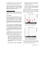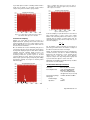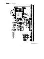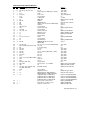
1
August 2005
Rev F
National Semiconductor
Evaluation Board Instruction Manual
ADC12040 12-Bit, 40 Msps, 5 Volt, 380 mW A/D Converter
ADC12010 12-Bit, 10 Msps, 5 Volt, 160 mW A/D Converter
ADC12020 12-Bit, 20 Msps, 5 Volt, 185 mW A/D Converter
ADC12L063 12-Bit, 62 Msps, 3.3 Volt 354 mW A/D Converter
© 2001, 2002, 2003, 2004 National Semiconductor Corporation.
1
http://www.national.com
Table of Contents
1.0 Introduction.............................................................................................................................3
2.0 Board Assembly .....................................................................................................................3
3.0 Quick Start..............................................................................................................................4
4.0 Functional Description............................................................................................................4
4.1 Input (signal conditioning) circuitry ............................................................................4
4.1.1 Single Input ...............................................................................................4
4.1.2 Dual Input ..................................................................................................5
4.2 ADC reference circuitry .............................................................................................5
4.3 ADC clock circuit .......................................................................................................5
4.5 Digital Data Output ....................................................................................................6
4.5 Power Supply Connections .......................................................................................6
4.6 Power Requirements.................................................................................................6
5.0 Installing the ADC12040 Evaluation Board ............................................................................6
6.0 Obtaining Best Results...........................................................................................................6
6.1 Clock Jitter.................................................................................................................6
6.2 Coherent Sampling....................................................................................................7
7.0 Evaluation Board Specifications .............................................................................................8
8.0 Hardware Schematic ..............................................................................................................9
9.0 Evaluation Board Bill of Materials...........................................................................................10
A1.0 Operating in the Computer Mode.........................................................................................12
A2.0 Summary Tables of Test Points and Connectors ................................................................12
2
http://www.national.com
In the Computer mode evaluation is simplified by
connecting the board to the WaveVision Digital Interface
Board (order number WAVEVSN BRD 3.0), which is
connected to a personal computer through a serial
communication port and running WaveVision software,
operating under Microsoft Windows. Or use WAVEVSN
BRD 4.0 when available on National's web site. Use the
WaveVision2 program (WAVEVSN2.EXE) or use
WaveVision 4.0 when available on National's web site.
1.0 Introduction
These Design Kits (each consisting of an Evaluation
Board, National's WaveVision software and this manual)
is designed to ease evaluation and design-in of Nationals
ADC12040, ADC12010, ADC12020, or ADC12L063 12bit Analog-to-Digital Converter, which operate at speeds
up to 40 Msps, 10 Msps, 20 Msps and 62 Msps,
respectively. Further reference in this manual to the
ADC12040 is meant to also include the ADC12010,
ADC12020 and the ADC12L063, unless otherwise
specified or implied. Note that the maximum sample rate
capability of the WaveVision system in the Computer or
Automatic mode is 60 Msps.
The signal at the Analog Input to the board is digitized
and is available at pins B16 through B21 and C16
through C21 of J2. Pins A16 through A21 of J2 are
ground pins.
The WaveVision software can be operated under
Microsoft Windows. The signal at the Analog Input is
digitized and can be captured and displayed on a PC
monitor as a dynamic waveform. The digitized output is
also available at Euro connector J2.
Provision is made for adjustment of the Reference
Voltage, VREF, with VR1.
2.0 Board Assembly
The ADC12040 Evaluation Board may come preassembled or as a bare board that must be assembled.
Refer to the Bill of Materials for a description of
components, to Figure 1 for major component placement
and to Figure 6 for the Evaluation Board schematic.
The software can perform an FFT on the captured data
upon command and, in addition to a frequency domain
plot, shows dynamic performance in the form of SNR,
SINAD, THD and SFDR.
A breadboard area is provided for building customized
circuitry. For best performance, keep circuitry neat and
arrange components to provide short, direct connections.
A prototype area is available for building customized
circuitry.
The evaluation board can be used in either of two modes.
In the Manual mode suitable test equipment can be used
with the board to evaluate the ADC12040 performance.
VR1
Ref. Adj.
TP3
Vin+
JP2
CLK
SELECT
TP4
Vin-
TP10
-V
TP8
+V
JS0 & JS1
Detail
Standard
TP2
DR VD
JS0 JS1
-V
TP10
CLK SEL
JP2
TP1
VREF
RP2
JS3
RP1
L2
VR1
TP20
OE-
U1
TP7
L10
ADC CLK
JP3 & JP4
Detail
J1 Input
Position
VREF
TP1
Vin+
Vin-
TP3
TP4
TP7
ADC CLK
VDO
TP2
POWER CONNECTOR
P1
L3
+V
GND
+5V
-V
Y1
L4
TP6
PWR DWN
+5V
TP9
T1
SIG IN
+V
TP8
L1
TP5
JP3
MIX
D1
L5
P1
Power
JP4
SELECT
JP2
Detail
Default
Position
JS3
Detail
Standard
J3
TP5
SIGNAL
INPUT
J1
J3
Analog
Input
J1
Analog
Input
TP6
PWR
DWN
TP9
+5V
Figure 1. Component and Test Point Locations
3
http://www.national.com
3.0 Quick Start
Note: To develop the ADC clock, the Digital Interface
Board divides its on-board clock. In doing so, jitter is
introduced to the ADC clock which degrades the
observed performance of the ADC12040. See Section
6.0 Obtaining Best Results for an explanation of this
phenomenon and how to avoid it.
Refer to Figure 1 for locations of test points and major
components. For Stand-Alone operation:
1.
2.
3.
Perform steps 2 and 3 of stand alone quick start,,
above.
3.
Use of the crystal oscillator located at Y1 is
recommended to clock the ADC. To do so, connect
the jumper at JP2 to pins 2 and 3. This is the default
position. The ADC clock signal may be monitored at
TP7. Because of clock isolation resistor R12 and the
scope probe capacitance, the clock signal at TP7
will appear integrated.
4.
Install an appropriate crystal into socket Y1. While
the oscillator may be soldered to the board, using a
socket will allow you to easily change clock
frequencies.
Perform steps 5 through 7 of the Stand-Alone quick
start, above.
5.
See the Digital Interface Board Manual for
instructions for setting the ADC clock frequency and
for gathering data.
Connect a clean power supply to Power Connector
P1. Supply +5V at pin 3 of P1 to supply the Digital
Interface board. Supply +3.3V to pin 1 for the
ADC12L063, or +5V to pin 1 for the ADC12010,
ADC12020 and the ADC12040. Pin 2 is ground.
4.0 Functional Description
Use VR1 to set the reference voltage (VREF), which
is 2.0V for the ADC12040, ADC12010, or
ADC12020, or to 1.0V for the ADC12L063. VREF
can be measured at TP1.
4.1 Input (signal conditioning) circuitry
4.
To use the crystal oscillator located at Y1 to clock
the ADC, connect the jumper at JP2 to pins 2 and 3.
This is the default position. The ADC clock signal
may be monitored at TP7. Because of clock
isolation resistor R12 and the scope probe
capacitance, the clock signal at TP7 will appear
integrated.
5.
Connect the jumper at JP3 between pins 1 and 2,
and the jumper at JP4 to pins 1 and 2 to select input
J1 only. This is the default position.
6.
Connect a signal of 1.4 VP-P amplitude for the
ADC12040, ADC12010 or the ADC12020, or 0.7
VP-P for the ADC12L063 from a 50-Ohm source to
Analog Input BNC J1. The ADC input signal can be
observed at TP5. Because of isolation resistor R18
and the scope probe capacitance, the input signal at
TP5 may not have the same frequency response as
the ADC input. Be sure to use a bandpass filter
before the Evaluation Board.
7.
Adjust the input signal amplitude as needed to
ensure that the signals at TP3 and TP4 remains
within the valid signal range of 0V to VREF.
8.
The digitized signal is available at pins B16 through
B21 and C16 through C21 of J2. See board
schematic of Figure 6.
For Computer Mode operation:
NB: Be sure to read section 6.1 before using this
board in the Computer Mode.
1.
2.
Connect the evaluation board to the Digital Interface
Board. See the Digital Interface Board Manual for
operation of that board.
The ADC12040 Evaluation Board schematic is shown in
Figure 6.
The input signal to be digitized should be applied to BNC
connector J1. This 50 Ohm input is intended to accept a
low-noise sine wave signal of 2V peak-to-peak amplitude
for the ADC12040, ADC12010 and ADC12020 or 1V
peak-to-peak for the ADC12L063. To accurately evaluate
the dynamic performance of these converters, the input
test signal will have to be passed through a high-quality
bandpass filter with at least 14-bit equivalent noise and
distortion characteristics.
Signal transformer T1 provides single-ended to
differential conversion. The common mode voltage at the
ADC input is equal to the reference voltage of the ADC.
No scope or other test equipment should be connected to
TP3 or to TP4 while gathering data.
This evaluation board is capable of accommodating a
single input or two different inputs. These inputs are NOT
differential in nature, but are intended to mix two different
signals before presenting them to the ADC.
NOTE: If input frequency components above 30
MHz are required, remove capacitor C7 at the ADC
differential input pins.
4.1.1 Single Input
To evaluate the ADC12040 with a single input, connect
jumpers JP3 and JP4 in their default positions, as shows
in Figure 1. That is, short together pins 1 and 2 of JP3
and of JP4. Doing so provides a 50-Ohm input at J1. No
connection should be made to J3. This configuration is
appropriate for evaluation of dynamic performance
parameters.
4
http://www.national.com
4.1.2 Dual Input
To look at intermodulation performance, moving shorting
jumpers of JP3 and JP4 to pins 2 and 3 of JP3. Connect
different signals to J1 and J3 from 50-Ohm sources.
When looking at the ADC output with two different signals
at the input, the dynamic performance parameters (SNR,
SINAD, THD and SFDR) are meaningless. With two input
signals we are looking for any spurs in the frequency
domain plot (FFT). The simple method used here to mix
two signals is not adequate to completely evaluate IMD of
these converters. Consequently, the actual IMD
performance of the A/D converter is better than would be
indicated by using this method. Most high speed ADCs
exhibit high spurious content under these conditions
unless the total input swing is very low compared with full
scale.
As mentioned in Section 5.0, it is important to use a
bandpass filter at BNC J1 (and BNC J3, if this input is
used) to ensure the quality of the signal presented to the
ADC and to get meaningful test results.
4.2 ADC reference circuitry
An adjustable reference circuit is provided on the board.
The simple circuit here is not temperature stable and is
not recommended for your final design solution. When
using the resistor values shown in Figure 1, the reference
circuit will generate a nominal reference voltage in the
range of 0 to 2.4 Volts for the ADC12040, ADC12010 and
ADC12020 or 0 to 1.2 Volts for the ADC12L063. The
ADC12040, ADC12010 and ADC12020 are specified to
operate with VREF in the range of 1.0 to 2.4 V, with a
nominal value of 2.0V while the ADC12L063 is specified
to operate with VREF in the range of 0.8 to 1.2 V, with a
nominal value of 1.0V. The reference voltage can be
monitored at test point TP1 and is set with VR1.
4.3 ADC clock circuit
The clock signal applied to the ADC is selected with
jumper JP2. A standard crystal oscillator can be installed
at Y1 and selected with jumper JP2 pins 2 and 3 shorted
together. To use a different clock source, connect the
signal to pin B23 of J2 and select pins 1 and 2 of jumper
JP2. The ADC clock frequency can be monitored at test
point TP7. R13 and C13 are used for high frequency
termination of the clock line. In the Computer mode of
operation using the Digital Interface Board, JP2 can have
pins 1 and 2 shorted together to use the clock from the
Digital Interface Board, but this is not recommended, as
discussed in Section 6.1.
Note that any external clock source must have
TTL/CMOS levels. Also, if using the Digital Interface
Board from National Semiconductor to capture data, the
oscillator at Y1 should be removed, the external clock
signal supplied at pin 3 of that socket and pins 2 and 3 of
JP2 should be selected. Additionally, the clock frequency
must be the same as that provided from the Digital
Interface Board.
See Section 6.1 for information on capturing data with a
clock that is not synchronized to the clock of the Digital
Interface Board.
4.5 Digital Data Output
The digital output data from the ADC12040 is available at
the 96-pin Euro connector J2. Series resistors RP1 and
RP2 isolate the ADC from the load circuit to reduce noise
coupling into the ADC.
4.5 Power Supply Connections
Power to this board is supplied through power connector
P1. The only supply needed is +5V at pin 1 for the
ADC12040, ADC12010 or the ADC12020, or +3.3V at pin
1 for the ADC12L063, plus ground at pin 2 for either. Any
circuitry you breadboard may need a negative voltage at
the -V supply pin 4.
When using the ADC12040 Evaluation Board with the
Digital Interface Board, a 5V logic power supply for the
interface board is needed at pin 3 of P1. This supply
voltage is passed through J2 to the Digital Interface
Board.
The supply voltages are protected by shunt diodes and
can be measured at TP8, TP9 and TP10. If a
breadboarded circuit requires voltages greater than 5V,
they will have to be separately provided by the user.
4.6 Power Requirements
Voltage and current requirements for the ADC12040
Evaluation Board mode are:
For the ADC12040, ADC12010 and the ADC12020:
• +5.0V at 100 mA [+V]
• +5.0V at 30 mA (1A when connected to the Digital
Interface Board) [+5V].
For the ADC12L063:
• +3.3V at 120 mA [+V]
• +5.0V at 30 mA (1A when connected to the Digital
Interface Board) [+5V].
There is no need for a negative supply for either ADC,
unless it may be needed for the breadboard area.
5.0 Installing the ADC12040 Evaluation Board
The evaluation board requires power supplies as
described in Section 4.6. An appropriate signal source
should be connected to the Analog Input BNC J1. When
evaluating dynamic performance, an appropriate signal
generator (such as the HP8644B, HP8662A or the R&S
SME-03) with 50 Ohm source impedance should be
connected to the Analog Input BNC J1 and/or J3 through
5
http://www.national.com
an appropriate bandpass filter as even the best signal
generator available can not produce a signal pure enough
to evaluate the dynamic performance of an ADC.
If this board is used in conjunction with the Digital
Interface Board and WaveVision software, a cable with a
DB-9 connector must be connected between the Digital
Interface Board and the host computer when using
WAVEVSN BRD 3.0 Digital Interface Board. See the
Digital Interface Board manual for details.
6.0 Obtaining Best Results
Obtaining the best results with any ADC requires both
good circuit techniques and a good PC board layout. The
layout is taken care of with the design of this evaluation
board.
ADC12010 evaluation board, a 20 MHz oscillator for
the ADC12020 evaluation board, or a 60 MHz on the
ADC12L063 evaluation board).
3.
Connect the jumper at JP2 to pins 2 and 3 (default
position). This selects the crystal oscillator located
at Y1 on the evaluation board (rather than the
divided oscillator signal on the Digital Interface
Board) to clock the ADC.
Because the divided signal from the Digital Interface
Board and the oscillator at Y1 are not synchronized, bad
data will sometimes be taken because we are latching
data when the outputs are in transition. This data might
be as you see in Figure 3 or Figure 4.
6.1 Clock Jitter
When any circuitry is added after a signal source, some
jitter is almost always added to that signal. Jitter in a
clock signal, depending upon how bad it is, can degrade
dynamic performance. We can see the effects of jitter in
the frequency domain (FFT) as "leakage" or "spreading"
around the input frequency, as seen in Figure 2a.
Compare this with the more desirable plot of Figure 2b.
Note that all dynamic performance parameters (shown to
the right of the FFT) are improved by eliminating clock
jitter.
To develop the ADC clock, WAVEVISON BRD 3.0 Digital
Interface Board divides its on-board clock to provide the
ADC clock. In doing so, jitter is introduced to the ADC
clock, degrading the observed performance of the ADC.
The amount of jitter produced by this evaluation system
is acceptable for relatively low input frequencies (below
about 5 MHz). But at higher frequencies and resolutions
this jitter can make it appear as though the ADC does not
perform well.
Figure 2a. Jitter causes a spreading around the
input signal, as well as undesirable signal spurs.
For many applications the results seen will be completely
acceptable. However, if it is desired to observe the best
results possible from the ADC, you should not use the
Digital Interface Board to capture data OR you should do
the following when using the Digital Interface Board:
1.
2.
Use an 80 MHz oscillator on the Digital Interface
Board (120 MHz for the ADC12L063) with the DIP
switches on that board set to divide the oscillator
frequency by the appropriate amount. See the
Digital Interface Board manual for details on setting
the divide ratio. The goal here is to have the divided
clock from the Digital Interface Board be the same
frequency as the oscillator on the ADC12040
Evaluation Board.
Use a 40 MHz oscillator on the ADC12040
evaluation board, a 10 MHz oscillator for the
Figure 2b. Eliminating or minimizing clock jitter
results in a more desirable FFT that is more
representative of how the ADC actually performs.
The problem of Figure 3 is obvious, but it is not as easy
to see the problem in Figure 4, where the only thing we
see is small excursions beyond the normal envelope.
Compare Figure 3 and Figure 4 with Figure 5.
6
http://www.national.com
If your data capture results in something similar to what is
shown here in Figure 3 or in Figure 4, take another
sample. It may take a few trials to get good data.
Figure 4 Marginal data capture that results from trying to
capture data that is near but not right at the point where the
ADC outputs are in transition.
Figure 5. Normal data capture.
Figure 3. Poor data capture resulting from trying to capture
data while the ADC outputs are in transition
6.2 Coherent Sampling
Artifacts can result when we perform an FFT on a
digitized waveform, producing inconsistent results when
testing repeatedly. The presence of these artifacts means
that the ADC under test may perform better than the
measurements would indicate.
We can eliminate the need for windowing and get more
consistent results if we observe the proper ratios between
the input and sampling frequencies. We call this coherent
sampling. Coherent sampling greatly increases the
spectral resolution of the FFT, allowing us to more
accurately evaluate the spectral response of the A/D
converter. When we do this, however, we must be sure
that the input signal has high spectral purity and stability
and that the sampling clock signal is extremely stable
with minimal jitter.
Coherent sampling of a periodic waveform occurs when a
prime integer number of cycles exists in the sample
window. The relationship between the number of cycles
sampled (CY), the number of samples taken (SS), the
signal input frequency (fin) and the sample rate (fs), for
coherent sampling, is
CY fin
SS = fs
CY, the number of cycles in the data record, must be a
prime integer number and SS, the number of samples in
the data record, must be a factor of 2 integer.
Further, fin (signal input frequency) and fs (sampling rate)
should be locked to each other so that the relationship
between the two frequencies is exact. Locking the two
signal sources to each other also causes whatever
sample-to-sample clock edge timing variation (jitter) that
is present in the two signals to cancel each other.
Windowing (an FFT Option under WaveVision) should be
turned off for coherent sampling.
7.0 Evaluation Board Specifications
Board Size:
Power Requirements:
Clock Frequency Range:
Analog Input
Nominal Voltage:
Impedance:
7
6.5" x 3.5" (16.5 cm x 8.9 cm)
+5.0V, 100 mA (ADC12040 /
ADC12010 / ADC12020) or
+3.3V, 120 mA (ADC12L063)
+5V @ 30 mA / 1A (see Sect 4.6)
1.0 MHz to 40 MHz or 60 MHz
1.4VP-P
50 Ohms
http://www.national.com
8
+V
4
3
2
1
-V
Power
Connector
-V
+5V
GND
P1
+V
L5
CHOKE
L4
CHOKE
L3
CHOKE
+
C16
33uF
C14
33uF
C18
D4
+ 33uF
1N4001
D3
1N4001
D2
1N4001
+
+V
+5V
-V
TP10
-V
+5V
TP9
+5V
TP8
+V
J1
INPUT
INPUT
[not used]
J3
D5
LM4050AEM3 -2.5 (ADC12010/020/040)
LM4041BIZ1-1.2 (ADC12L063/L066)
Values in parentheses for R7,
R8 and C7 at ADC input are
for ADC12010/12020
R3
330
[hard 1 2 3
wired]
R24
51
JP3
MIX
R22
68
[not
used]
R23
100
[not used]
VR1
1k
2
1
3
4
3
1
2
R17
47
+5VA
3 2 1
C15A
R15 D15
10k 1N4148
C15
0.1uF
JS1
JS2
R20
100k
R14
330
λ
1
2
3
4
5
6
7
8
+V
L1
CHOKE
C2 +5VA
0.1uF
C4
0.1uF
C5
0.1uF
VREF
VIN+
VINAGND
VA
VA
AGND
PD
C13
22pF
R13
200
E1
OutEn
(Not Used)
Q2
MMBT2222A
+5V
R11
10K
TP4
Vin-
D1
RED LED
TP6
PWR DWN
C10
1uF
R8
33 (47pF)
R10
not used
R9
200
R6
47
TP3
Vin+
C7
22pF
(330pF)
R7
33 (47pF)
JP2
CLK SELECT
R12
470
C17
0.1uF
R16
1K
+5V
R16 not used
for ADC12L066
OSC
Y1
TP7
ADC CLK
6
4
C6
1uF
C11
1uF
T1
C8
0.1uF
R18
100
TP5
SIG IN
C3
1uF
R5
100
JP4
IN SELECT
[hard wired]
3
2
1
R25
100
[not
used]
D11
(not used)
D10
(not used)
R4
0Ω
TP1
VREF
C1
1uF
R1
330
Q1
MMBT2222A
R21
1k
TP20
OE
L10
CHOKE
C12
1uF
+V
D3
D7
ADC12010
D6
ADC12020
DR VD
ADC12040
DR GND
or
D5
ADC12L063
D4
D8
U2
24
23
22
21
20
19
18
17
JS3
VDR Select
VRM 32
VRP 31
VRN 30
VA 29
AGND 28
D11 27
D10 26
D9 25
9 DGND
10 CLK
11 OE
12 DGND
13 V
D
14 D0
15 D1
16 D2
+V
D6
1N5227 (3.6V)
C9
1uF
L2
CHOKE
RP1
8x47 Ohms
RP2
8x47 Ohms
TP2
VDO
D0
D1
D2
D3
D4
D5
D6
D7
D8
D9
D10
D11
Figure 6. ADC 12040 Evaluation Board Schematic
A1
B1
C1
A2
B2
C2
A3
B3
C3
A4
B4
C4
A5
B5
C5
A6
B6
C6
A7
B7
C7
A8
B8
C8
A9
B9
C9
A10
B10
C10
A11
B11
C11
A12
B12
C12
A13
B13
C13
A14
B14
C14
A15
B15
C15
A16
B16
C16
A17
B17
C17
A18
B18
C18
A19
B19
C19
A20
B20
C20
A21
B21
C21
A22
B22
C22
A23
B23
C23
A24
B24
C24
A25
B25
C25
A26
B26
C26
A27
B27
C27
A28
B28
C28
A29
B29
C29
A30
B30
C30
A31
B31
C31
A32
B32
C32
J2
96 PIN FEMALE EURO (DIN) CONNECTOR
8.0 Hardware Schematic
http://www.national.com
9.0 Evaluation Board Bill of Materials
Item Qty
1
7
2
6
3
1
4
1
5
2
6
7
8
1
9
2
10
1
11
1
12
1
13
14
1
15
16
3
17
1
18
1
19
20
5
21
22
2
23
2
24
25
26
27
28
29
30
31
32
33
34
35
36
37
38
39
3
1
2
2
2
2
2
1
1
1
1
2
1
1
40
41
42
1
1
43
1
44
45
46
1
1
2
Reference
C1, C3, C6, C9, C10, C11, C12
C2, C4, C5, C8, C15, C17
C7
C13
C14, C16
C18
C15A
D1
D2, D3
D5
D6
D15
D4, D10, D11
JP2
JP3, JP4
JS1, JS2, JS3
J1
J2
J3
L1, L2, L3, L4, L10
L5
P1
Q1, Q2
Part
1 uF
0.1 uF
22 pF (330 pF for ADC12010 / 12020)
22 pF
33 uF, 6.3V
not populated
is diode D15
RED LED
1N4001
LM4041BIZ-2.5
1N5227 (Not used for the ADC12L063)
1N4148
not populated
3-Pin Post Header
not populated
2-Pin Post Header
BNC Connector
96-Pin Female
not populated
Choke
not populated
Terminal Block
MMBT2222A (Q1 not used for
ADC12L063)
R1, R3, R14
330, 5% (R1 not used for ADC12L063)
R2, R10, R19 (R2 & R19 no exist) not used
R4
0 (shorting strap)
R5, R18
100, 5%
R6, R17
47, 5%
R7, R8
33, 5% (47Ω for ADC12010 / 12020)
R9, R13
200, 5%
R11, R15
10k, 5%
R12
470, 5%
R16 (not used on ADC12L063) 1K, 5%
R20
100k, 5%
R21
1K, 5%
R22, R23, R24, R25
not populated
RP1, RP2
Resistor Pack - 8 x 47 Ohms
VR1
1K
TP1, TP2, TP3, TP4, TP5, TP6,
Breakable Header
TP7, TP8, TP9, TP20
TP10
not populated
T1
Signal Transformer
U1
ADC12010CIVY, ADC12020CIVY,
ADC12040CIVY or ADC12L063CIVY
Y1
10 MHz Oscillator for ADC12010
20 MHz Oscillator for ADC12020
40 MHz Oscillator for ADC12040
60 MHz Oscillator for ADC12L063
6-pin Socket for Transformer
-4-Pin full-size oscillator socket
--Jumpers for JP2 & JS3
9
Source
Type 1206
Type 1206
Type 1206
Type 1206
Type 7343 (D Size)
n/a
see D15
DigiKey # 160-1124-ND
Various
National Semiconductor
Various
Various
n/a
DigiKey # A19351-ND
n/a
DigiKey # A19350-ND
DigiKey # ARF1177-ND
DigiKey # H7096-ND
n/a
DigiKey # M2304-ND
n/a
DigiKey # ED1609-ND
Various
Type 1206
n/a
n/a
Type 1206
Type 1206
Type 1206
Type 1206
Type 1206
Type 1206
Type 1206
Type 1206
Type 1206
n/a
DigiKey # 767-163-R47-ND
DigiKey # 3386P-102-ND
DigiKey # S1012-36-ND
n/a
MiniCircuits type T4-6T
National Semiconductor
Pletronics #P1145-3SD-10.0M
Pletronics #P1145-3SD-20.0M
Pletronics #P1145-3SD-40.00M
Pletronics #P1145-3SD-60.0M or
DigiKey # AE8906-ND
DigiKey # A462-ND
DigiKey # S9001-ND
http://www.national.com
APPENDIX
A1.0 Operating in the Computer Mode
The ADC12040 Evaluation Board is compatible with the WaveVision Digital Interface Board and WaveVision software.
When connected to the Digital Interface Board, data capture is easily controlled from a personal computer operating in
the Windows environment. The data samples that are captured can be observed on the PC video monitor in the time and
frequency domains. The FFT analysis of the captured data yields insight into system noise and distortion sources and
estimates of ADC dynamic performance such as SINAD, SNR and THD.
See the Digital Interface Board manual for more information.
A2.0 Summary Tables of Test Points and Connectors
Test Points on the ADC12040 Evaluation Board
TP 1
ADC Reference Voltage
TP 2
ADC output driver supply voltage
TP 3
Positive input signal to the ADC (Vin+)
TP 4
Negative input signal to the ADC (Vin-)
TP 5
Signal Input test point
TP 6
Power Down (active high) input
TP 7
ADC clock frequency monitor
TP 8
+5V power supply for ADC12040 / 12010 / 12020 or +3.3V for ADC12L063
TP 9
+5V power supply for the Digital Interface Board, if used
TP 10
Optional negative power supply for breadboard area
TP 20
Output Enable input. Pull high to disable the outputs
P1 Connector - Power Supply Connections
J1-1
+V
Positive Power Supply (+5V for ADC12040/12010/12020 or +3.3V for ADC12L063)
J1-2
GND
Power Supply Ground
J1-3
+5V
+5.0V Logic Power Supply for Digital Interface Board
J1-4
-V
Optional Negative Power Supply for Breadboard Area
JP2 Jumper - ADC Clock selection jumper settings
Connect 1-2
Use Clock signal from J2 pin B23
Connect 2-3
Use crystal oscillator Y1
JP3 Jumper - ADC Input Select
Connect 1-2
Use single J1 Input
Connect 2-3
Mix J1 & J3 Inputs (must also have JP4 pins 1 & 2 shorted)
10
http://www.national.com
JP4 Jumper - ADC Input Select
Connect 1-2
Select input J1 only
Connect 2-3
Select mixed J1 & J3 Inputs (must also have JP3 pins 2 & 3 shorted)
J2 Connector - ADC Data Outputs - Connection to WaveVision Digital Interface Board
Signal
J2 pin number
ADC output D0
B16
ADC output D1
C16
ADC output D2
B17
ADC output D3
C17
ADC output D4
B18
ADC output D5
C18
ADC output D6
B19
ADC output D7
C19
ADC output D8
B20
ADC output D9
C20
ADC output D10
B21
ADC output D11
C21
GND
A1 thru A24, A28, B28, C28, A31, B31, C31
ADC Output Enable
C12 (not used)
External clock input
B23
Reserved, signal
B22, C22, C23
Reserved, power
A25, A26, B25, B26, C25, C26
(+5V Logic Power Supply to Digital Interface Board )
Reserved, power
A29, B29, C29
Reserved, power
A32, B32, C32
11
http://www.national.com
BY USING THIS PRODUCT, YOU ARE AGREEING TO BE BOUND BY THE TERMS AND CONDITIONS OF
NATIONAL SEMICONDUCTOR'S END USER LICENSE AGREEMENT. DO NOT USE THIS PRODUCT UNTIL YOU
HAVE READ AND AGREED TO THE TERMS AND CONDITIONS OF THAT AGREEMENT. IF YOU DO NOT AGREE
WITH THEM, CONTACT THE VENDOR WITHIN TEN (10) DAYS OF RECEIPT FOR INSTRUCTIONS ON RETURN OF
THE UNUSED PRODUCT FOR A REFUND OF THE PURCHASE PRICE PAID, IF ANY.
The ADC12040/ADC12010/ADC12020/ADC12L063 Evaluation Boards are intended for product evaluation purposes only
and are not intended for resale to end consumers, is not authorized for such use and is not designed for compliance with
European EMC Directive 89/336/EEC, or for compliance with any other electromagnetic compatibility requirements.
National Semiconductor Corporation does not assume any responsibility for use of any circuitry or software supplied or
described. No circuit patent licenses are implied.
LIFE SUPPORT POLICY
NATIONAL'S PRODUCTS ARE NOT AUTHORIZED FOR USE AS CRITICAL COMPONENTS IN LIFE SUPPORT
DEVICES OR SYSTEMS WITHOUT THE EXPRESS WRITTEN APPROVAL OF THE PRESIDENT OF NATIONAL
SEMICONDUCTOR CORPORATION. As used herein:
1. Life support devices or systems are devices or
systems which, (a) are intended for surgical implant
into the body, or (b) support or sustain life, and
whose failure to perform, when properly used in
accordance with instructions for use provided in the
labeling, can be reasonably expected to result in a
significant injury to the user.
National Semiconductor Corporation
Americas
Tel:
1-800-272-9959
Fax: 1-800-737-7018
Email: [email protected]
2. A critical component is any component in a life
support device or system whose failure to perform
can be reasonably expected to cause the failure of
the life support device or system, or to affect its
safety or effectiveness.
National Semiconductor Europe
Fax: +49 (0) 1 80-530 85 86
Email: [email protected]
Deutsch Tel: +49 (0) 699508 6208
English Tel: +49 (0) 870 24 0 2171
Français Tel: +49 (0) 141 91 8790
National Semiconductor
Asia Pacific Customer
Response Group
Tel: 65-2544466
Fax: 65-2504466
Email:[email protected]
National Semiconductor
Japan Ltd.
Tel: 81-3-5639-7560
Fax: 81-3-5639-7507
www.national.com
National does not assume any responsibility for any circuitry described, no circuit patent licenses are implied and National reserves the right
at any time without notice to change said circuitry and specifications.
12
http://www.national.com