1
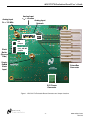
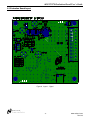
Evaluation Board User’s Guide for
ADC12V170: 12-Bit, 170 MSPS Analog to Digital Converter
with LVDS Outputs
N
www.national.com
Rev 0.0
October 2007
ADC12V170 Evaluation Board User’s Guide
Analog Input
FIN > 150 MHz
Analog Input
FIN < 150 MHz
Analog Input
Network
ADC
PD
Jumper
Clock
Buffer
(Reverse
Side)
CLK_SEL/DF
Jumper
SingleEnded
Clock
Input
FutureBus
Connector
5.0V Power
Connector
Figure 1. ADC12V170 Evaluation Board Connector and Jumper Locations
N
-2-
www.national.com
Rev 0.0
ADC12V170 Evaluation Board User’s Guide
1.0 Introduction
The ADC12V170 Evaluation Board is designed to
support the ADC12V170 12-bit 170 Mega Sample Per
Second (MSPS) Analog to Digital Converter with LVDS
Outputs.
The ADC12V170 Evaluation Board comes in two
versions:
1. ADC12V170HFEB (high frequency version)
for input frequencies greater than 150 MHz.
2. ADC12V170LFEB (low frequency version) for
input frequencies less than 150 MHz.
The digital data from the ADC12V170 evaluation board
can be captured with a suitable instrument, such as a
logic analyzer, or with National Semiconductor’s
WaveVision signal path data acquisition hardware and
software platform. The ADC12V170 evaluation board
can be connected to the data acquisition hardware
through the FutureBus connector (schematic reference
designator FB).
The ADC12V170 is compatible with National
Semiconductor’s WaveVision 5.1 and higher Signal
Path Digital Interface Board and associated
WaveVision software.
Please note that the
ADC12V170 board is not compatible with previous
versions of the WaveVision hardware (WaveVision 4.x
Digital Interface Boards).
The WaveVision hardware and software package
allows fast and easy data acquisition and analysis. The
WaveVision hardware connects to a host PC via a USB
cable and is fully configured and controlled by the latest
WaveVision software.
The latest version of the
WaveVision software is included in this evaluation kit
on a CD-ROM. The WaveVision 5.1 Signal Path Digital
Interface hardware is available through the National
Semiconductor website (part number: WAVEVSN 5.1).
2.0 Board Assembly
Each evaluation board from the factory is configured for
single-ended clock operation and is populated with an
analog input network which has been optimized for one
of two analog input frequencies ranges:
The location and description of the components on the
ADC12V170 evaluation board can be found in Figure 1
as well as Section 5.0 (Schematic) and Section 7.0 (Bill
of Materials) of this user’s guide.
3.0 Quick Start
The ADC12V170 evaluation board enables easy set up
for evaluating the performance of the ADC12V170.
If the WaveVision data acquisition and data analysis
system is to be used for capturing data, please follow
the Quick Start Guide in the WaveVision User’s Guide
to install the required software and to connect the
WaveVision Digital Interface Board to the PC and to
the ADC12V170 evaluation board. Please note that the
ADC12V170 evaluation board is only compatible with
National Semiconductor’s WaveVision 5.1 and higher
Signal Path Digital Interface boards.
3.1 Evaluation Board Jumper Positions
The ADC12V170 evaluation board jumpers should be
configured as follows. Please refer to Figure 1 for the
exact jumper locations.
1. J1 on the reverse of the board should be shorted.
2. The PD jumper places the ADC12V170 into either
powerdown or sleep mode. Table 1 below shows
how to select between the power modes.
PD Jumper
Setting
Open
1-2
3-4
Mode
Normal Operation
Power-down
Sleep
Table 1. CLK_SEL/DF Selection Table
3. CLK_SEL/DF pin jumpers select the output data
format (2’s complement or offset binary) and clock
mode (single-ended or differential). Table 2 below
shows how to select between the clock modes and
output data formats.
Please note that the
ADC12V170 evaluation board is delivered with the
ADC12V170 clock input configured for singleended operation and Offset Binary output data
format (Jumper 7-8).
CLK_SEL/DF
Jumper
Setting
1-2
3-4
5-6
7-8*
1. ADC12V170HFEB (high frequency version)
for input frequencies greater than 150 MHz.
2. ADC12V170LFEB (low frequency version) for
input frequencies less than 150 MHz.
Clock Mode
Output Data
Format
Differential
Differential
Single-Ended
Single-Ended
2’s Complement
Offset Binary
2’s Complement
Offset Binary
* As assembled from factory.
Please refer to the input circuit configurations
described in the Analog Input Section (4.2) of this
guide.
N
Table 2. CLK_SEL/DF Selection Table
-3-
www.national.com
Rev 0.0
ADC12V170 Evaluation Board User’s Guide
3.2 Connecting Power and Signal Sources
1. To power the ADC12V170 evaluation board,
connect a 5.0V power supply capable of supplying
up to 500mA to the green power connector labeled
“+5V” which is located along the bottom edge of
the ADC12V170 evaluation board.
2. Use the FutureBus connector (FB) to connect the
ADC12V170 evaluation board to the instrument
being used to capture the data from the evaluation
board. If the WaveVision Digital Interface Board is
being used for data capture, please consult the
WaveVision User’s Guide for details on installing
and operating the WaveVision hardware and
software system.
3. Connect the clock and signal inputs to the
CLK_IN_SE and AIN_XX (where XX = HF or LF)
SMA connectors.
4.0 Functional Description
4.1 Clock Input
The clock used to sample the analog input should be
applied to the CLK_IN_SE SMA connector (if using the
single-ended clock mode).
To achieve the best noise performance (best SNR), a
low jitter clock source with total additive jitter less than
150 fs should be used. A low jitter crystal oscillator is
recommended, but a sinusoidal signal generator with
low phase noise, such as the SMA100A from Rohde &
Schwarz or the HP8644B (discontinued) from Agilent /
Hewlett Packard, can also be used with a slight
degradation in the noise performance. When using a
low phase noise clock source, the SNR is primarily
degraded by the broadband noise of the signal
generator. The clock signal generator amplitude is
typically set to +19.9 dBm to produce the highest
possible slew rate, but the SNR performance will be
impacted minimally by lowering the signal generator
amplitude slightly. Placing a bandpass filter between
the clock source and the CLK_IN_SE SMA connector
will further improve the noise performance of the ADC
N
by filtering out the broadband noise of the clock source.
All results in the ADC12V170 datasheet are obtained
with a tunable bandpass filter made by Trilithic, Inc. in
the clock signal path.
The noise performance of the ADC12V170 can be
improved further by making the edge transitions of the
clock signal entering the ADC clock input (pin 11,
CLK+) very sharp. The ADC12V170 evaluation board
is assembled with a high speed buffer gate
(NC7WV125K8X, schematic reference designator U2)
in the clock input path to provide a sharp clock edge to
the clock inputs and improve the noise performance of
the ADC. The amplitude of the clock signal from the
NC7WV125K8X high speed buffer is 3.3V.
4.2 Analog Input
To obtain the best distortion results (best SFDR), the
analog input network on the evaluation board must be
optimized for the signal frequency being applied.
For analog input frequencies up to 150 MHz, the circuit
in Figure 2 is recommended. This is the configuration
of the assembled ADC12V170LFEB as it is delivered
from the factory. For input frequencies above 150
MHz, the circuit in Figure 3 is recommended. This is
the configuration of the assembled ADC12V170HFEB
as it is delivered from the factory.
A low noise signal generator such as the HP8644B is
recommended to drive the signal input of the
ADC12V170 evaluation board. The output of the signal
generator must be filtered to suppress the harmonic
distortion produced by the signal generator and to allow
accurate measurement of the ADC12V170 distortion
performance. A low pass or a bandpass filter is
recommended to filter the analog input signal. In some
cases, a second low pass filter may be necessary. The
bandpass filter on the analog input will further improve
the noise performance of the ADC by filtering the
broadband noise of the signal generator. Data shown
in the ADC12V170 datasheet was taken with a tunable
bandpass filter made by Trilithic in the analog signal
path.
-4-
www.national.com
Rev 0.0
ADC12V170 Evaluation Board User’s Guide
Figure 2. Analog Input Network of ADC12V170LFEB: FIN < 150 MHz
Figure 3. Analog Input Network of ADC12V170HFEB: FIN > 150 MHz
4.3 ADC Reference and Input Common Mode
The internal 1.0V reference on the ADC12V170 is used
to acquire all of the results in the ADC12V170
datasheet. It is recommended to use the internal
reference on the ADC12V170. However, if an external
reference is required, the ADC12V170 is capable of
accepting an external reference voltage between 0.9V
and 1.1V (1.0V recommended). The input impedance
of the ADC12V170 VREF pin (pin 46) is 9 kΩ.
Therefore, to overdrive this pin, the output impedance
of the exernal reference source should be << 9 kΩ.
It is recommended to use the voltage at the VRM pin
(pin 45) of the ADC12V170 to provide the 1.5V
common mode voltage required for the differential
analog inputs VIN+ and VIN-.
The ADC12V170
evaluation board is factory-assembled with VRM
connected to the transformer center-tap through a
N
49.9Ω resistor to provide the necessary common mode
voltage to the differential analog input.
4.4 Board Outputs
The digitized 12-bit output word from the ADC12V170
evaluation board is presented in interleaved double
data rate (DDR) format. The digital output lines from
the ADC12V170 evaluation board consist of 16 lines
which are arranged into 8 LVDS pairs. These 8 pairs
of lines carry the 12-bit output data (6 pairs), the DRDY
signal which should be used to capture the output data
(1 pair) and the over-range bit (OVR) which indicates
that the digital output has exceeded the maximum
digitizable signal (1 pair).
Since the data is presented in interleaved double data
rate (DDR) format, the 12-bit word is output on 6 data
pair lines with half of the data (odd bits: D1+/-, D3+/-,
-5-
www.national.com
Rev 0.0
ADC12V170 Evaluation Board User’s Guide
…, D11+/-) being emitted with one clock edge during
the first half of the clock period and the other half of the
data (even bits: D0+/-, D2+/-, …, D10+/-) being emitted
with the opposite clock edge during the second half of
the clock period. The odd data bits should be captured
with the falling edge of DRDY and the rising edge of
DRDY should be used to capture the even bits of the
data.
DRDY signal which is used to capture the data is also
in LVDS format and it is available at pins A4/D4
(DRDY+/-) on the FutureBus connector. The overrange bit (OVR) LVDS signal is available on pins
D22/D21 (OVR+/-) on the FutureBus connector.
The data is available on the evaluation board at pins
A5/B5 (MSB +/-) through A10/B10 (LSB +/-) of the
FutureBus connector (schematic reference designator
FB). Please keep in mind that because the data is in
DDR format, pins A5/B5 will carry data bit D11+/during the first half of the clock period and these lines
will carry bit D10+/- during the second half of the clock
period. Similarly, pins A10/B10 will carry D1+/- during
the first half of the clock period and these pins will carry
D0+/- during the second half of the clock period. The
4.5 Power requirements.
N
Please see the Evaluation Board schematic in Section
5.0 and the ADC12V170 datasheet for further details.
Power to the ADC12V170 evaluation board is supplied
through the green power connector labeled “+5V”
which is located along the bottom edge of the board.
Voltage and current requirements are:
• +5V capable of providing up to 500mA (ADC12V170
evaluation board only)
-6-
www.national.com
Rev 0.0
ADC12V170 Evaluation Board User’s Guide
5.0 Evaluation Board Schematic
Figure 4. Signals
N
-7-
www.national.com
Rev 0.0
ADC12V170 Evaluation Board User’s Guide
5.0 Schematic (cont.)
Figure 5. Power Distribution
N
-8-
www.national.com
Rev 0.0
ADC12V170 Evaluation Board User’s Guide
6.0 Evaluation Board Layout
Figure 6. Layer 1 - Signal
N
-9-
www.national.com
Rev 0.0
ADC12V170 Evaluation Board User’s Guide
6.0 Evaluation Board Layout (cont.)
Figure 7. Layer 2 - Ground
N
- 10 -
www.national.com
Rev 0.0
ADC12V170 Evaluation Board User’s Guide
6.0 Evaluation Board Layout (cont.)
Figure 8. Layer 3 - Power
N
- 11 -
www.national.com
Rev 0.0
ADC12V170 Evaluation Board User’s Guide
6.0 Evaluation Board Layout (cont.)
Figure 9. Layer 4 - Signal
N
- 12 -
www.national.com
Rev 0.0
Z1-3, Z6
R17, R19
R1-7, R12-13
R14-15
R26-27
R10, R24-25
AIN_HF,
CLK_IN_SE
sm/c_0201
sm/c_1206
Manufacturer
Atmel
National Semiconductor
MA/COM
AMP
Panasonic - ECG
Panasonic - ECG
0.1uF
0.1uF SMD CAP CERAMIC 10V X5R 10%
sm/c_0402
Panasonic - ECG
0.01uF
0.01uF SMD CAP CERAMIC 16V X7R 10%
sm/c_0402
AVX Corporation
10uF
2pF
1uF
10uF
10uF SMD CAP CERAMIC 10V X5R 20%
2pF SMD CAP CERAMIC 50v +/-0.25pF
1uF SMD CAP CERAMIC 25V X7R 10%
10uF SMD CAP TANTALUM 6.3V 20%
sm/c_1206
sm/c_0402
sm/c_1206
sm/c_3216
Panasonic - ECG
Murata Electronics
Panasonic - ECG
Kemet
2.2uF
68uF
Ferrite Bead Core
Jumper 1x8
Jumper 2X2
Jumper 2X4
Shunt
3.3V Regulator
1.8V Regulator
Power Connector Terminal Block
Power Connector Plug
Bump-on Rubber Feet
Tinylogic Buffer
Kemet
2.2uF SMD CAP TANTALUM 16V 10%
sm/c_3216
Kemet
68uF SMD CAP TANTALUM 6.3V 10%
sm/c_7343
Panasonic -ECG
SMD FERRITE BEAD CORE 4.5X3.2X1.8
Samtec
JUMPER BLOCK USING 8 PIN SIP HEADER
Samtec
2X2 JUMPER BLOCK HEADER CUT TO SIZE FROM 2X6 HEADER
Samtec
2X4 JUMPER BLOCK HEADER CUT TO SIZE FROM 2X6 HEADER
FCI Electronic
PLACE SHUNT ACROSS PINS 7-8 ON CLK_SEL/DF JUMPER
National Semiconductor
1A LOW DROPOUT REGULATOR FOR 5V TO 3.3 V CONVERSION
SOT-223
MICROPOWER/LOW NOISE, 500 mA ULTRA LOW-DROPOUT REGULATOR
SOIC NARROW -8 National Semiconductor
Phoenix Contact
TERMINAL BLOCK 2POS 5.08mm
Phoenix Contact
TERMINAL BLOCK PLUG 2POS 5.08mm
3M
PLACE BUMP ONS AT THE 4 CORNERS, ON BOTTOM OF BOARD
Fairchild Semiconductor
TINYLOGIC ULP-A BUFFER WITH 3-STATE OUTPUT
8-LEAD US8, JEDEC MO-187, CA 3.1 mm WIDE
Murata Electronics
FILTER LC HIGH FREQ .2UF
1806
Vishay Dale
0 OHM SMD RESISTOR
sm/r_0402
Panasonic - ECG
1 kOHM SMD RESISTOR 1/16W 1%
sm/r_0402
Yageo Corporation
24.9 OHM SMD RESISTOR 1/16W 1%
sm/r_0402
Vishay Dale
33.2 OHM SMD RESISTOR 1/16W 1%
sm/r_0402
Yageo Corporation
49.9 OHM SMD RESISTOR 1/16W 1%
sm/r_0402
Emerson Network Power Connectivity
PCB MOUNTABLE SMA CONNECTOR
-
Noise Suppression Filter
0 ohms
1 kOHM
24.9 ohms
33.2 ohms
49.9 ohms
SMA Input
PCB Footprint
SOIC-8
48-LLP
www.national.com
Rev 0.0
ADC12V170 Evaluation Board User’s Guide
4
2
9
2
2
3
2
Description
2K SERIAL EEPROM 1.8V
12-Bit, 170 MSPS Analog/Digital Converter with LVDS Outputs
BALUN TRANSFORMER
Z-PACK 2mm FB (Futurebus+) RIGHT ANGLE HEADER CONNECTOR
0.1uF SMD CAP CERAMIC 6.3V X5R 10%
0.1uF SMD CAP CERAMIC 25V X7R 10%
7.0 Evaluation Board Bill of Materials
- 13 -
26
27
28
29
30
31
32
Part Name
24C02
ADC12V170
ETC1-1-13
AMP_5223514-1
0.1uF
0.1uF
7.1 ADC12V170HFEB (For Fin > 150 MHz)
N
Item Quantity Schematic Reference
1
1
U6
2
1
ADC
3
2
T6, T10
4
4
FB
5
1
C75
6
6
C2, C14, C20, C22,
C24, C66
7
21
C9, C15
C26, C27, C29, C31, C33,
C35, C37, C39, C41,
C43, C45, C47, C49-51,
C53, C59, C71, C72
8
12
C10, C12, C28, C30, C32,
C34, C36, C38, C40, C42
C44, C46
9
1
C13
10
1
C74
11
2
C4, C6
12
9
C1, C3, C8, C19, C21, C23,
C48, C52, C54
13
1
C11
14
1
C5
15
2
L1, L2
16
1
JTAG
17
1
PD
18
1
CLK_SEL/DF
19
1
20
1
U1
21
1
U3
22
1
+5V
23
1
24
4
MT1-4
25
1
U2
Z1-3, Z6
R17, R19
R1-7, R12-13
R14-15, R24-25
R26-27
R10
AIN_LF,
CLK_IN_SE
PCB Footprint
SOIC-8
48-LLP
CD542
sm/c_0201
sm/c_1206
Manufacturer
Atmel
National Semiconductor
MINI CIRCUITS
AMP
Panasonic - ECG
Panasonic - ECG
0.1uF
0.1uF SMD CAP CERAMIC 10V X5R 10%
sm/c_0402
Panasonic - ECG
0.01uF
0.01uF SMD CAP CERAMIC 16V X7R 10%
sm/c_0402
AVX Corporation
10uF
15pF
1uF
10uF
10uF SMD CAP CERAMIC 10V X5R 20%
15pF SMD CAP CERAMIC 50v NP0 5%
1uF SMD CAP CERAMIC 25V X7R 10%
10uF SMD CAP TANTALUM 6.3V 20%
sm/c_1206
sm/c_0402
sm/c_1206
sm/c_3216
Panasonic - ECG
Panasonic - ECG
Panasonic - ECG
Kemet
2.2uF
68uF
Ferrite Bead Core
Jumper 1x8
Jumper 2X2
Jumper 2X4
Shunt
3.3V Regulator
1.8V Regulator
Power Connector Terminal Block
Power Connector Plug
Bump-on Rubber Feet
Tinylogic Buffer
Kemet
2.2uF SMD CAP TANTALUM 16V 10%
sm/c_3216
Kemet
68uF SMD CAP TANTALUM 6.3V 10%
sm/c_7343
Panasonic -ECG
SMD FERRITE BEAD CORE 4.5X3.2X1.8
Samtec
JUMPER BLOCK USING 8 PIN SIP HEADER
Samtec
2X2 JUMPER BLOCK HEADER CUT TO SIZE FROM 2X6 HEADER
Samtec
2X4 JUMPER BLOCK HEADER CUT TO SIZE FROM 2X6 HEADER
FCI Electronic
PLACE SHUNT ACROSS PINS 7-8 ON CLK_SEL/DF JUMPER
National Semiconductor
1A LOW DROPOUT REGULATOR FOR 5V TO 3.3 V CONVERSION
SOT-223
MICROPOWER/LOW NOISE, 500 mA ULTRA LOW-DROPOUT REGULATOR
SOIC NARROW -8 National Semiconductor
Phoenix Contact
TERMINAL BLOCK 2POS 5.08mm
Phoenix Contact
TERMINAL BLOCK PLUG 2POS 5.08mm
3M
PLACE BUMP ONS AT THE 4 CORNERS, ON BOTTOM OF BOARD
Fairchild Semiconductor
TINYLOGIC ULP-A BUFFER WITH 3-STATE OUTPUT
8-LEAD US8, JEDEC MO-187, CA 3.1 mm WIDE
Murata Electronics
FILTER LC HIGH FREQ .2UF
1806
Vishay Dale
0 OHM SMD RESISTOR
sm/r_0402
Panasonic - ECG
1 kOHM SMD RESISTOR 1/16W 1%
sm/r_0402
Yageo Corporation
24.9 OHM SMD RESISTOR 1/16W 1%
sm/r_0402
Vishay Dale
33.2 OHM SMD RESISTOR 1/16W 1%
sm/r_0402
Yageo Corporation
49.9 OHM SMD RESISTOR 1/16W 1%
sm/r_0402
Emerson Network Power Connectivity
PCB MOUNTABLE SMA CONNECTOR
-
Noise Suppression Filter
0 ohms
1 kOHM
24.9 ohms
33.2 ohms
49.9 ohms
SMA Input
www.national.com
Rev 0.0
ADC12V170 Evaluation Board User’s Guide
4
2
9
4
2
1
2
Description
2K SERIAL EEPROM 1.8V
12-Bit, 170 MSPS Analog/Digital Converter with LVDS Outputs
WIDEBAND RF TRANSFORMER 0.4MHz - 800 MHz
Z-PACK 2mm FB (Futurebus+) RIGHT ANGLE HEADER CONNECTOR
0.1uF SMD CAP CERAMIC 6.3V X5R 10%
0.1uF SMD CAP CERAMIC 25V X7R 10%
7.0 Evaluation Board Bill of Materials (cont.)
- 14 -
26
27
28
29
30
31
32
Part Name
24C02
ADC12V170
ADT1-1WT+
AMP_5223514-1
0.1uF
0.1uF
7.2 ADC12V170LFEB (For Fin < 150 MHz)
N
Item Quantity Schematic Reference
1
1
U6
2
1
ADC
3
1
T7
4
4
FB
5
1
C75
6
6
C2, C14, C20, C22,
C24, C66
7
21
C9, C15
C26, C27, C29, C31, C33,
C35, C37, C39, C41,
C43, C45, C47, C49-51,
C53, C59, C71, C72
8
12
C10, C12, C28, C30, C32,
C34, C36, C38, C40, C42
C44, C46
9
1
C13
10
3
C74, C78-79
11
2
C4, C6
12
9
C1, C3, C8, C19, C21, C23,
C48, C52, C54
13
1
C11
14
1
C5
15
2
L1, L2
16
1
JTAG
17
1
PD
18
1
CLK_SEL/DF
19
1
20
1
U1
21
1
U3
22
1
+5V
23
1
24
4
MT1-4
25
1
U2
ADC12V170 Evaluation Board User’s Guide
The ADC12V170 Evaluation Board is intended for product evaluation purposes only and is not intended for resale to end
consumers, is not authorized for such use and is not designed for compliance with European EMC Directive 89/336/EEC.
WaveVision is a trademark of National Semiconductor Corporation. National does not assume any responsibility for use of any
circuitry or software supplied or described. No circuit patent licenses are implied.
LIFE SUPPORT POLICY
NATIONAL'S PRODUCTS ARE NOT AUTHORIZED FOR USE AS CRITICAL COMPONENTS IN LIFE SUPPORT
DEVICES OR SYSTEMS WITHOUT THE EXPRESS WRITTEN APPROVAL OF THE PRESIDENT OF NATIONAL
SEMICONDUCTOR CORPORATION. As used herein:
1.
Life support devices or systems are devices or systems which, (a) are intended for surgical implant into the body, or (b) support or sustain life, and whose failure to
perform, when properly used in accordance with instructions for use provided in the labeling, can be reasonably expected to result in a significant injury to the user.
2.
A critical component is any component in a life support device or system whose failure to perform can be reasonably expected to cause the failure of the life
support device or system, or to affect its safety or effectiveness.
N
National Semiconductor
Corporation
Americas
Tel:
1-800-272-9959
Fax: 1-800-737-7018
Email: [email protected]
National Semiconductor
Europe
Fax: +49 (0) 1 80-530 85 86
Email: [email protected]
Deutsch Tel: +49 (0) 1 80-530 85 85
English Tel: +49 (0) 1 80 532 78 32
National Semiconductor
Asia Pacific Customer
Response Group
Tel:
65-2544466
Fax:
65-2504466
Email: [email protected]
National Semiconductor
Japan Ltd.
Tel: 81-3-5639-7560
Fax: 81-3-5639-7507
National does not assume any responsibility for any circuitry described, no circuit patent licenses are implied and National reserves the right at any time without notice to change
said circuitry and specifications.
N
- 15 -
www.national.com
Rev 0.0