1
V/Ethernet 4221 Condor
User’s Guide
Document No. UG04221-000, REVB
Release date: July 1994
Copyright 1994
Interphase Corporation
All Rights Reserved
Copyright Notice
Copyright 1993, 1994 by Interphase Corporation
All rights reserved
No part of this publication may be stored in a retrieval system, transmitted, or reproduced in any way, including, but
not limited to photocopy, photograph, electronic, or mechanical, without prior written permission of:
Interphase Corporation
13800 Senlac
Dallas, Texas 75234
Phone: (214) 919-9000
FAX: (214) 919-9200
Disclaimer
Information in this user document supercedes any preliminary specification, data sheets, and/or any other
documents that may have been made available. Every effort has been made to supply accurate and complete
information. However, Interphase Corporation assumes no responsibility or liability for its use. In addition,
Interphase Corporation reserves the right to make product improvement without prior notice. Such improvements
may include, but not limited to, command codes and error codes.
For Assistance
To place an order for an Interphase product, call:
Sales Support: (214) 919-9000
For assistance using this, or any other Interphase product, call:
Customer Service: (214) 919-9000
United Kingdom: +44-869-321222
To send in a board for repair or upgrade, call:
RMA Coordinator: (214) 919-9000
Trademark Acknowledgments
All terms used in this manual that are known to be trademarks or service marks are listed below. In addition, terms
suspected of being trademarks have been appropriately capitalized. Use of a term in this manual should not be
regarded as affecting the validity of any trademark or service mark.
•
Interphase is a registered trademark of Interphase Corporation.
•
Virtual Buffer ArchitectureSM, BUSpacket InterfaceSM, and CacheFlowSM are service marks of Interphase
Corporation.
•
UNIX® is a registered trademark of AT&T Bell Laboratories.
•
IBM® is a registered trademark of International Business Machines.
•
80486® 82503®, and 82596A® are registered trademarks/product marks of Intel.
•
MC68EC030® and MC68040® are registered trademarks/product marks of Motorola.
TABLE OF CONTENTS
CHAPTER 1
INTRODUCTION . . . . . . . . . . . . . . . . . . . . . . . . . . . . . . . . . . . . . . . . . . . . . . . . . . . . . . . . . . . . . . . . . . . . . . . . .
Intended Audience . . . . . . . . . . . . . . . . . . . . . . . . . . . . . . . . . . . . . . . . . . . . . . . . . . . . . . . . . . . . . . . . . . . . . . . . .
Scope Of Manual . . . . . . . . . . . . . . . . . . . . . . . . . . . . . . . . . . . . . . . . . . . . . . . . . . . . . . . . . . . . . . . . . . . . . . . . . .
References . . . . . . . . . . . . . . . . . . . . . . . . . . . . . . . . . . . . . . . . . . . . . . . . . . . . . . . . . . . . . . . . . . . . . . . . . . . . . . .
Conventions . . . . . . . . . . . . . . . . . . . . . . . . . . . . . . . . . . . . . . . . . . . . . . . . . . . . . . . . . . . . . . . . . . . . . . . . . . . . . .
General Description . . . . . . . . . . . . . . . . . . . . . . . . . . . . . . . . . . . . . . . . . . . . . . . . . . . . . . . . . . . . . . . . . . . . . . . .
Features . . . . . . . . . . . . . . . . . . . . . . . . . . . . . . . . . . . . . . . . . . . . . . . . . . . . . . . . . . . . . . . . . . . . . . . . . . . . . . . . .
Options . . . . . . . . . . . . . . . . . . . . . . . . . . . . . . . . . . . . . . . . . . . . . . . . . . . . . . . . . . . . . . . . . . . . . . . . . . . . . . . . . .
Physical Description . . . . . . . . . . . . . . . . . . . . . . . . . . . . . . . . . . . . . . . . . . . . . . . . . . . . . . . . . . . . . . . . . . . . . . .
Functional Description . . . . . . . . . . . . . . . . . . . . . . . . . . . . . . . . . . . . . . . . . . . . . . . . . . . . . . . . . . . . . . . . . . . . . .
Ethernet Front End Channel (FEC) . . . . . . . . . . . . . . . . . . . . . . . . . . . . . . . . . . . . . . . . . . . . . . . . . . . . . . . . . . . .
VMEbus Master Interface . . . . . . . . . . . . . . . . . . . . . . . . . . . . . . . . . . . . . . . . . . . . . . . . . . . . . . . . . . . . . . . . . . .
DMA Engine . . . . . . . . . . . . . . . . . . . . . . . . . . . . . . . . . . . . . . . . . . . . . . . . . . . . . . . . . . . . . . . . . . . . . .
VMEbus Drivers And Receivers . . . . . . . . . . . . . . . . . . . . . . . . . . . . . . . . . . . . . . . . . . . . . . . . . . . . . . .
Local Bus . . . . . . . . . . . . . . . . . . . . . . . . . . . . . . . . . . . . . . . . . . . . . . . . . . . . . . . . . . . . . . . . . . . . . . . . . . . . . . . .
VMEbus Short I/O Interface . . . . . . . . . . . . . . . . . . . . . . . . . . . . . . . . . . . . . . . . . . . . . . . . . . . . . . . . . . . . . . . . .
CPU Core . . . . . . . . . . . . . . . . . . . . . . . . . . . . . . . . . . . . . . . . . . . . . . . . . . . . . . . . . . . . . . . . . . . . . . . . . . . . . . . .
CPU/LBUS Interface . . . . . . . . . . . . . . . . . . . . . . . . . . . . . . . . . . . . . . . . . . . . . . . . . . . . . . . . . . . . . . . . . . . . . . .
1
1
1
1
2
2
2
3
3
3
4
4
4
4
4
5
5
6
CHAPTER 2
HARDWARE INSTALLATION . . . . . . . . . . . . . . . . . . . . . . . . . . . . . . . . . . . . . . . . . . . . . . . . . . . . . . . . . . . . . 7
Overview . . . . . . . . . . . . . . . . . . . . . . . . . . . . . . . . . . . . . . . . . . . . . . . . . . . . . . . . . . . . . . . . . . . . . . . . . . . . . . . . 7
4221 Condor Hardware Installation Procedures . . . . . . . . . . . . . . . . . . . . . . . . . . . . . . . . . . . . . . . . . . . . . . . . . 14
Step 1. Visual Inspection . . . . . . . . . . . . . . . . . . . . . . . . . . . . . . . . . . . . . . . . . . . . . . . . . . . . . . . . . . . . 14
Step 2. Fuse And Diagnostic LEDs . . . . . . . . . . . . . . . . . . . . . . . . . . . . . . . . . . . . . . . . . . . . . . . . . . . . 14
Step 3. Set Onboard Motherboard Jumpers . . . . . . . . . . . . . . . . . . . . . . . . . . . . . . . . . . . . . . . . . . . . . 16
Step 4. Set Daughter Card Jumpers And Terminations. . . . . . . . . . . . . . . . . . . . . . . . . . . . . . . . . . . . . 47
Step 5. Power Off System . . . . . . . . . . . . . . . . . . . . . . . . . . . . . . . . . . . . . . . . . . . . . . . . . . . . . . . . . . . 51
Step 6. Cabling Procedure . . . . . . . . . . . . . . . . . . . . . . . . . . . . . . . . . . . . . . . . . . . . . . . . . . . . . . . . . . . 51
CHAPTER 3
MACSI HOST INTERFACE. . . . . . . . . . . . . . . . . . . . . . . . . . . . . . . . . . . . . . . . . . . . . . . . . . . . . . . . . . . . . . . .
Introduction . . . . . . . . . . . . . . . . . . . . . . . . . . . . . . . . . . . . . . . . . . . . . . . . . . . . . . . . . . . . . . . . . . . . . . . . . . . . .
Typographic Convention . . . . . . . . . . . . . . . . . . . . . . . . . . . . . . . . . . . . . . . . . . . . . . . . . . . . . . . . . . . . . . . . . . .
Memory Address . . . . . . . . . . . . . . . . . . . . . . . . . . . . . . . . . . . . . . . . . . . . . . . . . . . . . . . . . . . . . . . . . .
Field Offset . . . . . . . . . . . . . . . . . . . . . . . . . . . . . . . . . . . . . . . . . . . . . . . . . . . . . . . . . . . . . . . . . . . . . .
Contiguous Data Allocation . . . . . . . . . . . . . . . . . . . . . . . . . . . . . . . . . . . . . . . . . . . . . . . . . . . . . . . . .
System Interface. . . . . . . . . . . . . . . . . . . . . . . . . . . . . . . . . . . . . . . . . . . . . . . . . . . . . . . . . . . . . . . . . . . . . . . . . .
MACSI Organization . . . . . . . . . . . . . . . . . . . . . . . . . . . . . . . . . . . . . . . . . . . . . . . . . . . . . . . . . . . . . . . . . . . . . .
Master Control Status Block (MCSB) . . . . . . . . . . . . . . . . . . . . . . . . . . . . . . . . . . . . . . . . . . . . . . . . . . . . . . . . .
Master Status Register (MSR) . . . . . . . . . . . . . . . . . . . . . . . . . . . . . . . . . . . . . . . . . . . . . . . . . . . . . . . .
Master Control Register (MCR) . . . . . . . . . . . . . . . . . . . . . . . . . . . . . . . . . . . . . . . . . . . . . . . . . . . . . .
Onboard Command Queue Entry. . . . . . . . . . . . . . . . . . . . . . . . . . . . . . . . . . . . . . . . . . . . . . . . . . . . . . . . . . . . .
Queue Entry Control Register (QECR) . . . . . . . . . . . . . . . . . . . . . . . . . . . . . . . . . . . . . . . . . . . . . . . . .
IOPB Address . . . . . . . . . . . . . . . . . . . . . . . . . . . . . . . . . . . . . . . . . . . . . . . . . . . . . . . . . . . . . . . . . . . .
Command Tag . . . . . . . . . . . . . . . . . . . . . . . . . . . . . . . . . . . . . . . . . . . . . . . . . . . . . . . . . . . . . . . . . . . .
Work Queue Number. . . . . . . . . . . . . . . . . . . . . . . . . . . . . . . . . . . . . . . . . . . . . . . . . . . . . . . . . . . . . . .
Offboard Command Queue Entry . . . . . . . . . . . . . . . . . . . . . . . . . . . . . . . . . . . . . . . . . . . . . . . . . . . . . . . . . . . .
Queue Entry Control Register (QECR) . . . . . . . . . . . . . . . . . . . . . . . . . . . . . . . . . . . . . . . . . . . . . . . . .
DMA Transfer Control Word . . . . . . . . . . . . . . . . . . . . . . . . . . . . . . . . . . . . . . . . . . . . . . . . . . . . . . . .
Host Address . . . . . . . . . . . . . . . . . . . . . . . . . . . . . . . . . . . . . . . . . . . . . . . . . . . . . . . . . . . . . . . . . . . . .
Offboard Transfer Length . . . . . . . . . . . . . . . . . . . . . . . . . . . . . . . . . . . . . . . . . . . . . . . . . . . . . . . . . . .
Work Queue Number. . . . . . . . . . . . . . . . . . . . . . . . . . . . . . . . . . . . . . . . . . . . . . . . . . . . . . . . . . . . . . .
vi
53
53
53
53
54
54
55
55
57
57
58
59
59
60
60
60
60
60
61
61
61
61
Command Response Block (CRB) . . . . . . . . . . . . . . . . . . . . . . . . . . . . . . . . . . . . . . . . . . . . . . . . . . . . . . . . . . . . 62
Command Response Status Word (CRSW) . . . . . . . . . . . . . . . . . . . . . . . . . . . . . . . . . . . . . . . . . . . . . . 62
Command Tag. . . . . . . . . . . . . . . . . . . . . . . . . . . . . . . . . . . . . . . . . . . . . . . . . . . . . . . . . . . . . . . . . . . . . 63
IOPB Length . . . . . . . . . . . . . . . . . . . . . . . . . . . . . . . . . . . . . . . . . . . . . . . . . . . . . . . . . . . . . . . . . . . . . . 63
Work Queue Number . . . . . . . . . . . . . . . . . . . . . . . . . . . . . . . . . . . . . . . . . . . . . . . . . . . . . . . . . . . . . . . 63
Multiple Completed Returned IOPB Structure . . . . . . . . . . . . . . . . . . . . . . . . . . . . . . . . . . . . . . . . . . . . . . . . . . . 64
Command Tag. . . . . . . . . . . . . . . . . . . . . . . . . . . . . . . . . . . . . . . . . . . . . . . . . . . . . . . . . . . . . . . . . . . . . 64
Port . . . . . . . . . . . . . . . . . . . . . . . . . . . . . . . . . . . . . . . . . . . . . . . . . . . . . . . . . . . . . . . . . . . . . . . . . . . . . 64
Work Queue Number . . . . . . . . . . . . . . . . . . . . . . . . . . . . . . . . . . . . . . . . . . . . . . . . . . . . . . . . . . . . . . . 64
Transfer Count . . . . . . . . . . . . . . . . . . . . . . . . . . . . . . . . . . . . . . . . . . . . . . . . . . . . . . . . . . . . . . . . . . . . 64
Configuration Status Block (CSB) . . . . . . . . . . . . . . . . . . . . . . . . . . . . . . . . . . . . . . . . . . . . . . . . . . . . . . . . . . . . 65
Product Code. . . . . . . . . . . . . . . . . . . . . . . . . . . . . . . . . . . . . . . . . . . . . . . . . . . . . . . . . . . . . . . . . . . . . . 65
Product Variation . . . . . . . . . . . . . . . . . . . . . . . . . . . . . . . . . . . . . . . . . . . . . . . . . . . . . . . . . . . . . . . . . . 65
Firmware Revision Level . . . . . . . . . . . . . . . . . . . . . . . . . . . . . . . . . . . . . . . . . . . . . . . . . . . . . . . . . . . . 66
Firmware Revision Date . . . . . . . . . . . . . . . . . . . . . . . . . . . . . . . . . . . . . . . . . . . . . . . . . . . . . . . . . . . . . 66
Ethernet MAC Addresses (Ports 0 - 3) . . . . . . . . . . . . . . . . . . . . . . . . . . . . . . . . . . . . . . . . . . . . . . . . . . 66
Controller Statistics Block . . . . . . . . . . . . . . . . . . . . . . . . . . . . . . . . . . . . . . . . . . . . . . . . . . . . . . . . . . . . . . . . . . 67
Transmit Commands Submitted . . . . . . . . . . . . . . . . . . . . . . . . . . . . . . . . . . . . . . . . . . . . . . . . . . . . . . . 68
Transmit DMA Completions . . . . . . . . . . . . . . . . . . . . . . . . . . . . . . . . . . . . . . . . . . . . . . . . . . . . . . . . . 68
Transmit 82596 Completions . . . . . . . . . . . . . . . . . . . . . . . . . . . . . . . . . . . . . . . . . . . . . . . . . . . . . . . . . 68
Successful Transmits . . . . . . . . . . . . . . . . . . . . . . . . . . . . . . . . . . . . . . . . . . . . . . . . . . . . . . . . . . . . . . . 68
Failed Transmits . . . . . . . . . . . . . . . . . . . . . . . . . . . . . . . . . . . . . . . . . . . . . . . . . . . . . . . . . . . . . . . . . . . 68
Transmit Completions Posted to Host . . . . . . . . . . . . . . . . . . . . . . . . . . . . . . . . . . . . . . . . . . . . . . . . . . 69
Receive Commands Submitted. . . . . . . . . . . . . . . . . . . . . . . . . . . . . . . . . . . . . . . . . . . . . . . . . . . . . . . . 69
Receives Dropped - No Pending Receive Command . . . . . . . . . . . . . . . . . . . . . . . . . . . . . . . . . . . . . . . 69
Receive 82596 Completions . . . . . . . . . . . . . . . . . . . . . . . . . . . . . . . . . . . . . . . . . . . . . . . . . . . . . . . . . . 69
Failed Receives . . . . . . . . . . . . . . . . . . . . . . . . . . . . . . . . . . . . . . . . . . . . . . . . . . . . . . . . . . . . . . . . . . . . 69
Receive DMA Completions . . . . . . . . . . . . . . . . . . . . . . . . . . . . . . . . . . . . . . . . . . . . . . . . . . . . . . . . . . 69
Receive Completions Posted to Host . . . . . . . . . . . . . . . . . . . . . . . . . . . . . . . . . . . . . . . . . . . . . . . . . . . 69
IO Parameter Blocks (IOPBs) . . . . . . . . . . . . . . . . . . . . . . . . . . . . . . . . . . . . . . . . . . . . . . . . . . . . . . . . . . . . . . . . 70
Common IOPB Structures. . . . . . . . . . . . . . . . . . . . . . . . . . . . . . . . . . . . . . . . . . . . . . . . . . . . . . . . . . . . . . . . . . . 70
Command Code . . . . . . . . . . . . . . . . . . . . . . . . . . . . . . . . . . . . . . . . . . . . . . . . . . . . . . . . . . . . . . . . . . . 71
Command Options . . . . . . . . . . . . . . . . . . . . . . . . . . . . . . . . . . . . . . . . . . . . . . . . . . . . . . . . . . . . . . . . . 71
Return Status. . . . . . . . . . . . . . . . . . . . . . . . . . . . . . . . . . . . . . . . . . . . . . . . . . . . . . . . . . . . . . . . . . . . . . 71
Normal Completion Level / Vector . . . . . . . . . . . . . . . . . . . . . . . . . . . . . . . . . . . . . . . . . . . . . . . . . . . . 71
Error Completion Level / Vector . . . . . . . . . . . . . . . . . . . . . . . . . . . . . . . . . . . . . . . . . . . . . . . . . . . . . . 71
DMA Transfer Control Word . . . . . . . . . . . . . . . . . . . . . . . . . . . . . . . . . . . . . . . . . . . . . . . . . . . . . . . . . 71
Initialize Controller . . . . . . . . . . . . . . . . . . . . . . . . . . . . . . . . . . . . . . . . . . . . . . . . . . . . . . . . . . . . . . . . . . . . . . . . 73
Command Code . . . . . . . . . . . . . . . . . . . . . . . . . . . . . . . . . . . . . . . . . . . . . . . . . . . . . . . . . . . . . . . . . . . 73
Controller Initialization Block Offset . . . . . . . . . . . . . . . . . . . . . . . . . . . . . . . . . . . . . . . . . . . . . . . . . . . 73
Controller Initialization Block (CIB) . . . . . . . . . . . . . . . . . . . . . . . . . . . . . . . . . . . . . . . . . . . . . . . . . . . . . . . . . . 74
Number of CQE Entries . . . . . . . . . . . . . . . . . . . . . . . . . . . . . . . . . . . . . . . . . . . . . . . . . . . . . . . . . . . . . 74
Special Network Options . . . . . . . . . . . . . . . . . . . . . . . . . . . . . . . . . . . . . . . . . . . . . . . . . . . . . . . . . . . . 75
Ethernet Physical Node Addresses . . . . . . . . . . . . . . . . . . . . . . . . . . . . . . . . . . . . . . . . . . . . . . . . . . . . . 75
Interrupt Levels and Vectors. . . . . . . . . . . . . . . . . . . . . . . . . . . . . . . . . . . . . . . . . . . . . . . . . . . . . . . . . . 75
DMA Burst Count. . . . . . . . . . . . . . . . . . . . . . . . . . . . . . . . . . . . . . . . . . . . . . . . . . . . . . . . . . . . . . . . . . 75
Offboard CRB DMA Transfer Control Word. . . . . . . . . . . . . . . . . . . . . . . . . . . . . . . . . . . . . . . . . . . . . 76
Offboard CRB host address . . . . . . . . . . . . . . . . . . . . . . . . . . . . . . . . . . . . . . . . . . . . . . . . . . . . . . . . . . 76
MAC Control/Status . . . . . . . . . . . . . . . . . . . . . . . . . . . . . . . . . . . . . . . . . . . . . . . . . . . . . . . . . . . . . . . . . . . . . . . 77
Command Code . . . . . . . . . . . . . . . . . . . . . . . . . . . . . . . . . . . . . . . . . . . . . . . . . . . . . . . . . . . . . . . . . . . 78
Command Options . . . . . . . . . . . . . . . . . . . . . . . . . . . . . . . . . . . . . . . . . . . . . . . . . . . . . . . . . . . . . . . . . 79
Return Status. . . . . . . . . . . . . . . . . . . . . . . . . . . . . . . . . . . . . . . . . . . . . . . . . . . . . . . . . . . . . . . . . . . . . . 80
Buffer address . . . . . . . . . . . . . . . . . . . . . . . . . . . . . . . . . . . . . . . . . . . . . . . . . . . . . . . . . . . . . . . . . . . . . 80
Transfer size . . . . . . . . . . . . . . . . . . . . . . . . . . . . . . . . . . . . . . . . . . . . . . . . . . . . . . . . . . . . . . . . . . . . . . 80
vii
MAC status/control . . . . . . . . . . . . . . . . . . . . . . . . . . . . . . . . . . . . . . . . . . . . . . . . . . . . . . . . . . . . . . . .
Intel 82596 Status/Control – Transmit Functions . . . . . . . . . . . . . . . . . . . . . . . . . . . . . . . . . . . . . . . . .
Intel 82596 Status/Control – Receive Functions . . . . . . . . . . . . . . . . . . . . . . . . . . . . . . . . . . . . . . . . . .
MAC returned information . . . . . . . . . . . . . . . . . . . . . . . . . . . . . . . . . . . . . . . . . . . . . . . . . . . . . . . . . .
Change Default Node Address. . . . . . . . . . . . . . . . . . . . . . . . . . . . . . . . . . . . . . . . . . . . . . . . . . . . . . . . . . . . . . .
Command Code . . . . . . . . . . . . . . . . . . . . . . . . . . . . . . . . . . . . . . . . . . . . . . . . . . . . . . . . . . . . . . . . . . .
Command Options . . . . . . . . . . . . . . . . . . . . . . . . . . . . . . . . . . . . . . . . . . . . . . . . . . . . . . . . . . . . . . . . .
Transmit . . . . . . . . . . . . . . . . . . . . . . . . . . . . . . . . . . . . . . . . . . . . . . . . . . . . . . . . . . . . . . . . . . . . . . . . . . . . . . . .
Command Code . . . . . . . . . . . . . . . . . . . . . . . . . . . . . . . . . . . . . . . . . . . . . . . . . . . . . . . . . . . . . . . . . . .
Command Options . . . . . . . . . . . . . . . . . . . . . . . . . . . . . . . . . . . . . . . . . . . . . . . . . . . . . . . . . . . . . . . . .
Transmit -- In-Line Gathers . . . . . . . . . . . . . . . . . . . . . . . . . . . . . . . . . . . . . . . . . . . . . . . . . . . . . . . . . . . . . . . . .
Number of Elements . . . . . . . . . . . . . . . . . . . . . . . . . . . . . . . . . . . . . . . . . . . . . . . . . . . . . . . . . . . . . . .
Total transfer count . . . . . . . . . . . . . . . . . . . . . . . . . . . . . . . . . . . . . . . . . . . . . . . . . . . . . . . . . . . . . . . .
Element transfer count. . . . . . . . . . . . . . . . . . . . . . . . . . . . . . . . . . . . . . . . . . . . . . . . . . . . . . . . . . . . . .
Buffer address . . . . . . . . . . . . . . . . . . . . . . . . . . . . . . . . . . . . . . . . . . . . . . . . . . . . . . . . . . . . . . . . . . . .
Receive. . . . . . . . . . . . . . . . . . . . . . . . . . . . . . . . . . . . . . . . . . . . . . . . . . . . . . . . . . . . . . . . . . . . . . . . . . . . . . . . .
Command Code . . . . . . . . . . . . . . . . . . . . . . . . . . . . . . . . . . . . . . . . . . . . . . . . . . . . . . . . . . . . . . . . . . .
Command Options . . . . . . . . . . . . . . . . . . . . . . . . . . . . . . . . . . . . . . . . . . . . . . . . . . . . . . . . . . . . . . . . .
Buffer Address. . . . . . . . . . . . . . . . . . . . . . . . . . . . . . . . . . . . . . . . . . . . . . . . . . . . . . . . . . . . . . . . . . . .
Maximum / Actual Transfer Size . . . . . . . . . . . . . . . . . . . . . . . . . . . . . . . . . . . . . . . . . . . . . . . . . . . . .
Packet Type / Length Field . . . . . . . . . . . . . . . . . . . . . . . . . . . . . . . . . . . . . . . . . . . . . . . . . . . . . . . . . .
Source Address . . . . . . . . . . . . . . . . . . . . . . . . . . . . . . . . . . . . . . . . . . . . . . . . . . . . . . . . . . . . . . . . . . .
Initialize Multiple Completions . . . . . . . . . . . . . . . . . . . . . . . . . . . . . . . . . . . . . . . . . . . . . . . . . . . . . . . . . . . . . .
Command Code . . . . . . . . . . . . . . . . . . . . . . . . . . . . . . . . . . . . . . . . . . . . . . . . . . . . . . . . . . . . . . . . . . .
Command Options . . . . . . . . . . . . . . . . . . . . . . . . . . . . . . . . . . . . . . . . . . . . . . . . . . . . . . . . . . . . . . . . .
Return Status . . . . . . . . . . . . . . . . . . . . . . . . . . . . . . . . . . . . . . . . . . . . . . . . . . . . . . . . . . . . . . . . . . . . .
Control Flags . . . . . . . . . . . . . . . . . . . . . . . . . . . . . . . . . . . . . . . . . . . . . . . . . . . . . . . . . . . . . . . . . . . . .
Group Interrupt Level / Vector . . . . . . . . . . . . . . . . . . . . . . . . . . . . . . . . . . . . . . . . . . . . . . . . . . . . . . .
Minimum Group Count . . . . . . . . . . . . . . . . . . . . . . . . . . . . . . . . . . . . . . . . . . . . . . . . . . . . . . . . . . . . .
Maximum Group Count. . . . . . . . . . . . . . . . . . . . . . . . . . . . . . . . . . . . . . . . . . . . . . . . . . . . . . . . . . . . .
Report Network Statistics . . . . . . . . . . . . . . . . . . . . . . . . . . . . . . . . . . . . . . . . . . . . . . . . . . . . . . . . . . . . . . . . . .
Command Code . . . . . . . . . . . . . . . . . . . . . . . . . . . . . . . . . . . . . . . . . . . . . . . . . . . . . . . . . . . . . . . . . . .
Command Options . . . . . . . . . . . . . . . . . . . . . . . . . . . . . . . . . . . . . . . . . . . . . . . . . . . . . . . . . . . . . . . . .
Return Status . . . . . . . . . . . . . . . . . . . . . . . . . . . . . . . . . . . . . . . . . . . . . . . . . . . . . . . . . . . . . . . . . . . . .
Host Memory Buffer Address . . . . . . . . . . . . . . . . . . . . . . . . . . . . . . . . . . . . . . . . . . . . . . . . . . . . . . . .
Max Transfer Size . . . . . . . . . . . . . . . . . . . . . . . . . . . . . . . . . . . . . . . . . . . . . . . . . . . . . . . . . . . . . . . . .
Timer Interval . . . . . . . . . . . . . . . . . . . . . . . . . . . . . . . . . . . . . . . . . . . . . . . . . . . . . . . . . . . . . . . . . . . .
Network Statistics Block . . . . . . . . . . . . . . . . . . . . . . . . . . . . . . . . . . . . . . . . . . . . . . . . . . . . . . . . . . . . . . . . . . .
Data Valid Indicator . . . . . . . . . . . . . . . . . . . . . . . . . . . . . . . . . . . . . . . . . . . . . . . . . . . . . . . . . . . . . . .
Port Indicator . . . . . . . . . . . . . . . . . . . . . . . . . . . . . . . . . . . . . . . . . . . . . . . . . . . . . . . . . . . . . . . . . . . . .
Transmits Submitted . . . . . . . . . . . . . . . . . . . . . . . . . . . . . . . . . . . . . . . . . . . . . . . . . . . . . . . . . . . . . . .
Transmits Completed. . . . . . . . . . . . . . . . . . . . . . . . . . . . . . . . . . . . . . . . . . . . . . . . . . . . . . . . . . . . . . .
Transmits Failed . . . . . . . . . . . . . . . . . . . . . . . . . . . . . . . . . . . . . . . . . . . . . . . . . . . . . . . . . . . . . . . . . .
Collisions . . . . . . . . . . . . . . . . . . . . . . . . . . . . . . . . . . . . . . . . . . . . . . . . . . . . . . . . . . . . . . . . . . . . . . . .
Receives Submitted . . . . . . . . . . . . . . . . . . . . . . . . . . . . . . . . . . . . . . . . . . . . . . . . . . . . . . . . . . . . . . . .
Receives Returned . . . . . . . . . . . . . . . . . . . . . . . . . . . . . . . . . . . . . . . . . . . . . . . . . . . . . . . . . . . . . . . . .
Receives Dropped (Resources) . . . . . . . . . . . . . . . . . . . . . . . . . . . . . . . . . . . . . . . . . . . . . . . . . . . . . . .
Receives Dropped (Errors) . . . . . . . . . . . . . . . . . . . . . . . . . . . . . . . . . . . . . . . . . . . . . . . . . . . . . . . . . .
80
81
82
84
85
85
86
87
87
88
88
89
89
89
89
90
91
91
91
91
91
92
93
93
94
94
94
94
94
94
95
95
96
96
96
96
96
97
97
97
97
97
98
98
98
98
98
98
APPENDIX A
SPECIFICATIONS . . . . . . . . . . . . . . . . . . . . . . . . . . . . . . . . . . . . . . . . . . . . . . . . . . . . . . . . . . . . . . . . . . . . . . . 99
VMEbus Specifications . . . . . . . . . . . . . . . . . . . . . . . . . . . . . . . . . . . . . . . . . . . . . . . . . . . . . . . . . . . . . . . . . . . . 99
Power Requirements . . . . . . . . . . . . . . . . . . . . . . . . . . . . . . . . . . . . . . . . . . . . . . . . . . . . . . . . . . . . . . . . . . . . . . 99
Mechanical (Nominal) . . . . . . . . . . . . . . . . . . . . . . . . . . . . . . . . . . . . . . . . . . . . . . . . . . . . . . . . . . . . . . . . . . . . 100
viii
Operating Environment . . . . . . . . . . . . . . . . . . . . . . . . . . . . . . . . . . . . . . . . . . . . . . . . . . . . . . . . . . . . . . . . . . . . 100
Fuse . . . . . . . . . . . . . . . . . . . . . . . . . . . . . . . . . . . . . . . . . . . . . . . . . . . . . . . . . . . . . . . . . . . . . . . . . . . . . . . . . . . 100
Reliability . . . . . . . . . . . . . . . . . . . . . . . . . . . . . . . . . . . . . . . . . . . . . . . . . . . . . . . . . . . . . . . . . . . . . . . . . . . . . . 100
APPENDIX B
CONNECTOR PINOUTS AND CABLING . . . . . . . . . . . . . . . . . . . . . . . . . . . . . . . . . . . . . . . . . . . . . . . . . . . 101
Overview . . . . . . . . . . . . . . . . . . . . . . . . . . . . . . . . . . . . . . . . . . . . . . . . . . . . . . . . . . . . . . . . . . . . . . . . . . . . . . . 101
VMEbus Connectors . . . . . . . . . . . . . . . . . . . . . . . . . . . . . . . . . . . . . . . . . . . . . . . . . . . . . . . . . . . . . . . . . . . . . . 102
Ethernet Connectors and Pinouts . . . . . . . . . . . . . . . . . . . . . . . . . . . . . . . . . . . . . . . . . . . . . . . . . . . . . . . . . . . . 104
RS232 Connector and Cable . . . . . . . . . . . . . . . . . . . . . . . . . . . . . . . . . . . . . . . . . . . . . . . . . . . . . . . . . . . . . . . . 106
APPENDIX C
ERROR CODES . . . . . . . . . . . . . . . . . . . . . . . . . . . . . . . . . . . . . . . . . . . . . . . . . . . . . . . . . . . . . . . . . . . . . . . . . 107
ix
LIST OF FIGURES
Figure 1-1.
Figure 2-1.
Figure 2-2.
Figure 2-3.
Figure 2-4.
Figure 2-5.
Figure 2-6.
Figure 2-7.
Figure 2-8.
4221 Condor Block Diagram . . . . . . . . . . . . . . . . . . . . . . . . . . . . . . . . . . . . . . . . . . . . . . . . . 3
10BaseT Condor Motherboard Layout (PB04221-000) . . . . . . . . . . . . . . . . . . . . . . . . . . . . . . 9
Single Channel AUI or 10BaseT Motherboard Layout (PB004221-001) . . . . . . . . . . . . . . . 10
AUI Condor Motherboard Layout (PB04221-000) . . . . . . . . . . . . . . . . . . . . . . . . . . . . . . . . 11
10BaseT Condor Motherboard Layout (PB04221-001) . . . . . . . . . . . . . . . . . . . . . . . . . . . . . 12
AUI Condor Motherboard Layout (PB04221-001) . . . . . . . . . . . . . . . . . . . . . . . . . . . . . . . . 13
Ethernet Single Channel AUI/10BaseT Daughter Card . . . . . . . . . . . . . . . . . . . . . . . . . . . . . 48
Dual Channel 10BaseT Ethernet Daughter Card . . . . . . . . . . . . . . . . . . . . . . . . . . . . . . . . . . 49
Ethernet Dual Channel AUI Daughter Card . . . . . . . . . . . . . . . . . . . . . . . . . . . . . . . . . . . . . 50
xii
xiii
LIST OF TABLES
Table 2-1.
Table 2-2.
Table 2-3.
Table 2-4.
Table 2-5.
Table 2-6.
Table 2-7.
Table 2-8.
Table 2-9.
Table 2-11.
Table 2-12.
Table 2-13.
Table 2-14.
Table 2-16.
Table 2-17.
Table 2-18.
Table 2-19.
Table 3-1.
Table 3-2.
Table 3-3.
Table 3-4.
Table 3-5.
Table 3-6.
Table 3-7.
Table 3-8.
Table 3-9.
Table 3-10.
Table 3-11.
Table 3-12.
Table 3-13.
Table 3-14.
Table 3-15.
Table 3-16.
Table 3-17.
Table 3-18.
Table 3-19.
Table 3-20.
Table 3-21.
Table 3-22.
Table 3-23.
Table 3-24.
Table 3-25.
Table 3-26.
Table 3-27.
Table 3-28.
Table 3-29.
Table 3-30.
Table 3-31.
Table 3-32.
Table 3-33.
Table 3-34.
Table 3-35.
Condor Products . . . . . . . . . . . . . . . . . . . . . . . . . . . . . . . . . . . . . . . . . . . . . . . . . . . . . . . . . . . . 8
4221 Condor LEDs. . . . . . . . . . . . . . . . . . . . . . . . . . . . . . . . . . . . . . . . . . . . . . . . . . . . . . . . . 14
Board Status Diagnostics Used In POST Mode. . . . . . . . . . . . . . . . . . . . . . . . . . . . . . . . . . . 15
Run Mode LED Matrix . . . . . . . . . . . . . . . . . . . . . . . . . . . . . . . . . . . . . . . . . . . . . . . . . . . . . . 16
VME Bus Grant Settings. . . . . . . . . . . . . . . . . . . . . . . . . . . . . . . . . . . . . . . . . . . . . . . . . . . . . 17
Secondary Short I/O . . . . . . . . . . . . . . . . . . . . . . . . . . . . . . . . . . . . . . . . . . . . . . . . . . . . . . . . 19
Primary Short I/O Size . . . . . . . . . . . . . . . . . . . . . . . . . . . . . . . . . . . . . . . . . . . . . . . . . . . . . . 19
Primary Base Address For 2K Short I/O . . . . . . . . . . . . . . . . . . . . . . . . . . . . . . . . . . . . . . . . 22
Primary Base Address For 1K Short I/O . . . . . . . . . . . . . . . . . . . . . . . . . . . . . . . . . . . . . . . . 23
Primary Base Address For 256 Byte Short I/O . . . . . . . . . . . . . . . . . . . . . . . . . . . . . . . . . . . 26
Secondary Base Address For 2K Short I/O. . . . . . . . . . . . . . . . . . . . . . . . . . . . . . . . . . . . . . . 34
Secondary Base Address For 1K Short I/O . . . . . . . . . . . . . . . . . . . . . . . . . . . . . . . . . . . . . . 35
Secondary Base Address For 512 Byte Short I/O . . . . . . . . . . . . . . . . . . . . . . . . . . . . . . . . . 37
Ethernet Single Channel Daughter Card LEDs. . . . . . . . . . . . . . . . . . . . . . . . . . . . . . . . . . . . 48
Dual Channel 10BaseT Ethernet Daughter Card LEDs . . . . . . . . . . . . . . . . . . . . . . . . . . . . . 49
Ethernet Dual Channel AUI Daughter Card LEDs . . . . . . . . . . . . . . . . . . . . . . . . . . . . . . . . . 50
Ethernet Cable Options . . . . . . . . . . . . . . . . . . . . . . . . . . . . . . . . . . . . . . . . . . . . . . . . . . . . . . 51
MACSI Memory Map . . . . . . . . . . . . . . . . . . . . . . . . . . . . . . . . . . . . . . . . . . . . . . . . . . . . . . 55
Master Control Status Block . . . . . . . . . . . . . . . . . . . . . . . . . . . . . . . . . . . . . . . . . . . . . . . . . 57
Master Status Register . . . . . . . . . . . . . . . . . . . . . . . . . . . . . . . . . . . . . . . . . . . . . . . . . . . . . . 57
Master Control Register . . . . . . . . . . . . . . . . . . . . . . . . . . . . . . . . . . . . . . . . . . . . . . . . . . . . . 58
Onboard Command Queue Entry . . . . . . . . . . . . . . . . . . . . . . . . . . . . . . . . . . . . . . . . . . . . . . 59
Queue Entry Control Register . . . . . . . . . . . . . . . . . . . . . . . . . . . . . . . . . . . . . . . . . . . . . . . . 59
Offboard Command Queue Entry . . . . . . . . . . . . . . . . . . . . . . . . . . . . . . . . . . . . . . . . . . . . . 60
Command Response Block . . . . . . . . . . . . . . . . . . . . . . . . . . . . . . . . . . . . . . . . . . . . . . . . . . 62
Command Response Block . . . . . . . . . . . . . . . . . . . . . . . . . . . . . . . . . . . . . . . . . . . . . . . . . . 62
Multiple Completed Returned IOPB Structure . . . . . . . . . . . . . . . . . . . . . . . . . . . . . . . . . . . 64
Configuration Status Block . . . . . . . . . . . . . . . . . . . . . . . . . . . . . . . . . . . . . . . . . . . . . . . . . . 65
4207 Eagle Controller Statistics Block . . . . . . . . . . . . . . . . . . . . . . . . . . . . . . . . . . . . . . . . . 67
IOPB Commands . . . . . . . . . . . . . . . . . . . . . . . . . . . . . . . . . . . . . . . . . . . . . . . . . . . . . . . . . . 70
Common IOPB Structures . . . . . . . . . . . . . . . . . . . . . . . . . . . . . . . . . . . . . . . . . . . . . . . . . . . 70
Command Options . . . . . . . . . . . . . . . . . . . . . . . . . . . . . . . . . . . . . . . . . . . . . . . . . . . . . . . . . 71
DMA Transfer Control Word. . . . . . . . . . . . . . . . . . . . . . . . . . . . . . . . . . . . . . . . . . . . . . . . . 71
Memory Type. . . . . . . . . . . . . . . . . . . . . . . . . . . . . . . . . . . . . . . . . . . . . . . . . . . . . . . . . . . . . 72
Transfer Type . . . . . . . . . . . . . . . . . . . . . . . . . . . . . . . . . . . . . . . . . . . . . . . . . . . . . . . . . . . . . 72
Initialize Controller . . . . . . . . . . . . . . . . . . . . . . . . . . . . . . . . . . . . . . . . . . . . . . . . . . . . . . . . 73
Controller Initialization Block . . . . . . . . . . . . . . . . . . . . . . . . . . . . . . . . . . . . . . . . . . . . . . . . 74
Special Network Options . . . . . . . . . . . . . . . . . . . . . . . . . . . . . . . . . . . . . . . . . . . . . . . . . . . . 75
MAC Control / Status. . . . . . . . . . . . . . . . . . . . . . . . . . . . . . . . . . . . . . . . . . . . . . . . . . . . . . . 78
Command Options . . . . . . . . . . . . . . . . . . . . . . . . . . . . . . . . . . . . . . . . . . . . . . . . . . . . . . . . . 79
MAC Status / Control. . . . . . . . . . . . . . . . . . . . . . . . . . . . . . . . . . . . . . . . . . . . . . . . . . . . . . . 80
Intel 82596 Transmit Status / Control . . . . . . . . . . . . . . . . . . . . . . . . . . . . . . . . . . . . . . . . . . 82
Intel 82596 Receive Status / Control . . . . . . . . . . . . . . . . . . . . . . . . . . . . . . . . . . . . . . . . . . . 83
Change Default Node Address . . . . . . . . . . . . . . . . . . . . . . . . . . . . . . . . . . . . . . . . . . . . . . . . 85
Command Options . . . . . . . . . . . . . . . . . . . . . . . . . . . . . . . . . . . . . . . . . . . . . . . . . . . . . . . . . 86
Transmit . . . . . . . . . . . . . . . . . . . . . . . . . . . . . . . . . . . . . . . . . . . . . . . . . . . . . . . . . . . . . . . . . 87
Command Options . . . . . . . . . . . . . . . . . . . . . . . . . . . . . . . . . . . . . . . . . . . . . . . . . . . . . . . . . 88
Transmit - In-Line Gathers. . . . . . . . . . . . . . . . . . . . . . . . . . . . . . . . . . . . . . . . . . . . . . . . . . . 89
Receive . . . . . . . . . . . . . . . . . . . . . . . . . . . . . . . . . . . . . . . . . . . . . . . . . . . . . . . . . . . . . . . . . . 90
Command Options . . . . . . . . . . . . . . . . . . . . . . . . . . . . . . . . . . . . . . . . . . . . . . . . . . . . . . . . . 91
Common IOPB Structures . . . . . . . . . . . . . . . . . . . . . . . . . . . . . . . . . . . . . . . . . . . . . . . . . . . 93
Control Flags . . . . . . . . . . . . . . . . . . . . . . . . . . . . . . . . . . . . . . . . . . . . . . . . . . . . . . . . . . . . . 94
xiv
Table 3-36.
Table 3-37.
Table 3-38.
Table C-39.
Table C-40.
Table C-41.
Table C-42.
Table C-43.
Table C-44.
Report Network Statistics . . . . . . . . . . . . . . . . . . . . . . . . . . . . . . . . . . . . . . . . . . . . . . . . . . . 95
Command Options. . . . . . . . . . . . . . . . . . . . . . . . . . . . . . . . . . . . . . . . . . . . . . . . . . . . . . . . . 96
Network Statistics Block . . . . . . . . . . . . . . . . . . . . . . . . . . . . . . . . . . . . . . . . . . . . . . . . . . . . 97
P1 Connector Signal Descriptions (All Versions). . . . . . . . . . . . . . . . . . . . . . . . . . . . . . . . 102
P2 Connector For Motherboards Which Only Uses P2 Row B . . . . . . . . . . . . . . . . . . . . . 103
RJ45 (10BaseT) Connector Signals . . . . . . . . . . . . . . . . . . . . . . . . . . . . . . . . . . . . . . . . . . 104
DB15 (AUI) Connector Signals . . . . . . . . . . . . . . . . . . . . . . . . . . . . . . . . . . . . . . . . . . . . . 105
Serial Connector Pinouts (SPA and SPB) . . . . . . . . . . . . . . . . . . . . . . . . . . . . . . . . . . . . . 106
Suggested RS232 Cable Pinout. . . . . . . . . . . . . . . . . . . . . . . . . . . . . . . . . . . . . . . . . . . . . . 106
xv
CHAPTER 1
INTRODUCTION
Intended Audience
Interphase wrote this manual for its customers. It is intended for a highly technical audience, specifically, users who
need to write their own software drivers.
Readers are assumed to have extensive knowledge of the following:
•
The C programming language, including experience writing and installing interface software (drivers).
•
The operating system of the host computer.
•
Ethernet specifications.
•
VME specifications.
Scope Of Manual
The manual organization allows the user to focus on specific areas of interest, without giving more information than
needed.
Specifically, this manual contains guidelines on:
•
Installing the V/Ethernet 4221 Condor.
•
Programming the V/Ethernet 4221 Condor, single through four port operation.
•
Determining the cause of any error messages generated by the board.
References
•
VMEbus Specification, Revision C
•
VMEbus Revision D, Draft 3.02, October 8, 1990
•
IEEE 802.3 CSMA/CD, 1985
•
Supplements to IEEE 802.3 CSMA/CD Local Area Network, 1988 through 1993
•
32 Bit Local Area Network (LAN) Component User’s Manual, Intel, 1992, Order No. 296853-001
1
Chapter 1 - Introduction
Conventions
This section details many of the writing conventions used throughout the manual. In addition, it gives many of the
technical conventions.
•
The V/Ethernet 4221 Condor will be referred to by the name Condor or referenced as the controller.
•
Byte represents 8 bits; word represents 16 bits (2 bytes); and longword represents 32 bits (2 words, 4 bytes).
•
Binary (single bit) data is represented as either 1 or 0.
•
To represent hexadecimal numbers, the manual adopts the C language notation. Decimal numbers are shown
as decimal digits. For example:
0x29 = 29 hex
41 = 41 decimal
•
Used in the context of a single bit of data, the term set means that the bit is a one ("1").
•
Similarly, the term cleared means that the bit is a zero ("0").
•
In many cases, bits, bytes, and words are marked RESERVED. If the value of the reserved bit, byte, or word
is sent to the controller by the host, the value must be cleared to 0.
•
If the reserved value is returned by the controller, it is reserved for future use by Interphase. The user should
not rely on these values to be consistent through different revisions of the product.
General Description
The Condor is the second-generation multi-channel multi-function I/O Host Bus Adapter (HBA) for the VMEbus in
the Cougar product line. The board is designed to maintain scalable performance and cost. The Condor architecture
can be implemented with up to four Front End Channels (FECs). The FECs interface directly to a local bus, which
contains a large memory buffer and a VMEbus DMA engine. This board also contains a CPU core with its own
memory area and host bus interface.
Features
The basic functions and features supported by the Condor are as follows:
•
Dual Ethernet Channel (10baseT or AUI) on the Motherboard.
•
Dual Ethernet Channel (10baseT or AUI) on the Daughter Card.
•
8-, 16-, 32- and 64-bit VMEbus Master DMA capability.
•
25 Mbytes/second master mode burst/sustained D32 transfer rate across the VMEbus (in some modes).
•
50 Mbytes/second master mode burst/sustained D64 transfer rate across the VMEbus (in some modes).
•
Programmable VME/interrupt levels and vectors.
•
16-bit, 24-bit, and 32-bit VMEbus DMA addressing, and all addressing modifiers.
•
Software programmable VMEbus priority levels.
•
Two VMEbus configurable 2K byte short I/O access areas of 8-bit, 16-bit, and 32-bit Slave mode transfers.
2
Options
Options
Interphase Corporation offers the following Condor options:
•
Dual Channel Ethernet (AUI)
•
Dual Channel Ethernet (10BaseT)
•
3 Channel Ethernet (AUI or 10BaseT)
•
Quad Ethernet Channel (AUI or 10BaseT)
Physical Description
The Condor physically conforms to the 6U VMEbus board standard. The board requires the VMEbus +5 (+/- 5%) volt
supply. The board supports two channels on the main board with the associated channel connectors and up to two
channels on daughter card. The cable connectors for the channels on the daughter cards reside on the daughter cards.
See Appendix A for a detailed list of the Condor’s physical requirements and specifications.
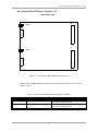
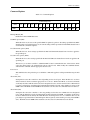
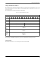
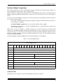
Functional Description
The Condor as shown in the block diagram (Figure 1-1.) consists primarily of four front-end channels, a VMEbus
Master Interface, a Local Bus (LBUS), a VMEbus Short I/O (slave only) Interface, a CPU Core and a CPU/Local bus
interface.
Each Ethernet Front End Channel (FEC) consists of an Ethernet controller, the associated Ethernet cable connections,
front end circuitry and a small amount of Local Bus interface glue logic. The VMEbus Master Interface consists of a
stand-alone VLSI DMA engine and the associated VMEbus high current driver and receiver devices. The Local Bus
(LBUS) consists of the memory buffer and the associated handshake logic for the bus. The VMEbus Short I/O interface
consists of the handshake and buffer logic for the host system to issue commands to the board. The CPU Core consists
of a CPU with the associated memory and glue logic required to allow the CPU to control the functions of the Condor
board. Finally, the CPU/Local Bus interface consists of the tri-state buffers and handshake logic required to allow the
CPU to access the resources on the LBUS.
Daughter
Card
(Optional)
Ethernet
Channels
CPU
Core
Local Bus
Short I/O
Slave
VMEbus
Master
VME/VME64
Figure 1-1.
4221 Condor Block Diagram
3
Buffer
SRAM
Chapter 1 - Introduction
Ethernet Front End Channel (FEC)
The 82596CA® Local Area Network (LAN) Co-processor is used as the FEC Ethernet controller. The 82596CA®
communicates with the rest of the board through the LBUS. The 82596CA® has a 80486® type bus interface, which
requires two PALs to convert the 80486® interface to meet the LBUS (MC68040_ type) specification. The 82596CA®
can be a master or a slave of the LBUS. As a LBUS master, the 82596CA® accesses both data and command lists for
both transmits and receives commands. As a slave, the CPU has write access to four locations within the 82596CA®
to establish a software reset or initialization and reset test pointers.
To complete the connections to the Ethernet cable, the 82596CA® connects to the encoder/decoder interface device
(82503®) which in turn connects through analog circuitry to the cable connectors. The encoder/decoder and analog
circuitry provides support for both 10BaseT and the Attachment Unit Interface (AUI).
VMEbus Master Interface
The VMEbus Master Interface consists of a VLSI DMA engine and the required high current VMEbus driver and
receiver devices.
DMA Engine
The DMA engine interfaces the LBUS with the VMEbus and performs the LBUS to VMEbus DMA functions. The
DMA engine communicates with the rest of the board through the LBUS. The DMA engine can be a master and a slave
of the LBUS. As a LBUS master, the DMA engine accesses linked list DMA commands as well as buffered data. As
a LBUS slave, the DMA engine is accessed by the CPU for configuration and status information.
The DMA engine provides the VMEbus interrupter support logic, some of the internal CPU interrupts (with vectors)
and the board timers.
The DMA engine also provides many functions and features which are not currently used on the Condor board. These
functions include a non-DMA LBUS to VMEbus interface, VMEbus slave to LBUS interface, system controller
functions, an interrupt handler and several global general purpose registers.
VMEbus Drivers And Receivers
External buffers are used to provide a more isolated and robust interface to the VMEbus. These buffers drive and
receive most of the VMEbus data, address and control lines.
Local Bus
The Local Bus (LBUS) is based primarily upon a MC68040® CPU bus structure. The channels and functions
connected to the LBUS must conform to the MC68040_bus specification. This allows easy design and development of
a wide variety of front ends and back ends into the controller board.
The LBUS encompasses the actual bus itself, the buffer memory and all of the logic which is not associated with any
one particular channel (front end or back end) on the LBUS.
The buffer memory is configured as two SRAM banks which consists of four SRAM devices for each bank. The two
banks of SRAM combined provide for 128K-, 256K-, 512K- and 1M-byte of memory.
The LBUS logic consists of an arbiter, an address decoder, a burst mode address counter, a write strobe generator, a
transfer acknowledge generator, a SRAM buffer memory and any miscellaneous handshake logic required to connect
the channels to the LBUS.
4
VMEbus Short I/O Interface
VMEbus Short I/O Interface
The VMEbus Short I/O interface allows for VMEbus host and onboard CPU communications. The host issues
commands to the Condor through the Short I/O interface and the CPU issues status back to the host.
The Short I/O Interface is a Slave-only interface to the Condor and contains two independent, jumper-configurable,
slave-access areas. The areas can be configured to be 256, 512-, 1K- or 2K- bytes in length.
VMEbus address lines A(15-08) and the Address Modifier lines are compared with the jumper-configurable,
slave-access areas. Address Modifiers "2D" and "29" are supported for the Short I/O access.
The Short I/O Mailboxes physically reside in the CPU Core SRAM. The reset and mailbox location monitor logic
resides in the VMEbus Short I/O Interface.
CPU Core
The CPU (and core logic) controls and configures the rest of the Condor. Each of the commands issued to the FECs
and the VMEbus DMA engine are issued by the onboard CPU.
The CPU Core consists of a MC68EC030 CPU and associated support logic. The CPU Core support logic includes the
following:
•
EPROM/FLASH
•
Serial EPROM
•
SRAM
•
DUART Port
•
Address Decoder
•
Wait State Generator
•
STERM/DSACK Generator
•
Control/Status Registers
•
Hardware Strobes
•
Clock Generation
•
Interrupt Handler
•
FLASH ROM Hardware
The program for the CPU is stored in a single-byte-wide, EPROM (or FLASH) device. The EPROM can be 128K-,
256K- or 512K- bytes in size. There are two SRAM banks which consists of four SRAM devices for each bank. The
two banks of SRAM combined provide for 128K-, 256K, 512K- and 1M-byte of SRAM. At board power-up, the
program is copied from the EPROM (or FLASH) device to the SRAM banks. The program is then executed from the
higher performance SRAM devices.
The interrupt-handler logic combines the three level interrupt from the DMA engine and the non-DMA
engine-interrupt sources and outputs the three-level interrupt signals to the CPU. During CPU IACK cycles, the
5
Chapter 1 - Introduction
interrupt handler outputs an interrupt vector number for the non-DMA engine interrupts or requests access to the LBUS
for a DMA engine IACK cycles.
CPU/LBUS Interface
The CPU/LBUS Interface links the CPU core with the LBUS resources. The CPU/LBUS interface converts the CPU
Core bus to the LBUS. The Interface is a one-way interface which allows the CPU to act as a LBUS master. The
interface does not allow other LBUS masters to access the CPU Core.
The CPU/LBUS interface is composed of address latches, data-latching transceivers, and control logic. The
CPU/LBUS Interface performs write-posting and read-latching to maximize the CPU bus and the LBUS performance.
The interface also performs relinquish retries, read-modify-write cycles, IACK cycles to the DMA engine,
back-to-back write-write cycles and back-to-back, write-read cycles.
6
CHAPTER 2
HARDWARE INSTALLATION
Overview
Before attempting installation, read this chapter thoroughly to insure the safe installation of the Condor into your
system. If you have any questions regarding installation, which are not answered in this chapter, please contact
Interphase Customer Service at (214) 919-9111.
The Condor is installed into the VMEbus system using the following steps:
•
Visual Inspection
•
Fuse And Diagnostic LEDs
•
Set Onboard Jumpers
•
Set Daughter Card Jumpers
•
Power Off System
•
Installing the Board
•
Cabling Procedure
When installing the Condor, heed the following WARNING:
WARNING
1.
Catastrophic DAMAGE can result if improper connections are made. Therefore, those planning
to connect power sources to the VMEbus for the purpose of feeding the user-defined 96 pins of
P2 (Rows A and C) should FIRST CHECK to ensure that all boards installed are compatible with
those connections.
2.
Do NOT install, or apply power to, a damaged board. Failure to observe this warning could result
in extensive damage to the board and/or the system.
3.
CAUTION! The Condor is extremely sensitive to electrostatic discharge (ESD), and the board
could be damaged if handled improperly. Interphase ships the board enclosed in a special
anti-static bag. Upon receipt of the board, take the proper measures to eliminate board damage
due to ESD (i.e., wear a wrist ground strap or other grounding device).
7
Chapter 2 - Hardware Installation
The daughter card installation procedure will vary depending on the desired configuration. Variables include:
•
Single Channel AUI/10BaseT.
•
Dual Ethernet AUI.
•
Dual Ethernet 10BaseT.
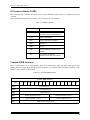
The following table summarizes the Condor products that are available from Interphase to implement various
combinations of the above functions.
Table 2-1. Condor Products
Product
Description
10BaseT Condor Motherboard (P2 Row B Only)
Provides Dual and/or Single 10BaseT Ethernet connections.
This board only uses row B of the P2 connector.
Single Channel AUI/10BaseT Motherboard
Provides Single AUI or 10BaseT Ethernet connections.
AUI Condor Motherboard
Provides Dual AUI Ethernet connections. This board only
uses row B of the P2 Connector.
Dual AUI Ethernet Daughter Card
Adds dual AUI connections to any of the above motherboards.
Dual 10BaseT Ethernet Daughter Card
Adds Dual 10BaseT connections to any of the above motherboards.
Single Channel AUI/10BaseT Daughter Card
Adds a single AUI or 10BaseT channel to any of the above
motherboards.
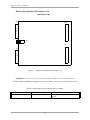
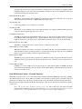
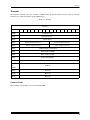
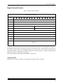
The following figures outline the board layout and jumper positions for the two different motherboard configurations:
8
Overview
J13
LED 6
J12
F
E
C
0
J10
J11
J9
LED 7
F
E
C
1
P1
J4
J3
SPA
J8
LED 5
J22
J21
J20
J26
J25
J24
J19
J23
J7
J6
J5
LED 4
LED 3
LED 2
J2
LED 1
SPB
J1
J16
J17
J18
J15
J14
OPTIONAL
DAUGHTER
CARD
P2
Figure 2-1.
10BaseT Condor Motherboard Layout (PB04221-000)
9
Chapter 2 - Hardware Installation
J13
LED 6
J12
F
E
C
0
F
E
C
0
J11
10BaseT
J9
AUI
P1
J4
J3
SPA
J8
LED 5
J7
J6
J5
LED 4
J14
J15
J16
J J
1 1
7 8
J22
J21
J20
J26
J25
J24
J19
J23
LED 3
LED 2
J2
LED 1
SPB
J1
P2
Figure 2-2.
Single Channel AUI or 10BaseT Motherboard Layout (PB004221-001)
10
Overview
J13
F
E
C
0
J12
J10
J11
F1
J9
F
E
C
1
P1
J4
J3
SPA
J8
LED 6
J7
J6
J5
LED 5
LED 4
LED 3
J22
J21
J20
J26
J25
J24
J19
J23
J2
LED 2
LED 1
J1
SPB
J16
J17
J18
J15
J14
OPTIONAL
DAUGHTER
CARD
P2
Figure 2-3.
AUI Condor Motherboard Layout (PB04221-000)
11
Chapter 2 - Hardware Installation
J15
LED 6
J12
F
E
C
0
J11
LED 7
F
E
C
1
J9
P1
J4
J3
SPA
J8
LED 5
J7
J6
J5
LED 4
J10
J14
J16
J J
1 1
7 8
J22
J21
J20
J26
J25
J24
J19
J23
LED 3
LED 2
J2
LED 1
SPB
J1
OPTIONAL
DAUGHTER
CARD
P2
Figure 2-4.
10BaseT Condor Motherboard Layout (PB04221-001)
12
Overview
J15
F
E
C
0
J12
J11
F1
J9
F
E
C
1
P1
J4
SPA
J3
J8
LED 6
J7
J6
J5
LED 5
LED 4
LED 3
J10
J2
J14
J16
J J
1 1
7 8
J22
J21
J20
J26
J25
J24
J19
J23
LED 2
LED 1
J1
SPB
OPTIONAL
DAUGHTER
CARD
P2
Figure 2-5.
AUI Condor Motherboard Layout (PB04221-001)
13
Chapter 2 - Hardware Installation
4221 Condor Hardware Installation Procedures
For proper installation of the Condor, it is imperative that you use the following procedures.
Step 1. Visual Inspection
Before attempting the installation of this board, make sure you are wearing an anti-static or grounding device. Remove
the Condor board from the anti-static bag, and visually inspect it to ensure no damage has occurred during shipment.
A visual inspection usually is sufficient, since each board is thoroughly checked at Interphase just prior to shipment.
If the board is undamaged and all parts are accounted for, proceed with the installation.
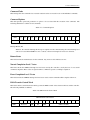
Step 2. Fuse And Diagnostic LEDs
The following discusses the fuse, diagnostic LEDs, and board status LEDs.
Fuse
The AUI version of the Condor has a 1.5A fuse (F1) used to protect the +12 volts when provided by the
Condor. Its part number is LITTLEFUSE 273-01.5. To determine the location of the fuse on the board, refer
to the appropriate board layout.
Diagnostic LEDs
The Condor has as many as 8 LEDs that are mounted on the component side of the motherboard. Refer to
Figures 2-1 and 2-2 for illustrations that shows the location of the component side LEDs. The following table
lists all LEDs and states their function and location.
Table 2-2. 4221 Condor LEDs
Designator
Description
Location
LED 1
Board Status 0 (LSB)
Component Side
LED 2
Board Status 1
Component Side
LED 3
Board Status 2
Component Side
LED 4
Board Status 3 (MSB)
Component Side
LED 5
Board OK (Red/Green) Green = Board OK
Component Side
LED 6
Fused +12 Volts Status (AUI only)
Component Side
LED 7
FEC1, Link OK Status (10BaseT only)
Component Side
LED 8
FEC0, Link OK Status (10BaseT only)
Component Side
14
4221 Condor Hardware Installation Procedures
Board Status LEDs
LEDs 1, 2, 3, and 4 are Board Status LEDs which provide the following functions:
•
Power On Self Test (POST) Mode
•
Monitor Mode
•
Run Mode
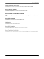
POST Mode: This mode provides diagnostics for the CPU and Buffer. Refer to the following table for a list
of diagnostics performed while in this mode:
Table 2-3. Board Status Diagnostics Used In POST Mode
Hex Code
Diagnostic
Definition
Type of Test
0x01
CPU Register Test
CPUFAIL
CPU Core Test
0x02
ROM Checksum
ROMFAIL
CPU Core Test
0x03
Walking 1’s SRAM
STAT1FAIL
CPU Core Test
0x04
Walking 0’s SRAM
STAT0FAIL
CPU Core Test
0x05
Decrementing Longwords
STATLFAIL
CPU Core Test
0x06
Word Access
STATWFAIL
CPU Core Test
0x07
Byte Access
STATBFAIL
CPU Core Test
0x08
Reserved
RESERVED
CPU Core Test
0x09
Walking 1’s In Buffer
BUFFERFAIL1
Static Buffer Test
0x0A
Walking 0’s In Buffer
BUFFERFAIL0
Static Buffer Test
0x0B
Decrementing Longwords
BUFFERFAIL
Static Buffer Test
0x0C
Walking 1’s, 0’s VME DMA
VMEFAIL
Control Register Access
0x0D
Motherboard FEC Tests
FEC0 & 1
Control Register Access
0x0E
Daughter Card FEC Tests
FEC2 & 3
Control Register Access
Monitor Mode: In this mode, LEDs will sequentially flicker when Serial Port A is active and the onboard
monitor is controlling the Condor.
Run Mode: When in this mode, the Condor is accepting commands from the host. Refer to the following
table for a list of LED definitions while in this mode:
15
Chapter 2 - Hardware Installation
Table 2-4. Run Mode LED Matrix
LED1
LED2
LED3
LED4
Function
ON
OFF
OFF
OFF
1-4 Commands On Board
ON
ON
OFF
OFF
5-16 Commands On Board
ON
ON
ON
OFF
17-64 Commands On Board
ON
ON
ON
ON
65 or More Commands On Board
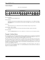
Step 3. Set Onboard Motherboard Jumpers
Set all onboard jumpers so that the Condor is properly configured for operation within your system. The board layout
as illustrated in figure 2-1 shows the location of the jumpers.
Motherboard Jumper Settings
The following are jumpers and the default settings used on the Condor motherboard. IN refers to the jumper
being installed across the pins indicated, OUT indicates the jumper is removed.
CAUTION!
Jumpers J1 through J4, J6 through J8, J10 and J11 are used for manufacturing
options. If populated, they are configured to factory default settings. These jumpers
must not be altered.
J5 FLASH0
J5
IN: FLASH logic enabled.
OUT: FLASH logic disabled.
16
4221 Condor Hardware Installation Procedures
J9 +12 VOLTS Flash Programming Protect:
J9
J9
(PB04221-000)
(PB04221-001)
IN: +12 Volt power connected to EPROM socket.
OUT: +12 Volt power disconnected from EPROM socket.
J12 VME Bus Grant:
2
16
J12
15
1
Pins 1 - 12
Reserved
Pins 13 - 16
VME Bus Grant:
Table 2-5. VME Bus Grant Settings
PIN #
BUS GRANT
13-14
15-16
0
IN
IN
1
IN
OUT
2
OUT
IN
*3
*OUT
*OUT
* = Factory Default
J13 Firmware Option Jumpers:
2
8
J13
1
7
(Pins 1-2)
Reserved
(Pins 3-4)
Memory Test Enable
IN = Disable
OUT = Enable
17
Chapter 2 - Hardware Installation
(Pins 5-6)
Console Message Disable
IN = Disable
OUT = Enable
(Pins 7-8)
GDB Enable Point
IN = GDB Initialized On Exit
OUT = GDB Initialized On Reset
J14 Firmware Option Jumpers:
8
7
2
8
1
7
J14
2
J14
1
(PB04221-001)
(PB04221-000)
(Pins 1-2)
16 Bit Block Enable (default = OUT)
IN = 16 bit Block Mode Disabled
OUT = 16 bit Block Mode Enabled
(Pins 3-4)
Sysfail (default = OUT)
IN = Clear Sysfail after passing diagnostics
OUT = Clear Sysfail before running Power-Up Diagnostics
(Pins 5-6)
Reserved
(Pins 7-8)
GDB Debugger Enable (default = OUT)
IN = Debugger Enabled
OUT = Debugger Disabled
J15 Firmware Option Jumpers / Secondary Short I/O Size:
8
7
2
8
1
7
J15
J15
2
1
(PB04221-000)
(PB04221-001)
(Pins 1-2)
Load Firmware (default = OUT)
IN = Load firmware from on-board buffer
OUT = Load firmware from EPROM
(Pins 3-4)
On Board Monitor Enable (default = OUT)
IN = Stop in monitor after loading firmware
OUT = Normal Run Mode
18
4221 Condor Hardware Installation Procedures
Table 2-6. Secondary Short I/O
J15 PINS
5-6
OUT
OUT
IN
*IN
SIZE (Bytes)
7-8
OUT
IN
OUT
*IN
256 bytes of Secondary Short I/O space
512 bytes of Secondary Short I/O space
1K bytes of Secondary Short I/O space
2K bytes of Secondary Short I/O space*
* Factory Default
J16 Primary Short I/O Size / Reset Enable:
Table 2-7. Primary Short I/O Size
J16 PINS
1-2
OUT
OUT
IN
*IN
SIZE (Bytes)
3-4
OUT
IN
OUT
*IN
256 bytes of Primary Short I/O space
512 bytes of Primary Short I/O space
1K bytes of Primary Short I/O space
2K bytes of Primary Short I/O space*
* Factory Default
(Pins 5-6) Secondary Master Control Register (MCR) Reset Enable (default = OUT)
IN = Reset Enable
OUT = Reset Disable
(Pins 7-8) Primary Master Control Register (MCR) Reset Enable (default = IN)
IN = Reset Enabled
OUT = Reset Disabled
J17 Secondary Channel Address Modifiers:
J17
IN = Secondary Channel Address Modifiers 29 or 2D.
OUT = Secondary Channel Address Modifier 2D only.
19
Chapter 2 - Hardware Installation
J18 Primary Channel Address Modifiers:
J18
IN = Primary Channel Address Modifiers 29 or 2D
OUT = Primary Channel Address Modifier 2D only
20
4221 Condor Hardware Installation Procedures
J19, J20, J21 & J22 Primary Short I/O Base Address:
J22
J21
J20
1
2
J19
15
16
Refer to the following tables when setting Primary Short I/O Base Addresses for the following:
•
Primary Short I/O For 2K Base Address
•
Primary Short I/O For 1K Base Address
•
Primary Short I/O For 512 Bytes Base Address
•
Primary Short I/O For 256 Bytes Base Address
NOTE:
The normal 4221 configuration is with the Primary Short I/O space disabled. To disable
the Primary Short I/O, set pins 15-16 of Jumper J19 to 0 (IN), and all other pins to F
(OUT).
21
Chapter 2 - Hardware Installation
Table 2-8. Primary Base Address For 2K Short I/O
ADDRESS
0000
0800
1000
1800
2000
2800
3000
3800
4000
4800
5000
5800
6000
6800
7000
7800
8000
8800
9000
9800
A000
A800
B000
B800
C000
C800
D000
D800
E000
E800
F000
F800
15-16
F
F
F
F
F
F
F
F
F
F
F
F
F
F
F
F
F
F
F
F
F
F
F
F
F
F
F
F
F
F
F
F
13-14
F
F
F
F
F
F
F
F
F
F
F
F
F
F
F
F
F
F
F
F
F
F
F
F
F
F
F
F
F
F
F
F
J19 PIN SETTINGS
11-12
9-10
7-8
5-6
F
0
0
0
F
F
0
0
F
0
F
0
F
F
F
0
F
0
0
F
F
F
0
F
F
0
F
F
F
F
F
F
F
0
0
0
F
F
0
0
F
0
F
0
F
F
F
0
F
0
0
F
F
F
0
F
F
0
F
F
F
F
F
F
F
0
0
0
F
F
0
0
F
0
F
0
F
F
F
0
F
0
0
F
F
F
0
F
F
0
F
F
F
F
F
F
F
0
0
0
F
F
0
0
F
0
F
0
F
F
F
0
F
0
0
F
F
F
0
F
F
0
F
F
F
F
F
F
3-4
0
0
0
0
0
0
0
0
F
F
F
F
F
F
F
F
0
0
0
0
0
0
0
0
F
F
F
F
F
F
F
F
NOTE: 0 = IN (Logical 0), F = OUT (Logical 1)
22
1-2
0
0
0
0
0
0
0
0
0
0
0
0
0
0
0
0
F
F
F
F
F
F
F
F
F
F
F
F
F
F
F
F
J20, J21, J22 PIN SETTINGS
J20
J21
J22
F
F
F
F
F
F
F
F
F
F
F
F
F
F
F
F
F
F
F
F
F
F
F
F
F
F
F
F
F
F
F
F
F
F
F
F
F
F
F
F
F
F
F
F
F
F
F
F
F
F
F
F
F
F
F
F
F
F
F
F
F
F
F
F
F
F
F
F
F
F
F
F
F
F
F
F
F
F
F
F
F
F
F
F
F
F
F
F
F
F
F
F
F
F
F
F
4221 Condor Hardware Installation Procedures
Table 2-9. Primary Base Address For 1K Short I/O
ADDRESS
8000
8400
8800
8C00
9000
9400
9800
9C00
A000
A400
A800
AC00
B000
B400
B800
BC00
C000
C400
C800
CC00
D000
D400
D800
DC00
E000
E400
E800
EC00
F000
F400
F800
FC00
15-16
F
F
F
F
F
F
F
F
F
F
F
F
F
F
F
F
F
F
F
F
F
F
F
F
F
F
F
F
F
F
F
F
13-14
F
F
F
F
F
F
F
F
F
F
F
F
F
F
F
F
F
F
F
F
F
F
F
F
F
F
F
F
F
F
F
F
11-12
0
F
0
F
0
F
0
F
0
F
0
F
0
F
0
F
0
F
0
F
0
F
0
F
0
F
0
F
0
F
0
F
J19 PIN SETTINGS
9-10
7-8
5-6
0
0
0
0
0
0
F
0
0
F
0
0
0
F
0
0
F
0
F
F
0
F
F
0
0
0
F
0
0
F
F
0
F
F
0
F
0
F
F
0
F
F
F
F
F
F
F
F
0
0
0
0
0
0
F
0
0
F
0
0
0
F
0
0
F
0
F
F
0
F
F
0
0
0
F
0
0
F
F
0
F
F
0
F
0
F
F
0
F
F
F
F
F
F
F
F
3-4
0
0
0
0
0
0
0
0
0
0
0
0
0
0
0
0
F
F
F
F
F
F
F
F
F
F
F
F
F
F
F
F
NOTE: 0 = IN (Logical 0), F = OUT (Logical 1)
23
1-2
F
F
F
F
F
F
F
F
F
F
F
F
F
F
F
F
F
F
F
F
F
F
F
F
F
F
F
F
F
F
F
F
J20, J21, J22 PIN SETTINGS
J20
J21
J22
F
F
0
F
F
0
F
F
0
F
F
0
F
F
0
F
F
0
F
F
0
F
F
0
F
F
0
F
F
0
F
F
0
F
F
0
F
F
0
F
F
0
F
F
0
F
F
0
F
F
0
F
F
0
F
F
0
F
F
0
F
F
0
F
F
0
F
F
0
F
F
0
F
F
0
F
F
0
F
F
0
F
F
0
F
F
0
F
F
0
F
F
0
F
F
0
Chapter 2 - Hardware Installation
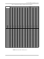
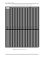
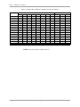
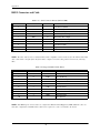
Table 2-10. Primary Base Address For 512 Byte Short I/O
ADDRESS
C000
C200
C400
C600
C800
CA00
CC00
CE00
D000
D200
D400
D600
D800
DA00
DC00
DE00
E000
E200
E400
E600
E800
EA00
EC00
EE00
F000
F200
F400
F600
F800
FA00
FC00
FE00
15-16
F
F
F
F
F
F
F
F
F
F
F
F
F
F
F
F
F
F
F
F
F
F
F
F
F
F
F
F
F
F
F
F
13-14
0
F
0
F
0
F
0
F
0
F
0
F
0
F
0
F
0
F
0
F
0
F
0
F
0
F
0
F
0
F
0
F
J19 PIN SETTINGS
11-12
9-10
7-8
5-6
0
0
0
0
0
0
0
0
F
0
0
0
F
0
0
0
0
F
0
0
0
F
0
0
F
F
0
0
F
F
0
0
0
0
F
0
0
0
F
0
F
0
F
0
F
0
F
0
0
F
F
0
0
F
F
0
F
F
F
0
F
F
F
0
0
0
0
F
0
0
0
F
F
0
0
F
F
0
0
F
0
F
0
F
0
F
0
F
F
F
0
F
F
F
0
F
0
0
F
F
0
0
F
F
F
0
F
F
F
0
F
F
0
F
F
F
0
F
F
F
F
F
F
F
F
F
F
F
3-4
F
F
F
F
F
F
F
F
F
F
F
F
F
F
F
F
F
F
F
F
F
F
F
F
F
F
F
F
F
F
F
F
NOTE: 0 = IN (Logical 0), F = OUT (Logical 1)
24
1-2
F
F
F
F
F
F
F
F
F
F
F
F
F
F
F
F
F
F
F
F
F
F
F
F
F
F
F
F
F
F
F
F
J20, J21, J22 PIN SETTINGS
J20
J21
J22
F
0
0
F
0
0
F
0
0
F
0
0
F
0
0
F
0
0
F
0
0
F
0
0
F
0
0
F
0
0
F
0
0
F
0
0
F
0
0
F
0
0
F
0
0
F
0
0
F
0
0
F
0
0
F
0
0
F
0
0
F
0
0
F
0
0
F
0
0
F
0
0
F
0
0
F
0
0
F
0
0
F
0
0
F
0
0
F
0
0
F
0
0
F
0
0
4221 Condor Hardware Installation Procedures
Table 2-10. Primary Base Address For 512 Byte Short I/O (Continued)
ADDRESS
0000
0200
0400
0600
0800
0A00
0C00
0E00
1000
1200
1400
1600
1800
1A00
1C00
1E00
2000
2200
2400
2600
2800
2A00
2C00
2E00
3000
3200
3400
3600
3800
3A00
3C00
3E00
15-16
F
F
F
F
F
F
F
F
F
F
F
F
F
F
F
F
F
F
F
F
F
F
F
F
F
F
F
F
F
F
F
F
13-14
0
F
0
F
0
F
0
F
0
F
0
F
0
F
0
F
0
F
0
F
0
F
0
F
0
F
0
F
0
F
0
F
11-12
0
0
F
F
0
0
F
F
0
0
F
F
0
0
F
F
0
0
F
F
0
0
F
F
0
0
F
F
0
0
F
F
J19 PIN SETTINGS
9-10
7-8
5-6
0
0
0
0
0
0
0
0
0
0
0
0
F
0
0
F
0
0
F
0
0
F
0
0
0
F
0
0
F
0
0
F
0
0
F
0
F
F
0
F
F
0
F
F
0
F
F
0
0
0
F
0
0
F
0
0
F
0
0
F
F
0
F
F
0
F
F
0
F
F
0
F
0
F
F
0
F
F
0
F
F
0
F
F
F
F
F
F
F
F
F
F
F
F
F
F
3-4
0
0
0
0
0
0
0
0
0
0
0
0
0
0
0
0
0
0
0
0
0
0
0
0
0
0
0
0
0
0
0
0
NOTE: 0 = IN (Logical 0), F = OUT (Logical 1)
25
1-2
0
0
0
0
0
0
0
0
0
0
0
0
0
0
0
0
0
0
0
0
0
0
0
0
0
0
0
0
0
0
0
0
J20, J21, J22 PIN SETTINGS
J20
J21
J22
F
0
0
F
0
0
F
0
0
F
0
0
F
0
0
F
0
0
F
0
0
F
0
0
F
0
0
F
0
0
F
0
0
F
0
0
F
0
0
F
0
0
F
0
0
F
0
0
F
0
0
F
0
0
F
0
0
F
0
0
F
0
0
F
0
0
F
0
0
F
0
0
F
0
0
F
0
0
F
0
0
F
0
0
F
0
0
F
0
0
F
0
0
F
0
0
Chapter 2 - Hardware Installation
Table 2-11. Primary Base Address For 256 Byte Short I/O
ADDRESS
0000
0100
0200
0300
0400
0500
0600
0700
0800
0900
0A00
0B00
0C00
0D00
0E00
0F00
1000
1100
1200
1300
1400
1500
1600
1700
1800
1900
1A00
1B00
1C00
1D00
1E00
1F00
2000
2100
2200
2300
2400
2500
2600
2700
15-16
0
F
0
F
0
F
0
F
0
F
0
F
0
F
0
F
0
F
0
F
0
F
0
F
0
F
0
F
0
F
0
F
0
F
0
F
0
F
0
F
13-14
0
0
F
F
0
0
F
F
0
0
F
F
0
0
F
F
0
0
F
F
0
0
F
F
0
0
F
F
0
0
F
F
0
0
F
F
0
0
F
F
J19 PIN SETTINGS
11-12
9-10
7-8
5-6
0
0
0
0
0
0
0
0
0
0
0
0
0
0
0
0
F
0
0
0
F
0
0
0
F
0
0
0
F
0
0
0
0
F
0
0
0
F
0
0
0
F
0
0
0
F
0
0
F
F
0
0
F
F
0
0
F
F
0
0
F
F
0
0
0
0
F
0
0
0
F
0
0
0
F
0
0
0
F
0
F
0
F
0
F
0
F
0
F
0
F
0
F
0
F
0
0
F
F
0
0
F
F
0
0
F
F
0
0
F
F
0
F
F
F
0
F
F
F
0
F
F
F
0
F
F
F
0
0
0
0
F
0
0
0
F
0
0
0
F
0
0
0
F
F
0
0
F
F
0
0
F
F
0
0
F
F
0
0
F
3-4
0
0
0
0
0
0
0
0
0
0
0
0
0
0
0
0
0
0
0
0
0
0
0
0
0
0
0
0
0
0
0
0
0
0
0
0
0
0
0
0
NOTE: 0 = IN (Logical 0), F = OUT (Logical 1)
26
1-2
0
0
0
0
0
0
0
0
0
0
0
0
0
0
0
0
0
0
0
0
0
0
0
0
0
0
0
0
0
0
0
0
0
0
0
0
0
0
0
0
J20, J21, J22 PIN SETTINGS
J20
J21
J22
0
0
0
0
0
0
0
0
0
0
0
0
0
0
0
0
0
0
0
0
0
0
0
0
0
0
0
0
0
0
0
0
0
0
0
0
0
0
0
0
0
0
0
0
0
0
0
0
0
0
0
0
0
0
0
0
0
0
0
0
0
0
0
0
0
0
0
0
0
0
0
0
0
0
0
0
0
0
0
0
0
0
0
0
0
0
0
0
0
0
0
0
0
0
0
0
0
0
0
0
0
0
0
0
0
0
0
0
0
0
0
0
0
0
0
0
0
0
0
0
4221 Condor Hardware Installation Procedures
Table 2-11. Primary Base Address For 256 Byte Short I/O (Continued)
ADDRESS
2800
2900
2A00
2B00
2C00
2D00
2E00
2F00
3000
3100
3200
3300
3400
3500
3600
3700
3800
3900
3A00
3B00
3C00
3D00
3E00
3F00
4000
4100
4200
4300
4400
4500
4600
4700
4800
4900
4A00
4B00
4C00
4D00
4E00
4F00
15-16
0
F
0
F
0
F
0
F
0
F
0
F
0
F
0
F
0
F
0
F
0
F
0
F
0
F
0
F
0
F
0
F
0
F
0
F
0
F
0
F
13-14
0
0
F
F
0
0
F
F
0
0
F
F
0
0
F
F
0
0
F
F
0
0
F
F
0
0
F
F
0
0
F
F
0
0
F
F
0
0
F
F
11-12
0
0
0
0
F
F
F
F
0
0
0
0
F
F
F
F
0
0
0
0
F
F
F
F
0
0
0
0
F
F
F
F
0
0
0
0
F
F
F
F
J19 PIN SETTINGS
9-10
7-8
5-6
F
0
F
F
0
F
F
0
F
F
0
F
F
0
F
F
0
F
F
0
F
F
0
F
0
F
F
0
F
F
0
F
F
0
F
F
0
F
F
0
F
F
0
F
F
0
F
F
F
F
F
F
F
F
F
F
F
F
F
F
F
F
F
F
F
F
F
F
F
F
F
F
0
0
0
0
0
0
0
0
0
0
0
0
0
0
0
0
0
0
0
0
0
0
0
0
F
0
0
F
0
0
F
0
0
F
0
0
F
0
0
F
0
0
F
0
0
F
0
0
3-4
0
0
0
0
0
0
0
0
0
0
0
0
0
0
0
0
0
0
0
0
0
0
0
0
F
F
F
F
F
F
F
F
F
F
F
F
F
F
F
F
NOTE: 0 = IN (Logical 0), F = OUT (Logical 1)
27
1-2
0
0
0
0
0
0
0
0
0
0
0
0
0
0
0
0
0
0
0
0
0
0
0
0
0
0
0
0
0
0
0
0
0
0
0
0
0
0
0
0
J20, J21, J22 PIN SETTINGS
J13
J14
J15
0
0
0
0
0
0
0
0
0
0
0
0
0
0
0
0
0
0
0
0
0
0
0
0
0
0
0
0
0
0
0
0
0
0
0
0
0
0
0
0
0
0
0
0
0
0
0
0
0
0
0
0
0
0
0
0
0
0
0
0
0
0
0
0
0
0
0
0
0
0
0
0
0
0
0
0
0
0
0
0
0
0
0
0
0
0
0
0
0
0
0
0
0
0
0
0
0
0
0
0
0
0
0
0
0
0
0
0
0
0
0
0
0
0
0
0
0
0
0
0
Chapter 2 - Hardware Installation
Table 2-11. Primary Base Address For 256 Byte Short I/O (Continued)
ADDRESS
5000
5100
5200
5300
5400
5500
5600
5700
5800
5900
5A00
5B00
5C00
5D00
5E00
5F00
6000
6100
6200
6300
6400
6500
6600
6700
6800
6900
6A00
6B00
6C00
6D00
6E00
6F00
7000
7100
7200
7300
7400
7500
7600
7700
15-16
0
F
0
F
0
F
0
F
0
F
0
F
0
F
0
F
0
F
0
F
0
F
0
F
0
F
0
F
0
F
0
F
0
F
0
F
0
F
0
F
13-14
0
0
F
F
0
0
F
F
0
0
F
F
0
0
F
F
0
0
F
F
0
0
F
F
0
0
F
F
0
0
F
F
0
0
F
F
0
0
F
F
J19 PIN SETTINGS
11-12
9-10
7-8
5-6
0
0
F
0
0
0
F
0
0
0
F
0
0
0
F
0
F
0
F
0
F
0
F
0
F
0
F
0
F
0
F
0
0
F
F
0
0
F
F
0
0
F
F
0
0
F
F
0
F
F
F
0
F
F
F
0
F
F
F
0
F
F
F
0
0
0
0
F
0
0
0
F
0
0
0
F
0
0
0
F
F
0
0
F
F
0
0
F
F
0
0
F
F
0
0
F
0
F
0
F
0
F
0
F
0
F
0
F
0
F
0
F
F
F
0
F
F
F
0
F
F
F
0
F
F
F
0
F
0
0
F
F
0
0
F
F
0
0
F
F
0
0
F
F
F
0
F
F
F
0
F
F
F
0
F
F
F
0
F
F
3-4
F
F
F
F
F
F
F
F
F
F
F
F
F
F
F
F
F
F
F
F
F
F
F
F
F
F
F
F
F
F
F
F
F
F
F
F
F
F
F
F
NOTE: 0 = IN (Logical 0), F = OUT (Logical 1)
28
1-2
0
0
0
0
0
0
0
0
0
0
0
0
0
0
0
0
0
0
0
0
0
0
0
0
0
0
0
0
0
0
0
0
0
0
0
0
0
0
0
0
J20, J21, J22 PIN SETTINGS
J20
J21
J22
0
0
0
0
0
0
0
0
0
0
0
0
0
0
0
0
0
0
0
0
0
0
0
0
0
0
0
0
0
0
0
0
0
0
0
0
0
0
0
0
0
0
0
0
0
0
0
0
0
0
0
0
0
0
0
0
0
0
0
0
0
0
0
0
0
0
0
0
0
0
0
0
0
0
0
0
0
0
0
0
0
0
0
0
0
0
0
0
0
0
0
0
0
0
0
0
0
0
0
0
0
0
0
0
0
0
0
0
0
0
0
0
0
0
0
0
0
0
0
0
4221 Condor Hardware Installation Procedures
Table 2-11. Primary Base Address For 256 Byte Short I/O (Continued)
ADDRESS
7800
7900
7A00
7B00
7C00
7D00
7E00
7F00
8000
8100
8200
8300
8400
8500
8600
8700
8800
8900
8A00
8B00
8C00
8D00
8E00
8F00
9000
9100
9200
9300
9400
9500
9600
9700
9800
9900
9A00
9B00
9C00
9D00
9E00
9F00
15-16
0
F
0
F
0
F
0
F
0
F
0
F
0
F
0
F
0
F
0
F
0
F
0
F
0
F
0
F
0
F
0
F
0
F
0
F
0
F
0
F
13-14
0
0
F
F
0
0
F
F
0
0
F
F
0
0
F
F
0
0
F
F
0
0
F
F
0
0
F
F
0
0
F
F
0
0
F
F
0
0
F
F
11-12
0
0
0
0
F
F
F
F
0
0
0
0
F
F
F
F
0
0
0
0
F
F
F
F
0
0
0
0
F
F
F
F
0
0
0
0
F
F
F
F
J19 PIN SETTINGS
9-10
7-8
5-6
F
F
F
F
F
F
F
F
F
F
F
F
F
F
F
F
F
F
F
F
F
F
F
F
0
0
0
0
0
0
0
0
0
0
0
0
0
0
0
0
0
0
0
0
0
0
0
0
F
0
0
F
0
0
F
0
0
F
0
0
F
0
0
F
0
0
F
0
0
F
0
0
0
F
0
0
F
0
0
F
0
0
F
0
0
F
0
0
F
0
0
F
0
0
F
0
F
F
0
F
F
0
F
F
0
F
F
0
F
F
0
F
F
0
F
F
0
F
F
0
3-4
F
F
F
F
F
F
F
F
0
0
0
0
0
0
0
0
0
0
0
0
0
0
0
0
0
0
0
0
0
0
0
0
0
0
0
0
0
0
0
0
NOTE: 0 = IN (Logical 0), F = OUT (Logical 1)
29
1-2
0
0
0
0
0
0
0
0
F
F
F
F
F
F
F
F
F
F
F
F
F
F
F
F
F
F
F
F
F
F
F
F
F
F
F
F
F
F
F
F
J20, J21, J22 PIN SETTINGS
J20
J21
J22
0
0
0
0
0
0
0
0
0
0
0
0
0
0
0
0
0
0
0
0
0
0
0
0
0
0
0
0
0
0
0
0
0
0
0
0
0
0
0
0
0
0
0
0
0
0
0
0
0
0
0
0
0
0
0
0
0
0
0
0
0
0
0
0
0
0
0
0
0
0
0
0
0
0
0
0
0
0
0
0
0
0
0
0
0
0
0
0
0
0
0
0
0
0
0
0
0
0
0
0
0
0
0
0
0
0
0
0
0
0
0
0
0
0
0
0
0
0
0
0
Chapter 2 - Hardware Installation
Table 2-11. Primary Base Address For 256 Byte Short I/O (Continued)
ADDRESS
A000
A100
A200
A300
A400
A500
A600
A700
A800
A900
AA00
AB00
AC00
AD00
AE00
AF00
B000
B100
B200
B300
B400
B500
B600
B700
B800
B900
BA00
BB00
BC00
BD00
BE00
BF00
C000
C100
C200
C300
C400
C500
C600
C700
15-16
0
F
0
F
0
F
0
F
0
F
0
F
0
F
0
F
0
F
0
F
0
F
0
F
0
F
0
F
0
F
0
F
0
F
0
F
0
F
0
F
13-14
0
0
F
F
0
0
F
F
0
0
F
F
0
0
F
F
0
0
F
F
0
0
F
F
0
0
F
F
0
0
F
F
0
0
F
F
0
0
F
F
J19 PIN SETTINGS
11-12
9-10
7-8
5-6
0
0
0
F
0
0
0
F
0
0
0
F
0
0
0
F
F
0
0
F
F
0
0
F
F
0
0
F
F
0
0
F
0
F
0
F
0
F
0
F
0
F
0
F
0
F
0
F
F
F
0
F
F
F
0
F
F
F
0
F
F
F
0
F
0
0
F
F
0
0
F
F
0
0
F
F
0
0
F
F
F
0
F
F
F
0
F
F
F
0
F
F
F
0
F
F
0
F
F
F
0
F
F
F
0
F
F
F
0
F
F
F
F
F
F
F
F
F
F
F
F
F
F
F
F
F
F
F
0
0
0
0
0
0
0
0
0
0
0
0
0
0
0
0
F
0
0
0
F
0
0
0
F
0
0
0
F
0
0
0
3-4
0
0
0
0
0
0
0
0
0
0
0
0
0
0
0
0
0
0
0
0
0
0
0
0
0
0
0
0
0
0
0
0
F
F
F
F
F
F
F
F
NOTE: 0 = IN (Logical 0), F = OUT (Logical 1)
30
1-2
F
F
F
F
F
F
F
F
F
F
F
F
F
F
F
F
F
F
F
F
F
F
F
F
F
F
F
F
F
F
F
F
F
F
F
F
F
F
F
F
J20, J21, J22 PIN SETTINGS
J20
J21
J22
0
0
0
0
0
0
0
0
0
0
0
0
0
0
0
0
0
0
0
0
0
0
0
0
0
0
0
0
0
0
0
0
0
0
0
0
0
0
0
0
0
0
0
0
0
0
0
0
0
0
0
0
0
0
0
0
0
0
0
0
0
0
0
0
0
0
0
0
0
0
0
0
0
0
0
0
0
0
0
0
0
0
0
0
0
0
0
0
0
0
0
0
0
0
0
0
0
0
0
0
0
0
0
0
0
0
0
0
0
0
0
0
0
0
0
0
0
0
0
0
4221 Condor Hardware Installation Procedures
Table 2-11. Primary Base Address For 256 Byte Short I/O (Continued)
ADDRESS
C800
C900
CA00
CB00
CC00
CD00
CE00
CF00
D000
D100
D200
D300
D400
D500
D600
D700
D800
D900
DA00
DB00
DC00
DD00
DE00
DF00
E000
E100
E200
E300
E400
E500
E600
E700
E800
E900
EA00
EB00
EC00
ED00
EE00
EF00
15-16
0
F
0
F
0
F
0
F
0
F
0
F
0
F
0
F
0
F
0
F
0
F
0
F
0
F
0
F
0
F
0
F
0
F
0
F
0
F
0
F
13-14
0
0
F
F
0
0
F
F
0
0
F
F
0
0
F
F
0
0
F
F
0
0
F
F
0
0
F
F
0
0
F
F
0
0
F
F
0
0
F
F
11-12
0
0
0
0
F
F
F
F
0
0
0
0
F
F
F
F
0
0
0
0
F
F
F
F
0
0
0
0
F
F
F
F
0
0
0
0
F
F
F
F
J19 PIN SETTINGS
9-10
7-8
5-6
F
0
0
F
0
0
F
0
0
F
0
0
F
0
0
F
0
0
F
0
0
F
0
0
0
F
0
0
F
0
0
F
0
0
F
0
0
F
0
0
F
0
0
F
0
0
F
0
F
F
0
F
F
0
F
F
0
F
F
0
F
F
0
F
F
0
F
F
0
F
F
0
0
0
F
0
0
F
0
0
F
0
0
F
0
0
F
0
0
F
0
0
F
0
0
F
F
0
F
F
0
F
F
0
F
F
0
F
F
0
F
F
0
F
F
0
F
F
0
F
3-4
F
F
F
F
F
F
F
F
F
F
F
F
F
F
F
F
F
F
F
F
F
F
F
F
F
F
F
F
F
F
F
F
F
F
F
F
F
F
F
F
NOTE: 0 = IN (Logical 0), F = OUT (Logical 1)
31
1-2
F
F
F
F
F
F
F
F
F
F
F
F
F
F
F
F
F
F
F
F
F
F
F
F
F
F
F
F
F
F
F
F
F
F
F
F
F
F
F
F
J20, J21, J22 PIN SETTINGS
J20
J21
J22
0
0
0
0
0
0
0
0
0
0
0
0
0
0
0
0
0
0
0
0
0
0
0
0
0
0
0
0
0
0
0
0
0
0
0
0
0
0
0
0
0
0
0
0
0
0
0
0
0
0
0
0
0
0
0
0
0
0
0
0
0
0
0
0
0
0
0
0
0
0
0
0
0
0
0
0
0
0
0
0
0
0
0
0
0
0
0
0
0
0
0
0
0
0
0
0
0
0
0
0
0
0
0
0
0
0
0
0
0
0
0
0
0
0
0
0
0
0
0
0
Chapter 2 - Hardware Installation
Table 2-11. Primary Base Address For 256 Byte Short I/O (Continued)
ADDRESS
F000
F100
F200
F300
F400
F500
F600
F700
F800
F900
FA00
FB00
FC00
FD00
FE00
FF00
15-16
0
F
0
F
0
F
0
F
0
F
0
F
0
F
0
F
13-14
0
0
F
F
0
0
F
F
0
0
F
F
0
0
F
F
J19 PIN SETTINGS
11-12
9-10
7-8
5-6
0
0
F
F
0
0
F
F
0
0
F
F
0
0
F
F
F
0
F
F
F
0
F
F
F
0
F
F
F
0
F
F
0
F
F
F
0
F
F
F
0
F
F
F
0
F
F
F
F
F
F
F
F
F
F
F
F
F
F
F
F
F
F
F
3-4
F
F
F
F
F
F
F
F
F
F
F
F
F
F
F
F
NOTE: 0 = IN (Logical 0), F = OUT (Logical 1)
32
1-2
F
F
F
F
F
F
F
F
F
F
F
F
F
F
F
F
J20, J21, J22 PIN SETTINGS
J20
J21
J22
0
0
0
0
0
0
0
0
0
0
0
0
0
0
0
0
0
0
0
0
0
0
0
0
0
0
0
0
0
0
0
0
0
0
0
0
0
0
0
0
0
0
0
0
0
0
0
0
4221 Condor Hardware Installation Procedures
J23, J24, J25 & J26 Secondary Short I/O Address:
J26
J25
J24
1
2
J23
15
16
Refer to the following tables when setting Secondary Short I/O Base Addresses for the following:
•
Secondary Short I/O For 2K Base Address
•
Secondary Short I/O For 1K Base Address
•
Secondary Short I/O For 512 Bytes Base Address
•
Secondary Short I/O For 256 Bytes Base Address
NOTE:
The short I/O interface of the 4221 Condor is accessed through the Secondary Short I/O
space only. The normal configuration is for the Secondary Short I/O to be enabled. To
disable the Secondary Short I/O, set pins 15-16 of Jumper J23 to 0 (IN), and all other
pins to F (OUT).
33
Chapter 2 - Hardware Installation
Table 2-12. Secondary Base Address For 2K Short I/O
ADDRESS
0000
0800
1000
1800
2000
2800
3000
3800
4000
4800
5000
5800
6000
6800
7000
7800
8000
8800
9000
9800
A000
A800
B000
B800
C000
C800
D000
D800
E000
E800
F000
F800
15-16
F
F
F
F
F
F
F
F
F
F
F
F
F
F
F
F
F
F
F
F
F
F
F
F
F
F
F
F
F
F
F
F
13-14
F
F
F
F
F
F
F
F
F
F
F
F
F
F
F
F
F
F
F
F
F
F
F
F
F
F
F
F
F
F
F
F
J23 PIN SETTINGS
11-12
9-10
7-8
5-6
F
0
0
0
F
F
0
0
F
0
F
0
F
F
F
0
F
0
0
F
F
F
0
F
F
0
F
F
F
F
F
F
F
0
0
0
F
F
0
0
F
0
F
0
F
F
F
0
F
0
0
F
F
F
0
F
F
0
F
F
F
F
F
F
F
0
0
0
F
F
0
0
F
0
F
0
F
F
F
0
F
0
0
F
F
F
0
F
F
0
F
F
F
F
F
F
F
0
0
0
F
F
0
0
F
0
F
0
F
F
F
0
F
0
0
F
F
F
0
F
F
0
F
F
F
F
F
F
3-4
0
0
0
0
0
0
0
0
F
F
F
F
F
F
F
F
0
0
0
0
0
0
0
0
F
F
F
F
F
F
F
F
NOTE: 0 = IN (Logical 0), F = OUT (Logical 1)
34
1-2
0
0
0
0
0
0
0
0
0
0
0
0
0
0
0
0
F
F
F
F
F
F
F
F
F
F
F
F
F
F
F
F
J24, J25, J26 PIN SETTINGS
J24
J25
J26
F
F
F
F
F
F
F
F
F
F
F
F
F
F
F
F
F
F
F
F
F
F
F
F
F
F
F
F
F
F
F
F
F
F
F
F
F
F
F
F
F
F
F
F
F
F
F
F
F
F
F
F
F
F
F
F
F
F
F
F
F
F
F
F
F
F
F
F
F
F
F
F
F
F
F
F
F
F
F
F
F
F
F
F
F
F
F
F
F
F
F
F
F
F
F
F
4221 Condor Hardware Installation Procedures
Table 2-13. Secondary Base Address For 1K Short I/O
ADDRESS
0000
0400
0800
0C00
1000
1400
1800
1C00
2000
2400
2800
2C00
3000
3400
3800
3C00
4000
4400
4800
4C00
5000
5400
5800
5C00
6000
6400
6800
6C00
7000
7400
7800
7C00
15-16
F
F
F
F
F
F
F
F
F
F
F
F
F
F
F
F
F
F
F
F
F
F
F
F
F
F
F
F
F
F
F
F
13-14
F
F
F
F
F
F
F
F
F
F
F
F
F
F
F
F
F
F
F
F
F
F
F
F
F
F
F
F
F
F
F
F
11-12
0
F
0
F
0
F
0
F
0
F
0
F
0
F
0
F
0
F
0
F
0
F
0
F
0
F
0
F
0
F
0
F
J23 PIN SETTINGS
9-10
7-8
5-6
0
0
0
0
0
0
F
0
0
F
0
0
0
F
0
0
F
0
F
F
0
F
F
0
0
0
F
0
0
F
F
0
F
F
0
F
0
F
F
0
F
F
F
F
F
F
F
F
0
0
0
0
0
0
F
0
0
F
0
0
0
F
0
0
F
0
F
F
0
F
F
0
0
0
F
0
0
F
F
0
F
F
0
F
0
F
F
0
F
F
F
F
F
F
F
F
3-4
0
0
0
0
0
0
0
0
0
0
0
0
0
0
0
0
F
F
F
F
F
F
F
F
F
F
F
F
F
F
F
F
NOTE: 0 = IN (Logical 0), F = OUT (Logical 1)
35
1-2
0
0
0
0
0
0
0
0
0
0
0
0
0
0
0
0
0
0
0
0
0
0
0
0
0
0
0
0
0
0
0
0
J24, J25, J26 PIN SETTINGS
J24
J25
J26
F
F
0
F
F
0
F
F
0
F
F
0
F
F
0
F
F
0
F
F
0
F
F
0
F
F
0
F
F
0
F
F
0
F
F
0
F
F
0
F
F
0
F
F
0
F
F
0
F
F
0
F
F
0
F
F
0
F
F
0
F
F
0
F
F
0
F
F
0
F
F
0
F
F
0
F
F
0
F
F
0
F
F
0
F
F
0
F
F
0
F
F
0
F
F
0
Chapter 2 - Hardware Installation
Table 2-13. Secondary Base Address For 1K Short I/O (Continued)
ADDRESS
8000
8400
8800
8C00
9000
9400
9800
9C00
A000
A400
A800
AC00
B000
B400
B800
BC00
C000
C400
C800
CC00
D000
D400
D800
DC00
E000
E400
E800
EC00
F000
F400
F800
FC00
15-16
F
F
F
F
F
F
F
F
F
F
F
F
F
F
F
F
F
F
F
F
F
F
F
F
F
F
F
F
F
F
F
F
13-14
F
F
F
F
F
F
F
F
F
F
F
F
F
F
F
F
F
F
F
F
F
F
F
F
F
F
F
F
F
F
F
F
J23 PIN SETTINGS
11-12
9-10
7-8
5-6
0
0
0
0
F
0
0
0
0
F
0
0
F
F
0
0
0
0
F
0
F
0
F
0
0
F
F
0
F
F
F
0
0
0
0
F
F
0
0
F
0
F
0
F
F
F
0
F
0
0
F
F
F
0
F
F
0
F
F
F
F
F
F
F
0
0
0
0
F
0
0
0
0
F
0
0
F
F
0
0
0
0
F
0
F
0
F
0
0
F
F
0
F
F
F
0
0
0
0
F
F
0
0
F
0
F
0
F
F
F
0
F
0
0
F
F
F
0
F
F
0
F
F
F
F
F
F
F
3-4
0
0
0
0
0
0
0
0
0
0
0
0
0
0
0
0
F
F
F
F
F
F
F
F
F
F
F
F
F
F
F
F
NOTE: 0 = IN (Logical 0), F = OUT (Logical 1)
36
1-2
F
F
F
F
F
F
F
F
F
F
F
F
F
F
F
F
F
F
F
F
F
F
F
F
F
F
F
F
F
F
F
F
J24, J25, J26 PIN SETTINGS
J24
J25
J26
F
F
0
F
F
0
F
F
0
F
F
0
F
F
0
F
F
0
F
F
0
F
F
0
F
F
0
F
F
0
F
F
0
F
F
0
F
F
0
F
F
0
F
F
0
F
F
0
F
F
0
F
F
0
F
F
0
F
F
0
F
F
0
F
F
0
F
F
0
F
F
0
F
F
0
F
F
0
F
F
0
F
F
0
F
F
0
F
F
0
F
F
0
F
F
0
4221 Condor Hardware Installation Procedures
Table 2-14. Secondary Base Address For 512 Byte Short I/O
ADDRESS
0000
0200
0400
0600
0800
0A00
0C00
0E00
1000
1200
1400
1600
1800
1A00
1C00
1E00
2000
2200
2400
2600
2800
2A00
2C00
2E00
3000
3200
3400
3600
3800
3A00
3C00
3E00
4000
4200
4400
4600
4800
4A00
4C00
4E00
15-16
F
F
F
F
F
F
F
F
F
F
F
F
F
F
F
F
F
F
F
F
F
F
F
F
F
F
F
F
F
F
F
F
F
F
F
F
F
F
F
F
13-14
0
F
0
F
0
F
0
F
0
F
0
F
0
F
0
F
0
F
0
F
0
F
0
F
0
F
0
F
0
F
0
F
0
F
0
F
0
F
0
F
11-12
0
0
F
F
0
0
F
F
0
0
F
F
0
0
F
F
0
0
F
F
0
0
F
F
0
0
F
F
0
0
F
F
0
0
F
F
0
0
F
F
J23 PIN SETTINGS
9-10
7-8
5-6
0
0
0
0
0
0
0
0
0
0
0
0
F
0
0
F
0
0
F
0
0
F
0
0
0
F
0
0
F
0
0
F
0
0
F
0
F
F
0
F
F
0
F
F
0
F
F
0
0
0
F
0
0
F
0
0
F
0
0
F
F
0
F
F
0
F
F
0
F
F
0
F
0
F
F
0
F
F
0
F
F
0
F
F
F
F
F
F
F
F
F
F
F
F
F
F
0
0
0
0
0
0
0
0
0
0
0
0
F
0
0
F
0
0
F
0
0
F
0
0
3-4
0
0
0
0
0
0
0
0
0
0
0
0
0
0
0
0
0
0
0
0
0
0
0
0
0
0
0
0
0
0
0
0
F
F
F
F
F
F
F
F
NOTE: 0 = IN (Logical 0), F = OUT (Logical 1)
37
1-2
0
0
0
0
0
0
0
0
0
0
0
0
0
0
0
0
0
0
0
0
0
0
0
0
0
0
0
0
0
0
0
0
0
0
0
0
0
0
0
0
J24, J25, J26 PIN SETTINGS
J24
J25
J26
F
0
0
F
0
0
F
0
0
F
0
0
F
0
0
F
0
0
F
0
0
F
0
0
F
0
0
F
0
0
F
0
0
F
0
0
F
0
0
F
0
0
F
0
0
F
0
0
F
0
0
F
0
0
F
0
0
F
0
0
F
0
0
F
0
0
F
0
0
F
0
0
F
0
0
F
0
0
F
0
0
F
0
0
F
0
0
F
0
0
F
0
0
F
0
0
F
0
0
F
0
0
F
0
0
F
0
0
F
0
0
F
0
0
F
0
0
F
0
0
Chapter 2 - Hardware Installation
Table 2-14. Secondary Base Address For 512 Byte Short I/O (Continued)
ADDRESS
5000
5200
5400
5600
5800
5A00
5C00
5E00
6000
6200
6400
6600
6800
6A00
6C00
6E00
7000
7200
7400
7600
7800
7A00
7C00
7E00
8000
8200
8400
8600
8800
8A00
8C00
8E00
9000
9200
9400
9600
9800
9A00
9C00
9E00
15-16
F
F
F
F
F
F
F
F
F
F
F
F
F
F
F
F
F
F
F
F
F
F
F
F
F
F
F
F
F
F
F
F
F
F
F
F
F
F
F
F
13-14
0
F
0
F
0
F
0
F
0
F
0
F
0
F
0
F
0
F
0
F
0
F
0
F
0
F
0
F
0
F
0
F
0
F
0
F
0
F
0
F
J23 PIN SETTINGS
11-12
9-10
7-8
5-6
0
0
F
0
0
0
F
0
F
0
F
0
F
0
F
0
0
F
F
0
0
F
F
0
F
F
F
0
F
F
F
0
0
0
0
F
0
0
0
F
F
0
0
F
F
0
0
F
0
F
0
F
0
F
0
F
F
F
0
F
F
F
0
F
0
0
F
F
0
0
F
F
F
0
F
F
F
0
F
F
0
F
F
F
0
F
F
F
F
F
F
F
F
F
F
F
0
0
0
0
0
0
0
0
F
0
0
0
F
0
0
0
0
F
0
0
0
F
0
0
F
F
0
0
F
F
0
0
0
0
F
0
0
0
F
0
F
0
F
0
F
0
F
0
0
F
F
0
0
F
F
0
F
F
F
0
F
F
F
0
3-4
F
F
F
F
F
F
F
F
F
F
F
F
F
F
F
F
F
F
F
F
F
F
F
F
0
0
0
0
0
0
0
0
0
0
0
0
0
0
0
0
NOTE: 0 = IN (Logical 0), F = OUT (Logical 1)
38
1-2
0
0
0
0
0
0
0
0
0
0
0
0
0
0
0
0
0
0
0
0
0
0
0
0
F
F
F
F
F
F
F
F
F
F
F
F
F
F
F
F
J24,J25,J26 PIN SETTINGS
J24
J25
J26
F
0
0
F
0
0
F
0
0
F
0
0
F
0
0
F
0
0
F
0
0
F
0
0
F
0
0
F
0
0
F
0
0
F
0
0
F
0
0
F
0
0
F
0
0
F
0
0
F
0
0
F
0
0
F
0
0
F
0
0
F
0
0
F
0
0
F
0
0
F
0
0
F
0
0
F
0
0
F
0
0
F
0
0
F
0
0
F
0
0
F
0
0
F
0
0
F
0
0
F
0
0
F
0
0
F
0
0
F
0
0
F
0
0
F
0
0
F
0
0
4221 Condor Hardware Installation Procedures
Table 2-14. Secondary Base Address For 512 Byte Short I/O (Continued)
ADDRESS
A000
A200
A400
A600
A800
AA00
AC00
AE00
B000
B200
B400
B600
B800
BA00
BC00
BE00
C000
C200
C400
C600
C800
CA00
CC00
CE00
D000
D200
D400
D600
D800
DA00
DC00
DE00
E000
E200
E400
E600
E800
EA00
EC00
EE00
15-16
F
F
F
F
F
F
F
F
F
F
F
F
F
F
F
F
F
F
F
F
F
F
F
F
F
F
F
F
F
F
F
F
F
F
F
F
F
F
F
F
13-14
0
F
0
F
0
F
0
F
0
F
0
F
0
F
0
F
0
F
0
F
0
F
0
F
0
F
0
F
0
F
0
F
0
F
0
F
0
F
0
F
11-12
0
0
F
F
0
0
F
F
0
0
F
F
0
0
F
F
0
0
F
F
0
0
F
F
0
0
F
F
0
0
F
F
0
0
F
F
0
0
F
F
J23 PIN SETTINGS
9-10
7-8
5-6
0
0
F
0
0
F
0
0
F
0
0
F
F
0
F
F
0
F
F
0
F
F
0
F
0
F
F
0
F
F
0
F
F
0
F
F
F
F
F
F
F
F
F
F
F
F
F
F
0
0
0
0
0
0
0
0
0
0
0
0
F
0
0
F
0
0
F
0
0
F
0
0
0
F
0
0
F
0
0
F
0
0
F
0
F
F
0
F
F
0
F
F
0
F
F
0
0
0
F
0
0
F
0
0
F
0
0
F
F
0
F
F
0
F
F
0
F
F
0
F
3-4
0
0
0
0
0
0
0
0
0
0
0
0
0
0
0
0
F
F
F
F
F
F
F
F
F
F
F
F
F
F
F
F
F
F
F
F
F
F
F
F
NOTE: 0 = IN (Logical 0), F= OUT (Logical 1)
39
1-2
F
F
F
F
F
F
F
F
F
F
F
F
F
F
F
F
F
F
F
F
F
F
F
F
F
F
F
F
F
F
F
F
F
F
F
F
F
F
F
F
J24, J25, J26 PIN SETTINGS
J24
J25
J26
F
0
0
F
0
0
F
0
0
F
0
0
F
0
0
F
0
0
F
0
0
F
0
0
F
0
0
F
0
0
F
0
0
F
0
0
F
0
0
F
0
0
F
0
0
F
0
0
F
0
0
F
0
0
F
0
0
F
0
0
F
0
0
F
0
0
F
0
0
F
0
0
F
0
0
F
0
0
F
0
0
F
0
0
F
0
0
F
0
0
F
0
0
F
0
0
F
0
0
F
0
0
F
0
0
F
0
0
F
0
0
F
0
0
F
0
0
F
0
0
Chapter 2 - Hardware Installation
Table 2-14. Secondary Base Address For 512 Byte Short I/O (Continued
ADDRESS
F000
F200
F400
F600
F800
FA00
FC00
FE00
15-16
F
F
F
F
F
F
F
F
13-14
0
F
0
F
0
F
0
F
J23 PIN SETTINGS
11-12
9-10
7-8
5-6
0
0
F
F
0
0
F
F
F
0
F
F
F
0
F
F
0
F
F
F
0
F
F
F
F
F
F
F
F
F
F
F
40
3-4
F
F
F
F
F
F
F
F
1-2
F
F
F
F
F
F
F
F
J24, J25, J26 PIN SETTINGS
J24
J25
J26
F
0
0
F
0
0
F
0
0
F
0
0
F
0
0
F
0
0
F
0
0
F
0
0
4221 Condor Hardware Installation Procedures
Table 2-15. Secondary Base Address For 256 Byte Short I/O
ADDRESS
0000
0100
0200
0300
0400
0500
0600
0700
0800
0900
0A00
0B00
0C00
0D00
0E00
0F00
1000
1100
1200
1300
1400
1500
1600
1700
1800
1900
1A00
1B00
1C00
1D00
1E00
1F00
2000
2100
2200
2300
2400
2500
2600
2700
15-16
0
F
0
F
0
F
0
F
0
F
0
F
0
F
0
F
0
F
0
F
0
F
0
F
0
F
0
F
0
F
0
F
0
F
0
F
0
F
0
F
13-14
0
0
F
F
0
0
F
F
0
0
F
F
0
0
F
F
0
0
F
F
0
0
F
F
0
0
F
F
0
0
F
F
0
0
F
F
0
0
F
F
11-12
0
0
0
0
F
F
F
F
0
0
0
0
F
F
F
F
0
0
0
0
F
F
F
F
0
0
0
0
F
F
F
F
0
0
0
0
F
F
F
F
J23 PIN SETTINGS
9-10
7-8
5-6
0
0
0
0
0
0
0
0
0
0
0
0
0
0
0
0
0
0
0
0
0
0
0
0
F
0
0
F
0
0
F
0
0
F
0
0
F
0
0
F
0
0
F
0
0
F
0
0
0
F
0
0
F
0
0
F
0
0
F
0
0
F
0
0
F
0
0
F
0
0
F
0
F
F
0
F
F
0
F
F
0
F
F
0
F
F
0
F
F
0
F
F
0
F
F
0
0
0
F
0
0
F
0
0
F
0
0
F
0
0
F
0
0
F
0
0
F
0
0
F
3-4
0
0
0
0
0
0
0
0
0
0
0
0
0
0
0
0
0
0
0
0
0
0
0
0
0
0
0
0
0
0
0
0
0
0
0
0
0
0
0
0
NOTE: 0 = IN (Logical 0), F = OUT (Logical 1)
41
1-2
0
0
0
0
0
0
0
0
0
0
0
0
0
0
0
0
0
0
0
0
0
0
0
0
0
0
0
0
0
0
0
0
0
0
0
0
0
0
0
0
J24, J25, J26 PIN SETTINGS
J24
J25
J26
0
0
0
0
0
0
0
0
0
0
0
0
0
0
0
0
0
0
0
0
0
0
0
0
0
0
0
0
0
0
0
0
0
0
0
0
0
0
0
0
0
0
0
0
0
0
0
0
0
0
0
0
0
0
0
0
0
0
0
0
0
0
0
0
0
0
0
0
0
0
0
0
0
0
0
0
0
0
0
0
0
0
0
0
0
0
0
0
0
0
0
0
0
0
0
0
0
0
0
0
0
0
0
0
0
0
0
0
0
0
0
0
0
0
0
0
0
0
0
0
Chapter 2 - Hardware Installation
Table 2-15. Secondary Base Address For 256 Byte Short I/O (Continued)
ADDRESS
2800
2900
2A00
2B00
2C00
2D00
2E00
2F00
3000
3100
3200
3300
3400
3500
3600
3700
3800
3900
3A00
3B00
3C00
3D00
3E00
3F00
4000
4100
4200
4300
4400
4500
4600
4700
4800
4900
4A00
4B00
4C00
4D00
4E00
4F00
15-16
0
F
0
F
0
F
0
F
0
F
0
F
0
F
0
F
0
F
0
F
0
F
0
F
0
F
0
F
0
F
0
F
0
F
0
F
0
F
0
F
13-14
0
0
F
F
0
0
F
F
0
0
F
F
0
0
F
F
0
0
F
F
0
0
F
F
0
0
F
F
0
0
F
F
0
0
F
F
0
0
F
F
J23 PIN SETTINGS
11-12
9-10
7-8
5-6
0
F
0
F
0
F
0
F
0
F
0
F
0
F
0
F
F
F
0
F
F
F
0
F
F
F
0
F
F
F
0
F
0
0
F
F
0
0
F
F
0
0
F
F
0
0
F
F
F
0
F
F
F
0
F
F
F
0
F
F
F
0
F
F
0
F
F
F
0
F
F
F
0
F
F
F
0
F
F
F
F
F
F
F
F
F
F
F
F
F
F
F
F
F
F
F
0
0
0
0
0
0
0
0
0
0
0
0
0
0
0
0
F
0
0
0
F
0
0
0
F
0
0
0
F
0
0
0
0
F
0
0
0
F
0
0
0
F
0
0
0
F
0
0
F
F
0
0
F
F
0
0
F
F
0
0
F
F
0
0
3-4
0
0
0
0
0
0
0
0
0
0
0
0
0
0
0
0
0
0
0
0
0
0
0
0
F
F
F
F
F
F
F
F
F
F
F
F
F
F
F
F
NOTE: 0 = IN (Logical 0), F = OUT (Logical 1)
42
1-2
0
0
0
0
0
0
0
0
0
0
0
0
0
0
0
0
0
0
0
0
0
0
0
0
0
0
0
0
0
0
0
0
0
0
0
0
0
0
0
0
J24, J25, J26 PIN SETTINGS
J24
J25
J26
0
0
0
0
0
0
0
0
0
0
0
0
0
0
0
0
0
0
0
0
0
0
0
0
0
0
0
0
0
0
0
0
0
0
0
0
0
0
0
0
0
0
0
0
0
0
0
0
0
0
0
0
0
0
0
0
0
0
0
0
0
0
0
0
0
0
0
0
0
0
0
0
0
0
0
0
0
0
0
0
0
0
0
0
0
0
0
0
0
0
0
0
0
0
0
0
0
0
0
0
0
0
0
0
0
0
0
0
0
0
0
0
0
0
0
0
0
0
0
0
4221 Condor Hardware Installation Procedures
Table 2-15. Secondary Base Address For 256 Byte Short I/O (Continued)
ADDRESS
5000
5100
5200
5300
5400
5500
5600
5700
5800
5900
5A00
5B00
5C00
5D00
5E00
5F00
6000
6100
6200
6300
6400
6500
6600
6700
6800
6900
6A00
6B00
6C00
6D00
6E00
6F00
7000
7100
7200
7300
7400
7500
7600
7700
15-16
0
F
0
F
0
F
0
F
0
F
0
F
0
F
0
F
0
F
0
F
0
F
0
F
0
F
0
F
0
F
0
F
0
F
0
F
0
F
0
F
13-14
0
0
F
F
0
0
F
F
0
0
F
F
0
0
F
F
0
0
F
F
0
0
F
F
0
0
F
F
0
0
F
F
0
0
F
F
0
0
F
F
11-12
0
0
0
0
F
F
F
F
0
0
0
0
F
F
F
F
0
0
0
0
F
F
F
F
0
0
0
0
F
F
F
F
0
0
0
0
F
F
F
F
J23 PIN SETTINGS
9-10
7-8
5-6
0
F
0
0
F
0
0
F
0
0
F
0
0
F
0
0
F
0
0
F
0
0
F
0
F
F
0
F
F
0
F
F
0
F
F
0
F
F
0
F
F
0
F
F
0
F
F
0
0
0
F
0
0
F
0
0
F
0
0
F
0
0
F
0
0
F
0
0
F
0
0
F
F
0
F
F
0
F
F
0
F
F
0
F
F
0
F
F
0
F
F
0
F
F
0
F
0
F
F
0
F
F
0
F
F
0
F
F
0
F
F
0
F
F
0
F
F
0
F
F
3-4
F
F
F
F
F
F
F
F
F
F
F
F
F
F
F
F
F
F
F
F
F
F
F
F
F
F
F
F
F
F
F
F
F
F
F
F
F
F
F
F
NOTE: 0 = IN (Logical 0), F= OUT (Logical 1)
43
1-2
0
0
0
0
0
0
0
0
0
0
0
0
0
0
0
0
0
0
0
0
0
0
0
0
0
0
0
0
0
0
0
0
0
0
0
0
0
0
0
0
J24, J25, J26 PIN SETTINGS
J24
J25
J26
0
0
0
0
0
0
0
0
0
0
0
0
0
0
0
0
0
0
0
0
0
0
0
0
0
0
0
0
0
0
0
0
0
0
0
0
0
0
0
0
0
0
0
0
0
0
0
0
0
0
0
0
0
0
0
0
0
0
0
0
0
0
0
0
0
0
0
0
0
0
0
0
0
0
0
0
0
0
0
0
0
0
0
0
0
0
0
0
0
0
0
0
0
0
0
0
0
0
0
0
0
0
0
0
0
0
0
0
0
0
0
0
0
0
0
0
0
0
0
0
Chapter 2 - Hardware Installation
Table 2-15. Secondary Base Address For 256 Byte Short I/O (Continued)
ADDRESS
7800
7900
7A00
7B00
7C00
7D00
7E00
7F00
8000
8100
8200
8300
8400
8500
8600
8700
8800
8900
8A00
8B00
8C00
8D00
8E00
8F00
9000
9100
9200
9300
9400
9500
9600
9700
9800
9900
9A00
9B00
9C00
9D00
9E00
9F00
15-16
0
F
0
F
0
F
0
F
0
F
0
F
0
F
0
F
0
F
0
F
0
F
0
F
0
F
0
F
0
F
0
F
0
F
0
F
0
F
0
F
13-14
0
0
F
F
0
0
F
F
0
0
F
F
0
0
F
F
0
0
F
F
0
0
F
F
0
0
F
F
0
0
F
F
0
0
F
F
0
0
F
F
J23 PIN SETTINGS
11-12
9-10
7-8
5-6
0
F
F
F
0
F
F
F
0
F
F
F
0
F
F
F
F
F
F
F
F
F
F
F
F
F
F
F
F
F
F
F
0
0
0
0
0
0
0
0
0
0
0
0
0
0
0
0
F
0
0
0
F
0
0
0
F
0
0
0
F
0
0
0
0
F
0
0
0
F
0
0
0
F
0
0
0
F
0
0
F
F
0
0
F
F
0
0
F
F
0
0
F
F
0
0
0
0
F
0
0
0
F
0
0
0
F
0
0
0
F
0
F
0
F
0
F
0
F
0
F
0
F
0
F
0
F
0
0
F
F
0
0
F
F
0
0
F
F
0
0
F
F
0
F
F
F
0
F
F
F
0
F
F
F
0
F
F
F
0
3-4
F
F
F
F
F
F
F
F
0
0
0
0
0
0
0
0
0
0
0
0
0
0
0
0
0
0
0
0
0
0
0
0
0
0
0
0
0
0
0
0
NOTE: 0 = IN (Logical 0), F = OUT (Logical 1)
44
1-2
0
0
0
0
0
0
0
0
F
F
F
F
F
F
F
F
F
F
F
F
F
F
F
F
F
F
F
F
F
F
F
F
F
F
F
F
F
F
F
F
J24, J25, J26 PIN SETTINGS
J24
J25
J26
0
0
0
0
0
0
0
0
0
0
0
0
0
0
0
0
0
0
0
0
0
0
0
0
0
0
0
0
0
0
0
0
0
0
0
0
0
0
0
0
0
0
0
0
0
0
0
0
0
0
0
0
0
0
0
0
0
0
0
0
0
0
0
0
0
0
0
0
0
0
0
0
0
0
0
0
0
0
0
0
0
0
0
0
0
0
0
0
0
0
0
0
0
0
0
0
0
0
0
0
0
0
0
0
0
0
0
0
0
0
0
0
0
0
0
0
0
0
0
0
4221 Condor Hardware Installation Procedures
Table 2-15. Secondary Base Address For 256 Byte Short I/O (Continued)
ADDRESS
A000
A100
A200
A300
A400
A500
A600
A700
A800
A900
AA00
AB00
AC00
AD00
AE00
AF00
B000
B100
B200
B300
B400
B500
B600
B700
B800
B900
BA00
BB00
BC00
BD00
BE00
BF00
C000
C100
C200
C300
C400
C500
C600
C700
15-16
0
F
0
F
0
F
0
F
0
F
0
F
0
F
0
F
0
F
0
F
0
F
0
F
0
F
0
F
0
F
0
F
0
F
0
F
0
F
0
F
13-14
0
0
F
F
0
0
F
F
0
0
F
F
0
0
F
F
0
0
F
F
0
0
F
F
0
0
F
F
0
0
F
F
0
0
F
F
0
0
F
F
11-12
0
0
0
0
F
F
F
F
0
0
0
0
F
F
F
F
0
0
0
0
F
F
F
F
0
0
0
0
F
F
F
F
0
0
0
0
F
F
F
F
J23 PIN SETTINGS
9-10
7-8
5-6
0
0
F
0
0
F
0
0
F
0
0
F
0
0
F
0
0
F
0
0
F
0
0
F
F
0
F
F
0
F
F
0
F
F
0
F
F
0
F
F
0
F
F
0
F
F
0
F
0
F
F
0
F
F
0
F
F
0
F
F
0
F
F
0
F
F
0
F
F
0
F
F
F
F
F
F
F
F
F
F
F
F
F
F
F
F
F
F
F
F
F
F
F
F
F
F
0
0
0
0
0
0
0
0
0
0
0
0
0
0
0
0
0
0
0
0
0
0
0
0
3-4
0
0
0
0
0
0
0
0
0
0
0
0
0
0
0
0
0
0
0
0
0
0
0
0
0
0
0
0
0
0
0
0
F
F
F
F
F
F
F
F
NOTE: 0 = IN (Logical 0), F = OUT (Logical 1)
45
1-2
F
F
F
F
F
F
F
F
F
F
F
F
F
F
F
F
F
F
F
F
F
F
F
F
F
F
F
F
F
F
F
F
F
F
F
F
F
F
F
F
J24, J25, J26 PIN SETTINGS
J24
J25
J26
0
0
0
0
0
0
0
0
0
0
0
0
0
0
0
0
0
0
0
0
0
0
0
0
0
0
0
0
0
0
0
0
0
0
0
0
0
0
0
0
0
0
0
0
0
0
0
0
0
0
0
0
0
0
0
0
0
0
0
0
0
0
0
0
0
0
0
0
0
0
0
0
0
0
0
0
0
0
0
0
0
0
0
0
0
0
0
0
0
0
0
0
0
0
0
0
0
0
0
0
0
0
0
0
0
0
0
0
0
0
0
0
0
0
0
0
0
0
0
0
Chapter 2 - Hardware Installation
Table 2-15. Secondary Base Address For 256 Byte Short I/O (Continued)
ADDRESS
F000
F100
F200
F300
F400
F500
F600
F700
F800
F900
FA00
FB00
FC00
FD00
FE00
FF00
15-16
0
F
0
F
0
F
0
F
0
F
0
F
0
F
0
F
13-14
0
0
F
F
0
0
F
F
0
0
F
F
0
0
F
F
J23 PIN SETTINGS
11-12
9-10
7-8
5-6
0
0
F
F
0
0
F
F
0
0
F
F
0
0
F
F
F
0
F
F
F
0
F
F
F
0
F
F
F
0
F
F
0
F
F
F
0
F
F
F
0
F
F
F
0
F
F
F
F
F
F
F
F
F
F
F
F
F
F
F
F
F
F
F
3-4
F
F
F
F
F
F
F
F
F
F
F
F
F
F
F
F
NOTE: 0 = IN (Logical 0), F = OUT (Logical 1)
46
1-2
F
F
F
F
F
F
F
F
F
F
F
F
F
F
F
F
J24, J25, J26 PIN SETTINGS
J24
J25
J26
0
0
0
0
0
0
0
0
0
0
0
0
0
0
0
0
0
0
0
0
0
0
0
0
0
0
0
0
0
0
0
0
0
0
0
0
0
0
0
0
0
0
0
0
0
0
0
0
4221 Condor Hardware Installation Procedures
Step 4. Set Daughter Card Jumpers And Terminations
The following daughter card settings are discussed:
•
Ethernet Single Channel AUI/10BaseT Daughter Card
•
Dual Channel 10BaseT Ethernet Daughter Card
•
Ethernet Dual Channel AUI Daughter Card
47
Chapter 2 - Hardware Installation
Ethernet Single Channel AUI/10BaseT Daughter Card
COMPONENT SIDE
P4
P6
D
B
1
5
F1
P5
LED 1
R
J
4
5
Figure 2-6.
Ethernet Single Channel AUI/10BaseT Daughter Card
NOTE: LED3 is located on the solder side of the daughter card and is not shown in this illustration.
The Ethernet Single Channel AUI/10BaseT Daughter Card provides two types of connectors (DB15 & RJ45)
as shown in Figure 2-7 above. However, only one connection (either AUI or 10BaseT) can be used at a time.
Table 2-16. Ethernet Single Channel Daughter Card LEDs
DESIGNATOR
LED1
LED3
FUNCTION
10BaseT Link
DESCRIPTION
When illuminated, indicates that 10BaseT
link has been established.
When illuminated, indicates that +12 Volts
for the AUI connection is present.
+12 Volts
48
4221 Condor Hardware Installation Procedures
Dual Channel 10BaseT Ethernet Daughter Card
COMPONENT SIDE
P6
LED 2
P4
R
J
4
5
P5
LED 1
R
J
4
5
Figure 2-7.
Dual Channel 10BaseT Ethernet Daughter Card
The Dual Channel 10BaseT Ethernet Daughter Card provides two RJ45 connectors as shown in
Figure 2-7 above.
Table 2-17. Dual Channel 10BaseT Ethernet Daughter Card LEDs
DESIGNATOR
LED1
LED2
FUNCTION
Daughter Card Channel 0 Link
DESCRIPTION
When illuminated, indicates that the Daughter Card
Channel 0 established a link.
When illuminated, indicates that the Daughter Card
Channel 1 established a link.
Daughter Card Channel 1 Link
49
Chapter 2 - Hardware Installation
Ethernet Dual Channel AUI Daughter Card
COMPONENT SIDE
P4
P6
D
B
1
5
F1
P5
P3
D
B
1
5
Figure 2-8.
Ethernet Dual Channel AUI Daughter Card
NOTE: LED3 is located on the solder side of the daughter card and is not shown in this illustration.
The Dual Channel AUI Ethernet Daughter Card provides two DB15 connectors as shown in Figure 2-8 above.
Table 2-18. Ethernet Dual Channel AUI Daughter Card LEDs
DESIGNATOR
LED3
FUNCTION
+12 Volts
DESCRIPTION
When illuminated, indicates that +12 Volts is
present.
50
4221 Condor Hardware Installation Procedures
Step 5. Power Off System
Once the board is configured, ensure that the host system and peripherals are turned OFF.
CAUTION
System power and peripheral power must be turned
OFF before attempting to install the Condor. Failure to
do so may result in severe damage to the board and/or
system.
Step 6. Cabling Procedure
The cabling procedure depends on how you wish to configure the system. Your options are summarized in Table 2-19.
Table 2-19. Ethernet Cable Options
TO IMPLEMENT
Ethernet Single Channel AUI/10BaseT Daughter
Card
Dual 10BaseT Ethernet Daughter Card
Dual AUI Ethernet Daughter Card
CABLING OPTIONS
Front Panel I/O, connect a cable to P3 (RJ45) or P4 (DB15) on
the front of the Ethernet Single Channel AUI/10BaseT
Daughter Card.
Note: Only one cable or interface type can be used at a time.
Front Panel I/O, connect cables to P3 & P4 (RJ45) on the front
of the Dual Channel 10BaseT Ethernet Daughter Card.
Front Panel I/O, connect cables to P3 & P4 (DB15) on the front
of the Dual Channel AUI Ethernet Daughter Card.
51
Chapter 2 - Hardware Installation
RS232 Connectors And Cables
There are two 10 pin connectors (2x5 Headers) which are used as the RS232 port cable connectors. These
connectors are the same type used for the second serial port I/O Extension-X.2 of PC compatible machines.
The connectors are labeled "SPA" and "SPB" (refer to Figure 2-1 or Figure 2-3 for location) for Serial Port A
and Serial Port B respectively. Both RS232 ports on the Condor are configured as Data Terminal Equipment
(DTE).
Installing The Cable(s) And Board
1.
Ensure that you have the correct cables for your configuration. (Refer to "Cabling Procedure", above).
2.
Make sure that the system and all peripherals are turned OFF.
3.
Carefully slide the Condor into the VMEbus card slot. It should slide all the way in without any difficulty.
If it doesn’t, pull it out and check to make sure that there are no cables in the way.
4.
Once the board is properly seated in the slot, tighten the captive mounting screws on each end of the front
panel.
5.
Connect Ethernet devices to the cable(s), following the directions given by the device manufacturers.
52
CHAPTER 3
MACSI HOST INTERFACE
Introduction
This chapter defines the MACSI host interface for the Interphase V/Ethernet 4221 Condor. The Condor and its MACSI
host interface are designed to be backwards compatible with the Interphase V/Ethernet 4207 Eagle MACSI host
interface. This compatibility exists to the extent that single port operation can be accomplished with virtually no
alterations to an existing Eagle driver, and full 4 port operation can be provided with minimal changes
This interface provides support for:
•
Offboard IOPBs, located in host memory
•
Offboard postback of completed commands
•
Multiple command completions
•
Offboard postback of network statistics
Typographic Convention
When defining the layout of commands and the shared memory interface between the host and the Condor controller,
three different conventions are used to specify the field offset:
Memory Address
The value in the far left column specifies an offset in bytes from the beginning of the Short I/O shared memory
space, as follows:
Command Response Block
Addr
0x730
15
14
13
12
11
10
9
8
7
6
5
4
Command Response Status Word (CRSW)
This is indicated by the term Addr appearing in the heading block of the table.
53
3
2
1
0
Chapter 3 - MACSI Host Interface
Field Offset
The value in the far left column specifies the field offset. This value measures increments of 16 bits from the
beginning of the record, and may be thought of as the displacement to be added to a pointer to short integer
data type required to differentiate the particular field.
Onboard Command Queue Entry
Offst
15
14
13
12
11
0x00
10
9
8
7
6
5
4
3
2
1
0
Queue Entry Control Register
0x01
Reserved
This construct is indicated by the term Offst appearing in the table heading, and is used for objects that may
appear in different locations, either in host system memory or the Short I/O space.
Contiguous Data Allocation
Finally, contiguous allocated space may be specified with a starting address and an ending address, as follows:
Command Response Block
Addr
15
14
13
12
11
10
9
0x73A
to
0x73E
8
7
6
5
4
3
2
1
0
Reserved
(8 Bytes)
For addresses, the final number will always represent the last byte address of the allocated space. For offsets,
it represents the final offset location, as follows:
Initialize Controller
Offst
15
14
13
12
11
10
9
8
7
6
0x07
Controller Initialization Block Offset
0x08
to
0x11
Reserved
(20 Bytes)
54
5
4
3
2
1
0
System Interface
System Interface
This section defines how the host communicates with the controller. The shared memory interface is defined, and each
major section described in detail. Full definitions for particular commands (what is communicated) can be found in
a following section.
MACSI Organization
Ethernet MACSI for the Condor consists of eight major sections, as illustrated in the following memory map:
Table 3-1. MACSI Memory Map
MACSI Memory Map
Addr
15
14
13
12
11
10
9
8
7
6
0x000
to
0x00F
Master Control Status Block
(16 Bytes)
0x010
to
0x01B
Master Command Queue Entry
(12 Bytes)
0x01C
to
0xXXX
Command Queue Entries
(12 Bytes * N)
0xXXX
to
0x72F
Onboard IOPBs (optional)
(1812 - 12N Bytes)
0x730
to
0x73F
0x740
to
0x763
5
4
3
2
1
0
Command Response Block
(16 Bytes)
Returned IOPB / Multiple Completion Return
(36 Bytes)
0x764
to
0x7AB
Configuration Status Block / Multiple Completion Return
(72 Bytes)
0x7AC
to
0x7FF
Controller Statistics Block / Multiple Completion Return
(84 Bytes)
The Master Control/Status Block (MCSB) is used to pass and receive information relating to the overall functioning of
the controller.
55
Chapter 3 - MACSI Host Interface
The Master Command Entry (MCE) and Command Queue Entries (CQE) are used to queue commands from the host
to the controller. A Command Queue Entry (in either the CQE or MCE) is a 12-byte block containing all of the
information needed for the 4221 to locate and execute a command issued by the host. Control commands, such as
Initialize Controller, are submitted through the MCE. Transmit and Receive commands are submitted through the
CQE.
Commands issued by the host are named IO Parameter Blocks, or IOPBs, and can either be located in the controller’s
Short I/O memory, in which case they are issued via an onboard CQE, or located in host system memory, in which the
host uses an offboard CQE, and the controller DMA transfers the command in prior to execution. If located in onboard
space, these IOPBs are located from the end of the last Command Queue Entry to the beginning of the Command
Response Block.
The Command Response Block (CRB) and Returned IOPB areas are where the controller posts back status about
completed commands to the host. Since interrupt bandwidth is the bottleneck resource in many network applications,
the 4221 provides a Multiple Completion facility in which multiple commands can be returned to the host with a single
interrupt, which uses not only the Returned IOPB space, but the entire rest of the Short I/O space.
Finally, the Configuration Status Block contains configuration information such as the firmware revision level.
Typically, this is used only at system initialization time, and is overwritten by multiple completion commands during
routine operation.
The Controller Statistics Block is a hold over from the old Eagle host interface. It is only updated on single channel
daughtercards. A special command has replaced the function provided here, which allows more statistics to be
reported for multiple ports. Again, as in the Configuration Status Block area, the Controller Statistics Block may be
overwritten by multiple completion commands during routine operation.
NOTE:
The short I/O interface of the 4221 Condor is accessed through the secondary short I/O
space only. Refer to “J23, J24, J25 & J26 Secondary Short I/O Address:” on page 33 for
secondary short I/O address settings.
56
Master Control Status Block (MCSB)
Master Control Status Block (MCSB)
The MCSB consists of a Master Status Register, which is used to report information from the controller to the host,
and the Master Control Register, which provides infrequently used control functions to the host.
Table 3-2. Master Control Status Block
Master Control/Status Block
Addr
15
14
13
12
11
0x000
10
9
8
7
6
5
4
3
2
1
0
3
2
1
0
Master Status Register
0x002
Reserved
0x004
Master Control Register
0x006
to
0x00F
Reserved
(10 Bytes)
Master Status Register (MSR)
The MSR reports to the host whether the controller is functional or not. Two bits are used.
Table 3-3. Master Status Register
Master Status Register
Addr
15
14
13
12
11
10
9
8
0x000
7
6
5
4
BOK CNA
Controller not available (CNA)
This bit is set to 1 by the controller to indicate that it is not available for receipt of a command. This condition
can be caused by a controller reset.
NOTE: On the V/Ethernet 4207 Eagle, the controller was defined to be available when this bit is
0. On the 4221 Condor, controller available is signalled by the presence of Board OK.
Board OK (BOK)
If 1, this bit indicates the controller has passed power up diagnostics, and is ready to accept commands.
57
Chapter 3 - MACSI Host Interface
Master Control Register (MCR)
The MCR provides the host with infrequently used services. These bits are both set and cleared by the host. The
controller clears these bits on power up, and does not alter them at any other time.
Table 3-4. Master Control Register
Master Control Register
Addr
15
14
0x004
13
12
11
10
9
8
SFEN RST
7
6
5
4
3
2
1
0
SQM
Start queue mode (SQM)
This bit is provided for compatibility with the 4207 Eagle MACSI interface. When the host sets this bit, the
controller returns a Command Complete interrupt, and then sets the QMS (Queue Mode Started) with all
subsequent returned commands. Setting this bit produces no operational effect on the controller.
Controller Reset (RST)
This bit generates a controller reset. To ensure proper operation, the host system must set the bit for at least
50 microseconds, and then clear it. Use of this bit should not be necessary under normal operation, but
typically only used during initialization.
Sysfail Enable (SFEN)
This bit is for backward compatibility to the 4207 Eagle. This bit does not perform any function. Use jumper
J14, Pins 3-4 for Sysfail options. (See page 18)
58
Onboard Command Queue Entry
Onboard Command Queue Entry
The host issues a command to the controller through a Command Queue Entry (CQE). Two types are provided: the
Master Command Entry (MCE), located at offset 0x0010 is used to issue control commands, such as Initialize
Controller, Report Network Statistics, and the like. The normal Command Queue Entry (CQE) is a circular queue of
CQE elements located immediately after the MCE, which the host uses to post Transmit and Receive commands. The
host specifies the number of elements in this circular list via the Initialize Controller command. The host submits a
command by filling out the command IOPB structure, filling out a Command Queue Entry pointing to the command,
and then setting the GO bit in the CQE. This signals the controller that the command is available, and it is picked up
as a soon as possible.
If the host locates the IOPB in controller-provided Short I/O space, an Onboard Command Queue structure is used to
submit the command. If the IOPB is located in host-provided system memory, an Offboard Command Queue structure
is used.
Table 3-5. Onboard Command Queue Entry
Onboard Command Queue Entry
Offst
15
14
13
12
11
0x00
10
9
8
7
6
5
4
3
2
1
0
1
0
Queue Entry Control Register
0x01
Reserved
0x02
0x03
Command Tag
(4 Bytes)
0x04
Reserved
Work Queue Number
0x05
Reserved
Queue Entry Control Register (QECR)
Table 3-6. Queue Entry Control Register
Queue Entry Control Register
Offst
15
14
13
12
11
10
9
8
0x00
7
6
5
FIP
4
3
FOB
2
GO
This field controls the submission of the associated command. The following bits are defined:
Go/busy (GO)
This bit is set by the host to initiate action on the Command Queue entry. Before this bit is set, an IOPB must
be assembled for this entry, and the entire Command Queue must be valid.
Upon detecting the Go bit set, the controller will move the CQE and IOPB into internal memory, and then
clear this bit, indicating that the host may use these locations to submit another command.
59
Chapter 3 - MACSI Host Interface
Fetch offboard (FOB)
Setting this bit makes the Command Queue entry an offboard entry. Please see the following section for
details.
Fetch offboard in progress (FIP)
This bit is used internally by the controller. It’s value should not be used by the host driver.
IOPB Address
This field contains a pointer to the IOPB for the command being issued, and is specified as an offset, in bytes, from the
start of Short I/O space. The space occupied by the IOPB will be available for re-use as soon as the controller clears
the Go bit, indicating that the command has been received.
Command Tag
This field is returned unchanged to the host upon completion of the command, and may be used to uniquely identify
the returned command. Typically, the host driver would place a pointer to a control structure associated with the
command in this field. The controller does not use the value in this field in any way.
Work Queue Number
This field is not currently used, though the value entered will be returned to the host.
Offboard Command Queue Entry
The following fields are defined for an offboard Command Queue entry.
Table 3-7. Offboard Command Queue Entry
Offboard Command Queue Entry
Offst
15
14
13
12
11
10
9
8
7
6
5
0x00
Queue Entry Control Register
0x01
Dma Transfer Control Word
0x02
Host Address (MSW)
0x03
Host Address (LSW)
0x04
Offboard Transfer Length
0x05
4
3
2
1
0
Work Queue Number
Reserved
Queue Entry Control Register (QECR)
The QECR field in the offboard entry is identical to the onboard version, except that the Fetch Offboard bit is set.
60
Offboard Command Queue Entry
DMA Transfer Control Word
This field specifies how the controller should DMA transfer the data from host memory. This field is fully defined in
the Common IOPB Structure definition, in the following section. Please refer there for full details.
Host Address
This field contains the physical address of the command, arranged in a big-endian order. The Host Address field points
to the beginning of an 12 byte CQE structure located immediately (or 12 bytes) before the beginning of the IOPB in
host system memory. After DMA transferring both the CQE and the IOPB from system memory, the controller will
associate this new CQE with the IOPB, which affects primarily the Command Tag field.
Offboard Transfer Length
If the host places zero in this field, the controller will use the default value of 12 bytes + 36 bytes for the combined
CQE/IOPB length. If in-line gathers are used which cause the size of the Transmit IOPB to exceed the default size of
36 bytes, the host needs to specify the total amount of data to transfer, in bytes, including both the CQE and the IOPB
located in system memory.
Work Queue Number
This value is not used, but is reported back when the command completes.
61
Chapter 3 - MACSI Host Interface
Command Response Block (CRB)
The CRB is used by the controller to post completed commands back to the host. It consists of the following fields:
Table 3-8. Command Response Block
Command Response Block
Addr
15
14
13
12
0x730
11
10
9
8
7
6
5
4
3
2
1
0
Command Response Status Word (CRSW)
0x732
Reserved
0x734
0x736
Command Tag
(4 Bytes)
0x738
Reserved
Work queue number
0x73A
to
0x73E
Reserved
(8 Bytes)
Command Response Status Word (CRSW)
The CRSW describes the nature of the response, and includes a handshake bit similar to the CQE Go bit to synchronize
the controller and the host.
Table 3-9. Command Response Block
Command Response Block
Addr
15
14
13
12
11
10
9
8
7
MC
0x730
6
5
4
3
2
1
0
QMS CE
EX
ER
CC
CRBV
Command Response Block Valid (CRBV)
The controller sets this bit after assembling the returned commands in host accessible memory. If Offboard
postbacks are enabled, the returned commands will be located in both the onboard memory and the offboard
memory. If commands are being returned one at a time (single completion), the entire IOPB will be located
in the Returned IOPB space. If multiple commands are being returned, several Multiple Command return
structures will located in Short I/O, starting at the same location as used for the returned IOPB.
Command Complete (CC)
This bit is set when an IOPB is being returned. If this bit is set, a returned IOPB will be located in Short I/O.
62
Command Response Block (CRB)
Error (ER)
This bit is set with Command Complete when a returned IOPB completed with an error. Errored commands
are never returned via the Multiple Completion mechanism. The nature of the error can be determined by
examining the Return Status field in the returned IOPB.
Exception (EX)
This bit is set with Command Complete to indicate that the command completed with some kind of exception,
which can be determined by examining the Return Status field in the returned IOPB.
Controller Error (CE)
This bit is set when a controller error is being returned. The controller error vector and level specified in the
Initialize Controller IOPB will be used to generate the interrupt. The error code will be returned at offset
0x740 from the base of short I/O. The only error code currently supported is 0xff, Controller Panic, which
will also include an ASCII string containing the file name and line number generating the panic, beginning at
location 0x744 in short I/O. This string will be null terminated. The only recovery from a controller panic is
to reset and re-initialize the controller. Panic’s should not occur after initial system qualification.
Queue Mode Started (QMS)
This bit is set by the controller when the host sets the Start Queue Mode bit in the Master Control Register.
Immediately the controller will acknowledge the setting of the SQM bit by generating a Command Complete
interrupt, using the interrupt vectors and level specified in the Controller Initialization Block. Subsequently,
all returned commands will have the QMS bit set.
Multiple Completion (MC)
The controller sets this bit when returning multiple completions with a single interrupt. When this bit is set,
there is no returned IOPB in short I/O, but a list of IOPB completion structures instead. The number of
commands being completed is located in the IOPB length field.
Command Tag
For a single completed command interrupt, this field contains the host-assigned Command Tag located in the
Command Queue entry. It is not modified in any way by the controller.
For multiple completed commands, this field is cleared to zero. The command tags of the completed commands are
written instead to a list of completed commands, using the Multiple Completed Returned IOPB structure, defined in
the next section.
IOPB Length
For a single completed command interrupt, this field is undefined.
For multiple completed commands, this field contains the number of commands being returned.
Work Queue Number
For a single completed command interrupt, this field contains the host provided work-queue number specified in the
Command Queue entry.
For multiple completed commands, this controller clears this field to zero.
63
Chapter 3 - MACSI Host Interface
Multiple Completed Returned IOPB Structure
When multiple commands are returned from the controller to the host with a single interrupt, the following structure
is used to return individual commands, starting in the location of Short I/O normally used for the returned IOPB, and
continuing for a maximum of 24 entries.
Table 3-10. Multiple Completed Returned IOPB Structure
Multiple Completed Returned IOPB Structure
Addr
15
14
0x740
0x742
13
12
11
10
9
8
7
6
5
4
3
2
1
0
Command Tag
(4 Bytes)
0x744
Port
0x746
Transfer Count
Work Queue Number
Note: Port and Transfer Count fields are valid only if the posted element is a receive.
Command Tag
This field contains the command tag associated with the original command specified in the by the host in the Command
Queue entry.
Port
For receives only, this field specifies the port on which in-coming frame was received. This field is not valid for
transmits.
Work Queue Number
This field contains the work queue number provided by the host in the original Command Queue entry.
Transfer Count
For receives only, this field specifies the size of the received frame subject to the same restriction as the returned frame
size parameter in the normal receive IOPB: you must subtract 4 from this value to get the actual number of bytes
transferred. This field is not valid for transmits.
64
Configuration Status Block (CSB)
Configuration Status Block (CSB)
The controller uses the CSB to report the firmware and hardware configuration upon power up. These contents are
valid from the time Board OK is asserted, to the time the controller posts back multiple completed returned commands
in this space. The following fields are defined:
Table 3-11. Configuration Status Block
Configuration Status Block
Addr
15
14
0x764
13
12
11
10
9
8
7
6
Reserved
0x766
4
3
2
Product Code
Product Code
0x768
Reserved
0x76A
Reserved
Product Variation
Firmware Revision Level
0x76C
Firmware Revision Level
0x76E
to
0x775
Firmware Revision Date
0x776
to
0x793
5
Reserved
(30 Bytes)
0x794
to
0x799
Ethernet MAC Address (Port 0)
(6 Bytes)
0x79A
to
0x79F
Ethernet MAC Address (Port 1)
(6 Bytes)
0x7A0
to
0x7A5
Ethernet MAC Address (Port 2)
(6 Bytes)
0x7A6
to
0x7AB
Ethernet MAC Address (Port 3)
(6 Bytes)
Product Code
The Interphase product code, represented as a 3-digit ASCII number.
Product Variation
The Interphase product variation code, represented as a 1-digit ASCII number.
65
1
0
Chapter 3 - MACSI Host Interface
Firmware Revision Level
The firmware revision level, represented as a 3-digit ASCII value.
Firmware Revision Date
The revision date of the installed firmware, represented as 8 ASCII digits. For example, a release data of January 15,
1994 would be represented as 01151994.
Ethernet MAC Addresses (Ports 0 - 3)
These field contain the current physical node addresses used to filter incoming receive packets for up to 4 Ethernet
ports.
66
Controller Statistics Block
Controller Statistics Block
This space was used to report network statistics in the original Eagle MACSI implementation for single port Ethernet
support. Statistics for multi-port controllers, or single port implementations not requiring Eagle MACSI compatibility,
should be obtained via the Report Network Statistics IOPB. The contents of this area are undefined for multi-port
controllers, and are overwritten in any case with multiple completed commands.
The Controller Statistics Block contains a variety of statistics concerning the transmission/reception of data from a
single Ethernet port. By default, these statistics are continuously updated. However, these updates are disabled if the
host is using the Multiple Completions Per Interrupt option and has specified a Maximum Group Count less than 13.
This prevents the returned list of IOPB completions from being overwritten by the Controller Statistics Block.
Once the host initializes the controller to any extended level of MACSI over that supported by the Eagle, or any multiport support, the contents of this block of memory will be zero-filled, and will not be updated with any further network
statistics. The Report Network Statistics IOPB may be used to obtain network statistics in this case.
Table 3-12. 4207 Eagle Controller Statistics Block
Controller Statistics Block
Addr
15
14
13
12
11
10
9
8
7
6
0x7AC
to
0x7AF
Transmit Commands Submitted
0x7B0
to
0x7B3
Transmit DMA Completions
0x7B4
to
0x7B7
Transmit 82596 Completions
0x7B8
to
0x7BB
Successful Transmits
0x7BC
to
0x7BF
Failed Transmits
0x7C0
to
0x7C3
0x7C4
to
0x7C7
0x7C8
to
0x7CB
5
4
Transmit Completions Posted to Host
Receive Commands Submitted
Receives Dropped - No Pending Receive Command
67
3
2
1
0
Chapter 3 - MACSI Host Interface
Controller Statistics Block
Addr
15
14
13
12
11
10
9
8
7
0x7CC
to
0x7CF
Receive 82596 Completions
0x7D0
to
0x7D3
Successful Receives
0x7D4
to
0x7D7
Failed Receives
0x7D8
to
0x7DB
Receive DMA Completions
0x7DC
to
0x7DF
6
Receive Completions Posted to Host
0x7E0
to
0x7FC
Reserved
Transmit Commands Submitted
Total number of attempted frame transmissions (successful and unsuccessful).
Transmit DMA Completions
Total number of DMA transfers completed as the result of a transmit command.
Transmit 82596 Completions
Total number of frames that the Intel 82596 Ethernet chip has transmitted.
Successful Transmits
Total number of frames successfully transmitted.
Failed Transmits
Total number of unsuccessful frame transmissions.
68
5
4
3
2
1
0
Controller Statistics Block
Transmit Completions Posted to Host
Total number of frame completions posted to the Command Response Block and Returned IOPB.
Receive Commands Submitted
Total number of attempted message receptions (successful and unsuccessful).
Receives Dropped - No Pending Receive Command
Number of frame receptions lost or ignored because the host had no outstanding Receive commands posted to the
Condor.
Receive 82596 Completions
Total number of frames received by the Intel 82596 Ethernet chip.
Failed Receives
Total number of messages unsuccessfully received.
Receive DMA Completions
Total number of DMA transfers completed as a result of a Receive command.
Receive Completions Posted to Host
Total number of Receive commands reported to the host via the Returned IOPB in the Command Response Block.
69
Chapter 3 - MACSI Host Interface
IO Parameter Blocks (IOPBs)
This section provides a detailed description of each of the commands used by the host to communicate with the
controller.
Each command is listed below, along with the code associated with each command.
Table 3-13. IOPB Commands
Command Code
Name
0x41
Initialize Controller
(includes Controller Initialize Block)
0x43
MAC Control IOPB
0x45
Change Default Node Address
0x50
Transmit
0x60
Receive
0x80
Initialize Multiple Completions per
Interrupt
0x91
Report Network Statistics
(includes Network Statistics Block)
Common IOPB Structures
Many commands share a set of common fields. These are documented here, rather than being duplicated for each
IOPB in which they appear. Fields missing from the description of a particular command should be found here, in the
definition of the common command fields.
Table 3-14. Common IOPB Structures
Common IOPB Structures
Offst
15
14
13
12
11
10
9
8
7
0x00
Command Code
0x01
Command Options
0x02
Return Status
6
5
4
3
2
0x03
Normal Completion Level
Normal Completion Vector
0x04
Error Completion Level
Error Completion Vector
0x05
DMA Transfer Control Word
70
1
0
Common IOPB Structures
Command Code
This field specifies the command to be executed. Particular values are noted for each of the individual commands.
Command Options
This field specifies operational parameters or options to be associated with the execution of the command. The
following subfields are available for all commands:
Table 3-15. Command Options
Command Options
Offst
15
14
13
12
11
10
9
8
7
6
5
4
3
2
1
0x01
0
IE
Interrupt Enable (IE)
When set, the controller interrupts the host upon completion of the command, using the normal interrupt level
and vector located in the IOPB if no error occurred, or the error interrupt level and vector otherwise.
Return Status
This field contains the returned status for the command. Any non-zero value indicates an error.
Normal Completion Level / Vector
This field contains the VMEbus interrupt level and vector used by the controller to notify the host of a successful
command completion. These values are ignored when a command is posted as a multiple completion.
Error Completion Level / Vector
This field contains the VMEbus interrupt level and vector used to return commands which complete with errors.
DMA Transfer Control Word
This field contains control information which governs the DMA transfer of data between the host and the controller.
The following subfields are defined:
Table 3-16. DMA Transfer Control Word
DMA Transfer Control Word
Offst
0x05
15
14
Reserved
13
12
DIR
11
10
TT
9
8
MT
71
7
6
5
4
3
Address modifier
2
1
0
Chapter 3 - MACSI Host Interface
Address modifier
This field contains the VMEbus address modifier used for the transfer. Refer to your system documentation
for possible values for this field.
Memory type (MT)
This 2-bit field specifies the width of the data transfers. Permitted values are:
Table 3-17. Memory Type
Bit 9
Bit 8
Memory Type
0
0
Reserved (or Short I/O)
0
1
16 bit transfers
1
0
32 bit transfers
1
1
Reserved
Transfer type (TT)
This 2-bit field specifies the type of data transfer to be performed. Permitted values are:
Table 3-18. Transfer Type
Bit 11
Bit 10
Transfer Type
0
0
Normal Type
0
1
Block Mode
1
0
Reserved
1
1
VME D64 Block
Direction bit (DIR)
This bit is ignored.
72
Initialize Controller
Initialize Controller
This command allows the host to specify global configuration parameters, and initializes the controller for use within
a particular system. Configurable parameters include the number of CQE entries, global DMA control parameters, and
possible offboard locations for posting back returned commands. In addition, this command can be used to associate
station addresses with each of the attached ports. The MAC Control IOPB may be used to control particular ports on
the controller. The actual Initialize Controller IOPB points to a table containing the actual initialization values, named
the Controller Initialization Block.
This command must be issued through the Master Command Entry.
Table 3-19. Initialize Controller
Initialize Controller
Offst
15
14
13
12
11
10
9
8
7
0x00
Command Code
0x01
Command Options
0x02
Return Status
6
5
4
3
2
0x03
Normal Completion Level
Normal Completion Vector
0x04
Error Completion Level
Error Completion Vector
0x05
0x06
Reserved
(4 Bytes)
0x07
Controller Initialization Block Offset
0x08
to
0x11
Reserved
(20 Bytes)
1
0
Command Code
This field must be set to 0x41 to execute the Initialize Controller command.
Controller Initialization Block Offset
This field contains the offset from the start of Short I/O to the beginning of the Controller Initialization Block, in bytes.
73
Chapter 3 - MACSI Host Interface
Controller Initialization Block (CIB)
The CIB contains the actual values to use when initializing the controller. It may be located anywhere in Short I/O,
though it makes sense to place it after the MCE and before the Command Response Block.
Table 3-20. Controller Initialization Block
Controller Initialization Block
Offst
15
14
13
0x00
12
11
10
9
8
7
6
Reserved
5
2
1
0
Special Network Options
0x02
Reserved
0x03
to
0x05
Ethernet Physical Address (Port 0)
(6 Bytes)
0x06
to
0x08
Ethernet Physical Address (Port 1)
(6 Bytes)
0x09
to
0x0B
Ethernet Physical Address (Port 2)
(6 Bytes)
0x0C
to
0x0E
Ethernet Physical Address (Port 3)
(6 Bytes)
0x10
3
Number of CQE Entries
0x01
0x0F
4
Controller Completion Level
Controller Completion Vector
Controller Error Level
Controller Error Vector
0x11
DMA Burst Count
0x12
Reserved
0x13
Offboard CRB Transfer Word
0x14
Offboard CRB Host Address (MSW)
0x15
Offboard CRB Host Address (LSW)
Number of CQE Entries
This field specifies the number of Command Queue entries to be used in the circular queue. Without using offboard
IOPBs, the maximum number ranges between 30 and 37. With offboard CQEs, this number can be increased to 151
(1812 / 12). Choosing the correct value is important to ensure maximum performance of the controller.
74
Controller Initialization Block (CIB)
Special Network Options
Originally, this field allowed the host to set several network related options, such as disabling receives, or disabling
transmit CRC. A multiport controller requires that this type of control be associated with a particular port, rather than
as a global configuration parameter, so these types of functions have been moved to the MAC Control IOPB. However,
the ability to place all attached ports into promiscuous mode has been retained for diagnostics purposes.
Table 3-21. Special Network Options
Special Network Options
Offst
0x01
15
14
PM
13
12
11
RSV RSV RSV
10
9
8
7
6
5
4
RSV DI4 DI3 DI2 DI1
3
2
1
0
RSV
Reserved field (RSV)
Any field marked Reserved must be set to zero, else an error will be returned. This informs drivers which
expect to be setting something with one of these bits that the function has been moved.
Disable on Initialization (DI1 through DI4)
Setting this bit causes the associated port to be disabled upon initialization, and requires that an Enable Port
command be issued via the MAC Control IOPB to activate the port. This allows the host to initialize the
controller, then set up various operational parameters for the individual ports, and then to enable the MAC
port.
Promiscuous mode (PM)
Setting this bit will cause all attached ports to be placed in promiscuous mode.
Ethernet Physical Node Addresses
These four fields may contain a MAC address which will be used as the station address for the particular Ethernet port.
If the contents of the field are zero, the station address stored in NVRAM will be used. Addresses specified here will
not be saved in NVRAM.
Interrupt Levels and Vectors
The controller normal and controller error interrupt levels and vectors are used to report controller errors and status
changes back to the host. This allows drivers to establish an independent entry point to handle exceptions, without
affecting high-performance processing of network traffic.
DMA Burst Count
This field allows the host to control, to some extent, the characteristics of controller DMA transfers. Originally, the
contents of this field determined the number of DMA transfers the controller would make in a single burst before
releasing the bus and re-requesting it. The current bus controller uses a different mechanism, so values have been
chosen that approximate that behavior, allowing substantial driver compatibility.
Using 0 (zero) in this field specifies "hog mode", where the controller after being granted the bus, the controller will
transfer data until there is no data left.
75
Chapter 3 - MACSI Host Interface
A value between 1 and 0x20 (40 decimal) causes the controller, after being granted the bus, to transfer data until 1)
there is no more data, or 2) 16 micro seconds elapses, or 3) one of the bus request lines on the VMEbus is asserted.
With a value between 0x21 and 0x80, the controller, after being granted the bus, will transfer data until 1) there is no
more data to be transferred, or 2) 32 microseconds elapses.
With a value greater than 0x80, the controller will, after being granted the bus, transfer data until 1) there is no more
data, or 2) 64 microseconds elapses.
Offboard CRB DMA Transfer Control Word
This work defines the DMA transfer of returned commands from the controller to the host, using the field definition
found in the Common IOPB Structures definition.
Offboard CRB host address
These two fields contain the address in host memory to which the controller will post off-board Command response
blocks. If these fields are zero, responses will be posted via on-board space only. When posting to the offboard
location, the controller will DMA transfer the 208 bytes of memory contents starting at the beginning of the Command
Response Block through the end of Short I/O. The host needs to make sure that adequate memory is mapped and
available for this transfer.
When the controller sets the CRBV in the onboard space, this signals the contents of both the offboard and onboard
CRB location are valid. When the host clears the CRBV bit, the controller will assume that the offboard location is
available to write the next response.
76
MAC Control/Status
MAC Control/Status
This command provides a host driver with two distinct levels of service to an Ethernet port located on the 4221.
First, it provides a general mechanism to control the Ethernet port, without the driver having to know any particulars
about the actual Ethernet interface chip being used. Drivers written for long-term portability should use these features.
Second, it provides a transparent access to certain useful capabilities provided by the actual Ethernet interface chip,
which could be quite useful in specialized applications like diagnostic programs, network monitor programs, custom
point-to-point applications, or for tuning for specialized network application environment. Since these capabilities are
intimately associated with a particular Ethernet interface chip, drivers using these will, by definition, not be as portable
to future versions of this host-interface on controller using a different chip.
Most of these operations are only permitted on a port that has been disabled. Normally, the host will disable the port,
change the operating parameters, and then enable the port, which activates it with the new operational characteristics.
This means that the host may have to submit a number of MAC Control IOPBs sequentially in order to perform
complex configurations on ports.
In order to disable a port, issue the MAC Control IOPB with the SM bit set in the Command Options field, and the
MAC Options field set to zero.
Please note that various error are returned if illegal combinations of options are specified, or the port is in the wrong
state to perform a particular action. Normally, there will be additional information printed to the controller console
when each of these errors occurs.
77
Chapter 3 - MACSI Host Interface
Table 3-22. MAC Control / Status
MAC Control/Status
Offst
15
14
13
12
11
10
9
8
7
0x00
Command Code
0x01
Command Options
0x02
6
5
4
3
2
Return Status
0x03
Normal Completion Level
Normal Completion Vector
0x04
Error Completion Level
Error Completion Vector
0x05
DMA Transfer Control Word
0x06
Buffer Address (MSW)
0x07
Buffer Address (LSW)
0x08
Reserved
0x09
Transfer Size
0x0A
Reserved
0x0B
0x0C
0x0D
0x0E
0x0F
0x10
0x11
MAC Status / Control
Intel 82596 Status / Control
Transmit Functions
Intel 82596 Status / Control
Receive Functions
Reserved
MAC Returned Information
Command Code
This field must contain 0x43 to execute the MAC Control IOPB.
78
1
0
MAC Control/Status
Command Options
Table 3-23. Command Options
Command Options
Offst
15
14
13
12
11
0x01
10
AR
9
8
AN AA
7
6
5
Port
4
3
2
1
SRX STX SM
0
IE
Interrupt Enable (IE)
Defined in Common IOPB Structures.
Set MAC options (SM)
When this bit is set, the state of the specified MAC is updated as per those bit settings specified in the MAC
Status/Control word. If this bit is not set, the current settings will be reported back in the MAC Status/Control
word when the command completes.
Set 596 transmit options (STX)
When this bit is set, those settings specified in the Intel 82596 Transmit Status/Control word are applied to
the specified port.
Set 596 receive options (SRX)
When this bit is set, those settings specified in the Intel 82596 Receive Status/Control word are applied to the
specified port.
The best way to use these would be to submit the MAC Control command with none of the Set bits, which
causes the current status to be returned in the various control words. Then, modify those subfields desired,
and return the command, with the appropriate Set bit active.
Port selector
This subfield selects the particular port to which the command is applied. Valid ports numbers range from 0
to 3.
Abort ALL (AA)
Setting this bit causes the controller to abort all pending receives for all ports. If the AR bit is also set, these
will be returned to the host with the appropriate error code set. Without the AR bit set, aborted commands
are silently discarded. This bit will not abort non-designated receives: use the next bit for that. When this bit
is set, the port designator specified in the Command Options field is ignored, and no further processing of the
IOPB is done. The MAC Control IOPB will be returned to the host after all commands have been aborted.
Abort ANY (AN)
Setting this bit causes the controller to abort any pending receives that were submitted for non-designated
ports, with the ANY bit set in the Command Options field of the Receive IOPB. As with the AA bit, these
aborted commands will be silently discarded unless the Abort Report bit is also set. When this bit is set, the
port designator specified in the Command Options field is ignored, and no further processing of the IOPB is
done. The MAC Control IOPB will be returned to the host after all commands have been aborted.
79
Chapter 3 - MACSI Host Interface
Abort Report (AR)
Setting this bit causes commands aborted with either the AA or the AN bit to be reported back to the host with
the appropriate error code set. Setting this bit has no effect on pending receives for particular ports aborted
via the Abort Pending bit in the MAC Status/Control field.
Setting all three of these bits (AA, AN, AR) will cause all pending receives posted for all ports, plus all nondesignated pending receives to be returned to the host with the appropriate error set.
Return Status
Full error return status details will be available after the module level design is complete.
Buffer address
This field contains the address of the 6-byte Individual Address when the command is used to set the station address,
or a list of possible addresses when setting up Multiple Individual Address or Multicast Address filtering. Otherwise
the contents of this field are ignored. With the correct Memory Type specified in the DMA Control Word (bit 9 = 0,
bit 8 = 0), this value could be an offset into Short I/O. The contents of the memory location specified in this way will
be reserved for the controllers use, and not available to the host, until the IOPB is returned. Writing additional
information into this field while the controller is processing the IOPB may cause undefined behavior.
Transfer size
This field contains the size in bytes of the data to be transferred from the location specified above.
MAC status/control
This field provides a general set of MAC level functions, which drivers can use to control the particular port without
any reference to the actual Ethernet control chip used on the controller. Drivers using these functions will be portable
to other Interphase Ethernet controllers employing this same MACSI host interface, though they may use different
front end chips. Programs, such as diagnostics and specialized network monitoring programs, can use the following
two fields to obtain direct access to more specialized functions provided by the particular Ethernet control chips
employed.
Table 3-24. MAC Status / Control
MAC Status/Control
Offst
15
0x0B
14
13
12
11
10
9
8
7
6
5
TDR LPB MC PM
4
3
2
1
0
IA
AR
AP
EM
IM
Initialize MAC (IM)
Setting this bit (along with the SM bit in the Command Options word) resets the port. This sets all
management counters for the port to zero, resets the physical interface circuitry, and aborts any pending
receives. Without the Enable MAC bit set, neither transmits nor receives will be active, and the port will
respond only to control commands issued through the Control MAC IOPB.
80
MAC Control/Status
Setting this bit resets the port: promiscuous mode is disabled, multicast is disabled, any supplied multiple
individual addresses are lost. All of the internal memory structures for the port are reinitialized, and the port
is reinitialized with power on default values.
Enable/Disable MAC (EM)
With SM set, setting this bit enables the MAC for both transmits and receives. If this bit is not set, the port
will not transmit, nor will it receive. Without SM, the bit reports status.
Abort Pending (AP)
Causes any pending receives for this port to be aborted.
Abort Report (AR)
With this bit set, any pending receives aborted with the AP bit or by setting the Initialize MAC bit will be
returned to the host with the appropriate error code set.
Set Individual address (IA)
With SM set, this bit changes the individual address for the port. The new station address needs to be located
by the Buffer Address field defined above. Without SM, the current station address for the port will be
returned. Please refer to the Buffer Address field definition for details on how to locate this in Short I/O.
Enable Promiscuous mode (PM)
With SM set, enables promiscuous reception on the port. Otherwise returns status.
Enable multi-cast receptions (MC)
With SM set enables native multi-cast receptions. On the Intel 596, this corresponds to Multi-Cast All, in
which all multicast frames are returned to the host. Use the multicast setup options specific to the 596 defined
below to set up particular filters. Otherwise reports current status.
Enable loopback (LPB)
With SM set places port in the native loopback mode. With the 596, this corresponds to External Loopback.
Additional modes are provided by the 596-specific functions below. Otherwise reports loopback status of
port.
Perform TDR test (TDR)
If SM bit is set, causes a TDR test to be executed on the port, and returns the number of 10 MHz ticks which
elapsed between the beginning of the test and the collision which ended it. Otherwise returns the results for
the last test executed, or zero.
Intel 82596 Status/Control – Transmit Functions
This field provides direct host access to several functions provided by the Intel 82596 Ethernet control chip controlling
the transmit function. Users of these functions should be aware that they are quite specific to the Intel 82596, and
should code accordingly. Users who desire portability should use the generic MAC control functions provided above.
These functions are fully documented in the Intel documentation. They are not intended to be used without referring
to that source.
Note: The specific source document referred to here is the Intel 32 Bit Local Area Network (LAN)
Component User’s Manual, 1992 (Order No. 296853-001). Use of an alternate Intel document for reference
may have the necessary information but may not correspond to the page numbers listed below.
81
Chapter 3 - MACSI Host Interface
Table 3-25. Intel 82596 Transmit Status / Control
Intel 82596 Transmit Status/Control
Offst
15
14
0x0C
0x0D
13
12
11
10
9
8
Interframe Spacing
Max Entry
7
6
5
EXP PRI
AR
4
3
LIN PRI
2
1
0
DB
BM
Slot Time
Backoff method (BM) (p. 4-131)
This parameter determines when to start the back-off timeout.
Disable backoff (DB) (p. 4-141)
Disables the backoff algorithm implemented in the 82596.
Linear priority (LIN PRI) (p. 4-130,131)
Specifies the number of slot times that the 82596 waits after Interframe Spacing or after Backoff before
enabling transmission.
Exponential priority (EXP PRI) (p 4-131)
Extends the range from which the random number for backoff is selected.
Interframe spacing (p 4-133)
Specifies the time period, in transmit unit clocks, that the 82596 must wait after detecting the later of the two
events; the last bit has been transmitted, or Carrier Sense becomes inactive.
Slot time (p. 4-133,134)
Specifies Slot Time, in transmit unit clocks, for the network. This can be changed to optimize the network to
specific application environments.
Automatic retry (AR) (p. 4-139)
Causes the 82596 to automatically retry transmission if a collision is detected before the last 30 bits of the
Preamble sequence.
Max retry (p. 4-134)
Specifies the maximum number of transmission retries (after a collision) that the 82596 performs before
transmission is aborted.
Intel 82596 Status/Control – Receive Functions
This field provides equivalent direct access to 82596 receive-related functions.
82
MAC Control/Status
Table 3-26. Intel 82596 Receive Status / Control
Intel 82596 Receive Status/Control
Offst
0x0E
0x0F
15
14
LPBK
DG
13
12
11
MONM
10
9
8
7
6
5
ADDR LEN
DU TDR
4
3
MI
MS
2
1
MA BD
0
SB
Min Frame Length
Save bad frames (SB) (p. 4-129)
When set bad frames (CRC error, Alignment error, etc.) are sent to the host.
Broadcast disable (BD) (p. 4-134)
Disables reception of frames with a Broadcast destination address or Multicast of all 1’s.
Multicast all (MA) (p. 4-140)
Enables the 82596 to receive all frames that have a multicast address in the destination address fields.
Multicast setup (MS) (p. 4-141)
This command loads the 82596 with the Multicast-IDs that should be accepted. The filtering done on these
is not perfect, and some unwanted frames may be accepted. A list of addresses may be specified with the
Buffer Address field: the controller uses the default address length, combined with the Transfer Size parameter
to determine the number of addresses provided. Multicast filtering may be active with multiple individual
addresses: in this case the host will need to issue the command twice in order to provide both the list of
multicast addresses to filter, and the list of multiple individual addresses to filter.
Multiple individual address (MI) (p. 4-141)
Enables the 82596 to receive multiple individual address frames using the same hashing mechanism as used
for multicast address filtering. A list of addresses may be specified with the Buffer Address field: the controller
uses the default address length, combined with the Transfer Size parameter to determine the number of
addresses provided.
Address length (p. 4-129)
Determines the length, in bytes, of the addresses used by the 82596. These include Individual, Source,
Destination, Multicast, or Broadcast addresses. This value is used to determine the number of entries in any
provided list of addresses, either for Multicast or multiple individual address filtering.
Monitor mode (MONM) (p. 4-128)
Refer to the 82596 documentation for a full description of monitor functions.
Loopback (LPBK) (p. 4-130)
Configures the loopback operation of the 82596. Refer to the 82596 documentation for a full description of
the modes of operation.
Min frame length (p. 4-138)
Specifies the minimum received frame size, not including preamble (in bytes).
83
Chapter 3 - MACSI Host Interface
Time domain reflectometry test (TDR) (p. 4-150)
This operation activates the Time Domain Reflectometry test. The result is returned in the MAC returned
information field. Refer to the 82596 documentation for full details of the returned values.
Dump 89596 internal registers (DU) (p. 4-153)
This command will cause the contents of the various 82596 registered to be transferred to the location in
system memory specified by the Buffer Address field.
Diagnose (DG) (p. 4-165)
Triggers an internal self-test that checks the 82596 hardware, and reports back a successful or failed status in
the MAC returned information field.
MAC returned information
This field may contain returned information from the MAC. Otherwise it will be set to all zeros.
84
Change Default Node Address
Change Default Node Address
This command is used to change the 48 bit physical address associated with any of the attached ports. It also can be
used to manage both the factory and user addresses stored in NVRAM, either by setting them to new values, or by
restoring preset values.
This command must be issued through the Master Command Entry.
Table 3-27. Change Default Node Address
Change Default Node Address
Offst
15
14
13
12
11
10
9
8
7
0x00
Command Code
0x01
Command Options
0x02
6
5
4
3
2
Return Status
0x03
Normal Completion Level
Normal Completion Vector
0x04
Error Completion Level
Error Completion Vector
0x05
to
0x09
Reserved
(10 Bytes)
0x0A
to
0x0C
Physical Node Address
(6 Bytes)
0x0D
to
0x11
Reserved
(10 Bytes)
The only change to this IOPB is the addition of a port selector sub-field in the Command options field.
Command Code
This field must contain 0x45 to execute the Change Default Node Address IOPB.
85
1
0
Chapter 3 - MACSI Host Interface
Command Options
Table 3-28. Command Options
Command Options
Offst
0x01
15
14
13
12
PFM
11
10
9
8
RUD RFD
7
6
5
4
Port
3
2
1
0
RMC UUD IE
Interrupt enable (IE)
As defined in the Common IOPB Structures.
Update user default (UUD)
Setting this bit updates the NVRAM-stored user default physical node address for the specified port with the
value provided in the Physical Node Address field.
Restore manufacturer’s address (RMC)
This field restores the original manufacturer’s MAC address, using information stored in the CIB.
Port selector
This field determines the port to which the action will be applied. Permitted values range from 0 to 3.
Restore factory default (RFD)
Setting this bit restores the current address from the factory assigned default stored in NVRAM. This action
eliminates any currently stored user default for the specified port.
Restore user default data (RUD)
Setting this bit restores the current address from the user data stored in the CIB.
Program factory MAC address (PFM)
Setting this bit updates the factory assigned default address stored in NVRAM from the contents of the
Physical Node Address field. This bit is intended only for internal Interphase use, and should not be
documented or used externally.
86
Transmit
Transmit
The Transmit command causes the controller to DMA transfer the specified frame from host memory, and then
transmit it (if possible) through the specified Ethernet port.
Table 3-29. Transmit
Transmit
Offst
15
14
13
12
11
10
9
8
7
0x00
Command Code
0x01
Command Options
0x02
6
5
4
3
2
Return Status
0x03
Normal Completion Level
Normal Completion Vector
0x04
Error Completion Level
Error Completion Vector
0x05
DMA Transfer Control Word
0x06
Buffer Address (MSW)
0x07
Buffer Address (LSW)
0x08
Transfer Size (MSW)
0x09
Transfer Size (LSW)
0x0A
to
0x0E
Reserved
(10 Bytes
0x0F
Reserved
0x10
Reserved
0x11
Reserved
Command Code
This field must contain 0x50 to execute the Transmit IOPB.
87
1
0
Chapter 3 - MACSI Host Interface
Command Options
Table 3-30. Command Options
Command Options
Offst
15
14
13
12
11
10
0x01
9
8
RSV
7
DMC
6
5
Port
4
3
IG
2
1
0
RSV RSV IE
Interrupt enable (IE)
As defined in Common IOPB Structures.
In-line gather (IG)
Setting this bit allows the host to define the frame location in system memory as a set of address/count pairs.
These gather elements are specified directly in the remainder of the IOPB, and do not require a separate DMA
of a gather-list.
Port selector
This field specifies the port to which the frame will be transmitted. Valid ports range from 0 to 3.
Disable multiple completion (DMC)
Setting this bit prevents the frame from being returned using the multiple completion mechanism.
Reserved bit (RSV)
Any bit marked Reserved must be set to zero. Failure to do so will cause an error to be returned to the host.
Transmit -- In-Line Gathers
By setting the IG bit in the Command Options field, the driver may define the data space for the frame to be transmitted
as a set of address/count pairs, or a gather list. By incorporating this directly in the Transmit IOPB, the controller saves
a separate DMA transfer of the gather list before beginning the DMA of the frame itself.
The gather list begins with the element immediately after the DMA Transfer Control Word (which controls the transfer
of each of the elements), and can continue for up to 8 elements. Note that if more than 2 elements are included, that
the resulting size of the IOPB exceeds normal, and the IOPB length field in the CQE must be set in order for the
controller to correctly process the command. This also means that fewer Command Queue Entries can be located in
short I/O if onboard IOPBs are employed.
Also note that the fields have been set up for long-word alignment to the structure elements, at the expense of
supporting fewer onboard CQE/IOPB’s. This is to accommodate RISC-based systems which make non-longword
aligned accesses difficult and expensive.
88
Transmit -- In-Line Gathers
Table 3-31. Transmit - In-Line Gathers
Transmit - In-Line Gathers
Offst
15
14
13
12
11
10
9
8
7
6
0x06
Number of Elements
0x07
Total Transfer Count
0x08
Reserved
0x09
Element Transfer Count
0x0A
Buffer Address (MSW)
0x0B
Buffer Address (LSW)
0x0C
Reserved
0x0D
Buffer Address (MSW)
0x0F
Buffer Address (LSW)
5
4
3
2
1
0
...
Number of Elements
This field contains the number of gather elements included in the IOPB. The only physical limit on this value is that
the size of the total IOPB to be processed by the controller must fit in the IOPB length field in the CQE. Practically,
however, this value should not exceed 4.
Total transfer count
This field contains the total number of bytes to be transferred for all elements. This value must match the sum of all
the element transfer counts.
Element transfer count
This field contains the number of bytes located at the physical address associated with this element.
Buffer address
This field contains the VMEbus physical address for the data associated with this gather element.
89
Chapter 3 - MACSI Host Interface
Receive
The host provides the controller with Receive commands, which specify the host resources to be used for incoming
frames. As frames come in, the controller transfers them to the specified host memory locations, updates the provided
Receive commands, and posts them back to the host.
Receive commands may be allocated to particular ports, or they may be placed in a "free pool", and the controller will
use them as needed. This is done with the ANY bit in the Command Options field. A suggested practice would be to
post a minimum number of Receive commands for each port, to prevent any port from getting starved out by activity
on other ports, and then post a pool of receives to be used by all ports.
The controller will use available internal resources to buffer incoming frames, so that the host does not have to meet
tight timing windows in order to prevent dropped packets. However, receive performance will largely be a function of
how many commands may be aggregated into a single multiple completion return, which will increase as the available
number of host-supplied commands increases.
Finally, receives posted back using the multiple completion mechanism will not be separated by port number. The host
will need to scan the list of returned frames to separate out by ports, if necessary.
Table 3-32. Receive
Receive
Offst
15
14
13
12
11
10
9
8
7
0x00
Command Code
0x01
Command Options
0x02
6
5
4
3
2
Return Status
0x03
Normal Completion Level
Normal Completion Vector
0x04
Error Completion Level
Error Completion Vector
0x05
DMA Transfer Control Word
0x06
Buffer Address (MSW)
0x07
Buffer Address (LSW)
0x08
Reserved
0x09
Max Transfer Size / Actual Transfer Size
0x0A
Reserved
0x0B
Packet Type / Length Field
0x0C
to
0x0E
Source Address
(6 Bytes)
0x0F
Reserved
0x10
Reserved
0x11
Reserved
90
1
0
Receive
Command Code
This field must contain 0x60 to execute the Receive IOPB.
Command Options
Table 3-33. Command Options
Command Options
Offst
0x01
15
14
13
12
11
10
9
8
AN
Y
7
DMC
6
5
4
PORT
3
2
1
0
RSV RSV IE
Interrupt enable
As defined in the Common IOPB Structures section.
Port selector
This field specifies the port to which the receive resources will be allocated. Valid ports range from 0 to 3.
Disable multiple completion (DMC)
Setting this bit prevents a returned frame from being returned using the multiple completion mechanism.
Non-port designated (ANY)
Setting this bit allows the receive resources specified in the command to be used for any port with incoming
traffic.
Buffer Address
This field contains the host VMEbus physical address for the start of the incoming data.
Maximum / Actual Transfer Size
When supplied by the host to the controller this field contains the maximum amount of data that can be transferred to
the specified location. This should be no smaller than the largest frame expected to be received, which for Ethernet
normally is 1518 bytes. When the controller returns this command for a received frame, this field will contain the
actual amount of data transferred, plus 4. Thus, a received frame of 64 bytes have 68 as the value returned in this field.
Packet Type / Length Field
When a particular MAC is placed in certain monitor modes, network traffic may be reported to the host without any
actual frame data being transferred. In this case, this field contains the Message Type frame header when operating on
an Ethernet compatible network, and the Length Field on an 802.3 network.
91
Chapter 3 - MACSI Host Interface
Source Address
When so monitoring the network, the source address for the incoming frame will be contained in this field. Neither
this field nor the previous will be used for normal frame reception activity.
92
Initialize Multiple Completions
Initialize Multiple Completions
This command enables the controller to return multiple completed commands to the host with a single completion via
the Command Response Block, with a single (optional) interrupt.
When commands are completed using this mechanism, the returned IOPB is replaced with a substantially different
Multiple Completion Returned Command structure. Please refer to the system interface section of this chapter for
details.
Once the host has enabled multiple completions, the controller will still post back individually completed commands,
for any of the following conditions:
Only a single command required posting back (the multiple completion mechanism will never be used to post
back less than two commands)
The Disable Multiple Completion bit is set in a particular Transmit or Receive IOPB
The IOPB completed with error or exception. Such IOPBs will always be returned from the controller to the
host as a single completion.
When posting a group of commands as a multiple completion, the controller will ignore all interrupt related
information in the individual IOPBs, including the Interrupt Enable bit in the Command Options word, and the
interrupt level and vector, and will use the related fields provided in the Initialize Multiple Completions instead.
However, commands returned via the single completion mechanism will always use the interrupt information
contained in the individual IOPB.
The Initialize Multiple Completion IOPB must be issued through the Master Command Entry.
Table 3-34. Common IOPB Structures
Common IOPB Structures
Offst
15
14
13
12
11
10
9
8
7
0x00
Command Code
0x01
Command Options
0x02
6
5
4
3
2
Return Status
0x03
Normal Completion Level
Normal Completion Vector
0x04
Error Completion Level
Error Completion Vector
0x05
Reserved
0x06
Control Flags
0x07
Group Interrupt Level
Group Interrupt Vector
0x08
Minimum Group Count
0x09
Maximum Group Count
Command Code
This field must be set to 0x80 to execute the Initialize Multiple Completions command.
93
1
0
Chapter 3 - MACSI Host Interface
Command Options
No special options are available for this command. Refer to Common IOPB structures for defined options.
Return Status
There are not particular errors currently defined for this IOPB.
Control Flags
Table 3-35. Control Flags
Control Flags
Offst
15
14
13
12
11
10
9
8
0x06
7
6
5
4
3
2
1
0
MIE MEN
Enable Multiple Completions (MEN)
Setting this bit enables posting of multiple commands completions. Issuing the command with this bit cleared
disables multiple command completions.
Interrupt on Multiple Completion (MEI)
Setting this bit causes the controller to issue an interrupt to the host when posting a multiple command
completion. Not setting this bit prevents any interrupt from being posted, requiring the host to poll the
Command Response Block for returned completions.
Group Interrupt Level / Vector
This field specifies the VMEbus interrupt level and vector to be used when posting back multiple command
completions. These values will override any values specified in the individual IOPBs being returned.
Minimum Group Count
This field is ignored.
Maximum Group Count
This field specifies the maximum number of IOPBs to be returned per completion. For the definition of the returned
structure, please refer to the System Interface section of this chapter.
A maximum of 4 entries will fill the Returned IOPB area. 13 overwrites the Configuration Status Block, and 24 fills
the remainder of short I/O. Setting this value any less than 24 will significantly constrain the performance of the
controller.
94
Report Network Statistics
Report Network Statistics
Table 3-36. Report Network Statistics
Report Network Statistics
Offst
15
14
13
12
11
10
9
8
7
0x00
Command Code
0x01
Command Options
0x02
6
5
4
3
2
1
0
Return Status
0x03
Normal Completion Level
Normal Completion Vector
0x04
Error Completion Level
Error Completion Vector
0x05
DMA Transfer Control Word
0x06
Buffer Address (MSW)
0x07
Buffer Address (LSW)
0x08
Max Transfer Size / Actual Transfer Size
0x09
Timer Tick Interval
0x0A
to
0x11
Reserved
(18 Bytes)
The Report Network Statistics Command can be used to obtain network statistics for any Ethernet port available on
the controller. These statistics are accumulated since the last controller reset. The host may also specify a fixed
duration time interval to expire between automatic posting back of network statistics. A separate command must be
issued for each port for which statistics are desired.
This command must be submitted through the MCE to work queue 0.
Command Code
This field must contain the value 0x91 to execute the Report network statistics command.
95
Chapter 3 - MACSI Host Interface
Command Options
Table 3-37. Command Options
Command Options
Offst
15
14
13
12
11
10
9
8
0x01
7
6
5
4
3
2
1
Port
0
IE
Interrupt enable (IE)
As defined in Common IOPB Structures.
Port selector
This field specifies the port for which the statistics will be reported. Valid ports range from 0 to 3.
Return Status
This field will contain any return status from the controller to the host. A value of 0 indicates that no error occurred,
and the command completed successfully.
Host Memory Buffer Address
This field contains the VMEbus address of host memory to which the controller will post the network statistics. Note
the distinct locations for most significant word (MSW) and least significant word (LSW) in this address.
Max Transfer Size
This field contains the maximum number of bytes allocated by the host to accommodate the information to be
transferred by the controller. When the command is complete, this field in the returned IOPB will contain the actual
number of bytes transferred by the controller.
Timer Interval
This field contains an integer which will be used by the controller to set up a fixed interval timer. Each time this timer
expires, the network statistics for the particular port will be posted to the host, along with a returned IOPB, just as if
the host had submitted a separate IOPB. The timer interval will be calculated by multiplying the value provided in this
field by 250 milliseconds.
Submitting a new Report Network Statistics Command for a particular port will cause any existing repeating statistics
command to be replaced with the value in the new command. Using this, a host can cancel a repeating statistics
command by submitting a new command with this field set to 0.
Timer intervals are maintained on a per port basis.
96
Network Statistics Block
Network Statistics Block
Table 3-38. Network Statistics Block
Network Statistics Block
Offst
15
14
13
12
11
10
9
8
7
6
0x00
Data Valid Indicator
0x01
Port Indicator
0x02
0x03
Transmits Submitted
0x04
0x05
Transmits Completed
0x06
0x07
Transmits Failed
0x08
0x09
5
4
3
2
1
0
Collisions
0x0A
0x0B
Receives Submitted
0x0C
0x0D
Receives Returned
0x0E
0x0F
Receives Dropped (Resources)
0x10
0x11
Receives Dropped (Errors)
Data Valid Indicator
When the data is transferred to the host, this field will contain a non-zero value. By clearing this field to zero, the host
can avoid inadvertent accesses to dirty data for repeating network statistics commands.n
Port Indicator
This field will contain an integer ranging between 0 and 3 indicating the port for which the statistics are being returned.
Transmits Submitted
This field contains the number of transmit commands submitted to the controller for the particular Ethernet port.
Transmits Completed
This field contains the number of transmit commands for the particular port that have been posted back to the host.
97
Chapter 3 - MACSI Host Interface
Transmits Failed
This field contains the number of transmit commands for the particular port that could not be transmitted out over the
media, due to excessive collisions.
Collisions
This field contains the total number of collisions for the particular interface.
Receives Submitted
This field contains the number of receive commands submitted to the controller by the host for the particular port.
Receives Returned
This field contains the number of completed receive commands returned from the controller to the host. This
represents the number of successful received frames.
Receives Dropped (Resources)
This field contains the number of receives from a particular port that were dropped due to no host-supplied receive
command.
Receives Dropped (Errors)
This field contains the number of receives in error. This includes in-coming frames dropped because of internal outof-resources errors in the controller.
98
APPENDIX A
SPECIFICATIONS
VMEbus Specifications
DTB Master
DTB Slave
Requester
Interrupter
A16, A24, A32, D08 (EO), D16, D32: BLT, D64: BLT
A16, D08 (EO), D16, D32
Any of R(0-3), Static RWD, ROR
Any of I(1-7), Dynamic D08 (O)
Power Requirements
Dual AUI Ethernet Motherboard
5.70A typical @ +5V DC (+/- 5%)
6.20A maximum @ +5V DC (+/- 5%)
7mA maximum @ +12V DC (+/- 5%) See note.
30mA maximum @ -12V DC (+/- 5%)
Dual 10BaseT Ethernet Motherboard
5.70A typical @ +5V DC (+/- 5%)
6.20A maximum @ +5V DC (+/- 5%)
7mA maximum @ +12V DC (+/- 5%) See note.
30mA maximum @ -12V DC (+/- 5%)
Dual AUI Daughter Card
0.80A typical @ +5V DC (+/- 5%)
0.60A maximum @ +5V DC (+/- 5%)
0.00A maximum @ +12V DC (+/- 5%) See note.
DUAL 10BaseT Daughter Card
0.80A typical @ +5V DC (+/- 5%)
0.60A maximum @ +5V DC (+/- 5%)
0.00A maximum @ +12V DC (+/- 5%) See note.
Single Channel Ethernet Daughter Card
0.70A typical @ +5V DC (+/- 5%)
0.50A maximum @ +5V DC (+/- 5%)
0.00A maximum @ +12V DC (+/- 5%) See note.
NOTE
Each Condor AUI port provides +12 volts at the cable connector
(DB15). An additional.5 amps (maximum) of +12 volts may be required
for each AUI transceiver (or box) connected to the Condor.
99
Appendix A
Mechanical (Nominal)
Length
Width
Thickness
Weight
233 mm
160 mm
20 mm
.45 Kg
Operating Environment
Temperature
Relative Humidity
Air Flow
0-55 degrees Centigrade
10% - 90% Noncondensing
250 CFM Minimum
Fuse
The AUI version of the Condor has a 1.5 amp fuse (F1) used to protect the +12 volts power when provided by the
Condor. LITTLEFUSE part number is PN 273-01.5. To determine the location of the fuse on the board, refer to the
appropriate board layout.
Reliability
MTBF per Bellcore Standard
209,697 hours
100
APPENDIX B
CONNECTOR PINOUTS AND CABLING
Overview
This chapter contains the connector pinouts and cabling information needed for various Condor configurations. The
tables in this chapter are listed below.
VMEbus Connectors
•
Table C-39
P1 Connector Signal Descriptions (All Versions)
•
Table C-40
P2 Connector For Motherboards Which Only Use P2 Row B
Ethernet Connector And Pinouts
•
Table C-41
RJ45 (10BaseT) Connector Signals
•
Table C-42
DB15 (AUI) Connector Signals
RS232 Connector And Cable Pinouts
•
Table C-43
Serial Connector Pinouts (SPA And SPB)
•
Table C-44
Suggested RS232 Cable Pinout
101
Appendix B
VMEbus Connectors
The following tables show the pin numbers and signal description for the P1 and P2 VMEbus Connectors.
•
Table C-39 - P1 Connector Signal Descriptions (All Versions)
•
Table C-40 - P2 Connector For Motherboards Which Only Uses P2 Row B
P1 Connector
Table C-39. P1 Connector Signal Descriptions (All Versions)
PIN
Row A Signal Mnemonic
Row B Signal Mnemonic
Row C Signal Mnemonic
1
D00
BBSY*
D08
2
D01
BCLR*
D09
3
D02
ACFAIL*
D10
4
D03
BG0IN*
D11
5
D04
BG0OUT*
D12
6
D05
BG1IN*
D13
7
D06
BG1OUT*
D14
8
D07
BG2IN*
D15
9
GND
BG2OUT*
GND
10
SYSCLK
BG3IN*
SYSFAIL*
11
GND
BG3OUT*
BERR*
12
DS1*
BR0*
SYSRESET*
13
DS0*
BR1*
LWORD*
14
WRITE
BR2*
AM5
15
GND
BR3*
A23
16
DTACK
AM0
A22
17
GND
AM1
A21
18
AS*
AM3
A20
19
GND
AM3
A19
20
IACK
GND
A18
21
IACKIN*
A17
22
IACKOUT*
A16
23
AM4
GND
A15
24
A07
IRQ7*
A14
25
A06
IRQ6*
A13
26
A05
IRQ5*
A12
27
A04
IRQ4*
A11
28
A03
IRQ3*
A10
29
A02
IRQ2*
A09
30
A01
IRQ1*
A08
31
-12V DC
32
+5V DC
+12V DC
+5V DC
102
+5V DC
VMEbus Connectors
P2 Connector Row B Only Version
Table C-40. P2 Connector For Motherboards Which Only Uses P2 Row B
PIN
Row A Signal Mnemonic
Row B Signal Mnemonic
1
+5V DC
2
GND
3
4
A24
5
A25
6
A26
7
A27
8
A28
9
A29
10
A30
11
A31
12
GND
13
+5V DC
14
D16
15
D17
16
D18
17
D19
18
D20
19
D21
20
D22
21
D23
22
GND
23
D24
24
D25
25
D26
26
D27
27
D28
28
D29
29
D30
30
D31
31
GND
32
+5V DC
103
Row C Signal Mnemonic
Appendix B
Ethernet Connectors and Pinouts
The Condor supports both the AUI and 10BaseT versions of the Ethernet 802.3 specification. The card will have a 15
pin "D" connector used for the AUI signals and a RJ45 connector for unshielded twisted pair (10BaseT). Transformers are used with both interfaces to isolate the external cable from the interface electronics.
The single-channel daughter card is manufactured with both of connectors. The connector used by the channel is
automatically selected by the hardware when a cable is connected.
A dual-channel daughter card and dual channel motherboard are manufactured with only one type of connector for
each channel. For example, a dual channel AUI board will have two DB15 connectors. A dual channel 10BaseT board
will have two RJ45 connectors.
10BaseT Connector Signals
The 10BaseT signals and connector pinout for the RJ45 connector are shown in the following table.
Table C-41. RJ45 (10BaseT) Connector Signals
Symbol
Dir
Pin
Description
TXPx
O
1
Transmit Data Positive
TXNx
O
2
Transmit Data Negative
RXPx
I
3
Receive Data Positive
RXNx
I
6
Receive Data Negative
104
Ethernet Connectors and Pinouts
AUI Connector Signals
The AUI signals and connector pinout for the DB15 connector are shown in the following table.
Table C-42. DB15 (AUI) Connector Signals
Symbol
Dir
Pin
GND
-
1
Digital Ground
Description
CLSNx
I
2
Collision
TRMTx
O
3
Transmit
GND
-
4
Digital Ground
RCVx
I
5
Receive Data
GND
-
6
Positive 12 Volts Return
-
-
7
No Connection
GND
-
8
Digital Ground
CLSNx*
I
9
Collision Inverted
TRMTx*
O
10
Transmit Inverted
GND
-
11
Digital Ground
RCVx*
I
12
Receive Inverted
12VDC
-
13
Positive 12 Volts
GND
-
14
Digital Ground
-
-
15
No Connection
105
Appendix B
RS232 Connector and Cable
Table C-43. Serial Connector Pinouts (SPA and SPB)
PIN
MNEMONIC
TYPE
1
-
-
DESCRIPTION
Unconnected (DCD)
2
DSR
I
Data Set Ready
3
RXD
I
Receiver Data Input
4
RCTS
I/O
5
TXD
O
6
RCTS
I/O
7
DTR
O
Data Terminal Ready
8
-
-
Unconnected (RI)
9
GND
-
Signal Ground
10
-
-
Unconnected
RTS/CTS, (shorted to pin 6)
Transmitter Data Output
RTS/CTS, (shorted to pin 4)
NOTE: The same cable for the second Serial Port for PC compatible systems can be used for the 4221 Condor. This
cable can be built or bought off-the-shelf from many computer stores. The cable pinout is shown in the following
table:
Table C-44. Suggested RS232 Cable Pinout
10-PIN
DB-25 PIN
MNEMONIC
1
8
DCD
Data Carrier Detect
DESCRIPTION
2
6
DSR
Data Set Ready
3
3
RXD
Receiver Data Input
4
4
RTS
Request to Send
5
2
TXD
Transmitter Data
6
5
CTS
Clear To Send
7
20
DTR
Data Terminal Ready
8
22
RI
Ring Indicator
9
7
GND
Signal Ground
10
-
-
Unconnected
NOTE: Both RS232 ports on the Condor are configured as Data Terminal Equipment (DTE). With this connector
and cable configuration, a NULL modem cable may be required to connect a terminal to the board.
106
APPENDIX C
ERROR CODES
The Return Status word in the command response contains information pertaining to the status of the IOPBs returned
in the Command Response Block. Error codes are reported in hexadecimal format.
HEX CODE
DESCRIPTION
0x110
VMEbus Error
An attempted VME bus transfer generated a system bus error.
0x115
Abort Pending Error
The errored command is being returned in response to an abort command issued by the MAC Status
IOPB.
0x120
Transmit Error
An error occurred while attempting to transmit frame. Currently, transmit commands are returned
immediately after the DMA transfer of the frame data from the host is complete, so transmit errors
will not be reported back to the host. Use the network statistics command to obtain counts of errored
transmits instead.
0x121
Network Interface Not Initialized
An operation was attempted on an uninitialized network interface.
0x141
Illegal Option
An illegal option was specified in the command options word of an IOPB. Note that only obvious
illegal combinations will generate this error: fully sanity checking for all possible illegal
combinations is not feasible.
0x142
Illegal MAC Option
An illegal option was specified in the MAC status word of the MAC Status IOPB.
0x143
Illegal Parameter
The submitted IOPB could not be processed due to an error in one of the fields.
0x144
Bus Error
A system bus error occurred. This error code is identical in meaning to 0x110, and will be replaced
by it.
0x145
Link Status Error
An attempt was made to perform some function using the MAC Status IOPB on a network interface
that was in a Link UP state.
107
Appendix B
108
INDEX
Controller Initialization Block (CIB) 74
Controller Initialization Block Offset 73
Controller Panic 63
controller reset (RES) 58
Controller Reset (RST) 58
Controller Statistics Block 56
CPU core 5, 6
CQE 56, 59, 74, 88
CRB 56, 62, 76
CRBV 62, 76
CRSW 62
CSB 65
customer service 7
Numerics
82596 4, 81, 82
A
AA 79
Abort ALL (AA) 79
Abort ANY (AN) 79
Abort Pending (AP) 81
Abort Report (AR) 80, 81
Air Flow 100
AN 79
ANY 91
AP 81
AR 80, 81
D
Data Valid Indicator 97
daughter card
dual 10BaseT 8, 49, 99
dual AUI 8, 50, 99
single AUI/10BaseT 8
single channel AUI/10BaseT 48, 99
DB15 101, 104
Default Node Address 85
DIR 72
Direction bit (DIR) 72
Disable multiple completion (DMC) 88, 91
DMA Burst Count 75
DMA Control Word 80
DMA engine 4
DMA Transfer Control Word 61, 71, 88
DMC 88, 91
B
binary 2
board ok (BOK) 57
BOK 57
byte 2
C
cabling 51
dual 10BaseT daughter card 51
dual AUI daughter card 51
installing 52
single channel AUI/10BaseT daughter card 51
CC 62
CE 63
CIB 74
CNA 57
Command Complete (CC) 62
Command Options 71, 79, 86, 88, 91, 94, 96
Command Queue Entry (CQE) 59, 60
Command Response Block (CRB) 56, 62, 74, 93
Command Response Block Valid (CRBV) 62
Command Response Status Word (CRSW) 62
Command Tag 60, 63
compatibility
Eagle 53
Configuration Status Block (CSB) 56, 65
connectors
dual 10BaseT daughter card 49
dual AUI daughter card 50
Ethernet 101, 102, 104
RS232 101, 106
single channel AUI/10BaseT daughter card 48
VMEbus 101, 102
contiguous data allocation 54
Control Flags 94
Control MAC IOPB 80
Controller Error (CE) 63
E
Electrostatic Discharge (ESD) 7
EM 81
Enable Multiple Completions (MEN) 94
Enable/Disable MAC (EM) 81
ER 63
error
abort pending 107
bus 107
illegal MAC option 107
illegal option 107
illegal parameter 107
link status 107
network interface not initialized 107
transmit 107
VMEbus 107
Error (ER) 63
Error Completion Level / Vector 71
Ethernet MAC Addresses 66
Ethernet Physical Node Addresses 75
109
EX 63
Exception (EX) 63
secondary short I/O size 18
VME bus grant 17
F
L
feature list 2
fetch offboard entry (FOB) 60
Fetch offboard in progress (FIP) 60
field offset 54
FIP 60
firmware revision level 66
FOB 60
Front End Channel (FEC) 3, 4
fuse 14, 100
G
LEDs
board status 15
diagnostic 14
dual 10BaseT daughter card 49
dual AUI daughter card 50
run mode 16
single channel AUI/10BaseT daughter card 48
Local Bus (LBUS) 4
longword 2
loopback (LPB) 81
LPB 81
go bit 59
grounding 14
M
MAC Control/Status 77, 80
MAC Status Word 93
MACSI 53, 55
Master Command Entry (MEC) 56, 59, 85, 93
master control register (MCR) 58
master control/status block (MCSB) 55, 57
master status register (MSR) 57
MC 63, 81
MC68EC030 5
MCE 56, 74
MCR 58
MCSB 55, 57
MEC 59
MEI 94
memory address 53
Memory Type 72, 80
Memory type (MT) 72
MEN 94
monitor mode 15
motherboard
10BaseT 8, 9, 12, 99
AUI 8, 11, 13, 99
MSR 57
MT 72
multi-cast receptions (MC) 81
Multiple Completions 56, 63, 64, 93
H
hexadecimal 2
hog mode 75
Host Address 61
I
IA 81
IE 71, 86, 88
IG 88
IM 80
Initialize Controller 73
Initialize MAC (IM) 80
In-line gather (IG) 88
In-Line Gathers
Transmit 88
Interrupt enable (IE) 71, 86, 88
Interrupt on Multiple Completion (MEI) 94
interval timer 96
IO Parameter Blocks (IOPBs) 56, 70
IOPB 56
IOPB Address 60
IOPB Commands 70
IOPB Length 63
J
jumpers 16
firmware options 17, 18
FLASH 16
flash programming 17
primary channel address modifiers 20
primary short I/O base address 21
primary short I/O size 19
reset enable 19
secondary channel address modifiers 19
secondary short I/O base address 33
N
Network Statistics Block 97
Non-port designated (ANY) 91
Normal Completion Level / Vector 71
O
Offboard Transfer Length 61
110
STX 79
P
PFM 86
PM 75, 81
POST mode 15
power requirements 99
Product Code 65, 68
Program factory MAC address (PFM) 86
Promiscuous mode (PM) 75, 81
T
TDR 81
TDR test 81
Temperature 100
Transfer Count 64
Transfer type (TT) 72
Transmit 81, 87, 93, 97
TT 72
Q
QECR 60
QMS 63
Queue Entry Control Register (QECR) 59, 60
Queue Mode Started (QMS) 63
U
Update user default (UUD) 86
UUD 86
R
V
Receive 82, 90, 93, 98
Relative Humidity 100
Reliability 100
Report Network Statistics 67, 95
Reserved field (RSV) 75
Restore factory default (RFD) 86
Restore manufacturer’s address 86
Restore user default data 86
Return Status 80, 94, 96
returned IOPB 56
revision date 66
RFD 86
RJ45 101, 104
RMC 86
RST 58
RSV 75
RUD 86
run mode 15
variation code 65
VMEbus master 4
W
word 2
Work Queue Number 60, 63, 64
S
Serial Port 106
Set 596 receive options (SRX) 79
Set 596 transmit options (STX) 79
Set Individual address (IA) 81
Set MAC options (SM) 79
Short I/O 5, 56
SM 79
specification
VMEbus 1
specifications
mechanical 100
operating environment 100
power 99
VMEbus 99
SQM 58
SRX 79
start queue mode (SQM) 58
111
112