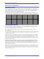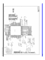
1
^1 HARDWARE REFERENCE MANUAL
^2 PMAC2 PCI
^3 PMAC 2 PCI Bus Expansion Card
^4 4XX-603486-xHxx
^5 May 26, 2004
Single Source Machine Control
Power // Flexibility // Ease of Use
21314 Lassen Street Chatsworth, CA 91311 // Tel. (818) 998-2095 Fax. (818) 998-7807 // www.deltatau.com
Copyright Information
© 2003 Delta Tau Data Systems, Inc. All rights reserved.
This document is furnished for the customers of Delta Tau Data Systems, Inc. Other uses are
unauthorized without written permission of Delta Tau Data Systems, Inc. Information contained
in this manual may be updated from time-to-time due to product improvements, etc., and may not
conform in every respect to former issues.
To report errors or inconsistencies, call or email:
Delta Tau Data Systems, Inc. Technical Support
Phone: (818) 717-5656
Fax: (818) 998-7807
Email: [email protected]
Website: http://www.deltatau.com
Operating Conditions
All Delta Tau Data Systems, Inc. motion controller products, accessories, and amplifiers contain
static sensitive components that can be damaged by incorrect handling. When installing or
handling Delta Tau Data Systems, Inc. products, avoid contact with highly insulated materials.
Only qualified personnel should be allowed to handle this equipment.
In the case of industrial applications, we expect our products to be protected from hazardous or
conductive materials and/or environments that could cause harm to the controller by damaging
components or causing electrical shorts. When our products are used in an industrial
environment, install them into an industrial electrical cabinet or industrial PC to protect them
from excessive or corrosive moisture, abnormal ambient temperatures, and conductive materials.
If Delta Tau Data Systems, Inc. products are exposed to hazardous or conductive materials and/or
environments, we cannot guarantee their operation.
PMAC2 PCI Hardware Reference Manual
Table of Contents
INTRODUCTION .......................................................................................................................................................1
Board Configuration..................................................................................................................................................1
Base Version .........................................................................................................................................................1
Option 1: Additional Four Channels Axis Interface Circuitry.............................................................................1
Option 2: Dual-Ported RAM................................................................................................................................1
Option 5xF: CPU Speed Options.........................................................................................................................2
Option 6: Extended Servo Algorithm ...................................................................................................................2
Option 7: Plate Mounting ....................................................................................................................................2
Option 8: High-Accuracy Clock Crystal..............................................................................................................2
Option 10: Firmware Version Specification ........................................................................................................2
Option 12: Analog-to-Digital Converters............................................................................................................2
Option 16: Battery-Backed Parameter Memory ..................................................................................................2
HARDWARE SETUP .................................................................................................................................................3
Piggyback CPU Board Jumper Configuration...........................................................................................................3
Watchdog Timer Jumper.......................................................................................................................................3
Dual-ported RAM Source Jumper.........................................................................................................................3
Power-Up State Jumpers ......................................................................................................................................3
Firmware Load Jumper ........................................................................................................................................3
Flash Memory Bank Select Jumpers.....................................................................................................................3
Base Board Jumper Configuration ............................................................................................................................3
Servo and Phase Clock Direction Control............................................................................................................3
CPU Frequency Control Jumpers.........................................................................................................................4
Re-Initialization Jumper .......................................................................................................................................4
Encoder Sample Clock Source Jumpers ...............................................................................................................4
Serial Port Selection Jumper ................................................................................................................................4
Output Disable State Jumpers ..............................................................................................................................4
Resistor Pack Configuration......................................................................................................................................5
Termination Resistors ...........................................................................................................................................5
Pull-Up/Pull-Down Resistors ...............................................................................................................................5
Connections...............................................................................................................................................................6
Mounting...............................................................................................................................................................6
Power Supply Connection.....................................................................................................................................6
Machine Port Connections ...................................................................................................................................6
Display Port..........................................................................................................................................................6
Multiplexer Port....................................................................................................................................................7
I/O Port.................................................................................................................................................................7
Serial Ports ...........................................................................................................................................................7
A/D-Converter Port ..............................................................................................................................................7
Handwheel Port ....................................................................................................................................................7
COMMUNICATIONS SETUP ..................................................................................................................................9
FLEX CPU BOARD JUMPER DESCRIPTIONS..................................................................................................11
E1: Watchdog Disable Jumper ...............................................................................................................................11
E2: Dual-Ported RAM Port Select .........................................................................................................................11
E4 – E6: Power-Up/Reset Load Source .................................................................................................................11
E7: Firmware Reload Enable..................................................................................................................................11
E10A, B, C: Flash Memory Bank Select................................................................................................................12
PMAC2 PCI BASE BOARD JUMPER DESCRIPTIONS ....................................................................................13
E2: CPU Frequency Select ......................................................................................................................................13
E3: Normal/Re-Initializing Power-Up/Reset...........................................................................................................13
E4: CPU Frequency Select ......................................................................................................................................13
E5 – E6: (Reserved for Future Use) ........................................................................................................................14
Table Of Contents
i
PMAC2 PCI Hardware Reference Manual
E13 - E14: Encoder Sample Clock Direction Control............................................................................................14
E17 - E18: Serial Port Type Selection....................................................................................................................14
E111-118: Command Output Disable State ...........................................................................................................15
MATING CONNECTORS .......................................................................................................................................17
CPU Board Connectors ...........................................................................................................................................17
J2 (JEXP)/Expansion ..........................................................................................................................................17
Baseboard Connectors.............................................................................................................................................17
J1 (JANA)/Analog (Option 12) ...........................................................................................................................17
J2 (JTHW)/Multiplexer Port ...............................................................................................................................17
J3 (JIO)/Digital I/O ............................................................................................................................................17
J5 (JRS232)/RS-232 Serial Communications......................................................................................................17
J5A (JRS422)/RS-422 Serial Communications ...................................................................................................17
J6 (JDISP)/Display .............................................................................................................................................17
J7 (JHW)/Auxiliary Channel...............................................................................................................................17
J8 (JEQU)/Position Compare.............................................................................................................................18
J9 (JMACH1)/Machine Port 1............................................................................................................................18
J10 (JMACH2)/Machine Port 2..........................................................................................................................18
J11 (JMACH3)/Machine Port 3..........................................................................................................................18
J12 (JMACH4)/Machine Port 4..........................................................................................................................18
PMAC2 PCI BASE BOARD CONNECTOR PINOUTS .......................................................................................19
J1 (JANA) Analog Input Port Connector ................................................................................................................19
J2 (JTHW) Multiplexer Port Connector ..................................................................................................................20
J3 (JI/O) General Input/Output Connector ..............................................................................................................21
J5 (JRS232) Serial Port Connector..........................................................................................................................22
J5A (RS422) Serial Port Connector ........................................................................................................................22
J6 (JDISP) Display Connector ................................................................................................................................23
J7 (JHW) Handwheel Encoder Connector...............................................................................................................23
J8 (JEQU) Position Compare Output Connector.....................................................................................................24
J9 (JMACH1) Connector Description .....................................................................................................................24
J9 JMACH1 Connector.......................................................................................................................................25
J9 JMACH1 Connector.......................................................................................................................................27
J10 (JMACH2) Connector Description ...................................................................................................................27
J11 (JMACH3) Connector Description ...................................................................................................................30
J11 JMACH3 Connector.....................................................................................................................................31
J12 (JMACH4) Connector Description ...................................................................................................................33
J12 JMACH4 Connector.....................................................................................................................................34
J12 JMACH4 Connector.....................................................................................................................................35
J12 JMACH4 Connector.....................................................................................................................................36
TB1 (2/4-Pin Terminal Block) ................................................................................................................................36
TB2 (3-Pin Terminal Block) ...................................................................................................................................37
BASE BOARD JUMPERS LAYOUT......................................................................................................................39
SCHEMATICS ..........................................................................................................................................................41
ii
Table of Contents
PMAC2 PCI Hardware Reference Manual
INTRODUCTION
The PMAC2 PCI (part number 400-603367-10x) is a member of the PMAC family of boards optimized
for interface to sinewave or direct-PWM servo drives and to pulse-and-direction stepper drives. Its
software is capable of eight axes of control. It can have up to eight channels of on-board axis interface
circuitry. It can also support up to eight channels of off-board axis interface circuitry through its
expansion port, connected to Acc-24P or Acc-24P2 ISA-format boards. Acc-24 boards in PCI format are
not yet available.
The PMAC2 PCI is a full-sized PCI-bus expansion card, with a small piggyback board containing the
CPU board. This piggyback board occupies part of the next slot, but ½-sized boards are permitted in this
next slot. While the PMAC2 PCI is capable of PCI bus communications, with or without the optional onboard dual-ported RAM, it does not need to be inserted into a PCI expansion slot. Communications can
be done through the standard RS-232/RS-422 serial port. Standalone operation is possible.
Board Configuration
Base Version
The base version of the PMAC2 PCI provides a 1-1/2-slot board with:
• 40MHz DSP563xx CPU (Option 5AF, 80MHz 56002 equivalent)
• 128k x 24 0-wait-state flash-backed SRAM
• 512k x 8 flash memory for user backup & firmware
• Latest released firmware version
• RS-232/RS422 serial interface, PCI bus interface
• Four channels axis interface circuitry, each including:
•
Three output command signal sets, configurable as either:
Two serial data streams to external DACs, 1 pulse-and-direction
Three PWM top-and-bottom pairs
•
3-channel differential/single-ended encoder input
•
Nine input flags, two output flags
•
Interface to two external serial ADCs, 8 to 18 bits
• Two channels supplemental interface circuitry, each including:
•
2-channel differential/single-ended encoder input
•
One output command signal set, configurable as
pulse-&-direction or PWM top-and-bottom pair
• Display, MACRO, muxed I/O, direct I/O interface ports
• PID/notch/feedforward servo algorithms
• 1-year warranty from date of shipment
• One manual per set of one to four PMACs shipped
(Cables, mounting plates, mating connectors not included)
Option 1: Additional Four Channels Axis Interface Circuitry
•
Option 1 provides an additional four channels of on-board axis interface circuitry, identical to the
standard first four channels. The key components on the board are the DSPGATE1 IC at U7 and
connectors J11 and J12.
Option 2: Dual-Ported RAM
Dual-ported RAM provides a very high-speed communications path for bus communications with the
host computer through a bank of shared memory. DPRAM is advised if more than 100 data items per
second are to be passed between the controller and the host computer in either direction.
• Option 2 provides an 8k x 16 bank of dual-ported RAM. The key component on the board is U28.
Introduction
1
PMAC2 PCI Hardware Reference Manual
Option 5xF: CPU Speed Options
•
•
•
Option 5CF: 80MHz DSP563xxx CPU (160MHz 56002 equivalent)
Option 5EF: 160MHz DSP563xxx CPU (320MHz 56002 equivalent)
Option 5AF: 40MHz DSP563xx CPU (80MHz 56002 equivalent) Default configuration provided
automatically if no CPU option ordered.
Option 6: Extended Servo Algorithm
The standard PID servo algorithm with feedforward and notch filter is suitable for most applications.
Systems with difficult dynamics, especially with significant flexibility, may require a more powerful
servo algorithm, such as the Extended Servo Algorithm (ESA).
Option 7: Plate Mounting
•
Option 7 provides a mounting plate connected to the PMAC2 PCI with standoffs. It is used to install
the PMAC2 PCI in standalone applications.
Option 8: High-Accuracy Clock Crystal
The PMAC2 PCI has a clock crystal (component Y1) of nominal frequency 19.6608MHz (~20MHz).
The standard crystal’s accuracy specification is +/-100 ppm.
• Option 8A provides a nominal 19.6608MHz crystal with a +/-15 ppm accuracy specification.
Option 10: Firmware Version Specification
Normally the Turbo PMAC2 PCI is provided with the newest released firmware version. A label on the
U10 flash memory IC on the CPU board shows the firmware version loaded at the factory.
• Option 10 provides for a user-specified firmware version.
Option 12: Analog-to-Digital Converters
•
•
•
Option 12 permits the installation of 8 or 16 channels of on-board multiplexed analog-to-digital
converters. 1 or 2 of these converters are read every phase interrupt. The analog inputs are not
optically isolated, and each can have a 0 – 5V input range, or a +/-2.5V input range, individually
selectable.
Option 12 provides an 8-channel 12-bit A/D converter. The key components on the board are U28
and connector J1.
Option 12A provides an additional 8-channel 12-bit A/D converter. The key component on the board
is U29.
Option 16: Battery-Backed Parameter Memory
The contents of the standard memory are not retained through a power-down or reset unless they have
been saved to flash memory first. Option 16 provides supplemental battery-backed RAM for real-time
parameter storage that is ideal for holding machine state parameters in case of an unexpected powerdown. The battery is located at component BT1.
• Option 16 provides a 16k x 24 bank of battery-backed parameter RAM in components U6, U9, and
U15 on the CPU board.
2
Introduction
PMAC2 PCI Hardware Reference Manual
HARDWARE SETUP
Piggyback CPU Board Jumper Configuration
Watchdog Timer Jumper
Jumper E1 on the Turbo CPU board must be OFF for the watchdog timer to operate. This is an important
safety feature, so it is vital that this jumper be OFF in normal operation. E1 should be put ON only to
debug problems with the watchdog timer circuit.
Dual-ported RAM Source Jumper
Jumper E2 must connect pins 1 and 2 to access dual-ported RAM from the baseboard. To use Option 2
DPRAM on the baseboard, jumper E2 must be in this setting.
Jumper E2 must connect pins 2 and 3 to access dual-ported RAM through the JEXP expansion port. To
use DPRAM on an external accessory board, jumper E2 must be in this setting.
Power-Up State Jumpers
Jumper E4 on the Turbo CPU board must be OFF, jumper E5 must be ON, and jumper E6 must be ON, in
order for the CPU to copy the firmware from flash memory into active RAM on power-up/reset. This is
necessary for normal operation of the card. (Other settings are for factory use only.)
Firmware Load Jumper
If jumper E7 on the CPU board is ON during power-up/reset, the board comes up in bootstrap mode,
which permits the loading of new firmware into the flash-memory IC on the board. When the PMAC
Executive program tries to establish communications with a board in this mode, it will detect
automatically that the board is in bootstrap mode and ask what file to download as the new firmware.
Jumper E7 must be OFF during power-up/reset for the board to come up in normal operational mode.
Flash Memory Bank Select Jumpers
The flash-memory IC in location U10 on the Flex CPU board has the capacity for eight separate banks of
firmware, only one of which can be used at any given time. The eight combinations of settings for
jumpers E10A, E10B, and E10C select which bank of the flash memory is used. In the factory production
process, firmware is loaded only into Bank 0, which is selected by having all of these jumpers OFF.
Base Board Jumper Configuration
Servo and Phase Clock Direction Control
Jumper E1 should be off if the board is using its own internally generated phase and servo clock signals.
In this case, these signals are output on spare pins on the J5A RS-422 serial-port connector, where they
can be used by other PMAC controllers set up to take external phase and servo clock signals.
Jumper E1 should be on if the board is using externally generated phase and servo clock signals brought
in on the J5A RS-422 serial port connector. In this case, another PMAC controller generates the clock
signals and output is on its serial port connector. Commonly, serial communications are also shared over
a multi-drop RS-422 cable, with software addressing of the cards matching the I0 serial card number for
each controller. Alternately, the phase and servo clock signals can come from clock signals involved in
the process.
If E1 is on for external phase and clock signals, and these clock signals are not brought in on the serial
port connector, the watchdog timer will trip immediately and shut down the board.
Hardware Setup
3
PMAC2 PCI Hardware Reference Manual
In order to change the state of the card between use of internal clock and use of external clock, the card
must be re-initialized (either powered up with jumper E3 on, or given the $$$*** command) with
jumper E1 in the new state. Before the card is reset again, a SAVE command must be issued to store the
new internal settings.
CPU Frequency Control Jumpers
If variable I46 is set to the default value of zero, jumpers E2 and E4 on the base PMAC2 PCI board
control the frequency at which the CPU will operate (or attempt to operate). Generally this will be the
highest frequency at which the CPU is rated to operate.
• If jumpers E2 and E4 are both OFF, the CPU will operate at a 40MHz frequency.
• If E2 is ON and E4 is OFF, the CPU will operate at a 60MHz frequency.
• If E2 is OFF and E4 is ON, the CPU will operate at an 80MHz frequency.
• If I46 is set to a value greater than zero, E2 and E4 are not used. The CPU frequency is set to 10MHz
(I46+1)
Re-Initialization Jumper
If E3 is off during power-up/reset, the controller will load its last saved set-up parameters from flash
memory into active memory. This is the setting for normal operation.
If E3 is on during power-up/reset, the controller will load its factory-default set-up parameters from
firmware into active memory. Generally, this is done only if communications cannot be established with
the card when it comes up in normal operational mode.
Encoder Sample Clock Source Jumpers
Jumpers E13 and E14 control the source of the SCLK encoder-sampling clock for each servo IC. The
default setting no jumper installed means that the SCLK signal comes from the servo IC and is output on
the JMACH connectors. This setting is suitable for all but a few very special applications.
Serial Port Selection Jumper
Jumpers E17 and E18 control which serial-port connector is used. If E17 and E18 connect their pins 1
and 2, the 10-pin RS-232 port connector J5 is used. If E17 and E18 connect their pins 2 and 3, the 26-pin
RS-422 port connector J5A is used. The RS-422 port must be used if several cards are to be daisychained together on a single multi-drop cable.
Output Disable State Jumpers
Jumpers E111 through E118 control the hardware state of the digital command output signals for each
channel when the amplifier enable signal for that channel is in the disable state (false). Jumper E11n (n =
1 to 8) controls the output signals for channel n on the board.
If E11n is off (default), the command output signals for channel n are still active when the amplifier
enable signal is in the disable state. The Turbo PMAC software should be commanding a net zero
command to be output on these signals and the amplifier enable signal should be used by the amplifier so
that no command output will cause action if it is receiving a disable signal. The off setting should be used
when DAC output format is selected for the channel.
If E11n is on, the command output signals for channel n are tri-stated when the amplifier-enable signal is
in the disable state. This setting is used only with direct-PWM power-block amplifiers that do not use
amplifier enable to gate the PWM signals, and in which the zero-command format of 50% top on-time,
and 50% bottom on-time cannot be tolerated in the disable state.
4
Hardware Setup
PMAC2 PCI Hardware Reference Manual
Resistor Pack Configuration
Termination Resistors
The PMAC2 PCI provides sockets for termination resistors on differential input pairs coming into the
board. As shipped, there are no resistor packs in these sockets. If these signals are brought long distances
into the PMAC2 PCI board and ringing at signal transitions is a problem, SIP resistor packs may be
mounted in these sockets to reduce or eliminate the ringing.
All termination resistor packs have independent resistors (no common connection) with each resistor
using two adjacent pins. The following table shows which packs are used to terminate each input device:
Input
Pack
Pack Size
Input
Pack
Pack Size
Encoder 1
Encoder 2
Encoder 3
Encoder 4
Encoder 5
Encoder 6
Encoder 7
Encoder 8
SCLK12&34
RP46
RP50
RP47
RP51
RP107
RP111
RP108
RP112
RP52
6-pin
6-pin
6-pin
6-pin
6-pin
6-pin
6-pin
6-pin
6-pin
ADC 1 & 2
ADC 3 & 4
ADC 5 & 6
ADC 7 & 8
Fault 1 & 2
Fault 3 & 4
Fault 5 & 6
Fault 7 & 8
SCLK56&78
RP60
RP61
RP121
RP122
RP63
RP64
RP124
RP125
RP113
8-pin
8-pin
8-pin
8-pin
6-pin
6-pin
6-pin
6-pin
6-pin
Pull-Up/Pull-Down Resistors
The differential input signal pairs to the PMAC2 PCI have user-configurable pull-up/pull-down resistor
networks to permit the acceptance of either single-ended or differential signals in one setting, or the
detection of lost differential signals in another setting.
The ‘+’ inputs of each differential pair each have a hard-wired 1 kohm pull-up resistor to +5V. This
cannot be changed.
The ‘-’ inputs of each differential pair each have a hard-wired 2.2 kohm resistor to +5V; each has another
2.2 kohm resistor as part of a socketed resistor pack that can be configured as a pull-up resistor to +5V, or
a pull-down resistor to GND.
If this socketed resistor is configured as a pull-down resistor (the default configuration), the combination
of pull-up and pull-down resistors on this line acts as a voltage divider, holding the line at +2.5V in the
absence of an external signal. This configuration is required for single-ended inputs using the ‘+’ lines
alone; it is desirable for unconnected inputs to prevent the pick-up of spurious noise. It is permissible for
differential line-driver inputs.
If this socketed resistor is configured as a pull-up resistor (by reversing the SIP pack in the socket), the
two parallel 2.2 kohm resistors act as a single 1.1 kohm pull-up resistor, holding the line at +5V in the
absence of an external signal. This configuration is required if encoder-loss detection is desired; or if
complementary open-collector drivers are used. It is permissible for differential line-driver inputs even
without encoder loss detection.
If Pin 1 of the resistor pack (marked by a dot on the pack) matches Pin 1 of the socket (marked by a wide
white line on the front side of the board and a square solder pin on the back side of the board), then the
pack is configured as a bank of pull-down resistors. If the pack is reversed in the socket, it is configured
as a bank of pull-up resistors.
Hardware Setup
5
PMAC2 PCI Hardware Reference Manual
The following table lists the pull-up/pull-down resistor pack for each input device:
Device
Resistor Pack
Device
Resistor Pack
Encoder 1
Encoder 2
Encoder 3
Encoder 4
Encoder 5
Encoder 6
Encoder 7
Encoder 8
RP43
RP48
RP44
RP49
RP104
RP109
RP105
RP110
ADC/Fault1&2
ADC/Fault3&4
ADC/Fault5&6
ADC/Fault7&8
SCLK12&34
SCLK56&78
RP58
RP59
RP119
RP120
RP62
RP123
Connections
Mounting
The PMAC2 PCI can be mounted in one of two ways: in the PCI bus, or using standoffs.
• PCI bus: To mount in the PCI bus, simply insert the P1 card-edge connector into the PCI socket. If
there is a standard PC-style housing, a bracket at the end of the PMAC2 PCI board can be used to
screw into the housing to hold the board down firmly.
• Standoffs: At each of the four corners of the PMAC2 PCI board, there are mounting holes that can be
used to mount the board on standoffs.
Power Supply Connection
The standard PMAC2 PCI requires only 5V power: 3A in a 4-channel configuration, 4A in an 8-channel
configuration (with Option 1). If the Option 12 A/D converters are installed, a –12V supply is also
required. In this case, a +12V supply also can be passed through the card and out to the analog devices
feeding the A/D converters.
The power can be provided in several ways:
• Bus connector: If the PMAC2 PCI is mounted in an electrically active PCI bus slot, it automatically
draws its 5V and +/-12V power from the bus.
• Terminal block: The TB1 2/4-point terminal block can be used to bring in 5V power, especially in
standalone applications. Point 1 is GND; Point 2 is +5V. Points 3 and 4 are needed only if the
Option-12 A/D converters are ordered.
• JMACH connectors: Up to 2A may be brought in through each 100-pin JMACH connector from an
Acc-8 board or its equivalent, provided the cable is 500mm (20 inches) or less in length.
Machine Port Connections
The PMAC2 PCI has a 100-pin high-density header for each pair of servo interface channels. Through
this connector pass all of the digital signals to and from the amplifier, encoder, and flags for the two
channels. Typically, this header is connected with a matching Delta Tau Acc-8 family 2-channel
breakout board or equivalent through a provided 100-pin flat cable.
The machine port connectors are:
• J9 (JMACH1)
Board Channels 1 and 2
• J10 (JMACH2)
Board Channels 3 and 4
• J11 (JMACH3)
Board Channels 5 and 6 (Option 1 required)
• J12 (JMACH4)
Board Channels 7 and 8 (Option 1 required)
Display Port
The J6 (JDISP) display port provides a 14-pin IDC header for connection to the Acc-12 family of
displays. Flat cables are provided with each of these displays for direct connection between the display
and this port.
6
Hardware Setup
PMAC2 PCI Hardware Reference Manual
Multiplexer Port
The J2 (JTHW) multiplexer port provides eight TTL-compatible 5V CMOS inputs and eight TTLcompatible 5V CMOS outputs on a 26-pin IDC header. These can be used directly as general-purpose
digital I/O, or with PMAC2’s special M-variable support (TWB, TWD, TWR, and TWS formats), they
can be used to support hundreds, or even thousands of multiplexed I/O points on accessory boards.
Delta Tau provides the following accessory boards that can be connected to the multiplexer port. Each
comes with a flat cable for direct connection to the port.
• Acc-8D Option 7 Resolver-to-Digital Converter Board
• Acc-18 Thumbwheel Board
• Acc-34 family of Digital I/O Boards
• Acc-35A and B Extender Boards
I/O Port
The J3 (JIO) I/O port provides 32 TTL-compatible 5V CMOS I/O points on a 40-pin IDC header.
Direction is selectable by byte. These are used as general-purpose digital I/O points. Acc-21A provides a
convenient connections adapter from this port to OPTO-22 style boards.
Serial Ports
The PMAC2 PCI has two serial-port connectors. Only one of these can be used in an application. J5 is a
10-pin IDC header for RS-232 communications. It can be connected to a standard DB9 RS-232
connector on a host computer or terminal via a flat cable such as the Acc-3L. A commercially available
DB9-to-DB25 adapter can be added to this flat cable if the host computer or terminal has a DB25 serial
connector. Jumpers E17 and E18 on the PMAC2 PCI must connect pins 1 and 2 to use this port.
J5A is 26-pin IDC header for RS-422 communications. It can be connected to a standard DB25 RS-422
connector on a host computer or terminal via a flat cable such as the Acc-3D. Jumpers E17 and E18 on
the PMAC2 PCI must connect pins 2 and 3 to use this port.
A/D-Converter Port
If the Option 12 A/D converters are ordered, the J1 (JANA) analog-input port is provided on the PMAC2
on a 20-pin IDC header. Option 12 provides eight analog inputs at 0 – 5V, or +/-2.5V levels. Option 12A
provides eight additional analog inputs at these levels. The +12V and –12V supplies can either be
brought in on this connector, or brought out on it for the external analog circuitry, if they have been
brought in through TB1 or P1.
Handwheel Port
The J7 (JHW) handwheel port provides two limited supplemental channels, each with a 2-channel
encoder input, and a pulse-and-direction or PWM top-and-bottom pair output. All inputs and outputs are
digital 5V differential line-driver pairs.
Hardware Setup
7
PMAC2 PCI Hardware Reference Manual
8
Hardware Setup
PMAC2 PCI Hardware Reference Manual
COMMUNICATIONS SETUP
Delta Tau provides communication tools that take advantage of the PCI bus Plug and Play feature of 32bits Windows® based computers. Starting with MOTIONEXE.EXE version 10.32.00, which is included
in PEWIN32 version 2.32 and newer, a PMAC2 PCI board plugged in a PCI bus slot will be recognized
by the operating system when the computer is booted up. The available PCI address, dual-ported RAM
address and Interrupt lines are set automatically by the operating system and can be checked (but not
modified) in the MOTIONEXE.EXE application.
Open MOTIONEXE
and press Setup for the
PCI device desired
The PMAC2 PCI board may have the optional on-board dual-ported RAM circuitry, which is ordered
through Option-2. If the dual-ported RAM circuitry is not on-board, manually disable its automatically
assigned use through the setup page of MOTIONEXE:
MOTIONEXE
version number
Disable Interrupts
and Dual-ported
RAM if not used
The MOTIONEXE application will look first for PMAC PCI boards on the PCI bus and will assign
device numbers sequentially from Device0 to each PMAC PCI until all the PMAC PCI boards found have
a device number assigned. Then, manually add other devices for either ISA bus or Serial port
communications.
After each PMAC has a device number assigned to it, communications through the PCI bus are identical
to the ISA bus. Any application written for the ISA bus using the Delta Tau provided 32-bits
communication libraries provided will not require any further change and the process is transparent.
Communications Setup
9
PMAC2 PCI Hardware Reference Manual
Note:
For example, if a Device0 for serial RS-232 communications was defined before a
PMAC PCI board was installed in the computer, its setup information will be
overwritten by the MOTIONEXE application when the PMAC2 PCI board is
found. Therefore, it is very important to take note of the all the devices and their
parameters defined in MOTIONEXE before installing a new PMAC board in the
computer.
10
Communications Setup
PMAC2 PCI Hardware Reference Manual
FLEX CPU BOARD JUMPER DESCRIPTIONS
E1: Watchdog Disable Jumper
E Point and
Physical Layout
Description
E1
Jump pin 1 to 2 to disable Watchdog timer (for test purposes
only).
Remove jumper to enable Watchdog timer.
Default
No jumper
installed
E2: Dual-Ported RAM Port Select
E Point and
Physical Layout
E2
Description
Jump pin 1 to 2 to access DPRAM from baseboard.
Jump pin 2 to 3 to access DPRAM through JEXP expansion
port.
Default
Pins 1 and 2
jumpered
E4 – E6: Power-Up/Reset Load Source
E Point and
Physical Layout
E6
Description
Remove jumper E4;
Jump E5 pin 1 to 2;
Jump E6 pin 2 to 3;
to read flash IC on power-up/reset
Other combinations are for factory use only; the board will
not operate in any other configuration.
Default
No E4 jumper
installed;
E5 and E6 jump
pin 1 to 2
E4
E7: Firmware Reload Enable
E Point and
Physical Layout
Description
E7
Jump pin 1 to 2 to reload firmware through serial or bus port
Remove jumper for normal operation.
Flex CPU Board Jumper Descriptions
Default
No jumper
installed
11
PMAC2 PCI Hardware Reference Manual
E10A, B, C: Flash Memory Bank Select
E Point and
Physical Layout
Description
Default
E10A
Remove all three jumpers to select flash memory bank with
factory-installed firmware.
Use other configuration to select one of the seven other flash
memory banks.
No jumpers
installed
E10C
12
Flex CPU Board Jumper Descriptions
PMAC2 PCI Hardware Reference Manual
PMAC2 PCI BASE BOARD JUMPER DESCRIPTIONS
E1: Servo and Phase Clock Direction Control
E Point and
Physical Layout
Location
Description
Default
Remove jumper for PMAC2 PCI to use its
No jumper
internally generated servo and phase clock
installed
signals and to output these signals on the J5A
serial port connector.
Jump pins 1 and 2 for PMAC2 PCI to expect
to receive its servo and phase clock signals on
the J5A serial port connector.
Note: If the E1 jumper is ON and the servo and phase clocks are not brought in on the J5A serial port, the
watchdog timer will trip immediately.
E1
C2
E2: CPU Frequency Select
E Point and
Physical layout
Location
E2
C2
Description
Remove jumper for 40MHz operation (E4
OFF also) or for 80MHz operation (E4 ON)
with I46 = 0.
Jump pin 1 to 2 for 60MHz operation (E4
OFF) with I46 = 0.
Not used if I46 > 0.
Default
No jumper
installed
Jumper installed
E3: Normal/Re-Initializing Power-Up/Reset
E Point and
Physical Layout
Location
E3
C2
Description
Jump pin 1 to 2 to re-initialize on powerup/reset, loading factory default settings.
Remove jumper for normal power-up/reset,
loading user-saved settings.
Default
No jumper
installed
E4: CPU Frequency Select
E Point and
Physical layout
Location
E4
C2
Base Board Jumper Descriptions
Description
Remove jumper for 40MHz operation (E2
OFF also) or for 60MHz operation (E4 ON)
with I46 = 0.
Jump pin 1 to 2 for 80MHz operation (E2
OFF) with I46 = 0.
Not used if I46 > 0
Default
No jumper
installed (standard
or Option 5B)
Jumper installed
(Option 5C)
13
PMAC2 PCI Hardware Reference Manual
E5 – E6: (Reserved for Future Use)
E13 - E14: Encoder Sample Clock Direction Control
E Point and
Physical layout
Location
Description
Default
Remove jumper to output SCLK generated in
first ASIC on SCLK_12 and SCLK_34, or to
1
control direction by software.
2
Jump pins 1 to 2 to input SCLK signal for
3
first ASIC on SCLK_34 and output this
signal on SCLK_12.
Jump pins 2 to 3 to input SCLK signal for
first ASIC on SCLK_12 and output this
signal on SCLK_34.
D2
Remove jumper to output SCLK generated in
E14
second ASIC on SCLK_56 and SCLK_78, or
3 2 1
to control direction by software.
Jump pins 1 to 2 to input SCLK signal for
second ASIC on SCLK_78 and output this
signal on SCLK_56.
Jump pins 2 to 3 to input SCLK signal for
second ASIC on SCLK_56 and output this
signal on SCLK_78.
Note: E14 is only installed if Option 1 has been ordered.
E13
D1
No jumper installed
No jumper installed
E17 - E18: Serial Port Type Selection
E Point and
Physical layout
Location
Description
E17
C1
Connect pins 1 and 2 to use the RS-232 port
on the J5 connector.
Connect pins 2 and 3 to use the RS-422 port
on the J5A connector.
Jumper installed in
1-2 position
C1
Connect pins 1 and 2 to use the RS-232 port
on the J5 connector.
Connect pins 2 and 3 to use the RS-422 port
on the J5A connector.
Jumper installed in
1-2 position
1
2
3
E18
1
2
3
Default
Serial Port Choice: Because both RS-232 and RS-422 ports are always provided, jumpers must be set
correctly to use the port of choice. Jumpers E17 and E18 must connect pins 1 and 2 to use the RS-232 port
on the J5 connector; to use the RS-422 port on the J5A connector, they must connect pins 2 and 3.
14
Base Board Jumper Descriptions
PMAC2 PCI Hardware Reference Manual
E111-118: Command Output Disable State
E Point and
Physical Layout
E111
E112
E113
E114
E115
Location
Description
C1
Jump pin 1 to 2 of E11n for digital
servo command output signals of
Channel n to tri-state when amplifierenable signal for Channel n is in
disable state.
Remove jumper for digital servo
command output signals of Channel n
to remain active (but typically with
zero command value) when amplifierenable signal for Channel n is in
disable state.
Default
No jumper
installed
E116
E117
E118
Base Board Jumper Descriptions
15
PMAC2 PCI Hardware Reference Manual
16
Base Board Jumper Descriptions
PMAC2 PCI Hardware Reference Manual
MATING CONNECTORS
CPU Board Connectors
J2 (JEXP)/Expansion
•
•
•
Two 50-pin female flat cable connector Delta Tau P/N 014-R00F50-0K0 - T&B Ansley P/N 609-5041
171-50 T&B Ansley standard flat cable stranded 50-wire
Phoenix varioface module type FLKM 50 (male pins) P/N 22 81 08 9
Baseboard Connectors
J1 (JANA)/Analog (Option 12)
•
•
•
Two 14-pin female flat cable connector Delta Tau P/N 014-R00F14-0K0 - T&B Ansley P/N 609-1441
171-14 T&B Ansley standard flat cable stranded 14-wire
Phoenix varioface modules type FLKM14 (male pins) P/N 22 81 02 1
J2 (JTHW)/Multiplexer Port
•
•
•
Two 26-pin female flat cable connector Delta Tau P/N 014-R00F26-0K0 - T&B Ansley P/N 609-2641
171-26 T&B Ansley standard flat cable stranded 26-wire
Phoenix varioface module type FLKM 26 (male pins) P/N 22 81 05 0
J3 (JIO)/Digital I/O
•
•
•
Two 40-pin female flat cable connector Delta Tau P/N 014-R00F40-0K0 - T&B Ansley P/N 609-4041
171-40 T&B Ansley standard flat cable stranded 40-wire
Phoenix varioface module type FLKM 40 (male pins)
J5 (JRS232)/RS-232 Serial Communications
•
•
•
Two 10-pin female flat cable connector Delta Tau P/N 014-ROOF10-0K0 - T&B Ansley P/N 609-1041
171-10 T&B Ansley standard flat cable stranded 10-wire
Phoenix varioface module type FLKM 10 (male pins) P/N 22 81 01 8
J5A (JRS422)/RS-422 Serial Communications
•
•
•
Two 26-pin female flat cable connector Delta Tau P/N 014-R00F26-0K0 - T&B Ansley P/N 609-2641
171-26 T&B Ansley standard flat cable stranded 26-wire
Phoenix varioface module type FLKM 26 (male pins) P/N 22 81 05 0
J6 (JDISP)/Display
•
•
•
Two 14-pin female flat cable connector Delta Tau P/N 014-R00F14-0K0 - T&B Ansley P/N 609-1441
171-14 T&B Ansley standard flat cable stranded 14-wire
Phoenix varioface modules type FLKM14 (male pins) P/N 22 81 02 1
J7 (JHW)/Auxiliary Channel
•
•
•
Two 20-pin female flat cable connector Delta Tau P/N 014-R00F20-0K0 - T&B Ansley P/N 609-2041
171-20 T&B Ansley standard flat cable stranded 20-wire
Phoenix varioface modules type FLKM20 (male pins)
Mating Connectors
17
PMAC2 PCI Hardware Reference Manual
J8 (JEQU)/Position Compare
•
•
•
Two 10-pin female flat cable connector Delta Tau P/N 014-ROOF10-0K0 - T&B Ansley P/N 609-1041
171-10 T&B Ansley standard flat cable stranded 10-wire
Phoenix varioface module type FLKM 10 (male pins) P/N 22 81 01 8
J9 (JMACH1)/Machine Port 1
•
•
Two 100-pin high-density box header with center key, 0.050” pitch - AMP P/N 1-04068-7, Delta Tau
P/N 014-00010-FPB
High-density flat cable stranded 100-wire
J10 (JMACH2)/Machine Port 2
•
•
Two 100-pin high-density box header with center key, 0.050” pitch - AMP P/N 1-04068-7, Delta Tau
P/N 014-00010-FPB
High-density flat cable stranded 100-wire
J11 (JMACH3)/Machine Port 3
•
•
Two 100-pin high-density box header with center key, 0.050” pitch - AMP P/N 1-04068-7, Delta Tau
P/N 014-00010-FPB
High-density flat cable stranded 100-wire
J12 (JMACH4)/Machine Port 4
•
•
18
Two 100-pin high-density box header with center key, 0.050” pitch - AMP P/N 1-04068-7, Delta Tau
P/N 014-00010-FPB
High-density flat cable stranded 100-wire
Mating Connectors
PMAC2 PCI Hardware Reference Manual
PMAC2 PCI BASE BOARD CONNECTOR PINOUTS
J1 (JANA) Analog Input Port Connector
This connector is present only if Option 12 is ordered.
Pin #
Symbol
Function
Description
Notes
1
ANAI00
Input
Analog input 0
0-5V or +/-2.5V range
2
ANAI01
Input
Analog input 1
0-5V or +/-2.5V range
3
ANAI02
Input
Analog input 2
0-5V or +/-2.5V range
4
ANAI03
Input
Analog input 3
0-5V or +/-2.5V range
5
ANAI04
Input
Analog input 4
0-5V or +/-2.5V range
6
ANAI05
Input
Analog input 5
0-5V or +/-2.5V range
7
ANAI06
Input
Analog input 6
0-5V or +/-2.5V range
8
ANAI07
Input
Analog input 7
0-5V or +/-2.5V range
9
ANAI08
Input
Analog input 8
0-5V or +/-2.5V range *
10
ANAI09
Input
Analog input 9
0-5V or +/-2.5V range *
11
ANAI10
Input
Analog input 10
0-5V or +/-2.5V range *
12
ANAI11
Input
Analog input 11
0-5V or +/-2.5V range *
13
ANAI12
Input
Analog input 12
0-5V or +/-2.5V range *
14
ANAI13
Input
Analog input 13
0-5V or +/-2.5V range *
15
ANAI14
Input
Analog input 14
0-5V or +/-2.5V range *
16
ANAI15
Input
Analog input 15
0-5V or +/-2.5V range *
17
GND
Common
PMAC common
Not isolated from digital
18
+12V
Output
Positive supply voltage To power external circuitry
19
GND
Common
PMAC common
Not isolated from digital
20
-12V
Output
Negative supply voltage To power external circuitry
*This signal is present only if Option-12A is ordered.
The JANA connector provides the inputs for the 8 or 16 optional analog inputs on the PMAC2.
Base Board Connector Pinouts
19
PMAC2 PCI Hardware Reference Manual
J2 (JTHW) Multiplexer Port Connector
Pin #
Symbol
Function
Description
1
2
3
4
5
6
7
8
9
10
11
12
13
14
15
16
17
18
19
20
21
22
23
24
25
26
GND
GND
DAT0
SEL0
DAT1
SEL1
DAT2
SEL2
DAT3
SEL3
DAT4
SEL4
DAT5
SEL5
DAT6
SEL6
DAT7
SEL7
N.C.
GND
BRLD/
GND
IPLD/
GND
+5V
INIT/
Common
Common
Input
Output
Input
Output
Input
Output
Input
Output
Input
Output
Input
Output
Input
Output
Input
Output
N.C.
Common
Output
Common
Output
Common
Output
Input
PMAC common
PMAC common
Data-0 input
Select-0 output
Data-1 input
Select-1 output
Data-2 input
Select-2 output
Data-3 input
Select-3 output
Data-4 input
Select-4 output
Data-5 input
Select-5 output
Data-6 input
Select-6 output
Data-7 input
Select-7 output
No connection
PMAC common
Buffer request
PMAC common
In position
PMAC common
+5Vdc supply
PMAC reset
20
Notes
Data input from MUX port accessories
Address/data output for MUX port accessories
Data input from MUX port accessories
Address/data output for MUX port accessories
Data input from MUX port accessories
Address/data output for MUX port accessories
Data input from MUX port accessories
Address/data output for MUX port accessories
Data input from MUX port accessories
Address/data output for MUX port accessories
Data input from MUX port accessories
Address/data output for MUX port accessories
Data input from MUX port accessories
Address/data output for MUX port accessories
Data input from MUX port accessories
Address/data output for MUX port accessories
Low is buffer required
Low is in position
Power supply out
Low is reset
Base Board Connector Pinouts
PMAC2 PCI Hardware Reference Manual
J3 (JI/O) General Input/Output Connector
Pin #
Symbol
Function
Description
Notes
1
I/O00
In/Out
Digital I/O 0
Software direction ctrl.
2
I/O01
In/Out
Digital I/O 1
Software direction ctrl.
3
I/O02
In/Out
Digital I/O 2
Software direction ctrl.
4
I/O03
In/Out
Digital I/O 3
Software direction ctrl.
5
I/O04
In/Out
Digital I/O 4
Software direction ctrl.
6
I/O05
In/Out
Digital I/O 5
Software direction ctrl.
7
I/O06
In/Out
Digital I/O 6
Software direction ctrl.
8
I/O07
In/Out
Digital I/O 7
Software direction ctrl.
9
I/O08
In/Out
Digital I/O 8
Software direction ctrl.
10
I/O09
In/Out
Digital I/O 9
Software direction ctrl.
11
I/O10
In/Out
Digital I/O 10
Software direction ctrl.
12
I/O11
In/Out
Digital I/O 11
Software direction ctrl.
13
I/O12
In/Out
Digital I/O 12
Software direction ctrl.
14
I/O13
In/Out
Digital I/O 13
Software direction ctrl.
15
I/O14
In/Out
Digital I/O 14
Software direction ctrl.
16
I/O15
In/Out
Digital I/O 15
Software direction ctrl.
17
I/O16
In/Out
Digital I/O 16
Software direction ctrl.
18
I/O17
In/Out
Digital I/O 17
Software direction ctrl.
19
I/O18
In/Out
Digital I/O 18
Software direction ctrl.
20
I/O19
In/Out
Digital I/O 19
Software direction ctrl.
21
I/O20
In/Out
Digital I/O 20
Software direction ctrl.
22
I/O21
In/Out
Digital I/O 21
Software direction ctrl.
23
I/O22
In/Out
Digital I/O 22
Software direction ctrl.
24
I/O23
In/Out
Digital I/O 23
Software direction ctrl.
25
I/O24
In/Out
Digital I/O 24
Software direction ctrl.
26
I/O25
In/Out
Digital I/O 25
Software direction ctrl.
27
I/O26
In/Out
Digital I/O 26
Software direction ctrl.
28
I/O27
In/Out
Digital I/O 27
Software direction ctrl.
29
I/O28
In/Out
Digital I/O 28
Software direction ctrl.
30
I/O29
In/Out
Digital I/O 29
Software direction ctrl.
31
I/O30
In/Out
Digital I/O 30
Software direction ctrl.
32
I/O31
In/Out
Digital I/O 31
Software direction ctrl.
33
GND
Common
Reference voltage
34
GND
Common
Reference voltage
35
PHASE/
Output
Phase clock
For latching data
36
SERVO/
Output
Servo clock
For latching data
37
GND
Common
Reference voltage
38
GND
Common
Reference voltage
39
+5V
Output
Supply voltage
To power external circuitry
40
+5V
Output
Supply voltage
To power external circuitry
The JI/O connector provides 32 input/output pins at TTL levels. Direction can be controlled in byte-wide
groups.
Base Board Connector Pinouts
21
PMAC2 PCI Hardware Reference Manual
J5 (JRS232) Serial Port Connector
Pin #
Symbol
Function
Description
Notes
1
PHASE
Output
Phasing clock
2
DTR
Bidirect
Data terminal ready
Tied to DSR
DSR
TXD/
Input
Receive data
Host transmit data
4
CTS
Input
Clear to send
Host ready bit
5
RXD/
Output
Send data
Host receives data
6
RTS
Output
Req. to send
PMAC ready bit
7
DSR
Bidirect
Data set ready
Tied to DTR
8
SERVO
Output
Servo clock
9
GND
Common
PMAC common
10
+5V
Output
+5Vdc supply
Power supply out
The JRS232 connector provides the PMAC2-PC with the ability to communicate serially with an RS232
port. This connector cannot be used for daisy-chain interconnection of multiple PMACs. The J5A RS422 port must be used for daisy chaining.
E17 and E18 must connect pins 1 and 2 to use the RS-232 port for serial communications.
J5A (RS422) Serial Port Connector
JRS422 (26-PIN Connector)
Front View
Pin #
Symbol
Function
Description
Notes
1
CHASSI
Common
PMAC common
2
S+5V
Output
+5Vdc supply
3
RDInput
Receive data
Diff. I/O low true
4
RD+
Input
Receive data
Diff. I/O high true
5
SDOutput
Send data
Diff. I/O low true
6
SD+
Output
Send data
Diff. I/O high true
7
CS+
Input
Clear to send
Diff I/O high true
8
CSInput
Clear to send
Diff. I/O low true
9
RS+
Output
Req. to send
Diff. I/O high true
10
RSOutput
Req. to send
Diff I/O low true
11
DTR
Bidirect
Data term read
Tied to DSR
12
INIT/
Input
PMAC reset
Low is reset
13
GND
Common
PMAC common
14
DSR
Bidirect
Data set ready
Tied to DTR
15
SDIOBidirect
Special data
Diff. I/O low true
16
SDIO+
Bidirect
Special data
Diff. I/O high true
17
SCIOBidirect
Special ctrl.
Diff I/O low true
18
SCIO+
Bidirect
Special ctrl.
Diff. I/O high true
19
SCKBidirect
Special clock
Diff. I/O low true
20
SCK+
Bidirect
Special clock
Diff. I/O high true
21
SERVOBidirect
Servo clock
Diff. I/O low true
22
SERVO+
Bidirect
Servo clock
Diff. I/O high true
23
PHASEBidirect
Phase clock
Diff. I/O low true
24
PHASE+
Bidirect
Phase clock
Diff. I/O high true
25
GND
Common
PMAC common
26
+5V
Output
+5Vdc supply
Power supply out
E17 and E18 must connect pins 2 and 3 to use the RS-422 port for serial communications. This connector
could be also used to daisy chain interconnect multiple PMACs for synchronized operation.
22
Base Board Connector Pinouts
PMAC2 PCI Hardware Reference Manual
J6 (JDISP) Display Connector
Pin #
Symbol
Function
Description
Notes
1
VDD
Output
+5V power
Power supply out
2
VSS
Common
PMAC common
3
RS
Output
Read strobe
TTL signal out
4
VEE
Output
Contrast adjust VEE
0 to +5Vdc *
5
E
Output
Display enable
High is enable
6
R/W
Output
Read or write
TTL signal out
7
DB1
Output
Display data1
8
DB0
Output
Display data0
9
DB3
Output
Display data3
10
DB2
Output
Display data2
11
DB5
Output
Display data5
12
DB4
Output
Display data4
13
DB7
Output
Display data7
14
DB6
Output
Display data6
The JDISP connector is used to drive the 2-line x 24-character (Acc-12), 2 x 40 (Acc-12A) LCD, or the 2
x 40 vacuum fluorescent (ACC 12C) display unit. The DISPLAY command may be used to send
messages and values to the display.
J7 (JHW) Handwheel Encoder Connector
Pin #
Symbol
Function
Description
Notes
1
GND
Common
Reference voltage
2
+5V
Output
Supply voltage
To power external circuitry
3
HWA1+
Input
HW positive A channel Also pulse input
4
HWA1Input
HW negative A channel Also pulse input
5
HWB1+
Input
HW positive B channel Also direction input
6
HWB1Input
HW negative B channel Also direction input
7
HWA2+
Input
HW positive A channel Also pulse input
8
HWA2Input
HW negative A channel Also pulse input
9
HWB2+
Input
HW positive B channel Also direction input
10
HWB2Input
HW negative B channel Also direction input
11
PUL1+
Output
PFM positive pulse
Also PWM bottom output
12
PUL1Output
PFM negative pulse
Also PWM bottom output
13
DIR1+
Output
PFM positive dir out
Also PWM top output
14
DIR1Output
PFM negative dir out
Also PWM top output
15
PUL2+
Output
PFM positive pulse
Also PWM bottom output
16
PUL2Output
PFM negative pulse
Also PWM bottom output
17
DIR2+
Output
PFM positive dir. out
Also PWM top output
18
DIR2Output
PFM negative dir out
Also PWM top output
19
GND
Common
Reference voltage
20
+5V
Output
Supply voltage
To power external circuitry
The VHW connector provides for two 2-channel encoder inputs and two sets of pulse outputs.
Base Board Connector Pinouts
23
PMAC2 PCI Hardware Reference Manual
J8 (JEQU) Position Compare Output Connector
Pin #
Symbol
Function
Description
Notes
1
EQU1/
Output
Encoder 1 comp-Eq
Programmed polarity
2
EQU2/
Output
Encoder 2 comp-Eq
Programmed polarity
3
EQU3/
Output
Encoder 3 comp-Eq
Programmed polarity
4
EQU4/
Output
Encoder 4 comp-Eq
Programmed polarity
5
EQU5/
Output
Encoder 5 comp-Eq
Programmed polarity
6
EQU6/
Output
Encoder 6 comp-Eq
Programmed polarity
7
EQU7/
Output
Encoder 7 comp-Eq
Programmed polarity
8
EQU8/
Output
Encoder 8 comp-Eq
Programmed polarity
9
+V
Supply
Positive supply
+5V
10
GND
Common
Digital ground
This connector provides the position-compare outputs for the eight encoder channels.
J9 (JMACH1) Connector Description
J9 JMACH1 Connector
Front View
Pin#
Symbol
Function
Description
Notes
1
+5V
Output / Input
+5V power
2
+5V
Output / Input
+5V power
For external circuit or from external
supply
For external circuit or from external
supply
3
4
5
6
7
8
9
10
11
12
13
14
15
16
17
18
19
20
21
GND
GND
CHA1+
CHA1CHB1+
CHB1CHC1+
CHC1CHU1
CHV1
CHW1
CHT1
USER1
PLIM1
MLIM1
HOME1
ACCFLT1
WD0/
SCLK12+
Common
Common
Input
Input
Input
Input
Input
Input
Input
Input
Input
Input
Input
Input
Input
Input
Input
Output
Input / Output
Reference voltage
Reference voltage
Encoder 1 positive A channel
Encoder 1 negative A channel
Encoder 1 positive B channel
Encoder 1 negative B channel
Encoder 1 positive C channel
Encoder 1 negative C channel
Channel 1 U flag
Channel 1 V flag
Channel 1 W flag
Channel 1 T flag
General purpose user flag
Positive overtravel limit
Negative overtravel limit
Home switch input
Accessory fault flag
Watchdog output
Encoder sample clock
22
SCLK12-
Input / Output
Encoder sample clock
23
24
25
26
ADC_CLK1+
ADC_CLK1ADC_STB1+
ADC_STB1-
Output
Output
Output
Output
A/D converter clock
A/D converter clock
A/D converter strobe
A/D converter strobe
24
Also pulse input
Also pulse input
Also direction input
Also direction input
Index channel
Index channel
Hall effect, fault code, or sub-count
Hall effect, fault code, or sub-count
Hall effect, fault code, or sub-count
Fault code, or sub-count
Hardware capture flag, or sub-count
Hardware capture flag
Hardware capture flag
Hardware capture flag
For loss of acc supply voltage
Low is PMAC watchdog fault
Direction controlled by PMAC2
jumper
Direction controlled by PMAC2
jumper
Programmable frequency
Programmable frequency
Programmable sequence
Programmable sequence
Base Board Connector Pinouts
PMAC2 PCI Hardware Reference Manual
J9 JMACH1 Connector
(Continued)
Front View
Pin#
Symbol
Function
Description
27
28
29
30
31
32
33
34
35
Input
Input
Input
Input
Output
Output
Input
Input
Output
47
48
49
ADC_DAA1+
ADC_DAA1ADC_DAB1+
ADC_DAB1AENA1+
AENA1FAULT1+
FAULT1PWMATOP1+
DAC_CLK1+
PWMATOP1DAC_CLK1PWMABOT1+
DAC1A+
PWMABOT1DAC1APWMBTOP1+
DAC_STB1+
PWMBTOP1DAC_STB1PWMBBOT1+
DAC1B+
PWMBBOT1DAC1BPWMCTOP1+
DIR1+
PWMCTOP1DIR1PWMCBOT1+
PULSE1+
PWMCBOT1PULSE1GND
GND
+5V
Notes
MSB first
MSB first
MSB first
MSB first
High is enable
Low is enable
Programmable polarity
Programmable polarity
Programmable function control
Common
Common
Output / Input
Chan A ADC serial data
Chan A ADC serial data
Chan B ADC serial data
Chan B ADC serial data
Amplifier enable
Amplifier enable
Amplifier fault
Amplifier fault
Phase A top Cmd. or DAC
clock
Phase A top Cmd. or DAC
clock
Phase A bottom Cmd. or
DAC A serial data
Phase A bottom Cmd. or
DAC A serial data
Phase B top Cmd. or DAC
strobe
Phase B top Cmd. or DAC
strobe
Phase B bottom Cmd. or DAC
B serial data
Phase B bottom Cmd. or DAC
B serial data
Phase B top Cmd. or PFM
direction
Phase B top Cmd. or PFM
direction
Phase B bottom Cmd. or PFM
pulse
Phase B tottom Cmd. or PFM
pulse
Reference voltage
Reference voltage
+5V power
50
+5V
Output / Input
+5V power
51
+5V
Output / Input
+5V power
52
+5V
Output / Input
+5V power
53
54
55
56
57
GND
GND
CHA2+
CHA2CHB2+
Common
Common
Input
Input
Input
36
37
38
39
40
41
42
43
44
45
46
Output
Output
Output
Output
Output
Output
Output
Output
Output
Output
Output
Base Board Connector Pinouts
Programmable function control
Programmable function control
Programmable function control
Programmable function control
Programmable function control
Programmable function control
Programmable function control
Programmable function control
Programmable function control
Programmable function control
Programmable function control
For external circuit or from external
supply
For external circuit or from external
supply
For external circuit or from external
supply
For external circuit or from external
supply
Reference voltage
Reference voltage
Encoder 2 positive A channel Also pulse input
Encoder 2 negative A channel Also pulse input
Encoder 2 positive B channel Also direction input
25
PMAC2 PCI Hardware Reference Manual
J9 JMACH1 Connector
(Continued)
Front View
Pin#
Symbol
Function
58
59
60
61
62
63
64
65
66
67
68
69
70
71
CHB2CHC2+
CHC2CHU2
CHV2
CHW2
CHT2
USER2
PLIM2
MLIM2
HOME2
ACCFLT2
WD0/
SCLK12+
72
73
74
75
76
77
78
79
80
81
82
83
84
85
86
87
88
89
90
91
92
93
26
Description
Notes
Input
Input
Input
Input
Input
Input
Input
Input
Input
Input
Input
Input
Output
Input / Output
Encoder 2 negative B channel
Encoder 2 positive C channel
Encoder 2 negative C channel
Channel 2 U flag
Channel 2 V flag
Channel 2 W flag
Channel 2 T flag
General purpose user flag
Positive overtravel limit
Negative overtravel limit
Home switch input
Accessory fault flag
Watchdog output
Encoder sample clock
SCLK12-
Input / Output
Encoder sample clock
ADC_CLK2+
ADC_CLK2ADC_STB2+
ADC_STB2ADC_DAA2+
ADC_DAA2ADC_DAB2+
ADC_DAB2AENA2+
AENA2FAULT2+
FAULT2PWMATOP2+
DAC_CLK2+
PWMATOP2DAC_CLK2PWMABOT2+
DAC2A+
PWMABOT2DAC2APWMBTOP2+
DAC_STB2+
PWMBTOP2DAC_STB2PWMBBOT2+
DAC2B+
PWMBBOT2DAC2BPWMCTOP2+
DIR2+
Output
Output
Output
Output
Input
Input
Input
Input
Output
Output
Input
Input
Output
Also direction input
Index channel
Index channel
Hall effect, fault code, or sub-count
Hall effect, fault code, or sub-count
Hall effect, fault code, or sub-count
Fault code, or sub-count
Hardware capture flag, or sub-count
Hardware capture flag
Hardware capture flag
Hardware capture flag
For loss of ACC supply voltage
Low is PMAC watchdog fault
Direction controlled by PMAC2
jumper
Direction controlled by PMAC2
jumper
Programmable frequency
Programmable frequency
Programmable sequence
Programmable sequence
MSB first
MSB first
MSB first
MSB first
High is enable
Low is enable
Programmable polarity
Programmable polarity
Programmable function control
Output
Output
Output
Output
Output
Output
Output
Output
A/D converter clock
A/D converter clock
A/D converter strobe
A/D converter strobe
Channel A ADC serial data
Channel A ADC serial data
Channel B ADC serial data
Channel B ADC serial data
Amplifier enable
Amplifier enable
Amplifier fault
Amplifier fault
Phase A top Cmd. or DAC
clock
Phase A top Cmd. or DAC
clock
Phase A bottom Cmd. or
DAC A serial data
Phase A bottom Cmd. or
DAC A serial data
Phase B top Cmd. or DAC
strobe
Phase B top Cmd. or DAC
strobe
Phase B bottom Cmd. or DAC
B serial data
Phase B bottom Cmd. or DAC
B serial data
Phase B top Cmd. or PFM
direction
Programmable function control
Programmable function control
Programmable function control
Programmable function control
Programmable function control
Programmable function control
Programmable function control
Programmable function control
Base Board Connector Pinouts
PMAC2 PCI Hardware Reference Manual
J9 JMACH1 Connector
(Continued)
Front View
Pin#
Symbol
Function
94
PWMCTOP2DIR2PWMCBOT2+
PULSE2+
PWMCBOT2PULSE2GND
GND
+5V
Output
95
96
97
98
99
Output
Output
Common
Common
Output / Input
Description
Notes
Phase B top Cmd. or PFM
direction
Phase B bottom Cmd. or PFM
pulse
Phase B bottom Cmd. or PFM
pulse
Reference voltage
Reference voltage
+5V power
Programmable function control
Programmable function control
Programmable function control
For external circuit or from external
supply
100
+5V
Output / Input +5V power
For external circuit or from external
supply
The JMACH1 connector provides the interface pins for channels 1 and 2. Usually, it is connected to a breakout
board, such as one of the Acc-8x family of boards, or an application-specific interface board.
J10 (JMACH2) Connector Description
J10 JMACH2 Connector
Front View
Pin#
Symbol
1
+5V
2
Function
Description
Notes
Output / Input
+5V power
+5V
Output / Input
+5V power
For external circuit or from external
supply
For external circuit or from external
supply
3
4
5
6
7
8
9
10
11
12
13
14
15
16
17
18
19
20
21
GND
GND
CHA3+
CHA3CHB3+
CHB3CHC3+
CHC3CHU3
CHV3
CHW3
CHT3
USER3
PLIM3
MLIM3
HOME3
ACCFLT3
WD0/
SCLK34+
Common
Common
Input
Input
Input
Input
Input
Input
Input
Input
Input
Input
Input
Input
Input
Input
Input
Output
Input / Output
Reference voltage
Reference voltage
Encoder 3 positive A channel
Encoder 3 negative A channel
Encoder 3 positive B channel
Encoder 3 negative B channel
Encoder 3 positive C channel
Encoder 3 negative C channel
Channel 3 U flag
Channel 3 V flag
Channel 3 W flag
Channel 3 T flag
General purpose user flag
Positive overtravel limit
Negative overtravel limit
Home switch input
Accessory fault flag
Watchdog output
Encoder sample clock
22
SCLK34-
Input / Output
Encoder sample clock
23
ADC_CLK3+
Output
Base Board Connector Pinouts
A/D converter clock
Also pulse input
Also pulse input
Also direction input
Also direction input
Index channel
Index channel
Hall effect, fault code, or sub-count
Hall effect, fault code, or sub-count
Hall effect, fault code, or sub-count
Fault code, or sub-count
Hardware capture flag, or sub-count
Hardware capture flag
Hardware capture flag
Hardware capture flag
For loss of acc supply voltage
Low is PMAC watchdog fault
Direction controlled by PMAC2
jumper
Direction controlled by PMAC2
jumper
Programmable frequency
27
PMAC2 PCI Hardware Reference Manual
J10 JMACH2 Connector
(Continued)
Front View
Pin#
Symbol
24
25
26
27
28
29
30
31
32
33
34
35
47
48
49
ADC_CLK3ADC_STB3+
ADC_STB3ADC_DAA3+
ADC_DAA3ADC_DAB3+
ADC_DAB3AENA3+
AENA3FAULT3+
FAULT3PWMATOP3+
DAC_CLK3+
PWMATOP3DAC_CLK3PWMABOT3+
DAC3A+
PWMABOT3DAC3APWMBTOP3+
DAC_STB3+
PWMBTOP3DAC_STB3PWMBBOT3+
DAC3B+
PWMBBOT3DAC3BPWMCTOP3+
DIR3+
PWMCTOP3DIR3PWMCBOT3+
PULSE3+
PWMCBOT3PULSE3GND
GND
+5V
Description
Notes
Programmable frequency
Programmable sequence
Programmable sequence
MSB first
MSB first
MSB first
MSB first
High is enable
Low is enable
Programmable polarity
Programmable polarity
Programmable function control
Common
Common
Output / Input
A/D converter clock
A/D converter strobe
A/D converter strobe
Channel A ADC serial data
Channel A ADC serial data
Channel B ADC serial data
Channel B ADC serial data
Amplifier enable
Amplifier enable
Amplifier fault
Amplifier fault
Phase A top Cmd. or DAC
clock
Phase A top Cmd. or DAC
clock
Phase A bottom Cmd. or
DAC A serial data
Phase A bottom Cmd. or
DAC A serial data
Phase B top Cmd. or DAC
strobe
Phase B top Cmd. or DAC
strobe
Phase B bottom Cmd. or DAC
B serial data
Phase B bottom Cmd. or DAC
B serial data
Phase B top Cmd. or PFM
direction
Phase B top Cmd. or PFM
direction
Phase B bottom Cmd. or PFM
pulse
Phase B bottom Cmd. or PFM
pulse
Reference voltage
Reference voltage
+5V power
50
+5V
Output / Input
+5V power
51
+5V
Output / Input
+5V power
52
+5V
Output / Input
+5V power
53
54
55
GND
GND
CHA4+
Common
Common
Input
36
37
38
39
40
41
42
43
44
45
46
28
Function
Output
Output
Output
Input
Input
Input
Input
Output
Output
Input
Input
Output
Output
Output
Output
Output
Output
Output
Output
Output
Output
Output
Output
Reference voltage
Reference voltage
Encoder 4 positive A channel
Programmable function control
Programmable function control
Programmable function control
Programmable function control
Programmable function control
Programmable function control
Programmable function control
Programmable function control
Programmable function control
Programmable function control
Programmable function control
For external circuit or from external
supply
For external circuit or from external
supply
For external circuit or from external
supply
For external circuit or from external
supply
Also pulse input
Base Board Connector Pinouts
PMAC2 PCI Hardware Reference Manual
J10 JMACH2 Connector
(Continued)
Front View
Pin#
Symbol
56
57
58
59
60
61
62
63
64
65
66
67
68
69
70
71
CHA4CHB4+
CHB4CHC4+
CHC4CHU4
CHV4
CHW4
CHT4
USER4
PLIM4
MLIM4
HOME4
ACCFLT4
WD0/
SCLK34+
72
73
74
75
76
77
78
79
80
81
82
83
84
85
86
87
88
89
90
91
92
Function
Description
Notes
Input
Input
Input
Input
Input
Input
Input
Input
Input
Input
Input
Input
Input
Input
Output
Input / Output
Encoder 4 negative A channel
Encoder 4 positive B channel
Encoder 4 negative B channel
Encoder 4 positive C channel
Encoder 4 negative C channel
Channel 4 U flag
Channel 4 V flag
Channel 4 W flag
Channel 4 T flag
General purpose user flag
Positive overtravel limit
Negative overtravel limit
Home switch input
Accessory fault flag
Watchdog output
Encoder sample clock
SCLK34-
Input / Output
Encoder sample clock
ADC_CLK4+
ADC_CLK4ADC_STB4+
ADC_STB4ADC_DAA4+
ADC_DAA4ADC_DAB4+
ADC_DAB4AENA4+
AENA4FAULT4+
FAULT4PWMATOP4+
DAC_CLK4+
PWMATOP4DAC_CLK4PWMABOT4+
DAC4A+
PWMABOT4DAC4APWMBTOP4+
DAC_STB4+
PWMBTOP4DAC_STB4PWMBBOT4+
DAC4B+
PWMBBOT4DAC4B-
Output
Output
Output
Output
Input
Input
Input
Input
Output
Output
Input
Input
Output
Also pulse input
Also direction input
Also direction input
Index channel
Index channel
Hall effect, fault code, or sub-count
Hall effect, fault code, or sub-count
Hall effect, fault code, or sub-count
Fault code, or sub-count
Hardware capture flag, or sub-count
Hardware capture flag
Hardware capture flag
Hardware capture flag
For loss of ACC supply voltage
Low is PMAC watchdog fault
Direction controlled by PMAC2
jumper
Direction controlled by PMAC2
jumper
Programmable frequency
Programmable frequency
Programmable sequence
Programmable sequence
MSB first
MSB first
MSB first
MSB first
High is enable
Low is enable
Programmable polarity
Programmable polarity
Programmable function control
Base Board Connector Pinouts
Output
Output
Output
Output
Output
Output
Output
A/D converter clock
A/D converter clock
A/D converter strobe
A/D converter strobe
Channel A ADC serial data
Channel A ADC serial data
Channel B ADC serial data
Channel B ADC serial data
Amplifier enable
Amplifier enable
Amplifier fault
Amplifier fault
Phase A top Cmd. or DAC
clock
Phase A top Cmd. or DAC
clock
Phase A bottom Cmd. or
DAC A serial data
Phase A bottom Cmd. or
DAC A serial data
Phase B top Cmd. or DAC
strobe
Phase B top Cmd. or DAC
strobe
Phase B bottom Cmd. or DAC
B serial data
Phase B bottom Cmd. or DAC
B serial data
Programmable function control
Programmable function control
Programmable function control
Programmable function control
Programmable function control
Programmable function control
Programmable function control
29
PMAC2 PCI Hardware Reference Manual
J10 JMACH2 Connector
(Continued)
Front View
Pin#
Symbol
93
PWMCTOP4+
DIR4+
PWMCTOP4DIR4PWMCBOT4+
PULSE4+
PWMCBOT4PULSE4GND
GND
+5V
94
95
96
97
98
99
Function
Output
Output
Output
Output
Common
Common
Output / Input
Description
Notes
Phase B top Cmd. or PFM
direction
Phase B top Cmd. or PFM
direction
Phase B bottom Cmd. or PFM
pulse
Phase B bottom Cmd. or PFM
pulse
Reference voltage
Reference voltage
+5V power
Programmable function control
Programmable function control
Programmable function control
Programmable function control
For external circuit or from external
supply
100
+5V
Output / Input +5V power
For external circuit or from external
supply
The JMACH2 connector provides the interface pins for channels 3 and 4. Usually, it is connected to a breakout
board, such as one of the Acc-8x family of boards, or an application-specific interface board.
J11 (JMACH3) Connector Description
This connector is present only if Option 1 is ordered.
J11 JMACH3 Connector
Front View
Pin#
Symbol
1
+5V
2
3
4
5
6
7
8
9
10
11
12
13
14
15
16
17
18
19
20
21
30
Function
Description
Notes
Output / Input
+5V power
+5V
Output / Input
+5V power
For external circuit or from external
supply
For external circuit or from external
supply
GND
GND
CHA5+
CHA5CHB5+
CHB5CHC5+
CHC5CHU5
CHV5
CHW5
CHT5
USER5
PLIM5
MLIM5
HOME5
ACCFLT5
WD0/
SCLK56+
Common
Common
Input
Input
Input
Input
Input
Input
Input
Input
Input
Input
Input
Input
Input
Input
Input
Output
Input / Output
Reference voltage
Reference voltage
Encoder 5 positive A channel
Encoder 5 negative A channel
Encoder 5 positive B channel
Encoder 5 negative B channel
Encoder 5 positive C channel
Encoder 5 negative C channel
Channel 5 U flag
Channel 5 V flag
Channel 5 W flag
Channel 5 T flag
General purpose user flag
Positive overtravel limit
Negative overtravel limit
Home switch input
Accessory fault flag
Watchdog output
Encoder sample clock
Also pulse input
Also pulse input
Also direction input
Also direction input
Index channel
Index channel
Hall effect, fault code, or sub-count
Hall effect, fault code, or sub-count
Hall effect, fault code, or sub-count
Fault code, or sub-count
Hardware capture flag, or sub-count
Hardware capture flag
Hardware capture flag
Hardware capture flag
For loss of ACC supply voltage
Low is PMAC watchdog fault
Direction controlled by PMAC2
jumper
Base Board Connector Pinouts
PMAC2 PCI Hardware Reference Manual
J11 JMACH3 Connector
(Continued)
Front View
Pin#
Symbol
22
SCLK56-
Input / Output
23
24
25
26
27
28
29
30
31
32
33
34
35
Output
Output
Output
Output
Input
Input
Input
Input
Output
Output
Input
Input
Output
47
48
49
ADC_CLK5+
ADC_CLK5ADC_STB5+
ADC_STB5ADC_DAA5+
ADC_DAA5ADC_DAB5+
ADC_DAB5AENA5+
AENA5FAULT5+
FAULT5PWMATOP5+
DAC_CLK5+
PWMATOP5DAC_CLK5PWMABOT5+
DAC5A+
PWMABOT5DAC5APWMBTOP5+
DAC_STB5+
PWMBTOP5DAC_STB5PWMBBOT5+
DAC5B+
PWMBBOT5DAC5BPWMCTOP5+
DIR5+
PWMCTOP5DIR5PWMCBOT5+
PULSE5+
PWMCBOT5PULSE5GND
GND
+5V
Common
Common
Output / Input
A/D converter clock
A/D converter clock
A/D converter strobe
A/D converter strobe
Channel A ADC serial data
Channel A ADC serial data
Channel B ADC serial data
Channel B ADC serial data
Amplifier enable
Amplifier enable
Amplifier fault
Amplifier fault
Phase A top Cmd. or DAC
clock
Phase A top Cmd. or DAC
clock
Phase A bottom Cmd. or
DAC A serial data
Phase A bottom Cmd. or
DAC A serial data
Phase B top Cmd. or DAC
strobe
Phase B top Cmd. or DAC
strobe
Phase B bottom Cmd. or DAC
B serial data
Phase B bottom Cmd. or DAC
B serial data
Phase B top Cmd. or PFM
direction
Phase B top Cmd. or PFM
direction
Phase B bottom Cmd. or PFM
pulse
Phase B bottom Cmd. or PFM
pulse
Reference voltage
Reference voltage
+5V power
50
+5V
Output / Input
+5V power
51
+5V
Output / Input
+5V power
52
+5V
Output / Input
+5V power
36
37
38
39
40
41
42
43
44
45
46
Function
Output
Output
Output
Output
Output
Output
Output
Output
Output
Output
Output
Base Board Connector Pinouts
Description
Notes
Encoder sample clock
Direction controlled by PMAC2
jumper
Programmable frequency
Programmable frequency
Programmable sequence
Programmable sequence
MSB first
MSB first
MSB first
MSB first
High is enable
Low is enable
Programmable polarity
Programmable polarity
Programmable function control
Programmable function control
Programmable function control
Programmable function control
Programmable function control
Programmable function control
Programmable function control
Programmable function control
Programmable function control
Programmable function control
Programmable function control
Programmable function control
For external circuit or from external
supply
For external circuit or from external
supply
For external circuit or from external
supply
For external circuit or from external
supply
31
PMAC2 PCI Hardware Reference Manual
J11 JMACH3 Connector
(Continued)
Front View
Pin#
Symbol
53
54
55
56
57
58
59
60
61
62
63
64
65
66
67
68
69
70
71
GND
GND
CHA6+
CHA6CHB6+
CHB6CHC6+
CHC6CHU6
CHV6
CHW6
CHT6
USER6
PLIM6
MLIM6
HOME6
ACCFLT6
WD0/
SCLK56+
Common
Common
Input
Input
Input
Input
Input
Input
Input
Input
Input
Input
Input
Input
Input
Input
Input
Output
Input / Output
Reference voltage
Reference voltage
Encoder 6 positive A channel
Encoder 6 negative A channel
Encoder 6 positive B channel
Encoder 6 negative B channel
Encoder 6 positive C channel
Encoder 6 negative C channel
Channel 6 U flag
Channel 6 V flag
Channel 6 W flag
Channel 6 T flag
General purpose user flag
Positive overtravel limit
Negative overtravel limit
Home switch input
Accessory fault flag
Watchdog output
Encoder sample clock
72
SCLK56-
Input / Output
Encoder sample clock
73
74
75
76
77
78
79
80
81
82
83
84
85
ADC_CLK6+
ADC_CLK6ADC_STB6+
ADC_STB6ADC_DAA6+
ADC_DAA6ADC_DAB6+
ADC_DAB6AENA6+
AENA6FAULT6+
FAULT6PWMATOP6+
DAC_CLK6+
PWMATOP6DAC_CLK6PWMABOT6+
DAC6A+
PWMABOT6DAC6APWMBTOP6+
DAC_STB6+
PWMBTOP6DAC_STB6PWMBBOT6+
DAC6B+
Output
Output
Output
Output
Input
Input
Input
Input
Output
Output
Input
Input
Output
86
87
88
89
90
91
32
Function
Output
Output
Output
Output
Output
Output
Description
A/D converter clock
A/D converter clock
A/D converter strobe
A/D converter strobe
Channel A ADC serial data
Channel A ADC serial data
Channel B ADC serial data
Channel B ADC serial data
Amplifier enable
Amplifier enable
Amplifier fault
Amplifier fault
Phase A top Cmd. or DAC
Clock
Phase A top Cmd. or DAC
Clock
Phase A bottom Cmd. or
DAC A serial data
Phase A bottom Cmd. or
DAC A serial data
Phase B top Cmd. or DAC
strobe
Phase B top Cmd. or DAC
strobe
Phase B bottom Cmd. or DAC
B serial data
Notes
Also pulse input
Also pulse input
Also direction input
Also direction input
Index channel
Index channel
Hall effect, fault code, or sub-count
Hall effect, fault code, or sub-count
Hall effect, fault code, or sub-count
Fault code, or sub-count
Hardware capture flag, or sub-count
Hardware capture flag
Hardware capture flag
Hardware capture flag
For loss of ACC supply voltage
Low is PMAC watchdog fault
Direction controlled by PMAC2
jumper
Direction controlled by PMAC2
jumper
Programmable frequency
Programmable frequency
Programmable sequence
Programmable sequence
MSB first
MSB first
MSB first
MSB first
High is enable
Low is enable
Programmable polarity
Programmable polarity
Programmable function control
Programmable function control
Programmable function control
Programmable function control
Programmable function control
Programmable function control
Programmable function control
Base Board Connector Pinouts
PMAC2 PCI Hardware Reference Manual
J11 JMACH3 Connector
(Continued)
Front View
Pin#
Symbol
92
PWMBBOT6DAC6BPWMCTOP6+
DIR6+
PWMCTOP6DIR6PWMCBOT6+
PULSE6+
PWMCBOT6PULSE6GND
GND
+5V
93
94
95
96
97
98
99
Function
Output
Output
Output
Output
Output
Common
Common
Output / Input
Description
Notes
Phase B bottom Cmd. or DAC
B serial data
Phase B top Cmd. or PFM
direction
Phase B top Cmd. or PFM
direction
Phase B bottom Cmd. or PFM
pulse
Phase B bottom Cmd. or PFM
pulse
Reference voltage
Reference voltage
+5V power
Programmable function control
Programmable function control
Programmable function control
Programmable function control
Programmable function control
For external circuit or from external
supply
100
+5V
Output / Input +5V power
For external circuit or from external
supply
The JMACH3 connector provides the interface pins for channels 5 and 6. It is usually connected to a breakout
board, such as one of the Acc-8x family of boards, or an application-specific interface board.
J12 (JMACH4) Connector Description
This connector is present only if Option 1 is ordered.
J12 JMACH4 Connector
Front View
Pin#
Symbol
Function
Description
1
+5V
Notes
Output / Input
+5V power
+5V
Output / Input
+5V power
For external circuit or from external
supply
For external circuit or from external
supply
2
3
4
5
6
7
8
9
10
11
12
13
14
15
16
17
18
19
GND
GND
CHA7+
CHA7CHB7+
CHB7CHC7+
CHC7CHU7
CHV7
CHW7
CHT7
USER7
PLIM7
MLIM7
HOME7
ACCFLT7
Common
Common
Input
Input
Input
Input
Input
Input
Input
Input
Input
Input
Input
Input
Input
Input
Input
Base Board Connector Pinouts
Reference voltage
Reference voltage
Encoder 7 positive A channel
Encoder 7 negative A channel
Encoder 7 positive B channel
Encoder 7 negative B channel
Encoder 7 positive C channel
Encoder 7 negative C channel
Channel 7 U flag
Channel 7 V flag
Channel 7 W flag
Channel 7 T flag
General purpose user flag
Positive overtravel limit
Negative overtravel limit
Home switch input
Accessory fault flag
Also pulse input
Also pulse input
Also direction input
Also direction input
Index channel
Index channel
Hall effect, fault code, or sub-count
Hall effect, fault code, or sub-count
Hall effect, fault code, or sub-count
Fault code, or sub-count
Hardware capture flag, or sub-count
Hardware capture flag
Hardware capture flag
Hardware capture flag
For loss of acc supply voltage
33
PMAC2 PCI Hardware Reference Manual
J12 JMACH4 Connector
(Continued)
Front View
Pin#
Symbol
Function
Description
20
21
WD0/
SCLK78+
Notes
Output
Input / Output
Watchdog output
Encoder sample clock
SCLK78-
Input / Output
Encoder sample clock
Output
Output
Output
Output
Input
Input
Input
Input
Output
Output
Input
Input
Output
47
48
49
ADC_CLK7+
ADC_CLK7ADC_STB7+
ADC_STB7ADC_DAA7+
ADC_DAA7ADC_DAB7+
ADC_DAB7AENA7+
AENA7FAULT7+
FAULT7PWMATOP7+
DAC_CLK7+
PWMATOP7DAC_CLK7PWMABOT7+
DAC7A+
PWMABOT7DAC7APWMBTOP7+
DAC_STB7+
PWMBTOP3DAC_STB7PWMBBOT7+
DAC7B+
PWMBBOT7DAC7BPWMCTOP7+
DIR7+
PWMCTOP7DIR7PWMCBOT7+
PULSE7+
PWMCBOT7PULSE7GND
GND
+5V
Common
Common
Output / Input
A/D converter clock
A/D converter clock
A/D converter strobe
A/D converter strobe
Channel A ADC serial data
Channel A ADC serial data
Channel B ADC serial data
Channel B ADC serial data
Amplifier enable
Amplifier enable
Amplifier fault
Amplifier fault
Phase A top Cmd. or DAC
clock
Phase A top Cmd. or DAC
clock
Phase A bottom Cmd. or
DAC A serial data
Phase A bottom Cmd. or
DAC A serial data
Phase B top Cmd. or DAC
strobe
Phase B top Cmd. or DAC
strobe
Phase B bottom Cmd. or DAC
B serial data
Phase B bottom Cmd. or DAC
B serial data
Phase B top Cmd. or PFM
direction
Phase B top Cmd. or PFM
direction
Phase B bottom Cmd. or PFM
Pulse
Phase B bottom Cmd. or PFM
pulse
Reference voltage
Reference voltage
+5V power
Low is PMAC watchdog fault
Direction controlled by PMAC2
jumper
Direction controlled by PMAC2
jumper
Programmable frequency
Programmable frequency
Programmable sequence
Programmable sequence
MSB first
MSB first
MSB first
MSB first
High is enable
Low is enable
Programmable polarity
Programmable polarity
Programmable function control
22
23
24
25
26
27
28
29
30
31
32
33
34
35
50
+5V
Output / Input
+5V power
36
37
38
39
40
41
42
43
44
45
46
34
Output
Output
Output
Output
Output
Output
Output
Output
Output
Output
Output
Programmable function control
Programmable function control
Programmable function control
Programmable function control
Programmable function control
Programmable function control
Programmable function control
Programmable function control
Programmable function control
Programmable function control
Programmable function control
For external circuit or from external
supply
For external circuit or from external
supply
Base Board Connector Pinouts
PMAC2 PCI Hardware Reference Manual
J12 JMACH4 Connector
(Continued)
Front View
Pin#
Symbol
Function
Description
51
+5V
Notes
Output / Input
+5V power
+5V
Output / Input
+5V power
For external circuit or from external
Supply
For external circuit or from external
supply
52
53
54
55
56
57
58
59
60
61
62
63
64
65
66
67
68
69
70
71
GND
GND
CHA8+
CHA8CHB8+
CHB8CHC8+
CHC8CHU8
CHV8
CHW8
CHT8
USER8
PLIM8
MLIM8
HOME8
ACCFLT8
WD0/
SCLK78+
Common
Common
Input
Input
Input
Input
Input
Input
Input
Input
Input
Input
Input
Input
Input
Input
Input
Output
Input / Output
Reference voltage
Reference voltage
Encoder 8 positive A channel
Encoder 8 negative A channel
Encoder 8 positive B channel
Encoder 8 negative B channel
Encoder 8 positive C channel
Encoder 8 negative C channel
Channel 8 U flag
Channel 8 V flag
Channel 8 W flag
Channel 8 T flag
General purpose user flag
Positive overtravel limit
Negative overtravel limit
Home switch input
Accessory fault flag
Watchdog output
Encoder sample clock
72
SCLK78-
Input / Output
Encoder sample clock
73
74
75
76
77
78
79
80
81
82
83
84
85
ADC_CLK8+
ADC_CLK8ADC_STB8+
ADC_STB8ADC_DAA8+
ADC_DAA8ADC_DAB8+
ADC_DAB8AENA8+
AENA8FAULT8+
FAULT8PWMATOP8+
DAC_CLK8+
PWMATOP8DAC_CLK8PWMABOT8+
DAC8A+
PWMABOT8DAC8APWMBTOP8+
DAC_STB8+
Output
Output
Output
Output
Input
Input
Input
Input
Output
Output
Input
Input
Output
86
87
88
89
Base Board Connector Pinouts
Output
Output
Output
Output
A/D converter clock
A/D converter clock
A/D converter strobe
A/D converter strobe
Channel A ADC serial data
Channel A ADC serial data
Channel B ADC serial data
Channel B ADC serial data
Amplifier enable
Amplifier enable
Amplifier fault
Amplifier fault
Phase A top Cmd. or DAC
clock
Phase A top Cmd. or DAC
clock
Phase A bottom Cmd. or
DAC A serial data
Phase A bottom Cmd. or
DAC A serial data
Phase B top Cmd. or DAC
strobe
Also pulse input
Also pulse input
Also direction input
Also direction input
Index channel
Index channel
Hall effect, fault code, or sub-count
Hall effect, fault code, or sub-count
Hall effect, fault code, or sub-count
Fault code, or sub-count
Hardware capture flag, or sub-count
Hardware capture flag
Hardware capture flag
Hardware capture flag
For loss of ACC supply voltage
Low is PMAC watchdog fault
Direction controlled by PMAC2
jumper
Direction controlled by PMAC2
jumper
Programmable frequency
Programmable frequency
Programmable sequence
Programmable sequence
MSB first
MSB first
MSB first
MSB first
High is enable
Low is enable
Programmable polarity
Programmable polarity
Programmable function control
Programmable function control
Programmable function control
Programmable function control
Programmable function control
35
PMAC2 PCI Hardware Reference Manual
J12 JMACH4 Connector
(Continued)
Front View
Pin#
Symbol
Function
90
PWMBTOP8DAC_STB8PWMBBOT8+
DAC8B+
PWMBBOT8DAC8BPWMCTOP8+
DIR8+
PWMCTOP8DIR8PWMCBOT8+
PULSE8+
PWMCBOT8PULSE8GND
GND
+5V
Output
91
92
93
94
95
96
97
98
99
Output
Output
Output
Output
Output
Output
Common
Common
Output / Input
Description
Notes
Phase B top Cmd. or DAC
strobe
Phase B bottom Cmd. or DAC
B serial data
Phase B bottom Cmd. or DAC
B serial data
Phase B top Cmd. or PFM
direction
Phase B top Cmd. or PFM
direction
Phase B bottom Cmd. or PFM
pulse
Phase B bottom Cmd. or PFM
pulse
Reference voltage
Reference voltage
+5V power
Programmable function control
Programmable function control
Programmable function control
Programmable function control
Programmable function control
Programmable function control
Programmable function control
For external circuit or from external
supply
100
+5V
Output / Input +5V power
For external circuit or from external
supply
The JMACH4 connector provides the interface pins for channels 7 and 8. Usually, it is connected to a breakout
board, such as one of the Acc-8x family of boards, or an application-specific interface board.
TB1 (2/4-Pin Terminal Block)
This terminal block can be used to provide the input for the power supply for the circuits on the PMAC2
board when it is not in a bus configuration. When the PMAC2 is in a bus configuration, these supplies
come through the bus connector from the bus power supply automatically; in this case, this terminal block
should not be used.
Pin#
Symbol
Function
Description
1
2
GND
+5V
Common
Input
Reference voltage
Positive supply voltage
Notes
Supplies all PMAC digital
circuits
3
+12V
Input
Positive supply voltage
+12v to +15v; not required
on-board; used on J1 to
supply analog inputs
4
-12V
Input
Negative supply voltage
-12v to -15v; required for opt12 ADCs; used on J1 to
supply analog inputs
Note: Unless Option 12 (Analog-to-Digital Converters) is included on the board, only pins 1 and 2 will be
provided on this terminal block.
36
Base Board Connector Pinouts
PMAC2 PCI Hardware Reference Manual
TB2 (3-Pin Terminal Block)
This terminal block provides the output for PMAC2's watchdog timer relay, both normally open and
normally closed contacts.
Pin#
Symbol
Function
Description
Notes
1
WD_NC
Output
Watchdog relay out
Normally closed
2
COM
Input
Watchdog return
+V or 0V
3
WD_NO
Output
Watchdog relay out
Normally open
Note: The normally closed relay contact is open while PMAC2 is operating properly — it has power and
the watchdog timer is not tripped. This contact is closed when the PMAC2 is not operating properly (either
the PMAC has lost power or the watchdog timer has tripped). The normally open relay contact is closed
while PMAC2 is operating properly, and open when PMAC2 is not operating properly.
Base Board Connector Pinouts
37
PMAC2 PCI Hardware Reference Manual
38
Base Board Connector Pinouts
PMAC2 PCI Hardware Reference Manual
BASE BOARD JUMPERS LAYOUT
Base Board Jumpers Layout
39
PMAC2 PCI Hardware Reference Manual
40
Base Board Jumpers Layout
Schematics
SCHEMATICS
PMAC2 PCI Hardware Reference Manual
41
42
Schematics
PMAC2 PCI Hardware Reference Manual
Schematics
PMAC2 PCI Hardware Reference Manual
43
44
Schematics
PMAC2 PCI Hardware Reference Manual
Schematics
PMAC2 PCI Hardware Reference Manual
45