1
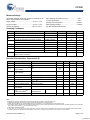
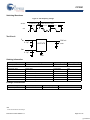
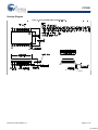
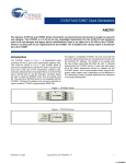
CY2291
Three-PLL General Purpose EPROM
Programmable Clock Generator
Features
Benefits
■
Three integrated phase-locked loops
■
■
EPROM programmability
Generates up to three custom frequencies from external
sources
■
Factory-programmable (CY2291) or field-programmable
(CY2291F) device options
■
Easy customization and fast turnaround
■
Programming support available for all opportunities
■
Low-skew, low-jitter, high-accuracy outputs
■
Meets critical industry standard timing requirements
■
Power-management options (Shutdown, OE, Suspend)
■
Supports low-power applications
■
Frequency select option
■
Eight user-selectable frequencies on CPU PLL
■
Smooth slewing on CPUCLK
■
Allows downstream PLLs to stay locked on CPUCLK output
■
Configurable 3.3V or 5V operation
■
Enables application compatibility
■
20-pin SOIC Package
■
Industry-standard packaging saves on board space
Part Number Outputs
Input Frequency Range
Output Frequency Range
Specifics
CY2291
8
10 MHz–25 MHz (external crystal)
1 MHz–30 MHz (reference clock)
76.923 kHz–100 MHz (5V)
76.923 kHz–80 MHz (3.3V)
Factory Programmable
Commercial Temperature
CY2291I
8
10 MHz–25 MHz (external crystal)
1 MHz–30 MHz (reference clock)
76.923 kHz–90 MHz (5V)
76.923 kHz–66.6 MHz (3.3V)
Factory Programmable
Industrial Temperature
CY2291F
8
10 MHz–25 MHz (external crystal)
1 MHz–30 MHz (reference clock)
76.923 kHz–90 MHz (5V)
76.923 kHz–66.6 MHz (3.3V)
Field Programmable
Commercial Temperature
CY2291FI
8
10 MHz–25 MHz (external crystal)
1 MHz–30 MHz (reference clock)
76.923 kHz–80 MHz (5V)
76.923 kHz–60.0 MHz (3.3V)
Field Programmable
Industrial Temperature
Logic Block Diagram
32XIN
32K
OSC.
32XOUT
XTALIN
OSC.
XTALOUT
XBUF
CPLL
(8 BIT)
/1,2,4
CPUCLK
S0
CLKA
S1
S2/SUSPEND
SPLL
(8 BIT)
CLKB
/1,2,4,8
MUX
UPLL
(10 BIT)
/1,2,3,4,5,6
/8,10,12,13
/20,24,26,40
/48,52,96,104
CLKD
/2,3,4
CLKF
CONFIG
EPROM
SHUTDOWN/
OE
Cypress Semiconductor Corporation
Document #: 38-07189 Rev. *C
CLKC
•
198 Champion Court
•
San Jose, CA 95134-1709
•
408-943-2600
Revised September 16, 2008
[+] Feedback
CY2291
Pinouts
Figure 1. CY2291- 20-pin SOIC
32XOUT
1
20
32XIN
32K
2
19
CLKC
3
18
VBATT
SHUTDOWN/OE
VDD
GND
XTALIN
4
17
S2/SUSPEND
5
16
6
15
VDD
S1
XTALOUT
7
14
S0
8
9
13
12
CLKF
CLKA
10
11
CLKB
XBUF
CLKD
CPUCLK
Pin Definitions
Name
Pin Number
Description
32XOUT
1
32.768-kHz crystal feedback.
32K
2
32.768-kHz output (always active if VBATT is present).
CLKC
3
Configurable clock output C.
VDD
4, 16
GND
5
Ground.
XTALIN[1]
6
Reference crystal input or external reference clock input.
XTALOUT[1, 2]
7
Reference crystal feedback.
XBUF
8
Buffered reference clock output.
CLKD
9
Configurable clock output D.
CPUCLK
10
CPU frequency clock output.
CLKB
11
Configurable clock output B.
CLKA
12
Configurable clock output A.
CLKF
13
Configurable clock output F.
S0
14
CPU clock select input, bit 0.
S1
15
CPU clock select input, bit 1.
S2/SUSPEND
17
CPU clock select input, bit 2. Optionally enables suspend feature when LOW.[3]
SHUTDOWN/OE
18
Places outputs in three-state[4] condition and shuts down chip when LOW. Optionally, only
places outputs in three-state[4] condition and does not shut down chip when LOW.
Voltage supply.
VBATT
19
Battery supply for 32.768-kHz circuit.
32XIN
20
32.768-kHz crystal input.
Notes
1. For best accuracy, use a parallel-resonant crystal, CLOAD ≈ 17 pF or 18 pF.
2. Float XTALOUT pin if XTALIN is driven by reference clock (as opposed to crystal).
3. Please refer to application note “Understanding the CY2291, CY2292 and CY2295” for more information.
4. The CY2291 has weak pull downs on all outputs (except 32K). Hence, when a three-state condition is forced on the outputs, the output pins are pulled LOW.
Document #: 38-07189 Rev. *C
Page 2 of 12
[+] Feedback
CY2291
Operation
The CY2291 is a third-generation family of clock generators. The
CY2291 is upwardly compatible with the industry standard
ICD2023 and ICD2028 and continues their tradition by providing
a high level of customizable features to meet the diverse clock
generation needs of modern motherboards and other
synchronous systems.
All parts provide a highly configurable set of clocks for PC
motherboard applications. Each of the four configurable clock
outputs (CLKA–CLKD) can be assigned 1 of 30 frequencies in
any combination. Multiple outputs configured for the same or
related[3] frequencies have low (<500 ps) skew, in effect
providing on-chip buffering for heavily loaded signals.
The CY2291 can be configured for either 5V or 3.3V operation.
The internal ROM tables use EPROM technology, allowing full
customization of output frequencies. The reference oscillator has
been designed for 10 MHz to 25 MHz crystals, providing
additional flexibility. No external components are required with
this crystal. Alternatively, an external reference clock of
frequency between 1 MHz and 30 MHz can be used. Customers
using the 32-kHz oscillator must connect a 10-MW resistor in
parallel with the 32-kHz crystal.
Output Configuration
The CY2291 has five independent frequency sources on-chip.
These are the 32-kHz oscillator, the reference oscillator, and
three Phase-Locked Loops (PLLs). Each PLL has a specific
function. The System PLL (SPLL) drives the CLKF output and
provides fixed output frequencies on the configurable outputs.
The SPLL offers the most output frequency divider options. The
CPU PLL (CPLL) is controlled by the select inputs (S0–S2) to
provide eight user-selectable frequencies with smooth slewing
between frequencies. The Utility PLL (UPLL) provides the most
accurate clock. It is often used for miscellaneous frequencies not
provided by the other frequency sources.
All configurations are EPROM programmable, providing short
sample and production lead times. Please refer to the application
note “Understanding the CY2291, CY2292, and CY2295” for
information on configuring the part.
Power Saving Features
The SHUTDOWN/OE input three-states the outputs when pulled
LOW (the 32-kHz clock output is not affected). If system
shutdown is enabled, a LOW on this pin also shuts off the PLLs,
counters, the reference oscillator, and all other active components. The resulting current on the VDD pins are less than 50 μA
(for Commercial Temp. or 100 μA for Industrial Temp.) plus 15
μA max. for the 32-kHz subsystem and is typically 10 μA. After
leaving shutdown mode, the PLLs have to re-lock. All outputs
except 32K have a weak pull down so that the outputs do not float
when three-stated.[4]
The S2/SUSPEND input can be configured to shut down a
customizable set of outputs and/or PLLs, when LOW. All PLLs
and any of the outputs except 32K can be shut off in nearly any
Document #: 38-07189 Rev. *C
combination. The only limitation is that if a PLL is shut off, all
outputs derived from it must also be shut off. Suspending a PLL
shuts off all associated logic, while suspending an output simply
forces a three-state condition.[3]
The CPUCLK can slew (transition) smoothly between 8 MHz and
the maximum output frequency (100 MHz at 5V/80 MHz at 3.3V
for Commercial Temp. parts or 90 MHz at 5V/66.6 MHz at 3.3V
for Industrial Temp. and for field-programmed parts). This feature
is extremely useful in “Green” PC and laptop applications, where
reducing the frequency of operation can result in considerable
power savings. This feature meets all 486 and Pentium®
processor slewing requirements.
CyClocks Software
CyClocks™ is an easy-to-use application that allows you to
configure any one of the EPROM programmable clocks offered
by Cypress. You may specify the input frequency, PLL and output
frequencies, and different functional options. Please note the
output frequency ranges in this data sheet when specifying them
in CyClocks to ensure that you stay within the limits. CyClocks
also has a power calculation feature that allows you to see the
power consumption of your specific configuration. CyClocks is a
sub-application within the CyberClocks™ software. You can
download a copy of CyberClocks for free on Cypress’s web site
at www.cypress.com.
Cypress FTG Programmer
The Cypress Frequency Timing Generator (FTG) Programmers
is a portable programmer designed to custom program our family
of EPROM Field Programmable Clock Devices. The FTG
programmers connect to a PC serial port and allow users of
CyClocks software to quickly and easily program any of the
CY2291F, CY2292F, CY2071AF, and CY2907F devices. The
ordering code for the Cypress FTG Programmer is CY3670.
Custom Configuration Request Procedure
The CY229x are EPROM-programmable devices that may be
configured in the factory or in the field by a Cypress Field Application Engineer (FAE). The output frequencies requested are
matched as closely as the internal PLL divider and multiplier
options allow. All custom requests must be submitted to your
local Cypress FAE or sales representative. The method to use to
request custom configurations is:
Use CyClocks™ software. This software automatically calculates the output frequencies that can be generated by the
CY229x devices and provides a print-out of final pinout which
can be submitted (in electronic or print format) to your local FAE
or sales representative. The CyClocks software is available free
of charge from the Cypress web site (http://www.cypress.com) or
from your local sales representative.
Once the custom request has been processed you receive a part
number with a 3-digit extension (for example, CY2292SC-128)
specific to the frequencies and pinout of your device. This is the
part number used for samples requests and production orders.
Page 3 of 12
[+] Feedback
CY2291
Maximum Ratings
(Exceeding maximum ratings may shorten the useful life of the
device. User guidelines are not tested.)
Max. Soldering Temperature (10 sec) ......................... 260°C
Supply Voltage...............................................–0.5V to + 7.0V
Package Power Dissipation...................................... 750 mW
DC Input Voltage ...........................................–0.5V to + 7.0V
Static Discharge Voltage.............................................≥ 2000V
(per MIL-STD-883, Method 3015)
Junction Temperature .................................................. 150°C
Storage Temperature ................................. –65°C to +150°C
Operating Conditions[5]
Parameter
Description
Part Numbers
Min.
Max.
Unit
VDD
Supply Voltage, 5.0V operation
All
4.5
5.5
V
VDD
Supply Voltage, 3.3V operation
All
3.0
3.6
V
VBATT
Battery Backup Voltage
All
2.0
5.5
V
TA
Commercial Operating Temperature, Ambient
CY2291/CY2291F
0
+70
°C
−40
+85
°C
25
pF
Industrial Operating Temperature, Ambient
CY2291I/CY2291FI
CLOAD
Max. Load Capacitance 5.0V Operation
All
CLOAD
Max. Load Capacitance 3.3V Operation
All
fREF
External Reference Crystal
All
External Reference Clock[6, 7, 8]
All
tPU
Power up time for all VDDs to reach minimum specified voltage (power
ramps must be monotonic)
15
pF
10.0
25.0
MHz
1
30
MHz
0.05
50
ms
Electrical Characteristics, Commercial 5.0V
Parameter
Description
Conditions
VOH
HIGH-Level Output Voltage IOH = 4.0 mA
VOL
LOW-Level Output Voltage
IOL = 4.0 mA
VOH–32
32.768-kHz HIGH-Level
Output Voltage
IOH = 0.5 mA
VOL–32
32.768-kHz LOW-Level
Output Voltage
IOL = 0.5 mA
VIH
HIGH-Level Input Voltage[9] Except crystal pins
Voltage[9]
Min.
Typ.
LOW-Level Input
IIH
Input HIGH Current
VIN = VDD – 0.5V
IIL
Input LOW Current
VIN = +0.5V
Unit
V
0.4
VBATT
0.5
V
V
0.4
2.0
V
V
Except crystal pins
VIL
Max.
2.4
0.8
V
<1
10
μA
<1
10
μA
IOZ
Output Leakage Current
Three-state outputs
250
μA
IDD
VDD Supply Current
Commercial[10]
VDD = VDD Max., 5V operation
75
100
mA
IDDS
VDD Power Supply Current
in Shutdown Mode[10]
Shutdown active,
excluding VBATT
10
50
μA
IBATT
VBATT Power Supply Current VBATT = 3.0V
5
15
μA
CY2291/CY2291F
Notes
5. Electrical parameters are guaranteed by design with these operating conditions, unless otherwise noted.
6. External input reference clock must have a duty cycle between 40% and 60%, measured at VDD/2.
7. Please refer to application note “Crystal Oscillator Topics” for information on AC-coupling the external input reference clock.
8. The oscillator circuit is optimized for a crystal reference and for external reference clocks up to 20 MHz. For external reference clocks above 20 MHz, it is recommended
that a 150Ω pull up resistor to VDD be connected to the Xout pin.
9. Xtal inputs have CMOS thresholds.
10. Load = Max., VIN = 0V or VDD, Typical (–104) configuration, CPUCLK = 66 MHz. Other configurations vary. Power can be approximated by the following formula
(multiply by 0.65 for 3V operation): IDD=10+0.06•(FCPLL+FUPLL+2•FSPLL)+0.27•(FCLKA+FCLKB+FCLKC+FCLKD+FCPUCLK+FCLKF+FXBUF).
Document #: 38-07189 Rev. *C
Page 4 of 12
[+] Feedback
CY2291
Electrical Characteristics, Commercial 3.3V
Parameter
Description
Conditions
VOH
HIGH-Level Output Voltage IOH = 4.0 mA
VOL
LOW-Level Output Voltage
IOL = 4.0 mA
VOH–32
32.768-kHz HIGH-Level
Output Voltage
IOH = 0.5 mA
VOL–32
32.768-kHz LOW-Level
Output Voltage
IOL = 0.5 mA
VIH
HIGH-Level Input Voltage[9] Except crystal pins
[9]
Min.
Typ.
Max.
Unit
0.4
V
2.4
V
VBATT
0.5
V
0.4
2.0
V
VIL
LOW-Level Input Voltage
Except crystal pins
IIH
Input HIGH Current
VIN = VDD–0.5V
<1
IIL
Input LOW Current
VIN = +0.5V
<1
IOZ
Output Leakage Current
Three-state outputs
IDD
VDD Supply Current[10]
Commercial
VDD = VDD Max., 3.3V operation
IDDS
VDD Power Supply Current
in Shutdown Mode[10]
Shutdown active,
excluding VBATT
IBATT
VBATT Power Supply Current VBATT = 3.0V
CY2291/CY2291F
V
0.8
V
10
μA
10
μA
250
μA
50
65
mA
10
50
μA
5
15
μA
Typ.
Max.
Unit
Electrical Characteristics, Industrial 5.0V
Parameter
Description
Conditions
VOH
HIGH-Level Output Voltage IOH = 4.0 mA
2.4
VOL
LOW-Level Output Voltage
IOL = 4.0 mA
VOH–32
32.768-kHz HIGH-Level
Output Voltage
IOH = 0.5 mA
VOL–32
32.768-kHz LOW-Level
Output Voltage
IOL = 0.5 mA
VIH
HIGH-Level Input Voltage[9] Except crystal pins
Voltage[9]
Min.
V
0.4
VBATT
0.5
V
V
0.4
2.0
V
V
Except crystal pins
0.8
V
VIL
LOW-Level Input
IIH
Input HIGH Current
VIN = VDD–0.5V
<1
10
μA
IIL
Input LOW Current
VIN = +0.5V
<1
10
μA
IOZ
Output Leakage Current
Current[10]
250
μA
VDD = VDD Max., 5V operation
75
110
mA
Shutdown active,
excluding VBATT
10
100
μA
5
15
μA
Typ.
Max.
Unit
0.4
V
Three-state outputs
IDD
VDD Supply
Industrial
IDDS
VDD Power Supply Current
in Shutdown Mode[10]
IBATT
VBATT Power Supply Current VBATT = 3.0V
CY2291I/CY2291FI
Electrical Characteristics, Industrial 3.3V
Parameter
Description
Conditions
VOH
HIGH-Level Output Voltage IOH = 4.0 mA
VOL
LOW-Level Output Voltage
IOL = 4.0 mA
VOH–32
32.768-kHz HIGH-Level
Output Voltage
IOH = 0.5 mA
VOL–32
32.768-kHz LOW-Level
Output Voltage
IOL = 0.5 mA
Document #: 38-07189 Rev. *C
Min.
2.4
V
V
VBATT
0.5
0.4
V
Page 5 of 12
[+] Feedback
CY2291
Electrical Characteristics, Industrial 3.3V (continued)
Parameter
VIH
Description
Conditions
[9]
Except crystal pins
[9]
HIGH-Level Input Voltage
VIL
LOW-Level Input Voltage
Except crystal pins
IIH
Input HIGH Current
VIN = VDD–0.5V
IIL
Input LOW Current
VIN = +0.5V
IOZ
Output Leakage Current
Min.
Typ.
Max.
Unit
2.0
V
0.8
V
<1
10
μA
<1
10
μA
250
μA
VDD Supply Current
Industrial
VDD = VDD max., 3.3V operation
50
70
mA
IDDS
VDD Power Supply Current
in Shutdown Mode[10]
Shutdown active,
excluding VBATT
10
100
μA
IBATT
VBATT Power Supply Current VBATT = 3.0V
5
15
μA
IDD
[10]
Three-state outputs
CY2291I/CY2291FI
Switching Characteristics, Commercial 5.0V
Parameter
t1
Name
Output Period
Output Duty
Cycle[11]
t3
Rise Time
Description
Clock output range, 5V
operation
Min.
Typ.
Max.
Unit
CY2291
10
(100 MHz)
13000
(76.923 kHz)
ns
CY2291F
11.1
(90 MHz)
13000
(76.923 kHz)
ns
Duty cycle for outputs, defined as t2 ÷ t1[12]
fOUT > 66 MHZ
40%
50%
60%
Duty cycle for outputs, defined as t2 ÷ t1[12]
fOUT < 66 MHZ
45%
50%
55%
3
5
ns
2.5
4
ns
Output clock rise time[13]
time[13]
t4
Fall Time
t5
Output Disable Time for output to enter three-state mode after
Time
SHUTDOWN/OE goes LOW
10
15
ns
t6
Output Enable
Time
Time for output to leave three-state mode after
SHUTDOWN/OE goes HIGH
10
15
ns
t7
Skew
Skew delay between any identical or related outputs[3,
< 0.25
0.5
ns
t8
CPUCLK Slew
Frequency transition rate
20.0
MHz/m
s
t9A
Clock Jitter[14]
Peak-to-peak period jitter (t9A Max. – t9A min.),% of
clock period (fOUT < 4 MHz)
< 0.5
1
%
t9B
Clock Jitter[14]
Peak-to-peak period jitter (t9B Max. – t9B min.)
(4 MHz < fOUT < 16 MHz)
< 0.7
1
ns
t9C
Clock Jitter[14]
Peak-to-peak period jitter
(16 MHz < fOUT < 50 MHz)
< 400
500
ps
t9D
Clock Jitter[14]
Peak-to-peak period jitter
(fOUT > 50 MHz)
< 250
350
ps
t10A
Lock Time for
CPLL
Lock Time from Power Up
< 25
50
ms
Output clock fall
12, 15]
1.0
Notes
11. XBUF duty cycle depends on XTALIN duty cycle.
12. Measured at 1.4V.
13. Measured between 0.4V and 2.4V.
14. Jitter varies with configuration. All standard configurations sample tested at the factory conform to this limit. For more information on jitter, please refer to the application
note: “Jitter in PLL-Based Systems.”
15. CLKF is not guaranteed to be in phase with CLKA-D, even if it is referenced off the same PLL.
Document #: 38-07189 Rev. *C
Page 6 of 12
[+] Feedback
CY2291
Switching Characteristics, Commercial 5.0V (continued)
Parameter
t10B
Name
Description
Min.
Lock Time for
Lock Time from Power Up
UPLL and SPLL
Slew Limits
CPU PLL Slew Limits
Typ.
Max.
Unit
< 0.25
1
ms
CY2291
8
100
MHz
CY2291F
8
90
MHz
Max.
Unit
12.5
(80 MHz)
13000
(76.923 kHz)
ns
15
(66.6 MHz)
13000
(76.923 kHz)
ns
Switching Characteristics, Commercial 3.3V
Parameter
t1
Name
Output Period
Description
Clock output range, 3.3V
operation
CY2291
CY2291F
Output Duty
Cycle[11]
t3
Rise Time
Min.
Typ.
Duty cycle for outputs, defined as t2 ÷ t1[12]
fOUT > 66 MHZ
40%
50%
60%
Duty cycle for outputs, defined as t2 ÷ t1[12]
fOUT < 66 MHZ
45%
50%
55%
3
5
ns
2.5
4
ns
Output clock rise time[13]
time[13]
t4
Fall Time
t5
Output Disable Time for output to enter three-state mode after
Time
SHUTDOWN/OE goes LOW
10
15
ns
t6
Output Enable
Time
Time for output to leave three-state mode after
SHUTDOWN/OE goes HIGH
10
15
ns
t7
Skew
Skew delay between any identical or related outputs[3,
< 0.25
0.5
ns
t8
CPUCLK Slew
Frequency transition rate
20.0
MHz/m
s
t9A
Clock Jitter[14]
Peak-to-peak period jitter (t9A Max. – t9A min.),% of
clock period (fOUT < 4 MHz)
<0.5
1
%
t9B
Clock Jitter[14]
Peak-to-peak period jitter (t9B Max. – t9B min.) (4 MHz
< fOUT < 16 MHz)
<0.7
1
ns
t9C
Clock Jitter[14]
Peak-to-peak period jitter
(16 MHz < fOUT < 50 MHz)
<400
500
ps
t9D
Clock Jitter[14]
Peak-to-peak period jitter
(fOUT > 50 MHz)
<250
350
ps
t10A
Lock Time for
CPLL
Lock Time from Power Up
<25
50
ms
t10B
Lock Time for
Lock Time from Power Up
UPLL and SPLL
<0.25
1
ms
Output clock fall
12, 15]
Slew Limits
CPU PLL Slew Limits
Document #: 38-07189 Rev. *C
1.0
CY2291
8
80
MHz
CY2291F
8
66.6
MHz
Page 7 of 12
[+] Feedback
CY2291
Switching Characteristics, Industrial 5.0V
Parameter
t1
Name
Output Period
Output Duty
Cycle[11]
t3
Rise Time
Description
Clock output range,
5V operation
Max.
Unit
CY2291I
Min.
11.1
(90 MHz)
Typ.
13000
(76.923 kHz)
ns
CY2291FI
12.5
(80 MHz)
13000
(76.923 kHz)
ns
Duty cycle for outputs, defined as t2 ÷ t1[12]
fOUT > 66 MHZ
40%
50%
60%
Duty cycle for outputs, defined as t2 ÷ t1[12]
fOUT < 66 MHZ
45%
50%
55%
3
5
ns
Output clock rise time[13]
time[13]
t4
Fall Time
2.5
4
ns
t5
Output Disable Time for output to enter three-state mode after
Time
SHUTDOWN/OE goes LOW
10
15
ns
t6
Output Enable
Time
Time for output to leave three-state mode after
SHUTDOWN/OE goes HIGH
10
15
ns
t7
Skew
Skew delay between any identical or related outputs[3,
< 0.25
0.5
ns
t8
CPUCLK Slew
Frequency transition rate
20.0
MHz/m
s
t9A
Clock Jitter[14]
Peak-to-peak period jitter (t9A Max. – t9A min.),% of
clock period (fOUT < 4 MHz)
<0.5
1
%
t9B
Clock Jitter[14]
Peak-to-peak period jitter (t9B Max. – t9B min.) (4 MHz
< fOUT < 16 MHz)
<0.7
1
ns
t9C
Clock Jitter[14]
Peak-to-peak period jitter
(16 MHz < fOUT < 50 MHz)
<400
500
ps
t9D
Clock Jitter[14]
Peak-to-peak period jitter
(fOUT > 50 MHz)
<250
350
ps
t10A
Lock Time for
CPLL
Lock Time from Power Up
<25
50
ms
t10B
Lock Time for
Lock Time from Power Up
UPLL and SPLL
<0.25
1
ms
Output clock fall
12, 15]
Slew Limits
CPU PLL Slew Limits
1.0
CY2291I
8
90
MHz
CY2291FI
8
80
MHz
Max.
Unit
15
(66.6 MHz)
13000
(76.923 kHz)
ns
16.66
(60 MHz)
13000
(76.923 kHz)
ns
Switching Characteristics, Industrial 3.3V
Parameter
t1
Name
Output Period
Description
Clock output range, 3.3V
operation
CY2291I
CY2291FI
Output Duty
Cycle[11]
t3
Rise Time
Min.
Typ.
Duty cycle for outputs, defined as t2 ÷ t1[12]
fOUT > 66 MHZ
40%
50%
60%
Duty cycle for outputs, defined as t2 ÷ t1[12]
fOUT < 66 MHZ
45%
50%
55%
3
5
ns
2.5
4
ns
10
15
ns
Output clock rise time[13]
time[13]
t4
Fall Time
t5
Output Disable Time for output to enter three-state mode after
Time
SHUTDOWN/OE goes LOW
Output clock fall
Document #: 38-07189 Rev. *C
Page 8 of 12
[+] Feedback
CY2291
Switching Characteristics, Industrial 3.3V (continued)
Parameter
Name
Description
Min.
Typ.
Max.
Unit
10
15
ns
< 0.25
0.5
ns
20.0
MHz/ms
1
%
< 0.7
1
ns
Peak-to-peak period jitter
(16 MHz < fOUT < 50 MHz)
< 400
500
ps
Clock Jitter[14]
Peak-to-peak period jitter (fOUT > 50 MHz)
< 250
350
ps
t10A
Lock Time for
CPLL
Lock Time from Power Up
< 25
50
ms
t10B
Lock Time for
Lock Time from Power Up
UPLL and SPLL
< 0.25
1
ms
t6
Output Enable
Time
Time for output to leave three-state mode after
SHUTDOWN/OE goes HIGH
t7
Skew
Skew delay between any identical or related outputs[3,
t8
CPUCLK Slew
Frequency transition rate
t9A
Clock Jitter[14]
Peak-to-peak period jitter (t9A Max. – t9A min.),% of
clock period (fOUT < 4 MHz)
< 0.5
t9B
Clock Jitter[14]
Peak-to-peak period jitter (t9B Max. – t9B min.) (4 MHz
< fOUT < 16 MHz)
t9C
Clock Jitter[14]
t9D
12, 15]
Slew Limits
1.0
CPU PLL Slew Limits
CY2291I
8
66.6
MHz
CY2291FI
8
60
MHz
Switching Waveforms
Figure 2. All Outputs, Duty Cycle and Rise/Fall Time
t1
t2
OUTPUT
t3
t4
Figure 3. Output Three-State Timing [4]
OE
t5
t6
ALL
THREE-STATE
OUTPUTS
Figure 4. CLK Outputs Jitter and Skew
t9A
CLK
OUTPUT
t7
RELATED
CLK
Document #: 38-07189 Rev. *C
Page 9 of 12
[+] Feedback
CY2291
Switching Waveforms
Figure 5. CPU Frequency Change
SELECT
OLD SELECT
NEW SELECT STABLE
t8 & t10
Fold
Fnew
CPU
Test Circuit
VDD
CLK out
0.1 μF
CLOAD
OUTPUTS
VDD
0.1 μF
GND
Ordering Information
Ordering Code
[16]
Package Type
Operating Range
Operating Voltage
20-Pin SOIC
Industrial
3.3V or 5.0V
CY2291SXC–XXX
20-Pin SOIC
Commercial
5.0V
CY2291SXC–XXXT
20-Pin SOIC – Tape and Reel
Commercial
5.0V
CY2291FI
Pb-Free
CY2291SXL–XXX
20-Pin SOIC
Commercial
3.3V
CY2291SXL–XXXT
20-Pin SOIC – Tape and Reel
Commercial
3.3V
CY2291FX
20-Pin SOIC
Commercial
3.3V or 5.0V
CY2291FXT
20-Pin SOIC – Tape and Reel
Commercial
3.3V or 5.0V
Package Characteristics
Package
θJA (C/W)
θJC (C/W)
Transistor Count
20-pin SOIC
125
25
9271
Note
16. Not recommended for new designs.
Document #: 38-07189 Rev. *C
Page 10 of 12
[+] Feedback
CY2291
Package Diagram
Figure 6. 20-Pin (300 MIL) SOIC Package Outline
51-85024 *C
Document #: 38-07189 Rev. *C
Page 11 of 12
[+] Feedback
CY2291
Document History Page
Document Title: CY2291 Three-PLL General Purpose EPROM Programmable Clock Generator
Document Number: 38-07189
REV.
**
ECN
110321
Orig. of
Change
Submission
Date
SZV
10/28/01
Description of Change
Change from Spec number: 38-00410 to 38-07189
*A
121836
RBI
12/14/02
Power up requirements added to Operating Conditions Information
*B
276756
RGL
10/18/04
Added Lead Free Devices
*C
2565316
AESA/KVM
09/16/08
Updated template. Added Note “Not recommended for new designs.”
Removed part number CY2291F, CY2291FT, CY2291SC-XXX,
CY2291SC-XXXT, CY2291SI-XXX, CY2291SI-XXXT, CY2291SL-XXX,
CY2291SL-XXXT, CY2291FIT, CY2291SXI-XXX, CY2291SXI-XXXT,
CY2291FXI and CY2291FXIT. Changed CyClocks reference to include
CyberClocks. Changed Lead-Free to Pb-Free.
Updated Package diagram 51-85024 *B to 51-85024 *C.
Sales, Solutions, and Legal Information
Worldwide Sales and Design Support
Cypress maintains a worldwide network of offices, solution centers, manufacturer’s representatives, and distributors. To find the office
closest to you, visit us at cypress.com/sales.
Products
PSoC
Clocks & Buffers
PSoC Solutions
psoc.cypress.com
clocks.cypress.com
General
Low Power/Low Voltage
psoc.cypress.com/solutions
psoc.cypress.com/low-power
Wireless
wireless.cypress.com
Precision Analog
Memories
memory.cypress.com
LCD Drive
psoc.cypress.com/lcd-drive
image.cypress.com
CAN 2.0b
psoc.cypress.com/can
USB
psoc.cypress.com/usb
Image Sensors
psoc.cypress.com/precision-analog
© Cypress Semiconductor Corporation, 2001-2008. The information contained herein is subject to change without notice. Cypress Semiconductor Corporation assumes no responsibility for the use of
any circuitry other than circuitry embodied in a Cypress product. Nor does it convey or imply any license under patent or other rights. Cypress products are not warranted nor intended to be used for
medical, life support, life saving, critical control or safety applications, unless pursuant to an express written agreement with Cypress. Furthermore, Cypress does not authorize its products for use as
critical components in life-support systems where a malfunction or failure may reasonably be expected to result in significant injury to the user. The inclusion of Cypress products in life-support systems
application implies that the manufacturer assumes all risk of such use and in doing so indemnifies Cypress against all charges.
Any Source Code (software and/or firmware) is owned by Cypress Semiconductor Corporation (Cypress) and is protected by and subject to worldwide patent protection (United States and foreign),
United States copyright laws and international treaty provisions. Cypress hereby grants to licensee a personal, non-exclusive, non-transferable license to copy, use, modify, create derivative works of,
and compile the Cypress Source Code and derivative works for the sole purpose of creating custom software and or firmware in support of licensee product to be used only in conjunction with a Cypress
integrated circuit as specified in the applicable agreement. Any reproduction, modification, translation, compilation, or representation of this Source Code except as specified above is prohibited without
the express written permission of Cypress.
Disclaimer: CYPRESS MAKES NO WARRANTY OF ANY KIND, EXPRESS OR IMPLIED, WITH REGARD TO THIS MATERIAL, INCLUDING, BUT NOT LIMITED TO, THE IMPLIED WARRANTIES
OF MERCHANTABILITY AND FITNESS FOR A PARTICULAR PURPOSE. Cypress reserves the right to make changes without further notice to the materials described herein. Cypress does not
assume any liability arising out of the application or use of any product or circuit described herein. Cypress does not authorize its products for use as critical components in life-support systems where
a malfunction or failure may reasonably be expected to result in significant injury to the user. The inclusion of Cypress’ product in a life-support systems application implies that the manufacturer
assumes all risk of such use and in doing so indemnifies Cypress against all charges.
Use may be limited by and subject to the applicable Cypress software license agreement.
Document #: 38-07189 Rev. *C
Revised September 16, 2008
Page 12 of 12
Pentium is a registered trademark of Intel Corporation. CyClocks is a trademark of Cypress Semiconductor Corporation. All product and company names mentioned in this document are trademarks
of their respective holders.
[+] Feedback