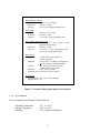
1
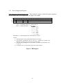
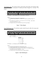
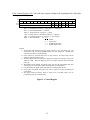
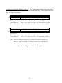
U S E R ' S VXI PULSE GENERATOR MODULE MODEL VX462B Manual Part No: 11026339D M A N U A L COPYRIGHT C&H Technologies, Inc. (C&H) provides this manual "as is" without warranty of any kind, either expressed or implied, including but not limited to the implied warranties of merchantability and fitness for a particular purpose. C&H may make improvements and/or changes in the product(s) and/or program(s) described in this manual at any time and without notice. This publication could contain technical inaccuracies or typographical errors. Changes are periodically made to the information herein; these changes will be incorporated in new editions of this publication. Copyright © 1993,1995, 2005 by C&H Technologies, Inc. The information and/or drawings set forth in this document and all rights in and to inventions disclosed herein which might be granted thereon disclosing or employing the materials, methods, techniques or apparatus described herein, are the exclusive property of C&H Technologies, Inc. A Reader's Comment Form is provided at the back of this publication. If this form has been removed address comments to: C&H Engineering, Inc. Technical Publications 445 West Round Rock Drive Round Rock, Texas 78681-5012 C&H may use or distribute any of the information you supply in any way that it believes appropriate without incurring any obligations whatever. AMENDMENT NOTICE C&H Technologies, Inc. makes every attempt to provide up-to-date manuals with the associated equipment. Occasionally, changes are made to the equipment wherein it is necessary to provide amendments to the manual. If any amendments are provided for this manual they are printed on colored paper and will be found at the rear of this manual. NOTE The contents of any amendment may affect operation, maintenance, or calibration of the equipment. iii INTRODUCTION This manual describes the functional operation of the C&H Model VX462B VXI Pulse Generator (Part No. 11026335). This module is one of a number of test and data acquisition/control modules in the VME and VXI format provided by C&H. Contained within this manual is information on the physical and electrical specifications, installation and startup procedures, operating procedures, functional analysis, and figures and diagrams required to adequately support this product. iv TABLE OF CONTENTS 1.0 GENERAL DESCRIPTION ............................................................................................. 1 1.1 PURPOSE OF EQUIPMENT ............................................................................... 1 1.2 SPECIFICATIONS OF EQUIPMENT.................................................................. 1 1.2.1 Key Specifications................................................................................ 1 1.2.2 Electrical.............................................................................................. 1 1.2.3 Mechanical........................................................................................... 1 1.2.4 Environmental...................................................................................... 2 1.2.5 Bus Compliance ................................................................................... 3 2.0 INSTALLATION ............................................................................................................. 5 2.1 UNPACKING AND INSPECTION ...................................................................... 5 2.2 HANDLING PRECAUTIONS.............................................................................. 5 2.3 INSTALLATION.................................................................................................. 5 2.4 PREPARATION FOR RESHIPMENT.................................................................. 5 3.0 FUNCTIONAL DESCRIPTION....................................................................................... 7 3.1 GENERAL............................................................................................................ 7 3.2 SWITCHES AND JUMPERS ............................................................................... 7 3.3 INDICATORS ...................................................................................................... 8 3.4 CONNECTORS .................................................................................................... 8 3.4.1 Front Panel Connectors ........................................................................ 8 3.4.2 Rear Connectors .................................................................................. 8 3.5 CONFIGURATION REGISTERS ........................................................................ 9 3.5.1 VXI Configuration Registers ................................................................ 9 3.5.2 Pulse Configuration Registers............................................................... 11 4.0 OPERATING INSTRUCTIONS ...................................................................................... 15 4.1 LOGICAL ADDRESS .......................................................................................... 15 4.2 PROGRAMMING SEQUENCE ........................................................................... 16 4.3 NORMAL MODES OF OPERATION .................................................................. 16 4.3.1 Single Pulse Mode................................................................................ 16 4.3.2 Delayed Pulse Mode............................................................................. 16 4.3.3 Double Pulse Mode.............................................................................. 16 4.4 TRIGGERED MODES OF OPERATION............................................................. 17 4.4.1 Free ..................................................................................................... 17 4.4.2 Triggered Mode ................................................................................... 17 4.4.3 Gated Mode ......................................................................................... 17 4.5 SPECIAL MODES OF OPERATION................................................................... 17 4.6 OUTPUT VOLTAGE LEVEL PROGRAMMING ................................................ 18 5.0 TROUBLE ANALYSIS.................................................................................................... 19 5.1 BUILT IN TEST AND DIAGNOSTICS ............................................................... 19 5.2 TROUBLE ANALYSIS GUIDE ........................................................................... 19 APPENDIX A - BOARD LAYOUT...................................................................................... A-1 APPENDIX B - CONNECTORS .......................................................................................... B-1 v LIST OF FIGURES Figure 1. Electrical Timing and Output Characteristics ........................................................... 2 Figure 2. Simplified Block Diagram........................................................................................ 7 Figure 3. Hardware Configurable Controls ............................................................................. 7 Figure 4. Front Panel.............................................................................................................. 8 Figure 5. VXI Configuration Registers ................................................................................... 10 Figure 6. PRI Register............................................................................................................ 11 Figure 7. Delay Register......................................................................................................... 12 Figure 8. Pulse Width Register ............................................................................................... 12 Figure 9. Control Register...................................................................................................... 13 Figure 10. Low/High Level Reference Registers..................................................................... 14 Figure 11. Functional Block Diagram ..................................................................................... 15 Figure B-1. P1 Pin Configuration ........................................................................................... B-1 Figure B-2. P2 Pin Configuration ........................................................................................... B-2 Figure B-3. Front Panel Connector......................................................................................... B-3 LIST OF TABLES Table I. VXI Register Address Map ....................................................................................... 9 vi 1.0 GENERAL DESCRIPTION The VX462B is a B-size VXIbus compatible programmable 20 MHz pulse generator with an additional 40 MHz square wave function. The module can output single or double pulse patterns that can be continuous streams or externally triggered or gated. The pulse repetition interval and pulse width are programmable and a delay time may be programmed in the delayed or double pulse modes. The output amplitude is also programmable. 1.1 PURPOSE OF EQUIPMENT This module is well suited for applications within automated test equipment and hardware-inthe-loop simulation systems, as well as development laboratory environments. 1.2 SPECIFICATIONS OF EQUIPMENT 1.2.1 Key Specifications Single and double pulse modes Continuous, triggered, gated, and delayed modes Programmable pulse repetition interval and pulse width Programmable delay time 10Vpp output amplitude with low impedance output, or 5Vpp output amplitude with 50 Ohm impedance output selected. Read back capability on all registers 1.2.2 Electrical The module requires the +5V and +12V power from the VXI backplane. The peak module current (IPM) for the +5 volt supply is 3.0 amps and for the +12 volts it is 0.4 amps. The pulse timing and output characteristics are shown in Figure 1. 1.2.3 Mechanical The mechanical dimensions of the module are in conformance with the VXIbus specification Rev 1.4 for single slot size 'B' modules. The nominal dimensions are 233.35 (9.187 in) high x 160 mm (6.299 in) deep. The module is designed for a mainframe with 20.32 mm (0.8 in) spacing between slots. As required by the VXI bus specification, these dimensions are in accordance with those given in the VME bus specification (Rev. C.1). 1 Pulse Repetition Interval Range: 50ns to 1 sec, in 6 ranges Resolution: 25ns min., 10 bits Accuracy: (1%+15ns) of the programmed value Pulse Width Range: Resolution: Accuracy: 25ns to 1sec, in 6 ranges 25ns min., 10 bits (1%+15ns) of the programmed value Delay Timing (from Trigger Out) Range: 25ns to 1 sec, range slaved to Pulse Repetition Interval range Resolution: 25ns min., 10 bits Accuracy: (1%+15ns) of the programmed value + 25ns to 75ns synchronization time Pulse Output Impedance: 2-5 ohms (max. load 50 ohms) or 50 ohms selectable. Amplitude: 10V (no load, <10 MHz) (low impedance) +5V into 50 ohms (50 Ohm impedance) Accuracy: 4% of the programmed value plus 100mv offset error (no load) Resolution 12 bit, 4.9mV (no load) Transition Time: Fixed rate, 5ns at 5V (typical) Trigger/Gate Trigger Output: TTL, 10 gate drive capability Trigger/Gate In: TTL Figure 1. Electrical Timing and Output Characteristics 1.2.4 Environmental The environmental specifications of the module are: Operating Temperature: Storage Temperature: Humidity: 0C to +50C -40C to +65C <95% without condensation 2 1.2.5 Bus Compliance The module complies with the VXIbus Specification Revision 1.4 for B-size register based modules and with VMEbus Specification ANSI/IEEE STD 1014-1987 and IEC 821. Manufacturer ID: Model Code: Access Type: Addressing: Data Transfer: Sysfail: Interrupts: Bus Arbitration: Local Bus: FC1 hex FFD hex Register Based A16 D16 not supported not supported (IACKIN tied to IACKOUT) BRx tied to BGx not used 3 4 2.0 INSTALLATION 2.1 UNPACKING AND INSPECTION In most cases the VX462B is individually sealed and packaged for shipment. Verify that there has been no damage to the shipping container. If damage exists then the container should be retained as it will provide evidence of carrier caused problems. Such problems should be reported to the carrier immediately as well as to C&H. If there is no damage to the shipping container, carefully remove the module from its box and anti static bag and inspect for any signs of physical damage. If damage exists, report immediately to C&H. 2.2 HANDLING PRECAUTIONS The VX462B contains components that are sensitive to electrostatic discharge. When handling the module for any reason, do so at a static-controlled workstation, whenever possible. At a minimum, avoid work areas that are potential static sources, such as carpeted areas. Avoid unnecessary contact with the components on the module. 2.3 INSTALLATION CAUTION: Read the entire User's Manual before proceeding with the installation and application of power. Set or verify the module's logical address. Insert the module into the appropriate slot according to the desired priority. Apply power. If no obvious problems exist, proceed to communicate with the module as outlined in Section 4.0 (Operating Instructions). 2.4 PREPARATION FOR RESHIPMENT If the module is to be shipped separately it should be enclosed in a suitable water and vapor proof anti static bag. Heat seal or tape the bag to insure a moisture-proof closure. When sealing the bag, keep trapped air volume to a minimum. The shipping container should be a rigid box of sufficient size and strength to protect the equipment from damage. If the module was received separately from a C&H system, then the original module shipping container and packing material may be re-used if it is still in good condition. 5 6 3.0 FUNCTIONAL DESCRIPTION 3.1 GENERAL The VX462B is configured, controlled, and statused through on-board registers accessible through the VXI backplane. These registers control the mode of operation, pulse repetition interval, pulse width, delay time, output amplitude and an output relay. A simplified block diagram of the module is shown in Figure 2. CONTROL LOGIC CONTROL ADDR BUS ADDRESS PULSE OUT PULSE DECODE VXI GENERATOR INTERFACE LOGIC TRIG IN/GATE ADDR BUS VXI & DATA BUS CONTROL USER DATA BUS TRIG OUT REGISTERS Figure 2. Simplified Block Diagram 3.2 SWITCHES AND JUMPERS 1 0 The following switches are used to configure the VX462B. Refer to Figure 3 for the switch and jumper locations. P1 128 Logical Address Selection LOGICAL ADDRESS An 8-bit logical address switch is provided to uniquely identify the module in the system. Refer to Section 4 for switch definition. 1 Output Impedance Selection OUTPUT IMPEDANCE The VX462B can be configured with a 50 Ohm or a 2 Ohm output impedance. Install a jumper in J5 only for 2 Ohms, and J6 only for 50 Ohm series output impedance. J5 J6 2 Ohm 50 Ohm P2 Figure 3. Hardware Configurable Controls 7 3.3 INDICATORS Two LED indicators are provided on the front panel. One indicates the MODID status and the other indicates the board status. VX462B MODID: This front panel LED illuminates whenever the host processor applies the MODID signal to the slot the module is occupying. MODID RUN: 3.4 This front panel LED illuminates when the modules is actively outputting pulses. RUN TRIG IN CONNECTORS 3.4.1 Front Panel Connectors TRIG OUT PULSE OUT Three BNC type connectors are provided for the pulse output, trigger output, and trigger input as shown in Figure 4. Their functions are as follows: VXI bus TRIG IN This TTL level Trigger Input signal initiates the pulse cycles when Free Running Mode bit (FRE) in the Pulse Control Figure 4. Front Panel Register is set to zero. If the Trigger Mode bit (TMD) is zero the rising edge of this signal starts one pulse cycle (single or double pulse). If the TMD bit is set to one, the TRIG IN signal acts as a gate. This gate allows the pulse cycle to repeat continuously while the gate is high. When the gate is lowered, the current pulse cycle completes, and the pulse output stops. TRIG OUT This TTL level Trigger Output signal indicates the beginning of a pulse cycle. It occurs 50-75ns after the RUN bit is set or the trigger input (TRIG IN) signal goes high. In single or double pulse mode, the output pulse (PULSE OUT) will start approximately 25ns after trigger out. In delayed pulse mode, the output pulse will start the programmed time after trigger out + approximately 25ns. The width of trigger out is equal to the pulse width range selected (i.e., 25ns, 100ns, 1s, etc.). When in free running mode a trigger output signal will occur at the beginning of every cycle. PULSE OUT The amplified pulse cycles are available at this connector. The output impedance of this signal in jumper selectable between 2 or 50 Ohms (see figure 3). The output amplitude, cycle period, pulse width, and other pulse and trigger characteristics are register programmable. 3.4.2 Rear Connectors The P1 and P2 connectors are configured in accordance with the VXI specification. Appendix B) 8 (See 3.5 CONFIGURATION REGISTERS There are several types of registers used to configure and control the VX462B. The VXI configuration registers provide for control and status as required by the VXIbus specification. The other register provides board-level control and status of the pulse repetition interval, pulse width, trigger modes and delay times, and output amplitude. An address map of the registers is shown in Table I. 3.5.1 VXI Configuration Registers The VXI configuration registers contain basic information needed to configure a VXIbus system. The configuration information includes: manufacturer identification, product model code, device type, memory requirements, device status, and device control. The registers are briefly described below and are detailed in Figure 5. VXI Identification (ID) Register (Base + 00h) - A read of this register provides manufacturer identification, device classification (i.e., register based), and the addressing mode (A16). A write to this register has no effect. VXI Device Type Register (Base + 02h) - A read of this register provides the model code identifier. A write to this register has no effect. VXI Status/Control Register (Base + 04h) - A read of this register provides the state of P2 MODID* line, and the Ready and self-test Passed status. A write to bit 0 of this register provides a reset of the module. SYSFAIL* is not implemented on this module. Table I. VXI Register Address Map A16 Address Base + 12 Base + 10 Base + 0E Base + 0C Base + 0A Base + 08 Base + 06 Base + 04 Base + 02 Base + 00 Bit Write Register Description High Reference Register Low Reference Register Pulse Control Register Pulse Width Register Delay Register PRI Register VXI Unused Register VXI Control Register VXI Read Only Register VXI Read Only Register D15 . . . . . D00 9 Read Register Description High Reference Register Low Reference Register Pulse Control Register Pulse Width Register Delay Register PRI Register VXI Unused Register VXI Status Register VXI Device Type Register VXI ID Register D15 . . . . . D00 00 Bit Write Read VXI ID 15 14 Device Class 13 12 11 10 9 8 7 Not Used Address Space 6 5 4 3 2 1 0 0 Not Used Manufacturer ID Device Class Device Class (Register Based = binary 11) Address Space Address Space (A16 Only = binary 11) Manuf. ID Manufacturer Identification (C & H Engineering = hex FC1) 02 VXI DEVICE TYPE Bit Write 15 Read 1 14 13 12 11 10 9 8 7 6 5 4 3 2 1 4 3 2 1 0 1 Rst 1 Not Used 1 1 1 Model Code Model Code Model code (C&H Model VX462B = hex FFD) 04 VXI Status/Control Bit Write 15 Read 0 14 MOD ID* Rst MOD ID* Rdy Pass 13 1 12 1 11 1 10 9 1 Not Used 1 1 0 8 7 6 0 5 0 0 Rdy Pass Reset (a 1 resets the card) Module ID Status (0 = P2 MODID* line is selected (active-high)) Ready (1 = ready) Self-test pass/fail indicator (1 = passed) Figure 5. VXI Configuration Registers 10 3.5.2 Pulse Configuration Registers Pulse Repetition Interval Register (08) This read/write register controls the pulse repetition interval and the state of the output relay. See Figure 6 for details. 08 PRI Register Bit 15 Write OEN Read OEN 14 13 Range Range 12 11 10 9 8 7 Not Used Not Used 6 5 4 3 2 1 PRI Multiplier PRI Multiplier OEN Output Relay Enable (1 = enabled/output on) Range PRI & Delay Range bit 14 13 12 0 0 0 25 ns 0 0 1 100 ns 0 1 0 1 s 0 1 1 10 s 1 0 0 100 s 1 0 1 1 ms 1 1 X invalid PRI Multiplier PRI Multiplier (period = PRI Multiplier Range) NOTES: 1) The Range field is used for both the PRI and Delay time settings. 2) The minimum programmable period is 100 nsec. Therefore the minimum PRI Multiplier is 4 in the 25 nsec range, and 2 for all other ranges. 3) The maximum PRI Multiplier is 1023; therefore, the maximum programmable period is 1.023 sec. 4) For highest accuracy use the smallest range with a larger multiplier. Figure 6. PRI Register 11 0 Delay Register (0A) This read/write register controls delay of the primary pulse from the trigger out or the delay of the second pulse of a double pulse from the trigger out. See Figure 7 for details. 0A Bit Write Delay Register 15 14 13 12 11 10 9 8 7 6 Not Used Not Used Read 5 4 3 2 1 0 Delay Multiplier Delay Multiplier Delay Multiplier Delay Multiplier (period = Delay Multiplier PRI Range) NOTES: 1) The Range field is programmable in the PRI register. 2) The minimum delay multiplier is 1; therefore, the minimum programmable delay is 25 ns. 3) The maximum delay multiplier is 1023, however do not set the Delay Pulse Width greater than the PRI Period 75 nsec. 4) For highest accuracy use the smallest PRI range with a larger multiplier. Figure 7. Delay Register Pulse Width Register (0C) This read/write register controls the pulse width of the output pulse. See Figure 8 for details. 0C Bit Write Pulse Width Register 15 N/U Read N/U 14 13 Range Range 12 11 10 9 8 7 Not Used Not Used N/U Not Used Range PW Range 6 5 4 3 2 1 0 PW Multiplier PW Multiplier bit 14 13 12 0 0 0 25 ns 0 0 1 100 ns 0 1 0 1 s 0 1 1 10 s 1 0 0 100 s 1 0 1 1 ms 1 1 X invalid PW Multiplier PW Multiplier (width = PW Multiplier Range) NOTES: 1) The minimum programmable pulse width period is 25 nsec. 2) The pulse typically requires 75 nsec to start after trigger out or the delay time-out. 3) The maximum pulse width multiplier is 1023, however do not program the Delay + Pulse Width greater than the PRI period 75 nsec. 4) For highest accuracy use the smallest range with a larger multiplier. Figure 8. Pulse Width Register 12 Pulse Control Register (0E) This read/write register configures the operating mode of the pulse. See Figure 9 for details. 0E Bit Write Pulse Control Register 15 14 13 12 11 10 9 8 7 Not Used Not Used Read DOU RUN TMD DEL FRE Mode 6 5 4 3 DOU RUN TMD DEL 2 FRE DOU RUN TMD DEL FRE 1 0 Mode Mode Double Pulse Control (0 = single pulse, 1 = double pulse) Run Enable/Disable (1 = enabled) Trigger Mode (0 = triggered, 1 = gated) Delay Mode (0 = immediate (no delay), 1 = delayed) Free Running Mode (0 = triggered, 1 = free running) Waveform Mode bit 1 0 0 0 Normal 0 1 Square Wave 1 0 20 MHz Square Wave 1 1 40 MHz Square Wave NOTES: 1) With double pulse enabled the primary pulse will start 75 nsec after trigger out. The second pulse will start the programmed delay time after trigger out. Double pulse enable has precedence over delayed pulse. 2) Pulse streams are generated when RUN is high, however, the output relay must be enabled to output to the front panel. 3) With the trigger mode set to gated, the output pulse stream will continue as long as the TRIG IN is high. When the TRIG IN goes low, the pulse sequence started will finish then stop. 4) With delayed pulse enabled, the primary pulse will start the programmed delay time after trigger out. Double pulse enable has precedence over delayed pulse. 5) Free run disables all trigger inputs and produces a continuous pulse stream. 6) In the square wave mode, the square wave period is equal to two times the PRI period programmed. 7) The special modes provide the ability to output a 20 or 40 MHz square wave by programming only the waveform mode. Figure 9. Control Register 13 Low/High Level Reference Register (10 & 12) Two 12 bit Digital to Analog Converters (DAC) are used to create the low and high level references to the output logic. These registers are write only. See Figure 10 for details. 10 Low Level Reference Registers Bit Write 15 Read 1 14 13 12 11 10 9 8 7 Not Used 1 6 5 4 3 2 1 0 1 1 1 1 Reference Voltage 1 1 Ref. Voltage 2 Ohm Output Imp: 50 Ohm Output Imp: 1 1 1 1 1 1 1 1 000h = -10.0 V, 800h = 0.0 V, FFFh = 10.0 V, bit resolution = 4.884 mV 000h = -5.0 V, 800h = 0.0 V, FFFh = +5.0 V, bit resolution = 2.442 mV 12 High Level Reference Registers Bit Write 15 Read 1 14 13 12 11 10 9 8 7 Not Used 1 6 5 4 3 2 1 0 1 1 1 1 Reference Voltage 1 1 Ref. Voltage 2 Ohm Output Imp: 50 Ohm Output Imp: 1 1 1 1 1 1 1 1 000h = -10.0 V, 800h = 0.0 V, FFFh = 10.0 V, bit resolution = 4.884 mV 000h = -5.0 V, 800h = 0.0 V, FFFh = +5.0 V, bit resolution = 2.442 mV NOTE: The Low Level Reference should not be programmed more positive than the High Level Reference. Likewise, the High Level Reference should not be programmed less negative than the Low Level Reference. Figure 10. Low/High Level Reference Registers 14 4.0 OPERATING INSTRUCTIONS The VX462B provides three normal modes, three triggered modes, and three special modes of operation, along with voltage level programming, output disconnect, and pulse enable controls. A functional block diagram is show in Figure 11. These operational modes are configured, controlled, and statused through on-board registers accessible through the VXI backplane. Refer to paragraph 3.5.2 for register bit definitions. CLOCK LOGIC TRIG IN/GATE PULSE GENERATION LOGIC PULSE OUT FRONT PANEL TRIG OUT CONTROL VOLTAGE REF OUTPUT LOGIC TRIG IN/GATE REFERENCE GENERATOR Figure 11. Functional Block Diagram 4.1 LOGICAL ADDRESS Addressing the VX462B is a function of the logical address switch (see paragraph 3.2) and the VXI host address modifier code. The logical address has a range of 0 to 255. Any value within this range is valid, but care should be taken not to set the logical address the same as another module in the system. Position 1 on the switch is the most significant bit and has a weighted value of 128 when the switch is in the off position. Position 8 on the switch is the least significant bit and has a weighted value of 1 when the switch is in the off position. The sum of the weighted values of all the switches in the off position is the module address. The VXI secondary address is the Logical Address divided by 8. For VME users, the board may be accessed in A32, A24, or A16 address space, although the VX462B decodes only the A16 address. The VME address is: Address = VME D16 Address Space + (LA * 64) + C000h. For example, if a VME D16 address space = FF0000h, and the VX462B Logical Address = 8: Address = FF0000h + (8 * 64) + C000h = 15 FFC200h. 4.2 PROGRAMMING SEQUENCE The RUN bit in the Pulse Control Register is the basic On/Off control for pulse generation. A separate output relay connects/disconnects the generated pulse to/from the BNC connector. The output relay is controlled by the OEN bit in the PRI Register. Before enabling the RUN control bit or output relay, be sure to program all of the timing and voltage level registers as prescribed in this manual. Special care should be taken to check the registers for timing over runs and output voltage levels. To prevent damage to the users circuitry, the following steps should be followed when programming: 1) 2) 3) 4) 5) 4.3 Disable the output relay and reset RUN. Program Voltage References. Setup Timing registers and control functions. Enable the output relay. Enable RUN. NORMAL MODES OF OPERATION The three normal modes of operation are single pulse, delayed pulse, and double pulse. All three modes of operation and their relationship to trigger out are described below. The Trigger Output signal indicates the beginning of a pulse cycle. It occurs 50-75ns after the RUN bit is set or the trigger input signal goes high. The width of trigger out is equal to the pulse width range selected (i.e., 25ns, 100ns, 1s, etc.). 4.3.1 Single Pulse Mode Single pulse mode produces the desired pulse immediately (approximately 25ns) after trigger out and is selected when neither delayed or double pulse are selected. 4.3.2 Delayed Pulse Mode When delayed pulse mode is selected, the pulse occurs the programmed delay time after the trigger out (plus Approximately 25ns). To prevent a pulse overrun, ensure that the delay time and the pulse width do not extend into the next cycle. The pulse generation logic takes about 75 nsec to start; therefore, ensure that the delay time + the pulse width is less than the pulse repetition interval 75 nsec. 4.3.3 Double Pulse Mode The double pulse mode combines the functions of the single pulse mode and the delayed pulse mode. The primary pulse occurs immediately after the trigger out and the secondary pulse occurs the programmed delay time after trigger out. The width of both pulses are equal to the pulse width clock range times the pulse width multiplier value. To prevent a pulse overrun, ensure that the delay time and the pulse width do not extend into the next cycle. The pulse generation logic takes about 75 nsec to start; therefore, ensure that the delay time + the pulse width is less than the pulse repetition interval 75 nsec. 16 4.4 TRIGGERED MODES OF OPERATION The pulse stream can be programmed to run continuously, output a single function when triggered, or output continuously as long as the gate (trigger in) is high (i.e., free run, trigger, or gated repetition.). All three trigger modes are described below. The RUN control bit must be set for any mode of operation to produce a pulse stream. 4.4.1 Free When the FRE and RUN bits are programmed high, a continuous stream of pulses are generated at the output driver. Both normal and special modes of operation function in the free run mode. The triggered modes operate only with the FRE bit set to 0. Each pulse cycle will be accompanied with a Trigger Out to indicate the beginning of the cycle. 4.4.2 Triggered Mode When the FRE bit is reset (low) and the RUN bit is set (high), the output pulse stream function is dependent on the TMD control bit. If TMD is reset (low) for triggered mode, an output pulse or a double pulse is generated on each rising edge of the trigger pulse. Any triggers occurring prior to the end of the pulse repetition interval are ignored, even if the pulse has finished. This allows the pulse repetition interval to be used to hold off retriggering. 4.4.3 Gated Mode When the FRE bit is reset (low) and the RUN bit is set (high), the output pulse stream function is dependent on the TMD control bit. If TMD is set (high) for gated mode, the output pulse stream performs like free run as long as the input gate (trigger in) is high. When the gate goes low, the current pulse stream completes then stops. For square wave modes, the level remains at the current level. 4.5 SPECIAL MODES OF OPERATION Along with the normal modes of operation, three special free running square wave modes are provided. These include a frequency programmable square wave and fixed frequency 20 MHz and 40 MHz square waves. These modes provide a rapid method of producing a square wave output. The square wave generation logic produces an output level change on each pulse repetition interval. Note that this results in a square wave with a period equal to twice the programmed PRI. The pulse width and delay time registers are disabled in this mode. In the 20 and 40 MHz modes the PRI, Pulse Width, and Delay time registers are disabled. Additionally, at these high frequencies the output has limited output voltage capability; however, 5 Vpp can still be sustained. 17 4.6 OUTPUT VOLTAGE LEVEL PROGRAMMING Two 12 bit digital to analog converters (DAC's) provide the output switch reference voltages. The DAC's have built in safety features to prevent damage if the positive reference is programmed below the negative voltage; however, the user should try to prevent this situation. The output logic switches the high and low reference voltages into a power op-amp output stage. The pulse string from the pulse generation logic provides the control to the switch, while the reference voltages provide the voltage levels. The op-amp power stage has 2-3 ohms output impedance. A jumper selectable resistor between the op-amp output and the BNC provides isolation and back termination. The resulting output impedance is about 5 ohms with jumper J5 installed and 50 ohms with Jumper J6 installed. A load of 50 ohms or more is recommended. 18 5.0 TROUBLE ANALYSIS 5.1 BUILT IN TEST AND DIAGNOSTICS Built in test functions are provided for the VX462B in the form of read back registers. The VXIbus registers perform as defined in the VXIbus specification and the timing and control registers have read back capability for data verification and test. 5.2 TROUBLE ANALYSIS GUIDE The first approach to troubleshooting is to attempt a A16 VXIbus access. A successful access (read or write) will not produce a bus error. If a bus error occurs, a probable cause is an improperly set logical address. Check this setting and verify the program for proper addressing. If no bus error occurs, read the first two VXIbus registers. The expected device type is 'FFFD', and the expected ID is 'FFC1' (refer to the paragraph 3.5.1 for the Device Type and ID bit locations). To check the register write capability, write a value to the Pulse Width Register, then read it back. The returned value should match the data written with the exception of the unused bits. If the module is responding as expected, program a pulse stream and monitor the Pulse Out with an oscilloscope. If no signal is seen or is not as expected, utilize the modules read back capability to verify that all registers are correctly set. When diagnosing output problems, isolate the module from external loads by removing the connector. 19 20 APPENDIX A - BOARD LAYOUT A-1 A-2 APPENDIX B - CONNECTORS PIN 1 2 3 4 5 6 7 8 9 10 11 12 13 14 15 16 17 18 19 20 21 22 23 24 25 26 27 28 29 30 31 32 C D08 D09 D10 D11 D12 D13 D14 D15 GND SYSRESET* LWORD* AM5 A23 A22 A21 A20 A19 A18 A17 A16 A15 A14 A13 A12 A11 A10 A09 A08 +12 V +5 V B BG0IN* BG0OUT* BG1IN* BG10UT* BG2IN* BG20UT* BG3IN* BG3OUT* AM0 AM1 AM2 AM3 GND GND IRQ7* IRQ6* IRQ5* IRQ4* IRQ3* IRQ2* IRQ1* +5 V A D00 D01 D02 D03 D04 D05 D06 D07 GND DS1* DS0* WRITE* DTACK* _ _ _ IACK* IACKIN* IACKOUT* AM4 A07 A06 A05 A04 A03 A02 A01 -12 V +5 V Figure B-1. P1 Pin Configuration B-1 PIN 1 2 3 4 5 6 7 8 9 10 11 12 13 14 15 16 17 18 19 20 21 22 23 24 25 26 27 28 29 30 31 32 C GND GND GND GND GND GND - B +5V GND GND +5V GND GND +5V A GND GND GND GND MODID GND - Figure B-2. P2 Pin Configuration B-2 BNC TRIGGER/GATE INPUT TRIG IN TRIGGER OUTPUT TRIG OUT PULSE PULSE OUT FRONT VIEW Figure B-3. Front Panel Connector B-3 B-4 NOTES READER'S COMMENT FORM Your comments assist us in improving the usefulness of C&H's publications; they are an important part of the inputs used for revision. C&H Technologies, Inc. may use and distribute any of the information that you supply in any way that it believes to be appropriate without incurring any obligation whatsoever. You may, of course, continue to use the information which you supply. Please refrain from using this form for technical questions or for requests for additional publications; this will only delay the response. Instead, please direct your technical questions to your authorized C&H representative. COMMENTS: Thank you for helping C&H to deliver the best possible product. Your support is appreciated. Sincerely, F.R.Harrison President and CEO INSTRUCTIONS In its continuing effort to improve documentation, C&H Technologies, Inc. provides this form for use in submitting any comments or suggestions that the user may have. This form may be detached, folded along the lines indicated, taped along the loose edge (DO NOT STAPLE), and mailed. Please try to be as specific as possible and reference applicable sections of the manual or drawings if appropriate. Also, indicate if you would like an acknowledgment mailed to you stating whether or not your comments were being incorporated. NOTE: This form may not be used to request copies of documents or to request waivers, deviations, or clarification of specification requirements on current contracts. Comments submitted on this form do not constitute or imply authorization to waive any portion of the referenced document(s) or to amend contractual requirements. (Fold along this line) (Fold along this line) ______________________ ______________________ ______________________ Place Stamp Here C&H Engineering, Inc. Technical Publications 445 West Round Rock Drive Round Rock, Texas 78681-5012