1
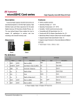
EMC210 – 8GB ~ 32GB
Features
• Compliant with JEDEC e.MMC Specification
Ver. 4.51
e.MMC 4.51 / BGA-153
• Supports three data bus widths: 1bit(default),
4bit, 8bit.
Transcend’s e.MMC-EMC210, is an
Embedded Flash Drive (EFD) designed
for industrial applications such as
embedded system, vehicle entertainment
system, GPS, games, email, office, etc. It
is a hybrid device combining an
embedded thin flash controller and
standard MLC NAND flash memory,
supporting an industry standard e.MMC
4.51 interface.
• Uses an embedded thin memory controller
and MLC NAND flash
The outstanding performance and strict
environment test enable Transcend’s
e.MMC 210 to fulfill the needs of a wide
variety of industrial application devices.
EMC 210 also provide 8~32GB of
capacities in JEDEC compatible form
factor and is an ideal solution for the
vendors who require easy integration, fast
entry to market and high storage capacity.
• Variable clock frequencies of 0-200 MHz
• Mechanical design complies with
JESD84-C44 Specification
• Dual power system
• Core voltage (VCC) 2.7-3.6V
• I/O (VCCQ) voltage, either: 1.7-1.95V or
2.7-3.6V
• Supports three data bus widths: 1bit(default),
4bit, 8bit.
• Static global wear leveling
• BCH ECC:53bit/1KB
• Fully cycle environment test
• RoHS compliant
Transcend e.MMC
Data I/O
MMC Bus Interface
Flash
Controller
Memory
CMD
e.MMC Bus and Power Lines
Transcend’s e.MMC bus has the following communication and power lines:
•
CMD: Command is a bidirectional signal. The host and Transcend’s e.MMC operate in two
modes, open drain and push-pull.
•
DAT0-7: Data lines are bidirectional signals. Host and Transcend’s e.MMC operate in
push-pull mode.
•
CLK: Clock input.
•
RST_n: Hardware Reset Input
•
VCCQ: VCCQ is the power supply line for host interface.
•
VCC: VCC is the power supply line for internal flash memory.
•
VDDi: VDDi is e.MMC’s internal power node, not the power supply. Connect 0.1µF
capacitor from VDDi to ground.
•
VSS, VSSQ : Ground lines
(Bus Signal Level)
Parameter
Min
Max
Unit
Supply voltage (3.3V)
2.7
3.6
V
Supply voltage (1.8V)
1.7
1.95
V
I/O Leakage current
-10
10
uA
Remark
Open-Drain bus signal level
Output high voltage (VOH)
VCCQ – 0.2
Output Low voltage (VOL)
V
0.3
V
IOL = 2mA
V
IOH = -100uA @ VDD min
0.125 * VCCQ
V
IOL = 100uA @ VDD min
Push-Pull bus signal level (2.7~3.6V)
Output high voltage (VOH)
0.75 * VCCQ
Output Low voltage (VOL)
Input high voltage (VIH)
0.625 * VCCQ
VCCQ + 0.3
V
Input Low voltage (VIL)
GND – 0.3
0.25 * VCCQ
V
Push-pull bus signal level (1.70V~1.95V)
Output high voltage (VOH)
VCCQ – 0.45
Output Low voltage (VOL)
V
IOH = -2 mA
0.45
V
IOL = 2 mA
Input high voltage (VIH)
0.65 * VCCQ
VCCQ + 0.3
V
Input Low voltage (VIL)
GND – 0.3
0.35 * VDD
V
e.MMC 4.51 selected feature overview
• Power Off Notification
The host should notify the device before it powers the device off. This allows the device to better
prepare itself for being powered off. For more details, refer to section 6.6.36 of the JEDEC Standard
Specification NO. JESD84-B451.
• Packed Commands
Read and write commands can be packed in groups of commands (either all read or all write)
that transfer the data for all commands in the group in one transfer on the bus, to reduce
overheads. For more details, refer to section 6.6.29 of the JEDEC Standard Specification NO.
JESD84-B451.
• Boot Partition
EMC210 supports e.MMC 4.51 boot operation modes. Boot partition size is reflected in
BOOT_SIZE_MULT register value in extended CSD.
• Automatic Sleep Mode
If there is no further command issued by the host in 11mS duration, after the previously issued
command is completed, the device enters “Power Saving Mode” to reduce power consumption. The
host does not have to take any action for this to occur. However, if host want to achieve the lowest
sleep current, the host needs to shut down its clock to the memory device. When the host is ready to
access a memory device in sleep mode, any command issued to it will cause devices to exit sleep
mode.
• Sleep (CMD5)
EMC210 may be switched between a sleep state and a standby state by SLEEP/AWAKE (CMD5).
In the sleep state the power consumption of EMC210 is minimized. For more details, refer to section
6.6.21 of the JEDEC Standard Specification No. JESD84-451.
• Enhanced Reliable Write
EMC210 supports enhanced reliable write as defined in e.MMC 4.51 spec. Enhanced reliable write
is a special write mode in which the old data pointed to by a logical address must remain unchanged
until the new data written to same logical address has been successfully programmed. This is to
ensure that the target address updated by the reliable write transaction never contains undefined
data. When writing in reliable write mode, data will remain valid even if a sudden power loss occurs
during programming.
• Sanitize
The sanitize operation is a feature, in addition to Trim and Erase is used to remove data from
EMC210. The use of sanitize operation requires EMC210 to physically remove data from the
unmapped user address space. For more details, refer to section 6.6.13 of the JEDEC Standard
Specification NO.JESD84-B451.
• Discard
The discard is similar operation to Trim. The discard function allows the host to identify data that’s no
longer required so that EMC210 can erase the data if necessary during background erase events.
For more details, refer to section 6.6.14 of the JEDEC Standard Specification NO.JESD84-B451.
• Erase
In addition to the implicit erase executed by EMC210 as part of the write operation, provides a host
explicit erase function. For more details, refer to section 6.6.11 of the JEDEC Standard Specification
NO.JESD84-B451.
• Trim
The Trim operation is similar to the default erase operation described above. The Trim function
applies the erase operation to write blocks instead of erase groups. The Trim function allows the
host to identify data that’s no longer required so that EMC210 can erase the data if necessary during
background erase events. For more details, refer to section 6.6.12 of the JEDEC Standard
Specification NO.JESD84-B451.
• Partition management
EMC210 offers the possibility for the host to configure addition split local memory partitions with
independent addressable space starting from logical address 0x00000000 for different usage
models. Therefore memory block area scan be classified as follows:
Two Boot Area partitions, whose size is 4MB and from which booting from EMC210 can be
performed.
One RPMB partition accessed through a trusted mechanism, whose size is defined as multiple
of 128KB.
Four General Purpose Area Partition to store sensitive data or for other host usage models. The
size of these partitions is a multiple of the write protect group. Size can be programmed once in
device life cycle (one-time programmable).
• Quick Health Info
Transcend designs several byte in extended CSD of EMC210. Customers can read UDA and EUDA
program/erase cycles information by CMD_8 and reading extended CSD structure without any
performance suffer. It’s well-designed for industrial use.
• Write Protect Management
In order to allow the host to protect data against erase or write, EMC210 supports two levels of write
protect commands. For more details, refer to section 6.6.17 of the JEDEC Standard Specification
NO.JESD84-B451.
• High Priority Interrupt (HPI)
In some scenarios, different types of data on the device may have different priorities for the host. For
example, writing operation may be time consuming and therefore there might be a need to suppress
the writing to allow demand paging requests in order launch a process when requested by the user.
For more details, refer to section 6.6.26 of the JEDEC Standard Specification NO. JESD84-B451.
• H/W Reset
Hardware reset may be used by the host to reset the device, moving the device to a Pre-idle state
and disabling the power-on period write protect on blocks that was set as power-on write protect
before the reset was asserted. For more details, refer to section 6.15.9 of the JEDEC Standard
Specification NO.JESD84-B451.
• DDR I/F
Support DDR signaling to double bus performance. For more details, refer to JESD84-B451
standard.
• Replay Protected Memory Block
A signed access to a Replay Protected Memory Block is provided. This function provides means for
the system to store data to the specific memory area in an authenticated and replay protected
manner. For more details, refer to section 6.6.22 of the JEDEC standard Specification
NO.JESD84-B451.
• Background Operation
EMC210 has various maintenance operations need to perform internally. In order to reduce
latencies during time critical operation like read and write, it is better to execute maintenance
operation in other times – when the host is not being serviced. For more details, refer to section
6.6.25 of the JEDEC Standard Specification NO.JESD84-B451.
Product Specifications
• Specification
P/N
Package
Ball Number
Technology
TS8GEMC210
11.5 x 13 x 1.0 mm
153
MLC
TS16GEMC210
11.5 x 13 x 1.0 mm
153
MLC
TS32GEMC210
11.5 x 13 x 1.2 mm
153
MLC
• Performance
Performance*
P/N
Seq. Read
Seq. Write
Ran. Read
Ran. Write
TS8GEMC210
140
40
2100 IOPS
600 IOPS
TS16GEMC210
140
60
2100 IOPS
700 IOPS
TS32GEMC210
140
60
2100 IOPS
700 IOPS
*Depending on operating condition, the result might be different.
• Terabytes Written
P/N
Terabytes Written
TS8GEMC210
9.23 TBW.
TS16GEMC210
18.46 TBW
TS32GEMC210
36.92 TBW
*Depending on different programming behavior and type.
• Power Consumption
Power Consumption (mA , 25°C)
P/N
VCCQ
APS
Sleep
Write
Read
TS8GEMC210
0.05
0.05
21
37
TS16GEMC210
0.05
0.05
23
37
TS32GEMC210
0.05
0.05
23
37
*APS: Auto Power Suspend
• Power Supply
P/N
VCC
VCCQ
TS8GEMC210
2.7-3.6V
1.7-1.95V / 2.7-3.6V
TS16GEMC210
2.7-3.6V
1.7-1.95V / 2.7-3.6V
TS32GEMC210
2.7-3.6V
1.7-1.95V / 2.7-3.6V
*VCCQ (I/O) 3.3V is not supported in HS200 operation.
• Temperature
Temperature
Operation
Storage
-25℃ to 85℃
-40℃ to 85℃
• Moisture Sensitivity
The moisture sensitivity for EMC210 is MSL = 3.
• Mechanical Property
Mechanical Property
Shock
Vibration
500G, 1ms (JESD22B104)
20.0G, 20 - 2000Hz (JESD22B103)
Physical Specifications
Interface Description
153-Ball AA Device
M6
Symbol
Type
Ball Function
CLK
Input
Clock:
Each cycle directs a 1-bit transfer on the
command and DAT lines.
M5
CMD
Input
Command:
A bidirectional channel used for device
initialization and command transfers.
Command has two operation modes:
• Open-drain for initialization
• Push-pull for fast command transfer
A3
DAT0
I/O
Data I/O0:
Bidirectional channel used for data transfer.
A4
DAT1
I/O
Data I/O1:
Bidirectional channel used for data transfer.
A5
DAT2
I/O
Data I/O2:
Bidirectional channel used for data transfer.
B2
DAT3
I/O
Data I/O3:
Bidirectional channel used for data transfer.
B3
DAT4
I/O
Data I/O4:
Bidirectional channel used for data transfer.
B4
DAT5
I/O
Data I/O5:
Bidirectional channel used for data transfer.
B5
DAT6
I/O
Data I/O6:
Bidirectional channel used for data transfer.
B6
DAT7
I/O
Data I/O7:
Bidirectional channel used for data transfer.
K5
E6, F5, J10, K9
RST_n
Input
VCC
Supply
Reset signal pin
VCC:
Flash memory I/F and Flash memory power
supply.
C6, M4, N4, P3, P5
VCCQ
Supply
VCCQ:
Memory controller core and MMC interface
I/O power supply.
153-Ball AA Device
E7, G5, H10, K8
Symbol
Type
VSS
Supply
Ball Function
VSS:
Flash memory I/F and Flash memory ground
connection.
C4, N2, N5, P4, P6
VSSQ
Supply
VSSQ:
Memory controller core and MMC I/F ground
connection.
C2
VDDi
VDDi:
Connect 0.1µF capacitor from VDDi to ground
Miscellaneous
D4
NC Index
─
Index:
Can be connected to ground or left floating.
A1, A2, A8, A9, A10, A11,
NC
─
A12, A13, A14, B1, B7,
No connect:
Can be connected to ground or left floating.
B8, B9, B10, B11, B12,
B13, B14, C1, C3, C7, C8,
C9, C10, C11, C12, C13,
C14, D1, D2, D3, D12,
D13, D14, E1, E2, E3,
E12, E13, E14, F1, F2,
F3, F12, F13, F14, G1,
G2, G12, G13, G14, H1,
H2, H3, H12, H13, H14,
J1, J2, J3, J12, J13, J14,
K1, K2, K3, K12, K13,
K14, L1, L2, L3, L12, L13,
L14, M1, M2, M3, M7, M8,
M9, M10, M11, M12, M13,
M14, N1, N3, N6, N7, N8,
N9, N10, N11, N12, N13,
N14, P1, P2, P8, P9, P11,
P12, P13, P14
A6, A7, C5, E5, E8, E9,
E10, F10, G3, G10, H5,
RFU
─
Reserved for future use.
Left it floating for future use.
153-Ball AA Device
Symbol
Type
Ball Function
J5, K6, K7, K10, P7, P10
Card Register
• OCR Register
For Transcend e.MMC, the value of 32-bit OCR register is 0xC0FF8080
Note: OCR bit [31] is set to LOW if the card has not finished the power up routine.
• CID Register
Name
Field
Width
Value
CSD-slice
Manufacturer ID
MID
8
1Eh
[127:120]
Card/BGA
CBX
2
01h
[113:112]
OEM/Application ID
OID
8
FFh
[111:104]
Product name
PNM
48
5453454D4D43h
[103:56]
Product revision
PRV
8
Counter to indicate FW ver.
[55:48]
Product serial number
PSN
32
Random by production
[47:16]
Manufacturing date
MDT
8
Month Year
[15:8]
CRC7 checksum
CRC
7
• (Note1)
[7:1]
Note1: The description is the same as e.MMC JEDEC standard
• CSD Register
R: Read only.
W: One time programmable and not readable.
R/W: One time programmable and readable.
W/E: Multiple writable with value kept after power failure, H/W reset assertion and any CMD0
reset and not readable.
R/W/E: Multiple writable with value kept after power failure, H/W reset assertion and any CMD0
reset and readable.
R/W/C_P: Writable after value cleared by power failure and H/W reset assertion (the value not
cleared by CMD0 reset) and readable.
R/W/E_P: Multiple writable with value reset after power failure, H/W reset assertion and any
CMD0 reset and readable.
W/E_P: Multiple writable with value reset after power failure, H/W reset assertion and any CMD0
reset and not readable.
Name
Field
Width
Cell
Type
CSD structure
Value
CSD-slice
CSD_STRUCTURE
2
R
11b
[127:126]
System specification
version
SPEC_VERS
4
R
0100b
[125:122]
Data read access-time 1
TAAC
8
R
27h
[119:112]
Data read access-time 2
in CLK cycles
(NSAC*100)
NSAC
8
R
01h
[111:104]
Max. bus clock frequency
TRAN_SPEED
8
R
32h
[103:96]
Card command classes
CCC
12
R
0F5h
[95:84]
Max. read data block
length
READ_BL_LEN
4
R
9h
[83:80]
Partial blocks for read
allowed
READ_BL_PARTIAL
1
R
0b
[79:79]
Write block misalignment
WRITE_BLK_MISALIG
N
1
R
0b
[78:78]
Read block misalignment
READ_BLK_MISALIGN
1
R
0b
[77:77]
DSR implemented
DSR_IMP
1
R
0b
[76:76]
Device size
C_SIZE
12
R
FFFh
[73:62]
Max. read current @ VDD
min
VDD_R_CURR_MIN
3
R
111b
[61:59]
Max. read current @ VDD
VDD_R_CURR_MAX
3
R
111b
[58:56]
max
Max. write current @ VDD
min
VDD_W_CURR_MIN
3
R
111b
[55:53]
Max. write current @ VDD
max
VDD_W_CURR_MAX
3
R
111b
[52:50]
Device size multiplier
C_SIZE_MULT
3
R
111b
[49:47]
Erase group size
ERASE_GRP_SIZE
5
R
11111b
[46:42]
Erase group size multiplier ERASE_GRP_MULT
5
R
11111b
[41:37]
Write protect group size
5
R
01111b
[36:32]
Write protect group enable WP_GRP_ENABLE
1
R
1b
[31:31]
Manufacturer default ECC DEFAULT_ECC
2
R
00b
[30:29]
Write speed factor
R2W_FACTOR
3
R
010b
[28:26]
Max. write data block
length
WRITE_BL_LEN
4
R
9h
[25:22]
Partial blocks for write
allowed
WRITE_BL_PARTIAL
1
R
0b
[21:21]
Content protection
application
CONTENT_PROT_APP
1
R
0b
[16:16]
File format group
FILE_FORMAT_GRP
1
R/W
0b
[15:15]
Copy flag (OTP)
COPY
1
R/W
1b
[14:14]
Permanent write
protection
PERM_WRITE_PROTE
CT
1
R/W
0b
[13:13]
Temporary write
protection
TMP_WRITE_PROTEC
T
1
R/W/E
0b
[12:12]
File format
FILE_FORMAT
2
R/W
00b
[11:10]
ECC code
ECC
2
R/W/E
00b
[9:8]
CRC
CRC
7
R/W/E
1101001b
[7:1]
Not used, always ’1’
-
1
─
1b
[0:0]
WP_GRP_SIZE
• Extended CSD register
R: Read only.
W: One time programmable and not readable.
R/W: One time programmable and readable.
W/E: Multiple writable with value kept after power failure, H/W reset assertion and any CMD0
reset and not readable.
R/W/E: Multiple writable with value kept after power failure, H/W reset assertion and any CMD0
reset and readable.
R/W/C_P: Writable after value cleared by power failure and H/W reset assertion (the value not
cleared by CMD0 reset) and readable.
R/W/E_P: Multiple writable with value reset after power failure, H/W reset assertion and any
CMD0 reset and readable.
W/E_P: Multiple writable with value reset after power failure, H/W reset assertion and any CMD0
reset and not readable.
Name
Field
Cell
Type
Value
CSD-slice
(Byte)
Supported Command
Sets
S_CMD_SET
R
1h
[504]
HPI features
HPI_FEATURES
R
3h
[503]
Background operations
support
BKOPS_SUPPORT
R
1h
[502]
Max packed read
commands
MAX_PACKED_READS
R
8h
[501]
Max packed write
commands
MAX_PACKED_WRITES
R
8h
[500]
Data tag support
DATA_TAG_SUPPORT
R
1h
[499]
Tag unit size
TAG_UNIT_SIZE
R
0h
[498]
Tag Resource size
TAG_RES_SIZE
R
6h
[497]
Context management
capabilities
CONTEXT_CAPABILITIES
R
78h
[496]
Large Unit Size
LARGE_UNIT_SIZE_M1
R
1h
[495]
Extended partitions
attribute support
EXT_SUPPORT
R
3h
[494]
Cache size
CACHE_SIZE
R
20000h
[252:249]
Generic CMD6 timeout
GENERIC_CMD6_TIME
R
64h
[248]
Power off
notification(long) timeout
POWER_OFF_LONG_TIME
R
64h
[247]
Background operations
status
BKOPS_STATUS
R
0h
[246]
Number of correctly
programmed sectors
CORRECTLY_PRG_SECTOR
S_NUM
R
0h
[245:242]
1st initialization time after
partitioning
INI_TIMEOUT_AP
R
Ah
[241]
Power class for 52MHz,
DDR at 3.6V
PWR_CL_DDR_52_360
R
0h
[239]
Power class for 52MHz,
DDR at 1.95V
PWR_CL_DDR_52_195
R
0h
[238]
Power class for 200MHz,
at 1.95V
PWR_CL_200_195
R
0h
[237]
Power class for 200MHz,
at 1.3V
PWR_CL_200_130
R
0h
[236]
Minimum Write
Performance for 8bit at
52MHz in DDR mode
MIN_PERF_DDR_W_8_52
R
0h
[235]
Minimum Read
Performance for 8bit at
52MHz in DDR mode
MIN_PERF_DDR_R_8_52
R
0h
[234]
TRIM Multiplier
TRIM_MULT
R
1h
[232]
Secure Feature support
SEC_FEATURE_SUPPORT
R
55h
[231]
Secure Erase Multiplier
SEC_ERASE_MULT
R
Ah
[230]
Secure TRIM Multiplier
SEC_TRIM_MULT
R
Ah
[229]
Boot information
BOOT_INFO
R
7h
[228]
Boot partition size
BOOT_SIZE_MULTI
R
20h
[226]
Access size
ACC_SIZE
R
6h
[225]
High-capacity erase unit
size
HC_ERASE_GRP_SIZE
R
1h
[224]
High-capacity erase
timeout
ERASE_TMEOUT_MULT
R
2h
[223]
Reliable write sector
count
REL_WR_SEC_C
R
1h
[222]
High-capacity write
protect group size
HC_WP_GRP_SIZE
R
10h
[221]
Sleep current (VCC)
S_C_VCC
R
7h
[220]
Sleep current (VCCQ)
S_C_VCCQ
R
7h
[219]
Sleep/awake timeout
S_A_TIMEOUT
R
13h
[217]
Sector Count
SEC_COUNT
R
Depends on
capacity
[215:212]
Minimum Write
Performance for 8bit at
52MHz
MIN_PERF_W_8_52
R
8h
[210]
Minimum Read
Performance for 8bit at
52MHz
MIN_PERF_R_8_52
R
8h
[209]
Minimum Write
Performance for 8bit at
26MHz, for 4bit at 52MHz
MIN_PERF_W_8_26_4_52
R
8h
[208]
Minimum Read
Performance for 8bit at
26MHz, for 4bit at 52MHz
MIN_PERF_R_8_26_4_62
R
8h
[207]
Minimum Write
Performance for 4 bit at
26MHz
MIN_PERF_W_4_26
R
8h
[206]
Minimum Read
Performance for 4bit at
26MHz
MIN_PERF_R_4_26
R
8h
[205]
R
0h
[203]
Power class for 26MHz at PWR_CL_26_360
3.6V 1 R
Power class for 52MHz at PWR_CL_52_360
3.6V 1 R
R
0h
[202]
Power class for 26MHz at PWR_CL_26_195
1.95V 1 R
R
0h
[201]
Power class for 52MHz at PWR_CL_52_195
1.95V 1 R
R
0h
[200]
Partition switching timing
PARTITION_SWITCH_TIME
R
3h
[199]
Out-of-interrupt busy
timing
OUT_OF_INTERRUPT_TIME
R
2h
[198]
I/O driver strength
DRIVER_STRENGTH
R
1h
[197]
Device type
DEVICE_TYPE
R
17h
[196]
CSD structure version
CSD_STRUCTURE
R
2h
[194]
Extended CSD revision
EXT_CSD_REV
R
6h
[192]
Command set
CMD_SET
R/W/E_P
0h
[191]
Command set revision
CMD_SET_REV
R
0h
[189]
Power class
POWER_CLASS
R/W/E_P
0h
[187]
High-speed interface
timing
HS_TIMING
R/W/E_P
2h
[185]
Bus width mode
BUS_WIDTH
W/E_P
2h
[183]
Erased memory content
ERASED_MEM_CONT
R
0h
[181]
Partition configuration
PARTITION_CONFIG
R/W/E &
R/W/E_P
0h
[179]
Boot config protection
BOOT_CONFIG_PROT
R/W &
R/W/C_P
0h
[178]
Boot bus condition
BOOT_BUS_CONDITION
R/W/E
0h
[177]
High-density erase group
definition
ERASE_GROUP_DEF
R/W/E_P
0h
[175]
Boot area write protection BOOT_WP
register
R/W &
R/W/C_P
0h
[173]
User area write protection USER_WP
register
R/W,
R/W/C_P
0h
[171]
&
R/W/E_P
FW configuration
FW_CONFIG
R/W
0h
[169]
RPMB Size
RPMB_SIZE_MULT
R
20h
[168]
Write reliability setting
register
WR_REL_SET
R/W
1Fh
[167]
Write reliability parameter
register
WR_REL_PARAM
R
5h
[166]
Start Sanitize operation
SANITIZE_START
W/E_P
0h
[165]
Manually start
background operations
BKOPS_START
W/E_P
0h
[164]
Enable background
operations handshake
BKOPS_EN
R/W
0h
[163]
H/W reset function
RST_n_FUNCTION
R/W
0h
[162]
HPI management
HPI_MGMT
R/W/E_P
0h
[161]
Partitioning Support
PARTITIONING_SUPPORT
R
7h
[160]
Max Enhanced Area Size
MAX_ENH_SIZE_MULT
R
Depends on
capacity
[159:157]
Partitions attribute
PARTITIONS_ATTRIBUTE
R/W
0h
[156]
Partitioning Setting
PARTITION_SETTING_COMP
LETED
R/W
0h
[155]
R/W
0h
[154:143]
General Purpose Partition GP_SIZE_MULT
Size
Enhanced User Data
Area Size
ENH_SIZE_MULT
R/W
0h
[142:140]
Enhanced User Data
Start Address
ENH_START_ADDR
R/W
0h
[139:136]
Bad Block Management
mode
SEC_BAD_BLK_MGMNT
R/W
0h
[134]
Package Case
Temperature is controlled
TCASE_SUPPORT
W/E_P
0h
[132]
Periodic Wake-up
PERIODIC_WAKEUP
R/W/E
0h
[131]
Program CID/CSD in
DDR mode support
PROGRAM_CID_CSD_DDR_
SUPPORT
R
0h
[130]
Vendor Specific Fields
VENDOR_SPECIFIC_FIELD
vendor
specific
Reserved
[127:64]
UDA Quick Health info
UDA_HEALTH_STATUS
R
0h
[71:68]
EUDA Quick Health info
EUDA_HEALTH_STATUS
R
0h
[67:64]
Native sector size
NATIVE_SECTOR_SIZE
R
1h
[63]
Sector size emulation
USE_NATIVE_SECTOR
R/W
0h
[62]
Sector size
DATA_SECTOR_SIZE
R
0h
[61]
1st initialization after
disabling sector size
emulation
INI_TIMEOUT_EMU
R
Ah
[60]
Class 6 commands
control
CLASS_6_CTRL
R/W/E_P
0h
[59]
Number of addressed
group to be Released
DYNCAP_NEEDED
R
0h
[58]
Exception events control
EXCEPTION_EVENTS_CTRL
R/W/E_P
0h
[57:56]
Exception events status
EXCEPTION_EVENTS_STAT
US
R
0h
[55:54]
Extended Partitions
Attribute
EXT_PARTITIONS_ATTRIBU
TE
R/W
0h
[53:52]
Context configuration
CONTEXT_CONF
R/W/E_P
0h
[51:37]
Packed command status
PACKED_COMMAND_STATU
S
R
0h
[36]
Packed command failure
index
PACKED_FAILURE_INDEX
R
0h
[35]
Power Off Notification
POWER_OFF_NOTIFICATIO
N
R/W/E_P
0h
[34]
Control to turn the Cache
ON/OFF
CACHE_CTRL
R/W/E_P
0h
[33]
Flushing of the cache
FLUSH_CACHE
W/E_P
0h
[32]
Marking
1st row :
2nd row :
3rd row:
4th row :
5th row :
Transcend LOGO
Sales P/N
Internal use
Country of Origin + Date Code
Serial number
Revision History
Modification Content
Version
Date
V0.1
2015/03/23
V0.2
2015/03/31
V1.0
2015/04/08 Formal Release