1
®
®
Mobile Intel Celeron Processor (0.18µ) in BGA2 and Micro-PGA2 Packages
These input buffers have no internal pull-up or pull-down resistors and system logic can use
CMOS or Open-drain drivers to drive them.
The Open-drain output signals have open drain drivers and external pull-up resistors are required.
One of the two output signals (IERR#) is a catastrophic error indicator and is tri-stated (and
pulled-up) when the processor is functioning normally. The FERR# output can be either tri-stated
or driven to VSS when the processor is in a low-power state depending on the condition of the
floating point unit. Since this signal is a DC current path when it is driven to VSS, Intel
recommends that the software clears or masks any floating-point error condition before putting the
processor into the Deep Sleep state.
3.1.5.3
Other Signals
The system bus clock (BCLK) must be driven in all of the low-power states except the Deep Sleep
state. The APIC clock (PICCLK) must be driven whenever BCLK is driven unless the APIC is
hardware disabled or the processor is in the Sleep state. Otherwise, it is permitted to turn off
PICCLK by holding it at VSS. The system bus clock should be held at VSS when it is stopped in the
Deep Sleep state.
In the Auto Halt and Stop Grant states the APIC bus data signals (PICD[1:0]) may toggle due to
APIC bus messages. These signals are required to be tri-stated and pulled-up when the processor
is in the Quick Start, Sleep, or Deep Sleep states unless the APIC is hardware disabled.
3.2
Power Supply Requirements
3.2.1
Decoupling Recommendations
The amount of bulk decoupling required on the VCC and VCCT planes to meet the voltage tolerance
requirements for the mobile Intel Celeron processor are a strong function of the power supply
design. Contact your Intel Field Sales Representative for tools to help determine how much bulk
decoupling is required. The processor core power plan (VCC) should have eight 0.1-µF high
frequency decoupling capacitors placed underneath the die and twenty 0.1-µF mid frequency
decoupling capacitors placed around the die as close to the die as flex solution allows. The system
bus buffer power plane (VCCT) should have twenty 0.1-µF high frequency decoupling capacitors
around the die.
3.2.2
Voltage Planes
All VCC and VSS pins/balls must be connected to the appropriate voltage plane. All VCCT and VREF
pins/balls must be connected to the appropriate traces on the system electronics. In addition to the
main VCC, VCCT, and VSS power supply signals, PLL1 and PLL2 provide analog decoupling to the
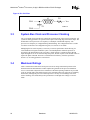
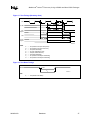
PLL section. PLL1 and PLL2 should be connected according to Figure 4. Do not connect PLL2
directly to VSS. Appendix A contains the RLC filter specification.
283654-003
Datasheet
21