1
Mobile Intel® Celeron® Processor (0.13 µ)
Micro-FCBGA and Micro-FCPGA Packages Datasheet
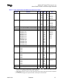
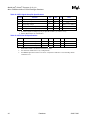
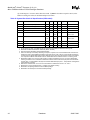
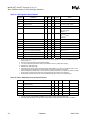
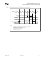
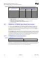
Table 29. AGTL Signal Groups AC Specifications1
2
RTT = 56Ω internally terminated to VCCT; VREF = /3VCCT; load = 50 ohms
Symbol
Parameter
T7
AGTL Output Valid Delay
T8
AGTL Input Setup Time
Min
0.40
Max
3.25
0.95
Unit
Figure
ns
9
ns
10
1.30
T9
AGTL Input Hold Time
1
Notes
Notes 2, 3, 6
Note 7
ns
10
Note 4
T10
RESET# Pulse Width
1
ms
11,12
Note 5
NOTES:
1. All AC timings for AGTL signals are referenced to the crossing point of the BCLK rising edge and the BCLK#
falling edge for Differential Clocking and to the BCLK rising edge at 1.25 V for Single Ended Clocking. All AGTL
signals are referenced at VREF. Unless other specified, all timings apply to both 100-MHz and 133-MHz bus
frequencies.
2. RESET# can be asserted (active) asynchronously, but must be deasserted synchronously.
3. Specification is for a minimum 0.40-V swing from Vref-200 mV to Vref+200 mV.
4. Specification is for a maximum 0.8-V swing from Vcct-0.8 V to Vcct.
5. After VCC, VCCT, and BCLK, BCLK# become stable and PWRGOOD is asserted.
6. Applies to all processors supporting 133-MHz bus clock frequency except Ultra Low Voltage processors.
7. Applies to all processors supporting 100-MHz bus clock frequency and Ultra Low Voltage processors supporting
133-MHz bus clock frequency.
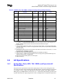
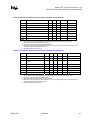
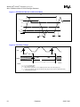
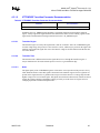
Table 30. CMOS and Open-drain Signal Groups AC Specifications1, 2
Symbol
Parameter
Min Max
Unit
Figure
Notes
T14
1.5V Input Pulse Width, except PWRGOOD and
LINT[1:0]
2
BCLKs
9
Active and inactive
states
T14B
LINT[1:0] Input Pulse Width
6
BCLKs
9
Note 3
T15
PWRGOOD Inactive Pulse Width
2
12
Note 4,5
µs
NOTES:
1. All AC timings for CMOS and Open-drain signals are referenced to the crossing point of the BCLK rising edge
and BCLK# falling edge for Differential Clocking and to the rising edge of BCLK at 1.25 V for Single Ended
Clocking. All CMOS and Open-drain signals are referenced at 1.0 V.
2. Minimum output pulse width on CMOS outputs is 2 BCLKs.
3. This specification only applies when the APIC is enabled and the LINT1 or LINT0 signal is configured as an
edge triggered interrupt with fixed delivery, otherwise specification T14 applies.
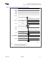
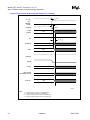
4. When driven inactive, or after VCC, VCCT and BCLK, BCLK# become stable. PWRGOOD must remain below
VIL18,MAX until all the voltage planes meet the voltage tolerance specifications in Table 12 through Table 21 and
BCLK, BCLK# have met the BCLK, BCLK# AC specifications in Table 35 and Table 36 for at least 2 µs.
PWRGOOD must rise error-free and monotonically to 1.8 V.
5. If the BCLK Settling Time specification (T60) can be guaranteed at power-on reset then the PWRGOOD
Inactive Pulse Width specification (T15) is waived and BCLK may start after PWRGOOD is asserted.
PWRGOOD must still remain below VIL25,max until all the voltage planes meet the voltage tolerance
specifications.
298517-006
Datasheet
45