1
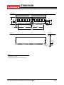
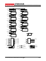
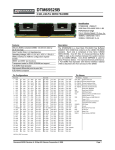
DTM63392B
1 GB - 128Mx72, 240-Pin Registered DDR2 DIMM with CMD/ADD Parity
Identification
DTM63392B 128Mx72
1Rx8 PC2-5300P-555-12-F0
Performance range
Clock / Module Speed / CL-tRCD -tRP
333 MHz / PC2-5300 / 5-5-5
266 MHz / PC2-4200 / 4-4-4
Features
Description
240-pin JEDEC-compliant Single Rank DIMM
DTM63392B is a Registered 128Mx72 memory module
which conforms to JEDEC's DDR2, PC2-5300
standard. The assembly is comprised of one Rank of
nine 128Mx8 DDR2 Hynix DRAMs, one Register with
command/address parity, one Phase-Locked Loop
(PLL), and one 2K-bit EEPROM used for Serial
Presence Detect.
Both output driver strength and input termination
impedance are programmable to maintain signal
integrity on the I/O signals. Error Checking and
Correction bits are provided to ensure data integrity. In
addition, parity is checked for all address and control
lines, even those address lines not used by this
module.
The eighteen Data Strobe signals may be used either
as nine differential pairs, or as eighteen single-ended
strobes for use in systems with a mix of x4 and x8
DRAMs.
Pin Description
Operating Voltage: 1.8 V ±0.1
I/O Type: SSTL_18
Data Transfer Rate: 5.3 Gigabytes/sec
Data Bursts: 4 or 8 bits, Sequential or Interleaved ordering
Error Checking and Correction (ECC) data bits
Programmable I/O driver strength (OCD)
Support Address and Control signal parity checking
Programmable CAS Latency: 4 and 5
Relative Humidity: 20% - 80% non-condensing
SDRAM Addressing (Row/Col/Bank): 14/10/3
Fully ROHS Compliant
Pin Configuration
Front Side
Back Side
Name
Function
151 GND
181 VDD
211 DM5/DQS14
/CAS
Column Address Strobe
92 /DQS5 122 DQ4
152 DQ28
182 A3
212 /DQS14
/Err_Out
Parity Error Found
63 A2
93 DQS5 123 DQ5
153 DQ29
183 A1
213 GND
34 DQ25
64 VDD
94 GND
154 GND
184 VDD
214 DQ46
/RAS
/RESET
Row Address Strobe
Register and PLL Reset
35 GND
65 GND
95 DQ42 125 DM0/DQS9
155 DM3/DQS12 185 CK0
215 DQ47
/S[1:0]
Chip Selects
6 /DQS0
36 /DQS3
66 GND
96 DQ43 126 /DQS9
156 /DQS12
186 /CK0
216 GND
7 DQS0
37 DQS3
67 VDD
97 GND
157 GND
187 VDD
217 DQ52
/WE
A[15:0]
Write Enable
Address Inputs
1 VREF
31 DQ19
61 A4
91 GND
2 GND
32 GND
62 VDD
3 DQ0
33 DQ24
4 DQ1
5 GND
121 GND
124 GND
127 GND
8 GND
38 GND
68 Par_In 98 DQ48 128 DQ6
158 DQ30
188 A0
218 DQ53
BA[2:0]
Bank Addresses
9 DQ2
39 DQ26
69 VDD
99 DQ49 129 DQ7
159 DQ31
189 VDD
219 GND
10 DQ3
40 DQ27
70 A10
100 GND
130 GND
160 GND
190 BA1
220 NC
CB[7:0]
CK0, /CK0
Data Check Bits
Differential Clock Inputs
11 GND
41 GND
71 BA0
101 SA2
131 DQ12
161 CB4
191 VDD
221 NC
CKE[1:0]
Clock Enables
12 DQ8
42 CB0
72 VDD
102 NC
132 DQ13
162 CB5
192 /RAS
222 GND
DQ[63:0]
Data Bits
13 DQ9
43 CB1
73 /WE
103 GND
133 GND
163 GND
193 /S0
223 DM6/DQS15
DQS[17:0], /DQS[17:0]
Differential Data Strobes
14 GND
44 GND
74 /CAS
104 /DQS6 134 DM1/DQS10 164 DM8/DQS17 194 VDD
224 /DQS15
15 /DQS1
45 /DQS8
75 VDD
105 DQS6 135 /DQS10
225 GND
GND
NC
Ground
No Connection
16 DQS1
46 DQS8
76 /S1*
106 GND
166 GND
196 A13
226 DQ54
ODT[1:0]
On Die Termination Inputs
17 GND
47 GND
77 ODT1* 107 DQ50 137 NC
167 CB6
197 VDD
227 DQ55
18 /RESET 48 CB2
78 VDD
108 DQ51 138 NC
168 CB7
198 GND
228 GND
Par_In
SA[2:0]
Parity Bit, Address & Control
SPD Address
19 NC
49 CB3
79 GND
109 GND
169 GND
199 DQ36
229 DQ60
SCL
SPD Clock Input
20 GND
50 GND
80 DQ32
110 DQ56 140 DQ14
170 VDD
200 DQ37
230 DQ61
SDA
SPD Data Input/Output
21 DQ10
51 VDD
81 DQ33
111 DQ57 141 DQ15
171 CKE1*
201 GND
231 GND
VDD
Power
22 DQ11
52 CKE0
82 GND
112 GND
172 VDD
202 DM4/DQS13 232 DM7/DQS16
23 GND
53 VDD
83 /DQS4 113 /DQS7 143 DQ20
173 A15
203 /DQS13
233 /DQS16
VDDSPD
VREF
SPD EEPROM Power
Reference Voltage
24 DQ16
25 DQ17
54 BA2
84 DQS4
55 /Err_Out 85 GND
174 A14
175 VDD
204 GND
205 DQ38
234 GND
235 DQ62
26 GND
56 VDD
86 DQ34
116 DQ58 146 DM2/DQS11 176 A12
206 DQ39
236 DQ63
27 /DQS2
57 A11
87 DQ35
117 DQ59 147 /DQS11
207 GND
237 GND
28 DQS2
58 A7
88 GND
118 GND
148 GND
178 VDD
208 DQ44
238 VDDSPD
29 GND
59 VDD
89 DQ40
119 SDA
149 DQ22
179 A8
209 DQ45
239 SA0
30 DQ18
60 A5
90 DQ41
120 SCL
150 DQ23
180 A6
210 GND
240 SA1
136 GND
139 GND
142 GND
114 DQS7 144 DQ21
115 GND 145 GND
165 /DQS17
177 A9
195 ODT0
* = Not Used.
Document 06929, Revision A, 3-Mar-09, Dataram Corporation © 2009
Page 1
DTM63392B
1 GB - 128Mx72, 240-Pin Registered DDR2 DIMM with CMD/ADD Parity
Front view
133.35
[5.250]
30.00
[1.181]
10.00
[0.394]
4.00
[0.157]
17.80
[0.700]
5.00
[0.197]
5.18
[0.204]
63.00
[2.480]
55.00
[2.165]
2.54 Min
[0.100 Min]
123.00
[4.843]
Back view
Side view
2.67 Max
[0.105] Max
4.00 Min
[0.157] Min
1.27 ±.10
[0.0500 ±0.0040]
Notes
Tolerances on all dimensions except where otherwise
indicated are ±.13 (.005).
All dimensions are expressed: millimeters [inches]
Document 06929, Revision A, 3-Mar-09, Dataram Corporation © 2009
Page 2
DTM63392B
1 GB - 128Mx72, 240-Pin Registered DDR2 DIMM with CMD/ADD Parity
DQR[55:48]
/DQS12
/DQS16
DM3/DQS12
DM7/DQS16
/DQS
NU/
/RDQS
/CS
I/O [7:0]
DM/
RDQS
DQR[31:24]
DQS
DQS7
/DQS7
/DQS
DQS3
/DQS3
DQR[63:56]
I/O [7:0]
NU/
/RDQS
NU/
/RDQS
DM/
RDQS
/CS
I/O [7:0]
NU/
/RDQS
/DQS
NU/
/RDQS
/CS
I/O [7:0]
DM/
RDQS
DQR[23:16]
DQS
DQS6
/DQS6
/DQS
DQS2
/DQS2
NU/
/RDQS
/DQS15
DM6/DQS15
DM/
RDQS
/DQS11
DM2/DQS11
I/O [7:0]
DM/
RDQS
DQR[47:40]
/CS
/DQS
NU/
/RDQS
/CS
I/O [7:0]
DM/
RDQS
DQR[15:8]
DQS
DQS5
/DQS5
/DQS
DQS1
/DQS1
/CS
/DQS14
DM5/DQS14
/CS
/DQS10
DM1/DQS10
I/O [7:0]
DM/
RDQS
/DQS
DQR[39:32]
DQS
NU/
/RDQS
/CS
I/O [7:0]
DM/
RDQS
DQR[7:0]
DQS
DQS4
/DQS4
/DQS
DQS0
/DQS0
DQS
DM4/DQS13
DQS
/DQS13
DM0/DQS9
DQS
/RS0
/DQS9
/DQS17
DM8/DQS17
DQS8
SCL
/DQS8
WP
NU/
/RDQS
DM/
RDQS
I/O [7:0]
/CS
DQS
/DQS
CBR[7:0]
SDA
Serial SPD
SA0 SA1 SA2
Register
1:1
/S0
/RS0
PLL
All SDRAMs
BA[2:0]
RBA[2:0] All SDRAMs
A[15:0]
RA[15:0] All SDRAMs
/RAS
/RRAS
All SDRAMs
/CAS
/RCAS
All SDRAMs
/WE
/RWE
All SDRAMs
CKE0
RCKE0 All SDRAMs
ODT0
RODT0 All SDRAMs
PCK0-6, 8, 9 to CK on SDRAMs.
CK0
/PCK0-6, 8, 9 to /CK on SDRAMs.
PCK7 to CK at Register.
/CK0
/PCK7 to /CK at Register.
/RESET
PAR_IN
/RESET
DQ[63:0]
PCLK7
/PCLK7
/ERR_OUT
CB[7:0]
DQR[63:0]
CBR[7:0]
VDDSPD
Serial SPD
VDD
All SDRAMs
DQS[17:0]
DQSR[17:0]
VREF
All SDRAMs
/DQS[17:0]
/DQSR[17:0]
VSS
All SDRAMs
1. Unless otherwise noted, resistor values are 22 ohms +/- 5%.
Document 06929, Revision A, 3-Mar-09, Dataram Corporation © 2009
Page 3
DTM63392B
1 GB - 128Mx72, 240-Pin Registered DDR2 DIMM with CMD/ADD Parity
Absolute Maximum Ratings
(Note: Operation at or above Absolute Maximum Ratings can adversely affect module reliability.)
PARAMETER
Symbol
Minimum
Maximum
Unit
Temperature, non-Operating
TSTORAGE
-55
100
C
TCASE
0
95
C
VDD
-1.0
2.3
V
VIN,VOUT
-0.5
2.3
V
DRAM Case Temperature, Operating
Voltage on VDD relative to VSS
Voltage on Any Pin relative to VSS
Recommended DC Operating Conditions (Voltages referenced to Vss = 0 V)
PARAMETER
Power Supply Voltage
Symbol
VDD
Minimum
1.7
Typical
1.8
Maximum
1.9
Unit
V
Note
I/O Reference Voltage
VREF
0.49 VDD
0.50 VDD
0.51 VDD
V
1
Bus Termination Voltage
VTT
VREF - 0.04
VREF
VREF + 0.04
V
Notes:
1. The value of VREF is expected to equal one-half VDD and to track variations in the VDD DC level. Peak-to-peak noise on VREF may
not exceed ±1% of its DC value.
DC Input Logic Levels, Single-Ended (Voltages referenced to Vss = 0 V)
PARAMETER
Logical High (Logic 1)
Symbol
VIH(DC)
Minimum
VREF + 0.125
Maximum
VDD + 0.300
Unit
V
Logical Low (Logic 0)
VIL(DC)
-0.300
VREF - 0.125
V
AC Input Logic Levels, Single-Ended (Voltages referenced to Vss = 0 V)
PARAMETER
Logical High (Logic 1)
Symbol
VIH(AC)
Minimum
VREF + 0.250
Maximum
-
Unit
V
Logical Low (Logic 0)
VIL(AC)
-
VREF - 0.250
V
Document 06929, Revision A, 3-Mar-09, Dataram Corporation © 2009
Page 4
DTM63392B
1 GB - 128Mx72, 240-Pin Registered DDR2 DIMM with CMD/ADD Parity
Differential Input Logic Levels (Voltages referenced to Vss = 0 V)
PARAMETER
DC Input Signal Voltage
Symbol
VIN(DC)
Minimum
-0.300
Maximum
VDD + 0.300
Unit
V
Note
1
DC Differential Input Voltage
VID(DC)
-0.250
VDD + 0.600
V
2
AC Differential Input Voltage
VID(AC)
-0.500
VDD + 0.600
V
3
AC Differential Cross-Point Voltage
VIX(AC)
0.50 VDD - 0.175
0.50 VDD + 0.175
V
4
Notes:
1. VIN(DC) specifies the allowable DC excursion of each input of a differential pair.
2. VID(DC) specifies the input differential voltage, i.e. the absolute value of the difference between the two voltages of a differential
pair.
3. VID(AC) specifies the input differential voltage required for switching.
4. The typical value of VIX(AC) is expected to be 0.5 VDD and is expected to track variations in VDD.
Capacitance (0 C < TCASE < 55 C, f = 100 MHz, VOUT(DC) = VDD/2, VOUT(ac) = 0.1V(p-p))
PARAMETER
Symbol
Minimum
Maximum
Unit
Input Capacitance, Clock
CK0, /CK0
Pin
CIN1
1
2
pF
Input Capacitance, Address
and Control
BA[2:0], A[15:0], /S0, /RAS, /CAS,
/WE, CKE0, ODT0
CIN2
2.5
3.5
pF
Input/Output Capacitance
DQ[63:0], CB[7:0], DQS[17:0],
/DQS[17:0]
CIO
2.5
4
pF
DC Characteristics (Voltages referenced to Vss = 0 V)
PARAMETER
Symbol
Minimum
Maximum
Unit
Note
Input Leakage Current
ILI
-5
5
μA
1
Output Leakage Current
IOZ
-5
5
μA
2
Output Minimum Source DC Current
IOH
-13.4
-
mA
3
Output Minimum Sink DC Current
IOL
+13.4
-
mA
4
Notes:
1.
2.
3.
4.
These values are guaranteed by design and are tested on a sample basis only
DQx and ODT are disabled, and 0 V ≤ VOUT ≤ VDD.
VDD = 1.7 V, VOUT = 1420 mV. (VOUT - VDD)/IOH must be less than 21 Ohms for values of VOUT between VDD and (VDD - 280
mV).
VDD = 1.7 V, VOUT = 280 mV. VOUT/IOL must be less than 21 Ohms for values of VOUT between 0 V and 280 mV.
Document 06929, Revision A, 3-Mar-09, Dataram Corporation © 2009
Page 5
DTM63392B
1 GB - 128Mx72, 240-Pin Registered DDR2 DIMM with CMD/ADD Parity
IDD Specifications and Conditions (Voltages referenced to Vss = 0 V)
PARAMETER
Operating One
Bank ActivePrecharge Current
Operating One
Bank Active-ReadPrecharge Current
Precharge PowerDown Current
Precharge Standby
Current
Symbol
IDD0
IDD1
IDD2P
IDD2N
Active Power-Down
Current
IDD3P
Active Standby
Current
IDD3N
Operating Burst
Write Current
IDD4W
Operating Burst
Read Current
IDD4R
Burst Refresh
Current
IDD5
Self Refresh
Current
IDD6
Operating Bank
Interleave Read
Current
IDD7
Test Condition
CKE is HIGH, /CS is HIGH between valid commands; Address
bus inputs are switching; Data bus inputs are switching.
IOUT = 0 mA; BL = 4, CL = 5 ns, AL = 0; CKE is HIGH, /CS is
HIGH between valid commands; Address bus inputs are
switching.
All banks idle; CKE is LOW; Other control and address bus inputs
are stable; Data bus inputs are floating.
All banks idle; CKE is HIGH, /CS is HIGH; Other control and
address bus inputs are switching; Data bus inputs are switching.
All banks open; CKE is LOW; Other control and address bus
inputs are stable; Data bus inputs are floating. Fast Power-down
exit (Mode Register bit 12 = 0)
All banks open; tRAS = 70 ms; CKE is HIGH, /CS is HIGH between
valid commands; Other control and address bus inputs are
switching; Data bus inputs are switching.
Burst Write: All banks open; Continuous burst writes; BL = 4; AL =
0, CL = CL(IDD); tCK = tCK(IDD); tRAS tRAS.MAX(IDD), tRP =
tRP(IDD); CKE is HIGH, CS is HIGH between valid commands.
Address inputs are switching; Data Bus inputs are switching;
Burst Read: All banks open; Continuous burst reads; BL = 4; AL =
0, CL = CL(IDD; tCK = tCK(IDD; tRAS =tRAS.MAX.(IDD, tRP =
tRP(IDD; CKE is HIGH, CS is HIGH between valid commands.
Address inputs are switching; Data Bus inputs are switching;
IOUT = 0 mA.
Refresh command at every 7.8 us; CKE is HIGH, /CS is HIGH
between valid commands; Other control and address bus inputs
are switching; Data bus inputs are switching.
CK and /CK at 0 V; CKE ≤ 0.2 V; Other control and address bus
inputs are floating; Data bus inputs are floating.
All bank interleaving reads, IOUT= 0 mA; BL = 4, CL = 5 tCK;
AL = 70 ns; tRRD = 7.5 ns; CKE is HIGH, /CS is HIGH between
valid commands; Address bus inputs are stable during deselects;
Data bus inputs are switching.
Max
Value
Unit
770
mA
880
mA
250
mA
630
mA
330
mA
650
mA
1431
mA
1324
mA
2160
mA
270
mA
2360
mA
Notes: 1. For all IDDX measurements, tCK = 3 ns, tRC = 60 ns, tRCD = 15 ns, tRAS = 45 ns, and tRP = 15 ns unless otherwise specified.
2. All IDDX values shown are worst-case maximums, considering all DRAMs, Register, and the PLL.
Document 06929, Revision A, 3-Mar-09, Dataram Corporation © 2009
Page 6
DTM63392B
1 GB - 128Mx72, 240-Pin Registered DDR2 DIMM with CMD/ADD Parity
AC Operating Conditions
PARAMETER
Symbol
Min
Max
Unit
DQ Output Access Time from Clock
tAC
-450
+450
ps
CAS-to-CAS Command Delay
tCCD
2
-
tCK
Clock High Level Width
tCH
0.45
0.55
tCK
Clock Cycle Time
tCK
3,000
8000
ps
Clock Low Level Width
tCL
0.45
0.55
tCK
tDH
175
-
ps
tDIPW
0.35
-
tCK
DQS Output Access Time from Clock
tDQSCK
-400
+400
ps
Write DQS High Level Width
tDQSH
0.35
-
tCK
Write DQS Low Level Width
tDQSL
0.35
-
tCK
DQS-Out Edge to Data-Out Edge Skew
tDQSQ
240
-
ps
Data Input Setup Time Before DQS Strobe
tDS
100
-
ps
DQS Falling Edge from Clock, Hold Time
tDSH
0.2
-
tCK
DQS Falling Edge to Clock, Setup Time
tDSS
0.2
-
tCK
Clock Half Period
tHP
minimum of tCH or tCL
-
ns
Address and Command Hold Time after Clock
tIH
275
-
ps
Address and Command Setup Time before Clock
tIS
200
-
ps
Load Mode Command Cycle Time
tMRD
2
-
tCK
DQ-to-DQS Hold
tQH
tHP - tQHS
-
-
Data Hold Skew Factor
tQHS
340
-
ps
Active-to-Precharge Time
tRAS
45
70K
ns
Active-to-Active / Auto Refresh Time
tRC
60
-
ns
RAS-to-CAS Delay
tRCD
15
-
ns
Average Periodic Refresh Interval
tREFI
-
7.8
μs
Auto Refresh Row Cycle Time
tRFC
127.5
-
ns
Row Precharge Time
tRP
15
-
ns
Read DQS Preamble Time
tRPRE
0.9
1.1
tCK
Read DQS Postamble Time
tRPST
0.4
0.6
tCK
Row Active to Row Active Delay
tRRD
7.5
-
ns
Data Input Hold Time after DQS Strobe
DQ Input Pulse Width
tRTP
7.5
-
ns
Write DQS Preamble Time
tWPRE
0.35
-
ps
Write DQS Postamble Time
tWPST
0.4
0.6
tCK
tWR
15
-
ns
Internal Read to Precharge Command Delay
Write Recovery Time
Internal Write to Read Command Delay
tWTR
7.5
-
ns
Exit Self Refresh to Non-Read Command
tXSNR
tRFC(min) + 10
-
ns
Exit Self Refresh to Read Command
tXSRD
200
-
tCK
Document 06929, Revision A, 3-Mar-09, Dataram Corporation © 2009
Page 7
DTM63392B
1 GB - 128Mx72, 240-Pin Registered DDR2 DIMM with CMD/ADD Parity
SERIAL PRESENCE DETECT MATRIX
Byte#
Function.
Value
Hex
0
Number of Bytes Utilized by Module Manufacturer
128 bytes
0x80
1
Total number of Bytes in Serial PD device
256 bytes
0x08
2
Memory Type
3
4
Number of Row Addresses
Number of Column Addresses
5
6
Module Attributes - Number of Ranks, Package and Height
# of Ranks Card on Card DRAM Package Module Height Module Data Width.
7
8
Reserved
Voltage Interface Level of this assembly
9
SDRAM Cycle time. (Max. Supported CAS Latency). CL=X
(tCK) ns
SDRAM Access from Clock. (Highest CAS latency). (tAC) ns
10
11
12
DIMM configuration type (Non-parity, Parity or ECC)
Data Parity Data ECC Address/Command Parity TBD TBD TBD TBD TBD Refresh Rate/Type (us)
13
14
0x0E
0x0A
0x60
1
No
Planar
30mm
72
0x48
UNUSED
SSTL/1.8V
0x00
0x05
3
0x30
0.45
0x45
0x06
X
X
0x82
Primary SDRAM Width
8
0x08
Error Checking SDRAM Width
8
0x08
Reserved
16
SDRAM Device Attributes: Burst Lengths Supported
18
14
10
7.8 (SR)
15
17
DDR2 SDRAM 0x08
TBD TBD Burst Length = 4 Burst Length = 8 TBD TBD TBD TBD SDRAM Device Attributes - Number of Banks on SDRAM
Device
SDRAM Device Attributes: CAS Latency
TBD TBD Latency = 2 -
Document 06929, Revision A, 3-Mar-09, Dataram Corporation © 2009
UNUSED
0x00
0x0C
X
X
8
0x08
0x30
Page 8
DTM63392B
1 GB - 128Mx72, 240-Pin Registered DDR2 DIMM with CMD/ADD Parity
19
20
21
22
23
24
25
26
Latency = 3 Latency = 4 X
Latency = 5 X
Latency = 6 TBD DIMM Mechanical Characteristics. Max. module thickness.
x </= 4.10
(mm)
DIMM type information
Regular RDIMM (133.35mm) X
Regular UDIMM (133.35mm) SODIMM (67.6mm) Micro-DIMM (45.5mm) Mini RDIMM (82.0mm) Mini UDIMM (82.0mm) TBD TBD SDRAM Module Attributes (Refer to Byte20 for DIMM type information).
Number of active registers on the DIMM (N/A for UDIMM) 1
Number of PLL on the DIMM (N/A for UDIMM) 1
FET Switch External Enable No
TBD Analysis probe installed No
TBD SDRAM Device Attributes: General
Includes Weak Driver X
Supports 50 ohm ODT X
Supports PASR (Partial Array Self Refresh) TBD TBD TBD TBD TBD Minimum Clock Cycle Time at Reduced CAS Latency, CL = X3.75
1 (ns)
Maximum Data Access Time (tAC ) from Clock at CL = X- 1
0.45
(ns)
Minimum Clock Cycle Time at CL = X-2 (ns)
UNUSED
0x01
0x01
0x04
0x03
0x3D
0x45
0x00
27
28
29
Maximum Data Access Time (tAC ) from Clock at CL = X-2
(ns)
Minimum Row Precharge Time (tRP ) (ns)
Minimum Row Active to Row Active Delay (tRRD ) (ns)
Minimum RAS to CAS Delay (tRCD ) (ns)
30
31
Minimum Active to Precharge Time (tRAS ) (ns)
Module Rank Density
45
1GB
0x2D
0x01
32
33
34
35
36
Address and Command Setup Time Before Clock (tIS) (ns)
Address and Command Hold Time After Clock (tIH) (ns)
Data Input Setup Time Before Strobe (tDS) (ns)
Data Input Hold Time After Strobe (tDH) (ns)
Write Recovery Time (tWR ) (ns)
0.2
0.27
0.1
0.17
15
0x20
0x27
0x10
0x17
0x3C
Document 06929, Revision A, 3-Mar-09, Dataram Corporation © 2009
UNUSED
0x00
15
7.5
15
0x3C
0x1E
0x3C
Page 9
DTM63392B
1 GB - 128Mx72, 240-Pin Registered DDR2 DIMM with CMD/ADD Parity
37
38
39
40
41
42
43
44
45
46
47
48
49
Internal write to read command delay (tWTR ) (ns)
Internal read to precharge command delay (tRTP ) (ns)
Memory Analysis Probe Characteristics.
Extension of Byte 41(tRC) and Byte 42 (tRFC) (ns)
Add this value to byte 41 Add this value to byte 42 SDRAM Device Minimum Active to Active/Auto Refresh Time
(tRC) (ns)
SDRAM Device Minimum Auto-Refresh to Active/AutoRefresh
Command Period (tRFC). (ns)
SDRAM Device Maximum Cycle Time (tCK max). (ns)
7.5
7.5
UNUSED
0
0.5
60
0x3C
127.5
0x7F
8
0x80
SDRAM Dev DQS-DQ Skew for DQS & DQ signals (tDQSQ)
0.24
(ns)
DDR SDRAM Device Read Data Hold Skew Factor (tQHS)
0.34
(ns)
PLL Relock Time (us)
6
DRAM maximun Case Temperature Delta. (Degree C).
DT4R4W Delta (Bits 0:3) 0.4
Tcasemax delta (Bits 7:4) 10
Thermal Resistance of DRAM Package from Top (Case) to
58
Ambient ( Psi T-A DRAM ). (C/Watt)
DRAM Case Temperature Rise from Ambient due to Activate-Precharge/
Mode Bits (DT0/Mode Bits). (Degree C).
Bit 0. If "0" DRAM does not support high temperature selfrefresh entry Bit 1. If "0" Do not need double refresh rate for the proper
operation DT0, (Bits 2:7) -
0x1E
0x1E
0x00
0x06
0x18
0x22
0x06
0x51
0x74
0x57
1
1
6.3
50
DRAM Case Temperature Rise from Ambient due to
Precharge/Quiet Standby (DT2N/DT2Q). (Degree C).
6
0x3C
51
DRAM Case Temperature Rise from Ambient due to
Precharge Power-Down (DT2P). (Degree C).
1.44
0x60
52
DRAM Case Temperature Rise from Ambient due to Active
Standby (DT3N). (Degree C).
6.9
0x2E
53
DRAM Case temperature Rise from Ambient due to Active
Power-Down with Fast PDN Exit (DT3Pfast). (Degree C).
4.4
0x58
54
DRAM Case temperature Rise from Ambient due to Active
Power-Down with Slow PDN Exit (DT3Pslow). (Degree C).
2.2
0x58
55
DRAM Case Temperature Rise from Ambient due to Page Open Burst
Read/DT4R4W Mode Bit (DT4R/DT4R4W Mode Bit). (Degree C).
Bit 0. "0" if DT4W is greater than DT4R DT4R, ( Bits 1:7 ) -
56
DRAM Case Temperature Rise from Ambient due to Burst
Refresh (DT5B). (Degree C).
Document 06929, Revision A, 3-Mar-09, Dataram Corporation © 2009
0x4A
0
14.8
24.5
0x31
Page 10
DTM63392B
1 GB - 128Mx72, 240-Pin Registered DDR2 DIMM with CMD/ADD Parity
57
DRAM Case Temperature Rise from Ambient due to Bank
Interleave Reads with Auto-Precharge (DT7). (Degree C).
26.5
0x35
58
Thermal Resistance of PLL Package from Top to Ambient
(Psi T-A PLL). (C/Watt).
87
0xAE
59
Thermal Resistance of Register Package from Top to Ambient
( Psi T-A Register). (C/Watt).
70
0x8C
60
PLL Case Temperature Rise from Ambient due to PLL Active
(DT PLL Active). (Degree C).
33.5
0x86
61
Register Case Temperature Rise from Ambient due to Register Active/Mode Bit 0x7C
(DT Register Active/Mode Bit).
Bit 0.If "0"Unit for Bits 2:7 is 0.75C Bit 1. RFU. Default: 0 Register Active,( Bits 2:7 ) -
62
63
64
65
66-71
72
73-90
91,92
93,94
95-98
99127
SPD Revision
Checksum for Bytes 0-62
Module Manufacturer’s JEDEC ID Code
Module Manufacturer’s JEDEC ID Code
Module Manufacturer’s JEDEC ID Code
Module Manufacturing Location
Module Part Number
Module Revision Code
Module Manufacturing Date
Module Serial Number
Manufacturer’s Specific Data
Document 06929, Revision A, 3-Mar-09, Dataram Corporation © 2009
0.75
0
23.25
Revision 1.2
Dataram ID
Dataram ID
UNUSED
UNUSED
UNUSED
UNUSED
#
UNUSED
0x12
0xF0
0x7F
0x91
0x00
0x00
0x20
0x00
0x00
0x23
0x00
Page 11
DTM63392B
1 GB - 128Mx72, 240-Pin Registered DDR2 DIMM with CMD/ADD Parity
DATARAM CORPORATION, USA Corporate Headquarters, P.O.Box 7528, Princeton, NJ 08543-7528;
Voice: 609-799-0071, Fax: 609-799-6734; www.dataram.com
All rights reserved.
The information contained in this document has been carefully checked and is believed to be reliable. However,
Dataram assumes no responsibility for inaccuracies.
The information contained in this document does not convey any license under the copyrights, patent rights or
trademarks claimed and owned by Dataram.
No part of this publication may be copied or reproduced in any form or by any means, or transferred to any third party
without prior written consent of Dataram.
Document 06929, Revision A, 3-Mar-09, Dataram Corporation © 2009
Page 12