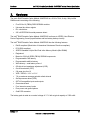
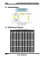
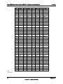
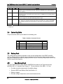
1
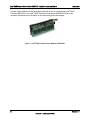
Intel® RAID Portable Cache Module AXXRPCM3 Technical Product Specification Intel order number E20184-002 Revision 1.1 July 2008 Enterprise Platforms and Services Marketing Revision History Intel® RAID Portable Cache Module AXXRPCM3 Technical Product Specification Revision History Date July 2007 Revision Number 1.0 Modifications Initial Release July 2008 1.1 Update Battery pack information Disclaimers INFORMATION IN THIS DOCUMENT IS PROVIDED IN CONNECTION WITH INTEL® PRODUCTS. NO LICENSE, EXPRESS OR IMPLIED, BY ESTOPPEL OR OTHERWISE, TO ANY INTELLECTUAL PROPERTY RIGHTS IS GRANTED BY THIS DOCUMENT. EXCEPT AS PROVIDED IN INTEL'S TERMS AND CONDITIONS OF SALE FOR SUCH PRODUCTS, INTEL ASSUMES NO LIABILITY WHATSOEVER, AND INTEL DISCLAIMS ANY EXPRESS OR IMPLIED WARRANTY, RELATING TO SALE AND/OR USE OF INTEL PRODUCTS INCLUDING LIABILITY OR WARRANTIES RELATING TO FITNESS FOR A PARTICULAR PURPOSE, MERCHANTABILITY, OR INFRINGEMENT OF ANY PATENT, COPYRIGHT OR OTHER INTELLECTUAL PROPERTY RIGHT. Intel products are not intended for use in medical, life saving, life sustaining, critical control or safety systems, or in nuclear facility applications. Intel might change specifications and product descriptions at any time, without notice. Designers must not rely on the absence or characteristics of any features or instructions marked "reserved" or "undefined." Intel reserves these for future definition and shall have no responsibility whatsoever for conflicts or incompatibilities arising from future changes to them. The Intel® RAID Portable Cache Module AXXRPCM3 may contain design defects or errors known as errata which may cause the product to deviate from published specifications. Current characterized errata are available on request. Intel is a trademark or registered trademark of Intel Corporation or its subsidiaries in the United States and other countries. *Other names and brands may be claimed as the property of others. Copyright © 2007-2008, Intel Corporation, Portions Copyright LSI Logic, Inc. ii Revision 1.1 Intel order number E20184-002 Intel® RAID Portable Cache Module AXXRPCM3 Technical Product Specification Table of Contents Table of Contents 1. Introduction .......................................................................................................................... 1 2. Hardware ............................................................................................................................... 3 2.1 Electrical and Mechanical Details ............................................................................ 4 2.2 Functional Block Diagram........................................................................................ 5 2.3 Gold PCB Connector Pin Assignment ..................................................................... 5 2.4 Connecting Cable .................................................................................................... 8 2.5 Battery Pack ............................................................................................................ 8 2.5.1 Smart Battery Circuit................................................................................................ 8 2.5.2 Battery States .......................................................................................................... 9 3. RAID Firmware Interaction ................................................................................................ 11 4. Intel® RAID Smart Battery Software.................................................................................. 12 4.1 Intel® RAID BIOS Console 2 .................................................................................. 12 4.2 Intel® RAID Web Console 2 ................................................................................... 12 4.3 Intel® RAID Command Line Utility 2....................................................................... 12 List of Figures Figure 1. Intel® RAID Portable Cache Module AXXRPCM3 ......................................................... 2 Figure 2. Block Diagram ............................................................................................................... 5 List of Tables Table 1. Electrical and Mechanical Details ................................................................................... 4 Table 2. PCB Connector Pin Assignment ..................................................................................... 5 Table 3. Pin Descriptions .............................................................................................................. 7 Table 4. Interface Connector Pin-out ............................................................................................ 8 Revision 1.1 Intel order number E20184-002 iii List of Tables Intel® RAID Portable Cache Module AXXRPCM3 Technical Product Specification < This page intentionally left blank. > iv Revision 1.1 Intel order number E20184-002 Introduction 1. Intel® RAID Portable Cache Module AXXRPCM3 Technical Product Specification Introduction This document specifies the key hardware components, firmware, and software utility requirements for the Intel® RAID Portable Cache Module AXXRPCM3. The Portable Cache Module is available as an accessory for the Intel® RAID Controller SRCSASJV to provide data integrity for the RAID solution by ensuring that the data passing through the cache is written to the hard drives. Intel® RAID Portable Cache Module AXXRPCM3 is a compact package that contains the following components Battery pack: Includes a circuit logic board and attached LiON (Lithium Ion) batteries. The logic board provides sensing and management logic to support the battery charge, discharge, and monitoring functionality. The battery includes a small cable that connects the battery to the battery logic board (Smart Battery Circuit). Smart Battery Circuit: Ensures that the battery is maintained at optimal performance and charge levels. This circuit is based on the Texas Instruments bq2060A SBS v1.1Compliant Gas Gauge IC*. Software to monitor / inform the user of issues and actions for the Intel® RAID Portable Cache Module. Monitoring is accomplished through the Intel® RAID BIOS Console 2, Intel® RAID Web Console 2, or Intel® RAID Command Line Utility 2 utilities. The Intel® RAID Portable Cache Module AXXRPCM3 provides the Intel® RAID Controller SRCSASJV adapter with battery-backed cache memory. Writing data to the controller’s cache memory is much faster than writing it to a storage device. The write operation is completed when data is transferred to the RAID (Redundant Array of Inexpensive Disks) cache. After data is written to the cached memory, the Intel® RAID Controller SRCSASJV writes the cached data to the storage device when system activity is low or when the cache is getting full. One risk of using a write-back cache is the cached data can be lost if the AC power fails before it is written to the storage device. The Portable Cache Module mitigates this risk by providing a battery as a backup source of power. Users can adjust options for the highest performance without increasing the risk of data loss. The Intel® RAID Portable Cache Module AXXRPCM3 provides additional fault tolerance when used in conjunction with a UPS (Uninterruptible Power Supply). The Intel® RAID Portable Cache Module AXXRPCM3 monitors the voltage level of the DRAM modules installed on the Intel® RAID Controller SRCSASJV. If the voltage level drops below a predefined level, the battery backup module portion of the Portable Cache Module switches the memory power source from the Intel® RAID Controller SRCSASJV to the battery pack on the Portable Cache Module. When the voltage level returns to an acceptable level, the battery backup circuitry switches the power source back to the Intel® RAID Controller SRCSASJV and all pending writes to storage devices are completed with no data loss. The Intel® RAID Portable Cache Module AXXRPCM3 has built-in functionality to charge the battery pack automatically and to communicate battery status information such as voltage, temperature, and current to the host computer system. The Portable Cache Module will cache data to a replacement controller if that data has not been written to a disk. This could be necessary if the RAID controller fails after an unexpected power failure. After moving the Revision 1.1 Intel order number E20184-002 1 Intel® RAID Portable Cache Module AXXRPCM3 Technical Product Specification Introduction Portable Cache Module and the associated hard disk drives to a replacement Intel® RAID Controller SRCSASJV, the Intel® RAID Portable Cache Module AXXRPCM3 flushes the unwritten data preserved in the cache to the disks through the new adapter. Figure 1. Intel® RAID Portable Cache Module AXXRPCM3 2 Revision 1.1 Intel order number E20184-002 Hardware 2. Intel® RAID Portable Cache Module AXXRPCM3 Technical Product Specification Hardware The Intel® RAID Portable Cache Module AXXRPCM3 is a 32 M x 72-bit, 8 chip, 244-pin Mini DIMM module consisting of the following: Five 32 M x16 (FBGA) DDR2 SDRAM modules Universal bus driver register PLL clock driver 256 x 8 EEPROM for serial presence detect The Intel® RAID Portable Cache Module AXXRPCM3 conforms to JEDEC (Joint Electron Device Engineering Council) specifications and has battery backup circuitry. The Intel® RAID Portable Cache Module AXXRPCM3 has the following features: RoHS compliant (Restriction of Hazardous Substances Directive compliant) PC2-5300 compliant JEDEC-Standard 244-pin Mini Dual Inline Memory Module (Mini-DIMM) Registered Based on 32 M x 8 DDR2 (FBGA) SDRAM components Programmable CAS latency Programmable additive latency Write latency = read latency minus 1 Off-chip driver impedance adjustment (OCD) On-die termination (ODT) 2 K page size for x16 VDD = VDDQ = 1.8 V +/-0.1 V 7.8 µs maximum average periodic refresh interval Serial presence detect (SPD) SSTL18 compatible inputs and outputs One external bank Four internal memory banks Pure power and ground planes Gold PCB connector The battery pack is rated at a nominal voltage of 3.7 V with a typical capacity of 1350 mAH. Revision 1.1 Intel order number E20184-002 3 Intel® RAID Portable Cache Module AXXRPCM3 Technical Product Specification 2.1 Hardware Electrical and Mechanical Details Table 1. Electrical and Mechanical Details 4 Feature Data retention Up to 72 hrs Description Chemistry LiON Dimensions 3.4-inches by 1.8-inches Weight 23.6 g nominal Operating temperature 10 to 45 degrees Celsius (the maximum dry bulb temperature shall be derated by 3.3° C per 1000 m above 500 m) Operating humidity 20% to 80%, non-condensing Storage temperature Greater than 90 days at 0 to 30 degrees Celsius 30 to 90 days at 0 to 40 degrees Celsius Less than 30 days at 0 to 50 degrees Celsius Storage humidity 20% to 80%, non-condensing Battery capacity 1350 mAH Voltages Nominal OCV: 3.7 V Fast charge current 500 mAH Trickle charge rate N/A Battery voltage conditioning Less than 3.0 V Battery charge time Typical: ~6 hours to charge from 3.6 V OCV to 4.2 V OCV Worst case: 8 hours if pack is completely depleted of charge Date retention times 72 hours for 256 MB standard cache using 256 Mbit x 16 DDR2 MTBF (Electrical Components) 1,187,012 hours at 40 degrees Celsius Battery shelf life 1 year Battery operational life 500 recharge cycles. Intel recommends replacing the battery yearly. Memory technology DDR2 SDRAM (1.8 V) Cache memory size supported 256 MB Memory bus speed 667 MHz Memory bus width 72-bit Revision 1.1 Intel order number E20184-002 Hardware 2.2 Intel® RAID Portable Cache Module AXXRPCM3 Technical Product Specification Functional Block Diagram Figure 2. Block Diagram 2.3 Gold PCB Connector Pin Assignment Table 2. PCB Connector Pin Assignment Pin# 1 Symbol VREF Pin# 62 Symbol A4 Pin# 123 Symbol VSS Pin# 184 Symbol VDDQ 2 VSS 63 VDDQ 124 DQ4 185 A3 3 DQ0 64 A2 125 DQ5 186 A1 4 DQ1 65 VDD 126 VSS 187 VDD 5 VSS 66 VSS 127 DM0 188 CK0 1 6 DQS0 67 VSS 128 NC 189 CK01 7 DQS0 68 NC 129 VSS 190 VDD 8 VSS 69 VDD 130 DQ6 191 A0 9 DQ2 70 A10/AP 131 DQ7 192 BA1 10 DQ3 71 BA0 132 VSS 193 VDD 11 VSS 72 VDD 133 DQ12 194 RAS1 12 DQ8 73 WE1 134 DQ13 195 VDDQ 13 DQ9 74 VDDQ 135 VSS 196 S01 14 VSS 75 CAS1 136 DM1 197 VDDQ 1 15 DQS1 76 VDDQ 137 NC 198 ODT0 16 DQS1 77 NC 138 VSS 199 NC 17 VSS 78 ODT1 139 RFU 200 VDD 18 RESET1 79 VDDQ 140 RFU 201 NC 19 NC 80 NC 141 VSS 202 VSS 20 VSS 81 VSS 142 DQ14 203 DQ36 Revision 1.1 Intel order number E20184-002 5 Intel® RAID Portable Cache Module AXXRPCM3 Technical Product Specification Hardware Pin# 21 Symbol DQ10 Pin# 82 Symbol DQ32 Pin# 143 Symbol DQ15 Pin# 204 Symbol DQ37 22 DQ11 83 DQ33 144 VSS 205 VSS 23 VSS 84 VSS 145 DQ20 206 DM4 1 24 DQ16 85 DQS4 146 DQ21 207 NC 25 DQ17 86 DQS4 147 VSS 208 VSS 26 VSS 87 VSS 148 DM2 209 DQ38 27 DQS21 88 DQ34 149 NC 210 DQ39 28 DQS2 89 DQ35 150 VSS 211 VSS 29 VSS 90 VSS 151 DQ22 212 DQ44 30 DQ18 91 DQ40 152 DQ23 213 DQ45 31 DQ19 92 DQ41 153 VSS 214 VSS 32 VSS 93 VSS 154 DQ28 215 DM5 1 33 DQ24 94 DQS5 155 DQ29 216 NC 34 DQ25 95 DQS5 156 VSS 217 VSS 35 VSS 96 VSS 157 DM3 218 DQ46 36 DQS31 97 DQ42 158 NC 219 DQ47 37 DQS3 98 DQ43 159 VSS 220 VSS 38 VSS 99 VSS 160 DQ30 221 DQ52 39 DQ26 100 DQ48 161 DQ31 222 DQ53 40 DQ27 101 DQ49 162 VSS 223 VSS 41 VSS 102 VSS 163 CB4 224 RFU 42 CB0 103 SA2 164 CB5 225 RFU 43 CB1 104 NC 165 VSS 226 VSS 44 VSS 105 VSS 166 DM8 227 DM6 45 DQS81 106 DQS61 167 NC 228 NC 46 DQS8 107 DQS6 168 VSS 229 VSS 47 VSS 108 VSS 169 CB6 230 DQ54 48 CB2 109 DQ50 170 CB7 231 DQ55 49 CB3 110 DQ51 171 VSS 232 VSS 50 VSS 111 VSS 172 NC 233 DQ60 51 NC 112 DQ56 173 VDDQ 234 DQ61 52 VDDQ 113 DQ57 174 CKE1 235 VSS 53 CKE0 114 VSS 175 VDD 236 DM7 54 VDD 115 DQS71 176 NC 237 NC 55 BA2 116 DQS7 177 NC 238 VSS 56 NC 117 VSS 178 VDDQ 239 DQ62 57 VDDQ 118 DQ58 179 A12 240 DQ63 58 A11 119 DQ59 180 A9 241 VSS 59 A7 120 VSS 181 VDD 242 SDA 60 VDD 121 SA0 182 A8 243 SCL 61 A5 122 SA1 183 A6 244 VDDSPD Note: 1 Active Low 6 Revision 1.1 Intel order number E20184-002 Hardware Intel® RAID Portable Cache Module AXXRPCM3 Technical Product Specification Table 3. Pin Descriptions Pin CK, CK1 Type Input Function Clock: CK and CK1 are differential system clock inputs. All address and control inputs are sampled on the crossing of the positive edge of CK and negative edge of CK1. Output (read) data is referenced to the crossing of CK and CK1 (both direction of crossing). ODT[1:0] Input On Die Termination: ODT (registered HIGH) enables termination resistance internal to the DDR2 SDRAM. When enabled, ODT is applied to each DQ, DQS, DQS1 and DM signal for x4 and DQ, DQS, DQS1 RDQS, RDQS1and DM for x8 configurations. For x16 configuration ODT is applied to each DQ, UDQS, UDQS LDQS, LDQS, UDM and LDM signal. The ODT pin will be ignored if the EMRS (1) is programmed to disable ODT. S1[1:0] Input Chip Select: Enables the associated SDRAM command decoder when low and disables decoder when high. When decoder is disabled, new commands are ignored and previous operations continue. These input signals also disable all outputs (except CKE and ODT) of the register(s) on the DIMM when both inputs are high. When both S [0:1] are high, all register outputs (except CKE, ODT and Chip select) remain in the previous state. CKE# Input Clock Enable: CKE high activates and CKE low deactivate internal clock signals and device input buffers and output drivers. Taking CKE low provides Precharge Power-Down and Self-Refresh operation (all banks idle), or Active Power- Down (row Active in any bank). CKE is synchronous for power down entry and exit and or Self-Refresh entry. CKE is asynchronous for Self-Refresh exit. CKE must be maintained high throughout read and write accesses. Input buffers, excluding CK, CK1, ODT and CKE are disabled during power-down. Input buffers, excluding CKE are disabled during Self-Refresh. A0 - A13 Input Address Inputs: Provides the row address for Activate commands and the column address and Auto-Pre-.charge bit A10 (=AP) for Read/Write commands to select one location out of the memory array in the respective bank. A10 (=AP) is sampled during a Precharge command to determine whether the Precharge applies to one bank (A10=low) or all banks (A10=high). If only one bank will be precharged, the bank is selected by BA0 and BA1. The address inputs also provide the op-code during Mode Register Set commands. Row address A13 is used on x4 and x8 components only. BA0, BA1 Input Bank Address Inputs: BA0 and BA1 define which bank the Activate, Read, Write, or Precharge command is applied to. BA0 and BA1 also determine if the mode register or extended mode register will be accessed during a MRS or EMRS cycle. RAS1 Input Row Address Strobe: When sampled at the positive rising edge of the clock RAS1, this command defines the operation to be executed by the SDRAM. CAS1 Input Column Address Strobe: When sampled at the positive rising edge of the clock, CAS1 defines the operation to be executed by the SDRAM. WE1 Input Write Enable: When sampled at the positive rising edge of the clock, WE1 defines the operation to be executed by the SDRAM. DM[8:0] Input Data Mask: Masks write data when high, and they are issued concurrently with input data. DQS[8:0] Input/ Output Data Strobe: Positive line of the differential data strobe for input and output data. DQS1[8:0] Input/ Output Data Strobe: Negative line of the differential data strobe for input and output data. DQ[63:0] Input/Output Data Lines: Data input/output pins. CB[7:0] - Check Bit: input/output lines, used for ECC. VDDQ SUPPLY DQ Power Supply: 1.8 V +/- 0.1 V VDDSPD SUPPLY Serial EEPROM: Positive power supply (wired to a separate power pin at the connector which supports from 1.7 V to 3.6 V (nominal 1.8 V, 2.5 V and 3.3 V operations. VDD SUPPLY Power Supply: 1.8 V +/- 0.1 V VSS SUPPLY Ground: VREF SUPPLY Reference voltage: For SSTL18 inputs. Revision 1.1 Intel order number E20184-002 7 Intel® RAID Portable Cache Module AXXRPCM3 Technical Product Specification Type Hardware Pin SCL - SDA - SPD Data: This bidirectional pin is used to transfer data into or out of the SPD EEPROM. A resistor must be connected from the SDA bus line to VDDSPD on the system planar to act as a pull-up. SA0 – SA2 SUPPLY SPD Address Lines: These signals are tied at the system planar to either VSS or VDD SPD to configure the serial SPD EEPROM address range. RESET1 Function SPD Clock Lines: This signal is used to clock data into and out of the SPD EEPROM. A resistor may be connected from the SCL bus time to VDDSPD on the system planar to act as a pull up. The RESET1 Pin is connected to the RST1 pin on the register and to the OE pin on the PLL. When low, all register outputs will be driven low and the PLL clocks to the DRAMs and register(s) will be set to low level (the PLL will remain synchronized with the input clock) NC SUPPLY No Connection: A line is unconnected in the DIMM. Note: 1 = Active Low 2.4 Connecting Cable A 5-pin connector cable is pre-installed in the battery pack. Table 4. Interface Connector Pin-out 2.5 Pin 1 Signal Name SMBD SMBus data Description Color Green 2 SMBC SMBus clock Blue 3 GND Battery negative terminal Black 4 PACK- Battery pack negative terminal White 5 PACK+ Battery pack positive terminal Red Battery Pack The cache-memory hold time depends on the size and configuration of the RAID controller memory. Battery backup retention time is estimated at 72 hours (three days) but the retention time varies depending on memory capacity and the number of memory components used on the DIMM to support that capacity. 2.5.1 Smart Battery Circuit ® The Intel RAID Portable Cache Module AXXRPCM3 is based on the Texas Instruments bq2060A SBS v1.1-compliant Gas Gauge IC*. The key features of the SBS v1.1 IC are: 8 Provides accurate measurement of available charge Supports SBS Smart Battery Data Specification v1.1 Reports voltages Provides voltage, temperature, and current measurements Revision 1.1 Intel order number E20184-002 Hardware Intel® RAID Portable Cache Module AXXRPCM3 Technical Product Specification Measures charge flow using a V-to-F converter with offset of less than 16 μV after calibration The Texas Instruments bq2060A SBS-compliant Gas Gauge IC* for the battery pack maintains an accurate record of the available charge. It determines battery capacity by monitoring the amount of charge input or removed from the smart battery. The bq2060A measures battery voltage, temperature, and current estimates battery selfdischarge, and monitors the battery for low-voltage thresholds. It measures charge and discharge activity by monitoring the voltage across a small-value series sense resistor between the battery’s negative terminal and the negative terminal of the battery pack. The available battery charge is determined by monitoring this voltage and correcting the measurement for environmental and operating conditions. For more information about the Texas Instruments bq2060A SBS-compliant Gas Gauge IC*, see the manufacturer website. The Intel® RAID Smart Battery features include: Integrated into battery pack Reduced host CPU intervention Shares I2C bus with the onboard EEPROM (Electronically Erasable Programmable Read-Only Memory) for memory Real-time battery status information Low charge warning Instantaneous voltage, current, and temperature Battery charge percentage remaining and at-rate information Broadcasts event alarms to the host: - Out-of-temperature - Terminate charge - Terminate discharge - Low capacity Manufacturing information Smart Charger Protocol for improved battery maintenance, calibration, and charging performance 2.5.2 Battery States The battery pack includes battery sensing logic that senses the battery voltage levels and recognizes the battery state. Revision 1.1 Intel order number E20184-002 9 Intel® RAID Portable Cache Module AXXRPCM3 Technical Product Specification 2.5.2.1 Hardware Initialized State The battery is in the initialized state during a normal power-up sequence. In RAID firmware, there are two levels of initialization: During boot loader execution During RAID firmware boot 2.5.2.2 Discharging State The battery voltage is drained as part of a relearn cycle. 2.5.2.3 Fully Charged State A battery that is not fully charged has a low-voltage level that indicates the level of charge. Charging begins when the battery logic detects low voltage and power is supplied. Once a new battery is fully charged, a relearn cycle is initiated. Relearn is the process of taking a fully charged battery through the discharge-charge cycle to update the gas gauge capacity parameters. The relearn cycle takes up to 24 hours to fully-discharge and recharge the battery pack. After the relearn cycle is complete, information from the battery accurately provides the state of charge, capacity, and other parameters. These parameters determine the health of the battery. The relearn cycle can be set at a user-definable interval. The default is a one-month (30 days) interval. A relearn cycle initiates on a newly-inserted battery, even if the battery was previously fully charged. Some applications can start a relearn, or a relearn can be manually started. 2.5.2.4 Fully-discharged State The fully-discharged state is detected as a low voltage parameter. The charger detects a fullydischarged battery state and starts charging the cells when sufficient power is available; and when the firmware has completed the pack’s initialization. 10 Revision 1.1 Intel order number E20184-002 RAID Firmware Interaction 3. Intel® RAID Portable Cache Module AXXRPCM3 Technical Product Specification RAID Firmware Interaction The RAID firmware detects the battery status and logs the following events: Battery is present Battery is not present New battery is detected Battery has been replaced Battery temperature is high Battery voltage is low Battery is charging Battery is discharging Battery voltage is normal Battery needs replacement: SOH bad Battery needs replacement: Battery is three years old Battery needs replacement: Charger is not working Relearn started Relearn in progress Relearn is complete Relearn timed out Relearn pending: Battery is under charge. Relearn postponed Relearn will start in four days Relearn will start in two days Relearn will start in one day Relearn will start in five hours Revision 1.1 Intel order number E20184-002 11 Intel® RAID Portable Cache Module AXXRPCM3 Technical Product Specification Intel® RAID Smart Battery Software 4. Intel® RAID Smart Battery Software 4.1 Intel® RAID BIOS Console 2 The system BIOS loads the RAID option ROM that is resident on the RAID controller flash. This utility is initiated by pressing <Ctrl> + <G> when prompted during POST (Power On Self Test). The option ROM checks for the presence of the battery and informs the user if the battery is missing or not fully charged. The Intel® RAID BIOS Console2 utility can be used to monitor the charge cycle count and voltage levels. It will display the number for fast charges and discharges on a battery. 4.2 Intel® RAID Web Console 2 This is an operating system based utility for the Microsoft Windows* and Linux* operating systems that are supported by the installed RAID controller. This utility can be used to monitor battery status, charge level, and the number of recharge cycles. 4.3 Intel® RAID Command Line Utility 2 This text-based utility is available for Microsoft Windows* and Linux* operating systems. It can be use to view battery status and to initiate a relearn. 12 Revision 1.1 Intel order number E20184-002