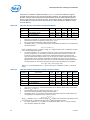
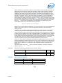
1
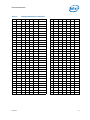
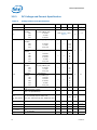
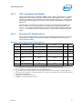
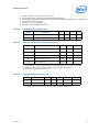
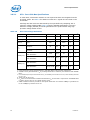
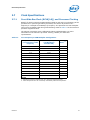
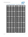
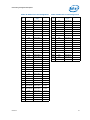
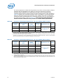
Land Listing and Signal Descriptions
Table 25.
Signal Description (Sheet 1 of 9)
Name
Type
Description
BSEL[2:0]
Output
The BCLK[1:0] frequency select signals BSEL[2:0] are used to select
the processor input clock frequency. Table 18 defines the possible
combinations of the signals and the frequency associated with each
combination. The required frequency is determined by the
processor, chipset and clock synthesizer. All agents must operate at
the same frequency. For more information about these signals,
including termination recommendations refer to Chapter 2.
COMP[5:4,1:0]
Analog
COMP[1:0] must be terminated to VSS on the system board using
precision resistors. COMP[5:4] must be terminated to VTT on the
system board using precision resistors.
D[63:0]# (Data) are the data signals. These signals provide a 64-bit
data path between the processor FSB agents, and must connect the
appropriate pins/lands on all such agents. The data driver asserts
DRDY# to indicate a valid data transfer.
D[63:0]# are quad-pumped signals and will, thus, be driven four
times in a common clock period. D[63:0]# are latched off the falling
edge of both DSTBP[3:0]# and DSTBN[3:0]#. Each group of 16
data signals correspond to a pair of one DSTBP# and one DSTBN#.
The following table shows the grouping of data signals to data
strobes and DBI#.
D[63:0]#
Input/
Output
Quad-Pumped Signal Groups
Data Group
DSTBN#/DSTBP#
DBI#
D[15:0]#
0
0
D[31:16]#
1
1
D[47:32]#
2
2
D[63:48]#
3
3
Furthermore, the DBI# signals determine the polarity of the data
signals. Each group of 16 data signals corresponds to one DBI#
signal. When the DBI# signal is active, the corresponding data
group is inverted and therefore sampled active high.
DBI[3:0]# (Data Bus Inversion) are source synchronous and
indicate the polarity of the D[63:0]# signals.The DBI[3:0]# signals
are activated when the data on the data bus is inverted. If more
than half the data bits, within a 16-bit group, would have been
asserted electrically low, the bus agent may invert the data bus
signals for that particular sub-phase for that 16-bit group.
DBI[3:0]#
66
Input/
Output
DBI[3:0] Assignment To Data Bus
Bus Signal
Data Bus Signals
DBI3#
D[63:48]#
DBI2#
D[47:32]#
DBI1#
D[31:16]#
DBI0#
D[15:0]#
Datasheet