1
MPAP-100
RS-232 PCMCIA
SYNCHRONOUS ADAPTER
for PCMCIA Card Standard compatible machines
User's Manual
QUATECH, INC.
5675 Hudson Industrial Parkway
Hudson, Ohio 44236
Quatech MPAP-100 User's Manual
TEL: (330) 655-9000
FAX: (330) 655-9010
www.quatech.com
1
WARRANTY INFORMATION
Quatech Inc. warrants the MPAP-100 to be free of defects for one (1) year from the date
of purchase. Quatech Inc. will repair or replace any board that fails to perform under normal
operating conditions and in accordance with the procedures outlined in this document during the
warranty period. Any damage that results from improper installation, operation, or general
misuse voids all warranty rights.
Although every attempt has been made to guarantee the accuracy of this manual, Quatech
Inc. assumes no liability for damages resulting from errors in this document. Quatech Inc.
reserves the right to edit or append to this document at any time without notice.
Please complete the following information and retain for your records. Have this
information available when requesting warranty service.
DATE OF PURCHASE:
MODEL NUMBER:
MPAP-100
PRODUCT DESCRIPTION: Single Channel PCMCIA RS-232-D
Synchronous Communications
Adapter
SERIAL NUMBER:
Quatech MPAP-100 User's Manual
2
Copyright 2001 Quatech, Inc.
NOTICE
The information contained in this document is protected by copyright, and cannot be
reproduced in any form without the written consent of Quatech, Inc. Likewise, any software
programs that might accompany this document are protected by copyright and can be used only
in accordance with any license agreement(s) between the purchaser and Quatech, Inc. Quatech,
Inc. reserves the right to change this documentation or the product to which it refers at any time
and without notice.
The authors have taken due care in the preparation of this document and every attempt
has been made to ensure its accuracy and completeness. In no event will Quatech, Inc. be liable
for damages of any kind, incidental or consequential, in regard to or arising out of the
performance or form of the materials presented in this document or any software programs that
might accompany this document.
Quatech, Inc. encourages feedback about this document. Please send any written
comments to the Technical Support department at the address listed on the cover page of this
document.
Quatech MPAP-100 User's Manual
3
Table of Contents
1 Introduction . . . . . . . . . . . . . . . . . . . . . . . . . . . . . . . . . . . . . . . . . . . . . . . . . . . . . . . 6
1.1 System Requirements . . . . . . . . . . . . . . . . . . . . . . . . . . . . . . . . . . . . . . . . . . . 6
2 Hardware Installation . . . . . . . . . . . . . . . . . . . . . . . . . . . . . . . . . . . . . . . . . . . . . . 7
3 DOS / Windows 3.x Software Installation . . . . . . . . . . . . . . . . . . . . . . . . . . . 8
3.1 MPAP-100 Client Driver for DOS . . . . . . . . . . . . . . . . . . . . . . . . . . . . . . 10
3.1.1 DOS client driver installation . . . . . . . . . . . . . . . . . . . . . . . . . . . . . . . 10
3.1.2 Auto Fallback configuration . . . . . . . . . . . . . . . . . . . . . . . . . . . . . . . . 11
3.1.3 Hot Swapping . . . . . . . . . . . . . . . . . . . . . . . . . . . . . . . . . . . . . . . . . . . . . . 11
3.2 DOS Client Driver examples . . . . . . . . . . . . . . . . . . . . . . . . . . . . . . . . . . . 13
3.3 MPAP-100 Enabler for DOS . . . . . . . . . . . . . . . . . . . . . . . . . . . . . . . . . . . 14
3.3.1 DOS Enabler Installation . . . . . . . . . . . . . . . . . . . . . . . . . . . . . . . . . . . 14
3.3.2 Hot Swapping is not supported . . . . . . . . . . . . . . . . . . . . . . . . . . . . . 14
3.3.3 Configuring a card . . . . . . . . . . . . . . . . . . . . . . . . . . . . . . . . . . . . . . . . . 14
3.3.4 Releasing a card's configuration . . . . . . . . . . . . . . . . . . . . . . . . . . . . 16
3.4 DOS Enabler Examples . . . . . . . . . . . . . . . . . . . . . . . . . . . . . . . . . . . . . . . . 17
4 Windows 95/98 Installation . . . . . . . . . . . . . . . . . . . . . . . . . . . . . . . . . . . . . . . . 18
4.3 Configuration Options . . . . . . . . . . . . . . . . . . . . . . . . . . . . . . . . . . . . . . . . . 22
5 OS/2 Software Installation . . . . . . . . . . . . . . . . . . . . . . . . . . . . . . . . . . . . . . . . . 23
5.1 System Requirements . . . . . . . . . . . . . . . . . . . . . . . . . . . . . . . . . . . . . . . . . . 23
5.2 OS/2 Client Driver Installation . . . . . . . . . . . . . . . . . . . . . . . . . . . . . . . . . 23
5.2.1 Tying a configuration to a particular socket . . . . . . . . . . . . . . . . 24
5.2.2 Auto Fallback configuration . . . . . . . . . . . . . . . . . . . . . . . . . . . . . . . . 24
5.2.3 Hot Swapping . . . . . . . . . . . . . . . . . . . . . . . . . . . . . . . . . . . . . . . . . . . . . . 24
5.3 OS/2 Client Driver Configuration Examples . . . . . . . . . . . . . . . . . . . . 25
5.4 Monitoring The Status Of PCMCIA Cards . . . . . . . . . . . . . . . . . . . . . 25
5.5 Installing OS/2 PCMCIA Support . . . . . . . . . . . . . . . . . . . . . . . . . . . . . . 26
6 Using the MPAP-100 with Syncdrive . . . . . . . . . . . . . . . . . . . . . . . . . . . . . . . 27
7 Addressing . . . . . . . . . . . . . . . . . . . . . . . . . . . . . . . . . . . . . . . . . . . . . . . . . . . . . . . . 28
8 Interrupts . . . . . . . . . . . . . . . . . . . . . . . . . . . . . . . . . . . . . . . . . . . . . . . . . . . . . . . . 29
9 SCC General Information . . . . . . . . . . . . . . . . . . . . . . . . . . . . . . . . . . . . . . . . . 30
9.1 Accessing the registers . . . . . . . . . . . . . . . . . . . . . . . . . . . . . . . . . . . . . . . . . 31
9.2 Baud Rate Generator Programming . . . . . . . . . . . . . . . . . . . . . . . . . . . . 34
9.3 SCC Data Encoding Methods . . . . . . . . . . . . . . . . . . . . . . . . . . . . . . . . . . 34
9.4 Support for SCC Channel B . . . . . . . . . . . . . . . . . . . . . . . . . . . . . . . . . . 34
9.4.1 Receive data and clock signals . . . . . . . . . . . . . . . . . . . . . . . . . . . . . . 35
9.4.2 Extra clock support for channel A . . . . . . . . . . . . . . . . . . . . . . . . . . 35
9.4.3 Extra handshaking for channel A . . . . . . . . . . . . . . . . . . . . . . . . . . . 35
9.4.4 Other signals are not used . . . . . . . . . . . . . . . . . . . . . . . . . . . . . . . . . . 35
9.5 SCC Incompatibility Warnings . . . . . . . . . . . . . . . . . . . . . . . . . . . . . . . . 36
9.5.1 Register Pointer Bits . . . . . . . . . . . . . . . . . . . . . . . . . . . . . . . . . . . . . . . 36
9.5.2 Software Interrupt Acknowledge . . . . . . . . . . . . . . . . . . . . . . . . . . . 36
10 FIFO Operation . . . . . . . . . . . . . . . . . . . . . . . . . . . . . . . . . . . . . . . . . . . . . . . . . 37
10.1 Enabling and disabling the FIFOs . . . . . . . . . . . . . . . . . . . . . . . . . . . . . 37
10.2 Accessing the FIFOs . . . . . . . . . . . . . . . . . . . . . . . . . . . . . . . . . . . . . . . . . . 37
10.2.1 Transmit FIFO . . . . . . . . . . . . . . . . . . . . . . . . . . . . . . . . . . . . . . . . . . . 37
10.2.2 Receive FIFO . . . . . . . . . . . . . . . . . . . . . . . . . . . . . . . . . . . . . . . . . . . . . 38
Quatech MPAP-100 User's Manual
iii
Table of Contents
10.3 SCC configuration for FIFO operation . . . . . . . . . . . . . . . . . . . . . . . .
10.3.1 Using channel A for both transmit and receive . . . . . . . . . . . . .
10.3.2 Using channel B for receive . . . . . . . . . . . . . . . . . . . . . . . . . . . . . . . .
10.4 FIFO status and control . . . . . . . . . . . . . . . . . . . . . . . . . . . . . . . . . . . . . .
10.4.1 Interrupt status . . . . . . . . . . . . . . . . . . . . . . . . . . . . . . . . . . . . . . . . . . .
10.4.2 Resetting the FIFOs . . . . . . . . . . . . . . . . . . . . . . . . . . . . . . . . . . . . . . .
10.4.3 Reading current FIFO status . . . . . . . . . . . . . . . . . . . . . . . . . . . . . .
10.4.4 Controlling the FIFOs . . . . . . . . . . . . . . . . . . . . . . . . . . . . . . . . . . . . .
10.5 Accessing the SCC while FIFOs are enabled . . . . . . . . . . . . . . . . . . .
10.6 Receive pattern detection . . . . . . . . . . . . . . . . . . . . . . . . . . . . . . . . . . . . .
10.7 Receive FIFO timeout . . . . . . . . . . . . . . . . . . . . . . . . . . . . . . . . . . . . . . . .
11 Communications Register . . . . . . . . . . . . . . . . . . . . . . . . . . . . . . . . . . . . . . . .
12 Configuration Register . . . . . . . . . . . . . . . . . . . . . . . . . . . . . . . . . . . . . . . . . . .
13 Interrupt Status Register . . . . . . . . . . . . . . . . . . . . . . . . . . . . . . . . . . . . . . . . .
14 FIFO Status Register . . . . . . . . . . . . . . . . . . . . . . . . . . . . . . . . . . . . . . . . . . . . .
15 FIFO Control Register . . . . . . . . . . . . . . . . . . . . . . . . . . . . . . . . . . . . . . . . . . .
16 Receive Pattern Character Register . . . . . . . . . . . . . . . . . . . . . . . . . . . . . . .
17 Receive Pattern Count Register . . . . . . . . . . . . . . . . . . . . . . . . . . . . . . . . . . .
18 Receive FIFO Timeout Register . . . . . . . . . . . . . . . . . . . . . . . . . . . . . . . . . .
19 External Connections . . . . . . . . . . . . . . . . . . . . . . . . . . . . . . . . . . . . . . . . . . . .
19.1 SYNCA (pin 10) . . . . . . . . . . . . . . . . . . . . . . . . . . . . . . . . . . . . . . . . . . . . . .
19.2 RING (pin 22) . . . . . . . . . . . . . . . . . . . . . . . . . . . . . . . . . . . . . . . . . . . . . . . .
19.3 Null-modem cables . . . . . . . . . . . . . . . . . . . . . . . . . . . . . . . . . . . . . . . . . . .
20 DTE Interface Signals . . . . . . . . . . . . . . . . . . . . . . . . . . . . . . . . . . . . . . . . . . . .
21 Specifications . . . . . . . . . . . . . . . . . . . . . . . . . . . . . . . . . . . . . . . . . . . . . . . . . . . .
22 Software Troubleshooting . . . . . . . . . . . . . . . . . . . . . . . . . . . . . . . . . . . . . . . .
22.1 DOS Client Driver . . . . . . . . . . . . . . . . . . . . . . . . . . . . . . . . . . . . . . . . . . . .
22.1.1 Generic "SuperClient" Drivers . . . . . . . . . . . . . . . . . . . . . . . . . . . .
22.1.2 Lack of Available Resources . . . . . . . . . . . . . . . . . . . . . . . . . . . . . . .
22.1.3 Multiple Configuration Attempts . . . . . . . . . . . . . . . . . . . . . . . . . .
22.1.4 Older Versions of Card and Socket Services . . . . . . . . . . . . . . . .
22.2 DOS Enabler . . . . . . . . . . . . . . . . . . . . . . . . . . . . . . . . . . . . . . . . . . . . . . . . .
22.2.1 With Card and Socket Services . . . . . . . . . . . . . . . . . . . . . . . . . . . .
22.2.2 Socket Numbers . . . . . . . . . . . . . . . . . . . . . . . . . . . . . . . . . . . . . . . . . .
22.2.3 Memory range exclusion . . . . . . . . . . . . . . . . . . . . . . . . . . . . . . . . . .
22.3 OS/2 Client Driver . . . . . . . . . . . . . . . . . . . . . . . . . . . . . . . . . . . . . . . . . . .
22.3.1 Resources Not Available . . . . . . . . . . . . . . . . . . . . . . . . . . . . . . . . . .
22.3.2 Insufficient Number Of Command Line Arguments . . . . . . . .
22.3.3 Bad Parameters . . . . . . . . . . . . . . . . . . . . . . . . . . . . . . . . . . . . . . . . . . .
Quatech MPAP-100 User's Manual
38
39
40
41
41
42
42
42
42
42
44
45
47
49
50
51
52
53
54
55
56
56
57
58
61
62
62
62
62
62
62
63
63
63
63
63
63
63
64
iii
1
Introduction
The Quatech MPAP-100 is a PCMCIA Type II (5 mm) card and is PCMCIA PC Card
Standard Specification 2.1 compliant. It provides a single-channel RS-232 synchronous
communication port. The base address and IRQ are configured through the PCMCIA hardware
and software using utility programs provided by Quatech. There are no switches or jumpers to
set.
The MPAP-100 uses a Zilog 85230-compatible Serial Communications Controller
(SCC). The SCC can support asynchronous formats, byte-oriented synchronous protocols such
as IBM Bisync, and bit-oriented synchronous protocols such as HDLC and SDLC. The SCC also
offers internal functions such as on-chip baud
rate generators, and digital phase-lock loop (DPLL) for recovering data clocking from received
data streams.
Because the PCMCIA 2.1 standard does not include a direct memory access (DMA)
interface, the MPAP-100 supports only interrupt-driven communications. To compensate for the
lack of DMA, the MPAP-100 is equipped with 1024-byte FIFOs for transmit and receive data.
The FIFOs provide for high data throughput with very low interrupt overhead.
1.1
System Requirements
16 bytes of contiguous I/O address space
one hardware interrupt (IRQ)
One available PCMCIA Type II socket
2
Hardware Installation
Hardware installation for the MPAP-100 is a very simple process:
1. Insert the MPAP-100 into a vacant PCMCIA Type II adapter socket.
2. If PCMCIA Card and Socket Services and a Quatech MPAP-100 Client Driver are
installed, the MPAP-100 will be configured for use automatically. Under DOS, it is also
possible to use the Quatech MPAP-100 Enabler program. (Software installation and
configuration is covered in other chapters of this manual.)
3. Attach the narrow connector on the supplied cable to the socket on the end of the
MPAP-100. The connector is keyed so that it can only be inserted in one orientation.
The connector should attach firmly and smoothly. Do not force the connector into the
socket!
4. Attach the male DB-25 connector on the supplied cable to the external equipment in use.
3
DOS / Windows 3.x Software Installation
Two DOS configuration software programs are provided with the MPAP-100: a client
driver and a card enabler. These programs are executed from DOS (before entering Windows)
and allow operation of the MPAP-100 in both the DOS and Windows 3.x environments. Table 1
highlights the differences between these programs.
Client Driver
Enabler
File name
MPAP1CL.SYS
MPAP1EN.EXE
File type
DOS device driver
DOS executable
Interfaces to
PCMCIA card and
Socket Services
(socket-independent)
socket controller
(Intel 82365 or
compatible only)
Automatic configuration of
MPAP-100 upon insertion
(Hot Swapping)
yes
no
PCMCIA Card and Socket
Services software required
yes
no
Best for most users.
Use if Card and
Socket Services
software is not
available and the
system has an Intel
82365 or compatible
socket controller.
Recommendation
Table 1 --- Client driver versus enabler for DOS/Windows 3.x.
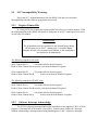
IMPORTANT
Do not use both the client driver and the enabler!
If you are unsure whether Card and Socket Services software is currently installed on
your system, install the client driver. When loaded, the client driver will display an error
message if Card and Socket Services software is not detected. If you receive such an error
message, remove the client driver software and install the enabler instead.
3.1
MPAP-100 Client Driver for DOS
In order to use the MPAP-100 client driver, the system must be configured with Card and
Socket Services software. Card and Socket Services software is not provided with the
MPAP-100 but is available from Quatech.
3.1.1
DOS client driver installation
The MPAP-100 client driver accepts between zero and eight sets of desired
configurations from the user on the command line. When an MPAP-100 is inserted, desired
configurations are tried in the order they appear on the command line from left to right. If the
user does not provide any desired configurations, the client driver will ask Card Services to
automatically determine a configuration for the card.
Each desired configuration must be enclosed in parentheses and must be separated from
other desired configurations by a space on the command line. Within each desired configuration,
parameters are separated using commas (no spaces). In the descriptions below, replace the '#'
symbols with the appropriate numeric values.
1. Copy the file MPAP1CL.SYS from the MPAP-100 distribution diskette onto the system's
hard drive.
2. Using an ASCII text editor, open the system's CONFIG.SYS file located in the root
directory of the boot drive.
3. Locate the line(s) in the CONFIG.SYS file where the Card and Socket Services software
is installed.
4. BELOW the line(s) installing the Card and Socket Services software, add the following
line to the CONFIG.SYS file:
DEVICE=drive:\path\MPAP1CL.SYS (S#,B#,I#,C) ... (S#,B#,I#,C)
where drive:\path specifies the drive letter and directory to which you copied the client
driver file, and (S#,B#,I#,C) ... (S#,B#,I#,C) stand for a variable number of desired
configurations. The configuration parameters are described below.
S#
The PCMCIA socket into which the MPAP-100 must be inserted for this
configuration to be used. This value is a decimal number ranging from 0 to 15. If
this parameter is not used, the configuration can apply to any socket.
B#
The base I/O address of the MPAP-100. This number must be a three-digit
hexadecimal value ending in 0. If this parameter is omitted, a base address will be
assigned by Card Services.
I#
The interrupt level (IRQ) of the MPAP-100. This decimal number must be one of
the following values: 3, 4, 5, 7, 9, 10, 11, 12, 14, 15, or 0 if no IRQ is desired. If
this parameter is omitted, an interrupt level will be assigned by Card Services.
C
Drive SYNC input of SCC channel A with the Remote Loopback bit of
Communications Register (see page 39). If this parameter is omitted, the SYNC
input of SCC channel A will be undefined.
5. Save the CONFIG.SYS file and exit the text editor.
6. Insert an MPAP-100 card in a PCMCIA socket, and reboot the computer. (If a card is
present in a socket at boot time, the card's configuration is reported on the screen as the
client driver loads. This feature can be used to verify the changes just made to the
CONFIG.SYS file.)
7. If the Client Driver reports the desired configuration, the installation process is complete
and the MPAP-100 may be removed from the system if desired.
8. If configuration of the card fails, the client driver will display an error message. If
"Invalid command line option" is displayed, correct the entry in the CONFIG.SYS file
and reboot the computer again. If "Card and Socket Services not found" is displayed,
install Card and Socket Services on the system or use the enabler program instead of the
client driver.
3.1.2
Auto Fallback configuration
The client driver can be instructed to try desired configurations first but fallback to
allowing Card Services to determine a configuration if none of the desired configurations are
available. This is done by adding a null configuration "()" to the end of the command line.
3.1.3
Hot Swapping
The client driver supports "hot swapping." After installation, it is not necessary for the
MPAP-100 to be inserted in the PCMCIA socket at boot time. When the card is inserted, it will
be configured according to the command line options. When the card is removed, the resources
it used will be made available for other devices.
If the MPAP-100 is in a socket at boot time, the client driver will display a message
indicating whether the card can be successfully configured and what resources will be used. This
is helpful if the user allows Card Services to select resources instead of specifying them on the
command line.
3.2
DOS Client Driver examples
Example: Attempt to configure an MPAP-100 inserted into any socket with a base address and
IRQ automatically assigned by Card Services.
DEVICE=C:\MPAP-100\MPAP1CL.SYS
Example: Attempt to configure an MPAP-100 inserted into any socket with a base address of
300 hex and an IRQ assigned by Card Services. Software control of SYNCA will be enabled. If
address 300 hex is unavailable, the card will not be configured.
DEVICE=C:\MPAP-100\MPAP1CL.SYS (b300,c)
Example: Attempt to configure an MPAP-100 inserted into socket 0 with a base address of 300
hex and IRQ 5. If address 300 hex or IRQ 5 is unavailable, the card will not be configured. In
addition, if an MPAP-100 is inserted into any other socket, it will not be configured.
DEVICE=C:\MPAP-100\MPAP1CL.SYS (s0,b300,i5)
Example: Attempt to configure an MPAP-100 inserted into any socket with a base address of
300 hex and IRQ 5. If address 300 hex or IRQ 5 is unavailable, attempt to configure the card
with a base address assigned by Card Services and IRQ 10. If IRQ 10 is also unavailable,
attempt to configure the card with a base address and an IRQ assigned by Card and Socket
Services.
DEVICE=C:\MPAP-100\MPAP1CL.SYS (b300,i5) (i10) ()
Example: Attempt to configure an MPAP-100 inserted into socket 0 with a base address of 300
hex and IRQ 5. Attempt to configure an MPAP-100 inserted into socket 1 with a base address of
340 hex and IRQ 10. This type of configuration may be desirable in systems where more than
one MPAP-100 is to be installed. It allows the user to force the MPAP-100 address and IRQ
settings to be socket-specific which may simplify cable connections and software development.
DEVICE=C:\MPAP-100\MPAP1CL.SYS (s0,b300,i5) (s1,b340,i10)
3.3
MPAP-100 Enabler for DOS
For systems that are not using PCMCIA Card and Socket Services software, the
MPAP-100 DOS enabler may be used to enable and configure the card. The enabler will operate
on any DOS system using an Intel 82365SL (PCIC) or PCIC-compatible PCMCIA socket adapter
including the Cirrus Logic CL-PD6710/6720, the VLSI VL82C146, and the Vadem VG-365
among others.
IMPORTANT
The enabler can be used ONLY if Card and Socket
Services is NOT installed on the system!
3.3.1
DOS Enabler Installation
To install the DOS enabler program, copy the file MPAP1EN.EXE from the MPAP-100
distribution diskette onto the system's hard drive. No setup steps are required.
IMPORTANT
The enabler requires a region of high DOS memory when configuring
an MPAP-100. This region is 1000H bytes (4KB) long and by default
begins at address D0000H (the default address may be changed using
the "W" option). If a memory manager such as EMM386, QEMM, or
386Max is installed on the system, this region of DOS memory must
be excluded from the memory manager's control. Consult the
documentation provided with the memory manager software for
instructions on how to exclude this memory region.
3.3.2
Hot Swapping is not supported
The MPAP-100 enabler does not support automatic configuration of adapters upon
insertion, commonly referred to as "Hot Swapping". The enabler must be executed after
insertion of an MPAP-100 card. If more than one MPAP-100 is installed in a system, the enabler
must be executed separately for each card. A card that is removed and reinserted must be
reconfigured by executing the enabler again.
3.3.3
Configuring a card
The enabler requires a single desired configuration to be provided on the command line.
The card will not be configured if the desired configuration is not provided. The desired
configuration must be enclosed in parentheses and it contains parameters separated using
commas (no spaces). In the descriptions below, replace the '#' symbols with the appropriate
numeric values.
MPAP1EN (S#,B#,I#,W#,C)
S#
The PCMCIA socket into which the MPAP-100 will be inserted. This value is a
decimal number ranging from 0 to 15. This parameter is always required when
configuring a card.
B#
The base I/O address of the MPAP-100. This number must be a three-digit
hexadecimal value ending in 0. This parameter is always required when
configuring a card.
I#
The interrupt level (IRQ) of the MPAP-100. This decimal number must be one of
the following values: 3, 4, 5, 7, 9, 10, 11, 12, 14, 15, or 0 if no IRQ is desired.
This parameter is always required when configuring a card.
W#
(optional) The base address of the memory window used by the enabler. This
two-digit hexadecimal number can be one of the following values: C8, CC, D0
(default), D4, D8, or DC. Use D4 for a memory window at segment D400, D8 for
a memory window at segment D800, etc. If this parameter is omitted, the default
setting of D000 will be used.
C
(optional) Drive SYNC input of SCC channel A with the Remote Loopback bit of
Communications Register (see page 39). If this parameter is omitted, the SYNC
input of SCC channel A will be undefined.
If configuration is successful, the enabler will display a message showing the
configuration on the screen. If the MPAP-100 is not successfully configured, then the
information in this section along with the Troubleshooting chapter of this manual should be
consulted to determine the cause of the problem.
3.3.4
Releasing a card's configuration
Before removing a MPAP-100 from its PCMCIA socket, the enabler should be executed
again to free the system resources allocated when the card was installed. Use the 'R' parameter to
do this.
MPAP1EN (S#,R,W#)
S#
The PCMCIA socket into which the MPAP-100 will be inserted. This value is a
decimal number ranging from 0 to 15. This parameter is always required when
releasing a card's configuration.
R
Release the resources previously allocated to the MPAP-100. This parameter is
always required when releasing a card's configuration. This option must not be
used when configuring an MPAP-100.
W#
(optional) The base address of the memory window used by the enabler. This
two-digit hexadecimal number can be one of the following values: C8, CC, D0
(default), D4, D8, or DC. Use D4 for a memory window at segment D400, D8 for
a memory window at segment D800, etc. If this parameter is omitted, the default
setting of D000 will be used.
3.4
DOS Enabler Examples
Example: Configure the MPAP-100 in socket 0 with a base address of 300H and IRQ 5.
Software control of SYNCA will be enabled.
MPAP1EN.EXE (s0,b300,i5,c)
Example: Configure the MPAP-100 in socket 1 with a base address of 300H and IRQ 3 using a
configuration memory window at segment D800.
MPAP1EN.EXE (s1,b300,i3,wd8)
Example: Release the configuration used by the MPAP-100 in socket 0.
MPAP1EN.EXE (s0,r)
Example: Release the configuration used by the MPAP-100 in socket 1 using a configuration
memory window at segment CC00.
MPAP1EN.EXE (s1,r,wcc)
4
Windows 95/98 Installation
Windows 95/98 maintains a registry of all known hardware installed in your computer.
Inside this hardware registry Windows keeps track of all of your system resources, such as I/O
locations, IRQ levels, and DMA channels. The "Add New Hardware Wizard" utility was
designed to add new hardware and update this registry.
An "INF" configuration file is included with the MPAP-100 to allow easy configuration
in the Windows 95/98 environment. Windows uses the "INF" file to determine the system
resources required by the MPAP-100, searches for available resources to fill the boards
requirements, and then updates the hardware registry with an entry that allocates these resources.
The Syncdrive DLL and VxD can then be used to access the card.
4.1 Using the "Add New Hardware" Wizard
The following instructions provide step-by-step instructions on installing the MPAP-100
in Windows 98 using the "Add New Hardware" wizard. Windows 95 uses a similar process to
load the INF file from a floppy disk with slightly different dialog boxes.
1. After inserting an MPAP-100 for the first time, the "Add New Hardware" wizard will
start. Click the "Next" button.
2. Click the "Next" button. Select the radio button for "Search for the best driver for your
device." Click the "Next" button to continue.
3. On the next dialog, select the "CD-ROM drive" checkbox. Insert the Quatech COM CD
(shipped with the card) into the CD-ROM drive. Click the "Next" button.
4. Windows should locate the INF file on the CD and display a dialog that looks like this.
Click the "Next" button.
5. Windows will copy the INF file from the CD and display a final dialog indicating that the
process is complete. Click the "Finish" button.
4.2 Viewing Resources with Device Manager
The following instructions provide step-by-step instructions on viewing resources used by
the MPAP-100 in Windows 95/98 using the "Device Manager" utility.
1. Double click the "System" icon inside the Control Panel folder. This opens up the
System Properties box.
2. Click the "Device Manager" tab located along the top of the System Properties box.
3. Double click the device group "Synchronous_Communication". The MPAP-100 model
name should appear in the list of adapters.
4. Double click the MPAP-100 model name and a properties box should open for the
hardware adapter.
5. Click the "Resources" tab located along the top of the properties box to view the
resources Windows has allocated for the MPAP-100 match the hardware configuration.
Click "Cancel" to exit without making changes.
6. If changes to the automatic configuration are necessary for compatibility with existing
programs, uncheck the "Use Automatic Settings" box and doubleclick on the Resource
Type that needs to be changed. Caution should be used to avoid creating device conflicts
with other hardware in the system.
4.3
Configuration Options
If the "Use Automatic Settings" box is unchecked, various options can be enabled by
selecting a different basic configuration in the "Setting based on" dropdown box. (Revision B5
hardware and later only.)
0000 Factory default. Suggested for nearly all customers.
0001 Drive SYNC input of SCC channel A with the Remote
Loopback bit of Communications Register (see page 39).
Otherwise the SYNC
input is undefined.
0002 Reserved. DO NOT USE!
0003 Reserved. DO NOT USE!
0004 Memory-mapped mode with no IRQ. Not suggested for use.
5
OS/2 Software Installation
An OS/2 client driver is provided with the MPAP-100. This client driver works with
OS/2's Card and Socket Services to allow operation of the MPAP-100 under OS/2.
5.1
5.2
System Requirements
OS/2 2.1 or later.
OS/2 PCMCIA Card and Socket Services support must be installed. See
"Installing OS/2 PCMCIA support" below if you do not already have this support
installed.
OS/2 Client Driver Installation
The MPAP-100 OS/2 client driver requires desired configurations from the user on the
command line. If no desired configurations are provided by the user, the client driver will NOT
ask Card Services to attempt to determine a hardware configuration for the card.
The client driver will attempt to configure an MPAP-100 with the first available
configuration listed from left to right on the command line. Each desired configuration must be
enclosed in parentheses and must be separated from other desired configurations by a space on
the command line. Within each desired configuration, the parameters are separated using
commas (no spaces).
1. Copy the MPAP100.SYS client driver file from the distribution disk to any convenient
directory on the hard disk.
2. Open the CONFIG.SYS file using any ASCII text editor.
3. Add the following line to the CONFIG.SYS file:
DEVICE=drive:\path\MPAP100.SYS (addr,irq,C) ... (addr,irq,C)
where drive:\path specifies the drive letter and directory to which you copied the client
driver file, and (addr,irq,C) ... (addr,irq,C) stand for a variable number of desired
configurations. The configuration parameters are described below.
addr
(required) The base I/O address of the MPAP-100. This number must be a
three-digit hexadecimal value ending in 0.
irq
(required) The interrupt level (IRQ) of the MPAP-100. This decimal number
must be one of the following values: 3, 4, 5, 7, 9, 10, 11, 12, 14, 15, or 0 if no IRQ
is desired.
C
(optional) Drive SYNC input of SCC channel A with the Remote Loopback bit of
Communications Register (see page 39). If this parameter is omitted, the SYNC
input of SCC channel A will be undefined.
4. Save the CONFIG.SYS file, exit the text editor, shutdown the system, and reboot to
activate the changes.
5.2.1
Tying a configuration to a particular socket
A configuration can be made specific to a socket by appending "=Sx" after the closing
parenthesis, where "X" is the desired socket number.
5.2.2
Auto Fallback configuration
OS/2 Card Services is capable of automatically determining a configuration for a
PCMCIA device, but due to limitations in Quatech's "Syncdrive" driver software, the client
driver does not support this feature. This support is planned for a future release of both the client
driver and Syncdrive.
5.2.3
Hot Swapping
The client driver supports "hot swapping." After installation, it is not necessary for the
MPAP-100 to be inserted in the PCMCIA socket at boot time. When the card is inserted, it will
be configured according to the command line options. When the card is removed, the resources
it used will be made available for other devices.
5.3
OS/2 Client Driver Configuration Examples
Example: Configure the MPAP-100 at base address 300 hex and IRQ 5. Configuration
will fail if any of these resources are already in use. Only one MPAP-100 can be used.
DEVICE=C:\MPAP-100\MPAP100.SYS (300,5)
Example: Configure the MPAP-100 at base address 300 hex and IRQ 5. Configuration
will fail if any of these resources are already in use. Only one MPAP-100 can be used.
Additionally, allow software control of the SYNC input of SCC channel A.
DEVICE=C:\MPAP-100\MPAP100.SYS (300,5,C)
Example: Configure the MPAP-100 at base address 300 hex and IRQ 5. If any of these
resources are not available, the second choice is to configure the MPAP-100 at base address
110 hex and IRQ 15. Up to two MPAP-100s can be used.
DEVICE=C:\MPAP-100\MPAP100.SYS (300,5) (110,15)
Example: If an MPAP-100 is inserted into socket 1, configure it at base address 300 hex
and IRQ 5. If any of these resources are not available, the card will not be configured. If an
MPAP-100 is inserted into socket 2, configure it at base address 110 hex and IRQ 15. If any of
these resources are not available, the card will not be configured. Up to two MPAP-100s can be
used.
DEVICE=C:\MPAP-100\MPAP100.SYS (300,5)=S1 (110,15)=S2
5.4
Monitoring The Status Of PCMCIA Cards
OS/2 Warp provides a utility called "Plug and Play for PCMCIA" that can be used to
monitor the status of each PCMCIA socket. In OS/2 2.1, this utility is called "Configuration
Manager". Under OS/2 Warp 4.0, when an MPAP-100 is inserted, the Card Type for the
appropriate socket will display "I/O." Clicking on the "Card" icon brings up a dialog where the
name displayed for the card can be changed to "Quatech MPAP-100" or any other desired name.
Under releases of OS/2 older than Warp 4.0, the default Card Type displayed may not
read "I/O," but the card should be configured properly by the client driver.
If the card is successfully configured, the Card Status will display "Ready". If the card
cannot be configured, the Card Status will be "Not Ready". You can view the resources claimed
by a configured card by double-clicking on that card's line or status icon.
5.5
Installing OS/2 PCMCIA Support
If PCMCIA support was not selected when OS/2 was installed, add it by using the
Selective Install facility in the System Setup folder. Full PCMCIA support is built into OS/2
Warp 3.0 and later. On OS/2 2.1 and 2.11, PCMCIA Card Services is built in, but you must add
Socket Services separately.
6
Using the MPAP-100 with Syncdrive
Syncdrive is a synchronous communications software driver package designed to aid
users of Quatech synchronous communication hardware in the development of their application
software. Syncdrive is included free of charge with all Quatech MPA-series synchronous
communication products. The MPAP-100 is backward-compatible with software written for
Quatech ISA-bus synchronous adapters and it operates with Syncdrive.
Syncdrive, however, is not aware of the plug-and-play nature of PCMCIA cards. A
Syncdrive application will expect to see the MPAP-100 at a specific base address and a specific
IRQ. When using Syncdrive with PCMCIA cards, it is necessary to obtain the base address and
IRQ assigned to the card by the PCMCIA Card Services and provide those values in the channel
configuration array.
For DOS, Windows 3.1, or OS/2, the client driver or enabler supplied with the card must
be used to configure the MPAP-100 with the settings expected by the Syncdrive application
before the application tries to use the card.
Under Windows 95/98, the card is automatically configured. To find the settings, click
the right mouse button on the My Computer icon and select Properties. Select the Device
Manager tab and double-click the card's entry under the "Synchronous Communication" section.
Select the Resources tab to see the card's base address and IRQ. Use these settings with the
Syncdrive application. Windows 95/98 may allow changes to the settings if the "Use Automatic
Settings" box is unchecked.
Syncdrive does not receive notifications of card insertion or card
removal events. Therefore it cannot support hot swapping without the user taking some kind of
action to force the Syncdrive application to initialize a newly-inserted card.
A future release of Syncdrive may permit automatic configuration by retrieving hardware
settings from the MPAP-100 client driver. For now, the user should consider the client driver to
be a replacement for jumper settings; it sets the card in a predetermined configuration before the
Syncdrive application is started.
7
Addressing
The MPAP-100 occupies a continuous 16-byte block of I/O addresses. For example, if
the base address is set to 300 hex, then the MPAP-100 will occupy address locations 300 hex to
30F hex. If the computer in which the MPAP-100 is installed is running PCMCIA Card and
Socket Services, the base address is set by the client driver. If PCMCIA Card and Socket
Services are not being used, the base address is set by the MPAP-100 enabler program.
The first four bytes of address space on the MPAP-100 contain the internal registers of
the SCC. Other Quatech architecture-specific registers occupy eight more bytes. The remainder
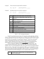
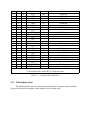
of the address space is reserved for future use. The MPAP-100 address map is shown in Table 2.
Address
Register Description
Base + 0
SCC Data Port, Channel A
Base + 1
SCC Control Port, Channel A
Base + 2
SCC Data Port, Channel B
Base + 3
SCC Control Port, Channel B
Base + 4
Communications Register
Base + 5
Configuration Register
Base + 6
Reserved
Base + 7
Reserved
Base + 8
Interrupt Status Register
Base + 9
FIFO Status Register
Base + A
FIFO Control Register
Base + B
Receive Pattern Character Register
Base + C
Receive Pattern Count Register
Base + D
Receive FIFO Timeout Register
Base + E
Reserved
Base + F
Reserved
Table 2 --- MPAP-100 Address Assignments
Information on the internal registers of the SCC can be found in Table 3 and Table 4 and
in the technical reference manuals available from Zilog. The other onboard registers are fully
described in subsequent chapters of this manual.
8
Interrupts
The MPAP-100 will operate using the interrupt level (IRQ) assigned by the PCMCIA
system. Interrupts can come from the SCC, the external FIFOs or RS-232 test mode. The
interrupt source is selected by bits 4 and 5 of the Configuration Register (see page 41).
When using interrupts with the MPAP-100, the application must have an interrupt service
routine (ISR). There are several things that an ISR must do to allow proper system operation:
1. If the external FIFOs are enabled, read the Interrupt Status Register (see page 43) to
determine whether the interrupt was caused by a FIFO event or by the SCC.
2. If the TX_FIFO bit is set, at least 512 bytes can be written to the Tx FIFO. If the
RX_FIFO bit is set, at least 512 bytes can be read from the Rx FIFO. I/O block move
instructions may be useful. Check the FIFO Status Register (see page 44) after servicing
the FIFO(s) to see if further FIFO service is required.
3. If the SCC bit is set, do an SCC software interrupt acknowledge by reading Read Register
2 in channel B of the SCC. The value read can also be used to vector to the appropriate
part of the ISR.
4. Service the SCC interrupt by reading the receiver buffer, writing to the transmit buffer,
issuing commands to the SCC, etc.
5. Write a Reset Highest Interrupt Under Service (IUS) command to the SCC by writing
0x38 to Write Register 0.
6. Check for other interrupts pending in the SCC by reading Read Register 3. Perform
further interrupt servicing if necessary.
7. For applications running under DOS, a nonspecific End of Interrupt must be submitted to
the interrupt controller. For Interrupts 2-7 this is done by writing a 0x20 to port 0x20.
For Interrupts 10-12, 14 and 15 this is done by writing a 0x20 to port 0x60, then a 0x20 to
port 0x20 (due to the interrupt controllers being cascaded). Device drivers running under
other operating systems may have varying requirements concerning the End of Interrupt
command.
For further information on these subjects or any others involving the SCC contact Zilog
for a complete technical manual.
9
SCC General Information
The Serial Communications Controller (SCC) is a dual channel, multi-protocol data
communications peripheral. The MPAP-100 provides a single channel for communications,
however, portions of the second channel can be utilized to support some special circumstances.
The SCC can be configured to satisfy a wide variety of serial communications applications.
Some of its protocol capabilities include:
SDLC/HDLC (Bit Synchronous) Communications
Abort sequence generation and checking
Automatic zero insertion and deletion
Automatic flag insertion between messages
Address field recognition
I-field residue handling
CRC generation and detection
SDLC loop mode with EOP recognition/loop entry and exit
Byte-oriented Synchronous Communications
Internal/external character synchronization
1 or 2 sync characters in separate registers
Automatic Cyclic Redundancy Check (CRC) generation/detection
Asynchronous Communications
5, 6, 7, or 8 bits per character
1, 1-1/2, or 2 stop bits
Odd, even, or no parity
Times 1, 16, 32, or 64 x clock modes
Break generation and detection
Parity, overrun and framing error detection
NRZ, NRZI, or FM encoding/decoding
9.1
Accessing the registers
The mode of communication desired is established and monitored through the bit values
of the internal read and write registers. The register set of the SCC includes 16 write registers
and 9 read registers. These registers only occupy four address locations, which start at the
MPAP-100's physical base address that is configured via the on board switches. This and all
other addresses are referenced from this base address in the form Base+Offset. An example of
this is Base+1 for the SCC Control Port, Channel A.
There are two register locations per SCC channel, a data port and a control port.
Accessing the internal SCC registers is a two step process that requires loading a register pointer
to perform the addressing to the correct data register. The first step is to write to the control port
the operation and address for the appropriate channel. The second step is to either read data from
or write data to the control port. The only exception to this rule is when accessing the transmit
and receive data buffers. These registers can be accessed with the two step process described or
with a single read or write to the data port. The following examples illustrate how to access the
internal registers of the SCC. Table 3 on page 26 describes the read registers and Table 4 on
page 27 describes the write registers for each channel.
The MPAP-100 has been designed to assure that all back to back access timing
requirements of the SCC are met without the need for any software timing control. The standard
of adding jmp $+2 between I/O port accesses is not required when accessing the MPAP-100.
Example 1:
Enabling the transmitter on channel A.
mov
add
mov
out
mov
out
Example 2:
dx,
dx,
al,
dx,
al,
dx,
base
ContA
05H
al
08H
al
; load base address
; add control reg A offset (1)
; write the register number
; write the data to the register
Monitoring the status of the transmit and receive buffers in RR0 of Channel A.
Register 0 is addressed by default if no register number is written to WR0 first.
mov
add
in
dx, base
dx, ContA
ax, dx
; load base address
; add control reg A offset (1)
; read the status
Example 3:
Write data into the transmit buffer of channel A.
mov
out
Example 4:
dx, base
dx, al
; load base address
; write data in ax to buffer
Read data from the receive buffer of channel A.
mov
in
dx, base
al, dx
; load base address
; write data in ax to buffer
RR0
Transmit, Receive buffer statuses and external status
RR1
Special Receive Condition status, residue codes, error
conditions
RR2
Modified Channel B interrupt vector and Unmodified
Channel A interrupt vector
RR3
Interrupt Pending bits
RR6
LSB of frame byte count register
RR7
MSB of frame byte count and FIFO status register
RR8
Receive buffer
RR10
Miscellaneous status parameters
RR12
Lower byte of baud rate time constant
RR13
Upper byte of baud rate time constant
RR15
External/Status interrupt information
Table 3 --- SCC read register description
The SCC can perform three basic forms of I/O operations: polling, interrupts, and block
transfer. Polling transfers data, without interrupts, by reading the status of RR0 and then reading
or writing data to the SCC buffers via CPU port accesses. Interrupts on the SCC can be sourced
from the receiver, the transmitter, or External/Status conditions. At the event of an interrupt,
Status can be determined, then data can be written to or read from the SCC via CPU port
accesses. Further information on this subject is found on page 23. For block transfer mode,
DMA transfers are used, so this type of operation is not supported on the MPAP-100.
The SCC incorporates additional circuitry supporting serial communications. This
circuitry includes clocking options, baud rate generator (BRG), data encoding, and internal
loopback. The SCC may be programmed to select one of several sources to provide the transmit
and receive clocks. These clocks can be programmed in WR11 to come from the RTxC pin, the
TRxC pin, the output of the BRG, or the transmit output of the DPLL. The MPAP-100 uses the
TRxC pin for its clock-on-transmit and the RTxC pin for its clock-on-receive. Programming of
the clocks should be done before enabling the receiver, transmitter, BRG, or DPLL.
WR0
Command Register, Register Pointer, CRC initialization, and
resets for various modes
WR1
Interrupt control, Wait/DMA request control
WR2
Interrupt vector
WR3
Receiver initialization and control
WR4
Transmit/Receive miscellaneous parameters and codes, clock rate,
stop bits, parity
WR5
Transmitter initialization and control
WR6
Sync character (1st byte) or SDLC address field
WR7
Sync character (2nd byte) or SDLC Flag
WR7'
Special HDLC Enhancement Register
WR8
Transmit buffer
WR9
Master interrupt control and reset
WR10 Miscellaneous transmitter/receiver control bits, NRZI, NRZ, FM
coding, CRC reset
WR11 Clock mode and source control
WR12 Lower byte of baud rate time constant
WR13 Lower byte of baud rate time constant
WR14 Miscellaneous control bits: baud rate generator, DPLL control, auto
echo
WR15 External/Status interrupt control
Table 4 --- SCC write register description
For complete information regarding the SCC registers please refer to Zilog's Z85230
technical manual.
9.2
Baud Rate Generator Programming
The baud rate generator (hereafter referred to as the BRG) of the SCC consists of a 16-bit
down counter, two 8-bit time constant registers, and an output divide-by-two. The time constant
for the BRG is programmed into WR12 (least significant byte) and WR13 (most significant
byte). The equation relating the baud rate to the time constant is given below while Table 5
shows the time constants associated with a number of popular baud rates when using the standard
MPAP-100 9.8304 MHz clock.
Time_Const =
Where:
Clock_Frequency
-2
2 & Baud_Rate & Clock_Mode
Clock_Frequency = 9.8304 x 10⁶
Clock_Mode = 1, 16, 32, or 64
Baud_Rate = desired baud rate
Baud Rate
Time Constant
38400
126
007E (hex)
19200
254
00FE (hex)
9600
510
01FE (hex)
4800
1022
03FE (hex)
2400
2046
07FE (hex)
1200
4094
0FFE (hex)
600
8190
1FFE (hex)
300
16382
3FFE (hex)
(for Clock_Frequency = 9.8304 MHz )
Table 5 --- time constants for common baud rates
9.3
SCC Data Encoding Methods
The SCC provides four different data encoding methods, selected by bits 6 and 5 in
WR10. These four include NRZ, NRZI, FM1 and FM0. The SCC also features a digital
phase-locked loop (DPLL) that can be programmed to operate in NRZI or FM modes. Also, the
SCC contains two features for diagnostic purposes, controlled by bits in WR14. They are local
loopback and auto echo.
For further information on these subjects or any others involving the SCC contact Zilog
for a complete technical manual.
9.4
Support for SCC Channel B
The MPAP-100 is a single-channel device. Portions of SCC channel B are used to
augment channel A. Channel B cannot be used for transmit, but may be used for receive, subject
to certain limitations.
9.4.1
Receive data and clock signals
The receive data signals RXDA and RXDB are tied together. The receive clock input
signals RTxCA and RTxCB are also tied together. This can be useful in unusual applications. It
would be possible to run the receiver and transmitter at different baud rates, using channel B's
baud rate generator and receiver for the received data. Of course, the channel A transmitter and
receiver can be run at different speeds simply by having external data clocks supplied to TRxCA
and RTxCA from the cable.
The W/REQB signal is used to generate DMA requests between the SCC and the external
FIFOs if channel B is used for receive.
9.4.2
Extra clock support for channel A
The TRxCB clock output can be routed back to RTxCA as another way to use the channel
B baud rate generator to derive an independent clock for the channel A receiver. This is
controlled by the RCKEN bit in the Communications Register (see page 39).
9.4.3
Extra handshaking for channel A
The SCC does not provide a DSR input for either channel. The MPAP-100 routes the
DSR signal from the connector to the DCDB input of the SCC. Software can therefore use
DCDB as a surrogate for DSR on channel A.
9.4.4
Other signals are not used
All channel B signals not listed above are not available at the connector. The CTSB and
SYNCB inputs are tied to their inactive states. The TXDB, DTR/REQB, and RTSB outputs are
left open.
9.5
SCC Incompatibility Warnings
Due to the SCC implementation used by the MPAP-100, there are two minor
incompatibilities that the software programmer must avoid.
9.5.1
Register Pointer Bits
In a Zilog 85230, the control port register pointer bits can be set in either channel. With
the implementation on the MPAP-100, however, both parts of an SCC control port access must
use the same I/O address.
IMPORTANT
The programmer must be certain not to mix channel usage during
the two-part access of SCC control ports. It would be highly
irregular for code to be written in such fashion, so this restriction is
not expected to be burdensome.
The following sequences will work:
Write Control Port A
(set pointer bits for desired register)
Read or Write Control Port A (read or write desired channel A register)
Write Control Port B
(set pointer bits for desired register)
Read or Write Control Port B
(read or write desired channel B register)
The following sequences will NOT work:
Write Control Port A
(set pointer bits for desired register)
Read or Write Control Port B (read or write desired channel B register)
Write Control Port B
(set pointer bits for desired register)
Read or Write Control Port A
(read or write desired channel A register)
9.5.2
Software Interrupt Acknowledge
The 85230's software interrupt acknowledge mechanism is not supported. Bit 5 of Write
Register 9 (Software INTACK Enable) is forced to 0. Software must employ the "Interrupt
Without Acknowledge" interrupt method using Read Registers 2 and 3 to process interrupts.
10 FIFO Operation
The MPAP-100 is equipped with 1024-byte external FIFOs in the transmit and receive
data paths. These FIFOs are implemented as extensions of the SCC's small internal FIFOs. They
have been designed to be as transparent as possible to the software operating the MPAP-100. By
using these FIFOs, it is possible to achieve high data rates despite the MPAP-100 not supporting
DMA.
The FIFOs are disabled by default after card insertion, power-up, or a socket reset.
10.1 Enabling and disabling the FIFOs
The FIFOs must be enabled or disabled as a pair. It is not possible to operate only the
transmit FIFO or only the receive FIFO. The FIFOs are enabled by setting bit 2 of the
Configuration Register to a logic 1. The FIFOs are disabled by clearing the same bit.
10.2 Accessing the FIFOs
When the FIFOs are enabled, they are accessed through either the channel A or channel B
SCC Data Port address. Writing to Base+0 or Base+2 will cause a byte to be written into the
transmit FIFO. Reading from Base+0 or Base+2 will cause a byte to be read from the receive
FIFO.
The FIFOs cannot be accessed if they are disabled. If the FIFOs are disabled, reads or
writes of the SCC Data Ports access the receive or transmit register of the appropriate SCC
channel. Any control port writes of SCC write register 8 (transmit buffer) or control port reads
of SCC read register 8 (receive buffer) directly access the SCC, whether the FIFOs are enabled or
not.
10.2.1 Transmit FIFO
The transmit FIFO always services the transmitter of channel A of the SCC. If the FIFOs
are enabled, an I/O write to either SCC Data Port (channel A or channel B) will write a byte to
the transmit FIFO. If the FIFOs are not enabled, an I/O write to the SCC Data Port will instead
write directly to the internal transmit buffer of the specified channel of the SCC.
10.2.2 Receive FIFO
The receive FIFO can service the receiver of either channel A or channel B of the SCC.
If RXSRC (bit 1) of the Configuration Register (see page 41) is logic 1, the receive FIFO will
service SCC channel B. If RXSRC is logic 0, the receive FIFO will service SCC channel A.
If the FIFOs are enabled, an I/O read from either SCC Data Port (channel A or channel B)
will read a byte from the receive FIFO. If the FIFOs are not enabled, an I/O read from the SCC
Data Port will instead read directly from the internal receive buffer of the specified channel of the
SCC.
10.3 SCC configuration for FIFO operation
The interface between the SCC and the external FIFOs uses the SCC's DMA request
functions. The SCC must therefore be configured for DMA operation in order to use the external
FIFOs. In order to properly configure the SCC, certain bits in various SCC registers need to be
set in a specific manner, as shown on the following pages.
Because the data transfer between the FIFOs and the SCC is controlled entirely by
hardware, per-character transmit and receive interrupts should be disabled. Interrupts on transmit
underruns and/or special receive conditions should usually be enabled so that end-of-frame
conditions can be detected.
IMPORTANT
The DMA operation described in this section is
between the SCC and the external FIFOs, and is
handled entirely by the MPAP-100 hardware.
DMA is not supported between the MPAP-100 and
the host computer due to the lack of DMA facilities
on the PCMCIA bus.
The MPAP-100 is a single-channel device. Accordingly, most applications will use SCC
channel A for both transmit and receive operations. It is possible, however, to use a limited
portion of SCC channel B for receive operations (see page 29). The channel used for receive will
determine how the SCC must be configured.
Do not enable the FIFOs until the SCC has been properly configured for DMA
operation!
10.3.1 Using channel A for both transmit and receive
This is the mode in which most applications will run. Set RXSRC (bit 1) in the
Configuration Register to logic 0. This will configure the MPAP-100 to use W/REQA for
receive DMA and DTR/REQA for transmit DMA. In addition to any other desired SCC
configuration, ensure that the following bits are set according to Table 6:
Register
Bit(s)
Value
7
1
6
5
1
1
1
11 or
00
0
WR14A
2
1
Enable DMA request-on-transmit on
DTR/REQA.
WR15A
0
1
Enable WR7A'.
5
0
4
1
WR1A
4-3
WR7A'
Function
Enable DMA request on W/REQA. This bit
should be set after the other bits in WR1 are set as
desired.
Set W/REQA for DMA Request mode.
Use W/REQA for receive.
Enable receive interrupts on special conditions
only (recommended), or disable them completely.
Disable transmit interrupts.
Assert transmit DMA request when entry location
of internal FIFO is empty.
Set DTR/REQA for W/REQA timing.
Table 6 --- Configuring the SCC for FIFO use with channel A only
10.3.2 Using channel B for receive
The MPAP-100 supplies only limited support for SCC channel B. This mode, therefore,
is not recommended for most applications. Set RXSRC (bit 1) in the Configuration Register to
logic 1. This will configure the MPAP-100 to use W/REQA for transmit DMA and W/REQB for
receive DMA. In addition to any other desired SCC configuration, ensure that the following bits
are set according to Table 7:
Register
Bit(s)
Value
7
1
6
5
1
1
0
0
WR14A
2
0
Disable DMA request-on-transmit on
DTR/REQA.
WR15A
0
1
Enable WR7A'.
WR7A'
5
0
Assert transmit DMA request when entry location
of internal FIFO is empty.
WR1A
WR1B
7
1
6
5
1
1
11 or
00
4-3
Function
Enable DMA request on W/REQA. This bit
should be set after the other bits in WR1 are set as
desired.
Set W/REQA for DMA Request mode.
Use W/REQA for transmit.
Disable transmit interrupts.
Enable DMA request on W/REQB. This bit
should be set after the other bits in WR1 are set as
desired.
Set W/REQB for DMA Request mode.
Use W/REQB for receive.
Enable receive interrupts on special conditions
only (recommended), or disable them completely.
Table 7 --- Configuring the SCC for Rx DMA on channel B
10.4 FIFO status and control
Several registers are used to control the FIFOs and monitor their status. These registers
are detailed in other chapters of this manual.
10.4.1 Interrupt status
Three interrupt statuses, listed in Table 8, can be generated by four events related to FIFO
activity. In each case, a latched bit in the Interrupt Status Register is set to a logic 1 (see page
43). These bits are write-clear, meaning that software must write a 1 to a bit in order to clear it.
IMPORTANT
FIFO-related interrupts will occur only when the
MPAP-100 interrupt source is set to INTSCC. See Table
10 on page 41 for details.
Interrupt Status
Register Bit
Event
Transmit FIFO drained
past the half-full mark
Receive FIFO filled past
the half-full mark
Receive data timeout with
non-empty FIFO
Special receive pattern
detected
TX_FIFO
(bit 1)
RX_FIFO
(bit 2)
RX_PAT
(bit 3)
Comment
Software can write at least
512 bytes to the transmit
FIFO.
Software can read at least
512 bytes from the receive
FIFO.
Software can read bytes
from the receive FIFO until
the FIFO is empty.
Software can read data
from the receive FIFO as
desired.
Table 8 --- FIFO-related interrupt statuses
IMPORTANT
Software can differentiate between the two types of
RX_FIFO interrupts by examining the RXH bit in the
FIFO Status Register. If RXH is clear (logic 0), the
interrupt occurred because of a timeout.
10.4.2 Resetting the FIFOs
The FIFOs are automatically disabled and reset at powerup or when the MPAP-100 is
inserted into a PCMCIA socket. The transmit and receive FIFOs can also be independently reset
by setting and clearing the appropriate bits in the FIFO Control Register. Resetting a FIFO sets
the appropriate FIFO empty status bit and resets the FIFO's internal read and write pointers. The
SCC's internal FIFOs are not affected when the external FIFOs are reset.
The external FIFOs cannot be reset while they are enabled! FIFO reset commands
will be ignored if the external FIFOs are enabled.
10.4.3 Reading current FIFO status
The FIFO Status Register is a read-only register which always indicates the current status
of both the transmit and receive external FIFOs. Each FIFO can be checked for empty, full, and
half-full (or more) status at any time. For details, see Table 12 on page 44.
10.4.4 Controlling the FIFOs
The FIFO Control Register is a read-write register which can be used to reset either or
both the receive and transmit external FIFOs. Receive pattern detection and receive FIFO
timeout modes are also controlled with this register. For details, see Table 13 on page 45.
10.5 Accessing the SCC while FIFOs are enabled
The SCC channel A and channel B control port registers are always accessible regardless
of whether the external FIFOs are enabled or disabled. While the FIFOs are enabled, SCC data
port accesses are redirected to the FIFOs. Access to the SCC's transmit or receive registers while
the FIFOs are enabled is possible indirectly by using the control port and register 8. Any writes
of SCC Write Register 8 (transmit buffer) or reads of SCC Read Register 8 (receive buffer) will
bypass the external FIFOs.
10.6 Receive pattern detection
The external FIFOs are most useful in bit-synchronous operational modes because the
SCC can generate a Special Condition interrupt when the closing flag of a bit-synchronous frame
is received. This allows the SCC to run with per-character receive interrupts disabled while
DMA transfers occur between the SCC and external FIFOs.
Byte-synchronous modes such as bisync, however, do not benefit from such a hardware
assist for detecting the end-of-frame condition. On the contrary, with byte-oriented protocols it is
usually necessary to check each byte received against a table of special function codes (e.g.
SYNC, PAD, SDI, STX, EDI, ETX, etc.) to determine where data and frames begin and end.
Unless the frames are of a fixed length, it is therefore difficult to use DMA with
byte-synchronous modes. This would seem to preclude the use of the MPAP-100's external
FIFOs with byte-oriented protocols.
To make the external FIFOs more useful in byte-synchronous modes, the MPAP-100 can
watch for a given character to be transferred consecutively a specific number of times from the
SCC into the receive FIFO. When this occurs, the RX_PAT bit in the Interrupt Status Register
(see page 43) is set. For instance, the MPAP-100 can watch for the end-of-text character to be
received, or for three consecutive pad characters to be received.
For byte-synchronous operation with simple unique markers in the data stream, this
feature may be quite useful. Even if it is not, however, the MPAP-100 can certainly be operated
with per-character interrupts enabled and the external FIFOs disabled. The tradeoff will be a
heavier interrupt burden and possibly somewhat lower throughput.
NOTE
While most useful in byte-synchronous modes, the
receive pattern detection feature can be used in any
operational mode.
10.7 Receive FIFO timeout
With asynchronous operational modes, the same problem exists. Namely, how is one to
determine when a reception is complete? While the receive pattern detection may be useful here,
the MPAP-100 also offers a timeout feature on the external receive FIFO.
If the external FIFO is not empty and a time interval equal to a specified number of
character-times has elapsed without any further data being received, a receive FIFO interrupt is
generated and RX_FIFO bit in the Interrupt Status Register (see page 43) is set. A character-time
is approximated by counting eight ticks of the bit clock.
To use this feature, the receive clock must be output on TRxCA. It can come from either
an external source or from the channel A baud rate generator. While the RTxCA signal is
typically used for a receive clock, it is not capable of being an output, so the TRxCA signal must
be used instead. Depending on the application, this may force the transmit and receive clocks to
be the same. For most asynchronous applications, this should not pose a problem.
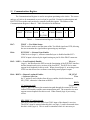
11 Communications Register
The Communications Register is used to set options pertaining to the clocks. The source
and type of clock to be transmitted or received can be specified. External synchronization and
RS-232 DTE test modes and can also be controlled with this register. The address of the
Communications Register is Base+4. Table 9 details its bit definitions.
Bit 7
Bit 6
Bit 5
TM ST EXTSYNC LLEN
Bit 4
Bit 3
Bit 2
RLEN
or
RCKEN TCKEN
SW_SYNC
Bit 1
Bit 0
0
0
Table 9 --- Communications Register - Read/Write
Bit 7:
TM ST --- Test Mode Status:
This bit can be used to read the status of the Test Mode signal on a DTE, allowing
the user to monitor the signal without generating any interrupts.
Bit 6:
EXTSYNC --- External Sync Enable:
If this bit is set (logic 1), software-controlled sync is disabled and the SCC's
SYNCA input is driven by the signal coming on pin 10 of the DB-25 connector.
Bit 5: LLEN --- Local Loopback Enable:
When set
(logic 1), this bit allows the DTE to test the functioning of the DTE/DCE interface
and the transmit and receive sections of the local DCE. The DCE device must
support local loopback for this to work. When cleared (logic 0), no testing occurs.
LLEN can also be used as a software-controlled general-purpose output.
Bit 4: RLEN --- Remote Loopback Enable:
SW_SYNC
--- Software Sync On:
When
the 'C' option is used with the client driver or enabler, this bit functions as
SW_SYNC, otherwise it functions as RLEN.
RLEN
('C' option not used)
If this bit is set
(logic 1), the DTE can test the transmission path through the remote DCE to the
remote DTE interface and the return transmission path. The remote device must
support remote loopback for this to work. When cleared (logic 0), no testing
occurs.
SW_SYNC ('C' option is used)
This bit is used to drive the active-low SYNC input of the channel A receiver.
The SYNC signal is asserted when this bit is set (logic 1), and is deasserted when
this bit is clear (logic 0). This is useful in situations where it is necessary to
receive unformatted serial data, as it allows the SCC receiver to be manually
placed into sync under program control. This bit is ignored if bit 6 is set (logic 1).
Bit 3:
RCKEN --- Receive Clock Source:
When
set (logic 1), this bit allows the receive clock (RCLK) signal to be generated by
the TRxC pin on channel B of the SCC. When cleared (logic 0), RCLK is
received on pin 17 of the DB-25 connector. In either case, RCLK is always
transmitted on pin 11 of the DB-25 connector.
Bit 2:
TCKEN --- Transmit Clock Source:
When set (logic 1), this bit allows the transmit clock (TCLK) to be generated by
the TRxC pin on channel A of the SCC. When cleared (logic 0), the DTE
receives TCLK on pin 15 of the DB-25 connector. In either case, TCLK is
always transmitted on pin 24 of the DB-25 connector.
Bits 1-0:
Reserved, always 0.
IMPORTANT
Local Loopback and Remote Loopback cannot be enabled
simultaneously. Bits 5 and 4 of the Communications
Register should therefore not be set (logic 1)
simultaneously.
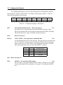
12 Configuration Register
The Configuration Register is used to set the interrupt source and enable the interface
between the SCC and the external FIFOs. The address of this register is Base+5. Table 10
details the bit definitions of the register.
Bit 7
Bit 6
Bit 5
Bit 4
Bit 3
1
0
INTS1
INTS0
0
Bit 2
Bit 1
FIFOEN RXSRC
Bit 0
0
Table 10 --- Configuration Register - Read/Write
Bit 7:
External Data FIFOs Present --- Reserved, always 1.
This
bit can be used as an indicator that external data FIFOs are present. Other
MPA-series products that are not equipped with external data FIFOs, including
MPAP-100 Revision A cards, will return 0 in this bit location.
Bit 6:
Reserved, always 0.
Bits 5-4:
INTS1, INTS0 --- Interrupt Source and Enable Bits:
These
two bits determine the source of the interrupt. The two sources are interrupt from
the SCC (INTSCC), and interrupt on Test Mode (INTTM). Only one interrupt
source can be active at a time. Below is the mapping for these bits. Note that
FIFO-related interrupts will occur only when INTSCC is chosen.
INTS1
0
0
1
1
INTS0
0
0
0
1
Interrupt Source
Interrupts disabled
reserved
INTSCC
INTTM
Bit 3: Reserved, always 0.
Bit 2:
FIFOEN --- External data FIFO enable:
If this
bit is set (logic 1), the external data FIFOs are enabled. If this bit is clear (logic
0), the external data FIFOs are disabled. (See page 31 for full details on FIFO
use.)
Bit 1:
RXSRC --- Receive FIFO DMA Source:
This
bit determines which SCC pins are used to control transmit and receive DMA
transactions between the SCC and the external FIFOs (when enabled). The
transmit data FIFO is always used with SCC channel A. The receive data FIFO
may be used with SCC channel A by setting RXSRC to logic 0, or with SCC
channel B by setting RXSRC to logic 1. (See page 29 for information on using
channel B.)
Receive DMA
Transmit
DMA
Bit 0:
Reserved, always 0.
RXSRC = 0
W/REQA
RXSRC = 1
W/REQB
DTR/REQA
W/REQA
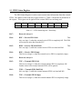
13 Interrupt Status Register
The Interrupt Status Register is used to determine the cause of an interrupt generated by
the MPAP-100. The address of this register is Base+8. Table 11 details the bit definitions of the
register. The interrupt source in the Configuration Register (see page 41) must be set to
INTSCC for any of the statuses indicated by this register to occur. This register can be
ignored if the external FIFOs are not being used.
Bit 7
0
Bit 6 Bit 5
0
0
Bit 4
Bit 3
Bit 2
Bit 1
Bit 0
0
RX_PAT
RX_FIFO
TX_FIFO
SCC
Table 11 --- Interrupt Status Register - Read Only/Write Clear
Bits 7-4:
Reserved, always 0.
Bit 3:
RX_PAT --- Receive Pattern Interrupt:
The
receive pattern interrupt occurs when the character set in the Receive Pattern
Character Register is detected 'n' consecutive times in the received data stream,
where 'n' is the value set in the Receive Pattern Count Register. This bit is set
(logic 1) to indicate the interrupt. It remains set until cleared by writing a '1' to
this bit.
Bit 2:
RX_FIFO --- Receive FIFO Interrupt:
The receive FIFO interrupt occurs when the number of bytes held in the external
receive FIFO rises above the half-full mark, or when a receive FIFO timeout
occurs. This bit is set (logic 1) to indicate the interrupt. It remains set until
cleared by writing a '1' to this bit.
Bit 1:
TX_FIFO --- Transmit FIFO Interrupt:
The
transmit FIFO interrupt occurs when the number of bytes held in the external
transmit FIFO falls below the half-full mark. This bit is set (logic 1) to indicate
the interrupt. It remains set until cleared by writing a '1' to this bit.
Bit 0:
SCC --- SCC Interrupt:
If this bit is set (logic 1), the SCC has generated an interrupt. Software should
clear the interrupt condition by performing appropriate service on the SCC. This
bit is not latched.
14 FIFO Status Register
The FIFO Status Register is used to return current status information about the external
FIFOs. The address of this read-only register is Base+9. Table 12 details the bit definitions of
the register. This register can be ignored if the external FIFOs are not being used.
Bit 7
Bit 6
Bit 5
Bit 4
Bit 3
Bit 2
Bit 1
Bit 0
0
RXF
RXH
RXE
0
TXF
TXH
TXE
Table 12 --- FIFO Status Register - Read Only
Bit 7:
Reserved, always 0.
Bit 6:
RXF --- Receive FIFO Full:
This
bit is set (logic 1) when the external receive FIFO is completely full. The FIFO
will accept no more data from the SCC.
Bit 5:
RXH --- Receive FIFO Half Full:
bit is set (logic 1) while the external receive FIFO is at least half-full.
Bit 4:
RXE --- Receive FIFO Empty:
This bit is set (logic 1) when the external receive FIFO is completely empty.
Bit 3:
Reserved, always 0.
Bit 2:
TXF --- Transmit FIFO Full:
This bit is set (logic 1) when the external transmit FIFO is completely full.
Further writes to the external transmit FIFO will be ignored.
Bit 1:
TXH --- Transmit FIFO Half Full:
bit is set (logic 1) while the external transmit FIFO is at least half-full.
Bit 0:
TXE --- Transmit FIFO Empty:
This bit is set (logic 1) when the external transmit FIFO is completely empty.
This
This
15 FIFO Control Register
The FIFO Control Register is used to control the external data FIFOs. The address of this
register is Base+A (hex). Table 13 details the bit definitions of the register. This register can be
ignored if the external FIFOs are not being used.
Bit 7
Bit 6
Bit 5
Bit 4
Bit 3
Bit 2
Bit 1
Bit 0
0
EN_PAT
EN_TO
RX_RESET
0
0
0
TX_RESET
Table 13 --- FIFO Control Register - Read/Write
Bit 7:
Reserved, always 0.
Bit 6:
EN_PAT --- Enable Receive Pattern Detection:
Set this
bit (logic 1), to enable the receive pattern detection circuitry. Clear this bit (logic
0), to disable pattern detection. See page 37 for details on the receive pattern
detection feature.
Bit 5:
EN_TO --- Enable Receive Timeout:
Set this bit (logic 1), to enable the external receive FIFO timeout. Clear this bit
(logic 0), to disable the receive FIFO timeout. See page 38 for details on the
receive FIFO timeout feature.
Bit 4:
RX_RESET --- Reset Receive FIFO:
Set (logic 1), then clear (logic 0) this bit to reset the external receive FIFO. The
FIFO can be reset only when it is disabled.
Bits 3-1:
Reserved, always 0.
Bit 0:
TX_RESET --- Reset Transmit FIFO:
Set (logic 1), then clear (logic 0) this bit to reset the external transmit FIFO. The
FIFO can be reset only when it is disabled.
16 Receive Pattern Character Register
The Receive Pattern Character Register is used to set the character value to be used in
receive pattern detection. The address of this register is Base+B (hex). This register can be
ignored if the external FIFOs are not being used.
Bit 7
Bit 6
Bit 5
Bit 4
Bit 3
Bit 2
Bit 1
Bit 0
character value (0-255)
Table 14 --- Receive Pattern Character Register - Read/Write
Bits 7-0:
Receive Pattern Character:
This is
the numeric value of the character to be detected. See page 37 for details on the
receive character pattern detection feature.
17 Receive Pattern Count Register
The Receive Pattern Count Register is used to set the counter value to be used in receive
pattern detection. The address of this register is Base+C (hex). This register can be ignored if
the external FIFOs are not being used.
Bit 7
Bit 6
Bit 5
Bit 4
Bit 3
Bit 2
Bit 1
Bit 0
counter value (0-255)
Table 15 --- Receive Pattern Count Register - Read/Write
Bits 7-0:
Receive Pattern Count:
This value is the number of times that the character stored in the Receive Pattern
Character Register (see page 46) must be consecutively detected for the receive
character pattern detect interrupt to be generated. See page 37 for details on the
receive character pattern detection feature.
18 Receive FIFO Timeout Register
The Receive FIFO Timeout Register is used to control the operation of the external
receive FIFO timeout feature. The address of this register is Base+D (hex). This register can be
ignored if the external FIFOs are not being used. See page 38 for details on the receive FIFO
timeout feature.
Bit 7
Bit 6
X16_MODE
0
Bit 5
Bit 4
Bit 3
Bit 2
Bit 1
Bit 0
timeout interval (0-63)
Table 16 --- Receive FIFO Timeout Register - Read/Write
Bit 7:
X16_MODE --- Clock Mode:
If this bit is set (logic 1), the data clock is divided by 16 (prescaled) before it is fed
to the timeout circuitry. This is useful for asynchronous operation. If this bit is
clear (logic 0), the data clock is not prescaled.
Bit 6:
Reserved, always 0.
Bits 5-0:
Timeout Interval:
This is the number of character-times that must elapse before a non-empty
external receive FIFO will trigger a timeout condition. This interval assumes
eight bits per character, so it will be an approximation for modes running at
settings other than eight bits per character.
19 External Connections
The MPAP-100 is configured as a Data Terminal Equipment (DTE) device, meeting the
RS-232-D standard using a DB-25 male connector. There is no DCE version available.
The control signals the DTE can generate are Request To Send (RTS) and Data Terminal
Ready (DTR). It can receive the signals Carrier Detect (DCD), Clear to Send (CTS), and Data
Set Ready (DSR). All the control signals are controlled through channel A of the SCC, with the
exception of the DSR signal, which is received on the DCDB pin on channel B. (The SCC has
no actual DSR inputs.)
The DTE can transmit its transmit clock (TCLK) from the TRxCA pin of the SCC, or
receive TCLK on the same pin. The DTE can also receive its receive clock (RCLK) on the
RTxC pins on channels A & B of the SCC, or can generate RCLK using the TRxCB pin. TCLK
and RCLK can also be internally sourced from the channel A baud rate generator.
Figure 1 shows the DTE clock configuration. On the left are the SCC clock pins and the
clock enable bits from the Communications Register. On the right are the signals at the DB-25
connector. Figure 2 illustrates the connector pinout.
RTxCA
RXCLK (DCE)
(RCLK)
RTxCB
TRxCB
RXCLK (DTE)
RCKEN
TRxCA
(TCLK)
TXCLK (DTE)
TXCLK (DCE)
TCKEN
Figure 1 --- MPAP-100 Clock Configuration
N/C 13
N/C 12
RxCLK (DTE) 11
SYNCA 10
N/C 9
CD 8
DGND 7
DSR 6
CTS 5
RTS 4
RxD 3
TxD 2
CGND 1
25
24
23
22
21
20
19
18
17
16
15
14
TM (OUTPUT)
TxCLK (DTE)
N/C
RING
RLBK (OUTPUT)
DTR
N/C
LLBK (OUTPUT)
RxCLK (DCE)
N/C
TxCLK (DCE)
N/C
Figure 2 --- MPAP-100 Output Connector
The testing signals the DTE can generate are Local Loopback (LL) and Remote Loopback
(RL). These signals are asserted with certain bits in the Communications Register. When a Test
Mode (TM) condition is received from the DCE, an interrupt can optionally be generated.
19.1 SYNCA (pin 10)
If EXTSYNC (bit 6) in the Communications Register is set to a logic 1, the SYNCA
signal from the connector is used to drive the active-low SYNC input of SCC channel A. The
signal is inverted by the RS-232 receiver, so a positive voltage on pin 10 will assert SYNCA.
The SCC must be specifically programmed to recognize external synchronization.
19.2 RING (pin 22)
If Card and Socket Services has set the SIGCHG bit in the PCMCIA Configuration Status
Register to a logic 1, the RING signal is routed to the STSCHG line on the PCMCIA bus. The
signal is inverted by the RS-232 receiver, so a positive voltage on pin 22 will assert STSCHG.
Table 17 shows the pin configuration of the MPAP-100 DTE connector. The definitions
of the interchange circuits according to the RS-232-D standard can be found starting on page 52.
Pin
To From
DTE DTE
Signal
RS-232-D
Circuit
SCC Pin or Register Bit
1
2
3
4
5
6
7
8
9
10
11
12
13
14
15
16
17
18
19
20
21
22
23
24
25
X
X
X
X
X
X
X
X
X
X
X
X
X
X
X
X
CGND
TXD
RXD
RTS
CTS
DSR
DGND
CD
N/C
SYNCA
RXCLK (DTE)
N/C
N/C
N/C
TXCLK (DCE)
N/C
RXCLK (DCE)
LLBK
N/C
DTR
RLBK
RING
N/C
TXCLK (DTE)
TEST MODE
BA
BB
CA
CB
CC
AB
CF
TxDA pin
RxDA pin
RTSA pin
CTSA pin
DCDB pin
DCDA pin
*
*
SYNCA pin
RTxCA or TRxCB pin
DB
TRxCA pin
DD
LL
RTxCA pin
Comm. Reg. bit 5
CD
RL
CE
DTR/REQA pin
Comm. Reg. bit 4
PCMCIA STSCHG signal
DA
TM
TRxCA pin
Comm. Reg. bit 7
* Not included in the official RS-232-D specification
Table 17 --- Connector Pin Definitions
19.3 Null-modem cables
The MPAP-100 does not use a standard asynchronous PC serial port connector pinout.
Typical off-the-shelf null-modem cables cannot be used with this card!
20 DTE Interface Signals
CIRCUIT AB - SIGNAL GROUND
CONNECTOR NOTATION: DGND
DIRECTION: Not applicable
This conductor directly connects the DTE circuit ground to the DCE circuit ground.
CIRCUIT BA - TRANSMITTED DATA
CONNECTOR NOTATION: TXD
DIRECTION: To DCE
This signal transfers the data generated by the DTE through the communication channel
to one or more remote DCE data stations.
CIRCUIT BB - RECEIVED DATA
CONNECTOR NOTATION: RXD
DIRECTION: From DCE
This signal transfers the data generated by the DCE, in response to data channel line
signals received from a remote DTE data station, to the DTE.
CIRCUIT CA - REQUEST TO SEND
CONNECTOR NOTATION: RTS
DIRECTION: To DCE
This signal controls the data channel transmit function of the local DCE and, on a
half-duplex channel, the direction of the data transmission of the local DCE.
CIRCUIT CB - CLEAR TO SEND
CONNECTOR NOTATION: CTS
DIRECTION: From DCE
This signal indicates to the DTE whether the DCE is conditioned to transmit data on the
communication channel.
CIRCUIT CC - DCE READY (DATA SET READY)
CONNECTOR NOTATION: DSR
DIRECTION: From DCE
This signal indicates the status of the local DCE by reporting to the DTE device that a
communication channel has been established.
CIRCUIT CD - DTE READY (DATA TERMINAL READY)
CONNECTOR NOTATION: DTR
DIRECTION: To DCE
This signal controls the switching of the DCE to the communication channel. The DTE
will generate this signal to prepare the DCE to be connected to or removed from the
communication channel.
CIRCUIT CE - RING INDICATOR
CONNECTOR NOTATION: RING
DIRECTION: From DCE
This signal indicates that a ringing signal is being received on the communication
channel.
CIRCUIT CF - RECEIVED LINE SIGNAL DETECT (CARRIER DETECT)
CONNECTOR NOTATION: CD
DIRECTION: From DCE
This signal indicates to the DTE whether the DCE is conditioned to receive data from the
communication channel, but does not indicate the relative quality of the data signals
being received.
CIRCUIT DA - TRANSMIT SIGNAL ELEMENT TIMING (DTE SOURCE)
CONNECTOR NOTATION: TXCLK (DTE)
DIRECTION: To DCE
This signal, generated by the DTE, provides the DCE with element timing information
pertaining to the data transmitted by the DTE. The DCE can use this information for its
received data.
CIRCUIT DB - TRANSMIT SIGNAL ELEMENT TIMING (DCE SOURCE)
CONNECTOR NOTATION:TXCLK (DCE)
DIRECTION: From DCE
This signal, generated by the DCE, provides the DTE with element timing information
pertaining to the data transmitted to the DCE. The DCE can use this information for its
received data.
CIRCUIT DD - RECEIVER SIGNAL ELEMENT TIMING (DCE SOURCE)
CONNECTOR NOTATION: RXCLK (DCE)
DIRECTION: From DCE
This signal, generated by the DCE, provides the DTE with element timing information
pertaining to the data transmitted by the DCE. The DTE can use this information for its
received data.
CIRCUIT LL - LOCAL LOOPBACK
CONNECTOR NOTATION: LLBK
DIRECTION: To DCE
This signal provides a means whereby a DTE may check the functioning of the DTE/DCE
interface and the transmit and receive sections of the local DCE.
CIRCUIT RL - REMOTE LOOPBACK
CONNECTOR NOTATION: RLBK
DIRECTION: To DCE
This signal provides a means whereby a DTE or a facility test center may check the
transmission path up to and through the remote DCE to the DTE interface and the similar
return transmission path.
CIRCUIT TM - TEST MODE
CONNECTOR NOTATION: TEST MODE
DIRECTION: From DCE
This signal indicates to the DTE that the DCE is in a test condition. The DCE generates
this signal when it has received a local loopback or remote loopback signal from the
DTE.
21 Specifications
Bus interface:
PCMCIA PC Card Standard 2.1
Physical Dimensions: Type II (5 mm) PCMCIA card
Controller:
85230-compatible 16-MHz Serial
Communications Controller (SCC)
DTE Interface:
Male D-25 connector
Transmit drivers:
RS-232 compatible,
600 kbps typical maximum data rate
Receive buffers:
RS-232 compatible,
600 kbps typical maximum data rate
I/O Address range:
Sixteen-byte contiguous range required,
determined by PCMCIA system
Interrupt levels:
One IRQ required, determined by
PCMCIA system
DMA channels:
Not supported by PCMCIA 2.1 bus
Power requirements: 115 mA at +5 volts, typical
22 Software Troubleshooting
This appendix discusses how to resolve some common problems sometimes encountered
when using the MPAP-100 configuration software.
22.1 DOS Client Driver
22.1.1 Generic "SuperClient" Drivers
Many Card and Socket Services packages include a generic client driver (or SuperClient)
which configures standard I/O devices such as serial ports or modems. If one of these generic
client drivers is installed, it may try to configure the MPAP-100 causing the MPAP-100 client
driver to fail installation. In these cases, the user should do one of the following:
1. Place the MPAP-100 client driver above the generic client driver in the CONFIG.SYS.
2. Configure the generic client driver to disable configuration of nonstandard I/O cards.
Consult the Card and Socket Services documentation for availability and details of this
feature.
22.1.2 Lack of Available Resources
One function of the Card and Socket Services software is to track which system resources
(memory addresses, I/O addresses, IRQs, etc.) are available for assignment to inserted PCMCIA
cards. Occasionally, Card Services may incorrectly determine that a particular resource is free
when it is actually in use or vice-versa. Most DOS-based Card and Socket Services generate a
resource table in a file (typically in the form of an .INI file) which the user can modify to adjust
the available system resources.
22.1.3 Multiple Configuration Attempts
Some Card and Socket Services have a setting which aborts the configuration process
after a single configuration failure (such as a request for an unavailable resource). The user
should change this setting to allow for multiple configuration attempts.
22.1.4 Older Versions of Card and Socket Services
Often, older versions of Card and Socket Services (with copyright date of 1993 and
before) don't work correctly with I/O cards such as the MPAP-100. An up-to-date version of
Card and Socket Services should be obtained by contacting Quatech, Inc.
22.2 DOS Enabler
22.2.1 With Card and Socket Services
The enabler should NOT be used if any Card and Socket Services are present on the
system. If Card and Socket Services is installed, the enabler may interfere with its operation and
with the device(s) it controls. The client driver should be used to configure the MPAP-100 if
Card and Socket Services are installed.
22.2.2 Socket Numbers
The enabler requires the socket number to be specified on the command line. Some
vendors number their sockets beginning with 1 while other vendors number their sockets
beginning with 0. The enabler considers the first socket in the system to be socket 0.
22.2.3 Memory range exclusion
The enabler requires a region of high DOS memory. This region is 1000h bytes (4 KB)
long and by default begins at address D0000H (the address may be changed using the "W"
parameter). If a memory manager such as EMM386, QEMM, or 386Max is installed on the
system, this region of DOS memory must be excluded from the memory manager's control.
Consult the documentation provided with the memory manager software for instructions on how
to exclude this memory region.
Some systems use the high memory area for BIOS shadowing to improve overall system
performance. In order for the enabler to operate, BIOS shadowing must be disabled in the
address range specified for the configuration window. BIOS shadowing can usually be disabled
through the system's CMOS setup utility.
22.3 OS/2 Client Driver
22.3.1 Resources Not Available
It is the user's responsibility to ensure the I/O address and IRQ resources are available.
For OS/2 Warp users, the RMVIEW utility may be useful in finding resource conflicts. Type
"rmview /?" at an OS/2 command prompt for details. On OS/2 Warp 4.0, the Hardware
Manager object in the System Setup folder provides a graphical view of the same information.
22.3.2 Insufficient Number Of Command Line Arguments
The MPAP-100 command line must contain at least one command line argument for each
MPAP-100 to be installed.
22.3.3 Bad Parameters
The base address or IRQ value may be out of range. Make sure that the base address is a
hexadecimal number between 100 hex and 3F0 hex ending in 0. Make sure that the IRQ is a
decimal number between 2 and 15.
MPAP-100 User's Manual
Revision 2.22
March 2004
P/N 940-0090-222
Quatech MPAP-100 User's Manual
i