1
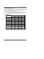
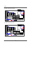
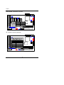
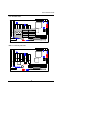
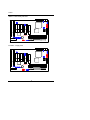
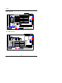
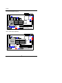
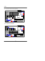
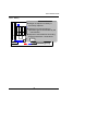
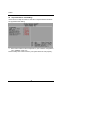
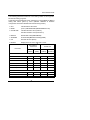
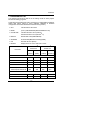
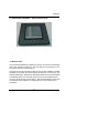
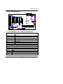
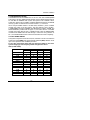
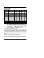
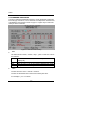
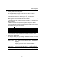
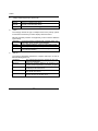
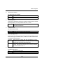
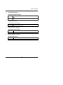
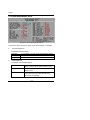
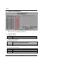
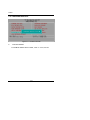
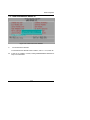
6VXE7+ USER'S MANUAL 1. System power on by PS/2 Mouse: First, enable this function in CMOS Setup, then you can power on the system by double clicking the right or left button of your PS/2 Mouse. 2. System power on by Keyboard: If your ATX power supply supports larger than 300 mA 5V Stand-By current (depends on the specification of keyboards), you can power on your system by entering password from the Keyboard after setting the “Keyboard power on” jumper and password in CMOS Setup. 3. Support 3 steps ACPI LED selectable. 4. Support Modem Ring-On. (Include internal Modem and external modem on COM A and COM B) 5. Support Wake -up On LAN. (Your ATX power supply must support larger than 720 mA 5V Stand-By current) CeleronTM /Pentium ® !!! Socket 370 Processor Motherboard REV. 1.0 Second Edition R-10-02-000427 6VXE7+ The author assumes no responsibility for any errors or omissions which may appear in this document nor does it make a commitment to update the information contained herein. Third-party brands and names are the property of their respective owners. Sound Blaster is a registered trademark of Creative Technology Ltd in the United States and certain other countries. Sound Blaster-LINK and SB-LINK are trademarks of Creative Technology Ltd. Apr. 27, 2000 Taipei, Taiwan 1 Quick Installation Guide I. Quick Installation Guide : The system bus speed can be set for 66,100,133MHz. The user can select the system bus speed (SW2) and change the DIP SWITCH (SW1) selection to set up the CPU speed for 300 - 866MHz processor. M The CPU speed must match with the frequency RATIO. It will cause system hanging up if the frequency RATIO is higher than CPU's. SW1: (O:ON / X:OFF) FREQ. RATIO X3 X 3.5 X4 X 4.5 X5 X 5.5 X6 X 6.5 X7 X 7.5 X8 X 8.5 X9 X 9.5 1 O X O X O X O X O X O X O X DIP SWITCH (SW) 2 3 X O X O O X O X X X X X O O O O X O X O O X O X X X X X 2 4 O O O O O O X X X X X X X X 6VXE7+ Set System Bus Speed SW2: (O:ON / X:OFF) CPU 66/100/ 133/Auto 66 75 83 100 112 124 133 140 150 PCICLK 1 2 3 4 5 6 33.3 X X X X O O 33.3 37.5 41.6 33.3 37.3 31 33.3 35 37.5 O O O O O X X X X O O O X X X X X X X O X X O X X O O X X O X X O X O X X X X X X X X X X X X X X X X X X X M Note: We don’t recommend you to set up your system speed to 75,83,112,124,140 or 150MHz because these frequencies are not the standard specifications for CPU, Chipset and most of the peripherals. Whether your system can run under 75,83,112,124,140 or 150 MHz properly will depend on your hardware configurations: CPU, SDRAM, Cards, etc. 1. CeleronTM 300A/ 66 MHz FSB ON ON 1 2 3 4 82443BX 1 2 3 4 5 6 SW2 PIIX4 6VXE7+ SW1 3 Quick Installation Guide 2. CeleronTM 333/ 66 MHz FSB ON 1 2 3 4 1 2 3 4 5 6 SW1 3. 1 2 3 4 ON 1 2 3 4 5 6 SW1 SW2 CeleronTM 400/ 66 MHz FSB ON 1 2 3 4 ON 1 2 3 4 5 6 SW1 5. SW2 CeleronTM 366/ 66 MHz FSB ON 4. ON SW2 CeleronTM 433/ 66 MHz FSB ON 1 2 3 4 SW1 ON 1 2 3 4 5 6 SW2 4 6VXE7+ 6. CeleronTM 466/ 66 MHz FSB ON 1 2 3 4 1 2 3 4 5 6 SW1 7. 1 2 3 4 ON 1 2 3 4 5 6 SW1 SW2 CeleronTM 533/ 66 MHz FSB ON 1 2 3 4 ON 1 2 3 4 5 6 SW1 9. SW2 CeleronTM 500/ 66 MHz FSB ON 8. ON SW2 CeleronTM 566/ 66 MHz FSB ON 1 2 3 4 SW1 ON 1 2 3 4 5 6 SW2 5 Quick Installation Guide 10. Cyrix Joshua 300/100MHz FSB ON 1 2 3 4 11. 1 2 3 4 5 6 SW2 SW1 ® Pentium !!! 500/100MHz FSB ON 1 2 3 4 SW2 ® Pentium !!! 550/100MHz FSB ON 1 2 3 4 13. ON 1 2 3 4 5 6 SW1 12. ON ON 1 2 3 4 5 6 SW2 SW1 ® Pentium !!! 600/100MHz FSB ON 1 2 3 4 SW1 ON 1 2 3 4 5 6 SW2 6 6VXE7+ 14. Pentium ® !!! 650/100MHz FSB ON 1 2 3 4 15. 1 2 3 4 5 6 SW2 SW1 ® Pentium !!! 700/100MHz FSB ON 1 2 3 4 SW2 ® Pentium !!! 750/100MHz FSB ON 1 2 3 4 17. ON 1 2 3 4 5 6 SW1 16. ON ON 1 2 3 4 5 6 SW2 SW1 ® Pentium !!! 800/100MHz FSB ON 1 2 3 4 SW1 ON 1 2 3 4 5 6 SW2 7 Quick Installation Guide 18. Pentium ® !!! 850/100MHz FSB ON 1 2 3 4 19. 1 2 3 4 5 6 SW2 SW1 ® Pentium !!! 533/133MHz FSB ON 1 2 3 4 20. ON 1 2 3 4 5 6 SW2 SW1 ® Pentium !!! 600/133 MHz FSB ON 1 2 3 4 21. ON ON 1 2 3 4 5 6 SW2 SW1 ® Pentium !!! 667/133MHz FSB ON 1 2 3 4 SW1 ON 1 2 3 4 5 6 SW2 8 6VXE7+ 22. Pentium ® !!! 733/133MHz FSB ON 1 2 3 4 23. 1 2 3 4 5 6 SW2 SW1 ® Pentium !!! 800/133MHz FSB ON 1 2 3 4 ON 1 2 3 4 5 6 SW1 24. ON SW2 Pentium ® !!! 866/133MHz FSB ON 1 2 3 4 SW1 ON 1 2 3 4 5 6 SW2 9 Quick Installation Guide II. Jumper setting : SPK : Speaker Connector External Speaker + 1 PIIX4 6VXE7+ PIN No. 1 82443BX 2 3 4 Function VCC NC NC Data RST : Reset Switch PIN No. Function Open Normal Operation 82443BX Close Reset Hardware System PIIX4 6VXE7+ 10 6VXE7+ PW LED : Power LED Connector + PIIX4 − PIN No. 1 2 6VXE7+ 3 − 82443BX Function LED + LED − LED − HD : IDE Hard Disk Active LED 82443BX PIIX4 PIN No. Function + 1 LED + − LED − 6VXE7+ 2 11 Quick Installation Guide GN : Green Function Switch 82443BX PIN No. Function Open Normal Operation Close Entering Green 6VXE7+ Mode PIIX4 GD : Green LED 82443BX − PIIX4 + PIN No. Function 1 LED + 2 LED − 6VXE7+ 12 6VXE7+ Soft POWER : Soft Power Connector PIIX4 PIN No. Function 1 Signal 2 GND 82443BX 6VXE7+ IR : Infrared Connector (Optional) 1 PIN No. 1 2 3 PIIX4 4 5 + Function IR data output GND IR data input NC 6VXE7+ VCC(+5V) 13 82443BX Quick Installation Guide ATX POWER : ATX Power Connector Pin No. Function 10 3,5,7,13, GND 15-17 1,2,11 3.3V 4,6,19,20 VCC 82443BX 1 10 +12V 12 -12V PIIX4 18 -5V 6VXE7+ 8 Power Good 9 5V SB stand by+5V 14 PS-ON(Soft On/Off) 20 11 PS/2 Mouse / Keyboard Connector PS/2 Mouse 6 4 PIIX4 5 3 2 1 PS/2 Keyboard 6VXE7+ PS/2 Mouse/ Keyboard Pin No. Function 1 Data 2 NC 82443BXGND 3 4 VCC(+5V) 5 Clock 6 NC 14 6VXE7+ J2: CPU FAN 1 PIN No. 1 2 3 Function GND +12V SENSE 82443BX PIIX4 6VXE7+ J3: PWR FAN 1 PIN No. 1 2 3 Function GND +12V SENSE 82443BX PIIX4 6VXE7+ 15 Quick Installation Guide J15 :SYSTEM FAN 1 PIIX4 PIN No. 1 2 3 6VXE7+ Function GND +12V SENSE 82443BX IDE1: For Primary IDE Port 82443BX PIIX4 6VXE7+ 1 16 6VXE7+ IDE2: For Secondary IDE Port 82443BX PIIX4 6VXE7+ 1 FLOPPY : Floppy Port 82443BX PIIX4 6VXE7+ 1 17 Quick Installation Guide LPT PORT / COM A / COM B LPT PORT 82443BX PIIX4 6VXE7+ COM B JP1 : PS/2 Keyboard Power On Selection PIN No. 1-2 close 2-3 close 3 2 1 Function PS/2 Keyboard Power on Enabled PS/2 Keyboard Power on Disabled (Default) 82443BX PIIX4 6VXE7+ 18 COM A 6VXE7+ USB : USB Port 5 6 7 8 1 2 3 4 PIN No. 1 2 3 4 5 6 7 8 Function USB V0 USB D0USB D0+ GND USB V1 USB D1USB D1+ 82443BX GND PIIX4 6VXE7+ JP7: Wake On LAN 1 2 3 PIIX4 PIN No. 1 2 3 6VXE7+ Function +5V SB GND Signal 19 82443BX Quick Installation Guide JP9 : Clear CMOS Function 3 2 1 PIN No. Function 1-2 close Clear CMOS 2-3 close Normal (Default) PIIX4 82443BX 6VXE7+ J14 :SB-LINK 6 5 4 3 2 1 PIIX4 6VXE7+ 20 PIN No. 1 2 3 4 5 82443BX 6 Function Signal GND NC Signal GND Signal 6VXE7+ J16: Internal Modem Ring On 1 PIN No. 1 2 PIIX4 Function Signal GND 82443BX 6VXE7+ JP10 : Case Open (Optional) PIN No. Function 1 Signal 2 GND 1 PIIX4 6VXE7+ 21 82443BX Quick Installation Guide JP15 : Over Voltage(Magic Booster)(Optional) (When JP15 set ”Open”, CPU Voltage is rising 10%) PIN No. Function open Turbo short Normal 82443BX (Default) 1 PIIX4 6VXE7+ JP16 : BIOS Flash ROM Write Protection PIN No. Function open Normal (Default) short Write Protection 1 M Please Set Jumper JP16 to “Open” to enabled BIOS Write Function 82443BX When you update new BIOS or new device. PIIX4 6VXE7+ 22 6VXE7+ J17 : Cyrix CPU Turbo Function (Optional) 1 PIN No. Function open Normal short Turbo 82443BX PIIX4 6VXE7+ JP17 : System After AC Back 1 PIN No. Function open Soft Off PIIX4 short Full On 82443BX 6VXE7+ 23 Quick Installation Guide BAT1 :Battery M Danger of explosion if battery is incorrectly replaced. MReplace only with the same or equivalent type recommended by the manufacturer. 82443BX PIIX4 M Dispose of used batteries according to the manufacturer’s instructions. + 6VXE7+ 24 6VXE7+ III. Top Performance Test Setting: Users have to modify the value for each item in chipset features as follow for top performance setting. ** Each value of items as above depends on your hardware configuration : CPU , SDRAM , Cards , etc. Please modify each value of items If your system does not work properly . 25 Quick Installation Guide The following performance data list is the testing results of some popular benchmark testing programs. These data are just referred by users, and there is no responsibility for different testing data values gotten by users. (Different Hardware & Software configuration will result in different benchmark testing results.) • CPU Intel Socket 370 Processor • DRAM (128 x 1) MB SAMSUNG (SECKM48S803CT-GA) • CACHE SIZE 128 KB included in CPU (Celeron); 256 KB included in CPU (Pentium® !!!) • DISPLAY GA-660 AGP Card (32MB SDRAM) • STORAGE Onboard IDE (IBM DJNA-371800) (18GB) • O.S. Windows NT™ 4.0 (SP6a) • DRIVER Display Driver at 1024 x 768 x 64K x 75Hz TM Intel Celeron Socket 370 Processor ® Intel Pentium !!! Socket 370 400MHz 533MHz 700MHz 600MHz (100x4) (66x8) (100x7) (133x4.5) 33.8 38.4 62.1 55.8 FPU Winmark 99 2140 2860 3760 3210 Business Disk Winmark 99 4950 4670 5550 5140 13000 12300 12700 13200 Business Gr aphics Winmark 99 181 188 312 298 Hi- End Graphics Winmark 99 352 400 626 572 Business Winstone99 29.7 30.7 40.5 39.5 Hi-End Winstone99 27.4 30.1 39.9 38.4 Winbench99 CPU mark99 Hi-End Disk Winmark 99 Winstone99 26 6VXE7+ TABLE OF CONTENTS 1. INTRODUCTION 1.1. PREFACE....................................................................................................1-1 1.2. KEY FEATHERS .........................................................................................1-1 1.3. PERFORMANCE LIST.................................................................................. 1-2 1.4. BLOCK DIAGRAM......................................................................................1-3 1.5. INTRODUCE THE INTELCeleronTM Socket 370 Processor.......................1-4 1.6. WHAT IS AGP?...........................................................................................1-4 2. SPECIFICATION 2.1. HARDWARE...............................................................................................2-1 2.2. SOFTWARE................................................................................................2-2 2.3. ENVIRONMENT...........................................................................................2-2 3. HARDWARE INSTALLATION 3.1. UNPACKING...............................................................................................3-1 3.2. MOTHERBOARD LAYOUT .........................................................................3-2 3.3. QUICK REFERENCE FOR JUMPERS & CONNECTORS................................3-2 3.4. DRAM INSTALLATION................................................................................3-6 3.5. CPU SPEED SETUP.....................................................................................3-6 3.6. CMOS RTC & ISA CFG CMOS RAM............................................................ 3-7 3.7. SPEAKER CONNECTOR INSTALLATION....................................................3-8 3.8. HARDWARE RESET SWITCH CONNECTOR INSTALLATION......................3-8 3.9. POWER LED CONNECTOR INSTALLATION ................................................3-8 3.10. IDE & ATAPI DEVICE INSTALLATION.......................................................3-8 1 Table of Contents 3.11. PERIPHERAL DEVICE INSTALLATION......................................................3-8 3.12. KEYBOARD & PS/2 MOUSE INSTALLATION............................................3-8 4. BIOS CONFIGURATION 4.1. ENTERING SETUP.......................................................................................4-1 4.2. CONTROL KEYS........................................................................................4-2 4.3. GETTING HELP...........................................................................................4-3 4.3.1. Main Menu .................................................................................. 4-3 4.3.2. Status Page Setup Menu / Option Page Setup Menu......................4-3 4.4. THE MAIN MENU.........................................................................................4-3 4.5. STANDARD CMOS SETUP MENU...............................................................4-5 4.6. BIOS FEATURES SETUP.............................................................................4-9 4.7. CHIPSET FEATURES SETUP....................................................................... 4-13 4.8. POWER MANAGEMENT SETUP..................................................................4-15 4.9. PNP/PCI CONFIGURATION.........................................................................4-19 4.10. LOAD BIOS DEFAULTS............................................................................4-21 4.11. LOAD PERFORMANCE DEFAULTS..........................................................4-22 4.12. INTEGRATED PERIPHERALS....................................................................4-23 4.13.SUPERVISOR/USER PASSWORD.............................................................4-26 4.14. IDE HDD AUTO DETECTION......................................................................4-27 4.15. SAVE & EXIT SETUP ................................................................................4-28 4.16. EXIT WITHOUT SAVING...........................................................................4-29 APPENDIX ……………………………………………………………………………….A-1 2 6VXE7+ 1. INTRODUCTION 1.1. PREFACE Welcome to use the 6VXE7+ motherboard. It is a Intel ® (CeleronTM /Pentium ® !!! )and Cyrix Joshua Socket 370 Processor based PC / AT Compatible system with AGP / PCI / ISA Bus, and has been designed to be the fastest PC / AT system. There are some new features allow you to operate the system with just the performance you want. This manual also explains how to install the motherboard for operation, and how to set up your CMOS CONFIGURATION with BIOS SETUP program. 1.2. KEY FEATURES q Intel Socket 370 Processor based PC / AT compatible Motherboard. q Socket 370 Pins ZIF white socket on board. q Supports Socket 370 processor running at 300-866MHz. q VIA Apollo chipset, Supports AGP / SDRAM / Ultra DMA 33 / ATA 66 IDE / Keyboard and PS/2 Mouse Power On / ACPI features. q Supports 3xDIMMs using 3.3V EDO or SDRAM DIMM module. q Supports external Modem Ring-On on COMA & COMB and internal Modem Ring-On. q Supports EDO 16MB ~ 384 MB, SDRAM 16MB ~ 1.5GB (256Mb DRAM technology) memory on board. q Supports Wake-up on LAN . q Supports ECC or Non-ECC type DRAM module. q 1xAGP slot, 5xPCI Bus slots, 2xISA Bus slots. q Supports 2 channels Ultra DMA33/ATA66 IDE ports for 4 IDE Devices. q Supports 2xCOM (16550), 1xLPT (EPP / ECP), 1x Floppy port. q Supports 2xUSB port & PS/2 Mouse/ Keyboard port. q Licensed AWARD BIOS, 2M bits FLASH ROM. q 30.5cm x 19 cm ATX SIZE form factor, 4 layers PCB. 1-1 Introduction 1.3. PERFORMANCE LIST The following performance data list is the testing results of some popular benchmark testing programs. These data are just referred by users, and there is no responsibility for different testing data values gotten by users. (Different Hardware & Software configuration will result in different benchmark testing results.) • CPU Intel Socket 370 Processor • DRAM (128 x 1) MB SAMSUNG (SECKM48S803CT-GA) • CACHE SIZE 128 KB included in CPU (Celeron); ® 256 KB included in CPU (Pentium !!!) • DISPLAY GA-660 AGP Card (32MB SDRAM) • STORAGE Onboard IDE (IBM DJNA-371800) (18GB) • O.S. Windows NT™ 4.0 (SP6a) • DRIVER Display Driver at 1024 x 768 x 64K x 75Hz TM Intel Celeron Socket 370 Processor ® Intel Pentium !!! Socket 370 400MHz 533MHz 700MHz 600MHz (100x4) (66x8) (100x7) (133x4.5) 33.8 38.4 62.1 55.8 FPU Winmark 99 2140 2860 3760 3210 Business Disk Winmark 99 4950 4670 5550 5140 13000 12300 12700 13200 Business Graphics Winmark 99 181 188 312 298 Hi- End Graphics Winmark 99 352 400 626 572 Business Winstone99 29.7 30.7 40.5 39.5 Hi-End Winstone99 27.4 30.1 39.9 38.4 Winbench99 CPU mark99 Hi-End Disk Winmark 99 Winstone99 1-2 6VXE7+ 1.4. BLOCK DIAGRAM 14.318MHz 3.3V SDRAM DIMM Sockets PGA 370 Host Bus Ultra DMA33/ ATA66 IDE Ports 33 MHz PCI Bus IDE Bus VIA 82C596B 66 /100 /133 MHz 66MHz 33MHz 66 /100 /133 MHz AGP VIA 82C693A 66 /100 /133 MHz AGP Bus Clock Generator 33 MHz 48MHz 14.318MHz USB Ports USB Bus ISA Bus 14.318MHz I/O CHIPSET ITE8671 COM Ports LPT Port Floppy Port Keyboard PS/2 Mouse 1-3 24MHz Introduction 1.5. INTRODUCE THE INTEL Socket 370 Processor Figure 1: INTEL Socket370 Processor 1.6 What is AGP? The Accelerated Graphics Port (AGP) is a new port on the Host-To-PCI bridge device that supports an AGP port. The main purpose of the AGP port is to provide fast access to system memory. The AGP port can be used either as fast PCI port (32-bits at 66MHz vs.32-Bits at 33MHz) or as an AGP port which supports 2x data-rate, a read queue, and side band addressing. When the 2x-data rate is used the port can transmit data at 533MB/sec (66.6*2*4). The read-queue can be used to pipeline reads – removing the effects of the reads-latency. Side band addressing can be used to transmit the data address on a separate line in order to speed up the transaction. 1-4 6VXE7+ 2. SPECIFICATION 2.1. HARDWARE • CPU − Support Socket 370 Processor: 300– 866MHz. − 370 pins 66/100/133MHz socket on board. • CHIPSET − VT82C693A PCI/AGP Controller(PAC) − VT82C596B PCI ISA IDE Controller. • SPEED − 66/100/133MHz system speed. − 66 MHz AGP bus speed. (2X mode 133MHz) − 33 MHz PCI-Bus speed. − 8 MHz AT bus speed. • DRAM MEMORY − 3 banks 168 pins DIMM module sockets on board. − Use 16 / 32 / 64 / 128 / 256 / 512MB DIMM module DRAM.(256Mb DRAM technology) − Supports EDO 16MB ~ 384 MB, SDRAM 16MB~1.5GB. (256Mb DRAM technology) − Supports 3.3V EDO / SDRAM. − Supports ECC or Non -ECC type DRAM. • CACHE MEMORY − 32 KB L1 cache memory included in CPU. − 128/256 KB L2 cache memory (included in CPU). − Supports DIB speed mode for L2 Cache. • I/O BUS SLOTS − 5 33MHz Master / Slave PCI-BUS. − 2 8MHz 16 bits ISA BUS. − 1 66MHz / 133MHz AGP bus. • IDE PORTS − 2 Ultra DMA 33/ATA66 Bus Master IDE channels onboard. (Using IRQ14,15) − Support Mode 3,4 IDE & ATAPI CD – ROM. 2-1 Specification • I/O PORTS − Supports 2 16550 COM ports. − Supports 1 EPP/ECP LPT port. − Supports 1 Floppy port. − Supports 2 USB ports. − Supports PS/2 Mouse & PS/2 Keyboard. • GREEN FUNCTION − Suspend mode support. − Green switch & Green LED support. − IDE & Display power down support. − Monitor all IRQ / DMA / Display / I/O events. • BIOS • DIMENSION − 2M bits FLASH ROM. − Supports Plug & Play, DMI F unction. − ATX Form Factor, 4 layers PCB. 2.2. SOFTWARE • DRIVER • BIOS − TUCD (Bus Master + Utilities) • O.S. − Operation with MS -DOS , Windows 95, − Licensed AWARD BIOS. − AT CMOS Setup, BIOS / Chipset Setup, Green Setup, Hard Disk Utility included. Windows 98, Windows NT™, OS/2, NOVELL and SCO UNIX. 2.3. ENVIRONMENT • Ambient Temp. • Relative Hum. • Altitude • Vibration • Electricity − 0°C to +50°C (Operating). − 0 to +85% (Operating). − 0 to 10,000 feet (Operating). − 0 to 1,000 Hz. − 4.9 V to 5.2 V. (Max. 20A current at 5V.) 2-2 6VXE7+ 3. HARDWARE INSTALLATION 3.1. UNPACKING The Motherboard package should contain the following: • The 6VXE7+ Motherboard. • USER’S MANUAL for Motherboard. • Cable set for IDE, Floppy devices. • A CD for Motherboard Utility.(TUCD) The motherboard contains sensitive electric components, which can be easily damaged by static electricity, so the Motherboard should be left in its original packing until it is installed. Unpacking and installation should be done on a grounded anti-static mat. The operator should be wearing an anti static wristband, grounded at the same point as the anti -static mat. Inspect the Motherboard carton for obvious damage. Shipping and handling may cause damage to your board. Be sure there are no shipping and handling damages on the board before proceeding. After opening the Motherboard carton, extract the system board and place it only on a grounded anti-static surface component side up. Again inspect the board for damage. Press down on all of the socket IC's to make sure that they are properly seated. Do this only on with the board placed on a firm flat surface. M DO NOT APPLY POWER TO THE BOARD IF IT HAS BEEN DAMAGED. 3-1 Hardware Installation 3.2. MOTHERBOARD LAYOUT COM B COM A LPT JP10 USB PS/2 J17 JP1 JP7 J14 CPU J2 AGP PCI 1 PCI 2 PCI 3 PCI 4 PCI 5 ISA 1 ISA 2 JP15 SW2 SW1 VT82C PIIX4 596B 6VXE7+ JP16 JP17 J16 BAT JP9 BIOS BANK 0 BANK 1 BANK 2 JP4 IDE 2 IDE 1 J15 ATX POWER VT82C 82443BX 693A J3 Floppy IR ×Figure 3.1Ø 3.3. QUICK REFERENCE FOR JUMPERS & CONNECTORS t I/O Ports Connector USB PS/2 IDE 1/ IDE 2 Floppy COM B COM A LPT ATX Power USB port. For PS/2 Keyboard and Mouse port. For Primary / Secondary IDE port. For Floppy port. For Serial port2 (COM B). For Serial port1 (COM A). For LPT port. For ATX Power Connector. t Socket 370 For CeleronT M , Pentium® !!!, Cyrix Joshua Socket 370 processor installed t J2: CPU FAN Pin No. 1 2 3 Function GND. +12V. Sense. 3-2 6VXE7+ t J3: PWR FAN Pin No. 1 2 3 Function GND. +12V. Sense. t J15: System FAN Pin No. 1 2 3 Function GND. +12V. Sense. t JP1: PS/2 Keyboard Power On Selection Pin No. 1-2 short 2-3 short Function Enable PS/2 Keyboard power on. Disable PS/2 Keyboard power on.(Default) t JP7: WAKE ON LAN ( Wake on LAN Connector) Pin No. 1 2 3 Function +5VSB. GND. Signal. t J16: RING PWR ON ( Internal Modem Ring On) Pin No. 1 2 Function Signal. GND. t IR: INFRARED Connector (Optional) Pin No. 1 2 3 4 5 Function IR DATA OUTPUT. GND. IR DATA INPUT. NC. VCC (+5V). t JP9: Clear CMOS Function Pin No. 1-2 Short 2-3 Short Function Clear CMOS . Normal.(Default) 3-3 Hardware Installation t JP10 : Case Open (Optional) Pin No. 1 2 Function Signal GND t J14: SB-LINK ( For PCI Audio / Sound Card use only ) Pin No. 1 2 3 4 5 6 Function Signal GND NC Signal GND Signal t JP15 :Over Voltage(Optional) Pin No. Open Short Function Turbo Normal(Default) t JP16 : BIOS Flash ROM Write Protection Pin No. Open Short Function Normal(Default) Write Protection t J17 : Cyrix CPU Turbo Function (Optional) Pin No. Open Short Function Normal Turbo t JP17 : System After AC Back Pin No. Open Short Function Soft Off Full On JP4 : 2*11PIN Jumper G− PW P+P− P− H+ 1 1 JP4 1 G+ 1 RST SPK 3-4 H− GN 6VXE7+ PW : Soft Power Connector On – Off : For POWER ON or Suspend IN / OUT. On 4 sec : For POWER OFF before VGA Enable or CMOS setup select “delay 4sec.” For POWER OFF mode. RST : Reset Switch Open: Normal Operation Short: For Hardware Reset System P+P− P−: Power LED PIN 1: anode (+) PIN 2: cathode (−) PIN 3: cathode (−) 1 SPK: Speaker Connector + − 1 PIN 1 : VCC (+) PIN 2 : NC PIN 3 : NC PIN 4 : Data (−) HD: IDE Hard Disk Active LED 1 PIN 1: LED anode (+) PIN 2: LED cathode (−) GN: Green Switch Open: Normal operation Short: Entering Green Mode GD: Green Function Active LED 1 PIN 1: LED anode (+) PIN 2: LED cathode (−) 3-5 Hardware Installation 3.4. DRAM INSTALLATION The Motherboard can be installed with 16 / 32 / 64 / 128 / 256 / 512MB (256Mb Technology) 168 pins DIMM module DRAM, and the DRAM speed must be 67~100 MHz for SDRAM when system bus speed is set to 66MHz. When system bus speed is set to 100MHz, 100MHz SDRAM is required. The DRAM memory system on Motherboard consists of bank 0, 1, 2 & bank 3. Since 168 pins DIMM module is 64 bits width, therefore 1 piece of DIMM module may match a 64 bits system. The total memory size is 16 MB ~ 1.5GMB(256Mb Techonloy) SDRAM, EDO DRAM size is 16MB ~ 384MB. The DRAM installation position refer to Figure 3.1, and notice the Pin 1 of DIMM module must match with the Pin 1 of DIMM socket. Insert the DRAM DIMM module into the DIMM socket at Vertical angle. If there is a wrong direction of Pin 1, the DRAM DIMM module could not be inserted into socket completely. 3.5. CPU SPEED SETUP The system bus speed can be set for 66,100,133 MHz. The user can select the system bus speed (SW2) and change the DIP SWITCH (SW1) selection to set up the CPU speed for 300 - 866MHz processor. M The CPU speed must match with the frequency RATIO. It will cause system hanging up if the frequency RATIO is higher than CPU's. SW1: (O:ON / X:OFF) FREQ. RATIO X3 X 3.5 X4 X 4.5 X5 X 5.5 X6 X 6.5 X7 X 7.5 X8 X 8.5 X9 X 9.5 1 O X O X O X O X O X O X O X DIP SWITCH (SW) 2 3 X O X O O X O X X X X X O O O O X O X O O X O X X X X X 3-6 4 O O O O O O X X X X X X X X 6VXE7+ Set System Bus Speed SW2: (O:ON / X:OFF) CPU PCICLK 1 2 3 4 5 6 33.3 X X X X O O 66 33.3 O O X X X X 75 37.5 O O O X X X 66/100/ 133/Auto 83 41.6 O O X O X X 100 33.3 O X X X X X 112 37.3 O X O X X X 124 31 X X X O X X 133 33.3 X X X X X X 140 35 X X O O X X 150 37.5 X X O X X X M Note: We don’t recommend you to set up your system speed to 75,83,112,124,140 or 150MHz because these frequencies are not the standard specifications for CPU, Chipset and most of the peripherals. Whether your system can run under 75,83,112,124,140 or 150 MHz properly will depend on your hardware configurations: CPU, SDRAM, Cards, etc. 3.6. CMOS RTC & ISA CFG CMOS RAM There're RTC & CMOS RAM on board; they have a power supply from external battery to keep the DATA inviolate & effective. The RTC is a REAL-TIME CLOCK device, which provides the DATE & TIME to system. The CMOS RAM is used for keeping the information of system configuration, so the system can automatically boot OS every time. Since the lifetime of internal battery is 5 years, the user can change a new Battery to replace old one after it cannot work. M Danger of explosion if battery is incorrectly replaced. M Replace only with the same or equivalent type recommended by the manufacturer. M Dispose of used batteries according to the manufacturer’s instructions. 3-7 Hardware Installation 3.7. SPEAKER CONNECTOR INSTALLATION There is a speaker in AT system for sound purpose. The 4 - Pins connector SPK is used to connect speaker. 3.8. HARDWARE RESET SWITCH CONNECTOR INSTALLATION The RESET switch on panel provides users with HARDWARE RESET function. The system will do a cold start after the RESET switch is pushed and released by user. The RESET switch is a 2 PIN connector and should be installed toRST on Motherboard. 3.9. POWER LED CONNECTOR INSTALLATION System has Power LED lamp on the panel of case. The Power LED will light on off or flash to indicate which step on the system. The connector should be connected to PW of Motherboard in correct direction. 3.10. IDE & ATAPI DEVICE INSTALLATION There are two-Enhanced PCI IDE ports (IDE1, IDE2 ) on board, which following ATAPI standard SPEC. Any one IDE port can connected to two ATAPI devices (IDE Hard Disk, CD-ROM & Tape Driver), so total four ATAPI devices can exist in a system. The HD is the active LED port for ATAPI devices. 3.11. PERIPHERAL DEVICE INSTALLATION After the I/O device installation and jumpers setup, the Motherboard can be mounted into the case and fixed by screw. To complete the Motherboard installation, the peripheral device could be installed now. The basic system needs a display interface card. If the PCI - Bus device is to be installed in the system, any one of four PCI - Bus slots can be used. 3.12. KEYBOARD & PS/2 MOUSE INSTALLATION The Motherboard supports PS/2 Mouse. The BIOS will auto detect whether the PS/2 Mouse is installed or not & assign IRQ12 for PS/2 Mouse port if it is installed. After installing the peripheral device, the user should check everything again, and prepare to power-on the system. 3-8 6VXE7+ 4. BIOS CONFIGURATION Award's BIOS ROM has a built-in Setup program that allows users to modify the basic system configuration. This type of information is stored in battery-backed CMOS RAM so that it retains the Setup information when the power is turned off. 4.1. ENTERING SETUP Power ON the computer and press <Del> immediately will allow you to enter Setup. The other way to enter Setup is to power on the computer, when the below message appears briefly at the bottom of the screen during the POST (Power On Self Test), press <Del> Key or simultaneously press <Ctrl>, <Alt>, and <Esc> keys. Ÿ Press DEL to enter SETUP. If the message disappears before you respond and you still wish to enter Setup, restart the system to try again by turning it OFF then ON or pressing the "RESET" bottom on the system case. You may also restart by simultaneously press <Ctrl>,<Alt>, and <Del> keys. 4-1 BIOS Configuration 4.2. CONTROL KEYS Up arrow Move to previous item. Down arrow Move to next item. Left arrow Move to the item in the left hand. Right arrow Move to the item in the right hand. Esc key Main Menu - Quit and not save changes into CMOS Status Page Setup Menu and Option Page Setup Menu Exit current page and return to Main Menu. PgUp key Increase the numeric value or make changes. PgDn key Decrease the numeric value or make changes. F1 key General help, only for Status Page Setup Menu and Option Page Setup Menu. F2 key Change color from total 16 colors. F3 key Calendar, only for Status Page Setup Menu. F4 key Reserved. F5 key Restore the previous CMOS value from CMOS, only for Option Page Setup Menu. F6 key Load the default CMOS value from BIOS default table, only for Option Page Setup Menu. F7 key Load the default. F8 key Reserved. F9 key Reserved. F10 key Save all the CMO S changes, only for Main Menu. 4-2 6VXE7+ 4.3. GETTING HELP 4.3.1 Main Menu The on-line description of the highlighted setup function is displayed at the bottom of the screen. 4.3.2 Status Page Setup Menu / Option Page Setup Menu Press F1 to pop up a small help window that describes the appropriate keys to use and the possible selections for the highlighted item. To exit the Help Window press <Esc>. 4.4. THE MAIN MENU Once you enter Award BIOS CMOS Setup Utility, the Main Menu (Figure 4.1) will appear on the screen. The Main Menu allows you to select setup functions and exit choices. Use arrow keys to select among the items and press <Enter> to accept or enter the sub-menu. Figure 4.1: Main Menu • Standard CMOS setup This setup page includes all the items in a standard compatible BIOS. • BIOS features setup This setup page includes all the items of Award special enhanced features. 4-3 BIOS Configuration • Chipset features setup This setup page includes all the items of chipset special features. • Power management setup This setup page includes all the items of Green function features. • PNP/PCI configuration This setup page includes all the items of PNP/PCI configuration features. • Load BIOS defaults BIOS defaults indicates the most appropriate value of the system parameter which the system would be in safe configuration. • Load Performance defaults Performance Defaults indicates the value of the system parameters which the system would be in best performance configuration. • Integrated Peripherals This setup page includes all the items of peripherals features. • Supervisor Password Change, set, or disable password. It allows you to limit access to the system and Setup, or just to Setup. • User Password Change, set, or disable password. It allows you to limit access to the system. • IDE HDD auto detection Automatically configure hard disk parameter. • Save & exit setup Save CMOS value changes to CMOS and exit setup. • Exit without save Abandon all CMOS value changes and exit setup. 4-4 6VXE7+ 4.5. STANDARD CMOS SETUP The items in Standard CMOS Setup (Figure 4.2) are divided into 9 categories. Each category includes no, one or more than one setup items. Use the arrows to highlight the item and then use the <PgUp> or <PgDn> keys to select the value you want in each item. Figure 4.2: Standard CMOS Setup • Date The date format is <week>, <month>, <day>, <year>. Press <F3> to show the calendar. Week Month Day Year • The week, from Sun to Sat, determined by the BIOS and is display-only The month, Jan. through Dec. The day, from 1 to 31 (or the maximum allowed in the month) The year, from 1994 through 2079 Time The time format in <hour> <minute> <second>. The time is calculated base on the 24-hour military-time clock. For example, 1 p.m. is 13:00:00. 4-5 BIOS Configuration • Primary HDDs / Secondary HDDs The category identify the types of hard disk from drive C to drive F 4 devices that has been installed in the computer. There are three options for definable type; User, Auto and None . Type User is user-definable; and type Auto means automatically detecting HDD's type and None means No IDE HDD installed. If you select Type User, related information is asked to be entered to the following items. Enter the information directly from the keyboard and press <Enter>. Those information should be provided in the documentation from your hard disk vendor or the system manufacturer. CYLS. HEADS PRECOMP LANDZONE SECTORS number of cylinders number of heads write precomp landing zone number of sectors If a hard disk has not been installed select NONE and press <Enter>. • Drive A type / Drive B type The category identify the types of floppy disk drive A or drive B that has been installed in the computer. None No floppy drive installed 360K, 5.25 in. 5-1/4 inch PC-type standard drive; 360 kilobyte capacity. 1.2M, 5.25 in. 5-1/4 inch AT -type high-density drive; 1.2 megabyte capacity (3-1/2 inch when 3 Mode is Enabled). 720K, 3.5 in. 1.44M, 3.5 in. 2.88M, 3.5 in. 3-1/2 inch double-sided drive; 720 kilobyte capacity 3-1/2 inch double-sided drive; 1.44 megabyte capacity. 3-1/2 inch double-sided drive; 2.88 megabyte capacity. 4-6 6VXE7+ • Floppy 3 Mode Support (for Japan Area) Disabled Drive A Drive B Both • Normal Floppy Drive. Drive A is 3 mode Floppy Drive. Drive B is 3 mode Floppy Drive. Drive A & B are 3 mode Floppy Drives. Video The category detects the type of adapter used for the primary system monitor that must match your video display card and monitor. Although secondary monitors are supported, you do not have to select the type in setup. EGA/VGA Enhanced Graphics Adapter/Video Graphics Array. For EGA, VGA, SVGA, or PGA monitor adapters CGA 40 Color Graphics Adapter, power up in 40 column mode CGA 80 Color Graphics Adapter, power up in 80 column mode MONO Monochrome adapter, includes high resolution monochrome adapters • Halt on The category determines whether the computer will stop if an error is detected during power up. NO Errors All Errors All, But Keyboard All, But Diskette All, But Disk/Key The system boot will not be stopped for any error that may be detected Whenever the BIOS detects a non-fatal error, the system will be stopped and you will be prompted The system boot will not stop for a keyboard error; it will stop for all other errors The system boot will not stop for a disk error; it will stop for all other errors The system boot will not stop for a keyboard or disk error; it will stop for all other errors 4-7 BIOS Configuration • Memory The category is display-only which is determined by POST (Power On Self Test) of the BIOS. Base Memory The POST of the BIOS will determine the amount of base (or conventional) memory installed in the system. The value of the base memory is typically 512 K for systems with 512 K memory installed on the motherboard, or 640 K for systems with 640 K or more memory installed on the motherboard. Extended Memory The BIOS determines how much extended memory is present during the POST. This is the amount of memory located above 1 MB in the CPU's memory address map. Expanded Memory Expanded Memory in memory defined by the Lotus / Intel / Microsoft (LIM) standard as EMS. Many standard DOS applications can not utilize memory above 640, the Expanded Memory Specification (EMS) swaps memory which not utilized by DOS with a section, or frame, so these applications can access all of the system memory. Memory can be swapped by EMS is usually 64K within 1 MB or memory above 1 MB, depends on the chipset design. Expanded memory device driver is required to use memory as Expanded Memory. Other Memory This refers to the memory located in the 640 to 1024 address space. This is memory that can be used for different applications. DOS uses this area to load device drivers to keep as much base memory free for application programs. Most use for this area is Shadow RAM. 4-8 6VXE7+ 4.6. BIOS FEATURES SETUP Figure 4.3: BIOS Features Setup • Virus Warning This category flashes on the screen. During and after the system boots up, any attempt to write to the boot sector or partition table of the hard disk drive will halt the system and the following error message will appear, in the mean time, you can run anti-virus program to locate the problem. The default value is Disabled. Enabled Activate automatically when the system boots up causing a warning message to appear when anything attempts to access the boot sector or hard disk partition t able. Disabled No warning message appears when anything attempts to access the boot sector or hard disk partition table. • Processor Number Feature The default value is Enabled. Enabled Disabled Enable Processor Number Feature. Disable Processor Number Feature. 4-9 BIOS Configuration • Boot From LAN First The default value is Disabled. Enabled Disabled AUTO • Enable Boot From LAN First. Disable Boot From LAN First. Auto detect Boot From LAN First. Boot Sequence This category determines which drive computer searches first for the disk operating system (i.e., DOS). Default value is A, C, SCSI. X1, X2, X3 • System will first search for X1 disk drive then X2 disk drive and then X3 disk drive. VGA Boot From The default value is AGP AGP PCI Slot • System will boot from AGP Display Card. System will boot from PCI Slot VGA Card. Boot Up Floppy Seek During POST, BIOS will determine the floppy disk drive installed is 40 or 80 tracks. 360 K type is 40 tracks 720 K, 1.2 M and 1.44 M are all 80 tracks. The default value is Enabled. Enabled Disabled • BIOS searches for floppy disk drive to determine it is 40 or 80 tracks. Note that BIOS can not tell from 720 K, 1.2 M or 1.44 M drive type as they are all 80 tracks. BIOS will not search for the type of floppy disk drive by track number. Note that there will not be any warning message if the drive installed is 360 K. Boot Up NumLock Status The default value is On. On Off Keypad is number keys. Keypad is arrow keys. 4-10 6VXE7+ • Memory Parity/ECC Check The default value is Disabled. Enabled Disabled • Enabled Memory Parity/ECC Check Function. Disabled Memory Parity/ECC Check Function. Typematic Rate Setting The default value is Disabled. Enabled Disabled • Enable Keyboard Typematic rate setting. Disable Keyboard Typematic rate setting. Typematic Rate (Chars / Sec.) The default value is 6. 6-30 • Set the maximum Typematic rate from 6 chars. Per second to 30 characters. Per second. Typematic Delay (Msec.) The default value is 250. 250-1000 • Set the time delay from first key to repeat the same key in to computer. Security option The default value is Setup. Setup The system will boot and access to Setup will be denied if System the correct password is not entered at the prompt. The system will not boot and access to Setup will be denied if the correct password is not entered at the prompt. M To disable security, select PASSWORD SETTING at Main Menu and then you will be asked to enter password. If the user does not type anything and just press <Enter>, it will disable security. Once the security is disabled, the system will boot and you can enter Setup freely. 4-11 BIOS Configuration • PCI/VGA Palette Snoop The default value are Disabled. • Enabled For having Video Card on ISA Bus and VGA Card on PCI Bus. Disabled For VGA Card only. Assign IRQ For VGA The default value is Enabled. Enabled Disabled • Assign IRQ For VGA Not assign IRQ For VGA HDD S.M.A.R.T. Capability The default value is Disable. • Enable Enable HDD S.M.A.R.T. Capability Disable Disable HDD S.M.A.R.T. Capability Report No FDD For WIN 95 The default value is No. No Yes Assign IRQ6 For FDD. FDD Detect IRQ6 Automatically. 4-12 6VXE7+ 4.7. CHIPSET FEATURES SETUP Figure 4.4: Chipset Features Setup • Top Performance The default value is Disabled. Enabled Top Performance. Enabled Disabled • Disabled Top Performance. (Default) SDRAM Cycle Length The default value is 3. Auto 3 2 • Set SDRAM Cycle Length is Auto For Slower SDRAM DIMM module. For Fastest SDRAM DIMM module. DRAM Clock The default value is Host CLK CPU CLK DRAM CLK 66,75,83 Host CLK Host CLK +33M Host CLK. 100,112,124,133,140,150 4-13 BIOS Configuration • Read Around write The default value is Enabled. Enabled Disabled • When set Enabled this feature speeds up data read performance. Normal operation. Concurrent PCI/Host The default value is Disabled. Enabled Disabled • Enabled Concurrent PCI/Host. Disabled Concurrent PCI/Host. AGP Aperture Size The default value is 64MB • 64MB 32MB Set AGP Aperture Size to 64MB. Set AGP Aperture Size to 32MB. 16MB 8MB 4MB Set AGP Aperture Size to 16MB. Set AGP Aperture Size to 8MB. Set AGP Aperture Size to 4MB. 128MB Set AGP Aperture Size to 128MB. Power LED in Suspend The default value is BLINKING • BLINKING ON Set Power LED in Suspend at BLINKING mode. Set Power LED in Suspend at ON mode. OFF/DUAL Set Power LED in Suspend at OFF/DUAL mode, if you use a dual color power LED , it will show dual color. Spread Spectrum The default value is Disabled. Disabled Enabled Spread Spectrum Disabled Set Spread Spectrum Enabled. 4-14 6VXE7+ 4.8. POWER MANAGEMENT SETUP Figure 4.5: Power Management Setup \ These two items will show up when “RTC Alarm Resume” is enabled. • Power Management The default value is Enabled. Enabled Min Saving Max Saving • For configuring our own power management features. Enable Green function. Disable Green function. Video Off Method The default value is DPMS Support. V/H SYNC + Blank Blank Screen DPMS Support BIOS will turn off V/H-SYNC when gets into Green mode for Green monitor power saving. BIOS will only black monitor when gets into Green mode. BIOS will use DPMS Standard to control VGA card. (The Green type VGA card will turn of V/H-SYNC automatically.) 4-15 BIOS Configuration • Soft -off by PWRBTN The default value is Instant-off. Instant-off Delay 4 sec • Soft switch ON/OFF for power ON/OFF. Soft switch on 4sec for power OFF. System After AC Back The default value is Soft-Off. Memory Soft-Off Full -On • This function depends on computer status Set System Soft-Off Status. Set System Full-On Status. CPU FAN In Suspend The default value is Off. On Off • Disable this function. Stop CPU FAN when entering Suspend mode. HDD Power Down The default value is Disabled. Disabled 1-15 mins. • Disabled HDD Power Down mode function. Enabled HDD Power Down mode between 1 to 15 mins. Suspend Mode The default value is Disabled. Disabled 10 Sec - 1 Hour • Disabled Suspend Mode. Setup the timer to enter Suspend Mode. VGA The default value is OFF. Disable monitor VGA activity. OFF Enable monitor VGA activity. ON 4-16 6VXE7+ • LPT & COM The default value is LPT/COM. LPT/COM NONE LPT COM • Enabled LPT/COM Ports Activity. Normal Operation. Enabled LPT Ports Activity. Enabled COM Ports Activity. HDD & FDD The default value is ON. ON OFF • Enabled HDD & FDD Ports Activi ty Disabled HDD & FDD Ports Activity DMA/master The default value is OFF. ON OFF • Don’t detect DMA/master PM event. Normal Operation. Wake Up On RI# The default value is Enabled . Enable Wake Up On LAN/Ring Enabled Disabled • Disable Wake Up On LAN/Ring Wake Up On PME# The default value is Enabled. Enable Wake Up On PME# Enabled Disabled Disable Wake Up On PME# 4-17 BIOS Configuration • RTC Alarm Resume You can set “RTC Alarm Resume” item to Enabled and key in date/time to power on system. The default value is Disabled. Disabled Enabled Disable this function. Enable alarm function to POWER ON system. If the “RTC Alarm Resume” is Enabled. Date ( of Month) Alarm : Time ( hh: mm: ss) Alarm : • 0~31 (0~23) : (0~59) : (0~59) Primary INTR The default value is ON. ON OFF • Primary INTR function is on. Normal Operation. IRQ [3~15] The default value is Primary/Secondary/Disabled. Disabled Primary Secondary Disable this function. The resource is used by Primary device . The resource is used by Secondary device . 4-18 6VXE7+ 4.9. PNP/PCI CONFIGURATION Figure 4.6: PNP/PCI Configuration M IRQ[3.4.5.7.9.10.11.12.14.15] & DMA[1.3.5.6.7]These items will show up when “Resources Controlled By” is Manual. • PNP OS Installed The default value is No. Yes Enable PNP OS Installed function. No Disable PNP OS Installed function. • Resources Controlled by The default value is Auto. Manual User can set the PnP resource (I/O Address, IRQ & DMA channels) used by legacy ISA DEVICE. Auto BIOS automatically use these PnP rescuers. • Reset Configuration Data The default value is Disabled. Disabled Disable this function. ESCD Enable clear PnP information in ESCD. DMI Enable clear PnP information in DMI. BOTH Enable clear PnP information in ESCD and DMI. 4-19 BIOS Configuration • IRQ (3,4,5,7,9,10,11,12,14,15), DMA(0,1,3,5,6,7) assigned to The default value is "Legacy ISA" or "PCI/ISA PnP". Legacy ISA The resource is used by Legacy ISA device. PCI/ISA PnP The resource is used by PCI/ISA PnP device (PCI or ISA). • Assign IRQ For USB The default value is Enabled. Enabled Assign a specific IRQ for USB. Disabled No IRQ is assigned for USB. 4-20 6VXE7+ 4.10. LOAD BIOS DEFAULTS Figure 4.7: Load BIOS Defaults • Load BIOS Defaults To load BIOS defaults value to CMOS , enter "Y". If not, enter "N". 4-21 BIOS Configuration 4.11. LOAD PERFORMANCE DEFAULTS Figure 4.8: Load Performance Defaults • Load Performance Defaults To load Performance defaults value to CMOS , enter "Y". If not, enter "N". M If there is any problem occurred, loading PERFORMANCE DEFAULTS step is recommended. 4-22 6VXE7+ 4.12. INTEGRATED PERIPHERALS ** * Figure 4.9: Integrated peripherals ** This items will show up when ”UART2 Mode Select” is set to IrDA 1.0or ASKIR. * This item will show up when “Keyboard Power On: Multikey” is selected. • USB Controller The default value is Enabled. Enabled Disabled • Enabled USB Controller. Disabled USB Controller. USB Keyboard Support The default value is Disabled. Enabled Enabled USB Keyboard Support. Disabled Disabled USB Keyboard Support. • Onboard Serial Port 1 The default value is 3F8/IRQ4. Auto 3F8/IRQ4 2F8/IRQ3 3E8/IRQ4 BIOS will automatically setup the port 1 address. Enable onboard Serial port 1 and address is 3F8. Enable onboard Serial port 1 and address is 2F8. Enable onboard Serial port 1 and address is 3E8. 4-23 BIOS Configuration 2E8/IRQ3 Disabled • Enable onboard Serial port 1 and address is 2E8. Disable onboard Serial port 1. Onboard Serial Port 2 The default value is 2F8/IRQ3. Auto 3F8/IRQ4 2F8/IRQ3 3E8/IRQ4 2E8/IRQ3 Disabled • BIOS will automatically setup the port 2 address. Enable onboard Serial port 2 and address is 3F8. Enable onboard Serial port 2 and address is 2F8. Enable onboard Serial port 2 and address is 3E8. Enable onboard Serial port 2 and address is 2E8. Disable onboard Serial port 2. Onboard Parallel port The default value is 378/IRQ7. 378/IRQ7 278/IRQ5 3BC/IRQ7 Disabled • Enable onboard LPT port and address is 378/IRQ7. Enable onboard LPT port and address is 278/IRQ5. Enable onboard LPT port and address is 3BC/IRQ7. Disable onboard LPT port. Parallel Port Mode The default value is SPP. SPP EPP ECP ECP+EPP • Using Parallel port as Standard Parallel Port. Using Parallel port as Enhanced Parallel Port. Using Parallel port as Extended Capabilities Port. Using Parallel port as ECP & EPP mode. UART2 Mode (This item allows you to determine which UART2 Mode of onboard I/O chip), the default value is Standard. ASKIR Set onboard I/O chip UART2 to ASKIR Mode. IrDA 1.0 Set onboard I/O chip UART2 to IrDA Mode. Standard Set onboard I/O chip UART2 to Standard Mode. 4-24 6VXE7+ • UART2 Duplex Mode The default value is Half. Half Full • Set UART2 Duplex Mode to Half. Set UART2 Duplex Mode to Full. PS/2 Mouse Power on The default value is Disabled. Disabled Db Click • Disable PS/2 Mouse Power on . Double click PS/2 Mouse bottom. Keyboard Power on The default value is POWER Key. POWER Key Multi key • If your keyboard have “POWER Key” button, you can press the key to power on your system. Enter multikey combination to Power on system. KB Power On Password Enter Enter from 1 to 5 characters to set the Keyboard Power On Password. 4-25 BIOS Configuration 4.13. SUPERVISOR / USER PASSWORD When you select this function, the following message will appear at the center of the screen to assist you in creating a password. Figure 4.10: Password Setting Type the password, up to eight characters, and press <Enter>. The password typed now will clear previously entered password from CMOS memory. You will be asked to confirm the password. Type the password again and press <Enter>. You may also press <Esc> to abort the selection and not enter a password. To disable password, just press <Enter> when you are prompted to enter password. A message will confirm the password being disabled. Once the password is disabled, the system will boot and you can enter Setup freely. PASSWORD DISABLED If you select “System” at “Security Option” of BIOS Features Setup Menu, you will be prompted for the password every time the system is rebooted or any time you try to enter Setup. If you select “Setup” at “Security Option” of BIOS Features Setup Menu, you will be prompted only when you try to enter Setup. 4-26 6VXE7+ 4.14. IDE HDD AUTO DETECTION Figure 4.11: IDE HDD Auto Detection Type "Y" will accept the H.D.D. parameter reported by BIOS. Type "N" will keep the old H.D.D. parameter setup. If the hard disk cylinder NO. is over 1024, then the user can select LBA mode or LARGE mode for DOS partition larger than 528 MB. 4-27 BIOS Configuration 4.15. SAVE & EXIT SETUP Figure 4.12: Save & Exit Setup Type "Y" will quit the Setup Utility and save the user setup value to RTC CMOS . Type "N" will return to Setup Utility. 4-28 6VXE7+ 4.16. EXIT WITHOUT SAVING Figure 4.13: Exit Without Saving Type "Y" will quit the Setup Utility without saving to RTC CMOS . Type "N" will return to Setup Utility. 4-29 Appendix Appendix A: BIOS Flash Procedure BIOS update procedure: ü Please check your BIOS vendor (AMI or AWARD) on the motherboard. ü It is recommended you copy the AWDFlash.exe or AMIFlash.exe in driver CD (D:\>Utility\BIOSFlash) and the BIOS binary files into the directory you made in your hard disk. 【i.e:C:\>Utility\ (C:\>Utility : denotes the driver and the directory where you put the flash utilities and BIOS file in.)】 ü Restart your computer into MS-DOS mode or command prompt only for Win95/98, go into the directory where the new BIOS file are located Use the utility AWDFlash.exe or AMIFlash.exe to update the BIOS. ü Type the following command once you have enter the directory where all the files are located C:\utility\ AWDFlash or AMIFlash <filename of the BIOS binary file intended for flashing> ü Once the process is finished, reboot the system MNote : Please download the newest BIOS from our website (www.gigabyte.com.tw) or contact your local dealer for the file. A-1 6VXE7+ Appendix B : VIA Chipsets Driver Installation VIA 4 in 1 Service Pack Utility: Insert the support CD that came with your motherboard into your CD-ROM driver or double –click the CD driver icon in My Computer to bring up the screen. 1.Click “VIA 4in 1 Service Pack Utility” item. (2) (1) 2.Click “Next”. 3.Click “Yes”. (4) (3) 5.Click “Next”. 4.Click “Next”. (6) (5) A-2 Appendix 7.Click “Next”. 6.Click “Next”. (7) (8) 8.Click “Next”. 9.Click “Next”. (10) (9) 10.Click “Finish” to Restart Computer. (12) (11) A-3 FCC Compliance Statement: DECLARATION OF CONFORMITY Per FCC Part 2 Section 2. 1077(a) This equipment has been tested and found to comply with limits for a Class B digital device , pursuant to Part 15 of the FCC rules. These limits are designed to provide reasonable protection against harmful interference in residential installations. This equipment generates, uses, and can radiate radio frequency energy, and if not installed and used in accordance with the instructions, may cause harmful interference to radio communications. However, there is no guarantee that Eric Lu interference will not occur in a particular installation. If this equipment does cause interference to radio or television equipment reception, which can be determined by turning the equipment off and on, the user is encouraged to try to correct the interference by one or more of the following measures: Responsible Party Name: G.B.T. INC. Address: 18305 Valley Blvd., Suite#A LA Puent, CA 91744 Phone/Fax No: (818) 854-9338/ (818) 854-9339 hereby declare s that the product Product Name: Mother Board Model Number: GA-6VXE7+ Conforms to the following specifications: FCC Part 15, Subpart B, Section 15.107(a) and Section 15.109(a), Class B Digital Device Supplementary Information: This device complies with part15 of the FCC Rules. Operation is subject to the following two conditions: (1) This device may not cause harmful and (2) this device must accept any inference received, including that may cause undesired operation. Representative Person's Name: ERIC LU Signature: Date: Mar. 16, 2000 -Reorient or relocate the receiving antenna -Move the equipment away from the receiver -Plug the equipment into an outlet on a circuit different from that to which the receiver is connected -Consult the dealer or an experienced radio/television technician for additional suggestions You are cautioned that any change or modifications to the equipment not expressly approve by the party responsible for compliance could void Your authority to operate such equipment. This device complies with Part 15 of the FCC Rules. Operation is subjected to the following two conditions 1) this device may not cause harmful interference and 2) this device must accept any interference recei ved, including interference that may cause undesired operation. Declaration of Conformity We, Manufacturer/Importer (full address) G.B.T. Technology Trading GMBH Ausschlager Weg 41, 1F, 20537 Hamburg, Germany declare that the product ( descri ption of the apparatus, system, installation to which it refers) Mother Board GA-6VXE7+ is in conformity with (reference to the specification under which conformity is declared) in accordance with 89/336 EEC-EMC Directive EN 55011 Limits and methods of measurement EN 61000-3-2* Disturbances in supply systems caused of radio disturbance characteristics of industrial, scientific and medical (ISM high frequency equipment EN60555-2 by household appliances and similar electrical equipment “Harmonics” EN55013 Limits and methods of measurement of radio disturbance characteristics of broadcast receivers and associated equipment EN61000-3-3* EN60555-3 Disturbances in supply systems caused by household appliances and similar electrical equipment “Voltage fluctuations” EN 55014 Limits and methods of measurement of radio disturbance characteristics of household electrical appliances, portable tools and similar electrical apparatus EN 50081-1 Generic emission standard Part 1: Residual, commercial and light industry EN 50082-1 Generic immunity standard Part 1: Residual, commercial and light industry EN 55015 Limits and methods of measurement of radio disturbance characteristics of fluorescent lamps and luminaries EN 55081-2 Generic emission standard Part 2: Industrial environment EN 55020 Immunity from radio interference of broadcast receivers and associated equipment EN 55082-2 Generic immunity standard Part 2: Industrial environment EN 55022 Limits and methods of measurement of radio disturbance characteristics of information technology equipment ENV 55104 Immunity requirements for household appliances tools and similar apparatus EN 50091- 2 EMC requirements for uninterruptible power systems (UPS) DIN VDE 0855 Cabled distribution systems; Equipment part 10 for receiving and/or distribution from part 12 sound and television signals CE marking (EC conformity marking) The manufacturer also declares the conformity of above mentioned product with the actual required safety standards in accordance with LVD 73/23 EEC EN 60065 Safety requirements for mains operated electronic and related apparatus for household and similar general use EN 60950 Safety for information technology equipment including electrical business equipment EN 60335 Safety of household and similar electrical appliances EN 50091-1 General and Saf ety requirements for uninterruptible power systems (UPS) Manufacturer/Importer Rex Lin Signature : (Stamp) Date : Mar. 16 ,2000 Name : Rex Lin