1
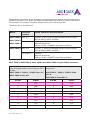
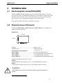
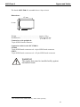
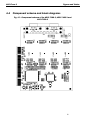
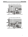
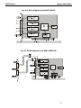
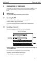
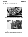
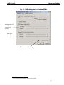
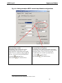
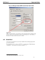
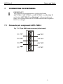
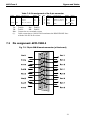
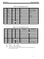
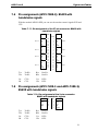
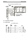
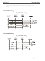
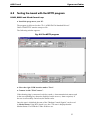
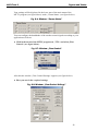
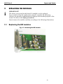
Important information
Communication boards
APCI-7300-3
APCI-7420-3
APCI-7500-3
APCI-7800-3
Pin assignments RS232 module
01.03-05/2008
Addi-data GmbH · Airpark Business Center · Airport Boulevard B210 · 77836 Rheinmünster · Germany
Phone +49 7229 1847-0 · Telefax +49 7229 1847-200 · info@ addi-data.com · www.addi-data.com
Please observe that during the migration to RoHS-compliant boards, the pin assignment
of RS232 changed. Thus, there are differences between the different revision numbers of
the printed circuit board. Therefore please check your revision number.
Thank you for your attention!
Board
Revision
number
Latest technical documentation
APCI-7300-3
Rev. A-C
See Rev. D, but with changed modem control signals
DCD & DSR at RS232 modules.
from Rev. D
Internet:
Manual download
Edition: 02.03 – 03/2007-b (and later editions)
Rev. A-B
See Rev. C, but with changed modem control signals
DCD & DSR at RS232 modules.
from Rev. C
Internet:
Manual download
Edition: 02.03 – 03/2007-b (and later editions)
APCI-7420-3
APCI-7500-3
APCI-7800-3
APCI-7300-3, APCI-7420-3, APCI-7500-3 and APCI-7800-3: 9-pin SUB-D connector
9-pin SUB-D connector pin assignment
with changed modem control signals DCD
& DSR.
APCI-7300-3, -7420-3, -7500-3: Rev. A-C
APCI-7800-3: Rev. A-B
Standard 9-pin SUB-D connector pin
assignment
APCI-7300-3, -7420-3, -7500-3: from
Rev. D
APCI-7800-3: from Rev. C
Pin-No.
Signal
Pin-No.
Signal
1
DSR
1
DCD
2
RXD
2
RXD
3
TXD
3
TXD
4
DTR
4
DTR
5
GND
5
GND
6
DCD
6
DSR
7
RTS
7
RTS
8
CTS
8
CTS
9
RI
9
RI
www.addi-data.com
APCI-7500-3: 37-pin SUB-D-connector
37-pin SUB-D connector pin assignment
with changed modem control signals DCD
& DSR.
APCI-7500-3: Rev. A-C
Pin-No.
Standard 37-pin SUB-D connector pin
assignment
APCI-7500-3: from Rev. D
Signal
Pin-No.
Signal
1, 10, 24, 33
DSR
1, 10, 24, 33
DCD
2, 11, 25, 34
RXD
2, 11, 25, 34
RXD
3, 12, 26, 35
TXD
3, 12, 26, 35
TXD
4, 13, 27, 36
DTR
4, 13, 27, 36
DTR
5, 14, 28, 37
GND
5, 14, 28, 37
GND
6, 15, 20, 29
DCD
6, 15, 20, 29
DSR
APCI-7800-3: 78-pin SUB-D connector
78-pin SUB-D connector pin assignment
Standard 78-pin SUB-D connector pin
with changed modem control signals DCD assignment
& DSR.
APCI-7800-3: Rev. A-B
Pin-No.
1, 6, 11, 16, 62, 67, 72, 77
APCI-7800-3: from Rev. C
Signal
Pin-No.
Signal
RI
1, 6, 11, 16, 62, 67, 72, 77
2, 7, 12, 17, 63, 68, 73, 78
DTR
2, 7, 12, 17, 63, 68, 73, 78
DTR
3, 8, 13, 18, 40, 64, 69, 74
GND
3, 8, 13, 18, 40, 64, 69, 74
GND
4, 9, 14, 20, 60, 65, 70, 75,
TXD
4, 9, 14, 20, 60, 65, 70, 75,
TXD
5, 10, 15, 19, 61, 66, 71, 76
RXD
5, 10, 15, 19, 61, 66, 71, 76
RXD
21, 23, 26, 31, 36, 48, 53, 58
DCD
21, 23, 26, 31, 36, 48, 53, 58
DSR
22, 27, 32, 37, 44, 49, 54, 59
DSR
22, 27, 32, 37, 44, 49, 54, 59
DCD
23, 28, 33, 38, 41, 45, 50, 55
CTS
23, 28, 33, 38, 41, 45, 50, 55
CTS
24, 29, 34, 39, 42, 46, 51, 56
RTS
24, 29, 34, 39, 42, 46, 51, 56
RTS
www.addi-data.com
RI
Should you have questions
that you do not find in the manual
or on our website (http://www.addi-data.com),
please contact us by phone or e-mail:
[email protected]
Addi-data GmbH · Airpark Business Center · Airport Boulevard B210 · 77836 Rheinmünster · Germany
Phone +49 7229 1847-0 · Telefax +49 7229 1847-200 · [email protected] · www.addi-data.com
DIN EN ISO 9001:2000
certified
ADDI-DATA GmbH
Airpark Business Center
Airport Boulevard B210
77836 Rheinmünster
Germany
+49 7229 1847-0
Technical description
APCI-7300-3, APCI-7420-3,
APCI-7500-3(/4C), APCI-7800-3
1-port, 2-port, 4-port, 8-port serial
interface for the PCI bus
Edition: 02.05 - 12/2009
Product information
This manual contains the technical installation and important instructions for correct commissioning
and usage, as well as production information according to the current status before printing.
The content of this manual and the technical product data may be changed without prior notice.
ADDI-DATA GmbH reserves the right to make changes to the technical data and the materials
included herein.
Warranty and liability
The user is not permitted to make changes to the product beyond the intended use, or to interfere with
the product in any other way.
ADDI-DATA shall not be liable for obvious printing and phrasing errors. In addition, ADDI DATA, if
legally permissible, shall not be liable for personal injury or damage to materials caused by improper
installation and/or commissioning of the board by the user or improper use, for example, if the board is
operated despite faulty safety and protection devices, or if notes in the operating instructions regarding
transport, storage, installation, commissioning, operation, thresholds, etc. are not taken into
consideration. Liability is further excluded if the operator changes the board or the source code files
without authorisation and/or if the operator is guilty of not monitoring the permanent operational
capability of working parts and this has led to damage.
Copyright
This manual, which is intended for the operator and its staff only, is protected by copyright.
Duplication of the information contained in the operating instructions and of any other product
information, or disclosure of this information for use by third parties, is not permitted, unless this right
has been granted by the product licence issued. Non-compliance with this could lead to civil and
criminal proceedings.
ADDI-DATA software product licence
Please read this licence carefully before using the standard software. The customer is only granted the
right to use this software if he/she agrees with the conditions of this licence.
The software must only be used to set up the ADDI-DATA boards.
Reproduction of the software is forbidden (except for back-up and for exchange of faulty data
carriers). Disassembly, decompilation, decryption and reverse engineering of the software are
forbidden. This licence and the software may be transferred to a third party if this party has acquired a
board by purchase, has agreed to all the conditions in this licence contract and the original owner does
not keep any copies of the software.
Trademarks
- ADDI-DATA is a registered trademark of ADDI-DATA GmbH.
- Turbo Pascal, Delphi, Borland C, Borland C++ are registered trademarks of Borland Insight
Company.
- Microsoft C, Visual C++, Windows XP, 98, Windows 2000, Windows 95, Windows NT,
EmbeddedNT and MS DOS are registered trademarks of Microsoft Corporation.
- LabVIEW, LabWindows/CVI, DasyLab, Diadem are registered trademarks of National Instruments
Corp.
- CompactPCI is a registered trademark of PCI Industrial Computer Manufacturers Group.
- VxWorks is a registered trademark of Wind River Systems Inc.
WARNING
The following risks result from improper implementation
and from use of the board contrary to the regulations:
♦ Personal injury
♦ Damage to the board, PC and peripherals
♦ Pollution of the environment
♦
Protect yourself, the others and the environment!
♦
Read carefully the safety precautions
(yellow leaflet).
If this leaflet is not with the documentation, please contact
us and ask for it.
♦
Observe the instructions of the manual.
Make sure that you do not forget or skip any step.
We are not liable for damages resulting from a wrong use
of the board.
♦
i
Used symbols:
IMPORTANT!
designates hints and other useful information.
WARNING!
It designates a possibly dangerous situation.
If the instructions are ignored the board, PC and/or peripheral may
be destroyed.
3
Contents
APCI-7xxx-3
1
DEFINITION OF APPLICATION ............................... 8
1.1
Intended use ....................................................................8
1.2
Usage restrictions.............................................................8
1.3
General description of the board ....................................8
2
USER .................................................................. 11
2.1
Qualification ..................................................................11
2.2
Country-specific regulations .........................................11
3
HANDLING OF THE BOARD.................................. 12
4
TECHNICAL DATA ............................................... 13
4.1
Electromagnetic compatibility (EMC) ............................13
4.2
Physical set-up of the board ..........................................13
4.3
Limit values.....................................................................15
4.3.1
4.3.2
4.3.3
RS232.................................................................................. 16
RS422, RS485 ...................................................................... 16
20mA constant current loop (MXTTY)................................... 17
4.4
Component scheme and block diagrams.....................18
5
INSTALLATION OF THE BOARD ............................. 24
5.1
Opening the PC..............................................................24
5.2
Selecting a free slot .......................................................24
5.3
Plugging the board into the slot ....................................25
5.4
Closing the PC ...............................................................25
6
BOARD CONFIGURATION ................................... 26
6.1
Configuration under Windows XP/2000/95/98/ Server 2003
26
6.2
Board test .......................................................................30
6.3
Questions and software downloads on the web............31
7
CONNECTING THE PERIPHERAL........................... 32
7.1
Connector pin assignment: APCI-7500-3 ......................32
7.2
Pin assignment: APCI-7420-3, APCI-7300-3 and APCI-75003(/4C) 33
7.3
Pin assignment: APCI-7800-3.........................................34
7.4
Pin assignments (APCI-7500-3): RS422 with handshake
signals 39
4
Contents
APCI-7xxx-3
7.5
Pin assignments (APCI-7420-3 and APCI-7300-3): RS422 with
handshake signals .....................................................................39
7.6
Connection cable – APCI-7500-3 ..................................40
7.7
Connection examples....................................................41
7.7.1
7.7.3
APCI-7500-3 ........................................................................ 41
RS232 cabling .....................................................................41
RS422 cabling .....................................................................41
RS485 cabling .....................................................................42
Current loop (20 mA) cabling ..............................................42
APCI-7300-3, APCI-7420-3, APCI-7500-3/4C ....................... 44
RS232 cabling .....................................................................44
RS422 cabling .....................................................................45
RS485 cabling .....................................................................45
Current loop (20 mA) cabling ..............................................46
APCI-7800-3 ........................................................................ 48
7.8
Connection examples....................................................49
7.8.1
7.8.2
7.8.3
7.8.4
RS232 cabling ..................................................................... 49
RS422 cabling ..................................................................... 50
RS485 cabling ..................................................................... 50
Current Loop (20 mA) cabling ............................................. 51
8
TESTING THE BOARD ........................................... 53
8.1
Connecting a shorting plug ...........................................53
8.2
Testing the board with the MTTTY program.....................55
7.7.2
RS422, RS232 and 20 mA Current Loop ..............................55
RS485 ..................................................................................57
9
REPLACING THE MODULES.................................. 58
9.1
Replacing the MX modules ............................................58
10
GLOSSARY.......................................................... 60
11
INDEX ................................................................ 63
5
APCI-7xxx-3
Figures and Tables
Figures
Fig. 3-1: Correct handling.........................................................................12
Fig. 4-1: Component scheme of the APCI-7300-3, APCI-7420-3 and APCI7500-3 .....................................................................................18
Fig. 4-2: Component scheme of the APCI-7800-3...................................19
Fig. 4-3: Component scheme of the APCI-7800-3 (solder side) ...............20
Fig. 4-4: Block diagram of the APCI-7300-3..............................................21
Fig. 4-5: Block diagram of the APCI-7420-3..............................................21
Fig. 4-6: Block diagram of the APCI-7500-3..............................................22
Fig. 4-7: Block diagram of the APCI-7500-3/4C........................................22
Fig. 4-8: Block diagram of the APCI-7800-3..............................................23
Fig. 5-1: Slot types.....................................................................................24
Fig. 5-2: Inserting the board......................................................................25
Fig. 5-3: Fastening the board at the back cover......................................25
Fig. 6-1: FIFO settings under Windows 2000 ..........................................27
Fig. 6-2: Setting example: RS485 ..........................................................28
Fig. 6-3: Setting example: MXTTY current loop: Module configuration ..29
Fig. 6-4: Setting example: MXTTY current loop: Input clock ...................30
Fig. 7-1: 37-pin SUB-D male connector (of the board)..............................32
Fig. 7-2: 9-pin SUB-D male connector ......................................................33
Fig. 7-3: 78-pin SUB-D female connector (of the board) ..........................34
Fig. 7-4: Connection cable ST074 (4 x 25-pin)..........................................40
Fig. 7-5: Connection cable ST075 (4 x 9-pin)............................................40
Fig. 7-6: RS232 cabling - 4-port interface .................................................41
Fig. 7-7: RS422 cabling - 4-port interface .................................................41
Fig. 7-8: RS485 cabling - 4-port interface .................................................42
Fig. 7-9: Active transmission/active reception 4-port serial interface ........42
Fig. 7-10: Active transmission/passive reception 4-port serial interface ....43
Fig. 7-11: Passive transmission/active reception 4-port serial interface ....43
Fig. 7-12: Passive transmission/passive reception 4-port serial interface ..44
Fig. 7-13: RS232 cabling - 9-pin connector..............................................44
Fig. 7-14: RS422 cabling - 9-pin connector..............................................45
Fig. 7-15: RS485 cabling - 9-pin connector..............................................45
Fig. 7-16: Active transmission/active reception 9-pin connector..............46
Fig. 7-17: Active transmission/passive reception 9-pin connector ............46
Fig. 7-18: Passive transmission/active reception 9-pin connector ............47
Fig. 7-19: Passive transmission/passive reception 9-pin connector ..........47
Fig. 7-20: Connection cable ST7809 (8 x 9 pin) ........................................48
Fig. 7-21: Connection cable ST7825 (8 x 25 pin) ......................................49
Fig. 7-22: RS232 cabling...........................................................................49
Fig. 7-23: RS422 cabling...........................................................................50
Fig. 7-24: RS485 cabling...........................................................................50
Fig. 7-25: Active transmission/active reception ........................................51
Fig. 7-26: Active transmission/passive reception ......................................51
Fig. 7-27: Active transmission/passive reception – 4-fold interface ..........52
Fig. 7-28: Passive transmission/passive reception .....................................52
Fig. 8-1: Connection of the shorting plug RS232 ......................................53
6
APCI-7xxx-3
Figures and Tables
Fig. 8-2: Connection of the shorting plug RS422 ...................................... 53
Fig. 8-3: Connection of the shorting plug for 20 mA Current Loop – active
transmission/passive reception................................................ 54
Fig. 8-4: Connection of the shorting plug for 20 mA current Loop – passive
transmission / active reception................................................ 54
Fig. 8-5: The MTTTY program ..................................................................... 55
Fig. 8-6: Window: “Comm Status” ............................................................ 56
Fig. 8-7: Window: „Flow Control“............................................................... 56
Fig. 8-8: Window: „Flow Control Settings”.................................................. 56
Fig. 9-1: Removing the MX module ......................................................... 58
Fig. 9-2: Inserting the MX module............................................................. 59
Tables
Table 1-1: Different communication operating modes .......................... 10
Table 7-1: Pin assignment of the 37-pin connector ................................. 34
Table 7-2: Pin assignment of the 9-pin connector ................................... 35
Table 7-3: Pin assignment of port 1 .......................................................... 36
Table 7-4: Pin assignment of port 2 ......................................................... 37
Table 7-5: Pin assignment of port 3 ......................................................... 37
Table 7-6: Pin assignment of port 4 ......................................................... 38
Table 7-7: Pin assignment of port 5 ......................................................... 38
Table 7-8: Pin assignment of port 6 .......................................................... 39
Table 7-9: Pin assignment of port 7 ......................................................... 39
Table 7-10: Pin assignment of port 8 ....................................................... 40
Table 7-11: Pin assignment of the 37-pin connector: RS422 with
handshake signals................................................................... 41
Table 7-12: Pin assignment of the 9-pin connector: RS422 with
handshake signals................................................................... 41
Table 10-1: Glossary................................................................................. 61
7
APCI-7xxx-3
Figures and Tables
1
DEFINITION OF APPLICATION
1.1
Intended use
The board APCI-7xxx-3 1 must be inserted in a PC with PCI 5V/32 bit (PCI
3.3V/32 Bit) which is used as electrical equipment for measurement, control and
laboratory pursuant to the norm EN 61010-1 (IEC 61010-1). The used personal
computer (PC) must fulfil the requirements of IEC 60950-1 or EN 60950-1 and
55022 or IEC/CISPR 22 and EN 55024 or IEC/CISPR 24.
The use of the board APCI-7xxx-3 in combination with external screw terminal
panels requires correct installation according to IEC 60439-1 or EN 60439-1
(switch cabinet / switch box).
1.2
Usage restrictions
The APCI-7xxx-3 board must not to be used as safety related part (SRP).
The board must not be used for safety related functions, for example for
emergency stop functions.
The APCI-7xxx-3 board must not be used in potentially explosive atmospheres.
The APCI-7xxx-3 board must not be used as electrical equipment according to
the Low Voltage Directive 2006/95/EC.
1.3
General description of the board
The board APCI-7xxx-3 provides the personal computer (PC) with 1-port, 2-port,
4-port or 8-port asynchronous serial interface for the communication with external
devices:
Board
Interface
APCI-7300-3
1-port
APCI-7420-3
2-port
APCI-7500-3,
APCI-7500-3/4C
4-port
APCI-7800-3
8-port
The operating mode of the interface depends on the MX modules installed.
1 Common designation in the manual for the boards APCI-7300-3, APCI-7420-3, APCI-7500-3,
APCI-7500-3/4C and APCI-7800-3
8
APCI-7xxx-3
Figures and Tables
The board is to be connected to the peripheral through a shielded cable, which
shielding should be grounded on both ends.
Minimum specifications of the connection cable:
- metallised plastic hoods
- shielded cable
- cable shield folded back and firmly screwed to the connector housing.
The board supports serial communication through 1, 2 or 4 asynchronous serial
ports. The use of the board depends on the following parameters (See table
below).
Table 1-1: Different communication operating modes
Plug-in
module 1
Transmission
standard
Maximum
transmission
rate 2
MX232
RS232
115 kbps
Optical
isolation
no
MX232-G
1 kV
MX422
no
MX422-G
MX422-PEP
(RTS/CTS as
RS422)
RS422
115 kbps
MX485
RS485
TTY (20 mA
current loop)
19.2 kbps
-
30 m
-
1.2 km
no
automatic
transmitter control
1 kV
automatic
transmitter control
1 kV
standby current on
transmit and
receive channel
115 kbps
MX485-G
MXTTY
1 kV
Interface setting
Distance
between
transmitter
and receiver 3
1.2 km
1 km
If the basic board APCI-7xxx-3 is used with optically isolated modules and non
isolated modules, then the safety built by the creeping distance of 3.2 mm is not
ensured for the non isolated modules.
Check the shielding capacity of the PC housing and cable prior to putting the
device into operation.
The use of the board includes observing all advises given in this manual and in the
safety leaflet.
1
MXxxx-G: MX232-G, for example, stands for a plug-in module with the RS232 standard.
The -G suffix means that the module is optically isolated. The MXTTY module is always
optically isolated.
2 Transfer rates > 115 kbps on the board xPCI-7xx0 are possible up to 1 Mbps by means of an
equipment option.
3 The indicated maximum lengths apply to normal interface cables (shielded control lead,
0.14 mm²). The length is also limited by the number of users, impedance, line capacity and
transfer rate.
9
APCI-7xxx-3
Figures and Tables
Uses beyond these specifications are not allowed. The manufacturer is not liable
for any damages which would result from the non-observance of this clause.
Make sure that the board remains in the protective blister pack
until it is used.
For all operating modes, the signal lines are to be twisted in pairs with GND.
Use exclusively connection cable with twisted pairs.
The housing of the peripheral connector
- is to be firmly screwed together with the shield of the cable.
- is to assure a low-resistance connection (< 100 mΩ) between the shield and the
housing of the PC.
The shield of the cable is to be earthed on both ends.
Do not remove or alter the identification numbers of the board.
If you do, the guarantee expires.
10
APCI-7xxx-3
2
USER
2.1
Qualification
Figures and Tables
Only persons trained in electronics are entitled to perform the following works:
- installation
- use
- maintenance
2.2
Country-specific regulations
Consider the country-specific regulations about:
- the prevention of accidents
- electrical and mechanical installations
- radio interference suppression
11
APCI-7xxx-3
3
Figures and Tables
HANDLING OF THE BOARD
Fig. 3-1: Correct handling
12
APCI-7xxx-3
Figures and Tables
4
TECHNICAL DATA
4.1
Electromagnetic compatibility (EMC)
The board APCI-7xxx-3 complies with the European EMC directive. The tests
were carried out by a certified EMC laboratory in accordance with the norm from
the EN 61326 series (IEC 61326). The limit values as set out by the European
EMC directive for an industrial environment are complied with.
The respective EMC test report is available on request.
4.2
Physical set-up of the board
The boards APCI-7500-3, APCI-4720-3 and APCI-7300-3 are assembled on a
4-layer printed circuit card.
Dimensions:
151 mm
99 mm
Weight: ...................................................... approx. 120 g
Installation in: ........................................... 32/64-bit PCI slot
(5 V and 3.3 V)
Connection to the peripheral:
APCI-7300-3: ........................................... 9-pin SUB-D male connector
APCI-7420-3: ........................................... 2 x 9-pin male SUD-D male connector
APCI-7500-3: ........................................... 37-pin SUB-D male connector
APCI-7500-3/4C: ..................................... 4 x 9-pin SUB-D male connector with 2nd slot
Connection cables for the APCI-7500-3 1 :
ST074:
37-pin SUB-D female connector to 4 x 25-pin SUB-D male connector
ST075:
37-pin SUB-D female connector to 4 x 9-pin SUB-D male connector
WARNING!
The supply lines must be installed safely against mechanical
loads.
1
Not included in the standard delivery.
13
APCI-7xxx-3
Figures and Tables
The board APCI-7800-3 is assembled on a 6-layer circuit.
Dimensions:
175 mm
99 mm
Weight: ..................................................... approx. 150 g
Installation in: ........................................... 32/64-bit PCI slot
(5 V and 3.3 V)
Connection to the peripheral:
78-pin SUB-D female connector
Connection cable for the APCI-7800-3 1
ST7809:
78-pin SUB-D male connector to 8 x 9 pin SUB-D male connector
ST075:
78-pin SUB-D male connector to 8 x 25-pin SUB-D male connector
WARNING!
The supply lines must be installed safely against
mechanical loads.
1
Not contained in the standard delivery. Please order separately.
14
APCI-7xxx-3
4.3
Figures and Tables
Limit values
Max. altitude: ............................................ 2000 m
Operating temperature: .............................. 0 to 60°C
Storage temperature: ................................. -25 to 70°C
Relative humidity at indoor installation
50% at +40 °C
80% at +31 °C
Minimum PC requirements:
PCI BIOS from Version 1.0
Bus speed: ................................................. < 33 MHz
Operating system: ..................................... Windows Vista (32-bit), XP, 2000,
Linux
Energy requirements:
- Operating voltage of the PC: .................. 5 V ± 5%
- Current consumption (without load): ...... typ. see table ± 10%
+ 5 V from PC
APCI-7300-3
APCI-7400-3
APCI-7500-3
APCI-7800-3
160 mA
160 mA
160 mA
220 mA
Add to this data the current consumption of the used modules according to the
following table:
MXxxx
MXxxx-G
RS 232
10 mA
86 mA
RS 422
10 mA
46 mA
RS 485
10 mA
58 mA
20 mA
75 mA
-
-
66 mA
MX 422-PEP 1
1
With software handshake (RTS CTS version)
15
APCI-7xxx-3
Figures and Tables
4.3.1 RS232
CCITT-recommendation: ......................... V.24
US-Norm EIA: .......................................... RS 232
Without optical isolation (MX232)
Max. transfer rate: ................................... 1 MBaud
Transfer rate on request ........................... Up to 2.5 MBaud
ESD protection ....................................... 15 kV
With optical isolation (MX232-G)
Max. transfer rate: ................................... 1 MBaud
Transfer rate on request ........................... Up to 2.5 MBaud
ESD protection ....................................... 15 kV
Creeping distance: .................................. 3.2 mm
Test voltage: ............................................ 1000 VAC
Short-circuit protection
4.3.2 RS422, RS485
CCITT recommendation: .......................... V.11
US norm EIA: ........................................... RS422, RS485
Without optical isolation (MX422, MX485)
Max. transfer rate: .................................... 1 MBaud
Transfer rate on request ............................ Up to 2.5 MBaud
ESD protection ........................................ 15 kV
Transorb diodes
With optical isolation (MX422-G, MX485-G)
Max. transfer rate: .....................................
Transfer rate on request .............................
ESD protection .........................................
Creeping distance: ....................................
Test voltage: ..............................................
Short-circuit protection
1 Mbaud
Up to 2.5 MBaud
15 kV
3.2 mm
1000 VAC
16
APCI-7xxx-3
Figures and Tables
4.3.3 20mA constant current loop (MXTTY)
Max. Baud rate:....................................... 19.2 kBaud
Transorb diodes: ..................................... 400 W
Absorption power
Creeping distance: .................................. 3.2 mm
Test voltage: ............................................ 1000 VAC
Load: ....................................................... 500 Ω
Voltage reversal and short-circuit protection through transorb diodes
i
IMPORTANT!
Basic board and 1MBd configuration (option): Please check that the
quartz frequency is correctly set in ADDIREG or in the device
manager of your operating system. See 6.1 for Windows XP/2000.
The 1M Baud rate can only be programmed with the device drivers
delivered with the board.
17
APCI-7xxx-3
4.4
Figures and Tables
Component scheme and block diagrams
Fig. 4-1: Component scheme of the APCI-7300-3, APCI-7420-3 and
APCI-7500-3
18
APCI-7xxx-3
Figures and Tables
Fig. 4-2: Component scheme of the APCI-7800-3
19
APCI-7xxx-3
Figures and Tables
Fig. 4-3: Component scheme of the APCI-7800-3 (solder side)
20
APCI-7xxx-3
Figures and Tables
Fig. 4-4: Block diagram of the APCI-7300-3
Fig. 4-5: Block diagram of the APCI-7420-3
21
APCI-7xxx-3
Figures and Tables
Fig. 4-6: Block diagram of the APCI-7500-3
Fig. 4-7: Block diagram of the APCI-7500-3/4C
22
APCI-7xxx-3
Figures and Tables
Fig. 4-8: Block diagram of the APCI-7800-3
23
APCI-7xxx-3
5
Figures and Tables
INSTALLATION OF THE BOARD
The interrupt lines and base address of the board are allocated by the BIOS of the
PC system through software. No setting is then required before inserting the
board.
i
5.1
IMPORTANT!
Do observe the safety precautions (yellow leaflet)!
Opening the PC
♦ Switch off your PC and all the units connected to the PC
♦ Pull the PC mains plug from the socket.
♦ Open your PC as described in the manual of the PC manufacturer.
5.2
Selecting a free slot
♦ Insert the board in a free PCI-5 V or 3.3 V slot (32/64-bit).
Fig. 5-1: Slot types
♦ Remove the back cover of the selected slot according to the instructions of
the PC manufacturer.
Keep the back cover. You will need it if you remove the board
♦ Discharge yourself from electrostatic charges.
♦ Take the board out of its protective pack.
24
APCI-7xxx-3
5.3
Figures and Tables
Plugging the board into the slot
♦ Insert the board vertically into the chosen slot.
Fig. 5-2: Inserting the board
♦ Fasten the board to the rear of the PC housing with the screw which was
fixed on the back cover.
Fig. 5-3: Fastening the board at the back cover
♦ Tighten all the loosen screws.
5.4
Closing the PC
♦ Close your PC as described in the manual of the PC manufacturer.
25
APCI-7xxx-3
6
Figures and Tables
BOARD CONFIGURATION
In this chapter you will find a description of the delivered software and its
possible applications.
i
IMPORTANT!
Further information for installing and uninstalling the different
drivers is to be found in the delivered description
"Installation instructions for the PCI and ISA bus".
A link to the corresponding PDF file is available in the navigation pane
(Bookmarks) of Acrobat Reader.
The board is supplied with a driver CD-ROM (CD1) containing:
- ADDICOM software samples with API function for the ADDI-DATA boards
in 32-bits
6.1
Configuration under Windows XP/2000/95/98/
Server 2003
In the Windows device manager you can set the different interfaces according to
your requirements through double click.
Start the device manager of your operating system under Start/(Settings)/Control
panel/System
In the "FIFO" register the following settings are possible:
26
APCI-7xxx-3
Figures and Tables
Fig. 6-1: FIFO settings under Windows 2000 ∗
PCI bus and
device number
Management of
the transmitter
and receiver
buffer
Data flow
control
Reset the standard settings
∗
The example shows the settings under Windows 2000
27
APCI-7xxx-3
Figures and Tables
Under "Setting" you adapt the operating mode to the used interface.
Fig. 6-2: Setting example: RS485 ∗
RS 485 echo enable: For the control of the receiver at RS485 half duplex
communication:
Checked :During sending of data of the board to the peripheral, the receiver of
the board is released.
Not checked : During sending of data of the board to the peripheral, the
receiver of the board is blocked.
∗
The example shows the settings under Windows 2000
28
APCI-7xxx-3
Figures and Tables
Fig. 6-3: Setting example: MXTTY current loop: Module configuration ∗
Current flows (send):
Definition of the current flow in the
transmitting current loop, i.e. the
non-operative connection of the board
APCI-7xxx-3 (sender) to the peripheral
device (receiver) (no serial data flow):
: Current flows
Checked
Not checked
: No current flows
∗
Current flows (reception):
Definition of the current flow in the receiving
current loop, i.e. the non-operative connection of
the board APCI-7xxx-3 (receiver) to the
peripheral device (sender) (no data flow):
: Current flows
Checked
Not checked
: No current flows
The example shows the settings under Windows 2000
29
APCI-7xxx-3
Figures and Tables
Fig. 6-4: Setting example: MXTTY current loop: Input clock ∗
Input clock:
Under ”Crystal frequency“ the frequency of the integrated quartz oscillator of the
board is indicated. The standard PC quartz crystal frequency is 1.8432 MHz, so
that the max. baud rate that can be set is 115200.
6.2
Board test
You can test if you board is not correctly installed with a shorting plug and the
test software MTTTY.
The setup file for the test software MTTTY is supplied on the CD-ROM under
CD/MMTTY. The program is described in chapter 7.7.3.
∗
The example shows the settings under Windows 2000
30
APCI-7xxx-3
6.3
Figures and Tables
Questions and software downloads on the web
Do not hesitate to e-mail us your questions.
per e-mail:
[email protected]
Free downloads of standard software
You can download the latest version of the software for the board APCI-7xxx-3
http://www.addi-data.com.
i
IMPORTANT!
Before using the board or in case of malfunction during
operation, check if there is an update of the product (technical
description, driver). The current version can be found on the
internet or contact us directly.
31
APCI-7xxx-3
7
CONNECTING THE PERIPHERAL
i
7.1
Figures and Tables
IMPORTANT!
The connector pin assignments are valid for the boards
APCI-7300-3, APCI-7420-3 and APCI-7500-3 from Revision D
and for the APCI-7800-3 from Revision C of the printed circuit
board. At revisions before the DCD/DSR modem control signals at
RS232 are changed.
Connector pin assignment: APCI-7500-3
Fig. 7-1: 37-pin SUB-D male connector (of the board)
32
APCI-7xxx-3
Figures and Tables
Table 7-1: Pin assignment of the 37-pin connector
RS485
RS422
Current Loop
RS232
Pin
RS232
Current Loop
RS422
DCD
RxD
TxD
DTR
GND
DSR
RTS
CTS
RI
DCD
RxD
TxD
DTR
GND
DSR
RTS
CTS
RI
+XMIT-CL-DATA TA
-XMIT-CL-DATA TB
+RCV-CL-DATA RA
RS485
Pin
120 Ω
100 Ω
Tx/Rx-
RB
TA
TB
Tx/Rx+ RA
Rab (1)
GND
GND
120 Ω 100 Ω
Tx/Rx-
RB
TA
TB
Tx/Rx+ RA
Rab (1)
GND
GND
TA:
TB:
Rab:
(1):
7.2
DSR
RTS
CTS
RI
DCD
RxD
TxD
DTR
GND
GND
DSR
Tsource
RTS
Rsource
CTS
-RCV-CL-DATA
RI
+XMIT-CL-DATA DCD
-XMIT-CL-DATA RxD
+RCV-CL-DATA TxD
DTR
GND
GND
Tsource
Rsource
-RCV-CL-DATA
+XMIT-CL-DATA
-XMIT-CL-DATA
+RCV-CL-DATA
20
21
22
23
24
25
26
27
28
29
30
31
32
33
34
35
36
37
1
2
3
4
5
6
7
8
9
10
11
12
13
14
15
16
17
18
19
Port 4
Tx/Rx+
Rab (1)
GND
GND
100 Ω 120 Ω
GND
Tsource
Rsource
-RCV-CL-DATA
+XMIT-CL-DATA
-XMIT-CL-DATA
+RCV-CL-DATA
Port 3
RB
TA
TB
RA
Tx/RxPort 2
Tx/Rx+
Rab (1)
GND
GND
100 Ω 120 Ω
GND
Tsource
Rsource
-RCV-CL-DATA
Port 1
RB
Tx422+
RA: Rx422+
Tx422RB: Rx422Connection to a terminal resistor
Cable connection to 100 Ω/120 Ω terminates the RS422/RS485 lines
with the 100 Ω/120 Ω resistor.
Pin assignment: APCI-7420-3, APCI-7300-3 and
APCI-7500-3(/4C)
Fig. 7-2: 9-pin SUB-D male connector
33
Tx/Rx-
APCI-7xxx-3
Figures and Tables
Table 7-2: Pin assignment of the 9-pin connector
RS485
120 Ω
Tx/Rx-
RS422
100 Ω
RB
TA:
TB:
Rab:
(1):
7.3
Current Loop
Tsource
Rsource
-RCV-CL-DATA
RS232
DSR
RTS
CTS
RI
Pin
6
7
8
9
Pin
1
2
3
4
5
RS232
DCD
RxD
TxD
DTR
GND
Current Loop
+XMIT-CL-DATA
-XMIT-CL-DATA
+RCV-CL-DATA
GND
RS422 RS485
TA
TB
RA
Tx/Rx+
Rab (1)
GND
GND
Tx422+
RA: Rx422+
Tx422RB: Rx422Connection to a terminal resistor
Cable connection to 100 Ω/120 Ω terminates the RS422/RS485 lines
with the 100 Ω/120 Ω resistor.
Pin assignment: APCI-7800-3
Fig. 7-3: 78-pin SUB-D female connector (of the board)
34
APCI-7xxx-3
Figures and Tables
Table 7-3: Pin assignment of port 1
Pin
RS 232
RS 422
20
TxD
RA
19
RxD
TB
18
RS 485
Tx / Rx +
RS422PEP
Current Loop
Rx+
+RCV-CL-DATA
Tx-
-XMIT-CL-DATA
GND
GND
GND
39
RTS
RTS-
Tsource
38
CTS
RTS+
Rsource
59
DCD
TA
Tx+
+XMIT-CL-DATA
58
DSR
100 Ω
78
DTR
Rab
77
RI
RB
120 Ω
CTS+
CTS-
Tx / Rx -
RX-
-RCV-CL-DATA
Table 7-4: Pin assignment of port 2
Pin
RS 232
RS 422
75
TxD
RA
76
RxD
TB
57
-
74
RS 485
Tx / Rx +
RS422PEP
Current Loop
Rx+
+RCV-CL-DATA
Tx-
-XMIT-CL-DATA
GND
GND
GND
56
RTS
RTS-
Tsource
55
CTS
RTS+
Rsource
37
DCD
TA
Tx+
+XMIT-CL-DATA
36
DSR
100 Ω
17
DTR
Rab
16
RI
RB
120 Ω
CTS+
CTS-
Tx / Rx -
RX-
-RCV-CL-DATA
35
APCI-7xxx-3
Figures and Tables
Table 7-5: Pin assignment of port 3
Pin
RS 232
RS 422
14
TxD
RA
15
RxD
TB
35
-
13
RS 485
Tx / Rx +
RS422PEP
Current Loop
Rx+
+RCV-CL-DATA
Tx-
-XMIT-CL-DATA
GND
GND
GND
34
RTS
RTS-
Tsource
33
CTS
RTS+
Rsource
54
DCD
TA
Tx+
+XMIT-CL-DATA
53
DSR
100 Ω
73
DTR
Rab
72
RI
RB
120 Ω
CTS+
CTS-
Tx / Rx -
RX-
-RCV-CL-DATA
Table 7-6: Pin assignment of port 4
Pin
RS 232
RS 422
70
TxD
RA
71
RxD
TB
69
GND
52
-
51
RS 485
Tx / Rx +
RS422PEP
Current Loop
Rx+
+RCV-CL-DATA
Tx-
-XMIT-CL-DATA
GND
GND
RTS
RTS-
Tsource
50
CTS
RTS+
Rsource
32
DCD
TA
Tx+
+XMIT-CL-DATA
31
DSR
100 Ω
12
DTR
Rab
11
RI
RB
120 Ω
CTS+
CTS-
Tx / Rx -
RX-
-RCV-CL-DATA
36
APCI-7xxx-3
Figures and Tables
Table 7-7: Pin assignment of port 5
Pin
RS 232
RS 422
9
TxD
RA
10
RxD
TB
8
GND
30
-
29
RS 485
Tx / Rx +
RS422PEP
Current Loop
Rx+
+RCV-CL-DATA
Tx-
-XMIT-CL-DATA
GND
GND
RTS
RTS-
Tsource
28
CTS
RTS+
Rsource
49
DCD
TA
Tx+
+XMIT-CL-DATA
48
DSR
100 Ω
68
DTR
Rab
67
RI
RB
120 Ω
CTS+
CTS-
Tx / Rx -
RX-
-RCV-CL-DATA
Table 7-8: Pin assignment of port 6
Pin
RS 232
RS 422
65
TxD
RA
66
RxD
TB
64
GND
47
-
46
RS 485
Tx / Rx +
RS422PEP
Current Loop
Rx+
+RCV-CL-DATA
Tx-
-XMIT-CL-DATA
GND
GND
RTS
RTS-
Tsource
45
CTS
RTS+
Rsource
27
DCD
TA
Tx+
+XMIT-CL-DATA
26
DSR
100 Ω
7
DTR
Rab
6
RI
RB
120 Ω
CTS+
CTS-
Tx / Rx -
RX-
-RCV-CL-DATA
37
APCI-7xxx-3
Figures and Tables
Table 7-9: Pin assignment of port 7
Pin
RS 232
RS 422
4
TxD
RA
5
RxD
TB
3
GND
25
-
24
RS 485
Tx / Rx +
RS422PEP
Current Loop
Rx+
+RCV-CL-DATA
Tx-
-XMIT-CL-DATA
GND
GND
RTS
RTS-
Tsource
23
CTS
RTS+
Rsource
44
DCD
TA
Tx+
+XMIT-CL-DATA
43
DSR
100 Ω
63
DTR
Rab
62
RI
RB
120 Ω
Tx / Rx -
CTS+
CTS-
CTS-
RTS-
-RCV-CL-DATA
Table 7-10: Pin assignment of port 8
Pin
RS 232
RS 422
RS 485
Current Loop
60
TxD
RA
61
RxD
TB
40
GND
GND
42
RTS
RTS-
Tsource
41
CTS
RTS+
Rsource
22
DCD
TA
Tx+
+XMIT-CL-DATA
21
DSR
Rab
CTS+
CTS+
2
DTR
100 Ω
120 Ω
CTS-
1
RI
RB
Tx / Rx -
RX-
TA:
TB:
Rab:
(1):
Tx / Rx +
RS422PEP
Rx+
+RCV-CL-DATA
Tx-
-XMIT-CL-DATA
-RCV-CL-DATA
Tx422+
RA: Rx422+
Tx422RB: Rx422Connection to the terminal resistor
Cable connection to 100 Ω/120 Ω terminates the lines RS422/RS485 with
the resistor 100 Ω/120 Ω.
38
APCI-7xxx-3
7.4
Figures and Tables
Pin assignments (APCI-7500-3): RS422 with
handshake signals
With the module MX422-PEP you can use the modem control signals RTS and
CTS.
Table 7-11: Pin assignment of the 37-pin connector: RS422 with
handshake signals
RS422
RS422
Pin
Pin
Port 4
Port 3
Port 2
Port 1
7.5
IA
CB
CA
RB
TA
TB
RA
IB
GND
IA
CB
CA
RB
TA
TB
RA
IB
GND
20
21
22
23
24
25
26
27
28
29
30
31
32
33
34
35
36
37
TA:
TB:
Tx422+
Tx422-
RA:
RB:
Rx422+
Rx422-
IA:
IB:
CTS+
CTS-
CA:
CB:
RTS+
RTS-
1
2
3
4
5
6
7
8
9
10
11
12
13
14
15
16
17
18
19
TA
TB
RA
IB
GND
IA
CB
CA
RB
TA
TB
RA
IB
GND
IA
CB
CA
RB
Port 4
Port 3
Port 2
Port 1
Pin assignments (APCI-7420-3 and APCI-7300-3):
RS422 with handshake signals
Table 7-12: Pin assignment of the 9-pin connector:
RS422 with handshake signals
RS422
IA
CB
CA
RB
Pin
6
7
8
9
TA:
TB:
Tx422+
Tx422-
RA:
RB:
Rx422+
Rx422-
IA:
IB:
CTS+
CTS-
CA:
CB:
RTS+
RTS-
Pin
1
2
3
4
5
RS422
TA
TB
RA
IB
GND
39
APCI-7xxx-3
7.6
Figures and Tables
Connection cable – APCI-7500-3
Fig. 7-4: Connection cable ST074 (4 x 25-pin)
*1
*2
Resistor integrated on the MX module
Cable connection to 100 Ω/120 Ω terminates the RS422/RS485 lines with
100 Ω/120 Ω resistor. (Wire bridges between pin 20 and 6)
Fig. 7-5: Connection cable ST075 (4 x 9-pin)
*1
*2
Resistor integrated on the MX module
Cable connection to 100 Ω/120 Ω terminates the RS422/RS485 lines with
100 Ω/120 Ω resistor. (Wire bridges between pin 4 and pin 6).
40
APCI-7xxx-3
7.7
Figures and Tables
Connection examples
7.7.1 APCI-7500-3
RS232 cabling
Fig. 7-6: RS232 cabling - 4-port interface
1 If the modem control signals are not used, they must be bridged externally via a
jumper.
RS422 cabling
Fig. 7-7: RS422 cabling - 4-port interface
41
APCI-7xxx-3
Figures and Tables
RS485 cabling
Fig. 7-8: RS485 cabling - 4-port interface
Current loop (20 mA) cabling
Active/passive: When a transmitter and a receiver communicate, one of them has
to supply the necessary current. If the transmitter supplies the current, it is active.
The receiver is passive. In reverse, if the receiver supplies the current, it is active.
Fig. 7-9: Active transmission/active reception
4-port serial interface
42
APCI-7xxx-3
Figures and Tables
Fig. 7-10: Active transmission/passive reception
4-port serial interface
Fig. 7-11: Passive transmission/active reception
4-port serial interface
43
APCI-7xxx-3
Figures and Tables
Fig. 7-12: Passive transmission/passive reception
4-port serial interface
7.7.2 APCI-7300-3, APCI-7420-3, APCI-7500-3/4C
RS232 cabling
Fig. 7-13: RS232 cabling - 9-pin connector
44
APCI-7xxx-3
Figures and Tables
RS422 cabling
Fig. 7-14: RS422 cabling - 9-pin connector
RS485 cabling
Fig. 7-15: RS485 cabling - 9-pin connector
45
APCI-7xxx-3
Figures and Tables
Current loop (20 mA) cabling
Fig. 7-16: Active transmission/active reception
9-pin connector
Fig. 7-17: Active transmission/passive reception
9-pin connector
46
APCI-7xxx-3
Figures and Tables
Fig. 7-18: Passive transmission/active reception
9-pin connector
Fig. 7-19: Passive transmission/passive reception
9-pin connector
47
APCI-7xxx-3
Figures and Tables
7.7.3 APCI-7800-3
Fig. 7-20: Connection cable ST7809 (8 x 9 pin)
48
APCI-7xxx-3
Figures and Tables
Fig. 7-21: Connection cable ST7825 (8 x 25 pin)
7.8
Connection examples
7.8.1 RS232 cabling
Fig. 7-22: RS232 cabling
49
APCI-7xxx-3
Figures and Tables
1: If the modem control signals are not used, they must be bridged via a wire
bridge.
7.8.2 RS422 cabling
Fig. 7-23: RS422 cabling
7.8.3 RS485 cabling
Fig. 7-24: RS485 cabling
50
APCI-7xxx-3
Figures and Tables
7.8.4 Current Loop (20 mA) cabling
Active/passive: When a transmitter and a receiver communicate, one of them has
to supply the necessary current. If the transmitter supplies the current, it is active.
The receiver is passive. In reverse, if the receiver supplies the current, it is active.
Fig. 7-25: Active transmission/active reception
Fig. 7-26: Active transmission/passive reception
51
APCI-7xxx-3
Figures and Tables
Fig. 7-27: Active transmission/passive reception – 4-fold interface
Fig. 7-28: Passive transmission/passive reception
52
APCI-7xxx-3
Figures and Tables
8
TESTING THE BOARD
8.1
Connecting a shorting plug
When using the shorting plug described below and the test program MTTTY you
can carry out a self-test of the board.
Please note the signal connection of the different ports through the 9-pin shorting
plug for the test: The recipient will be switched on the transmitter.
Fig. 8-1: Connection of the shorting plug RS232
Fig. 8-2: Connection of the shorting plug RS422
53
APCI-7xxx-3
Figures and Tables
Fig. 8-3: Connection of the shorting plug for 20 mA Current Loop –
active transmission/passive reception
Fig. 8-4: Connection of the shorting plug for 20 mA current Loop –
passive transmission / active reception
54
APCI-7xxx-3
8.2
Figures and Tables
Testing the board with the MTTTY program
RS422, RS232 and 20 mA Current Loop
♦ Install the program on your PC.
The program is delivered on the CD 1 “ADDI-DATA Standard Drivers”.
Under CD/MTTTY start the setup.exe file.
The following window appears:
Fig. 8-5: The MTTTY program
♦ Select the right COM interface under "Port".
♦ Connect it with "File/Connect".
If the shorting plug is connected, each key stroke (= data transmission) must result
in the corresponding key character displayed on the screen (= data reception). If
the test is successfully carried out, the board works.
Once the port is initialised the state of the "Modem Control Signals" can be read
in Modem Status. If the RTS signal is set, the CTS state is displayed under
Modem Status. For DTR the 3 other fields are set.
55
APCI-7xxx-3
Figures and Tables
Your settings will be displayed in the lower part of the main menu of the
MTTY-program (see figure above) under „Comm Status“ (see figure below).
Fig. 8-6: Window: “Comm Status”
You can configure the handshake of the modem control signals according to your
application as follows:
♦ Click in the menu of the MTTY program on „TTY“ and select„Flow
Control“ (see figure below).
Fig. 8-7: Window: „Flow Control“
After this the window „Flow Control Settings“ appears (see figure below).
♦ Here you can do the required settings
Fig. 8-8: Window: „Flow Control Settings”
56
APCI-7xxx-3
Figures and Tables
Below on the right of the main window of the MTTTY-program there is a text
field for error or status messages.
RS485
i
IMPORTANT!
For the self-test of the RS485 mode a short plug is needed.
This operating mode shall be set firstly via the device manager of Windows XP/2000.
♦ In the device manager of Windows XP/2000 select under Settings "RS485
ECHO enable" and confirm with "OK".
Start MTTTY and check with key press if the interface works correctly.
57
APCI-7xxx-3
9
i
9.1
Figures and Tables
REPLACING THE MODULES
IMPORTANT!
We advise you to send us the board if a module is to be replaced.
If you wish to effect the replacement yourself, consider the following:
Observe the possible combinations according to the intended purpose of the
board. Do observe the Safety precautions.
Insert/remove the module carefully according to the following illustrations.
Replacing the MX modules
Fig. 9-1: Removing the MX module
58
APCI-7xxx-3
Figures and Tables
Fig. 9-2: Inserting the MX module
59
APCI-7xxx-3
10
Figures and Tables
GLOSSARY
Table 10-1: Glossary
Term
A/D converter
Acquisition
Baud rate
D/A converter
Data acquisition
DC voltage
Disturb signal
Driver
Duplex
Gain
Ground
Half duplex
Handshaking
Impedance
Inductive loads
Input impedance
Limit value
Low-pass filter
MUX
Noise immunity
Description
= ADC
An electronic device that produces a digital output directly
proportional to an analog signal output.
The process by which data is gathered by the computer for analysis or
storage.
Serial communications data transmission rate; usually the number of
bits-per-second.
= DAC
A device that converts digital information into a corresponding analog
voltage or current.
Gathering information from sources such as sensors and transducers
in an accurate, timely and organized manner. Modern systems convert
this information to digital data which can be stored and processed by a
computer.
= Direct current voltage
DC voltage means that the voltage is constant respecting the time. It
will always fluctuate slightly. Especially at switching on and
switching off the transition behaviour is of high significance.
Interferences that occur during the transfer caused by reduced
bandwidth, attenuation, gain, noise, delay time etc.
A part of the software that is used to control a specific hardware
device such as a data acquisition board or a printer.
The ability to both send and receive data simultaneously over the
same communications line
The factor by which an incoming signal is multiplied.
A common reference point for an electrical system.
Transmission in either direction, but not simultaneous
Exchange of predetermined signals between two devices establishing
a connection. Usually part of a communications protocol
The reciprocal of admittance. Admittance is the complex ratio of the
voltage across divided by the current flowing through a device, circuit
element, or network.
The voltage over the inductor is U=L.(dI/dt), whereas L is the
inductivity and I is the current. If the current is switched on fast, the
voltage over the load can become very highly for a short time.
The measured resistance and capacitance between the high and low
inputs of a circuit.
Exceeding the limit values, even for just a short time, can lead to the
destruction or to a loss of functionality.
Transmitting all frequencies below a certain value
= Multiplexer
An array of semiconductor or electromechanical switches with a
common output used for selecting one of a number of input signals.
Noise immunity is the ability of a device to work during an
electromagnetic interference without reduced functions.
60
APCI-7xxx-3
Noise suppression
Operating voltage
Optical isolation
Output voltage
Parameter
PCI bus
Protective circuitry
Protective diode
Resolution
RS…
RS232
RS422
RS485
RTD
Figures and Tables
The suppression of undesirable electrical interferences to a signal.
Sources of noise include the ac power line, motors, generators,
transformers, fluorescent lights, CRT displays, computers, electrical
storms, welders, radio transmitters, and others.
The operating voltage is the voltage that occurs during the continuous
operation of the device. It may not exceed the continuous limit
voltage. Furthermore, any negative operation situations, such as net
overvoltages over one minute at switching on the device must be
taken in consideration.
The technique of using an optoelectric transmitter and receiver to
transfer data without electrical continuity, to eliminate high-potential
differences and transients.
The nominal voltage output reading when shaft is rotated to full
range, expressed in volts DC /Vo DC)
The parameters of a control comprise all fort he control process
required numeric values, e.g. for limit values and technological
number.
PCI bus is a fast local bus with a clock rate up to 33 MHz. This bus is
used for processing a great number of data. The PCI bus is not limited
like the ISA and EISA systems.
A protective circuitry of the active part is done in order to protect the
control electronic. The simplest protective circuitry is the parallel
switching of a resistance.
At the input of the integrated MOS (Metal Oxide Semi-Conductor)circuits used diodes, which operate at the permitted input voltages in
the reverse range, but at overvoltage in the transition range and
therefore protects the circuits against damage.
The smallest significant number to which a measurement can be
determined. For example a converter with 12-bit resolution can
resolve 1 part in 4096.
= Recommended standard number
A serial asynchronous communications standard used to connect
modems, terminals and printers with serial interfaces.
Electrical characteristics of balanced-voltage digital interface circuits.
Maximum connection distance of 4000 feet.
The recommended standard of the Electronic Industry Association
that specifies the electrical characteristics of drivers and receivers for
use in balanced digital multipoint systems.
= Resistance temperature detector
An electrical circuit element characterized by a positive coefficient
for resistivity.
Sensor
A device that responds to physical stimuli (heat, light, sound,
pressure, motion, etc.) and produces a corresponding electrical output.
Settling time
The time required, after application of a step input signal, for the
output voltage to settle and remain within a specified error band
around the final value. The settling time of a system includes that of
all of the components of the system.
A short circuit of two clamps of an electric switch is when the
Short circuit
61
APCI-7xxx-3
Short circuit current
Synchronous
Timer
Figures and Tables
concerning clamp voltage is zero.
Short circuit current is the current between tow short-circuited
clamps.
In hardware, it is an event that occurs in a fixed time relationship to
another event. In software, it refers to a function that begins an
operation and returns to the calling program only when the operation
is complete.
The timer allows the adaptation of program processes between
processor and peripheral devices. It usually contains from each other
independent counters and can be programmed for several operation
types over a control word register.
62
APCI-7xxx-3
11
Figures and Tables
INDEX
B
Block diagrams 21
Board configuration 26
Board test 30
L
Limit values 15
M
C
Component scheme
APCI-7300, APCI-7420-3, APCI-500-3 18
APCI-7800-3 19
Configuration under Windows XP/2000 26
Connection cable
APCI-7500-3 40
APCI-7800-3 48
Connection examples 41
Connector pin assignment
APCI-7420-3, APCI-7300-3, APCI-75003/4C 33
APCI-7500-3 32
Current loop
Cabling APCI-7300-3, APCI-74203. APCI7500-3/4C 46
Cabling APCI-7500-3 42
Connection of shorting plug 54
Limit values 17
Current Loop
APCI-7800-3 51
D
Dimensions 13
E
EMC
Electromagnetic compatibility 13
Energy requirements 15
F
MTTTY program 55
MX module
Inserting 59
Removing 58
P
Physical set-up 13
Pin assignment
APCI-7800-3 34
R
Replacing the modules 58
RS232
Cabling APCI-7300-3, APCI-7420-3, APCI7500-3/4C 44
Cabling APCI-7500-3 41
Cabling APCI-7800-3 49
Connection of a shorting plug 53
Limit values 16
RS422
Cabling APCI-7300-3, APCI-7420-3, APCI7500-3/4C 45
Cabling APCI-7500-3 41
Cabling APCI-7800-3 50
Connection of a shorting plug 53
RS422, RS485
Limit values 16
RS485
Cabling APCI-7300-3, APCI-7420-3, APCI7500-3/4C 45
Cabling APCI-7500-3 42
Cabling APCI-7800-3 50
S
FIFO settings under Windows 2000 27
G
Slot types 24
Software download 31
Glossary 60
T
H
Handling of the board 12
I
Installation of the board 24
Intended use 8
Internet 31
Technical data 13
Testing the board 53
Testing the board with MTTTY 55
U
Update 31
Usage restrictions 8
User
Personal protection 11
Qualification 11
63