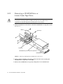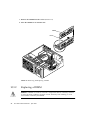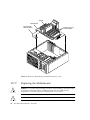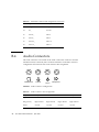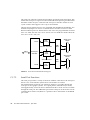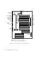
1
Sun Ultra™ 30 Service
Manual
Sun Microsystems, Inc.
901 San Antonio Road
Palo Alto, CA 94303-4900 USA
650 960-1300
Fax 650 969-9131
Part No.: 802-7719-12
April 1998, Revision A
Send comments about this document to: [email protected]
[email protected]
Copyright 1999 Sun Microsystems, Inc., 901 San Antonio Road, Palo Alto, California 94303-4900 U.S.A. All rights reserved.
This product or document is protected by copyright and distributed under licenses restricting its use, copying, distribution, and decompilation.
No part of this product or document may be reproduced in any form by any means without prior written authorization of Sun and its licensors,
if any. Third-party software, including font technology, is copyrighted and licensed from Sun suppliers .
Parts of the product may be derived from Berkeley BSD systems, licensed from the University of California. UNIX is a registered trademark in
the U.S. and other countries, exclusively licensed through X/Open Company, Ltd. For Netscape Communicator™, the following notice applies:
(c) Copyright 1995 Netscape Communications Corporation. All rights reserved.
Sun, Sun Microsystems, the Sun logo, SunStore, AnswerBook2, docs.sun.com, and Solaris are trademarks, registered trademarks, or service
marks of Sun Microsystems, Inc. in the U.S. and other countries. All SPARC trademarks are used under license and are trademarks or registered
trademarks of SPARC International, Inc. in the U.S. and other countries. Products bearing SPARC trademarks are based upon an architecture
developed by Sun Microsystems, Inc.
The OPEN LOOK and Sun™ Graphical User Interface was developed by Sun Microsystems, Inc. for its users and licensees. Sun acknowledges
the pioneering efforts of Xerox in researching and developing the concept of visual or graphical user interfaces for the computer industry. Sun
holds a non-exclusive license from Xerox to the Xerox Graphical User Interface, which license also covers Sun’s licensees who implement OPEN
LOOK GUIs and otherwise comply with Sun’s written license agreements.
RESTRICTED RIGHTS: Use, duplication, or disclosure by the U.S. Government is subject to restrictions of FAR 52.227-14(g)(2)(6/87) and FAR
52.227-19(6/87), or DFAR 252.227-7015(b)(6/95) and DFAR 227.7202-3(a).
DOCUMENTATION IS PROVIDED “AS IS” AND ALL EXPRESS OR IMPLIED CONDITIONS, REPRESENTATIONS AND WARRANTIES,
INCLUDING ANY IMPLIED WARRANTY OF MERCHANTABILITY, FITNESS FOR A PARTICULAR PURPOSE OR NON-INFRINGEMENT,
ARE DISCLAIMED, EXCEPT TO THE EXTENT THAT SUCH DISCLAIMERS ARE HELD TO BE LEGALLY INVALID.
Copyright 1999 Sun Microsystems, Inc., 901 San Antonio Road, Palo Alto, Californie 94303-4900 U.S.A. Tous droits réservés.
Ce produit ou document est protégé par un copyright et distribué avec des licences qui en restreignent l’utilisation, la copie, la distribution, et la
décompilation. Aucune partie de ce produit ou document ne peut être reproduite sous aucune forme, par quelque moyen que ce soit, sans
l’autorisation préalable et écrite de Sun et de ses bailleurs de licence, s’il y en a. Le logiciel détenu par des tiers, et qui comprend la technologie
relative aux polices de caractères, est protégé par un copyright et licencié par des fournisseurs de Sun.
Des parties de ce produit pourront être dérivées des systèmes Berkeley BSD licenciés par l’Université de Californie. UNIX est une marque
déposée aux Etats-Unis et dans d’autres pays et licenciée exclusivement par X/Open Company, Ltd. La notice suivante est applicable à
Netscape Communicator™ : (c) Copyright 1995 Netscape Communications Corporation. All rights reserved.
Sun, Sun Microsystems, le logo Sun, SunStore, AnswerBook2, docs.sun.com, et Solaris sont des marques de fabrique ou des marques déposées,
ou marques de service, de Sun Microsystems, Inc. aux Etats-Unis et dans d’autres pays. Toutes les marques SPARC sont utilisées sous licence et
sont des marques de fabrique ou des marques déposées de SPARC International, Inc. aux Etats-Unis et dans d’autres pays. Les produits portant
les marques SPARC sont basés sur une architecture développée par Sun Microsystems, Inc.
L’interface d’utilisation graphique OPEN LOOK et Sun™ a été développée par Sun Microsystems, Inc. pour ses utilisateurs et licenciés. Sun
reconnaît les efforts de pionniers de Xerox pour la recherche et le développement du concept des interfaces d’utilisation visuelle ou graphique
pour l’industrie de l’informatique. Sun détient une licence non exclusive de Xerox sur l’interface d’utilisation graphique Xerox, cette licence
couvrant également les licenciés de Sun qui mettent en place l’interface d’utilisation graphique OPEN LOOK et qui en outre se conforment aux
licences écrites de Sun.
CETTE PUBLICATION EST FOURNIE "EN L’ETAT" ET AUCUNE GARANTIE, EXPRESSE OU IMPLICITE, N’EST ACCORDEE, Y COMPRIS
DES GARANTIES CONCERNANT LA VALEUR MARCHANDE, L’APTITUDE DE LA PUBLICATION A REPONDRE A UNE UTILISATION
PARTICULIERE, OU LE FAIT QU’ELLE NE SOIT PAS CONTREFAISANTE DE PRODUIT DE TIERS. CE DENI DE GARANTIE NE
S’APPLIQUERAIT PAS, DANS LA MESURE OU IL SERAIT TENU JURIDIQUEMENT NUL ET NON AVENU.
Please
Recycle
Contents
Preface
xix
How This Book Is Organized xix
UNIX Commands xx
Typographic Conventions xxi
Shell Prompts xxi
Related Documents xxii
Sun Documentation on the Web xxiii
Sun Welcomes Your Comments xxiii
1.
2.
3.
Product Description
1-1
1.1
I/O Devices
1.2
System Unit Features
1.3
System Unit Components
SunVTS Overview
1-2
1-5
2-1
2.1
SunVTS Description
2.2
SunVTS Operation
Power-On Self-Test
1-3
2-1
2-2
3-1
3.1
POST Overview
3-1
3.2
Pre-POST Preparation
3-2
iii
4.
3.2.1
Setting Up a Tip Connection
3.2.2
Verifying the Baud Rate
3-4
3.3
Initializing POST
3.4
Maximum and Minimum Levels of POST
3-4
diag-level Variable Set to max
3-6
3.4.2
diag-level Variable Set to min
3-12
3.5
POST Progress and Error Reporting
3.6
Bypassing POST
3.7
Additional Keyboard Control Commands
3.8
System and Keyboard LEDs
3.9
Motherboard Test
3-18
3-20
3-20
3-20
3-21
Troubleshooting Procedures
4-1
4.1
Power-On Failure
4.2
Video Output Failure
4.3
Hard Drive or CD-ROM Drive Failure
4.4
Power Supply Test
4.5
DIMM Failure
4.6
OpenBoot PROM On-Board Diagnostics
4.7
3-5
3.4.1
4-1
4-2
4-3
4-4
4-6
4-7
4.6.1
watch-clock
4.6.2
watch-net and watch-net-all
4.6.3
probe-scsi and probe-scsi-all
4.6.4
test alias name, device path, -all
4.6.5
UPA Graphics Card
▼
4-7
4-8
4-9
4-10
4-11
To initialize the UPA graphics card diagnostic:
OpenBoot Diagnostics
▼
iv
3-2
4-12
To initialize the OBDiag menu:
4.7.1
PCI/PCIO
4.7.2
EBus DMA/TCR Registers
4.7.3
Ethernet
Sun Ultra 30 Service Manual • April 1998
4-12
4-16
4-17
4-17
4-11
4.7.4
Keyboard
4.7.5
Mouse
4-19
4.7.6
Floppy
4-19
4.7.7
Parallel Port
4-20
4.7.8
Serial Port A
4-20
4.7.9
Serial Port B
4-21
4.7.10
NVRAM
4.7.11
Audio
4.7.12
SCSI
4.7.13
All Above
▼
5.
7.
4-22
4-23
4-23
4-24
To recover the original N1fsVRAM variable settings:
Safety and Tool Requirements
5.1
Safety Requirements
5.2
Symbols
5.3
Safety Precautions
5.4
6.
4-18
5-1
5-1
5-1
5-2
5.3.1
Modification to Equipment
5-2
5.3.2
Placement of a Sun Product
5-2
5.3.3
Power Cord Connection
5.3.4
Electrostatic Discharge
5.3.5
Lithium Battery
Tools Required
Power On and Off
5-3
5-3
5-3
5-3
6-1
6.1
Powering On the System Unit
6-1
6.2
Powering Off the System Unit
6-3
Internal Access
4-26
7-1
7.1
Removing the Side Access Cover
7.2
Attaching the Wrist Strap
7.3
Replacing the Side Access Cover
7-1
7-4
7-5
v
8.
Major Subassemblies
8.1
8.2
8.3
8.4
8.5
8.6
8.7
8.8
vi
Power Supply
8-1
8-1
8.1.1
Removing the Power Supply
8-2
8.1.2
Replacing the Power Supply
8-4
PCI Fan Assembly
8-5
8.2.1
Removing the PCI Fan Assembly
8-5
8.2.2
Replacing the PCI Fan Assembly
8-7
Hard Drive Bay With SCSI Assembly
8-7
8.3.1
Removing the SCSI Drive Bay
8-7
8.3.2
Replacing the SCSI Drive Bay
8-9
Cable Assemblies
8-10
8.4.1
Removing the Peripheral Power Cable Assembly
8-10
8.4.2
Replacing the Peripheral Power Cable Assembly
8-11
8.4.3
Removing the Diskette Drive Cable Assembly
8-12
8.4.4
Replacing the Diskette Drive Cable Assembly
8-13
8.4.5
Removing the UPA Graphics Card
Cable Assembly 8-13
8.4.6
Replacing the UPA Graphics Card
Cable Assembly 8-16
EMI Filler Panels
8-16
8.5.1
Removing an EMI Filler Panel
8-17
8.5.2
Replacing an EMI Filler Panel
8-18
Chassis Foot
8-18
8.6.1
Removing the Chassis Foot
8-18
8.6.2
Replacing the Chassis Foot
8-19
Speaker Assembly
8-20
8.7.1
Removing the Speaker Assembly
8-20
8.7.2
Replacing the Speaker Assembly
8-21
DC Switch Assembly
8-22
8.8.1
Removing the DC Switch Assembly
8-22
8.8.2
Replacing the DC Switch Assembly
8-24
Sun Ultra 30 Service Manual • April 1998
8.9
Shroud Assembly
8.9.1
8.9.2
8.9.3
9.
9.2
10.
One-Piece Shroud Assembly
8-25
8.9.1.1
Removing the One-Piece Shroud Assembly
8-26
8.9.1.2
Replacing the One-Piece Shroud Assembly
8-27
Two-Piece Shroud Assembly
8-28
8.9.2.1
Removing the Two-Piece Shroud Assembly
8-28
8.9.2.2
Replacing the Two-Piece Shroud Assembly
8-30
Two-Piece Shroud Fan Assembly
Removing the Two-Piece Shroud Fan Assembly
8-31
8.9.3.2
Replacing the Two-Piece Shroud Fan Assembly
8-32
9-1
Hard Drive
9-1
9.1.1
Removing a Hard Drive
9-1
9.1.2
Replacing a Hard Drive
9-3
Removable Media Assembly Drive
9-4
9.2.1
Removing the RMA
9-4
9.2.2
Removing a CD-ROM Drive or
4-mm/8-mm Tape Drive 9-6
9.2.3
Replacing a CD-ROM Drive or
4-mm/8-mm Tape Drive 9-7
9.2.4
Removing a Diskette Drive
9-7
9.2.5
Replacing a Diskette Drive
9-7
9.2.6
Replacing the RMA
9-8
Motherboard and Component Replacement
10.1
10.2
8-30
8.9.3.1
Storage Devices
9.1
8-25
CPU Module
10-1
10-1
10.1.1
Removing the CPU Module
10-2
10.1.2
Replacing the CPU Module
10-3
NVRAM/TOD
10-4
10.2.1
Removing the NVRAM/TOD
10-4
10.2.2
Replacing the NVRAM/TOD
10-5
vii
10.3
10.4
10.5
10.6
10.7
11.
PCI Card
10-6
10.3.1
Removing a PCI Card
10-6
10.3.2
Replacing a PCI Card
10-8
UPA Graphics Card
10.4.1
Removing a UPA Graphics Card
10-9
10.4.2
Replacing a UPA Graphics Card
10-11
DIMM
10-12
10.5.1
Removing a DIMM
10-13
10.5.2
Replacing a DIMM
10-14
Audio Card
10-16
10.6.1
Removing the Audio Card
10-16
10.6.2
Replacing the Audio Card
10-17
Motherboard
10-18
10.7.1
Removing the Motherboard
10-19
10.7.2
Replacing the Motherboard
10-22
Illustrated Parts List
11-1
A. Product Specifications
A-1
A.1
Physical Specifications
A.2
Electrical Specifications
A.3
Environmental Requirements
B. Signal Descriptions
B.1
viii
10-9
A-1
A-2
A-2
B-1
Keyboard/Mouse and
Serial Ports A and B B-1
B.1.1
Keyboard/Mouse Connector
B.1.2
Serial Port A and B Connectors
B.2
Twisted-Pair Ethernet Connector
B.3
UltraSCSI Connector
B.4
Audio Connectors
B.5
Parallel Port Connector
Sun Ultra 30 Service Manual • April 1998
B-6
B-10
B-11
B-5
B-1
B-2
B.6
Media Independent Interface Connector
B.7
UPA Graphics Card Connector
C. Functional Description
C.1
B-13
B-15
C-1
System Unit
C-1
C.1.1
UPA
C-4
C.1.2
PCI Bus
C-5
C.1.2.1
U2P ASIC
C.1.2.2
Symbios 53C875 SCSI Controller
C.1.2.3
PCIO ASIC
C-5
C-6
C.1.3
UltraSPARC II Processor
C.1.4
Memory System
C.1.5
C.1.6
C.1.7
C-6
C-7
C.1.4.1
DIMM
C.1.4.2
Memory System Timing
C-13
C.1.4.3
Graphics Card Features
C-13
C.1.4.4
Graphics Card Performance
Peripherals
C-6
C-11
C-14
C-14
C.1.5.1
CD-ROM Drive
C-15
C.1.5.2
Diskette Drive
C.1.5.3
Hard Drives
C.1.5.4
Optional 4-mm or 8-mm Tape Drive
C-15
C-17
C-18
Keyboard and Mouse, Diskette, and Parallel Port
C.1.6.1
Keyboard and Mouse Port
C.1.6.2
Diskette Port
C.1.6.3
Parallel Port
Serial Port
C-19
C-19
C-20
C-20
C-21
C.1.7.1
Serial Port Components
C-21
C.1.7.2
Serial Port Functions
C.1.7.3
EIA Levels
C.1.7.4
Synchronous Rates
C.1.7.5
Asynchronous Rates
C.1.7.6
Slew Rate and Cable Length
C-22
C-23
C-23
C-23
C-23
ix
C.1.8
C.1.9
Ethernet
C-24
C.1.8.1
Automatic Negotiation
C.1.8.2
External Transceivers
C.1.8.3
External Cables
C.1.8.4
Connectors
C.1.8.5
MII Power
C.1.8.6
MII Port Timing
C-26
Audio Card and Connector
C-27
C.1.10 SCSI
C-25
C-25
C-26
C-28
Host Adapter
C.1.10.2
Supported Target Devices
C.1.10.3
External Cables
C.1.10.4
Internal SCSI Subassembly
C.1.10.5
SCSI ID Selection
C-29
C-30
C-30
C-30
C-31
C-32
C.1.11.1
SC_UP+
C.1.11.2
UltraBMX
C.1.11.3
PCIO
C.1.11.4
U2P
C-33
C.1.11.5
FBC
C-34
C.1.11.6
RISC
C.1.12 SuperIO
C-32
C-33
C-33
C-34
C-34
C.1.13 Power Supply
C-35
C.1.14 Control Signals
C-36
C.1.14.1
Remote Enable PowerOn and PowerOff
C.1.14.2
ON/OFF Functionality
C.1.14.3
System Unit Power Budget
C.1.15 Built-In Speaker
C.1.16 Microphone
C-40
C-41
C.1.17 Standard System Facilities
x
C-25
C.1.10.1
C.1.11 ASIC
C.2
C-25
Motherboard
Sun Ultra 30 Service Manual • April 1998
C-41
C-41
C-36
C-37
C-36
C.3
C.4
Jumper Descriptions
C-43
C.3.1
Serial Port Jumpers
C.3.2
Flash PROM Jumpers
Enclosure
C-45
C-45
C.4.1
Enclosure Basics
C.4.2
Enclosure Features
C-45
C.5
Environmental Compliance
C.6
Agency Compliance
Glossary
C-44
C-46
C-46
C-46
Glossary-1
xi
xii
Sun Ultra 30 Service Manual • April 1998
Figures
FIGURE 1-1
Sun Ultra 30 Desktop Workstation
FIGURE 1-2
System Unit Front View 1-3
FIGURE 1-3
System Unit Rear View
FIGURE 3-1
Setting Up a tip Connection 3-3
FIGURE 3-2
Sun Type-5 Keyboard 3-5
FIGURE 4-1
Power Supply Connector J2901
4-5
FIGURE 4-2
Power Supply Connector J2902
4-5
FIGURE 4-3
Power Supply Connector J2903
4-6
FIGURE 6-1
System Power On (Front Panel)
6-2
FIGURE 6-2
Sun Type-5 Keyboard 6-2
FIGURE 6-3
System Power Off (Front Panel)
FIGURE 7-1
Lock Block Location
FIGURE 7-2
Removing the Side Access Cover
FIGURE 7-3
Attaching the Wrist Strap 7-5
FIGURE 7-4
Replacing the Side Access Cover 7-6
FIGURE 8-1
Removing and Replacing the Power Supply (Part 1 of 2)
8-3
FIGURE 8-2
Removing and Replacing the Power Supply (Part 2 of 2)
8-4
FIGURE 8-3
Removing and Replacing the PCI Fan Assembly 8-6
FIGURE 8-4
Removing and Replacing the SCSI Drive Bay
FIGURE 8-5
Removing and Replacing the UPA Graphics Card Cable Assembly 8-15
1-2
1-4
6-4
7-2
7-3
8-9
xiii
xiv
FIGURE 8-6
Removing and Replacing the Bezel EMI Filler Panel
8-17
FIGURE 8-7
Removing and Replacing the RMA EMI Filler Panel
8-18
FIGURE 8-8
Removing and Replacing the Chassis Foot
FIGURE 8-9
Removing and Replacing the Speaker Assembly
FIGURE 8-10
Removing and Replacing the DC Switch Assembly 8-24
FIGURE 8-11
Removing and Replacing the One-Piece Shroud Assembly (Part 1 of 2)
8-26
FIGURE 8-12
Removing and Replacing the One-Piece Shroud Assembly (Part 2 of 2)
8-27
FIGURE 8-13
Removing and Replacing the Two-Piece Shroud Assembly
FIGURE 8-14
Removing and Replacing the Two-Piece Shroud Fan Assembly
FIGURE 9-1
Removing and Replacing a Hard Drive
FIGURE 9-2
Removing and Replacing the RMA Drive (Part 1 of 2) 9-5
FIGURE 9-3
Removing and Replacing the RMA Drive (Part 2 of 2) 9-6
FIGURE 10-1
Removing and Replacing the CPU Module
FIGURE 10-2
Removing and Replacing the NVRAM/TOD 10-5
FIGURE 10-3
Removing and Replacing a PCI Card 10-7
FIGURE 10-4
Removing and Replacing a UPA Graphics Card
FIGURE 10-5
DIMM Ejection Lever
FIGURE 10-6
Removing and Replacing a DIMM 10-14
FIGURE 10-7
Removing and Replacing the Audio Card 10-18
FIGURE 10-8
Removing and Replacing the Motherboard (Part 1 of 2)
10-21
FIGURE 10-9
Removing and Replacing the Motherboard (Part 2 of 2)
10-22
FIGURE 10-10
Location of the Motherboard Serial Port Jumpers 10-23
FIGURE 10-11
Identifying Jumper Pins
FIGURE 11-1
System Unit Exploded View
FIGURE B-1
Keyboard/Mouse Connector Pin Configuration B-2
FIGURE B-2
Serial Port A and B Connector Pin Configurations
FIGURE B-3
TPE Connector Pin Configuration
FIGURE B-4
UltraSCSI Connector Pin Configuration
FIGURE B-5
Audio Connector Configuration
FIGURE B-6
Parallel Port Connector Pin Configuration
8-19
8-21
8-29
9-3
10-3
10-10
10-13
Sun Ultra 30 Service Manual • April 1998
10-24
11-3
B-6
B-7
B-10
B-11
B-3
8-32
FIGURE B-7
MII Connector Pin Configuration B-13
FIGURE B-8
UPA Graphics Card Con
FIGURE C-1
System Unit Functional Block Diagram C-3
FIGURE C-2
UPA Address and Data Buses Functional Block Diagram C-5
FIGURE C-3
Memory System Functional Block Diagram
FIGURE C-4
Memory Module Functional Block Diagram (Part 1 of 2) C-9
FIGURE C-5
Memory Module Functional Block Diagram (Part 2 of 2) C-10
FIGURE C-6
DIMM Row Mapping C-11
FIGURE C-7
Keyboard and Mouse, Diskette, and Parallel Port
Functional Block Diagram C-19
FIGURE C-8
Serial Port Functional Block Diagram C-22
FIGURE C-9
MII Port Timing Model C-26
FIGURE C-10
Audio Card Functional Block Diagram
FIGURE C-11
Configuration for the SCSI Bus
FIGURE C-12
SCSI Subassembly Functional Block Diagram
FIGURE C-13
System Unit Motherboard Functional Block Diagram C-42
FIGURE C-14
Selected Jumper Settings
FIGURE C-15
Identifying Jumper Pins
B-16
C-8
C-28
C-29
C-31
C-43
C-43
xv
xvi
Sun Ultra 30 Service Manual • April 1998
Tables
TABLE P-1
Document Organization
TABLE P-2
Typographic Conventions xxi
TABLE P-3
Shell Prompts
TABLE P-4
Related Documents
TABLE 1-1
Supported I/O Devices
TABLE 1-2
Ultra 30 System Unit Replaceable Components
TABLE 2-1
SunVTS Documentation
TABLE 3-1
diag-switch? and diag-level Flag Settings
TABLE 3-2
Keyboard LED Patterns
TABLE 4-1
Internal Drives Identification 4-3
TABLE 4-2
Power Supply Connector J2901 Pin Assignments
4-5
TABLE 4-3
Power Supply Connector J2902 Pin Assignments
4-5
TABLE 4-4
Power Supply Connector J2903 Pin Assignments
4-6
TABLE 4-5
DIMM Physical Memory Addresses
TABLE 4-6
Selected OBP On-Board Diagnostic Tests
TABLE 10-1
DIMM Installation Locations
TABLE 10-2
Motherboard Serial Port Jumpers J2604 and J2605 10-23
TABLE 11-1
System Unit Replaceable Components
TABLE A-1
Ultra 30 Physical Specifications A-1
TABLE A-2
Ultra 30 Electrical Specifications
xix
xxi
xxii
1-2
1-5
2-2
3-2
3-19
4-6
4-10
10-12
11-3
A-2
xvii
xviii
TABLE A-3
Ultra 30 Environmental Requirements
TABLE B-1
Keyboard/Mouse Connector Pin Assignments
TABLE B-2
Serial Port A and B Connector Pin Assignments
TABLE B-3
TPE Connector Pin Assignments
TABLE B-4
UltraSCSI Connector Pin Assignments
TABLE B-5
Audio Connector Line Assignments B-10
TABLE B-6
Parallel Port Connector Pin Assignments
TABLE B-7
MII Connector Pin Assignments
TABLE B-8
UPA Graphics Card Connector Pin Assignments
TABLE C-1
UPA Port Identification Assignments
TABLE C-2
DIMM Pair-To-U Number
TABLE C-3
Physical Address Map to DIMM Pair (Non-Interleave) C-12
TABLE C-4
Physical Address Maps to DIMM Pair (Interleave) C-13
TABLE C-5
Diskette Drive Signals by Mnemonic Name C-16
TABLE C-6
Supported Hard Drives
TABLE C-7
Major Features of the Audio Card
TABLE C-8
SCSI Subsystem Supported Target Devices
TABLE C-9
Power Supply Output Voltages C-35
TABLE C-10
Power Supply Control Signals C-36
TABLE C-11
Power Estimate (3.3-ns CPU Module)
TABLE C-12
Power Estimate (4-ns CPU Module)
TABLE C-13
Power Estimate for the 5-Vdc PCI Card C-38
TABLE C-14
Power Estimate for the 3.3-Vdc PCI Card C-39
TABLE C-15
Power Estimate for the Memory Subsystem C-39
TABLE C-16
Power Estimates for the Storage Devices
TABLE C-17
Built-In Speaker Specifications
TABLE C-18
Serial Port Jumper Settings
TABLE C-19
Flash PROM Jumper Settings C-45
A-2
B-2
B-3
B-6
B-7
B-11
B-13
B-16
C-4
C-12
C-18
Sun Ultra 30 Service Manual • April 1998
C-27
C-40
C-44
C-30
C-37
C-38
C-39
Preface
The Sun Ultra 30 Service Manual provides detailed procedures that describe the
removal and replacement of replaceable parts in the Ultra™ 30 computer (system
unit). This book is written for technicians, system administrators, authorized service
providers (ASPs), and advanced computer system end users who have experience
troubleshooting and replacing hardware.
How This Book Is Organized
This document is organized into chapters and appendixes as in the following table.
A glossary and an index is also included.
TABLE P-1
Document Organization
Chapter Number/Title
Content Description
Chapter 1, “Product Description”
Describes the major components of the
system unit.
Chapter 2, “SunVTS Overview”
Describes the execution of individual tests
for verifying hardware configuration and
functionality.
Chapter 3, “Power-On Self-Test”
Describes the execution of POST and
provides examples of POST output patterns.
Chapter 4, “Troubleshooting Procedures”
Provides troubleshooting advice and
suggested corrective actions for hardware
problems.
Chapter 5, “Safety and Tool Requirements”
Explains how to work safely when servicing
the system unit.
xix
TABLE P-1
Document Organization (Continued)
Chapter Number/Title
Content Description
Chapter 6, “Power On and Off”
Provides step-by-step procedures to power
on and power off the system unit.
Chapter 7, “Internal Access”
Provides step-by-step procedures to remove
the side access panel, attach the wrist strap,
and replace the side access panel.
Chapter 8, “Major Subassemblies”
Provides step-by-step procedures to remove
and replace major subassemblies.
Chapter 9, “Storage Devices”
Provides step-by-step procedures to remove
and replace storage devices.
Chapter 10, “Motherboard and Component
Replacement”
Provides step-by-step procedures to remove
and replace the motherboard, and various
components associated with motherboard
operation.
Chapter 11, “Illustrated Parts List”
Lists replaceable parts for the system unit.
Appendix A, “Product Specifications”
Provides product specifications, system
requirements about power and environment,
system unit dimensions, weight, memory
mapping, and peripheral component
interconnect (PCI) card slot specifications.
Appendix B, “Signal Descriptions”
Provides signal descriptions.
Appendix C, “Functional Description”
Provides functional descriptions for the
system unit.
Glossary
Provides a listing of acronyms, terms, and
definitions.
Index
Provides a quick reference to specific topics.
UNIX Commands
This document may not contain information on basic UNIXcommands® and
procedures.
See one or more of the following for this information:
■
■
■
xx
Solaris 2.x Handbook for SMCC Peripherals
AnswerBook™ online documentation for the Solaris 2.x software environment
Other software documentation that you received with your system
Sun Ultra 30 Service Manual • April 1998
Typographic Conventions
TABLE P-2
Typographic Conventions
Typeface or Symbol
Meaning
Examples
AaBbCc123
The names of commands,
files, and directories;
on-screen computer output.
Edit your .login file.
Use ls -a to list all files.
% You have mail.
AaBbCc123
What you type, when
contrasted with on-screen
computer output.
% su
Password:
AaBbCc123
Book titles, new words or
terms, words to be
emphasized.
Command-line variable;
replace with a real name or
value.
Read Chapter 6 in the User’s
Guide.
These are called class
options.
You must be root to do this.
To delete a file, type rm
filename.
Shell Prompts
TABLE P-3
Shell Prompts
Shell
Prompt
C shell
machine_name%
C shell superuser
machine_name#
Bourne shell and Korn shell
$
Bourne shell and Korn shell
superuser
#
xxi
Related Documents
TABLE P-4
xxii
Related Documents
Application
Title
Part Number
Configuration
Sun Ultra 30 System Reference Manual
802-4147
Configuration
Solaris Handbook for SMCC Peripherals
802-7675
Diagnostics
SunVTS 2.0 User’s Guide
802-5331
Diagnostics
SunVTS 2.0 Test Reference Manual
802-5330
Diagnostics
SunVTS 2.0 Quick Reference Card
802-5329
Installation
14-Gbyte, 8-mm Tape Drive Installation
Manual
802-1849
Installation
Creator Frame Buffer Installation Guide
802-6682
Installation
Creator Installation Guide
802-7731
Installation
Elite3D Installation Guide
805-4391
Installation/User
12-24 Gbyte 4-mm DDS-3 Tape Drive
Installation and User’s Guide
802-7791
Installation
5.25” Fast/Wide Differential SCSI Disk Drive
Installation Manual
802-1653
Specification
Manual Eject Diskette Drive Specifications
805-ii33
Specification
DDS-2 Tape Drive Specifications
802-5324
Specification
17-Inch Entry, 17-Inch Premium, and 20-Inch
Premium Color Monitors Specifications
802-6168
Specification
2.1-Gbyte 7200-RPM Disk Drive Specifications
802-7743
Specification
4.2-Gbyte 7200-RPM Disk Drive Specifications
802-7744
Specification
9-Gbyte 7200-RPM Disk Drive Specifications
802-7745
Specification
SunCD 4 Drive Specifications
802-4157
Specification
Diskette Drive Specification
802-6285
Sun Ultra 30 Service Manual • April 1998
TABLE P-4
Related Documents (Continued)
Application
Title
Part Number
Specification
8-mm Tape Drive Specifications
802-5775
Specification
4-mm, DDS-2 Tape Drive Specifications
802-7790
Specification
Manual Eject Diskette Drive Specifications
805-1133
User
SunVTS 2.0 User’s Guide
802-5331
User
24-Inch Premium (22.5-inch Viewable) Color
Monitor Guide
875-1799
User
14-Gbyte, 8-mm Tape Drive User’s Guide
802-1850
User
Ultra Systems Flash PROM Programming
Guide
802-3233
Sun Documentation on the Web
The docs.sun.com web site enables you to access Sun technical documentation on
the World Wide Web. You can browse the docs.sun.com archive or search for a
specific book title or subject at http://docs.sun.com
Sun Welcomes Your Comments
We are interested in improving our documentation and welcome your comments
and suggestions. You can email your comments to us at [email protected].
Please include the part number of your document in the subject line of your email.
xxiii
xxiv
Sun Ultra 30 Service Manual • April 1998
CHAPTER
1
Product Description
The Ultra 30 desktop workstation is a uniprocessor device that uses the family of
UltraSPARC™ processors. It supports high-performance processing (UltraSPARC II)
and high-performance graphics. Enclosed within a minitower enclosure, the Ultra 30
desktop workstation provides the following:
■
■
■
■
■
Power and cooling requirements for a high-performance processor and graphics
Modular internal design
Improved disk, system, memory, and I/O performance and capacity
Dual-head UltraSPARC port architecture (UPA) graphics capability
High-performance peripheral component interconnect (PCI) I/O expansion with
comparable options to existing SBus options
FIGURE 1-1 illustrates the Ultra 30 desktop workstation. The following sections
provide a brief description of the Ultra 30 desktop workstation I/O devices and a
detailed overview of the Ultra 30 computer (system unit) features.
-1
System unit
Monitor (24-inch optional)
Keyboard
Mouse/pad
FIGURE 1-1
1.1
Sun Ultra 30 Desktop Workstation
I/O Devices
The Ultra 30 desktop workstation uses the I/O devices as listed in TABLE 1-1.
TABLE 1-1
-2
Supported I/O Devices
I/O Device
Description
21-inch (53-cm) color monitor
1600 x 1000 resolution, 76- or 66-Hz refresh rate
24-inch (61-cm) color monitor
1920 x 1200 resolution, 70-Hz refresh rate
Microphone
SunMicrophone™ II
Keyboard
Sun Type-5; AT 101 or UNIX layout available
Opto-mechanical mouse
Optomechanical, 3-button
Sun Ultra 30 Service Manual • April 1998
1.2
System Unit Features
System unit components are housed in a tower configuration enclosure. Overall
enclosure dimensions (width x depth x height) are 17.72 inches (45.00 cm) x 7.50
inches (19.00 cm) x 19.61 inches (49.80 cm). System unit electronics are contained on
a single printed circuit board (motherboard). The motherboard contains the CPU
module, memory, system control application specific integrated circuits (ASICs), and
I/O ASICs.
FIGURE 1-2 illustrates the system unit front view. FIGURE 1-3 illustrates the system unit
rear view. System unit electronics and peripherals contain (or may be upgraded to
contain) the following features:
CD-ROM drive
(or tape drive)
Diskette drive
Power LED
Second 3.5-inch drive bay
Power on/standby
switch
Chassis foot (4)
FIGURE 1-2
System Unit Front View
■
Tower enclosure with power supply.
■
Support for modular UltraSPARC II processor with 1-megabyte (Mbyte) or
2-Mbyte Ecache and system operating frequencies from 100 megahertz (MHz) to
333 MHz.
■
UPA coherent memory interconnect.
Chapter
-3
■
Use of dual in-line memory modules (DIMMs), with an interleaved memory
system. Each pair of DIMM slots (four rows of two pairs each) accepts 32-, 64-, or
128-Mbyte DIMM modules. Populating with two pair of identical capacity
DIMMs enables the memory controller to interleave and overlap, providing the
optimal system performance. There are a total of 16 DIMM slots.
■
Four PCI slots:
■
Three 33-MHz, 64-bit or 32-bit, 5-Vdc slots
■
One 66-MHz or 33-MHz, 64-bit or 32-bit, 3.3-Vdc slot
■
Two UPA graphics slots.
■
10/100-megabits per second Ethernet.
■
40-Mbytes per second UltraSCSI (Fast-20).
■
Two DB25 serial ports (synchronous and asynchronous protocols).
■
Centronics-compatible parallel port interface with extended capability port (ECP)
support.
■
Modular audio interface.
Parallel DB25 connector
Keyboard/mouse connector
Serial connector (2)
RS-432/RS-232
TPE connector
MII connector
68-pin SCSI connector
Audio module connector
UPA graphics (2)
PCI 66 connector 1
PCI 2, 3, 4 connector (3)
FIGURE 1-3
-4
System Unit Rear View
Sun Ultra 30 Service Manual • April 1998
AC power inlet
1.3
System Unit Components
TABLE 1-2 lists the system unit components. A brief description of each listed
component is also provided.
Note – Removal and replacement of selected system unit components are also
illustrated with photographs and audio/visual instructions on the Sun Ultra 30
ShowMe How Multimedia Documentation, part number 704-5681.
Note – Consult your authorized Sun sales representative or service provider prior to
ordering a replacement part.
TABLE 1-2
Ultra 30 System Unit Replaceable Components
Component
Description
Motherboard
System board
Hard drive bay with SCSI
Mechanical hard drive housing
2.1-Gbyte SCSI assembly
Hard drive
4.2-Gbyte SCSI assembly
Hard drive
9.1-Gbyte SCSI assembly
Hard drive
PCI fan assembly
PCI fan
Fan assembly
CPU fan
One-piece shroud assembly
Shroud assembly
Two-piece shroud assembly
Shroud assembly
CPU module
250-MHz, 1-Mbyte external cache
CPU module
300-MHz, 2-Mbyte external cache
Graphics card
Vertical, single buffer UPA graphics card, 75-MHz
Graphics card
Vertical, double buffer plus Z (DBZ) UPA graphics card, 75-MHz
Chapter
-5
TABLE 1-2
Ultra 30 System Unit Replaceable Components (Continued)
Component
Description
Graphics card
Vertical, DBZ UPA graphics card, 83-MHz
Graphics card
Vertical, single buffer UPA graphics card, 83-Mhz
Graphics card
Vertical UPA graphics card, 100-MHz, with stereo application
Graphics card
Vertical UPA graphics card, 100-MHz, without stereo application
Power supply
Power supply
Audio module
Audio applications, 16-bit audio, 8 kHz to 48 kHz
Speaker assembly
Speaker
Peripheral cable
Peripheral cable
Diskette drive cable
Diskette drive cable
Manual eject floppy
Diskette drive, 3.5-inch, MS-DOS compatible
EMI filler panel
CD-ROM drive filler panel
EMI filler panel
Diskette drive filler panel
32-Mbyte DIMM
60-ns, 32-Mbyte DIMM
64-Mbyte DIMM
60-ns, 64-Mbyte DIMM
128-Mbyte DIMM
60-ns, 128-Mbyte DIMM
NVRAM/TOD
Time of day, 48T59, with carrier
CD-ROM drive
CD-ROM drive, 1.6-inch height
4-mm tape drive
12-24-Gbyte, 4-mm DDS-2 tape drive
8-mm tape drive
14-Gbyte, 8-mm tape drive
TPE cable (category 5)
Twisted-pair Ethernet cable
DC switch assembly
DC switch assembly
Chassis foot
Chassis foot
-6
Sun Ultra 30 Service Manual • April 1998
CHAPTER
2
SunVTS Overview
This chapter contains an overview of the SunVTS™ diagnostic tool.
This chapter contains the following topics:
■
■
2.1
Section 2.1 “SunVTS Description”
Section 2.2 “SunVTS Operation” on page 2-2
SunVTS Description
The SunVTS software executes multiple diagnostic hardware tests from a single user
interface. SunVTS verifies the configuration, functionality, and reliability of most
hardware controllers and devices.
The SunVTS software is used in both the Common Desktop Environment (CDE) and
the OPEN LOOK graphical user interface environments, or from a TTY interface.
Within the CDE and OPEN LOOK GUI environments, test parameters are quickly
and easily set by pointing and clicking a mouse button.
With a TTY interface, the SunVTS software is used from a terminal or modem
attached to a serial port. Data is input through the keyboard, rather than with a
mouse, and only one screen of information is displayed at a time.
-1
2.2
SunVTS Operation
TABLE 2-1 lists the documentation for the SunVTS software. These documents are
available on the Solaris on Sun Hardware AnswerBook, which is on the SMCC Updates
for the Solaris release.
TABLE 2-1
SunVTS Documentation
Title
Description
SunVTS User’s Guide
802-7299
Describes the SunVTS environment;
starting and controlling various user
interfaces; feature descriptions
SunVTS Test Reference Manual
802-7300
Describes each SunVTS test; provides
various test options and command line
arguments
SunVTS Quick Reference Card
-2
Part Number
Sun Ultra 30 Service Manual • April 1998
802-7301
Provides overview of vtsui interface
features
CHAPTER
3
Power-On Self-Test
This chapter describes how to initiate power-on self-test (POST) diagnostics.
This chapter contains the following topics:
■
■
■
■
■
■
■
■
■
3.1
Section
Section
Section
Section
Section
Section
Section
Section
Section
3.1
3.2
3.3
3.4
3.5
3.6
3.7
3.8
3.9
“POST Overview” on page 3-1
“Pre-POST Preparation” on page 3-2
“Initializing POST” on page 3-4
“Maximum and Minimum Levels of POST” on page 3-5
“POST Progress and Error Reporting” on page 3-18
“Bypassing POST” on page 3-20
“Additional Keyboard Control Commands” on page 3-20
“System and Keyboard LEDs” on page 3-20
“Motherboard Test” on page 3-21
POST Overview
POST is useful in determining if a portion of the system unit has failed and should
be replaced. POST detects approximately 95 percent of system unit faults and is
located in the system board OpenBoot™ PROM (OBP). The setting of two NVRAM
variables, the diag-switch? and the diag-level flag, determine if POST is
executed. TABLE 3-1 lists the diag-switch? and diag-level flag settings for
disabling POST (off), enabling POST maximum (max), or enabling POST minimum
(min).
-1
Note – With the diag-level set to off and the diag-switch? set to true, a
serial port A output is enabled, but the output is not a POST display.
TABLE 3-1
3.2
diag-switch? and diag-level Flag Settings
diag-level Setting
diag-switch? Setting
POST Initialization
Serial Port A Output
Off
N/A
No
Disabled
N/A
False
No
Disabled
Max
True
Yes (power-on)
Enabled
Min
True
Yes (power-on)
Enabled
Pre-POST Preparation
Pre-POST preparation includes:
■
■
tipSetting up a connection to another workstation or terminal to view POST
progress and error messages. See Section 3.2.1 “Setting Up a Tip Connection” on
page 3-2.
Verifying baud rates between a workstation and a monitor or a workstation and a
terminal. See Section 3.2.2 “Verifying the Baud Rate” on page 3-4.
If a terminal or a monitor is not connected to serial port A (default port) of a
workstation or server to be tested, the keyboard LEDs are used to determine error
conditions. See Section 3.8 “System and Keyboard LEDs” on page 3-20.
3.2.1
Setting Up a Tip Connection
A tip connection enables a remote shell window to be used as a terminal to display
test data of a system being tested. Serial port A or serial port B of a tested system
unit is used to establish the tip connection between the system unit being tested
and another Sun™ workstation monitor or TTY-type terminal. The tip connection is
used in a SunOS™ window and provides features to help with the OBP.
To set up a tip connection:
-2
Sun Ultra 30 Service Manual • April 1998
1. See FIGURE 3-1. Connect serial port A of the system being tested to another Sun
workstation serial port B using a serial null modem cable (connect cable pins 2-3,
3-2, 7-20, and 20-7).
FIGURE 3-1
2
2
3
3
7
7
20
20
Setting Up a tip Connection
2. At the other Sun workstation, check the /etc/remote file by changing the
directory to /etc and then editing the remote file:
hardwire:/ dv=/dev/term/b:br#9600:el=^C^S^Q^U^D:ie=%$:oe=^D:
Note – The example shows connection to serial port B.
3. To use serial port A:
a. Copy and paste the serial port B remote file.
b. Modify the serial port B remote file as follows:
hardwire:/ dv=/dev/term/a:br#9600:el=^C^S^Q^U^D:ie=%$:oe=^D:
4. In a shell window on the Sun workstation, type tip hardwire.
hostname% tip hardwire
connected
Note – The shell window is now a tip window directed to the serial port of the
system unit being tested. When power is applied to the system unit being tested,
POST messages will be displayed in this window.
5. When POST is completed, disconnect the tip window as follows:
a. Open a shell window.
Chapter
-3
b. Type ps -a to view the active tip line and process ID (PID) number.
c. Type the following to kill the tip hardwire process.
hostname% kill -9 PID# of tip hardwire process
3.2.2
Verifying the Baud Rate
To verify the baud rate between the system unit being tested and a terminal or
another Sun workstation monitor:
1. Open a shell window.
2. Type eeprom.
3. Verify the following serial port default settings as follows:
ttyb-mode = 9600,8,n,1
ttya-mode = 9600,8,n,1
Note – Ensure that the settings are consistent with TTY-type terminal or
workstation monitor settings.
3.3
Initializing POST
POST is initilized in two ways:
■
■
By setting the diag-switch? to true and the diag-level to max or min,
followed by power cycling the system unit
By simultaneously pressing the Type-5 keyboard Stop and D keys while power is
applied to the system unit and the diag-level setting is set to either min or max
To set the diag-switch? to true and power cycle the system unit:
1. At the system prompt, type:
ok setenv diag-switch? true
-4
Sun Ultra 30 Service Manual • April 1998
2. At the keyboard, power cycle the system unit by simultaneously pressing the
Shift key and the Power-on key (FIGURE 3-2). After a few seconds, press the
Power-on key again.
Scroll Lock
key indicator
Stop key
Caps Lock
key indicator
FIGURE 3-2
Shift key
D key
Power-on key
Compose
key indicator
Num Lock
key indicator
Sun Type-5 Keyboard
3. Verify the following:
1. The display prompt disappears.
2. The monitor power-on indicator flashes on and off.
3. The keyboard Caps Lock key indicator flashes on and off.
● When POST is complete, type the following at the system prompt:
ok setenv diag-switch? false
3.4
Maximum and Minimum Levels of
POST
Two levels of POST are available: maximum (max) level and minimum (min) level.
The system initiates the selected level of POST based upon the setting of
diag-level, a NVRAM variable.
Chapter
-5
The default setting for diag-level is max. An example of a max level POST output
on serial port A is provided in Section 3.4.1 “diag-level Variable Set to max”. An
example of a min level POST output on serial port A is provided in Section 3.4.2
“diag-level Variable Set to min” on page 3-12.
To set the diag-level variable to min, type:
ok setenv diag-level min
To return to the default setting:
ok setenv diag-level max
3.4.1
diag-level Variable Set to max
When the diag-level variable is set to max, POST enables an extended set of
diagnostic-level tests. This mode requires approximately 4 minutes to complete
(with 128 Mbytes of DIMM installed). CODE EXAMPLE 3-1 identifies a typical serial
port A POST output with the diag-level variable set to max.
CODE EXAMPLE 3-1
diag-level Variable Set to max
Executing Power On SelfTest
@(#) Sun Ultra 30 UPA/PCI POST 1.1.1 03/04/97
CPU: UltraSPARC 2 (MHz: 296 MID: 0 Ecache Size: 2048KB)
Init System BSS
NVRAM Battery Detect Test
NVRAM Scratch Addr Test
NVRAM Scratch Data Test
M48T59 TOD Timestamp Test
M48T59 TOD Init Test
M48T59 TOD Functional Test
DMMU TLB Tag Access Test
DMMU TLB RAM Access Test
Probe Ecache
Ecache RAM Addr Test
Ecache Tag Addr Test
Invalidate Ecache Tags
Init SC Regs
SC Address Reg Test
SC Reg Index Test
-6
Sun Ultra 30 Service Manual • April 1998
CODE EXAMPLE 3-1
diag-level Variable Set to max (Continued)
SC Regs Test
Init SC Regs
Probe Memory
INFO:
0MB Bank 0
INFO:
0MB Bank 1
INFO:
0MB Bank 2
INFO:
0MB Bank 3
INFO:
0MB Bank 4
INFO:
0MB Bank 5
INFO:
64MB Bank 6
INFO:
64MB Bank 7
Interleave Mode Enable
Malloc Post Memory
Init Post Memory
Memory Addr w/ Ecache Test
Map PROM/STACK/NVRAM in DMMU
Update Master Stack/Frame Ptrs
V9 Instruction Test
CPU Tick and Tick Compare Reg Test
CPU Soft Trap Test
CPU Softint Reg and Int Test
FPU Regs Test
FPU Move Regs Test
FPU State Reg Test
FPU Functional Test
FPU Trap Test
DMMU Primary Context Reg Test
DMMU Secondary Context Reg Test
DMMU TSB Reg Test
DMMU Tag Access Reg Test
DMMU VA Watchpoint Reg Test
DMMU PA Watchpoint Reg Test
IMMU TSB Reg Test
IMMU Tag Access Reg Test
IMMU TLB RAM Access Test
IMMU TLB Tag Access Test
Dcache RAM Test
Dcache Tag Test
Icache RAM Test
Icache Tag Test
Icache Next Test
Icache Predecode Test
Displacement Flush Ecache
Ecache RAM Test
Ecache Tag Test
Ecache Access Test
Chapter
-7
CODE EXAMPLE 3-1
diag-level Variable Set to max (Continued)
Init Psycho
Psycho Cntl and UPA Reg Test
Psycho DMA Scoreboard Reg Test
Psycho Perf Cntl Reg Test
PIO Decoder and BCT Test
PCI Byte Enable Test
Counter/Timer Limit Regs Test
Timer Increment Test
Timer Reload Test
Timer Periodic Test
Mondo Int Map (short) Reg Test
Mondo Int Set/Clr Reg Test
Psycho IOMMU Regs Test
Psycho IOMMU RAM NTA Test
Psycho IOMMU CAM NTA Test
Psycho IOMMU RAM Address Test
Psycho IOMMU CAM Address Test
IOMMU TLB Compare Test
IOMMU TLB Flush Test
Stream Buff A Control Reg Test
Psycho ScacheA Page Tag Addr Test
Psycho ScacheA Line Tag Addr Test
Psycho ScacheA RAM Addr Test
Psycho ScacheA Page Tag NTA Test
Psycho ScacheA Line Tag NTA Test
Psycho ScacheA Error Status NTA Test
Psycho ScacheA RAM NTA Test
Stream Buff B Control Reg Test
Psycho ScacheB Page Tag Addr Test
Psycho ScacheB Line Tag Addr Test
Psycho ScacheB RAM Addr Test
Psycho ScacheB Page Tag NTA Test
Psycho ScacheB Line Tag NTA Test
Psycho ScacheB Error Status NTA Test
Psycho ScacheB RAM NTA Test
PBMA PCI Config Space Regs Test
PBMA Control/Status Reg Test
PBMA Diag Reg Test
PBMB PCI Config Space Regs Test
PBMB Control/Status Reg Test
PBMB Diag Reg Test
Init Memory
INFO:
0MB Bank 0
INFO:
0MB Bank 1
INFO:
0MB Bank 2
INFO:
0MB Bank 3
-8
Sun Ultra 30 Service Manual • April 1998
CODE EXAMPLE 3-1
diag-level Variable Set to max (Continued)
INFO:
0MB Bank 4
INFO:
0MB Bank 5
INFO:
64MB Bank 6
INFO:
64MB Bank 7
Memory RAM Test
INFO:
0MB Bank 0
INFO:
0MB Bank 1
INFO:
0MB Bank 2
INFO:
0MB Bank 3
INFO:
0MB Bank 4
INFO:
0MB Bank 5
INFO:
64MB Bank 6
INFO:
64MB Bank 7
Memory Addr w/ Ecache Test
INFO:
0MB Bank 0
INFO:
0MB Bank 1
INFO:
0MB Bank 2
INFO:
0MB Bank 3
INFO:
0MB Bank 4
INFO:
0MB Bank 5
INFO:
64MB Bank 6
INFO:
64MB Bank 7
Block Memory Addr Test
INFO:
0MB Bank 0
INFO:
0MB Bank 1
INFO:
0MB Bank 2
INFO:
0MB Bank 3
INFO:
0MB Bank 4
INFO:
0MB Bank 5
INFO:
64MB Bank 6
INFO:
64MB Bank 7
Displacement Flush Ecache Test
ECC Memory Addr Test
INFO:
0MB Bank 0
INFO:
0MB Bank 1
INFO:
0MB Bank 2
INFO:
0MB Bank 3
INFO:
0MB Bank 4
INFO:
0MB Bank 5
INFO:
64MB Bank 6
INFO:
64MB Bank 7
DMMU Hit/Miss Test
IMMU Hit/Miss Test
DMMU Little Endian Test
IU ASI Access Test
FPU ASI Access Test
Chapter
-9
CODE EXAMPLE 3-1
diag-level Variable Set to max (Continued)
Ecache Thrash Test
UltraSPARC-2 Prefetch Instructions Test
CPU UPA Config: 000006b6.3cc0803b
SRAM Mode: 22 Clock Mode: 3:1 ELIM: 3 PCON: 0f3 MCAP: 13
Ecache Size Limited: 2048KB
Test 0: prefetch_mr
Test 1: prefetch to non-cacheable page
Test 2: prefetch to page with dmmu misss
Test 3: prefetch miss does not check alignment
Test 4: prefetcha with asi 0x4c is noped
Test 5: prefetcha with asi 0x54 is noped
Test 6: prefetcha with asi 0x6e is noped
Test 7: prefetcha with asi 0x76 is noped
Test 8: prefetch with fcn 5
Test 9: prefetch with fcn 2
Test 10: prefetch with fcn 12
Test 11: prefetch with fcn 16 is noped
Test 12: prefetch with fcn 29 is noped
Test 13: prefetcha with asi 0x15 is noped
Test 14: prefetch with fcn 3
Test 15: prefetcha14 with fcn 2
Test 16: prefetcha80_mr
Test 17: prefetcha81_1r
Test 18: prefetcha10_mw
Test 19: prefetcha80_17 is noped
Test 20: prefetcha10_6: illegal instruction trap
Test 21: prefetcha11_1w
Test 22: prefetcha81_31
Test 23: prefetcha11_15: illegal instruction trap
Init Psycho
Mondo Generate Interrupt Test
Timer Interrupt Test
Timer Interrupt w/ periodic Test
Psycho Stream Buff A Flush Sync Test
Psycho Stream Buff B Flush Sync Test
Psycho Stream Buff A Flush Invalidate Test
Psycho Stream Buff B Flush Invalidate Test
Psycho Merge Buffer w/ Scache A Test
Psycho Merge Buffer w/ Scache B Test
Consist DMA Rd, IOMMU miss Ebus Test
Consist DMA Rd, IOMMU miss Lpbk Test
Consist DMA Rd, IOMMU hit Ebus Test
Consist DMA Rd, IOMMU hit Lpbk Test
Consist DMA Wr, IOMMU miss Ebus Test
Consist DMA Wr, IOMMU miss Lpbk Test
Consist DMA Wr, IOMMU hit Ebus Test
-10
Sun Ultra 30 Service Manual • April 1998
CODE EXAMPLE 3-1
diag-level Variable Set to max (Continued)
Consist DMA Wr, IOMMU hit Lpbk Test
Stream DMA Rd, IOMMU miss, Scache Miss Ebus Test
Stream DMA Rd, IOMMU miss, Scache Miss Lpbk Test
Stream DMA Rd, IOMMU hit, Scache Miss Ebus Test
Stream DMA Rd, IOMMU hit, Scache Miss Lpbk Test
Stream DMA Rd, IOMMU Miss, Scache(prev rd) Hit Ebus Test
Stream DMA Rd, IOMMU Miss, Scache Hit (prev rd) Lpbk Test
Stream DMA Rd, IOMMU Hit, Scache Hit Ebus Test
Stream DMA Rd, IOMMU Hit, Scache Hit (prev rd) Lpbk Test
Stream DMA Rd, IOMMU Miss, Scache Hit(prev wr) Ebus Test
Stream DMA Rd, IOMMU Miss, Scache Hit (prev wr) Lpbk Test
Stream DMA Rd, IOMMU Hit, Scache Hit(prev wr) Ebus Test
Stream DMA Rd, IOMMU Hit, Scache Hit (prev wr) Lpbk Test
Stream DMA Wr, IOMMU miss, Scache Miss Ebus Test
Stream DMA Wr, IOMMU miss, Scache Miss Lpbk Test
Stream DMA Wr, IOMMU hit, Scache Miss Ebus Test
Stream DMA Wr, IOMMU hit, Scache Miss Lpbk Test
Stream DMA Wr, IOMMU Miss, Scache(prev rd) Hit Ebus Test
Stream DMA Wr, IOMMU Miss, Scache(prev rd) Hit Lpbk Test
Stream DMA Wr, IOMMU Hit, Scache(prev rd) Hit Ebus Test
Stream DMA Wr, IOMMU Hit, Scache(prev rd) Hit Lpbk Test
Stream DMA Wr, IOMMU Miss, Scache(prev wr) Hit Ebus Test
Stream DMA Wr, IOMMU Miss, Scache(prev wr) Hit Lpbk Test
Stream DMA Wr, IOMMU Hit, Scache(prev wr) Hit Ebus Test
Stream DMA Wr, IOMMU Hit, Scache(prev wr) Hit Lpbk Test
Pass-Thru DMA Rd, Ebus device Test
Pass-Thru DMA Wr, Ebus device Test
Consist DMA Rd, IOMMU LRU Lock Ebus Test
Consist DMA Rd, IOMMU LRU Lock Lpbk Test
Stream DMA Rd, IOMMU LRU Lock, Scache LRU Lock Ebus Test
Stream DMA Rd, IOMMU LRU Lock, Scache LRU Lock Lpbk Test
Stream DMA Rd, IOMMU miss, Scache LRU Lock Ebus Test
Stream DMA Rd, IOMMU Miss, Scache LRU Lock Lpbk Test
Stream DMA Rd, IOMMU Hit, Scache LRU Lock Ebus Test
Stream DMA Rd, IOMMU Hit, Scache LRU Lock Lpbk Test
Stream DMA Rd, IOMMU LRU Lock, Scache Miss Ebus Test
Stream DMA Rd, IOMMU LRU Lock, Scache Miss Lpbk Test
Consist DMA Wr, IOMMU LRU Locked Ebus Test
Consist DMA Wr, IOMMU LRU Lock Lpbk Test
Stream DMA Wr, IOMMU LRU Lock, Scache LRU Lock Ebus Test
Stream DMA Wr, IOMMU LRU Lock, Scache LRU Lock Lpbk Test
Stream DMA Wr, IOMMU Miss, Scache LRU Lock Ebus Test
Stream DMA Wr, IOMMU Miss, Scache LRU Lock Lpbk Test
Stream DMA Wr, IOMMU Hit, Scache LRU Lock Ebus Test
Stream DMA Wr, IOMMU Hit, Scache LRU Lock Lpbk Test
Stream DMA Wr, IOMMU LRU Lock, Scache Miss Ebus Test
Chapter
-11
CODE EXAMPLE 3-1
diag-level Variable Set to max (Continued)
Stream DMA Wr, IOMMU LRU Lock, Scache Miss Lpbk Test
Stream DMA Wr, IOMMU LRU Lock, Scache(prev rd) Hit Ebus Test
Stream DMA Wr, IOMMU LRU Lock, Scache(prev rd) Hit Lpbk Test
CPU Addr Align Trap Test
DMMU Access Priv Page Test
DMMU Write Protected Page Test
Init Psycho
PIO Read Error, Master Abort Test
PIO Read Error, Target Abort Test
PIO Write Error, Master Abort Test
PIO Write Error, Target Abort Test
Pri CE ECC Error Test
Pri UE ECC Error Test
Pri 2 bit w/ bit hole UE ECC Err Test
Pri 3 bit UE ECC Err Test
STATUS =PASSED
Power On Selftest Completed
3.4.2
CODE EXAMPLE 3-2
diag-level Variable Set to min
diag-level Variable Set to min
Executing Power On SelfTest
@(#) Sun Ultra 30 UPA/PCI POST 1.1.1 03/04/97
CPU: UltraSPARC 2 (MHz: 296 MID: 0 Ecache Size: 2048KB)
Init System BSS
NVRAM Battery Detect Test
NVRAM Scratch Addr Test
NVRAM Scratch Data Test
M48T59 TOD Timestamp Test
M48T59 TOD Init Test
M48T59 TOD Functional Test
DMMU TLB Tag Access Test
DMMU TLB RAM Access Test
Probe Ecache
Ecache RAM Addr Test
Ecache Tag Addr Test
Invalidate Ecache Tags
Init SC Regs
-12
Sun Ultra 30 Service Manual • April 1998
CODE EXAMPLE 3-2
diag-level Variable Set to min (Continued)
SC Address Reg Test
SC Reg Index Test
SC Regs Test
Init SC Regs
Probe Memory
INFO:
0MB Bank 0
INFO:
0MB Bank 1
INFO:
0MB Bank 2
INFO:
0MB Bank 3
INFO:
0MB Bank 4
INFO:
0MB Bank 5
INFO:
64MB Bank 6
INFO:
64MB Bank 7
Interleave Mode Enable
Malloc Post Memory
Init Post Memory
Memory Addr w/ Ecache Test
Map PROM/STACK/NVRAM in DMMU
Update Master Stack/Frame Ptrs
V9 Instruction Test
CPU Soft Trap Test
CPU Softint Reg and Int Test
FPU Regs Test
FPU Move Regs Test
DMMU Primary Context Reg Test
DMMU Secondary Context Reg Test
DMMU TSB Reg Test
DMMU Tag Access Reg Test
IMMU TSB Reg Test
IMMU Tag Access Reg Test
Dcache Tag Test
Icache Tag Test
Displacement Flush Ecache
Ecache RAM Test
Ecache Tag Test
Ecache Access Test
Init Psycho
Psycho Cntl and UPA Reg Test
Psycho DMA Scoreboard Reg Test
Counter/Timer Limit Regs Test
Mondo Int Map (short) Reg Test
Psycho IOMMU Regs Test
Psycho IOMMU RAM Address Test
Psycho IOMMU CAM Address Test
Psycho ScacheA RAM Addr Test
Psycho ScacheB RAM Addr Test
Chapter
-13
CODE EXAMPLE 3-2
diag-level Variable Set to min (Continued)
PBMA PCI Config Space Regs Test
PBMA Control/Status Reg Test
PBMB PCI Config Space Regs Test
PBMB Control/Status Reg Test
Init Memory
INFO:
0MB Bank 0
INFO:
0MB Bank 1
INFO:
0MB Bank 2
INFO:
0MB Bank 3
INFO:
0MB Bank 4
INFO:
0MB Bank 5
INFO:
64MB Bank 6
INFO:
64MB Bank 7
Memory Addr w/ Ecache Test
INFO:
0MB Bank 0
INFO:
0MB Bank 1
INFO:
0MB Bank 2
INFO:
0MB Bank 3
INFO:
0MB Bank 4
INFO:
0MB Bank 5
INFO:
64MB Bank 6
INFO:
64MB Bank 7
IU ASI Access Test
FPU ASI Access Test
Ecache Thrash Test
~~~x|``Hardware Power On`Button Power ON
SCUPP detected
Configuring SCUP for 84.0-100.0 Mhz
@(#) Sun Ultra 30 UPA/PCI 3.11 Version 1 created 1997/12/03 16:46
Probing keyboard Done
%o0 = 0000.0000.0000.2001
Executing Power On SelfTest
@(#) Sun Ultra 30 UPA/PCI POST 1.1.1 03/04/97
CPU: UltraSPARC 2 (MHz: 296 MID: 0 Ecache Size: 2048KB)
Init System BSS
NVRAM Battery Detect Test
NVRAM Scratch Addr Test
NVRAM Scratch Data Test
M48T59 TOD Timestamp Test
M48T59 TOD Init Test
M48T59 TOD Functional Test
DMMU TLB Tag Access Test
DMMU TLB RAM Access Test
-14
Sun Ultra 30 Service Manual • April 1998
CODE EXAMPLE 3-2
diag-level Variable Set to min (Continued)
Probe Ecache
Ecache RAM Addr Test
Ecache Tag Addr Test
Invalidate Ecache Tags
Init SC Regs
SC Address Reg Test
SC Reg Index Test
SC Regs Test
Init SC Regs
Probe Memory
INFO:
0MB Bank 0
INFO:
0MB Bank 1
INFO:
0MB Bank 2
INFO:
0MB Bank 3
INFO:
0MB Bank 4
INFO:
0MB Bank 5
INFO:
64MB Bank 6
INFO:
64MB Bank 7
Interleave Mode Enable
Malloc Post Memory
Init Post Memory
Memory Addr w/ Ecache Test
Map PROM/STACK/NVRAM in DMMU
Update Master Stack/Frame Ptrs
V9 Instruction Test
CPU Soft Trap Test
CPU Softint Reg and Int Test
FPU Regs Test
FPU Move Regs Test
DMMU Primary Context Reg Test
DMMU Secondary Context Reg Test
DMMU TSB Reg Test
DMMU Tag Access Reg Test
IMMU TSB Reg Test
IMMU Tag Access Reg Test
Dcache Tag Test
Icache Tag Test
Displacement Flush Ecache
Ecache RAM Test
Ecache Tag Test
Ecache Access Test
Init Psycho
Psycho Cntl and UPA Reg Test
Psycho DMA Scoreboard Reg Test
Counter/Timer Limit Regs Test
Mondo Int Map (short) Reg Test
Chapter
-15
CODE EXAMPLE 3-2
diag-level Variable Set to min (Continued)
Psycho IOMMU Regs Test
Psycho IOMMU RAM Address Test
Psycho IOMMU CAM Address Test
Psycho ScacheA RAM Addr Test
Psycho ScacheB RAM Addr Test
PBMA PCI Config Space Regs Test
PBMA Control/Status Reg Test
PBMB PCI Config Space Regs Test
PBMB Control/Status Reg Test
Init Memory
INFO:
0MB Bank 0
INFO:
0MB Bank 1
INFO:
0MB Bank 2
INFO:
0MB Bank 3
INFO:
0MB Bank 4
INFO:
0MB Bank 5
INFO:
64MB Bank 6
INFO:
64MB Bank 7
Memory Addr w/ Ecache Test
INFO:
0MB Bank 0
INFO:
0MB Bank 1
INFO:
0MB Bank 2
INFO:
0MB Bank 3
INFO:
0MB Bank 4
INFO:
0MB Bank 5
INFO:
64MB Bank 6
INFO:
64MB Bank 7
IU ASI Access Test
FPU ASI Access Test
Ecache Thrash Test
UltraSPARC-2 Prefetch Instructions Test
CPU UPA Config: 000006b6.3cc0803b
SRAM Mode: 22 Clock Mode: 3:1 ELIM: 3 PCON: 0f3 MCAP: 13
Ecache Size Limited: 2048KB
Test 0: prefetch_mr
Test 1: prefetch to non-cacheable page
Test 2: prefetch to page with dmmu misss
Test 3: prefetch miss does not check alignment
Test 4: prefetcha with asi 0x4c is noped
Test 5: prefetcha with asi 0x54 is noped
Test 6: prefetcha with asi 0x6e is noped
Test 7: prefetcha with asi 0x76 is noped
Test 8: prefetch with fcn 5
Test 9: prefetch with fcn 2
Test 10: prefetch with fcn 12
Test 11: prefetch with fcn 16 is noped
-16
Sun Ultra 30 Service Manual • April 1998
CODE EXAMPLE 3-2
diag-level Variable Set to min (Continued)
Test 12: prefetch with fcn 29 is noped
Test 13: prefetcha with asi 0x15 is noped
Test 14: prefetch with fcn 3
Test 15: prefetcha14 with fcn 2
Test 16: prefetcha80_mr
Test 17: prefetcha81_1r
Test 18: prefetcha10_mw
Test 19: prefetcha80_17 is noped
Test 20: prefetcha10_6: illegal instruction trap
Test 21: prefetcha11_1w
Test 22: prefetcha81_31
Test 23: prefetcha11_15: illegal instruction trap
Init Psycho
Mondo Generate Interrupt Test
CPU Addr Align Trap Test
DMMU Access Priv Page Test
DMMU Write Protected Page Test
Init Psycho
PIO Read Error, Master Abort Test
PIO Read Error, Target Abort Test
PIO Write Error, Master Abort Test
PIO Write Error, Target Abort Test
Pri CE ECC Error Test
Pri UE ECC Error Test
Pri 2 bit w/ bit hole UE ECC Err Test
Pri 3 bit UE ECC Err Test
STATUS =PASSED
Power On Selftest Completed
When the diag-level variable is set to min, POST enables an abbreviated set of
diagnostic-level tests. This mode requires approximately 3 minutes to complete.
CODE EXAMPLE 3-2 identifies a serial port A POST output with the diag-level
NVRAM variable set to min.
Chapter
-17
3.5
POST Progress and Error Reporting
While POST is initialized, the Caps Lock key on the Sun Type-5 keyboard flashes on
and off to indicate that POST tests are being executed. Additional POST progress
indications are also visible when a TTY-type terminal or a tip line is connected
between serial port A (default port) of the system being tested and a POST
monitoring system.
If an error occurs during the POST execution, the keyboard Caps Lock key indicator
stops flashing and an error code is displayed using the Caps Lock, Compose, Scroll
Lock, and Num Lock key indicators. The error code indicates a particular system
hardware failure.
Note – An error code may only be visible for a few seconds. Observe the Caps Lock,
Compose, Scroll Lock, and Num Lock key indicators closely while POST is active.
In most cases, POST also attempts to send a failure message to the POST monitoring
system. CODE EXAMPLE 3-3 identifies the typical appearance of a failure message. If a
keyboard error code is displayed, determine the meaning of the error code by
comparing the keyboard error code pattern to the corresponding error code meaning
listed in TABLE 3-2 on page 3-19.
Note – The system does not automatically boot if a POST error occurs; it halts at the
ok prompt to alert the user of a failure.
CODE EXAMPLE 3-3
Typical Error Code Failure Message
UltraSPARC-2 Prefetch Instructions Test
CPU UPA Config: 000006b8.3cc0803b
SRAM Mode: 22 Clock Mode: 3:1 ELIM: 4 PCON: 0f3 MCAP: 13
Ecache Size Limited: 2048KB
Test 0: prefetch_mr
STATUS =FAILED
TEST
=UltraSPARC-2 Prefetch Instructions
TTF
=0
PASSES =1
ERRORS =1
SUSPECT=CPU (Basic) U0101
MESSAGE=
Edata Mismatch(T0) Data compare error.
addr
00000000.40802000
-18
Sun Ultra 30 Service Manual • April 1998
CODE EXAMPLE 3-3
Typical Error Code Failure Message (Continued)
expected 00000000
observed 22222222
xor
22222222
TABLE 3-2
Keyboard LED Patterns
Caps Lock
Compose
Scroll Lock
Num Lock
Bit Value
Meaning of Pattern
Blink
Off
Off
Off
x000(2)
POST in progress
Off
Off
Off
Off
0000(2)
POST successfully completed
Off
Off
Off
On
0001(2)
DIMMs in slot U0701/U0801 failed
Off
Off
On
Off
0010(2)
DIMMs in slot U0901/U1001 failed
Off
Off
On
On
0011(2)
DIMMs in slot U0702/U0802 failed
Off
On
Off
Off
0100(2)
DIMMs in slot U0902/U1002 failed
Off
On
Off
On
0101(2)
DIMMs in slot U0703/U0803 failed
Off
On
On
Off
0110(2)
DIMMs in slot U0903/U1003 failed
Off
On
On
On
0111(2)
DIMMs in slot U0704/U0804 failed
On
Off
Off
Off
1000(2)
DIMMs in slot U0904/U1004 failed
On
Off
Off
On
1001(2)
System board failed
On
Off
On
Off
1010(2)
No memory found
On
Off
On
On
1011(2)
Reserved
On
On
Off
Off
1100(2)
Reserved
On
On
Off
On
1101(2)
Reserved
On
On
On
Off
1110(2)
Bad CPU
On
On
On
On
1111(2)
Reserved
Chapter
-19
3.6
Bypassing POST
POST can be disabled and thereby bypassed. To bypass POST:
1. Prior to powering on the system, press and hold the Stop key on the keyboard
(FIGURE 3-2 on page 3-5).
2. With the Stop key pressed, turn on the system by pressing the Power-on key.
3.7
Additional Keyboard Control
Commands
■
Stop Key
If the diag-level is set to either max or min and the diag-level switch?
variable is set to true and POST is not to be executed when the system is
powered on, press and hold the keyboard Stop key and press the keyboard
Power-on key.
Note – Press and hold the Stop key for approximately 5 seconds.
■
Stop and N Keys
To set the system NVRAM parameters to the original default settings, press and
hold the Stop and N keys before powering on the system. Continue to hold the
Stop and N keys until the system banner displays on the monitor.
3.8
System and Keyboard LEDs
The power light-emitting diode (LED), located at the chassis front, remains lighted
when the system is operating normally. FIGURE 1-2 on page 1-3 shows the location of
the power LED.
While POST is executing and making progress, the Caps Lock key LED blinks while
the rest of the LEDs are off. If POST finds an error, a pattern is encoded in the LEDs
to indicate the defective part. If POST completes with no errors, all LEDs will be
-20
Sun Ultra 30 Service Manual • April 1998
turned off before returning to the OpenBoot PROM (OBP). TABLE 3-2 on page 3-19
defines the keyboard LED patterns. FIGURE 3-2 on page 3-5 shows the location of the
LED keys on the keyboard.
3.9
Motherboard Test
To initialize the motherboard POST:
1. At the keyboard:
a. With the system unit in power off, simultaneously press and hold the keyboard
Stop and D keys.
b. While holding the Stop and D keys, press the Power-on key.
Note – There will be no video output while POST is initialized.
Note – If POST output results are to be viewed, a tip connection must be set up.
See Section 3.2.1 “Setting Up a Tip Connection” on page 3-2.
2. Verify the keyboard LEDs light to confirm the system is in the POST mode and
the keyboard Caps Lock key LED flashes on and off to indicate the system has
enabled the POST.
3. If a failure occurs during POST, a keyboard key LED other than the Caps Lock
key LED may light, indicating a failed system component.
See Section 3.8 “System and Keyboard LEDs” on page 3-20.
4. If the Caps Lock key LED fails to flash after the Stop and D keys are pressed,
POST has failed.
See Section 3.8 “System and Keyboard LEDs” on page 3-20.
Note – The most probable cause of this type of failure is the motherboard. However,
optional system components could also cause POST to fail.
5. Before replacing the motherboard, remove any optional components, such as PCI
cards and memory, and repeat the POST.
Chapter
-21
Note – Non-optional components such as four DIMMs in slots U0704, U0804,
U0904, and U1004; the motherboard; the power supply; and the keyboard must be
installed for POST to execute properly. Removing the optional system components
and retesting the system unit isolates the possibility that those components are the
cause of the failure.
6. To receive additional POST failure information, establish a tip connection.
See Section 3.2.1 “Setting Up a Tip Connection” on page 3-2.
-22
Sun Ultra 30 Service Manual • April 1998
CHAPTER
4
Troubleshooting Procedures
This chapter describes how to troubleshoot possible hardware problems and
includes suggested corrective actions.
■
■
■
■
■
■
■
4.1
Section
Section
Section
Section
Section
Section
Section
4.1
4.2
4.3
4.4
4.5
4.6
4.7
“Power-On Failure” on page 4-1
“Video Output Failure” on page 4-2
“Hard Drive or CD-ROM Drive Failure” on page 4-3
“Power Supply Test” on page 4-4
“DIMM Failure” on page 4-6
“OpenBoot PROM On-Board Diagnostics” on page 4-7
“OpenBoot Diagnostics” on page 4-12
Power-On Failure
This section provides examples of power-on failure symptoms and suggested
actions.
Symptom
The system unit does not power up when the keyboard power switch is pressed.
Action
Check the keyboard connection. Ensure that the keyboard is properly connected to
the system unit. Check the AC power cord. Ensure that the AC power cord is
properly connected to the system unit and to the wall receptacle. Verify that the wall
receptacle is supplying AC power to the system unit.
Press the power switch. If the system unit powers on, the keyboard may be defective
or the system unit is unable to accept the keyboard power-on signal. Power off the
system unit and press the keyboard Power-on switch again. If the system unit
powers on, no further action is required. If the system unit does not power on, the
-1
CPU module may not be properly seated. Inspect the CPU module for proper
seating. If the system unit powers on, no further action is required. If the system unit
does not power on, the keyboard may be defective. Connect a spare Sun Type-5
keyboard to the system unit and press the Power-on key.
If the wall receptacle AC power has been verified, the CPU module is properly
seated, and a spare Sun Type-5 keyboard has been connected to the system unit and
the Power-on key has been pressed but the system unit does not power up, the
system unit power supply may be defective. See Section 4.4 “Power Supply Test” on
page 4-4.
Symptom
The system unit attempts to power up but does not boot or initialize the monitor.
Action
Press the keyboard Power-on key and watch the keyboard. The keyboard LEDs
should light briefly and a tone from the keyboard should be heard. If a tone is not
heard or if the keyboard LEDs do not light briefly, the system unit power supply
may be defective. See Section 4.4 “Power Supply Test” on page 4-4. If a keyboard
tone is heard and the keyboard LEDs light briefly but the system unit still fails to
initialize, see Section 3.9 “Motherboard Test” on page 3-21.
4.2
Video Output Failure
This section provides a video output failure symptom and suggested actions.
Symptom
No video at the system monitor.
Action
Check the monitor AC power cord. Ensure that the AC power cord is connected to
the monitor and to the wall receptacle. Verify that the wall receptacle is supplying
AC power to the monitor. Check the video cable connection between the monitor
and the system graphics card output port at the rear of the system. Check that the
CPU module is properly seated. If the AC connection to the monitor is correct, the
video cable is correctly connected, and the CPU module is properly seated, the
system monitor or the system graphics card may be defective. Replace the monitor
or the UPA graphics card.
-2
Sun Ultra 30 Service Manual • April 1998
4.3
Hard Drive or CD-ROM Drive Failure
This section provides hard drive and CD-ROM drive failure symptoms and
suggested actions.
Symptom
A hard drive read, write, or parity error is reported by the operating system or
customer application.
A CD-ROM drive read error or parity error is reported by the operating system or
customer application.
Action
Replace the drive indicated by the failure message. The operating system identifies
the internal drives as listed in TABLE 4-1.
TABLE 4-1
Internal Drives Identification
Operating System Address
Drive Physical Location and Target
c0t0d0s#
Lower hard disk, target 0
c0t1d0s#
Upper hard disk, target 1
c0t6d0s#
CD-ROM drive, target 6 (optional)
c0t5d0s#
Tape drive, target 5 (optional)
Note – The # symbol in the operating system address examples is a numeral
between 0 and 7 that describes the slice or partition on the drive.
Symptom
Hard drive or CD-ROM drive fails to respond to commands.
Note – To bypass POST, type: setenv diag-switch? false at the ok prompt.
Action
Test the drive response to the probe-scsi command as follows:
● At the system ok prompt:
a. Type reset-all.
Chapter
-3
b. Type probe-scsi.
If the hard drive responds correctly to probe-scsi, the message identified in
CODE EXAMPLE 4-7 on page 4-11 is displayed. If the drives respond and a message is
displayed, the system SCSI controller has successfully probed the devices. This is an
indication that the motherboard is operating correctly. If one drive does not respond
to the SCSI controller probe but the other does, replace the unresponsive drive. If
one hard drive is configured with the system and the probe-scsi test fails to show
the device in the message, replace the drive. If the problem is still evident after
replacing the hard drive, replace the SCSI drive bay (see Section 8.3 “Hard Drive Bay
With SCSI Assembly” on page 8-7). If replacing both the hard drive and the SCSI
drive bay does not correct the problem, replace the motherboard.
4.4
Power Supply Test
The section describes how to test the power supply. FIGURE 4-1 and TABLE 4-2 identify
power supply connector J2901. FIGURE 4-2 and TABLE 4-3 identify power supply
connector J2902. FIGURE 4-3 and TABLE 4-4 identify power supply connector J2903.
1. Power off the system unit.
See Section 6.2 “Powering Off the System Unit” on page 6-3.
2. Remove the side access cover.
See Section 7.1 “Removing the Side Access Cover” on page 7-1.
3. Slide the power supply from the chassis enough to expose connectors J2901
through J2903.
4. Power on the system.
5. Using a digital voltage meter (DVM), check the power supply output voltages as
follows:
Note – Power supply connectors J2901 through J2903 must remain connected to the
motherboard.
a. With the negative probe of the DVM placed on a connector ground (Gnd) pin,
position the positive probe on each power pin.
b. Verify voltage and signal availability as listed in Tables 4-2 through 4-4.
6. If any power pin signal is not present with the power supply active and properly
connected to the motherboard, replace the power supply.
-4
Sun Ultra 30 Service Manual • April 1998
11
22
33
44
55
66
77
88
99
10
10
11
11
12
12
FIGURE 4-1
Power Supply Connector J2901
TABLE 4-2
Power Supply Connector J2901 Pin Assignments
13
13
14
14
Pin
Description
Pin
Description
1
Rtn
9
SUPPLY TRIP L
2
+3.3 Vdc SENSE
10
POWERON L
3
Rtn
11
-12 Vdc
4
+5.0 Vdc SENSE
12
POWER OK
5
POWER SET0 NEG
13
Gnd
6
+3.0 Vdc SENSE
14
+12 Vdc
7
POWER 0V
15
Rtn
8
POWER SET0 POS
16
+12 Vdc
1
1 2
2
3
3 4
5 6
4
7 8
FIGURE 4-2
Power Supply Connector J2902
TABLE 4-3
Power Supply Connector J2902 Pin Assignments
Pin
Description
Pin
Description
1
+5.0 Vdc Rtn
3
+3.3 Vdc Rtn
+5.0 Vdc Rtn
2
+5.0 Vdc
+5.0 Vdc
15
15 16
16
+3.3 Vdc Rtn
4
+3.3 Vdc
+3.3 Vdc
Chapter
-5
11 2
4.5
32 4
53 6
74 8 9510 11612
FIGURE 4-3
Power Supply Connector J2903
TABLE 4-4
Power Supply Connector J2903 Pin Assignments
Pin
Function
Pin
Function
1
+3.3 Vdc Rtn
4
+3.3 Vdc
2
+3.3 Vdc Rtn
5
+3.3 Vdc
3
+3.3 Vdc Rtn
6
+3.3 Vdc
DIMM Failure
At times, the operating system, diagnostic program, or POST may not display a
DIMM location (U number) as part of a memory error message. In this situation, the
only available information is a physical memory address and failing byte (or bit).
Physical memory addresses to locate a defective DIMM are listed in TABLE 4-5.
TABLE 4-5
DIMM Physical Memory Addresses
DIMM Slot
-6
DIMM Pair
(non-interleave)
U701
U801
00000000 - 0fffffff
U901
U1001
10000000 - 1fffffff
U702
U802
20000000 - 2fffffff
U902
U1002
30000000 - 3fffffff
U703
U803
40000000 - 4fffffff
Sun Ultra 30 Service Manual • April 1998
DIMM Quad
(interleave)
00000000 - 1fffffff
20000000 - 3fffffff
40000000 - 5fffffff
4.6
TABLE 4-5
DIMM Physical Memory Addresses (Continued)
DIMM Slot
DIMM Pair
(non-interleave)
U903
U1003
50000000 - 5fffffff
U704
U804
60000000 - 6fffffff
U904
U1004
70000000 - 7fffffff
DIMM Quad
(interleave)
60000000 - 7fffffff
OpenBoot PROM On-Board Diagnostics
The following sections describe the OpenBoot PROM (OBP) on-board diagnostics. To
execute the OBP on-board diagnostics, the system must be at the ok prompt. The
OBP on-board diagnostics are listed as follows:
■
■
■
■
■
4.6.1
Section 4.6.1 “watch-clock” on page 4-7
Section 4.6.2 “watch-net and watch-net-all” on page 4-8
Section 4.6.3 “probe-scsi and probe-scsi-all” on page 4-9
Section 4.6.4 “test alias name, device path, -all” on page 4-10
Section 4.6.5 “UPA Graphics Card” on page 4-11
watch-clock
watch-clock reads a register in the NVRAM/TOD chip and displays the result as
a seconds counter. During normal operation, the seconds counter repeatedly
increments from 0 to 59 until interrupted by pressing any key on the Sun Type-5
keyboard. CODE EXAMPLE 4-1 identifies the watch-clock output message.
CODE EXAMPLE 4-1
watch-clock Output Message
ok watch-clock
Watching the
It should be
Type any key
41 (41 is an
'seconds' register of the real time clock chip.
'ticking' once a second.
to stop.
example. Counter increments from 0 to 59
Chapter
-7
4.6.2
watch-net and watch-net-all
watch-net and watch-net-all monitor Ethernet packets on the Ethernet
interfaces connected to the system. Good packets received by the system are
indicated by a period (.). Errors such as the framing error and the cyclic redundancy
check (CRC) error are indicated with an X and an associated error description.
CODE EXAMPLE 4-2 identifies the watch-net output message. CODE EXAMPLE 4-3
identifies the watch-net-all output message.
CODE EXAMPLE 4-2
watch-net Output Message
ok watch-net
Hme register test --- succeeded.
Internal loopback test -- succeeded.
Transceiver check -- Using Onboard Transceiver - Link Up.
passed
Using Onboard Transceiver - Link Up.
Looking for Ethernet Packets.
'.' is a Good Packet. 'X' is a Bad Packet.
Type any key to stop.
.............
ok
CODE EXAMPLE 4-3
watch-net-all Output Message
ok watch-net-all
/pci@1f,4000/network@1,1
Hme register test --- succeeded.
Internal loopback test -- succeeded.
Transceiver check -- Using Onboard Transceiver - Link Up.
passed
Using Onboard Transceiver - Link Up.
Looking for Ethernet Packets.
'.' is a Good Packet. 'X' is a Bad Packet.
Type any key to stop.
.
ok
-8
Sun Ultra 30 Service Manual • April 1998
4.6.3
probe-scsi and probe-scsi-all
probe-scsi transmits an inquiry command to internal and external SCSI devices
connected to the system unit on-board SCSI interface. If the SCSI device is connected
and active, the target address, unit number, device type, and manufacturer name is
displayed. probe-scsi-all transmits an inquiry command to SCSI devices
connected to the system SCSI host adapters. The first identifier listed in the display
is the SCSI host adapter address in the system device tree followed by the SCSI
device identification data.
CODE EXAMPLE 4-4 identifies the probe-scsi output message. CODE EXAMPLE 4-5
identifies the probe-scsi-all output message
CODE EXAMPLE 4-4
probe-scsi Output Message
ok probe-scsi
This command may hang the system if a Stop-A or halt command
has been executed. Please type reset-all to reset the system
before executing this command.
Do you wish to continue? (y/n) y
Target 0
Unit 0
Disk
QUANTUM VK2275J SUN2.1G1210
Target 1
Unit 0
Disk
SEAGATE ST32171W SUN2.1G8254
Target 6
Unit 0 Removable Read Only device
TOSHIBA XM5701TASUN12XCD0997
ok
CODE EXAMPLE 4-5
probe-scsi-all Output Message
ok probe-scsi-all
This command may hang the system if a Stop-A or halt command
has been executed. Please type reset-all to reset the system
before executing this command.
Do you wish to continue? (y/n) y
/pci@1f,4000/scsi@3
Target 0
Unit 0
Disk
QUANTUM VK2275J SUN2.1G1210
Target 1
Unit 0
Disk
SEAGATE ST32171W SUN2.1G8254
Target 6
Unit 0 Removable Read Only device
TOSHIBA XM5701TASUN12XCD0997
Chapter
-9
CODE EXAMPLE 4-5
probe-scsi-all Output Message
ok
4.6.4
test alias name, device path, -all
The test command, combined with a device alias or device path, enables a device
self-test program. If a device has no self-test program, the message:
No selftest method for device name is displayed. To enable the self-test
program for a device, type the test command followed by the device alias or device
path name.
CODE EXAMPLE 4-6 identifies the test output message. TABLE 4-6 lists test alias name
selections, a description of the selection, and preparation.
Note – The diskette drive (floppy) is selected as the test alias name example.
CODE EXAMPLE 4-6
test Output Message
ok test floppy
Testing floppy disk system. A formatted disk should be in the
drive.
Test succeeded.
ok
TABLE 4-6
Selected OBP On-Board Diagnostic Tests
Type of Test
Description
Preparation
test screen
Tests system video graphics hardware and
monitor.
diag-switch? NVRAM parameter must
be true for the test to execute.
test floppy
Tests diskette drive response to commands.
A formatted diskette must be inserted into
the diskette drive.
test net
Performs internal/external loopback test of
the system auto-selected Ethernet interface.
An Ethernet cable must be attached to the
system and to an Ethernet tap or hub or the
external loopback test fails.
-10
Sun Ultra 30 Service Manual • April 1998
TABLE 4-6
Selected OBP On-Board Diagnostic Tests (Continued) (Continued)
Type of Test
Description
Preparation
test ttya
test ttyb
Outputs an alphanumeric test pattern on
the system serial ports: ttya, serial port A;
ttyb, serial port B.
A terminal must be connected to the port
being tested to observe the output.
test
keyboard
Executes the keyboard self-test.
Four keyboard LEDs should flash once and
a message is displayed: Keyboard
Present.
test -all
Sequentially tests
system-configured devices containing
self-test.
Tests are sequentially executed in devicetree order (viewed with the show-devs
command).
4.6.5
UPA Graphics Card
The UPA graphics card contains a built-in diagnostic test that is enabled through the
OBP. The UPA graphics card built-in diagnostic test verifies basic graphics
functionality without booting the operating system software.
To execute the built-in diagnostic test, the system must be at the ok prompt.
▼ To initialize the UPA graphics card diagnostic:
1. At the ok prompt, type:
CODE EXAMPLE 4-7
ok setenv diag-switch? true
diag-switch? = true
2. At the ok prompt, type:
CODE EXAMPLE 4-8
ok test screen
Verifying
This will
Verifying
This will
Console Mode for Frame Buffer Board
take a few minutes
Frame Buffer Memory used for console mode
take about two minutes
Chapter
-11
CODE EXAMPLE 4-8
FFB Frame Buffer functional test passed
ok
3. When the UPA graphics card on-board diagnostics are completed, type:
CODE EXAMPLE 4-9
ok setenv diag-switch? false
diag-switch? = false
4.7
OpenBoot Diagnostics
The OpenBoot diagnostic (OBDiag) is a menu-driven diagnostic that
verifies the system unit’s internal I/O system; Ethernet, SCSI, keyboard, mouse,
serial port, parallel port, audio, diskette, NVRAM, and PCIO ASIC. OBDiag
performs root-cause failure analysis on the referenced devices by testing internal
registers, confirming subsystem integrity, and verifying device functionality.
▼
To initialize the OBDiag menu:
1. At the ok prompt, type:
CODE EXAMPLE 4-10
ok setenv mfg-mode on
mfg-mode = on
2. At the ok prompt, type:
CODE EXAMPLE 4-11
ok setenv diag-switch? true
diag-switch? = true
-12
Sun Ultra 30 Service Manual • April 1998
3. At the ok prompt, type:
CODE EXAMPLE 4-12
ok setenv auto-boot? false
auto-boot? = false
4. At the ok prompt, type:
CODE EXAMPLE 4-13
ok reset-all
5. Verify that the platform resets (CODE EXAMPLE 4-14).
CODE EXAMPLE 4-14
Reset Verification
ok reset-all
Resetting ...
Software Power ON
SCUPP detected
Configuring SCUP for 84.0-100.0 Mhz
@(#) Sun Ultra 30 UPA/PCI 3.11 Version 1 created 1997/12/03 16:46
Clearing E$ Tags Done
Clearing I/D TLBs Done
Probing Memory
SIMM population : 0000.0000.2200.0000
SIMM esize info : 0000.0000.2200.0000
SIMM msize info : 0000.0000.2200.0000
MEM BASE = 0000.0000.6000.0000
MEM SIZE = 0000.0000.0800.0000
Memory interleave: Enabled
MMUs ON
Copy Done
PC = 0000.01ff.f000.242c
PC = 0000.0000.0000.2470
Decompressing into Memory Done
Size = 0000.0000.0006.d970
ttya initialized
SC Control: EWP:0 IAP:0 FATAL:0 WAKEUP:0 BXIR:0 BPOR:0 SXIR:0
SPOR:1 POR:0
Probing Memory Bank #0
0 +
0 +
0 +
0 :
0 Megabytes
Probing Memory Bank #1
0 +
0 +
0 +
0 :
0 Megabytes
Probing Memory Bank #2
0 +
0 +
0 +
0 :
0 Megabytes
Probing Memory Bank #3 32 + 32 + 32 + 32 : 128 Megabytes
Chapter
-13
CODE EXAMPLE 4-14
Reset Verification (Continued)
Probing Floppy: drive detected on ID0
Probing EBUS Nothing there
Probing UPA Slot at 1e,0 SUNW,ffb
Probing UPA Slot at 1d,0 Nothing there
Probing /pci@1f,4000 at Device 1 pci108e,1000 network
Probing /pci@1f,4000 at Device 3 scsi disk tape
Probing /pci@1f,4000 at Device 2 Nothing there
Probing /pci@1f,4000 at Device 4 Nothing there
Probing /pci@1f,4000 at Device 5 Nothing there
Probing /pci@1f,2000 at Device 1 Nothing there
Probing /pci@1f,2000 at Device 2 Nothing there
Sun Ultra 30 UPA/PCI (UltraSPARC-II 296MHz), Keyboard Present
OpenBoot 3.11, 128 MB memory installed, Serial #9097271.
Ethernet address 8:0:20:8a:d0:37, Host ID: 808ad037.
ok
6. At the ok prompt, type: obdiag.
7. Verify that the OBDiag menu is displayed (CODE EXAMPLE 4-15).
CODE EXAMPLE 4-15
OBDiag Menu
ok obdiag
stdin: fffe1bc8
stdout: fffe1bd0
loading code into: /pci@1f,4000/ebus@1
loading code into: /pci@1f,4000/ebus@1/eeprom
loading code into: /pci@1f,4000/ebus@1/ecpp@14,3043bc
loading code into: /pci@1f,4000/ebus@1/su@14,3062f8
loading code into: /pci@1f,4000/ebus@1/se:a
loading code into: /pci@1f,4000/network@1,1
loading code into: /pci@1f,4000/ebus@1/fdthree@14,3023f0
loading code into: /pci@1f,4000/ebus@1
SUNW,CS4231 Debugging enabled
OBDiag Menu
0 ..... PCI/Cheerio
1 ..... EBUS DMA/TCR Registers
2 ..... Ethernet
-14
Sun Ultra 30 Service Manual • April 1998
CODE EXAMPLE 4-15
3
4
5
6
7
8
9
10
11
12
13
14
15
16
17
.....
.....
.....
.....
.....
.....
.....
.....
.....
.....
.....
.....
.....
.....
.....
OBDiag Menu (Continued)
Keyboard
Mouse
Floppy
Parallel Port
Serial Port A
Serial Port B
NVRAM
Audio
SCSI
All Above
Quit
Display this Menu
Toggle script-debug
Enable External Loopback Tests
Disable External Loopback Tests
Enter (0-12 tests, 13 -Quit, 14 -Menu) ===>
8. At the OBDiag menu prompt, type 15 to enable toggle script-debug messages.
9. At the OBDiag menu prompt, type 17 to disable external loopback tests.
The OBDiag test are listed as follows:
■
■
■
■
■
■
■
■
■
■
■
■
■
Section 4.7.1 “PCI/PCIO” on page 4-16
Section 4.7.2 “EBus DMA/TCR Registers” on page 4-17
Section 4.7.3 “Ethernet” on page 4-17
Section 4.7.4 “Keyboard” on page 4-18
Section 4.7.5 “Mouse” on page 4-19
Section 4.7.6 “Floppy” on page 4-19
Section 4.7.7 “Parallel Port” on page 4-20
Section 4.7.8 “Serial Port A” on page 4-20
Section 4.7.9 “Serial Port B” on page 4-21
Section 4.7.10 “NVRAM” on page 4-22
Section 4.7.11 “Audio” on page 4-23
Section 4.7.12 “SCSI” on page 4-23
Section 4.7.13 “All Above” on page 4-24
Chapter
-15
Note – The OBDiag test result data captured in CODE EXAMPLE 4-9 through
CODE EXAMPLE 4-22 represent the test result data that is output when the system
being tested is connected to a remote shell window through a tip connection. When
the system being tested is tested in a standalone configuration, the test result data
may differ from the test result data captured in CODE EXAMPLE 4-9 through CODE
EXAMPLE 4-22.
4.7.1
PCI/PCIO
The PCI/PCIO diagnostic performs the following:
1. vendor_ID_test – Verifies the PCIO ASIC vender ID is 108e.
2. device_ID_test – Verifies the PCIO ASIC device ID is 1000.
3. mixmode_read – Verifies the PCI configuration space is accessible as
half-word bytes by reading the EBus2 vendor ID address.
4. e2_class_test – Verifies the address class code. Address class codes include
bridge device (0 x B, 0 x 6), other bridge device (0 x A and 0 x 80), and
programmable interface (0 x 9 and 0 x 0).
5. status_reg_walk1 – Performs walk-one test on status register with mask
0 x 280 (PCIO ASIC is accepting fast back-to-back transactions, DEVSEL
timing is 0 x 1).
6. line_size_walk1 – Performs tests a through e.
7. latency_walk1 – Performs walk1 test on latency timer.
8. line_walk1 – Performs walk1 test on interrupt line.
9. pin_test – Verifies interrupt pin is logic-level high (1) after reset.
CODE EXAMPLE 4-16 identifies the PCI/PCIO output message.
CODE EXAMPLE 4-16
PCI/PCIO Output Message
Enter (0-12 tests, 13 -Quit, 14 -Menu) ===> 0
TEST='all_pci/cheerio_test'
SUBTEST='vendor_id_test'
SUBTEST='device_id_test'
SUBTEST='mixmode_read'
SUBTEST='e2_class_test'
-16
Sun Ultra 30 Service Manual • April 1998
CODE EXAMPLE 4-16
PCI/PCIO Output Message (Continued)
SUBTEST='status_reg_walk1'
SUBTEST='line_size_walk1'
SUBTEST='latency_walk1'
SUBTEST='line_walk1'
SUBTEST='pin_test'
Enter (0-12 tests, 13 -Quit, 14 -Menu) ===>
4.7.2
EBus DMA/TCR Registers
The EBus DMA/TCR registers diagnostic performs the following:
1. DMA_reg_test – Performs a walking ones bit test for control status register,
address register, and byte count register of each channel. Verifies that the control
status register is set properly.
2. DMA_func-test – Validates the DMA capabilities and FIFOs. Test is executed in
a DMA diagnostic loopback mode. Initializes the data of transmitting memory
with its address, performs a DMA read and write, and verifies that the data
received is correct. Repeats for four channels.
CODE EXAMPLE 4-17 identifies the EBus DMA/TCR registers output message.
CODE EXAMPLE 4-17
EBus DMA/TCR Registers Output Message
Enter (0-12 tests, 13 -Quit, 14 -Menu) ===> 1
TEST='all_dma/ebus_test'
SUBTEST='dma_reg_test'
SUBTEST='dma_func_test'
Enter (0-12 tests, 13 -Quit, 14 -Menu) ===>
4.7.3
Ethernet
The Ethernet diagnostic performs the following:
1. my_channel_reset – Resets the Ethernet channel.
2. hme_reg_test – Performs Walk1 on the following registers set: global register 1,
global register 2, bmac xif register, bmac tx register, and the mif register.
Chapter
-17
3. MAC-internal-loopback-test – Performs Ethernet channel engine internal
loopback.
4. 10_mb_xcvr_loopback_test – Enables the 10BASE-T data present at the
transmit MII data inputs to be routed back to the receive MII data outputs.
5. 100_mb_phy_loopback_test – Enables MII transmit data to be routed to the
MII receive data path.
6. 100_mb_twister_loopback_test – Forces the twisted-pair transceiver into
loopback mode.
CODE EXAMPLE 4-18 identifies the Ethernet output message.
CODE EXAMPLE 4-18
Ethernet Output Message
Enter (0-12 tests, 13 -Quit, 14 -Menu) ===> 2
TEST='ethernet_test'
SUBTEST='my_channel_reset'
SUBTEST='hme_reg_test'
SUBTEST='global_reg1_test'
SUBTEST='global_reg2_test'
SUBTEST='bmac_xif_reg_test'
SUBTEST='bmac_tx_reg_test'
SUBTEST='mif_reg_test'
SUBTEST='mac_internal_loopback_test'
SUBTEST='10mb_xcvr_loopback_test'
SUBTEST='100mb_phy_loopback_test'
SUBTEST='100mb_twister_loopback_test'
Enter (0-12 tests, 13 -Quit, 14 -Menu) ===>
4.7.4
Keyboard
The keyboard diagnostic consists of an external and an internal loopback. The
external loopback requires a passive loopback connector. The internal loopback
verifies the keyboard port by transmitting and receiving 128 characters.
CODE EXAMPLE 4-19 identifies the keyboard output message.
-18
Sun Ultra 30 Service Manual • April 1998
CODE EXAMPLE 4-19
Keyboard Output Message
Enter (0-12 tests, 13 -Quit, 14 -Menu) ===> 3
TEST='keyboard_test'
SUBTEST='internal_loopback'
Enter (0-12 tests, 13 -Quit, 14 -Menu) ===>
4.7.5
Mouse
The mouse diagnostic performs a keyboard-to-mouse loopback.
CODE EXAMPLE 4-20 identifies the mouse output message.
Note – For the mouse_test to pass, an external loopback connectoris required..
CODE EXAMPLE 4-20
Mouse Output Message
Enter (0-12 tests, 13 -Quit, 14 -Menu) ===> 4
TEST='mouse_test'
SUBTEST='mouse_loopback'
###OBDIAG_MFG_START###
TEST='mouse_test'
STATUS='FAILED'
SUBTEST='mouse_loopback'
ERRORS='1 '
TTF='227 '
SPEED='295.99 MHz'
PASSES='1 '
MESSAGE='Error: Timeout receiving a character'
Enter (0-12 tests, 13 -Quit, 14 -Menu) ===>
4.7.6
Floppy
The floppy diagnostic verifies the diskette drive controller initialization. It also
validates the status of a selected hard drive and reads the diskette drive header.
Chapter
-19
CODE EXAMPLE 4-21 identifies the floppy output message.
CODE EXAMPLE 4-21
Floppy Output Message
Enter (0-12 tests, 13 -Quit, 14 -Menu) ===> 5
TEST='floppy_test'
SUBTEST='floppy_id0_read_test'
Enter (0-12 tests, 13 -Quit, 14 -Menu) ===>
4.7.7
Parallel Port
The parallel port diagnostic performs the following:
1. sio-passive-lb – Sets up the SuperIO configuration register to enable
extended/compatible parallel port select, then does a write 0, walk one,
write 0 x ff to the data register. It verifies the results by reading the status register.
2. dma_read – Enables ECP mode and ECP DMA configuration, and FIFO test
mode. Transfers 16 bytes of data from memory to the parallel port device and
then verifies the data is in TFIFO.
CODE EXAMPLE 4-22 identifies the parallel port output message.
CODE EXAMPLE 4-22
Parallel Port Output Message
Enter (0-12 tests, 13 -Quit, 14 -Menu) ===> 6
TEST='parallel_port_test'
SUBTEST='dma_read'
Enter (0-12 tests, 13 -Quit, 14 -Menu) ===>
4.7.8
Serial Port A
The serial port A diagnostic invokes the uart-loopback test. The uart-loopback test
transmits and receives 128 characters and checks the transaction validity.
CODE EXAMPLE 4-23 identifies the serial port A output message.
-20
Sun Ultra 30 Service Manual • April 1998
Note – The serial port A diagnostic will stall if the tip line is installed on serial
port A.
CODE EXAMPLE 4-23
Serial Port A Output Message
Enter (0-12 tests, 13 -Quit, 14 -Menu) ===> 7
TEST='uarta_test'
BAUDRATE='1200'
BAUDRATE='1800'
BAUDRATE='2400'
BAUDRATE='4800'
BAUDRATE='9600'
BAUDRATE='19200'
BAUDRATE='38400'
BAUDRATE='57600'
BAUDRATE='76800'
BAUDRATE='115200'
BAUDRATE='153600'
BAUDRATE='230400'
BAUDRATE='307200'
BAUDRATE='460800'
Enter (0-12 tests, 13 -Quit, 14 -Menu) ===>
Note – The serial port A diagnostic will stall if the TIP line is installed on serial
port A. CODE EXAMPLE 4-17 identifies the serial port A output message when the
TIP line is installed on serial port A.
CODE EXAMPLE 4-24
Serial Port A Output Message with TIP Line Installed
Enter (0-12 tests, 13 -Quit, 14 -Menu) ===> 7
TEST='uarta_test'
'UART A in use as console - Test not run.'
Enter (0-12 tests, 13 -Quit, 14 -Menu) ===>
4.7.9
Serial Port B
The serial port B diagnostic is identical to the serial port A.
Chapter
-21
CODE EXAMPLE 4-25 identifies the serial port B output message.
Note – The serial port B diagnostic will stall if the tip line is installed on serial
port B.
CODE EXAMPLE 4-25
Serial Port B Output Message
Enter (0-12 tests, 13 -Quit, 14 -Menu) ===> 8
TEST='uartb_test'
BAUDRATE='1200'
BAUDRATE='1800'
BAUDRATE='2400'
BAUDRATE='4800'
BAUDRATE='9600'
BAUDRATE='19200'
BAUDRATE='38400'
BAUDRATE='57600'
BAUDRATE='76800'
BAUDRATE='115200'
BAUDRATE='153600'
BAUDRATE='230400'
BAUDRATE='307200'
BAUDRATE='460800'
Enter (0-12 tests, 13 -Quit, 14 -Menu) ===>
4.7.10
NVRAM
The NVRAM diagnostic verifies the NVRAM operation by performing a write and
read to the NVRAM.
CODE EXAMPLE 4-26 identifies the NVRAM output message.
CODE EXAMPLE 4-26
NVRAM Output Message
Enter (0-12 tests, 13 -Quit, 14 -Menu) ===> 9
TEST='nvram_test'
SUBTEST='write/read_patterns'
SUBTEST='write/read_inverted_patterns'
Enter (0-12 tests, 13 -Quit, 14 -Menu) ===>
-22
Sun Ultra 30 Service Manual • April 1998
4.7.11
Audio
The audio diagnostic performs the following:
1. cs4231_test – Verifies the cs4231 internal registers.
2. Line-in to line-out external loopback.
3. Microphone to headphone external loopback.
CODE EXAMPLE 4-27 identifies the audio output message.
CODE EXAMPLE 4-27
Audio Output Message
Enter (0-12 tests, 13 -Quit, 14 -Menu) ===> 10
TEST='audio_test'
SUBTEST='cs4231_test'
Fail on probing Audio module.
SUBTEST='external_lpbk'
External Audio Test not run: Please set the mfg-mode to sys-ext.
###OBDIAG_MFG_START###
TEST='audio_test'
STATUS='FAILED'
SUBTEST='external_lpbk'
ERRORS='1 '
TTF='439 '
SPEED='295.99 MHz'
PASSES='1 '
MESSAGE='Error: '
Enter (0-12 tests, 13 -Quit, 14 -Menu) ===>
4.7.12
SCSI
The SCSI diagnostic validates both the SCSI chip and the SCSI bus subsystem.
CODE EXAMPLE 4-28 identifies the SCSI output message.
CODE EXAMPLE 4-28
SCSI Output Message
Enter (0-12 tests, 13 -Quit, 14 -Menu) ===> 11
Chapter
-23
CODE EXAMPLE 4-28
SCSI Output Message (Continued)
TEST='selftest'
Enter (0-12 tests, 13 -Quit, 14 -Menu) ===>
4.7.13
All Above
The all above diagnostic validates the system unit.
CODE EXAMPLE 4-29 identifies the all above output message.
Note – The all above diagnostic will stall if the tip line is installed on serial port A
or serial port B.
CODE EXAMPLE 4-29
All Above Output Message
Enter (0-12 tests, 13 -Quit, 14 -Menu) ===> 12
TEST='all_pci/cheerio_test'
SUBTEST='vendor_id_test'
SUBTEST='device_id_test'
SUBTEST='mixmode_read'
SUBTEST='e2_class_test'
SUBTEST='status_reg_walk1'
SUBTEST='line_size_walk1'
SUBTEST='latency_walk1'
SUBTEST='line_walk1'
SUBTEST='pin_test'
TEST='all_dma/ebus_test'
SUBTEST='dma_reg_test'
SUBTEST='dma_func_test'
TEST='ethernet_test'
SUBTEST='my_channel_reset'
SUBTEST='hme_reg_test'
SUBTEST='global_reg1_test'
SUBTEST='global_reg2_test'
SUBTEST='bmac_xif_reg_test'
SUBTEST='bmac_tx_reg_test'
SUBTEST='mif_reg_test'
SUBTEST='mac_internal_loopback_test'
-24
Sun Ultra 30 Service Manual • April 1998
CODE EXAMPLE 4-29
All Above Output Message (Continued)
SUBTEST='10mb_xcvr_loopback_test'
SUBTEST='100mb_phy_loopback_test'
SUBTEST='100mb_twister_loopback_test'
TEST='keyboard_test'
SUBTEST='internal_loopback'
TEST='mouse_test'
SUBTEST='mouse_loopback'
###OBDIAG_MFG_START###
TEST='mouse_test'
STATUS='FAILED'
SUBTEST='mouse_loopback'
ERRORS='1 '
TTF='83 '
SPEED='295.99 MHz'
PASSES='1 '
MESSAGE='Error: Timeout receiving a character'
TEST='floppy_test'
SUBTEST='floppy_id0_read_test'
TEST='parallel_port_test'
SUBTEST='dma_read'
TEST='uarta_test'
'UART A in use as console - Test not run.'
TEST='uartb_test'
BAUDRATE='1200'
BAUDRATE='1800'
BAUDRATE='2400'
BAUDRATE='4800'
BAUDRATE='9600'
BAUDRATE='19200'
BAUDRATE='38400'
BAUDRATE='57600'
BAUDRATE='76800'
BAUDRATE='115200'
BAUDRATE='153600'
BAUDRATE='230400'
BAUDRATE='307200'
BAUDRATE='460800'
TEST='nvram_test'
Chapter
-25
CODE EXAMPLE 4-29
All Above Output Message (Continued)
SUBTEST='write/read_patterns'
SUBTEST='write/read_inverted_patterns'
TEST='audio_test'
SUBTEST='cs4231_test'
Fail on probing Audio module.
SUBTEST='external_lpbk'
External Audio Test not run: Please set the mfg-mode to sys-ext.
###OBDIAG_MFG_START###
TEST='audio_test'
STATUS='FAILED'
SUBTEST='external_lpbk'
ERRORS='1 '
TTF='97 '
SPEED='295.99 MHz'
PASSES='1 '
MESSAGE='Error: internal_loopback TBD'
TEST='selftest'
Enter (0-12 tests, 13 -Quit, 14 -Menu) ===>0
▼ To recover the original N1fsVRAM variable settings:
1. At the ok prompt, type:
CODE EXAMPLE 4-30
ok setenv mfg-mode off
mfg-mode = off
2. At the ok prompt, type:
CODE EXAMPLE 4-31
ok setenv diag-switch? false
diag-switch? = false
3. At the ok prompt, type:
-26
Sun Ultra 30 Service Manual • April 1998
CODE EXAMPLE 4-32
ok setenv auto-boot? true
auto-boot? = true
4. At the ok prompt, type:
CODE EXAMPLE 4-33
ok reset-all
Chapter
-27
-28
Sun Ultra 30 Service Manual • April 1998
CHAPTER
5
Safety and Tool Requirements
This chapter describes the safety requirements, symbols, safety precautions, and
tools required.
This chapter contains the following topics:
■
■
■
■
5.1
Section
Section
Section
Section
5.1
5.2
5.3
5.4
“Safety Requirements” on page 5-1
“Symbols” on page 5-1
“Safety Precautions” on page 5-2
“Tools Required” on page 5-3
Safety Requirements
For protection, observe the following safety precautions when setting up the
equipment:
■
■
■
■
5.2
Follow all cautions, warnings, and instructions marked on the equipment.
Ensure that the voltages and frequency rating of the power receptacle match the
electrical rating label on the equipment.
Never push objects of any kind through openings in the equipment. They may
touch dangerous voltage points or short components resulting in fire or electric
shock.
Refer servicing of equipment to qualified personnel.
Symbols
The following symbols mean:
-1
Caution – Risk of personal injury and equipment damage. Follow the instructions.
Caution – Hazardous voltages are present. To reduce the risk of electric shock and
danger to personal health, follow the instructions.
Caution – Hot surfaces. Avoid contact. Surfaces are hot and may cause personal
injury if touched.
5.3
Safety Precautions
Follow all safety precautions.
5.3.1
Modification to Equipment
Caution – Do not make mechanical or electrical modifications to the equipment.
Sun Microsystems is not responsible for regulatory compliance of a modified Sun
product.
5.3.2
Placement of a Sun Product
Caution – To ensure reliable operation of the Sun product and to protect it from
overheating, openings in the equipment must not be blocked or covered. A Sun
product should never be placed near a radiator or hot air register.
-2
Sun Ultra 30 Service Manual • April 1998
5.3.3
Power Cord Connection
Caution – Not all power cords have the same current ratings. Household extension
cords do not have overload protection. Do not use household extension cords with
the Sun product.
Caution – The power switch of this product functions as a standby type device
only. The power cord serves as the primary disconnect device for the system. Be sure
to connect the power cord into a grounded electrical receptacle that is nearby the
system and is readily accessible. Do not connect the power cord when the power
supply has been removed from the system chassis.
5.3.4
Electrostatic Discharge
Caution – The boards and hard disk drives contain electronic components that are
extremely sensitive to static electricity. Ordinary amounts of static electricity from
clothes or the work environment can destroy components.
Do not touch the components themselves or any metal parts. Wear a wrist strap
when handling the drive assemblies, boards or the cards.
5.3.5
Lithium Battery
Caution – On Sun system boards, a lithium battery is molded into the real-time
clock, SDS No. M48T59Y, MK48TXXB-XX, M48T18-XXXPCZ or M48T59W-XXXPCZ.
Batteries are not customer-replaceable parts. They may explode if mistreated. Do not
dispose of the battery in fire. Do not disassemble it or attempt to recharge it.
5.4
Tools Required
The following tools are required to service the Ultra 30 computer (system unit).
■
No. 2 Phillips screwdriver (magnetized tip suggested)
Chapter
-3
■
■
■
■
Needle-nose pliers
Grounding wrist strap
Digital voltage meter (DVM)
Antistatic mat
Place ESD-sensitive components such as system board, circuit cards, disk drives, and
TOD/NVRAM on an antistatic mat. The following items can be used as an antistatic
mat:
■
■
■
■
■
-4
Bag used to wrap a Sun replacement part
Shipping container used to package a Sun replacement part
Inner side (metal part) of the system unit cover
Sun ESD mat, part number 250-1088 (can be purchased through your Sun sales
representative)
Disposable ESD mat; shipped with replacement parts or optional system features
Sun Ultra 30 Service Manual • April 1998
CHAPTER
6
Power On and Off
This chapter contains procedures to power on and power off the Ultra 30 computer.
This chapter contains the following topics:
■
■
Section 6.1 “Powering On the System Unit” on page 6-1
Section 6.2 “Powering Off the System Unit” on page 6-3
Note – The actions required to power on and power off the system unit are also
illustrated with photographs and audio/visual instructions on the Sun Ultra 30
ShowMe How Multimedia Documentation, part number 704-5681.
6.1
Powering On the System Unit
To power on the system unit:
1. Turn on power to all connected peripherals.
Note – Peripheral power is activated prior to system power so the system can
recognize the peripherals when it is activated.
2. Connect the AC power cord.
3. Set the front panel power switch to the On position (FIGURE 6-1) or press the Sun
Type-5 keyboard Power-on key (FIGURE 6-2).
4. Verify the following:
a. The front panel LED is on.
-1
b. The system unit fans are spinning.
FIGURE 6-1
System Power On (Front Panel)
Power on key
FIGURE 6-2
-2
Sun Type-5 Keyboard
Sun Ultra 30 Service Manual • April 1998
6.2
Powering Off the System Unit
Caution – Prior to turning off system power, exit from the operating system. Failure
to do so may result in data loss.
Caution – Wear an antistatic wrist strap and use an ESD-protected mat when
handling components. When servicing or removing system unit components, attach
an ESD strap to your wrist, then to a metal area on the chassis, and then disconnect
the power cord from the system unit and the wall receptacle. Following this caution
equalizes all electrical potentials with the system unit.
To power off the system unit:
1. Back up system files and data.
See Solaris Handbook for SMCC Peripherals, part number 802-7675.
2. Halt the system.
Caution – Pressing the front panel power switch does not remove all power from
the system unit; a trickle voltage remains in the power supply. To remove all power
from the system unit, disconnect the AC power cord from the system unit.
3. Set the front panel power switch to the Off position (FIGURE 6-3).
Caution – Disconnect the AC power cord from the AC receptacle prior to servicing
system components.
4. Verify the following:
a. The front panel LED is off.
b. The system unit fans are not spinning.
Caution – When the Power-on/Standby switch is in standby and the AC power
cord remains connected to a power receptacle, AC voltage is present in the power
supply primary.
5. Turn off the power to the monitor and any peripheral equipment.
Chapter
-3
6. Disconnect cables to any peripheral equipment.
FIGURE 6-3
-4
System Power Off (Front Panel)
Sun Ultra 30 Service Manual • April 1998
CHAPTER
7
Internal Access
This chapter describes how to access the Ultra 30 computer for service.
This chapter contains the following topics:
■
■
■
Section 7.1 “Removing the Side Access Cover” on page 7-1
Section 7.2 “Attaching the Wrist Strap” on page 7-4
Section 7.3 “Replacing the Side Access Cover” on page 7-5
Note – How to access the Ultra 30 computer for service is also illustrated with
photographs and audio/visual instructions on the Sun Ultra 30 ShowMe How
Multimedia Documentation, part number 704-5681.
7.1
Removing the Side Access Cover
1. Power off the system unit.
See Section 6.2 “Powering Off the System Unit” on page 6-3
2. Disconnect the lock block (FIGURE 7-1).
3. Lay the system unit in the service position.
-1
Lock block
FIGURE 7-1
Lock Block Location
4. Remove the side access cover as follows (FIGURE 7-2):
a. Grasp the side panel and pull it toward the back of the system unit.
b. Disengage the side access cover from the chassis hooks.
c. Grasping the access cover sides, lift the side access cover up and remove.
-2
Sun Ultra 30 Service Manual • April 1998
Side access cover
Chassis hooks
System unit front
System unit
(service position)
FIGURE 7-2
Removing the Side Access Cover
Chapter
-3
7.2
Attaching the Wrist Strap
Caution – Wear an antistatic wrist strap and use an ESD-protected mat when
handling components. When servicing or removing system unit components, an ESD
strap should be attached to the wrist, then to a metal area on the chassis, and then
the power cord should be removed from the system unit and the wall receptacle.
Following this caution equalizes all electrical potentials within the system unit.
1. Unwrap the first two folds of the wrist strap; wrap the adhesive side firmly
against the wrist.
2. Peel the liner from the copper foil at the opposite end of the wrist strap.
3. Attach the copper end of the wrist strap to the chassis (FIGURE 7-3).
4. Disconnect the AC power cord.
-4
Sun Ultra 30 Service Manual • April 1998
Wrist strap
Chassis
System unit rear
FIGURE 7-3
7.3
Attaching the Wrist Strap
Replacing the Side Access Cover
1. Position the side access cover (FIGURE 7-4).
2. Engage the side access cover and the chassis hooks. Push the access cover toward
the system unit front.
3. Connect the lock block (FIGURE 7-1).
Chapter
-5
4. Position the system unit in the operating position.
5. Power on the system unit.
See Section 6.1 “Powering On the System Unit” on page 6-1
Side access cover
Chassis hooks
System unit front
FIGURE 7-4
-6
Replacing the Side Access Cover
Sun Ultra 30 Service Manual • April 1998
System unit
(service position)
CHAPTER
8
Major Subassemblies
This chapter describes how to remove and replace the major subassemblies.
This chapter contains the following topics:
■
■
■
■
■
■
■
■
■
■
■
Section
Section
Section
Section
Section
Section
Section
Section
Section
Section
Section
8.1 “Power Supply” on page 8-1
8.2 “PCI Fan Assembly” on page 8-5
8.3 “Hard Drive Bay With SCSI Assembly” on page 8-7
8.4 “Cable Assemblies” on page 8-10
8.5 “EMI Filler Panels” on page 8-16
8.6 “Chassis Foot” on page 8-18
8.7 “Speaker Assembly” on page 8-20
8.8 “DC Switch Assembly” on page 8-22
8.9.1 “One-Piece Shroud Assembly” on page 8-25
8.9.2 “Two-Piece Shroud Assembly” on page 8-28
8.9.3 “Two-Piece Shroud Fan Assembly” on page 8-30
Note – Removal and replacement of major subassemblies are also illustrated with
photographs and audio/visual instructions on the Sun Ultra 30 ShowMe How
Multimedia Documentation, part number 704-5681.
8.1
Power Supply
To remove and replace the power supply, proceed as follows.
-1
8.1.1
Removing the Power Supply
1. Power off the system unit.
See Section 6.2 “Powering Off the System Unit” on page 6-3.
2. Remove the side access cover.
See Section 7.1 “Removing the Side Access Cover” on page 7-1.
Caution – Use proper ESD grounding techniques when handling components. Wear
an antistatic wrist strap and use an ESD-protected mat. Store ESD-sensitive
components in antistatic bags before placing them on any surface.
Caution – When removing the power supply, attach the copper end of the wrist
strap to the system unit chassis, not the power supply.
3. Attach the wrist strap.
See Section 7.2 “Attaching the Wrist Strap” on page 7-4.
4. Remove the power supply as follows (FIGURE 8-1 and FIGURE 8-2):
a. Using a number 2 Phillips screwdriver, loosen the four captive screws securing
the power supply to the chassis.
b. Slide the power supply from the chassis rear until the power supply is stopped
by the power supply cables.
c. Disconnect the peripheral cable connector from the power supply.
d. Disconnect the power supply cables from the motherboard (not illustrated).
e. Remove the power supply from the chassis.
-2
Sun Ultra 30 Service Manual • April 1998
Peripheral power cable
Peripheral power
cable connector
Power supply
(partially extended)
Captive screw (4)
FIGURE 8-1
Removing and Replacing the Power Supply (Part 1 of 2)
Chapter
-3
Power supply
(fully extended)
FIGURE 8-2
8.1.2
Removing and Replacing the Power Supply (Part 2 of 2)
Replacing the Power Supply
Caution – Use proper ESD grounding techniques when handling components. Wear
an antistatic wrist strap and use an ESD-protected mat. Store ESD-sensitive
components in antistatic bags before placing them on any surface.
1. Replace the power supply as follows (FIGURE 8-1 and FIGURE 8-2):
a. Feed the power supply cables through the chassis opening; support the power
supply cables while engaging the power supply into the chassis rails.
b. Position the power supply into the chassis.
c. Slide the power supply toward the chassis front.
d. Connect the power cables to the motherboard.
e. Connect the peripheral cable connector to the power supply.
f. Replace the peripheral power cable through the cable routing clips.
-4
Sun Ultra 30 Service Manual • April 1998
g. Slide the power supply toward the chassis front until the power supply rear
panel is flush with the chassis.
h. Using a number 2 Phillips screwdriver, tighten the captive screws securing the
power supply to the chassis.
Note – Tighten the captive screws in a clockwise order beginning with the upper
right captive screw.
2. Connect the AC power cord.
3. Detach the wrist strap.
4. Replace the side access cover.
See Section 7.3 “Replacing the Side Access Cover” on page 7-5.
5. Power on the system unit.
See Section 6.1 “Powering On the System Unit” on page 6-1.
8.2
PCI Fan Assembly
To remove and replace the PCI fan assembly, proceed as follows.
8.2.1
Removing the PCI Fan Assembly
1. Power off the system.
See Section 6.2 “Powering Off the System Unit” on page 6-3.
2. Remove the side access cover.
See Section 7.1 “Removing the Side Access Cover” on page 7-1.
Caution – Use proper ESD grounding techniques when handling components. Wear
an antistatic wrist strap and use an ESD-protected mat. Store ESD-sensitive
components in antistatic bags before placing them on any surface.
3. Attach the wrist strap.
See Section 7.2 “Attaching the Wrist Strap” on page 7-4.
4. Disconnect the PCI fan assembly as follows (FIGURE 8-3):
Chapter
-5
a. Remove any long PCI cards.
See Section 10.3.1 “Removing a PCI Card” on page 10-6.
b. Remove any long UPA graphics cards.
See Section 10.4.1 “Removing a UPA Graphics Card” on page 10-9.
c. Disconnect the PCI fan power harness from the motherboard.
d. Press the locking snap and disengage.
e. Disengage the studs from the chassis slots.
5. Remove the PCI fan assembly by moving it back, over, and up.
Locking snap
PCI fan assembly
Power harness
Stud (2)
Chassis slot (2)
FIGURE 8-3
-6
Removing and Replacing the PCI Fan Assembly
Sun Ultra 30 Service Manual • April 1998
8.2.2
Replacing the PCI Fan Assembly
Caution – Use proper ESD grounding techniques when handling components. Wear
an antistatic wrist strap and use an ESD-protected mat. Store ESD-sensitive
components in antistatic bags before placing them on any surface.
1. Position the PCI fan over the speaker assembly (FIGURE 8-3).
2. Connect the PCI fan as follows (FIGURE 8-3):
a. Position the studs into the chassis slots and engage.
b. Press the locking snap and engage.
c. Connect the power harness to the motherboard.
d. Replace any long UPA graphics cards.
See Section 10.4.2 “Replacing a UPA Graphics Card” on page 10-11.
e. Replace any long PCI cards.
See Section 10.3.2 “Replacing a PCI Card” on page 10-8.
3. Connect the AC power cord.
4. Detach the wrist strap.
5. Replace the side access cover.
See Section 7.3 “Replacing the Side Access Cover” on page 7-5.
6. Power on the system unit.
See Section 6.1 “Powering On the System Unit” on page 6-1.
8.3
Hard Drive Bay With SCSI Assembly
To remove and replace the hard drive bay with SCSI assembly (SCSI drive bay),
proceed as follows.
8.3.1
Removing the SCSI Drive Bay
1. Power off the system unit.
See Section 6.2 “Powering Off the System Unit” on page 6-3.
Chapter
-7
2. Remove the side access cover.
See Section 7.1 “Removing the Side Access Cover” on page 7-1.
Caution – Use proper ESD grounding techniques when handling components. Wear
an antistatic wrist strap and use an ESD-protected mat. Store ESD-sensitive
components in antistatic bags before placing them on any surface.
3. Attach the wrist strap.
See Section 7.2 “Attaching the Wrist Strap” on page 7-4.
4. Remove the SCSI drive bay as follows (FIGURE 8-4):
a. Remove the hard drive(s).
See Section 9.1.1 “Removing a Hard Drive” on page 9-1.
b. Disconnect the SCSI cables from the motherboard connectors.
c. Disconnect the peripheral power cable.
d. Remove the peripheral power cable from the cable routing clips.
e. Remove the diskette drive cable from the plastic spring clips installed adjacent
to the drive bay.
f. Unfeed the peripheral power cable through the chassis opening.
g. Using a number 2 Phillips screwdriver, remove the screws securing the SCSI
drive bay to the chassis.
h. Feed the SCSI cable under the PCI fan bracket while pulling up in Step 4-g.
i. Slide the SCSI drive bay out of the chassis.
-8
Sun Ultra 30 Service Manual • April 1998
Screw (2)
SCSI drive bay
FIGURE 8-4
8.3.2
Removing and Replacing the SCSI Drive Bay
Replacing the SCSI Drive Bay
Caution – Use proper ESD grounding techniques when handling components. Wear
an antistatic wrist strap and use an ESD-protected mat. Store ESD-sensitive
components in antistatic bags before placing them on any surface.
Chapter
-9
1. Replace the SCSI drive bay as follows (FIGURE 8-4):
a. Position the SCSI drive bay on the channel slides and slide it in.
b. Using a number 2 Phillips screwdriver, replace the screws securing the SCSI
drive bay to the chassis.
c. Connect the SCSI cables to the motherboard connectors.
d. Press the SCSI cables into the cage hole and beneath the PCI fan assembly.
e. Replace the peripheral power cable into the cable routing clips.
f. Replace the diskette drive cable into the plastic spring clips installed adjacent
to the drive bay.
g. Replace the hard drive(s).
See Section 9.1.2 “Replacing a Hard Drive” on page 9-3.
Note – Hooks at the chassis base must lock into the bottom holes of the drive
bracket.
2. Connect the AC power cord.
3. Detach the wrist strap.
4. Replace the side access cover.
See Section 7.3 “Replacing the Side Access Cover” on page 7-5.
5. Power on the system unit.
See Section 6.1 “Powering On the System Unit” on page 6-1.
8.4
Cable Assemblies
To remove and replace the peripheral power cable assembly, the diskette drive cable
assembly, or the M6-type UPA graphics card cable assembly, proceed as follows.
8.4.1
Removing the Peripheral Power Cable Assembly
1. Power off the system unit.
See Section 6.2 “Powering Off the System Unit” on page 6-3.
-10
Sun Ultra 30 Service Manual • April 1998
2. Remove the side access cover.
See Section 7.1 “Removing the Side Access Cover” on page 7-1.
Caution – Use proper ESD grounding techniques when handling components. Wear
an antistatic wrist strap and use an ESD-protected mat. Store ESD-sensitive
components in antistatic bags before placing them on any surface.
3. Attach the wrist strap.
See Section 7.2 “Attaching the Wrist Strap” on page 7-4.
4. Disconnect the peripheral power cable assembly as follows:
a. Remove the peripheral power cable connector from the power supply.
b. Partially remove the drive tray.
See Section 9.2.1 “Removing the RMA” on page 9-4.
c. Remove the peripheral power cable connector from the CD-ROM drive (or tape
drive) and the diskette drive.
d. Remove the peripheral power cable connector from the hard drive SCSI
subassembly.
5. Remove the peripheral power cable from the cable routing clips.
6. Remove the peripheral power cable assembly.
8.4.2
Replacing the Peripheral Power Cable Assembly
Caution – Use proper ESD grounding techniques when handling components. Wear
an antistatic wrist strap and use an ESD-protected mat. Store ESD-sensitive
components in antistatic bags before placing them on any surface.
1. Position the peripheral power cable assembly into the chassis.
2. Replace the peripheral power cable through the cable routing clips.
3. Connect the following:
a. Replace the peripheral power cable connector to the hard drive SCSI
subassembly.
b. Replace the peripheral power cable connector to the CD-ROM drive (or tape
drive) and the diskette drive.
Chapter
-11
c. Replace the drive tray.
See Section 9.2.6 “Replacing the RMA” on page 9-8.
d. Replace the peripheral power cable connector to the power supply.
4. Connect the AC power cord.
5. Detach the wrist strap.
6. Replace the side access cover.
See Section 7.3 “Replacing the Side Access Cover” on page 7-5.
7. Power on the system unit.
See Section 6.1 “Powering On the System Unit” on page 6-1.
8.4.3
Removing the Diskette Drive Cable Assembly
1. Power off the system unit.
See Section 6.2 “Powering Off the System Unit” on page 6-3.
2. Remove the side access cover.
See Section 7.1 “Removing the Side Access Cover” on page 7-1.
Caution – Use proper ESD grounding techniques when handling components. Wear
an antistatic wrist strap and use an ESD-protected mat. Store ESD-sensitive
components in antistatic bags before placing them on any surface.
3. Attach the wrist strap.
See Section 7.2 “Attaching the Wrist Strap” on page 7-4.
4. Disconnect the diskette drive cable assembly as follows:
a. Partially remove the drive tray.
See Section 9.2.1 “Removing the RMA” on page 9-4.
b. Disconnect the SCSI cable from the CD-ROM drive (or tape drive) and unfeed
the cable through the chassis opening to expose the diskette drive cable
(underneath).
c. Remove the diskette drive cable connector from the diskette drive.
d. Remove the diskette drive cable from the plastic spring clips installed adjacent
to the drive bay.
e. Remove the diskette drive cable connector from the motherboard.
-12
Sun Ultra 30 Service Manual • April 1998
5. Remove the diskette drive cable assembly.
8.4.4
Replacing the Diskette Drive Cable Assembly
Caution – Use proper ESD grounding techniques when handling components. Wear
an antistatic wrist strap and use an ESD-protected mat. Store ESD-sensitive
components in antistatic bags before placing them on any surface.
1. Position the diskette drive cable assembly into the chassis.
2. Connect the following:
a. Replace the diskette drive cable connector to the motherboard.
b. Replace the diskette drive cable into the plastic spring clips installed adjacent
to the drive bay.
c. Replace the diskette drive cable connector to the diskette drive.
d. Connect the SCSI cable to the CD-ROM drive (or tape drive).
e. Replace the drive tray.
See Section 9.2.6 “Replacing the RMA” on page 9-8.
3. Connect the AC power cord.
4. Detach the wrist strap.
5. Replace the side access cover.
See Section 7.3 “Replacing the Side Access Cover” on page 7-5.
6. Power on the system unit.
See Section 6.1 “Powering On the System Unit” on page 6-1.
8.4.5
Removing the UPA Graphics Card
Cable Assembly
1. Power off the system unit.
See Section 6.2 “Powering Off the System Unit” on page 6-3.
2. Disconnect the video cable from the graphics card video connector.
Chapter
-13
3. Remove the side access cover.
See Section 7.1 “Removing the Side Access Cover” on page 7-1.
Caution – Use proper ESD grounding techniques when handling components. Wear
an antistatic wrist strap and use an ESD-protected mat. Store ESD-sensitive
components in antistatic bags before placing them on any surface.
4. Attach the wrist strap.
See Section 7.2 “Attaching the Wrist Strap” on page 7-4.
5. Remove the UPA graphics card cable assembly as follows (FIGURE 8-5):
a. Disconnect the two 10-position sockets from the mating connectors.
b. Using a number 2 Phillips screwdriver, remove the screw securing the end
panel to the chassis.
c. Remove the UPA graphics card cable assembly end panel from the chassis PCI
slot.
-14
Sun Ultra 30 Service Manual • April 1998
M6-type UPA graphics card
Screw
PCI slot
End panel
UPA graphics card
cable assembly
FIGURE 8-5
10-position
socket (2)
Removing and Replacing the UPA Graphics Card Cable Assembly
Chapter
-15
8.4.6
Replacing the UPA Graphics Card
Cable Assembly
Note – The UPA graphics card cable assembly is installed only on an M6-type UPA
graphics card.
1. Replace the UPA graphics card cable assembly as follows (FIGURE 8-5):
a. Insert the cable assembly end panel into the chassis PCI slot.
b. Using a number 2 Phillips screwdriver, replace the screw securing the end
panel to the chassis (not illustrated).
c. Connect the two 10-position sockets to the mating connectors.
Note – One cable is shorter than the other to provide intuitive insertion. Sockets are
polarized and marked.
d. Dress the cables away from the adjacent PCI slot.
2. Connect the AC power cord to the system unit.
3. Detach the wrist strap.
4. Replace the side access cover.
See Section 7.3 “Replacing the Side Access Cover” on page 7-5.
5. Connect the video cable to the graphics card video connector.
6. Power on the system unit.
See Section 6.1 “Powering On the System Unit” on page 6-1.
8.5
EMI Filler Panels
To remove and replace the EMI filler panels from the front bezel or the drive tray,
proceed as follows.
-16
Sun Ultra 30 Service Manual • April 1998
8.5.1
Removing an EMI Filler Panel
1. Identify the EMI filler panel to be removed.
2. Remove an EMI filler panel as follows (FIGURE 8-6):
a. Remove the front bezel.
b. Use your finger to pop the EMI filler panel from the bezel.
3. Remove the drive tray drive.
See Section 9.2.1 “Removing the RMA” on page 9-4.
4. Use your fingers to pop the drive tray EMI filler panel from the drive tray
(FIGURE 8-7).
Bezel
EMI filler panel (3)
FIGURE 8-6
Removing and Replacing the Bezel EMI Filler Panel
Chapter
-17
RMA
Filler panel (3)
FIGURE 8-7
8.5.2
Removing and Replacing the RMA EMI Filler Panel
Replacing an EMI Filler Panel
1. Position and snap the EMI filler panel into the RMA (FIGURE 8-7).
2. Replace the RMA.
See Section 9.2.6 “Replacing the RMA” on page 9-8.
3. Position and snap the EMI filler panel into the bezel (FIGURE 8-6).
8.6
Chassis Foot
To remove and replace a chassis foot, proceed as follows.
8.6.1
Removing the Chassis Foot
1. Power off the system unit.
See Section 6.2 “Powering Off the System Unit” on page 6-3.
2. Lay the system in the service position.
-18
Sun Ultra 30 Service Manual • April 1998
3. Using a number 2 Phillips screwdriver, loosen the screw securing the chassis foot
to the chassis (FIGURE 8-8).
4. Remove the chassis foot.
Chassis foot (4)
Screw (4)
FIGURE 8-8
8.6.2
Removing and Replacing the Chassis Foot
Replacing the Chassis Foot
1. Position the chassis foot (FIGURE 8-8).
2. Using a number 2 Phillips screwdriver, tighten the screw securing the chassis foot
to the chassis.
3. Position the system unit in the operating position.
4. Power on the system unit.
See Section 6.1 “Powering On the System Unit” on page 6-1.
Chapter
-19
8.7
Speaker Assembly
To remove and replace the speaker assembly, proceed as follows.
8.7.1
Removing the Speaker Assembly
1. Power off the system unit.
See Section 6.2 “Powering Off the System Unit” on page 6-3.
2. Remove the side access cover.
See Section 7.1 “Removing the Side Access Cover” on page 7-1.
Caution – Use proper ESD grounding techniques when handling components. Wear
an antistatic wrist strap and use an ESD-protected mat. Store ESD-sensitive
components in antistatic bags before placing them on any surface.
3. Attach the wrist strap.
See Section 7.2 “Attaching the Wrist Strap” on page 7-4.
4. Remove the PCI fan assembly.
See Section 8.2.1 “Removing the PCI Fan Assembly” on page 8-5.
5. Disconnect the speaker power cable from the motherboard (FIGURE 8-9).
6. Using a number 2 Phillips screwdriver, remove the screw securing the speaker
assembly to the chassis.
7. Remove the speaker assembly.
-20
Sun Ultra 30 Service Manual • April 1998
Speaker assembly
Screw
Speaker power cable
FIGURE 8-9
8.7.2
Removing and Replacing the Speaker Assembly
Replacing the Speaker Assembly
Caution – Use proper ESD grounding techniques when handling components. Wear
an antistatic wrist strap and use an ESD-protected mat. Store ESD-sensitive
components in antistatic bags before placing them on any surface.
1. Position the speaker assembly in the chassis (FIGURE 8-9).
2. Connect the speaker power cable to the motherboard.
3. Using a number 2 Phillips screwdriver, replace the screw securing the speaker
assembly to the chassis.
Chapter
-21
4. Replace the PCI fan assembly.
See Section 8.2.2 “Replacing the PCI Fan Assembly” on page 8-7.
5. Connect the AC power cord.
6. Detach the wrist strap.
7. Replace the side access cover.
See Section 7.3 “Replacing the Side Access Cover” on page 7-5.
8. Power on the system unit.
See Section 6.1 “Powering On the System Unit” on page 6-1.
8.8
DC Switch Assembly
To remove and replace the DC switch assembly, proceed as follows.
8.8.1
Removing the DC Switch Assembly
1. Power off the system unit.
See Section 6.2 “Powering Off the System Unit” on page 6-3.
2. Remove the side access cover.
See Section 7.1 “Removing the Side Access Cover” on page 7-1.
Caution – Use proper ESD grounding techniques when handling components. Wear
an antistatic wrist strap and use an ESD-protected mat. Store ESD-sensitive
components in antistatic bags before placing them on any surface.
3. Attach the wrist strap.
See Section 7.2 “Attaching the Wrist Strap” on page 7-4.
4. Remove the bezel.
5. Using a number 2 Phillips screwdriver, remove the four screws securing the front
panel to the chassis. Remove the front panel.
6. Remove the SCSI drive bay.
See Section 8.3.1 “Removing the SCSI Drive Bay” on page 8-7.
-22
Sun Ultra 30 Service Manual • April 1998
7. Remove the PCI fan assembly.
See Section 8.2.1 “Removing the PCI Fan Assembly” on page 8-5.
8. Remove the DC switch assembly as follows (FIGURE 8-10):
a. Using a small flat-blade screwdriver, press the detent tab on one side of the DC
switch assembly while pushing the switch toward the front.
b. Repeat Step 8-a for the other side of the DC switch assembly.
c. Continue from side-to-side to press the detent tab and pushing the DC switch
assembly toward the front until the DC switch assembly can be removed from
the housing.
d. Disconnect the DC switch assembly DC power connector from motherboard
connector J3504.
e. Remove the SCSI drive.
See Section 8.3.1 “Removing the SCSI Drive Bay” on page 8-7.
f. Remove the DC switch assembly through the chassis front.
Chapter
-23
DC power connector
J3504
DC switch
Detent tabs
FIGURE 8-10
8.8.2
Removing and Replacing the DC Switch Assembly
Replacing the DC Switch Assembly
Caution – Use proper ESD grounding techniques when handling components. Wear
an antistatic wrist strap and use an ESD-protected mat. Store ESD-sensitive
components in antistatic bags before placing them on any surface.
1. Replace the DC switch assembly as follows (FIGURE 8-10):
a. Feed the DC switch assembly power connector through the chassis front.
b. Position the DC power connector adjacent to motherboard connector J3504.
-24
Sun Ultra 30 Service Manual • April 1998
c. Connect the DC switch assembly power connector to motherboard connector
J3504.
d. Position the DC switch assembly into the chassis housing and snap it into
place.
2. Replace the SCSI drive bay.
See Section 8.3.2 “Replacing the SCSI Drive Bay” on page 8-9.
3. Replace the PCI fan assembly.
See Section 8.2.2 “Replacing the PCI Fan Assembly” on page 8-7.
4. Position the front panel. Using a number 2 Phillips screwdriver, replace the four
screws securing the front panel to the chassis.
5. Replace the bezel.
6. Connect the AC power cord.
7. Detach the wrist strap.
8. Replace the side access cover.
See Section 7.3 “Replacing the Side Access Cover” on page 7-5.
9. Power on the system unit.
See Section 6.1 “Powering On the System Unit” on page 6-1.
8.9
Shroud Assembly
A one-piece shroud assembly contains a non-removable fan that provides CPU
cooling. Unlike the one-piece shroud assembly, a two-piece shroud assembly allows
for the removal and replacement of the fan. To remove and replace the two-piece
shroud assembly, refer to Section 8.9.2 “Two-Piece Shroud Assembly” on page 8-28.
To remove and replace the two-piece shroud fan assembly, refer to Section 8.9.3
“Two-Piece Shroud Fan Assembly” on page 8-30. To remove and replace the
one-piece shroud assembly, proceed as follows.
8.9.1
One-Piece Shroud Assembly
To remove and replace the one-piece shroud assembly, proceed as follows.
Chapter
-25
8.9.1.1
Removing the One-Piece Shroud Assembly
1. Remove the motherboard.
See Section 10.7.1 “Removing the Motherboard” on page 10-19.
2. Remove the following from the motherboard:
a. CPU module.
See Section 10.1.1 “Removing the CPU Module” on page 10-2.
b. DIMMs.
See Section 10.5.1 “Removing a DIMM” on page 10-13.
3. Disconnect the one-piece shroud assembly from the motherboard as follows
(FIGURE 8-11 and FIGURE 8-12):
a. Disconnect the CPU fan assembly power cable from the motherboard connector
J2601.
b. Unlatch the shroud-to-PCI bracket latch.
c. Flip the motherboard over. Dislodge the three retaining clips securing the
shroud assembly to the motherboard.
4. Separate the shroud assembly from the motherboard.
Shroud-to-PCI bracket latch
CPU fan assembly
power cable
Connector J2601
FIGURE 8-11
-26
Removing and Replacing the One-Piece Shroud Assembly (Part 1 of 2)
Sun Ultra 30 Service Manual • April 1998
Motherboard bottom side
Retaining clip (3)
FIGURE 8-12
8.9.1.2
Removing and Replacing the One-Piece Shroud Assembly (Part 2 of 2)
Replacing the One-Piece Shroud Assembly
Caution – Use proper ESD grounding techniques when handling components. Wear
an antistatic wrist strap and use an ESD-protected mat. Store ESD-sensitive
components in antistatic bags before placing them on any surface.
1. Join the one-piece shroud assembly to the motherboard.
2. Connect the one-piece shroud assembly to the motherboard as follows:
a. Position the shroud assembly and the motherboard, ensuring that the shroud
assembly retaining clips are aligned with the motherboard retaining clip holes.
b. Secure each shroud assembly retaining clip by pressing down on the
motherboard around the area of each retaining clip (FIGURE 8-12).
c. Slowly flip the motherboard over, ensuring that the shroud assembly and
motherboard connection is secure.
d. Latch the shroud-to-PCI bracket latch.
Chapter
-27
e. Connect the CPU fan assembly power cable to the motherboard connector J2601
(FIGURE 8-11).
3. Replace the following into the motherboard:
a. DIMMs.
See Section 10.5.2 “Replacing a DIMM” on page 10-14.
b. CPU module.
See Section 10.1.2 “Replacing the CPU Module” on page 10-3.
4. Replace the motherboard.
See Section 10.7.2 “Replacing the Motherboard” on page 10-22.
8.9.2
Two-Piece Shroud Assembly
To remove and replace the two-piece shroud assembly, proceed as follows.
8.9.2.1
Removing the Two-Piece Shroud Assembly
1. Power off the system unit.
See Section 6.2 “Powering Off the System Unit” on page 6-3.
2. Remove the side access cover.
See Section 7.1 “Removing the Side Access Cover” on page 7-1.
Caution – Use proper ESD grounding techniques when handling components. Wear
an antistatic wrist strap and use an ESD-protected mat. Store ESD-sensitive
components in antistatic bags before placing them on any surface.
3. Attach the wrist strap.
See Section 7.2 “Attaching the Wrist Strap” on page 7-4.
4. Remove the power supply.
See Section 8.1.1 “Removing the Power Supply” on page 8-2.
5. Remove the CPU module.
See Section 10.1.1 “Removing the CPU Module” on page 10-2.
6. Remove the DIMMs.
See Section 10.5.1 “Removing a DIMM” on page 10-13.
-28
Sun Ultra 30 Service Manual • April 1998
7. Disconnect the shroud assembly as follows (FIGURE 8-13):
a. Disconnect the CPU fan assembly power cable from the motherboard connector
J2601.
b. Using a number 2 Phillips screwdriver, loosen the captive screws securing the
shroud assembly and motherboard to the chassis (the captive screws will pop
up).
c. Lift the shroud assembly locking lever to unlock the shroud assembly from the
motherboard. Unlatch the shroud-to-PCI bracket latch.
8. Remove the shroud assembly from the motherboard.
Shroud-to-PCI
bracket latch
Fan assembly
power cable
Captive screw
(not illustrated)
Captive screw
(not illustrated)
Locking lever
FIGURE 8-13
Removing and Replacing the Two-Piece Shroud Assembly
Chapter
-29
8.9.2.2
Replacing the Two-Piece Shroud Assembly
Caution – Use proper ESD grounding techniques when handling components. Wear
an antistatic wrist strap and use an ESD-protected mat. Store ESD-sensitive
components in antistatic bags before placing them on any surface.
1. Join the shroud assembly onto the motherboard.
2. Connect the shroud assembly as follows (FIGURE 8-13):
a. Lower the locking lever to lock the shroud assembly to the motherboard. Latch
the shroud-to-PCI bracket latch.
b. Using a number 2 Phillips screwdriver, tighten the captive screws securing the
shroud assembly and motherboard to the chassis.
c. Connect the power cable to the motherboard connector J2601.
3. Replace the DIMMs.
See Section 10.5.2 “Replacing a DIMM” on page 10-14.
4. Replace the CPU module.
See Section 10.1.2 “Replacing the CPU Module” on page 10-3.
5. Replace the power supply.
See Section 8.1.2 “Replacing the Power Supply” on page 8-4.
6. Connect the AC power cord to the system unit.
7. Detach the wrist strap.
8. Replace the side access cover.
See Section 7.3 “Replacing the Side Access Cover” on page 7-5.
9. Power on the system unit.
See Section 6.1 “Powering On the System Unit” on page 6-1.
8.9.3
Two-Piece Shroud Fan Assembly
To remove and replace the two-piece shroud fan assembly, proceed as follows.
-30
Sun Ultra 30 Service Manual • April 1998
8.9.3.1
Removing the Two-Piece Shroud Fan Assembly
1. Power off the system unit.
See Section 6.2 “Powering Off the System Unit” on page 6-3.
2. Remove the side access cover.
See Section 7.1 “Removing the Side Access Cover” on page 7-1.
Caution – Use proper ESD grounding techniques when handling components. Wear
an antistatic wrist strap and use an ESD-protected mat. Store ESD-sensitive
components in antistatic bags before placing them on any surface.
3. Attach the wrist strap.
See Section 7.2 “Attaching the Wrist Strap” on page 7-4.
4. Disconnect the fan assembly as follows (FIGURE 8-14):
a. Disconnect the fan assembly power cable from the motherboard connector
J2601.
b. Unroute the fan assembly power cable from the five cable clips.
c. Using a number 2 Phillips screwdriver, press the snap catch to release the fan
assembly from the two-piece shroud assembly.
d. Using the metal handle, lift the fan assembly from the two-piece shroud
assembly.
Chapter
-31
Power cable
Metal handle
Snap catch
Shroud assembly
FIGURE 8-14
8.9.3.2
Removing and Replacing the Two-Piece Shroud Fan Assembly
Replacing the Two-Piece Shroud Fan Assembly
Caution – Use proper ESD grounding techniques when handling components. Wear
an antistatic wrist strap and use an ESD-protected mat. Store ESD-sensitive
components in antistatic bags before placing them on any surface.
1. Connect the fan assembly as follows (FIGURE 8-14):
a. Using the metal handle, insert the fan assembly into the two-piece shroud
assembly, firmly compressing the foam until the catch snap activates into the
square opening.
b. Route the fan assembly power cable through the five cable clips.
-32
Sun Ultra 30 Service Manual • April 1998
c. Connect the fan assembly power cable to the motherboard connector J2601.
2. Connect the AC power cord.
3. Detach the wrist strap.
4. Replace the side access cover.
See Section 7.3 “Replacing the Side Access Cover” on page 7-5.
5. Power on the system unit.
See Section 6.1 “Powering On the System Unit” on page 6-1.
Chapter
-33
-34
Sun Ultra 30 Service Manual • April 1998
CHAPTER
9
Storage Devices
This chapter describes how to remove and replace the Ultra 30 storage devices.
This chapter contains the following topics:
■
■
Section 9.1 “Hard Drive” on page 9-1
Section 9.2 “Removable Media Assembly Drive” on page 9-4
Note – Removal and replacement of selected storage devices are also illustrated
with photographs and audio/visual instructions on the Sun Ultra 30 ShowMe How
Multimedia Documentation, part number 704-5681.
9.1
Hard Drive
To remove and replace a hard drive, proceed as follows.
9.1.1
Removing a Hard Drive
1. Power off the system unit.
See Section 6.2 “Powering Off the System Unit” on page 6-3.
2. Remove the side access cover.
See Section 7.1 “Removing the Side Access Cover” on page 7-1.
-1
Caution – Use proper ESD grounding techniques when handling components. Wear
an antistatic wrist strap and use an ESD-protected mat. Store ESD-sensitive
components in antistatic bags before placing them on any surface.
3. Attach the wrist strap.
See Section 7.2 “Attaching the Wrist Strap” on page 7-4.
4. Remove the hard drive as follows (FIGURE 9-1):
a. Push the handle latch to open the hard drive handle.
b. Extend the hard drive handle to disconnect the hard drive from the system.
c. Holding the drive handle, remove the hard drive from the drive bay.
5. Place the hard drive on an antistatic mat.
-2
Sun Ultra 30 Service Manual • April 1998
Hard drive handle
Handle latch
Hard drive
Drive bay
FIGURE 9-1
9.1.2
Removing and Replacing a Hard Drive
Replacing a Hard Drive
Caution – Use proper ESD grounding techniques when handling components. Wear
an antistatic wrist strap and use an ESD-protected mat. Store ESD-sensitive
components in antistatic bags before placing them on any surface.
1. Replace the hard drive as follows (FIGURE 9-1):
a. Holding the drive handle, insert the hard drive into the drive bay.
b. Push the front of the hard drive to connect it to the SCSI bus.
c. Close the hard drive handle to lock the hard drive into the system.
Chapter
-3
2. Connect the AC power cord to the system unit.
3. Detach the wrist strap.
4. Replace the side access cover.
See Section 7.3 “Replacing the Side Access Cover” on page 7-5.
5. Power-on the system.
See Section 6.1 “Powering On the System Unit” on page 6-1.
9.2
Removable Media Assembly Drive
To remove and replace a removable media assembly (RMA) drive, it is necessary to
remove and replace the RMA. To remove and replace the RMA and a RMA drive,
refer to FIGURE 9-2 and FIGURE 9-3 and proceed as follows.
Note – An RMA drive can include a CD-ROM drive, 4-mm tape drive, 8-mm tape
drive, a diskette drive, and any other 3.5-inch device, such as a second diskette drive
or a peripheral component interconnect (PCI)-connected device.
9.2.1
Removing the RMA
1. Power off the system.
See Section 6.2 “Powering Off the System Unit” on page 6-3.
2. Remove the side access cover.
See Section 7.1 “Removing the Side Access Cover” on page 7-1.
Caution – Use proper ESD grounding techniques when handling components. Wear
an antistatic wrist strap and use an ESD-protected mat. Store ESD-sensitive
components in antistatic bags before placing them on any surface.
3. Attach the wrist strap.
See Section 7.2 “Attaching the Wrist Strap” on page 7-4.
4. Remove the RMA as follows (FIGURE 9-2):
a. Remove the front bezel.
-4
Sun Ultra 30 Service Manual • April 1998
b. Using a number 2 Phillips screwdriver, loosen the two captive screws securing
the RMA to the chassis.
c. Partially remove the RMA from the chassis.
d. Disconnect the peripheral cables and the power cables from the drives
(not illustrated).
e. Remove the RMA from the chassis.
5. Place the RMA on an antistatic mat.
RMA
Diskette drive
CD-ROM drive
(or 4-mm/8-mm tape drives)
Captive screw (2)
Front bezel
FIGURE 9-2
Removing and Replacing the RMA Drive (Part 1 of 2)
Chapter
-5
9.2.2
Removing a CD-ROM Drive or
4-mm/8-mm Tape Drive
Caution – Use proper ESD grounding techniques when handling components. Wear
an antistatic wrist strap and use an ESD-protected mat. Store ESD-sensitive
components in antistatic bags before placing them on any surface.
1. Position the RMA on a flat surface so that the CD-ROM drive or tape drive is flat
(FIGURE 9-3).
RMA
Screw (4)
Screw (4)
CD-ROM drive (or 4-mm/8-mm tape drive)
Diskette drive
FIGURE 9-3
Removing and Replacing the RMA Drive (Part 2 of 2)
2. Using a number 2 Phillips screwdriver, remove the four screws securing the
CD-ROM drive or tape drive to the RMA.
3. Remove the CD-ROM drive or tape drive and place it on an antistatic mat.
-6
Sun Ultra 30 Service Manual • April 1998
9.2.3
Replacing a CD-ROM Drive or
4-mm/8-mm Tape Drive
Caution – Use proper ESD grounding techniques when handling components. Wear
an antistatic wrist strap and use an ESD-protected mat. Store ESD-sensitive
components in antistatic bags before placing them on any surface.
1. Position the CD-ROM drive or tape drive into the RMA (FIGURE 9-3).
2. Using a number 2 Phillips screwdriver, replace the four screws securing the
CD-ROM drive or tape drive to the RMA.
3. Replace the RMA.
See Section 9.2.6 “Replacing the RMA” on page 9-8
9.2.4
Removing a Diskette Drive
Caution – Use proper ESD grounding techniques when handling components. Wear
an antistatic wrist strap and use an ESD-protected mat. Store ESD-sensitive
components in antistatic bags before placing them on any surface.
1. Position the RMA on a flat surface so that the diskette drive is flat ( FIGURE 9-3).
2. Using a number 2 Phillips screwdriver, remove the four screws securing the
diskette drive to the RMA.
3. Remove the diskette drive and place it on an antistatic mat.
9.2.5
Replacing a Diskette Drive
Caution – Use proper ESD grounding techniques when handling components. Wear
an antistatic wrist strap and use an ESD-protected mat. Store ESD-sensitive
components in antistatic bags before placing them on any surface.
1. Position the diskette drive into the RMA (FIGURE 9-3).
2. Using a number 2 Phillips screwdriver, replace the four screws securing the
diskette drive to the RMA.
Chapter
-7
3. Replace the RMA.
See Section 9.2.6 “Replacing the RMA” on page 9-8
9.2.6
Replacing the RMA
Caution – Use proper ESD grounding techniques when handling components. Wear
an antistatic wrist strap and use an ESD-protected mat. Store ESD-sensitive
components in antistatic bags before placing them on any surface.
1. Replace the RMA as follows (FIGURE 9-2):
a. Position the RMA into the chassis, connect the rear cable connectors as
required.
b. Using a number 2 Phillips screwdriver, tighten the captive screws securing the
RMA to the chassis.
2. Replace the front bezel.
3. Connect the AC power cord to the system unit.
4. Detach the wrist strap.
5. Replace the side access cover.
See Section 7.3 “Replacing the Side Access Cover” on page 7-5.
6. Power on the system unit.
See Section 6.1 “Powering On the System Unit” on page 6-1.
-8
Sun Ultra 30 Service Manual • April 1998
CHAPTER
10
Motherboard and Component
Replacement
This chapter describes how to remove and replace the Ultra 30 motherboard and
motherboard components.
This chapter contains the following topics:
■
■
■
■
■
■
■
Section
Section
Section
Section
Section
Section
Section
10.1
10.2
10.3
10.4
10.5
10.6
10.1
“CPU Module” on page 10-1
“NVRAM/TOD” on page 10-4
“PCI Card” on page 10-6
“UPA Graphics Card” on page 10-9
“DIMM” on page 10-12
“Audio Card” on page 10-16
“CPU Module” on page 10-1
Note – Removal and replacement of the motherboard and motherboard components
are also illustrated with photographs and audio/visual instructions on the Ultra 30
ShowMe How Multimedia Documentation, part number 704-5681.
10.1
CPU Module
To remove and replace the CPU module, proceed as follows.
-1
10.1.1
Removing the CPU Module
1. Power off the system unit.
See Section 6.2 “Powering Off the System Unit” on page 6-3.
2. Remove the side access cover.
See Section 7.1 “Removing the Side Access Cover” on page 7-1.
3. Attach a wrist strap.
See Section 7.2 “Attaching the Wrist Strap” on page 7-4.
Caution – Use proper ESD grounding techniques when handling components. Wear
an antistatic wrist strap and use an ESD-protected mat. Store ESD-sensitive
components in antistatic bags before placing them on any surface.
4. Remove the CPU module as follows (FIGURE 10-1):
a. Using the thumbs of both hands, simultaneously lift the two levers on the CPU
module up and to the side to approximately 135 degrees.
b. Lift the CPU module up until it clears the shroud assembly and system chassis.
5. Place the CPU module on an antistatic mat.
-2
Sun Ultra 30 Service Manual • April 1998
CPU module
Lever (2)
Shroud assembly
FIGURE 10-1
10.1.2
Removing and Replacing the CPU Module
Replacing the CPU Module
Caution – Use proper ESD grounding techniques when handling components. Wear
an antistatic wrist strap and use an ESD-protected mat. Store ESD-sensitive
components in antistatic bags before placing them on any surface.
1. Replace the CPU module as follows (FIGURE 10-1):
a. On the antistatic mat, hold the CPU module in an upright position with the
plastic surface facing you.
b. Move the levers on the CPU module to the 135-degree position.
Chapter
-3
c. Lower the CPU module along the vertical plastic guides until the module
touches the motherboard slot socket. Lock the CPU module in place as follows
(FIGURE 10-1):
i. With both hands, simultaneously turn and press the levers down to the fully
horizontal position.
ii. Firmly press the module down into the socket until it is fully seated and the
levers are fully locked.
2. Connect the AC power cord to the system unit.
3. Detach the wrist strap.
4. Replace the side access cover.
See Section 7.3 “Replacing the Side Access Cover” on page 7-5.
5. Power on the system.
See Section 6.1 “Powering On the System Unit” on page 6-1.
10.2
NVRAM/TOD
To remove and replace the NVRAM/TOD, proceed as follows.
10.2.1
Removing the NVRAM/TOD
1. Power off the system unit.
See Section 6.2 “Powering Off the System Unit” on page 6-3.
2. Remove the side access cover.
See Section 7.1 “Removing the Side Access Cover” on page 7-1.
3. Attach a wrist strap.
See Section 7.2 “Attaching the Wrist Strap” on page 7-4.
Caution – Use proper ESD grounding techniques when handling components. Wear
an antistatic wrist strap and use an ESD-protected mat. Store ESD-sensitive
components in antistatic bags before placing them on any surface.
-4
Sun Ultra 30 Service Manual • April 1998
4. Remove the power supply.
See Section 8.1.1 “Removing the Power Supply” on page 8-2.
5. Remove the NVRAM/TOD as follows (FIGURE 10-2):
a. Locate the NVRAM/TOD and carrier on the motherboard.
b. Grasp the NVRAM/TOD carrier at each end and pull straight up.
Note – Gently wiggle the NVRAM/TOD as necessary.
6. Place the NVRAM/TOD and carrier on an antistatic mat.
NVRAM/TOD
Carrier
FIGURE 10-2
10.2.2
Removing and Replacing the NVRAM/TOD
Replacing the NVRAM/TOD
Caution – Use proper ESD grounding techniques when handling components. Wear
an antistatic wrist strap and use an ESD-protected mat. Store ESD-sensitive
components in antistatic bags before placing them on any surface.
1. Replace the NVRAM/TOD as follows (FIGURE 10-2):
Chapter
-5
a. Position the NVRAM/TOD and carrier on the motherboard.
b. Carefully insert the NVRAM/TOD and carrier into the socket.
Note – The carrier is keyed so the NVRAM/TOD can be installed only one way.
c. Push the NVRAM/TOD into the carrier until properly seated.
2. Replace the power supply.
See Section 8.1.2 “Replacing the Power Supply” on page 8-4.
3. Connect the AC power cord to the system unit.
4. Detach the wrist strap.
5. Replace the side access cover.
See Section 7.3 “Replacing the Side Access Cover” on page 7-5.
6. Power on the system unit.
See Section 6.1 “Powering On the System Unit” on page 6-1.
10.3
PCI Card
To remove and replace a PCI card, proceed as follows.
10.3.1
Removing a PCI Card
1. Power off the system unit.
See Section 6.2 “Powering Off the System Unit” on page 6-3.
2. Disconnect cables from the PCI card being removed.
3. Remove the side access cover.
See Section 7.1 “Removing the Side Access Cover” on page 7-1.
Caution – Use proper ESD grounding techniques when handling components. Wear
an antistatic wrist strap and use an ESD-protected mat. Store ESD-sensitive
components in antistatic bags before placing them on any surface.
-6
Sun Ultra 30 Service Manual • April 1998
4. Attach the wrist strap.
See Section 7.2 “Attaching the Wrist Strap” on page 7-4.
5. Remove the PCI card as follows (FIGURE 10-3):
a. Using a Phillips screwdriver, remove the screw securing the PCI card bracket
tab to the system chassis.
Caution – Avoid damaging the connector by not applying force to one end or one
side of the board.
b. At the two upper corners of the PCI card, pull the card straight up from the slot.
c. Remove the PCI card.
6. Place the PCI card on an antistatic mat.
Screw
PCI card
FIGURE 10-3
Removing and Replacing a PCI Card
Chapter
-7
10.3.2
Replacing a PCI Card
Caution – Use proper ESD grounding techniques when handling components. Wear
an antistatic wrist strap and use an ESD-protected mat. Store ESD-sensitive
components in antistatic bags before placing them on any surface.
Note – Read the PCI card product guide for information about jumper or switch
settings, slot requirements, and required tools.
1. Replace the PCI card as follows (FIGURE 10-3):
a. Position the PCI card into the chassis.
b. Lower the PCI card connector so that it touches its associated PCI card slot on
the motherboard.
c. Guide the PCI card back panel into the chassis back panel.
d. At the two upper corners of the card, push the card straight down into the slot
until the card is fully seated.
e. Using a Phillips screwdriver, replace the screw securing the card bracket tab to
the system chassis.
2. Connect the AC power cord to the system unit.
3. Detach the wrist strap.
4. Replace the side access cover.
See Section 7.3 “Replacing the Side Access Cover” on page 7-5.
5. Connect all cables to the PCI slots.
6. Power on the system unit.
See Section 6.1 “Powering On the System Unit” on page 6-1.
-8
Sun Ultra 30 Service Manual • April 1998
10.4
UPA Graphics Card
Note – If the UPA graphics card is an M6-type graphics card, it may be necessary to
remove and replace the UPA graphics card cable assembly that is used for stereo
applications. To remove the UPA graphics card cable assembly, see Section 8.4.5
“Removing the UPA Graphics Card Cable Assembly” on page 8-13. To replace the
UPA graphics card cable assembly, see Section 8.4.6 “Replacing the UPA Graphics
Card Cable Assembly” on page 8-16.
To remove and replace a UPA graphics card, proceed as follows.
10.4.1
Removing a UPA Graphics Card
1. Power off the system unit.
See Section 6.2 “Powering Off the System Unit” on page 6-3.
2. Disconnect the video cable from the graphics card video connector.
3. Remove the side access cover.
See Section 7.1 “Removing the Side Access Cover” on page 7-1.
Caution – Use proper ESD grounding techniques when handling components. Wear
an antistatic wrist strap and use an ESD-protected mat. Store ESD-sensitive
components in antistatic bags before placing them on any surface.
4. Attach the wrist strap.
See Section 7.2 “Attaching the Wrist Strap” on page 7-4.
5. Remove a UPA graphics card as follows (FIGURE 10-4):
Note – If the UPA graphics card being removed is an M6-type UPA graphics card,
refer to Section 8.4.5 “Removing the UPA Graphics Card Cable Assembly” on page
8-13.
a. Using a Phillips screwdriver, remove the screw securing the graphics card
bracket tab to the system chassis.
Chapter
-9
Caution – Avoid applying force to one end or one side of the board or connector
damage may occur.
b. At the two upper corners of the graphics card, pull the card straight up from the
slot.
c. Remove the UPA graphics card.
6. Place the UPA graphics card on an antistatic mat.
Screw
UPA graphics card
FIGURE 10-4
-10
Removing and Replacing a UPA Graphics Card
Sun Ultra 30 Service Manual • April 1998
10.4.2
Replacing a UPA Graphics Card
Caution – Use proper ESD grounding techniques when handling components. Wear
an antistatic wrist strap and use an ESD-protected mat. Store ESD-sensitive
components in antistatic bags before placing them on any surface.
1. Replace the UPA graphics card as follows (FIGURE 10-4):
a. Position the UPA graphics card into the chassis.
b. Guide the UPA graphics card back panel into the chassis back panel.
c. Lower the UPA graphics card connector so that it touches its associated UPA
card slot on the motherboard.
Caution – Avoid damaging the connector by not applying force to one end or one
side of the board.
Note – The UPA graphics card connector is a double-row connector that requires
two levels of insertion. When installing the graphics card, ensure that the connector
is fully seated into the slot.
d. At the two upper corners of the card, push the card straight down into the slot
until the card is fully seated.
e. Using a Phillips screwdriver, replace the screw securing the card bracket tab to
the system chassis.
Note – If the UPA graphics card being replaced is an M6-type UPA graphics card,
refer to Section 8.4.6 “Replacing the UPA Graphics Card Cable Assembly” on page 816.
2. Connect the AC power cord to the system unit.
3. Detach the wrist strap.
4. Replace the side access cover.
See Section 7.3 “Replacing the Side Access Cover” on page 7-5.
5. Connect the video cable to the graphics card video connector.
6. Power on the system unit.
See Section 6.1 “Powering On the System Unit” on page 6-1.
Chapter
-11
10.5
DIMM
To remove and replace a DIMM, proceed as follows.
Caution – DIMMs consist of electronic components that are extremely sensitive to
static electricity. Ordinary amounts of static electricity from clothing or work
environment can destroy the DIMM.
Caution – When removing a DIMM, an identical replacement is required. The
replacement DIMM must be inserted into the same socket as the removed DIMM.
Caution – Each DIMM bank must contain at least two DIMMs of equal density (for
example: two 32-Mbyte DIMMs) to function properly. Do not mix DIMM densities in
any bank.
Note – The system unit must have at least two identical DIMMs installed in paired
sockets of any DIMM bank. For best system performance, install four identical
DIMMs. TABLE 10-1 identifies DIMM installation locations.
TABLE 10-1
-12
DIMM Installation Locations
Bank
Slot Pairs
0
U0701, U0801, U0901, and U1001
1
U0702, U0802, U0902 and U1002
2
U0703, U0803, U0903, and U1003
3
U0704, U0804, U0904, and U1004
Sun Ultra 30 Service Manual • April 1998
10.5.1
Removing a DIMM
Caution – Handle DIMMs only by the edges. Do not touch the DIMM components
or metal parts. Always wear a grounding strap when handling a DIMM.
1. Power off the system unit.
See Section 6.2 “Powering Off the System Unit” on page 6-3.
2. Remove the side access cover.
See Section 7.1 “Removing the Side Access Cover” on page 7-1.
Caution – Use proper ESD grounding techniques when handling components. Wear
an antistatic wrist strap and use an ESD-protected mat. Store ESD-sensitive
components in antistatic bags before placing them on any surface.
3. Attach the wrist strap.
See Section 7.2 “Attaching the Wrist Strap”.
4. Remove the power supply.
See Section 8.1.1 “Removing the Power Supply” on page 8-2.
5. Locate the DIMM to be removed.
6. Push the ejection lever away from the DIMM (FIGURE 10-5).
DIMM
DIMM
Ejection lever
FIGURE 10-5
DIMM Ejection Lever
Chapter
-13
7. Remove the DIMM from the socket (FIGURE 10-6).
8. Place the DIMM on an antistatic mat.
DIMM
Notch
FIGURE 10-6
10.5.2
Removing and Replacing a DIMM
Replacing a DIMM
Caution – DIMMs are made of electronic components that are extremely sensitive
to static electricity. Ordinary amounts of static electricity from clothing or work
environment can destroy the DIMM.
-14
Sun Ultra 30 Service Manual • April 1998
Caution – Do not remove any DIMM from the antistatic container until ready to
install it on the motherboard. Handle DIMMs only by their edges. Do not touch
DIMM components or metal parts. Always wear a grounding strap when handling
DIMMs.
Caution – Each DIMM bank must contain two DIMMs of equal density (for
example two 32-Mbyte DIMMs) to function properly. Do not mix DIMM density in
any bank.
Caution – Use proper ESD grounding techniques when handling components. Wear
an antistatic wrist strap and use an ESD-protected mat. Store ESD-sensitive
components in antistatic bags before placing them on any surface.
1. Locate the DIMM slot(s) on the motherboard where DIMMs where removed.
Note – The system unit must have at least two identical DIMMs installed in paired
sockets of any DIMM bank. For best system performance, install four identical
DIMMs. TABLE 10-1 on page 10-12 identifies DIMM installation locations.
Caution – Hold DIMMs only by the edges.
2. Remove the DIMM from the antistatic container.
3. Install the DIMM as follows (FIGURE 10-6):
a. Position the DIMM in the socket, ensure that the notch is on the same side as
the lever.
b. Using your thumbs, press firmly on the DIMM top until the DIMM is properly
seated.
Note – Proper DIMM seating is verified by a clicking sound. Ensure proper seating
occurs.
4. Replace the power supply.
See Section 8.1.2 “Replacing the Power Supply” on page 8-4.
5. Connect the AC power cord to the system unit.
6. Detach the wrist strap.
Chapter
-15
7. Replace the side access cover.
See Section 7.3 “Replacing the Side Access Cover” on page 7-5.
8. Power on the system unit.
See Section 6.1 “Powering On the System Unit” on page 6-1.
10.6
Audio Card
To remove and replace the audio card, proceed as follows.
10.6.1
Removing the Audio Card
1. Power off the system unit.
See Section 6.2 “Powering Off the System Unit” on page 6-3.
2. Disconnect any audio cables from the audio card.
3. Remove the side access cover.
See Section 7.1 “Removing the Side Access Cover” on page 7-1.
Caution – Use proper ESD grounding techniques when handling components. Wear
an antistatic wrist strap and use an ESD-protected mat. Store ESD-sensitive
components in antistatic bags before placing them on any surface.
4. Attach the wrist strap.
See Section 7.2 “Attaching the Wrist Strap” on page 7-4.
5. Remove the audio card as follows (FIGURE 10-7):
a. Using a Phillips screwdriver, remove the screw securing the audio card bracket
tab to the system chassis.
Caution – Avoid damaging the connector by not applying force to one end or one
side of the board.
b. Remove the UPA graphics card(s).
See Section 10.4.1 “Removing a UPA Graphics Card” on page 10-9.
-16
Sun Ultra 30 Service Manual • April 1998
c. At the two upper corners of the audio card, pull the card straight up from the
slot.
d. Remove the audio card.
6. Place the audio card on an antistatic mat.
10.6.2
Replacing the Audio Card
Caution – Use proper ESD grounding techniques when handling components. Wear
an antistatic wrist strap and use an ESD-protected mat. Store ESD-sensitive
components in antistatic bags before placing them on any surface.
1. Replace the audio module as follows (FIGURE 10-7):
a. Position the audio module into the chassis.
b. Lower the audio module connector so that it touches its associated card slot on
the motherboard.
c. At the two upper corners of the card, push the card straight down into the slot
until the card is fully seated.
d. Using a Phillips screwdriver, replace the screw securing the audio module to
the system chassis.
e. Replace the UPA graphics card(s).
See Section 10.4.2 “Replacing a UPA Graphics Card” on page 10-11.
2. Connect the AC power cord to the system unit.
3. Detach the wrist strap.
4. Replace the side access cover.
See Section 7.3 “Replacing the Side Access Cover” on page 7-5.
5. Connect any audio cables to the audio module.
6. Power on the system unit.
See Section 6.1 “Powering On the System Unit” on page 6-1.
Chapter
-17
Screw
Audio card
FIGURE 10-7
10.7
Removing and Replacing the Audio Card
Motherboard
To remove and replace the motherboard, proceed as follows.
Caution – Use an antistatic mat when working with the motherboard. An antistatic
mat contains the cushioning needed to protect the underside components, to prevent
motherboard flexing, and to provide antistatic protection.
-18
Sun Ultra 30 Service Manual • April 1998
Note – If the motherboard is being replaced, remove all DIMMs, UPA graphics
cards, PCI card(s), audio card, and CPU module prior to removing the motherboard.
Note the chassis slot location for each DIMM, UPA graphics card, and PCI card prior
to removal.
Note – The NVRAM/TOD contains the system host identification (ID) and Ethernet
address. If the same ID and Ethernet address are to be used on the replacement
motherboard, remove the NVRAM/TOD from the motherboard and install the
removed NVRAM/TOD on the replacement motherboard.
10.7.1
Removing the Motherboard
1. Power off the system unit.
See Section 6.2 “Powering Off the System Unit” on page 6-3.
2. Remove the side access cover.
See Section 7.1 “Removing the Side Access Cover” on page 7-1.
3. Attach a wrist strap.
See Section 7.2 “Attaching the Wrist Strap” on page 7-4.
Caution – Use proper ESD grounding techniques when handling components. Wear
an antistatic wrist strap and use an ESD-protected mat. Store ESD-sensitive
components in antistatic bags before placing them on any surface.
4. Remove the power supply.
See Section 8.1.1 “Removing the Power Supply” on page 8-2.
5. Remove the following from the motherboard:
a. PCI card(s).
See Section 10.3.1 “Removing a PCI Card” on page 10-6.
b. UPA graphics card(s).
See Section 10.4.1 “Removing a UPA Graphics Card” on page 10-9.
c. Audio card.
See Section 10.6.1 “Removing the Audio Card” on page 10-16.
Chapter
-19
d. NVRAM/TOD.
See Section 10.2.1 “Removing the NVRAM/TOD” on page 10-4.
Note – Do not remove the NVRAM/TOD if the one-piece shroud assembly is being
removed.
6. Remove the motherboard as follows (FIGURE 10-8) and (FIGURE 10-9):
a. Unlatch the shroud from the PCI fan bracket hinge clip.
b. Disconnect the following:
■
Peripheral cable. See Section 8.4.1 “Removing the Peripheral Power Cable
Assembly” on page 8-10.
Note – Unconnected peripheral power cables should remain clipped inside the
main chassis.
■
■
■
■
■
External cables.
DC power cable.
Internal SCSI cable assembly.
Speaker assembly cable connector.
PCI fan assembly cable connector.
c. Using a number 2 Phillips screwdriver, proceed as follows:
■
■
-20
Remove the three screws securing the motherboard to the chassis.
Loosen the two captive screws (until the screws pop up) securing either the onepiece or two-piece shroud assembly to the motherboard.
Sun Ultra 30 Service Manual • April 1998
Shroud-to-PCI bracket latch
(shown closed)
Screw (3)
FIGURE 10-8
Removing and Replacing the Motherboard (Part 1 of 2)
Caution – Handle the motherboard by the handle, back panel, or the edges only.
d. Grasping the shroud assembly handle, lift the motherboard from the chassis.
7. Place the motherboard on an antistatic mat.
8. Remove the shroud assembly from the motherboard.
■
■
One-piece shroud assembly – See Section 8.9.1 “One-Piece Shroud Assembly” on
page 8-25.
Two-piece shroud assembly – See Section 8.9.2 “Two-Piece Shroud Assembly” on
page 8-28, beginning at Step 5.
Chapter
-21
Handle
Motherboard
Internal SCSI
cable assembly
FIGURE 10-9
10.7.2
Captive screw (2)
(not illustrated)
Removing and Replacing the Motherboard (Part 2 of 2)
Replacing the Motherboard
Caution – Use proper ESD grounding techniques when handling components. Wear
an antistatic wrist strap and use an ESD-protected mat. Store ESD-sensitive
components in antistatic bags before placing them on any surface.
Caution – Handle the motherboard by the handle, back panel, or the edges only.
-22
Sun Ultra 30 Service Manual • April 1998
Note – Jumpers J2604 and J2605 can be set to either RS-423 or RS-232 serial
interface. The jumpers are preset for RS-423. RS-232 is required for digital
telecommunication within the European Community.
1. Using needle-nose pliers, set the motherboard serial port jumpers J2604 and J2605.
See TABLE 10-2 and FIGURE 10-10.
TABLE 10-2
Motherboard Serial Port Jumpers J2604 and J2605
Jumper
Pins 1 + 2 Select
Pins 2 + 3 Select
Default Shunt
on Pins
J2604
RS-232
RS-423
2+3
J2605
RS-232
RS-423
2+3
Caution – Handle the motherboard by the handle, back panel, or the edges only.
2. Place the motherboard on an antistatic mat.
Top
U1004
U0904
U0804
U0704
Jumpers
U1003
U0903
U0803
U0703
Rear
U1002
U0902
U0802
U0702
J2702
J2703
J2605
J2604
Front
U1001
U0901
U0801
U0701
J2801
J2804
J3001
J3004
Bottom
FIGURE 10-10
Location of the Motherboard Serial Port Jumpers
Chapter
-23
Note – Motherboard jumpers are identified with part numbers. Jumper pins are
located immediately adjacent to the part number. Pin 1 is marked with an asterisk in
any of the positions shown (FIGURE 10-11). Ensure that the serial port jumpers are set
correctly.
J2XXX
Jumper number
Pins
*
*
*
*
*
FIGURE 10-11
*
Identifying Jumper Pins
3. Replace the motherboard as follows:
a. Replace the shroud assembly to the motherboard.
■
■
One-piece shroud assembly – See Section 8.9.1.2 “Replacing the One-Piece Shroud
Assembly” on page 8-27.
Two-piece shroud assembly – See Section 8.9.3.2 “Replacing the Two-Piece Shroud
Fan Assembly” on page 8-32.
b. Grasp the shroud assembly handle and place the motherboard into the chassis
(FIGURE 10-9).
c. Using a number 2 Phillips screwdriver, proceed as follows:
i. Tighten the two captive screws securing the CPU fan assembly to the
motherboard (FIGURE 10-9).
ii. Tighten the three screws securing the motherboard to the chassis
(FIGURE 10-8).
d. Connect the following:
■
■
■
Speaker assembly cable connector.
PCI fan assembly cable connector.
Internal SCSI cable assembly.
Note – Ensure that the SCSI cable is routed through both plastic spring clips
installed adjacent to the drive bay.
■
■
-24
DC power cable.
External cables.
Sun Ultra 30 Service Manual • April 1998
■
Peripheral cable. See Section 8.4.2 “Replacing the Peripheral Power Cable
Assembly” on page 8-11.
Note – Ensure that the peripheral power cable is routed through the cable routing
clips.
e. Latch the shroud to the PCI fan bracket hinge clip.
4. Replace the following on the motherboard:
a. NVRAM/TOD.
See Section 10.2.2 “Replacing the NVRAM/TOD” on page 10-5.
b. UPA graphics card(s).
See Section 10.4.2 “Replacing a UPA Graphics Card” on page 10-11.
c. PCI card(s).
See Section 10.3.2 “Replacing a PCI Card” on page 10-8.
d. Audio card.
See Section 10.6.2 “Replacing the Audio Card” on page 10-17.
5. Replace the power supply.
See Section 8.1.2 “Replacing the Power Supply” on page 8-4.
6. Connect the AC power cord to the system unit.
7. Detach the wrist strap.
8. Replace the side access cover.
See Section 7.3 “Replacing the Side Access Cover” on page 7-5.
9. Reset the #power-cycles NVRAM variable to zero as follows:
a. Power on the system unit.
See Section 6.1 “Powering On the System Unit” on page 6-1.
b. Press the keyboard Stop and A keys after the system banner appears on the
monitor.
c. At the ok prompt, type:
ok setenv #power-cycles 0
d. Verify the #power-cycles NVRAM variable increments each time the system
is power cycled.
Chapter
-25
Note – The Solaris operating environment Power Management software uses the
#power-cycles NVRAM variable to control the frequency of automatic system
shutdown if automatic shutdown is enabled.
-26
Sun Ultra 30 Service Manual • April 1998
CHAPTER
11
Illustrated Parts List
This chapter lists the authorized replaceable parts for the Ultra 30 computer (system
unit). FIGURE 11-1 illustrates an exploded view of the system unit. TABLE 11-1 lists the
system unit replaceable components. A brief description of each listed component is
also provided.
Note – Removal and replacement of selected system unit components are illustrated
with photographs and audio/visual instructions on the Ultra 30 ShowMe How
Multimedia Documentation, part number 704-5681.
Numerical references illustrated in FIGURE 11-1 correlate to the numerical references
listed in TABLE 11-1. Consult your authorized Sun sales representative or service
provider prior to ordering a replacement part.
-1
20
21
1
19
2
22
3
18
17
16
4
15
5
14
12
13
6
11
7
8
10
9
-2
Sun Ultra 30 Service Manual • April 1998
FIGURE 11-1
System Unit Exploded View
TABLE 11-1
System Unit Replaceable Components
Numerical
Reference
Component
Description
1
2.1-Gbyte SCSI assembly
Hard drive
1
4.2-Gbyte SCSI assembly
Hard drive
1
9.1-Gbyte SCSI assembly
Hard drive
2
Hard drive bay with SCSI
Mechanical hard drive housing
3
PCI fan assembly
PCI fan
4
CD-ROM drive
CD-ROM drive
4
4-mm tape drive
12/24-Gbyte, 4-mm tape drive, DDS-3
4
8-mm tape drive
14-Gbyte, 8-mm tape drive
5
Manual eject floppy
Diskette drive
6
DC switch assembly
DC switch assembly
7
Speaker assembly
Speaker
8
Peripheral cable
Peripheral cable
9
Foot
Chassis foot
10
Power supply
Power supply
11
TPE cable (category 5)
Provides Ethernet interconnection
12
PCI card
Generic
13
Graphics card
Vertical, single buffer UPA graphics card, 75-MHz
13
Graphics card
Vertical, double buffer plus Z (DBZ) UPA graphics card,
75-MHz
13
Graphics card
Vertical, single buffer UPA graphics card, 83-MHz
13
Graphics card
Vertical, DBZ UPA graphics card, 83-Mhz
13
Graphics card
Vertical UPA graphics card, 100-MHz, without stereo
application
Chapter
-3
TABLE 11-1
System Unit Replaceable Components (Continued)
Numerical
Reference
Component
Description
13
Graphics card
Vertical UPA graphics card, 100-MHz, with stereo application
14
Audio module
Audio applications
15
Motherboard
System board
16
32-Mbyte DIMM
60-ns, 32-Mbyte DSIMM
16
64-Mbyte DIMM
60-ns, 64-Mbyte DSIMM
16
128-Mbyte DIMM
60-ns, 128-Mbyte DSIMM
17
NVRAM/TOD
Time of day, 48T59, with carrier
18
One-piece shroud assembly
CPU fan shroud
19
Two-piece shroud assembly
CPU fan shroud
20
Fan assembly
CPU fan
21
CPU module
250-MHz, 1-Mbyte external cache
21
CPU module
300-MHz, 2-Mbyte external cache
22
Diskette drive cable
Diskette drive cable
Not
illustrated
Filler panel
Diskette drive filler panel
Not
illustrated
Filler panel
CD-ROM drive or tape drive filler panel
Not
illustrated
24-inch HDTV monitor
24-inch high-definition television monitor
Not
illustrated
24-inch HDTV monitor
24-inch high-definition television monitor (logo-less)
Not
illustrated
SCSI cable
68-pin external SCSI cable (2 m)
Not
illustrated
SCSI cable
68-pin external SCSI cable (0.8-m)
-4
Sun Ultra 30 Service Manual • April 1998
APPENDIX
A
Product Specifications
This appendix provides product specifications for the Ultra 30 computer.
■
■
■
A.1
Section A.1 “Physical Specifications” on page A-1
Section A.2 “Electrical Specifications” on page A-2
Section A.3 “Environmental Requirements” on page A-2
Physical Specifications
TABLE A-1 lists physical specifications for the system unit.
TABLE A-1
Ultra 30 Physical Specifications
Specification
U.S.A.
Metric
Height
19.60 in.
Width
17.70 in.
45.00 cm
Depth
7.50 in.
19.00 cm
Weight (approximate)
38.80 lb
17.60 kg
49.80 cm
-1
A.2
Electrical Specifications
TABLE A-2 lists electrical specifications for the system unit.
TABLE A-2
A.3
Ultra 30 Electrical Specifications
Parameter
Value
AC input
100 to 240 Vac, 47 to 63 Hz
DC output
Greater than or equal to 300W (total)
Output 1
+3.3 Vdc, 50A
Output 2
+5.0 Vdc, 30A
Output 3
+12.0 Vdc, 5.0A
Output 4
-12.0 Vdc, 0.4A
Output 5
-12.0V, 0.3A
Environmental Requirements
TABLE A-3 lists environmental requirements for the system unit.
TABLE A-3
Environmental
Ultra 30 Environmental Requirements
Operating
C1
Non-operating
(41 to 104° F)
-40 to 60° C (-40 to 140° F)2
Temperature:
5 to 40°
Temperature
4 to 95°F (5 to 35°C)
-4 to 140°F (-20 to 60°C)
Humidity
20 to 80% relative humidity
(noncondensing) at 27° C (81° F)
maximum wet bulb
93% relative humidity
(noncondensing)
Altitude
10,000 ft (3 km)
40,000 ft (12 km)
1. Not to exceed 35° C (95° F) with tape media.
2. Refer to tape media specifications for recommended tape media storage.
-2
Sun Ultra 30 Service Manual • April 1998
APPENDIX
B
Signal Descriptions
This appendix provides signal descriptions for the Ultra 30 computer (system unit)
motherboard connectors. Tables B-1 through B-9 list connector pin assignments and
signal descriptions. An illustration of each connector is also provided.
■
■
■
■
■
■
■
Section
Section
Section
Section
Section
Section
Section
B.1
B.2
B.3
B.4
B.5
B.6
B.7
“Keyboard/Mouse and Serial Ports A and B” on page B-1
“Twisted-Pair Ethernet Connector” on page B-5
“UltraSCSI Connector” on page B-6
“Audio Connectors” on page B-10
“Parallel Port Connector” on page B-11
“Media Independent Interface Connector” on page B-13
“UPA Graphics Card Connector” on page B-15
B.1
Keyboard/Mouse and
Serial Ports A and B
B.1.1
Keyboard/Mouse Connector
The keyboard/mouse connector is a DIN-8 type connector located on the
motherboard back panel. FIGURE B-1 illustrates the keyboard/mouse connector
configuration and TABLE B-1 lists the connector pin assignments.
-1
8
5
4
2
B.1.2
6
7
3
1
FIGURE B-1
Keyboard/Mouse Connector Pin Configuration
TABLE B-1
Keyboard/Mouse Connector Pin Assignments
Pin
Signal Name
Description
1
Gnd
Ground
2
Gnd
Ground
3
+5 Vdc
+5 Vdc
4
Mse-rxd
Mouse receive data
5
Kbd-txd
Keyboard out
6
Kbd-rxd
Keyboard in
7
Kbd-pwk
Keyboard power on
8
+5 Vdc
+5 Vdc
Serial Port A and B Connectors
The serial port A and B connectors are DB-25 type connectors located on the
motherboard back panel. FIGURE B-2 illustrates the serial port A and serial port B
connector configuration and TABLE B-2 lists the connector pin assignments.
-2
Sun Ultra 30 Service Manual • April 1998
13
25
1
14
Serial port B
13
25
1
14
Serial port A
FIGURE B-2
Serial Port A and B Connector Pin Configurations
TABLE B-2
Serial Port A and B Connector Pin Assignments
Pin
Mnemonic
1
Signal Name
Description
Not connected
None
2
TXD
Transmit Data
Used by the data terminal
equipment (DTE) to transmit data
to the data circuit equipment (DCE).
Except when control data is being
sent, RTS, CTS, SYNC, and DCD
must be ON for this line to be
active.
3
RXD
Receive Data
Used by the DCE in response to
received data from the DTE.
4
RTS
Ready To Send
Used by the DTE to condition the
DCE for data transmission. The
transition to ON directs the DCE to
go into transmit mode. The
transition to OFF directs the DCE to
complete the transmission.
5
CTS
Clear To Send
Used by the DCE to indicate if it is
ready to receive data from the DTE.
When CTS, DSR, RTS, and DTR are
ON, the DCE is ready to transmit
data received from the DTE across
the communications channel. When
only CTS is ON, the DCE is ready to
accept dialing or control signals
only. When CTS is OFF, the DTE
should not transfer data across
TXD.
Appendix
-3
TABLE B-2
Serial Port A and B Connector Pin Assignments (Continued)
Pin
Mnemonic
Signal Name
Description
6
DSR
Data Set Ready
Used by the DCE to indicate if it is
ready to operate. When DSR is ON,
the DCE is connected to the line and
ready to exchange further control
signals to start data transfer.
7
Gnd
Signal Ground
8
DCD
Data Carrier Detect
Used by the DCE to indicate it is
receiving a suitable signal from the
communications channel.
9
Not connected
None.
10
Not connected
None.
11
Not connected
None.
12
Not connected
None.
13
Not connected
None.
14
Not connected
None.
Transmit Clock
Used by the DCE to provide timing
information to the DTE. The DTE
provides data on TXD in which the
transition of the bit corresponds to
the rising edge of the clock.
Not connected
None.
Receive Clock
Used by the DCE to provide timing
information to the DTE. The falling
edge of the clock corresponds to the
center of the data bit received on
RXD.
18
Not connected
None.
19
Not connected
None.
Data Terminal Ready
Used to control switching of the
DCE to the communication channel.
Once disabled, DTR can not be
enabled until SYNC is turned OFF.
Not connected
None.
15
TRXC
16
17
20
21
-4
RTXC
DTR
Sun Ultra 30 Service Manual • April 1998
TABLE B-2
Pin
Signal Name
Description
22
Not connected
None.
23
Not connected
None.
Terminal Clock
Generated by the DTE to provide
timing information to the DCE.
Used only in synchronous mode
and only when the driver requests a
locally generated clock. Otherwise,
TXC echoes the modem-generated
clock. The falling edge of the clock
corresponds to the center of the
data bit transmitted on TXD.
Not connected
None.
24
25
B.2
Serial Port A and B Connector Pin Assignments (Continued)
Mnemonic
TXC
Twisted-Pair Ethernet Connector
The twisted-pair Ethernet (TPE) connector is an RJ-45 type connector located on the
motherboard board back panel. FIGURE B-3 illustrates the TPE connector
configuration and TABLE B-3 lists the connector pin assignments.
Caution – Connect only TPE cable into the TPE connector.
Appendix
-5
8
B.3
1
FIGURE B-3
TPE Connector Pin Configuration
TABLE B-3
TPE Connector Pin Assignments
Pin
Signal Name
Description
1
tpe0
Transmit data +
2
tpe1
Transmit data -
3
tpe2
Receive data +
4
Common mode termination
Termination
5
Common mode termination
Termination
6
tpe3
Receive data -
7
Common mode termination
Termination
8
Common mode termination
Termination
UltraSCSI Connector
The UltraSCSI connector is located on the motherboard back panel. FIGURE B-4
illustrates the UltraSCSI connector configuration and TABLE B-4 lists the connector
pin assignments.
-6
Sun Ultra 30 Service Manual • April 1998
11
34
34
35
35
68
68
FIGURE B-4
UltraSCSI Connector Pin Configuration
TABLE B-4
UltraSCSI Connector Pin Assignments
Pin
Signal Name
Description
1
Gnd
Ground
2
Gnd
Ground
3
Gnd
Ground
4
Gnd
Ground
5
Gnd
Ground
6
Gnd
Ground
7
Gnd
Ground
8
Gnd
Ground
9
Gnd
Ground
10
Gnd
Ground
11
Gnd
Ground
12
Gnd
Ground
13
Gnd
Ground
14
Gnd
Ground
15
Gnd
Ground
16
Gnd
Ground
Appendix
-7
TABLE B-4
-8
UltraSCSI Connector Pin Assignments (Continued)
Pin
Signal Name
Description
17
Termpower
Termpower
18
Termpower
Termpower
19
Not used
Undefined
20
Gnd
Ground
21
Gnd
Ground
22
Gnd
Ground
23
Gnd
Ground
24
Gnd
Ground
25
Gnd
Ground
26
Gnd
Ground
27
Gnd
Ground
28
Gnd
Ground
29
Gnd
Ground
30
Gnd
Ground
31
Gnd
Ground
32
Gnd
Ground
33
Gnd
Ground
34
Gnd
Ground
35
Dat<12>_
Data 12
36
Dat<13>_
Data 13
37
Dat<14>_
Data 14
38
Dat<15>_
Data 15
39
Par1 l_
Parity 1
Sun Ultra 30 Service Manual • April 1998
TABLE B-4
UltraSCSI Connector Pin Assignments (Continued)
Pin
Signal Name
Description
40
Dat<0>_
Data 0
41
Dat<1>_
Data 1
42
Dat<2>_
Data 2
43
Dat<3>_
Data 3
44
Dat<4>_
Data 4
45
Dat<5>_
Data 5
46
Dat<6>_
Data 6
47
Dat<7>_
Data 7
48
Par0 l_
Parity 0
49
Gnd
Ground
50
Term_dis_
Term disable
51
Termpower
Termpower
52
Termpower
Termpower
53
Not used
Undefined
54
Gnd
Ground
55
Atn_
Attention
56
Gnd
Ground
57
Bsy_
Busy
58
Ack_
Acknowledge
59
Rst_
Reset
60
Msg_
Message
61
Sel_
Select
62
Cd_
Command
Appendix
-9
TABLE B-4
B.4
UltraSCSI Connector Pin Assignments (Continued)
Pin
Signal Name
Description
63
Req_
Request
64
IO_
In/Out
65
Dat<8>_
Data 8
66
Dat<9>_
Data 9
67
Dat<10>_
Data 10
68
Dat<11>_
Data 11
Audio Connectors
The audio connectors are located on the audio card. These connectors use EIA
standard 3.5-mm/0.125-inch jacks. FIGURE B-5 illustrates each audio connector
configuration and TABLE B-5 lists each connector line assignment.
Headphones
-10
Line-out
Line-in
Microphone
FIGURE B-5
Audio Connector Configuration
TABLE B-5
Audio Connector Line Assignments
Component
Headphones
Line Out
Line In
Microphone
Tip
Left channel
Left channel
Left channel
Left channel
Ring (center)
Right channel
Right channel
Right channel
Right channel
Shield
Ground
Ground
Ground
Ground
Sun Ultra 30 Service Manual • April 1998
B.5
Parallel Port Connector
The parallel port connector is a DB-25 type connector located on the motherboard
back panel. FIGURE B-6 illustrates the parallel port connector configuration and
TABLE B-6 lists the connector pin assignments.
13
1
25
14
FIGURE B-6
Parallel Port Connector Pin Configuration
TABLE B-6
Parallel Port Connector Pin Assignments
Pin
Mnemonic
Signal Name
Description
1
Data_Strobe_L
Data Strobe Low
Set low during forward channel
transfers to latch data into
peripheral device. Set high during
reverse channel transfers.
2 to 9
Data[0..7]
Data0 Thru Data7
The main data bus for the parallel
port. Data0 is the least significant
bit (LSB). Are not used during
reverse channel transfers.
10
ACK_L
Acknowledge Low
Driven low by the peripheral
device to acknowledge data byte
transfer from host during forward
channel transfer. Qualifies data
being transferred to host in reverse
channel transfer.
11
BUSY
Busy
Driven high to indicate the
peripheral device is not ready to
receive data during forward
channel transfer. Used to send
Data3 and Data7 during reverse
channel transfer.
Appendix
-11
-12
TABLE B-6
Parallel Port Connector Pin Assignments (Continued)
Pin
Mnemonic
Signal Name
Description
12
PERROR
Parity Error
Driven high by peripheral device
to indicate an error in the paper
path during forward channel
transfer. Used to send Data2 and
Data6 during reverse channel
transfer.
13
SELECT_L
Select Low
Indicates the peripheral device is
on line during forward channel
transfer. Used to send Data1 and
Data5 during reverse channel
transfer.
14
AFXN_L
Auto Feed Low
Set low by the host to drive the
peripheral into auto-line feed
mode during forward channel
transfer. During reverse channel
transfer, set low to indicate host
can receive peripheral device data
and then set high to acknowledge
receipt of peripheral data.
15
ERROR_L
Error Low
Set low by the peripheral device to
indicate an error during forward
channel transfer. In reverse channel
transfer, set low to indicate
peripheral device has data ready to
send to the host. Used to send
Data0 and Data4.
16
INIT_L
Initialize Low
Driven low by the host to reset
peripheral.
17
PAR_IN_L
Peripheral Input
Low
Set low by the host to select
peripheral device for forward
channel transfer. Set high to
indicate bus direction is from
peripheral to host.
18
Signal Ground
Signal ground.
19
Signal Ground
Signal ground.
20
Signal Ground
Signal ground.
21
Signal Ground
Signal ground.
22
Signal Ground
Signal ground.
Sun Ultra 30 Service Manual • April 1998
B.6
TABLE B-6
Parallel Port Connector Pin Assignments (Continued)
Pin
Mnemonic
Signal Name
Description
23
Signal ground
Signal ground
24
Signal ground
Signal ground
25
Signal ground
Signal ground
Media Independent Interface Connector
The media independent interface (MII) connector is located on the motherboard back
panel. FIGURE B-7 illustrates the MII connector configuration and TABLE B-7 lists the
connector pin assignments.
1
1
20
20
21
40
21
40
FIGURE B-7
MII Connector Pin Configuration
TABLE B-7
MII Connector Pin Assignments
Pin
Signal Name
Description
1
Pwr
Power
2
Mdio
Management data I/O
3
Mdc
Management data clock
4
Rxd3
Receive data 3
5
Rxd2
Receive data 2
6
Rxd1
Receive data 1
Appendix
-13
TABLE B-7
-14
MII Connector Pin Assignments (Continued)
Pin
Signal Name
Description
7
Rxd0
Receive data 0
8
Rx dv
Receive data valid
9
Rx clk
Receive clock
10
Rx er
Receive error
11
Tx er
Transmit error
12
Tx clk
Transmit clock
13
Tx en
Transmit data enable
14
Txd0
Transmit data 0
15
Txd1
Transmit data 1
16
Txd2
Transmit data 2
17
Txd3
Transmit data 3
18
Col
Collision detected
19
Crs
Carrier sense
20
Pwr
Power
21
Pwr
Power
22
Gnd
Ground
23
Gnd
Ground
24
Gnd
Ground
25
Gnd
Ground
26
Gnd
Ground
27
Gnd
Ground
28
Gnd
Ground
29
Gnd
Ground
Sun Ultra 30 Service Manual • April 1998
TABLE B-7
B.7
MII Connector Pin Assignments (Continued)
Pin
Signal Name
Description
30
Gnd
Ground
31
Gnd
Ground
32
Gnd
Ground
33
Gnd
Ground
34
Gnd
Ground
35
Gnd
Ground
36
Gnd
Ground
37
Gnd
Ground
38
Gnd
Ground
39
Gnd
Ground
40
Pwr
Power
UPA Graphics Card Connector
The UPA graphics card connector is located on the UPA graphics card. FIGURE B-8
illustrates the UPA graphics card connector configuration and TABLE B-8 lists the
connector pin assignments.
Appendix
-15
1
A1 6
-16
5
10 A2
A3
FIGURE B-8
UPA Graphics Card Con
TABLE B-8
UPA Graphics Card Connector Pin Assignments
Pin
Signal Name
Description
A1
R
Red
A2
G
Green
A3
B
Blue
1
Serial Read
Serial Read
2
Vert Sync
Vertical Sync
3
Sense <0>
Sense <0>
4
Gnd
Ground
5
Comp Sync
Composite Sync
6
Horiz Sync
Horizontal Sync
7
Serial Write
Serial Write
8
Sense <1>
Sense <1>
9
Sense <2>
Sense <2>
10
Gnd
Ground
Sun Ultra 30 Service Manual • April 1998
APPENDIX
C
Functional Description
This appendix provides a functional description for the Ultra 30 computer (system
unit).
■
■
■
■
■
■
C.1
Section
Section
Section
Section
Section
Section
C.1
C.2
C.3
C.4
C.5
C.6
“System Unit” on page C-1
“Motherboard” on page C-41
“Jumper Descriptions” on page C-43
“Enclosure” on page C-45
“Environmental Compliance” on page C-46
“Agency Compliance” on page C-46
System Unit
The system unit is an UltraSPARC port architecture (UPA)-based uniprocessor
machine that uses peripheral component interconnect (PCI) as the I/O bus. The CPU
module, U2P ASIC (UPA-to-PCI bridge), and UPA graphics cards communicate with
each other using the UPA protocol. The CPU module and the U2P ASIC are UPA
master-slave devices. The UPA graphics cards are UPA slave-only devices. The
SC_UP+ ASIC routes UPA requests packets through the UPA address bus and
controls the flow of data using the UltraBMX ASIC. FIGURE C-1 illustrates the
functional throughput of the various ASICs and buses.
■
■
■
■
■
■
■
■
Section
Section
Section
Section
Section
Section
Section
Section
C.1.1
C.1.2
C.1.3
C.1.4
C.1.5
C.1.6
C.1.7
C.1.8
“UPA” on page C-4
“PCI Bus” on page C-5
“UltraSPARC II Processor” on page C-6
“Memory System” on page C-7
“Peripherals” on page C-14
“Keyboard and Mouse, Diskette, and Parallel Port” on page C-19
“Serial Port” on page C-21
“Ethernet” on page C-24
-1
■
■
■
■
■
■
■
■
■
-2
Section
Section
Section
Section
Section
Section
Section
Section
Section
C.1.9 “Audio Card and Connector” on page C-27
C.1.10 “SCSI” on page C-28
C.1.11 “ASIC” on page C-32
C.1.12 “SuperIO” on page C-34
C.1.13 “Power Supply” on page C-35
C.1.14 “Control Signals” on page C-36
C.1.15 “Built-In Speaker” on page C-40
C.1.16 “Microphone” on page C-41
C.1.17 “Standard System Facilities” on page C-41
Sun Ultra 30 Service Manual • April 1998
UPA_AD0
UPA
graphics
2
Memory address/control
UPA_AD1
UPA
graphics
1
SC_UP+
ASIC
UPA_AD1
Control
U2P
ASIC
MEM_DATA_A
64
64
UPA_DATA1
72
UPA_AD0
UltraBMX
ASIC
288
MEM_DATA_B
288
Memory
CPU
module
UPA_DATA0
144
Clock control
66-MHz/64-bit PCI bus
33-MHz/64-bit PCI bus
PCI
slot 2
PCIO
ASIC
8
Symbios
controller
EBus
Audio
module
SuperIO
ASIC
PCI 66
Slot 1
10/100 ETHERNET
SCSI Bus
FIGURE C-1
Serial
ports
XCVR
PCI
slot 3
PCI
slot 4
RISC
ASIC
AUDIO
NVRAM
/TOD
Serial
ports
Keyboard/mouse
/parallel/diskette
System Unit Functional Block Diagram
Appendix
-3
C.1.1
UPA
The UltraSPARC port architecture (UPA) provides a packet-based interconnect
between the UPA clients: CPU module, U2P ASIC, UPA graphics 0, and UPA
graphics 1. Electrical interconnection is provided through two address buses and
two data buses. See FIGURE C-2.
The two address buses are:
■
■
UPA address bus 0 (UPA_AD0)
UPA address bus 1 (UPA_AD1)
The two data buses are:
■
■
UPA data bus 0 (UPA_DATA0)
UPA data bus 1 (UPA_DATA1).
UPA_AD0 connects the SC_UP+ ASIC to the CPU module and the U2P ASIC.
UPA_AD1 connects the SC_UP+ ASIC to UPA graphics 0 and UPA graphics 1.
UPA_DATA0 is a bidirectional 144-bit data bus (128 bits of data and 16 bits of ECC)
that connects the CPU module to the UltraBMX ASIC. UPA_DATA1 is a bidirectional
72-bit data bus (64 bits of data and eight bits of ECC) that connects the U2P ASIC
and the UPA graphics to the UltraBMX ASIC. The UPA graphics do not have ECC,
and therefore only consist of 64 bits of data.
TABLE C-1 lists UPA port identification assignments. FIGURE C-2 illustrates how the
UPA address and data buses are connected between the UPA and the UPA clients.
TABLE C-1
-4
UPA Port Identification Assignments
UPA Slot Number
UPA Port ID <4:0>
CPU module slot 0
0x0
U2P ASIC
0x1F
Sun Ultra 30 Service Manual • April 1998
UPA_AD0
<35:0>
UPA_AD0
CPU
module
UPA_DATA0
P Bus
UltraBMX
ASIC
SC_UP+
ASIC
UPA_AD1
<28:0>
UPA_AD0
UPA_AD1
UPA_AD1
FIGURE C-2
C.1.2
U2P
ASIC
UPA
graphics 0
UPA
graphics 1
UPA_DATA1
I Bus
UPA_DATA1
UPA_DATA1
UPA Address and Data Buses Functional Block Diagram
PCI Bus
The peripheral component interconnect (PCI) bus is a high-performance 32-bit or
64-bit bus with multiplexed address and data lines. The PCI bus provides electrical
interconnect between highly integrated peripheral controller components, peripheral
add-on devices, and the processor/memory system.
There are two PCI buses (FIGURE C-1). The first bus is a one-slot, 3.3-Vdc, 64-bit or
32-bit, 66-MHz or 32-MHz bus. The second bus is a three-slot, 5.0-Vdc, 64-bit or
32-bit, 33-MHz bus. Each bus is controlled by the UPA-to-PCI bridge (U2P) ASIC.
There are also two on-board controllers, the Symbios 53C875 SCSI controller and the
PCI-to-EBus/Ethernet controller (PCIO) ASIC, on the 33-MHz PCI bus.
C.1.2.1
U2P ASIC
The UPA-to-PCI bridge (U2P) ASIC controls the PCI buses. It forms the bridge from
the UPA bus to the PCI buses. For a brief description of the U2P ASIC, see Section
C.1.11.4 “U2P” on page C-33.
Appendix
-5
C.1.2.2
Symbios 53C875 SCSI Controller
The Symbios 53C875 SCSI controller provides electrical connection between the
motherboard and the internal and external SCSI buses to the PCI bus. The Symbois
controller also provides the SCSI bus control.
C.1.2.3
PCIO ASIC
The PCI-to-EBus/Ethernet controller (PCIO) ASIC bridges the PCI bus to the EBus,
enabling communication between the PCI bus and all miscellaneous I/O functions,
as well as the connection to slower on-board functions. The PCIO ASIC also embeds
the Ethernet controller. For a brief description of the PCIO ASIC, see Section C.1.2.3
“PCIO ASIC” on page C-6.
C.1.3
UltraSPARC II Processor
The UltraSPARC II processor is a high-performance, highly-integrated superscalar
processor implementing the SPARC-V9 64-bit RISC architecture. The UltraSPARC II
processor is capable of sustaining the execution of up to four instructions per cycle
even in the presence of conditional branches and cache misses. This sustained
performance is supported by a decoupled prefetch and dispatch unit with
instruction buffer. The UltraSPARC II processor supports both 2D and 3D graphics,
as well as image processing, video compression and decompression, and video
effects through the sophisticated visual instruction set (VIS). VIS provides high
levels of multimedia performance, including real-time video compression/
decompression and two streams of MPEG-2 decompression at full broadcast quality
with no additional hardware support. The UltraSPARC II processor provides either a
1-Mbyte or 2-Mbyte ecache, with system operating frequencies from 250 MHz to 300
MHz.
UltraSPARC II processor characteristics and associated features include:
■
■
■
SPARC-V9 architecture compliant
Binary compatible with all SPARC application code
Multimedia capable visual instruction set (VIS)
Multi-processing support
Glueless four-processor connection with minimum latency
Snooping or directory based protocol support
Four-way superscalar design with nine execution units and
four integer execution units
Three floating-point execution units
Two graphics execution units
Selectable little- or big-endian byte ordering
■
■
■
■
■
■
■
-6
Sun Ultra 30 Service Manual • April 1998
■
■
■
■
■
■
C.1.4
64-bit address pointers
16-Kbyte non-blocking data cache
16-Kbyte instruction cache with single cycle branch following
Power management
Software prefetch instruction support
Multiple outstanding requests
Memory System
The memory system (FIGURE C-3) consists of three components: the system controller
uniprocessor plus (SC_UP+) ASIC, the crossbar switch 1 (UltraBMX) ASIC, and the
memory module. The SC_UP+ ASIC generates memory addresses and control
signals to the memory module. The SC_UP+ ASIC also coordinates the data transfers
among the DIMMs through the 144-bit-wide processor data bus (UPA_DATA0) and
the 72-bit-wide I/O data bus (UPA_DATA1).
DIMMs are organized in four rows with each row consisting of a bank 0 and a bank
1. DIMM capacities of 16 Mbytes, 32 Mbytes, 64 Mbytes, and 128 Mbytes are
supported by the memory module. When all DIMM slots are populated (16 DIMMs)
with 128-Mbyte DIMMs, maximum memory capacity is 2 gigabytes.
Organizing two DIMM banks of a given row with 128-Mbyte (plus ECC bit) DIMMs
allows data streams to be transferred on two 288-bit-wide (plus ECC) memory data
bus, designated MEM_DAT_A and MEM_DAT_B. The UltraBMX ASIC is controlled
by the SC_UP+ ASIC and performs all data bus switching.
Appendix
-7
MEM_ADR_A<12..00>
MEM_ADR_B<12..00>
RAS_L<7..0>
SC_UP+
ASIC
Address/control
CAS_L<7..0>
WE_A_L
Memory
interface
WE_B_L
Memory
module
MEM_A_SEL
MEM_DAT_A<287..000>
MEM_B_SEL
MEM_A_RD
MEM_B_RD
UltraBMX
ASIC
MEM_DAT_B<287..000>
MEM_A_WR
MEM_B_WR
UPA_DATA0<144..000>
UPA_DATA1<72..00>
FIGURE C-3
Memory System Functional Block Diagram
As shown in FIGURE C-4 and FIGURE C-5, the memory module is arranged in two
banks. DIMMs are always accessed in pairs. Consequently, the memory system must
be installed in pairs and individual DIMMs within a pair should be of equal
capacity. FIGURE C-6 illustrates DIMM row mapping.
Caution – Failure to populate a DIMM pair with DIMMs of equal capacity and at
least 60-ns speed will result in inefficient use of memory resource or system failure.
Note – For best system performance, install four DIMMs of identical capacity.
The memory system normally operates in a non-interleave mode. To operate in the
interleave mode, three conditions must exist:
■
■
-8
The interleave bit in the SC_UP+ ASIC is set.
Any row containing DIMMs is fully populated.
Sun Ultra 30 Service Manual • April 1998
■
All DIMMs in the same row must have identical capacity.
Row A
MEM_ADR_A
U0701
U0801
WE_A_L
RAS0_L
Bank 0
CAS0_L
MEM_DATA_A
Row B
MEM_ADR_A
U0702
U0802
WE_A_L
RAS0_L
RAS0_L
CAS0_L
Bank 0
MEM_DATA_A
DIMM Pair 0A
MEM_ADR_B
WE_B_L
RAS1_L
Bank 1
CAS1_L
MEM_DATA_B
MEM_DATA_A
U0902
U1002
FIGURE C-4
(Sh 2)
MEM_ADR_B
WE_B_L
WE_B_L
RAS1_L
RAS1_L
CAS1_L
Bank 1
MEM_DATA_B
DIMM Pair 1A
CAS0_L
DIMM Pair 0B
U0901
U1001
MEM_ADR_B
MEM_ADR_A
WE_A_L
CAS1_L
MEM_DATA_B
DIMM Pair 1B
Memory Module Functional Block Diagram (Part 1 of 2)
Appendix
-9
Row C
Row D
U0703
U0803
MEM_ADR_A
MEM_ADR_A
WE_A_L
RAS0_L
U0704
U0804
WE_A_L
Bank 0
RAS0_L
CAS0_L
CAS0_L
MEM_DATA_A
MEM_DATA_A
DIMM Pair 0C
(Sh 1)
MEM_ADR_B
U0903
U1003
WE_B_L
DIMM Pair 0D
MEM_ADR_B
RAS1_L
Bank 1
CAS1_L
DIMM Pair 1C
-10
Memory Module Functional Block Diagram (Part 2 of 2)
Sun Ultra 30 Service Manual • April 1998
Bank 1
MEM_DATA_B
MEM_DATA_B
FIGURE C-5
U0904
U1004
WE_B_L
RAS1_L
CAS1_L
Bank 0
DIMM Pair 1D
Top
Row D
Row C
Rear
Row B
Row A
U1004
U0904
U0804
U0704
U1003
U0903
U0803
U0703
U1002
U0902
U0802
U0702
U1001
U0901
U0801
U0701
Front
Bottom
FIGURE C-6
C.1.4.1
DIMM Row Mapping
DIMM
The DIMM is a 60-nanosecond, fast-page-mode-style DIMM. Four DIMM
configurations are supported in the system unit: 16-Mbyte, 32-Mbyte,
64-Mbyte, and 128-Mbyte. The minimum memory capacity is 32 Mbytes (two
16-Mbyte DIMMs). The maximum memory capacity is 2 Gbytes (sixteen
128-Mbyte DIMMs).
A block of data (64 bytes) always comes from one pair of DIMMs, even in
interleaved mode. An error code containing the address of where a failure occurred,
as well as the associated syndrome, is logged when an ECC error occurs.
Appendix
-11
There are a total of eight DIMM-pairs in the system unit. TABLE C-2 matches DIMM
pairs to U numbers. TABLE C-3 lists non-interleave (IL = 0) physical address mapping
to DIMM pairs. TABLE C-4 lists interleave (IL = 1) physical address maps to DIMM
pairs. The DIMM pair numbering scheme is illustrated in FIGURE C-4.
TABLE C-2
DIMM Pair
U Number
0A
U0701 and U0801
0B
U0702 and U0802
0C
U0703 and U0803
0D
U0704 and U0804
1A
U0901 and U1001
1B
U0902 and U1002
1C
U0903 and U1003
1D
U0904 and U1004
TABLE C-3
-12
DIMM Pair-To-U Number
Physical Address Map to DIMM Pair (Non-Interleave)
DIMM Pair
PA[30:28]
0A
000
0B
001
1A
010
1B
011
2A
100
2B
101
3A
110
3B
111
Sun Ultra 30 Service Manual • April 1998
TABLE C-4
C.1.4.2
Physical Address Maps to DIMM Pair (Interleave)
DIMM Pair
{PA[30:29],PA[6]}
0A
000
0B
001
1A
010
1B
011
2A
100
2B
101
3A
110
3B
111
Memory System Timing
The SC_UP+ ASIC generates the memory addresses and control signals to the
memory system. The UPA clock is the clock source for the SC_UP+ ASIC and
operates at a 100-MHz frequency.
The system unit takes advantage of UPA features to provide high-performance
graphics. High-performance graphics can include a vertical, single buffer UPA
graphics card or a vertical, double buffer plus Z (DBZ) UPA graphics card. The UPA
graphics card consists of the frame buffer controller (FBC) ASIC, the
three-dimensional RAM (3DRAM), the RAM digital-to-analog converter
(RAMDAC), and associated circuitry. The graphics card connects to the system unit
through the UPA64S expansion connector.
The 3DRAM is a standard dynamic random-access memory (DRAM) that includes a
multi-level cache and a separate graphics port. The FBC ASIC provides acceleration
for 2-D and 3-D imaging primitives. This, combined with the 3DRAM cache and
support for graphics operations, supports a high-performance frame buffer.
C.1.4.3
Graphics Card Features
Features provided by the UPA graphics card include:
■
■
■
■
■
YCC-to-RGB color space conversion for faster video decompression
Contrast stretch support for imaging
Line doubling for interlaced video writes
Consecutive block prefetch for smart frame buffer reads
DDC2B monitor serial communication with EDID default resolution support in
the boot PROM
Appendix
-13
■
■
■
3DRAM3 OpenGL stencil function (four planes) support
New RAMDAC support
Single-buffered high-resolution (2.5 Mpixels) supports the following screen
resolutions (DBZ graphics card only):
1920 × 1360 landscape mode (HDTV)
1280 × 2048 portrait mode (medical)
Buffer B addressing for stateless (dumb frame buffer) and video accesses
Simultaneous 8-bit and 24-bit visual support
Multiple hardware color maps
Programmable gamma correction; four color lookup tables help eliminate color
flashing within 8-bit window system environment
Texture cache for texture mapping
Acceleration for X11 and XIL graphics libraries
Acceleration for 3-D applications (XGL, OpenGL, and Java3D )
3-D solids, dynamic shading, rotation, and Z-buffered acceleration
High resolution (1280 x 1024 at 76 Hz, non-interlaced)
Stereo ready (960 x 680 at 122 Hz, non-interlaced)
Dedicated graphics floating-point processing (can turn on more light points for
enhanced visual display without a performance penalty)
■
■
■
■
■
■
■
■
■
■
■
■
■
C.1.4.4
Graphics Card Performance
The UPA graphics cards have identical window system performance characteristics,
2-D graphics, and imaging and video applications. In addition, the UPA graphics
cards provide very fast, high-quality transformation and display of 3-D solid and
wireframe objects and dramatically accelerates high-end functionality like double
buffering, triangle and quad rendering, and lighting and shading. At the same time,
the UPA graphics cards accelerate 2-D objects that meet X11 rules. Fast 8- and 24-bit
window system and imaging performance are provided along with acceleration for
decompression and display of compressed digital video.
C.1.5
Peripherals
The following peripherals are supported by the system unit: CD-ROM drive,
diskette drive, and hard drive. An optional 4-mm or 8-mm tape drive is also
supported.
-14
Sun Ultra 30 Service Manual • April 1998
C.1.5.1
CD-ROM Drive
The CD-ROM drive is a standard device with multimedia features. This includes
multi-session capability and fast access (16X-speed) for image and video data. The
CD-ROM drive dimensions are 5.94 inch (149.5 mm) x 7.78 inch (196 mm) x 1.71 inch
(43 mm) and the drive slot is a standard 1.6-inch (40.64 mm) bay that uses
industry-standard bezels. Headphone access, eject, pin eject, and volume control are
available on the front panel. Audio from the CD is available through either the front
panel headphone connection, the line-out connector at the system unit rear
(accessible by cabling from front to rear), or the internal speaker.
C.1.5.2
Diskette Drive
The system unit uses a standard 1.44-Mbyte diskette drive that is 1 inch (25.40 mm)
high. The system-to-diskette drive interface is an 82077 style interface. Refer to the
Manual Eject Diskette Drive Specifications, part number 805-1133, for cleaning, jumper
setting, and instructions for the diskette drive.
SuperIO Diskette Drive Interface
The SuperIO component contains an onboard diskette drive controller. There is a
16-byte FIFO that buffers and supports burst and non-burst modes. The diskette
drive controller handles data rates of 500 Kbps and 250 Kbps.
Supported Features
Two additional pins on the PCIO ASIC combine with the SuperIO diskette drive
interface to support all standard Sun diskette drives. This includes
Density_Select-type diskette drives, Density_Sense-type diskette drives, and diskette
drives that use a Disk_Change signal.
Diskette Drive Connectors
Power is supplied to the diskette drive from a pigtailed connector at the power
supply. The diskette drive operates from a 5-Vdc supply and uses a maximum
power of 1.1 watts during operation. A maximum of 44 milliwatts is used during
standby mode. The diskette drive is connected to the SCSI backplane with a 34-pin
ribbon cable. The maximum cable length is 1.5 meters. From the SCSI backplane, the
diskette drive is cabled to the motherboard with the SCSI connections.
Appendix
-15
Diskette Drive Signals
TABLE C-5 lists diskette drive signals by mnemonic name and provides the function.
TABLE C-5
-16
Diskette Drive Signals by Mnemonic Name
Mnemonic Name
Function
AUTO_EJECT
When active low, AUTO_EJECT causes the
diskette drive to eject its media at least
15 mm beyond the front of the device. If the
drive is actively writing data when
AUTO_EJECT is active, the diskette is
ejected after the write is completed.
MODE_SELECT
When active low, MODE_SELECT sets the
drive for a 1.2-Mbyte formatted disk. When
active high, MODE_SELECT sets the drive
for a 1.44-Mbyte formatted disk.
HIGH_DENSITY_IN_L
When active low, HIGH_DENSITY_IN_L
indicates that a high-density disk is
inserted into the drive.
INDEX
When active, INDEX indicates the
beginning of each track. An active pulse is
sent for each disk rotation.
DRIVE_SELECT
When set true, DRIVE_SELECT enables the
drive to respond to other input signals.
MOTOR_ENABLE
When set low, MOTOR_ENABLE initiates
the spindle motor rotation.
DIRECTION
When active high, DIRECTION indicates
movement of the magnetic head assembly
toward the outer cylinders. When active
low, it indicates movement of the magnetic
head assembly toward the inner cylinders.
STEP
On the trailing edge, STEP moves the
magnetic head in the direction specified by
DIRECTION at a rate of one cylinder per
pulse.
WRITE_DATA
WRITE_DATA supplies the hard drive with
the data to be written to disk provided the
WRITE_GATE signal is active low.
WRITE_GATE
When active low, WRITE_GATE enables the
drive write circuits. When active high,
WRITE_GATE enables drive read circuits.
Sun Ultra 30 Service Manual • April 1998
TABLE C-5
C.1.5.3
Diskette Drive Signals by Mnemonic Name (Continued)
Mnemonic Name
Function
TRACK0
When active low, TRACK0 indicates that
the track zero sensor has been activated and
that the heads are over the outermost
cylinder.
WRITE_PROTECT
When active low, WRITE_PROTECT
indicates that the inserted diskette is writeprotected and that drive write operations
are disabled.
READ_DATA
When active, READ_DATA enables data
from the disk to be transferred to the host
through this signal line.
HEAD_SELECT
When low, HEAD_SELECT selects head 1.
When high, HEAD_SELECT selects head 0.
DISK_CHANGE
When low, DISK_CHANGE indicates that
the drive tape medium has been changed.
DISK_CHANGE is reset when a new disk is
inserted and an enable signal is sent by the
host.
Hard Drives
The system unit supports three SCSI hard drive capacities: 2.1-Gbyte, 4.2-Gbyte, and
9-Gbyte. The 2.1-Gbyte and 4.2-Gbyte hard drives are of the 1-inch form factor. The
9-Gbyte hard drive is of the 1.6-inch form factor. All hard drives have a single
connector configuration. A drive bracket is used to mount the drive. TABLE C-6 lists
the supported hard drives. The 2.1-Gbyte Disk Drive Specifications, part number
802-7743, provides installation instructions, power requirements, and performance
data for the 2.1-Gbyte hard drive. The 4.2-Gbyte Disk Drive Specifications, part number
802-7744, provides installation instructions, power requirements, and performance
Appendix
-17
data for the 4.2-Gbyte hard drive. The 9-Gbyte Disk Drive Specifications, part number
802-7745, provides installation instructions, power requirements, and performance
data for the 9-Gbyte hard drive.
TABLE C-6
Form Factor
Dimension
C.1.5.4
Supported Hard Drives
Hard Drive Capacity
Wide
RPM
Seek Time
1.00-inch
(25.4 mm)
2.1 Gbyte
Yes
7200
9.5 ms
1.00-inch
(2.54 mm)
4.2 Gbyte
Yes
7200
9.5 ms
1.63-inch
(41.3 mm)
9.1 Gbyte
Yes
7200
9.5 ms
Optional 4-mm or 8-mm Tape Drive
The system unit supports optional 4-mm, 8-mm, QIC, or SLR tape drives. These tape
drives can be installed in the system unit in lieu of the CD-ROM drive. Brief
descriptions of the 4-mm, 8-mm, and QIC tape drives follow.
4-mm Tape Drive
The 4-mm tape drive is equipped with a single-ended SCSI controller and a 1-Mbyte
on-drive buffer. The 12-24 Gbyte 4-mm DDS-3 Tape Drive Installation and User’s Guide,
part number 802-7791, provides cleaning, jumper setting, and tape cartridge
instructions for the 4-mm DDS-3 tape drive.
8-mm Tape Drive
The 8-mm tape drive is an enhanced 8-mm digital helical-scan cartridge tape
subsystem. It is packaged in the industry-standard 5.25-inch half-height form factor.
The 8-mm Tape Drive Specifications, part number 802-5775, provides cleaning, jumper
setting, and tape cartridge instructions for the 8-mm tape drive.
-18
Sun Ultra 30 Service Manual • April 1998
C.1.6
Keyboard and Mouse, Diskette, and Parallel Port
The keyboard and mouse, diskette, and parallel port interfaces are managed by the
SuperIO component. FIGURE C-7 shows keyboard, diskette, and parallel port interface
functionality. For a brief description of the SuperIO, see Section C.1.12 “SuperIO” on
page C-34.
C.1.6.1
Keyboard and Mouse Port
The keyboard and mouse are connected to an 8-pin DIN connector, located on the
motherboard, and to two serial ports on the SuperIO ASIC. Each serial port on the
SuperIO ASIC provides 16-byte first-in-first-out (FIFO) buffering. Data is
asynchronously exchanged with the keyboard and mouse at 1200 baud. Keyboard
current is limited to 700 milliamperes (mA) by a resettable fuse. Only the Type-5
keyboard is supported.
Parallel port
DB-25
EMI
filter
Parallel
port
SuperIO
PCIO
ASIC
Serial
port
1
2
Keyboard
Mouse
EMI
filter
Keyboard
& mouse
DIN-8
Diskette drive
Mode select
Density sense
Diskette drive
edge connector
EBus
Diskette
controller
FIGURE C-7
Keyboard and Mouse, Diskette, and Parallel Port
Functional Block Diagram
Appendix
-19
C.1.6.2
Diskette Port
The diskette port is supported by a diskette controller, located on the SuperIO ASIC,
and the PCIO ASIC. The diskette controller is software compatible with the DP8473,
DP765A, and the N82077 diskette drive standards. The SuperIO ASIC is compatible
with perpendicular recording drives (2.88-Mbyte formatted diskettes) as well as
standard diskette drives. There is a 16-byte FIFO for buffering and support for burst
and non-burst modes. The diskette controller handles data rates of 2 Mbps, 1 Mbps,
500 Kbps, and 250 Kbps.
Note – Sun utilizes the N82077 diskette drive standard.
There are two extra pins on PCIO ASIC that combine with the SuperIO
ASIC-to-diskette drive interface to support all Sun standard diskette drives. This
includes diskette drives that use Density_Select and Density_Sense pins as well as
diskette drives that use a Disk_Change signal. It is DMA driven through a DMA
channel in the EBus interface of the PCIO ASIC. Auto eject and manual eject diskette
drives (IDs of 0 or 1, respectively) are supported.
Power is supplied to the diskette drive from a separate connector pigtailed from the
power supply. The diskette drive operates from the 5-Vdc supply and draws a
maximum power of 1.1 watts operating and 44 milliwatts in standby mode. The
diskette drive is connected to the SCSI backplane with a 34-pin ribbon cable.
Maximum cable length is 1.5 meters. From the SCSI backplane, it is cabled to the
motherboard with the SCSI connections.
C.1.6.3
Parallel Port
The parallel port is supported by an IEEE 1284-compatible parallel port controller
that is located on the SuperIO ASIC. The parallel port controller is a PC-industrystandard controller that achieves a 2-megabits per second (Mbps) data transfer rate.
The parallel port controller interface supports the ECP protocol as well as the
following:
■
■
■
-20
Centronics – A widely accepted parallel port interface.
Compatibility – Provides an asynchronous, byte-wide forward (host to
peripheral) channel with data and status lines used according to their original
definitions.
Nibble mode – Provides an asynchronous, reverse (peripheral-to-host) channel,
under control of the host. Data bytes are transmitted as two sequential, four-bit
nibbles using four peripheral-to-host status lines.
Sun Ultra 30 Service Manual • April 1998
Parallel Port Cables
The parallel port cable is IEEE 1284 compliant and consists of 18 pairs of signal wires
that are double shielded with braid and foil. The maximum length of the parallel
port cable is 2 meters.
Electrical Characteristics
Drivers operate at a nominal 5-Vdc transistor-transistor logic (TTL) levels. The
maximum open circuit voltage is 5.5 Vdc and the minimum is -0.5 Vdc. A logic
high-level signal is at least 2.4 Vdc at a source current of 0.32 mA and a logic
low-level signal is no more than 0.4 Vdc at a sink current of 14 mA.
Receivers also operate at nominal 5-Vdc TTL levels and can withstand peak voltage
transients between -2 Vdc and 7 Vdc without damage or improper operation. The
high-level threshold is less than or equal to 2.0 Vdc and the low-level threshold is at
least 0.8 Vdc. Sink current is less than or equal to 0.32 mA at 2.0 Vdc and source
current is less than or equal to 12 mA at 0.8 Vdc.
C.1.7
Serial Port
The system unit incorporates two serial ports. Each serial port is synchronous and
asynchronous with full modem controls. All serial port functions are controlled by a
serial port controller that is electrically connected to the system through the EBus.
Line drivers and line receivers control the serial port signal levels and provide
RS-232 and RS-423 compatibility. Each serial port interfaces through its own DB-25
connector.
The major features of each serial port include:
■
■
■
■
■
Two fully functional synchronous and asynchronous serial ports
DB-25 connectors
Increased baud rate speed (to 384 Kbaud, synchronous; 460.8 Kbaud,
asynchronous)
Variable edge rate for greater performance
EBus interface
FIGURE C-8 shows a functional block diagram of the serial port.
C.1.7.1
Serial Port Components
Serial port components include a serial port controller, line drivers, and the line
receivers.
Appendix
-21
The serial port controller contains 64-byte buffers on both the input and output. This
enables the serial port to require less CPU bandwidth. Interrupts are generated when
the buffer reaches 32 bytes or half full. The serial port controller contains its own
crystal oscillator that supports rates of up to 921.6 Kbaud.
The line drivers and line receivers are compatible with both RS-232 and RS-423. Two
motherboard jumpers are used to set the line drivers and line receivers to either
RS-232 or RS-423 protocols. The line driver slew rate is also programmable. For baud
rates over 100 K, the slew rate is set to 10 Vdc/µsec. For baud rates under 100 K, the
slew rate is set to 5 Vdc/µsec.
Port A
RS-232/-423 select
EBus
Serial port
controller
Serial port A
DB-25
Line
receiver
EMI
filter
Line
driver
Serial port B
DB-25
Slew rate select
Port B
FIGURE C-8
C.1.7.2
EMI
filter
Line
receiver
Serial Port Functional Block Diagram
Serial Port Functions
The serial port provides a variety of functions. Modem connection to the serial port
allows access to the internet. Synchronous X.25 modems are used for
telecommunications in Europe. An ASCII text window is accessible through the
serial port on non-graphic systems. Low-speed printers, buttonboxes (for CAD/
CAM applications), and exotic devices that function like a mouse are also accessible
through the serial port. The additional speed of the serial port can be used to execute
communications with a CSU/DSU for a partial T1 line to the internet at 384 Kbaud
per second.
-22
Sun Ultra 30 Service Manual • April 1998
C.1.7.3
EIA Levels
Each serial port supports both RS-232 and RS-423 protocols. RS-232 signaling levels
are between -3 Vdc and -15 Vdc and +3 Vdc and +15 Vdc. A binary 1 (0012) is
anything greater than +3 Vdc and a binary 0 (0002) is anything less than -3 Vdc. The
signal is undefined in the transition area between -3 Vdc and +3 Vdc. The line driver
switches at -10 Vdc and +10 Vdc with a maximum of -12 Vdc and +12 Vdc in RS-232
mode. RS-423 is similar except that signaling levels are between -4 Vdc to -6 Vdc and
+4 Vdc and +6 Vdc. The line driver switches at -5.3 Vdc and +5.3 Vdc with a
maximum of -6 V and +6 Vdc. Switching from RS-232 to RS-423 protocol is
accomplished by changing jumpers J2604 and J2605. Jumper positions 1 and 2 are for
RS-232 and jumper positions 2 and 3 are for RS-423.
The preferred signaling protocol is RS-423. The higher voltages of R-232 make it
difficult to switch at the higher baud rates. The maximum rate for RS-232 is
approximately 64 Kbaud while the maximum rate for RS-423 is 460.8 Kbaud. The
system default is set to RS-232.
C.1.7.4
Synchronous Rates
The serial synchronous ports operate at any rate from 50 Kbaud to 256 Kbaud when
the clock is generated from the serial port controller. When the clock is generated
from an external source, the synchronous ports operate at up to 384 Kbaud. Clock
generation is accurate within 1 percent for any rate that is generated between 50
Kbaud and 256 Kbaud.
C.1.7.5
Asynchronous Rates
The serial asynchronous ports support twenty baud rates that are all exact divisors
of the crystal frequency (with exception for 110, which is off by less than 1 percent).
Baud rates include 50, 75, 110, 200, 300, 600, 1200, 1800, 2400, 4800, 9600, 19200,
38400, 57600, 76800, 115200, 153600, 230400, 307200, and 460800.
C.1.7.6
Slew Rate and Cable Length
The maximum cable length RS-423 is 118 feet (30 meters) and the maximum cable
length RS-232 is 50 feet (15.24 meters). The slew rate changes depending on the
speed. For speeds less than 100 Kbaud, the slew rate is set at 5 Vdc per microsecond.
For rates greater than 100 Kbaud, the slew rate is increased to 10 Vdc per
microsecond. This allows maximum performance for the greater baud rates and
better signal quality at the lesser baud rates.
Appendix
-23
C.1.8
Ethernet
The system unit supports 10-Mbps, 10BASE-T, twisted-pair Ethernet and 100-Mbps,
100BASE-X, media independent interface (MII) Ethernet with the use of a single
magnetics module. Twisted-pair Ethernet is provided through an 8-pin RJ45
connector. MII Ethernet is provided through a 40-pin MII connector. The MII port
allows connection to any cable medium, including unshielded twisted-pair (UTP),
shielded twisted-pair (STP), and fiber optic accompanied by the appropriate external
transceiver. The system automatically senses an external transceiver, thus disabling
an on-board transceiver.The Ethernet circuitry design is based on two National
Semiconductor ICs: the DP83840 (PHY) IC and the DP83223 (Twister) IC.
The PHY chip integrates a 100BASE-T physical coding sub-layer (PCS) and a
complete 10BASE-T module in a single chip. It provides a standard MII to
communicate between the physical signaling and the medium access control layers
for both 100BASE-X and 10BASE-T operations. The PHY IC interfaces to the
100-Mbps physical-medium-dependent transceiver Twister IC.
The 100BASE-X portion of the PHY IC consists of the following functional blocks:
■
■
■
■
Transmitter
Receiver
Clock generation module
Clock recovery module
The 10BASE-T section of the PHY IC consists of the 10-Mbps transceiver module
with filters.
The 100BASE-T transceiver is included in a separate Twister IC and features
adaptive equalization, baseline wander correction, and transition time control on the
output signals.
The 100BASE-X and 10BASE-T sections share the following functional
characteristics:
■
■
■
■
PCS control
MII registers
IEEE 1149.1 controller (JTAG compliance)
IEEE 802.3u auto negotiation
The next sections provide brief descriptions of the following:
■
■
■
■
■
■
-24
Automatic negotiation
External transceivers
External cables
Connectors
MII power
MII port timing
Sun Ultra 30 Service Manual • April 1998
C.1.8.1
Automatic Negotiation
Automatic negotiation controls the cable when a connection is established to a
network device. It detects the various modes that exist in the linked partner and
advertises its own abilities to automatically configure the highest performance mode
of inter-operation, namely, 10BASE-T, 100BASE-TX, or 100BASE-T4 in half- and
full-duplex modes.
The Ethernet port supports automatic negotiation. At power up, an on-board
transceiver advertises 100BASE-TX in half-duplex mode, which is configured by the
automatic negotiation to the highest common denominator based on the linked
partner.
C.1.8.2
External Transceivers
The following external transceivers are connected through the MII port:
■
■
■
■
C.1.8.3
6211 Micro 100BASE-FX FastEthernet transceiver
CT4-1030 100BASE-T4 transceiver
CFX-107X 100BASE-FX transceiver
XF467A MII-to-AUI transceiver
External Cables
The MII port supports a 0.5-meter-long, 40-conductor, 20 signal-ground, STP cable.
The single-ended impedance of the cable is 68 ohms (+/-10%). The propagation
delay for each twisted-pair, measured from the MII connector to the PHY, does not
exceed 2.5 nanoseconds.
The RJ45 Ethernet port supports a Category 5, UTP cable for the 100BASE-T, and a
Category 3, 4, or 5 UTP cable for the 10BASE-T operation.
Note – The maximum cable segment lengths for the 100BASE-TX and 10BASE-TX
are 100 meters and 1000 meters, respectively.
C.1.8.4
Connectors
A 40-pin connector is used for the MII connector. A standard 8-pin RJ45 connector
with a shield is used for the AUI connector.
Appendix
-25
C.1.8.5
MII Power
A regulated 5-Vdc (+/- 5%) voltage is supplied to the PHY IC over the load range of
from 0 to 750 mA. A 2-amp overcurrent protection circuit is provided by a
polymer-based resettable fuse to the MII supply voltage.
MII-to-AUI connection to a 10-Mbps medium attachment unit requires a
supplemental power source to meet the AUI power supply requirements. The
MII-AUI converter provides the necessary supplemental power.
C.1.8.6
MII Port Timing
MII port timing encompasses two configurations involving the use of either an
on-board transceiver or external transceivers. For either transceiver configuration,
the MII port timing is the same because MII operates with a 40-nanosecond cycle
time.
FIGURE C-9 illustrates MII being used to interconnect both integrated circuits and
circuit assemblies. This enables separate signal transmission paths to exist between
the reconciliation sublayer, embedded in the PCIO ASIC, and a local PHY IC, and
between the reconciliation sublayer and a remote PHY IC. The unidirectional paths
between the reconciliation sublayer and the local PHY IC are composed of sections
A1, B1, C1, and D1. The unidirectional paths between the reconciliation sublayer and
the remote PHY IC are composed of sections A2, B2, C2, and D2.
B2
A2
A1
B1
PCIO ASIC
D1
D2
FIGURE C-9
-26
MII Port Timing Model
Sun Ultra 30 Service Manual • April 1998
PHY
(remote)
PHY
(local)
C1
C2
C.1.9
Audio Card and Connector
The audio card provides various audio applications from telephone-quality speech
to CD-quality music. The audio card supports four jacks of identical type: line in,
line out, headphone out, and microphone in. TABLE C-7 lists the major features of the
audio card and FIGURE C-10 illustrates a functional block diagram.
TABLE C-7
Major Features of the Audio Card
Figure
Reference
Feature
Description
A
Stereo line level
Attenuated by a resistor divider network and
then fed into the Line Inputs of the Codec.
B
Stereo microphone input
Buffered by a non-inverting operational
amplifier (one operational amplifier for the
left channel and one operational amplifier for
the right channel). The left and right outputs
are then fed into the left and right Mic Inputs
of the Codec. A filtered +5 Vdc is fed to the
signal inputs.
C
Internal CD-ROM
peripheral analog outputs
Cabled to the motherboard and AC-coupled
to the left and right Aux1 inputs of the Codec.
D
Codex mono-output
Fed into an active graphic equalizer to add
bass boost and mid-range attenuation.
Equalizer output is amplified and routed to
the front mounted 16-ohm, 68-mm speaker.
E
Line output
A direct output, except E1, which enables
muting of this signal. The mute function is
driven from the Codec PIO lines.
F
Headphone output
Buffered by an operational amplifier to give
headphone drive with low impedances of 16
ohms or more. Is independently mutable,
driven from Codec PIO lines.
G
MultiMedia Codec
(MMCodec)
Heart of the audio module. A single-chip,
stereo, A/D and D/A converter based on
delta-sigma conversion.
The audio card connector is a dual-position, standard-edge connector whose features
include:
■
■
■
23 dual positions (46 total)
50-millimeter centerline
1.49 inches (3.78 cm) total length
The audio connector supports the following:
Appendix
-27
■
■
■
■
■
■
■
■
■
Nine Codec address lines
Eight Codec data lines
Control lines: Write, Read, Codec chip select, PROM chip select, Reset
Codec DMA support signals: playback request, playback acknowledge, capture
request, and capture acknowledge
Codec power down line
Audio analog lines: DC volume control line
Audio present
Power/ground: Two +12 Vdc lines, one -12 Vdc line, one Vcc line, five digital
grounds, and four analog grounds
Two spare pins
MONO_OUT
LINL
A
LINR
Line level
input (stereo)
LOUT L
LOUT R E1
MINL
B
E
G
Line Out
mute control
MINR
Microphone level
input (stereo)
C
Mono
speaker
D
Line level out
(stereo)
Codec
Aux 1 L
LOUT L
Aux 1 R
LOUT R F1
F
Headphone
mute control
Headphone
out (stereo)
CD-ROM drive
(Internal/optional)
EBus Interface
FIGURE C-10
C.1.10
Audio Card Functional Block Diagram
SCSI
The system unit implements a small computer system interface (SCSI) Fast-20
(UltraSCSI) parallel interface bus. The UltraSCSI provides the following:
-28
Sun Ultra 30 Service Manual • April 1998
■
■
■
Efficient peer-to-peer I/O bus devices
Mechanical, electrical, and timing specification definitions that support transfer
rates of 20 or 40 Mbytes per second (corresponding to the data path width of an
8-bit, or 16-bit bus, respectively)
Peak bandwidth of 40 Mbytes per second (with implemented 16-bit bus width)
The internal SCSI bus is terminated at each end. One set of terminators is located
close to the CD-ROM drive connector on the CD-ROM SCSI card. A second set of
terminators is located close to the 68-pin external SCSI connector. FIGURE C-11 shows
the SCSI bus configuration.
CD-ROM
drive
(8-bit)
Disk 1
(UltraSCSI)
SCSI bus
Disk 0
(UltraSCSI)
Host
adapter
(UltraSCSI)
External
devices
(UltraSCSI)
SCSI bus
Internal to chassis
FIGURE C-11
C.1.10.1
Configuration for the SCSI Bus
Host Adapter
The host adapter is a Symbios Logic PCI-SCSI I/O processor IC. The host adapter
and all target devices comply with the UltraSCSI single-ended drivers and receivers
characteristics. The electrical characteristics of the output buffers include:
■
■
■
■
Vol (output low) equals 0 to 0.5 Vdc with Iol at 48 mA (signal asserted)
Voh (out high) equals 2.5 to 3.7 Vdc (signal negated)
trise (rising slew rate) equals 520 mV per nanosecond maximum
(0.7 to 2.3 Vdc)
tfall (falling slew rate) equals 520 mV per nanosecond maximum
(2.3 to 0.7 Vdc)
The UltraSCSI electrical characteristics for the host adapter and target device
include:
■
■
■
■
■
Vil (input low) equals 1.0 Vdc maximum (signal true)
Vih (input high) equals 1.9 Vdc minimum (signal false)
Iil (input low current) equals +/- 20 µA at Vi equals 0.5 Vdc
Iih (input high current) equals +/- 20 µA at Vi equals 2.7 Vdc
Minimum input hysteresis equals 0.3 Vdc
Appendix
-29
C.1.10.2
Supported Target Devices
The SCSI subsystem supports a maximum of four internal devices, including the
host adapter. The CD-ROM drive is a narrow device. A unipack with one drive or a
six-pack, accommodating six drives, can be used as external devices. TABLE C-8 lists
the target devices supported by the SCSI subsystem.
TABLE C-8
C.1.10.3
SCSI Subsystem Supported Target Devices
Target Device
Comment
Internal disks
Up to two 3.5-inch x 1.6-inch disks (2.1, 4.2,
or 9.1-Gbyte). All internal disks are
Fast-20 compliant.
Internal CD-ROM drive
Headphone jack with volume control.
CD-ROM drive is a narrow SCSI device.
Internal tape drive
Optional 12/24-Gbyte DDS3, 4-mm,
supporting narrow SCSI; optional 14-Gbyte
8-mm, supporting wide SCSI.
External SPARCstorage UniPack
Disk 2.1- or 4.2-Gbyte, Fast-20 compliant.
External SPARCstorage SixPack
Disk 2.1- or 4.2-Gbyte, Fast-20 compliant.
External Cables
External UltraSCSI-compliant SCSI cables have an impedance of 90 ohm
(+/- 6 ohm) and are required for UltraSCSI interface. Sun’s implementation of
UltraSCSI requires that the total SCSI bus length be limited to no more than
approximately 20 feet (6 meters) with up to 12 Sun compensated devices. Due to the
considerably short bus length, an approximate 32-inch (0.8-meter)
UltraSCSI-compliant external cable is supported in addition to an approximate
6.5-foot (2-meter) UltraSCSI-compliant external cable.
C.1.10.4
Internal SCSI Subassembly
The internal SCSI subassembly consists of two cable assemblies and two SCSI cards.
The SCSI subassembly is attached to the motherboard using an insulation
displacement connector (IDC) receptacle attached to a 80-conductor cable. In
addition to the SCSI signals, the 80-conductor cable carries diskette drive and system
LED signals to the SCSI backplane card. The IDC receptacle mates with a right angle
plug that is mounted on the motherboard in close proximity to the test edge
connector.
-30
Sun Ultra 30 Service Manual • April 1998
The 80-conductor cable attaches on the other end to the SCSI backplane card with
another IDC connector. The SCSI backplane card incorporates two SCA-2 connectors
for mounting the hard drives, a four-circuit power connector to supply 5-Vdc and
12-Vdc power to the hard drives, a 34-pin diskette drive signal connector, and a
green, right-angle LED.
A 68-conductor cable exits the SCSI backplane card, carrying 27 SCSI signals and the
Termpower to the internal CD-ROM drive (or tape drive). The SCSI backplane card
houses the CD-ROM drive connector and three SCSI bus terminators. The
Termpower is routed through the SCSI subassembly to connect to the terminators on
the SCSI backplane card in support of the multi-host configuration. FIGURE C-12
functionally shows the internal SCSI subassembly.
68-pin external SCSI connector
68-pin cable
IDC connector
CD-ROM drive connector
SCA-2 connector
SCSI bus terminator (3)
IDC connector
Motherboard
SCA-2
connector (2)
Drive
power
Diskette
signal
IDC connector
80-conductor cable
Test edge connector
IDC receptacle connector
SCSI bus
Board-mounted right-angle IDC plug
FIGURE C-12
C.1.10.5
SCSI Subassembly Functional Block Diagram
SCSI ID Selection
The motherboard host adapter is assigned the SCSI identification of 7. The two
internal drives attached to the SCA-2 connectors have a SCSI identification of 0 and
1, while the CD-ROM has an identification of 6.
Appendix
-31
C.1.11
ASIC
The system unit achieves a high level of integration through application-specific
intergrated circuits (ASICs). With exception of the UltraBMX ASIC, all ASICs are
1149.1 (JTAG) compliant. The following ASICs are highlighted and are described in
the following sections:
■
■
■
■
■
■
System controller uniprocessor plus (SC_UP+)
UltraBMX
PCI-to Ebus/Ethernet controller (PCIO)
UPA-to-PCI bridge (U2P)
Frame buffer controller (FBC)
Reset, interrupt, scan, and clock (RISC)
Also included in this section are brief discussions of the SuperIO component.
C.1.11.1
SC_UP+
The system controller uniprocessor plus (SC_UP+) ASIC regulates the flow of
requests and data throughout the system unit. The SC_UP+ ASIC also controls the
resets being transmitted to all UPA clients. The SC_UP+ ASIC provides the
following:
■
■
■
■
■
■
■
Supports multiple outstanding loads (up to three read transactions in Class 0)
Supports dual UPA graphics
Supports two outstanding write-backs and write-back cancels
Provides enhanced memory subsystem comprised of two memory banks
delivering higher memory bandwidth
Supports up to 16 DIMMs, yielding a maximum memory configuration of
2 Gbytes.
Supports 10-nanosecond and 12-nanosecond system timing in memory wave
forms
Queue depth of eight Class 1 transactions from the CPU module for higher
graphics performance
The SC_UP+ ASIC performs the following functions:
■
■
■
■
■
■
-32
Accepts UPA request packets from the two masters, CPU module and U2P ASIC;
routes the request packets to the correct slave destination.
Maintains cache coherence between the merger buffer in the U2P ASIC and the
CPU module cache.
Implements blocking to guarantee all requests are properly ordered.
Controls the UltraBMX ASIC, hence controls the data flow throughout the system.
Contains a memory controller that supplies address and control lines to memory.
Receives and distributes resets to all system UPA clients.
Sun Ultra 30 Service Manual • April 1998
■
C.1.11.2
Contains logic for the CPU module wake up.
UltraBMX
The UltraBMX ASIC is the hub of all data transfers in the system unit. The UltraBMX
ASIC permits the implementation of a high-bandwidth/-interleaved dual bank
memory system. It coordinates among memory (two buses, each 288 bits wide), the
processor UPA bus (144 bits wide), and the I/O UPA bus (72 bits wide). Data
transfers take place among any of the ports, sliced into 18 parts.
C.1.11.3
PCIO
The PCI-to-EBus/Ethernet controller (PCIO) ASIC performs dual roles:
PCI bus-to-EBus bridging and Ethernet control. The PCIO ASIC provides the
electrical connection between the PCI bus and all other I/O functions. In addition,
the PCIO ASIC also contains an embedded Ethernet controller to manage Ethernet
transactions and provides the electrical connection to slower on-board functions,
such as the Flash PROM and the audio module.
C.1.11.4
U2P
The UPA-to-PCI bridge (U2P) ASIC provides an I/O connection between the UPA
bus and the two PCI buses. The U2P ASIC features include:
■
■
Full master and slave port connection to the high-speed UPA interconnect. The
UPA is a split address/data packet-switched bus that has a potential data
throughput rate of greater than 1 Gbyte per second. UPA data is ECC protected.
Two physically separate PCI bus segments with full master and slave support:
66-MHz PCI bus segment (PCI bus A): 3.3-Vdc I/O signaling, 64-bit data bus,
compatible with the PCI 66-MHz extensions, support for up to four master
devices (at 33 MHz only)
■
33-MHz PCI bus segment (PCI bus B): 5.0-Vdc I/O signaling, 64-bit data bus,
support for up to six master devices
Two separate 16-entry streaming caches, one for each bus segment, for
accelerating some kinds of PCI DVMA activity. Single IOMMU with 16-entry TLB
for mapping DVMA addresses for both buses (IOMMU used to translate 32-bit or
64-bit PCI addresses into 41-bit UPA addresses).
A mono-vector dispatch unit for delivering interrupt requests to CPU module,
including support for PCI interrupts from up to six slots, as well as interrupts
from on-board I/O devices.
■
■
■
Appendix
-33
C.1.11.5
FBC
The frame buffer controller (FBC) ASIC is the graphics draw ASIC that provides
interface between the UPA and the 3DRAM. The FBC ASIC provides 2-D and 3-D
graphics draw acceleration. Highlights of the FBC ASIC features include:
■
■
■
■
■
■
■
■
C.1.11.6
UPA slave device with write-mostly philosophy
Supports single buffered and DBZ configurations
Interfaces with 3DRAM to achieve accelerated graphics performance
Supports frame buffer-to-frame buffer copy
Supports viewport clipping, picking, and pixel processing
Supports byte, plane masks, raster operations, blend operations, and conditional
writes in 3DRAM
83.3-MHz UPA operation and 75-MHz 3DRAM operation
3.3-Vdc and 5-Vdc (for RAMDAC ASIC) supply voltage
RISC
The reset, interrupt, scan, and clock (RISC) ASIC implements four functions: reset,
interrupt, scan, and clock. Generation and stretching of the reset pulse is performed
in this ASIC. Interrupt logic concentrates 42 different interrupt sources into a 6-bit
code, which communicates with the U2P ASIC. It also integrates a JTAG controller.
Highlights of the RISC ASIC features include:
■
■
■
■
■
■
C.1.12
Determines system clock frequency
Controls reset generation
Performs PCI bus and miscellaneous interrupt concentration for U2P
Controls Flash PROM programming, frequency margining, and lab console
operation
33-MHz operation
3.3-Vdc and 5-Vdc supply voltage
SuperIO
The SuperIO is a commercial, off-the-shelf component that controls the keyboard,
diskette, and parallel port interfaces. It contains a DMA-driven diskette controller,
two serial port controllers, an IEEE 1284 parallel port interface, and an IDE disk
interface (not currently used). The SuperIO drives the various ports directly with
some EMI filtering on the keyboard and parallel port signals. Support for mixed
voltage modes and power management features for low power operation are also
included. Features of the SuperIO include:
■
-34
Two independent serial ports used for keyboard and mouse
Sun Ultra 30 Service Manual • April 1998
■
■
C.1.13
N82077 diskette drive interface
IEEE 1284 parallel port interface
Power Supply
The system unit uses a 300-watt power supply that operates under the voltage range
of 85 to 264 volts root-mean-square (Vrms) and a frequency range of 47 to 63 Hz. The
maximum input current is 7 amps and the inrush current is limited to 80 peak amps.
The power supply output voltages are listed in TABLE C-9. The power supply
continues to regulate all outputs for 20 milliseconds after AC power is removed.
TABLE C-9
Power Supply Output Voltages
Output
Voltage (Vdc)
Max Current (A)
Regulation Band
1
3.3
50.0
3.23 to 3.43
2
5.0
30.0
4.85 to 5.25
3
12.0
6.0
11.65 to 12.6
4
-12.0
0.4
-12.6 to -11.4
5
2.5 to 3.5
16.0
+/- 2%
Note – The combined power of output 1 and output 2 is less than 235 watts.
Appendix
-35
C.1.14
Control Signals
With the exception of the PowerOn signal, all power supply control signals are at
TTL signal levels. TABLE C-10 lists these control signal values.
TABLE C-10
Power Supply Control Signals
Parameter
Min
VOH (high-level output voltage)
2.4 Vdc
VOL (low-level output voltage)
VIH (high-level input voltage)
0.4 Vdc
2.0 Vdc
VIL (low-level input voltage)
C.1.14.1
Max
0.8 Vdc
Remote Enable PowerOn and PowerOff
A remote interface can disable the DC outputs with a momentary low signal to the
PowerOff input and enable the DC outputs with a momentary low signal to the
PowerOn input. Both signals are interfaced to the power supply through the
motherboard.
C.1.14.2
ON/OFF Functionality
The system unit uses a latching relay to remember the state of the power supply.
This system uses a momentary ON/OFF switch and enables other parts of the
system (such as software or the keyboard switch) to control the state of power
supply.
Turning the System Unit On
The system unit can be turned on in the following ways:
■
■
■
Keyboard switch
Set the TOD timer to wake-up at a given time
Power switch on front of the system
Turning the System Unit Off
The system unit can be turned off in the following ways:
-36
Sun Ultra 30 Service Manual • April 1998
■
■
■
■
■
Type poweroff from shell (this does a graceful shutdown)
Halt system and type poweroff from the OBP
Activate Energy Star
Press the keyboard Shift and Power key simultaneously from the OBP
Press power switch on front of the system unit
Note – Energy Star powers off the system only after a period of inactivity and does
not turn the system back on. Energy Star can only be set to be on during a certain
time frame, such as from 6 p.m. to 7 a.m. and only comes back on through: TOD,
keyboard, or power switch. Energy Star is not a part of the operating system and
must be loaded by the user.
Note – When enabled, Energy Star will also checkpoint the system unit from UNIX.
C.1.14.3
System Unit Power Budget
The following sections present the system unit power budgets.
CPU Modules
TABLE C-11 lists the power estimate for the 3.3-ns CPU module and TABLE C-12 lists
the power estimate for the 4-ns CPU module.
TABLE C-11
Description
Power Estimate (3.3-ns CPU Module)
Qty
SRAM (4 data +1 tag)
5
CPU module core + I/O
1
CPU module I/O
1
BDB (@ 2.5 Vdc, EPIC 4)
2
CPU module
1
2.5-Vdc Core (A)
3.3-Vdc System (A)
Watt
(max)
Watt
(max)
ea.
ea.
sub
ea.
sub
0.909
8.18
3.00
27.00
33.33
33.33
0.90
0.90
2.6
5.20
13.33
sub
13.33
0.27
1.04
0.27
2.08
15.41
8.45
66.43
Appendix
-37
TABLE C-12
Power Estimate (4-ns CPU Module)
Description
Qty
2.5-Vdc Core (A)
3.3 Vdc System (A)
Watt
(max)
Watt
(max)
ea.
ea.
sub
ea.
sub
0.76
6.82
2.50
22.50
25.00
25.00
sub
SRAM (8 data +1 tag)
9
CPU module core + IO
1
CPU module IO
1
0.27
0.27
0.89
0.89
BDB (@ 3.3 Vdc, TGC3000)
2
1.21
2.42
2.6
7.99
CPU Module (est. @ 4 ns)
1
10.00
10.00
10.00
9.51
56.38
PCI Cards
The PCI card power budget supports a total of 60 watts, which is distributed among
four PCI cards in an arbitrary way as long as the total PCI power does not exceed 60
watts. TABLE C-13 lists the power estimate for the 5-Vdc PCI card and TABLE C-14 lists
the power estimate for the 3.3-Vdc PCI card.
TABLE C-13
-38
Power Estimate for the 5-Vdc PCI Card
Voltage Rail (Vdc)
PCI Cards
(Max No.)
Current each (A)
Current total (A)
5
4
3.0
12.0
3.3
4
0
0
+12
4
0.5
2.0
-12
4
0.1
0.4
Sun Ultra 30 Service Manual • April 1998
Total Power (W)
<= 60
TABLE C-14
Power Estimate for the 3.3-Vdc PCI Card
Voltage Rail (Vdc)
PCI Cards
(Max No.)
Current each (A)
Current total (A)
5
4
0
0
3.3
4
4.55
18.18
+12
4
0.5
2.0
-12
4
0.1
0.4
Total Power (W)
<= 60
Memory System
TABLE C-15 lists the power estimates for the memory subsystem.
TABLE C-15
Power Estimate for the Memory Subsystem
Number of DIMMs
WC current total [A]
Total Power @5 Vdc [W]
16
9.33
46.66
Mass Storage Devices
TABLE C-16 lists power estimates for specific storage devices
TABLE C-16
Description
Qty
Power Estimates for the Storage Devices
5-Vdc
System
(A)
2.5-Vdc
Core (A)
3.3-Vdc
System
(A)
12-Vdc
System
(A)
-12Vdc
System
[A]
Watt
(max
)
Watt
(max
)
ea.
sub
ea.
ea.
sub
ea.
sub
ea.
ea.
sub
9.9
9.9
4.25
4.25
0.23
0.23
66.2
66.2
9.5
9.5
66.4
66.4
1.20
1.2
15.0
0.0
Motherboard
16-DIMM
no CPU
module
1
CPU Module
1
Diskette drive
1
0.3
0.3
Hard drive,
1-inch
7200 rpm
0
1.2
0.0
15.4
sub
15.4
1.2
0
sub
Appendix
-39
TABLE C-16
Power Estimates for the Storage Devices (Continued)
Description
Qty
5-Vdc
System
(A)
Hard drive,
1.6-inch
7200 rpm
2
1.5
3.0
1.65
Mammoth
tape
1
2.4
2.4
UPA graphics
0
0.4
0
3
12
PCI (5 Vdc)
2.5-Vdc
Core (A)
3.3-Vdc
System
(A)
5
0
4.6
18.2
4
PCI (3.3 Vdc)
MII
1
Fan
2
0.8
Total
20
12-Vdc
System
(A)
-12Vdc
System
[A]
Watt
(max
)
Watt
(max
)
3.3
20.0
40.0
0.7
0.7
17.0
17.0
0.1
0
20
0.0
0.5
2.0
15
60.0
4
4.0
4.8
9.6
185
264
0.1
0.4
0.8
28
15
15
27
32
0.4
0.8
5
7
0.1
0.4
.
C.1.15
Built-In Speaker
The system unit contains a cost-effective speaker. The speaker provides audio
functionality in the absence of external speakers. Audio from all sources is available.
TABLE C-17 lists the built-in speaker specifications.
TABLE C-17
-40
Built-In Speaker Specifications
Speaker
Specifications
Power output
1.5W average, 3W peak
Distortion
0.02%, typical at 1 kHz
Impedance
16 Ohms +/- 20%
Frequency response
150 Hz-17 kHz +/- 0.5 dB
Sun Ultra 30 Service Manual • April 1998
C.1.16
Microphone
A SunMicrophone™ II mono microphone is included with each system unit.
C.1.17
Standard System Facilities
In addition to the previously listed features, the system unit provides the following:
■
■
■
C.2
TOD/NVRAM for clock and identification functions.
Flash PROM for operating system initialization. The Flash PROM is
re-programmable through UNIX and OBP utilities.
Single LED for status. If the LED is lit, the system unit has power and some
functional intelligence through OBP.
Motherboard
FIGURE C-13 illustrates a block diagram of the system unit motherboard.
Appendix
-41
System Top
DIMM
Row
Keyboard/Mouse
J2501
Serial Port A
(Bottom) J4003
Serial Port B
(Top) J4002
3
2
TPE
J2301
System
Rear
U2703
FPROM
Parallel Port
J2502
1
MII
J2101
TOD/
NVRAM
U2706
U1004
U0904
U0804
U0704
U1003
U0903
U0803
U0703
U1002
U0902
U0802
U0702
U1001
U0901
U0801
U0701
System
Front
Jumpers
Inner:
J2702
J2605
J2801
J3001
Outer:
J2703
J2604
J0103
J2804
0
SCSI
J1901
CPU Module J0101
Audio J3501
Monitor 0 J3301
Monitor 1 J3401
PCI 66 1 J1301
PCI 2 J1401
Internal SCSI
J1801
PCI 3 J1501
PCI 4 J1601
System Bottom
J2703=FPROM R/W, J2605 + J2604=RS423/
232,
J3001=UPA Clk /2 /3, J2804=FPROM Boot HiFIGURE C-13
-42
System Unit Motherboard Functional Block Diagram
Sun Ultra 30 Service Manual • April 1998
C.3
Jumper Descriptions
Jumper descriptions include brief overviews of serial port jumpers, Flash PROM
jumpers, and additional motherboard jumper and connector blocks.
FIGURE C-14 shows typical jumper layout patterns. Jumpers are identified on the
motherboard by J designations. Jumper pins are located immediately adjacent to the
J designator. Pin 1 is marked with an asterisk in any of the positions shown
(FIGURE C-15).
Open
Closed
1
1
1-2
FIGURE C-14
2-3
Selected Jumper Settings
J2XXX
Part number
Pins
*
*
*
*
*
FIGURE C-15
*
Identifying Jumper Pins
Appendix
-43
C.3.1
Serial Port Jumpers
Serial port jumpers J2604 and J2605 can be set to either RS-423 or RS-232 serial
interface. The jumpers are preset for RS-423. RS-232 is required for digital
telecommunication within the European Community. TABLE C-18 identifies serial port
jumper settings. If the system is being connected to a public X.25 network, the serial
port mode jumper setting may need to change from RS-423 to RS-232 mode.
To change the serial port mode jumper setting:
1. Power off the system unit.
See Section 6.2 “Powering Off the System Unit” on page 6-3.
2. Remove the side access cover.
See Section 7.1 “Removing the Side Access Cover” on page 7-1.
Caution – Use proper ESD grounding techniques when handling components. Wear
an antistatic wrist strap and use an ESD-protected mat. Store ESD-sensitive
components in antistatic bags before placing them on any surface.
3. Attach the wrist strap.
See Section 7.2 “Attaching the Wrist Strap” on page 7-4.
4. Locate the jumpers on the motherboard and change the selection of jumpers J2604
and J2605 to position B.
5. Detach the wrist strap.
6. Replace the side access cover.
See Section 7.3 “Replacing the Side Access Cover” on page 7-5.
7. Power on the system unit.
See Section 6.1 “Powering On the System Unit” on page 6-1.
TABLE C-18
-44
Serial Port Jumper Settings
Jumper
Pins 1 + 2 Select
Pins 2 + 3 Select
Default Jumper
on Pins
J2604
RS-232
RS-423
2+3
J2605
RS-232
RS-423
2+3
Sun Ultra 30 Service Manual • April 1998
C.3.2
Flash PROM Jumpers
Flash PROM jumpers J2703 and J2704 are for reprogramming specific code blocks
and remote programming of the Flash PROM. TABLE C-19 identifies the Flash PROM
jumper settings. The default shunt setting of J2703 is on pins 1 and 2. Placing the
shunt on pins 2 and 3 enables reprogramming of the Flash PROM.
TABLE C-19
C.4
Flash PROM Jumper Settings
Jumper
Pins 1 + 2 Select
Pins 2 + 3 Select
Default
Jumper on
Pins
J2703
Write protect
Write Enable
1+2
FLASH PROM PROG
ENABLE
J2804
High half
booting
Normal
Booting
2+3
XOR LOGIC SET
Signal Controlled
Enclosure
The system unit uses an enclosure that reflects style, ergonomics, serviceability,
functionality, versatility, and quality. Physical orientation allows for a rack-mount,
desktop, or under desk installation. The enclosure design complies with all
necessary environmental and regulatory specifications.
C.4.1
Enclosure Basics
Overall dimensions of the enclosure are 17.70 inches (45.00 cm) x 7.50 inches (19.00
cm) x 17.60 inches (49.60 cm). The enclosure houses:
■
■
■
One 3.5-inch diskette drive
One 1.6-inch CD-ROM drive
One spare 3.5-inch device slot
Note – The CD-ROM drive slot is used for either the CD-ROM drive or optional
2.5-Gbyte, 4-mm, 8-mm, or SLR tape drives.
■
■
■
Two 1-inch single-connector 3.5-inch hard drives
One plug-in UltraSPARC module
Sixteen DIMMs
Appendix
-45
■
■
C.4.2
Four PCI slots
One UPA64S module
Enclosure Features
Enclosure features include:
■
■
■
■
■
C.5
Good access for internal upgrades and service
Optimized motherboard layout
Graphics expansion module (UPA64S connector)
Processor placed on plug-in module; allows for upgrades
All standard connectors and no splitter cables on rear panel
Environmental Compliance
The system unit meets or exceeds the specifications defined by the “Controlled
Office” classification of the 990-1146-03, Rev A document.
C.6
Agency Compliance
The system unit complies with international and domestic regulatory requirements
for safety, ergonomics, EMI, immunity, electrical, and telecommunication.
-46
Sun Ultra 30 Service Manual • April 1998
Glossary
10BASE-T
An evolution of Ethernet technology that succeeded 10BASE5 and 10BASE2 as
the most popular method of physical network implementation. A 10BASE-T
network has a data transfer rate of 10 megabits per second and uses
unshielded twisted-pair wiring with RJ-45 modular telephone plugs and
sockets.
100BASE-T
Also known as Fast Ethernet, an Ethernet technology that supports a data
transfer rate of 100 megabits per second over special grades of twisted-pair
wiring. 100BASE-T uses the same protocol as 10BASE-T. There are three
subsets of the 100BASE-T technology: 100BASE-TX defines digital transmission
over two pairs of shielded twisted-pair wire. 100BASE-T4 defines digital
transmission over four pairs of unshielded twisted-pair wire. 100BASE-TX
defines digital transmission over fiber optic cable.
ADC
Analog-to-digital converter. A device that translates analog signals to digital
signals.
address
A unique location within computer or peripheral memory. Reference made to
an address is usually for retrieving or storing data.
address bus
A hardware pathway, typically consisting of from 20 to 32 separate lines, that
carries the signals specifying locations in a computer's memory. The address
bus enables the microprocessor to select a specific location in memory for
transfer of data via the data bus.
ANSI
American National Standards Institute. An organization that reviews and
approves product standards in the United States. In the electronics industry, its
work enables designers and manufacturers to create and support products that
are compatible with other hardware platforms in the industry.
ASIC
Application-specific integrated circuit.
ASP
Authorized service provider.
-1
asynchronous
audio port
A circuit to which the computer sends signals to be output as audible tones.
The circuit is a digital-to-analog converter.
baud rate
The rate at which information is transmitted between devices; for example,
between a terminal and the computer. Often incorrectly assumed to indicate
the number of bits per second (bps) transmitted, baud rate actually measures
the number of events, or signal changes, that occur in 1 second. Because one
event can actually encode more than one bit in high-speed digital
communications, baud rate and bits per second are not always synonymous,
and the latter is the more accurate term to apply to modems. For example, a socalled 9600-baud modem that encodes four bits per event actually operates at
2400 baud but transmits 9600 bits per second (2400 events times 4 bits per
event) and thus should be called a 9600-bps modem.
big-endian
A format for storage or transmission of binary data in which the most
significant bit (or byte) comes first (the word is stored "big-end-first"). Contrast
with little-endian.
bit
boot
boot PROM
-2
(1) Without regular time relationship; unexpected and unpredictable with
respect to the execution of a program's instructions. Contrast with
synchronous. (2) A form of data transmission in which information is sent one
character at a time, with variable time intervals between characters; generally
used in communicating via modem. Asynchronous transmission does not use a
separate clock signal to enable the sending and receiving units to separate
characters by specific time periods. Instead, each transmitted character consists
of a number of data bits (the character itself) preceded by a "begin character"
signal, called a start bit, and ending with an optional parity bit followed by one
or more "end character" signals, called stop bits.
Short for "binary digit." Indicates the smallest unit of information stored in a
digital memory. Binary digits indicate two possible values: on and off.
A term used to identify the process of reading initial software into the
computer.
In Sun workstations, contains the PROM monitor program, a command
interpreter used for booting, resetting, low-level configuration, and simple test
procedures.
bps
Bits per second.
bus
(1) A circuit over which data or power is transmitted, one that often acts as a
common connection among a number of locations. (2) A set of parallel
communication lines that connect the major components of a computer system,
including CPU, memory, and device controllers.
byte
A group of adjacent binary digits (bits) operated on by the computer as a unit.
The most common size byte contains eight binary digits.
Sun Ultra 30 Service Manual • April 1998
CDE
CD-ROM
chip
codec
console
Common desktop environment. A graphical user interface running on UNIX.
Compact disc, read-only memory. A form of storage characterized by high
capacity (roughly 600 megabytes) and the use of laser optics rather than
magnetic means for reading data.
(1) A small chunk of silicon bearing the equivalent of a large number of
electrical components. (2) An integrated circuit (IC).
An encoder-decoder.
A terminal, or a dedicated window on the screen, where system messages are
displayed.
CRC
Cycle-redundancy check. (1) An error check in which the check key is
generated by a cyclic algorithm. (2) A system of error checking performed at
both the send and receiving station after a block-check character (BCC) has
been accumulated.
DAC
Digital-to-analog converter. A mechanical or electronic device used to convert
discrete digital numbers to continuous analog signals.
data bus
A set of hardware lines (wires) used for data transfer among the components of
a computer system.
DBZ
Double buffer with Z.
DCE
Data communication equipment. A type of hardware, such as a modem, that is
responsible for encoding a digital signal for delivery to a compatible DCE
connected by a data link.
default
A preset value that is assumed to be correct unless changed by the user.
DIMM
Dual in-line memory module. A small printed circuit card that contains
dynamic random-access memory chips.
DIN connector
DIP
DIP switch
DMA
Deutsch Industrie Norm. A multipin connector conforming to the specification
of the German national standards organization.
Dual in-line package. Refers to the physical geometry of an integrated circuit
or other electronic package; rectangular, with pins on the two longer sides.
A multi-sectioned switch that has DIP geometry.
Direct memory access. The transfer of data directly into memory without
supervision of the processor. The data is passed on the bus directly between
the memory and another device.
-3
dpi
DPS
Data path scheduler. Controls all data flow that coordinates the activity of the
BMX chips.
DRAM
Dynamic random-access memory. A read/write dynamic memory in which the
data can be read or written in approximately the same amount of time for any
memory location.
DTAG
Dual tag or data tag.
DTE
Data terminal equipment. That part of a data station that serves as a data
source, data sink, or both, and provides for the data communication control
function according to protocols.
ECC
Error checking and correction. The detection, in the processing unit, and
correction of all single-bit errors, plus the detection of double-bit and some
multiple-bit errors.
ECP
Extended capability port. An IEEE 1284 standard.
EMI
Electrostatic magnetic interference. Electrical phenomena that directly or
indirectly contributes to a degradation in performance of an electronic system.
Ethernet
A type of local area network that enables real-time communication between
machines connected directly together through cables. Ethernet was developed
by Xerox in 1976, originally for linking minicomputers at the Palo Alto
Research Center. A widely implemented network from which the IEEE 802.3
standard for contention networks was developed, Ethernet uses a bus topology
(configuration) and relies on the form of access known as CSMA/CD to
regulate traffic on the main communication line. Network nodes are connected
by coaxial cable (in either of two varieties) or by twisted-pair wiring.
FBC
FBRAM
FIFO
Flash PROM
Gbyte
IDC
-4
Dots per inch.
Frame buffer controller. An ASIC responsible for the interface between the
UPA and the 3DRAM. Also controls graphic draw acceleration.
Frame buffer RAM. A special type of DRAM used in high-speed frame buffers.
First-in first-out.
Flash programmable read-only memory. Can be reprogrammed by a voltage
pulse or a flash of light.
Gigabyte. One billion bytes.
Insulation displacement connector.
Sun Ultra 30 Service Manual • April 1998
I/O
Input/output. Refers to equipment used to communicate with a computer, the
data involved in that communication, the media carrying the data, and the
process of communicating that information.
ISO
International Organization for Standardization. An international agency that
reviews and approves independently designed products for use within specific
industries. ISO is also responsible for developing standards for information
exchange.
Kbyte
Kilobyte. A unit of measure equal to 1024 bytes.
kHz
Kilohertz. 1000 Hertz.
LED
Light-emitting diode.
little-endian
A format for storage or transmission of binary data in which the least
significant byte (bit) comes first.
Mbyte
Megabyte. One million bytes.
MBps
Megabyte per second.
Mbps
Megabit per second.
MHz
Megahertz. One million cycles per second.
MII
Media independent interface. A 40-pin miniature-D connector that provides
the electrical interface between some Sun systems and 10BASE-T or 100BASE-T
Ethernet network transceivers.
modem
Short for modulator/demodulator. A device that enables a machine or terminal
to establish a connection and transfer data through telephone lines. Because a
computer is digital and a telephone line is analog, modems are needed to
convert digital into analog and vice versa. When transmitting, modems impose
(modulate) a computer's digital signals onto a continuous carrier frequency on
the telephone line. When receiving, modems sift out (demodulate) the
information from the carrier and transfer it in digital form to the computer.
Modems operating over telephone lines typically transmit at speeds ranging
from 300 to 9600 baud. Higher rates of operation are also possible but are
generally constrained by the limitations of the telephone lines themselves.
motherboard
ns
NVRAM
The main circuit board containing the primary components of a computer
system to which other boards may be attached.
Nanosecond.
Non-volatile random-access memory. Stores system variables used by the boot
PROM. Contains the system hostID number and Ethernet address.
-5
OBP
PCI bus
Peripheral component interconnect. A 32-bit bus providing a maximum of 132
Mbytes per second data transfer rate. PCI devices have autoconfiguration
capabilities and do not have to be configured by users.
PCIO
PCI-to-EBus/Ethernet controller. An ASIC that bridges the PCI bus to the
EBus, enabling communication between the PCI bus and all miscellaneous I/O
functions, as well as the connection to slower on-board functions.
PCMCIA
PID
POR
POST
RAMDAC
RC
-6
OpenBoot PROM. A routine that tests the network controller, diskette drive
system, memory, cache, system clock, network monitoring, and control
registers.
Personal Computer Memory Card International Association. A standard that
describes a compact hardware interface that accepts a variety of devices.
Process ID. A unique, system-wide, identification number assigned to a
process.
Power-on reset.
Power-on self-test. A set of routines stored in a computer's read-only memory
(ROM) that tests various system components such as RAM, the disk drives,
and the keyboard to see if they are properly connected and operating. If
problems are found, the POST routines alert the user by displaying a message,
often accompanied by a diagnostic numeric value, to the standard output
device. If the POST is successful, it passes control to the system's bootstrap
loader.
RAM digital-to-analog converter. An ASIC responsible for direct interface to
3DRAM. Also provides on-board phase-lock loop (PLL) and clock generator
circuitry for the pixel clock.
Resistive-capacitive.
RISC
Reset, interrupt, scan, and clock. An ASIC responsible for reset, interrupt, scan,
and clock.
RMA
Removable media assembly. Can include a CD-ROM drive or
4-mm, 8-mm, 2.5-Gbyte, or SLR tape drive; a diskette drive, and any other 3.5inch device, such as a second diskette drive or a peripheral component
interconnect (PCI) device.
RJ-45 connector
A modular cable connector standard, used with consumer telecommunications
equipment.
RS-232-C standard
An industry standard for serial communications connections. Adopted by the
Electronic Industries Association (EIA), this standard defines the characteristics
for serial communications between devices.
Sun Ultra 30 Service Manual • April 1998
RS-423 standard
SB
SCSI
SC_UP+
STP
SunVTS
TPE
TOD
TTL
UART
An industry standards for serial communications between devices with
transission distances over 50 feet.
Single buffer.
Small computer system interface. An industry standard bus used to connect
disk and tape devices to a workstation.
System controller uniprocessor plus. An ASIC that regulates the flow of
requests and data throughout the system unit.
Shielded twisted-pair.
A diagnostic application designed to test hardware.
Twisted-pair Ethernet.
Time of day. A time-keeping intergrated circuit.
Transistor-transistor logic.
Universal asynchronous receiver-transmitter. A device that contains both the
receiver and transmitter circuits required for asynchronous serial
communications.
U2P
UPA-to-PCI. An ASIC that controls the PCI buses. It forms the bridge from the
UPA bus to the PCI buses.
UPA
UltraSPARC port architecture. Provides processor-to-memory interconnection.
UPA AB 0
UPA address bus 0. Provides data interface between the UltraSPARC processor
and the SYSIO ASIC.
UPA AB 1
UPA address bus 1. Supports slave UPA connection to the expansion slot for
graphics capability.
UTP
Unshielded twisted-pair.
VIS
Visual instruction set.
Vrms
Volts root-mean-square.
-7
-8
Sun Ultra 30 Service Manual • April 1998
Index
NUMERICS
4-mm tape drive
description, C-18
removing, 9-6
replacing, 9-7
8-mm tape drive
description, C-18
removing, 9-6
replacing, 9-7
automatic negotiation, C-25
B
baud rate, verifying, 3-4
built-in speaker, C-40
bypassing POST, 3-20
C
A
agency compliance, C-46
all above output message, 4-24
ASIC
FBC, C-34
PCIO, C-6, C-33
RISC, C-34
SC_UP+, C-32
U2P, C-5, C-33
UltraBMX, C-33
attaching wrist strap, 7-4
audio, 4-23
card
connector, C-27
functional block diagram, C-28
connector, B-10
line assignment, B-10
pin configuration, B-10
module
removing, 10-16
replacing, 10-17
output message, 4-23
CD-ROM drive, C-15
failure, 4-3
removing, 9-6
replacing, 9-7
chassis foot, 8-18
removing, 8-18, 8-20
replacing, 8-19, 8-21
commands, keyboard control, 3-20
compliance
agency, C-46
environmental, C-46
components, system unit, 1-5
connector
audio, B-10
keyboard/mouse, B-1
MII, B-13
parallel port, B-11
pin assignments
keyboard/mouse, B-2
serial port A, B-3
serial port B, B-3
pin configuration
-1
audio, B-10
keyboard/mouse, B-2
MII, B-13
parallel port, B-11
TPE, B-6
UltraSCSI, B-7
UPA graphics card, B-16
serial port A, B-2
serial port B, B-2
TPE, B-5
UPA graphics card, B-15
cover, side access
removing, 7-1, 7-3
replacing, 7-5, 7-6
CPU module
removing, 10-2
replacing, 10-3
D
DC switch assembly
removing, 8-22
replacing, 8-24
description, product, 1-1
desktop workstation, Ultra 30 series, 1-2
diag-level flag setting, 3-2
diag-level variable
set to max, 3-6
set to min, 3-12
diagnostics, OBP on-board, 4-7
diag-switch? flag setting, 3-2
DIMM
ejection lever, 10-13
failure, 4-6
installation locations, 10-12
physical memory addresses, 4-6
removing, 10-13
replacing, 10-14
diskette drive
cable assembly
removing, 8-12
replacing, 8-13
functions, C-16
removing, 9-7
replacing, 9-7
signals, C-16
diskette port, C-19, C-20
diskette port functional block diagram, C-19
-2
Sun Ultra 30 Service Manual • April 1998
document organization, xix
E
EBus
DMA register, 4-17
DMA register output message, 4-17
TCR register, 4-17
TCR register output message, 4-17
electrical specifications, A-2
EMI filler panel
removing, 8-17
replacing, 8-18
enclosure
basics, C-45
features, C-46
environmental
compliance, C-46
requirements, A-2
error reporting, POST, 3-18
Ethernet, 4-17, C-24
automatic negotiation, C-25
connectors, C-25
external cables, C-25
MII port timing, C-26
MII power, C-26
output message, 4-18
transceivers, external, C-25
external
cables
Ethernet, C-25
SCSI, C-30
Ethernet transceivers, C-25
F
failure
CD-ROM drive, 4-3
DIMM, 4-6
hard drive, 4-3
power-on, 4-1
video output, 4-2
FBC ASIC, C-34
flag setting
diag-level, 3-2
diag-switch?, 3-2
Flash PROM
jumper settings, C-45
jumpers, C-45
floppy
diagnostic, 4-19
output message, 4-20
foot, chassis, 8-18
front view, system unit, 1-3
functional block diagram
audio card, C-28
diskette port, C-19
keyboard and mouse port, C-19
memory module, C-9, C-10
memory system, C-8
parallel port, C-19
SCSI subassembly, C-31
serial port, C-22
system unit, C-3
system unit motherboard, C-42
UPA
address bus, C-5
data bus, C-5
G
graphics card
features, C-13
performance, C-14
internal
drives identification, 4-3
SCSI sub-assembly, C-30
J
jumper
Flash PROM, C-45
pins, identifying, C-43
serial port, C-44
settings, selected, C-43
K
keyboard, 4-18
LED patterns, 3-19
output message, 4-19
Sun Type-5, 6-2
keyboard and mouse port functional block
diagram, C-19
keyboard/mouse
connector, B-1
pin assignments, B-2
pin configuration, B-2
port, C-19
L
H
hard drive
failure, 4-3
removing, 9-1
replacing, 9-3
supported, C-18
host adapter, C-29
how this book is organized, xix
LEDs, 3-5
keyboard, 3-20
patterns, keyboard, 3-19
system, 3-20
line assignment, audio connector, B-10
lock block location, 7-2
M
I
I/O devices, 1-2
identification assignments, UPA port, C-4
identifying jumper pins, 10-24, C-43
illustrated parts list, 11-1
initializing POST, 3-4
installation locations, DIMM, 10-12
major subassemblies, 8-1
maximum level of POST, 3-5
memory
module functional block diagram, C-9, C-10
system, C-7
functional block diagram, C-8
timing, C-13
menu, OBDiag, 4-14
microphone, C-41
-3
MII
connector, B-13
pin assignments, B-13
pin configuration, B-13
port timing, C-26
model, C-26
power, C-26
minimum level of POST, 3-5
motherboard
component replacement, 10-1
removing, 10-19
replacement, 10-1
replacing, 10-22
test, 3-21
mouse, 4-19
mouse output message, 4-19
N
NVRAM, 4-22
NVRAM output message, 4-22
NVRAM/TOD
removing, 10-4
replacing, 10-5
O
OBDiag
audio, 4-23
EBus DMA register, 4-17
EBus TCR register, 4-17
Ethernet, 4-17
floppy, 4-19
keyboard, 4-18
menu, 4-14
mouse, 4-19
NVRAM, 4-22
parallel port, 4-20
pci/pcio, 4-16
SCSI, 4-23
serial port A, 4-20
serial port B, 4-21
OBDiags, 4-12
OBP on-board diagnostics, 4-7
probe-SCSI, 4-9
probe-SCSI-all, 4-9
selected tests, 4-10
-4
Sun Ultra 30 Service Manual • April 1998
watch-clock, 4-7
watch-net, 4-8
watch-net-all, 4-8
on/off functionality, C-36
one-piece shroud assembly
removing, 8-26
replacing, 8-27
OpenBoot diagnostics, 4-12
operation, SunVTS, 2-2
optional tape drive
4-mm, C-18
8-mm, C-18
output message
all above, 4-24
audio, 4-23
EBus DMA register, 4-17
EBus TCR register, 4-17
Ethernet, 4-18
floppy, 4-20
keyboard, 4-19
mouse, 4-19
NVRAM, 4-22
parallel port, 4-20
pci/pcio, 4-16
probe-scsi, 4-9
probe-scsi-all, 4-9
scsi, 4-23
serial port A, 4-21
serial port A with TIP line, 4-21
serial port B, 4-22
test, 4-10
watch-clock, 4-7
watch-net, 4-8
watch-net-all, 4-8
overview
I/O devices, 1-2
POST, 3-1
SunVTS, 2-1
P
parallel port, 4-20, C-19, C-20
cables, C-21
connector, B-11
pin assignments, B-11
pin configuration, B-11
electrical characteristics, C-21
functional block diagram, C-19
output message, 4-20
parts list, illustrated, 11-1
PCI
card
removing, 10-6
replacing, 10-8
fan assembly
removing, 8-5, 8-6
replacing, 8-7
pci/pcio, 4-16
pci/pcio output message, 4-16
PCIO ASIC, C-6, C-33
peripheral
component interconnect bus, C-5
power cable assembly
removing, 8-10
replacing, 8-11
peripherals
CD-ROM drive, C-15
tape drive
4-mm, C-18
8-mm, C-18
physical specifications, A-1
pin assignments
J2901 connector, 4-5
J2902 connector, 4-5
J2903 connector, 4-6
MII connector, B-13
parallel port connector, B-11
TPE connector, B-6
UltraSCSI connector, B-7
UPA graphics card connector, B-16
POST
bypassing, 3-20
error reporting, 3-18
initializing, 3-4
maximum level, 3-5
minimum level, 3-5
overview, 3-1
progress reporting, 3-18
power estimate
3.3-ns CPU module, C-37
3.3-Vdc PCI card, C-39
4-ns CPU module, C-38
5-Vdc PCI card, C-38
memory subsystem, C-39
storage devices, C-39
power supply
connector J2901, 4-5
connector J2902, 4-5
connector J2903, 4-6
control signals, C-36
on/off functionality, C-36
remote enable
PowerOff, C-36
PowerOn, C-36
removing, 8-2
replacing, 8-4
test, 4-4
power supply connector
J2901 pin assignments, 4-5
J2902 pin assignments, 4-5
J2903 pin assignments, 4-6
powering
off system unit, 6-3
on system unit, 6-1
power-on
failure, 4-1
self-test, 3-1
pre-POST preparation, 3-2
setting up tip connection, 3-2
verifying baud rate, 3-4
probe-SCSI, 4-9
probe-scsi output message, 4-9
probe-SCSI-all, 4-9
probe-scsi-all output message, 4-9
procedures, troubleshooting, 4-1
product
description, system unit features, 1-3
specifications, A-1
product description, 1-1
progress reporting, POST, 3-18
R
rear view, system unit, 1-4
removing
4-mm tape drive, 9-6
8-mm tape drive, 9-6
audio module, 10-16
CD-ROM drive, 9-6
chassis foot, 8-18, 8-20
CPU module, 10-2
DC switch assembly, 8-22
DIMM, 10-13
diskette drive, 9-7
diskette drive cable assembly, 8-12
-5
EMI filler panel, 8-17
hard drive, 9-1, 9-3
motherboard, 10-19
NVRAM/TOD, 10-4
one-piece shroud assembly, 8-26
PCI card, 10-6
PCI fan assembly, 8-5, 8-6
peripheral power cable assembly, 8-10
power supply, 8-2
RMA, 9-4
SCSI drive bay, 8-7
side access cover, 7-1, 7-3
two-piece shroud assembly, 8-28
two-piece shroud fan assembly, 8-31
UPA graphics card, 10-9
UPA graphics card cable assembly, 8-13
replaceable components
system unit, 11-3
replacing
4-mm tape drive, 9-7
8-mm tape drive, 9-7
audio module, 10-17
CD-ROM drive, 9-7
chassis foot, 8-19, 8-21
CPU module, 10-3
DC switch assembly, 8-24
DIMM, 10-14
diskette drive, 9-7
diskette drive cable assembly, 8-13
EMI filler panel, 8-18
hard drive, 9-3
motherboard, 10-22
NVRAM/TOD, 10-5
one-piece shroud assembly, 8-27
PCI card, 10-8
PCI fan assembly, 8-7
peripheral power cable assembly, 8-11
power supply, 8-4
RMA, 9-8
SCSI drive bay, 8-9
side access cover, 7-5, 7-6
two-piece shroud assembly, 8-30
two-piece shroud fan assembly, 8-32
UPA graphics card, 10-11
UPA graphics card cable assembly, 8-16
requirements, environmental, A-2
reset verification, 4-13
RISC ASIC, C-34
RMA
-6
Sun Ultra 30 Service Manual • April 1998
removing, 9-4
replacing, 9-8
S
safety requirements, 5-1
SC_UP+ ASIC, C-32
SCSI, 4-23, C-28
drive bay
removing, 8-7
replacing, 8-9
external cables, C-30
host adapter, C-29
internal SCSI sub-assembly, C-30
subassembly functional block diagram, C-31
supported target devices, C-30
scsi output message, 4-23
selected jumper settings, C-43
serial
port
cable length, C-23
port A
output message with TIP line, 4-21
serial port, C-21
asynchronous rates, C-23
components, C-21
EIA levels, C-23
functional block diagram, C-22
functions, C-22
jumper settings, C-44
jumpers, C-44
slew rate, C-23
synchronous rates, C-23
serial port A
connector, B-2
connector pin assignments, B-3
output message, 4-21
serial port B
connector, B-2
connector pin assignments, B-3
output message, 4-22
setting up tip connection, 3-2
shell prompts, xxi
signal descriptions, B-1
speaker, built-in, C-40
specifications
electrical, A-2
physical, A-1
product, A-1
standard system facilities, C-41
storage devices, 9-1
Sun
Type-5 keyboard, 3-5, 6-2
Type-5 keyboard LEDs, 3-5
SunVTS
description, 2-1
documentation, 2-2
operation, 2-2
overview, 2-1
SuperIO, C-34
supported
hard drives, C-18
target devices, C-30
symbios SCSI controller, C-6
symbols, 5-1
system
facilities, standard, C-41
power off (front panel), 6-4
power on (front panel), 6-2
system unit, C-1
components, 1-5
exploded view, 11-3
features, 1-3
front view, 1-3
functional block diagram, C-3
motherboard functional block diagram, C-42
power budget, C-37
CPU modules, C-37
mass storage devices, C-39
memory system, C-39
PCI cards, C-38
rear view, 1-4
replaceable components, 11-3
T
tape drive
4-mm, C-18
8-mm, C-18
test
motherboard, 3-21
power supply, 4-4
test output message, 4-10
tip connection, setting up, 3-2
tools required, 5-3
TPE connector, B-5, B-6
pin assignments, B-6
troubleshooting procedures, 4-1
two-piece shroud
assembly
removing, 8-28
replacing, 8-30
fan
removing, 8-31
replacing, 8-32
typical error code failure message, 3-18
typographic conventions, xxi
U
U2P ASIC, C-5, C-33
Ultra 30
electrical specifications, A-2
environmental requirements, A-2
physical specifications, A-1
series desktop workstation, 1-2
UltraBMX ASIC, C-33
UltraSCSI connector
pin assignments, B-7
pin configuration, B-7
UltraSPARC II processor, C-6
UNIX commands, xx
UPA, C-4
address bus functional block diagram, C-5
data bus functional block diagram, C-5
port identification assignments, C-4
UPA graphics card, 4-11
cable assembly
removing, 8-13
replacing, 8-16
connector, B-15
pin assignments, B-16
pin configuration, B-16
removing, 10-9
replacing, 10-11
V
verifying baud rate, 3-4
video output failure, 4-2
-7
W
watch-clock, 4-7
watch-clock output message, 4-7
watch-net, 4-8
watch-net output message, 4-8
watch-net-all, 4-8
watch-net-all output message, 4-8
wrist strap, attaching, 7-4
-8
Sun Ultra 30 Service Manual • April 1998