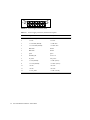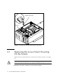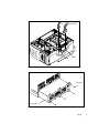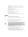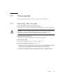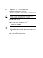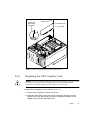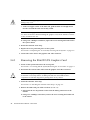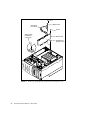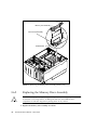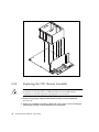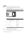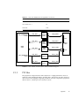
1
Sun™ Ultra™ 80 Service Manual
Sun Microsystems, Inc.
901 San Antonio Road
Palo Alto, CA 94303-4900
U.S.A. 650-960-1300
Part No. 805-6618-11
March 2000, Revision A
Send comments about this document to: [email protected]
Copyright 2000 Sun Microsystems, Inc., 901 San Antonio Road, Palo Alto, California 94303-4900 U.S.A. All rights reserved.
This product or document is protected by copyright and distributed under licenses restricting its use, copying, distribution, and decompilation.
No part of this product or document may be reproduced in any form by any means without prior written authorization of Sun and its licensors,
if any. Third-party software, including font technology, is copyrighted and licensed from Sun suppliers.
Parts of the product may be derived from Berkeley BSD systems, licensed from the University of California. UNIX is a registered trademark in
the U.S. and other countries, exclusively licensed through X/Open Company, Ltd. For Netscape Communicator™, the following notice applies:
(c) Copyright 1995 Netscape Communications Corporation. All rights reserved.
Sun, Sun Microsystems, the Sun logo, AnswerBook2, docs.sun.com, SunDocs, The Network is the Computer, Ultra, Ultra Port Architecture,
SunMicrophone, SunVTS, UltraSPARC, OpenBoot, StroEdge, SunOS, ShowMe How, PGX32, and Solaris are trademarks, registered
trademarks, or service marks of Sun Microsystems, Inc. in the U.S. and other countries. All SPARC trademarks are used under license and are
trademarks or registered trademarks of SPARC International, Inc. in the U.S. and other countries. Products bearing SPARC trademarks are
based upon an architecture developed by Sun Microsystems, Inc.
The OPEN LOOK and Sun™ Graphical User Interface was developed by Sun Microsystems, Inc. for its users and licensees. Sun acknowledges
the pioneering efforts of Xerox in researching and developing the concept of visual or graphical user interfaces for the computer industry. Sun
holds a non-exclusive license from Xerox to the Xerox Graphical User Interface, which license also covers Sun’s licensees who implement OPEN
LOOK GUIs and otherwise comply with Sun’s written license agreements.
RESTRICTED RIGHTS: Use, duplication, or disclosure by the U.S. Government is subject to restrictions of FAR 52.227-14(g)(2)(6/87) and FAR
52.227-19(6/87), or DFAR 252.227-7015(b)(6/95) and DFAR 227.7202-3(a).
DOCUMENTATION IS PROVIDED “AS IS” AND ALL EXPRESS OR IMPLIED CONDITIONS, REPRESENTATIONS AND WARRANTIES,
INCLUDING ANY IMPLIED WARRANTY OF MERCHANTABILITY, FITNESS FOR A PARTICULAR PURPOSE OR NON-INFRINGEMENT,
ARE DISCLAIMED, EXCEPT TO THE EXTENT THAT SUCH DISCLAIMERS ARE HELD TO BE LEGALLY INVALID.
Copyright 2000 Sun Microsystems, Inc., 901 San Antonio Road, Palo Alto, Californie 94303 Etats-Unis. Tous droits réservés.
Ce produit ou document est protégé par un copyright et distribué avec des licences qui en restreignent l’utilisation, la copie, la distribution, et la
décompilation. Aucune partie de ce produit ou document ne peut être reproduite sous aucune forme, par quelque moyen que ce soit, sans
l’autorisation préalable et écrite de Sun et de ses bailleurs de licence, s’il y en a. Le logiciel détenu par des tiers, et qui comprend la technologie
relative aux polices de caractères, est protégé par un copyright et licencié par des fournisseurs de Sun.
Des parties de ce produit pourront être dérivées des systèmes Berkeley BSD licenciés par l’Université de Californie. UNIX est une marque
déposée aux Etats-Unis et dans d’autres pays et licenciée exclusivement par X/Open Company, Ltd. La notice suivante est applicable à
Netscape Communicator™: (c) Copyright 1995 Netscape Communications Corporation. Tous droits réservés.
Sun, Sun Microsystems, le logo Sun, AnswerBook2, docs.sun.com, SunDocs, The Network is the Computer, Ultra, Ultra Port Architecture,
SunMicrophone, SunVTS, UltraSPARC, OpenBoot, StroEdge, SunOS, ShowMe How, PGX32, et Solaris sont des marques de fabrique ou des
marques déposées, ou marques de service, de Sun Microsystems, Inc. aux Etats-Unis et dans d’autres pays. Toutes les marques SPARC sont
utilisées sous licence et sont des marques de fabrique ou des marques déposées de SPARC International, Inc. aux Etats-Unis et dans d’autres
pays. Les produits portant les marques SPARC sont basés sur une architecture développée par Sun Microsystems, Inc.
L’interface d’utilisation graphique OPEN LOOK et Sun™ a été développée par Sun Microsystems, Inc. pour ses utilisateurs et licenciés. Sun
reconnaît les efforts de pionniers de Xerox pour la recherche et le développement du concept des interfaces d’utilisation visuelle ou graphique
pour l’industrie de l’informatique. Sun détient une licence non exclusive de Xerox sur l’interface d’utilisation graphique Xerox, cette licence
couvrant également les licenciés de Sun qui mettent en place l’interface d’utilisation graphique OPEN LOOK et qui en outre se conforment aux
licences écrites de Sun.
CETTE PUBLICATION EST FOURNIE "EN L’ETAT" ET AUCUNE GARANTIE, EXPRESSE OU IMPLICITE, N’EST ACCORDEE, Y COMPRIS
DES GARANTIES CONCERNANT LA VALEUR MARCHANDE, L’APTITUDE DE LA PUBLICATION A REPONDRE A UNE UTILISATION
PARTICULIERE, OU LE FAIT QU’ELLE NE SOIT PAS CONTREFAISANTE DE PRODUIT DE TIERS. CE DENI DE GARANTIE NE
S’APPLIQUERAIT PAS, DANS LA MESURE OU IL SERAIT TENU JURIDIQUEMENT NUL ET NON AVENU.
Please
Recycle
Contents
Preface
1.
2.
Product Description
1-1
1.1
Product Overview
1.2
I/O Devices
1.3
System Features
1.4
Replaceable Components
SunVTS Overview
2.1
3.
i
1-3
1-7
2-1
2-1
2.1.1
SunVTS Requirements
2.1.2
SunVTS References
2-2
2-2
3-1
POST Overview
3.1.1
3.2
1-2
SunVTS Description
Power-On Self-Test
3.1
1-1
3-1
How to Use POST
Pre-POST Preparation
3-2
3-2
3.2.1
Setting Up a Tip Connection
3.2.2
Verifying the Baud Rate
3.3
Initializing POST
3.4
Bypassing POST
3-3
3-4
3-5
3-6
iii
3.5
4.
3-6
3.5.1
diag-level Variable Set to max
3-7
3.5.2
diag-level Variable Set to min
3-28
3.5.3
POST Progress and Error Reporting
3.6
Additional Keyboard Control Commands
3.7
System and Keyboard LEDs
3.8
Initializing Motherboard POST
Troubleshooting Procedures
3-37
3-41
3-41
3-42
4-1
4.1
Problems During Initial Set-up
4.2
Power-On Failure
4.3
Video Output Failure
4.4
Hard Drive or CD-ROM Drive Failure
4.5
Power Supply Troubleshooting
4.6
DIMM Failure
4.7
OpenBoot PROM On-Board Diagnostics
4.8
iv
Maximum and Minimum Levels of POST
4-2
4-3
4-4
4-5
4-6
4-9
4-10
4.7.1
Watch-Clock Diagnostic
4.7.2
Watch-Net and Watch-Net-All Diagnostics
4.7.3
Probe-SCSI and Probe-SCSI-All Diagnostics
4.7.4
Test alias name, device path, -all Diagnostic
4.7.5
UPA Graphics Card
OpenBoot Diagnostics
4-10
4-12
4-13
4-14
4-15
4.8.1
Starting the OpenBoot Diagnostics Menu
4.8.2
OpenBoot Diagnosticss
4.8.3
PCI/Cheerio
4.8.4
EBus DMA/TCR Registers
4.8.5
Ethernet
4.8.6
Keyboard
4.8.7
Mouse
4-22
4.8.8
Floppy
4-22
Ultra 80 Service Manual • March 2000
4-11
4-18
4-19
4-21
4-22
4-20
4-16
4.9
5.
7.
Parallel Port
4-23
4.8.10
Serial Port A
4-24
4.8.11
Serial Port B
4-25
4.8.12
NVRAM
4.8.13
Audio
4.8.14
SCSI
4.8.15
All Above
4-25
4-26
4-26
4-27
How to Get Technical Assistance
4.9.1
SunSolve Online
4.9.2
Access1
4.9.3
docs.sun.com
4.9.4
Free Services Areas
4-29
4-29
4-29
4-30
Safety and Tool Requirements
5.1
Safety Requirements
5.2
Symbols
5.3
Safety Precautions
5.4
6.
4.8.9
4-30
5-1
5-1
5-2
5-2
5.3.1
Modification to Equipment
5-2
5.3.2
Placement of a Sun Product
5-2
5.3.3
Power Cord Connection
5.3.4
Electrostatic Discharge
5.3.5
Lithium Battery
Tools Required
5-3
5-3
5-3
5-4
Power On/Off and Internal Access
6-1
6.1
Powering Off the System/Removing the Access Panel
6.2
Attaching the Antistatic Wrist Strap
6.3
Replacing the Access Panel/Powering On the System
Major Subassemblies
7.1
6-1
6-5
6-6
7-1
Power Supply Assembly
7-1
v
7.2
7.3
7.4
7.5
7.6
7.7
7.8
7.9
vi
7.1.1
Removing the Power Supply Assembly
7-1
7.1.2
Replacing the Power Supply Assembly
7-4
Power Switch Assembly
7-5
7.2.1
Removing the Power Switch Assembly
7-5
7.2.2
Replacing the Power Switch Assembly
7-6
DC-to-DC Converter Assembly
7-7
7.3.1
Removing the DC-to-DC Converter Assembly
7-7
7.3.2
Replacing the DC-to-DC Converter Assembly
7-8
Cable Assemblies
7-9
7.4.1
Removing the Peripheral Power Cable Assembly
7.4.2
Replacing the Peripheral Cable Assembly
7.4.3
Removing the Diskette Drive Cable Assembly
7-11
7.4.4
Replacing the Diskette Drive Cable Assembly
7-12
7.4.5
Removing the Combined Cable Assembly
7-13
7.4.6
Replacing the Combined Cable Assembly
7-14
Interlock Switch Assembly
7-10
7-15
7.5.1
Removing the Interlock Switch Assembly
7-15
7.5.2
Replacing the Interlock Switch Assembly
7-16
Air Guide
7-17
7.6.1
Removing the Air Guide
7-17
7.6.2
Replacing the Air Guide
7-18
Fan Assembly
7-19
7.7.1
Removing a Fan Assembly
7-19
7.7.2
Replacing a Fan Assembly
7-20
Speaker Assembly
7-21
7.8.1
Removing the Speaker Assembly
7-21
7.8.2
Replacing the Speaker Assembly
7-22
SCSI Assembly
7-23
7.9.1
Removing the SCSI Assembly
7-23
7.9.2
Replacing the SCSI Assembly
7-26
Ultra 80 Service Manual • March 2000
7-9
7.10
7.11
8.
8.2
7-27
7.10.1
Removing a Chassis Foot
7-27
7.10.2
Replacing a Chassis Foot
7-28
Filler Panels
7-28
7.11.1
Removing a Filler Panel
7-29
7.11.2
Replacing a Filler Panel
7-30
Storage Devices
8.1
9.
Chassis Foot
8-1
Hard Drive
8-1
8.1.1
Removing a Hard Drive
8-1
8.1.2
Replacing a Hard Drive
8-2
Peripheral Assembly Drive
8-3
8.2.1
Removing the Peripheral Assembly
8.2.2
Removing the CD-ROM Drive or Any Optional Tape Drive
Component 8-5
8.2.3
Replacing the CD-ROM Drive or Any Optional Tape Drive
Component 8-6
8.2.4
Removing the Diskette Drive
8-6
8.2.5
Replacing the Diskette Drive
8-7
8.2.6
Replacing the Peripheral Assembly
Motherboard and Component Replacement
9.1
9.2
9.3
CPU Module
Removing a CPU Module
9-1
9.1.2
Replacing a CPU Module
9-3
9-1
9-5
9.2.1
Removing the NVRAM/TOD
9-5
9.2.2
Replacing the NVRAM/TOD
9-7
PCI Card
8-7
9-1
9.1.1
NVRAM/TOD
8-3
9-7
9.3.1
Removing a PCI Card
9-7
9.3.2
Replacing a PCI Card
9-9
vii
9.4
9.5
9.6
9.7
9.8
9.9
10.
UPA Graphics Card
9.4.1
Removing the UPA Graphics Card
9-10
9.4.2
Replacing the UPA Graphics Card
9-11
9.4.3
Removing the Elite3D UPA Graphics Card
9-12
9.4.4
Replacing the Elite 3D UPA Graphics Card
9-15
9.4.5
Elite3D UPA Graphics Card Patch Information
Audio Module Assembly
9-16
9.5.1
Removing the Audio Module Assembly
9-16
9.5.2
Replacing the Audio Module Assembly
9-18
Memory Riser Assembly
9-19
9.6.1
Removing the Memory Riser Assembly
9-20
9.6.2
Replacing the Memory Riser Assembly
9-22
DIMM
9-25
9.7.1
Removing a DIMM
9-25
9.7.2
Replacing a DIMM
9-27
Motherboard
9-30
9.8.1
Removing the Motherboard
9-31
9.8.2
Replacing the Motherboard
9-33
CPU Shroud Assembly
9-37
9.9.1
Removing the CPU Shroud Assembly
9-37
9.9.2
Replacing the CPU Shroud Assembly
9-38
Illustrated Parts List
10-1
A. Product Specifications
A-1
A.1
Physical Specifications
A.2
Electrical Specifications
A.3
Environmental Requirements
B. Signal Descriptions
B.1
viii
9-9
B-1
Power Connectors
Ultra 80 Service Manual • March 2000
B-1
A-2
A-2
A-3
9-16
B.2
Serial Ports A and B
B-7
B.3
UltraSCSI Connector
B.4
Parallel Port Connector
B.5
Keyboard/Mouse
B.6
Twisted-Pair Ethernet Connector
B-9
B-13
B-15
B.6.1
TPE Cable-Type Connectivity
B.6.2
External UTP-5 Cable Lengths
B.7
Audio Connectors
B.8
UPA Graphics Card Connectors
System
B-16
B-17
B-17
C. Functional Description
C.1
B-16
B-18
C-1
C-1
C.1.1
System Overview
C-2
C.1.2
UPA
C.1.3
PCI Bus
C-5
C.1.3.1
PCI Cards
C.1.3.2
PCI Slot Logical-to-Physical Mapping
C.1.3.3
Using a Token Ring PCI Card
C.1.3.4
U2P ASIC
C.1.3.5
SCSI Controller
C.1.3.6
PCIO ASIC
C-4
C-6
C-8
C-8
UltraSPARC-II Processor
C.1.5
Memory System
C.1.7
C-8
C-9
C.1.5.1
DIMM
C.1.5.2
Interleaving
C.1.5.3
Memory System Timing
C-12
Graphics and Imaging
C-13
C-15
C-15
C.1.6.1
Graphics Card Features
C.1.6.2
Graphics Card Performance
Peripherals
C.1.7.1
C-7
C-7
C.1.4
C.1.6
C-7
C-16
C-17
C-17
CD-ROM Drive
C-17
ix
C.1.7.2
Diskette Drive
C.1.7.3
Hard Drive
C-18
C-20
C.1.8
Other Peripheral Assembly Options
C.1.9
Keyboard and Mouse, Diskette, and Parallel Port
C.1.9.1
Keyboard and Mouse Port
C.1.9.2
Diskette Port
C.1.9.3
Parallel Port
C.1.10 Serial Port
C-21
C-22
C-22
C-23
C.1.10.1
Serial Port Components
C.1.10.2
Serial Port Functions
C.1.10.3
EIA Levels
C.1.10.4
Synchronous Rates
C.1.10.5
Asynchronous Rates
C.1.10.6
Slew Rate and Cable Length
C.1.11 Ethernet
C-24
C-25
C-25
Automatic Negotiation
C.1.11.2
External Cables
C-26
C-27
C-27
C-29
C.1.13.1
Host Adapter
C.1.13.2
Supported Target Devices
C.1.13.3
External Cables
C.1.13.4
Internal SCSI Subassembly
C.1.13.5
SCSI ID Selection
C.1.14 ASICs
C-33
C.1.14.1
XB9++
C.1.14.2
QSC
C.1.14.3
PCIO
C.1.14.4
U2P
C.1.14.5
RISC
C.1.15 SuperIO
C-35
Ultra 80 Service Manual • March 2000
C-25
C-26
C.1.11.1
C.1.13 SCSI
C-24
C-25
C.1.12 Audio Card and Connector
x
C-20
C-33
C-33
C-34
C-34
C-34
C-30
C-31
C-31
C-32
C-31
C-21
C.2
Power Supply
C.2.1
C-35
Control Signals
C-36
C.2.1.1
Remote Enable PowerOn
C.2.1.2
On/Off Functionality
C-37
C.2.1.3
System Power Budget
C-38
C.2.2
Built-In Speaker
C.2.3
Standard System Facilities
C-39
C.3
DC-to-DC Converter Assembly
C.4
Power Management
C.5
Motherboard
C.6
Jumper Descriptions
C.7
C.8
C-39
C-40
C-40
C-41
C-42
C.6.1
Serial Port Jumpers
C.6.2
Flash PROM Jumpers
Enclosure
C-36
C-43
C-44
C-45
C.7.1
Enclosure Basics
C-45
C.7.2
Enclosure Features
C-46
Solaris 2.5.1 and 2.6 Software Upgrades for Systems Faster Than 400 MHz
C-46
D. Conformity
D-1
D.1
Declaration of Conformity
D-1
D.2
Regulatory Compliance Statement
D.3
Agency Compliance
D.4
German Acoustic Compliance
D-5
E. Safety Agency Compliance Statement
Glossary
D-2
D-5
E-1
Glossary-1
xi
xii
Ultra 80 Service Manual • March 2000
Figures
FIGURE 1-1
Ultra 80 Workstation 1-2
FIGURE 1-2
System Front View
1-5
FIGURE 1-3
System Rear View
1-6
FIGURE 3-1
Setting Up a Tip Connection 3-3
FIGURE 3-2
Sun Type-6 Keyboard 3-5
FIGURE 4-1
Power Supply Connector Jack Location
FIGURE 4-2
Power Supply Connector J4106
4-8
FIGURE 4-3
Power Supply Connector J4107
4-9
FIGURE 6-1
System Power 6-2
FIGURE 6-2
Lock Block Location
FIGURE 6-3
Removing/Replacing the Access Panel 6-4
FIGURE 6-4
Attaching the Antistatic Wrist Strap to the Chassis 6-6
FIGURE 6-5
Type-6 Keyboard
FIGURE 7-1
Removing and Replacing the Power Supply Assembly (Sheet 1 of 2) 7-3
FIGURE 7-2
Removing and Replacing the Power Supply Assembly (Sheet 2 of 2) 7-3
FIGURE 7-3
Removing and Replacing the Power Switch Assembly 7-6
FIGURE 7-4
Removing and Replacing the DC-To-DC Converter Assembly 7-8
FIGURE 7-5
Removing and Replacing the Peripheral Power Cable Assembly 7-10
FIGURE 7-6
Removing and Replacing the Diskette Drive Cable Assembly
FIGURE 7-7
Removing and Replacing the Combined Cable Assembly 7-14
4-7
6-3
6-7
7-12
xiii
xiv
FIGURE 7-8
Removing and Replacing the Interlock Switch Assembly
FIGURE 7-9
Removing and Replacing the Air Guide
FIGURE 7-10
Removing and Replacing a Fan Assembly 7-20
FIGURE 7-11
Removing and Replacing the Speaker Assembly
FIGURE 7-12
Removing and Replacing the Hard Drive Cage (Sheet 1 of 2) 7-25
FIGURE 7-13
Removing and Replacing the SCSI Assembly (Sheet 2 0f 2) 7-26
FIGURE 7-14
Removing and Replacing the Chassis Foot
FIGURE 7-15
Removing and Replacing Plastic Filler Panels
FIGURE 7-16
Removing and Replacing Metal Filler Panels
FIGURE 8-1
Removing and Replacing a Hard Drive
FIGURE 8-2
Removing and Replacing the Peripheral Assembly 8-4
FIGURE 8-3
Removing and Replacing the CD-ROM Drive/Diskette Drive 8-5
FIGURE 9-1
Removing and Replacing a CPU Module
FIGURE 9-2
CPU Placement Diagram 9-4
FIGURE 9-3
Removing and Replacing the NVRAM/TOD 9-6
FIGURE 9-4
Removing and Replacing a PCI Card 9-8
FIGURE 9-5
Removing and Replacing a UPA Graphics Card
FIGURE 9-6
Removing and Replacing the Elite3D UPA Graphics Card 9-14
FIGURE 9-7
Removing and Replacing the Audio Module Assembly
FIGURE 9-8
Torque-Indicator Driver Storage Location 9-19
FIGURE 9-9
Removing the Memory Riser Assembly (Sheet 1 of 2) 9-21
FIGURE 9-10
Removing the Memory Riser Assembly (Sheet 2 of 2) 9-22
FIGURE 9-11
Setting the Memory Riser Assembly Thumbscrew Torque 9-24
FIGURE 9-12
Removing and Replacing a DIMM (Sheet 1 of 2) 9-26
FIGURE 9-13
Removing and Replacing a DIMM (Sheet 2 of 2) 9-27
FIGURE 9-14
DIMM Bank Arrangement
FIGURE 9-15
Removing and Replacing the Motherboard 9-33
FIGURE 9-16
Location of the Motherboard Serial Port Jumpers 9-34
FIGURE 9-17
Identifying Jumper Pins
FIGURE 9-18
Removing and Replacing the CPU Shroud Assembly
7-16
7-18
7-22
7-28
7-29
7-30
8-2
9-3
9-11
9-18
9-29
9-35
Sun Ultra 80 Service Manual • March 2000
9-38
FIGURE 10-1
System Exploded View 10-2
FIGURE B-1
DC-to-DC Converter Connector J4105 B-2
FIGURE B-2
Power Supply Connector J4106
B-3
FIGURE B-3
Power Supply Connector J4107
B-4
FIGURE B-4
DC-to-DC Converter Connector J4108 B-5
FIGURE B-5
PCI Fan Connector J4109
FIGURE B-6
CPU Fan Connector J4110
FIGURE B-7
Combined Cable Assembly Connector J4111
FIGURE B-8
Peripheral Power Cable Assembly Connector J4112
FIGURE B-9
Serial Port A and B Connector Pin Configuration
FIGURE B-10
UltraSCSI Connector Pin Configuration
FIGURE B-11
Parallel Port Connector Pin Configuration
FIGURE B-12
Keyboard/Mouse Connector Pin Configuration B-15
FIGURE B-13
TPE Connector Pin Configuration
FIGURE B-14
Audio Connector Configuration
FIGURE B-15
UPA Graphics Card Connector Pin Configuration B-19
FIGURE C-1
System Functional Block Diagram
FIGURE C-2
UPA Address and Data Buses Functional Block Diagram C-5
FIGURE C-3
Memory System Functional Block Diagram
FIGURE C-4
Memory Module Functional Block Diagram C-11
FIGURE C-5
DIMM Mapping C-12
FIGURE C-6
Keyboard and Mouse, Diskette, and Parallel Port
Functional Block Diagram C-21
FIGURE C-7
Serial Port Functional Block Diagram C-24
FIGURE C-8
Audio Card Functional Block Diagram
FIGURE C-9
Configuration for the SCSI Bus
FIGURE C-10
SCSI Subassembly Functional Block Diagram
FIGURE C-11
System Motherboard Block Diagram C-41
FIGURE C-12
Selected Jumper Settings
FIGURE C-13
Identifying Jumper Pins
B-5
B-6
B-6
B-7
B-8
B-10
B-14
B-16
B-18
C-3
C-10
C-28
C-30
C-32
C-42
C-42
Figures
xv
xvi
FIGURE C-14
Serial Port Jumpers
FIGURE C-15
Flash PROM Jumpers C-45
C-43
Sun Ultra 80 Service Manual • March 2000
Tables
TABLE 1-1
Supported I/O Devices
TABLE 1-2
Replaceable Components
TABLE 3-1
diag-level and diag-switch? Settings 3-2
TABLE 3-2
POST Completion Times 3-6
TABLE 3-3
Keyboard LED Patterns
TABLE 4-1
Troubleshooting Information
TABLE 4-2
Internal Drives Identification 4-5
TABLE 4-3
Power Supply Connector J4106 Pin Description
4-8
TABLE 4-4
Power Supply Connector J4107 Pin Description
4-9
TABLE 4-5
Listing of Memory Addressing Tables 4-10
TABLE 4-6
Selected OBP On-Board Diagnostic Tests
TABLE 4-7
PCI/Cheerio Diagnostic
TABLE 4-8
EBus DMA/TCR Registers Diagnostic
TABLE 4-9
Ethernet Diagnostic 4-21
TABLE 4-10
Parallel Port Function 4-23
TABLE 9-1
CPU Placement Order 9-4
TABLE 9-2
DIMM Bank Arrangement
TABLE 9-3
Serial Port Jumper Settings
9-34
TABLE 10-1
Replaceable Components
10-3
TABLE A-1
System Physical Specifications
1-3
1-7
3-40
4-2
4-14
4-19
4-20
9-28
A-2
xvii
xviii
TABLE A-2
Electrical Specifications
TABLE A-3
Environmental Requirements
TABLE B-1
Power Connectors
TABLE B-2
DC-to-DC Converter Connector J4105 Pin Description
TABLE B-3
Power Supply Connector J4106 Pin Description
B-3
TABLE B-4
Power Supply Connector J4107 Pin Description
B-4
TABLE B-5
DC-to-DC Converter Connector J4108 Pin Description
TABLE B-6
PCI Fan Connector J4109 Pin Description
TABLE B-7
CPU Fan Connector J4110 Pin Description B-6
TABLE B-8
Combined Cable Assembly Connector J4111 Pin Description
TABLE B-9
Peripheral Power Cable Assembly Connector J4112 Pin Description
TABLE B-10
Serial Port A and B Connector Pin Assignments
TABLE B-11
UltraSCSI Connector Pin Assignments
TABLE B-12
Parallel Port Connector Pin Assignments
TABLE B-13
Keyboard/Mouse Connector Pin Assignments
TABLE B-14
TPE Connector Pin Assignments
TABLE B-15
TPE UTP-5 Cables
TABLE B-16
Audio Connector Line Assignment B-18
TABLE B-17
UPA Graphics Card Connector Pin Assignments
TABLE C-1
UPA Interconnect C-4
TABLE C-2
UPA Port Identification Assignments
TABLE C-3
PCI Slot-To-PCI Bus Mapping
TABLE C-4
PCI Slot Logical-to-Physical Mapping C-7
TABLE C-5
DIMM Bank-to-U-Number Mapping C-13
TABLE C-6
1-Gbyte DIMM Configuration Scenario C-14
TABLE C-7
Memory Relative Starting Address with No Interleaving C-14
TABLE C-8
Memory Addressing for 2-Way Interleaving C-15
TABLE C-9
Memory Addressing for 4-Way Interleaving C-15
TABLE C-10
Diskette Drive Signals and Functions C-19
TABLE C-11
18-Gbyte Hard Drive Features
A-2
A-3
B-1
B-2
B-5
B-5
B-8
B-10
B-14
B-15
B-16
B-17
Sun Ultra 80 Service Manual • March 2000
B-19
C-4
C-6
C-20
B-6
B-7
TABLE C-12
Audio Card Features
TABLE C-13
Supported Target Devices C-31
TABLE C-14
Power Supply Output Values
TABLE C-15
Power Supply Control Signal C-36
TABLE C-16
450-MHz CPU Module Power Estimate
TABLE C-17
Built-In Speaker Specifications
TABLE C-18
Serial Port Jumper Settings
TABLE C-19
Flash PROM Jumper Settings C-45
C-27
C-36
C-38
C-39
C-44
Tables
xix
xx
Sun Ultra 80 Service Manual • March 2000
Code Samples
CODE EXAMPLE 3-1
diag-level Variable Set to max (4-Way CPU)
3-7
CODE EXAMPLE 3-2
diag-level Variable Set to max (2-Way CPU)
3-16
CODE EXAMPLE 3-3
diag-level Variable Set to max (Single CPU)
3-22
CODE EXAMPLE 3-4
diag-level Variable Set to min (4-Way CPU)
3-29
CODE EXAMPLE 3-5
diag-level Variable Set to min (2-Way CPU)
3-32
CODE EXAMPLE 3-6
diag-level Variable Set to min (Single CPU)
3-35
CODE EXAMPLE 3-7
Typical Error Code Failure Message
CODE EXAMPLE 4-1
Watch-Clock Diagnostic Output Message
CODE EXAMPLE 4-2
Watch-Net Diagnostic Output Message
CODE EXAMPLE 4-3
Watch-Net-All Diagnostic Output Message
CODE EXAMPLE 4-4
Probe-SCSI Diagnostic Output Message
CODE EXAMPLE 4-5
Probe-SCSI-All Output Message
CODE EXAMPLE 4-6
Test Output Message
CODE EXAMPLE 4-7
Reset Verification 4-16
CODE EXAMPLE 4-8
OBDiag Menu
CODE EXAMPLE 4-9
PCI/Cheerio Diagnostic Output Message
3-37
4-10
4-11
4-11
4-12
4-13
4-13
4-18
4-19
CODE EXAMPLE 4-10
EBus DMA/TCR Registers Diagnostic Output Message
CODE EXAMPLE 4-11
Ethernet Diagnostic Output Message
CODE EXAMPLE 4-12
Keyboard Diagnostic Output Message
CODE EXAMPLE 4-13
Mouse Diagnostic Output Message
4-20
4-21
4-22
4-22
xxi
xxii
CODE EXAMPLE 4-14
Floppy Diagnostic Output Message
CODE EXAMPLE 4-15
Parallel Port Output Message
CODE EXAMPLE 4-16
Serial Port A Diagnostic Output Message with Tip Line Installed
CODE EXAMPLE 4-17
Serial Port A Diagnostic Output Message
4-24
CODE EXAMPLE 4-18
Serial Port B Diagnostic Output Message
4-25
CODE EXAMPLE 4-19
NVRAM Diagnostic Output Message
CODE EXAMPLE 4-20
Audio Diagnostic Output Message 4-26
CODE EXAMPLE 4-21
SCSI Output Message
CODE EXAMPLE 4-22
All Above Diagnostic Output Message
Sun Ultra 80 Service Manual • March 2000
4-23
4-23
4-25
4-26
4-27
4-24
Preface
The Sun Ultra 80 Service Manual provides detailed procedures that describe the
removal and replacement of replaceable parts in the Ultra™ 80 computer (system).
The service manual also includes information about the use and maintenance of the
system. This book is written for technicians, system administrators, authorized
service providers (ASPs), and advanced computer system end users who have
experience troubleshooting and replacing hardware.
How This Book Is Organized
This document is organized into chapters and appendices as listed in the following
table. A glossary and an index is also included.
TABLE P-1
Document Organization
Chapter
Content Description
Chapter 1
Describes the major components of the system.
Chapter 2
Describes the execution of individual tests for verifying
hardware configuration and functionality.
Chapter 3
Describes the execution of POST and provides examples of POST
output patterns.
Chapter 4
Provides troubleshooting advice and suggested corrective
actions for hardware problems.
Chapter 5
Explains how to work safely when servicing the system.
i
TABLE P-1
Document Organization (Continued)
Chapter
Content Description
Chapter 6
Provides step-by-step procedures to power on and power off the
system. Also provides step-by-step procedures to remove the
side access panel, attach the wrist strap, and replace the side
access panel.
Chapter 7
Provides step-by-step procedures to remove and replace major
subassemblies.
Chapter 8
Provides step-by-step procedures to remove and replace storage
devices.
Chapter 9
Provides step-by-step procedures to remove and replace the
motherboard, and various components associated with
motherboard operation.
Chapter 10
Lists replaceable parts for the system.
Appendix A
Provides product specifications, system requirements about
power and environment, system dimensions, weight, memory
mapping, and PCI card slot specifications.
Appendix B
Provides signal descriptions.
Appendix C
Provides functional descriptions for the system.
Appendix D
Provides Declaration of Conformity and Regulatory Compliance
statements.
Appendix E
Provides Safety Agency Compliance statement.
Glossary
Provides a listing of acronyms, terms, and definitions.
UNIX Commands
This document may not contain information on basic UNIX™ commands and
procedures such as shutting down the system, booting the system, and configuring
devices.
See one or more of the following for this information:
■
■
■
ii
Solaris Handbook for Sun Peripherals
AnswerBook2™ online documentation for the Solaris™ software environment
Other software documentation that you received with your system
Sun Ultra 80 Service Manual • March 2000
Typographic Conventions
TABLE P-2
Typographic Conventions
Typeface or Symbol
Meaning
Examples
AaBbCc123
The names of commands, files,
and directories; on-screen
computer output.
Edit your .login file.
Use ls -a to list all files.
% You have mail.
AaBbCc123
What you type, when contrasted
with on-screen computer output.
% su
Password:
AaBbCc123
Book titles, new words or terms,
words to be emphasized.
Command-line variable; replace
with a real name or value.
Read Chapter 6 in the User’s
Guide.
These are called class options.
You must be root to do this.
To delete a file, type rm
filename.
iii
Shell Prompts
TABLE P-3
Shell Prompts
Shell
Prompt
C shell
machine_name%
C shell superuser
machine_name#
Bourne shell and Korn shell
$
Bourne shell and Korn shell
superuser
#
Related Documents
TABLE P-4
iv
Related Documents
Application
Title
Part Number
Configuration
Solaris Handbook for SMCC Peripherals
802-7675
Diagnostics
SunVTS 2.1 User’s Guide (Solaris 2.5.1 11/97)
805-1631
Diagnostics
SunVTS 2.1 Quick Reference Card
(Solaris 2.5.1 11/97)
805-1629
Diagnostics
SunVTS 2.1.1 Test Reference Manual
(Solaris 2.5.1 11/97)
805-2976
Diagnostics
SunVTS 2.3 User’s Guide (SunVTS 2.1.3)
802-7299
Diagnostics
SunVTS 2.3 Quick Reference Card (SunVTS 2.1.3)
802-7301
Diagnostics
SunVTS 2.3 Test Reference Manual
(SunVTS 2.1.3)
805-4163
Diagnostics
SunVTS 3.0 User’s Guide (SunVTS 3.0)
805-4442
Diagnostics
SunVTS 3.0 Quick Reference Card (SunVTS 3.0)
805-5589
Diagnostics
SunVTS 3.0 Test Reference Manual (SunVTS 3.0)
805-4443
Sun Ultra 80 Service Manual • March 2000
TABLE P-4
Related Documents (Continued)
Application
Title
Part Number
Diagnostics
SunVTS 3.1 User’s Guide (SunVTS 3.1)
805-7406
Diagnostics
SunVTS 3.1 Quick Reference Card (SunVTS 3.1)
805-7408
Diagnostics
SunVTS 3.1 Test Reference Manual (SunVTS 3.1)
805-7407
Installation
14-Gbyte, 8-mm Tape Drive Installation Manual
802-1849
Installation
Elite3D Installation Guide
805-4391
Installation
Creator Frame Buffer Installation Guide
802-6682
Installation
Sun PGX32 PCI Graphics Card Installation Guide
805-7770
Installation/user
12-24 Gbyte 4-mm DDS-3 Tape Drive Installation
and User’s Guide
802-7791
Installation
5.25” Fast/Wide Differential SCSI Disk Drive
Installation Manual
802-1653
Installation
Sun Ultra 80 Rack Mount Installation Guiide
805-7959
Installation/user
Sun StorEdge CD32 Installation and User’s Guide
805-4237
Specification
Manual Eject Diskette Drive Specifications
805-1133
Specification
18 Gbyte 10K rpm Disk Drive Specifications
806-1057-10
Specification
8-mm Tape Drive Specifications
802-5775
Specification
4-mm, DDS-2 Tape Drive Specifications
802-7790
User
21-Inch Premium (19.8-inch Viewable) Color
Monitor Guide
875-1844
User
24-Inch Premium
(22.5-inch Viewable) Color Monitor Guide
875-1799
User
14-Gbyte, 8-mm Tape Drive User’s Guide
802-1850
User
SBus Wide Intelligent UltraSCSI Differential Host
Adapter Guide
802-7748
v
Ordering Sun Documents
The docs.sun.comSM web site enables you to access Sun technical documentation
on the web. You can browse the docs.sun.com archive or search for a specific book
title or subject at:
http://docs.sun.com
Sun Welcomes Your Comments
We are interested in improving our documentation and welcome your comments
and suggestions. You can email your comments to us at:
[email protected]
Please include the part number of your document in the subject line of your email.
vi
Sun Ultra 80 Service Manual • March 2000
CHAPTER
1
Product Description
This chapter contains the following topics:
■
■
■
■
1.1
Section
Section
Section
Section
1.1
1.2
1.3
1.4
“Product Overview” on page 1-1
“I/O Devices” on page 1-2
“System Features” on page 1-3
“Replaceable Components” on page 1-7
Product Overview
The Sun™ Ultra™ 80 workstation is a multiprocessor workstation that uses the
UltraSPARC™-II family of processors. The workstation offers super-scalar processor
technology, multiprocessing, high-performance memory interconnection, and highbandwidth input/output (I/O). In addition, the workstation provides accelerated
graphics.
The following figure illustrates the Ultra 80 workstation. The high-level functions of
the Ultra 80 workstation include:
■
■
■
■
Power and cooling requirements for a high-performance processor
Modular internal design
Improved disk, system, memory, and I/O performance and capacities
High-performance peripheral component interconnect (PCI) I/O expansion
-1
FIGURE 1-1
1.2
Ultra 80 Workstation
I/O Devices
The Ultra 80 workstation uses the I/O devices listed in the following table:
-2
Sun Ultra 80 Service Manual • March 2000
Note – If a Sun PGX32™ PCI graphics card is installed, the 15HDM/13W3F video
adapter 24-inch cable, part number 530-2917, is required between the Sun 21-inch
monitor cable connector and the PGX32 PCI graphics card connector.
TABLE 1-1
Supported I/O Devices
I/O Devices
Description
21-inch (51-cm)
color monitor
1152 x 900 resolution, 76- or 66-Hz refresh rate, 84 dots per inch
(dpi)
1280 x 1024 resolution, 76- or 66-Hz refresh rate, 93 dpi
960 x 680 resolution, 112-Hz refresh rate, 70 dpi
24-inch (61-cm)
color monitor
1920 x 1200 resolution, 70-Hz refresh rate, 103 dpi
1600 x 1000 resolution, 76- or 66-Hz refresh rate, 86 dpi
1400 x 900 resolution, 76-Hz refresh rate, 77 dpi
1280 x 800 resolution, 76-Hz refresh rate, 69 dpi
1.3
Microphone
(optional)
SunMicrophone™ II
Keyboard
Sun Type-6
Mouse
Crossbow; optomechanical, 3-button
System Features
Ultra 80 workstation electronics are contained on a single printed circuit board
(motherboard). The motherboard contains the CPU modules, memory (with half of
memory being extended to the memory riser assembly), system control applicationspecific integrated circuits (ASICs), and I/O ASICs.
The following illustrations show the front and rear views. The electronics and
peripherals contain (or may be upgraded to contain) the following features:
■
■
■
System enclosure with 670-watt power supply.
Support for modular UltraSPARC II processor with up to a
8-megabyte (Mbyte) Ecache.
112.5-megahertz (MHz) UPA coherent memory interconnect.
Chapter
-3
■
■
Use of dual in-line memory modules (DIMMs). There are a total of 16 DIMM
slots, with 8 slots located on four banks on the motherboard and 8 slots located on
four banks on the memory riser assembly. Each bank of four DIMM slots accepts
64-Mbyte or 256-Mbyte DIMM modules. Populating with either eight identical
capacity DIMMs in banks 0 and 1 (with banks 2 and 3 empty), or 16 identical
capacity DIMMs in banks 0, 1, 2, and 3 enables the memory controller for optimal
interleaving performance.
Four PCI slots:
Two 33-MHz, 64-bit/32-bit, 5 VDC/3 VDC slots
One 33-MHz, 32-bit, 5 VDC/3 VDC slot
■
One 66-MHz/33-MHz, 64-bit/32-bit, 5 VDC slot
Two UPA graphics slots
10-/100-megabits per second Ethernet
40 Mbytes/sec. UltraSCSI (two channels)
Two DB-25 serial ports (synchronous and asynchronous protocols)
Centronics-compatible parallel port interface with extended capability port (ECP)
support
Modular audio interface
Power interlock switch. As a safety precaution, the Ultra 80 system is equipped
with a power interlock switch that shuts off system power when the access panel
is opened. Be sure to power down the system before you open the access panel to
avoid losing data.
■
■
■
■
■
■
■
■
■
-4
Sun Ultra 80 Service Manual • March 2000
CD-ROM drive
3.5-/5.25-inch slot
Power switch
FIGURE 1-2
Diskette drive
System Front View
Chapter
-5
Lock block
Serial port A
Serial port B
SCSI port
Parallel port
Keyboard/mouse
Power supply
RJ-45 (TPE)
Audio
Power inlet
FIGURE 1-3
-6
System Rear View
Sun Ultra 80 Service Manual • March 2000
UPA graphics
PCI 4
PCI 3
PCI 2
PCI 66 1
1.4
Replaceable Components
The following table lists the replaceable components for the Ultra 80 workstation by
part number. A brief description of each listed component is also provided.
Note – The part numbers listed in the following table are correct as of the service
manual publication date but are subject to change without notice. Consult your
authorized Sun sales representative or service provider to confirm a part number
prior to ordering a replacement part.
TABLE 1-2
Replaceable Components
Component
Part Number
Description
Power switch
150-3112
Provides main power to system
Interlock switch
150-3114
Provides power interlock
SCSI assembly
530-2691
Provides interface between hard drive(s) and motherboard
Power supply assembly
300-1411
Power supply, 670 watts, 220 VAC only
Power supply assembly
300-1357
Power supply, 670 watts
Feet
330-2321
Kit, 5 per box (part of #560-2525, Ultra 30/60/80 accessory
kit)
5.25-inch filler panel
330-2187
Plastic (part of #560-2525, Ultra 30/60/80 accessory kit)
3.5-inch filler panel
330-2186
Plastic (part of #560-2525, Ultra 30/60/80 accessory kit)
3.5-/5.25-inch filler panel
330-2691
Plastic, combo (part of #560-2525, Ultra 30/60/80 accessory
kit)
3.5-inch filler panel
340-4067
Metal (part of #560-2525, Ultra 30/60/80 accessory kit)
5.25-inch filler panel
340-4068
Metal (part of #560-2525, Ultra 30/60/80 accessory kit)
3.5-/5.25-inch filler panel
340-4764
Metal (part of #560-2525, Ultra 30/60/80 accessory kit)
Speaker assembly
370-1579
16-ohm speaker
Fan assembly
370-3718
120-mm fan assembly
Manual eject floppy assembly
370-2729
Diskette drive
CD-ROM drive
370-3415
1.6-inch 32x CD-ROM drive
4-mm tape drive
370-2176
4-Gbyte/8-Gbyte, 4-mm tape drive, DDS-2
4-mm tape drive
370-2377
12-Gbyte/24-Gbyte, 4-mm tape drive, DDS-3
8-mm tape drive
370-1922
14-Gbyte, 8-mm tape drive
Chapter
-7
TABLE 1-2
Replaceable Components (Continued)
Component
Part Number
Description
Motherboard assembly
501-5168
System board
Graphics card
540-3902
Elite3D m6 UPA graphics card
AFB serial port cable
530-2672
Elite3D m6 UPA graphics card stereo cable assembly
CPU module
501-5344
450-MHz UltraSPARC-II CPU module
64-Mbyte DIMM
501-5691
60-ns, 64-Mbyte DIMM
256-Mbyte DIMM
501-4743
60-ns, 256-Mbyte DIMM
Audio module assembly
501-4155
Audio applications, 16-bit audio, 8 kHz to 48 kHz
Drive power cable assembly
530-2582
DC power cable assembly
Diskette drive cable assembly
530-2346
Diskette drive cable assembly
Combined cable assembly
530-2583
Combined cable assembly
Memory riser assembly
501-5218
Riser board assembly
DC-to-DC converter assembly
300-1407
DC-to-DC converter with fan
Hard drive
540-4177
18-GByte, 10000 RPM hard drive
PCI card
N/A
Generic
TPE cable (category 5)
530-1871
Twisted-pair Ethernet cable
CPU filler panel
330-2805
CPU filler panel (part of #560-2525, Ultra 30/60/80 accessory
kit)
NVRAM/TOD
525-1430
Time of day, 48T59, with carrier
PCI filler panel
240-2750
PCI filler panel (part of #560-2525, Ultra 30/60/80 accessory
kit)
Torque-indicator driver
340-6091
Used to loosen and tighten the torque-limiting screws
on the memory riser assembly
SCSI cable assembly
530-2937
Installed when second SCSI device installed
-8
Sun Ultra 80 Service Manual • March 2000
CHAPTER
2
SunVTS Overview
This chapter contains an overview of the SunVTS™ diagnostic tool.
This chapter contains the following topics:
■
■
■
2.1
Section 2.1 “SunVTS Description” on page 2-1
Section 2.1.1 “SunVTS Requirements” on page 2-2
Section 2.1.2 “SunVTS References” on page 2-2
SunVTS Description
SunVTS™ is Sun’s online Validation Test Suite. SunVTS is a comprehensive software
diagnostic package that tests and validates hardware by verifying the connectivity
and functionality of most hardware controllers, devices, and platforms.
SunVTS can be tailored to run on various types of systems ranging from desktops to
servers with many customizable features to meet the varying requirements of many
diagnostic situations.
Use SunVTS to validate a system during development, production, receiving
inspection, troubleshooting, periodic maintenance, and system or subsystem
stressing.
SunVTS executes multiple diagnostic tests from one graphical user interface (GUI)
that provides test configuration and status monitoring. The user interface can run in
the CDE or OPEN LOOK environments or through a TTY-mode interface for
situations when running a GUI is not possible.
The SunVTS interface can run on one system to display the SunVTS test session of
another system on the network.
SunVTS is distributed with each SPARC™ Solaris™ release. It is located on the Sun
Computer Systems Supplement CD.
-1
2.1.1
SunVTS Requirements
Your system must meet the following requirements to run SunVTS:
■
■
■
2.1.2
The SunVTS packages must be installed. The main package is SUNWvts. There
are additional supporting packages that differ based on the revision of Solaris
that is installed. For specific details, refer to the corresponding SunVTS
documentation (described below).
The system must be booted to the multiuser level (level 3).
To run SunVTS with a GUI, that GUI must be installed. Otherwise, run SunVTS
with the TTY-mode interface.
SunVTS References
To find out more information about the use of SunVTS, refer to the SunVTS
documentation that corresponds to the Solaris release that you are running.
The following list describes the content of each SunVTS document:
■
■
■
SunVTS User’s Guide – describes how to install, configure, and run the SunVTS
diagnostic software.
SunVTS Quick Reference Card – provides an overview of how to use the SunVTS
CDE interface.
SunVTS Test Reference Manual – provides details about each individual SunVTS
test.
These documents are part of the Solaris on Sun Hardware Collection AnswerBook set.
This collection is distributed on the Sun Computer Systems Supplement CD with each
SPARC Solaris release and also accessible at http://docs.sun.com.
-2
Sun Ultra 80 Service Manual • March 2000
CHAPTER
3
Power-On Self-Test
This chapter describes how to initiate power-on self-test (POST) diagnostics.
This chapter contains the following topics:
■
■
■
■
■
■
■
■
3.1
Section
Section
Section
Section
Section
Section
Section
Section
3.1
3.2
3.3
3.4
3.5
3.6
3.7
3.8
“POST Overview” on page 3-1
“Pre-POST Preparation” on page 3-2
“Initializing POST” on page 3-5
“Bypassing POST” on page 3-6
“Maximum and Minimum Levels of POST” on page 3-6
“Additional Keyboard Control Commands” on page 3-41
“System and Keyboard LEDs” on page 3-41
“Initializing Motherboard POST” on page 3-42
POST Overview
POST is useful in determining if a portion of the system has failed and should be
replaced. POST verifies the core functionality of the system, including the
motherboard, memory, and any on-board I/O devices. POST can be run even if the
system is unable to boot.
POST detects approximately 95 percent of system faults and is located in the system
board OpenBoot™ PROM (OBP). The setting of two NVRAM variables, the
diag-switch? and the diag-level flag, determine if POST is executed.
POST diagnostic and error message reports are displayed on a console terminal or
through the LEDs located on the Type-6 keyboard.
-1
3.1.1
How to Use POST
When the system power is applied, POST runs automatically if any of the following
conditions apply:
■
■
The diag-switch? NVRAM parameter is set to true.
The Type-6 keyboard Stop and D keys are pressed as power is applied to the
system.
In the event of an automatic system reset, POST runs if the diag-switch? NVRAM
parameter is set to true and the diag-level flag is set to either max or min.
The following table lists the diag-switch? and diag-level flag settings for
disabling POST (off), enabling POST maximum (max), or enabling POST minimum
(min).
TABLE 3-1
diag-level and diag-switch? Settings
diag-level Setting
POST
Initialization
Serial Port A
I/O
Serial Port A
Error Output
diag-switch?
Setting
Off
No
N/A
N/A
N/A
Max
Yes (power-on)
Enabled
Enabled
True
Min
Yes (power-on)
Disabled
Enabled
True
3.2
Pre-POST Preparation
Pre-POST preparation includes:
■
■
Setting up a Tip connection to another system or terminal to view POST progress
and error messages. See Section 3.2.1 “Setting Up a Tip Connection”.
Verifying baud rates between a system and a monitor or a system and a terminal.
See Section 3.2.2 “Verifying the Baud Rate” on page 3-4.
If a terminal or a monitor is not connected to serial port A (default port) of a system
or server to be tested, the keyboard LEDs are used to determine error conditions. See
Section 3.7 “System and Keyboard LEDs” on page 3-41.
-2
Sun Ultra 80 Service Manual • March 2000
3.2.1
Setting Up a Tip Connection
A tip connection enables a remote shell window to be used as a terminal to display
test data from a system. Serial port A or serial port B of a tested system is used to
establish the tip connection between the system being tested and another Sun system
monitor or TTY-type terminal. The tip connection is used in a terminal window and
provides features to help with the OBP.
To set up a tip connection:
1. Connect serial port A of the system being tested to serial port B of another Sun
system using a serial null modem cable (connect cable pins 2-3, 3-2, 7-20, and
20-7).
2
2
3
3
7
7
20
20
FIGURE 3-1
Setting Up a Tip Connection
2. At the other Sun system, check the /etc/remote file by changing to the
/etc directory and then editing the remote file:
hardwire:/ dv=/dev/term/b:br#9600:el=^C^S^Q^U^D:ie=%$:oe=^D:
Note – The example shows connection to serial port B.
3. To use serial port A:
a. Copy and paste the serial port B remote file.
b. Modify the serial port B remote file as follows:
hardwire:\ dv=/dev/term/a:br#9600:el=^C^S^Q^U^D:ie=%$:oe=^D:
Chapter
-3
4. In a shell window on the Sun system, type: tip hardwire.
hostname% tip hardwire
connected
Note – The shell window is now a tip window directed to the serial port of the
system being tested. When power is applied to the system being tested, POST
messages will be displayed in this window.
5. When POST is completed, disconnect the tip window as follows:
a. Open a shell window.
b. Type ps -a to view the active tip line and process ID (PID) number.
c. Type the following to kill the tip hardwire process.
% kill -9 PID#
3.2.2
Verifying the Baud Rate
To verify the baud rate between the system being tested and a terminal or another
Sun system monitor:
1. Open a shell window.
2. Type eeprom.
3. Verify the following serial port default settings as follows:
ttyb-mode = 9600,8,n,1
ttya-mode = 9600,8,n,1
Note – Ensure that the settings are consistent with TTY-type terminal or system
monitor settings.
-4
Sun Ultra 80 Service Manual • March 2000
3.3
Initializing POST
You can initialize POST in two ways:
■
■
Set the diag-switch? to true and the diag-level to max or min, and then
power cycle the system
Simultaneously press the Stop and D keyboard keys while power is applied to the
system
To set the diag-switch? to true and power cycle the system:
1. At the system prompt, type:
ok setenv diag-switch? true
2. At the Type-6 keyboard, power cycle the system by simultaneously pressing the
Shift key and the power key. After a few seconds, press the power key again.
Caps
lock
Num
Lock
Shift key
Esc
F1
F2
F3
F4
F5
F6
Power key
Compose
Num Lock
Help
Scroll
lock
Caps Lock
F7
Scroll Lock
F8
Compose
F9
F10
F11
F12
Print
Screen
Scroll
Lock
SysRq
Stop
Again
~
!
`
1
Props
Undo
Tab
Front
Copy
@
#
2
$
3
Q
%
4
W
^
5
E
&
6
R
*
7
T
(
8
Y
)
9
U
_
0
I
+
P
{
S
D
F
G
H
J
K
L
:
;
Open
Paste
Find
Cut
FIGURE 3-2
Z
X
C
V
B
N
Shift
Control
Alt
M
<
,
>
.
|
}
[
A
Caps Lock
Break
Insert
Home
Page
Up
Num
Lock
/
*
-
Del
End
Page
Down
7
8
9
+
=
-
O
Back Space
]
Pause
\
"
Enter
PgUp
Home
4
5
6
1
2
3
'
?
Shift
/
End
Compose
Alt
Graph
Enter
PgDn
0
.
Ins
Del
Sun Type-6 Keyboard
3. Verify the following:
■
■
■
The display prompt is no longer displayed.
The monitor power indicator flashes on and off.
The keyboard Caps Lock key indicator flashes on and off.
Chapter
-5
3.4
Bypassing POST
POST can be disabled and thereby bypassed as follows:
1. Prior to powering on the system, press and hold the Stop key on the keyboard
(FIGURE 3-1 on page 3-3).
2. Pressing the power key and then immediately pressing the keyboard Stop key.
3.5
Maximum and Minimum Levels of
POST
Two levels of POST are available: maximum (max) level and minimum (min) level.
The system initiates the selected level of POST based upon the setting of
diag-level, a NVRAM variable.
Various CPU configurations coupled with the amount of installed memory effects
the amount of time that is required to complete the POST. The following table lists
the approximate amount of time that is required to complete the POST with 2.5
Gbytes of DIMM installed for the diag-level variable set to max and the diaglevel variable set to min with regard to the various CPU configurations.
TABLE 3-2
POST Completion Times
CPU Configuration
max setting
min setting
4-way
8 minutes
6 minutes
2-way
3.5 minutes
3 minutes
Single
1.5 minutes
1.3 minutes
The default setting for diag-level is max. Examples of the max-level POST output
on serial port A is provided in Section 3.5.1 “diag-level Variable Set to max”.
Examples of the min-level POST output on serial port A is provided in
Section 3.5.2 “diag-level Variable Set to min” on page 3-28.
To set the diag-level variable to min, type:
ok setenv diag-level min
-6
Sun Ultra 80 Service Manual • March 2000
To return to the default setting:
ok setenv diag-level max
3.5.1
diag-level Variable Set to max
When the diag-level variable is set to max, POST enables an extended set of
diagnostic-level tests. The following code examples identify a typical serial port A
POST output with the diag-level variable set to max for 4-way, 2-way, and single
CPU configurations.
■
CODE EXAMPLE 3-1 on page 3-7
■
CODE EXAMPLE 3-2 on page 3-16
■
CODE EXAMPLE 3-3 on page 3-22
Note – The following POST examples are executed with 450-MHz CPUs and
2.5 Gbytes of memory.
CODE EXAMPLE 3-1
diag-level Variable Set to max (4-Way CPU)
Executing Power On SelfTest
0>
0>@(#) Sun U80(UltraSPARC-II 4-way) UPA/PCI POST 1.2.5 04/05/1999
09:42 AM
0>INFO: Processor 0 is master. CPU 450 MHz. 4304KB Ecache.
0>
0> <00> Init System BSS
0> <00> NVRAM Battery Detect Test
0> <00> NVRAM Scratch Addr Test
0> <00> DMMU TLB Tag Access Test
0> <00> DMMU TLB RAM Access Test
0> <00> IMMU TLB Tag Access Test
0> <00> IMMU TLB RAM Access Test
0> <00> Probe Ecache
0> <00> Ecache RAM Addr Test
0> <00> Ecache Tag Addr Test
0> <00> Ecache Tag Test
0> <00> Invalidate Ecache Tags
0>INFO: Processor 1 - UltraSPARC-II.
0>INFO: Processor 2 - UltraSPARC-II.
0>INFO: Processor 3 - UltraSPARC-II.
0> <00> Init SC Regs
Chapter
-7
CODE EXAMPLE 3-1
0> <00>
0> <00>
0> <00>
0> <00>
0> <00>
0> <00>
0> <00>
0> <00>
0>INFO:
0>INFO:
0>INFO:
0>INFO:
0> <00>
0> <00>
0> <00>
0> <00>
0> <00>
3> <00>
1> <00>
2> <00>
3> <00>
2> <00>
1> <00>
3> <00>
2> <00>
1> <00>
3> <00>
2> <00>
1> <00>
3> <00>
2> <00>
3> <00>
2> <00>
1> <00>
3> <00>
2> <00>
1> <00>
3> <00>
2> <00>
1> <00>
1> <00>
3> <00>
2> <00>
1> <00>
3> <00>
2> <00>
-8
diag-level Variable Set to max (4-Way CPU) (Continued)
SC Address Reg Test
SC Reg Index Test
SC Regs Test
SC Dtag RAM Addr Test
SC Cache Size Init
SC Dtag RAM Data Test
SC Dtag Init
Probe Memory
0MB Bank 0
1024MB Bank 1
512MB Bank 2
1024MB Bank 3
Malloc Post Memory
Init Post Memory
Post Memory Addr Test
Map PROM/STACK/NVRAM in DMMU
Memory Stack Test
DMMU TLB Tag Access Test
DMMU TLB Tag Access Test
DMMU TLB Tag Access Test
DMMU TLB RAM Access Test
DMMU TLB RAM Access Test
DMMU TLB RAM Access Test
IMMU TLB Tag Access Test
IMMU TLB Tag Access Test
IMMU TLB Tag Access Test
IMMU TLB RAM Access Test
IMMU TLB RAM Access Test
IMMU TLB RAM Access Test
Probe Ecache
Probe Ecache
Ecache RAM Addr Test
Ecache RAM Addr Test
Probe Ecache
Ecache Tag Addr Test
Ecache Tag Addr Test
Ecache RAM Addr Test
Ecache Tag Test
Ecache Tag Test
Ecache Tag Addr Test
Ecache Tag Test
Invalidate Ecache Tags
Invalidate Ecache Tags
Invalidate Ecache Tags
Map PROM/STACK/NVRAM in DMMU
Map PROM/STACK/NVRAM in DMMU
Sun Ultra 80 Service Manual • March 2000
CODE EXAMPLE 3-1
3>
1>
2>
0>
1>
0>
0>
0>
0>
3>
1>
2>
3>
1>
2>
3>
1>
2>
3>
1>
2>
3>
1>
2>
3>
2>
1>
3>
2>
1>
3>
2>
1>
3>
2>
1>
3>
2>
1>
3>
2>
1>
0>
0>
0>
0>
<00>
<00>
<00>
<00>
<00>
<00>
<00>
<00>
<00>
<00>
<00>
<00>
<00>
<00>
<00>
<00>
<00>
<00>
<00>
<00>
<00>
<00>
<00>
<00>
<00>
<00>
<00>
<00>
<00>
<00>
<00>
<00>
<00>
<00>
<00>
<00>
<00>
<00>
<00>
<00>
<00>
<00>
<1f>
<1f>
<1f>
<1f>
diag-level Variable Set to max (4-Way CPU) (Continued)
Update Slave Stack/Frame Ptrs
Map PROM/STACK/NVRAM in DMMU
Update Slave Stack/Frame Ptrs
DMMU Hit/Miss Test
Update Slave Stack/Frame Ptrs
IMMU Hit/Miss Test
DMMU Little Endian Test
IU ASI Access Test
FPU ASI Access Test
DMMU Hit/Miss Test
DMMU Hit/Miss Test
DMMU Hit/Miss Test
IMMU Hit/Miss Test
IMMU Hit/Miss Test
IMMU Hit/Miss Test
DMMU Little Endian Test
DMMU Little Endian Test
DMMU Little Endian Test
IU ASI Access Test
IU ASI Access Test
IU ASI Access Test
FPU ASI Access Test
FPU ASI Access Test
FPU ASI Access Test
Dcache RAM Test
Dcache RAM Test
Dcache RAM Test
Dcache Tag Test
Dcache Tag Test
Dcache Tag Test
Icache RAM Test
Icache RAM Test
Icache RAM Test
Icache Tag Test
Icache Tag Test
Icache Tag Test
Icache Next Test
Icache Next Test
Icache Next Test
Icache Predecode Test
Icache Predecode Test
Icache Predecode Test
Init Psycho
PIO Read Error, Master Abort Test
PIO Read Error, Target Abort Test
PIO Write Error, Master Abort Test
Chapter
-9
CODE EXAMPLE 3-1
0> <1f>
0> <1f>
0> <1f>
0> <1f>
0> <1f>
0> <00>
0> <00>
0> <00>
0> <00>
3> <00>
1> <00>
2> <00>
3> <00>
1> <00>
2> <00>
0> <00>
0> <00>
0> <00>
0> <00>
0>INFO:
0>INFO:
0>INFO:
0>INFO:
0> <00>
0>INFO:
0>INFO:
0>INFO:
0>INFO:
0> <00>
0>INFO:
0>INFO:
0>INFO:
0>INFO:
0> <00>
0>INFO:
0>INFO:
0>INFO:
0>INFO:
0> <00>
0> <00>
0> <00>
0> <00>
0> <00>
0> <00>
0> <00>
0> <00>
-10
diag-level Variable Set to max (4-Way CPU) (Continued)
PIO Write Error, Target Abort Test
Timer Increment Test
Init Psycho
Consistent DMA UE ECC Rd Err Lpbk Test
Pass-Thru DMA UE ECC Rd Err Lpbk Test
V9 Instruction Test
CPU Tick and Tick Compare Reg Test
CPU Soft Trap Test
CPU Softint Reg and Int Test
V9 Instruction Test
V9 Instruction Test
V9 Instruction Test
CPU Tick and Tick Compare Reg Test
CPU Tick and Tick Compare Reg Test
CPU Tick and Tick Compare Reg Test
Copy Post to Memory
Ecache Thrash Test
ECC Mem Addr Clear
Memory Addr w/ Ecache Test
No memory in Bank 0
1024MB Bank 1
512MB Bank 2
1024MB Bank 3
Block Memory Addr Test
No memory in Bank 0
1024MB Bank 1
512MB Bank 2
1024MB Bank 3
ECC Memory Addr Test
No memory in Bank 0
1024MB Bank 1
512MB Bank 2
1024MB Bank 3
Memory Status Test
No memory in Bank 0
1024MB Bank 1
512MB Bank 2
024MB Bank 3
FPU Regs Test
FPU Move Regs Test
FPU State Reg Test
FPU Functional Test
FPU Trap Test
DMMU Primary Context Reg Test
DMMU Secondary Context Reg Test
DMMU TSB Reg Test
Sun Ultra 80 Service Manual • March 2000
CODE EXAMPLE 3-1
0>
0>
0>
0>
0>
0>
0>
0>
0>
0>
0>
0>
0>
1>
2>
3>
1>
2>
3>
1>
2>
3>
1>
2>
3>
1>
2>
3>
1>
2>
3>
1>
2>
3>
1>
2>
3>
1>
2>
3>
1>
2>
3>
1>
2>
3>
<00>
<00>
<00>
<00>
<00>
<00>
<00>
<00>
<00>
<00>
<00>
<00>
<00>
<00>
<00>
<00>
<00>
<00>
<00>
<00>
<00>
<00>
<00>
<00>
<00>
<00>
<00>
<00>
<00>
<00>
<00>
<00>
<00>
<00>
<00>
<00>
<00>
<00>
<00>
<00>
<00>
<00>
<00>
<00>
<00>
<00>
diag-level Variable Set to max (4-Way CPU) (Continued)
DMMU Tag Access Reg Test
DMMU VA Watchpoint Reg Test
DMMU PA Watchpoint Reg Test
IMMU TSB Reg Test
IMMU Tag Access Reg Test
DMMU TLB Tag Access Test
DMMU TLB RAM Access Test
Dcache RAM Test
Dcache Tag Test
Icache RAM Test
Icache Tag Test
Icache Next Test
Icache Predecode Test
FPU Regs Test
FPU Regs Test
FPU Regs Test
FPU Move Regs Test
FPU Move Regs Test
FPU Move Regs Test
FPU State Reg Test
FPU State Reg Test
FPU State Reg Test
FPU Functional Test
FPU Functional Test
FPU Functional Test
FPU Trap Test
FPU Trap Test
FPU Trap Test
DMMU Primary Context Reg Test
DMMU Primary Context Reg Test
DMMU Primary Context Reg Test
DMMU Secondary Context Reg Test
DMMU Secondary Context Reg Test
DMMU Secondary Context Reg Test
DMMU TSB Reg Test
DMMU TSB Reg Test
DMMU TSB Reg Test
DMMU Tag Access Reg Test
DMMU Tag Access Reg Test
DMMU Tag Access Reg Test
DMMU VA Watchpoint Reg Test
DMMU VA Watchpoint Reg Test
DMMU VA Watchpoint Reg Test
DMMU PA Watchpoint Reg Test
DMMU PA Watchpoint Reg Test
DMMU PA Watchpoint Reg Test
Chapter
-11
CODE EXAMPLE 3-1
1>
2>
3>
1>
2>
3>
1>
2>
3>
1>
2>
3>
0>
0>
0>
0>
0>
0>
0>
0>
0>
0>
0>
0>
0>
0>
0>
0>
0>
0>
0>
0>
0>
0>
0>
0>
0>
0>
0>
0>
0>
0>
0>
0>
0>
0>
-12
<00>
<00>
<00>
<00>
<00>
<00>
<00>
<00>
<00>
<00>
<00>
<00>
<00>
<00>
<00>
<1f>
<1f>
<1f>
<1f>
<1f>
<1f>
<1f>
<1f>
<1f>
<1f>
<1f>
<1f>
<1f>
<1f>
<1f>
<1f>
<1f>
<1f>
<1f>
<1f>
<1f>
<1f>
<1f>
<1f>
<1f>
<1f>
<1f>
<1f>
<1f>
<1f>
<1f>
diag-level Variable Set to max (4-Way CPU) (Continued)
IMMU TSB Reg Test
IMMU TSB Reg Test
IMMU TSB Reg Test
IMMU Tag Access Reg Test
IMMU Tag Access Reg Test
IMMU Tag Access Reg Test
DMMU TLB Tag Access Test
DMMU TLB Tag Access Test
DMMU TLB Tag Access Test
DMMU TLB RAM Access Test
DMMU TLB RAM Access Test
DMMU TLB RAM Access Test
CPU Addr Align Trap Test
DMMU Access Priv Page Test
DMMU Write Protected Page Test
Init Psycho
Psycho Cntl and UPA Reg Test
Psycho DMA Scoreboard Reg Test
Psycho Perf Cntl Reg Test
PIO Decoder and BCT Test
PCI Byte Enable Test
Counter/Timer Limit Regs Test
Timer Reload Test
Timer Periodic Test
Mondo Int Map (short) Reg Test
Mondo Int Set/Clr Reg Test
Psycho IOMMU Regs Test
Psycho IOMMU RAM NTA Test
Psycho IOMMU CAM NTA Test
Psycho IOMMU RAM Address Test
Psycho IOMMU CAM Address Test
IOMMU TLB Compare Test
IOMMU TLB Flush Test
Stream Buff A Control Reg Test
Psycho ScacheA Page Tag Addr Test
Psycho ScacheA Line Tag Addr Test
Psycho ScacheA RAM Addr Test
Psycho ScacheA Page Tag NTA Test
Psycho ScacheA Line Tag NTA Test
Psycho ScacheA Error Status NTA Test
Psycho ScacheA RAM NTA Test
Stream Buff B Control Reg Test
Psycho ScacheB Page Tag Addr Test
Psycho ScacheB Line Tag Addr Test
Psycho ScacheB RAM Addr Test
Psycho ScacheB Page Tag NTA Test
Sun Ultra 80 Service Manual • March 2000
CODE EXAMPLE 3-1
0>
0>
0>
0>
0>
0>
0>
0>
0>
0>
0>
0>
0>
0>
0>
0>
0>
0>
0>
0>
0>
0>
0>
0>
0>
0>
0>
0>
0>
0>
0>
0>
0>
0>
0>
0>
0>
0>
0>
0>
0>
0>
0>
0>
0>
0>
<1f>
<1f>
<1f>
<1f>
<1f>
<1f>
<1f>
<1f>
<1f>
<1f>
<1f>
<1f>
<1f>
<1f>
<1f>
<1f>
<1f>
<1f>
<1f>
<1f>
<1f>
<1f>
<1f>
<1f>
<1f>
<1f>
<1f>
<1f>
<1f>
<1f>
<1f>
<1f>
<1f>
<1f>
<1f>
<1f>
<1f>
<1f>
<1f>
<1f>
<1f>
<1f>
<1f>
<1f>
<1f>
<1f>
diag-level Variable Set to max (4-Way CPU) (Continued)
Psycho ScacheB Line Tag NTA Test
Psycho ScacheB Error Status NTA Test
Psycho ScacheB RAM NTA Test
PBMA PCI Config Space Regs Test
PBMA Control/Status Reg Test
PBMA Diag Reg Test
PBMB PCI Config Space Regs Test
PBMB Control/Status Reg Test
PBMB Diag Reg Test
Init Psycho
Pri CE ECC Error Test
Pri UE ECC Error Test
Pri 2 bit w/ bit hole UE ECC Err Test
Pri 3 bit UE ECC Err Test
Streaming DMA UE ECC Rd Err Ebus Test
Streaming DMA CE ECC Rd Err Ebus Test
Streaming DMA CE ECC Rd Err Lpbk Test
Consistent DMA UE ECC Rd Error Ebus Test
Consistent DMA UE ECC R/M/W Err Ebus Test
Consistent DMA UE ECC R/M/W Err Lpbk Test
Consistent DMA CE ECC Rd Err Ebus Test
Consistent DMA CE ECC Rd Err Lpbk Test
Consistent DMA CE ECC R/M/W Err Ebus Test
Consistent DMA CE ECC R/M/W Err Lpbk Test
Consistent DMA Wr Data Parity Err Lpbk Test
Pass-Thru DMA UE ECC Rd Err Ebus Test
Pass-Thru DMA UE ECC R/M/W Err Ebus Test
Pass-Thru DMA UE ECC R/M/W Err Lpbk Test
Pass-Thru DMA CE ECC Rd Err Ebus Test
Pass-Thru DMA CE ECC Rd Err Lpbk Test
Pass-Thru DMA CE ECC R/M/W Err Ebus Test
Pass-Thru DMA CE ECC R/M/W Err Lpbk Test
Pass-Thru DMA Write Data Parity Err, Lpbk Test
Init Psycho
Mondo Generate Interrupt Test
Timer Interrupt Test
Timer Interrupt w/ periodic Test
Psycho Stream Buff A Flush Sync Test
Psycho Stream Buff B Flush Sync Test
Psycho Stream Buff A Flush Invalidate Test
Psycho Stream Buff B Flush Invalidate Test
Psycho Merge Buffer w/ Scache A Test
Psycho Merge Buffer w/ Scache B Test
Consist DMA Rd, IOMMU miss Ebus Test
Consist DMA Rd, IOMMU miss Lpbk Test
Consist DMA Rd, IOMMU hit Ebus Test
Chapter
-13
CODE EXAMPLE 3-1
0>
0>
0>
0>
0>
0>
0>
0>
0>
0>
0>
0>
0>
0>
0>
0>
0>
0>
0>
0>
0>
0>
0>
0>
0>
0>
0>
0>
0>
0>
0>
0>
0>
0>
0>
0>
0>
0>
0>
0>
0>
0>
0>
0>
0>
0>
-14
<1f>
<1f>
<1f>
<1f>
<1f>
<1f>
<1f>
<1f>
<1f>
<1f>
<1f>
<1f>
<1f>
<1f>
<1f>
<1f>
<1f>
<1f>
<1f>
<1f>
<1f>
<1f>
<1f>
<1f>
<1f>
<1f>
<1f>
<1f>
<1f>
<1f>
<1f>
<1f>
<1f>
<1f>
<1f>
<1f>
<1f>
<1f>
<1f>
<1f>
<1f>
<1f>
<1f>
<1f>
<1f>
<1f>
diag-level Variable Set to max (4-Way CPU) (Continued)
Consist DMA Rd, IOMMU hit Lpbk Test
Consist DMA Wr, IOMMU miss Ebus Test
Consist DMA Wr, IOMMU miss Lpbk Test
Consist DMA Wr, IOMMU hit Ebus Test
Consist DMA Wr, IOMMU hit Lpbk Test
Stream DMA Rd, IOMMU miss, Scache Miss Ebus Test
Stream DMA Rd, IOMMU miss, Scache Miss Lpbk Test
Stream DMA Rd, IOMMU hit, Scache Miss Ebus Test
Stream DMA Rd, IOMMU hit, Scache Miss Lpbk Test
Stream DMA Rd, IOMMU Miss, Scache(prev rd) Hit Ebus Test
Stream DMA Rd, IOMMU Miss, Scache Hit (prev rd) Lpbk Test
Stream DMA Rd, IOMMU Hit, Scache Hit Ebus Test
Stream DMA Rd, IOMMU Hit, Scache Hit (prev rd) Lpbk Test
Stream DMA Rd, IOMMU Miss, Scache Hit(prev wr) Ebus Test
Stream DMA Rd, IOMMU Miss, Scache Hit (prev wr) Lpbk Test
Stream DMA Rd, IOMMU Hit, Scache Hit(prev wr) Ebus Test
Stream DMA Rd, IOMMU Hit, Scache Hit (prev wr) Lpbk Test
Stream DMA Wr, IOMMU miss, Scache Miss Ebus Test
Stream DMA Wr, IOMMU miss, Scache Miss Lpbk Test
Stream DMA Wr, IOMMU hit, Scache Miss Ebus Test
Stream DMA Wr, IOMMU hit, Scache Miss Lpbk Test
Stream DMA Wr, IOMMU Miss, Scache(prev rd) Hit Ebus Test
Stream DMA Wr, IOMMU Miss, Scache(prev rd) Hit Lpbk Test
Stream DMA Wr, IOMMU Hit, Scache(prev rd) Hit Ebus Test
Stream DMA Wr, IOMMU Hit, Scache(prev rd) Hit Lpbk Test
Stream DMA Wr, IOMMU Miss, Scache(prev wr) Hit Ebus Test
Stream DMA Wr, IOMMU Miss, Scache(prev wr) Hit Lpbk Test
Stream DMA Wr, IOMMU Hit, Scache(prev wr) Hit Ebus Test
Stream DMA Wr, IOMMU Hit, Scache(prev wr) Hit Lpbk Test
Pass-Thru DMA Rd, Ebus device Test
Pass-Thru DMA Rd, Loopback Mode Test
Pass-Thru DMA Wr, Ebus device Test
Pass-Thru DMA Wr, Loopback Mode Test
Consist DMA Rd, IOMMU LRU Lock Ebus Test
Consist DMA Rd, IOMMU LRU Lock Lpbk Test
Stream DMA Rd, IOMMU LRU Lock, Scache LRU Lock Ebus Test
Stream DMA Rd, IOMMU LRU Lock, Scache LRU Lock Lpbk Test
Stream DMA Rd, IOMMU miss, Scache LRU Lock Ebus Test
Stream DMA Rd, IOMMU Miss, Scache LRU Lock Lpbk Test
Stream DMA Rd, IOMMU Hit, Scache LRU Lock Ebus Test
Stream DMA Rd, IOMMU Hit, Scache LRU Lock Lpbk Test
Stream DMA Rd, IOMMU LRU Lock, Scache Miss Ebus Test
Stream DMA Rd, IOMMU LRU Lock, Scache Miss Lpbk Test
Consist DMA Wr, IOMMU LRU Locked Ebus Test
Consist DMA Wr, IOMMU LRU Lock Lpbk Test
Stream DMA Wr, IOMMU LRU Lock, Scache LRU Lock Ebus Test
Sun Ultra 80 Service Manual • March 2000
CODE EXAMPLE 3-1
diag-level Variable Set to max (4-Way CPU) (Continued)
0> <1f> Stream DMA Wr, IOMMU LRU Lock, Scache LRU Lock Lpbk Test
0> <1f> Stream DMA Wr, IOMMU Miss, Scache LRU Lock Ebus Test
0> <1f> Stream DMA Wr, IOMMU Miss, Scache LRU Lock Lpbk Test
0> <1f> Stream DMA Wr, IOMMU Hit, Scache LRU Lock Ebus Test
0> <1f> Stream DMA Wr, IOMMU Hit, Scache LRU Lock Lpbk Test
0> <1f> Stream DMA Wr, IOMMU LRU Lock, Scache Miss Ebus Test
0> <1f> Stream DMA Wr, IOMMU LRU Lock, Scache Miss Lpbk Test
0> <1f> Stream DMA Wr, IOMMU LRU Lock, Scache(prev rd) Hit Ebus
Test
0> <1f> Stream DMA Wr, IOMMU LRU Lock, Scache(prev rd) Hit Lpbk
Test
0> <00> UltraSPARC-2 Prefetch Instructions Test
0> <00> Test 0: prefetch_mr
0> <00> Test 1: prefetch to non-cacheable page
0> <00> Test 2: prefetch to page with dmmu misss
0> <00> Test 3: prefetch miss does not check alignment
0> <00> Test 4: prefetcha with asi 0x4c is noped
0> <00> Test 5: prefetcha with asi 0x54 is noped
0> <00> Test 6: prefetcha with asi 0x6e is noped
0> <00> Test 7: prefetcha with asi 0x76 is noped
0> <00> Test 8: prefetch with fcn 5
0> <00> Test 9: prefetch with fcn 2
0> <00> Test 10: prefetch with fcn 12
0> <00> Test 11: prefetch with fcn 16 is noped
0> <00> Test 12: prefetch with fcn 29 is noped
0> <00> Test 13: prefetcha with asi 0x15 is noped
0> <00> Test 14: prefetch with fcn 3
0> <00> Test 15: prefetcha14 with fcn 2
0> <00> Test 16: prefetcha80_mr
0> <00> Test 17: prefetcha81_1r
0> <00> Test 18: prefetcha10_mw
0> <00> Test 19: prefetcha80_17 is noped
0> <00> Test 20: prefetcha10_6: illegal instruction trap
0> <00> Test 21: prefetcha11_1w
0> <00> Test 22: prefetcha81_31
0> <00> Test 23: prefetcha11_15: illegal instruction trap
0>STATUS =PASSED
Power On Selftest Completed
Chapter
-15
CODE EXAMPLE 3-2
diag-level Variable Set to max (2-Way CPU)
Executing Power On SelfTest
1>
1>@(#) Sun U80(UltraSPARC-II 4-way) UPA/PCI POST 1.2.5 04/05/1999
09:42 AM
1>INFO: Processor 1 is master. CPU 450 MHz. 4304KB Ecache.
1>
1> <00> Init System BSS
1> <00> NVRAM Battery Detect Test
1> <00> NVRAM Scratch Addr Test
1> <00> DMMU TLB Tag Access Test
1> <00> DMMU TLB RAM Access Test
1> <00> IMMU TLB Tag Access Test
1> <00> IMMU TLB RAM Access Test
1> <00> Probe Ecache
1> <00> Ecache RAM Addr Test
1> <00> Ecache Tag Addr Test
1> <00> Ecache Tag Test
1> <00> Invalidate Ecache Tags
1>INFO: Processor 0 is missing or disabled.
1>INFO: Processor 2 - UltraSPARC-II.
1>INFO: Processor 3 is missing or disabled.
1> <00> Init SC Regs
1> <00> SC Address Reg Test
1> <00> SC Reg Index Test
1> <00> SC Regs Test
1> <00> SC Dtag RAM Addr Test
1> <00> SC Cache Size Init
1> <00> SC Dtag RAM Data Test
1> <00> SC Dtag Init
1> <00> Probe Memory
1>INFO: 0MB Bank 0
1>INFO: 1024MB Bank 1
1>INFO: 512MB Bank 2
1>INFO: 1024MB Bank 3
1> <00> Malloc Post Memory
1> <00> Init Post Memory
1> <00> Post Memory Addr Test
1> <00> Map PROM/STACK/NVRAM in DMMU
1> <00> Memory Stack Test
2> <00> DMMU TLB Tag Access Test
2> <00> DMMU TLB RAM Access Test
2> <00> IMMU TLB Tag Access Test
2> <00> IMMU TLB RAM Access Test
2> <00> Probe Ecache
-16
Sun Ultra 80 Service Manual • March 2000
CODE EXAMPLE 3-2
2> <00>
2> <00>
2> <00>
2> <00>
2> <00>
2> <00>
1> <00>
1> <00>
1> <00>
1> <00>
1> <00>
2> <00>
2> <00>
2> <00>
2> <00>
2> <00>
2> <00>
2> <00>
2> <00>
2> <00>
2> <00>
2> <00>
1> <1f>
1> <1f>
1> <1f>
1> <1f>
1> <1f>
1> <1f>
1> <1f>
1> <1f>
1> <1f>
1> <00>
1> <00>
1> <00>
1> <00>
2> <00>
2> <00>
1> <00>
1> <00>
1> <00>
1> <00>
1>INFO:
1>INFO:
1>INFO:
1>INFO:
1> <00>
diag-level Variable Set to max (2-Way CPU) (Continued)
Ecache RAM Addr Test
Ecache Tag Addr Test
Ecache Tag Test
Invalidate Ecache Tags
Map PROM/STACK/NVRAM in DMMU
Update Slave Stack/Frame Ptrs
DMMU Hit/Miss Test
IMMU Hit/Miss Test
DMMU Little Endian Test
IU ASI Access Test
FPU ASI Access Test
DMMU Hit/Miss Test
IMMU Hit/Miss Test
DMMU Little Endian Test
IU ASI Access Test
FPU ASI Access Test
Dcache RAM Test
Dcache Tag Test
Icache RAM Test
Icache Tag Test
Icache Next Test
Icache Predecode Test
Init Psycho
PIO Read Error, Master Abort Test
PIO Read Error, Target Abort Test
PIO Write Error, Master Abort Test
PIO Write Error, Target Abort Test
Timer Increment Test
Init Psycho
Consistent DMA UE ECC Rd Err Lpbk Test
Pass-Thru DMA UE ECC Rd Err Lpbk Test
V9 Instruction Test
CPU Tick and Tick Compare Reg Test
CPU Soft Trap Test
CPU Softint Reg and Int Test
V9 Instruction Test
CPU Tick and Tick Compare Reg Test
Copy Post to Memory
Ecache Thrash Test
ECC Mem Addr Clear
Memory Addr w/ Ecache Test
No memory in Bank 0
1024MB Bank 1
512MB Bank 2
1024MB Bank 3
Block Memory Addr Test
Chapter
-17
CODE EXAMPLE 3-2
1>INFO:
1>INFO:
1>INFO:
1>INFO:
1> <00>
1>INFO:
1>INFO:
1>INFO:
1>INFO:
1> <00>
1>INFO:
1>INFO:
1>INFO:
1>INFO:
1> <00>
1> <00>
1> <00>
1> <00>
1> <00>
1> <00>
1> <00>
1> <00>
1> <00>
1> <00>
1> <00>
1> <00>
1> <00>
1> <00>
1> <00>
1> <00>
1> <00>
1> <00>
1> <00>
1> <00>
1> <00>
2> <00>
2> <00>
2> <00>
2> <00>
2> <00>
2> <00>
2> <00>
2> <00>
2> <00>
2> <00>
2> <00>
-18
diag-level Variable Set to max (2-Way CPU) (Continued)
No memory in Bank 0
1024MB Bank 1
512MB Bank 2
1024MB Bank 3
ECC Memory Addr Test
No memory in Bank 0
1024MB Bank 1
512MB Bank 2
1024MB Bank 3
Memory Status Test
No memory in Bank 0
1024MB Bank 1
512MB Bank 2
1024MB Bank 3
FPU Regs Test
FPU Move Regs Test
FPU State Reg Test
FPU Functional Test
FPU Trap Test
DMMU Primary Context Reg Test
DMMU Secondary Context Reg Test
DMMU TSB Reg Test
DMMU Tag Access Reg Test
DMMU VA Watchpoint Reg Test
DMMU PA Watchpoint Reg Test
IMMU TSB Reg Test
IMMU Tag Access Reg Test
DMMU TLB Tag Access Test
DMMU TLB RAM Access Test
Dcache RAM Test
Dcache Tag Test
Icache RAM Test
Icache Tag Test
Icache Next Test
Icache Predecode Test
FPU Regs Test
FPU Move Regs Test
FPU State Reg Test
FPU Functional Test
FPU Trap Test
DMMU Primary Context Reg Test
DMMU Secondary Context Reg Test
DMMU TSB Reg Test
DMMU Tag Access Reg Test
DMMU VA Watchpoint Reg Test
DMMU PA Watchpoint Reg Test
Sun Ultra 80 Service Manual • March 2000
CODE EXAMPLE 3-2
2>
2>
2>
2>
1>
1>
1>
1>
1>
1>
1>
1>
1>
1>
1>
1>
1>
1>
1>
1>
1>
1>
1>
1>
1>
1>
1>
1>
1>
1>
1>
1>
1>
1>
1>
1>
1>
1>
1>
1>
1>
1>
1>
1>
1>
1>
<00>
<00>
<00>
<00>
<00>
<00>
<00>
<1f>
<1f>
<1f>
<1f>
<1f>
<1f>
<1f>
<1f>
<1f>
<1f>
<1f>
<1f>
<1f>
<1f>
<1f>
<1f>
<1f>
<1f>
<1f>
<1f>
<1f>
<1f>
<1f>
<1f>
<1f>
<1f>
<1f>
<1f>
<1f>
<1f>
<1f>
<1f>
<1f>
<1f>
<1f>
<1f>
<1f>
<1f>
<1f>
diag-level Variable Set to max (2-Way CPU) (Continued)
IMMU TSB Reg Test
IMMU Tag Access Reg Test
DMMU TLB Tag Access Test
DMMU TLB RAM Access Test
CPU Addr Align Trap Test
DMMU Access Priv Page Test
DMMU Write Protected Page Test
Init Psycho
Psycho Cntl and UPA Reg Test
Psycho DMA Scoreboard Reg Test
Psycho Perf Cntl Reg Test
PIO Decoder and BCT Test
PCI Byte Enable Test
Counter/Timer Limit Regs Test
Timer Reload Test
Timer Periodic Test
Mondo Int Map (short) Reg Test
Mondo Int Set/Clr Reg Test
Psycho IOMMU Regs Test
Psycho IOMMU RAM NTA Test
Psycho IOMMU CAM NTA Test
Psycho IOMMU RAM Address Test
Psycho IOMMU CAM Address Test
IOMMU TLB Compare Test
IOMMU TLB Flush Test
Stream Buff A Control Reg Test
Psycho ScacheA Page Tag Addr Test
Psycho ScacheA Line Tag Addr Test
Psycho ScacheA RAM Addr Test
Psycho ScacheA Page Tag NTA Test
Psycho ScacheA Line Tag NTA Test
Psycho ScacheA Error Status NTA Test
Psycho ScacheA RAM NTA Test
Stream Buff B Control Reg Test
Psycho ScacheB Page Tag Addr Test
Psycho ScacheB Line Tag Addr Test
Psycho ScacheB RAM Addr Test
Psycho ScacheB Page Tag NTA Test
Psycho ScacheB Line Tag NTA Test
Psycho ScacheB Error Status NTA Test
Psycho ScacheB RAM NTA Test
PBMA PCI Config Space Regs Test
PBMA Control/Status Reg Test
PBMA Diag Reg Test
PBMB PCI Config Space Regs Test
PBMB Control/Status Reg Test
Chapter
-19
CODE EXAMPLE 3-2
1>
1>
1>
1>
1>
1>
1>
1>
1>
1>
1>
1>
1>
1>
1>
1>
1>
1>
1>
1>
1>
1>
1>
1>
1>
1>
1>
1>
1>
1>
1>
1>
1>
1>
1>
1>
1>
1>
1>
1>
1>
1>
1>
1>
1>
1>
-20
<1f>
<1f>
<1f>
<1f>
<1f>
<1f>
<1f>
<1f>
<1f>
<1f>
<1f>
<1f>
<1f>
<1f>
<1f>
<1f>
<1f>
<1f>
<1f>
<1f>
<1f>
<1f>
<1f>
<1f>
<1f>
<1f>
<1f>
<1f>
<1f>
<1f>
<1f>
<1f>
<1f>
<1f>
<1f>
<1f>
<1f>
<1f>
<1f>
<1f>
<1f>
<1f>
<1f>
<1f>
<1f>
<1f>
diag-level Variable Set to max (2-Way CPU) (Continued)
PBMB Diag Reg Test
Init Psycho
Pri CE ECC Error Test
Pri UE ECC Error Test
Pri 2 bit w/ bit hole UE ECC Err Test
Pri 3 bit UE ECC Err Test
Streaming DMA UE ECC Rd Err Ebus Test
Streaming DMA CE ECC Rd Err Ebus Test
Streaming DMA CE ECC Rd Err Lpbk Test
Consistent DMA UE ECC Rd Error Ebus Test
Consistent DMA UE ECC R/M/W Err Ebus Test
Consistent DMA UE ECC R/M/W Err Lpbk Test
Consistent DMA CE ECC Rd Err Ebus Test
Consistent DMA CE ECC Rd Err Lpbk Test
Consistent DMA CE ECC R/M/W Err Ebus Test
Consistent DMA CE ECC R/M/W Err Lpbk Test
Consistent DMA Wr Data Parity Err Lpbk Test
Pass-Thru DMA UE ECC Rd Err Ebus Test
Pass-Thru DMA UE ECC R/M/W Err Ebus Test
Pass-Thru DMA UE ECC R/M/W Err Lpbk Test
Pass-Thru DMA CE ECC Rd Err Ebus Test
Pass-Thru DMA CE ECC Rd Err Lpbk Test
Pass-Thru DMA CE ECC R/M/W Err Ebus Test
Pass-Thru DMA CE ECC R/M/W Err Lpbk Test
Pass-Thru DMA Write Data Parity Err, Lpbk Test
Init Psycho
Mondo Generate Interrupt Test
Timer Interrupt Test
Timer Interrupt w/ periodic Test
Psycho Stream Buff A Flush Sync Test
Psycho Stream Buff B Flush Sync Test
Psycho Stream Buff A Flush Invalidate Test
Psycho Stream Buff B Flush Invalidate Test
Psycho Merge Buffer w/ Scache A Test
Psycho Merge Buffer w/ Scache B Test
Consist DMA Rd, IOMMU miss Ebus Test
Consist DMA Rd, IOMMU miss Lpbk Test
Consist DMA Rd, IOMMU hit Ebus Test
Consist DMA Rd, IOMMU hit Lpbk Test
Consist DMA Wr, IOMMU miss Ebus Test
Consist DMA Wr, IOMMU miss Lpbk Test
Consist DMA Wr, IOMMU hit Ebus Test
Consist DMA Wr, IOMMU hit Lpbk Test
Stream DMA Rd, IOMMU miss, Scache Miss Ebus Test
Stream DMA Rd, IOMMU miss, Scache Miss Lpbk Test
Stream DMA Rd, IOMMU hit, Scache Miss Ebus Test
Sun Ultra 80 Service Manual • March 2000
CODE EXAMPLE 3-2
1>
1>
1>
1>
1>
1>
1>
1>
1>
1>
1>
1>
1>
1>
1>
1>
1>
1>
1>
1>
1>
1>
1>
1>
1>
1>
1>
1>
1>
1>
1>
1>
1>
1>
1>
1>
1>
1>
1>
1>
1>
1>
1>
1>
1>
<1f>
<1f>
<1f>
<1f>
<1f>
<1f>
<1f>
<1f>
<1f>
<1f>
<1f>
<1f>
<1f>
<1f>
<1f>
<1f>
<1f>
<1f>
<1f>
<1f>
<1f>
<1f>
<1f>
<1f>
<1f>
<1f>
<1f>
<1f>
<1f>
<1f>
<1f>
<1f>
<1f>
<1f>
<1f>
<1f>
<1f>
<1f>
<1f>
<1f>
<1f>
<1f>
<1f>
<1f>
<1f>
diag-level Variable Set to max (2-Way CPU) (Continued)
Stream DMA Rd, IOMMU hit, Scache Miss Lpbk Test
Stream DMA Rd, IOMMU Miss, Scache(prev rd) Hit Ebus Test
Stream DMA Rd, IOMMU Miss, Scache Hit (prev rd) Lpbk Test
Stream DMA Rd, IOMMU Hit, Scache Hit Ebus Test
Stream DMA Rd, IOMMU Hit, Scache Hit (prev rd) Lpbk Test
Stream DMA Rd, IOMMU Miss, Scache Hit(prev wr) Ebus Test
Stream DMA Rd, IOMMU Miss, Scache Hit (prev wr) Lpbk Test
Stream DMA Rd, IOMMU Hit, Scache Hit(prev wr) Ebus Test
Stream DMA Rd, IOMMU Hit, Scache Hit (prev wr) Lpbk Test
Stream DMA Wr, IOMMU miss, Scache Miss Ebus Test
Stream DMA Wr, IOMMU miss, Scache Miss Lpbk Test
Stream DMA Wr, IOMMU hit, Scache Miss Ebus Test
Stream DMA Wr, IOMMU hit, Scache Miss Lpbk Test
Stream DMA Wr, IOMMU Miss, Scache(prev rd) Hit Ebus Test
Stream DMA Wr, IOMMU Miss, Scache(prev rd) Hit Lpbk Test
Stream DMA Wr, IOMMU Hit, Scache(prev rd) Hit Ebus Test
Stream DMA Wr, IOMMU Hit, Scache(prev rd) Hit Lpbk Test
Stream DMA Wr, IOMMU Miss, Scache(prev wr) Hit Ebus Test
Stream DMA Wr, IOMMU Miss, Scache(prev wr) Hit Lpbk Test
Stream DMA Wr, IOMMU Hit, Scache(prev wr) Hit Ebus Test
Stream DMA Wr, IOMMU Hit, Scache(prev wr) Hit Lpbk Test
Pass-Thru DMA Rd, Ebus device Test
Pass-Thru DMA Rd, Loopback Mode Test
Pass-Thru DMA Wr, Ebus device Test
Pass-Thru DMA Wr, Loopback Mode Test
Consist DMA Rd, IOMMU LRU Lock Ebus Test
Consist DMA Rd, IOMMU LRU Lock Lpbk Test
Stream DMA Rd, IOMMU LRU Lock, Scache LRU Lock Ebus Test
Stream DMA Rd, IOMMU LRU Lock, Scache LRU Lock Lpbk Test
Stream DMA Rd, IOMMU miss, Scache LRU Lock Ebus Test
Stream DMA Rd, IOMMU Miss, Scache LRU Lock Lpbk Test
Stream DMA Rd, IOMMU Hit, Scache LRU Lock Ebus Test
Stream DMA Rd, IOMMU Hit, Scache LRU Lock Lpbk Test
Stream DMA Rd, IOMMU LRU Lock, Scache Miss Ebus Test
Stream DMA Rd, IOMMU LRU Lock, Scache Miss Lpbk Test
Consist DMA Wr, IOMMU LRU Locked Ebus Test
Consist DMA Wr, IOMMU LRU Lock Lpbk Test
Stream DMA Wr, IOMMU LRU Lock, Scache LRU Lock Ebus Test
Stream DMA Wr, IOMMU LRU Lock, Scache LRU Lock Lpbk Test
Stream DMA Wr, IOMMU Miss, Scache LRU Lock Ebus Test
Stream DMA Wr, IOMMU Miss, Scache LRU Lock Lpbk Test
Stream DMA Wr, IOMMU Hit, Scache LRU Lock Ebus Test
Stream DMA Wr, IOMMU Hit, Scache LRU Lock Lpbk Test
Stream DMA Wr, IOMMU LRU Lock, Scache Miss Ebus Test
Stream DMA Wr, IOMMU LRU Lock, Scache Miss Lpbk Test
Chapter
-21
CODE EXAMPLE 3-2
diag-level Variable Set to max (2-Way CPU) (Continued)
1> <1f> Stream DMA Wr, IOMMU LRU Lock, Scache(prev rd) Hit Ebus
Test
1> <1f> Stream DMA Wr, IOMMU LRU Lock, Scache(prev rd) Hit Lpbk
Test
1> <00> UltraSPARC-2 Prefetch Instructions Test
1> <00> Test 0: prefetch_mr
1> <00> Test 1: prefetch to non-cacheable page
1> <00> Test 2: prefetch to page with dmmu misss
1> <00> Test 3: prefetch miss does not check alignment
1> <00> Test 4: prefetcha with asi 0x4c is noped
1> <00> Test 5: prefetcha with asi 0x54 is noped
1> <00> Test 6: prefetcha with asi 0x6e is noped
1> <00> Test 7: prefetcha with asi 0x76 is noped
1> <00> Test 8: prefetch with fcn 5
1> <00> Test 9: prefetch with fcn 2
1> <00> Test 10: prefetch with fcn 12
1> <00> Test 11: prefetch with fcn 16 is noped
1> <00> Test 12: prefetch with fcn 29 is noped
1> <00> Test 13: prefetcha with asi 0x15 is noped
1> <00> Test 14: prefetch with fcn 3
1> <00> Test 15: prefetcha14 with fcn 2
1> <00> Test 16: prefetcha80_mr
1> <00> Test 17: prefetcha81_1r
1> <00> Test 18: prefetcha10_mw
1> <00> Test 19: prefetcha80_17 is noped
1> <00> Test 20: prefetcha10_6: illegal instruction trap
1> <00> Test 21: prefetcha11_1w
1> <00> Test 22: prefetcha81_31
1> <00> Test 23: prefetcha11_15: illegal instruction trap
1>STATUS =PASSED
Power On Selftest Completed
CODE EXAMPLE 3-3
diag-level Variable Set to max (Single CPU)
Executing Power On SelfTest
2>
2>@(#) Sun U80(UltraSPARC-II 4-way) UPA/PCI POST 1.2.5 04/05/1999
09:42 AM
2>INFO: Processor 2 is master. CPU 450 MHz. 4304KB Ecache.
2>
2> <00> Init System BSS
-22
Sun Ultra 80 Service Manual • March 2000
CODE EXAMPLE 3-3
2> <00>
2> <00>
2> <00>
2> <00>
2> <00>
2> <00>
2> <00>
2> <00>
2> <00>
2> <00>
2> <00>
2>INFO:
2>INFO:
2>INFO:
2> <00>
2> <00>
2> <00>
2> <00>
2> <00>
2> <00>
2> <00>
2> <00>
2> <00>
2>INFO:
2>INFO:
2>INFO:
2>INFO:
2> <00>
2> <00>
2> <00>
2> <00>
2> <00>
2> <00>
2> <00>
2> <00>
2> <00>
2> <00>
2> <1f>
2> <1f>
2> <1f>
2> <1f>
2> <1f>
2> <1f>
2> <1f>
2> <1f>
2> <1f>
diag-level Variable Set to max (Single CPU) (Continued)
NVRAM Battery Detect Test
NVRAM Scratch Addr Test
DMMU TLB Tag Access Test
DMMU TLB RAM Access Test
IMMU TLB Tag Access Test
IMMU TLB RAM Access Test
Probe Ecache
Ecache RAM Addr Test
Ecache Tag Addr Test
Ecache Tag Test
Invalidate Ecache Tags
Processor 0 is missing or disabled.
Processor 1 is missing or disabled.
Processor 3 is missing or disabled.
Init SC Regs
SC Address Reg Test
SC Reg Index Test
SC Regs Test
SC Dtag RAM Addr Test
SC Cache Size Init
SC Dtag RAM Data Test
SC Dtag Init
Probe Memory
0MB Bank 0
1024MB Bank 1
512MB Bank 2
1024MB Bank 3
Malloc Post Memory
Init Post Memory
Post Memory Addr Test
Map PROM/STACK/NVRAM in DMMU
Memory Stack Test
DMMU Hit/Miss Test
IMMU Hit/Miss Test
DMMU Little Endian Test
IU ASI Access Test
FPU ASI Access Test
Init Psycho
PIO Read Error, Master Abort Test
PIO Read Error, Target Abort Test
PIO Write Error, Master Abort Test
PIO Write Error, Target Abort Test
Timer Increment Test
Init Psycho
Consistent DMA UE ECC Rd Err Lpbk Test
Pass-Thru DMA UE ECC Rd Err Lpbk Test
Chapter
-23
CODE EXAMPLE 3-3
2> <00>
2> <00>
2> <00>
2> <00>
2> <00>
2> <00>
2> <00>
2> <00>
2>INFO:
2>INFO:
2>INFO:
2>INFO:
2> <00>
2>INFO:
2>INFO:
2>INFO:
2>INFO:
2> <00>
2>INFO:
2>INFO:
2>INFO:
2>INFO:
2> <00>
2>INFO:
2>INFO:
2>INFO:
2>INFO:
2> <00>
2> <00>
2> <00>
2> <00>
2> <00>
2> <00>
2> <00>
2> <00>
2> <00>
2> <00>
2> <00>
2> <00>
2> <00>
2> <00>
2> <00>
2> <00>
2> <00>
2> <00>
2> <00>
-24
diag-level Variable Set to max (Single CPU) (Continued)
V9 Instruction Test
CPU Tick and Tick Compare Reg Test
CPU Soft Trap Test
CPU Softint Reg and Int Test
Copy Post to Memory
Ecache Thrash Test
ECC Mem Addr Clear
Memory Addr w/ Ecache Test
No memory in Bank 0
1024MB Bank 1
512MB Bank 2
1024MB Bank 3
Block Memory Addr Test
No memory in Bank 0
1024MB Bank 1
512MB Bank 2
1024MB Bank 3
ECC Memory Addr Test
No memory in Bank 0
1024MB Bank 1
512MB Bank 2
1024MB Bank 3
Memory Status Test
No memory in Bank 0
1024MB Bank 1
512MB Bank 2
1024MB Bank 3
FPU Regs Test
FPU Move Regs Test
FPU State Reg Test
FPU Functional Test
FPU Trap Test
DMMU Primary Context Reg Test
DMMU Secondary Context Reg Test
DMMU TSB Reg Test
DMMU Tag Access Reg Test
DMMU VA Watchpoint Reg Test
DMMU PA Watchpoint Reg Test
IMMU TSB Reg Test
IMMU Tag Access Reg Test
DMMU TLB Tag Access Test
DMMU TLB RAM Access Test
Dcache RAM Test
Dcache Tag Test
Icache RAM Test
Icache Tag Test
Sun Ultra 80 Service Manual • March 2000
CODE EXAMPLE 3-3
2>
2>
2>
2>
2>
2>
2>
2>
2>
2>
2>
2>
2>
2>
2>
2>
2>
2>
2>
2>
2>
2>
2>
2>
2>
2>
2>
2>
2>
2>
2>
2>
2>
2>
2>
2>
2>
2>
2>
2>
2>
2>
2>
2>
2>
2>
<00>
<00>
<00>
<00>
<00>
<1f>
<1f>
<1f>
<1f>
<1f>
<1f>
<1f>
<1f>
<1f>
<1f>
<1f>
<1f>
<1f>
<1f>
<1f>
<1f>
<1f>
<1f>
<1f>
<1f>
<1f>
<1f>
<1f>
<1f>
<1f>
<1f>
<1f>
<1f>
<1f>
<1f>
<1f>
<1f>
<1f>
<1f>
<1f>
<1f>
<1f>
<1f>
<1f>
<1f>
<1f>
diag-level Variable Set to max (Single CPU) (Continued)
Icache Next Test
Icache Predecode Test
CPU Addr Align Trap Test
DMMU Access Priv Page Test
DMMU Write Protected Page Test
Init Psycho
Psycho Cntl and UPA Reg Test
Psycho DMA Scoreboard Reg Test
Psycho Perf Cntl Reg Test
PIO Decoder and BCT Test
PCI Byte Enable Test
Counter/Timer Limit Regs Test
Timer Reload Test
Timer Periodic Test
Mondo Int Map (short) Reg Test
Mondo Int Set/Clr Reg Test
Psycho IOMMU Regs Test
Psycho IOMMU RAM NTA Test
Psycho IOMMU CAM NTA Test
Psycho IOMMU RAM Address Test
Psycho IOMMU CAM Address Test
IOMMU TLB Compare Test
IOMMU TLB Flush Test
Stream Buff A Control Reg Test
Psycho ScacheA Page Tag Addr Test
Psycho ScacheA Line Tag Addr Test
Psycho ScacheA RAM Addr Test
Psycho ScacheA Page Tag NTA Test
Psycho ScacheA Line Tag NTA Test
Psycho ScacheA Error Status NTA Test
Psycho ScacheA RAM NTA Test
Stream Buff B Control Reg Test
Psycho ScacheB Page Tag Addr Test
Psycho ScacheB Line Tag Addr Test
Psycho ScacheB RAM Addr Test
Psycho ScacheB Page Tag NTA Test
Psycho ScacheB Line Tag NTA Test
Psycho ScacheB Error Status NTA Test
Psycho ScacheB RAM NTA Test
PBMA PCI Config Space Regs Test
PBMA Control/Status Reg Test
PBMA Diag Reg Test
PBMB PCI Config Space Regs Test
PBMB Control/Status Reg Test
PBMB Diag Reg Test
Init Psycho
Chapter
-25
CODE EXAMPLE 3-3
2>
2>
2>
2>
2>
2>
2>
2>
2>
2>
2>
2>
2>
2>
2>
2>
2>
2>
2>
2>
2>
2>
2>
2>
2>
2>
2>
2>
2>
2>
2>
2>
2>
2>
2>
2>
2>
2>
2>
2>
2>
2>
2>
2>
2>
2>
-26
<1f>
<1f>
<1f>
<1f>
<1f>
<1f>
<1f>
<1f>
<1f>
<1f>
<1f>
<1f>
<1f>
<1f>
<1f>
<1f>
<1f>
<1f>
<1f>
<1f>
<1f>
<1f>
<1f>
<1f>
<1f>
<1f>
<1f>
<1f>
<1f>
<1f>
<1f>
<1f>
<1f>
<1f>
<1f>
<1f>
<1f>
<1f>
<1f>
<1f>
<1f>
<1f>
<1f>
<1f>
<1f>
<1f>
diag-level Variable Set to max (Single CPU) (Continued)
Pri CE ECC Error Test
Pri UE ECC Error Test
Pri 2 bit w/ bit hole UE ECC Err Test
Pri 3 bit UE ECC Err Test
Streaming DMA UE ECC Rd Err Ebus Test
Streaming DMA CE ECC Rd Err Ebus Test
Streaming DMA CE ECC Rd Err Lpbk Test
Consistent DMA UE ECC Rd Error Ebus Test
Consistent DMA UE ECC R/M/W Err Ebus Test
Consistent DMA UE ECC R/M/W Err Lpbk Test
Consistent DMA CE ECC Rd Err Ebus Test
Consistent DMA CE ECC Rd Err Lpbk Test
Consistent DMA CE ECC R/M/W Err Ebus Test
Consistent DMA CE ECC R/M/W Err Lpbk Test
Consistent DMA Wr Data Parity Err Lpbk Test
Pass-Thru DMA UE ECC Rd Err Ebus Test
Pass-Thru DMA UE ECC R/M/W Err Ebus Test
Pass-Thru DMA UE ECC R/M/W Err Lpbk Test
Pass-Thru DMA CE ECC Rd Err Ebus Test
Pass-Thru DMA CE ECC Rd Err Lpbk Test
Pass-Thru DMA CE ECC R/M/W Err Ebus Test
Pass-Thru DMA CE ECC R/M/W Err Lpbk Test
Pass-Thru DMA Write Data Parity Err, Lpbk Test
Init Psycho
Mondo Generate Interrupt Test
Timer Interrupt Test
Timer Interrupt w/ periodic Test
Psycho Stream Buff A Flush Sync Test
Psycho Stream Buff B Flush Sync Test
Psycho Stream Buff A Flush Invalidate Test
Psycho Stream Buff B Flush Invalidate Test
Psycho Merge Buffer w/ Scache A Test
Psycho Merge Buffer w/ Scache B Test
Consist DMA Rd, IOMMU miss Ebus Test
Consist DMA Rd, IOMMU miss Lpbk Test
Consist DMA Rd, IOMMU hit Ebus Test
Consist DMA Rd, IOMMU hit Lpbk Test
Consist DMA Wr, IOMMU miss Ebus Test
Consist DMA Wr, IOMMU miss Lpbk Test
Consist DMA Wr, IOMMU hit Ebus Test
Consist DMA Wr, IOMMU hit Lpbk Test
Stream DMA Rd, IOMMU miss, Scache Miss Ebus Test
Stream DMA Rd, IOMMU miss, Scache Miss Lpbk Test
Stream DMA Rd, IOMMU hit, Scache Miss Ebus Test
Stream DMA Rd, IOMMU hit, Scache Miss Lpbk Test
Stream DMA Rd, IOMMU Miss, Scache(prev rd) Hit Ebus Test
Sun Ultra 80 Service Manual • March 2000
CODE EXAMPLE 3-3
2> <1f>
2> <1f>
2> <1f>
2> <1f>
2> <1f>
2> <1f>
2> <1f>
2> <1f>
2> <1f>
2> <1f>
2> <1f>
2> <1f>
2> <1f>
2> <1f>
2> <1f>
2> <1f>
2> <1f>
2> <1f>
2> <1f>
2> <1f>
2> <1f>
2> <1f>
2> <1f>
2> <1f>
2> <1f>
2> <1f>
2> <1f>
2> <1f>
2> <1f>
2> <1f>
2> <1f>
2> <1f>
2> <1f>
2> <1f>
2> <1f>
2> <1f>
2> <1f>
2> <1f>
2> <1f>
2> <1f>
2> <1f>
2> <1f>
2> <1f>
2> <1f>
Test
diag-level Variable Set to max (Single CPU) (Continued)
Stream DMA Rd, IOMMU Miss, Scache Hit (prev rd) Lpbk Test
Stream DMA Rd, IOMMU Hit, Scache Hit Ebus Test
Stream DMA Rd, IOMMU Hit, Scache Hit (prev rd) Lpbk Test
Stream DMA Rd, IOMMU Miss, Scache Hit(prev wr) Ebus Test
Stream DMA Rd, IOMMU Miss, Scache Hit (prev wr) Lpbk Test
Stream DMA Rd, IOMMU Hit, Scache Hit(prev wr) Ebus Test
Stream DMA Rd, IOMMU Hit, Scache Hit (prev wr) Lpbk Test
Stream DMA Wr, IOMMU miss, Scache Miss Ebus Test
Stream DMA Wr, IOMMU miss, Scache Miss Lpbk Test
Stream DMA Wr, IOMMU hit, Scache Miss Ebus Test
Stream DMA Wr, IOMMU hit, Scache Miss Lpbk Test
Stream DMA Wr, IOMMU Miss, Scache(prev rd) Hit Ebus Test
Stream DMA Wr, IOMMU Miss, Scache(prev rd) Hit Lpbk Test
Stream DMA Wr, IOMMU Hit, Scache(prev rd) Hit Ebus Test
Stream DMA Wr, IOMMU Hit, Scache(prev rd) Hit Lpbk Test
Stream DMA Wr, IOMMU Miss, Scache(prev wr) Hit Ebus Test
Stream DMA Wr, IOMMU Miss, Scache(prev wr) Hit Lpbk Test
Stream DMA Wr, IOMMU Hit, Scache(prev wr) Hit Ebus Test
Stream DMA Wr, IOMMU Hit, Scache(prev wr) Hit Lpbk Test
Pass-Thru DMA Rd, Ebus device Test
Pass-Thru DMA Rd, Loopback Mode Test
Pass-Thru DMA Wr, Ebus device Test
Pass-Thru DMA Wr, Loopback Mode Test
Consist DMA Rd, IOMMU LRU Lock Ebus Test
Consist DMA Rd, IOMMU LRU Lock Lpbk Test
Stream DMA Rd, IOMMU LRU Lock, Scache LRU Lock Ebus Test
Stream DMA Rd, IOMMU LRU Lock, Scache LRU Lock Lpbk Test
Stream DMA Rd, IOMMU miss, Scache LRU Lock Ebus Test
Stream DMA Rd, IOMMU Miss, Scache LRU Lock Lpbk Test
Stream DMA Rd, IOMMU Hit, Scache LRU Lock Ebus Test
Stream DMA Rd, IOMMU Hit, Scache LRU Lock Lpbk Test
Stream DMA Rd, IOMMU LRU Lock, Scache Miss Ebus Test
Stream DMA Rd, IOMMU LRU Lock, Scache Miss Lpbk Test
Consist DMA Wr, IOMMU LRU Locked Ebus Test
Consist DMA Wr, IOMMU LRU Lock Lpbk Test
Stream DMA Wr, IOMMU LRU Lock, Scache LRU Lock Ebus Test
Stream DMA Wr, IOMMU LRU Lock, Scache LRU Lock Lpbk Test
Stream DMA Wr, IOMMU Miss, Scache LRU Lock Ebus Test
Stream DMA Wr, IOMMU Miss, Scache LRU Lock Lpbk Test
Stream DMA Wr, IOMMU Hit, Scache LRU Lock Ebus Test
Stream DMA Wr, IOMMU Hit, Scache LRU Lock Lpbk Test
Stream DMA Wr, IOMMU LRU Lock, Scache Miss Ebus Test
Stream DMA Wr, IOMMU LRU Lock, Scache Miss Lpbk Test
Stream DMA Wr, IOMMU LRU Lock, Scache(prev rd) Hit Ebus
Chapter
-27
CODE EXAMPLE 3-3
diag-level Variable Set to max (Single CPU) (Continued)
2> <1f> Stream DMA Wr, IOMMU LRU Lock, Scache(prev rd) Hit Lpbk
Test
2> <00> UltraSPARC-2 Prefetch Instructions Test
2> <00> Test 0: prefetch_mr
2> <00> Test 1: prefetch to non-cacheable page
2> <00> Test 2: prefetch to page with dmmu misss
2> <00> Test 3: prefetch miss does not check alignment
2> <00> Test 4: prefetcha with asi 0x4c is noped
2> <00> Test 5: prefetcha with asi 0x54 is noped
2> <00> Test 6: prefetcha with asi 0x6e is noped
2> <00> Test 7: prefetcha with asi 0x76 is noped
2> <00> Test 8: prefetch with fcn 5
2> <00> Test 9: prefetch with fcn 2
2> <00> Test 10: prefetch with fcn 12
2> <00> Test 11: prefetch with fcn 16 is noped
2> <00> Test 12: prefetch with fcn 29 is noped
2> <00> Test 13: prefetcha with asi 0x15 is noped
2> <00> Test 14: prefetch with fcn 3
2> <00> Test 15: prefetcha14 with fcn 2
2> <00> Test 16: prefetcha80_mr
2> <00> Test 17: prefetcha81_1r
2> <00> Test 18: prefetcha10_mw
2> <00> Test 19: prefetcha80_17 is noped
2> <00> Test 20: prefetcha10_6: illegal instruction trap
2> <00> Test 21: prefetcha11_1w
2> <00> Test 22: prefetcha81_31
2> <00> Test 23: prefetcha11_15: illegal instruction trap
2>STATUS =PASSED
Power On Selftest Completed
3.5.2
diag-level Variable Set to min
When the diag-level variable is set to min, POST enables an abbreviated set of
diagnostic-level tests. See TABLE 3-2 on page 3-6 for approximate completion times.
The following code example identifies a serial port A POST output with the diaglevel NVRAM variable set to min for 4-way, 2-way, and single CPU configurations.
-28
■
CODE EXAMPLE 3-4 on page 3-29
■
CODE EXAMPLE 3-5 on page 3-32
■
CODE EXAMPLE 3-6 on page 3-35
Sun Ultra 80 Service Manual • March 2000
Note – The following POST examples are executed with 450-MHz CPUs and
2.5 Gbyte of memory.
CODE EXAMPLE 3-4
diag-level Variable Set to min (4-Way CPU)
Executing Power On SelfTest
0>
0>@(#) Sun U80(UltraSPARC-II 4-way) UPA/PCI POST 1.2.5 04/05/1999
09:42 AM
0>INFO: Processor 0 is master. CPU 450 MHz. 4304KB Ecache.
0>
0> <00> Init System BSS
0> <00> NVRAM Battery Detect Test
0> <00> NVRAM Scratch Addr Test
0> <00> DMMU TLB Tag Access Test
0> <00> DMMU TLB RAM Access Test
0> <00> IMMU TLB Tag Access Test
0> <00> IMMU TLB RAM Access Test
0> <00> Probe Ecache
0> <00> Ecache RAM Addr Test
0> <00> Ecache Tag Addr Test
0> <00> Ecache Tag Test
0> <00> Invalidate Ecache Tags
0>INFO: Processor 1 - UltraSPARC-II.
0>INFO: Processor 2 - UltraSPARC-II.
0>INFO: Processor 3 - UltraSPARC-II.
0> <00> Init SC Regs
0> <00> SC Address Reg Test
0> <00> SC Reg Index Test
0> <00> SC Regs Test
0> <00> SC Dtag RAM Addr Test
0> <00> SC Cache Size Init
0> <00> SC Dtag RAM Data Test
0> <00> SC Dtag Init
0> <00> Probe Memory
0>INFO: 0MB Bank 0
0>INFO: 1024MB Bank 1
0>INFO: 512MB Bank 2
0>INFO: 1024MB Bank 3
0> <00> Malloc Post Memory
0> <00> Init Post Memory
0> <00> Post Memory Addr Test
0> <00> Map PROM/STACK/NVRAM in DMMU
0> <00> Memory Stack Test
3> <00> DMMU TLB Tag Access Test
Chapter
-29
CODE EXAMPLE 3-4
1>
2>
3>
2>
1>
3>
2>
1>
3>
2>
1>
3>
2>
3>
2>
1>
3>
2>
1>
3>
2>
1>
1>
3>
2>
1>
3>
2>
3>
1>
2>
0>
1>
0>
0>
0>
0>
3>
1>
2>
3>
1>
2>
3>
1>
2>
-30
<00>
<00>
<00>
<00>
<00>
<00>
<00>
<00>
<00>
<00>
<00>
<00>
<00>
<00>
<00>
<00>
<00>
<00>
<00>
<00>
<00>
<00>
<00>
<00>
<00>
<00>
<00>
<00>
<00>
<00>
<00>
<00>
<00>
<00>
<00>
<00>
<00>
<00>
<00>
<00>
<00>
<00>
<00>
<00>
<00>
<00>
diag-level Variable Set to min (4-Way CPU) (Continued)
DMMU TLB Tag Access Test
DMMU TLB Tag Access Test
DMMU TLB RAM Access Test
DMMU TLB RAM Access Test
DMMU TLB RAM Access Test
IMMU TLB Tag Access Test
IMMU TLB Tag Access Test
IMMU TLB Tag Access Test
IMMU TLB RAM Access Test
IMMU TLB RAM Access Test
IMMU TLB RAM Access Test
Probe Ecache
Probe Ecache
Ecache RAM Addr Test
Ecache RAM Addr Test
Probe Ecache
Ecache Tag Addr Test
Ecache Tag Addr Test
Ecache RAM Addr Test
Ecache Tag Test
Ecache Tag Test
Ecache Tag Addr Test
Ecache Tag Test
Invalidate Ecache Tags
Invalidate Ecache Tags
Invalidate Ecache Tags
Map PROM/STACK/NVRAM in DMMU
Map PROM/STACK/NVRAM in DMMU
Update Slave Stack/Frame Ptrs
Map PROM/STACK/NVRAM in DMMU
Update Slave Stack/Frame Ptrs
DMMU Hit/Miss Test
Update Slave Stack/Frame Ptrs
IMMU Hit/Miss Test
DMMU Little Endian Test
IU ASI Access Test
FPU ASI Access Test
DMMU Hit/Miss Test
DMMU Hit/Miss Test
DMMU Hit/Miss Test
IMMU Hit/Miss Test
IMMU Hit/Miss Test
IMMU Hit/Miss Test
DMMU Little Endian Test
DMMU Little Endian Test
DMMU Little Endian Test
Sun Ultra 80 Service Manual • March 2000
CODE EXAMPLE 3-4
3>
1>
2>
3>
1>
2>
3>
2>
1>
3>
2>
1>
3>
2>
1>
3>
2>
1>
3>
2>
1>
3>
2>
1>
0>
0>
0>
0>
0>
0>
0>
0>
0>
0>
0>
0>
0>
3>
1>
2>
3>
1>
2>
0>
0>
0>
diag-level Variable Set to min (4-Way CPU) (Continued)
<00> IU ASI Access Test
<00> IU ASI Access Test
<00> IU ASI Access Test
<00> FPU ASI Access Test
<00> FPU ASI Access Test
<00> FPU ASI Access Test
<00> Dcache RAM Test
<00> Dcache RAM Test
<00> Dcache RAM Test
<00> Dcache Tag Test
<00> Dcache Tag Test
<00> Dcache Tag Test
<00> Icache RAM Test
<00> Icache RAM Test
<00> Icache RAM Test
<00> Icache Tag Test
<00> Icache Tag Test
<00> Icache Tag Test
<00> Icache Next Test
<00> Icache Next Test
<00> Icache Next Test
<00> Icache Predecode Test
<00> Icache Predecode Test
<00> Icache Predecode Test
<1f> Init Psycho
<1f> PIO Read Error, Master Abort Test
<1f> PIO Read Error, Target Abort Test
<1f> PIO Write Error, Master Abort Test
<1f> PIO Write Error, Target Abort Test
<1f> Timer Increment Test
<1f> Init Psycho
<1f> Consistent DMA UE ECC Rd Err Lpbk Test
<1f> Pass-Thru DMA UE ECC Rd Err Lpbk Test
<00> V9 Instruction Test
<00> CPU Tick and Tick Compare Reg Test
<00> CPU Soft Trap Test
<00> CPU Softint Reg and Int Test
<00> V9 Instruction Test
<00> V9 Instruction Test
<00> V9 Instruction Test
<00> CPU Tick and Tick Compare Reg Test
<00> CPU Tick and Tick Compare Reg Test
<00> CPU Tick and Tick Compare Reg Test
<00> UltraSPARC-2 Prefetch Instructions Test
<00>Test 0: prefetch_mr
<00>Test 1: prefetch to non-cacheable page
Chapter
-31
CODE EXAMPLE 3-4
diag-level Variable Set to min (4-Way CPU) (Continued)
0> <00>Test 2: prefetch to page with dmmu misss
0> <00>Test 3: prefetch miss does not check alignment
0> <00>Test 4: prefetcha with asi 0x4c is noped
0> <00>Test 5: prefetcha with asi 0x54 is noped
0> <00>Test 6: prefetcha with asi 0x6e is noped
0> <00>Test 7: prefetcha with asi 0x76 is noped
0> <00>Test 8: prefetch with fcn 5
0> <00>Test 9: prefetch with fcn 2
0> <00>Test 10: prefetch with fcn 12
0> <00>Test 11: prefetch with fcn 16 is noped
0> <00>Test 12: prefetch with fcn 29 is noped
0> <00>Test 13: prefetcha with asi 0x15 is noped
0> <00>Test 14: prefetch with fcn 3
0> <00>Test 15: prefetcha14 with fcn 2
0> <00>Test 16: prefetcha80_mr
0> <00>Test 17: prefetcha81_1r
0> <00>Test 18: prefetcha10_mw
0> <00>Test 19: prefetcha80_17 is noped
0> <00>Test 20: prefetcha10_6: illegal instruction trap
0> <00>Test 21: prefetcha11_1w
0> <00>Test 22: prefetcha81_31
0> <00>Test 23: prefetcha11_15: illegal instruction trap
0>STATUS =PASSED
Power On Selftest Completed
CODE EXAMPLE 3-5
diag-level Variable Set to min (2-Way CPU)
Executing Power On SelfTest
1>
1>@(#) Sun U80(UltraSPARC-II 4-way) UPA/PCI POST 1.2.5 04/05/1999
09:42 AM
1>INFO: Processor 1 is master. CPU 450 MHz. 4304KB Ecache.
1>
1> <00> Init System BSS
1> <00> NVRAM Battery Detect Test
1> <00> NVRAM Scratch Addr Test
1> <00> DMMU TLB Tag Access Test
1> <00> DMMU TLB RAM Access Test
1> <00> IMMU TLB Tag Access Test
1> <00> IMMU TLB RAM Access Test
1> <00> Probe Ecache
-32
Sun Ultra 80 Service Manual • March 2000
CODE EXAMPLE 3-5
diag-level Variable Set to min (2-Way CPU) (Continued)
1> <00> Ecache RAM Addr Test
1> <00> Ecache Tag Addr Test
1> <00> Ecache Tag Test
1> <00> Invalidate Ecache Tags
1>INFO: Processor 0 is missing or disabled.
1>INFO: Processor 2 - UltraSPARC-II.
1>INFO: Processor 3 is missing or disabled.
1> <00> Init SC Regs
1> <00> SC Address Reg Test
1> <00> SC Reg Index Test
1> <00> SC Regs Test
1> <00> SC Dtag RAM Addr Test
1> <00> SC Cache Size Init
1> <00> SC Dtag RAM Data Test
1> <00> SC Dtag Init
1> <00> Probe Memory
1>INFO:
0MB Bank 0
1>INFO:1024MB Bank 1
1>INFO: 512MB Bank 2
1>INFO:1024MB Bank 3
1> <00> Malloc Post Memory
1> <00> Init Post Memory
1> <00> Post Memory Addr Test
1> <00> Map PROM/STACK/NVRAM in DMMU
1> <00>Memory Stack Test
2> <00> DMMU TLB Tag Access Test
2> <00> DMMU TLB RAM Access Test
2> <00> IMMU TLB Tag Access Test
2> <00> IMMU TLB RAM Access Test
2> <00> Probe Ecache
2> <00> Ecache RAM Addr Test
2> <00> Ecache Tag Addr Test
2> <00> Ecache Tag Test
2> <00> Invalidate Ecache Tags
2> <00> Map PROM/STACK/NVRAM in DMMU
2> <00> Update Slave Stack/Frame Ptrs
1> <00> DMMU Hit/Miss Test
1> <00> IMMU Hit/Miss Test
1> <00> DMMU Little Endian Test
1> <00> IU ASI Access Test
1> <00> FPU ASI Access Test
2> <00> DMMU Hit/Miss Test
2> <00> IMMU Hit/Miss Test
2> <00> DMMU Little Endian Test
2> <00> IU ASI Access Test
2> <00> FPU ASI Access Test
Chapter
-33
CODE EXAMPLE 3-5
2>
2>
2>
2>
2>
2>
1>
1>
1>
1>
1>
1>
1>
1>
1>
1>
1>
1>
1>
2>
2>
1>
1>
1>
1>
1>
1>
1>
1>
1>
1>
1>
1>
1>
1>
1>
1>
1>
1>
1>
1>
1>
1>
1>
1>
1>
-34
diag-level Variable Set to min (2-Way CPU) (Continued)
<00> Dcache RAM Test
<00> Dcache Tag Test
<00> Icache RAM Test
<00> Icache Tag Test
<00> Icache Next Test
<00> Icache Predecode Test
<1f> Init Psycho
<1f> PIO Read Error, Master Abort Test
<1f> PIO Read Error, Target Abort Test
<1f> PIO Write Error, Master Abort Test
<1f> PIO Write Error, Target Abort Test
<1f> Timer Increment Test
<1f> Init Psycho
<1f> Consistent DMA UE ECC Rd Err Lpbk Test
<1f> Pass-Thru DMA UE ECC Rd Err Lpbk Test
<00> V9 Instruction Test
<00> CPU Tick and Tick Compare Reg Test
<00> CPU Soft Trap Test
<00> CPU Softint Reg and Int Test
<00> V9 Instruction Test
<00> CPU Tick and Tick Compare Reg Test
<00> UltraSPARC-2 Prefetch Instructions Test
<00>Test 0: prefetch_mr
<00>Test 1: prefetch to non-cacheable page
<00>Test 2: prefetch to page with dmmu misss
<00>Test 3: prefetch miss does not check alignment
<00>Test 4: prefetcha with asi 0x4c is noped
<00>Test 5: prefetcha with asi 0x54 is noped
<00>Test 6: prefetcha with asi 0x6e is noped
<00>Test 7: prefetcha with asi 0x76 is noped
<00>Test 8: prefetch with fcn 5
<00>Test 9: prefetch with fcn 2
<00>Test 10: prefetch with fcn 12
<00>Test 11: prefetch with fcn 16 is noped
<00>Test 12: prefetch with fcn 29 is noped
<00>Test 13: prefetcha with asi 0x15 is noped
<00>Test 14: prefetch with fcn 3
<00>Test 15: prefetcha14 with fcn 2
<00>Test 16: prefetcha80_mr
<00>Test 17: prefetcha81_1r
<00>Test 18: prefetcha10_mw
<00>Test 19: prefetcha80_17 is noped
<00>Test 20: prefetcha10_6: illegal instruction trap
<00>Test 21: prefetcha11_1w
<00>Test 22: prefetcha81_31
<00>Test 23: prefetcha11_15: illegal instruction trap
Sun Ultra 80 Service Manual • March 2000
CODE EXAMPLE 3-5
diag-level Variable Set to min (2-Way CPU) (Continued)
1>STATUS =PASSED
Power On Selftest Completed
CODE EXAMPLE 3-6
diag-level Variable Set to min (Single CPU)
Executing Power On SelfTest
2>
2>@(#) Sun U80(UltraSPARC-II 4-way) UPA/PCI POST 1.2.5 04/05/1999
09:42 AM
2>INFO: Processor 2 is master. CPU 450 MHz. 4304KB Ecache.
2>
2> <00> Init System BSS
2> <00> NVRAM Battery Detect Test
2> <00> NVRAM Scratch Addr Test
2> <00> DMMU TLB Tag Access Test
2> <00> DMMU TLB RAM Access Test
2> <00> IMMU TLB Tag Access Test
2> <00> IMMU TLB RAM Access Test
2> <00> Probe Ecache
2> <00> Ecache RAM Addr Test
2> <00> Ecache Tag Addr Test
2> <00> Ecache Tag Test
2> <00> Invalidate Ecache Tags
2>INFO: Processor 0 is missing or disabled.
2>INFO: Processor 1 is missing or disabled.
2>INFO: Processor 3 is missing or disabled.
2> <00> Init SC Regs
2> <00> SC Address Reg Test
2> <00> SC Reg Index Test
2> <00> SC Regs Test
2> <00> SC Dtag RAM Addr Test
2> <00> SC Cache Size Init
2> <00> SC Dtag RAM Data Test
2> <00> SC Dtag Init
2> <00> Probe Memory
2>INFO:
0MB Bank 0
2>INFO:1024MB Bank 1
2>INFO: 512MB Bank 2
2>INFO:1024MB Bank 3
2> <00> Malloc Post Memory
2> <00> Init Post Memory
Chapter
-35
CODE EXAMPLE 3-6
2>
2>
2>
2>
2>
2>
2>
2>
2>
2>
2>
2>
2>
2>
2>
2>
2>
2>
2>
2>
2>
2>
2>
2>
2>
2>
2>
2>
2>
2>
2>
2>
2>
2>
2>
2>
2>
2>
2>
2>
2>
2>
2>
2>
2>
2>
-36
diag-level Variable Set to min (Single CPU) (Continued)
<00> Post Memory Addr Test
<00> Map PROM/STACK/NVRAM in DMMU
<00>Memory Stack Test
<00> DMMU Hit/Miss Test
<00> IMMU Hit/Miss Test
<00> DMMU Little Endian Test
<00> IU ASI Access Test
<00> FPU ASI Access Test
<1f> Init Psycho
<1f> PIO Read Error, Master Abort Test
<1f> PIO Read Error, Target Abort Test
<1f> PIO Write Error, Master Abort Test
<1f> PIO Write Error, Target Abort Test
<1f> Timer Increment Test
<1f> Init Psycho
<1f> Consistent DMA UE ECC Rd Err Lpbk Test
<1f> Pass-Thru DMA UE ECC Rd Err Lpbk Test
<00> V9 Instruction Test
<00> CPU Tick and Tick Compare Reg Test
<00> CPU Soft Trap Test
<00> CPU Softint Reg and Int Test
<00> UltraSPARC-2 Prefetch Instructions Test
<00>Test 0: prefetch_mr
<00>Test 1: prefetch to non-cacheable page
<00>Test 2: prefetch to page with dmmu misss
<00>Test 3: prefetch miss does not check alignment
<00>Test 4: prefetcha with asi 0x4c is noped
<00>Test 5: prefetcha with asi 0x54 is noped
<00>Test 6: prefetcha with asi 0x6e is noped
<00>Test 7: prefetcha with asi 0x76 is noped
<00>Test 8: prefetch with fcn 5
<00>Test 9: prefetch with fcn 2
<00>Test 10: prefetch with fcn 12
<00>Test 11: prefetch with fcn 16 is noped
<00>Test 12: prefetch with fcn 29 is noped
<00>Test 13: prefetcha with asi 0x15 is noped
<00>Test 14: prefetch with fcn 3
<00>Test 15: prefetcha14 with fcn 2
<00>Test 16: prefetcha80_mr
<00>Test 17: prefetcha81_1r
<00>Test 18: prefetcha10_mw
<00>Test 19: prefetcha80_17 is noped
<00>Test 20: prefetcha10_6: illegal instruction trap
<00>Test 21: prefetcha11_1w
<00>Test 22: prefetcha81_31
<00>Test 23: prefetcha11_15: illegal instruction trap
Sun Ultra 80 Service Manual • March 2000
CODE EXAMPLE 3-6
diag-level Variable Set to min (Single CPU) (Continued)
2>STATUS =PASSED
Power On Selftest Completed
3.5.3
POST Progress and Error Reporting
While POST is initialized, the Caps Lock key on the Sun Type-6 keyboard flashes on
and off to indicate that POST tests are being executed. Additional POST progress
indications are also visible when a TTY-type terminal or a tip line is connected
between serial port A (default port) of the system being tested and a POST
monitoring system.
If an error occurs during the POST execution, the keyboard Caps Lock key indicator
stops flashing and an error code is displayed using the Caps Lock, Compose, Scroll
Lock, and Num Lock key indicators. The error code indicates a particular system
hardware failure.
Note – An error code may only be visible for a few seconds. Observe the Caps Lock,
Compose, Scroll Lock, and Num Lock key indicators closely while POST is active.
In most cases, POST also attempts to send a failure message to the POST monitoring
system. The following code example identifies the typical appearance of a failure
message. If a keyboard error code is displayed, determine the meaning of the error
using the information in TABLE 3-3 on page 3-40.
Note – The system does not automatically boot if a POST error occurs; it halts at the
ok prompt to alert the user of a failure.
CODE EXAMPLE 3-7
Typical Error Code Failure Message
Executing Power On SelfTest
1>
1>@(#) Sun U80(UltraSPARC-II 4-way) UPA/PCI POST 1.2.5 04/05/1999
09:42 AM
1>INFO: Processor 1 is master. CPU 450 MHz. 4304KB Ecache.
1>
1> <00> Init System BSS
1> <00> NVRAM Battery Detect Test
1> <00> NVRAM Scratch Addr Test
Chapter
-37
CODE EXAMPLE 3-7
Typical Error Code Failure Message (Continued)
1> <00> DMMU TLB Tag Access Test
1> <00> DMMU TLB RAM Access Test
1> <00> IMMU TLB Tag Access Test
1> <00> IMMU TLB RAM Access Test
1> <00> Probe Ecache
1> <00> Ecache RAM Addr Test
1> <00> Ecache Tag Addr Test
1> <00> Ecache Tag Test
1> <00> Invalidate Ecache Tags
1>INFO: Processor 0 is missing or disabled.
1>INFO: Processor 2 - UltraSPARC-II.
1>INFO: Processor 3 is missing or disabled.
1> <00> Init SC Regs
1> <00> SC Address Reg Test
1> <00> SC Reg Index Test
1> <00> SC Regs Test
1> <00> SC Dtag RAM Addr Test
1> <00> SC Cache Size Init
1> <00> SC Dtag RAM Data Test
1> <00> SC Dtag Init
1> <00> Probe Memory
1>INFO:
0MB Bank 0
1>INFO:1024MB Bank 1
1>INFO: 512MB Bank 2
1>INFO:1024MB Bank 3
1> <00> Malloc Post Memory
1> <00> Init Post Memory
1> <00> Post Memory Addr Test
1> <00> Map PROM/STACK/NVRAM in DMMU
1> <00>Memory Stack Test
2> <00> DMMU TLB Tag Access Test
2> <00> DMMU TLB RAM Access Test
2> <00> IMMU TLB Tag Access Test
2> <00> IMMU TLB RAM Access Test
2> <00> Probe Ecache
2> <00> Ecache RAM Addr Test
2> <00> Ecache Tag Addr Test
2> <00> Ecache Tag Test
2> <00> Invalidate Ecache Tags
2> <00> Map PROM/STACK/NVRAM in DMMU
2> <00> Update Slave Stack/Frame Ptrs
1> <00> DMMU Hit/Miss Test
1> <00> IMMU Hit/Miss Test
1> <00> DMMU Little Endian Test
1> <00> IU ASI Access Test
1> <00> FPU ASI Access Test
-38
Sun Ultra 80 Service Manual • March 2000
CODE EXAMPLE 3-7
Typical Error Code Failure Message (Continued)
2> <00> DMMU Hit/Miss Test
2> <00> IMMU Hit/Miss Test
2> <00> DMMU Little Endian Test
2> <00> IU ASI Access Test
2> <00> FPU ASI Access Test
2> <00> Dcache RAM Test
2> <00> Dcache Tag Test
2> <00> Icache RAM Test
2> <00> Icache Tag Test
2> <00> Icache Next Test
2> <00> Icache Predecode Test
1> <1f> Init Psycho
1> <1f> PIO Read Error, Master Abort Test
1> <1f> PIO Read Error, Target Abort Test
1> <1f> PIO Write Error, Master Abort Test
1> <1f> PIO Write Error, Target Abort Test
1> <1f> Timer Increment Test
1> <1f> Init Psycho
1> <1f> Consistent DMA UE ECC Rd Err Lpbk Test
1> <1f> Pass-Thru DMA UE ECC Rd Err Lpbk Test
1> <00> V9 Instruction Test
1> <00> CPU Tick and Tick Compare Reg Test
1> <00> CPU Soft Trap Test
1> <00> CPU Softint Reg and Int Test
2> <00> V9 Instruction Test
2> <00> CPU Tick and Tick Compare Reg Test
1> <00> Copy Post to Memory
1> <00> Ecache Thrash Test
1> <00> ECC Mem Addr Clear
1> <00> Memory Addr w/ Ecache Test
1>INFO:No memory in Bank 0
1>INFO:1024MB Bank 1
1>INFO: 512MB Bank 2
1>INFO:1024MB Bank 3
1>illegal physical address in mem_err_bd_desc() detected:
0x00000000.c0000000
1>illegal physical address in mem_err_bd_desc() detected:
0x00000000.c0000000
1>STATUS =FAILED
1>TEST
=Memory Addr w/ Ecache
TTF
=0
PASSES =1
ERRORS =1
SUSPECT=Unexpected event occurred - Trap
1> tl tt tstate
tpc
tnpc
1> 01 30 00000044.80001606 ffffffff.f008689c ffffffff.f00868a0
Chapter
-39
CODE EXAMPLE 3-7
1>
1>
1>
1>
1>
1>
1>
1>
1>
1>
1>
1>
1>
1>
1>
1>
1>
1>
Typical Error Code Failure Message (Continued)
DMMU SFSR 00000000.00801009
DMMU SFAR 00000350.4152432d
(FV) Fault Valid Bit Set
(ASI) 0x80
(FT) VA out of range IDMMU
(CT) Context 0
(PR) Privilege Bit Set
AFSR 00000001.80f0ff00
AFAR 00000000.c0000410
(ME)
Multiple Errors
(PRIV) Privileged Code
(WP)
Ecache Parity Error on Writeback
(EDP) Ecache Parity Error
(UE)
Uncorrectable ECC Error
(CE)
Correctable ECC Error
(P_SYND) Ecache Parity Syndrome = ff00
SDBH = 00000000.00000399 SDBL = 00000000.00000070
Failing address = 00000000.0000000c
1>TT(0x30) Data Acc Exception Error
Power On Selftest Completed
TABLE 3-3
-40
Keyboard LED Patterns
Caps Lock
Compose
Scroll Lock
Num Lock
Meaning of Pattern
On
Off
Off
Off
System motherboard
Off
On
Off
Off
CPU module 0
Off
On
Off
On
CPU module 1
Off
On
On
Off
CPU module 2
Off
On
On
On
CPU module 3
On
Off
On
On
No memory detected
Off
Off
On
On
Memory bank 0
Off
On
On
On
Memory bank 1
Sun Ultra 80 Service Manual • March 2000
TABLE 3-3
Keyboard LED Patterns (Continued)
Caps Lock
Compose
Scroll Lock
Num Lock
Meaning of Pattern
On
Off
On
On
Memory bank 2
On
On
On
On
Memory bank 3
Off
Off
Off
On
NVRAM
Note – The Caps Lock LED blinks on and off to indicate that the POST diagnostics
are running. When it lights steadily, it indicates an error.
3.6
Additional Keyboard Control
Commands
If the diag-level is set to either max or min and the diag-level switch?
variable is set to true, and POST does not execute when the system is powered on,
press and hold the keyboard Stop key for approximately 5 seconds and press the
keyboard power key.
To set the system NVRAM parameters to the original default settings, press and hold
the Stop and N keys before powering on the system. Continue to hold the Stop and
N keys until the system banner displays on the monitor.
3.7
System and Keyboard LEDs
The power light-emitting diode (LED), located at the chassis front, remains lighted
when the system is operating normally. FIGURE 1-2 on page 1-5 shows the location of
the power LED.
While POST is executing and making progress, the Caps Lock key LED blinks while
the rest of the LEDs are off. If POST finds an error, a pattern is encoded in the LEDs
to indicate the defective part. If POST completes with no errors, all LEDs will be off
and the system will return to the OpenBoot PROM (OBP). TABLE 3-3 on page 3-40
defines the keyboard LED patterns. FIGURE 3-2 on page 3-5 shows the location of the
LED keys on the keyboard.
Chapter
-41
3.8
Initializing Motherboard POST
To initialize the motherboard POST:
1. Power off the system.
2. At the keyboard, simultaneously press and hold the Stop and D keys and press
the power key.
Note – Video output is disabled while POST is initialized.
3. Verify the keyboard LEDs light to confirm the system is in the POST mode and
the keyboard Caps Lock key LED flashes on and off to indicate the system has
enabled POST.
4. If a failure occurs during POST, a keyboard key LED other than the Caps Lock
key LED may light, indicating a failed system component.
See Section 3.7 “System and Keyboard LEDs” on page 3-41.
5. If the Caps Lock key LED fails to flash after the Stop and D keys are pressed,
POST has failed.
See Section 3.7 “System and Keyboard LEDs” on page 3-41.
Note – The most probable cause of this type of failure is the motherboard. However,
optional system components could also cause POST to fail. Non-optional
components such as DIMMs, the motherboard, the power supply, and the keyboard
must be installed for POST to execute properly. Removing the optional system
components and retesting the system isolates the possibility that those components
are the cause of the failure.
6. Before replacing the motherboard, remove any optional components, such as PCI
cards and memory, and repeat the POST.
7. To receive additional POST failure information, establish a tip connection.
See Section 3.2.1 “Setting Up a Tip Connection” on page 3-3.
-42
Sun Ultra 80 Service Manual • March 2000
CHAPTER
4
Troubleshooting Procedures
This chapter describes how to troubleshoot possible hardware problems and
includes suggested corrective actions.
This chapter contains the following topics:
■
■
■
■
■
■
■
■
■
Section
Section
Section
Section
Section
Section
Section
Section
Section
4.1
4.2
4.3
4.4
4.5
4.6
4.7
4.8
4.9
“Problems During Initial Set-up” on page 4-2
“Power-On Failure” on page 4-3
“Video Output Failure” on page 4-4
“Hard Drive or CD-ROM Drive Failure” on page 4-5
“Power Supply Troubleshooting” on page 4-6
“DIMM Failure” on page 4-9
“OpenBoot PROM On-Board Diagnostics” on page 4-10
“OpenBoot Diagnostics” on page 4-15
“How to Get Technical Assistance” on page 4-29
-1
4.1
Problems During Initial Set-up
If you experience problems while setting up your system for the first time, refer to
the troubleshooting information in the following table. If the problem persists, see
Section 4.9 “How to Get Technical Assistance” on page 4-29.
TABLE 4-1
-2
Troubleshooting Information
Problem
Solution
System does not
power on when the
front panel power
switch is pressed.
1. Verify the system power cord is connected to the system and a
wall outlet.
2. Verify that the system cover is fully closed.
3. Verify there is power to the wall outlet.
System does not
power on when the
keyboard Power key
is pressed.
1. Verify the keyboard cable is attached to the system keyboard
connector.
2. Verify that the system cover is fully closed.
3. Verify the system power cord is connected to the system and a
wall outlet.
4. Verify there is power to the wall outlet.
System powers on,
monitor does not.
1. Verify the monitor power cord is connected to a wall outlet.
2. Verify there is power to the wall outlet.
System and monitor
power on, but no
video displays on the
monitor screen.
1. Verify the monitor cable is attached to the system motherboard
or optional graphics card.
Sun Ultra 80 Service Manual • March 2000
TABLE 4-1
4.2
Troubleshooting Information (Continued)
Problem
Solution
Keyboard or mouse
does not respond to
actions.
1. Verify the mouse cable is attached to the keyboard.
2. Verify the keyboard cable is attached to the system keyboard
connector.
3. Verify that the system is powered on.
An installed hard
drive or peripheral
drive is not
recognized by the
system after power
on.
1. Power off the system and remove the access panel as described
in Chapter 6 “Power On/Off and Internal Access”. Attach an
antistatic wrist strap as described in Section 6.2 “Attaching the
Antistatic Wrist Strap” on page 6-5.
2. Verify that all power and data cables are firmly attached to the
drive.
3. Close and power on the system as described in Section 6.3
“Replacing the Access Panel/Powering On the System” on page
6-6.
4. Reboot your system with the command: boot -r
Installed memory is
not recognized by
the system after
power on.
1. Power off the system and remove the access panel as described
in Chapter 6 “Power On/Off and Internal Access”. Attach an
antistatic wrist strap as described in Section 6.2 “Attaching the
Antistatic Wrist Strap” on page 6-5.
2. Verify that the memory riser assembly is firmly and evenly
tightened down into the motherboard connector. See Section
9.6.2 “Replacing the Memory Riser Assembly” on page 9-22 for
more information.
3. Verify that memory contains DIMMs of the same density.
4. Close and power on the system as described in Section 6.3
“Replacing the Access Panel/Powering On the System” on page
6-6.
Power-On Failure
This section provides examples of power-on failure symptoms and suggested
actions.
Symptom
The system does not power up when the keyboard power switch is pressed.
Chapter
-3
Action
Ensure that the keyboard is properly connected to the system. Ensure that the AC
power cord is properly connected to the system and to the wall receptacle. Verify
that the wall receptacle is supplying AC power to the system.
Press the power switch. If the system powers on, the keyboard may be defective
or the system is unable to accept the keyboard power-on signal. Power off the
system and press the keyboard power switch again. If the system powers on, no
further action is required. If the system does not power on, the CPU module(s)
may not be properly seated. Inspect the CPU module(s) for proper seating. If the
system powers on, no further action is required. If the system does not power on,
the keyboard may be defective. Connect a spare Sun Type-6 keyboard to the
system and press the power key.
If the wall receptacle AC power has been verified, the CPU module(s) is properly
seated, and a spare Sun Type-6 keyboard has been connected to the system and
the power key has been pressed but the system does not power up, the system
power supply may be defective. See Section 4.5 “Power Supply Troubleshooting”
on page 4-6.
Symptom
The system attempts to power up but does not boot or initialize the monitor.
Action
Press the keyboard power key and watch the keyboard. The keyboard LEDs
should light briefly and a tone from the keyboard should be heard. If a tone is not
heard or if the keyboard LEDs do not light briefly, the system power supply may
be defective. See Section 4.5 “Power Supply Troubleshooting” on page 4-6. If a
keyboard tone is heard and the keyboard LEDs light briefly but the system still
fails to initialize, see Section 3.8 “Initializing Motherboard POST” on page 3-42.
4.3
Video Output Failure
This section provides video output failure symptom and suggested action.
Symptom
No video at the system monitor.
Action
Ensure that the power cord is connected to the monitor and to the wall
receptacle. Verify that the wall receptacle is supplying AC power to the monitor.
Check the video cable connection between the monitor and the system graphics
-4
Sun Ultra 80 Service Manual • March 2000
card output port at the rear of the system. Check that the CPU module(s) is
properly seated. If the AC connection to the monitor is correct, the video cable is
correctly connected, and the CPU module(s) is properly seated, the system
monitor or the system graphics card may be defective. Replace the monitor or the
graphics card.
4.4
Hard Drive or CD-ROM Drive Failure
This section provides hard drive and CD-ROM drive failure symptoms and
suggested actions.
Symptom
A hard drive read, write, or parity error is reported by the operating system or
customer application.
A CD-ROM drive read error or parity error is reported by the operating system
or customer application.
Action
Replace the drive indicated by the failure message. The operating system
identifies the internal drives as listed in the following table.
TABLE 4-2
Internal Drives Identification
Operating System Address
Drive Physical Location and Target
c0t0d0s#
Lower hard drive, target 0
c0t1d0s#
Upper hard drive, target 1
c0t6d0s#
CD-ROM drive, target 6 (optional)
c0t5d0s#
Tape drive, target 5 (optional)
Note – The # symbol in the operating system address examples is a numeral
between 0 and 7 that describes the slice or partition on the drive.
Symptom
Hard drive or CD-ROM drive fails to respond to commands.
Action
Test the drive response to the probe-scsi command as follows:
Chapter
-5
Note – To bypass POST, type setenv diag-switch? false at the ok prompt.
At the system ok prompt:
ok reset-all
ok probe-scsi
If the hard drive responds correctly to probe-scsi, the message identified in
CODE EXAMPLE 4-4 on page 4-12 is displayed; the system SCSI controller has
successfully probed the devices. This is an indication that the motherboard is
operating correctly. If one drive does not respond to the SCSI controller probe but
the other does, replace the unresponsive drive. If one hard drive is configured with
the system and the probe-scsi test fails to show the device in the message, replace
the drive. If replacing the hard drive does not correct the problem, replace the
motherboard.
4.5
Power Supply Troubleshooting
Caution – This procedure must be performed by a qualified service-trained
maintenance provider. Persons who remove any of the outer panels to access this
equipment must observe all safety precautions and comply with skill level
requirements, certification, and all applicable local and national laws.
Caution – During the power supply voltage measurement checks, an operational
load must be on the power supply. Ensure that the power supply cables remain
connected to the motherboard.
The section describes how to test the power supply when under an operational load
using a DVM. See the figures and tables that follow to identify the J4106 and J4107
power connectors.
1. Power off the system and remove the access panel.
See Section 6.1 “Powering Off the System/Removing the Access Panel” on page 6-1.
-6
Sun Ultra 80 Service Manual • March 2000
Caution – Use proper ESD grounding techniques when handling components. Wear
an antistatic wrist strap and use an ESD-protected mat. Store ESD-sensitive
components in antistatic bags before placing them on any surface.
2. Remove the memory riser assembly.
See Section 9.6.1 “Removing the Memory Riser Assembly” on page 9-20.
3. Defeat the interlock.
4. Power on the system.
5. Using a DVM, check the power supply output voltages as follows:
Note – All power supply connectors being tested must remain connected to the
motherboard.
a. With the negative probe of the DVM placed on a connector ground (Gnd) pin,
position the positive probe on each power pin.
b. Verify voltage and signal availability as listed in the following tables.
6. If any power pin signal is not present with the power supply active and properly
connected to the motherboard, replace the power supply.
Power connectors
Motherboard Top
J4105
J4108
J2804
Bank 3
*
*
Bank 1
J2805
Bank 2
Bank 0
FIGURE 4-1
J4107
U1404
U1403
U1402
U1401
U1304
U1303
U1302
U1301
J4106
J4112
Power Supply Connector Jack Location
Chapter
-7
-8
14
8
7
1
FIGURE 4-2
Power Supply Connector J4106
TABLE 4-3
Power Supply Connector J4106 Pin Description
Pin
Signal
Description
1
POWERON_L
Power on
2
-12 Vdc
-12 VDC
3
+5 Vdc RTN (SENSE)
+5 VDC Rtn
4
+3.3 Vdc RTN (SENSE)
+3.3 VDC Rtn
5
RETURN
Return
6
RETURN
Return
7
Spare
Spare
8
POWER_OK
Power ok
9
PS_FAN
Fan power
10
+5 Vdc (SENSE)
+5 VDC (Sense)
11
+3.3 Vdc (SENSE)
+3.3 VDC (Sense)
12
+12 Vdc
+12 VDC
13
+12 Vdc
+12 VDC
14
+5 Vdc_STBY
+5 VDC standby
Sun Ultra 80 Service Manual • March 2000
4.6
13, 14
1, 2
27, 28
15, 16
FIGURE 4-3
Power Supply Connector J4107
TABLE 4-4
Power Supply Connector J4107 Pin Description
Pin
Signal
Description
1
+3.3 Vdc
+3.3 VDC
2
+3.3 Vdc
+3.3 VDC
3
+3.3 Vdc
+3.3 VDC
4
+3.3 Vdc
+3.3 VDC
5
+5 Vdc
+5 VDC
6
+5 Vdc
+5 VDC
7
+5 Vdc
+5 VDC
8
RETURN +3.3 Vdc
+3.3 VDC Return
9
RETURN +3.3 Vdc
+3.3 VDC Return
10
RETURN +3.3 Vdc
+3.3 VDC Return
11
RETURN +3.3 Vdc
+3.3 VDC Return
12
RETURN +5 Vdc
+5 VDC Return
13
RETURN +5 Vdc
+5 VDC Return
14
RETURN +5 Vdc
+5 VDC Return
DIMM Failure
The operating system, diagnostic program, or POST may not always display a
DIMM location (U number) as part of a memory error message. In this situation, the
only available information is a physical memory address and failing byte (or bit).
Chapter
-9
The following table lists tables that include the physical memory addresses for
locating a defective DIMM, depending on your system’s memory configuration.
TABLE 4-5
4.7
Listing of Memory Addressing Tables
Table
Memory configuration
TABLE C-7 on page C-14
Memory addressing for no interleaving
TABLE C-8 on page C-15
Memory addressing for 2-way interleaving
TABLE C-9 on page C-15
Memory addressing for 4-way interleaving
OpenBoot PROM On-Board Diagnostics
The following sections describe the following OpenBoot PROM (OBP) on-board
diagnostics. To execute the OBP on-board diagnostics, the system must be at the ok
prompt.
■
■
■
■
■
4.7.1
Section
Section
Section
Section
Section
4.7.1
4.7.2
4.7.3
4.7.4
4.7.5
“Watch-Clock Diagnostic” on page 4-10
“Watch-Net and Watch-Net-All Diagnostics” on page 4-11
“Probe-SCSI and Probe-SCSI-All Diagnostics” on page 4-12
“Test alias name, device path, -all Diagnostic” on page 4-13
“UPA Graphics Card” on page 4-14
Watch-Clock Diagnostic
The watch-clock diagnostic reads a register in the NVRAM/TOD chip and displays
the result as a seconds counter. During normal operation, the seconds counter
repeatedly increments from 0 to 59 until interrupted by pressing any key on the Sun
Type-6 keyboard. The watch-clock diagnostic is initialized by typing the watchclock command at the ok prompt.
The following code example identifies the watch-clock diagnostic output message.
CODE EXAMPLE 4-1
Watch-Clock Diagnostic Output Message
{0} ok watch-clock
Watching the ‘seconds’ register of the real time clock chip.
It should be ‘ticking’ once a second.
-10
Sun Ultra 80 Service Manual • March 2000
CODE EXAMPLE 4-1
Watch-Clock Diagnostic Output Message (Continued)
Type any key to stop.
4
4.7.2
Watch-Net and Watch-Net-All Diagnostics
The watch-net and watch-net-all diagnostics monitor Ethernet packets on the
Ethernet interfaces connected to the system. Good packets received by the system
are indicated by a period (.). Errors such as the framing error and the cyclic
redundancy check (CRC) error are indicated with an X and an associated error
description. The watch-net diagnostic is initialized by typing the watch-net
command at the ok prompt and the watch-net-all diagnostic is initialized by typing
the watch-net-all command at the ok prompt.
The following code example identifies the watch-net output message.
CODE EXAMPLE 4-3 identifies the watch-net-all output message.
CODE EXAMPLE 4-2
Watch-Net Diagnostic Output Message
{0} ok watch-net
Hme register test --- succeeded.
Internal loopback test -- succeeded.
Transceiver check -- Using Onboard Transceiver - Link Up.
passed
Using Onboard Transceiver - Link Up.
Looking for Ethernet Packets.
‘.’ is a Good Packet. ‘X’ is a Bad Packet.
Type any key to stop.
...........
CODE EXAMPLE 4-3
Watch-Net-All Diagnostic Output Message
{0} ok watch-net-all
/pci@1f,4000/network@1,1
Hme register test --- succeeded.
Internal loopback test -- succeeded.
Transceiver check -- Using Onboard Transceiver - Link Up.
passed
Using Onboard Transceiver - Link Up.
Chapter
-11
CODE EXAMPLE 4-3
Watch-Net-All Diagnostic Output Message (Continued)
Looking for Ethernet Packets.
‘.’ is a Good Packet. ‘X’ is a Bad Packet.
Type any key to stop.
...
4.7.3
Probe-SCSI and Probe-SCSI-All Diagnostics
The probe-SCSI diagnostic transmits an inquiry command to internal and external
SCSI devices connected to the system on-board SCSI interface. If the SCSI device is
connected and active, the target address, unit number, device type, and
manufacturer name are displayed.
The probe-SCSI-all diagnostic transmits an inquiry command to SCSI devices
connected to the system SCSI host adapters. The first identifier listed in the display
is the SCSI host adapter address in the system device tree followed by the SCSI
device identification data.
The probe-SCSI diagnostic is initialized by typing the probe-scsi command at the
ok prompt and the probe-SCSI-all diagnostic is initialized by typing the probescsi-all command at the ok prompt.
The following code examples identify the probe-SCSI output message and the
probe-SCSI-all diagnostic output message.
CODE EXAMPLE 4-4
Probe-SCSI Diagnostic Output Message
ok probe-scsi
Target 0
Unit 0
Disk
SEAGATE ST34371W SUN4.2G7462
Target 1
Unit 0
Disk
SEAGATE ST19171W SUN9.0G0776
Target 6
Unit 0
Removable Read Only device
TOSHIBA
XM6201TASUN32XCD1103
ok
-12
Sun Ultra 80 Service Manual • March 2000
CODE EXAMPLE 4-5
Probe-SCSI-All Output Message
ok probe-scsi-all
/pci@1f,4000/scsi@3,1
/pci@1f,4000/scsi@3
Target 0
Unit 0
Disk
SEAGATE ST34371W SUN4.2G7462
Target 1
Unit 0
Disk
SEAGATE ST19171W SUN9.0G0776
Target 6
Unit 0
Removable Read Only device
TOSHIBA
XM6201TASUN32XCD1103
ok
4.7.4
Test alias name, device path, -all Diagnostic
The test diagnostic, combined with a device alias or device path, enables a device
self-test program. If a device has no self-test program, the message:
No selftest method for device name is displayed.
To enable the self-test program for a device, type the test command followed by
the device alias or device path name.
The following code example identifies the test output message. TABLE 4-6 lists test
alias name selections, a description of the selection, and preparation.
Note – The diskette drive is selected as the test alias name example.
CODE EXAMPLE 4-6
Test Output Message
ok test floppy
Testing floppy disk system. A formatted disk should be in the
drive.
Test succeeded.
Chapter
-13
TABLE 4-6
Selected OBP On-Board Diagnostic Tests
Type of Test
Description
Preparation
test screen
Tests system video graphics hardware and
monitor.
diag-switch? NVRAM parameter must
be true for the test to execute.
test floppy
Tests diskette drive response to commands.
A formatted diskette must be inserted into
the diskette drive.
test net
Performs internal/external loopback test of
the system auto-selected Ethernet interface.
An Ethernet cable must be attached to the
system and to an Ethernet tap or hub or the
external loopback test fails.
test
keyboard
Executes the keyboard selftest.
Four keyboard LEDs should flash once and
a message is displayed: Keyboard
Present.
test-all
Sequentially test system-configured devices
containing selftest.
Tests are sequentially executed in devicetree order (viewed with the show-devs
command).
4.7.5
UPA Graphics Card
The UPA graphics card contains a built-in diagnostic test that is enabled through the
OBP. The UPA graphics card built-in diagnostic test verifies basic graphics
functionality without booting the operating system software.
To execute the built-in diagnostic test, the system must be at the ok prompt.
To initilize the UPA graphics card diagnostic:
1. At the ok prompt, type:
ok setenv diag-switch? true
diag-switch? = true
-14
Sun Ultra 80 Service Manual • March 2000
2. At the ok prompt, type:
ok test screen
Starting AFB Selftest
2-4 minutes for the full test)
(This will take an estimated
AFB Command Register Test ......... pass
AFB Float Microcode Test .......... pass
AFB Passthru Packet Test .......... pass
AFB RAMDAC Register Test .......... pass
AFB General Initialization Test ... pass
AFB RAMDAC Sync Generator Test .... pass
AFB Memory Fixed-Value Test ....... pass
AFB Memory Sequenced-Value Test ... pass
AFB Rectangle/Scroll Test ......... pass
AFB Selftest Completed: No Errors Detected
ok
3. When the UPA graphics card on-board diagnostics are completed, type:
ok setenv diag-switch? false
diag-switch? = false
4.8
OpenBoot Diagnostics
The OpenBoot diagnostics is a menu-driven set of diagnostics that reside in flash
PROM on the motherboard. OpenBoot diagnostics can isolate errors in the following
system components:
■
■
■
■
■
Motherboard
Diskette drive
CD-ROM drive
Hard drive
Any option card that contains an on-board self-test
OpenBoot diagnostics perform root-cause failure analysis on the referenced devices
by testing internal registers, confirming subsystem integrity, and verifying device
functionality.
On the motherboard, OpenBoot diagnostics test not only the motherboard but also
its interfaces:
■
PCI
Chapter
-15
■
■
■
■
■
4.8.1
SCSI
Ethernet
Keyboard/mouse
Serial
Parallel
Starting the OpenBoot Diagnostics Menu
1. At the ok prompt, type:
ok setenv mfg-mode on
mfg-mode = on
2. Then type:
ok setenv diag-switch? true
diag-switch? = true
3. Then type:
ok setenv auto-boot? false
auto-boot? = false
4. Then type:
ok reset-all
5. Verify that the platform resets (see following code example).
CODE EXAMPLE 4-7
Reset Verification
ok reset-all
Resetting ...
Software Power ON
Master CPU : 0000.0000.0055.1190
CPU Offline (not present)
CPU Offline (not present)
-16
Sun Ultra 80 Service Manual • March 2000
CODE EXAMPLE 4-7
Reset Verification (Continued)
CPU Offline (not present)
Master E$ : 0000.0000.0040.0000
@(#) Sun U80/E410 UPA/PCI 3.19 Version 4 created 1999/01/19 11:12
Clearing DTAGS Done
Probing Memory
CONFIG
= 0000.0000.0008.0008
MEM BASE = 0000.0000.8000.0000
MEM SIZE = 0000.0000.2000.0000
MMUs ON
Copy Done
PC = 0000.01ff.f000.2980
PC = 0000.0000.0000.29c4
Decompressing into Memory Done
Size = 0000.0000.0006.ec40
ttya initialized
SC Control: EWP:0 IAP:0 FATAL:0 WAKEUP:0 BXIR:0 BPOR:0 SXIR:0
SPOR:1 POR:0
Probing Memory Bank #0 64 64 64 64 : 256 Megabytes
Probing Memory Bank #1 64 64 64 64 : 256 Megabytes
Probing Memory Bank #2 0
0
0
0 : 0 Megabytes
Probing Memory Bank #3 0
0
0
0 : 0 Megabytes
Probing Floppy: drive detected on ID0
Probing EBUS SUNW,CS4231
Probing UPA Slot at 1e,0 SUNW,afb
Probing UPA Slot at 1d,0 Nothing there
Probing /pci@1f,4000 at Device 1 pci108e,1000 network
Probing /pci@1f,4000 at Device 3 scsi disk tape scsi disk tape
Probing /pci@1f,4000 at Device 2 Nothing there
Probing /pci@1f,4000 at Device 4 TECH-SOURCE,gfxp
Probing /pci@1f,4000 at Device 5 Nothing there
Probing /pci@1f,2000 at Device 1 Nothing there
Probing /pci@1f,2000 at Device 2 Nothing there
Sun U80/E410 UPA/PCI (UltraSPARC-II 450MHz), Keyboard Present
OpenBoot 3.19, 1024 MB memory installed, Serial #8818031.
Ethernet address 8:0:20:86:8d:6f, Host ID: 80868d6f.
ok
6. At the ok prompt, type obdiag. Verify that the OpenBoot diagnostics menu is
displayed (CODE EXAMPLE 4-8 on page 4-18).
7. At the OBDiag menu prompt, type 15 to enable toggle script-debug messages.
Chapter
-17
Note – Enabling the toggle script-debug messages allows verbose test message
displays.
8. At the OpenBoot diagnostics menu prompt, type 17 to disable external loopback
test.
CODE EXAMPLE 4-8
OBDiag Menu
OBDiag Menu
0
1
2
3
4
5
6
7
8
9
10
11
12
13
14
15
16
17
.....
.....
.....
.....
.....
.....
.....
.....
.....
.....
.....
.....
.....
.....
.....
.....
.....
.....
PCI/Cheerio
EBUS DMA/TCR Registers
Ethernet
Keyboard
Mouse
Floppy
Parallel Port
Serial Port A
Serial Port B
NVRAM
Audio
SCSI
All Above
Quit
Display this Menu
Toggle script-debug
Enable External Loopback Tests
Disable External Loopback Tests
Enter (0-12 tests, 13 -Quit, 14 -Menu) ===>
4.8.2
OpenBoot Diagnosticss
The OpenBoot diagnostics are described in the following sections:
■
■
■
■
■
■
■
■
-18
Section
Section
Section
Section
Section
Section
Section
Section
4.8.3 “PCI/Cheerio” on page 4-19
4.8.4 “EBus DMA/TCR Registers” on page 4-20
4.8.5 “Ethernet” on page 4-21
4.8.6 “Keyboard” on page 4-22
4.8.7 “Mouse” on page 4-22
4.8.8 “Floppy” on page 4-22
4.8.9 “Parallel Port” on page 4-23
4.8.10 “Serial Port A” on page 4-24
Sun Ultra 80 Service Manual • March 2000
■
■
■
■
■
4.8.3
Section 4.8.11 “Serial Port B” on page 4-25
Section 4.8.12 “NVRAM” on page 4-25
Section 4.8.13 “Audio” on page 4-26
Section 4.8.14 “SCSI” on page 4-26
Section 4.8.15 “All Above” on page 4-27
PCI/Cheerio
The PCI/Cheerio diagnostic performs the following:
TABLE 4-7
PCI/Cheerio Diagnostic
Test
Function
vendor_ID_test
Verifies the U2P ASIC vender ID is 108e.
device_ID_test
Verifies the U2P ASIC device ID is 1000.
mixmode_read
Verifies the PCI configuration space is accessible as
half-word bytes by reading the EBus2 vender ID address.
e2_class_test
Verifies the address class code. Address class codes include bridge
device (0 x B, 0 x 6), other bridge device (0 x A and 0 x 80), and
programmable interface (0 x 9 and 0 x 0).
status_reg_walk1
Performs walk-one test on status register with mask
0 x 280 (U2P ASIC is accepting fast back-to-back transactions,
DEVSEL timing is 0 x 1).
line_size_walk1
Performs tests a through e.
latency_walk1
Performs walk-one test on latency timer.
line_walk1
Performs walk-one test on interrupt line.
pin_test
Verifies interrupt pin is logic-level high (1) after reset.
The following code example shows the PCI/Cheerio output message.
CODE EXAMPLE 4-9
PCI/Cheerio Diagnostic Output Message
Enter (0-12 tests, 13 -Quit, 14 -Menu) ===> 0
TEST=’all_pci/cheerio_test’
SUBTEST=’vendor_id_test’
SUBTEST=’device_id_test’
SUBTEST=’mixmode_read’
SUBTEST=’e2_class_test’
Chapter
-19
CODE EXAMPLE 4-9
PCI/Cheerio Diagnostic Output Message (Continued)
SUBTEST=’status_reg_walk1’
SUBTEST=’line_size_walk1’
SUBTEST=’latency_walk1’
SUBTEST=’line_walk1’
SUBTEST=’pin_test’
Enter (0-12 tests, 13 -Quit, 14 -Menu) ===>
4.8.4
EBus DMA/TCR Registers
The EBus DMA/TCR registers diagnostic performs the following:
TABLE 4-8
EBus DMA/TCR Registers Diagnostic
Test
Function
DMA_reg_test
Performs a walking ones bit test for control status register, address
register, and byte count register of each channel. Verifies that the
control status register is set properly.
DMA_func_test
Validates the DMA capabilities and FIFOs. Test is executed in a
DMA diagnostic loopback mode. Initializes the data of transmitting
memory with its address, performs a DMA read and write, and
verifies that the data received is correct. Repeats for four channels.
The following code example shows the EBus DMA/TCR registers output message.
CODE EXAMPLE 4-10
EBus DMA/TCR Registers Diagnostic Output Message
Enter (0-12 tests, 13 -Quit, 14 -Menu) ===> 1
TEST=’all_dma/ebus_test’
SUBTEST=’dma_reg_test’
SUBTEST=’dma_func_test’
Enter (0-12 tests, 13 -Quit, 14 -Menu) ===>
-20
Sun Ultra 80 Service Manual • March 2000
4.8.5
Ethernet
The Ethernet diagnostic performs the following:
TABLE 4-9
Ethernet Diagnostic
Test
Function
my_channel_reset
Resets the Ethernet channel.
hme_reg_test
Performs Walk1 on the following registers set: global register 1,
global register 2, bmac xif register, bmac tx register, and the mif
register.
MAC_internal_loo
pback_test
Performs Ethernet channel engine internal loopback.
10_mb_xcvr_loopb
ack_test
Enables the 10BASE-T data present at the transmit MII data inputs
to be routed back to the receive MII data outputs.
100_mb_phy_loopb
ack_test
Enables MII transmit data to be routed to the MII receive data path.
100_mb_twister_l
oopback_test
Forces the twisted-pair transceiver into loopback mode.
The following code example shows the Ethernet output message.
CODE EXAMPLE 4-11
Ethernet Diagnostic Output Message
Enter (0-12 tests, 13 -Quit, 14 -Menu) ===> 2
TEST=’ethernet_test’
SUBTEST=’my_channel_reset’
SUBTEST=’hme_reg_test’
SUBTEST=’global_reg1_test’
SUBTEST=’global_reg2_test’
SUBTEST=’bmac_xif_reg_test’
SUBTEST=’bmac_tx_reg_test’
SUBTEST=’mif_reg_test’
SUBTEST=’mac_internal_loopback_test’
SUBTEST=’10mb_xcvr_loopback_test’
SUBTEST=’100mb_phy_loopback_test’
Enter (0-12 tests, 13 -Quit, 14 -Menu) ===>
Chapter
-21
4.8.6
Keyboard
The keyboard diagnostic consists of an external and an internal loopback. The
external loopback requires a passive loopback connector. The internal loopback
verifies the keyboard port by transmitting and receiving 128 characters.
The following code example shows the keyboard output message.
CODE EXAMPLE 4-12
Keyboard Diagnostic Output Message
Enter (0-12 tests, 13 -Quit, 14 -Menu) ===> 3
TEST=’keyboard_test’
SUBTEST=’internal_loopback’
Enter (0-12 tests, 13 -Quit, 14 -Menu) ===>
4.8.7
Mouse
The mouse diagnostic performs a keyboard-to-mouse loopback.
The following code example shows the mouse output message.
CODE EXAMPLE 4-13
Mouse Diagnostic Output Message
Enter (0-12 tests, 13 -Quit, 14 -Menu) ===> 4
TEST=’mouse_test’
Enter (0-12 tests, 13 -Quit, 14 -Menu) ===>
4.8.8
Floppy
The floppy diagnostic verifies the diskette drive controller initialization. It also
validates the status of a selected disk drive and reads the diskette drive header.
The following code example shows the floppy output message.
-22
Sun Ultra 80 Service Manual • March 2000
CODE EXAMPLE 4-14
Floppy Diagnostic Output Message
Enter (0-12 tests, 13 -Quit, 14 -Menu) ===> 5
TEST=’floppy_test’
SUBTEST=’floppy_id0_read_test’
Enter (0-12 tests, 13 -Quit, 14 -Menu) ===>
4.8.9
Parallel Port
The parallel port diagnostic performs the following:
TABLE 4-10
Parallel Port Function
Test
Function
sio_passive_lb
Sets up the SuperIO configuration register to enable extended/
compatible parallel port select, then does a write 0, walk one,
write 0 x ff to the data register. It verifies the results by reading the
status register.
dma_read
Enables ECP mode and ECP DMA configuration, and FIFO test
mode. Transfers 16 bytes of data from memory to the parallel port
device and then verifies the data is in FIFO device.
The following code example shows the parallel port output message.
CODE EXAMPLE 4-15
Parallel Port Output Message
Enter (0-12 tests, 13 -Quit, 14 -Menu) ===> 6
TEST=’parallel_port_test’
SUBTEST=’dma_read’
Enter (0-12 tests, 13 -Quit, 14 -Menu) ===>
Chapter
-23
4.8.10
Serial Port A
The serial port A diagnostic invokes the uart_loopback test which transmits
and receives 128 characters and checks the transaction validity. The following baud
rates are tested in asynchronous mode: 460800, 307200, 230400, 153600, 76800, 57600,
38400, 19200, 9600, 4800, 2400, and 800.
The following code example shows the serial port A output message when serial
port A is being used for the tip connection. CODE EXAMPLE 4-17 identifies the serial
port A output message.
CODE EXAMPLE 4-16
Serial Port A Diagnostic Output Message with Tip Line Installed
Enter (0-12 tests, 13 -Quit, 14 -Menu) ===> 7
TEST=’uarta_test’
‘UART A in use as console - Test not run.’
Enter (0-12 tests, 13 -Quit, 14 -Menu) ===>
CODE EXAMPLE 4-17
Serial Port A Diagnostic Output Message
Enter (0-12 tests, 13 -Quit, 14 -Menu) ===> 7
TEST=’uarta_test’
BAUDRATE=’1200’
BAUDRATE=’1800’
BAUDRATE=’2400’
BAUDRATE=’4800’
BAUDRATE=’9600’
BAUDRATE=’19200’
BAUDRATE=’38400’
BAUDRATE=’57600’
BAUDRATE=’76800’
BAUDRATE=’115200’
BAUDRATE=’153600’
BAUDRATE=’230400’
BAUDRATE=’307200’
BAUDRATE=’460800’
Enter (0-12 tests, 13 -Quit, 14 -Menu) ===>
-24
Sun Ultra 80 Service Manual • March 2000
4.8.11
Serial Port B
The serial port B diagnostic is identical to the serial port A diagnostic.
The following code example shows the serial port B output message.
CODE EXAMPLE 4-18
Serial Port B Diagnostic Output Message
Enter (0-12 tests, 13 -Quit, 14 -Menu) ===> 8
TEST=’uartb_test’
BAUDRATE=’1200’
BAUDRATE=’1800’
BAUDRATE=’2400’
BAUDRATE=’4800’
BAUDRATE=’9600’
BAUDRATE=’19200’
BAUDRATE=’38400’
BAUDRATE=’57600’
BAUDRATE=’76800’
BAUDRATE=’115200’
BAUDRATE=’153600’
BAUDRATE=’230400’
BAUDRATE=’307200’
BAUDRATE=’460800’
Enter (0-12 tests, 13 -Quit, 14 -Menu) ===>
4.8.12
NVRAM
The NVRAM diagnostic verifies the NVRAM operation by performing a write and
read to the NVRAM.
The following code example shows the NVRAM output message.
CODE EXAMPLE 4-19
NVRAM Diagnostic Output Message
Enter (0-12 tests, 13 -Quit, 14 -Menu) ===> 9
TEST=’nvram_test’
SUBTEST=’write/read_patterns’
SUBTEST=’write/read_inverted_patterns’
Enter (0-12 tests, 13 -Quit, 14 -Menu) ===>
Chapter
-25
4.8.13
Audio
The audio diagnostic performs the following:
■
■
■
cs4231_test – Verifies the cs4231 internal registers.
Line-in to line-out external loopback.
Microphone to headphone external loopback.
The following code example shows the audio output message.
Note – Audio output message without mfg-mode set to sys-ext.
CODE EXAMPLE 4-20
Audio Diagnostic Output Message
Enter (0-12 tests, 13 -Quit, 14 -Menu) ===> 10
TEST=’audio_test’
SUBTEST=’cs4231_test’
Codec_ID=’8a’
Version_ID=’a0’
SUBTEST=’external_lpbk’
External Audio Test not run: Please set the mfg-mode to sysext.Fast Data Access MMU Miss
ok
4.8.14
SCSI
The SCSI diagnostic validates both the SCSI chip and the SCSI bus subsystem.
The following code example shows the SCSI output message.
CODE EXAMPLE 4-21
SCSI Output Message
Enter (0-12 tests, 13 -Quit, 14 -Menu) ===> 11
TEST=’selftest’
Enter (0-12 tests, 13 -Quit, 14 -Menu) ===>
-26
Sun Ultra 80 Service Manual • March 2000
4.8.15
All Above
The all above diagnostic validates the system.
The following code example shows the all above output message.
Note – The all above diagnostic will stall if the tip line is installed on serial port A
or serial port B.
CODE EXAMPLE 4-22
All Above Diagnostic Output Message
Enter (0-12 tests, 13 -Quit, 14 -Menu) ===> 12
TEST=’all_pci/cheerio_test’
SUBTEST=’vendor_id_test’
SUBTEST=’device_id_test’
SUBTEST=’mixmode_read’
SUBTEST=’e2_class_test’
SUBTEST=’status_reg_walk1’
SUBTEST=’line_size_walk1’
SUBTEST=’latency_walk1’
SUBTEST=’line_walk1’
SUBTEST=’pin_test’
TEST=’all_dma/ebus_test’
SUBTEST=’dma_reg_test’
SUBTEST=’dma_func_test’
TEST=’ethernet_test’
SUBTEST=’my_channel_reset’
SUBTEST=’hme_reg_test’
SUBTEST=’global_reg1_test’
SUBTEST=’global_reg2_test’
SUBTEST=’bmac_xif_reg_test’
SUBTEST=’bmac_tx_reg_test’
SUBTEST=’mif_reg_test’
SUBTEST=’mac_internal_loopback_test’
SUBTEST=’10mb_xcvr_loopback_test’
SUBTEST=’100mb_phy_loopback_test’
TEST=’keyboard_test’
SUBTEST=’internal_loopback’
TEST=’mouse_test’
SUBTEST=’mouse_loopback’
Chapter
-27
CODE EXAMPLE 4-22
All Above Diagnostic Output Message (Continued)
###OBDIAG_MFG_START###
TEST=’mouse_test’
STATUS=’FAILED’
SUBTEST=’mouse_loopback’
ERRORS=’1 ‘
TTF=’456 ‘
SPEED=’450.04 MHz’
PASSES=’1 ‘
MESSAGE=’Error: Timeout receiving a character’
TEST=’floppy_test’
SUBTEST=’floppy_id0_read_test’
TEST=’parallel_port_test’
SUBTEST=’dma_read’
TEST=’uarta_test’
‘UART A in use as console - Test not run.’
TEST=’uartb_test’
BAUDRATE=’1200’
BAUDRATE=’1800’
BAUDRATE=’2400’
BAUDRATE=’4800’
BAUDRATE=’9600’
BAUDRATE=’19200’
BAUDRATE=’38400’
BAUDRATE=’57600’
BAUDRATE=’76800’
BAUDRATE=’115200’
BAUDRATE=’153600’
BAUDRATE=’230400’
BAUDRATE=’307200’
BAUDRATE=’460800’
TEST=’nvram_test’
SUBTEST=’write/read_patterns’
SUBTEST=’write/read_inverted_patterns’
TEST=’audio_test’
SUBTEST=’cs4231_test’
Codec_ID=’8a’
Version_ID=’a0’
SUBTEST=’external_lpbk’
External Audio Test not run: Please set the mfg-mode to sys-ext.
-28
Sun Ultra 80 Service Manual • March 2000
CODE EXAMPLE 4-22
All Above Diagnostic Output Message (Continued)
###OBDIAG_MFG_START###
TEST=’audio_test’
STATUS=’FAILED’
SUBTEST=’external_lpbk’
ERRORS=’1 ‘
TTF=’468 ‘
SPEED=’450.04 MHz’
PASSES=’1 ‘
MESSAGE=’Error: internal_loopback TBD’
TEST=’selftest’
Enter (0-12 tests, 13 -Quit, 14 -Menu) ===>
4.9
How to Get Technical Assistance
Sun has designed interactive online support tools to help you solve problems,
provide patches, and give you access to bug reports and other valuable information.
These tools are located at http://www.sun.com/service/online/.
4.9.1
SunSolve Online
In conjunction with the SunSpectrum support program, SunSolve Online provides
24-hour access to Sun’s extensive knowledge database. This site contains many free
downloadable patches.
4.9.2
Access1
In conjunction with the Access support programs, Access1 SM provides up-to-date
information on the full line of Sun’s software products, technical bulletins written by
support engineers, and product patches. Like SunSolve Online, Access1 provides a
variety of free patches and drivers.
Chapter
-29
4.9.3
docs.sun.com
The http://docs.sun.com online documentation system contains new and
existing product information, including a searchable list of manuals, guides,
AnswerBook2 collections, and man pages.
4.9.4
Free Services Areas
This page provides access to recommended patches, security information, x86
drivers, and public information.
If your company has purchased a service contract, you can call a Sun Service
Solution Center.
To contact Sun Service Solution Centers for answers to your technical questions, go
to:
http://www.sun.com/service/contacting/solution.html
-30
Sun Ultra 80 Service Manual • March 2000
CHAPTER
5
Safety and Tool Requirements
This chapter describes the following requirements and precautions:
■
■
■
■
5.1
Section
Section
Section
Section
5.1
5.2
5.3
5.4
“Safety Requirements” on page 5-1
“Symbols” on page 5-2
“Safety Precautions” on page 5-2
“Tools Required” on page 5-4
Safety Requirements
For protection, observe the following safety precautions when setting up the
equipment:
■
■
■
■
■
Follow all cautions, warnings, and instructions marked on the equipment.
Ensure that the voltages and frequency rating of the power receptacle match the
electrical rating label on the equipment.
Never push objects of any kind through openings in the equipment. They may
touch dangerous voltage points or short components, resulting in fire or electric
shock.
When the access panel is removed, the system power interlock switch is activated.
This safety mechanism prevents any DC voltages (except 5-VDC standby power)
from reaching the motherboard while the access panel is removed.
Refer servicing of equipment to qualified personnel.
-1
5.2
Symbols
The following symbols mean:
Caution – Risk of personal injury and equipment damage. Follow the instructions.
Caution – Hazardous voltages are present. To reduce the risk of electric shock and
danger to personal health, follow the instructions.
Caution – Hot surfaces. Avoid contact. Surfaces are hot and may cause personal
injury if touched.
5.3
Safety Precautions
Follow all safety precautions.
5.3.1
Modification to Equipment
Caution – Do not make mechanical or electrical modifications to the equipment.
Sun Microsystems is not responsible for regulatory compliance of a modified Sun
product.
5.3.2
Placement of a Sun Product
Caution – To ensure reliable operation of the Sun product and to protect it from
overheating, openings in the equipment must not be blocked or covered. A Sun
product should never be placed near a radiator or hot air register.
-2
Sun Ultra 80 Service Manual • March 2000
5.3.3
Power Cord Connection
Caution – Not all power cords have the same current ratings. Household extension
cords do not have overload protection. Do not use household extension cords with
the Sun product.
Caution – The power switch of this product functions as a standby type device
only. The power cord serves as the primary disconnect device for the system. Be sure
to connect the power cord into a grounded electrical receptacle that is nearby the
system and is readily accessible. Do not connect the power cord when the power
supply has been removed from the system chassis.
5.3.4
Electrostatic Discharge
Caution – DIMMs, circuit boards, and hard drives contain electronic components
that are extremely sensitive to static electricity. Ordinary amounts of static electricity
from clothes or work environment can destroy components. Do not touch the
components themselves or any metal parts. Wear the wrist strap when the system
access panel is open.
5.3.5
Lithium Battery
Caution – On Sun system boards, a lithium battery is molded into the real-time
clock, SDS No. M48T59Y,MK48TXXB-XX, M48T18-XXXPCZ, or M48T59W-XXXPCZ.
Batteries are not customer replaceable parts. They may explode if mistreated. Do not
dispose of the battery in fire. Do not disassemble it or attempt to recharge the
lithium battery.
Chapter
-3
5.4
Tools Required
The following tools are required to service the system.
■
■
■
■
■
■
■
No. 2 Phillips screwdriver (a magnetized tip is helpful)
Long-nose pliers
Nut-driver set
Torque-indicator driver (340-6091)
Grounding wrist strap
Digital voltage meter (DVM)
Antistatic mat
Place ESD-sensitive components such as the motherboard, circuit cards, hard drives,
DIMMs, and TOD/NVRAM on an antistatic surface. The following items can be
used as an antistatic surface:
■
■
■
■
■
-4
The bag used to wrap a Sun replacement part
The shipping container used to package a Sun replacement part
The inner side (metal part) of the system access panel
A Sun ESD mat, part number 250-1088 (can be purchased through your Sun sales
representative)
A disposable ESD mat; shipped with replacement parts or optional system
features
Sun Ultra 80 Service Manual • March 2000
CHAPTER
6
Power On/Off and Internal Access
This chapter contains procedures to power on and off the system, and how to access
the system for service:
■
■
■
6.1
Section 6.1 “Powering Off the System/Removing the Access Panel” on page 6-1
Section 6.2 “Attaching the Antistatic Wrist Strap” on page 6-5
Section 6.3 “Replacing the Access Panel/Powering On the System” on page 6-6
Powering Off the System/Removing the
Access Panel
Caution – Prior to turning off the system power, exit from the operating system.
Failure to do so may result in data loss.
To power off the system and remove the access panel:
1. Back up system files and data.
2. Halt the system.
Caution – Pressing the power switch does not remove all power from the system; a
trickle voltage remains in the power supply. To remove all power from the system,
disconnect the power cord.
3. Momentarily press the front panel power switch (FIGURE 6-1); and follow the
instructions on the screen.
-1
Note – If the system will not shut down, such as when the operating system has
crashed, press and hold the power switch for at least five seconds.
Power switch
FIGURE 6-1
System Power
4. Verify the following:
a. The front panel LED is off.
b. The system fans are not spinning.
Caution – Disconnect the power cord prior to servicing system components.
5. Turn off the power to the monitor.
6. Disconnect cables to any peripheral equipment.
7. Remove the lock block, if installed (FIGURE 6-2).
-2
Sun Ultra 80 Service Manual • March 2000
Lock block
Workstation
FIGURE 6-2
Lock Block Location
8. Remove the access panel as follows:
Caution – As a safety precaution, the access panel is equipped with an interlock
switch that immediately shuts off system power when the access panel is opened.
Be sure to power down the system before you open the access panel to avoid losing
data.
Note – Removing the access panel activates the system power interlock circuit. This
safety mechanism prevents all DC voltages (except 5 VDC standby power) from
reaching any internal components when the access panel is removed.
a. Remove the lock block (FIGURE 6-2).
b. Place the system in the service position (FIGURE 6-3).
c. Press down on the finger depressions on top of the access panel while pulling
the top of the access panel away from the system chassis.
d. Disengage the hooks on the access panel from the chassis.
Chapter
-3
e. Lift the access panel up and clear of the chassis.
Access panel
Depression (2)
FIGURE 6-3
-4
Removing/Replacing the Access Panel
Sun Ultra 80 Service Manual • March 2000
6.2
Attaching the Antistatic Wrist Strap
Caution – Wear an antistatic wrist strap and use an ESD-protected mat when
handling components. When servicing or removing system components, attach an
ESD strap to your wrist, then to a metal area on the chassis, and then disconnect the
power cord from the system and the wall receptacle. Following this caution
equalizes all electrical potentials with the system.
1. Disconnect the power cord.
2. Attach the antistatic wrist strap as follows:
a. Unwrap the first two folds of the antistatic wrist strap and wrap the adhesive
side firmly against wrist.
b. Peel the liner from the copper foil at the opposite end of the antistatic wrist
strap.
c. Attach the copper end of the antistatic wrist strap to the chassis ( FIGURE 6-4).
Chapter
-5
Antistatic wrist strap
Chassis
FIGURE 6-4
6.3
Attaching the Antistatic Wrist Strap to the Chassis
Replacing the Access Panel/Powering
On the System
Replace the access panel and power on the system as follows (FIGURE 6-3 on page 64):
Caution – If the access panel is installed incorrectly, the power interlock circuit will
remain activated. Ensure that the access panel is installed correctly.
1. Hold the access panel, centering it over the chassis opening.
-6
Sun Ultra 80 Service Manual • March 2000
2. Lower the access panel lightly onto the chassis until the access panel hooks
engage the chassis rail.
3. Tilt the top of the access panel in toward the chassis until it clicks into place.
4. Verify that the access panel clicks into both sides of the chassis top.
5. Replace the lock block (FIGURE 6-2 on page 6-3).
6. Position the system into the operating position.
7. Turn on power to all connected peripherals.
Note – Peripheral power is activated prior to system power so the system can
recognize the peripherals when it is activated.
8. Connect the power cord to the wall and the system.
9. Momentarily press the power switch (FIGURE 6-1 on page 6-2) or the Type-6
keyboard power key (FIGURE 6-5).
10. Verify the following:
a. The front panel LED is on.
b. The system fans are spinning.
Power key
Num Lock
Esc
Help
F1
F4
F5
F6
Caps Lock
F7
Scroll Lock
F8
Compose
F2
F3
F9
F10
~
!
@
#
$
%
^
&
*
(
)
_
+
`
1
2
3
4
5
6
7
8
9
0
-
=
F11
F12
Print
Screen
Scroll
Lock
SysRq
Stop
Again
Props
Undo
Front
Copy
Tab
Q
W
E
R
T
Y
U
I
O
P
{
S
D
F
G
H
J
K
L
:
;
Open
Find
Paste
Cut
FIGURE 6-5
Z
X
C
V
B
Shift
Control
Alt
N
M
<
,
>
.
|
}
[
A
Caps Lock
Back Space
]
\
"
Enter
Pause
Break
Insert
Home
Page
Up
Num
Lock
/
*
-
Del
End
Page
Down
7
8
9
+
PgUp
Home
4
5
6
1
2
3
'
?
Shift
/
End
Compose
Alt
Graph
Enter
PgDn
0
.
Ins
Del
Type-6 Keyboard
Chapter
-7
-8
Sun Ultra 80 Service Manual • March 2000
CHAPTER
7
Major Subassemblies
This chapter describes how to remove and replace the following major
subassemblies:
■
■
■
■
■
■
■
■
■
■
■
7.1
Section
Section
Section
Section
Section
Section
Section
Section
Section
Section
Section
7.1 “Power Supply Assembly” on page 7-1
7.2 “Power Switch Assembly” on page 7-5
7.3 “DC-to-DC Converter Assembly” on page 7-7
7.4 “Cable Assemblies” on page 7-9
7.5 “Interlock Switch Assembly” on page 7-15
7.6 “Air Guide” on page 7-17
7.7 “Fan Assembly” on page 7-19
7.8 “Speaker Assembly” on page 7-21
7.9 “SCSI Assembly” on page 7-23
7.10 “Chassis Foot” on page 7-27
7.11 “Filler Panels” on page 7-28
Power Supply Assembly
Use the following procedures to remove and replace the power supply assembly.
7.1.1
Removing the Power Supply Assembly
1. Power off the system and remove the access panel.
See Section 6.1 “Powering Off the System/Removing the Access Panel” on page 6-1.
-1
Caution – Use proper ESD grounding techniques when handling components. Wear
an antistatic wrist strap and use an ESD-protected mat. Store ESD-sensitive
components in antistatic bags before placing them on any surface.
2. Remove the DC-to-DC converter assembly.
See Section 7.3.1 “Removing the DC-to-DC Converter Assembly” on page 7-7.
3. Remove the memory riser assembly.
See Section 9.6.1 “Removing the Memory Riser Assembly” on page 9-20.
4. Remove the power supply assembly as follows (FIGURE 7-1 and FIGURE 7-2):
a. Disconnect the power supply assembly connectors from J4106 and J4107 on the
motherboard.
b. Using a No. 2 Phillips screwdriver, remove the six screws securing the power
supply assembly to the chassis back panel.
5. Remove the power supply from the chassis by pulling on the power supply
assembly handle.
Note – Support the power supply assembly with one hand as you remove it from
the chassis.
-2
Sun Ultra 80 Service Manual • March 2000
Power supply
connectors
J4106
FIGURE 7-1
J4107
Removing and Replacing the Power Supply Assembly (Sheet 1 of 2)
Screw (6)
Power supply
FIGURE 7-2
Removing and Replacing the Power Supply Assembly (Sheet 2 of 2)
Chapter
-3
7.1.2
Replacing the Power Supply Assembly
Caution – Use proper ESD grounding techniques when handling components. Wear
an antistatic wrist strap and use an ESD-protected mat. Store ESD-sensitive
components in antistatic bags before placing them on any surface.
1. Replace the power supply assembly as follows (FIGURE 7-1 and FIGURE 7-2):
a. Place the power supply into the chassis.
b. Tip the front of the power supply up as you slide it into the chassis so that the
front edge of the power supply engages the chassis tab under the motherboard.
c. Pull the power supply cables through the cutout at the upper right corner of the
motherboard.
d. Push the power supply assembly fully into the chassis while feeding the power
supply cables through the motherboard cutout.
e. Connect the power supply assembly connectors to J4106 and J4107 on the
motherboard.
f. Using a No. 2 Phillips screwdriver, replace the six screws securing the power
supply assembly to the chassis back panel.
Note – Tighten the captive screws in a clockwise order beginning with the upper
right captive screw.
2. Replace the memory riser assembly.
See Section 9.6.2 “Replacing the Memory Riser Assembly” on page 9-22.
3. Replace the DC-to-DC converter assembly.
See Section 7.3.2 “Replacing the DC-to-DC Converter Assembly” on page 7-8.
4. Detach the antistatic wrist strap.
5. Replace the access panel and power on the system.
See Section 6.3 “Replacing the Access Panel/Powering On the System” on page 6-6.
-4
Sun Ultra 80 Service Manual • March 2000
7.2
Power Switch Assembly
Use the following procedures to remove and replace the power switch assembly.
7.2.1
Removing the Power Switch Assembly
1. Power off the system and remove the access panel.
See Section 6.1 “Powering Off the System/Removing the Access Panel” on page 6-1.
Caution – Use proper ESD grounding techniques when handling components. Wear
an antistatic wrist strap and use an ESD-protected mat. Store ESD-sensitive
components in antistatic bags before placing them on any surface.
2. Attach the antistatic wrist strap (FIGURE 7-3).
See Section 6.2 “Attaching the Antistatic Wrist Strap” on page 6-5.
3. Remove the peripheral bezel assembly by pressing on top of the bezel and tilting
it out from the system chassis.
4. Remove the power switch assembly as follows (FIGURE 7-3):
a. Using a 5/16-inch nutdriver, remove the nut securing the power switch
assembly to the chassis.
b. Remove the combined cable assembly connectors from the power switch
assembly terminators.
5. Remove the power switch assembly.
Chapter
-5
Combined cable
assembly connectors
Power switch
5/16-inch
nut
Peripheral
bezel assembly
FIGURE 7-3
7.2.2
Removing and Replacing the Power Switch Assembly
Replacing the Power Switch Assembly
Caution – Use proper ESD grounding techniques when handling components. Wear
an antistatic wrist strap and use an ESD-protected mat. Store ESD-sensitive
components in antistatic bags before placing them on any surface.
1. Replace the power switch assembly as follows (FIGURE 7-3):
a. Position the power switch assembly into the chassis cutout.
b. Replace the combined cable assembly connectors to the power switch assembly
terminators.
c. Using a 5/16-inch nutdriver, replace the nut securing the power switch
assembly to the chassis.
2. Replace the peripheral bezel assembly.
-6
Sun Ultra 80 Service Manual • March 2000
3. Detach the antistatic wrist strap.
4. Replace the access panel and power on the system.
See Section 6.3 “Replacing the Access Panel/Powering On the System” on page 6-6.
7.3
DC-to-DC Converter Assembly
Use the following procedures to remove and replace the DC-to-DC converter
assembly.
7.3.1
Removing the DC-to-DC Converter Assembly
1. Power off the system and remove the access panel.
See Section 6.1 “Powering Off the System/Removing the Access Panel” on page 6-1.
Caution – Use proper ESD grounding techniques when handling components. Wear
an antistatic wrist strap and use an ESD-protected mat. Store ESD-sensitive
components in antistatic bags before placing them on any surface.
2. Attach the antistatic wrist strap.
See Section 6.2 “Attaching the Antistatic Wrist Strap” on page 6-5.
3. Remove the DC-to-DC converter assembly as follows (FIGURE 7-4):
a. Using a No. 2 Phillips screwdriver, loosen the captive screw securing the
DC-to-DC converter assembly to the motherboard.
b. Using the two holes in the converter’s metal shroud as a grip, lift the converter
straight up, disconnecting connectors from motherboard connectors J4105 and
J4108.
4. Remove the DC-to-DC converter assembly from the chassis.
Chapter
-7
DC-to-DC converter
Captive screw
(not illustrated)
FIGURE 7-4
7.3.2
Removing and Replacing the DC-To-DC Converter Assembly
Replacing the DC-to-DC Converter Assembly
Caution – Use proper ESD grounding techniques when handling components. Wear
an antistatic wrist strap and use an ESD-protected mat. Store ESD-sensitive
components in antistatic bags before placing them on any surface.
1. Replace the DC-to-DC converter as follows (FIGURE 7-4):
a. Position the DC-to-DC converter assembly into the chassis.
b. Position the two DC-to-DC converter assembly connectors on the motherboard
connectors J4105 and J4108.
c. Using a No. 2 Phillips screwdriver, tighten the captive screw securing the
DC-to-DC converter assembly to the motherboard.
2. Detach the antistatic wrist strap.
-8
Sun Ultra 80 Service Manual • March 2000
3. Replace the access panel and power on the system.
See Section 6.3 “Replacing the Access Panel/Powering On the System” on page 6-6.
7.4
Cable Assemblies
Use the following procedures to remove and replace the peripheral power cable
assembly, the diskette drive cable assembly, and the combined cable assembly.
Note – Unconnected portions of the peripheral power cable assembly should
remain clipped inside the chassis.
7.4.1
Removing the Peripheral Power Cable Assembly
1. Power off the system and remove the access panel.
See Section 6.1 “Powering Off the System/Removing the Access Panel” on page 6-1.
Caution – Use proper ESD grounding techniques when handling components. Wear
an antistatic wrist strap and use an ESD-protected mat. Store ESD-sensitive
components in antistatic bags before placing them on any surface.
2. Attach the antistatic wrist strap.
See Section 6.2 “Attaching the Antistatic Wrist Strap” on page 6-5.
3. Disconnect the peripheral power cable assembly as follows ( FIGURE 7-5):
a. Disconnect the peripheral power cable assembly connector from connector
J4112 on the motherboard.
b. Disconnect the peripheral power cable assembly from the chassis clips.
c. Disconnect the peripheral power cable assembly connectors from the CD-ROM
drive, the hard drive cage, and the diskette drive.
4. Lift the peripheral power cable assembly up and out of the chassis.
Chapter
-9
From connector J4112
From hard
drive cage
From CD-ROM drive
From diskette drive
FIGURE 7-5
7.4.2
Removing and Replacing the Peripheral Power Cable Assembly
Replacing the Peripheral Cable Assembly
Caution – Use proper ESD grounding techniques when handling components. Wear
an antistatic wrist strap and use an ESD-protected mat. Store ESD-sensitive
components in antistatic bags before placing them on any surface.
1. Position the peripheral cable assembly into the chassis ( FIGURE 7-5).
2. Connect the peripheral power cable assembly as follows (FIGURE 7-5):
a. Connect the peripheral power cable assembly connectors to the CD-ROM drive,
the hard drive cage, and the diskette drive.
b. Connect the peripheral power cable assembly connector to connector J4112 on
the motherboard.
-10
Sun Ultra 80 Service Manual • March 2000
c. Connect the peripheral power cable to the chassis clips.
3. Detach the antistatic wrist strap.
4. Replace the access panel and power on the system.
See Section 6.3 “Replacing the Access Panel/Powering On the System” on page 6-6.
7.4.3
Removing the Diskette Drive Cable Assembly
1. Power off the system and remove the access panel.
See Section 6.1 “Powering Off the System/Removing the Access Panel” on page 6-1.
Caution – Use proper ESD grounding techniques when handling components. Wear
an antistatic wrist strap and use an ESD-protected mat. Store ESD-sensitive
components in antistatic bags before placing them on any surface.
2. Attach the antistatic wrist strap.
See Section 6.2 “Attaching the Antistatic Wrist Strap” on page 6-5.
3. Disconnect the diskette drive cable assembly as follows (FIGURE 7-6):
a. Disconnect the diskette drive cable assembly from the hard drive cage SCSI
assembly connector.
b. Disconnect the diskette drive cable assembly from the rear of the diskette
drive.
4. Remove the diskette drive cable assembly.
Chapter
-11
Diskette drive
cable assembly
From SCSI assembly
connector
FIGURE 7-6
7.4.4
From diskette drive
assembly rear
Removing and Replacing the Diskette Drive Cable Assembly
Replacing the Diskette Drive Cable Assembly
Caution – Use proper ESD grounding techniques when handling components. Wear
an antistatic wrist strap and use an ESD-protected mat. Store ESD-sensitive
components in antistatic bags before placing them on any surface.
1. Position the diskette drive cable assembly into the chassis ( FIGURE 7-6).
2. Connect the diskette drive cable assembly as follows (FIGURE 7-6):
a. Connect the diskette drive cable assembly to the hard drive cage SCSI
assembly connector.
b. Connect the diskette drive cable assembly to the rear of the diskette drive.
-12
Sun Ultra 80 Service Manual • March 2000
3. Detach the antistatic wrist strap.
4. Replace the access panel and power on the system.
See Section 6.3 “Replacing the Access Panel/Powering On the System” on page 6-6.
7.4.5
Removing the Combined Cable Assembly
1. Power off the system and remove the access panel.
See Section 6.1 “Powering Off the System/Removing the Access Panel” on page 6-1.
Caution – Use proper ESD grounding techniques when handling components. Wear
an antistatic wrist strap and use an ESD-protected mat. Store ESD-sensitive
components in antistatic bags before placing them on any surface.
2. Attach the antistatic wrist strap.
See Section 6.2 “Attaching the Antistatic Wrist Strap” on page 6-5.
3. Remove the air guide.
See Section 7.6.1 “Removing the Air Guide” on page 7-17.
4. Remove the fans and the fan bracket.
See Section 7.7.1 “Removing a Fan Assembly” on page 7-19.
5. Disconnect the combined cable assembly as follows (FIGURE 7-7):
a. Remove the combined cable assembly connectors from the interlock switch
terminators.
b. Remove the combined cable assembly connectors from the power switch
terminators.
c. Remove the combined cable assembly connectors from the speaker assembly
terminators.
d. Remove the combined cable assembly connector from J4111 on the
motherboard.
6. Remove the LED from the chassis and lift the combined cable assembly up and
out from chassis.
Chapter
-13
From speaker assembly
From interlock switch
From J4111
From power
switch
LED
Peripheral
bezel assembly
FIGURE 7-7
7.4.6
Removing and Replacing the Combined Cable Assembly
Replacing the Combined Cable Assembly
Caution – Use proper ESD grounding techniques when handling components. Wear
an antistatic wrist strap and use an ESD-protected mat. Store ESD-sensitive
components in antistatic bags before placing them on any surface.
1. Position the combined cable assembly into the chassis (FIGURE 7-7).
2. Connect the combined cable assembly as follows:
a. Replace the combined cable assembly connectors to the interlock switch
terminators.
-14
Sun Ultra 80 Service Manual • March 2000
b. Replace the combined cable assembly connectors to the power switch
terminators.
c. Replace the combined cable assembly connectors to the speaker assembly
terminators.
3. Replace the fans and the fan bracket.
See Section 7.7.2 “Replacing a Fan Assembly” on page 7-20.
4. Replace the air guide.
See Section 7.6.2 “Replacing the Air Guide” on page 7-18.
5. Detach the antistatic wrist strap.
6. Replace the access panel and power on the system.
See Section 6.3 “Replacing the Access Panel/Powering On the System” on page 6-6.
7.5
Interlock Switch Assembly
Use the following procedures to remove and replace the interlock switch assembly.
7.5.1
Removing the Interlock Switch Assembly
1. Power off the system and remove the access panel.
See Section 6.1 “Powering Off the System/Removing the Access Panel” on page 6-1.
Caution – Use proper ESD grounding techniques when handling components. Wear
an antistatic wrist strap and use an ESD-protected mat. Store ESD-sensitive
components in antistatic bags before placing them on any surface.
2. Attach the antistatic wrist strap.
See Section 6.2 “Attaching the Antistatic Wrist Strap” on page 6-5.
3. Remove the interlock switch assembly as follows (FIGURE 7-8):
a. Press the detent tabs at either side of the interlock switch assembly while
pulling the switch from the chassis switch housing.
b. Continue to press the detent tabs and pull the interlock switch assembly
until the interlock switch assembly is free from the housing.
Chapter
-15
c. Remove the combined cable assembly connectors from the interlock switch
terminators.
4. Remove the interlock switch assembly.
Combined cable
assembly connectors
FIGURE 7-8
7.5.2
Detent tab (2)
Removing and Replacing the Interlock Switch Assembly
Replacing the Interlock Switch Assembly
Caution – Use proper ESD grounding techniques when handling components. Wear
an antistatic wrist strap and use an ESD-protected mat. Store ESD-sensitive
components in antistatic bags before placing them on any surface.
1. Replace the interlock switch assembly as follows (FIGURE 7-8):
a. Connect the combined cable assembly connectors to the interlock switch
terminators.
-16
Sun Ultra 80 Service Manual • March 2000
b. Press the detent tabs at either side of the interlock switch assembly while
positioning the switch into the chassis.
c. Continue to press the detent tabs and pull the interlock switch assembly
until the switch is properly seated.
2. Detach the antistatic wrist strap.
3. Replace the access panel and power on the system.
See Section 6.3 “Replacing the Access Panel/Powering On the System” on page 6-6.
7.6
Air Guide
Use the following procedures to remove and replace the air guide.
7.6.1
Removing the Air Guide
1. Power off the system and remove the access panel.
See Section 6.1 “Powering Off the System/Removing the Access Panel” on page 6-1.
Caution – Use proper ESD grounding techniques when handling components. Wear
an antistatic wrist strap and use an ESD-protected mat. Store ESD-sensitive
components in antistatic bags before placing them on any surface.
2. Attach the antistatic wrist strap.
See Section 6.2 “Attaching the Antistatic Wrist Strap” on page 6-5.
3. Remove the air guide as follows (FIGURE 7-9):
a. Placing fingers in the slots at the air guide top, gently pull air guide away from
chassis frame while lifting air guide at the same time.
b. Lift the air guide from the chassis.
Chapter
-17
Slot (2)
Air guide
FIGURE 7-9
7.6.2
Removing and Replacing the Air Guide
Replacing the Air Guide
Caution – Use proper ESD grounding techniques when handling components. Wear
an antistatic wrist strap and use an ESD-protected mat. Store ESD-sensitive
components in antistatic bags before placing them on any surface.
1. Replace the air guide as follows (FIGURE 7-9):
a. Position the air guide into the chassis.
b. Placing fingers in the slots at the air guide top, gently push the air guide down
and towards the chassis frame until the air guide seats.
2. Detach the antistatic wrist strap.
3. Replace the access panel and power on the system.
See Section 6.3 “Replacing the Access Panel/Powering On the System” on page 6-6.
-18
Sun Ultra 80 Service Manual • March 2000
7.7
Fan Assembly
Use the following procedures to remove and replace a fan assembly.
7.7.1
Removing a Fan Assembly
1. Power off the system and remove the access panel.
See Section 6.1 “Powering Off the System/Removing the Access Panel” on page 6-1.
Caution – Use proper ESD grounding techniques when handling components. Wear
an antistatic wrist strap and use an ESD-protected mat. Store ESD-sensitive
components in antistatic bags before placing them on any surface.
2. Attach the antistatic wrist strap.
See Section 6.2 “Attaching the Antistatic Wrist Strap” on page 6-5.
3. Remove the air guide.
See Section 7.6.1 “Removing the Air Guide” on page 7-17.
4. Remove a fan assembly as follows (FIGURE 7-10):
a. Disconnect the fan assembly power connector from the motherboard connector
J4109 or J4110, depending on which fan assembly is to be removed.
b. Lift the fan assembly from the fan bracket and remove it from the chassis.
Chapter
-19
Fan assembly
Power
connector
Fan
bracket
FIGURE 7-10
7.7.2
Removing and Replacing a Fan Assembly
Replacing a Fan Assembly
Caution – Use proper ESD grounding techniques when handling components. Wear
an antistatic wrist strap and use an ESD-protected mat. Store ESD-sensitive
components in antistatic bags before placing them on any surface.
1. Replace a fan assembly as follows (FIGURE 7-10):
a. Position the fan assembly into the fan bracket.
b. Connect the fan assembly power connector to the motherboard connector J4109
or J4110, depending on which fan assembly is to be replaced.
2. Replace the air guide.
See Section 7.6.2 “Replacing the Air Guide” on page 7-18.
3. Detach the antistatic wrist strap.
-20
Sun Ultra 80 Service Manual • March 2000
4. Replace the access panel and power on the system.
See Section 6.3 “Replacing the Access Panel/Powering On the System” on page 6-6.
7.8
Speaker Assembly
Use the following procedures to remove and replace the speaker assembly.
7.8.1
Removing the Speaker Assembly
1. Power off the system and remove the access panel.
See Section 6.1 “Powering Off the System/Removing the Access Panel” on page 6-1.
Caution – Use proper ESD grounding techniques when handling components. Wear
an antistatic wrist strap and use an ESD-protected mat. Store ESD-sensitive
components in antistatic bags before placing them on any surface.
2. Attach the antistatic wrist strap.
See Section 6.2 “Attaching the Antistatic Wrist Strap” on page 6-5.
3. Remove the air guide.
See Section 7.6.1 “Removing the Air Guide” on page 7-17.
4. Remove the fans and fan bracket.
See Section 7.7.1 “Removing a Fan Assembly” on page 7-19.
5. Remove the speaker assembly as follows (FIGURE 7-11):
a. Using a No. 2 Phillips screwdriver, remove the screw securing the speaker
assembly to the chassis (not illustrated).
b. Disconnect the combined cable assembly connectors from the speaker
assembly terminators.
6. Remove the speaker assembly.
Chapter
-21
Screw
Combined cable
assembly tabs
FIGURE 7-11
7.8.2
Removing and Replacing the Speaker Assembly
Replacing the Speaker Assembly
Caution – Use proper ESD grounding techniques when handling components. Wear
an antistatic wrist strap and use an ESD-protected mat. Store ESD-sensitive
components in antistatic bags before placing them on any surface.
1. Replace the speaker assembly as follows (FIGURE 7-11):
a. Connect the combined cable assembly connectors to the speaker assembly
terminators.
b. Using a No. 2 Phillips screwdriver, replace the screw securing the speaker
assembly to the chassis.
-22
Sun Ultra 80 Service Manual • March 2000
2. Replace the fans and fan bracket.
See Section 7.7.2 “Replacing a Fan Assembly” on page 7-20.
3. Replace the air guide.
See Section 7.6.2 “Replacing the Air Guide” on page 7-18.
4. Detach the antistatic wrist strap.
5. Replace the access panel and power on the system.
See Section 6.3 “Replacing the Access Panel/Powering On the System” on page 6-6.
7.9
SCSI Assembly
Use the following procedures to remove and replace the SCSI assembly.
7.9.1
Removing the SCSI Assembly
1. Power off the system and remove the access panel.
See Section 6.1 “Powering Off the System/Removing the Access Panel” on page 6-1.
Caution – Use proper ESD grounding techniques when handling components. Wear
an antistatic wrist strap and use an ESD-protected mat. Store ESD-sensitive
components in antistatic bags before placing them on any surface.
2. Attach the antistatic wrist strap.
See Section 6.2 “Attaching the Antistatic Wrist Strap” on page 6-5.
3. Remove the air guide.
See Section 7.6.1 “Removing the Air Guide” on page 7-17.
4. Remove the fans and fan bracket.
See Section 7.7.1 “Removing a Fan Assembly” on page 7-19.
5. Remove the hard drive(s).
See Section 8.1.1 “Removing a Hard Drive” on page 8-1.
6. Disconnect the power connector from the SCSI assembly.
7. Disconnect the SCSI cable assemblies from the motherboard and the CD-ROM
drive.
Chapter
-23
8. Disconnect the diskette drive cable assembly from the motherboard and the
diskette drive.
9. Remove the hard drive cage as follows (FIGURE 7-12):
a. Using a No. 2 Phillips screwdriver, proceed as follows:
i. Loosen the two captive screws (located on the left side of the hard drive
cage).
ii. Remove the two screws from the chassis bottom that secure the hard drive
cage to the chassis.
b. Disconnect the hard drive cage from the chassis cutouts and lift the hard drive
cage from the chassis.
10. Remove the SCSI assembly as follows (FIGURE 7-13):
a. Using a No. 2 Phillips screwdriver, remove the four screws securing the SCSI
assembly to the hard drive cage.
b. Separate the SCSI assembly from the hard drive cage.
-24
Sun Ultra 80 Service Manual • March 2000
Hard drive cage
Captive screw (2)
SCSI
cable
assembly
Screw (2)
FIGURE 7-12
Removing and Replacing the Hard Drive Cage (Sheet 1 of 2)
Chapter
-25
Screw (4)
Hard drive cage
SCSI assembly
FIGURE 7-13
7.9.2
Removing and Replacing the SCSI Assembly (Sheet 2 0f 2)
Replacing the SCSI Assembly
Caution – Use proper ESD grounding techniques when handling components. Wear
an antistatic wrist strap and use an ESD-protected mat. Store ESD-sensitive
components in antistatic bags before placing them on any surface.
1. Replace the SCSI assembly as follows (FIGURE 7-13):
a. Join the SCSI assembly to the hard drive cage.
b. Using a No. 2 Phillips screwdriver, replace the four screws securing the SCSI
assembly to the hard drive cage.
2. Replace the hard drive cage as follows (FIGURE 7-12):
a. Position the hard drive cage into the chassis and connect the hard drive cage to
the chassis cutouts.
b. Using a No. 2 Phillips screwdriver, proceed as follows:
-26
Sun Ultra 80 Service Manual • March 2000
i. Replace the two screws into the chassis bottom that secure the hard drive
cage to the chassis.
ii. Tighten the two captive screws (located on the left side of the hard drive
cage).
3. Connect the diskette drive cable assembly to the motherboard and the diskette
drive.
4. Connect the SCSI cable assemblies to the motherboard and the CD-ROM drive.
5. Connect the power connector to the SCSI assembly.
6. Replace the hard drive(s).
See Section 8.1.2 “Replacing a Hard Drive” on page 8-2.
7. Replace the fans and fan bracket.
See Section 7.7.2 “Replacing a Fan Assembly” on page 7-20.
8. Replace the air guide.
See Section 7.6.2 “Replacing the Air Guide” on page 7-18.
9. Detach the antistatic wrist strap.
10. Replace the access panel and power on the system.
See Section 6.3 “Replacing the Access Panel/Powering On the System” on page 6-6.
7.10
Chassis Foot
Use the following procedure to remove and replace a chassis foot.
7.10.1
Removing a Chassis Foot
Remove a chassis foot as follows (FIGURE 7-14):
■
Remove a chassis foot by using a flat-tipped tool to pry the foot from the chassis
(FIGURE 7-14).
Chapter
-27
Foot (5)
FIGURE 7-14
7.10.2
Removing and Replacing the Chassis Foot
Replacing a Chassis Foot
Replace a chassis foot as follows (FIGURE 7-14):
1. Using a cloth rag and cleanser, clean the chassis area where the foot is to be
mounted.
2. Peel the protective cover from the adhesive side of the foot and place the foot onto
the chassis.
7.11
Filler Panels
Use the following procedures to remove and replace a filler pane.
-28
Sun Ultra 80 Service Manual • March 2000
7.11.1
Removing a Filler Panel
1. Identify the filler panel to be removed.
2. Remove an filler panel as follows (FIGURE 7-15):
a. Remove the peripheral bezel assembly.
b. Use your finger to remove the plastic filler panel from the peripheral bezel
assembly.
3. Use your fingers to remove the metal filler panel from the peripheral assembly
(FIGURE 7-16).
Plastic
filler panel (4)
Peripheral bezel assembly
FIGURE 7-15
Removing and Replacing Plastic Filler Panels
Chapter
-29
Metal filler panel
Peripheral
assembly
Metal filler panel
FIGURE 7-16
7.11.2
Removing and Replacing Metal Filler Panels
Replacing a Filler Panel
1. Position and snap the metal filler panel into the peripheral assembly ( FIGURE 7-16).
2. Position and snap the plastic filler panel into the peripheral bezel assembly
(FIGURE 7-15).
-30
Sun Ultra 80 Service Manual • March 2000
CHAPTER
8
Storage Devices
This chapter describes how to remove and replace the Ultra 80 storage devices.
This chapter contains the following topics:
■
■
8.1
Section 8.1 “Hard Drive” on page 8-1
Section 8.2 “Peripheral Assembly Drive” on page 8-3
Hard Drive
Use the following procedures to remove and replace a hard drive.
8.1.1
Removing a Hard Drive
1. Power off the system and remove the access panel.
See Section 6.1 “Powering Off the System/Removing the Access Panel” on page 6-1.
Caution – Use proper ESD grounding techniques when handling components. Wear
an antistatic wrist strap and use an ESD-protected mat. Store ESD-sensitive
components in antistatic bags before placing them on any surface.
2. Attach the antistatic wrist strap.
See Section 6.2 “Attaching the Antistatic Wrist Strap” on page 6-5.
3. Remove the hard drive as follows (FIGURE 8-1):
a. Release the drive handle by pushing the handle release button toward the front
of the chassis housing.
-1
b. Pull up on the drive handle to disconnect the hard drive from the SCSI
assembly connector.
4. Place the hard drive on an antistatic mat.
Hard
drive
FIGURE 8-1
8.1.2
Drive handle
Release button
Removing and Replacing a Hard Drive
Replacing a Hard Drive
Caution – Use proper ESD grounding techniques when handling components. Wear
an antistatic wrist strap and use an ESD-protected mat. Store ESD-sensitive
components in antistatic bags before placing them on any surface.
1. Replace the hard drive as follows (FIGURE 8-1):
a. Holding the drive handle, insert the hard drive into the hard drive cage along
the vertical plastic guides until the drive engages the card cage SCSI assembly
connector.
b. Close the hard drive handle to lock the hard drive into the system.
-2
Sun Ultra 80 Service Manual • March 2000
2. Detach the antistatic wrist strap.
3. Replace the access panel and power on the system.
See Section 6.3 “Replacing the Access Panel/Powering On the System” on page 6-6.
8.2
Peripheral Assembly Drive
To remove and replace a peripheral assembly drive, it is necessary to remove and
replace the peripheral assembly.
Note – A peripheral assembly drive can include a CD-ROM drive, a 4-mm tape
drive, or any offered optional drive component, such as a second diskette drive or a
PCI-connected device.
Note – If there are no drives installed into the peripheral assembly, only the SCSI
cable should be routed into the upper drive bay. Attach the SCSI cable into the clip
affixed on the rear wall of the peripheral assembly.
8.2.1
Removing the Peripheral Assembly
1. Remove any CD, tape, or diskette in the drive.
2. Power off the system and remove the access panel.
See Section 6.1 “Powering Off the System/Removing the Access Panel” on page 6-1.
Caution – Use proper ESD grounding techniques when handling components. Wear
an antistatic wrist strap and use an ESD-protected mat. Store ESD-sensitive
components in antistatic bags before placing them on any surface.
3. Attach the antistatic wrist strap.
See Section 6.2 “Attaching the Antistatic Wrist Strap” on page 6-5.
4. Remove the peripheral assembly as follows (FIGURE 8-2 and FIGURE 8-3):
a. Remove the peripheral bezel assembly by pressing down on the top of the
bezel and pulling it straight out from the chassis.
Chapter
-3
b. Using a No. 2 Phillips screwdriver, remove the four screws securing the
peripheral assembly to the chassis.
c. Partially remove the peripheral assembly from the chassis.
d. Disconnect the power and interface cables from all drives installed in the
peripheral assembly.
e. Remove the peripheral assembly from the chassis.
5. Place the peripheral assembly on an antistatic mat.
Peripheral assembly
Screw (4)
Peripheral bezel assembly
FIGURE 8-2
-4
Removing and Replacing the Peripheral Assembly
Sun Ultra 80 Service Manual • March 2000
8.2.2
Removing the CD-ROM Drive or Any Optional
Tape Drive Component
Caution – Use proper ESD grounding techniques when handling components. Wear
an antistatic wrist strap and use an ESD-protected mat. Store ESD-sensitive
components in antistatic bags before placing them on any surface.
1. Position the peripheral assembly on a flat surface so that the CD-ROM drive or
tape drive is flat (FIGURE 8-3).
2. Using a No. 2 Phillips screwdriver, remove the four screws securing the CD-ROM
drive or tape drive to the peripheral assembly.
Note – The four screws used to secure a drive to the peripheral drive assembly are
specifically sized screws. Do not intermingle these screws with other screws.
3. Remove the CD-ROM drive or tape drive and place it on an antistatic mat.
4. Install the filler panel, if necessary.
Filler panel
Screw (4)
Screw (4)
CD-ROM drive
Filler panel
Diskette drive
FIGURE 8-3
Removing and Replacing the CD-ROM Drive/Diskette Drive
Chapter
-5
8.2.3
Replacing the CD-ROM Drive or Any Optional
Tape Drive Component
Note – If installing a CD-ROM drive or any optional tape drive component (instead
of replacing it), ensure that the peripheral power cable and all data cables are
properly routed through the clips adjacent to the peripheral assembly. Route the
SCSI data cable through both plastic spring clips installed adjacent to the hard drive
cage.
Caution – Use proper ESD grounding techniques when handling components. Wear
an antistatic wrist strap and use an ESD-protected mat. Store ESD-sensitive
components in antistatic bags before placing them on any surface.
1. Remove the filler panel, if necessary (FIGURE 8-3 on page 8-5).
2. Position the CD-ROM drive or tape drive into the peripheral assembly.
3. Using a No. 2 Phillips screwdriver, replace the four screws securing the CD-ROM
drive or tape drive to the peripheral assembly.
4. Replace the peripheral assembly.
See Section 8.2.6 “Replacing the Peripheral Assembly” on page 8-7.
8.2.4
Removing the Diskette Drive
Caution – Use proper ESD grounding techniques when handling components. Wear
an antistatic wrist strap and use an ESD-protected mat. Store ESD-sensitive
components in antistatic bags before placing them on any surface.
1. Position the peripheral assembly on a flat surface so that the diskette drive is flat
(FIGURE 8-3).
2. Using a No. 2 Phillips screwdriver, remove the four screws securing the diskette
drive to the peripheral assembly.
Note – The four screws used to secure a drive to the peripheral drive assembly are
specifically sized screws. Do not intermingle these screws with other screws.
3. Remove the diskette drive and place it on an antistatic mat.
-6
Sun Ultra 80 Service Manual • March 2000
4. Install the filler panel, if necessary.
8.2.5
Replacing the Diskette Drive
Note – If installing a diskette drive (instead of replacing it), ensure that the
peripheral power cable and all data cables are properly routed through the clips
adjacent to the drive bay. Route the combined cable through the wire saddle
installed adjacent to the hard drive cage.
Caution – Use proper ESD grounding techniques when handling components. Wear
an antistatic wrist strap and use an ESD-protected mat. Store ESD-sensitive
components in antistatic bags before placing them on any surface.
1. Remove the filler panel, if necessary (FIGURE 8-3 on page 8-5).
2. Position the diskette drive into the peripheral assembly.
3. Using a No. 2 Phillips screwdriver, replace the four screws securing the diskette
drive to the peripheral assembly.
4. Replace the peripheral assembly.
See Section 8.2.6 “Replacing the Peripheral Assembly” on page 8-7.
8.2.6
Replacing the Peripheral Assembly
Caution – Use proper ESD grounding techniques when handling components. Wear
an antistatic wrist strap and use an ESD-protected mat. Store ESD-sensitive
components in antistatic bags before placing them on any surface.
1. Replace the peripheral assembly as follows (FIGURE 8-2 on page 8-4):
a. Position the peripheral assembly into the chassis.
b. Connect the rear cable connectors as required.
c. Using a No. 2 Phillips screwdriver, tighten the captive screws securing the
peripheral assembly to the chassis.
2. Replace the peripheral bezel assembly.
3. Detach the antistatic wrist strap.
Chapter
-7
4. Replace the access panel and power-on the system.
See Section 6.3 “Replacing the Access Panel/Powering On the System” on page 6-6.
-8
Sun Ultra 80 Service Manual • March 2000
CHAPTER
9
Motherboard and Component
Replacement
This chapter describes how to remove and replace the system motherboard and
motherboard components.
This chapter contains the following topics:
■
■
■
■
■
■
■
■
■
9.1
Section
Section
Section
Section
Section
Section
Section
Section
Section
9.1
9.2
9.3
9.4
9.5
9.6
9.7
9.8
9.9
“CPU Module” on page 9-1
“NVRAM/TOD” on page 9-5
“PCI Card” on page 9-7
“UPA Graphics Card” on page 9-9
“Audio Module Assembly” on page 9-16
“Memory Riser Assembly” on page 9-19
“DIMM” on page 9-25
“Motherboard” on page 9-30
“CPU Shroud Assembly” on page 9-37
CPU Module
Use the following procedures to remove and replace a CPU module.
9.1.1
Removing a CPU Module
1. Power off the system and remove the access panel.
See Section 6.1 “Powering Off the System/Removing the Access Panel” on page 6-1.
-1
Caution – Use proper ESD grounding techniques when handling components. Wear
an antistatic wrist strap and use an ESD-protected mat. Store ESD-sensitive
components in antistatic bags before placing them on any surface.
2. Attach a antistatic wrist strap.
See Section 6.2 “Attaching the Antistatic Wrist Strap” on page 6-5.
Caution – To ensure proper system cooling, any unused CPU slot(s) must contain a
CPU filler panel in place of a CPU module.
3. Remove a CPU module as follows (FIGURE 9-1):
a. Using the thumbs of both hands, simultaneously lift the two extraction levers
on the CPU module up and out to approximately 135 degrees.
b. Lift the CPU module up until it clears the chassis.
4. Place the CPU module on an antistatic mat.
-2
Sun Ultra 80 Service Manual • March 2000
CPU
filler panel
Extraction lever (2)
CPU module
J0101
J0201
J0301
J0401
0
FIGURE 9-1
9.1.2
12
3
Removing and Replacing a CPU Module
Replacing a CPU Module
Caution – Use proper ESD grounding techniques when handling components. Wear
an antistatic wrist strap and use an ESD-protected mat. Store ESD-sensitive
components in antistatic bags before placing them on any surface.
Caution – To ensure proper system cooling, any unused CPU slot(s) must contain a
CPU filler panel in place of a CPU module.
Chapter
-3
Note – The system can use either one, two, three, or four CPU modules. When
replacing or installing CPU modules, fill the CPU slots as follows:
Note – All CPU modules in the system must be of the same clock speed. When
installing CPU modules, fill the CPU slots in this order: 2, 1, 3, 0. Slot 0 is closest to
the system bottom when the CPU air guide is oriented on the right side of the CPU
shroud.
Caution – To ensure proper system cooling and avoid a system shutdown, any
unused CPU slots must contain a filler panel in place of a CPU module.
CPU Placement Order
TABLE 9-1
CPU Configuration
Motherboard CPU Slot
1-CPU
CPU slot 2
2-CPU
CPU slots 2 and 1
3-CPU
CPU slots 2, 1, and 3
4-CPU
All
Top
*
*
NVRAM/
TOD
J1501
J3001
J3002
Audio J3501
J1601
CPU
slot 3
CPU module J0401
CPU
slot 2
CPU module J0301
CPU
slot 1
CPU module J0201
CPU
slot 0
CPU module J0101
Bottom
FIGURE 9-2
-4
CPU Placement Diagram
Sun Ultra 80 Service Manual • March 2000
Front
J4110
J4111
J2802
1. Replace a CPU module as follows (FIGURE 9-1):
a. On the antistatic mat, hold the CPU module in an upright position with the
plastic surface facing you.
b. Move the extraction levers on the CPU module to the 135-degree position.
c. Lower the CPU module along the vertical plastic guides until the module
touches the motherboard slot socket. Lock the CPU module in place as follows:
i. With both hands, simultaneously turn and press the extraction levers down
to the fully horizontal position.
ii. Firmly press the module down into the socket until it is fully seated and the
extraction levers are fully locked.
2. Detach the antistatic wrist strap.
3. Replace the access panel and power on the system.
See Section 6.3 “Replacing the Access Panel/Powering On the System” on page 6-6.
4. Verify proper operation.
See Section 3.5 “Maximum and Minimum Levels of POST” on page 3-6.
9.2
NVRAM/TOD
Use the following procedure to remove and replace the NVRAM/TOD.
Note – The NVRAM/TOD contains the system host identification (ID) and Ethernet
address. If the same ID and Ethernet address are to be used, consult your authorized
Sun sales representative or service provider to confirm a NVRAM/TOD part
number prior to replacement.
9.2.1
Removing the NVRAM/TOD
1. Power off the system and remove the access panel.
See Section 6.1 “Powering Off the System/Removing the Access Panel” on page 6-1.
Chapter
-5
Caution – Use proper ESD grounding techniques when handling components. Wear
an antistatic wrist strap and use an ESD-protected mat. Store ESD-sensitive
components in antistatic bags before placing them on any surface.
2. Attach a antistatic wrist strap.
See Section 6.2 “Attaching the Antistatic Wrist Strap” on page 6-5.
3. Remove the NVRAM/TOD as follows (FIGURE 9-3):
a. Locate the NVRAM/TOD and carrier on the motherboard.
b. Grasp the NVRAM/TOD carrier at each end and pull straight up.
Note – Gently wiggle the NVRAM/TOD as necessary.
4. Place the NVRAM/TOD and carrier on an antistatic mat.
NVRAM/TOD
Carrier
FIGURE 9-3
-6
Removing and Replacing the NVRAM/TOD
Sun Ultra 80 Service Manual • March 2000
9.2.2
Replacing the NVRAM/TOD
Caution – Use proper ESD grounding techniques when handling components. Wear
an antistatic wrist strap and use an ESD-protected mat. Store ESD-sensitive
components in antistatic bags before placing them on any surface.
1. Replace the NVRAM/TOD as follows (FIGURE 9-3):
a. Position the NVRAM/TOD and carrier on the motherboard.
b. Carefully insert the NVRAM/TOD and carrier into the socket.
Note – The carrier is keyed so the NVRAM/TOD can be installed only one way.
c. Push the NVRAM/TOD into the carrier until properly seated.
2. Detach the antistatic wrist strap.
3. Replace the access panel and power on the system.
See Section 6.3 “Replacing the Access Panel/Powering On the System” on page 6-6.
4. Verify proper operation.
See Section 3.5 “Maximum and Minimum Levels of POST” on page 3-6.
9.3
PCI Card
Use the following procedures to remove and replace a PCI card.
9.3.1
Removing a PCI Card
1. Power off the system and remove the access panel.
See Section 6.1 “Powering Off the System/Removing the Access Panel” on page 6-1.
2. Disconnect the external cables from the PCI card being removed.
Caution – Use proper ESD grounding techniques when handling components. Wear
an antistatic wrist strap and use an ESD-protected mat. Store ESD-sensitive
components in antistatic bags before placing them on any surface.
Chapter
-7
3. Attach the antistatic wrist strap.
See Section 6.2 “Attaching the Antistatic Wrist Strap” on page 6-5.
4. Remove the PCI card as follows (FIGURE 9-4):
a. Using a No. 2 Phillips screwdriver, remove the screw securing the PCI card
bracket tab to the system chassis.
Caution – Avoid damaging the connector by not applying force to one end or one
side of the board.
b. Pull the upper two corners of the card straight up from the slot.
c. Remove the PCI card.
5. Place the PCI card on an antistatic mat.
Aligned with
fan bracket
card guide
Screw
Bracket tab
PCI card
FIGURE 9-4
-8
Removing and Replacing a PCI Card
Sun Ultra 80 Service Manual • March 2000
9.3.2
Replacing a PCI Card
Caution – Use proper ESD grounding techniques when handling components. Wear
an antistatic wrist strap and use an ESD-protected mat. Store ESD-sensitive
components in antistatic bags before placing them on any surface.
Note – Read the PCI card product guide for information about jumper or switch
settings, slot requirements, and required tools.
1. Replace the PCI card as follows (FIGURE 9-4):
a. Position the PCI card into the chassis.
b. Guide the card bracket tab into the chassis back-panel opening; guide the
opposite end of the card into the fan bracket card guide so that the card is
aligned evenly with the motherboard slot.
c. At the two upper corners of the PCI card, push the PCI card straight down into
the slot until the PCI card is fully seated.
d. Using a No. 2 Phillips screwdriver, replace the screw securing the PCI card
bracket tab to the system chassis.
2. Detach the antistatic wrist strap.
3. Connect all cables to the PCI slots.
4. Replace the access panel and power on the system.
See Section 6.3 “Replacing the Access Panel/Powering On the System” on page 6-6.
5. Verify proper operation.
See Section 3.5 “Maximum and Minimum Levels of POST” on page 3-6.
9.4
UPA Graphics Card
Use the following procedures to remove and replace a UPA graphics card. To remove
and replace an Elite3D graphics card, refer to Section 9.4.3 “Removing the Elite3D
UPA Graphics Card” on page 9-12 and Section 9.4.4 “Replacing the Elite 3D UPA
Graphics Card” on page 9-15.
Chapter
-9
9.4.1
Removing the UPA Graphics Card
1. Power off the system and remove the access panel.
See Section 6.1 “Powering Off the System/Removing the Access Panel” on page 6-1.
2. Disconnect the video cable from the graphics card video connector.
Caution – Use proper ESD grounding techniques when handling components. Wear
an antistatic wrist strap and use an ESD-protected mat. Store ESD-sensitive
components in antistatic bags before placing them on any surface.
3. Attach the antistatic wrist strap.
See Section 6.2 “Attaching the Antistatic Wrist Strap” on page 6-5.
4. Remove the UPA graphics card as follows (FIGURE 9-5):
a. Using a No. 2 Phillips screwdriver, remove the screw securing the graphics card
bracket tab to the system chassis.
Caution – Avoid applying force to one end or one side of the board or connector
damage may occur.
b. At the two upper corners of the graphics card, pull the card straight up from the
slot.
c. Remove the UPA graphics card.
5. Place the UPA graphics card on an antistatic mat.
-10
Sun Ultra 80 Service Manual • March 2000
Aligned with
fan bracket
card guide
Screw
Bracket tab
UPA card
FIGURE 9-5
9.4.2
Removing and Replacing a UPA Graphics Card
Replacing the UPA Graphics Card
Caution – Use proper ESD grounding techniques when handling components. Wear
an antistatic wrist strap and use an ESD-protected mat. Store ESD-sensitive
components in antistatic bags before placing them on any surface.
1. Replace the UPA graphics card as follows (FIGURE 9-5):
a. Position the UPA graphics card into the chassis.
b. Guide the card bracket tab into the chassis back-panel opening; guide the
opposite end of the card into the fan bracket card guide so that the card is
aligned evenly with the motherboard slot.
Chapter
-11
Caution – Avoid applying force to one end or one side of the card or connector
damage may occur.
c. At the two upper corners of the UPA card, push the UPA card straight down
into the slot until the UPA card is fully seated.
Note – The UPA graphics card connector is a double-row connector that requires
two levels of insertion. When installing the graphics card, ensure that the connector
is fully seated into the slot.
d. Using a No. 2 Phillips screwdriver, replace the screw securing the bracket tab to
the system chassis.
2. Detach the antistatic wrist strap.
3. Replace the access panel and power on the system.
See Section 6.3 “Replacing the Access Panel/Powering On the System” on page 6-6.
4. Connect the video cable to the graphics card video connector.
9.4.3
Removing the Elite3D UPA Graphics Card
1. Power off the system and remove the access panel.
See Section 6.1 “Powering Off the System/Removing the Access Panel” on page 6-1.
2. Disconnect the external video cable from the graphics card video connector.
Caution – Use proper ESD grounding techniques when handling components. Wear
an antistatic wrist strap and use an ESD-protected mat. Store ESD-sensitive
components in antistatic bags before placing them on any surface.
3. Attach the antistatic wrist strap.
See Section 6.2 “Attaching the Antistatic Wrist Strap” on page 6-5.
4. Remove the AFB serial port cable as follows (FIGURE 9-6):
a. Disconnect the two 10-position sockets from the mating connectors on the
Elite3D.
b. Using a No. 2 Phillips screwdriver, remove the screw securing the bracket tab
to the chassis.
-12
Sun Ultra 80 Service Manual • March 2000
Note –
FIGURE 9-6 illustrates the Elite3D graphics card detached from the chassis to
provide clarity.
Caution – Avoid applying force to one end or one side of the card or connector
damage may occur.
c. Remove the bracket tab from the chassis.
5. Remove the Elite3D UPA graphics card.
See Section 9.4.1 “Removing the UPA Graphics Card” on page 9-10.
Chapter
-13
Screw
AFB serial
port cable
Bracket tab
Screw
Aligned with
fan bracket
card guide
Bracket tab
Elite3D UPA
graphics card
FIGURE 9-6
-14
Removing and Replacing the Elite3D UPA Graphics Card
Sun Ultra 80 Service Manual • March 2000
9.4.4
Replacing the Elite 3D UPA Graphics Card
Note – If you are installing or using the Solaris 2.5.1 HW:11/97 or the
Solaris 2.6 5/98 operating environments, and you are installing an Elite3D UPA
graphics card, see Section 9.4.5 “Elite3D UPA Graphics Card Patch Information” on
page 9-16.
Note – The UPA graphics card connector is a double-row connector that requires
two levels of insertion. When installing the graphics card, ensure that the connector
is fully seated into the slot.
Caution – Use proper ESD grounding techniques when handling components. Wear
an antistatic wrist strap and use an ESD-protected mat. Store ESD-sensitive
components in antistatic bags before placing them on any surface.
Caution – Avoid applying force to one end or one side of the card or connector
damage may occur.
1. Install the Elite3D UPA graphics card into the system.
See Section 9.4.2 “Replacing the UPA Graphics Card” on page 9-11.
2. Install the AFB serial port cable as follows:
a. Insert the cable assembly bracket tab into an available chassis PCI slot
(FIGURE 9-6).
b. Using a No. 2 Phillips screwdriver, replace the screw securing the bracket tab to
the chassis.
c. Connect the two 10-position sockets to the mating connectors on the Elite3D.
d. Move the cables away from the adjacent PCI slot.
Note –
FIGURE 9-6 illustrates the Elite3D graphics card detached from chassis to
provide clarity.
Note – One cable is shorter than the other to provide easy insertion. Sockets are
polarized and marked.
Chapter
-15
3. Detach the antistatic wrist strap.
4. Connect the external video cable to the graphics card video connector.
5. Replace the access panel and power on the system.
See Section 6.3 “Replacing the Access Panel/Powering On the System” on page 6-6.
9.4.5
Elite3D UPA Graphics Card Patch Information
If you are installing or using the Solaris 2.5.1 HW:11/97 or the Solaris 2.6 5/98
operating environment, and you are also installing an Elite3D UPA graphics card,
you must install the respective software patch(es):
■
■
Solaris 2.5.1 HW:11/97 - Patch 105789-01 is automatically installed when the
Elite3D UPA graphics card software is installed. It is recommend that software
patch 105791-05 (or a more current version of the patch, if available) also be
installed.
Solaris 2.6 5/98 - After installing the Elite 3D UPA graphics card, software patch
105363-06 (or a more current version of the patch, if available) should be installed.
This patch is available through the upgrade CD included with your system (part
number 704-6657), the SunSolve Online website at http://www.sun.com/
service/online/index.html, or by contacting Enterprise Service.
9.5
Audio Module Assembly
Use the following procedures to remove and replace the audio module assembly.
9.5.1
Removing the Audio Module Assembly
1. Power off the system and remove the access panel.
See Section 6.1 “Powering Off the System/Removing the Access Panel” on page 6-1.
2. Disconnect any external audio cables from the audio module assembly.
Caution – Use proper ESD grounding techniques when handling components. Wear
an antistatic wrist strap and use an ESD-protected mat. Store ESD-sensitive
components in antistatic bags before placing them on any surface.
-16
Sun Ultra 80 Service Manual • March 2000
3. Attach the antistatic wrist strap.
See Section 6.2 “Attaching the Antistatic Wrist Strap” on page 6-5.
4. Remove the audio module assembly as follows (FIGURE 9-7):
a. Using a No. 2 Phillips screwdriver, remove the screw securing the audio
module assembly bracket tab to the system chassis.
Caution – Avoid damaging the connector by not applying force to one end or one
side of the module.
b. At the two upper corners of the audio module assembly, pull the module
straight up from the slot.
c. Remove the audio module assembly.
5. Place the audio module assembly on an antistatic mat.
Chapter
-17
Screw
Bracket tab
Audio module assembly
FIGURE 9-7
9.5.2
Removing and Replacing the Audio Module Assembly
Replacing the Audio Module Assembly
Caution – Use proper ESD grounding techniques when handling components. Wear
an antistatic wrist strap and use an ESD-protected mat. Store ESD-sensitive
components in antistatic bags before placing them on any surface.
1. Replace the audio module assembly as follows (FIGURE 9-7):
a. Position the audio module assembly into the chassis.
b. Lower the audio module assembly connector so that it touches its associated
card slot on the motherboard.
-18
Sun Ultra 80 Service Manual • March 2000
c. Align the audio module assembly bracket tab with the chassis back panel
cutout.
d. At the two upper corners of the module, push the module straight down into
the slot until the module is fully seated.
e. Using a No. 2 Phillips screwdriver, replace the screw securing the audio
module assembly to the system chassis.
2. Detach the antistatic wrist strap.
3. Connect any external audio cables to the audio card.
4. Replace the access panel and power on the system.
See Section 6.3 “Replacing the Access Panel/Powering On the System” on page 6-6.
Memory Riser Assembly
Note – The torque-indicator driver, part number 340-6091, must be used to loosen
and tighten the torque-limiting screws on the memory riser assembly. The
torque-indicator driver is kept in the green torque tool carrier that is stored in the
center of the hard drive cage.
m ic
ro sy
st em
s
9.6
FIGURE 9-8
Torque-Indicator Driver Storage Location
Chapter
-19
Caution – If the memory riser assembly is removed and replaced improperly,
damage to the connectors on the motherboard or the memory riser assembly can
occur.
Use the following procedure to remove and replace the memory riser assembly.
9.6.1
Removing the Memory Riser Assembly
1. Power off the system and remove the access panel.
See Section 6.1 “Powering Off the System/Removing the Access Panel” on page 6-1.
Caution – Use proper ESD grounding techniques when handling components. Wear
an antistatic wrist strap and use an ESD-protected mat. Store ESD-sensitive
components in antistatic bags before placing them on any surface.
2. Attach the antistatic wrist strap.
See Section 6.2 “Attaching the Antistatic Wrist Strap” on page 6-5.
3. If necessary, remove the DC-to-DC converter.
See Section 7.3.1 “Removing the DC-to-DC Converter Assembly” on page 7-7.
Caution – When removing the memory riser assembly, loosen both of the memory
riser assembly’s thumbscrews at the same time to avoid connector damage.
4. Remove the memory riser assembly as follows:
a. Using the short leg of the torque-indicator driver, loosen the thumbscrews by
turning each screw one turn in a counter-clockwise direction (FIGURE 9-9).
b. Using your hands, loosen the thumbscrews simultaneously until the assembly
is loose.
Caution – The memory riser assembly must come straight out of the motherboard
connectors to avoid damaging the connectors.
c. When the thumbscrews have reached their full travel, lift the memory riser
assembly straight up out of the system (FIGURE 9-10).
5. Place the memory riser assembly on an antistatic mat.
-20
Sun Ultra 80 Service Manual • March 2000
Torque-indicator driver
Thumbscrew (2)
FIGURE 9-9
Removing the Memory Riser Assembly (Sheet 1 of 2)
Chapter
-21
Thumbscrew (2)
Memory riser assembly
CPU shroud assembly
Motherboard
FIGURE 9-10
9.6.2
Removing the Memory Riser Assembly (Sheet 2 of 2)
Replacing the Memory Riser Assembly
Caution – Use proper ESD grounding techniques when handling components. Wear
an antistatic wrist strap and use an ESD-protected mat. Store ESD-sensitive
components in antistatic bags before placing them on any surface.
1. Replace the memory riser assembly as follows:
-22
Sun Ultra 80 Service Manual • March 2000
a. Position the memory riser assembly on the motherboard connectors
(FIGURE 9-10).
Caution – The memory riser assembly connectors must be seated straight into the
motherboard connectors to avoid damaging the motherboard connector pins.
b. Using your hands, tighten the thumbscrews simultaneously until they are both
finger-tight.
Caution – Do not apply more torque than needed to close the torque-indicator
drivers’s gap. If you apply more torque than needed to close the gap, you might
damage the connectors.
c. Using the short leg of the torque-indicator driver, alternately turn each
thumbscrew clockwise one turn at a time. Stop turning each thumbscrew as
soon as the torque indicator driver gap closes (FIGURE 9-11).
d. Press straight down on the middle of the top of the memory riser assembly to
ensure that it is firmly seated in the motherboard connector.
e. Using the torque-indicator driver, alternately turn each thumbscrew clockwise
to ensure that the thumbscrews remained properly torqued after you pressed
downward on the assembly in the previous step.
Chapter
-23
Torque-indicator driver
Thumbscrew (2)
FIGURE 9-11
Setting the Memory Riser Assembly Thumbscrew Torque
2. If necessary, replace the DC-to-DC converter.
See Section 7.3.2 “Replacing the DC-to-DC Converter Assembly” on page 7-9.
3. Detach the antistatic wrist strap.
4. Connect any external audio cables to the audio card.
5. Replace the access panel and power on the system.
See Section 6.3 “Replacing the Access Panel/Powering on the System” on page 6-6.
6. Verify proper operation.
See Section 3.5 “Maximum and Minimum Level of POST” on page 3-7.
-24
Sun Ultra 80 Service Manual • March 2000
9.7
DIMM
Use the following procedures to remove and replace a DIMM.
Caution – DIMMs consist of electronic components that are extremely sensitive to
static electricity. Ordinary amounts of static electricity from clothing or work
environment can destroy the DIMM.
Caution – When removing and replacing a single DIMM, an identical replacement
is required. The replacement DIMM must be inserted into the same socket as the
removed DIMM.
Caution – Each DIMM bank must contain at least four DIMMs of equal density (for
example: four 64-Mbyte DIMMs) to function properly. Do not mix DIMM densities
in any bank.
9.7.1
Removing a DIMM
Caution – Handle DIMMs only by the edges. Do not touch the DIMM components
or metal parts. Always wear a grounding strap when handling a DIMM.
1. Power off the system and remove the access panel.
See Section 6.1 “Powering Off the System/Removing the Access Panel” on page 6-1.
Caution – Use proper ESD grounding techniques when handling components. Wear
an antistatic wrist strap and use an ESD-protected mat. Store ESD-sensitive
components in antistatic bags before placing them on any surface.
2. Attach the antistatic wrist strap.
See Section 6.2 “Attaching the Antistatic Wrist Strap” on page 6-5.
Caution – The memory riser assembly must come straight out of the motherboard
connectors to avoid damaging the connectors.
Chapter
-25
3. Remove the memory riser assembly.
See Section 9.6.1 “Removing the Memory Riser Assembly” on page 9-20.
4. Locate the DIMM(s) to be removed.
5. Remove a DIMM from either the motherboard or the memory riser assembly as
follows: (FIGURE 9-12 and FIGURE 9-13):
a. Press down the ejection lever at the end of the DIMM connector.
b. Lift the DIMM straight out of the connector and set it aside on the antistatic
mat.
Memory riser assembly
DIMM
Double notch nearest
ejection lever
FIGURE 9-12
-26
Removing and Replacing a DIMM (Sheet 1 of 2)
Sun Ultra 80 Service Manual • March 2000
Motherboard
DIMM
Double notch nearest
ejection lever
FIGURE 9-13
9.7.2
Removing and Replacing a DIMM (Sheet 2 of 2)
Replacing a DIMM
Caution – Do not remove any DIMM from the antistatic container until ready to
install it on the motherboard. Handle DIMMs only by their edges. Do not touch
DIMM components or metal parts. Always wear a grounding strap when handling
DIMMs.
Caution – For optimum memory performance, consider interleaving issues when
installing DIMMs. See Section C.1.5.2 “Interleaving” on page C-13.
Chapter
-27
Caution – Use proper ESD grounding techniques when handling components. Wear
an antistatic wrist strap and use an ESD-protected mat. Store ESD-sensitive
components in antistatic bags before placing them on any surface.
1. Review the important memory installation information below before you begin
replacing or installing the memory.
Note – Bank 0 is the default DIMM position for DIMMs installed at the factory. If
DIMMs are being installed rather than being replaced, fill additional DIMM banks
with identical capacity DIMMs in this order: bank 0 and bank 1 (for 2-way
interleaving); or bank 0, bank 1, bank 2, and bank 3 (for 4-way interleaving).
The DIMMs are arranged in four banks, each bank consisting of four slots. The four
slots in each bank are separated, with two slots on the motherboard, and two slots
on the memory riser assembly. Refer to the following table and figure.
TABLE 9-2
DIMM Bank Arrangement
DIMM Bank
DIMM Slots on Memory Riser
Assembly
DIMM Slots on Motherboard
3
U0403, U0404
U1403, U1404
1
U0401, U0402
U1401, U1402
2
U0303, U0304
U1303, U1304
0
U0301, U0302
U1301, U1302
Note – The following figure shows the placement of the DIMM banks on the
memory riser assembly (left) and the motherboard (right). On the motherboard,
bank 3 is closest to the system top, bank 0 is closest to the CPU shroud.
-28
Sun Ultra 80 Service Manual • March 2000
3
1
2
0
02
FIGURE 9-14
13
DIMM Bank Arrangement
2. Locate the DIMM slot(s) on the motherboard and the memory riser assembly
where DIMMs where removed.
Caution – Handle DIMMs only by the edges. Do not touch the DIMM components
or metal parts. Always wear a grounding strap when handling a DIMM.
Caution – Each DIMM bank being used must contain four DIMMs of equal density
(for example, four 64-Mbyte DIMMs) to function properly. Do not mix DIMM
densities in any bank.
3. Remove the DIMM from the antistatic container.
4. Install the DIMM as follows (FIGURE 9-12 and FIGURE 9-13):
Note – Fill additional DIMM banks in this order: bank 2, bank 1, bank 3. Bank 0 is
the default DIMM position for DIMMs installed at the factory.
Chapter
-29
a. Align the DIMM with the memory connector, with the DIMM’s double notch
nearest the memory connector ejection lever.
b. Using your thumbs, press the DIMM straight down into the connector until the
ejection lever clicks, locking the DIMM in the connector.
Note – Ensure the DIMM is properly seated; a clicking sound will be heard.
5. Replace the memory riser assembly.
See Section 9.6.2 “Replacing the Memory Riser Assembly” on page 9-22.
6. Detach the antistatic wrist strap.
7. Replace the access panel and power on the system.
See Section 6.3 “Replacing the Access Panel/Powering On the System” on page 6-6.
8. Verify proper operation.
See Section 3.5 “Maximum and Minimum Levels of POST” on page 3-6.
9.8
Motherboard
To remove and replace the motherboard, proceed as follows.
Caution – Use an antistatic mat when working with the motherboard. An antistatic
mat contains the cushioning needed to protect the underside components, to prevent
motherboard flexing, and to provide antistatic protection.
Note – If the motherboard is being replaced, remove the memory riser assembly,
UPA graphics card(s), CPU module(s), and PCI card(s) prior to removing the
motherboard. Note the chassis slot location for each UPA graphics card and PCI card
prior to removal.
Note – The NVRAM/TOD contains the system host identification (ID) and Ethernet
address. If the same ID and Ethernet address are to be used on the replacement
motherboard, remove the NVRAM/TOD from the motherboard and install the
removed NVRAM/TOD on the replacement motherboard after motherboard
installation.
-30
Sun Ultra 80 Service Manual • March 2000
9.8.1
Removing the Motherboard
1. Power off the system and remove the access panel.
See Section 6.1 “Powering Off the System/Removing the Access Panel” on page 6-1.
Caution – Use proper ESD grounding techniques when handling components. Wear
an antistatic wrist strap and use an ESD-protected mat. Store ESD-sensitive
components in antistatic bags before placing them on any surface.
2. Attach a antistatic wrist strap.
See Section 6.2 “Attaching the Antistatic Wrist Strap” on page 6-5.
3. Remove the following:
a. DC-to-DC converter assembly.
See Section 7.3.1 “Removing the DC-to-DC Converter Assembly” on page 7-7.
b. Air guide.
See Section 7.6.1 “Removing the Air Guide” on page 7-17.
c. CPU module(s).
See Section 9.1.1 “Removing a CPU Module” on page 9-1.
d. NVRAM/TOD with carrier.
See Section 9.2.1 “Removing the NVRAM/TOD” on page 9-5.
e. PCI card(s).
See Section 9.3.1 “Removing a PCI Card” on page 9-7.
f. UPA graphics card(s).
See Section 9.4.1 “Removing the UPA Graphics Card” on page 9-10 or Section
9.4.3 “Removing the Elite3D UPA Graphics Card” on page 9-12.
g. Audio card.
See Section 9.5.1 “Removing the Audio Module Assembly” on page 9-16.
h. Memory riser assembly.
See Section 9.6.1 “Removing the Memory Riser Assembly” on page 9-20.
i. DIMMs.
See Section 9.7.1 “Removing a DIMM” on page 9-25.
4. Disconnect the power supply cables from motherboard connectors J4106 and
J4107.
Chapter
-31
5. Disconnect the following cables from the motherboard:
■
■
■
■
Power supply cables to each fan
Combined cable assembly
Internal SCSI cable assemblies
Power cable for the peripheral assembly
6. Remove the motherboard as follows:
a. Using a No. 2 Phillips screwdriver, remove the three screws securing the
motherboard to the chassis backpanel (FIGURE 9-14).
Caution – Handle the motherboard by the CPU shroud assembly handle, back
panel, or edges only.
b. Lift the motherboard from the chassis and place on an antistatic mat.
7. Remove the CPU shroud assembly from the motherboard.
See Section 9.9.1 “Removing the CPU Shroud Assembly” on page 9-37.
-32
Sun Ultra 80 Service Manual • March 2000
FIGURE 9-15
9.8.2
Removing and Replacing the Motherboard
Replacing the Motherboard
Caution – Use proper ESD grounding techniques when handling components. Wear
an antistatic wrist strap and use an ESD-protected mat. Store ESD-sensitive
components in antistatic bags before placing them on any surface.
Note – Jumpers J2804 and J2805 can be set to either RS-423 or RS-232 serial
interface. The jumpers are preset for RS-423. RS-232 is required for digital
telecommunication within the European Community.
Chapter
-33
1. Place the motherboard on an antistatic mat.
Caution – Handle the motherboard by the back panel or edges only.
2. Using long-nose pliers, set the motherboard serial port jumpers J2804 and J2805
(see the following table and figure).
TABLE 9-3
Serial Port Jumper Settings
Jumper
Pins 1 + 2 Select
Pins 2 + 3 Select
Default Shunt
on Pins
J2804
RS-232
RS-423
2+3
J2805
RS-232
RS-423
2+3
J4105
Serial
*
port
*
jumpers
FIGURE 9-16
J4108
J2804 Bank 3
J2805
Bank 1
J4107
U1404
U1403
U1402
U1401
J4106
J4112
Location of the Motherboard Serial Port Jumpers
Note – Motherboard jumpers are identified with reference designations. Jumper
pins are located immediately adjacent to the reference designation. Pin 1 is marked
with an asterisk in any of the positions shown in the following figure. Ensure that
the jumpers are set correctly.
-34
Sun Ultra 80 Service Manual • March 2000
J2XXX
Jumper reference designation
Pins
*
*
*
*
*
FIGURE 9-17
*
Identifying Jumper Pins
3. Replace the CPU shroud assembly to the motherboard.
See Section 9.9.2 “Replacing the CPU Shroud Assembly” on page 9-38.
4. Replace the motherboard as follows:
a. Position the motherboard into the chassis.
b. Using a No. 2 Phillips screwdriver, replace the three screws that secure the
motherboard to the chassis back panel, and the single screw connecting the
motherboard groundplane to the chassis (FIGURE 9-14).
Caution – Handle the motherboard by the shroud assembly handle, back panel, or
edges only.
5. Connect the following cables to the motherboard:
■
■
■
■
Power supply cables to each fan
Combined cable assembly
Internal SCSI cable assemblies
Power cable for the peripheral assembly.
6. Connect the power supply cables to motherboard connectors J4106 and J4107.
7. Replace the following:
a. DIMMs.
See Section 9.7.2 “Replacing a DIMM” on page 9-27.
b. Memory riser assembly.
See Section 9.6.2 “Replacing the Memory Riser Assembly” on page 9-22.
c. Audio card.
See Section 9.5.2 “Replacing the Audio Module Assembly” on page 9-18.
Chapter
-35
d. UPA graphics card(s).
See Section 9.4.2 “Replacing the UPA Graphics Card” on page 9-11 or Section 9.4.4
“Replacing the Elite 3D UPA Graphics Card” on page 9-15.
e. PCI card(s).
See Section 9.3.2 “Replacing a PCI Card” on page 9-9.
f. NVRAM/TOD with carrier.
See Section 9.2.2 “Replacing the NVRAM/TOD” on page 9-7.
g. CPU module(s).
See Section 9.1.2 “Replacing a CPU Module”.
h. Air guide.
See Section 7.6.2 “Replacing the Air Guide” on page 7-18.
i. DC-to-DC converter assembly.
See Section 7.3.2 “Replacing the DC-to-DC Converter Assembly” on page 7-8.
8. Detach the antistatic wrist strap.
9. Replace the access panel and power on the system.
See Section 6.3 “Replacing the Access Panel/Powering On the System” on page 6-6.
10. Reset the #power-cycles NVRAM variable to zero as follows:
a. Press the keyboard Stop and A keys after the system banner appears on the
monitor.
b. At the ok prompt, type:
ok setenv #power-cycles 0
c. Verify that the #power-cycles NVRAM variable increments each time the
system is power cycled.
Note – The Solaris operating environment Power Management software uses the
#power-cycles NVRAM variable to control the frequency of automatic system
shutdown if automatic shutdown is enabled.
11. Verify proper operation.
See Section 3.5 “Maximum and Minimum Levels of POST” on page 3-6.
-36
Sun Ultra 80 Service Manual • March 2000
9.9
CPU Shroud Assembly
Use the following procedures to remove and replace the CPU shroud assembly.
9.9.1
Removing the CPU Shroud Assembly
Caution – Use proper ESD grounding techniques when handling components. Wear
an antistatic wrist strap and use an ESD-protected mat. Store ESD-sensitive
components in antistatic bags before placing them on any surface.
1. Using a No. 2 Phillips screwdriver, loosen the seven captive screws securing the
CPU shroud assembly to the motherboard (not illustrated).
2. Lift the CPU shroud assembly from the motherboard (FIGURE 9-18).
Chapter
-37
FIGURE 9-18
9.9.2
Removing and Replacing the CPU Shroud Assembly
Replacing the CPU Shroud Assembly
Caution – Use proper ESD grounding techniques when handling components. Wear
an antistatic wrist strap and use an ESD-protected mat. Store ESD-sensitive
components in antistatic bags before placing them on any surface.
1. Position and properly align the CPU shroud assembly on the motherboard
(FIGURE 9-18).
2. Using a No. 2 Phillips screwdriver, tighten the seven captive screws securing the
CPU shroud assembly to the motherboard (not illustrated).
-38
Sun Ultra 80 Service Manual • March 2000
CHAPTER
10
Illustrated Parts List
This chapter lists the authorized replaceable parts for the system. FIGURE 10-1
illustrates an exploded view of the system. TABLE 10-1 lists the system replaceable
components. A brief description of each listed component is also provided.
-1
24
1
25
23
2
3
22
4
5
21
6
20
7
8
19
9
18
17
10
16
11
15
26
14
12
13
FIGURE 10-1
-2
System Exploded View
Sun Ultra 80 Service Manual • March 2000
Note – The part numbers listed in the following table are correct as of the service
manual publication date but are subject to change without notice. Consult your
authorized Sun sales representative or service provider to confirm a part number
prior to ordering a replacement part.
TABLE 10-1
Replaceable Components
Ref. No.
Component
Part Number
Description
1
Audio module
assembly
501-4155
Audio applications, 16-bit audio, 8 kHz
to 48 kHz
2
CPU module
501-5344
450-MHz UltraSPARC-II CPU module
3
CPU filler panel
330-2805
CPU filler panel
4
Memory riser
assembly
501-5218
Riser board assembly
5
64-Mbyte DIMM
501-5691
60-ns, 64-Mbyte DIMM
5
256-Mbyte DIMM
501-4743
60-ns, 256-Mbyte DIMM
6
DC-to-DC converter
assembly
300-1407
DC-to-DC converter with fan
7
Combined cable
assembly
530-2583
Combined cable assembly
8
Motherboard
assembly
501-5168
System board
9
Power supply
assembly
300-1411
Power supply, 670 watts, 220 VAC only
9
Power supply
assembly
300-1357
Power supply, 670 watts
10
Diskette drive cable
assembly
530-2346
Diskette drive cable assembly
11
5.25-inch filler panel
340-4068
Metal (part of #560-2525, Ultra 30/60/80
accessory kit)
12
5.25-inch filler panel
340-4764
Metal (part of #560-2525, Ultra 30/60/80
accessory kit)
13
3.5-inch filler panel
340-4764
Metal (part of #560-2525, Ultra 30/60/80
accessory kit)
14
CD-ROM drive
370-3415
1.6-inch 32x CD-ROM drive
15
Manual eject floppy
assembly
370-2729
Diskette drive
Chapter
-3
TABLE 10-1
-4
Replaceable Components (Continued)
Ref. No.
Component
Part Number
Description
16
3.5-inch filler panel
340-4067
Metal (part of #560-2525, Ultra 30/60/80
accessory kit)
17
SCSI assembly
530-2691
Provides interface between hard drive(s)
and motherboard
18
Speaker assembly
370-1579
16-ohm speaker
19
Fan assembly
370-3718
120-mm fan assembly
20
Hard drive
540-4177
18-GByte, 10000 RPM hard drive
21
Drive power cable
assembly
530-2582
DC power cable assembly
22
Graphics card
540-3902
Elite3D M6 UPA graphics card
23
AFB serial port
cable
530-2672
Elite3D M6 UPA graphics card stereo
cable assembly
24
PCI card
N/A
Generic
25
Graphics card
N/A
UPA graphics card
26
SCSI cable assembly
530-2937
Installed when second SCSI device is
installed
Not
illustrated
Power switch
150-3112
Provides main power to system
Not
illustrated
Torque-indicator
driver
340-6091
Used to loosen and tighten the torquelimiting screws on the memory riser
assembly
Not
illustrated
Interlock switch
150-3114
Provides power interlock
Not
illustrated
Feet
330-2321
Kit, 5 per box (part of #560-2525, Ultra
30/60/80 accessory kit)
Not
illustrated
5.25-inch filler panel
330-2187
Plastic (part of #560-2525, Ultra 30/60/80
accessory kit)
Not
illustrated
3.5-inch filler panel
330-2186
Plastic (part of #560-2525, Ultra 30/60/80
accessory kit)
Not
illustrated
3.5-/5.25-inch filler
panel
330-2691
Plastic, combo (part of #560-2525, Ultra
30/60/80 accessory kit)
Not
illustrated
4-mm tape drive
370-2176
4-Gbyte/8-Gbyte, 4-mm tape drive, DDS2
Not
illustrated
4-mm tape drive
370-2377
12-Gbyte/24-Gbyte, 4-mm tape drive,
DDS-3
Sun Ultra 80 Service Manual • March 2000
TABLE 10-1
Replaceable Components (Continued)
Ref. No.
Component
Part Number
Description
Not
illustrated
8-mm tape drive
370-1922
14-Gbyte, 8-mm tape drive
Not
illustrated
TPE cable (category
5)
530-1871
Twisted-pair Ethernet cable
Not
illustrated
NVRAM/TOD
525-1430
Time of day, 48T59, with carrier
Not
illustrated
PCI filler panel
240-2750
PCI filler panel (part of #560-2525, Ultra
30/60/80 accessory kit)
Not
illustrated
SCSI cable
530-2384
68-pin external SCSI cable (2-m)
Not
illustrated
SCSI cable
530-2383
68-pin external SCSI cable (.8-m)
Chapter
-5
-6
Sun Ultra 80 Service Manual • March 2000
APPENDIX
A
Product Specifications
This appendix provides product specifications for the system.
■
■
■
Section A.1 “Physical Specifications” on page A-2
Section A.2 “Electrical Specifications” on page A-2
Section A.3 “Environmental Requirements” on page A-3
-1
A.1
Physical Specifications
TABLE A-1
A.2
Specification
U.S.A.
Metric
Height
17.5 in.
445 mm
Width
10.0 in.
254 mm
Depth
23.7 in.
602 mm
Weight (approximate)
65.0 lbs
29.5 Kg
Electrical Specifications
TABLE A-2
-2
System Physical Specifications
Electrical Specifications
Parameter
Value
AC input
100 to 240 Vac, 47 to 63 Hz
DC output
670W (maximum)
Output 1
+3.3 Vdc, 90A
Output 2
+5.0 Vdc, 70A
Output 3
+12.0 Vdc, 8.0A
Output 4
-12.0 Vdc, 0.4A
Output 5
5.0 Vdc, 1.5A
Sun Ultra 80 Service Manual • March 2000
A.3
TABLE A-3
Environmental Requirements
Environmental Requirements
Environmental
Operating
Non-operating
Temperature (with tape drive)
41 to 104° degrees F
(5 to 40 degrees C)
-40 to 149 degrees F
(-40 to 65 degrees C)
Temperature (without tape drive)
41 to 113 degrees F
(5 to 45 degrees C)
-40 to 149 degrees F
(-40 to 65 degrees C)
Humidity
5 to 90% at 104 degrees F
(40 degrees C) noncondensing
5 to 93% at 104 degrees F
(40 degrees C)
Altitude (with tape drive)
10,000 ft (3 km) at 86 degrees F
(30 degrees C)
40,000 ft (12 km) at 32 degrees F
(0 degrees C)
Altitude (without tape drive)
10,000 ft (3 km) at 95 degrees F
(35 degrees C)
40,000 ft (12 km) at 32 degrees F
(0 degrees C)
Maximum dwells at extremes
16 hr
16 hr
Appendix
-3
-4
Sun Ultra 80 Service Manual • March 2000
APPENDIX
B
Signal Descriptions
This appendix describes the system motherboard connector signals and pin
assignments.
■
■
■
■
■
■
■
■
B.1
Section
Section
Section
Section
Section
Section
Section
Section
B.1
B.2
B.3
B.4
B.5
B.6
B.7
B.8
“Power Connectors” on page B-1
“Serial Ports A and B” on page B-7
“UltraSCSI Connector” on page B-9
“Parallel Port Connector” on page B-13
“Keyboard/Mouse” on page B-15
“Twisted-Pair Ethernet Connector” on page B-16
“Audio Connectors” on page B-17
“UPA Graphics Card Connectors” on page B-18
Power Connectors
There are seven power connectors on the motherboard. The following table lists
these power connectors, the connector use, and the supporting figure and table.
FIGURE C-11 on page C-41 identifies the motherboard connector location.
TABLE B-1
Power Connectors
Connector
Use
Supporting Figure
Supporting Table
J4105
Power to DC-to-DC
converter
FIGURE B-1 on page B-2
TABLE B-2 on page B-2
J4106
Power from power
supply
FIGURE B-2 on page B-3
TABLE B-3 on page B-3
J4107
Power from power
supply
FIGURE B-3 on page B-4
TABLE B-4 on page B-4
-1
TABLE B-1
Power Connectors (Continued)
Connector
Use
Supporting Figure
Supporting Table
J4108
Power to DC-to-DC
converter
FIGURE B-4 on page B-5
TABLE B-5 on page B-5
J4109
Power to PCI fan
FIGURE B-5 on page B-5
TABLE B-6 on page B-5
J4110
Power to CPU fan
FIGURE B-6 on page B-6
TABLE B-7 on page B-6
J4111
Power to combined
cable assembly
FIGURE B-7 on page B-6
TABLE B-8 on page B-6
J4112
Power to peripheral
power cable assembly
FIGURE B-8 on page B-7
TABLE B-9 on page B-7
1
9
18
-2
10
FIGURE B-1
DC-to-DC Converter Connector J4105
TABLE B-2
DC-to-DC Converter Connector J4105 Pin Description
Pin
Signal
Description
1
Return
Return
2
Return
Return
3
Return
Return
4
-Sense
-Sense
5
2.6 Vdc
2.6 Vdc
6
2.6 Vdc
2.6 Vdc
7
2.6 Vdc
2.6 Vdc
8
2.6 Vdc
2.6 Vdc
9
+12 Vdc
+12 Vdc
10
Return
Return
11
Return
Return
12
Return
Return
13
Return
Return
14
2.6 Vdc
2.6 Vdc
15
2.6 Vdc
2.6 Vdc
Sun Ultra 80 Service Manual • March 2000
TABLE B-2
DC-to-DC Converter Connector J4105 Pin Description (Continued)
Pin
Signal
Description
16
2.6 Vdc
2.6 Vdc
17
2.6 Vdc
2.6 Vdc
18
+ Sense 2.6 Vdc
2.6 Vdc sense
14
8
7
1
FIGURE B-2
Power Supply Connector J4106
TABLE B-3
Power Supply Connector J4106 Pin Description
Pin
Signal
Description
1
POWERON_L
Power on
2
-12 Vdc
-12 Vdc
3
+5 Vdc RTN (SENSE)
+5 Vdc Rtn
4
+3.3 Vdc RTN (SENSE)
+3.3 Vdc Rtn
5
RETURN
Return
6
RETURN
Return
7
Spare
Spare
8
POWER_OK
Power ok
9
PS_FAN
Fan power
10
+5 Vdc (SENSE)
+5 Vdc (Sense)
11
+3.3 Vdc (SENSE)
+3.3 Vdc (Sense)
12
+12 Vdc
+12 Vdc
13
+12 Vdc
+12 Vdc
14
+5 Vdc_STBY
+5 Vdc standby
Appendix
-3
-4
13, 14
1, 2
27, 28
15, 16
FIGURE B-3
Power Supply Connector J4107
TABLE B-4
Power Supply Connector J4107 Pin Description
Pin
Signal
Description
1, 2
+3.3 Vdc
+3.3 Vdc
3, 4
+3.3 Vdc
+3.3 Vdc
5, 6
+3.3 Vdc
+3.3 Vdc
7, 8
+3.3 Vdc
+3.3 Vdc
9, 10
+5 Vdc
+5 Vdc
11, 12
+5 Vdc
+5 Vdc
13, 14
+5 Vdc
+5 Vdc
15, 16
RETURN +3.3 Vdc
+3.3 Vdc Return
17, 18
RETURN +3.3 Vdc
+3.3 Vdc Return
19, 20
RETURN +3.3 Vdc
+3.3 Vdc Return
21, 22
RETURN +3.3 Vdc
+3.3 Vdc Return
23, 24
RETURN +5 Vdc
+5 Vdc Return
25, 26
RETURN +5 Vdc
+5 Vdc Return
27, 28
RETURN +5 Vdc
+5 Vdc Return
Sun Ultra 80 Service Manual • March 2000
5
1
10
6
FIGURE B-4
DC-to-DC Converter Connector J4108
TABLE B-5
DC-to-DC Converter Connector J4108 Pin Description
Pin
Signal
Description
1
OVP
Over voltage protect
2
VCC
Voltage at the common collector
3
VCC
Voltage at the common collector
4
GND
Ground
5
GND
Ground
6
GND
Ground
7
GND
Ground
8
VCC
Voltage at the common collector
9
VCC
Voltage at the common collector
10
POWER_OK
Power okay
2
1
FIGURE B-5
PCI Fan Connector J4109
TABLE B-6
PCI Fan Connector J4109 Pin Description
Pin
Signal
Description
1
FAN_V_OUT0
Fan voltage
2
Gnd
Ground
Appendix
-5
2
1
-6
FIGURE B-6
CPU Fan Connector J4110
TABLE B-7
CPU Fan Connector J4110 Pin Description
Pin
Signal
Description
1
FAN_V_OUT1
Fan voltage
2
Gnd
Ground
1
4
5
8
FIGURE B-7
Combined Cable Assembly Connector J4111
TABLE B-8
Combined Cable Assembly Connector J4111 Pin Description
Pin
Signal
Description
1
VCC
Voltage at the common collector
2
SPEAKER_OUT+
Speaker out +
3
SWITCH_L
Switch low
4
POWERON_L
Power on low
5
SYS LED
System LED
6
SPEAKER_OUT-
Speaker out -
7
GND
Ground
8
INTERLOCK_L
Interlock low
Sun Ultra 80 Service Manual • March 2000
B.2
1
5
6
10
FIGURE B-8
Peripheral Power Cable Assembly Connector J4112
TABLE B-9
Peripheral Power Cable Assembly Connector J4112 Pin Description
Pin
Signal
Description
1
VCC
Voltage at the common collector
2
VCC
Voltage at the common collector
3
VCC
Voltage at the common collector
4
+12 VDC
+12 VDC
5
+12 VDC
+12 VDC
6
GND
Ground
7
GND
Ground
8
GND
Ground
9
GND
Ground
10
GND
Ground
Serial Ports A and B
The serial port A and B connectors (J2902 and J2903, respectively) are DB-25
connectors located on the motherboard back panel (horizontal and vertical views).
Appendix
-7
Serial port A
Serial port B
25 13
25 13
1
14
13
25
Serial port B
1
13
25
14 1
-8
14 1
14
Serial port A
FIGURE B-9
Serial Port A and B Connector Pin Configuration
TABLE B-10
Serial Port A and B Connector Pin Assignments
Pin
Signal
Description
1
NC
Not connected
2
SER_TDX_A_CONN
Transmit Data
3
SER_RXD_A_CONN
Receive Data
4
SER_RTS_A_L_CONN
Ready To Send
5
SER_CTS_A_L_CONN
Clear To Send
6
SER_DSR_A_L_CONN
Data Set Ready
7
Gnd
Signal Ground
8
SER_DCD_A_L-CONN
Data Carrier Detect
9
BUTTON_POR
Power-on reset
10
BUTTON_XIR_L
Transmit internal reset
11
+5Vdc
+5 VDC
12
NC
Not connected
13
NC
Not connected
14
NC
Not connected
Sun Ultra 80 Service Manual • March 2000
TABLE B-10
B.3
Serial Port A and B Connector Pin Assignments (Continued)
Pin
Signal
Description
15
SER_TRXC_A_L_CONN
Transmit Clock
16
NC
Not connected
17
SER_RXC_A_L_CONN
Receive Clock
18
NC
Not connected
19
NC
Not connected
20
SER_DTR_A_L_CONN
Data Terminal Ready
21
NC
Not connected
22
NC
Not connected
23
NC
Not connected
24
SER_TXC_A_L_CONN
Terminal Clock
25
NC
Not connected
UltraSCSI Connector
The Ultra small computer system interface (UltraSCSI) connector (J2201) is located
on the motherboard back panel.
Appendix
-9
35
35
1
68
34
68
-10
1
34
FIGURE B-10
UltraSCSI Connector Pin Configuration
TABLE B-11
UltraSCSI Connector Pin Assignments
Pin
Signal
Description
1
Gnd
Ground
2
Gnd
Ground
3
NC
Not connected
4
Gnd
Ground
5
Gnd
Ground
6
Gnd
Ground
7
Gnd
Ground
8
Gnd
Ground
9
Gnd
Ground
10
Gnd
Ground
11
Gnd
Ground
Sun Ultra 80 Service Manual • March 2000
TABLE B-11
UltraSCSI Connector Pin Assignments (Continued)
Pin
Signal
Description
12
Gnd
Ground
13
Gnd
Ground
14
Gnd
Ground
15
Gnd
Ground
16
Gnd
Ground
17
TERMPOWER
Termpower
18
TERMPOWER
Termpower
19
NC
Not connected
20
Gnd
Ground
21
Gnd
Ground
22
Gnd
Ground
23
Gnd
Ground
24
Gnd
Ground
25
Gnd
Ground
26
Gnd
Ground
27
Gnd
Ground
28
Gnd
Ground
29
Gnd
Ground
30
Gnd
Ground
31
Gnd
Ground
32
Gnd
Ground
33
Gnd
Ground
34
Gnd
Ground
Appendix
-11
TABLE B-11
-12
UltraSCSI Connector Pin Assignments (Continued)
Pin
Signal
Description
35
SCSI_B_DAT<12>
Data 12
36
SCSI_B_DAT<13>_
Data 13
37
SCSI_B_DAT<14>_
Data 14
38
SCSI_B_DAT<15>_
Data 15
39
SCSI_B_PAR<l>
Parity 1
40
SCSI_B_DAT<0>_
Data 0
41
SCSI_B_DAT<1>_
Data 1
42
SCSI_B_DAT<2>_
Data 2
43
SCSI_B_DAT<3>_
Data 3
44
SCSI_B_DAT<4>_
Data 4
45
SCSI_B_DAT<5>_
Data 5
46
SCSI_B_DAT<6>_
Data 6
47
SCSI_B_DAT<7>_
Data 7
48
SCSI_B_PAR<0>
Parity 0
49
Gnd
Ground
50
NC
Not connected
51
TERMPOWER_B
Terminal B power
52
TERMPOWER_B
Terminal B power
53
NC
Not connected
54
Gnd
Ground
55
SCSI_B_ATN_L
Attention
56
Gnd
Ground
57
SCSI_B-BSY_L
Busy
Sun Ultra 80 Service Manual • March 2000
TABLE B-11
UltraSCSI Connector Pin Assignments (Continued)
Pin
Signal
Description
58
SCSI_B_ACK_L
Acknowledge
59
SCSI_B_RESET_L
Reset
60
SCSI_B_MSG_L
Message
61
SCSI_B_SEL_L
Select
62
SCSI_B-CD_L
Command
63
SCSI_B_REQ_L
Request
64
SCSI_B_IO_L
In/out
65
SCSI_B_DAT<8>_
Data 8
66
SCSI_B_DAT<9>_
Data 9
67
SCSI_B_DAT<10>_
Data 10
68
SCSI_B_DAT<11>_
Data 11
Note – _ (underscore) signifies active low.
B.4
Parallel Port Connector
The parallel port connector (J2702) is a DB-25 connector located on the motherboard
back panel.
Appendix
-13
25
14
-14
13
1
FIGURE B-11
Parallel Port Connector Pin Configuration
TABLE B-12
Parallel Port Connector Pin Assignments
Pin
Signal
Description
1
PAR_DS_L_CONN
Data Strobe Low
2 to 9
PP_DAT[0..7]_CONN
Data0 Thru Data7
10
PAR_ACK_L_CONN
Acknowledge Low
11
PAR_BUSY_CONN
Busy
12
PAR_PE_CONN
Parity Error
13
PAR_SELECT_L_CONN
Select Low
14
PAR_AFXN_L_CONN
Auto Feed Low
15
PAR_ERROR_L_CONN
Error Low
16
PAR_INIT_L_CONN
Initialize Low
17
PAR_IN_L_CONN
Peripheral Input Low
18
Gnd
Chassis ground
19
Gnd
Chassisl ground
20
Gnd
Chassis ground
21
Gnd
Chassis ground
Sun Ultra 80 Service Manual • March 2000
TABLE B-12
B.5
Parallel Port Connector Pin Assignments (Continued)
Pin
Signal
Description
22
Gnd
Chassis ground
23
Gnd
Signal ground
24
Gnd
Signal ground
25
Gnd
Signal ground
Keyboard/Mouse
The keyboard/mouse connector (J2701) is a DIN-8 connector located on the
motherboard back panel.
5
2
8
4
7
3
6
1
FIGURE B-12
Keyboard/Mouse Connector Pin Configuration
TABLE B-13
Keyboard/Mouse Connector Pin Assignments
Pin
Signal Name
Description
1
Gnd
Ground
2
Gnd
Ground
3
+5 Vdc
+5 Vdc
4
MOUSE_IN_CONN
Mouse receive data
5
KBD_OUT_L
Keyboard out
6
KBD_IN_CONN
Keyboard in
7
KPOWERON_L
Keyboard power on
8
+5 Vdc
+5 Vdc
Appendix
-15
B.6
Twisted-Pair Ethernet Connector
The twisted pair Ethernet (TPE) connector (J2401) is an RJ-45 connector located on
the motherboard back panel.
Caution – Connect only TPE cables into the TPE connector.
8
1
B.6.1
FIGURE B-13
TPE Connector Pin Configuration
TABLE B-14
TPE Connector Pin Assignments
Pin
Signal
Description
1
Common mode termination
Termination
2
Common mode termination
Termination
3
TX+
Transmit data +
4
+5Vdc
+5VDC
5
TX-
Transmit data -
6
RX+
Receive data +
7
RX_
Receive data -
8
Common mode termination
Termination
TPE Cable-Type Connectivity
The following types of TPE cables can be connected to the TPE connector.
-16
Sun Ultra 80 Service Manual • March 2000
■
For 10BASE-T applications, unshielded twisted-pair (UTP) cable:
Category 3 (UTP-3, voice grade)
■
Category 4 (UTP-4)
■
Category 5 (UTP-5, data grade)
For 100BASE-T applications, UTP cable, UTP-5, data grade
■
■
B.6.2
External UTP-5 Cable Lengths
The following table lists TPE UTP-5 types, applications, and maximum lengths.
TABLE B-15
B.7
TPE UTP-5 Cables
Cable Type
Application(s)
UTP-5, “data grade”
10BASE-T or
100BASE-T
Maximum Length
(Metric)
Maximum Length (US)
100 meters
109 yards
Audio Connectors
The audio connectors are located on the audio card. The connectors use EIA
standard 3.5-mm/0.125-inch jacks.
Appendix
-17
Headphones
B.8
Line-out
Line-in
Microphone
FIGURE B-14
Audio Connector Configuration
TABLE B-16
Audio Connector Line Assignment
Component
Headphones
Line Out
Line In
Microphone
Tip
Left channel
Left channel
Left channel
Left channel
Ring (center)
Right channel
Right channel
Right channel
Right channel
Shield
Ground
Ground
Ground
Ground
UPA Graphics Card Connectors
The UPA graphics card connector is located on the UPA graphics card.
-18
Sun Ultra 80 Service Manual • March 2000
A1 A2
1
5
6
10
FIGURE B-15
UPA Graphics Card Connector Pin Configuration
TABLE B-17
UPA Graphics Card Connector Pin Assignments
Pin
Signal Name
Description
A1
R
Red
A2
G
Green
A3
B
Blue
1
Serial Read
Serial Read
2
Vert Sync
Vertical Sync
3
Sense <0>
Sense <0>
4
Gnd
Ground
5
Comp Sync
Composite Sync
6
Horiz Sync
Horizontal Sync
7
Serial Write
Serial Write
8
Sense <1>
Sense <1>
9
Sense <2>
Sense <2>
10
Gnd
Ground
A3
Appendix
-19
-20
Sun Ultra 80 Service Manual • March 2000
APPENDIX
C
Functional Description
This section provides functional descriptions for the following:
■
■
■
■
■
■
■
■
C.1
Section C.1 “System” on page C-1
Section C.2 “Power Supply” on page C-35
Section C.3 “DC-to-DC Converter Assembly” on page C-40
Section C.4 “Power Management” on page C-40
Section C.5 “Motherboard” on page C-41
Section C.6 “Jumper Descriptions” on page C-42
Section C.7 “Enclosure” on page C-45
Section C.8 “Solaris 2.5.1 and 2.6 Software Upgrades for Systems Faster Than 400
MHz” on page C-46
System
This section is organized into the following subsections:
■
■
■
■
■
■
■
■
■
■
■
■
Section
Section
Section
Section
Section
Section
Section
Section
Section
Section
Section
Section
C.1.1 “System Overview” on page C-2
C.1.2 “UPA” on page C-4
C.1.3 “PCI Bus” on page C-5
C.1.4 “UltraSPARC-II Processor” on page C-8
C.1.5 “Memory System” on page C-9
C.1.6 “Graphics and Imaging” on page C-15
C.1.7 “Peripherals” on page C-17
C.1.8 “Other Peripheral Assembly Options” on page C-20
C.1.9 “Keyboard and Mouse, Diskette, and Parallel Port” on page C-21
C.1.10 “Serial Port” on page C-23
C.1.11 “Ethernet” on page C-26
C.1.12 “Audio Card and Connector” on page C-27
-1
■
■
■
C.1.1
Section C.1.13 “SCSI” on page C-29
Section C.1.14 “ASICs” on page C-33
Section C.1.15 “SuperIO” on page C-35
System Overview
The system is an UltraSPARC port architecture (UPA)-based multiprocessor machine
that uses peripheral component interconnect (PCI) as the I/O bus. The CPU
modules, U2P ASIC (UPA-to-PCI bridge), and UPA graphics cards communicate
using the UPA protocol. The CPU modules and the U2P ASIC are UPA master-slave
devices. The UPA graphics cards are UPA slave-only devices. The QSC ASIC routes
UPA requests packets through the UPA address bus and controls the flow of data
using the XB9++ ASIC and the CBT switching network.
-2
Sun Ultra 80 Service Manual • March 2000
BANK_SEL
UPA_AD2
CBT
Ntwk
UPA_AD3
CPU
modules
0 and 1
QSC
ASIC
UPA_AD0
Memory address/control
UPA_AD1
Control
U2P
ASIC
Memory
144
UPA_DATA1
UPA_DATA0
144
UPA
graphics
slots 1/2
XB9++
ASIC
UPA_E_DAT
64
Memory
data
576
Memory
data
287
Memory
data
287
CBT
Ntwk
UPA_D_DAT
QSC BANK_SEL
ASIC
72
66-MHz/32- or 64-bit PCI bus
Clock control
RISC
ASIC
SCSI bus
33-MHz/32- or 64-bit PCI bus
PCI
66 1
CPU
modules
2 and 3
SCSI
controller
(External)
SCSI bus
(Internal)
PCI
Slot 4
PCIO
ASIC
EBus2
8
Audio
module
PCI
slot 3
Serial
ports
PHY
SuperIO
ASIC
PCI
slot 2
10/100
Ethernet
NVRAM/
TOD
1-Mbyte
Flash
PROM
XCVR
Audio
Serial
Ports
Keyboard/mouse/parallel/diskette
FIGURE C-1
System Functional Block Diagram
Appendix
-3
C.1.2
UPA
The UltraSPARC port architecture (UPA) provides a packet-based interconnect
between the UPA clients: CPU modules, U2P ASIC, and UPA graphics cards.
Electrical interconnection is provided through four address buses and four data
buses.
TABLE C-1
UPA Interconnect
Bus Name
Bus Designation
Bus Type
Function
UPA address bus 0
UPA_AD0
Address
Connects the QSC ASIC to the CPU modules and
the U2P ASIC.
UPA address bus 1
UPA_AD1
Address
Connects the QSC ASIC to the CPU modules and
the U2P ASIC.
UPA address bus 2
UPA_AD2
Address
Connects the QSC ASIC to the U2P ASIC.
UPA address bus 3
UPA_AD3
Address
Connects the QSC ASIC to the UPA graphics.
UPA data bus 0
UPA_DATA0
Data
A bidirectional 144-bit data bus (128 bits of data
and 16 bits of ECC) that connects CPU modules 0
and 1 to the XB9++ ASIC.
UPA data bus 1
UPA_DATA1
Data
A bidirectional 144-bit data bus (128 bits of data
and 16 bits of ECC) that connects CPU modules 2
and 3 to the XB9++ ASIC.
UPA data bus 2
UPA_D_DAT
Data
A 72-bit data bus (64 bits of data and eight bits of
ECC) that connects the XB9++ ASIC and the U2P
ASIC.
UPA data bus 3
UPA_E_DAT
Data
A 64-bit data bus that connects the U2P ASIC
and the UPA graphics.
The following table lists UPA port identification assignments. The following figure
illustrates how the UPA address and data buses are connected between the UPA and
the UPA clients.
TABLE C-2
-4
UPA Port Identification Assignments
UPA Slot Number
UPA Port ID <4:0>
CPU module slot 0
0x0
CPU module slot 1
0x1
Sun Ultra 80 Service Manual • March 2000
TABLE C-2
UPA Port Identification Assignments (Continued)
UPA Slot Number
UPA Port ID <4:0>
CPU module slot 2
0x2
CPU module slot 3
03
U2P ASIC
0x1F
UPA_AD0
UPA_ADDRBUS0
<35:0>
CPU
modules
0 and 1
UPA_DATA0
P Bus
UPA_AD1
QSC
ASIC
UPA_AD2
UPA_ADDRBUS1
<28:0>
FIGURE C-2
C.1.3
CPU
modules
2 and 3
U2P
ASIC
UPA_DATA1
XB9++
ASIC
UPA_D_DAT
I Bus
UPA_AD3
UPA
graphics 0
UPA_E_DAT
UPA_AD3
UPA
graphics 1
UPA_E_DAT
UPA Address and Data Buses Functional Block Diagram
PCI Bus
The peripheral component interconnect (PCI) bus is a high-performance 32-bit or
64-bit bus with multiplexed address and data lines. The PCI bus provides electrical
interconnect between highly integrated peripheral controller components, peripheral
add-on devices, and the processor/memory system.
Appendix
-5
There are two PCI buses. The first bus is a one-slot, 3.3-VDC, 64-bit or
32-bit, 66-MHz or 33-MHz bus. The second bus is a three-slot, 5.0-VDC, 64-bit or
32-bit, 33-MHz bus. Both buses are controlled by the UPA-to-PCI bridge (U2P) ASIC.
There are also two on-board PCI controllers, the Symbios 53C876 SCSI controller and
the PCI-to-Ebus/Ethernet controller (PCIO) ASIC, on the 33-MHz PCI bus.
C.1.3.1
PCI Cards
PCI cards come in a variety of configurations. Not all cards will fit or operate in all
PCI slots, so it is important to know the specifications of your PCI cards and the
types of cards supported by each PCI slot in the system.
Some PCI cards are as short as 6.875 inches (17.46 cm) in length (called “short”
cards), while the maximum length of PCI cards is 12.28 inches (31.19 cm, called
“long” cards). Each slot in the system can accommodate either a long or a short card.
Older PCI cards communicate over 32-bit PCI buses, while many newer cards
communicate over wider 64-bit buses. PCI slot PCI 1 accepts 32-bit-wide PCI cards
only and PCI slots 2 through 4 will accept either 32-bit or 64-bit wide cards.
Older PCI cards operate at 5 VDC, while newer cards are designed to operate at
3.3 VDC. Cards that require 5 volts will not operate in 3.3-volt slots, and 3.3-volt
cards will not operate in 5-volt slots. “Universal” PCI cards are designed to operate
on either 3.3 volts or 5 volts, so these cards can be inserted into either type of slot.
The system provides three slots for 5-volt cards and one slot for a 3.3-volt card.
All four PCI slots accept universal cards.
Most PCI cards operate at clock speeds of 33 MHz, while some newer cards operate
at 66 MHz. All four PCI slots can accept 33-MHz cards. 66-MHz cards are restricted
to the slot labelled PCI 4. The following table lists the mapping of the PCI slots to
the two PCI buses, and the type of PCI cards supported in each slot.
TABLE C-3
PCI Slot-To-PCI Bus Mapping
Connector Label
Jack No.
PCI Bus
Slot Width (bits)/
Card Type (bits)
Clock Rates (MHz)
DC Voltage (VDC)/
Card Type
PCI 4
J4701
0
32/32
33
5/32-bit
PCI 3
J1901
0
64/32 or 64
33
5/universal
PCI 2
J2001
0
64/32 or 64
33
5/universal
PCI 66 1
J1801
1
64/32 or 64
66
3/64-bit
-6
Sun Ultra 80 Service Manual • March 2000
C.1.3.2
PCI Slot Logical-to-Physical Mapping
The PCI slot logical addresses are displayed during a system reset. The relationship
between the logical addresses displayed and their corresponding physical slot
number is listed in the following table.
TABLE C-4
PCI Slot Logical-to-Physical Mapping
Device Addresses
Motherboard PCI Slot #
/pci@1f,2000 at Device 1
1
/pci@1f,4000 at Device 4
2
/pci@1f,4000 at Device 2
3
/pci@1f,4000 at Device 5
4
/pci@1f,4000 at Device 1
(Built-in Ethernet on motherboard)
/pci@1f,4000 at Device 3
(Built-in SCSI on motherboard)
A PCI card that has more than one I/O port displays each port as a separate line in
the device list.
C.1.3.3
Using a Token Ring PCI Card
Caution – A Sun Token Ring PCI card, optional component (x-option) X1039 or
X1154, will not function properly if you install it in PCI slot number 4 in an Ultra 80
workstation.
A Sun Token Ring PCI card must be installed in PCI slots 3, 2, or 1.
C.1.3.4
U2P ASIC
The UPT-to-PCI bridge (U2P) ASIC controls the PCI buses. It forms the bridge from
the UPA bus to the PCI buses. For a brief description of the U2P ASIC, see Section
C.1.14.4 “U2P” on page C-34.
Appendix
-7
C.1.3.5
SCSI Controller
The SCSI controller provides electrical connection between the motherboard and the
internal and external SCSI buses to the PCI bus. The Symbois controller is a dual
SCSI bus controller on the same PCI slot. SCSI “A” is used to interface to internal
devices. SCSI “B” is used to interface to external devices.
C.1.3.6
PCIO ASIC
The PCI-to-EBus/Ethernet controller (PCIO) ASIC bridges the PCI bus to the EBus,
enabling communication between the PCI bus and all miscellaneous I/O functions,
as well as the connection to slower on-board devices. The PCIO ASIC also embeds
the Ethernet controller. For a brief description of the PCIO ASIC, see Section C.1.14.3
“PCIO” on page C-34.
C.1.4
UltraSPARC-II Processor
The UltraSPARC-II processor is a high-performance, highly-integrated superscalar
processor implementing the SPARC-V9 64-bit RISC architecture. The UltraSPARC-II
processor is capable of sustaining the execution of up to four instructions per cycle
even in the presence of conditional branches and cache misses. This sustained
performance is supported by a decoupled prefetch and dispatch unit with
instruction buffer.
The UltraSPARC-II processor supports both 2D and 3D graphics, as well as image
processing, video compression and decompression, and video effects through the
sophisticated visual instruction set (VIS). VIS provides high levels of multimedia
performance, including real-time video compression/decompression and two
streams of MPEG-2 decompression at full broadcast quality with no additional
hardware support.
The UltraSPARC-II processor provides a 2-Mbyte ecache.
UltraSPARC-II processor characteristics and associated features include:
■
■
■
SPARC-V9 architecture compliant
Binary compatible with all SPARC application code
Multimedia capable visual instruction set (VIS)
Multiprocessing support
Glueless four-processor connection with minimum latency
Snooping cache coherency
Four-way superscalar design with nine execution units; four integer
execution units
Three floating-point execution units
■
■
■
■
■
-8
Sun Ultra 80 Service Manual • March 2000
■
■
■
■
■
■
■
■
C.1.5
Two graphics execution units
Selectable little- or big-endian byte ordering
64-bit address pointers
16-Kbyte non-blocking data cache
16-Kbyte instruction cache; single cycle branch following
Power management
Software prefetch instruction support
Multiple outstanding requests
Memory System
The system’s motherboard provides sixteen slots for high-capacity dual inline
memory modules (DIMMs). Eight of the sixteen slots are located on the motherboard
and the other eight memory slots are located on the memory riser assembly. The
system supports Sun standard 168-pin, 5-volt, 60-nanosecond DIMMs. DIMMs of
16-, 32-, 64-, 128-, and 256-Mbyte capacities can be installed in the system, but only
DIMMs of 64- and 256-Mbyte capacities are supported. Total supported system
memory capacity ranges from 256 Mbytes to 4 Gbytes.
Memory slots are organized into four banks (bank 0 through bank 3), with each bank
comprising four slots. Each bank is divided between the motherboard and the
memory riser assembly. Consequently, the DIMMs must be installed in groups of
four, with two DIMMs being installed in a motherboard bank and the second set of
two DIMMs being installed in the associated memory riser assembly bank.The
system reads from, or writes to, all four DIMMs in a bank at the same time.
The memory system (see the following figure) consists of four components: the QSC
ASIC, the XB9++ ASIC, the CBT switching network, and the memory module.
The QSC ASIC generates memory addresses and control signals to the memory
module. The QSC ASIC also coordinates the two 288-bit-wide data bus {MEM_DAT0
and MEM_DAT1) data transfers between the XB9++ ASIC. Coordination is provided
by the BANK_SEL control signal to the CBT switching network.
The XB9++ ASIC exchanges 144-bit-wide bus data with the two CPU data buses:
UPA_DATA0 and UPA_DATA1; exchanges 64-bit-wide bus (UPA_E_DAT) data with
the two UPA graphic slots; and exchanges 72-bit-wide bus (UPA_D_DAT) data with
the U2P ASIC. This data is placed on a 576-bit-wide bus and exchanged with the
CBT switching network where it is divided on to two 276-bit-wide data buses and
exchanged with the memory module.
The following figure illustrates a functional block diagram of the memory system.
FIGURE C-4 illustrates the memory module arranged in four banks; 0, 1, 2, and 3.
FIGURE C-5 shows the DIMM slot mapping for the motherboard and the memory
riser assembly.
Appendix
-9
Caution – Failure to populate a memory bank with DIMMs of equal capacity will
result in inefficient use of memory resource or system failure.
MEM_ADDR
MEM_B_WR
MEM_RASA2_L
MEM_A_WR
To
XB9++
ASIC
MEM_RASA0_L
MEM_B_RD
MEM_CASR2_L
QSC
ASIC
MEM_A_RD
MEM_CASR0_L
MEM_WRR2_L
MEM_B_SEL
MEM_WRR0_L
MEM_A_SEL
Memory
interface
BANK_SEL
XB9++_CMD
MEM_A_SEL
Memory
module
MEM_B_SEL
From
QSC
ASIC
MEM_A_RD
CBT
SW
MEM_B_RD
MEM_A_WR
MEM_B_WR
XB9++
ASIC
UPA_DATA0<127..000>
UPA_DATA1<127..000>
<575..000>
UPA_E_DAT<63..00>
FIGURE C-3
-10
Memory System Functional Block Diagram
Sun Ultra 80 Service Manual • March 2000
<287..000>
MEM_DAT
CBT
SW
UPA_D_DAT<71..00>
MEM_DAT
MEM_DAT
<287..000>
Bank 0
U1301
MEM_ADR_A
WE_A_L
Bank 2
MEM_ADR_A
U1302
U0301
U1304
WE_A_L
U0302
RAS1_L
RAS0_L
U1303
U0303
U0304
MEM_DAT
<287..000>
CAS0_L
CAS0_L
MEM_DAT
Bank 1
Bank 3
U1401
MEM_ADR_B
U1402
U0401
WE_B_L
U0402
MEM_ADR_B
U1403
U1404
WE_B_L
U0403
U0404
MEM_DAT
RAS2_L
RAS3_L
CAS2_L
<287..000>
CAS2_L
MEM_DAT
FIGURE C-4
Memory Module Functional Block Diagram
Appendix
-11
(U0301, U0302)
Memory riser assembly
DIMM slots
(U0303, U0304)
(U0401, U0402)
(U0403, U0404)
3
3
1
1
2
2
0
0
Motherboard DIMM slots
30
12
2
1
03
(U1403, U1404)
(U1401, U1402)
(U1303, U1304)
(U1301, U1302)
FIGURE C-5
C.1.5.1
DIMM Mapping
DIMM
Caution – DIMMs are made of electronic components that are extremely sensitive
to static electricity. Static from your clothes or work environment can destroy the
modules.
Do not remove any DIMM from its antistatic packaging until you are ready to install
it on the motherboard. Handle the modules only by their edges. Do not touch the
components or any metal parts. Always wear a anti-static wrist strap when you
handle the modules.
-12
Sun Ultra 80 Service Manual • March 2000
The DIMM is a 60-nanosecond, fast-page-mode-style DIMM. Two DIMM
configurations are supported in the system: 64-Mbytes and 256-Mbytes. The
minimum memory capacity is 256 Mbytes (four 64-Mbyte DIMMs) and the
maximum memory capacity is 4 Gbytes (sixteen 256-Mbyte DIMMs).
There are a total of four DIMM banks in the system. The following table matches the
DIMM bank to the DIMM U number. The DIMM bank numbering scheme is
illustrated in FIGURE C-5 on page C-12.
TABLE C-5
C.1.5.2
DIMM Bank-to-U-Number Mapping
Bank
U Number (Motherboard)
U Number (Riser card)
0
U1301 and U1302
U0301 and U0302
2
U1303 and U1304
U0303 and U0304
1
U1401 and U1402
U0401 and U0402
3
U1403 and U1404
U0403 and U0404
Interleaving
Whenever banks 0 and 1 are populated with identical capacity DIMMs and banks 2
and 3 are empty, memory reads and writes are automatically interleaved between
the two banks. This is called two-way interleaving. Two-way interleaving
significantly reduces the average memory latency, thus improving overall system
performance. When all four banks contain identical capacity DIMMs, the system
interleaves across all four banks (called four-way interleaving), to further reduce
average memory latency.
The system can operate with memory DIMMs of different capacities in different
banks (for example four 64-Mbyte DIMMs in bank 0 and four 256-Mbyte DIMMs in
bank 1), but for improved performance, populate all banks with DIMMs of identical
capacity.
Appendix
-13
For maximum performance, install identical capacity DIMMs in all four memory
banks. The following table lists how to best populate the memory banks when
configuring the system for 1 Gbyte of memory.
TABLE C-6
1-Gbyte DIMM Configuration Scenario
Memory Performance Level
Memory Slot Population
Good
Bank 0 has four, 64-Mbyte DIMMs (no interleaving)
Banks 0 and 1 each have four 64-Mbyte DIMMs and banks
Better
2 and 3 are empty (2-way interleaving)
Best
Banks 0, 1, 2, and 3 all have four 64-Mbyte DIMMs (4-way
interleaving)
TABLE C-7 lists the starting relative address of memory with no interleaving with four
DIMMs of a particular size being installed in a particular memory bank. For
instance, if four 64-Mbyte DIMMs are in bank 0, the relative starting addresses are
from 0 x 0000.0000 to 0 x 0fff.ffc0. Likewise, if four 256-Mbyte DIMMs are in bank 2,
the relative starting addresses are from 0 x 8000.0000 to 0 x bfff.ffc0.
TABLE C-7
-14
Memory Relative Starting Address with No Interleaving
DIMM Size/Quantity
Memory Bank
Addressing
64-Mbyte/4
0
0 x 0000.0000 to 0 x 0fff.ffc0
64-Mbyte/4
1
0 x 4000.0000 to 0 x 4fff.ffc0
64-Mbyte/4
2
0 x 8000.0000 to 0 x 8fff.ffc0
64-Mbyte/4
3
0 x c000.0000 to 0 x cfff.ffc0
256-Mbyte/4
0
0 x 0000.0000 to 0 x 3fff.ffc0
256-Mbyte/4
1
0 x 4000.0000 to 0 x 7fff.ffc0
256-Mbyte/4
2
0 x 8000.0000 to 0 x bfff.ffc0
256-Mbyte/4
3
0 x c000.0000 to 0 ffff.ffc0
Sun Ultra 80 Service Manual • March 2000
TABLE C-8 lists memory addressing with 2-way interleaving with eight DIMMs of a
particular size being installed in banks 0 and 1. TABLE C-9 lists memory addressing
with 4-way interleaving with 16 DIMMs of a particular size being installed in banks
0, 1, 2, and 3.
TABLE C-8
DIMM Size/Quantity
DIMM Bank
Addressing
64-Mbyte/4
0
0 x 0000.0000 to 0 x 1fff.ff80
64-Mbyte/4
1
0 x 0000.0040 to 0 x 1fff.ffc0
256-Mbyte/4
0
0 x 0000.0000 to 0 x 3fff.ffff)
256-Mbyte/4
1
0 x 0000.0040 to 0 x 7fff.ffco
TABLE C-9
C.1.5.3
Memory Addressing for 2-Way Interleaving
Memory Addressing for 4-Way Interleaving
DIMM Size/Quantity
DIMM Bank
Addressing
64-Mbyte/4
0
0 x 0000.0000 to 0 x 3fff.ff00
64-Mbyte/4
1
0 x 0000.0040 to 0 x 3fff.ff40
64-Mbyte/4
2
0 x 0000.0080 to 0 x 3fff.ff80
64-Mbyte/4
3
0 x 0000.00c0 to 0 x 8fff.ffco
256-Mbyte/4
0
0 x 0000.0000 to 0 x ffff.ff00
256-Mbyte/4
1
0 x 0000.0040 to 0 x ffff.ff40
256-Mbyte/4
2
0 x 0000.0080 to 0 x ffff.ff80
256-Mbyte/4
3
0 x 0000.00c0 to 0 x ffff.ffc0
Memory System Timing
The QSC ASIC generates the memory addresses and control signals to the memory
system. The UPA clock is the clock source for the QSC ASIC and operates as fast as
120 MHz.
C.1.6
Graphics and Imaging
The system takes advantage of UPA features to provide high-performance graphics.
High-performance graphics can include a vertical, single buffer UPA graphics card, a
vertical, double buffer plus Z (DBZ) UPA graphics card, or an Elite3D UPA graphics
card. The UPA graphics card consists of the frame buffer controller (FBC) ASIC, the
Appendix
-15
three-dimensional RAM (3DRAM), the RAM digital-to-analog converter
(RAMDAC), and associated circuitry. The graphics card connects to the system
through the UPA64S expansion connector.
The 3DRAM is a standard dynamic random access memory (DRAM) that includes a
multi-level cache and a separate graphics port. The FBC ASIC provides acceleration
for 2D and 3D imaging primitives. This, combined with the 3DRAM cache and
support for graphics operations, supports a high-performance frame buffer.
The single buffer UPA graphics card accelerates applications-like windowing, 2D
graphics, imaging, and video. The DBZ UPA graphics card adds double-buffering
capabilities and a Z-buffer for accelerating 3D graphics and animation. The single
buffer graphics card uses a 75-MHz frame buffer clock and the DBZ graphics card
uses an 83-MHz clock.
The Elite3D UPA graphics card accelerates applications-like windowing, 3D
graphics, imaging, and video. The Elite3D graphics card uses a 100-MHz frame
buffer clock.
C.1.6.1
Graphics Card Features
Features provided by the UPA graphics card include:
■
■
■
■
■
■
■
■
YCC-to-RGB color space conversion for faster video decompression
Contrast stretch support for imaging
Line doubling for interlaced video writes
Consecutive block prefetch for smart frame buffer reads
DDC2B monitor serial communication with EDID default resolution support in
the boot PROM
3DRAM OpenGL stencil function (four planes) support
New RAMDAC support
Single-buffered high-resolution (2.5 Mpixels) supports the following screen
resolutions (DBZ graphics card only):
■
1920 × 1360 pixel landscape mode (HDTV)
1280 × 2048 pixel portrait mode (medical)
Buffer B addressing for stateless (dumb frame buffer) and video accesses
Simultaneous 8-bit and 24-bit visual support
Multiple hardware color maps
Programmable gamma correction; four-color lookup tables help eliminate color
flashing within an 8-bit window system environment
Texture cache for texture mapping
Acceleration for X11 and XIL graphics libraries
Acceleration for 3D applications (XGL, OpenGL, and Java3D)
3D solids, dynamic shading, rotation, and Z-buffered acceleration
■
■
■
■
■
■
■
■
■
-16
Sun Ultra 80 Service Manual • March 2000
■
■
■
C.1.6.2
High resolution (1280 x 1024 pixels at 76 Hz, non-interlaced)
Stereo ready (960 x 680 pixels at 122 Hz, non-interlaced)
Dedicated graphics floating-point processing (can turn on more light points for
enhanced visual display without a performance penalty)
Graphics Card Performance
The UPA graphics cards have identical window system performance characteristics,
2D graphics, and imaging and video applications. In addition, the UPA graphics
cards provide very fast, high-quality transformation and display of 3D solid and
wireframe objects and dramatically accelerate high-end functionality like double
buffering, triangle and quad rendering, and lighting and shading. At the same time,
the UPA graphics cards accelerate 2D objects that meet X11 rules. A fast 8- and 24-bit
window system and imaging performance are provided along with acceleration for
decompression and display of compressed digital video.
C.1.7
Peripherals
The following peripherals are supported by the system:
■
■
■
C.1.7.1
Section C.1.7.1 “CD-ROM Drive” on page C-17
Section C.1.7.2 “Diskette Drive” on page C-18
Section C.1.7.3 “Hard Drive” on page C-20
CD-ROM Drive
The Sun StorEdge™ CD32 CD-ROM drive is a 32x-speed (maximum) read-only
random access CD-ROM device. It operates on the industry standard SCSI-2
interface. The CD32 drive uses standard 4.76-inch (120-mm), 644-Mbyte compact
disks. The Sun StorEdge CD32 Installation and User’s Guide, part number 805-4237,
provides cleaning, jumper setting, and operation instructions for the CD-ROM drive.
Note – The CD-ROM drive is factory set to SCSI target ID 6. Refer to the Sun
StorEdge CD32 Installation and User’s Guide, part number 805-4237, to change the
target address.
Appendix
-17
C.1.7.2
Diskette Drive
The system uses a standard 1.44-Mbyte diskette drive that is 1 inch (25.40 mm) high.
Refer to the Manual Eject Diskette Drive Specifications, part number 805-1133, for
diskette information, panel descriptions, and drive specifications.
Note – The diskette drive is factory set to target address 0. Refer to the Manual Eject
Diskette Drive Specifications, part number 805-1133, to change the target address.
SuperIO Diskette Drive Interface
The SuperIO component contains an onboard diskette drive controller. There is a
16-byte first-in-first-out (FIFO) device that buffers and supports burst and non-burst
modes. The diskette drive controller handles data rates of 500 Kbps and 250 Kbps.
Supported Features
Two additional pins on the PCIO ASIC combine with the SuperIO diskette drive
interface to support all standard Sun diskette drives. This includes
Density_Select-type diskette drives, Density_Sense-type diskette drives, and diskette
drives that use a Disk_Change signal.
Diskette Drive Connectors
Power is supplied to the diskette drive from a cable connecting from the
motherboard to the peripheral assembly. The diskette drive operates from a 5-VDC
supply and uses a maximum power of 1.1 watts during operation. A maximum of 44
milliwatts is used during standby mode. The diskette drive is connected to the SCSI
backplane with a 34-pin ribbon cable. The maximum cable length is 1.6 yards (1.5
meters). From the SCSI backplane, the diskette drive is cabled to the motherboard
with the SCSI connections.
-18
Sun Ultra 80 Service Manual • March 2000
Diskette Drive Signals
TABLE C-10
Diskette Drive Signals and Functions
Signal Name
Function
MODE_SELECT
When active low, MODE_SELECT sets the drive for a
1.2-Mbyte formatted disk. When active high,
MODE_SELECT sets the drive for a 1.44-Mbyte
formatted disk.
HIGH_DENSITY_IN_L
When active low, HIGH_DENSITY_IN_L indicates
that a high-density disk is inserted into the drive.
NDEX
When active, INDEX indicates the beginning of each
track. An active pulse is sent for each disk rotation.
DRIVE_SELECT
When set true, DRIVE_SELECT enables the drive to
respond to other input signals.
MOTOR_ENABLE
When set low, MOTOR_ENABLE initiates the spindle
motor rotation.
DIRECTION
When active high, DIRECTION indicates movement
of the magnetic head assembly toward the outer
cylinders. When active low, indicates movement of
the magnetic head assembly toward the inner
cylinders.
STEP
On the trailing edge, STEP moves the magnetic head
in the direction specified by DIRECTION at a rate of
one cylinder per pulse.
WRITE_DATA
WRITE_DATA supplies the disk drive with the data
to be written to disk provided the WRITE_GATE
signal is active low.
WRITE_GATE
When active low, WRITE_GATE enables the drive
write circuits. When active high, WRITE_GATE
enables drive read circuits.
TRACK0
When active low, TRACK0 indicates that the track
zero sensor has been activated and that the heads are
over the outermost cylinder.
WRITE_PROTECT
When active low, WRITE_PROTECT indicates that
the inserted diskette is write-protected and that drive
write operations are disabled.
Appendix
-19
TABLE C-10
C.1.7.3
Diskette Drive Signals and Functions (Continued)
Signal Name
Function
READ_DATA
When active, READ_DATA enables data from the
disk to be transferred to the host through this signal
line.
HEAD_SELECT
When low, HEAD_SELECT selects head 1. When
high, HEAD_SELECT selects head 0.
DISK_CHANGE
When low, DISK_CHANGE indicates that the drive
tape medium has been changed. DISK_CHANGE is
reset when a new disk is inserted and an enable
signal is sent by the host.
Hard Drive
The system supports an 18-Gbyte hard drive. The hard drive has a single connector
configuration. A drive bracket is used to mount the drive. The following table lists
the hard drive features.
TABLE C-11
Form Factor
Dimension
1.00-inch
(2.54-cm)
18-Gbyte Hard Drive Features
Disk Drive Capacity
Wide
RPM
Seek Time(read/write)
(average)
18 Gbytes
Yes
10K
7.5 msec / 8.5 msec
The 18 Gbyte 10K rpm Disk Drive Specifications, part number 806-1057, provides
installation instructions, power requirements, and performance data for the 18Gbyte 10K rpm hard drive.
C.1.8
Other Peripheral Assembly Options
The system supports other peripheral assembly options that can be installed in the
system in lieu of the CD-ROM drive. These options can include the
4-Gbyte 4-mm DDS2 tape drive; the 12-24-Gbyte 4-mm DDS3 tape drive;
the 8705 7-Gbyte 8-mm tape drive; the 4-8-Gbyte tape drive; and the 14-Gbyte tape
drive. For a listing of all optional components, refer to the product guide.
-20
Sun Ultra 80 Service Manual • March 2000
C.1.9
Keyboard and Mouse, Diskette, and Parallel Port
The keyboard and mouse, diskette, and parallel port interfaces are managed by the
SuperIO component. FIGURE C-6 shows keyboard, diskette, and parallel port interface
functionality. For a brief description of the SuperIO, see Section C.1.15 “SuperIO” on
page C-35.
C.1.9.1
Keyboard and Mouse Port
The keyboard and mouse are connected to an 8-pin DIN connector, located on the
motherboard, and to two serial ports on the SuperIO component. Each serial port on
the SuperIO ASIC provides 16-byte FIFO buffering. Data is asynchronously
exchanged with the keyboard and mouse at 1200 baud. Keyboard current is limited
to 700 milliamperes (mA) by a resettable fuse. Only the Sun Type-6 keyboard is
supported.
Parallel port
DB-25
EMI
filter
Parallel
port
SuperIO
PCIO
ASIC
1
Serial
port
2
Keyboard
Mouse
EMI
filter
Keyboard
& mouse
DIN-8
Diskette drive
Mode select
Density sense
Diskette drive
edge connector
EBus
Diskette
controller
FIGURE C-6
Keyboard and Mouse, Diskette, and Parallel Port
Functional Block Diagram
Appendix
-21
C.1.9.2
Diskette Port
The diskette port is supported by a diskette controller, located on the SuperIO ASIC,
and the PCIO ASIC. The diskette controller is software compatible with the DP8473,
DP765A, and the N82077 diskette controllers. The SuperIO ASIC is compatible with
perpendicular recording drives (2.88-Mbyte formatted diskettes) as well as standard
diskette drives. There is a 16-byte FIFO for buffering and support for burst and nonburst modes. The diskette controller handles data rates of 2 Mbps, 1 Mbps, 500 Kbps,
and 250 Kbps.
Note – Sun uses the N82077 diskette controller.
There are two extra pins on the PCIO ASIC that combine with the SuperIO
component-to-diskette drive interface to support all Sun standard diskette drives.
This includes diskette drives that use Density_Select and Density_Sense pins as well
as diskette drives that use a Disk_Change signal. It is DMA driven via a DMA
channel in the EBus interface of the PCIO ASIC. Auto eject and manual eject diskette
drives (IDs of 0 or 1, respectively) are supported.
Power is supplied to the diskette drive from a separate connector pigtailed from the
power supply. The diskette drive operates from the 5-VDC supply and draws a
maximum power of 1.1 watts operating and 44 milliwatts in standby mode. The
diskette drive is connected to the SCSI backplane with a 34-pin ribbon cable.
Maximum cable length is 1.6 yards (1.5 meters). From the SCSI backplane, it is
cabled to the motherboard with the SCSI connections.
C.1.9.3
Parallel Port
The parallel port is supported by an IEEE 1284-compatible parallel port controller
that is located on the SuperIO component. The parallel port controller is a
PC-industry-standard controller that achieves a 2-megabits per second (Mbps) data
transfer rate. The parallel port controller interface supports the ECP protocol as well
as the following:
■
■
■
-22
Centronics – Provides a widely accepted parallel port interface.
Compatibility – Provides an asynchronous, byte-wide forward
(host-to-peripheral) channel with data and status lines used according to their
original definitions.
Nibble mode – Provides an asynchronous, reverse (peripheral-to-host) channel,
under control of the host. Data bytes are transmitted as two sequential, four-bit
nibbles using four peripheral-to-host status lines.
Sun Ultra 80 Service Manual • March 2000
Parallel Port Cables
The parallel port cable is IEEE1284 compliant and consists of 18 pairs of signal wires
that are double shielded with braid and foil. The maximum length of the parallel
port cable is 2.2 yards (2 meters).
Electrical Characteristics
Drivers operate at a nominal 5-VDC transistor-transistor logic (TTL) levels. The
maximum open circuit voltage is 5.5 VDC and the minimum is -0.5 VDC. A logic
high-level signal is at least 2.4 VDC at a source current of 0.32 mA and a logic
low-level signal is no more than 0.4 VDC at a sink current of 14 mA.
Receivers also operate at nominal 5-VDC TTL levels and can withstand peak voltage
transients between -2 VDC and 7 VDC without damage or improper operation. The
high-level threshold is less than or equal to 2.0 VDC and the low-level threshold is at
least 0.8 VDC. Sink current is less than or equal to 0.32 mA at 2.0 VDC and source
current is less than or equal to 12 mA at 0.8 VDC.
C.1.10
Serial Port
The system incorporates two serial ports. Each serial port is synchronous and
asynchronous with full modem controls. All serial port functions are controlled by a
serial port controller that is electrically connected to the system through the EBus.
Line drivers and line receivers control the serial port signal levels and provide
RS-232 and RS-423 compatibility. Each serial port interfaces through its own DB-25
connector.
The major features of each serial port include:
■
■
■
■
■
Two fully functional synchronous and asynchronous serial ports
DB-25 connectors
Increased baud rate speed (to 384 Kbaud, synchronous, 460.8 Kbaud,
asynchronous)
Variable edge rate for greater performance
EBus interface
The following figure shows a functional block diagram of the serial port:
Appendix
-23
RS-232/-423 select
EBus
Serial port A
DB-25
Line
receiver
Port A
Serial port
controller
EMI
filter
Line
driver
Serial port B
DB-25
Slew rate select
Port B
FIGURE C-7
C.1.10.1
EMI
filter
Line
receiver
Serial Port Functional Block Diagram
Serial Port Components
Serial port components include a serial port controller, line drivers, and receivers.
The serial port controller contains 64-byte buffers on both the input and output. This
enables the serial port to require less CPU bandwidth. Interrupts are generated when
the buffer reaches 32 bytes or half full. The serial port controller contains its own
crystal oscillator that supports rates of up to 921.6 Kbaud.
The line drivers and line receivers are compatible with both RS-232 and RS-423. Two
system board jumpers are used to set the line drivers and line receivers to either
RS-232 or RS-423 protocols. The line driver slew rate is also programmable. For baud
rates over 100K, the slew rate is set to 10 VDC/µsec. For baud rates under 100K, the
slew rate is set to 5 VDC/µsec.
C.1.10.2
Serial Port Functions
The serial port provides a variety of functions. Modem connection to the serial port
allows access to the internet. Synchronous X.25 modems are used for
telecommunications in Europe. An ASCII text window is accessible through the
serial port on non-graphic systems. Low speed printers, buttonboxes (for CAD/
CAM applications), and devices that function like a mouse are also accessible
-24
Sun Ultra 80 Service Manual • March 2000
through the serial port. The additional speed of the serial port can be used to execute
communications with a CSU/DSU for a partial T1 line to the internet at 384 Kbaud
per second.
C.1.10.3
EIA Levels
Each serial port supports both RS-232 and RS-423 protocols. RS-232 signaling levels
are between -3 VDC and -15 VDC and +3 VDC and +15 VDC. A binary 1 (0012) is
anything greater than +3 VDC and a binary 0 (0002) is anything less than -3 VDC.
The signal is undefined in the transition area between -3 VDC and +3 VDC. The line
driver switches at -10 VDC and +10 VDC with a maximum of -12 VDC and +12 VDC
in RS-232 mode. RS-423 is similar except that signaling levels are between -4 VDC to
-6 VDC and +4 VDC and +6 VDC. The line driver switches at -5.3 VDC and +5.3
VDC with a maximum of -6 V and +6 VDC. Switching from RS-232 to RS-423
protocol is accomplished by changing jumpers J2604 and J2605. Jumper positions 1
and 2 are for RS-232 and jumper positions 2 and 3 are for RS-423.
The preferred signaling protocol is RS-423. The higher voltages of R-232 make it
difficult to switch at the higher baud rates. The maximum rate for RS-232 is
approximately 64 Kbaud while the maximum rate for RS-423 is 460.8 Kbaud. The
system default is set to RS-232.
C.1.10.4
Synchronous Rates
The serial synchronous ports operate at any rate from 50 Kbaud to 256 Kbaud when
the clock is generated from the serial port controller. When the clock is generated
from an external source, the synchronous ports operate at up to 384 Kbaud. Clock
generation is accurate within 1 percent for any rate that is generated between 50
Kbaud and 256 Kbaud.
C.1.10.5
Asynchronous Rates
The serial asynchronous ports support twenty baud rates that are all exact divisors
of the crystal frequency (with the exception of 110, which is off by less than 1
percent). Baud rates include 50, 75, 110, 200, 300, 600, 1200, 1800, 2400, 4800, 9600,
19200, 38400, 57600, 76800, 115200, 153600, 230400, 307200, and 460800.
C.1.10.6
Slew Rate and Cable Length
The maximum RS-423 cable length is 118 feet (30 meters) and the maximum RS-232
cable length is 50 feet (15.24 meters). The slew rate changes depending on the speed.
For speeds less than 100 Kbaud, the slew rate is set at 5 VDC per microsecond. For
Appendix
-25
rates greater than 100 Kbaud, the slew rate is increased to 10 VDC per microsecond.
This allows maximum performance for the greater baud rates and better signal
quality at the lesser baud rates.
C.1.11
Ethernet
The system supports 10-Mbps, 10BASE-T, twisted-pair Ethernet and 100-Mbps,
100BASE-T. Twisted-pair Ethernet is provided through an 8-pin RJ45 connector. The
Ethernet circuitry design is based on a Quality Semiconductor PHY.
The PHY chip integrates a 100BASE-T physical coding sub-layer (PCS) and a
complete 10BASE-T module in a single chip.
The 100BASE-X portion of the PHY IC consists of the following functional blocks:
■
■
■
■
Transmitter
Receiver
Clock generation module
Clock recovery module
The 10BASE-T section of the PHY IC consists of the 10-Mbps transceiver module
with filters.
The 100BASE-X and 10BASE-T sections share the following functional
characteristics:
■
■
PCS control
IEEE 802.3u auto negotiation
The following sections provide brief descriptions of the following:
■
■
C.1.11.1
Automatic negotiation
Connectors
Automatic Negotiation
Automatic negotiation controls the cable when a connection is established to a
network device. It detects the various modes that exist in the linked partner and
advertises its own abilities to automatically configure the highest performance mode
of inter-operation, namely, 10BASE-T, 100BASE-TX, or 100BASE-T4 in half- and fullduplex modes.
The Ethernet port supports automatic negotiation. At power up, an on-board
transceiver advertises 100BASE-TX in half-duplex mode, which is configured by the
automatic negotiation to the highest common denominator based on the linked
partner.
-26
Sun Ultra 80 Service Manual • March 2000
C.1.11.2
External Cables
The RJ-45 Ethernet port supports a Category 5, UTP cable for the 100BASE-T, and a
Category 3, 4, or 5 UTP cable for the 10BASE-T operation.
Note – The maximum cable segment lengths for the 100BASE-TX and
10BASE-TX are 109 yards (100 meters) and 1094 yards (1000 meters), respectively.
C.1.12
Audio Card and Connector
The audio card provides various audio applications from telephone-quality speech
to CD-quality music. The audio card supports four jacks of identical type: line in,
line out, headphone out, and microphone in. The following table lists the major
features of the audio card and the following figure illustrates a functional block
diagram.
TABLE C-12
Audio Card Features
Figure
Reference
Feature
Description
1
Stereo line level
Attenuated by a resistor divider network and
then fed into the Line Inputs of the Codec.
2
Stereo microphone input
Buffered by a non-inverting operational
amplifier (one operational amplifier for the left
channel and one operational amplifier for the
right channel). The left and right outputs are
then fed into the left and right Mic Inputs of
the Codec. A filtered +5 VDC is fed to the
signal inputs.
3
Internal CD-ROM
peripheral analog outputs
Cabled to the motherboard and AC-coupled to
the left and right Aux1 inputs of the Codec.
4
Codex mono-output
Fed into an active graphic equalizer to add bass
boost and mid-range attenuation. Equalizer
output is amplified and routed to the front
mounted 16-ohm, 68-mm speaker.
Appendix
-27
TABLE C-12
Audio Card Features (Continued)
Figure
Reference
Feature
Description
5
Line output
A direct output, except E1, which enables
muting of this signal. The mute function is
driven from the Codec PIO lines.
6
Headphone output
Buffered by an operational amplifier to give
headphone drive with low impedances of 16
ohms or more. Is independently mutable,
driven from Codec PIO lines.
7
MultiMedia Codec
(MMCodec)
Heart of the audio module. A single-chip,
stereo, A/D and D/A converter based on deltasigma conversion.
MONO_OUT
LINL
1
LINR
Line level
input (stereo)
LOUT L
LOUT R
MINL
2
5
7
Line Out
mute control
MINR
Microphone level
input (stereo)
3
Mono
speaker
4
Line level out
(stereo)
Codec
Aux 1 L
LOUT L
Aux 1 R
LOUT R
6
Headphone
mute control
Headphone
out (stereo)
CD-ROM drive
(Internal/optional)
EBus Interface
FIGURE C-8
Audio Card Functional Block Diagram
The audio card connector is a dual-position, standard-edge connector whose features
include:
-28
Sun Ultra 80 Service Manual • March 2000
■
■
■
23 dual positions (46 total)
50-millimeter centerline
1.49 inches (total length)
The audio connector supports the following:
■
■
■
■
■
■
■
■
■
C.1.13
Nine Codec address lines
Eight Codec data lines
Control lines: Write, read, Codec chip select, PROM chip select, reset
Codec DMA support signals: playback request, playback acknowledge, capture
request, and capture acknowledge
Codec power down line
Audio analog lines: DC volume control line
Audio present
Power/ground: Two +12 VDC lines, one -12 VDC line, one voltage at the common
collector (VCC) line, five digital grounds, and four analog grounds
Two spare pins
SCSI
The system implements a small computer system interface (SCSI) FastWide-20
(UltraSCSI) parallel interface bus. The UltraSCSI provides the following:
■
■
■
Efficient peer-to-peer I/O bus devices
Mechanical, electrical, and timing specification definition that support transfer
rates of 20 or 40 Mbytes per second (corresponding to the data path width of an
8-bit, or 16-bit bus, respectively)
Peak bandwidth of 40 Mbytes per second (with implemented 16-bit bus width)
The internal SCSI bus is terminated at each end. One set of terminators is located
close to the CD-ROM drive connector on the CD-ROM SCSI card. A second set of
terminators is located close to the 68-pin external SCSI connector. The following
figure shows the SCSI bus configuration.
Appendix
-29
CD-ROM
drive
(8-bit)
T
Disk 1
(UltraSCSI)
Disk 0
(UltraSCSI)
T
C.1.13.1
T
SCSI bus
SCSI bus
Internal SCSI bus
FIGURE C-9
External
devices
(UltraSCSI)
Host
adapter
(UltraSCSI)
External to chassis
Configuration for the SCSI Bus
Host Adapter
The host adapter is a Symbios Logic PCI-SCSI I/O processor IC. The host adapter
and all target devices comply with the UltraSCSI single-ended drivers and receivers
characteristics. The electrical characteristics of the output buffers include:
■
■
■
■
Vol (output low) equals 0 to 0.5 VDC with Iol at 48 mA (signal asserted)
Voh (out high) equals 2.5 to 3.7 VDC (signal negated)
trise (rising slew rate) equals 520 mV per nanosecond maximum
(0.7 to 2.3 VDC)
tfall (falling slew rate) equals 520 mV per nanosecond maximum
(2.3 to 0.7 VDC)
The UltraSCSI electrical characteristics for the host adapter and target device
include:
■
■
■
■
■
-30
Vil (input low) equals 1.0 VDC maximum (signal true)
Vih (input high) equals 1.9 VDC minimum (signal false)
Iil (input low current) equals +/- 20 µA at Vi equals 0.5 VDC
Iih (input high current) equals +/- 20 µA at Vi equals 2.7 VDC
Minimum input hysteresis equals 0.3 VDC
Sun Ultra 80 Service Manual • March 2000
C.1.13.2
Supported Target Devices
The SCSI subsystem supports a maximum of four internal devices, including the
host adapter. A unipack with one drive or a six-pack, accommodating six drives, can
be used as external devices. The following table lists the target devices supported by
the SCSI subsystem.
TABLE C-13
C.1.13.3
Supported Target Devices
Target Device
Comment
Internal hard drives
Up to two 18-Gbyte. Internal hard drives are
UltraSCSI compliant.
Internal CD-ROM drive
Optional 644-Mbyte SunCD 32X speed; photo CD
compatible. Headphone jack with volume control.
CD-ROM drive is a narrow SCSI device.
Internal tape drive(s)
Refer to product guide.
External SPARCstorage UniPack
Refer to product guide.
External SPARCstorage SixPack
Refer to product guide.
External Cables
External UltraSCSI-compliant SCSI cables have an impedance of 90 ohm (+/- 6 ohm)
and are required for UltraSCSI interface. Sun’s implementation of UltraSCSI requires
that the total SCSI bus length be limited to no more than approximately 20 feet
(6 meters) with up to 12 Sun compensated devices. Due to the considerably short
bus length, an approximate 32-inch (0.8-meter) UltraSCSI-compliant external cable is
supported in addition to an approximate 6.5-foot (2-meter) UltraSCSI-compliant
external cable.
Note – Consult your authorized Sun sales representative or service provider to
order a 31.5-inch (0.8-meter) or a 2.2-yard (2-meter) UltraSCSI-compliant external
cable.
C.1.13.4
Internal SCSI Subassembly
The internal SCSI subassembly consists of two cable assemblies and two SCSI cards.
The SCSI subassembly is attached to the motherboard using an insulation
displacement connector (IDC) receptacle attached to an 80-conductor cable. In
Appendix
-31
addition to the SCSI signals, the 80-conductor cable carries diskette drive and system
LED signals to the SCSI backplane card. The IDC receptacle mates with a right-angle
plug that is mounted on the motherboard.
The 80-conductor cable attaches on the other end to the SCSI backplane card with
another IDC connector. The SCSI backplane card incorporates two SCA-2 connectors
for mounting the hard drives, a four-circuit power connector to supply 5 VDC and
12 VDC power to the hard drives, a 34-pin diskette drive signal connector, and a
green, right-angle LED.
A 68-conductor cable exits the SCSI backplane card, carrying 27 SCSI signals and the
Termpower to the internal CD-ROM drive (or tape drive). The SCSI backplane card
houses the CD-ROM drive connector and three SCSI bus terminators. The
Termpower is routed through the SCSI subassembly to connect to the terminators on
the SCSI backplane card in support of the multi-host configuration. The following
figure shows the functionality of the internal SCSI subassembly.
68-pin external SCSI connector
68-pin cable
IDC connector
CD-ROM drive connector
SCA-2 connector
SCSI bus terminator (3)
IDC connector
Motherboard
SCA-2
connector (2)
Drive
power
Diskette
signal
SCSI
controller
IDC connector
80-conductor cable
Test edge connector
IDC receptacle connector
SCSI bus
Board-mounted right-angle IDC plug
FIGURE C-10
C.1.13.5
SCSI Subassembly Functional Block Diagram
SCSI ID Selection
The motherboard host adapter is assigned the SCSI identification of 7 for both ports.
The two internal drives attached to the SCA-2 connectors have a SCSI identification
of 0 and 1, while the CD-ROM has an identification of 6.
-32
Sun Ultra 80 Service Manual • March 2000
C.1.14
ASICs
The system achieves a high level of integration through application-specific
intergrated circuits (ASICs). The following ASICs are highlighted and are described
in the following subsections:
■
■
■
■
■
Section
Section
Section
Section
Section
C.1.14.1
C.1.14.2
C.1.14.3
C.1.14.4
C.1.14.5
“XB9++” on page C-33
“QSC” on page C-33
“PCIO” on page C-34
“U2P” on page C-34
“RISC” on page C-34
Also included in this section are brief discussions of the SuperIO component.
C.1.14.1
XB9++
The XB9++ ASIC is a buffered memory crossbar device that acts as the bridge
between the six system buses. The six system buses include two processor buses, a
memory data bus, a graphics bus, and two I/O buses. The XB9++ ASIC provides the
following:
Note – Referred data formats are as follows: a byte is 8 bits, a halfword is 16 bits, a
word is 32 bits, and a doubleword is 64 bits.
■
■
■
■
■
C.1.14.2
Six-port crossbar
Decoupled memory port; loading and unloading of memory data can take place
in parallel with other operations
Burst transfers operate on a doubleword of data per slice
A total of eight two-entry first-in-first-out (FIFO) devices for read data storage
Power-up safe buses (tristated)
QSC
The QSC ASIC provides system control. It controls the UPA interconnect between
the major system components and main memory. The QSC ASIC provides the
following:
■
■
■
■
■
■
Interconnect packet receive
Memory arbiter
Non-cached arbiter
Memory controller
Snoop interface
Coherence controller
Appendix
-33
■
■
■
■
C.1.14.3
S_register dispatcher
Internet packet send
Datapatch scheduler
EBus interface
PCIO
The PCI-to-EBus/Ethernet controller (PCIO) ASIC performs dual roles: PCI bus-toEbus bridging and Ethernet control. The PCIO ASIC provides the electrical
connection between the PCI bus and all other I/O functions. In addition, the PCIO
ASIC also contains an embedded Ethernet controller to manage Ethernet
transactions and provides the electrical connection to slower on-board functions,
such as the Flash PROM and the audio module.
C.1.14.4
U2P
The UPA-to-PCI bridge (U2P) ASIC provides an I/O connection between the UPA
bus and the two PCI buses. The U2P ASIC features include:
■
■
Full master and slave port connection to the high-speed UPA interconnect. The
UPA is a split address/data packet-switched bus that has a potential data
throughput rate of greater than 1 Gbyte per second. UPA data is ECC protected.
Two physically separate PCI bus segments with full master and slave support:
■
66-MHz PCI bus segment (PCI bus A): 3.3-VDC I/O signaling, 64-bit data bus,
compatible with the PCI 66-MHz extensions, support for up to four master
devices (at 33 MHz only)
33-MHz PCI bus segment (PCI bus B): 5.0-VDC I/O signaling, 64-bit data bus,
support for up to six master devices
Two separate 16-entry streaming caches, one for each bus segment, for
accelerating some kinds of PCI DVMA activity. Single IOMMU with
16-entry TLB for mapping DVMA addresses for both buses (IOMMU used to
translate 32-bit or 64-bit PCI addresses into 41-bit UPA addresses).
A mondo-vector dispatch unit for delivering interrupt requests to CPU modules,
including support for PCI interrupts from up to six slots, as well as interrupts
from on-board I/O devices.
■
■
■
C.1.14.5
RISC
The reset, interrupt, scan, and clock (RISC) ASIC implements four functions: reset,
interrupt, scan, and clock. Generation and stretching of the reset pulse is performed
in this ASIC. Interrupt logic concentrates 42 different interrupt sources into a 6-bit
code, which communicates with the U2P ASIC. It also integrates a JTAG controller.
-34
Sun Ultra 80 Service Manual • March 2000
Highlights of the RISC ASIC features include:
■
■
■
■
■
■
C.1.15
Determines system clock frequency
Controls reset generation
Performs PCI bus and miscellaneous interrupt concentration for U2P
Controls flash PROM programming, frequency margining, and lab console
operation
33-MHz operation
3.3-VDC and 5-VDC supply voltage
SuperIO
The SuperIO is a commercial, off-the-shelf component that controls the keyboard,
diskette, and parallel port interfaces. It contains a DMA-driven diskette controller,
two serial port controllers, an IEEE 1284 parallel port interface, and an IDE disk
interface (not currently used). The SuperIO drives the various ports directly with
some EMI filtering on the keyboard and parallel port signals. Support for mixed
voltage modes and power management features for low power operation are also
included. Features of the SuperIO include:
■
■
■
C.2
Two independent serial ports used for keyboard and mouse
N82077 diskette drive interface
IEEE 1284 parallel port interface
Power Supply
The system uses a 670-watt power supply that operates under the voltage range of
90 to 264 volts root-mean-square (Vrms) (220-Vac model power supply voltage range
is restricted to 200 to 264 Vrms) and a frequency range of 47 to 63 Hz. The maximum
input current is 9 amps at 100 volts and the inrush current is limited to 80 peak
amps.
Appendix
-35
The power supply output voltages are listed in the following table. The power
supply continues to regulate all outputs for 20 milliseconds after AC power is
removed.
TABLE C-14
Power Supply Output Values
Output
Voltage (VDC)
Max Current (A)
Regulation Band
1
3.3
90.0
3.23 to 3.43
2
5.0
70.0
4.85 to 5.25
3
12.0
8.0
11.65 to 12.60
4
-12.0
0.4
-12.60 to -11.40
5
5.0
1.5
4.75 to 5.25
Note – The combined power of output 1 and output 3 must be less than 600 watts.
C.2.1
Control Signals
With the exception of the PowerOn signal, all power supply control signals are at
TTL signal levels.
TABLE C-15
Power Supply Control Signal
Parameter
Min
VOH (high-level output voltage)
2.4 VDC
VOL (low-level output voltage)
VIH (high-level input voltage)
VIL (low-level input voltage)
C.2.1.1
Max
0.4 VDC
2.0 VDC
0.8 VDC
Remote Enable PowerOn
A remote interface can enable the DC outputs with a low signal to the PowerOn
input. Both signals are interfaced to the power supply through the motherboard.
-36
Sun Ultra 80 Service Manual • March 2000
C.2.1.2
On/Off Functionality
The system uses a latching relay to remember the state of the system.
Turning the System On
The system can be turned on in the following ways:
■
■
■
Keyboard switch
Set the TOD timer to wake-up at a given time
Power switch on front of system
Turning the System Off
The system can be turned off in the following ways:
■
■
■
■
■
■
Type power-off from a shell window (this does a graceful shutdown)
Halt system and type power-off from the OBP
Activate Energy Star
Press the keyboard Shift and Power key simultaneously from the OBP
Press power switch on front of system
Press and hold power switch for at least five seconds
Note – Energy Star powers off the system only after a period of inactivity and will
turn the system back on if set by the user. Energy Star can only be set to be on
during a certain time frame, such as from 6 p.m. to 7 a.m. and only comes back on
through TOD, keyboard, or power switch. Energy Star is not a part of the operating
system and must be loaded by the user. Power management software, however, is
supported on Solaris™ version 2.6 and later.
Appendix
-37
C.2.1.3
System Power Budget
CPU Modules
The following table lists the power estimates for the 450-MHz CPU module.
TABLE C-16
450-MHz CPU Module Power Estimate
Description
Qty
2.5-VDC Core (amps)
3.3-VDC System (amps)
Watt (max)
CPU module
1
15.41
8.45
66.43
CPU module
2
15.41 x 2
8.45 x 2
66.43 x 2
CPU module
4
15.41 x 4
8.45 x 4
66.43 x 4
PCI Cards
The system has 4 PCI card slots and a total power budget of 60 watts to power these
slots. The PCI slots are one of three power levels; 7.5 watts, 15 watts, and 25 watts.
The power is provided from either the 3.3-VDC or 5-VDC voltage rails. The 66MHz
PCI slot is 3.3 VDC only. The sum of the power requirements for all the PCI cards
must be less than 60 watts as listed in the following examples:
■
■
■
■
Two 25-watt cards plus one 7.5-watt card (equals 57.5 watts)
One 25-watt card plus two 15-watt cards (equals 55 watts)
Four 15-watt cards (equals 60 watts)
Three 15-watt cards plus a second UPA graphics card
(equals 60-watts)
Note – A graphics card installed in the second UPA slot results in an unusable PCI
slot, however, the unusable PCI slot must be counted as a 15-watt PCI card for
power budgeting.
Internal Access Drive Bay
Not to exceed 1.2 amps at 5 VDC; 1.5 amps at 12 VDC; 24 watts per drive
(times 2 internal drive bays)
-38
Sun Ultra 80 Service Manual • March 2000
External Access Drive Bay
5.25-inch; not to exceed 2 amps at 5 VDC; 1.2 amps at 12 VDC; 17 watts per bay
(times 2)
3.5-inch 1.5 watts (times 2, 5 VDC only)
UPA Slots
65 watts per slot (times 2 slots)
C.2.2
Built-In Speaker
The system contains a cost-effective speaker. The speaker provides audio
functionality in the absence of external speakers. Audio from all sources is available.
The following table lists the built-in speaker specifications.
TABLE C-17
C.2.3
Built-In Speaker Specifications
Speaker
Specifications
Power output
1.5W average, 3W peak
Distortion
0.02%, typical at 1 kHz
Impedance
16W +/- 20%
Frequency response
150 Hz to 17 kHz +/- 0.5 dB
Standard System Facilities
In addition to the previously listed features, the system provides the following:
■
■
■
TOD/NVRAM for clock and identification functions
Flash PROM for operating system initialization. The flash PROM is
re-programmable through UNIX and OBP utilities.
Single LED for status. If LED is lighted, the system has power and some
functional intelligence through OBP.
Appendix
-39
C.3
DC-to-DC Converter Assembly
The DC-to-DC converter assembly converts 5 VDC to 2.6 VDC/48 amps. The
converted voltage is used to power up to four CPU modules. The DC-to-DC
converter assembly is protected against overcurrents and provides current limiting.
If an over-voltage condition occurs, the DC-to-DC converter assembly will turn off
the power supply assembly.
The DC-to-DC converter assembly uses +12 VDC to power its fan and control
circuitry. Included with the DC-to-DC converter assembly is a temperature
dependent variable speed fan that is used to cool memory and the converter control
circuitry.
C.4
Power Management
Power management software is supported on Solaris™ 2.6 Hardware 5/98,
Solaris 7 5/99, or later.
-40
Sun Ultra 80 Service Manual • March 2000
C.5
Motherboard
Top
J4108
Serial port B
(right) J2903
J2804
Bank 3
*
*
Bank 1
J2805
SCSI
(left) J2201
Rear
RJ-45 (TPE)
J2401
*
*
Keyboard/mouse
J2701
Bank 0
U1404
U1403
U1402
U1401
U1304
U1303
U1302
U1301
J2802 J1501
NVRAM/
TOD
Parallel port
(right) J2702
Bank 2
J4107
CPU module J0401
CPU module J0301
J3001
J3002
Audio J3501
CPU
slot 1
CPU module J0201
CPU
slot 0
CPU module J0101
J4106
J4112
J1601
CPU
slot 3
CPU
slot 2
*
UPA graphics J3501
PCI 4 J4701
Front
J4110
J3201 J4111
J4105
Serial port A
(left) J2902
UPA graphics J3601
PCI 3 J2001
PCI 2 J1901
J4109
PCI 66 1 J1801
Bottom
J2805+J2804=RS423/RS232, J3001=FPROM R/W, J3002=FPROM Select
FIGURE C-11
System Motherboard Block Diagram
Appendix
-41
C.6
Jumper Descriptions
Jumper configurations can be changed by setting jumper switches on the
motherboard. The motherboard’s jumpers are preset at the factory.
A jumper switch is closed (sometimes referred to as shorted) with the plastic cap
inserted over two pins of the jumper. A jumper is open with the plastic cap inserted
over one or no pin(s) of the jumper.
*
*
Open
Closed
*
*
1
1
1-2
FIGURE C-12
2-3
Selected Jumper Settings
Jumper descriptions include brief overviews of serial port jumpers, flash PROM
jumpers, and additional system board jumper and connector blocks.
Jumpers are identified on the system board by J designations. Jumper pins are
located immediately adjacent to the J designator. Pin 1 is marked with an asterisk in
any of the positions shown (FIGURE C-13). Ensure that the serial port jumpers are set
correctly.
J 2 xxx
Jumper designation
Pins
*
*
*
*
*
FIGURE C-13
-42
*
Identifying Jumper Pins
Sun Ultra 80 Service Manual • March 2000
C.6.1
Serial Port Jumpers
Serial port jumpers J2804 and J2805 can be set to either the RS-423 or RS-232 serial
interface. The jumpers are preset for RS-423. RS-232 is required for digital
telecommunication within the European Community. TABLE C-18 identifies serial port
jumper settings. If the system is being connected to a public X.25 network, the serial
port mode jumper setting may need to change from RS-423 to RS-232 mode.
J4105
J2804
Serial
port
jumpers
FIGURE C-14
*
*
J2805
J4108
Bank 3
Bank 1
J4107
U1404
U1403
U1402
U1401
J4106
J4112
Serial Port Jumpers
To change the serial port mode jumper setting:
1. Power off the system and remove the access panel.
See Section 6.1 “Powering Off the System/Removing the Access Panel” on page 6-1
Caution – Use proper ESD grounding techniques when handling components. Wear
an antistatic wriststrap and use an ESD-protected mat. Store ESD-sensitive
components in antistatic bags before placing them on any surface.
2. Attach the wrist strap.
See Section 6.2 “Attaching the Antistatic Wrist Strap” on page 6-5.
3. Remove the DC-to-DC converter.
See Section 7.3.1 “Removing the DC-to-DC Converter Assembly” on page 7-7.
Appendix
-43
4. Locate the jumpers on the motherboard. Change the J2804 and J2805 jumper
selection.
TABLE C-18
Serial Port Jumper Settings
Jumper
Pins 1 + 2 Select
Pins 2 + 3 Select
Default Jumper
on Pins
J2804
RS-232
RS-423
2+3
J2805
RS-232
RS-423
2+3
5. Replace the DC-to-DC converter.
See Section 7.3.2 “Replacing the DC-to-DC Converter Assembly” on page 7-8.
6. Detach the wrist strap.
7. Replace the access panel and power on the system.
See Section 6.3 “Replacing the Access Panel/Powering On the System” on page 6-6.
C.6.2
Flash PROM Jumpers
Flash PROM jumpers J3001 and J3002 are for reprogramming specific code blocks
and remote programming of the flash PROM. TABLE C-19 identifies the flash PROM
jumper settings.
-44
Sun Ultra 80 Service Manual • March 2000
U1304
U1303
U1302
U1301
Bank 2
Bank 0
J3001
J3002
C.7
CPU module J0401
*
*
NVRAM/
TOD
J2802 J1501
CPU module J0301
CPU
slot 1
J1601
CPU
slot 3
CPU
slot 2
CPU module J0201
FIGURE C-15
Flash PROM Jumpers
TABLE C-19
Flash PROM Jumper Settings
J4110
Jumper
Pins 1 + 2 Select
Pins 2 +3 Select
Default
Jumper on
Pins
J3001
Write protect
Write Enable
1+2
FLASH PROM PROG
ENABLE
J3002
Select
No select
1+2
XOR LOGIC SET
Signal Controlled
Enclosure
The physical orientation of the enclosure allows for a rack-mount, desktop, or underdesk installation. The enclosure design complies with all necessary environmental
and regulatory specifications.
C.7.1
Enclosure Basics
Overall dimensions of the enclosure are 17.50 inches (445 mm) x 10.0 inches
(254 mm) x 23.70 inches (602 mm). The enclosure houses:
■
■
■
One 3.5-inch diskette drive
One 1.6-inch CD-ROM drive
One spare 3.5-inch or 5.25-inch device slot
Appendix
-45
Note – The CD-ROM drive slot is used for either the CD-ROM drive or an optional
component tape drive.
■
■
■
■
■
C.7.2
Two 1-inch single-connector 4.0-inch hard drives
Four plug-in UltraSPARC-II modules
Sixteen DIMMs (grouped in banks of four)
Four PCI slots
Two UPA64S module
Enclosure Features
Enclosure features include:
■
■
■
■
■
C.8
Good access for internal upgrades and service
Optimized system board layout
Graphics expansion module (UPA64S connector)
Processor placed on plug-in module. Allows for upgrades
All standard connectors and no splitter cables on rear panel
Solaris 2.5.1 and 2.6 Software Upgrades
for Systems Faster Than 400 MHz
After the system powers on, the Solaris operating environment can now be loaded.
Refer to the documentation that comes with your version of the Solaris operating
environment for instructions on loading and getting started with the software
(Solaris 2.5.1 and Solaris 2.6 software users see note below).
Note – If you plan on installing Solaris 2.5.1 or Solaris 2.6 software, you must first
install upgrade patches from the CD. Use the upgrade CD included with your new
system (part number 704-6657). Refer to the installation instructions in the CD-insert
document included with the CD.
-46
Sun Ultra 80 Service Manual • March 2000
APPENDIX
D
Conformity
D.1
Declaration of Conformity
The following pages provide the decalration of conformity for the Ultra 80
workstation.
-1
D.2
Regulatory Compliance Statement
The following pages provide the regulatory compliance statements for the Ultra 80
workstation.
-2
Sun Ultra 80 Service Manual • March 2000
Regulatory Compliance Statements
Your Sun product is marked to indicate its compliance class:
•
•
•
Federal Communications Commission (FCC) — USA
Department of Communications (DOC) — Canada
Voluntary Control Council for Interference (VCCI) — Japan
Please read the appropriate section that corresponds to the marking on your Sun product before attempting to install the product.
FCC Class A Notice
This device complies with Part 15 of the FCC Rules. Operation is subject to the following two conditions:
1. This device may not cause harmful interference.
2. This device must accept any interference received, including interference that may cause undesired operation.
Note: This equipment has been tested and found to comply with the limits for a Class A digital device, pursuant to Part 15 of the FCC
Rules. These limits are designed to provide reasonable protection against harmful interference when the equipment is operated in a
commercial environment. This equipment generates, uses and can radiate radio frequency energy and, if not installed and used in
accordance with the instruction manual, may cause harmful interference to radio communications. Operation of this equipment in a
residential area is likely to cause harmful interference in which case the user will be required to correct the interference at his own
expense.
Shielded Cables: Connections between the workstation and peripherals must be made using shielded cables in order to maintain
compliance with FCC radio frequency emission limits. Networking connections can be made using unshielded twisted-pair (UTP)
cables.
Modifications: Any modifications made to this device that are not approved by Sun Microsystems, Inc. may void the authority
granted to the user by the FCC to operate this equipment.
FCC Class B Notice
This device complies with Part 15 of the FCC Rules. Operation is subject to the following two conditions:
1. This device may not cause harmful interference.
2. This device must accept any interference received, including interference that may cause undesired operation.
Note: This equipment has been tested and found to comply with the limits for a Class B digital device, pursuant to Part 15 of the FCC
Rules. These limits are designed to provide reasonable protection against harmful interference in a residential installation. This
equipment generates, uses and can radiate radio frequency energy and, if not installed and used in accordance with the instructions,
may cause harmful interference to radio communications. However, there is no guarantee that interference will not occur in a
particular installation. If this equipment does cause harmful interference to radio or television reception, which can be determined by
turning the equipment off and on, the user is encouraged to try to correct the interference by one or more of the following measures:
•
•
•
•
Reorient or relocate the receiving antenna.
Increase the separation between the equipment and receiver.
Connect the equipment into an outlet on a circuit different from that to which the receiver is connected.
Consult the dealer or an experienced radio/television technician for help.
Shielded Cables: Connections between the workstation and peripherals must be made using shielded cables in order to maintain
compliance with FCC radio frequency emission limits. Networking connections can be made using unshielded twisted pair (UTP)
cables.
Modifications: Any modifications made to this device that are not approved by Sun Microsystems, Inc. may void the authority
granted to the user by the FCC to operate this equipment.
Appendix
-3
DOC Class A Notice - Avis DOC, Classe A
This Class A digital apparatus meets all requirements of the Canadian Interference-Causing Equipment Regulations.
Cet appareil numérique de la classe A respecte toutes les exigences du Règlement sur le matériel brouilleur du Canada.
DOC Class B Notice - Avis DOC, Classe B
This Class B digital apparatus meets all requirements of the Canadian Interference-Causing Equipment Regulations.
Cet appareil numérique de la classe B respecte toutes les exigences du Règlement sur le matériel brouilleur du Canada.
-4
Sun Ultra 80 Service Manual • March 2000
D.3
Agency Compliance
The system complies with international and domestic regulatory requirements for
safety, ergonomics, and electromagnetic compatibility. When installed and operated
in accordance with this service manual, the EMC class marked on your system unit
label remains the same.
D.4
German Acoustic Compliance
ACHTUNG: Der arbeitsplatzbezogenr Schalldruckpegel nach DIN 45 635.
Teil 1000 beträgt 70 dB(A) order weniger.
Appendix
-5
-6
Sun Ultra 80 Service Manual • March 2000
APPENDIX
E
Safety Agency Compliance
Statement
-1
Safety Agency Compliance Statements
Read this section before beginning any procedure. The
following text provides safety precautions to follow when
installing a Sun Microsystems product.
Safety Precautions
For your protection, observe the following safety precautions
when setting up your equipment:
• Follow all cautions and instructions marked on the
equipment.
• Ensure that the voltage and frequency of your power
source match the voltage and frequency inscribed on the
equipment’s electrical rating label.
• Never push objects of any kind through openings in the
equipment. Dangerous voltages may be present.
Conductive foreign objects could produce a short circuit
that could cause fire, electric shock, or damage to your
equipment.
Symbols
Placement of a Sun Product
!
Caution – Do not block or cover the openings of your
Sun product. Never place a Sun product near a
radiator or heat register. Failure to follow these
guidelines can cause overheating and affect the
reliability of your Sun product.
SELV Compliance
Safety status of I/O connections comply to SELV
requirements.
Power Cord Connection
Caution – Sun products are designed to work with
single-phase power systems having a grounded
neutral conductor. To reduce the risk of electric
shock, do not plug Sun products into any other type
of power system. Contact your facilities manager or a
qualified electrician if you are not sure what type of
power is supplied to your building.
The following symbols may appear in this book:
!
Caution – There is risk of personal injury and
equipment damage. Follow the instructions.
Caution – Hot surface. Avoid contact. Surfaces are
hot and may cause personal injury if touched.
Caution – Hazardous voltages are present. To reduce
the risk of electric shock and danger to personal
health, follow the instructions.
On – Applies AC power to the system.
Depending on the type of power switch your device has, one
of the following symbols may be used:
Off – Removes AC power from the system.
Standby – The On/Standby switch is in the standby
position.
Modifications to Equipment
Do not make mechanical or electrical modifications to the
equipment. Sun Microsystems is not responsible for
regulatory compliance of a modified Sun product.
-2
Sun Ultra 80 Service Manual • March 2000
Caution – Not all power cords have the same current
ratings. Household extension cords do not have
overload protection and are not meant for use with
computer systems. Do not use household extension
cords with your Sun product.
Caution – Your Sun product is shipped with a
grounding type (three-wire) power cord. To reduce
the risk of electric shock, always plug the cord into a
grounded power outlet.
The following caution applies only to devices with a
Standby power switch:
Caution – The power switch of this product functions
as a standby type device only. The power cord serves
as the primary disconnect device for the system. Be
sure to plug the power cord into a grounded power
outlet that is nearby the system and is readily
accessible. Do not connect the power cord when the
power supply has been removed from the system
chassis.
Lithium Battery
!
Caution – On Sun CPU boards, there is a lithium
battery molded into the real-time clock, SGS No.
MK48T59Y, MK48TXXB-XX, MK48T18-XXXPCZ,
M48T59W-XXXPCZ, or MK48T08. Batteries are not
customer replaceable parts. They may explode if
mishandled. Do not dispose of the battery in fire. Do
not disassemble it or attempt to recharge it.
• Vergewissern Sie sich, daß Spannung und Frequenz Ihrer
Stromquelle mit der Spannung und Frequenz
übereinstimmen, die auf dem Etikett mit den elektrischen
Nennwerten des Geräts angegeben sind.
• Stecken Sie auf keinen Fall irgendwelche Gegenstände in
Öffnungen in den Geräten. Leitfähige Gegenstände
könnten aufgrund der möglicherweise vorliegenden
gefährlichen Spannungen einen Kurzschluß verursachen,
der einen Brand, Stromschlag oder Geräteschaden
herbeiführen kann.
System Unit Cover
Symbole
You must remove the cover of your Sun computer system
unit in order to add cards, memory, or internal storage
devices. Be sure to replace the top cover before powering up
your computer system.
Die Symbole in diesem Handbuch haben folgende
Bedeutung:
!
Caution – Do not operate Sun products without the
top cover in place. Failure to take this precaution
may result in personal injury and system damage.
!
Achtung – Gefahr von Verletzung und
Geräteschaden. Befolgen Sie die Anweisungen.
Achtung – Hohe Temperatur. Nicht berühren, da
Verletzungsgefahr durch heiße Oberfläche besteht.
Laser Compliance Notice
Sun products that use laser technology comply with
Class 1 laser requirements.
Class 1 Laser Product
Luokan 1 Laserlaite
Klasse 1 Laser Apparat
Laser Klasse 1
CD-ROM
!
Caution – Use of controls, adjustments, or the
performance of procedures other than those specified
herein may result in hazardous radiation exposure.
Einhaltung sicherheitsbehördlicher
Vorschriften
Auf dieser Seite werden Sicherheitsrichtlinien beschrieben,
die bei der Installation von Sun-Produkten zu beachten sind.
Achtung – Gefährliche Spannungen. Anweisungen
befolgen, um Stromschläge und Verletzungen zu
vermeiden.
Ein – Setzt das System unter Wechselstrom.
Je nach Netzschaltertyp an Ihrem Gerät kann eines der
folgenden Symbole benutzt werden:
Aus – Unterbricht die Wechselstromzufuhr zum
Gerät.
Wartezustand (Stand-by-Position) - Der Ein-/
Wartezustand-Schalter steht auf Wartezustand.
Änderungen an Sun-Geräten.
Nehmen Sie keine mechanischen oder elektrischen
Änderungen an den Geräten vor. Sun Microsystems,
übernimmt bei einem Sun-Produkt, das geändert wurde,
keine Verantwortung für die Einhaltung behördlicher
Vorschriften
Sicherheitsvorkehrungen
Treffen Sie zu Ihrem eigenen Schutz die folgenden
Sicherheitsvorkehrungen, wenn Sie Ihr Gerät installieren:
• Beachten Sie alle auf den Geräten angebrachten
Warnhinweise und Anweisungen.
Appendix
-3
Aufstellung von Sun-Geräten
!
Die folgende Warnung gilt nur für Geräte mit WartezustandNetzschalter:
Achtung – Um den zuverlässigen Betrieb Ihres SunGeräts zu gewährleisten und es vor Überhitzung zu
schützen, dürfen die Öffnungen im Gerät nicht
blockiert oder verdeckt werden. Sun-Produkte sollten
niemals in der Nähe von Heizkörpern oder
Heizluftklappen aufgestellt werden.
Achtung – Der Ein/Aus-Schalter dieses Geräts
schaltet nur auf Wartezustand (Stand-By-Modus).
Um die Stromzufuhr zum Gerät vollständig zu
unterbrechen, müssen Sie das Netzkabel von der
Steckdose abziehen. Schließen Sie den Stecker des
Netzkabels an eine in der Nähe befindliche, frei
zugängliche, geerdete Netzsteckdose an. Schließen
Sie das Netzkabel nicht an, wenn das Netzteil aus der
Systemeinheit entfernt wurde.
Einhaltung der SELV-Richtlinien
Die Sicherung der I/O-Verbindungen entspricht den
Anforderungen der SELV-Spezifikation.
Anschluß des Netzkabels
Achtung – Sun-Produkte sind für den Betrieb an
Einphasen-Stromnetzen mit geerdetem Nulleiter
vorgesehen. Um die Stromschlaggefahr zu
reduzieren, schließen Sie Sun-Produkte nicht an
andere Stromquellen an. Ihr Betriebsleiter oder ein
qualifizierter Elektriker kann Ihnen die Daten zur
Stromversorgung in Ihrem Gebäude geben.
Achtung – Nicht alle Netzkabel haben die gleichen
Nennwerte. Herkömmliche, im Haushalt verwendete
Verlängerungskabel besitzen keinen
Überlastungsschutz und sind daher für
Computersysteme nicht geeignet.
Achtung – Ihr Sun-Gerät wird mit einem dreiadrigen
Netzkabel für geerdete Netzsteckdosen geliefert. Um
die Gefahr eines Stromschlags zu reduzieren,
schließen Sie das Kabel nur an eine fachgerecht
verlegte, geerdete Steckdose an.
Lithiumbatterie
!
Achtung – CPU-Karten von Sun verfügen über eine
Echtzeituhr mit integrierter Lithiumbatterie (Teile-Nr.
MK48T59Y, MK48TXXB-XX, MK48T18-XXXPCZ,
M48T59W-XXXPCZ, oder MK48T08). Diese Batterie
darf nur von einem qualifizierten Servicetechniker
ausgewechselt werden, da sie bei falscher
Handhabung explodieren kann. Werfen Sie die
Batterie nicht ins Feuer. Versuchen Sie auf keinen
Fall, die Batterie auszubauen oder wiederaufzuladen.
Gehäuseabdeckung
Sie müssen die obere Abdeckung Ihres Sun-Systems
entfernen, um interne Komponenten wie Karten,
Speicherchips oder Massenspeicher hinzuzufügen. Bringen
Sie die obere Gehäuseabdeckung wieder an, bevor Sie Ihr
System einschalten.
!
Achtung – Bei Betrieb des Systems ohne obere
Abdeckung besteht die Gefahr von Stromschlag und
Systemschäden.
Einhaltung der Richtlinien für Laser
Sun-Produkte, die mit Laser-Technologie arbeiten,
entsprechen den Anforderungen der Laser Klasse 1.
Class 1 Laser Product
Luokan 1 Laserlaite
Klasse 1 Laser Apparat
Laser Klasse 1
-4
Sun Ultra 80 Service Manual • March 2000
CD-ROM
!
ARRET – Votre système est hors tension (courant
alternatif).
Warnung – Die Verwendung von anderen
Steuerungen und Einstellungen oder die
Durchfhrung von Prozeduren, die von den hier
beschriebenen abweichen, knnen gefhrliche
Strahlungen zur Folge haben.
Conformité aux normes de sécurité
VEILLEUSE – L'interrupteur Marche/Veilleuse est
en position « Veilleuse ».
Modification du matériel
Ce texte traite des mesures de sécurité qu’il convient de
prendre pour l’installation d’un produit Sun Microsystems.
Ne pas apporter de modification mécanique ou électrique au
matériel. Sun Microsystems n’est pas responsable de la
conformité réglementaire d’un produit Sun qui a été modifié.
Mesures de sécurité
Positionnement d’un produit Sun
Pour votre protection, veuillez prendre les précautions
suivantes pendant l’installation du matériel :
• Suivre tous les avertissements et toutes les instructions
inscrites sur le matériel.
• Vérifier que la tension et la fréquence de la source
d’alimentation électrique correspondent à la tension et à la
fréquence indiquées sur l’étiquette de classification de
l’appareil.
• Ne jamais introduire d’objets quels qu’ils soient dans une
des ouvertures de l’appareil. Vous pourriez vous trouver
en présence de hautes tensions dangereuses. Tout objet
conducteur introduit de la sorte pourrait produire un
court-circuit qui entraînerait des flammes, des risques
d’électrocution ou des dégâts matériels.
Symboles
Vous trouverez ci-dessous la signification des différents
symboles utilisés :
!
Attention : risques de blessures corporelles et de
dégâts matériels. Veuillez suivre les instructions.
Attention : surface à température élevée. Evitez le
contact. La température des surfaces est élevée et leur
contact peut provoquer des blessures corporelles.
Attention : présence de tensions dangereuses. Pour
éviter les risques d’électrocution et de danger pour la
santé physique, veuillez suivre les instructions.
MARCHE – Votre système est sous tension (courant
alternatif).
!
Attention : pour assurer le bon fonctionnement de
votre produit Sun et pour l’empêcher de surchauffer,
il convient de ne pas obstruer ni recouvrir les
ouvertures prévues dans l’appareil. Un produit Sun
ne doit jamais être placé à proximité d’un radiateur
ou d’une source de chaleur.
Conformité SELV
Sécurité : les raccordements E/S sont conformes aux normes
SELV.
Connexion du cordon d’alimentation
Attention : les produits Sun sont conçus pour
fonctionner avec des alimentations monophasées
munies d’un conducteur neutre mis à la terre. Pour
écarter les risques d’électrocution, ne pas brancher de
produit Sun dans un autre type d’alimentation
secteur. En cas de doute quant au type d’alimentation
électrique du local, veuillez vous adresser au
directeur de l’exploitation ou à un électricien qualifié.
Attention : tous les cordons d’alimentation n’ont pas
forcément la même puissance nominale en matière de
courant. Les rallonges d’usage domestique n’offrent
pas de protection contre les surcharges et ne sont pas
prévues pour les systèmes d’ordinateurs. Ne pas
utiliser de rallonge d’usage domestique avec votre
produit Sun.
Attention : votre produit Sun a été livré équipé d’un
cordon d’alimentation à trois fils (avec prise de terre).
Pour écarter tout risque d’électrocution, branchez
toujours ce cordon dans une prise mise à la terre.
Un des symboles suivants sera peut-être utilisé en fonction
du type d'interrupteur de votre système:
Appendix
-5
L'avertissement suivant s'applique uniquement aux systèmes
équipés d'un interrupteur VEILLEUSE:
Attention : le commutateur d’alimentation de ce
produit fonctionne comme un dispositif de mise en
veille uniquement. C’est la prise d’alimentation qui
sert à mettre le produit hors tension. Veillez donc à
installer le produit à proximité d’une prise murale
facilement accessible. Ne connectez pas la prise
d’alimentation lorsque le châssis du système n’est
plus alimenté.
Batterie au lithium
!
Attention : sur les cartes CPU Sun, une batterie au
lithium (référence MK48T59Y, MK48TXXB-XX,
MK48T18-XXXPCZ, M48T59W-XXXPCZ, ou
MK48T08.) a été moulée dans l’horloge temps réel
SGS. Les batteries ne sont pas des pièces
remplaçables par le client. Elles risquent d’exploser
en cas de mauvais traitement. Ne pas jeter la batterie
au feu. Ne pas la démonter ni tenter de la recharger.
Couvercle
Pour ajouter des cartes, de la mémoire, ou des unités de
stockage internes, vous devrez démonter le couvercle de
l’unité système Sun. Ne pas oublier de remettre ce couvercle
en place avant de mettre le système sous tension.
CD-ROM
!
Attention – L’utilisation de contrôles, de réglages ou
de performances de procédures autre que celle
spécifiée dans le présent document peut provoquer
une exposition à des radiations dangereuses.
Normativas de seguridad
El siguiente texto incluye las medidas de seguridad que se
deben seguir cuando se instale algún producto de Sun
Microsystems.
Precauciones de seguridad
Para su protección observe las siguientes medidas de
seguridad cuando manipule su equipo:
• Siga todas los avisos e instrucciones marcados en el
equipo.
• Asegúrese de que el voltaje y la frecuencia de la red
eléctrica concuerdan con las descritas en las etiquetas de
especificaciones eléctricas del equipo.
• No introduzca nunca objetos de ningún tipo a través de los
orificios del equipo. Pueden haber voltajes peligrosos.
Los objetos extraños conductores de la electricidad pueden
producir cortocircuitos que provoquen un incendio,
descargas eléctricas o daños en el equipo.
Símbolos
En este libro aparecen los siguientes símbolos:
!
Attention : il est dangereux de faire fonctionner un
produit Sun sans le couvercle en place. Si l’on néglige
cette précaution, on encourt des risques de blessures
corporelles et de dégâts matériels.
Conformité aux certifications Laser
Les produits Sun qui font appel aux technologies lasers sont
conformes aux normes de la classe 1 en la matière.
Class 1 Laser Product
Luokan 1 Laserlaite
Klasse 1 Laser Apparat
Laser Klasse 1
!
Precaución – Existe el riesgo de lesiones personales y
daños al equipo. Siga las instrucciones.
Precaución – Superficie caliente. Evite el contacto.
Las superficies están calientes y pueden causar daños
personales si se tocan.
Precaución – Voltaje peligroso presente. Para reducir
el riesgo de descarga y daños para la salud siga las
instrucciones.
Encendido – Aplica la alimentación de CA al sistema.
Según el tipo de interruptor de encendido que su equipo
tenga, es posible que se utilice uno de los siguientes
símbolos:
-6
Sun Ultra 80 Service Manual • March 2000
Apagado – Elimina la alimentación de CA del
sistema.
Precaución – No todos los cables de alimentación
eléctrica tienen la misma capacidad. Los cables de
tipo doméstico no están provistos de protecciones
contra sobrecargas y por tanto no son apropiados
para su uso con computadores. No utilice
alargadores de tipo doméstico para conectar sus
productos Sun.
En espera – El interruptor de Encendido/En espera
se ha colocado en la posición de En espera.
Modificaciones en el equipo
No realice modificaciones de tipo mecánico o eléctrico en el
equipo. Sun Microsystems no se hace responsable del
cumplimiento de las normativas de seguridad en los equipos
Sun modificados.
Ubicación de un producto Sun
!
Precaución – Para asegurar la fiabilidad de
funcionamiento de su producto Sun y para protegerlo
de sobrecalentamien-tos no deben obstruirse o
taparse las rejillas del equipo. Los productos Sun
nunca deben situarse cerca de radiadores o de
fuentes de calor.
Precaución – Con el producto Sun se proporciona un
cable de alimentación con toma de tierra. Para
reducir el riesgo de descargas eléctricas conéctelo
siempre a un enchufe con toma de tierra.
La siguiente advertencia se aplica solamente a equipos con
un interruptor de encendido que tenga una posición "En
espera":
Precaución – El interruptor de encendido de este
producto funciona exclusivamente como un
dispositivo de puesta en espera. El enchufe de la
fuente de alimentación está diseñado para ser el
elemento primario de desconexión del equipo. El
equipo debe instalarse cerca del enchufe de forma
que este último pueda ser fácil y rápidamente
accesible. No conecte el cable de alimentación cuando
se ha retirado la fuente de alimentación del chasis del
sistema.
Cumplimiento de la normativa SELV
El estado de la seguridad de las conexiones de entrada/
salida cumple los requisitos de la normativa SELV.
Conexión del cable de alimentación eléctrica
Precaución – Los productos Sun están diseñados
para
trabajar en una red eléctrica monofásica con toma de
tierra. Para reducir el riesgo de descarga eléctrica, no
conecte los productos Sun a otro tipo de sistema de
alimentación eléctrica. Póngase en contacto con el
responsable de mantenimiento o con un electricista
cualificado si no está seguro del sistema de
alimentación eléctrica del que se dispone en su
edificio.
Batería de litio
!
Precaución – En las placas de CPU Sun hay una
batería de litio insertada en el reloj de tiempo real,
tipo SGS Núm. MK48T59Y, MK48TXXB-XX,
MK48T18-XXXPCZ, M48T59W-XXXPCZ, o MK48T08.
Las baterías no son elementos reemplazables por el
propio cliente. Pueden explotar si se manipulan de
forma errónea. No arroje las baterías al fuego. No las
abra o intente recargarlas.
Tapa de la unidad del sistema
Debe quitar la tapa del sistema cuando sea necesario añadir
tarjetas, memoria o dispositivos de almacenamiento internos.
Asegúrese de cerrar la tapa superior antes de volver a
encender el equipo.
!
Precaución – Es peligroso hacer funcionar los
productos Sun sin la tapa superior colocada. El hecho
de no tener en cuenta esta precaución puede
ocasionar daños personales o perjudicar el
funcionamiento del equipo.
Appendix
-7
Aviso de cumplimiento con requisitos de láser
Los productos Sun que utilizan la tecnología de láser
cumplen con los requisitos de láser de Clase 1.
Class 1 Laser Product
Luokan 1 Laserlaite
Klasse 1 Laser Apparat
Laser Klasse 1
CD-ROM
!
Precaución – El manejo de los controles, los ajustes o
la ejecución de procedimientos distintos a los aquí
especificados pueden exponer al usuario a
radiaciones peligrosas.
GOST-R Certification Mark
Nordic Lithium Battery Cautions
Norge
!
A D V A R S E L – Litiumbatteri — Eksplosjonsfare.
Ved utskifting benyttes kun batteri som anbefalt av
apparatfabrikanten. Brukt batteri returneres
apparatleverandøren.
Sverige
!
VARNING – Explosionsfara vid felaktigt batteribyte.
Använd samma batterityp eller en ekvivalent typ
som rekommenderas av apparattillverkaren. Kassera
använt batteri enligt fabrikantens instruktion.
Danmark
-8
Sun Ultra 80 Service Manual • March 2000
!
ADVARSEL! – Litiumbatteri — Eksplosionsfare ved
fejlagtig håndtering. Udskiftning må kun ske med
batteri af samme fabrikat og type. Levér det brugte
batteri tilbage til leverandøren.
Suomi
!
VAROITUS – Paristo voi räjähtää, jos se on
virheellisesti asennettu. Vaihda paristo ainoastaan
laitevalmistajan suosittelemaan tyyppiin. Hävitä
käytetty paristo valmistajan ohjeiden mukaisesti.
Glossary
address
ASIC
A number used by the system software to identify a storage location. (2) In
networking, a unique code that identifies a node to the network
Application-specific integrated circuit.
ASP
Authorized service provider.
boot
Short for bootstrap. To load the system software into memory and start it
running.
boot PROM
CDE
CD-ROM
CSMA/CD
DBZ
DCE
In Sun workstations, contains the PROM monitor program, a command
interpreter used for booting, resetting, low-level configuration, and simple test
procedures.
Common Desktop Environment.
Compact disk-read only memory.
Abbreviation for "Carrier sense multiple access with collision detection." The
access method used by local area networking technologies such as Ethernet.
Double buffer with Z.
Data communication equipment. An external modem.
default
An alternative value, attribute, or option assumed when none has been
specified.
DIMM
Dual in-line memory module. A small printed circuit card that contains
dynamic random-access memory chips.
DMA
Direct memory address.
-1
dpi
DPS
DRAM
DTAG
DTE
Data path scheduler. Controls all data flow that coordinates the activity of the
BMX chips.
Acronym for "dynamic random-access memory." SA read/write dynamic
memory in which the data can be read or written in approximately the same
amount of time for any memory location.
Dual tag or data tag.
Data terminal equipment.
ECP
Extended capability port. An IEEE.1284 standard.
EMI
Electro-magnetic interference. Electrical characteristic that directly or indirectly
contributes to a degradation in performance of an electronic system.
Ethernet
A type of local area network that enables real-time communication between
machines connected directly together through cables. A widely implemented
network from which the IEEE 802.3 standard for contention networks was
developed, Ethernet uses a bus topology (configuration) and relies on the form
of access known as CSMA/CD to regulate traffic on the main communication
line. Network nodes are connected by coaxial cable (in either of two varieties)
or by twisted-pair wiring. See also 10BASE-T, and 100BASE-T.
FBC
FIFO
flash PROM
Gbyte
Frame buffer controller. An ASIC responsible for the interface between the
UPA and the 3DRAM. Also controls graphic draw acceleration.
First-in first-out.
A type of programmable read-only memory (PROM) that can be
reprogrammed by a voltage pulse or a flash of light. See also PROM.
Gigabyte.
GUI
Graphical user interface.
IDC
Insulation displacement connector.
I/O
Kbyte
LED
Mbyte
-2
Dots per inch.
Input/output.
Kilobyte.
Light-emitting diode.
Megabyte.
Sun Ultra 80 Service Manual • March 2000
MBps
Megabyte per second.
Mbps
Megabit per second.
MHz
MII
Network
Megahertz.
Media independent interface.
Technically, the hardware connecting various systems enabling them to
communicate. Informally, the systems so
connected.
Node
ns
NVRAM
OBP
An addressable point on a network. Each node in a Sun network has a different
name. A node can connect a computing system, a terminal, or various other
peripheral devices to the network.
Nanosecond.
Non-volatile random-access memory. A type of RAM that retains information
when power is removed from the system. Stores system variables used by the
boot PROM. Contains the system hostID number and Ethernet address.
OpenBoot PROM. A routine that tests the network controller, diskette drive
system, memory, cache, system clock, network monitoring, and control
registers.
PCI bus
Peripheral component interconnect bus. A high-performance 32- or 64-bit-wide
bus with multiplexed address and data lines.
PCIO
PCI-to-EBus/Ethernet controller. An ASIC that bridges the PCI bus to the
EBus, enabling communication between the PCI bus and all miscellaneous I/O
functions, as well as the connection to slower on-board functions.
PCMCIA
Peripheral assembly
PID
POR
POST
Personal Computer Memory Card International Association. A standard that
describes a compact hardware interface that accepts a variety of devices.
Removable media assembly. Can include a CD-ROM drive or 4-mm, 8-mm, a
diskette drive, and any other 3.5-inch device, such as a second diskette drive or
a peripheral component interconnect (PCI) device.
Process ID.
Power-on reset.
Power-on self-test. A series of tests that verify system board components are
operating properly. Initialized at system power-on or when the system is
rebooted.
-3
PROM
RAMDAC
RC
RISC
SB
SCSI
SC_UP+
STP
SunVTS
Tip
TPE
TOD
-4
Pronounced "prom." An acronym for programmable read-only memory. A type
of read-only memory (ROM) that allows data to be written into the device with
hardware called a PROM programmer. After the PROM has been programmed,
it is dedicated to that data and cannot be reprogrammed.
RAM digital-to-analog converter. An ASIC responsible for direct interface to
3DRAM. Also provides on-board phase-lock loop (PLL) and clock generator
circuitry for the pixel clock.
Resistive-capacitive.
Reset, interrupt, scan, and clock. An ASIC responsible for reset, interrupt, scan,
and clock.
Single buffer.
Small computer system interface.
System controller uniprocessor plus. An ASIC that regulates the flow of
requests and data throughout the system unit.
Shielded twisted-pair.
A diagnostic application designed to test hardware.
A connection that enables a remote shell window to be used as a terminal to
display test data from a system.
Twisted-pair Ethernet.
Time of day. A timekeeping intergrated circuit.
TTL
Transistor-transistor logic.
U2P
UPA-to-PCI. An ASIC that controls the PCI buses. It forms the bridge from the
UPA bus to the PCI buses.
UPA
UltraSPARC port architecture. Provides processor-to-memory interconnection.
UPA AD 0
UPA address bus 0. Provides data interface between CPU module 0 and the
QSC ASIC.
UPA AD 1
UPA address bus 1. Provides data interface between CPU module 1 and the
QSC ASIC. Supports slave UPA connection to the expansion slot for graphics
capability.
Sun Ultra 80 Service Manual • March 2000
UPA AD 2
UPA address bus 2. Provides data interface between QSC ASIC and the U2P
ASIC.
UPA AD 3
UPA address bus 3. Provides data interface between QSC ASIC and the UPA
graphics.
UPA DATA 0
UPA data bus 0. Provides 144-bit-wide data bus between the XB9+ ASIC and
CPU module 0.
UPA DATA 1
UPA data bus 1. Provides 144-bit-wide data bus between the XB9+ ASIC and
the UPA graphics.
UPA DATA 2
UPA data bus 2. Provides 64-bit-wide data bus between the XB9+ ASIC and
CPU module 0.
UPA DATA 3
UPA data bus 3. Provides 72-bit-wide data bus between the XB9+ ASIC and the
U2P ASIC.
UTP
Unshielded twisted-pair.
VCC
Voltage at the common collector (positive [+] electrical connection).
VIS
Vrms
Visual instruction set.
Volts root-mean-square.
10BASE-T
An evolution of Ethernet technology that succeeded 10BASE5 and 10BASE2 as
the most popular method of physical network implementation. A 10BASE-T
network has a data transfer rate of 10 megabits per second and uses
unshielded twisted-pair wiring with RJ-45 modular telephone plugs and
sockets.
100BASE-T
Also known as Fast Ethernet, an Ethernet technology that supports a data
transfer rate of 100 megabits per second over special grades of twisted-pair
wiring. 100BASE-T uses the same protocol as 10BASE-T. There are three
subsets of the 100BASE-T technology: 100BASE-TX defines digital transmission
over two pairs of shielded twisted-pair wire. 100BASE-T4 defines digital
transmission over four pairs of unshielded twisted-pair wire. 100BASE-TX
defines digita transmission over fiber optic cable.
-5
-6
Sun Ultra 80 Service Manual • March 2000
Index
A
B
access panel
removing, 6-1
replacing, 6-6
agency compliance, D-5
air guide
removing, 7-17
replacing, 7-18
all above, 4-27
all above diagnostic output message, 4-27
ASIC
PCIO, C-8, C-34
QSC, C-33
RISC, C-34
U2P, C-7, C-34
XB9++, C-33
ASICs, C-33
attaching
antistatic wrist strap, 6-5
audio
card
connector, C-28
features, C-27
functional block diagram, C-28
connector, B-17
line assignments, B-18
pin configuration, B-18
module
removing, 9-16
replacing, 9-18
baud rate, verifying, 3-4
built-in speaker, C-39
bypassing POST, 3-6
C
CD-ROM drive, C-17
failure, 4-5
removing, 8-5
replacing, 8-6
chassis foot
removing, 7-27
replacing, 7-28
combined cable assembly
connector J4111, B-6
pin assignments, B-6
removing, 7-13
replacing, 7-14
commands, keyboard control, 3-41
compliance
agency, D-5
German acoustic, D-5
components, replaceable, 1-7, 10-3
connector
audio, B-17
combined cable assembly (J4111), B-6
CPU fan (J4110), B-6
dc-to-dc converter
connector (J4105), B-2
connector (J4108), B-5
parallel port, B-13
PCI fan (J4109), B-5
Index-1
peripheral power cable assembly (J4112), B-7
pin assignments
combined cable assembly connector J4111, B6
CPU fan connector J4110, B-6
dc-to-dc converter connector J4105, B-2
dc-to-dc converter connector J4108, B-5
keyboard/mouse connector, B-15
parallel port connector, B-14
PCI fan connector J4109, B-5
peripheral power cable assembly
connector J4112, B-7
power supply connector J4106, B-3
power supply connector J4107, B-4
serial port A connector, B-8
serial port B connector, B-8
TPE connector, B-16
UltraSCSI connector, B-10
UPA graphics card connector, B-19
pin configuration
audio connector, B-18
keyboard/mouse connector, B-15
parallel port connector, B-14
serial port A connector, B-8
serial port B connector, B-8
TPE connector, B-16
UltraSCSI connector, B-10
UPA graphics card connector, B-19
power supply connector J4106, B-3
power supply connector J4107, B-4
TPE, B-16
UltraSCSI, B-9
connectors
power, B-1
UPA graphics card, B-18
CPU
module
removing, 9-1
replacing, 9-3
placement diagram, 9-4
placement order, 9-4
CPU fan
connector J4110, B-6
pin assignments, B-6
CPU shroud assembly
removing, 9-37
replacing, 9-38
Index-2
Sun Ultra 80 Service Manual • March 2000
D
dc-to-dc converter
connector J4105, B-2
pin assignments, B-2
connector J4108, B-5
pin assignments, B-5
removing, 7-7
replacing, 7-8
declaration of conformity, D-1
description
functional, C-1
product, 1-1
signal, B-1
SunVTS, 2-1
diag-level
and dial-switch? settings, 3-2
variable
set to max, 3-7
set to max (2-way CPU), 3-16
set to max (4-way CPU), 3-7
set to max (single CPU), 3-22
set to min, 3-28
set to min (2-way CPU), 3-32
set to min (4-way CPU), 3-29
set to min (single CPU), 3-35
diagnostic output message
all above, 4-27
EBus DMA/TCR registers, 4-20
Ethernet, 4-21
floppy, 4-23
keyboard, 4-22
mouse, 4-22
NVRAM, 4-25
parallel port, 4-23
PCI/Cheerio, 4-19
probe SCSI, 4-12
probe-scsi all, 4-13
SCSI, 4-26
serial port A, 4-24
serial port A with TIP line, 4-24
serial port B, 4-25
watch-clock, 4-10
watch-net, 4-11
watch-net all, 4-11
diagnostics, OBP on-board, 4-10
DIMM, C-12
bank-to-U-number mapping, C-13
failure, 4-9
mapping (memory riser assembly), C-12
removing, 9-25
replacing, 9-27
diskette drive, C-18
cable assembly
removing, 7-11
replacing, 7-12
connectors, C-18
functions, C-19
signals, C-19
SuperIO interface, C-18
supported features, C-18
diskette port, C-21, C-22
functional block diagram, C-21
document organization, i
E
EBus DMA/TCR registers diagnostic output
message, 4-20
electrical specifications, A-2
Elite3D graphics card
patch information, 9-16
removing, 9-12
replacing, 9-15
enclosure
basics, C-45
features, C-46
environmental requirements, A-3
error reporting, POST, 3-37
Ethernet, 4-21, C-26
diagnostic output message, 4-21
external cables, C-27
external
cables, C-27
cables, SCSI, C-31
UTP-5 cable lengths, B-17
F
failure
CD-ROM drive, 4-5
DIMM, 4-9
hard drive, 4-5
power-on, 4-3
video output, 4-4
fan assembly
removing, 7-19
replacing, 7-20
filler panel
removing, 7-29
replacing, 7-30
flash PROM
jumper settings, C-45
jumpers, C-44
floppy, 4-22
floppy diagnostic output message, 4-23
front view, system, 1-5
functional
block diagram
audio card, C-28
diskette port, C-21
keyboard/mouse port, C-21
memory module, C-11
memory system, C-10
parallel port, C-21
SCSI subassembly, C-32
system, C-3
system motherboard, C-41
description, C-1
G
German acoustic compliance, D-5
graphics
card
features, C-16
performance, C-17
imaging, C-15
H
hard drive, C-20
failure, 4-5
removing, 8-1
replacing, 8-2
host adapter, C-30
how
this book is organized, i
to use POST, 3-2
I
I/O devices, 1-2
Index-3
identification, internal drives, 4-5
identifying jumper pins, 9-35, C-42, C-43
illustrated parts list, 10-1
initializing POST, 3-5
interleaving, C-13
interlock
switch assembly
removing, 7-15
replacing, 7-16
switches, 6-3
internal
drives identification, 4-5
SCSI subassembly, C-31
J
jumper
settings
flash PROM, C-45
serial port, 9-34, C-44
settings, selected, C-42
jumper pins
identifying, C-42, C-43
jumpers
flash PROM, C-44
serial port, C-43
line assignments, audio connector, B-18
lock block location, 6-3
M
major subassemblies, 7-1
maximum level of POST, 3-6
memory
interleaving, C-13
module functional block diagram, C-11
modules
capacities, C-9
configuration guidelines, C-9
riser assembly
removing, 9-20
replacing, 9-22
system, C-9
functional block diagram, C-10
timing, C-15
minimum level of POST, 3-6
motherboard
component replacement, 9-1
initializing POST, 3-42
removing, 9-31
replacement, 9-1
replacing, 9-33
mouse, 4-22
mouse diagnostic output message, 4-22
K
keyboard, 4-22
diagnostic output message, 4-22
LED patterns, 3-40
Sun type-6, 6-7
keyboard/mouse
connector
pin assignments, B-15
pin configuration, B-15
port, C-21
functional block diagram, C-21
L
LEDs, 3-5
keyboard, 3-41
patterns, keyboard, 3-40
system, 3-41
Index-4
Sun Ultra 80 Service Manual • March 2000
N
NVRAM, 4-25
diagnostic output message, 4-25
NVRAM/TOD
removing, 9-5
replacing, 9-7
O
OBDiags, 4-15
all above, 4-27
Ethernet, 4-21
floppy, 4-22
keyboard, 4-22
mouse, 4-22
NVRAM, 4-25
PCI/Cheerio, 4-19
SCSI, 4-26
serial port A, 4-24
serial port B, 4-25
OBP on-board diagnostics, 4-10
probe-SCSI, 4-12
probe-SCSI-all, 4-12
selected tests, 4-14
watch-clock, 4-10
watch-net, 4-11
watch-net-all, 4-11
on/off functionality, C-37
OpenBoot diagnostics, 4-15
optional tape drive
removing, 8-5
replacing, 8-6
other peripheral assembly options, C-20
output message, test, 4-13
overview
POST, 3-1
product, 1-1
SunVTS, 2-1
P
parallel port, C-21, C-22
cables, C-23
connector, B-13
pin assignments, B-14
pin configuration, B-14
diagnostic output message, 4-23
electrical characteristics, C-23
functional block diagram, C-21
parts list, illustrated, 10-1
patch information, Elite3D graphics card, 9-16
PCI
buses, C-6
card, C-6
removing, 9-7
replacing, 9-9
slot characteristics, C-6
universal, C-6
fan
connector J4109, B-5
connector J4109 pin assignments, B-5
slot-to-PCI bus mapping, C-6
PCI/Cheerio, 4-19
PCIO ASIC, C-8, C-34
peripheral
component interconnect bus, C-5
power cable assembly
removing, 7-9
replacing, 7-10
peripheral power cable assembly
connector J4112 pin assignments, B-7
peripheral power cable assembly connector
J4112, B-7
peripherals, C-17
CD-ROM drive, C-17
diskette drive, C-18
physical specifications, A-2
system, A-2
pin
assignments
combined cable assembly connector J4111, B6
CPU fan connector J4110, B-6
dc-to-dc converter connector J4105, B-2
dc-to-dc converter connector J4108, B-5
keyboard/mouse connector, B-15
parallel port connector, B-14
PCI fan connector J4109, B-5
peripheral power cable assembly connector
J4112, B-7
power supply connector J4106, B-3
power supply connector J4107, B-4
serial port A connector, B-8
serial port B connector, B-8
TPE connector, B-16
UltraSCSI connector, B-10
UPA graphics card connector, B-19
configuration
audio connector, B-18
keyboard/mouse connector, B-15
parallel port connector, B-14
serial port A connector, B-8
serial port B connector, B-8
TPE connector, B-16
UltraSCSI connector, B-10
UPA graphics card connector, B-19
placement diagram, CPU, 9-4
placement order, CPU, 9-4
POST
bypassing, 3-6
error reporting, 3-37
how to use, 3-2
initializing, 3-5
Index-5
maximum level, 3-6
minimum level, 3-6
motherboard, initializing, 3-42
overview, 3-1
progress reporting, 3-37
power interlock switches, 6-3
power on/off and internal access, 6-1
power supply
connector J4106, 4-8, B-3
pin assignments, B-3
pin description, 4-8
connector J4107, 4-9, B-4
pin assignments, B-4
pin description, 4-9
control signals, C-36
on/off functionality, C-37
output values, C-36
remote enable
PowerOff, C-36
PowerOn, C-36
power supply assembly
connector jack location, 4-7
removing, 7-1
replacing, 7-4
power switch assembly
removing, 7-5, 7-6
replacing, 7-6
powering
off the system, 6-1
on the system, 6-6
power-on
failure, 4-3
self-test, 3-1
pre-POST preparation, 3-2
setting up tip connection, 3-3
verifying baud rate, 3-4
probe
SCSI, 4-12
SCSI diagnostic output message, 4-12
SCSI-all, 4-12
SCSI-all diagnostic output message, 4-13
procedures, troubleshooting, 4-1
processor, UltraSPARC-II, C-8
product
description, 1-1
overview, 1-1
specifications, A-1
progress reporting, POST, 3-37
Index-6
Sun Ultra 80 Service Manual • March 2000
Q
QSC ASIC, C-33
R
rear view, system, 1-6
reference, SunVTS, 2-2
related documents, iv
removing
access panel, 6-1
air guide, 7-17
audio module, 9-16
cable assembly
combined, 7-13
diskette drive, 7-11
peripheral power, 7-9
CD-ROM drive, 8-5
chassis foot, 7-27
CPU module, 9-1
CPU shroud assembly, 9-37
dc-to-dc converter assembly, 7-7
DIMM, 9-25
Elite 3D graphics card, 9-12
fan assembly, 7-19
filler panel, 7-29
hard drive, 8-1, 8-2
interlock switch assembly, 7-15
memory riser assembly, 9-20
motherboard, 9-31
NVRAM/TOD, 9-5
optional tape drive, 8-5
PCI card, 9-7
peripheral assembly, 8-4
power supply assembly, 7-1
power switch assembly, 7-5, 7-6
SCSI assembly, 7-23
speaker assembly, 7-21
UPA graphics card, 9-10
replaceable components, 1-7, 10-3
replacing
access panel, 6-6
air guide, 7-18
audio module, 9-18
cable assembly
combined, 7-14
diskette drive, 7-12
peripheral power, 7-10
CD-ROM drive, 8-6
chassis foot, 7-28
CPU module, 9-3
CPU shroud assembly, 9-38
dc-to-dc converter assembly, 7-8
DIMM, 9-27
Elite3D graphics card, 9-15
fan assembly, 7-20
filler panel, 7-30
hard drive, 8-2
interlock switch assembly, 7-16
memory riser assembly, 9-22
motherboard, 9-33
NVRAM/TOD, 9-7
optional tape drive, 8-6
PCI card, 9-9
peripheral assembly, 8-4
power supply assembly, 7-4
power switch assembly, 7-6
SCSI assembly, 7-26
speaker assembly, 7-22
UPA graphics card, 9-11
requirements
environmental, A-3
SunVTS, 2-2
RISC ASIC, C-34
S
safety agency compliance statement, E-1
safety precautions, 5-2
modification to equipment, 5-2
placement of Sun product, 5-2
safety requirements, 5-1
SCSI, 4-26, C-29
assembly
removing, 7-23
replacing, 7-26
diagnostic output message, 4-26
external cables, C-31
host adapter, C-30
ID selection,ID selection, SCSI, C-32
internal SCSI subassembly, C-31
subassembly functional block diagram, C-32
supported target devices, C-31
selected jumper settings, C-42
serial
port, C-23
asynchronous rates, C-25
cable length, C-25
components, C-24
EIA levels, C-25
functions, C-24
jumper settings, 9-34, C-44
jumpers, C-43
slew rate, C-25
synchronous rates, C-25
port A, 4-24
connector pin assignment, B-8
connector pin configuration, B-8
diagnostic output message, 4-24
diagnostic output message with TIP line, 4-24
port B, 4-25
connector pin assignment, B-8
connector pin configuration, B-8
diagnostic output message, 4-25
setting up tip connection, 3-3
settings, diag-level and diag-switch?, 3-2
shell prompts, iv
signal descriptions, B-1
speaker assembly
removing, 7-21
replacing, 7-22
speaker, built-in, C-39
specifications
electrical, A-2
physical, A-2
product, A-1
standard system facilities, C-39
storage devices, 8-1
Sun
Type-6 keyboard, 3-5
type-6 keyboard, 6-7
Type-6 keyboard LEDs, 3-5
SunVTS
description, 2-1
overview, 2-1
reference, 2-2
requirements, 2-2
SuperIO, C-35
diskette drive interface, C-18
supported
target devices, C-31
symbols, 5-2
system, C-1
exploded view, 10-2
facilities, standard, C-39
front view, 1-5
Index-7
functional block diagram, C-3
motherboard functional block diagram, C-41
overview, C-2
physical specifications, A-2
power, 6-2
power budget
CPU modules, C-38
external access drive bay, C-39
internal access drive bay, C-38
PCI cards, C-38
UPA slots, C-39
rear view, 1-6
V
verifying baud rate, 3-4
video output failure, 4-4
W
watch
-clock, 4-10
-clock diagnostic output message, 4-10
-net all diagnostic output message, 4-11
-net diagnostic output message, 4-11
workstation, Ultra 80, 1-2
T
tip connection, setting up, 3-3
tools required, 5-4
TPE
cable-type connectivity, B-16
connector
pin assignments, B-16
pin configuration, B-16
troubleshooting procedures, 4-1
typical error code failure message, 3-37
typographic conventions, iii
U
U2P ASIC, C-7, C-34
Ultra 80 workstation, 1-2
UltraSCSI connector, B-9
pin assignments, B-10
pin configuration, B-10
UltraSPARC-II processor, C-8
universal PCI card, C-6
UNIX commands, ii
UPA, C-4
interconnect, C-4
port identification assignments, C-4
UPA graphics card, 4-14
connector
pin assignments, B-19
pin configuration, B-19
connectors, B-18
removing, 9-10
replacing, 9-11
Index-8
Sun Ultra 80 Service Manual • March 2000
X
XB9++ ASIC, C-33