1
HMD-A240
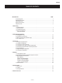
TABLE OF CONTENTS
SECTION TITLE
PAGE
Power Management.................................................................................................................................. 4
Self Diagnosis Function ............................................................................................................................ 4
Timing SpeciÞcation.................................................................................................................................. 4
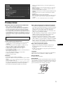
Warnings and Cautions............................................................................................................................. 5
Safety Check Out ..................................................................................................................................... 6
1. Disassembly
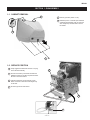
1-1. Cabinet Removal ............................................................................................................................... 7
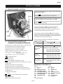
1-2. Service Position................................................................................................................................. 7
1-3. A & D Board Removal........................................................................................................................ 8
1-4. Picture Tube Removal ....................................................................................................................... 9
Anode Cap Removal ......................................................................................................................... 9
2. Safety Related Adjustments
2-1. HV Regulator Check........................................................................................................................ 10
2-2. HV Protector Circuit Check.............................................................................................................. 10
2-3. Beam Protector Check (Software Logic) ......................................................................................... 10
2-4. B+ Voltage Check............................................................................................................................ 10
3. Adjustments
3-1. Landing Rough Adjustment ..............................................................................................................11
3-2. Landing Fine Adjustment ..................................................................................................................11
3-3. Convergence Rough Adjustment......................................................................................................11
3-4. Convergence and V. Key (H. TRP) Fine Adjustment ........................................................................11
3-5. Vertical and Horizontal Position and Size SpeciÞcation .................................................................. 12
3-6. Focus Adjustment ............................................................................................................................ 13
3-7. Digital Convergence Adjustment ..................................................................................................... 13
3-8. Convergence SpeciÞcation.............................................................................................................. 13
4. Diagrams
4-1. Circuit Boards Location ................................................................................................................... 14
4-2. Printed Wiring Board and Schematic Diagram Information ............................................................. 14
4-3. Block Diagram and Schematics
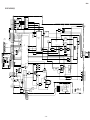
Block Diagrams ............................................................................................................................... 15
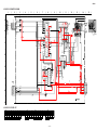
A Board - Schematic Diagram......................................................................................................... 17
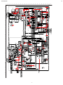
D Board - Schematic Diagram ........................................................................................................ 19
H1 Board - Schematic Diagram ...................................................................................................... 23
J Board - Schematic Diagram ......................................................................................................... 24
4-4. Semiconductors............................................................................................................................... 25
5. Exploded Views
5-1. Picture Tube .................................................................................................................................... 26
5-2. Chassis............................................................................................................................................ 27
5-2. Packing Materials ............................................................................................................................ 28
6. Electrical Parts List ....................................................................................................................................... 29
—3—