1
MXD-D400
SERVICE MANUAL
US Model
Ver 1.0 2003.05
US and foreign patents licensed from Dolby
Laboratories.
MD
Section
Model Name Using Similar Mechanism
NEW
MD Mechanism Type
MDM-7S2C
Optical Pick-up Name
KMS-262E
Model Name Using Similar Mechanism
NEW
CD
CD Mechanism Type
CDM66C-30B61M
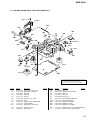
Section
Base Unit Name
BU-30BD61B
Optical Pick-up Name
OP Assy (A-MAX.4T)
SPECIFICATIONS
CD player section
System
Laser
Frequency response
Wow and flutter
Outputs
Compact Disc digital
audio system
Semiconductor laser
(λ=780 nm)
20 Hz – 20 kHz (±0.5 dB)
Below measureable limit
(±0.001% W.PEAK)
MD deck section
System
Disc
Laser
Sampling frequency
Frequency response
MiniDisc digital audio system
MiniDisc
Semiconductor laser
(λ=780 nm)
Emission duration:
continuous
44.1 kHz
20 Hz – 20 kHz (±0.5 dB)
ANALOG OUT
Jack type
Rated output
Load
impedance
Pin jack
2 Vrms
(at 47 kilohms)
Over 10 kilohms
DIGITAL
Squqre optical -18 dBm
OPTICAL OUT connector jack
Optical wave
length:660 nm
PHONES
32 ohm
Stereo phone
jack
10 mW
General
120 V AC, 60 Hz
19 watts
Less than 1 watt (at the
power saving mode)
Dimensions (w/h/d) incl. projecting parts and controls
Approx. 430 × 108 × 399 mm
Mass
Approx. 5.4 kg
Power requirements
Power consumption
Supplied accessories
Inputs
Jack type Input
impedance
ANALOG IN Pin jack
47 kilohms
DIGITAL
Squqre
OPTICAL IN optical
connector
jack
Optical wave
length:
660 nm
Rated
input
Minimum
input
500 mVrms
250 mVrms
–
–
• Audio connection cords (2)
• Remote commander (remote) (1)
• Sony R6 (size-AA) batteries (2)
Design and specifications are subject to change
without notice.
COMPACT DISC MINIDISC DECK
9-877-241-01
Sony Corporation
2003E05-1
C 2003.5
Home Audio Company
Published by Sony Engineering Corporation
MXD-D400
SELF-DIAGNOSIS FUNCTION
The self-diagnosis function consists of error codes for customers which are displayed automatically when errors occur, and error codes
which show the error history in the test mode during servicing. For details on how to view error codes for the customer, refer to the
following box in the instruction manual. For details on how to check error codes during servicing, refer to the following “Procedure for
using the Self-Diagnosis Function (Error History Display Mode)”.
This deck has a Self-diagnosis display function
to let you know if there is a deck malfunction.
The display shows a code made up of three or
five letters and a message alternately to show
you the problem. To solve the problem refer to
the following list. If any problem persists,
consult your nearest Sony dealer.
C11/Protected
The MD is protected against erasure.
cRemove the MD and slide the tab to close the slot.
C12/Cannot Copy
You tried to record a CD with a format that the deck
does not support, such as a CD-ROM or MD data.
cReplace the playable disc.
C13/REC Error
Recording could not be performed properly.
cMove the deck to a stable place, and start
recording over from the beginning.
The MD is dirty or scratched, or the MD does not
meet the standards.
cReplace the MD and start recording over from the
beginning.
C13/Read Error
The MD deck cannot read the disc information
properly.
cRemove the MD once, then insert it again.
C14/TOC Error
The MD deck cannot read the disc information
properly.
cReplace the MD.
cErase all the recorded contents of the MD using
the All Erase Function.
C41/Cannot Copy
The digitally dubbed material cannot be recorded
digitally.
C71/Din Unlock
The digitally dubbed material cannot be recorded
digitally.
A moment’s lighting is due to the signals of the
digital program being recorded. This does not affect
the recorded material.
The digital optical cable is disconnected, or the
power of the connected component is turned off
while recording the digital audio from the
component connected to the DIGITAL OPTICAL
IN jack.
cConnect the digital optical cable, or turn on the
power of the connected component.
E0001/MEMORY NG
The component has internal problem.
cConsult your nearest Sony dealer.
E0101/LASER NG
There is a problem with the laser pickup.
cThe laser pickup may be damaged. Consult your
nearest Sony dealer.
E0201/LOADING NG
There is a problem with the loading.
cThe loading may be failed. Consult your nearest
Sony dealer.
PROCEDURE FOR USING THE SELF-DIAGNOSIS FUNCTION (ERROR HISTORY DISPLAY MODE)
Note: Perform the self-diagnosis function in the “error history display mode” in the test mode. The following describes the least required procedure. Be
careful not to enter other modes by mistake. If you set other modes accidentally, pull out the AC cord to turn the power off and retry to enter the test
mode.
1. Press the ?/1 button to turn he power on.
2. Press the [l AMS L ] (CD) knob and [INPUT] button at the same time, press the [l AMS L] (MD) knob to display “SYS
version”.
3. Turn the [ l AMS L ] (CD) knob and when “MD Test” is displayed, press the [ l AMS L ] (MD) knob.
4. Turn the [ l AMS L ] (MD) knob and when “[Service]” is displayed, press the [YES] button.
5. Turn the [ l AMS L ] (MD) knob to display “Err Display”.
6. Press the [YES] button to sets the error history mode and displays “op rec tm”.
7. Select the contents to be displayed or executed using the [ l AMS L ] (MD) knob.
8. Press the [ l AMS L ] (MD) knob to display or execute the contents selected.
9. Press the [ l AMS L ] (MD) knob another time returns to step 6.
10. Press the [MENU/NO] button to display “Err Display” and release the error history mode.
11. To release the test mode, press the [l AMS L] (CD) knob and [INPUT] button at the same time, press the [l AMSL ] (MD)
knob.
12. Press the ?/1 button to turn the power off.
2
MXD-D400
ITEMS OF ERROR HISTORY MODE ITEMS AND CONTENTS
Selecting the Test Mode
Display
Details of History
op rec tm
Cumulative recording time is displayed.
When cumulative recording time is over 1 minute, the hour and minute are displayed as they are.
When it is under 1 minute, “Under 1 min” is displayed.
The displayed time shows how long the laser is in high power state.
It is about one fourth the actual recording time.
op play tm
Cumulative playing time is displayed.
When cumulative playing time is over 1 minute, the hour and minute are displayed as they are.
When it is under 1 minute, “Under 1 min” is displayed.
spdl rp tm
Cumulative spindle motor running time is displayed.
When cumulative spindle motor run time is over 1 minute, the hour and minute are displayed as they are.
When it is under 1 minute, “Under 1 min” is displayed.
retry err
Displays the total number of retries during recording and number of retry errors during play.
Displayed as “rss pss”.
“r” indicates the retries during recording while “p” indicates the retry errors during play.
The number of retries and retry errors are displayed in hexadecimal digits from 00 to FF.
total err
Displays the total number of errors.
Displayed as “total ss”.
The number of errors is displayed in hexadecimal digits from 00 to FF.
err history
Displays the 10 latest errors.
Displayed as “0s ErrCd@@”.
s indicates the history number. The smaller the number, the more recent is the error. (00 is the latest).
@@ indicates the error code.
Refer to the following table for the details. The error history can be switched by turning the [ l AMS L ]
(MD) knob.
retry adrs
Displays the past five retry addresses.
Displays “ss ADRS ssss”, ss is the history number, ssss is the cluster with the retry error.
Select the error history number using the [ l AMS L ] (MD) knob.
er refresh
Mode to clear the error history and retry address history.
[Operating method]
1) Press [ l AMS L ] (MD) knob when “er refresh” is displayed.
2) The display will change to “er refresh?”, and then press [YES] button.
The operation is over if “Complete!” is displayed.
After this mode was executed, check the following:
• The data have been cleared.
• Perform the recording and playing to check that the mechanism operates normally.
tm refresh
Mode to clear the “op rec tm” and “op play tm” histories.
These histories serve as approximate indications of when to replace the optical pick-up. If the optical pick-up
has been replaced, perform this operation and clear the history.
[Operating method]
1) Press [ l AMS L ] (MD) knob when “tm refresh” is displayed.
2) The display will change to “tm refresh?”, and then press [YES] button.
The operation is over if “Complete!” is displayed.
After this mode was executed, check the following:
• The data have been cleared.
• Perform the recording and playing to check that the mechanism operates normally.
op change
Mode to clear cumulative time of “op rec tm” and “op play tm”.
These historical data are used to determine the timing when the optical pick-up is to be replaced. When the
optical pick-up was replaced, perform this operation to clear historical data.
[Operating method]
1) Press [ l AMS L ] (MD) knob when “op change” is displayed.
2) The display will change to “op chang?”, and then press [YES] button.
The operation is over if “Complete!” is displayed.
spdl change
Mode to clear cumulative time of “spdl rp tm”.
This historical data is used to determine the timing when the spindle motor is to be replaced. When the spindle
motor was replaced, perform this operation to clear historical data.
[Operating method]
1) Press [ l AMS L ] (MD) knob when “spdl change” is displayed.
2) The display will change to “spdl chang?”, and then press [YES] button.
The operation is over if “Complete!” is displayed.
3
MXD-D400
Table of Error Codes
Error Code
4
Details of Error
10
Loading failed
12
Loading switch combination is illegal
20
Head of PTOC could not be read within the
specified time
21
Head of PTOC could be read but its content is
erroneous
22
Access to UTOC could not be made within the
specified time
23
UTOC could be not read within the specified
3time
24
Content of UTOC is erroneous
30
Playing could not start
31
Content of sector is erroneous
40
Cause of retry occurred during normal recording
41
D-RAM overflowed and retry was executed
42
Retry was executed during the writing to TOC
43
S.F editing was interrupted by retry
50
Address could not be read except in access
processing
51
Focusing failed and it is out of control
60
Unlock retry
MXD-D400
TABLE OF CONTENTS
SELF-DIAGNOSIS FUNCTION ........................... 2
7-7. Base Unit Section (BU-30BD61M) ................................ 89
1.
SERVICING NOTES ............................................... 7
8.
2.
GENERAL ................................................................... 16
3.
DISASSEMBLY
3-1.
3-2.
3-3.
3-4.
3-5.
3-6.
3-7.
3-8.
3-9.
3-10.
3-11.
3-12.
3-13.
Disassembly Flow ...........................................................
Case (409538) .................................................................
Loading Panel (CD) ........................................................
MD Mechanism Deck (MDM-7S2C) .............................
CD Mechanism Deck (CDM66C-30B61C) ...................
Transformer Board ..........................................................
Main Board ......................................................................
Front Panel Block Section ..............................................
Holder Section .................................................................
Over Write Head (HR901) ..............................................
Optical Pick-up (KMS-262E) .........................................
BD (MD) Board ..............................................................
Loading Motor Assembly (M103), Spindle Motor
Assembly (M101), Sled Motor Assembly (M102) ........
3-14. Tray (66) ..........................................................................
3-15. BD (CD) Board ...............................................................
3-16. Optical Block Section .....................................................
ELECTRICAL PARTS LIST ............................... 90
17
18
18
19
19
20
20
21
21
22
22
23
23
24
25
25
4.
TEST MODE .............................................................. 26
5.
ELECTRICAL ADJUSTMENTS
MD Section ..................................................................... 32
CD Section ...................................................................... 44
6.
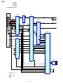
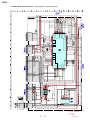
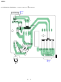
DIAGRAMS
6-1.
6-2.
6-3.
6-4.
6-15.
6-16.
6-17.
6-18.
6-19.
6-20.
Block Diagram – CD Section – .....................................
Block Diagram – MD Section – ....................................
Block Diagram – MAIN Section – ................................
Note for Printed Wiring Boards and
Schematic Diagrams .......................................................
Printed Wiring Board – BD (CD) Section – ..................
Schematic Diagram – BD (CD) Section – ....................
Schematic Diagram – BD (MD) Board (1/2) – .............
Schematic Diagram – BD (MD) Board (2/2) – .............
Printed Wiring Board – BD (MD) Board – ...................
Printed Wiring Board
– MAIN Board (Component Side) – ..............................
Printed Wiring Board
– MAIN Board (Conductor Side) – ................................
Schematic Diagram – MAIN Board (1/4) – ..................
Schematic Diagram – MAIN Board (2/4) – ..................
Schematic Diagram
– MAIN (3/4)/LOADING Boards – ...............................
Schematic Diagram – MAIN Board (4/4) – ..................
Printed Wiring Boards – Panel Section – ......................
Schematic Diagram – Panel Section – ..........................
Printed Wiring Board – TRANSFORMER Board – .....
Schematic Diagram – TRANSFORMER Board – ........
IC Pin Function Description ...........................................
7.
EXPLODED VIEWS
7-1.
7-2.
7-3.
7-4.
7-5.
7-6.
Overall Section ................................................................
Front Panel Section .........................................................
Chassis Section ...............................................................
MD Mechanism Deck Section-1 (MDM-7S2C) ............
MD Mechanism Deck Section-2 (MDM-7S2C) ............
CD Mechanism Deck Section (CDM66C-30B61M) .....
6-5.
6-6.
6-7.
6-8.
6-9.
6-10.
6-11.
6-12.
6-13.
6-14.
46
47
48
49
50
51
52
53
54
56
57
58
59
60
61
62
63
64
65
74
83
84
85
86
87
88
5
MXD-D400
SAFETY CHECK-OUT
After correcting the original service problem, perform the following safety check before releasing the set to the customer:
Check the antenna terminals, metal trim, “metallized” knobs,
screws, and all other exposed metal parts for AC leakage.
Check leakage as described below.
LEAKAGE TEST
The AC leakage from any exposed metal part to earth ground and
from all exposed metal parts to any exposed metal part having a
return to chassis, must not exceed 0.5 mA (500 microamperes.).
Leakage current can be measured by any one of three methods.
1. A commercial leakage tester, such as the Simpson 229 or RCA
WT-540A. Follow the manufacturers’ instructions to use these
instruments.
2. A battery-operated AC milliammeter. The Data Precision 245
digital multimeter is suitable for this job.
3. Measuring the voltage drop across a resistor by means of a
VOM or battery-operated AC voltmeter. The “limit” indication is 0.75 V, so analog meters must have an accurate lowvoltage scale. The Simpson 250 and Sanwa SH-63Trd are examples of a passive VOM that is suitable. Nearly all battery
operated digital multimeters that have a 2 V AC range are
suitable. (See Fig. A)
To Exposed Metal
Parts on Set
0.15 µF
1.5 kΩ
AC
voltmeter
(0.75 V)
Earth Ground
Fig. A. Using an AC voltmeter to check AC leakage.
CAUTION
Use of controls or adjustments or performance of procedures
other than those specified herein may result in hazardous radiation exposure.
Notes on chip component replacement
• Never reuse a disconnected chip component.
• Notice that the minus side of a tantalum capacitor may be damaged by heat.
Flexible Circuit Board Repairing
• Keep the temperature of the soldering iron around 270 ˚C during repairing.
• Do not touch the soldering iron on the same conductor of the
circuit board (within 3 times).
• Be careful not to apply force on the conductor when soldering
or unsoldering.
UNLEADED SOLDER
Boards requiring use of unleaded solder are printed with the leadfree mark (LF) indicating the solder contains no lead.
(Caution: Some printed circuit boards may not come printed with
the lead free mark due to their particular size)
: LEAD FREE MARK
Unleaded solder has the following characteristics.
• Unleaded solder melts at a temperature about 40 ˚C higher than
ordinary solder.
Ordinary soldering irons can be used but the iron tip has to be
applied to the solder joint for a slightly longer time.
Soldering irons using a temperature regulator should be set to
about 350 ˚C.
Caution: The printed pattern (copper foil) may peel away if the
heated tip is applied for too long, so be careful!
• Strong viscosity
Unleaded solder is more viscou-s (sticky, less prone to flow)
than ordinary solder so use caution not to let solder bridges occur such as on IC pins, etc.
• Usable with ordinary solder
It is best to use only unleaded solder but unleaded solder may
also be added to ordinary solder.
This appliance is classified as a CLASS 1
LASER product. The CLASS 1 LASER
PRODUCT MARKING is located on the
rear exterior.
The following caution label is located
inside of the apparatus.
SAFETY-RELATED COMPONENT WARNING!!
COMPONENTS IDENTIFIED BY MARK 0 OR DOTTED
LINE WITH MARK 0 ON THE SCHEMATIC DIAGRAMS
AND IN THE PARTS LIST ARE CRITICAL TO SAFE
OPERATION. REPLACE THESE COMPONENTS WITH
SONY PARTS WHOSE PART NUMBERS APPEAR AS
SHOWN IN THIS MANUAL OR IN SUPPLEMENTS PUBLISHED BY SONY.
6
MXD-D400
SECTION 1
SERVICING NOTES
NOTES ON HANDLING THE OPTICAL PICK-UP
BLOCK OR BASE UNIT
CLEANING OBJECTIVE LENS OF OPTICAL PICK-UP
• In cleaning the objective lens of optical pick-up, be sure the
following below.
The laser diode in the optical pick-up block may suffer electrostatic break-down because of the potential difference generated
by the charged electrostatic load, etc. on clothing and the human
body.
During repair, pay attention to electrostatic break-down and also
use the procedure in the printed matter which is included in the
repair parts.
The flexible board is easily damaged and should be handled with
care.
1. In cleaning the lens, do not apply an excessive force.
As the optical pick-up is vulnerable, application of excessive
force could damage the lens holder.
2. In cleaning, do not use a cleaner other than exclusive cleaning
liquid (KK-91 or isopropyl alcohol).
3. Wipe the objective lens spirally from center toward outside.
(See Figure A)
For CD
NOTES ON LASER DIODE EMISSION CHECK
The laser beam on this model is concentrated so as to be focused
on the disc reflective surface by the objective lens in the optical
pick-up block. Therefore, when checking the laser diode emission, observe from more than 30 cm away from the objective lens.
LASER DIODE AND FOCUS SEARCH OPERATION
CHECK
Carry out the “S curve check” in “CD section adjustment” and
check that the S curve waveforms is output three times.
For MD
(Figure A)
4. Eject the disk, if loaded.
5. Disconnect the power cord from the socket to shut off the power
supply.
NOTES ON LASER DIODE EMISSION CHECK
Never look into the laser diode emission from right above when
checking it for adjustment. It is feared that you will lose your sight.
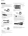
HOW TO OPEN THE LOADING PANEL (CD) WHEN POWER SWITCH IS OFF
1 Turn the cam (66) in the direction of arrow A.
2 Pull out the loading
panel (CD).
A
7
MXD-D400
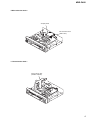
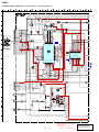
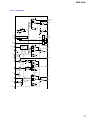
SERVICE POSITION
– Main board –
main board
– Front panel block section –
front panel block section
8
MXD-D400
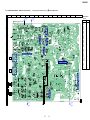
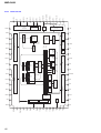
– MD mechanism deck –
BD (MD) board
MD mechanism deck
(MDM-7S2C)
– CD mechanism deck –
CD mechanism deck
(CDM66C-30B61M)
9
MXD-D400
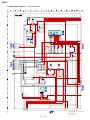
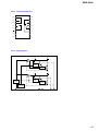
NOTE FOR POSITION OF THE CABLE (4P)
Fix the cable (4P) between the transformer board and the main board
with a lead pin keeping the cable from the powertransformer (TR651).
transformer board
power transformer
(TR651)
cable (4P)
lead pin
main board
10
MXD-D400
MD SECTION
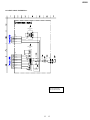
JIG FOR CHECKING BD (MD) BOARD WAVEFORM
The special jig (J-2501-196-A) is useful for checking the waveform of the BD (MD) board. The names of terminals and the checking items
to be performed are shown as follows.
GND
I+3V
IOP
TE
VC
RF
FE
: Ground
: For measuring IOP (Check the deterioration of the optical pick-up laser)
: For measuring IOP (Check the deterioration of the optical pick-up laser)
: Tracking error signal (Traverse adjustment)
: Reference level for checking the signal
: RF signal (Check jitter)
: Focus error signal
CN105
IOP
TE
I+3V
GND
FE
VC
RF
1
I+3V
IOP
GND
TE
FE
VC
RF
I+3V
IOP
GND
TE
FE
VC
RF
for
MDM-7S2C
7
11
MXD-D400
IOP DATA RECORDING AND DISPLAY WHEN OPTICAL PICK-UP AND NON-VOLATILE MEMORY (IC195 OF
BD (MD) BOARD) ARE REPLACED
The IOP value labeled on the optical pick-up can be recorded in the non-volatile memory. By recording the value, it will eliminate the need
to look at the value on the optical pick-up label. When replacing the optical pick-up or non-volatile memory (IC195 of BD (MD) board),
record the IOP value on the optical pick-up according to the following procedure.
Record Procedure:
1. Press the ?/1 button to turn on the power.
2. Press the [l AMS L ] (CD) knob and [INPUT] button at the same time, press the [l AMS L] (MD) knob to display “SYS
version”.
3. Turn the [ l AMS L] (CD) knob and when “MD Test” is displayed, press the [l AMS L ] (MD) knob.
4. Turn the [ l AMS L ] (MD) knob to display “[Service]”, and press the [YES] button.
5. Turn the [ l AMS L ] (MD) knob to display “Iop Write” (C05), and press the [YES] button.
6. The display becomes “Ref=@@@.@” (@ is an arbitrary number) and the numbers which can be changed will blink.
7. Input the IOP value written on the optical pick-up label.
To select the number : Turn the [ l AMS L ] (MD) knob.
To select the digit : Press the [ l AMS L ] (MD) knob.
8. When the [YES] button is pressed, the display becomes “Measu=@@@.@” (@ is an arbitrary number).
9. As the adjustment results are recorded for the 4 value. Leave it as it is and press the [YES] button.
10. “Complete!” will be displayed momentarily. The value will be recorded in the non-volatile memory and the display will become “Iop
Write (C05)”.
11. Press the [MENU/NO] button to display “MD Test”.
12. Press the ?/1 button to turn the power off.
Display Procedure:
1. Press the ?/1 button to turn on the power.
2. Press the [l AMS L ] (CD) knob and [INPUT] button at the same time, press the [l AMS L] (MD) knob to display “SYS
version”.
3. Turn the [ l AMS L ] (CD) knob and when “MD Test” is displayed, press the [l AMS L ] (MD) knob.
4. Turn the [ l AMS L ] (MD) knob to display “[Service]”, and press the [YES] button.
5. Turn the [ l AMS L ] (MD) knob to display “Iop Read” (C26), and press the [YES] button.
6. “@@.@/##.#” is displayed and the recorded contents are displayed.
@@.@ : indicates the IOP value on the optical pick-up label.
##.# : indicates the IOP value after adjustment
7. To end, press the [MENU/NO] button to display “Iop Read” (C26).
8. Press the [MENU/NO] button to display “MD Test”.
9. Press the ?/1 button to turn the power off.
12
MXD-D400
CHECKS PRIOR TO PARTS REPLACEMENT AND ADJUSTMENTS IN MD
Before performing repairs, perform the following checks to determine the faulty locations up to a certain extent.
Details of the procedures are described in “5 Electrical Adjustments”.
Criteria for Determination
(Unsatisfactory if specified value is not satisfied)
Laser power check
(5-7-2 : See page 36)
Measure if unsatisfactory:
• 0.93 mW power
Specified value : 0.84 to 0.92 mW (KMS-262A)
0.90 to 0.96 mW (KMS-262E)
• 8.65 mW power
Specified value : 8.1 to 8.7 mW (KMS-262A)
8.4 to 8.9 mW (KMS-262E)
• Clean the optical pick-up
• Adjust again
• Replace the optical pick-up
• Iop (at 8.65mW)
Labeled on the optical pick-up
Iop value ± 10mA
• Replace the optical pick-up
Auto check
(5-7-4 : See page 37)
• Unsatisfactory if displayed as “NG: XXXX”
NG
(XXXX is arbitrary number)
• Replace the optical pick-up
Temperature
compensation
offset check
(5-7-1 : See page 36)
• Unsatisfactory if displayed as “T=@@ (##) [NG]”
NG
(@@, ## are both arbitrary numbers)
• Check for disconnection of the circuits around
D101 (BD (MD) board)
• Check the signals around IC101, IC151, CN102,
CN103 (BD (MD) board)
Note:
The criteria for determination above is intended merely to determine if satisfactory or not, and does not serve as the specified value for adjustments.
When performing adjustments, use the specified values for adjustments.
13
MXD-D400
CD SECTION
CD-TEXT TEST DISC
This unit is able to display the test data (character information) written in the CD on its fluorescent indicator tube.
The CD-TEXT TEST DISC (TGCS-313:4-989-366-01) is used for checking the display.
To check, perform the following procedure.
Checking Method:
1. Turn ON the power, set the disc to the disc table with the “test disc” label facing up, and chuck the disc.
2. Press the H (CD) button and play back the disc.
3. The following will be displayed on the fluorescent indicator tube.
Display : 1KHZ 0DB
4. Rotating [ l AMS L ] (CD) knob, select the track. The text data of each track will be displayed.
For details of the displayed contents for each track, refer to “Table 1 : CD-TEXT TEST DISC TEXT Data Contents” and “Table 2 : CDTEXT TEST DISC Recorded Contents and Display”.
Restrictions in CD-TEXT Display
In this unit, some special characters will not be displayed properly. These will be displayed as a space or a character resembling it. For
details, refer to “Table 2 : CD-TEXT DISC Recorded Contents and Display”.
Table 1 : CD-TEXT TEST DISC TEXT Data Contents (TRACKS No. 1 to 41:Normal Characters)
TRACK
No.
Displayed Contents
TRACK
Displayed Contents
No.
1
1kHz/0dB/L&R
22
1kHz/–90dB/L&R
2
20Hz/0dB/L&R
23
Infinity Zero w/o emphasis//L&R
3
40Hz/0dB/L&R
24
Infinity Zero with emphasis//L&R
4
100Hz/0dB/L&R
25
400Hz+7kHz(4:1)/0dB/L&R
5
200Hz/0dB/L&R
26
400Hz+7kHz(4:1)/–10dB/L&R
6
500Hz/0dB/L&R
27
19kHz+20kHz(1:1)/0dB/L&R
7
1kHz/0dB/L&R
28
19kHz+20kHz(1:1)/–10dB/L&R
8
5kHz/0dB/L&R
29
100Hz/0dB/L*
9
7kHz/0dB/L&R
30
1kHz/0dB/L*
10
10kHz/0dB/L&R
31
10kHz/0dB/L*
11
16kHz/0dB/L&R
32
20kHz/0dB/L*
12
18kHz/0dB/L&R
33
100Hz/0dB/R*
13
20kHz/0dB/L&R
34
1kHz/0dB/R*
14
1kHz/0dB/L&R
35
10kHz/0dB/R*
15
1kHz/–1dB/L&R
36
20kHz/0dB/R*
16
1kHz/–3dB/L&R
37
100Hz Squer Wave//L&R
17
1kHz/–6dB/L&R
38
1kHz Squer Wave//L&R
18
1kHz/–10dB/L&R
39
1kHz w/emphasis/–0.37dB/L&R
19
1kHz/–20dB/L&R
40
5kHz w/emphasis/–4.53dB/L&R
20
1kHz/–60dB/L&R
41
16kHz w/emphasis/–9.04dB/L&R
21
1kHz/–80dB/L&R
Note: The contents of Track No. 1 to 41 are the same as those of the current TEST DISC-their titles are displayed.
14
MXD-D400
Table 2: CD-TEXT TEST DISC Recorded Contents and Display
(In this unit, some special characters cannot be displayed. This is not a fault)
TRACK
No.
Recorded contents
Display
42
! ” # $ %& ´
(21h to 27h)1kHz 0dB L&R
T All the same
43
( )
(28h to 2Fh)
T All the same
44
012345 67
(30h to 37h)
T All the same
45
89 : ; <=>?
(38h to 3Fh)
T All the same
46
@A B C D E F G
(40h to 47h)
T All the same
47
H I J K L MNO
(48h to 4Fh)
T All the same
48
P Q R S T U V W (50h to 57h)
T All the same
49
XYZ [ ¥ ] ^ _
(58h to 5Fh)
T All the same
50
′
ab c de f g
(60h to 67h)
T All the same
51
h i j k l mn o
(68h to 6Fh)
T All the same
52
pq r s t u vw
(70h to 77h)
T All the same
53
x y z { I } ~
(78h to 7Fh)
T All the same
*
+ , – . /
i ¢£¤¥ §
C ª ¬ PR–
54
(A0h to A7h) 8859-1
(A8h to AFh)
(A8h to AFh)
′
µ¶ •
(B0h to B7h)
(B0h to B7h)
1
4
1
2
¿
(B8h to BFh)
À Á Â Ã Ä Å ÆÇ
(C0h to C7h)
55
•
±
57
†
1
58
59
È ÉÊË Ì Í Î Ï
60
61
D ÑÒÓÔÕÖ
Ø Ù Ú Û Ü Y˙ ß
62
63
56
(A0h to A7h) 8859-1
2
º
3
3
4
(B8h to BFh)
C
(C0h to C7h)
(C8h to CFh)
EEEE I I I I
(C8h to CFh)
(D0h to D7h)
D NOOOOO
(D0h to D7h)
(D8h to DFh)
OUUUUY
(D8h to DFh)
à á â ã ä åæç
(E0h to E7h)
aaaaaa
c
(E0h to E7h)
è éêë ì í î ï
(E8h to FFh)
eeee i i i i
(E8h to EFh)
64
∂ ñòóôõ ö÷
(F0h to F7h)
dnooooo
(F0h to F7h)
65
ø ù ú û ü y´
(F8h to FFh)
ouuuu y
66
No.66
T All the same
67
No.67
T All the same
to
99
to
No.99
ÿ
AAAAAA
y
(F8h to FFh)
to
T All the same
15
MXD-D400
SECTION 2
GENERAL
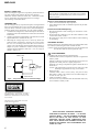
Remote control
Main unit
1
This section is extracted from
instruction manual.
2
3
4
5
6 7890qa
NS
efed e;wlwkwj whwg
esea
wf
wd ws waw;
qhqgqfqd qs
qlqkqj
ALPHABETICAL ORDER
A–I
ALBUM wh
AMS wa wg
CD SYNCHRO NORMAL/HIGH 4
CLEAR ws
Disc tray 3
DISPLAY ql
Display window wf
EJECT 6
GROUP ON/OFF 9
GROUP SKIP 0
INPUT qa
ALPHABETICAL ORDER
J– Z
A–M
MD slot 5
MDLP indicator 7
MENU/NO wd
OPEN/CLOSE 2
PHONES jack es
PHONE LEVEL ed
PLAY MODE qj wj
REC LEVEL qd
REC MODE 8
REC z qs
STANDB Y indicator ef
TIME qk wk
YES w;
ALBUM/GROUP -/+ qf
CD MD select wk
CD SYNCHRO NORMAL/
HIGH wa
CLEAR 8
DISPLAY wg
FADER ws
GROUP ON/OFF wd
INPUT wj
MENU/NO wf
MUSIC SYNC 9
BUTTON DESCRIPT
?/1 (power/standby) 1
H (play) qf wl
X (pause) qh e;
x (stop) qg ea
N–Z
NAME EDIT/SELECT 6
number buttons 7
PLAY MODE 3
REC MODE 2
REC-IT 0
REPEAT qh
SCROLL wh
SLEEP qg
T.REC qd
TIME 4
YES 5
BUTTON DESCRIPTIO
. / > (skip)qk
?/1 (power/standby) 1
m / M (search) qj
H (play) w;
X (pause) qa
x (stop) qs
z (record) ql
16
MXD-D400
SECTION 3
DISASSEMBLY
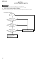
• This set can be disassembled in the order shown below.
3-1.
DISASSEMBLY FLOW
SET
3-2. CASE (409538)
(Page 18)
3-6. TRANSFORMER BOARD
(Page 20)
3-3. LOADING PANEL (CD)
(Page 18)
3-4. MD MECHANISM DECK
(MDM-7S2C)
(Page 19)
3-8. FRONT PANEL BLOCK
SECTION
(Page 21)
3-5. CD MECHANISM DECK
(CDM66C-30B61M)
(Page 19)
3-9. HOLDER SECTION
(Page 21)
3-12.BD (MD) BOARD
(Page 23)
3-10.OVER WRITE HEAD
(HR901)
(Page 22)
3-13.LOADING MOTOR ASSY (M103),
SPINDLE NOTOR ASSY (M101),
SLED MOTOR ASSY (M102)
(Page 23)
3-14.TRAY (66)
(Page 24)
3-7. MAIN BOARD
(Page 20)
3-15.BD (CD) BOARD
(Page 25)
3-16.OPTICAL BLOCK
SECTION
(Page 25)
3-11.OPTICAL PICK-UP
(KMS-262E)
(Page 22)
17
MXD-D400
Note: Follow the disassembly procedure in the numerical order given.
3-2.
CASE (409538)
3 case
(409538)
1 two screws
(case 3 TP2)
2 two screws
(case 3 TP2)
3 two screws
(case 3 TP2)
3-3.
LOADING PANEL (CD)
3 four claws
4 loading panel (CD)
cam (66)
2
1 Rotate the cam (66) with a screwdriver.
18
MXD-D400
3-4.
MD MECHANISM DECK (MDM-7S2C)
9 MD mechanism deck
(MDM-7S2C)
4 two step screws
5 two step screws
7 two insulators
8 two insulators
2 two screws
(+BVTP3 × 8)
6
1 two wires (flat type)
(17 core : CN9,
27 core : CN10)
3 two harnesses
3-5.
CD MECHANISM DECK (CDM66C-30B61M)
3 three screws
(+BVTP3 × 8)
1 two wires (flat type)
(25 core : CN5,
9 core : CN4)
5 CD mechanism deck
(CDM66C-30B61M)
2 connector
(CN6)
4
19
MXD-D400
3-6.
TRANSFORMER BOARD
3 connector
(CN652)
5 four screws
(+BVTT3 × 6)
4 screw
(+BVTT3 × 6)
6 transformer board
1 connector
(CN1)
2 connector
(CN2)
3-7.
MAIN BOARD
5 connector (CN6)
4 wire (flat type)
(9 core) (CN4)
6 two connectors
(CN1, CN2)
9 main board
7 two screws
(+BVTP3 × 8)
1 two wires (flat type)
(25 core : CN5,
17 core : CN9)
3 wire (flat type) (19 core) (CN11)
2 wire (flat type) (27 core) (CN10)
8 four screws
(+BVTP3 × 8)
20
MXD-D400
3-8.
FRONT PANEL BLOCK SECTION
1 wire (flat type)
(CN11)
2 connector (CN12)
5 screw
(+BVTP3 × 8)
3 two screws
(+BVTP3 × 8)
8 claw
4 two
harnesses
0 front panel
block section
9 claw
7 two screws
(+BVTP3 × 8)
6 three screws
(+BVTP3 × 8)
3-9.
HOLDER SECTION
3 holder section
1 tension spring (holder)
2 hook
21
MXD-D400
3-10. OVER WRITE HEAD (HR901)
1 screw (P 1.7 × 6)
2 over write head
(HR901)
3-11. OPTICAL PICK-UP (KMS-262E)
8 optical pick-up (KMS-262E)
6 main shaft
3 screw (+B 2 × 6)
7 flexible board
4 base (BU-A)
5 two screws
(+KTP 2 × 6)
1 screw (+B 2 × 6)
2 base (BU-D)
22
MXD-D400
3-12. BD (MD) BOARD
1 Remove two solders (sled motor).
2 Remove
two solders
(spindle motor).
M102
6 flexible board (CN101)
M101
3 Remove
two solders
(loading motor).
M103
S102
4 Remove
three solders .
5 screw (M1.7)
8 BD (MD) board
7 connector
(CN104)
3-13. LOADING MOTOR ASSY (M103), SPINDLE MOTOR ASSY (M101), SLED MOTOR ASSY (M102)
1 lever (head)
3 torsion spring (SPDL)
8 bushing (rivet)
2 belt (loading)
9 gear (sa)
4 two screws
(PWH 1.7 × 2.5)
0 two screws
(+PWH 1.7 × 2.5)
qa sled motor assy
(M102)
5 loading motor assy
(M103)
7 spindle motor assy
(M101)
6 three tapping screws
(M1.7)
23
MXD-D400
3-14. TRAY (66)
3 Push the switch (S151) and releace two claws.
switch (S151)
claw of tray (66)
1 Turn the cam to the
direction of arrow.
claw of lever (SW)
4 hook
4 hook
2
6 hook
7 tray (66)
6 hook
5
24
MXD-D400
3-15. BD (CD) BOARD
1 Remove four solders.
2 flexible flat cable
(16core) (CN101)
3 BD (CD) board
3-16. OPTICAL BLOCK SECTION
4 optical block section
1 floating screw
3 shaft (BU holder)
cam (66)
2
Rotate the cam (66) in the direction of 2 to move
the shaft (BU holder) upper.
25
MXD-D400
SECTION 4
TEST MODE
Setting the Test Mode
Procedure:
1. Press the ?/1 button to turn the power on.
2. Press the [l AMS L ] (CD) knob and [INPUT] button at the same time, press the [l AMS L ] (MD) knob.
3. Turn the [ l AMS L] (CD) knob to select the menu.
4. Press the [l AMS L ] (CD) knob to execute the test mode.
Releasing the Test Mode
Procedure 1:
1. Press the [ l AMS L] (CD) knob and [INPUT] button at the same time, press the [l AMS L ] (MD) knob.
2. Press the ?/1 button to turn the power off.
Procedure 2:
1. Pull out the AC cord to turn the power off.
Contents of test mode
No.
1
2
3
4
5
6
7
8
9
10
11
12
13
Display
SYS Version
BU Test
SERVICE
MD Version
MD Test
Initialize
FL ALL ON
FL ALL OFF
FL ITIMATSU
LED CHECK
KEY CHECK
RM CHECK
Play Speed
Function
System version display
CD BU test mode
CD Service mode
MD version display
MD test mode*
MD initialize
Fluorescent indicator tube test
Fluorescent indicator tube test
Fluorescent indicator tube test
LED check
Keyboard check
Remote commander check
CD x4 speed
* Details of MD test mode is described on and after page 28.
System Version Display
Procedure:
1. Enter the test mode, then turn the [l AMS L] (CD) knob to display “SYS Version”, and press the [l AMS L] (CD) knob.
2. The system version is displayed.
3. To exit from this mode, turn the [l AMS L ] (CD) knob.
4. Press the ?/1 button to turn the power off.
CD Test Mode
Procedure:
1. Enter the test mode, then turn the [l AMS L ] (CD) knob to display “BU Test”, and press the [l AMS L ] (CD) knob.
2. “bdt S CURVE” is displayed. This test mode is used in the Electrical Adjustment section.
3. Turn the [l AMS L] (CD) knob. “bdt RAM REA”, “bdt RAM WRI”, “bdt COMOUT”, “bdt FB TUNE”, and “bdt ERR RATE”
are displayed.
4. To exit from this mode, press the [MENU/NO] button and turn the [ l AMS L] (CD) knob to display “bdt ERR RATE”.
5. Press the [l AMS L ] (CD) knob and [INPUT] button at the same time, press the [ l AMS L] (MD) knob.
6. Press the ?/1 button to turn the power off.
CD service Mode
Procedure:
1. Enter the test mode, then turn the [l AMS L ] (CD) knob to display “SERVICE”, and press the [l AMS L ] (CD) knob.
2. “SERVICE MOD” is displayed.
3. Press the [SKIP] button, the “SLED OUT” is displayed and the sled moves to the outermost position.
4. Press the [GROUP ON/OFF] button, the “SLED IN” is displayed and the sled moves to the innermost position.
5. Press the [REC] button, the “TRV ON” is displayed.
6. Press the [ l AMS L ] (CD) knob, then “SERVICE MOD” is displayed again.
7. To exit from this mode, press the [l AMS L ] (CD) knob and [INPUT] button at the same time, press the [ l AMS L] (MD)
knob.
8. Press the ?/1 button to turn the power off.
Note: Always move the pick-up to the most inside position when exiting from this mode.
MD Version Display
Procedure:
1. Enter the test mode, then turn the [l AMS L] (CD) knob to display “MD Version”, and press the [l AMS L] (CD) knob.
26
MXD-D400
2. The MD version is displayed.
3. To exit from this mode, turn the [l AMS L ] (CD) knob.
4. Press the ?/1 button to turn the power off.
Initialize
Procedure:
1. Enter the test mode, then turn the [l AMS L ] (CD) knob to display “Initialize”, and press the [l AMS L ] (CD) knob.
2. MD is Initialised.
3. To exit from this mode, press the [l AMS L ] (CD) knob and [INPUT] button at the same time, press the [l AMS L] (MD)
knob.
4. Press the ?/1 button to turn the power off.
FL ALL ON Mode
Procedure:
1. Enter the test mode, then turn the [l AMS L ] (CD) knob to display “FL ALL ON”, and press the [l AMS L] (CD) knob.
2. All segments of fluorescent indicator tube turn on.
3. To exit from this mode, press the [MENU/NO] button, then “FL ALL ON” is displayed again.
4. Press the ?/1 button to turn the power off.
FL ALL OFF Mode
Procedure:
1. Enter the test mode, then turn the [l AMS L] (CD) knob to display “FL ALL OFF”, and press the [l AMS L] (CD) knob.
2. All segments of fluorescent indicator tube turn off.
3. To exit from this mode, press the [MENU/NO] button, then “FL ALL OFF” is displayed again.
4. Press the ?/1 button to turn the power off.
FL ITIMATSU Mode
Procedure:
1. Enter the test mode, then turn the [l AMS L] (CD) knob to display “FL ITIMATSU”, and press the [l AMS L ] (CD) knob.
2. Checkered patterns of segments are displayed.
3. To exit from this mode, press the [MENU/NO] button, then “FL ITIMATSU” is displayed again.
4. Press the ?/1 button to turn the power off.
LED Check Mode
Procedure:
1. Enter the test mode, then turn the [l AMS L] (CD) knob to display “LED CHECK”, and press the [l AMS L] (CD) knob.
2. Turn the [l AMS L ] (CD) knob, the LED on front panel will repeat lighting on and off.
3. To exit from this mode, press the [MENU/NO] button, then “LED CHECK” is displayed again.
4. Press the ?/1 button to turn the power off.
KEY Check Mode
Procedure:
1. Enter the test mode, then turn the [l AMS L] (CD) knob to display “KEY CHECK”, and press the [l AMS L] (CD) knob.
2. “Got 1 keys” is displayed.
3. Press the buttons and knobs, and when all the buttons and knobs are pressed, “Got 27 keys” will be displayed.
4. To exit from this mode, press the [l AMS L] (CD) knob and [INPUT] button at the same time, press the [l AMS L] (MD)
knob.
5. Press the ?/1 button to turn the power off.
Remote Commander Check
Procedure:
1. Enter the test mode, then turn the [l AMS L ] (CD) knob to display “RM CHECK”, and press the [l AMS L ] (CD) knob.
2. Press the H key on the remote commander, then “Got PlayCom” is displayed.
3. To exit from this mode, press the [MENU/NO] button, then “RM CHECK” is displayed again.
4. Press the ?/1 button to turn the power off.
CD Play Speed Selection Mode
Procedure:
1. Enter the test mode, then turn the [l AMS L ] (CD) knob to display “Play Speed”, and press the [l AMS L ] (CD) knob.
2. “x4 Play” is displayed. If a CD is in the deck, pressing the H (CD) button executes the 4 times speed playback.
3. Press the x button to stop the playback.
4. To exit from this mode, press the [MENU/NO] button, then “Play Speed” is displayed again.
5. Press the ?/1 button to turn the power off.
27
MXD-D400
MD SECTION
1. PRECAUTIONS FOR USE OF TEST MODE
• As loading related operations will be performed regardless of the test mode operations being performed, be sure to check that the disc
is stopped before setting and removing it.
Even if the [EJECT] button is pressed while the disc is rotating during continuous playback, continuous recording, etc., the disc will not
stop rotating.
Therefore, it will be ejected while rotating.
Be sure to press the [EJECT] button after pressing the [MENU/NO] button and the rotation of disc is stopped.
1-1. Recording laser emission mode and operating buttons
• Continuous recording mode (CREC 2MODE) (C37)
• Laser power check mode (LDPWR CHECK) (C13)
• Laser power adjustment mode (LDPWR ADJUST) (C04)
• Comparison with initial Iop value written in nonvolatile memory (Iop Compare) (C27)
• Write current Iop value read in nonvolatile memory using microprocessor (Iop NV Save) (C06)
• Traverse (MO) check (EF MO CHECK) (C14)
• Traverse (MO) adjustment (EF MO ADJUST) (C07)
• When pressing the [REC z ] button.
2. SETTING THE TEST MODE
1. Press the ?/1 button to turn the power on.
2. Press the [l AMS L] (CD) knob and [INPUT] button at the same time, press the [l AMS L] (MD) knob to display “SYS
version”.
3. Turn the [l AMS L ] (CD) knob and when “MD Test” is displayed, press the [l AMS L ] (MD) knob.
When the test mode is set, “[Check]” will be displayed. Turn the [l AMS L ] (MD) knob switches between the following three
groups; ···Tt [Check] Tt [Service] Tt [Develop] Tt ···.
Note: Do not use the test mode in the [Develop] group.
If used, the unit may not operate normally.
If the [Develop] group is set accidentally, press the [MENU/NO] button immediately to exit the [Develop] group.
3. RELEASING THE TEST MODE
Procedure 1:
Press the [l AMS L] (CD) knob and [INPUT] button at the same time, press the [ l AMS L] (MD) knob, press the ?/1 button
to turn the power off.
Procedure 2:
Pull out the AC cord to return the power off.
4. BASIC OPERATIONS OF THE TEST MODE
All operations are performed using the [l AMS L ] (MD) knob, [YES] button, and [MENU/NO] button.
The functions of these buttons are as follows.
Function name
[ l AMS L ] (MD) knob (turn)
Function
Select.
[ l AMS L ] (MD) knob (push)
Set Sub menu.
[YES] button
Proceeds onto the next step. Finalizes input.
[MENU/NO] button
Returns to previous step. Stops operations.
28
MXD-D400
5. SELECTING THE TEST MODE
There are 26 types of test modes as shown below. The groups can be switched by turning the [l AMS L ] (MD) knob. After selecting
the group to be used, press the [YES] button. After setting a certain group, turn the [l AMS L ] (MD) knob switches between these
modes.
Refer to “Group” in the table for details can be selected.
All items used for servicing can be treated using group [Service]. So be carefully not to enter other groups by mistake.
Note: Do not use the test mode in the [Develop] group.
If used, the unit may not operate normally.
If the [Develop] group is set accidentally, press the [MENU/NO] button immediately to exit the [Develop] group.
Group
Display
No.
Details
AUTO CHECK
C01
Automatic self-diagnosis
Err Display
C02
Error history display, clear
TEMP ADJUS
C03
Temperature compensation offset adjustment
LDPWR ADJUS
C04
Laser power adjustment
Iop Write
C05
Iop data writing
Iop NV Save
C06
Writes current Iop value in read nonvolatile memory using microprocessor
EF MO ADJUS
C07
Traverse (MO) adjustment
EF CD ADJUS
C08
Traverse (CD) adjustment
FBIAS ADJUS
C09
Focus bias adjustment
AG Set (MO)
C10
Auto gain output level adjustment (MO)
AG Set (CD)
C11
Auto gain output level adjustment (CD)
TEMP CHECK
C12
Temperature compensation offset check
LDPWR CHECK
C13
Laser power check
EF MO CHECK
C14
Traverse (MO) check
EF CD CHECK
C15
Traverse (CD) check
FBIAS CHECK
C16
Focus bias check
ScurveCHECK
C17
S-curve check
VERIFYMODE
C18
Nonvolatile memory check
DETRK CHECK
C19
Detrack check
0920 CHECK
C25
Most circumference check
Iop Read
C26
Iop data display
Iop Compare
C27
Comparison with initial Iop value written in nonvolatile memory
ADJ CLEAR
C28
Initialization of nonvolatile memory for adjustment values
INFORMATION
C31
Display of microprocessor version, etc.
CPLAY 2MODE
C36
Continuous playback mode
CREC 2MODE
C37
Continuous recording mode
Mark
Check
Service
• For details of each adjustment mode, refer to “SECTION 5. Electrical Adjustments”.
For details of “Err Display” (C02), refer to “Self-Diagnosis Function” on page 2.
• If a different mode has been selected by mistake, press the [MENU/NO] button to release that mode.
• Modes with (×) in the Mark column are not used for servicing and therefore are not described in detail. If these modes are set accidentally, press the [MENU/NO] button to release the mode immediately.
29
MXD-D400
5-1. Operating the Continuous Playback Mode
1. Entering the continuous playback mode
(1) Set the disc in the unit. (Whichever recordable discs or discs for playback only are available)
(2) Turn the [ l AMS L ] (MD) knob and display “CPLAY 2MODE” (C36).
(3) Press the [YES] button to change the display to “CPLAY 2MID”.
(4) When access completes, the display changes to “C =
AD = ”.
Note: The numbers “ ” displayed show you error rates and ADER.
2. Changing the parts to be played back
(1) Press the [YES] button during continuous playback to change the display as below.
“CPLAY 2MID” t “CPLAY 2OUT” t “CPLA Y2IN”
(2)
When pressed another time, the parts to be played back can be moved.
When access completes, the display changes to “C =
AD = ”.
Note: The numbers “ ” displayed show you error rates and ADER.
3. Ending the continuous playback mode
(1) Press the [MENU/NO] button. The display will change to “CPLAY 2MODE” (C36).
(2) Press the [EJECT] button and take out the disc.
Note: The playback start addresses for IN, MID, and OUT are as follows.
IN 40h cluster
MID 300h cluster
OUT 700h cluster
5-2. Operating the Continuous Recording Mode (Use only when performing self-recording/palyback check)
1. Entering the continuous recording mode
(1) Set a recordable disc in the unit.
(2) Turn the [ l AMS L ] (MD) knob and display “CREC 2MODE” (C37).
(3) Press the [YES] button to change the display to “CREC 2MID”.
” and “ REC ” lights up.
(4) When access completes, the display changes to “CREC 1 (
Note: The numbers “ ” displayed shows you the recording position addresses.
2. Changing the parts to be recorded
(1) When the [YES] button is pressed during continuous recording, the display changes as below.
“CREC 2MID” t “CREC 2OUT” t “CREC 2IN”
(2)
When pressed another time, the parts to be recorded can be changed. “ REC ” goes off.
” and “ REC ” lights up.
When access completes, the display changes to “CREC 2 (
Note: The numbers “ ” displayed shows you the recording position addresses.
3. Ending the continuous recording mode
(1) Press the [MENU/NO] button. The display changes to “CREC 2MODE” (C37) and “ REC ” goes off.
(2) Press the [EJECT] button and take out the disc.
Note 1: The recording start addresses for IN, MID, and OUT are as follows.
IN 40h cluster
MID 300h cluster
OUT 700h cluster
Note 2: The [MENU/NO] button can be used to stop recording anytime.
Note 3: Do not perform continuous recording for long periods of time above 5 minutes.
Note 4: During continuous recording, be careful not to apply vibration.
6. FUNCTIONS OF OTHER BUTTONS
Function
Contents
H (MD)
Sets continuous playback when pressed in the STOP state. When pressed during continuous playback,
the tracking servo turns ON/OFF.
x (MD)
Stops continuous playback and continuous recording.
REC MODE
Switches between the pit and groove modes when pressed.
PLAY MODE (MD)
Switches the spindle servo mode (CLV S y CLV A).
DISPLAY
Switches the displayed contents each time the button is pressed
EJECT
Ejects the disc
REC z
Starts recording from the present position while servo is turning on.
30
MXD-D400
7. AUTOMATIC SELF-DIAGNOSIS FUNCTION
This test mode performs CREC and CPLAY automatically for mainly checking the characteristics of the optical pick-up.
To perform this test mode, the laser power must first be checked.
Perform AUTO CHECK after the laser power check and Iop check.
Procedure:
1. Display “AUTO CHECK” and press the [YES] button. If “LDPWR
” is displayed, it means that the laser power check has not
been performed. In this case, perform the laser power check (C13) and Iop Compare (C27), and then repeat from step 1.
2. If a disc is in the mechanical deck, it will be ejected forcibly.
“DISC IN” will be displayed in this case. Load a test disc (MDW-74/GA-1) which can be recorded.
3. If a disk is loaded at step 2, the check will start automatically.
4. When “XX CHECK” is displayed, the item corresponding to XX will be performed.
When “06 CHECK” completes, the disc loaded at step 2 will be ejected. “DISC IN” will be displayed. Load the check disc (MD) TDYS-1.
5. When the disc is loaded in step 4, the check will automatically be resumed from “07 CHECK”.
6. After completing to test item 12, check OK or NG will be displayed. If all items are OK, “CHK ALL OK” will be displayed. If any item
is NG, it will be displayed as “NG:xxxx”.
When “CHK ALL OK” is displayed, it means that the optical pick-up is normal. Check the operations of the other spindle motor, sled
motor, etc.
When displayed as “NG:xxxx”, it means that the optical pick-up is faulty. In this case, replace the optical pick-up.
31
MXD-D400
SECTION 5
ELECTRICAL ADJUSTMENTS
MD SECTION
Note: Incorrect operations may be performed if the MD test mode is not entered properly.
In this case, pull out the AC cord to turn the power off, and retry to enter the MD test mode.
5-1.
PARTS REPLACEMENT AND ADJUSTMENT
If malfunctions caused by Optical pick-up such as sound skipping are suspected, follow the following check.
Check before replacement
Start
5-7-2.
Laser Power Check
(See page 36)
NG
OK
5-7-3.
Iop Compare
(See page 36)
NG
OK
5-7-4.
Auto Check
(See page 37)
OK
Other faults are suspected.
Check the mechanism
(sled motor, etc).
32
NG
Replace optical pick-up or MDM-7S2C
MXD-D400
Adjustment flow
• Abbreviation
OP: optical pick-up
Start
Replace IC195
YES
After turning off and then on the power,
initialize the non-volatile memory (EEPROM)
YES
5-8.
YES
5-10. TEMPERATURE COMPENSATION OFFSET
ADJUSTMENT (See page 39)
YES
5-11. LASER POWER ADJUSTMENT
(See page 39)
NO
Replace OP or IC195
INITIAL SETTING OF ADJUSTMENT VALUE
(See page 38)
NO
Replace IC101, IC195, or D101
NO
Replace OP, IC933, or IC195
NO
Replace OP, IC12, IC933,
or IC195
YES
5-12. Iop NV SAVE (See page 40)
NO
Replace OP, IC101, IC201,
or IC195
YES
5-13. TRAVERSE ADJUSTMENT (See page 40)
5-14. FOCUS BIAS ADJUSTMENT (See page 41)
5-17. AUTO GAIN CONTROL OUTPUT LEVEL
ADJUSTMENT (See page 42)
NO
Replace OP
YES
OP change in Err Display mode
Iop write
NO
Replace the spindle motor
YES
Spindle change in Err Display mode
NO
5-7-4. Auto Check
(See page 37)
End adjustments
33
MXD-D400
5-2.
PRECAUTIONS FOR CHECKING LASER
DIODE EMISSION
To check the emission of the laser diode during adjustments, never
view directly from the top as this may lose your eye-sight.
5-3.
PRECAUTIONS FOR USE OF OPTICAL
PICK-UP (KMS-262A/262E)
As the laser diode in the optical pick-up is easily damaged by static
electricity, solder the laser tap of the flexible board when using it.
Before disconnecting the connector, desolder first. Before connecting the connector, be careful not to remove the solder. Also
take adequate measures to prevent damage by static electricity.
Handle the flexible board with care as it breaks easily.
pick-up
flexible board
laser tap
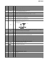
Optical pick-up flexible board
5-4.
HOW TO IDENTIFY OPTICAL PICK-UP
KMS-262A/KMS-262E
This set uses optical pick-up KMS-262E in the production, but for
the repair, only the KMS-262A is supplied. As a result, two types
of optical pick-ups are used for this set, and the specified values
for the check and adjustment of the laser power vary depending on
the type. Therefore, in performing the check and adjustment of
the laser power, first make sure the type of optical pick-up. The
type of optical pick-up can be identified as follows.
– KMS-262A –
– KMS-262E –
[Top view]
[Top view]
[Side view]
TYPE2 VR (small)
34
[Side view]
TYPE3 VR (large)
MXD-D400
5-5.
PRECAUTIONS FOR ADJUSTMENTS
1. When replacing the following parts, perform the adjustments
and checks with in the order shown in the following table.
2. Set the test mode when performing adjustments.
After completing the adjustments, exit the test mode.
Perform the adjustments and checks in “group Service” of the
test mode.
3. Perform the adjustments to be needed in the order shown.
4. Use the following tools and measuring devices.
• Check Disc (MD) (TDYS-1) (Parts No. 4-963-646-01)
• Test Disk (MDW-74/GA-1) (Parts No. 4-229-747-01)
• Laser power meter LPM-8001 (Parts No. J-2501-046-A)
or
MD Laser power meter 8010S (Parts No. J-2501-145-A)*1
• Oscilloscope (Measure after performing CAL of prove.)
• Digital voltmeter
• Thermometer
• Jig for checking BD (MD) board waveform
(Parts No. : J-2501-196-A)
5. When observing several signals on the oscilloscope, etc.,
make sure that VC and ground do not connect inside the oscilloscope.
(VC and ground will become short-circuited.)
6. Using the above jig enables the waveform to be checked without the need to solder.
(Refer to Servicing Note on page 7.)
7. As the disc used will affect the adjustment results, make sure
that no dusts nor fingerprints are attached to it.
*1 Laser power meter
When performing laser power checks and adjustment (electrical
adjustment), use of the new MD laser power meter 8010S (Part
No. J-2501-145-A) instead of the conventional laser power meter is convenient.
It sharply reduces the time and trouble to set the laser power
meter sensor onto the objective lens of optical pick-up.
Parts to be replaced
Adjustment
5-8.
Initial setting of adjustment value
5-9.
Recording of Iop information
Optical
Pick-up
IC101
IC12
IC201
IC933
IC195
D101
5-10. Temperature compensation
offset adjustment
5-11. Laser power adjustment
5-12. Iop NV Save
5-13. Traverse adjustment
5-14. Focus bias adjustment
5-17. Auto gain adjustment
5-7-4. AUTO CHECK
35
MXD-D400
5-6.
USING THE CONTINUOUSLY RECORDED
DISC
* This disc is used in focus bias adjustment and error rate check.
The following describes how to create a continuous recording
disc.
1. Insert a disc (blank disc) commercially available.
2. Rotate the l AMS L (MD) knob and display “CREC
2MODE” (C37).
3. Press the [YES] button again to display “CREC 2MID”.
Display “CREC 2(0300)” and start to recording.
4. Complete recording within 5 minutes.
5. Press the [MENU/NO] button and stop recording .
6. Press the [EJECT] button and remove the disc.
The above has been how to create a continuous recorded data for
the focus bias adjustment and error rate check.
Note: Be careful not to apply vibration during continuous recording.
5-7.
CHECKS PRIOR TO REPAIRS
These checks are performed before replacing parts according to
“approximate specifications” to determine the faulty locations. For
details, refer to “Checks Prior to Parts Replacement and Adjustments” (see page 13).
5-7-1. Temperature Compensation Offset Check
When performing adjustments, set the internal temperature and
room temperature to 22 to 28ºC.
Checking Procedure:
1. Rotate the l AMS L (MD) knob to display “TEMP
CHECK” (C12).
2. Press the [YES] button.
3. “T=@@(##) [OK” should be displayed. If “T=@@ (##) [NG]”
is displayed, it means that the results are bad.
(@@ indicates the current value set, and ## indicates the value
written in the non-volatile memory.)
Checking Procedure:
1. Set the laser power meter on the objective lens of the optical
pick-up.
Connect the digital volt meter to CN105 pin 1 (I+3V) and
CN105 pin 2 (IOP).
2. Then, rotate the l AMS L (MD) knob and display
“LDPWR CHECK” (C13).
3. Press the [YES] button once and display “L 0.93 mW $ ”.
Check that the reading of the laser power meter becomes the
specified value.
Note: Never allow the laser emission at 8.65 mW for 1.5 seconds or longer.
Specified Value: 0.84 to 0.92 mW (KMS-262A)
0.90 to 0.96 mW (KMS-262E)
4. Press the [YES] button once more and display “ L 8.65 mW $
”. Check that the reading the laser power meter and digital
volt meter satisfy the specified value.
Specified Value:
Laser power meter reading : 8.1 to 8.7 mW (KMS-262A)
8.4 to 8.9 mW (KMS-262E)
Digital voltmeter reading : Optical pick-up displayed value ± 10%
(Optical pick-up label)
KMS
262E
20101
B0576
(For details of the method for
checking this value, refer to “5-9.
Recording and Displaying the Iop
Information”.)
Iop = 57.6 mA in this case
Iop (mA) = Digital voltmeter reading (mV)/1 (Ω)
5. Press the [MENU/NO] button and display “LDPWR CHECK”
(C13) and stop the laser emission.
(The [MENU/NO] button is effective at all times to stop the
laser emission.)
5-7-2. Laser Power Check
Before checking, check the Iop value of the optical pick-up.
(Refer to 5-9. Recording and Displaying the Iop Information (see
page 39.)
Note: After step 4, each time the [YES] button is pressed, the display
will be switched between “L 0.73 mW $ ”, “L 7.70 mW $ ”,
and “L Wp
$ ”. Nothing needs to be performed here.
Connection:
Check Location: BD (MD) board (see page 43)
laser
power meter
Optical pick-up
objective lens
5-7-3. Iop Compare
The current Iop value at laser power 8.65 mW (KMS-262E) or 8.4
mW (KMS-262A) output and reference Iop value (set at shipment)
written in the nonvolatile memory are compared, and the rate of
increase/decrease will be displayed in percentage.
Note: Perform this function with the optical pick-up set at room
temperature.
digital voltmeter
BD (MD) board
CN105 pin 1 (I +3 V)
CN105 pin 2 (IOP)
36
+
–
Procedure:
1. Rotate the l AMS L (MD) knob to display “Iop Compare” (C27).
2. Press the [YES] button and start measurements.
3. When measurements complete, the display changes to
“±xx%yy”.
xx is the percentage of increase/decrease, and OK or NG is
displayed at yy to indicate whether the percentage of increase/
decrease is within the allowable range.
4. Press the [MENU/NO] button to end this mode.
MXD-D400
5-7-4. Auto Check
This test mode performs CREC and CPLAY automatically for
mainly checking the characteristics of the optical pick-up. To
perform this test mode, the laser power must first be checked.
Perform Auto Check after the laser power check and Iop compare.
Procedure:
1. Display “AUTO CHECK” and press the [YES] button. If
“LDPWR
” is displayed, it means that the laser
power check has not been performed. In this case, perform the
laser power check and Iop compare, and then repeat from step
1.
2. If a disc is in the mechanical deck, it will be ejected forcibly.
“DISC IN” will be displayed in this case. Load a test disc
(MDW-74/GA-1) which can be recorded.
3. If a disk is loaded at step 2, the check will start automatically.
4. When “XX CHECK” is displayed, the item corresponding to
XX will be performed.
When “06 CHECK” completes, the disc loaded at step 2 will
be ejected. “DISC IN” will be displayed. Load the check disc
(MD) (TDYS-1).
5. When the disc is loaded in the step 4, the check will automatically be resumed from “07 CHECK”.
6. After completing to test item “0C check”, check OK or NG
will be displayed. If all items are OK, “CHECK ALL OK”
will be displayed. If any item is NG, it will be displayed as
“NG:xxxx”.
When “CHECK ALL OK” is displayed, it means that the optical
pick-up is normal. Check the operations of the other spindle motor,
sled motor, etc.
When displayed as “NG:xxxx”, it means that the optical pick-up
is faulty. In this case, replace the optical pick-up.
5-7-5. Other Checks
All the following checks are performed by the Auto Check mode.
They therefore need not be performed in normal operation.
6-6. Traverse Check
6-7. Focus Bias Check
6-8. C PLAY Check
6-9. Self-Recording/Playback Check
5-7-6. Traverse Check
Note 1: Data will be erased during MO reading if a recorded disc is
used in this adjustment.
Note 2: If the traverse waveform is not clear, connect the oscilloscope
as shown in the following figure so that it can be seen more
clearly.
oscilloscope
(DC range)
BD (MD) board
330 k Ω
CN105 pin 4 (TE)
CN105 pin 6 (VC)
+
–
10 pF
Connection:
oscilloscope
(DC range)
BD (MD) board
CN105 pin 4 (TE)
CN105 pin 6 (VC)
+
–
V: 0.1 V/div
H: 10 ms/div
Checking Procedure:
1. Connect an oscilloscope to CN105 pin 4 (TE) and CN105
pin 6 (VC) on the BD (MD) board.
2. Load a disc (any available on the market). (Refer to Note 1)
3. Turn the l AMS L (MD) knob to display “EF MO
CHECK”(C14).
MO-R”.
4. Press the [YES] button to display “EFB =
(Laser power READ power/Focus servo ON/tracking servo
OFF/spindle (S) servo ON)
5. Observe the waveform of the oscilloscope, and check that the
specified value is satisfied. Do not turn the l AMS L (MD)
knob.
(Read power traverse checking)
Traverse Waveform
A
VC
B
Specified value : Below 10% offset value
Offset value (%) = IA – BI X 100
2 (A + B)
6. Press the [YES] button to display “EFB =
MO-W”.
7. Observe the waveform of the oscilloscope, and check that the
specified value is satisfied. Do not turn the l AMS L (MD)
knob.
(Write power traverse checking)
Traverse Waveform
A
VC
B
Specified value : Below 10% offset value
Offset value (%) = IA – BI X 100
2 (A + B)
37
MXD-D400
8. Press the [YES] button to display “EFB =
MO-P”.
Then, the optical pick-up moves to the pit area automatically
and servo is imposed.
9. Observe the waveform of the oscilloscope, and check that the
specified value is satisfied. Do not turn the l AMS L (MD)
knob.
Traverse Waveform
A
VC
B
Specified value : Below 10% offset value
Offset value (%) = IA – BI X 100
2 (A + B)
10. Press the [YES] button to display “EF MO CHECK (C14)”.
The disc stops rotating automatically.
11. Press the [EJECT] button and take out the disc.
12. Load the check disc (MD) (TDYS-1).
13. Turn the l AMS L (MD) knob and display “EF CD
CHECK” (C15).
14. Press the [YES] button to display “EFB =
CD”. Servo is
imposed automatically.
15. Observe the waveform of the oscilloscope, and check that the
specified value is satisfied. Do not turn the l AMS L (MD)
knob.
Traverse Waveform
A
VC
B
Specified value : Below 10% offset value
Offset value (%) = IA – BI X 100
2 (A + B)
16. Press the [YES] button to display “EF CD CHECK” (C15).
17. Press the [EJECT] button and take out the check disc (MD)
(TDYS-1).
Check Location: BD (MD) board (see page 43)
5-7-7. Focus Bias Check
Change the focus bias and check the focus tolerance amount.
Checking Procedure:
1. Load the test disk (MDW-74/GA-1).
2. Turn the l AMS L (MD) knob to display “CPLAY 2
MODE” (C36).
3. Press the [YES] button to display “CPLAY 2MID”.
4. Press the [MENU/NO] button when “C =
AD = ” is
displayed.
5. Turn the l AMS L (MD) knob to display “FBIAS
CHECK” (C16).
6. Press the [YES] button to display “
/ c = ”.
The first four digits indicate the C error rate, the two digits
after [/] indicate ADER, and the 2 digits after [c =] indicate
the focus bias value.
7. Press the [YES] button to display “
/ b = ”.
Check that the C error is about 220 and ADER is below 2.
8. Press the [YES] button to display “
/ a = ”.
Check that the C error is about 220 and ADER is below 2.
9. Press the [MENU/NO] button, then press the [EJECT] button
and take out the test disc.
38
5-7-8. C PLAY Check
MO Error Rate Check
Checking Procedure:
1. Load the test disk (MDW-74/GA-1).
2. Turn the l AMS L (MD) knob to display “CPLAY 2
MODE” (C36).
3. Press the [YES] button to display “CPLAY 2MID”.
4. The display changes to “C =
AD = ”.
5. If the C error rate is below 20, check that ADER is 00.
6. Press the [MENU/NO] button to stop playback, then press the
[EJECT] button and take out the test disc.
CD Error Rate Check
Checking Procedure:
1. Load the check disc (MD) (TDYS-1).
2. Turn the l AMS L (MD) knob to display “CPLAY 2
MODE” (C36).
3. Press the [YES] button to display “CPLAY 2MID”.
4. The display changes to “C =
AD = ”.
5. Check that the C error rate is below 20.
6. Press the [MENU/NO] button to stop playback, then press the
[EJECT] button and take out the check disc.
5-7-9. Self-Recording/playback Check
Prepare a continuous recording disc using the unit to be repaired
and check the error rate.
Checking Procedure:
1. Load a recordable disc (blank disc).
2. Turn the l AMS L (MD) knob to display
“CREC 2MODE” (C37).
3. Press the [YES] button to display “CREC 2MID”.
4. When recording starts, lights up “ REC ” and display “CREC
2 @@@@” (@@@@ is the address).
5. About 1 minute later, press the [MENU/NO] button to stop
continuous recording.
6. Turn the l AMS L (MD) knob to display “CPLAY 2
MODE” (C36).
7. Press the [YES] button to display “CPLAY 2MID”.
8. “C =
AD = ” will be displayed.
9. Check that the C error becomes below 20 and the AD error
below 2.
10. Press the [MENU/NO] button to stop playback, then press the
[EJECT] button and take out the disc.
5-8.
INITIAL SETTING OF ADJUSTMENT
VALUE
Note:
Mode which sets the adjustment results recorded in the non-volatile
memory to the initial setting value. However the results of the temperature compensation offset adjustment will not change to the initial setting
value.
If initial setting is performed, perform all adjustments again excluding the
temperature compensation offset adjustment.
For details of the initial setting, refer to “5-5. Precautions for Adjustments”
and execute the initial setting before the adjustment as required.
Setting Procedure:
1. Turn the l AMS L (MD) knob to display “ADJ CLEAR”
(C28).
2. Press the [YES] button. “Complete!” will be displayed momentarily and initial setting will be executed, after which “ADJ
CLEAR” (C28) will be displayed.
MXD-D400
5-9.
RECORDING AND DISPLAYING THE IOP
INFORMATION
The Iop data can be recorded in the non-volatile memory. The Iop
value on the optical pick-up label and the Iop value after the adjustment will be recorded. Recording these data eliminates the need
to read the label on the optical pick-up.
Recording Procedure:
1. Turn the l AMS L (MD) knob to display “Iop Write”
(C05), and press the [YES] button.
2. The display becomes “Ref=@@@.@” (@ is an arbitrary number) and the numbers which can be changed will blink.
3. Input the Iop value on the optical pick-up label.
To select the number : Turn the l AMS L (MD) knob.
To select the digit : Press the l AMS L (MD) knob
4. When the [YES] button is pressed, the display becomes
“Measu=@@@.@” (@ is an arbitrary number).
5. As the adjustment results are recorded for the 4 value. Leave it
as it is and press the [YES] button.
6. “Complete!!” will be displayed momentarily. The value will
be recorded in the non-volatile memory and the display will
become “Iop Write” (C05).
5-11. LASER POWER ADJUSTMENT
Check the Iop value of the optical pick-up before adjustments.
(Refer to 5-9. Recording and Displaying Iop Information)
Connection:
laser
power meter
Optical pick-up
objective lens
digital voltmeter
BD (MD) board
CN105 pin 1 (I +3 V)
CN105 pin 2 (IOP)
+
–
Display Procedure:
1. Turn the l AMS L (MD) knob to display “Iop Read”
(C26), and press the [YES] button.
2. “@@.@/##.#” is displayed and the recorded contents are displayed.
@@.@ indicates the Iop value on the optical pick-up label.
##.# indicates the Iop value after adjustment
3. To end, press the l AMS L (MD) button or [MENU/NO]
button to display “Iop Read” (C26).
Adjusting Procedure:
1. Set the laser power meter on the objective lens of the optical
pick-up.
Connect the digital voltmeter to CN105 pin 1 (I+3V) and
CN105 pin 2 (IOP) on the BD (MD) board.
2. Turn the l AMS L (MD) knob to display “LDPWR
ADJUS” (C04).
(Laser power : For adjustment)
3. Press the [YES] button once to display “L 0.93 mW $ ”.
4. Turn the l AMS L (MD) knob so that the reading of the
laser power meter becomes the specified value. Press the [YES]
button after setting the range knob of the laser power meter to
10 mW, and save the adjustment results. (“L SAVE $ ” will
be displayed for a moment)
5-10. TEMPERATURE COMPENSATION OFFSET
ADJUSTMENT
Specified Value: 0.85 to 0.91 mW (KMS-262A)
0.90 to 0.95 mW (KMS-262E)
Save the temperature data at that time in the non-volatile memory
as 25 ˚C reference data.
Note:
1. Usually, do not perform this adjustment.
2. Perform this adjustment in an ambient temperature of 22 ˚C to 28 ˚C.
Perform it immediately after the power is turned on when the internal
temperature of the unit is the same as the ambient temperature of 22 ˚C
to 28 ˚C.
3. When D101 has been replaced, perform this adjustment after the temperature of this part has become the ambient temperature.
Adjusting Procedure:
1. Turn the l AMS L (MD) knob to display “TEMP
ADJUS” (C03).
2. Press the [YES] button to select the “TEMP ADJUS” mode.
3. “TEMP =
[OK” and the current temperature data will be
displayed.
4. To save the data, press the [YES] button.
When not saving the data, press the [MENU/NO] button.
5. When the [YES] button is pressed, “TEMP =
SAVE” will
be displayed and turned back to “TEMP ADJUS” (C03) display then. When the [MENU/NO] button is pressed, “TEMP
ADJUS” (C03) will be displayed immediately.
5. Then “L 8.65 mW $ ” will be displayed.
6. Turn the l AMS L (MD) knob so that the reading of the
laser power meter becomes the specified value, press the [YES]
button to save it.
Specified Value: 8.2 to 8.6 mW (KMS-262A)
8.5 to 8.8 mW (KMS-262E)
Note: Do not perform the emission with 8.65 mW more than 15 seconds
continuously.
7. Then, turn the l AMS L (MD) knob to display “LDPWR
CHECK” (C13).
8. Press the [YES] button once to display “L 0.93 mW $ ”.
Check that the reading of the laser power meter becomes the
specified value.
Specified Value: 0.84 to 0.92 mW (KMS-262A)
0.90 to 0.96 mW (KMS-262E)
Specified Value:
The “TEMP =
” should be within “E0 - EF”, “F0 - FF”, “00 0F”, “10 - 1F” and “20 - 2F”.
39
MXD-D400
9. Press the [YES] button once more to display “L 8.65 mW $
”. Check that the reading the laser power meter and digital
voltmeter satisfy the specified value.
Note down the digital voltmeter reading value.
Specified Value:
Laser power meter reading : 8.1 to 8.7 mW (KMS-262A)
8.4 to 8.9 mW (KMS-262E)
Digital voltmeter reading : Value on the optical pick-up label
±10%
(Optical pick-up label)
KMS
262E
20101
B0576
(For details of the method for
checking this value, refer to “5-9.
Recording and Displaying the Iop
Information”.)
Iop = 57.6 mA in this case
Iop (mA) = Digital voltmeter reading (mV)/1 (Ω)
10. Press the [MENU/NO] button to display “LDPWR CHECK”
(C13) and stop the laser emission.
(The [MENU/NO] button is effective at all times to stop the
laser emission.)
11. Turn the l AMS L (MD) knob to display “Iop Write”
(C05).
12. Press the [YES] button. When the display becomes
Ref=@@@.@ (@ is an arbitrary number), press the [YES]
button to display “Measu=@@@.@” (@ is an arbitrary number).
13. The numbers which can be changed will blink. Input the Iop
value noted down at step 9.
To select the number : Turn the l AMS L (MD) knob.
To select the digit : Press the l AMS L (MD) knob.
14. When the [YES] button is pressed, “Complete!” will be displayed momentarily. The value will be recorded in the nonvolatile memory and the display will become “Iop Write”
(C05).
Note: After step 9, each time the [YES] button is pressed, the display
will be switched “L 0.73 mW $ ”, “L 7.70 mW $ ”, and “L
$ ”. Nothing needs to be performed here.
Wp
5-13. TRAVERSE ADJUSTMENT
Note 1:Data will be erased during MO reading if a recorded disc is
used in this adjustment.
Note 2:If the traverse waveform is not clear, connect the oscilloscope
as shown in the following figure so that it can be seen more
clearly.
oscilloscope
(DC range)
BD (MD) board
330 k Ω
CN105 pin 4 (TE)
CN105 pin 6 (VC)
+
–
10 pF
Connection:
oscilloscope
(DC range)
BD (MD) board
CN105 pin 4 (TE)
CN105 pin 6 (VC)
+
–
V: 0.1 V/div
H: 10 ms/div
Adjusting Procedure:
1. Connect an oscilloscope to CN105 pin 4 (TE) and CN105
pin 6 (VC) on the BD (MD) board.
2. Load a disc (any available on the market). (Refer to Note 1)
3. Turn the l AMS L (MD) knob to display “EF MO
ADJUS” (C07).
4. Press the [YES] button to display “EFB =
MO-R”.
(Laser power READ power/Focus servo ON/tracking servo
OFF/spindle (S) servo ON)
5. Turn the l AMS L (MD) knob so that the waveform of
the oscilloscope becomes the specified value.
of
(When the l AMS L (MD) knob is turned, the
“EFB= ” changes and the waveform changes.) In this adjustment, waveform varies at intervals of approx. 2%. Adjust
the waveform so that the specified value is satisfied as much
as possible.
(Read power traverse adjustment)
Traverse Waveform
A
Adjustment Location: BD (MD) board (see page 43)
VC
B
11. Iop NV SAVE
Write the reference values in the nonvolatile memory to perform
“Iop compare”. As this involves rewriting the reference values, do
not perform this procedure except when adjusting the laser power
during replacement of the optical pick-up and when replacing the
IC12. Otherwise the optical pick-up check may deteriorate.
Note: Perform this function with the optical pick-up set at room temperature.
Procedure:
1. Rotate the l AMS L (MD) knob to display “Iop NV
Save” (C06).
2. Press the [YES] button and display “Iop [stop]”.
3. After the display changes to “Iop =xxsave?”, press the [YES]
button.
4. After “Complete!” is displayed momentarily, the display
changes to “Iop 8.4 mW”.
5. After the display changes to “Iop=yysave?”, press the [YES]
button.
6. When “Complete!” is displayed, it means that Iop NV saving
has been completed.
40
Specification A = B
6. Press the [YES] button and save the result of adjustment to the
non-volatile memory (“EFB = SAVE” will be displayed for
a moment. Then “EFB =
MO-W” will be displayed).
MXD-D400
7. Turn the l AMS L (MD) knob so that the waveform of
the oscilloscope becomes the specified value.
(When the l AMS L (MD) knob is turned, the
of
“EFB= ” changes and the waveform changes.) In this adjustment, waveform varies at intervals of approx. 2%. Adjust
the waveform so that the specified value is satisfied as much
as possible.
(Write power traverse adjustment)
Traverse Waveform
17. Press the [YES] button, display “EFB =
SAVE” for a moment and save the adjustment results in the non-volatile
memory.
Next “EF CD ADJUS” (C08) will be displayed.
18. Press the [EJECT] button and take out the disc (MD) (TDYS1).
Adjustment Location: BD (MD) board (see page 43)
5-14. FOCUS BIAS ADJUSTMENT
A
VC
B
Specification A = B
8. Press the [YES] button, and save the adjustment results in the
non-volatile memory. (“EFB =
SAVE” will be displayed
for a moment)
9. “EFB =
MO-P” will be displayed.
The optical pick-up moves to the pit area automatically and
servo is imposed.
10. Turn the l AMS L (MD) knob until the waveform of
the oscilloscope moves closer to the specified value.
In this adjustment, waveform varies at intervals of approx. 2%.
Adjust the waveform so that the specified value is satisfied as
much as possible.
Traverse Waveform
A
VC
B
Specification A = B
11. Press the [YES] button, and save the adjustment results in the
SAVE” will be displayed
non-volatile memory. (“EFB =
for a moment.)
Next “EF MO ADJUS” (C07) is displayed. The disc stops rotating automatically.
12. Press the [EJECT] button and take out the disc.
13. Load the check disc (MD) (TDYS-1).
14. Turn the l AMS L (MD) knob to display “EF CD
ADJUS” (C08).
15. Press the [YES] button to display “EFB =
CD”. Servo is
imposed automatically.
16. Turn the l AMS L (MD) knob so that the waveform of
the oscilloscope moves closer to the specified value.
In this adjustment, waveform varies at intervals of approx. 2%.
Adjust the waveform so that the specified value is satisfied as
much as possible.
Adjusting Procedure:
1. Load the test disc (MDW-74/GA-1).
2. Turn the l AMS L (MD) knob to display “CPLAY 2
MODE” (C36).
3. Press the [YES] button to display “CPLAY 2MID”.
4. Press the [MENU/NO] button when “C =
AD = ” is
displayed.
5. Turn the l AMS L (MD) knob to display “FBIAS
ADJUS” (C09).
6. Press the [YES] button to display “
/ a = ”.
The first four digits indicate the C error rate, the two digits
after “/ ” indicate ADER, and the 2 digits after “a =” indicate
the focus bias value.
7. Turn the l AMS L (MD) knob clockwise and find the
focus bias value at which the C error rate becomes about 200
(refer to Note 2).
8. Press the [YES] button to display “
/ b = ”.
9. Turn the l AMS L (MD) knob counterclockwise and find
the focus bias value at which the C error rate becomes about
200.
10. Press the [YES] button to display “
/ c = ”.
11. Check that the C error rate is below 20 and ADER is 00. Then
press the [YES] button.
12. If the “( )” in “ - - ( )” is above 20, press the [YES]
button.
If below 20, press the [MENU/NO] button and repeat the adjustment from step 2.
13. Press the [EJECT] button and take out the disc.
Note 1: The relation between the C error and focus bias is as shown in
the following figure. Find points A and B in the following figure
using the above adjustment. The focal point position C is automatically calculated from points A and B.
Note 2: As the C error rate changes, perform the adjustment using the
average vale.
C error
about
200
Focus bias value
B
C
A
Traverse Waveform
A
VC
B
Specification A = B
41
MXD-D400
5-15. ERROR RATE CHECK
5-17. AUTO GAIN CONTROL OUTPUT LEVEL
ADJUSTMENT
5-15-1. CD Error Rate Check
Checking Procedure:
1. Load the check disc (MD) (TDYS-1).
2. Turn the l AMS L (MD) knob to display “CPLAY 2
MODE” (C36).
3. Press the [YES] button twice and display “CPLAY 2MID”.
4. The display changes to “C =
AD = ”.
5. Check that the C error rate is below 20.
6. Press the [MENU/NO] button to stop playback, then press the
[EJECT] button and take out the check disc.
Be sure to perform this adjustment when the optical pick-up is
replaced.
If the adjustment results becomes “Adjust NG!”, the optical pickup may be faulty or the servo system circuits may be abnormal.
5-15-2. MO Error Rate Check
Checking Procedure:
1. Load the continuously-recorded disc. (Refer to “5-6. USING
THE CONTINUOUSLY RECORDED DISC”)
2. Turn the l AMS L (MD) knob to display “CPLAY 2
MODE” (C36).
3. Press the [YES] button to display “CPLAY 2MID”.
4. The display changes to “C =
AD = ”.
5. If the C error rate is below 20, check that ADER is 00.
6. Press the [MENU/NO] button to stop playback, then press the
[EJECT] button and take out the test disc.
5-16. FOCUS BIAS CHECK
Change the focus bias and check the focus tolerance amount.
Checking Procedure:
1. Load the continuously-recorded disc. (Refer to “5-6. USING
THE CONTINUOUSLY RECORDED DISC”)
2. Turn the l AMS L (MD) knob to display “CPLAY 2
MODE” (C36).
3. Press the [YES] button twice to display “CPLAY 2MID”.
4. Press the [MENU/NO] button when “C =
AD = ” is
displayed.
5. Turn the l AMS L (MD) knob to display “FBIAS
CHECK” (C16).
/ c = ”.
6. Press the [YES] button to display “
The first four digits indicate the C error rate, the two digits
after “/ ” indicate ADER, and the 2 digits after “c =” indicate
the focus bias value.
7. Press the [YES] button and display “
/ b = ”.
Check that the C error is about 220 and ADER is below 2.
8. Press the [YES] button and display “
/ a = ”.
Check that the C error is about 220 and ADER is below 2
9. Press the [MENU/NO] button, then press the [EJECT] button
and take out the disc.
Note:
42
If the C error and ADER are above other than the specified value
at points a (step 8. in the above) or b (step 7. in the above), the
focus bias adjustment may not have been carried out properly.
Adjust perform the beginning again.
5-17-1. CD Auto Gain Control Output Level Adjustment
Adjusting Procedure:
1. Load the check disc (MD) (TDYS-1).
2. Turn the l AMS L (MD) knob to display “AG Set (CD)”
(C11).
3. When the [YES] button is pressed, the adjustment will be performed automatically.
“Complete!!” will then be displayed momentarily when the
value is recorded in the non-volatile memory, after which the
display changes to “AG Set (CD)” (C11).
4. Press the [EJECT] button and take out the check disc.
5-17-2. MO Auto Gain Control Output Level Adjustment
Adjusting Procedure:
1. Load the test disc (MDW-74/GA-1).
2. Turn the l AMS L (MD) knob to display “AG Set (MO)”
(C10).
3. When the [YES] button is pressed, the adjustment will be performed automatically.
“Complete!!” will then be displayed momentarily when the
value is recorded in the non-volatile memory, after which the
display changes to “AG Set (MO)” (C10).
4. Press the [EJECT] button and take out the test disc.
MXD-D400
Adjustment and checking Location:
– BD (MD) BOARD (Side A) –
D101
CN101
– BD (MD) BOARD (Side B) –
IC101
CN105
1
IC701
7
1. I+3V
2. IOP
3. GND
4. TE
5. FE
6. VC
7. RF
IC201
IC933
IC195
17
1
CN103
1
27
CN102
Note: It is useful to use the jig for checking the waveform. (Refer to Servicing Notes on page 11)
43
MXD-D400
Note: A clear RF signal waveform means that the shape “◊” can be clearly
distinguished at the center of the waveform.
CD SECTION
Note:
1. CD Block is basically designed to operate without adjustment. Therefore, check each item in order given.
2. Use YEDS-18 disc (3-702-101-01) unless otherwise indicated.
3. Use an oscilloscope with more than 10MΩ impedance.
4. Clean the object lens by an applicator with neutral detergent when the
signal level is low than specified value with the following checks.
RF signal waveform
VOLT/DIV: 200 mV
TIME/DIV: 500 ns
(normal speed)
level: 1.1 ±0.3 Vp-p
S Curve Check
Connection:
oscilloscope
(DC range)
BD (CD) board
Checking Location: BD (CD) board (see page 45)
TP (FE)
TP (VC)
+
–
E-F Balance (1 Track Jump) Check
Connection:
Procedure:
1. Connect oscilloscope to test point TP (FE) and TP (VC) on
BD (CD) board.
2. Turn the power on.
3. Put disc (YEDS-18) in.
4. Enter the test mode, select the BU Test and press
the l AMS L (CD) knob to display “bdt S CURVED”.
5. Press the l AMS L (CD) knob. “LD AL” is displayed
and playback starts automatically.
6. Check the oscilloscope waveform (S-curve) is symmetrical
between A and B. And confirm peak to peak level within 3.6 ±
0.5 Vp-p.
7. Press the [MENU/NO] button to stop playback.
8. Exit from the test mode.
(Refer to the TEST MODE Section)
S-curve waveform
symmetry
oscilloscope
(DC range)
BD (CD) board
TP (TE)
TP (VC)
+
–
Procedure:
1. Connect oscilloscope to test point TP (TE) and TP (VC) on
BD (CD) board.
2. Press the ?/1 button to turn the power on.
3. Put disc (YEDS-18) in to play the number five track.
4. Enter the service mode, press the [INPUT] button until “TRV
ON” is displayed. (The tracking servo and the sledding servo
are turned OFF)
5. Rotate RV101 on BD (CD) board to adjust A (DC voltage) of
the center of the oscilloscope waveform becomes 0 V.
6. Enter the service mode, press the [INPUT] button until “TRV
ON” is displayed (The tracking servo and the sledding servo
are turned OFF), confirm A (DC voltage) at that time is 0 V.
A
Traverse Waveform
within 3.6 ± 0.5 Vp-p
Center of
waveform
B
B
Note: • Try to measure several times to make sure than the ratio of A : B
or B : A is more than 10 : 7.
• Take sweep time as long as possible and light up the
brightness to obtain best waveform.
Check Location: BD (CD) board (see page 45)
RF Level Check
Connection:
BD (CD) board
+
–
Procedure:
1. Connect oscilloscope to test point TP (RFDC) and TP (VC) on
BD (CD) board.
2. Turn ON the power.
3. Put disc (YEDS-18) in to play the number five track.
4. Confirm that oscilloscope waveform is clear and check RF signal level is correct or not.
44
level=1.1 ±0.6Vp-p
Symmetry
Checking Location: BD (CD) board (see page 45)
oscilloscope
(AC range)
TP (RFDC)
TP (VC)
A (DC voltage)
0V
Adjustment after CD Base Unit (BU-30BBD61B) is Replaced
Perform the “E-F Balance (1 track jump) check”.
MXD-D400
Checking Location:
– BD (CD) BOARD (Conductor Side) –
TP (TE)
RV101
TP (RFAC)
TP (FE)
TP (VC)
45
45
MXD-D400
SECTION 6
DIAGRAMS
6-1.
BLOCK DIAGRAM – CD Section –
RF AMP,
FOCUS TRACKING ERROR AMP
IC103
OPTICAL PICK-UP
BLOCK
(A-MAX.4T)
2
4
7
5
3
1
VC
27 VC
VCC
RF AC 15
SELECTOR
IC105
3 Y
50 RFAC
Y1 5
RF
+3.3V
D OUT
DOUT
64
Y2 2
PD1
PD2
I5-10
I1-6
DOUT TO MD
6
A
7
B
8
C
9
D
PCMD
66
12 SDIO
10 E
BCLK
67
13 BCKIA
LRCK
65
14 LRCKIA
11 F
LD
CD DSP
IC101
Y0 1
Y3 4
B
9
D/A CONVERTER,
MP3 DECODER
IC104
A
10
43 RFDC
RFDC 28
1
LD
RV101
PD
FE 16
39 FE
FEI 17
40 SE
19 TE_BAL
TE 18
41 TE
PD
SW 12
GND
2
XTAI
71
XTAO
72
52 VO1+
T+
TRACKING
COIL
T-
M102
(SLED)
IN1+
33 FFDR
35
47 VO1-
IN1- 34
34 FRDR
56 VO2+
IN2+
32
31 TFDR
55 VO2-
IN2-
31
32 TRDR
MIDIO 5
5
6
MP3DOUT
MP3DIN
MICK 6
7
MP3CLK
2
VO3+
IN3+
VO3-
10 VO4+
IN3-
IN4R
30 SRDR
26
RESET 1
19 MP3RESET
MICS 3
22 MP3CS
REQ 39
18 MP3REQ
MILP 4
23 MP3LT
4
6
37 CLK
XLAT
5
38 XLT
SQCK
77
33 SQCLK
SCLK
8
SCOR
15
20 SCOR
SQSO
76
32 SUBQ
SENS
7
34 SENSE
XRST
2
25 MDP
24
10 MP3ACK
DATA
29 SFDR
27
MIACK 7
CLOK
M
1
M101
(SPINDLE)
(Page 47)
C
(Page 48)
D
(Page 47)
CD MECHANISM CONTROLLER
IC6 (1/2)
62 XI
26 SSTP
FOCUS/TRACKING COIL DRIVE,
SLED/SPINDLE MOTOR DRIVE
IC102
F-
B
X201
33.8688MHz
63 XO
IL-SW
OUT SW
AUTO PWRON 73
VR
FOCUS
COIL
(Page 48)
RFDCI 29
AUTOMATIC
POWER CONTROL
Q701
F+
AOUT
TXO 30
A
35 DATA
M
M
5
VO4-
STBY
8
SW
19
LOADING MOTOR DRIVE
IC10
27 CTRL1
LOADNEG 53
5
IN1
OUT1 2
LOADPOS 54
6
IN2
OUT2 10
25 X4
45 BDRST
24 PWM3
26 PWM2
28 PWM1
47 LDON
• R-ch is omitted due to same as L-ch.
• SIGNAL PATH
: CD PLAY (ANALOG OUT)
: CD PLAY (DIGITAL OUT)
46
46
OUTSW 56
INSW 55
S271
(LOADING OUT)
S272
(LOADING IN)
M
M151
(LOADING)
MXD-D400
6-2.
BLOCK DIAGRAM – MD Section –
MD DSP
IC201
HR901
OVER WRITE
HEAD
OVER WRITE
HEAD DRIVE
IC181, Q181, 182
CODEC DOUT
115 EFMO
17 XT
DIN0 24
D OUT TO MD
DIN 25
MD DOUT
D OUT 26
OPTICAL PICK-UP BLOCK
(KMS-262E)
VCC
DETECTOR
VC
I
B
I
C
B
SWDT
6
SCLK
7
XLAT
8
6 C
FE 34
79 FE
5 B
TE 26
86 TE
SRDT 10
SE 28
85 SE
SENS 11
31 SWDT
33 SCLK
50 XLATCH
J
A
D
70 RFIN
2 J
C
ABCD 35
A
4 A
D
7 D
E
E
8 E
F
ILCC
LD DRIVE
Q202, 203
78 ABCD
XINT 16
AUX 33
80 AUX
DQSY 14
SQSY 13
PEAK 37
76 PEAK
BOTM 36
77 BOTM
ADFG 32
91 ADFG
9 F
SWDT 16
99 DTRF
SCLK 17
98 CLRF
XLAT 18
97 XLRF
11 APC
LD
MNT1
2
MNT2
3
D0
D3
LASER
DIODE
FCONT 20
PD
APC REF
PD
LD
POWER
LASER ON
SWITCH
Q201
94 FCONT
100 APC REF
12
10 PD
VR
A00
A10
MOD
HF
MODULE
HF MODULE
SWITCH
Q701 – 704
FOCUS/TRACKING COIL DRIVE,
SPINDLE/SLED MOTOR DRIVE
IC401
F+
12 OUT3F
IN3F 14
104 FFDR
10 OUT3R
IN3R 15
105 FRDR
FOCUS
COIL
F-
T+
TRACKING
COIL
21 OUT1F
IN1F 19
103 TFDR
43
.
45
.
44
.
42
52
.
54
.
56
.
60
.
59
.
55
.
53
.
51
.
49
.
48
.
50
15
XOUT
13
32 SRDT
58 SENS
XIN-T
10
25 XINT
18 DQSY
20 SQSY
XOUT-T
11
59 SHOCK
48 XBUSY
DRAM
IC152
3
.
24
.
25
.
2
XIN
23 OUT1R
27 OUT2F
M102
(SLED)
6 OUT4F
M101
(SPINDLE)
IN1R 18
F
(Page 48)
G
(Page 48)
D
(Page 46)
EEPROM
IC195
SDA
60
5
SDA
SCL
45
6
SCL
EEP-WP
47
7
WP
IIC DATA
30
DQ4,
DQ1
IIC CLK 29
9
12
.
15
19
.
21
.
8
X3
32.768kHz
DQ3,
A0
A10
LEVELL
3
LEVELR
4
PDOWN
19
SRST 12
IIC DATA
IIC CLK
LEVEL L
LEVEL R
P DOWN
SRST
IN2F 29
108 SFDR
IN2R 30
XOE 38
22 OE
XWE 37
4
WE
XRAS 47
5
RAS
XCAS 46
23 CAS
RESET
SWITCH
Q2
OUT SW
OSC 28
5
CLKA
FS256 36
1
XIN
IN4F
4
8
107 SRDR
VCO
IC803
S101
(LIMIT IN)
IN4R
3
109 SPRD
110 SPFR
OUTSW
49
S103
(OUT)
PLAYSW
51
S104
(PLAY)
RECSW 53
S105
(REC)
XOUT
X804
11.2896MHz
RPWR
IIC DATA, IIC CLK,
LEVEL L, LEVEL R,
P DOWN, SRST, MD RESET
MD
RESET
102 TRDR
M
8 OUT4R
(Page 46)
DQ2,
M
25 OUT2R
B
X2
10MHz
LIMITIN 55
T-
(Page 48)
MD MECHANISM CONTROLLER
IC12
RF 38
1 I
J
F
RF AMP,
FOCUS/TRACKING ERROR AMP
IC101
E
15
REFELECT
61
PROTECT
44
S102
(REFRECT/PROTECT)
LOADING MOTOR DRIVE
IC18
XRST 12
52 DRESET
PSB 16
LOAD IN
67
5
IN1
OUT1
2
M
COMPARATOR
IC701
89 IOP
LOAD OUT
66
6
57 LD ON
4
56 MOD
+3.3V
LOAD LO
47
OUT2 10
VZ
54 WRPWR
47
IN2
65
REFERENCE
VOLTAGE
SWITCH
Q7, 8
M103
(LOADING)
• R-ch is omitted due to same as L-ch.
• SIGNAL PATH
: MD PLAY
: MD REC
: CD PLAY (DIGITAL OUT)
MXD-D400
6-3.
BLOCK DIAGRAM – MAIN Section –
(Page 46)
(Page 46)
A
C
DOUT
-2
SPDIF
BUFFER
IC8
AOUT
42 RX1
L
L-IN 38
LINE AMP
IC16
-1
R
ANALOG
INPUT
R-IN 37
(Page 47)
(Page 47)
F
E
J1
OPTICAL
RECEIVER
IC15
44 RX2
MD DOUT
2
CODEC
DOUT
BUFFER
IC19
OPTICAL
DIGITAL
OUTPUT
L
RY650
R
RX3
A/D, D/A CONVERTER
IC11
RELAY
DRIVE
Q4
RV790
PHONE LEVEL
13 TX1
14 TX2
HEADPHONE
AMP
IC17
LINE AMP
IC13
R-OUT 33
ANALOG
OUTPUT
J790
PHONES
-1
L-OUT 32
OPTICAL
TRANSCEIVER
IC14
CDTI
CDTO
CCLK
CS
INT0
INT1
PDOWN
OPTICAL
DIGITAL
INPUT
-2
8 9 10 11 6 7 5
: AUDIO
97 KEY0
S710 –716,
S718, 719
95 KEY1
49
70 72 69 68 75 74 76
ADADATAO
ADADATAI
ADACLK
CS_ADALAT
ADAINT0
ADAINT1
ADARST
• R-ch is omitted due to same as L-ch.
• SIGNAL PATH
S700 –704,
S720
CDMP3SEL
MUTING
Q5, 6
MUTING
CONTROL
Q3
SCMS 66
: CD PLAY (ANALOG OUT)
S706, 721, 722,
S725 –729, 1701
: CD PLAY (DIGITAL OUT)
LINEMUTE
85
AMUTE
94 KEY2
: MD PLAY
l AMS L
: MD REC
(MD)
ROTALY
ENCODER
S717
87 MDJOG0
ROTALY
ENCODER
S723
78 CDJOG0
: OPTICAL DIGITAL OUT
: OPTICAL DIGITAL IN
l AMS L
(CD)
REGULATOR
IC7
BACKUP +3.3V
RV780
REC REVEL
REMOTE CONTROL
RECEIVER
IC781
X1
16MHz
RECT
D18
MD +2.6V
+2.6V
REGULATOR
IC926
–32V
–32V
REGULATOR
IC3
RECT
D16, 17
3 − 37
−
40 − 61
SEG35
−
MAINACCUT 79
39 COM01
70
69
68
67
1
2
3
81
13 P.DOWN
10 S.RST
DRVDAT
DRVCLK
DRVCS
DRVRST
(AC IN)
CD +3.3V
LOADING +10V
VCC1 6
VCC2 7
RECT
D6, 7
+2.5V/+3.3V
REGULATOR
IC122
62 COM24
72
73
74
LED
DRIVE
Q726
LED
DRIVE
Q772
LED
DRIVE
Q775
RF +3.3V
MDRESET
RESET
12
MD RESET
LEVEL L
LEVEL R
D775
GROUP
ON/OFF
RESET SIGNAL
GENERATOR
IC2
EVER
+3.3V
48
SRST
LEVELL
LEVELR
88
P DOWN
IICDATA
IICCLK
89 90
IIC DATA
IIC CLK
IIC DATA, IIC CLK,
LEVEL L, LEVEL R,
P DOWN, SRST, MD RESET
D772
MDLP
30 29
48
+3.3V
REGULATOR
IC9
LINE FILTER
LF651
RECT
D14, 15
AC 2
RELAY
+5V
CD +2.5V
D726
STANDBY
G
+8V
REGULATOR
IC4
COM01
STB 11
(Page 47)
+8V
4 ANA5
P3
GRID
DRIVE
Q762
MD +3.3V
91 RECLEVEL
SIRCS
FL B+
+3.3V
REGULATOR
IC933
5 PH5
P2
GRID
DRIVE
Q761
FL B+
8 SYS3.5
SYS +3.5V
MD +5V
DA
CP
CS
RESET
RECT
D2, 3
POWER TRANSFORMER
(MAIN)
TR651
ANA +5V
COM23
+3.3V
REGULATOR
IC1
LITHIUM
BATTERY
BT1
XIN 15
77 CDJOG1
4
EVER
+3.3V
11 V.BAK
SEG01
P1
FLUORESCENT
INDICATOR
TUBE
FL750
D23
86 MDJOG1
XOUT 13
FL/LED DRIVER
IC760
POWER TRANSFORMER
(SUB)
TR652
D28
SYSTEM CONTROLLER
IC6 (2/2)
+5V
REGULATOR
IC5
AMP B+
RECT
D8, 9
AMP B–
RECT
D10, 11
RY650
POWER ON/OFF
RELAY DRIVE
Q1
MXD-D400
6-4.
• Circuit Boards Location
NOTE FOR PRINTED WIRING BOARDS AND SCHEMATIC DIAGRAMS
Note on Printed Wiring Boards:
• X : parts extracted from the component side.
• Y : parts extracted from the conductor side.
a
•
: Through hole.
f
•
: internal component.
•
: Pattern from the side which enables seeing.
(The other layers' patterns are not indicated.)
Caution:
Pattern face side:
(Conductor Side)
Parts face side:
(Component Side)
Caution:
Pattern face side:
(Side B)
Parts face side:
(Side A)
Parts on the pattern face side seen from
the pattern face are indicated.
Parts on the parts face side seen from
the parts face are indicated.
Parts on the pattern face side seen from
the pattern face are indicated.
Parts on the parts face side seen from
the parts face are indicated.
Note on Schematic Diagram:
• All capacitors are in µF unless otherwise noted. pF: µµF
50 WV or less are not indicated except for electrolytics
and tantalums.
• All resistors are in Ω and 1/4 W or less unless otherwise
specified.
f
•
: internal component.
• C : panel designation.
BD (CD) board
MAIN board
CD-EJECT board
Note: The components identified by mark 0 or dotted line
with mark 0 are critical for safety.
Replace only with part number specified.
TRANSFORMER board
POWER SWITCH board
• A : B+ Line.
• B : B– Line.
• Voltages are taken with a VOM (Input impedance 10 MΩ).
Voltage variations may be noted due to normal production tolerances.
• Waveforms are taken with a oscilloscope.
Voltage variations may be noted due to normal production tolerances.
• Circled numbers refer to waveforms.
• Signal path.
F : AUDIO
J : CD PLAY (ANALOG OUT)
c : CD PLAY (DIGITAL OUT)
p : MD PLAY
l : MD REC
I : OPTICAL DIGITAL OUT
i : OPTICAL DIGITAL IN
HP board
LOADING board
CD-SW board
BD (MD) board
DISPLAY board
49
49
MXD-D400
6-5.
PRINTED WIRING BOARD – BD (CD) Section – • See page 49 for Circuit Boards Location.
1
2
3
4
5
6
:Uses unleaded solder.
7
8
9
10
11
12
13
14
15
A
C249
C248
R304
C203
IC104
R231
R232
R233
C230 C228
C256
C269
C227
C258
R309
41
61
40
C255
IC101
C250
FB103
D
R257
60
X201
R208
FB104
R252
R230
C251
FB102
C254
FB203
R201
R206
R305
R251
C270
C257
R250
R204 C212
R205
R216
C259
C263
C216
C211
C305
C271
R260
C253
C215
C209
C
R255
C304
C224
C226
R202
R229
C266
C277
R308
R207
R203
M101
(SPINDLE)
R275
R272
C274
R271
R279
B
JR2
R259
R276
BD (CD) BOARD
(CONDUCTOR SIDE)
R291
BD (CD) BOARD
(COMPONENT SIDE)
C222
R253
R111 C132
C117
R118
C111
30
R114
RV101
16
TP (TE)
CN103
TP (FE)
56
MAIN BOARD
CN5
(Page 56)
C108
IC102
C118
Q101
C113
1
IC103
CN101
15
1
C110
12
C158
L163
C161
R125
12
(12)
C160
1-687-189-
R152
28
R126
R122
C121
R151
TP (VC)
R123
C114
C152
B
29
C156
FB161
R221
C165
TP (RFAC)
C109
C119
G
R104
R131
R113
R120
C116 R115
FB351
C115
C112
C150
R220
C157
8
R199
R158
R157
R155
1
C102
C131
R222
C310
R132
C213
C229
C159
R228
C151
F
C153 C164
R223
C163
C301
20
R315
C107
9
1
R312
2
1
(Page 56)
R102
16
R218
21
3
R314
R103
R105
C303
R302
C133
C302
C103
IC105
C169
5
4
MAIN
BOARD
CN4
R166
C101
C104
R224
C231
R301
R225
E
R226
R227
80
A
FB101
R320
R169
IC122
CN105
C307
C205
R101
R219
FB202
FB201
R116
R167
R318
C273
R117
R168
R313
C208 FB291 C292
C260
R133
R249
C202
(12)
1-687-189-
M102
(SLED)
OPTICAL
PICK-UP
BLOCK
(A-MAX. 4T)
H
LOADING BOARD
I
CN151
5
• Semiconductor
Location
J
Ref. No.
Location
IC101
IC102
IC103
IC104
IC105
IC122
D-13
F-12
F-9
C-10
F-4
E-10
Q101
G-6
I
MAIN
BOARD
CN6
S272
LOADING
IN
S271
LOADING
OUT
M
M151
(LOADING)
1
(Page 57)
21
1-645-721-
50
50
(21)
MXD-D400
SCHEMATIC DIAGRAM – BD (CD) Section –
• See page 55 for Waveforms.
• See page 66 for IC Block Diagrams.
R301 150k
FB202
C271
0.01
VO2
VO1
PI3
PI2
PI5/DATA
PI4/CLCK
VDD(2.5V)
TSTIN/SFSY
FI2/SBSY
PDO
VSSP
VCOI
CKO/XRDE
MIMD
VDDP(2.5V)
R255
100
IC105
TC74HC4052
C301
820p
VSS
PI1
MICS
PI0
MILP
VSSM
C302
2200p
R257 100
MILP
R272 4.7k
MIDIO
MICK
R276 100
MIACK
R259 100
MIDIO
FI1
MICK
FI0
VDDT(3.3V)
C231 220 10V
C292
0.1
MP3 DECODER
VSS
BCKO
IC104
CXD9717R-008
REQ
REQ
RF AMP,
LRCKO
PO6
SDI0
PO5
BCKIA
C119
1
R104
15k
VDDT(3.3V)
FE
SDI1
STANDBY
PO1
PO0
TXO
TESTP
VSSR
VRAR
RO
VDAR
VDAL
VRAL
VSSL
VSS
VDD
C131 R102 R105
1k
0.068 15k
TE
C107
33p
R131
68k
PO2
PWM1
FE
R103
100k
SE
C101
470p
C102
0.1
C104
3300p
R116
33k
R115
33k
RV101
47k
R117
120k
R318
0
0
C249
0.1
C253
0.1
C277
0
DVC
TE
DVCC
R114
390k
R313
0
CEI
E
VCC
D
RFG
C
BST
B
VFC
A
CN105
9P
R101
0
RFDC
C248
2.2
C212
470p
R320
0
DGND
C209
220p
R304
100
DGND
RFVDD
R205
1.5k
C216
0.01
R206
270k
R203
100k
R202
10k
TXO
DGND
I3
I5
I4
PD2
GND
PD1
IL-SW
PD
C110
0.1
PD
DC_OFST
LD
LD GND
C114
1000p
LD
VCC
T-
TP2
(TE)
FC111
47
4V
TP7
(VC)
TD+
C108
0.1
T+
FD+
Q101
2SB970
F+
AUTOMATIC
PWM2
SD-
POWER
C133
2.2
C132
0.022
M102
CONTROL
R132
330k
C115
100
10V
C117
0.1
C113
100
10V
R122
100k
SD+
R123
3.3
(SLED)
SP-
TE
CE
ADIO
RFDC
AVSS0
IGEN
ASYO
AVDD0
ASYI
RFAC
FILI
FILO
CLTV
AVSS1
DVDD2
PCO
AVDD1
BIAS
VCTL
VPCO
V16M
FB203
I4
I5
RFDCI
R199
0
C228
1
I5-10
VCC
EQ_IN
R118
10k
R219
1k
CN103
25P
VC
C118
1
I3
FD-
R305
100k
RFGND
R125 39k
TD-
C224 1
DVDD
C215
0.47
R201 33k
R207
470k
C305
0.01
RFAC
R308
C211
0.47
R204 10k
R312
0
MGND
C304
2.2
6.3V
RFDC
MGND
R133
2.2k
C310
0.1
TE
C230
0.1
I2
I1-6
I2
AC_SUM
VC
PWM3
C226
47
4V
CD-VM(+7/+8V)
R126 39k
GND
RFDC
CD-VM(+8V)
(Page
60)
R113
2.4k
TP6
(RFDC)
I1
I1
F
RFC
C251 0.1
CN101
16P
SW
CE
C103
470p
FB201 0
TP8
(RFAC)
RFAC
FEI
TE_BAL
R208
150
R260
1k
FB103
IC103
CXA2647
R120
120k
PO3
LRCKIB
C229
0.1
C112
0.1
ERROR AMP
PO4
LRCKIA
FB101
0
C109
0.1
FOCUS/TRACKING
C250
0.1
LRC
BCKIB
C213
820p
RFSW
IRQ
D/A CONVERTER,
SDO
BCK
C208
0.1
C303
0.1
FB291
0
SDI
C307
0.1
TP5
(RFACI)
RFAC
VDDM(2.5V)
MIACK
C266
0.1
C260
82
6.3V
LO
GND
XI
RESET
MICS
NC
XO
R279
100
REGULATO