1
The IDT79R3071™,
IDT 79R3081™
RISController™
Hardware User's Manual
Revision 2.0
April 4, 1994
©1992, 1994 Integrated Device Technology, Inc.
ABOUT THIS MANUAL
This manual provides a qualitative description of the operation of the IDT
79R3071 and IDT 79R3081, members of the IDT R30xx family of integrated
RISControllers.
A quantitative description of the processor electrical interface is provided in
the data sheets for these products. Also included in the data sheets are the
mechanical descriptions of the parts, including packaging and pin-out.
Additional information on development tools, complementary support chips,
and the use of this product in various applications, is provided in separate data
sheets, applications notes, software reference manuals, and IDT Advantage
Program Guide.
Additional information on other family members can be found in the
documentation for those devices.
Any of this information is readily available from your local IDT sales
representative.
CONTENTSOVERVIEW
Chapter 1 contains an overview description of the R3071/R3081 integrated
RISControllers, including a brief discussion of development tools and a family
overview.
Chapter 2 describes the instruction set architecture of the R3071/R3081.
Chapter 3 describes the instruction set architecture of the on-chip hardware
floating point unit of the R3071/R3081.
Chapter 4 describes the on-chip caches of the R3071/R3081.
Chapter 5 discusses the memory management capabilities of the R3071/
R3081.
Chapter 6 describes the exception interface and handling capabilities of the
processors.
Chapter 7 provides an overview of the bus interface of the R3071/R3081,
including signal description and transaction priority model.
Chapter 8 describes the read interface of the R3071/R3081.
Chapter 9 describes the write interface of the R3071/R3081.
Chapter 10 describes the DMA Arbiter interface and cache coherency
mechanisms of the devices.
Chapter 11 describes the reset, mode initialization, and clocking of the
processors.
Chapter 12 describes various debug features of the processors.
Appendix A describes design considerations for systems which may
interchange among the R3041, R3051, R3052, R3071, and R3081 processors.
Integrated Device Technology, Inc. reserves the right to make changes to its products or specifications at any time, without notice,
in order to improve design or performance and to supply the best possible product. IDT does not assume any responsibility for
use of any circuitry described other than the circuitry embodied in an IDT product. The Company makes no representations that
circuitry described herein is free from patent infringement or other rights of third parties which may result from its use. No license
is granted by implication or otherwise under any patent, patent rights or other rights, of Integrated Device Technology, Inc.
LIFE SUPPORT POLICY
Integrated Device Technology's products are not authorized for use as critical components in life support
devices or systems unless a specific written agreement pertaining to such intended use is executed
between the manufacturer and an officer of IDT.
1. Life support devices or systems are devices or systems which (a) are intended for surgical implant into
the body or (b) support or sustain life and whose failure to perform, when properly used in accordance
with instructions for use provided in the labeling, can be reasonably expected to result in a significant
injury to the user.
2. A critical component is any components of a life support device or system whose failure to perform can
be reasonably expected to cause the failure of the life support device or system, or to affect its safety
or effectiveness.
The IDT logo is a registered trademark and RISController, R3051, R3041, R3071, R3081 and RISChipset are trademarks of Integrated Device Technology, Inc.
MIPS is a registered trademarks of MIPS Computer Systems, Inc.
UNIX is a registered trademark of AT&T.
MC680x0 and iAPXx86 are registered trademarks of Motorola Corporation and Intel Corporation, respectively.
®
TABLE OF CONTENTS
Integrated Device Technology, Inc.
Family Overview
Introduction
Features
Device Overview
CPU Core
System Control Co-Processor
Floating Point Co-Processor
Clock Generator Unit
Instruction Cache
Data Cache
Bus Interface Unit
System Usage
Development Support
Performance Overview
Family Instruction Set Architecture
Introduction
R3051 Family Processor Features Overview
CPU Registers Overview
Instruction Set Overview
Programming Model
Data Formats and Addressing
CPU General Registers
CPO Special Registers
Operating Modes
Pipeline Architecture
Pipeline Hazards
Instruction Set Summary
Instruction Formats
Instruction Notational Conventions
Load and Store Instructions
Computational Instructions
Jump and Branch Instructions
Special Instructions
Co-processor Instructions
System Control Co-processor Instructions
Opcode Encoding
R3081 Floating Point Accelerator
Introduction
FPA Features
FPA Programming Model
Floating-Point General Registers
Floating-Point Registers
Floating-Point Control Registers
Control/Status Register (Read and Write)
Control/Status Register Condition Bit
Control/Status Register Exception Bits
Control/Status Register Exception Bits
Control/Status Register TrapEnable Bits
Control/Status Register Rounding Mode Control Bits
Implementation and Revision Register (Read Only)
1-1
1-1
1-1
1-2
1-3
1-4
1-4
1-4
1-4
1-5
1-5
1-6
1-8
1-10
2-1
2-1
2-1
2-1
2-2
2-4
2-4
2-6
2-6
2-7
2-7
2-8
2-10
2-10
2-10
2-10
2-13
2-15
2-16
2-17
2-18
2-18
3-1
3-1
3-1
3-2
3-2
3-2
3-3
3-3
3-4
3-4
3-5
3-5
3-5
3-5
Floating-Point Formats
Number Definitions
Normalized Numbers
Denormalized Numbers
Infinity
Zero
Co-Processor Operation
Load, Store and Move Operations
Floating-Point Operations
Exceptions
Instruction Set Overview
Instruction Set Summary
Load, Store and Move Operations
Floating-Point Computational Instructions
Floating-Point Relational Instructions
Branch On FPA Condition Instructions
FPA Opcode Encoding
The Instruction Pipeline
Instruction Execution Times
Overlapping FPA Instructions
R3081 Cache Architecture
Introduction
Fundamentals of Cache Operation
R3081 Cache Organization
Basic Cache Operation
Memory Address to Cache Location Mapping
Cache Addressing
Write Policy
Partial Word Writes
Instruction Cache Line Size
Data Cache Line Size
Cache Configurability
Cache Construction Summary
Cache Operation
Basic Cache Fetch Operation
Cache Miss Processing
Instruction Streaming
Cacheable References
Software Directed Cache Operations
Cache Sizing
Cache Flushing
Forcing Data Into Caches
Summary
Memory Management
Introduction
Virtual Memory In the R3051 Family
Privilege States
User Mode Virtual Addressing
Kernel Mode Virtual Addressing
Base Versions Address Translation
Extended Versions Address Translation
TLB Entries
EntryHi and EntryLo Registers
Virtual Address Translation
The Index Register
The Random Register
TLB Instructions
TLB Shutdown
3-6
3-7
3-7
3-7
3-7
3-7
3-8
3-8
3-8
3-8
3-8
3-10
3-10
3-10
3-13
3-14
3-15
3-16
3-18
3-19
4-1
4-1
4-1
4-2
4-2
4-2
4-3
4-3
4-3
4-3
4-4
4-5
4-5
4-6
4-6
4-6
4-7
4-7
4-7
4-8
4-8
4-9
4-9
5-1
5-1
5-1
5-2
5-2
5-2
5-3
5-5
5-6
5-6
5-7
5-8
5-9
5-9
5-10
Summary
Exception Handling
Introduction
R3051 Family Exception Model
Precise vs. Imprecise Exceptions
Exception Processing
Exception Handling Registers
The Cause Register
The EPC Register
Bad VAddr Register
Context Register
The Status Register
The Config Register
Lock:
Slow Bus
FPInt:
DB Refill:
RF:
Halt:
Alt Cache:
Reserved:
PrId Register
Exception Vector Locations
Exception Prioritization
Exception Latency
Interrupts in the R3051 Family
Using The BrCond Inputs
Interrupt Handling
Interrupt Servicing
Basic Software Techniques for Handling Interrupts
Preserving Context
Determining the Cause of the Exception
Return From Exceptions
Special Techniques for Interrupt Handling
Interrupt Masking
Using the BrCond for Fast Response
Nested Interrupts
Catastrophic Exceptions
Handling Specific Exceptions
Address Error Exception
Breakpoint Exception
Bus Error Exception
Co-processor-Unusable Exception
Interrupt Exception
Overflow Exception
Reserved Instruction Exception
Reset Exception
System Call Exception
TLB Miss Exceptions
TLB Miss Exception
TLB Modified Exception
UTLB Miss Exception
Floating-Point Exceptions
Exception Trap Processing
Inexact Exception
Invalid Operation Exception (V)
Division-By-Zero Exception
Underflow Exception
5-10
6-1
6-1
6-1
6-2
6-3
6-3
6-4
6-5
6-5
6-5
6-6
6-8
6-8
6-8
6-9
6-9
6-9
6-9
6-10
6-10
6-10
6-10
6-11
6-12
6-12
6-14
6-14
6-15
6-15
6-16
6-17
6-18
6-19
6-19
6-19
6-21
6-22
6-23
6-23
6-24
6-25
6-26
6-27
6-28
6-29
6-30
6-31
6-32
6-33
6-34
6-35
6-36
6-37
6-39
6-39
6-40
6-40
Unimplemented Operation Exception (E)
Saving and Restoring State
Interface Overview
Multiple Operations
Execution Engine Fundamentals
Execution Core Cycles
Cycles
Run Cycles
Stall Cycles
Multiple Stalls
Pin Description
Read Interface
Introduction
Types of Read Transactions
Read Interface Signals
Read Interface Timing Overview
Initiation of Read Request
Memory Addressing
Bus Turn Around
Bringing Data into the Processor
Terminating the Read
Latency Between Processor Operations
Processor Internal Activity
Read Timing Diagrams
Single Word Reads
Block Reads
Bus Error Operation
Write Interface
Introduction
Importance of Writes in R3081 Systems
Types of Write Transactions
Partial Word Writes
Write Interface Signals
Write Interface Timing Overview
Initiating the write
Memory Addressing
Data Phase
Terminating the Write
Latency Between Processor Operations
Write buffer Full Operation
Write Timing Diagrams
Basic Write
Bus Error Operation
DMA Interface and Cache Coherency
Introduction
Interface Overview
DMA Arbiter Interface Signals
Non-Coherent DMA Arbitration Timing Diagrams
Initiation of DMA Mastership
Relinquishing Mastership Back to the CPU
Hardware-Based Cache Coherency
Cache Coherency Interface Signals
Cache Coherency Operations Timing
Initiating Coherent DMA
Capturing Write Target Address
Invalidating the Data Cache Word
Ending the Current Write
Terminating the Coherent DMA
6-40
6-41
7-1
7-2
7-4
7-4
7-4
7-4
7-4
7-5
7-6
8-1
8-1
8-1
8-2
8-4
8-4
8-6
8-6
8-7
8-8
8-9
8-11
8-13
8-13
8-15
8-20
9-1
9-1
9-1
9-2
9-2
9-3
9-5
9-5
9-6
9-7
9-8
9-8
9-9
9-10
9-10
9-12
10-1
10-1
10-1
10-2
10-3
10-3
10-4
10-5
10-6
10-7
10-7
10-9
10-10
10-11
10-12
Reset Initialization and Input Clocking
Introduction
Reset Timing
Mode Selectable Features
CoherentDMAEn
1xClockEn
Half-Frequency Bus
DBlockRefill
Tri-State
BigEndian
R3000A Equivilant Modes
Reset Behavior
Boot Software Requirements
Detailed Reset Timing Diagrams
Reset Pulse Width
Mode Initialization Timing Requirements
Reset Setup Time Requirements
ClkIn Requirements
Debug Mode Features
Introduction
Overview of Features
Debug Mode Activation
Address Display
Run Status Display
Forcing Cache Misses
Compatibility Among R3051 Family Devices
Introduction
Software Considerations
Hardware Considerations
R3041 Unique Features
R3081 Unique Features
Pin Description Differences
Reset Mode Selection
Reserved No-Connect Pins
DIAG Pins
BrCond(1:0), SBrCond(3:2)
Slow Bus Turn Around Mode
The R3081 FPA Interrupt
Half-Frequency Bus Mode
Reduced Frequency/Halt Capability
DMA Issues
Debug Features
WrNear Page Size
Hardware Compatibility Summary
Summary
11-1
11-1
11-1
11-1
11-1
11-1
11-2
11-2
11-2
11-2
11-2
11-3
11-3
11-4
11-4
11-5
11-6
11-6
12-1
12-1
12-1
12-1
12-2
12-2
12-4
A-1
A-1
A-1
A-2
A-2
A-3
A-3
A-4
A-5
A-5
A-5
A-6
A-6
A-6
A-6
A-6
A-7
A-7
A-7
A-8
List of Figures
1.1. Block Diagram
1.2. System Diagram
1.3. Development Support
2.1. CPU Registers
2.2. Instruction Encoding
2.3. Byte Ordering Conventions
2.4. Unaligned Words
2.5. 5-Stage Pipeline
2.6. 5-Instructions per Clock Cycle
2.7. Load Delay
1-3
1-7
1-9
2-1
2-2
2-5
2-5
2-7
2-8
2-9
2.8. Branch Delay
3.1. On-Chip FPA Functional Block Diagram
3.2. FPA Registers
3.3. Control/Status Register Bit Assignments
3.4. Control/Status Register Exception/Sticky/Trap Enable Bits
3.5. Implementation/Revision Register
3.6. Single Precision Floating Point Format
3.7. Double Precision Floating Point Format
3.8. FPA Instruction Execution Sequence
3.9. FPA Instruction Pipeline
3.10. An FPA Pipeline Stall
3.11. FPA Instruction Execution Times
3.12. Overlapping FPA Instructions
3.13. Overlapped Instructions in FPA Pipeline
4.1. Cache Line Selection
4.2. R3081 Execution Core and Cache Interface
4.3. R3081 Execution Core and Cache Interface
4.4. Phased Access of Instruction and Data Caches
5.1. Virtual Address Format
5.2. Virtual to Physical Address Translation in Base Versions
5.3. Virtual to Physical Address Mapping of Extended Archit.
5.4. The System Co-Processor Registers
5.5. Format of a TLB Entry
5.6. The TLB EntryLo and EntryHi Registers
5.7. TLB Address Translation
5.8. Virtual to Physical TLB Translation
5.9. The Index Register
5.10. The Random Register
6.1. The CPO Execution Handling Registers
6.2. The Cause Register
6.3. Context Register
6.4. The Status Register
6.5. R3081 Config Register
6.6. Format of Prid Register
6.7. Pipelining in the R3051 Family
6.8. Synchronized Interrupt Operation
6.9. Direxct Interrupt Operation
6.10. Synchronized BrCond Inputs
6.11. Direct BrCond Inputs
6.12. Kernal and Interrupt Status Being Saved on Interrupts
6.13. Code Sequence to Initialize Exception Vectors
6.14. Preserving Processor Context
6.15. Exception Cause Decoding
6.16. Exception Service Branch Table
6.17. Returning from Exception
6.18. Polling System Using BrCond
6.19. Using BrCond for Fast Interrupt Decoding
6.20. TLB Miss Exceptions
6.21. User TLB Refill Code
6.22. FPA Control/Status Register
8.1(a). CPU Latency to Start of Read (Full Frequency Mode)
8.1(b). CPU Latency to start of Read (Half Frequency Mode)
8.2. Start of Bus Read Operation
8.3. Data Sampling on R3051/52
8.4. Read Cycle Termination
8.5. Use of DataEn as Output Enable Control
8.6(a). Internal Processor States on Burst Read (Full Freq. Mode)
8.6(b). Internal Processor States on Burst Read (Half Freq. Mode)
2-9
3-1
3-2
3-3
3-4
3-5
3-6
3-6
3-16
3-17
3-17
3-18
3-19
3-20
4-2
4-4
4-5
4-6
5-1
5-2
5-4
5-5
5-6
5-6
5-7
5-8
5-9
5-9
6-3
6-4
6-5
6-6
6-8
6-10
6-11
6-13
6-13
6-14
6-14
6-15
6-16
6-17
6-17
6-18
6-18
6-20
6-21
6-32
6-35
6-36
8-4
8-5
8-7
8-8
8-9
8-10
8-11
8-11
8.7. Instruction Streaming Example (Full Freq. Mode)
8-12
8.8. Single Word Read Without Bus Wait Cycles
8-13
8.9. Single Word Read With Bus Wait Cycles
8-14
8.10. Burst Read With No Wait Cycle
8-15
8.11(a). Start of Burst Read with Initial Wait Cycles
8-16
8.11(b). End of Burst Read
8-17
8.12(a). First Two Words of "Throttled" Quad Word Read
8-18
8.12(b). End of Throttled Quad Word Read
8-19
8.13. Single Word Read Terminated by Bus Error
8-20
8.14. Block Read Terminated by Bus Error
8-21
9.1(a). Start of Write Operation—BIU Arbitration
9-5
9.1(b). Start of Write Arbitration—Half-frequency Mode
9-6
9.2. Memory addressing and Start of Write
9-7
9.3. End of Write
9-8
9.4. Write Buffer Full Operation
9-9
9.5. Bus Write with No Wait Cycles
9-10
9.6. Write with Bus Wait Cycles
9-11
9.7. Bus Error on Write
9-12
10.1. Bus Grant and Start off DMA Transaction
10-3
10.2. Regaining Bus Mastership
10-4
10.3. Requesting Coherent DMA
10-8
10.4. Capturing Write Target Address During Coherent DMA
10-9
10.5. Invalidating Current Data Cache Word and Incrementing
Invalidate Address
10-10
10.6. Terminating a Coherent Write Sequence
10-11
10.7. Terminating Coherent DMA
10-12
11.1. Cold Start
11-4
11.2. Warm Reset
11-4
11.3. R3081 Internal Mode Vector Logic
11-5
11.4. Mode Vector Timing
11-5
11.5. Reset Timing
11-6
11.6(a). R3081 Family Clocking (1x ClkIn, Full Frequency)
11-6
11.6(b). R3081 Family Clocking (1x ClkIn, Half Frequency)
11-6
11.6(c). R3081 Family Clocking (2x ClkIn, Full Frequency)
11-7
11.6(d). R3081 Family Clocking (2x ClkIn, Half Frequency)
11-7
12.1(a). R3051 Debug Mode Instruction Address Display
12-3
12.1(b). R3051 Debug Mode Instruction Address Display
12-3
12.1(c). Instruction Cache Miss Sequence in Address Display Mode 12-3
12.3. Forcing an Instruction Cache Miss in Debug Mode
12-4
Listing of Tables
1.1. Pin-, Socket-, and Software-Compatible R3051 Family
2.1. Instruction Set Mnemonics
2.2. CPO Registers
2.3. Byte Addressing in Load/Store Operations
2.4. Load and Store Instructions
2.5(a). ALU Immediate Operations
2.5(b). Three Operand Register-Type Operations
2.5(c). Shift Operations
2.5(d). Multiply and Divide Operations
2.6(a). Jump Instructions
2.6(b). Branch Instructions
2.7. Special Instructions
2.8. Co-Processor Operations
2.9. System Control Co-Processor (CPO) Operations
2.10. OpCode Encoding
3.1. Floating Point General Registers
3.2. Rounding Mode Bit Decoding
1-2
2-4
2-6
2-11
2-12
2-13
2-14
2-14
2-15
2-16
2-16
2-17
2-17
2-18
2-19
3-3
3-5
3.3. Equations for Calculating Values in Floating-Point Format
3.4. Floating Point Parameter Values
3.5. Floating Point Instruction Summary
3.6. Floating Point Load, Store, and Move Instruction Summary
3.7. Floating Point Computational Instruction Summary
3.8. Relationship Mnemonic Definitions
3.9. Floating Point Relational Operators
3.10. Branch on FPA Condition Instructions
3.11. FPA OpCode Encoding
5.1. Virtual and Physical Address Relationships in Base Versions
5.2. TLB Instructions
6.1. R3051 Family Exceptions
6.2. Co-Processor O Register addressing
6.3. Cause Register Exception Codes
6.4. Encoding of FPInt Field of Config Register
6.5. Exception Vectors When BEV = 0
6.6. Exception Vectors When BEV = 1
6.7. Exception Priority
6.8. FPA Exception Causing Codes
6.9. FPA Exception Causing Conditions
11.1. R3081 Mode Selectable Features
A.1. CPO Registers in the R3051 Family
A.2. Pin Considerations Among R3051 Family Members
A.3. Reset Mode Vectors of R3041, R3051/52, and R3081
A.4. Rsvd Pins of R3041, 3051/52, and R3081
A.5. Summary of Hardware Design Considerations
3-6
3-7
3-9
3-11
3-12
3-13
3-14
3-14
3-15
5-4
5-9
6-2
6-4
6-5
6-9
6-10
6-10
6-12
6-37
6-38
11-1
A-1
A-3
A-4
A-5
A-7
FAMILY OVERVIEW
®
CHAPTER 1
R3071/R3081
OVERVIEW
CHAPTER 1
Integrated Device Technology, Inc.
INTRODUCTION
The IDT R30xx family is a series of high-performance 32-bit microprocessors
featuring a high-level of integration, and targeted to high-performance but cost
sensitive processing applications. The R30xx family is designed to bring the
high-performance inherent in the MIPS RISC architecture into low-cost,
simplified, power sensitive applications.
Thus, functional units have been integrated onto the CPU core in order to
reduce the total system cost, rather than to increase the inherent performance
of the integer engine. Nevertheless, the R30xx family is able to offer over 40
MIPS of integer performance at 50 MHz without requiring external SRAM or
caches.
The R3071 and R3081 extend the capabilities of the R30xx family by
integrating additional resources into the same pin-out. The R3071 and R3081
thus extend the range of applications addressed by the R30xx family, and allow
designers to implement a single, base system and software set capable of
accepting a wide variety of CPUs, according to the price performance goals of
the end system.
This manual describes the 79R3071, 79R3071E, 79R3081 and 79R3081E
devices; the 79R3041, and 79R3051/52 (and their "E" variants), are described
in separate manuals. Appendix A describes design considerations for those
wishing to interchange various R3051 family CPUs in a given design.
FEATURES
•
•
•
•
•
•
•
•
•
•
•
•
•
•
•
•
•
•
•
•
Instruction set compatible with IDT 79R3000A RISC CPU
High level of integration minimizes system cost
Over 40 MIPS at 50 MHz
Low cost 84-pin packaging
Large on-chip instruction and data caches with user configurability
Parity protection over on-chip caches
R3081 includes on-chip R3010A compatible Floating Point Accelerator
Flexible bus interface allows simple, low cost designs.
Optional half-frequency bus mode allows high-execution rate with low
cost, low-speed system interface
1X clock input with 45-55% duty cycle tolerance
R3081 offers optional R3051 compatible 2x clock input for 20-40MHz
R3081 features 20 through 50 MHz operation
R3071 features 33 through 50MHz Operation
Superset Pin- and Software- compatible with R3041, R3051, R3052
Multiplexed bus interface with support for low cost, low speed memory
systems with a high-speed CPU
On-chip 4-deep write buffer eliminates memory write stalls
On-chip 4-deep read buffer supports burst or simple block reads
On-chip DMA arbiter
Hardware-based Cache Coherency Support
Dynamic power management capability through the ability to reduce
operation frequency under software control.
NOTES:
At 50MHz, only 1/2 frequency bus is available
For the R3071 at all frequencies, and for the R3081 at 50 MHz, only 1x input clock mode is
available
CHAPTER 1
FAMILY OVERVIEW
DEVICE OVERVIEW
The R30xx family offers a wide range of functionality in a pin-compatible
interface. The R30xx family allows the system designer to implement a single
base system, and utilize interface-compatible processors of various complexity
to achieve the price-performance goals of the particular end system.
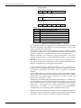
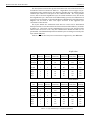
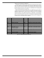
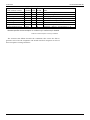
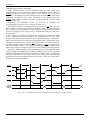
Differences among the various family members pertain to the on-chip
resources of the processor, as illustrated in Table 1.1.
Device
R3041
Instr.
Name
2kB
Data
Cache
512B
Freq.
Cache
16-25
MMU
(MHz)
No
R3051
4kB
2kB
20-40
R3052
8kB
2kB
20-40
R3071
16kB
0r 8kB
16kB
0r 8kB
4kB
or 8kB
4kB
or 8kB
33-50
"E"
Version
"E"
Version
"E"
Version
"E"
Version
R3081
20-50
Floating
Option
Software
Emulation
Software
Emulation
Software
Emulation
Software
Emulation
On-chip
Hardware
Bus
Point Options
8-, 16-, and 32-bit port width support
Programmable timing support
32-bit Mux'ed Address/Data
32-bit Mux'ed Address/Data
1/2 frequency bus option
1/2 frequency bus option
Table 1.1. Pin-, Socket-, and Software- Compatible R3051 Family
Current family members include:
• The R3041, which incorporates 2kB of instruction cache, 512B of data
cache, and a flexible system interface suited to low cost memory systems.
The R3041 does not feature an on-chip MMU, but is fully address map
compatible with the base versions of the R3051 family.
• The R3052E, which incorporates an 8kB instruction cache, a 2kB data
cache, and full function memory management unit (MMU) including 64entry fully associative Translation Lookaside Buffer (TLB).
• The R3052, which also incorporates an 8kB instruction cache and 2kB
data cache, but does not include the TLB, and instead uses a simpler
virtual to physical address mapping.
• The R3051E, which incorporates 4kB of instruction cache and 2kB of data
cache, along with the full function MMU/TLB of the R3000A.
• The R3051, which incorporates 4kB of instruction cache and 2kB of data
cache, but omits the TLB, and instead uses a simpler virtual to physical
address mapping.
• The R3071E, which incorporates a 16kB instruction cache, a 4kB data
cache, and full function memory management unit (MMU) including 64entry fully associative Translation Lookaside Buffer (TLB). The cache on
the R3081E is user configurable to 8kB I-Cache and 8kB D-Cache.
• The R3071, which incorporates a 16kB instruction cache, a 4kB data
cache, but uses the simpler memory mapping of the R3051/52, and thus
omits the TLB. The cache on the R3081 is user configurable to 8kB ICache and 8kB D-Cache.
• The R3081E, which incorporates a 16kB instruction cache, a 4kB data
cache, and full function memory management unit (MMU) including 64entry fully associative Translation Lookaside Buffer (TLB). The cache on
the R3081E is user configurable to 8kB I- Cache and 8kB D-Cache. The
R3081E also includes an on-chip floating-point accelerator.
• The R3081, which incorporates a 16kB instruction cache, a 4kB data
cache, but uses the simpler memory mapping of the R3051/52, and thus
omits the TLB. The cache on the R3081 is user configurable to 8kB ICache and 8kB D-Cache. The R3081 also includes an on-chip floatingpoint accelerator.
FAMILY OVERVIEW
CHAPTER 1
BrCond(3:2,0)
ClkIn
Master Pipeline Control
Clock
Generator
Unit/
Clock Doubler
System Control
Coprocessor
(CP0)
Integer
CPU Core
Floating Point
Coprocessor
(CP1)
Exception/Control
Registers
General Registers
(32 x 32)
Memory Management
Registers
ALU
Register Unit
(16 x 64)
Exponent Unit
Shifter
Int(5:0)
Add Unit
Mult/Div Unit
Translation
Lookaside Buffer
(64 entries)
Divide Unit
Address Adder
Multiply Unit
PC Control
Exception/Control
Virtual Address
FP Interrupt
Data Bus
Physical Address Bus
32
Configurable
Instruction
Cache
(16kB/
8kB)
Configurable
Data
Cache
(4kB/
8kB)
36
Data Bus
Parity
Generator
4-deep
Read
Buffer
R3051 Superset Bus Interface Unit
4-deep
Write
Buffer
DMA
Arbiter
BIU
Control
Coherency
Logic
Address/
DMA Rd/Wr SysClk Invalidate
Data
Ctrl
Ctrl
Control
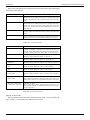
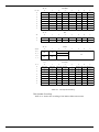
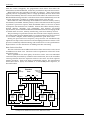
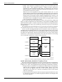
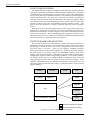
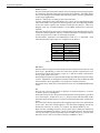
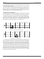
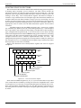
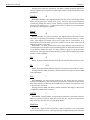
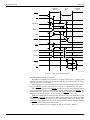
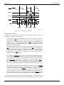
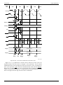
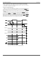
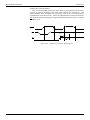
Figure 1.1. Block Diagram
Figure 1.1 shows a block level representation of the functional units within
the R3081E. The R3081E could be viewed as the embodiment of a discrete
solution built around the R3000A and R3010A. However, by integrating this
functionality on a single chip, dramatic cost and power reductions are
achieved.
Non-E versions differ from the block diagram shown in that they omit the
TLB structure. R3071 devices differ from the block diagram in that they omit
the floating-point accelerator unit.
An overview of these blocks is presented here, with detailed information on
each block found in subsequent chapters.
CHAPTER 1
CPU Core
The CPU core is a full 32-bit RISC integer execution engine, capable of
sustaining close to single cycle execution rate. The CPU core contains a five
stage pipeline, and 32 orthogonal 32-bit registers. The R3071 and R3081 use
the same basic integer execution core as the entire R30xx family, which is the
R3000A implementation of the MIPS instruction set. Thus, the R3071 and
R3081 families are binary compatible with the R3051, R3052, R3000A, R3001,
and R3500 CPUs. In addition, the R4000 family (including the R4600 Orion
family) represents an upwardly software compatible migration path to still
higher levels of performance.
System Control Co-Processor
The R3071 and R3081 families also integrate on-chip the System Control
Co-processor, CP0. CP0 manages both the exception handling capability of the
CPU, as well as the virtual to physical address mapping. These topics are
discussed in subsequent chapters.
As with the R3051 and R3052, the R3071 and R3081 families offer two
versions of memory management and virtual to physical address mapping: the
extended architecture versions, the R3051E, R3052E, R3071E, and R3081E,
incorporate the same MMU as the R3000A and R3001. These versions contain
a fully associative 64-entry TLB which maps 4kB virtual pages into the physical
address space. The virtual to physical mapping thus includes kernel segments
which are hard-mapped to physical addresses, and kernel and user segments
which are mapped page by page by the TLB into anywhere in the 4GB physical
address space. In this TLB, 8 pages can be “locked” by the kernel to insure
deterministic response in real-time applications.
R30xx family base versions (the R3041, R3051, R3052, R3071, and R3081)
remove the TLB and institute a fixed address mapping for the various segments
of the virtual address space. These devices still support distinct kernel and
user mode operation, but do not require page management software, leading
to a simpler software model.
Floating Point Co-Processor
The R3081 devices also integrate an R3010A compatible floating point
accelerator. The R3010A is a high performance floating point co-processor (coprocessor 1 to the CPU) providing separate add, multiply, and divide functional
units for single and double precision floating point arithmetic. The floating
point accelerator features low latency operations, and autonomous functional
units which allow differing types of floating point operations to function
concurrently with integer operations. The R3010A appears to the software
programmer as a simple extension of the integer execution unit, with 16
dedicated 64-bit floating point registers (software references these as 32 32-bit
registers when performing loads or stores).
The primary difference between the R3071 family and the R3081 family is
that the R3081 devices include the FPA, while the R3071 devices do not.
Clock Generator Unit
The R3071 and R3081 family CPUs are driven from a single input clock.
For the R3081, this input clock can either be at twice the execution rate (2x
clock mode, provided for R3051 input clocking compatibility) or exactly at the
execution rate (1x clock mode). For the R3071, only the 1x clock mode is
available.
On-chip, the clock generator unit is responsible for managing the interaction
of the CPU core, caches, and bus interface. The R3071 and R3081 include an
on-chip clock doubler to provide higher frequency signals to the internal
execution core.
FAMILY OVERVIEW
FAMILY OVERVIEW
CHAPTER 1
Instruction Cache
The R3071 and R3081 implement a 16kB Instruction Cache. The system
designer may choose to repartition the on-chip caches, so that the instruction
cache is reduced to 8kB but the data cache is increased to 8kB. The instruction
cache is organized with a line size of 16 bytes (four 32-bit entries). This large
cache achieves hit rates in excess of 98% in most applications, and substantially
contributes to the performance inherent in the R3071/R3081. The cache is
implemented as a direct mapped cache, and is capable of caching instructions
from anywhere within the 4GB physical address space. The cache is implemented
using physical addresses and physical tags (rather than virtual addresses or
tags), and thus does not require flushing on context switch.
The on-chip instruction cache is parity protected over both the instruction
word and tag fields. The read buffer will generate proper parity into the cache
during cache refills; on cache references, the parity will be checked. If a parity
error is detected, a cache miss will be processed.
Data Cache
The R3071/R3081 incorporate an on-chip data cache of 4kB, organized as
a line size of 4 bytes (one word). The R3071 and R3081 allow the system
software to reconfigure the on-chip cache from the default 16kB I-Cache/4kB
D-Cache to 8kB of Instruction and 8kB of Data caches.
The relatively large data cache achieves hit rates in excess of 95% in most
applications, and contributes substantially to the performance inherent in the
R3071/R3081. As with the instruction cache, the data cache is implemented
as a direct mapped physical address cache. The cache is capable of mapping
any word within the 4GB physical address space.
The data cache is implemented as a write through cache, to insure that main
memory is always consistent with the internal cache. In order to minimize
processor stalls due to data write operations, the bus interface unit incorporates
a 4-deep write buffer which captures address and data at the processor
execution rate, allowing it to be retired to main memory at a much slower rate
without impacting system performance. Further, support has been provided
to allow hardware based data cache coherency in a multi-master environment,
such as one utilizing DMA from I/O to memory.
The on-chip data cache is parity protected over both the data and tag fields.
The read buffer will generate proper parity into the cache during cache refills;
on cache references, the parity will be checked. If a parity error is detected, a
cache miss will be processed.
Bus Interface Unit
The R3071/R3081 uses thelarge internal caches to provide the majority of
the bandwidth requirements of the execution engine, and thus can utilize a
simple bus interface connected to slower memory devices.
The R30xx family bus interface utilizes a 32-bit address and data bus
multiplexed onto a single set of pins. The bus interface unit also provides an
ALE (Address Latch Enable) output signal to de-multiplex the A/D bus, and
simple handshake signals to process CPU read and write requests. In addition
to the read and write interface, the R30xx family incorporates a DMA arbiter,
to allow an external master to control the external bus. The R3071 and R3081
can be used in a multi-master system using hardware-based cache coherency.
The R3071/R3081 incorporate a 4-deep write buffer to decouple the speed
of the execution engine from the speed of the memory system. The write buffers
capture and FIFO processor address and data information in store operations,
and present it to the bus interface as write transactions at the rate the memory
system can accommodate.
CHAPTER 1
The R3071/R3081 read interface performs both single word reads and quad
word reads. Single word reads work with a simple handshake, and quad word
reads can either utilize the simple handshake (in lower performance, simple
systems) or utilize a tighter timing mode when the memory system can burst
data at the processor clock rate. Thus, the system designer can choose to
utilize page or nibble mode DRAMs (and possibly use interleaving, if desired,
in high-performance systems), or use simpler techniques to reduce complexity.
During cache refills, the bus interface unit generates parity over the incoming
data values, and places the parity in the on-chip caches.
In order to accommodate slower quad word reads, the R3071/R3081
incorporate a 4-deep read buffer FIFO, so that the external interface can queue
up data within the processor before releasing it to perform a burst fill of the
internal caches.
The R3071 and R3081 are R3051 superset compatible in their bus interface.
Specifically, the R3071/R3081 have additional support to simplify the design
of very high frequency systems. This support includes the ability to run the bus
interface at one-half the processor execution rate, as well as the ability to slow
the transitions between reads and writes to provide extra buffer disable time
for the memory interface.
SYSTEM USAGE
The IDT R30xx family bus interface has been specifically designed to allow
a wide variety of memory systems. Low cost systems can use slow speed
memories and simple controllers, while other designers may choose to
incorporate higher frequencies, faster memories, and techniques such as DMA
to achieve maximum performance. The R3071 and R3081 include specific
support for high perfromance systems, including the ability to perform
hardware based cache coherency in multi-master systems.
A typical system implementation using off-the-shelf logic devices contains
simple transparent latches to de-multiplex the R30xx address and data busses
from the A/D bus; the data path between the memory system elements and the
R30xx family A/D bus is managed by simple octal transceivers; a small set of
simple PALs is used to control the various data path elements, and to control
the handshake between the memory devices and the R30xx.
Depending on the cost vs. performance tradeoffs appropriate to a given
application, the system design engineer could include true burst support from
the DRAM to provide for high-performance cache miss processing, or utilize a
simpler, lower performance memory system to reduce cost and simplify the
design. Similarly, the system designer could choose to implement techniques
such as DMA to further improve system performance.
FAMILY OVERVIEW
FAMILY OVERVIEW
CHAPTER 1
DEVELOPMENT SUPPORT
The IDT R30xx family is supported by a rich set of development tools, ranging
from system simulation tools through PROM monitor and debug support,
applications software and utility libraries, logic analysis tools, sub-system
modules, and shrink wrap operating systems. IDT's development support
program, called "AdvantageIDT", insures the availability of all the tools
required to rapidly bring an R30xx-based system rapidly to market.
The R3071 and R3081 are pin and software compatible with many other
family members, allowing the system designer to use a single toolchain and
methodology for multiple system development efforts.
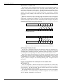
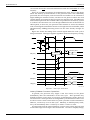
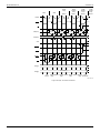
Figure 1.2 is an overview of the system development process typically used
when developing R30xx family applications. The R30xx family is supported in
all phases of project development. These tools allow timely, parallel development
of hardware and software for R30xx family based applications, and include
tools such as:
• Optimizing compilers from MIPS, the acknowledged leader in optimizing
compiler technology. The compilers are available in both native and cross
environments.
• Cross development tools, available in a variety of development
environments and from a number of vendors.
• The high-performance IDT floating point library software, including
transcendental functions and IEEE compliant exception handlers.
• IDT Evaluation systems, which includes RAM, EPROM, I/O, and the IDT
PROM Monitor.
• IDT Adobe Reference Printer systems, which directly drive low-cost print
engines, and run PostScript™ software from Adobe.
• IDT/sim, which implements a full prom monitor (diagnostics, remote
debug support, peek/poke, etc.).
• IDT/kit, which implements a run-time support package for R3051 family
systems.
• In-circuit Emulator equipment.
System
Architecture
Evaluation
System
Development
Phase
System
Integration
and Verfification
Software
Remote Target Debug
MIPS Compiler Suite
Stand-Alone Libraries
Floating Point Library
Cross Development Tools
GNU Tools
PostScript™ SW from Adobe
Benchmarks
Evaluation Boards
Adobe Reference Systems
End Products
Hardware
Hardware Models
General CAD Tools
Evaluation Boards
Adobe Reference Systems
Support Chips
Figure 1.2. Development Support
Logic Analysis
Diagnostics
IDT/sim
IDT/kit
ROM Emulation
In-Circuit Emulation
Remote Debug
Real-Time OS
CHAPTER 1
PERFORMANCE OVERVIEW
The R3071/R3081 achieves a very high-level of performance. This
performance is based on:
• An efficient execution engine. The CPU performs ALU operations and
store operations in single cycle, and has an effective load time of 1.3
cycles, and branch execution rate of 1.5 cycles (based on the ability of the
compilers to avoid software interlocks). Thus, the execution engine
achieves over 40 MIPS performance when operating out of cache.
• A full featured floating point accelerator/co-processor. The R3081
incorporates the R3010A floating point accelerator on-chip, with
independent ALUs for floating point add, multiply, and divide. The
floating point unit is fully hardware interlocked, and features overlapped
operation and precise exceptions. The FPA allows floating point adds,
multiplies, and divides to occur concurrently with each other, as well as
concurrently with integer operations.
• Large on-chip caches. The R3071/R3081 contain caches which are
substantially larger than those on the majority of today’s microprocessors.
These large caches minimize the number of bus transactions required,
and allow the R30xx family to achieve actual sustained performance very
close to its peak execution rate. The R3071/R3081 double the cache
available on the R3052, making it a suitable engine for many highperformance applications, including color printing systems and internetworking devices.
• Autonomous multiply and divide operations. The R30xx family features
an on-chip integer multiplier/divide unit which is separate from the main
ALU. This allows the CPU to perform multiply or divide operations in
parallel with other integer operations, using a single multiply or divide
instruction rather than “step” operations.
• Integrated write buffer. The R3071/R3081 feature a four deep write
buffer, which captures store target addresses and data at the processor
execution rate and retires it to main memory at the slower main memory
access rate. Use of on-chip write buffers eliminates the need for the
processor to stall when performing store operations.
• Burst read support. The R3071/R3081 enable the system designer to
utilize page mode or nibble mode RAMs when performing read operations
to minimize the main memory read penalty and increase the effective
cache hit rates.
The performance differences amongst the various family members depend
on the application software and the design of the memory system. Since the
R3041, R3051, R3052, R3071, and R3081 are all pin and software compatible,
the system designer has maximum freedom in trading between performance
and cost. A system can be designed, and later the appropriate CPU inserted
into the board, depending on the desired system performance.
FAMILY OVERVIEW
INSTRUCTION SET ARCHITECTURE
®
CHAPTER 2
FAMILY INSTRUCTION SET
ARCHITECTURE
CHAPTER 2
Integrated Device Technology, Inc.
INTRODUCTION
The IDT R30xx family contains the same basic execution core as the IDT/
MIPS R3000A. In addition to being able to run software written for either of this
processor family, this enables the R30xx family to achieve dramatic levels of
performance, based on the efficiency of the execution engine. The R3071 and
R3081 include the same integer execution unit as all members of the R30xx
family, and thus is fully binary compatible with applications for that processor.
The floating point accelerator included in the R3081 acts as an extension to the
CPU, and is described in chapter 3.
This chapter gives an overview of the MIPS architecture implemented in the
R30xx family, and discusses the programmers' model for this device. Further
detail is available in the book “R30xx Family Software Reference Manual”,
available from IDT.
R30XX FAMILY PROCESSOR FEATURES OVERVIEW
The R30xx family has many of the same attributes of the IDT R3000A, at a
higher level of integration geared to lower system cost. These features include:
• Full 32-bit Operation. The R30xx family contains thirty-two 32-bit
integer registers, and all instructions and addresses are 32 bits.
• Efficient Pipelining. The CPU utilizes a 5-stage pipeline design to
achieve an execution rate approaching one instruction per cycle. Pipeline
stalls, hazards, and exceptional events are handled precisely and efficiently.
• Large On-Chip Instruction and Data Caches. The R30xx family utilizes
large on-chip caches to provide high-bandwidth to the execution engine.
The large size of the caches insures high hit rates, minimizing stalls due
to cache miss processing and dramatically contributing to overall
performance. Both the instruction and data cache can be accessed during
a single CPU cycle.
• On-chip Memory Management. The IDT Extended Architecture versions
of the R305xx family (the R3051E, R3052E, R3071E, and R3081E) utilize
the same memory management scheme as the R3000A, providing a 64entry fully-associative TLB to provide fast virtual to physical address
translation of the 4GB address space. The base versions of the family (the
R3041, R3051, R3052, R3071, and R3081) do not utilize the TLB, but
perform fixed segment-based mapping of the virtual space to physical
addresses.
CHAPTER 2
INSTRUCTION SET ARCHITECTURE
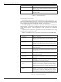
CPU REGISTERS OVERVIEW
The IDT R30xx family CPU engine provides 32 general purpose 32-bit
registers, a 32-bit Program Counter, and two dedicated 32-bit registers which
hold the result of an integer multiply or divide operation. The CPU registers,
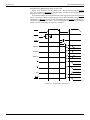
illustrated in Figure 2.1, are discussed later in this chapter.
General Purpose
Registers
31
0
0
r1
r2
•
•
r29
r30
r31
Multiply/Divide Result
Registers
31
0
HI
31
0
LO
Program Counter
31
0
PC
4000 drw 01
Figure 2.1. CPU Registers
Note that the MIPS architecture does not use a traditional Program Status
Word (PSW) register. The functions normally provided by such a register are
instead provided through the use of “Set” instructions and conditional branches.
By avoiding the use of traditional condition codes, the architecture can be more
finely pipelined. This, coupled with the fine granularity of the instruction set,
allows the compilers to achieve dramatically higher levels of optimizations than
for traditional architectures.
Overflow and exceptional conditions are then handled through the use of the
on-chip Status and Cause registers, which reside on-chip as part of the System
Control Co-Processor (Co-Processor 0). These registers contain information
about the run-time state of the machine, and any exceptional conditions it has
encountered.
INSTRUCTION SET OVERVIEW
All instructions are 32-bits long, and there are only three basic instruction
formats. This approach dramatically simplifies instruction decoding, permitting
higher frequency operation. More complicated (but less frequently used)
operations and addressing modes are synthesized by the assembler, using
sequences of the basic instruction set. This approach enables object code
optimizations at a finer level of resolution than achievable in micro-coded CPU
architectures.
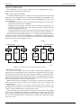
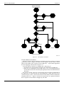
Figure 2.2 shows the instruction set encoding used by the MIPS architecture.
This approach simplifies instruction decoding in the CPU.
The instruction set can be divided into the following basic groups:
• Load/Store instructions move data between memory and the general
registers. They are all encoded as “I-Type” instructions, and the only
addressing mode implemented is base register plus signed, immediate
offset. This directly enables the use of three distinct addressing modes:
register plus offset; register direct; and immediate.
• Computational instructions perform arithmetic, logical, and shift
operations on values in registers. They are encoded as either “R-Type”
instructions, when both source operands as well as the result are general
registers, and “I-Type”, when one of the source operands is a 16-bit
immediate value. Computational instructions use a three address
format, so that operations don’t needlessly interfere with the contents of
source registers.
• Jump and Branch instructions change the control flow of a program. A
Jump instruction can be encoded as a “J-Type” instruction, in which case
INSTRUCTION SET ARCHITECTURE
CHAPTER 2
I-Type (Immediate)
31
26
op
25 21
20 16
rs
rt
15
0
immediate
J-Type (Jump)
31
26
25
0
op
target
R-Type (Register)
31
26
op
where:
op
rs
rt
25 21
20 16
15 11
rs
rt
rd
10
6
shamt
5
0
funct
is a 6-bit operation code
is a five bit source register specifier
is a 5-bit target register or branch condition
immediate is a 16-bit immediate, or branch or address displacement
target
is a 26-bit jump target address
rd
is a 5-bit destination register specifier
shamt
is a 5-bit shift amount
funct
is a 6-bit function field
Figure 2.2. Instruction Encoding
4000 drw 02
the Jump target address is a paged absolute address formed by combining
the 26-bit immediate value with four bits of the Program Counter. This
form is used for subroutine calls.
Alternately, Jumps can be encoded using the “R-Type” format, in which
case the target address is a 32-bit value contained in one of the general
registers. This form is typically used for returns and dispatches.
Branch operations are encoded as “I-Type” instructions. The target
address is formed from a 16-bit displacement relative to the Program
Counter.
The Jump and Link instructions save a return address in Register r31.
These are typically used as subroutine calls, where the subroutine return
address is stored into r31 during the call operation.
• Co-Processor instructions perform operations on the co-processor set.
Co-Processor Loads and Stores are always encoded as “I-Type” instructions;
co-processor operational instructions have co-processor dependent
formats.
In the R30xx family, the System Control Co-Processor (CP0) contains
registers which are used in memory management and exception handling.
In the R3081, the floating point accelerator also resides on-chip, and
operates as Co-Processor 1 (CP1)
Additionally, the R30xx family implements BrCond inputs. Software can
use the Branch on Co-Processor Condition instructions to test the state
of these external inputs, and thus they may be used like general purpose
input ports. In the R3071 and R3081, BrCond(1) is not available
externally; in the R3081, it is used internally for the floating-point
condition flag, used on floating-point conditional instructions.
• Special instructions perform a variety of tasks, including movement of
data between special and general registers, system calls, and breakpoint
operations. They are always encoded as “R-Type” instructions.
CHAPTER 2
OP
LB
LBU
LH
LHU
LW
LWL
LWR
SB
SH
SW
SWL
SWR
INSTRUCTION SET ARCHITECTURE
Description
Load/Store Instructions
Load Byte
Load Byte Unsigned
Load Halfword
Load Halfword Unsigned
Load Word
Load Word Left
Load Word Right
Store Byte
Store Halfword
Store Word
Store Word Left
Store Word Right
ANDI
ORI
XORI
LUI
Arithmetic Instructions
(ALU Immediate)
Add Immediate
Add Immediate Unsigned
Set on Less Than Immediate
Set on Less Than Immediate
Unsigned
AND Immediate
OR Immediate
Exclusive OR Immediate
Load Upper Immediate
ADD
ADDU
SUB
SUBU
SLT
SLTU
AND
OR
XOR
NOR
Arithmetic Instructions
(3-operand, register-type)
Add
Add Unsigned
Subtract
Subtract Unsigned
Set on Less Than
Set on Less Than Unsigned
AND
OR
Exclusive OR
NOR
SLL
SRL
SRA
SLLV
SRLV
SRAV
Shift Instructions
Shift Left Logical
Shift Right Logical
Shift Right Arithmetic
Shift Left Logical Variable
Shift Right Logical Variable
Shift Right Arithmetic Variable
ADDI
ADDIU
SLTI
SLTIU
OP
Description
MULT
MULTU
DIV
DIVU
Multiply/Divide Instructions
Multiply
Multiply Unsigned
Divide
Divide Unsigned
MFHI
MTHI
MFLO
MTLO
Move
Move
Move
Move
J
JAL
JR
JALR
BEQ
BNE
BLEZ
BGTZ
BLTZ
BGEZ
BLTZAL
BGEZAL
From HI
To HI
From LO
To LO
Jump and Branch Instructions
Jump
Jump and Link
Jump to Register
Jump and Link Register
Branch on Equal
Branch on Not Equal
Branch on Less than or Equal
to Zero
Branch on Greater Than Zero
Branch on Less Than Zero
Branch on Greater Than or
Equal to Zero
Branch on Less Than Zero and
Link
Branch on Greater Than or Equal
to Zero and Link
SYSCALL
BREAK
Special Instructions
System Call
Break
LWCz
SWCz
MTCz
MFCz
CTCz
CFCz
COPz
BCzT
BCzF
Coprocessor Instructions
Load Word from Coprocessor
Store Word to Coprocessor
Move To Coprocessor
Move From Coprocessor
Move Control To Coprocessor
Move Control From Coprocessor
Coprocessor Operation
Branch on Coprocessor z True
Branch on Coprocessor z False
MTC0
MFC0
TLBR
TLBWI
TLBWR
TLBP
RFE
System Control Coprocessor
(CP0) Instructions
Move To CP0
Move From CP0
Read indexed TLB entry
Write indexed TLB entry
Write Random TLB entry
Probe TLB for matching entry
Restore From Exception
4000 tbl 01
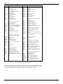
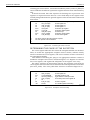
Table 2.1. Instruction Set Mnemonics
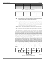
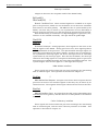
Table 2.1 lists the instruction set mnemonics of the R30xx family. More
detail on these operations is presented later in this chapter. For further detail,
consult “R30xx Software Reference Manual”, available from IDT.
INSTRUCTION SET ARCHITECTURE
CHAPTER 2
PROGRAMMING MODEL
This section describes the organization of data in the general registers and
in memory, and discusses the set of general registers available. A summary
description of all of the CPU registers is presented. The Floating Point Registers
in the R3081 are discussed in Chapter 3.
Data Formats and Addressing
The R30xx family defines a word as 32-bits, a half-word as 16-bits, and a
byte as 8-bits. The byte ordering convention is configurable during hardware
reset (Chapter 11) into either a big-endian or little-endian convention.
When configured as a big-endian system, byte 0 is always the most
significant (leftmost) byte in a word. This is the order used in MC680x0®
microprocessors, and systems from MIPS.
When configured as a little-endian system, byte 0 is always the least
significant (rightmost) byte in a word. This is compatible with the iAPX® x86
microprocessors and systems from Digital Equipment Corporation.
Figure 2.3 shows the ordering of bytes within words and the ordering of
words within multiple word structures for the big-endian and little-endian
conventions.
Higher
Address 31
Lower
Address
Big-Endian Byte Ordering
24 23 16 15
8 7
8
9
A
B
4
5
6
7
0
1
2
3
Word
0 Address
8
4
0
• Most significant byte is at lowest address
• Word is addressed by byte address of
most significant byte
Higher
Address 31
Little-Endian Byte Ordering
24 23 16 15
8 7
B
A
9
8
7
6
5
4
3
2
1
0
Word
0 Address
8
4
0
Lower
Address • Least significant byte is at lowest address
• Word is addressed by byte address of
least significant byte
4000 drw 03
Figure 2.3. Byte Ordering Conventions
The R30xx family uses byte addressing for all accesses, including half-word
and word. The MIPS architecture has alignment constraints that require halfword access to be aligned on an even byte boundary, and word access to be
aligned on a modulo-4 byte boundary. Thus, in big-endian systems, the
address of a multiple-byte data item is the address of the most-significant byte,
while in little-endian systems it is the address of the least-significant byte of
the structure.
CHAPTER 2
INSTRUCTION SET ARCHITECTURE
For compatibility with older programs written for 8- or 16-bit machines, the
MIPS instruction set provides special instructions for addressing 32-bit words
which are not aligned on 4-byte boundaries. These instructions, which are
Load/Store Left/Right, are used in pairs to provide addressing of misaligned
words. This effectively means that these types of data movements require only
one-additional instruction cycle over that required for properly aligned words,
and provides a much more efficient way of dealing with this case than is
possible using sequences of loads/stores and shift operations. Figure 2.4
shows the bytes accessed when addressing a mis-aligned word with a byte
address of 3, for each of the two byte ordering conventions.
Higher
Address 31
24 23
4
16 15
5
8 7
0
Big
Endian
6
3
31
24 23
16 15
6
8 7
5
0
4
3
Little
Endian
Lower
Address
4000 drw 04
Figure 2.4. Unaligned Words
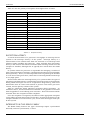
CPU General Registers
The R30xx family contains 32-general registers, each containing a single 32bit word. The 32 general registers are treated symmetrically (orthogonally),
with two notable exceptions: general register r0 is hardwired to a zero value,
and r31 is used as the link register in Jump and Link instructions
Register r0 maintains the value zero under all conditions when used as a
source register, and discards data written to it. Thus, instructions which
attempt to write to it may be used as No-Op Instructions. The use of a register
wired to the zero value allows the simple synthesis of different addressing
modes, no-ops, register or memory clear operations, etc., without requiring
expansion of the basic instruction set.
Register r31 is used as the link register in jump and link instructions. These
instructions are used in subroutine calls, and the subroutine return address
is placed in register r31. This register can be written to or read as a normal
register in other operations.
In addition to the general registers, the CPU contains two registers (HI and
LO) which store the double-word, 64-bit result of integer multiply operations,
and the quotient and remainder of integer divide operations.
CP0 Special Registers
In addition to the general CPU registers, the R30xx family contains a number
of special registers on-chip. These registers logically reside in the on-chip
System Control Co-processor CP0, and are used in memory management and
exception handling. There may be some differences in the set of CP0 registers
across the various R30xx family members; it is recommended that applications
perform a CPU identification routine at boot-up, and perform a device specific
initialization routine, to preserve interchangeability among the various family
members.
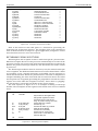
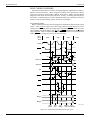
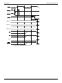
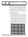
Table 2.2 shows the logical CP0 address of each of the registers in the
R3071/R3081. The format of each of these registers, and their use, is
discussed in Chapter 5 (Memory Management), and Chapter 6 (Exception
Handling). Note that the Config register is unique to the R3071 and R3081; it
is used to allow software to control a number of system hardware options. Its
use is discussed in chapter 6.
INSTRUCTION SET ARCHITECTURE
CHAPTER 2
Number
Mnemonic
Description
0
Index
Programmable pointer into on-chip TLB array
1
Random
Pseudo-random pointer into on-chip TLB array (read only)
2
EntryLo
Low-half of TLB entry
3
Config*
Hardware configuration register
4
Context
Pointer to kernel virtual Page Table Entry Table
5-7
Reserved
8
BadVAddr
9
Reserved
10
EntryHi
11
Reserved
12
SR
Status Register
13
Cause
Cause of last exception
14
EPC
Exception Program Counter
15
PRId
Processor Revision Identifier
16-31
Bad virtual address
High-half of TLB entry
Reserved
*: This presence and functions of this register varies among R30xx family members.
Table 2.2. CP0 Registers
Operating Modes
The R30xx family supports two different operating modes: User and Kernel
modes. The processor normally operates in User mode until an exception is
detected, forcing it into kernel mode. It remains in Kernel mode until a Return
From Exception (RFE) instruction is executed, returning it to its previous
operation mode.
The processor supports these levels of protection by segmenting the 4GB
virtual address space into 4 distinct segments. One segment is accessible from
either the User state or the Kernel mode, and the other three segments are only
accessible from kernel mode.
In addition to providing memory address protection, the kernel can protect
the co-processors from access or modification by the user task.
Finally, the R30xx family supports the execution of user programs with the
opposite byte ordering (Reverse Endianness) of the kernel, facilitating the
exchange of programs and data between dissimilar machines.
Chapter 5 discusses the memory management facilities of the processor.
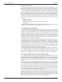
Pipeline Architecture
The IDT R30xx family uses the same basic pipeline structure as that
implemented in the R3000A. Thus, the execution of a single instruction is
performed in five distinct steps.
IF
RD
I-Cache
ALU
ID
PAddr
OP
PAddr
MEM
D-Cache
WB
WB
One Cycle
4000 drw 05
Figure 2.5. 5-Stage Pipeline
CHAPTER 2
INSTRUCTION SET ARCHITECTURE
• Instruction Fetch (IF). In this stage, the instruction virtual address is
translated to a physical address and the instruction is read from the
internal Instruction Cache.
• Read (RD). During this stage, the instruction is decoded and required
operands are read from the on-chip register file.
• ALU. The required operation is performed on the instruction operands.
• Memory Access (MEM). If the instruction was a load or store, the Data
Cache is accessed. Note that there is a skew between the instruction cycle
which fetches the instruction and the one in which the required data
transfer occurs. This skew is a result of the intervening pipestages.
• Write Back (WB). During the write back pipestage, the results of the ALU
stage operation are updated into the on-chip register file.
Each of these pipestages requires approximately one CPU cycle, as shown
in Figure 2.5. Parts of some operations lap into the next cycle, while other
operations require only 1/2 cycle.
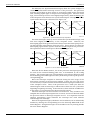
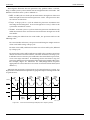
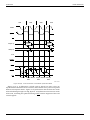
The net effect of the pipeline structure is that a new instruction can be
initiated every clock cycle. Thus, the execution of five instructions at a time is
overlapped, as shown in Figure 2.6.
The pipeline operates efficiently, because different CPU resources such as
address and data bus access, ALU operations, and the register file, are utilized
on a non-interfering basis.
I#1
IF
RD
ALU MEM
WB
I#2
IF
RD
ALU MEM
I#3
IF
RD
ALU MEM
I#4
IF
RD
ALU MEM
I#5
IF
RD
WB
WB
WB
ALU MEM
WB
Current
CPU
Cycle
4000 drw 06
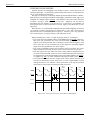
Figure 2.6. 5-Instructions per Clock Cycle
Pipeline Hazards
In a pipelined machine such as an R30xx family CPU, there are certain
instructions which, based on the pipeline structure, can potentially disrupt the
smooth operation of the pipeline. The basic problem is that the current
pipestage of an instruction may require the result of a previous instruction, still
in the pipeline, whose result is not yet available. This class of problems is
referred to as pipeline hazards.
An example of a potential pipeline hazard occurs when a computational
instruction (instruction n+1) requires the result of the immediately prior
instruction (instruction n). Instruction n+1 wants to access the register file
during the RF pipestage. However, instruction n has not yet completed its
register writeback operation, and thus the current value is not available
INSTRUCTION SET ARCHITECTURE
CHAPTER 2
directly from the register file. In this case, special logic within the execution
engine forwards the result of instruction n’s ALU operation to instruction n+1,
prior to the true writeback operation. The pipeline is undisturbed, and no
pipeline stalls need to occur.
Another example of a pipeline hazard handled in hardware is the integer
multiply and divide operations. If an instruction attempts to access the HI or
LO registers prior to the completion of the multiply or divide, that instruction
will be interlocked (held off) until the multiply or divide operation completes.
Thus, the programmer is isolated from the actual execution time of this
operation. The optimizing compilers attempt to schedule as many instructions
as possible between the start of the multiply/divide and the access of its result,
to minimize stalls.
However, not all pipeline hazards are handled in hardware. There are two
categories of instructions which utilize software intervention to insure logical
operation. The optimizing compilers (and peephole scheduler of the assembler)
are capable of insuring proper execution. These two instruction classes are:
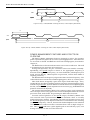
• Load instructions have a delay, or latency, of one cycle before the data
loaded from memory is available another instruction. This is because the
ALU stage of the immediately subsequent instruction is processed
simultaneously with the Data Cache access of the load operation. Figure
2.7 illustrates the cause of this delay slot.
IF
RD
I#1
I-Cache
ALU
MEM
OP
D-Cache
ID
WB
WB
(Load)
I#2
I-Cache
ID
OP
(Delay Slot)
Data
Available
I-Cache
I#3
ID
OP
One Cycle
Figure 2.7. Load Delay
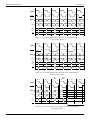
4000 drw 07
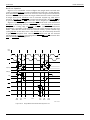
• Jump and Branch instructions have a delay of one cycle before the
program flow change can occur. This is due to the fact that the next
instruction is fetched prior to the decode and ALU stage of the jump/
branch operation. Figure 2.8 illustrates the cause of this delay slot.
IF
I#1
RD
I-Cache
(Branch)
ALU
MEM
OP
D-Cache
ID
WB
WB
I-Address
I#2
I-Cache
ID
I#3
Address
Available
I-Cache
OP
(Delay Slot)
ID
OP
One Cycle
Figure 2.8. Branch Delay
4000 drw 08
CHAPTER 2
The CPU continues execution, despite the delay in the operation. Thus,
loads, jumps and branches do not disrupt the pipeline flow of instructions, and
the processor always executes the instruction immediately following one of
these “delayed” instructions.
Rather than include extensive pipeline control logic, the CPU gives
responsibility for dealing with “delay slots” to software. Thus, the peephole
optimizer (which can be performed as part of compilation or assembly) can reorder the code to insure that the instruction in the delay slot does not require
the logical result of the “delayed” instruction. In the worst case, a NOP can be
inserted to guarantee proper software execution.
Chapter 6 discusses the impact of pipelining on exception handling. In
general, when an instruction causes an exception, it is desirable for all
instructions initiated prior to that instruction to complete, and all subsequent
instructions to abort. This insures that the machine state presented to the
exception handler reflects the logical state that existed at the time the exception
was detected. In addition, it is desirable to avoid requiring software to explicitly
manage the pipeline when handling or returning from exceptions. The IDT
R30xx family CPU pipeline is designed to properly manage exceptional events.
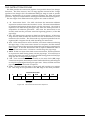
INSTRUCTION SET SUMMARY
This section provides an overview of the R30xx family instruction set by
presenting each category of instructions in a tabular summary form. Refer to
the “R30xx Family Software Reference Manual” reference for a detailed
description of each instruction.
Instruction Formats
Every instruction consists of a single word (32 bits) aligned on a word
boundary. There are only three instruction formats as shown in Figure 2.2.
This approach simplifies instruction decoding. More complicated (less frequently
used) operations and addressing modes are synthesized by the compilers.
Instruction Notational Conventions
In this manual, all variable sub-fields in an instruction format (such as rs,
rt, immediate, and so on) are shown in lower-case names.
For the sake of clarity, an alias is sometimes used for a variable sub-field in
the formats of specific instructions. For example, “base” rather than “rs” is
used in the format for Load and Store instructions. Such an alias is always
lower case, since it refers to a variable sub-field.
Instruction opcodes are shown in all upper case.
The actual bit encoding for all the mnemonics is specified at the end of this
chapter.
Load and Store Instructions
Load/Store instructions move data between memory and general registers.
They are all I-type instructions. The only addressing mode directly supported
is base register plus 16-bit signed immediate offset. This can be used to directly
implement immediate addressing (using the r0 register) or register direct
(using an immediate offset value of zero).
All load operations have a latency of one instruction. That is, the data being
loaded from memory into a register is not available to the instruction that
immediately follows the load instruction: the data is available to the second
instruction after the load instruction. An exception is the target register for the
“load word left” and “load word right” instructions, which may be specified as
the same register used as the destination of a load instruction that immediately
precedes it.
INSTRUCTION SET ARCHITECTURE
INSTRUCTION SET ARCHITECTURE
CHAPTER 2
The Load/Store instruction opcode determines the size of the data item to
be loaded or stored as shown in Table 2.1. Regardless of access type or bytenumbering order (endian-ness), the address specifies the byte which has the
smallest byte address of all bytes in the addressed field. For a big-endian
access, this is the most significant byte; for a little-endian access, this is the
least significant byte. Note that in an R30xx family system, the endianness of
a given access is dynamic, in that the RE (Reverse Endianness) bit of the Status
Register can be used to force user space accesses of the opposite byte
convention of the kernel.
The bytes within the addressed word that are used can be determined
directly from the access size and the two low-order bits of the address, as shown
in Table 2.3. Note that certain combinations of access type and low-order
address bits can never occur: only the combinations shown in Table 2.3 are
permissible. The R30xx family indicates which bytes are being accessed by the
byte-enable (BE) bus.
Table 2.4 shows the load/store instructions supported by the MIPS ISA.
Big-Endian
Size
BE(3)
BE(2)
BE(1)
BE(0)
AdrLo(1)
AdrLo(0)
Data(31:24)
Data(23:16)
Data(15:8)
Data(7:0)
Word
0
0
Yes
Yes
Yes
Yes
Tri-Byte
0
0
Yes
Yes
Yes
No
Tri-Byte
0
1
No
Yes
Yes
Yes
16-Bit
0
0
Yes
Yes
No
No
16-Bit
1
0
No
No
Yes
Yes
Byte
0
0
Yes
No
No
No
Byte
0
1
No
Yes
No
No
Byte
1
0
No
No
Yes
No
Byte
1
1
No
No
No
Yes
Little-Endian
BE(3)
BE(2)
BE(1)
BE(0)
AdrLo(1)
AdrLo(0)
Data(31:24)
Data(23:16)
Data(15:8)
Data(7:0)
Word
0
0
Yes
Yes
Yes
Yes
Tri-Byte
0
0
No
Yes
Yes
Yes
Tri-Byte
0
1
Yes
Yes
Yes
No
16-Bit
0
0
No
No
Yes
Yes
16-Bit
1
0
Yes
Yes
No
No
Byte
0
0
No
No
No
Yes
Byte
0
1
No
No
Yes
No
Byte
1
0
No
Yes
No
No
Byte
1
1
Yes
No
No
No
Size
4000 tbl 03
Table 2.3. Byte Addressing in Load/Store Operations
CHAPTER 2
INSTRUCTION SET ARCHITECTURE
Instruction
Format and Description
Load Byte
LB rt, offset (base)
Sign-extend 16-bit offset and add to contents of register base to
form address.
Sign-extend contents of addressed byte and load into rt.
Load Byte Unsigned
LBU rt, offset (base)
Sign-extend 16-bit offset and add to contents of register base to
form address.
Zero-extend contents of addressed byte and load into rt.
Load Halfword
LH rt, offset (base)
Sign-extend 16-bit offset and add to contents of register base to
form address.
Sign-extend contents of addressed byte and load into rt.
Load Halfword Unsigned
LHU rt, offset (base)
Sign-extend 16-bit offset and add to contents of register base to
form address.
Zero-extend contents of addressed byte and load into rt.
Load Word
LW rt, offset (base)
Sign-extend 16-bit offset and add to contents of register base to
form address.
Load contents of addressed word into register rt.
Load Word Left
LWL rt, offset (base)
Sign-extend 16-bit offset and add to contents of register base to
form address.
Shift addressed word left so that addressed byte is leftmost byte
of a word.
Merge bytes from memory with contents of register rt and load
result into register rt.
Load Word Right
LWR rt, offset (base)
Sign-extend 16-bit offset and add to contents of register base to
form address.
Shift addressed word right so that addressed byte is rightmost
byte of a word.
Merge bytes from memory with contents of register rt and load
result into register rt.
Store Byte
SB rt, offset (base)
Sign-extend 16-bit offset and add to contents of register base to
form address.
Store least significant byte of register rt at addressed location.
Store Halfword
SH rt, offset (base)
Sign-extend 16-bit offset and add to contents of register base to
form address.
Store least significant halfword of register rt at addressed location.
Store Word
SW rt, offset (base)
Sign-extend 16-bit offset and add to contents of register base to
form address.
Store least significant word of register rt at addressed location.
Store Word Left
SWL rt, offset (base)
Sign-extend 16-bit offset and add to contents of register base to
form address.
Shift contents of register rt right so that leftmost byte of the word
is in position of addressed byte. Store bytes containing original
data into corresponding bytes at addressed byte.
Store Word Right
SWR rt, offset (base)
Sign-extend 16-bit offset and add to contents of register base to
form address.
Shift contents of register rt left so that rightmost byte of the word
is in position of addressed byte. Store bytes containing original
data into corresponding bytes at addressed byte.
4000 tbl 04
Table 2.4. Load and Store Instructions
INSTRUCTION SET ARCHITECTURE
CHAPTER 2
Computational Instructions
Computational instructions perform arithmetic, logical and shift operations
on values in registers. They occur in both R-type (both operands are registers)
and I-type (one operand is a 16-bit immediate) formats. There are four
categories of computational instructions:
• ALU Immediate instructions are summarized in Table 2.5a.
• 3-Operand Register-Type instructions are summarized in Table 2.5b.
• Shift instructions are summarized in Table 2.5c.
• Multiply/Divide instructions are summarized in Table 2.5d.
Instruction
Format and Description
ADD Immediate
ADDI rt, rs, immediate
Add 16-bit sign-extended immediate to register rs and place 32bit result in register rt . Trap on two’s complement overflow.
ADD Immediate
Unsigned
ADDIU rt, rs, immediate
Add 16-bit sign-extended immediate to register rs and place 32bit result in register rt . Do not trap on overflow.
Set on Less Than
Immediate
SLTI rt, rs, immediate
Compare 16-bit sign-extended immediate with register rs as
signed 32-bit integers. Result = 1 if rs is less than immediate;
otherwise result = 0.
Place result in register rt.
Set on Less Than
Unsigned Immediate
SLTIU rt, rs, immediate
Compare 16-bit sign-extended immediate with register rs as
unsigned 32-bit integers. Result = 1 if rs is less than immediate;
otherwise result = 0. Place result in register rt. Do not trap on
overflow.
AND Immediate
ANDI rt, rs, immediate
Zero-extend 16-bit immediate, AND with contents of register rs
and place result in register rt.
OR Immediate
ORI rt, rs, immediate
Zero-extend 16-bit immediate, OR with contents of register rs
and place result in register rt.
Exclusive OR Immediate
XORI rt, rs, immediate
Zero-extend 16-bit immediate, exclusive OR with contents of
register rs and place result in register rt.
Load Upper Immediate
LUI rt, immediate
Shift 16-bit immediate left 16 bits. Set least significant 16 bits
of word to zeroes. Store result in register rt.
4000 tbl 05
Table 2.5a. ALU Immediate Operations
CHAPTER 2
INSTRUCTION SET ARCHITECTURE
Instruction
Format and Description
Add
ADD rd, rs, rt
Add contents of registers rs and rt and place 32-bit result in
register rd. Trap on two’s complement overflow.
ADD Unsigned
ADDU rd, rs, rt
Add contents of registers rs and rt and place 32-bit result in
register rd. Do not trap on overflow.
Subtract
SUB rd, rs, rt
Subtract contents of registers rt and rs and place 32-bit result
in register rd. Trap on two’s complement overflow.
Subtract Unsigned
SUBU rd, rs, rt
Subtract contents of registers rt and rs and place 32-bit result
in register rd. Do not trap on overflow.
Set on Less Than
SLT rd, rs, rt
Compare contents of register rt to register rs (as signed 32-bit
integers).
If register rs is less than rt, result = 1; otherwise, result = 0.
Set on Less Than
Unsigned
SLTU rd, rs, rt
Compare contents of register rt to register rs (as unsigned 32bit integers). If register rs is less than rt, result = 1; otherwise,
result = 0.
AND
AND rd, rs, rt
Bit-wise AND contents of registers rs and rt and place result in
register rd.
OR
OR rd, rs, rt
Bit-wise OR contents of registers rs and rt and place result in
register rd.
Exclusive OR
XOR rd, rs, rt
Bit-wise Exclusive OR contents of registers rs and rt and place
result in register rd.
NOR
NOR rd, rs, rt
Bit-wise NOR contents of registers rs and rt and place result in
register rd.
4000 tbl 06
Table 2.5b. Three Operand Register-Type Operations
Instruction
Format and Description
Shift Left Logical
SLL rd, rt, shamt
Shift contents of register rt left by shamt bits, inserting zeroes
into low order bits. Place 32-bit result in register rd.
Shift Right Logical
SRL rd, rt, shamt
Shift contents of register rt right by shamt bits, inserting zeroes
into high order bits. Place 32-bit result in register rd.
Shift Right Arithmetic
SRA rd, rt, shamt
Shift contents of register rt right by shamt bits, sign-extending
the high order bits. Place 32-bit result in register rd.
Shift Left Logical
Variable
SLLV rd, rt, rs
Shift contents of register rt left. Low-order 5 bits of register rs
specify number of bits to shift. Insert zeroes into low order bits
of rt and place 32-bit result in register rd.
Shift Right Logical
Variable
SRLV rd, rt, rs
Shift contents of register rt right. Low-order 5 bits of register rs
specify number of bits to shift. Insert zeroes into high order bits
of rt and place 32-bit result in register rd.
Shift Right Arithmetic
Variable
SRAV rd, rt, rs
Shift contents of register rt right. Low-order 5 bits of register rs
specify number of bits to shift. Sign-extend the high order bits
of rt and place 32-bit result in register rd.
4000 tbl 07
Table 2.5c. Shift Operations
INSTRUCTION SET ARCHITECTURE
CHAPTER 2
Instruction
Format and Description
Multiply
MULT rs, rt
Multiply contents of registers rs and rt as twos complement
values. Place 64-bit result in special registers HI/LO
Multiply Unsigned
MULTU rs, rt
Multiply contents of registers rs and rt as unsigned values. Place
64-bit result in special registers HI/LO
Divide
DIV rs, rt
Divide contents of register rs by rt treating operands as twos
complements values. Place 32-bit quotient in special register
LO, and 32-bit remainder in HI.
Divide Unsigned
DIVU rs, rt
Divide contents of register rs by rt treating operands as unsigned
values. Place 32-bit quotient in special register LO, and 32-bit
remainder in HI.
Move From HI
MFHI rd
Move contents of special register HI to register rd.
Move From LO
MFLO rd
Move contents of special register LO to register rd.
Move To HI
MTHI rd
Move contents of special register rd to special register HI.
Move To LO
MTLO rd
Move contents of register rd to special register LO.
4000 tbl 08
Table 2.5d. Multiply and Divide Operations
Jump and Branch Instructions
Jump and Branch instructions change the control flow of a program. All
Jump and Branch instructions occur with a one instruction delay: that is, the
instruction immediately following the jump or branch is always executed while
the target instruction is being fetched from storage, regardless of whether the
branch is to be taken.
An assembler has several possibilities for utilizing the branch delay slot
productively:
• It can insert an instruction that logically precedes the branch instruction
in the delay slot since the instruction immediately following the jump/
branch effectively belongs to the block preceding the transfer instruction.
• It can replicate the instruction that is the target of the branch/jump into
the delay slot provided that no side-effects occur if the branch falls
through.
• It can move an instruction up from below the branch into the delay slot,
provided that no side-effects occur if the branch is taken.
• If no other instruction is available, it can insert a NOP instruction in the
delay slot.
The J-type instruction format is used for both jumps and jump-and-links for
subroutine calls. In this format, the 26-bit target address is shifted left two
bits, and combined with high-order 4 bits of the current program counter to
form a 32-bit absolute address.
The R-type instruction format which takes a 32-bit byte address contained
in a register is used for returns, dispatches, and cross-page jumps.
Branches have 16-bit offsets relative to the program counter (I-type). Jumpand-Link and Branch-and-Link instructions save a return address in register
31.
CHAPTER 2
INSTRUCTION SET ARCHITECTURE
Table 2.6a summarizes the Jump instructions and Table 2.6b summarizes
the Branch instructions.
Instruction
Format and Description
Jump
J target
Shift 26-bit target address left two bits, combine with highorder 4 bits of PC and jump to address with a one instruction
delay.
Jump and Link
JAL target
Shift 26-bit target address left two bits, combine with highorder 4 bits of PC and jump to address with a one instruction
delay. Place address of instruction following delay slot in r31
(link register).
Jump Register
JR rs
Jump to address contained in register rs with a one instruction
delay.
Jump and Link Register
JALR rs, rd
Jump to address contained in register rs with a one instruction
delay. Place address of instruction following delay slot in rd.
4000 tbl 09
Table 2.6a. Jump Instructions
Instruction
Format and Description
Branch Target: All Branch instruction target addresses are
computed as follows: Add address of instruction in delay slot
and the 16-bit offset (shifted left two bits and sign-extended to
32 bits). All branches occur with a delay of one instruction.
Branch on Equal
BEQ rs, rt, offset
Branch to target address if register rs equal to rt
Branch on Not Equal
BNE rs, rt, offset
Branch to target address if register rs not equal to rt.
Branch on Less than or
Equal Zero
BLEZ rs,offset
Branch to target address if register rs less than or equal to 0.
Branch on Greater Than
Zero
BGTZ rs,offset
Branch to target address if register rs greater than 0.
Branch on Less Than
Zero
BLTZ rs,offset
Branch to target address if register rs less than 0.
Branch on Greater than
or Equal Zero
BGEZ rs,offset
Branch to target address if register rs greater than or equal to
0.
Branch on Less Than
Zero And Link
BLTZAL rs, offset
Place address of instruction following delay slot in register r31
(link register). Branch to target address if register rs less than
0.
Branch on greater than
or Equal Zero And Link
BGEZAL rs, offset
Place address of instruction following delay slot in register r31
(link register). Branch to target address if register rs is greater
than or equal to 0.
4000 tbl 10
Table 2.6b. Branch Instructions
Special Instructions
The two Special instructions let software initiate traps. They are always Rtype. Table 2.7 summarizes the Special instructions.
INSTRUCTION SET ARCHITECTURE
CHAPTER 2
Instruction
Format and Description
System Call
SYSCALL
Initiates system call trap, immediately transferring control to
exception handler.
Breakpoint
BREAK
Initiates breakpoint trap, immediately transferring control to
exception handler.
4000 tbl 11
Table 2.7. Special Instructions
Co-processor Instructions
Co-processor instructions perform operations in the co-processors. Coprocessor Loads and Stores are I-type. Co-processor computational instructions
have co-processor-dependent formats; Chapter 3 discusses the operation of
the on-chip Floating Point Accelerator, which is Co-Processor 1.
The R30xx family may use certain co-processor instructions to utilize the
BrCond inputs. Specifically, the BCzT/F instructions are used to test the state
of the BrCond inputs. Other operations to CP2 and CP3 have undefined
results.
A special set of co-processor operations are used to manage the on-chip
system control co-processor, CP0.
Table 2.8 summarizes the Co-processor Instruction Set of the MIPS ISA.
Instruction
Format and Description
Load Word to
Co-processor
LWCz rt, offset (base)
Sign-extend 16-bit offset and add to base to form address. Load
contents of addressed word into co-processor register rt of coprocessor unit z.
Store Word from
Co-processor
SWCz rt, offset (base)
Sign-extend 16-bit offset and add to base to form address. Store
contents of co-processor register rt from co-processor unit z at
addressed memory word.
Move To Co-processor
MTCz rt, rd
Move contents of CPU register rt into co-processor register rd of
co-processor unit z.
Move from Co-processor
MFCz rt,rd
Move contents of co-processor register rd from co-processor unit
z to CPU register rt.
Move Control To
Co-processor
CTCz rt,rd
Move contents of CPU register rt into co-processor control register
rd of co-processor unit z.
Move Control From
Co-processor
CFCz rt,rd
Move contents of control register rd of co-processor unit z into
CPU register rt.
Co-processor Operation
COPz cofun
Co-processor z performs an operation. The state of the CPU is
not modified by a co-processor operation.
Branch on Co-processor
z True
BCzT offset
Compute a branch target address by adding address of
instruction in the 16-bit offset (shifted left two bits and signextended to 32-bits). Branch to the target address (with a delay
of one instruction) if co-processor z’s condition line is true.
Branch on Co-processor
z False
BCzF offset
Compute a branch target address by adding address of
instruction in the 16-bit offset (shifted left two bits and signextended to 32-bits). Branch to the target address (with a delay
of one instruction) if co-processor z’s condition line is false.
4000 tbl 12
Table 2.8. Co-Processor Operations
CHAPTER 2
INSTRUCTION SET ARCHITECTURE
System Control Co-processor (CP0) Instructions
Co-processor 0 instructions perform operations on the System Control Coprocessor (CP0) registers to manipulate the memory management and exception
handling facilities of the processor. Memory Management is discussed in
chapter 5; exception handling is covered in detail in chapter 6.
Table 2.9 summarizes the instructions available to work with CP0.
Instruction
Format and Description
Move To CP0
MTC0 rt, rd
Store contents of CPU register rt into register rd of CP0. This
follows the convention of store operations.
Move From CP0
MFC0 rt, rd
Load CPU register rt with contents of CP0 register rd.
Read Indexed TLB Entry
TLBR
Load EntryHi and EntryLo registers with TLB entry pointed at by
Index register.
Write Indexed TLB Entry
TLBWI
Load TLB entry pointed at by Index register with contents of
EntryHi and EntryLo registers.
Write Random TLB Entry
TLBWR
Load TLB entry pointed at by Random register with contents of
EntryHi and EntryLo registers.
Probe TLB for Matching
Entry
TLBP
Load Index register with address of TLB entry whose contents
match EntryHi and EntryLo. If no TLB entry matches, set highorder bit of Index register.
Restore From Exception
RFE
Restore previous interrupt mask and mode bits of status register
into current status bits. Restore old status bits into previous
status bits.
4000 tbl 13
Table 2.9. System Control Co-Processor (CP0) Operations
OPCODEENCODING
Table 2.10 shows the opcode encoding for the R30xx family.
INSTRUCTION SET ARCHITECTURE
CHAPTER 2
28..26
OPCODE
31..29
0
1
2
3
4
5
6
7
0
SPECIAL
BCOND
J
JAL
BEQ
BNE
BLEZ
BGTZ
1
ADDI
ADDIU
SLTI
SLTIU
ANDI
ORI
XORI
LUI
2
COP0
COP1
COP2
COP3
†
†
†
†
3
†
†
†
†
†
†
†
†
4
LB
LH
LWL
LW
LBU
LHU
LWR
†
5
SB
SH
SWL
SW
†
†
SWR
†
6
LWC0
LWC1
LWC2
LWC3
†
†
†
†
7
SWC0
SWC1
SWC2
SWC3
†
†
†
†
2..0
SPECIAL
5..3
0
1
2
3
4
5
6
7
0
SLL
†
SRL
SRA
SLLV
†
SRLV
SRAV
1
JR
JALR
†
†
SYSCALL
BREAK
†
†
†
2
MFHI
MTHI
MFLO
MTLO
†
†
†
3
MULT
MULTU
DIV
DIVU
†
†
†
†
4
ADD
ADDU
SUB
SUBU
AND
OR
XOR
NOR
5
†
†
SLT
SLTU
†
†
†
†
6
†
†
†
†
†
†
†
†
7
†
†
†
†
†
†
†
†
2
4
5
6
7
4
5
6
7
18..16
BCOND
20..19
0
1
0
BLTZ
BGEZ
BLTZAL
BGEZAL
3
1
2
3
4
23..21
25..24
0
0
MF
1
BC
COPz
1
2
3
CF
†
†
2
MT
†
†
CT
†
†
†
4
5
6
7
4
5
6
7
Co-Processor Specific
3
Operations
18..16
20..19
0
1
2
0
BCzF
BCzT
3
1
2
3
2..0
4..3
0
0
1
TLBP
2
RFE
CP0
1
2
TLBR
TLBWI
3
TLBWR
3
4000 tbl 14
Table 2.10. Opcode Encoding
FLOATING POINT ACCELERATOR
®
CHAPTER 3
CHAPTER 3
R3081 FLOATING POINT
ACCELERATOR
Integrated Device Technology, Inc.
INTRODUCTION
The R3081 devices (R3081 and R3081E) contain an on-chip Floating-Point
Accelerator (FPA), which operates as a coprocessor for the R3000A integer
processor and extends the instruction set to perform arithmetic operations on
values in floating-point representations. The FPA, with associated system
software, fully conforms to the requirements of ANSI/IEEE Standard 7541985, “IEEE Standard for Binary Floating-Point Arithmetic.” In addition, the
MIPS architecture fully supports the standard’s recommendations. Figure 3.1
illustrates the functional organization of the FPA.
The FPA described in this chapter is only available on the R3081 devices; on
the R3071, FP operations must be performed using appropriate software.
FPA FEATURES
• Full 64-bit Operation. The FPA contains sixteen, 64-bit registers that can
each be used to hold single-precision or double-precision values. The FPA
also includes a 32-bit status/control register that provides access to all
IEEE-Standard exception handling capabilities.
• Load/Store Instruction Set. Like the Integer Processor, the FPA uses a
load/store-oriented instruction set, with single-cycle loads and stores.
Floating-point operations are started in a single cycle and their execution
is overlapped with other fixed point or floating-point operations.
• Tightly-coupled Coprocessor Interface. The FPA connects with the
Integer Processor to form a tightly-coupled unit with a seamless integration
of floating-point and fixed-point instruction sets. Since each unit receives
and executes instructions in parallel, some floating-point instructions
can execute at the same single-cycle per instruction rate as fixed pointinstructions.
cache
data
Data Bus
(32)
(32)
instructions
operands
Register unit (16 X 64)
exponent part
fraction
condition
codes
(11)
(11)
A
Control
unit
&
Clocks
B
(11)
(53)
result
(53)
A
(53)
B
result
Add unit
Exponent
unit
round
(53)
(53)
A
(56)
B
result
Divide unit
(53)
(53)
A
(56)
B
Multiply unit
Figure 3.1. On-Chip FPA Functional Block Diagram
result
CHAPTER 3
FLOATING POINT ACCELERATOR
FPA PROGRAMMING MODEL
This section describes the organization of data in registers and in memory
and the set of general registers available. This section also gives a summary
description of all the FPA registers
The FPA provides three types of registers as shown in Figure 3.2:
• Floating-Point General-Purpose Registers (FGR)
• Floating-Point Registers (FPR)
• Floating-Point Control Registers (FCR)
Floating-Point General Registers (FGR) are directly addressable, physical
registers. The FPA provides thirty-two 32-bit FGRs.
Floating-Point Registers (FPR) are logical registers used to store data values
during floating-point operations. Each of the 16 FPRs is 64 bits wide and is
formed by concatenating two adjacent FGRs. Depending on the requirements
of an operation, FPRs hold either single- or double-precision floating-point
values.
Floating-Point Control Registers (FCR) are used for rounding mode control,
exception handling, and state saving. The FCRs include the Control/Status
register and the Implementation/Revision register.
Floating-Point General Registers
The 32 Floating-Point General Registers (FGRs) on the FPA are directly
addressable 32-bit registers used in floating point operations and individually
accessible via move, load, and store instructions. The FGRs are listed in Table
3.1, and the Floating Point Registers (FPRs) that are logically formed by the
general registers are described in the section that follows.
Floating-Point
Registers (FCR)
FPR0
FPR2
(least)
Floating-Point
General Purpose Registers
(FGR)
FGR0
(most)
(least)
FGR1
FGR2
(most)
FGR3
Floating-Point
Control Registers
(FCR)
Control/Status Register
31
0
Interrupts/Enables/Modes
Implementation/Revision
31
0
Register
FPR28
FPR30
(least)
FGR28
(most)
(least)
FGR29
FGR30
(most)
FGR31
Figure 3.2. FPA Registers
Floating-Point Registers
The FPA produces 16 Floating-Point Registers (FPR). These logical 64-bit
registers hold floating-point values during floating-point operations and are
physically formed from the General-Purpose Registers (FGR).
The FPRs hold values in either single- or double-precision floating-point
format. Only even numbers are used to address FPRs: odd FPR register
numbers are invalid. During single-precision floating-point operations, only
the even-numbered (least) general registers are used, and during doubleprecision floating-point operations, the general registers are accessed in
double pairs. Thus, in a double-precision operation, selecting Floating-Point
Register 0 (FPR0) addresses adjacent Floating-Point General-Purpose Registers
FGR0 and FGR1.
FLOATING POINT ACCELERATOR
CHAPTER 3
FGR
Number
0
1
2
3
•
•
•
28
29
30
31
Usage
FPR 0 (least)
FPR 0 (most)
FPR 2 (least)
FPR 2 (most)
•
•
•
FPR 28 (least)
FPR 28 (most)
FPR 30 (least)
FPR 30 (most)
Table 3.1. Floating Point General Registers
Floating-Point Control Registers
MIPS coprocessors can have as many as 32 control registers. The FPA
coprocessor implements two Floating-Point Control Registers (FCRs). These
registers can be accessed only by Move operations and contain the following:
• The Control/Status Register (FCR31), is used to control and monitor
exceptions, hold result of compare operations, and establish rounding
modes; and
• The Implementation/Revision Register (FCR0), holds revision information
about the FPA.
Control/Status Register (Read and Write)
The Control/Status Register, FCR31, contains control and status data and
can be accessed by instructions running in either Kernel or User mode. It
controls the arithmetic rounding mode and the enabling of exceptions. It also
indicates exceptions that occurred in the most recently executed instruction,
and all exceptions that have occurred since the register was cleared. Figure 3.3
shows the bit assignments.
The Control/Status Register
31
24 23 22
0
C
0
8
1
5
C
Exceptions
TrapEnable
Sticky bits
RM
0
18 17
12 11
7 6
2 1 0
Exceptions TrapEnable Sticky Bits RM
EVZOUI VZOUI
VZOUI
6
5
5
2
Condition bit. Set/cleared to reflect result of Compare instruction
and drives the FPA’s CpCond signal to the internal BrCond(1) input.
These bits are set to indicate any exceptions that ocurred during
the most recent instruction.
Trap Enables. These bits enable assertion of the CpInt* signal if the
corresponding Exception bit is set during a floating-point operation.
These bits are set if an exception occurs and are reset only by
explicitly loading new settings into this register (with a Move instruction).
Rounding Mode. These two bits specify which of the four rounding
modes is to be used by the FPA.
Reserved. Must be written as '0'; undefined when read.
Figure 3.3. Control/Status Register Bit Assignments
CHAPTER 3
FLOATING POINT ACCELERATOR
When the Control/Status Register is read using a Move Control From
Coprocessor 1 (CFC1) instruction, all unfinished instructions in the pipeline
are completed before the contents of the register are moved to the main
processor. If a floating-point exception occurs as the pipeline empties, the
exception is taken and the CFC1 instruction can be re-executed after the
exception is serviced.
The bits in the Control/Status Register can be set or cleared by writing to the
register using a Move Control To Coprocessor 1 (CTC1) instruction. This register
must only be written to when the FPA is not actively executing floating-point
operations: this can be assured by first reading the contents of the register to
empty the pipeline.
Control/Status Register Condition Bit
Bit 23 of the Control/Status Register is the Condition bit. When a floatingpoint Compare operation takes place, the detected condition is placed at bit 23,
so that the state of the condition line may be saved or restored. The “C” bit is
set (1) if the condition is true and cleared (0) if the condition is false. Bit 23 is
affected only by Compare and Move Control To FPA instructions.
Control/Status Register Exception Bits
Bits 17:12 in the Control/Status Register contain Exception bits as shown
in Figure 3.4 that reflect the results of the most recently executed instruction.
These bits are appropriately set or cleared after each floating-point operation.
Exception bits are set for instructions that cause one of the five IEEE standard
exceptions or the Unimplemented Operation exception.
If two exceptions occur together in one instruction, both of the appropriate
bits in the exception bit field will be set. When an exception occurs, both the
correspondingException and Stickybits are set. Refer to Chapter6,Exceptions,
for a complete description of floating-point exceptions.
The Unimplemented Operation exception is not one of the standard IEEEdefined floating-point exceptions.
It is provided to permit software
implementation of IEEE standard operations and exceptions that are not fully
supported by the FPA. Note that trapping on this exception cannot be disabled:
there is no TrapEnable bit for E.
Bit #17
16
15
14
13
12
E
V
Z
O
U
I
10
9
8
7
Z
O
U
I
Bit #11
V
Bit #6
5
4
3
2
V
Z
O
U
I
Exception
Bits
TrapEnable
Bits
Sticky
Bits
Inexact Operation
Underflow
Overflow
Division by Zero
Invalid Operation
Unimplemented Operation
Figure 3.4. Control/Status Register Exception/Sticky/Trap Enable Bits
FLOATING POINT ACCELERATOR
CHAPTER 3
Control/Status Register Sticky Bits
The Sticky bits shown in Figure 3.4 hold the accumulated or accrued
exception bits required by the IEEE standard for trap disabled operation.
These bits are set whenever an FPA operation result causes one of the
corresponding Exception bits to be set. However, unlike the Exception bits, the
Sticky bits are never cleared as a side-effect of floating-point operations; they
can be cleared only by writing a new value into the Control/Status Register,
using the Move Control To Coprocessor 1 (CTC1) instruction.
Control/Status Register TrapEnable Bits
The TrapEnable bits shown in Figure 3.4 are used to enable a user trap when
an exception occurs during a floating-point operation. If the TrapEnable bit
corresponding to the exception is set it causes assertion of the FPA’s FpInt
signal. The processor responds to the FpInt signal by taking an interrupt
exception which can then be used to implement trap handling of the FPA
exception.
Control/Status Register Rounding Mode Control Bits
Bits 1 and 0 in the Control/Status Register comprise the Rounding Mode
(RM) field. These bits specify the rounding mode that the FPA will use for all
floating-point operations as shown in Table 3.2.
RM Bits
00
Mnemonic
RN
01
RZ
10
RP
11
RM
Rounding Mode Description
Rounds result to nearest representable value; round
to value with least significant bit zero when the two
nearest representable values are equally near.
Rounds result toward zero; round to value closest
to and not greater in magnitude than the infinitely
precise result.
Rounds toward +∞; round to value closest to
and not less than the infinitely precise result.
Rounds toward –∞; round to value closest to
and not greater than the infinitely precise result.
Table 3.2. Rounding Mode Bit Decoding
Implementation and Revision Register (Read Only)
The FPA control register zero (FCR0) contains values that define the
implementation and revision number of the FPA. This information can be used
to determine the coprocessor revision and performance level and can also be
used by diagnostic software.
Only the low-order bytes of the implementation and revision register are
defined. Bits 15 through 8 identify the implementation and bits 7 through 0
identify the revision number as shown in Figure 3.5.
Implementation/Revision Register
31
16 15
8 7
Imp
Rev
16
8
8
Imp
Implementation: 0x03 to indicate R3010 compatibility
Rev
Revision of FPA: this value is reserved
0
0
0
Unused; must be written as '0'; returns '0' when read
Figure 3.5. Implementation/Revision Register
CHAPTER 3
FLOATING POINT ACCELERATOR
FLOATING-POINT FORMATS
The FPA performs both 32-bit (single-precision) and 64-bit (double-precision)
IEEE standard floating-point operations. The 32-bit format has a 24-bit
signed-magnitude fraction field and an 8-bit exponent, as shown in Figure 3.6.
31
30
23 22
0
S
Sign
e
Exponent
f
Fraction
1
8
23
Figure 3.6. Single Precision Floating Point Format
The 64-bit format has a 53-bit singed-magnitude fraction field and an 11bit exponent, as shown in Figure 3.7.
63
62
52 51
0
S
Sign
e
Exponent
f
Fraction
1
11
52
Figure 3.7. Double Precision Floating Point Format
Numbers in the single-precision and double-precision floating-point formats
(extended and quad formats are not supported by the FPA) are composed of
three fields:
• A 1-bit sign:
s,
• A biased exponent:
e = E + bias, and
• A fraction:
f = .b1b2 . . . bp-1
The range of the unbiased exponent E includes every integer between two
values E min and E max inclusive, and also two other reserved values: E min
- 1 to encode ± 0 and denormalized numbers, and E max + 1 to encode ± ∞ and
NaNs (Not a Number). For single- and double-precision formats, each
representable non-zero numerical value has just one encoding.
For single- and double-precision formats, the value of a number, v, is
determined by the equations shown in Table 3.3
(1)
if E = Emax + 1 and f ≠ 0, then v is NAN, regardless of s.
(2)
if E = Emax + 1 and f = 0, then v =(–1)S ∞.
(3)
if Emin ≤ E ≤ Emax, then v = (–1)S 2E(1.f).
(4)
if E = Emin – 1 and f ≠ 0, then v = (–1)S 2Emin (0.f).
(5)
if E = Emin – 1 and f = 0, then v = (–1)S 0.
Table 3.3. Equations for Calculating Values in Floating-Point Format
For all floating-point formats, if v is NaN, the most significant bit of f
determines whether the value is a signaling or quiet NaN. v is a signaling NaN
if the most significant bit of f is set; otherwise v is a quiet NaN.
Table 3.4 defines the values for the format parameters in the preceding
description.
FLOATING POINT ACCELERATOR
CHAPTER 3
Parameter
Single
Double
P
24
53
Emax
+127
+1023
Emin
–126
–1022
exponent bias
+127
+1023
exponent width in bits
8
11
integer bit
hidden
hidden
fraction width in bits
23
52
format width in bits
32
64
Table 3.4. Floating Point Parameter Values
NUMBER DEFINITIONS
This subsection contains a definition of the following number types specified
in the IEEE 754 standard:
• Normalized Numbers
• Denormalized Numbers
• Infinity
• Zero
For more information, refer to the ANSI/IEEE Std. 754-1985 IEEE Standard
for Binary Floating-Point Arithmetic.
Normalized Numbers
Most floating-point calculations are performed on normalized numbers. For
single-precision operations, normalized numbers have a biased exponent that
ranges from 1 to 254 (-126 to +127 unbiased) and a normalized fraction field,
meaning that the leftmost, or hidden, bit is one. In decimal notation, this allows
representation of a range of positive and negative numbers from approximately
1038 to 10-38, with accuracy to 7 decimal places.
Denormalized Numbers
Denormalized numbers have a zero exponent and a denormalized (hidden bit
equal to zero) non-zero fraction field.
Infinity
Infinity has an exponent of all ones and a fraction field equal to zero. Both
positive and negative infinity are supported.
Zero
Zero has an exponent of zero, a hidden bit equal to zero, and a value of zero
in the fraction field. Both +0 and -0 are supported.
CHAPTER 3
COPROCESSOR OPERATION
The FPA continually monitors the Integer Processor instruction stream. If
an instruction does not apply to the coprocessor, it is ignored; if an instruction
does apply to the coprocessor, the FPA executes that instruction and transfers
necessary result and exception data synchronously to the main processor.
The FPA performs three types of operations:
• Loads and Stores;
• Moves;
• Two- and three-register floating-point operations.
Load, Store, and Move Operations
Load, Store, and Move operations move data between memory or the Integer
Processor registers and the FPA registers. These operations perform no format
conversions and cause no floating-point exceptions. Load, Store, and Move
operations reference a single 32-bit word of either the Floating-Point General
Registers (FGR) or the Floating-Point Control Registers (FCR).
Floating-Point Operations
The FPA supports the following single- and double-precision format floatingpoint operations:
• Add
• Subtract
• Multiply
• Divide
• Absolute Value
• Move
• Negate
• Compare
In addition, the FPA supports conversion between single- and doubleprecision floating-point formats and fixed-point formats.
Exceptions
The FPA supports all five IEEE standard exceptions:
• Invalid Operation
• Inexact Operation
• Division by Zero
• Overflow
• Underflow
The FPA also supports the optional, Unimplemented Operation exception
that allows unimplemented instructions to trap to software emulation routines.
INSTRUCTION SET OVERVIEW
All FPA instructions are 32 bits long and they can be divided into the
following groups:
• Load/Store and Move instructions move data between memory, the
main processor and the FPA general registers.
• Computational instructions perform arithmetic operations on floating
point values in the FPA registers.
• Conversion instructions perform conversion operations between the
various data formats.
• Compare instructions perform comparisons of the contents of registers
and set a condition bit based on the results.
Table 3.5 lists the instruction set of the FPA.
FLOATING POINT ACCELERATOR
FLOATING POINT ACCELERATOR
OP
CHAPTER 3
LWC1
SWC1
MTC1
MFC1
CTC1
CFC1
Description
Load/Store/Move Instructions
Load Word to FPA
Store Word from FPA
Move word to FPA
Move word from FPA
Move Control word to FPA
Move Control word from FPA
CVT.S.fmt
CVT.D.fmt
Conversion Instructions
Floating-point Convert to Single FP
Floating-point Convert to Double FP
CVT.W.fmt
Floating-point Convert to fixed-point
OP
ADD.fmt
SUB.fmt
MUL.fmt
DIV.fmt
ABS.fmt
MOV.fmt
NEG.fmt
Description
Computational Instructions
Floating-point Add
Floating-point Subtract
Floating-point Multiply
Floating-point Divide
Floating-point Absolute value
Floating-point Move
Floating-point Negate
Compare Instructions
C.cond.fmt Floating-point Compare
Table 3.5. Floating Point Instruction Summary
CHAPTER 3
INSTRUCTION SET SUMMARY
The floating point instructions supported by the FPA are all implemented
using the coprocessor unit 1 (CP1) operation instructions of the Processor
instruction set. The basic operations performed by the FPA are:
• Load and store operations from/to the FPA registers
• Moves between FPA and CPU registers
• Computational operations including floatation-point add, subtract,
multiply, divide, and convert instructions
• Floating point comparisons
Load, Store, and Move Instructions
All movement of data between the FPA and memory is accomplished by load
word to coprocessor 1 (LWC1) and store word to coprocessor 1 (SWC1)
instructions which reference a single 32-bit word of the FPA’s general registers.
These loads and stores are unformatted; no format conversions are performed
and therefore no floating-point exceptions occur due to these operations.
Data may also be directly moved between the FPA and the Integer Processor
by move to coprocessor 1 (MTC1) and move from coprocessor 1 (MFC1)
instructions. Like the floating-point load and store operations, these operations
perform no format conversions and never cause floating-point exceptions.
The load and move to operations have a latency of one instruction. That is,
the data being loaded from memory or the CPU into an FPA register is not
available to the instruction that immediately follows the load instruction: the
data is available to the second instruction after the load instruction.
Floating Point Computational Instructions
Computational instructions perform arithmetic operations on floating-point
values in registers. There are four categories of computational instructions
summarized in Table 3.7:
• 3-OperandRegister-Typeinstructionsthatperformfloatingpointaddition,
subtraction, multiplication, and division operations
• 2-OperandRegister-Typeinstructions that perform floating point absolute
value, move, and negate operations
• Convert instructions that perform conversions between the various data
formats
• Compare instructions that perform comparisons of the contents of two
registers and set or clear a condition signal based on the result of the
comparison.
In the instruction formats shown in Table 3.7, the fmt term appended to the
instruction op code is the data format specifier: s specifies Single-precision
binary floating-point, d specifies Double-precision binary floating-point, and
w specifies binary fixed-point. For example, an ADD.d specifies that the
operands for the addition operation are double-precision binary floating-point
values. NOTE: when fmt is single-precision or binary fixed point, the odd
register of the destination is undefined.
FLOATING POINT ACCELERATOR
FLOATING POINT ACCELERATOR
CHAPTER 3
Instruction
Load Word
to FPA
(coprocessor 1)
Format and Description
LWC1 ft,offset(base)
Sign-extend 16-bit offset and add to contents of CPU register base to form
address. Load contents of addressed word into FPA general register ft.
Store Word
from FPA
(coprocessor 1)
SWC1 ft,offset(base)
Sign-extend 16-bit offset and add to contents of CPU register base to form
address. Store 32-bit contents of FPA general register ft at addressed location
Move Word
to FPA
(coprocessor 1)
MTC1 rt,fs
Move contents of CPU general register rt into FPA register fs.
Move Word
from FPA
(coprocessor 1)
MFC1 rt,fs
Move contents of FPA general register fs into CPU register rt.
Move Control
Word to FPA
(coprocessor 1)
CTC rt,fs
Move contents of CPU register rt into FPA control register fs.
Move Control
Word from FPA
(coprocessor 1)
CFC1, rt,fs
Move contents of FPA control register fs into CPU register rt.
Table 3.6. Floating Point Load, Store, and Move Instruction Summary
CHAPTER 3
FLOATING POINT ACCELERATOR
Instruction
Format and Description
Floating-point Add
ADD.fmt fd,fs,ft
Interpret contents of FPA registers fs and ft in specified format (fmt)
and add arithmetically. Place rounded result in FPA register fd.
Floating-point
Subtract
SUB.fmt fd,fs,ft
Interpret contents of FPA registers fs and ft in specified format (fmt)
and arithmetically subtract ft from fs. Place result in FPA register fd.
Floating-point
Multiply
MUL.fmt fd,fs,ft
Interpret contents of FPA registers fs and ft in specified format (fmt)
and arithmetically multiply ft and fs. Place result in FPA register fd.
Floating-point
Divide
DIV.fmt fd,fs,ft
Interpret contents of FPA registers fs and ft in specified format (fmt)
and arithmetically divide fs by ft. Place rounded result in register fd.
Floating-point
Absolute Value
ABS.fmt fd,fs
Interpret contents of FPA register fs in specified format (fmt)
and take arithmetic absolute value. Place result in FPA register fd.
Floating-point
Move
Move.fmt fd,fs
Interpret contents of FPA register fs in specified format (fmt)
and copy into FPA register fd.
Floating-point
Negate
NEG.fmt fd,fs
Interpret contents of FPA register fs in specified format (fmt)
and take arithmetic negation. Place result in FPA register fd.
Floating-point
Convert to Single
FP Format
CVT.S.fmt fd,fs
Interpret contents of FPA register fs in specified format (fmt) and
arithmetically convert to the single binary floating point format. Place
rounded result in FPA register fd.
Floating-point
Convert to Double
FP Format
CVT.D.fmt fd,fs
Interpret contents of FPA register fs in specified format (fmt) and
arithmetically convert to the double binary floating point format. Place
rounded result in FPA register fd.
Floating-point
Conver to Single
Fixed-Point Format
CVT.W.fmt fd,fs
Interpret contents of FPA register fs in specified format (fmt) and
arithmetically convert to the single fixed-point format. Place result in
FPA register fd.
Floating-point
Compare
C.cond.fmt fs,ft
Interpret contents of FPA registers fs, and ft in specified format (fmt)
and arithmetically compare. The result is determined by the
comparison and the specified condition (cond). After a one instruction
delay, the condition is available for testing by the with the branch
on floating-point coprocessor condition (BC1T, BC1F) instructions.
Table 3.7. Floating Point Computational Instruction Summary
FLOATING POINT ACCELERATOR
CHAPTER 3
Floating Point Relational Operations
The Floating-point compare (C.fmt.cond) instructions interpret the contents
of two FPA registers in the specified format (fmt) and arithmetically compares
them. A result is determined based on the comparison and conditions (cond)
specified in the instruction. Table 3.8 lists the conditions that can be specified
for the Compare instruction and Table 3.9 summarizes the floating-point
relational operations that are performed.
Table 3.9 is derived from the similar table in the IEEE floating point standard
and describes the 26 predicates named in the standard. The table includes six
additional predicates (for a total of 32) to round out the set of possible
predicates based on the conditions tested by a comparison. Four mutually
exclusive relations are possible: less than, equal, greater than, and unordered.
Note that invalid operation exceptions occur only when comparisons include
the less than (<) or greater than (>) characters but not the unordered (?)
character in the ad hoc form of the predicate.
Mnemonic
F
UN
EQ
UEQ
OLT
ULT
OLE
ULE
SF
NGLE
SEQ
NGL
LT
NGE
LE
NGT
Definition
False
Unordered
Equal
Unordered or Equal
Ordered Less Than
Unordered or Less Than
Ordered Less than or Equal
Unordered or Less than or Equal
Signaling False
Not Greater than or
Less than or Equal
Signaling Equal
Not Greater than or Less than
Less Than
Not Greater then or Equal
Less than or Equal
Not Greater Than
Mnemonic Definition
T
True
OR
Ordered
NEQ
Not Equal
OLG
Ordered or Less than or Greater than
UGE
Unordered or Greater than or Equal
OGE
Ordered Greater Than
UGT
Unordered or Greater Than
OGT
Ordered Greater Than
ST
Signal True
GLE
Greater than, or Less than or Equal
SNE
GL
NLT
GE
NLE
GT
Signaling Not Equal
Greater Than or Less Than
Not Less Than
Greater Than or Equal
Not Less Than or Equal
Greater Than
Table 3.8. Relationship Mnemonic Definitions
CHAPTER 3
FLOATING POINT ACCELERATOR
PREDICATES
Condition
Mnemonic
F
UN
EQ
UEQ
OLT
ULT
OLE
ULE
OGT
UGT
OGE
UGE
OLG
NEQ
OR
T
SF
NGLE
SEQ
NGL
LT
NGE
LE
NGT
GT
NLE
GE
NLT
GL
SNE
GLE
ST
ad hoc
false
?
=
?=
NOT(?>=)
?<
NOT(?>)
?<=
NOT(?<=)
?>
NOT(?<)
?>=
NOT(?=)
NOT(=)
NOT(?)
true
RELATIONS
FORTRAN
.EQ.
.UE.
.NOT. .UG.
.UL.
.NOT. .UG.
.ULE.
.NOT. .ULE.
.UGT.
.NOT. .UL.
.UGE.
.NE.
NOT(<=>) .NOT. .LEG.
NOT(<>)
<
NOT(>=)
<=
NOT(>)
>
NOT(<=)
>=
NOT(<)
<>
.NOT. .LG.
.LT.
.NOT. .GE.
.LE.
.NOT. .GT.
.GT.
.NOT. .LE.
.GE.
.NOT. .LT.
.LG.
<=>
.LEG.
Greater
Than
F
F
F
F
F
F
F
F
T
T
T
T
T
T
T
T
F
F
F
F
F
F
F
F
T
T
T
T
T
T
T
T
Less
Than
F
F
F
F
T
T
T
T
F
F
F
F
T
T
T
T
F
F
F
F
T
T
T
T
F
F
F
F
T
T
T
T
Equal
F
F
T
T
F
F
T
T
F
F
T
T
F
F
T
T
F
F
T
T
F
F
T
T
F
F
T
T
F
F
T
T
Unordered
F
T
F
T
F
T
F
T
F
T
F
T
F
T
F
T
F
T
F
T
F
T
F
T
F
T
F
T
F
T
F
T
Invalid
Operation
Exception if
Unordered
no
no
no
no
no
no
no
no
no
no
no
no
no
no
no
no
yes
yes
yes
yes
yes
yes
yes
yes
yes
yes
yes
yes
yes
yes
yes
yes
Table 3.9. Floating Point Relational Operators
Branch on FPA Condition Instructions
Table 3.10 summarized the two branch on FPA (coprocessor unit 1)
condition instructions that can be used to test the result of the FPA Compare
(C.cond) instructions. In this table, the phrase delay slot refers to the
instruction immediately following the branch instruction. Refer to chapter 2
for a discussion of the branch delay slot.
Instruction
Branch on
FPA True
Format and Description
BC1T
Compare a branch target address by adding address of instruction in the delay
slot and the 16-bit offset (shifted left two bits and sign-extended to 32 bits).
Branch to the target address (with a delay of one instruction) if the FPA’s
CpCond signal is true.
Branch on
FPA False
BC1F
Compute a branch target address by adding address of instruction in the delay
slot and the 16-bit offset (shifted left two bits and sign-extended to 32 bits).
Branch to the target address (with a delay of one instruction) if the FPA’s
CpCond signal is false.
Table 3.10. Branch on FPA Condition Instructions
FLOATING POINT ACCELERATOR
CHAPTER 3
28..26
31..29
0
OPCODE
1
2
3
4
5
6
7
0
1
2
COP1
3
4
5
6
LWC1
7
SWC1
23..21
fmt
24
0
1
2
3
4
5
6
7
6
Single
Double
†
†
†
†
†
†
7
†
†
†
†
†
†
†
†
0
1
2
4
5
6
7
MF
MT
CF
CT
6
7
25..23
22,16
0, 0
0, 1
1, 0
COP1
3
BCF
BCT
CO
1, 1
2..0
function
5..3
0
1
2
3
0
ADD.fmt
SUB.fmt
1
†
†
†
†
†
†
†
†
2
†
†
†
†
†
†
†
†
MUL.fmt DIV.fmt
4
†
5
ABS.fmt MOV.fmtNEG.fmt
3
†
†
†
†
†
†
†
†
4
CVT.S
CVT.D
†
†
CVT.W
†
†
†
5
†
†
†
†
†
†
†
†
6
C.F
C.UN
C.EQ
C.UEQ
C.OLT
C.ULT
C.OLE
C.ULE
7
C.SF
C.NGLE
C.SEQ
C.NGL
C.LT
C.NGE
C.LE
C.NGT
Table 3.11. FPA Opcode Encoding
FPA Opcode Encoding
Table 3.11 shows the encoding of the R3081 FPA instructions.
CHAPTER 3
FLOATING POINT ACCELERATOR
THE INSTRUCTION PIPELINE
The FPA provides an instruction pipeline that parallels that of the Integer
Processor. The FPA, however, has a 6-stage pipeline instead of the 5-stage
pipeline of the Integer CPU: the additional FPA pipe stage is used to provide
efficient coordination of exception responses between the FPA and main
processor. Figure 3.8 illustrates the six stages of the FPA instruction pipeline.
The six stages of the FPA instruction pipeline are used as follows:
1) IF - Instruction Fetch. The CPU calculates the instruction address
required to read an instruction from the I-Cache. The instruction address
is generated and output during phase 2 of this pipe stage. No action is
required of the FPA during this pipe stage since the main processor is
responsible for address generation. Note that the instruction is not
actually read into the processor until the beginning (phase 1) of the RD
pipe stage.
2) RD - The instruction is present on data bus during phase 1 of this pipe
stage and the FPA decodes the data on the bus to determine if it is an
instruction for the FPA. The FPA reads any required operands from its
registers (RF = Register Fetch) while decoding the instruction.
3) ALU - If the instruction is one for the FPA, execution commences during
this pipe stage. If the instruction causes an exception, the FPA notifies
the main processor of the exception during this pipe stage by asserting the
FpInt signal. If the FPA determines that it requires additional time to
complete this instruction, it initiates a stall during this pipe stage.
4) MEM - If this is a coprocessor load or store instruction, the FPA presents
or captures the data during phase 2 of this pipe stage. If an interrupt is
taken by the main processor, it notifies the FPA during phase 2 of this pipe
stage (via the on-chip Exception signal).
5) WB - If the instruction that is currently in the write back (WB) stage
caused an exception, the main processor notifies the FPA by asserting the
on-chip Exception signal during this pipe state. Thus, the FPA uses this
pipe stage solely to deal with exceptions.
6) FWB - The FPA uses this stage to write back ALU results to its register
file. This stage is the equivalent of the WB stage in the main processor.
Instruction Execution
IF
RD
I-Cache
RF
ALU
MEM
WB
FWB
OP
D-Cache
exceptions
FpWB
one cycle
Figure 3.8. FPA Instruction Execution Sequence
FLOATING POINT ACCELERATOR
CHAPTER 3
Figure 3.9 illustrates how the six instructions would be overlapped in the
FPA pipeline.
This figure presumes that each instruction can be completed in a single
cycle. Most FPA instructions, however, require more than one cycle to execute.
Therefore, the FPA must stall the pipeline if an instruction’s execution cannot
proceed because of register or resource conflicts due to prior FPA operations.
Figure 3.10 illustrates the effect of a three-cycle stall on the FPA pipeline.
To mitigate the performance impact that would result from frequently
stalling the instruction pipeline, the FPA allows overlapping of instructions so
that instruction execution can proceed so long as there are no resource
conflicts, data dependencies or exception conditions. The sections that follow
describe and illustrate the timing and overlapping of FPA instructions.
IF
RD
ALU MEM
IF
RD
ALU MEM
IF
RD
ALU MEM
IF
RD
ALU MEM
IF
RD
ALU MEM
IF
RD
Instruction
Flow
WB FWB
WB FWB
WB FWB
WB FWB
WB FWB
ALU MEM
WB FWB
Current
CPU
cycle
Figure 3.9. FPA Instruction Pipeline
I#1
IF
RD
ALU MEM
I#2
IF
RD
ALU MEM
I#3
IF
I#4
Instruction
Flow
WB FWB
WB
stall
stall
stall
FWB
RD
ALU MEM stall
stall
stall
WB
IF
RD
ALU
alu
alu
alu
MEM
I#5
IF
RD
stall
stall
stall
ALU MEM
I#6
IF
stall
stall
stall
RD
Stall initiated by instruction
#4 during its ALU pipe stage.
Figure 3.10. An FPA Pipeline Stall
FWB
WB FWB
WB FWB
ALU MEM
WB FWB
CHAPTER 3
FLOATING POINT ACCELERATOR
Instruction Execution Times
Unlike the Integer Processor which executes almost all instructions in a
single cycle, the time required to execute FPA instructions ranges from one
cycle to 19 cycles. Figure 3.11 illustrates the number of cycles required to
execute each of the FPA instructions.
In Figure 3.11, the cycles of an instruction’s execution time that are darkly
shaded require exclusive access to an FPA resource (such as buses or ALU) that
precludes the concurrent use by another instruction and therefore prohibits
overlapping execution of another FPA instruction. (Note that load and store
operations can be overlapped with these cycles.) Those instruction cycles that
are lightly shaded, however, are placing minimal demands on the FPA
resources, and other instructions can be overlapped (with some restrictions)
to obtain simultaneous execution of instructions without stalling the instruction
pipeline.
For example, an instruction such as DIV.D that requires a large number of
cycles to complete could begin execution, and another instruction such as
ADD.D could be initiated and completed while the DIV.D instruction is still
being executed. Note that only one multiply instruction is still being executed.
Note that only one multiply instruction can be running at a time and only one
divide instruction can run at a time.
0
2
4
6
8
Cycles
10
12
14
16
18
20
ADD.fmt
SUB.fmt
MUL.S
MUL.D
DIV.S
DIV.D
2
3
8
15
ABS.fmt
MOV.fmt
NEG.fmt
Other FPA instructions can proceed during these
cycles. However, two multiply operations or two
divide operations cannot be overlapped.
CVT.S.D
CVT.S.W
CVT.D.S
CVT.D.W
CVT.W
C.cond.fmt
BC1T/BC1F
LWC1
SWC1
MTC1
MFC1
CTC1
CFC1
Software must schedule operations to avoid reading the FP
register that is the target of an FP Load or Move to FPA
instruction less than two cycles later. Software must also ensure
that FP branch instructions occur two or more cycles after an
FP compare instruction. The MIPS compilers and assembler
generate code that obeys these restrictions.
The results are not available in the CPU’s destination register
until after this cycle.
Load, store, and move instructions can be executed regardless
of what other FPA instructions are in progress.
Figure 3.11. FPA Instruction Execution Times
FLOATING POINT ACCELERATOR
CHAPTER 3
Overlapping FPA Instructions
Figure 3.12 illustrates the overlapping of several FPA (and non-FPA)
instructions. In this figure, the first instruction (DIV.S) requires a total of 12
cycles for execution but only the first cycle and last three cycles preclude the
simultaneous execution of other FPA instructions. Similarly, the second
instruction (MULS) has 2 cycles in the middle of its total of 4 required cycles
that can be used to advance the execution of the third (ADD.S) and fourth
instructions shown in the figure.
Note that although processing of a single instruction consists of six pipe
stages, the FPA does not require that an instruction actually be completed
within six cycles to avoid stalling the instruction pipeline. If a subsequent
instruction does not require FPA resources being used by a preceding
instruction and has no data dependencies on preceding instruction and has no
data dependencies on preceding uncompleted instructions, then execution
continues.
Figure 3.13 illustrates the progression of the FPA instruction pipeline with
some overlapped FPA instructions. The first instruction (DIV.S) in this figure
requires eight additional cycles beyond its FWB pipe stage before it is
completed. The pipeline need not be stalled, however, because the way in
which the FPA instructions are overlapped avoids resource conflicts.
Figure 3.13 also presumes that there are no data dependencies between the
instructions that would stall the pipeline. For example, if any instruction
before I#13 required the results of the DIV.S (I#1) instruction, then the pipeline
would be stalled until those results were available.
0
(I#1)
1
2
3
4
5
6
7
8
9 10 11 12
DIV.S
(I#2) MUL.S
(I#3) ADD.S
(I#4) SWC1
(I#5) non FPA
(I#6) MUL.S
(I#7) MOV.S
(I#8) ABS.S
(I#9) SWC1
(I#10) LWC1
(I#11) SWC1
(I#12) non FPA
Figure 3.12. Overlapping FPA Instructions
CHAPTER 3
FLOATING POINT ACCELERATOR
Cycles
0
I#1
1
2
3
4
5
6
7
8
9
IF
RD
ALU MEM
I#2
IF
RD
ALU MEM
I#3
IF
RD
ALU MEM
I#4
IF
RD
ALU MEM
I#5
IF
RD
ALU MEM
I#6
IF
RD
ALU MEM
I#7
IF
RD
ALU MEM
I#8
IF
RD
ALU MEM
I#9
IF
RD
10
11
12
WB FWB
WB FWB
WB FWB
Instruction
Flow
WB FWB
WB FWB
WB FWB
WB FWB
WB FWB
ALU MEM
WB FWB
(I#1) div.s
(I#2) mul.s
(I#3) add.s
(I#4) swc1
(I#5) non FPA
(I#6) mul.s
(I#7) mov.s
(I#8) abs.s
(I#9) swc1
(I#10) lwc1
(I#11) non FPA
(I#12) non FPA
Figure 3.13. Overlapped Instructions in FPA Pipeline
CACHE ARCHITECTURE
®
CHAPTER 4
R3071/R3081
CACHE ARCHITECTURE
CHAPTER 4
Integrated Device Technology, Inc.
INTRODUCTION
The R30xx family achieves its high standard of performance by combining
a fast, efficient execution engine (the R3000A) with high-memory bandwidth,
supplied from its large internal instruction and data caches. These caches
insure that the majority of processor execution occurs at the rate of one
instruction per clock cycle, and serve to decouple the high-speed execution
engine from slower, external memory resources.
Portions of this chapter review the fundamentals of general cache operation,
and may be skipped by readers already familiar with these concepts. This
chapter also discusses the particular organization of the on-chip caches of the
R30xx family in general, and the R3071 and R3081 specifically. However, as
these caches are managed by the CPU itself, the system designer does not
typically need to be explicitly aware of this structure.
FUNDAMENTALS OF CACHE OPERATION
High-performance microprocessor based systems frequently borrow from
computer architecture principles long used in mini-computers and mainframes.
These principles include instruction execution pipelining (discussed in Chapter
2) and instruction and data caching.
A cache is a high-speed memory store which contains the instructions and
data most likely to be needed by the processor. That is, rather than implement
the entire memory system with zero wait-state memory devices, a small zero
wait-state memory is implemented. This memory, called a cache, then
contains the instructions/data most likely to be referenced by the processor.
If indeed the processor issues a reference to an item contained in the cache,
then a zero wait-state access is made; if the reference is not contained in the
cache, then the longer latency associated with the true system memory is
incurred. The processor will achieve its maximum performance as long as its
references “hit” (are resident) in the cache.
Caches rely on the principles of locality of software. These principles state
that when a data/instruction element is used by a processor, it and its close
neighbors are likely to be used again soon. The cache is then constructed to
keep a copy of instructions and data referenced by the processor, so that
subsequent references occur with zero wait-states.
Since the cache is typically many orders of magnitude smaller than main
memory or virtual address space, each cache element must contain both the
data (or instruction) required by the processor, as well as information which
can be used to determine whether a cache “hit” occurs. This information, called
the cache “TAG”, is typically some or all of the address in main memory of the
data item contained in that cache element as well as a “Valid” flag for that cache
element. Thus, when the processor issues an address for a reference, the cache
controller compares the TAG with the processor address to determine whether
a hit occurs.
CHAPTER 4
CACHE ARCHITECTURE
R3071/R3081 CACHE ORGANIZATION
There are a number of algorithms possible for managing a processor cache.
This section describes the cache organization of the R3071 and R3081; in
general, the only differences in the cache organization amongst the various
members of the R30xx family pertain to the cache size, and whether parity on
the internal caches is implemented.
Basic Cache Operation
When the processor makes a reference, its 32-bit internal address bus
contains the address it desires. The processor address bus is split into two
parts; the low-order address bits specify a location in the cache to access, and
the remaining high-order address bits contain the value expected from the
cache TAG. Thus, both the instruction/data element and the cache TAG are
fetched simultaneously from the cache memory. If the value read from the TAG
memories is the same as the high-order address bits, a cache hit occurs and
the processor is allowed to operate on the instruction/data element retrieved.
Otherwise, a cache miss is processed. This operation is illustrated in Figure
4.1.
To maximize performance, the R30xx family implements a Harvard
Architecture caching strategy. That is, there are two separate caches: one
contains instructions (operations), and the other contains data (operands). By
separating the caches, higher overall bandwidth to the execution core is
achieved, and thus higher performance is realized.
PID
Virtual Address
10
20
Execution
Core
Virtual → Physical
Address Translation
?
Present?
PID Match?
Valid?
Physical
Address
20
TLB Miss
Cache Hit
Cache
Tag
Cache
Data
2
Compare? 20
Tag
=
Valid
4
Parity Error
Parity
3
Data
32
Figure 4.1. Cache Line Selection
Memory Address to Cache Location Mapping
The R30xx family caches are direct-mapped. That is, each main memory
address can be mapped to (contained in) only one particular cache location.
This is different from set-associative mappings, where each main memory
location has multiple candidates for address mapping.
This organization, coupled with the large cache sizes resident on the R3071
and R3081, achieve extremely high hit rates while maximizing speed and
minimizing complexity and power consumption.
CACHE ARCHITECTURE
CHAPTER 4
Cache Addressing
The address presented to the cache and cache controller is that of the
physical (main) memory element to be accessed. That is, the virtual address
to physical address translation is performed by the memory management unit
prior to the processor issuing its reference address.
Some microprocessors utilize virtual indexing in the cache, where the
processor virtual address is used to specify the cache element to be retrieved.
This type of cache structure complicates software and slows embedded
applications:
• When the processor performs a context switch, a virtually indexed cache
must be flushed. This is because two different tasks can use the same
virtual address but mean totally different physical addresses. Cache
flushing for a large cache dramatically slows context switch performance.
• Software must be aware of and specifically manage against “aliasing”
problems. An alias occurs when two different virtual addresses correspond
to the same physical address. If that occurs in a virtually indexed cache,
then the same data element may be present in two different cache
locations. If one virtual address is used to change the value of that
memory location, and a different address used to read it later, then the
second reference will not get the current value of that data item.
By providing for the memory management unit in the processor pipeline,
physical cache addressing is used with no inherent speed penalty.
Write Policy
The R30xx family utilizes a write through cache. That is, whenever the
processor performs a write operation to memory, then both the cache (data and
TAG fields) and main memory are written. If the reference is uncacheable, then
only main memory is written.
To minimize the delays associated with updating main memory, the R3071/
R3081 contain a 4 element write buffer. The write buffer captures the target
address and data value in a single processor clock cycle, and subsequently
performs the main memory write at its own, slower rate. The write buffer can
FIFO up to 4 pending writes, as described in a later chapter.
Partial Word Writes
In the case of partial word writes, the R3071/R3081 operate by performing
a read-modify-write sequence in the cache: the store target address is used to
perform a cache fetch; if the cache “hits”, then the partial word data is merged
with the cache and the cache is updated. If the cache read results in a hit, the
memory interface will see the full word write, rather than the partial word. This
allows the designer to observe the actual activity of the cache.
If the cache lookup of a partial word write “misses” in the cache, then only
main memory is updated.
Instruction Cache Line Size
The “line size” of a cache refers to the number of cache elements mapped by
a single TAG element. In the R3071/R3081, the instruction cache line size is
16 bytes, or four words.
This means that each cache line contains four adjacent words from main
memory. In order to accommodate this, an instruction cache miss is processed
by performing a quad word (block) read from the main memory, as discussed
in a later chapter. This insures that a cache line contains four adjacent
memory locations. Note that since the instruction cache is typically never
written into directly by user software, the larger line size is permissible. If
software does explicitly store into the instruction cache (perform store operations
CHAPTER 4
CACHE ARCHITECTURE
with the caches “swapped”), the programmer must insure that either the
written lines are left invalidated, or that they contain four adjacent instructions.
Block refill uses the principle of locality of reference. Since instructions
typically execute sequentially, there is a high probability that the instruction
address immediately after the current instruction will be the next instruction.
Block refill then brings into the cache those instructions immediately near the
current instruction, resulting in a higher instruction cache hit rate.
Block refill also takes advantage of the difference between memory latency
and memory bandwidth. Memory latency refers to the amount of time required
to perform a processor request, while bandwidth refers to the rate at which
subsequent data elements are available. Factors that affect memory latency
include address decoding, bus arbitration, and memory pre-charge
requirements; factors which maximize bandwidth include the use of page mode
or nibble mode accesses, memory interleaving, and burst memory devices.
The processing of a quad word read is discussed in a later chapter; however,
it is worth noting that the R30xx family can support either true burst accesses
or can utilize a simpler, slower memory protocol for quad word reads.
During the quad word read sequence, the processor can simultaneously
update its on-chip caches and execute the incomping instruction stream. This
process is commonly called streaming, and results in a 5% to 10% performance
improvement over the alternative of refilling and then executing.
Data Cache Line Size
The data cache line size is different from that of the instruction cache, based
on differences in their uses. The data cache is organized as a line size of one
word (four bytes).
This is optimal for the write policy of the data cache: since an individual
cache word may be written by a software store instruction, the cache controller
cannot guarantee that four adjacent words in the cache are from adjacent
memory locations. Thus each word is individually tagged. The partial word
writes (less than 4 bytes) are handled as a read-modify-write sequence, as
described above.
Data,
DataParity
Execution
Core
DWr
AddrLo
DClk
TAG(31:12),
TagParity,
Valid
IRd
DRd
IClk
IWr
AdrLo Bus
Latch
Latch
DClk
IClk
DAd(11:2)
IAd(13:2)
D-Cache
Tags
1kx25
D-Cache
Data
1kx36
DWr
IWr
DRd
IRd
I-Cache
Data
4kx36
IAd(13:4)
I-Cache
Tags
1kx23
Data Bus
Tag Bus (Plus Valid)
Figure 4.2. R3071/R3081 Execution Core and Cache Interface
(Configured as 16kB Instruction Cache, 4kB Data Cache)
4000 drw 13
CACHE ARCHITECTURE
CHAPTER 4
Although the data cache line size is one word, the system may elect to
perform data cache updates using quad word reads (block refill). The
performance of the data cache update options can be measured in an actual
system; some systems may achieve higher performance through the use of data
cache burst fill. No “streaming” occurs on data cache refills. Note that for the
R3071/R3081, software can dynamically select the data cache block refill size
(one or four words) using the on-chip Config register. This allows the
programmer to optimize the algorithms for key sections of the code, such as
window copying into and out of the frame buffer.
Cache Configurability
The R3071/R3081 allow the system designer to select (via software) from two
different cache organizations. The default organization provides 16kB of
Instruction Cache, and 4kB of Data Cache. This organization is illustrated in
figure 4.2.
If the Alternative Cache Size bit of the CP0 Config register is set, the internal
cache organization will be changed to 8kB of Instruction Cache, and 8kB of
data cache, as shown in figure 4.3. The write-through, direct mapped, and line
size characteristics of the cache remain unchanged.
When re-configuring the cache, the programmer must use software operating
out of the uncacheable address space; further, both the instruction and data
caches must be flushed after re-configuring the caches, prior to their use in
normal operation. Note that the ability to dynamically switch between cache
organizations may be of particular benefit to some applications. Specifically,
the default organization may be chosen when performing certain tasks such as
data movement of graphics windows (where D-Cache is of reduced benefit),
while the alternative organization may be used when performing data base
manipulation or calculation on a large array (where the larger D-Cache will gain
substantial performance).
Cache Construction Summary
The on-chip caches of the R30xx family can be thought of as constructed
from discrete devices around the R3000A. The R3071/R3081 allow the system
designer to select either a 16kB Instruction Cache/4kB Data Cache organization,
or an 8kB Instruction Cache/8kB Data Cache organization.
Data,
DataParity
AddrLo
Execution
Core
TAG(31:12)
TagParity
Valid
DWr
IRd
IClk
DClk
DRd
IWr
AdrLo Bus
Latch
Latch
DClk
IClk
DAd(12:2)
IAd(12:2)
D-Cache
Tags
2kx25
D-Cache
Data
2kx36
DWr
IWr
DRd
IRd
I-Cache
Data
2kx36
IAd(12:4)
I-Cache
Tags
512x23
Data Bus
Tag Bus (Plus Valid)
Figure 4.3. R3071/R3081 Execution Core and Cache Interface
(Configured as 8kB Instruction Cache, 8kB Data Cache)
CHAPTER 4
CACHE ARCHITECTURE
CACHE OPERATION
The operation of the on-chip caches is very straightforward, and is
automatically handled by the processor.
Basic Cache Fetch Operation
As with the R3000A, the R3071/R3081 can access both the instruction and
data caches in a single clock cycle, resulting in 400 MB/sec bandwidth to the
execution core at 50MHz. It does this by time multiplexing the cycle in the
cache interface:
• During the first phase, a data cache address is presented, and a previous
instruction cache read is completed.
• During the second phase, the data cache is read into the processor (or
written by the processor). Also, the instruction cache is addressed with
the next desired instruction.
• During the first phase of the next cycle, the instruction fetch begun in the
previous phase is completed and a new data transaction is initiated.
This operation is illustrated in Figure 4.4. As long as the processor hits in
the cache, and no internal stall conditions are encountered, it will continue to
execute run cycles. A run cycle is defined to be a clock cycle in which forward
progress in the processor pipeline occurs.
Phase 1
Phase 2
Low Order Address
Latch
Instruction
Cache
Low Order Address
Latch
Latch
Execution
Core
Latch
Execution
Core
Data
Cache
Data, TAG, Valid
Data
Cache
Instruction
Cache
Data, TAG, Valid
4000 drw 14
Figure 4.4. Phased Access of Instruction and Data Caches
Cache Miss Processing
In the case of a cache miss (due to either a failed tag comparison, the
detection of an internal parity error on the data or tag field of the cache word,
or because the processor issued an uncacheable reference), the main memory
interface (discussed in a later chapter) is invoked. If, during a given clock cycle,
both the instruction and data cache miss, the data reference will be resolved
before the instruction cache miss is processed.
While the processor is waiting for a cache miss to be processed, it will enter
stall cycles until the bus interface unit indicates that it has obtained the
necessary data.
When the bus interface unit returns the data from main memory, it is
simultaneously brought to the execution unit and written into the on-chip
caches. This is performed in a processor fixup cycle.
During a fixup cycle, the processor re-issues the cache access that failed;
this occurs by having the processor re-address the instruction and data
caches, so that the data may be written into the caches. If the cache miss was
due to an uncacheable reference, the write is not performed, although a fixup
cycle does occur.
CACHE ARCHITECTURE
CHAPTER 4
Instruction Streaming
A special feature of the R30xx family is utilized when performing block reads
for instruction cache misses. This process is called instruction streaming.
Instruction streaming is simultaneous instruction execution and cache refill.
As the block is brought into the chip, the processor refills the instruction
cache. Execution of the instructions within the block begins when the
instruction corresponding to the cache miss is returned by the bus interface
unit to the execution core. Execution continues until the end of the block is
reached (in which case normal execution is resumed), or until some event
forces the processor core to discontinue execution of that stream. These events
include:
• Taken branches
• Data cache miss
• Internal stalls (TLB miss, multiply/divide interlock)
• Exceptions
When one of these events occur, the processor re-enters simple cache refill
until the rest of the block has been written into the cache.
CACHEABLE REFERENCES
Chapter 5 on memory management explains how the processor determines
whether a particular reference (either instruction or data) is to a memory
location that may reside in the cache. The fundamental mechanism is that
certain virtual addresses are considered to be “cacheable”. If the processor
attempts to make a reference to a cacheable address, then it will employ its
cache management protocol through that reference. Otherwise, the cache will
be bypassed, and the execution engine core will directly communicate with the
bus interface unit to process the reference.
Whether a given reference should be cacheable or not depends very much
on the application, and on the target of the reference. Generally, I/O devices
should be referenced as uncacheable data; for example, if software was polling
a status register, and that register was cached, then it would never see the
I/O device update the status (note that the compiler suite supports the
“volatile” data type to insure that the I/O device status register value in this
case never gets allocated into an internal register).
There may be other instances where the uncacheable attribute is appropriate.
For example, software which directly manipulates or flushes the caches can
not be cached; similarly, boot software can not rely on the state of the caches,
and thus must operate uncached at least until the caches are initialized.
SOFTWARE DIRECTED CACHE OPERATIONS
In order to support certain system requirements, the R30xx family provides
mechanisms for software to explicitly manipulate the caches. These mechanisms
support diagnostics, cache and memory sizing, and cache flushing. In general,
these mechanisms are enabled/disabled through the use of the Status Register
in CP0.
The primary mechanisms for supporting these operations are cache swapping
and cache isolation. Cache swapping forces the processor to use the data cache
as an instruction cache, and vice versa. It is useful for allowing the processor
to issue store instructions which cause the instruction cache to be written.
Cache isolation causes the current data cache to be “isolated” from memory;
stores do not cause main memory to be written, and all loads “hit” in the data
cache. These operations are described in chapter 6.
These mechanisms are enabled through the use of the “IsC” (Isolate Cache)
and SwC (Swap Cache) bits of the status register, which resides in the on-chip
System Control Co-Processor (CP0). Instructions which immediately precede
and succeed these operations must not be cacheable, so that the actual
swapping/isolation of the cache does not disrupt operation.
CHAPTER 4
In addition to these general mechanisms, the R3071/R3081 allow software
to select between two cache organizations, through the use of the Alternate
Cache bit of the Config register in CP0.
Cache Sizing
It is possible for software to determine the amount of cache on-chip. This
may be desirable when the application may be running on a variety of R30xx
family members; in this case, software can perform simple diagnostics to
determine the amount of cache (and thus how much cache must be flushed).
Cache sizing in an R30xx family CPU is performed much like traditional
memory sizing algorithms, but with the cache isolated. This avoids side-effects
in memory from the sizing algorithm, and allows the software to use the “Cache
Miss” bit of the status register in the sizing algorithm.
To determine the size of the on-chip cache, software must:
1: Swap Caches (not needed for D-Cache sizing)
2: Isolate Caches
3: Write a value at location 8000_0000
4: Write a value at location 8000_0200 (8000_0000 + 512B)
Read location 8000_0000.
Examine the CM (Cache Miss) bit of the status register; if it indicates a
cache miss, then the cache is 512B; if the CM bit is negated, the cache is
1kB or larger.
5: Write a value at location 8000_0400 (8000_0000 + 1kB)
Read location 8000_0000.
Examine the CM (Cache Miss) bit of the status register; if it indicates a
cache miss, then the cache is 1kB; if the CM bit is negated, the cache is
2kB or larger.
6: etc...
Other algorithms could be developed. However, any algorithm will probably
include the Swap and Isolate of the Instruction Cache, and the use of the Cache
Miss bit. Sizing the data cache is done with a similar algorithm, although the
caches need not be swapped.
Note that this software should operate as uncached. Once this algorithm is
done, software should return the caches to their normal state by performing
either a complete cache flush or an invalidate of those cache lines modified by
the sizing algorithm.
Cache Flushing
Cache flushing refers to the act of invalidating (indicating a line does not
have valid contents) lines within either the instruction or data caches.
Flushing must be performed before the caches are first used as real caches, and
might also be performed during main memory page swapping or at certain
context switches (note that the R30xx family implements physical caches, so
that cache flushing at context switch time is not generally required).
The basic concept behind cache flushing is to have the “Valid” bit of each
cache line set to indicate invalid. This is done in the R30xx family by having
the cache isolated, and then writing a partial word quantity into the current
data cache. Under these conditions, the CPU will negate the “Valid” bit of the
target cache line.
CACHE ARCHITECTURE
CACHE ARCHITECTURE
CHAPTER 4
Again, this software should operate as uncached. To flush the data cache:
1: Isolate Caches
2: Perform a byte write every 4 bytes, starting at location 0, until all words
of the D-Cache have been flushed (128 writes for a 512B cache; 512 writes
for a 2kB cache; 1024 writes for a 4kB cache; 2048 writes when the cache
is configured as 8kB).
3: Return the data cache to its normal state by clearing the IsC function.
To flush the instruction cache:
1: Swap Caches
2: Isolate Caches
3: Perform a byte write every 16 bytes (based on the instruction cache line
size of 16 bytes). This should be done until each line (128 lines for the
R3041; 256 lines in the R3051, 512 in the R3052; 1024 or 2048 for the
R3071 and R3081, depending on the cache organization selected) have
been invalidated. Note that always invalidating the instruction cache as
though it contains 16kB is acceptable although less efficient.
4: Return the caches to their normal state (unswapped and not isolated).
To minimize the execution time of the cache flush, this software should
probably use an “unrolled” loop. That is, rather than have one iteration of the
loop invalidate only one cache line, each iteration should invalidate multiple
lines. This spreads the overhead of the loop flow control over more cache line
invalidates, thus reducing execution time.
Also, it is recommended that the cache sizing algorithm described above to
determine the number of lines to flush. It is acceptable to flush more lines than
are actually in the cache, but this is not particularly efficient.
Forcing Data into the Caches
Using these basic tools, it is possible to have software directly place values
into the caches. When combined with appropriate memory management
techniques, this could be used to “lock” values into the on-chip caches, by
insuring that software does not issue other address references which may
displace these locked values.
In order to force values into a cache, the cache should be Isolated. If software
is trying to write instructions into the instruction cache, then the caches
should also be swapped.
When forcing values into the instruction cache, software must take care with
regards to the line size of the instruction cache. Specifically, a single TAG and
Valid field describe four words in the instruction cache; software must then
insure that any instruction cache line tagged as Valid actually contains valid
data from all four words of the block.
CHAPTER 4
SUMMARY
The on-chip caches of the R3071/R3081 are key to the inherent performance
of the processor. The R30xx family design, however, does not require the
system designer (either software or hardware) to explicitly manage this
important resource, other than to correctly choose virtual addresses which
may or may not be cached, and to flush the caches at system boot. This
contributes to both the simplicity and performance of an R30xx family system.
CACHE ARCHITECTURE
MEMORY MANAGEMENT
®
CHAPTER 5
CHAPTER 5
MEMORY MANAGEMENT
Integrated Device Technology, Inc.
INTRODUCTION
The R30xx family provides two basic flavors of memory management. The
base versions (the R3041, R3051, R3052, R3071, and R3081) provide segmentbased virtual to physical address translation, and support the segregation of
kernel and user tasks without requiring extensive virtual page management.
The extended versions (the R3051E, R3052E, R3071E, and R3081E) provide
a full featured memory management unit (MMU) identical to the MMU
structure of the R3000A. The extended MMU uses an on-chip translation
lookaside buffer (TLB) and dedicated registers in CP0 to provide for software
management of page tables.
This chapter describes the operating states of the processor (kernel and
user), and describes the virtual to physical address translation mechanisms
provided in both versions of the architecture.
VIRTUAL MEMORY IN THE R30XX FAMILY
There are two primary purposes of the memory management capabilities of
the R30xx family.
• Various areas of main memory can have individual sets of attributes
associated with them. For example, some segments may be indicated as
requiring kernel status to be accessed; others may have cacheable or
uncacheable attributes. The virtual to physical address translation
establishes the rules appropriate for a given virtual address.
• The virtual memory system can be used to logically expand the physical
memory space of the processor, by translating addresses composed in a
large virtual address space into the physical address space of the system.
This is particularly important in applications where software may not be
explicitly aware of the hardware resources of the processor system, and
includes applications such as ARC-compliant systems and X-Window
display systems. These types of applications are better served by the “E”
(extended architecture) versions of the processor.
Figure 5.1 shows the form of an R30xx family virtual address. The most
significant 20 bits of the 32-bit virtual address are called the virtual page
number, or VPN. In the extended architecture versions, the VPN allows
mapping of virtual addresses based on 4k Byte pages; in the base versions, only
the three highest bits (segment number) are involved in the virtual to physical
address translation.
31
12 11
31 30 29
0
1
1
1
x
0
0
1
x
0
1
x
0
VPN
Offset
20
12
kuseg
kseg0
kseg1
kseg2
4000 drw 15
Figure 5.1. Virtual Address Format
CHAPTER 5
In all versions, the three most significant bits of the virtual address identify
which virtual address segment the processor is currently referencing; these
segments have associated with them the mapping algorithm to be employed,
and whether virtual addresses in that segment may reside in the cache. The
translation of the virtual address to an equivalent privilege level/segment is the
same for the base and extended versions of the architecture.
PRIVILEGE STATES
The R30xx family provides for two unique privilege states: the “Kernel” mode,
which is analogous to the “supervisory” mode provided in many systems, and
the “User” mode, where non-supervisory programs are executed. Kernel mode
is entered whenever the processor detects an exception; when a Restore From
Exception (RFE) instruction is executed, the processor will return either to its
previous privilege mode or to User mode, depending on the state of the machine
and when the exception was detected.
User Mode Virtual Addressing
While the processor is operating in User mode, a single, uniform virtual
address space (kuseg) of 2 GBytes is available for Users. All valid user-mode
virtual addresses have the most significant bit of the virtual address cleared to
0. An attempt to reference a Kernel address (most significant bit of the virtual
address set to 1) while in User mode will cause an Address Error Exception (see
chapter 5). Kuseg begins at virtual address 0 and extends linearly for 2 GBytes.
This segment is typically used to hold user code and data, and the current user
processes. The virtual to physical address translation depends on whether the
processor is a base or extended architecture version.
Kernel Mode Virtual Addressing
When the processor is operating in Kernel mode, four distinct virtual
address segments are simultaneously available. The segments are:
• kuseg. The kernel may assert the same virtual address as a user process,
and have the same virtual to physical address translation performed for
it as the translation for the user task. This facilitates the kernel having
direct access to user memory regions. The virtual to physical address
translation depends on whether the processor is a base or extended
architecture version.
• kseg0. Kseg0 is a 512 MByte segment, beginning at virtual address
0x8000_0000. This segment is always translated to a linear 512 MByte
region of the physical address space starting at physical address 0. All
references through this segment are cacheable.
When the most significant three bits of the virtual address are “100”, the
virtual address resides in kseg0. The physical address is constructed by
replacing these three bits of the virtual address with the value “000”. As
these references are cacheable, kseg0 is typically used for kernel executable
code and some kernel data.
• kseg1. Kseg1 is a 512 MByte segment, beginning at virtual address
0xa000_0000. This segment is also translated directly to the 512 MByte
physical address space starting at address 0. All references through this
segment are uncacheable.
When the most significant three bits of the virtual address are “101”, the
virtual address resides in kseg1. The physical address is constructed by
replacing these three bits of the virtual address with the value “000”.
Unlike kseg0, references through kseg1 are not cacheable. This segment
is typically used for I/O registers, boot ROM code, and operating system
data areas such as disk buffers.
MEMORY MANAGEMENT
MEMORY MANAGEMENT
CHAPTER 5
• kseg2. This segment is analogous to kuseg, but is accessible only from
kernel mode. This segment contains 1 GByte of linear addresses,
beginning at virtual address 0xc000_0000. As with kuseg, the virtual to
physical address translation depends on whether the processor is a base
or extended architecture version.
When the two most significant bits of the virtual address are “11”, the
virtual address resides in the 1024 MByte segment kseg2. The virtual to
physical translation is done either through the TLB (extended versions of
the processor) or through a direct segment mapping (base versions). An
operating system would typically use this segment for stacks, per-process
data that must be re-mapped at context switch, user page tables, and for
some dynamically allocated data areas.
Thus, in both the base and extended versions of the processor, kseg0 and
kseg1 are always mapped in the same fashion, to the lowest 512 MBytes of the
physical address space. In both versions of the architecture, kseg0 references
may reside in the on-chip cache, while kseg1 references may never reside in the
on-chip caches.
The mapping of kuseg and kseg2 from virtual to physical addresses depends
on whether the processor is a base or extended version of the architecture.
A base version is distinguishable from an extended version in software by
examining the TS (TLB Shutdown) bit of the Status Register after reset, before
the TLB is used. If the TS bit is set (1) immediately after reset, indicating that
the TLB is non-functional, then the current processor is a base version of the
architecture. If the TS bit is cleared after reset, then the software is executing
on an extended architecture version of the processor.
0xffffffff
1MB Kernel Reserved
Kernel Cached
Kernel Cached
Tasks
1024 MB
Kernel/User
Cached
Tasks
2048 MB
Inaccessible
512 MB
Kernel Boot
and I/O
512 MB
(kseg2)
0xc0000000
Kernel Uncached
0xa0000000
(kseg1)
Kernel Cached
0x80000000
(kseg0)
1MB User Reserved
Kernel/User
Cached
(kuseg)
0x00000000
4000 drw 16
Figure 5.2. Virtual to Physical Address Translation in Base Versions
BASE VERSIONS ADDRESS TRANSLATION
Processors which only implement the base versions of memory management
perform direct segment mapping of virtual to physical addresses, as illustrated
in Figure 5.2. Thus, the mapping of kuseg and kseg2 is performed as follows:
• Kuseg is always translated to a contiguous 2 GByte region of the physical
address space, beginning at location 0x4000_0000. That is, the value
“00” in the two highest order bits of the virtual address space are
translated to the value “01”, with the remaining 30 bits of the virtual
address unchanged.
• Virtual addresses in kseg2 are directly output as physical addresses; that
is, references to kseg2 occur with the physical address unchanged from
the virtual address.
CHAPTER 5
MEMORY MANAGEMENT
• The upper 1 MByte of each of Kuseg and Kseg2 should not be used. This
region is being reserved for compatibility with future revisions of the chip,
which may include on-chip resources which map to these virtual addresses.
The base versions of the architecture allow kernel software to be protected
from user mode accesses, without requiring virtual page management software.
User references to kernel virtual address will result in an address error
exception.
Some systems may elect to protect external physical memory as well. That
is, the system may include distinct memory devices which can only be accessed
from kernel mode. The physical address output determines whether the
reference occurred from kernel or user mode, according to Table 5.1.
Physical Address (31:29)
Virtual Address Segment
‘000’
Kseg0 or Kseg1
‘001’
Inaccessible
’01x’
Kuseg
’10x’
Kuseg
’11x’
Kseg2
4000 tbl 15
Table 5.1. Virtual and Physical Address Relationships in Base Versions
Thus, some systems may wish to limit accesses to some memory or I/O
devices to those physical address bits which correspond to kernel mode virtual
addresses.
Alternately, some systems may wish to have the kernel and user tasks share
common areas of memory. Those systems could choose to have their address
decoder ignore the high-order physical address bits, and compress all of
memory into the lower region of physical memory. The high-order physical
address bits may be useful as privilege mode status outputs in these systems.
Note that for base version CPUs, the CP0 registers associated with the TLB
are undefined. That is, writes to these registers do not alter the memory
mapping, and the value of the registers when read is undefined/reserved.
VIRTUAL
PHYSICAL
0xffffffff
Kernel Mapped
Cacheable
Any
(kseg2)
0xc0000000
Kernel Uncached
0xa0000000
Physical
Memory
(kseg1)
3548 MB
Kernel Cached
0x80000000
(kseg0)
Kernel/User
Mapped
Cacheable
(kuseg)
0x00000000
Any
Memory
512 MB
4000 drw 17
Figure 5.3. Virtual to Physical Address Mapping of Extended Architecture
MEMORY MANAGEMENT
CHAPTER 5
EXTENDED VERSIONS ADDRESS TRANSLATION
The extended versions of the architecture use a full featured MMU, like that
found in the R3000A, to manage the virtual to physical address translation of
kuseg and kseg2. This MMU maps 4kByte virtual pages to 4kByte physical
pages, and controls the attribute of these pages on a page by page basis. The
extended versions of the architecture map the virtual address space as
illustrated in Figure 5.3.
Note that kuseg and kseg2 may be mapped anywhere in the 4GByte physical
address space. Thus, the external memory system may not be able to examine
the physical address outputs from the processor to determine the virtual
segment origin of the reference. Software in such a system will be much more
responsible for managing the separation of kernel and user resources.
Pages are mapped by substituting a 20-bit physical frame number (PFN) for
the 20-bit virtual page number field of the virtual address. This substitution
is performed through the use of the on-chip Translation Lookaside Buffer
(TLB). The TLB is a fully associative memory that holds 64 entries to provide
a mapping of 64 4kByte pages. When a virtual reference to kuseg or kseg2
occurs, each TLB entry is probed to see if it maps the corresponding VPN.
The mapping function is provided as part of the on-chip System Control CoProcessor, CP0. CP0 supports address translation, exception handling, and
other privileged transactions. CP0 contains the TLB and the other registers
shown in Figure 5.4.
The sections that follow describes the virtual to physical address mapping
performed by the TLB.
CONFIG
STATUS
ENTRYHI
CAUSE
ENTRYLO
EPC
INDEX
63
RANDOM
TLB
CONTEXT
8
7
NOT ACCESSED BY RANDOM
BADVA
0
Used with Virtual Memory System
Used with Exception Processing
Figure 5.4. The System Coprocessor Registers
CHAPTER 5
MEMORY MANAGEMENT
TLB Entries
Each TLB entry is 64 bits wide, and its format is illustrated in Figure 5.5.
Each field of a TLB entry has a corresponding field in the EntryHi/EntryLo
register pair (described next). Figure 5.6 describes each of the fields of a TLB
entry.
63
0
VPN
PID
0
PFN
20
6
6
20
N
1
D
1
V
1
G
0
1
8
4000 drw 19
Figure 5.5. Format of a TLB Entry
EntryHi and EntryLo Registers
These two registers provide the data path for operations which read, write,
or probe the TLB file. The format of these registers is the same as the format
of a TLB entry, and is illustrated in Figure 5.6.
For maximum software efficiency, operating system software could use the
format of EntryLo to describe a Page Table Entry in the operating system Page
Table; however, since PTE’s are managed through software algorithms, rather
than hardware, an operating system could choose a different format than that
of EntryLo.
TLB EntryHi Register
63
44
43
38
37
32
VPN
PID
0
20
6
6
VPN
Virtual Page Number. Bits 31..12 of virtual address.
PID
Process ID field. A 6-bit field which lets multiple processes share the TLB
while each process has a distinct mapping of otherwise identical virtual page
numbers.
Reserved. Must be written as '0'; returns zero when read.
0
TLB EntryLo Register
31
PFN
N
12 11 10
9
8
PFN
N
D
V
G
7
0
0
20
1
1
1
1
8
Page Frame Number. Bits 31..12 of the physical address. The R3051/52"E"
maps a virtual page to the PFN.
Non-cacheable. If this bit is set, the page is marked as non-cacheable and
the R3081"E" directly accesses main memory instead of first accessing
the cache.
D
Dirty. If this bit is set, the page is marked as "dirty" and therefore writable.
This bit is actually a "write-protect" bit that software can use to prevent
alteration of data. If an entry is accessed for a write operation when the D
bit is cleared, the R3081"E" causes a TLB Mod trap. The TLB entry is not
modified on such a trap.
V
Valid. If this bit is set, it indicates that the TLB entry is valid; otherwise, a
TLBL or TLBS Miss occurs.
G
Global. If this bit is set, the R3081"E" ignores the PID match requirement
for valid translation. In kseg2, the Global bit lets the kernel access all
mapped data without requiring it to save or restore PID (Process ID) values.
Reserved. Must be written as '0', returns '0' when read.
0
Figure 5.6. The TLB EntryLo and EntryHi Registers
4000 drw 20
MEMORY MANAGEMENT
CHAPTER 5
Address Translation
Input Virtual Address
VPN
and
PID
MSB
=1
Yes
User
Mode
No
Yes
Address
Error
No
VPN
Match
Exception
No
Yes
Global
G
=1
No
PID
Match
Yes
No
Yes
Valid
V
=1
No
Yes
Dirty
Yes
No
Write
No
TLB
Mod
D
=1
Yes
MSB
=1
No
Yes
Yes
N
=1
Noncacheable
No
TLB
Miss
Exception
UTLB
Miss
Exception
Access
Main
Memory
Access
Cache
Output Physical Address
4000 drw
4000
drw21
21
Figure 5.7. TLB Address Translation
Virtual Address Translation
During a virtual to physical address translation in kuseg or kseg2, extended
architecture CPUs compare the PID and the highest 20 bits of the virtual
address (the VPN) to the contents of each TLB entry. A generalized algorithm
for this mapping is illustrated in Figure 5.7.
A virtual address matches (is mapped by) a TLB entry if:
• the VPN of the virtual address matches the VPN field of a TLB entry
• either the “G” (global) bit of the TLB entry is set, or the PID field of the
virtual address (stored in the EntryHi register) matches the PID field of the
TLB entry.
If a match is found, then the corresponding physical address (PFN) field of
the TLB entry is retrieved from the matching entry, along with the access
control bits (N, D, and V). If no match is found, then either a TLB or UTLB miss
exception will occur. Figure 5.8 shows the generation of a physical address
from a specific virtual address mapped by the TLB.
CHAPTER 5
MEMORY MANAGEMENT
Current
Process ID
5
Program Counter
0
31
12
11
0
Virtual
Address
PID
VPN
Flags
PFN
63
62
61
60
CAM
(Content Addressable
Memory)
RAM
3
2
1
0
Physical
Address
31
12
11
0
Figure 5.8. Virtual to Physical TLB Translation
4000 drw 22
If the access control bits (D and V) indicate that the access is not valid (either
the TLB entry is not valid, or the page is write protected or not yet dirty), then
a TLB modification or TLB miss exception will occur. If the N (Non-cacheable)
bit is set, then the processor will not look in its caches for the data, but rather
will directly use the bus interface unit to retrieve the word from main memory.
The Index Register
The Index register is a 32-bit, read-write register, which has a 6-bit field used
to index to a specific entry in the 64-entry TLB file. The high-order bit of the
register is a status bit which reflects the success or failure of a TLB Probe (tlbp)
instruction, described later in this chapter.
The Index register also specifies the TLB entry that will be affected by the TLB
Read (tlbr) and TLB Write Index (tlbwi) instructions. Figure 5.9 shows the
format of the Index register.
Index Register
31
14
13
8
7
0
P
0
Index
0
1
17
6
8
P
Probe failure. Set to 1 when the last TLBProbe (tlbp) instruction was
unsuccessful.
Index
Index to the TLB entry that will be affected by the TLBRead and TLBWrite
instructions.
0
Reserved. Must be written as zero, returns zero when read.
4000 drw 23
Figure 5.9. The Index Register
MEMORY MANAGEMENT
CHAPTER 5
The Random Register
The Random register is a 32-bit read-only register. The format of the
Random register is shown in figure 5.10.
The six-bit Random field indexes a Random entry in the TLB. It is basically
a counter which decrements on every clock cycle, but which is constrained to
count in the range of 63 to 8. That is, software is guaranteed that the Random
register will never index into the first 8 TLB entries. These entries can be
“locked” by software into the TLB file, guaranteeing that no TLB miss
exceptions will occur in operations which use those virtual address. This is
useful for particularly critical areas of the operating system.
The Random register is typically used in the processing of a TLB miss
exception. The Random register provides software with a “suggested” TLB
entry to be written with the correct translation; although slightly less efficient
than a Least Recently Used (LRU) algorithm, Random replacement offers
substantially similar performance while allowing dramatically simpler hardware
and software management. To perform a TLB replacement, the TLB Write
Random (tlbwr) instruction is used to write the TLB entry indexed by this
register.
At reset, this counter is preset to the value ‘63’. Thus, it is possible for two
processors to operate in “lock-step”, even when using the Random TLB
replacement algorithm. Also, software may directly read this register, although
this feature probably has little utility outside of device testing and diagnostics.
Random Register
31
14
13
8
7
0
0
Random
0
18
6
8
Random A random index (with a value from 8 to 63) to a TLB entry.
0
Reserved. Returns zero when read.
Figure 5.10. The Random Register
4000 drw 24
TLB Instructions
Extended architecture CPUs provide instructions for working with the TLB,
as listed in Table 5.2. These instructions are described briefly below. Their
operation in base versions of the R30xx family architecture is undefined.
Translation Lookaside Buffer Probe (tlbp). This instruction “probes” the
TLB to see if an entry matches the EntryHi register contents. If a match occurs,
the CPU loads the Index register with the index of the entry that matched. If
no match exists, the processor will set the high order bit (the P bit) of the Index
Register.
Translation Lookaside Buffer Read (tlbr). This instruction loads the
EntryHi and EntryLo registers with the contents of the TLB entry pointed to by
the Index register.
Op Code
Description
tlbp
Translation Lookaside Buffer Probe
tlbr
Translation Lookaside Buffer Read
tlbwi
Translation Lookaside Buffer Write at Index
tlbwr
Translation Lookaside Buffer Write at Random
4000 tbl 16
Table 5.2. TLB Instructions
CHAPTER 5
Translation Lookaside Buffer Write at Index (tlbwi). This instruction
loads the TLB entry pointed to by the Index register with the current values of
the EntryHi and EntryLo register.
Translation Lookaside Buffer Write at Random (tlbwr). This instruction
loads the TLB entry pointed to by the Random register with the current values
of the EntryHi and EntryLo register.
TLB Shutdown
The status register contains a single bit which indicates whether the TLB is
operating properly. This bit, once set, may only be cleared by a device reset.
There are two reasons this bit might be set:
• If this bit is set at device reset, prior to the actual use of the TLB for address
mapping, then this is not an “Extended” version of the R30xx family
architecture, and thus no TLB is present.
• If this bit is cleared at reset, but set subsequently, then the TLB detected
multiple virtual to physical mappings for the same VPN. This is either the
result of improper software, or of improper operation of the TLB. If this
condition is detected, the TLB will be shutdown, prohibiting further
virtual to physical address mappings through the TLB. The virtual to
physical translation of kuseg and kseg2 is undefined under these
conditions.
SUMMARY
The R30xx family provides two models of memory management: a very
simple, segment based mapping, found in the base versions of the architecture,
and a more sophisticated, TLB-based page mapping scheme, present in the
extended versions of the architecture.
Each scheme has advantages to
different applications.
For example, many stand-alone applications have no need for paging, as the
memory requirements of the application are absolutely determined when the
system is designed. Examples of these types of systems include data
communications applications, navigation, and process control.
Other applications may have unpredictable memory requirements, since the
target system can not predict the resource requirements of the various tasks
which operate on it. This is the classic model for virtual memory management
in general purpose computers. Additionally, this model is increasingly
appropriate in a number of embedded applications, such as X-Window
Terminals. Applications such as these may be connected on a network to
numerous hosts, each of which presents tasks to the system without explicit
awareness of the resource utilization of other hosts. Virtual memory management
in such applications may then be appropriate, with the unmapped segments
(kseg0 and kseg1) used for the application operating system and I/O channels.
MEMORY MANAGEMENT
EXCEPTION HANDLING
®
CHAPTER 6
EXCEPTION HANDLING
CHAPTER 6
Integrated Device Technology, Inc.
INTRODUCTION
Processors in general execute code in a highly-directed fashion. The
instruction immediately subsequent to the current instruction is fetched and
then executed; if that instruction is a branch instruction, the program
execution is diverted to the specified location. Thus, program execution is
relatively straightforward and predictable.
Exceptions are a mechanism used to break into this execution stream and
to force the processor to begin handling another task, typically related to either
the system state or to the erroneous or undesirable execution of the program
stream. Thus, exceptions typically are viewed by programmers as asynchronous
interruptions of their program. (Note that exceptions are not necessarily
unpredictable or asynchronous, in that the events which cause the exception
may be exactly repeatable by the same software executing on the same data;
however, the programmer does not typically "expect" an exception to occur
when and where it does, and thus will view exceptions as asynchronous
events).
The R30xx family architecture provides for extremely fast, flexible interrupt
and exception handling. The processor makes no assumptions about interrupt
causes or handling techniques, and allows the system designer to build his own
model of the best response to exception conditions. However, the processor
provides enough information and resources to minimize both the amount of
time required to begin handling the specific cause of the exception, and to
minimize the amount of software required to preserve processor state information
so that the normal instruction stream may be resumed.
This chapter discusses exception handling issues in R30xx family systems.
The topics examined are: the exception model, the machine state to be saved
on an exception, and nested exceptions. Representative software examples of
exception handlers are also provided, as are techniques and issues appropriate
to specific classes of exceptions.
R30XX FAMILY EXCEPTION MODEL
The exception processing capability of the R30xx family is provided to assure
an orderly transfer of control from an executing program to the kernel.
Exceptions may be broadly divided into two categories: they can be caused by
an instruction or instruction sequence, including an unusual condition arising
during its execution; or can be caused by external events such as interrupts.
When an R30xx family processor detects an exception, the normal sequence
of instruction flow is suspended; the processor is forced to kernel mode where
it can respond to the abnormal or asynchronous event. Table 6.1 lists the
exceptions recognized by the R30xx family.
CHAPTER 6
EXCEPTION HANDLING
Exception
Mnemonic
Cause
Reset
Reset
Assertion of the Reset signal causes an exception
that transfers control to the special vector at
virtual address 0xbfc0_0000.
UTLB Miss
UTLB
User TLB Miss. A reference is made (in either
kernel or user mode) to a page in kuseg that has
no matching TLB entry. This can occur only in
extended architecture versions of the processor.
TLB Miss
TLBL (Load)
TLBS (Store)
A referenced TLB entry’s Valid bit isn’t set, or
there is a reference to a kseg2 page that has no
matching TLB entry. This can occur only in
extended architecture versions of the processor.
TLB Modified
Mod
During a store instruction, the Valid bit is set
but the dirty bit is not set in a matching TLB
entry.
This can occur only in extended
architecture versions of the processor.
Bus Error
IBE (Instruction)
DBE (Data)
Assertion of the Bus Error input during
a read operation, due to such external events as
bus timeout, backplane memory errors, invalid
physical address, or invalid access types.
Address Error AdEL (Load)
AdES (Store)
Attempt to load, fetch, or store an unaligned
word; that is, a word or halfword at an address
not evenly divisible by four or two, respectively.
Also caused by reference to a virtual address
with most significant bit set while in User Mode.
Overflow
Ovf
Twos complement overflow during add or
subtract.
System Call
Sys
Execution of the SYSCALL Trap Instruction
Breakpoint
Bp
Execution of the break instruction
Reserved
Instruction
RI
Execution of an instruction with an undefined
or reserved major operation code (bits 31:26), or
a special instruction whose minor opcode (bits
5:0) is undefined.
Co-processor
Unusable
CpU
Execution of a co-processor instruction when
the CU (Co-processor Usable) bit is not set for
the target co-processor.
Interrupt
Int
Assertion of one of the six hardware interrupt
inputs or setting of one of the two software
interrupt bits in the Cause register.
4000 tbl 17
Table 6.1. R30xx Family Exceptions
Precise vs. Imprecise Exceptions
One classification of exceptions refers to the precision with which the
exception cause and processor context can be determined. That is, some
exceptions are precise in their nature, while others are ‘‘imprecise.’’
In a precise exception, much is known about the system state at the exact
instance the exception is caused. Specifically, the exact processor context and
the exact cause of the exception are known. The processor thus maintains its
exact state before the exception was generated, and can accurately handle the
exception, allowing the instruction stream to resume when the situation is
corrected. Additionally, in a precise exception model, the processor can not
advance state once an exception condition occurs; that is, subsequent
instructions, which may already be in the processor pipeline, are not allowed
to change the state of the machine.
Many real-time applications greatly benefit from a processor model which
guarantees precise exception context and cause information. The MIPS
architecture, including the R30xx family, implements a precise exception
model for all exceptional events, including long-latency floating point operations.
EXCEPTION HANDLING
CHAPTER 6
EXCEPTION PROCESSING
The R30xx family's exception handling system efficiently handles machine
exceptions, including Translation Lookaside Buffer (TLB) misses, arithmetic
overflows (integer or floating point), I/O interrupts, system calls, breakpoints,
reset, and co-processor unusable conditions. Any of these events interrupt the
normal execution flow; the processor aborts the instruction causing the
exception and also aborts all those following in the exception pipeline which
have already begun, thus not modifying processor context. The processor then
performs a direct jump into a designated exception handler routine. This
insures that the processor is always consistent with the precise exception
model.
Note that the on-chip floating point unit uses one of the general processor
interrupts to signal that an exception occured in a floating point operation.
Software then examines the status register of the FPA to determine the exact
nature of the exception. Since even floating point exceptions are precise, the
Exception Program Counter (EPC, described later) will indicate which floating
point instruction was responsible for the exception.
EXCEPTION HANDLING REGISTERS
The system co-processor (CP0) registers contain information pertinent to
exception processing. Software can examine these registers during exception
processing to determine the cause of the exception and the state of the
processor when it occurred. There are six registers handling exception
processing, shown in shaded boxes in Figure 6.1. These are the Cause register,
the EPC register, the Status register, the BadVAddr register, the Context
register, and the Config register. Note that the presence and/or format of the
configuration register varies among family members. In the R3071/R3081,
the register powers up into a "rational" (R3051 compatible) state, and thus
many operating systems will never need to read or write the register. Thus,
software compatibility with the R3000A and R30xx is maintained, even for
operating system kernels and boot proms. A brief description of each of these
registers follows.
CONFIG
STATUS
ENTRYHI
CAUSE
ENTRYLO
EPC
INDEX
63
RANDOM
TLB
CONTEXT
8
7
NOT ACCESSED BY RANDOM
BADVA
0
Used with Virtual Memory System
Used with Exception Processing
Figure 6.1. The CPO Execution Handling Registers
CHAPTER 6
EXCEPTION HANDLING
Table 6.2 lists the register address of each of the CP0 registers (as used in
CP0 operations); the register number is used by software when issuing coprocessor load and store instructions.
Register Name
Register Number (Decimal)
Status
Cause
Exception PC
TLB Entry Hi
TLB Entry Lo
Index
Random
Context
Bad Virtual Address
Config
$12
$13
$14
$10
$2
$0
$1
$4
$8
$3
PrId
$15
Reserved
$5-$7, $9, $11, $16-$31
4000 tbl 18
Table 6.2. Co-processor 0 Register Addressing
The Cause Register
The contents of the Cause register describe the last exception. A 5-bit
exception code indicates the cause of the current exception; the remaining
fields contain detailed information specific to certain exceptions.
All bits in this register, with the exception of the SW bits, are read-only. The
SW bits can be written to set or reset software interrupts. Figure 6.2 illustrates
the format of the Cause register. Table 6.3 details the meaning of the various
exception codes.
The meaning of the other bits of the cause register is as follows:
BD
The Branch Delay bit is set (1) if the last exception was taken while the
processor was executing in the branch delay slot. If so, then the EPC
will be rolled back to point to the branch instruction, so that it can be
re-executed and the branch direction re-determined.
CE
The Co-processor Error field captures the co-processor unit number
referenced when a Co-processor Unusable exception is detected.
IP
The Interrupt Pending field indicates which interrupts are pending.
Regardless of which interrupts are masked, the IP field can be used
to determine which interrupts are pending.
SW
The Software interrupt bits can be thought of as the logical extension
of the IP field. The SW interrupts can be written to to force an interrupt
to be pending to the processor, and are useful in the prioritization of
31
0
BD 0
1
1
CE
0
IP[5..0]
Sw
0
ExcCode
0
2
12
6
2
1
5
2
BD: BRANCH DELAY
CE: COPROCESSOR ERROR
IP: INTERRUPTS PENDING
Sw: SOFTWARE INTERRUPTS*
ExcCode: EXCEPTION CODE FIELD
0
: RESERVED
Must Be Written as 0
Returns 0 when Read
*READ AND WRITE. THE REST ARE READ-ONLY.
Figure 6.2. The Cause Register
4000 drw 26
EXCEPTION HANDLING
CHAPTER 6
exceptions. To set a software interrupt, a “1” is written to the
appropriate SW bit, and a “0” will clear the pending interrupt. There
are corresponding interrupt mask bits in the status register for these
interrupts.
ExcCode
The exception code field encodes the cause of the most recently
taken exception. The values of this field are shown in table 6.3.
Number
0
1
2
3
4
5
6
7
8
9
10
11
12
13-31
Mnemonic
Int
MOD
TLBL
TLBS
AdEL
AdES
IBE
DBE
Sys
Bp
RI
CpU
Ovf
-
Description
External Interrupt
TLB Modification Exception
TLB miss Exception (Load or instruction fetch)
TLB miss exception (Store)
Address Error Exception (Load or instruction fetch)
Address Error Exception (Store)
Bus Error Exception (for Instruction Fetch)
Bus Error Exception (for data Load or Store)
SYSCALL Exception
Breakpoint Exception
Reserved Instruction Exception
Co-Processor Unusable Exception
Arithmetic Overflow Exception
Reserved
4000 tbl 19
Table 6.3. Cause Register Exception Codes
The EPC (Exception Program Counter) Register
The 32-bit EPC register contains the virtual address of the instruction which
took the exception, from which point processing resumes after the exception
has been serviced. When the virtual address of the instruction resides in a
branch delay slot, the EPC contains the virtual address of the instruction
immediately preceding the exception (that is, the EPC points to the Branch or
Jump instruction).
Bad VAddr Register
The Bad VAddr register saves the entire bad virtual address for any
addressing exception.
Context Register
The Context register duplicates some of the information in the BadVAddr
register, but provides this information in a form that may be more useful for
a software TLB exception handler.
Figure 6.3 illustrates the layout of the Context register. The Context register
is used to allow software to quickly determine the main memory address of the
page table entry corresponding to the bad virtual address, and allows the TLB
to be updated by software very quickly (using a nine-instruction code sequence).
PTE Base
BadVPN
0
11
19
2
0:
RESERVED: READ AS 0, MUST BE WRITTEN AS 0
BadVPN:
FAILING VIRTUAL PAGE NUMBER (SET BY HARDWARE;
READ ONLY FIELD DERIVED FROM BADVADDR REGISTER)
PTE Base: BASE ADDRESS OF PAGE TABLE ENTRY;
SET BY KERNEL SOFTWARE
Figure 6.3. Context Register
4000 drw 27
CHAPTER 6
EXCEPTION HANDLING
The Status Register
The Status register contains all the major status bits; any exception puts the
system in Kernel mode. All bits in the status register, with the exception of the
TS (TLB Shutdown) bit, are readable and writable; the TS bit is read-only.
Figure 6.4 shows the functionality of the various bits in the status register.
The status register contains a three level stack (current, previous, and old)
of the kernel/user mode bit (KU) and the interrupt enable (IE) bit. The stack
is pushed when each exception is taken, and popped by the Restore From
Exception instruction. These bits may also be directly read or written.
At reset, the SWc, KUc, and IEc bits are set to zero; BEV is set to one; and
the value of the TS bit depends on whether the device is an Extended
Architecture version (TS = 0) or base version (TS = 1). The rest of the bit fields
are undefined after reset.
31
28 27 26 25 24 23 22 21
CU
0
RE
0 BEV TS
(Cu3...Cu0)
4
2
1
2
1
1
CU: COPROCESSOR USABILITY
BEV: BOOTSTRAP EXCEPTION VECTOR
TS: TLB SHUTDOWN
PE: PARITY ERROR
CM: CACHE MISS
PZ: PARITY ZERO
SwC: SWAP CACHES
IsC: ISOLATE CACHE
RE: REVERSE ENDIANNESS
20
19
18
PE
CM
PZ SwC IsC
1
1
1
17
1
16 15
1
8 7 6 5
4
3
2
1
0
IntMask
0 KUo IEo KUp IEp KUc IEc
Intr5..0, Sw1:0
8
2
1
1
1
1
1
1
IntMASK: INTERRUPT MASK
KUo: KERNEL/USER MODE, OLD
IEo: INTERRUPT ENABLE, OLD
KUp: KERNEL/USER MODE, PREVIOUS
IEp: INTERRUPT ENABLE, PREVIOUS
KUc: KERNEL/USER MODE, CURRENT
IEc: INTERRUPT ENABLE, CURRENT
0: RESERVED: READ AS ZERO
MUST BE WRITTEN AS ZERO
Figure 6.4. The Status Register
4000 drw 28
The various bits of the status register are defined as follows:
CU
Co-processor Useability. These bits individually control user level
access to co-processor operations, including the polling of the BrCond
input port and the manipulation of the System Control Co-processor.
RE
Reverse Endianness. The R30xx family allows the system to determine
the byte ordering convention for the Kernel mode, and the default
setting for user mode, at reset time. If this bit is cleared, the
endianness defined at reset is used for the current user task. If this
bit is set, then the user task will operate with the opposite byte
ordering convention from that determined at reset. This bit has no
effect on kernel mode operation.
BEV Bootstrap Exception Vector. The value of this bit determines the
locations of the exception vectors of the processor. If BEV = 1, then
the processor is in “Bootstrap” mode, and the exception vectors reside
in uncacheable space. If BEV = 0, then the processor is in normal
mode, and the exception vectors reside in cacheable space.
TS
TLB Shutdown. This bit reflects whether the TLB is functioning. At
reset, this bit can be used to determine whether the current processor
is a base or extended architecture version. In extended architecture
versions, this bit will also reflect whether the TLB is operating
normally, as described in Chapter 5.
PE
Parity Error. This bit is set if a cache parity error has occurred. Since
the R3081 transparently recovers from parity errors by processing a
cache miss to access main memory, this bit is only intended for
diagnostic purposes. Software can use this bit to log cache parity
errors, and diagnostics can use it to verify proper functioning of the
cache parity bits and parity trees. To clear this bit, write a '1' to PE;
EXCEPTION HANDLING
CHAPTER 6
writing a zero does not affect its value. At boot time, this bit should
be cleared by software.
CM
Cache Miss. This bit is set if a cache miss occurred while the cache
was isolated. It is useful in determining the size and operation of the
internal cache subsystem.
PZ
Parity Zero. If this bit is set, outgoing cache parity bits (for both the
data and tag fields) for store instructions are set to '0', regardless of
the data pattern. This bit is used for diagnostics.
SwC Swap Caches. Setting this bit causes the execution core to use the onchip instruction cache as a data cache and vice-versa. Resetting the
bit to zero unswaps the caches. This is useful for certain operations
such as instruction cache flushing. This bit is not intended for normal
operation.
IsC
Isolate Cache. If this bit is set, the data cache is “isolated” from main
memory; that is, store operations modify the data cache but do not
cause a main memory write to occur, and load operations return the
data value from the cache whether or not a cache hit occurred. This
bit is also useful in various operations such as flushing, as described
in Chapter 4.
IM
Interrupt Mask. This 8-bit field can be used to mask the hardware and
software interrupts to the execution engine (that is, not allow them to
cause an exception). IM(1:0) are used to mask the software interrupts,
and IM (7:2) mask the 6 external interrupts. A value of ‘0’ disables a
particular interrupt, and a ‘1’ enables it. Note that the IE bit is a global
interrupt enable; that is, if the IE is used to disable interrupts, the
value of particular mask bits is irrelevant; if IE enables interrupts,
then a particular interrupt is selectively masked by this field.
KUo Kernel/User old. This is the privilege state two exceptions previously.
A ‘0’ indicates kernel mode.
IEo
Interrupt Enable old. This is the global interrupt enable state two
exceptions previously. A ‘1’ indicates that interrupts were enabled,
subject to the IM mask.
KUp Kernel/User previous. This is the privilege state prior to the current
exception A ‘0’ indicates kernel mode.
IEp
Interrupt Enable old. This is the global interrupt enable state prior to
the current exception. A ‘1’ indicates that interrupts were enabled,
subject to the IM mask.
KUc Kernel/User current. This is the current privilege state. A ‘0’ indicates
kernel mode.
IEc
Interrupt Enable current. This is the current global interrupt enable
state. A ‘1’ indicates that interrupts are enabled, subject to the IM
mask.
‘0’
Fields indicated as ‘0’ are reserved; they must be written as ‘0’, and will
return ‘0’ when read.
CHAPTER 6
EXCEPTION HANDLING
Config Register
The Config register is unique to the R3071/R3081. It is provided to allow the
system designer more flexibility in the CPU interface to the rest of the system.
Functions included in this register are the FPA to CPU interrupt assignment
(for R3081 only), the data cache refill block size, and power reduction logic. The
format for this register is shown in Figure 6.5. In general, software should allow
a minimum of 10 instruction cycles before relying on a change to any of these
bit fields resulting in a change in the processor's behavior.
There are two important notes for this register with respect to software
compatibility with the R3000A and R3051:
•
The individual bit fields of the register are reset into a known, useful,
and compatible state. Thus, shrink wrap operating systems which do not
access the register will still operate properly on the R3071/R3081.
•
The register contains a "Lock" bit feature. This bit, once set, inhibits
future writes to the register. Only a processor reset can clear the lock.
31
30 29 28
Slow DB
Lock Bus Refill
26 25
FPInt
24
Halt RF
23
22
21
AC Rev
Lock:
Slow Bus:
DB Refill:
FPInt:
Halt:
RF:
AC:
Rev:
Reserved:
0
Reserved
1 -> Ignore subsequent writes to this register
1 -> Extra time for bus turnaround
1-> 4 word refill
Encoding of FPInt <-> CPU Interrupt; only valid for R3081 devices
1 -> Stall CPU until reset or interrupt
1 -> Divide frequency by (16 for initial stepping; 32 for "A" revision)
1 -> 8kB per cache configuration
Read only. 0-> Initial stepping; 1-> "A" revision
Must be written as 0; returns 0 when read
Figure 6.5. R3081 Config Register
The individual bit fields of this register include:
Lock:
A '1' written to this bit field forces all subsequent writes to the Config register
to be ignored. Note that values written to the other bit fields of the config
register in the same store operation used to "lock" the register will be
accepted, but future attempts to change those values will be ignored.
A processor Reset clears this bit to "0"
Slow Bus:
This bit affects the bus turnaround characteristics of the multiplexed A/D
bus of the processor. Specifically, this bit affects the minimum amount of
time allowed in transitioning the bus from being driven externally (i.e. read
data) to being driven by the processor (i.e. providing an address for a
subsequent transfer). The R30xx family samples data on the falling edge of
SysClk, and can begin driving a new address on the immediately subsequent
rising edge of the clock.
If the bus is operating at full processor frequency, the only case where such
a rapid transition can occur is in a read followed by a write; the internal
processor fixup cycle insures a minimum of one additional cycle between
reads. Thus, if slow bus turnaround is desired, software must set this bit
prior to executing any main memory writes. When half-frequency bus mode
is selected, the default value for this bit is "1", corresponding to a slow bus.
If this bit is set to a "1", the R3071/R3081 will insure an additional cycle
(minimum of 1.5 cycles total) for transitioning between bus sources. If this
bit is cleared to a "0", R3051-compatible operation will result.
At Reset, the initial value of this bit is determined by the value of the halffrequency bus option; if a full frequency bus is selected, the initial value of
this bit is "0"; if a half frequency bus is selected, the initial value of this bit
is "1".
EXCEPTION HANDLING
CHAPTER 6
R3081 FPInt:
This three bit field determines which of the six integer unit Interrupt inputs
is used for the floating point interrupt signal on the R3081. This field allows
the system designer to establish the interrupt priority scheme appropriate
to the target application.
Table 6.4 shows the encoding of this three bit field.
At reset, the default value of this field is '011'; thus, the on-chip floating point
unit of the R3081 uses processor interrupt input (3), corresponding to IP(5)
of the CP0 status register (the software interrupts are IP(1:0)). This is in
keeping with the recommendations of the MIPS Architecture reference
manual.
Note that the interrupt input pin corresponding to the floating point to CPU
connection will be ignored. That is, external transitions on this pin will not
cause the processor to take an interrupt exception.
For the R3071, software is recommended to write "011" to this field. All 6
external hardware interrupts are available on the R3071.
FPInt(2:0)
000
001
010
011
100
101
11x
CPU Interrupt
Int(0)
Int(1)
Int(2)
Int(3)
Int(4)
Int(5)
Reserved
Table 6.4. Encoding of FPInt field of Config Register
DB Refill:
This bit selects the type of read transfer used to satisfy misses in the on-chip
data cache. Specifically, a value of '0' will cause all data cache misses to be
processed as single word reads; a value of '1' will cause data cache misses
to use quad word read cycles.
This bit allows software to dynamically change the refill characteristics of the
system. Algorithms to manipulate a frame buffer may choose different refill
characteristics than algorithms to manage the network interface.
The initial value of this bit is determined at reset, via the DBlockRefill mode
vector.
RF:
This bit can cause the processor to operate at reduced frequency, in order
to reduce power consumption.
If this bit is cleared ("0"), the processor will operate at the frequency provided
at its clock input. If this bit is set ("1"), the processor will internally divide
down the input clock frequency to reduce the internal operation, and the bus
clock.
The value of the divisor depends on the stepping of the processor (determined
by the "Rev" bit of the Config register). For the initial stepping, the RF bit
divides the clock by 16; for the "A" revision, the RF bit divides by 32.
Note that the resulting frequency of operation must satisfy the minimum
clock rate specified for the device. Thus, for the intial revision, this function
can only be used in systems operating above 33 MHz; for the "A" revision, this
function can be used in systems running at 20MHz or above..
CHAPTER 6
EXCEPTION HANDLING
Halt:
This bit is used to force the processor to enter a stall. The processor will
remain stalled until it is either reset, or an interrupt input is asserted
(regardless of the current masking state). Writing a '1' to this bit causes the
processor to stall. At reset, this bit is cleared.
Alt Cache:
This bit is used to select between the two cache configurations supported by
the R3081. At reset, this bit is cleared ("0"), corresponding to the 16kB
Instruction/4kB Data cache configuration.
Writing a "1" to this bit re-configures the on-chip caches as 8kB of
Instruction and 8kB of Data cache. The cache can be dynamically changed
between the two configurations. After changing the cache configuration,
both caches must be fully flushed to insure proper operation.
Rev:
This field is used to distinguish between the initial stepping (Rev = 0) and
the "A" revision of the CPU (Rev = 1).
Reserved:
This field must be written with the value "0". This field will return "0" when
read.
PrId Register
This register is useful to software in determining which revision of the
processor is executing the code. The format of this register is illustrated in
Figure 6.6; the value currently returned is 0x0000_0230, which is the same as
the R3000A.
0
Implementation
Revision
16
8
8
0:
Implementation:
Revision:
Read as "0"
Execution Engine Implementation Level
Revision Level for this Implementation4000 drw 29
Figure 6.6. Format of Prid Register
EXCEPTION VECTOR LOCATIONS
The R30xx family separates exceptions into three vector spaces. The value
of each vector depends on the BEV (Boot Exception Vector) bit of the status
register, which allows two alternate sets of vectors (and thus two different
pieces of code) to be used. Typically, this is used to allow diagnostic tests to
occur before the functionality of the cache is validated; processor reset forces
the value of the BEV bit to a 1. Tables 6.5 and 6.6 list the exception vectors
for the R30xx family for the two different modes.
EXCEPTION PRIORITIZATION
It is important to understand the structure of the R30xx family instruction
execution unit in order to understand the exception priority model of the
processor. The R30xx family runs instructions through a five stage pipeline,
illustrated in Figure 6.7. The pipeline stages are:
• IF:
Instruction Fetch. This cycle contains two parts: the IVA (Instruction
Virtual Address) phase, which generates the virtual instruction
address of the next instruction to be fetched, and the ITLB phase,
which performs the virtual to physical translation of the address.
EXCEPTION HANDLING
CHAPTER 6
Virtual Address
Physical Address
Reset
Exception
0xbfc0_0000
0x1fc0_0000
UTLB Miss
0x8000_0000
0x0000_0000
General
0x8000_0080
0x0000_0080
4000 tbl 20
Table 6.5. Exception Vectors When BEV = 0
Exception
Virtual Address
Physical Address
Reset
0xbfc0_0000
0x1fc0_0000
UTLB Miss
0xbfc0_0100
0x1fc0_0100
General
0xbfc0_0180
0x1fc0_0180
4000 tbl 21
Table 6.6. Exception Vectors When BEV = 1
• RD:
Read and Decode. This phase obtains the required data from the
internal registers and also decodes the instruction.
• ALU:
This phase either performs the desired arithmetic or logical operation,
or generates the address for the upcoming data operation. For data
operations, this phase contains both the data virtual address stage,
which generates the desired virtual address, and the data TLB stage,
which performs the virtual to physical translation.
• MEM: Memory. This phase performs the data load or store transaction.
• WB:
Write Back. This stage updates the registers with the result data.
High performance is achieved because five instructions are operating
concurrently, each in a different stage of the pipeline. However, since multiple
instructions are operating concurrently, it is possible that multiple exceptions
are generated concurrently. If so, the processor must decide which exception
to process, basing this decision on the stage of the pipeline that detected the
exception. The processor will then flush all preceding pipeline stages to avoid
altering processor context, thus implementing precise exceptions. This
determines the relative priority of the exceptions.
For example, an illegal instruction exception can only be detected in the
instruction decode stage of the processor; an Instruction Bus Error can only
be determined in the I-Fetch pipe stage. Since the illegal instruction was
fetched before the instruction which generated the bus error was fetched, and
since it is conceivable that handling this exception might have avoided the
second exception, it is important that the processor handle the illegal instruction
before the bus error. Therefore the exception detected in the latest pipeline
stage has priority over exceptions detected in earlier pipeline stages. All
instructions fetched subsequent to this (all preceding pipeline stages) are
flushed to avoid altering state information, maintaining the precise exception
model.
IF
RD
IVA
I
TLB
ID
DVA
ALU
MEM
OP
D-FETCH
WB
WB
D
TLB
4000 drw 30
Figure 6.7. Pipelining in the R30xx Family
CHAPTER 6
EXCEPTION HANDLING
Table 6.7 lists the priority of exceptions from highest first to lowest.
Mnemonic
Pipestage
Reset
Any
AdEL
Memory (Load instruction)
AdES
Memory (Store instruction)
DBE
Memory (Load or store)
MOD
ALU (Data TLB)
TLBL
ALU (DTLB Miss)
TLBS
ALU (DTLB Miss)
Int
ALU
Ovf
ALU
Sys
RD (Instruction Decode)
Bp
RD (Instruction Decode)
RI
RD (Instruction Decode)
CpU
RD (Instruction Decode)
TLBL
I-Fetch (ITLB Miss)
AdEL
IVA (Instruction Virtual Address)
IBE
RD (end of I-Fetch)
4000 tbl 22
Table 6.7. Exception Priority
EXCEPTION LATENCY
A critical measurement of a processor’s throughput in interrupt driven
systems is the interrupt ‘‘latency’’ of the system. Interrupt latency is a
measurement of the amount time from the assertion of an interrupt until
software begins handling that interrupt. Often included when discussing
latency is the amount of overhead associated with restoring context once the
exception is handled, although this is typically less critical than the initial
latency.
In systems where the processor is responsible for managing a number of
time-critical operations in real time, it is important that the processor minimize
interrupt latency. That is, it is more important that every interrupt be handled
at a rate above some given value, rather than occasionally handle an interrupt
at very high speed.
Factors which affect the interrupt latency of a system include the types of
operations it performs (that is, systems which have long sequences of operations
during which interrupts can not be accepted have long latency), how much
information must be stored and restored to preserve and restore processor
context, and the priority scheme of the system.
Table 6.7 illustrates which pipestage recognizes which exceptions. As
mentioned above, all instructions less advanced in the pipeline are flushed
from the pipeline to avoid altering state execution. Those instructions will be
restarted when the exception handler completes.
Once the exception is recognized, the address of the appropriate exception
vector will be the next instruction to be fetched. In general, the latency to the
exception handler is one instruction cycle, and at worst the longest stall cycle
in that system.
INTERRUPTS IN THE R30XX FAMILY
The R30xx family features two types of interrupt inputs: synchronized
internally and non-synchronized, or direct.
EXCEPTION HANDLING
CHAPTER 6
The SInt(2:0) bus (Synchronized Interrupts) allow the system designer to
connect unsynchronized interrupt sources to the processor. The processor
includes special logic on these inputs to avoid meta-stable states associated
with switching inputs right at the processor sampling point. Because of this
logic, these interrupt sources have slightly longer latency from the SInt(n) pin
to the exception vector than the non-synchronized inputs. The operation of the
synchronized interrupts is illustrated in Figure 6.8.
Run Cycle
Exception Vector
Phi
SysClk
SInt(n)
t 28
t 29
Figure 6.8. Synchronized Interrupt Operation
4000
drw 31
4000 drw 31
The other interrupts, Int(5:3), do not contain this synchronization logic, and
thus have slightly better latency to the exception vector. However, the
interrupting agent must guarantee that it always meets the interrupt input setup and hold time requirements of the processor. These inputs are useful for
interrupting agents which operate off of the SysClk output of the processor.
The operation of these interrupts is illustrated in Figure 6.9.
Run Cycle
Exception Vector
Phi
SysClk
Int(n)
t 30
t 31
Figure 6.9. Direct Interrupt Operation
4000drw
drw 32
4000
32
Note that for the R3081 devices, one of the processor interrupt inputs will
be used for the internal floating point unit, as determined by the Config
register. The external input pin corresponding to the selected interrupt path
for the floating point will be ignored. The system must provide a pull-up at the
corresponding pin.
Since the interrupt exception is detected during the ALU stage of the
instruction currently in the processor pipeline, at least one run cycle must
occur between (or at) the assertion of the external interrupt input and the fetch
of the exception vector. Thus, if the processor is in a stall cycle when an
external agent sends an interrupt, it will execute at least one run cycle before
beginning exception processing. In this instance, there would be no difference
in the latency of synchronized and direct interrupt inputs.
All of the interrupts are level-sensitive and active low. They continue to be
sampled after an interrupt exception has occurred, and are not latched within
the processor when an interrupt exception occurs. It is important that the
external interrupting agent maintain the interrupt line until software
acknowledges the interrupt.
Each of the eight interrupts (6 hardware and 2 software) can be individually
masked by clearing the corresponding bit in the Interrupt Mask field of the
Status Register. All eight interrupts can be masked at once by clearing the IEc
bit in the Status Register.
CHAPTER 6
EXCEPTION HANDLING
On the synchronized interrupts, care should be taken to allow at least two
clock cycles between the negation of the interrupt input and the re-enabling of
the interrupt mask for that bit.
The value shown in the interrupt pending bits of the Cause register reflects
the current state of the interrupt pins and floating point interrupt of the
processor. These bits are not latched (except for sampling from the data bus
to guarantee that they are stable when examined), and the masking of specific
interrupt inputs does not mask the bits from being read.
USING THE BrCond INPUTS
In addition to the interrupt pins themselves, many systems can use the
BrCond input port pins in their exception model. These pins can be directly
tested by software, and can be used for polling or fast interrupt decoding.
As with the interrupt bus, there are two versions of the BrCond pins.
BrCond(1:0) are direct inputs, and thus the set-up and hold requirements of
the processor must be met. BrCond(3:2) are synchronized inputs, and thus
may be driven by asynchronous sources. The timing requirements of the
BrCond inputs are illustrated in Figure 6.10 and Figure 6.11.
Run Cycle
Capture BrCond
BCzT/F Instruction
Phi
SysClk
SBrCond(n)
4000 drw 33
t 28
t29
4000 drw 33
Figure 6.10. Synchronized BrCond Inputs
Run Cycle
Capture BrCond
BCzT/F Instruction
Phi
SysClk
BrCond(n)
4000 drw 34
t 30
t 31
4000 drw 34
Figure 6.11. Direct BrCond Inputs
In the R3071/R3081, BrCond(1) is reserved by the internal floating point
unit (even though the R3071 has no internal FPA, BrCond(1) is unavailable).
Thus, this pin is a "no connect" on these devices; when software performs a
Branch on the value of CpCond(1), the outcome of the branch is determined by
the state of the floating point unit, rather than the value of this external pin.
Similar to the interrupt inputs, at least one instruction must be executed (in
the ALU stage) of the instruction pipeline prior to software being able to detect
a change in one of these inputs. This is because the processor actually
captures the value of these flags one instruction prior to the branch on coprocessor instruction. Thus, if the processor is in a stall when the flag changes,
there will be no difference in the time required for the processor to recognize
synchronized or direct BrCond inputs.
EXCEPTION HANDLING
CHAPTER 6
INTERRUPT HANDLING
The assertion of an unmasked interrupt input causes the R30xx family to
branch to the general exception vector at virtual address 0x8000_0080, and
write the ‘Int’ code in the Cause register. The IP field of the Cause register shows
which of the six hardware interrupts are pending and the SW field in the Cause
register show which of the two software interrupts are pending. Multiple
interrupts can be pending at the same time, with no priority assumed by the
processor.
When an interrupt occurs, the KUp, IEp, KUc and IEc bits of the Status
register are saved in the KUo, IEo, KUp, IEp bit fields in the Status register,
respectively, as illustrated in Figure 6.12. The current kernel status bit KUc
and the interrupt bit IEc are cleared. This masks all the interrupts and places
the processor in kernel mode. This sequence will be reversed by the execution
of an rfe (restore from exception) instruction.
KUo
IEo
KUp
IEp
KUc
IEc
0
0
KUo
IEo
KUp
IEp
KUc
IEc
KUo
IEo
KUp
IEp
KUc
IEc
KUo
IEo
KUp
IEp
KUc
IEc
Exception Recognition
RFE Instruction
4000 drw 35
Figure 6.12. Kernel and Interrupt Status Being Saved on Interrupts
INTERRUPT SERVICING
In case of an hardware interrupt, the interrupt must be cleared by deasserting the interrupt line, which has to be done by alleviating the external
conditions that caused the interrupt. Software interrupts have to be cleared
by clearing the corresponding bits, SW(1:0), in the Cause register to zero.
If the case where the interrupt to be serviced corresponds to the on-chip
floating point, software in general will examine the floating point status register
to determine the exact nature of the floating point exception. Later in this
chapter, specific techniques for handling floating point exceptions will be
discussed.
BASIC SOFTWARE TECHNIQUES FOR HANDLING
INTERRUPTS
Once an exception is detected the processor suspends the current task,
enters kernel mode, disables interrupts, and begins processing at the exception
vector location. The EPC is loaded with the address the processor will return
to once the exception event is handled.
The specific actions of the processor depend on the cause of the exception
being handled. The R30xx family classifies exceptions into three distinct
classes: RESET, UTLB Miss, and General.
CHAPTER 6
EXCEPTION HANDLING
Coming out of reset, the processor initializes the state of the machine. In
addition to initializing system peripherals, page tables, the TLB, and the
caches, software clears both STATUS and CAUSE registers, and initializes the
exception vectors.
The code located at the exception vector may be just a branch to the actual
exception code; however, in more time critical systems the instructions located
at the exception vector may perform the actual exception processing. In order
to cause the exception vector location to branch to the appropriate exception
handler (presuming that such a jump is appropriate), a short code sequence
such as that illustrated in Figure 6.13 may be used.
It should be noted the the contents of register k0 are not preserved. This is
not a problem for software, since MIPS compiler and assembler conventions
reserve k0 for kernel processes, and do not use it for user programs. For the
system developer it is advised that the use of k0 be reserved for use by the
exception handling code exclusively. This will make debugging and development
much easier.
.set
/*
**
*/
# tells the assembler not to reorder the code
code sequence copied to UTLB exception vector
la
j
nop
/*
**
*/
noreorder
k0,excep_utlb
k0
#address of utlb excp. handler
# jump via reg k0
code sequence copied to general exception vector
la
j
nop
k0,excep_general
k0
#address of general excp. handler
# jump via reg k0
4000 drw 36
Figure 6.13. Code Sequence to Initialize Exception Vectors
PRESERVING CONTEXT
The R30xx family has the following registers related to exception processing:
1.
2.
3.
4.
5.
6.
The Cause register
The EPC (exception program counter) register
The Status register
The BadVAddr (bad virtual address) register
The Context register
The Config register
Typical exception handlers preserve the status, cause, and EPC registers in
general registers (or on the system stack). If the exception cause is due to a TLB
miss, software may also preserve the bad virtual address and context registers
for later processing.
Note that not all systems need to preserve this information. Since the R30xx
family disables subsequent interrupts, it is possible for software to directly
process the exception while leaving the processor context in the CP0 registers.
Care must be taken to insure that the execution of the exception handler does
not generate subsequent exceptions.
Preserving the context in general registers (and on the stack) does have the
advantage that interrupts can be re-enabled while the original exception is
handled, thus allowing a priority interrupt model to be built.
A typical code sequence to preserve processor context is shown in Figure
6.14. This code sequence preserves the context into an area of memory pointed
to by the k0 kernel register. This register points to a block of memory capable
EXCEPTION HANDLING
CHAPTER 6
of storing processor context. Constants identified by name (such as R_EPC) are
used to indicate the offset of a particular register from the start of that memory
area.
It should be noted that this sequence for fetching the co-processor zero
registers is required because there is a one clock delay in the register value
actually being loaded into the general registers after the execution of the mfc0
instruction.
la
sw
sw
sw
mfc0
mfc0
sw
mfc0
sw
/*
**
*/
k0,except_regs
AT,R_AT*4(k0)
v0,R_V0*4(k0)
v1,R_V1*4(k0)
v0,C0_EPC
v1,C0_SR
v0,R_EPC*4(k0)
v0,C0_CAUSE
v1,R_SR*4(k0)
# fetch address of reg save array
# save register AT
# save register v0
# save register v1
# fetch the epc register
# fetch the status register
# save the epc
# fetch the cause register
# save status register
The above code is about the minimum required
The user specific code would follow
4000 drw 37
Figure 6.14. Preserving Processor Context
DETERMINING THE CAUSE OF THE EXCEPTION
The cause register indicates the reason the exception handler was invoked.
Thus, to invoke the appropriate exception service routine, software merely
needs to examine the cause register, and use its contents to direct a branch to
the appropriate handler.
One method of decoding the jump to an appropriate software routine to
handle the exception and cause is shown in Figure 6.15. Register v0 contains
the cause register, and register k0 still points to the register save array.
The above sequence of instructions extracts the exception code from the
cause register and uses that code to index into the table of pointers to functions
(the cause_table). The cause_table data structure is shown in Figure 6.16.
.set
sw
and
lw
sw
j
sw
.set
noreorder
a0,R_A0*4(k0)
v1,v0,EXCMASK
a0,cause_table(v1)
a1,R_A1*4(k0)
a0
k1,R_K1*4(sp)
reorder
# save register a0
# isolate exception code
# get address of interrupt routine.
# use delay slot to save register a1
# save k1 register
# re-enable pipeline scheduling
4000 drw 38
Figure 6.15. Exception Cause Decoding
CHAPTER 6
EXCEPTION HANDLING
int (*cause_table[16])() = {
int_extern,
int_tlbmod,
int_tlbmiss,
int_tlbmiss,
int_addrerr,
int_addrerr,
int_ibe,
int_dbe,
int_syscall,
int_breakpoint,
int_trap,
int_cpunuse,
int_trap,
int_unexp,
int_unexp,
int_unexp
};
/* External interrupts
/* TLB modification error
/* load or instruction fetch
/* write miss
/* load or instruction fetch
/* write address error
/* Bus error - Instruction fetch
/* Bus error - load or store data
/* SYSCALL exception
/* breakpoint instruction
/* Reserved instruction
/* coprocessor unusable
/* Arithmetic overflow
/* Reserved
/* Reserved
/* Reserved
*/
*/
*/
*/
*/
*/
*/
*/
*/
*/
*/
*/
*/
*/
*/
*/
4000 drw 39
Figure 6.16. Exception Service Branch Table
Each of the entries in this table point to a function for processing the
particular type of interrupt detected. The specifics of the code contained in
each of these functions is unique for a given application; all registers used in
these functions must be saved and restored.
RETURNING FROM EXCEPTIONS
Returning from the exception routine is made through the rfe instruction.
When the exception first occurs the processor automatically saves some of the
processor context, the current value of the interrupt enable bit is saved into the
field for the previous interrupt enable bit, and the kernel/user mode context
is preserved.
The IE interrupt enable bit must be asserted (a one) for external interrupts
to be recognized. The KU kernel mode bit must be a zero in kernel mode. When
an exception occurs, external interrupts are disabled and the processor is
forced into kernel mode. When the rfe instruction is executed at completion of
exception handling, the state of the mode bits is restored to what it was when
the exception was recognized (presuming the programmer restored the status
register to its value when the exception occurred). This is done by “popping”
the old/previous/current KU and IE bits of the status register.
The code sequence in Figure 6.17 is an example of exiting an interrupt
handler. The assumption is that registers and context were saved as outlined
above.
gen_excp_exit:
.set
noreorder
lw
lw
mtc0
lw
lw
j
rfe
k0,C0_SR*4(AT)
v0,R_V0*4(AT)
k0,C0_SR
k0,R_EPC*4(AT)
AT,R_AT*4(AT)
k0
.set
reorder
# by the time we have gotten here
# all general registers have been
# restored (except of k0 and v0)
# reg. AT points to the reg save array
# fetch status reg. contents
# restore reg. v0
# restore the status reg. contents
# Get the return address
# restore AT in load delay
# return from int. via jump reg.
# the rfe instr. is executed in the
# branch delay slot
4000 drw 40
Figure 6.17. Returning from Exception
EXCEPTION HANDLING
CHAPTER 6
This code sequence must either be replicated in each of the cause handling
functions, or each of them must branch to this code sequence to properly exit
from exception handling.
Note that this code sequence must be executed with interrupts disabled. If
the exception handler routine re-enables interrupts they must be disabled
when the CP0 registers are being restored.
SPECIAL TECHNIQUES FOR INTERRUPT HANDLING
There are a number of techniques which take advantage of the R30xx family
architecture to minimize exception latency and maximize throughput in
interrupt driven systems. This section discusses a number of those techniques.
Interrupt Masking
Only the six external and two software interrupts are maskable exceptions.
The mask for these interrupts are in the status register.
To enable a given external interrupt, the corresponding bit in the status
register must be set. The IEc bit in the status register must also be set. It
follows that by setting and clearing these bits within the interrupt handler that
interrupt priorities can be established. The general mechanism for doing this
is performed within the external interrupt-handler portion of the exception
handler.
The interrupt handler preserves the current mask value when the status
register is preserved. The interrupt handler then calculates which (if any)
external interrupts have priority, and sets the interrupt mask bit field of the
status register accordingly. Once this is done, the IEc bit is changed to allow
higher priority interrupts. Note that all interrupts must again be disabled
when the return from exception is processed.
Using BrCond For Fast Response
The R30xx family instruction set contains mechanisms to allow external or
internal co-processors to operate as an extension of the main CPU. Some of
these features may also be used in an interrupt-driven system to provide the
highest levels of response.
Specifically, the R30xx family has external input port signals, the BrCond(3:0)
signals. These signals are used by external agents to report status back to the
processor. The instruction set contains instructions which allow the external
bits to be tested, and branches to be executed depending on the value of
BrCond. Note that for the R3071/R3081, BrCond(1) isnot available externally.
An interrupt-driven system can use the BrCond signals, and the corresponding
instructions, to implement an input port for time-critical interrupts. Rather
than mapping an input port in memory (which requires external logic), the
BrCond signals can be examined by software to control interrupt handling.
There are actually two methods of advantageously using this. One method
uses these signals to perform interrupt polling; in this method, the processor
continually examines these signals, waiting for an appropriate value before
handling the interrupt. A sample code sequence is shown in Figure 6.18.
CHAPTER 6
.set
polling_loop:
bc2f
nop
EXCEPTION HANDLING
noreorder
polling_loop
# prevents the assembler from
# reordering the code below
# branch to yourself until
# BrCond(2) is asserted
# Once BrCond(2) is asserted, fall through
# and begin processing the external event
fast_response_cp2:
# code sequence that would do the
# event processing
b
polling_loop
# return to polling
4000 drw 41
Figure 6.18. Polling System Using BrCond
The software in this system is very compact, and easily resides in the on-chip
cache of the processor. Thus, the latency to the interrupt service routine in this
system is minimized, allowing the fastest interrupt service capabilities.
A second method utilizes external interrupts combined with the BrCond
signals. In this method, both the BrCond signal and one of the external
interrupt lines are asserted when an external event occurs. This configuration
allows the CPU to perform normal tasks while waiting for the external event.
For example, assume that that a valve must be closed and then normal
processing continued when BrCond(2) is asserted TRUE. The valve is
controlled by a register that is memory-mapped to address 0xaffe_0020 and
writing a one to this location closes the valve. The software in Figure 6.19
accomplishes this, using BrCond(2) to aid in cause decoding.
The number of cycles for a deterministic system is five cycles between the
time the interrupt occurred and it was serviced. Interrupts were re-enabled in
four additional cycles. Note that none of the processor context needs to be
preserved and restored for this routine.
EXCEPTION HANDLING
CHAPTER 6
.set
noreorder
# prevents the assembler from reordering
# the code sequences below
/* This section of code is placed at the general exception
** vector location 0x8000_0080. When an external interrupt is
** asserted execution begins here.
*/
bc2t
li
la
j
nop
close_valve
k0,1
k0,gen_exp_hand
k0
# test for emergency condition and
# jump to close valve if TRUE
# otherwise,
# jump to general exc. handler
# and process less critical excepts.
/* This is the close valve routine - its sole purpose is to close the
** valve as quickly as possible. The registers ’k0’ and ’k1’ are reserved
** for kernel use and therefore need not be saved when a client or
** user program is interrupted. It should be noted that the value to
** write to the valve close register was put in reg ’k0’ in the
** branch delay slot above - so by the time we get here it is
** ready to output to the close register.
*/
close_valve:
la
k1,0xaffe0020
# the address of the close register
sw
k0,0(k1)
# write the value to the close register
mfc0
k0,C0_EPC
# get the return address to cont processing
nop
j
k0
# return to normal processing
rfe
# restore previous interrupt mask
# and kernel/user mode bits of the
# status register.
.set
reorder
4000 drw 42
Figure 6.19. Using BrCond for Fast Interrupt Decoding
Nested Interrupts
Note that the processor does not automatically stack processor context
when an exception occurs; thus, to allow nested exceptions it is important that
software perform this stacking.
Most of the software illustrated above also applies to a nested exception
system. However, rather than using just one register (pointed to by k0) as a
save area, a stacking area must be implemented and managed by software.
Also, since interrupts are automatically disabled once an exception is detected,
the interrupt handling routine must mask the interrupt it is currently
servicing, re-enable other interrupts (once context is preserved) through the
IEc bit.
The use of Interrupt Mask bits of the status register to implement an
interrupt prioritization scheme was discussed earlier. An analogous technique
can be performed by using an external interrupt encoder to allow more
interrupt sources to be presented to the processor.
Software interrupts can also be used as part of the prioritization of
interrupts. If the interrupt service routine desires to service the interrupting
agent, but not completely perform the interrupt service, it can cause the
external agent to negate the interrupt input but leave interrupt service pending
through the use of the SW bits of the Cause register.
CHAPTER 6
Catastrophic Exceptions
There are certain types of exceptions that indicate fundamental problems
with the system. Although there is little the software can do to handle such
events, they are worth discussing. Exceptions such as these are typically
associated with faulty systems, such as in the initial debugging or development
of the system.
Potential problems can arise because the processor does not automatically
stack context information when an exception is detected. If the processor
context has not been preserved when another exception is recognized, the
value of the status, cause, and EPC registers are lost and thus the original task
can not be resumed.
An example of this occurring is an exception handler performing a memory
reference that results in a bus error (for example, when attempting to preserve
context). The bus error forces execution to the exception vector location,
overwriting the status, cause, and context registers. Proper operation cannot
be resumed.
EXCEPTION HANDLING
EXCEPTION HANDLING
CHAPTER 6
HANDLING SPECIFIC EXCEPTIONS
This section documents some specific issues and techniques for handling
particular R30xx family exceptions.
Address Error Exception
Cause
This exception occurs when an attempt is made to load, fetch, or store a word
that is not aligned on a word boundary. Attempting to load or store a half-word
that is not aligned on a half-word boundary will also cause this exception. The
exception also occurs in User mode if a reference is made to a virtual address
whose most significant bit is set (a kernel address). This exception is not
maskable.
Handling
The R30xx family branches to the General Exception vector for this
exception. When the exception occurs, the processor sets the ADEL or ADES
code in the Cause register ExcCode field to indicate whether the address error
occurred during an instruction fetch or a load operation (ADEL) or a store
operation (ADES).
The EPC register points at the instruction that caused the exception, unless
the instruction is in a branch delay slot: in that case, the EPC register points
at the branch instruction that preceded the exception-causing instruction and
sets the BD bit of the Cause register.
The processor saves the KUp, IEp, KUc, and IEc bits of the Status register
in the KUo, IEo, KUp, and IEp bits, respectively and clears the KUc and IEc bits.
When this exception occurs, the BadVAddr register contains the virtual
address that was not properly aligned or that improperly addressed kernel data
while in User mode. The contents of the VPN field of the Context and EntryHi
registers are undefined.
Servicing
A kernel should hand the executing process a segmentation violation signal.
Such an error is usually fatal although an alignment error might be handled
by simulating the instruction that caused the error.
CHAPTER 6
Breakpoint Exception
Cause
This exception occurs when the processor executes the BREAK instruction.
This exception is not maskable.
Handling
The processor branches to the General Exception vector for the exception
and sets the BP code in the CAUSE register ExcCode field.
The processor saves the KUp, IEp, KUc, and IEc bits of the Status register in
the KUo, KUp, and IEp bits, respectively, and clears the KUc and IEc bits.
The EPC register points at the BREAK instruction that caused the exception,
unless the instruction is in a branch delay slot: in that case, the EPC register
points at the BRANCH instruction that preceded the BREAK instruction and
sets the BD bit of the Cause register.
Service
The breakpoint exception is typically handled by a dedicated system routine.
Unused bits of the BREAK instruction (bits 25..6) can be used pass additional
information. To examine these bits, load the contents of the instruction
pointed at by the EPC register. NOTE: If the instruction resides in the branch
delay slot, add four to the contents of the EPC register to find the instruction.
To resume execution, change the EPC register so that the processor does not
execute the BREAK instruction again. To do this, add four to the EPC register
before returning. NOTE: If a BREAK instruction is in the branch delay slot,
the BRANCH instruction must be interpreted in order to resume execution.
EXCEPTION HANDLING
EXCEPTION HANDLING
CHAPTER 6
Bus Error Exception
Cause
This exception occurs when the Bus Error input to the CPU is asserted by
external logic during a read operation. For example, events like bus time-outs,
backplane bus parity errors, and invalid physical memory addresses or access
types can signal exception. This exception is not maskable.
This exception is used for synchronously occurring events such as cache
miss refills. The general interrupt mechanism must be used to report a bus
error that results from asynchronous events such as a buffered write transaction.
Handling
The processor branches to the General Exception vector for this exception.
When exception occurs, the processor sets the IBE or DBE code in the CAUSE
register ExcCode field to indicate whether the error occurred during an
instruction fetch reference (IBE) or during a data load or store reference (DBE).
The EPC register points at the instruction that caused the exception, unless
the instruction is in a branch delay slot: in that case, the EPC register points
at the BRANCH instruction that preceded the exception-causing instruction
and sets the BD bit of the cause register.
The processor saves the KUp, IEp, KUc, and IEc bits of the Status register
in the KUo, IEo, KUp, and IEp bits, respectively, and clears the KUc and IEc
bits.
Servicing
The physical address where the fault occurred can be computed from the
information in the CP0 registers:
• If the Cause register’s IBE code is set (showing an instruction fetch
reference), the virtual address resides in the EPC register.
• If the Cause register’s DBE exception code is set (specifying a load or store
reference), the instruction that caused the exception is at the virtual
address contained in the EPC register (if the BD bit of the cause register
is set, add four to the contents of the EPC register). Interpret the
instruction to get the virtual address of the load or store reference and
then use the TLBProbe (tlbp) instruction and read EntryLo to compute the
physical page number.
A kernel should hand the executing process a bus error when this exception
occurs. Such an error is usually fatal.
CHAPTER 6
Co-processor Unusable Exception
Cause
This exception occurs due to an attempt to execute a co-processor instruction
when the corresponding co-processor unit has not been marked usable (the
appropriate CU bit in the status register has not been set). For CP0
instructions, this exception occurs when the unit has not been marked usable
and the process is executing in User mode: CP0 is always usable from Kernel
mode regardless of the setting of the CP0 bit in the status register. This
exception is not maskable.
Handling
The processor branches to the General Exception vector for this exception.
It sets the CPU code in the CAUSE register ExcCode field. Only one coprocessor can fail at a time.
The contents of the cause register’s CE (Co-processor Error) field show which
of the four coprocessors (3,2,1, or 0) the processor referenced when the
exception occurred.
The EPC register points at the co-processor instruction that caused the
exception, unless the instruction is in a branch delay slot: in that case, the EPC
register points at the branch instruction that preceded the co-processor
instruction and sets the BD bit of the Cause register.
The processor saves the KUp, IEp, KUc, and IEc bits of the status register
in the KUo, IEo, KUp, and IEp bits, respectively, and clears the KUc and IEc
bits.
Servicing
To identify the co-processor unit that was referenced, examine the contents
of the Cause register’s CE field. If the process is entitled to access, mark the
co-processor usable and restore the corresponding user state to the coprocessor.
If the process is entitled to access to the co-processor, but the co-processor
is known not to exist or to have failed, the system could interpret the coprocessor instruction. If the BD bit is set in the Cause register, the BRANCH
instruction must be interpreted; then, the co-processor instruction could be
emulated with the EPC register advanced past the co-processor instruction.
If the process is not entitled to access to the co-processor, the process
executing at the time should be handed an illegal instruction/privileged
instruction fault signal. Such an error is usually fatal.
EXCEPTION HANDLING
EXCEPTION HANDLING
CHAPTER 6
Interrupt Exception
Cause
This exception occurs when one of eight interrupt conditions (software
generates two, hardware generates six) occurs.
Each of the eight external interrupts can be individually masked by clearing
the corresponding bit in the IntMask field of the status register. All eight of the
interrupts can be masked at once by clearing the IEc bit in the status register.
Handling
The processor branches to the General Exception vector for this exception.
The processor sets the INT code in the Cause register’s ExcCode field.
The IP field in the Cause register show which of six external interrupts are
pending, and the SW field in the cause register shows which two software
interrupts are pending. More than one interrupt can be pending at a time.
The processor saves the KUp, IEp, KUc, and IEc bits of the status register
in the KUo, IEo, KUp, and IEp bits, respectively, and clears the KUc and IEc
bits.
Servicing
If software generates the interrupt, clear the interrupt condition by setting
the corresponding Cause register bit (SW1:0) to zero.
If external hardware generated the interrupt, clear the interrupt condition
by alleviating the conditions that assert the interrupt signal.
If the interrupt corresponds to the R3081 on-chip FPA interrupt, service
according to the discussion later in this chapter.
CHAPTER 6
Overflow Exception
Cause
This exception occurs when an ADD ADDI, SUB, or SUBI instruction results
in two’s complement overflow. This exception is not maskable.
Handling
The processor branches to the General Exception vector for this exception.
The processor sets the OV code in the CAUSE register.
The EPC register points at the instruction that caused the exception, unless
the instruction is in a branch delay slot: in that case, the EPC register points
at the Branch instruction that preceded the exception-causing instruction and
sets the BD bit of the CAUSE register.
The processor saves the KUp, IEp, KUc, and IEc bits of the status register
in the KUo, IEo, KUp, and IEp bits, respectively, and clears the KUc and IEc
bits.
Servicing
A kernel should hand the executing process a floating point exception or
integer overflow error when the exception occurs. Such an error is usually
fatal.
EXCEPTION HANDLING
EXCEPTION HANDLING
CHAPTER 6
Reserved Instruction Exception
Cause
This exception occurs when the processor executes an instruction whose
major opcode (bits 31..26) is undefined or a Special instruction whose minor
opcode (bits 5..0) is undefined.
This exception provides a way to interpret instructions that might be added
to or removed from the processor architecture.
Handling
The processor branches to the General Exception vector for this exception.
It sets the RI code of the Cause register’s ExcCode field.
The EPC register points at the instruction that caused the exception, unless
the instruction is in a branch delay slot: in that case, the EPC register points
at the Branch instruction that preceded the reserved instruction and sets the
BD bit of the CAUSE register.
The processor saves the KUp, IEp, KUc, and IEc bits of the status register
in the KUo, IEo, KUp, and IEp bits, respectively, and clears the KUc and IEc
bits.
Servicing
If instruction interpretation is not implemented, the kernel should hand the
executing process an illegal instruction/reserved operand fault signal. Such
an error is usually fatal.
An operating system can interpret the undefined instruction and pass
control to a routine that implements the instruction in software. If the
undefined instruction is in the branch delay slot, the routine that implements
the instruction is responsible for simulating the branch instruction after the
undefined instruction has been “executed”. Simulation of the branch instruction
includes determining if the conditions of the branch were met and transferring
control to the branch target address ( if required) or to the instruction following
the delay slot if the branch is not taken. If the branch is not taken, the next
instruction’s address is [EPC] + 8. If the branch is taken, the branch target
address is calculated as [EPC] + 4 + (Branch Offset * 4).
Note that the target address is relative to the address of the instruction in
the delay slot, not the address of the branch instruction. Refer to the
description of branch instruction for details on how branch target addresses
are calculated.
CHAPTER 6
Reset Exception
Cause
This exception occurs when the processor RESET signal is asserted and then
de-asserted.
Handling
The processor provides a special exception vector for this exception. The
Reset vector resides in the processor’s unmapped and uncached address
space; Therefore the hardware need not initialize the Translation Lookaside
Buffer (TLB) or the cache to handle this exception. The processor can fetch and
execute instructions while the caches and virtual memory are in an undefined
state.
The contents of all registers in the processor are undefined when this
exception occurs except for the following:
• The SWc, KUc, and IEc bits of the Status register are cleared to zero.
• The BEV bit of the Status register is set to one.
• The Random register is initialized to 63.
• For extended versions of the architecture, the TS bit is cleared to zero.
• For base versions of the architecture, the TS bit is frozen at one.
• The Config register is initialized and unlocked.
Servicing
The reset exception is serviced by initializing all processor registers, coprocessor registers, the caches, and the memory system. Typically, diagnostics
would then be executed and the operating system bootstrapped. The reset
exception vector is selected to appear in the uncached, unmapped memory
space of the machine so that instructions can be fetched and executed while
the cache and virtual memory system are still in an undefined state.
EXCEPTION HANDLING
EXCEPTION HANDLING
CHAPTER 6
System Call Exception
Cause
This exception occurs when the processor executes a SYSCALL instruction.
Handling
The processor branches to the General Exception vector for this exception
and sets the SYS code in the CAUSE register’s ExcCode field.
The EPC register points at the SYSCALL instruction that caused the
exception, unless the SYSCALL instruction is in a branch delay slot: in that
case, the EPC register points at the branch instruction that preceded the
SYSCALL instruction and the BD bit of the CAUSEregister is set.
The processor saves the KUp, IEp, KUc, and IEc bits of the status register
in the KUo, IEo, KUp, and IEp bits, respectively, and clears the KUc and IEc
bits.
Servicing
The operating system transfers control to the applicable system routine. To
resume execution, alter the EPC register so that the SYSCALL instruction does
not execute again. To do this, add four to the EPC register before returning.
NOTE: If a SYSCALL instruction is in a branch delay slot, the branch
instruction must be interpreted in order to resume execution.
CHAPTER 6
EXCEPTION HANDLING
TLB Miss Exceptions
There are three different types of TLB misses that can occur:
• If the input Virtual Page Number (VPN) does not match the VPN of any TLB
entry, or if the Process Identifier (PID) in EntryHi does not match the TLB
entry’s PID (and the Global bit is not set), a miss occurs. For KUSEG
references, a UTLB Miss exception is taken. For KSEG2 references, a TLB
Miss occurs.
• If everything matches, but the valid bit of the matching TLB entry is not
set, a TLB Miss occurs.
• If the dirty bit in a matching TLB entry is not set and the access is a write,
a TLB MOD exception occurs.
Figure 6.20 (a simplified version of TLB address translation figure used in
Chapter 5) illustrates how the three different kinds of TLB miss exceptions are
generated. Each of the exceptions is described in detail in the pages that follow.
The TLB exceptions obviously only occur in extended architecture versions
of the processor.
Input Virtual Address
VPN
and
PID
VPN
Match
No
Yes
Global
G
=1
No
Yes
PID
Match
No
Yes
Valid
V
=1
No
Yes
Dirty
Yes
Write
No
No
D
=1
MSB
=1
No
Yes
TLB
Mod
Exception
Yes
TLB
Miss
Output Physical Address
UTLB
Miss
Exception
4000 drw 43
4000 drw 43
Figure 6.20. TLB Miss Exceptions
EXCEPTION HANDLING
CHAPTER 6
TLB Miss Exception
Cause
This exception occurs when a Kernel mode virtual address reference to
memory is not mapped, when a User mode virtual address reference to memory
matches an invalid TLB entry, or when a Kernel mode reference to user memory
space matches an invalid TLB entry.
Handling
The processor branches to the General Exception vector for this exception.
When the exception occurs, the processor sets the TLBL or TLBS code in the
CAUSE register’s ExcCode field to indicate whether the miss was due to an
instruction fetch or a load operation (TLBL) or a store operation (TLBS).
The EPC register points at the instruction that caused the exception, unless
the instruction is in a branch delay slot: in that case, the EPC register points
at the Branch instruction that preceded the exception-causing instruction and
sets the BD bit of the Cause register. The processor saves the KUp, IEp, KUc,
and IEc bits of the status register in the KUo, IEo, KUp, and IEp bits,
respectively, and clears the KUc and IEc bits.
When this exception occurs, the BadVAddr, Context, and EntryHi register
contain the virtual address that failed address translation. The PID field of
EntryHi remains unchanged by this exception. The Random register normally
specifies the pseudo-random location where the processor can put a replacement
TLB entry.
Servicing
The failing virtual address or virtual page number identifies the corresponding
PTE. The operating system should load EntryLo with the appropriate PTE that
contains the physical page frame and access control bits and also write the
contents of EntryLo and EntryHi into the TLB.
Servicing Multiple (nested) TLB Misses
Within a UTLB Miss handler, the virtual address that specifies the PTE
contains physical address and access control information that might not be
mapped in the TLB. Then, a TLB Miss exception occurs. This case is recognized
by noting that the EPC register points within the UTLB Miss handler. The
operating system might interpret the event as an address error (when the
virtual address falls outside the valid region for the process) or as a TLB Miss
on the page mapping table.
This second TLB miss obscures the contents of the BadVAddr, Context, and
EntryHi registers as they were within the UTLB Miss handler. As a result, the
exact virtual address whose translation caused the first fault is not known
unless the UTLB Miss handler specifically saved this address. You can only
observe the failing PTE virtual address. The BadVAddr register now contains
the original contents of the Context register within the UTLB Miss handler,
which is the PTE for the original faulting address.
If the operating system interprets the exception as a TLB Miss on the page
table, it constructs a TLB entry to map the page table and writes the entry into
the TLB. Then, the operating system can determine the original faulting virtual
page number, but not the complete address. The operating system uses this
information to fetch the PTE that contains the physical address and access
control information. It also writes this information into the TLB.
The UTLB Miss handler must save the EPC in a way that allows the second
miss to find it. The EPC register information that the UTLB Miss handler saved
gives the correct address at which to resume execution. The”old” KUo and IEo
bits of the status register contain the correct mode after the processor services
a double miss. NOTE: You neither need nor want to return to the UTLB Miss
handler at this point.
CHAPTER 6
TLB Modified Exception
Cause
This exception occurs when the virtual address target of a store operation
matches a TLB entry is marked valid, but not marked dirty. This exception is
not maskable.
Handling
The processor branches to the General Exception vector for this exception
and sets the MOD exception code in the CAUSE register’s ExcCode field.
When this exception occurs, the BadVAddr, Context, and EntryHi registers
contain the virtual address that failed address translation. EntryHi also
contains the PID from which the translation fault occurred.
The EPC register points at the instruction that caused the exception, unless
the instruction is in a branch delay slot: in that case, the EPC register points
at the Branch instruction that preceded the exception-causing instruction and
sets the BD bit of the Cause register.
The processor saves the KUp, IEp, KUc, and IEc bits of the status register
in the KUo, IEo, KUp, and IEp bits, respectively, and clears the KUc and IEc
bits.
Servicing
A kernel should use the failing virtual address or virtual page number to
identify the corresponding access control information. The identified page
might or might not permit write accesses. (Typically, software maintains the
“real” write protection in other memory areas.) If the page does not permit write
access, a “Write Protection Violation” occurs.
If the page does permit write accesses, the kernel should mark the page
frame as dirty in its own data structures. Use the TLBProbe (tlbp) instruction
to put the index of the TLB entry that must be altered in the Index register. Then
load the EntryLo register with a word that contains the physical page frame and
access control bits (with the data bit D set). Finally, use the TLBWrite Indexed
(tlbwi) instruction to write EntryHi and EntryLo into the TLB.
EXCEPTION HANDLING
EXCEPTION HANDLING
CHAPTER 6
UTLB Miss Exception
Cause
This exception occurs from User or Kernel mode references to user memory
space when no TLB entry matches both the VPN and the PID. Invalid entries
cause a TLB Miss rather than a UTLB Miss. This exception is not maskable.
Handling
The processor uses the special UTLB Miss interrupt vector for this exception.
When the exception occurs, the processor sets the TLBL or TLBS code in the
Cause register ExcCode field to indicate whether the miss was due to an
instruction fetch or a load operation (TLBL) or a store operation (TLBS).
The EPC register points at the instruction that caused the exception, unless
the instruction is in a branch delay slot: in that case, the EPC register points
at the Branch instruction that preceded the exception-causing instruction and
sets the BD bit of the Cause register.
The processor saves the KUp, IEp, KUc, and IEc bits of the status register
in the KUo, IEo, KUp, and IEp bits, respectively, and clears the KUc and IEc
bits.
The virtual address that failed translation is held in the BadVAddr, Context,
and EntryHi registers. The EntryHi register also contains the PID (Process
Identifier) from which the translation fault occurred. The Random register
contains a valid pseudo-random location in which to put a replacement TLB
entry.
Servicing
The contents of the Context register can be used as the virtual address of the
memory word that contains the physical page frame and the access control
bits(a Page Table Entry, or PTE) for the failing reference. An operating system
should put the memory word in EntryLo and write the contents of EntryHi and
EntryLo into the TLB by using a TLB Write Random (tlbwr) assembly instruction.
The PTE virtual address might be on a page that is not resident in the TLB.
Therefore, before an operating system can reference the PTE virtual address,
it should save the EPC register’s contents in a general register reserved for
kernel use or in a physical memory location. If the reference is not mapped in
the TLB, a TLB Miss exception would occur within the UTLB Miss handler.
A short routine (nine instructions, one load) to service a UTLB miss is shown.
in figure 6.21.
mfc0
mfc0
lw
nop
mtc0
nop
c0
j
rfe
k0, C0_CTX
k1, C0_EPC
k0, 0(k0)
k0, C0_TLBLO
C0_WriteR
k1
# get address of PTE
# get address of failed reference
# fetch PTE
# load delay slot
# write EntryLo (EntryHi set by chip hardware)
# effective delay slot due to CP0 move
# tlbwr; write random TLB entry
# return to EPC
# restore context from exception
4000 drw 44
Figure 6.21. User TLB Refill Code
CHAPTER 6
EXCEPTION HANDLING
FLOATING POINT EXCEPTIONS
This section describes how the R3081 FPA handles floating point exceptions.
A floating point exception occurs whenever the FPA cannot handle the
operands or results of a floating point operation in the normal way. The FPA
responds either by generating a CPU interrupt to initiate a software trap or by
setting a status flag. The Control/Status register described in Chapter 3
contains a trap enable bit for each exception type that determines whether an
exception will cause the FPA to initiate a trap or just set a status flag. If a trap
is taken, the FPA remains in the state found at the beginning of the operation,
and a software exception handling routine is executed. If no trap is taken, an
appropriate value is written into the FPA destination register and execution
continues.
The FPA supports the five IEEE exception types— inexact (I), overflow
(O), underflow (U), divide by zero (Z), and invalid operation (V) — with exception
bits, trap enables, and sticky bits (status flags). The FPA adds a sixth exception
type, unimplemented operation (E), to be used in those cases where the FPA
itself cannot implement the standard MIPS floating-point architecture, including
cases where the FPA cannot determine the correct exception behavior. This
exception indicates that a software implementation must be used. The
unimplemented operation exception has no trap enable or sticky bit; whenever
this exception occurs, an unimplemented exception trap is taken (if the FPA’s
interrupt input to the CPU is enabled).
Figure 6.22 illustrates the Control/Status register bits used to support
exceptions.
Bit #17
16
15
14
13
12
E
V
Z
O
U
I
10
9
8
7
V
Z
O
U
I
Bit #6
5
4
3
2
V
Z
O
U
I
Bit #11
Exception
Bits
TrapEnable
Bits
Sticky
Bits
Inexact Operation
Underflow Exception
Overflow Exception
Division by Zero
Invalid Operation
Unimplemented Operation
Figure 6.22. FPA Control/Status Register
Each of the five IEEE exceptions (V, Z, O, U, I) is associated with a trap under
user control which is enabled by setting one of the five TrapEnable bits. when
an exception occurs, both the corresponding Exception and Sticky bits are set.
If the corresponding TrapEnable bit is set, the FPA generates an interrupt to
the main processor and the subsequent exception processing allows a trap to
be taken.
EXCEPTION HANDLING
CHAPTER 6
Exception Trap Processing
When a floating-point exception trap is taken, the Processor’s Cause register
indicates that an external interrupt from the FPA is the cause of the exception
and the EPC (Exception Program Counter) contains the address of the
instruction that caused the exception trap.
For each IEEE standard exception, a status flag (Sticky bit) is provided that
is set on any occurrence of the corresponding exception condition with no
corresponding exception trap signaled. The Sticky bits may be reset by writing
a new value into the Control/Status register and may be saved and restored
individually, or as a group, by software.
When no exception trap is signaled, a default action is taken by the FPA,
which provides a substitute value for the original, exceptional, result of the
floating-point operation. The default action taken depends on the type of
exception, and in the case of the Overflow exception, the current rounding
mode. Table 6.7 lists the default action taken by the FPA for each of the IEEE
exceptions.
V
Z
O
Exception
Invalid Operation
Division by zero
Overflow
Rounding
Mode
—
—
RN
RZ
RP
RM
U
I
Underflow
Inexact
—
—
Default Action (no exception trap signaled)
Supply a quiet NaN
Supply a properly signed ∞.
Modify overflow values to ∞ with the sign of the intermediate result
Modify overflow values to the format’s largest finite
number with the sign of the intermediate result.
Modify negative overflows to the format’s most negative
finite number. Modify positive overflows to + ∞.
Modify positive overflows to the format’s largest finite
number. Modify negative overflows to – ∞.
Generate an Unimplemented exception.
Supply a rounded result
Table 6.8. FPA Exception Causing Codes
The FPA internally detects eight different conditions that can cause exceptions.
When the FPA encounters one of these unusual situations, it will cause either
an IEEE exception or an Unimplemented Operation exception (E). Table 6.8
lists the exception-causing situations and contrasts the behavior of the FPA
with the IEEE standard’s requirements.
CHAPTER 6
FPA internal result
Inexact result
Exponent overflow
Divide by zero
Overflow on convert
Signaling NaN source
Invalid operation
Exponent underflow
Denormalized source
EXCEPTION HANDLING
IEEE
Stndrd
I
O I*
Z
V
V
V
U
none
Trap
Enab.
I
OI
Z
V
V
V
E
E
Trap
Disab.
I
OI
Z
E
E
E
E
E
Note
loss of accuracy
normalized exponent > Emax
zero is (exponent = Emin–1, mantissa = 0)
source out of integer range
quiet NaN source produces quiet NaN result
0/0 etc.
normalized exponent < Emin
exponent = Emin–1 and mantissa <> 0
*Standard specifies inexact exception on overflow only if overflow trap is disabled.
Table 6.9 FPA Exception-causing Conditions
The sections that follow describe the conditions that cause the FPA to
generate each of its six exceptions and details the FPA’s response to each of
these exception-causing situations.
EXCEPTION HANDLING
CHAPTER 6
Inexact Exception (I)
The FPA generates this exception if the rounded result of an operation is not
exact or if it overflows.
NOTE: The FPA usually examines the operands of floating point operation
before execution actually begins to determine (based on the exponent values
of the operands) if the operation can possibly cause an exception. If there is
a possibility of an instruction causing an exception trap, then the FPA uses a
coprocessor stall mechanism to execute the instruction. It is impossible,
however, for the FPA to predetermine if an instruction will produce an inexact
result. Therefore, if inexact exception traps are enabled, the FPA uses the
coprocessor stall mechanism to execute all floating point operations that
require more than one cycle. Since this mode of execution can impact
performance, inexact exception traps should be enabled only when necessary.
Trap Enabled Results: If inexact exception traps are enabled, the result
register is not modified and the source registers are preserved.
Trap Disabled Results: The rounded or overflowed result is delivered to the
destination register if no other software trap occurs.
Invalid Operation Exception (V)
The invalid operation exception is signaled of one or both of the operands are
invalid for an implemented operation. the invalid operations are:
1) Addition or subtraction: magnitude subtraction of infinities, such as: ( =
∞)-(=∞)
2) Multiplication: 0 times ∞, with any signs
3) Division: 0 ÷ 0, or ∞ ÷ ∞, with any signs
4) Conversion of a floating point number to a fixed-point format when an
overflow, or operand value of infinity or NaN, precludes a faithful
representation in that format
5) Comparison of predicates involving < or > without ?, when the operands
are “unordered”
6) Any arithmetic operation on a signaling NaN. Note that a move (MOV)
operation is not considered to be an arithmetic operation, but that ABS
and NEG are considered to be arithmetic operations and will cause this
exception if one or both operands is a signaling NaN.
Software may simulate this exception for other operations that are invalid
for the given source operands. Examples of these operations include IEEEspecified functions implemented in software, such as Remainder: x REM y,
where y is zero or x is infinite; conversion of a floating-point number to a
decimal format whose value causes an overflow or is infinity or NaN; and
transcendental functions, such as ln (-5) or cos-1(3).
Trap Enabled Results: The original operand values are undisturbed.
Trap Disabled Results: The FPA always signals an Unimplemented
exception because it does not create the NaN that the Standard specifies should
be returned under these circumstances.
CHAPTER 6
Division-by-Zero Exception (Z)
The division by zero exception is signaled on a divide operation if the divisor
is zero and the dividend is a finite non-zero number.
Trap Enabled Results: The result register is not modified, and the source
registers are preserved.
Trap Disabled Results: The result, when no trap occurs, is a correctly
signed infinity.
Overflow Exception (O)
The overflow exception is signaled when what would have been the magnitude
of the rounded floating-point result, were the exponent range unbounded, is
larger than the destination format’s largest finite number. (This exception also
sets the Inexact exception and sticky bits.)
Trap Enabled Results: The result register is not modified, and the source
registers are preserved.
Trap Disabled Results: The result, when no trap occurs, is determined by
the rounding mode and the sign of the intermediate result (as listed in Table
6.7).
Underflow Exception (U)
The FPA never generates an Underflow exception and never sets the U bit in
either the Exceptions field or Sticky field of the Control/Status register. If the
FPA detects a condition that could be either an underflow or a loss of accuracy,
it generates an Unimplemented exception.
Unimplemented Operation Exception (E)
The FPA generates this exception when it attempts to execute an instruction
with an OpCode (bits 31-26) or format code (bits 24-21) which has been
reserved for future use.
This exception is not maskable: the trap is always enabled. When an
Unimplemented Operation is signaled, an interrupt is sent to the Integer
Processor so that the operation can be emulated in software. When the
operation is emulated in software, any of the IEEE exceptions may arise; these
exceptions must, in turn, be simulated.
This exception is also generated when any of the following exceptions are
detected by the FPA.
•
•
•
•
•
Denormalized Operand
Not-a-Number (NaN) Operand
Invalid operation with trap disabled
Denormalized Result
Underflow
Trap Enabled Results: The original operand values are undisturbed.
Trap Disabled Results: This trap cannot not be disabled.
EXCEPTION HANDLING
EXCEPTION HANDLING
CHAPTER 6
Saving and Restoring State
Thirty-two coprocessor load or store instructions will save or restore the
FPA’s floating-point register state in memory. The contents of the Control/
Status register can be saved using the “move to/from coprocessor control
register” instructions (CTC1/CFC1). Normally, the Control/Status register
contents are saved first and restored last.
If the Control/Status register is read when the coprocessor is executing one
or more floating-point instructions, the instructions in progress (in the
pipeline) are completed before the contents of the register are moved to the
main processor. If an exception occurs during one of the in-progress
instructions, that exception is written into the Control/Status register Exceptions
field.
Note that the Exceptions field of the control/Status register holds the results
of only one instruction: the FPA examines source operands before an operation
is initiated to determine if the instruction can possibly cause an exception. If
an exception is possible, the FPA executes the instruction in “stall” mode to
ensure that no more than one instruction can possibly cause an exception. If
an exception is possible, the FPA executes the instruction in “stall” mode to
ensure that no more than one instruction at a time is executed that might cause
an exception.
All of the bits in the Exceptions field can be cleared by writing a zero value
to this field. This permits restarting of normal processing after the Control/
Status register state is restored.
INTERFACE OVERVIEW
®
CHAPTER 7
INTERFACE OVERVIEW
CHAPTER 7
Integrated Device Technology, Inc.
The IDT R30xx family utilizes a simple, flexible bus interface to its external
memory and I/O resources. The interface uses a single, multiplexed 32-bit
address and data bus and a simple set of control signals to manage read and
write operations. Complementing the basic read and write interface is a DMA
Arbiter interface which allows an external agent to gain control of the memory
interface to transfer data.
The R3071 and R3081 are superset pin-compatible with the R3051. That
is, most systems which employ the R3051 can remove that CPU and replace
it with an R3071 or R3081, with no changes to the board. Alternately, the
system designer could choose to take advantage of new features in the R3071/
R3081, such as the half-frequency bus mode or cache coherency capability.
The R3071/R3081 support the following types of operations on the bus
interface:
• Read Operations: The processor executes read operations as the result
of either a cache miss or an uncacheable reference. As with the write
interface, the read interface has been designed to accommodate a wide
variety of memory system strategies. There are two types of reads
performed by the processor:
Quad word reads occur when the processor requests a contiguous block
of four words from memory. These reads occur in response to instruction
cache misses, and may occur in response to a data cache miss. The
processor incorporates an on-chip 4-deep read buffer which may be used
to “queue up” the read response before passing it through to the highbandwidth cache and execution core. Read buffering is appropriate in
systems which require wait states between adjacent words of a block read.
On the other hand, systems which use high-bandwidth memory techniques
(such as page mode, static column, nibble mode, or memory interleaving)
can effectively bypass the read buffer by bursting words of the block at the
processor clock rate. Note that the choice of burst vs. read buffering is
independent of the initial latency of the memory; that is, burst mode can
be used even if multiple wait states are required to access the first word
of the block.
Single word reads are used for uncacheable references (such as I/O or
boot code) and may be used in response to a data cache miss. The
processor is capable of retiring a single word read in as few as two clock
cycles.
The read interface of the R3071/R3081 is detailed in Chapter 8.
• Write Operations: The R3071/R3081 utilize an on-chip write buffer to
isolate the execution core from the speed of external memory during write
operations. The write interface of the R3071/R3081 is designed to allow
a variety of write strategies, from fast 2-cycle write operations through
multiple wait-state writes.
CHAPTER 7
The R3071/R3081 support the use of fast page mode writes by providing
an output indicator, WrNear, to indicate that the current write may be
retired using a page mode access. This facilitates the rapid “flushing” of
the on-chip write buffer to main memory, since the majority of processor
writes will occur within a localized area of memory.
The write interface is described in detail in Chapter 9.
• DMA Operations: The R3071/R3081 include a DMA arbiter which allows
an external agent to gain full control of the processor read and write
interface. DMA is useful in systems which need to move significant
amounts of data within memory (e.g. BitBlT operations) or move data
between memory and I/O channels.
The R30xx family utilizes a very simple handshake to transfer control of
its interface bus. This handshake is described in detail in chapter 10.
The R3071/R3081 add the capability to perform hardware based data
cache coherency during DMA cycles. This capability includes the
capability of performing hardware invalidation of specific data cache
lines, as well as the capability of performing burst invalidations during
burst DMA writes. This capability is also described in chapter 10.
MULTIPLE OPERATIONS
It is possible for the CPU to have multiple interface activities pending.
Specifically, there may be data in the write buffer, a read request (e.g. due to
a cache miss), a DMA mastership request, and an ongoing transaction all
occurring simultaneously.
In establishing the order in which the requests are processed, the R30xx
family is sensitive to possible conflicts and data coherency issues. For
example, if the on-chip write buffer contains data which has not yet been
written to memory, and the processor issues a read request to the target
address of one of the write buffer entries, then the processor strategy must
insure that the read request is satisfied by the new, current value of the data.
Note that there are two levels of prioritization: that performed by the CPU
engine internal to the R3071/R3081, and that performed by the bus interface
unit. The internal execution engine can be viewed as making requests to the
bus interface unit. In the case of multiple requests in the same clock cycle, the
CPU core will:
1: Perform the data request first. That is, if both the data cache and
instruction cache miss in the same clock cycle, the processor core will
request a read to satisfy the data cache first. Similarly, a write buffer full
stall will be processed before an instruction cache miss.
2: Perform a read due to an instruction cache miss.
This prioritization is important in maintaining the precise exception model
of the MIPS architecture. Since data references are the result of instructions
which entered the pipeline earlier, they must be processed (and any exceptions
serviced) before subsequent instructions (and their exceptions) are serviced.
Once the processor core internally decides which type of request to make to
the bus interface unit, it then presents that request to the bus interface unit.
INTERFACE OVERVIEW
INTERFACE OVERVIEW
CHAPTER 7
Thus, in the R3071/R3081 Bus Interface Unit, multiple operations are
serviced in the following order:
1:
2:
3:
4:
5:
6:
Ongoing transactions are completed without interruption.
DMA requests not requiring cache coherency are serviced.
Instruction cache misses are processed.
Pending writes are processed.
DMA requests indicating possible coherency are processed.
Data cache misses or uncacheable reads are processed.
This service order has been designed to achieve maximum performance,
minimize complexity, and solve the data coherency problem possible in write
buffer systems.
Note that this order assumes that the write buffer does not contain
instructions which the processor may wish to execute. The processor does not
write directly into the instruction cache: store instructions generate data
writes which may change only the data cache. The only way in which an
instruction reference may reside in the write buffer is in the case of self
modifying code, generated with the caches swapped. However, in order to
unswap the caches, an uncacheable instruction which modifies CP0 must be
executed; the fetch of this instruction would cause the write buffer to be flushed
to memory. Thus, this ordering enforces strong ordering of operations in
hardware, even for self modifying code. Of course, software could perform an
uncacheable reference to flush the write buffer at any time, thus achieving
memory synchronization with software.
The final consideration in the priority structure has to do with cache
coherency operations. Specifically, the R3071/R3081 bus interface unit
insures that memory is completely current with the on-chip caches by retiring
all pending writes to memory, and further insures that an ongoing read has
updated the on-chip caches. Only after these conditions are met is the
coherent DMA request granted.
Specifically, when a coherent DMA request is detected, the R3071/R3081
will complete its current bus cycle, and then insure that memory is consistent
with the on-chip caches. It will bring data out of the read buffer and into the
caches; if the read response data contains instructions to be executed, then
those instructions will be streamed normally, and may generate additional
data values into the write buffer.
Once the read buffer is brought into the cache, the CPU core is stalled and
pending writes are retired to memory. Any additional writes generated during
streaming will also be updated to the main memory. Since the processor core
is stalled, no additional read requests will be generated.
At this point, the processor core will be stalled in anticipation of potential
invalidates, the read buffer is empty, and the memory is current with the onchip caches. The R3071/R3081 will then grant the bus to the DMA requester.
POWER MANAGEMENT OPERATION
The R3071/R3081 provide features to help minimize dynamic power
consumptions. These features are provided via the "Config" register, described
in chapter 6. There are two such features:
Halt: Setting the halt bit stalls the internal execution core, and holds it in
a stall until it is "re-awakened" by an interrupt. During Halt operation, the bus
interface continues to function normally; the output clock is provided at the
appropriate frequency, and DMA requests are serviced.
RF: The reduce-frequency bit reduces the operational frequency of the
device by a factor of 16 or 32 (depending on device revision). This bit has the
added affect of reducing the frequency of the SysClk output reference clock.
CHAPTER 7
EXECUTION ENGINE FUNDAMENTALS
This section describes the fundamentals of the processor read interface and
its interaction with the execution core. These fundamentals will help to explain
the relationship between design tradeoffs in the system interface and the
performance achieved in R3071/R3081 based systems.
Execution Core Cycles
The execution core utilizes many of the same operation fundamentals as
does the R3000A processor. Thus, much of the terminology used to describe
the activity of the R3071/R3081 is derived from the terminology used to
describe the R3000A. In many instances, the activity of the execution core is
independent of that of the bus interface unit.
Cycles
A cycle is the basic timing reference of the R3071/R3081 execution core.
Cycles in which forward progress is made (the processor pipeline advances) are
called Run cycles. Cycles in which no forward progress occurs are called Stall
cycles. Stall cycles are used for resolving exigencies such as cache misses,
write stalls, and other types of events. All cycles can be classified as either run
or stall cycles. Note that the bus cycle rate may differ from the execution cycle
rate, due to half-frequency bus mode.
Run Cycles
Run cycles are characterized by the transfer of an instruction into the
processor core, and the optional transfer of data into or out of the execution
core. Thus, each run cycle can be thought of as having an instruction and data,
or ID, pair.
There are actually two types of run cycles: cache run cycles, and refill run
cycles. Cache run cycles (typically referred to as just run cycles) occur while
the execution core is executing out of its on chip cache; these are the principal
execution mechanism.
Refill run cycles, referred to as streaming cycles, occur when the execution
core is executing instructions as they are brought into the on-chip cache. For
the R3071/R3081, streaming cycles are defined as cycles in which data is
brought out of the on-chip read buffer into the execution core (rather than
defining them as cycles in which data is brought from the memory interface to
the read buffer).
Stall Cycles
There are three types of stall cycles:
Wait Stall Cycles. These are commonly referred to simply as stall cycles.
During wait stall cycles, the execution core maintains a state consistent
with resolving a stall causing event. No cache activity will occur during
wait stalls.
Refill Stall Cycles. These occur only during memory reads, and are used
to transfer data from the on-chip read buffer into the caches.
Fixup Stall Cycles. Fixup cycles occur during the final cycle of a stall; that
is, one cycle before entering a run cycle or entering another stall. During
the final fixup cycle (the one which occurs before finally re-entering run
operation), the ID pair which should have been processed during the last
run cycle is handled by the processor. The fixup cycle is used to restart
the processor and co-processor pipelines, and in general to fixup conditions
which caused the stall.
INTERFACE OVERVIEW
INTERFACE OVERVIEW
CHAPTER 7
The basic causes of stalls include:
Read Busy Stalls: If the processor is utilizing its read interface, either to
process a cache miss or an uncacheable reference, then it will be stalled
until the read data is brought back to the execution core.
Write Busy Stalls: If the processor attempts to perform a store operation
while the on-chip write buffer is already full, then the processor will stall
until a write transaction is begun on the interface to free up room in the
write buffer for the new address and data.
Multiply/Divide Busy Stalls: If software attempts to read the result
registers of the integer multiply/divide unit (the HI and LO registers) while
a multiply or divide operation is underway, the processor execution core
will stall until the results are available.
Coprocessor Busy Stalls: These stalls origintate when the CPU makes a
request of the FPA co-processor (R3081 devices only), but the requested
resource is unavailable. Examples of such events include: references to
an FPA register currently being used for another operation, and requesting
an arithmetic operation when the required ALU is still busy with another
instruction. In these cases, the FPA will stall the main processor until the
requested resource is available.
Micro-TLB Fill Stalls: These stalls can occur when an instruction translation
misses in the instruction TLB cache (the micro-TLB, which is a two-entry
cache of the main TLB used to translate instruction references). When
such an event occurs, the execution core will stall for one cycle, in order
to refill the micro-TLB from the main TLB. Since this is a single-cycle stall,
it is of necessity a fixup cycle.
Multi-master Stalls: These stalls occur during coherent DMA.
The
execution core is stalled, leaving the on-chip caches free for potential
invalidations.
Multiple Stalls
Multiple stalls are possible whenever more than one stall initiating event
occurs within a single run cycle. An example of such activity is when a single
cycle results in both an instruction cache miss and a data cache miss.
The most important characteristic of any multiple stall cycle is the validity
of the ID pair processed in the final fixup cycle. The R3071/R3081 execution
core keeps track of nested stalls to insure that orderly operation is resumed
once all of the stall causing events are processed.
For the general case of multiple stalls, the service order is:
1: Micro-TLB Miss, Multi-master and Partial Word Stores
2: Halt requested through Config register.
3: Data Cache Miss or Write Busy Stall
4: Co-processor Busy Stall
5: Instruction Cache Miss
6: Multiply/Divide Unit Busy
CHAPTER 7
INTERFACE OVERVIEW
PIN DESCRIPTION
This section describes the signals used in the above interfaces. More detail
on the actual use of these pins is found in other chapters. Note that many of
the signals have multiple definitions which are de-multiplexed either by the
ALE signal or the Rd and Wr control signals. Note that signals indicated with
an overbar are active low.
System Bus Interface Signals
These signals are used by the bus interface to perform read and write
operations.
Address and Data Path
A/D(31:0)
I/O
Address/Data: A 32-bit, time multiplexed bus which indicates the desired
address for a bus transaction in one cycle, and which is used to transmit data
between this device and external memory resources on other cycles.
Bus transactions on this bus are logically separated into two phases: during
the first phase, information about the transfer is presented to the memory
system to be captured using the ALE output. This information consists of:
Address(31:4):
The high-order address for the transfer is presented.
BE(3:0):
These strobes indicating which bytes of the 32-bit bus
will be involved in the transfer. BE(3) indicates that
AD(31:24) is used; BE(2) indicates that AD(23:16) is
used; BE(1) indicates that AD(15:8) is used; and BE(0)
indicates that AD(7:0) is used.
During write cycles, the bus contains the data to be stored and is driven from
the internal write buffer. On read cycles, the bus receives the data from the
external resource, in either a single word transaction or in a burst of four words,
and places it into the on-chip read buffer.
During cache coherency operations, the R3071/R3081 monitors the A/D
bus at the start of a DMA write to capture the write target address for potential
data cache invalidates.
Addr(3:2)
I/O
Low Address (3:2) A 2-bit bus which indicates which word is currently
expected by the processor. Specifically, this two bit bus presents either the
address bits for the single word to be transferred (writes or single word reads)
or functions as a two bit counter starting at ‘00’ for burst read operations.
During cache coherency operations, the R3071/R3081 monitors the Addr
bus at the start of a DMA write to capture the write target address for potential
data cache invalidates.
Read and Write Control Signals
ALE
I/O
Address Latch Enable: Used to indicate that the A/D bus contains valid
address information for the bus transaction. This signal is used by external
logic (transparent latches) to capture the address for the transfer.
INTERFACE OVERVIEW
CHAPTER 7
During cache coherency operations, the R3071/R3081 monitors ALE at the
start of a DMA write to capture the write target address for potential data cache
invalidates.
DataEn
O
Data Input Enable: This signal indicates that the AD bus is no longer being
driven by the processor during read cycles, and thus the external memory
system may enable the drivers of the memory system onto this bus without
having a bus conflict occur. During write cycles, or when no bus transaction
is occurring, this signal is negated.
Burst/
WrNear
O
Burst Transfer: On read transactions, this signal indicates that the current
bus read is requesting a block of four contiguous words from memory (a burst
read). This signal is asserted only in read cycles due to cache misses; it is
asserted for all I-Cache miss read cycles, and for D-Cache miss read cycles if
selected at device reset time.
Write Near: On write transactions, this output tells the external memory
system that the bus interface unit is performing back-to-back write transactions
to an address within the same 512 entry memory “page” as the prior write
transaction. This signal is useful in memory systems which employ page mode
or static column DRAMs.
Rd
O
Read: An output which indicates that the current bus transaction is a read.
Wr
I/O
Write: An output which indicates that the current bus transaction is a write.
During coherent DMA, the R3071/R3081 monitors this input to detect DMA
write operations.
Ack
I
Acknowledge: An input which indicates to the device that the memory
system has sufficiently processed the bus transaction, and that the processor
may either advance to the next write buffer entry or release the execution core
to process the read data.
During coherent DMA, the R3071/R3081 monitors this input to detect the
completion of DMA write transfers.
RdCEn
I
Read Buffer Clock Enable: An input which indicates to the device that the
memory system has placed valid data on the AD bus, and that the processor
may move the data into the on-chip Read Buffer.
BusError
I
Bus Error: Input to the bus interface unit to terminate a bus transaction
due to an external bus error. This signal is only sampled during read and write
CHAPTER 7
INTERFACE OVERVIEW
operations. If the bus transaction is a read operation, then the CPU will also
take a bus error exception.
Status Information
Diag(1)
O
Diagnostic Pin 1. This output indicates whether the current bus read
transaction is due to an on-chip cache miss, and also presents part of the miss
address. During reads, the value output on this pin is time multiplexed:
During the phase in which the A/D bus presents
address information, this pin is an active high output
which indicates whether the current read is a result of
a cache miss.
Cached:
Miss Address (3): During the remainder of the read operation, this output
presents address bit (3) of the address the processor was
attempting to reference when the cache miss occurred.
Regardless of whether a cache miss is being processed,
this pin reports the transfer address during this time.
On write cycles, this output signals whether the data being written was
retained in the on-chip data cache. The value of this pin is time multiplexed:
Cached:
During the address phase of write operations, this
signal is an active high output which indicates that the
store data was retained in the on-chip data cache.
Reserved:
The value of this pin during the data phase of writes is
reserved.
Diag(0)
O
Diagnostic Pin 0. This output distinguishes cache misses due to instruction
references from those due to data references, and presents the remaining bit
of the miss address. During read cycles, the value output on this pin is also
time multiplexed:
I/D:
If the “Cached” Pin indicates a cache miss, then a high
on this pin at this time indicates an instruction reference,
and a low indicates a data reference. If the read is not
due to a cache miss but rather an uncached reference
(“Cached” is negated), then this pin is undefined during
this phase.
Miss Address (2): During the remainder of the read operation, this output
presents address bit (2) of the address the processor was
attempting to reference when the cache miss occurred.
Regardless of whether a cache miss is being processed,
this pin reports the transfer address during this time.
During write cycles, the value of this pin during both the address and data
phase is reserved.
INTERFACE OVERVIEW
CHAPTER 7
Interrupt Interface
Chapter 6 discusses the exception model of the R30xx family.
BrCond(0)
SBrCond(3:2)
I
Branch Condition Port: These external signals are available as an input
port to the processor, which can use the Branch on Co-Processor Condition
instructions to test their polarity. The SBrCond bus is synchronized by the
R3081, and thus may be driven by an asynchronous source; BrCond(0) is
directly tied to the execution core, and thus must be generated synchronously.
Note that BrCond(1) is used for the on-chip floating point co-processor, CP1,
and thus is not available externally. This pin should be pulled-high.
SInt(2:0)
Int(5:3)
I
Processor Interrupt: During operation, these signals are the same as the
Int(5:0) signals of the R3000. During processor reset, these signals perform
mode initialization of the processor. The Synchronized interrupt inputs are
internally synchronized by the R3071/R3081, and thus may be generated by
an asynchronous interrupt agent; the direct interrupts must be externally
synchronized by the interrupt agent. Note that for the R3081, the interrupt
selected in the Config register to correspond to the floating point co-processor
interrupt is not available externally; the value of the signal will be ignored. The
system designer must tie this signal to a valid logic level anyway.
DMA Arbiter Interface
These signals are involved when the processor exchanges bus mastership
with an external agent. This operation is described in chapter 10.
BusReq
I
DMA Arbiter Bus Request: An input to the device which requests that the
processor tri-state its bus interface signals so that they may be driven by an
external master. The negation of this input releases the bus back to the CPU.
BusGnt
O
DMA Arbiter Bus Grant. An output from the CPU used to acknowledge that
a BusReq has been granted, and that the bus is relinquished to the external
master.
Cache Coherency Interface
These signals are involved when the processor exchanges bus mastership
with an external agent, and the cache coherency interface is invoked. This
operation is described in chapter 10.
CHAPTER 7
IvdReq
INTERFACE OVERVIEW
I
Invalidate Request: This input is used to cause the R3071/R3081 to
invalidate the currently indicated data cache word during a coherent DMA
write sequence. During memory cycles in which an external DMA master
controls the processor bus, the R3071/R3081 monitors ALE, Wr, and the
address bus. If the current DMA write also signals an IvdReq, the R3071/
R3081 will cause the corresponding Data cache word to be invalidated, as
described in chapter 10. This signal is only monitored during coherent DMA
write cycles. This signal shares the same pin as Diag(0).
CohReq
I
Coherent DMA Request: This input is sampled along with BusReq to
indicate that the currently requested DMA transfer may involve cache coherency
operations. In this case, the R3071/R3081 will fully complete any ongoing
reads and update the main memory from the write buffer prior to granting the
DMA request, as described earlier in this chapter. Once the coherent DMA
request is granted, the memory system can then use IvdReq to request that the
cache line corresponding to the current address be invalidated, as described
in chapter 10. This input signal uses the pin designated as Rsvd(0) in the
R3051. In systems which do not use cache coherency (as indicated at reset),
this input is ignored, and need not be connected.
Reset and Clocking
ClkIn
I
Master clock Input: This is an input clock which will be either at the
processor execution frequency (1x clock mode) or at twice the cycle rate (2x
clock mode). 2x Clock mode is only available for R3081 devices at 40MHz or
less.
SysClk
O
System Reference Clock: An output from the processor which reflects the
clock used to perform bus interface functions. This clock is used to control
state transitions in the read buffer, write buffer, memory controller, and bus
interface unit. It should be used as a timing reference by the external memory
system. The frequency of this clock will be either the same as the CPU cycle
rate, or one-half that frequency, depending on the reset initialization mode
selected. There is no guaranteed AC timing relationship between this clock and
the input clock.
Reset
I
Master Processor Reset: This signal initializes the processor. Optional
features of the processor are established during the last cycle of reset using the
interrupt inputs.
Miscellaneous
Rsvd(4:1)
I/O
Reserved: These four signal pins are reserved for testing and for future
revisions of this device. Users must not connect these pins. Note that Rsvd(0)
on the R3051 is used for CohReq on the R3071/R3081.
READ INTERFACE
®
CHAPTER 8
READ INTERFACE
CHAPTER 8
Integrated Device Technology, Inc.
INTRODUCTION
The R30xx family read protocol has been designed to interface to a wide
variety of memory and I/O devices. Particular care has been taken in the
definition of the control signals available to the system designer. These signals
allow the system designer to implement a memory interface appropriate to the
cost and performance goals of the end application. The R3071/R3081 use the
same protocol as the R3051 and R3052. However, new features have been
added which maintain pin compatibility but which simplify the design of highfrequency systems. These features include the slow bus turn-around mode
and half-frequency bus mode.
This chapter includes both an overview of the read interface as well as
provides detailed timing diagrams of the read interface.
TYPES OF READ TRANSACTIONS
The majority of the execution engine read requests are never seen at the
memory interface, but rather are satisfied by the internal cache resources of
the processor. Only in the cases of uncacheable references or cache misses do
read transactions occur on the bus.
In general, there are only two types of read transactions: quad word reads
and single word reads. Note that partial word reads of less than 32-bits can
be thought of as a simple subset of the single word read, with only some of the
byte enable strobes asserted. As part of the read response processing, the
R3071/R3081 bus interface unit will generate parity over the incoming words
for protection over the on-chip caches. Quad word reads occur only in response
to cache misses. All instruction cache misses are processed as quad word
reads; data cache misses may be processed as quad word reads or single word
reads, depending on the current value of the DBRefill bit of the Config register.
In processing reads, there are two parameters of interest. The first
parameter is the initial latency to the first word of the read. This latency is
influenced by the overall system architecture as well as the type of memory
system being addressed: time required to perform address decoding, and
perform bus arbitration, memory pre-charge requirements, and memory
control requirements, as well as memory access time. The initial latency is the
only parameter of interest in single word reads.
The second parameter of interest (only in quad word refills) is the repeat rate
of data. Factors which influence the repeat rate include the memory system
architecture, the types and speeds of devices used, and the sophistication of
the memory controller: memory interleaving, the use of page mode, and faster
devices all serve to increase the repeat rate.
The R30xx family has been designed to accommodate a wide variety of
memory system designs, including no wait state operations (first word available
in two cycles) and true burst operation (adjacent words every clock cycle),
through simpler, slower systems incorporating many bus wait states to the first
word and multiple clock cycles between adjacent words (this is accomplished
by use of the on-chip read buffer).
The R3071/R3081 adds slow bus turnaround and half-frequency bus
operation. Both of these modes are fully compatible with the types of
operations performed by the R3051: slow bus turnaround merely affects the
spacing of bus operations, not the protocol of those operations. Similarly, halffrequency mode has been designed to present the appearance of a processor
running at one-half the frequency; the system designer, and the system
interface, is not explicitly aware that this mode is active.
CHAPTER 8
READ INTERFACE
READ INTERFACE SIGNALS
The read interface uses the signals listed below. Signal names indicated with
an overbar are active low. Timing is always with respect to the SysClk output,
which will be either at the CPU frequency, or at one-half the CPU frequency.
Rd
O
This output indicates that a read operation is occurring.
A/D (31:0)
I/O
During read operations, this bus is used to transmit the read target
address to the memory system, and is used by the memory system to
return the required data back to the processor. Its function is demultiplexed using other control signals.
During the addressing portion of the read transaction, this bus contains
the following:
Address(31:4)
The upper 28 bits of the read address are presented
on A/D (31:4).
BE(3:0)
The byte strobes for the read transaction are presented
on A/D(3:0).
ALE
O
This output signal is typically connected directly to the latch enable of
transparent latches. Latches are typically used to de-multiplex the
address and Byte Enable information from the A/D bus.
Addr(3:2)
O
The remaining bits of the transfer address are presented directly on these
outputs. In the case of quad word reads, these pins function as a two bit
counter starting at ‘00’, and are used to perform the quad word transfer.
In the case of single datum reads, these pins contain Address (3:2) of the
transfer address.
DataEn
O
This output indicates that the A/D bus is no longer being driven by the
processor, and thus the output drivers of the memory system may be
enabled.
Special logic on the CPU guarantees the following:
The A/D bus is driven to guarantee hold time from the negation of ALE.
The A/D bus output drivers will be disabled before the assertion of
DataEn.
Thus, the system designer is assured that ALE can be used to directly
control the latch enable of a transparent latch. Similarly, DataEn can be
used to directly control the output enable of memory system drivers.
Burst
O
This output distinguishes between quad word and single datum reads.
READ INTERFACE
CHAPTER 8
RdCEn
I
Read Buffer Clock Enable is used by the external memory system to cause
the processor to capture the contents of the A/D bus. In the case of quad
word reads, this causes the contents of the A/D bus to be strobed into the
on-chip read buffer; in the case of single datum reads, this causes the
processor to capture the read data and may also terminate the read
operation.
Ack
I
Acknowledge is used by the memory system to indicate that it has
sufficiently processed the read transaction, and that the internal execution
core may begin processing the read data. Thus, Ack can be used by the
external memory system to cause the execution core to begin processing
the read data simultaneously with the memory system bringing in
additional words of the burst refill. The timing of the assertion of Ack by
the memory system must be constructed to insure that words not yet
retrieved from the memory will be brought in before they are required by
the execution core.
When the memory system is able to supply words at the rate of one per
clock cycle (after the initial latency), Ack can be asserted simultaneous
with the initial RdCEn to achieve the highest levels of performance.
Other systems, which utilize simpler memory system strategies, may
ignore the use of Ack in read transactions. The processor will recognize
the implicit termination of a read operation by the assertion of the
appropriate number (one or four) of RdCEn. While this approach is simpler
to design, a loss of performance will result.
BusError
I
This input can be used to terminate a read operation. It will also cause
the processor to take a BusError exception. Read transactions terminated
by BusError do not require the assertion of Ack or RdCEn.
Diag(1)
O
During the address phase of the read transaction, this output indicates
whether the read is a result of a cache miss or an uncacheable reference.
During the remainder of the transfer, this output indicates Address(3) of
the actual address reference which missed in the cache.
This pin is useful in the initial debug of R30xx family based systems.
Diag(0)
O
During the address phase of the read transaction, this output indicates
whether the read is a result of an instruction or data reference.
During the remainder of the transfer, this output indicates Address(2) of
the actual address reference which missed in the cache.
This pin is useful in the initial debug of R30xx family based systems.
CHAPTER 8
READ INTERFACE
READ INTERFACE TIMING OVERVIEW
The read interface is designed to allow a variety of memory strategies. An
overview of how data is transmitted from memory and I/O devices to the
processor is discussed below. Note that multiplexing the address and data bus
does not slow down read transactions: the address is on the A/D bus for only
one-half clock cycle, so the data drivers can be enabled quickly; memory and
I/O devices initiate their transfers based on addressing and chip enable, not
on the availability of the bus. Thus, memory does not need to “wait” for the bus,
and no performance penalty occurs.
Initiation of Read Request
A read transaction occurs when the processor internally performs a run
cycle which is not satisfied by the internal caches. Immediately after the run
cycle, the processor enters a stall cycle and asserts the internal control signal
MemRd. This signals to the internal bus interface unit arbiter that a read
transaction is pending.
Assuming that the read transaction can be immediately processed (that is,
there are no ongoing bus operations, and no higher priority operations
pending), the processor will initiate a bus read transaction on rising edge of
SysClk, which occurs during phase 2 of the processor stall cycle. Higher
priority operations would have the effect of delaying the start of the read by
inserting additional processor stall cycles.
Run
Stall
(Arbitration)
Stall
PhiClk
SysClk
MemRd
Rd
Burst
ALE
A/D(31:0)
Addr
DataEn
Diag(1:0)
Control
Address
Mem.
Miss Addr
Turn
Bus
Figure 8.1(a). CPU Latency to Start of Read (Full Frequency Mode)
4000 drw 45
READ INTERFACE
CHAPTER 8
Figure 8.1(a, b) illustrates the initiation of a read transaction, based on the
internal assertion of the MemRd control signal. This figure is useful in
determining the overall latency of cache misses on processor operation. Figure
8.1(a) shows the arbitration in full frequency mode; figure 8.1(b) shows the
arbitration in half-frequency mode.
Run
Stall
(Arbitration)
Stall
Stall
PhiClk
SysClk
MemRd
Rd
Burst
ALE
Addr
A/D(31:0)
DataEn
Diag(1:0)
Control
Address
Mem.
Figure 8.1(b). CPU Latency to Start of Read (Half Frequency Mode)
Miss Addr
Turn
Bus
CHAPTER 8
Memory Addressing
A read transaction begins when the processor asserts its Rd control output,
and also drives the address and other control information onto the A/D and
memory interface bus. Figure 8.2 illustrates the start of a processor read
transaction, including the addressing of memory and the bus turn around.
Note that all of this timing is with respect to the CPU SysClk output, and thus
applies in either half- or full-frequency mode.
The addressing occurs in a half-cycle of the SysClk output. At the rising edge
of SysClk, the processor will drive the read target address onto the A/D bus.
At this time, ALE will also be asserted, to allow an external transparent latch
to capture the address. Depending on the system design, address decoding
could occur in parallel with address de-multiplexing (that is, the decoder could
start on the assertion of ALE, and the output of the decoder captured by ALE),
or could occur on the output side of the transparent latches. During this phase,
DataEn will be held high indicating that memory drivers should not be enabled
onto the A/D bus.
Concurrent with driving addresses on the A/D bus, the processor will
indicate whether the read transaction is a quad word read or single word read,
by driving Burst to the appropriate polarity (low for a quad word read). If a quad
word read is indicated, the Addr(3:2) lines will drive ‘00’ (the start of the block);
if a single datum is indicated, the Addr(3:2) lines will indicate the word address
for the transfer. The functioning of the counter during quad words is described
later.
Bus Turn Around
Once the A/D bus has presented the address for the transfer, it is “turned
around” by the processor to accept the incoming data. This occurs in the
second phase of the first clock cycle of the read transaction, as illustrated in
Figure 8.2.
The processor turns the bus around by carefully performing the following
sequence of events:
• It negates ALE, causing the transparent address latches to capture the
contents of the A/D bus.
• It disables its output drivers on the A/D bus, allowing it to be driven by
an external agent. The processor design guarantees that the ALE is
negated prior to tri-stating the A/D bus.
• The processor then asserts DataEn, to indicate that the bus may be now
driven by the external memory resource. The processor design insures
that the A/D bus is released prior to DataEn being asserted. DataEn may
be directly connected to the output enable of external memory, and no bus
conflicts will occur.
Thus, the processor A/D bus is ready to be driven by the end of the second
phase of the read transaction. At this time, it begins to look for the end of the
read cycle.
READ INTERFACE
READ INTERFACE
CHAPTER 8
Address
Memory
Turn
Bus
Sample
Data?
SysClk
t7
Rd
t14
t18
Addr
BE
A/D(31:0)
t10
Addr(3:2)
t9
t8
ALE
t12
DataEn
t11
t7
Burst
t17
t17
Diag(1)
Cached?
Miss Addr(3)
Diag(0)
I/D
Miss Addr(2)
t1
RdCEn
t2
Ack
4000 drw 46
Figure 8.2. Start of Bus Read Operation
Bringing Data into the Processor
Regardless of whether the transfer is a quad word read or a single word
transfer, the basic mechanism for transferring data presented on the A/D bus
into the processor is the same.
Although there are two control signals involved in terminating read operations,
only the RdCEn signal is used to cause data to be captured from the bus.
The memory system asserts RdCEn to indicate to the processor that it has
(or will have) data on the A/D bus to be sampled. The earliest that RdCEn can
be detected by the processor is the rising edge of SysClk after it has turned the
bus around (start of phase 1 of the second clock cycle of the read).
If RdCEn is detected as asserted (with adequate setup and hold time to the
rising edge of SysClk), the processor will capture (with proper setup and hold
time) the contents of the A/D bus on the immediately subsequent falling edge
of SysClk. This captures the data in the internal read buffer for later processing
by the execution core/cache subsystem.
Figure 8.3 illustrates the sampling of data by an R3071/R3081.
CHAPTER 8
READ INTERFACE
SysClk
t1a
A/D(31:0)
Data Input
t2a
Addr(3:2)
Current Word Address
Next Word Address
t16
t1
RdCEn
t1
t1
t2
Ack
t2
Ack or
RdCen?
t2
Ack/ Sample
RdCen Data
Ack or
RdCen?
4000 drw 47
Figure 8.3. Data Sampling on R3051/52
Terminating the Read
There are actually three methods for the external memory system to
terminate an ongoing read operation:
• It can supply an Ack (acknowledge) to the processor, to indicate that it has
sufficiently processed the read request and has or will supply the
requested data in a timely fashion. Note that Ack may be signalled to the
processor “early”, to enable it to begin processing the read data even while
additional data is brought from the A/D bus. This is applicable only in
quad word read operations.
To simplify design, half-frequency mode has been constructed to reference
Ack in bus cycles. That is, the system will return Ack in half-frequency
mode with the same timing as it would for a processor running in fullfrequency mode but at half the clock rate. The processor will internally
synchronize the Ack signal to compensate for the speed difference
between the CPU and the bus.
• It can supply a BusError to the processor, to indicate that the requested
data transfer has “failed” on the bus, and force the processor to take a bus
error exception. Although the system interface behavior of the processor
when BusError is presented is similar to the behavior when Ack is
presented, no data will actually be written into the on-chip cache. Rather,
the cache line will either remain unchanged, or will be invalidated by the
processor, depending on how much of the read has already been processed.
• The external memory system can supply the requested data, using RdCEn
to enable the processor to capture data from the bus. The processor will
“count” the number of times RdCEn is sampled as asserted; once the
processor counts that the memory system has returned the desired
amount of data (one or four words), it will implicitly “acknowledge” the
read at the same time that it samples the last required RdCEn. This
approach leads to a simpler memory design at the cost of lower performance.
Throughout this chapter, method one will be illustrated. The other cases can
easily be extrapolated from these diagrams (for example, the system designer
READ INTERFACE
CHAPTER 8
can assume that Ack is asserted simultaneous with the last RdCEn of a read
transfer).
There are actually two phases of terminating the read: there is the phase
where the memory system indicates to the processor that it has sufficiently
processed the read request, and the internal read buffer can be released to
begin refilling the internal caches; and there is the phase in which the read
control signals are negated by the processor bus interface unit. The difference
between these phases is due to block refill: it is possible for the memory system
to “release” the execution core even though additional words of the block are
still required; in that case, the processor will continue to assert the external
read control signals until all four words are brought into the read buffer, while
simultaneously refilling/executing based on the data already brought on
board.
Figure 8.4 shows the timing of the control signals when the read cycle is
being terminated. This figure applies regardless of the bus-frequency setting.
SysClk
t1
Ack
t2
RdCEn
t2a
t14
Driven by CPU
Data In
A/D(31:0)
t1a
Rd
t15
DataEn
Burst
ALE
Addr(3:2)
Diag(1:0)
4000 drw 48
Figure 8.4. Read Cycle Termination
Latency Between Processor Operations
In general, the processor may begin a new bus activity in the phase
immediately after the termination of the read cycle. This operation may
logically be either a read, write, or bus grant. In full-frequency mode, there are
no cases where a read operation can be signalled by the internal execution core
in order to cause a read to start in the very next cycle after a read is terminated.
However, a write may occur in this cycle. Similarly, in half-frequency mode,
the cycle immediately after a read may be either a read or a write.
It is important that the external memory system cease to drive the bus prior
to this clock edge used to begin a new transaction. In order to simplify design,
CHAPTER 8
READ INTERFACE
the processor provides the DataEn output, which can be used to control either
the Output Enable of the memory device (presuming its tri-state time is fast
enough), or to control the Output Enable of a buffer or transceiver between the
memory device data bus and the processor A/D bus. The use of this signal is
illustrated in Figure 8.5.
R305x RISController
A/D
Address Latch
Addr
ALE
DataEn
Memory
CS
Data
OE
Address
Decode
CS
Memory
OE
X
C
V
R
OE
4000 drw 49
Figure 8.5. Use of DataEn as Output Enable Control
In addition, the system designer can choose to enable the slow bus
turnaround mode of the R3071/R3081, through the Config register. If this
mode is enabled, the processor will guarantee a minimum of one idle clock cycle
after a read and before another transaction is begun.
READ INTERFACE
CHAPTER 8
Refill/
Fixup
Stall
Stall
Refill/
Stream/
Fixup
Word 1
Word 0
Refill/
Stream/
Fixup
Word 2
Refill/
Stream/
Fixup
Word 3
PhiClk
SysClk
Ack
RdBusy
Instr.
XEn
Data
Instr.
Data
Instr.
Data
Instr.
Data
RdBusy
negated
4000 drw 50
Figure 8.6(a). Internal Processor States on Burst Read (Full Frequency Mode)
Processor Internal Activity
In general, the processor will execute stall cycles until Ack is detected. It will
then begin the process of refilling the internal caches from the read buffer. Note
that in the case of half-frequency mode, the processor uses an internal Ack
(IAck) to control this event. IAck is generated from the external Ack with timing
that depends on the type of transfer. In general, if the timing of the external
Ack is proper for a full frequency bus with a processor at half the speed, the
internal Ack will insure proper timing of the read-buffer/cache interface. The
IAck signal is internally delayed by n processor clock periods from the external
Ack, where n is the number of data items read (one or four).
The system designer should consider the difference between the time when
the memory interface has completed the read, and when the processor core has
completed the read. The bus interface may have successfully returned all of
the required data, but the processor core may still require additional clock
cycles to bring the data out of the read buffer and into the caches. Figure 8.6
(a, b) illustrates the relationship between Ack and the internal activity for a
block read. Figure 8.6 (a) shows the timing for a full frequency interface; figure
8.6 (b) shows the timing for a half-frequency bus interface, and shows the
relationship of IAck to Ack.
Refill/
Fixup
Stall
Stall
Stall
Stall
Stall
Stall
Word 0
Refill/
Stream/
Fixup
Word 1
Refill/
Stream/
Fixup
Word 2
Refill/
Stream/
Fixup
Word 3
PhiClk
SysClk
IAck
4 Processor Cycles for Synchronization
Ack
RdBusy
XEn
RdBusy
negated
Instr.
Data
Instr.
Data
Figure 8.6(b). Internal Processor States on Burst Read (Half Frequency Mode)
Instr.
Data
Instr.
Data
CHAPTER 8
READ INTERFACE
These figures illustrate that the processor may perform either a stream,
fixup, or refill cycle in cycles in which data is brought from the read buffer. The
difference between these cycles is defined as:
• Refill. A refill cycle is a clock cycle in which data is brought out of the read
buffer and placed into the internal processor cache. The processor does
not execute on this data.
• Fixup. A fixup cycle is a cycle in which the processor transitions into
executing the incoming data. It can be thought of as a “retry” of the cache
cycle which resulted in a miss.
• Stream. A stream cycle is a cycle in which the processor simultaneously
refills the internal cache and executes the instruction brought out of the
read buffer.
When reading the block from the read buffer, the processor will use the
following rules:
For uncacheable references, the processor will bring the single word out
of the read buffer using a fixup cycle.
For data cache refill, it will execute either one or four refill cycles, followed
by a fixup cycle.
For instruction cache refill, it will execute refill cycles starting at word zero
until it encounters the miss address, and then transition to a fixup cycle.
It will then execute stream cycles until either the entire block is processed,
or an event stops execution. If something causes execution to stop, the
processor will process the remainder of the block using simple refill cycles.
For example, Figure 8.7 illustrates the refill/fixup/stream sequence
appropriate for a miss which occurs on the second word of the block (word
address 1).
Although this operation is transparent to the external memory system, it is
important to understand this operation to gauge the impact of design trade-offs
on performance.
Stall
Stall
Refill
Word 0
Fixup
Word 1
Stream
Word 2
Stream
Word 3
PhiClk
SysClk
Ack
RdBusy
Instr.
XEn
Instr.
Instr.
Instr.
RdBusy
negated
4000 drw 51
Figure 8.7. Instruction Streaming Example (Full Frequency Mode)
READ INTERFACE
CHAPTER 8
READ TIMING DIAGRAMS
This section illustrates a number of timing diagrams applicable to R3071/
R3081 read transactions. These diagrams reference AC parameters whose
values are contained in the R3071/R3081 data sheets. Many of these timing
diagrams also show the internal processor activity, assuming full frequency
bus mode. In half-frequency mode, additional stall cycles would be incurred;
however, the external timing shown would be unchanged.
Single Word Reads
Figure 8.8 illustrates the case of a single word read which did not require wait
states. Thus, Ack was detected at the rising edge of SysClk which occurred
exactly one clock cycle after the rising edge of SysClk which asserted Rd. Data
was sampled one phase later, and Rd and DataEn disabled from that falling
edge of SysClk. Thus, in full frequency mode, the execution core required three
stall cycles and a fixup to process the internal data.
Run/
Fixup/
Stall
Stall
Stall
Stall
Fixup
PhiClk
SysClk
t7
t15
Rd
t14
t18
A/D(31:0)
t16
t14
t1a
Addr
BE
Data Input
t2a
t10
Word Address
Addr(3:2)
t9
t8
ALE
t12
t15
DataEn
t11
t7
Burst
t1
RdCEn
t2
Ack
t17
t17
Diag(1)
Diag(0)
Start
Read
Cached?
Miss Address(3)
I/D
Miss Address(2)
Turn
Bus
Ack/
RdCen
Sample New
Data Transaction
Figure 8.8. Single Word Read Without Bus Wait Cycles
4000 drw 52
CHAPTER 8
READ INTERFACE
Figure 8.9 also illustrates the case of a single word read. However, in this
figure, two bus wait cycles were required before the data was returned. Thus,
two rising edges of SysClk occurred where neither RdCEn or Ack were asserted.
On the third rising edge of SysClk, RdCEn was asserted. Optionally, Ack could
also be asserted at this time, although it is not strictly necessary.
Run/
Stall
Stall
Stall
Stall
Stall
Stall
Fixup
PhiClk
SysClk
t7
t15
Rd
t14
t18
A/D(31:0)
t16
t14
t1a
Addr
BE
Data Input
t2a
t10
Word Address
Addr(3:2)
t8
ALE
t9
t12
DataEn
t15
t11
t7
Burst
t1
RdCEn
t2
Ack
t17
t17
Diag(1)
Diag(0)
Start
Read
Cached?
Miss Address(3)
I/D
Miss Address(2)
Turn
Bus
Ack?
Ack?
Ack/ Sample
RdCen Data
End
Read
4000 drw 53
Figure 8.9. Single Word Read With Bus Wait Cycles
READ INTERFACE
CHAPTER 8
Run/
Fixup/
Stall
Stall
Stall
Refill/
Fixup
Refill/
Stream/
Fixup
Refill/
Stream/
Fixup
Refill/
Stream/
Fixup
Word 0
Word 1
Word 2
Word 3
Stall
PhiClk
SysClk
t7
t15
Rd
t14
t18
t1a
Addr
BE
A/D(31:0)
t16
t1a
Word 0
t2a
t10
t16
t9
t8
Word 3
t2a
'01'
t2a
'10'
t16
t14
t1a
Word 2
t2a
'00'
Addr(3:2)
t1a
Word 1
'11'
t16
ALE
t12
DataEn
t15
t11
t7
Burst
t1
t1
t1
t1
RdCEn
t2
t2
t2
t2
Ack
t17
t17
Cached?
Diag(1)
Miss Address(3)
I/D
Diag(0)
Start
Read
Turn
Bus
Miss Address(2)
Ack/
RdCen
Sample RdCEn Sample RdCEn Sample RdCEn Sample
New
Data
Data
Data
Data Transaction
Figure 8.10. Burst Read With No Wait Cycles
4000 drw 54
Block Reads
Figure 8.10 illustrates the absolute fastest block read. The first word of the
block is returned in the second cycle of the read; each additional word is
returned in the immediately subsequent clock cycle. Thus, Ack can be
returned simultaneously with the first RdCEn, to minimize the number of
processor stall cycles.
Note that although Ack is brought in the first data cycle, a number of clock
cycles are required before the processor negates the Rd control output. Thus,
the system designer is assured that Rd remains active as long as the processor
continues to expect data.
CHAPTER 8
Run/
Stall
READ INTERFACE
Stall
Stall
Stall
Stall
Stall
PhiClk
SysClk
t7
Rd
t14
t18
Addr
BE
A/D(31:0)
t16
t10
'00'
Addr(3:2)
t9
t8
ALE
t12
DataEn
t7
Burst
t1
t1
t2
RdCEn
t1
t2
t2
Ack
t17
t17
Diag(1)
Diag(0)
Start
Read
Cached?
Miss Address(3)
I/D
Miss Address(2)
Turn
Bus
Ack or
RdCEn
?
Ack or
RdCEn
?
Ack or
RdCEn
?
4000 drw 55
Figure 8.11(a). Start of Burst Read With Initial Wait Cycles
Figure 8.11 (a, b) illustrates a block read in which bus wait cycles are
required before the first word is brought to the processor, but in which
additional words can be brought in at the bus clock rate. Thus, as with the no
wait cycle operation, Ack is returned simultaneously with the first RdCEn.
Figure 8.11 (a) illustrates the start of the block read, including initial wait
cycles to the first word; Figure 8.11 (b) illustrates the activity which occurs as
data is brought onto the chip and the read is terminated.
READ INTERFACE
CHAPTER 8
Stall
Refill/
Fixup
Refill/
Stream/
Fixup
Refill/
Stream/
Fixup
Refill/
Stream/
Fixup
Word 0
Word 1
Word 2
Word 3
Stall
PhiClk
SysClk
t15
Rd
t1a
t1a
Word 0
A/D(31:0)
Word 1
t2a
Addr(3:2)
t1a
Word 2
t2a
'00'
Word 3
t2a
'01'
t16
t2a
'10'
t16
t14
t1a
'11'
t16
ALE
t15
DataEn
Burst
t1
t1
t1
t1
RdCEn
t2
t2
t2
t2
Ack
Miss Address(3)
Diag(1)
Miss Address(2)
Diag(0)
Ack/
RdCen
Sample RdCEn Sample RdCEn Sample RdCEn Sample
New
Data
Data
Data
Data Transaction
4000 drw 56
Figure 8.11(b). End of Burst Read
CHAPTER 8
READ INTERFACE
Stall
Stall
Stall
Stall
PhiClk
SysClk
Rd
t1a
t1a
Word 0
A/D(31:0)
Word 1
t2a
Addr(3:2)
t2a
'00'
'01'
'10'
t16
t16
ALE
DataEn
Burst
t1
t1
t1
RdCEn
t2
t2
t2
Ack
RdCEn
Sample RdCEn Sample RdCEn Sample
Data
Data
Data
4000 drw 57
Figure 8.12(a). First Two Words of "Throttled" Quad Word Read
Figure 8.12 (a, b) illustrates a block read in which bus wait cycles are
required before the first word is returned, and in which wait cycles are required
between subsequent words: figure 8.12 (a) illustrates the the first two words
of the block being brought on chip; figure 8.12 (b) illustrates the last two words
of the read, including the optimum timing of Ack, and the negation of the read
control signals.
READ INTERFACE
CHAPTER 8
Refill/
Fixup
Refill/
Stream/
Fixup
Refill/
Stream/
Fixup
Refill/
Stream/
Fixup
Word 0
Word 1
Word 2
Word 3
Stall
PhiClk
SysClk
t15
Rd
t1a
A/D(31:0)
Word 3
t2a
t2a
'01'
Addr(3:2)
t14
t1a
Word 2
'11'
t16
ALE
t15
DataEn
Burst
t1
t1
t1
RdCEn
t2
t1
t2
t2
Ack
t2
Ack
RdCEn Sample
Data
RdCEn Sample
New
Data Transaction
4000 drw 58
Figure 8.12(b). End of Throttled Quad Word Read
In this diagram, the memory system returns Ack according to when the
processor will empty the read buffer (assuming full frequency bus mode). As
shown in figure 8.12(b), the optimum time for the memory system to return Ack
is five cycles prior to when the execution core requires the fourth word (in full
frequency mode). That is, for a quad word read, Ack should be returned four
cycles before the fourth word is provided by the memory system to the read
buffer. This "four-cycles" rule applies regardless of the bus frequency setting
selected. As a final note, the system designer should also insure that the third,
second, etc. words of the read cycle are available to the read buffer before the
execution core removes them to the caches.
CHAPTER 8
READ INTERFACE
Bus Error Operation
Figure 8.13 is a modified version of Figure 8.9 (single word read with wait
cycles), in which BusError is used to terminate the read cycle. In this diagram,
note that RdCEn does not need to be asserted, since the processor will insure
that the contents of the A/D bus do not get written into the cache or executed.
In single word reads, BusError can be asserted anytime up until Ack is
asserted. If BusError and Ack are asserted simultaneously, the BusError will
be processed; if BusError is asserted after Ack is sampled, it will be ignored.
Figure 8.14 shows the impact of BusError on block reads. The assertion of
BusError is allowed up until the assertion of Ack. Once BusError is asserted
(sampled on a rising edge of SysClk), the read cycle will be terminated
immediately, regardless of how many words have been written into the read
buffer. Note that this means that the external memory system should stop
cycling RdCEn at this time, since a late RdCEn may be erroneously detected
as part of a subsequent read. Note that if BusError and Ack are asserted
simultaneously, BusError processing will occur. If BusError is asserted after
Ack, the BusError will be ignored.
Run/
Stall
Stall
Stall
Stall
Stall
Stall
Fixup
PhiClk
SysClk
t7
t15
Rd
t14
t18
A/D(31:0)
t16
t14
t1a
Addr
BE
XXX
t2a
t10
Word Address
Addr(3:2)
t8
ALE
t9
t12
DataEn
t7
t15
t11
Burst
t1
RdCEn
t2
Ack
BusError
Start
Read
Turn
Bus
Ack?
Ack?
Bus
Error
Null
Data
End
Read
4000 drw 59
Figure 8.13. Single Word Read Terminated by Bus Error
READ INTERFACE
CHAPTER 8
Stall
Stall
PhiClk
SysClk
t15
Rd
t1a
XXX
A/D(31:0)
t2a
Addr(3:2)
'00'
XX
ALE
t15
DataEn
Burst
t1
RdCEn
t2
Ack
BusError
4000 drw 60
Figure 8.14. Block Read Terminated by Bus Error
WRITE INTERFACE
CHAPTER 9
WRITE INTERFACE
CHAPTER 9
Integrated Device Technology, Inc.
INTRODUCTION
The write protocol of the R3071/R3081 has been designed to complement
the read interface of the processor. Many of the same signals are used for both
reads and writes, simplifying the design of the memory system control logic.
This chapter includes both an overview of the write interface as well as
provides detailed timing diagrams of the write interface.
IMPORTANCE OF WRITES IN R3071/R3081 SYSTEMS
The design goal of the write interface was to achieve two things:
Insure that a relatively slow write cycle does not unduly degrade the
performance of the processor. To this end, a four deep write buffer has
been incorporated on chip. The role of the write buffer is to decouple the
speed of the memory interface from the speed of the execution engine. The
write buffer captures store information (data, address, and transaction
size) from the processor at its clock rate, and later presents it to the
memory interface at the rate it can perform the writes. Four such buffer
entries are incorporated, thus allowing the processor to continue execution
even when performing a quick succession of writes. Only when the write
buffer is filled must the processor stall; simulations have shown that
significantly less than 1% of processor clock cycles are lost to write buffer
full stalls.
Allow the memory system to optimize for fast writes. To this end, a number
of design decisions were made: the WrNear signal is provided to allow page
mode writes to be used in even simple memory systems; the A/D bus
presents the data to be written in the second phase of the first clock cycle
of a write transaction; and writes can be performed in as few as two clock
cycles.
Although it may be counter-intuitive, the majority of bus traffic will in fact
be processor writes to memory. This can be demonstrated if one assumes the
following:
Instruction Mix:
ALU Operations
Branch Operations
Load Operations
Store Operations
55%
15%
20%
10%
Cache Performance
Instruction Hit Rate
Data Hit Rate
98%
96%
Under these assumptions, in 100 instructions, the processor would
perform:
2 Reads to process instruction cache misses on instruction fetches
4% x 20 = 0.8 reads to process data cache misses on loads
10 store operations to the write through cache
Total: 2.8 reads and 10 writes
9–1
CHAPTER 9
WRITE INTERFACE
Thus, in this example, over 75% of the bus transactions are write operations,
even though only 10 instructions were store operations, vs. 100 instruction
fetches and 20 data fetches.
TYPES OF WRITE TRANSACTIONS
Unlike instruction fetches and data loads, which are usually satisfied by the
on-chip caches and thus are not seen at the bus interface, all write activity is
seen at the bus interface as single write transactions. There is no such thing
as a “burst write”; the processor performs a word or subword write as a single
autonomous bus transaction; however, the WrNear output does allow successive
write transactions to be processed using page mode writes. This is particularly
important when “flushing” the write buffer before performing a data read.
Thus, there really is only one type of write transaction: however, the memory
system may elect to take advantage of the assertion of WrNear during a write
to perform quicker write operations than would otherwise be performed.
Alternately, a high-performance DRAM controller may utilize a different
strategy for performing page mode transactions (read or write) to the DRAM.
In processing writes, there is only one parameter of interest: the latency of
the write. This latency is influenced by the overall system architecture as well
as the type of memory system being addressed: time required to perform
address decoding and bus arbitration, memory pre-charge requirements, and
memory control requirements, as well as memory access time. WrNear may be
used to reduce the latency of successive write operations within the same
DRAM page.
The R30xx family has been designed to accommodate a wide variety of
memory system designs, including no wait cycle operations (write completed
in two cycles) through simpler, slower systems incorporating many bus wait
cycles.
Partial Word Writes
When the processor issues a store instruction which stores less than a 32bit quantity, a partial word store occurs. The R30xx family processes partial
word stores using a two clock cycle sequence:
It attempts a cache read to see if the store address is cache resident. If
it is, it will merge the partial word with the word read from the cache, and
write the resulting word back into the cache.
It will use a second clock cycle to allow the write buffer to capture the data
and target address and update the cache if appropriate. If the store target
word was cache resident, a full word write will be processed. Otherwise,
only the partial word write will be seen on the bus.
9–2
WRITE INTERFACE
CHAPTER 9
WRITE INTERFACE SIGNALS
The write interface uses the following signals:
Wr
O
This output indicates that a write operation is occurring.
A/D (31:0)
O
During write operations, this bus is used to transmit the write target
address to the memory system, and is also used to transmit the store data
to the memory system. Its function is de-multiplexed using other control
signals.
During the addressing portion of the write transaction, this bus contains
the following:
Address(31:4)
The upper 28 bits of the write address are presented
on A/D (31:4).
BE(3:0)
Thebyte strobes for the write transaction are presented
on A/D(3:0).
During the data portion of the write transaction, the A/D bus contains the
store data on the appropriate data lines, as indicated by the BE strobes
during the addressing phase.
ALE
O
This output signal is typically connected directly to the latch enable of
transparent latches. Latches are typically used to de-multiplex the
address and Byte Enable information from the A/D bus.
Addr(3:2)
O
The remaining bits of the transfer address are presented directly on these
outputs. During write transactions, these pins contain Address (3:2) of
the transfer address.
Diag(1)
O
Diagnostic Pin 1. On write cycles, this output signals whether the data
being written was retained in the on-chip data cache. The value of this pin is
time multiplexed:
Cached:
During the address phase of write operations, this
signal is an active high output which indicates that the
store data was retained in the on-chip data cache.
Reserved:
The value of this pin during the data phase of writes is
reserved.
Diag(0)
O
Diagnostic Pin 0. During write cycles, the value of this pin during both the
address and data phase is reserved.
9–3
CHAPTER 9
DataEn
WRITE INTERFACE
O
This output will remain high throughout the write transaction. It is
typically used by the memory system to enable output drivers; the CPU
will maintain this output as high throughout write transactions, thus
disabling memory system output drivers.
WrNear
O
This output is driven valid during the addressing phase of the write
transaction. It is asserted if:
1: The store target address of this write operation has the same
Addr(31:11) as the previous write transaction, and
2: No read or DMA transaction has occurred since the last write.
If one or both of these conditions are not met, the WrNear output will not
be asserted during the write transaction.
Ack
I
Acknowledge is used by the memory system to indicate that it has
sufficiently processed the write transaction, and that the CPU may
terminate the write transaction (and cease driving the write data).
BusError
I
This input can also be used to terminate a write operation. BusError
asserted during a write will not cause the processor to take a BusError
exception. If the system designer would like the occurrence of a BusError
to cause a processor exception, he must use it to externally generate an
interrupt to the processor. Write transactions terminated by BusError do
not require the assertion of Ack. BusError can be asserted at at any time
the processor is looking for Ack to be asserted, up to and including the
cycle in which the memory system does signal Ack.
9–4
WRITE INTERFACE
CHAPTER 9
WRITE INTERFACE TIMING OVERVIEW
The protocol for transmitting data from the processor to memory and I/O
devices is discussed below. Note that the choice between half- and fullfrequency mode for the bus interface does not affect the timing diagrams.
Initiating the Write
A write transaction occurs when the processor has placed data into the write
buffer, and the bus interface is either free, or write has the highest priority.
Internally, the processor bus arbiter uses the NotEmpty indicator from the
write buffer to indicate that a write is being requested.
Assuming that the write transaction can be processed (that is, there are no
ongoing bus operations, and no higher priority operations pending), the
processor will initiate a bus write transaction on the next rising edge of SysClk.
Higher priority operations would have the effect of delaying the start of the
write.
Figure 9.1 (a) illustrates the initiation of a write transaction, based on the
internal negation of the WbEmpty control signal. This figure applies when the
processor is performing a write, and the write buffer is otherwise empty, and
further assumes that the bus interface uses the full frequency mode of
operation. In half-frequency mode, the MemWr and WbEmpty signals would
still be asserted with the timing shown in figure 9.1; however, the bus interface
unit arbitration would actually take place in the next PhiClk, and thus the write
would not be begun until one cycle later. This is shown in figure 9.1 (b).
Store
Run
(Arbitration)
Run
PhiClk
SysClk
MemWr
WbEmpty
Wr
WrNear
ALE
Addr
A/D(31:0)
Data
Address Drive
Mem.
Data
4000 drw 61
Figure 9.1 (a). Start of Write Operation – BIU Arbitration
9–5
CHAPTER 9
WRITE INTERFACE
Store
Run
Run
(Arbitration)
Run
PhiClk
SysClk
MemWr
WbEmpty
Wr
WrNear
ALE
A/D(31:0)
Addr
Address
Mem.
Data
Drive
Data
Figure 9.1 (b). Start of Write Arbitration - Half-frequency Mode
If the write buffer already had data in it, it would continually request the use
of the bus until it was emptied; it would be up to the bus interface unit arbiter
to decide the priority of the request relative to other pending requests.
Additional stores would be captured by other write buffer entries, until the
write buffer was filled.
Memory Addressing
A write transaction begins when the processor asserts its Wr control output,
and also drives the address and other control information onto the A/D and
memory interface bus. Figure 9.2 illustrates the start of a processor write
transaction, including the addressing of memory and presenting the store data
on the A/D bus.
The addressing occurs in a half-cycle of the SysClk output. At the rising edge
of SysClk, the processor will drive the write target address onto the A/D bus.
At this time, ALE will also be asserted, to allow an external transparent latch
to capture the address. Depending on the system design, address decoding
could occur in parallel with address de-multiplexing (that is, the decoder could
start on the assertion of ALE, and the output of the decoder captured by ALE),
or could occur on the output side of the transparent latches. During this phase,
WrNear will also be determined and driven out by the processor.
9–6
WRITE INTERFACE
CHAPTER 9
Address
Memory
Data
Phase
End
Write?
SysClk
t7
Wr
t14
t19
Addr
BE
A/D(31:0)
Data
Out
t10
Addr(3:2)
t9
t8
ALE
t7
WrNear
t1
t2
Ack
t17
t17
Diag(1)
Cached
Reserved
Diag(0)
Reserved
Reserved
Figure 9.2. Memory Addressing and Start of Write
Data Phase
Once the A/D bus has presented the address for the transfer, the address
is replaced on the A/D bus by the store data. This occurs in the second phase
of the first bus clock cycle of the write transaction, as illustrated in Figure 9.2.
The processor enters the data phase by performing the following sequence
of events:
• It negates ALE, causing the transparent address latches to capture the
contents of the A/D bus.
• It internally captures the data in a register in the bus interface unit, and
enables this register onto its output drivers on the A/D bus. The
processor design guarantees that the ALE is negated prior to the address
being removed from the A/D bus.
Thus, the processor A/D bus is driving the store data by the end of the
second phase of the write transaction. At this time, it begins to look for the end
of the write cycle.
9–7
CHAPTER 9
WRITE INTERFACE
Terminating the Write
There are only two methods for the external memory system to terminate a
write operation:
• It can supply an Ack (acknowledge) to the processor, to indicate that it has
sufficiently processed the write request, and the processor may terminate
the write.
• It can supply a BusError to the processor, to indicate that the requested
data transfer has “failed” on the bus. The system interface behavior of the
processor when BusError is presented is identical to the behavior when
Ack is asserted. In the case of writes terminated by BusError, no
exception is taken, and the data transfer cannot be retried.
Figure 9.3 shows the timing of the control signals when the write cycle is
being terminated.
SysClk
t1
t2
Ack
t14
New Cycle
A/D(31:0)
Wr
t15
WrNear
ALE
Addr(3:2)
Ack
Negate
Wr
Start New
Transaction
4000 drw 63
Figure 9.3. End of Write
Latency Between Processor Operations
In general, the processor may begin a new bus activity in the phase
immediately after the termination of the write cycle. This operation may be
either a read, write, or bus grant.
Since a new operation may begin one clock cycle after Ack is sampled , it is
important that the external memory system not rely on the store data still being
present on the bus at this time.
Note that the slow bus turn-around mode does not impact the latency after
a write cycle. This is because the R3071/R3081 retains control of the A/D bus
during the entire write cycle, and thus there is no concern about one driver
turning off before another turns on.
9–8
WRITE INTERFACE
CHAPTER 9
Write Buffer Full Operation
It is possible that the execution core on occasion may be able to fill the onchip write buffer. If the processor core attempts to perform a store to the write
buffer while the buffer is full, the execution core will be stalled by the write
buffer until a space is available. Once space is made available, the execution
core will use a fixup cycle to “retry” the store, allowing the data to be captured
by the write buffer. It will then resume execution.
The write buffer can actually be thought of as “four and one-half” entries: it
contains a special data buffer which captures the data being presented by an
ongoing bus write transaction. Thus, when the bus interface unit begins a
write transaction, the write buffer slot containing the data for that write is freed
up in the second phase of the write transaction. If the processor was in a write
busy stall, it will be released to write into the now available slot at this time,
regardless of how long it takes the memory system to retire the ongoing write.
This operation is illustrated in figure 9.4 for a full-frequency bus unit. At
half-frequency, the WbFull is negated one PhiClk later (based on the longer
address phase), and thus one extra stall cycle is encountered.
Write
Busy
Stall
Start
Write
(Arbitration)
Stall
Stall
Fixup
Run
PhiClk
SysClk
MemWr
WbFull
Wr
WrNear
ALE
4000 drw 64
A/D(31:0)
Addr
Data
Address Drive
Mem. Data
Figure 9.4. Write Buffer Full Operation
9–9
CHAPTER 9
WRITE INTERFACE
WRITE TIMING DIAGRAMS
This section illustrates a number of timing diagrams applicable to R30xx
family writes. The values for the AC parameters referenced are contained in
the R3071 and R3081 data sheets.
Basic Write
Figure 9.5 illustrates the case of a write operation which did not require bus
wait states. Thus, Ack was detected at the rising edge of SysClk which occurred
exactly one clock cycle after the rising edge of SysClk which asserted Wr.
Figure 9.6 also illustrates the case of a basic write. However, in this figure,
two bus wait cycles were required before the data was retired. Thus, two rising
edges of SysClk occurred where Ack was not asserted. On the third rising edge
of SysClk, Ack was asserted, and the write operation was terminated.
SysClk
t7
t15
Wr
t14
t14
t19
Addr
BE
A/D(31:0)
t16
Data
Out
t10
Addr(3:2)
Word Address
t9
t8
ALE
t17
t17
Diag(1)
Cached
Reserved
Diag(0)
Reserved
Reserved
t1
Ack
t2
t7
t15
WrNear
Start
Write
Data
Out
Ack
Negate
Wr
Figure 9.5. Bus Write With No Wait Cycles
9 – 10
New
Transfer
WRITE INTERFACE
CHAPTER 9
SysClk
t7
t15
Wr
t14
t14
t19
Addr
BE
A/D(31:0)
t16
Data
Out
t10
Word Address
Addr(3:2)
t8
ALE
t9
t17
Diag(1)
Cached
Reserved
Reserved
Reserved
t17
Diag(0)
t7
t15
WrNear
t2
Ack
Start
Write
Data
Out
Ack?
Ack?
t1
Ack
Figure 9.6. Write With Bus Wait Cycles
9 – 11
Negate
New
Wr
Transfer
CHAPTER 9
WRITE INTERFACE
Bus Error Operation
Figure 9.7 is a modified version of Figure 9.6 (basic write with wait cycles),
in which BusError is used to terminate the write cycle. If BusError and Ack
are asserted simultaneously, the BusError will be processed.
No exception is taken because such an exception would violate the precise
exception model of the processor. Since writes are buffered, the processor
program counter will no longer be pointing to the address of the store
instruction which requested the write, and other state information of the
processor may have been changed. Thus, if the system designer would like the
processor core to take an exception as a result of the bus error, he should
externally latch the BusError signal, and use the output of the latch to cause
an interrupt to the processor.
SysClk
t7
t15
Wr
t14
t14
t19
Addr
BE
A/D(31:0)
t16
Data
Out
t10
Word Address
Addr(3:2)
t8
ALE
t9
t17
Diag(1)
Cached
Reserved
Reserved
Reserved
t17
Diag(0)
t7
t15
WrNear
t2
BusError
Ack
Start
Write
Data
Out
Ack?
Ack?
t1
Ack
Figure 9.7. Bus Error on Write
9 – 12
Negate
New
Wr
Transfer
DMA ARBITER INTERFACE
®
CHAPTER 10
DMA INTERFACE and
CACHE COHERENCY
CHAPTER 10
Integrated Device Technology, Inc.
INTRODUCTION
The R30xx family contains provisions to allow an external agent to remove
the processor from its memory bus, and thus perform transfers (DMA). These
provisions use the DMA arbiter to coordinate the external request for mastership
with the CPU read and write interface.
The DMA arbiter interface uses a simple two signal protocol to allow an
external agent to obtain mastership of the external system bus. Logic internal
to the CPU synchronizes the external interface to the internal arbiter unit to
insure that no conflicts between the internal synchronous requesters (read and
write engines) and external asynchronous (DMA) requester occurs.
The R3071 and R3081 also allow the system designer to utilize hardware
based cache coherency. Thus, if an external DMA master updates main
memory, appropriate lines in the processor data cache may be invalidated,
insuring that there is no stale data, and avoiding software directed cache
flushing. The cache coherency mechanisms of the R3071/R3081 are also
described in this chapter.
INTERFACE OVERVIEW
An external agent indicates the desire to perform DMA requests by asserting
the BusReq input to the processor. Non-coherent DMA requests have the
highest priority, and thus, once the request is detected, is guaranteed to gain
mastership at the next arbitration; for coherent DMA requests, the read buffer
must be emptied to the caches and the write buffer contents written to main
memory before the bus is granted, to insure memory coherency.
The CPU indicates that the external DMA cycle may begin by asserting its
BusGnt output on the rising edge of SysClk. During DMA cycles, the processor
holds the following memory interface signals in tri-state:
•
•
•
•
A/D Bus
Addr(3:2)
Interface control signals: Rd, Wr, DataEn, Burst/WrNear, and ALE
Diag(1:0)
Thus, the DMA master can use the same memory control logic as that used
by the CPU; it may use Burst, for example, to obtain a burst of data from the
memory; it may use RdCEn to detect whether the memory has satisfied its
request, etc. Thus, DMA can occur at the same speed at which the CPU allows
data transfers on its bus (a peak of one word per clock cycle). During DMA
cycles, the processor can continue to operate out of cache until it requires the
bus; alternately, hardware based cache coherency can be used to avoid stale
data; however, the execution core will be stalled to allow maximum invalidation
bandwidth.
The external agent indicates that the DMA transfer has terminated by
negating the BusReq input to the processor, which is sampled on the rising
edge of SysClk. BusGnt is negated on a falling edge of SysClk, so that it will
be negated before the assertion of Rd or Wr for a subsequent transfer. On the
next rising edge of SysClk, the processor will resume driving tri-stated signals.
CHAPTER 10
DMA ARBITER INTERFACE
DMA ARBITER INTERFACE SIGNALS
BusReq
I
This signal is an input to the processor, used to request mastership of the
external interface bus. Mastership is granted according to the assertion of this
input, and taken back based on its negation.
BusGnt
O
This signal is an output from the processor, used to indicate that it has
relinquished mastership of the external interface bus.
DMA ARBITER INTERFACE
CHAPTER 10
NON-COHERENT DMA ARBITRATION TIMING DIAGRAMS
These figures reference AC timing parameters whose values are contained
in the R3071 and R3081 data sheets.
Initiation of DMA Mastership
Figure 10.1 shows the beginning of a DMA cycle. Note that if BusReq were
asserted while the processor was performing a read or write operation, BusGnt
would be delayed until the next bus slot after the read or write operation is
completed.
To initiate DMA, the processor must detect the assertion of BusReq with proper
set-up time to SysClk. Once BusReq is detected, and the bus is free, the
processor will grant control to the requesting agent by asserting its BusGnt
output, and tri-stating its output drivers, from a rising edge of SysClk. The bus
will remain in the control of the external master until it negates BusReq,
indicating that the processor is once again the bus master.
SysClk
t2
BusReq
t1
BusGnt
t5
t3
A/D(31:0)
Addr(3:2)
Diag(1:0)
Rd
Wr
ALE
Burst/
WrNear
Figure 10.1. Bus Grant and Start of DMA Transaction
CHAPTER 10
DMA ARBITER INTERFACE
Relinquishing Mastership Back to the CPU
Figure 10.2 shows the end of a DMA cycle. The next rising edge of SysClk
after the negation of BusReq is sampled may actually be the beginning of a
processor read or write operation.
To terminate DMA, the external master must negate the processor BusReq
input. Once this is detected (with proper setup and hold time), the processor
will negate its BusGnt output on the next falling edge of SysClk. It will also reenable its output drivers. Thus, the external agent must disable its output
drivers by this clock edge, to avoid bus conflicts.
SysClk
BusReq
BusGnt
t2
t1
t6
t4
A/D(31:0)
Addr(3:2)
Diag(1:0)
Rd
Wr
ALE
Burst/
WrNear
4000 drw 69
Figure 10.2. Regaining Bus Mastership
DMA ARBITER INTERFACE
CHAPTER 10
HARDWARE-BASED CACHE COHERENCY
The R3071/R3081 provides support for hardware based cache coherency.
Specifically, during DMA writes, the processor can be directed to invalidate the
cache line(s) corresponding to the current DMA writes. Thus, when the DMA
master updates main memory, software referencing the memory will miss in
the cache, and thus get the current value from memory.
The cache coherency mechanisms of the R3071/R3081 were designed
principally to support cache coherency in a multi-master, DMA environment.
Tightly coupled symmetric multiprocessing requires a great deal more support,
and is best performed by the R4400MC processor.
The basic operation of the R3071/R3081 coherency involves the use of two
input signals, used to signal to the CPU that it should invalidate a given data
cache line.
The system designer selects cache coherency by enabling the coherent DMA
feature at reset time. If this feature is not enabled, the processor will continue
to operate out of its internal cache during DMA, until it needs access to the
external bus, thus maintaining strict compatibility with the R3051. In this
case, the coherency interface signals will not be monitored, and the system
designer does not need to worry about driving them to a particular polarity.
If the coherent interface is enabled, the processor will stall to allow
maximum cache invalidation bandwidth. During DMA cycles, it will monitor
the ALE signal, and capture the external address (A/D and Addr busses) at the
start of a write transfer. It will then monitor the IvdReq input; if the IvdReq
input is asserted, the processor will invalidate the data cache word corresponding
to the current DMA write target address.
The R3071/R3081 also supports invalidation during burst DMA write
transfers. A burst DMA write will use a single address cycle and multiple data
cycles, thus achieving maximum write bandwidth. The R3071/R3081 will
capture the starting address at the initiation of the transfer cycle. Every time
the memory system signals Ack (to indicate that the current word has been
written), the current write target address inside the R3081 will be incremented.
Thus, the R3071/R3081 always knows the current write target address.
During burst DMA writes, if the memory system asserts the IvdReq, the
R3071/R3081 will then invalidate the data cache line corresponding to the
current write target address. Thus, the cache coherency mechanism can be
used to invalidate a sequence of data cache lines during burst DMA writes.
System performance will be augmented if an external secondary cache is
used. This cache would be constructed to be a superset of the on-chip caches;
thus, cache line snoop would occur in the secondary cache. The system could
then request that only lines it knows to be cache resident would be invalidated.
Alternately, the system designer could hold IvdReq low during all coherent
DMA writes; the R3071/R3081 will then blindly invalidate cache lines that may
(or may not) be affected by the current DMA write.
CHAPTER 10
CACHE COHERENCY INTERFACE SIGNALS
The following signals are used by the R3071/R3081 cache coherency
mechanism: These signals are in addition to the DMA arbitration signals
described earlier.
ALE
I
Address Latch Enable: This signal is used by the external DMA controller
to indicate that a DMA target address is currently available on the A/D bus.
The R3071/R3081 use the trailing edge of ALE to capture the write target
address, and uses that as the target address for the potential cache invalidate.
Wr
I
Write: This signal is used by the external DMA controller to signal that the
current transfer is a DMA write. The processor only performs cache coherency
operations during cycles in which the DMA controller is updating main memory
(writing).
Ack
I
Acknowledge: This signal is used by the memory system to indicate that
it has retired the current write. During burst DMA writes, the processor uses
this information to advance its burst invalidate address counter.
A/D(31:0)
I
Address/Data: This bus contains part of the target address for the DMA
transfer. At the start of a DMA write, the R3071/R3081 captures the target
address on the falling edge of ALE.
Addr(3:2)
I
Address/Data: This 32-bit bus contains the target address for the DMA
transfer. At the start of a DMA write, the R3071/R3081 captures the target
address on the falling edge of ALE.
IvdReq
I
Invalidate Request: This input signals to the R3071/R3081 that it must
invalidate the data cache line corresponding to the current DMA write. This
input, which is the same signal pin as Diag(0), is only sampled under the
following conditions:
•
Coherent DMA enabled via reset vector
•
Current DMA request indicated potential coherency requests
•
Current DMA transfer is a write (Wr is asserted)
•
In the current cycle, Ack is also asserted to indicate completion of the
current DMA write transfer.
If all of these conditions are met, the corresponding data cache word will be
invalidated.
CohReq
I
Coherent DMA Request: This input is sampled along with the BusReq
input, to request external mastership of the R3071/R3081 bus. Coherent DMA
requests differ from other DMA requests in that the processor will:
•
Update the cache with the contents of the read buffer
•
Update memory with all pending writes
•
Stall the execution core
All of this activity will occur prior to asserting the BusGnt output to the
external requester. Note that this signal uses the pin indicated as Rsvd(0) in
the R3051. This input is only sampled if Coherent DMA is enabled at reset time.
DMA ARBITER INTERFACE
DMA ARBITER INTERFACE
CHAPTER 10
CACHE COHERENCY OPERATIONS TIMING
The following timing diagrams reference AC parameters contained in the
R3071 and R3081 data sheets.
Initiating Coherent DMA
Coherent DMA is requested at the same time the external DMA master
requests bus mastership. Coherent DMA is requested by asserting the CohReq
input at the same time that the BusReq input is asserted, as shown in figure
10.3. In the case of a coherent DMA request, the R3071/R3081 must perform
some memory system housekeeping before granting bus mastership, in order
to insure that the caches and main memory are consistent with each other and
the current program state, and to support maximum cache invalidation
bandwidth.
If a coherent DMA request is detected, the R3071/R3081 will complete its
current bus cycle, and then insure that memory is made consistent with the
on-chip caches before the bus is granted. Thus, the R3071/R3081 will insure
that data pending in the read buffer is brought into the cache; if that data was
the result of an instruction cache miss, normal instruction streaming will
occur, and in fact the processor may generate additional store data.
Once the read buffer is brought into the cache, the CPU core is stalled and
pending writes are retired to memory. During streaming, additional writes may
have been generated; the R3071/R3081 will insure that these too are updated
into main memory. Note that since the processor core is effectively stalled, no
other read requests can be generated.
At this point, the processor core is stalled in anticipation of potential
invalidates, the read buffer is empty, and memory is current with the on-chip
caches. The R3071/R3081 will then assert BusGnt as for a normal DMA
mastership grant.
The assertion of BusGnt after BusReq is thus highly dependent on the
internal state of the processor when the coherent DMA request was asserted,
as well as the speed with which memory can retire the pending writes.
Note that once BusReq is asserted, the value of CohReq must be stable until
the request is granted, and until BusReq is negated to end the external
mastership.
CHAPTER 10
DMA ARBITER INTERFACE
∫∫
SysClk
t2
BusReq
t1
CohReq
t5
BusGnt
t3
A/D(31:0)
Addr(3:2)
Diag(1:0)
Rd
Wr
ALE
Burst/
WrNear
Figure 10.3. Requesting Coherent DMA
DMA ARBITER INTERFACE
CHAPTER 10
Capturing Write Target Address
The R3081 will monitor the address bus (specifically A/D(12:4) and Addr(3:2))
during coherent DMA cycles. If, in a given cycle, ALE and Wr are asserted, the
R3081 will capture the contents of the address bus in its internal invalidate
address counter, according to figure 10.4. Note that the timing used by the
R3071/R3081 is basically compatible with its own bus timing; that is, if the
DMA master uses timing similar to the timing of the R3071/R3081, the CPU
is guaranteed to be able to capture the A/D bus.
SysClk
T41
Wr
T40
T37
ALE
T36
A/D
T38
T39
Addr
Internal
Invalidate
Address
Figure 10.4. Capturing Write Target Address During Coherent DMA
CHAPTER 10
DMA ARBITER INTERFACE
Invalidating the Data Cache Word
If the external memory system determines that the data cache word
corresponding to the current write should be invalidated, it will assert its
IvdReq input in the same cycle the memory system asserts Ack, as shown in
figure 10.5. The DMA master may determine that an invalidate is required by
examining an external snoop cache; alternately, it may blindly assert the
IvdReq input based on address decoding, preprogramming, or some other
system specific rule.
Requesting an invalidation causes the processor to invalidate the
corresponding data cache word, as shown in figure 10.5.
Regardless of whether an invalidation was requested, Ack will cause the
R3071/R3081 to increment its internal invalidate counter, as shown in figure
10.5. Of course, if an invalidate was also requested, the processor will insure
that the appropriate data cache word is invalidated before the address is
incremented.
This feature is provided to support burst invalidation during burst DMA
writes. Although the R30xx bus does not explicitly define a burst write
protocol, one could easily be built from the bus protocol in place. The R3071/
R3081 assumes that a burst write protocol would involve a single ALE cycle to
establish the initial address, and an Ack provided with each word transfered.
The R3071/R3081 cache coherency protocol thus uses Ack to increment the
current invalidate address. The protocol is flexible enough to support burst
writes of any length. A single word write is a subset of this burst write protocol.
The R3071/R3081 supports an invaldiation per bus cycle during burst DMA
writes. During single DMA writes, the R3071/R3081 cache coherency protocol
will support the maximum write rate of the R3071/R3081; that is, a single word
write in a minimum of two cycles, with a new single word write initiated
immediately after the completion of the current write. Obviously, slower write
protocols can also be supported.
SysClk
Ack
T1
T2
IvdReq
Internal
Ivd
Internal
Invalidate
Address
Figure 10.5. Invalidating Current Data Cache Word and Incrementing Invalidate Address
DMA ARBITER INTERFACE
CHAPTER 10
Ending the Current Write
Once a coherent DMA request has been made, it is possible for the memory
system to perform multiple reads and writes within one arbitration. The
R3071/R3081 must recognize the end of the write cycle, to avoid spurious
invalidations of the Data cache. Thus, the DMA master must insure that the
Wr signal is negated with proper setup and hold time characteristics, as shown
in Figure 10.6.
SysClk
Ack
T40
Wr
T41
Figure 10.6. Terminating a Coherent Write Sequence
CHAPTER 10
DMA ARBITER INTERFACE
Terminating the Coherent DMA
The R3071/R3081 requires that the CohReq input remain stable through
the entire DMA mastership cycle; that is, if the initial DMA request also
indicated coherency, CohReq must remain asserted the entire time that
BusReq is asserted.
Figure 10.7 shows the negation of BusReq and CohReq.
SysClk
BusReq
t2
t1
CohReq
BusGnt
t6
t4
A/D(31:0)
Addr(3:2)
Diag(1:0)
Rd
Wr
ALE
Burst/
WrNear
Figure 10.7. Terminating Coherent DMA
RESET INITIALIZATION AND INPUT CLOCKING
CHAPTER 11
CHAPTER 11
RESET INITIALIZATION
AND INPUT CLOCKING
Integrated Device Technology, Inc.
INTRODUCTION
This chapter discusses the reset initialization sequence required by the
R3071/R3081. Also included is a discussion of the mode selectable features
of the processor, and of the software requirements of the boot program.
There are a small number of selectable features in the R3071 and R3081.
These mode selectable features are determined by the polarity of the appropriate
Interrupt inputs when the rising edge of Reset occurs.
RESET TIMING
Unlike the R3000, which requires the use of a state machine during the last
four cycles of reset to initialize the device and perform mode selection, the
R3071/R3081 require a very simple reset sequence. There are only two
concerns for the system designer:
• The set-up time and hold requirements of the interrupt inputs (mode
selectable features) with respect to the rising edge of Reset are met.
• The minimum Reset pulse width is satisfied.
MODE SELECTABLE FEATURES
The R3071/R3081 have features which are determined at reset time. This
is done using a latch internal to the CPU: this latch samples the contents of the
Interrupt bus (Int(5:3) and SInt(2:0)) at the negating edge of Reset. The
encoding of the mode selectable features on the interrupt bus is described in
Table 11.1.
Interrupt Pin
Mode Feature
Int(5)
CoherentDMAEn
Int(4)
1xClockEn
Int(3)
Half-frequency Bus
SInt(2)
DBlockRefill
SInt(1)
Tri-State
SInt(0)
BigEndian
4000 tbl 23
Table 11.1. R3071/R3081 Mode Selectable Features
CoherentDMAEn
If asserted (active low), then the cache coherent interface described in
chapter 10 is enabled. If negated (high), then R3051 compatible DMA is
performed, and the coherent DMA signals are ignored. In R3051 systems, this
mode vector was reserved and thus this will be high, insuring R3051
compatibility.
1xClockEn
If asserted (active low), the input clock is a 1x clock at the processor
execution rate. If negated (high), then the input clock is a 2x clock at twice the
execution rate. This mode vector was reserved in the R3051, and thus those
systems will have this vector selected as high, corresponding to an R3051
compatible 2x clock input.
11 – 1
CHAPTER 11
RESET INITIALIZATION AND INPUT CLOCKING
This value should be held stable throughout the Reset period, to allow the
PLL to synchronize to the input clock and provide a stable SysClk output.
Note that devices which only support 1x clock mode (e.g. 50MHz devices)
must have this vector asserted (low) at reset to insure proper operation.
Half-Frequency Bus
If asserted (active low), the bus interface will be operated at one-half the
frequency of the internal processor. If negated, the bus interface will operate
at the processor frequency. During Reset, this value should be held stable for
128 clock cycles, to avoid clock glitches in the R3071/R3081 bus interface unit
and to allow the external memory controllers to stabilize to the final frequency.
Note that devices which only support 1/2 frequency bus mode (e.g. 50MHz
devices) must have this vector asserted (low) at reset to insure proper
operation.
DBlockRefill
If asserted (active high), data cache misses will be processed using quad
word refills. If negated, data cache misses will be processed using single word
reads. This mode bit does not affect the processing of instruction cache misses
(always handled as quad word reads) or uncacheable references (always
handled as single word reads).
Tri-State
If asserted (active low) at the end of reset, all CPU outputs (except SysClk)
will remain in tri-state after reset. They will remain in tri-state until another
reset occurs (with tri-state disabled).
This mode input has the unique feature that it can be used to force the CPU
outputs to tri-state during the entire reset period. That is, if Tri-State is
asserted while Reset is asserted, the processor outputs will be tri-stated
through the reset period. If Tri-State is negated during reset, the output drivers
will be enabled. Again, note that the Tri-State mode does not affect SysClk,
which is driven regardless of the tri-state mode.
Thus, it is possible to hold tri-state low during the majority of reset, and bring
it high only during the last four cycles of reset. The CPU outputs would be tristate through the reset, but the processor would operate normally after reset.
This is useful in board testing, and also for in-circuit emulators.
BigEndian
If asserted (active high), the processor will operate as a big-endian machine,
and the RE bit of the status register would then allow little-endian tasks to
operate in a big-endian system. If negated, the processor will operate as a littleendian machine, and the RE bit will allow big-endian tasks to operate on a littleendian machine.
R3000A Equivalent Modes
The R3000A features a number of modes, which are selected at Reset time.
Although most of those modes are irrelevant, a number of equivalences can be
made:
• IBlkSize = 4 word refill.
• DBlkSize = 1 or 4 word refill, depending on the DBlockRefill mode selected.
• Reverse Endianness capability enabled.
• Instruction Streaming enabled.
• Partial Word Stores enabled.
• MP enabled.
Other modes of the R3000A primarily pertain to its cache interface, which
is incorporated within the R3081 and thus transparent to users of these
processors.
11 – 2
RESET INITIALIZATION AND INPUT CLOCKING
CHAPTER 11
RESET BEHAVIOR
While Reset is asserted and Tri-State negated, the processor maintains its
interface in a state which allows the rest of the system to also be reset.
Specifically:
• A/D is tri-stated
• SysClk operates.
• Addr(3:2) and Diag(1:0) are driven (reserved value).
• ALE is driven negated (low).
• DataEn, Burst/WrNear, BusGnt, Rd, and Wr are driven negated (high).
The R30xx family samples for the negation of Reset relative to a falling edge
of SysClk. The processor will initiate a read request for the instruction located
at the Reset Vector at the 6th rising edge of SysClk after the negation of Reset
is detected. These cycles are a result of:
• Reset input synchronization performed by the CPU. The Reset input uses
special synchronization logic, thus allowing Reset to be negated
asynchronously to the processor. This synchronization logic introduces
a two cycle delay between the external negation of Reset and the negation
of Reset to the execution core.
• Internal clock cycles in which the execution core flushes its pipeline,
before it attempts to read the exception vector.
• One additional cycle for the read request to propagate from the internal
execution core to the read interface, as described in Chapter 8.
BOOT SOFTWARE REQUIREMENTS
Basic mode selection is performed using hardware during the reset sequence,
as discussed in the mode initialization section. However, there are certain
aspects of the boot sequence that must be performed by software.
The assertion and subsequent negation of reset forces the CPU to begin
execution at the reset vector, which is address 0x1FC0_0000. This address
resides in uncached, unmapped memory, and thus does not require that the
caches or TLB be initialized for the processor to execute boot code.
The processor needs to perform the following activities during boot:
• Initialize the CP0 Status Register
The processor must be assured of having the kernel enabled to perform
the boot sequence. Specifically, co-processor useable bits, and cache
control bits (note especially the "Isolate Cache" bit must be initialized
before attempting any writes to memory, cacheable or not), must be set
to the desired value for diagnostics and initialization to occur.
• Initialize the CP0 Config Register
If the system requires the floating point interrupt to be re-mapped from
its default, or if the system is to be operated with the alternative cache
configuration, or if the system desires slow bus turnaround, the Config
register must be written. The system could also choose to "lock" this
register at this time.
• Initialize the caches
The processor needs to determine the sizes of the on-chip caches, and
flush each entry, as discussed in Chapter 4. This must be done before the
processor attempts to execute cacheable code.
11 – 3
CHAPTER 11
RESET INITIALIZATION AND INPUT CLOCKING
• Initialize the TLB
The processor needs to examine the TLB Shutdown bit to determine if a
TLB is present. If this is an extended architecture version of the processor,
software must sequence through all 64 TLB entries, giving them either a
valid translation, or marking them as not Valid. This must be done before
software attempts to reference through mapped space.
• Initialize CP0 Registers
The processor should establish appropriate values in various CP0 registers,
including:
The PID field of EntryHi.
The IM bits of the status register.
The BEV bit.
Initialize KUp/IEp so that user state can be entered using a RFE
instruction
• Enter User State
Branch to the first user task, and perform an RFE.
DETAILED RESET TIMING DIAGRAMS
The timing requirements of the processor reset sequence are illustrated
below. The timing diagrams reference AC parameters whose values are
contained in the R3071 and R3081 data sheets.
Reset Pulse Width
There are two parameters to be concerned with: the power on reset pulse
width, and the warm reset pulse width.
Figure 11.1 illustrates the power on reset requirements of the R3071/
R3081.
Figure 11.2 illustrates the warm reset requirements of the processor.
Vcc
ClkIn
Reset
t23
Figure 11.1. Cold Start
ClkIn
Reset
t24
Figure 11.2. Warm Reset
11 – 4
RESET INITIALIZATION AND INPUT CLOCKING
CHAPTER 11
Mode Initialization Timing Requirements
The mode initialization vectors are sampled by a transparent latch, whose
output enable is directly controlled by the Reset input of the processor. The
internal structure of the processor is illustrated in Figure 11.3.
Thus, the mode vectors have a set-up and hold time with respect to the rising
edge of Reset, as illustrated in Figure 11.4.
R3081 Mode Vector Logic
SInt(0)
BigEndian
SInt(1)
SInt(2)
Tri-State
Transparent
Latch
DBlockRefill
Int(3)
Half-frequency Bus
Int(4)
1XClockEn
Int(5)
En
CoherentDMAEn
Reset
CPU_Reset
Reset
Synchronizer
SysClk
Figure 11.3. R3071/R3081 Internal Mode Vector Logic
SysClk
Reset
t25
t26
Int(n)
t27
Figure 11.4. Mode Vector Timing
11 – 5
CHAPTER 11
RESET INITIALIZATION AND INPUT CLOCKING
Reset Setup Time Requirements
The reset signal incorporates special synchronization logic which allows it
to be driven from an asynchronous source. This is done to allow the processor
Reset signal to be derived from a simple circuit, such as an RC network with
a time constant long enough to guarantee the reset pulse width requirement
is met.
The Reset set-up time parameter can then be thought of as the amount of
time Reset must be negated before the rising edge of SysClk for it to be
guaranteed to be recognized; failure to meet this requirement will not result in
improper operation, but rather will have the effect of delaying the internal
recognition of the end of reset by one clock cycle. This does not affect the timing
of the sampling of the mode initialization vectors.
Figure 11.5 illustrates the set-up time parameter of the R3081.
SysClk
Reset
t25
Figure 11.5. Reset Timing
ClkIn Requirements
The input clock timing requirements are illustrated in Figure 11.6 (a, b, c,
d). The system designer does not need to be explicitly aware of the timing
relationship between ClkIn and SysClk, and no timing relationship is guaranteed.
Note that SysClk is driven even during the Reset period, (regardless of the Tristate mode), as long as ClkIn is provided. However, the Reset signal logic
should not require SysClk to assert at power up.
t4
4
ClkIn
t4
3
t4
2
t33
SysClk
t32
tsys
Figure 11.6 (a). R3071/R3081 Clocking (1x ClkIn, Full-Frequency Bus Mode)
t44
ClkIn
SysClk
t43
t42
t35
t34
tsys/2
Figure 11.6 (b). R3071/R3081 Clocking (1x ClkIn, Half-Frequency Bus Mode)
11 – 6
RESET INITIALIZATION AND INPUT CLOCKING
CHAPTER 11
t22
ClkIn
t21
t20
SysClk
t33
t32
tsys
Figure 11.6 (c). R3071/R3081 Clocking (2x ClkIn, Full-Frequency Bus Mode)
t22
ClkIn
t21
t20
t33
SysClk
t34
tsys/2
Figure 11.6 (d). R3071/R3081 Clocking (2x ClkIn, Half-Frequency Bus Mode)
POWER MANAGEMENT FEATURES AND EFFECTS ON
CLOCKING
The R3071/R3081 implement features designed to reduce the dynamic
power requirements of the CPU in certain system applications. These features
are accessed via the RF and Halt bits of the CP0 Config register, described in
chapter 6.
The Halt bit forces the internal execution core to enter a stall state. The stall
is terminated by the assertion of an interrupt.
During Halt operation, the part continues to drive its interface normally.
Specifically, the SysClk output is driven at the appropriate frequency (a
function of the input clock frequency, 1x or 2x clock mode, half-frequency bus
mode, and the RF bit). DMA requests are processed, and the write buffer is
emptied to memory.
The RF bit divides the frequency of operation down to a lower frequency. The
value of the divisor used is 16 for initial stepping parts, 32 for "A" revision parts.
This clock divisor is logically a part of the input clock buffer logic. Thus,
setting RF has the effect of slowing both the processor internal pipeline clock,
and the output SysClk. Systems which use the RF feature must explicitly plan
for this, and make other system adjustments as necessary (e.g. if DRAM refresh
period is derived from SysClk).
The internal mechanism for RF is a free running counter used to divide the
CPU core input clock. The output of the counter is multiplexed with the normal
processor clock, with the RF bit providing the MUX select function.
To avoid unusual "glitches" in the SysClk output, the R3071/R3081 CPU
uses internal clock synchronization logic to determine when to actually
perform frequency division. Specifically, the clock synchronizer insures that
the SysClk frequency is not adjusted until there is a transition in the resulting
(new) SysClk frequency. That is, the internal clock multiplexor is not switched
until the counter is about to make a transition from a low-to-high or high-tolow. Thus, SysClk will have a pulse width equal to one-half duty cycle, even
during transitions in and out of the RF mode.
11 – 7
CHAPTER 11
RESET INITIALIZATION AND INPUT CLOCKING
CLOCK SYNCHRONIZATION
The R3071/R3081 do not have a guaranteed time relationship between the
input clock and the SysClk output reference clock. However, it is possible to
insure the phase of the output clock, allowing multiple processors (even of
disparate type) to be in the same phase.
The R3071/R3081 contain logic as part of the reset state machine, designed
to "force" the SysClk into a known state. This logic is illustrated (in abstract
form) in figure 11.7.
The "Reset Synchronizer" forces the internal Clk1x signal to a pre-determined
state with the negation of reset. This may appear on the SysClk output as a
"stretched" output clock, where the high-time of the SysClk output is extended
by 1/2 clock period to force the proper phase relationship. Only one such clock
stretch is required.
In a system using multiple R3071/R3081 processors in full frequency bus,
the negation of Reset is sufficient to insure that the output SysClk signals of
each processor are operating in the same phase, presuming all processors are
driven by the same input clock.
If, however, the system was using 1/2 frequency bus, and additional step is
required to synchronize the output clocks. The algorithm is as follows:
• Perform a "normal" reset sequence, including negation of Reset, but select
full-frequency bus (negate half-frequency bus mode). This will force all
processors to align the phases of their output clocks.
• Allow Reset to be de-asserted for at least two or three clock cycles, and
then re-assert Reset. Perform a normal "Warm Reset" according to the
number of clock cycles required by the data sheet.
• Now de-assert Reset, this time selecting one-half frequency bus (along
with other appropriate mode vector values). Begin normal operation.
Basically, the first Reset forced the clocks to be phase-aligned, while the
second reset selected the true mode of operation. Note that this sequence will
work even for devices which do not guarantee normal operation in fullfrequency bus mode (such as 50 MHz devices).
ClkIn
PLL
X2
Clk2xIn
R
Reset
FF
/2
D-FF
/2
Clk0.5x
SysClk
Clk1x
Reset
Synchronizer
Figure 11.7. R3071/R3081 Reset Clock Phase Synchronization Logic
11 – 8
DEBUG MODE FEATURES
®
CHAPTER 12
DEBUG MODE FEATURES
CHAPTER 12
Integrated Device Technology, Inc.
INTRODUCTION
This chapter discusses particular features of the R3071/R3081 included to
facilitate debugging of R3071/R3081-based systems. Although many of these
features are intended to be used by an In-Circuit Emulator, the features
documented in this chapter are also useful in environments which use a logic
analyzer or similar tool.
OVERVIEW OF FEATURES
The features described in this chapter include:
• The ability of the processor to display internal instruction addresses on
its A/D bus during idle bus cycles. This mode facilitates the trace of
instruction streams operating out of the internal cache.
• The ability of the processor to have instruction cache misses forced, thus
allowing control to be brought to the bus interface. This mode is useful
for breaking into infinite loops, and is also useful for “jamming” an
alternate instruction stream (such as a debug monitor) into the instruction
stream.
Other features useful in debug and In-Circuit Emulation are contained in
the definition of the DIAG pins, described in an earlier chapter.
Note that the features described in this chapter are performed on the
“Reserved” pins of the processor. Thus, other R30xx family members may or
may not incorporate these features in the same fashion. The features described
in this chapter are intended for initial debug, rather than continued use in a
production system.
DEBUG MODE ACTIVATION
Debug mode in the R3071/R3081 is activated by driving the Reserved(2) pin
high. This mode can be selected any time that the part is running, or may be
selected while the part is being reset. Again, it is not recommended that logic
driving Reserved(2) be placed on the production board, since other R30xx
family members may use this signal for a different function.
CHAPTER 12
ADDRESS DISPLAY
Activating the debug mode forces the CPU to display Instruction stream
addresses on its A/D bus during idle bus cycles. Refer to figure 12.1 (a, b)
regarding the timing relationship between instruction initiation in the on-chip
cache and the output address. Even in half-frequency bus mode, the R3071/
R3081 will display internal addresses at the execution engine rate. Note that
the address is driven out, but ALE is not asserted. This is to reduce the impact
of this mode on system designs which may use the initiation of ALE to start a
state machine to process the bus cycle. Instead of ALE, external logic should
use the rising edge of SysClk (full-frequency mode) or both edges of SysClk
(half-frequency mode) to latch the current contents of the address bus.
The address displayed is determined by capturing the low order address bits
used to address the instruction cache (AddrLo), and then capturing the TAG
response from the cache one-half clock cycle later. As described in Chapter 4,
cache accesses occur by separating the physical address into two portions:
AddrLo, used to index the specific cache entry to check for a hit, and TAG,
which is the high-order address bits indicating the value currently cached by
that cache line. The on-chip cache controller compares the TAG returned by
the cache with the high-order bits of the physical address currently referenced
by the CPU. These address lines are concatenated, and presented as follows
(Note AddrLo(1:0) will be '00' in all Instruction Cache cycles):
• A/D(31:12) displays TAG(31:12)
• A/D(11:4) displays AddrLo(11:4)
• A/D(3:2) displays AddrLo(13:12)
• A/D(1:0) is reserved for future use.
• Addr(3:2) displays AddrLo(3:2)
This mode is intended to allow gross, rather than fine, instruction trace.
Specifically, branches taken while a write or DMA operation occurs may not be
displayed, and there is no indication that an exception has occurred (and thus
that initiated instructions have been aborted). Additionally, erroneous addresses
may be presented in cycles where internal processor stalls occur, such as those
for integer multiply/divide interlocks or µTLB misses.
Finally, note that the two cycles immediately before a main memory read
may contain erroneous addresses. Specifically, if the memory read is due to
an instruction cache miss, the address displayed two cycles before the
assertion of Rd will be that of the cache contents, rather than the current
program counter, as illustrated in figure 12.2.
Finally, note that the cycle immediately after a memory read or write may not
produce the address with appropriate timing. It is recommended that these
cycles be ignored when tracing execution.
RUN STATUS DISPLAY
In addition to displaying the current address, the R3071/R3081 will provide
an output signal called "Run" during debug mode. This output indicates
whether the execution core is in a run cycle or in a stall cycle, and is useful in
system debug to determine the activity of the execution core.
Since Run indicates the status of the execution core, its basic timing is
dependent on the internal PhiClk. However, the R3071/R3081 use the rising
edge of SysClk to synchronize the Run output, and the falling edge to transition
the output; thus, external logic should use the rising edge of SysClk as a timing
reference. In one-half frequency bus mode, Run is driven from both edges of
SysClk, and thus should be sampled with 0ns hold time from each edge.
The BrCond(1) pin, which is otherwise unused by the R3071/R3081, is used
as the Run output pin during address display mode.
DEBUG MODE FEATURES
DEBUG MODE FEATURES
CHAPTER 12
Run 0
Run 1
Run 2
Run 3
Run 4
Run 5
PhiClk
SysClk
IAdr 1
AddrLo
IAdr 2
IAdr 4
IAdr 5
IAdr 6
I Tag 1
I Tag 2
I Tag 3
I Tag 4
I Tag 5
A/D,
Addr
Run 0 Addr
Run 1 Addr
Run 2 Addr
Run 3 Addr
Run 4 Addr
Run
xx
Run Cycle 0
Run Cycle 1
Run Cycle 2
Run Cycle 3
TAG
I Tag x
IAdr 3
Figure 12.1 (a). R3071/R3081 Debug Mode Instruction Address Display
(Full-Frequency Mode)
Run 0
Run 1
Run 2
Run 3
Run 4
Run 5
PhiClk
SysClk
IAdr 1
AddrLo
TAG
A/D,
Addr
IAdr 2
I Tag x
I Tag 1
Run 0 Addr
I Tag 2
Run 1 Addr
xx
Run
IAdr 3
IAdr 4
I Tag 3
Run 2 Addr
Run Cycle 1
Run Cycle 2
IAdr 5
I Tag 4
Run 3 Addr
IAdr 6
I Tag 5
Run 4 Addr
Run Cycle 3
Run Cycle 4
Figure 12.1 (b). R3071/R3081 Debug Mode Instruction Address Display
(Half-Frequency Mode)
Run 0
Run/
Miss
Run 1
Stall/
Arbitrate
Stall
Stall
PhiClk
SysClk
AddrLo
IAdr 0
TAG
I Tag x
A/D,
Addr
IAdr 1
I Tag 0
IAdr 2
Miss Tag
Run 0 Addr
IAdr 1
Adr1 Tag
Run 1 Miss
xx
Run 1 Target Address
Rd
Figure 12.2. Instruction Cache Miss Sequence in Address Display Mode
(full frequency bus)
CHAPTER 12
DEBUG MODE FEATURES
FORCING CACHE MISSES
Another feature for debugging is the ability to force a cache miss from an
external signal pin. As with debug mode itself, this mode is not intended for
use in a production environment.
Forcing a cache miss is a relatively simple operation with the R3071/R3081.
With the device in debug mode (Reserved(2) high), drive Reserved(1) high, to be
sampled on a falling edge of SysClk. This will force the next cache reference
to “miss”, forcing a read operation to the bus. Diag(1:0) can be used to
determine that the memory cycle was due to a cache miss, and whether an
instruction cache or data cache miss occurred. Figure 12.3 illustrates a "jam"
operation.
Note that the "A" revision differs slightly from the initial stepping, in that the
"A" revision contains special logic to insure that a "jam" does not disrupt a
partial-word-store read-modify-write sequence. Instead, "jam" only operates
on I-Cache fetches, D-Cache fetches, and full-word stores.
When jamming the cache, a couple of things must be considered:
• The "Jam" input is sampled relative to the falling edge of SysClk. However,
IDT does not guarantee the setup and hold time parameters for this
signal—it is recommended that a relatively conservative design be used
here, since the set-up and hold time of this input are probably slightly
larger than the parameters for other inputs.
• Due to the possibility of other bus activities (such as writes), the “Jam”
input should be asserted at least until a read is detected on the bus.
• The Jam input does not affect the value of the Valid bit written into the
cache on cache line refill. However, it is recommended that the Jam input
be negated prior to the Acknowledge of the read (either implicit, by RdCEn,
or explicit, by Ack), to avoid unwanted subsequent miss cycles.
• If an instruction other than the target of the read is forced onto the A/D
bus for an instruction cache miss read, it is the responsibility of that
debug monitor to use software cache operations to fix-up the internal
instruction cache before resuming normal execution.
Run 0
Run 1
Run 2
Run 3
(Miss)
Stall
PhiClk
SysClk
Rsvd(1)
Rsvd(2)
Figure 12.3. Forcing an Instruction Cache Miss in Debug Mode
Stall
R30XX FAMILY COMPATIBILITY
®
APPENDIX A
COMPATIBILITY AMONG R30xx
FAMILY DEVICES
APPENDIX A
Integrated Device Technology, Inc.
INTRODUCTION
One of the unique advantages of the IDT R30xx family is the high level of pin,
socket, and software compatibility across a very wide price-performance range.
Although some devices do offer features not found in other family members, in
general it is very straightforward to design a single system and set of software
capable of using either the R3041, R3051, R3052, R3071, or R3081; the
decision as to which processor to use can be made at board manufacturing time
(as opposed to at design time) or as a program of field upgrades.
This chapter discusses compatibility issues among the various R30xx family
members. The goal of this chapter is to provide the system designer with the
understanding necessary to be able to interchange various R30xx family
members in a single design environment, and with a single set of software tools.
SOFTWARE CONSIDERATIONS
In general, software considerations among the various family members can
be summarized into the following areas:
• Cache Size differences. One of the obvious differences among the devices
is the amount of instruction and data cache integrated on chip. Although
the cache size is typically transparent to the applications software, the
kernel must typically know how much cache to flush, etc. during system
boot up. This manual presents an algorithm for determining the amount
of cache on the executing processor; to insure compatibility, software
should be written to dynamically determine the amount of cache on-chip.
• Differences in CP0 registers. Another area where the various family
members differ slightly is in their implementation of CP0 registers. Table
A.1 summarizes the CP0 registers of the various family members.
In general, these differences are only relevent at system startup. The
startup code should determine which device is running, and branch to a
CPU specific CP0 initialization routine. Determining which CPU is
executing is straightforward, and can be accomplished by reading the
PrID register (to determine the presence of an R3041) and other simple
tests. IDT/sim version 5.0 contains a module which can accomplish this
identification.
Register
R3041
R3051/52
R3071/81
$0
rsvd
Index
Index
$1
rsvd
Random
Random
$2
BusCtrl
EntryLo
EntryLo
$3
CacheConfig
rsvd
Config
$4
rsvd
Context
Context
$5-$7
rsvd
rsvd
rsvd
$8
BadVA
BadVA
BadVA
$9
Count
rsvd
rsvd
$10
PortSize
EntryHi
EntryHi
$11
Compare
rsvd
rsvd
$12
Status
Status
Status
$13
Cause
Cause
Cause
$14
EPC
EPC
EPC
$15
PrID
PrID
PrID
Table A.1. CP0 Registers in the R3051 Family
APPENDIX A
• "E" vs. "non-E" parts. In general, few applications will freely interchange
devices with TLB's with those that do not. However, a given kernel source
tree may be used across multiple applications; in this case, the startup
code should examine the "TS" bit of the status register after reset to
determine the presence of an on-chip TLB, and initialize the TLB if needed.
• Hardware vs. Software Floating Point. The R3081 offers a very highperformance floating point accelerator on-chip, while the R3041, R3051,
R3052, and R3071 do not. In this case, it may be advantageous to
generate two distinct binaries from the same source tree (one for hardware
floating point and one for software). However, the R30xx architecture
does support the ability to trap on floating point instructions (for later
emulation), by negating the CP1 usable bit. Thus, initialization software
may wish to determine the presence of an on-chip FPA, and initialize the
CP1 useable bit accordingly.
HARDWARE CONSIDERATIONS
In general, the R3041, R3051/52, and R3071/R3081 offer the same system
interface and pin-out, simplifying the interchange of the various family
members. However, the R3041 and the R3071/R3081 offer some device
specific features, which should be considered when designing a common
board. The differences among the devices are summarized below.
R3041 Unique Features
The R3041 includes features targetting reduced system cost. Systems may
wish to take full advantage of these features, in which case they may sacrifice
the ability to readily interchange various CPUs in the design. Specifically, the
R3041 can be interchanged with an R3051 or R3081 only in systems which
implement a full 32-bit wide memory interface to the CPU, since the R3051 and
R3081 do not offer the variable port width interface found in the R3041.
In general, the areas of differences between the R3041 and the R3051 are
summarized below:
• The R3041 has a unique processor ID (PRId) of 0x0000_0700.
• The R3041 has the base address translation memory map only (w/o TLB).
• Different Instruction and Data Cache sizes.
• The R3041 software selects the DBlockRefill mode, rather than as a reset
mode.
• The R3041 does not externally connect the BrCond(1:0) input pins.
• Diag(1:0) are not available on the R3041. Similar information is available
with the Diag pin.
• The R3041 WrNear page size is decreased.
• The R3041 has additional/different reset modes.
• The R3041 includes new Co-processor 0 Config Registers.
• The R3041 can configure SBrCond(3:2) as outputs.
• The R3041 uses pins that are Reserved as no-connects on the R3051/
R3081.
• The R3041 has an Extended Address Hold mode.
• The R3041 has a Slow Bus Turnaround mode with programmable bus
wait timing.
• The R3041 has 8-bit and 16-bit ports with appropriately sized bus cycles.
The R3041 can boot directly from an 8- or 16-bit wide PROM.
• The R3041 has additional outputs for BE16(1:0), Last, MemStrobe,
ExtDataEn, and IOStrobe, and TC.
• The R3041 has a read/write mask for BE(3:0).
• The R3041 has an on-chip Timer with Count and Compare registers in
CP0.
• The R3041 has a DMA protocol option.
• The R3041 is offered in a TQFP package, not available in other family
members.
R30XX FAMILY COMPATIBILITY
R30XX FAMILY COMPATIBILITY
APPENDIX A
R3071/R3081 Unique Features
The R3071/R3081 include features targeted to simplifying its use in highfrequency, high-performance systems. Systems may wish to take advantage
of these features, in which case they may sacrifice some level of interchangeability
with other CPUs. Key differences between the R3071/R3081 and the R3051
are summarized below:
• The R3081 includes an on-chip FPA.
• The R3071/R3081 features larger caches, which are configurable.
• The R3081on-chip FPA uses one of the six CPU interrupts; the
corresponding input pin is logically not connected.
• The R3071/R3081 implements Half-frequency bus mode.
• The R3071/R3081 features Hardware cache coherency capability during
DMA.
• The R3071/R3081 can use (or may require, for some speed grades) a 1x
(rather than 2x) clock input.
• The R3071/R3081 WrNear page size is increased.
• The R3071/R3081 implement an additional CP0 Config register.
• The R3071/R3081 implements a power down (reduced frequency, halt)
option.
• The R3071/R3081 features a dynamic data cache miss refill option.
• The R3071/R3081 BrCond(1) input is not available externally. It may be
used as a "Run" output indicator in "debug" mode.
• The R3071/R3081 implement additional reset mode vectors.
• The R3071/R3081 differ slightly in their use of the reserved pins.
In general, the similarities in features allow the R3041 to use the same
DRAM, I/O, and peripheral controllers that the R3051/52/71/81 use. It is
possible by only using a subset of the interface features of the R3041 to also
use the same system board socket as the R3051/52/71/81. However, many
of these features, for instance the Extended Address Hold mode and the
BootProm8 mode, allow inexpensive interface alternatives that often will justify
a dedicated system board design.
Pin Description Differences
Table A.2 lists the significant R3051/52, R3071/81, and R3041 pin
differences. These differences can easily be accomodated in a single board
design, as described in this chapter.
R3051/52
R3071/81
R3041
Rsvd(0)
CohReq
Addr(0)
Rsvd(1)
Rsvd(1)
Addr(1)
Rsvd(2)
Rsvd(2)
BE16(0)
Rsvd(3)
Rsvd(4)
Rsvd(3)
Rsvd(4)
BE16(1)
TriState
BrCond(0)
BrCond(0)
MemStrobe
BrCond(1)
unused/Run
TC
Diag(0)
Diag(0)
Last
Diag(1)
Diag(1)
Diag
Table A.2. Pin Considerations Among R30xx Family Members
APPENDIX A
R30XX FAMILY COMPATIBILITY
Reset Mode Selection
Table A.3 shows the various reset mode vectors available in the various
family members. As can be seen from the table, there are differences in the
mode vector options available in the different devices.
Designing a board which accomodates these differences is very
straightforward:
•
Use pull-up resistors on Addr(3:2). These pull-ups will have no effect
on the R3051/52 or R3071/81; in the R3041, they will cause the device to boot
from a 32-bit wide EPROM, which is compatible with the R3051/52 and
R3071/81.
•
Do not connect anything to the R3051 reserved pins. This will insure
that the R3051/52 and R3071/81 function properly. In the R3041, this will
negate the Extended Address Hold feature, causing the address to data
transition of the processor A/D bus to be compatible with the R3051/52 and
R3071/81.
•
Use dip-switches with a MUX or 3-state buffer to select the reset
initialization presented on the interrupt pins. Thus, selecting different reset
mode vectors merely involves setting the dip switches.
Note that may systems may not need to do this either. For example, using
pull-ups on the interrupt inputs will result in a BigEndian system for all
devices, and in general disable the various device specific modes of the R3071/
81 and R3041.
Pin
R3041
R3051/52
R3071/81
Int(5)
Rsvd
Rsvd
CoherentDMA
Int(4)
Rsvd
Rsvd
1xClkEn
Int(3)
AddrDisplay
Rsvd
1/2FreqBus
SInt(2)
Rsvd
DBlockRefill
DBlkRefill
SInt(1)
Rsvd
Tri-State
Tri-State
SInt(0)
BigEndian
BigEndian
BigEndian
Addr(3)
BootProm16
N/A
N/A
Addr(2)
BootProm8
N/A
N/
Rsvd(4)
Tri-State
NC
NC
Rsvd(3)
Rsvd(*)
NC
NC
Rsvd(2)
Rsvd(*)
NC
NC
Rsvd(1)
Rsvd(*)
NC
NC
Rsvd(0)
ExtAddrHold(*)
NC
NC
NOTES:
Rsvd:
N/A:
NC:
*:
Must be driven high
Must not be driven
Must not be connected
Contains an internal pull-up
Table A.3. Reset Mode Vectors of R3041, R3051/52, and R3071/81
R30XX FAMILY COMPATIBILITY
APPENDIX A
Reserved No-Connect Pins
The R3051/52/71/81 contain not-to-be-connected reserved pins that
R3041 systems may use. Table A.4 illustrates the different uses of the reserved
pins.
To insure compatibility in systems using the same physical socket, various
options exist:
• Use the internal pull-ups of the R3041 by extending the length of warm
resets to be the same as that of power-up resets.
• Use external pull-ups which can be removed when an R3051/52/71/81
is used. This is so the R3051/52/71/81 Reserved pins have no chance
of being driven.
• Use a tri-statable device to drive the reset configuration mode pins during
reset and which then tri-state after reset when the R3041 is used, but
which can be removed when the R3051/52/71/81 is used.
Of these options, the first is obviously the simplest; by not connecting the
reserved pins, the R3051/52 and R3071/81 specifications will be met, and the
extended features of the R3041 will not be accessed.
Pin
R3041
R3051/52
R3071/81
Rsvd(4)
Tri-State
Rsvd
Rsvd
Rsvd(3)
BE16(1)
Rsvd
Rsvd
Rsvd(2)
BE16(0)
Rsvd
Rsvd
Rsvd1)
Addr(1)
Rsvd
Rsvd
Rsvd(0)
Addr(0)
Ravd
CohReq
Table A.4. Rsvd Pins of R3041, R3051/52, and R3071/81
DIAG Pins
The R3051 features a pair of DIAG output pins which can be used during
system debug. There are subtle differences in these pins in the various family
members:
•
The R3071/81 indicates the cacheability of data on writes, to simplify
cache coherency. Since the R3041 and R3051/52 do not feature cache
coherency, this feature would not be used in systems which wish to interchange
the various family members.
•
The R3041 uses a single DIAG pin (on the same physical pin as DIAG(1),
to report the cacheability of an access. The other pin is used as the "Last"
output of the R3041. Since the "Last" output is not available on the R3051/52
or R3071/81, systems designed to interchange CPUs will not use this output.
In general, the DIAG pins will only be used in system debug, rather than used
to control some aspect of board operation. Thus, the differences in these pins
will not impact the interchangeability of various CPUs.
BrCond(1:0), SBrCond(3:2)
There are also some differences among the devices in their treatment of the
the BrCond input pins. Specifically:
•
The R3051 allows software to access all of BrCond(3:0).
•
The R3071/81 reserves BrCond(1) for internal use by the FPA. Software
can access the BrCond(3:2) and BrCond(0) inputs.
•
The R3041 does not provide access to the BrCond(1:0) pins, which
instead are used for other functions. Additionally, the R3041 defaults to using
the SBrCond(3:2) pins as inputs on reset, although they can be used to provide
other functions.
Thus, to insure CPU interchangeability, the system designer should provide
pull-ups on BrCond(1:0), and only use BrCond(3:2). Of course, if these are also
not used, pull-ups should be provided.
APPENDIX A
Slow Bus Turn Around Mode
Slow bus turn around on the R3041 allows extra cycles between changes in
A/D bus direction. The R3071/81 also have a bus turn around feature, but
the maximum number of extra cycles is fewer. Note that with the bus
turnaround slowed, the R3041 continues to operate in a 100% compatible
fashion with the R3051 (there is no R3051 transaction that "guarantees" a
"quick" bus turnaround).
Note that there is a hardware solution to bus turnaround in the R3051,
which will also work with the R3041 and R3071/81. This involves using the
DMA arbiter to prevent the R3041/51/52/71/81 from issuing a bus cycle, and
is explained in an applications note available from IDT.
Most systems that are using an R3041 and R3051 in the same socket may
want to immediately reprogram the Bus Turn Around Control bits in the Bus
Control CP0 register to '00' to match up exactly with the R3051 (and thus
increase performance), instead of the default '11' which is used at reset,
although it is not strictly necessary.
The R3081 FPA Interrupt
The on-chip FPA of the R3081 reports exceptions to the CPU using one of the
general purpose interrupts. The corresponding input pin is ignored. Systems
desiring to interchange an R3041/51/52/71 with an R3081 must reserve an
interrupt pin for the FPA, and provide a pull-up for that signal. The R3081
Config register allows software to select any of the 6 interrupts; at reset, the
default used is interrupt 3.
Half-Frequency Bus Mode
The R3071/81 allow the bus to operate at one-half the CPU frequency. When
enabled, the bus will operate as for an R3041/51/52 operating at half the
frequency of the R3071/81 CPU. Thus, this mode is entirely compatible with
an R3041/51/52 at one-half the R3081 frequency.
In the R3071 and R3081, this feature is enabled as a reset option. Systems
may choose to employ a jumper on this value, so that this feature may be
selectively enabled when a R3071/R3081 is used, but the pin may be pulledhigh or pulled-low when an R3041 is used.
Reduced Frequency/Halt Capability
This R3071/R3081 mode is incorporated to reduce power consumption
when waiting for an interrupt or other external event. This mode is unavailable
in an R3041/51/52.
Note that reduced frequency mode will appear to merely reduce the bus
frequency of the R3071/R3081; most R3041/51 systems should operate
correctly under this circumstance. However, the DRAM refresh timer, and
other real-time timers, should either use a clock source other than the SysClk
output, or reprogram their time constants, when this feature is used.
The R3041/51/52 does not offer the software stall capability of the R3071/
R3081. Software executing on an R3041/51 which attempts to halt the
processor will product no effect, and thus may result in erroneous software
operation.
DMA Issues
Each of the CPUs can operate using R3051 compatible DMA. In these
systems, the processor will attempt to continue execution out of on-chip cache
during bus DMA; however, once the CPU core needs the bus, it will wait for the
external master to relinquish the bus.
The R3071/R3081 allow hardware cache coherency during DMA writes.
R30XX FAMILY COMPATIBILITY
R30XX FAMILY COMPATIBILITY
APPENDIX A
This capability may be disabled using the Coherent DMA Enable feature of the
processor.
The R3041 implements a DMA Pulse Protocol, whereby the R3041 may
negate BusGnt during an external DMA cycle to indicate that it wishes to regain
bus mastership. This feature is not available on the other family members, and
can be enabled or disabled via the R3041 CP0 registers.
To insure CPU compatibility, systems should disable both the R3071/
R3081 cache coherency mode, and the R3041 Pulse Protocol, so that all devices
will operate in R3051 compatible fashion.
Debug Features
Debug and in-circuit emulator features are not compatible between the
R3041 and the R3051/52 and R3071/81. These debug features are intended
for initial development and manufacturing tests and are not recommended for
functional use on fielded end-user systems. These features include the Diag
pin(s), Tri-State mode, AddrDisplay mode, and ForceCacheMiss mode.
WrNear Page Size
The various processors implement different choics for the size of the address
compared for WrNear output assertion:
• The R3051/52 compare Address(31:10), compatible with 64kxn and
deeper DRAMs.
• The R3071/81 compare Address(31:11), compatible with 256kxn and
deeper DRAMs.
• The R3041 compares Address(31:8), compatible with 64kxn and deeper
DRAMs in an 8-bit wide memory port.
To insure proper operation, the system designer can make one of two
choices:
• Ignore the WrNear output, which simplifies system design but sacrifices
performance.
• Always use 256kxn or deeper DRAMs.
Hardware Compatibility Summary
It is very simple to design a board capable of using any of the 5 CPUs
described above. Table A.5 provides a summary of the design considerations
to insure CPU interchangeability. In general, any board designed around the
R3051 can easily be migrated up in performance to the R3071/R3081, or down
in cost to the R3041.
Design Consideration
Compatible Solution
WrNear page size
Use 256kx4 or larger DRAM
Rsvd Pins
Leave unconnected
BrCond pins
Use only BrCond(3:2); Pullups on BrCond(1:0)
R3081 FPA Interrupt
Reserve one CPU interrupt for FPA;
Use external Pull-up
DIAG pins
Use only for system debug; not a production function
Reset Logic
Pull -ups on Addr(3:2); no connects on reserved lines
Dip switches and mux on Interrupt lines
DMA options
Use R3051 compatible DMA
Bus Turn-around
Meet R3051 timing or use DMA to add time
Table A.5. Summary of Hardware Design Considerations
APPENDIX A
SUMMARY
The R30xx family offers a unique level of compatibility among various CPUs,
offering a wide range of price performance options for a single design. This
capability extends not only to the signal interface, but to the actual footprint
of the device itself. Using advanced packaging techniques, the 84-pin PLCC
footprint is available across the entire family, including the entire frequency
range of the family.
Although some systems will find it advantageous to use the features
particular to a given CPU; others will find advantage in the ability to offer a
single design, with real value added manufacturing and field upgrade capability.
This choice is unique among high-performance embedded processors.
R30XX FAMILY COMPATIBILITY