1
ca
c:
::J
-----------------------~--~--_._
><
ca
.:2
W~
....I -s;:
Wi..
.... ~
Ci
_-
_.
c)
mm",,~~
..J
<t
:E
w
I-en
enW
fa 8
0
>Z
enD:
Q(/):Em
l~iDD ~
it 3= ~
ttl
a~~~ ~ d a: ~
l l~L. .
lOO~
j
.-"\
€l
X
W
.J
W
I-
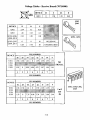
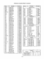
Table of Contents
Page
Chapter 1
General Description
Specifications BTR-200
Controls and Connections
Front Panel
Rear Panel
1-1
1-1
1-2
1-2
1-5
Chapter 2 - Identification of Circuit Board Revision and Version
Audio Boards ......•.................................................................................................................................... 2-1
Receive Board
2-2
Transmit Board
2-3
Chapter 3 - Transmit, Receive & Audio Circuit Boards
()
BTR-200 Instrument Disassembly
Transmit Board
Circuit Descdption
Alignment Procedure
Voltage Tables - Transmit Board (878521)
PCB Transmit Assembly (878521-*)(palts List)
Receive Board
Circuit Descdption (PCB 70714000)
Circuit Descdption (PCB 750309))
Alignment Procedure
Receive Board (70714000)
Equipment Required
Receive Board (750309)
Equipment Required
Voltage Tables - Receive Board (70714000)
Voltage Tables - Receive Board (750309)
PCB Receive Assembly 878522* (Parts List)
PCB Receive Assembly 878662* (Parts List)
Audio Board
,
Audio Board Circuit Description
Receive Expanders
Microphone Amplifier
Auxiliary Input Amplifier
Intercom Driver
Intercom Input.
Headset and Speaker Amplifiers
Transmit'Mixer and Filter
Auxiliary Output·
Remote Transmit Circuit
Power Supply
Alignment Procedure
Equipment Required
:
;
::
-i-
3-1
3-2
3-2
3-2
3-3
3-7
3-9
3-9
3-9
3-10
3-10
3-10
3-11
3-11
3-14
3-15
3-21
3-24
3-27
3-27
3-27
3-27
3-27
3-27
3-28
3-28
3-28
3-28
3-28
3-28
3-29
3-29
Page
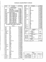
Chapter 3· Transmit, Receive & Audio Circuit Boards (Continued)
Audio Board
PCB Audio Assembly (878520) Versions 1 thru 6 (Parts List)
Display Board
PCB Display 878519 (Parts Lists)
Continued
3-45
3-48
3-48
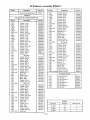
List of Illustrations
Figure
1
2
3
4
5
6
7
8
9
10
II
12
13
14
15
16
17A
17B
18
19
20
21
22
23
24
25
26
27
28
29
30
31
32
33
34
Description
Headset XLR Connector Wiring
Front Panel-BTR200
Rear Panel - BTR-200
Location of Rev Level for Versions 1 and 2 (Audio Board)
Location of Rev Level for Versions 3 thlU 6 (Audio Board)
Location of Rev Level for Versions I and 2 (Receive Board)
Location of Rev Level for Versions I and 2 (Transmit Board)
Exploded View - BTR-200
Transmit Board Component Layout (Foil Side)
Transmit Board Component Layout (Component Side)
Schematic Diagram Transmit Board - Version 1
Schematic Diagram Transmit Board - Version 2
Schematic Diagram Receive Board
Receive Board Component Layout (Component Side)
Versions I and 2 (70714000)
Schematic Diagram Receive Board Version 2 (750309)
Receive Board Component Layout (Component Side) Version 1..
Receive Board Component Layout (Foil Side)
Receive Board Component Layout (Component Side) Version 2 (750309)
Schematic Diagram Receive Board Version I (750309)
Block Diagram Versions 1 and 2
Block Diagram Versions 3 thlU 6
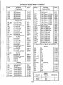
:
Audio Board Component Layout (Component Side) Versions land 2
Audio Board Component Layout (Foil Sde)
Schematic Diagram Audio Board Version I
Schematic Diagram Audio Board Version 2
Details of Board Differences Between Versions I and 2
Details of Board Difference in Versions 3, 4, 5, and 6
Audio Board Component Layout (Component Side) Version 6
with Detailed Areas Showing Differences of Versions 3,4,5, and 6
Audio Board Component Layout (Foil Side) Version 6
Schematic Diagram Audio Board Version 3
Schematic Diagram Audio Board Version 4
Schematic Diagram Audio Board Version 5
Schematic Diagram Audio Board Version 6
Display Board Component Layout (Foil Side)
Display Board Component Layout (Component Side)
-11-
Page
1-2
1-3
1-4
2-1
2-1
2-2
2-3
2-4
3-4
3-4
3-5
3-6
3-16
3-17
3-18
3-19
3-19
3-19
3-20
3-31
3-32
3-33
3-34
3-35
3-36
3-37
3-38
3-39
3-40
3-41
3-42
3-43
3-44
3-48
3-48
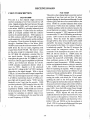
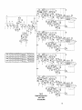
CHAPTER 1
: -')
GENERAL DESCRIPTION
The BTR-200 is a base station which communicates with up to four portable units simultaneously,
in full duplex. It may be used alone with a headset
or interfaced to other equipment such as a
hardwired intercom system.
n
1-1
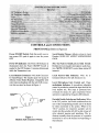
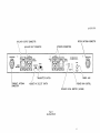
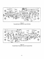
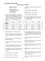
CONTROLS and CONNECTIONS
FRONT PANEL (Refer to Figure 2)
Power ON/OFF Switch: Push this switch once to
turn power ON; push it again to turn the power
OFF.
Local Headset Volume: Adjusts volume to Local
Headset. DOES NOT AFFECT MICROPHONE
GAIN.
Power ON Indicator: The Power ON Indicator is
illuminated when the Power ON/OFF Switch is
pushed in the ON Position. It remains illuminated
while the Transceiver is on.
Mic On-Push-to-Talk/Lock-to-Talk Switch:
Enables the local headset microphone audio function. NOTE: DOES NOT control base station RF
transmit.
Local Headset Connector: 4 Pin XLR Connector
for InputJOutput. The headset jack will accept 6
different Telex Model Headsets. Compatible with
other intercom headsets with four pin XLR connectors that are wired as shown in Figure 1.
Local Push-to-Talk Indicator: Will be illuminated whenever the talk function is on.
Local Microphone Gain Control and Overmodulation Indicator: A screwddver adjustable
control is provided to control the input level of the
local headset mic. This input is protected from
overloads by means of a gain compressor whose
operation is signaled by the gain LED indicator.
MICROPHONE
GROUND
Portable Enable Switches and Indicators: When
in the "IN" position, the Enable switches allow the
user of the conesponding portable unit to be heard
by others connected to the system. When in the
"OUT" position, the respective portable will be
muted, but this portable will still be able to hear all
other selected remotes and interfaces. The indicators normally show the presence of a portable
transceiver in use on the channel corresponding to
that indicator.
BALANCED
AUDIO
OUT
MICROPHONE
AUDIO
Figure 1
Headset XLR Connector Wiring
1-2
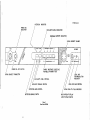
INTERCOM
27160-8-00I-A
INDICATOR
POWER ON
INDICATOR
AUXILIARY ENABLE INDICATOR
PORTABLE CARRIER INDICATORS
I
I
I
~OCAL HEADSET VOLUME
I
i
8TR-200 1I
Headset
I.-.--~
Portabte Station Connect--
ENABLE SWITCHES TO RECEIVE
PORTABLE TRANSMITTERS
. LOCAL HEADSET CONNECTOR
LOCAL MIC
OVE RMODULATION
INDICATOR
AUXILIARY LEVEL CONTROL
AUXILIARY ENABLE SWITCH
INTERCOM LEVEL CONTROL
INTERCOM ENABLE SWITCH
LOCAL PUSH-TO-TALK INDICATOR
MIC ON PUSIH-lO-TALKI
LOCK-TO -TALK SWITCH
Figure 2
Front Panel-BTR200
1-3
LOCAL MIC GAIN CONTROL
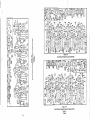
27160-B-002-A
RECEIVE ANTENNA CONNECTOR
AUXILI ARY OUTPUT CONNECTOR
INTERCOM CONNECTORS
AUXILJARY INPUT CONNECTOR
Transmit Anteflna
o
o
Headset Mic
Transmit
Fex 1.0. 850BTR-200
Jack
r"=-hfit Cant
r~l
Off Remote
CO
G~
LSpeaker-l
Oyn
o
TELEX COMMUNICA TtONS. INC.
Intercom
Input
MADE IN U.S.A.
Power
A~'~------300 rnA
1
POWER
TRANSMITTER SWITCH
TRANSM IT ANTENNA
CONNECTOR
HEADSET MIC SELECT SWITCH
JACK
SPEAKER GAIN CONTROL
SPEAKER / LOCAL MONITOR (8
Figure 3
Rear Panel BTR-200
1-4
n
MIN.)
Ext Intercom Switch, Level Control, and Indicator: This switch enables the wired intercom
interface when "IN", and disables it when "OUT".
For RTS intercoms, the "IN" position is channel A
and the "OUT" position is channel B. Ascrewdriver
adjustable control is provided to control the input
level of the wired intercom.
Auxiliary Audio Enable Switch, Level Control,
and Indicator: The switch enables and disables the
Auxiliary intelface when "IN" and "OUT", respectively. The function of the level control here is the
same as that described for the intercom.
REAR PANEL (Refer to Figure 3)
TransmitAntenna Connector: Connect 5/8-wave
antenna (supplied) to this connector. Antenna color
should match connector dot on BTR-200.
(j
Receive Antenna Connector: Connect 5/S-wave
antenna (supplied) to this connector. Antenna color
should match connector dot on BTR-200.
Transmit Switch: Slide switch that allows the
operator to select one of three transmit modes. In
the "OFF" position, the transmitter is always off.
This mode may be used if the base is functioning
solely as a monitor. In the "CONT" position, the
transmitter is always on. This continuous mode is
recommended over the "REMOTE" mode. In the
"REMOTE" position, the transmitter is enabled
only when one or more portables are active.
Headset Microphone Select Switch: This switch
allows the user to select either an Electret or
Dynamic microphone. This switch i~ factory preset
to DYN Position.
NOTE: All Telex headsets that are used with this
intercom are dynamic type microphones.
Intercom Connectors: Connections to interface
the BTR-200 with a wired intercom system.
Auxiliary Output/Input Connectors: Can be
used for 2-way (four wire) input and output to the
BTR-200 or as a simplex input or output. Typical
uses are 4 wire low level intercoms, tape recorders,
public address inputs or outputs, or when operating
two BTR-200 units simultaneously.
Power Jack: For external AC wall supply adaptor
(supplied) or any filtered 12 to 14 VDC/300 rnA
source, or 13.0 VAC RMS/300 rnA source.
Speaker Jack: Allows the user to connect an external speaker (8 ohms minimum) to the unit.
Speaker Gain Control: Screwdriver adjustable.
Adjust the gain control clockwise to increase
speaker gain or counterclockwise to decrease
speaker gain.
NOTE: Leave setting counterclockwise if no
speaker is attached.
1-511-6 Blank
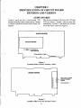
CHAPTER 2
IDENTIFICATION OF CIRCUIT BOARD
REVISION AND VERSION
AUDIO BOARDS
This board is installed in the holes for C124 and
C125 (see below). Version 1 does not have this
switchboard. For Rev C and higher, the location
for the Rev letter is shown in Figure 5.
Version 1 and 2 use Rev A circuit boards. The
location for the Rev letter is shown below. Version
2 contains a small circuit board with a switch. See
Figure 4.
AUDIO BOARD
RECEIVE BOARD
.... __ ..
~---~_.:
o
LOCATION OF
SWITCHBOARD
70723-000 REV A COMP " ' - .•••
r--------.
_
:I.• .2"!!2";!!.'!!!.I!.E!..~~_:
Figure 4
Location of Rev Level for Versions 1 and 2
AUDIO BOARD
c
a:
«
0
!Xl
l-
:E
en
z
«
a:
. .
I
I
I
I
I
U
3
0
I & I
L_
'
"
I
I-
U
REV LEVEL LOCATED
I
if . - - UNDER TRANSMIT
I
BOARD
I
I
Figure 5
Location of Rev Level for Versions 3 thru 6
2-1
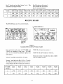
70723-000 REV C
Rev D boards are all version 5.
Rev E boards are all version 6.
Rev B was not produced.
Rev C boards can be either Verion 3 or 4. The
differences are all parts values:
Version
RIOI
RI03
Rl25
Rl30
Rl31
Rl32
Rl33
Rl54
Rl62
Rl68
Rl70
Cl33
3
82K
82K
6.2K
1.5K
1.5K
1.5K
1.5K
5.6K
9.lK
68K
68K
lO~F
4
200K
200K
4.7K
4.7K
4.7K
4.7K
4.7
8.2K
3.9K
15K
10K
22~F
RECEIVE BOARD
The BTR-200 uses one of two receive boards.
750309 COMP REV A
Figure 6
Location of Rev Level for Versions 1 and 2
750309 Rev A boards are version 1.
Early production units came with 70714000, and
750309 was installed in later units. 70714000
came in two versions that differed slightly (See
table below):
750309 Rev Band C boards are version 2.
Some early version 1 boards did not have a shield
over the oscillator section..
Version 2 was built only with Rev C boards.
Version 1 was built with Rev A, B, or C boards.
The different revisions on this board were manufacturing changes that did not change the schematic.
70714000
Version
R327
R345
R363
R381
VR302
VR304
VR306
VR308
1
4.7K
4.7K
4.7K
4.7K
10K
10K
10K
10K
2
10K
10K
10K
10K
20K
20K
20K
20K
2-2
TRANSMIT BOARD
,.-- --------
7-------I
70724-000 REV A COMP
'70"12'....-000
rEV A
OONP
I
Figure 7
Location of Rev Level for Versions 1 and 2
All Rev A boards are version 1. Rev B boards may
be version 1 or 2:
o
Version
R503
R521
CS31
1
4.7K
10K
.0033uF
2
15K
68K
.001 uF
2-3
30
(TYPICAL\~e.
BOTH SIDES)
31
":
/(TYPICAL 3 PLACES)
,fj
th
~.
32
DETAILB
31
(TYPICAL
4 PLACES)
10
10-9-12
(TYPICAL
4 PLACES)
10-9-12~
(TYPICAL
4 PLACES)
"*--/t-'12
8
(SEE DETAIL A)
26
3
DETAIL A
13
10 --===--
(TYPICA~
4 PLACES)
_._ : . :/'
1 ",... . . /"
J/~
/
;b
",
.'
..""/""
DETAILC
34
25
~//
2~/'>
7
(TYPICAL
8 PLACES)
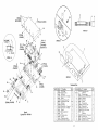
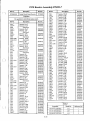
Item No. Part No.
TfJ
19'2124//~
18
(TYPICAL 6 PLACES)
Mechanical Parts
17
13
11
Figure 8
Exploded View· BTR-200
I
2
3
4
5
6
7
8
9
10
II
12
13
14
15
16
17
18
878519
54460001
878520
51847011
878560
52264005
0086300
970011-1
50049003
51845038
51847003
450520
51856001
270229
57722000
450464-1
450463-1
53431002
Description
PCB, Display
Receptacle, crimp
PCB, Audio
Screw, #4-40 x 1/4", flathead
Wireset
Connector Housing, 5 Pin
Copper strip, .343 x .005
Fish Paper
Lockwasher
Screw, #4-40 x 114", pan head
Screw, #2-56 x 1/8" flathead
Standoff
Screw, plastite, #2-28
Lug
Connector, antenna
Sprocket
Volume Control Knob
Switch Button, rectangular
Qty
Item No. Part No.
I
5
I
8
I
I
AIR
1
16
18
1
8
7
2
2
I
1
6
19
20& 21
22
23
24
25
26
27
28
29
30
31
32
33
34
35
36
37
2-4
53431005
878517
59908001
150624-3
878439-3
878430
878521
51845091
878662
51845093
51845055
878431
51845074
557000
500322
760386
Descrilltion
Switch Button, round
(Not Used)
Connector bracket
Connector, B4MB Switchcraft
Telex label
Front Panel
Chassis
Transmit Board
Screw, #6-32 x 3/16"
Receive Board
Screw, #6-32 x 3/8"
#4-40 x 3/16", pan head
Covel'
(Not Used)
Screw, #6-32 x 1/4", pan head
Nut, #6-32, hex
Screw, #6-32 x 3/8", hex head
Insulator, Pre-impreg.
Qty
2
I
I
1
I
1
1
10
1
6
7
I
8
I
I
I
CHAPTER 3
TRANSMIT, RECEIVE & AUDIO CIRCUIT,BOARDS
BTR-200 INSTRUMENT
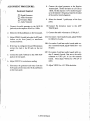
DISASSEMBLY
9. Unplug the cable harness at P1l4 and the two
ribbon cables at P102 and P103.
1. Remove 6 each #6 pan head phillips and 7 each
#14 head phillips screws and remove cover.
Refer to Figure 8.
10. Remove 10 each #6 pan head phillips screws
holding the circuit board to the chassis.
2. Unsolder coax cables from transmit and receive
boards.
11. Slide the circuit board forward and lift up and
out from the rear.
3. Unsolder 3 copper straps from receive board (if
present)
12. Remove 8 each #6 pan head phillips screws
holding front panel to chassis.
4. Remove transmit and receive boards. Early
versions are equipped with snap-on nylon standoffs and later versions are held with #4 pan
head phillips screws.
13. Remove 2 each #4 pan head phillips screws
holding headset connector bracket to chassis
and remove front panel.
5. Remove ring nuts from the two RF connectors.
o
14. Remove 7 each phillips sorews holding front
circuit board to front panel and remove circuit
board. NOTE: When refitting this circuit
board the volume control on the front panel
must be positioned so that the pins and slots
mate properly.
6. Remove the hex head nylon screw and nut
holding Q108 to the chassis.
7. Remove 8 each #4 flat head phillips screws
holding the four XLR connectorhousings to the
chassis. On some early versions, the upper
PEM nuts will be replaced with nuts and lockwashers.
15. Reassembly is the reverse of these procedures.
8. Using an XLR tool or small flat bladed
screwdriver, unlock the XLR housings by turning the locking screw counterclockwise. Then
remove the XLR housings by pulling them to
the rear.
3-1
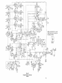
TRANSMIT BOARD
CIRCUIT DESCRIPTION
ALIGNMENT PROCEDURE
U50IC is an amplifier whose gain is controlled by
the level of audio entering the rectifier at pin 16.
As the level here increases, the gain is decreased
and this results in a 2:1 compression characteristic.
Pre-emphasis is added by U501B. R504, R505,
and C508 set this at 115uS. C531 rolls the response
off above 10KHz to further attenuate the 20 KHz
call signal (see Audio Board Circuit Description).
Q501 is a Colpitts oscillator with the collector
tuned to the third harmonic. T501, VVC501 and
VVC502 are added in selies with the crystal to
allow frequency modulation of the oscillator. The
oscillator is operated 10KHz below the series
resonant point of the crystal. This improves
linearity at the expense of some stability. Q502 is a
trip1er and Q503 is a straight through amplifier.
The catTier frequency is thus nine times the crystal.
C529, C530 and L503 function as a low pass filter
and matching network.
EQUIPMENT REQUIRED:
o
o
o
RF POWER METER
FREQUENCY COUNTER
DC VOLTMETER
1. Connect the RF power meter and frequency
counter to the Transmit Antenna jack. Make
sure the Transmit switch on the reat· panel is set
the the Cont position.
2. Adjust T502, T503, T504, VC501, and VC502
for maximum power. Note: If adjustments are
severly out of alignment and no output can be
obtained, it may be necessmy to first adjust
T502 and T503 for maximum DC voltage at the
emitter of Q502. Then adjust T504 for maximum DC voltage at the emitter of Q503. Now
adjust VC50 1 and VC502 for maximum power.
3. Adjust T501 for the COlTeCt frequency:
Y501 Marking
Frequency
154T570
154.570
177T800
177.800
183T730
183.730
4. Repeat Steps 2 and 3 as necessmy.
5. Deviation will be adjusted in the audio board
alignment.
3-2
Voltage Tables - Transmit Board (878521)
DEVICE 1====-r===r===r====jPI=N=N=U=rM=B=E"F'R==~===r==~==l1 .--18
17
16
15
14
13
12
11
20
19
U501
5
2.5
2.5
2.5
2.5
1
2.5
2.5
2.5
---,
2.5
U501
0
2.5
1
2
3
4
5
7
6
8
9
10
PIN NUMBER
Q501, Q502
o
DEVICE
E
B
C
Q50l
1.88
2.44
10
Q502
0.78
0.66
9.7
Q503
1.21
0.26
9.5
C
B
E
)
3-3
Q503
C
E
B
Figure 9
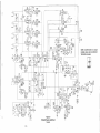
Transmit Board Component Layout (Foil Side)
C501
o0
+
I
R502
-e::>-
R501
+~04
V
a
O
c:::>
R504
C507
C5<t9,.-t
U
ylQ OC506
R51 6
l'l
Y
C525
aY
l'l RS20
U502
CS11
I()C512QQ
lQ
+
C522
a
R517
~ OS03 ~@C501
N
::!
Y -e:::>-
-e::>-
PS12
0+
n
I
l'lN
U
')
~~~6 0
0
0
9' ~ nS005&'
05'3-/\10 I Q
§ t"03
~'3 101 Q I0 I0,~~ I0 Iy C~: 00 Al~ ~O 0" O~
~
USO 1
~nc5°bc50~
",y f1 -f1505 CS08
C503
...
D
00
00
Q~
~0
0
G
@
VRS01
u:;
o
0501
YWC502 l'l
\J Y
Wc501 r
-e::>- Al
R508 ~ YSOl
a
C517
~~N(] u:;l'l(")ol'l~~ ~ OC5:m~
o~
o::y~~ylO . . . ~ C529
U
C518?tQ~~ ~~ ~Ol
~
C516
R510
0
R 5
SILK SCREEN REV.S
~
Figure 10
Transmit Board Component Layout (Component Side)
3-4
L502
0
R502
JoK
R501
30K
C506
loopf
T
G50J
1UF
P512
I ..
(
(
R521
10K
1
20
12
13 10K
R50410K
14
, R503
C507
1UF
4.7K
10
I
+
G501
+
lOoU~
I
C505
4-.7UF
15
8
T
I
.. C5041UF
T
o
G511
10UF
+
I..
G509 +
N
4.7UF
C510
4-.7UF
t-+-'-~\I\1~-'
VR501
5K
L501
C527
J.3PF
Q503~502
R508
47K
MPs9011 L.
WC501
MV21 08 T
R507
100pf 47K
T
FREQUENCY DEPENDENT COMPONENTS TABLE
T501
FREQUENCY
C516
C519
C520
C523
C524
C529
C530
154.570 MHZ
27PF
39PF 100PF 18PF
33PF
68PF
20PF -000
177.800 MHZ
22PF
30PF
75PF
12PF
27PF
47PF
15PF -002
183.730 MHZ
22PF
30PF
75PF
12PF
24PF
47PF
15PF -002
Figure 11
Schematic Diagram Transmit Board - Version 1
3-5
C530
I
T
T
C513
T
VC502
T501
R502
30K
R501
30K
C506
100P~
"'f
20 12
C507
1 UF"
P512
R503
15K
+
(
(
1
j'"
10
3.9K
+
100U1
j"
C505
4.7UF
15
8
C501
16--l +
I
.. C504
1UF
j'"
U502
78L05
C511i
10U~
j'"
I
7'
FREQUENCY DE:PENDENT COMPONENTS TABLE
T501
FREQUENCY
154.570 MHZ
177.800 MHZ
183.730 MHZ
C516
27PF
22PF
22PF
C519
39PF
30PF
30PF
C520
100PF
75PF
75PF
C523
18PF
12PF
12PF
C524
33PF
27PF
24PF
C529
68PF
47PF
47PF
C5JO T501
20PF -000
15PF -002
15PF -002
Figure 12
Schematic Diagram Transmit Board - Version 2
C529
C530
IT
PCB Transmit Assembly (878521-*)
Description
Ref No.
PCB500
PCB Transmit
Part No.
70724000
All capacitors in microfarads unless noted.
C501
C502-C504
C505
C506
C507
C508
C509-C51O
C511
C512
C513
C514
C515
C516',2
3
C516
C517
C518
C519,,2
C519 3
C520',2
3
C520
C521
C522
C523,,2
C523 3
C524'
2
C524
C524 3
C525
C526
C527
C528
C529,,2
3
C529
C530,,2
C530
C531
C531
3
Description
Part No.
Electrolytic, 100
Electrolytic, 1
Electrolytic, 4.7
Ceramic, 100 pF
Electrolytic, 1
Film, poly, .01
Electrolytic, 4.7
Electrolytic, 10
Ceramic, .01
Ceramic, 100 pF
Ceramic, TC, 47 pF
Ceramic, TC, 68 pF
Ceramic, 22 pF
Ceramic, 27 pF
Ceramic, .01
Ceramic, 1.5 pF
Ceramic, 30 pf
Ceramic, 39 pF
Ceramic, 75 pF
Ceramic, 100 pF
Ceramic, 100 pF
Ceramic, .001
Ceramic, 12 pF
Ceramic, 18 pF
Ceramic, 27 pF
Ceramic, 24 pF
Ceramic, 33 pF
Ceramic, .001
Ceramic, ',lOO pF
Ceramic, 3.3 pF
Ceramic, 100 pF
Ceramic, 47 pF
Ceramic, 68 pF
Ceramic, 15 pF
Ceramic, 20 pF
Ceramic, .0033 (Version 1)
Ceramic, .001 (Version 2)
51821524
51821106
51821109
35693019
51821106
52719007
51821109
52723008
52676107
35693019
52713002
52713003
35693011
35693012
52676107
35693047
35693046
35693014
35693061
35693019
35693019
52676101
35693008
35693010
35693012
35693060
35693013
52676101
35693019
35693002
35693019
35693015
35693017
35693009
35693048
52719004
52676101
Description
Part No.
Coils
3
Capacitors
Ref No.
Ref No.
T501
T501',2
T502, T503
T504
L501,,2
L501 3
L502,,2
L5023
L503',2
L503 3
Coil
Coil
Coil
Coil
Coil, Air Wound
Coil, Air Wound
Coil, Air Wound
Coil, Air Wound
Coil, Air Wound
Coil, Air Wound
52978000
52978002
52979000
52977003
63725000
63725005
6372..')000
63725005
63725000
63725005
Crystals
Y501'
2
Y501
Y501 3
Crystal, 177.800 MHz
Crystal, 183.730 MHz
Crystal, 154.570 MHz
52989120
52989214
52989100
All resistors in ohms, 1/8 Watt, 5%, unless noted.
Resistors
R501, R502
R503
R503
R504
R505
R506-R508
R509, R510
R511
R512
R513
R514
R515
R516
R517
R518
R519
R520
R521
R521
R522
30K
4.7K (Version 1)
15K (Version 2)
10K
15K
47K
10K
820
47
47K
5.6K
100
47
8.2K
470
56
47
10K (Version 1)
68K (Version 2)
10K
52154025
52154044
52154032
52154036
52154056
52154020
52154036
52154062
52154092
52154020
52154042
52154084
52154092
52154038
52154068
52154090
52154092
52154036
52154016
52154036
Connector
P512
Header, 3 pin
670062
Variable Capacitors
VC501, VC502 Variable Capacitor
35837007
Transistors
Q501, Q502
Q503
Transistor, 2N5770
Transistor, MPS-901
54689000
760376
Integrated Circuits
mOl
U502
IC,NE575N
IC,78L05
53277003
54680005
Diodes
VVC501
VVC502
Diode, MV2108
Diode, MV2108
58675000
58675000
Variable Resistor
VR501
5K Variable resistor
57148068
878521-*
Frequency
*Dash No.
Reference No.
177.800 MHz
-177
1
183.730 MHz
-183
2
154,570 MHz
-154
3
3-7/3-8 Blank
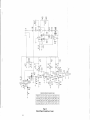
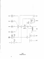
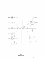
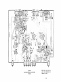
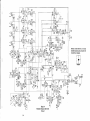
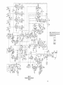
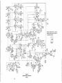
RECEIVE BOARD
()
PCB 750309
This unit is a four channel dual conversion receiver
consisting of one front end and four I.F. strips.
Signals entering the board proceed through 3 tuned
circuits, Q301, and three more tuned circuits to the
mixer. HY301 is a doubly balanced diode mixer
and receives +7 dBm from the oscillator. Q302 is
a Colpitts oscillator with the collector tuned to the
second harmonic on version 1 boards and the third
harmonic on version 2. Y301 operates on the fifth
overtone with C311 and L308 acting as mode suppressor. L307 is used to set the oscillator on frequency. From the mixer the signal continues
through Q303 to filtet drivers Q320, Q370, Q420
and Q470. On version 1 boards the signal is resistively coupled to the filters. On version 2 boards it
is inductively coupled. The four I.F. strips are the
same except for component values. For the
remainder of the description the parts in the 10.7
MHz I.F. will be referred to. U320A mixes the
incoming signal with a 10.245 MHz oscillator to
produce the second I.F. of 455 KHz. (The other
three oscillators operate at 455 KHz above their
n~spective input frequencies). U320B contains a
limiter and quadrature detector, which is tuned by
L322. U320C functions as a 94 KHz bandpass
filter for operating the squelch. With. no signal a
large amount of noise is present at U320 pin 13 and
a portion of this is rectified by Q321. If the emitter
rises above .7V U320D clamps pin 16 to ground,
muting the audio, and drives pin 15 low, extinguishing the LED on the front panel via Q322.
When a signal is received, the noise at U320 pin 13
drops and lowers the voltage at the emitter of Q321,
releasing the audio clamp and lighting the front
panel LED. Since the LED current flows through
R33l, the voltage drop acts on Q32l and provides
hysteresis. VR321 adjusts not only the noise
amplitude delivered to Q321 but also the D.C. bias,
and is used to set the squelch at 1 microvolt. From
U320 the audio is buffered and filtered by U321.
R328, C335, and VR320 set the de-emphasis at
l15uS. U321Ais a three pole Butterworth low pass
filter with a cutoff frequency of 10 KHz.
CIRCUIT DESCRIPTION
PCB 70714000
This unit is a four channel single conversion
receiver consisting of one front end and four I.F.
strips. Signals entering the board proceed through
3 tuned circuits, Q30l, and 3 more tuned circuits
to the mixer. MX301 is a doubly balanced diode
mixer and receives +7 dBm from the oscillator.
Q302 is a Colpitts oscillator with the collector
tuned to the second harmonic. Y301 operates on
the fifth overtone with C319 and L308 acting as
mode suppressor. L310 is used to set the oscillator
on frequency. From the mixer the signal continues
through a broadband filter to line driver Q303.
VR309 is used to set the collector current to 20 rnA.
Q303 drives the four I.F. strips, beginning with
crystal filters FL30l-FL308. The four I.F. strips
are the same except for component values. Also,
the 10.7 MHz I.F. substitutes a ceramic filter for
two tuned circuits. For the remainder of the
description the parts in the 10.7 MHz I.F. will be
referred to. The I.F. signal is amplified by Q304 and
U301A, and limited and detected by U301B.
U301B contains a quadrature detector which is
tuned by T309. Squelch is of the amplitude
type, the D.C. voltage at pin 5 of U301 varying in
propOltion to the signal strength. With no signal
U302 pin 1is low and the audio outputis squelched.
When the received signal causes the voltage at pin
3 of U302 to exceed that of pin 2 of U302, pin 1
goes high and the squelch opens. VR30l sets the
threshold at pin 2 and thus the squelch. R320
provides hysteresis. Q305 is used to drive the LED
on the front panel. From U301 the audio is
amplified by U303A. R389, R328 and C354 set
the de-emphasis at 115uS. VR302 is used to compensate for variations in detector output level.
U303B is a 3 pole ButterwOlth low pass filter with
a cutoff frequency of 10KHz.
3-9
ALIGNMENT PROCEDURE
Receive Board - 70714000
Equipment Required:
D
D
D
D
11. Place the RF voltmeter probe tip inside the top
ofL304.
Signal Generator
Sensitive RF Voltmeter
DC Voltmeter
AF Voltmeter
12. Adjust VC304 for a peak indication.
13. Adjust VC305 for a null indication.
1. Connect the signal generator to the Receive
Antenna jack. Set the deviation at ± 3 KHz at
1 KHz. Refer to the frequency chart below.
Look at the marking on the Y301 and set the
generator to the corresponding ALIGN frequency.
14. Adjust VC306 for a peak indication.
15. Place the RF voltmeter probe tip on the collector ofQ303 and adjust T301, T302, and T303
for a peak indication.
Y30l
Marking
Align
CHl
CH2
CH3
CH4
171R905
170.705
171.905
171.045
170.245
169.505
207R800
206.900
207.800
207.425
206.800
206.000
213R800
212.900
213.800
213.425
212.800
212.000
16. In the following alignment, unless othelwise
directed, adjust the signal generator output
level to maintain a DC voltage of between 1 and
1.5 volts.
2. Adjust VR309 for 0.44 VDC across R312.
3. Place the RF voltemter probe tip inside the top
of L307 and adjust VC307 for a peck indication.
17. Set the signal generator to the channel 1 frequency.
4. Set the RF voltmeter to its most sensitive scale
without stray pickup.
18. Adjust T304, T305, and T308 for maximum
DC voltage at pin 5 of U301.
5. Place the RF voltmeter probe tip inside the top
of L301.
19. Set the signal generator output to 1 mV and
adjust T309 for maximum audio at pin 7 of
U303.
6. Increase the signal generator output level until
the RF voltmeter indication just begins to rise.
20. Adjust VR302 for 140 mV of audio at pin 7 of
U303.
7. When adjusting, reduce the signal generator
output rather then reducing the RF voltmeter
sensitivity.
21. Set the signal generator output to 1 ~ V and
adjust VR301 to just extinguish the number 1
LED on the front panel.
8. Adjust VC301 for a peak indication.
9. Adjust VC302 for a null indication.
22. Set the signal generator to the channel 2 frequency.
10. Adjust VC303 for a peak indication.
3-10
23. Adjust T31O, T311, T312, T313, and T314 for
maximum DC voltage at pin 5 of U304.
30. Adjust VR306 for 140 mV of audio at pin 7 of
U307.
24. Set the signal generator output to 1 mV and
adjust T315 for maximum audio at pin 7 of
U305.
31. Set the signal generator output to 1 ~V and
adjust VR305 to just extinguish the number 3
LED on the front panel.
25. Adjust VR304 for 140 mV of audio at pin 7 of
U305.
32. Set the signal generator to the channel 4 frequency.
26. Set the signal generator output to 1 ~V and
adjust VR303 to just extinguish the number 2
LED on the front panel.
33. Adjust T322, T323, T324, T325 and T326 for
maximum DC voltage at pin 5 of U309.
27. Set the signal generator to the channel 3 frequency.
34. Set the signal generator output to 1 mV and
adjust T327 for maximum audio at pin 7 of
U31O.
28. Adjust T316, TIl?, T318, T319, and T320 for
_ maximum DC voltage at pin 5 of U306.
35. Adjust VR308 for 140 mV of audio at pin 7 of
U31O.
29. Set the signal generator output to 1 mV and
adjust T321 for maximum audio at pin 7 of
U307.
36. Set the signal generator output to 1 ~ V and
adjust VR307 to just extinguish the number 4
LED on the front panel.
Receive Board - 750309
lA Version 1: Place the RF voltmeter probe tip
inside the top of L309 and adjust VC307 for a
peak indication.
Equipment Required:
D
D
D
D
D
D
Signal Generator
Sensitive RF Voltmeter
Audio Distortion Meter
Spectrum Analyzer or VHF
Monitor
AF VoltmeterSINAD Meter
1B Version 2: Place the RF voltmeter probe tip
inside the top of L313 and adjust VC307 and
VC308 for a peak indication.
2. Connect the signal generator to a shott piece of
wire and set it to the oscillator frequency as
shown in the chart below:
3. Using either a spectrum analyzer or a VHF
monitor, adjust L307 for a zero beat.
Y30I
Marking
Oscillator
CHI
CH2
CH3
CH4
171 R905
182.605
171.905
171.045
170.245
169.505
207 R800
218.5
207.800
207.425
206.800
206.000
213 R800
224.5
213.800
213.425
212.800
212.000
3-11
4. Connect the signal generator to the Receive
Antenna jack. Set the deviation to ± 3 KHz at
I KHz. Refer to the chart and select the channel
3 frequency.
20. Adjust VR321 fully clockwise, then turn it
counterclockwise until the number I LED on
the front panel just comes on.
21. Set the signal generator to the channel 2 frequency and increase the output to I mV.
5. Connect the AF voltmeter, distortion meter, and
SINAD meter to U421 pin 1.
22. Move the audio hook up to U371 pin I.
6.
Adjust VR421 to maximum counterclockwise.
23. Adjust L372 for maximum audio.
7. Adjust VC301, VC302, VC303, VC304,
VC305 and VC306 for best SINAD.
8. Increase signal generator output to I mV.
9
24A. Version I: Adjust L371 and L372 for minimum
distortion.
24B. Version 2: Adjust L371, L372, and L373 for
minimum distortion.
Adjust L422 for maximum audio.
25. Adjust VR370 for 140 mV of audio.
lOA. Version I: Adjust L421 and L422 for minimum
distortion.
26. Set the signal generator output to 1 !-tv.
lOB. Version 2: Adjusut L421, L422 and L423 for
minimum distortion.
27. Adjust VR371 fully clockwise, then turn it
counterclockwise until the number 2 LED on
the front panel just comes on.
11. Adjust VR420 for 140 mV of audio.
28. Set the signal generator to the channel 4 frequency and increase the output to I mV.
12. Set the signal generator output to I !-tV.
13. Adjust VR421 fully clockwise, then turn it
counterclockwise until the number 3 LED on
the front panel just comes on.
29. Move the audio hook up to U471 pin 1.
30. Adjust L472 for maximum audio.
14. Set the signal generator to the channel I frequency and increase the output to 1 m V.
31 A. Version I: Adjust L471 and L472 for minimum
distortion.
15. Move the audio hook up to U321 pin I.
31 B. Version 2: Adjust L471, L472, and L473 for
minimum distortion.
16. Adjust L322 for maximum audio.
32. Adjust VR470 for 140 mV of audio.
17A. Version I: Adjust L321 and L322 for minimum
distortion.
33. Set the signal generator output to I !-tv.
17B. Version 2: Adjust L321, L322, and L323 for
minimum distortion.
34. Adjust VR471 fully clockwise, then turn it
counterclockwise until the number 4 LED on
the front panel just comes on.
18. Adjust VR320 for 140 mV of audio.
19. Set the signal generator output to I !-tv.
3-12
NOTES:
/
o
3-13
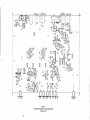
Voltage Tables - Receive Board (70714000)
S
Gl
~ Q301
D
DEVICE
G1
S
G2
D
Q301
0
1.58
1.58
8.68
G2
Q302
Q303
DEVICE
E
B
C
Q302
2.54
3.3
8.56
Q303
.44
1.23
4.2
Q304, Q306,
Q308, Q310
2.63
1.89
1.08
Q305, Q307,
Q309, Q311
0
o
10
NO SIGNAL
6.65
7.34
10
UNSQUELCHED
Q304 - Q311
C
B
E
DEVICE t==r-=r-=PrIN=N=UrM=B=E=Rr===r====r=====I
16
15
14
13
12
10
11
9
U301
U304
U306
U309
1.58
1.58
1.61
o
1.59
1.59
1.59
1.73
1
2
3
4
5
6
7
8
PIN NUMBER
DEVICE 1I==,=====,====PF I=N=N=UF M=B=E=Rr=====.===.==l
16
15
14
13
12
11
10
9
U301
U304
U306
U309
1.58
1.58
1.61
0
1.59
1.59
1.59
1.73
1
tmV
RF
1.58
0
7.35
6.09
3.34
2.07
1.84
3.44
1
2
3
4
5
6
7
8
PIN NUMBER
3-14
IN
U301, U304, U306,
U309
Voltage Tables • Receiv~ Board (750309) Continued,
Voltage Tables· Receive Board (70714000) Continued
DEVICE ......._PIN.,.-N_U"T"M_B..,.E_R-==J
U303
U305
U307
U310
8
7
6
5
DEVICE t===P.,..IN=N_U=M=B....,E.-=R==j
876
5
10
5
5
5
10 0.05
1
550
1
i
NO
SIGNAL
0.05
234
DEVICE l--___r---r--..,.-P-IN--rN-U-M-BI"""'E-R--r--+r--........---t
18
17
16
15 14
13
12, 11
10
.21
U302
U308
5
,1
1
.21
123
PIN NUMBER
0
1
U302, U303, U305,
U307, U308, U310
U320
U370
U420
U470
2.13
0
0
0
0.792.57 2.47 ,
U320, U370, U420,
U470
...·
10
9.38 9.26
10
1.1
1.1
i
1.11i
10
5.9
I
4
123
PIN NUMBER
4
5
6
I
789
PIN NUMBER
I
G20 0
a.
/
<"4
G10S
NOTE: If this part is
absent, then surface
mount part has been
installed on foil side.
Pad designations are
the same.
DEVICE VERSION Gl
G2
D
S
9.22
1
Q301
1
0
1
Q301
2
0
1.8
8.8 0.36
U320
U370
U420
U470
2.13
0
0
\
9.34 0.36 2.57 2.471
DEVICE
E
B
C
Q302
3.69
4.37
9.22
Q320, Q370,
Q420,Q470
1.05
1.76
5
0.8
1.54
10
Q321, Q371,
Q421, Q471
0.79
0.77
10
NO SIGNAL
Q321, Q371,
Q421, Q471
0.35
0.8
9.4
UNSQUELCHED
Q322, Q372
Q422, Q472
0.79
0
10
NO SIGNAL
Q321, Q371,
Q421, Q471
8.67
9.34
9.4
UNSQUELCED
3-15
Q321, Q322, Q371,
Q372, Q421, Q422,
Q471, Q472
5.5
1
10
9.38 9.26
123
Q302, Q320, Q370,
Q420, Q470
0
IIIIIIIIIIIIIIIIIIIIIIIIIIIIIIIIUNSQUELCHED
10
1.1
1.1
456
PIN NUMBER
lj
NO
DEVICE 1----r_...,.._-,-.P_IN-rN_U_M.....,Br-E_R......,._.,..Ir--.....,._""""1
18 17 16
15 14 13
121 11
10
L303
o
5.5
:1 1 1 1 1 1 1 1 1 1 1 1 1 1.!1 1 1!1 1 1 [~1 1 1 1 1 1 1 1 1 1 1 1 1 !1 1 1 1 1 1 1 !l lih: : : :~:l~I !1 1 1 1 1 1 1 1 1 1 1 Ii'l.I!l l l l lrl!I I I I I I ~r. :~: SIGNAL
Voltage Tables - Receive Board (750309)
O
[Q]
0
I
1.1·
10
5.9
789
i
~-------'--------------------r---:-:--------~----------,
RJ1S
RJ19
CJ4B
1.5K
1.5K
47PF
Q304
MPSJ640
CJJJ
F1.J09
C326U~3:~2~PFTl
SFE10.7J
.01UF
~------------------------jr------------r------------------,-----j
G6PF
LJ09
1MH
UJOJ:A
RJ29
_ _~ +
NE5532
10K
"=
CJ29
'Rg;g
RJ24
2
2 0 K ,~.
470PF
f-f:"
1
"l
CJOl
CaD;:}
!
VCJO~
()--j VC,JOl
.
T
i"
.
01UF
,
T
-t"
"
Rg~:,
RJ25
10K
Q301
3SK174
C 3 0 :LJ05
:f
VC305,
VC30.
LJ02
T
CJ56
j
I,
O '~
FL303
1 FREQUENCY
CJoa
lOOPF
CJ25
10PF'
,
FL304
C334 IC360 c3621c3631c3641c3651c3661c3671 C373 IC3801
1169-172 MHZ 11.56MHZ .001 UF 150PF 175PF168PFli .oPFI39PF .oPFI50PF I 470PF 139PF
1206 214 MHZ 11.075MHZ 6.2PF 156PF 82PF 175PFIt, 1PFI43PF It, 1PF!56PF IS60PF 143PF 1
h
I
1.5K
0302
CJ69 lN4148
CJ64
CJ66
"
TJ12
.,
220
RJJ6
..
220
39QP
,
T
CJ71
I
RJ42
220K
CJ70
.OlUF
,OlUF ""f
•
,
RJ40
....
_
1
R343
10K
'7RJ45
V.l 4.7K
V.2 10K
22K
FL305
\206- 214 MHZ
0385
I10UF'
"'f
172 MHZ
PJ09
CJB2
.1UF
UJ04:A
NEBl4
C3.W 7313
390P
RJJ5
'169
r--1'
-t~r
,OlUF
O""Q,~I~~~O"
~d
Ie3••
,
t-
CJ57
,
,0022UFlo056UF
l
RJJJ
, FREQUENCY
RJJ1
10K
CJ54
i-------,
VCJOJ*r;;..::=.-_-+,,,,,b'-1
1
LJOl
-:r
220
240
C31J
CJ05
C339
RJ17
R31J
R3JO
10K
FL306
C3921 C393 IC3941c3951c3961c3971c3981c3991 C400 1 C405 IC4061c4071 C408 IC4121
12.36MHZ 43PF I 330PF 168PF 150PF 1.82PFI36PF!.82PFI43PF 1330PF I 390PF 120PF 120PF 1330PF 136PF 1
11,7MHZ 47PF \ 390PF \75PF\62PF!1.0PFI39PF 11.0PF147PFI 390PF I 470PF 124PFI24PF I 270PF 139PF I
QJ07
MPSJ704
VRJOJ
5K
CJ67 +
,
lUF
r,
RJ55
1.5K
RJ51
1.5K
DJOJ
lN4148
CJ96
'"lp~lr
C39J
RJ53
220
CJ96
RJ60
220K
CJ97
, TJ18
i'
C400
T
C403T
,OlUF
Y
I
lOUr
V.2
13.1MHZ
C424
39PF
12.5MHZ
43PF
10K
C41B
.OO15Uf
'7 RJ63
V.l 4.7K
0309
MPSJ704
P311
'r
SR3.,
'7
FL307
FL308
C
C402
.OlUF
10K
I
~
C419 +
lUF'+
C444
I
C446
.1Uf
RJ76
220K
C
R371
220
RJ79
10K
RJB6
10K
C450
.OO15Uf
RJ76
22K
VRJOB
V.l
V.2
VRJ07
5K
Figure 13
Schematic Diagram Receive Board
70714000
PCB Assembly 878522
C451 +
,
lUf~
3-16
10K
20K
PJ10
T
I
SHL~
\~ @
R332
@c::::J@FU03
I
~ANT::::;/~g
9
1301r
O
<>1
°~ ~
@§l§J
~
FU01 R314
1310 \ @c:.J@ FL302
~~~OO1r§§§ ~
@R33~@R334@ A[;. ~
§§§
0___
~ T304 FL30~368@
)gE" 01
0
~
lO
FU08
§@@l @@§
gj
~~
R350
@c::::J@ FL305
~~~o01~
§§§
:q-
FU06
~
§§§
~
131 6
~
l2.
~~
~050
ml
o
~~~o01
@R317~316©1A~ ~ ~ @R371~!I@[email protected];, ~ @R353IlR352@J~[; ~
N~§1J0303 T311Fo~CJeO ~~~~~&>C359 ro~o~~j~~~ em ro8G~~~~~cdiCE42~JOO~CJ92 ~~Po,~dC391
~I')O ~ ~@R369@ ~~ ~I
o
@(f10R312@
'C7@R333@
8lb \...J OO31 5@ (Q)
Y@R351@
0
0 CO>c325C360Cjg 0
10 0'.13140 0
0' P313 0 I=- 0
10 01
0 0
1'0
01
0
O
VC301
't1 @o::
<O>c324
~ ~013130
O@)
~;(r
T324joool()otoOo~ 013260:; 10001 060 01"31 013200
C304CCb @@C303 @ @-U09-@ 10001~oo2JJooOJ C377
:J@)
88100~T308 0
0 0 0 100010 or3180~ °oo~oooJ C409
vn020=:<\"y'::\ lf1C3oitQ> Q C323 0
0 ~~ ~~l!!9 <>£oro
LL
9J~~t9 ~ ~ ~:lJ9 ~:r9~ oAo 10 01 ~a9 ~~~ 0-40
co
l~gAC326JO 01 10 ol~flo ~noft> ~5@R318@~ 8Jb::10~ ~ OO372@~~ ~t.O~ ~ @R354@~tO ~~M o-e..C41 0
u~o
OJ
1312~D Olooooof01o 'tr,
PuC379 ijaoooooooo A
0304 00000000 FfJ443
200060000 AC411
o
10 00_ 1302 n
~
'dC347 00
't:1_ DJOJe·'-''-''':~'':'':''~..loo/...:'''' 'd
L.302
L303 T30310 01
cr@
U304
U301
U309
U306
@ 0 @
?o 0
0 0 0 0 0 0 0 0
0 0 0 0 0 10 0 0 OT30
0{) 0 0 0 0 0 0 0 0 df32
0 §] 0 0 0 0 0 0 oT321
VCJ03
@R301@
C3720 N
0 0 <0 C340b 0 l"I'"'h
0 0 0 <0
C436b lO rrn
0
0 0 CO>
0 CO> C404b '<t _
ro QC383 0
Ul ~C351
C3 9
'<t~C44 70 C445
: ~ --C415 0
3
A 1000 11301 @R337@ 8 b OO342@C381OO31OO;:]0 @R324@
4 @R373@ 0 0 ~378@
@R35~ 0 0 @R360@C41
@R303@ ~302@
C308C@]lQ]030107C321'c/OO
@-R338-@@R341@ ~n
@-R320-@OO323© ~n
@-R374-@@R377@@~ @-R356.-@@R359@ @.~
C3
@R304@ lQ] lQ] 6
10 01
C384CCb @R343@ '<tp
C352CCP 00325@
C448b ~379@ ~R449 C4160 @R361@ ~1417
@R30S@ 6 C311 ;
U06 @R306@
@R345@ 003400 ~ C385 @R327@ @R328@ ~ C353
@R381@ @R382@
@R363@ @R364@ ~ 0
o
@I ~31
0 I')
J@J§I§]C386@R39()@ @
~ @R389@@C450 @R388@(Q)
frV,
~41 ~ @R387@@
O
o
IQ\ O , >
• ~ '©@
@I' )
[ \
~ 0I')
~
@ @
0 0 0 0 0 ~
, 0 0 0 0 0 @ If)
U
@
'6'1
Ii ~ ~
c
@
~~00l
0-
01
~
~~
I@ _ If(§)
o
[]@]]
N
FU04
~
9?1
C3ee.~ ~
0
~~
° .
~O~~
~
O~ C370~ ~
~O~ ~~
(}U
~O~~
~ tR30~
2
1
O~
~0~C412
3J
NP
0I~@tL
rJ;
~~Ul~
ro 6
~ C~[R30~0:....
~
[0 ~~. ~
0~
0
o
u041@lc309
@§I§] @)
0
U305
VRJ02
U31 0
VR306 .
U307
C312 ~ f@1
0
0
C306~
@g 0 0 0 0 @
@I') 0 0 0 0 @ ~
~0 0 0 0 0 @
©@N 0 0 0 0 @
I.@JCo ~~
0
©
~U @R348@~ @ nO @R330@~
@ro@R384@1@ @I
+~0
I@@I
L310 0 ~
L305 ~314 + 387
~F?> @IC389C388QI'AAI
C356
~I@ @!C453C452<:>i.::i@R366@C420
8
@
<O>C315 0 @
r@
C355@ ~
@
I@
C419i@ ~
o >
~316 ' < t o @ o o
C357
D@oro o
@:c421
[Q]
(1 ~
@
~
VR303@ 0 8 0
@
R376
VR307@ 0 g 0 @VR305
.
@R38OO
8:()
C30]©> @
I 0
0 @VR301
@ @
J 0 ~ 0
@
0
(:J
o
2®"
g
gOO
@ ~c~ ~x
~o
~
U07 I')
lQ] 0
Y30,(@
@R31 O@
o
1
..J
I
Pi (QJ
L
lQJ
CO> 0302 @
@R309@ ~ 1 7 \.C319
I
I
0::
@ @
:1 ~
8
00339@
~
0 0 0
0I') (Q)
(L
0307
(Q)
(Q)
O~
N
@
~
ID
, @ DR322
lQ]
03°05
@
l
~
(OJ 'U
(Q) ~
ID
Figure 14
Receive Board Component Layout (Component Side)
Versions 1 and 2
70714000
3-17
~I o@0 1lQ])
@R375@
~
lQ] [Q] lQ] I')
\...J
0311
(L
IQ1
~
(Q)
(Q)
em
@
R357
lQ]
0309
@
R358
P~311
~
~
0320
MPSH10
P301
R305
lK
R306
100
C302
C301
T
r r
C30~
L302
r
VC305
L301
I
C315
.01 ur
C306
o--1~~VC303
1
L312
10UH
I
I
T
C305
lOOP/,
I
P320
R313
10K
or
VC306
C316
.0lUr
T
R314
2.2K +-+----t------.---.-,=~----
or
0370
MPSH10
R307
~P370
2.2K
FB371
T
FREQUENCY
C301
C422 ,C472
CF370
CF371
CF420
CF421
CF470
CF471
169-172 MHz
5.6 pI' .62 pI' .50 pF .50 pI' 1.2pF 4.7 pI' 150 pI' 43 PI' 39pF
11.56
MHz
12.36
MHz
13,1
MHz
.15/lH 171.005 12.015 12,815 12,555
MHz
MHz
MHz
MHz
206-208 MHz
4.7 pI' .SOpF .33 pI' .33 PI' .33 pI' 2.2pF 180 PI' 50 pI' 43 pI'
11.075
MHz
11.7
MHz
12.5
MHz
.1O/lH 207.6
11.53
MHz
12,155
MHz
12.955
MHz
212-214 MHz
4.7 pI' .SOpF .33 pI' .33 pI' .33 pI' 2.2 pI' 180 pI' 50 pI' 43 pI'
11.075
MHz
11,7
MHz
12,5
MHz
.1O IIH 213.6
11.53
MHz
12.155
MHz
12.995
MHz
C302
C303
C307
C308
C313
C421
L308
Y301
MHz
MHz
Y370
Y420
Y470
0420
MPSH10
T
~P420
FB421
0470
MPSH10
R470
4.7K
Cf470
R471
lK
P470
C479
.OO47UF
WV~=::':-+-III--+..llj·::-""
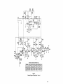
Figure 15
Schematic Diagram Receive Board
Version 1 - 750309
PCB Assembly 878662
3-18
-
-.
(j
r:--------,
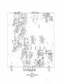
Figure 1'"(A
Receive Board Componen~Layout (Foil Side)
o
vo~oQ01oI~~o~0 1000I~':CD~'t
0'(0 tr~ IQAgT01'~ .:
r
0D
o
CJo
C30l
C302
-c:>R30l
C303
C305
-e>
~ ~
~
L304
c=:Jo C30
g
II:
R303
•
L3l2
p
FB371
0
7
ril....
Uhy
0 ~ 00
L37l
Y370
~
C37~
a
R320
00-c:>-0
CF372
C37f'
~<:>
~a
>
o
o~
o
L372
0
13
3
0
R383
og
Q ~
0
O
0
13
0
C3260
Iil
a
0
-e:>-
Q37l
R378
c::::>
C385
R470
Ii
R4210
Q420D
G-
R480
L4~
:s;(:R479
486 ---
R430
0
g
R429
'<-)01;1 0
R~::o
i 0 0 00
-c:>-
0
L322 C328
R334
OC470 CF47
C489
L470
R484
Y470
P370
0
~~C4760 0 :
Q ~ 5c::>
(J°D>
C334(J
°
11:
-e:::>-
c:>
R328
C335
0
L472
750309
°
..
P~20
~
5
IL
R433
0
0 C 2l(J
~
"
>
000>~
8
0
5 C42a 0
~00~
0
>
°O"(d
00C]
~
.()°C]°D
g478 C484 -c:>c:::>
R478
C485
R434
L420"' L42l
-c:>R483 C4240 °
If'\
-0
'
0
OC439
CF420
Y420
IL II:
R333 C4740
0
L47l
l::
Figure 17B
Receive Board Component Layout (Component Side)
Version 2
3-19
FB421
U~O 0 0
Q470 D
0
L47 3
-e>
0° C339
\;0
Ii! -c:>-
00
0
00
0~38l>ic]oD ~0 O~D~DO
C378
~
<:>
-e> R329
C336
~
R471j\
L\
C3ll0
R31Jc): (J
-c::::I- 0
OJ;)
L308 C3l2 Q302 0 L307
0 0 O~550'00 0 8 a~o~~-c:>0
c:::Ji$
c::::> 0r:J
0
oJc32()'0~GO§i ~ §c!i0i g08
"'0
CF32
C324'QOU 0
,.
FB321
R330
n ~O
olJ
00
1
L32l
Ii
~
Y320
rvC371~0i ~O~
;
0~ iO~0>
0
\()
0 C3890-C:>-L03C20320
C370 CF'"
L370
0 01
388 <:> R379
OR321
D
L~
Q320
\:T
-e>
L373
R370
~
R380
OR37l
i6i?7
OC3l4 L3l3
L3l0
,c=:J- -g2
(J'
c=:Jc=:JL3ll Q303IC~6 ~3l4
C3150
-e>
R313
306
Q37b
P30l
0
D
D~2o~:O°
D° ~
G
~
C434
470
L422
(J
R42~
C435
P420
I
I
II
~
PJ01
9
R306
"0
L312
'OUH
RJ15
C301
100PF
,
I,001uF
IK
47K
C"2
CJ',
CJ<lB
R305
I
C318
I·oo1uF
1'"
1'"
CJ15
,01UF
C3"
CJ<l~V"OB
y,
"'05
I
,
1.311
R31J
10UH
10K
G
PJ20
G
,
P420
T
I.305
C316
,01Uf
RJ14
2,21<
RJ12
470
",307
3.JK
FREQUENCY DEPENDENT COMPONENTS TABLE
C421
CF470
CF471
1J.1
MHZ
SOPF
43PF
11.075
11.7
12.5
MHZ
Mill
MHZ
,J3PF .33PF laOPF
SOPF
4JPF
11.075
11.7
12.5
MHI
MHI
212-214 MHZ 4,7PF ,50PF .33PF .33PF
CJ1J
MHI
206-208 MHZ 4.7PF .50PF .33PF .33PF .33PF .J3PF 180PF
169-172 MHZ S.6PF .B2PF .SOPF .SOPF
CJOB
CF420
Cf.421
12,J8
39PF
C302
C307
MHZ
C472
4JPF
CJ01
C30J
CF370
CFJ71
11,58
C422
1.2PF .SOPF 1S0PF
FREQUENCY
MHZ
L306
Y301
Y370
Y420
Y470
.22UH
171.905
12.015
12.815
\2.555
MIlZ
207.6
MHZ
MHZ
.15UH
.1SUH
11.53
12,155
MHZ
12.955
MHZ
MHZ
MHZ
MHZ
21J.8
11.53
12.155
MHl
MHZ
MHZ
12.9"
MHZ
~P470
'I
I
L-
Figure 18
Schematic Diagram Receive Board
Version 2 . 750309
PCB Assembly 878662
3-20
~
PCB Receive Assembly 878522-*
Description
Ref No.
PCB300/400
Printed Circuit Board, Receive
Part No.
Ref No.
70714000
C361
C362 1
C3622,3
C363 1
C363 2 ,3
C364 1
C3642 ,3
C365 1
C365 2 ,3
C366 1
C3662 ,3
C367 1
C367 23
C368
C369-C372
C373 1
C373 2 ,3
C374, C375
C376
C377, C378
C379
C380 1
C3802 ,3
C381
C382
C383
C384
C385
C386
C387
C388
C389
C390
C391
C392 1
C3922,3
C393 1
C393 2 ,3
C394 1
C3942 ,3
C395 1
C395 2,3
C396 1
C396 2,3
C397 1
C3972 ,3
1
C398
2
C398 ,3
1
C399
C399 2,3
C4OO 1
C4OO2 ,3
C401-404
C405 1
C405 2,3
Capacitors
All capacitors in microfarads unless noted.
Ref No.
C301 1
C301 2 ,3
lJ
C302
C303 1
C303 2,3
C304
C305 1
C305 2 ,3
C306
C307, C308
C309, C310
C311
C312
C313 1
C313 2,3
C314
C315 1
C315 2 ,3
C316
C317
C318
C319
C320
C321, C322
C323
C324
C325
C326, C327
C328
C329
C330
C331
C332
C333
C334 1
C3342,3
C335, C336
C337-C340
C341
C342, C343
C344
C345, C346
C347
C348
C349
C350
C351
C352
C353
C354
C355
C356
C357
C358
C359
C360 1
C3602,3
Description
Ceramic, 5.6 pF
Ceramic, 4.7 pF
(Not Used)
Ceramic, .82 pF
Ceramic, .5 pF
(Not Used)
Ceramic, .5 pF
Ceramic, .33 pF
(Not Used)
Ceramic, 100 pF
(Not Used)
Ceramic, .001
(Not Used)
Ceramic, 1.2 pF
Ceramic, .33 pF
(Not Used)
Ceramic, 4.7 pF
Ceramic, 2.2 pF
(Not Used)
Ceramic, .001
Ceramic, 56 pF
Ceramic, 47 pF
Ceramic, 4700 pF
Ceramic, 12 pF
Ceramic, 36 pF
Ceramic, 9.1 pF
Ceramic, 10 pF
Ceramic, .01
Ceramic, 56 pF
Ceramic, 470 Pf
Ceramic, 82 pF
Ceramic, 100 pF
(Not Used)
Ceramic, 8.2 pF
Ceramic, .001
Ceramic, 6.2 pF
(Not Used)
Ceramic, .01
Ceramic, 560 pF
Ceramic, 27 pF
Ceramic, 470 pF
Ceramic, .01
Ceramic, 2.2 pF
. Ceramic, 47 pF
Ceramic, .01
Ceramic, .1
Ceramic, 100 pF
Ceramic, .01
Electrolytic, 10
Ceramic, 1500 pF
Electrolytic, 1
Poly Film, .0022
Poly Film, .0056
Ceramic, 330 pF
Ceramic, .01
Ceramic, 50 pF
Ceramic, 56 pF
Part No.
35693004
35693003
52007003
52007000
52007000
52007012
35693019
52676101
52007009
52007012
35693003
35693000
52676101
35693016
35693015
52676105
35693008
35693078
35693056
35693007
52676107
35693016
35693026
35693018
35693019
35693006
52676101
35693074
52676107
35693027
35693012
35693026
52676107
35693000
35693015
52676107
52676113
35693019
52676107
52723008
35693032
51821106
52719053
52719068
35693024
52676107
35693049
35693016
Description
Ceramic, 390 pF
Ceramic, 75 pF
Ceramic, 82 pF
Ceramic, 68 pF
Ceramic, 75 pF
Ceramic, 1 pF
Ceramic, 1.1 pF
Ceramic, 39 pF
Ceramic, 43 pF
Ceramic, 1 pF
Ceramic, 1.1 pF
Ceramic, 50 pF
Ceramic, 56 pF
Ceramic, 390 pF
Ceramic, .01
Ceramic, 470 pF
Ceramic, 560 pF
Ceramic, 24 pF
Ceramic, 470 pF
Ceramic, .01
Ceramic, 2.2 pF
Ceramic, 39 pF
Ceramic, 43 pF
Ceramic, .01
Ceramic, .1
Ceramic, 100 pF
Ceramic, .01
Electolytic, 10
Ceramic, 1500 pF
Electrolytic, 1
Poly Film, .0022
Poly Film, .0056
Ceramic, 330 pF
Ceramic, .01
Ceramic,43 pF
Ceramic, 47 pF
Ceramic, 330 pF
Ceramic, 390 pF
Ceramic, 68 pF
Ceramic,75 pF
Ceramic, 50 pF
Ceramic, 62 pF
Cerainic, .82 pF
Ceramic, 1 pF
Ceramic, 36 pF
Ceramic, 39 pF
Ceramic, .82 pF
Ceramic, 1 pF
Ceramic, 43 pF
Ceramic, 47 pF
Ceramic, 330 pF
Ceramic, 390 pF
Ceramic, .01
Ceramic, 390 pF
Ceramic, 470 pF
Part No.
35693025
35693061
35693018
35693017
35693061
35693054
724772
35693014
35693070
35693054
724772
35693049
35693016
35693025
52676107
35693026
35693027
35693060
35693026
52676107
35693000
35693014
35693070
52676107
52676113
35693019
52676107
52723008
35693032
51821106
52719053
52719068
35693024
52676107
35693070
35693015
35693024
35693025
35693017
35693061
35693049
35693071
724771
35693054
35693078
35693014
724771
35693054
35693070
35693015
35693024
35693025
52676107
35693025
35693026
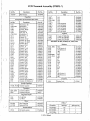
878522-*
3-21
Frequency
*Dash No.
Reference No.
169.505-171.905 MHz
-171
1
206.000-207.800 MHz
-207
2
212.000-213.800 MHz
-213
3
PCB Receive Assembly 878522-* (Continued)
RerNo.
1
C406
C4062,3
C407 1
C407 2,3
C408 1
C4082 ,3
C409, C410
C411
C412 1
C4122 ,3
C413
C414
C4i5
C416
C417
C418
C419
C420
C421
C422
C423
C424 1
C4242,3
1
C425
C425 2,3
C426 1
C4262 ,3
C427 I
C427 2,3
C428
1
C429
C4292 ,3
C430
C431 1
C431 2,3
C432 1
C4322,3
C433-C436
C437 1
C437 2,3
C438 1
C438 2 ,3
1
C439
C439 2,3
C440
C441-C442
C443
C444 1
C4442,3
C445
C446
C447
C448
C449
C450
C451
C452
C453
C454
VC301-VC307
Description
Ceramic, 20 pF
Ceramic, 24 pF
Ceramic, 20 pF
Ceramic, 24 pF
Ceramic, 330 pF
Ceramic, 270 pF
Ceramic, .01
Ceramic, 2.2 pF
Ceramic, 36 pF
Ceramic, 39 pF
Ceramic, .01
Ceramic, .1
Ceramic, 100 pF
Ceramic, .01
Electolytic, 10
Cel'amic, 1500 pF
Electrolytic, 1
Poly Film, .0022
Poly Film, .0056
Ceramic, 330 pF
Ceramic, .01
Ceramic, 39 pF
Ceramic, 43 pF
Ceramic, 270 pF
Ceramic, 330 pF
Ceramic, 62 pF
Ceramic, 68 pF
Ceramic, 43 pF
Ceramic, 50 pF
Ceramic, .82 pF
Ceramic, 30 pF
Ceramic, 33 pF
Ceramic, .82 pF
Ceramic, 39 pF
Ceramic, 43 pF
Ceramic, 270 pF
Ceramic, 330 pF
Ceramic, .01
Ceramic, 390 pF
Ceramic, 470 pF
Ceramic, 18 pF
Ceramic, 20 pf
Ceramic, 18 pF
Ceramic, 20 pf
Ceramic, 270 pF
Ceramic, .01
Ceramic, 2.2 pF
Ceramic, 30 pF
Ceramic, 33 pF
Ceramic, .01
Ceramic, .1
Ceramic, 100 pF
Ceramic, .01
Electolytic, 10
Ceramic, 1500 pF
Electrolytic, 1
Poly Film, .0022
Poly Film, .0056
Ceramic, 330 pF
Capacitor, Variable
DescrIption
RerNo.
Part No.
Part No.
Intergrated Circuits
35693048
35693060
35693048
35693060
35693024
35693076
52676107
35693000
35693078
35693014
52676107
52676113
35693019
52676107
52723008
35693032
51821106
52719053
52719068
35693024
52676107
35693014
35693070
35693076
35693024
35693071
35693017
35693070
35693049
724771
35693046
35693013
724771
35693014
35693070
35693076
35693024
52676107
35693025
35693026
35693010
35693038
35693010
35693038
35693076
52676107
35693000
35693046
35693013
52676107
52676113
35693019
52676107
52723008
35693032
51821106
52719053
52719068
35693024
723086-4
760375
53284000
53295001
760375
53295001
760375
53295001
53284000
760375
53295001
IC, NE614
IC,LM393
IC, NE 5532AN
IC, NE614
IC, NE 5532AN
IC, NE614
IC, NE 5532AN
IC,LM393
IC, NE614
IC, NE 5532AN
0301
0302
0303
U304
0305
0306
0307
0308
U309
0310
Potentiometers
VR301
VR302
VR303
VR304
VR305
VR306
VR307
VR308
VR309
5K Potentiometer
20K Potentiometer
5K Potentiometer
20K Potentiometer
5K Potentiometer
20K Potentiometer
5K Potentiometer
20K Potentiometer
50K Variable Resistor
57148068
57148071
57148068
57148071
57148068
57148071
57148068
57148071
723091-1
Colis and Inductors
L301 L302
L303 1
L303 2,3
L304 1
L3042,3
L305
L306
L307 1
L307 2,3
L308 1
L308 2,3
L309
L310 1
L3102,3
Coil, 2 1I2T, 10 nun
Coil, 1 3/4T,
Coil, 1 1I4T,
Coil, 1 3/4T,
Coil, 1 1/4T,
Coil, MC120 red wlcase
Coil, 1I4T red w/case
Coil, 1 3/4T,
Coil, 1 1I4T,
Inductor, .151lH
Inductor, .11lH
Inductor, 1 mH
Coil, MC120 blue w/case
Coil, MC120 green w/case
724778
724777
724766
724777
724766
724775
724765
724777
724766
35689041
35689045
35689035
724767
724769
Transistors
Q301
Q302, Q303
Q304
Q305
Q306
Q307
Q308
Q309
Q310
Q311
Transistor,
Transistor,
Transistor,
Transistor,
Transistor,
Transistor,
Transistor,
Transistor,
Transistor,
Transistor,
NE 25137
MPS-901
MPS-3640
MPS-3704
MPS-3640
MPS-3704
MPS-3640
MPS-3704
MPS-3640
MPS-3704
760488
760376
54734000
54712000
54734000
54712000
54734000
54712000
54734000
54712000
878522-*
3-22
Frequency
*Dash No.
Reference No.
1
169.505-171.905 MHz
-171
206.000-207.800 MHz
-207
2
212.000-213.800 MHz
-213
3
PCB Receive Assembly 878522
Ref No.
Description
Crystal Filter Insulator
Mixer, ASK-1
Crystal, Receive, 171.905 MHz
Crystal, Receive, 207.800 MHz
Crystal, Receive, 213.800 MHz
Filter, 10.7 Crystal
Filter, 11.56 MHz Crystal
Filter, 11.075 MHz Crystal
Filter, 11.56 MHz Cryst31
Filter, 11.075 MHz Crystal
Filter, 12.36 MHz Crystal
Filter, 11.7 MHz Crystal
Filter, 12.36 MHz Crystal
Filter, 11.7 MHz Crystal
Filter, 13.1 MHz Crystal
Filter, 12.5 MHz Crystal
Filter, 13.1 MHz Crystal
Filter, 12.5 MHz Crystal
Filter, SFE 10.7 MHz J red
R351
R352
R353, R354
R355
R356
R357
R358
R359
R360
R361-R363
R364
R365-R367
R368
R369
R370
R371, R372
R373
R374
R375
R376
R377
R378
R379-R381
R382
R383-R385
R386
R387-R390
450471
760382
780089-1
780089-2
780089-3
780087-0
780087-4
780087-7
780087-4
780087-7
780087-5
780087-2
780087-5
780087-2
780087-6
780087-3
780087-6
780087-3
52990001
All resistors in ohms, 1/8 Watt, 5%, unless noted.
Resistors
o
R301
R302
R303
R304
R305
R306 R307
R308 i
R3082 ,3
R309-R311
R312
R313
R314
R315
R316
R317
R318
R319
R320
R321
R322
R323
R324
R325-R327
R328
R329-R331
R332
R333
R334
R335, R336
R337
R338
R339
R340
R341
R342
R343-R345
R346
R347-R349
R350
lK
10K
130
10
lK
100
470
180
10K
22
240
4.7K
1.5K
16K
220
330
l.5K
10M, 1/4 watt
10K
22K
lOOK
220K
10K
68K
10K
4.7K
1.5K
16K
220
l.5K
10M, 1/4 watt
10K
22K
lOOK
220K
10K
68K
10K
4.7K
* (Continued)
Description
Ref No.
Part No.
Crystals and Filters
MX301
Y301'
Y301 2
Y301 3
FL301 FL302
FL303 1
FL303 2 ,3
FL304'
FL3042,3
FL305'
FL305 2 ,3
FL306'
FL3062 ,3
FL307'
FL3072 ,3
FL308'
FL308 2,3
FL309
M
52154060
52154036
52154081
52154108
52154060
52154084
52154068
52154078
52154036
52154100
52154075
52154044
52154056
52154031
52154076
52154072
52154056
52154185
52154036
52154028
52154012
52154004
52154036
52154016
52154036
52154044
52154056
52154031
52154076
52154056
52154185
52154036
52154028
52154012
52154004
52154036
52154016
52154036
52154044
Part No.
52154056
52154031
52154076
52154056
52154185
52154036
52154028
52154012
52154004
52154036
52154016
52154036
52154044
52154056
52154031
52154076
52154056
52154185
52154036
52154028
52154012
52154004
52154036
52154016
52154036
52154052
52154036
l.5K
16K
220
l.5K
10M, 1/4 watt
10K
22K
lOOK
220K
10K
68K
10K
4.7K
l.5K
16K
220
l.5K
10M, 1/4 watt
10K
22K
lOOK
220K
10K
68K
10K
2.2K
10K
Connectors
P301-P307
P308"P311
P312
P313
(Not Used)
3 Pin Header
(Not Used)
3 Pin Header
670062
670062
Transformers
1'301-1'303
1'304,1'305
1'306,1'307
1'308-1'324
Transformer
Transformer
(Not Used)
Transformer
724770
724774
724774
Diodes
D301-D304
52228000
Diode, IN4148
878522-*
3-23
Frequency
*Dash No.
Reference No.
169.505-171.905 MHz
-171
1
206.000-207.800 MHz
-207
2
212.000-213.800 MHz
-213
3
PCB Receive Assembly 878662-*
Description
Ref No.
Printed Circuit Board, Receive
Part No.
Ref No.
750309
C420
C421 1
C421 2 ,3
1
C422
2
C422 ,3
C423
C424
C425-C427
C428
C429
C430, C431
C432
C433, C434
C435
C436
C437
C438
C439
C440
C441-C469
C470
C471
C472 1
C4722 ,3
C473
C474
C475-C477
C478
C479
C480, C481
C482
C483, C484
C485
C486
C487
C488
C489
C490
VC301-VC308
Capacitors
All capacitors in microfarads unless noted.
Ref No.
C301 1
C301 2,3
C302 1
C3022 ,3
C303 1
C303 2,3
C304, C305
C306
C3071
C307 23
C308 1
C308 23
C309
C310
C311
C312
C313 1
C313 2 ,3
C314-C316
C317
C318
C319
C320
C321
C322
C323
C324
C325-C327
C328
C329
C330, C331
C332
C333, C334
C335
C336
C337
C338
C339
C340
C341-C369
C370
C371
C372
C373
C374
C375-C377
C378
C379
C380, C381
C382
C383, C384
C385
C386
C387
C388
C389
C390
C391-C419
Description
Ceramic, 5.6 pF
Ceramic, 4.7 pF
Ceramic, .82 pF
Ceramic, .5 pF
Ceramic, .5 pF
Ceramic, .33 pF
Ceramic, 100 pF
Ceramic, Z5U, .001
Ceramic, .5 pF
Ceramic, .33 pF
Ceramic, 1.2 pF
Ceramic, .33 pF
Ceramic, Z5U, .001
Ceramic, 33 pF
Ceramic, 47 pF
Ceramic, Z5U, .0047
Ceramic, .5 pF
Ceramic, .33 pF
Ceramic, Z5U, .0 I
Ceramic, 100 pF
Ceramic, .00 I
(Not Used)
Ceramic, Z5U, .01
Ceramic, 180 pF
Ceramic, 56 pF
Ceramic, 68 pF
Ceramic, 220 pF
Ceramic, Z5U,.1
Ceramic, 100 pF
Ceramic, Z5U, .0047
Ceramic, 120 pF
Ceramic, Z5U, .1
Electrolytic, 1.0
Mylar, .015
Ceramic, Z5U, .1
Mylar, .0022
Mylar, .0056
Ceramic, 330 pF
Ceramic, Z5U, .001
(Not Used)
Ceramic, Z5U, .01
Ceramic, 180 pF
Ceramic, 50 pF
Ceramic, 68 pF
Ceramic, 220 pF
Ceramic, Z5U,.1
Ceramic, 100 pF
Ceramic, Z5U, .0047
Ceramic, 120 pF
Ceramic, Z5U, .1
Electrolytic, 1.0
Mylar, .015
Ceramic, Z5U, .1
Mylar, .0022
Mylar, .0056
Ceramic, 330 pF
Ceramic, Z5U, .001
(Not Used)
Part No.
35693004
35693003
52007003
52007000
52007000
52007012
35693019
52676101
52007000
52007012
52007009
52007012
52676101
35693013
35693015
52676105
52007000
52007012
52676107
723023
102881301
52676107
35693022
35693016
35693017
35693023
52676113
35693019
52676105
35693020
52676113
52723025
52719058
52676113
52719053
52719068
35693024
52676101
Description
Ceramic, Z5U, .01
Ceramic, 150 pF
Ceramic, 180 pF
Ceramic, 43 pF
Ceramic, 50 pF
Ceramic, 68 pF
Ceramic, 220 pF
Ceramic, Z5U, .1
Ceramic, 100 pF
Ceramic, Z5U, .0047
Ceramic, 120 pF
Ceramic, Z5U,.1
Electrolytic, 1.0
Mylar, .015
Ceramic, Z5U, .1
Mylar, .0022
Mylar, .0056
Ceramic, 330 pF
Ceramic, Z5U, .001
(Not Used)
Ceramic, Z5U, .01
Ceramic, 150 pF
Ceramic, 39 pF
Ceramic, 43 pF
Ceramic, 68 pF
Ceramic, 220 pF
Ceramic, Z5U, .1
Ceramic, 100 pF
Ceramic, Z5U, .0047
Ceramic, 120 pF
Ceramic, Z5U, .1
Electrolytic, 1.0
Mylar, .015
Ceramic, Z5U, .1
Mylar, .0022
Mylar, .0056
Ceramic, 330 pF
Ceramic, Z5U, .00 I
Capacitor, Trinuner
Part No.
52676107
35693021
35693022
35693070
35693049
35693017
35693023
52676113
35693019
52676105
35693020
52676113
52723025
52719058
52676113
52719053
52719068
35693024
52676101
52676107
35693021
35693014
35693070
35693017
35693023
52676113
35693019
52676105
35693020
526761 i3
52723025
52719058
52676113
52719053
52719068
35693024
52676101
723086-4
Intergrated Circuits
U320
U321
lJ370
U371
lJ420
U421
1I470
U471
52676107
35693022
35693049
35693017
35693023
52676113
35693019
52676105
35693020
52676113
52723025
52719058
52676113
52719053
52719068
35693024
52676101
IC, MC3359 MOT
IC, NE5532
IC, MC3359 MOT
IC, NE 5532
IC, MC3359 MOT
IC, NE 5532
IC, MC3359 MOT
IC, NE 5532
760494
53295001
760494
53295001
760494
53295001
760494
53295001
878662-*
Frequency
3-24
*Dash No.
Reference No.
171 MHz
-171
I
207 MHz
-207
2
213 MHz
-213
3
PCB Receive Assembly 878662-* (Continued)
Ref No.
Description
Part No.
Ref No.
Crystals and Filters
Potentiometers
VR320
VR321
VR370
VR371
VR420
VR421
VR470
VR321
20K Potentiometer
50K Potentiometer
20K Potentiometer
50K Potentiometer
20K potentiometer
50K Potentiometer
20K Potentiometer
50K Potentiometer
Crystal Filter Insulator
Crystal Insulator
Mixer, ASKI
HY301
Crystal, Receive, 171.905 MHz
Y301 1
Crystal, Receive, 207.8 MHz
Y301 2
Crystal, Receive, 213.8 MHz
Y301 3
Crystal, Receive, 10.245 MHz
Y320
Crystal, Receive, 12.015 MHz
Y370 1
Y3702 •3
Crystal, Receive, 11.53 MHz
Crystal, Receive, 12.815 MHz
Y420 1
Y4202•3
Crystal, Receive, 12.155 MHz
Crystal, Receive, 12.555 MHz
Y470 1
Y4702•3
Crystal, Receive, 12.955 MHz
CF320, CF32 1 Filter, 10.7 Crystal
Filter, 455 kHz Ceramic
CF322
Filter, 11.56 MHz Crystal
CF370 1
CF3702•3
Filter, 11.075 MHz Crystal
Filter, 11.56 MHz Crystal
CF371 1
CF371 2•3
Filter, 11.075 MHz Crystal
Filter, 455 kHz Ceramic
CF372
Filter, 12.36 MHz Crystal
CF420 1
CF4202,3
Filter, 11.7 MHz Crystal
Filter, 12.36 MHz Crystal
CF421 1
CF421 2,3
Filter, 11.7 MHz Crystal
Filter, 455 kHz Ceramic
CF422
Filter, 13.1 MHz Crystal
CF470 1
CF4702•3
Filter, 12.5 MHz Crystal
Filter, 13.1 MHz Crystal
CF471 1
CF471 2•3
Filter, 12.5 MHz Crystal
Filter, 4%% kHz, Ceramic
CF472
57148071
57148072
57148071
57148072
57148071
57148072
57148071
57148072
Colls and Chokes
l)
L301,L302
L303,L304
L305
L306
L307 1
L307 2
L307 3
L308 1
L3082•3
L309
L310
L311, L312
L313
L314-L319
L320
L321
L322
L323
L324-L369
L370
L371
L372
L373
L374-L419
L420
L421
L422
L423
L424-L469
L470
L471
L472
L473
FB321
FB371
FB421
Coil, 2 1I2T, 10 mm .
Coil, 2 1/2 CT, 10 mm
Coil, 2 1I2T, 10 mm
Coil,2 1I4T, 114 Tap, 10 mm
Coil, TOKO, Red
Coil, TOKO, Brown
Coil, TOKO, Black
Inductor, .22/!H
Incuctor, .15 /!H
Coil, 2 112 CT 10 mm
Inductor, 56 /!H
Inductor, 10 /!H
Coil, 2 1I4T, 114 Tap, 10 mm
(Not Used)
Inductor, 10 /!H
Inductor, 3.95 /!H
Coil, 455 kHz, discriminator
Coil, IF, 10.7 MHz
(Not Used)
Inductor, 10 /!H
Inductor, 3.95 /!H
Coil, 455 kHz, discriminator
Coil, IF, 10.7 MHz
(Not Used)
Inductor, 10 /!H
Inductor, 3.95 /!H
Coil, 455 kHz, discriminator
Coil, IF, 10.7 MHz
(Not Used)
Inductor, 10 /!H
Inductor, 3.95 /!H
Coil, 455 kHz, discriminator
Coil, IF, 10.7 MHz
Ferrite Bead
Ferrite Bead
Ferrite Bead
724778
724766
724775
724765
723403-3
723403-2
723403-1
35689047
35689041
724766
35689020
35689011
724765
35689011
724774
52982000
53029000
35689011
724774
52982000
53029000
GAASFET, NE 25139
Transitor, MPS901
JFET, J309
Transistor, MPSH 10
Transistor, MPS3704
Transistor, MPSH10
Transistor, MPS3704
Transistor, MPSHIO
Transistor, MPS3704
Transistor, MPSH 10
Transistor, MPS3704
450471
450474
760382
780092-1
780092-2
780092-3
780088
780088-6
780088-3
780088-7
780088-4
780088-8
780088-5
780087-0
723088
780087-4
780087-7
780087-4
780087-7
723088
780087-5
780087-2
780087-5
780087-2
723088
780087-6
780087-3
780087-6
780087-3
620088
All resistors in ohms, lIS Watt, 5%, unless noted.
Resistors
R301
R302
R303
R304
R305
R306
R307
R308, R309
R310
R311, R312
R313
R314
R315
R316-R319
R320
R321
R322
R323
R324
R325
R326
35689011
724774
52982000
53029000
35689011
724774
52982000
53029000
56632007
56632007
56632007
Transistors
Q301
Q302
Q303
Q320
Q321, Q322
Q370
Q371, Q372
Q420
Q421, Q422
Q470
Q471,Q472
Part No.
Description
760392
760376
54722000
54736000
54712000
54736000
54712000
54736000
54712000
54736000
54712000
52154060
52154036
52154096
52154108
52154060
52154301
52154048
52154036
52154084
52154068
52154036
52154052
52154020
lK
10K
33
10
lK
150
3.3K
10K
100
470
10K
2.2K
47K
(Not Used)
52154058
52154076
52154016
52154056
52154060
52154000
52154004
I.2K
220
68K
l.5K
lK
330K
220K
878662-*
3-25
Frequency
*Dash No.
Reference No.
171 MHz
-171
1
207 MHz
-207
2
213 MHz
-213
3
PCB Receive Assembly 878662-* (Continued)
Resistors (Continued)
Ref No.
R327
R328
R329, R330
R331
R332-R334
R335-R369
R370
R371
R372
R373
R374
R375
R376
R377
R378
R379, R380
R381
R382-R384
R385-R419
R420
R421
R422
R423
R424
R425
R426
Description
lOOK
13K
220K
100
10K
Part No.
Ref No.
52154012
52154033
52154004
52154084
52154036
R427
R428
R429, R430
R431
R432-R434
R435-R469
R470
R471
R472
R473
R474
R475
R476
R477
R478
R479, R480
R481
R482-R484
(Not Used)
52154058
52154076
52154016
52154056
52154060
52154000
52154004
52154012
52154033
52154004
52154084
52154036
1.2K
220
68K
l.5K
1K
330K
220K
lOOK
13K
220K
100
10K
Description
lOOK
13K
220K
100
10K
52154012
52154033
52154004
52154084
52154036
(Not Used)
1.2K
220
68K
l.5K
1K
330K
220K
lOOK
13K
220K
100
10K
(Not Used)
1.2K
220
68K
1.5K
IK
330K
220K
Part No.
52154058
52154076
52154016
52154056
52154060
52154000
52154004
52154012
52154033
52154004
52154084
52154036
Connectors
52154058
52154076
52154016
52154056
52154060
52154000
52154004
P301
P320
P370
P420
P470
3-26
3 Pin
3 Pin
3 Pin
3 Pin
3 Pin
Header
Header
Header
Header
Header
670062
670062
670062
670062
670062
AUDIO BOARD
(\
\
)
AUDIO BOARD CIRCUIT
DESCRIPTION
The audio board receives signals from the receive
board, the headset microphone, intercom input and
,auxiliary input, and outputs to the transmit board,
the headset earpiece, an external speaker, intercom
out and auxiliary out (see block diagram).
Receive Expanders
Audio from the receive board is routed through
Jl08, Jl09, JllO and Jlll to U1l2 and U1l3. The
gain ofthese devices is controlled by the audio level
at the rectifier pins .(4 and' 16). As the level increases, so does the gain, and this results in a 2: 1
linear expander characteristic. This complements
the processing done in the transmitter. The audio
is then buffered and delivered to the remote select
switches.
C)
Microphone Amplifier
From the headset connector the microphone signal
is amplified by U103. Depending upon which type
of microphone is used, S102 is set by the user to
dynamic or electret. The electret position provides
an 11 dB drop in gain to compensate for the extra
output. The amplifier is peak limiting, and
responds to either positive or negative peaks exceeding about 1.1 volts in amplitude. Peak detectors Q106 and Q107 charge C120 and C121,
driving QI05 toward pinchoff. This reduces the
gain momentarily until the input signal is reduced.
Visual indication of peak limiting is provided by
D608 which is driven by U105 when the voltage at
pin 6 exceeds half a volt. D111 (version 3 and later)
/isolates the time constant of the amplifier from'that
of the LED driver. The latter is much shorter than
the former, and causes the LED to extinguish immediately upon removing the input signal. On
versions 1 and 2 the LED will remain lit for several
seconds. VR604 is adjusted by the user for maximum input with minimal limiting. QI04 is used to
tum the microphone on and off and is driven by the
push-to-talk latch circuit. When SIlO is pressed in
and held, the state of Ul16B follows the switch and
tums on Q110 and Q111 via D110. This lights
D609 and gates on the microphone audio. Releasing S110 tums off the microphone.
U116A does not change state under these conditions because C~82 is discharged when the clock is
pulsed. If, however, S110 is depressed twice in
quick succession, C 182 will be charged for the
second clock pulse and this will set U116A. Now
the microphone is latched on via D109 and will
remain on until S110 is depressed once again,
resetting U 116A.
Auxiliary Input Amplifier
Audio from JlOl is attenuated and converted from
balanced to single-ended by U101A. U101B,
UI02A, Q101, QI02 and QI03 form a peak limiting amplifier identical to that described for the
microphone above. S101 not only enables the
audio path for the auxiliary input but also lights
D607 to half-brilliance to indicate active auxiliary.
When peak limiting occurs U 105A shorts out R 120
and D607 is brought to full brilliance.
Intercom Driver
UI07A is configured as an AC current source
whose output CUlTent equals the input voltage at
C125 divided by the value of R158. Thus the
voltage gain is dependent on the value of the load.
In this way many such intercom stations can be
connected in parallel without each successive station loading the line. A single load resistor is
usually located in the power supply for the wired
intercom. On versions 3 and later, U I07B is used
to drive the lower end ofTIOl. This section is not
a current source and was added to provide more
headroom. To this end, U107 is operated from the
higher voltage ahead of the regulator. S 104 is a 9
section DIP switch which is used to configure the
base for compatability with a specific wired intercom. S103 functions as either an intercom onloff
switch.(Telex, Clearcom standard) or as a channel
AlB switch (RTS, Clem'com TW). In the case
where the intercom interface is disconnected by
S 103, R 186 functions as the load resistor. The full
secondary ofTlOl is used for 300 ohm intercoms;
the tap is used for 200 ohm systems. On version 2
and later, S 112 allows selection of either low output
(100 mY) or high output (800 mY).
3-27
Intercom Input
Since U 107A is a current source, signals arriving
from an external intercom appear unloaded at pin
1 and are coupled via C126 and R154 to U106. To
prevent intercom output signals from appearing at
the output of U106, these signals are nulled by the
branch containing C124, VRlOl and R152.
U 106A and U 109 form a peak limiting am plifier
similiar to that described for the microphone
amplifier above, except that CA10l is used instead
of a JFET to control the gain. The reason for this
is that the higher level signals being handled by
U 106A would cause high distortion if a JFET were
used. CA10l is merely an LDR (light dependent
resistor) together with an LED in the same package.
More current through the LED reduces the value of
resistance.
Headset and Speaker Amplifiers
U 111 and Ul19B (U107B in versions 1 and 2) drive
the headset while U108 drives the external speaker
jack. On versions 1 and 2 this signal was derived
by mixing the microphone signal with the intercom
output, via R175 and R177. On later versions the
intercom output alone is used, being first amplified
by U119A. S112B maintains the headset/speaker
level constant when switching intercom output
levels.
Auxiliary Output
UllOA mixes together intercom input,
microphone, and receive board signals. U11 OB
inverts the resultant to provide a balanced output.
Remote Transmit Circuit
When the transmit switch on the rear panel is in the
remote position, the transmitter will only operate
when at least one receive squelch is open. On
versions 1 through 4 this is done with Ul15 which
turns on Q109. Versions 3 and 4 have a circuit
board error, however, which prevents this option
from working. To correct this move the inputs of
Ul15 to the left side (on the schematic) of R195,
R198, R20l, and R204. The version 3 and 4
schematics show these inputs as they are unmodified, that is, connected to the right side of the
resistors. On versions 5 and above, U 115 is
replaced with Ql12, Ql13, Ql14 and Ql15 and no
modifications are necessary.
Power Supply
Q 108 and U114 form a 10 volt regulated power
supply. On versions 1 and 2, ZD101 is used as the
5 volt reference while on later versions this comes
from U 117. U 112 and U 113 are also supplied by
U1l7.
Transmit Mixer and Filter
U 106B mixes the intercom input, auxiliary input,
microphone and receive board signals together to
modulate the transmitter. VR102 is used to set the
level going into the transmit compressor for proper
tracking. On versions 3 and later, U118 acts as a
four pole Chebyshev low pass filter with a cutoff
frequency of 5 KHz. This is to prevent transmission of the 20 KHz tone which Telex intercoms use
as the call signal.
3-28
8. Connect the signal generator to the Receive
Antenna jack. Set the deviation to ± 3 KHz at
1 KHz. Set the output to 1 mV. Set the frequency to the channel 1 frequency listed in the chart
of the receive board alignment.
ALIGNMENT PROCEDURE:
)
Equipment Required:
D
D
D
D
Signal Generator
Audio Generator
Deviation Meter
Audio Voltmeter
-
I
9. Select the channel 1 pushbutton on the front
panel.
1. Connect the audio generator to the AUX IN
jack and set the output to 20 mV at 1 KHz.
10. Connect the deviation meter to the ANT
TRANS jack.
2. Select the AUX pushbutton on therront panel.
11. Connect the audio voltmeter to U106 pin 7.
3. Adjust VR601 (located just under the I1C push-
12A. On version 1 and 2 audio boards, adjust VR102
for 300 mV of audio.
button on the front panel) to maximum
counterclockwise.
4. If the base is configured for an RTS intercom
connect the load to the llC jack pn the rear
panel.
5. Connect the audio voltmeter to the AUX OUT
jack on the rear panel.
0
6. Adjust VR101 for a minimum reading.
7. Disconnect the generator and meter from the
12B. On version 3 and later audio boards with version 1 transmit boards, adjust VR102 for 1 volt
of audio.
12C. On version 3 and later audio boards with version 2 transmit boards, first move the audio
voltmeter to U501 pin 16 (on the transmit
board). Then adjust VR102 for 140 mV of
audio.
13. Adjust VR501 for ± 4.2 KHz deviation.
AUX jacks and de-select the AUX pushbutton
on the front panel.
3-29/3-30 Blank
RECEIVER 1
RECEIVER 2
-1
-1
EXPANDER
EXPANDER
__---------,
I--"~
>--+
__--""
AUXOUT
INTERCOM GAIN
I---"~
~
TRANSMIT OUT
BALANCE
RECEIVER 3
o
-1
EXPANDER
__
I---"~
HIGH/LOW
RS
------+I
(ON VERSION 2 ONLy)
RECEIVER 4
-1
EXPANDER
DYNAMIC/
ELECTRET
HEADSET _~~ ....
I.4ICROPHONE
....
INTERCOM
__
IC---....~
-.J
T
MIC GAIN
~
>---\-------11> SPEAKER
T
AUXIN
Figure 19
Block Diagram Versions 1 and 2
3-31
RECEIVER 1
RECEIVER 2
---1
---1
EXPANDER
. --------
I--"~
AUX OUT
INTERCOM GAIN
EXPANDER
~
I
TRANSMIT OUT
BALANCE
RECENER 3
---1
HIGH/LOW
EXPANDER
I
RS
~_------toI
INTERCOM
RECEIVER 4
---1
EXPANDER
I--"'~--"'/
DYNAMIC/
ELECTRET
HEADSET
HEADSET
MICROPHONE
AUX GAIN
- - - - - - - - -...
~ SPEAKER
~
AUX IN
Figure 20
Block Diagram Versions 3 thru 6
3-32
1')
,.........e...,S102
L--J
S111
Jl01
Rl22
<>
Jl04
~ li1aaaal
0109
0
J10S
C18
~
""""""
<:)
C1S8
Ul11~
~
aooo
R192
C150+
:0
C1SS
o
o
Cl53
O
....
Rl88
C188
o
0
o
:
0+
0
C1800"':
.0 C173
a
T
o
o
0
0u
0
n
0
U112
Cl63
R197 O
C17~
o
C164
0
r'Yt" :
OR194
V
0C171
o
o
1
q 0
(aanaaaaaaal
C144 C145
Ul08
0
101
FIGURE
25
DETAIL
C143
SEE
FIGURE 25
C142
c:::J
C148 Cl48
:(J
*l)
..
am
0
: CiS
0
C128
I
II
I
o
R178
<>
OCl30
R;l.§Z.:;
I
~ ~33
L
Cll80 :;
1101
~I
VI
~3)u L~~l
SlO9
a~W70
g
<:>
o
·0
o
0
o
0
0
o
o
o
o
III
r-)+
~ 'i:r'
0
0
"'0
C149
o
06
'"
~o: ~
~O Ego
i-
OR124
Rl12
a
a
D
a
a
Rl~63
+0
C131
...
~~
o
R162
<:>
0
00
o!+1~119
I,
Ul10
0'" o
0 a
ll:
o
R141
-c:>R221
-c:>-c:>-
OR136
O~O Rl~
o
0
0
Sl04
0
a
r'\R220
mrt
OC+1l7
R219
:
<:>
:JI:
U
D
0
~
?r\
1L6-
0
i 1l0~
0:
D
Rl~:
R201 Pl03
R~0109
0
l.:!~
0108
U~118:
0 0 ~ ~ ~
b
C18300
-c:>- 0
0
RIM
J112
~!:! I
R216
C182
+
C184
<:>
0
C1370
~o OR217
-¢>
D
R2040
Rl90
<:>
0
0
R211
0
R212
: :
0
<:>
<:>
0
0
°
0
aU109
Rl111
<:>
Cl540
+
R128
C178
0
0
0
(jRl02
~
R129
~O sO~O
o
UllS
C18S/l0:3 0
Rl88Y iC
a;: aooo
0
o
o
-c:>-
"'O~Ul04
..
L-.....J
o
o
~~R167 0
0000
C174
0000
C1180
o
OR222
Pl02
<> CllS \.AJ
b O~ bO~. .o
C172
~
-c:>-
0
O:! 0
0
dJC123
g18 Ql04
R1340
R1530
R151
:
lilCii-C:>-
R12S
<:>
~O
~.
Q10SV
_0 00QU106
'"
0
R17.
'"
flRlos
C121
0~
R1S0
-c:>-
Figure 21
S'd )
A dio Board Component Layout (Component I e
u
Versions 1 and 2
3-33
Cl20
~
<>
0 :; : ; : oooa
«
0000
oa~o
1111:0
I
R121
<:>
. . SCJ
Cl40
<:>
II~_
o
JIll
<>
Rm
0
0I
Q]
CA101
;
R1180
R1711
U
R1060
C1l4
aoo o!Q"0
()
R1S8
"'c::J
G
a
0 U113
0
O C167
R200
R203
J110
DETAIL B............. ~---~---l
OORl82
o ...C17S
+ = c::J
R1S9
<>Rl54
U107:r
1£1~ £!:!J .... :!
RIse
o
:8
R119
0
0
1.
Rl07 D
R18S
: ...
0
R172
OR10l
Cl03
Rl04
Ql03
Rl48 00 R147
0 Co
~
Jl09
C126 ~ R1S2
'Kg'10 ~:
A~V
0
R1840 s O O O Q 1 8 1
o
;
VAl01
SEE
0
Cl77 0
'"
H114 0102
Ul0S .
C108
R1060
CD
Rl17 ( ]
0
0
<:>
<:>
0
0
R137
~ ~ +0 0+
0
0
a
13
L101 CISI
6 ~C~
(] FfrrS i
Cl0S~OO0cJ"O~u
::D~O(]O~
C181
+
Cl02
ov·",!:!o 6
00
0
V
C1S9
00
0
0(\
<D+~
~
i'"
~O
0
<>0
;;t
C101
07
§~
(\
~
:+0 0
... u
Ul0l 0 Rl030
0
<:>
0 0
Rl99 liDo
C1520+
Qf{
~
0
Cl11
P114
0000
o
C'l
0::
R17S
0
o
00 cm
Cl22+
O
0
R133
R20S
0
<:>
o
C178
S110
o
o
o
Figure 22
Audio Board Component Layout (Foil Side)
Versions 1 and 2
3-34
i
I
R'69
10K
R170
C)
'OK
~r68
68K
i
U110:A
......NE5532
e150
·10UF
R171
330
[5
.~
R,'6: :
8 10K
I~R17J
•
-
C151
R174
330
7
AUX OUT
•
l~UF
REMOTE
T
~~110:B
Orf
NE55J2
R163
10K
R162
2.2K
PORTABLE 3
SELECT
e175
C176
tOUF 5107
lour
3
lR~~~
R161
3DK
R132
6SK
.-
5111
*-
CONT
TRANSMIT
AUDIO LEVEL
~~
...... I.Y
,'I
,
Ul~:O
-R202T •
NE55J2
1OOK1'OOKl
""f
Y
U109:8
J113
r
R'BS
3,6K
LM,;'92j·.,., •
I
R1~
R190
4,OK
10K
--<
RECEIVE
BOARD
r- D60;J
:
R'BS
lOOK
I--<
J
.gJ:~F L _
~: INTERCOM
IOV£RLOAD
_ -l INDICATOR
NOTE: COMPONENTS IN DASH
BORDER AREAS ARE LOCATED ON
THE DISPLAY BOARD.
:-f. ~:
I
;.-0'
I
L _ _ .J
Example
el03
.0022UF
0110
lN4148
r.-r
~~R-2~'2-----'8 ~~~g:B
S110
11'OOK 9
TAlK
~
..
S
0
Q
C
a
13
1')
~D!,0~8
.,r
~01J
, r-:l
:~'~: :i ' ~~C
JOOK
..
lOOK
. It
c,'~iI
...
R214
470K
R220
5.1K
~
7
='
C184-
H'~
R216
10K
SPEAKER
Q110
0111
IdPSJ704
MPS3704
...
R219
l.OK
R217
10K
...
- D6091
I
I
I
I
I -
~
I
TALK:
L"'::__ .JI
3-35
HEADSET
R216
:
R213 -:::"
lN
r-_ ___j-----1T~TI---v'VDKIr1'__j
R211
10K
gQ'f~'+--1~-+-"".I'--!I--~
D S
lo--------l<I
LY-
R221
Dl09
lN4146
C'3.
Figure 23
Schematic Diagram Audio Board
Version 1
,urI
...
R'88
B.OK
C152
IUr
•
R189
68K
I~15jr
+ '7
t
r
U"':A"
PORTABLE
3.•K
t Rl~5J7
1-
l
06051
~:
I
~~;~
lU'I
u~~~~~
;~~'
'- __ J
P~2
II
I
~4002
NE575
0
3.•K
J
R201
1K
ORTABLE J
1-
I
~
V
5
10
J..
Y
C166 +
06031
lu'I
~I
~~1;:;T
I I
I
I
Jll0~
'~,~'
IlH
1
~LV
MIC
.6K
>-j!.
N;~2
R12J
C113_Jo
100PFI
2.2K
~,C116
47PF
MlQ..GAltt
R150
lK
PORTABLE 4
I"
U113:0
~ "1~::~~:.r'0u'
IvRPQ~'
Cl17
R151
lK
5BO
~ ~\~~
R101
R140
Rl41
1M
10K
I
~~1~3
Q °
Rl03
RI05
0107
2.2UI'"
82K
2.2K
R1J9
AUX GAIN
'1"lP'/¥"
__
R1D6
10K
1'°1~F
~"'-
R12.
82K
100PF
1
+
4
nr-
,,31/91/'K- t - H :
C115"
:
B
NE5532
fl238
: 1K
'
~1
R23.
!.. .~~.~!
__
r
'-1 "',2'-9-'0-0-P,'
C132
1UF
It
R187
47K
rJ!~
+
I
C185
10UF
'} ~
R16 '
1M
'="
I
I
R159
C127l='=~
1DOPF
+
•
~
~~g~ ~
"
II
R156
150K
+C128
1U
'
I·
~;3~:~
~
_I_.J~V'.\V'~2-I+<~iLl"-::-U,;~~2
,
"7
T
!
~1~8
r
T101
r---'
R17B
1M
~UF
C108 +
R;15
L _ _ .J
IV'
S~4:2
S.!24:4
5'2"3 [
522"5
-(r"
I-(r"
Ip-~·o-
5~
-........
....
1
R117
15K
1/
~-\
0808
~
I
R116
22K
L_ M~_
~ ~J~9
101<
='
,
1,C157
5104:1
1
-
I·001UF
7
7
0607 1
~
LM39J
I
R,2 0 6 r. . '
70
A~~i
OVERLOAD
INDICATORS
J!
J;C161
I
C141
470UFI
T
VR103
-J+--"~OOK
C144
+-
EXTERNAL
SPfAI<ER
VOLUME
4.31<
T
:$.
l~
_
.1UF
R181
51
A
1
~+-""""'"
U106
6
LM2895 T
R121~
10K f NE~53r-: Is
R221
10K
C114~
10UF
I
T
R124
13K
---:-1:~
rv-
r--1 \!R60J
I lOOK
I
L_ _ _
3
I C137
_I 220PFI
T
-
?:~ 220U,
"f
"f
C13B
lU'I
I
TAU<:
T
,lR162
1
+ C14B
Z~01~
l'W'
C142
470UF
r-
I'70U'
---I
I
DBOl I
I
~
I
~~E~.1
I
Ul11
C140 I rl>-.-I!!-, Rl.3
Pl,.
!.. ?UF 311 13;".J 1 lLII,,'°;e-_-<
" J~ 5J R"',".!'2--'--<
r
2~
I
~~:
C152
~
+
I
1~~~64 1~~gg4
L-------.-1,C~,7B7,------J
7
I
'1
~
r·01~
R222
lK
h ,
I J!C156
~
1~'20.
~~CJ4119
1UF
I
LM35B
n
1N4733
SPfAI<ER
181<
R179
'OOK
!!
I' 0.0.1
C13.1
220PF!
~
't ·"'1
510.
---.....--.--,--<1'
~_L..;l...LI:: ;;.:rU;;-l1t'~--j'lt--!-----J
R209
16.9K
POWER
'~N:~'
1~::' lAm. -+=Vcif~, ~
.1UF
01O~¥'~1
~C180 ' r~C179
TlPJO
R207 I .1UF
2200UF
8
+~J106
R183
T+--'\i¥-----l
R180
22K
L"': __ -II
10ur
6~~glj~
T
~+IF-~>:cU~7' _ __J
R219
1.SK
~
1
R17B
1Mot r-.
EXTERNAL
JJOPF
~C14B
-I C136
1 .1~F
R206
16.2K
~ C143
01 47
R184
200
HEADSET
SPEAKER
VOLUME
'u ,
T
1-----1f-"
1
0110
1N41'!9
Q111
MPSJ704
'U,
F101
I ' Cl04
r"N'--.------___.--,
'T
R220
5.1K
~~L1~
~""
..J:.
+ C193
U105:8
-!
7
--..
C;45T
100UQ
I
C203
,
10url "",,1M
i
"ci\u,
--'I
...-
'~i~~M
MP~~~2. ~ LM3.3
P-G)'>U--',L05-:A-~ R120
R14a ~
T
Example
CC1
1,I
,,6 : 11~
S~~OO~
5~4:7
~~~~
+
MP~~~2
R217
10K
_I
-I
I
5104:9
:,7~1~,~~~-HI---I--r--+-_------jf-_---J1
~
~
47K
r-t-I
'1
+ =,">--'4
R113
22K
~Ql0l I ~~~~
Jl77
Rll~ll #,Cl0.
LM3.2
R187
6.8K
_
I
.o;~~J
lBOK
1
R109
4.71.4
NOTE: COMPONENTS IN DASH
BORDER AREAS ARE LOCATED ON
THE DISPLAY BOARD.
U109:A
lOU'
.~~~4
"
C130
100PF
•
C1JJ
~~~B
U107:A
NE5532
i INTERCOM
,.. 1 OVERLOAD
_ -I INDICATOR
--LI:V"1>-"--
+
R191
C154 I
620
10UF T _
"f
R155
Lj~_~'50K
C125:
1UF:
,
0102
lN4146
,
l~~~;Bt
NE5532
VR101
il......:~.~.
\ ~~~ ~EVEL
~.~j~~\
-
R126
---.5.J,,-";
~ ~:8
I ~!~7
:~~
I
~I r---.
INTERCOM:
OUTPUT
C1J1
lUF
'"
C191 1
.D01UF L_
~--~~~1A~U!:~:~LE!:~--~-R-,.-7--.-~~==~=~==~----------~.~m~1--:;~~~7---~-~7,~~:~~~'
~~~3
I-;;y,{15K
C106
.01UF
R160
10K
r- o;~
I
I
R165
100K
GAlN
100~:
':~~' ~~f$
;lANCE
MPSJ702~
1-'[001-1
~
C135
4
+......;;·2;,;..'
R175
- j_ _+-_
Rl06
3.9K
I-VA"''''';:-. .,
r
R190
'OK
4,OK
3.•K
~:;,
100
Cl05
.,.
lUF
/
1
Rl'i:----- --- --
101:A' ' : 8">NE-'5,'-5-3.2.
Rl07
NE'::5>53...:2.4.i·,I.~uf·'_"VIr---J_.z._P"'_
~~Jg;5'2
, ..
l l ! I ' C121
47K
T 1UF
+
BOARD
RECEIVE
BOARD
R1B5
3.61<
R1,~
INTERCOM
r::- L__ J
?
R13~
0105
J177
~---'-0-~~rt,~7~lM---~-
tESS3
10K
~1~6 ~1~5:~.~~~3
)..;-\v-r
J177
MPS~7~2
2.~~, B2K 1 Rl0'
~-1-W-"-'M~'2KUlO',B
Cl;;'
4
_
R125
t--'W'---t
C122
T
010'
22K
R'2B
3.9K
U103,B
A
~
II
:
R152
3K
I
'-..:.:/
R153 v.-;O~
+ - 1 - + - - - - \ - - - - - - - \ - - - " -'j'+/1
Ul06:A
4.7M
~
~
( \\
'OK
C1SB R223
.01BUF 2'0
"f
"'f
.fJ~.:~
22UF:~ 1~lQQ!S...J
~C'-\1i"lB'lI".0'"'U~r.VY'..,R137
C103
.OO22Ur
L----4
R133
BBK
1OOK1'OOK
R142
C120
~~~:
+
0177 SELECT e178
n~575
TRANSMIT
J113
Y
CAl01
101<
R1J5
J112
~
lOOK
"7
1
TRANSMIT
AUDIO lEVEL
U1'66:8
NE5532
T
B
_2J:".:::
5111
orr ~
CONT
~~~3 'rdk3i
R202
lOOK
REMOTE
T
-j~
_ _-'L.j,,//>-7L~
1--------------------_1_-1-1--<
+-1-
5107r'°I'U'_6'vBvK'-_4
IR200
Ul0J:A
1~~811
I
'"
R132
R144
10K
?
C176
I
R134
C101
C175
lR~F
,---------------"IV'--I,-~~-.\.\-~~11-T
,"'1\,,_,,-+IB-N,.,(h,
.'1
SELECT
~
R174
330
7
AUX OUT
C151 7"
U110:B
NE55J2
'i
T
Cll2 ..,..
t100PF
+5102 0
rlL-Jvv'-----.l
PORTABLE 3
U113:8
0169
+ l00UF
~
~. I
HE'AO~.~'22
iN' l.,-.;
-
+
0167
100PF
~~U'
II'
BBK
R162
9.1K
C170 +
lU'I
'- __ J
!~
'
I~R173
o 10K
R131
lOUr
••
1OOKl'OOK
NE575
A~l[) I1..1
:- ~~
P114
lR7.~Rl
rwV
,.
3.•Kr L,
R2D4
lK
I
I
l~UF Sl~
/£575• .,
'i
L-,"-J
ORTABLE .+
G173 SELECT 0174
I
C162IT::E0K
>-------t_------I---~
I..
10K
I
3
on
r
2
.. ~ I ~ 'I
. .~IH
~,
>-----.>--------I+--------+--...iIl
AUJ~~~
U112:0
1..1
I
I
!_LJ
:
I"
~
'i
6BK
0150
R171
330
-"
Q
R168
10K
I
C161¢;;OK
Ul10:A
"NESS32
?
PORTABLE 2
10K
lU'I
U11J:A -
R170
10K
1,RJ;~~~~f
~
U115:A
R130
0172
S~ 10I'U'_'v6B'vK,-_~
lOU'
C166 +
j- fb6b4]
R169
10K
SELECT
I~75.
Y
3.•Kr L,
Rl.B
lK
II
PORTABLE 1
0111
U112'8
L-,"-J
ORTABLE 2+
Jll1
T
A~4S
>--------~-----+_-t_--'_lIlH
Jl0B~
I
I
C160~OK
I
i'
I
~ 1~JgJ'
C'6':
~ 0~~:"702
'OK
,:...J
~>-----------------\-----.
..jIH
10QPF
I.,
I~
~V
'o,VF
Jl09
1,C'63
1°
NE575
9!~~~OK
.. 0
HEADSET
SPfAI<ER
10
16153100PF
"
~~9
IC155
+ T 4.7UF
:+
Figure 24
Schematic Diagram Audio Board
Version 2
3-36
NOTE: VERSION 1 DOES NOT HAVE THE SWITCH BOARD
ASSEMBLY. C124 AND C125 WILL BE LOCATED ON THE
AUDIO BOARD RATHER THAN ON THE SWITCH BOARD.
'
·@5
1
~@o
----.lI~-.=Joqa
'~.C_
It)
Riv.A
Figure 25
Details of Board Differences Between Versions 1 and 2
3-37
QC117
e+
aad
Q105"-../
R185
o
oc::::Jo
a
a
R134D
o
0
DR222
0
o
e
C136
0
0
0
0
0
0
0
0
0
0
0
0
0
a
a
a
a
NOTE: THIS AREA OF THE
BOARD WILL LOOK LIKE
THIS ON VERSION 3 AND 4
BOARD ONLY. VERSIONS 5
AND 6 WILL REFLECT WHAT
IS SHOWN ON FIGURE 27.
D
D
D
a
a
a
P103
U115
Detail A
C144
C141
C145
U108(;)(;)
laaaa aaa aaaa 0
070'\0
R184~~~~l8
o
R181
0-1
d)(;) R182
CD)
C148 C146
1-0
C142
NOTE: THIS AREA OF THE
BOARD WILL LOOK LIKE
THIS ON VERSIONS 3, 4, AND
5 BOARD ONLY. VERSIONS 6
WILL REFLECT WHAT IS
SHOWN ON FIGURE 27.
o
Detail B
Figure 26
Details of Board Difference in Versions 3, 4, 5, and 6
3-38
U117
R2ll9
R2Il8
[]
01llS""""'"
Dl117
'---J
1117
R:l112
0
~&
E'
2:i'Q.. ''''. . gggg '"''
c::::J
'"
.... '"
~ ~ ~..
a
Q
o
0109~
Jl00
C157 Cl:l8
<II
~
c a
o
C1M+
~
Cl 85
+
~+'Cl1eeu &!
IlIIl
'3.~'::
~1I0,-~.r
c:.F"
c::::I
R1211
C1M
~
C162
CJ.Z!
u·
+~ D~
C171
Cf03 U112
~Om
Rl19
Pg;
!l
c:::J
+B
5
~
5
CrG7 113
D~
R1M
c:::::J
18
Cl119
~Q
o
D
Jl111
J Ill
0Ill:
R2ll1
C2ll0+
Cl14
RllSO
..
O
~,+
0....
A 5CJ
~
!!1!l
'-c!'1111
Rl10
c=J
~
Cln
SlllS
"0
::J
Ill:
!~
r--;!Ulll6
IlI:cL--..)
VRl92
Rl82Qg~~
Rl25 c:::J
c=J
c:::JC~5 +'~'87
Cl
Rl28
c;;!...
~
Cl
;O~Ulll4
C174
5106
Ic:::J
+
I'> I
+
gg
a
D
C:"1
1
~0113
Rlee
D0
1';
~
Ill:
C191
Cl:l:tr'\ Cl22
+VO
Q178
5107
+
O~
R21ll5
c:::J
+OC178
5108
Figure 27
Audio Board Component Layout (Component Side)
Version 6 with Detailed Areas Showing Differences of Versions
3,4,5, and 6
Cl17
co
~
I
~
R2111 0111
I R~~ll
I
o
IDDR217
I
I)
I
I
0
I
J l12
Dl111B',BD108
,
I
I ~ if'Cl8 I U~'18
r'llJ~::!
1,-....
0114
,
'alIa
c::::I
Rlll4..
R221
e:p
Cl38
-
R141 I
c:::J ,
_
R111
I""'
I -
1'~>0
0212
D!,~!t
1
Ul_~ii1.J
0'+ I
_::J '-.-/
c::::I
D~
Ull11-
Cll1 A.,r--;J:.lrI (
D:ll
fRla;-
'--'
R12l1
~O
~
~0112
1
~
;;:
rf.!CllSII_
I O~
Rl~~53D
~D~O
bO~ bO~+
0
RH3
R142
RHfi
Rl45
~
L.IlJIQ105
~D QI:lQ'~ = ~~ ~ -
Ill:
I)
(I.. .
+
~D D~ID
I
01116
~ U~
1
c:::J
;n+
~
~D
3-39
~ll:l
c:::::J I" 1
R117 \..
01llJ~0 ~
+0 0 +
..
Ill:
~
enD Rlll4
~ a+
Rl38
CO'
07+
D112
= ~;;:~I:l(
ClllS
Cl5!1
(J
~
Cl
0
+
~) S~:!~ g~o:: nC::t 1 D!lR:~ :OC~3~18 ~~:!
0
of
0
I
I~
Cl5!l
OR171
C151
~D o~
O ~OOtll ~ ~II D£J nDIlI:~
C152
ii:
+
::Cl53 Ul11l RlllJD
l
0_
T°
Ull1~ ~
L-J
u
a c;Q;J ~0l) 0 ~
Pl14
C1M
r.O
c:8>
~
~
O2113
Pcg;
II
Jlll4
VRlllJ
C1Ii6
Cl800+
(R)
sO ~O"~
Sllll
JlllS
LJSl02
..
- -
-
I....
~
Cl82
+0'
C1M
b ;:8
SEE
FIGURE 26
1
Cl95
R212
c:::J
R226
msl[]
C]q;:J
DETAIL A
I'>
..
..
Ill:
O~D
0
Cl117
~
i
,
CJ
i,
Cl98
".
Figure 28
Audio Board Component Layout (Foil Side)
Version 6
NOTE: REFER TO FIGURES 26
AND 27 FOR DIFFERENCES IN
VERSIONS 3, 4, AND 5.
3-40
12
U112:A
NE575
45 I.
1J
C159~0J(
ioil;'
• \--.>---R-,9-5-------------t----.,IH
JlOO:
r«
1 IK
I C;~9 I,
+1·our=I
PORTABLE I'
7
'-
1-,'06051
I :; I
R2'O
I
3.3K
I
,:
' -I'OIU~. .jF
W8
-+- 10UFT
-=IF
9Rl~.1
-"IIh--r-...J
LG
3.9K
'OOK
~I:!'o
I
r-_ _
----------------l--~"ff:R~~1', ~R ilki?73i]
;=,It=:
3.9K
1 C20~
-t"OUFl
ORTABLE 4
'f,-
I
I
....,
r.?" I
I
1'4
CI89 Ri22-UO'
~?UF S800 1.2UH
Cll1
IUf
,.
,qrF
N~2,
"'f 2.2K1I47PF
C112
I'OOPF
RHO
Rl35
,
~I03:B
RI41
C'22
4
+.1ur 1 (
l..·I'2
S80
~
0104
J177
18K
'f
R,14,••6
,..
RI2S
6.2K
RI28
10K
~'M~'OK
~Z.E553~, ~LR~29
.mn,
$"'''
'1
MICGAlN
I{ij\ib~'i
C117H:.:J;)'¢V-f-J
22UF , 1_.LO!!t<..J
~
( \\
1M
I
"
R145
16K
.
C115
lOOPF
UI04:A
NE5532
r--+-jl'-,-.I'VV~2'2K
...,
3
-
O+.....C-,~0~1f'"2-4..,RI,..03IV-+R'05 \IE553
.2U'·
R112
10K
U'O':8
~ 'N~2
"OI:A~
I
RI02
2.2K
82K :::Z.2K
' .. CI04
A~~~tF
7
IVRBmoI
'----~
C105 +
lUF
RI06
10K
RI06
3.9K
R113
18K
rt
R,1J:
~
'OK
7
R117
15K
Rll0
4.7M
1N4,1.30
•
~
r.<
R2'"
~{
CI2S
'UF
R~
NE5532
~~
,,1~
....----<\IV'---I
, ....- J177
C108 +
10U~
R;15
1M
!Jll].=~
-
lUU1't
l:;Jt1O
5110
OOK
,~m:B
DS
TAlK
I
1
•
c
0------1'
L,)---"-
R211
lOOK
4013
C1~
Q
~
•••
O!~F
1M T
CI34
: ,~\L~
:I
R118
18K
I•
-'
ri
,
R146
10K
'
R234
'OOK
~
R21;~1
1001(
t
4
7
~
8
H~
R21ilK
CI;t¥
IUF
-+-
R214
470K
~M'
0100
IN4146
R218
'OK
R2,7
10K
0110
MPS3704
0111
MPS3704
I-~l
I
~
I
TAlK I
:
I
I
S~4:S S~
14,6 I "I1~203
~~OO~
~4'7
,~S/'.~~--:::...-JL-../' S~4:6
~/'.
':M
S104:1
Y
3
J,Cl.7
+.OOIUF
U117
~~:T. . ~~
,",!n+
L------------------+--..----ii------...---,
+
R228
47
003
lN4OO4
R 5
39K
09......,~,~-<
":l.+-¥--H
+: .'Jir
'-..,--t------R2-33- - - - - - - - - . . , - - - C - , -41-t"
J!-..,--t------,..t:1;,C""'"8·,-----t----I~--I---"O""Di..:~c-t.¥
OVERLOAD
INDICATORS
16K
470UF
+
t
L
~!!7
~~:
8.6K
C207
IUF
N"
•
~~2
J
IU
> ',;! •
EXTERNALSPEAKER
Cl45::r
lOOU,..
,
RI21
10K
C114"g
lOOUFI
...
~'24
13K
tulii2:iil
f N~~I'
-:-r>-z.~
HOOSEr
SPEAKER
VOlUME
,- - , VR803
lOOK
I'___
I
+'~~"""'"
VOLUME
~137+
- : 220PF
-
Figure 29
Schematic Diagram Audio Board
Version 3
RI76
1M...... •
'+/
~~~
~.
CI391
22_
3
'~1~F
OOER
- "1+
.......
~- U114 0~
R209
' . lJo4358 , 07 4
16.9K,
i
Rt~2
SPEAKER
47~F
+-
t·
C147
J30PF
+'OUF
HAL
I
CI~;-01106
•
.!'
,n~30
R206
16.2K
RI62
I
,CI46 h'CI58
~---lj-J ,UF I ..J!+'47OUF
~C'46
I·!.~F
I--
UI06' RI63
LM289S'
18K
R'64
200
-I C136
IUF
RI81
5,
'35~'OPF C206
~
~~--:'~~~~':>-wJ
;11.'iu;.F~_---_.....j~VRi!IOOK~'03C144
>U""'I 05-:A--l
;.-or"1
Example
,
'~'NTE~~
I'~-':'I
. I'r-..
CI49
22UF
__ I
1.. _ _ .J
..l"r·lil\OOIIUF
-----'1::[ I(
.....
-f-"i
7
R219
1.81<
L":__-'
3-41
R220
5.'K
I
S124:4
1
.....-
0110
IN4146
~ \lo
~1\
f
.:1;++1~~F
,Ul07:8
C206 +
lUFf:
lJo4393
• lJo4393
..
S194:2
~M2
R231
20K
AUX..JI
rI
~4:9
~I~ S~4:~
~-;o-;I
~
~I
MIC
NOTE: COMPONENTS IN DASH
BORDER AREAS ARE LOCATED ON
THE DISPLAY BOARD.
_
•
R186
294
'M
3."
4 LM392
'
~
R176
T
'OUF.
7
TIOI
R.I'9
L-
......
I Q,I-l+--IIl1--l-'lAI'-I--~
~~!8
0 S
•
0106
IN4~46
rt
~~"6:A'1
~:A
RI91
1.3K
"
4
T ..
~2
I
RI58 CI33
180 'OUF
>--4.JV\,I'--!Jh
.!.~F
•
,,-
n~~~
160
R229
lOOK
RECEIVE
BOARD
CI91 I
+ 'C154r'
lOUFI
C2~~ R230
~B~~9
Rl1~i
I :1;ClOO
• J,
47K
::fUF R236 r.JIJF
\..c!:%,01
cuis
t,c,
VRIOI
I. 2.5K
R237 lEVEL
I. CI24 RI55
ISO J!.
,;:: :~?UF '5OK
I
MPS3702
+-
TRANSMIT
BOARD
~II
L ;;.>-.L-.-H-'----'
~-------L.jN,-.!~2
lOOUF lOOK
~.
R147
I80K
~
O'.~~. (~02
C108 R109
.O!~F 4.7M
A:::::\
UI02:A
-::NE5532
'.
I:",{~.J
R'07
100
+
CI32ltlJRI84
'UFI
1M
OUTPuT'
""
~
R116
10K
~t04
2
.00I,~FI-
rCE
S112"
INTERCOM
SELECT
~
\2_
h
U118:8
R,65
3.6K
RI90
'OK
"'f'
r-
CIOI
2.2UF Rm
1.M~92
O'07~
AU)(
R227
.0015UF
1!I
RI65
lOOK
C118".01Uf.
(
DIll
0'06
"PS3702
R134 +-'~"t"'IF"'~WL~~"R137
R 6 4.7M
1N4148
MPSJ702
IVI
10K
:I;~4.,lI7W~tt~I~~-tG~=---j_-__jH=====:t::-------l---__l--.L--J
RI38J .b CI21
. ..L C210
T
.. ~~~~
47K
I1UF R235 I·o1UF
C120 + R~9
10urI ..... 1M
'f'
U109:B
C213
UI03:A
R228
+-
R,52
'f
7A~4
H~~~_~S'02ofJJt1'~3 ~116
.+
R151
IK
lOOK
I
I .
E
lOOK
'f
U118:A
.o,5uFf~,58OP~,;Ff~J-rvf...:...-/i--...J CI96T'~~FT I V
CAIO,
RISO
IK
I
CI70 ,
IUF
I
'f
08021
R225
J113
7'
+
UI'3o
R223
NE5532
LG 1..1 NE57~ S:2:r'OUJ±:~W'--4
~ >.p.t.I!--~-.Il···lI;;::+':'';J:~F
I..
.00IUF
t'!!..=~t~~.~.L.~6~.2~KI~'6~K~;:j~tE5535:2...Jl..~33~KI~S~6K~~N~E55~.-.:r.32~'~..:L1Ll-l'-<~
t - t - - - - - - - - - - - - - - - - - / t - - -..·U~"'It'K.O'8/:.8·
C'9~..LC197..L, ( : I . ..L.~..L -.;I' ':: .
CI75
PORTABLE 4
SELECT
C177
C178 RI33
1.5K
10K
i
~~
~A~'
SELECT
T
1
I
CONT
TRANSMIT
AUDIO LEVEL
\W&2
....--------------w'--+---+---II~I_
PORTABLE 3
7
'0!JUIHF~
-j
RI83
10K
RI82
CI76 RI32
~'irj
10JU~F
SI07r'0..
~F-J>IVI·5I'_K--j
r
200 R202
'OOK lOOK
1
REMOTE ~11
OFF 0+
•
NE~32
~K
U"3:B
NE575
lOUF
330
AUX OUT
• ".
• v-1Jll0:B
"'f
'i
CISO
10UF
"". " " •
1--:1"": •
I
C16~ ~
I
I.::-:..::...::.:-::.J::.-I
1.1
;;m
RI71
'330
:J~~
'f
CI67
elM
.. 100ur
U113:C I
NE575 7
I
P3
~
T
~L~8.
~,
I ,
I
AUJ~~~
U110:A
• .....NE5532
68K
PORTABLE 2
CI73 SELECT CI74 RI31
',OUF SI~ IOU,F 1.5K
U112:0
•• ~NE575..
'f
~
II
•
+1- D60Jl
o
'OOK
r'OOPF
I.
10K
A~;
~
C20d!
-1~
ORTABL£ 3'
~
1..' 1
1
13
NE575'f
10UF
>-----===--JI+--:;:::=-----+----"4H
R224
10K
RI96
'f
r--
C161~OK
,
1 .::..__'
P114
IRi94
I..
A~;
U113~FI
U115:A
~ I ~4002
'I
~ Rl~4
IIV
'f
C166 +
' , - 061.4}
mo
CI72 R'30
3.9K~;8
I I ,. r ~
T~--'Ii'V'---j
I ,.--v
IRI9:~i:R'99
I '
OOK lOOK
1
I C200.1!
>--
C171
CI65
,IOOUF
I
CI60tt:3:
10K
l£)'OK
" ,
ORTABL£ 2
JIll
'f
SELECT
U"2:B
~U~F
S105r'OI'-~~F__'liI.'V5K'--_,
I
•
--l-_--l-
'-==:.:'=-=_:...I--+
>
J'08 \--.
~
C212
IOPF
PORTABLE I
T
1
"T
CI64 ,
IUF
u~~~~~ I'f
0100
I..
10K
A~;
3.9Kr L,
L
MPS3702
--rC163
I 100PF
I"
Ull1
....-!'~MC34119
I
CI40
r-l>>-.I!-. RI93 PI14
gUF 311 ~.-l I luv.'°t-_-< HOOSEr
SPEAKER
41
~ 5Jr~-'lAI92"-t--<
2~
"
10
I +C!!53,00PF
~~
RI68
~
6.81< TCI55
CI52 ,+4.7UF
IUF+
I
,-- ~11
I
I
~.,
~I
I__ ~V~::J
'
R207
47
SI....
·
CI 80
,IUF
CI79
2200uF
0104
0108
I 4004
J,CI68
OIUF
T·
0105
'IN4OO4 L;;.N_400-.,;4
'
...,..,.... ...l
CI67
+.OIUF
::h
POWER
JI07
I,
U"2:A
l[5
I
'1
I
,
~L~4
C159¢:;OK
AG
,<iii
>-----------------l---:.;"IJ:--l,
J109 ~ R~~~
+~M~=f
J108
~
+1_ 06051
PORTABLE 1
~
,-
I .1>:' :
R210
I
3.3K
I
3.
,
t
~ I ~'002
I C20'~
PORTABLE J+ 10U~
'r
+__',q?,~HF
I
J110
r
"~;
F
-/__--"OnU-i
I C20~
I
Y
C170 +
I
C189 Ri22--Ll01
~
R214 ET100f'F
101<'"
IVc1l6
'7PF
.,
-rP
1...
~~~
~~;o
C120
1~~\~
R2~
fC121
1UF
+
'OUF+:
?Jg~F
T
J113
7'
l[5>.p.o...'-'_ll
1..' •••y"-=
~~~~~
..,
I
C177 SELECT C'78
10UF SlOB
,.1';''''''
)
'..:.:.:./
~~;~
TfL--'V\!'---l
10UF
R1Gl
lK
R152
JK
R104o4
R128
10K
10K
,
~
1/1'-
-"- :
RI29
CI23 10K
+.1UF
0J ,' 0774
R145
18K
R,14
c7.6.
R139
0107~'
IAP~%2
n
U104:A
NE5532
~'~U05F'
~
10K
pI
1
,~~~FI-
R,'~ ~W 1~~?~ ~W
~ IltrrERCO~
I OVERLOAD
, INDICATOR
" ::
Rl08
R11~
3.0K
•
ION~\,~2.
','P
M
""
.
1{{1 ~
R~i:
NOTE: COMPONENTS IN DASH
BORDER AREAS ARE LOCATED ON
THE DISPLAY BOARD.
S112:A
4.7K
C115
100PF
NE5532
Im£RCOY
OllTPUT
R237 LEVEl.
J.~ ...li..
R.~¥
~i
lK R23
10K
R1M
C133
160
~~,UF
r-f-,
'IIII'-"'jr
1110
I
R147
1601<
A
5101:8
-------
10K
Ul02:A
R119
3.JK
~~R~1
Ql02
MPSJ702
~:'-..-
";~1~~
Il117
R118
15K
IIlK
~
1- - -
r-------.j....lLT:'~~
R228
47
--I
~ D~71
L_ ~IC ~xJ
C194
.lUF~
I
~~ ~~g I=~S
Q1OJ'
~PSJ702.....
Ul~:B
LMJ93
=1*.,,~10CC1-~Rll1il'-~4
"r-",g~""-C-+'094-+.+-'
:b-'--'-'--+---H---4-----j-~.Lfbf:>-.
..........'">-U.l-,O!l-:A--4
J177
47K
C10l1 ,
lUF R2Jll
R115
_I
-I
Example
R112
~',7'!!
R125
I
AUX SELECT
~i~; ~
Cl08 Rl09
.OlUF 4.7~
Rl08
r - Daoai
I
RIM
lOOK
BOARD
L _ _ ..J
1~
~'01:A~Cl04
Rl07
Rlg0
10K
1M
• U'OI:8
~~~~
L2~.J
4
. ' rl.VJl..-'60"-l',il,: INTERCOM
Rl
10K '.....".,1 CIAlN
,,1____
I:
3.6K
J,C210
R:Y:--
d...."!r
R\~~
RECEIVE
RI85
t-
+.01UF
S1g~
/olJX
."
MPS3702\2T"
~;t~iN)N:~:L:;2-------+=:::1_-1~~'OK~+J-k_l .....~NE55J2
E55J
_«/::c=-
~~~~
2'2U~~101
Rld'4
~~~ :ri: ~,~'ii'
r-.l..
('~.
~2~~
tR205
lOOK lOOK
r-v---
,,-
+
UI09:B
LM3g
'>r-t
PORTABLE 4
~---
...
com
U1~:8
Rll10
~
'K
r--'I/I
I'--f,-jo,.....
I"
C103
2.2K
~m!'2
HFJl5J2
CAl 01
.~~2UF
-r. .".
lR~iO~~202r
10K
C'lIl".OIUf.
""'fN.=fft.Jl0l '
Rl02
2.2K
REMOTE 5111
OFF . _
lOUF
3JO
100K1100K
~~1t2
1
R1341--''-t''~gF=~W~'--,~~?~
Cl01
' ".
.......
R181
15K
C176 R132
10UF 4.7K
T
10K
.1UF
R135
~'jp~, 560
C1l7I-i-v'IM.i-+--'
10K
AUX OUT
." ""
'~r'
-l22U~~ LlD,2.K_'
1--
_
C175
10UF' 5107
~2~~:;-r-------hC~IJI9[-t-T~~~IJO~r~~1t<~'=~j:
.-.!-~~N~'~0).;-:~~2+.~fl~~~-=-2_:x.y,__~_f~
~~n
2.2K
~2~
1/
PORTABLE 3
SELECT
U113:B
~E575
Ul03:A
2
510 D
C112
OOPF
1.
Cl11
H~;r;':
4,7~ ~:~;~~~
~IC
'00PF~'23
IN
..
I
I
R1
-:f
'UF~
,- iiiio2j
I ~I
I
+
3.9K:=;:::
...... 10UF'T
W'
I
~~1~:g,
~ R,2~'
I
-+
C162~OK
I
>_--::~_I==""...:-:..:.J-/
PORTABLE 4
I
II ~
C166 +
CIllO
lOUF
g>.-'-t-JW--'l3s
3JO
C'67
V
,
: f,:
l'
I..
10K
I~ L
~
lUF
IR1~~1:RI99
lOOK 'OOK
ft171
-t-_-'Wr:='OK=7 !•"iR"'lk773J1
L
o...~"",: •
r-
ri±---AJ\JL--~
T
0
;:.J
3.9K
00031
~~:-
Ull0:A
......NEMJ2
~ua
PORTABLE 2
I r--v-
,
R!tO
101<
C'73 SELECT C'74 R131
10UF SI~ 10UF 4.7K
+
C16'¢::O
4GK
I
R"~'
>-r
NE575
'
4.7K
'i
10K
r Ii
UllJ:A
I
10UF
lOOKl'OOK
I. <i...1-l{>rM,:;.-J1>,1
U112:0
3.9K"
'>-.p.o..II
.. '-I-.lLJ" NE575
!.J
..I 151+ ;; ...
1L~6
C'72 R'30
S1..9i
fi±----'vV'----.,
IR'~~rR'96
' I' =
r-v---
t
I
p2
C171
',OUF
..hiOOUF
C160~OK
U115:A
>--__----'===-I+_==-
J111
T
+
U~~;~~
0109
10UFT
I
SELECT
U112:8
C165
MPS3702
"'" I,
J'C2,""-'-'
',I
PORTAI3LE 1
t;:-- NE575.
llil
'----+---r.,..-,-J
~ R,W
"1- ioog41
100Pf
Y
I
!J
,
..!
'OUF
>---------+------+--+---...
·I::H
8
PORTABLE 2
17
10K
::.J;
:I1
9K
C212
10Pt'
J,C163
1
Ib
NE575
-r:~iJF
1~ T"
• I.IlJV;
R,' :
~120
4.JK
100,+ ,1U
R121~
10K:
C1l4:!! R124
t
100l1F
13K
N~':'l.
~"">--L
~
R2ll
lOOK
RIM
'M:
a.1lK TC151l
C102 • -+4.7Uf'
HR'+
Figure 30
Schematic Diagram Audio Board
Version 4
3-42
Fl0l
1MB
POWER
t
Jl07
~
~OlUF ~----=.
I!
II
U1120A
NE575
C159~OK
ole
iO~F
,::J;
'---R-"19-"5--;;;01~"'2;;-------+----:;.~H 3,9K ~
,>Jl09,
1
lK
I cj~!~
't"OUFT
PORTABLE l'
-ti
B
R210
3.3K
.....A·"IV·AA-._t-t
r
08051
~,
I
I
C164 +
\.!),
PI 1
5105
!
+ 1OOUF
"
~
3.9K
IIPS370
I c'2~
+10UF'T
...
11." I
Rl~' IIPJ~Jt
I!
•
rI
oio3l
'I
P3 'I
UI13:C
CI6~~
1~~Fi •.1 3'9K~
I1D :---J:~~::Rl:2~:4::II:PS3~0:~~~::-+I-+-----4-----'1 ,,1-4
3.9K:::;~
~
I c202..h
T
I
I
P114
HEADSET
MICIN
C169 Rl'22 -LiOl
":.~UF 5600
1.2UH
_~CI13..L
D
~
R224
,10K
R240
470
E
Cl11
lUF
I
10K \ .
t
C176 RI33
lOOK
lOOK
C122
.
D111
Ql06
4.7M
1N4148
MPSJ702
RI38:i
47K \
C120 +
~C121
1M
U104:A
~2
""
'"
.
~ ~
R,l~
+.... : . {
RJ1K'
r
~
~92
RI90
10K
RIBS
lOOK
VI· ~~2
VR1Dl
2.5K
C124 RI55
:~?UF 1501<
C\'25
lUF
10K
n
R159
lUF
1M
Dl::~I C132,g~lJ:R184
1l5OK
::;;UF
RI153
.160
"'" I O'IERLOAIl
--! INDICATOR
R112
10K
BORDER AREAS ARE LOCATED ON
THE DISPLAY BOARD.
or
•
•
"
,
3.9K
~L~"
C106
~~ ~:~
,
J177
~EM32
R117
15K
'~~R~1
R109
Rll0
4.711
0112
lN4)1s
R147
l80K
100,+
1M
i~l~~
r
;;"-;;-~I
R118
18K
I
IIIC
AUX
-
- --I
RI48
10K
....,
R119
3.3K
-
k~,03
~702
Q1D2
IIPS3702
RI1~l
~Cl09 • J,
47K
liUF R238 ~alJF
C108...
~
I
'_
~
7'
~
R149
10K
8228
47
I
I
O'IERUWl
INDICATORS
~B
~
u.t393
.
--.......
~U1DSoA
:
..&
LMJ9J
~120
4.3K
R115
111
~
0110
lN4148
~M'
0109
lN4148
R22D
5.1K
~.18
~
R217
10K
R219
1.!<_
I
1
·1
L
)~"D
IIPS3704
0111
UPS3704
RI21~'02:B
10K
NEM32
.1>.
C114:!! R124
lDOUF+ 13K
~~
IV
HEADSET
SPfAKER
VOlUIIE
r
CI48
,--
our
-T~W ~~8 '" ~,UI19:B
'I ~·$4t!·.:.::·~±_=~::::J·r)~;-~;-~2-:......J
1
1__
J~~+
RI80
221<
~-:
CI38 •
lUF+
"'"'J
__
'; :--; i~
H£AIlSEI'
SP£"AI<ER
~~
n.
~
~
RIllS
8.8K TCI55
C152 ..... 4.7UF
lUF+
TAU< ,
Figure 31
Schematic Diagram Audio Board
Version 5
3-43
:I -r.---:
--I
Ul020A
R113
18K
I~'i¥...l
Rl07
100
11
Example
U1Dl:8
• NEM32
JJrwr R1D8
I:'
CI33
~~UF
10K
~
RECEIVE
BOARD
II NOTE: COMPONENTS IN DASH
+
C1541
AUX SElECf
R~;:--
.'
1010A ~ -:
C102 R103 RIDS NE553 --';'-:;Cl04
.2UF 200K :;I.2K •
AUX
!VR.~:l
~
t
lOUF~ 10UF • •
:1 "128
~~2
CI27·_
lOOP,
C185 +
08061'
..., I,NTERCOM
~"
lN4148
8.2K •
I
1
.001,~F - -
R187
47K
RI5~"
,r
80AAD
J113
RIBS
3.8K
' .....
('"
E
R23
180
NE5532
,1:
~
W
~
AUX~N
Rl02
J1Dl 3
.J....ifo• 4..L\-liLl~2".2I1Krl
~ TRANSMIT
DP,+
.,
C103
.0022UF
~L04
UI18:B
N~ • •
L. _ _ .J
lOUF~ ,111
'---1Htl'-1~V'V-~2.2K
J112
--<
I'
..0
. 1"C210
I·D1UF
1'UF R236
R,'39
+.1Uf 10K
C115
l00PF
'RI45
18K
0107
MPS3702
R137
,,-~~23iir29
4
51120A
INTERCOII
OUlPUT'/
R237 lEVEL
150 ..lI..
4.7K
10K
lDK
Ul03:B
~m
15
CI1a.,.OIU£,
.J.-!.!. RL~
(~4.7M
~
~'~1~2
R125
R128
.mn~;J .Jl..~"J/
58D
R227
58K
.0015UF
Ul09:B
R152
~~~
Rl35
~~~~. I-""~-l
CAl01
3K
R141
R228
33K
,....
C191
RI40
~~
3
+ +
•
R151
lK
I' ~?_:...,-------h;m;r-r-~--'V'II1~ln"'lOK'I'-&-:·Ji~.-:;-.N"E553:>--'~4:.~:I.!U;I.:.f-'\JII'-L--t--~
•
rv-;;C116
47PF
,
~~
RI50
lK
U113D
C177
,
I
U1160A
NE5532
HI-I------------l--------r---.------,
"'f
P~~.:'g:4
LtS>.p.t.Il--~-.lI···4
1..1
NE57~
.,;.: :. . .
l;J:~F
::r'0Uf';~f.j4.f.j7K'-_~
U1030A
N~":2.
, 01DS
JI77
Cl0l
2.2UF
lOOK
"'f
5111
Orr ...CONT
B~.L..A~C~19~~Jrc~C~19~?ff~-~:=.j:-::>-~J.~v.-,J~~~~~:i-rY/~f.N:>_.z...,J--~-I=~
C19
C198
D15UF 5&OPF
U.,'i;,D+6••
NE5532
R202
lOOK
+ l00UF
REMD!E
---I\N-_+_-+_-j-=-jH.
rl.t--'VII'----4
200
-
R174
330
+
UI1D:B
NE5532
RI6J
TRANSMIT
10K
~ AUDIO lEVEL
r'\/II'--HW;'CI29
001UF
R161
R223 R225
UK
~ •
~ - '---. 8.2K 16K
R182
3.9K
.--__.
~;44
I fJJ~F
-
.,
lUF+
~~4
fY
lOOK
.,
"
IODPFlii123
+2.2K
5102
.~
PORTABlE 3
T
UI13:B
SElECT
NE575
C175
C176 R132
~~~
lOUJ~F
5107 10~F 4.7K
!
Tr- 06021
~I
i1'4 I
• 101<
._
C170 +
10UFJ
I
I
~
IfJJ'tF
1 1~
T
!UFI
~,
I
R173
rl.t-·-'IoIV'--~
.,
e168 +
330
I R.l.?~+
7
IRI9~i:RI99
lOOK
-
R171
~Ms~
C173 SELECT C174 R131
10UF 5106 10UF 4.7K
r-v--
'-''-'
_1:--
PORTABLE 4
UI12:D
,. ~NE575
,I
>-~I-+.---"-lOf+L'"; '"
!UFI
U1100A
• ",NEM32
AUX OUT
~~
U1130A
Rffo
10K
10K
1 P2,
NE575 ,
I'
1
C181~OK 10K I,
L"
1
lOUF
ol~4) I I
>-----==:=:.~=---++----l------'~ "I--~ 3.9Kr.:.,-,
I.
.1 C201~
+~~
7
C166 •
'1-0604'1
, ~ I
RI30
R198
lOOK
PORTABLE 2
+-----'~~nU'_4¢$OK
AG 4)'OK
0~'3
ORTABLE 3
R194
lOOK
I
...
NE575 ...
PORTABLE 2
111 ': - -1
-
~:C185
7
uI12:~uFI
IIPS3702
0109
r'"
l{5 I, I ~"""j~
~l1~g fJJ~
C172
1~,,,U~,F-,,4,,,.7/,-K_~
SELECT
C180
-='-:.:-::'=_:::_:..I_++
>Jl08 ' - - R198
,:
1 lK
•
1!fF
PORTABLE 1
I,...
10K
;!J
I
'---1---,r;---,-'
IIPS370
0212
J,CI6J
I 'OOPF
Ii
U112:A
NE575
C159~OK...
10~F
J,09
*rJe~~
~ ~~~~
~ _ 00051
PORTABLE 1
~
1
1
I
PI I
I
J
1
10K
'1
~L~4 +
MPS3702
Ql09
I
U112:C
NE575
,
I' C165
7
+,1
:
~
I"
DRTABLE J
lou1'1-
~
3.9K""
,
I
I
__
...
C162~OK
J
"~;
10UF
IC202,/;
DATABLE 4
Y1_
~n
~~tO
1 ~I
1 ~ I
1
Cl11
MIC IN
0
5102
PORTABLE 4
SELECT
N 575
CI77
10UF 5106
,...E
lOOK
~C
l00PFlR123
C112 y2,2K
~ ~~~4 ~Et'OOPF
1l47PF
R134
i
...
.IUF
1
0111
0120
R;39
+
10UFl
..-
CI03
.0022UF
R235
-
2.2K
+
~~~~ :~; ;.~~5
'NE553
AU~ ';1"1!PF
C105 +
lUF
Rl0B
10K
Cl06
C209
lUf
AUX SELECT
R147
160K
.-
4f=
R113
16K
R166
294
1
C130
+
27PF~
~M'~
R156
lOOK
Cl08 +
I
0112
(
Ql02
lN4ija
~Cl09
11 UF
1M
,1
T?8/JF
~~6~0
+
R146
10K
y"
--
~~2
1UF+
U117
78~05
R226
47
51~B
C194 .t
.1UF~
R
5
39K
OVERLOAD
INDICATORS
R233
16K
~C1Bl
CI41-J!470UFT
t
U105:8
. -'--
It.4393
C'35
FiUl05:A
4 LM393
lOP!'
." ~ IJ~~
C~~7 ri:::U>-I..J19-:A~.tJ
"-
11120
4.3K
1UF
• NE5532
~
VOLUME
R115
JJ
~:
tR~
·4013!~ (F: .r
: '~.. :ir~'F! ~S~8
~4(
8
Ul08
It.4363
EXTERNAl
SPEAKER
+5--ll'--nLf:N.:
r-
~R182
1
1
I
1 l>-----__¥'
R211
'OOK
-lOOK
0108
lN4248 R21ilK
R121~
~~1
R:!;6
C18'tf R214
lUF", 470K
4
~
7
R218
10K
Qll0
MPS3704
Qlll
MPS3704
f NE~~III
R124 --:-i:>-z.13K
IV
10K
R220
5.1K
0'09
lN4148
:-t~
C114:!!
l00UF
t
r-
10K
lUK
~
+
T1P~
't'"
0107
It.4358 1N4004
R222
IK
C1~108
47~F +
C14tJ I.cuse
T~7OUF
1- - -, C138
l· lUF
I VRl103
1001<
I
R178
1M ~
,
C137·
' - - - -'220P!'t
CI38
~I
TALK I
1
~;;
~~
RlllO
22K
,1r ,ii6091
+.....
Cl48
10UF
U119:B
N~2
CI391
220Pt
'"
Ulll
330PF
VOLUIoI£
l.BK
1
;;'1~7
R184
200
HE:AOSEl'
SP£AJ<ER
R219
R217
~U114
I'
t
~~4110
C140
4.7UF 3
II
4
rl>-.-I!-.
I~ d
R193
Pl14
[ Il...o\l,,0r-_-<
~ 5Jr-'~VI!191'-2"---<
T
1~~'034
10~4 l~l~+~JreF ~
,2
~09
'"
Ql~~)+~F-~C..~I~---.1-t-7.Cl=79-<
l----_-ll-..J llUF
:I--'-+.---t'!-+"IY'-t--,.-,
~
lUF
R209
+
U116:8
R206
16.2K
'"
"f--o----EXTER--NAl--l-.:;
C144
SPEAKER' 1UF
10U,+ ,,/1.1
0110
lN4148
-I
Example
C206 +
--
16K
MPSJ702
MPS3702
•
R236
I
_I
I
R176
1M
t
R231
20K
---,
1-06071
O~
1
~
~ 1
I
AUX I
MIC
_J
1-
R118
~.
~K
'#
r-f.-
~4:9
,+C205
'OOUF
3.3K
;~1~~
R117
~
Rl1:J
47K
NOTE: COMPONENTS IN DASH
BORDER AREAS ARE LOCATED ON
THE DISPLAY BOARD.
{V'
II
R234
lOOK
R119
-
'5K
Rl09
R229
lOOK
~o~:~
-- --
10K
Rl06
3.0K
+
LM392
...
L _ _ .J
~~~;=;
'!=?QIOI
J177
'" 1+
R191
1.3K
lOUF+-
C1JJ
22UF
160
+.,UF
R116
l---+-.0~1!~IUI_F---'4J.7JM~ Rll0
~
l4.7M
"-
1M "'f
'_':f:.ol>l...!
Rl07
100
;-",
R.~~8
;O{
lK R23
NES532
"i" 1M
Cl04
lViiOO2O>'
~~
R158
160
,OlUF
R112
Ul02:A
+ II NE~532
10K
"NE5532
>-'-.----------l--~-+__'\N__I-l-ll'_r_"
-
"'
~
~
\.2-
101:A
~
10K
'
+C128
t
~.\8~
lif0'4
r,-+-j~4''::lVH~.2K Ul01:B
R102
4f
R~O~
t
060;;1
/. IINTERCOM
OVERLOAD
_ -' INOIQATOR
--U:~:A
C18~~+C154T
R237 lEVEL
'±C21O
2,2UF
.u
+ .1UF 10K
t
10UF
J.~O ..li..,
A\'
MPS3702
Cl01
AU X 'N
J 10 l
~ C123 R!29
I
1~~~:' ~Wl
5112:A
INTERCOM
OUTPUT
C115
l00PF
Ul04:A
NE5532
~-:';:'M~1t5
'1~6
Ql07
I.IPS3702
"gC121
11UF
47K
+lQ_Jl_~_i
Ql06
lN4148
R13:i
~~~~
~.
+
...
BOARD
._
Cl0l I
.001 UF _
'81 ~ ~ ~~64
R125
4.7K
R126
'OK
~Rl1JO~ '1~' --'- ~+10N'~.~;:~2 .~~~2
~1~1~2 r
71.4
RI65
lOOK
Cl
~~44
r
R190
10K
R152
•
R135
..
\\
lK
lOOK
9~~~
l~rF
Cl10
~\te:
(
RECEIVE
J,6K
R151
10K
I-!C'1'~'6~~.0!lI'9U·W'"-.RI37
10K
t
C176 R133
10UF 4.7K
1L~OI+
C1 7H!f-V1\M,pI,..:LOO_iLI
~£.;):'jl,'ltI1Ir-1N+- J 560
-l22U~~
~
RI65
3K
~~~r?CI16
4.7UF
J113
~" IR;~~-tR205rl'---'VV'---+
Ul03:A
H~;-r;':5~6~OO'~:~:~~
=.8Jf8F
Y
CAl01
~--------r----+
1
C160 R)n--crol
com
TRANSMIT
AUDIO LEVEL
".+'
U113'O
I
REMmE SIll
OFF . . -
C176 R132
lK
, I
C151
10UF
'------'I~~~~~~~ ...
I....
I
R174
,330
~ ~1~2
R150
lt5 I. [
10K
10K
AUX OUT
1~~F 51~r'0~UF-J41!'.70K--..
lOOUF
3.0K '-'r'
MPS370
:t" 10UFf
T
Cl50
10UF
SELECT
C175
~
1
a
..
RI63
10K
T
PORTABLE 3
UI13,B
::E575
~~~~;
+
"",,---=,.-,
I
.
R131
10UF 4.7K
R162
3.9K
C167
l00PF
...
~ C169
T
>---j-:-:R::20:-:4-':'=":Q:-:l::;~5';:--+,.-J+----I------'l"1H Kr.~
lK
V
1L'}8i
D603t
,>JllO
I
I.
10K
[I'---- I.
'-'~1 I'
~l
1
10UF 51~
r-
~IR~~~~199r~
Ii
I'
C16l~0K
&
~It.j0U~F...,
I C~:I..hMPS3704
"IT
"..-NE575"
T
I
+-
T
C173 SELECT C174
R171
330
~·:>-'4--¥.f'o--'jffiJl03
-l-_-IU~::::'lJ1(~¢";R"I~73i1
l
100K.,I,'OOK
lUF
U113:A
NE575 ...
Ql1~
JIll >---j R201
U112:0
I
1__
; __I
-=-7:=:c'-_HI-
>-
Ull0:A
"NE.5532
PORTABLE 2
I"
C166 +
06041
~ I
P2,
10K
R130
'00K
T
7
10K
r-,-R-,1-K96-M=PS3=-=:~=6Y7\C:3=--H----if-------...ijHi..l3.9Kf l[5
TI~~~
' Ff
C172
100Kl
~~
Jl06>-
ORTABLE 2
C171
I
10UF~
Rlh9
SELECT
U'12:B
~S.2h~I'U~F--'lJ4.,,7K,-_-,
~ lOOUF
T
C212
lOP!'
PORTABLE 1
T
i'
1
3.9K8~ V
/?
!-'N--g\!),
I.,
Ir..::::.
~
r-,>--::Rl:-:~:-5-M-PS3---;;~;-;I;;;;~2--------I-----':.l+
rH
±C163
100PF
I
I'
HEADSET
SPEAKER
2m~:
~
1UF:+:
L__ ...J
Figure 32
Schematic Diagram Audio Board
Version 6
3-44
R;~7 T. lUF
..
T
'+'
22DOUF
0104
D1o:l
lN4004
lN4004
J:C1ft7
+.01UF
PCB Audio Assembly, (878520) Versions 1 thru 6
Description
Ref No.
(j
IPCB100nOO
Printed Circuit Board, Audio
Part No.
Ref No.
70723000
C159 cCl62
C163
C164
C165
C166
C167
C168
C169
C170
Cl71-C178
C179
C180
C181, C182
C183
C184
C185
C186 C187
C1881,2
C188 3-6
C189 1,2
C189 3-6
C190
Cl91
C192
C193 1,2
C193 3-6
Cl94
CI95-C213 1,2
C195%
C196 3-6
C197 3-6
C198 3-6
CI99-C2023-6
C203 2-6
C2043-6
C205 3-6
C206-C209 3-6
C210, C211 3-6
C212, C2l3 3-6
Capacitors
AU capacitors in microfarads unless noted.
Ref No.
o
C101, C102
CI03
CI04
CI05
C106
C107
C108
C109
ClIO
Cll1
C112, C113
C114
C115
C116
C117
C118
C119
C120
Cl21
C122, C123
C124
CI25, C126
C127
C128
C129 1,2
C1293-6
Cl30 1,2
Cl303-6
Cl31 C132
Cl33 l ,2
C133 3-6
C134 .
Cl35 1,2
C135 3-6
C136
Cl37
C138
Cl39
C140
C141 C142
C143 l -5
C143 6
CI44
C145 1-5
6
Cl45
C146 1-5
Cl46 6
C147
C148
Cl49
C150, C15L
CL52
C153
C154
C155
C156
C157, Cl58
Description
Electrolytic, 2.2
Poly film, .0022
Ceramic, 100 pF
Electrolytic, 1
Ceramic, .01
Electrolytic, .1
Electrolytic, 10
Electrolytic, 1
Electrolytic, .1
Electrolytic, 1
Ceramic, 100 pF
Electrolytic, 100
Ceramic, 100 pF
Ceramic, 47 pF
Electrolytic, 22
Ceramic, .01
Electrolytic, .1
Electrolytic, 10
Electrolytic, 1
Electrolytic, .1
Electrolytic, .47
Electrolytic, 1
Ceramic, 100 pF
Electrolytic, .1
Ceramic, 100 pF
Ceramic, 1000 pF
Ceramic, 100 pF
Ceramic, 27 pF
Electrolytic, 1
Electrolytic, 10
Electrolytic, 22·
Electrolytic, .1
Ceramic, .01
Ceramic, 10 pF
Ceramic, .1
Ceramic, 220 pF
Electrolytic, 1
Ceramic, 220 pF
Electrolytic, 4.7
Electrolytic, 470
Electrolytic, 220
(Not Used)
Ceramic, .1
Electrolytic, 100
(Not Used)
Electrolytic, .1
Ceramic, .1
Ceramic, 330 pF,
Electrolytic, 10
Electrolytic, 22, 63 WV
Electrolytic, 10
ELectrolytic, 1
Ceramic, 100 pF
Electrolytic, 10
Electrolytic, 4.7
Electrolytic, 470
Ceramic, .001
Part No.
51821107
52719053
35693019
51821106
52676107
51821065
52723008
51821106
51821065
51821106
35693019
52723004
35693019
35693015
52723009
52676107
51821065
527~008
51821106
51821065
51821105
51821106
35693019
51821065
35693019
35693030
35693019
35693012
51821106
52723008
52723009
51821065
52676107
35693007
52676113
35693023
51821106
35693023
51821109
51821071
51821525
Description
Part No.
Electrolytic, 10
Ceramic, 100 pF
Electrolytic, 1.0
Electrolytic, 100
Electrolytic, 1.0
Ceramic, 100 pF
Electrolytic, 1.0
Electrolytic, 100
Electrolytic, 1.0
Electrolytic, 10
Electrolytic, 2200, 35WV
Electrolytic, .1
Electrolytic, 1
Ceramic, .01
Electrolytic, 1
Electrolytic, 10
Ceramic, .01
Poly Film, .018
(Not Used)
(Not Used)
Electrolytic, 4.7
(Not Used)
Ceramic, .001
(Not Used)
Ceramic, .1
(Not Used)
Ceramic, .1
(Not Used)
Poly film, .015
Poly film, .0015
Ceramic, 560 pF
Ceramic, 820 pF
Electrolytic, 10
Electrolytic, 100, 50v
Electrolytic, 100
Electrolytic, 100, 50v
Electrolytic, 1.0
Ceramic, .01
Ceramic, 10 pF
52723008
35693019
52723025
52723004
52723025
35693019
52723025
52723004
52723025
52723008
51821232
51821065
51821106
52676107
51821106
52723008
52676107
52719183
51821109
52676101
52676113
52676113
52719008
52719052
35693027
35693029
52723008
51821115
51821524
51821115
52723025
52676107
35693007
Diodes andLEDs
CA10l
D101, D102
D103-Dl07
DI08_DlI0 1,2
DI08_D1123-6
Diode, Photoelectric, VTL5Cl
Diode, IN4148
Diode, IN4004
Diode, IN4148
Diode, 1N4148
58693001
52228000
85759002
52228000
52228000
Intergrated Circuits
UlOI-Ul04
U105
U106 U107
Ul08 1-5
6
U108
UlO9
U110
Ulll
U112, U113
U114
U1l5 1-4
U1l5 5,6
U1l6
U117
U118, U119 1,2
U118, U119 3-6
52676113
51821524
51821065
52676113
35693024
52723008
51821538
52723008
51821106
35693019
52723008
51821109
51821071
52676101
3-45
ICNE5532AN
ICLM393
ICNE5532AN
ICLM2895P
LM383
ICLM392
ICNE5532AN
IC MC34119P
It NE575N
ICLM358
IC CMOS 4002
(Not Used)
IC CMOS 4013B
IC78L05
(Not Used)
ICNE5532AN
53295001
53284000
53295001
760381
59521000
53295001
760374-1
53277003
53227004
53266003
53266095
54680005
53295001
PCB Audio Assembly (878520) Versions 1 thru 6 Continued
Description
Ref No.
Part No.
Ref No.
R126
R127 1.2
R127 3-6
R128
R129 12
R129 3-6
R130-133 '.2
R130-133 3
R130_1334-6
R134
R135
R136, R137
R138
R139, R140
R141
R1421,2
R142 3-6
R143
RI441,2
RI44 3-6
R145 1.2
R145 3-6
R146
R147
R148, R149
R150, R151
R152
R153
R154 1•2
R154 3
R154 4-6
R155-R157
R158'
R158 2-6
R159
R160
RI61'·2
R161 3-6
R162'
R1622.3
R1624-6
R163
R164
R165
R166
R167
R168'-3
R 168 4-6
R169
R170'-2
R170 3
R170 4•6
RI71
RI72,173
R174
R175'·2
R175 3-6
R176
Rln'·2
Rln 3•6
R178
R179
R180
RI81'-5
R181 6
Connectors
1101
1102
1103
1104
1105
1106
1107
1108-1113
P102, P103
P114
Connector, 3 Pin, XLR Female
(Not Used)
Connector, 3 Pin, XLR Male
Connector,3 Pin, XLR Female
Connector, 3 Pin, XLR Male
Jack, speaker, 1/4" phone
Jack, power, 2.1 mm
Socket, 3 pin
Header, 11 pin
Header, 5 pin
59893001
59892001
59893001
59892001
53326000
59697001
640064
670061
52263005
Coils and Chokes
Inductor, 1.2 mh
LlOl
35689000
Transistors
Q101
Q102, Q103
Q104, Q105
Q106, Q107
Q108
Q109
Q110, Qll1
Ql12-Ql15'-4
Ql12-Ql15 5.6
Transistor, 1177
Transistor, MPS-3702
Transistor, 1177
Transistor, MPS-3702
Transistor, TIP-30
Transistor, MPS-3702
Transistor, MPS-3704
(Not Used)
Transistor,2N4124
54687003
54713000
54687003
54713000
760384
54713000
54712000
35573000
Miscellaneous
FlOl
FC101, FC102
Fuse
Fuse Holder
710081
710082
All resistors in ohms, 1/8 watt, 5% unless noted.
Resistors & Potentiometers
R101'-3
RlO1 4-6
R102
RI03'-3
R103 4-6
R104, R105
R106
R107
R108
R109, RllO
RIll
R112
RI13'·2
R113 3-6
R114
R115
RI16'·2
R116 3.6
R117
RI18'·2
R118 3-6
R119
R120
R121
R122
R123
R124
R125'
R125 2
R125 3
R 125 4-6
82K
200K
2.2K
82K
200K
2.2K
3.9K
100
10K
4.7M
15K
10K
22K
18K
47K
1M
3.9K
10K
15K
22K
18K
3.3K
4.3K
10K
5.6K
2.2K
13K
10K
39K
6.2K
4.7K
52154014
52154005
52154052
52154014
52154005
52154052
52154046
52154084
52154036
52154972
52154032
52154036
52154028
52154030
52154020
52154988
52154046
52154036
52154032
52154028
52154030
52154048
52154045
52154036
52154042
52154052
52154033
52154036
52154022
52154041
52154044
3-46
Description
10K
82K
10K
10K
82K
10K
68K
UK
4.7K
10K
560
4.7M
47K
1M
10K
22K
18K
15K
3.9K
10K
22K
18K
15K
180K
10K
lK
3K
10K
12K
5.6K
8.2K
150K, 1%
330
160
150K,I%
10K
30K
15K
2.2K
9.1K
3.9K
10K
1M
lOOK
470K
47K
68K
15K
10K
10K
68K
10K
330
10K
330
47K
39K
1M
47K
6.8K
1M
lOOK
22K
51
(Not Used)
Part No.
52154036
52154014
52154036
52154036
52154014
52154036
52154016
52154044
52154036
52154066
52154972
52154020
52154988
52154036
52154028
52154030
52154032
52154046
52154036
52154028
52154030
52154032
52154006
52154036
52154060
52154049
52154036
52154034
52154042
52154038
54046150
52154072
52154079
54046150
52154036
52154025
52154032
52154052
52154037
52154046
52154036
52154988
52154012
52154996
52154020
52154016
52154032
52154036
52154036
52154016
52154036
52154072
52154036
52154072
52154020
52154022
52154988
52154020
52154040
52154988
52154012
52154028
52154091
PCB Audio Assembly (878520) Versions 1 thru 6 Continued
All resistors in ohms, 1/8 watt, 5 % unless noted.
Resistors & Potentiometers Continued
Ref No.
o
R182
R183 1-5
R183 6
R184
R185
R186
R187 1,2
R187 3-6
R188
R189
R190
R191 1,2
R191 3-6
R192, R193
R194
R195
R196, R197
R198
R199, R200
R201
R202, R203
R204
R205
R206 1•2
R206 3-6
R207
R208
R209
R210
R211,R212
R213
R214
R215
R216, R217
R218
R219
R220
R221
R222
R223-R236 1,2
R223 3-6
R224 3-6
R225 3-6
R226 3-6
R227 3-6
R228 3-6
R229 R2303-6
R231 3-6
R2323-6
R233 3-6
R234 3-6
R235, R236 3-6
R237-R239 1
R2372-6
R2382-6
R2392-6
R240 1-4
R2405•6
VRlOl
VR102
VR103
Description
1,1/4 watt
18K
(Not Used)
200
3.6K
294, 1%, 1/4 watt
6.8K
(Not Used)
6.8K
68K
10K
620
I.3K
10
lOOK
lK
lOOK
lK
lOOK
lK
lOOK
lK
lOOK
470
(Not Used)
47
16.2K,I%
16.9K, 1%
3.3K
lOOK
10K
470K
lOOK
10K
22K
1.8K
5.1K
10K
lK
(Not Used)
6.2K
10K
16K
33K
56K
47
lOOK
20K
10K
16K
lOOK
1M
(Not Used)
150
lK
180
(Not Used)
470
2.5K, variable
10K, variable
lOOK, speaker potentiometer
Part No.
Ref No.
Description
Part No.
Switches
52154909
52154030
SIOI
S102
S103
S104
S105-S109
SilO
S111
S112
52154077
52154047
54042294
52154040
52154040
52154016
52154036
52154065
52154057
52154108
52154012
52154060
52154012
52154060
52154012
52154060
52154012
52154060
52154012
52154068
Switch, push button
Switch, 2 position, slide
Switch, push button
Switch, Dip, 9 position
Switch, push button
Switch, momentary push button
Switch, 3 position, slide
Switch, DPDT
57604001
700127
57604001
700128-1
57604001
57604002
700126
700091
Transformers
TIOI
Transformer
730094
52154092
54045162
54045169
52154048
52154012
52154036
52154996
52154012
52154036
52154028
52154054
52154043
52154036
52154060
52154041
52154036
52154031
52154024
52154018
52154092
52154012
52154020
52154036
52154031
52154012
52154988
52154080
52154060
52154078
52154068
57148067
57148069
57148013
1,2,3,4,5,6 _ Indicates
3-47
the Version number in which that part is used.
DISPLAY BOARD
Figure 33
Display Board Component Layout (Foil Side)
PCB Display (878519)
Ref No.
J601
J602
VR601
VR602
VR603
VR604
PCB600
LED601
LED602
LED603
LED604
LED605
LED606
LED607
LED608
LED609
Description
Part No.
Cable Assembly
Cable Assembly
Sprocket
Pilier Potentiometel~ lOOK
Piber Potentiometer, lOOK
Volumne Potentiometer
Piber Potentiometer, lOOK
PCB, Display
LED,Red
LED, Green
LED, Green
LED, Green
LED, Green
LED, Yellow
LED, Yellow
LED, Red
LED, Green
640063-3
640063-3
450464
724779
724779
723087
724779
70716000
58713000
58714000
58714000
58714000
58714000
58676000
58676000
58713000
58714000
"
J601
[[]
~=-_L_ED=60....,7"",,)
([J
[]
ID
[J
ll
A
{....'_ED_6_05_L_E_D6_0_4_L_ED_6_03_L_E_D_60.....
']
OR602
Figure 34
Display Board Component Layout (Component View)
3-48
J602
VR603
0 0011
VR604
_ _ _ _ _ _TELEX@
PN 802482
24 MAR 1993
_
Printed in U.S.A.