1
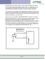
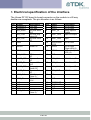
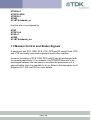
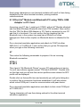
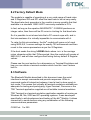
2i
blu Module
User Guide
The information contained in this document is subject to change without notice. TDK Systems Europe makes no warranty of
any kind with regard to this material including, but not limited to, the implied warranties of merchant ability and fitness for a
particular purpose. TDK Systems Europe shall not be liable for errors contained herein or for incidental or consequential
damages in connection with the furnishing, performance, or use of this material.
© Copyright 2004 TDK Systems Europe Limited.
All rights reserved.
This document contains information that is protected by copyright. All rights reserved. No part of this document may be
photocopied, reproduced, or translated to another language without the prior written consent of TDK Systems Europe.
Other product or company names used in this publication are for identification purposes only and may be trademarks of their
respective owners.
1 of 36
Contents
BEFORE YOU BEGIN.................................................................................................................................................................... 3
SAFETY GUIDELINES ................................................................................................................................................................... 3
RF APPROVALS .......................................................................................................................................................................... 3
1
FUNCTIONS ...................................................................................................................................................................... 4
2
APPLICATION INTERFACE ............................................................................................................................................. 5
2.1
2.2
2.3
2.4
2.5
2.6
3
SERIAL INTERFACE ......................................................................................................................................................... 5
POWER SUPPLY ............................................................................................................................................................. 6
POWER-ON-RESET (POWER CYCLING AND BROWN OUT CONSIDERATIONS) ..................................................................... 6
SPI BUS ........................................................................................................................................................................ 8
PARALLEL PIO PORT ..................................................................................................................................................... 8
PCM CODEC INTERFACE ................................................................................................................................................ 8
ELECTRICAL SPECIFICATION OF THE INTERFACE .................................................................................................... 9
3.1
4
ELECTRIC CHARACTERISTICS ....................................................................................................................................... 11
PHYSICAL CHARACTERISTICS.................................................................................................................................... 13
4.1
4.2
4.3
5
MECHANICAL DIMENSIONS............................................................................................................................................ 13
2I
MOUNTING THE BLU MODULE ONTO THE APPLICATION PLATFORM ................................................................................. 14
BOARD TO BOARD CONNECTOR.................................................................................................................................... 14
ELECTRICAL AND RADIO CHARACTERISTICS.......................................................................................................... 16
ABSOLUTE MAXIMUM RATINGS ...................................................................................................................................... 16
OPERATING TEMPERATURES......................................................................................................................................... 16
POWER CONSUMPTION ................................................................................................................................................ 16
LOW POWER MODES USING SNIFF ................................................................................................................................ 19
RF PERFORMANCE ....................................................................................................................................................... 21
5.5.1
Transmit Power ............................................................................................................................................. 21
5.5.2
Receive Sensitivity ........................................................................................................................................ 21
5.5.3
Range ............................................................................................................................................................ 21
5.5.4
Performance against Temperature................................................................................................................ 22
5.6
RELIABILITY ................................................................................................................................................................. 23
5.1
5.2
5.3
5.4
5.5
6
RS232 MODEM SIGNALS............................................................................................................................................... 24
6.1
6.2
6.3
7
PURE CABLE REPLACEMENT MODE.......................................................................................................................... 27
7.1
7.2
7.3
8
MODEM SIGNALLING OVER BLUETOOTH ......................................................................................................................... 25
BREAK SIGNAL ON RX LINE ......................................................................................................................................... 25
RESET ......................................................................................................................................................................... 26
DATA CABLE ................................................................................................................................................................ 27
AUDIO CABLE............................................................................................................................................................... 28
MODEM CONTROL AND STATUS SIGNALS ...................................................................................................................... 29
GETTING STARTED ....................................................................................................................................................... 30
2i
8.1.1
Two blu Modules.......................................................................................................................................... 30
2i
8.1.2
One blu Module and Bluetooth PC using TDK’s USB Adaptor or PC Card................................................. 31
8.2
FACTORY DEFAULT MODE ............................................................................................................................................ 32
8.3
SOFTWARE .................................................................................................................................................................. 32
APPENDIX A ................................................................................................................................................................................ 34
EUROPE – EU DECLARATION OF CONFORMITY .......................................................................................................................... 34
FCC AND INDUSTRY CANADA STATEMENTS ............................................................................................................................... 34
APPENDIX B ................................................................................................................................................................................ 35
ESD (ELECTROSTATIC DISCHARGE).......................................................................................................................................... 35
ADDITIONAL STATEMENT ........................................................................................................................................................... 35
WARRANTY ................................................................................................................................................................................. 36
2 of 36
Before You Begin
Congratulations on your purchase of the TDK Systems blu2i Module.
The Module is designed to be built into a device and to provide a simple,
low cost Bluetooth interface. The module is designed to integrate with a
wide range of applications and platforms with a simple electrical and
software interface using AT commands.
This guide aims to provide all the electrical and mechanical information
needed to design applications using the blu2i Module. A separate
document, blu2i Module - AT Command Set, outlines the protocol for the
software interface.
Safety Guidelines
The following safety precautions must be observed during all phases of
the operation, usage, service or repair of any application incorporating
this Bluetooth Module. Manufacturers of the RF equipment are advised
to convey the following safety information to users and operating
personnel and to incorporate these guidelines into all manuals supplied
with the product. Failure to comply with these precautions violates safety
standards of design, manufacture and intended use of the product. TDK
Systems assumes no liability for customer failure to comply with these
precautions.
RF Approvals
The blu2i Module is listed as a Bluetooth Product in terms of the
Bluetooth SIG Program Reference Document (PRD). This means that it
can be integrated into end products without further testing or approval
listing. The manufacturer must state the TDK part number and product
reference in his literature in order to meet the requirements of the
Bluetooth and regulatory approvals.
A list of the countries where the module is approved will be provided by
TDK Systems as required. As a minimum the product is listed in Europe,
Scandinavia and USA. TDK Systems assumes no liability for customer
failure to comply with national RF approvals.
3 of 36
1 Functions
The blu2i Module contains a complete Bluetooth interface and requires
no further hardware to implement full Bluetooth communication. The
module has an integrated, high performance antenna together with all
RF and Baseband circuitry, it interfaces to the host over a straight
forward serial port using AT commands. The module runs specific
firmware within the Virtual Processor that includes a serial Port Profile
and AT command interpreter. The module can be configured so that it
can be attached to a ‘dumb’ terminal or attached to a PC or PDA for
cable replacement applications.
The module provides access to 5 General I/O lines and 2 analogue I/O
lines to provide Bluetooth connection to simple devices such as switches
or LEDs without requiring any processing at the module end.
blu2i Module features at a glance:
Feature
Bluetooth Transmission
Frequency
Minimum Transmit Power
Maximum Transmit Power
Receive Sensitivity
Antenna Gain
Range (see Section 6.1.3)
Data Transfer Rate
Physical size
Weight
Fully Bluetooth pre-qualified
Current consumption
Temperature Range
Audio
Implementation
Class 1
2.400 – 2.485Ghz
+0dBm
+6dBm
Better than -85dB
+2dBi
Up to 100 metres, free space
Up to 200Kbps
24 x 69 x 5 mm
8g
Bluetooth 1.1 PRODUCT listing
Less than 36mA during data
transfer
-20°C to +75°C
Audio can be transferred over
SCO channels through the PCM
interface at 64Kbps
4 of 36
2 Application Interface
The blu2i Module is equipped with a 40-pin 0.5mm pitch board to board
connector that connects to the application platform. Electrical and
mechanical characteristics of the board-to-board connector are specified
in Chapter 3.
• Serial interface (see Section 3.0)
• Electrical specification of the interface (see Section 3.1)
2.1 Serial Interface
UART_TX, UART_RX, UART_RTS and UART_CTS form a conventional
asynchronous serial data port. The interface is designed to operate
correctly when connected to other UART devices such as the 16550A.
The signalling levels are nominal 0V and 3.3V and are inverted with
respect to the signalling on an RS232 cable. The interface is
programmable over a variety of bit rates; no, even or odd parity; stop bit
and hardware flow control. The default condition on power-up is preassigned in the external Flash. Two-way hardware flow control is
implemented by UART_RTS and UART_CTS. UART_RTS is an output
and is active low. UART_CTS is an input and is active low. These
signals operate according to normal industry convention.
By writing different values to the S register the UART_RI can be
continuously polled to detect incoming communication. The UART_RI
signal serves to indicate incoming calls.
UART_DSR is an active low input. It should be connected to DTR output
of the host. When the module is running in high speed mode (See
definition for S Register 512), this pin should be asserted by the host to
ensure connection is maintained. A deassertion is taken to mean that the
connection should be dropped, or an online command mode is being
requested.
The module communicates with the customer application using the
following signals:
RS-232
• Port /TXD @ application sends data to the module’s UART_RX
signal line
• Port /RXD @ application receives data from the module’s
UART_TX signal line
5 of 36
blu2i Module
Application
/RXD
/TXD
/RTS
/CTS
/DTR
/DSR
/DCD
/RING
RS232 Interface
UART Interface
UART_TX
UART_RX
UART_CTS
UART_RTS
UART_DTS
UART_DTR
UART_DCD
UART RI
Figure: UART interfaces
2.2 Power Supply
The power supply for the blu2i Module has to be a single voltage source
of Vcc= 3.6V to 6V. It must be able to provide sufficient current in a
transmit burst which can rise to 65mA.
The module includes regulators to provide local 3.3V and 1.8V. These
rails are accessible on connector J2 for monitoring.
Power (Vcc) should be provided via the board-to-board connector Pin 29
on J2.
Section 5.3 details the power consumption in different modes.
2.3 Power-On-Reset (Power Cycling and Brown Out
considerations)
The Module is provided with an active high reset pin (Hirose 40 way
DF12C connector pin 13). This pin whose electrical specification may be
found in section 3.3 is internally pulled to ground through a 10KΩ
resistor. Upon the application of power, the Power On Reset circuit built
into the module will ensure that the unit starts correctly.
However the module utilises a split rail design with some components
working at 3V3 and some at 1V8. Under certain extreme conditions, for
6 of 36
example when the supply voltage to the module experiences a BrownOut (momentary dip in the supply voltage level), or a rapid power cycle
i.e. the power is switched off and then on within 1second, there is a
possibility that the module can enter an unknown state of operation.
It is strongly recommended that the application hardware onto which the
module is mounted provides a Power-On-Reset circuit with a Brown-Out
detection capability. This will guarantee that under all circumstances the
module will operate in a known state.
A device such as the Maxim MAX6382XR26D3-T would be a suitable
part to perform the reset – it has an active high push-pull output, a 2.63V
detection threshold, and an active reset period of 140ms. This
inexpensive device is available in a SC70-3 package (2.2mm x 2.4mm)
and requires no additional components to operate. The device is used to
monitor the output of the voltage regulator on the module (through pin
27), and drives the Reset line (pin13) high when the supply voltage falls
out of tolerance. The schematic below illustrates its use.
Please note that this 3V3 is the output of
the 3V3 regulator on the blu2i Module and
should not be connected to any other
supplies on the application hardware.
blu2i Module
BC02 3V3
Pin27
BC02 MRESET
Pin13
3
Vcc
MAX6382
Gnd
Reset
1
2
10K
GND
GND
7 of 36
2.4 SPI Bus
The module is a slave device that uses terminals SPI_MOSI, SPI_MISO,
SPI_CLK and SPI_CSB. This interface is used for program firmware
update.
Note: The designer should be aware that no security protection is built
into the hardware or firmware associated with this port, so the terminals
should not be permanently connected in a PC application.
2.5 Parallel PIO Port
Five lines of programmable bi-directional input/outputs (I/O) are
provided. GPIO[1:5] are powered from VCC. The mode of these lines
can be configured and the lines are accessed via S Registers 621 to
625.
Auxiliary functions available via these pins include an 8-bit ADC and an
8-bit DAC. This function is not implemented at this time.
2.6 PCM Codec Interface
PCM_OUT, PCM_IN, PCM_CLK and PCM_SYNC carry up to three bidirectional channels of voice data, each at 8K samples/s. The format of
the PCM samples can be 8-bit A-law, 8-bit µ-law, 13-bit linear or 16-bit
linear. The PCM_CLK and PCM_SYNC terminals can be configured as
inputs or outputs, depending on whether the module is the Master or
Slave of the PCM interface.
The blu2i module is compatible with the Motorola SSI TM interface and
interfaces directly to PCM audio devices including the following:
• Qualcomm MSM 3000 series and MSM 5000 series CDMA
baseband devices
• OKI MSM7705 four channel A-law and µ-law CODEC
• Motorola MC145481 8-bit A-law and µ-law CODEC
• Motorola MC145483 13-bit linear CODEC
8 of 36
3 Electrical specification of the interface
The Hirose DF12C board to board connector on the module is a 40 way
double-row receptacle. The pin allocation is as follows:
Pin
1
3
5
Signal
Analogue 0
Analogue 1
SPI_MISO
7
SPI_CSB
9
SPI_CLK
11
GND
13
RESET
15
GND
17
SPI_MOSI
19
UART_CTS
21
UART_TX
23
UART_RTS
25
UART_RX
27
VCC_3V3
29
VCC_5V
31
33
35
37
39
N/C
N/C
N/C
N/C
VCC_1V8
Description
1.8v Max
1.8v Max
SPI bus serial
O/P
SPI bus chip
select I/P
SPI bus clock
I/P
Reset I/P
SPI bus serial
I/P
Clear to Send
I/P
Transmit Data
O/P
Request to
Send O/P
Receive Data
I/P
3.3V Output
(Note 3)
3.6V < VIN <
6.0V
1.8V Output
(Note 3)
Pin
2
4
6
Signal
GPIO1
GPIO2
UART_RI
8
UART_DCD
Description
I/O for Host
I/O for Host
‘Ring’ Input or
Output
Input or Output
10
UART_DSR
Input
12
I/O for Host
14
GPIO3/UART
_DTR
GPIO4
16
GPIO5
18
GND
20
PCM_CLK
PCM Clock I/P
22
PCM_IN
PCM Data I/P
24
PCM_SYNC
PCM Sync I/P
26
PCM_OUT
PCM Data O/P
28
N/C
30
GND
32
34
36
38
40
RESERVED
RESERVED
GND
GND
N/C
9 of 36
I/O for Host
(Right LED)(2)
I/O for Host (Left
LED) (2)
Do not connect
Do not connect
Notes:
• UART_RX, UART_TX, UART_CTS, UART_RTS, UART_RI,
UART_DCD and UART_DSR are all 3.3v level logic. For example,
when RX and TX are idle they will be sitting at 3.3V. Conversely
for handshaking pins CTS, RTS, RI, DCD, DSR a 0v is treated as
an assertion.
• Pin 6 (UART_RI) is active low. It is normally 3.3v. When a remote
device initiates a connection, this pin goes low. This means that
when this pin is converted to RS232 voltage levels it will have the
correct voltage level for assertion.
• Pin 8 (UART_DCD) is active low. It is normally 3.3v. When a
connection is live this pin is low. This means that when this pin is
converted to RS232 voltage levels it will have the correct voltage
level for assertion.
• Pin 10 (UART_DSR) is an input, with active low logic. It should be
connected to the DTR output of the host. When the blu2i Module is
in high speed mode (See definition for S Register 512), this pin
should be asserted by the host to ensure that the connection is
maintained. A deassertion is taken to mean that the connection
should be dropped, or an online command mode is being
requested.
• The GPIOn pins can be accessed using S Registers 621 to 625
• GPIO4 and GPIO5 are also connected to LEDs on the module. If
these I/O pins are set for input, then the LED will be driven by the
host and appropriate drive current requirements must be satisfied.
By default GPIO4 is used to drive the right LED which indicates
connection status. A Logic 1 switches on the LED.
• Analogue 0 and 1 should not exceed 1.8v and S Registers 7xx are
used to access them.
• GPIO3 is used for DTR output (active low).
10 of 36
3.1 Electric Characteristics
Function
Power
Supply
RS232
Interface
External
Power
Supply
SPI Bus
Signal Name
Vcc
Pin No
29
I/O
I
GND
11, 15,
18, 30,
36, 38
UART_TX
21
O
UART_RX
25
I
UART_CTS
19
I
UART_RTS
23
O
UART_DSR
10
I
UART_DTR
12
O
UART_RI
6
I or O
UART_DCD
8
I or O
VCC_1V8
39
O
VCC_3V3
SPI_MOSI
27
17
O
I
SPI_MISO
5
O
SPI_CSB
7
I
SPI_CLK
9
I
Signal level
3.6V to 6V
Comments
Ityp = 50mA
6 Ground
terminals to
be attached
in parallel
11 of 36
VOLmax=0.2V
VOHmin=2.8V
VILmax=0.8V
VIHmin=2.10V
VIHmax=3.7V
VILmax=0.8V
VIHmin=2.10V
VIHmax=3.7V
VOLmax=0.2V
VOHmin=2.8V
VILmax=0.8V
VIHmin=2.10V
VIHmax=3.7V
VOLmax=0.2V
VOHmin=2.8V
O/P : VOLmax=0.2V
VOHmin=2.8V
I/P : VILmax=0.8V
VIHmin=2.10V
VIHmax=3.7V
O/P : VOLmax=0.2V
VOHmin=2.8V
I/P : VILmax=0.8V
VIHmin=2.10V
VIHmax=3.7V
1.8V typical
3.3V typical
VILmax=0.8V
VIHmin=2.10V
VIHmax=3.7V
VOLmax=0.2V
VOHmin=2.8V
VILmax=0.8V
VIHmin=2.10V
VIHmax=3.7V
VILmax=0.8V
Shared with
GPIO3
Direction
may be
programme
d.
Direction
may be
programme
d.
For
monitoring
only. No
current
source
Used to
reprogram
Flash
PCM
Interface
PCM_CLK
20
I or O
PCM_IN
22
I
PCM_SYNC
24
I or O
PCM_OUT
26
O
BC02
USB D-
32
I
34
I
GPIO
BC02
USB D+
GPIO 1 - 5
2,4,12,
14,16
I or O
Analog
I/O
AIO_0,
AIO_1
1, 3
I/O
Reset
RESET
13
I
Reserved
12 of 36
VIHmin=2.10V
VIHmax=3.7V
O/P : VOLmax=0.2V
VOHmin=2.8V
I/P : VILmax=0.8V
VIHmin=2.10V
VIHmax=3.7V
VILmax=0.8V
VIHmin=2.10V
VIHmax=3.7V
O/P : VOLmax=0.2V
VOHmin=2.8V
I/P : VILmax=0.8V
VIHmin=2.10V
VIHmax=3.7V
VOLmax=0.2V
VOHmin=2.8V
VILmax =0.3vdd_pads
VIHmin =0.7cdd_pads
VILmax =0.3vdd_pads
VIHmin =0.7cdd_pads
O/P : VOLmax=0.2V
VOHmin=2.8V
I/P : VILmax=0.8V
VIHmin=2.10V
VIHmax=3.7V
Vout max=VDD_PIO.3
Vout min=VDD_PIO
VDD falling
threshold=1.5V typ
VDD rising
threshold=1.6V typ
If unused
keep pins
open
Normally
inactive.
Pull to GND
through 10K
4 Physical Characteristics
4.1 Mechanical Dimensions
13 of 36
4.2 Mounting the blu2i Module onto the application
platform
There are many ways to properly install the Module in a host device. An
efficient approach is to mount the PCB to a frame, plate, rack or chassis.
Fasteners can be M1.8 or M2 screws plus suitable washers, circuit
board spacers, or customized screws, clamps, or brackets in 2.2mm
diameter holes. Note that care should be taken to ensure the head of the
fixing does not interfere with the circuit. Nylon fixings are recommended.
In addition, the board to board connection can also be utilized to achieve
better support.
The antenna (Brown square component on top side of PCB) must not be
influenced by any other PCBs, components or by the housing of the host
device. The proximity of the antenna to large metallic objects can affect
the range and performance of the system. Designers should carefully
consider the location of the module and the type of enclosure material
that is used.
To prevent mechanical damage, be careful not to force, bend or twist the
module. Be sure it is positioned flat against the host device.
4.3 Board to Board Connector
This section provides specifications for the 40 way board-to-board
connector which serves as physical interface to the host application. The
receptacle assembled on the blu2i Module is type Hirose DF12C.
Item
Receptacle
on Module
Part number
DF12C-40DS0.5V(81)
Stacking height
3.5mm - 5mm
14 of 36
HRS number
CL537-0007-7-
Mating headers from Hirose are available in different stacking heights.
Details are available at:
http://www.hirose.co.jp/cat2002e/500/e53700036.pdf
Item
Headers
DF12 series
Part number
DF12(3.5)-40DP0.5V(81)
DF12(4.0)-40DP0.5V(81)
DF12(5.0)-40DP0.5V(81)
Stacking height
3.5mm
4.0mm
5.0mm
HRS number
CL537-0032-4**
CL537-0057-5**
CL537-0157-0**
Note: The headers listed above are without boss and metal fitting.
Electrical and mechanical characteristics of the Hirose DF12C
connector:
Parameter
Number of Contacts
Quantity delivered
Voltage
Current Rating
Resistance
Dielectric Withstanding Voltage
Operating Temperature
Contact Material
Insulator
Stacking height
Insertion force
Withdrawal force 1st
Withdrawal force 50th
Maximum connection cycles
Specification (40 pin Board to
Board connector)
40
2000 Connectors per Tape & Reel
50V
0.5A max per contact
0.05 Ohm per contact
500V RMS min
-45°C to +125°C
phosphor bronze (surface: gold
plated)
Material PA , beige natural
3.0 mm; 3.5 mm; 4.0 mm; 5.0 mm
21.8N
10N
10N
50
15 of 36
5 Electrical and radio characteristics
5.1 Absolute Maximum ratings
Absolute maximum ratings for supply voltage and voltages on digital and
analog pins of the module are listed below. Exceeding these values will
cause permanent damage.
Minimum
0mA
-0.3V
3.3V
Peak current of power supply
Voltage at digital pins
Voltage at POWER pin
Maximum
100mA
3.7V
7V
5.2 Operating temperatures
Minimum
-20°C
Operating temperature
Typical
25°C
Maximum
+75°C
5.3 Power Consumption
The current drain from the Vcc power input line is dependent on various
factors. The three most significant factors are the voltage level at Vcc,
UART baud rate and the operating mode.
The hardware specification for the blu2i module allows for a voltage
range of 3.6 to 6.0v at Vcc. Tests have shown that there is no significant
difference in current draw when Vcc is 5 or 6V. Therefore the data
presented below, pertains to Vcc levels of 3.6 and 5v only. Tests have
shown that where power drain is an issue, it is best to keep Vcc at the
lower end of the range.
The UART baud rate has a bearing on power drain because as is normal
for digital electronics, the power requirements increase linearly with
increasing clocking frequencies. Hence higher baud rates result in a
higher current drain.
Finally with regards to operating mode the significant modes are; idle,
waiting for a connection, inquiring, initiating a connection and connected.
With connected mode, it is also relevant to differentiate between no data
16 of 36
being transferred and when data is being transferred at the maximum
rate possible.
The operating mode can best be described by stating the AT commands
required to enter that mode. In addition, there are certain S Registers
which have a direct impact on power consumption, which are described
next.
The blu2i Module has 2 LEDs which can be configured to display
connection status. One led is used to display connection status, while
the other is used to either display ‘Ring Indicate’ status or follow the
state of the incoming DSR line on the UART interface. Tests have shown
that these LEDs can consume up to 5.3mA which is more than double
the current draw when in Idle mode. Therefore S Registers 533 and 534
can be used to completely disable these indications.
Finally S Registers 508 to 511, which specify the page and inquiry scan
intervals and windows, can be used to adjust the average current drain
when in discoverable and or connectable modes. Registers 508 and 509
specify the interval and window for page scans and registers 510 and
511 specify the interval and window for inquiry scans. Register pairs
508/509 and 510/511 describe duty cycles when the blu2i module goes
into scan modes. It is while scanning that the highest current draw
occurs. The average current draw is determined by simple arithmetic
using the values stored in the 508/509 and 510/511 register pairs.
The operating modes described above are entered using AT commands
as follows
Idle
Wait for Connection
Discoverable Only
Connecting
Connected
Connected
On power up, with S Register 512 = 1
AT+BTG (100% page scan duty cycle)
AT+BTQ (100% inquiry scan duty cycle)
ATD
No Data
Max data transfer
All current consumption values in the table below assume that the
connection status indication functionality of the LEDs has been disabled
by setting S Registers 533 and 534 to 0.
All current values are in milliamps (mA).
17 of 36
Current per LED
Idle Mode, S512=1
Wait for Connection Or
Discoverable Mode,
AT+BTP
S508=S510=640,
S509=S511=320
Wait for Connection Or
Discoverable Mode,
AT+BTP
S508=S510=1000,
S509=S511=11
Inquiring Mode, AT+BTI
Connecting Mode
(ATDxxx)
Connected as Master
Mode (No Data Transfer)
Sniff NOT activated
Connected as Master
Mode (Max Data
Transfer)
Sniff NOT activated
Connected as Slave
Mode (No Data Transfer)
Connected as Slave
Mode (No Data Transfer)
Sniff Enabled (AT&F1
setting)
9600
3.20
5.30
Baud rate
38400 115200 460800
3.20
3.20
3.20
5.30
5.30
5.30
3.6V
5.0V
3.6V
5.0V
9600
1.60
2.00
59.00
65.00
Baud rate
38400 115200
1.80
1.96
2.10
2.30
59.00
59.00
65.00
65.00
460800
3.00
3.40
59.00
65.00
3.6V
5.0V
2.75
3.26
2.94
3.36
3.10
3.55
4.12
4.63
3.6V
5.0V
3.6V
5.0V
3.6V
5.0V
50.00
54.00
50.00
54.00
6.00
7.20
50.00
54.00
50.00
54.00
6.10
7.20
50.00
54.00
50.00
54.00
6.40
7.40
50.00
54.00
50.00
54.00
7.20
8.20
3.6V
5.0V
21.50
24.50
22.50
26.00
24.50
28.00
32.50
36.00
5.0V
32.00
33.00
33.50
34.00
5.0V
4.90
3.6V
5.0V
As can be seen, the current drain while waiting for a connection or
discoverable mode is about 30 times higher than in idle mode. This is
when the page/inquiry scan duty cycle is 100%. These modes give the
quickest response to a page or inquiry request from a remote peer.
18 of 36
It is possible to reduce the duty cycle down to as low as 0.5% at the
expense of response time. The response time can be specified via S
Registers 508 and 510 for page and inquiry respectively, where the
worst case response time can be as high as 2.5 seconds. Then the duty
cycle can be varied by changing the value of S Registers 509 and 511
appropriately.
For example, if S Register 508 and 510 are both set to 1000ms and S
Register 509 and 511 are both set to 11ms then the duty cycle is
reduced to 1%, this means that average current drain at 5.0v will be 2%
of 65mA plus the normal idle mode current, that is, it is as low as
2.75mA. However, in this case, it can take up to 1 second to establish a
connection.
The connected state current consumption while a master or slave can be
considerably reduced by enabling Sniff mode, described in detail in the
next section.
5.4 Low Power Modes using Sniff
Bluetooth connections are master/slave in nature. A master sends
packets and a slave has to acknowledge that packet in the next timeslot.
Timeslots in Bluetooth are 625 microseconds wide. This implies that a
master will always know when packets will be sent and received, which
further means it is able to optimise power usage by switching on power
hungry circuitry only when needed.
A slave on the other hand does NOT have prior knowledge of when a
packet will be received and has to assume that a packet will be received
from a master on every receive slot. This means that it has to leave it’s
receiving circuitry on for most of the receive slot duration. The result of
this is high power consumption as illustrated in the power table above,
where a slave with no data transmission still consumes around 31mA
whereas a master consumes only 6mA.
This problem was identified very early in the evolution of Bluetooth
(especially since headsets spend all their time as a slave in a Bluetooth
connection) and it was solved by having a mode called Sniff, with
appropriate lower layer negotiating protocol.
Sniff mode during connection is basically an agreement between the
slave and its master that data packets will only be exchanged for N
timeslots every M slots. The slave can then assume that it will never be
19 of 36
contacted during N-M slots, and so can switch its power hungry circuitry
off. The specification goes further by also specifying a third parameter
called ‘timeout’ (T) which specifies ‘extra’ timeslots that the slave will
agree to listen for after receiving a valid data packet. Put another way, if
a data packet is received by the slave, then it knows that it MUST carry
on listening for at least T more slots. If within that T slot time period
another data packet is received, then the timer is restarted. This
mechanism ensures low power consumption when there is no data
transfer – at the expense of latency. When there is a lot of data to be
transferred, it acts as if sniff mode were not enabled.
It is stated above that during sniff mode, a slave listens for N slots every
M slots. The Bluetooth specification states that a master can have up to
7 slaves attached to it with all slaves having requested varying sniff
parameters. It may therefore be impossible to guarantee that each slave
gets the M parameter it requested. In light of this, the protocol for
enabling sniff mode specifies that a requesting peer specify the M
parameter as a minimum and maximum value. This will allow the master
to interleave the sniff modes for all slaves attached.
For this reason, the sniff parameters are specified in TDK module via
four S registers. S Register 561 is used to specify ‘N’, S Register 562 is
used to specify ‘T’ and S Registers 563/564 are used to specify
minimum ‘M’ and maximum ‘M’ respectively. Although the specification
defines these parameters in terms of timeslots, the S register values
have to be specified in units of milliseconds and the firmware does the
necessary translation to timeslots.
Low Power Consumption
T Slots
T Slots
Data Exchange
Data Exchange
Data
Data Exchange
Exhange
Data Exchange
Data Exchange
High Power Consumption
T Slots
T Slots
N Slots
T Slots
N Slots
M Slots (Negotiated)
N Slots
M Slots (Negotiated)
20 of 36
5.5 RF performance
5.5.1Transmit Power
Conducted Transmit Power:
Antenna Gain:
Effective Transmit Power:
minimum: 1mW (0dBm)
maximum: 4mW (6dBm)
Power class 1
+2dBi typical.
min: 2dBm max:8dBm
5.5.2Receive Sensitivity
Receive Sensitivity:
Antenna Gain:
Effective Receive Sensitivity:
-86dBm (at 25ºC)
+2dBi typical
-88dBm (at 25ºC)
Receive Sensitivity
0
-40 deg
-20 deg
0 deg
20 deg
40 deg
60 deg
80 deg
100 deg
-10
-20
Attenuation Setting dBm
-30
-40
-50
-60
-70
-80
-90
NOTE: Measured as attenuation required
to achieve better than 0.1% BER
-100
Temperature Deg. C.
5.5.3Range
See Data Transfer Rate vs distance. The data throughput of the blu2i
Module is limited to 200Kbps by the parsing of the data being transferred
through the AT command processor. The graph below shows the best
21 of 36
case data though-put with and without the AT command processing.
Distances are measured in free space between 2 blu2i Modules.
Data Transfer Rate / Distance
800
700
Data Transfer Rate (kbps)
600
500
RF data rate
Serial port data rate
400
300
200
100
0
10m
50m
100m
150m
200m
250m
300m
Distance (meters)
5.5.4Performance against Temperature
Data Transmit Rate with Temperature and Attenuation
800
700
600
Data Transmission Rate kbs
-40 deg
-20 deg
500
0 deg
20 deg
400
40 deg
60 deg
300
80 deg
200
100 deg
100
0
-60dBm
-65dBm
-70dBm
-75dBm
dBm attenuation
22 of 36
-80dBm
-85dBm
-90dBm
5.6 Reliability
Parameter
Thermal Shock
Vibration
Shock
Moisture Resistance
High Temp Storage
Low Temp Storage
High Temp/Humidity
Operation
High Temp/Humidity
Storage
Thermal shock
Electro Static
Discharge
Drop Test
Minimum
200cycles -40ºC
/+85ºC 30 min
Continuous operation
at 60 Hz, 2mm stroke
50G 11ms Half Sine
Wave
Maximum
1 cycle/hour
15g max sine wave,
12 hours
6 axis x 3 cycles each
axis
85ºC, 360 hours
-40ºC, 240 hours
60ºC, 90%RH, 360
hours
-40 to 60ºC in 30min
EN55024:1998 &
IEC61000-4-3
75cm to concrete, 3
axis x 2 cycles per
corner
23 of 36
200 cycles with
continuous operation
6 RS232 Modem Signals
Just as a telephony modem has control and status lines, the blu2i Module
also provides for 6 control and status lines as per the table below. The
direction column is as seen from the modules viewpoint.
Direction
IN or OUT
IN or OUT
IN
OUT
IN
OUT
Function
CI also known as RI (Ring Indicate)
DCD (Data Carrier Detect)
DSR (Data Set ready)
DTR (Data Terminal Ready)
CTS (Clear to Send)
RTS (Request to Send)
The first four lines are under program control and as such require GPIO
pins and they are mapped to I/O as per the table below. The last two are
under control of the UART driver and their functionality is always
enabled.
PIO
Pin
0
1
2
3
4
5
Direction
Connector Pin Label
Function
IN/OUT
IN/OUT
IN/OUT
IN/OUT
IN
IN/OUT
GPIO1
GPIO2
UART_RI
UART_DCD
UART_DSR
GPIO3/UART_DTR
6
IN/OUT
GPIO4
7
IN/OUT
GPIO5
General Purpose I/O
General Purpose I/O
Input/Output from module
Input/Output from module
Input to Module
General Purpose I/O (or
DTR functionality)
General Purpose I/O
(Right LED)
General Purpose I/O (Left
LED)
Notes:
1
PIO4 (DSR) is used by the blu2i module to sense that the host is
connected, and is intricately linked with connections. For outgoing calls,
if this line is not asserted then an error is immediately. Similarly for
AT+BTP and AT+BTG.
While in a call, for appropriate modes, a deassertion means fall into
command state. If the deassertion exists for longer than the period
24 of 36
specified in S Register 519 then the connection is dropped as if an ATH
command was received.
2
PIO2 (RI), is normally deasserted. When an incoming connection
is detected it will be asserted, until the connection is either answered or
rejected using ATA and ATH respectively. See S Registers 552 & 553
for more details
3
PIO3 (DCD) will be deasserted when the device is in the
unconnected state. Asserted when a connection is active. See S
Registers 552 and 553 for more details.
4
PIO5 is either used as GPIO or driven as UART_DTR. When the
unit is configured in pure host mode, this pin is forced into UART_DTR
and is asserted when there is a Bluetooth connection.
GPIO Pins 1,2,3,4 and 5 are available for general purpose use.
6.1 Modem signalling over Bluetooth
The RFCOMM protocol used in Bluetooth for implementing the serial
port profile allows for the exchange of four modem signals. This
information is contained in a special transparent message which
contains bits identified as RTR, RTC, DV and IC which depending on the
type of serial device being emulated maps to DTR or DSR, RTS, DCD
and RI respectively. In addition, this message also includes the ability to
convey a BREAK input from one end to the other.
So to allow for the greatest flexibility and variability in how the modem
control signals are used out in the real world, S Registers 551, 552 and
553 have been provided which allow for any of RTR,RTC,DV and IC to
be mapped to any modem control/status line.
6.2 BREAK signal on RX line
If the host sends a break signal of duration greater than 100ms, then the
blu2i module is configured to treat that as a signal to perform a hardware
reset.
This being the case it is not possible to convey a BREAK over Bluetooth
to the peer device.
25 of 36
Future enhancement may allow the BREAK signal to be used to map to
GPIO which with appropriate external hardware may allow for a BREAK
to be reproduced on the TX line.
6.3 Reset
The module can be reset by the host without the need of any I/O using a
BREAK signal. The module has been configured to reset when the RX
line detects a break condition for durations greater than 100
milliseconds.
26 of 36
7 Pure Cable Replacement Mode
7.1 Data Cable
The module has the capability of being preset into a pure 5-wire data
cable replacement mode. The 5 wires being RX, TX, CTS, RTS and
GND. This mode requires no changes to a host application since the
Bluetooth connection is automatically set up on power up and will retry
when the connection drops.
By implication, two devices are needed to replace a cable. One device is
pre-configured to always be a master and the other, a slave.
Assuming the Bluetooth address of the master to be <bdaddr_m> and
that of the slave to be <bdaddr_s>, the master module is configured by
sending it the following AT commands.
AT&F
ATS512=1
ATS504=1
ATS507=2
ATS530=2000
AT&W
AT+BTR<bdaddr_s>
Where the ATS507=2 setting puts the device in DSR drop mode only.
This means that when the device needs to be reconfigured, deasserting
the DSR line will ensure that the module responds quickly to AT
commands. This further means that in stand alone mode, the DSR input
line MUST be asserted e.g. 0v in TTL signal mode.
The slave is configured by,
AT&F
ATS512=4
ATS0=-1
AT&W
AT+BTR<bdaddr_m>
27 of 36
Where <bdaddr_m> is optional. If it is not specified, then the slave unit
will accept connections from any device. If specified then only
connections from the device specified will be accepted.
If it is desired that the slave unit not be discoverable (the master is by
default not discoverable), then the configuration commands are,
AT&F
ATS512=3
ATS0=-1
AT&W
AT+BTR<bdaddr_m>
Where <bdaddr_m> is optional. If it is not specified, then the slave unit
will accept connections from any device. If specified then only
connections from the device specified will be accepted.
When the units are next power cycled, the slave unit will wait for the
master to connect to it and the master will continually look for the slave.
If a connection attempt fails, the master will wait for 2 seconds before
reattempting a connection. This 2 second delay can be varied by issuing
it an ATS530 command with an appropriate value in the range 100ms to
15000ms.
IMPORTANT NOTE: When S Register 507 = 0, the DSR input to the
module MUST be asserted for the auto connection to succeed. When
operating at TTL levels a 0V is seen as an assert state. When operating
at RS232 levels and voltage greater than 3V is seen as assert. It is usual
to connect the DTR line of the host to the DSR line of this device.
7.2 Audio Cable
With a pair of these modules it is possible to replace a mono audio cable
with two way traffic. That is, a setup where a microphone is connected to
a speaker at the remote end and vice versa. So this mode effectively
replaces two audio cables.
Assuming the Bluetooth address of the master to be <bdaddr_m> and
that of the slave to be <bdaddr_s>, the master module is configured by
sending it the following AT commands.
AT&F
ATS512=1
28 of 36
ATS504=1
ATS530=2000
ATS532=1
AT&W
AT+BTR<bdaddr_s>
And the slave is configured by,
AT&F
ATS512=4
ATS0=-1
AT&W
AT+BTR<bdaddr_m>
7.3 Modem Control and Status Signals
A serial port has DTR, DSR, RTS, CTS, DCD and RI control lines. RTS
and CTS are locally controlled to prevent local buffer overflow.
However the status of DTR, DRS, DCD and RI can be exchanged with
the remote peer device. If for example, the DTR/DSR lines are to be
exchanged between the two peers to simulate the performance of a
physical cable, then it is possible to do so. Refer to the description for S
Registers 551, 552 and 553 for more details.
29 of 36
8 Getting Started
This section describes how to quickly make your first Bluetooth
connection based on the following combinations of Bluetooth hardware:1.
Two blu2i Modules.
2.
One blu2i Module and a Bluetooth Enabled PC using TDK’s Go
Blue USB Adaptor or PC Card.
Note: The following examples assume that a PC is used to control the
blu2i Module using a Terminal Emulation application.
8.1.1Two blu2i Modules
Assuming your PC has 2 serial ports (COM1 and COM2) or that you
have 2 PCs that each have one free serial port, attach a blu2i Module to
each COM port. Launch a terminal emulation for each COM port and
start off with comms parameters 9600,N,8,1.
Type AT<enter> and confirm that you see it echoed and then an OK
response. If you do not see this behavior, close the application and
restart with comms parameters 115200,N,8,1 and try again.
On the first terminal emulator application, enter the following
commands:ATI4
ATS0=1
AT+BTP
The response to ATI4 will be the modules Bluetooth address in the form
of a 12 digit hex number.
On the second terminal emulator app, enter the following command:ATD<bd_addr>
Where <bd_addr> is the 12 digit Bluetooth address you saw in response
to ATI4 above.
After a moment, you will see the response “CONNECT <bd_addr>” on
both terminal emulators. This confirms that you have a Bluetooth
connection between the two.
30 of 36
Now typing characters on one terminal emulator will result in them being
displayed on the other terminal emulator, proving wireless
communications.
8.1.2One blu2i Module and Bluetooth PC using TDK’s USB
Adaptor or PC Card
Assuming your PC has 1 serial port (COM1) with a blu2i Module attached
and the latest Windows Bluetooth stack from TDK installed. Also confirm
that the TDK Go Blue USB Adaptor or PC Card is connected to your PC
and that it is functional. You can confirm this by checking that the
Bluetooth icon in the system tray area has a White B on a blue
background. Red on blue implies no Bluetooth device is attached to the
PC.
Run a terminal emulation application and attach to COM1 at either
9600,N,8,1 or 115200,N,8,1 and confirm that you get an OK response
when you type in the following command:
AT
Then enter the following commands to prepare it for an incoming
Bluetooth connection:
ATS0=1
AT+BTP
Then launch “My Bluetooth Places” on your PC and perform an inquiry.
You will see a device appear named “TDK blu2i XXXXXX”. Double click
on that item and you will see the service profiles screen where the SPP
profile will be displayed.
Double click on that profile item and eventually you will get a dialog box
to confirm that a connection has been established. It will also advise
which virtual COM port it uses for communication with peer device.
Run a terminal emulation application and attach to that virtual COM port
at 115200,N,8,1.
Typing characters will see them being echoed in the other terminal
emulation application.
31 of 36
8.2 Factory Default Mode
The module is capable of operating at a very wide range of baud rates
and S Registers 520 and 521 allow the baud rate to be set very easily.
The baud rate clock generator in the module is more versatile that that
available in a standard 16550 UART commonly available in PCs.
In fact, as long as the equation BAUDRATE * 0.004096 produces an
integer value, then there will be 0% error in clocking for that baud rate.
So it is possible to set a baud rate that a PC cannot cope with, and in
that circumstance it is virtually impossible to communicate with it.
To cater for this circumstance, the blu2i module will come out of reset
using 9600,N,8,1 comms settings for exactly 750 milliseconds and then
revert to the comms parameters as per the S Registers.
If the host sends the string !<BISM>!<cr> where <cr> is the carriage
return character within that 750ms period, then the module will remain at
9600,N,8,1 and will also configure itself using factory default S Register
values.
Please see the next section for a discussion on Terminal Emulators and
how you can obtain a terminal emulator which has this ‘reset’ feature
built in.
8.3 Software
The Bluetooth Module described in this document uses the serial
interface to accept commands and provide responses. While in
command mode all interaction between it and a host is done purely in
text mode. This means that virtually all terminal emulators available are
adequate for testing and prototyping. HyperTerminal, Procomm or the
TDK Terminal application supplied are all suitable terminal emulators.
TDK Terminal is a terminal emulation application capable of running on
Windows 98, Me, 2000 and XP operating systems. It was developed
specifically to aid development and testing of the blu2i Module. It allows
connection to serial devices using any combination of the following
communications parameters:
COM Port: 1 to 255
32 of 36
Baud rate: 300 to 921600
Parity:
None, Odd, Even
Data Bits: 7 or 8
Stop Bits: 1 or 2
Handshaking:
None or CTS/RTS
The unique benefits of using TDK Terminal are:
•
•
•
•
Status of DSR, CTS, DCD and RI are continuously displayed
DTR can be directly controlled via a check box
RTS can be directly controlled
BREAK signals can be sent
Also, there is a “Data Transfer Test” mode allowing data to be sent as
fast as the handshaking will permit. This feature is very useful for testing
the bit transfer rate of a Bluetooth connection.
TDK Terminal is included on the blu2i CD and is also available for
download from http://www.blu2i.com.
33 of 36
Appendix A
Europe – EU Declaration of Conformity
DECLARATION OF CONFORMITY
In accordance with Annex IV of the EU directive 1999/5/EC
Notified Body consulted:
ID-Number of Notified Body:
Phoenix Test-Lab
0700
declare under our responsibility that the blu2i Module
complies with the appropriate essential requirements of the Article 3 of the R&TTE and the
other relevant provisions, when used for its intended purpose.
Health and Safety requirements contained in Article 3 (1) a)
EN 60 950: 1992 Safety of information technology equipment + Amendment A1:1993,
Amendment A2:1993, Amendment A3:1995, Amendment A4:1997, Amendment A11:1997
EN 50371: Generic standard to demonstrate the compliance of low-power electronic and
electrical apparatures with the basic restrictions related to human exposure to
electromagnetic fields (10 MHz - 300 GHz) – General public
Protection requirements with respect to electromagnetic compatibility Art.3 (1) b)
EN 301489-17 V1.1.1 (09-2000), Electromagnetic Compatibility and radio spectrum
Matters (ERM); ElectroMagnetic Compatibility (EMC) standard for radio equipment and
services; Part 17: Specific conditions for wideband data Hiperlan equipment
Means of the efficient use of the radio frequency spectrum
EN 300328-2 V1.2.1 (11-2001), Radio Equipment and Systems (RES); Wideband
transmission systems; Technical characteristics and test conditions for data transmission
equipment operating in the 2,4 GHz ISM band and using spread spectrum modulation
techniques. Part 2: Harmonized EN covering essential requirements under article 3(2) of the
R&TTE directive.
TDK Systems Europe Ltd
tel: +44 (0)20 8938 1000
126 Colindale Avenue, Colindale
fax: +44 (0)20 8905 8608
London NW9 5HD, United Kingdom
www.tdksys.com
Registered in England No. 2348741
FCC and Industry Canada Statements
This device complies with part 15 of the FCC Rules. Operation is subject
to the following two conditions: (1) This device may not cause harmful
interference, and (2) this device must accept any interference received,
including interference that may cause undesired operation.
Changes or modifications not expressly approved by the party
responsible for compliance could void the user's authority to operate the
equipment.
34 of 36
Appendix B
ESD (Electrostatic Discharge)
If your TDK Bluetooth device is affected by ESD, it is recommended that
you restart any Bluetooth processes that were active at the time.
Additional Statement
TDK SYSTEMS' BLUETOOTH PRODUCTS ARE NOT AUTHORISED
FOR USE AS CRITICAL COMPONENTS IN LIFE SUPPORT DEVICES
OR SYSTEMS WITHOUT THE EXPRESS WRITTEN APPROVAL OF
THE MANAGING DIRECTOR OF TDK SYSTEMS EUROPE.
The definitions used herein are:
a) Life support devices or systems are devices which (1) are intended for
surgical implant into the body, or (2) support or sustain life and whose
failure to perform when properly used in accordance with the instructions
for use provided in the labelling can reasonably be expected to result in
a significant injury to the user.
b) A critical component is any component of a life support device or
system whose failure to perform can be reasonably expected to cause
the failure of the life support device or system, or to affect its safety or
effectiveness.
35 of 36
Warranty
TDK warrants that its products shall conform to TDK’s published
specifications and remain free from defects in materials and
workmanship under normal, proper and intended use for a period of two
(2) years from date of purchase, provided that proof of purchase be
furnished with any returned equipment.
If during the warranty period any component part of the equipment
becomes defective by reason of material or workmanship, and TDK is
immediately notified of such defect, TDK shall at its option supply a
replacement part or request return of equipment, freight prepaid, to its
designated facility for repair. In the event no trouble is found on products
returned for repair, TDK reserves the right to charge the customer its
standard published repair charge.
This warranty shall not apply to any products that have been subject to
misuse, bending, twisting, neglect, alteration, improper installation,
testing or unauthorized repair performed by anyone other than a TDK
designated repair facility. Any non-warranty repairs or maintenance shall
be at TDK’s standard rates in effect at the time.
This warranty is in lieu of all other warranties, whether expressed,
implied, or statutory, including but not limited to, implied warranties or
merchantability and fitness for a particular purpose. In no event shall
TDK be liable, whether in contract, in part, or on any other basis, for any
damage sustained by its customers or any other person arising from or
related to loss of use, failure or interruption in the operation of any
products, or delay in maintenance, or for incidental, consequential, in
direct, or special damages or liabilities, or for loss of revenue, loss of
business, or other financial loss arising out of or in connection with the
sale, lease, maintenance, use, performance, failure, or interruption of
these products.
36 of 36