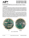
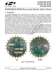
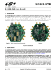
1
A NY - F R E Q U E N C Y P RECISION C L O C K S Si5316, Si5319, Si5322, S i 5 3 2 3 , S i 5 3 2 4 , S i 5 3 2 5 , Si5326, Si5327, Si5365, Si5366, Si5367, Si5368, Si5369, Si5374, Si5375 F AMILY R EFERENCE M ANUAL Rev. 0.5 6/11 Copyright © 2011 by Silicon Laboratories Si53xx-RM Si53xx-RM 2 Rev. 0.5 Si53xx-RM TABLE O F C ONTENTS Section Page 1. Any-Frequency Precision Clock Product Family Overview . . . . . . . . . . . . . . . . . . . . . . 12 2. Narrowband vs. Wideband Overview . . . . . . . . . . . . . . . . . . . . . . . . . . . . . . . . . . . . . . . . 16 3. Any-Frequency Clock Family Members . . . . . . . . . . . . . . . . . . . . . . . . . . . . . . . . . . . . . . 17 3.1. Si5316 . . . . . . . . . . . . . . . . . . . . . . . . . . . . . . . . . . . . . . . . . . . . . . . . . . . . . . . . . . . . 17 3.2. Si5319 . . . . . . . . . . . . . . . . . . . . . . . . . . . . . . . . . . . . . . . . . . . . . . . . . . . . . . . . . . . . 18 3.3. Si5322 . . . . . . . . . . . . . . . . . . . . . . . . . . . . . . . . . . . . . . . . . . . . . . . . . . . . . . . . . . . . 19 3.4. Si5323 . . . . . . . . . . . . . . . . . . . . . . . . . . . . . . . . . . . . . . . . . . . . . . . . . . . . . . . . . . . . 20 3.5. Si5324 . . . . . . . . . . . . . . . . . . . . . . . . . . . . . . . . . . . . . . . . . . . . . . . . . . . . . . . . . . . . 21 3.6. Si5325 . . . . . . . . . . . . . . . . . . . . . . . . . . . . . . . . . . . . . . . . . . . . . . . . . . . . . . . . . . . . 22 3.7. Si5326 . . . . . . . . . . . . . . . . . . . . . . . . . . . . . . . . . . . . . . . . . . . . . . . . . . . . . . . . . . . . 23 3.8. Si5327 . . . . . . . . . . . . . . . . . . . . . . . . . . . . . . . . . . . . . . . . . . . . . . . . . . . . . . . . . . . . 24 3.9. Si5365 . . . . . . . . . . . . . . . . . . . . . . . . . . . . . . . . . . . . . . . . . . . . . . . . . . . . . . . . . . . . 25 3.10. Si5366 . . . . . . . . . . . . . . . . . . . . . . . . . . . . . . . . . . . . . . . . . . . . . . . . . . . . . . . . . . . 26 3.11. Si5367 . . . . . . . . . . . . . . . . . . . . . . . . . . . . . . . . . . . . . . . . . . . . . . . . . . . . . . . . . . . 27 3.12. Si5368 . . . . . . . . . . . . . . . . . . . . . . . . . . . . . . . . . . . . . . . . . . . . . . . . . . . . . . . . . . . 28 3.13. Si5369 . . . . . . . . . . . . . . . . . . . . . . . . . . . . . . . . . . . . . . . . . . . . . . . . . . . . . . . . . . . 29 3.14. Si5374/75 Compared to Si5324/19 . . . . . . . . . . . . . . . . . . . . . . . . . . . . . . . . . . . . . 29 3.15. Si5374 . . . . . . . . . . . . . . . . . . . . . . . . . . . . . . . . . . . . . . . . . . . . . . . . . . . . . . . . . . . 30 3.16. Si5375 . . . . . . . . . . . . . . . . . . . . . . . . . . . . . . . . . . . . . . . . . . . . . . . . . . . . . . . . . . . 31 4. Device Specifications . . . . . . . . . . . . . . . . . . . . . . . . . . . . . . . . . . . . . . . . . . . . . . . . . . . .32 5. DSPLL (All Devices) . . . . . . . . . . . . . . . . . . . . . . . . . . . . . . . . . . . . . . . . . . . . . . . . . . . . . . 46 5.1. Clock Multiplication . . . . . . . . . . . . . . . . . . . . . . . . . . . . . . . . . . . . . . . . . . . . . . . . . . 47 5.2. PLL Performance . . . . . . . . . . . . . . . . . . . . . . . . . . . . . . . . . . . . . . . . . . . . . . . . . . . 48 5.2.1. Jitter Generation . . . . . . . . . . . . . . . . . . . . . . . . . . . . . . . . . . . . . . . . . . . . . . . . . . . . . . . . . . . . 48 5.2.2. Jitter Transfer. . . . . . . . . . . . . . . . . . . . . . . . . . . . . . . . . . . . . . . . . . . . . . . . . . . . . . . . . . . . . . . 48 5.2.3. Jitter Tolerance . . . . . . . . . . . . . . . . . . . . . . . . . . . . . . . . . . . . . . . . . . . . . . . . . . . . . . . . . . . . . 49 6. Pin Control Parts (Si5316, Si5322, Si5323, Si5365, Si5366) . . . . . . . . . . . . . . . . . . . . . . 50 6.1. Clock Multiplication (Si5316, Si5322, Si5323, Si5365, Si5366) . . . . . . . . . . . . . . . . 50 6.1.1. Clock Multiplication (Si5316) . . . . . . . . . . . . . . . . . . . . . . . . . . . . . . . . . . . . . . . . . . . . . . . . . . . 6.1.2. Clock Multiplication (Si5322, Si5323, Si5365, Si5366) . . . . . . . . . . . . . . . . . . . . . . . . . . . . . . . 6.1.3. CKOUT3 and CKOUT4 (Si5365 and Si5366) . . . . . . . . . . . . . . . . . . . . . . . . . . . . . . . . . . . . . . 6.1.4. Loop bandwidth (Si5316, Si5322, Si5323, Si5365, Si5366) . . . . . . . . . . . . . . . . . . . . . . . . . . . 6.1.5. Jitter Tolerance (Si5316, Si5323, Si5366) . . . . . . . . . . . . . . . . . . . . . . . . . . . . . . . . . . . . . . . . . 6.1.6. Narrowband Performance (Si5316, Si5323, Si5366). . . . . . . . . . . . . . . . . . . . . . . . . . . . . . . . . 6.1.7. Input-to-Output Skew (Si5316, Si5323, Si5366) . . . . . . . . . . . . . . . . . . . . . . . . . . . . . . . . . . . . 6.1.8. Wideband Performance (Si5322 and Si5365) . . . . . . . . . . . . . . . . . . . . . . . . . . . . . . . . . . . . . . 6.1.9. Lock Detect (Si5322 and Si5365) . . . . . . . . . . . . . . . . . . . . . . . . . . . . . . . . . . . . . . . . . . . . . . . 6.1.10. Input-to-Output Skew (Si5322 and Si5365) . . . . . . . . . . . . . . . . . . . . . . . . . . . . . . . . . . . . . . . 50 52 64 64 64 64 64 64 64 64 6.2. PLL Self-Calibration . . . . . . . . . . . . . . . . . . . . . . . . . . . . . . . . . . . . . . . . . . . . . . . . . 65 6.2.1. Input Clock Stability during Internal Self-Calibration (Si5316, Si5322, Si5323, Si5365, Si5366). . . . . . . . . . . . . . . . . . . . . . . . . . . . . . . . . . . . . . . . . 65 6.2.2. Self-Calibration caused by Changes in Input Frequency (Si5316, Si5322, Si5323, Si5365, Si5366). . . . . . . . . . . . . . . . . . . . . . . . . . . . . . . . . . . . . . . . . 65 6.2.3. Recommended Reset Guidelines (Si5316, Si5322, Si5323, Si5365, Si5366). . . . . . . . . . . . . . 65 6.3. Pin Control Input Clock Control . . . . . . . . . . . . . . . . . . . . . . . . . . . . . . . . . . . . . . . . . 67 Rev. 0.5 3 Si53xx-RM 6.3.1. Manual Clock Selection . . . . . . . . . . . . . . . . . . . . . . . . . . . . . . . . . . . . . . . . . . . . . . . . . . . . . . . 67 6.3.2. Automatic Clock Selection (Si5322, Si5323, Si5365, Si5366) . . . . . . . . . . . . . . . . . . . . . . . . . . 68 6.3.3. Hitless Switching with Phase Build-Out (Si5323, Si5366) . . . . . . . . . . . . . . . . . . . . . . . . . . . . . 69 6.4. Digital Hold/VCO Freeze . . . . . . . . . . . . . . . . . . . . . . . . . . . . . . . . . . . . . . . . . . . . . . 70 6.4.1. Narrowband Digital Hold (Si5316, Si5323, Si5366) . . . . . . . . . . . . . . . . . . . . . . . . . . . . . . . . . . 70 6.4.2. Recovery from Digital Hold (Si5316, Si5323, Si5366) . . . . . . . . . . . . . . . . . . . . . . . . . . . . . . . . 70 6.4.3. Wideband VCO Freeze (Si5322, Si5365) . . . . . . . . . . . . . . . . . . . . . . . . . . . . . . . . . . . . . . . . . 70 6.5. Frame Synchronization (Si5366) . . . . . . . . . . . . . . . . . . . . . . . . . . . . . . . . . . . . . . . . 70 6.6. Output Phase Adjust (Si5323, Si5366) . . . . . . . . . . . . . . . . . . . . . . . . . . . . . . . . . . .71 6.6.1. FSYNC Realignment (Si5366) . . . . . . . . . . . . . . . . . . . . . . . . . . . . . . . . . . . . . . . . . . . . . . . . . . 6.6.2. Including FSYNC Inputs in Clock Selection (Si5366) . . . . . . . . . . . . . . . . . . . . . . . . . . . . . . . . 6.6.3. FS_OUT Polarity and Pulse Width Control (Si5366) . . . . . . . . . . . . . . . . . . . . . . . . . . . . . . . . . 6.6.4. Using FS_OUT as a Fifth Output Clock (Si5366) . . . . . . . . . . . . . . . . . . . . . . . . . . . . . . . . . . . 6.6.5. Disabling FS_OUT (Si5366) . . . . . . . . . . . . . . . . . . . . . . . . . . . . . . . . . . . . . . . . . . . . . . . . . . . 71 71 71 71 72 6.7. Output Clock Drivers . . . . . . . . . . . . . . . . . . . . . . . . . . . . . . . . . . . . . . . . . . . . . . . . .72 6.7.1. LVPECL and CMOS TQFP Output Signal Format Restrictions at 3.3 V (Si5365, Si5366) . . . . 72 6.8. PLL Bypass Mode . . . . . . . . . . . . . . . . . . . . . . . . . . . . . . . . . . . . . . . . . . . . . . . . . . . 73 6.9. Alarms . . . . . . . . . . . . . . . . . . . . . . . . . . . . . . . . . . . . . . . . . . . . . . . . . . . . . . . . . . . . 73 6.9.1. Loss-of-Signal Alarms (Si5316, Si5322, Si5323, Si5365, Si5366) . . . . . . . . . . . . . . . . . . . . . . 6.9.2. FOS Alarms (Si5365 and Si5366) . . . . . . . . . . . . . . . . . . . . . . . . . . . . . . . . . . . . . . . . . . . . . . . 6.9.3. FSYNC Align Alarm (Si5366 and CK_CONF = 1 and FRQTBL = L) . . . . . . . . . . . . . . . . . . . . . 6.9.4. C1B and C2B Alarm Outputs (Si5316, Si5322, Si5323) . . . . . . . . . . . . . . . . . . . . . . . . . . . . . . 6.9.5. C1B, C2B, C3B, and ALRMOUT Outputs (Si5365, Si5366) . . . . . . . . . . . . . . . . . . . . . . . . . . . 73 73 74 74 74 6.10. Device Reset . . . . . . . . . . . . . . . . . . . . . . . . . . . . . . . . . . . . . . . . . . . . . . . . . . . . . . 75 6.11. DSPLLsim Configuration Software . . . . . . . . . . . . . . . . . . . . . . . . . . . . . . . . . . . . . 75 7. Microprocessor Controlled Parts (Si5319, Si5324, Si5325, Si5326, Si5327, Si5367, Si5368, Si5369, Si5374, Si5375) . . . . . . . . . . . . . . . . . . . . . . . . . . . . . . .76 7.1. Clock Multiplication . . . . . . . . . . . . . . . . . . . . . . . . . . . . . . . . . . . . . . . . . . . . . . . . . . 76 7.1.1. Jitter Tolerance (Si5319, Si5324, Si5325, Si5326, Si5327, Si5368, Si5369, Si5374 and Si5375) . . . . . . . . . . . . . . . . . . . . . . . . . . . . . . . . . . . . . . . . . . . . . . . . . . . . . . . . 7.1.2. Wideband Parts (Si5325, Si5367) . . . . . . . . . . . . . . . . . . . . . . . . . . . . . . . . . . . . . . . . . . . . . . . 7.1.3. Narrowband Parts (Si5319, Si5324, Si5326, Si5327, Si5368, Si5369, Si5374, Si5375) . . . . . . . . . . . . . . . . . . . . . . . . . . . . . . . . . . . . . . . . . . . . . . . . . . . . . 7.1.4. Loop Bandwidth (Si5319, Si5326, Si5368, Si5375) . . . . . . . . . . . . . . . . . . . . . . . . . . . . . . . . . . 7.1.5. Lock Detect (Si5319, Si5326, Si5327, Si5368, Si5369, Si5374, Si5375) . . . . . . . . . . . . . . . . . 76 76 77 79 79 7.2. PLL Self-Calibration . . . . . . . . . . . . . . . . . . . . . . . . . . . . . . . . . . . . . . . . . . . . . . . . . 79 7.2.1. Initiating Internal Self-Calibration . . . . . . . . . . . . . . . . . . . . . . . . . . . . . . . . . . . . . . . . . . . . . . . . 7.2.2. Input Clock Stability during Internal Self-Calibration . . . . . . . . . . . . . . . . . . . . . . . . . . . . . . . . . 7.2.3. Self-Calibration Caused by Changes in Input Frequency . . . . . . . . . . . . . . . . . . . . . . . . . . . . . 7.2.4. Narrowband Input-to-Output Skew (Si5319, Si5324, Si5326, Si5327, Si5368, Si5369, Si5374, Si5375) . . . . . . . . . . . . . . . . . . . . . . . . . . . . . . . . . . . . . . . . . . . . . . . . 7.2.5. Clock Output Behavior Before and During ICAL . . . . . . . . . . . . . . . . . . . . . . . . . . . . . . . . . . . . 79 80 80 80 80 7.3. Input Clock Configurations (Si5367 and Si5368) . . . . . . . . . . . . . . . . . . . . . . . . . . . 81 7.4. Input Clock Control . . . . . . . . . . . . . . . . . . . . . . . . . . . . . . . . . . . . . . . . . . . . . . . . . . 81 7.4.1. Manual Clock Selection (Si5324, Si5325, Si5326, Si5367, Si5368, Si5369, Si5374) . . . . . . . . . . . . . . . . . . . . . . . . . . . . . . . . . . . . . . . . . . . . . . . . . . . . . . 82 7.4.2. Automatic Clock Selection (Si5324, Si5325, Si5326, Si5367, Si5368, Si5369, Si5374) . . . . . . . . . . . . . . . . . . . . . . . . . . . . . . . . . . . . . . . . . . . . . . . . . . . . . . 83 7.4.3. Hitless Switching with Phase Build-Out (Si5324, Si5326, Si5327, Si5368, Si5369, Si5374) . . . . . . . . . . . . . . . . . . . . . . . . . . . . . . . . . . . . . . . . . . . . . . . . . . . . . . 84 7.5. Si5319, Si5324, Si5326, Si5327, Si5368, Si5369, Si5374 4 Rev. 0.5 Si53xx-RM and Si5375 Free Run Mode . . . . . . . . . . . . . . . . . . . . . . . . . . . . . . . . . . . . . . . . . . . 85 7.5.1. Free Run Mode Programming Procedure . . . . . . . . . . . . . . . . . . . . . . . . . . . . . . . . . . . . . . . . . 7.5.2. Clock Control Logic in Free Run Mode . . . . . . . . . . . . . . . . . . . . . . . . . . . . . . . . . . . . . . . . . . . 7.5.3. Free Run Reference Frequency Constraints . . . . . . . . . . . . . . . . . . . . . . . . . . . . . . . . . . . . . . . 7.5.4. Free Run Reference Frequency Constraints . . . . . . . . . . . . . . . . . . . . . . . . . . . . . . . . . . . . . . . 85 85 86 86 7.6. Digital Hold . . . . . . . . . . . . . . . . . . . . . . . . . . . . . . . . . . . . . . . . . . . . . . . . . . . . . . . . 87 7.6.1. Narrowband Digital Hold (Si5316, Si5324, Si5326, Si5368, Si5369, Si5374) . . . . . . . . . . . . . . 7.6.2. History Settings for Low Bandwidth Devices (Si5324, Si5327, Si5369, Si5374) . . . . . . . . . . . . 7.6.3. Recovery from Digital Hold (Si5319, Si5324, Si5326, Si5327, Si5368, Si5369, Si5374) . . . . . 7.6.4. VCO Freeze (Si5319, Si5325, Si5367, Si5375). . . . . . . . . . . . . . . . . . . . . . . . . . . . . . . . . . . . . 7.6.5. Digital Hold versus VCO Freeze . . . . . . . . . . . . . . . . . . . . . . . . . . . . . . . . . . . . . . . . . . . . . . . . 87 89 89 89 89 7.7. Output Phase Adjust (Si5326, Si5368) . . . . . . . . . . . . . . . . . . . . . . . . . . . . . . . . . . .90 7.7.1. Coarse Skew Control (Si5326, Si5368) . . . . . . . . . . . . . . . . . . . . . . . . . . . . . . . . . . . . . . . . . . . 7.7.2. Fine Skew Control (Si5326, Si5368) . . . . . . . . . . . . . . . . . . . . . . . . . . . . . . . . . . . . . . . . . . . . . 7.7.3. Independent Skew (Si5324, Si5326, Si5368, Si5369, Si5374) . . . . . . . . . . . . . . . . . . . . . . . . . 7.7.4. Output-to-output Skew (Si5324, Si5326, Si5327, Si5368, Si5369, Si5374) . . . . . . . . . . . . . . . 7.7.5. Input-to-Output Skew (All Devices) . . . . . . . . . . . . . . . . . . . . . . . . . . . . . . . . . . . . . . . . . . . . . . 90 90 91 91 91 7.8. Frame Synchronization Realignment (Si5368 and CK_CONFIG_REG = 1) . . . . . . . 91 7.8.1. FSYNC Realignment (Si5368) . . . . . . . . . . . . . . . . . . . . . . . . . . . . . . . . . . . . . . . . . . . . . . . . . . 7.8.2. FSYNC Skew Control (Si5368) . . . . . . . . . . . . . . . . . . . . . . . . . . . . . . . . . . . . . . . . . . . . . . . . . 7.8.3. Including FSYNC Inputs in Clock Selection (Si5368) . . . . . . . . . . . . . . . . . . . . . . . . . . . . . . . . 7.8.4. FS_OUT Polarity and Pulse Width Control (Si5368) . . . . . . . . . . . . . . . . . . . . . . . . . . . . . . . . . 7.8.5. Using FS_OUT as a Fifth Output Clock (Si5368) . . . . . . . . . . . . . . . . . . . . . . . . . . . . . . . . . . . 93 94 94 94 94 7.9. Output Clock Drivers (Si5319, Si5324, Si5325, Si5326, Si5327, Si5367, Si5368, Si5369, Si5374, Si5375) . . . . . . . . . . . . . . . . . . . . . . . . . . 95 7.9.1. Disabling CKOUTn. . . . . . . . . . . . . . . . . . . . . . . . . . . . . . . . . . . . . . . . . . . . . . . . . . . . . . . . . . . 95 7.9.2. LVPECL TQFP Output Signal Format Restrictions at 3.3 V (Si5367, Si5368, Si5369) . . . . . . . 95 7.10. PLL Bypass Mode (Si5319, Si5324, Si5325, Si5326, Si5327, Si5367, Si5368, Si5369, Si5374, Si5375) . . . . . . . . . . . . . . . . . . . . . . . . . . . . . . . . 96 7.11. Alarms (Si5319, Si5324, Si5325, Si5326, Si5327, Si5367, Si5368, Si5369, Si5374, Si5375) . . . . . . . . . . . . . . . . . . . . . . . . . . . . . . . . . . . . . .96 7.11.1. Loss-of-Signal Alarms (Si5319, Si5324, Si5325, Si5326, Si5327, Si5367, Si5368, Si5369, Si5374, Si5375) . . . . . . . . . . . . . . . . . . . . . . . . . . . . . . . . . . . . . . . . 96 7.11.2. FOS Algorithm (Si5324, Si5325, Si5326, Si5368, Si5369, Si5374). . . . . . . . . . . . . . . . . . . . . 97 7.11.3. C1B, C2B (Si5319, Si5324, Si5325, Si5326, Si5327, Si5374, Si5375) . . . . . . . . . . . . . . . . . . 99 7.11.4. LOS (Si5319, Si5375) . . . . . . . . . . . . . . . . . . . . . . . . . . . . . . . . . . . . . . . . . . . . . . . . . . . . . . . 99 7.11.5. C1B, C2B, C3B, ALRMOUT (Si5367, Si5368, Si5369 [CK_CONFIG_REG = 0]) . . . . . . . . . . 99 7.11.6. C1B, C2B, C3B, ALRMOUT (Si5368 [CK_CONFIG_REG = 1]) . . . . . . . . . . . . . . . . . . . . . . 100 7.11.7. LOS Algorithm for Reference Clock Input (Si5319, Si5324, Si5326, Si5327, Si5368, Si5369, Si5374, Si5375) . . . . . . . . . . . . . . . . . . . . . . . . . . . . . . . . . . . . . . . 100 7.11.8. LOL (Si5319, Si5324, Si5326, Si5327, Si5368, Si5369, Si5374, Si5375) . . . . . . . . . . . . . . . 100 7.11.9. Device Interrupts . . . . . . . . . . . . . . . . . . . . . . . . . . . . . . . . . . . . . . . . . . . . . . . . . . . . . . . . . . 101 7.12. Device Reset . . . . . . . . . . . . . . . . . . . . . . . . . . . . . . . . . . . . . . . . . . . . . . . . . . . . . 101 7.13. I2C Serial Microprocessor Interface . . . . . . . . . . . . . . . . . . . . . . . . . . . . . . . . . . . 102 7.14. Serial Microprocessor Interface (SPI) . . . . . . . . . . . . . . . . . . . . . . . . . . . . . . . . . .103 7.14.1. Default Device Configuration . . . . . . . . . . . . . . . . . . . . . . . . . . . . . . . . . . . . . . . . . . . . . . . . . 104 7.15. Register Descriptions . . . . . . . . . . . . . . . . . . . . . . . . . . . . . . . . . . . . . . . . . . . . . . 104 7.16. DSPLLsim Configuration Software . . . . . . . . . . . . . . . . . . . . . . . . . . . . . . . . . . . . 104 8. High-Speed I/O . . . . . . . . . . . . . . . . . . . . . . . . . . . . . . . . . . . . . . . . . . . . . . . . . . . . . . . . . 105 8.1. Input Clock Buffers . . . . . . . . . . . . . . . . . . . . . . . . . . . . . . . . . . . . . . . . . . . . . . . . . 105 8.2. Output Clock Drivers . . . . . . . . . . . . . . . . . . . . . . . . . . . . . . . . . . . . . . . . . . . . . . . .107 Rev. 0.5 5 Si53xx-RM 8.2.1. LVPECL TQFP Output Signal Format Restrictions at 3.3 V (Si5367, Si5368, Si5369) . . . . . . 107 8.2.2. Typical Output Circuits. . . . . . . . . . . . . . . . . . . . . . . . . . . . . . . . . . . . . . . . . . . . . . . . . . . . . . . 107 8.2.3. Typical Clock Output Scope Shots . . . . . . . . . . . . . . . . . . . . . . . . . . . . . . . . . . . . . . . . . . . . . 109 8.3. Typical Scope Shots for SFOUT Options . . . . . . . . . . . . . . . . . . . . . . . . . . . . . . . . 110 8.4. Crystal/Reference Clock Interfaces (Si5316, Si5319, Si5323, Si5324, Si5326, Si5327, Si5366, Si5368, Si5369, Si5374, and Si5375) . . . . . . . . 113 8.5. Three-Level (3L) Input Pins (No External Resistors) . . . . . . . . . . . . . . . . . . . . . . .115 8.6. Three-Level (3L) Input Pins (With External Resistors) . . . . . . . . . . . . . . . . . . . . . . 116 9. Power Supply . . . . . . . . . . . . . . . . . . . . . . . . . . . . . . . . . . . . . . . . . . . . . . . . . . . . . . . . . .117 10. Packages and Ordering Guide . . . . . . . . . . . . . . . . . . . . . . . . . . . . . . . . . . . . . . . . . . . 118 Appendix A—Narrowband References . . . . . . . . . . . . . . . . . . . . . . . . . . . . . . . . . . . . . . . 119 Appendix B—Frequency Plans and Jitter Performance (Si5316, Si5319, Si5323, Si5324, Si5326, Si5327, Si5366, Si5368, Si5369, Si5374, Si5375) . . . . . . . . . . . . . . . . . . . . . . . . . . . . . . . . . . . . . . . . . . . . . . . 121 Appendix C—Typical Phase Noise Plots . . . . . . . . . . . . . . . . . . . . . . . . . . . . . . . . . . . . . . 126 Appendix D—Alarm Structure . . . . . . . . . . . . . . . . . . . . . . . . . . . . . . . . . . . . . . . . . . . . . . . 144 Appendix E—Internal Pullup, Pulldown by Pin . . . . . . . . . . . . . . . . . . . . . . . . . . . . . . . . . 147 Appendix F—Typical Performance: Bypass Mode, PSRR, Crosstalk, Output Format Jitter . . . . . . . . . . . . . . . . . . . . . . . . . . . . . . . . . . . . . . . . . . . 154 Appendix G—Near Integer Ratios . . . . . . . . . . . . . . . . . . . . . . . . . . . . . . . . . . . . . . . . . . . . 162 Appendix H—Jitter Attenuation and Loop BW . . . . . . . . . . . . . . . . . . . . . . . . . . . . . . . . . 164 Appendix I—Si5374 and Si5375 PCB Layout Recommendations . . . . . . . . . . . . . . . . . . 169 Appendix J—Si5374 and Si5375 Crosstalk . . . . . . . . . . . . . . . . . . . . . . . . . . . . . . . . . . . . 173 Document Change List . . . . . . . . . . . . . . . . . . . . . . . . . . . . . . . . . . . . . . . . . . . . . . . . . . . . 178 Contact Information . . . . . . . . . . . . . . . . . . . . . . . . . . . . . . . . . . . . . . . . . . . . . . . . . . . . . . .180 6 Rev. 0.5 Si53xx-RM L I S T OF F IGURES Figure 1. Si5316 Any-Frequency Jitter Attenuator Block Diagram . . . . . . . . . . . . . . . . . . . . . 17 Figure 2. Si5319 Any-Frequency Jitter Attenuating Clock Multiplier Block Diagram . . . . . . . . 18 Figure 3. Si5322 Low Jitter Clock Multiplier Block Diagram . . . . . . . . . . . . . . . . . . . . . . . . . . 19 Figure 4. Si5323 Jitter Attenuating Clock Multiplier Block Diagram . . . . . . . . . . . . . . . . . . . . 20 Figure 5. Si5324 Clock Multiplier and Jitter Attenuator Block Diagram. . . . . . . . . . . . . . . . . . 21 Figure 6. Si5325 Low Jitter Clock Multiplier Block Diagram . . . . . . . . . . . . . . . . . . . . . . . . . . 22 Figure 7. Si5326 Clock Multiplier and Jitter Attenuator Block Diagram. . . . . . . . . . . . . . . . . . 23 Figure 8. Si5327 Clock Multiplier and Jitter Attenuator Block Diagram. . . . . . . . . . . . . . . . . . 24 Figure 9. Si5365 Low Jitter Clock Multiplier Block Diagram . . . . . . . . . . . . . . . . . . . . . . . . . . 25 Figure 10. Si5366 Jitter Attenuating Clock Multiplier Block Diagram . . . . . . . . . . . . . . . . . . . 26 Figure 11. Si5367 Clock Multiplier Block Diagram . . . . . . . . . . . . . . . . . . . . . . . . . . . . . . . . . 27 Figure 12. Si5368 Clock Multiplier and Jitter Attenuator Block Diagram. . . . . . . . . . . . . . . . . 28 Figure 13. Si5369 Clock Multiplier and Jitter Attenuator Block Diagram. . . . . . . . . . . . . . . . . 29 Figure 14. Si5374 Functional Block Diagram . . . . . . . . . . . . . . . . . . . . . . . . . . . . . . . . . . . . . 30 Figure 15. Si5375 Functional Block Diagram . . . . . . . . . . . . . . . . . . . . . . . . . . . . . . . . . . . . . 31 Figure 16. Differential Voltage Characteristics . . . . . . . . . . . . . . . . . . . . . . . . . . . . . . . . . . . . 32 Figure 17. Rise/Fall Time Characteristics . . . . . . . . . . . . . . . . . . . . . . . . . . . . . . . . . . . . . . . . 32 Figure 18. SPI Timing Diagram . . . . . . . . . . . . . . . . . . . . . . . . . . . . . . . . . . . . . . . . . . . . . . . . 38 Figure 19. Frame Synchronization Timing . . . . . . . . . . . . . . . . . . . . . . . . . . . . . . . . . . . . . . . 39 Figure 20. Any-Frequency Precision Clock DSPLL Block Diagram . . . . . . . . . . . . . . . . . . . . 46 Figure 21. Clock Multiplication Circuit . . . . . . . . . . . . . . . . . . . . . . . . . . . . . . . . . . . . . . . . . . . 47 Figure 22. PLL Jitter Transfer Mask/Template . . . . . . . . . . . . . . . . . . . . . . . . . . . . . . . . . . . . 48 Figure 23. Jitter Tolerance Mask/Template. . . . . . . . . . . . . . . . . . . . . . . . . . . . . . . . . . . . . . . 49 Figure 24. Si5316 Divisor Ratios. . . . . . . . . . . . . . . . . . . . . . . . . . . . . . . . . . . . . . . . . . . . . . . 51 Figure 25. Wideband PLL Divider Settings (Si5325, Si5367) . . . . . . . . . . . . . . . . . . . . . . . . . 76 Figure 26. Narrowband PLL Divider Settings (Si5319, Si5324, Si5326, Si5327, Si5368, Si5369, Si5374, Si5375) . . . . . . . . . . . . . . . . . . . . . . . . . . . . . . . 78 Figure 27. Si5324, Si5325, Si5326, Si5327, and Si5374 Input Clock Selection . . . . . . . . . . . 81 Figure 28. Si5367, Si5368, and Si5369 Input Clock Selection . . . . . . . . . . . . . . . . . . . . . . . . 82 Figure 29. Free Run Mode Block Diagram . . . . . . . . . . . . . . . . . . . . . . . . . . . . . . . . . . . . . . . . 85 Figure 30. Parameters in History Value of M . . . . . . . . . . . . . . . . . . . . . . . . . . . . . . . . . . . . . 87 Figure 31. Digital Hold vs. VCO Freeze Example . . . . . . . . . . . . . . . . . . . . . . . . . . . . . . . . . . 89 Figure 32. Frame Sync Frequencies . . . . . . . . . . . . . . . . . . . . . . . . . . . . . . . . . . . . . . . . . . . . 92 Figure 33. FOS Compare . . . . . . . . . . . . . . . . . . . . . . . . . . . . . . . . . . . . . . . . . . . . . . . . . . . . 98 Figure 34. I2C Command Format . . . . . . . . . . . . . . . . . . . . . . . . . . . . . . . . . . . . . . . . . . . . . 102 Figure 35. I2C Example. . . . . . . . . . . . . . . . . . . . . . . . . . . . . . . . . . . . . . . . . . . . . . . . . . . . . 102 Figure 36. SPI Write/Set Address Command . . . . . . . . . . . . . . . . . . . . . . . . . . . . . . . . . . . . 104 Figure 37. SPI Read Command . . . . . . . . . . . . . . . . . . . . . . . . . . . . . . . . . . . . . . . . . . . . . . 104 Figure 38. Differential LVPECL Termination . . . . . . . . . . . . . . . . . . . . . . . . . . . . . . . . . . . . . 105 Figure 39. Single-Ended LVPECL Termination. . . . . . . . . . . . . . . . . . . . . . . . . . . . . . . . . . . 105 Figure 40. CML/LVDS Termination (1.8, 2.5, 3.3 V) . . . . . . . . . . . . . . . . . . . . . . . . . . . . . . . 106 Figure 41. CMOS Termination (1.8, 2.5, 3.3 V). . . . . . . . . . . . . . . . . . . . . . . . . . . . . . . . . . . 106 Figure 42. Typical Output Circuit (Differential) . . . . . . . . . . . . . . . . . . . . . . . . . . . . . . . . . . . 107 Rev. 0.5 7 Si53xx-RM Figure 43. Differential Output Example Requiring Attenuation . . . . . . . . . . . . . . . . . . . . . . . 108 Figure 44. Typical CMOS Output Circuit (Tie CKOUTn+ and CKOUTn– Together) . . . . . . . 108 Figure 45. CKOUT Structure . . . . . . . . . . . . . . . . . . . . . . . . . . . . . . . . . . . . . . . . . . . . . . . . . 109 Figure 46. sfout_2, CMOS. . . . . . . . . . . . . . . . . . . . . . . . . . . . . . . . . . . . . . . . . . . . . . . . . . . 110 Figure 47. sfout_3, lowSwingLVDS. . . . . . . . . . . . . . . . . . . . . . . . . . . . . . . . . . . . . . . . . . . . 110 Figure 48. sfout_5, LVPECL . . . . . . . . . . . . . . . . . . . . . . . . . . . . . . . . . . . . . . . . . . . . . . . . . 111 Figure 49. sfout_6, CML . . . . . . . . . . . . . . . . . . . . . . . . . . . . . . . . . . . . . . . . . . . . . . . . . . . . 111 Figure 50. sfout_7, LVDS . . . . . . . . . . . . . . . . . . . . . . . . . . . . . . . . . . . . . . . . . . . . . . . . . . . 112 Figure 51. CMOS External Reference Circuit . . . . . . . . . . . . . . . . . . . . . . . . . . . . . . . . . . . . 113 Figure 52. Sinewave External Clock Circuit . . . . . . . . . . . . . . . . . . . . . . . . . . . . . . . . . . . . . 113 Figure 53. Differential External Reference Input Example (Not for Si5374 or Si5375) . . . . . 114 Figure 54. Differential OSC Reference Input Example for Si5374 and Si5375 . . . . . . . . . . . 114 Figure 55. Three Level Input Pins . . . . . . . . . . . . . . . . . . . . . . . . . . . . . . . . . . . . . . . . . . . . . 115 Figure 56. Three Level Input Pins . . . . . . . . . . . . . . . . . . . . . . . . . . . . . . . . . . . . . . . . . . . . . 116 Figure 57. Typical Power Supply Bypass Network (TQFP Package) . . . . . . . . . . . . . . . . . . 117 Figure 58. Typical Power Supply Bypass Network (QFN Package) . . . . . . . . . . . . . . . . . . . 117 Figure 59. Typical Reference Jitter Transfer Function . . . . . . . . . . . . . . . . . . . . . . . . . . . . . 120 Figure 60. Jitter vs. f3 . . . . . . . . . . . . . . . . . . . . . . . . . . . . . . . . . . . . . . . . . . . . . . . . . . . . . . 121 Figure 61. Jitter vs. f3 with FPGA . . . . . . . . . . . . . . . . . . . . . . . . . . . . . . . . . . . . . . . . . . . . . 122 Figure 62. Reference vs. Output Frequency . . . . . . . . . . . . . . . . . . . . . . . . . . . . . . . . . . . . . 123 Figure 63. Jitter vs. Reference Frequency (1 of 2) . . . . . . . . . . . . . . . . . . . . . . . . . . . . . . . . 124 Figure 64. Jitter vs. Reference Frequency (2 of 2) . . . . . . . . . . . . . . . . . . . . . . . . . . . . . . . . 125 Figure 65. 155.52 MHz In; 622.08 MHz Out . . . . . . . . . . . . . . . . . . . . . . . . . . . . . . . . . . . . . . 126 Figure 66. 155.52 MHz In; 622.08 MHz Out; Loop BW = 7 Hz, Si5324 . . . . . . . . . . . . . . . . . 127 Figure 67. 19.44 MHz In; 156.25 MHz Out; Loop BW = 80 Hz . . . . . . . . . . . . . . . . . . . . . . .128 Figure 68. 19.44 MHz In; 156.25 MHz Out; Loop BW = 5 Hz, Si5324 . . . . . . . . . . . . . . . . . . 129 Figure 69. 27 MHz In; 148.35 MHz Out; Light Trace BW = 6 Hz; Dark Trace BW = 110 Hz, Si5324 . . . . . . . . . . . . . . . . . . . . . . . . . . . . . . . . . . . . . 130 Figure 70. 61.44 MHz In; 491.52 MHz Out; Loop BW = 7 Hz, Si5324 . . . . . . . . . . . . . . . . . . 131 Figure 71. 622.08 MHz In; 672.16 MHz Out; Loop BW = 6.9 kHz . . . . . . . . . . . . . . . . . . . . . 132 Figure 72. 622.08 MHz In; 672.16 MHz Out; Loop BW = 100 Hz . . . . . . . . . . . . . . . . . . . . . 133 Figure 73. 156.25 MHz In; 155.52 MHz Out . . . . . . . . . . . . . . . . . . . . . . . . . . . . . . . . . . . . . . 134 Figure 74. 78.125 MHz In; 644.531 MHz Out . . . . . . . . . . . . . . . . . . . . . . . . . . . . . . . . . . . . . 135 Figure 75. 78.125 MHz In; 690.569 MHz Out . . . . . . . . . . . . . . . . . . . . . . . . . . . . . . . . . . . . . 136 Figure 76. 78.125 MHz In; 693.493 MHz Out . . . . . . . . . . . . . . . . . . . . . . . . . . . . . . . . . . . . 137 Figure 77. 86.685 MHz In; 173.371 MHz and 693.493 MHz Out . . . . . . . . . . . . . . . . . . . . . 138 Figure 78. 86.685 MHz In; 173.371 MHz Out . . . . . . . . . . . . . . . . . . . . . . . . . . . . . . . . . . . . 139 Figure 79. 86.685 MHz In; 693.493 MHz Out . . . . . . . . . . . . . . . . . . . . . . . . . . . . . . . . . . . . 140 Figure 80. 155.52 MHz and 156.25 MHz In; 622.08 MHz Out . . . . . . . . . . . . . . . . . . . . . . . 141 Figure 81. 10 MHz In; 1 GHz Out . . . . . . . . . . . . . . . . . . . . . . . . . . . . . . . . . . . . . . . . . . . . . 142 Figure 82. Si5324 and Si5326 Alarm Diagram . . . . . . . . . . . . . . . . . . . . . . . . . . . . . . . . . . . 144 Figure 83. Si5368 Alarm Diagram (1 of 2). . . . . . . . . . . . . . . . . . . . . . . . . . . . . . . . . . . . . . . 145 Figure 84. Si5368 Alarm Diagram (2 of 2). . . . . . . . . . . . . . . . . . . . . . . . . . . . . . . . . . . . . . . 146 Figure 85. ±50 ppm, 2 ppm Steps . . . . . . . . . . . . . . . . . . . . . . . . . . . . . . . . . . . . . . . . . . . . . 162 Figure 86. ±200 ppm, 10 ppm Steps . . . . . . . . . . . . . . . . . . . . . . . . . . . . . . . . . . . . . . . . . . . 163 Figure 87. ±2000 ppm, 50 ppm Steps . . . . . . . . . . . . . . . . . . . . . . . . . . . . . . . . . . . . . . . . . . 163 8 Rev. 0.5 Si53xx-RM Figure 88. RF Generator, Si5326, Si5324; No Jitter (For Reference) . . . . . . . . . . . . . . . . . . 165 Figure 89. RF Generator, Si5326, Si5324 (50 Hz Jitter) . . . . . . . . . . . . . . . . . . . . . . . . . . . . 165 Figure 90. RF Generator, Si5326, Si5324 (100 Hz Jitter) . . . . . . . . . . . . . . . . . . . . . . . . . . . 166 Figure 91. RF Generator, Si5326, Si5324 (500 Hz Jitter) . . . . . . . . . . . . . . . . . . . . . . . . . . . 166 Figure 92. RF Generator, Si5326, Si5324 (1 kHz Jitter) . . . . . . . . . . . . . . . . . . . . . . . . . . . . 167 Figure 93. RF Generator, Si5326, Si5324 (5 kHz Jitter) . . . . . . . . . . . . . . . . . . . . . . . . . . . . 167 Figure 94. RF Generator, Si5326, Si5324 (10 kHz Jitter) . . . . . . . . . . . . . . . . . . . . . . . . . . . 168 Figure 95. Vdd Plane . . . . . . . . . . . . . . . . . . . . . . . . . . . . . . . . . . . . . . . . . . . . . . . . . . . . . . . 169 Figure 96. Ground Plane and Reset . . . . . . . . . . . . . . . . . . . . . . . . . . . . . . . . . . . . . . . . . . . 170 Figure 97. Output Clock Routing . . . . . . . . . . . . . . . . . . . . . . . . . . . . . . . . . . . . . . . . . . . . . . 171 Figure 98. OSC_P, OSC_N Routing . . . . . . . . . . . . . . . . . . . . . . . . . . . . . . . . . . . . . . . . . . . 172 Figure 99. Si5374, Si5375 DSPLL A . . . . . . . . . . . . . . . . . . . . . . . . . . . . . . . . . . . . . . . . . . . 174 Figure 100. Si5374, Si5375 DSPLL B . . . . . . . . . . . . . . . . . . . . . . . . . . . . . . . . . . . . . . . . . . 175 Figure 101. Si5374, Si5375 DSPLL C. . . . . . . . . . . . . . . . . . . . . . . . . . . . . . . . . . . . . . . . . . 176 Figure 102. Si5374, Si5375 DSPLL D. . . . . . . . . . . . . . . . . . . . . . . . . . . . . . . . . . . . . . . . . . 177 Rev. 0.5 9 Si53xx-RM L I S T OF TABLES Table 1. Product Selection Guide . . . . . . . . . . . . . . . . . . . . . . . . . . . . . . . . . . . . . . . . . . . . . . Table 2. Product Selection Guide (Si5322/25/65/67) . . . . . . . . . . . . . . . . . . . . . . . . . . . . . . . Table 3. Recommended Operating Conditions1 . . . . . . . . . . . . . . . . . . . . . . . . . . . . . . . . . . . Table 4. DC Characteristics . . . . . . . . . . . . . . . . . . . . . . . . . . . . . . . . . . . . . . . . . . . . . . . . . . Table 5. DC Characteristics—Microprocessor Devices (Si5324, Si5325, Si5367, Si5368) . . . . . . . . . . . . . . . . . . . . . . . . . . . . . . . . . . . . . . . . . . . . . . . . . . . . Table 6. SPI Specifications (Si5324, Si5325, Si5367, and Si5368) . . . . . . . . . . . . . . . . . . . . Table 7. DC Characteristics—Narrowband Devices (Si5316, Si5319, Si5323, Si5366, Si5368) . . . . . . . . . . . . . . . . . . . . . . . . . . . . . . . . . . . . . . . . . . . . . . Table 8. AC Characteristics—All Devices . . . . . . . . . . . . . . . . . . . . . . . . . . . . . . . . . . . . . . . . Table 9. Jitter Generation (Si5316, Si5324, Si5366, Si5368) . . . . . . . . . . . . . . . . . . . . . . . . . Table 10. Jitter Generation (Si5322, Si5325, Si5365, Si5367) . . . . . . . . . . . . . . . . . . . . . . . . Table 11. Thermal Characteristics . . . . . . . . . . . . . . . . . . . . . . . . . . . . . . . . . . . . . . . . . . . . . Table 12. Si5316, Si5322, Si5323, Si5365 and Si5366 Key Features . . . . . . . . . . . . . . . . . . Table 13. Frequency Settings . . . . . . . . . . . . . . . . . . . . . . . . . . . . . . . . . . . . . . . . . . . . . . . . . Table 14. Input Divider Settings . . . . . . . . . . . . . . . . . . . . . . . . . . . . . . . . . . . . . . . . . . . . . . . Table 15. Si5316 Bandwidth Values . . . . . . . . . . . . . . . . . . . . . . . . . . . . . . . . . . . . . . . . . . . . Table 16. SONET Clock Multiplication Settings (FRQTBL=L) . . . . . . . . . . . . . . . . . . . . . . . . Table 17. Datacom Clock Multiplication Settings (FRQTBL = M, CK_CONF = 0) . . . . . . . . . Table 18. SONET to Datacom Clock Multiplication Settings. . . . . . . . . . . . . . . . . . . . . . . . . . Table 19. Clock Output Divider Control (DIV34) . . . . . . . . . . . . . . . . . . . . . . . . . . . . . . . . . . . Table 20. Si5316, Si5322, and Si5323 Pins and Reset . . . . . . . . . . . . . . . . . . . . . . . . . . . . . Table 21. Si5365 and Si5366 Pins and Reset. . . . . . . . . . . . . . . . . . . . . . . . . . . . . . . . . . . . . Table 22. Manual Input Clock Selection (Si5316, Si5322, Si5323), AUTOSEL = L . . . . . . . . Table 23. Manual Input Clock Selection (Si5365, Si5366), AUTOSEL = L . . . . . . . . . . . . . . . Table 24. Automatic/Manual Clock Selection . . . . . . . . . . . . . . . . . . . . . . . . . . . . . . . . . . . . . Table 25. Clock Active Indicators (AUTOSEL = M or H) (Si5322 and Si5323) . . . . . . . . . . . . Table 26. Clock Active Indicators (AUTOSEL = M or H) (Si5365 and Si5367) . . . . . . . . . . . . Table 27. Input Clock Priority for Auto Switching (Si5322, Si5323) . . . . . . . . . . . . . . . . . . . . Table 28. Input Clock Priority for Auto Switching (Si5365, Si5366) . . . . . . . . . . . . . . . . . . . . Table 29. FS_OUT Disable Control (DBLFS) . . . . . . . . . . . . . . . . . . . . . . . . . . . . . . . . . . . . . Table 30. Output Signal Format Selection (SFOUT). . . . . . . . . . . . . . . . . . . . . . . . . . . . . . . . Table 31. DSBL2/BYPASS Pin Settings . . . . . . . . . . . . . . . . . . . . . . . . . . . . . . . . . . . . . . . . . Table 32. Frequency Offset Control (FOS_CTL). . . . . . . . . . . . . . . . . . . . . . . . . . . . . . . . . . . Table 33. Alarm Output Logic Equations. . . . . . . . . . . . . . . . . . . . . . . . . . . . . . . . . . . . . . . . . Table 34. Lock Detect Retrigger Time. . . . . . . . . . . . . . . . . . . . . . . . . . . . . . . . . . . . . . . . . . . Table 35. Narrowband Frequency Limits . . . . . . . . . . . . . . . . . . . . . . . . . . . . . . . . . . . . . . . . Table 36. Dividers and Limits . . . . . . . . . . . . . . . . . . . . . . . . . . . . . . . . . . . . . . . . . . . . . . . . . Table 37. CKOUT_ALWAYS_ON and SQ_ICAL Truth Table. . . . . . . . . . . . . . . . . . . . . . . . . Table 38. Manual Input Clock Selection (Si5367, Si5368, Si5369). . . . . . . . . . . . . . . . . . . . . Table 39. Manual Input Clock Selection (Si5324, Si5325, Si5326, Si5374) . . . . . . . . . . . . . . Table 40. Automatic/Manual Clock Selection . . . . . . . . . . . . . . . . . . . . . . . . . . . . . . . . . . . . . Table 41. Input Clock Priority for Auto Switching . . . . . . . . . . . . . . . . . . . . . . . . . . . . . . . . . . 10 Rev. 0.5 14 15 32 33 37 37 38 40 44 44 45 50 50 51 51 52 57 61 64 66 66 67 67 68 68 68 68 69 72 72 73 74 74 75 78 78 80 82 83 83 84 Si53xx-RM Table 42. Digital Hold History Delay . . . . . . . . . . . . . . . . . . . . . . . . . . . . . . . . . . . . . . . . . . . . 88 Table 43. Digital Hold History Averaging Time . . . . . . . . . . . . . . . . . . . . . . . . . . . . . . . . . . . . 88 Table 44. CKIN3/CKIN4 Frequency Selection (CK_CONF = 1) . . . . . . . . . . . . . . . . . . . . . . . 92 Table 45. Common NC5 Divider Settings . . . . . . . . . . . . . . . . . . . . . . . . . . . . . . . . . . . . . . . . 93 Table 46. Alignment Alarm Trigger Threshold. . . . . . . . . . . . . . . . . . . . . . . . . . . . . . . . . . . . . 93 Table 47. Output Signal Format Selection . . . . . . . . . . . . . . . . . . . . . . . . . . . . . . . . . . . . . . . 95 Table 48. Loss-of-Signal Validation Times . . . . . . . . . . . . . . . . . . . . . . . . . . . . . . . . . . . . . . . 96 Table 49. Loss-of-Signal Registers . . . . . . . . . . . . . . . . . . . . . . . . . . . . . . . . . . . . . . . . . . . . . 96 Table 50. FOS Reference Clock Selection . . . . . . . . . . . . . . . . . . . . . . . . . . . . . . . . . . . . . . . 98 Table 51. CLKnRATE Registers . . . . . . . . . . . . . . . . . . . . . . . . . . . . . . . . . . . . . . . . . . . . . . . 98 Table 52. Alarm Output Logic Equations (Si5367, Si5368, and Si5369 [CONFIG_REG = 0]) . . . . . . . . . . . . . . . . . . . . . . . . 99 Table 53. Alarm Output Logic Equations [Si5368 and CKCONFIG_REG = 1] . . . . . . . . . . . 100 Table 54. Lock Detect Retrigger Time (LOCKT) . . . . . . . . . . . . . . . . . . . . . . . . . . . . . . . . . . 101 Table 55. SPI Command Format. . . . . . . . . . . . . . . . . . . . . . . . . . . . . . . . . . . . . . . . . . . . . . 103 Table 56. Output Driver Configuration. . . . . . . . . . . . . . . . . . . . . . . . . . . . . . . . . . . . . . . . . . 107 Table 57. Disabling Unused Output Driver . . . . . . . . . . . . . . . . . . . . . . . . . . . . . . . . . . . . . . 108 Table 58. Output Format Measurements1,2 . . . . . . . . . . . . . . . . . . . . . . . . . . . . . . . . . . . . . 109 Table 59. Approved Crystals . . . . . . . . . . . . . . . . . . . . . . . . . . . . . . . . . . . . . . . . . . . . . . . . . 119 Table 60. XA/XB Reference Sources and Frequencies . . . . . . . . . . . . . . . . . . . . . . . . . . . . 119 Table 61. Jitter Values for Figure 61 . . . . . . . . . . . . . . . . . . . . . . . . . . . . . . . . . . . . . . . . . . . 122 Table 62. Jitter Values for Figure 62 . . . . . . . . . . . . . . . . . . . . . . . . . . . . . . . . . . . . . . . . . . . 123 Table 63. Jitter Values for Figure 74 . . . . . . . . . . . . . . . . . . . . . . . . . . . . . . . . . . . . . . . . . . 135 Table 64. Jitter Values for Figure 75 . . . . . . . . . . . . . . . . . . . . . . . . . . . . . . . . . . . . . . . . . . . 136 Table 65. Jitter Values for Figure 76 . . . . . . . . . . . . . . . . . . . . . . . . . . . . . . . . . . . . . . . . . . . 137 Table 66. Jitter Values for Figure 77 . . . . . . . . . . . . . . . . . . . . . . . . . . . . . . . . . . . . . . . . . . . 138 Table 67. Jitter Values for Figure 80 . . . . . . . . . . . . . . . . . . . . . . . . . . . . . . . . . . . . . . . . . . . 141 Table 68. Si5316 Pullup/Down . . . . . . . . . . . . . . . . . . . . . . . . . . . . . . . . . . . . . . . . . . . . . . . 147 Table 69. Si5322 Pullup/Down . . . . . . . . . . . . . . . . . . . . . . . . . . . . . . . . . . . . . . . . . . . . . . . 147 Table 70. Si5323 Pullup/Down . . . . . . . . . . . . . . . . . . . . . . . . . . . . . . . . . . . . . . . . . . . . . . . 148 Table 71. Si5319, Si5324, Pullup/Down . . . . . . . . . . . . . . . . . . . . . . . . . . . . . . . . . . . . . . . . 148 Table 72. Si5325 Pullup/Down . . . . . . . . . . . . . . . . . . . . . . . . . . . . . . . . . . . . . . . . . . . . . . . 149 Table 73. Si5326 Pullup/Down . . . . . . . . . . . . . . . . . . . . . . . . . . . . . . . . . . . . . . . . . . . . . . . 149 Table 74. Si5327 Pullup/Down . . . . . . . . . . . . . . . . . . . . . . . . . . . . . . . . . . . . . . . . . . . . . . . 150 Table 75. Si5365 Pullup/Down . . . . . . . . . . . . . . . . . . . . . . . . . . . . . . . . . . . . . . . . . . . . . . . 150 Table 76. Si5366 Pullup/Down . . . . . . . . . . . . . . . . . . . . . . . . . . . . . . . . . . . . . . . . . . . . . . . 151 Table 77. Si5367 Pullup/Down . . . . . . . . . . . . . . . . . . . . . . . . . . . . . . . . . . . . . . . . . . . . . . . 152 Table 78. Si5368 Pullup/Down . . . . . . . . . . . . . . . . . . . . . . . . . . . . . . . . . . . . . . . . . . . . . . . 152 Table 79. Si5369 Pullup/Down . . . . . . . . . . . . . . . . . . . . . . . . . . . . . . . . . . . . . . . . . . . . . . . 153 Table 80. Si5374/75 Pullup/Down . . . . . . . . . . . . . . . . . . . . . . . . . . . . . . . . . . . . . . . . . . . . . 153 Table 81. Output Format vs. Jitter . . . . . . . . . . . . . . . . . . . . . . . . . . . . . . . . . . . . . . . . . . . . 161 Table 82. Jitter Values. . . . . . . . . . . . . . . . . . . . . . . . . . . . . . . . . . . . . . . . . . . . . . . . . . . . . . 164 Table 83. Si5374/75 Crosstalk Jitter Values . . . . . . . . . . . . . . . . . . . . . . . . . . . . . . . . . . . . . 173 Rev. 0.5 11 Si53xx-RM 1. Any-Frequency Precision Clock Product Family Overview Silicon Laboratories Any-Frequency Precision Clock products provide jitter attenuation and clock multiplication/ clock division for applications requiring sub 1 ps rms jitter performance. The device product family is based on Silicon Laboratories' 3rd generation DSPLL technology, which provides any-frequency synthesis and jitter attenuation in a highly integrated PLL solution that eliminates the need for discrete VCXO/VCSOs and loop filter components. These devices are ideally suited for applications which require low jitter reference clocks, including OTN (OTU-1, OTU-2, OTU-3, OTU-4), OC-48/STM-16, OC-192/STM-64, OC-768/STM-256, GbE, 10GbE, Fibre Channel, 10GFC, synchronous Ethernet, wireless backhaul, wireless point-point infrastructure, broadcast video/ HDTV (HD SDI, 3G SDI), test and measurement, data acquisition systems, and FPGA/ASIC reference clocking. Table 1 provides a product selector guide for the Silicon Laboratories Any-Frequency Precision Clocks. Three product families are available. The Si5316, Si5319, Si5323, Si5324, Si5326, Si5366, and Si5368 are jitterattenuating clock multipliers that provide ultra-low jitter generation as low as 0.30 ps RMS. The devices vary according to the number of clock inputs, number of clock outputs, and control method. The Si5316 is a fixedfrequency, pin controlled jitter attenuator that can be used in clock smoothing applications. The Si5323 and Si5366 are pin-controlled jitter-attenuating clock multipliers. The frequency plan for these pin-controlled devices is selectable from frequency lookup tables and includes common frequency translations for SONET/SDH, ITU G.709 Forward Error Correction (FEC) applications (255/238, 255/237, 255/236, 238/255, 237/255, 236/255), Gigabit Ethernet, 10G Ethernet, 1G/2G/4G/8G/10G Fibre Channel, ATM and broadcast video (Genlock). The Si5319, Si5324, Si5326, Si5327, Si5368, and Si5369 are microprocessor-controlled devices that can be controlled via an I2C or SPI interface. These microprocessor-controlled devices accept clock inputs ranging from 2 kHz to 710 MHz and generate multiple independent, synchronous clock outputs ranging from 2 kHz to 945 MHz and select frequencies to 1.4 GHz. Virtually any frequency translation combination across this operating range is supported. Independent dividers are available for every input clock and output clock, so the Si5324, Si5326, Si5327, and Si5368 can accept input clocks at different frequencies and generate output clocks at different frequencies. The Si5316, Si5319, Si5323, Si5326, Si5327, Si5366, Si5368, and Si5369 support a digitally programmable loop bandwidth that can range from 60 Hz to 8.4 kHz. An external (37–41 MHz, 55–61 MHz, 109–125.5 MHz, or 163– 180 MHz) reference clock or a low-cost 114.285 MHz 3rd overtone crystal is required for these devices to enable ultra-low jitter generation and jitter attenuation. (See "Appendix A—Narrowband References" on page 119.) The Si5324 and Si5369 are much lower bandwidth devices, providing a user-programmable loop bandwidth from 4 to 525 Hz. The Si5323, Si5324, Si5326, Si5327, Si5366, Si5368, and Si5369 support hitless switching between input clocks in compliance with GR-253-CORE and GR-1244-CORE that greatly minimizes the propagation of phase transients to the clock outputs during an input clock transition (<200 ps typ). Manual, automatic revertive and automatic nonrevertive input clock switching options are available. The devices monitor the input clocks for loss-of-signal and provide a LOS alarm when missing pulses on any of the input clocks are detected. The devices monitor the lock status of the PLL and provide a LOL alarm when the PLL is unlocked. The lock detect algorithm works by continuously monitoring the phase of the selected input clock in relation to the phase of the feedback clock. The Si5326, Si5366, Si5368, and Si5369 monitor the frequency of the input clocks with respect to a reference frequency applied to an input clock or the XA/XB input, and generates a frequency offset alarm (FOS) if the threshold is exceeded. This FOS feature is available for SONET/SDH applications. Both Stratum 3/3E and SONET Minimum Clock (SMC) FOS thresholds are supported. The Si5319, Si5323, Si5324, Si5326, Si5366, Si5368, and Si5369 provide a digital hold capability that allows the device to continue generation of a stable output clock when the selected input reference is lost. During digital hold, the DSPLL generates an output frequency based on a historical average that existed a fixed amount of time before the error event occurred, eliminating the effects of phase and frequency transients that may occur immediately preceding entry into digital hold. The Si5322, Si5325, Si5365, and Si5367 are frequency flexible, low jitter clock multipliers that provide jitter generation of 0.6 ps RMS without jitter attenuation. These devices provide low jitter integer clock multiplication or fractional clock synthesis, but they are not as frequency-flexible as the Si5319/23/24/26/66/68/69. The devices vary according to the number of clock inputs, number of clock outputs, and control method. The Si5322 and Si5365 are pin-controlled clock multipliers. The frequency plan for these devices is selectable from frequency lookup tables. 12 Rev. 0.5 Si53xx-RM A wide range of settings are available, but they are a subset of the frequency plans supported by the Si5323 and Si5366 jitter-attenuating clock multipliers. The Si5325 and Si5367 are microprocessor-controlled clock multipliers that can be controlled via an I2C or SPI interface. These devices accept clock inputs ranging from 10 MHz to 710 MHz and generate multiple independent, synchronous clock outputs ranging from 10 MHz to 945 MHz and select frequencies to 1.4 GHz. The Si5325 and Si5367 support a subset of the frequency translations available in the Si5319, Si5324, Si5326, Si5327, Si5368, and Si5369 jitter-attenuating clock multipliers. The Si5325 and Si5367 can accept input clocks at different frequencies and generate output clocks at different frequencies. The Si5322, Si5325, Si5365, and Si5367 support a digitally programmable loop bandwidth that ranges from 150 kHz to 1.3 MHz. No external components are required for these devices. LOS and FOS monitoring is available for these devices, as described above. The Si5374 and Si5375 are quad DSPLL versions of the Si5324 and Si5319, respectively. Each of the four DSPLLs can operate at completely independent frequencies. The only resources that they share are a common I2C bus and a common XA/XB jitter reference oscillator. The Si5375 consists of four one-input and one-output DSPLLs. The Si5374 consists of four two-input and two-output DSPLLs with very low loop bandwidth. The Any-Frequency Precision Clocks have differential clock output(s) with programmable signal formats to support LVPECL, LVDS, CML, and CMOS loads. If the CMOS signal format is selected, each differential output buffer generates two in-phase CMOS clocks at the same frequency. For system-level debugging, a PLL bypass mode drives the clock output directly from the selected input clock, bypassing the internal PLL. Silicon Laboratories offers a PC-based software utility, DSPLLsim, that can be used to determine valid frequency plans and loop bandwidth settings for the Any-Frequency Precision Clock product family. For the microprocessorcontrolled devices, DSPLLsim provides the optimum PLL divider settings for a given input frequency/clock multiplication ratio combination that minimizes phase noise and power consumption. Two DSPLLsim configuration software applications are available for the 1-PLL and 4-PLL devices, respectively. DSPLLsim can also be used to simplify device selection and configuration. This utility can be downloaded from http://www.silabs.com/timing. Other useful documentation, including device data sheets and programming files for the microprocessor-controlled devices are available from this website. Rev. 0.5 13 Si53xx-RM Table 1. Product Selection Guide Part Number Control Number of Input Output RMS Phase Jitter PLL Hitless Inputs and Frequency Frequency (12 kHz–20 MHz) Bandwidth Switching Outputs (MHz)* (MHz)* Free Run Mode Package 0.008–644 0.45 ps 60 Hz to 8 kHz 19–710 19–710 0.3 ps 60 Hz to 8 kHz 6x6 mm 36-QFN 1–710 1–710 0.3 ps 60 Hz to 8 kHz 6x6 mm 36-QFN 1PLL, 1 | 1 0.002–710 0.002–1417 0.3 ps 60 Hz to 8 kHz Pin 1PLL, 2 | 2 0.008–707 0.008–1050 0.3 ps 60 Hz to 8 kHz Si5324 I2C/SPI 1PLL, 2 | 2 0.002–710 0.002–1417 0.3 ps 4 Hz to 525 Hz 6x6 mm 36-QFN Si5326 I2C/SPI 1PLL, 2 | 2 0.002–710 0.002–1417 0.3 ps 60 Hz to 8 kHz 6x6 mm 36-QFN Si5327 I2C/SPI 1PLL, 2 | 2 0.002–710 0.002–808 0.5 ps 60 Hz to 8 kHz 6x6 mm 36-QFN Si5366 Pin 1PLL, 4 | 5 0.008–707 0.008–1050 0.3 ps 60 Hz to 8 kHz Si5368 I2C/SPI 1PLL, 4 | 5 0.002–710 0.002–1417 0.3 ps 60 Hz to 8 kHz 14x14 mm 100-TQFP Si5369 I2C/SPI 1PLL, 4 | 5 0.002–710 0.002–1417 0.3 ps 4 Hz to 525 Hz 14x14 mm 100-TQFP Si5374 I 2C 4PLL, 8 | 8 0.002–710 0.002–808 0.4 ps 4 Hz to 525 Hz 10x10 mm 80-BGA Si5375 I 2C 4PLL, 4 | 4 0.002–710 0.002–808 0.4 ps 60 Hz to 8 kHz 10x10 mm 80-BGA Si5315 Pin 1PLL, 2 | 2 0.008–644 Si5316 Pin 1PLL, 2 | 1 Si5317 Pin 1PLL, 1 | 2 Si5319 I2C/SPI Si5323 6x6 mm 36-QFN 6x6 mm 36-QFN 6x6 mm 36-QFN 14x14 mm 100-TQFP *Note: Maximum input and output rates may be limited by speed rating of device. See each device’s data sheet for ordering information. 14 Rev. 0.5 Si53xx-RM 1.8, 2.5 V Operation 1.8, 2.5, 3.3 V Operation 100 Lead 14 x 14 mm TQFP 36 Lead 6 mm x 6 mm QFN FSYNC Realignment LOL Alarm FOS Alarm Hitless Switching LOS Jitter Generation (12 kHz – 20 MHz) Max Output Frequency (MHz) Max Input Freq (MHz)1 P Control Clock Outputs Clock Inputs Device Table 2. Product Selection Guide (Si5322/25/65/67) Low Jitter Precision Clock Multipliers (Wideband) Si5322 2 2 Si5325 2 2 Si5365 4 5 Si5367 4 5 707 1050 0.6 ps rms typ 710 1400 0.6 ps rms typ 707 1050 0.6 ps rms typ 710 1400 0.6 ps rms typ Notes: 1. Maximum input and output rates may be limited by speed rating of device. See each device’s data sheet for ordering information. 2. Requires external low-cost, fixed frequency 3rd overtone 114.285 MHz crystal or reference clock. See "Table 60.XA/XB Reference Sources and Frequencies" on page 119. Rev. 0.5 15 Si53xx-RM 2. Narrowband vs. Wideband Overview The narrowband (NB) devices offer a number of features and capabilities that are not available with the wideband (WB) devices, as outlined in the below list: 16 Broader set of frequency plans due to more divisor options Hitless switching between input clocks Lower minimum input clock frequency Lower loop bandwidth Digital Hold (reference-based holdover instead of VCO freeze) FRAMESYNC realignment CLAT and FLAT (input to output skew adjust) INC and DEC pins PLL Loss of Lock status indicator FOS is not supported. Rev. 0.5 Si53xx-RM 3. Any-Frequency Clock Family Members 3.1. Si5316 The Si5316 is a low jitter, precision jitter attenuator for high-speed communication systems, including OC-48, OC192, 10G Ethernet, and 10G Fibre Channel. The Si5316 accepts dual clock inputs in the 19, 38, 77, 155, 311, or 622 MHz frequency range and generates a jitter-attenuated clock output at the same frequency. Within each of these clock ranges, the device can be tuned approximately 14% higher than nominal SONET/SDH frequencies, up to a maximum of 710 MHz in the 622 MHz range. The DSPLL loop bandwidth is digitally selectable, providing jitter performance optimization at the application level. Operating from a single 1.8, 2.5, or 3.3 V supply, the Si5316 is ideal for providing jitter attenuation in high performance timing applications. See "6. Pin Control Parts (Si5316, Si5322, Si5323, Si5365, Si5366)" on page 50 for a complete description. Xtal or Refclock RATE[1:0] XA XB CK1DIV CKIN_1+ CKIN_1– CKIN_2+ CKIN_2– 2 2 ÷ N31 SFOUT[1:0] f3_1 0 f3_2 ÷ N32 1 fOSC f3 0 2 DSPLL® CKOUT+ CKOUT– 1 DBL_BY CK2DIV C1B C2B Signal Detect RST Bandwidth Control CS BWSEL[1:0] FRQSEL[1:0] LOL Control Frequency Control VDD GND Figure 1. Si5316 Any-Frequency Jitter Attenuator Block Diagram Rev. 0.5 17 Si53xx-RM 3.2. Si5319 The Si5319 is a jitter-attenuating precision M/N clock multiplier for applications requiring sub 1 ps jitter performance. The Si5319 accepts one clock input ranging from 2 kHz to 710 MHz and generates one clock output ranging from 2 kHz to 945 MHz and select frequencies to 1.4 GHz. The Si5319 can also use its crystal oscillator as a clock source for frequency synthesis. The device provides virtually any frequency translation combination across this operating range. The Si5319 input clock frequency and clock multiplication ratio are programmable through an I2C or SPI interface. The Si5319 is based on Silicon Laboratories' 3rd-generation DSPLL® technology, which provides any-frequency synthesis and jitter attenuation in a highly integrated PLL solution that eliminates the need for external VCXO and loop filter components. The DSPLL loop bandwidth is digitally programmable, providing jitter performance optimization at the application level. Operating from a single 1.8, 2.5, or 3.3 V supply, the Si5319 is ideal for providing clock multiplication and jitter attenuation in high performance timing applications. See "7. Microprocessor Controlled Parts (Si5319, Si5324, Si5325, Si5326, Si5327, Si5367, Si5368, Si5369, Si5374, Si5375)" on page 76 for a complete description. Xtal or Refclock XO ÷ N32 f3 CKIN ® DSPLL ÷ N1_HS ÷ NC1 CKOUT ÷ N31 ÷ N2 VDD Loss of Signal Loss of Lock Control Signal Detect I2C/SPI Port GND Xtal/Clock Select Device Interrupt Rate Select Figure 2. Si5319 Any-Frequency Jitter Attenuating Clock Multiplier Block Diagram 18 Rev. 0.5 Si53xx-RM 3.3. Si5322 The Si5322 is a low jitter, precision clock multiplier for applications requiring clock multiplication without jitter attenuation. The Si5322 accepts dual clock inputs ranging from 19.44 to 707 MHz and generates two frequencymultiplied clock outputs ranging from 19.44 to 1050 MHz. The input clock frequency and clock multiplication ratio are selectable from a table of popular SONET, Ethernet, Fibre Channel, and broadcast video (HD SDI, 3G SDI) rates. The DSPLL loop bandwidth is digitally selectable from 150 kHz to 1.3 MHz. Operating from a single 1.8, 2.5, or 3.3 V supply, the Si5322 is ideal for providing low jitter clock multiplication in high performance timing applications. See "6. Pin Control Parts (Si5316, Si5322, Si5323, Si5365, Si5366)" on page 50 for a complete description. 0 CKIN_1+ CKIN_1– CKIN_2+ CKIN_2– 2 2 0 f3 2 DSPLL® fOSC 1 SFOUT[1:0] 1 0 2 C1B C2B CKOUT_1+ CKOUT_2– CKOUT_2+ CKOUT_2– 1 Signal Detect AUTOSEL DBL2_BY Bandwidth Control CS_CA BWSEL[1:0] Control FRQTBL FRQSEL[3:0] RST Frequency Control VDD GND Figure 3. Si5322 Low Jitter Clock Multiplier Block Diagram Rev. 0.5 19 Si53xx-RM 3.4. Si5323 The Si5323 is a jitter-attenuating precision clock multiplier for high-speed communication systems, including SONET OC-48/OC-192, Ethernet, Fibre Channel, and broadcast video (HD SDI, 3G SDI). The Si5323 accepts dual clock inputs ranging from 8 kHz to 707 MHz and generates two frequency-multiplied clock outputs ranging from 8 kHz to 1050 MHz. The input clock frequency and clock multiplication ratio are selectable from a table of popular SONET, Ethernet, Fibre Channel, and broadcast video rates. The DSPLL loop bandwidth is digitally selectable, providing jitter performance optimization at the application level. Operating from a single 1.8, 2.5, or 3.3 V supply, the Si5323 is ideal for providing clock multiplication and jitter attenuation in high-performance timing applications. See "6. Pin Control Parts (Si5316, Si5322, Si5323, Si5365, Si5366)" on page 50 for a complete description. Xtal or Refclock RATE[1:0] XA XB 0 CKIN_1+ CKIN_1– 2 2 0 f3 DSPLL® CKIN_2+ CKIN_2– 2 fOSC CKOUT_1+ CKOUT_1– 1 SFOUT[1:0] 1 0 2 CKOUT_2+ CKOUT_2– 1 C1B C2B Signal Detect DBL2/BY AUTOSEL LOL Bandwidth Control CS/CA BWSEL[1:0] FRQTBL Control FRQSEL[3:0] INC DEC Frequency Control VDD RST GND Figure 4. Si5323 Jitter Attenuating Clock Multiplier Block Diagram 20 Rev. 0.5 Si53xx-RM 3.5. Si5324 The Si5324 is a jitter-attenuating precision clock multiplier for applications requiring sub 1 ps jitter performance. The Si5324 accepts dual clock inputs ranging from 2 kHz to 710 MHz and generates two independent, synchronous clock outputs ranging from 2 kHz to 945 MHz and select frequencies to 1.4 GHz. The device provides virtually any frequency translation combination across this operating range. The Si5324 input clock frequency and clock multiplication ratios are programmable through an I2C or SPI interface. The DSPLL loop bandwidth is digitally programmable, providing jitter performance optimization at the application level. The Si5324 features loop bandwidth values as low as 4 Hz. Operating from a single 1.8, 2.5, or 3.3 V supply, the Si5324 is ideal for providing clock multiplication and jitter attenuation in high-performance timing applications. See "7. Microprocessor Controlled Parts (Si5319, Si5324, Si5325, Si5326, Si5327, Si5367, Si5368, Si5369, Si5374, Si5375)" on page 76 for a complete description. Xtal or Refclock RATE[1:0] XB XA 3 0 1 CKIN_2 + CKIN_2 – 2 BYPASS ÷ N31 0 ÷ N32 1 INT_C1B C2B LOL CS_CA CMODE SDA_SDO SCL SDI A[2]/SS A[1:0] INC DEC RST DSPLL f3 DSPLL® fOSC 1 ÷ NC1 2 0 / CKOUT_1 + CKOUT_1 – ÷ N1_HS Signal Detect ÷ N2 ÷ NC2 1 0 2 / CKIN_1 + CKIN_1 – 2 CKOUT_2 + CKOUT_2 – Control VDD GND Figure 5. Si5324 Clock Multiplier and Jitter Attenuator Block Diagram Rev. 0.5 21 Si53xx-RM 3.6. Si5325 The Si5325 is a low jitter, precision clock multiplier for applications requiring clock multiplication without jitter attenuation. The Si5325 accepts dual clock inputs ranging from 10 to 710 MHz and generates two independent, synchronous clock outputs ranging from 2 kHz to 945 MHz and select frequencies to 1.4 GHz. The Si5325 input clock frequency and clock multiplication ratios are programmable through an I2C or SPI interface. The DSPLL loop bandwidth is digitally programmable from 150 kHz to 1.3 MHz. Operating from a single 1.8, 2.5, or 3.3 V supply, the Si5325 is ideal for providing clock multiplication in high performance timing applications. See "7. Microprocessor Controlled Parts (Si5319, Si5324, Si5325, Si5326, Si5327, Si5367, Si5368, Si5369, Si5374, Si5375)" on page 76 for a complete description. 0 1 2 CKIN_2 + CKIN_2 – 2 BYPASS ÷ N31 0 ÷ N32 1 INT_C1B C2B CMODE SDA_SDO SCL SDI A[2]/SS A[1:0] f3 DSPLL® fOSC 1 ÷ NC1 0 2 / CKOUT_1 + CKOUT_1 – ÷ N1_HS Signal Detect ÷ N2 ÷ NC2 1 0 2 / CKIN_1 + CKIN_1 – CKOUT_2 + CKOUT_2 – Control VDD RST GND Figure 6. Si5325 Low Jitter Clock Multiplier Block Diagram 22 Rev. 0.5 Si53xx-RM 3.7. Si5326 The Si5326 is a jitter-attenuating precision clock multiplier for applications requiring sub 1 ps jitter performance. The Si5326 accepts dual clock inputs ranging from 2 kHz to 710 MHz and generates two independent, synchronous clock outputs ranging from 2 kHz to 945 MHz and select frequencies to 1.4 GHz. The device provides virtually any frequency translation combination across this operating range. The Si5326 input clock frequency and clock multiplication ratios are programmable through an I2C or SPI interface. The DSPLL loop bandwidth is digitally programmable from 60 Hz to 8 kHz, providing jitter performance optimization at the application level. Operating from a single 1.8, 2.5, or 3.3 V supply, the Si5326 is ideal for providing clock multiplication and jitter attenuation in high-performance timing applications. See "7. Microprocessor Controlled Parts (Si5319, Si5324, Si5325, Si5326, Si5327, Si5367, Si5368, Si5369, Si5374, Si5375)" on page 76 for a complete description. Xtal or Refclock RATE[1:0] XB XA 3 0 1 CKIN_2 + CKIN_2 – 2 BYPASS ÷ N31 0 ÷ N32 1 INT_C1B C2B LOL CS_CA CMODE SDA_SDO SCL SDI A[2]/SS A[1:0] INC DEC RST DSPLL f3 DSPLL® fOSC 1 ÷ NC1 2 0 / CKOUT_1 + CKOUT_1 – ÷ N1_HS Signal Detect ÷ N2 ÷ NC2 1 0 2 / CKIN_1 + CKIN_1 – 2 CKOUT_2 + CKOUT_2 – Control VDD GND Figure 7. Si5326 Clock Multiplier and Jitter Attenuator Block Diagram Rev. 0.5 23 Si53xx-RM 3.8. Si5327 The Si5327 is a jitter-attenuating precision clock multiplier for applications requiring sub 1 ps jitter performance. The Si5327 accepts dual clock inputs ranging from 2 kHz to 710 MHz and generates two independent, synchronous clock outputs ranging from 2 kHz to 808 MHz. The device provides virtually any frequency translation combination across this operating range. The Si5327 input clock frequency and clock multiplication ratios are programmable through an I2C or SPI interface. The DSPLL loop bandwidth is digitally programmable, providing jitter performance optimization at the application level. The Si5327 features loop bandwidth values as low as 4 Hz. Operating from a single 1.8, 2.5, or 3.3 V supply, the Si5327 is ideal for providing clock multiplication and jitter attenuation in high-performance timing applications. See "7. Microprocessor Controlled Parts (Si5319, Si5324, Si5325, Si5326, Si5327, Si5367, Si5368, Si5369, Si5374, Si5375)" on page 76 for a complete description. Xtal or Refclock RATE[1:0] XB 3 XA 0 DSPLL 1 CKIN_2 + CKIN_2 – 2 BYPASS ÷ N31 0 ÷ N32 1 INT_C1B C2B LOL CS_CA CMODE SDA_SDO SCL SDI A[2]/SS A[1:0] INC DEC RST f3 DSPLL® fOSC 1 ÷ NC1 0 2 / CKOUT_1 + CKOUT_1 – 2 CKOUT_2 + CKOUT_2 – ÷ N1_HS Signal Detect ÷ N2 ÷ NC2 1 0 / CKIN_1 + CKIN_1 – 2 Control VDD GND Figure 8. Si5327 Clock Multiplier and Jitter Attenuator Block Diagram 24 Rev. 0.5 Si53xx-RM 3.9. Si5365 The Si5365 is a low jitter, precision clock multiplier for applications requiring clock multiplication without jitter attenuation. The Si5365 accepts four clock inputs ranging from 19.44 MHz to 707 MHz and generates five frequency-multiplied clock outputs ranging from 19.44 MHz to 1050 MHz. The input clock frequency and clock multiplication ratio are selectable from a table of popular SONET, Ethernet, Fibre Channel, and broadcast video rates. The DSPLL loop bandwidth is digitally selectable. Operating from a single 1.8, 2.5 V, or 3.3 V supply, the Si5365 is ideal for providing clock multiplication in high performance timing applications. See "6. Pin Control Parts (Si5316, Si5322, Si5323, Si5365, Si5366)" on page 50 for a complete description. BYPASS/ DSBL2 CKIN_1+ CKIN_1– 2 ÷ NC1 CKIN_2+ CKIN_2– 2 CKIN_3+ CKIN_3– 2 CKIN_4+ CKIN_4– ÷ N3_1 1 2 CKOUT_1+ CKOUT_1– 2 CKOUT_2+ CKOUT_2– 2 CKOUT_3+ CKOUT_3– 0 ÷ N3_2 f3 fOSC DSPLL® ÷ N3_3 ÷ N1_HS ÷ NC2 1 0 DBL2_BY 2 ÷ N3_4 ÷ NC3 1 0 ÷ N2 DBL34 DIV34[1:0] ÷ NC4 C1B C2B C3B ALRMOUT C1A C2A CS0_C3A CS1_C4A ÷ NC5 Control 1 2 CKOUT_4+ CKOUT_4– 2 CKOUT_5+ CKOUT_5– 0 1 0 DBL5 VDD RST FOS_CTL SFOUT[1:0] DIV34[1:0] FRQTBL FRQSEL[3:0] CMODE BWSEL[1:0] AUTOSEL GND Figure 9. Si5365 Low Jitter Clock Multiplier Block Diagram Rev. 0.5 25 Si53xx-RM 3.10. Si5366 The Si5366 is a jitter-attenuating precision clock multiplier for high-speed communication systems, including SONET OC-48/OC-192, Ethernet, and Fibre Channel. The Si5366 accepts four clock inputs ranging from 8 kHz to 707 MHz and generates five frequency-multiplied clock outputs ranging from 8 kHz to 1050 MHz. The input clock frequency and clock multiplication ratio are selectable from a table of popular SONET, Ethernet, Fibre Channel, and broadcast video (HD SDI, 3G SDI) rates. The DSPLL loop bandwidth is digitally selectable from 60 Hz to 8 kHz, providing jitter performance optimization at the application level. Operating from a single 1.8, 2.5, or 3.3 V supply, the Si5366 is ideal for providing clock multiplication and jitter attenuation in high performance timing applications. See "6. Pin Control Parts (Si5316, Si5322, Si5323, Si5365, Si5366)" on page 50 for a complete description. RATE[1:0] Xtal or Refclock XA XB BYPASS/DSBL2 3 CKIN_1+ CKIN_1– 2 CKIN_2+ CKIN_2– 2 CKIN_3+ CKIN_3– 2 CKIN_4+ CKIN_4– ÷ N3_1 fx ÷ NC1 1 2 CKOUT_1+ CKOUT_1– 2 CKOUT_2+ CKOUT_2– 0 ÷ N3_2 f3 fOSC DSPLL® ÷ N3_3 ÷ N1_HS ÷ NC2 1 0 DBL2_BY 2 ÷ N3_4 ÷ NC3 1 2 0 ÷ N2 DBL34 CKOUT_2 CKIN_3 CKIN_4 ÷ NC4 1 2 CKOUT_4+ CKOUT_4– 2 CKOUT_5+ CKOUT_5– 0 1 FSYNC DIV34[1:0] FSYNC LOGIC/ ALIGN 0 CK_CONF C1B C2B C3B ALRMOUT C1A C2A CS0_C3A CS1_C4A LOL CKOUT_3+ CKOUT_3– ÷ NC5 1 0 Control DBL5 VDD RST FS_ALIGN INC DEC FS_SW FOS_CTL SFOUT[1:0] DIV34[1:0] FRQSEL[3:0] CMODE BWSEL[1:0] FRQTBL AUTOSEL GND Figure 10. Si5366 Jitter Attenuating Clock Multiplier Block Diagram 26 Rev. 0.5 Si53xx-RM 3.11. Si5367 The Si5367 is a low jitter, precision clock multiplier for applications requiring clock multiplication without jitter attenuation. The Si5367 accepts four clock inputs ranging from 10 to 707 MHz and generates five frequencymultiplied clock outputs ranging from 2 kHz to 945 MHz and select frequencies to 1.4 GHz. The Si5367 input clock frequency and clock multiplication ratio are programmable through an I2C or SPI interface. The DSPLL loop bandwidth is digitally programmable from 150 kHz to 1.3 MHz. Operating from a single 1.8, 2.5, or 3.3 V supply, the Si5367 is ideal for providing clock multiplication in high performance timing applications. See "7. Microprocessor Controlled Parts (Si5319, Si5324, Si5325, Si5326, Si5327, Si5367, Si5368, Si5369, Si5374, Si5375)" on page 76 for a complete description. BYPASS/DSBL2 3 CKIN_1+ CKIN_1– 2 CKIN_2+ CKIN_2– 2 CKIN_3+ CKIN_3– 2 CKIN_4+ CKIN_4– 2 ÷ N3_1 ÷ NC1 ÷ N3_2 f3 fOSC DSPLL® ÷ N3_3 ÷ N1_HS ÷ NC2 1 2 CKOUT_1+ CKOUT_1– 2 CKOUT_2+ CKOUT_2– 0 1 0 DSBL2/BYPASS ÷ N3_4 ÷ NC3 1 2 0 ÷ N2 DSBL34 ÷ NC4 C1B C2B C3B INT_ALM C1A C2A CS0_C3A CS1_C4A CKOUT_3+ CKOUT_3– ÷ NC5 1 2 CKOUT_4+ CKOUT_4– 2 CKOUT_5+ CKOUT_5– 0 1 0 DSBL5 Control VDD RST A[1:0] SDI A[2]/SS SCL CMODE SDA_SDO GND Figure 11. Si5367 Clock Multiplier Block Diagram Rev. 0.5 27 Si53xx-RM 3.12. Si5368 The Si5368 is a jitter-attenuating precision clock multiplier for applications requiring sub 1 ps rms jitter performance. The Si5368 accepts four clock inputs ranging from 2 kHz to 710 MHz and generates five independent, synchronous clock outputs ranging from 2 kHz to 945 MHz and select frequencies to 1.4 GHz. The device provides virtually any frequency translation combination across this operating range. The Si5368 input clock frequency and clock multiplication ratio are programmable through an I2C or SPI interface. The DSPLL loop bandwidth is digitally programmable from 60 Hz to 8 kHz, providing jitter performance optimization at the application level. Operating from a single 1.8, 2.5, or 3.3 V supply, the Si5368 is ideal for providing clock multiplication and jitter attenuation in high performance timing applications. See "7. Microprocessor Controlled Parts (Si5319, Si5324, Si5325, Si5326, Si5327, Si5367, Si5368, Si5369, Si5374, Si5375)" on page 76 for a complete description. RATE[1:0] Xtal or Refclock XA XB BYPASS/DSBL2 3 CKIN_1+ CKIN_1– 2 CKIN_2+ CKIN_2– 2 CKIN_3+ CKIN_3– 2 CKIN_4+ CKIN_4– 2 ÷ N3_1 ÷ NC1 fx ÷ N3_2 1 2 CKOUT_1+ CKOUT_1– 2 CKOUT_2+ CKOUT_2– 0 f3 DSPLL® fOSC ÷ N3_3 ÷ N1_HS ÷ NC2 1 0 DSBL2/BYPASS ÷ N3_4 ÷ NC3 1 2 0 ÷ N2 DSBL34 CKOUT_2 CKIN_3 ÷ NC4 1 2 CKOUT_4+ CKOUT_4– 2 CKOUT_5+ CKOUT_5– 0 1 FSYNC FSYNC LOGIC/ ALIGN 0 CKIN_4 C1B C2B C3B INT_ALM C1A C2A CS0_C3A CS1_C4A LOL CKOUT_3+ CKOUT_3– ÷ NC5 1 0 DSBL5 Control VDD RST INC DEC FS_ALIGN A[1:0] SDI A[2]/SS SCL CMODE SDA_SDO GND Figure 12. Si5368 Clock Multiplier and Jitter Attenuator Block Diagram 28 Rev. 0.5 Si53xx-RM 3.13. Si5369 The Si5369 is a jitter-attenuating precision clock multiplier for applications requiring sub 1 ps rms jitter performance. The Si5369 accepts four clock inputs ranging from 2 kHz to 710 MHz and generates five independent, synchronous clock outputs ranging from 2 kHz to 945 MHz and select frequencies to 1.4 GHz. The device provides virtually any frequency translation combination across this operating range. The Si5369 input clock frequency and clock multiplication ratio are programmable through an I2C or SPI interface. The DSPLL loop bandwidth is digitally programmable, providing loop bandwidth values as low as 4 Hz. Operating from a single 1.8, 2.5, or 3.3 V supply, the Si5369 is ideal for providing clock multiplication and jitter attenuation in high performance timing applications. See "7. Microprocessor Controlled Parts (Si5319, Si5324, Si5325, Si5326, Si5327, Si5367, Si5368, Si5369, Si5374, Si5375)" on page 76 for a complete description. RATE[1:0] Xtal or Refclock XA XB BYPASS/DSBL2 3 CKIN_1+ CKIN_1– 2 CKIN_2+ CKIN_2– 2 CKIN_3+ CKIN_3– 2 CKIN_4+ CKIN_4– 2 ÷ N3_1 ÷ NC1 fx ÷ N3_2 1 2 CKOUT_1+ CKOUT_1– 2 CKOUT_2+ CKOUT_2– 0 f3 DSPLL® fOSC ÷ N3_3 ÷ N1_HS ÷ NC2 1 0 DSBL2/BYPASS ÷ N3_4 ÷ NC3 1 2 CKOUT_3+ CKOUT_3– 2 CKOUT_4+ CKOUT_4– 2 CKOUT_5+ CKOUT_5– 0 ÷ N2 DSBL34 CKOUT_2 CKIN_3 C1B C2B C3B INT_ALM C1A C2A CS0_C3A CS1_C4A LOL FSYNC ÷ NC4 1 0 1 0 CKIN_4 FSYNC LOGIC/ ALIGN ÷ NC5 1 0 DSBL5 Control VDD RST INC DEC FS_ALIGN A[1:0] SDI A[2]/SS SCL CMODE SDA_SDO GND Figure 13. Si5369 Clock Multiplier and Jitter Attenuator Block Diagram 3.14. Si5374/75 Compared to Si5324/19 In general, the Si5374 can be viewed as a quad version of the Si5324 and the Si5375 can be viewed as a quad version of the Si5319. However, there are not exactly the same. This is an overview of the differences: 1. The Si5374/75 cannot use a crystal as its OSC reference. It requires the use of a single external single-ended or differential crystal oscillator. 2. The Si5374/75 only supports I2C as its serial port protocol and does not have SPI. No I2C address pins are available on the Si5374/75. 3. The Si5374/75 does not provide separate INT_CK1B and CK2B pins to indicate when CKIN1 and CKIN2 do not have valid clock inputs. Instead, the IRQ pin can be programmed to function as one pin, the other pin or both. 4. Selection of the OSC frequency is done by a register (RATE_REG), not by using the RATE pins. 5. The Si5374/75 uses a different version of DSPLLsim: Si537xDSPLLsim. 6. The Si5374/75 does not support 3.3 V operation. Rev. 0.5 29 Si53xx-RM 3.15. Si5374 The Si5374 is a highly integrated, 4-PLL jitter-attenuating precision clock multiplier for applications requiring sub 1 ps jitter performance. Each of the DSPLL® clock multiplier engines accepts two input clocks ranging from 2 kHz to 710 MHz and generates two independent, synchronous output clocks ranging from 2 kHz to 808 MHz. Each DSPLL provides virtually any frequency translation across this operating range. For asynchronous, free-running clock generation applications, the Si5374’s reference oscillator can be used as a clock source for the four DSPLLs. The Si5374 input clock frequency and clock multiplication ratio are programmable through an I2C interface. The Si5374 is based on Silicon Laboratories' 3rd-generation DSPLL® technology, which provides any-frequency synthesis and jitter attenuation in a highly integrated PLL solution that eliminates the need for external VCXO and loop filter components. Each DSPLL loop bandwidth is digitally programmable from 4 to 525 Hz, providing jitter performance optimization at the application level. The device operates from a single 1.8 or 2.5 V supply with onchip voltage regulators with excellent PSRR. The Si5374 is ideal for providing clock multiplication and jitter attenuation in high port count optical line cards requiring independent timing domains. Input Stage Synthesis Stage PLL Bypass Output Stage CKIN1P_A ÷ N31 CKIN1N_A Input Monitor f3 CKIN2P_A CKIN2N_A ® DSPLL fOSC A Hitless Switch PLL Bypass CKOUT1P_A ÷ NC1 CKOUT1N_A ÷ NC1_HS ÷ NC2 ÷ N32 Internal Osc ÷ N2 CKOUT2P_A PLL Bypass CKOUT2N_A PLL Bypass CKOUT3P_B ÷ NC1 CKOUT3N_B PLL Bypass CKIN3P_B ÷ N31 CKIN3N_B Input Monitor f3 CKIN4P_B fOSC B Hitless Switch CKIN4N_B ® DSPLL ÷ NC1_HS ÷ NC2 ÷ N32 Internal Osc PLL Bypass ÷ N2 CKOUT4P_B CKOUT4N_B PLL Bypass CKIN5P_C ÷ N31 CKIN5N_C Input Monitor f3 CKIN6P_C CKIN6N_C ® DSPLL fOSC C Hitless Switch PLL Bypass CKOUT5P_C ÷ NC1 CKOUT5N_C ÷ NC1_HS ÷ NC2 ÷ N32 Internal Osc ÷ N2 CKOUT6P_C PLL Bypass CKOUT6N_C PLL Bypass CKOUT7P_D ÷ NC1 CKOUT7N_D PLL Bypass CKIN7P_D ÷ N31 CKIN7N_D Input Monitor f3 CKIN8P_D D Hitless Switch CKIN8N_D ® DSPLL ÷ NC1_HS ÷ NC2 ÷ N32 Internal Osc ÷ N2 RSTL_q PLL Bypass High PSRR Voltage Regulator Status / Control CS_q fOSC OSC_P/N SCL SDA LOL_q IRQ_q Low Jitter XO or Clock Figure 14. Si5374 Functional Block Diagram 30 Rev. 0.5 CKOUT8P_D CKOUT8N_D VDD_q GND Si53xx-RM 3.16. Si5375 The Si5375 is a highly integrated, 4-PLL jitter-attenuating precision clock multiplier for applications requiring sub 1 ps jitter performance. Each of the DSPLL® clock multiplier engines accepts an input clock ranging from 2 kHz to 710 MHz and generates an output clock ranging from 2 kHz to 808 MHz. Each DSPLL provides virtually any frequency translation combination across this operating range. For asynchronous, free-running clock generation applications, the Si5375’s reference oscillator can be used as a clock source for any of the four DSPLLs. The Si5375 input clock frequency and clock multiplication ratio are programmable through an I2C interface. The Si5375 is based on Silicon Laboratories' third-generation DSPLL® technology, which provides any-frequency synthesis and jitter attenuation in a highly integrated PLL solution that eliminates the need for external VCXO and loop filter components. Each DSPLL loop bandwidth is digitally programmable from 60 Hz to 8 kHz, providing jitter performance optimization at the application level. The device operates from a single 1.8 or 2.5 V supply with onchip voltage regulators with excellent PSRR. The Si5375 is ideal for providing clock multiplication and jitter attenuation in high port count optical line cards requiring independent timing domains. Input Stage Synthesis Stage PLL Bypass Output Stage CKIN1P_A ÷ N31 CKIN1N_A Input Monitor f3 DSPLL® A fOSC ÷ NC1_HS PLL Bypass ÷ NC1 CKOUT1P_A CKOUT1N_A ÷ N32 ÷ N2 PLL Bypass CKIN1P_B ÷ N31 CKIN1N_B Input Monitor f3 DSPLL® B fOSC ÷ NC1_HS PLL Bypass CKOUT1P_B ÷ NC1 CKOUT1N_B ÷ N32 ÷ N2 PLL Bypass CKIN1P_C ÷ N31 CKIN1N_C Input Monitor f3 DSPLL® C fOSC ÷ NC1_HS PLL Bypass CKOUT1P_C ÷ NC1 CKOUT1N_C ÷ N32 ÷ N2 PLL Bypass CKIN1P_D ÷ N31 CKIN1N_D Input Monitor f3 DSPLL® D fOSC ÷ NC1_HS PLL Bypass CKOUT1P_D ÷ NC1 CKOUT1N_D High PSRR Voltage Regulator VDD_q ÷ N32 ÷ N2 RSTL_q Status / Control CS_q GND OSC_P/N SCL SDA LOL_q IRQ_q Low Jitter XO or Clock Figure 15. Si5375 Functional Block Diagram Rev. 0.5 31 Si53xx-RM 4. Device Specifications The following tables are intended to simplify device selection. The specifications in the individual device data sheets take precedence over this document. Refer to the respective device data sheet for devices not listed in the tables below. Si5325 Si5365 Si5366 Si5367 Si5368 Supply Voltage During Normal Operation Si5324 Ambient Temperature Si5322 Parameter Si5316 Table 3. Recommended Operating Conditions1 3.3 V Nominal 2.5 V Nominal 1.8 V Nominal Symbol Test Condition TA VDD Min Typ Max Unit –40 Note 2 Note 2 Note 2 Note 2 25 85 ºC 2.97 3.3 3.63 V 2.25 2.5 2.75 V 1.71 1.8 1.89 V Note: 1. All minimum and maximum specifications are guaranteed and apply across the recommended operating conditions. Typical values apply at nominal supply voltages and an operating temperature of 25 ºC unless otherwise stated. 2. See Sections 6.7.1 and 8.2.1 for restrictions on output formats for TQFP devices at 3.3 V. V SIGNAL + Differential I/Os VICM , VOCM SIGNAL – VISE , VOSE Single-Ended Peak-to-Peak Voltage (SIGNAL +) – (SIGNAL –) Differential Peak-to-Peak Voltage VID,VOD VICM, VOCM t SIGNAL + VID = (SIGNAL+) – (SIGNAL–) SIGNAL – Figure 16. Differential Voltage Characteristics 80% CKIN, CKOUT 20% tF tR Figure 17. Rise/Fall Time Characteristics 32 Rev. 0.5 Si53xx-RM LVPECL Format 622.08 MHz Out Only 1 CKOUT Enabled Disable Mode 1.8 V ± 10% 2.5 V ± 10% 3.3 V ± 10% CMOS Format 19.44 MHz Out Only 1 CKOUT Enabled CMOS Format 19.44 MHz Out All CKOUTs Enabled Si5368 Si5367 Si5366 LVPECL Format 622.08 MHz Out All CKOUT’s Enabled Si5365 IDD Si5325 Test Condition Si5324 Supply Current (Independent of Supply Voltage) Symbol Si5322 Parameter Si5316 Table 4. DC Characteristics Min Typ Max Units — 251 279 mA — 394 435 mA — 217 243 mA — 253 284 mA — 204 234 mA — 278 321 mA — 194 220 mA — 229 261 mA — 165 — mA 0.9 — 1.4 V 1.0 — 1.7 1.1 — 1.95 CKIN_n Input Pins Input Common Mode Voltage (Input Threshold Voltage) VICM1 Input Resistance CKNRIN Single-ended 20 40 60 k VISE fCKIN < 212.5 MHz See Figure 16. 0.2 — — VPP fCKIN > 212.5 MHz See Figure 16. 0.25 — — VPP fCKIN < 212.5 MHz See Figure 16. 0.2 — — VPP fCKIN > 212.5 MHz See Figure 16. 0.25 — — VPP Single-Ended Input Voltage Swing Differential Input Voltage Swing VID Notes: 1. Refer to Section 6.7.1 and 8.2.1 for restrictions on output formats for TQFP devices at 3.3 V. 2. This is the amount of leakage that the 3L inputs can tolerate from an external driver. See Figure 55 on page 115. 3. No under- or overshoot is allowed. Rev. 0.5 33 Si53xx-RM Si5368 Si5367 Si5366 Si5365 Si5325 Test Condition Si5324 Symbol Si5322 Parameter Si5316 Table 4. DC Characteristics (Continued) Min Typ Max Units Output Clocks (CKOUTn—See “8.2. Output Clock Drivers” for Configuring Output Drivers for LVPECL/CML/LVDS/CMOS) Common Mode VOCM LVPECL 100 load line-to-line VDD – — VDD – 1.42 V 1.25 Differential Output Swing VOD LVPECL 100 load line-to-line1 1.1 — 1.9 VPP Single Ended Output Swing VSE LVPECL 100 load line-to-line1 0.5 — 0.93 VPP CKOVD CML 100 load line-to-line 350 425 500 mVPP Common Mode Output Voltage CKOVCM CML 100 load line-to-line — VDD – .36 — V Differential Output Voltage CKOVD LVDS 100 load line-to-line 500 700 900 mVPP Low swing LVDS 100 load line-to-line 350 425 500 mVPP CKOVCM LVDS 100 load line-to-line 1.125 1.2 1.275 V CKORD CML, LVPECL, LVDS, Disabled, Sleep 170 200 230 CKO- CMOS — — 0.4 V VDD = 1.71 V CMOS 0.8 x — — V Differential Output Voltage Common Mode Output Voltage Differential Output Resistance Output Voltage Low VOLLH Output Voltage High CKOVOHLH VDD Notes: 1. Refer to Section 6.7.1 and 8.2.1 for restrictions on output formats for TQFP devices at 3.3 V. 2. This is the amount of leakage that the 3L inputs can tolerate from an external driver. See Figure 55 on page 115. 3. No under- or overshoot is allowed. 34 Rev. 0.5 Si53xx-RM Si5366 Si5367 Si5368 CMOS Driving into CKOVOL for output low or CKOVOH for output high. CKOUT+ and CKOUT– shorted externally. Si5365 CKOIO Si5325 Test Condition Si5324 Output Drive Current (CMOS driving into CKOVOL for output low or CKOVOH for output high. CKOUT+ and CKOUT- shorted externally) Symbol Si5322 Parameter Si5316 Table 4. DC Characteristics (Continued) Min — Typ Max Units VDD = 1.8 V ICMOS[1:0] = 11 7.5 — mA — 5.5 — mA — 3.5 — mA — 1.75 — mA — 32 — mA ICMOS[1:0] = 10 ICMOS[1:0] = 01 ICMOS[1:0] = 00 VDD = 3.3 V ICMOS[1:0] = 10 ICMOS[1:0] = 01 ICMOS[1:0] = 00 ICMOS[1:0] = 11 — 32 — mA — 24 — mA — 16 — mA — 8 — mA 2-Level LVCMOS Input Pins Input Voltage Low Input Voltage High VIL VIH VDD = 1.71 V — — 0.5 V VDD = 2.25 V — — 0.7 V VDD = 2.97 V — — 0.8 V VDD = 1.89 V 1.4 — — V VDD = 2.25 V 1.8 — — V VDD = 3.63 V 2.5 — — V — — 3-Level Input Pins Input Voltage Low VILL 0.15 x VDD V Input Voltage Mid VIMM 0.45 x — 0.55 x V Input Voltage High VIHH VDD VDD 0.85 x — — V — µA VDD Input Low Current IILL See note 2 –20 — Notes: 1. Refer to Section 6.7.1 and 8.2.1 for restrictions on output formats for TQFP devices at 3.3 V. 2. This is the amount of leakage that the 3L inputs can tolerate from an external driver. See Figure 55 on page 115. 3. No under- or overshoot is allowed. Rev. 0.5 35 Si53xx-RM Si5322 Si5324 Si5325 Si5365 Si5366 Si5368 Test Condition Input Mid Current IIMM See note 2 Input High Current IIHH See note 2 VOL IO = 2 mA VDD = 1.62 V IO = 2 mA VDD = 2.97 V IO = –2 mA VDD = 1.62 V IO = –2 mA VDD = 2.97 V RST = 0 Parameter Si5367 Symbol Si5316 Table 4. DC Characteristics (Continued) Min Typ Max Units –2 — 2 µA — — 20 µA — — 0.4 V — — 0.4 V VDD – — — V — — V — 100 µA LVCMOS Output Pins Output Voltage Low Output Voltage High Tri-State Leakage Current VOH IOZ 0.4 VDD – 0.4 –100 Notes: 1. Refer to Section 6.7.1 and 8.2.1 for restrictions on output formats for TQFP devices at 3.3 V. 2. This is the amount of leakage that the 3L inputs can tolerate from an external driver. See Figure 55 on page 115. 3. No under- or overshoot is allowed. 36 Rev. 0.5 Si53xx-RM Table 5. DC Characteristics—Microprocessor Devices (Si5324, Si5325, Si5367, Si5368) Parameter Symbol Test Condition Min Typ Max Units I2C Bus Lines (SDA, SCL) Input Voltage Low VILI2C — — 0.25 x VDD V Input Voltage High VIHI2C 0.7 x VDD — VDD V Input Current III2C VIN = 0.1 x VDD to 0.9 x VDD –10 — 10 µA Hysteresis of Schmitt trigger inputs VHYSI2C VDD = 1.8 V 0.1 x VDD — — V VDD = 2.5 or 3.3 V 0.05 x VDD — — V Output Voltage Low VOHI2C VDD = 1.8 V IO = 3 mA — — 0.2 x VDD V VDD = 2.5 or 3.3 V IO = 3 mA — — 0.4 V Table 6. SPI Specifications (Si5324, Si5325, Si5367, and Si5368) Parameter Symbol Test Conditions Min Typ Max Unit Duty Cycle, SCLK tDC SCLK = 10 MHz 40 — 60 % Cycle Time, SCLK tc 100 — — ns Rise Time, SCLK tr 20–80% — — 25 ns Fall Time, SCLK tf 20–80% — — 25 ns Low Time, SCLK tlsc 20–20% 30 — — ns High Time, SCLK thsc 80–80% 30 — — ns Delay Time, SCLK Fall to SDO Active td1 — — 25 ns Delay Time, SCLK Fall to SDO Transition td2 — — 25 ns Delay Time, SS Rise to SDO Tri-state td3 — — 25 ns Setup Time, SS to SCLK Fall tsu1 25 — — ns Hold Time, SS to SCLK Rise th1 20 — — ns Setup Time, SDI to SCLK Rise tsu2 25 — — ns Hold Time, SDI to SCLK Rise th2 20 — — ns Delay Time between Slave Selects tcs 25 — — ns Note: All timing is referenced to the 50% level of the waveform unless otherwise noted. Input test levels are VIH = VDD – 4 V, VIL = 0.4 V. Rev. 0.5 37 Si53xx-RM tc tr tf SCLK thsc tlsc tsu1 th1 SS tcs tsu2 th2 SDI td1 td3 td2 SDO Figure 18. SPI Timing Diagram Table 7. DC Characteristics—Narrowband Devices (Si5316, Si5319, Si5323, Si5366, Si5368) Parameter Symbol Test Condition Min Typ Max Unit — 10 — k Single-Ended Reference Clock Input Pin XA (XB with cap to gnd) Input Resistance XARIN Input Voltage Level Limits XAVIN 0 — 1.2 V Input Voltage Swing XAVPP 0.5 — 1.2 VPP 0 — 1.2 V 0.5 — 2.4 VPP (RATE[1:0] = LM, ML, MH, or HM) Differential Reference Clock Input Pins (XA/XB) Differential Input Voltage Level Limits Input Voltage Swing 38 XA/XBVIN (RATE[1:0] = LM, ML, MH, or HM) XAVPP/XBVPP Rev. 0.5 Si53xx-RM CLKOUT_2 1/f FSYNC CLKIN_4* t FSSU tFSH FSYNC_ALIGN t LATF FSYNCOUT* Fixed number of CLKOUT_2 clock cycles. * CLKIN_2 and CLKIN_4 are the active input clock and frame sync pair in this example Figure 19. Frame Synchronization Timing Rev. 0.5 39 Si53xx-RM Si5367 Si5368 Test Condition Si5325 Si5365 Si5366 Symbol Si5322 Si5324 Parameter Si5316 Table 8. AC Characteristics—All Devices Min Typ Max Units 19.38 — 710 MHz 19.43 — 707.35 MHz 0.002 — 707.35 MHz 10 — 710 MHz — 0.008 — MHz 2 — 512 kHz Input Frequency CKNF When used as frame synchronization input CKIN_n Input Pins Input Duty Cycle (Minimum Pulse Width) Whichever is smaller (i.e., the 40% / 60 % CKNDC limitation applies only to high frequency clocks) 40 — 60 % 2 — — ns Input Capacitance CKNCIN — — 3 pF Input Rise/Fall Time CKNTRF — — 11 ns 19.38 — 710 MHz 19.43 — 1049 MHz 0.008 — 1049 MHz 10 — 945 MHz — 945 MHz — 1134 MHz — 1.4 GHz — 212.5 MHz 20–80% See Figure 17 CKOUT_n Output Pins (See individual data sheets for speed grade limits) Output Frequency (Output not configured for CMOS or tri-state) CKOF Maximum Output Frequency in CMOS Format CKOFMC Output Rise/Fall (20–80%) at 622.08 MHz CKOTRF Output Rise/Fall (20–80%) at 212.5 MHz Output Duty Cycle Differential Uncertainty 40 CKOTRF CKODC 0.002 970 1.213 — Output not configured for CMOS See Figure 17 — 230 350 ps CMOS Output VDD = 1.62 Cload = 5 pF — — 8 ns CMOS Output VDD = 2.97 Cload = 5 pF — — 2 ns — — ±40 ps 100 Load Line to Line Measured at 50% Point (not for CMOS) Rev. 0.5 Si53xx-RM Si5367 Si5368 Test Condition Si5325 Si5365 Si5366 Symbol Si5322 Si5324 Parameter Si5316 Table 8. AC Characteristics—All Devices (Continued) Min Typ Max Units — — 3 pF 1 — — µs — — 10 ms 100 x N3 — 570 x N3 TCKIN 0.8 x N3 — LVCMOS Pins Input Capacitance Cin Minimum Reset Pulse Width tRSTMN Reset to Microprocessor Access Ready tREADY LVCMOS Output Pins LOSn Trigger Window From last CKIN_n to internal detection of LOSn From last CKIN_n to internal detection of LOSn LOSTRIG From last CKIN_n to internal detection of LOSn N3 = 1 250 ns — 4.5 TCKIN 10 — ms 4.5 x N3 TCKIN N3 1 Time to Clear LOL after LOS Cleared tCLRLOL LOS to LOL Assume Fold = Fnew, Stable XA/XB reference Rev. 0.5 — 41 Si53xx-RM tSKEW of CKOUT_n to of CKOUT_m, CKOUT_n and CKOUT_m at same frequency and signal format PHASE OFFSET = 0 SQICAL = 1 CKOUT_ALWAYS_O N=1 Coarse Skew Adjust Resolution tPHRES Using CLAT[7:0] register Si5367 Si5368 Output Clock Skew, see Section 7.7.4 Si5325 Si5365 Si5366 Test Condition Si5322 Si5324 Symbol Parameter Si5316 Table 8. AC Characteristics—All Devices (Continued) Min Typ Max Units — — 100 ps — 1/FVCO — ps — 1/FVCO — ps – — + – — + s Device Skew using INC/DEC pins Coarse Skew Adjust Range tPHSRNG Using CLAT[7:0] register using INC/DEC pins Fine Skew Adjust Resolution tFPHSRES using FLAT[14:0] register — 9 — ps Fine Skew Adjust Range tFPHSRNG using FLAT[14:0] register –110 — 110 ps Phase Offset Resolution tOFSTRES using PHASEOFFSETn[7:0] registers — N1_HS/ fVCO — Phase Offset Range tOFSTRNG using PHASEOFFSETn[7:0] registers –128 x — tOF- 127 x tOF- STRES STRES — 1.2 sec PLL Performance Lock Time tLOCKHW RST with valid CKIN to LOL; BW = 100 Hz tREADY Reset to first on CKOUT tSTART Minimum Reset Pulse Width tRSTMIN Lock Time tLOCKMP Start of ICAL to of LOL, lowest BW setting 42 JPK Pin Reset or Register Reset to Microprocessor Access Ready Closed Loop Jitter Peaking Valid, stable clock on CKIN — — 10 ms — — 1.2 sec 1 — — µs — 35 1000 ms — 0.05 0.1 dB Rev. 0.5 Si53xx-RM Output Phase Change due to Temperature Variation Jitter Tolerance Phase Noise fout = 622.08 MHz tTEMP Max phase changes from –40 to +85 °C Spurious Noise SPSPUR Typ Max Units — 300 500 ps See "5.2.3. Jitter Tolerance" on page 49. — –106 –87 dBc/Hz 10 kHz Offset — –121 –100 dBc/Hz — –132 –110 dBc/Hz — –132 –125 dBc/Hz — –88 –76 dBc — –93 –70 dBc 1 MHz Offset SPSUBH Min 1 kHz Offset 100 kHz Offset Subharmonic Noise JTOL CKOPN Si5367 Si5368 Test Condition Si5325 Si5365 Si5366 Symbol Si5322 Si5324 Parameter Si5316 Table 8. AC Characteristics—All Devices (Continued) Phase Noise @ 100 kHz Offset Rev. 0.5 43 Si53xx-RM Table 9. Jitter Generation (Si5316, Si5324, Si5366, Si5368) Parameter Symbol Test Condition1,2,3,4,5 Min Typ Max GR-253 Spec Unit — 4.2 6.2 30 ps pp/0.3 UIpp psPP — .27 .42 N/A psrms — 3.7 6.4 10 ps pp/0.1 UIpp psPP — .14 .31 N/A psrms — 4.4 6.9 10 ps pp/0.1 UIpp psPP — .26 .41 1.0 psrms (0.01 UIrms psrms — 3.5 5.4 40.2 ps pp/ (0.1 UIpp) psPP — .27 .41 4.02 psrms (0.01 UIrms psrms Measurement DSPLL Filter (MHz) Bandwidth2 0.02–80 120 Hz 4–80 Jitter Gen OC-192 120 Hz JGEN 0.05–80 120 Hz 0.012–20 Jitter Gen OC-48 120 Hz JGEN Notes: 1. Test condition: fIN = fOUT = 622.08 MHz, LVPECL clock input: 1.19 Vppd with 0.5 ns rise/fall time (20–80%), LVPECL clock output. 2. BWSEL [1:0] loop bandwidth settings provided in Pin Descriptions. 3. 114.285 MHz 3rd OT crystal used as XA/XB input. 4. VDD = 2.5 V 5. TA = 85 °C Table 10. Jitter Generation (Si5322, Si5325, Si5365, Si5367) Parameter Jitter Gen OC-192 Jitter Gen OC-48 Symbol JGEN JGEN Test Condition1,2 Min Typ Max Unit Measurement Filter (MHz) DSPLL Bandwidth2 (kHz) 0.02–80 1096 — .49 — psrms 4–80 1096 — .23 — psrms 0.05–80 1096 — .47 — psrms 0.012–20 1096 — .48 — psrms Notes: 1. Test condition: fIN = fOUT = 622.08 MHz, LVPECL clock input: 1.19 Vppd with 0.5 ns rise/fall time (20–80%), LVPECL clock output. 2. BWSEL [1:0] loop bandwidth settings provided in Pin Descriptions. 44 Rev. 0.5 Si53xx-RM Table 11. Thermal Characteristics Parameter Thermal Resistance Junction to Ambient Thermal Resistance Junction to Case Symbol Test Condition Devices Value Unit JA Still Air Si5316, Si5319, Si5322, Si5323, Si5324, Si5325 32 ºC/W Si5365, Si5366, Si5367, Si5368 40 ºC/W Si5316, Si5319, Si5322, Si5323, Si5324, Si5325 14 ºC/W JC Still Air Rev. 0.5 45 Si53xx-RM 5. DSPLL (All Devices) All members of the Any-Frequency Precision Clocks family incorporate a phase-locked loop (PLL) that utilizes Silicon Laboratories' third generation DSPLL technology to eliminate jitter, noise, and the need for external VCXO and loop filter components found in discrete PLL implementations. This is achieved by using a digital signal processing (DSP) algorithm to replace the loop filter commonly found in discrete PLL designs. Because external PLL components are not required, sensitivity to board-level noise sources is minimized. This digital technology provides highly stable and consistent operation over process, temperature, and voltage variations. A simplified block diagram of the DSPLL is shown in Figure 20. This algorithm processes the phase detector error term and generates a digital frequency control word M to adjust the frequency of the digitally-controlled oscillator (DCO). The narrowband configuration devices (Si5316, Si5319, Si5323, Si5324, Si5326, Si5327, Si5366, Si5368, and Si5369) provide ultra-low jitter generation by using an external jitter reference clock and jitter attenuation. For applications where basic frequency multiplication of low jitter clocks is all that is required, the wideband parts (Si5322, Si5325, Si5365, and Si5367) are available. DSPLL fIN Phase Detector Digital Loop Filter M Digital DCO Fvco Figure 20. Any-Frequency Precision Clock DSPLL Block Diagram 46 Rev. 0.5 fOUT Si53xx-RM 5.1. Clock Multiplication Fundamental to these parts is a clock multiplication circuit that is simplified in Figure 21. By having a large range of dividers and multipliers, nearly any output frequency can be created from a fixed input frequency. For typical telecommunications and data communications applications, the hardware control parts (Si5316, Si5322, Si5323, Si5365, and Si5366) provide simple pin control. The microprocessor controlled parts (Si5319, Si5324, Si5325, Si5326, Si5327, Si5367, Si5368, and Si5369) provide a programmable range of clock multiplications. To assist users in finding valid divider settings for a particular input frequency and clock multiplication ratio, Silicon Laboratories offers PC-based software (DSPLLsim) that calculates these settings automatically. When multiple divider combinations produce the same output frequency, the software recommends the divider settings yielding the recommended settings for phase noise performance and power consumption. DSPLL Fin Divide By N3 f3 Phase Detector Digital Loop Filter Digital DCO fVCO Divide By NC1 Fout Divide By N2 fOUT = (Fin/N3) x N2/NC1 fvco = (Fin/N3) x N2 Figure 21. Clock Multiplication Circuit Rev. 0.5 47 Si53xx-RM 5.2. PLL Performance All members of the Any-Frequency Precision Clock family of devices provide extremely low jitter generation, a wellcontrolled jitter transfer function, and high jitter tolerance. For more information the loop bandwidth and its effect on jitter attenuation, see "Appendix H—Jitter Attenuation and Loop BW" on page 164. 5.2.1. Jitter Generation Jitter generation is defined as the amount of jitter produced at the output of the device with a jitter free input clock. Generated jitter arises from sources within the VCO and other PLL components. Jitter generation is a function of the PLL bandwidth setting. Higher loop bandwidth settings may result in lower jitter generation, but may result in less attenuation of jitter that might be present on the input clock signal. 5.2.2. Jitter Transfer Jitter transfer is defined as the ratio of output signal jitter to input signal jitter for a specified jitter frequency. The jitter transfer characteristic determines the amount of input clock jitter that passes to the outputs. The DSPLL technology used in the Any-Frequency Precision Clock devices provides tightly controlled jitter transfer curves because the PLL gain parameters are determined largely by digital circuits which do not vary over supply voltage, process, and temperature. In a system application, a well-controlled transfer curve minimizes the output clock jitter variation from board to board and provides more consistent system level jitter performance. The jitter transfer characteristic is a function of the loop bandwidth setting. Lower bandwidth settings result in more jitter attenuation of the incoming clock, but may result in higher jitter generation. Section 1 Any-Frequency Precision Clock Product Family Overview also includes specifications related to jitter bandwidth and peaking. Figure 22 shows the jitter transfer curve mask. Jitter Transfer 20 x LOG Out ( Jitter Jitter In ) 0 dB Peaking –20 dB/dec. BW Figure 22. PLL Jitter Transfer Mask/Template 48 Rev. 0.5 fJitter Si53xx-RM 5.2.3. Jitter Tolerance Jitter tolerance is defined as the maximum peak-to-peak sinusoidal jitter that can be present on the incoming clock before the DSPLL loses lock. The tolerance is a function of the jitter frequency, because tolerance improves for lower input jitter frequency. The jitter tolerance of the DSPLL is a function of the loop bandwidth setting. Figure 23 shows the general shape of the jitter tolerance curve versus input jitter frequency. For jitter frequencies above the loop bandwidth, the tolerance is a constant value Aj0. Beginning at the PLL bandwidth, the tolerance increases at a rate of 20 dB/decade for lower input jitter frequencies. Input Jitter Amplitude –20 dB/dec. Excessive Input Jitter Range Aj0 BW/100 BW/10 BW fJitter In Figure 23. Jitter Tolerance Mask/Template The equation for the high frequency jitter tolerance can be expressed as a function of the PLL loop bandwidth (i.e., bandwidth): 5000 A j0 = ------------- ns pk-pk BW For example, the jitter tolerance when fin = 155.52 MHz, fout = 622.08 MHz and the loop bandwidth (BW) is 100 Hz: 5000 A j0 = ------------- = 50 ns pk-pk 100 Rev. 0.5 49 Si53xx-RM 6. Pin Control Parts (Si5316, Si5322, Si5323, Si5365, Si5366) These parts provide high-performance clock multiplication with simple pin control. Many of the control inputs are three levels: High, Low, and Medium. High and Low are standard voltage levels determined by the supply voltage: VDD and Ground. If the input pin is left floating, it is driven to nominally half of VDD. Effectively, this creates three logic levels for these controls. These parts span a range of applications and I/O capacity as shown in Table 12. Table 12. Si5316, Si5322, Si5323, Si5365 and Si5366 Key Features Si5316 Si5322 Si5323 Si5365 Si5366 SONET Frequencies DATACOM Frequencies DATACOM/SONET internetworking Fixed Ratio between input clocks Flexible Frequency Plan Number of Inputs 2 2 2 4 4 Number of Outputs 1 2 2 5 5 Jitter Attenuation 6.1. Clock Multiplication (Si5316, Si5322, Si5323, Si5365, Si5366) By setting the tri-level FRQSEL[3:0] pins these devices provide a wide range of standard SONET and data communications frequency scaling, including simple integer frequency multiplication to fractional settings required for coding and decoding. 6.1.1. Clock Multiplication (Si5316) The device accepts dual input clocks in the 19, 39, 78, 155, 311, or 622 MHz frequency range and generates a dejittered output clock at the same frequency. The frequency range is set by the FRQSEL [1:0] pins, as shown in Table 13. Table 13. Frequency Settings 50 FRQSEL[1:0] Output Frequency (MHz) LL 19.38–22.28 LM 38.75–44.56 LH 77.50–89.13 ML 155.00–178.25 MM 310.00–356.50 MH 620.00–710.00 Rev. 0.5 Si53xx-RM The Si5316 can accept a CKIN1 input at a different frequency than the CKIN2 input. The frequency of one input clock can be 1x, 4x, or 32x the frequency of the other input clock. The output frequency is always equal to the lower of the two clock inputs and is set via the FRQSEL [1:0] pins. The frequency applied at each clock input is divided down by a pre-divider as shown in the Figure 1 on page 17. These pre-dividers must be set such that the two resulting clock frequencies, f3_1 and f3_2 must be equal and are set by the FRQSEL [1:0] pins. Input divider settings are controlled by the CK1DIV and CK2DIV pins, as shown in Table 14. Table 14. Input Divider Settings CKnDIV N3n Input Divider L 1 M 4 H 32 Table 15. Si5316 Bandwidth Values FRQSEL[1:0] Nominal Frequency Values (MHz) LL LM BW[1:0] 19.44 MHz 38.88 MHz HM 100 Hz 100 Hz 100 Hz 100 Hz 100 Hz 100 Hz HL 210 Hz 210 Hz 200 Hz 200 Hz 200 Hz 200 Hz MH 410 Hz 410 Hz 400 Hz 400 Hz 400 Hz 400 Hz MM 1.7 kHz 1.7 kHz 1.6 kHz 1.6 kHz 1.6 kHz 1.6 kHz ML 7.0 kHz 7.0 kHz 6.8 kHz 6.7 kHz 6.7 kHz 6.7 kHz CKIN1 LH ML MM 77.76 MHz 155.52 MHz 311.04 MHz 622.08 MHz One-to-one frequency ratio 1, 4, 32 f3 CKIN2 MH 1, 4, 32 DSPLL Fout f3 = Fout Figure 24. Si5316 Divisor Ratios Rev. 0.5 51 Si53xx-RM 6.1.2. Clock Multiplication (Si5322, Si5323, Si5365, Si5366) These parts provide flexible frequency plans for SONET, DATACOM, and interworking between the two (Table 16, Table 17, and Table 18 respectively). The CKINn inputs must be the same frequency as specified in the tables. The outputs are the same frequency; however, in the Si5365 and Si5366, CKOUT3 and CKOUT4 can be further divided down by using the DIV34 [1:0] pins. The following notes apply to Tables 16, 17, and 18: 1. All entries are available for the Si5323 and Si5366. Only those marked entries under the WB column are available for the Si5322 and Si5365. 2. The listed output frequencies appear on CKOUTn. For the Si5365 and Si5366, sub-multiples are available on CKOUT3 and CKOUT4 using the DIV34[1:0] control pins. 3. All ratios are exact, but the frequency values are rounded. 4. For bandwidth settings, f3 values, and frequency operating ranges, consult DSPLLsim. 5. For the Si5366 with CK_CONF = 1, CKIN3 and CKIN4 are the same frequency as FS_OUT. Table 16. SONET Clock Multiplication Settings (FRQTBL=L) 52 FRQSEL [3:0] 0 LLLL 1 fIN MHz Mult Factor WB No 0.008 Nominal fOUT MHz All Devices Si5366 Only fCKOUT5 (MHz) (CK_CONF = 0) FS_OUT (MHz) (CK_CONF = 1) 1 0.008 0.008 0.008 LLLM 2430 19.44 19.44 0.008 2 LLLH 4860 38.88 38.88 0.008 3 LLML 9720 77.76 77.76 0.008 4 LLMM 19440 155.52 155.52 0.008 5 LLMH 38880 311.04 311.04 0.008 6 LLHL 77760 622.08 622.08 0.008 Rev. 0.5 Si53xx-RM Table 16. SONET Clock Multiplication Settings (FRQTBL=L) (Continued) FRQSEL [3:0] fIN MHz Mult Factor Nominal fOUT MHz WB No 7 LLHM 8 LLHH 9 19.44 All Devices Si5366 Only fCKOUT5 (MHz) (CK_CONF = 0) FS_OUT (MHz) (CK_CONF = 1) 1 19.44 19.44 0.008 2 38.88 38.88 0.008 LMLL 4 77.76 77.76 0.008 10 LMLM 8 155.52 155.52 0.008 11 LMLH 8 x (255/238) 166.63 166.63 NA 12 LMML 8 x (255/237) 167.33 167.33 NA 13 LMMM 8 x (255/236) 168.04 168.04 NA 14 LMMH 16 311.04 311.04 0.008 15 LMHL 32 622.08 622.08 0.008 16 LMHM 32 x (255/238) 666.51 666.51 NA 17 LMHH 32 x (255/237) 669.33 669.33 NA 18 LHLL 32 x (255/236) 672.16 672.16 NA 19 LHLM 48 933.12 933.12 0.008 20 LHLH 54 1049.76 1049.76 0.008 21 LHML 1 38.88 38.88 0.008 22 LHMM 2 77.76 77.76 0.008 23 LHMH 4 155.52 155.52 0.008 24 LHHL 16 622.08 622.08 0.008 25 LHHM 16 x (255/238) 666.51 666.51 NA 26 LHHH 16 x (255/237) 669.33 669.33 NA 27 MLLL 16 x (255/236) 672.16 672.16 NA 38.88 Rev. 0.5 53 Si53xx-RM Table 16. SONET Clock Multiplication Settings (FRQTBL=L) (Continued) 54 FRQSEL [3:0] fIN MHz Mult Factor Nominal fOUT MHz WB No 28 MLLM 29 MLLH 30 77.76 All Devices Si5366 Only fCKOUT5 (MHz) (CK_CONF = 0) FS_OUT (MHz) (CK_CONF = 1) 1/4 19.44 19.44 0.008 1/2 38.88 38.88 0.008 MLML 1 77.76 77.76 0.008 31 MLMM 2 155.52 155.52 0.008 32 MLMH 2 x (255/238) 166.63 166.63 NA 33 MLHL 2 x (255/237) 167.33 167.33 NA 34 MLHM 2 x (255/236) 168.04 168.04 NA 35 MLHH 4 311.04 311.04 0.008 36 MMLL 8 622.08 622.08 0.008 37 MMLM 8 x (255/238) 666.51 666.51 NA 38 MMLH 8 x (255/237) 669.33 669.33 NA 39 MMML 8 x (255/236) 672.16 672.16 NA 40 MMMM 1/8 19.44 19.44 0.008 41 MMMH 1/4 38.88 38.88 0.008 42 MMHL 1/2 77.76 77.76 0.008 43 MMHM 1 155.52 155.52 0.008 44 MMHH 255/238 166.63 166.63 NA 45 MHLL 255/237 167.33 167.33 NA 46 MHLM 255/236 168.04 168.04 NA 47 MHLH 2 311.04 311.04 0.008 48 MHML 4 622.08 622.08 0.008 49 MHMM 4 x (255/238) 666.51 666.51 NA 50 MHMH 4 x (255/237) 669.33 669.33 NA 51 MHHL 4 x (255/236) 672.16 672.16 NA 52 MHHM 238/255 155.52 155.52 NA 53 MMHM 1 166.63 166.63 NA 54 MHHH 4 x (238/255) 622.08 622.08 NA 55 MHML 4 666.51 666.51 NA 155.52 166.63 Rev. 0.5 Si53xx-RM Table 16. SONET Clock Multiplication Settings (FRQTBL=L) (Continued) FRQSEL [3:0] fIN MHz Mult Factor Nominal fOUT MHz WB No 56 HLLL 167.33 57 MMHM 58 HLLM 59 MHML 60 HLLH 61 MMHM 62 HLML 63 MHML 64 HLMM 65 HLMH 66 HLHL 67 All Devices Si5366 Only fCKOUT5 (MHz) (CK_CONF = 0) FS_OUT (MHz) (CK_CONF = 1) 237/255 155.52 155.52 NA 1 167.33 167.33 NA 4 x (237/255) 622.08 622.08 NA 4 669.33 669.33 NA 236/255 155.52 155.52 NA 1 168.04 168.04 NA 4 x (236/255) 622.08 622.08 NA 4 672.16 672.16 NA 1 311.04 311.04 0.008 2 622.08 622.08 0.008 2 x (255/238) 666.51 666.51 NA HLHM 2 x (255/237) 669.33 669.33 NA 68 HLHH 2 x (255/236) 672.16 672.16 NA 69 HMLL 1/32 19.44 19.44 0.008 70 HMLM 1/16 38.88 38.88 0.008 71 HMLH 1/8 77.76 77.76 0.008 72 HMML 1/4 155.52 155.52 0.008 73 HMMM 1/2 311.04 311.04 0.008 74 HMMH 1 622.08 622.08 0.008 75 HMHL 255/238 666.51 666.51 NA 76 HMHM 255/237 669.33 669.33 NA 77 HMHH 255/236 672.16 672.16 NA 78 HHLL 1/4 x 238/255 155.52 155.52 NA 79 HMML 1/4 166.63 166.63 NA 80 HHLM 238/255 622.08 622.08 NA 81 HMMH 1 666.51 666.51 NA 168.04 311.04 622.08 666.51 Rev. 0.5 55 Si53xx-RM Table 16. SONET Clock Multiplication Settings (FRQTBL=L) (Continued) 56 FRQSEL [3:0] 82 HHLH 83 HMML 84 HHML 85 HMMH 86 HHMM 87 HMML 88 HHMH 89 HMMH fIN MHz Mult Factor Nominal fOUT MHz WB No 669.33 672.16 All Devices Si5366 Only fCKOUT5 (MHz) (CK_CONF = 0) FS_OUT (MHz) (CK_CONF = 1) 1/4 x 237/255 155.52 155.52 NA 1/4 167.33 167.33 NA 237/255 622.08 622.08 NA 1 669.33 669.33 NA 1/4 x 236/255 155.52 155.52 NA 1/4 168.04 168.04 NA 236/255 622.08 622.08 NA 1 672.16 672.16 NA Rev. 0.5 Si53xx-RM Setting FRQSEL[3:0] WB Table 17. Datacom Clock Multiplication Settings (FRQTBL = M, CK_CONF = 0) fIN (MHz) Mult Factor fOUT* (MHz) 15.625 2 31.25 4 62.5 8 125 16 250 17/4 106.25 5 125 0 LLLL 1 LLLM 2 LLLH 3 LLML 4 LLMM 5 LLMH 6 LLHL 25/4 x 66/64 161.13 7 LLHM 51/8 x 66/64 164.36 8 LLHH 25/4 x 66/64 x 255/238 172.64 9 LMLL 25/4 x 66/64 x 255/237 173.37 10 LMLM 51/8 x 66/64 x 255/238 176.1 11 LMLH 51/8 x 66/64 x 255/237 176.84 12 LMML 17/2 212.5 13 LMMM 17 425 14 LMMH 25 x 66/64 644.53 15 LMHL 51/2 x 66/64 657.42 16 LMHM 25 x 66/64 x 255/238 690.57 17 LMHH 25 x 66/64 x 255/237 693.48 18 LHLL 51/2 x 66/64 x 255/238 704.38 19 LHLM 51/2 x 66/64 x 255/237 707.35 20 LHLH 2 62.5 21 LHML 4 125 22 LHMM 8 250 23 LHMH 2 106.25 24 LHHL 4 212.5 25 LHHM 8 425 26 LHHH 3/2 x 66/64 164.36 27 MLLL 3/2 x 66/64 x 255/238 176.1 28 MLLM 3/2 x 66/64 x 255/237 176.84 29 MLLH 2 212.5 30 MLML 4 425 31 MLMM 6 x 66/64 657.42 32 MLMH 6 x 66/64 x 255/238 704.38 33 MLHL 6 x 66/64 x 255/237 707.35 25 31.25 53.125 106.25 Rev. 0.5 57 Si53xx-RM Setting FRQSEL[3:0] 58 WB Table 17. Datacom Clock Multiplication Settings (FRQTBL = M, CK_CONF = 0) (Continued) fIN (MHz) Mult Factor fOUT* (MHz) 125 10/8 x 66/64 161.13 172.64 34 MLHM 35 MLHH 10/8 x 66/64 x 255/238 36 MMLL 10/8 x 66/64 x 255/237 173.37 37 MMLM 5 x 66/64 644.53 38 MMLH 5 x 66/64 x 255/238 690.57 39 MMML 5 x 66/64 x 255/237 693.48 40 MMMM 66/64 161.13 41 MMMH 66/64 x 255/238 172.64 42 MMHL 66/64 x 255/237 173.37 43 MMHM 4 x 66/64 644.53 44 MMHH 4 x 66/64 x 255/238 690.57 45 MHLL 4 x 66/64 x 255/237 693.48 46 MMMM 66/64 164.36 47 MMMH 66/64 x 255/238 176.1 48 MMHL 66/64 x 255/237 176.84 49 MMHM 4 x 66/64 657.4 50 MMHH 4 x 66/64 x 255/238 704.38 51 MHLL 4 x 66/64 x 255/237 707.35 52 MHLM 4/5 x 64/66 125 53 MHLH 255/238 172.64 54 MHML 255/237 173.37 55 MHMM 4 644.53 56 MHMH 4 x 255/238 690.57 57 MHHL 4 x 255/237 693.48 58 MHHM 2/3 x 64/66 106.25 59 MHLH 255/238 176.1 60 MHML 61 MHMM 62 MHMH 63 MHHL 64 MHHH 65 HLLL 66 HLLM 67 HLLH 68 MHMM 156.25 159.375 161.13 164.36 172.64 Rev. 0.5 255/237 176.84 4 657.42 4 x 255/238 704.38 4 x 255/237 707.35 4/5 x 64/66 x 238/255 125 64/66 x 238/255 156.25 238/255 161.13 4 x 238/255 644.53 4 690.57 Si53xx-RM Setting FRQSEL[3:0] 69 HLML 70 HLMM 71 HLMH 72 HLHL 73 MHMM 74 HLHM 75 HLLL 76 HLLM 77 HLLH 78 MHMM 79 HLHH 80 HLMM 81 HLMH 82 HLHL 83 MHMM 84 HMLL 85 HMLM 86 HMLH 87 HMML 88 HMMM 89 HMMH 90 HMHL 91 HMHM 92 HMML 93 HMMM 94 HMMH 95 HMHL 96 HMHH 97 HHLL 98 HHLM 99 HMML 100 HHLH 101 HMMM WB Table 17. Datacom Clock Multiplication Settings (FRQTBL = M, CK_CONF = 0) (Continued) fIN (MHz) Mult Factor fOUT* (MHz) 173.37 4/5 x 64/66 x 237/255 125 64/66 x 237/255 156.25 237/255 161.13 4 x 237/255 644.53 4 693.48 2/3 x 64/66 x 238/255 106.25 64/66 x 238/255 159.375 238/255 164.36 4 x 238/255 657.42 4 704.38 176.1 176.84 2/3 x 64/66 x 237/255 106.25 64/66 x 237/255 159.375 237/255 164.36 4 x 237/255 657.42 4 707.35 212.5 2 425 425 1 425 644.53 1/5 x 64/66 125 1/4 161.13 1 644.53 255/238 690.57 255/237 693.48 1/6 x 64/66 106.25 1/4 164.36 1 657.42 255/238 704.38 657.42 690.57 Rev. 0.5 255/237 707.35 1/5 x 64/66 x 238/255 125 1/4 x 64/66 x 238/255 156.25 1/4 x 238/255 161.13 1/4 172.64 238/255 644.53 1 690.57 59 Si53xx-RM Setting FRQSEL[3:0] 60 102 HHML 103 HHMM 104 HHMH 105 HMML 106 HHHL 107 HMMM 108 HHHM 109 HHLL 110 HHLM 111 HMML 112 HHLH 113 HMMM 114 HHHH 115 HHMM 116 HHMH 117 HMML 118 HHHL 119 HMMM WB Table 17. Datacom Clock Multiplication Settings (FRQTBL = M, CK_CONF = 0) (Continued) fIN (MHz) Mult Factor fOUT* (MHz) 693.48 1/5 x 64/66 x 237/255 125 1/4 x 64/66 x 237/255 156.25 1/4 x 237/255 161.13 1/4 173.37 237/255 644.53 1 693.48 1/6 x 64/66 x 238/255 106.25 1/4 x 64/66 x 238/255 159.375 1/4 x (238/255) 164.36 1/4 176.1 238/255 657.42 1 704.38 1/6 x 64/66 x 237/255 106.25 1/4 x 64/66 x 237/255 159.375 1/4 x (237/255) 164.36 1/4 176.84 237/255 657.42 1 707.35 704.38 707.35 Rev. 0.5 Si53xx-RM Setting FRQSEL[3:0] WB Table 18. SONET to Datacom Clock Multiplication Settings fIN (MHz) Mult Factor fOUT* (MHz) 0.008 3125 25 0 LLLL 1 LLLM 6480 51.84 2 LLLH 53125/8 53.125 3 LLML 15625/2 62.5 4 LLMM 53125/4 106.25 5 LLMH 15625 125 6 LLHL 78125/4 156.25 7 LLHM 159375/8 159.375 8 LLHH 53125/2 212.5 9 LMLL 53125 425 10 LMLM 625/486 25 11 LMLH 10625/3888 53.125 12 LMML 3125/972 62.5 13 LMMM 10625/1944 106.25 14 LMMH 3125/486 125 15 LMHL 15625/1944 156.25 16 LMHM 31875/3888 159.375 17 LMHH 15625/1944 x 66/64 161.13 18 LHLL 31875/3888 x 66/64 164.36 19 LHLM 15625/1944 x 66/ 64 x 255/238 172.64 20 LHLH 31875/3888 x 66/ 64 x 255/238 176.1 21 LHML 10625/972 212.5 22 LHMM 10625/486 425 23 LHMH 15625/486 x 66/64 644.53 24 LHHL 31875/972 x 66/64 657.42 25 LHHM 15625/486 x 66/ 64 x 255/238 690.57 26 LHHH 31875/972 x 66/ 64 x 255/238 704.38 27 MLLL 1 27 28 MLLM 250/91 74.17582 29 MLLH 11/4 74.25 19.440 27.000 Rev. 0.5 61 Si53xx-RM WB Table 18. SONET to Datacom Clock Multiplication Settings (Continued) fIN (MHz) 30 MLML 62.500 31 MLMM 32 MLMH 33 MLHL 1 74.17582 34 MLHM 91 x 11/250 x 4 74.25 35 MLHH 4/11 27 36 MMLL 4 x 250/11 x 91 74.17582 37 MMLM 1 74.25 38 MMLH 10625/7776 106.25 39 MMML 3125/1944 125 40 MMMM 15625/7776 156.25 41 MMMH 31875/15552 159.375 42 MMHL 15625/7776 x 66/64 161.13 43 MMHM 31875/15552 x 66/64 164.36 44 MMHH 15625/7776 x 66/ 64 x 255/238 172.64 45 MHLL 31875/15552 x 66/ 64 x 255/238 176.1 46 MHLM 10625/3888 212.5 47 MHLH 10625/1944 425 48 MHML 15625/1944 x 66/64 644.53 49 MHMM 31875/3888 x 66/64 657.42 50 MHMH 15625/1944 x 66/ 64 x 255/238 690.57 51 MHHL 31875/3888 x 66/ 64 x 255/238 704.38 Setting FRQSEL[3:0] 62 74.176 74.250 77.760 Rev. 0.5 Mult Factor fOUT* (MHz) 2 125 4 250 91/250 27 Si53xx-RM Setting FRQSEL[3:0] WB Table 18. SONET to Datacom Clock Multiplication Settings (Continued) fIN (MHz) Mult Factor fOUT* (MHz) 155.520 15625/15552 156.25 52 MHHM 53 MHHH 31875/31104 159.375 54 HLLL 15625/15552 x 66/64 161.13 55 HLLM 31875/31104 x 66/64 164.36 56 HLLH 15625/15552 x 66/ 64 x 255/238 172.64 57 HLML 31875/31104 x 66/ 64 x 255/238 176.1 58 HLMM 10625/7776 212.5 59 HLMH 10625/3888 425 60 HLHL 15625/3888 x 66/64 644.53 61 HLHM 31875/7776 x 66/64 657.42 62 HLHH 15625/3888 x 66/ 64 x 255/238 690.57 63 HMLL 31875/7776 x 66/ 64 x 255/238 704.38 64 HMLM 15625/15552 x 66/64 644.53 65 HMLH 31875/31104 x 66/64 657.42 66 HMML 15625/15552 x 66/ 64 x 255/238 690.57 67 HMMM 31875/31104 x 66/ 64 x 255/238 704.38 622.080 Rev. 0.5 63 Si53xx-RM 6.1.3. CKOUT3 and CKOUT4 (Si5365 and Si5366) Submultiples of the output frequency on CKOUT1 and CKOUT2 can be produced on the CKOUT3 and CKOUT4 outputs using the DIV34 [1:0] control pins as shown in Table 19. Table 19. Clock Output Divider Control (DIV34) DIV34[1:0] Output Divider Value HH 32 HM 16 HL 10 MH 8 MM 6 ML 5 LH 4 LM 2 LL 1 6.1.4. Loop bandwidth (Si5316, Si5322, Si5323, Si5365, Si5366) The loop bandwidth (BW) is digitally programmable using the BWSEL [1:0] input pins. The device operating frequency should be determined prior to loop bandwidth configuration because the loop bandwidth is a function of the phase detector input frequency and the PLL feedback divider setting. Use DSPLLsim to calculate these values automatically. This utility is available for download from www.silabs.com/timing. 6.1.5. Jitter Tolerance (Si5316, Si5323, Si5366) Refer to "5.2.3. Jitter Tolerance" on page 49. 6.1.6. Narrowband Performance (Si5316, Si5323, Si5366) The DCO uses the reference clock on the XA/XB pins as its reference for jitter attenuation. The XA/XB pins support either a crystal oscillator or an input buffer (single-ended or differential) so that an external oscillator can be used as the reference source. The reference source is chosen with the RATE [1:0] pins. In both cases, there are wide margins in the absolute frequency of the reference input because it is a fixed frequency reference and is only used as a jitter reference and holdover reference (see "6.4. Digital Hold/VCO Freeze" on page 70). However, care must be taken in certain areas for optimum performance. For details on this subject, refer to "Appendix B—Frequency Plans and Jitter Performance (Si5316, Si5319, Si5323, Si5324, Si5326, Si5327, Si5366, Si5368, Si5369, Si5374, Si5375)" on page 121. For examples of connections to the XA/XB pins, refer to "8.4. Crystal/Reference Clock Interfaces (Si5316, Si5319, Si5323, Si5324, Si5326, Si5327, Si5366, Si5368, Si5369, Si5374, and Si5375)" on page 113. 6.1.7. Input-to-Output Skew (Si5316, Si5323, Si5366) The input-to-output skew for these devices is not controlled. 6.1.8. Wideband Performance (Si5322 and Si5365) These devices operate as wideband clock multipliers without an external resonator or reference clock. They are ideal for applications where the input clock is already low jitter and only simple clock multiplication is required. A limited selection of clock multiplication factors is available (See Table 16, Table 17, and Table 18). 6.1.9. Lock Detect (Si5322 and Si5365) A PLL loss of lock indicator is not available in these parts. 6.1.10. Input-to-Output Skew (Si5322 and Si5365) The input-to-output skew for these devices is not controlled. 64 Rev. 0.5 Si53xx-RM 6.2. PLL Self-Calibration An internal self-calibration (ICAL) is performed before operation to optimize loop parameters and jitter performance. While the self-calibration is being performed, the DSPLL is being internally controlled by the selfcalibration state machine, and the LOL alarm will be active for narrowband parts. The self-calibration time tLOCKHW is given in Table 8, “AC Characteristics—All Devices”. Any of the following events will trigger a self-calibration: Power-on-reset (POR) Release of the external reset pin RST (transition of RST from 0 to 1) Change in FRQSEL, FRQTBL, BWSEL, or RATE pins Internal DSPLL registers out-of-range, indicating the need to relock the DSPLL. In any of the above cases, an internal self-calibration will be initiated if a valid input clock exists (no input alarm) and is selected as the active clock at that time. For the Si5316, Si5323 and Si5366, the external crystal or reference clock must also be present for the self-calibration to begin. If valid clocks are not present, the selfcalibration state machine will wait until they appear, at which time the calibration will start. All outputs are on during the calibration process. After a successful self-calibration has been performed with a valid input clock, no subsequent self-calibrations are performed unless one of the above conditions are met. If the input clock is lost following self-calibration, the device enters digital hold mode. When the input clock returns, the device relocks to the input clock without performing a self-calibration. (Narrow band devices only). 6.2.1. Input Clock Stability during Internal Self-Calibration (Si5316, Si5322, Si5323, Si5365, Si5366) An exit from reset must occur when the selected CKINn clock is stable in frequency with a frequency value that is within the operating range that is reported by DSPLLsim. The other CKINs must also either be stable in frequency or squelched during a reset. 6.2.2. Self-Calibration caused by Changes in Input Frequency (Si5316, Si5322, Si5323, Si5365, Si5366) If the selected CKINn varies by 500 ppm or more in frequency since the last calibration, the device may initiate a self-calibration. 6.2.3. Recommended Reset Guidelines (Si5316, Si5322, Si5323, Si5365, Si5366) Follow the recommended RESET guidelines in Table 20 and Table 21 when reset should be applied to a device. Rev. 0.5 65 Si53xx-RM Table 20. Si5316, Si5322, and Si5323 Pins and Reset Pin # Si5316 Pin Name Si5322 Pin Name Si5323 Pin Name Must Reset after Changing 2 N/A FRQTBL FRQTBL Yes 11 RATE 0 N/A RATE 0 Yes 14 DBL_BY DBL2_BY DBL2_BY No 15 RATE1 N/A RATE1 Yes 19 N/A N/A DEC No 20 N/A N/A INC No 22 BWSEL0 BWSEL0 BWSEL0 Yes 23 BWSEL1 BWSEL1 BWSEL1 Yes 24 FRQSEL0 FRQSEL0 FRQSEL0 Yes 25 FRQSEL1 FRQSEL1 FRQSEL1 Yes 26 N/A FRQSEL2 FRQSEL2 Yes 27 N/A FRQSEL3 FRQSEL3 Yes 30 SFOUT1 N/A SFOUT1 No, but skew not guaranteed without Reset 33 SFOUT0 N/A SFOUT0 No, but skew not guaranteed without Reset Table 21. Si5365 and Si5366 Pins and Reset 66 Pin # Si5365 Pin Name Si5366 Pin Name Must Reset after Changing 4 FRQTBL FRQTBL Yes 32 N/A RATE 0 Yes 42 N/A RATE 1 Yes 51 N/A CK_CONF Yes 54 N/A DEC No 55 N/A INC No 60 BWSEL0 BSWEL0 Yes 61 BWSEL1 BWSEL1 Yes 66 DIV34_0 DIV34_0 Yes 67 DIV34_1 DIV34_1 Yes 68 FRQSEL0 FRQSEL0 Yes 69 FRQSEL1 FRQSEL1 Yes 70 FRQSEL2 FRQSEL2 Yes 71 FRQSEL3 FRQSEL3 Yes 80 N/A SFOUT1 No, but skew not guaranteed without Reset 95 N/A SFOUT0 No, but skew not guaranteed without Reset Rev. 0.5 Si53xx-RM 6.3. Pin Control Input Clock Control This section describes the clock selection capabilities (manual input selection, automatic input selection, hitless switching, and revertive switching). When switching between two clocks, LOL may temporarily go high if the two clocks differ in frequency by more than 100 ppm. 6.3.1. Manual Clock Selection Manual control of input clock selection is chosen via the CS[1:0] pins according to Table 22 and Table 23. Table 22. Manual Input Clock Selection (Si5316, Si5322, Si5323), AUTOSEL = L CS (Si5316) CS_CA (Si5322, Si5323) Si5316 Si5322 0 CKIN1 1 CKIN2 Si5323 The manual input clock selection settings for the Si5365 and the Si5366 are shown in Table 23. The Si5366 has two modes of operation (See Section “6.5. Frame Synchronization (Si5366)”). With CK_CONF = 0, any of the four input clocks may be selected manually; however, when CK_CONF = 1 the inputs are paired, CKIN1 is paired with CKIN3 and likewise for CKIN2 and CKIN4. Therefore, only two settings are available to select one of the two pairs. Table 23. Manual Input Clock Selection (Si5365, Si5366), AUTOSEL = L [CS1_CA4, CS0_CA3]_Pins Si5365 Si5366 CK_CONF = 0 (5 Output Clocks) CK_CONF = 1 (FS_OUT Configuration) 00 CKIN1 CKIN1 CKIN1/CKIN3 01 CKIN2 CKIN2 CKIN2/CKIN4 10 CKIN3 CKIN3 Reserved 11 CKIN4 CKIN4 Reserved Notes: 1. To avoid clock switching based on intermediate states during a CS state change, the CS input pins are internally deglitched. 2. If the selected clock enters an alarm condition, the PLL enters digital hold mode. Rev. 0.5 67 Si53xx-RM 6.3.2. Automatic Clock Selection (Si5322, Si5323, Si5365, Si5366) The AUTOSEL input pin sets the input clock selection mode as shown in Table 24. Automatic switching is either revertive or non-revertive. Setting AUTOSEL to M or H, changes the CSn_CAm pins to output pins that indicate the state of the automatic clock selection (See Table 25 and Table 26). Digital hold is indicated by all CnB signals going high after a valid ICAL. Table 24. Automatic/Manual Clock Selection AUTOSEL Clock Selection Mode L Manual (See Previous Section) M Automatic Non-revertive H Automatic Revertive Table 25. Clock Active Indicators (AUTOSEL = M or H) (Si5322 and Si5323) CS_CA Active Clock 0 CKIN1 1 CKIN2 Table 26. Clock Active Indicators (AUTOSEL = M or H) (Si5365 and Si5367) CA1 CA2 CS0_CA3 CS1_CA4 Active Clock 1 0 0 0 CKIN1 0 1 0 0 CKIN2 0 0 1 0 CKIN3 0 0 0 1 CKIN4 The prioritization of clock inputs for automatic switching is shown in Table 27 and Table 28. This priority is hardwired in the devices. Table 27. Input Clock Priority for Auto Switching (Si5322, Si5323) 68 Priority Input Clocks 1 CKIN1 2 CKIN2 3 Digital Hold Rev. 0.5 Si53xx-RM Table 28. Input Clock Priority for Auto Switching (Si5365, Si5366) Priority Input Clock Configuration Si5365 Si5366 4 Input Clocks (CK_CONF = 0) FSYNC Switching (CK_CONF = 1) 1 CKIN1 CKIN1/CKIN3 2 CKIN2 CKIN2/CKIN4 3 CKIN3 N/A 4 CKIN4 N/A 5 Digital Hold Digital Hold At power-on or reset, the valid CKINn with the highest priority (1 being the highest priority) is automatically selected. If no valid CKINn is available, the device suppresses the output clocks and waits for a valid CKINn signal. If the currently selected CKINn goes into an alarm state, the next valid CKINn in priority order is selected. If no valid CKINn is available, the device enters Digital Hold. Operation in revertive and non- revertive is different when a signal becomes valid: Revertive (AUTOSEL = H): The device constantly monitors all CKINn. If a CKINn with a higher priority than the current active CKINn becomes valid, the active CKINn is changed to the CKINn with the highest priority. Non-revertive (AUTOSEL = M): The active clock does not change until there is an alarm on the active clock. The device will then select the highest priority CKINn that is valid. Once in digital hold, the device will switch to the first CKINn that becomes valid. 6.3.3. Hitless Switching with Phase Build-Out (Si5323, Si5366) Silicon Laboratories switching technology performs “phase build-out” to minimize the propagation of phase transients to the clock outputs during input clock switching. All switching between input clocks occurs within the input multiplexor and phase detector circuitry. The phase detector circuitry continually monitors the phase difference between each input clock and the DSPLL output clock, fOSC. The phase detector circuitry can lock to a clock signal at a specified phase offset relative to fOSC so that the phase offset is maintained by the PLL circuitry. At the time a clock switch occurs, the phase detector circuitry knows both the input-to-output phase relationship for the original input clock and for the new input clock. The phase detector circuitry locks to the new input clock at the new clock's phase offset so that the phase of the output clock is not disturbed. The phase difference between the two input clocks is absorbed in the phase detector's offset value, rather than being propagated to the clock output. The switching technology virtually eliminates the output clock phase transients traditionally associated with clock rearrangement (input clock switching). Rev. 0.5 69 Si53xx-RM 6.4. Digital Hold/VCO Freeze All Any-Frequency Precision Clock devices feature a hold over or VCO freeze mode, whereby the DSPLL is locked to a digital value. 6.4.1. Narrowband Digital Hold (Si5316, Si5323, Si5366) If an LOS or FOS condition exists on the selected input clock, the device enters digital hold. In this mode, the device provides a stable output frequency until the input clock returns and is validated. When the device enters digital hold, the internal oscillator is initially held to its last frequency value. Next, the internal oscillator slowly transitions to a historical average frequency value that was taken over a time window of 6,711 ms in size that ended 26 ms before the device entered digital hold. This frequency value is taken from an internal memory location that keeps a record of previous DSPLL frequency values. By using a historical average frequency, input clock phase and frequency transients that may occur immediately preceding loss of clock or any event causing digital hold do not affect the digital hold frequency. Also, noise related to input clock jitter or internal PLL jitter is minimized. If a highly stable reference, such as an oven-controlled crystal oscillator, is supplied at XA/XB, an extremely stable digital hold can be achieved. If a crystal is supplied at the XA/XB port, the digital hold stability will be limited by the stability of the crystal. 6.4.2. Recovery from Digital Hold (Si5316, Si5323, Si5366) When the input clock signal returns, the device transitions from digital hold to the selected input clock. The device performs hitless recovery from digital hold. The clock transition from digital hold to the returned input clock includes “phase buildout” to absorb the phase difference between the digital hold clock phase and the input clock phase. 6.4.3. Wideband VCO Freeze (Si5322, Si5365) If an LOS condition exists on the selected input clock, the device freezes the VCO. In this mode, the device provides a stable output frequency until the input clock returns and is validated. When the device enters VCO freeze, the internal oscillator is initially held to its last frequency value. 6.5. Frame Synchronization (Si5366) FSYNC is used in applications that require a synchronizing pulse that has an exact number of periods of a highrate clock, Frame Synchronization is selected by setting CK_CONF = 1 and FRQTBL = L). In a typical frame synchronization application, CKIN1 and CKIN2 are high-speed input clocks from primary and secondary clock generation cards and CKIN3 and CKIN4 are their associated primary and secondary frame synchronization signals. The device generates four output clocks and a frame sync output FS_OUT. CKIN3 and CKIN4 control the phase of FS_OUT. The frame sync inputs supplied to CKIN3 and CKIN4 must be 8 kHz. Since the frequency of FS_OUT is derived from CKOUT2, CKOUT2 must be a standard SONET frequency (e.g. 19.44 MHz, 77.76 MHz). Table 16 lists the input frequency/clock multiplication ratio combinations supporting an 8 kHz output on FS_OUT. 70 Rev. 0.5 Si53xx-RM 6.6. Output Phase Adjust (Si5323, Si5366) Overall device skew (CKINn to CKOUT_n phase delay) is controllable via the INC and DEC input pins. A positive pulse applied at the INC pin increases the device skew by 1/fOSC, one period of the DCO output clock. A pulse on the DEC pin decreases the skew by the same amount. Since fOSC is close to 5 GHz, the resolution of the skew control is approximately 200 ps. Using the INC and DEC pins, there is no limit to the range of skew adjustment that can be made. Following a power-up or reset, the skew will revert to the reset value. The INC pin function is not available for all frequency table selections. DSPLLsim reports this whenever it is used to implement a frequency plan. 6.6.1. FSYNC Realignment (Si5366) The FS_ALIGN pin controls the realignment of FS_OUT to the active CKIN3 or CKIN4 input. The currently active frame sync input is determined by which input clock is currently being used by the PLL. For example, if CKIN1 is being selected as the PLL input, CKIN3 is the currently-active frame sync input. If neither CKIN3 or CKIN4 are currently active (digital hold), the realignment request is ignored. The active edge used for realignment is the CKIN3 or CKIN4 rising edge. FS_ALIGN operates in Level Sensitive mode (See Figure 19, “Frame Synchronization Timing.”). While FS_ALIGN is active, each active edge of the currently-active frame sync input (CKIN3 or CKIN4) is used to control the NC5 output divider and therefore the FS_OUT phase. Note that while the realignment control is active, it cannot be guaranteed that a fixed number of high-frequency clock (CKOUT2) cycles exists between each FS_OUT cycle. The resolution of the phase realignment is 1 clock cycle of CKOUT2. If the realignment control is not active, the NC5 divider will continuously divide down its fCKOUT2 input. This guarantees a fixed number of high-frequency clock (CKOUT2) cycles between each FS_OUT cycle. At power-up or any time after the PLL has lost lock and relocked, the device automatically performs a realignment of FS_OUT using the currently active sync input. After this, as long as the PLL remains in lock and a realignment is not requested, FS_OUT will include a fixed number of high-speed clock cycles, even if input clock switches are performed. If many clock switches are performed in phase build-out mode, it is possible that the input sync to output sync phase relationship will shift due to the accumulated residual phase transients of the phase build-out circuitry. If the sync alignment error exceeds the threshold in either the positive or negative direction, an alignment alarm becomes active. If it is then desired to reestablish the desired input-to-output sync phase relationship, a realignment can be performed. A realignment request may cause FS_OUT to instantaneously shift its output edge location in order to align with the active input sync phase. 6.6.2. Including FSYNC Inputs in Clock Selection (Si5366) The frame sync inputs, CKIN3 and CKIN4, are both monitored for loss-of-signal (LOS3_INT and LOS4_INT) conditions. To include these LOS alarms in the input clock selection algorithm, set FS_SW = 1. The LOS3_INT is logically ORed with LOS1_INT and LOS4_INT is ORed with LOS2_INT as inputs to the clock selection state machine. If it is desired not to include these alarms in the clock selection algorithm, set FS_SW = 0. The FOS alarms for CKIN3 and CKIN4 are ignored. See Table 33 on page 74. 6.6.3. FS_OUT Polarity and Pulse Width Control (Si5366) Additional output controls are available for FS_OUT. FS_OUT is active high, and the pulse width is equal to one period of the CKOUT2 output clock. For example, if CKOUT2 is 622.08 MHz, the FS_OUT pulse width will be 1/ 622.08e6 = 1.61 ns. 6.6.4. Using FS_OUT as a Fifth Output Clock (Si5366) In applications where the frame synchronization functionality is not needed, FS_OUT can be used as a fifth clock output. In this case, no realignment requests should be made to the NC5 divider. (This is done by holding FS_ALIGN to 0 and CK_CONF = 0). Rev. 0.5 71 Si53xx-RM 6.6.5. Disabling FS_OUT (Si5366) The FS_OUT maybe disabled via the DBLFS pin, see Table 29. The additional state (M) provided allows for FS_OUT to drive a CMOS load while the other clock outputs use a different signal format as specified by the SFOUT[1:0] pins. Table 29. FS_OUT Disable Control (DBLFS) DBLFS FS_OUT State H Tri-State/Powerdown M Active/CMOS Format L Active/SFOUT[1:0] Format 6.7. Output Clock Drivers The devices include a flexible output driver structure that can drive a variety of loads, including LVPECL, LVDS, CML, and CMOS formats. The signal format is selected jointly for all outputs using the SFOUT [1:0] pins, which modify the output common mode and differential signal swing. See Table 4, “DC Characteristics” for output driver specifications. The SFOUT [1:0] pins are three-level input pins, with the states designated as L (ground), M (VDD/ 2), and H (VDD). Table 30 shows the signal formats based on the supply voltage and the type of load being driven. For the CMOS setting (SFOUT = LH), both output pins drive single-ended in-phase signals and should be externally shorted together to obtain the drive strength specified in Table 4, “DC Characteristics”, see Section “8.2. Output Clock Drivers”. Table 30. Output Signal Format Selection (SFOUT) SFOUT[1:0] Signal Format HL CML HM LVDS LH CMOS LM Disabled MH LVPECL ML Low-swing LVDS All Others Reserved The SFOUT [1:0] pins can also be used to disable the output. Disabling the output puts the CKOUT+ and CKOUT– pins in a high-impedance state relative to VDD (common mode tri-state) while the two outputs remain connected to each other through a 200 on-chip resistance (differential impedance of 200 ). The maximum amount of internal circuitry is powered down, minimizing power consumption and noise generation. Changing SFOUT without a reset causes the output to output skew to become random. When SFOUT = LH for CMOS, PLL bypass mode is not supported. 6.7.1. LVPECL and CMOS TQFP Output Signal Format Restrictions at 3.3 V (Si5365, Si5366) The LVPECL and CMOS output formats draw more current than either LVDS or CML. However, the allowed output format pin settings are restricted so that the maximum power dissipation for the TQFP devices is limited when they are operated at 3.3 V. When SFOUT[1:0] = MH or LH (for either LVPECL or CMOS), either DBL5 must be H or DBL34 must be high. 72 Rev. 0.5 Si53xx-RM 6.8. PLL Bypass Mode The device supports a PLL bypass mode in which the selected input clock is fed directly to all enabled output buffers, bypassing the DSPLL. In PLL bypass mode, the input and output clocks will be at the same frequency. PLL bypass mode is useful in a laboratory environment to measure system performance with and without the effects of jitter attenuation provided by the DSPLL. The DSBL2/BYPASS pin is used to select the PLL bypass mode according to Table 31. Table 31. DSBL2/BYPASS Pin Settings DSBL2/BYPASS Function L CKOUT2 Enabled M CKOUT2 Disabled H PLL Bypass Mode w/ CKOUT2 Enabled Internally, the bypass path is implemented with high-speed differential signaling for low jitter. Bypass mode does not support CMOS clock output. 6.9. Alarms Summary alarms are available to indicate the overall status of the input signals and frame alignment (Si5366 only). Alarm outputs stay high until all the alarm conditions for that alarm output are cleared. 6.9.1. Loss-of-Signal Alarms (Si5316, Si5322, Si5323, Si5365, Si5366) The device has loss-of-signal circuitry that continuously monitors CKINn for missing pulses. The LOS circuitry generates an internal LOSn_INT output signal that is processed with other alarms to generate CnB. An LOS condition on CKIN1 causes the internal LOS1_INT alarm to become active. Similarly, an LOS condition on CKINn causes the LOSn_INT alarm to become active. Once a LOSn_INT alarm is asserted on one of the input clocks, it remains asserted until that input clock is validated over a designated time period. The time to clear LOSn_INT after a valid input clock appears is listed in Table 8, “AC Characteristics—All Devices”. If another error condition on the same input clock is detected during the validation time then the alarm remains asserted and the validation time starts over. 6.9.1.1. Narrowband LOS Algorithm (Si5316, Si5323, Si5366) The LOS circuitry divides down each input clock to produce an 8 kHz to 2 MHz signal. (For the Si5316, the output of divider N3 (See Figure 1) is used.) The LOS circuitry over samples this divided down input clock using a 40 MHz clock to search for extended periods of time without input clock transitions. If the LOS monitor detects twice the normal number of samples without a clock edge, a LOSn_INT alarm is declared. Table 8, “AC Characteristics—All Devices” gives the minimum and maximum amount of time for the LOS monitor to trigger. 6.9.1.2. Wideband LOS Algorithm (Si5322, Si5365) Each input clock is divided down to produce a 78 kHz to 1.2 MHz signal before entering the LOS monitoring circuitry. The same LOS algorithm as described in the above section is then used. 6.9.2. FOS Alarms (Si5365 and Si5366) If FOS alarms are enabled (See Table 32), the internal frequency offset alarms (FOSn_INT) indicate if the input clocks are within a specified frequency band relative to the frequency of CKIN2. The frequency offset monitoring circuitry compares the frequency of the input clock(s) with CKIN2. If the frequency offset of an input clock exceeds a preset frequency offset threshold, an FOS alarm (FOSn_INT) is declared for that clock input. Note that FOS monitoring is not available on CKIN3 and CKIN4 if CK_CONF = 1. The device supports FOS hysteresis per GR1244-CORE, making the device less susceptible to FOS alarm chattering. A TCXO or OCXO reference clock must be used in conjunction with either the SMC or Stratum 3/3E settings. Note that wander can cause false FOS alarms. Rev. 0.5 73 Si53xx-RM Table 32. Frequency Offset Control (FOS_CTL) FOS_CNTL Meaning L FOS Disabled. M Stratum 3/3E FOS Threshold (12 ppm) H SONET Minimum Clock Threshold (48 ppm) 6.9.3. FSYNC Align Alarm (Si5366 and CK_CONF = 1 and FRQTBL = L) At power-up or any time after the PLL has lost lock and relocked, the device automatically performs a realignment of FS_OUT using the currently active sync input. After this, as long as the PLL remains in lock and a realignment is not requested, FS_OUT will include a fixed number of high-speed clock cycles, even if input clock switches are performed. If many clock switches are performed, it is possible that the input sync to output sync phase relationship will shift due to the accumulated residual phase transients of the phase build-out circuitry. The internal ALIGN_INT signal is asserted when the accumulated phase errors exceeds two cycles of CKOUT2. 6.9.4. C1B and C2B Alarm Outputs (Si5316, Si5322, Si5323) The alarm outputs (C1B and C2B) are determined directly by the LOS1_INT and LOS2_INT internal indicators directly. That is C1B = LOS1 and C2B = LOS2. 6.9.5. C1B, C2B, C3B, and ALRMOUT Outputs (Si5365, Si5366) The alarm outputs (C1B, C2B, C3B, ALRMOUT) provide a summary of various alarm conditions on the input clocks depending on the setting of the FOS_CNTL and CK_CONF pins. The following internal alarm indicators are used in determining the output alarms: LOSn_INT: See section “6.9.1. Loss-of-Signal Alarms (Si5316, Si5322, Si5323, Si5365, Si5366)” for a description of how LOSn_INT is determined FOSn_INT: See section “6.9.2. FOS Alarms (Si5365 and Si5366)”for a description of how FOSn_INT is determined ALIGN_INT: See section “6.9.3. FSYNC Align Alarm (Si5366 and CK_CONF = 1 and FRQTBL = L)” for a description of how ALIGN_INT is determined Based on the above internal signals and the settings of the CK_CONF and FOS_CTL pins, the outputs C1B, C2B, C3B, ALRMOUT are determined (See Table 33). For details, see "Appendix D—Alarm Structure" on page 144. . Table 33. Alarm Output Logic Equations CK_CONF FOS_CTL Alarm Output Equations 0 Four independent input clocks L (Disables FOS) C1B = LOS1_INT C2B = LOS2_INT C3B = LOS3_INT ALRMOUT = LOS4_INT M or H C1B = LOS1_INT or FOS1_INT C2B = LOS2_INT or FOS2_INT C3B = LOS3_INT or FOS3_INT ALRMOUT = LOS4_INT or FOS4_INT L (Disables FOS) C1B = LOS1_INT or (LOS3_INT and FSYNC_SWTCH) C2B = LOS2_INT or (LOS4_INT and FSYNC_SWTCH) C3B = tri-state ALRMOUT = ALIGN_INT M or H C1B = LOS1_INT or (LOS3_INT and FSYNC_SWTCH) or FOS1_INT C2B = LOS2_INT or (LOS4_INT and FSYNC_SWTCH) or FOS2_INT C3B = tri-state ALRMOUT = ALIGN_INT 1 (FSYNC switching mode) 74 Rev. 0.5 Si53xx-RM 6.9.5.1. PLL Lock Detect (Si5316, Si5323, Si5366) The PLL lock detection algorithm indicates the lock status on the LOL output pin. The algorithm works by continuously monitoring the phase of the input clock in relation to the phase of the feedback clock. If the time between two consecutive phase cycle slips is greater than the Retrigger Time, the PLL is in lock. The LOL output has a guaranteed minimum pulse width as shown in (Table 8, “AC Characteristics—All Devices”). The LOL pin is also held in the active state during an internal PLL calibration. The retrigger time is automatically set based on the PLL closed loop bandwidth (See Table 34). Table 34. Lock Detect Retrigger Time PLL Bandwidth Setting (BW) Retrigger Time (ms) 60–120 Hz 53 120–240 Hz 26.5 240–480 Hz 13.3 480–960 Hz 6.6 960–1920 Hz 3.3 1920–3840 Hz 1.66 3840–7680 Hz .833 6.9.5.2. Lock Detect (Si5322, Si5365) A PLL loss of lock indicator is not available for these devices. 6.10. Device Reset Upon powerup, the device internally executes a power-on-reset (POR) which resets the internal device logic. The pin RST can also be used to initiate a reset. The device stays in this state until a valid CKINn is present, when it then performs a PLL Self-Calibration (See “6.2. PLL Self-Calibration”). 6.11. DSPLLsim Configuration Software To simplify frequency planning, loop bandwidth selection, and general device configuration of the Any-Frequency Precision Clocks. Silicon Laboratories offers the DSPLLsim configuration utility for this purpose. This software is available to download from www.silabs.com/timing. Rev. 0.5 75 Si53xx-RM 7. Microprocessor Controlled Parts (Si5319, Si5324, Si5325, Si5326, Si5327, Si5367, Si5368, Si5369, Si5374, Si5375) The devices in this family provide a rich set of clock multiplication/clock division options, loop bandwidth selections, output clock phase adjustment, and device control options. 7.1. Clock Multiplication The input frequency, clock multiplication ratio, and output frequency are set via register settings. Because the DSPLL dividers settings are directly programmable, a wide range of frequency translations is available. In addition, a wider range of frequency translations is available in narrowband parts than wideband parts due to the lower phase detector frequency range in narrowband parts. To assist users in finding valid divider settings for a particular input frequency and clock multiplication ratio, Silicon Laboratories offers the DSPLLsim utility to calculate these settings automatically. When multiple divider combinations produce the same output frequency, the software recommends the divider settings that yield the best combination of phase noise performance and power consumption. 7.1.1. Jitter Tolerance (Si5319, Si5324, Si5325, Si5326, Si5327, Si5368, Si5369, Si5374 and Si5375) See Section 5.2.3. 7.1.2. Wideband Parts (Si5325, Si5367) These devices operate as wideband clock multipliers without an external resonator or reference clock. This mode may be desirable if the input clock is already low jitter and only simple clock multiplication is required. A limited selection of clock multiplication factors is available in this mode. The input-to-output skew for wideband parts is not controlled. Refer to Figure 25. The selected input clock passes through the N3 input divider and is provided to the DSPLL. The input-to-output clock multiplication ratio is defined as follows: fOUT = fIN x N2/(N1 x N3) where: N1 = output divider N2 = feedback divider N3 = input divider fOUT = 2 kHz-–1. 4 GHz f IN = 10 MHz–710 MHz N1 CKIN1 / 2 N31 f3 DSPLL® CKIN2 / N32 NC1 4.85 – 5.67 GHz / 2 N33 CKOUT_1 / CKOUT_2 fOSC N1_HS 10 MHz– 157.5 MHz NC2 2 CKIN3 / 2 2 N2 f3 N 2 = N2_LS N2_LS = [32, 34, 36, …, 512] CKIN4 / N34 NC5 2 NC1 = N1_ HS x N1_LS N1_ HS = [4,5,6,...,11] N1_ LS = [1,2,4,6,...,220] N3 = [1,2,3,...,219] Figure 25. Wideband PLL Divider Settings (Si5325, Si5367) 76 / 2 Rev. 0.5 CKOUT_5 Si53xx-RM Because there is only one DCO and all of the outputs must be frequencies that are integer divisions of the DCO frequency, there are restrictions on the ratio of one output frequency to another output frequency. That is, there is considerable freedom in the ratio between the input frequency and the first output frequency; but once the first output frequency is chosen, there are restrictions on subsequent output frequencies. These restrictions are made tighter by the fact that the N1_HS divider is shared among all of the outputs. DSPLLsim should be used to determine if two different simultaneous outputs are compatible with one another. The same issue exists for inputs of different frequencies: both inputs, after having been divided by their respective N3 dividers, must result in the same f3 frequency because the phase/frequency detector can operate at only one frequency at one time. 7.1.2.1. Loop Bandwidth (Si5325, Si5367) The loop bandwidth (BW) is digitally programmable using the BWSEL_REG[3:0] register bits. The device operating frequency should be determined prior to loop bandwidth configuration because the loop bandwidth is a function of the phase detector input frequency and the PLL feedback divider. See DSPLLsim for BWSEL_REG settings and associated bandwidth. 7.1.2.2. Lock Detect (Si5325, Si5367) A PLL loss of lock indicator is not available in these devices. 7.1.2.3. Input to Output Skew (Si5325, Si5367) The input to output skew for wideband devices is not controlled. 7.1.3. Narrowband Parts (Si5319, Si5324, Si5326, Si5327, Si5368, Si5369, Si5374, Si5375) The DCO uses the reference clock on the XA/XB pins (OSC_P and OSC_N for the Si5374 and Si5375) as its reference for jitter attenuation. The XA/XB pins support either a crystal oscillator or an input buffer (single-ended or differential) so that an external oscillator can become the reference source. In both cases, there are wide margins in the absolute frequency of the reference input because it is a fixed frequency and is used only as a jitter reference and holdover reference (see "7.6. Digital Hold" on page 87). See " Appendix A—Narrowband References" on page 119 for more details. The Si5374 and Si5375 must be used with an external crystal oscillator and cannot use crystals. Care must be exercised in certain areas for optimum performance. For details on this subject, refer to "Appendix B—Frequency Plans and Jitter Performance (Si5316, Si5319, Si5323, Si5324, Si5326, Si5327, Si5366, Si5368, Si5369, Si5374, Si5375)" on page 121. For examples of connections to the XA/XB (for the Si5374 and Si5375, OSC_P, OSC_N) pins, refer to "8.4. Crystal/Reference Clock Interfaces (Si5316, Si5319, Si5323, Si5324, Si5326, Si5327, Si5366, Si5368, Si5369, Si5374, and Si5375)" on page 113. Refer to Figure 26 Narrowband PLL Divider Settings (Si5319, Si5324, Si5326, Si5327, Si5368, Si5374, Si5375), a simplified block diagram of the device and Table 35 and Table 36 for frequency and divider limits. The PLL dividers and their associated ranges are listed in the diagram. Each PLL divider setting is programmed by writing to device registers. There are additional restrictions on the range of the input frequency fIN, the DSPLL phase detector clock rate f3, and the DSPLL output clock fOSC. The selected input clock passes through the N3 input divider and is provided to the DSPLL. In addition, the external crystal or reference clock provides a reference frequency to the DSPLL. The DSPLL output frequency, fOSC, is divided down by each output divider to generate the clock output frequencies. The input-to-output clock multiplication ratio is defined as follows: fOUT = fIN x N2/(N1 x N3) where: N1 = output divider N2 = feedback divider N3 = input divider Rev. 0.5 77 Si53xx-RM Xtal, or Refclock (Si5319, Si5324, Si5326, Si5327, Si5368, Si5369; Refclock only for the Si5374 and Si5375) BYPASS 2 CKIN_1+ CKIN_1– 2 CKIN_2+ CKIN_2– ÷ N31 ÷ N32 f3 Si5368 Si5369 f3 2 CKIN_3+ CKIN_3– 2 CKIN_4+ CKIN_4– ÷ NC1 fx Digital Phase M Detector/ Loop Filter DCO fOSC ÷ N33 ÷ N2_LS ÷ N34 ÷ N1_HS ÷ NC2 Si5368 Si5369 ÷ NC3 ÷ NC5 Control Bandwidth Control 2 CKOUT_1+ CKOUT_1– 2 CKOUT_2+ CKOUT_2– 2 CKOUT_3+ CKOUT_3– 2 CKOUT_4+ CKOUT_4– 2 CKOUT_5+ CKOUT_5– 0 1 0 1 0 ÷ N2_HS ÷ NC4 SPI/I2C Si5319, Si5326, Si5368 1 FSYNC (Si5368) 1 0 1 0 Note: See section 6.7 for FSYNC details. Note: There are multiple outputs at different frequencies because of limitations caused by the DCO and N1_HS. Figure 26. Narrowband PLL Divider Settings (Si5319, Si5324, Si5326, Si5327, Si5368, Si5369, Si5374, Si5375) Table 35. Narrowband Frequency Limits Signal Frequency Limits CKINn 2 kHz–710 MHz f3 2 kHz–2 MHz fOSC 4.85–5.67 GHz fOUT 2 kHz–1.475 GHz Note: Fmax = 808 MHz for the Si5327, Si5374 and Si5375 Table 36. Dividers and Limits Divider 78 Equation Si5325, Si5367 Si5319, Si5324, Si5326, Si5327, Si5368, Si5369, Si5374, Si5375 N1 N1 = N1_HS x NCn_LS N1_HS = [4, 5, …, 11] NCn_LS = [1, 2, 4, 6, …, 2^20] N1_HS = [4, 5, …, 11] NCn_LS = [1, 2, 4, 6, …, 2^20] N2 N2 = N2_HS x N2_LS N2_HS = 1 N2_LS = [32, 34, 36, …, 2^9] N2_HS = [4, 5, …, 11] N2_LS = [2, 4, 6, …, 2^20] N3 N3 = N3n N3n = [1,2,3,..,2^19] N3n = [1,2,3,..,2^19] Rev. 0.5 Si53xx-RM The output divider, NC1, is the product of a high-speed divider (N1_HS) and a low-speed divider (N1_LS). Similarly, the feedback divider N2 is the product of a high-speed divider N2_HS and a low-speed divider N2_LS. When multiple combinations of high-speed and low-speed divider values are available to produce the desired overall result, selecting the largest possible high-speed divider value will produce lower power consumption. With the fOSC and N1 ranges given above, any output frequency can be achieved from 2 kHz to 945 MHz where NC1 ranges from (4 x 220) to 6. For NC1 = 5, the output frequency range 970 MHz to 1.134 GHz can be obtained. For NC1 = 4, the output frequency range from 1.2125 to 1.4175 GHz is available. Because there is only one DCO and all of the outputs must be frequencies that are integer divisions of the DCO frequency, there are restrictions on the ratio of one output frequency to another output frequency. That is, there is considerable freedom in the ratio between the input frequency and the first output frequency; but once the first output frequency is chosen, there are restrictions on subsequent output frequencies. These restrictions are caused by the fact that the N1_HS divider is shared among all of the outputs. DSPLLsim should be used to determine if two different simultaneous outputs are compatible with one another. The same issue exists for inputs of different frequency: both inputs, after having been divided by their respective N3 dividers, must result in the same f3 frequency because the phase/frequency detector can operate at only one frequency at one time. 7.1.4. Loop Bandwidth (Si5319, Si5326, Si5368, Si5375) The device functions as a jitter attenuator with digitally programmable loop bandwidth (BW). The loop bandwidth settings range from 60 Hz to 8.4 kHz and are set using the BWSEL_REG[3:0] register bits. The device operating frequency should be determined prior to loop bandwidth configuration because the loop bandwidth is a function of the phase detector input frequency and the PLL feedback divider. See DSPLLsim for a table of BWSEL_REG and associated loop bandwidth settings. For more information the loop BW and its effect on jitter attenuation, see "Appendix H—Jitter Attenuation and Loop BW" on page 164. 7.1.4.1. Low Loop Bandwidth (Si5324, Si5327, Si5369, Si5374) The loop BW of the Si5324, Si5327, Si5369, and Si5374 is significantly lower than the BW of the Si5326. The available Si5324/27/69/74 loop bandwidth settings and their register control values for a given frequency plan are listed by DSPLLsim (Revision 4.0.1 or higher) or in Si537xDSPLLsim. Compared to the Si5326, the BW Si5324/27/ 69/74 settings are approximately 16 times lower, which means that the Si5324/27/69/74 loop bandwidth ranges from about 4 to 525 Hz. 7.1.5. Lock Detect (Si5319, Si5326, Si5327, Si5368, Si5369, Si5374, Si5375) The device has a PLL lock detection algorithm that indicates the lock status on the LOL output pin and the LOL_INT read-only register bit. See Section “7.11.8. LOL (Si5319, Si5324, Si5326, Si5327, Si5368, Si5369, Si5374, Si5375)” for a detailed description of the LOL algorithm. 7.2. PLL Self-Calibration The device performs an internal self-calibration before operation to optimize loop parameters and jitter performance. While the self-calibration is being performed, the DCO is being internally controlled by the selfcalibration state machine, and the LOL alarm will be active. The output clocks can either be active or disabled depending on the SQ_ICAL bit setting. The self-calibration time tLOCKMP is given in Table 8, “AC Characteristics— All Devices”. The procedure for initiating the internal self-calibration is described below. 7.2.1. Initiating Internal Self-Calibration Any of the following events will trigger an automatic self-calibration: Internal DCO registers out-of-range, indicating the need to relock the DCO Setting the ICAL register bit to 1 In any of the above cases, an internal self-calibration will be initiated if a valid input clock exists (no input alarm) and is selected as the active clock at that time. The external crystal or reference clock must also be present for the self-calibration to begin (LOSX_INT = 0 [narrowband only]). When self-calibration is initiated the device generates an output clock if the SQ_ICAL bit is set to 0. The output clock will appear when the device begins self-calibration. The frequency of the output clocks may be as high as 5% above or as low as 20% below the final locked value. If SQ_ICAL = 1, the output clocks are disabled during self- Rev. 0.5 79 Si53xx-RM calibration and will appear after the self-calibration routine is completed. The SQ_ICAL bit is self-clearing after a successful ICAL. After a successful self-calibration has been performed with a valid input clock, it is not necessary to reinitiate a selfcalibration for subsequent losses of input clock. If the input clock is lost following self-calibration, the device enters digital hold mode. When the input clock returns, the device relocks to the input clock without performing a selfcalibration. After power-up and writing of dividers or PLL registers, the user must set ICAL = 1 to initiate a self-calibration. LOL will go low when self calibration is complete. Depending on the selected value of the loop bandwidth, it may take a few seconds more for the output frequency and phase to completely settle. It is recommended that a software reset precede all ICALs and their associated register writes by setting RST_REG (Register 136.7). 7.2.1.1. PLL Self-Calibration (Si5324, Si5327, Si5369, Si5374) Due to the low loop bandwidth of the Si5324, Si5327, Si5369, and Si5374, the lock time of the Si5324/27/69/75 is significantly longer than the lock time of the Si5326. As a method of reducing the lock time, the FAST_LOCK register bit can be set to improve lock times. As the Si5324/27/69/74 data sheets indicate, FAST_LOCK is the LSB of register 137. When FAST_LOCK is high, the lock time decreases. Because the Si5324/27/74 is initialized with FAST_LOCK low, it must be written before ICAL is set. Typical Si5324/27/69/74 lock times (as defined from the start of ICAL until LOL going low) with FAST_LOCK set are one to two seconds. To further reduce lock times, it is also recommended that a value of 001 be written to LOCKT (the three LSBs of register 19). 7.2.2. Input Clock Stability during Internal Self-Calibration An ICAL must occur when the selected active CKINn clock is stable in frequency and with a frequency value that is within the operating range that is reported by DSPLLsim. The other CKINs must be stable in frequency (< 100 ppm from nominal) or squelched during an ICAL. 7.2.3. Self-Calibration Caused by Changes in Input Frequency If the selected CKINn varies by 500 ppm or more in frequency since the last calibration, the device may initiate a self-calibration. 7.2.4. Narrowband Input-to-Output Skew (Si5319, Si5324, Si5326, Si5327, Si5368, Si5369, Si5374, Si5375) The input-to-output skew is not controlled. External circuitry is required to control the input-to-output skew. Contact Silicon Labs for further information. 7.2.5. Clock Output Behavior Before and During ICAL Table 37. CKOUT_ALWAYS_ON and SQ_ICAL Truth Table Cases CKOUT_ALWAYS_ON SQ_ICAL 1 Results 1 0 0 CKOUT OFF until after the first ICAL 22 0 1 CKOUT OFF until after the first successful ICAL (i.e., when LOL is low) 33 1 0 CKOUT always ON, including during an ICAL 44 1 1 CKOUT always ON, including during an ICAL. Use these settings to preserve output-to-output skew Notes: 1. Case 1 should be selected when an output clock is not desired until the part has been initialized after power-up, but is desired all of the time after initialization. 2. Case 2 should be selected when an output clock is never desired during an any ICAL. Case 2 will only generate outputs when the outputs are at the correct output frequency. 3. Case 3 should be selected whenever a clock output is always desired. 4. Case 4 is the same as Case 3. 80 Rev. 0.5 Si53xx-RM 7.3. Input Clock Configurations (Si5367 and Si5368) The device supports two input clock configurations based on CK_CONFIG_REG. See "6.5. Frame Synchronization (Si5366)" on page 70 for additional details. 7.4. Input Clock Control This section describes the clock selection capabilities (manual input selection, automatic input selection, hitless switching, and revertive switching). The Si5319, Si5327, and Si5375 support only pin-controlled manual clock selection. Figure 27 and Figure 28 provide top level overviews of the clock selection logic, though they do not cover wideband or frame sync applications. Register values are indicated by underscored italics. Note that, when switching between two clocks, LOL may temporarily go high if the clocks differ in frequency by more than 100 ppm. CKIN1 Selected Clock CKIN2 LOS/FOS detect CK_PRIORn LOS/FOS detect 4 Clock priority logic CS_CA pin 1 CKSEL_REG 0 Auto 2 AUTOSEL_REG decode 0 Manual 1 CK_ACTV_PIN CKSEL_PIN Figure 27. Si5324, Si5325, Si5326, Si5327, and Si5374 Input Clock Selection Rev. 0.5 81 Si53xx-RM CKIN1 CKIN2 Selected Clock CKIN3 CKIN4 LOS/FOS detect LOS/FOS detect LOS/FOS detect LOS/FOS detect 8 CK_PRIORn Clock priority logic 2 1 2 2 2 CKSEL_REG CS0_C3A, CS1_C4A pins 0 Auto 2 AUTOSEL_REG decode 0 2 Manual 1 CKSEL_PIN Figure 28. Si5367, Si5368, and Si5369 Input Clock Selection 7.4.1. Manual Clock Selection (Si5324, Si5325, Si5326, Si5367, Si5368, Si5369, Si5374) Manual control of input clock selection is available by setting the AUTOSEL_REG[1:0] register bits to 00. In manual mode, the active input clock is chosen via the CKSEL_REG[1:0] register setting according to Table 38 and Table 39. Table 38. Manual Input Clock Selection (Si5367, Si5368, Si5369) CKSEL_REG[1:0] Register Bits Active Input Clock CK_CONFIG_REG = 0 (CKIN1,2,3,4 inputs) CK_CONFIG_REG = 1 (CKIN1,3 & CKIN2,4 clock/FSYNC pairs) 00 CKIN1 CKIN1/CKIN3 01 CKIN2 CKIN2/CKIN4 10 CKIN3 Not used 11 CKIN4 Not used Note: Setting the CKSEL_PIN register bit to one allows the CS [1:0] pins to continue to control input clock selection. If CS_PIN is set to zero, the CKSEL_REG[1:0] register bits perform the input clock selection function. 82 Rev. 0.5 Si53xx-RM Table 39. Manual Input Clock Selection (Si5324, Si5325, Si5326, Si5374) CKSEL_REG or CS pin Active Input Clock 0 CKIN1 1 CKIN2 If the selected clock enters an alarm condition, the PLL enters digital hold mode. The CKSEL_REG[1:0] controls are ignored if automatic clock selection is enabled. 7.4.2. Automatic Clock Selection (Si5324, Si5325, Si5326, Si5367, Si5368, Si5369, Si5374) The AUTOSEL_REG[1:0] register bits sets the input clock selection mode as shown in Table 40. Automatic switching is either revertive or non-revertive. Table 40. Automatic/Manual Clock Selection AUTOSEL_REG[1:0] Clock Selection Mode 00 Manual 01 Automatic Non-revertive 10 Automatic Revertive 11 Reserved CKSEL_PIN is of significance only when Manual is selected. 7.4.2.1. Detailed Automatic Clock Selection Description (Si5324, Si5325, Si5326, Si5374) Automatic switching is either revertive or non-revertive. The default prioritization of clock inputs when the device is configured for automatic switching operation is CKIN1, followed by CKIN2, and finally, digital hold mode. The inverse input clock priority arrangement is available through the CK_PRIOR bits, as shown in the Si5325, Si5326, and Si5374. For the default priority arrangement, automatic switching mode selects CKIN1 at powerup, reset, or when in revertive mode with no alarms present on CKIN1. If an alarm condition occurs on CKIN1 and there are no active alarms on CKIN2, then the device switches to CKIN2. If both CKIN1 and CKIN2 are alarmed, then the device enters digital hold mode. If automatic mode is selected and the frequency offset alarms (FOS1_INT and FOS2_INT) are disabled, automatic switching is not initiated in response to FOS alarms. The loss-of-signal alarms (LOS1_INT and LOS2_INT) are always used in making automatic clock selection choices. In non-revertive mode, once CKIN2 is selected, CKIN2 selection remains as long as it is valid even if alarms are cleared on CKIN1. Rev. 0.5 83 Si53xx-RM 7.4.2.2. Detailed Automatic Clock Selection Description (Si5367, Si5368, Si5369) The prioritization of clock inputs for automatic switching is shown in Table 41. For example, if CK_CONFIG_REG = 0 and the desired clock priority order is CKIN4, CKIN3, CKIN2, and then CKIN1 as the lowest priority clock, the user should set CK_PRIOR1[1:0] = 11, CK_PRIOR2[1:0] = 10, CK_PRIOR3[1:0] = 01, and CK_PRIOR4[1:0] = 00. Table 41. Input Clock Priority for Auto Switching Selected Clock CK_PRIORn[1:0] CK_CONFIG_REG = 0 CK_CONFIG_REG = 1 00 CKIN1 CKIN1/CKIN3 01 CKIN2 CKIN2/CKIN4 10 CKIN3 Not Used 11 CKIN4 Not Used If CK_CONFIG_REG = 1 and the desired clock priority is CKIN1/CKIN3 and then CKIN2/CKIN4, the user should set CK_PRIOR1[1:0] = 00 and CK_PRIOR2[1:0] = 01 (CK_PRIOR3[1:0] and CK_PRIOR4[1:0] are ignored in this case). The following discussion describes the clock selection algorithm for the case of four possible input clocks (CK_CONFIG_REG = 0) in the default priority arrangement (priority order CKIN1, CKIN2, CKIN3, CKIN4). Automatic switching mode selects CKIN1 at powerup, reset, or when in revertive mode with no alarms present on CKIN1. If an alarm condition occurs on CKIN1 and there are no active alarms on CKIN2, the device switches to CKIN2. If both CKIN1 and CKIN2 are alarmed and there is no alarm on CKIN3, the device switches to CKIN3. If CKIN1, CKIN2, and CKIN3 are alarmed and there is no alarm on CKIN4, the device switches to CKIN4. If alarms exist on CKIN1, CKIN2, CKIN3, and CKIN4, the device enters digital hold mode. If automatic mode is selected and the frequency offset alarms (FOS1_INT, FOS2_INT, FOS3_INT, FOS4_INT) are disabled, automatic switching is not initiated in response to FOS alarms. The loss-of-signal alarms (LOS1_INT, LOS2_INT, LOS3_INT, LOS4_INT) are always used in making automatic clock selection choices. In non-revertive mode, once CKIN2 is selected, CKIN2 selection remains as long as it is valid even if alarms are cleared on CKIN1. 7.4.3. Hitless Switching with Phase Build-Out (Si5324, Si5326, Si5327, Si5368, Si5369, Si5374) Silicon Laboratories switching technology performs phase build-out, which maintains the phase of the output when the input clock is switched. This minimizes the propagation of phase transients to the clock outputs during input clock switching. All switching between input clocks occurs within the input multiplexer and phase detector circuitry. The phase detector circuitry continually monitors the phase difference between each input clock and the DSPLL output clock, fOSC. The phase detector circuitry can lock to a clock signal at a specified phase offset relative to fOSC so that the phase offset is maintained by the PLL circuitry. At the time a clock switch occurs, the phase detector circuitry knows both the input-to-output phase relationship for the original input clock and for the new input clock. The phase detector circuitry locks to the new input clock at the new clock's phase offset so that the phase of the output clock is not disturbed. The phase difference between the two input clocks is absorbed in the phase detector's offset value, rather than being propagated to the clock output. The switching technology virtually eliminates the output clock phase transients traditionally associated with clock rearrangement (input clock switching). Note that hitless switching between input clocks applies only when the input clock validation time is VALTIME[1:0] = 01 or higher. 84 Rev. 0.5 Si53xx-RM 7.5. Si5319, Si5324, Si5326, Si5327, Si5368, Si5369, Si5374 and Si5375 Free Run Mode Si5319, Si5324, Si5326, Si5327, Si5368, Si5369, Si5374, Si5375 C K IN 1 C K IN 2 C rystal or an external oscillator (external oscillator only for the Si5374/75) XB XA Xtal osc N 31 N 32 XA-X B D SPLL C ore C K O U T1 C K O U T2 C ontrol I 2 C/SPI Figure 29. Free Run Mode Block Diagram CKIN2 has an extra mux with a path to the crystal oscillator output. When in Free Run mode, CKIN2 is sacrificed (Si5326, Si5368, Si5369, Si5374). Switching between the crystal oscillator and CLKIN1 is hitless. Either a crystal or an external oscillator can be used. External oscillator connection can be either single ended or differential. All other features and specifications remain the same. 7.5.1. Free Run Mode Programming Procedure Using DSPLLsim, determine the frequency plan: Write to the internal dividers, including N31 and N32. Enable Free Run Mode (the mux select line), FREE_RUN. Select CKIN1 as the higher priority clock. Establish revertive and autoselect modes. Once properly programmed, the part will: Initially lock to either the XA/XB (OSC_P and OSC_N for the Si5374/75) or to CKIN1. select CKIN1, if it is available. Automatically and hitlessly switch to XA/XB if CKIN1 fails. Automatically and hitlessly switch back to CKIN1 when it subsequently returns. Automatically For the Si5319: Clock selection is manual using an input pin. switching is not hitless. CKIN2 is not available. Clock 7.5.2. Clock Control Logic in Free Run Mode Noting that the mux that selects CKIN2 versus the XA/XB oscillator is located before the clock selection and control logic, when in Free Run mode operation, all such logic will be driven by the XA/XB oscillator, not the CKIN2 pins. For example, when in Free Run mode, the CK2B pin will reflect the status of the XA/XB oscillator and not the status of the CKIN2 pins. Rev. 0.5 85 Si53xx-RM 7.5.3. Free Run Reference Frequency Constraints XA/XB Frequency Min XA/XB Frequency Max Xtal 109 MHz 125.5 MHz 3rd overtone 37 MHz 41 MHz Fundamental CKIN --------------- = XA-XB ------------------ = f 3 N31 N32 CKOUT ---------------------- Integer XA-XB All crystals and external oscillators must lie within these two bands Not An every crystal will work; they should be tested external oscillator can be used at all four bands The frequency at the phase detector (f3) must be the same for both CKIN1 and XA/XB or else switching cannot be hitless To avoid spurs, avoid outputs that are an integer (or near integer) of the XA/XB frequency. 7.5.4. Free Run Reference Frequency Constraints While in Free Run: CKOUT frequency tracks the reference frequency. For very low drift, a TCXO or OCXO reference is necessary. CKOUT Jitter: XA/XB to CKOUT jitter transfer function is roughly one-to-one. very low jitter, either use a high quality crystal or external oscillator. 3rd overtone crystals have lower close-in phase noise. In general, higher XA/XB frequency > lower jitter. For XA/XB frequency accuracy: For hitless switching, to meet all published specifications, the XA/XB frequency divided by N32 should match the CLKIN frequency divided by N31. If they do not match, the clock switch will still be well-behaved. Other than the above, the absolute accuracy of the XA/XB frequency is not important. 86 Rev. 0.5 Si53xx-RM 7.6. Digital Hold All Any-Frequency Precision Clock devices feature a holdover mode, whereby the DSPLL is locked to a digital value. 7.6.1. Narrowband Digital Hold (Si5316, Si5324, Si5326, Si5368, Si5369, Si5374) After the part's initial self-calibration (ICAL), when no valid input clock is available, the device enters digital hold. Referring to the logical diagram in "Appendix D—Alarm Structure" on page 144, lack of clock availability is defined by following the boolean equation for the Si5324, Si5326, and Si5374: (LOS1_INT OR FOS1_INT) AND (LOS2_INT OR FOS2_INT) = enter digital hold The equivalent Boolean equation for the Si5327 is as follows: LOS1 and LOS2 = enter digital hold The equivalent boolean equation for the Si5367, Si5368, and Si5369 is as follows: (LOS1_INT OR FOS1_INT) AND (LOS2_INT OR FOS2_INT) AND (LOS3_INT OR FOS3_INT) AND (LOS4_INT OR FOS4_INT) = enter digital hold 7.6.1.1. Digital Hold Detailed Description (Si5324, Si5326, Si5327, Si5368, Si5369, Si5374) In this mode, the device provides a stable output frequency until the input clock returns and is validated. Upon entering digital hold, the internal DCO is initially held to its last frequency value, M (See Figure 30). Next, the DCO slowly transitions to a historical average frequency value supplied to the DSPLL, MHIST, as shown in Figure 30. Values of M starting from time t = –(HIST_DEL + HIST_AVG) and ending at t = –HIST_DEL are averaged to compute MHIST. This historical average frequency value is taken from an internal memory location that keeps a record of previous M values supplied to the DCO. By using a historical average frequency, input clock phase and frequency transients that may occur immediately preceding digital hold do not affect the digital hold frequency. Also, noise related to input clock jitter or internal PLL jitter is minimized. Digital Hold @ t=0 t = –HIST_DEL HIST_AVG MHIST M Time Figure 30. Parameters in History Value of M The history delay can be set via the HIST_DEL[4:0] register bits as shown in Table 42 and the history averaging time can be set via the HIST_AVG[4:0] register bits as shown in Table 43. The DIGHOLDVALID register can be used to determine if the information in HIST_AVG is valid and the device can enter SONET/SDH compliant digital hold. If DIGHOLDVALID is not active, the part will enter VCO freeze instead of digital hold. Rev. 0.5 87 Si53xx-RM Table 42. Digital Hold History Delay HIST_DEL[4:0] History Delay Time (ms) HIST_DEL[4:0] History Delay Time (ms) 00000 0.0001 10000 6.55 00001 0.0002 10001 13 00010 0.0004 10010 (default) 26 00011 0.0008 10011 52 00100 0.0016 10100 105 00101 0.0032 10101 210 00110 0.0064 10110 419 00111 0.01 10111 839 01000 0.03 11000 1678 01001 0.05 11001 3355 01010 0.10 11010 6711 01011 0.20 11011 13422 01100 0.41 11100 26844 01101 0.82 11101 53687 01110 1.64 11110 107374 01111 3.28 11111 214748 Table 43. Digital Hold History Averaging Time HIST_AVG[4:0] History Averaging Time (ms) HIST_AVG[4:0] History Averaging Time (ms) 00000 0.0000 10000 26 00001 0.0004 10001 52 00010 0.001 10010 105 00011 0.003 10011 210 00100 0.006 10100 419 00101 0.012 10101 839 00110 0.03 10110 1678 00111 0.05 10111 3355 01000 0.10 11000 (default) 6711 01001 0.20 11001 13422 01010 0.41 11010 26844 01011 0.82 11011 53687 01100 1.64 11100 107374 01101 3.28 11101 214748 01110 6.55 11110 429497 01111 13 11111 858993 If a highly stable reference, such as an oven-controlled crystal oscillator (OCXO) is supplied at XA/XB, an extremely stable digital hold can be achieved. If a crystal is supplied at the XA/XB port, the digital hold stability will be limited by the stability of the crystal. 88 Rev. 0.5 Si53xx-RM 7.6.2. History Settings for Low Bandwidth Devices (Si5324, Si5327, Si5369, Si5374) Because of the extraordinarily low loop bandwidth of the Si5324, Si5369 and Si5374, it is recommended that the values for both history registers be increased for longer histories. 7.6.3. Recovery from Digital Hold (Si5319, Si5324, Si5326, Si5327, Si5368, Si5369, Si5374) When the input clock signal returns, the device transitions from digital hold to the selected input clock. The device performs hitless recovery from digital hold. The clock transition from digital hold to the returned input clock includes “phase buildout” to absorb the phase difference between the digital hold clock phase and the input clock phase. 7.6.4. VCO Freeze (Si5319, Si5325, Si5367, Si5375) If an LOS or FOS condition exists on the selected input clock, the device enters VCO freeze. In this mode, the device provides a stable output frequency until the input clock returns and is validated. When the device enters digital hold, the internal oscillator is initially held to the frequency value at roughly one second prior to the leading edge of the alarm condition. VCO freeze is not compliant with SONET/SDH MTIE requirements; applications requiring SONET/SDH MTIE requirements should use the Si5324, Si5326, Si5368, Si5369 or Si5374. Unlike the Si5325 and Si5367, the Si5319’s VCO freeze is controlled by the XA/XB reference (which is typically a crystal) resulting in greater stability. For the Si5319, Si5327, and Si5375, VCO freeze is similar to the Digital Hold function of the Si5326, Si5368, and Si5369 except that the HIST_AVG and HIST_DEL registers do not exist. 7.6.5. Digital Hold versus VCO Freeze Figure 31 below is an illustration of the difference in behavior between Digital Hold and VCO Freeze. freq HIST_AVG Digital Hold HIST_DEL f0 Normal operation VCO freeze ~1 sec Input clock drifts time Clock input cable is pulled LOS alarm occurs, Start Digital hold Figure 31. Digital Hold vs. VCO Freeze Example Rev. 0.5 89 Si53xx-RM 7.7. Output Phase Adjust (Si5326, Si5368) The device has a highly accurate, digitally controlled device skew capability. For more information on Output Phase Adjustments, see both DSPLLsim and the respective data sheets. Both can be downloaded by going to www.silabs.com/timing and clicking on “Documentation” at the bottom of the page. 7.7.1. Coarse Skew Control (Si5326, Si5368) With the INCDEC_PIN register bit set to 0 (pin control off), overall device skew is controlled via the CLAT[7:0] register bits. This skew control has a resolution of 1/fOSC, approximately 200 ps, and a range from –25.6 to 25.4 ns. Following a powerup or reset (RST pin or RST_REG register bit), the skew will revert to the reset value. Any further changes made in the skew register will be read and compared to the previously held value. The difference will be calculated and applied to the clock outputs. All skew changes are made in a glitch-free fashion. When a phase adjustment is in progress, any new CLAT[7:0] values are ignored until the update is complete. The CLATPROG register bit is set to 1 during a coarse skew adjustment. The time for an adjustment to complete is dependent on bandwidth and the delta value in CLAT. To verify a written value into CLAT, the CLAT register should be read after the register is written. The time that it takes for the effects of a CLAT change to complete is proportional to the size of the change, at 83 msec for every unit change, assuming the lowest available loop bandwidth was selected. For example, if CLAT is zero and has the value 100 written to it, the changes will complete in 100 x 83 msec = 8.3 sec. If it is necessary to set the high-speed output clock divider N1_HS to divide-by-4 in order to achieve the desired overall multiplication ratio and output frequency, only phase increments are allowed and negative settings in the CLAT register or attempts to decrement the phase via writes to the CLAT register will be ignored. Because of this restriction, when there is a choice between using N1_HS = 4 and another N1_HS value that can produce the desired multiplication ratio, the other N1_HS value should be selected. This restriction also applies when using the INC pin. With the INCDEC_PIN register bit set to 1 (pin control on), the INC and DEC pins function the same as they do for pin controlled parts. See "6.6. Output Phase Adjust (Si5323, Si5366)" on page 71. 7.7.1.1. Unlimited Coarse Skew Adjustment (Si5326, Si5368) Using the following procedure, the CLAT register can be used to adjust the device clock output phase to an arbitrarily large value that is not limited by the size of the CLAT register: 1. Write a phase adjustment value to the CLAT register (Register 16). The DSPLLsim configuration software provides the size of a single step. 2. Wait until CLATPROGRESS = 0 (register 130, bit 7), which indicates that the adjustment is complete (Maximum time for adjustment: 20 seconds for the Si5326 or Si5368). 3. Set INCDEC_PIN = 1 (Register 21, bit 7). 4. Write 0 to CLAT register (Register 16). 5. Wait until CLATPROGRESS = 0. 6. Set INCDEC_PIN = 0. 7. Repeat the above process as many times as desired. Steps 3-6 will clear the CLAT register without changing the output phase. This allows for unlimited output clock phase adjustment using the CLAT register and repeating steps 1–3 as many times as needed. Note: The INC and DEC pins must stay low during this process. 7.7.2. Fine Skew Control (Si5326, Si5368) An additional fine adjustment of the overall device skew can be used in conjunction with the INC and DEC pins or the CLAT[7:0] register bits to provide finer resolution output phase adjustments. Fine phase adjustment is available using the FLAT[14:0] bits. The nominal range and resolution of the FLAT[14:0] skew adjustment word are: Range FLAT = ±110 ps Resolution FLAT = 9 ps 90 Rev. 0.5 Si53xx-RM Before writing a new FLAT[14:0] value, the FLAT_VALID bit must be set to 0 to hold the existing FLAT[14:0] value while the new value is being written. Once the new value is written, set FLAT_VALID = 1 to enable its use. To verify a written value into FLAT, the FLAT register should be read after the register is written. Because the FLAT resolution varies with the frequency plan and selected bandwidth, DSPLLsim reports the FLAT resolution each time it creates a new frequency plan. 7.7.2.1. Output Phase Adjust (Si5324, Si5327, Si5369, Si5374) Because of its very low loop bandwidth, the output phase of the Si5324, Si5327, Si5369, and Si5374 are not adjustable. This means that the Si5324, Si5327, Si5369, and Si5374 do not have any INC or DEC pins and that they do not have CLAT or FLAT registers. 7.7.3. Independent Skew (Si5324, Si5326, Si5368, Si5369, Si5374) The phase of each clock output may be adjusted in relation to the phase of the other clock outputs, respectively. This feature is available when CK_CONFIG_REG = 0. The resolution of the phase adjustment is equal to [NI HS/ FVCO]. Since FVCO is approximately 5 GHz and N1_HS = (4, 5, 6, …, 11), the resolution varies from approximately 800 ps to 2.2 ns depending on the PLL divider settings. Silicon Laboratories' PC-based configuration software (DSPLLsim) provides PLL divider settings for each frequency translation, if applicable. If more than one set of PLL divider settings is available, selecting the combination with the lowest N1_HS value provides the finest resolution for output clock phase offset control. The INDEPENDENTSKEWn[7:0] (n = 1 to 5) register bits control the phase of the device output clocks. By programming a different phase offset for each output clock, output-to-output delays can easily be set. 7.7.4. Output-to-output Skew (Si5324, Si5326, Si5327, Si5368, Si5369, Si5374) The output-to-output skew is guaranteed to be preserved only if the following two register bits are both high: Register Bit: Location CKOUT_ALWAYS_ON addr 0, bit 5 SQICAL addr 3, bit 4 In addition, if SFOUT is changed, the output-to-output skew may be disturbed until after a successful ICAL. Note: CKOUT5 phase is random unless it is used for Frame Sync (See section 7.8). 7.7.5. Input-to-Output Skew (All Devices) The input-to-output skew for these devices is not controlled. 7.8. Frame Synchronization Realignment (Si5368 and CK_CONFIG_REG = 1) Frame Synchronization Realignment is selected by setting CK_CONFIG_REG = 1. In a typical frame synchronization application, CKIN1 and CKIN2 are high-speed input clocks from primary and secondary clock generation cards and CKIN3 and CKIN4 are their associated primary and secondary frame synchronization signals. The device generates four output clocks and a frame sync output FS_OUT. CKIN3 and CKIN4 control the phase of FS_OUT. When CK_CONFIG_REG = 1, the Si5368 can lock onto only CKIN1 or CKIN2. CKIN3 and CKIN4 are used only for purposes of frame synchronization. The inputs supplied to CKIN3 and CKIN4 can range from 2 to 512 kHz. So that two different frame sync input frequencies can be accommodated, CKIN3 and CKIN4 each have their own input dividers, as shown in Figure 32. The CKIN3 and CKIN4 frequencies are set by the CKIN3RATE[2:0] and CKIN4RATE[2:0] register bits, as shown in Table 44. The frequency of FS_OUT can range from 2 kHz to 710 MHz and is set using the NC5_LS divider setting. FS_OUT must divide evenly into CKOUT2. For example, if CKOUT2 is 156.25 MHz, then 8 kHz would not be an acceptable frame rate because 156.25 MHz/8 kHz = 19,531.25, which is not an integer. However, 2 kHz would be an acceptable frame rate because 156.25 MHz/2 kHz = 78,125. Rev. 0.5 91 Si53xx-RM Table 44. CKIN3/CKIN4 Frequency Selection (CK_CONF = 1) CKLNnRATE[2:0] CKINn Frequency (kHz) Divisor 000 2–4 1 001 4–8 2 010 8–16 4 011 16–32 8 100 32–64 16 101 64–128 32 110 128–256 64 111 256–512 128 DCO, N1_HS 4.85 GHz to 5.67 GHz NC2_LS CKOUT2 NC5_LS CKIN3 CLKIN3RATE to align CKIN4 CLKIN4RATE Typically the same frequency Clock select Figure 32. Frame Sync Frequencies 92 Rev. 0.5 FS_OUT Si53xx-RM The NC5_LS divider uses CKOUT2 as its clock input to derive FS_OUT. The limits for the NC5_LS divider are NC5_LS = [1, 2, 4, 6, …, 219] fCKOUT2 < 710 MHz Note that when in frame synchronization realignment mode, writes to NC5_LS are controlled by FPW_VALID. See section “7.8.4. FS_OUT Polarity and Pulse Width Control (Si5368)”. Common NC5_LS divider settings on FS_OUT are shown in Table 45. Table 45. Common NC5 Divider Settings CKOUT2 Frequency (MHz) NC5 Divider Setting 2 kHz FS_OUT 8 kHz FS_OUT 19.44 9720 2430 77.76 38880 9720 155.52 77760 19440 622.08 311040 77760 7.8.1. FSYNC Realignment (Si5368) The FSYNC_ALIGN_PIN bit determines if the realignment will be pin-controlled via the FS_ALIGN pin or registercontrolled via the FSYNC_ALIGN_REG register bit. The active CKIN3 or CKIN4 edge to be used is controlled via the FSYNC_POL register bit. In either FSYNC alignment control mode, the resolution of the phase realignment is 1 clock cycle of CKOUT2. If the realignment control is not active, the NC5 divider will continuously divide down its fCKOUT2 input. This guarantees a fixed number of high-frequency clock (CKOUT2) cycles between each FS_OUT cycle. At power-up, the device automatically performs a realignment of FS_OUT using the currently active sync input. After this, as long as the PLL remains in lock and a realignment is not requested, FS_OUT will include a fixed number of high-speed clock cycles, even if input clock switches are performed. If many clock switches are performed in phase build-out mode, it is possible that the input sync to output sync phase relationship will shift due to the accumulated residual phase transients of the phase build-out circuitry. The ALIGN_ERR[8:0] status register reports the deviation of the input-to-output sync phase skew from the desired FSYNC_SKEW[16:0] value in units of fCKOUT2 periods. A programmable threshold to trigger the ALIGN_INT alarm can be set via the ALIGN_THR[2:0] bits, whose settings are given in Table 46. If the sync alignment error exceeds the threshold in either the positive or negative direction, the alarm becomes active. If it is then desired to reestablish the desired input-to-output sync phase relationship, a realignment can be performed. A realignment request may cause FS_OUT to instantaneously shift its output edge location in order to align with the active input sync phase. Table 46. Alignment Alarm Trigger Threshold ALIGN_THR [2:0] Alarm Trigger Threshold (Units of TCKOUT2) 000 4 001 8 010 16 011 32 100 48 101 64 110 96 111 128 Rev. 0.5 93 Si53xx-RM For cases where phase skew is required, see Section “7.7. Output Phase Adjust (Si5326, Si5368)” for more details on controlling the sync input to sync output phase skew via the FSYNC_SKEW[16:0] bits. See Section “8.2. Output Clock Drivers” for information on the FS_OUT signal format, pulse width, and active logic level control. 7.8.2. FSYNC Skew Control (Si5368) When CKIN3 and CKIN4 are configured as frame sync inputs (CK_CONFIG_REG = 1), phase skew of the sync input active edge to FS_OUT active edge is controllable via the FSYNC_SKEW[16:0] register bits. Skew control has a resolution of 1/fCKOUT2 and a range of 131,071/fCKOUT2. The entered skew value must be less than the period of CKIN3, CKIN4, and FS_OUT. The skew should not be changed more than once per FS_OUT period. If a FSYNC realignment is being made, the skew should not be changed until the realignment is complete. The skew value and the FS_OUT pulse width should not be changed within the same FS_OUT period. Before writing the three bytes needed to specify a new FSYNC_SKEW[16:0] value, the user should set the register bit FSKEW_VALID = 0. This causes the alignment state machine to keep using the previous FSYNC_SKEW[16:0] value, ignoring the new register values as they are being written. Once the new FSYNC_SKEW[16:0] value has been completely written, the user should set FSKEW_VALID = 1 at which time the alignment state machine will read the new skew alignment value. Note that when the new FSYNC_SKEW[16:0] value is used, a phase step will occur in FS_OUT. 7.8.3. Including FSYNC Inputs in Clock Selection (Si5368) The frame sync inputs, CKIN3 and CKIN4, are both monitored for loss-of-signal (LOS3_INT and LOS4_INT) conditions. To include these LOS alarms in the input clock selection algorithm, set FSYNC_SWTCH_REG = 1. The LOS3_INT is logically ORed with LOS1_INT and LOS4_INT is ORed with LOS2_INT as inputs to the clock selection state machine. If it is desired not to include these alarms in the clock selection algorithm, set FSYNC_SWTCH_REG = 0. The frequency offset (FOS) alarms for CKIN1 and CKIN2 can also be included in the state machine decision making as described in Section “7.11. Alarms (Si5319, Si5324, Si5325, Si5326, Si5327, Si5367, Si5368, Si5369, Si5374, Si5375)”; however, in frame sync mode (CK_CONFIG_REG = 1), the FOS alarms for CKIN3 and CKIN4 are ignored. 7.8.4. FS_OUT Polarity and Pulse Width Control (Si5368) Additional output controls are available for FS_OUT. The active polarity of FS_OUT is set via the FS_OUT_POL register bit and the active duty cycle is set via the FSYNC_PW[9:0] register. Pulse width settings have a resolution of 1/fCKOUT2, and a 50% duty cycle setting is provided. Pulse width settings can range from 1 to (NC5-1) CKOUT2 periods, providing the full range of pulse width possibilities for a given NC5 divider setting. The FS_OUT pulse should not be changed more than once per FS_OUT period. If a FSYNC realignment is being made, the pulse width should not be changed until the realignment is complete. The FS_OUT pulse width and the skew value should not be changed within the same FS_OUT period. Before writing a new value into FSYNC_PW[9:0], the user should set the register bit FPW_VALID = 0. This causes the FS_OUT pulse width state machine to keep using the previous FSYNC_PW[9:0] value, ignoring the new register values as they are being written. Once the new FSYNC_PW[9:0] value has been completely written, the user should set FPW_VALID = 1, at which time the FS_OUT pulse width state machine will read the new pulse width value. Writes to NC5_LS should be treated the same as writes to FSYNC_PW. Thus, all writes to NC5_LS should occur only when FPW_VALID = 0. Any such writes will not take effect until FPW_VALID = 1. Note that fCKOUT2 must be less than or equal to 710 MHz when CK_CONFIG_REG = 1; otherwise, the FS_OUT buffer and NC5 divider must be disabled. 7.8.5. Using FS_OUT as a Fifth Output Clock (Si5368) In applications where the frame synchronization functionality is not needed (CK_CONFIG_REG = 0), FS_OUT can be used as a fifth clock output. In this case, no realignment requests should be made to the NC5 divider (hold FS_ALIGN = 0 and FSYNC_ALIGN_REG = 0). Output pulse width and polarity controls for FS_OUT are still available as described above. The 50% duty cycle setting would be used to generate a typical balanced output clock. 94 Rev. 0.5 Si53xx-RM 7.9. Output Clock Drivers (Si5319, Si5324, Si5325, Si5326, Si5327, Si5367, Si5368, Si5369, Si5374, Si5375) The device includes a flexible output driver structure that can drive a variety of loads, including LVPECL, LVDS, CML, and CMOS formats. The signal format of each output is individually configurable through the SFOUTn_REG[2:0] register bits, which modify the output common mode and differential signal swing. Table 47 shows the signal formats based on the supply voltage and the type of load being driven. For the CMOS setting, both output pins drive single-ended in-phase signals and should be externally shorted together to obtain the maximum drive strength. Table 47. Output Signal Format Selection SFOUTn_REG[2:0] Signal Format 111 LVDS 110 CML 101 LVPECL 011 Low-swing LVDS 010 CMOS 000 Disabled All Others Reserved The SFOUTn_REG[2:0] register bits can also be used to disable the outputs. Disabling the outputs puts the CKOUT+ and CKOUT– pins in a high-impedance state relative to VDD (common mode tri-state) while the two outputs remain connected to each other through a 200 on-chip resistance (differential impedance of 200 ). The clock output buffers and DSPLL output dividers NCn are powered down in disable mode. The additional functions of “Hold Logic 1” and “Hold Logic 0”, which create static logic levels at the outputs, are available. For differential output buffer formats, the Hold Logic 1 state causes the positive output of the differential signal to remain at its high logic level while the negative output remains at the low logic level. For CMOS output buffer format, both outputs remain high during the Hold Logic 1 state. These functions are controlled by the HLOG_n bits. When entering or exiting the “Hold Logic 1” or “Hold Logic 0” states, no glitches or runt pulses are generated on the outputs. Changes to SFOUT or HLOG will change the output phase. An ICAL is required to reestablish the output phase. When SFOUT = 010 for CMOS, bypass mode is not supported. 7.9.1. Disabling CKOUTn Disabling CKOUTn output powers down the output buffer and output divider. Individual disable controls are available for each output using the DSBLn_REG. 7.9.2. LVPECL TQFP Output Signal Format Restrictions at 3.3 V (Si5367, Si5368, Si5369) The LVPECL and CMOS output formats draw more current than either LVDS or CML; therefore, there are restrictions in the allowed output format pin settings that limit the maximum power dissipation for the TQFP devices when they are operated at 3.3 V. When Vdd = 3.3 V and there are four enabled LVPECL or CMOS outputs, the fifth output must be disabled. When Vdd = 3.3 V and there are five enabled outputs, there can be no more than three outputs that are either LVPECL or CMOS. All other configurations are valid, including all with Vdd = 2.5 V. Rev. 0.5 95 Si53xx-RM 7.10. PLL Bypass Mode (Si5319, Si5324, Si5325, Si5326, Si5327, Si5367, Si5368, Si5369, Si5374, Si5375) The device supports a PLL bypass mode in which the selected input clock is fed directly to the output buffers, bypassing the DSPLL. In PLL bypass mode, the input and output clocks will be at the same frequency. PLL bypass mode is useful in a laboratory environment to measure system performance with and without the jitter attenuation provided by the DSPLL. The BYPASS_REG bit controls enabling/disabling PLL bypass mode. Before going into bypass mode, it is recommended that the part enter Digital Hold by setting DHOLD. Internally, the bypass path is implemented with high-speed differential signaling for low jitter. Note that the CMOS output format does not support bypass mode. 7.11. Alarms (Si5319, Si5324, Si5325, Si5326, Si5327, Si5367, Si5368, Si5369, Si5374, Si5375) Summary alarms are available to indicate the overall status of the input signals and frame alignment (Si5368 only). Alarm outputs stay high until all the alarm conditions for that alarm output are cleared. The Register VALTIME controls how long a valid signal is re-applied before an alarm clears. Table 48 shows the available settings. Note that only for VALTIME[1:0] = 00, hitless switching is not possible. Table 48. Loss-of-Signal Validation Times VALTIME[1:0] Clock Validation Time 00 2 ms (hitless switching not available) 01 100 ms 10 200 ms 11 13 s 7.11.1. Loss-of-Signal Alarms (Si5319, Si5324, Si5325, Si5326, Si5327, Si5367, Si5368, Si5369, Si5374, Si5375) The device has loss-of-signal circuitry that continuously monitors CKINn for missing pulses. The LOS circuitry generates an internal LOSn_INT output signal that is processed with other alarms to generate CnB and ALARMOUT. An LOS condition on CKIN1 causes the internal LOS1_INT alarm become active. Similarly, an LOS condition on CKINn causes the LOSn_INT alarm become active. Once a LOSn_INT alarm is asserted on one of the input clocks, it remains asserted until that input clock is validated over a designated time period. If another error condition on the same input clock is detected during the validation time then the alarm remains asserted and the validation time starts over. 7.11.1.1. Narrowband LOS Algorithms (Si5319, Si5324, Si5326, Si5327, Si5368, Si5369, Si5374, Si5375) There are three options for LOS: LOS, LOS_A, and no LOS, which are selected using the LOSn_EN registers. The values for the LOSn_EN registers are given in Table 49. Table 49. Loss-of-Signal Registers 96 LOSn_EN[1:0] LOS Selection 00 Disable all LOS monitoring 01 Reserved 10 LOS_A enabled 11 LOS enabled Rev. 0.5 Si53xx-RM 7.11.1.2. Standard LOS (Si5319, Si5324, Si5326, Si5327, Si5368, Si5369, Si5374, Si5375) To facilitate automatic hitless switching, the LOS trigger time can be significantly reduced by using the default LOS option (LOSn_EN = 11). The LOS circuitry divides down each input clock to produce a 2 kHz to 2 MHz signal. The LOS circuitry over samples this divided down input clock using a 40 MHz clock to search for extended periods of time without input clock transitions. If the LOS monitor detects twice the normal number of samples without a clock edge, an LOS alarm is declared. The LOSn trigger window is based on the value of the input divider N3. The value of N3 is reported by DSPLLsim. The range over which LOS is guaranteed to not produce false positive assertions is 100 ppm. For example, if a device is locked to an input clock on CKIN1, the frequency of CKIN2 should differ by no more than 100 ppm to avoid false LOS2 assertions. The frequency range over which FOS monitoring may occur is from 10 to 710 MHz. 7.11.1.3. LOSA (Si5319, Si5324, Si5326, Si5327, Si5368, Si5369, Si5374, Si5375) A slower response version of LOS called LOSA is available and should be used under certain conditions. Because LOSA is slower and less sensitive than LOS, its use should be considered for applications with quasi-periodic clocks (e.g., gapped clocks with one or more consecutive clock edges removed), when switching between input clocks with a large difference in frequency and any other application where false positive assertions of LOS may incorrectly cause the Any-Frequency device to be forced into Digital Hold. For example, it is recommended that while in Free Run Mode LOSA be used instead of LOS because the two clock inputs will not be the same exact frequency. This will avoid false LOS assertions when the XA/XB frequency differs from the other clock inputs by more than 100 ppm. See Section 7.11.1.3 for more information on LOSA. 7.11.1.4. LOS disabled (Si5319, Si5324, Si5326, Si5327, Si5368, Si5369, Si5374, Si5375) For situations where no form of LOS is desired, LOS can be disabled by writing 00 to LOSn_EN. This mode is provided to support applications which implement custom LOS algorithms off-chip. If this approach is taken, the only remaining methods of entering Digital Hold will be FOS or by setting DHOLD (register 3, bit 5). 7.11.1.5. Wideband LOS Algorithm (Si5322, Si5365) Each input clock is divided down to produce a 78 kHz to 1.2 MHz signal before entering the LOS monitoring circuitry. The same LOS algorithm as described in the above section is then used. FOS is not available in wideband devices. 7.11.1.6. LOS Alarm Outputs (Si5319, Si5324, Si5325, Si5326, Si5327, Si5367, Si5369, Si5374, Si5375) When LOS is enabled, an LOS condition on CKIN1 causes LOS1_INT to become active. Similarly, when LOS is enabled, an LOS condition on CKIN2 causes LOS2_INT to become active. Once a LOSn_INT alarm is asserted on one of the input clocks, it remains asserted until the input clock is validated over a designated time period. If another error condition on the same input clock is detected during the validation time then the alarm remains asserted and the validation time starts over. 7.11.2. FOS Algorithm (Si5324, Si5325, Si5326, Si5368, Si5369, Si5374) The frequency offset (FOS) alarms indicate if the input clocks are within a specified frequency range relative to the frequency of a reference clock. The reference clock can be provided by any of the four input clocks (two for Si5324, Si5325 or Si5326) or the XA/XB input. The default FOS reference is CKIN2. The frequency monitoring circuitry compares the frequency of the input clock(s) with the FOS reference clock If the frequency offset of an input clock exceeds a selected frequency offset threshold, an FOS alarm (FOS_INT register bit) is declared for that clock input. Be aware that large amounts of wander can cause false FOS alarms. Note: For the Si5368, If CK_CONFIG_REG = 1, only CKIN1 and CKIN2 are monitored; CKIN3 and CKIN4 are used for FSYNC and are not monitored. The frequency offset threshold is selectable using the FOS_THR[1:0] bits. Settings are available for compatibility with SONET Minimum Clock (SCMD) or Stratum 3/3E requirements. See Table 8 on page 40. The device supports FOS hystereses per GR-1244-CORE, making the device less susceptible to FOS alarm chattering. A reference clock with suitable accuracy and drift specifications to support the intended application should be used. The FOS reference clock is set via the FOSREFSEL[2:0] bits as shown in Table 50. More than one input can be monitored against the FOS reference, i.e., there can be more than one monitored clock, but only one FOS reference. When the XA/XB input is used as the FOS reference, there is only one reference frequency band that is allowed: from 37 MHz to 41 MHz. Rev. 0.5 97 Si53xx-RM Table 50. FOS Reference Clock Selection FOS Reference FOSREFSEL[2:0] Si5326 Si5368 000 XA/XB XA/XB 001 CKIN1 CKIN1 010 CKIN2 (default) CKIN2 (default) 011 Reserved CKIN3 100 Reserved CKIN4 all others Reserved Reserved Both the FOS reference and the FOS monitored clock must be divided down to the same clock rate and this clock rate must be between 10 MHz and 27 MHz. As can be seen in Figure 33, the values for P and Q must be selected so that the FOS comparison occurs at the same frequency. The registers that contain the values for P and Q are the CKINnRATE[2:0] registers. CKIN P FOS Compare FOS_REF Q 10 MHz min, 27 MHz max Figure 33. FOS Compare The frequency band of each input clock must be specified to use the FOS feature. The CLKNRATE registers specify the frequency of the device input clocks as shown in Table 51. When the FOS reference is the XA/XB oscillator (either internal or external), the value of Q in Figure 33 is always 2, for an effective CLKINnRATE of 1, as shown in Table 51. Table 51. CLKnRATE Registers CLKnRATE Divisor, P or Q Min Frequency, MHz Max Frequency, MHz 0 1 10 27 1 2 25 54 2 4 50 105 3 8 95 215 4 16 190 435 5 32 375 710 For example, to monitor a 544 MHz clock at CKIN1 with a FOS reference of 34 MHz at CKIN2: CLK1RATE = 5 CLK2RATE = 1 FOSREFSEL[2:0] = 010 98 Rev. 0.5 Si53xx-RM 7.11.3. C1B, C2B (Si5319, Si5324, Si5325, Si5326, Si5327, Si5374, Si5375) A LOS condition causes the associated LOS1_INT or LOS2_INT read only register bit to be set. A LOS condition on CKIN_1 will also be reflected onto C1B if CK1_BAD_PIN = 1. Likewise, a LOS condition on CKIN_2 will also be reflected onto C2B if CK2_BAD_PIN = 1. A FOS condition causes the associated FOS1_INT or FOS2_INT read only register bit to be set. FOS monitoring is enabled or disabled using the FOS_EN bit. If FOS is enabled (FOS_EN = 1) and CK1_BAD_PIN = 1, a FOS condition will also be reflected onto its associated output pin, C1B or C2B. If FOS is disabled (FOS_EN = 0), the FOS1_INT and FOS2_INT register bits do not affect the C1B and C2B alarm outputs, respectively. Once an LOS or FOS alarm is asserted on one of the input clocks, it is held high until the input clock is validated over a designated time period. The validation time is programmable via the VALTIME[1:0] register bits as shown in Table 48 on page 96. If another error condition on the same input clock is detected during the validation time then the alarm remains asserted and the validation time starts over. [Si5326]: Note that hitless switching between input clocks applies only when the input clock validation time VALTIME[1:0] = 01 or higher. 7.11.4. LOS (Si5319, Si5375) A LOS condition causes the LOS_INT read only register bit to be set. This LOS condition will also be reflected onto the INT_CB pin. 7.11.5. C1B, C2B, C3B, ALRMOUT (Si5367, Si5368, Si5369 [CK_CONFIG_REG = 0]) The generation of alarms on the C1B, C2B, C3B, and ALRMOUT outputs is a function of the input clock configuration, and the frequency offset alarm enable as shown in Table 52. The LOSn_INT and FOSn_INT signals are the raw outputs of the alarm monitors. These appear directly in the device status registers. Sticky versions of these bits (LOSn_FLG, FOSn_FLG) drive the output interrupt and can be individually masked. When the device inputs are configured as four input clocks (CK_CONFIG = 0), the ALRMOUT pin reflects the status of the CKIN4 input. The equations below assume that the output alarm is active high; however, the active polarity is selectable via the CK_BAD_POL bit. Operation of the C1B, C2B, C3B, and ALRMOUT pins is enabled based on setting the C1B_PIN, C2B_PIN, C3B_PIN, and ALRMOUT_PIN register bits. Otherwise, the pin will tri-state. Also, if INT_PIN = 1, the interrupt functionality will override the appearance of ALRMOUT at the output even if ALRMOUT_PIN = 1. Once an LOS or FOS alarm is asserted for one of the input clocks, it is held high until the input clock is validated over a designated time period. The validation time is programmable via the VALTIME[1:0] register bits as shown in Table 48 on page 96. If another error condition on the same input clock is detected during the validation time then the alarm remains asserted and the validation time starts over. Note that hitless switching between input clocks applies only when the input clock validation time VALTIME[1:0] = 01 or higher. For details, see "Appendix D—Alarm Structure" on page 144. Table 52. Alarm Output Logic Equations (Si5367, Si5368, and Si5369 [CONFIG_REG = 0]) FOS_EN Alarm Output Equations 0 (Disables FOS) C1B = LOS1_INT C2B = LOS2_INT C3B = LOS3_INT ALRMOUT = LOS4_INT 1 C1B = LOS1_INT or FOS1_INT C2B = LOS2_INT or FOS2_INT C3B = LOS3_INT or FOS3_INT ALRMOUT = LOS4_INT or FOS4_INT Rev. 0.5 99 Si53xx-RM 7.11.6. C1B, C2B, C3B, ALRMOUT (Si5368 [CK_CONFIG_REG = 1]) The generation of alarms on the C1B, C2B, C3B, and ALRMOUT outputs is a function of the input clock configuration, and the frequency offset alarm enable as shown in Table 53. The LOSn_INT and FOSn_INT signals are the raw outputs of the alarm monitors. These appear directly in the device status registers. Sticky versions of these bits (LOSn_FLG, FOSn_FLG) drive the output interrupt and can be individually masked. Since, CKIN3 and CKIN4 are configured as frame sync inputs (CK_CONFIG_REG = 1), ALRMOUT functions as the alignment alarm output (ALIGN_INT) as described in Section “7.8. Frame Synchronization Realignment (Si5368 and CK_CONFIG_REG = 1)”. The equations below assume that the output alarm is active high; however, the active polarity is selectable via the CK_BAD_POL bit. Operation of the C1B, C2B, C3B, and ALRMOUT pins is enabled based on setting the C1B_PIN, C2B_PIN, C3B_PIN, and ALRMOUT_PIN register bits. Otherwise, the pin will tri-state. Also, if INT_PIN = 1, the interrupt functionality will override the appearance of ALRMOUT at the output even if ALRMOUT_PIN = 1. Once an LOS or FOS alarm is asserted for one of the input clocks, it is held high until the input clock is validated over a designated time period. The validation time is programmable via the VALTIME[1:0] register bits as shown in Table 8, “AC Characteristics—All Devices”. If another error condition on the same input clock is detected during the validation time then the alarm remains asserted and the validation time starts over. Note that hitless switching between input clocks applies only when the input clock validation time VALTIME[1:0] = 01 or higher. Table 53. Alarm Output Logic Equations [Si5368 and CKCONFIG_REG = 1] FOS_EN Alarm Output Equations 0 (Disables FOS) C1B = LOS1_INT or (LOS3_INT and FSYNC_SWTCH_REG) C2B = LOS2_INT or (LOS4_INT and FSYNC_SWTCH_REG) C3B tri-state, ALRMOUT = ALIGN_INT 1 C1B = LOS1_INT or (LOS3_INT and FSYNC_SWTCH_REG) or FOS1_INT C2B = LOS2_INT or (LOS4_INT and FSYNC_SWTCH_REG) or FOS2_INT C3B tri-state, ALRMOUT = ALIGN_INT 7.11.7. LOS Algorithm for Reference Clock Input (Si5319, Si5324, Si5326, Si5327, Si5368, Si5369, Si5374, Si5375) The reference clock input on the XA/XB port is monitored for LOS. The LOS circuitry divides the signal at XA/XB by 128, producing a 78 kHz to 1.2 MHz signal, and monitors the signal for LOS using the same algorithm as described in Section “7.11.1. Loss-of-Signal Alarms (Si5319, Si5324, Si5325, Si5326, Si5327, Si5367, Si5368, Si5369, Si5374, Si5375)”. The LOSX_INT read only bit reflects the state of a loss-of-signal monitor on the XA/XB port. For the Si5374 and Si5375, the XA/XB port refers to the OSC_P and OSC_N pins. 7.11.8. LOL (Si5319, Si5324, Si5326, Si5327, Si5368, Si5369, Si5374, Si5375) The device has a PLL lock detection algorithm that indicates the lock status on the LOL output pin and the LOL_INT read-only register bit. The algorithm works by continuously monitoring the phase of the input clock in relation to the phase of the feedback clock. A retriggerable one-shot is set each time a potential phase cycle slip condition is detected. If no potential phase cycle slip occurs for the retrigger time, the LOL output is set low, indicating the PLL is in lock. The LOL pin is held in the active state during an internal PLL calibration. The active polarity of the LOL output pin is set using the LOL_POL register bit (default active high). The lock detect retrigger time is user-selectable, independent of the loop bandwidth. The LOCKT[2:0] register bits must be set by the user to the desired setting. Table 54 shows the lock detect retrigger time for both modes of operation. LOCKT is the minimum amount of time that LOL will be active. 100 Rev. 0.5 Si53xx-RM Table 54. Lock Detect Retrigger Time (LOCKT) LOCKT[2:0] Retrigger Time (ms) 000 106 001 53 010 26.5 011 13.3 100 6.6 (value after reset) 101 3.3 110 1.66 111 .833 7.11.9. Device Interrupts Alarms on internal real-time status bits such as LOS1_INT, FOS1_INT, etc. cause their associated interrupt flags (LOS1_FLG, FOS1_FLG, etc.) to be set and held. The interrupt flag bits can be individually masked or unmasked with respect to the output interrupt pin. Once an interrupt flag bit is set, it will remain high until the register location is written with a “0” to clear the flag. 7.12. Device Reset Upon powerup or asserting Reset via the RST pin or software, the device internally executes a power-on-reset (POR) which resets the internal device logic and tristates the device outputs. The device waits for configuration commands and the receipt of the ICAL = 1 command to start its calibration. Any changes to the CMODE pin require that RST be toggled to reset the part. The power-up default register values are given in the data sheets for these parts. Rev. 0.5 101 Si53xx-RM 7.13. I2C Serial Microprocessor Interface When configured in I2C control mode (CMODE = L), the control interface to the device is a 2-wire bus for bidirectional communication. The bus consists of a bidirectional serial data line (SDA) and a serial clock input (SCL). Both lines must be connected to the positive supply via an external pull-up. In addition, an output interrupt (INT) is provided with selectable active polarity (determined by INT_POL bit). Fast mode operation is supported for transfer rates up to 400 kbps as specified in the I2C-Bus Specification standard. To provide bus address flexibility, three pins (A[2:0]) are available to customize the LSBs of the device address. The complete bus address for the device is as follows: 1 1 0 1 A[2] A[1] A[0] R/W. Figure 34 shows the command format for both read and write access. Data is always sent MSB first. The timing specifications and timing diagram for the I2C bus can be found in the I2C-Bus Specification standard (fast mode operation) (See: http://www.standardics.nxp.com/literature/books/i2c/pdf/i2c.bus.specification.pdf). The maximum I2C clock speed is 400 kHz. S Slave Address 0 Byte Address A A Data A Data A P Write Command S Slave Address 0 Byte Address A A S Slave Address 1 A Data A Data A P Read Command –address auto incremented after each data read or write (this can be two separate transactions) A – Acknowledge (SDA LOW) From master to slave S – START condition P – STOP condition From slave to master Figure 34. I2C Command Format In Figure 35, the value 68 is seven bits. The sequence of the example is: Write register 00 with the value 0xAA; then, read register 00. Note that 0 = Write = W, and 1 = Read = R. S Slave Address 68 0 A Byte Address A Data AA 00 W A Write Command S Slave Address 0 68 W A Byte Address A S Slave Address 68 00 Read Command Figure 35. I2C Example 102 Rev. 0.5 1 R A Data AA Si53xx-RM 7.14. Serial Microprocessor Interface (SPI) When configured in SPI control mode (CMODE = H), the control interface to the device is a 4-wire interface modeled after commonly available microcontroller and serial peripheral devices. The interface consists of a clock input (SCLK), slave select input (SSb), serial data input (SDI), and serial data output (SDO). In addition, an output interrupt (INT) is provided with selectable active polarity (determined by INT_POL bit). Data is transferred a byte at a time with each register access consisting of a pair of byte transfers. Figure 36 and Figure 37 illustrate read and write/set address operations on the SPI bus, and AC SPEC gives the timing requirements for the interface. Table 55 shows the SPI command format. Table 55. SPI Command Format Instruction(BYTE0) Address/Data[7:0](BYTE1) 00000000—Set Address AAAAAAAA 01000000—Write DDDDDDDD 01100000—Write/Address Increment DDDDDDDD 10000000—Read DDDDDDDD 10100000—Read/Address Increment DDDDDDDD The first byte of the pair is the instruction byte. The “Set Address” command writes the 8 bit address value that will be used for the subsequent read or write. The “Write” command writes data into the device based on the address previously established and the “Write/Address Increment” command writes data into the device and then automatically increments the register address for use on the subsequent command. The “Read” command reads one byte of data from the device and the “Read/Address Increment” reads one byte and increments the register address automatically. The second byte of the pair is the address or data byte. As shown in Figure 36 and Figure 37, SSb should be held low during the entire two byte transfer. Raising SSb resets the internal state machine; so, SSb can optionally be raised between each two byte transfers to guarantee the state machine will be reinitialized. During a read operation, the SDO becomes active on the falling edge of SCLK and the 8-bit contents of the register are driven out MSB first. The SDO is high impedance on the rising edge of SS. SDI is a “don’t care” during the data portion of read operations. During write operations, data is driven into the device via the SDI pin MSB first. The SDO pin will remain high impedance during write operations. Data always transitions with the falling edge of the clock and is latched on the rising edge. The clock should return to a logic high when no transfer is in progress. The SPI port supports continuous clocking operation where SSb is used to gate two or four byte transfers. The maximum speed supported by SPI is 10 MHz. Rev. 0.5 103 Si53xx-RM SS SCLK SDI 7 6 5 4 3 2 1 0 7 6 Instruction Byte SDO 5 4 3 2 1 0 Address or Write Data High Impedance Figure 36. SPI Write/Set Address Command SS SCLK SDI 7 6 5 4 3 2 1 0 Read Command SDO 7 High Impedance 6 5 4 3 2 1 0 Read Data Figure 37. SPI Read Command 7.14.1. Default Device Configuration For ease of manufacture and bench testing of the device, the default register settings have been chosen to place the device in a fully-functional mode with an easily-observable output clock. Refer to the data sheet for your device. 7.15. Register Descriptions See the device data sheet for a full description of the registers. 7.16. DSPLLsim Configuration Software To simplify frequency planning, loop bandwidth selection, and general device configuration, of the Any-Frequency Precision Clocks. Silicon Laboratories has a configuration utility - DSPLLsim for the Si5319, Si5325, Si5326, Si5327, Si5367, Si5368 and Si5369. For the Si5374 and Si5375, there is a different configuration utility Si537xDSPLLsim. Both are available to download from www.silabs.com/timing. 104 Rev. 0.5 Si53xx-RM 8. High-Speed I/O 8.1. Input Clock Buffers Any-Frequency Precision Clock devices provide differential inputs for the CKINn clock inputs. These inputs are internally biased to a common mode voltage and can be driven by either a single-ended or differential source. Figure 38 through Figure 41 show typical interface circuits for LVPECL, CML, LVDS, or CMOS input clocks. Note that the jitter generation improves for higher levels on CKINn (within the limits in Table 8, “AC Characteristics—All Devices”). AC coupling the input clocks is recommended because it removes any issue with common mode input voltages. However, either ac or dc coupling is acceptable. Figures 38 and 39 show various examples of different input termination arrangements. Unused inputs should have an AC ground connection. For microprocessor-controlled devices, the PD_CKn bits may be set to shut off unused input buffers to reduce power. 3.3 V Si53xx 130 130 C CKIN + 40 k LVPECL Driver 300 40 k CKIN 82 82 ± VICM ± VICM _ C Figure 38. Differential LVPECL Termination 3.3 V 130 Si53xx C CKIN + Driver 40 k 300 40 k CKIN 82 _ C Figure 39. Single-Ended LVPECL Termination Rev. 0.5 105 Si53xx-RM Si53xx C CKIN + CML/ LVDS Driver 40 k 300 100 ± 40 k VICM CKIN _ C Figure 40. CML/LVDS Termination (1.8, 2.5, 3.3 V) CMOS Driver V DD V DD V DD Si53xx R3 R1 R2 C1 CKIN+ See Table 33 ohms R4 150 ohms VDD R2 Notes 3.3 V 2.5 V 1.8 V 100 ohm 49.9 ohm 14.7 ohm Locate R1 near CMOS driver Locate other components near Si5317 Recalculate resistor values for other drive strengths CKIN– C2 100 nF Figure 41. CMOS Termination (1.8, 2.5, 3.3 V) Rev. 0.5 R5 40 kohm 100 nF Additional Notes: 1. Attenuation circuit limits overshoot and undershoot. 2. Not to be used with non-square wave input clocks. 106 V ICM 150 ohms 50 R6 40 kohm Si53xx-RM 8.2. Output Clock Drivers The output clocks can be configured to be compatible with LVPECL, CML, LVDS, or CMOS as shown in Table 56. Unused outputs can be left unconnected. For microprocessor-controlled devices, it is recommended to write “disable” to SFOUTn to disable the output buffer and reduce power. When the output mode is CMOS, bypass mode is not supported. Table 56. Output Driver Configuration Output Mode SFOUTn Pin Settings (Si5316, Si5322, Si5323, Si5365) SFOUTn_REG [2:0] Settings (Si5319, Si5325, SI5326, Si5327, Si5367, Si5368, Si5369, Si5374, Si5375) LVDS HM 111 CML HL 110 LVPECL MH 101 Low-swing LVDS ML 011 CMOS LH 010 Disabled LM 000 Reserved All Others All Others Note: The LVPECL outputs are “LVPECL compatible.” No DC biasing circuitry is required to drive a standard LVPECL load. 8.2.1. LVPECL TQFP Output Signal Format Restrictions at 3.3 V (Si5367, Si5368, Si5369) The LVPECL and CMOS output formats draw more current than either LVDS or CML; however, there are restrictions in the allowed output format pin settings so that the maximum power dissipation for the TQFP devices is limited when they are operated at 3.3 V. When Vdd = 3.3 V and there are four enabled LVPECL or CMOS outputs, the fifth output must be disabled. When Vdd = 3.3 V and there are five enabled outputs, there can be no more than three outputs that are either LVPECL or CMOS. All other configurations are valid, including those with Vdd = 2.5 V. 8.2.2. Typical Output Circuits It is recommended that the outputs be ac coupled to avoid common mode issues. This suggestion does not apply to the Si5366 and Si5368 when CKOUT5 is configured as FS_OUT (frame sync) because it can a have a duty cycle significantly different from 50%. Si53xx Z0 = 50 100 Z0 = 50 Rcvr Figure 42. Typical Output Circuit (Differential) Rev. 0.5 107 Si53xx-RM Si53xx 10 80 10 All resistors are located next to RCVR Rcvr Figure 43. Differential Output Example Requiring Attenuation Si53xx CMOS Logic CKOUTn Optionally Tie CKOUTn Outputs Together for Greater Strength Figure 44. Typical CMOS Output Circuit (Tie CKOUTn+ and CKOUTn– Together) Unused output drivers should be powered down, per Table 57, or left floating. The pin-controlled parts have a DBL2_BY pin that can be used to disable CKOUT2. Table 57. Disabling Unused Output Driver 108 Output Driver Si5365, Si5366 Si5325, Si5326, Si5367, Si5368 CKOUT1 and CKOUT2 N/A CKOUT3 and CKOUT4 DBL34 Use SFOUT_REG to disable individual CKOUTn. CKOUT5/FS_OUT DBL5/DBL_FS Rev. 0.5 Si53xx-RM + Output Disable 100 100 CKOUT+ CKOUT - Figure 45. CKOUT Structure 8.2.3. Typical Clock Output Scope Shots Table 58. Output Format Measurements1,2 Name SFOUT Pin SFOUT Code Single Vpk–pk Diff Vpk–pk Vocm Reserved HH — — — — LVDS HM 7 .35 .7 1.2 CML HLK 6 .25 .5 3.05 LVPECL MH 5 .75 1.5 2.10 Reserved MM 4 — — — Low Swing LVDS ML 3 .25 .5 1.2 CMOS LH 2 3.3 — 1.65 Disable LM 1 — — — Reserved LL 0 — — — Notes: 1. Typical measurements with an Si5326 at VC = 3.3 V. 2. For all measurements: Vpk-pk on a single output, double the values for differential. Vdd = 3.3 V. 50 ac load to ground. Rev. 0.5 109 Si53xx-RM 8.3. Typical Scope Shots for SFOUT Options Figure 46. sfout_2, CMOS Figure 47. sfout_3, lowSwingLVDS 110 Rev. 0.5 Si53xx-RM Figure 48. sfout_5, LVPECL Figure 49. sfout_6, CML Rev. 0.5 111 Si53xx-RM Figure 50. sfout_7, LVDS 112 Rev. 0.5 Si53xx-RM 8.4. Crystal/Reference Clock Interfaces (Si5316, Si5319, Si5323, Si5324, Si5326, Si5327, Si5366, Si5368, Si5369, Si5374, and Si5375) All devices other than the Si5374 and Si5375 can use an external crystal or external clock as a reference. The Si5374 and Si5375 are limited to an external reference oscillator and cannot use a crystal. If an external clock is used, it must be ac coupled. With appropriate buffers, the same external reference clock can be applied to CKINn. Although the reference clock input can be driven single ended (See Figure 51), best performance is with a crystal or differential LVPECL source. See Figure 55. If the crystal is located close to a fan, it is recommended that the crystal be covered with some type of thermal cap. For various crystal vendors and part numbers, see " Appendix A—Narrowband References" on page 119. 1. For SONET applications, the best jitter performance is with a 114.285 MHz third overtone crystal. The Si5327 crystal is fundamental mode and is limited to values between 37 MHz and 41 MHz. 2. The jitter transfer for the external reference to CKOUT is nearly 1:1 (see " Appendix A—Narrowband References" on page 119.) 3. In digital hold or VCO freeze mode, the VCO tracks any changes in the external reference clock. 3.3 V 150 3.3 V 130 Si53xx 0.1 F 10 k XA CMOS buffer, 8mA output current 150 .6 V XB 0.1 F For 1.8 V operation, change 130 to 47.5 . For 2.5 V operation, change 130 to 82 . Figure 51. CMOS External Reference Circuit 0 dBm into 50 0.01 F 0.01 F External Clock Source 50 1.2 V Si53xx XA 10 pF XB 0.1 µF 10 k 0.6 V Figure 52. Sinewave External Clock Circuit Rev. 0.5 113 Si53xx-RM 0.01 F Si53xx 1.2 V XA 100 LVDS, LVPECL, CML, etc. 0.01 F XB 10 k 10 k 0.6 V Figure 53. Differential External Reference Input Example (Not for Si5374 or Si5375) 0.01 F LVDS, LVPECL, CML, etc. 0.01 F Si5374/75 OSC-P OSC-N 100 1.2 V 2.5 k 0.6 V Figure 54. Differential OSC Reference Input Example for Si5374 and Si5375 114 Rev. 0.5 Si53xx-RM 8.5. Three-Level (3L) Input Pins (No External Resistors) Si53xx VDD 75 k Iimm 75 k External Driver Figure 55. Three Level Input Pins Parameter Symbol Min Max Input Voltage Low Vill — .15 x VDD Input Voltage Mid Vimm .45 x Vdd .55 x VDD Input Voltage High Vihh .85 x Vdd — Input Low Current Iill –6 µA — Input Mid Current Iimm –2 µA 2 µA Input High Current Iihh — 6 µA Note: The above currents are the amount of leakage that the 3L inputs can tolerate from an external driver. Rev. 0.5 115 Si53xx-RM 8.6. Three-Level (3L) Input Pins (With External Resistors) V DD Iimm External Driver V DD Si53xx 18 k 75 k 18 k 75 k One of eight resistors from a Panasonic EXB-D10C183J (or similar) resistor pack Figure 56. Three Level Input Pins Parameter Symbol Min Max Input Low Current Iill –30 µA — Input Mid Current Iimm –11 µA –11 µA Input High Current Iihh — –30 µA Note: The above currents are the amount of leakage that the 3L inputs can tolerate from an external driver. Any resistor pack may be used. The Panasonic EXB-D10C183J is an example. layout is not critical. PCB Resistor packs are only needed if the leakage current of the external driver exceeds the listed currents. If a pin is tied to ground or Vdd, no resistors are needed. If a pin is left open (no connect), no resistors are needed. 116 Rev. 0.5 Si53xx-RM 9. Power Supply These devices incorporate an on-chip voltage regulator to power the device from supply voltages of 1.8, 2.5, or 3.3 V. Internal core circuitry is driven from the output of this regulator while I/O circuitry uses the external supply voltage directly. Figure 57 shows a typical power supply bypass network for the TQFP packages. Figure 58 shows a typical power supply bypass network for QFN. In both cases, the center ground pad under the device must be electrically and thermally connected to the ground plane. System Power Supply (1.8, 2.5 or 3.3 V) 0.1 uF C1 – C8 Ferrite Bead 1.0 uF C9 Ferrite bead is Venkel BC1206-471H or equivalent. VDD GND TQFP PKG Figure 57. Typical Power Supply Bypass Network (TQFP Package) System Power Supply (1.8, 2.5, or 3.3 V) 0.1 uF C1 – C3 Ferrite Bead 1.0 uF C4 Ferrite bead is Venkel BC1206-471H or equivalent. VDD GND QFN PKG Figure 58. Typical Power Supply Bypass Network (QFN Package) Rev. 0.5 117 Si53xx-RM 10. Packages and Ordering Guide Refer to the respective data sheet for your device packaging and ordering information. 118 Rev. 0.5 Si53xx-RM APPENDIX A—NARROWBAND REFERENCES Resonator/External Clock Selection Table 59 shows the 114.285 MHz third overtone crystals that have been approved for use with the Si53xx jitter attenuating clocks. Table 59. Approved Crystals Manufacturer Part Number Web Site Stability Initial Accuracy TXC 7MA1400014 http://www.txc.com.tw 100 ppm 100 ppm Connor Winfield CS-018 http://www.conwin.com 100 ppm 100 ppm Connor Winfield CS-023 http://www.conwin.com 20 ppm 20 ppm NDK EXS00A-CS00871 http://www.ndk.com/en/ 100 ppm 100 ppm NDK EXS00A-CS00997 http://www.ndk.com/en/ 20 ppm 20 ppm Siward XTL573200NLG114.285 MHz-OR http://www.siward.com 20 ppm 20 ppm Saronix/eCera FLB420001 http://www.pericom.com/saronix http://www.ecera.tw 100 ppm 100 ppm Mtron M1253S071 http://www.mtronpti.com 100 ppm 100 ppm Table 60. XA/XB Reference Sources and Frequencies RATE[1:0] NB/WB Type Recommended Lower limit Upper limit HH WB No crystal or external clock — — — HM NB Reserved — — — HL NB Reserved — — — MH NB External clock 114.285 MHz 109 MHz 125.5 MHz MM NB 3rd overtone crystal 114.285 MHz — — ML NB Reserved — — — LH NB Reserved — — — LM NB External clock 38.88 MHz 37 MHz 41 MHz LL NB Fundamental mode crystal 40 MHz 37 MHz 41 MHz In some applications, a crystal with frequencies other than 114.285 MHz may be used. Contact Silicon Labs for details and a current list of crystal vendors and approved part numbers. External reference (and crystal) frequency values should be avoided that result in an output frequency that is an integer or near integer multiple of the reference frequency. See Appendix B for details. Because the crystal is used as a jitter reference, rapid changes of the crystal temperature can temporarily disturb the output phase and frequency. For example, it is recommended that the crystal not be placed close to a fan that is being turned off and on. If a situation such as this is unavoidable, the crystal should be thermally isolated with an insulating cover. Rev. 0.5 119 Si53xx-RM Fundamental Mode Crystals For cost sensitive applications that do not have the most demanding jitter requirements, all of the narrow band devices can use fundamental mode crystals that are in the lowest frequency band ranging from 37 to 41 MHz (corresponding to RATE = LL). Unlike the other narrowband members of the family, the Si5327 is only capable of using fundamental mode crystals that are in this range. For a more detailed discussion of the trade-offs associated with this approach and a list of approved low frequency crystals, please see the application note AN591, which can be downloaded from www.silabs.com/timing. Reference Drift During Digital Hold, long-term and temperature related drift of the reference input result in a one-to-one drift of the output frequency. That is, the stability of the any-frequency output is identical to the drift of the reference frequency. This means that for the most demanding applications where the drift of a crystal is not acceptable, an external temperature compensated or ovenized oscillator will be required. Drift is not an issue unless the device is in Digital Hold. Also, the initial accuracy of the reference oscillator (or crystal) is not relevant as long as it is within one of the frequency bands described in Table 60. Reference Jitter Jitter on the reference input has a roughly one-to-one transfer function to the output jitter over the band from 100 Hz up to about 30 kHz. If the XA/XB pins implement a crystal oscillator, the reference will have suitably low jitter if a suitable crystal is used. If the XA/XB pins are connected to an external reference oscillator, the jitter of the external reference oscillator may also contribute significantly to the output jitter. A typical reference input-to-output jitter transfer function is shown in Figure 59. 38.88MHz XO, 38.88MHz CKIN, 38.88MHz CKOUT 10 Power (dB) 0 -10 Jitter Xfer -20 -30 1 10 100 1000 10000 100000 1000000 Frequency (Hz) Figure 59. Typical Reference Jitter Transfer Function 120 Rev. 0.5 Si53xx-RM APPENDIX B—FREQUENCY PLANS AND JITTER PERFORMANCE (Si5316, Si5319, Si5323, SI5324, Si5326, Si5327, Si5366, Si5368, Si5369, Si5374, Si5375) Introduction To achieve the best jitter performance from Narrowband Any-Frequency Clock devices, a few general guidelines should be observed: High f3 Value f3 is defined as the comparison frequency at the Phase Detector. It is equal to the input frequency divided by N3. DSPLLsim automatically picks the frequency plan that has the highest possible f3 value and it reports f3 for every new frequency plan that it generates. f3 has a range from 2 kHz minimum up to 2 MHz maximum. The two main causes of a low f3 are a low clock input frequency (which establishes an upper bound on f3) and a PLL multiplier ratio that is comprised of large and mutually prime nominators and denominators. Specifically, for CKOUT = CKIN x (P/Q), if P and Q are mutually prime and large in size, then f3 may have a low value. Very low values of f3 usually result in extra jitter as can be seen in Figure 60. Phase Noise versus f3, 155.52 MHz in, 622.08 MHz out 0 -20 Phase Noise (dBc/Hz) 1709 kHz -40 855 kHz 427 kHz -60 214 kHz 107 kHz -80 54 kHz 27 kHz -100 13 kHz -120 7 kHz 3 kHz -140 -160 10 100 1000 10000 100000 1000000 1E+07 1E+08 Frequency (Hz) Figure 60. Jitter vs. f3 For the f3 study, the input, output and DCO frequencies were held constant while the dividers were manipulated by hand to artificially reduce the value of f3. Two effects can be seen as f3 approaches the 2 kHz lower limit: there are “spur like” spikes in the mid-band and the noise floor is elevated at the near end. It is also clear that once f3 is above roughly 50 kHz, there is very little benefit from further increasing f3. Note that the loop bandwidth for this study was 60 Hz and any noise below 60 Hz is a result of the input clock, not the Any-Frequency Precision Clock. Rev. 0.5 121 Si53xx-RM Figure 61 shows similar results and ties them to RMS jitter values. It also helps to illustrate one potential remedy for solutions with low f3. Note that 38.88 MHz x 5 = 194.4 MHz. In this case, an FPGA was used to multiply a 38.88 MHz input clock up by a factor of five to 194.4 MHz, using a feature such as the Xilinx DCM (Digital Clock Manager). Even though FPGAs are notorious for having jittered outputs, the jitter attenuating feature of the Narrowband Any-Frequency Clocks allow an FPGA’s output to be used to produce a very clean clock, as can be seen from the jitter numbers below. 38.88 MHz in, 194.4 MHz in, 690.57 MHz out 0 P hase Noise (dBc/Hz ) -20 -40 -60 -80 -100 -120 -140 -160 10 100 1000 10000 100000 1000000 10000000 100000000 Offset Frequency (Hz) Dark blue—38.88 MHz in, f3 = 3.214 kHz Light blue—194.4 MHz in, f3 = 16.1 kHz Figure 61. Jitter vs. f3 with FPGA Table 61. Jitter Values for Figure 61 122 f3 = 3.214 kHz f3 = 16.1 kHz CKIN = 38.88 MHz CKIN = 194.4 MHz Jitter Bandwidth Jitter, RMS Jitter, RMS OC-48, 12 kHz to 20 MHz 1,034 fs 285 fs OC-192, 20 kHz to 80 MHz 668 fs 300 fs OC-192, 4 MHz to 80 MHz 169 fs 168 fs OC-192, 50 kHz to 80 MHz 374 fs 287 fs 800 Hz to 80 MHz 3,598 fs 378 fs Rev. 0.5 Si53xx-RM Reference vs. Output Frequency Because of internal coupling, output frequencies that are an integer multiple (or close to an integer multiple) of the XA/XB reference frequency (either internal or external) should be avoided. Figure 62 illustrates this by showing a 38.88 MHz reference being used to generate both a 622.08 MHz output (which is an integer multiple of 38.88 MHz) and 696.399 MHz (which is not an integer multiple of 38.88 MHz). Notice the mid-band spurs on the 622.08 MHz output, which contribute to the RMS phase noise for the SONET jitter masks. Their effect is more pronounced for the broadband case. For more information on this effect, see "Appendix G—Near Integer Ratios" on page 162. 155.52 MHz in, 622.08 MHz out, 696.399 MHz out 0 Phase Noise (dBc/Hz) -20 -40 -60 -80 -100 -120 -140 -160 100 1000 10000 100000 1000000 10000000 100000000 Offset Frequency (Hz) Yellow—696.399 MHz output Blue—622.08 MHz output Figure 62. Reference vs. Output Frequency Table 62. Jitter Values for Figure 62 696.399 MHz Out 622.08 MHz Out Yellow, fs RMS Blue, fs RMS SONET_OC48, 12 kHz to 20 MHz 379 679 SONET_OC192_A, 20 kHz to 80 MHz 393 520 SONET_OC192_B, 4 MHz to 80 MHz 210 191 SONET_OC192_C, 50 kHz to 80 MHz 373 392 Broadband, 800 Hz to 80 MHz 484 1,196 Jitter Bandwidth The crystal frequency of 114.285 MHz was picked for its lack of integer relationship to most of the expected output frequencies. If, for instance, an output frequency of 457.14 MHz (= 4 x 114.285 MHz) were desired, it would be preferable not to use the 114.285 MHz crystal as the reference. For a more detailed study of this, see "Appendix G—Near Integer Ratios" on page 162. Rev. 0.5 123 Si53xx-RM High Reference Frequency When selecting a reference frequency, with all other things being equal, the higher the reference frequency, the lower the output jitter. Figures 63 and 64 illustrate this. For a discussion of the available reference frequencies, see section " Resonator/External Clock Selection" on page 119. 37 MHz thru 163 MHz Ext Ref, 155.52 MHz in, 622.08 MHz out 0 Phase Noise (dBc/Hz) -20 -40 -60 -80 -100 -120 -140 -160 100 1000 10000 100000 1000000 10000000 Offset Frequency (Hz) Dark Blue—37 MHz Violet—55 MHz Light Blue—109 MHz Yellow-Green—163 MHz Figure 63. Jitter vs. Reference Frequency (1 of 2) 124 Rev. 0.5 100000000 Si53xx-RM 41 MHz thru 180 MHz Ext Ref, 155.52 MHz in, 622.08 MHz out 0 Phase Noise (dBc/Hz) -20 -40 -60 -80 -100 -120 -140 -160 100 1000 10000 100000 1000000 10000000 100000000 Offset Frequency (Hz) Dark Blue—41 MHz Light Blue—61 MHz Red—125.5 MHz Green—180 MHz Figure 64. Jitter vs. Reference Frequency (2 of 2) All phase noise numbers are in fs, RMS External Reference Frequency: 37 41 55 61 109 125.5 163 180 Jitter Bandwidth: MHz MHz MHz MHz MHz MHz MHz MHz SONET_OC48, 12 kHz to 20 MHz 1092 858 633 715 330 321 292 298 SONET_OC192_A, 20 kHz to 80 MHz 1086 855 639 698 356 335 325 331 SONET_OC192_B, 4 MHz to 80 MHz 226 229 232 221 217 183 221 226 SONET_OC192_C, 50 kHz to 80 MHz 1028 797 597 651 340 316 314 320 BroadBand, 800 Hz to 80 MHz 1165 956 728 773 423 375 393 393 Rev. 0.5 125 Si53xx-RM APPENDIX C—TYPICAL PHASE NOISE PLOTS Introduction The following are some typical phase noise plots. The clock input source is a Rohde and Schwarz model SML03 RF Generator. Except as noted, the phase noise analysis equipment is the Agilent E5052B. Also (except as noted), the Any-Frequency part was an Si5326 operating at 3.3 V with an ac-coupled differential PECL output and an accoupled differential sine wave input from the RF generator at 0 dBm. Note that, as with any PLL, the output jitter that is below the loop bandwidth of the Any-Frequency device is caused by the jitter of the input clock, not the AnyFrequency Precision Clock. Except as noted, the loop bandwidths were 60 Hz to 100 Hz. Figure 65. 155.52 MHz In; 622.08 MHz Out 126 Rev. 0.5 Si53xx-RM Figure 66. 155.52 MHz In; 622.08 MHz Out; Loop BW = 7 Hz, Si5324 Rev. 0.5 127 Si53xx-RM Figure 67. 19.44 MHz In; 156.25 MHz Out; Loop BW = 80 Hz 128 Rev. 0.5 Si53xx-RM Figure 68. 19.44 MHz In; 156.25 MHz Out; Loop BW = 5 Hz, Si5324 Rev. 0.5 129 Si53xx-RM Figure 69. 27 MHz In; 148.35 MHz Out; Light Trace BW = 6 Hz; Dark Trace BW = 110 Hz, Si5324 130 Rev. 0.5 Si53xx-RM Figure 70. 61.44 MHz In; 491.52 MHz Out; Loop BW = 7 Hz, Si5324 Rev. 0.5 131 Si53xx-RM Figure 71. 622.08 MHz In; 672.16 MHz Out; Loop BW = 6.9 kHz 132 Rev. 0.5 Si53xx-RM Figure 72. 622.08 MHz In; 672.16 MHz Out; Loop BW = 100 Hz Rev. 0.5 133 Si53xx-RM Figure 73. 156.25 MHz In; 155.52 MHz Out 134 Rev. 0.5 Si53xx-RM Figure 74. 78.125 MHz In; 644.531 MHz Out Table 63. Jitter Values for Figure 74 Jitter Bandwidth 644.531 MHz Jitter (RMS) Broadband, 1 kHz to 10 MHz 223 fs OC-48, 12 kHz to 20 MHz 246 fs OC-192, 20 kHz to 80 MHz 244 fs OC-192, 4 MHz to 80 MHz 120 fs OC-192, 50 kHz to 80 MHz 234 fs Broadband, 800 Hz to 80 MHz 248 fs Rev. 0.5 135 Si53xx-RM Figure 75. 78.125 MHz In; 690.569 MHz Out Table 64. Jitter Values for Figure 75 136 Jitter Bandwidth 690.569 MHz Jitter (RMS) Broadband, 1 kHz to 10 MHz 244 fs OC-48, 12 kHz to 20 MHz 260 fs OC-192, 20 kHz to 80 MHz 261 fs OC-192, 4 MHz to 80 MHz 120 fs OC-192, 50 kHz to 80 MHz 253 fs Broadband, 800 Hz to 80 MHz 266 fs Rev. 0.5 Si53xx-RM Figure 76. 78.125 MHz In; 693.493 MHz Out Table 65. Jitter Values for Figure 76 Jitter Bandwidth 693.493 MHz Jitter (RMS) Broadband, 1 kHz to 10 MHz 243 fs OC-48, 12 kHz to 20 MHz 265 fs OC-192, 20 kHz to 80 MHz 264 fs OC-192, 4 MHz to 80 MHz 124 fs OC-192, 50 kHz to 80 MHz 255 fs Broadband, 800 Hz to 80 MHz 269 fs Rev. 0.5 137 Si53xx-RM 86.685 MHz in, 173.371 MHz and 693.493 MHz out 0.00E+00 Phase Noise (dBc/Hz) -2.00E+01 -4.00E+01 -6.00E+01 -8.00E+01 -1.00E+02 -1.20E+02 -1.40E+02 -1.60E+02 -1.80E+02 1.00E+02 1.00E+03 1.00E+04 1.00E+05 1.00E+06 1.00E+07 1.00E+08 Offset Frequency (Hz) Red = 693.493 MHz Blue = 173.371 MHz Figure 77. 86.685 MHz In; 173.371 MHz and 693.493 MHz Out Table 66. Jitter Values for Figure 77 138 Jitter Bandwidth 173.371 MHz Jitter (RMS) 693.493 MHz Jitter (RMS) Broadband, 1 kHz to 10 MHz 262 fs 243 fs OC-48, 12 kHz to 20 MHz 297 fs 265 fs OC-192, 20 kHz to 80 MHz 309 fs 264 fs OC-192, 4 MHz to 80 MHz 196 fs 124 fs OC-192, 50 kHz to 80 MHz 301 fs 255 fs Broadband, 800 Hz to 80 MHz 313 fs 269 fs Rev. 0.5 Si53xx-RM Figure 78. 86.685 MHz In; 173.371 MHz Out Rev. 0.5 139 Si53xx-RM Figure 79. 86.685 MHz In; 693.493 MHz Out 140 Rev. 0.5 Si53xx-RM 155.52 MHz and 156.25MHz in, 622.08 MHz out 0.00E+00 Pha ase Noise (dB Bc/Hz) -2.00E+01 -4.00E+01 -6.00E+01 6.00E 01 -8.00E+01 -1.00E+02 -1.20E+02 -1.40E+02 -1.60E+02 1.00E+02 1.00E+03 1.00E+04 1.00E+05 1.00E+06 1.00E+07 1.00E+08 Offset Frequency (Hz) Blue = 155.52 MHz Red = 156.25 MHz Figure 80. 155.52 MHz and 156.25 MHz In; 622.08 MHz Out Table 67. Jitter Values for Figure 80 Jitter Bandwidth 155.52 MHz Input Jitter (RMS) 156.25 MHz Input Jitter (RMS) Broadband, 100 Hz to 10 MHz 4432 fs 4507 fs OC-48, 12 kHz to 20 MHz 249 fs 251 fs OC-192, 20 kHz to 80 MHz 274 fs 271 fs OC-192, 4 MHz to 80 MHz 166 fs 164 fs OC-192, 50 kHz to 80 MHz 267 fs 262 fs Broadband, 800 Hz to 80 MHz 274 fs 363 fs Rev. 0.5 141 Si53xx-RM Figure 81. 10 MHz In; 1 GHz Out 142 Rev. 0.5 Si53xx-RM Digital Video (HD-SDI) 27 MHz in, 148.5 MHz out 0 Phase Noise (dBc/Hz) -20 -40 -60 -80 -100 -120 -140 -160 10 100 1000 10000 100000 1000000 10000000 100000000 Offset Frequency (Hz) Jitter Band Brick Wall, 10 Hz to 20 MHz Peak-to-peak Jitter 2.42 ps, RMS 14.0 ps Phase noise equipment: Agilent model JS500. Rev. 0.5 143 Si53xx-RM APPENDIX D—ALARM STRUCTURE LOS_INT in Sticky LOSX_FLG out LOSX_MSK Write 0 to clear INT_POL LOS1_INT in Sticky LOS1_FLG out LOS1_MSK Write 0 to clear LOS2_INT in Sticky LOS2_FLG out LOS2_MSK Write 0 to clear FOS1_INT in Sticky FOS1_FLG out FOS1_MSK Write 0 to clear FOS2_INT in Sticky FOS2_FLG out FOS2_MSK Write 0 to clear LOL_INT in Sticky LOL_FLG out LOL_MSK Write 0 to clear WIDEBAND MODE LOS1-EN CKIN1 LOS1_INT LOS Detector CK_BAD_POL PD_CK1 INT_C1B 1 E FOS Detector 0 FOS1_EN INT_PIN FOS_EN CK1_BAD_PIN LOS2_EN CKIN2 LOS2_INT LOS Detector CK_BAD_POL PD_CK2 C2B FOS2_INT FOS Detector E FOS2_EN CK2_BAD_PIN FOS_EN Figure 82. Si5324 and Si5326 Alarm Diagram 144 Rev. 0.5 Si53xx-RM LOS_INT in Sticky out Write 0 to clear LOS1_INT in in Sticky out Sticky out Write 0 to clear LOS3_INT in Sticky out Write 0 to clear LOS4_INT in Sticky out Write 0 to clear FOS1_INT in Sticky out Write 0 to clear FOS2_INT in Sticky out Write 0 to clear FOS3_INT in Sticky out Write 0 to clear FOS4_INT in Sticky out Write 0 to clear ALIGN_INT in Sticky out Write 0 to clear LOL_INT in LOSX_MSK INT_POL Write 0 to clear LOS2_INT LOSX_FLG Sticky out Write 0 to clear LOS1_FLG LOS1_MSK LOS2_FLG LOS2_MSK LOS3_FLG LOS3_MSK LOS4_FLG LOS4_MSK FOS1_FLG FOS1_MSK FOS2_FLG FOS2_MSK FOS3_FLG FOS3_MSK FOS4_FLG FOS4_MSK ALIGN_FLG ALIGN_MSK LOL_FLG LOL_MSK WIDEBAND MODE To Next Page CK_BAD_POL LOS4_EN CKIN4 LOS4_INT LOS Detector CK_CONFIG_REG 1 PD_CK4 ALIGN_INT INT_ALM E 1 0 FOS Detector 0 FOS4_EN INT_PIN ALRMOUT_PIN FOS_EN Figure 83. Si5368 Alarm Diagram (1 of 2) Rev. 0.5 145 Si53xx-RM LOS3_EN CKIN3 LOS3_INT LOS Detector CK_BAD_POL PD_CK3 C3B FOS Detector E FOS3_EN LOSI_EN CKIN1 LOS1_INT LOS Detector CK3_BAD_PIN CK_CONFIG_REG FOS_EN PD_CK1 C1B 1 E FOS Detector 0 FOS_EN CK1_BAD_PIN FOSI_EN CK_CONFIG_REG FSYNC_SWTCH_REG LOS2_EN LOS4_INT CKIN2 LOS Detector LOS2_INT PD_CK2 C2B 1 E FOS Detector 0 CK2_BAD_PIN FOS2_EN FOS_EN Figure 84. Si5368 Alarm Diagram (2 of 2) 146 Rev. 0.5 Si53xx-RM APPENDIX E—INTERNAL PULLUP, PULLDOWN BY PIN Tables 68–79 show which 2-Level CMOS pins have pullups or pulldowns. Note the value of the pullup/pulldown resistor is typically 75 k. Table 68. Si5316 Pullup/Down Pin # Si5316 Pull? 1 RST U 11 RATE0 U, D 14 DBL2_BY U, D 15 RATE1 U, D 21 CS U, D 22 BWSEL0 U, D 23 BWSEL1 U, D 24 FRQSEL0 U, D 25 FRQSEL1 U, D 26 CK1DIV U, D 27 CK2DIV U, D 30 SFOUT1 U, D 33 SFOUT0 U, D Table 69. Si5322 Pullup/Down Pin # Si5322 Pull? 1 RST U 2 FRQTBL U, D 9 AUTOSEL U, D 14 DBL2_BY U, D 21 CS_CA U, D 22 BWSEL0 U, D 23 BWSEL1 U, D 24 FRQSEL0 U, D 25 FRQSEL1 U, D 26 FRQSEL2 U, D 27 FRQSEL3 U, D 30 SFOUT1 U, D 33 SFOUT0 U, D Rev. 0.5 147 Si53xx-RM Table 70. Si5323 Pullup/Down Pin # Si5323 Pull? 1 RST U 2 FRQTBL U, D 9 AUTOSEL U, D 11 RATE0 U, D 14 DBL2_BY U, D 15 RATE1 U, D 19 DEC D 20 INC D 21 CS_CA U, D 22 BWSEL0 U, D 23 BWSEL1 U, D 24 FRQSEL0 U, D 25 FRQSEL1 U, D 26 FRQSEL2 U, D 27 FRQSEL3 U, D 30 SFOUT1 U, D 33 SFOUT0 U, D Table 71. Si5319, Si5324, Pullup/Down 148 Pin # Si5326 Pull? 1 RST U 11 RATE0 U, D 15 RATE1 U, D 21 CS_CA U, D 22 SCL D 24 A0 D 25 A1 D 26 A2_SS D 27 SDI D 36 CMODE U, D Rev. 0.5 Si53xx-RM Table 72. Si5325 Pullup/Down Pin # Si5325 Pull? 1 RST U 21 CS_CA U, D 22 SCL D 24 A0 D 25 A1 D 26 A2_SS D 27 SDI D 36 CMODE U, D Table 73. Si5326 Pullup/Down Pin # Si5326 Pull? 1 RST U 11 RATE0 U, D 15 RATE1 U, D 19 DEC D 20 INC D 21 CS_CA U, D 22 SCL D 24 A0 D 25 A1 D 26 A2_SS D 27 SDI D 36 CMODE U, D Rev. 0.5 149 Si53xx-RM Table 74. Si5327 Pullup/Down Pin # Si5327 Pull? 1 RST U 11 RATE0 U, D 15 RATE1 U, D 21 CS U, D 22 SCL D 24 A0 D 25 A1 D 26 A2_SS D 27 SDI D 36 CMODE U, D Table 75. Si5365 Pullup/Down 150 Pin # Si5365 Pull? 3 RST U 4 FRQTBL U, D 13 CS0_C3A D 22 AUTOSEL U, D 37 DBL2_BY U, D 50 DSBL5 U, D 57 CS1_C4A U, D 60 BWSEL0 U, D 61 BWSEL1 U, D 66 DIV34_0 U, D 67 DIV34_1 U, D 68 FRQSEL0 U, D 69 FRQSEL1 U, D 70 FRQSEL2 U, D 71 FRQSEL3 U, D 80 SFOUT1 U, D 85 DBL34 U 95 SFOUT0 U, D Rev. 0.5 Si53xx-RM Table 76. Si5366 Pullup/Down Pin # Si5366 Pull? 3 RST U 4 FRQTBL U, D 13 CS0_C3A D 20 FS_SW D 21 FS_ALIGN D 22 AUTOSEL U, D 32 RATE0 U, D 37 DBL2_BY U, D 42 RATE1 U, D 50 DBL_FS U, D 51 CK_CONF D 54 DEC D 55 INC D 56 FOS_CTL U, D 57 CS1_C4A U, D 60 BWSEL0 U, D 61 BWSEL1 U, D 66 DIV34_0 U, D 67 DIV34_1 U, D 68 FRQSEL0 U, D 69 FRQSEL1 U, D 70 FRQSEL2 U, D 71 FRQSEL3 U, D 80 SFOUT1 U, D 85 DSBL34 U 95 SFOUT0 U, D Rev. 0.5 151 Si53xx-RM Table 77. Si5367 Pullup/Down Pin # Si5367 Pull? 3 RST U 13 CS0_C3A D 57 CS1_C4A U, D 60 SCL D 68 A0 D 69 A1 D 70 A2_SSB D 71 SDI D 90 CMODE U, D Table 78. Si5368 Pullup/Down 152 Pin # Si5368 Pull? 3 RST U 13 CS0_C3A D 21 FS_ALIGN D 32 RATE0 U, D 42 RATE1 U, D 54 DEC D 55 INC D 57 CS1_C4A U, D 60 SCL D 68 A0 D 69 A1 D 70 A2_SSB D 71 SDI D 90 CMODE U, D Rev. 0.5 Si53xx-RM Table 79. Si5369 Pullup/Down Pin # Si5368 Pull? 3 RST U 13 CS0_C3A D 21 FS_ALIGN D 32 RATE0 U, D 42 RATE1 U, D 57 CS1_C4A U, D 60 SCL D 68 A0 D 69 A1 D 70 A2_SSB D 71 SDI D 90 CMODE U, D Table 80. Si5374/75 Pullup/Down Pin # Si5374/75 Pull? D4 RSTL_A U D6 RSTL_B U F6 RSTL_C U F4 RSTL_D U D1 CS_CA_A U/D A6 CS_CA_B U/D F9 CS_CA_C U/D J4 CS_CA_A U/D G5 SCL D Rev. 0.5 153 Si53xx-RM APPENDIX F—TYPICAL PERFORMANCE: CROSSTALK, OUTPUT FORMAT JITTER BYPASS MODE, PSRR, This appendix is divided into the following four sections: Bypass Mode Performance Power Supply Noise Rejection Crosstalk Output Format Jitter Bypass: 622.08 MHz In, 622.08 MHz Out 622.08 M Hz in, 622.08 M Hz out -60 P h ase Noi se (d Bc/ Hz -70 -80 -90 -100 -110 -120 -130 -140 -150 -160 100 1000 10000 100000 1000000 10000000 100000000 Offse t Fre qu e ncy (Hz ) Dark blue — normal, locked Pink — bypass Light blue — digital hold Green — Marconi RF generator Normal, Locked Jitter Bandwidth Jitter (RMS) In Digital Hold Jitter (RMS) In Bypass Jitter (RMS) Marconi RF Source Jitter (RMS) Broadband, 1000 Hz to 10 MHz 296 fs 294 fs 2,426 fs 249 fs OC-48, 12 kHz to 20 MHz 303 fs 304 fs 2,281 fs 236 fs OC-192, 20 kHz to 80 MHz 321 fs 319 fs 3,079fs 352 fs OC-192,4 MHz to 80 MHz 169 fs 165 fs 2,621 fs 305 fs OC-192, 50 kHz to 80 MHz 304 fs 303 fs 3,078 fs 340 fs Broadband, 800 Hz to 80 MHz 329 fs 325 fs 3,076 fs 370 fs 154 Rev. 0.5 Si53xx-RM Power Supply Noise Rejection Power Supply Noise to Output Transfer Function -60 -65 -70 dB -75 -80 -85 -90 -95 -100 -105 1 10 100 1000 kHz 38.88 MHz in, 155.52 MHz out; Bandwidth = 110 Hz Rev. 0.5 155 Si53xx-RM Clock Input Crosstalk Results: Test Conditions Jitter Band 155.52 MHz in, 155.521 MHz in, 155.521 MHz in, 155.521 MHz in, 155.521 MHz in, 622 MHz out, 622.084 MHz 622.084 MHz 622.084 MHz 622.084 MHz For reference, out, out, out, out, No crosstalk No crosstalk 155.52 MHz 155.52 MHz 155.52 MHz Xtalk, Xtalk, Xtalk, 99 Hz loop 6.72 kHz loop In digital hold Bandwidth Bandwidth OC-48, 12 kHz to 20 MHz 262 fs 262 fs 269 fs 422 fs 255 fs OC-192, 20 kHz to 80 MHz 287 fs 290 fs 296 fs 366 fs 280 fs Broadband, 800 Hz to 80 MHz 285 fs 289 fs 298 fs 1,010 fs 277 fs Measurement conditions: 1. 2. 3. 4. 156 Using Si5365/66-EVB. Clock input on CKIN1, a 0dBm sine wave from Rohde and Schwarz RF Generator, model SML03 Crosstalk interfering signal applied to CKIN3, a PECL output at 155.52 MHz All differential, AC coupled signals Rev. 0.5 Si53xx-RM Clock Input Crosstalk: Phase Noise Plots 1 5 5 . 5 2 1 M H z in , 6 2 2 .0 8 4 M H z o u t 0 -2 0 Phase Noise (dBc/Hz) -4 0 -6 0 -8 0 -10 0 -12 0 -14 0 -16 0 -18 0 1 00 1000 10000 100000 1000000 1 0 0 00 0 0 0 1 0 0 00 0 0 00 O f f s e t F r e q u e n c y (H z ) Dark blue — No crosstalk Light blue — With crosstalk, low bandwidth Yellow — With crosstalk, high bandwidth Red — With crosstalk, in digital hold Rev. 0.5 157 Si53xx-RM Clock Input Crosstalk: Detail View 155 .521 MH z i n, 622 .084 MH z ou t -60 Phase Noise (dBc/Hz) -70 -80 -90 -100 -110 -120 -130 100 1000 10000 O ffset F req u ency ( Hz) Dark blue — No crosstalk Light blue — With crosstalk, low bandwidth Yellow — With crosstalk, high bandwidth Red — With crosstalk, in digital hold 158 Rev. 0.5 100000 Si53xx-RM Clock Input Crosstalk: Wideband Comparison 155 .521 M H z in , 62 2.08 4 M H z o u t 0 P h ase N oi se (d B c/ -20 -40 -60 -80 -100 -120 -140 -160 -180 100 1000 10000 100000 1000000 10000000 100000000 O ffse t Fre qu e ncy (H z ) Dark blue — Bandwidth = 6.72 kHz; no Xtalk Light blue — Bandwidth = 6.72 kHz; with Xtalk Jitter Band Jitter, w/ Xtlk Jitter, no Xtlk OC-48, 12 kHz to 20 MHz 303 fs RMS 422 fs RMS OC-192, 20 kHz to 80 MHz 316 fs RMS 366 fs RMS Broadband, 800 Hz to 80 MHz 340 fs RMS 1,010 fs RMS Rev. 0.5 159 Si53xx-RM Clock Input Crosstalk: Output of Rohde and Schwartz RF R ohde and S chwarz : 155.521 M H z -60 P h ase Noi se (d Bc/ H -70 -80 -90 -100 -110 -120 100 1000 O ffse t Fre q ue n cy (Hz) 160 Rev. 0.5 Si53xx-RM Jitter vs. Output Format: 19.44 MHz In, 622.08 MHz Out 1 9.4 4 M H z in , 6 2 2.0 8 M H z o ut 0 -20 Phase Noise (dBc/Hz) -40 -60 -80 -1 00 -1 20 -1 40 -1 60 10 0 100 0 10000 1000 00 1 000 000 1000 000 0 10 00 0000 0 Offse t Fre quenc y (H z) Spectrum Analyzer: Agilent Model E444OA Table 81. Output Format vs. Jitter Bandwidth LVPECL Jitter (RMS) LVDS Jitter (RMS) Broadband, 1 kHz to 10 MHz 282 fs 269 fs 257 fs 261 fs OC-48, 12 kHz to 20 MHz 297 fs 289 fs 290 fs 291 fs OC-192, 20 kHz to 80 MHz 315 fs 327 fs 358 fs 362 fs OC-192, 4 MHz to 80 MHz 180 fs 222 fs 277 fs 281 fs OC-192, 50 kHz to 80 MHz 299 fs 313 fs 348 fs 351 fs Broadband, 800 Hz to 80 MHz 325 fs 332 fs 357 fs 360 fs Rev. 0.5 CML Jitter (RMS) Low Swing LVDS Jitter (RMS) 161 Si53xx-RM APPENDIX G—NEAR INTEGER RATIOS To provide more details and to provide boundaries with respect to the “Reference vs. Output Frequency” issue described in Appendix B on page 121, the following study was performed and is presented below. Test Conditions XA/XB External Reference held constant at 38.88 MHz Input frequency centered at 155.52 MHz, then scanned. Scan Ranges and Resolutions: ± 50 ppm with 2 ppm steps 200 ppm with 10 ppm steps ± 2000 ppm with 50 ppm steps ± Output frequency always exactly four times the input frequency Centered at 622.08 MHz Jitter values are RMS, integrated from 800 Hz to 80 MHz 38.88 MHz External XA-XB Reference 1200 RMS jitter, fs 1000 800 600 400 200 0 155.51 155.515 155.52 155.525 Input Frequency (MHz) Input Frequency Variation = ±50 ppm Figure 85. ±50 ppm, 2 ppm Steps 162 Rev. 0.5 155.53 Si53xx-RM 38.88 MHz External XA-XB Reference 1200 RMS jitter, fs 1000 800 600 400 200 0 155.49 155.5 155.51 155.52 155.53 155.54 155.55 Input Frequency (MHz) Input Frequency Figure 86. ±200 ppm, 10 ppm Steps 38.88 MHz External XA-XB Reference 1200 RMS jitter, fs 1000 800 600 400 200 0 155.2 155.3 155.3 155.4 155.4 155.5 155.5 155.6 155.6 155.7 155.7 155.8 155.8 155.9 155.9 Input Frequency (MHz) Input Frequency Variation = ±2000 ppm Figure 87. ±2000 ppm, 50 ppm Steps Rev. 0.5 163 Si53xx-RM APPENDIX H—JITTER ATTENUATION AND LOOP BW The following illustrates the effects of different loop BW values on the jitter attenuation of the Any-Frequency devices. The jitter consists of sine wave modulation at varying frequencies. The RMS jitter values of the modulated sine wave input is compared to the output jitter of an Si5326 and an Si5324. For reference, the top entry in the table lists the jitter without any modulation. For each entry in the table, the corresponding phase noise plots are presented. Table 82. Jitter Values Fmod Fdev Jitter Start RF Gen Si5326 Si5324 0 0 500 Hz 1.18 ps 283 fs 281 fs 50 Hz 50 Hz 10 Hz 181 ps 169 ps 10.6 ps 100 Hz 100 Hz 50 Hz 177 ps 136 ps 2.04 ps 500 Hz 500 Hz 100 Hz 175 ps 18.6 ps 295 fs 1 kHz 1 kHz 500 Hz 184 ps 4.28 ps 292 fs 5 kHz 5 kHz 500 Hz 138 ps 297 fs 302 fs 10 kHz 10 kHz 500 Hz 139 ps 302 fs 304 fs Notes: 1. All phase noise plots are with 622.08 MHz input and 622.08 MHz output. Si5326 bandwidth = 120 Hz; Si5324 bandwidth = 7 Hz. 2. FM modulation at F = Fmod with modulation amplitude = Fdev. 3. Jit start is the start of the brick wall integration band. All integration bands end at 50 MHz. 4. Phase noise measured by Agilent model E5052B. 5. RF Generator was Rohde and Schwarz model SML03. 164 Rev. 0.5 Si53xx-RM 622.08 MHz in, 622.08 MHz out 0.00E+00 Phase Noise (dBc/Hz) -2.00E+01 -4.00E+01 -6.00E+01 -8.00E+01 -1.00E+02 -1.20E+02 -1.40E+02 -1.60E+02 -1.80E+02 1.00E+01 1.00E+02 1.00E+03 1.00E+04 1.00E+05 1.00E+06 1.00E+07 1.00E+08 Offset Frequency (Hz) Blue = RF Generator Green = Si5326 Red = Si5324 Figure 88. RF Generator, Si5326, Si5324; No Jitter (For Reference) 622.08 MHz in, 622.08 MHz out 0.00E+00 Phase Noise (dBc/Hz) -2.00E+01 -4.00E+01 -6.00E+01 -8.00E+01 -1.00E+02 -1.20E+02 -1.40E+02 -1.60E+02 -1.80E+02 1.00E+01 1.00E+02 1.00E+03 1.00E+04 1.00E+05 1.00E+06 1.00E+07 1.00E+08 Offset Frequency (Hz) Blue = RF Generator Figure 89. RF Generator, Si5326, Si5324 (50 Hz Jitter) Rev. 0.5 165 Si53xx-RM 622.08 MHz in, 622.08 MHz out 0.00E+00 Phase Noise (dBc/Hz) -2.00E+01 -4.00E+01 -6.00E+01 -8.00E+01 -1.00E+02 -1.20E+02 -1.40E+02 -1.60E+02 -1.80E+02 1.00E+01 1.00E+02 1.00E+03 1.00E+04 1.00E+05 1.00E+06 1.00E+07 1.00E+08 Offset Frequency (Hz) Blue = RF Generator Green = Si5326 Red = Si5324 Figure 90. RF Generator, Si5326, Si5324 (100 Hz Jitter) 622.08 MHz in, 622.08 MHz out 0.00E+00 Phase Noise (dBc/Hz) -2.00E+01 -4.00E+01 -6.00E+01 -8.00E+01 -1.00E+02 -1.20E+02 -1.40E+02 -1.60E+02 -1.80E+02 1.00E+02 1.00E+03 1.00E+04 1.00E+05 1.00E+06 1.00E+07 Offset Frequency (Hz) Blue = RF Generator Green = Si5326 Red = Si5324 Figure 91. RF Generator, Si5326, Si5324 (500 Hz Jitter) 166 Rev. 0.5 1.00E+08 Si53xx-RM 622.08 MHz in, 622.08 MHz out 0.00E+00 Phase Noise (dBc/Hz) -2.00E+01 -4.00E+01 -6.00E+01 -8.00E+01 -1.00E+02 -1.20E+02 -1.40E+02 -1.60E+02 -1.80E+02 1.00E+02 1.00E+03 1.00E+04 1.00E+05 1.00E+06 1.00E+07 1.00E+08 Offset Frequency (Hz) Blue = RF Generator Green = Si5326 Red = Si5324 Figure 92. RF Generator, Si5326, Si5324 (1 kHz Jitter) 622.08 MHz in, 622.08 MHz out 0.00E+00 Phase Noise (dBc/Hz) -2.00E+01 -4.00E+01 -6.00E+01 -8.00E+01 -1.00E+02 -1.20E+02 -1.40E+02 -1.60E+02 -1.80E+02 1.00E+02 1.00E+03 1.00E+04 1.00E+05 1.00E+06 1.00E+07 1.00E+08 Offset Frequency (Hz) Blue = RF Generator Green = Si5326 Red = Si5324 Figure 93. RF Generator, Si5326, Si5324 (5 kHz Jitter) Rev. 0.5 167 Si53xx-RM 622.08 MHz in, 622.08 MHz out 0.00E+00 Phase Noise (dBc/Hz) -2.00E+01 -4.00E+01 -6.00E+01 -8.00E+01 -1.00E+02 -1.20E+02 -1.40E+02 -1.60E+02 -1.80E+02 1.00E+02 1.00E+03 1.00E+04 1.00E+05 1.00E+06 1.00E+07 Offset Frequency (Hz) Blue = RF Generator Green = Si5326 Red = Si5324 Figure 94. RF Generator, Si5326, Si5324 (10 kHz Jitter) 168 Rev. 0.5 1.00E+08 Si53xx-RM APPENDIX I—Si5374 AND Si5375 PCB LAYOUT RECOMMENDATIONS The following is a set of recommendations and guidelines for printed circuit board layout with the Si5374 and Si5374 devices. Because the four DSPLLs are in close physical and electrical proximity to one another, PCB layout is critical to achieving the highest levels of jitter performance. The following images were taken from the Si537xEVB (evaluation board) layout. For more details about this board, refer to the Si537x-EVB Evaluation Board User's Guide. Isolated Vdd’s Main Vdd Isolated Vdd’s The four Vdd supplies should be isolated from one another with four ferrite beads. They should be separately bypassed with capacitors that are located very close to the Si537x device. Figure 95. Vdd Plane Use a solid and undisturbed ground plane for the Si537x and all of the clock input and output return paths. For applications that wish to logically connect the four RSTL_x signals, do not tie them together underneath the BGA package. Instead connect them outside of the BGA footprint. Where possible, place the CKOUT and CKIN signals on separate PCB layers with a ground layer between them. The use of ground guard traces between all clock inputs and outputs is recommended. Rev. 0.5 169 Si53xx-RM These four resistors force the common RESET connection away from the BGA footprint Figure 96. Ground Plane and Reset 170 Rev. 0.5 Si53xx-RM The following is a set of recommendations and guidelines for printed circuit board layout with the Si5374 and Si5374 devices. Because the four DSPLLs are in close physical and electrical proximity to one another, PCB layout is critical to achieving the highest levels of jitter performance. The following images were taken from the Si537xEVB (evaluation board) layout. For more details about this board, please refer to the Si537x-EVB Evaluation Board User's Guide. As much as is possible, do not route clock input and output signals underneath the BGA package. The clock output signals should go directly outwards from the BGA footprint. Figure 97. Output Clock Routing Rev. 0.5 171 Si53xx-RM OSC_P, OSC_N Avoid placing the OCS_P and OSC_N signals on the same layer as the clock outputs. Add grounded guard traces surrounding the OSC_P and OSC_N signals. Figure 98. OSC_P, OSC_N Routing 172 Rev. 0.5 Si53xx-RM APPENDIX J—Si5374 AND Si5375 CROSSTALK While the four DSPLLs of the Si5374 and Si5375 are in close physical and electrical proximity to one another, crosstalk interference between the DSPLLs is minimal. The following measurements show typical performance levels that can be expected for the Si5374 and Si5375 when all four of their DSPLLs are operating at frequencies that are close in value to one another, but not exactly the same. Si5374, Si5375 Crosstalk Test Bed All four DSPLLs share the same frequency plan: 38.88 MHz input. 38.88 MHz x 4080 / 227 = 698.81 MHz output (rounded). There are four slightly different input frequencies: DSPLL A: DSPLL B: DSPLL C: DSPLL D: 38.88 MHz + 0 ppm => 38.88000000 MHz 38.88 MHz + 1 ppm => 38.88003888 MHz 38.88 MHz + 10 ppm => 38.88038880 MHz 38.88 MHz + 20 ppm => 38.88077760 MHz Table 83. Si5374/75 Crosstalk Jitter Values DSPLL Jitter, fsec RMS A 334 B 327 C 358 D 331 OSC_P, OSC_N Reference: Si530 at 121.109 MHz Test equipment: Agilent E5052B Rev. 0.5 173 Si53xx-RM Figure 99. Si5374, Si5375 DSPLL A 174 Rev. 0.5 Si53xx-RM Figure 100. Si5374, Si5375 DSPLL B Rev. 0.5 175 Si53xx-RM Figure 101. Si5374, Si5375 DSPLL C 176 Rev. 0.5 Si53xx-RM Figure 102. Si5374, Si5375 DSPLL D Rev. 0.5 177 Si53xx-RM DOCUMENT CHANGE LIST Revision 0.3 to Revision 0.4 Updated AC Specifications in Table 8, “AC Characteristics—All Devices” Added Si5365, Si5366, Si5367, and Si5368 operation at 3.3 V Updated Section “7.8. Frame Synchronization Realignment (Si5368 and CK_CONFIG_REG = 1)” Added input clock control diagrams in Section “7.4. Input Clock Control” Added new crystals into Table 59, “Approved Crystals” Updated "Appendix D—Alarm Structure" on page 144 Added "Appendix F—Typical Performance: Bypass Mode, PSRR, Crosstalk, Output Format Jitter" on page 154 Revision 0.4 to Revision 0.41 Added Si5324. Revision 0.41 to Revision 0.42 Moved Si5326 specifications to the Si5326 data sheet. Corrected Figure 23, “Jitter Tolerance Mask/ Template.” Simplified Section “4. Device Specifications” Updated Figure 41, “CMOS Termination (1.8, 2.5, 3.3 V).” Revision 0.42 to Revision 0.5 Added Si5327, Si5369, Si5374, and Si5375. Removed Si5319 and Si5323 from the spec tables. Updated the typical phase noise plots. Added new appendixes G, H, I, and J. Updated spec table values. Added examples and diagrams throughout. 178 Rev. 0.5 Si53xx-RM NOTES: Rev. 0.5 179 Si53xx-RM CONTACT INFORMATION Silicon Laboratories Inc. 400 West Cesar Chavez Austin, TX 78701 Tel: 1+(512) 416-8500 Fax: 1+(512) 416-9669 Toll Free: 1+(877) 444-3032 Please visit the Silicon Labs Technical Support web page: https://www.silabs.com/support/pages/contacttechnicalsupport.aspx and register to submit a technical support request. The information in this document is believed to be accurate in all respects at the time of publication but is subject to change without notice. Silicon Laboratories assumes no responsibility for errors and omissions, and disclaims responsibility for any consequences resulting from the use of information included herein. Additionally, Silicon Laboratories assumes no responsibility for the functioning of undescribed features or parameters. Silicon Laboratories reserves the right to make changes without further notice. Silicon Laboratories makes no warranty, representation or guarantee regarding the suitability of its products for any particular purpose, nor does Silicon Laboratories assume any liability arising out of the application or use of any product or circuit, and specifically disclaims any and all liability, including without limitation consequential or incidental damages. Silicon Laboratories products are not designed, intended, or authorized for use in applications intended to support or sustain life, or for any other application in which the failure of the Silicon Laboratories product could create a situation where personal injury or death may occur. Should Buyer purchase or use Silicon Laboratories products for any such unintended or unauthorized application, Buyer shall indemnify and hold Silicon Laboratories harmless against all claims and damages. Silicon Laboratories, Silicon Labs, and DSPLL are trademarks of Silicon Laboratories Inc. Other products or brandnames mentioned herein are trademarks or registered trademarks of their respective holders. 180 Rev. 0.5