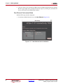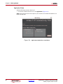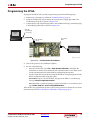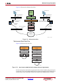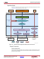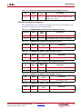
1
Virtex-7 FPGA
XT Connectivity
Targeted Reference Design
for the VC709 Board
User Guide
Vivado Design Suite 2014.3
UG962 (v3.0) December 20, 2014
Notice of Disclaimer
The information disclosed to you hereunder (the “Materials”) is provided solely for the selection and use of Xilinx products. To the maximum
extent permitted by applicable law: (1) Materials are made available "AS IS" and with all faults, Xilinx hereby DISCLAIMS ALL
WARRANTIES AND CONDITIONS, EXPRESS, IMPLIED, OR STATUTORY, INCLUDING BUT NOT LIMITED TO WARRANTIES OF
MERCHANTABILITY, NON-INFRINGEMENT, OR FITNESS FOR ANY PARTICULAR PURPOSE; and (2) Xilinx shall not be liable (whether
in contract or tort, including negligence, or under any other theory of liability) for any loss or damage of any kind or nature related to, arising
under, or in connection with, the Materials (including your use of the Materials), including for any direct, indirect, special, incidental, or
consequential loss or damage (including loss of data, profits, goodwill, or any type of loss or damage suffered as a result of any action
brought by a third party) even if such damage or loss was reasonably foreseeable or Xilinx had been advised of the possibility of the same.
Xilinx assumes no obligation to correct any errors contained in the Materials or to notify you of updates to the Materials or to product
specifications. You may not reproduce, modify, distribute, or publicly display the Materials without prior written consent. Certain products are
subject to the terms and conditions of Xilinx’s limited warranty, please refer to Xilinx’s Terms of Sale which can be viewed at
http://www.xilinx.com/legal.htm#tos; IP cores may be subject to warranty and support terms contained in a license issued to you by Xilinx.
Xilinx products are not designed or intended to be fail-safe or for use in any application requiring fail-safe performance; you assume sole risk
and liability for use of Xilinx products in such critical applications, please refer to Xilinx’s Terms of Sale which can be viewed at
http://www.xilinx.com/legal.htm#tos.
AUTOMOTIVE APPLICATIONS DISCLAIMER
XILINX PRODUCTS ARE NOT DESIGNED OR INTENDED TO BE FAIL-SAFE, OR FOR USE IN ANY APPLICATION REQUIRING
FAIL-SAFE PERFORMANCE, SUCH AS APPLICATIONS RELATED TO: (I) THE DEPLOYMENT OF AIRBAGS, (II) CONTROL OF A
VEHICLE, UNLESS THERE IS A FAIL-SAFE OR REDUNDANCY FEATURE (WHICH DOES NOT INCLUDE USE OF SOFTWARE IN THE
XILINX DEVICE TO IMPLEMENT THE REDUNDANCY) AND A WARNING SIGNAL UPON FAILURE TO THE OPERATOR, OR (III) USES
THAT COULD LEAD TO DEATH OR PERSONAL INJURY. CUSTOMER ASSUMES THE SOLE RISK AND LIABILITY OF ANY USE OF
XILINX PRODUCTS IN SUCH APPLICATIONS.
Fedora Information
Xilinx obtained the Fedora Linux software from Fedora (http://fedoraproject.org/), and you may too. Xilinx made no changes to the software
obtained from Fedora. If you desire to use Fedora Linux software in your product, Xilinx encourages you to obtain Fedora Linux software
directly from Fedora (http://fedoraproject.org/), even though we are providing to you a copy of the corresponding source code as provided
to us by Fedora. Portions of the Fedora software may be covered by the GNU General Public license as well as many other applicable open
source licenses. Please review the source code in detail for further information. To the maximum extent permitted by applicable law and if
not prohibited by any such third-party licenses, (1) XILINX DISCLAIMS ANY AND ALL EXPRESS OR IMPLIED WARRANTIES,
INCLUDING, BUT NOT LIMITED TO, THE IMPLIED WARRANTIES OF MERCHANTABILITY AND FITNESS FOR A PARTICULAR
PURPOSE; AND (2) IN NO EVENT SHALL XILINX BE LIABLE FOR ANY DIRECT, INDIRECT, INCIDENTAL, SPECIAL, EXEMPLARY, OR
CONSEQUENTIAL DAMAGES (INCLUDING, BUT NOT LIMITED TO, PROCUREMENT OF SUBSTITUTE GOODS OR SERVICES; LOSS
OF USE,DATA, OR PROFITS; OR BUSINESS INTERRUPTION) HOWEVER CAUSED AND ON ANY THEORY OF LIABILITY, WHETHER
IN CONTRACT, STRICT LIABILITY, OR TORT (INCLUDING NEGLIGENCE OR OTHERWISE) ARISING IN ANY WAY OUT OF THE USE
OF THIS SOFTWARE, EVEN IF ADVISED OF THE POSSIBILITY OF SUCH DAMAGE.
Fedora software and technical information is subject to the U.S. Export Administration Regulations and other U.S. and foreign law, and may
not be exported or re-exported to certain countries (currently Cuba, Iran, Iraq, North Korea, Sudan, and Syria) or to persons or entities
prohibited from receiving U.S. exports (including those (a) on the Bureau of Industry and Security Denied Parties List or Entity List, (b) on
the Office of Foreign Assets Control list of Specially Designated Nationals and Blocked Persons, and (c) involved with missile technology or
nuclear, chemical or biological weapons). You may not download Fedora software or technical information if you are located in one of these
countries, or otherwise affected by these restrictions. You may not provide Fedora software or technical information to individuals or entities
located in one of these countries or otherwise affected by these restrictions. You are also responsible for compliance with foreign law
requirements applicable to the import and use of Fedora software and technical information.
© Copyright 2013–2014 Xilinx, Inc. Xilinx, Inc. Xilinx, the Xilinx logo, Artix, ISE, Kintex, Spartan, Virtex, Zynq, and other designated brands
included herein are trademarks of Xilinx in the United States and other countries. All other trademarks are the property of their respective
owners.
VC709 Virtex-7 FPGA XT Connectivity TRD
www.xilinx.com
UG962 (v3.0) December 20, 2014
Revision History
The following table shows the revision history for this document.
Date
Version
Revision
07/26/2013
1.0
Initial Xilinx Release.
06/30/2014
2.0
Updated 64-bit datapath operation from 1,866 MT/s to 1,600 MT/s throughout. Updated
Figure 1-1, Figure 1-2, Figure 1-3, and Figure 3-4. Updated Table 1-1. Changed
description of Hardware Test Setup and modified VC709 Board Setup in Chapter 2.
Replaced Figure 2-13, Figure 2-17, and Figure 2-21. Modified simulation procedures,
including Simulation Using QuestaSim, Windows QuestaSim Simulation Flow, Linux
QuestaSim Simulation Flow, Simulation Using Vivado Simulator, Windows Vivado
Simulator Flow, and Linux Vivado Simulator Flow. Modified User-Controlled Macros
section, including adding TRD_MODE information. Updated Figure B-1 and Directory
Structure. Replaced references to ModelSim simulator with QuestaSim throughout.
12/20/2014
3.0
Updated for the Vivado Design Suite 2014.3 release. Updated Table 1-1 and Table A-2.
Updated Programming the VC709 Board and Power Monitoring Registers.
UG962 (v3.0) December 20, 2014
www.xilinx.com
VC709 Virtex-7 FPGA XT Connectivity TRD
VC709 Virtex-7 FPGA XT Connectivity TRD
www.xilinx.com
UG962 (v3.0) December 20, 2014
Table of Contents
Revision History . . . . . . . . . . . . . . . . . . . . . . . . . . . . . . . . . . . . . . . . . . . . . . . . . . . . . . . . . . . . . . . . . . . . 3
Chapter 1: Introduction
Operation Modes . . . . . . . . . . . . . . . . . . . . . . . . . . . . . . . . . . . . . . . . . . . . . . . . . . . . . . . . . . . . . . . . . . 10
PCIe DMA Performance Mode . . . . . . . . . . . . . . . . . . . . . . . . . . . . . . . . . . . . . . . . . . . . . . . . . . . . 10
Raw Ethernet Performance Mode . . . . . . . . . . . . . . . . . . . . . . . . . . . . . . . . . . . . . . . . . . . . . . . . . . 11
Application Mode . . . . . . . . . . . . . . . . . . . . . . . . . . . . . . . . . . . . . . . . . . . . . . . . . . . . . . . . . . . . . . . 12
Features . . . . . . . . . . . . . . . . . . . . . . . . . . . . . . . . . . . . . . . . . . . . . . . . . . . . . . . . . . . . . . . . . . . . . . . . . . . . 12
Base Features . . . . . . . . . . . . . . . . . . . . . . . . . . . . . . . . . . . . . . . . . . . . . . . . . . . . . . . . . . . . . . . . . . . 12
NIC Application Features . . . . . . . . . . . . . . . . . . . . . . . . . . . . . . . . . . . . . . . . . . . . . . . . . . . . . . . . . 12
Resource Utilization. . . . . . . . . . . . . . . . . . . . . . . . . . . . . . . . . . . . . . . . . . . . . . . . . . . . . . . . . . . . . . . . 13
Chapter 2: Getting Started
Requirements . . . . . . . . . . . . . . . . . . . . . . . . . . . . . . . . . . . . . . . . . . . . . . . . . . . . . . . . . . . . . . . . . . . . . . 15
Simulation Requirements . . . . . . . . . . . . . . . . . . . . . . . . . . . . . . . . . . . . . . . . . . . . . . . . . . . . . . . . . 15
Test Setup Requirements . . . . . . . . . . . . . . . . . . . . . . . . . . . . . . . . . . . . . . . . . . . . . . . . . . . . . . . . . 15
Hardware Test Setup . . . . . . . . . . . . . . . . . . . . . . . . . . . . . . . . . . . . . . . . . . . . . . . . . . . . . . . . . . . . . . . 16
VC709 Board Setup . . . . . . . . . . . . . . . . . . . . . . . . . . . . . . . . . . . . . . . . . . . . . . . . . . . . . . . . . . . . . .
Driver Installation and Modes of Operation . . . . . . . . . . . . . . . . . . . . . . . . . . . . . . . . . . . . . . . . .
GEN/CHK Performance Mode . . . . . . . . . . . . . . . . . . . . . . . . . . . . . . . . . . . . . . . . . . . . . . . . . .
Raw Ethernet Performance Mode . . . . . . . . . . . . . . . . . . . . . . . . . . . . . . . . . . . . . . . . . . . . . . . . .
Application Mode . . . . . . . . . . . . . . . . . . . . . . . . . . . . . . . . . . . . . . . . . . . . . . . . . . . . . . . . . . . . .
Ethernet-Specific Features . . . . . . . . . . . . . . . . . . . . . . . . . . . . . . . . . . . . . . . . . . . . . . . . . . . . . . . .
NIC Statistics . . . . . . . . . . . . . . . . . . . . . . . . . . . . . . . . . . . . . . . . . . . . . . . . . . . . . . . . . . . . . . . .
16
19
23
26
30
33
34
Rebuilding the XT Connectivity TRD . . . . . . . . . . . . . . . . . . . . . . . . . . . . . . . . . . . . . . . . . . . . . . 34
Windows Implementation Flow . . . . . . . . . . . . . . . . . . . . . . . . . . . . . . . . . . . . . . . . . . . . . . . . . . .
Linux Implementation Flow . . . . . . . . . . . . . . . . . . . . . . . . . . . . . . . . . . . . . . . . . . . . . . . . . . . . . . .
Programming the VC709 Board . . . . . . . . . . . . . . . . . . . . . . . . . . . . . . . . . . . . . . . . . . . . . . . . . . . .
Programming Using the Prebuilt Design . . . . . . . . . . . . . . . . . . . . . . . . . . . . . . . . . . . . . . . . . . .
Programming Using the Rebuilt Design . . . . . . . . . . . . . . . . . . . . . . . . . . . . . . . . . . . . . . . . . . . .
34
35
35
35
36
Programming the FPGA . . . . . . . . . . . . . . . . . . . . . . . . . . . . . . . . . . . . . . . . . . . . . . . . . . . . . . . . . . . . 37
Simulation . . . . . . . . . . . . . . . . . . . . . . . . . . . . . . . . . . . . . . . . . . . . . . . . . . . . . . . . . . . . . . . . . . . . . . . . . 38
Overview . . . . . . . . . . . . . . . . . . . . . . . . . . . . . . . . . . . . . . . . . . . . . . . . . . . . . . . . . . . . . . . . . . . . . . .
Simulating the Design . . . . . . . . . . . . . . . . . . . . . . . . . . . . . . . . . . . . . . . . . . . . . . . . . . . . . . . . . . . .
Simulation Using QuestaSim . . . . . . . . . . . . . . . . . . . . . . . . . . . . . . . . . . . . . . . . . . . . . . . . . . . .
Windows QuestaSim Simulation Flow . . . . . . . . . . . . . . . . . . . . . . . . . . . . . . . . . . . . . . . . . . . . .
Linux QuestaSim Simulation Flow . . . . . . . . . . . . . . . . . . . . . . . . . . . . . . . . . . . . . . . . . . . . . . . .
Simulation Using Vivado Simulator . . . . . . . . . . . . . . . . . . . . . . . . . . . . . . . . . . . . . . . . . . . . . . .
Windows Vivado Simulator Flow. . . . . . . . . . . . . . . . . . . . . . . . . . . . . . . . . . . . . . . . . . . . . . . . .
Linux Vivado Simulator Flow . . . . . . . . . . . . . . . . . . . . . . . . . . . . . . . . . . . . . . . . . . . . . . . . . . . .
User-Controlled Macros . . . . . . . . . . . . . . . . . . . . . . . . . . . . . . . . . . . . . . . . . . . . . . . . . . . . . . . . . .
Test Selection . . . . . . . . . . . . . . . . . . . . . . . . . . . . . . . . . . . . . . . . . . . . . . . . . . . . . . . . . . . . . . . . . . .
VC709 Virtex-7 FPGA XT Connectivity TRD
UG962 (v3.0) December 20, 2014
www.xilinx.com
Send Feedback
38
38
39
39
39
39
40
40
41
42
5
Chapter 3: Functional Description
Hardware Architecture . . . . . . . . . . . . . . . . . . . . . . . . . . . . . . . . . . . . . . . . . . . . . . . . . . . . . . . . . . . . . 43
Base System Components . . . . . . . . . . . . . . . . . . . . . . . . . . . . . . . . . . . . . . . . . . . . . . . . . . . . . . . . .
PCI Express . . . . . . . . . . . . . . . . . . . . . . . . . . . . . . . . . . . . . . . . . . . . . . . . . . . . . . . . . . . . . . . . . .
Performance Monitor for PCIe . . . . . . . . . . . . . . . . . . . . . . . . . . . . . . . . . . . . . . . . . . . . . . .
Scatter Gather Packet DMA . . . . . . . . . . . . . . . . . . . . . . . . . . . . . . . . . . . . . . . . . . . . . . . . . . . . .
Scatter Gather Operation . . . . . . . . . . . . . . . . . . . . . . . . . . . . . . . . . . . . . . . . . . . . . . . . . . .
Packet Transmission . . . . . . . . . . . . . . . . . . . . . . . . . . . . . . . . . . . . . . . . . . . . . . . . . . . . . .
Packet Reception . . . . . . . . . . . . . . . . . . . . . . . . . . . . . . . . . . . . . . . . . . . . . . . . . . . . . . . . .
Virtual FIFOs . . . . . . . . . . . . . . . . . . . . . . . . . . . . . . . . . . . . . . . . . . . . . . . . . . . . . . . . . . . . . . . .
AXI Stream Interconnect . . . . . . . . . . . . . . . . . . . . . . . . . . . . . . . . . . . . . . . . . . . . . . . . . . . . . . . .
AXI VFIFO Controller . . . . . . . . . . . . . . . . . . . . . . . . . . . . . . . . . . . . . . . . . . . . . . . . . . . . . . . . . .
Memory Interface Generator. . . . . . . . . . . . . . . . . . . . . . . . . . . . . . . . . . . . . . . . . . . . . . . . . . . . .
Application Components . . . . . . . . . . . . . . . . . . . . . . . . . . . . . . . . . . . . . . . . . . . . . . . . . . . . . . . . .
AXI4-Stream Packet Generator and Checker . . . . . . . . . . . . . . . . . . . . . . . . . . . . . . . . . . . . . . . .
Packet Format and Data Integrity . . . . . . . . . . . . . . . . . . . . . . . . . . . . . . . . . . . . . . . . . . . .
Packet Checker . . . . . . . . . . . . . . . . . . . . . . . . . . . . . . . . . . . . . . . . . . . . . . . . . . . . . . . . . . .
Packet Generator . . . . . . . . . . . . . . . . . . . . . . . . . . . . . . . . . . . . . . . . . . . . . . . . . . . . . . . . .
Network Path Components . . . . . . . . . . . . . . . . . . . . . . . . . . . . . . . . . . . . . . . . . . . . . . . . . . . . . . .
Quad 10GBASE-R Implementation . . . . . . . . . . . . . . . . . . . . . . . . . . . . . . . . . . . . . . . . . . . . . . . .
Receive Interface Logic . . . . . . . . . . . . . . . . . . . . . . . . . . . . . . . . . . . . . . . . . . . . . . . . . . . . . . . . .
Address Filtering Logic. . . . . . . . . . . . . . . . . . . . . . . . . . . . . . . . . . . . . . . . . . . . . . . . . . . . . . . . .
Utility Components . . . . . . . . . . . . . . . . . . . . . . . . . . . . . . . . . . . . . . . . . . . . . . . . . . . . . . . . . . . . . .
PicoBlaze-Based Power Monitor . . . . . . . . . . . . . . . . . . . . . . . . . . . . . . . . . . . . . . . . . . . . . . . . . .
PicoBlaze-Based SI5324 Programming and GTH transceiver Reference Clock Generation . . . . .
User Register Interface . . . . . . . . . . . . . . . . . . . . . . . . . . . . . . . . . . . . . . . . . . . . . . . . . . . . . . . . . . .
Clocking and Reset . . . . . . . . . . . . . . . . . . . . . . . . . . . . . . . . . . . . . . . . . . . . . . . . . . . . . . . . . . . . . .
43
43
44
44
44
46
47
48
48
49
49
49
49
50
50
50
51
51
51
52
52
52
53
55
55
Software Design Description . . . . . . . . . . . . . . . . . . . . . . . . . . . . . . . . . . . . . . . . . . . . . . . . . . . . . . . 56
User-Space Application Features . . . . . . . . . . . . . . . . . . . . . . . . . . . . . . . . . . . . . . . . . . . . . . . . . . .
Kernel-Space Driver Features . . . . . . . . . . . . . . . . . . . . . . . . . . . . . . . . . . . . . . . . . . . . . . . . . . . . . .
Data Flow . . . . . . . . . . . . . . . . . . . . . . . . . . . . . . . . . . . . . . . . . . . . . . . . . . . . . . . . . . . . . . . . . . . . . .
Ethernet Data Flow . . . . . . . . . . . . . . . . . . . . . . . . . . . . . . . . . . . . . . . . . . . . . . . . . . . . . . . . . . . .
Performance Mode Data Flow . . . . . . . . . . . . . . . . . . . . . . . . . . . . . . . . . . . . . . . . . . . . . . . . . . .
Performance Mode . . . . . . . . . . . . . . . . . . . . . . . . . . . . . . . . . . . . . . . . . . . . . . . . . . . . . . . . . . . . . . .
Datapath Components . . . . . . . . . . . . . . . . . . . . . . . . . . . . . . . . . . . . . . . . . . . . . . . . . . . . . . . . .
Application Traffic Generator . . . . . . . . . . . . . . . . . . . . . . . . . . . . . . . . . . . . . . . . . . . . . . .
Driver Entry . . . . . . . . . . . . . . . . . . . . . . . . . . . . . . . . . . . . . . . . . . . . . . . . . . . . . . . . . . . . .
Driver Private Interface . . . . . . . . . . . . . . . . . . . . . . . . . . . . . . . . . . . . . . . . . . . . . . . . . . . .
Application Layer Interface . . . . . . . . . . . . . . . . . . . . . . . . . . . . . . . . . . . . . . . . . . . . . . . . .
DMA Operations . . . . . . . . . . . . . . . . . . . . . . . . . . . . . . . . . . . . . . . . . . . . . . . . . . . . . . . . .
Interrupt or Polling Operations . . . . . . . . . . . . . . . . . . . . . . . . . . . . . . . . . . . . . . . . . . . . . .
Control Path Components . . . . . . . . . . . . . . . . . . . . . . . . . . . . . . . . . . . . . . . . . . . . . . . . . . . . . .
Graphical User Interface . . . . . . . . . . . . . . . . . . . . . . . . . . . . . . . . . . . . . . . . . . . . . . . . . . .
Driver Entry Points . . . . . . . . . . . . . . . . . . . . . . . . . . . . . . . . . . . . . . . . . . . . . . . . . . . . . . .
Performance Monitor . . . . . . . . . . . . . . . . . . . . . . . . . . . . . . . . . . . . . . . . . . . . . . . . . . . . . .
Performance mode design implementation . . . . . . . . . . . . . . . . . . . . . . . . . . . . . . . . . . . . . . . . .
User Application . . . . . . . . . . . . . . . . . . . . . . . . . . . . . . . . . . . . . . . . . . . . . . . . . . . . . . . . .
Driver implementation. . . . . . . . . . . . . . . . . . . . . . . . . . . . . . . . . . . . . . . . . . . . . . . . . . . . .
Application Mode . . . . . . . . . . . . . . . . . . . . . . . . . . . . . . . . . . . . . . . . . . . . . . . . . . . . . . . . . . . . . . .
Datapath Components . . . . . . . . . . . . . . . . . . . . . . . . . . . . . . . . . . . . . . . . . . . . . . . . . . . . . . . . .
Networking Applications. . . . . . . . . . . . . . . . . . . . . . . . . . . . . . . . . . . . . . . . . . . . . . . . . . .
TCP/IP Stack . . . . . . . . . . . . . . . . . . . . . . . . . . . . . . . . . . . . . . . . . . . . . . . . . . . . . . . . . . . .
Driver Entry Points . . . . . . . . . . . . . . . . . . . . . . . . . . . . . . . . . . . . . . . . . . . . . . . . . . . . . . .
6
Send Feedback
www.xilinx.com
56
56
56
56
57
58
59
59
59
59
59
59
59
60
60
60
60
60
60
60
61
61
61
62
62
VC709 Virtex-7 FPGA XT Connectivity TRD
UG962 (v3.0) December 20, 2014
Application Driver Interface . . . . . . . . . . . . . . . . . . . . . . . . . . . . . . . . . . . . . . . . . . . . . . . .
Interrupt or Polling Operations . . . . . . . . . . . . . . . . . . . . . . . . . . . . . . . . . . . . . . . . . . . . . .
Control Path Components . . . . . . . . . . . . . . . . . . . . . . . . . . . . . . . . . . . . . . . . . . . . . . . . . . . . . .
Networking Tools . . . . . . . . . . . . . . . . . . . . . . . . . . . . . . . . . . . . . . . . . . . . . . . . . . . . . . . .
Graphical User Interface . . . . . . . . . . . . . . . . . . . . . . . . . . . . . . . . . . . . . . . . . . . . . . . . . . .
Performance Monitor . . . . . . . . . . . . . . . . . . . . . . . . . . . . . . . . . . . . . . . . . . . . . . . . . . . . . .
Application Mode Implementation. . . . . . . . . . . . . . . . . . . . . . . . . . . . . . . . . . . . . . . . . . . . . . . .
User Applications . . . . . . . . . . . . . . . . . . . . . . . . . . . . . . . . . . . . . . . . . . . . . . . . . . . . . . . .
Driver implementation. . . . . . . . . . . . . . . . . . . . . . . . . . . . . . . . . . . . . . . . . . . . . . . . . . . . .
62
62
62
62
62
62
62
62
63
DMA Descriptor Management . . . . . . . . . . . . . . . . . . . . . . . . . . . . . . . . . . . . . . . . . . . . . . . . . . . . . 63
Dynamic DMA Updates . . . . . . . . . . . . . . . . . . . . . . . . . . . . . . . . . . . . . . . . . . . . . . . . . . . . . . . . . .
Initialization Phase . . . . . . . . . . . . . . . . . . . . . . . . . . . . . . . . . . . . . . . . . . . . . . . . . . . . . . . . . . . .
Transmit (S2C) Descriptor Management . . . . . . . . . . . . . . . . . . . . . . . . . . . . . . . . . . . . . . .
Receive (C2S) Descriptor Management . . . . . . . . . . . . . . . . . . . . . . . . . . . . . . . . . . . . . . . .
63
64
64
65
User Interface–Control and Monitor GUI . . . . . . . . . . . . . . . . . . . . . . . . . . . . . . . . . . . . . . . . . . . 65
Chapter 4: Performance Estimation
Theoretical Estimate. . . . . . . . . . . . . . . . . . . . . . . . . . . . . . . . . . . . . . . . . . . . . . . . . . . . . . . . . . . . . . . . 67
PCIe–DMA . . . . . . . . . . . . . . . . . . . . . . . . . . . . . . . . . . . . . . . . . . . . . . . . . . . . . . . . . . . . . . . . . . . . . 67
DDR3 Virtual FIFO . . . . . . . . . . . . . . . . . . . . . . . . . . . . . . . . . . . . . . . . . . . . . . . . . . . . . . . . . . . . 69
Ten Gigabit Ethernet . . . . . . . . . . . . . . . . . . . . . . . . . . . . . . . . . . . . . . . . . . . . . . . . . . . . . . . . . . . . . 70
Chapter 5: Designing with the Platform
Overview . . . . . . . . . . . . . . . . . . . . . . . . . . . . . . . . . . . . . . . . . . . . . . . . . . . . . . . . . . . . . . . . . . . . . . . . . . 71
Software-only Modifications . . . . . . . . . . . . . . . . . . . . . . . . . . . . . . . . . . . . . . . . . . . . . . . . . . . . . . . 71
Macro-Based Modifications . . . . . . . . . . . . . . . . . . . . . . . . . . . . . . . . . . . . . . . . . . . . . . . . . . . . . . .
Descriptor Ring Size . . . . . . . . . . . . . . . . . . . . . . . . . . . . . . . . . . . . . . . . . . . . . . . . . . . . . . . . . . .
Log Verbosity Level . . . . . . . . . . . . . . . . . . . . . . . . . . . . . . . . . . . . . . . . . . . . . . . . . . . . . . . . . . .
Driver Mode of Operation . . . . . . . . . . . . . . . . . . . . . . . . . . . . . . . . . . . . . . . . . . . . . . . . . . . . . .
Jumbo Frames . . . . . . . . . . . . . . . . . . . . . . . . . . . . . . . . . . . . . . . . . . . . . . . . . . . . . . . . . . . . . . . .
Driver Queue Depth . . . . . . . . . . . . . . . . . . . . . . . . . . . . . . . . . . . . . . . . . . . . . . . . . . . . . . . . . . .
64-Bit Driver Compilation . . . . . . . . . . . . . . . . . . . . . . . . . . . . . . . . . . . . . . . . . . . . . . . . . . . . . . .
71
72
72
72
72
72
73
Appendix A: Register Descriptions
DMA Registers. . . . . . . . . . . . . . . . . . . . . . . . . . . . . . . . . . . . . . . . . . . . . . . . . . . . . . . . . . . . . . . . . . . . . 76
Channel-Specific Registers . . . . . . . . . . . . . . . . . . . . . . . . . . . . . . . . . . . . . . . . . . . . . . . . . . . . . . . .
Engine Control (0x0004) . . . . . . . . . . . . . . . . . . . . . . . . . . . . . . . . . . . . . . . . . . . . . . . . . . . . . . .
Next Descriptor Pointer (0x0008) . . . . . . . . . . . . . . . . . . . . . . . . . . . . . . . . . . . . . . . . . . . . . . . .
Software Descriptor Pointer (0x000C) . . . . . . . . . . . . . . . . . . . . . . . . . . . . . . . . . . . . . . . . . . . . .
Completed Byte Count (0x001C) . . . . . . . . . . . . . . . . . . . . . . . . . . . . . . . . . . . . . . . . . . . . . . . . .
Common Control and Status Register . . . . . . . . . . . . . . . . . . . . . . . . . . . . . . . . . . . . . . . . . . . . . .
Common Control and Status (0x4000) . . . . . . . . . . . . . . . . . . . . . . . . . . . . . . . . . . . . . . . . . . . .
User Space Registers . . . . . . . . . . . . . . . . . . . . . . . . . . . . . . . . . . . . . . . . . . . . . . . . . . . . . . . . . . . . .
Design Version and Status Registers. . . . . . . . . . . . . . . . . . . . . . . . . . . . . . . . . . . . . . . . . . . . . . .
Design Version (0x9000). . . . . . . . . . . . . . . . . . . . . . . . . . . . . . . . . . . . . . . . . . . . . . . . . . .
Design Mode (0x9004) . . . . . . . . . . . . . . . . . . . . . . . . . . . . . . . . . . . . . . . . . . . . . . . . . . . .
Design Status (0x9008) . . . . . . . . . . . . . . . . . . . . . . . . . . . . . . . . . . . . . . . . . . . . . . . . . . . .
Transmit Utilization Byte Count (0x900C) . . . . . . . . . . . . . . . . . . . . . . . . . . . . . . . . . . . . .
Receive Utilization Byte Count (0x9010) . . . . . . . . . . . . . . . . . . . . . . . . . . . . . . . . . . . . . .
Upstream Memory Write Byte Count (0x9014) . . . . . . . . . . . . . . . . . . . . . . . . . . . . . . . . .
VC709 Virtex-7 FPGA XT Connectivity TRD
UG962 (v3.0) December 20, 2014
www.xilinx.com
Send Feedback
76
77
77
78
78
78
78
79
79
79
79
80
80
80
81
7
Downstream Completion Byte Count (0x9018) . . . . . . . . . . . . . . . . . . . . . . . . . . . . . . . . .
Initial Completion Data Credits for Downstream Port (0x901C) . . . . . . . . . . . . . . . . . . . .
Initial Completion Header Credits for Downstream Port (0x9020) . . . . . . . . . . . . . . . . . .
PCIe Credits Status - Initial Non-Posted Data Credits for Downstream Port (0x9024) . . .
PCIe Credits Status - Initial Non-Posted Header Credits for Downstream Port (0x9028) .
PCIe Credits Status - Initial Posted Data Credits for Downstream Port (0x902C) . . . . . . .
PCIe Credits Status - Initial Posted Header Credits for Downstream Port (0x9030) . . . . .
Performance Scaling Factor User Register (0x9034) . . . . . . . . . . . . . . . . . . . . . . . . . . . . . .
Power Monitoring Registers . . . . . . . . . . . . . . . . . . . . . . . . . . . . . . . . . . . . . . . . . . . . . . . . . . . . .
Performance Mode: Generator/Checker/Loopback Registers Channel-0 . . . . . . . . . . . . . . . . . .
XGEMAC-Related User Registers . . . . . . . . . . . . . . . . . . . . . . . . . . . . . . . . . . . . . . . . . . . . . . . . .
81
81
81
81
82
82
82
82
82
84
85
Appendix B: Directory Structure and File Descriptions
Directory Structure . . . . . . . . . . . . . . . . . . . . . . . . . . . . . . . . . . . . . . . . . . . . . . . . . . . . . . . . . . . . . . . . . 87
Hardware Folder . . . . . . . . . . . . . . . . . . . . . . . . . . . . . . . . . . . . . . . . . . . . . . . . . . . . . . . . . . . . . . . .
Vivado Folder . . . . . . . . . . . . . . . . . . . . . . . . . . . . . . . . . . . . . . . . . . . . . . . . . . . . . . . . . . . . . . . .
Scripts Folder . . . . . . . . . . . . . . . . . . . . . . . . . . . . . . . . . . . . . . . . . . . . . . . . . . . . . . . . . . . .
Runs Folder . . . . . . . . . . . . . . . . . . . . . . . . . . . . . . . . . . . . . . . . . . . . . . . . . . . . . . . . . . . . .
Sources Folder. . . . . . . . . . . . . . . . . . . . . . . . . . . . . . . . . . . . . . . . . . . . . . . . . . . . . . . . . . . . . . . .
Constraints Folder . . . . . . . . . . . . . . . . . . . . . . . . . . . . . . . . . . . . . . . . . . . . . . . . . . . . . . . .
HDL Folder . . . . . . . . . . . . . . . . . . . . . . . . . . . . . . . . . . . . . . . . . . . . . . . . . . . . . . . . . . . . .
Ip_catalog Folder . . . . . . . . . . . . . . . . . . . . . . . . . . . . . . . . . . . . . . . . . . . . . . . . . . . . . . . . .
Ip_cores Folder. . . . . . . . . . . . . . . . . . . . . . . . . . . . . . . . . . . . . . . . . . . . . . . . . . . . . . . . . . .
Testbench Folder . . . . . . . . . . . . . . . . . . . . . . . . . . . . . . . . . . . . . . . . . . . . . . . . . . . . . . . . .
Software Folder . . . . . . . . . . . . . . . . . . . . . . . . . . . . . . . . . . . . . . . . . . . . . . . . . . . . . . . . . . . . . . . . .
Linux Folder . . . . . . . . . . . . . . . . . . . . . . . . . . . . . . . . . . . . . . . . . . . . . . . . . . . . . . . . . . . . . . . . .
Linux_driver_app Folder . . . . . . . . . . . . . . . . . . . . . . . . . . . . . . . . . . . . . . . . . . . . . . . . . . .
Readme.txt File . . . . . . . . . . . . . . . . . . . . . . . . . . . . . . . . . . . . . . . . . . . . . . . . . . . . . . . . . .
Quickstart.sh File . . . . . . . . . . . . . . . . . . . . . . . . . . . . . . . . . . . . . . . . . . . . . . . . . . . . . . . . .
Ready_to_test Folder . . . . . . . . . . . . . . . . . . . . . . . . . . . . . . . . . . . . . . . . . . . . . . . . . . . . . . . . . . . . .
Readme.txt File . . . . . . . . . . . . . . . . . . . . . . . . . . . . . . . . . . . . . . . . . . . . . . . . . . . . . . . . . . . . . . . . . .
87
87
88
88
88
88
88
88
88
88
88
88
88
89
89
89
89
Appendix C: Software Application Compilation and Network
Performance
Compiling Traffic Generator Application . . . . . . . . . . . . . . . . . . . . . . . . . . . . . . . . . . . . . . . . . . . 91
Private Network Setup and Test . . . . . . . . . . . . . . . . . . . . . . . . . . . . . . . . . . . . . . . . . . . . . . . . . . . . 91
Default Setup . . . . . . . . . . . . . . . . . . . . . . . . . . . . . . . . . . . . . . . . . . . . . . . . . . . . . . . . . . . . . . . . . . . 91
Peer Mode Setup . . . . . . . . . . . . . . . . . . . . . . . . . . . . . . . . . . . . . . . . . . . . . . . . . . . . . . . . . . . . . . . . 92
Appendix D: Troubleshooting
Appendix E: Additional Resources
Xilinx Resources . . . . . . . . . . . . . . . . . . . . . . . . . . . . . . . . . . . . . . . . . . . . . . . . . . . . . . . . . . . . . . . . . . . 97
Solution Centers . . . . . . . . . . . . . . . . . . . . . . . . . . . . . . . . . . . . . . . . . . . . . . . . . . . . . . . . . . . . . . . . . . . 97
References . . . . . . . . . . . . . . . . . . . . . . . . . . . . . . . . . . . . . . . . . . . . . . . . . . . . . . . . . . . . . . . . . . . . . . . . . 97
Appendix F: Warranty
Statement . . . . . . . . . . . . . . . . . . . . . . . . . . . . . . . . . . . . . . . . . . . . . . . . . . . . . . . . . . . . . . . . . . . . . . . . . . 99
8
Send Feedback
www.xilinx.com
VC709 Virtex-7 FPGA XT Connectivity TRD
UG962 (v3.0) December 20, 2014
Chapter 1
Introduction
This chapter introduces the Virtex®-7 FPGA XT Connectivity Targeted Reference Design
(XT Connectivity TRD), summarizes its modes of operation and lists the TRD features.
The XT Connectivity TRD targets the XC7V690T-2FFG1761C FPGA running on the VC709
Evaluation Board and demonstrates a high-performance data transfer system using a PCI
Express® (PCIe®) Endpoint block in x8 Gen3 configuration with a high-performance
scatter-gather packet DMA core by Northwest Logic [Ref 12], two DDR3 small-outline
dual-inline memory modules (SODIMM), each providing a 64-bit datapath operating at
1,600 MT/s, and four 10GBASE-R links.
Figure 1-1 shows the XT Connectivity TRD block diagram.
X-Ref Target - Figure 1-1
Host Computer with
PCIe v3.0 slot
VC709 Board
PCIe
Monitor
Network
Application
(ping, http)
AXI4Lite
Slave
S2C
3
C2S
Integrated Block on FPGA
Xilinx IP Core
AXI-MM
Figure 1-1:
DDR 3
10G
10G
XGMII
MAC
PHY
10G
10G
XGMII
MAC
PHY
64-bit at
156.25 MHz
RD
M01
M00
AXIS-IC
M03
M02
Fabric Logic
AXI-MIG
64-bit at
1,600 MT/s
SI
S00
S01
AXIS-IC
S02
S03
WR
AXI VFIFO
PCIe IP
DDR 3
SI
512-bit at
200 MHz
GTH
S2C
2
C2S
RD
M01
M00
AXIS-IC
M03
M02
GTH
256-bit at
250 MHz
256-bit at 250 MHz
PCIe Express (Gen3)
S2C
1
C2S
Network
Application
(ping, http)
10G
10G
XGMII
MAC
PHY
64-bit at
156.25 MHz
AXI VFIFO
Packet
DMA
10G
10G
XGMII
MAC
PHY
GTH
S00
S01
AXIS-IC
S02
S03
WR
S2C
0
C2S
GTH
x8 Gen3 PCIe
Software
Driver
AXI Target
Master
GTH
AXI4LITE Interconnect
GUI
TCP/IP
Stack
User
Registers
Third Party IP Core
AXI-Lite
Component On Board
AXI-Stream
UG962_c1_01_060214
XT Connectivity TRD Block Diagram
The XT Connectivity TRD facilitates high speed data transfers between host computer
memory and the VC709 board. A software driver located on the host computer is the data
VC709 Virtex-7 FPGA XT Connectivity TRD
UG962 (v3.0) December 20, 2014
www.xilinx.com
Send Feedback
9
Chapter 1: Introduction
source and generates data packets for the performance demonstration. It connects to a
TCP/IP stack for the networking application demonstration.
Operation Modes
The XT Connectivity TRD offers PCIe DMA Performance, Raw Ethernet Performance and
Application modes of operation. All modes are available within a single design bitstream.
PCIe DMA Performance Mode
The PCIe DMA performance mode provides performance-oriented operation using the x8
Gen3 PCIe DMA followed by a packet generator and checker in the hardware. Figure 1-2
shows the PCIe DMA performance mode block diagram.
X-Ref Target - Figure 1-2
User
Registers
PCIe
Monitor
AXI4Lite
Slave
Packet
GEN
AXI VFIFO
AXI VFIFO
S2C
3
C2S
Xilinx IP Core
DDR 3
Third Party IP Core
AXI-MM
10G
10G
XGMII
MAC
PHY
10G
10G
XGMII
MAC
PHY
64-bit at
156.25 MHz
RD
M01
M00
AXIS-IC
M03
M02
Fabric Logic
AXI-MIG
64-bit at
1,600 MT/s
SI
S00
S01
AXIS-IC
S02
S03
WR
PCIe IP
Integrated Block on FPGA
DDR 3
SI
512-bit at
200 MHz
GTH
256-bit at
250 MHz
256-bit at 250 MHz
PCIe Express (Gen3)
RD
M01
M00
AXIS-IC
M03
M02
S2C
2
C2S
CHK
10G
10G
XGMII
MAC
PHY
64-bit at
156.25 MHz
S2C
1
C2S
Packet
DMA
10G
10G
XGMII
MAC
PHY
GTH
S00
S01
AXIS-IC
S02
S03
WR
S2C
0
C2S
GTH
x8 Gen3 PCIe
Software
Driver
GUI
GEN
Packet
CHK
GTH
AXI Target
Master
GTH
AXI4LITE Interconnect
AXI-Lite
Component On Board
AXI-Stream
UG962_c1_02_060214
Figure 1-2:
PCIe DMA Performance Mode
This mode demonstrates the performance capabilities of the PCIe DMA system only
without involvement of the other design blocks. This mode exercises two channels (S2C0
and C2S0) in DMA.
The PCIe DMA performance mode supports:
10
•
Loopback mode: The software user application generates packets that are sent through
drivers to hardware over the PCIe interface and DMA. Packets are sent back to the
software user application through drivers for checking data integrity.
•
Generator mode: The FPGA (configured by the TRD) generates packets and the
software driver checks them for integrity
Send Feedback
www.xilinx.com
VC709 Virtex-7 FPGA XT Connectivity TRD
UG962 (v3.0) December 20, 2014
Operation Modes
•
Checker mode: The software user application generates packets that are sent to
hardware where data integrity is verified.
These modes of operation are configurable by way of the GUI through register
programming. See Appendix A, Register Descriptions for more information.
Raw Ethernet Performance Mode
The raw ethernet performance mode demonstrates the 10G Ethernet path demonstrating
the high-performance capabilities of the XT Connectivity TRD. The software application
generates raw broadcast Ethernet frames with no connection to the networking stack.
Figure 1-3 shows the raw ethernet performance mode block diagram.
X-Ref Target - Figure 1-3
User
Registers
PCIe
Monitor
AXI4Lite
Slave
512-bit at
200 MHz
AXI VFIFO
S2C
3
C2S
AXI-MM
64-bit at
1,600 MT/s
DDR 3
10G
10G
XGMII
MAC
PHY
10G
10G
XGMII
MAC
PHY
64-bit at
156.25 MHz
RD
M01
M00
AXIS-IC
M03
M02
Fabric Logic
AXI-MIG
SI
S00
S01
AXIS-IC
S02
S03
WR
PCIe IP
Xilinx IP Core
DDR 3
SI
GTH
256-bit at
250 MHz
RD
M01
M00
AXIS-IC
M03
M02
GTH
256-bit at 250 MHz
PCIe Express (Gen3)
AXI VFIFO
S2C
2
C2S
Integrated Block on FPGA
10G
10G
XGMII
MAC
PHY
64-bit at
156.25MHz
S2C
1
C2S
Packet
DMA
10G
10G
XGMII
MAC
PHY
GTH
S00
S01
AXIS-IC
S02
S03
WR
S2C
0
C2S
GTH
x8 Gen3 PCIe
Software
Driver
GUI
AXI Target
Master
GTH
AXI4LITE Interconnect
Third Party IP Core
AXI-Lite
Component On Board
AXI-Stream
UG962_c1_03_060214
Figure 1-3:
Raw Ethernet Performance Demo
The packet originates from the user application and moves to the FPGA through the PCIe
interface and DMA, traverses AXI-VFIFO through the DDR3 memory, then through
XGEMAC and 10GBASE-R physical layer. The data is looped back through the fiber cables
installed in one of the SFP+ module to another SFP+ module, goes through the receive side
of a different 10GBASE-R PHY and XGEMAC, then back into AXI-VFIFO and DDR3, and
through PCIe-DMA and back to software application.
All four Ethernet channels can be enabled in the GUI in loopback mode. The generator and
checker modes are not supported for raw Ethernet performance mode.
VC709 Virtex-7 FPGA XT Connectivity TRD
UG962 (v3.0) December 20, 2014
www.xilinx.com
Send Feedback
11
Chapter 1: Introduction
Application Mode
The application mode demonstrates end-to-end application of a quad 10G network
interface card (NIC). The software driver connects to the networking stack allowing
standard networking applications to be used. However, due to lack of an offload engine in
hardware, the performance remains low because the software has to handle all of the
TCP/IP overhead. In application mode, the packets originate from TCP/IP stack by
invoking various standard networking applications.
Features
Base Features
The basic features of the PCIe and DMA IP that form the backbone of the design include:
•
•
PCIe v3.0 compliant x8 Endpoint operating at 8 Gb/s per lane/direction
•
PCIe transaction interface utilization engine
•
MSI and legacy interrupt support
Bus mastering scatter-gather DMA
•
Multichannel DMA
•
AXI4 streaming interface for data
•
AXI4-Lite interface for register space access
•
DMA performance engine
•
Full duplex operation
•
Independent transmit and receive channels
NIC Application Features
The features of the quad 10G network interface card application provided with the XT
Connectivity TRD include:
•
Two DDR3 SODIMMs operating 64-bit at 1,600 Mb/s
•
•
•
•
12
Use of AXI Stream Interconnect and AXI Virtual FIFO controller IP to make DDR3
a packet FIFO
10 Gigabit Ethernet MAC with 10G BASE-R PHY
•
Address filtering
•
Inter-frame gap control
•
Jumbo frame support up to 16,383 bytes in size
•
Ethernet statistics engine
•
Management interface for configuration (MDIO)
PicoBlaze™-based power, voltage, and temperature monitoring:
•
Engine in hardware to monitor power consumption by reading the TI UCD9248
power controller devices on the VC709 board
•
Engine in hardware to monitor die temperature and voltage rails by way of
Xilinx® Analog-to-Digital Converter (XADC)
PicoBlaze-based I2C programming of SI5324 clock multiplier or jitter attenuator
device on the VC709 board
Send Feedback
www.xilinx.com
VC709 Virtex-7 FPGA XT Connectivity TRD
UG962 (v3.0) December 20, 2014
Resource Utilization
Resource Utilization
Table 1-1 lists the resources used by the XT Connectivity TRD at the time of production
after placement has run. These numbers might vary based on the version of the XT
Connectivity TRD and the tools being used to regenerate the design.
Table 1-1:
Resource Utilization
Resource
Total Available
Usage
Slice Registers
864,736
203,391 (23%)
Slice LUT
432,368
221,348 (51%)
Block RAM
1,470
303 (20%)
MMCME2_ADV
20
4 (20%)
PLLE2_ADV
20
2 (10%)
BUFG/BUFGCTRL
32
18 (56%)
XADC
1
1 (100%)
IOB
850
253 (30%)
GTHE2_CHANNEL
36
12 (33%)
GTHE2_COMMON
9
3 (33%)
VC709 Virtex-7 FPGA XT Connectivity TRD
UG962 (v3.0) December 20, 2014
www.xilinx.com
Send Feedback
13
Chapter 1: Introduction
14
Send Feedback
www.xilinx.com
VC709 Virtex-7 FPGA XT Connectivity TRD
UG962 (v3.0) December 20, 2014
Requirements
Chapter 2
Getting Started
This chapter describes the requirements and provides the procedures for setting up the
hardware and software to test and simulate the XT Connectivity TRD.
Note: For an updated list of known issues, refer to the Virtex®-7 FPGA VC709 Connectivity Kit known issues and release notes master answer record master answer record (AR#51901). See
References in Appendix E. A list of answer records known at the time the kit was shipped is available
in the readme included on the CD containing the design files.
Requirements
Simulation Requirements
Simulation of the XT Connectivity TRD requires:
•
Vivado® simulator
or
•
QuestaSim simulation and verification tool
•
Xilinx simulation libraries compiled for the QuestaSim tool
Test Setup Requirements
Setting up the XT Connectivity TRD for operation and test requires:
•
VC709 Evaluation Board with XC7V690T-2FFG1761C FPGA
•
XT Connectivity TRD file rdf0285-vc709-connectivity-trd-2014-1.zip
consisting of:
•
Design source files
•
Device driver files
•
FPGA programming files
•
Linux driver documentation
•
Vivado Design Edition
•
USB cable, standard-A plug to micro-B plug
•
Four Avago SFP+ connector modules with two fiber optic cables [Ref 13]
•
ATX Power Supply Adapter Cable (4-pin to 6-pin adapter)
•
Fedora 16 LiveDVD [Ref 14]
•
PC with PCIe v3.0 slot and monitor (not supplied with the VC709 Connectivity Kit)
VC709 Virtex-7 FPGA XT Connectivity TRD
UG962 (v3.0) December 20, 2014
www.xilinx.com
Send Feedback
15
Chapter 2: Getting Started
Note: The VC709 board must be installed in a full-sized chassis because of the presence of the
four SFP+ modules on the back side of the board. If the VC709 board is installed in a rack-sized
chassis, two of the four SFP+ modules will not be accessible.
•
PC with monitor or laptop computer (not supplied with the VC709 Connectivity Kit)
with Vivado Design Edition installed
Hardware Test Setup
This section details the hardware setup and use of the application and control GUI.
These instructions assume that the VC709 board has the TRD pre-programmed into the
flash. If using a board that does not have the TRD pre-programmed, see Programming the
VC709 Board section of this user guide to program the flash before continuing.
All procedures require super-user access on the Linux computer. When using the Fedora
16 LiveDVD, super-user access is granted by default due to the way the kernel image is
built. If not using the LiveDVD contact the system administrator for super-user access.
VC709 Board Setup
To set up the VC709 board:
1.
Turn off the host computer.
2.
On SW11, set the mode pins and the BPI upper address pins to configure the FPGA
(see the settings in Figure 2-1). A25 and A24 are set to 00 and the mode pins are set to
010.
ON Position = 1
A25
A24
M2
M1
M0
X-Ref Target - Figure 2-1
1 2 3 4 5
OFF Position = 0
UG962_c2_104_071513
Figure 2-1:
16
SW11 Switch Settings for Mode Pins and BPI Upper Addresses
3.
Insert the VC709 board into a PCIe slot.
4.
Insert SFP+ connectors into the SFP+ module positions, as shown in Figure 2-2.
Send Feedback
www.xilinx.com
VC709 Virtex-7 FPGA XT Connectivity TRD
UG962 (v3.0) December 20, 2014
Hardware Test Setup
Note: To provide loopback capability, module connector P2 is connected to P3 and P4 to P5
(module P2 is the bottom one nearer to PCIe finger). For clarity, Figure 2-2 shows the board outside
of the PC chassis.
X-Ref Target - Figure 2-2
UG962_c2_01_011513
Figure 2-2: SFP+ Connector Locations on the VC709 Board (Left) and Cables Showing Loopback
Configuration (Right)
Figure 2-3 shows the setup with fiber optic cables installed in the PC chassis.
X-Ref Target - Figure 2-3
UG962_c2_02_011513
Figure 2-3: Setup with Fiber Optic Cable Installed in PC Chassis
VC709 Virtex-7 FPGA XT Connectivity TRD
UG962 (v3.0) December 20, 2014
www.xilinx.com
Send Feedback
17
Chapter 2: Getting Started
5.
Connect the 12V ATX power supply adapter cable (6-pin side) to the board at
connector J18, and the other side (4-pin) to the ATX Power Supply. Cable is shown in
Figure 2-4.
X-Ref Target - Figure 2-4
To ATX 4-Pin Peripheral
Power Connector
To J18 on VC709 Board
UG962_c2_03_011513
Figure 2-4:
6.
12V ATX Power Supply Adapter Cable
Ensure the connections are secure.
Note: The ATX Power Supply Adapter Cable is needed because the 6-pin ATX supply cannot be
connected directly to the VC709 board.
7.
Power on the VC709 board.
8.
Power on the system.
The GPIO LEDs on the VC709 board indicate the conditions as described in Table 2-1.
Table 2-1:
VC709 Board GPIO LEDs
GPIO LED
Reference
Description
Proper Behavior
Incorrect Behavior
0
PCIe link up
On (after a few seconds)
Off after BIOS loads (no link)
1
PCIe 250 MHz clock heart beat
Blinks slowly
Off (no clock)
2
PCIe linked at x8
On
Blinking fast (not x8)
3
PCIe linked at Gen3
On
Blinking fast (not Gen3)
4
Ethernet 156.25 clock heart
beat
Blinks slowly
Off (no clock)
5
10GBASE-R links ready (for all
four links)
On
Off (one or more links down)
6
DDR3 calibration done (both
SODIMMs)
On
Off (calibration failed on at
least one SODIMM)
7
Unused
Note: LED positions are marked on the board starting with 0 on the right to 7 on the left.
18
Send Feedback
www.xilinx.com
VC709 Virtex-7 FPGA XT Connectivity TRD
UG962 (v3.0) December 20, 2014
Hardware Test Setup
Figure 2-5 shows the location of LED indicators on the board.
X-Ref Target - Figure 2-5
LED[0] PCIe Link Up
UG962_c2_04_052113
Figure 2-5:
GPIO LEDs on the VC709 Board
Note: See Appendix D, Troubleshooting if the LEDs are not exhibiting proper behavior.
Driver Installation and Modes of Operation
These steps describe the installation of the device drivers for the XT Connectivity TRD
after hardware setup and demonstrate all modes of test operation by installing and
uninstalling various drivers.
Note: If Fedora 16 is currently installed on the hard disk of the host PC, reboot the PC as a user with
root privileges. After reboot, proceed to Step 2 (copy the folder) of this procedure.
1.
Place the DVD for Fedora 16 LiveDVD in the CD-ROM drive of the host PC.
The PC should reboot automatically from the CD-ROM drive.
The Fedora 16 Live Media is for Intel-compatible PCs. The DVD contains a complete,
bootable 32-bit Fedora 16 LiveDVD environment with the proper packages installed
for the XT Connectivity TRD demonstration environment. The PC boots from the
CD-ROM drive and logs into a liveuser account. This account has kernel development
root privileges required to install and remove device driver modules.
Note: Users might have to adjust BIOS boot order settings to ensure that the CD-ROM drive is the
first drive in the boot order. To enter the BIOS menu to set the boot order, press the Delete or F2 key
when the system is powered on. Set the boot order and save the changes.
VC709 Virtex-7 FPGA XT Connectivity TRD
UG962 (v3.0) December 20, 2014
www.xilinx.com
Send Feedback
19
Chapter 2: Getting Started
Figure 2-6 shows the screen images that are displayed during a successful Fedora 16
LiveDVD boot sequence.
X-Ref Target - Figure 2-6
First Screen
Last Boot Screen
Booted
UG962_c2_05_011513
Figure 2-6:
Fedora 16 LiveDVD Boot Sequence
2.
Copy v7_xt_conn_trd.tar.gz from the XT Connectivity TRD file
rdf0285-vc709-connectivity-trd-2014-1.zip to the home directory on the
Fedora 16 machine
3.
Click the Home folder on the left side of the screen to open the folder. Right-click
v7_xt_conn_trd.tar.gz (Figure 2-7) and select Extract Here.
X-Ref Target - Figure 2-7
UG962_c2_05_052213
Figure 2-7: TAR File In Home Folder
20
Send Feedback
www.xilinx.com
VC709 Virtex-7 FPGA XT Connectivity TRD
UG962 (v3.0) December 20, 2014
Hardware Test Setup
4.
Double-clock on the v7_xt_conn_trd folder. Figure 2-8 shows the contents of the
v7_xt_conn_trd folder.
X-Ref Target - Figure 2-8
UG962_c2_108_052213
Figure 2-8:
5.
Contents of v7_xt_conn_trd Folder
Double-click quickstart.sh script (Figure 2-8). This script sets the proper
permissions and starts the driver installation GUI, as shown in Figure 2-9.
X-Ref Target - Figure 2-9
UG962_c2_07_052213
Figure 2-9: Running QuickStart Script
VC709 Virtex-7 FPGA XT Connectivity TRD
UG962 (v3.0) December 20, 2014
www.xilinx.com
Send Feedback
21
Chapter 2: Getting Started
6.
Click Run in Terminal (Figure 2-9). The XT Connectivity TRD setup window is
displayed as shown in Figure 2-10.
X-Ref Target - Figure 2-10
UG962_c2_06_052813
Figure 2-10: XT Connectivity TRD Setup
As described in the following sections, this window is used to install the drivers for testing
the different modes of operation. Hovering the mouse pointer over the choices brings up a
short description. The available tests are:
GEN/CHK: Selects PCIe-DMA driver with Generator and Checker in hardware or
Loopback for maximum PCIe-DMA performance
Raw Ethernet: Selects the Raw Ethernet drivers exercising the Quad 10G links in hardware
for maximum Ethernet performance
Application: Selects the Application mode drivers that connect to the networking
(TCP/IP) stack for demonstrating a real networking application.
These modes are further explained in GEN/CHK Performance Mode, Raw Ethernet
Performance Mode, page 26, and Application Mode, page 30.
22
Send Feedback
www.xilinx.com
VC709 Virtex-7 FPGA XT Connectivity TRD
UG962 (v3.0) December 20, 2014
Hardware Test Setup
GEN/CHK Performance Mode
With the TRD Setup window displayed:
1.
In the Driver Mode Selection area select GEN/CHK (Figure 2-10).
2.
Click Install. After installation of the GEN/CHK performance mode driver is
complete, the XT Connectivity TRD Control and Monitoring Interface is displayed
(Figure 2-11). This interface includes control parameters such as test mode (loopback,
generator, or checker) and packet length. The System Monitor tab displays system
power consumption and die temperature.
X-Ref Target - Figure 2-11
UG962_c2_09_052113
Figure 2-11: GEN/CHK Performance Mode
Note: This interface also provides LED indicators for DDR3 memory calibration and 10G PHY link
status.
Note: Only Data Path-0 is enabled in Performance mode GEN/CHK flow.
3.
In the Data Path-0 field, with Loopback selected by default, click Start.
The Virtex-7 XT Connectivity TRD Control and Monitoring Interface is updated.
VC709 Virtex-7 FPGA XT Connectivity TRD
UG962 (v3.0) December 20, 2014
www.xilinx.com
Send Feedback
23
Chapter 2: Getting Started
4.
Click the Performance Plots tab. The Performance Plots tab (Figure 2-12) shows the
system-to-card and card-to-system performance numbers for a specific packet size.
You can vary packet size and view performance variations accordingly.
X-Ref Target - Figure 2-12
UG962_c2_10_061813
Figure 2-12:
24
GEN/CHK Performance Mode Plots
5.
Stop the Gen/Chk test by clicking Stop for Data Path 0.
6.
Click the Block Diagram tab on the right side of the GUI to bring up the block diagram
of the XT Connectivity TRD with the datapath highlighted for the selected mode. See
Figure 2-13.
Send Feedback
www.xilinx.com
VC709 Virtex-7 FPGA XT Connectivity TRD
UG962 (v3.0) December 20, 2014
Hardware Test Setup
X-Ref Target - Figure 2-13
8*BFBB
Figure 2-13: Performance Mode (GEN/CHK) Block Diagram
VC709 Virtex-7 FPGA XT Connectivity TRD
UG962 (v3.0) December 20, 2014
www.xilinx.com
Send Feedback
25
Chapter 2: Getting Started
7.
Close the Virtex-7 XT Connectivity TRD Control and Monitoring Interface by clicking
X in the upper right corner. Closing the interface stops any running test, uninstalls the
driver, and returns to the TRD Setup window.
Raw Ethernet Performance Mode
With the TRD setup window displayed:
1.
In the Driver Mode Selection area select Raw Ethernet (Figure 2-14).
X-Ref Target - Figure 2-14
UG962_c2_11_052813
Figure 2-14: Raw Ethernet Driver Installation
26
Send Feedback
www.xilinx.com
VC709 Virtex-7 FPGA XT Connectivity TRD
UG962 (v3.0) December 20, 2014
Hardware Test Setup
2.
Click Install. The Virtex-7 XT Connectivity TRD Control and Monitoring Interface
starts with Performance Mode (Raw Ethernet) displayed by default (Figure 2-15). You
can configure packet size in this mode. The System Monitor tab monitors system
power consumption and die temperature.
X-Ref Target - Figure 2-15
UG962_c2_12_052113
Figure 2-15: Raw Ethernet Mode
3.
Click Start All to start tests on all channels at once or Start for each datapath to start
each channel separately.
VC709 Virtex-7 FPGA XT Connectivity TRD
UG962 (v3.0) December 20, 2014
www.xilinx.com
Send Feedback
27
Chapter 2: Getting Started
4.
Click the Plots tab to see performance on system-to-card and card-to-system
(Figure 2-16).
X-Ref Target - Figure 2-16
UG962_c2_13_052113
Figure 2-16: Raw Ethernet Driver Performance Plots
5.
28
Stop the Raw Ethernet test by clicking Stop All or stop an individual datapath by
clicking Stop associated with the individual datapath.
Send Feedback
www.xilinx.com
VC709 Virtex-7 FPGA XT Connectivity TRD
UG962 (v3.0) December 20, 2014
Hardware Test Setup
6.
Click the Block Diagram tab on the right side of the GUI to bring up the block diagram
of the XT Connectivity TRD with the datapath highlighted for the selected mode
(Figure 2-17).
X-Ref Target - Figure 2-17
8*BFBB
Figure 2-17:
7.
Performance Mode (Raw Ethernet) Block Diagram
Close the Virtex-7 XT Connectivity TRD Control and Monitoring Interface by clicking
X in the upper right corner. Closing the interface stops any running test, uninstalls the
driver, and returns to the TRD Setup window.
VC709 Virtex-7 FPGA XT Connectivity TRD
UG962 (v3.0) December 20, 2014
www.xilinx.com
Send Feedback
29
Chapter 2: Getting Started
Application Mode
With the TRD Setup window displayed:
1.
In the Driver Mode Selection area select Application (Figure 2-18).
Note: Do not select the Peer-to-Peer option if a peer machine is not available with 10G NIC or an
identical VC709 setup.
X-Ref Target - Figure 2-18
UG962_c2_14_052313
Figure 2-18:
30
Send Feedback
Application Mode Driver Installation
www.xilinx.com
VC709 Virtex-7 FPGA XT Connectivity TRD
UG962 (v3.0) December 20, 2014
Hardware Test Setup
2.
Click Install. After installing the application mode driver the Virtex-7 XT Connectivity
TRD Control and Monitoring Interface starts (see Figure 2-19). However, in
application mode you cannot start or stop a test because the traffic is generated by the
networking stack.
X-Ref Target - Figure 2-19
UG962_c2_15_052113
Figure 2-19: Application Driver Interface
3.
Open a command prompt on the host PC and ping the four network interfaces by
entering:
% ping 10.60.0.1
% ping 10.60.1.1
% ping 10.60.2.1
% ping 10.60.3.1
VC709 Virtex-7 FPGA XT Connectivity TRD
UG962 (v3.0) December 20, 2014
www.xilinx.com
Send Feedback
31
Chapter 2: Getting Started
The results should be similar to the output shown in Figure 2-20.
X-Ref Target - Figure 2-20
UG962_c2_16_052113
Figure 2-20: System Output from Ping of Network Interfaces
32
Send Feedback
www.xilinx.com
VC709 Virtex-7 FPGA XT Connectivity TRD
UG962 (v3.0) December 20, 2014
Hardware Test Setup
4.
Click the Block Diagram tab on the right side of the GUI to bring up the block diagram
of the XT Connectivity TRD with the datapath highlighted for the selected mode. See
Figure 2-21.
X-Ref Target - Figure 2-21
8*BFBB
Figure 2-21:
5.
Access the Block Diagram
Close the Virtex-7 XT Connectivity TRD Control and Monitoring Interface by clicking
X in the upper right corner. Closing the interface stops any running test, uninstalls the
driver, and returns to the TRD setup window.
Ethernet-Specific Features
The Ethernet-specific features are exercised by using Linux command line utilities such as
ifconfig and ethtool.
The Ethernet driver provides functions that are used by ifconfig and ethtool to report
information about the NIC. The ifconfig utility is used to configure the kernel-resident
network interface and the TCP/IP stack. It is commonly used for setting the IP address and
netmask of an interface and disabling or enabling a given interface. This is in addition to
assigning MAC addresses and changing maximum transfer unit (MTU) size. The ethtool
utility is used to change or display Ethernet card settings. Using ethtool with a single
argument specifying the device name prints the current setting of the specific device. More
information about ifconfig and ethtool can be obtained from the Linux man pages.
VC709 Virtex-7 FPGA XT Connectivity TRD
UG962 (v3.0) December 20, 2014
www.xilinx.com
Send Feedback
33
Chapter 2: Getting Started
NIC Statistics
The NIC statistics can be obtained using the command:
ethtool -S ethX
The error statistics are obtained by reading the registers provided by the Ethernet Statistics
IP. PHY registers can be read using the command:
ethtool -d ethX
Certain statistics can also be obtained from the command:
ifconfig ethX
Rebuilding the XT Connectivity TRD
The design is rebuilt using Vivado design tools. Before proceeding, ensure that you have
Vivado Design Edition installed and the environment variables are set up appropriately.
Note: The development machine does not have to be the hardware test machine with the PCIe slots
used to run the XT Connectivity TRD.
To rebuild the XT Connectivity TRD:
1.
Copy and unzip rdf0285-vc709-connectivity-trd-2014-1.zip to a
working directory.
2.
Go to the appropriate operating system instructions:
•
For Windows, go to Windows Implementation Flow
•
For Linux, go to Linux Implementation Flow
Windows Implementation Flow
1.
In Windows, open Vivado Tcl Shell, and navigate to the XT Connectivity TRD
vivado folder. Do one of the following:
•
To run the Vivado flow in batch mode, type at the prompt:
source scripts/v7_xt_conn_trd_batch_impl.tcl
This command runs the implementation flow in Tcl mode and generates a
bitstream file.
Synthesis and implementation results can be found in the
runs\xt_conn_trd.runs directory.
•
To run the flow in GUI mode, open the Vivado GUI, and from the Tcl Console,
type:
cd <TRD location>/vivado
source scripts/v7_xt_conn_trd.tcl
This command loads the project, sources the RTL and generates IP files.
Click Generate Bitstream and the flow will run Synthesis and Implementation
and generate a bitstream file.
34
Send Feedback
www.xilinx.com
VC709 Virtex-7 FPGA XT Connectivity TRD
UG962 (v3.0) December 20, 2014
Rebuilding the XT Connectivity TRD
Linux Implementation Flow
1.
In Linux, navigate to the XT Connectivity TRD vivado folder. Do one of the following:
•
To run the Vivado flow in batch mode, at the prompt enter:
vivado -mode batch -source scripts/v7_xt_conn_trd_batch_impl.tcl
Synthesis and implementation results can be found in the
runs/xt_conn_trd.runs directory.
•
To run the flow in GUI mode, at the prompt enter:
vivado -source scripts/v7_xt_conn_trd.tcl
This command loads the project, sources the RTL and generates IP files.
Click Generate Bitstream and the flow will run Synthesis and Implementation
and generate a bitstream file.
Programming the VC709 Board
Programming Using the Prebuilt Design
The XT Connectivity TRD includes a ready_to_test directory that contains a BIT file
and a PROM programming file, along with a script to use them to program the TRD into
the FPGA.
This procedure describes how to program the BPI flash memory. The PCIe operation
requires the use of the BPI flash mode of the VC709 board because this is the only
configuration option that meets the strict programming time of the PCIe standard. Refer to
the FPGA Integrated Block for PCI Express User Guide (PG023) [Ref 1] for more information
on PCIe configuration time requirements.
To program the VC709 board:
1.
Ensure that the VC709 board switches are as shown in Figure 2-22.
ON Position = 1
A25
A24
M2
M1
M0
X-Ref Target - Figure 2-22
1 2 3 4 5
OFF Position = 0
UG962_c2_17_071513
Figure 2-22: SW11 Switch Settings
VC709 Virtex-7 FPGA XT Connectivity TRD
UG962 (v3.0) December 20, 2014
www.xilinx.com
Send Feedback
35
Chapter 2: Getting Started
2.
Connect the computer and power supply to the VC709 board as shown Figure 2-23.
3.
Turn on the power to the VC709 board (SW12).
X-Ref Target - Figure 2-23
USB cable
standard-A plug
to micro-B plug
Computer
(PC)
To U26 USB JTAG
Receptacle
To J18
Power Supply
100VAC–240VAC Input
12 VDC 5.0A Output
UG966_c2_106_051513
Figure 2-23: Cable Installation for VC709 Board Programming
4.
Copy the v7_xt_conn_trd directory to the computer using the Xilinx programming
tools. Navigate to the v7_xt_conn_trd/ready_to_test directory in a Vivado Tcl
shell (Windows) or at a Linux command prompt.
5.
Execute the flash programming script.
For Windows:
source program_flash.tcl
For Linux:
vivado -mode batch -source program_flash.tcl
Note: This operation can take 5–10 minutes to complete.
When complete, remove the power supply connector from J18 and the standard-A to
micro-B USB cable. The XT Connectivity TRD is now programmed into the BPI flash and
will automatically configure the VC709 board at powerup.
Programming Using the Rebuilt Design
If the design has been rebuilt according to this procedure, the PROM can be programmed
with the regenerated design file in the same way. To generate a new PROM programming
file from a bit file you generated, execute the gen_mcs.tcl script in the
vivado/scripts directory of the TRD package. This script can be executed in the GUI or
at a Vivado command prompt:
•
To use in the GUI, select Tools > Run Tcl Script, navigate to the vivado/scripts
directory of the TRD package, and select gen_mcs.tcl.
•
To use in batch mode, navigate to the vivado directory in the TRD package and
source scripts/gen_mcs.tcl.
Execute the flash programming script in the vivado/scripts directory to program the
newly generated VC709.mcs file, as described in step 5.
36
Send Feedback
www.xilinx.com
VC709 Virtex-7 FPGA XT Connectivity TRD
UG962 (v3.0) December 20, 2014
Programming the FPGA
Programming the FPGA
To program the FPGA with a bit file you generated, perform the following steps:
1.
Perform step 1 through step 4 from the VC709 Board Setup, page 16.
2.
Verify the VC709 board is powered by the external power supply provided in the
VC709 Connectivity Kit as shown in Figure 2-24.
3.
Connect the PC with Vivado Design Suite to the VC709 board using a standard-A plug
to micro-B plug USB cable as shown in Figure 2-24.
X-Ref Target - Figure 2-24
Computer
(PC)
USB cable
standard-A plug
to micro-B plug
To U26 USB JTAG
Receptacle
Power Switch
SW12
To J18
Power Supply
100VAC–240VAC Input
12 VDC 5.0A Output
UG962_c2_106_071613
Figure 2-24:
PC Connection to the Board
4.
Turn on the power to the VC709 board (SW12).
5.
Do one of the following:
•
From the Vivado GUI, select File > Open Hardware Session, and follow the
instructions to connect to the hardware and to download the BIT file. Refer to the
Vivado documentation for detailed FPGA programming instructions.
•
Use the scripts that are provided to program the FPGA. Going through the Vivado
GUI is not required when using the scripts.
For Windows: Open a Vivado Tcl Shell, navigate to the TRD vivado directory,
and type source scripts/download.tcl.
For Linux: From a command prompt, navigate to the TRD vivado directory, and
type vivado -mode tcl -source scripts/download.tcl.
After the FPGA is programmed, the host system can be powered on. Follow the rest of the
instructions listed in Driver Installation and Modes of Operation, page 19.
VC709 Virtex-7 FPGA XT Connectivity TRD
UG962 (v3.0) December 20, 2014
www.xilinx.com
Send Feedback
37
Chapter 2: Getting Started
Simulation
This section details the out-of-box simulation environment provided with the design. This
simulation environment provides you with a feel for the general functionality of the
design. The simulation environment shows basic traffic movement end-to-end.
Overview
The out-of-box simulation environment consists of the design under test (DUT) connected
to the Virtex®-7 XT FPGA Root Port Model for PCIe. This simulation environment
demonstrates the basic functionality of the XT Connectivity TRD through various test
cases. The out-of-box simulation environment also demonstrates the end-to-end (in
loopback mode) data flow for Ethernet packet.
The Root Port Model for PCIe is a limited test bench environment that provides a test
program interface. The purpose of the Root Port Model is to provide a source mechanism
for generating downstream PCIe traffic to simulate the DUT and a destination mechanism
for receiving upstream PCIe traffic from the DUT in a simulation environment.
As shown in Figure 2-25, the out-of-box simulation environment consists of:
•
Root Port Model for PCIe connected to the DUT
•
Transaction Layer Packet (TLP) generation tasks for various programming operations
•
Test cases to generate different traffic scenarios
X-Ref Target - Figure 2-25
Command Line or
User Defined
Parameters for Tests
Serial Loopback
for 10GBASE-R
PHY
Test
Tasks For
TLP Generation
Virtex-7XT
Gen3 PCIe
Root Port
Model
x8 Gen3
Link
Virtex-7 XT
Connectivity TRD
(DUT)
DDR3
Model
UG962_c2_20_060413
Figure 2-25:
Out-of-Box Simulation Overview
The simulation environment creates log files during simulation. These log files contain a
detailed record of every TLP that was received and transmitted by the Root Port Model.
Simulating the Design
Note: When using a simulator other than QuestaSim or Vivado Simulator, refer to the Synthesis and
Simulation Design Guide (UG626) [Ref 11].
38
Send Feedback
www.xilinx.com
VC709 Virtex-7 FPGA XT Connectivity TRD
UG962 (v3.0) December 20, 2014
Simulation
Simulation Using QuestaSim
To run the simulation in QuestaSim:
1.
Copy and unzip rdf0285-vc709-connectivity-trd-2014-1.zip to a
working directory.
2.
Go to the appropriate operating system instructions:
•
For Windows, go to Windows QuestaSim Simulation Flow
•
For Linux, go to Linux QuestaSim Simulation Flow
Windows QuestaSim Simulation Flow
1.
In Windows, open Vivado Tcl Shell, and navigate to the XT Connectivity TRD
vivado folder. Do one of the following:
•
To run the Vivado flow in batch mode, type at the prompt:
source scripts/v7_xt_conn_trd_batch_sim_mti.tcl
This command runs the simulation flow in Tcl mode.
•
To run the flow in GUI mode, open the Vivado GUI, and from the Tcl Console,
type:
cd <TRD location>/vivado
source scripts/v7_xt_conn_trd.tcl
This command loads the project, sources the RTL and generates IP files.
Click Run Simulation > Run Behavioral Simulation and the flow will open and
run QuestaSim in a new window.
This command runs the simulation until it finishes.
Linux QuestaSim Simulation Flow
1.
In Linux, navigate to the XT Connectivity TRD vivado folder. Do one of the following:
•
To run the Vivado flow in batch mode, type at the prompt:
vivado -source scripts/v7_xt_conn_trd_batch_sim_mti.tcl
This command runs the simulation flow in Tcl mode.
•
To run the flow in GUI mode, and from the command prompt, type:
vivado -source v7_xt_conn_trd.tcl
This command loads the project, sources the RTL and generates IP files.
Click Run Simulation > Run Behavioral Simulation and the flow will open and
run QuestaSim in a new window.
This command runs the simulation until it finishes.
Simulation Using Vivado Simulator
To run the simulation in Vivado Simulator:
1.
Copy and unzip rdf0285-vc709-connectivity-trd-2014-1.zip to a
working directory.
2.
Go to the appropriate operating system instructions:
•
For Windows, go to Windows Vivado Simulator Flow
•
For Linux, go to Linux Vivado Simulator Flow
VC709 Virtex-7 FPGA XT Connectivity TRD
UG962 (v3.0) December 20, 2014
www.xilinx.com
Send Feedback
39
Chapter 2: Getting Started
Windows Vivado Simulator Flow
1.
In Windows, open Vivado Tcl Shell, and navigate to the XT Connectivity TRD
vivado folder. Do one of the following:
•
To run the Vivado flow in batch mode, type at the prompt:
source scripts/v7_xt_conn_trd_batch_sim_xsim.tcl
This command runs the simulation flow in Tcl mode.
•
To run the flow in GUI mode, open the Vivado GUI, and from the Tcl Console,
type:
cd <TRD location>/vivado
source scripts/v7_xt_conn_trd.tcl
This command loads the project, sources the RTL and generates IP files.
Click Simulation Settings. Choose Vivado Simulator from the target simulator
pull-down menu. Click Yes, then OK.
Click Run Simulation > Run Behavioral Simulation and the flow will open and
run Vivado simulator.
This command runs the simulation until it finishes.
Linux Vivado Simulator Flow
1.
In Linux, navigate to the XT Connectivity TRD vivado folder. Do one of the following:
•
To run the Vivado flow in batch mode, type at the prompt:
vivado -source scripts/v7_xt_conn_trd_batch_sim_xsim.tcl
This command runs the simulation flow in the GUI with no user interaction.
•
To run the flow in GUI mode, and from the command prompt, type:
vivado -source scripts/v7_xt_conn_trd.tcl
This command loads the project, sources the RTL and generates IP files.
Click Simulation Settings. Choose Vivado Simulator from the target simulator
pull-down menu. Click Yes, then OK.
Click Run Simulation > Run Behavioral Simulation and the flow will open and
run Vivado simulator.
This command runs the simulation until it finishes.
40
Send Feedback
www.xilinx.com
VC709 Virtex-7 FPGA XT Connectivity TRD
UG962 (v3.0) December 20, 2014
Simulation
User-Controlled Macros
The simulation environment allows you to define macros that control the DUT
configuration (Table 2-2). These values can be changed in the user_defines.v file.
Table 2-2:
User-Controlled Macros
Macro Name
Description
Default Value
CH0
Defined
Enables Channel-0 initialization
and traffic flow.
CH1
Defined
Enables Channel-1 initialization
and traffic flow.
DETAILED_LOG
Undefined
Enables a detailed log of each
transaction.
Table 2-3 lists additional macros provided to change design and try the same in simulation.
These macros are defined in the v7_xt_conn_trd.tcl file in the vivado/scripts
directory through the use of the TRD_MODE parameter (see Table 2-4) in the script.
Table 2-3:
Macro Descriptions for Design Change
Macro Name
Description
USE_DDR3_FIFO
By default, defined to use DDR3 based virtual FIFO. If it is not
defined, a Block RAM-based FIFO is used instead.
USE_XPHY
By default, defined to enable usage of Ethernet in the design. If it is
not defined, then the network path is not enabled and all the
channels on the FIFO are in loopback.
DMA_LOOPBACK
Connects the design in loopback mode at DMA user ports; no other
macro should be defined
BASE_ONLY
By default, this macro is not defined. Defining this macro disables
usage of Ethernet in the design. If it is defined, then the network path
is not enabled and all the channels on the FIFO are in loopback.
The settings for TRD_MODE are FULL, LOOPBACK, BASE, and NODDR3 (see Table 2-4).
Changing the TRD_MODE automatically sets the macros to match the selected mode.
Currently, these modes are only supported for simulation.
Table 2-4:
TRD_MODE Settings
Setting
Description
FULL
Default setting. Entire design from PCIe to Ethernet through DDR3.
LOOPBACK
Just the PCIe and DMA with the DMA channels all in loopback.
BASE
PCIe to DDR3 virtual FIFO with Ethernet replaced by a loopback on
the FIFO.
NODDR3
PCIe to Ethernet through Block RAM FIFO.
VC709 Virtex-7 FPGA XT Connectivity TRD
UG962 (v3.0) December 20, 2014
www.xilinx.com
Send Feedback
41
Chapter 2: Getting Started
Test Selection
Table 2-5 describes the various tests provided by the out-of-box simulation environment.
Table 2-5:
Test Descriptions
Test Name
Description
basic_test
Basic Test: This test runs two packets for each DMA channel. One
buffer descriptor defines one full packet in this test.
packet_spanning
Packet Spanning Multiple Descriptors: This test spans a packet
across two buffer descriptors. It runs two packets for each DMA
channel.
test_interrupts
Interrupt Test: This test sets the interrupt bit in the descriptor and
enables the interrupt registers. This test also shows interrupt
handling by acknowledging relevant registers. To run this test, only
one channel (either CH0 or CH1) should be enabled in
include/user_defines.v
dma_disable
DMA Disable Test: This test shows the DMA disable operation
sequence on a DMA channel
The name of the test (Table 2-5) to be run can be specified on the command line while
starting the relevant simulators in the provided scripts. By default, the simulation script
file specifies the basic_test to be run using the following syntax:
+TESTNAME=basic_test
42
Send Feedback
www.xilinx.com
VC709 Virtex-7 FPGA XT Connectivity TRD
UG962 (v3.0) December 20, 2014
Hardware Architecture
Chapter 3
Functional Description
This chapter describes the hardware and software architectures.
Hardware Architecture
The hardware design architecture is described in the following sections:
•
Base System Components: PCIe-DMA and the DDR3 virtual FIFO components
•
Application Components: User application design
•
Utility Components: Power monitor block and the SI5324 Jitter Attenuator block for
156.25 MHz clock generation
•
Register Interface: Control path of the design
•
Clocking and Reset: Schemes
Base System Components
The PCIe standard is a high-speed serial protocol that allows transfer of data between host
system memory and Endpoint cards. To efficiently use the processor bandwidth a
bus-mastering scatter-gather DMA controller is used to push and pull data from the
system memory.
All data to and from the system is stored in the DDR3 memory through a Multiport Virtual
FIFO abstraction layer before interacting with the user application.
PCI Express
The Virtex®-7 XT FPGA Integrated Block for PCIe provides a wrapper around the
integrated block in the FPGA. The integrated block is compliant with the PCIe v3.0
specification. It supports x1, x2, x4, x8 lane widths operating at 2.5 Gb/s (Gen1), 5 Gb/s
(Gen2), or 8 Gb/s (Gen3) line rate per direction. The wrapper combines the Virtex-7 XT
FPGA Integrated Block for PCIe with transceivers, clocking, and reset logic to provide an
industry standard AXI4-Stream interface as the user interface.
The XT Connectivity TRD uses PCIe in x8 Gen3 configuration and buffering set for high
performance applications. For details refer to Virtex-7 XT FPGA Gen3 Integrated Block for
PCI Express (PG023) [Ref 1].
VC709 Virtex-7 FPGA XT Connectivity TRD
UG962 (v3.0) December 20, 2014
www.xilinx.com
Send Feedback
43
Chapter 3: Functional Description
Performance Monitor for PCIe
This performance monitor snoops on the 256-bit Requester and Completer PCIe interface
operating at 250 MHz and provides the following measurements that are updated once
every second:
•
Count of active beats upstream which include the TLP headers for various
transactions
•
Count of active beats downstream which include the TLP headers for various
transactions
•
Count of payload bytes for upstream memory write transactions that includes buffer
write (in C2S) and buffer descriptor updates (for both S2C and C2S)
•
Count of payload bytes for downstream completion with data transactions that
includes buffer fetch (in S2C) and buffer descriptor fetch (for both S2C and C2S)
These performance numbers measured are reflected in user space registers which software
can read periodically and display.
Scatter Gather Packet DMA
The Scatter Gather Packet DMA IP is provided by Northwest Logic. This DMA controller
is configured to support simultaneous operation of four user applications utilizing eight
channels in all. This involves four system-to-card (S2C) or transmit channels and four
card-to-system (C2S) or receive channels. The DMA controller requires a 64 KB register
space mapped to BAR0. All DMA registers are mapped to BAR0 from 0x0000 to 0x7FFF.
The address range from 0x8000 to 0xFFFF is available to you by way of this interface.
Each DMA channel has its own set of independent registers. For further information, refer
to Appendix A, Register Descriptions.
The front-end of the DMA interfaces to the AXI4-Stream interface on PCIe Endpoint IP
core. The backend of the DMA provides an AXI4-Stream interface as well, which connects
to the user application side.
Scatter Gather Operation
The term scatter gather refers to the ability to write packet data segments into different
memory locations and gather data segments from different memory locations to build a
packet. This allows for efficient memory utilization because a packet does not need to be
stored in physically contiguous locations. Scatter gather requires a common memory
resident data structure that holds the list of DMA operations to be performed. DMA
operations are organized as a linked list of buffer descriptors. A buffer descriptor describes
a data buffer. Each buffer descriptor is eight doublewords in size (a doubleword is 4 bytes),
for a total of 32 bytes. The DMA operation implements buffer descriptor chaining that
allows a packet to be described by more than one buffer descriptor.
44
Send Feedback
www.xilinx.com
VC709 Virtex-7 FPGA XT Connectivity TRD
UG962 (v3.0) December 20, 2014
Hardware Architecture
Figure 3-1 shows the buffer descriptor layout for S2C and C2S directions.
X-Ref Target - Figure 3-1
S2C Buffer Descriptor
0
S
O
P
0
E
O
P
0
0
E
R
R
0
0
0
S
H
T
C
M
P
C2S Buffer Descriptor
ByteCount[19:0]
Rsvd
S
O
P
E
O
P
0
E
Hi
R
0
R
S
H
T
L
0
C
M
P
ByteCount[19:0]
Rsvd
User Control [31:0]
User Status [31:0]
User Control [63:32]
User Status [63:32]
Card Address – (Reserved)
Card Address – (Reserved)
0
0
Ir Ir
q q
Er C
Rsvd
ByteCount[19:0]
0
0
0
0
0
0
Ir Ir
q q
Er C
Rsvd
RsvdByteCount[19:0]
System Address [31:0]
System Address [31:0]
System Address [63:32]
System Address [63:32]
NextDescPtr[31:5],5'b00000
NextDescPtr[31:5],5'b00000
UG962_c3_01_011513
Figure 3-1:
Buffer Descriptor Layout
Table 3-1 describes the buffer descriptor fields.
Table 3-1:
Buffer Descriptor Fields
Descriptor Field
Functional Description
SOP
Start of packet: In S2C direction, indicates to the DMA the start of a new packet. In C2S, DMA
updates this field to indicate to software start of a new packet.
EOP
End of packet: In S2C direction, indicates to the DMA the end of current packet. In C2S, DMA
updates this field to indicate to software end of the current packet.
ERR
Error: This is set by DMA on descriptor update to indicate error while executing that
descriptor
SHT
Short: Set when the descriptor completed with a byte count less than the requested byte
count. This is common for C2S descriptors having EOP status set but should be analyzed
when set for S2C descriptors.
CMP
Complete: This field is updated by the DMA to indicate to the software completion of
operation associated with that descriptor.
Hi 0
User Status High is zero: Applicable only to C2S descriptors - this is set to indicate Users
Status [63:32] = 0
L0
User Status Low is zero: Applicable only to C2S descriptors - this is set to indicate User Status
[31:0] = 0
Irq Er
Interrupt On Error: This bit indicates DMA to issue an interrupt when the descriptor results
in error
Irq C
Interrupt on Completion: This bit indicates DMA to issue an interrupt when operation
associated with the descriptor is completed
VC709 Virtex-7 FPGA XT Connectivity TRD
UG962 (v3.0) December 20, 2014
www.xilinx.com
Send Feedback
45
Chapter 3: Functional Description
Buffer Descriptor Fields (Cont’d)
Table 3-1:
Descriptor Field
Functional Description
ByteCount[19:0]
Byte Count: In S2C direction, this indicates DMA the byte count queued up for transmission.
In C2S direction, DMA updates this field to indicate the byte count updated in system
memory.
RsvdByteCount[19
:0]
Reserved Byte Count: In S2C direction, this is equivalent to the byte count queued up for
transmission. In C2S direction, this indicates the data buffer size allocated - the DMA may
or might not use the entire buffer depending on the packet size.
User Control/User
Status
User Control or Status Field (The use of this field is optional.): In S2C direction, this is used
to transport application specific data to DMA. Setting of this field is not required by this
reference design. In C2S direction, DMA can update application specific data in this field.
Card Address
Card Address Field: This is reserved for Packet DMA
System Address
System Address: This defines the system memory address where the buffer is to be fetched
from or written to.
NextDescPtr
Next Descriptor Pointer: This field points to the next descriptor in the linked list. All
descriptors are 32-byte aligned.
Packet Transmission
Figure 3-2 shows the S2C data transfer.
X-Ref Target - Figure 3-2
Complete=1
SOP=1
clk
Status & ByteCount
User Control [31:0]
User Control [63:32]
Card Address
Pacet DMA AXI4 Stream Signals
Control Flags & Count
System Address [31:0]
axi_str_s2c_tuser
Data
Buffer
System Address [63:32]
axi_str_s2c_tdata
Next Descriptor
Complete=1
EOP=1
axi_str_s2c_tvalid
Status & ByteCount
User Control [31:0]
axi_str_s2c_tready
User Control [63:32]
Card Address
axi_str_s2c_tlast
Control Flags & Count
System Address [31:0]
System Address [63:32]
Data
Buffer
axi_str_s2c_tkeep
4’b1111
Next Descriptor
UG962_c3_02_011513
Figure 3-2:
Data transfer from System to Card
Note: Start of Packet is derived based on the signal values of source valid (s2c_tvalid), destination
ready (s2c_tready) and end of packet (s2c_tlast) indicator. The next source valid after end of packet
or tlast indicates start of packet.
The software driver prepares a ring of descriptors in system memory and writes the start
and end addresses of the ring to the relevant S2C channel registers of the DMA. When
enabled, the DMA fetches the descriptor followed by the data buffer it points to. Data is
fetched from the host memory and made available to the user application through the
DMA S2C streaming interface.
46
Send Feedback
www.xilinx.com
VC709 Virtex-7 FPGA XT Connectivity TRD
UG962 (v3.0) December 20, 2014
Hardware Architecture
The packet interface signals (for example, user control and the end of packet) are built from
the control fields in the descriptor. The information present in the user control field is made
available during the start of packet. The reference design does not use the user control
field.
To indicate data fetch completion corresponding to a particular descriptor, the DMA
engine updates the first doubleword of the descriptor by setting the complete bit of the
Status and Byte Count field to 1. The software driver analyzes the complete bit field to free
up the buffer memory and reuse it for later transmit operations.
Packet Reception
Figure 3-3 shows the C2S data transfer.
X-Ref Target - Figure 3-3
SOP=1
Complete=1
Status & ByteCount
User Control [31:0]
clk
User Control [63:32]
Card Address
Pacet DMA AXI4 Stream Signals
Control Flags & Count
System Address [31:0]
System Address [63:32]
axi_str_c2s_tuser
Data
Buffer
axi_str_c2s_tdata
Next Descriptor
EOP=1
Complete=1
axi_str_c2s_tvalid
Status & ByteCount
axi_str_c2s_tready
User Control [31:0]
User Control [63:32]
Card Address
axi_str_c2s_tlast
Control Flags & Count
System Address [31:0]
System Address [63:32]
Data
Buffer
axi_str_c2s_tkeep
4’b1111
Next Descriptor
UG962_c3_03_011513
Figure 3-3:
Data transfer from Card to System
Note: Start of packet is derived based on the signal values of source valid (c2s_tvalid), destination
ready (c2s_tready), and end of packet (c2s_tlast) indicator. The clock cycle after end of packet is
deasserted and source valid is asserted indicating start of a new frame.
The software driver prepares a ring of descriptors with each descriptor pointing to an
empty buffer. It then programs the start and end addresses of the ring in the relevant C2S
DMA channel registers. The DMA reads the descriptors and waits for the user application
to provide data on the C2S streaming interface. When the user application provides data,
the DMA writes the data into one or more empty data buffers pointed to by the prefetched
descriptors. When a packet fragment is written to host memory, the DMA updates the
status fields of the descriptor. The c2s_tuser signal on the C2S interface is valid only
during c2s_tlast. Hence, when updating the EOP field, the DMA engine also needs to
update the User Status fields of the descriptor. In all other cases, the DMA updates only the
Status and Byte Count field. The completed bit in the updated status field indicates to the
software driver that data was received from the user application. When the software driver
processes the data, it frees the buffer and reuses it for later receive operations.
The software periodically updates the end address register on the Transmit and Receive
DMA channels to ensure uninterrupted data flow to and from the DMA.
VC709 Virtex-7 FPGA XT Connectivity TRD
UG962 (v3.0) December 20, 2014
www.xilinx.com
Send Feedback
47
Chapter 3: Functional Description
Virtual FIFOs
The XT Connectivity TRD uses DDR3 space as multiple FIFOs for storage. It achieves this
by use of the following IP cores:
•
AXI Stream Interconnect: In 4x1 and 1x4 configurations that are used for width
conversion and clock domain crossing as well as providing interconnect between the
applications and the AXI VFIFO Controller
•
AXI VFIFO Controller: Four channels used for connecting the AXI Interconnect
AXI-ST interface to AXI-MM interface on MIG and also handles the addressing needs
for DDR3 FIFO
•
Memory Interface Generator: Provides the DDR3 memory controller for interfacing to
external SODIMM
Two instances of 4-channel AXIS-IC and AXI-VFIFO are used to connect to two MIG
controllers. Each controller (DDR3 SDRAM) supports four packet FIFO channels.
Each instance is connected as shown in Figure 3-4 (two such instances, one for each
SODIMM controller are used).
X-Ref Target - Figure 3-4
AXIS Interconnect + VFIFO IP Design
4 x 1 AXIS
Interconnect
256-bit at 250 MHz
S00
64-bit at 156.25 MHz
S01
256-bit at 250 MHz
S02
64-bit at 156.25 MHz
S03
64-bit at 156.25 MHz
S00
256-bit at 250 MHz
S01
64-bit at 156.25 MHz
S02
256-bit at 250 MHz
S03
32-bit at 200 MHz
WR
AXI
VFIFO
Controller
512-bit at
200 MHz
AXI
MIG
DDR3 IO
64 x
1,600 M/Ts
DDR 3
RD
1x4 AXIS
Interconnect
UG962_c3_04_062614
Figure 3-4:
Virtual FIFO Based on AXIS-IC and AXI-VFIFO IP
AXI Stream Interconnect
The AXI stream interconnect is used to provide the following:
48
•
Four write channels to one stream for AXI-VFIFO and de-multiplex one read channel
from AXI-VFIFO to four read channels
•
Provide packet mode FIFO support on read interface connecting to XGEMAC to
support transmit interface requirement
Send Feedback
www.xilinx.com
VC709 Virtex-7 FPGA XT Connectivity TRD
UG962 (v3.0) December 20, 2014
Hardware Architecture
•
•
Width and Clock conversion:
•
256-bit at 250 MHz from DMA S2C interface and 64-bit at 156.25 MHz from
XGEMAC-RX interface to 512-bit at 200 MHz to AXI-VFIFO interface on writes
•
512-bit at 200 MHz from AXI-VFIFO interface to 256-bit at 250 MHz to DMA
interface and 64-bit at 156.25 MHz to XGEMAC-TX interface on reads
Buffer for storage to avoid frequent back-pressure to PCIe-DMA
For further information, see LogiCORE IP AXI4-Stream Interconnect v1.1 Product Guide
(PG035) [Ref 2].
AXI VFIFO Controller
The Virtual FIFO controller is responsible for managing the DDR3 address space for FIFO
mode of operation. Two instances each of four channels are used in this design. This block
operates at 512-bits at 200 MHz clock across AXI4-MM interface for MIG controller. For
further information see LogiCORE IP AXI Virtual FIFO Controller v1.1 Product Guide
(PG038) [Ref 3].
Memory Interface Generator
The Memory Interface Generator (MIG) is Xilinx® IP that provides a memory controller
for DDR3. This design uses dual controller option in MIG, which provides two slave
interfaces for connecting to two independent DDR3 SODIMMs.
The following configuration of MIG is used for this design:
•
64-bit DDR3 operating at 1600 Mb/s (or 800 MHz)
•
AXI4 interface operating 512-bit at 200 MHz
For further information see Zynq-7000 SoC and 7 Series Devices Memory Interface Solutions
User Guide (UG586) [Ref 6].
Application Components
The application components are described in the following sections:
•
AXI4-Stream Packet Generator and Checker Module
•
Network Path Components (describes XGEMAC, 10GBASE-R PHY and associated
logic)
AXI4-Stream Packet Generator and Checker
The traffic generator and checker interface follows AXI4-Stream protocol with the packet
length being configurable through control interface. This interface module can be used in
three different modes- loopback mode, data checker mode, and data generator mode. The
module enables specific functions depending on the configuration options selected by you
(functions are programmed through control interface to user space registers). On the
transmit path, the data checker verifies the data transmitted from the host system by way
of the Packet DMA. On the receive path, data can be sourced either by the data generator
or transmit data from host system that can be looped back to itself. Based on your inputs,
the software driver programs the user space registers to enable checker, generator, or
loopback mode of operation.
If the Enable Loopback bit is set, the transmit data from DMA in the S2C direction is looped
back to receive data in the C2S direction. However, in the loopback mode data is not
VC709 Virtex-7 FPGA XT Connectivity TRD
UG962 (v3.0) December 20, 2014
www.xilinx.com
Send Feedback
49
Chapter 3: Functional Description
verified by the checker. Hardware generator and checker modules are enabled if Enable
Generator and Enable Checker bits are set from software.
Packet Format and Data Integrity
The data integrity is checked by the use of CRC32 polynomial. This makes the generator
and checker modules generic. The data format is incremental sequence numbers but the
integrity check is based upon CRC32. CRC32 for the first four bytes in the packet are
calculated and placed in subsequent four byte (4B) locations. The basic syntax for the
format of the packet with the CRC32 packet included is:
<LEN (2B)><SeqNo (2B)><CRC32 (4B)><….>
This enables ease of calculation with respect to latency in hardware and CPU time in
software, and leaves room for any packet size to be operational.
As an extended data integrity check scheme, the SeqNo. picked after CRC check is used to
cross-check rest of the packet (or other bytes in the same packet) against it.
Table 3-2 shows the format of the packets.
Table 3-2:
Packet Format
[255:240]
[239:224]
[79:72]
[71:64]
[63:56]
[55:48]
[47:40]
[39:32]
[31:24]
[23:16]
[15:8] [7:0]
TAG
--
--
TAG
CRC32
TAG
PKT_LEN
--
TAG
--
--
TAG
TAG
TAG
TAG
TAG
TAG
--
--
TAG
TAG
TAG
TAG
TAG
--
--
--
--
--
--
--
--
--
--
--
--
--
--
--
--
TAG
--
--
TAG
TAG
TAG
TAG
TAG
The tag or sequence number is two bytes long. The least significant two bytes of the start of
a new packet is formatted with packet length information. The remaining bytes are
formatted with a sequence number that is unique for each packet. The subsequent packets
have an incremental sequence number.
Packet Checker
If the Enable Checker bit is set (see Appendix A, Register Descriptions), as soon as data is
valid on the DMA transmit channels (namely S2C0) each data byte received is checked
against a pre-determined data pattern. If there is a mismatch during a comparison, the
data_mismatch signal is asserted. This status is reflected back in a register that can be read
by software.
Packet Generator
If the Enable Generator bit is set (see Appendix A, Register Descriptions), the data
produced by the generator is passed to the receive channel of the DMA (namely C2S0). The
data from the generator also follows the same pre-determined data pattern as the packet
checker.
50
Send Feedback
www.xilinx.com
VC709 Virtex-7 FPGA XT Connectivity TRD
UG962 (v3.0) December 20, 2014
Hardware Architecture
Network Path Components
When using the Application mode of operation, the XT Connectivity TRD operates as a
NIC (network interface card). A NIC is a device used to connect computers to a LAN (local
area network). The software driver interfaces to the networking stack (or the TCP-IP stack)
and the Ethernet frames are transferred between system memory and Ethernet MAC in
hardware using the PCIe interface.
The XGEMAC block connects to 10GBASE-R IP through the 10 gigabit media-independent
interface (XGMII) using a 64-bit wide single data rate (SDR) interface at 156.25 MHz clock
frequency.
The XGEMAC IP requires interface logic to support AXI-ST compliant flow control. The
sections that follow describe the custom logic blocks that implement the interface logic
around XGEMAC and 10GBASE-R block.
For details on the cores, see LogiCORE IP 10-Gigabit Ethernet MAC Product Guide (PG072)
[Ref 5] and LogiCORE IP 10-Gigabit Ethernet PCS/PMA Product Guide (PG068) [Ref 4]
respectively.
Quad 10GBASE-R Implementation
The XT Connectivity TRD optimizes the clocking resource used in four GTH transceiver
instances corresponding four 10GBASE-R core by sharing the transmit user clock for GTH
transceivers belonging to same Quad.
On the VC709 board, the four instances of 10GBASE-R IP use four GTH transceivers from
Quad 113. The reference clock 0 for quad 113 is sourced from the SI5324 Jitter Attenuator
module on the VC709 board and all clock nets required for the IP are derived from this
reference clock.
The receive clock output from a GTH transceiver cannot be shared across multiple GTH
transceivers because these clocks are out of phase. In the transmit direction, the phase
mismatch between clocks in PCS and PMA domain is taken care by the use of transmit
FIFO in the GTH transceiver.
The read output of the AXI Stream interconnect directly interfaces to the XGEMAC
Transmit interface. Presence of packet mode FIFO at the read interface of AXIS-IC fulfills
the transmit interface requirement of XGEMAC of no pause in between currently active
frame.
Receive Interface Logic
The receive interface logic is shown inFigure 3-5.
X-Ref Target - Figure 3-5
Virtual
FIFO
64-bit at
156.25 MHz
FIFO
Address
Filtering
64-bit at
156.25 MHz
XGEMAC
Receive
Interface
Receive
Interface Logic
UG962_c3_05_061813
Figure 3-5:
VC709 Virtex-7 FPGA XT Connectivity TRD
UG962 (v3.0) December 20, 2014
Receive Interface Logic
www.xilinx.com
Send Feedback
51
Chapter 3: Functional Description
The receive interface logic:
•
Receives incoming frames from XGEMAC and performs address filtering (if enabled
to do so)
•
Decides whether to drop a packet or pass it ahead to the system for further processing
based on packet status provided by XGEMAC-RX interface
XGEMAC-RX interface does not allow back-pressure (once a packet reception has started it
completes the entire packet). The receive interface logic stores the incoming frame in a local
receive FIFO. This FIFO stores the data until it receives the entire frame. If the frame is
received without any error (indicated by tlast and tuser from XGEMAC-RX interface), it is
passed ahead, otherwise it is dropped. The Ethernet packet length is read from the receive
statistics vector instead of implementing a separate counter in logic. This limits the upper
bound on packet length to be 16383 bytes as supported by the receive statistics packet
count vector in the XGEMAC IP.
The depth of the FIFO in receive interface logic is decided based on the maximum length of
the frame to be buffered and the potential back pressure imposed by the packet buffer. The
possible scenario of FIFO overflow occurs when the received frames are not drained out at
the required rate in which case receive interface logic drops Ethernet frames. The logic also
takes care of clean drop of entire packets due to this receive FIFO overflowing.
Address Filtering Logic
Address filtering logic filters out a specific packet that is output from the XGEMAC receive
interface if the destination address of the packet does not match with the programmed
MAC address. MAC address can be programmed by software using the register interface.
Address filtering logic performs the following:
•
Address filtering on-the-fly based on MAC address programmed by software
•
Allows broadcast frames to pass through
•
Allows all frames to pass through when promiscuous mode is enabled
The receive interface state machine compares this address with the first 48 bits it receives
from XGEMAC-RX interface during start of a new frame. If it finds a match it writes the
packet to the receive FIFO in the receive interface, otherwise, the packet is dropped as it
comes out of the XGEMAC receive interface.
Utility Components
The utility components (as described in the following sections) include:
•
PicoBlaze™-based power monitor
•
PicoBlaze-based SI5324 programming and GTH transceiver reference clock
generation
PicoBlaze-Based Power Monitor
The design employs an 8-bit PicoBlaze microcontroller to monitor the die temperature and
power consumption of the FPGA. PicoBlaze connects with the built in Xilinx
Analog-to-Digital Converter (XADC) so that it can read the die temperature. To calculate
the power consumption, PicoBlaze reads voltage and current values from the UCD9248
power supply controllers on the VC709 board. Communication is by way of Power
Management Bus (PMBus), which is based on I2C signaling with a byte-centric command,
address, and data protocol.
52
Send Feedback
www.xilinx.com
VC709 Virtex-7 FPGA XT Connectivity TRD
UG962 (v3.0) December 20, 2014
Hardware Architecture
Figure 3-6 shows the block diagram of the power monitoring logic.
X-Ref Target - Figure 3-6
Register Interface
XADC
Block RAM
PicoBlaze Processor
UCD9248
Read Logic
UG962_c3_06_011513
Figure 3-6: Power Monitor Logic Block Overview
PicoBlaze is optimized for Xilinx FPGAs and require minimal interfacing logic resulting in
a tiny footprint. PicoBlaze continuously reads the raw temperature, voltage and current
values from the internal XADC and the external UCD9248 devices. Following conversion
to the traditionally expected units (degrees Celsius, volts, and amps) and computation of
power, the values are written to specified locations of a Block RAM.
The power and temperature numbers are read periodically by the software using DMA
backend interface. The register interface interacts with the read logic block to access the
same Block RAM locations containing the most recent values.
The PicoBlaze interface operates in the 50 MHz clock domain. For further details on
PicoBlaze and related programming, see [Ref 7].
PicoBlaze-Based SI5324 Programming and GTH transceiver Reference
Clock Generation
The design employs an 8-bit PicoBlaze microcontroller to communicate with the SI5324
Jitter Attenuator module on the VC709 board and program it to generate a clean
156.25 MHz differential clock from a 114.285 MHz crystal oscillator that is used to clock the
gigabit transceivers for the Ethernet components.
VC709 Virtex-7 FPGA XT Connectivity TRD
UG962 (v3.0) December 20, 2014
www.xilinx.com
Send Feedback
53
Chapter 3: Functional Description
Figure 3-7 shows the organization of the hardware and software for the Picoblaze-based
clock control circuitry.
X-Ref Target - Figure 3-7
Hardware Definition
clock_control.vhd
Software Definition
kcpsm6.vhd
KCPSM6 Assembler
clock_control_program.psm
clock_control_program.vhd
Primary definition of I2C signalling
i2c_routines.psm
I2C Transactions to read/write
PCA9548 Switch, Si570, and Si5324
vc709_i2c_routines.psm
Programs registers of Si5324 to generate
156.25 MHz clock from 114.285 oscillator
si5324_clock_setup.psm
Logic Inside TRD
to other I2C
devices
i2c_clk
PCA9548
i2c_data
Clock
Control
i2c_mux_reset_n
114.285 MHz
i2c_clk
osc
i2c_data
Si5324
si5324_reset_n
xphy_refclk_p
To Ethernet systems
xphy_refclk_n
Components on VC709
UG962_c3_07_011513
Figure 3-7: Setup for PicoBlaze-Based Clock Control Circuit
PicoBlaze implements both the I2C signaling and command sequences required; first to
control the PCA9548 I2C Bus Switch device to select the Si5324 device and then to program
the registers within the Si5324 such that it generates the clean 156.25 MHz clock.
54
Send Feedback
www.xilinx.com
VC709 Virtex-7 FPGA XT Connectivity TRD
UG962 (v3.0) December 20, 2014
Hardware Architecture
User Register Interface
DMA provides AXI4 target interface for user space registers as shown in Figure 3-8.
X-Ref Target - Figure 3-8
User Registers
(0x9000 – 0x9FFF)
AXI4LITE
IPIF (slave)
IPIF
User
Registers
0xB000 – 0xBFFF
XGEMAC#0
DMA AXI4
Target
Master
MDIO
10G BASE-R
0xC000 – 0xCFFF
AXI4LITE
Interconnect
XGEMAC#1
MDIO
10G BASE-R
0xD000 – 0xDFFF
MDIO
10G BASE-R
XGEMAC#2
0xE000 – 0xEFFF
XGEMAC#3
MDIO
10G BASE-R
UG962_c3_08_011513
Figure 3-8: User Register Interface
Register address offsets from 0x0000 to 0x7FFF on BAR0 are consumed internally by the
DMA engine. Address offset space on BAR0 from 0x8000 to 0xFFFF is provided to user.
Transactions targeting this address range are made available on the AXI4 target interface.
This design uses the range 0x9000 to 0x9FFF to implement the required user space
registers; 0xB000 to 0xEFFF to implement the address space four MACs.
The design uses the 1x5 AXI4LITE Interconnect to route the request to right slave.
Clocking and Reset
The design uses the following clock inputs:
•
100 MHz clock through PCIe connector from motherboard
•
200 MHz differential clock for MIG
•
156.25 MHz for 10G PHY as GTH transceiver reference clock available onboard
The logic in the design operates at 250 MHz provided by the PCIe IP and the virtual FIFO
portion operates at 200 MHz and the network path operates at 156.25 MHz as indicated in
Figure 1-1, page 9. The 156.25 MHz clock is available only after the PicoBlaze based circuit
programs the SI5324 clock multiplier/jitter attenuator device on the VC709 board. This
clock should be available as soon as reset is released on the motherboard.
The design uses one hard reset (PERST#) coming from the motherboard PCIe slot. This is
the master reset for the design. Additionally, DMA-provided soft resets can be used for
intermediate logic, however PERST# is used for PCIe, memory controller, and 10G PHY
instances.
VC709 Virtex-7 FPGA XT Connectivity TRD
UG962 (v3.0) December 20, 2014
www.xilinx.com
Send Feedback
55
Chapter 3: Functional Description
Software Design Description
The software architecture of the XT Connectivity TRD framework is comprised of one or
more Linux kernel-space driver modules with one user-space application that controls the
design operation.
Note: For details on available user APIs, refer to the documentation supplied with the driver
sources.
The software is comprised of building blocks designed with scalability in mind. Additional
user-space applications can be designed using the existing blocks.
The software meets these requirements:
•
Generate adequate data to exercise the high performance capabilities of the hardware
design with specific focus on throughput
•
Effectively demonstrate the use of the multichannel DMA transfers
•
Provide a user interface that is easy to use and intuitive
•
Provide a modular design which is extensible, reusable, and customizable
User-Space Application Features
The user-space application is a graphical user interface (GUI) that provides these features:
•
Driver and device management for configuration control and for status display
•
Graphical display of performance statistics collected from the PCIe transaction
interface, the DMA engine, and the kernel
Kernel-Space Driver Features
The kernel-space driver provides the DMA engine configuration required to achieve data
transfer between the hardware and main system memory.
Data Flow
This section summarizes top-level hardware and software data flow for the performance
and application modes.
Ethernet Data Flow
On the transmit path, data from the networking application (for example, an Internet
browser) is packetized in the TCP/IP stack, converted into Ethernet frames, and handed
over to driver for transmission. The Ethernet driver then queues up the packet for
scatter-gather DMA in the XT Connectivity TRD. The DMA fetches the packet through the
PCIe Endpoint and transfers it to the XGEMAC where it is transmitted through the
Ethernet link into the LAN.
On the receive side, packets arriving on XGEMAC are collected by the scatter-gather DMA.
The DMA pushes the packet to the driver through the PCIe Endpoint. The driver hands off
the packet to the upper layers for further processing.
In a typical use scenario, you run an application such as a web browser and packets are
transmitted to, and received from, the network.
56
Send Feedback
www.xilinx.com
VC709 Virtex-7 FPGA XT Connectivity TRD
UG962 (v3.0) December 20, 2014
Software Design Description
Figure 3-9 illustrates the Ethernet Data Flow.
X-Ref Target - Figure 3-9
Internet Browser
Internet Browser
Networking
Applications
Packet Formation by
Header Inclusion
Payload Extraction by
Stripping Headers
TCP/IP Stack
Payload
Payload
Ethernet Handler
Descriptor Allocation for
Packet DMA
Packet Handover to TCP Stack
Based on Descriptor Status
DMA Port
Packet DMA to
Hardware
Packet DMA to
System Memory
DDR3
Frame Check Sequence
insertion
Payload
Payload
XGEMAC
Ethernet
UG962_c3_09_052113
Figure 3-9: Ethernet Data Flow
Performance Mode Data Flow
Figure 3-10 illustrates the data flow.
X-Ref Target - Figure 3-10
Raw Data
Handler
Raw Ethernet
Handler
DMA Port
DMA Port
GEN
CHK
DDR3
10 GMAC
10 GPHY
UG962_c3_10_052213
Figure 3-10: Data Flow for GEN/CHK (left) and Raw Ethernet (right) Modes
On the transmit side, data buffers are generated in the raw data handler and queued up for
transmission. The scatter-gather DMA fetches the packets through the PCIe Endpoint and
transfers them to the virtual FIFO which writes them into the DDR3 memory. The data
VC709 Virtex-7 FPGA XT Connectivity TRD
UG962 (v3.0) December 20, 2014
www.xilinx.com
Send Feedback
57
Chapter 3: Functional Description
written to the DDR3 memory are read and then sent to the 10G MAC and 10G PHY where
it is looped back. Data received at the 10G MAC is then again stored in DDR3 memory and
transferred back to the DMA creating a loopback. On the receive side, the DMA pushes the
packets to the software driver through the PCIe Endpoint. The driver receives the packets
in its data buffers, verifies the data, and discards the buffers.
The software comprises several Linux kernel-space drivers and a user-space application.
The traffic is generated from user application.
Performance Mode
The Performance mode datapath components and control path components shown in
Figure 3-11 are described here in this section.
X-Ref Target - Figure 3-11
GUI
Application Traffic Generator
User Space
Kernel Space
Driver Entry: ioctl,read,write
Driver Private Interface
User Driver
Base DMA Driver
Performance
Monitor
Driver Entry: open, ioctl
Application Layer Interface
Interrupt or Polling Operations
DMA Operations
Software
Hardware
Northwest Logic DMA
Driver Entry Points
Poll Interrupt
Routines
Data Path Flow
Control Path Flow
UG962_c3_11_052213
Figure 3-11: Software Architecture
58
Send Feedback
www.xilinx.com
VC709 Virtex-7 FPGA XT Connectivity TRD
UG962 (v3.0) December 20, 2014
Software Design Description
Datapath Components
Application Traffic Generator
The application traffic generator generates the raw data when enabled in the user interface.
The application opens the interface of the application driver through exposed driver entry
points. The application transfers the data using read and write entry points provided by
application driver interface. The application traffic generator also performs the data
integrity test if enabled.
Driver Entry
This block creates a character driver interface and enhances different driver entry points
for user application. The entry point also enables sending free user buffers for filling DMA
descriptor. Additionally the entry point conveys completed transmit and receive buffers
from driver queue to user application.
Driver Private Interface
The driver private interface enables interaction with the DMA driver through a private
data structure interface. The data that comes from the user application through the driver
entry points is sent to the DMA driver through the private driver interface. The private
interface handles received data and housekeeping of completed transmit and receive
buffers by putting them in a completed queue.
Application Layer Interface
This block is responsible for dynamic registering and unregistering of user application
drivers. The data that is transmitted from the user application driver is sent over to the
DMA operations block.
DMA Operations
For each DMA channel, the driver sets up a buffer descriptor ring. At test start, the receive
ring (associated with a C2S channel) is fully populated with buffers meant to store
incoming packets, and the entire receive ring is submitted for DMA while the transmit ring
(associated with a S2C channel) is empty. As packets arrive at the base DMA driver for
transmission, they are added to the buffer descriptor ring and submitted for DMA transfer.
Interrupt or Polling Operations
If interrupts are enabled (by setting the compile-time macro TH_BH_ISR), the interrupt
service routine (ISR) handles interrupts from the DMA engine. The driver sets up the DMA
engine to interrupt after every N descriptors that it processes. This value of N can be set by
a compile-time macro. The ISR schedules bottom half (BH) which invokes the functionality
in the driver private interface pertaining to handling received data and housekeeping of
completed transmit and receive buffers.
In polling mode, the driver registers a timer function which periodically polls the DMA
descriptors. The poll function performs:
•
Housekeeping of completed transmit and receive buffer
•
Handling of received data.
VC709 Virtex-7 FPGA XT Connectivity TRD
UG962 (v3.0) December 20, 2014
www.xilinx.com
Send Feedback
59
Chapter 3: Functional Description
Control Path Components
Graphical User Interface
The Control and Monitor GUI is used to monitor device status, run performance tests, and
to display statistics. It communicates the user-configured test parameters to the user traffic
generator application which in turn generates traffic with the specified parameters.
Performance statistics gathered during the test are periodically conveyed to the GUI
through the base DMA driver, where the performance numbers are displayed in several
graphs.
When installed, the base DMA driver appears as a device table entry in Linux. The GUI
uses file-handling functions (open, close, and ioctl) on this device to communicate
with the driver. These function calls result in the appropriate driver entry points being
started.
Driver Entry Points
DMA driver registers with Linux kernel as character driver to enable GUI to interface with
DMA driver. The driver entry points allow conveying of application specific control
information to user application driver through private interface.
A driver entry point also allows collecting and monitoring periodic statistical information
from hardware through performance monitor block.
Performance Monitor
The performance monitor is a handler that reads all the performance-related registers
(PCIe link status, DMA Engine status). Each of these parameters is read periodically at an
interval of one second.
Performance mode design implementation
This section provides an overview of implementation of the software components. Users
are advised to refer to driver code along with Doxygen generated documentation for
further implementation details.
User Application
The User traffic generator is implemented with multiple threads. The traffic generator
application spawns thread according to parameter and mode selected in GUI. For transmit
two threads are needed, one for transmitting and when for transmitter done
housekeeping. For receive one thread provides free buffers for DMA descriptors and other
thread receives packets from driver. The receive thread is also responsible for data integrity
check if enable in GUI.
The GUI and user application communicate through the Linux socket interface. Test
parameters are conveyed to the user application which in turn starts the traffic accordingly.
The user application conveys data mismatch occurrences to GUI if enabled. Two threads
are dedicated: one in the GUI and other in the user application for Unix socket
communication.
Driver implementation
Improved performance can be achieved by implementing zero copy. The user buffers
address is translated into pages and mapped to PCI space for transmission to DMA. On the
receive side packets received from DMA and stored in queue which is periodically polled
by user application thread for consumption.
60
Send Feedback
www.xilinx.com
VC709 Virtex-7 FPGA XT Connectivity TRD
UG962 (v3.0) December 20, 2014
Software Design Description
Application Mode
The Ethernet application mode datapath components and control path components shown
in Figure 3-12 are described here in this section.
X-Ref Target - Figure 3-12
Network Tools
lfconfig, eth tool
GUI
Network Application
eth0/1/2/3
User Space
Kernel Space
TCP/IP STACK
Four Networking
Interfaces
Driver Entry:
net_device,_ops,ethtool_ops
Driver Private
Interface
User Driver
Base DMA Driver
Driver Entry:
open, ioctl
Application Layer Interface
Perf
Monitor
Interrupt or Polling Operations
DMA Operations
Software
Hardware
10G MAC &
10G BASE-R PHY
Driver Entry Points
PCIe Link, DMNA
Engine and Power
Statistics
Northwest Logic DMA
Poll/Interrupt
Routines
Data Path Flow
Control Path Flow
UG962_c3_12_052213
Figure 3-12: Network Ethernet Application Mode Software Architecture
Datapath Components
Networking Applications
Standard networking applications such as web browser, telnet, or Netperf can be used to
initiate traffic in the Ethernet flow. The driver hooks up with the TCP/IP stack software
present in the Linux kernel.
VC709 Virtex-7 FPGA XT Connectivity TRD
UG962 (v3.0) December 20, 2014
www.xilinx.com
Send Feedback
61
Chapter 3: Functional Description
TCP/IP Stack
The TCP/IP stack has defined hooks for the Ethernet driver to attach and allow
communication of all standard networking applications with the driver. TCP/IP stack calls
appropriate driver entry points to transfer data to driver.
Driver Entry Points
The driver has several entry points. Some points are used for data connectivity and others
are used for Ethernet configurations. Standard network tools use driver entry points for
Ethernet configurations. The driver hooks in entry points configure 10G Ethernet MAC
and PHY. The other driver entry points are mainly used in the data flow for transmitting
and receiving Ethernet packets.
Application Driver Interface
This block is responsible for dynamic registering and de-registering of user application
drivers. The data that is sent from user application driver is sent to DMA operations block.
Interrupt or Polling Operations
The DMA and interrupt or polling mode operations remain the same as explained in
Interrupt or Polling Operations, page 59.
Control Path Components
Networking Tools
Unlike the raw data driver, the Ethernet functionality in the driver does not require the
control and monitor GUI to be operational. Ethernet comes up with the prior configured
settings. Standard Linux networking tools (for example, ifconfig and ethtool) can be
used by the system administrator when the configuration needs to be changed. The driver
provides the necessary hooks which enable standard tools to communicate with it.
Graphical User Interface
Unlike the performance mode, GUI does not control test parameters and traffic generation
in the application mode. GUI periodically polls and updates the various statistics through
DMA driver entry points.
Performance Monitor
The performance monitor is a handler which reads all the performance-related registers
(link level for PCIe, DMA engine level and power level). Each of these parameters is read
periodically at an interval of one second.
Application Mode Implementation
Users are advised to refer to driver code along with Doxygen generated documentation for
further implementation details.
User Applications
User applications in this mode are standard network applications like ping, ftp, http and
web browser. Networking tools open a socket interface and start transmitting the data. The
TCP/IP stack segments the packets according to MTU size set in network device structure.
The TCP/IP stack opens the driver interface and sends the packet which is then
transmitted to hardware.
62
Send Feedback
www.xilinx.com
VC709 Virtex-7 FPGA XT Connectivity TRD
UG962 (v3.0) December 20, 2014
DMA Descriptor Management
Driver implementation
User application driver sends the received socket buffer packet to DMA driver for
mapping to PCI space and sending it to DMA. On the receiver side buffers are
pre-allocated to store incoming packets. These packets are allocated from networking
stack. The received packets are added to network stack queue for sending it to application
for further processing.
DMA Descriptor Management
This section describes the descriptor management portion of the DMA operation. It also
describes the data alignment requirements of the DMA engine.
The nature of traffic, especially on the Ethernet side of the design, is bursty and packets are
not of fixed sizes. For example, connect/disconnect establishment and ACK/NAK packets
are small. Therefore, the software is not able to determine in advance the number of
packets to be transferred and set up a descriptor chain for it. Packets can fit in a single
descriptor or they might be required to span multiple descriptors. Also, on the receive side
the actual packet might be smaller than the original buffer provided to accommodate it.
Because of this:
•
The software and hardware must be able to independently work on a set of buffer
descriptors in a supplier-consumer model
•
The software must be informed of packets being received and transmitted as it
happens
•
On the receive side, the software needs a way of knowing the size of the actual
received packet
The rest of this section describes how the driver uses the features provided by third-party
DMA IP to achieve these objectives.
The status fields in descriptor help define the completion status, start and end of packet to
the software driver.
Table 3-3 presents a summary of the terminology used in the following sections
Table 3-3:
Terminology Summary
Term
Description
HW_Completed
Register with the address of the last descriptor that DMA engine has
completed processing
HW_Next
Register with the address of the next descriptor that DMA engine will
process
SW_Next
Register with the address of the next descriptor that software will
submit for DMA
ioctl()
The input output control function is a driver entry point invoked by
the application tool
Dynamic DMA Updates
This section describes how the descriptor ring is managed in the Transmit or
System-to-Card (S2C) and Receive or Card-to-System (C2S) directions. It does not give
details on the driver interactions with upper software layers.
VC709 Virtex-7 FPGA XT Connectivity TRD
UG962 (v3.0) December 20, 2014
www.xilinx.com
Send Feedback
63
Chapter 3: Functional Description
Initialization Phase
The Driver prepares descriptor rings, each containing 1,999 descriptors, for each DMA
channel. In the current design, driver will thus prepare three rings.
Transmit (S2C) Descriptor Management
The dark blocks in Figure 3-13 indicate descriptors that are under hardware control while
the light blocks indicate descriptors that are under software control.
X-Ref Target - Figure 3-13
HW_Next
HW_Next
SW_Next
1
SW_Next
HW_Completed
2
3
SW_Next
HW_Next
UG962_c3_13_011513
Figure 3-13:
Transmit Descriptor Ring Management
Initialization Phase:
•
Driver initializes HW_Next and SW_Next registers to start of ring
•
Driver resets HW_Completed register
•
Driver initializes and enables DMA engine
Packet Transmission:
•
Packet arrives in Ethernet packet handler
•
Packet is attached to one or more descriptors in ring
•
Driver marks SOP, EOP and IRQ_on_completion in descriptors
•
Driver adds any User Control information (for example, checksum-related) to
descriptors
•
Driver updates SW_Next register
Post-Processing:
•
Driver checks for completion status in descriptor
•
Driver frees packet buffer
This process continues as the driver keeps adding packets for transmission, and the DMA
engine keeps consuming them. Since the descriptors are already arranged in a ring,
post-processing of descriptors is minimal and dynamic allocation of descriptors is not
required.
64
Send Feedback
www.xilinx.com
VC709 Virtex-7 FPGA XT Connectivity TRD
UG962 (v3.0) December 20, 2014
User Interface–Control and Monitor GUI
Receive (C2S) Descriptor Management
In Figure 3-14 the dark blocks indicate descriptors that are under hardware control, and
the light blocks indicate descriptors that are under software control.
X-Ref Target - Figure 3-14
SW_Next
HW_Next
SW_Next
1
2
3
SW_Next
HW_Next
HW_Completed
HW_Next
HW_Completed
UG962_c3_14_011113
Figure 3-14:
Receive Descriptor Ring Manage
Initialization Phase:
•
Driver initializes each receive descriptor with an appropriate Ethernet or Block Data
buffer
•
Driver initializes HW_Next register to start of ring and SW_Next register to end of
ring
•
Driver resets HW_Completed register
•
Driver initializes and enables DMA engine
Post-Processing after Packet Reception:
•
Driver checks for completion status in descriptor
•
Driver checks for SOP, EOP and User Status information
•
Driver forwards completed packet buffer(s) to upper layer
•
Driver allocates new packet buffer for descriptor
•
Driver updates SW_Next register
This process continues as the DMA engine keeps adding received packets in the ring, and
the driver keeps consuming them. Since the descriptors are already arranged in a ring,
post-processing of descriptors is minimal and dynamic allocation of descriptors is not
required.
User Interface–Control and Monitor GUI
The graphical user interface (GUI) is developed in Java and is used to:
•
Control tests and parameters associated with tests
•
Monitor performance and system statistics
The Java native interface (JNI) is used to build the bridge between driver and user
interface. The same code can be used for the Windows OS with minor changes in JNI for
operating system related calls.
The graphical user interface (GUI) is developed in JAVA environment.
VC709 Virtex-7 FPGA XT Connectivity TRD
UG962 (v3.0) December 20, 2014
www.xilinx.com
Send Feedback
65
Chapter 3: Functional Description
66
Send Feedback
www.xilinx.com
VC709 Virtex-7 FPGA XT Connectivity TRD
UG962 (v3.0) December 20, 2014
Theoretical Estimate
Chapter 4
Performance Estimation
This chapter presents a theoretical estimation of performance. The best effort has been
made to achieve performance as close to this but it might not always be realistic.
Theoretical Estimate
PCIe–DMA
This section provides an estimate on performance of the PCIe link using Northwest Logic
Packet DMA.
PCIe is a serialized, high bandwidth, and scalable point-to-point protocol that provides
highly reliable data transfer operations. The maximum transfer rate for a PCIe
3.0-compliant device is 8 Gb/s per lane/direction. The actual throughput is lower due to
protocol overheads and system design trade-offs. For more information, see Understanding
Performance of PCI Express Systems (WP350) [Ref 10].
The PCIe link performance together with scatter-gather DMA is estimated under the
following assumptions:
•
Each buffer descriptor points to a 4 KB data buffer space
•
Maximum payload size (MPS) = 128 bytes
•
Maximum read request size (MRRS) = 128 bytes
•
Read completion boundary (RCB) = 64 bytes
•
TLPs of 3DW considered without extended CRC (ECRC)—total overhead of 20 bytes
•
One ACK assumed per TLP—DLLP overhead of 8 bytes
•
Update FC DLLPs are not accounted for but they do affect the final throughput
slightly
The performance is projected by estimating the overheads and then calculating the
effective throughput by deducting the overheads.
The following conventions are used in the calculations below:
•
MRD: Memory read transaction
•
WR: Memory write transaction
•
CPLD: Completion with data
•
C2S: Card-to-System
•
S2C: System-to-Card
Calculations are done considering unidirectional data traffic; that is either transmit (data
transfer from S2C) or receive (data transfer from C2S).
VC709 Virtex-7 FPGA XT Connectivity TRD
UG962 (v3.0) December 20, 2014
www.xilinx.com
Send Feedback
67
Chapter 4: Performance Estimation
The C2S DMA engine (which deals with data reception—writing data to system memory)
first does a buffer descriptor fetch. Using the buffer address in the descriptor, it issues
memory writes to the system. Once the actual payload in transferred to the system it sends
a memory write to update the buffer descriptor. Table 4-1 shows the overhead incurred
during data transfer in the C2S direction.
Note: In Table 4-1, Traffic on upstream (C2S) PCIe link is in bold while traffic on downstream (S2C)
PCIe link is in italics.
Table 4-1:
PCIe Performance Estimation with DMA in the C2S Direction
Transaction Overhead
ACK Overhead
Comment
MRD - C2S Desc Fetch =
20/4096 = 0.625/128
8/4096 = 0.25/128
One descriptor fetch in C2S engine for 4KB
data (TRN-TX); 20B of TLP overhead and 8
bytes DLLP overhead
CPLD - C2S Desc
Completion =
(20+32)/4096 = 1.625/128
8/4096=0.25/128
Descriptor reception C2S engine (TRN-RX).
CPLD Header is 20 bytes and the C2S Desc
data is 32 bytes.
MWR - C2S buffer write =
20/128
8/128
MPS=128B; Buffer write C2S engine
(TRN-TX)
MWR - C2S Desc Update =
(20+12)/4096 = 1/128
8/4096 = 0.25/128
Descriptor update C2S engine (TRN-TX).
MWR Header is 20 bytes and the C2S Desc
update data is 12 bytes.
For every 128 bytes of data sent from card to the system the overhead on the upstream link
(indicated in bold) is 21.875 bytes.
% Overhead = 21.875/ (128 + 21.875) = 14.60%
The throughput per PCIe lane is 8 Gb/s (encoding overhead is minimal in PCIe 3.0
protocol):
•
Maximum Theoretical throughput per lane for Receive = (100 – 14.60)/100 * 8 =
6.80 Gb/s
•
Maximum Theoretical throughput for a x8 Gen3 link for Receive = 8 * 6.8 = 54.4 Gb/s
The S2C DMA engine (which deals with data transmission - reading data from system
memory) first does a buffer descriptor fetch. Using the buffer address in the descriptor, it
issues memory read requests and receives data from system memory through completions.
Once the actual payload in transferred from the system, it sends a memory write to update
the buffer descriptor. Table 4-2 shows the overhead incurred during data transfer in the
S2C direction.
Note: In Table 4-2, Traffic on upstream (C2S) PCIe link is in bold while traffic on downstream (S2C)
PCIe link is in italics.
Table 4-2:
PCIe Performance Estimation with DMA in the S2C Direction
Transaction Overhead
ACK Overhead
Comment
MRD - S2C Desc Fetch
=20/4096=0.625/128
8/4096 = 0.25/128
Descriptor fetch in S2C engine
(TRN-TX)
CPLD - S2C Desc Completion
=(20+32)/4096=1.625/128
8/4096 = 0.25/128
Descriptor reception S2C engine
(TRN-RX). CPLD Header is 20 bytes and
the S2C Desc data is 32 bytes.
68
Send Feedback
www.xilinx.com
VC709 Virtex-7 FPGA XT Connectivity TRD
UG962 (v3.0) December 20, 2014
Theoretical Estimate
Table 4-2:
PCIe Performance Estimation with DMA in the S2C Direction (Cont’d)
Transaction Overhead
ACK Overhead
Comment
MRD - S2C Buffer Fetch =
20/128
8/128
Buffer fetch S2C engine (TRN-TX).
MRRS=128B
CPLD - S2C buffer
Completion = 20/64 = 40/128
8/64=16/128
Buffer reception S2C engine (TRN-RX).
Since RCB=64B, 2 completions are
received for every 128 byte read
request
MWR - S2C Desc Update
=20+4/4096=0.75/128
8/4096=0.25/128
Descriptor update S2C engine
(TRN-TX). MWR Header is 20 bytes and
the S2C Desc update data is 12 bytes.
For every 128 bytes of data sent from S2C the overhead on the downstream link (indicated
in italics) is 50.125 bytes.
% Overhead = 50.125/128 + 50.125 = 28.14%
The throughput per PCIe lane is 8 Gb/s, (encoding overhead is minimal in the PCIe 3.0
protocol)
•
Maximum theoretical throughput per lane for transmit = (100 – 28.14)/100 * 8 =
5.72 Gb/s
•
Maximum theoretical throughput for a x8 Gen3 link for transmit = 8 x 5.72 =
45.76 Gb/s
For transmit (S2C), the effective throughput is ~45 Gb/s and for receive (C2S) it is
~54 Gb/s.
The throughput numbers are theoretical and could go down further due other factors.
•
The user interface of PCIe is 256-bits wide. The data sent is not always 128-bit aligned
and this could cause some reduction in throughput. Though data realignment mode is
enabled, movement of descriptors might use up cycles.
•
Changes in MPS, MRRS, RCB, buffer descriptor size also have significant impact on
the throughput
•
If bidirectional traffic is enabled then overhead incurred is more reducing throughput
further
•
Software overhead/latencies also contribute to reduction in throughput.
DDR3 Virtual FIFO
The design uses two 64-bit DDR3 SODIMMs operating at 800 MHz or 1,600 Mb/s.
This provides a total performance of 64 x 1,600 = ~102 Gb/s per memory controller.
For burst size of 128, total bits to be transferred is 64 x 128 = 8,192 bits.
For DDR3, numbers of bits transferred per cycle is:
64 (DDR3 bit width) x 2 (double data rate) = 128 bits per cycle
Total number of cycles for transfer of 8,192 bits is:
8,192/128 = 64 cycles
Assuming 10 cycles read to write overhead:
64/74 = 86%
VC709 Virtex-7 FPGA XT Connectivity TRD
UG962 (v3.0) December 20, 2014
www.xilinx.com
Send Feedback
69
Chapter 4: Performance Estimation
Assuming 5% overhead for refresh or other actions, the total achievable efficiency is ~81%
which is ~83 Gb/s throughput on one instance of the Virtual FIFO controller.
Ten Gigabit Ethernet
The design uses four instances of 10G Ethernet MAC and 10GBASE-R PHY. Each MAC
operates 64 bits at 156.25 MHz providing throughput of 10 Gb/s. Connection between
10G MAC and 10G PHY is through XGMII interface (64-bit SDR).
For XGMII, three cycles of interframe gap is the minimum required. Additionally, one byte
each for start and terminate control characters is needed. Ethernet frame in itself requires
one byte of preamble, six bytes each of source and destination address and four bytes of
FCS. This gives a total overhead of 43 bytes per Ethernet packet. Table 4-3 provides an
estimate of XGEMAC performance.
Table 4-3:
XGEMAC Performance Estimate
Ethernet Payload Size
Overhead
Effective Throughput
64 bytes
43/(64 + 43) = 40.1%
5.98 Gb/s
512 bytes
43/(43 + 512) = 7.7%
9.2 Gb/s
1024 bytes
43/(43 + 1024) = 4.02%
9.59 Gb/s
16384 bytes
43/(16384 + 43) = 0.26%
9.9 Gb/s
70
Send Feedback
www.xilinx.com
VC709 Virtex-7 FPGA XT Connectivity TRD
UG962 (v3.0) December 20, 2014
Overview
Chapter 5
Designing with the Platform
Overview
The XT Connectivity TRD is a framework for system designers to extend or modify. This
chapter outlines how to modify XT Connectivity TRD. The modifications are grouped
under three categories:
Software-only modifications: Do not require the design to be re-implemented. For
example, modification of software components only (drivers, demonstration parameters,
and others).
Top-level design modifications: Require the design to be re-implemented using
Vivado® tools. For example, changes to parameters in the top-level of the design,
modification of hardware components, or adding custom logic.
Architectural changes: Require the design to be re-implemented using Vivado tools.
Modified designs must be evaluated to ensure the removal or addition of new blocks
maintains proper communication with the existing interfaces in the framework and that
added IP does not adversely impact or break the interfaces within the framework.
This chapter provides an example for Software-only modifications.
Software-only Modifications
This section describes modifications to the platform done directly in the software driver.
The same hardware design (BIT/MCS files) works. After any software modification, the
code needs to be recompiled. The Linux driver compilation procedure is detailed in
Appendix C, Software Application Compilation and Network Performance.
Macro-Based Modifications
This section describes the modifications that can be realized by compiling the software
driver with macro options either in the Makefile or in the driver source code.
VC709 Virtex-7 FPGA XT Connectivity TRD
UG962 (v3.0) December 20, 2014
www.xilinx.com
Send Feedback
71
Chapter 5: Designing with the Platform
Descriptor Ring Size
The number of descriptors to be set up in the descriptor ring can be defined as a compile
time option. To change the size of the buffer descriptor ring used for DMA operations,
modify DMA_BD_CNT in linux_driver/xdma/xdma_base.c.
Smaller rings can affect throughput adversely, which can be observed by running the
performance tests.
A larger descriptor ring size uses additional memory but improves performance because
more descriptors can be queued to hardware. Also see section Size of Block Data.
Note: The DMA_BD_CNT in the driver is set to 1999, increasing this number might not improve
performance.
Log Verbosity Level
To control the log verbosity level in Linux:
•
Add DEBUG_VERBOSE in the Makefiles in the provided driver directories. This causes
the drivers to generate verbose logs.
•
Add DEBUG_NORMAL in the Makefiles in the provided driver directories. This cause
the drivers to generate informational logs.
Changes in the log verbosity are observed when examining the system logs.
DEBUG_VERBOSE also causes a drop in throughput.
Driver Mode of Operation
The base DMA driver can be configured to run in either interrupt mode (Legacy or MSI as
supported by the system) or in polled mode. Only one mode can be selected. To control the
driver:
•
Add TH_BH_ISR to the linux_driver/xdma Makefile to run the base DMA driver
in interrupt mode.
•
Remove the TH_BH_ISR macro to run the base DMA driver in polled mode.
Jumbo Frames
The corresponding change in software requires jumbo frames to be enabled in the Ethernet
driver. To enable the driver:
•
Add ENABLE_JUMBO in the linux_driver_app/driver/xxgbeth0/Makefile
•
Add ENABLE_JUMBO in the linux_driver_app/driver/xxgbeth1/Makefile
•
Add ENABLE_JUMBO in the linux_driver_app/driver/xxgbeth2/Makefile
•
Add ENABLE_JUMBO in the linux_driver_app/driver/xxgbeth3/Makefile
Enabling JUMBO will allow networking stack to send big packets. User can change MTU
with standard networking tools for sending bigger packets.
Driver Queue Depth
The depth of queue implemented in driver can be modified through the following
changes.
•
72
For GEN/CHK mode and Raw Ethernet mode, edit macro MAX_BUFF_INFO in the
file:
Send Feedback
www.xilinx.com
VC709 Virtex-7 FPGA XT Connectivity TRD
UG962 (v3.0) December 20, 2014
Software-only Modifications
•
•
linux_driver_app\driver\xrawdata0\sguser.c
For Raw Ethernet mode, edit macro MAX_BUFF_INFO in the files:
•
linux_driver_app\driver\xrawdata1\sguser.c
•
linux_driver_app\driver\xrawdata2\sguser.c
•
linux_driver_app\driver\xrawdata3\sguser.c
•
Edit macro MAX_BUFF_INFO in the file:
linux_driver_app\driver\xrawdata1\sguser.c
The depth increase will help in queuing more packets of receiver side and transmit
housekeeping. This will help in reducing the packet drop when thread is not able to pool in
time.
64-Bit Driver Compilation
The internal scripts will detect the operating system and install the drivers accordingly:
•
If user wants to specifically compile 64-bit drivers, add X86_64 in the makefile for
corresponding drivers.
•
For compiling all drivers as 64-bit drivers, initialize and export OS_TYPE as 64 bit in
linux_driver_app/driver/Makefile.
VC709 Virtex-7 FPGA XT Connectivity TRD
UG962 (v3.0) December 20, 2014
www.xilinx.com
Send Feedback
73
Chapter 5: Designing with the Platform
74
Send Feedback
www.xilinx.com
VC709 Virtex-7 FPGA XT Connectivity TRD
UG962 (v3.0) December 20, 2014
Appendix A
Register Descriptions
This appendix describes the custom registers implemented in the user space. All registers
are 32-bits wide. Register bit positions are read 31 to 0 from left to right. All bits undefined
in this section are reserved and will return zero on read. All registers return to their default
values on reset. Address holes return a value of zero on being read. All registers are
mapped to BAR0 and relevant offsets are provided.
Table A-1 shows the mapping of multiple DMA channel registers across the BAR.
Table A-1:
DMA Channel Register Address
DMA Channel
Offset from BAR0
Channel 0 S2C
0x0
Channel 1 S2C
0x100
Channel 2 S2C
0x200
Channel 3 S2C
0x300
Channel 0 C2S
0x2000
Channel 1 C2S
0x2100
Channel 2 C2S
0x2200
Channel 3 C2S
0x2300
VC709 Virtex-7 FPGA XT Connectivity TRD
UG962 (v3.0) December 20, 2014
www.xilinx.com
Send Feedback
75
Appendix A: Register Descriptions
Registers in DMA for interrupt handling are grouped under a category called common
registers which are at an offset of 0x4000 from BAR0 (see Figure A-1).
X-Ref Target - Figure A-1
PCIe Core
NWL PACKET DMA
BAR0
Target Master
Interface
USER SPACE REGISTERS
(0x9000 – 0x9FFF)
GenChk
PCIe Monitor
PCIe Credits
Engine Registers
DMA Engine Control
Reg_Next_Desc_Ptr
Reg_SW_Desc_Ptr
AXI4LITE
0xB000 – 0xBFFF
XGEMAC#0
10G BASE-R
MDIO
10G BASE-R
MDIO
10G BASE-R
MDIO
10G BASE-R
0xC000 – 0xCFFF
XGEMAC#1
DMA Completed Byte
Count
0xD000 – 0xDFFF
BAR0 + 0x4000
XGEMAC#2
DMA Common
Control_Status
MDIO
0xE000 – 0xEFFF
XGEMAC#3
UG962_aA_01_030413
Figure A-1: Register Space
Table A-2 shows how the user logic registers are mapped.
Table A-2: User Register Address Offsets
User Logic Register Group
Range (Offset from BAR0)
PCIe performance registers design version, power
monitor, and status registers
0x9000-0x90FF
PCIe performance mode
GEN/CHK 0 Registers
0x9100-0x91FF
Packetized VFIFO registers
0x9300-0x93FF
XGEMAC 0 registers
0xB000-0xBFFF
XGEMAC 1 registers
0xC000-0xCFFF
XGEMAC 2 registers
0xD000-0xDFFF
XGEMAC 3 registers
0xE000-0xEFFF
DMA Registers
This section describes DMA registers used by the software driver. For a description of all
registers contact Northwest Logic [Ref 12].
Channel-Specific Registers
The registers described in this section are present in all channels. The address of the
register is the channel address offset from BAR0 + the register offset.
76
Send Feedback
www.xilinx.com
VC709 Virtex-7 FPGA XT Connectivity TRD
UG962 (v3.0) December 20, 2014
DMA Registers
Table A-3 through Table A-6 describe the channel-specific registers.
Engine Control (0x0004)
Table A-3:
DMA Engine Control Register
Bit
Field
Mode
Default
Value
0
Interrupt Enable
RW
0
Enables interrupt generation
1
Interrupt Active
RW1C
0
Interrupt active is set whenever an
interrupt event occurs. Write 1 to clear.
Description
2
Descriptor Complete
RW1C
0
Interrupt active was asserted due to
completion of descriptor. This is asserted
when descriptor with interrupt on
completion bit set is seen.
3
Descriptor Alignment Error
RW1C
0
Causes interrupt when descriptor
address is unaligned and that DMA
operation is aborted
4
Descriptor Fetch Error
RW1C
0
Causes interrupt when descriptor fetch
errors (completion status is not
successful)
5
SW_Abort_Error
RW1C
0
Asserted when DMA operation is
aborted by software
8
DMA Enable
RW
0
Enables the DMA engine and once
enabled, the engine compares the next
descriptor pointer and software
descriptor pointer to begin execution
10
DMA_Running
RO
0
Indicates DMA in operation
11
DMA_Waiting
RO
0
Indicates DMA waiting on software to
provide more descriptors
14
DMA_Reset_Request
RW
0
Issues a request to user logic connected
to DMA to abort outstanding operation
and prepare for reset. This is cleared
when user acknowledges the reset
request
15
DMA_Reset
RW
0
Assertion of this bit resets the DMA
engine and issues a reset to user logic
Next Descriptor Pointer (0x0008)
Table A-4:
DMA Next Descriptor Pointer Register
Bit
Field
Mode
Default
Value
[31:5]
Reg_Next_Desc_Ptr
RW
0
[4:0]
Reserved
RO
5'b00000
VC709 Virtex-7 FPGA XT Connectivity TRD
UG962 (v3.0) December 20, 2014
www.xilinx.com
Description
Written to initialize the start of a new
DMA chain.
Required for 32-byte alignment
Send Feedback
77
Appendix A: Register Descriptions
Software Descriptor Pointer (0x000C)
Table A-5:
DMA Software Descriptor Pointer Register
Bit
Field
Mode
Default
Value
[31:5]
Reg_SW_Desc_Ptr
RW
0
[4:0]
Reserved
RO
5'b00000
Description
Software descriptor pointer is the
location of the first descriptor in chain
which is still owned by the software
Required for 32-byte alignment
Completed Byte Count (0x001C)
Table A-6:
Bit
DMA Completed Byte Count Register
Field
Mode
Default
Value
Description
[31:2]
DMA_Completed_Byte_Count
RO
0
Completed byte count records the
number of bytes that transferred in the
previous one second. This has a
resolution of four bytes.
[1:0]
Sample Count
RO
0
This sample count is incremented every
time a sample is taken at one second
intervals
Common Control and Status Register
The register described in this section is common to all engines. This is located at the given
offsets from BAR0. Table A-7 describes the Common Control and Status register.
Common Control and Status (0x4000)
Table A-7:
78
DMA Common Control and Status Register
Bit
Field
Mode
Default
Value
0
Global Interrupt Enable
RW
0
Global DMA Interrupt Enable. This bit
globally enables or disables interrupts
for all DMA engines
1
Interrupt Active
RO
0
Reflects the state of the DMA interrupt
hardware output considering the state is
global interrupt enable
2
Interrupt Pending
RO
0
Reflects the state of the DMA interrupt
output without considering the state of
the global interrupt enable
3
Interrupt Mode
RO
0
4
User Interrupt Enable
RW
0
Enables generation of user interrupts
5
User Interrupt Active
RW1C
0
Indicates active user interrupt
Send Feedback
www.xilinx.com
Description
0 - MSI mode
1 - Legacy interrupt mode
VC709 Virtex-7 FPGA XT Connectivity TRD
UG962 (v3.0) December 20, 2014
DMA Registers
Table A-7:
DMA Common Control and Status Register (Cont’d)
Bit
Field
Mode
Default
Value
23:16
S2C Interrupt Status
RO
0
Bit[i] indicates interrupt status of S2C
DMA engine[i]. If S2C engine is not
present, then this bit is read as zero.
31:24
C2S Interrupt Status
RO
0
Bit[i] indicates interrupt status of C2S
DMA engine[i]. If C2S engine is not
present, then this bit is read as zero.
Description
User Space Registers
Table A-8 through Table A-21 describe the custom registers implemented in the user space.
All registers are 32 bits wide. Register bits positions are to be read 31 to 0 from left to right.
All bits undefined in this section are reserved and will return zero on read. All registers
would return default values on reset. Address holes will return a value of zero when read.
All registers are mapped to BAR0 and relevant offsets are provided.
Design Version and Status Registers
Design Version (0x9000)
Table A-8:
Design Version Register
Bit
Mode
Default
Value
3:0
RO
0000
Minor version of the XT Connectivity TRD
7:4
RO
0001
Major version of the XT Connectivity TRD
15:8
RO
0100
Northwest DMA core version
19:16
RO
0011
Target Device. 0011 = 690T (FPGA part number
XC7V690T-2FFG1761C)
Description
Design Mode (0x9004)
Table A-9:
Design Version Register
Bit
Mode
Default
Value
0
RW
1
VC709 Virtex-7 FPGA XT Connectivity TRD
UG962 (v3.0) December 20, 2014
www.xilinx.com
Description
Performance mode (GEN/CHK) enabled for
DMA S2C0/C2S0
Send Feedback
79
Appendix A: Register Descriptions
Design Status (0x9008)
Table A-10:
Bit
Design Status Register
Mode
Default
Value
0
RO
0
9:2
RO
FF
29:26
RO
00
Description
DDR3 memory controller
initialization/calibration done for both DDR3
devices (operational status from hardware
provided to the XT Connectivity TRD)
ddr3_fifo_empty: Indicates the DDR3 FIFO per
port is empty
10G BASE-R PHY link status:
Bit 29 - PHY3
Bit 28 - PHY2
Bit 27 - PHY1
Bit 29 - PHY0
0 indicates the link is down, 1 indicates the link is
good.
31:30
RO
00
DDR3 Calibration Status:
[31] - SODIMM-B
[30] - SODIMM-A
0 indicates the DDR3 is not calibrated, 1 indicates
the DDR3 is calibrated.
Transmit Utilization Byte Count (0x900C)
Table A-11:
PCIe Performance Monitor - Transmit Utilization Byte Count Register
Bit
Mode
Default
Value
1:0
RO
00
31:2
RO
0
Description
Sample count. Increments every second.
Transmit utilization byte count: This field contains
the interface utilization count for active beats on
the PCIe AXI4-stream interface for transmit. It has
a resolution of four bytes.
Receive Utilization Byte Count (0x9010)
Table A-12:
Bit
Mode
Default
Value
1:0
RO
00
31:2
80
Send Feedback
PCIe Performance Monitor - Receive Utilization Byte Count Register
RO
0
www.xilinx.com
Description
Sample count. Increments every second.
Receive utilization payload byte count: This field
contains the interface utilization count for active
beats on the PCIe AXI4-Stream interface for
receive. It has a resolution of four bytes.
VC709 Virtex-7 FPGA XT Connectivity TRD
UG962 (v3.0) December 20, 2014
DMA Registers
Upstream Memory Write Byte Count (0x9014)
Table A-13:
Register
PCIe Performance Monitor - Upstream Memory Write Byte Count
Bit
Mode
Default
Value
1:0
RO
00
31:2
RO
0
Description
Sample count. Increments every second.
Upstream memory write byte count: This field
contains the payload byte count for upstream
PCIe memory write transactions and has a
resolution of four bytes.
Downstream Completion Byte Count (0x9018)
Table A-14:
Register
PCIe Performance Monitor - Downstream Completion Byte Count
Bit
Mode
Default
Value
1:0
RO
00
31:2
RO
0
Description
Sample count. Increments every second.
Downstream completion byte count: This field
contains the payload byte count for downstream
PCIe completion with data transactions. It has a
resolution of 4 bytes.
Initial Completion Data Credits for Downstream Port (0x901C)
Table A-15:
PCIe Performance Monitor - Initial Completion Data Credits Register
Bit Position
Mode
Default
Value
Description
11:0
RO
00
INIT_FC_CD: Captures initial flow control credits
for completion data for host system
Initial Completion Header Credits for Downstream Port (0x9020)
Table A-16:
PCIe Performance Monitor - Initial Completion Header Credits Register
Bit
Mode
Default
Value
Description
7:0
RO
00
INIT_FC_CH: Captures initial flow control credits
for completion header for host system
PCIe Credits Status - Initial Non-Posted Data Credits for Downstream Port
(0x9024)
Table A-17:
PCIe Performance Monitor - Initial NPD Credits Register
Bit Position
Mode
Default
Value
11:0
RO
00
VC709 Virtex-7 FPGA XT Connectivity TRD
UG962 (v3.0) December 20, 2014
www.xilinx.com
Description
INIT_FC_NPD: Captures initial flow control
credits for non-posted data for host system
Send Feedback
81
Appendix A: Register Descriptions
PCIe Credits Status - Initial Non-Posted Header Credits for Downstream Port
(0x9028)
Table A-18:
PCIe Performance Monitor - Initial NPH Credits Register
Bit
Mode
Default
Value
7:0
RO
00
Description
INIT_FC_NPH: Captures initial flow control
credits for non-posted header for host system
PCIe Credits Status - Initial Posted Data Credits for Downstream Port (0x902C)
Table A-19:
PCIe Performance Monitor - Initial PD Credits Register
Bit
Mode
Default
Value
Description
11:0
RO
00
INIT_FC_PD: Captures initial flow control credits
for posted data for host system
PCIe Credits Status - Initial Posted Header Credits for Downstream Port (0x9030)
Table A-20:
PCIe Performance Monitor - Initial PH Credits Register
Bit
Mode
Default
Value
Description
7:0
RO
00
INIT_FC_PH: Captures initial flow control credits
for posted header for host system
Performance Scaling Factor User Register (0x9034)
Table A-21:
Bit
1:0
PCIe Performance Monitor - Performance Scaling Factor
Default
Value
Mode
RW
01
Description
Performance scaling factor for the PCIe
performance monitor:
00 - No scaling
01 - 2x
10 - 4x
11 - 8x
Power Monitoring Registers
Table A-22 through Table A-29 describe the power monitoring registers.
describes the voltage and current values for each power rail controlled by the UCD9248
PMBus controller at address 52 (U42).
Table A-22:
82
VCCINT Power Consumption (0x9040)
Bit
Mode
Default
Value
31:0
RO
00
Send Feedback
www.xilinx.com
Description
Power for VCCINT_FPGA
VC709 Virtex-7 FPGA XT Connectivity TRD
UG962 (v3.0) December 20, 2014
DMA Registers
Table A-23:
VCCAUX Power Consumption (0x9044)
Bit
Mode
Default
Value
31:0
RO
00
Table A-24:
Mode
Default
Value
31:0
RO
00
Mode
Default
Value
31:0
RO
00
Mode
Default
Value
31:0
RO
00
Mode
Default
Value
31:0
RO
00
Mode
Default
Value
31:0
RO
00
Mode
Default
Value
31:0
RO
00
Power for VCC2v5
Description
Power for VCC1v5
Description
Power for MGT_AVCC
Description
Power for MGT_AVTT
VCC_AUXIO Power Consumption (0x9060)
Bit
Mode
Default
Value
31:0
RO
00
Table A-31:
Description
MGT_AVTT Power Consumption (0x905C)
Bit
Table A-30:
Reserved
MGT_AVCC Power Consumption (0x9058)
Bit
Table A-29:
Description
VCC1v5 Power Consumption (0x9054)
Bit Position
Table A-28:
Power for VCC3v3
VCC2v5 Power Consumption (0x9050)
Bit
Table A-27:
Description
Reserved (0x904C)
Bit
Table A-26:
Power for VCCAUX
VCC3v3 Power Consumption (0x9048)
Bit
Table A-25:
Description
Description
Power for VCC_AUXIO
Reserved (0x9064)
Bit
Mode
Default
Value
31:0
RO
00
VC709 Virtex-7 FPGA XT Connectivity TRD
UG962 (v3.0) December 20, 2014
www.xilinx.com
Description
Reserved
Send Feedback
83
Appendix A: Register Descriptions
Table A-32:
MGT_VCCAUX Power Consumption (0x9068)
Bit
Mode
Default
Value
31:0
RO
00
Table A-33:
Power for MGT_VCCAUX
VCC1v8 Power Consumption (0x906C)
Bit
Mode
Default
Value
31:0
RO
00
Table A-34:
Description
Description
Power for VCC1v8
Die Temperature (0x9070)
Bit
Mode
Default
Value
31:0
RO
00
Description
Die temperature of the FPGA
Performance Mode: Generator/Checker/Loopback Registers Channel-0
Table A-35 through Table A-39 describe the registers to be configured in performance
mode for enabling generator/checker or loopback mode.
Table A-35:
Bit
Mode
Default
Value
0
RW
0
Table A-36:
Description
Enable traffic generator: C2S0
PCIe Performance Module #0 Packet Length Register (0x9104)
Bit
Mode
Default
Value
Description
15:0
RW
16'd4096
Packet length to be generated. Maximum length
is 32 KB (C2S0).
Table A-37:
Send Feedback
Module #0 Enable Loopback/Checker Register (0x9108)
Bit
Mode
Default
Value
0
RW
0
Enable traffic checker: S2C0
1
RW
0
Enable loopback: S2C0 ↔ C2S0
Table A-38:
84
PCIe Performance Module #0 Enable Generator Register (0x9100)
Description
PCIe Performance Module #0 Checker Status Register (0x910C)
Bit
Mode
Default
Value
Description
0
RW1C
0
Checker error: Indicates data mismatch when set
(S2C0)
www.xilinx.com
VC709 Virtex-7 FPGA XT Connectivity TRD
UG962 (v3.0) December 20, 2014
DMA Registers
Table A-39:
PCIe Performance Module #0 Count Wrap Register (0x9110)
Bit
Mode
Default
Value
31:0
RW
511
Description
Wrap count: Value at which sequence number
should wrap around
XGEMAC-Related User Registers
Table A-40 through Table A-51 describe the registers that are not part of the IP but were
implemented strictly for the XT Connectivity TRD.
Table A-40:
XGEMAC0 Address Filtering Control Register (0x9400)
Bit Position
Mode
Default
Value
0
RW
0
Promiscuous mode enable for XGEMAC0
31
RO
0
Receive FIFO overflow status for XGEMAC0
Table A-41:
Description
XGEMAC0 MAC Address Lower Register (0x9404)
Bit Position
Mode
Default
Value
Description
31:0
RW
32'hAABBCCDD
MAC address lower
Table A-42:
XGEMAC0 MAC Address Upper Register (0x9408)
Bit
Mode
Default
Value
15:0
RW
16'hEEFF
Table A-43:
Description
MAC address upper
XGEMAC1 Address Filtering Control Register (0x940C)
Bit
Mode
Default
Value
0
RW
0
Promiscuous mode enable for XGEMAC1
31
RO
0
Receive FIFO overflow status for XGEMAC1
Table A-44:
Description
XGEMAC1 MAC Address Lower Register (0x9410)
Bit
Mode
Default
Value
Description
31:0
RW
32'hAAAACCCC
MAC address lower
Table A-45:
XGEMAC1 MAC Address Upper Register (0x9414)
Bit
Mode
Default
Value
15:0
RW
16'hEEEE
VC709 Virtex-7 FPGA XT Connectivity TRD
UG962 (v3.0) December 20, 2014
www.xilinx.com
Description
MAC address upper
Send Feedback
85
Appendix A: Register Descriptions
Table A-46:
Bit
Mode
Default
Value
0
RW
0
Promiscuous Mode Enable for XGEMAC2
31
RO
0
Receive FIFO Overflow status for XGEMAC2
Table A-47:
Description
XGEMAC2 MAC Address Lower Register (0x941C)
Bit
Mode
Default
Value
31:0
RW
32'hAABBCCDD
Table A-48:
Description
Mode
Default
Value
15:0
RW
16'hEEFF
Description
MAC address upper
XGEMAC3 Address Filtering Control Register (0x9424)
Bit
Mode
Default
Value
0
RW
0
Promiscuous mode enable for XGEMAC3
31
RO
0
Receive FIFO overflow status for XGEMAC3
Table A-50:
Description
XGEMAC3 MAC Address Lower Register (0x9428)
Bit
Mode
Default
Value
31:0
RW
32'hAABBCCDD
Table A-51:
Description
MAC address lower
XGEMAC3 MAC Address Upper Register (0x942C)
Bit
Mode
Default
Value
15:0
RW
16'hEEFF
Send Feedback
MAC address lower
XGEMAC2 MAC Address Upper Register (0x9420)
Bit
Table A-49:
86
XGEMAC2 Address Filtering Control Register (0x9418)
www.xilinx.com
Description
MAC address upper
VC709 Virtex-7 FPGA XT Connectivity TRD
UG962 (v3.0) December 20, 2014
Appendix B
Directory Structure and File
Descriptions
The hardware and software directory structures for the XT Connectivity TRD is shown in
Figure B-1.
X-Ref Target - Figure B-1
v7_xt_conn_trd
linux_driver_app
1
hardware
sources
quickstart.sh
constraints
vivado
scripts
hdl
readme.txt
runs
ip_catalog
software
linux
ip_cores
testbench
ready_to_test
readme.txt
Note:
1. The linux_driver_app directory is extracted from v7_xt_conn_trd.tar.gz.
UG962_aB_01_061714
Figure B-1:
Hardware and Software Directory Structure
Directory Structure
The files and directories contained in the hardware and software directory structure are
described in this section.
Hardware Folder
The hardware folder contains the hardware design within the Vivado and Sources
folders.
Vivado Folder
The vivado folder contains Vivado scripts and project files.
VC709 Virtex-7 FPGA XT Connectivity TRD
UG962 (v3.0) December 20, 2014
www.xilinx.com
Send Feedback
87
Appendix B: Directory Structure and File Descriptions
Scripts Folder
The scripts folder contains unified scripts for simulation/implementation.
Runs Folder
The runs folder is the result folder for simulation/implementation.
Sources Folder
The sources folder contains all source deliverables.
Constraints Folder
The constraints folder contains the contraints files.
HDL Folder
The hdl folder contains the HDL source code.
Ip_catalog Folder
The ip_catalog folder contains XCI/PRJ files for IP generation through the Vivado IP
catalog.
Ip_cores Folder
The ip_cores folder contains third-party cores like the DMA netlist.
Testbench Folder
The testbench folder contains the files for simulation.
Software Folder
The software folder contains the software driver/GUI source code.
Linux Folder
The linux folder contains Linux drivers/GUI.
Linux_driver_app Folder
The linux_driver_app folder must be extracted from v7_xt_conn_trd.tar.gz. It
contains the software design deliverables including:
•
88
driver: Contains these subdirectories:
•
xrawdata0: Raw datapath driver files for path 0
•
xrawdata1: Raw datapath driver files for path 1
•
xrawdata2: Raw datapath driver files for path 2
•
xrawdata3: Raw datapath driver files for path 3
•
xxgbeth0: 10G Ethernet driver files for path 0
•
xxgbeth1: 10G Ethernet driver files for path 1
•
xxgbeth2: 10G Ethernet driver files for path 2
•
xxgbeth3: 10G Ethernet driver files for path 3
•
xdma: XDMA driver files
Send Feedback
www.xilinx.com
VC709 Virtex-7 FPGA XT Connectivity TRD
UG962 (v3.0) December 20, 2014
Directory Structure
•
include: Contains the include files used in the driver
•
Makefile: Driver compilation
•
gui: Contains executable file for running the Control and Monitor GUI.
•
doc: Contains Doxygen generated HTML files describing software driver details.
•
Scripts to compile and execute drivers
Readme.txt File
Text file that provides information about the software directory structure and known
issues.
Quickstart.sh File
Executable script that starts the control and performance monitor GUI.
Ready_to_test Folder
The ready_to_test folder contains programming files and scripts used to configure the
VC709 board.
Readme.txt File
The text file that provides information about the hardware directory structure and known
issues.
VC709 Virtex-7 FPGA XT Connectivity TRD
UG962 (v3.0) December 20, 2014
www.xilinx.com
Send Feedback
89
Appendix B: Directory Structure and File Descriptions
90
Send Feedback
www.xilinx.com
VC709 Virtex-7 FPGA XT Connectivity TRD
UG962 (v3.0) December 20, 2014
Appendix C
Software Application Compilation and
Network Performance
This appendix describes the software application compilation procedure and private
Network setup.
Note: The traffic generator needs CPP compiler which is not shipped with live OS - it needs
additional installation for compilation. Likewise, Java compilation tools are not shipped as part of
LiveDVD - hence GUI compilation will need additional installations. The source code is provided for
an end user to build upon this design; recompilation of application or GUI is not recommended for XT
Connectivity TRD testing.
Compiling Traffic Generator Application
The source code (threads.cpp) for the design is available under the
v7_xt_conn_trd/linux_driver_app/App directory. Any changes to the data
structure (which are not recommended) require recompilation of the GUI.
To compile the traffic generator application:
1.
Start a command prompt on the PC.
2.
Navigate to the linux_driver_app/App directory.
3.
Enter:
$ make
If needed, user can enable verbose debug log messaging by adding the
-DDEBUG_VERBOSE flag to the Makefile. If needed, you can also enable data integrity by
adding -DDATA_INTEGRITY flag in the Makefile.
Private Network Setup and Test
The benchmarking tool used with the design is netperf, which operates in client-server
model. This tool is not shipped as part of Fedora Live OS but is available as a free
downloaded from www.netperf.org.
Note: Firewall must be disabled to run netperf.
Default Setup
In the setup connected onto same machine, network benchmarking tool can be run as
follows:
1.
Using the procedure described in Chapter 2, Getting Started, install the Application
mode driver and try the ping test.
VC709 Virtex-7 FPGA XT Connectivity TRD
UG962 (v3.0) December 20, 2014
www.xilinx.com
Send Feedback
91
Appendix C: Software Application Compilation and Network Performance
The four interfaces are ethX, eth(X+1), eth(X+2) and eth(X+3) with IP addresses
10.60.0.1, 10.60.1.1, 10.60.2.1 and 10.6.3.1 respectively.
2.
Open a command prompt and enter:
$ netserver -p 5005
This sets up the netserver to listen at port 5005
3.
Open another command prompt and enter:
$ netperf -H 10.60.0.1 -p 5005
This runs netperf (TCP_STREAM test for 10 seconds) and targets the server at port
5005.
To repeat this for the 10.60.1.1 IP address, setup netserver on a different port (for example,
5006) and follow the steps above.
Peer Mode Setup
This section describes steps to set up private LAN connection between two machines for
10G Ethernet performance measurement. Figure C-1 shows the private LAN setup in peer
mode.
X-Ref Target - Figure C-1
PC System with VC709
PC System with VC709
UG962_aC_01_011613
Figure C-1: Private LAN Setup on PCs
To set up a private LAN connection:
1.
Using two PCs (call them PC-A and PC-B), connect to the VC709 board and connect
the fiber optical cable between them.
Connect the fiber cable in a 1:1 manner (corresponding SFP+ connectors on VC709
board connected to same ones on peer VC709 board).
92
2.
Open a command prompt and navigate to the v7_xt_conn_trd directory.
3.
Run quickstart.sh script provided in the package.
Send Feedback
www.xilinx.com
VC709 Virtex-7 FPGA XT Connectivity TRD
UG962 (v3.0) December 20, 2014
Private Network Setup and Test
The XT Connectivity TRD setup GUI is displayed as shown in Figure C-2.
X-Ref Target - Figure C-2
UG962_aC_02_052813
Figure C-2: Private LAN Driver Setup
4.
Select Application mode and the Peer to Peer option.
5.
Click Install.
The Application mode drivers are installed.
6.
Install the Application mode driver on both PCs using the GUI as described in
Chapter 2, Getting Started.
7.
On PC-A, change MAC address by entering the commands:
$ ifconfig ethX down
$ ifconfig ethX hw ether 22:33:44:55:66:77 172.16.64.7 up
8.
On PC-B, set the IP to be in the same subnet by entering the commands:
$ ifconfig ethX 172.16.64.6 up
9.
Follow the same steps for the other interfaces by changing MAC address on one PC
and assigning IP address to be in a different subnet (but not the same as what was
assigned for ethX).
4.Perform a ping test between the PCs.
5.Make one of the PCs a server by entering the command:
$ netserver
6.Make the other PC a client by entering the command:
$ netperf -H <IP-address>
This runs a 10 second (by default) TCP_STREAM test and reports outbound
performance.
Note: Connecting the SFP+ channels at each end in 1:1 mode ensures that ethX on one PC
connects to ethX on the other PC. If the order of connection is changed, ethX of one machine gets
connected to eth(X+1) or another interface. This means that setting up MAC and IP addresses has to
be handled appropriately based on connections made.
VC709 Virtex-7 FPGA XT Connectivity TRD
UG962 (v3.0) December 20, 2014
www.xilinx.com
Send Feedback
93
Appendix C: Software Application Compilation and Network Performance
94
Send Feedback
www.xilinx.com
VC709 Virtex-7 FPGA XT Connectivity TRD
UG962 (v3.0) December 20, 2014
Appendix D
Troubleshooting
For the latest information on known issues, refer the VC709 Connectivity Kit master
answer record AR# 51901.
Assumptions:
•
The setup procedures described in Getting Started, page 15 have been followed.
•
The PCIe link is up, the Endpoint device is discovered by the host and can be seen
with the lspci command.
•
The GPIO LEDs indicate proper operation of the functions listed in Table 2-1, page 18.
Table D-1 lists some problems and possible solutions
Table D-1: Troubleshooting Tips
Number
Issue
Possible Solution
1
Performance is low
• Check if the XT Connectivity TRD is linked at
rate of x8 8 Gb/s.
• Check the dmesg output from the system to
verify the PCIe link has no errors.
2
Power numbers do not populate in the GUI
Power-cycle the VC709 board to reset the
UCD9248 PMBus controllers and bring the
PMBus back to a working state. This issue is
caused by PMBus signals getting into an
unknown state during FPGA configuration.
3
Test does not start and host computer uses:
• An Intel motherboard
• Fedora 16 operating system
Check the dmesg command if user is getting
nommu_map_single. To start the test:
• If the Fedora 16 operating system is installed
on a hard disk, edit /etc/grub2.cfg and
add mem=2g to the kernel options.
• If the Fedora LiveDVD stops at the LiveDVD
boot-up prompt, add mem=2g to the kernel
boot-up options.
VC709 Virtex-7 FPGA XT Connectivity TRD
UG962 (v3.0) December 20, 2014
www.xilinx.com
Send Feedback
95
Appendix D: Troubleshooting
Table D-1: Troubleshooting Tips (Cont’d)
Number
Issue
Possible Solution
4
Performance numbers are very low and the
system hangs when uninstalling drivers. Host
computer uses:
• An Intel motherboard
• Fedora 16 operating system
If the Fedora 16 operating system is installed on
a hard drive, edit the /etc/grab2.cfg file and
add IOMMU=pt64 to the kernel boot-up options.
5
Not able to install drivers
An error message displayed during installation
indicates a possible reason for the issue, but you
can select the View Log option for detailed
analysis. Selecting this option creates and opens
a driver_log file.
96
Send Feedback
www.xilinx.com
VC709 Virtex-7 FPGA XT Connectivity TRD
UG962 (v3.0) December 20, 2014
Appendix E
Additional Resources
Xilinx Resources
For support resources such as Answers, Documentation, Downloads, and Forums, see the
Xilinx® support website at:
www.xilinx.com/support
For continual updates, add the Answer Record to your myAlerts:
www.xilinx.com/support/myalerts
For a glossary of technical terms used in Xilinx documentation, see:
www.xilinx.com/company/terms.htm
Solution Centers
See the Xilinx Solution Centers for support on devices, software tools, and intellectual
property at all stages of the design cycle. Topics include design assistance, advisories, and
troubleshooting tips.
References
The most up to date information related to the ZC709 board and its documentation is
available on the following websites.
The VC709 Connectivity Kit Product Page:
www.xilinx.com/vc709
The VC709 Connectivity Kit Master Answer Record is AR# 51901
These Xilinx documents provide supplemental material useful with this guide:
1.
Virtex-7 FPGA Gen3 Integrated Block for PCI Express (PG023)
2.
LogiCORE IP AXI Stream Interconnect (PG035)
3.
LogiCORE IP AXI Virtual FIFO Controller (PG038)
4.
LogicCORE IP Ten Gigabit Ethernet PCS/PMA (PG068)
5.
LogiCORE IP 10-Gigabit Ethernet (PG072)
6.
Zynq-7000 SoC and 7 Series Devices Memory Interface Solutions User Guide (UG586)
7.
PicoBlaze 8-bit Embedded Microcontroller User Guide (UG129)
8.
7 Series FPGAs GTX/GTH Transceivers User Guide (UG476)
9.
VC709 Evaluation Board for the Virtex-7 FPGA User Guide (UG887)
VC709 Virtex-7 FPGA XT Connectivity TRD
UG962 (v3.0) December 20, 2014
www.xilinx.com
Send Feedback
97
Appendix E: Additional Resources
10. Understanding Performance of PCI Express Systems (WP350)
11. Synthesis and Simulation Design Guide (UG626)
The following websites provide supplemental material useful with this guide:
12. Northwest Logic: http://nwlogic.com/
(DMA back-end core)
13. Avago Technologies: http://www.avagotech.com
(AFBR-703SDZ 10Gb Ethernet 850 nm 10GBASE-SR SFP+ Transceiver)
14. Fedora: http://fedoraproject.org/
(Fedora Linux-based operating system)
15. Amphenol Cables on Demand: http://www.cablesondemand.com/
(FO-10GGBLCX20-001 LC-LC Duplex 10Gb Multimode 50/125 OM3 Fiber Optic Patch
Cable, 2 x LC Male to 2 x LC Male)
16. Ayera Technologies: http://www.ayera.com/teraterm/
(TeraTerm Pro Terminal Emulator)
17. Silicon Labs: http://www.silabs.com/
(CP210x USB to UART Bridge Virtual COM Port (VCP) drivers)
98
Send Feedback
www.xilinx.com
VC709 Virtex-7 FPGA XT Connectivity TRD
UG962 (v3.0) December 20, 2014
Appendix F
Warranty
Statement
THIS LIMITED WARRANTY applies solely to standard hardware development boards
and standard hardware programming cables manufactured by or on behalf of Xilinx
(“Development Systems”). Subject to the limitations herein, Xilinx warrants that
Development Systems, when delivered by Xilinx or its authorized distributor, for ninety
(90) days following the delivery date, will be free from defects in material and
workmanship and will substantially conform to Xilinx publicly available specifications for
such products in effect at the time of delivery. This limited warranty excludes:
(i) engineering samples or beta versions of Development Systems (which are provided
“AS IS” without warranty); (ii) design defects or errors known as “errata”;
(iii) Development Systems procured through unauthorized third parties; and
(iv) Development Systems that have been subject to misuse, mishandling, accident,
alteration, neglect, unauthorized repair or installation. Furthermore, this limited warranty
shall not apply to the use of covered products in an application or environment that is not
within Xilinx specifications or in the event of any act, error, neglect or default of Customer.
For any breach by Xilinx of this limited warranty, the exclusive remedy of Customer and
the sole liability of Xilinx shall be, at the option of Xilinx, to replace or repair the affected
products, or to refund to Customer the price of the affected products. The availability of
replacement products is subject to product discontinuation policies at Xilinx. Customer
may not return product without first obtaining a customer return material authorization
(RMA) number from Xilinx.
THE WARRANTIES SET FORTH HEREIN ARE EXCLUSIVE. XILINX DISCLAIMS ALL
OTHER WARRANTIES, WHETHER EXPRESS, IMPLIED OR STATUTORY, INCLUDING,
WITHOUT LIMITATION, ANY WARRANTY OF MERCHANTABILITY, FITNESS FOR A
PARTICULAR PURPOSE, OR NON-INFRINGEMENT, AND ANY WARRANTY THAT
MAY ARISE FROM COURSE OF DEALING, COURSE OF PERFORMANCE, OR USAGE
OF TRADE. (2008.10)
Do not throw Xilinx products marked with the “crossed out wheeled bin” in the trash.
Directive 2002/96/EC on waste electrical and electronic equipment (WEEE) requires the
separate collection of WEEE. Your cooperation is essential in ensuring the proper
management of WEEE and the protection of the environment and human health from
VC709 Virtex-7 FPGA XT Connectivity TRD
UG962 (v3.0) December 20, 2014
www.xilinx.com
Send Feedback
99
Appendix F: Warranty
potential effects arising from the presence of hazardous substances in WEEE. Return the
marked products to Xilinx for proper disposal. Further information and instructions for
free-of-charge return available at: www.xilinx.com\ehs\weee.
100
Send Feedback
www.xilinx.com
VC709 Virtex-7 FPGA XT Connectivity TRD
UG962 (v3.0) December 20, 2014