1
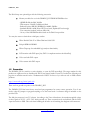
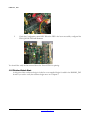
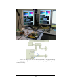
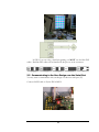
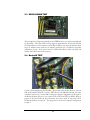
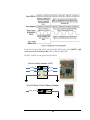
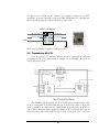
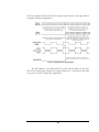
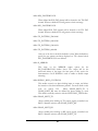
THE DINI GROUP
DVI DAUGHTER CARD - PROVISIONAL
User Guide
DNMEG_DVI
PROVISIONAL NOT COMPLETE – SEE SCHEMATIC FOR DETAILS
LOGIC EMULATION SOURCE
DNMEG_DVI User Manual Version 1.2
The Dini Group
7469 Draper Ave.
La Jolla, CA92037
Phone 858.454.3419 • Fax 858.454.1728
[email protected]
www.dinigroup.com
Last Modified: 8/3/2009 12:35:27
Last saved by bpoladian
0
Chapter
Welcome to DNMEG_DVI
Daughter Card
:
r1
te
p
a
h
C
Congratulations on your purchase of the DNMEG_DVI
Daughter Card!
Q U I C K
S T A R T
1
Chapter
G U I D E
1 Quick Start Guide
The Dini Group DNMEG_DVI is the user-friendliest board available with a
Virtex 4 FPGA and two DVI interfaces
1.1 What’s provided
First, let‟s examine the contents of your DNMEG_DVI kit. It should contain:
DNMEG_DVI board
RS 232 IDC header cable to female DB9
CD ROM containing:
o Virtex 4 Reference Design [Note: update to follow]
o User manual PDF [Note: update to follow]
o Board Schematic PDF
o DNMEG_DVI firmware [Note: update to follow]
DNMEG_DVI User Guide
www.dinigroup.com
3
D N M E G _ D V I
The Dini Group can optionally provide the following accessories:
Memory modules for use in the DNMEG_DVI DDR2 SODIMM socket
- QDRII SRAM 64x1Mb, 300Mhz
- Flash memory 32x4Mb, 2x4Mb serial flash
- Reduced Latency DRAM (RLDRAM) 64x8Mb, 300Mhz
- Standard SRAM, 64x2M (Select ZBT/sync-burst, Pipelined/Flow through)
- Test connection module (with two Mictor38)
- Or any of the SODIMM modules listed on the Dini Group website.
You may also want to obtain from a third party vendor:
Xilinx Parallel Cable IV or Xilinx Platform Cable USB
200-pin DDR2 SODIMM
Xilinx Chipscope for embedded logic analyzer functionality.
LCD monitor with DVI input [Any DVI 1.0 compliant monitor should suffice].
Video card with DVI output.
Video camera with DVI output.
1.2 Precaution
The DNMEG_DVI is sensitive to static electricity, so treat the PCB accordingly. The target markets for this
product are engineers who are familiar with FPGAs and circuit boards. However, if needed, the following web
page has an excellent tutorial on the “Fundamentals of ESD” for those of you who are new to ESD sensitive
products:
http://www.esda.org/basics/part1.cfm
There are four ground test points on the DNMEG_DVI
The DNMEG_DVI has been factory tested and pre-programmed to ensure correct operation. You do not
need to alter any jumpers or program anything to see the board work. A reference design is included on the
provided CD.
The 400-pin connector is not 5V tolerant. According to the Virtex 4 datasheets, the maximum applied voltage
to these signals is VCCO + 0.5V (3.0V while powered on). These connections are not buffered, and the Virtex
4 part is sensitive to ESD. Take care when handling the board to avoid touching the daughter card connectors.
DNMEG_DVI User Guide
www.dinigroup.com
4
D N M E G _ D V I
1.3 Power-On Instructions
The image below represents your DNMEG_DVI. You will need to know the location of the following parts
referenced in this chapter.
DNMEG_DVI User Guide
www.dinigroup.com
5
D N M E G _ D V I
To begin working with the DNMEG_DVI, follow the steps below:
1.4 Verify Switch Settings
The DNMEG_DVI uses a DIP switch to program the FPGA configuration circuitry. The function of these
DIP switches is listed in Table 2. Verify that the switch settings on your board match the default settings.
Table 1 - Switch Description
Switch
Default
Position
Signal Name
On setting
Off setting
S1-1
Off
CFG_REV0
S1-2
Off
S1-3
Off
When CFG_REVSEL is ON - CFG_REV0
and CFG_REV1 are used to select the design
CFG_REV1
revision to be enabled, overriding the internal
CFG_REVSEL programmable revision selection control bits.
S1-4
Off
DIPSW4
Configurable
Configurable
1.5 Memory and heat sinks
There should be an active heat sink installed on the FPGA on the DNMEG_DVI. Virtex 4 FPGAs are capable
of dissipating 15W or more, so you should always run the board with the heat sink installed.
The DNMEG_DVI comes packaged without memory installed. If you want the Dini Group reference design
to test your memory module, you can install it now in the 1.8V DDR2 DIMM socket.
The socket DDR2_SODIMM can accept any capacity DDR2 SODIMM. Note that DDR1 modules will not
work in these slots since they are supplied with 1.8V power and DDR1 requires 2.5V power (and a completely
different pin-out). [Note that the Dini Group has a DDR2 module that provides a DDR1 socket, even so,
changing all the voltages would still be required. In the DNMEG_DVI this is a jumper setting on H9.]
DNMEG_DVI User Guide
www.dinigroup.com
6
D N M E G _ D V I
1.6 Power Up Procedure
1. Plug the four pin hard drive power connector from the power supply into P2. Make sure your work
area is clear and there are no metal wrenches under the board. Turn on the power supply.
When the DNMEG_DVI powers on, it automatically loads Xilinx FPGA design bit file stored in the PROM
(if the load FPGA option was selected during PROM programming).
To load a different Xilinx bit program file into the DNMEG_DVI follow the steps outlined in section 2.4.
1.7 Loading FPGA configuration once
The DNMEG_DVI reads FPGA configuration data from the JTAG chain. To program the FPGA on the
DNMEG_DVI, FPGA design file (with a .bit file extension) are uploaded through the JTAG chain. This can
be accomplished using the Xilinx ISE iMPACT tool.
Step by step instructions for loading bit file into the FPGA via iMPACT.
1. Attach the Xilinx JTAG cable to J8 on the DNMEG_DVI
2. Start iMPACT.
3. Create a new project in iMPACT [file -> new -> create new project]
4. Choose “Configure devices using Boundary-Scan (JTAG)” as the project action.
5. Bypass the first “Assign New Configuration File” pop-up menu.
6. Select the FPGA design bit file in the second “Assign New Configuration File” pop-up menu.
7. Right click on the FPGA in the JTAG chain display select program and then OK at the
“Programming Properties” menu.
1.8 Loading FPGA bitfile into the PROM
There is an XCF32P Xilinx FLASH-PROM on the board to allow the FPGA to automatically be programmed
when the board is powered on. To use this feature, the ISE tools must be version 7.1sp3 or newer.
1.
Attach a Xilinx JTAG cable to J8 on the DNMEG_DVI.
DNMEG_DVI User Guide
www.dinigroup.com
7
D N M E G _ D V I
2.
Start iMPACT.
3.
Create a new project in iMPACT.
4.
Choose “Prepare a PROM File” as the project action.
5.
Target: “Xilinx PROM”, “MCS” file format, and give it a filename.
6.
Select an “xcf32p” as the PROM Device, and add it to the list.
7.
When it brings up the GUI, and asks for a “.bit” file, give it your “.bit” file generated by the
ISE tools. Don‟t add a second “.bit” file, because there is only 1 FPGA on the board.
8.
Now generate the “.mcs” output file by double clicking on “Generate File”. Go check to make
sure that the “.mcs” file was created.
9.
To program that “.mcs” file into the Prom:
a. Switch iMPACT to boundary scan mode.
b. Initialize the JTAG chain. It should find the “xcf32p” and the “xc4vfx60/100” devices.
c. Assign the “.mcs” file as the programming file for the “xcf32p”.
d. “Bypass” the programming file for the “xc4vfx60/100”.
e. Double click “Program” while the “xcf32p” is selected. Make sure to select “Verify”,
“Erase Before Programming”, and “Load FPGA” from the options given in the
programming window. Hit “OK” and wait for about 2 minutes until the programming has
completed.
10.
Now when the board is power-cycled, it will automatically have the “.mcs” file loaded into the
FPGA.
1.9 Check LED status lights
The DNMEG_DVI has many status LEDs to help the user confirm the status of the configuration process.
1.
Check the power voltage indication LEDs to confirm that all voltage rails of the
DNMEG_DC are present. The LEDs indicate the presence of 12V, 5V, 3.3V, 2.5V, and 1.8V
DNMEG_DVI User Guide
www.dinigroup.com
8
D N M E G _ D V I
2.
Check the Configuration status LED. When the FPGA has been successfully configured the
FPGA_DONE LED will illuminate.
You should also verify the fan mounted above the Virtex 4 FPGA is spinning.
1.10 Finished Quick Start
At this point either a reference design is loaded or a user supplied design is loaded in the DNMEG_DVI
board. If you wish to verify the reference design move on to chapter 2.
DNMEG_DVI User Guide
www.dinigroup.com
9
2
Chapter
D N M E G _ D V I
2 Testing the Reference design using the
Included software
To test the reference design on the daughter card, the DNMEG_DVI provides tests
for the following options out of the box.
DVI RX0, RX1, TX0, TX1
200-pin SODIMM socket
RS232 Loopback
Rocket IO
The 4 DVI connectors allow single-link and dual-link digital video to be received and
transmitted.
The RS232 interface allows low-speed data transfers to and from the User design.
A DDR2 SDRAM SODIMM can be installed in the 200-pin SODIMM socket, or one
of our other cards (SSRAM, FLASH, Mictor, …) can be installed instead.
The 400-pin header can be used to connect the DNMEG_DVI to many of the
DiniGroup FPGA emulation boards (check http://www.dinigroup.com for the
compatibility list).
This section will get you started and show you how to operate the provided software.
2.1 DVI reference design
The FPGA is initially programmed with a reference design that will receive DVI video
on RX0, and send it back out on TX0. (The RST switch may need to be applied after
changing input frequencies). The same is true for RX1 and TX1.
DNMEG_DVI User Guide
www.dinigroup.com
10
There is also sample code that can be un-commented in the reference design
that will generate a simple video output pattern (without requiring a DVI input cable
connected to RX0).
11
NOTE: If you are using a dual link signaling you MUST use dual link DVI
cables. Dual link DVI cables can be identified by the pin out on the connector.
2.2 Communicating to the User Design over the Serial Port
You may want to communicate with your design over the user serial port (P3).
Connect a RS232 cable to P4, the FPGA RS232.
12
2.2.1
RS232 in the Provided Reference Design
The reference design is programmed to test the Top and Bottom 400-pin MEG-array
connectors. The loopback adapter used in this test is generally not included with the
board package (because this test has been successfully completed during the
manufacturing testing before the board was shipped), but these adapters are available
upon request. The following settings should be used to establish RS232
communication with the board:
If an adapter is installed on the top MEG-Array connector, the following text should
be output:
T
999999999999999999999999999999
99999999999999999999999999999999
999999999999999999999999999999
9999
If the adapter is installed on the bottom MEG-Array connector:
B
999999999999999999999999999999
99999999999999999999999999999999
999999999999999999999999999999
9999
13
If the adapters are not installed, an output of similar format indicating an error should
print repeatedly to the screen.
2.2.2
Optional RS232 Debug Design
See Section 6.1 for instructions on building a bitfile with the optional RS232 controls.
The effect of the controls will be described here. This optional part of the passthrough
reference design allows to phase shift either the input or the output by one complete
period in either the negative or positive direction. It also can enable certain
interference patterns intended to munge output data. These design options are
generally most desirable for hardware debugging purposes rather than development,
which is why they have not been included in the standard production test.
To control the phase shift of the input/output (only input or output shifting is allowed
– see build options for further details), use the „w‟ and „s‟ keys on the keyboard (in a
hyperterminal window as described in the previous section). „w‟ will shift the phase
1/255 in the positive direction, and „s‟ will shift 1/255 in the negative direction. The
phase begins at 0, and the phase is displayed every time it is changed. The value of the
phase shift is displayed in hexadecimal notation, with negative numbers displayed in
parentheses. Attempts at a phase shift that exceed the limit (ie, shifting past 0xFF) will
not be acknowledged.
To enable an output interference pattern, use the „a‟ and „d‟ keys. „a‟ selects a lower
numbered pattern, and „d‟ selects a higher numbered pattern. The interference patterns
are as follows:
0) No interference
1) All „even‟ pixel data is overwritten w/ 0‟s
2) All „odd‟ pixel data is overwritten w/ 0‟s
3) All „even‟ pixel data is overwritten w/ 1‟s
4) All „odd‟ pixel data is overwritten w/ 1‟s
5) The lower half of every pixel is overwritten w/ 0‟s
6) The upper half of every pixel is overwritten w/ 0‟s
7) The lower half of every pixel is overwritten w/ 1‟s
8) The upper half of every pixel is overwritten w/ 1‟s
9-15) No interference
Upon increment, the number of the interference pattern will be displayed.
Incrementing past 0xF or below 0x0 will not be acknowledged.
14
2.3 DDR2 SODIMM TEST
The provided test design automatically runs a DDR2 memory test with status indicated
by the LEDs. After reset LED 5 will go high for approximately 20 seconds followed
by LED indicators of the memory test. LED10-9 indicate test stage. 00 indicates initial
stage, 01 indicates write read test, 10 indicates read back test, 11 indicates successful
completion of tests. If an error occurs the LEDS will indicate which test failed and
indicate the LSB of error in the memory.
2.4 RocketIO TEST
On the CD accompanying the DNMEG_DVI board in the bit file directory one can
find the RocketIO MCS file. Load the MCS file into the PROM following the steps
outlined in section 2.5. Connect SMA cables in loop back configuration on all eight of
the RocketIO pairs. [That is to say connect TXP to RXP and TXN to RXN]. Reset or
power on the board after all the connections have been made. If test passes all 10
LEDS should flash on and off. The image above shows the loopback configuration
for pair 3.
15
16
3
Chapter
3 DNMEG_DVI Hardware
3.1 Multiplexed Serial Port
The DNMEG_DC has one serial port (P4) for user use. No configuration is required
to enable the first serial port. This can be extended to two serial ports by use of a
breakout serial cable. LED5 and LED6 are tied to the second serial ports TX and RX
respectively.
Serial port 1 uses pins 2 and 3. Serial port 2 uses pins 6 and 7 of port P4.
To enable the second RS232 Port: Add the following 0 Ohm resistors. R403, R413,
R405, R414. This will enable the second serial port on pins 6 and 7 on P4. For more
details see page 21 in the Schematic. “DN5000123 – Misc. Peripherals”.
17
4
Chapter
4 Clocking Overview
This chapter discusses the various clocks available on the DNMEG_DVI and any user
settable options available.
18
4.1 Block Diagram of the DNMEG_DVI clocks:
FPGA_GCA
MC_GCA
400 Pin
Daughtercard
Header P5
DVI 0
RX J1
RX0_RXC
DVI 1
RX J4
RX1_RXC
SMA
J25, J26
DC_GCB
DC_GCC
Sil163B
U9
RX0_CLK
Sil163B
U12
RX1_CLK
U56
Clk Mux/Buf
B0L31
TX0_CG_TO_FPGA
Si5326
U25
RX0_CLK_FWD
TX0_BUFR_TO_FPGA
TX0_GC_TO_PLL
TX0_M_CLK
CDCU877
U29
TX0_BUFR_FROM_FPGA
TX0_CG_TO_FPGA
TX0_BUFR_TO_FPGA
TX1_CG_TO_FPGA
TX1_BUFR_TO_FPGA
TX0_S_CLK
TX1_M_CLK
TX1_BUFR_FROM_FPGA
Sil1178
U8
CDCU877
U27
TX1_S_CLK
Sil1178
U1
Sil1178
U10
DIMM_OSC_OUT
FPGA
DIMM_FPGA_FB
DIMM_FPGA_FB
DIMM_PLL_CKIN
FPGA_GC_MGT
CDCU877
U54
DIMM_CK
MGTCG1_CLK0
SAMTEC
cable J5
CABLE1_CIN
Si5326
U40
MGTCG1_CLK1
114 Mhz Xtal
DIMM_PLL_FB
250MHz
OSC U41
MGTOSC1_CLK
250MHz
OSC U24
MGTOSC2_CLK
MICTOR_E_CLK
MICTOR_O_CLK
Mictor
J11
FPGA_GC_MGT
19
DVI 0
J2
TX1_BUFR_TO_FPGA
TX1_GC_TO_PLL
200MHz
OSC U30
TX0_TXC
TX1_CG_TO_FPGA
Si5326
U26
RX1_CLK_FWD
Sil1178
U9
DDR 2
SODIMM
TX1_TXC
DVI 1
J3
4.2 Meg-Array Clocking
There are several dedicated clock paths between the DNMEG_DVI and the
host card connecting through the Meg-Array header (J5). The signals used in
these clock paths are as follows:
DC_GCBP/N : AF19, AF20 : INOUT : Connection between FPGA
and Meg-Array – Note: check clocking circuitry on host board for
design compatibility
DC_GCCP/N : AE18, AE17 : INOUT : Connection between FPGA
and Meg-Array – Note: check clocking circuitry on host board for
design compatibility
B0L31P/N : W26, Y26 : OUT : Clock sent from FPGA to U56 Clock
Mux/Buffer to be sent back to FPGA and to Meg-Array Header
CLKIN_DCC : External clock from SMA connectors J25, J26 to U56
Clock Mux/Buffer to be sent back to FPGA and to Meg-Array Header
FPGA_GCA : K16, L16: IN : Clock from U56 sent to FPGA, sourced
either externally by CLKIN_DCC or by B0L31P/N. Identical to
MC_GCAP/N.
MC_GCAP/N Clock from U56 sent to Meg-Array header, sourced
either externally by CLKIN_DCC or by B0L31P/N. Identical to
FPGA_GCA.
Recommended Source-Synchronous Setup:
Use DC_GCB to send a clock from the FPGA on the host board across the
Meg-Array connector to the DNMEG_DVI‟s FPGA. Use DC_GCC to send
a clock from the FPGA on the DNMEG_DVI across the Meg-Array
connector to the host board‟s FPGA. Use these clocks for I/O and optionally
also for internal logic. If using a separate clock for internal logic, make sure to
have appropriate clock-domain-crossing logic implemented. Clocks can be
sourced by any on-board oscillator or external source. Note: Make sure to
check host board clock circuitry before implementing your design.
Recommended System-Synchronous Setup:
Output a clock on B0L31P/N and ensure that the clock buffer/mux (U56) is
set to take B0L31P/N as its input. Use FPGA_GCAP/N as the clock for I/O
in the DNMEG_DVI‟s FPGA, and use MC_GCAP/N as the I/O clock in
the host board‟s FPGA. This clock can also be used for internal logic. If using
20
a separate clock for internal logic, make sure to have appropriate clockdomain-crossing logic implemented. Clocks can be sourced by any on-board
oscillator or external source. Note: Make sure to check host board clock
circuitry before implementing your design.
4.3 DVI RX Clocking
RX0_CLK : AD31 : IN :
RX1_CLK : AE31 : IN : Clock sent from DVI receiver chip to FPGA
used to clock data sent from DVI to the FPGA..
Recommended Usage:
These source-synchronous clocks are to be used to clock the data sent from the
receiver chips to the FPGA. Phase shifting is necessary to meet the necessary
setup and hold times of the data. Please consult both the datasheet for the Sil163B
and the included DNMEG_DVI Verilog reference design for implementation
details.
4.4 DVI TX Clocking
RX0_CLK_FWDP/N : G18, F18 : OUT :
RX1_CLK_FWDP/N : H14, H13 : OUT : Clock sent from the FPGA for
the clocking of DVI TX data to the transmitter chips.
TX0_CG_TO_PLL :
TX1_CG_TO_PLL : Clock sent from clock generator to PLL buffer.
TX0_BUFR_FROM_FPGA : AD5, AD4 : OUT :
TX1_BUFR_FROM_FPGA : AC5, AB5 : OUT : Clock sent directly from
FPGA to the PLL buffer. Use this clock to bypass the Si5326 input to the
PLL. This clock path is selectable by modifying the physical placement of
resistors on the board, and is not connected by default. See section 7 of this
document for further detail.
TX0_CG_TO_FPGA : J16, J15 : IN :
TX1_CG_TO_FPGA : J14, K14 : IN : Feedback clock sent from Si5326
Clock Generator to FPGA.
TX0_BUFR_TO_FPGA : K18, K17 : IN :
TX1_BUFR_TO_FPGA : K19, J19 : IN : Feedback clock sent from PLL
buffer to FPGA..
TX0_M_CLK, TX0_S_CLK, TX1_M_CLK, TX1_S_CLK : Master and
slave clocks sent from PLL buffer to DVI Transmitter chips (Sil1178)
21
TX0_TXC, TX1_TXC : Clock sent from DVI Transmitter chip (Sil1178) to
DVI connector.
Recommended Usage:
Output a clock on RX_CLK_FWD and use this as the source for the clock generator.
The clock generator will then output a clock to the PLL, and the PLL will use this
clock to send to the DVI transmitter chips.
The PLL will also send
TX_BUFR_TO_FPGA back to the FPGA, which should be used to define the setup
and hold timing requirements on the FPGA outputs. Please see the Verilog reference
design for further detail.
4.5 SODIMM Clocking
DIMM_PLL_CKINP/N : AD7, AD6 : OUT : clock sent from FPGA to PLL
to be sent to SODIMM
DIMM_FPGA_FBP/N : L15, L14 : IN : clock sent from PLL back to FPGA
Recommended Usage:
Send a clock to the SODIMM using DIMM_PLL_CKIN. Clock requirements will
vary widely by the type of module installed. The DNMEG_DVI reference design
assumes the installation of a DDR2 SODIMM, and clocking is appropriately assigned.
Use the feedback clock DIMM_FPGA_FB for FPGA setup/hold timing constraint.
4.6 MGT Clocking
MGTCG1_CLK0P/N : AP29, AP28 : IN :
MGTCG1_CLK1P/N : AP3, AP4 : IN : MGT clock inputs from Si5326
MGTCG1_OSC1P/N : M34, N34 : IN :
MGTCG1_OSC2P/N : J1, K1 : IN : MGT clock inputs from frequencyselectable oscillators. Oscillator frequency is set using installed resistors. See
schematic for details
Recommended Usage:
Application specific.
4.7 Configuring the Si5326 and the CDCU877s
Note that the reference manuals should be considered the authority concerning
these parts. The manual is available on the DNMEG_DVI CD in the
Datasheets directory, but updated manuals may be available online from the
manufacturer‟s website. The provided DNMEG_DVI Verilog reference design
gives an example of the programming necessary for common operation.
22
5
Chapter
5 DVI Interfaces : Receivers and Transmitters
5.1 Receivers SiI163B
Note that the SiI 163B reference manual should be considered the authority
concerning the SiI 163B. The manual is available on the DNMEG_DVI CD as
SiI163b-DS-0055.pdf.
The DNMEG_DVI board has two Sil 163B chips per receiver channel. One Sil
163B is designated as the MASTER and one as the SLAVE. When a single link signal
is applied to the receiver the MASTER SiI 163B will handle all 48 bits of output. When
a dual link signal is applied the Master SiI 163B will handle the even 24 bits and the
Slave SiI163B will handle the odd 24 bits [NOTE – The slave is bit-reversed!]
23
In the above diagram DE is RX?_QE_[23:0], DO is RX?_QO_[23:0]. [NOTE – QO
is bit-reversed in dual link mode!]. Master ODCK is RX?_CLK.
HSYNC, VSYNC are also passed into the FPGA.
Receive Debug Headers H3/H7
HSYNC
1
2RX_CLK
VSYNC
3
4 RX_DE
5
6
H1/H4 Slave Clock Debug Header
1
RX?_S_CLK
2
24
I2C Bypass: If so desired the I2C channel can be directly connected to the DVI
transmitter. To do this one needs to remove the DDC EEPROM (U13/U20) [Default:
Removed] and use jumpers to short the RX I2C to the TX I2C.
H2/H6 – I2C Bypass
+5V
RX?_DDC_SCL
1
2TX?_DDC_SCL
RX?_DDC_SDA
3
4TX?_DDC_SDA
5
6
Please see the schematic for specific connection issues.
5.2 Transmitters SiI1178
Note that the SiI 1178 reference manual should be considered the authority
concerning the SiI 1178. The manual is available on the DNMEG_DVI CD as
SiI1178_SiI-DS-0127.pdf
The DNMEG_DVI board has two Sil 1178 chips per transmitter channel. One
Sil 1178 is designated as the MASTER and one as the SLAVE. When a single link
signal is applied to the transmitter the MASTER SiI 1178 will handle all 24 bits of
output. When a dual link signal is applied the Master SiI 1178 will handle the lower 12
bits and the Slave SiI1178 will handle the upper 12 bits of each pixel. Note – while the
25
SiI 1178 is capable of both 24 bit and 12 bit input modes only the 12 bit input mode is
available in dual link configurations.
The I2C address of the Master SiI1178 is 0x70 and the address of the Slave
SiI178 is 0x72 [Only after writing to 0x70 register PD set to 0 – this must be done after
every reset, see SiI1178 manual for explanation].
26
6
Chapter
6 Reference Design
This section will discuss the options available in the reference design along with the
steps needed to generate bit files from the reference design using standard
development tools.
The reference design provides an example interface to the RS232 port, DVI ports, and
DDR2 module port. The provided design files can also be used to test the process of
generating FPGA programming files and loading them into the FPGA.
6.1 Reference Design Verilog Files
Included on the CD are the Verilog files for the reference design. The top level file
U1_fpga.v has several defines which determine the behavior of the design.
`define SETUP_8442
When defined the 8442s are configured.
`define EXPCONIO_TEST
When defined the 400 pin header is active and will respond to the
daughter card header test. [This is used internally in the Dini group to
verify functionality of the header. If one desires to use this test one will
need a host card configured with the matching end of this test or a
special loopback test card.]
`define INCLUDE_DDR2_LOGIC
When defined the DDR2 test is enabled.
`define DDR2_LEDS
When defined the LEDS are used to indicate states of the DDR2 test.
`define DDR2_MICTOR_DEBUG
When defined the mictor connector will hold the data returned from
an invalid ddr2 read if one exists. This is used internally.
27
`define RX0_PASSTHROUGH
When defined the RX0 DVI channel will be shunted to the TX0 DVI
channel. When not defined TX0 will generate a basic test image.
`define RX1_PASSTHROUGH
When defined RX1 DVI channel will be shunted to the TX1 DVI
channel. When not defined TX1 will generate a basic test image.
`define TX_PATTERN_2560x1600
`define TX_PATTERN_1600x1200
`define TX_PATTERN_1280x1024
`define TX_PATTERN_640x480
Only one of the above should be defined at a time. When defined they
specify the test pattern resolution displayed on TX* channel where
RX*_PASSTHROUGH is not defined.
`define H_MIRROR
This turns on the MIRROR output option for the
RX_PASSTHROUGH defines above. The output will be the
horizontal mirror of the input. See later parts of this section for
demonstration. On S2 DIPSW4 is used to enable or disable output
mirroring.
`define DEBUG_RS232_CONTROLS
This enables control over phase shifting input or output, and allows
the insertion of the data interference patterns. For more detail on this
code, see section 2.2.2.
Either PHASE_SHIFT_TX or
PHASE_SHIFT_RX must be defined for phase shifting to work.
This define is mutually exclusive with the EXPCONIO_TEST define.
`define PHASE_SHIFT_TX
Allows variable phase shifting on TX (output) signals, controlled over
RS232. Mutually exclusive with PHASE_SHIFT_RX.
`define PHASE_SHIFT_RX
Allows variable phase shifting on RX (input) signals, controlled over
RS232. Mutually exclusive with PHASE_SHIFT_TX.
28
6.2 Synthesizing the Reference Design
Synthesis of the Dini Group reference design requires Xilinx‟s ISE software. If you
don‟t have this software, it can be downloaded from Xilinx‟s website. The reference
design can be built either using the provided makefile or using the provided ISE
project.
To use the makefile, you must have a UNIX-like shell (Linux, cygwin on
Windows) with the „sed‟ and „make‟ commands. If you are running on Windows
without cygwin, please use the ISE project to build. To use the makefile,
navigate to /FPGA_Reference_Designs/DNMEG_DVI/Work-Area/ and
type „make‟. This will build bitfiles for both the FX60 and FX100 stuffing
options; if you wish only to build for one of these stuffing options, type “make
fx60” or “make fx100” respectively. All logfiles and outputs will be made in the
directory /FPGA_Reference_Designs/DNMEG_DVI/Work-Area/implement
/FX*/
Using the project for Xilinx‟s ISE is as simple as opening the project
(dn123_dnmeg_dvi.ise file) in project navigator. The source included in this
project is the top level verilog file (Verilog-files/U1_fpga.v) and the appropriate
UCF constraint file (Verilog-files/Rev2_U1_fpga.ucf). All other required files
will be automatically found during compilation; if this is not the case, please
ensure that “FPGA_Reference_Designs” is included in the „Verilog Include
Directories” Synthesis option. Use ISE to synthesize, place, route, and generate
your bitfile. All output from ISE will reside in the same folder as the ISE
project.
At this point a bit file should be created, load it into the DNMEG_DVI board
following the steps outlined in section 1.4.
6.3 Horizontal Mirroring
After recompiling the bitfile including the H_MIRROR option the following
demonstration can be performed.
29
DNDVI_DC HORIZONTAL MIRROR TEST SETUP
DVI IMAGE SOURCE
[DUAL LINK/SINGLE LINK]
CAMERA/COMPUTER/ETC
Horizontal
Mirror
RX0
DISPLAY
DUAL LINK/SINGLE LINK
TX0
DNDVI_DC
TX1
Horizontal
Mirror
DISPLAY
DUAL LINK/SINGLE LINK
RX1
DVI IMAGE SOURCE
[DUAL LINK/SINGLE LINK]
CAMERA/COMPUTER/ETC
30
With the following results:
Note that dip switch S2 leaver 4 can be used in this mode to switch between
mirrored output and non-mirrored output.
Also note that a different bitfile will be needed for single link and dual link
applications.
Important: If for some reason noise exists on the screen or the clock is
dysynched press the RESET button (S1).
31
7
Chapter
7 Optional Hardware Modifications
7.1 TX PLL Buffer Source
The source clocks for the TX PLL Buffers (U27 and U29) are by default driven
by Si5326 Any-Rate Precision Clock Multiplier / Jitter Attenuator parts (U25
and U26). By changing the stuffing options on the board, the FPGA (U36) can
directly source the buffers.
TX0:
Remove C158, C159, and R52
Install R47 and R48 with 0-ohm Resistors
TX1:
Remove C160, C161, and R54
Install R50 and R53 with 0-ohm Resistors
Consult the provided schematic for additional detail.
For the purposes of signal integrity and the prevention of signal contention, the
above parts share pads on the PCB. The picture on the next page shows a
detailed view of the TX0 stuffing options. Note that {R47, R48} cannot be
installed while {C158, C159, R52} are installed.
While not pictured, TX1 uses the same exact pad configuration and has the
same options/restrictions as TX0.
32
TX0 PLL Buffer Stuffing Options
33