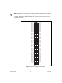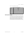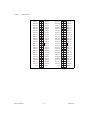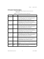
1
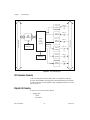
DAQ
6527 User Manual
Isolated Digital I/O Interface
for PCI, PXI, and CompactPCI
6527 User Manual
December 1999 Edition
Part Number 322164A-01
Worldwide Technical Support and Product Information
www.ni.com
National Instruments Corporate Headquarters
11500 North Mopac Expressway
Austin, Texas 78759-3504
USA Tel: 512 794 0100
Worldwide Offices
Australia 03 9879 5166, Austria 0662 45 79 90 0, Belgium 02 757 00 20, Brazil 011 284 5011,
Canada (Calgary) 403 274 9391, Canada (Ontario) 905 785 0085, Canada (Québec) 514 694 8521,
China 0755 3904939, Denmark 45 76 26 00, Finland 09 725 725 11, France 01 48 14 24 24,
Germany 089 741 31 30, Greece 30 1 42 96 427, Hong Kong 2645 3186, India 91805275406,
Israel 03 6120092, Italy 02 413091, Japan 03 5472 2970, Korea 02 596 7456, Mexico (D.F.) 5 280 7625,
Mexico (Monterrey) 8 357 7695, Netherlands 0348 433466, Norway 32 27 73 00, Poland 48 22 528 94 06,
Portugal 351 1 726 9011, Singapore 2265886, Spain 91 640 0085, Sweden 08 587 895 00,
Switzerland 056 200 51 51, Taiwan 02 2377 1200, United Kingdom 01635 523545
For further support information, see the Technical Support Resources appendix. To comment on the
documentation, send e-mail to [email protected]
© Copyright 1999 National Instruments Corporation. All rights reserved.
Important Information
Warranty
The 6527 device is warranted against defects in materials and workmanship for a period of one year from the date of shipment, as
evidenced by receipts or other documentation. National Instruments will, at its option, repair or replace equipment that proves to
be defective during the warranty period. This warranty includes parts and labor.
The media on which you receive National Instruments software are warranted not to fail to execute programming instructions,
due to defects in materials and workmanship, for a period of 90 days from date of shipment, as evidenced by receipts or other
documentation. National Instruments will, at its option, repair or replace software media that do not execute programming
instructions if National Instruments receives notice of such defects during the warranty period. National Instruments does not
warrant that the operation of the software shall be uninterrupted or error free.
A Return Material Authorization (RMA) number must be obtained from the factory and clearly marked on the outside of
the package before any equipment will be accepted for warranty work. National Instruments will pay the shipping costs of
returning to the owner parts which are covered by warranty.
National Instruments believes that the information in this document is accurate. The document has been carefully reviewed
for technical accuracy. In the event that technical or typographical errors exist, National Instruments reserves the right to
make changes to subsequent editions of this document without prior notice to holders of this edition. The reader should consult
National Instruments if errors are suspected. In no event shall National Instruments be liable for any damages arising out of
or related to this document or the information contained in it.
EXCEPT AS SPECIFIED HEREIN, NATIONAL INSTRUMENTS MAKES NO WARRANTIES, EXPRESS OR IMPLIED, AND SPECIFICALLY DISCLAIMS ANY
WARRANTY OF MERCHANTABILITY OR FITNESS FOR A PARTICULAR PURPOSE. CUSTOMER’S RIGHT TO RECOVER DAMAGES CAUSED BY FAULT OR
NEGLIGENCE ON THE PART OF NATIONAL INSTRUMENTS SHALL BE LIMITED TO THE AMOUNT THERETOFORE PAID BY THE CUSTOMER. NATIONAL
INSTRUMENTS WILL NOT BE LIABLE FOR DAMAGES RESULTING FROM LOSS OF DATA, PROFITS, USE OF PRODUCTS, OR INCIDENTAL OR
CONSEQUENTIAL DAMAGES, EVEN IF ADVISED OF THE POSSIBILITY THEREOF. This limitation of the liability of National Instruments will
apply regardless of the form of action, whether in contract or tort, including negligence. Any action against National Instruments
must be brought within one year after the cause of action accrues. National Instruments shall not be liable for any delay in
performance due to causes beyond its reasonable control. The warranty provided herein does not cover damages, defects,
malfunctions, or service failures caused by owner’s failure to follow the National Instruments installation, operation, or
maintenance instructions; owner’s modification of the product; owner’s abuse, misuse, or negligent acts; and power failure or
surges, fire, flood, accident, actions of third parties, or other events outside reasonable control.
Copyright
Under the copyright laws, this publication may not be reproduced or transmitted in any form, electronic or mechanical, including
photocopying, recording, storing in an information retrieval system, or translating, in whole or in part, without the prior written
consent of National Instruments Corporation.
Trademarks
ComponentWorks™, CVI™, LabVIEW™, MITE™, National Instruments™, ni.com™, NI-DAQ™, and PXI™ are trademarks of
National Instruments Corporation.
Product and company names mentioned herein are trademarks or trade names of their respective companies.
WARNING REGARDING USE OF NATIONAL INSTRUMENTS PRODUCTS
(1) NATIONAL INSTRUMENTS PRODUCTS ARE NOT DESIGNED WITH COMPONENTS AND TESTING FOR A LEVEL
OF RELIABILITY SUITABLE FOR USE IN OR IN CONNECTION WITH SURGICAL IMPLANTS OR AS CRITICAL
COMPONENTS IN ANY LIFE SUPPORT SYSTEMS WHOSE FAILURE TO PERFORM CAN REASONABLY BE
EXPECTED TO CAUSE SIGNIFICANT INJURY TO A HUMAN.
(2) IN ANY APPLICATION, INCLUDING THE ABOVE, RELIABILITY OF OPERATION OF THE SOFTWARE PRODUCTS
CAN BE IMPAIRED BY ADVERSE FACTORS, INCLUDING BUT NOT LIMITED TO FLUCTUATIONS IN ELECTRICAL
POWER SUPPLY, COMPUTER HARDWARE MALFUNCTIONS, COMPUTER OPERATING SYSTEM SOFTWARE
FITNESS, FITNESS OF COMPILERS AND DEVELOPMENT SOFTWARE USED TO DEVELOP AN APPLICATION,
INSTALLATION ERRORS, SOFTWARE AND HARDWARE COMPATIBILITY PROBLEMS, MALFUNCTIONS OR
FAILURES OF ELECTRONIC MONITORING OR CONTROL DEVICES, TRANSIENT FAILURES OF ELECTRONIC
SYSTEMS (HARDWARE AND/OR SOFTWARE), UNANTICIPATED USES OR MISUSES, OR ERRORS ON THE PART OF
THE USER OR APPLICATIONS DESIGNER (ADVERSE FACTORS SUCH AS THESE ARE HEREAFTER
COLLECTIVELY TERMED “SYSTEM FAILURES”). ANY APPLICATION WHERE A SYSTEM FAILURE WOULD
CREATE A RISK OF HARM TO PROPERTY OR PERSONS (INCLUDING THE RISK OF BODILY INJURY AND DEATH)
SHOULD NOT BE RELIANT SOLELY UPON ONE FORM OF ELECTRONIC SYSTEM DUE TO THE RISK OF SYSTEM
FAILURE. TO AVOID DAMAGE, INJURY, OR DEATH, THE USER OR APPLICATION DESIGNER MUST TAKE
REASONABLY PRUDENT STEPS TO PROTECT AGAINST SYSTEM FAILURES, INCLUDING BUT NOT LIMITED TO
BACK-UP OR SHUT DOWN MECHANISMS. BECAUSE EACH END-USER SYSTEM IS CUSTOMIZED AND DIFFERS
FROM NATIONAL INSTRUMENTS' TESTING PLATFORMS AND BECAUSE A USER OR APPLICATION DESIGNER
MAY USE NATIONAL INSTRUMENTS PRODUCTS IN COMBINATION WITH OTHER PRODUCTS IN A MANNER NOT
EVALUATED OR CONTEMPLATED BY NATIONAL INSTRUMENTS, THE USER OR APPLICATION DESIGNER IS
ULTIMATELY RESPONSIBLE FOR VERIFYING AND VALIDATING THE SUITABILITY OF NATIONAL
INSTRUMENTS PRODUCTS WHENEVER NATIONAL INSTRUMENTS PRODUCTS ARE INCORPORATED IN A
SYSTEM OR APPLICATION, INCLUDING, WITHOUT LIMITATION, THE APPROPRIATE DESIGN, PROCESS AND
SAFETY LEVEL OF SUCH SYSTEM OR APPLICATION.
Contents
About This Manual
How To Use the Manual Set..........................................................................................ix
Conventions ...................................................................................................................x
Related Documentation..................................................................................................x
Chapter 1
Introduction
About the 6527 Device ..................................................................................................1-1
Using PXI with CompactPCI.........................................................................................1-2
What You Need to Get Started ......................................................................................1-2
Unpacking ......................................................................................................................1-3
Software Programming Choices ....................................................................................1-3
National Instruments Application Software ....................................................1-3
NI-DAQ Driver Software ................................................................................1-4
Optional Equipment .......................................................................................................1-5
Custom Cabling .............................................................................................................1-6
Safety Information .........................................................................................................1-6
Chapter 2
Installation and Configuration
Software Installation ......................................................................................................2-1
Hardware Installation.....................................................................................................2-1
Board Configuration ......................................................................................................2-2
Chapter 3
Signal Connections
I/O Connector ................................................................................................................3-1
Cable Assembly Connectors............................................................................3-3
I/O Connector Signal Descriptions..................................................................3-5
Power Connections ........................................................................................................3-6
Isolation Voltages ..........................................................................................................3-7
Optically Isolated Inputs ................................................................................................3-7
Input Channels.................................................................................................3-7
Sensing DC Voltages.......................................................................................3-8
Signal Connection Example ............................................................................3-8
Reducing the Forward Current for High Voltages ..........................................3-9
© National Instruments Corporation
v
6527 User Manual
Contents
Solid-State Relay Outputs ............................................................................................. 3-9
Output Channels.............................................................................................. 3-9
Overcurrent Protection .................................................................................... 3-12
Power-on and Power-off Conditions............................................................... 3-12
Chapter 4
Device Overview
Functional Overview ..................................................................................................... 4-1
PCI Interface Circuitry.................................................................................... 4-2
Digital I/O Circuitry........................................................................................ 4-2
Optical Isolation Circuitry .............................................................................. 4-3
Digital Filtering ............................................................................................................. 4-3
Change Notification....................................................................................................... 4-5
Appendix A
Specifications
Appendix B
Technical Support Resources
Glossary
Index
Figures
Figure 1-1.
The Relationship between the Programming Environment,
NI-DAQ, and Your Hardware............................................................... 1-5
Figure 3-1.
Figure 3-2.
Figure 3-3.
Figure 3-4.
Figure 3-5.
Figure 3-6.
6527 Device Connector Pin Assignments............................................. 3-2
Cable-Assembly Connector Pinout
for the R1005050 Ribbon Cable3-4
Signal Connection Example for Isolated Input ..................................... 3-8
Reducing Input Current for High Voltage Signals ............................... 3-9
Signal Connections for Solid-State Relays ........................................... 3-10
Signal Connections for Driving TTL Voltages..................................... 3-11
Figure 4-1.
Figure 4-2.
6527 Block Diagram ............................................................................. 4-2
Digital Filter Timing ............................................................................. 4-5
6527 User Manual
vi
www.ni.com
Contents
Tables
Table 3-1.
Table 3-2.
Port Functionality for 6527 Devices .....................................................3-3
Signal Descriptions for 6527 Device I/O Connectors ...........................3-5
Table 4-1.
Table 4-2.
Digital Filter Characteristics .................................................................4-4
Change Notification Example ...............................................................4-6
© National Instruments Corporation
vii
6527 User Manual
About This Manual
This manual describes the electrical and mechanical aspects of the 6527
devices, and contains information concerning their operation and
programming.
Unless otherwise noted, the text applies to all devices in the 6527 family,
which includes the PCI-6527 and PXI-6527.
How To Use the Manual Set
The 6527 User Manual is one piece of the documentation set for your data
acquisition system. You could have any of several types of manuals,
depending on the hardware and software in your system. Use the manuals
you have as follows:
•
Your DAQ hardware user manuals—These manuals have detailed
information about the DAQ hardware that plugs into or is connected
to your computer. Use these manuals for hardware installation and
configuration instructions, specification information about your DAQ
hardware, and application hints.
•
Software documentation—Examples of software documentation you
may have are the LabVIEW, LabWindows/CVI, or ComponentWorks
documentation sets and the NI-DAQ documentation. After you set up
your hardware system, use either the application software or the
NI-DAQ documentation to help you write your application. If you have
a large and complicated system, it is worthwhile to look through the
software documentation before you configure your hardware.
•
Accessory installation guides or manuals—If you are using accessory
products, read the terminal block and cable assembly installation
guides or accessory board user manuals. They explain how to
physically connect the relevant pieces of the system. Consult these
guides when you are making your connections.
© National Instruments Corporation
ix
6527 User Manual
About This Manual
Conventions
The following conventions appear in this manual:
<>
Angle brackets that contain numbers separated by an ellipsis represent a
range of values associated with a bit or signal name—for example,
DIG+0.<3..0>.
♦
The ♦ symbol indicates that the text following it applies only to a specific
product, a specific operating system, or a specific software version.
This icon denotes a note, which alerts you to important information.
This icon denotes a caution, which advises you of precautions to take to
avoid injury, data loss, or a system crash.
This icon denotes a warning, which advises you of precautions to take to
avoid being electrically shocked.
italic
Italic text denotes variables, emphasis, a cross reference, or an introduction
to a key concept. This font also denotes text that is a placeholder for a word
or value that you must supply.
monospace
Text in this font denotes text or characters that you should enter from the
keyboard, sections of code, programming examples, and syntax examples.
This font is also used for the proper names of disk drives, paths, directories,
programs, subprograms, subroutines, device names, functions, operations,
variables, filenames and extensions, and code excerpts.
Related Documentation
The following documents also contain information that you may find
helpful as you read this manual:
6527 User Manual
•
Your computer’s technical reference manual
•
PCI Local Bus Specification, Revision 2.0
•
National Instruments PXI Specification, Revision 1.0
•
PICMG 2.0 R2.1 CompactPCI
x
www.ni.com
1
Introduction
This chapter describes the 6527 devices; lists what you need to get started,
software programming choices, and optional equipment; describes custom
cabling options; and explains how to unpack your board.
About the 6527 Device
Thank you for purchasing a National Instruments 6527 device. The 6527
devices are 48-bit, parallel, isolated digital I/O interfaces for PCI bus
computers and PXI or Compact PCI chassis. The 6527 devices offer
48 channels of isolated digital data acquisition. Twenty-four of the
channels are optocoupler inputs and 24 are solid-state relay outputs. You
can sense digital levels up to 28 VDC and switch currents of up to 120 mA.
Digital filtering is available to eliminate glitches on the input lines. All
input lines can also generate interrupts on rising or falling edges to notify
you of changing data.
The PCI-6527 and PXI-6527 devices are completely jumperless DAQ
devices for PCI buses and PXI or CompactPCI chassis, respectively. All
devices in this family contain the National Instruments PCI MITE
interface.
The 6527 devices are ideal for low-voltage isolation and switching in both
industrial and laboratory environments. You can use the optically isolated
digital input lines to read the status of external digital logic at TTL and
non-TTL levels. You can use the solid-state relay outputs to switch external
devices, including those requiring high input currents, and to control digital
logic levels at both TTL and non-TTL levels. Because of the isolated nature
of the 6527 devices, you can decouple the noise and harsh ground of the
computer from external signals, and vice versa.
Detailed 6527 device specifications are in Appendix A, Specifications.
© National Instruments Corporation
1-1
6527 User Manual
Chapter 1
Introduction
Using PXI with CompactPCI
Using PXI-compatible products with standard CompactPCI products is an
important feature provided by the PXI Specification, Revision 1.0. If you
use a PXI-compatible plug-in device in a standard CompactPCI chassis,
you will be unable to use PXI-specific functions, but you can still use the
basic plug-in device functions. All 6527 device functions are available in a
CompactPCI chassis.
The CompactPCI specification permits vendors to develop sub-buses that
coexist with the basic PCI interface on the CompactPCI bus. Compatible
operation is not guaranteed between CompactPCI devices with different
sub-buses nor between CompactPCI devices with sub-buses and PXI.
The standard implementation for CompactPCI does not include these
sub-buses. Your 6527 device will work in any standard CompactPCI
chassis adhering to the PICMG 2.0 R2.1 CompactPCI core specification.
What You Need to Get Started
To set up and use your 6527 device, you will need the following:
❑ One of the following devices:
–
PCI-6527
–
PXI-6527
❑ 6527 User Manual
❑ One of the following software packages and documentation:
–
LabVIEW for Windows
–
LabWindows/CVI for Windows
–
ComponentWorks
–
NI-DAQ for PC Compatibles
❑ Your computer, or PXI or CompactPCI chassis and controller
6527 User Manual
1-2
www.ni.com
Chapter 1
Introduction
Unpacking
Your 6527 device is shipped in an antistatic package to prevent electrostatic
damage to the board. Electrostatic discharge can damage several
components on the board. To avoid such damage in handling the board,
take the following precautions:
•
Ground yourself via a grounding strap or by holding a grounded object.
•
Touch the antistatic package to a metal part of your computer chassis
before removing the board from the package.
•
Remove the board from the package and inspect the board for loose
components or any other sign of damage. Notify National Instruments
if the board appears damaged in any way. Do not install a damaged
board into your computer.
•
Never touch the exposed pins of connectors.
Software Programming Choices
There are several options to choose from when programming your National
Instruments DAQ hardware. You can use LabVIEW, LabWindows/CVI,
ComponentWorks, or other application development environments with
the NI-DAQ driver software.
National Instruments Application Software
LabVIEW features interactive graphics, a state-of-the-art user interface,
and a powerful graphical programming language. The LabVIEW Data
Acquisition VI Library, a series of VIs for using LabVIEW with National
Instruments DAQ hardware, is included with LabVIEW. The LabVIEW
Data Acquisition VI Library is functionally equivalent to the NI-DAQ
software.
LabWindows/CVI features interactive graphics and a state-of-the-art user
interface, and uses the ANSI standard C programming language. The
LabWindows/CVI Data Acquisition Library, a series of functions for using
LabWindows/CVI with National Instruments DAQ hardware, is included
with the NI-DAQ software kit. The LabWindows/CVI Data Acquisition
Library is functionally equivalent to the NI-DAQ software.
© National Instruments Corporation
1-3
6527 User Manual
Chapter 1
Introduction
ComponentWorks contains tools for data acquisition and instrument
control built on NI-DAQ driver software. ComponentWorks provides a
higher-level programming interface for building virtual instruments
through standard OLE controls and DLLs. With ComponentWorks, you
can use all of the configuration tools, resource management utilities, and
interactive control utilities included with NI-DAQ.
Using LabVIEW, LabWindows/CVI, or ComponentWorks software will
greatly reduce the development time for your data acquisition and control
application.
NI-DAQ Driver Software
The NI-DAQ driver software is included with most National Instruments
DAQ hardware. NI-DAQ has an extensive library of functions that you can
call from your application programming environment. These functions
allow you to use all features of your 6527 device.
NI-DAQ addresses many of the complex issues between the computer and
the DAQ hardware such as programming interrupts. NI-DAQ maintains a
consistent software interface among its different versions so that you can
change platforms with minimal modifications to your code. Whether you
are using LabVIEW, LabWindows/CVI, ComponentWorks, or other
programming languages, your application uses the NI-DAQ driver
software, as illustrated in Figure 1-1.
6527 User Manual
1-4
www.ni.com
Chapter 1
LabVIEW,
LabWindows/CVI,
or
ComponentWorks
Introduction
Conventional
Programming Environment
NI-DAQ
Driver Software
DAQ or
SCXI Hardware
Personal
Computer or
Workstation
Figure 1-1. The Relationship between the Programming Environment,
NI-DAQ, and Your Hardware
Optional Equipment
National Instruments offers a variety of products to use with your
6527 device, including cables, connector blocks, and other accessories,
as follows:
•
Cables and cable assemblies, shielded and ribbon
•
Connector blocks, unshielded and shielded 50- and 100-pin screw
terminals
For more information about optional equipment available from National
Instruments, refer to your National Instruments catalogue or web site or call
the office nearest you.
© National Instruments Corporation
1-5
6527 User Manual
Chapter 1
Introduction
Custom Cabling
National Instruments offers cables and accessories for you to prototype
your application or to use if you frequently change board interconnections.
If you want to develop your own cable, note that the 6527 device uses a
100-pin female cable header. AMP Corporation part number 749621-9 may
be used for the mating connector. Backshells available for use on a cable
with this connector include the following:
•
AMP 749081-1
•
AMP 749854-1
These backshells have a different thread width than the I/O connector on
the 6527. A jackscrew to adapt the different thread widths is available from
National Instruments; the part number is 745444-01.
Safety Information
Cautions Do not operate the 6527 in an explosive atmosphere or where there may be
flammable gases or fumes.
Do not operate the 6527 in a manner not specified in the manual.
Clean the 6527 and accessories by brushing off light dust with a soft nonmetallic brush.
Remove other contaminants with a stiff nonmetallic brush. The unit must be completely
dry and free from contaminants before returning it to service.
Connections, including power-signal-to-ground and ground-to-power-signal, that exceed
any of the maximum signal ratings for the 6527 can damage any or all of the modules in
the same PXI or CompactPCI chassis, or PCI-bus computer. National Instruments is not
liable for any damages or injuries resulting from incorrect signal connections.
All signal wiring must be properly insulated. National Instruments is not liable for damage
to equipment or injuries caused by improper signal wiring.
The 6527 must be used in a CE-marked PXI or CompactPCI chassis, or PCI-bus computer.
6527 User Manual
1-6
www.ni.com
Installation and Configuration
2
This chapter describes how to install and configure your 6527 device.
Software Installation
Note Install your software before you install your 6527 device.
Refer to the appropriate release notes indicated below for specific
instructions on the software installation sequence.
If you are using NI-DAQ, refer to your NI-DAQ release notes. Find
the installation section for your operating system and follow the
instructions given there.
If you are using LabVIEW, LabWindows/CVI, or other National
Instruments application software packages, refer to the appropriate release
notes. After you have installed your application software, refer to your
NI-DAQ release notes and follow the instructions given there for your
operating system and application software package.
Hardware Installation
Note Install your software before you install your 6527 device.
The following are general installation instructions for each device. Consult
your computer or chassis user manual or technical reference manual for
specific instructions about installing new devices in your computer or
chassis.
♦
PCI-6527
You can install a PCI-6527 in any available 5 V PCI expansion slot in your
computer:
1.
Turn off and unplug your computer.
2.
Remove the top cover or access port to the expansion slots.
© National Instruments Corporation
2-1
6527 User Manual
Chapter 2
Installation and Configuration
♦
3.
Remove the expansion slot cover on the back panel of the computer.
4.
Touch a metal part inside your computer to discharge any static
electricity that might be on your clothes or body.
5.
Insert the PCI-6527 in a 5 V PCI slot. It may be a tight fit, but do not
force the device into place.
6.
Screw the mounting bracket of the PCI-6527 to the back panel rail of
the computer.
7.
Visually verify the installation.
8.
Replace the top cover of your computer.
9.
Plug in and turn on your computer.
PXI-6527
You can install a PXI-6527 in any available 5 V peripheral slot in your PXI
or CompactPCI chassis:
1.
Turn off and unplug your PXI or CompactPCI chassis.
2.
Choose an unused PXI or CompactPCI 5 V peripheral slot.
3.
Remove the filler panel for the peripheral slot you have chosen.
4.
Touch a metal part of your chassis to discharge any static electricity
that might be on your clothes or body.
5.
Insert the PXI-6527 in the selected 5 V slot. Use the injector/ejector
handle to fully inject the device into place.
6.
Screw the front panel of the PXI-6527 to the front panel mounting rails
of the PXI or CompactPCI chassis.
7.
Visually verify the installation.
8.
Plug in and turn on the PXI or CompactPCI chassis.
Your 6527 is now installed. You are now ready to configure your hardware
and software.
Board Configuration
Your 6527 device is completely software configurable. The PCI-6527 is
fully compliant with the PCI Local Bus Specification, Revision 2.0, and the
PXI-6527 is fully compliant with the PXI Specification, Revision 1.0.
Therefore, all board resources are automatically allocated by the PCI
system, including the base address and interrupt level. The board’s base
address is mapped into PCI memory space. You do not need to perform any
configuration steps after the system powers up.
6527 User Manual
2-2
www.ni.com
3
Signal Connections
This chapter describes the pin arrangement, signal names, and signal
connections on your 6527 device.
Connections that exceed any of the maximum ratings of input or output signals
on your 6527 device can damage the board and your computer. The description of each
signal in this chapter includes information about maximum input ratings. National
Instruments is not liable for any damages resulting from signal connections that exceed
these maximum ratings.
Caution
I/O Connector
The I/O connector for the 6527 device has 100 pins that you can connect to
50-pin accessories with the R1005050 cable or to 100-pin accessories with
the shielded SH100100-F cable. Figure 3-1 shows the pin assignments for
the 6527 device digital I/O connector. A signal description follows the
figures.
© National Instruments Corporation
3-1
6527 User Manual
Chapter 3
Signal Connections
Note For input ports, connect the higher voltage to the DIG+ pin and the lower voltage to
the DIG– pin. For output ports, you can connect signals to the two pins of each line without
regard to which voltage is higher. The output lines consist of solid-state relays and act as
bidirectional switches.
DIG+2.7
DIG–2.7
DIG+2.6
DIG–2.6
DIG+2.5
DIG–2.5
DIG+2.4
DIG–2.4
DIG+2.3
DIG–2.3
DIG+2.2
DIG–2.2
DIG+2.1
DIG–2.1
DIG+2.0
DIG–2.0
DIG+1.7
DIG–1.7
DIG+1.6
DIG–1.6
DIG+1.5
DIG–1.5
DIG+1.4
DIG–1.4
DIG+1.3
DIG–1.3
DIG+1.2
DIG–1.2
DIG+1.1
DIG–1.1
DIG+1.0
DIG–1.0
DIG+0.7
DIG–0.7
DIG+0.6
DIG–0.6
DIG+0.5
DIG–0.5
DIG+0.4
DIG–0.4
DIG+0.3
DIG–0.3
DIG+0.2
DIG–0.2
DIG+0.1
DIG–0.1
DIG+0.0
DIG–0.0
+5 V
GND
1
2
3
4
5
6
7
8
9
10
11
12
13
14
15
16
17
18
19
20
21
22
23
24
25
26
27
28
29
30
31
32
33
34
35
36
37
38
39
40
41
42
43
44
45
46
47
48
49
50
51
52
53
54
55
56
57
58
59
60
61
62
63
64
65
66
67
68
69
70
71
72
73
74
75
76
77
78
79
80
81
82
83
84
85
86
87
88
89
90
91
92
93
94
95
96
97
98
99
100
DIG+5.7
DIG–5.7
DIG+5.6
DIG–5.6
DIG+5.5
DIG–5.5
DIG+5.4
DIG–5.4
DIG+5.3
DIG–5.3
DIG+5.2
DIG–5.2
DIG+5.1
DIG–5.1
DIG+5.0
DIG–5.0
DIG+4.7
DIG–4.7
DIG+4.6
DIG–4.6
DIG+4.5
DIG–4.5
DIG+4.4
DIG–4.4
DIG+4.3
DIG–4.3
DIG+4.2
DIG–4.2
DIG+4.1
DIG–4.1
DIG+4.0
DIG–4.0
DIG+3.7
DIG–3.7
DIG+3.6
DIG–3.6
DIG+3.5
DIG–3.5
DIG+3.4
DIG–3.4
DIG+3.3
DIG–3.3
DIG+3.2
DIG–3.2
DIG+3.1
DIG–3.1
DIG+3.0
DIG–3.0
+5 V
GND
Figure 3-1. 6527 Device Connector Pin Assignments
6527 User Manual
3-2
www.ni.com
Chapter 3
Signal Connections
Table 3-1 shows the functionality of each port.
Table 3-1. Port Functionality for 6527 Devices
Port
Function
0
Input
1
Input
2
Input
3
Output with readback
4
Output with readback
5
Output with readback
Cable Assembly Connectors
The optional R1005050 cable assembly you can use with the 6527 device
is an assembly of two 50-pin cables and three connectors. Both cables are
joined to a single connector on one end and to individual connectors on the
free ends. The 100-pin connector that joins the two cables plugs into the I/O
connector of the 6527 device. The other two connectors are 50-pin
connectors, one of which is connected to pins 1 through 50 and the other to
pins 51 through 100 of the 6527 device connector. Figures 3-2 and 3-3
show the pin assignments for the 50-pin connectors on the cable assembly.
© National Instruments Corporation
3-3
6527 User Manual
Chapter 3
Signal Connections
DIG+2.7
DIG+2.6
DIG+2.5
DIG+2.4
DIG+2.3
DIG+2.2
DIG+2.1
DIG+2.0
DIG+1.7
DIG+1.6
DIG+1.5
DIG+1.4
DIG+1.3
DIG+1.2
DIG+1.1
DIG+1.0
DIG+0.7
DIG+0.6
DIG+0.5
DIG+0.4
DIG+0.3
DIG+0.2
DIG+0.1
DIG+0.0
+5 V
1
3
5
7
9
11
13
15
17
19
21
23
25
27
29
31
33
35
37
39
41
43
45
47
49
2
4
6
8
10
12
14
16
18
20
22
24
26
28
30
32
34
36
38
40
42
44
46
48
50
DIG–2.7
DIG+5.7
DIG–2.6
DIG+5.6
DIG–2.5
DIG+5.5
DIG–2.4
DIG+5.4
DIG–2.3
DIG+5.3
DIG–2.2
DIG+5.2
DIG–2.1
DIG+5.1
DIG–2.0
DIG+5.0
DIG–1.7
DIG+4.7
DIG–1.6
DIG+4.6
DIG–1.5
DIG+4.5
DIG–1.4
DIG+4.4
DIG–1.3
DIG+4.3
DIG–1.2
DIG+4.2
DIG–1.1
DIG+4.1
DIG–1.0
DIG+4.0
DIG–0.7
DIG+3.7
DIG–0.6
DIG+3.6
DIG–0.5
DIG+3.5
DIG–0.4
DIG+3.4
DIG–0.3
DIG+3.3
DIG–0.2
DIG+3.2
DIG–0.1
DIG+3.1
DIG–0.0
DIG+3.0
GND
+5 V
51
53
55
57
59
61
63
65
67
69
71
52
54
56
58
60
62
64
66
68
70
72
DIG–5.7
73
75
77
79
81
83
85
87
89
91
93
95
97
99
74
76
78
80
82
84
86
88
90
92
94
96
98
100
DIG–4.4
DIG–5.6
DIG–5.5
DIG–5.4
DIG–5.3
DIG–5.2
DIG–5.1
DIG–5.0
DIG–4.7
DIG–4.6
DIG–4.5
DIG–4.3
DIG–4.2
DIG–4.1
DIG–4.0
DIG–3.7
DIG–3.6
DIG–3.5
DIG–3.4
DIG–3.3
DIG–3.2
DIG–3.1
DIG–3.0
GND
Figure 3-2. Cable-Assembly Connector Pinout for the R1005050 Ribbon Cable
6527 User Manual
3-4
www.ni.com
Chapter 3
Signal Connections
I/O Connector Signal Descriptions
Table 3-2 lists the signal descriptions for the 6527 device I/O
connector pins.
Table 3-2. Signal Descriptions for 6527 Device I/O Connectors
Pin
Signal Name
Description
33, 35, 37, 39,
41, 43, 45, 47
DIG+0.<7..0>
Isolated input port 0, positive terminals—Take measurements at
these terminals. These terminals should be positive relative to
their corresponding DIG– lines. A logic high (data bit of 1)
indicates input voltage and current are present.
34, 36, 38, 40,
42, 44, 46, 48
DIG–0.<7..0>
Isolated input port 0, negative terminals—Each of these
terminals serves as the reference terminal from which the
corresponding DIG+ line is measured. A logic high (data bit of
1) indicates input voltage and current are present.
17, 19, 21, 23,
25, 27, 29, 31
DIG+1.<7..0>
Isolated input port 1, positive terminals—Take measurements at
these terminals. These terminals should be positive relative to
their corresponding DIG– lines. A logic high (data bit of 1)
indicates input voltage and current are present.
18, 20, 22, 24,
26, 28, 30, 32
DIG–1.<7..0>
Isolated input port 1, negative terminals—Each of these
terminals serves as the reference terminal from which the
corresponding DIG+ line is measured. A logic high (data bit of
1) indicates input voltage and current are present.
1, 3, 5, 7, 9,
11, 13, 15
DIG+2.<7..0>
Isolated input port 2, positive terminals—Take measurements at
these terminals. These terminals should be positive relative to
their corresponding DIG– lines. A logic high (data bit of 1)
indicates input voltage and current are present.
2, 4, 6, 8, 10,
12, 14, 16
DIG–2.<7..0>
Isolated input port 2, negative terminals—Each of these
terminals serves as the reference terminal from which the
corresponding DIG+ line is measured. A logic high (data bit of
1) indicates input voltage and current are present.
49, 99
+5 V
+5 Volts—These pins are fused for up to 1 A total of +4.5 to
+5.25 V from the computer power supply. These pins are not
isolated.
50, 100
GND
Ground—These pins are connected to the computer ground
reference. These pins are not isolated.
© National Instruments Corporation
3-5
6527 User Manual
Chapter 3
Signal Connections
Table 3-2. Signal Descriptions for 6527 Device I/O Connectors (Continued)
Pin
Signal Name
Description
83, 85, 87, 89,
91, 93, 95, 97
DIG+3.<7..0>
Isolated output port 3, first terminals—Each of these is the first
of two terminals of a bidirectional solid-state relay. A logic low
(data bit of 0) closes the relay.
84, 86, 88, 90,
92, 94, 96, 98
DIG–3.<7..0>
Isolated output port 3, second terminals—Each of these is the
second of two terminals of a bidirectional solid-state relay.
A logic low (data bit of 0) closes the relay.
67, 69, 71, 73,
75, 77, 79, 81
DIG+4.<7..0>
Isolated output port 4, first terminals—Each of these is the first
of two terminals of a bidirectional solid-state relay. A logic low
(data bit of 0) closes the relay.
68, 70, 72, 74,
76, 78, 80, 82
DIG–4.<7..0>
Isolated output port 4, second terminals—Each of these is the
second of two terminals of a bidirectional solid-state relay.
A logic low (data bit of 0) closes the relay.
51, 53, 55, 57,
59, 61, 63, 65
DIG+5.<7..0>
Isolated output port 5, first terminals—Each of these is the first
of two terminals of a bidirectional solid-state relay. A logic low
(data bit of 0) closes the relay.
52, 54, 56, 58,
60, 62, 64, 66
DIG–5.<7..0>
Isolated output port 5, second terminals—Each of these is the
second of two terminals of a bidirectional solid-state relay.
A logic low (data bit of 0) closes the relay.
Power Connections
Four of the pins on the I/O connector are not isolated. Pin 50 and pin 100
connect to GND, the computer ground reference. Pin 49 and pin 99 of the
I/O connector supply +5 V from the computer power supply via a
self-resetting fuse. The fuse resets automatically within a few seconds after
an overcurrent condition is removed. The +5 V pins are referenced to the
GND pins and can be used to power external digital circuitry that does not
require isolation.
•
Power rating: 1 A at +4.5 to +5.25 V
The power pins, +5 V and GND, are not isolated; they connect to your computer
power supply. Never connect a +5 V power pin directly to GND. Never connect a +5 V or
GND pin to any other voltage source; doing so can lead to injury. National Instruments is
not liable for any damages or injuries resulting from such a connection.
Warning
6527 User Manual
3-6
www.ni.com
Chapter 3
Signal Connections
Isolation Voltages
The positive and negative (DIG+ and DIG–) terminals of each channel are
isolated from the other input and output channels, from the +5 V and GND
pins, and from the computer power supply. Isolation barriers provide
isolation up to 60 VDC or 30 VAC (42 V peak) between any two terminals,
except between the two terminals making up a single digital I/O channel.
Do not exceed 60 VDC or 30 VAC between any two terminals of the 6527
device, including:
•
any two digital I/O (DIG+ or DIG–) lines of separate channels
•
any DIG+ or DIG– line and the GND or +5 V lines
•
the DIG+ line and the DIG– line of any output channel
Do not exceed 28 VDC or apply any negative or AC voltage between the
DIG+ and DIG– terminals of any input channel.
You must not exceed the isolation voltage limits. Exceeding the voltage limits
can lead to injury. National Instruments is not liable for any damages resulting from signal
connections that exceed these limits.
Warning
Optically Isolated Inputs
On a 6527 device, I/O connector pins 1 through 48, shown in Figure 3-1,
represent the optically isolated input signal pins.
Input Channels
The optically isolated inputs of a 6527 device contain a light-emitting
diode (LED), a resistor for current limiting, and digital filtering and
change-detection circuitry. The 6527 boards offer 24 channels of isolated
digital input. Each channel has its own positive and negative terminals.
Always apply the higher voltage, if any, to the positive terminal. The
maximum input voltage (VIN) on these channels is +28 VDC.
Never apply a voltage to the positive (DIG+) terminal of any input channel that is
lower than the voltage on the channel’s negative (DIG–) terminal. National Instruments is
not liable for any damages resulting from incorrect signal connection.
Caution
© National Instruments Corporation
3-7
6527 User Manual
Chapter 3
Signal Connections
Sensing DC Voltages
When you apply a DC voltage of at least 2 V across the two input terminals,
the 6527 device registers a logic high for that input. If no voltage is present
(a voltage difference of 1 V or less), the 6527 device registers a logic low
for that input. DC voltages between 1 V and 2 V are invalid and register an
indeterminate value. Thus, you can use the 6527 device to sense a wide
range of DC signals—from TTL logic levels to DC power supply levels up
to 28 V.
Signal Connection Example
Figure 3-3 shows signal connections for a supply and load connected to an
isolated input. In this figure, the 6527 device is being used to sense that a
load is being powered. The load is connected to the power supply by means
of a switch. This power supply can be any DC voltage within the 6527
device range. When the switch is open, no current flows through the load
and no voltage is applied to the load or to the 6527 device input. The digital
logic of the 6527 device then registers a logic low for the channel. When
the switch is closed, current flows through the LED and the 6527 device
registers a logic high for the channel.
6527
+5 V
15 kΩ
IL55B
3 kΩ
0.25 W
Digital Logic
DIG+
Load
Computer Ground
+
Supply
–
DIG–
Isolation
Isolated Ground
Figure 3-3. Signal Connection Example for Isolated Input
6527 User Manual
3-8
www.ni.com
Chapter 3
Signal Connections
Reducing the Forward Current for High Voltages
As input voltage increases above 5 V, the input current drawn by the 6527
(forward current IF) also rises. At 24 V, for example, current is
approximately (24 V – 1.5 V)/3 kΩ = 7.5 mA per line.
If you wish to reduce the current and power the 6527 draws—to reduce the
impact on a circuit you are monitoring, for example—you can add another
resistor in series with the 3 kΩ current-limiting resistor on the 6527. It is
recommended you choose a resistance value allowing at least 1 mA to flow
through the LED. Assume a maximum drop across the LED of 1.5 V. For
example, for 24 V inputs you could use a resistance of up to
(24 V – 1.5 V)/1 mA – 3 kΩ ≈ 20 kΩ for RS.
6527
3 kΩ
0.25 W
Rs
DIG+
If
Load
+
Supply
–
DIG–
Isolation
Isolated Ground
Figure 3-4. Reducing Input Current for High Voltage Signals
Solid-State Relay Outputs
On a 6527 device, I/O connector pins 51 through 98 shown in Figure 3-1
represent the terminals of the solid-state relays.
Output Channels
The output channels of a 6527 device are solid-state relays containing an
LED and two MOSFETs connected together to form a bidirectional switch.
Depending on how the load is connected to the terminals, an output can
either source or sink currents.
Figure 3-5 shows two signal connection examples for driving a load with
these solid-state relays.
© National Instruments Corporation
3-9
6527 User Manual
Chapter 3
Signal Connections
6527
+5 V
If
LH1546
390 Ω
DIG+
RS
35 Ω
+
Supply
–
Load
Digital
Logic
DIG–
Isolated
Ground
Isolation
a. Sinking Current
6527
+5 V
LH1546
390 Ω
DIG+
35 Ω
+
Supply
–
If
Digital
Logic
DIG–
Isolation
RS
Load
Isolated
Ground
b. Sourcing Current
Figure 3-5. Signal Connections for Solid-State Relays
Writing a 0 (logic low) to an output bit closes the relay, and writing a 1
(logic high) opens the relay.
To both sink and source current with one channel requires an external
resistor. You can use the solid-state relays of a 6527 device with external
resistors to drive voltages at TTL or non-TTL levels, from -60 to 60 VDC
or 30 VAC (42 V peak).
For isolated power, total current on all channels exceeding 1 A, or voltages
other than +5 V, you can provide an external power supply. For driving
non-isolated +5 V outputs totaling less than 1 A—for example, when using
the 6527 as a TTL-level output device—you can use the +5 V line from the
6527 device as your voltage source.
6527 User Manual
3-10
www.ni.com
Chapter 3
Signal Connections
Figure 3-6 shows a signal connection example for both sinking and
sourcing current. The example shows a TTL-level application with a supply
voltage of +5 V. The 6527 provides sink current when the relay is closed.
Resistor RL provides source current when the relay is open.
When the relay is open, little current flows through the resistor and the
output voltage is close to 5 V, a logic high. When the relay is closed, current
flows through the load and the output voltage is close to 0 V, a logic low. If
isolation is not a concern, you can use the +5 V line from the 6527 device
in place of the external +5 V supply.
Choose a value of RL small enough to provide the source current you need
but large enough to avoid reducing sink current or consuming unnecessary
power. For many TTL-level applications, a value of approximately
RL = 5 kΩ works well. This gives a source current at 2.8 V of
(5 V – 2.8 V)/5 kΩ = 440 µA. The sink current at 0.5 V is then at least
(0.5 V / 35 Ω) – (5 V – 0.5 V)/5 kΩ = 13.4 mA.
6527
+5 V
To External +5 V Supply
RL= 5 kΩ
390 Ω
VOUT
35 Ω
If
Digital
Logic
Isolation
Isolated
Ground
Figure 3-6. Signal Connections for Driving TTL Voltages
The maximum power ratings for the output channels on a 6527 device are
as follows:
1
•
Maximum DC voltage across the terminals (VOUT) = 60 VDC
•
Maximum AC voltage across the terminals (VOUT) = 30 VRMS
(42 VPeak)
•
Maximum current (If) = 120 mA1
With all relays carrying 120 mA and all inputs driven to 28 V, the total power dissipation can approach 20 W. The maximum
switching capacity in PCI and CompactPCI systems must be derated according to the ambient temperature. (The PXI chassis
has built-in fans to handle 25 W per slot.)
© National Instruments Corporation
3-11
6527 User Manual
Chapter 3
Signal Connections
Overcurrent Protection
The 6527 device outputs include circuitry to protect them from currents
over the specified range. When excessive current flows through the relay,
the relay increases resistance. Once the current level drops back under the
specified range, the relays return to normal operation.
The overcurrent protection ratings for a 6527 device are as follows
(typical at 25 °C):
•
Overcurrent protection limit = 260 mA
•
Current limit time = 1 µs at 7 V
•
Duration of current above operating current (120 mA): 1 s max at 7 V
Overcurrent protection is for protection against transient fault conditions only.
The 6527 should not normally be operated above 120 mA. National Instruments is not
liable for any damages resulting from signal connections that exceed 120 mA.
Caution
Power-on and Power-off Conditions
At power-up, the initial state of the digital output lines are logic high and
the solid-state relays are open. The solid-state relays are also open when the
computer and the 6527 device are powered off.
6527 User Manual
3-12
www.ni.com
4
Device Overview
This chapter contains a functional overview of the 6527 device and
explains the operation of each functional unit. The digital filter and change
detection options are also described.
Functional Overview
The block diagram in Figure 4-1 illustrates the key functional components
of your 6527 device.
The major components making up your 6527 device include the following:
•
PCI interface circuitry
•
Digital I/O circuitry
•
Optical isolation circuitry
© National Instruments Corporation
4-1
6527 User Manual
Device Overview
Port 0
Isolation
Port 1
Isolation
PCI or PXI Bus
PCI
MITE
Interface
Digital
I/O
Circuitry
(FPGA)
Port 2
Isolation
EEPROM
Port 3
Isolation
Port 4
Isolation
EEPROM
Port 5
Isolation
Port 0
16
Port 1
16
Port 2
16
Port 3
I/O Connector
Chapter 4
16
Port 4
16
Port 5
16
Figure 4-1. 6527 Block Diagram
PCI Interface Circuitry
Your 6527 board uses the PCI MITE ASIC to communicate with the
PCI bus. The PCI MITE was designed by National Instruments specifically
for data acquisition. The PCI MITE is fully compliant with PCI Local Bus
Specification 2.0.
Digital I/O Circuitry
You can use your 6527 board as follows:
•
6527 User Manual
Output ports
–
Write
–
Read back
4-2
www.ni.com
Chapter 4
•
Device Overview
Input ports
–
Read
–
Apply digital filtering (software programmable)
–
Detect changes on selected lines (software programmable)
Table 3-1, Port Functionality for 6527 Devices, contains a summary of port
functions.
Optical Isolation Circuitry
The digital input ports of a 6527 device are optically isolated using Infineon
IL55B optocouplers. Each IL55B provides optical isolation for one channel
of input.
Isolation on the output is provided by Infineon LH1546 solid-state relays.
One solid-state relay is used for isolation at each channel of output.
For diagrams of the complete input and output circuitry, see Chapter 3,
Signal Connections.
Digital Filtering
All of the inputs on the 6527 device contain a digital filter option. Filtering
can help eliminate glitches on input data. When used with change
notification, filtering can also reduce the number of changes for you to
examine and process.
You can configure any of the digital input channels from the optocouplers
to pass through a digital filter. You can also control the timing interval used
by the filter. The filter blocks pulses shorter than the specified timing
interval, treating them as glitches. The filter passes pulses longer than twice
the specified interval. Intermediate-length pulses—pulses longer than the
interval but less than twice the interval—may or may not pass the filter.
The filter operates on the inputs from the optocouplers. The optocouplers
turn on faster than they turn off, passing rising edges faster than falling
edges. The optocouplers can therefore add up to 100 µs to a high pulse or
subtract up to 100 µs from a low pulse (a 100 µs change is typical at
IF = 5 mA, RL = 100 Ω). As a result, the pulse widths guaranteed to be
passed and blocked are those shown in Table 4-1.
© National Instruments Corporation
4-3
6527 User Manual
Chapter 4
Device Overview
Table 4-1. Digital Filter Characteristics
Pulse Width Passed
Pulse Width Blocked
Filter Interval
Low Pulse
High Pulse
Low Pulse
High Pulse
tinterval
tinterval + 100 µs
tinterval
tinterval /2
(tinterval /2) – 100 µs
You can enable filtering on as many input lines as you wish. All filtered
lines share the same timing interval. The interval ranges from 100 ns to
100 ms. However, as shown in Table 4-1, an interval of 200 µs or less does
not guarantee blocking of high pulses. Therefore, an interval greater than
200 µs is recommended.
Internally, the filter uses two clocks. The first, a sample clock, has a 100 ns
period. The second, a filter clock, is generated by a counter and has a period
equal to one half your specified timing interval. The input signal from the
optocoupler is sampled on each rising edge of the sample clock— every
100 ns. However, a change in the input signal is recognized only if it
maintains its new state for at least two consecutive rising edges of the filter
clock.
The two clocks serve different functions. The filter clock, which is
programmable, lets you control how long a pulse must last to be
recognized. The sample clock provides a fast sample rate to ensure that
input pulses remain constant between filter clocks.
6527 User Manual
4-4
www.ni.com
Chapter 4
Device Overview
Figure 4-2 shows a filter configuration with an 800 ns filter interval (400 ns
filter clock). In practice, a much slower filter interval is recommended. In
periods A and B the filter blocks the glitches because the external signal
does not remain steadily high from one filter clock to the next. In period C,
the filter passes the transition because the external signal does remain
steadily high. Depending on when the transition occurs, the filter may
require up to two filter clocks—one full filter interval—to pass a transition.
The figure shows a rising 0-to-1 transition; the same filtering applies to
falling 1-to-0 transitions.
External
Signal
Filter
Clock
Sample Clock (100 ns)
External
Signal
Sampled
H
H
L
L
H
H
L
L
B
H
H
H
H
H
H
H
C
A
Filtered
Signal
Figure 4-2. Digital Filter Timing
Change Notification
You can program the 6527 to notify you of changes on input lines. Change
notification can reduce the number of reads your software must perform to
monitor inputs. Instead of reading the inputs continuously, your software
reacts only to transitions.
You can monitor changes on selected input lines or on all lines. You can
monitor for rising edges (0-to-1), falling edges (1-to-0), or both. When an
input change occurs matching your criteria, the 6527 generates an interrupt.
The NI-DAQ driver can then notify your software using a DAQ event,
message, or LabVIEW occurrence. See your software documentation for
information about support for event notification in your software
environment.
The 6527 notifies you when any one of the changes you are monitoring
occurs; the 6527 does not report which line changed or whether the line
rose or fell. After a change, you can read the input lines to determine the
current line states. The maximum rate of change notification is therefore
limited by software response time and varies from system to system.
© National Instruments Corporation
4-5
6527 User Manual
Chapter 4
Device Overview
If you anticipate noisy or rapidly changing input lines, use digital filtering
to reduce the changes to a manageable number; excessive notifications can
hurt system performance. For example, if you want to limit the rate of
notifications (and interrupts) to a maximum of one change per line every
10 ms, set a filter interval of 10 ms.
Table 4-2 shows configuring change notification for five bits of one port.
This example assumes the following line connections:
•
Bits 7, 6, 5, and 4 are connected to data lines from a four-bit TTL input
device. The 6527 detects any change in the input data so you can read
the new data value.
•
Bit 1 is connected to a limit sensor; the 6527 detects rising edges on
the sensor, which correspond to over-limit conditions.
•
Bit 0 is connected to a switch. Your software can react to any switch
closure, represented by a falling edge. If the switch closure is noisy,
you should also enable digital filtering for at least this line.
In this example, the 6527 reports rising and falling edges on bits 7, 6, 5,
and 4; rising edges only on bit 1; and falling edges only on bit 0. The 6527
reports no changes for bits 3 and 2. After receiving notification of a change,
you can read the port to determine the current values of all eight lines.
Table 4-2. Change Notification Example
Bit
7
6
5
4
Changes to
detect
6527 User Manual
3
2
—
—
1
0
Enable risingedge detection
yes
yes
yes
yes
no
no
yes
no
Enable fallingedge detection
yes
yes
yes
yes
no
no
no
yes
4-6
www.ni.com
A
Specifications
This appendix lists the specifications for the 6527 devices. These
specifications are typical at 25 °C unless otherwise noted.
Digital I/O
PCI/PXI-6527......................................... 24 optically isolated digital input
channels and
24 solid-state relay output
channels
Isolated Inputs
Number of input channels ...................... 24, each with its own ground
reference isolated from other
channels
Max input voltage .................................. 28 VDC
Digital logic levels
Level
Min
Max
Input low voltage
0 VDC
1 VDC
Input high voltage
2 VDC
28 VDC
Input current
5 V inputs........................................ 1.5 mA/channel max
24 V inputs...................................... 8 mA/channel max
Isolation.................................................. 60 VDC channel-to-channel and
from computer ground and VCC
© National Instruments Corporation
A-1
6527 User Manual
Appendix A
Specifications for
Relay Outputs
Number of channels................................24, each with two terminals that
are isolated from other channels
Relay type ...............................................Normally open form A solid-state
relays
Max switching voltage
AC....................................................30 V RMS (42 V peak)
DC....................................................60 VDC
Max switching capacity ..........................120 mA1
Common-mode isolation ........................60 VDC
30 VRMS (42 V peak)
(channel-to-channel and channelto-computer)
On resistance (see Figure A-2) ...............35 Ω max; 25 Ω typ
Output capacitance .................................55 pF at 1 V
Off leakage current (max).......................200 nA
Relay set time (max)...............................3.0 ms
Relay reset time (max)............................3.0 ms
Power-on state ........................................Relays open
Overcurrent protection on outputs, typical at 25 °C, Vrelay = 7 V
Current limit ....................................260 mA
Shutdown time.................................1 µs
Overcurrent duration (max).............1 second
Power Requirement
+5 VDC (±5%) .......................................500 mA max
Power available at I/O connector............+4.5 to +5.25 VDC, fused at 1 A
1
With all relays carrying 120 mA and all inputs driven to 28 V, the total power dissipation can approach 20 W. The maximum
switching capacity in PCI and CompactPCI systems must be derated according to the ambient temperature. (The PXI chassis
has built-in fans to handle 25 W per slot.)
6527 User Manual
A-2
www.ni.com
Appendix A
Specifications for
Physical
Dimensions (not including connectors)
PCI-6527 ......................................... 17.5 × 10.7 cm (6.9 × 4.2 in.)
PXI-6527......................................... 16 × 10 cm (6.3 × 3.9 in.)
I/O connector.......................................... 100-pin keyed female
ribbon-cable connector
Environment
Operating temperature............................ 0 to 50 °C
Storage temperature ............................... –20 to 70 °C
Relative humidity ................................... 10% to 90% noncondensing
Functional shock (PXI-6527)................. MIL-T-28800 E Class 3 (per
Section 4.5.5.4.1); half-sine shock
pulse, 11 ms duration, 30 g peak,
30 shocks per face
Operational random vibration
(PXI-6527) ............................................. 5 to 500 Hz, 0.31 grms, 3 axes
Nonoperational random vibration
(PXI-6527) ............................................. 5 to 500 Hz, 2.5 grms, 3 axes
Note Non-operational random vibration profiles were developed in accordance
with MIL-T-28800E and MIL-STD-810E Method 514. Test levels exceed those
recommended in MIL-STD-810E for Category 1 (Basic Transportation, Figures 514.4-1
through 514.4-3).
Safety
Designed in accordance with IEC/EN 61010-1, UL 3111-1, and
CAN/CSA C22.2 No. 1010.1 for electrical measuring and test equipment.
Maximum altitude .................................. 2000 m
Pollution degree ..................................... 2
Overvoltage category ............................. CAT I
Indoor use only
© National Instruments Corporation
A-3
6527 User Manual
Technical Support Resources
B
This appendix describes the comprehensive resources available to you in
the Technical Support section of the National Instruments Web site and
provides technical support telephone numbers for you to use if you have
trouble connecting to our Web site or if you do not have internet access.
NI Web Support
To provide you with immediate answers and solutions 24 hours a day,
365 days a year, National Instruments maintains extensive online technical
support resources. They are available to you at no cost, are updated daily,
and can be found in the Technical Support section of our Web site at
www.ni.com/support
Online Problem-Solving and Diagnostic Resources
•
KnowledgeBase—A searchable database containing thousands of
frequently asked questions (FAQs) and their corresponding answers or
solutions, including special sections devoted to our newest products.
The database is updated daily in response to new customer experiences
and feedback.
•
Troubleshooting Wizards—Step-by-step guides lead you through
common problems and answer questions about our entire product line.
Wizards include screen shots that illustrate the steps being described
and provide detailed information ranging from simple getting started
instructions to advanced topics.
•
Product Manuals—A comprehensive, searchable library of the latest
editions of National Instruments hardware and software product
manuals.
•
Hardware Reference Database—A searchable database containing
brief hardware descriptions, mechanical drawings, and helpful images
of jumper settings and connector pinouts.
•
Application Notes—A library with more than 100 short papers
addressing specific topics such as creating and calling DLLs,
developing your own instrument driver software, and porting
applications between platforms and operating systems.
© National Instruments Corporation
B-1
6527 User Manual
Appendix B
Technical Support Resources
Software-Related Resources
•
Instrument Driver Network—A library with hundreds of instrument
drivers for control of standalone instruments via GPIB, VXI, or serial
interfaces. You also can submit a request for a particular instrument
driver if it does not already appear in the library.
•
Example Programs Database—A database with numerous,
non-shipping example programs for National Instruments
programming environments. You can use them to complement the
example programs that are already included with National Instruments
products.
•
Software Library—A library with updates and patches to application
software, links to the latest versions of driver software for National
Instruments hardware products, and utility routines.
Worldwide Support
National Instruments has offices located around the globe. Many branch
offices maintain a Web site to provide information on local services. You
can access these Web sites from www.ni.com/worldwide
If you have trouble connecting to our Web site, please contact your local
National Instruments office or the source from which you purchased your
National Instruments product(s) to obtain support.
For telephone support in the United States, dial 512 795 8248. For
telephone support outside the United States, contact your local branch
office:
Australia 03 9879 5166, Austria 0662 45 79 90 0, Belgium 02 757 00 20,
Brazil 011 284 5011, Canada (Calgary) 403 274 9391,
Canada (Ontario) 905 785 0085, Canada (Québec) 514 694 8521,
China 0755 3904939, Denmark 45 76 26 00, Finland 09 725 725 11,
France 01 48 14 24 24, Germany 089 741 31 30, Greece 30 1 42 96 427,
Hong Kong 2645 3186, India 91805275406, Israel 03 6120092,
Italy 02 413091, Japan 03 5472 2970, Korea 02 596 7456,
Mexico (D.F.) 5 280 7625, Mexico (Monterrey) 8 357 7695,
Netherlands 0348 433466, Norway 32 27 73 00, Poland 48 22 528 94 06,
Portugal 351 1 726 9011, Singapore 2265886, Spain 91 640 0085,
Sweden 08 587 895 00, Switzerland 056 200 51 51,
Taiwan 02 2377 1200, United Kingdom 01635 523545
6527 User Manual
B-2
www.ni.com
Glossary
Prefix
Meanings
Value
n-
nano-
10 –9
µ-
micro-
10 – 6
m-
milli-
10 –3
k-
kilo-
10 3
Numbers/Symbols
°
degrees
–
negative of, or minus
Ω
ohms
/
per
%
percent
±
plus or minus
+
positive of, or plus
+5 V
+5 Volts signal
A
A
amperes
AC
alternating current
ANSI
American National Standards Institute
ASIC
Application-Specific Integrated Circuit—a proprietary semiconductor
component designed and manufactured to perform a set of specific
functions
© National Instruments Corporation
G-1
6527 User Manual
Glossary
C
C
Celsius
CAT I
installation category (overvoltage category) I—equipment for which
measures are taken to limit transient overvoltages to an appropriate low
level. Examples include signal-level, telecommunications, and electronic
equipment with transient overvoltages smaller than local-level mains
supplies.
cm
centimeters
CompactPCI
refers to the core specification defined by the PCI Industrial Computer
Manufacturer’s Group (PICMG)
D
DAQ
data acquisition—a system that uses the personal computer to collect,
measure, and generate electrical signals
DC
direct current
DIG+
positive data terminal
DIG–
negative data terminal
DIO
digital input/output
DMA
direct memory access—a method by which data can be transferred to or
from computer memory from or to a device or memory on the bus while the
processor does something else. DMA is the fastest method of transferring
data to or from computer memory.
G
GND
ground reference
H
Hz
6527 User Manual
hertz
G-2
www.ni.com
Glossary
I
IIH
current, input high
IIL
current, input low
in.
inches
I/O
input/output
IOH
current, output high
IOL
current, output low
isolation
signal conditioning to break ground loops and reject high common-mode
voltages to protect equipment and users and to ensure accurate
measurements
L
LED
light-emitting diode
LSB
least significant bit
M
m
meters
max
maximum
MB
megabytes of memory
min
minimum
MOSFET
metal-oxide semiconductor field-effect transistor
MSB
most significant bit
© National Instruments Corporation
G-3
6527 User Manual
Glossary
O
optocoupler
a device that transfers electrical signals by utilizing light waves to provide
coupling with electrical isolation between input and output
optical isolation
the technique of using an optocoupler to transfer data without electrical
continuity, to eliminate high-potential differences and transients
P
PCI
Peripheral Component Interconnect—a high-performance expansion bus
architecture originally developed by Intel to replace ISA and EISA.
port
a digital port, consisting of four or eight lines of digital input and/or output
PXI
PCI eXtensions for Instrumentation—an open specification that builds on
the CompactPCI specification by adding instrumentation-specific features
R
rms
root mean square
S
S
samples
s
seconds
SCXI
Signal Conditioning eXtensions for Instrumentation—the National
Instruments product line for conditioning low-level signals within an
external chassis near sensors so only high-level signals are sent to DAQ
boards in the noisy PC environment
signal conditioning
the manipulation of signals to prepare them for digitizing
6527 User Manual
G-4
www.ni.com
Glossary
T
TTL
transistor-transistor logic, or 5 V digital voltage levels originally used with
transistor-transistor logic
typ
typical
V
V
volts
Vcc
supply voltage; for example, the voltage a computer supplies to its plug-in
devices
VDC
volts direct current
VI
virtual instrument—a combination of hardware and/or software elements,
typically used with a PC, that has the functionality of a classic standalone
instrument
VIH
volts, input high
VIL
volts, input low
VIN
input voltage
VOH
volts, output high
VOL
volts, output low
W
W
watts
© National Instruments Corporation
G-5
6527 User Manual
Index
Numbers
CompactPCI, using with PXI, 1-2
ComponentWorks software, 1-4
configuration, 2-2
connector. See I/O connector.
conventions used in manual, x
custom cabling, 1-6
+5 V signal
description (table), 3-5
power connections, 3-6
6527 devices
block diagram, 4-2
change notification, 4-5 to 4-6
custom cabling, 1-6
digital filtering, 4-3 to 4-5
features, 1-1
functional overview, 4-1 to 4-3
optional equipment, 1-5
requirements for getting started, 1-2
safety information, 1-6
software programming choices, 1-3 to 1-5
National Instruments application
software, 1-3 to 1-4
NI-DAQ driver software, 1-4 to 1-5
unpacking, 1-3
using PXI with CompactPCI, 1-2
D
DC voltages, sensing, 3-8
diagnostic resources, online, B-1
DIG+0 .<7..0> signal (table), 3-5
DIG–0 .<7..0> signal (table), 3-5
DIG+1 .<7..0> signal (table), 3-5
DIG–1 .<7..0> signal (table), 3-5
DIG+2 .<7..0> signal (table), 3-5
DIG–2 .<7..0> signal (table), 3-5
DIG+3 .<7..0> signal (table), 3-6
DIG–3 .<7..0> signal (table), 3-6
DIG+4 .<7..0> signal (table), 3-6
DIG–4 .<7..0> signal (table), 3-6
DIG+5 .<7..0> signal (table), 3-6
DIG–5 .<7..0> signal (table), 3-6
digital filtering, 4-3 to 4-5
characteristics (table), 4-4
clocks, 4-4 to 4-5
timing (figure), 4-5
digital I/O circuitry
functional overview, 4-2 to 4-3
specifications, A-1
documentation
conventions used in manual, x
how to use manual set, ix
related documentation, x
B
block diagram of 6527 devices, 4-2
board configuration, 2-2
C
cable assembly connectors
overview, 3-3 to 3-4
pinout for R1005050 ribbon cable
(figure), 3-4
cabling, custom, 1-6
change notification
example, 4-6
purpose and use, 4-5 to 4-6
clocks, for digital filtering, 4-4 to 4-5
© National Instruments Corporation
I-1
6527 User Manual
Index
E
L
environment specifications, A-3
equipment, optional, 1-5
LabVIEW software, 1-3
LabWindows/CVI software, 1-3
F
M
filtering. See digital filtering.
forward current for high voltages, reducing,
3-8 to 3-9
fuse, self-resetting, 3-6
manual. See documentation.
N
National Instruments application software,
1-3 to 1-4
National Instruments Web support, B-1 to B-2
NI-DAQ driver software, 1-4 to 1-5
G
GND signal
description (table), 3-5
power connections, 3-6
O
online problem-solving and diagnostic
resources, B-1
optical isolation circuitry, 4-3
optically isolated inputs, 3-7 to 3-9
input channels, 3-7
reducing forward current for high
voltages, 3-8 to 3-9
sensing DC voltages, 3-8
signal connection example, 3-8
specifications, A-1
output channels, 3-9 to 3-11
driving a load (example), 3-9 to 3-10
sinking and sourcing current
(example), 3-11
overcurrent protection, 3-12
H
hardware installation, 2-1 to 2-2
I
input channels, 3-7
inputs, optically isolated. See optically
isolated inputs.
installation
board configuration, 2-2
hardware installation, 2-1 to 2-2
software installation, 2-1
unpacking 6527 devices, 1-3
I/O connector, 3-1 to 3-6
cable assembly connectors, 3-3 to 3-4
pin assignments (figure), 3-2
port functionality (table), 3-3
signal descriptions (table), 3-5 to 3-6
isolated inputs. See optically isolated inputs.
isolation voltages, 3-7
6527 User Manual
P
PCI interface circuitry, 4-2
PCI MITE ASIC, 4-2
physical specifications, A-3
pin assignments for I/O connector (figure), 3-2
port functionality (table), 3-3
power connections, 3-6
I-2
www.ni.com
Index
power-on and power-off
conditions, 3-12
software installation, 2-1
software programming choices, 1-3 to 1-5
National Instruments application
software, 1-3 to 1-4
NI-DAQ driver software, 1-4 to 1-5
software-related resources, B-2
solid-state relay outputs, 3-9 to 3-12
output channels, 3-9 to 3-11
driving a load (example), 3-9 to 3-10
sinking and sourcing current
(example), 3-11
overcurrent protection, 3-12
power-on and power-off conditions, 3-12
specifications, A-2
specifications, A-1 to A-3
digital I/O, A-1
environment, A-3
isolated inputs, A-1
physical, A-3
power requirements, A-2
relay outputs, A-2
safety, A-3
power rating, 3-6
power requirement specifications, A-2
power-on and power-off conditions, 3-12
problem-solving and diagnostic resources,
online, B-1
PXI, using with CompactPCI, 1-2
R
R1005050 cable assembly. See cable assembly
connectors.
reducing forward current for high voltages,
3-8 to 3-9
relay outputs. See solid state relay outputs.
requirements for getting started, 1-2
S
safety information, 1-6
safety specifications, A-3
self-resetting fuse, 3-6
sensing DC voltages, 3-8
signal connections, 3-1 to 3-12
exceeding maximum ratings
(warning), 3-1
I/O connector, 3-1 to 3-6
cable assembly connectors, 3-3 to 3-4
pin assignments (figure), 3-2
port functionality (table), 3-3
signal descriptions (table), 3-5 to 3-6
isolation voltages, 3-7
optically isolated inputs, 3-7 to 3-9
input channels, 3-7
reducing forward current for high
voltages, 3-8 to 3-9
sensing DC voltages, 3-8
signal connection example, 3-8
power connections, 3-6
solid-state relay outputs, 3-9 to 3-12
output channels, 3-9 to 3-11
overcurrent protection, 3-12
© National Instruments Corporation
T
technical support resources, B-1 to B-2
U
unpacking 6527 devices, 1-3
W
Web support from National Instruments,
B-1 to B-2
online problem-solving and diagnostic
resources, B-1
software-related resources, B-2
Worldwide technical support, B-2
I-3
6527 User Manual