1
Intel® PXA26x Processor Family
Developer’s Manual
March, 2003
Order Number: 278638-002
Contents
INFORMATION IN THIS DOCUMENT IS PROVIDED IN CONNECTION WITH INTEL® PRODUCTS. NO LICENSE, EXPRESS OR IMPLIED, BY
ESTOPPEL OR OTHERWISE, TO ANY INTELLECTUAL PROPERTY RIGHTS IS GRANTED BY THIS DOCUMENT. EXCEPT AS PROVIDED IN
INTEL'S TERMS AND CONDITIONS OF SALE FOR SUCH PRODUCTS, INTEL ASSUMES NO LIABILITY WHATSOEVER, AND INTEL DISCLAIMS
ANY EXPRESS OR IMPLIED WARRANTY, RELATING TO SALE AND/OR USE OF INTEL PRODUCTS INCLUDING LIABILITY OR WARRANTIES
RELATING TO FITNESS FOR A PARTICULAR PURPOSE, MERCHANTABILITY, OR INFRINGEMENT OF ANY PATENT, COPYRIGHT OR OTHER
INTELLECTUAL PROPERTY RIGHT. Intel products are not intended for use in medical, life saving, or life sustaining applications.
Intel may make changes to specifications and product descriptions at any time, without notice.
Designers must not rely on the absence or characteristics of any features or instructions marked “reserved” or “undefined.” Intel reserves these for
future definition and shall have no responsibility whatsoever for conflicts or incompatibilities arising from future changes to them.
The Intel® PXA26x Processor Family may contain design defects or errors known as errata which may cause the product to deviate from published
specifications. Current characterized errata are available on request.
MPEG is an international standard for video compression/decompression promoted by ISO. Implementations of MPEG CODECs, or MPEG enabled
platforms may require licenses from various entities, including Intel Corporation.
This document and the software described in it are furnished under license and may only be used or copied in accordance with the terms of the
license. The information in this document is furnished for informational use only, is subject to change without notice, and should not be construed as a
commitment by Intel Corporation. Intel Corporation assumes no responsibility or liability for any errors or inaccuracies that may appear in this
document or any software that may be provided in association with this document. Except as permitted by such license, no part of this document may
be reproduced, stored in a retrieval system, or transmitted in any form or by any means without the express written consent of Intel Corporation.
Contact your local Intel sales office or your distributor to obtain the latest specifications and before placing your product order.
Copies of documents which have an ordering number and are referenced in this document, or other Intel literature may be obtained by calling
1-800-548-4725 or by visiting Intel's website at http://www.intel.com.
Copyright © Intel Corporation, 2003
AlertVIEW, i960, AnyPoint, AppChoice, BoardWatch, BunnyPeople, CablePort, Celeron, Chips, Commerce Cart, CT Connect, CT Media, Dialogic,
DM3, EtherExpress, ETOX, FlashFile, GatherRound, i386, i486, iCat, iCOMP, Insight960, InstantIP, Intel, Intel logo, Intel386, Intel486, Intel740,
IntelDX2, IntelDX4, IntelSX2, Intel ChatPad, Intel Create&Share, Intel Dot.Station, Intel GigaBlade, Intel InBusiness, Intel Inside, Intel Inside logo, Intel
NetBurst, Intel NetStructure, Intel Play, Intel Play logo, Intel Pocket Concert, Intel SingleDriver, Intel SpeedStep, Intel StrataFlash, Intel TeamStation,
Intel WebOutfitter, Intel Xeon, Intel XScale, Itanium, JobAnalyst, LANDesk, LanRover, MCS, MMX, MMX logo, NetPort, NetportExpress, Optimizer
logo, OverDrive, Paragon, PC Dads, PC Parents, Pentium, Pentium II Xeon, Pentium III Xeon, Performance at Your Command, ProShare,
RemoteExpress, Screamline, Shiva, SmartDie, Solutions960, Sound Mark, StorageExpress, The Computer Inside, The Journey Inside, This Way In,
TokenExpress, Trillium, Vivonic, and VTune are trademarks or registered trademarks of Intel Corporation or its subsidiaries in the United States and
other countries.
*Other names and brands may be claimed as the property of others.
ii
Intel® PXA26x Processor Family Developer’s Manual
Contents
Contents
1
Introduction...................................................................................................................................1-1
1.1
1.2
2
Intel® XScale™ Core Features .........................................................................................1-1
System Integration Features..............................................................................................1-2
1.2.1 Memory Controller ................................................................................................1-2
1.2.2 Clocks and Power Controllers...............................................................................1-2
1.2.3 Universal Serial Bus (USB) Client.........................................................................1-3
1.2.4 Direct Memory Access Controller (DMAC) ...........................................................1-3
1.2.5 Liquid Crystal Display (LCD) Controller ................................................................1-3
1.2.6 AC97 Controller ....................................................................................................1-3
1.2.7 Inter-Integrated Circuit Sound (I2S) Controller .....................................................1-3
1.2.8 Multimedia Card (MMC) Controller .......................................................................1-4
1.2.9 Fast Infrared (FIR) Communication Port...............................................................1-4
1.2.10 Synchronous Serial Protocol Controller (SSPC)...................................................1-4
1.2.11 Inter-Integrated Circuit (I2C) Bus Interface Unit....................................................1-4
1.2.12 General Purpose Input/Output (GPIO) .................................................................1-4
1.2.13 Universal Asynchronous Receiver/Transmitters (UARTs) ....................................1-4
1.2.14 Real-Time Clock (RTC).........................................................................................1-5
1.2.15 Operating System (OS) Timers.............................................................................1-5
1.2.16 Pulse-Width Modulator (PWM) .............................................................................1-5
1.2.17 Interrupt Controller ................................................................................................1-5
1.2.18 Integrated Synchronous Flash..............................................................................1-5
1.2.19 Single-ended Universal Serial Bus Client interface ..............................................1-5
1.2.20 Network Synchronous Serial Protocol Port...........................................................1-6
1.2.21 Audio Synchronous Serial Protocol Port...............................................................1-6
1.2.22 Hardware UART (HWUART) ................................................................................1-6
System Architecture .....................................................................................................................2-1
2.1
2.2
2.3
2.4
2.5
2.6
2.7
2.8
2.9
2.10
2.11
2.12
2.13
2.14
Overview............................................................................................................................2-1
Package Types ..................................................................................................................2-2
Intel® XScale™ Microarchitecture Implementation Options..............................................2-3
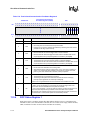
2.3.1 CPU Core Fault Register — PSFS Bit ..................................................................2-3
2.3.2 Coprocessor 14 Registers 0-3 – Performance Monitoring....................................2-3
2.3.3 Coprocessor 14 Register 6 and 7– Clock and Power Management .....................2-4
2.3.4 Coprocessor 15 Register 0 – ID Register Definition .............................................2-4
2.3.5 Coprocessor 15 Register 1 – P-Bit .......................................................................2-5
Input/Output Ordering ........................................................................................................2-5
Semaphores ......................................................................................................................2-6
Interrupts............................................................................................................................2-6
Reset .................................................................................................................................2-7
Internal Registers...............................................................................................................2-7
Selecting Peripherals vs. General Purpose Input/Output ..................................................2-8
Power on Reset and Boot Operation .................................................................................2-8
Power Management...........................................................................................................2-8
Pin List ...............................................................................................................................2-9
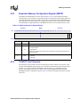
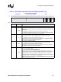
Register Address Summary.............................................................................................2-21
Memory Map....................................................................................................................2-33
Intel® PXA26x Processor Family Developer’s Manual
iii
Contents
3
Clocks and Power Manager .........................................................................................................3-1
3.1
3.2
3.3
3.4
3.5
3.6
3.7
3.8
4
System Integration Unit ................................................................................................................ 4-1
4.1
iv
Clock Manager Introduction...............................................................................................3-1
Power Manager Introduction..............................................................................................3-2
Clock Manager...................................................................................................................3-2
3.3.1 32.768-KHz Oscillator...........................................................................................3-4
3.3.2 3.6864-MHz Oscillator ..........................................................................................3-4
3.3.3 Core Phase Locked Loop .....................................................................................3-4
3.3.4 95.85-MHz Peripheral Phase Locked Loop ..........................................................3-5
3.3.5 147.46-MHz Peripheral Phase Locked Loop ........................................................3-6
3.3.6 Clock Gating .........................................................................................................3-6
Resets and Power Modes..................................................................................................3-6
3.4.1 Hardware Reset....................................................................................................3-7
3.4.2 Watchdog Reset ...................................................................................................3-7
3.4.3 GPIO Reset ..........................................................................................................3-8
3.4.4 Run Mode .............................................................................................................3-9
3.4.5 Turbo Mode ..........................................................................................................3-9
3.4.6 Idle Mode ............................................................................................................3-10
3.4.7 33-MHz Idle Mode ..............................................................................................3-12
3.4.8 Frequency Change Sequence ............................................................................3-13
3.4.9 Sleep Mode.........................................................................................................3-15
3.4.10 Power Mode Summary .......................................................................................3-20
Power Manager Registers ...............................................................................................3-22
3.5.1 Power Manager Control Register (PMCR) .........................................................3-23
3.5.2 Power Manager General Configuration Register (PCFR)...................................3-24
3.5.3 Power Manager Wake-Up Enable Register (PWER)..........................................3-25
3.5.4 Power Manager Rising-Edge Detect Enable Register (PRER) ..........................3-26
3.5.5 Power Manager Falling-Edge Detect Enable Register (PFER) ..........................3-27
3.5.6 Power Manager GPIO Edge Detect Status Register (PEDR).............................3-28
3.5.7 Power Manager Sleep Status Register (PSSR) .................................................3-29
3.5.8 Power Manager Scratch Pad Register (PSPR) ..................................................3-30
3.5.9 Power Manager Fast Sleep Wake Up Configuration Register (PMFWR)...........3-31
3.5.10 Power Manager GPIO Sleep State Registers (PGSR0, PGSR1, PGSR2).........3-31
3.5.11 Reset Controller Status Register (RCSR)...........................................................3-33
3.5.12 Power Manager Register Locations....................................................................3-34
Clocks Manager Registers...............................................................................................3-35
3.6.1 Core Clock Configuration Register (CCCR) .......................................................3-35
3.6.2 Clock Enable Register (CKEN)...........................................................................3-37
3.6.3 Oscillator Configuration Register (OSCC) ..........................................................3-39
3.6.4 Clocks Manager Register Locations ...................................................................3-39
Coprocessor 14: Clock and Power Management ............................................................3-40
3.7.1 Core Clock Configuration Register (CCLKCFG).................................................3-40
3.7.2 Power Mode Register (PWRMODE)...................................................................3-41
External Hardware Considerations ..................................................................................3-41
3.8.1 Power-On-Reset Considerations ........................................................................3-41
3.8.2 Driving the Crystal Pins from an External Clock Source.....................................3-41
3.8.3 Noise Coupling Between Driven Crystal Pins and a Crystal Oscillator...............3-42
General-Purpose Input/Output...........................................................................................4-1
4.1.1 GPIO Operation ....................................................................................................4-1
Intel® PXA26x Processor Family Developer’s Manual
Contents
4.2
4.3
4.4
4.5
5
Direct Memory Access Controller .................................................................................................5-1
5.1
5.2
5.3
5.4
5.5
6
4.1.2 GPIO Alternate Functions.....................................................................................4-3
4.1.3 GPIO Register Definitions.....................................................................................4-7
4.1.4 GPIO Register Locations ....................................................................................4-21
Interrupt Controller...........................................................................................................4-22
4.2.1 Interrupt Controller Operation .............................................................................4-23
4.2.2 Interrupt Controller Register Definitions..............................................................4-24
4.2.3 Interrupt Controller Register Locations ...............................................................4-31
Real-Time Clock (RTC) ...................................................................................................4-32
4.3.1 Real-Time Clock Operation.................................................................................4-32
4.3.2 Real-Time Clock Register Definitions .................................................................4-32
4.3.3 Trim Procedure ...................................................................................................4-35
4.3.4 Real-Time Clock Register Locations...................................................................4-38
Operating System Timer..................................................................................................4-38
4.4.1 Watchdog Timer Operation.................................................................................4-38
4.4.2 Operating System Timer Register Definitions.....................................................4-39
4.4.3 Operating System Timer Register Locations ......................................................4-42
Pulse Width Modulator.....................................................................................................4-43
4.5.1 Pulse Width Modulator Operation .......................................................................4-43
4.5.2 Register Descriptions..........................................................................................4-44
4.5.3 Pulse Width Modulator Output Wave Example...................................................4-47
4.5.4 Register Summary ..............................................................................................4-48
Direct Memory Access Description....................................................................................5-1
5.1.1 Direct Memory Access Controller Channels .........................................................5-2
5.1.2 Signal Descriptions ...............................................................................................5-3
5.1.3 Direct Memory Access Channel Priority Scheme .................................................5-4
5.1.4 Direct Memory Access Descriptors.......................................................................5-6
5.1.5 Channel States .....................................................................................................5-9
5.1.6 Read and Write Order...........................................................................................5-9
5.1.7 Byte Transfer Order ............................................................................................5-10
5.1.8 Trailing Bytes ......................................................................................................5-11
Transferring Data.............................................................................................................5-11
5.2.1 Servicing Internal Peripherals .............................................................................5-12
5.2.2 Quick Reference for Direct Memory Access Programming ................................5-13
5.2.3 Servicing Companion Chips and External Peripherals .......................................5-14
5.2.4 Memory-to-Memory Moves .................................................................................5-16
Direct Memory Access Controller Registers ....................................................................5-17
5.3.1 DMA Interrupt Register .......................................................................................5-17
5.3.2 DMA Channel Control/Status Register ...............................................................5-17
5.3.3 DMA Request to Channel Map Registers ...........................................................5-19
5.3.4 DMA Descriptor Address Registers ....................................................................5-20
5.3.5 DMA Source Address Registers .........................................................................5-21
5.3.6 DMA Target Address Registers ..........................................................................5-22
5.3.7 DMA Command Registers ..................................................................................5-23
Examples .........................................................................................................................5-25
Direct Memory Access Controller Registers Locations....................................................5-28
Memory Controller ........................................................................................................................6-1
6.1
Overview............................................................................................................................6-1
Intel® PXA26x Processor Family Developer’s Manual
v
Contents
6.2
6.3
6.4
6.5
6.6
6.7
6.8
6.9
6.10
6.11
6.12
6.13
7
Liquid Crystal Display Controller ..................................................................................................7-1
7.1
7.2
vi
Functional Description .......................................................................................................6-2
6.2.1 SDRAM Interface Overview.................................................................................. 6-2
6.2.2 Static Memory Interface / Variable Latency I/O Interface .....................................6-3
6.2.3 16-Bit PC Card / Compact Flash Interface ...........................................................6-4
Memory System Examples ................................................................................................6-4
Memory Accesses .............................................................................................................6-6
6.4.1 Reads and Writes .................................................................................................6-7
6.4.2 Aborts and Nonexistent Memory ..........................................................................6-7
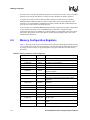
Memory Configuration Registers .......................................................................................6-8
Synchronous DRAM Memory Interface .............................................................................6-9
6.6.1 SDRAM MDCNFG Register.................................................................................. 6-9
6.6.2 SDRAM Mode Register Set Configuration Register ...........................................6-12
6.6.3 SDRAM MDREFR Register ................................................................................6-14
6.6.4 SDRAM Memory Options ...................................................................................6-17
6.6.5 SDRAM Command Overview .............................................................................6-25
6.6.6 SDRAM Waveforms............................................................................................6-27
Synchronous Static Memory Interface.............................................................................6-30
6.7.1 Synchronous Static Memory Configuration Register ..........................................6-30
6.7.2 Synchronous Static Memory Mode Register Set Configuration Register ...........6-36
6.7.3 Synchronous Static Memory Timing Diagrams...................................................6-37
6.7.4 Non-SDRAM Timing SXMEM Operation ............................................................6-38
Asynchronous Static Memory ..........................................................................................6-41
6.8.1 Static Memory Interface......................................................................................6-41
6.8.2 Asynchronous Static Memory Control Registers (MSC0 – 2).............................6-44
6.8.3 ROM Interface ....................................................................................................6-48
6.8.4 SRAM Interface Overview ..................................................................................6-51
6.8.5 Variable Latency I/O (VLIO) Interface Overview.................................................6-53
6.8.6 FLASH Memory Interface ...................................................................................6-56
16-Bit PC Card/Compact Flash Interface ........................................................................6-57
6.9.1 Expansion Memory Timing Configuration Register ............................................6-58
6.9.2 Expansion Memory Configuration Register (MECR) ..........................................6-61
6.9.3 16-Bit PC Card Overview....................................................................................6-61
6.9.4 External Logic for 16-Bit PC Card Implementation .............................................6-64
6.9.5 Expansion Card Interface Timing Diagrams and Parameters ............................6-67
Companion Chip Interface ...............................................................................................6-68
6.10.1 Alternate Bus Master Mode ................................................................................6-70
Options and Settings for Boot Memory............................................................................6-72
6.11.1 Alternate Booting ................................................................................................6-72
6.11.2 Boot Time Defaults .............................................................................................6-72
6.11.3 Memory Interface Reset and Initialization...........................................................6-75
Hardware, Watchdog, or Sleep Reset Operation ............................................................6-76
General Purpose Input/Output Reset Procedure.............................................................6-78
Overview............................................................................................................................7-1
7.1.1 Features................................................................................................................ 7-2
7.1.2 Pin Descriptions....................................................................................................7-4
Liquid Crystal Display Controller Operation.......................................................................7-4
7.2.1 Enabling the Controller .........................................................................................7-4
7.2.2 Disabling the Controller ........................................................................................7-5
Intel® PXA26x Processor Family Developer’s Manual
Contents
7.3
7.4
7.5
7.6
8
Synchronous Serial Port Controller ..............................................................................................8-1
8.1
8.2
8.3
8.4
8.5
8.6
8.7
9
7.2.3 Resetting the Controller ........................................................................................7-5
Detailed Module Descriptions ............................................................................................7-5
7.3.1 Input FIFOs ...........................................................................................................7-6
7.3.2 Lookup Palette ......................................................................................................7-6
7.3.3 Temporal Modulated Energy Distribution (TMED) Dithering.................................7-6
7.3.4 Output FIFOs ........................................................................................................7-9
7.3.5 Liquid Crystal Display Controller Pin Usage .........................................................7-9
7.3.6 Direct Memory Access ........................................................................................7-10
Liquid Crystal Display External Palette and Frame Buffers .............................................7-11
7.4.1 External-Palette Buffer........................................................................................7-11
7.4.2 External-Frame Buffer ........................................................................................7-12
Functional Timing ............................................................................................................7-15
Liquid Crystal Display Register Descriptions ...................................................................7-19
7.6.1 LCD Controller Control Register 0 (LCCR0) .......................................................7-20
7.6.2 LCD Controller Control Register 1 (LCCR1) .......................................................7-28
7.6.3 LCD Controller Control Register 2 (LCCR2) .......................................................7-30
7.6.4 LCD Controller Control Register 3 (LCCR3) .......................................................7-33
7.6.5 LCD Controller DMA ...........................................................................................7-37
7.6.6 LCD DMA Frame Branch Registers (FBRx) .......................................................7-41
7.6.7 LCD Controller Status Register (LCSR)..............................................................7-42
7.6.8 LCD Controller Interrupt ID Register (LIIDR) ......................................................7-46
7.6.9 TMED RGB Seed Register .................................................................................7-46
7.6.10 TMED Control Register (TCR) ............................................................................7-47
7.6.11 LCD Controller Register Summary .....................................................................7-49
Overview............................................................................................................................8-1
Signal Description..............................................................................................................8-1
8.2.1 External Interface to Synchronous Serial Peripherals ..........................................8-1
Functional Description .......................................................................................................8-2
8.3.1 Data Transfer........................................................................................................8-2
Data Formats .....................................................................................................................8-2
8.4.1 Serial Data Formats for Transfer to/from Peripherals ...........................................8-2
8.4.2 Parallel Data Formats for FIFO Storage ...............................................................8-6
FIFO Operation and Data Transfers ..................................................................................8-6
8.5.1 Using Programmed I/O Data Transfers ................................................................8-7
8.5.2 Using DMA Data Transfers ...................................................................................8-7
Baud Rate Generation .......................................................................................................8-7
SSP Serial Port Registers..................................................................................................8-7
8.7.1 SSP Control Register 0 (SSCR0) .........................................................................8-8
8.7.2 SSP Control Register 1 (SSCR1) .......................................................................8-11
8.7.3 SSP Data Register (SSDR) ................................................................................8-15
8.7.4 SSP Status Register (SSSR) ..............................................................................8-16
8.7.5 SSP Register Address Map ................................................................................8-19
Inter-Integrated Circuit Bus Interface Unit ....................................................................................9-1
9.1
9.2
9.3
Overview............................................................................................................................9-1
Signal Description..............................................................................................................9-1
Functional Description .......................................................................................................9-1
9.3.1 Operational Blocks................................................................................................9-3
Intel® PXA26x Processor Family Developer’s Manual
vii
Contents
9.4
9.5
9.6
9.7
9.8
9.9
10
Universal Asynchronous Receiver/Transmitter ..........................................................................10-1
10.1
10.2
10.3
10.4
10.5
11
Feature List......................................................................................................................10-1
Overview..........................................................................................................................10-2
10.2.1 Full Function UART ............................................................................................10-2
10.2.2 Bluetooth UART..................................................................................................10-2
10.2.3 Standard UART ..................................................................................................10-2
10.2.4 Compatibility with 16550.....................................................................................10-2
Signal Descriptions ..........................................................................................................10-3
UART Operational Description ........................................................................................10-4
10.4.1 Reset ..................................................................................................................10-5
10.4.2 Internal Register Descriptions.............................................................................10-5
10.4.3 FIFO Interrupt Mode Operation ........................................................................10-21
10.4.4 FIFO Polled Mode Operation............................................................................10-22
10.4.5 DMA Requests.................................................................................................. 10-22
10.4.6 Slow Infrared Asynchronous Interface..............................................................10-23
Register Summary .........................................................................................................10-26
10.5.1 UART Register Differences .............................................................................. 10-27
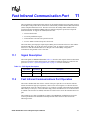
Fast Infrared Communication Port..............................................................................................11-1
11.1
11.2
viii
9.3.2
Inter-Integrated Circuit Bus Interface Modes .......................................................9-3
9.3.3 Start and Stop Bus States ....................................................................................9-4
Inter-Integrated Circuit Bus Operation ...............................................................................9-6
9.4.1 Serial Clock Line (SCL) Generation......................................................................9-7
9.4.2 Data and Addressing Management ......................................................................9-7
9.4.3 Inter-Integrated Circuit Acknowledge....................................................................9-8
9.4.4 Arbitration .............................................................................................................9-9
9.4.5 Master Operations ..............................................................................................9-11
9.4.6 Slave Operations ................................................................................................9-15
9.4.7 General Call Address..........................................................................................9-16
Slave Mode Programming Examples ..............................................................................9-18
9.5.1 Initialize Unit .......................................................................................................9-18
9.5.2 Write n Bytes as a Slave.....................................................................................9-18
9.5.3 Read n Bytes as a Slave ....................................................................................9-19
Master Programming Examples ......................................................................................9-19
9.6.1 Initialize Unit .......................................................................................................9-19
9.6.2 Write 1 Byte as a Master ....................................................................................9-19
9.6.3 Read 1 Byte as a Master ....................................................................................9-20
9.6.4 Write 2 Bytes and Repeated Start Read 1 Byte as a Master..............................9-20
9.6.5 Read 2 Bytes as a Master - Send STOP Using the Abort ..................................9-21
Glitch Suppression Logic .................................................................................................9-22
Reset Conditions .............................................................................................................9-22
Register Definitions..........................................................................................................9-22
9.9.1 I2C Bus Monitor Register- IBMR ........................................................................9-22
9.9.2 I2C Data Buffer Register- IDBR..........................................................................9-23
9.9.3 I2C Control Register- ICR...................................................................................9-24
9.9.4 I2C Status Register.............................................................................................9-26
9.9.5 I2C Slave Address Register- ISAR .....................................................................9-28
Signal Description............................................................................................................11-1
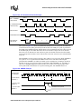
Fast Infrared Communications Port Operation ................................................................11-1
Intel® PXA26x Processor Family Developer’s Manual
Contents
11.3
11.4
12
11.2.1 Four-Position Pulse Modulation ..........................................................................11-2
11.2.2 Frame Format .....................................................................................................11-3
11.2.3 Address Field......................................................................................................11-4
11.2.4 Control Field .......................................................................................................11-4
11.2.5 Data Field ...........................................................................................................11-4
11.2.6 CRC Field ...........................................................................................................11-4
11.2.7 Baud Rate Generation ........................................................................................11-5
11.2.8 Receive Operation ..............................................................................................11-5
11.2.9 Transmit Operation .............................................................................................11-6
11.2.10 Transmit and Receive FIFOs ..............................................................................11-7
11.2.11 Trailing or Error Bytes in the Receive FIFO........................................................11-7
Fast Infrared Communications Port Register Descriptions..............................................11-8
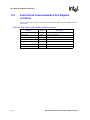
11.3.1 FICP Control Register 0......................................................................................11-8
11.3.2 FICP Control Register 1....................................................................................11-10
11.3.3 FICP Control Register 2....................................................................................11-11
11.3.4 FICP Data Register...........................................................................................11-12
11.3.5 FICP Status Register 0 .....................................................................................11-13
11.3.6 FICP Status Register 1 .....................................................................................11-14
Fast Infrared Communications Port Register Locations ................................................11-16
Universal Serial Bus Device Controller.......................................................................................12-1
12.1
12.2
12.3
12.4
12.5
12.6
Universal Serial Bus Overview ........................................................................................12-1
Device Configuration .......................................................................................................12-2
Universal Serial Bus Protocol ..........................................................................................12-3
12.3.1 Signalling Levels .................................................................................................12-3
12.3.2 Bit Encoding........................................................................................................12-4
12.3.3 Field Formats ......................................................................................................12-4
12.3.4 Packet Formats...................................................................................................12-5
12.3.5 Transaction Formats ...........................................................................................12-7
12.3.6 UDC Device Requests ........................................................................................12-8
12.3.7 Configuration ....................................................................................................12-10
UDC Hardware Connection ...........................................................................................12-10
12.4.1 Self-Powered Device ........................................................................................12-10
12.4.2 Bus-Powered Devices ......................................................................................12-12
UDC Operation ..............................................................................................................12-12
12.5.1 Case 1: EP0 Control Read ...............................................................................12-12
12.5.2 Case 2: EP0 Control Read with a Premature Status Stage..............................12-13
12.5.3 Case 3: EP0 Control Write With or Without a Premature Status Stage............12-14
12.5.4 Case 4: EP0 No Data Command ......................................................................12-15
12.5.5 Case 5: EP1 Data Transmit (BULK-IN).............................................................12-15
12.5.6 Case 6: EP2 Data Receive (BULK-OUT)..........................................................12-16
12.5.7 Case 7: EP3 Data Transmit (ISOCHRONOUS-IN)...........................................12-17
12.5.8 Case 8: EP4 Data Receive (ISOCHRONOUS-OUT)........................................12-18
12.5.9 Case 9: EP5 Data Transmit (INTERRUPT-IN) .................................................12-20
12.5.10 Case 10: RESET Interrupt ................................................................................12-20
12.5.11 Case 11: SUSPEND Interrupt...........................................................................12-21
12.5.12 Case 12: RESUME Interrupt.............................................................................12-21
UDC Register Descriptions ............................................................................................12-21
12.6.1 UDC Control Register .......................................................................................12-22
12.6.2 UDC Endpoint 0 Control/Status Register (UDCCS0)........................................12-24
Intel® PXA26x Processor Family Developer’s Manual
ix
Contents
12.6.3 UDC Endpoint x Control/Status Register (UDCCSx), Where x is 1, 6, or 11....12-26
12.6.4 UDC Endpoint x Control/Status Register (UDCCSx), Where x is 2, 7, or 12....12-28
12.6.5 UDC Endpoint x Control/Status Register (UDCCSx), Where x is 3, 8, or 13....12-31
12.6.6 UDC Endpoint x Control/Status Register (UDCCSx), Where x is 4, 9, or 14....12-33
12.6.7 UDC Endpoint x Control/Status Register (UDCCSx), Where x is 5, 10, or 15..12-35
12.6.8 UDC Interrupt Control Register 0 (UICR0) .......................................................12-37
12.6.9 UDC Interrupt Control Register 1 (UICR1) .......................................................12-38
12.6.10 UDC Status/Interrupt Register 0 (USIR0) .........................................................12-40
12.6.11 UDC Status/Interrupt Register 1 (USIR1) .........................................................12-41
12.6.12 UDC Frame Number High Register (UFNHR) ..................................................12-43
12.6.13 UDC Frame Number Low Register (UFNLR) ...................................................12-45
12.6.14 UDC Byte Count Register x (UBCRx), Where x is 2, 4, 7, 9, 12, or 14. ...........12-45
12.6.15 UDC Endpoint 0 Data Register (UDDR0) .........................................................12-46
12.6.16 UDC Data Register x (UDDRx), Where x is 1, 6, or 11 ....................................12-47
12.6.17 UDC Data Register x (UDDRx), Where x is 2, 7, or 12 ....................................12-48
12.6.18 UDC Data Register x (UDDRx), Where x is 3, 8, or 13 ....................................12-48
12.6.19 UDC Data Register x (UDDRx), Where x is 4, 9, or 14 ....................................12-49
12.6.20 UDC Data Register x (UDDRx), Where x is 5, 10, or 15 ..................................12-49
12.6.21 UDC Register Locations ...................................................................................12-50
13
AC97 Controller Unit...................................................................................................................13-1
13.1
13.2
13.3
13.4
13.5
13.6
13.7
13.8
14
Inter-Integrated Circuit Sound Controller....................................................................................14-1
14.1
14.2
14.3
x
Overview..........................................................................................................................13-1
Feature List......................................................................................................................13-1
Signal Description............................................................................................................13-2
13.3.1 Signal Configuration Steps .................................................................................13-2
13.3.2 Example AC-link .................................................................................................13-2
AC-link Digital Serial Interface Protocol...........................................................................13-3
13.4.1 AC-link Audio Output Frame (SDATA_OUT)......................................................13-4
13.4.2 AC-link Audio Input Frame (SDATA_IN).............................................................13-8
AC-link Low Power Mode ..............................................................................................13-12
13.5.1 Powering Down the AC-link .............................................................................. 13-12
13.5.2 Waking up the AC-link ......................................................................................13-13
ACUNIT Operation.........................................................................................................13-14
13.6.1 Initialization .......................................................................................................13-15
13.6.2 Trailing bytes ....................................................................................................13-16
13.6.3 Operational Flow for Accessing Codec Registers ............................................13-16
Clocks and Sampling Frequencies ................................................................................13-16
Functional Description ...................................................................................................13-17
13.8.1 FIFOs................................................................................................................13-17
13.8.2 Interrupts...........................................................................................................13-18
13.8.3 Registers...........................................................................................................13-18
Overview..........................................................................................................................14-1
Signal Descriptions ..........................................................................................................14-2
Controller Operation ........................................................................................................14-3
14.3.1 Initialization .........................................................................................................14-3
14.3.2 Disabling and Enabling Audio Replay.................................................................14-4
14.3.3 Disabling and Enabling Audio Record ................................................................14-4
14.3.4 Transmit FIFO Errors..........................................................................................14-5
Intel® PXA26x Processor Family Developer’s Manual
Contents
14.4
14.5
14.6
14.7
15
14.3.5 Receive FIFO Errors ...........................................................................................14-5
14.3.6 Trailing Bytes ......................................................................................................14-5
Serial Audio Clocks and Sampling Frequencies..............................................................14-5
Data Formats ...................................................................................................................14-6
14.5.1 FIFO and Memory Format ..................................................................................14-6
14.5.2 I2S and MSB-Justified Serial Audio Formats......................................................14-6
I2S Controller Register Descriptions ................................................................................14-7
14.6.1 Serial Audio Controller Global Control Register (SACR0) ..................................14-8
14.6.2 Serial Audio Controller I2S/MSB-Justified Control Register (SACR1) ..............14-10
14.6.3 Serial Audio Controller I2S/MSB-Justified Status Register (SASR0)................14-11
14.6.4 Serial Audio Clock Divider Register (SADIV)....................................................14-13
14.6.5 Serial Audio Interrupt Clear Register (SAICR)..................................................14-13
14.6.6 Serial Audio Interrupt Mask Register (SAIMR) .................................................14-14
14.6.7 Serial Audio Data Register (SADR) ..................................................................14-14
14.6.8 Controller: Register Memory Map .....................................................................14-15
Interrupts........................................................................................................................14-16
MultiMediaCard Controller..........................................................................................................15-1
15.1
15.2
15.3
15.4
15.5
Overview..........................................................................................................................15-1
MultiMediaCard Controller Functional Description ..........................................................15-4
15.2.1 Signal Description ...............................................................................................15-4
15.2.2 MultiMediaCard Controller Reset........................................................................15-5
15.2.3 Card Initialization Sequence ...............................................................................15-5
15.2.4 MMC and SPI Modes..........................................................................................15-5
15.2.5 Error Detection....................................................................................................15-7
15.2.6 Interrupts.............................................................................................................15-7
15.2.7 Clock Control ......................................................................................................15-7
15.2.8 Data FIFOs .........................................................................................................15-8
Card Communication Protocol.......................................................................................15-11
15.3.1 Basic, No Data, Command and Response Sequence ......................................15-11
15.3.2 Data Transfer....................................................................................................15-12
15.3.3 Busy Sequence.................................................................................................15-15
15.3.4 SPI Functionality ...............................................................................................15-15
MultiMediaCard Controller Operation ............................................................................15-15
15.4.1 Start and Stop Clock .........................................................................................15-16
15.4.2 Initialize .............................................................................................................15-16
15.4.3 Enabling SPI Mode ...........................................................................................15-16
15.4.4 No Data Command and Response Sequence..................................................15-16
15.4.5 Erase ................................................................................................................15-17
15.4.6 Single Data Block Write ....................................................................................15-17
15.4.7 Single Block Read ............................................................................................15-18
15.4.8 Multiple Block Write ..........................................................................................15-18
15.4.9 Multiple Block Read ..........................................................................................15-19
15.4.10 Stream Write.....................................................................................................15-19
15.4.11 Stream Read.....................................................................................................15-20
MultiMediaCard Controller Register Descriptions ..........................................................15-21
15.5.1 MMC_STRPCL Register...................................................................................15-21
15.5.2 MMC_STAT Register........................................................................................15-22
15.5.3 MMC_CLKRT Register .....................................................................................15-23
15.5.4 MMC_SPI Register ...........................................................................................15-24
Intel® PXA26x Processor Family Developer’s Manual
xi
Contents
15.5.5 MMC_CMDAT Register ....................................................................................15-25
15.5.6 MMC_RESTO Register ....................................................................................15-26
15.5.7 MMC_RDTO Register.......................................................................................15-27
15.5.8 MMC_BLKLEN Register ...................................................................................15-28
15.5.9 MMC_NOB Register .........................................................................................15-28
15.5.10 MMC_PRTBUF Register ..................................................................................15-28
15.5.11 MMC_I_MASK Register....................................................................................15-29
15.5.12 MMC_I_REG Register ......................................................................................15-30
15.5.13 MMC_CMD Register.........................................................................................15-31
15.5.14 MMC_ARGH Register ......................................................................................15-34
15.5.15 MMC_ARGL Register .......................................................................................15-34
15.5.16 MMC_RES FIFO (read only) ............................................................................15-35
15.5.17 MMC_RXFIFO FIFO (read only).......................................................................15-35
15.5.18 MMC_TXFIFO FIFO .........................................................................................15-35
16
Network/Audio Synchronous Serial Protocol Serial Ports ..........................................................16-1
16.1
16.2
16.3
16.4
16.5
16.6
17
Hardware UART .........................................................................................................................17-1
17.1
17.2
17.3
17.4
17.5
xii
Overview..........................................................................................................................16-1
Features...........................................................................................................................16-1
Signal Description............................................................................................................16-2
Operation .........................................................................................................................16-2
16.4.1 Processor and DMA FIFO Access......................................................................16-3
16.4.2 Trailing Bytes in the Receive FIFO .....................................................................16-3
16.4.3 Data Formats ......................................................................................................16-4
16.4.4 Hi-Z on SSPTXD...............................................................................................16-13
16.4.5 FIFO Operation.................................................................................................16-17
16.4.6 Baud-Rate Generation......................................................................................16-17
SSP Port Register Descriptions.....................................................................................16-18
16.5.1 SSP Control Register 0 (SSCR0) .....................................................................16-18
16.5.2 SSP Control Register 1 (SSCR1) .....................................................................16-21
16.5.3 SSP Programmable Serial Protocol Register (SSPSP)....................................16-27
16.5.4 SSP Time Out Register (SSTO) .......................................................................16-28
16.5.5 SSP Interrupt Test Register (SSITR)................................................................16-29
16.5.6 SSP Status Register (SSSR)............................................................................16-30
16.5.7 SSP Data Register (SSDR) .............................................................................. 16-34
Register Summary .........................................................................................................16-34
Overview..........................................................................................................................17-1
Features...........................................................................................................................17-2
Signal Descriptions ..........................................................................................................17-3
Operation .........................................................................................................................17-3
17.4.1 Reset ..................................................................................................................17-5
17.4.2 FIFO Operation...................................................................................................17-5
17.4.3 Autoflow Control .................................................................................................17-7
17.4.4 Auto-Baud-Rate Detection..................................................................................17-8
17.4.5 Slow Infrared Asynchronous Interface................................................................17-8
Hardware UART Register Descriptions .........................................................................17-10
17.5.1 Receive Buffer Register (RBR).........................................................................17-10
17.5.2 Transmit Holding Register (THR) .....................................................................17-11
17.5.3 Divisor Latch Registers (DLL and DLH)............................................................17-11
Intel® PXA26x Processor Family Developer’s Manual
Contents
17.6
18
17.5.4 Interrupt Enable Register (IER) ........................................................................17-13
17.5.5 Interrupt Identification Register (IIR) .................................................................17-14
17.5.6 FIFO Control Register (FCR) ............................................................................17-17
17.5.7 Receive FIFO Occupancy Register (FOR) .......................................................17-18
17.5.8 Auto-Baud Control Register (ABR) ...................................................................17-19
17.5.9 Auto-Baud Count Register (ACR) .....................................................................17-20
17.5.10 Line Control Register (LCR)..............................................................................17-21
17.5.11 Line Status Register (LSR) ...............................................................................17-23
17.5.12 Modem Control Register (MCR) .......................................................................17-26
17.5.13 Modem Status Register (MSR) .........................................................................17-28
17.5.14 Scratchpad Register (SPR) ..............................................................................17-29
17.5.15 Infrared Selection Register (ISR) ......................................................................17-30
Hardware UART Register Summary..............................................................................17-31
Internal Flash..............................................................................................................................18-1
18.1
18.2
Initialization ......................................................................................................................18-1
18.1.1 Intel StrataFlash® Memory Reset Configuration ................................................18-1
18.1.2 BOOT_SEL[2:0] Configuration ...........................................................................18-2
18.1.3 Determining the Size and Configuration of Flash Using Software ......................18-2
18.1.4 SXCNFG Configuration ......................................................................................18-2
18.1.5 Configuring the Intel StrataFlash® Memory........................................................18-3
Additional Intel StrataFlash® Memory Information ..........................................................18-6
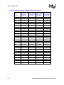
Figures
2-1
2-2
2-3
3-1
4-1
4-2
4-3
4-4
5-1
5-2
5-3
5-4
5-5
6-1
6-2
6-3
6-4
6-5
6-6
6-7
6-8
6-9
6-10
6-11
6-12
6-13
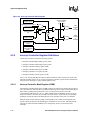
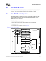
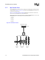
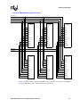
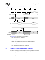
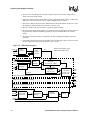
Block Diagram ...........................................................................................................................2-2
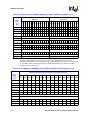
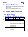
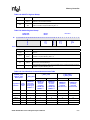
Memory Map (Part One) — From 0x8000 0000 to 0xFFFF FFFF...........................................2-34
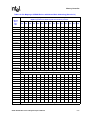
Memory Map (Part Two) — From 0x0000 0000 to 0x7FFF FFFF ...........................................2-35
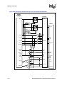
Clocks Manager Block Diagram ................................................................................................3-3
General-Purpose I/O Block Diagram .........................................................................................4-2
Interrupt Controller Block Diagram ..........................................................................................4-24
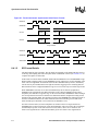
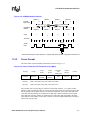
PWMn Block Diagram..............................................................................................................4-43
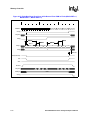
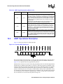
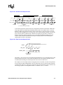
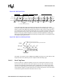
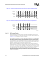
Basic Pulse Width Waveform ..................................................................................................4-47
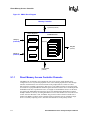
DMAC Block Diagram................................................................................................................5-2
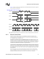
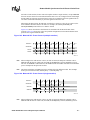
DREQ timing requirements........................................................................................................5-3
No-Descriptor Fetch Mode Channel State.................................................................................5-7
Descriptor Fetch Mode Channel State.......................................................................................5-8
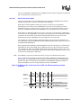
Little Endian Transfers.............................................................................................................5-10
General Memory Interface Configuration...................................................................................6-2
SDRAM Memory System Example............................................................................................6-5
Asynchronous Static Memory System Example ........................................................................6-6
External to Internal Address Mapping Options ........................................................................6-19
SDRAM Read ..........................................................................................................................6-27
SDRAM Read With a Second Read to Same Bank, Same Row .............................................6-27
SDRAM Read With a Second Read to Same Bank, Different Row.........................................6-28
SDRAM Read With a Second Read to a Different Bank .........................................................6-28
SDRAM Write ..........................................................................................................................6-29
SDRAM Write With a Second Write to Same Bank, Same Row .............................................6-29
SMROM Read Timing Diagram Half-Memory Clock Frequency, ............................................6-38
Burst-of-Eight Synchronous Flash Timing Diagram (non-divide-by-2 mode) ..........................6-40
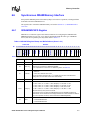
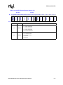
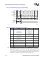
MSC0/1/2 Register Bitmap ......................................................................................................6-44
Intel® PXA26x Processor Family Developer’s Manual
xiii
Contents
6-14
6-15
6-16
6-17
6-18
6-19
6-20
6-21
6-22
6-23
6-24
6-25
6-26
6-27
6-28
6-29
6-30
6-31
6-32
6-33
7-1
7-2
7-3
7-4
7-5
7-6
7-8
7-9
7-10
7-7
7-11
7-12
7-13
7-14
7-15
7-16
7-17
7-18
8-1
8-2
8-3
8-4
9-1
9-2
9-3
9-4
xiv
32-Bit Burst-of-Eight ROM or Flash Read Timing Diagram (MSC0:RDF = 4,
MSC0:RDN = 1, MSC0:RRR = 1)............................................................................................6-49
Eight-Beat Burst Read from 16-Bit Burst-of-Four ROM or Flash (MSC0:RDF = 4,
MSC0:RDN = 1, MSC0:RRR = 0)............................................................................................6-50
32-Bit Non-burst ROM, SRAM, or Flash Read Timing Diagram - Four Data Beats
(MSC0:RDF = 4, MSC0:RRR = 1) ...........................................................................................6-51
32-Bit SRAM Write Timing Diagram (4-beat Burst) (MSC0:RDN = 2, MSC0:RRR = 1)..........6-52
32-Bit Variable Latency I/O Read Timing (Burst-of-Four, One Wait Cycle Per Beat)
(MSC0:RDF = 2, MSC0:RDN = 2, MSC0:RRR = 1) ...............................................................6-54
32-Bit Variable Latency I/O Write Timing (Burst-of-Four, Variable Wait Cycles Per Beat)......6-55
Asynchronous 32-Bit Flash Write Timing Diagram (2 Writes) .................................................6-57
MCMEM1 Register Bitmap ......................................................................................................6-58
MCATT1 Register Bitmap........................................................................................................6-58
MCIO1 Register Bitmap...........................................................................................................6-59
16-Bit PC Card Memory Map ..................................................................................................6-62
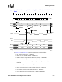
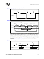
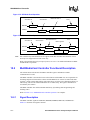
Expansion Card External Logic for a One-Socket Configuration.............................................6-65
Expansion Card External Logic for a Two-Socket Configuration.............................................6-66
16-Bit PC Card Memory or I/O 16-Bit (Half-word) Access.......................................................6-67
16-Bit PC Card I/O 16-Bit Access to 8-Bit Device ...................................................................6-68
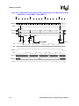
Alternate Bus Master Mode .....................................................................................................6-69
Variable Latency IO .................................................................................................................6-69
Asynchronous Boot Time Configurations and Register Defaults.............................................6-73
SMROM Boot Time Configurations and Register Defaults......................................................6-74
SMROM Boot Time Configurations and Register Defaults (Continued) ..................................6-75
LCD Controller Block Diagram ..................................................................................................7-3
Temporal Dithering Concept - Single Color ...............................................................................7-7
Compare Range for TMED........................................................................................................7-7
TMED Block Diagram ...............................................................................................................7-8
Palette-Buffer Format ..............................................................................................................7-12
1-Bit Per Pixel Data Memory Organization..............................................................................7-12
4-Bits Per Pixel Data Memory Organization ............................................................................7-13
8-Bits Per Pixel Data Memory Organization ............................................................................7-13
16-Bits Per Pixel Data Memory Organization – Passive Mode ...............................................7-13
2-Bits Per Pixel Data Memory Organization ............................................................................7-13
16-Bits Per Pixel Data Memory Organization – Active Mode ..................................................7-14
Passive Mode Start-of-Frame Timing......................................................................................7-16
Passive Mode End-of-Frame Timing .......................................................................................7-17
Passive Mode Pixel Clock and Data Pin Timing......................................................................7-17
Active Mode Timing .................................................................................................................7-18
Active Mode Pixel Clock and Data Pin Timing ........................................................................7-19
Frame Buffer/Palette Output to LCD Data Pins in Active Mode ..............................................7-25
LCD Data-Pin Pixel Ordering...................................................................................................7-27
Texas Instruments’ Synchronous Serial Frame* Format ...........................................................8-4
Motorola SPI* Frame Format.....................................................................................................8-5
National Microwire* Frame Format............................................................................................8-6
Motorola SPI* Frame Formats for SPO and SPH Programming .............................................8-14
I2C Bus Configuration Example................................................................................................9-2
Start and Stop Conditions..........................................................................................................9-5
START and STOP Conditions ...................................................................................................9-6
Data Format of First Byte in Master Transaction.......................................................................9-8
Intel® PXA26x Processor Family Developer’s Manual
Contents
9-5
9-6
9-7
9-8
9-9
9-10
9-11
9-12
9-13
9-14
10-1
10-2
10-3
10-4
11-1
11-2
11-3
12-1
12-2
13-1
13-2
13-3
13-4
13-5
13-6
13-7
13-8
13-9
13-10
13-11
14-1
14-2
14-3
15-1
15-2
15-3
15-4
15-5
15-6
16-1
16-2
16-3
16-4
16-5
16-6
16-7
16-8
16-9
Acknowledge on the I2C Bus.....................................................................................................9-8
Clock Synchronization During the Arbitration Procedure.........................................................9-10
Arbitration Procedure of Two Masters .....................................................................................9-10
Master-Receiver Read from Slave-Transmitter .......................................................................9-14
Master-Receiver Read from Slave-Transmitter / Repeated Start / Master-Transmitter
Write to Slave-Receiver ...........................................................................................................9-14
A Complete Data Transfer .......................................................................................................9-14
Master-Transmitter Write to Slave-Receiver............................................................................9-16
Master-Receiver Read to Slave-Transmitter ...........................................................................9-16
Master-Receiver Read to Slave-Transmitter, Repeated START, Master-Transmitter
Write to Slave-Receiver ...........................................................................................................9-16
General Call Address...............................................................................................................9-17
Example UART Data Frame ....................................................................................................10-4
Example NRZ Bit Encoding (0b0100 1011).............................................................................10-5
IR Transmit and Receive Example ........................................................................................10-25
XMODE Example...................................................................................................................10-25
4PPM Modulation Encodings...................................................................................................11-2
4PPM Modulation Example .....................................................................................................11-3
Frame Format for IrDA Transmission (4.0 Mbps) ....................................................................11-3
NRZI Bit Encoding Example ....................................................................................................12-4
Self-Powered Device .............................................................................................................12-11
Data Transfer Through the AC-link..........................................................................................13-3
AC97 Standard Bidirectional Audio Frame ..............................................................................13-4
AC-link Audio Output Frame....................................................................................................13-5
Start of Audio Output Frame....................................................................................................13-5
AC97 Input Frame ...................................................................................................................13-9
Start of an Audio Input Frame..................................................................................................13-9
AC-link Powerdown Timing....................................................................................................13-12
SDATA_IN Wake Up Signaling..............................................................................................13-13
PCM Transmit and Receive Operation ..................................................................................13-27
Mic-in Receive-Only Operation..............................................................................................13-29
Modem Transmit and Receive Operation ..............................................................................13-32
I2S Data Formats (16 bits).......................................................................................................14-7
MSB-Justified Data Formats (16 bits)......................................................................................14-7
Transmit and Receive FIFO Accesses Through the SADR...................................................14-15
MMC System Interaction .........................................................................................................15-1
MMC Mode Operation Without Data Token.............................................................................15-3
MMC Mode Operation With Data Token..................................................................................15-3
SPI Mode Operation Without Data Token ...............................................................................15-3
SPI Mode Read Operation.......................................................................................................15-4
SPI Mode Write Operation.......................................................................................................15-4
Texas Instruments Synchronous Serial Frame* Protocol (multiple transfers) .........................16-6
Texas Instruments Synchronous Serial Frame* Protocol (single transfers) ............................16-6
Motorola SPI* Frame Protocol (multiple transfers) ..................................................................16-7
Motorola SPI* Frame Protocol (single transfers) .....................................................................16-7
Motorola SPI* Frame Protocols for SPO and SPH Programming (multiple transfers).............16-8
Motorola SPI* Frame Protocols for SPO and SPH Programming (single transfers)................16-9
National Semiconductor Microwire* Frame Protocol (multiple transfers) ..............................16-10
National Semiconductor Microwire* Frame Protocol (single transfers) .................................16-10
Programmable Serial Protocol (multiple transfers) ................................................................16-11
Intel® PXA26x Processor Family Developer’s Manual
xv
Contents
16-10
16-11
16-12
16-13
16-14
16-15
16-16
16-17
17-1
17-2
17-3
17-4
18-1
18-2
Programmable Serial Protocol (single transfers)...................................................................16-12
TI SSP with SSCR[TTE]=1 and SSCR[TTELP]=0.................................................................16-13
TI SSP with SSCR[TTE]=1 and SSCR[TTELP]=1.................................................................16-14
Motorola SPI with SSCR[TTE]=1...........................................................................................16-14
National Semiconductor Microwire with SSCR1[TTE]=1.......................................................16-15
PSP mode with SSCR1[TTE]=1 and SSCR1[TTELP]=0 (slave to frame) .............................16-15
PSP mode with SSCR1[TTE]=1 and SSCR1[TTELP]=0 (master to frame) ..........................16-16
PSP mode with SSCR1[TTE]=1 and SSCR1[TTELP]=1 (must be slave to frame) ...............16-16
Example UART Data Frame....................................................................................................17-4
Example NRZ Bit Encoding (0b0100 1011).............................................................................17-4
IR Transmit and Receive Example ..........................................................................................17-9
XMODE Example. .................................................................................................................17-10
Flash Memory Reset Using State Machine .............................................................................18-1
Flash Memory Reset Logic if Watchdog Reset is Not Necessary ...........................................18-2
Tables
2-1
2-2
2-3
2-4
2-5
2-6
2-7
2-8
3-1
3-2
3-3
3-4
3-5
3-6
3-7
3-8
3-9
3-10
3-11
3-12
3-13
3-14
3-15
3-16
3-17
3-18
3-19
3-20
3-21
3-22
3-23
3-24
3-25
xvi
CPU Core Fault Register Bitmap...............................................................................................2-3
ID Register Bitmap and Bit Definitions (Read-only)...................................................................2-4
PXA26x processor family ID Values ..........................................................................................2-5
Effect of Each Type of Reset on Internal Register State ..........................................................2-7
Processor Pin Types ................................................................................................................ 2-9
Pin & Signal Descriptions for the PXA26x Processor Family .................................................... 2-9
Pin Description Notes ..............................................................................................................2-21
Register Address Summary.....................................................................................................2-21
Core PLL Output Frequencies for 3.6864-MHz Crystal .............................................................3-5
95.85-MHz Peripheral PLL Output Frequencies for 3.6864-MHz Crystal..................................3-5
147.46-MHz Peripheral PLL Output Frequencies for 3.6864-MHz Crystal................................ 3-6
Power Mode Entry Sequence Table .......................................................................................3-20
Power Mode Exit Sequence Table .........................................................................................3-21
Power and Clock Supply Sources and States During Power Modes .....................................3-22
PMCR Bit Definitions ...............................................................................................................3-23
PCFR Bit Definitions................................................................................................................3-24
PWER Bit Definitions ...............................................................................................................3-25
PRER Bit Definitions................................................................................................................3-26
PFER Bit Definitions ................................................................................................................3-27
PEDR Bit Definitions................................................................................................................3-28
PSSR Bit Definitions................................................................................................................3-29
PSPR Bit Definitions................................................................................................................3-30
PMFWR Register Bitmap and Bit Definitions ..........................................................................3-31
PGSR0 Bit Definitions .............................................................................................................3-32
PGSR1 Bit Definitions .............................................................................................................3-32
PSPR Bit Definitions................................................................................................................3-32
RCSR Bit Definitions ...............................................................................................................3-34
Power Manager Register Locations ........................................................................................3-34
CCCR Register Bitmap and Bit Definitions..............................................................................3-36
CKEN Register Bitmap and Bit Definitions ..............................................................................3-37
OSCC Bit Definitions ...............................................................................................................3-39
Clocks Manager Register Locations ........................................................................................3-39
Coprocessor 14 Clock and Power Management Summary.....................................................3-40
Intel® PXA26x Processor Family Developer’s Manual
Contents
3-26
3-27
4-1
4-2
4-3
4-4
4-5
4-6
4-7
4-8
4-9
4-10
4-11
4-12
4-13
4-14
4-15
4-16
4-17
4-18
4-19
4-20
4-21
4-22
4-23
4-24
4-25
4-26
4-27
4-28
4-29
4-30
4-31
4-32
4-33
4-34
4-35
4-36
4-37
4-38
4-39
4-40
4-41
4-42
4-43
4-44
4-45
4-46
4-47
4-48
CCLKCFG Bit Definitions.........................................................................................................3-40
PWRMODE Bit Definitions.......................................................................................................3-41
GPIO Alternate Functions..........................................................................................................4-3
GPIO Register Definitions..........................................................................................................4-7
GPLR0 Bit Definitions ................................................................................................................4-8
GPLR1 Bit Definitions ................................................................................................................4-9
GPLR2 Register Bitmap ............................................................................................................4-9
GPDR0 Bit Definitions .............................................................................................................4-10
GPDR1 Bit Definitions .............................................................................................................4-10
GPDR2 Register Bitmap..........................................................................................................4-10
GPSR0 Bit Definitions..............................................................................................................4-11
GPSR1 Bit Definitions..............................................................................................................4-11
GPSR2 Register Bitmap ..........................................................................................................4-12
GPCR0 Bit Definitions .............................................................................................................4-12
GPCR1 Bit Definitions .............................................................................................................4-12
GPCR2 Register Bitmap..........................................................................................................4-13
GRER0 Bit Definitions .............................................................................................................4-14
GRER1 Bit Definitions .............................................................................................................4-14
GRER2 Register Bitmap..........................................................................................................4-14
GFER0 Bit Definitions..............................................................................................................4-15
GFER1 Bit Definitions..............................................................................................................4-15
GFER2 Register Bitmap ..........................................................................................................4-15
GEDR0 Bit Definitions .............................................................................................................4-16
GEDR1 Bit Definitions .............................................................................................................4-17
GEDR2 Register Bitmap..........................................................................................................4-17
GAFR0_L Bit Definitions..........................................................................................................4-18
GAFR0_U Bit Definitions .........................................................................................................4-18
GAFR1_L Bit Definitions..........................................................................................................4-19
GAFR1_U Bit Definitions .........................................................................................................4-19
GAFR2_L Bit Definitions..........................................................................................................4-20
GAFR2_U Register Bitmap......................................................................................................4-20
GPIO Register Addresses .......................................................................................................4-21
ICMR Register Bitmap .............................................................................................................4-25
ICLR Register Bitmap ..............................................................................................................4-25
ICCR Bit Definitions .................................................................................................................4-26
ICIP Register Bitmap ...............................................................................................................4-27
ICFP Register Bitmap ..............................................................................................................4-27
ICPR Register Bitmap..............................................................................................................4-28
List of First–Level Interrupts ....................................................................................................4-30
Interrupt Controller Register Addresses ..................................................................................4-31
RTTR Bit Definitions ................................................................................................................4-33
RTAR Bit Definitions ................................................................................................................4-34
RCNR Bit Definitions ...............................................................................................................4-34
RTSR Bit Definitions ................................................................................................................4-35
RTC Register Addresses .........................................................................................................4-38
OSMR[x] Bit Definitions ...........................................................................................................4-39
OIER Bit Definitions .................................................................................................................4-40
OWER Bit Definitions...............................................................................................................4-40
OSCR Bit Definitions ...............................................................................................................4-41
OSSR Bit Definitions................................................................................................................4-42
Intel® PXA26x Processor Family Developer’s Manual
xvii
Contents
4-49
4-50
4-51
4-52
4-53
5-1
5-2
5-3
5-4
5-5
5-6
5-7
5-8
5-9
5-10
5-11
5-12
5-13
6-1
6-2
6-3
6-4
6-5
6-6
6-7
6-8
6-9
6-10
6-11
6-12
6-13
6-14
6-15
6-16
6-17
6-18
6-19
6-20
6-21
6-22
6-23
6-24
6-25
6-26
6-27
6-28
6-29
6-30
6-31
6-32
xviii
OS Timer Register Locations ..................................................................................................4-42
PWM_CTRLn Bit Definitions ...................................................................................................4-45
PWM_DUTYn Bit Definitions ...................................................................................................4-46
PWM_PERVALn Bit Definitions...............................................................................................4-47
PWM Register Locations .........................................................................................................4-48
DMAC Signal List ......................................................................................................................5-3
Channel Priority (if all channels are running concurrently) ........................................................5-5
Channel Priority .........................................................................................................................5-5
Priority Schemes Examples.......................................................................................................5-5
DMA Quick Reference for Internal Peripherals .......................................................................5-13
DINT Register Bitmap and Bit Definitions................................................................................5-17
DMA Channel Control/Status Register Bitmap and Bit Definitions ..........................................5-18
DRCMRx Registers Bitmap Bit Definitions ..............................................................................5-20
DMA Descriptor Address Register Bit Definitions....................................................................5-21
DSADRx Register Bitmap Bit Definitions.................................................................................5-22
DTADRx Register Bitmap Bit Definitions .................................................................................5-23
DCMDx Register Bitmap and Bit Definitions ...........................................................................5-24
DMA Controller Registers ........................................................................................................5-28
Device Transactions ..................................................................................................................6-7
Memory Interface Control Registers ..........................................................................................6-8
MDCNFG Register Bitmap and Bit Definitions ..........................................................................6-9
MDMRS Register Bitmap ........................................................................................................6-12
MDMRSLP Register Bit Definitions .........................................................................................6-14
MDREFR Register Bitmap.......................................................................................................6-15
Sample SDRAM Memory Size Options ...................................................................................6-18
External to Internal Address Mapping for Normal Bank Addressing .......................................6-19
External to Internal Address Mapping for SA-1111 Addressing ..............................................6-21
Pin Mapping to SDRAM Devices with Normal Bank Addressing.............................................6-22
Pin Mapping to SDRAM Devices with SA-1111 Addressing ...................................................6-24
SDRAM Command Encoding ..................................................................................................6-26
SDRAM Mode Register Opcode Table....................................................................................6-26
SXCNFG Register Bitmap .......................................................................................................6-30
SXCNFG Register Bitmap .......................................................................................................6-35
Synchronous Static Memory External to Internal Address Mapping Options ..........................6-35
SXMRS Register Bitmap .........................................................................................................6-36
Read Configuration Register Programming Values.................................................................6-39
Frequency Code Configuration Values Based on Clock Speed ..............................................6-39
32-Bit Bus Write Access ..........................................................................................................6-41
16-Bit Bus Write Access ..........................................................................................................6-42
32-Bit Byte Address Bits MA[1:0] for Reads Based on DQM[3:0] ...........................................6-43
16-Bit Byte Address Bit MA[0] for Reads Based on DQM[1:0] ................................................6-43
SA-1111 Register Bit Definitions .............................................................................................6-43
MSC0/1/2 Register Bit Definitions ...........................................................................................6-45
Asynchronous Static Memory and Variable Latency I/O Capabilities......................................6-47
MCMEMx Register Bitmap ......................................................................................................6-58
MCATTx Register Bitmap ........................................................................................................6-58
MCIOx Register Bitmap ...........................................................................................................6-59
Card Interface Command Assertion Code Table.....................................................................6-59
MECR Configuration Register Bitmap .....................................................................................6-61
Common Memory Space Write Commands ............................................................................6-63
Intel® PXA26x Processor Family Developer’s Manual
Contents
6-33
6-34
6-35
6-36
6-37
6-38
6-39
6-40
6-41
7-1
7-2
7-3
7-4
7-5
7-6
7-7
7-8
7-9
7-10
7-11
7-12
7-13
7-14
7-15
7-16
8-1
8-2
8-3
8-4
8-5
8-6
8-7
9-1
9-2
9-3
9-4
9-5
9-6
9-7
9-8
9-9
9-10
9-11
9-12
9-13
10-1
10-2
10-3
10-4
10-5
Common Memory Space Read Commands ............................................................................6-63
Attribute Memory Space Write Commands .............................................................................6-63
Attribute Memory Space Read Commands .............................................................................6-63
16-Bit I/O Space Write Commands (nIOIS16 = 0) ...................................................................6-63
16-Bit I/O Space Read Commands (nIOIS16 = 0)...................................................................6-63
8-Bit I/O Space Write Commands (nIOIS16 = 1).....................................................................6-64
8-Bit I/O Space Read Commands (nIOIS16 = 1).....................................................................6-64
BOOT_DEF Register Bitmap...................................................................................................6-72
Memory Controller Pin Reset Values.......................................................................................6-76
Pin Descriptions.........................................................................................................................7-4
LCD Controller Control Register 0 ...........................................................................................7-20
LCD Controller Data Pin Utilization..........................................................................................7-26
LCD Controller Control Register 1 ...........................................................................................7-28
LCD Controller Control Register 2 ...........................................................................................7-31
LCD Controller Control Register 3 ...........................................................................................7-33
LCD DMA Frame Descriptor Address Registers .....................................................................7-38
LCD DMA Frame Source Address Registers ..........................................................................7-39
LCD Frame ID Registers .........................................................................................................7-39
LCD DMA Command Registers...............................................................................................7-40
LCD DMA Frame Branch Registers (FBRx) ............................................................................7-42
LCD Controller Status Register ...............................................................................................7-43
LCD Controller Interrupt ID Register........................................................................................7-46
TMED RGB Seed Register ......................................................................................................7-47
TMED Control Register............................................................................................................7-47
LCD Controller Register Locations ..........................................................................................7-49
External Interface to Codec .......................................................................................................8-1
SSP Control Register 0 (SSCR0) Bitmap and Bit Definitions ....................................................8-9
SSP Control Register 1 (SSCR1) Bitmap and Definitions .......................................................8-11
TFT and RFT Values for DMA Servicing .................................................................................8-15
SSP Data Register (SSDR) Bitmap and Definitions ................................................................8-16
SSP Status Register (SSSR) Bitmap and Bit Definitions.........................................................8-17
SSP Register Address Map .....................................................................................................8-19
MMC Signal Description ............................................................................................................9-1
I2C Bus Definitions ...................................................................................................................9-2
Modes of Operation ...................................................................................................................9-3
START and STOP Bit Definitions ..............................................................................................9-5
Master Transactions ................................................................................................................9-12
Slave Transactions ..................................................................................................................9-15
General Call Address Second Byte Definitions .......................................................................9-17
I2C Register Definitions ...........................................................................................................9-22
I2C Bus Monitor Register - IBMR ...........................................................................................9-23
I2C Data Buffer Register - IDBR.............................................................................................9-23
I2C Control Register - ICR......................................................................................................9-24
I2C Status Register - ISR .......................................................................................................9-27
I2C Slave Address Register - ISAR ........................................................................................9-28
UART Signal Descriptions .......................................................................................................10-3
UART Register Addresses as Offsets of a Base .....................................................................10-6
Receive Buffer Register – RBR ...............................................................................................10-6
Transmit Holding Register – THR............................................................................................10-7
Divisor Latch Low Register – DLL ...........................................................................................10-8
Intel® PXA26x Processor Family Developer’s Manual
xix
Contents
10-6
10-7
10-8
10-9
10-10
10-11
10-12
10-13
10-14
10-15
10-16
10-17
10-18
10-19
10-20
10-21
11-1
11-2
11-3
11-4
11-5
11-6
11-7
11-8
12-1
12-2
12-3
12-4
12-5
12-6
12-7
12-8
12-9
12-10
12-11
12-12
12-13
12-14
12-15
12-16
12-17
12-18
12-19
12-20
12-21
12-22
12-23
12-24
12-25
12-26
xx
Divisor Latch High Register – DLH..........................................................................................10-8
Interrupt Enable Register – IER...............................................................................................10-9
Interrupt Conditions ...............................................................................................................10-11
Interrupt Identification Register – IIR .....................................................................................10-11
Interrupt Identification Register Decode ................................................................................10-12
FIFO Control Register – FCR ................................................................................................10-13
Line Control Register – LCR.................................................................................................. 10-14
Line Status Register – LSR ...................................................................................................10-16
Modem Control Register – MCR ...........................................................................................10-18
Modem Status Register – MSR .............................................................................................10-20
Scratch Pad Register – SPR .................................................................................................10-21
Infrared Selection Register – ISR ..........................................................................................10-24
FFUART Register Addresses ................................................................................................10-26
BTUART Register Locations .................................................................................................10-26
STUART Register Locations .................................................................................................10-27
Flow Control Registers in BTUART and STUART.................................................................10-27
FICP Signal Description ..........................................................................................................11-1
Fast Infrared Communication Port Control Register 0.............................................................11-9
Fast Infrared Communication Port Control Register 1...........................................................11-11
Fast Infrared Communication Port Control Register 2...........................................................11-11
Fast Infrared Communication Port Data Register..................................................................11-13
Fast Infrared Communication Port Status Register 0 ............................................................11-14
Fast Infrared Communication Port Status Register 1 ............................................................11-15
FICP Control, Data, and Status Register Locations ..............................................................11-16
Endpoint Configuration ............................................................................................................12-2
USB States ..............................................................................................................................12-3
IN, OUT, and SETUP Token Packet Format ...........................................................................12-6
SOF Token Packet Format......................................................................................................12-6
Data Packet Format.................................................................................................................12-6
Handshake Packet Format ......................................................................................................12-6
Bulk Transaction Formats........................................................................................................12-7
Isochronous Transaction Formats ...........................................................................................12-7
Control Transaction Formats ...................................................................................................12-8
Interrupt Transaction Formats .................................................................................................12-8
Host Device Request Summary ..............................................................................................12-9
UDC Control Register............................................................................................................ 12-23
UDC Endpoint 0 Control Status Register .............................................................................. 12-26
UDC Endpoint x Control Status Register, Where x is 1, 6 or 11 ...........................................12-28
UDC Endpoint x Control Status Register, Where x is 2, 7, or 12 ..........................................12-30
UDC Endpoint x Control Status Register, Where x is 3, 8, or 13 ..........................................12-33
UDC Endpoint x Control Status Register, Where x is 4, 9, or 14 ..........................................12-35
UDC Endpoint x Control Status Register, Where x is 5, 10, or 15 ........................................12-37
UDC Interrupt Control Register 0 ..........................................................................................12-38
UDC Interrupt Control Register 1 ..........................................................................................12-39
UDC Status / Interrupt Register 0..........................................................................................12-41
UDC Status / Interrupt Register 1..........................................................................................12-43
UDC Frame Number High Register.......................................................................................12-44
UDC Frame Number Low Register........................................................................................ 12-45
UDC Byte Count Register x, Where x is 2, 4, 7, 9, 12, or 14.................................................12-46
UDC Endpoint 0 Data Register..............................................................................................12-47
Intel® PXA26x Processor Family Developer’s Manual
Contents
12-27
12-28
12-29
12-30
12-31
12-32
13-1
13-2
13-3
13-4
13-5
13-6
13-7
13-8
13-9
13-10
13-11
13-12
13-13
13-14
13-15
13-16
13-17
13-18
13-19
13-20
13-21
13-22
13-23
13-24
14-1
14-2
14-3
14-4
14-5
14-6
14-7
14-8
14-9
14-10
14-11
14-12
15-1
15-2
15-3
15-4
15-5
15-6
15-7
15-8
UDC Endpoint x Data Register, Where x is 1, 6, or 11..........................................................12-47
UDC Endpoint x Data Register, Where x is 2, 7, or 12..........................................................12-48
UDC Endpoint x Data Register, where x is 3, 8, or 13...........................................................12-48
UDC Endpoint x Data Register, Where x is 4, 9, or 14..........................................................12-49
UDC Endpoint x Data Register, Where x is 5, 10, or 15........................................................12-49
UDC Control, Data, and Status Register Locations...............................................................12-50
External Interface to Codecs ...................................................................................................13-2
Supported Data Stream Formats.............................................................................................13-3
Slot 1 Bit Definitions.................................................................................................................13-7
Slot 2 Bit Definitions.................................................................................................................13-7
Input Slot 1 Bit Definitions......................................................................................................13-10
Input Slot 2 Bit Definitions......................................................................................................13-11
Register Mapping Summary ..................................................................................................13-19
Global Control Register .........................................................................................................13-20
Global Status Register...........................................................................................................13-22
PCM-Out Control Register.....................................................................................................13-24
PCM-In Control Register (PICR)............................................................................................13-24
PCM-Out Status Register ......................................................................................................13-25
PCM_In Status Register ........................................................................................................13-25
Codec Access Register .........................................................................................................13-26
PCM Data Register................................................................................................................13-26
Mic-In Control Register ..........................................................................................................13-27
Mic-In Status Register ...........................................................................................................13-28
Mic-In Data Register ..............................................................................................................13-28
Modem-Out Control Register.................................................................................................13-29
Modem-In Control Register....................................................................................................13-30
Modem-Out Status Register ..................................................................................................13-30
Modem-In Status Register .....................................................................................................13-31
Modem Data Register............................................................................................................13-31
Address Mapping for Codec Registers ..................................................................................13-33
External Interface to CODEC...................................................................................................14-2
Supported Sampling Frequencies ...........................................................................................14-6
SACR0 Bit Descriptions...........................................................................................................14-8
FIFO Write/Read table...........................................................................................................14-10
TFTH and RFTH Values for DMA Servicing ..........................................................................14-10
SACR1 Bit Descriptions.........................................................................................................14-11
SASR0 Bit Descriptions .........................................................................................................14-12
SADIV Bit Descriptions ..........................................................................................................14-13
SAICR Bit Descriptions..........................................................................................................14-14
SAIMR Bit Descriptions .........................................................................................................14-14
SADR Bit Descriptions...........................................................................................................14-15
Register Memory Map ...........................................................................................................14-16
Command Token Format.........................................................................................................15-2
MMC Data Token Format ........................................................................................................15-2
SPI Data Token Format ...........................................................................................................15-2
MMC Signal Description ..........................................................................................................15-5
MMC Controller Registers .....................................................................................................15-21
MMC_STRPCL Register........................................................................................................15-22
MMC_STAT Register.............................................................................................................15-22
MMC_CLK Register...............................................................................................................15-24
Intel® PXA26x Processor Family Developer’s Manual
xxi
Contents
15-9
15-10
15-11
15-12
15-13
15-14
15-15
15-16
15-17
15-18
15-19
15-20
15-21
15-22
15-23
15-24
16-1
16-2
16-3
16-4
16-5
16-6
16-7
16-8
16-9
16-10
16-11
17-1
17-2
17-3
17-4
17-5
17-6
17-7
17-8
17-9
17-10
17-11
17-12
17-13
17-14
17-15
17-16
17-17
17-18
17-19
17-20
18-1
18-2
xxii
MMC_SPI Register................................................................................................................15-24
MMC_CMDAT Register .........................................................................................................15-25
MMC_RESTO Register .........................................................................................................15-27
MMC_RDTO Register ...........................................................................................................15-27
MMC_BLKLEN Register........................................................................................................15-28
MMC_NOB Register..............................................................................................................15-28
MMC_PRTBUF Register .......................................................................................................15-29
MMC_I_MASK Register ........................................................................................................15-29
MMC_I_REG Register...........................................................................................................15-31
MMC_CMD Register .............................................................................................................15-32
Command Index Values ........................................................................................................15-32
MMC_ARGH Register ...........................................................................................................15-34
MMC_ARGL Register............................................................................................................ 15-34
MMC_RES, FIFO Entry .........................................................................................................15-35
MMC_RXFIFO, FIFO Entry ...................................................................................................15-35
MMC_TXFIFO, FIFO Entry....................................................................................................15-36
SSP Serial Port I/O Signals .....................................................................................................16-2
Programmable Serial Protocol (PSP) Parameters ................................................................16-12
SSCR0 Bit Definitions............................................................................................................ 16-19
SSCR1 Bit Definitions............................................................................................................ 16-21
SSPSP Bit Definitions............................................................................................................ 16-27
SSTO Bit Definitions..............................................................................................................16-29
SSITR Bit Definitions .............................................................................................................16-29
SSSR Bit Definitions..............................................................................................................16-31
SSDR Bit Definitions..............................................................................................................16-34
NSSP Register Address Map ................................................................................................16-35
ASSP Register Address Map ................................................................................................16-35
UART Signal Descriptions .......................................................................................................17-3
RBR Bit Definitions ................................................................................................................17-11
THR Bit Definitions ................................................................................................................17-11
Divisor Latch Register Low (DLL) Bit Definitions...................................................................17-12
Divisor Latch Register High (DLH) Bit Definitions .................................................................17-12
IER Bit Definitions..................................................................................................................17-13
Interrupt Conditions ...............................................................................................................17-15
IIR Bit Definitions ...................................................................................................................17-15
Interrupt Identification Register Decode ................................................................................17-16
FCR Bit Definitions ................................................................................................................17-17
FOR Bit Definitions ................................................................................................................17-19
ABR Bit Definitions ................................................................................................................17-20
ACR Bit Definitions ................................................................................................................17-21
LCR Bit Definitions ................................................................................................................17-22
LSR Bit Definitions.................................................................................................................17-24
MCR Bit Definitions ...............................................................................................................17-27
MSR Bit Definitions................................................................................................................17-29
SPR Bit Definitions ................................................................................................................17-29
ISR Bit Definitions..................................................................................................................17-30
HWUART Register Locations ................................................................................................17-31
SXCNFG Configuration for Internal Flash ...............................................................................18-3
RCR Values for Each PXA26x processor family Applications Processor Version ..................18-3
Intel® PXA26x Processor Family Developer’s Manual
Contents
Revision History
Date
Revision
October 2002
Public Release -001
March 2003
Release -002
Intel® PXA26x Processor Family Developer’s Manual
Description
Released to the public
Added fast wake-up and 33-MHz idle mode.
xxiii
Contents
xxiv
Intel® PXA26x Processor Family Developer’s Manual
Introduction
1
The Intel® PXA26x Processor Family is a 32-bit, multi-chip device which combines a processor
based on Intel® XScale™ microarchitecture and Intel StrataFlash® memory. (Intel StrataFlash®
memory is available on some versions.) The PXA26x processor family provides industry-leading
MIPS/mW performance for handheld computing and cell phone applications.
The PXA26x processor family is available in a 13x13mm 294-pin TF-BGA package. It is available
in multiple versions with different flash configurations:
•
•
•
•
1.1
PXA260 processor – No Intel StrataFlash® memory
PXA261 processor – 128 megabit x 16 Intel StrataFlash® memory
PXA262 processor – 256 megabit x 16 Intel StrataFlash® memory
PXA263 processor – 256 megabit x 32 Intel StrataFlash® memory
Intel® XScale™ Core Features
The Intel® XScale™ core has these features:
• ARM* version 5TE ISA compliant.
— ARM* thumb instruction support
— ARM* DSP enhanced instructions
• Low power consumption and high performance
• Intel media processing technology
— Enhanced 16-bit multiply
— 40-bit accumulator
•
•
•
•
•
•
•
32-KByte instruction cache
32-KByte data cache
2-KByte mini data cache
2-KByte mini instruction cache
Instruction and data memory management units
Branch target buffer
Debug capability via JTAG port
Refer to the Intel® XScale™ Microarchitecture for the Intel® PXA255 Processor User’s Manual
for more details.
Intel® PXA26x Processor Family Developer’s Manual
1-1
Introduction
1.2
System Integration Features
The PXA26x processor family features are:
•
•
•
•
•
•
•
•
•
•
•
•
•
•
•
•
•
•
•
•
•
•
•
1.2.1
Integrated synchronous Intel StrataFlash® memory on some versions
Single-ended universal serial bus client interface
Network synchronous serial protocol port
Audio synchronous serial protocol port
Low voltage support (2.775 volts) for VCCQ
Low voltage support (2.5 volts) for VCCN
Memory controller
Clock and power controllers
Universal serial bus client
DMA controller
LCD controller
AC97
I2S
MultiMediaCard
FIR communication
Synchronous serial protocol port
I2C
General purpose I/O pins
Four UARTs, one with hardware flow control
Real-time clock
OS timers
Pulse width modulation
Interrupt control
Memory Controller
The memory controller provides glueless control signals with programmable timing for a wide
assortment of memory-chip types and organizations. It supports up to four SDRAM partitions; six
static chip selects for SRAM, SSRAM, flash, ROM, SROM, and companion chips; as well as
support for two PCMCIA or Compact Flash slots
1.2.2
Clocks and Power Controllers
The PXA26x processor family functional blocks are driven by clocks that are derived from a
3.6864-MHz crystal and an optional 32.768-KHz crystal.
1-2
Intel® PXA26x Processor Family Developer’s Manual
Introduction
The 3.6864-MHz crystal drives a core phase locked loop (PLL) and a peripheral PLL. The PLLs
produce selected clock frequencies to run particular functional blocks.
The 32.768-KHz crystal provides an optional clock source that must be selected after a hard reset.
This clock drives the real time clock, power management controller, and interrupt controller. The
32.768-KHz crystal is on a separate power island to provide an active clock while the processor is
in sleep mode.
Power management controls the transition between the turbo/run, idle, and sleep operating modes.
1.2.3
Universal Serial Bus (USB) Client
The USB client module is based on the Universal Serial Bus Specification, Revision 1.1. It supports
up to sixteen endpoints and provides an internally generated 48-MHz clock. The USB device
controller provides FIFOs with direct memory access (DMA) to or from memory.
1.2.4
Direct Memory Access Controller (DMAC)
The DMAC provides sixteen prioritized channels to service transfer requests from internal
peripherals and up to two data transfer requests from external companion chips. The DMAC is
descriptor-based to allow command chaining and looping constructs.
The DMAC operates in flow-through mode when performing peripheral-to-memory, memory-toperipheral, and memory-to-memory transfers. The DMAC is compatible with peripherals that use
word, half-word, or byte data sizes.
1.2.5
Liquid Crystal Display (LCD) Controller
The LCD controller supports both passive (DSTN) and active (TFT) flat-panel displays with a
maximum recommended resolution of 640x480x16-bit per pixel for 32 bit SDRAM buses, or
320x240x16-bit per pixel for 16 bit SDRAM buses. An internal 256 entry palette expands 1, 2, 4,
or 8-bit encoded pixels. Non-encoded 16-bit pixels bypass the palette.
Two dedicated DMA channels allow the LCD Controller to support single- and dual-panel
displays. Passive monochrome mode supports up to 256 gray-scale levels and passive color mode
supports up to 64K colors. Active color mode supports up to 64K colors.
1.2.6
AC97 Controller
The AC97 controller supports AC97 Revision 2.0 CODECs. These CODECs operate at sample
rates up to 48 KHz. The controller provides independent 16-bit channels for stereo pulse code
modulation (PCM) in, stereo PCM out, modem in, modem out, and mono microphone in. Each
channel includes a FIFO that supports DMA access to memory.
1.2.7
Inter-Integrated Circuit Sound (I2S) Controller
The I2S controller provides a serial link to standard I2S CODECs for digital stereo sound. It
supports both the normal I2S and MSB-justified I2S formats, and provides four signals for
connection to an I2S CODEC. I2S controller signals are multiplexed with AC97 controller pins.
The controller includes FIFOs that support DMA access to memory.
Intel® PXA26x Processor Family Developer’s Manual
1-3
Introduction
1.2.8
Multimedia Card (MMC) Controller
The MMC controller provides a serial interface to standard memory cards. The controller supports
up to two cards in either MMC or SPI modes with serial data transfers up to 20 Mbps. The MMC
controller has FIFOs that support DMA access to and from memory.
1.2.9
Fast Infrared (FIR) Communication Port
The FIR communication port is based on the 4-Mbps Infrared Data Association (IrDA)
Specification. It operates at half-duplex and has FIFOs with DMA access to memory. The FIR
communication port uses the STUART’s transmit and receive pins to directly connect to external
IrDA LED transceivers.
1.2.10
Synchronous Serial Protocol Controller (SSPC)
The SSP port provides a full-duplex synchronous serial interface that operates at bit rates from
7.2 KHz to 1.84 MHz. It supports National Semiconductor’s Microwire*, Texas Instruments’
Synchronous Serial Protocol*, and Motorola’s Serial Peripheral Interface*. The SSPC has FIFOs
with DMA access to memory.
1.2.11
Inter-Integrated Circuit (I2C) Bus Interface Unit
The I2C bus interface unit provides a general purpose 2-pin serial communication port. The
interface uses one pin for data and address and a second pin for clocking.
1.2.12
General Purpose Input/Output (GPIO)
Each GPIO pin can be individually programmed as an output or an input. Inputs can cause
interrupts on rising or falling edges. Primary GPIO pins are not shared with peripherals while
secondary GPIO pins have alternate functions which can be mapped to the peripherals.
1.2.13
Universal Asynchronous Receiver/Transmitters (UARTs)
The processor provides three UARTs. Each UART can be used as a slow infrared (SIR) transmitter/
receiver based on the Infrared Data Association Serial Infrared (SIR) Physical Layer Link
Specification. The three UARTs are (refer to Section 1.2.22, “Hardware UART (HWUART)” on
page 1-6 for a brief overview of the HWUART):
• Full Function UART (FFUART) – The FFUART baud rate is programmable up to 921.6 Kbps.
The FFUART provides a complete set of modem control pins: nCTS, nRTS, nDSR, nDTR,
nRI, and nDCD. It has FIFOs with DMA access to or from memory.
• Bluetooth UART (BTUART) – The BTUART baud rate is programmable up to 921.6 Kbps.
The BTUART provides a partial set of modem control pins: nCTS and nRTS. Other modem
control pins can be implemented via GPIOs. The BTUART has FIFOs with DMA access to or
from memory.
• Standard UART (STUART) – The STUART baud rate is programmable up to 921.6 Kbps. The
STUART does not provide any modem control pins. The modem control pins can be
implemented via GPIOs. The STUART has FIFOs with DMA access to or from memory.
1-4
Intel® PXA26x Processor Family Developer’s Manual
Introduction
The STUART’s transmit and receive pins are multiplexed with the fast infrared communication
port.
1.2.14
Real-Time Clock (RTC)
The RTC can be clocked from either the 3.6864-MHz crystal or from an optional 32-KHz crystal.
A system with a 32.768-KHz crystal consumes less power during sleep versus a system using only
the 3.6864-MHz crystal. The RTC provides a constant frequency output with a programmable
alarm register. This alarm register can be used to wake up the processor from sleep mode.
1.2.15
Operating System (OS) Timers
The OS timers can be used to provide a 3.68-MHz reference counter with four match registers.
When equal to the reference counter, the four match registers can be configured to cause interrupts.
One match register can be used to cause a watchdog reset.
1.2.16
Pulse-Width Modulator (PWM)
The PWM has two independent outputs that can be programmed to drive two GPIOs. The
frequency and duty cycle are independently programmable. For example, one GPIO can control
LCD contrast and the other LCD brightness.
1.2.17
Interrupt Controller
The interrupt controller directs the processor interrupts into the core’s interrupt request (IRQ) and
fast interrupt request (FIQ) inputs. The Mask Register enables or disables individual interrupt
sources.
1.2.18
Integrated Synchronous Flash
The synchronous flash integrated into some versions of the PXA26x processor family is based on
the synchronous Intel StrataFlash® memory (K3). 128 Mbit or 256 Mbit of flash in a x16
configuration, and 256 Mbit of flash in a x32 configuration are available. This flash supports bus
frequencies as fast as 66 MHz. This flash uses one chip-select, nCS0.
1.2.19
Single-ended Universal Serial Bus Client interface
On the Intel® PXA26x Processor Family, a single-ended interface to an external transceiver was
added which can be used instead of the differential interface.
The extra pins required are multiplexed on the AC97 second codec interface, MMC second card
chip select, and the FFUART. Multiplexing these pins with the FFUART lets you easily switch
between a USB interface or UART interface for a cradle.
Intel® PXA26x Processor Family Developer’s Manual
1-5
Introduction
1.2.20
Network Synchronous Serial Protocol Port
The PXA26x processor family has an SSP port optimized for connection to other network ASICs.
This NSSP adds a Hi-Z function to TXD, the ability to control when Hi-Z occurs, and swapping the
TXD/RXD pins.
This port is not multiplexed with other interfaces.
1.2.21
Audio Synchronous Serial Protocol Port
The PXA26x processor family has an SSP port optimized for connection to audio ASICs. This
ASSP adds a Hi-Z function to TXD and the ability to control when Hi-Z occurs.
This port is multiplexed on the same pins as the I2S port and the AC97 port.
1.2.22
Hardware UART (HWUART)
The PXA26x processor family has a UART with hardware flow control. The HWUART provides a
partial set of modem control pins: nCTS and nRTS. These modem control pins provide full
hardware flow control. Other modem control pins can be implemented via GPIOs. The HWUART
baud rate is programmable as fast as 921.6 Kbps.
The HWUART’s pins are multiplexed with the PCMCIA control pins. Because of this, these
HWUART pins operate at the same voltage as the memory bus. Also, since the PCMCIA pin
nPWE is used for variable-latency input/output (VLIO), while using these pins for the HWUART,
VLIO is unavailable. The HWUART pins are also available over the BTUART pins. When
operating over the BTUART pins, the HWUART pins operate at the I/O voltage.
1-6
Intel® PXA26x Processor Family Developer’s Manual
System Architecture
2.1
2
Overview
The Intel® PXA26x Processor Family is an integrated system-on-a-chip microprocessor for high
performance, low-power-portable handheld and handset devices. It incorporates the Intel®
XScale™ microarchitecture with on-the-fly frequency scaling and sophisticated power
management to provide industry leading MIPs/mW performance. The processor is ARM* Version
5TE instruction set compliant (excluding floating point instructions) and follows the ARM*
programmer’s model.
The processor memory interface supports a variety of memory types to allow design flexibility.
The PXA26x processor family comes either without flash, or with 128- or 256-Mbit flash. As
many as two companion chips may be connected to members of the PXA26x processor family
which permits a glueless interface to external devices. An integrated LCD display controller
provides support for displays up to 320x240 pixels for platforms with 16-bit SDRAM bus,
640x480 pixels for versions with 32-bit SDRAM bus, and permits 1-, 2-, 4-, and 8-bit grayscale
and 8- or 16-bit color pixels. A 256 entry/512 byte palette RAM provides flexibility in color
mapping.
A set of serial devices and general system resources provide computational and connectivity
capability for a variety of applications. Refer to Figure 2-1, “Block Diagram” on page 2-2 for an
overview of the microprocessor system architecture.
Intel® PXA26x Processor Family Developer’s Manual
2-1
System Architecture
Figure 2-1. Block Diagram
RTC
Color or
Grayscale
LCD
Controller
OS Timer
PWM(2)
Int.
Controller
Clocks &
Power Man.
Variable
Latency I/O
Control
I2S
2
UART2
DMA Controller
and Bridge
UART1
System Bus
Peripheral Bus
General Purpose I/O
IC
AC97
Memory
Controller
Slow IrDA
PCMCIA
& CF
Control
ASIC
XCVR
Dynamic
Memory
Control
SDRAM/
SMROM
4 banks
Static
Memory
Control
ROM/
Flash/
SRAM
4 banks
Socket 0
Socket 1
Fast IrDA
SSP
Intel(R) XScale TM
Microarchitecure
USB
Client
Synchronous
Intel
StrataFlash(R)
Memory
MMC
NSSP
ASSP
3.6864
MHz
Osc
32.768
KHz
Osc
HWUART
2.2
Package Types
The PXA26x processor family is available in a 13x13mm 294-pin TF-BGA package. It is available
in multiple versions with different flash configurations:
•
•
•
•
PXA260 processor – No Intel StrataFlash® memory
PXA261 processor – 128 megabit x 16 Intel StrataFlash® memory
PXA262 processor – 256 megabit x 16 Intel StrataFlash® memory
PXA263 processor – 256 megabit x 32 Intel StrataFlash® memory
Please contact your local Intel representative for details.
Software can detect the processor version by checking the flash size and configuration. Information
about the flash internal to the PXA26x processor family can be found in Section 18, “Internal
Flash”.
2-2
Intel® PXA26x Processor Family Developer’s Manual
System Architecture
2.3
Intel® XScale™ Microarchitecture Implementation
Options
The processor incorporates the Intel® XScale™ microarchitecture. This core contains
implementation options which an Application Specific Standard Product (ASSP) may elect to
implement or omit. This section describes these options.
Most of these options are specified within the coprocessor register space. The processor does not
implement any coprocessor registers beyond those defined in the Intel® XScale™
Microarchitecture for the Intel® PXA255 Processor User’s Manual. The coprocessor registers
which are ASSP specific, as stated in the Intel® XScale™ Microarchitecture for the Intel®
PXA255 Processor User’s Manual, are defined in the following sections.
2.3.1
CPU Core Fault Register — PSFS Bit
Bit 5 of the Coprocessor 7 Register 4 – PSFS Bit, shown in Table 2-1, is defined as the Power
Source Fault Status (PSFS) bit. This bit is set when either nVDD_FAULT or nBATT_FAULT pins
are asserted and the Imprecise Data Abort Enable (IDAE) bit in the Power Manager Control
Register (PMCR) is set.
This is a read-only register. Ignore reads from reserved bits.
Table 2-1. CPU Core Fault Register Bitmap
System Architecture
31 30 29 28 27 26 25 24 23 22 21 20 19 18 17 16 15 14 13 12 11 10 9
8
7
6
0
0
0
Reset
0
0
0
[31:6]
0
0
0
0
0
—
0
0
0
0
0
5
4
3
0
0
PSFS
Reserved
Bit
CPU Core Fault
0
0
0
0
0
0
0
0
0
0
0
2
1
0
0
0
Reserved
Coprocessor 7
Register 4
0
Reserved
POWER SOURCE FAULT STATUS:
5
PSFS
0 – nVDD_FAULT or nBATT_FAULT pin has not been asserted since it was
last cleared by a reset or the CPU.
1 – nVDD_FAULT or nBATT_FAULT pin was asserted and PMCR[IDAE]
equals one.
Cleared by hardware, watchdog, and GPIO Resets.
[4:0]
2.3.2
—
Reserved
Coprocessor 14 Registers 0-3 – Performance Monitoring
The processor does not define any performance monitoring features beyond those called out in the
Intel® XScale™ Microarchitecture for the Intel® PXA255 Processor User’s Manual. The interrupt
generated by performance monitoring events is defined in Chapter 4, “System Integration Unit”.
The ASSP defined performance monitoring events (events 0x10 – 0x17), defined through the
PMNC register, are reserved for the processor.
Intel® PXA26x Processor Family Developer’s Manual
2-3
System Architecture
2.3.3
Coprocessor 14 Register 6 and 7– Clock and Power
Management
These registers allow software to use the clocking and power management modes. The valid
operations are described in Table 3-25, “Coprocessor 14 Clock and Power Management Summary”
on page 3-40.
2.3.4
Coprocessor 15 Register 0 – ID Register Definition
The Coprocessor 15 register may be read by software to determine the device type and revision.
The contents of this register for the PXA26x processor family is defined in the table below. This
register must read as 0x6905 2X0R where R = 0b0011 for the first stepping and then increments for
subsequent steppings, and X is the revision of the Intel® XScale™ microarchitecture present.
Please see the Intel® Developer Homepage at http://developer.intel.com for updates.
Table 2-2. ID Register Bitmap and Bit Definitions (Read-only) (Sheet 1 of 2)
[31:16]
[23:16]
1
0
0
0
1
0
1
0
0
Core
0
Revision
0
1
0
1
1
Implementation
Implementation trademark.
Trademark
0x69 – Intel® Corporation.
Architecture
ARM* Architecture version of the core.
Version
0x05 – ARM* architecture version 5TE
0
1
6
0
0
5
4
3
0
0
0
2
1
Product
0
7
Revision
0
Core
1
generation
0
8
Product
1
Version
1
Architecture
0
Trademark
Reset
CP15
31 30 29 28 27 26 25 24 23 22 21 20 19 18 17 16 15 14 13 12 11 10 9
Implementation
Bit
ID
Number
CP15 Register 0
1
0
0
1
This field is updated when new sets of features are added to the core. This
allows software that is dependant on core features to target a specific core.
[15:13]
Core Generation
Core generation:
0b001 – Intel® XScale™ Core
This field is updated each time a core is revised. Differences may include
errata, software workarounds, etc.
Core revision:
[12:10]
Core Revision
0b000 – First version of the core
0b010 – Third version of the core
0b011 – Fourth version of the core
2-4
Intel® PXA26x Processor Family Developer’s Manual
System Architecture
Table 2-2. ID Register Bitmap and Bit Definitions (Read-only) (Sheet 2 of 2)
1
0
0
0
1
0
1
0
0
Core
0
Revision
0
1
0
1
1
0
1
6
0
0
5
4
3
0
0
0
2
1
Product
0
7
Revision
0
Core
1
generation
0
8
Product
1
Version
1
Architecture
0
Trademark
Reset
CP15
31 30 29 28 27 26 25 24 23 22 21 20 19 18 17 16 15 14 13 12 11 10 9
Implementation
Bit
ID
Number
CP15 Register 0
1
0
0
1
This field is specific to each ASSP.
[9:4]
Product Number
Product Number
0b010000 = PXA26x processor family
This field tracks the different steppings for each ASSP.
Product Revision
0b0000 – Reserved
[3:0]
Product Revision
0b0001 – Reserved
0b0010 – Reserved
0b0011 – A0 Stepping
0b0101 – B0 Stepping
0b0110 – B1 Stepping
Table 2-3. PXA26x processor family ID Values
2.3.5
Stepping
ARM* ID
JTAG ID
A0
0x69052903
0x39264013
B0
0x69052D05
0x59264013
B1
0x69052D06
0x69264013
Coprocessor 15 Register 1 – P-Bit
Bit 1 of this register is defined as the Page Table Memory Attribute bit or P-bit. It is not
implemented in the processor and must be written as zero. Similarly, the P-bit in the page table
descriptor in the Memory Management Unit (MMU) is not implemented and must be written to
zero.
2.4
Input/Output Ordering
The processor uses queues that accept memory requests from the three internal masters: core,
DMA controller, and LCD controller. Operations issued by a master are completed in the order
they were received. Operations from one master may be interrupted by operations from another
master. The processor does not provide a method to regulate the order of operations from different
masters.
Intel® PXA26x Processor Family Developer’s Manual
2-5
System Architecture
Loads and stores to internal addresses are generally completed more quickly than those issued to
external addresses. The difference in completion time allows one operation to be received before
another operation, but completed after the second operation.
In the following sequence, the store to the address in r4 is completed before the store to the address
in r2 because the first store waits for memory in the queue while the second is not delayed.
str r1, [r2]
; store to external memory address [r2].
str r3, [r4]
; store to internal (on-chip) memory address [r4].
If the two stores are control operations that must be completed in order, the recommended sequence
is to insert a load to an unbuffered, uncached memory page followed by an operation that depends
on data from the load:
2.5
str r1, [r2]
; first store issued
ldr r5, [r6]
; load from external unbuffered, uncached address ([r2] if possible)
mov r5, r5
; nop stalls until r5 is loaded
str r3, [r4]
; second store completes in program order
Semaphores
The Swap (SWP) and Swap Byte (SWPB) instructions, as described in the ARM* architecture
reference, may be used for semaphore manipulation. No on-chip master or process can access a
memory location between the load and store portion of a SWP or SWPB to the same location.
Note:
2.6
Semaphore coherency may be interrupted because an external companion chip that uses the
MBREQ/MBGNT handshake can take ownership of the bus during a locked sequence. To allow
semaphore manipulation by external companion chips, the software must manage coherency.
Interrupts
The interrupt controller is described in detail in Section 4.2, “Interrupt Controller”. All on-chip
interrupts are enabled, masked, and routed to the core fast interrupt request (FIQ) or interrupt
request (IRQ). Each interrupt is enabled or disabled at the source through an interrupt mask bit.
Generally, all interrupt bits in a unit are ORed together and present a single value to the interrupt
controller.
Each interrupt goes through the Interrupt Controller Mask Register and then the Interrupt
Controller Level Register directs the interrupt into either the IRQ or FIQ. If an interrupt is taken,
the software may read the Interrupt Controller Pending Register to identify the source. After it
identifies the interrupt source, the software is responsible for servicing the interrupt and clearing it
in the source unit before exiting the service routine.
2-6
Intel® PXA26x Processor Family Developer’s Manual
System Architecture
Note:
Clearing interrupts may take a delay. To allow the status bit to clear before returning from an
interrupt service routine (ISR), clear the interrupt early in the routine.
2.7
Reset
Table 2-4 shows each pin’s state after each type of reset.
Table 2-4. Effect of Each Type of Reset on Internal Register State
Unit
Core
Sleep Mode
GPIO Reset
Watchdog Reset
Hard Reset
reset
reset
reset
reset
Memory Controller
reset
All registers except
configuration registers
(refresh maintained)
reset
reset
LCD Controller
reset
reset
reset
reset
DMA Controller
reset
reset
reset
reset
Full Function UART
reset
reset
reset
reset
Bluetooth UART
reset
reset
reset
reset
Standard UART
reset
reset
reset
reset
Hardware UART
reset
reset
reset
reset
I2C
reset
reset
reset
reset
I2S
reset
reset
reset
reset
AC97
reset
reset
reset
reset
USB
reset
reset
reset
reset
ICP
reset
reset
reset
reset
RTC
preserved
preserved
reset (except RTTR)
reset
OS Timer
reset
reset
reset
reset
PWM
reset
reset
reset
reset
Interrupt Controller
reset
reset
reset
reset
GPIO
reset
reset
reset
reset
Power Manager
preserved
reset
reset
reset
SSP
reset
reset
reset
reset
Network SSP
reset
reset
reset
reset
Audio SSP
reset
reset
reset
reset
MMC
reset
reset
reset
reset
Clocks
preserved (except CP14)
preserved (except CP14)
reset (except OSCC)
reset
2.8
Internal Registers
All internal registers are mapped in physical memory space on 32-bit address boundaries. Use
word access loads and stores to access internal registers. Internal register space must be mapped as
non-cacheable.
Intel® PXA26x Processor Family Developer’s Manual
2-7
System Architecture
Byte and halfword accesses to internal registers are not permitted and yield unpredictable results.
Register space, where a register is not specifically mapped, is defined as reserved space. Reading
or writing reserved space causes unpredictable results.
The processor does not use all register bit locations. The unused bit locations are marked reserved
and are allocated for future use. Write reserved bit locations as zeros. Ignore the values of these bits
during reads because their states are unpredictable.
2.9
Selecting Peripherals vs. General Purpose Input/
Output
Most peripherals connect to the external pins through GPIOs. To use a peripheral connected
through a GPIO, the software must first configure the GPIO so that the desired peripheral is
connected to its pins. The default state for most of the pins is GPIO inputs. Some of the GPIOs
default to their alternate function and do not need to be configured for use.
To allocate a peripheral to a pin, disable the GPIO function for that pin, then map the peripheral
function onto the pin by selecting the proper alternate function for the pin. Some GPIOs have
multiple alternate functions. After a function is selected for a pin, all other functions are excluded.
For this reason some peripherals are mapped to multiple GPIOs, as shown in Section 4.1.2, “GPIO
Alternate Functions” on page 4-3. Multiple mapping does not mean multiple instances of a
peripheral – only that the peripheral is connected to the pins in several ways.
2.10
Power on Reset and Boot Operation
Before the device using the processor is powered on, the system must assert nRESET and nTRST.
To allow the internal clocks to stabilize, all power supplies must be stable for a specified period
before nRESET or nTRST are deasserted. When nRESET is asserted, nRESET_OUT is driven
active and can be used to reset other devices in the system. For additional information, see the
Intel® PXA26x Processor Family Design Guide.
When the system deasserts nRESET and nTRST, the processor deasserts nRESET_OUT a
specified time later and the device attempts to boot from physical address location 0x0000 0000,
located in flash.
The BOOT_SEL[2:0] pins are sampled when reset is deasserted. The PXA26x processor family
version defines the BOOT_SEL[2:0] pins configuration.
2.11
Power Management
The processor offers a number of modes to manage system power. These range widely in level of
power savings and level of functionality. These modes are supported:
• Turbo mode – low latency (nanoseconds) switch between two preprogrammed frequencies
• Run mode – normal full function mode
• Idle mode – core clocks are stopped – resume through an interrupt
2-8
Intel® PXA26x Processor Family Developer’s Manual
System Architecture
• Sleep mode – low power mode that does not save state but keeps I/Os powered. While the
RTC, power manager, and clock module states are saved, coprocessor 14 is not.
Note:
In low power modes, ensure that input pins are not floating and output pins are not driven by an
external device in conflict with how the processor is driving that pin. In either case, the system
draws excess current. Current draw that varies in sleep mode or varies greatly between parts is
typically a sign of floating pins.
Section 3.4, “Resets and Power Modes” describes the modes in detail.
2.12
Pin List
Some of the processor pins can be connected to multiple signals. The signal connected to the pin is
determined by the GPIO Alternate Function Select Registers (GAFRn_m). Some signals can be
connected to multiple pins. The signal must be routed to only one pin by using the GAFRn_m
registers. Because this is true, some pins are listed twice, once in each unit that can use the pin.
Table 2-5. Processor Pin Types
Type
Function
IC
CMOS input
OC
CMOS output
OCZ
CMOS output, Hi-Z
ICOCZ
CMOS bidirectional, Hi-Z
IA
Analog input
OA
Analog output
IAOA
Analog bidirectional
SUP
Supply pin (either VCC or VSS)
Table 2-6 describes the PXA26x processor family pins.
Table 2-6. Pin & Signal Descriptions for the PXA26x Processor Family (Sheet 1 of 12)
Pin Name
Type
Signal Descriptions
Reset State
Sleep State
Memory Controller Pins
MA[25:0]
OCZ
MD[15:0]
ICOCZ
MD[31:16]
ICOCZ
nOE
OCZ
nWE
OCZ
MEMORY ADDRESS BUS (output):
Signals the address requested for memory accesses.
MEMORY DATA BUS (input/output):
Lower 16 bits of the data bus.
MEMORY DATA BUS (input/output):
Used for 32-bit memories.
Driven Low
Driven Low
Hi-Z
Driven Low
Hi-Z
Driven Low
Driven High
Note [4]
Driven High
Note [4]
MEMORY OUTPUT ENABLE (output):
Connect to the output enables of memory devices to
control data bus drivers.
MEMORY WRITE ENABLE (output):
Connect to the write enables of memory devices.
Intel® PXA26x Processor Family Developer’s Manual
2-9
System Architecture
Table 2-6. Pin & Signal Descriptions for the PXA26x Processor Family (Sheet 2 of 12)
Pin Name
Type
Signal Descriptions
Reset State
Sleep State
nSDCS[0]
OCZ
Driven High
Driven High
nSDCS[1]
OC
Driven High
Driven High
nSDCS[2]/
GPIO[86]
ICOC
nSDCS[3]/
GPIO[87]
ICOC
DQM[3:0]
OCZ
nSDRAS
OCZ
nSDCAS
OCZ
SDCKE[0]
OC
SDRAM CS FOR BANKS 0 THROUGH 3 (output):
Connect to the chip select (CS) pins for SDRAM. For the Driven High (but see
PXA26x processor family nSDCS0 can be Hi-Z, nSDCS1- Note[8])
3 cannot.
Driven High (but see
Note[8])
Driven High (but
see Note [8])
Driven High (but
see Note [8])
SDRAM DQM FOR DATA BYTES 3 THROUGH 0 (output):
Driven Low
Driven Low
Driven High
Driven High
Driven High
Driven High
Driven Low
Driven Low
Connect to the clock enable pins of SDRAM. It is
Driven Low
deasserted during sleep. SDCKE[1] is always deasserted
upon reset. The memory controller provides control
register bits for deassertion.
Driven Low
Connect to the data output mask enables (DQM) for
SDRAM.
SDRAM RAS (output):
Connect to the row address strobe (RAS) pins for all
banks of SDRAM.
SDRAM CAS (output):
Connect to the column address strobe (CAS) pins for all
banks of SDRAM.
Synchronous Static Memory clock enable (output):
Connect to the CKE pins of SMROM. The memory
controller provides control register bits for deassertion.
SDRAM OR SYNCHRONOUS STATIC MEMORY CLOCK
ENABLE (output):
SDCKE[1]
OC
SYNCHRONOUS STATIC MEMORY CLOCK (output):
SDCLK[0]
OC
Connect to the clock (CLK) pins of SMROM. It is driven by
either the internal memory controller clock, or the internal
memory controller clock divided by 2. At reset, all clock
pins are free running at the divide by 2 clock speed and
may be turned off via free running control register bits in
the memory controller. The memory controller also
provides control register bits for clock division and
deassertion of each SDCLK pin. SDCLK[0] control register
assertion bit defaults to on if the boot-time static memory
bank 0 is configured for SMROM.
SDRAM CLOCKS (output):
SDCLK[1]
OCZ
SDCLK[2]
OC
2-10
Connect SDCLK[1] and SDCLK[2] to the clock pins of
SDRAM in bank pairs 0/1 and 2/3, respectively. They are Driven Low
driven by either the internal memory controller clock, or the
internal memory controller clock divided by 2. At reset, all
clock pins are free running at the divide by 2 clock speed
and may be turned off via free running control register bits
in the memory controller. The memory controller also
Driven Low
provides control register bits for clock division and
deassertion of each SDCLK pin. SDCLK[2:1] control
register assertion bits are always deasserted upon reset.
Driven Low
Driven Low
Intel® PXA26x Processor Family Developer’s Manual
System Architecture
Table 2-6. Pin & Signal Descriptions for the PXA26x Processor Family (Sheet 3 of 12)
Pin Name
nCS[5]/
GPIO[33]
nCS[4]/
GPIO[80]
nCS[3]/
GPIO[79]
nCS[2]/
GPIO[78]
nCS[1]/
GPIO[15]
Type
Signal Descriptions
Reset State
Sleep State
ICOCZ
ICOCZ
STATIC CHIP SELECTS (output):
ICOCZ
Chip selects to static memory devices such as ROM and Pulled High
flash. Individually programmable in the memory
Note [1]
configuration registers. nCS[5:0] can be used with variable
latency I/O devices.
Note [4]
ICOCZ
ICOCZ
STATIC CHIP SELECT 0 (output):
nCS[0]
ICOCZ
RD/nWR/
GPIO[88]
OCZ
RDY/
GPIO[18]
Chip select for the boot memory. nCS[0] is a dedicated pin Driven High
used for internal flash.
Note [4]
READ/WRITE FOR STATIC INTERFACE (output):
Driven Low
(but see Note[8])
Driven High (but
see Note[8])
Pulled High
Note [1]
Note [3]
Transfers pixel information from the LCD Controller to the
Pulled High
external LCD panel.
Note [1]
Memory Controller alternate bus master request. (input)
Note [3]
Signals that the current transaction is a read or write.
VARIABLE LATENCY I/O READY PIN (input):
ICOCZ
Notifies the memory controller when an external bus
device is ready to transfer data.
LCD DISPLAY DATA (output):
L_DD[8]/
GPIO[66]
ICOCZ
Allows an external device to request the system bus from
the Memory Controller.
LCD DISPLAY DATA (output):
L_DD[15]/
GPIO[73]
ICOCZ
Transfers pixel information from the LCD Controller to the
Pulled High
external LCD panel.
Note [1]
Memory Controller grant. (output) Notifies an external
device that it has been granted the system bus.
MEMORY CONTROLLER GRANT (output):
MBGNT/GP[13] ICOCZ
MBREQ/GP[14] ICOCZ
Note [3]
Pulled High
Note [1]
Note [3]
Pulled High
Note [1]
Note [3]
Pulled High
Note [1]
Note [5]
Performs writes to PCMCIA memory and to PCMCIA
attribute space. Also used as the write enable signal for
Variable Latency I/O.
Pulled High
Note [1]
Note [5]
PCMCIA I/O WRITE (output):
Pulled High
Note [1]
Note [5]
Notifies an external device that it has been granted the
system bus.
MEMORY CONTROLLER ALTERNATE BUS MASTER
REQUEST (input):
Allows an external device to request the system bus from
the Memory Controller.
PCMCIA/CF Control Pins
nPOE/
GPIO[48]
PCMCIA OUTPUT ENABLE (output):
ICOCZ
Reads from PCMCIA memory and to PCMCIA attribute
space.
PCMCIA WRITE ENABLE (output):
nPWE/
GPIO[49]
nPIOW/
GPIO[51]
ICOCZ
ICOCZ
Performs write transactions to PCMCIA I/O space.
Intel® PXA26x Processor Family Developer’s Manual
2-11
System Architecture
Table 2-6. Pin & Signal Descriptions for the PXA26x Processor Family (Sheet 4 of 12)
Pin Name
nPIOR/
GPIO[50]
Type
ICOCZ
Signal Descriptions
PCMCIA I/O READ (output):
Reset State
Sleep State
Pulled High
Note [1]
Note [5]
Pulled High
Note [1]
Note [5]
Pulled High
Note [1]
Note [5]
Pulled High
Note [1]
Note [5]
Pulled High
Driven low by the PCMCIA card to extend the length of the Note [1]
transfers to/from the PXA26x processor family.
Note [5]
Performs read transactions from PCMCIA I/O space.
PCMCIA CARD ENABLE 2 (output):
nPCE[2]/
GPIO[53]
ICOCZ
Selects a PCMCIA card. nPCE[2] enables the high byte
lane and nPCE[1] enables the low byte lane.
MMC clock. (output) Clock signal for the MMC Controller.
nPCE[1]/
GPIO[52]
nIOIS16/
GPIO[57]
nPWAIT/
GPIO[56]
PCMCIA CARD ENABLE 1 (outputs):
ICOCZ
Selects a PCMCIA card. nPCE[2] enables the high byte
lane and nPCE[1] enables the low byte lane.
IO SELECT 16 (input):
ICOCZ
Acknowledge from the PCMCIA card that the current
address is a valid 16 bit wide I/O address.
PCMCIA WAIT (input):
ICOCZ
PCMCIA SOCKET SELECT (output):
PSKTSEL/
GPIO[54]
ICOCZ
Used by external steering logic to route control, address,
and data signals to one of the two PCMCIA sockets. When Pulled High
PSKTSEL is low, socket zero is selected. When PSKTSEL Note [1]
is high, socket one is selected. Has the same timing as the
address bus.
Note [5]
PCMCIA REGISTER SELECT (output):
nPREG/
GPIO[55]
ICOCZ
Indicates that the target address on a memory transaction Pulled High
Note [1]
is attribute space. Has the same timing as the address
bus.
Note [5]
LCD Controller Pins
L_DD(7:0)/
GPIO[65:58]
LCD DISPLAY DATA (outputs):
ICOCZ
Pulled High
Transfers pixel information from the LCD Controller to the Note [1]
external LCD panel.
Note [3]
LCD DISPLAY DATA (output):
L_DD[8]/
GPIO[66]
ICOCZ
Transfers pixel information from the LCD Controller to the
Pulled High
external LCD panel.
Note [1]
Memory Controller alternate bus master request. (input)
Note [3]
Allows an external device to request the system bus from
the Memory Controller.
LCD DISPLAY DATA (output):
L_DD[9]/
GPIO[67]
ICOCZ
Transfers pixel information from the LCD Controller to the
Pulled High
external LCD panel.
Note [1]
MMC chip select 0. (output) Chip select 0 for the MMC
Controller.
Note [3]
LCD DISPLAY DATA (output):
L_DD[10]/
GPIO[68]
ICOCZ
Transfers pixel information from the LCD Controller to the
Pulled High
external LCD panel.
Note [1]
MMC chip select 1. (output) Chip select 1 for the MMC
Controller.
Note [3]
LCD DISPLAY DATA (output):
L_DD[11]/
GPIO[69]
ICOCZ
Transfers pixel information from the LCD Controller to the Pulled High
external LCD panel.
Note [1]
Note [3]
MMC clock. (output) Clock for the MMC Controller.
2-12
Intel® PXA26x Processor Family Developer’s Manual
System Architecture
Table 2-6. Pin & Signal Descriptions for the PXA26x Processor Family (Sheet 5 of 12)
Pin Name
Type
Signal Descriptions
Reset State
Sleep State
LCD DISPLAY DATA (output):
L_DD[12]/
GPIO[70]
ICOCZ
Transfers pixel information from the LCD Controller to the Pulled High
external LCD panel.
Note [1]
Note [3]
RTC clock. (output) Real time clock 1 Hz tick.
LCD DISPLAY DATA (output):
L_DD[13]/
GPIO[71]
ICOCZ
Transfers pixel information from the LCD Controller to the
Pulled High
external LCD panel.
Note [1]
3.6864-MHz clock. (output) Output from 3.6864-MHz
oscillator.
Note [3]
LCD DISPLAY DATA (output):
L_DD[14]/
GPIO[72]
ICOCZ
Transfers pixel information from the LCD Controller to the Pulled High
external LCD panel.
Note [1]
Note [3]
32-KHz clock. (output) Output from the 32-KHz oscillator.
LCD DISPLAY DATA (output):
L_DD[15]/
GPIO[73]
L_FCLK/
GPIO[74]
L_LCLK/
GPIO[75]
L_PCLK/
GPIO[76]
ICOCZ
Transfers pixel information from the LCD Controller to the
Pulled High
external LCD panel.
Note [1]
Memory Controller grant. (output) Notifies an external
device it has been granted the system bus.
LCD FRAME CLOCK (output):
ICOCZ
ICOCZ
ICOCZ
Note [3]
Pulled High
Note [1]
Note [3]
Pulled High
Indicates the start of a new line. Also referred to as Hsync. Note [1]
Note [3]
Indicates the start of a new frame. Also referred to as
Vsync.
LCD LINE CLOCK (output):
LCD PIXEL CLOCK (output):
Clocks valid pixel data into the LCD’s line shift buffer.
Pulled High
Note [1]
Note [3]
AC BIAS DRIVE (output):
L_BIAS/
GPIO[77]
ICOCZ
Notifies the panel to change the polarity for some passive Pulled High
LCD panel. For TFT panels, this signal indicates valid pixel Note [1]
data.
Note [3]
Full Function UART Pins
FFRXD/
GPIO[34]
FFTXD/
GPIO[39]
FFCTS/
GPIO[35]
FFDCD/
GPIO[36]
FFDSR/
GPIO[37]
FFRI/
GPIO[38]
FFDTR/
GPIO[40]
FULL FUNCTION UART RECEIVE (input):
ICOCZ
MMC chip select 0. (output) Chip select 0 for the MMC
Controller.
FULL FUNCTION UART TRANSMIT (output):
Pulled High
Note [1]
Note [3]
Pulled High
Note [1]
Note [3]
ICOCZ
MMC chip select 1. (output) Chip select 1 for the MMC
Controller.
ICOCZ
FULL FUNCTION UART CLEAR-TO-SEND (input)
Pulled High
Note [1]
Note [3]
ICOCZ
FULL FUNCTION UART DATA-CARRIER-DETECT
(input)
Pulled High
Note [1]
Note [3]
ICOCZ
FULL FUNCTION UART DATA-SET-READY (input)
Pulled High
Note [1]
Note [3]
ICOCZ
FULL FUNCTION UART RING INDICATOR (input)
Pulled High
Note [1]
Note [3]
ICOCZ
FULL FUNCTION UART DATA-TERMINAL-READY
(output)
Pulled High
Note [1]
Note [3]
Intel® PXA26x Processor Family Developer’s Manual
2-13
System Architecture
Table 2-6. Pin & Signal Descriptions for the PXA26x Processor Family (Sheet 6 of 12)
Pin Name
FFRTS/
GPIO[41]
Type
Signal Descriptions
Reset State
Sleep State
FULL FUNCTION UART REQUEST-TO-SEND (output):
Pulled High
Note [1]
Note [3]
ICOCZ
BLUETOOTH UART RECEIVE (input):
Pulled High
Note [1]
Note [3]
ICOCZ
BLUETOOTH UART TRANSMIT (output):
Pulled High
Note [1]
Note [3]
ICOCZ
BLUETOOTH UART CLEAR-TO-SEND (input):
Pulled High
Note [1]
Note [3]
ICOCZ
BLUETOOTH UART DATA-TERMINAL-READY (output):
Pulled High
Note [1]
Note [3]
Pulled High
Note [1]
Note [3]
Pulled High
Note [1]
Note [3]
ICOCZ
Bluetooth UART Pins
BTRXD/
GPIO[42]
BTTXD/
GPIO[43]
BTCTS/
GPIO[44]
BTRTS/
GPIO[45]
Standard UART and ICP Pins
IRRXD/
GPIO[46]
IRDA RECEIVE SIGNAL (input):
ICOCZ
Receive pin for the FIR function.
STANDARD UART RECEIVE (input)
IRDA TRANSMIT SIGNAL (output):
IRTXD/
GPIO[47]
ICOCZ
Transmit pin for the Standard UART, SIR and FIR
functions.
STANDARD UART TRANSMIT (output)
MMC Controller Pins
MMCMD
ICOCZ
MULTIMEDIA CARD COMMAND (bidirectional)
Hi-Z
Hi-Z
MMDAT
ICOCZ
MULTIMEDIA CARD DATA (bidirectional)
Hi-Z
Hi-Z
Pulled High
Note [1]
Note [5]
Transfers pixel information from the LCD Controller to the
Pulled High
external LCD panel.
Note [1]
MMC CHIP SELECT 0 (output):
Note [3]
PCMCIA CARD ENABLE 2 (outputs):
nPCE[2]/
GPIO[53]
ICOCZ
Selects a PCMCIA card. Bit one enables the high byte
lane and bit zero enables the low byte lane.
MMC clock. (output) Clock signal for the MMC Controller.
LCD DISPLAY DATA (output):
L_DD[9]/
GPIO[67]
ICOCZ
Chip select 0 for the MMC Controller.
LCD DISPLAY DATA (output):
L_DD[10]/
GPIO[68]
ICOCZ
Transfers pixel information from the LCD Controller to the
Pulled High
external LCD panel.
Note [1]
MMC CHIP SELECT 1 (output):
Note [3]
Chip select 1 for the MMC Controller.
LCD DISPLAY DATA (output):
L_DD[11]/
GPIO[69]
ICOCZ
Transfers pixel information from the LCD Controller to the
Pulled High
external LCD panel.
Note [1]
MMC CLOCK (output):
Note [3]
Clock for the MMC Controller.
FFRXD/
GPIO[34]
2-14
FULL FUNCTION UART RECEIVE (input)
ICOCZ
MMC CHIP SELECT 0 (output):
Pulled High
Note [1]
Note [3]
Chip select 0 for the MMC Controller.
Intel® PXA26x Processor Family Developer’s Manual
System Architecture
Table 2-6. Pin & Signal Descriptions for the PXA26x Processor Family (Sheet 7 of 12)
Pin Name
FFTXD/
GPIO[39]
Type
Signal Descriptions
Reset State
Sleep State
FULL FUNCTION UART TRANSMIT (output)
ICOCZ
MMC CHIP SELECT 1 (output):
Pulled High
Note [1]
Note [3]
Pulled High
Note [1]
Note [3]
Pulled High
Note [1]
Note [3]
Pulled High
Note [1]
Note [3]
Chip select 1 for the MMC Controller.
MMCCLK/GP[6] ICOCZ
MMCCS0/GP[8] ICOCZ
MMCCS1/GP[9] ICOCZ
MMC CLOCK (output):
Clock signal for the MMC Controller.
MMC CHIP SELECT 0 (output):
Chip select 0 for the MMC Controller.
MMC CHIP SELECT 1 (output):
Chip select 1 for the MMC Controller.
SSP Pins
SSPSCLK/
ICOCZ
SYNCHRONOUS SERIAL PORT CLOCK (output)
Pulled High
Note [1]
Note [3]
ICOCZ
SYNCHRONOUS SERIAL PORT FRAME (output)
Pulled High
Note [1]
Note [3]
ICOCZ
SYNCHRONOUS SERIAL PORT TRANSMIT (output)
Pulled High
Note [1]
Note [3]
ICOCZ
SYNCHRONOUS SERIAL PORT RECEIVE (input)
Pulled High
Note [1]
Note [3]
ICOCZ
SYNCHRONOUS SERIAL PORT EXTERNAL CLOCK
(input)
Pulled High
Note [1]
Note [3]
USB_P
IAOAZ
USB CLIENT POSITIVE (bidirectional)
Hi-Z
Hi-Z
USB_N
IAOAZ
USB CLIENT NEGATIVE PIN (bidirectional)
Hi-Z
Hi-Z
GPIO[23]
SSPSFRM/
GPIO[24]
SSPTXD/
GPIO[25]
SSPRXD/
GPIO[26]
SSPEXTCLK/
GPIO[27]
USB Client Pins
Single Ended USB Pins
USB_RCV/
GPIO[9]
ICOCZ
USB_VP/
GPIO[32]
ICOCZ
USB_VM/
GPIO[34]
ICOCZ
USB_VPO/
GPIO[39]
ICOCZ
USB_VMO/
GPIO[56]
ICOCZ
USB CLIENT SINGLE-ENDED INTERFACE RCV (input): Pulled High
Note [1]
Differential receive data from the USB transceiver.
USB CLIENT SINGLE-ENDED INTERFACE VP (input):
Gated version of D+ from the USB transceiver.
USB CLIENT SINGLE-ENDED INTERFACE VM (input):
Gated version of D- from the USB transceiver.
USB CLIENT SINGLE-ENDED INTERFACE VPO
(output):
Output to USB transceiver differential driver D+.
USB CLIENT SINGLE-ENDED INTERFACE VMO
(output):
Output to USB transceiver differential driver D-.
Note [3]
Pulled High
Note [1]
Note [3]
Pulled High
Note [1]
Note [3]
Pulled High
Note [1]
Note [3]
Pulled High
Note [1]
Note [3]
USB CLIENT SINGLE-ENDED INTERFACE nOE (output):
USB_nOE/
GPIO[57]
ICOCZ
Output enable for the USB transceiver to transmit data on Pulled High
Note [1]
the bus. When deasserted, the transceiver is in receive
mode.
Intel® PXA26x Processor Family Developer’s Manual
Note [3]
2-15
System Architecture
Table 2-6. Pin & Signal Descriptions for the PXA26x Processor Family (Sheet 8 of 12)
Pin Name
Type
Signal Descriptions
Reset State
Sleep State
AC97 Controller and I2S Controller Pins
AC97 AUDIO PORT BIT CLOCK (input):
AC97 clock is generated by Codec 0 and fed into the
PXA26x processor family and Codec 1.
AC97 AUDIO PORT BIT CLOCK (output):
BITCLK/
GPIO[28]
ICOCZ
AC97 clock is generated by the PXA26x processor family. Pulled High
Note [1]
I2S BIT CLOCK (input):
Note [3]
I2S clock is generated externally and fed into PXA26x
processor family.
I2S BIT CLOCK (output):
I2S clock is generated by the PXA26x processor family.
AC97 AUDIO PORT DATA IN (input):
SDATA_IN0/
GPIO[29]
ICOCZ
Input line for Codec 0.
Pulled High
Note [1]
Note [3]
Pulled High
Note [1]
Note [3]
Output from the PXA26x processor family to Codecs 0 and
Pulled High
1.
Note [1]
I2S DATA OUT (output):
Note [3]
I2S DATA IN (input):
Input line for the I2S Controller.
AC97 AUDIO PORT DATA IN (input):
SDATA_IN1/
GPIO[32]
ICOCZ
Input line for Codec 1.
I2S SYSTEM CLOCK (output):
System clock from I2S Controller.
AC97 AUDIO PORT DATA OUT (output):
SDATA_OUT/
GPIO[30]
ICOCZ
Output line for the I2S Controller.
AC97 AUDIO PORT SYNC SIGNAL (output):
SYNC/
GPIO[31]
ICOCZ
Frame sync signal for the AC97 Controller.
I2S SYNC (output):
Pulled High
Note [1]
Note [3]
Driven Low
(but see Note[8])
Driven Low (but see
Note[8])
Frame sync signal for the I2S Controller.
nACRESET/
GPIO[89]
ICOC
AC97 AUDIO PORT RESET SIGNAL (output)
I2C Controller Pins
SCL
ICOCZ
I2C CLOCK (bidirectional)
Hi-Z
Hi-Z
SDA
ICOCZ
I2C DATA (bidirectional).
Hi-Z
Hi-Z
ICOCZ
PULSE WIDTH MODULATION CHANNELS 0 AND 1
(outputs)
Pulled High
Note [1]
Note [3]
Pulled High
Note [1]
Note [3]
Pulled High
Note [1]
Note [3]
PWM Pins
PWM[1:0]/
GPIO[17:16]
DMA Pins
DMA REQUEST (input):
DREQ[1:0]/
GPIO[19:20]
ICOCZ
Notifies the DMA Controller that an external device
requires a DMA transaction. DREQ[1] is GPIO[19].
DREQ[0] is GPIO[20].
GPIO Pins
GENERAL PURPOSE I/O:
GPIO[1:0]
2-16
ICOCZ
Walk-up sources on both rising and falling edges on
nRESET.
Intel® PXA26x Processor Family Developer’s Manual
System Architecture
Table 2-6. Pin & Signal Descriptions for the PXA26x Processor Family (Sheet 9 of 12)
Pin Name
Type
GPIO[14:2]
ICOCZ
GPIO[22:21]
ICOCZ
GPIO[85]
ICOCZ
Signal Descriptions
GENERAL PURPOSE I/O:
More wake-up sources for sleep mode.
GENERAL PURPOSE I/O:
Additional General Purpose I/O pins.
GENERAL PURPOSE I/O:
Additional General Purpose I/O pins.
Reset State
Sleep State
Pulled High
Note [1]
Note [3]
Pulled High
Note [1]
Note [3]
Pulled High
Note [1]
Note [3]
Note [2]
Note [2]
Note [2]
Note [2]
Note [2]
Note [2]
Note [2]
Note [2]
Crystal and Clock Pins
PXTAL
OA
PEXTAL
IA
TXTAL
OA
TEXTAL
IA
3.6864-MHz CRYSTAL OUTPUT:
No external caps are required.
3.6864-Mhz CRYSTAL INPUT:
No external caps are required.
32.768-Khz CRYSTAL OUTPUT:
No external caps are required.
32.768-Khz CRYSTAL INPUT:
No external caps are required.
LCD DISPLAY DATA (output):
L_DD[12]/
GPIO[70]
ICOCZ
Transfers pixel information from the LCD Controller to the
Pulled High
external LCD panel.
Note [1]
RTC CLOCK (output):
Note [3]
Real time clock 1 Hz tick.
LCD DISPLAY DATA (output):
L_DD[13]/
GPIO[71]
ICOCZ
Transfers the pixel information from the LCD Controller to
Pulled High
the external LCD panel.
Note [1]
3.6864-MHz CLOCK (output):
Note [3]
Output from 3.6864-MHz oscillator.
LCD DISPLAY DATA (output):
L_DD[14]/
GPIO[72]
ICOCZ
Transfers pixel information from the LCD Controller to the
Pulled High
external LCD panel.
Note [1]
32-KHz CLOCK (output):
Note [3]
Output from the 32-KHz oscillator.
48-MHz CLOCK (output):
Peripheral clock output derived from the PLL.
48MHz/GP[7]
ICOCZ
NOTE: This clock is only generated when the USB unit
clock enable is set.
REAL TIME CLOCK (output):
RTCCLK/GP[10] ICOCZ
3.6MHz/GP[11]
ICOCZ
32KHz/GP[12]
ICOCZ
1-Hz output derived from the 32-KHz or 3.6864-MHz
output.
3.6864-MHz CLOCK (output):
Output from 3.6864-MHz oscillator.
32-KHz CLOCK (output):
Output from the 32-KHz oscillator.
Intel® PXA26x Processor Family Developer’s Manual
Pulled High
Note [1]
Note [3]
Pulled High
Note [1]
Note [3]
Pulled High
Note [1]
Note [3]
Pulled High
Note [1]
Note [3]
2-17
System Architecture
Table 2-6. Pin & Signal Descriptions for the PXA26x Processor Family (Sheet 10 of 12)
Pin Name
Type
Signal Descriptions
Reset State
Sleep State
Miscellaneous Pins
BOOT SELECT PINS (input):
BOOT_SEL
[2:0]
IC
Indicates type of boot device. See Section 18.1,
“Initialization” for information on configuring BOOT_SEL
for proper flash initialization.
Input
Input
Driven High
Driven low while
entering sleep
mode. Driven high
when sleep exit
sequence begins.
Input
Input
POWER ENABLE FOR THE POWER SUPPLY (output):
PWR_EN
OC
When negated, it signals the power supply to remove
power to the core because the system is entering sleep
mode.
MAIN BATTERY FAULT (input):
nBATT_FAULT
IC
Signals that main battery is low or removed. Assertion
causes PXA26x processor family to enter sleep mode or
force an imprecise data exception, which cannot be
masked. PXA26x processor family will not recognize a
wake-up event while this signal is asserted. Minimum
assertion time for nBATT_FAULT is 1 ms.
VDD FAULT (input):
nVDD_FAULT
IC
Signals that the main power source is going out of
regulation. nVDD_FAULT causes the PXA26x processor
family to enter sleep mode or force an Imprecise Data
Input
Exception, which cannot be masked. nVDD_FAULT is
ignored after a wake-up event until the power supply timer
completes (approximately 10 ms). Minimum assertion time
for nVDD_FAULT is 1 ms.
Input
HARD RESET (input):
nRESET
IC
Level sensitive input used to start the processor from a
known address. Assertion causes the current instruction to
terminate abnormally and causes a reset. When nRESET Input
is driven high, the processor starts execution from address
0. nRESET must remain low until the power supply is
stable.
RESET OUT (output):
nRESET_OUT
OC
Asserted when nRESET is asserted and deasserts after
nRESET is deasserted but before the first instruction
fetch. nRESET_OUT is also asserted for “soft” reset
events: sleep, watchdog reset, or GPIO reset.
Input. Driving low
during sleep will
cause normal reset
sequence and exit
from sleep mode.
Driven low during
any reset sequence –
Driven Low
driven high prior to
first fetch.
JTAG and Test Pins
JTAG TEST INTERFACE RESET:
nTRST
IC
Resets the JTAG/Debug port. If JTAG/Debug is used,
drive nTRST from low to high either before or at the same Input
time as nRESET. If JTAG is not used, nTRST must be
either tied to nRESET or tied low.
Input
JTAG TEST DATA INPUT (input):
TDI
IC
TDO
OCZ
Data from the JTAG controller is sent to the PXA26x
processor family using this pin. This pin has an internal
pull-up resistor.
Input
Input
JTAG TEST DATA OUTPUT (output):
2-18
Data from the PXA26x processor family is returned to the Hi-Z
JTAG controller using this pin.
Hi-Z
Intel® PXA26x Processor Family Developer’s Manual
System Architecture
Table 2-6. Pin & Signal Descriptions for the PXA26x Processor Family (Sheet 11 of 12)
Pin Name
Type
Signal Descriptions
Reset State
Sleep State
JTAG TEST MODE SELECT (input):
TMS
IC
TCK
IC
TEST
IC
TESTCLK
IC
Selects the test mode required from the JTAG controller.
This pin has an internal pull-up resistor.
JTAG TEST CLOCK (input):
Clock for all transfers on the JTAG test interface.
TEST MODE (input):
Reserved. Must be grounded.
TEST CLOCK (input):
Reserved. Must be grounded.
Input
Input
Input
Input
Input
Input
Input
Input
Powered
Note [6]
Grounded
Grounded
Powered
Note [6]
Grounded
Grounded
Powered
Note [7]
Grounded
Grounded
Powered
Note [7]
Grounded
Grounded
Power and Ground Pins
INTERNAL LOGIC POSITIVE SUPPLY:
VCC
SUP
VSS
SUP
PLL_VCC
SUP
PLL_VSS
SUP
Must be connected to the low voltage (.85 – 1.3v) supply
on the PCB.
INTERNAL LOGIC GROUND SUPPLY:
Must be connected to the common ground plane on the
PCB.
PLLS AND OSCILLATORS POSITIVE SUPPLY:
Must be connected to the common low voltage supply.
PLL GROUND SUPPLY:
Must be connected to common ground plane on the PCB.
CMOS I/O POSITIVE SUPPLY:
VCCQ
SUP
VSSQ
SUP
VCCN
SUP
VSSN
SUP
EXCEPT memory bus and PCMCIA pins. Must be
connected to the common 2.775 – 3.3v supply on the
PCB.
CMOS I/O GROUND SUPPLY:
Except memory bus and PCMCIA pins. Must be
connected to the common ground plane on the PCB.
MEMORY BUS AND PCMCIA PINS POSITIVE SUPPLY:
Must be connected to the common 2.5 – 3.3v supply on
the PCB.
MEMORY BUS AND PCMCIA PINS GROUND SUPPLY:
Must be connected to the common ground plane on the
PCB.
Network SSP pins
NSSPSCLK/
GPIO[81]
ICOCZ
NETWORK SYNCHRONOUS SERIAL PORT CLOCK
Pulled High
Note [1]
Note [3]
NSSPSFRM/
GPIO[82]
ICOCZ
NETWORK SYNCHRONOUS SERIAL PORT FRAME
SIGNAL
Pulled High
Note [1]
Note [3]
NSSPTXD/
GPIO[83]
ICOCZ
NETWORK SYNCHRONOUS SERIAL PORT TRANSMIT
Pulled High
Note [1]
Note [3]
NSSPRXD/
GPIO[84]
ICOCZ
NETWORK SYNCHRONOUS SERIAL PORT RECEIVE
Pulled High
Note [1]
Note [3]
ICOCZ
AUDIO SYNCHRONOUS SERIAL PORT CLOCK
Pulled High
Note [1]
Note [3]
Audio SSP Pins
ASSPSCLK/
GPIO[28]
Intel® PXA26x Processor Family Developer’s Manual
2-19
System Architecture
Table 2-6. Pin & Signal Descriptions for the PXA26x Processor Family (Sheet 12 of 12)
Pin Name
Type
Signal Descriptions
Reset State
Sleep State
ASSPSFRM/
GPIO[31]
ICOCZ
AUDIO SYNCHRONOUS SERIAL PORT FRAME
SIGNAL
Pulled High
Note [1]
Note [3]
ASSPTXD/
GPIO[30]
ICOCZ
AUDIO SYNCHRONOUS SERIAL PORT TRANSMIT
Pulled High
Note [1]
Note [3]
ASSPRXD/
GPIO[29]
ICOCZ
AUDIO SYNCHRONOUS SERIAL PORT RECEIVE
Pulled High
Note [1]
Note [3]
HWTXD/
GPIO[48]
ICOCZ
HARDWARE UART TRANSMIT DATA
Pulled High
Note [1]
Note [3]
HWRXD/
GPIO[49]
ICOCZ
HARDWARE UART RECEIVE DATA
Pulled High
Note [1]
Note [3]
HWCTS/
GPIO[50]
ICOCZ
HARDWARE UART CLEAR-TO-SEND
Pulled High
Note [1]
Note [3]
HWRTS/
GPIO[51]
ICOCZ
HARDWARE UART REQUEST-TO-SEND
Pulled High
Note [1]
Note [3]
HWUART Pins
Internal flash pins (See Section 18, “Internal Flash” for more information)
RESET FOR FLASH ONLY (input):
nRST_F
IC
Resets internal circuitry and inhibits all operations. Exit
from reset places the flash in asynchronous read-array
mode.
—
—
—
—
—
—
—
—
—
—
—
—
—
—
—
—
FLASH WRITE PROTECT (input):
nWP_F
IC
Enables the lock-down mechanism. Blocks locked down
cannot be unlocked with the unlock command. nWP_F
high overrides the lock-down function enabling blocks to
be erased or programmed through software.
FLASH ERASE/PROGRAM/BLOCK LOCK ENABLE
(input):
VPEN_F
IC
WAIT_F1
Controls device protection. When VPEN_F is less than the
lock voltage, flash contents are protected against Program
and Erase.
FLASH WAIT (output):
OCZ
WAIT_F2
Indicates invalid data in synchronous-read (burst) modes.
Not used by the processor, can be used for flash memory
programmers.
FLASH CORE LOGIC SUPPLY:
VCC_F
SUP
VSS_F
SUP
VCCQ_F
SUP
VSSQ_F
SUP
Writes to the flash array are inhibited when VCC_F is less
than lockout voltage. Operations at invalid VCC voltages
must not be attempted.
FLASH CORE GROUND:
Ground reference for flash core.
FLASH I/O POWER SUPPLY:
2-20
Must be the same voltage as the PXA26x processor family
VCCN.
FLASH I/O GROUND:
Ground reference for flash I/O.
Intel® PXA26x Processor Family Developer’s Manual
System Architecture
Table 2-7. Pin Description Notes
Note
Description
[1]
GPIO Reset Operation: Configured as GPIO inputs by default after any reset. The input buffers for these pins
are disabled to prevent current drain and the pins are pulled high with 10K to 60K internal resistors. The input
paths must be enabled and the pull-ups turned off by clearing the Read Disable Hold (RDH) bit described in
Section 3.5.7, “Power Manager Sleep Status Register” on page 3-27. Even though sleep mode sets the RDH bit,
the pull-up resistors are not re-enabled by sleep mode. The exact value of the internal pull-up resistor cannot be
guaranteed; always use an external pull-up for signals that require pull-ups.
[2]
Crystal oscillator pins: These pins are used to connect the external crystals to the on-chip oscillators. Refer to
Section 3.3, “Clock Manager” on page 3-2 for details on sleep mode operation.
GPIO Sleep operation: During the transition into sleep mode, the state of these pins is determined by the
corresponding PGSRn. See Section 3.5.9, “Power Manager GPIO Sleep State Registers” and Section 4.1.3.2,
“GPIO Pin Direction Registers (GPDR)” on page 4-6. If selected as an input, this pin does not drive during sleep.
If selected as an output, the value contained in the Sleep State Register is driven out onto the pin and held there
while the PXA26x processor family is in sleep mode.
[3]
GPIOs configured as inputs after exiting sleep mode cannot be used until PSSR[RDH] is cleared.
[4]
Static Memory Control Pins: During sleep mode, these pins can be programmed to either drive the value in
the Sleep State Register or to be placed in Hi-Z. To select the Hi-Z state, software must set the FS bit in the
Power Manager General Configuration Register. If PCFR[FS] is not set, then during the transition to sleep these
pins function as described in [3], above. For nWE, nOE, and nCS[0], if PCFR[FS] is not set, they are driven high
by the Memory Controller before entering sleep. If PCFR[FS] is set, these pins are placed in Hi-Z.
[5]
PCMCIA Control Pins: During sleep mode: Can be programmed either to drive the value in the Sleep State
Register or to be placed in Hi-Z. To select the Hi-Z state, software must set PCFR[FP]. If it is not set, then during
the transition to sleep these pins function as described in [3], above.
[6]
During sleep, this supply must be driven low to conserve power.
[7]
Remains powered in sleep mode.
[8]
There are four GPIO pins on the PXA26x processor family that do not default to GPIOs out of reset. Instead,
these four pins, nSDCS[3:2], RDnWR, nACRESET, default to their alternate function. During sleep, if the pins
are configured or left in their alternate function, their sleep state is as shown in the table above. If the pins are
configured as GPIOs, their sleep state is determined similar to other GPIOs (See Note[3]); however, on sleep
exit they default to their alternate function and the state after sleep exit is determined by their alternate function.
See Section 4.1, “General-Purpose I/O” for more information.
2.13
Register Address Summary
Table 2-8 lists the registers present in the PXA26x processor family.
Table 2-8. Register Address Summary (Sheet 1 of 13)
Unit
DMA
Controller
Address
Register Symbol
Register Description
0x4000 0000
0x4000 0000
DCSR0
DMA Control / Status Register for Channel 0
0x4000 0004
DCSR1
DMA Control / Status Register for Channel 1
0x4000 0008
DCSR2
DMA Control / Status Register for Channel 2
0x4000 000C
DCSR3
DMA Control / Status Register for Channel 3
0x4000 0010
DCSR4
DMA Control / Status Register for Channel 4
0x4000 0014
DCSR5
DMA Control / Status Register for Channel 5
0x4000 0018
DCSR6
DMA Control / Status Register for Channel 6
Intel® PXA26x Processor Family Developer’s Manual
2-21
System Architecture
Table 2-8. Register Address Summary (Sheet 2 of 13)
Unit
2-22
Address
Register Symbol
Register Description
0x4000 001C
DCSR7
DMA Control / Status Register for Channel 7
0x4000 0020
DCSR8
DMA Control / Status Register for Channel 8
0x4000 0024
DCSR9
DMA Control / Status Register for Channel 9
0x4000 0028
DCSR10
DMA Control / Status Register for Channel 10
0x4000 002C
DCSR11
DMA Control / Status Register for Channel 11
0x4000 0030
DCSR12
DMA Control / Status Register for Channel 12
0x4000 0034
DCSR13
DMA Control / Status Register for Channel 13
0x4000 0038
DCSR14
DMA Control / Status Register for Channel 14
0x4000 003C
DCSR15
DMA Control / Status Register for Channel 15
0x4000 00f0
DINT
DMA Interrupt Register
0x4000 0100
DRCMR0
Request to Channel Map Register for DREQ 0
0x4000 0104
DRCMR1
Request to Channel Map Register for DREQ 1
0x4000 0108
DRCMR2
Request to Channel Map Register for I2S receive Request
0x4000 010C
DRCMR3
Request to Channel Map Register for I2S transmit Request
0x4000 0110
DRCMR4
Request to Channel Map Register for BTUART receive Request
0x4000 0114
DRCMR5
Request to Channel Map Register for BTUART transmit Request.
0x4000 0118
DRCMR6
Request to Channel Map Register for FFUART receive Request
0x4000 011C
DRCMR7
Request to Channel Map Register for FFUART transmit Request
0x4000 0120
DRCMR8
Request to Channel Map Register for AC97 microphone Request
0x4000 0124
DRCMR9
Request to Channel Map Register for AC97 modem receive Request
0x4000 0128
DRCMR10
Request to Channel Map Register for AC97 modem transmit Request
0x4000 012C
DRCMR11
Request to Channel Map Register for AC97 audio receive Request
0x4000 0130
DRCMR12
Request to Channel Map Register for AC97 audio transmit Request
0x4000 0134
DRCMR13
Request to Channel Map Register for SSP receive Request
0x4000 0138
DRCMR14
Request to Channel Map Register for SSP transmit Request
0x4000 013C
DRCMR15
Request to Channel Map Register for NSSP receive Request
0x4000 0140
DRCMR16
Request to Channel Map Register for NSSP transmit Request
0x4000 0144
DRCMR17
Request to Channel Map Register for ICP receive Request
0x4000 0148
DRCMR18
Request to Channel Map Register for ICP transmit Request
0x4000 014C
DRCMR19
Request to Channel Map Register for STUART receive Request
0x4000 0150
DRCMR20
Request to Channel Map Register for STUART transmit Request
0x4000 0154
DRCMR21
Request to Channel Map Register for MMC receive Request
0x4000 0158
DRCMR22
Request to Channel Map Register for MMC transmit Request
0x4000 015C
DRCMR23
Request to Channel Map Register for ASSP receive Request
0x4000 0160
DRCMR24
Request to Channel Map Register for ASSP transmit Request
0x4000 0164
DRCMR25
Request to Channel Map Register for USB endpoint 1 Request
0x4000 0168
DRCMR26
Request to Channel Map Register for USB endpoint 2 Request
0x4000 016C
DRCMR27
Request to Channel Map Register for USB endpoint 3 Request
0x4000 0170
DRCMR28
Request to Channel Map Register for USB endpoint 4 Request
0x4000 0174
DRCMR29
Request to Channel Map Register for HWUART receive Request
Intel® PXA26x Processor Family Developer’s Manual
System Architecture
Table 2-8. Register Address Summary (Sheet 3 of 13)
Unit
Address
Register Symbol
Register Description
0x4000 0178
DRCMR30
Request to Channel Map Register for USB endpoint 6 Request
0x4000 017C
DRCMR31
Request to Channel Map Register for USB endpoint 7 Request
0x4000 0180
DRCMR32
Request to Channel Map Register for USB endpoint 8 Request
0x4000 0184
DRCMR33
Request to Channel Map Register for USB endpoint 9 Request
0x4000 0188
DRCMR34
Request to Channel Map Register for HWUART transmit Request
0x4000 018C
DRCMR35
Request to Channel Map Register for USB endpoint 11 Request
0x4000 0190
DRCMR36
Request to Channel Map Register for USB endpoint 12 Request
0x4000 0194
DRCMR37
Request to Channel Map Register for USB endpoint 13 Request
0x4000 0198
DRCMR38
Request to Channel Map Register for USB endpoint 14 Request
0x4000 019C
DRCMR39
reserved
0x4000 0200
DDADR0
DMA Descriptor Address Register Channel 0
0x4000 0204
DSADR0
DMA Source Address Register Channel 0
0x4000 0208
DTADR0
DMA Target Address Register Channel 0
0x4000 020C
DCMD0
DMA Command Address Register Channel 0
0x4000 0210
DDADR1
DMA Descriptor Address Register Channel 1
0x4000 0214
DSADR1
DMA Source Address Register Channel 1
0x4000 0218
DTADR1
DMA Target Address Register Channel 1
0x4000 021C
DCMD1
DMA Command Address Register Channel 1
0x4000 0220
DDADR2
DMA Descriptor Address Register Channel 2
0x4000 0224
DSADR2
DMA Source Address Register Channel 2
0x4000 0228
DTADR2
DMA Target Address Register Channel 2
0x4000 022C
DCMD2
DMA Command Address Register Channel 2
0x4000 0230
DDADR3
DMA Descriptor Address Register Channel 3
0x4000 0234
DSADR3
DMA Source Address Register Channel 3
0x4000 0238
DTADR3
DMA Target Address Register Channel 3
0x4000 023C
DCMD3
DMA Command Address Register Channel 3
0x4000 0240
DDADR4
DMA Descriptor Address Register Channel 4
0x4000 0244
DSADR4
DMA Source Address Register Channel 4
0x4000 0248
DTADR4
DMA Target Address Register Channel 4
0x4000 024C
DCMD4
DMA Command Address Register Channel 4
0x4000 0250
DDADR5
DMA Descriptor Address Register Channel 5
0x4000 0254
DSADR5
DMA Source Address Register Channel 5
0x4000 0258
DTADR5
DMA Target Address Register Channel 5
0x4000 025C
DCMD5
DMA Command Address Register Channel 5
0x4000 0260
DDADR6
DMA Descriptor Address Register Channel 6
0x4000 0264
DSADR6
DMA Source Address Register Channel 6
0x4000 0268
DTADR6
DMA Target Address Register Channel 6
0x4000 026C
DCMD6
DMA Command Address Register Channel 6
0x4000 0270
DDADR7
DMA Descriptor Address Register Channel 7
0x4000 0274
DSADR7
DMA Source Address Register Channel 7
Intel® PXA26x Processor Family Developer’s Manual
2-23
System Architecture
Table 2-8. Register Address Summary (Sheet 4 of 13)
Unit
Full Function
UART
2-24
Address
Register Symbol
Register Description
0x4000 0278
DTADR7
DMA Target Address Register Channel 7
0x4000 027C
DCMD7
DMA Command Address Register Channel 7
0x4000 0280
DDADR8
DMA Descriptor Address Register Channel 8
0x4000 0284
DSADR8
DMA Source Address Register Channel 8
0x4000 0288
DTADR8
DMA Target Address Register Channel 8
0x4000 028C
DCMD8
DMA Command Address Register Channel 8
0x4000 0290
DDADR9
DMA Descriptor Address Register Channel 9
0x4000 0294
DSADR9
DMA Source Address Register Channel 9
0x4000 0298
DTADR9
DMA Target Address Register Channel 9
0x4000 029C
DCMD9
DMA Command Address Register Channel 9
0x4000 02A0
DDADR10
DMA Descriptor Address Register Channel 10
0x4000 02A4
DSADR10
DMA Source Address Register Channel 10
0x4000 02A8
DTADR10
DMA Target Address Register Channel 10
0x4000 02AC
DCMD10
DMA Command Address Register Channel 10
0x4000 02B0
DDADR11
DMA Descriptor Address Register Channel 11
0x4000 02B4
DSADR11
DMA Source Address Register Channel 11
0x4000 02B8
DTADR11
DMA Target Address Register Channel 11
0x4000 02BC
DCMD11
DMA Command Address Register Channel 11
0x4000 02C0
DDADR12
DMA Descriptor Address Register Channel 12
0x4000 02C4
DSADR12
DMA Source Address Register Channel 12
0x4000 02C8
DTADR12
DMA Target Address Register Channel 12
0x4000 02CC
DCMD12
DMA Command Address Register Channel 12
0x4000 02D0
DDADR13
DMA Descriptor Address Register Channel 13
0x4000 02D4
DSADR13
DMA Source Address Register Channel 13
0x4000 02D8
DTADR13
DMA Target Address Register Channel 13
0x4000 02DC
DCMD13
DMA Command Address Register Channel 13
0x4000 02E0
DDADR14
DMA Descriptor Address Register Channel 14
0x4000 02E4
DSADR14
DMA Source Address Register Channel 14
0x4000 02E8
DTADR14
DMA Target Address Register Channel 14
0x4000 02EC
DCMD14
DMA Command Address Register Channel 14
0x4000 02F0
DDADR15
DMA Descriptor Address Register Channel 15
0x4000 02F4
DSADR15
DMA Source Address Register Channel 15
0x4000 02F8
DTADR15
DMA Target Address Register Channel 15
0x4000 02FC
DCMD15
DMA Command Address Register Channel 15
0x4010 0000
0x4010 0000
FFRBR
Receive Buffer Register (read only)
0x4010 0000
FFTHR
Transmit Holding Register (write only)
0x4010 0004
FFIER
Interrupt Enable Register (read/write)
0x4010 0008
FFIIR
Interrupt ID Register (read only)
0x4010 0008
FFFCR
FIFO Control Register (write only)
Intel® PXA26x Processor Family Developer’s Manual
System Architecture
Table 2-8. Register Address Summary (Sheet 5 of 13)
Unit
Bluetooth
UART
I2C
I2S
Address
Register Symbol
Register Description
0x4010 000C
FFLCR
Line Control Register (read/write)
0x4010 0010
FFMCR
Modem Control Register (read/write)
0x4010 0014
FFLSR
Line Status Register (read only)
0x4010 0018
FFMSR
Modem Status Register (read only)
0x4010 001C
FFSPR
Scratch Pad Register (read/write)
0x4010 0020
FFISR
Infrared Selection Register (read/write)
0x4010 0000
FFDLL
Divisor Latch Low Register (DLAB = 1) (read/write)
0x4010 0004
FFDLH
Divisor Latch High Register (DLAB = 1) (read/write)
0x4020 0000
0x4020 0000
BTRBR
Receive Buffer Register (read only)
0x4020 0000
BTTHR
Transmit Holding Register (write only)
0x4020 0004
BTIER
Interrupt Enable Register (read/write)
0x4020 0008
BTIIR
Interrupt ID Register (read only)
0x4020 0008
BTFCR
FIFO Control Register (write only)
0x4020 000C
BTLCR
Line Control Register (read/write)
0x4020 0010
BTMCR
Modem Control Register (read/write)
0x4020 0014
BTLSR
Line Status Register (read only)
0x4020 0018
BTMSR
Modem Status Register (read only)
0x4020 001C
BTSPR
Scratch Pad Register (read/write)
0x4020 0020
BTISR
Infrared Selection Register (read/write)
0x4020 0000
BTDLL
Divisor Latch Low Register (DLAB = 1) (read/write)
0x4020 0004
BTDLH
Divisor Latch High Register (DLAB = 1) (read/write)
0x4030 1680
IBMR
I2C Bus Monitor Register – IBMR
0x4030 1688
IDBR
I2C Data Buffer Register – IDBR
0x4030 1690
ICR
I2C Control Register – ICR
0x4030 1698
ISR
I2C Status Register – ISR
0x4030 16A0
ISAR
I2C Slave Address Register – ISAR
0x4040 0000
SACR0
Global Control Register
0x4040 0004
SACR1
Serial Audio I2S/MSB-Justified Control Register
0x4030 0000
0x4040 0000
0x4040 0008
—
reserved
0x4040 000C
SASR0
Serial Audio I2S/MSB-Justified Interface and FIFO Status Register
0x4040 0010
—
reserved
0x4040 0014
SAIMR
Serial Audio Interrupt Mask Register
0x4040 0018
SAICR
Serial Audio Interrupt Clear Register
—
reserved
SADIV
Audio Clock Divider Register.
0x4040 001C
through
0x4040 005C
0x4040 0060
Intel® PXA26x Processor Family Developer’s Manual
2-25
System Architecture
Table 2-8. Register Address Summary (Sheet 6 of 13)
Unit
Address
Register Symbol
Register Description
0x4040 0064
through
—
reserved
SADR
Serial Audio Data Register (TX and RX FIFO access Register).
0x4050 0000
POCR
PCM Out Control Register
0x4050 0004
PICR
PCM In Control Register
0x4050 0008
MCCR
Mic In Control Register
0x4050 000C
GCR
Global Control Register
0x4050 0010
POSR
PCM Out Status Register
0x4050 0014
PISR
PCM In Status Register
0x4050 0018
MCSR
Mic In Status Register
0x4050 001C
GSR
Global Status Register
0x4050 0020
CAR
CODEC Access Register
—
reserved
PCDR
PCM FIFO Data Register
—
reserved
MCDR
Mic-in FIFO Data Register
—
reserved
MOCR
Modem Out Control Register
0x4040 007C
0x4040 0080
AC97
0x4050 0000
0x4050 0024
through
0x4050 003C
0x4050 0040
0x4050 0044
through
0x4050 005C
0x4050 0060
0x4050 0064
through
0x4050 00FC
0x4050 0100
0x4050 0104
—
reserved
0x4050 0108
MICR
Modem In Control Register
0x4050 010C
—
reserved
0x4050 0110
MOSR
Modem Out Status Register
0x4050 0114
—
reserved
0x4050 0118
MISR
Modem In Status Register
—
reserved
MODR
Modem FIFO Data Register
—
reserved
—
Primary Audio codec Registers
0x4050 011C
through
0x4050 013C
0x4050 0140
0x4050 0144
through
0x4050 01FC
0x4050 0200
through
0x4050 02FC
2-26
Intel® PXA26x Processor Family Developer’s Manual
System Architecture
Table 2-8. Register Address Summary (Sheet 7 of 13)
Unit
Address
Register Symbol
Register Description
0x4050 0300
through
—
Secondary Audio codec Registers
—
Primary Modem codec Registers
—
Secondary Modem codec Registers
0x4050 03FC
0x4050 0400
through
0x4050 04FC
0x4050 0500
through
0x4050 05FC
UDC
0x4060 0000
0x4060 0000
UDCCR
UDC Control Register
0x4060 0010
UDCCS0
UDC Endpoint 0 Control/Status Register
0x4060 0014
UDCCS1
UDC Endpoint 1 (IN) Control/Status Register
0x4060 0018
UDCCS2
UDC Endpoint 2 (OUT) Control/Status Register
0x4060 001C
UDCCS3
UDC Endpoint 3 (IN) Control/Status Register
0x4060 0020
UDCCS4
UDC Endpoint 4 (OUT) Control/Status Register
0x4060 0024
UDCCS5
UDC Endpoint 5 (Interrupt) Control/Status Register
0x4060 0028
UDCCS6
UDC Endpoint 6 (IN) Control/Status Register
0x4060 002C
UDCCS7
UDC Endpoint 7 (OUT) Control/Status Register
0x4060 0030
UDCCS8
UDC Endpoint 8 (IN) Control/Status Register
0x4060 0034
UDCCS9
UDC Endpoint 9 (OUT) Control/Status Register
0x4060 0038
UDCCS10
UDC Endpoint 10 (Interrupt) Control/Status Register
0x4060 003C
UDCCS11
UDC Endpoint 11 (IN) Control/Status Register
0x4060 0040
UDCCS12
UDC Endpoint 12 (OUT) Control/Status Register
0x4060 0044
UDCCS13
UDC Endpoint 13 (IN) Control/Status Register
0x4060 0048
UDCCS14
UDC Endpoint 14 (OUT) Control/Status Register
0x4060 004C
UDCCS15
UDC Endpoint 15 (Interrupt) Control/Status Register
0x4060 0060
UFNRH
UDC Frame Number Register High
0x4060 0064
UFNRL
UDC Frame Number Register Low
0x4060 0068
UBCR2
UDC Byte Count Register 2
0x4060 006C
UBCR4
UDC Byte Count Register 4
0x4060 0070
UBCR7
UDC Byte Count Register 7
0x4060 0074
UBCR9
UDC Byte Count Register 9
0x4060 0078
UBCR12
UDC Byte Count Register 12
0x4060 007C
UBCR14
UDC Byte Count Register 14
0x4060 0080
UDDR0
UDC Endpoint 0 Data Register
0x4060 0100
UDDR1
UDC Endpoint 1 Data Register
0x4060 0180
UDDR2
UDC Endpoint 2 Data Register
0x4060 0200
UDDR3
UDC Endpoint 3 Data Register
0x4060 0400
UDDR4
UDC Endpoint 4 Data Register
0x4060 00A0
UDDR5
UDC Endpoint 5 Data Register
Intel® PXA26x Processor Family Developer’s Manual
2-27
System Architecture
Table 2-8. Register Address Summary (Sheet 8 of 13)
Unit
Standard
UART
ICP
RTC
2-28
Address
Register Symbol
Register Description
0x4060 0600
UDDR6
UDC Endpoint 6 Data Register
0x4060 0680
UDDR7
UDC Endpoint 7 Data Register
0x4060 0700
UDDR8
UDC Endpoint 8 Data Register
0x4060 0900
UDDR9
UDC Endpoint 9 Data Register
0x4060 00C0
UDDR10
UDC Endpoint 10 Data Register
0x4060 0B00
UDDR11
UDC Endpoint 11 Data Register
0x4060 0B80
UDDR12
UDC Endpoint 12 Data Register
0x4060 0C00
UDDR13
UDC Endpoint 13 Data Register
0x4060 0E00
UDDR14
UDC Endpoint 14 Data Register
0x4060 00E0
UDDR15
UDC Endpoint 15 Data Register
0x4060 0050
UICR0
UDC Interrupt Control Register 0
0x4060 0054
UICR1
UDC Interrupt Control Register 1
0x4060 0058
USIR0
UDC Status Interrupt Register 0
0x4060 005C
USIR1
UDC Status Interrupt Register 1
0x4070 0000
STRBR
Receive Buffer Register (read only)
0x4070 0000
STTHR
Transmit Holding Register (write only)
0x4070 0004
STIER
Interrupt Enable Register (read/write)
0x4070 0008
STIIR
Interrupt ID Register (read only)
0x4070 0000
0x4070 0008
STFCR
FIFO Control Register (write only)
0x4070 000C
STLCR
Line Control Register (read/write)
0x4070 0010
STMCR
Modem Control Register (read/write)
0x4070 0014
STLSR
Line Status Register (read only)
0x4070 0018
STMSR
reserved
0x4070 001C
STSPR
Scratch Pad Register (read/write)
0x4070 0020
STISR
Infrared Selection Register (read/write)
0x4070 0000
STDLL
Divisor Latch Low Register (DLAB = 1) (read/write)
0x4070 0004
STDLH
Divisor Latch High Register (DLAB = 1) (read/write)
0x4080 0000
ICCR0
ICP Control Register 0
0x4080 0004
ICCR1
ICP Control Register 1
0x4080 0000
0x4080 0008
ICCR2
ICP Control Register 2
0x4080 000C
ICDR
ICP Data Register
0x4080 0010
—
reserved
0x4080 0014
ICSR0
ICP Status Register 0
0x4080 0018
ICSR1
ICP Status Register 1
0x4090 0000
RCNR
RTC Count Register
0x4090 0004
RTAR
RTC Alarm Register
0x4090 0008
RTSR
RTC Status Register
0x4090 0000
Intel® PXA26x Processor Family Developer’s Manual
System Architecture
Table 2-8. Register Address Summary (Sheet 9 of 13)
Unit
Address
0x4090 000C
OS Timer
PWM 0
PWM 1
Interrupt
Control
GPIO
Register Symbol
RTTR
Register Description
RTC Timer Trim Register
0x40A0 0000
0x40A0 0000
OSMR<0>
0x40A0 0004
OSMR<1>
0x40A0 0008
OSMR<2>
0x40A0 000C
OSMR<3>
OS Timer Match Registers<3:0>
0x40A0 0010
OSCR
OS Timer Counter Register
0x40A0 0014
OSSR
OS Timer Status Register
0x40A0 0018
OWER
OS Timer Watchdog Enable Register
0x40A0 001C
OIER
OS Timer Interrupt Enable Register
0x40B0 0000
PWM_CTRL0
PWM 0 Control Register
0x40B0 0004
PWM_PWDUTY0
PWM 0 Duty Cycle Register
0x40B0 0008
PWM_PERVAL0
PWM 0 Period Control Register
0x40C0 0000
PWM_CTRL1
PWM 1Control Register
0x40C0 0004
PWM_PWDUTY1
PWM 1 Duty Cycle Register
0x40C0 0008
PWM_PERVAL1
PWM 1 Period Control Register
0x40D0 0000
ICIP
Interrupt Controller IRQ Pending Register
0x40D0 0004
ICMR
Interrupt Controller Mask Register
0x40B0 0000
0x40C0 0000
0x40D0 0000
0x40D0 0008
ICLR
Interrupt Controller Level Register
0x40D0 000C
ICFP
Interrupt Controller FIQ Pending Register
0x40D0 0010
ICPR
Interrupt Controller Pending Register
0x40D0 0014
ICCR
Interrupt Controller Control Register
0x40E0 0000
GPLR0
GPIO Pin-Level Register GPIO<31:0>
0x40E0 0004
GPLR1
GPIO Pin-Level Register GPIO<63:32>
0x40E0 0008
GPLR2
GPIO Pin-Level Register GPIO<80:64>
0x40E0 000C
GPDR0
GPIO Pin Direction Register GPIO<31:0>
0x40E0 0010
GPDR1
GPIO Pin Direction Register GPIO<63:32>
0x40E0 0014
GPDR2
GPIO Pin Direction Register GPIO<80:64>
0x40E0 0018
GPSR0
GPIO Pin Direction Register GPIO<31:0>
0x40E0 001C
GPSR1
GPIO Pin Output Set Register GPIO<63:32>
0x40E0 0020
GPSR2
GPIO Pin Output Set Register GPIO<80:64>
0x40E0 0024
GPCR0
GPIO Pin Output Clear Register GPIO<31:0>
0x40E0 0028
GPCR1
GPIO Pin Output Clear Register GPIO <63:32>
0x40E0 002C
GPCR2
GPIO Pin Output Clear Register GPIO <80:64>
0x40E0 0030
GRER0
GPIO Rising-Edge Detect Register GPIO<31:0>
0x40E0 0034
GRER1
GPIO Rising-Edge Detect Register GPIO<63:32>
0x40E0 0000
Intel® PXA26x Processor Family Developer’s Manual
2-29
System Architecture
Table 2-8. Register Address Summary (Sheet 10 of 13)
Unit
Power
Manager and
Reset
Control
SSP
MMC
Controller
Address
Register Description
0x40E0 0038
GRER2
GPIO Rising-Edge Detect Register GPIO<80:64>
0x40E0 003C
GFER0
GPIO Falling-Edge Detect Register GPIO<31:0>
0x40E0 0040
GFER1
GPIO Falling-Edge Detect Register GPIO<63:32>
0x40E0 0044
GFER2
GPIO Falling-Edge Detect Register GPIO<80:64>
0x40E0 0048
GEDR0
GPIO Edge Detect Status Register GPIO<31:0>
0x40E0 004C
GEDR1
GPIO Edge Detect Status Register GPIO<63:32>
0x40E0 0050
GEDR2
GPIO Edge Detect Status Register GPIO<80:64>
0x40E0 0054
GAFR0_L
GPIO Alternate Function Select Register GPIO<15:0>
0x40E0 0058
GAFR0_U
GPIO Alternate Function Select Register GPIO<31:16>
0x40E0 005C
GAFR1_L
GPIO Alternate Function Select Register GPIO<47:32>
0x40E0 0060
GAFR1_U
GPIO Alternate Function Select Register GPIO<63:48>
0x40E0 0064
GAFR2_L
GPIO Alternate Function Select Register GPIO<79:64>
0x40E0 0068
GAFR2_U
GPIO Alternate Function Select Register GPIO 80
0x40F0 0000
PMCR
Power Manager Control Register
0x40F0 0004
PSSR
Power Manager Sleep Status Register
0x40F0 0000
0x40F0 0008
PSPR
Power Manager Scratch Pad Register
0x40F0 000C
PWER
Power Manager Wake-up Enable Register
0x40F0 0010
PRER
Power Manager GPIO Rising-Edge Detect Enable Register
0x40F0 0014
PFER
Power Manager GPIO Falling-Edge Detect Enable Register
0x40F0 0018
PEDR
Power Manager GPIO Edge Detect Status Register
0x40F0 001C
PCFR
Power Manager General Configuration Register
0x40F0 0020
PGSR0
Power Manager GPIO Sleep State Register for GP[31-0]
0x40F0 0024
PGSR1
Power Manager GPIO Sleep State Register for GP[63-32]
0x40F0 0028
PGSR2
Power Manager GPIO Sleep State Register for GP[84-64]
0x40F0 002C
—
reserved
0x40F0 002C
—
reserved
0x40F0 0030
RCSR
Reset Controller Status Register
0x40F0 0034
PMFWR
Power Manager Fast Sleep Walk-up Configuration Register
0x4100 0000
SSCR0
SSP Control Register 0
0x4100 0004
SSCR1
SSP Control Register 1
0x4100 0000
0x4100 0008
SSSR
SSP Status Register
0x4100 000C
SSITR
SSP Interrupt Test Register
0x4100 0010
SSDR (Write / Read)
SSP Data Write Register/SSP Data Read Register
MMC_STRPCL
Control to start and stop MMC clock
0x4110 0000
0x4110 0000
2-30
Register Symbol
Intel® PXA26x Processor Family Developer’s Manual
System Architecture
Table 2-8. Register Address Summary (Sheet 11 of 13)
Unit
Clocks
Manager
Address
Audio SSP
Hardware
UART
Register Description
0x4110 0004
MMC_STAT
MMC Status Register (read only)
0x4110 0008
MMC_CLKRT
MMC clock rate
0x4110 000C
MMC_SPI
SPI mode control bits
0x4110 0010
MMC_CMDAT
Command/response/data sequence control
0x4110 0014
MMC_RESTO
Expected response time out
0x4110 0018
MMC_RDTO
Expected data read time out
0x4110 001C
MMC_BLKLEN
Block length of data transaction
0x4110 0020
MMC_NOB
Number of blocks, for block mode
0x4110 0024
MMC_PRTBUF
Partial MMC_TXFIFO FIFO written
0x4110 0028
MMC_I_MASK
Interrupt Mask
0x4110 002C
MMC_I_REG
Interrupt Register (read only)
0x4110 0030
MMC_CMD
Index of current command
0x4110 0034
MMC_ARGH
MSW part of the current command argument
0x4110 0038
MMC_ARGL
LSW part of the current command argument
0x4110 003C
MMC_RES
Response FIFO (read only)
0x4110 0040
MMC_RXFIFO
Receive FIFO (read only)
0x4110 0044
MMC_TXFIFO
Transmit FIFO (write only)
CCCR
Core Clock Configuration Register
0x4130 0000
0x4130 0000
Network SSP
Register Symbol
0x4130 0004
CKEN
Clock Enable Register
0x4130 0008
OSCC
Oscillator Configuration Register
0x4140 0000
NSSCR0
NSSP Control register 0
0x4140 0004
NSSCR1
NSSP Control register 1
0x4140 0008
NSSSR
NSSP Status register
0x4140 000C
NSSITR
NSSP Interrupt Test register
0x4140 0010
NSSDR
NSSP Data Write Register / Data Read register
0x4140 0028
NSSTO
NSSP Time Out register
0x4140 002C
NSSPSP
NSSP Programmable Serial Protocol
0x4150 0000
ASSCR0
ASSP Control register 0
0x4150 0004
ASSCR1
ASSP Control register 1
0x4150 0008
ASSSR
ASSP Status register
0x4150 000C
ASSITR
ASSP Interrupt Test register
0x4150 0010
ASSDR
ASSP Data Write Register / Data Read register
0x4150 0028
ASSTO
ASSP Time Out register
0x4150 002C
ASSPSP
ASSP Programmable Serial Protocol
HWRBR
Receive Buffer register (read only)
0x4140 0000
0x4150 0000
0x4160 0000
0x4160 0000
Intel® PXA26x Processor Family Developer’s Manual
2-31
System Architecture
Table 2-8. Register Address Summary (Sheet 12 of 13)
Unit
LCD
Controller
Memory
Controller
2-32
Address
Register Symbol
Register Description
0x4160 0000
HWTHR
Transmit Holding register (write only)
0x4160 0004
HWIER
Interrupt Enable register (read/write)
0x4160 0008
HWIIR
Interrupt ID register (read only)
0x4160 0008
HWFCR
FIFO Control register (write only)
0x4160 000C
HWLCR
Line Control register (read/write)
0x4160 0010
HWMCR
Modem Control register (read/write)
0x4160 0014
HWLSR
Line Status register (read only)
0x4160 0018
HWMSR
Modem Status register (read only)
0x4160 001C
HWSPR
Scratch Pad register (read/write)
0x4160 0020
HWISR
Slow Infrared Select register (read/write)
0x4160 0024
HWFOR
FIFO Occupancy register (read only)
0x4160 0028
HWABR
Auto-Baud Control register (read/write)
0x4160 002C
HWACR
Auto-Baud Count register
0x4160 0000
HWDLL
Divisor Latch Low Register (DLAB = 1) (read/write)
0x4160 0004
HWDLH
Divisor Latch High Register (DLAB = 1) (read/write)
0x4400 0000
LCCR0
LCD Controller Control Register 0
0x4400 0004
LCCR1
LCD Controller Control Register 1
0x4400 0008
LCCR2
LCD Controller Control Register 2
0x4400 000C
LCCR3
LCD Controller Control Register 3
0x4400 0200
FDADR0
DMA Channel 0 Frame Descriptor Address Register
0x4400 0000
0x4400 0204
FSADR0
DMA Channel 0 Frame Source Address Register
0x4400 0208
FIDR0
DMA Channel 0 Frame ID Register
0x4400 020C
LDCMD0
DMA Channel 0 Command Register
0x4400 0210
FDADR1
DMA Channel 1 Frame Descriptor Address Register
0x4400 0214
FSADR1
DMA Channel 1 Frame Source Address Register
0x4400 0218
FIDR1
DMA Channel 1 Frame ID Register
0x4400 021C
LDCMD1
DMA Channel 1 Command Register
0x4400 0020
FBR0
DMA Channel 0 Frame Branch Register
0x4400 0024
FBR1
DMA Channel 1 Frame Branch Register
0x4400 0038
LCSR
LCD Controller Status Register
0x4400 003C
LIIDR
LCD Controller Interrupt ID Register
0x4400 0040
TRGBR
TMED RGB Seed Register
0x4400 0044
TCR
TMED Control Register
0x4800 0000
MDCNFG
SDRAM Configuration Register 0
0x4800 0004
MDREFR
SDRAM Refresh Control Register
0x4800 0000
0x4800 0008
MSC0
Static Memory Control Register 0
0x4800 000C
MSC1
Static Memory Control Register 1
Intel® PXA26x Processor Family Developer’s Manual
System Architecture
Table 2-8. Register Address Summary (Sheet 13 of 13)
Unit
2.14
Address
Register Symbol
Register Description
0x4800 0010
MSC2
Static Memory Control Register 2
0x4800 0014
MECR
Expansion Memory (PCMCIA/Compact Flash) Bus Configuration
Register
0x4800 001C
SXCNFG
Synchronous Static Memory Control Register
0x4800 0024
SXMRS
MRS value to be written to SMROM
0x4800 0028
MCMEM0
Card interface Common Memory Space Socket 0 Timing
Configuration
0x4800 002C
MCMEM1
Card interface Common Memory Space Socket 1 Timing
Configuration
0x4800 0030
MCATT0
Card interface Attribute Space Socket 0 Timing Configuration
0x4800 0034
MCATT1
Card interface Attribute Space Socket 1 Timing Configuration
0x4800 0038
MCIO0
Card interface I/O Space Socket 0 Timing Configuration
0x4800 003C
MCIO1
Card interface I/O Space Socket 1 Timing Configuration
0x4800 0040
MDMRS
MRS value to be written to SDRAM
0x4800 0044
BOOT_DEF
Read-Only Boot-Time Register. Contains BOOT_SEL and PKG_SEL
values.
0x4800 0058
MDMRSLP
Low-Power SDRAM Mode Register Set Configuration Register
0x4800 0064
SA1111CR
SA1111 compatibility register
Memory Map
Figure 2-3 on page 2-35 and Figure 2-2 on page 2-34 show the full processor memory map.
Any unused register space from 0x4000 0000 to 0x4BFF FFFF is reserved.
Note:
Accessing reserved portions of the memory map gives unpredictable results.
The PCMCIA interface is divided into socket 0 and socket 1 space. These two partitions are each
subdivided into I/O, memory and attribute space. Each is allocated 128 MB of memory space.
Intel® PXA26x Processor Family Developer’s Manual
2-33
System Architecture
Figure 2-2. Memory Map (Part One) — From 0x8000 0000 to 0xFFFF FFFF
0xFFFF FFFF
0xFC00 0000
0xF800 0000
Reserved (64 MB)
0xF400 0000
Reserved (64 MB)
0xF000 0000
Reserved (64 MB)
0xEC00 0000
Reserved (64 MB)
0xE800 0000
Reserved (64 MB)
0xE400 0000
Reserved (64 MB)
0xE000 0000
0xDC00 0000
Reserved (64 MB)
Reserved (64 MB)
0xD800 0000
Reserved (64 MB)
0xD400 0000
Reserved (64 MB)
0xD000 0000
Reserved (64 MB)
0xCC00 0000
Reserved (64 MB)
0xC800 0000
Reserved (64 MB)
0xC400 0000
0xC000 0000
0xBC00 0000
0xB800 0000
0xB400 0000
Reserved (64 MB)
Reserved (64 MB)
Reserved (64 MB)
Reserved (64 MB)
Reserved (64 MB)
0xB000 0000
Reserved (64 MB)
0xAC00 0000
SDRAM Bank 3 (64 MB)
0xA800 0000
SDRAM Bank 2 (64 MB)
0xA400 0000
0xA000 0000
0x9C00 0000
0x9800 0000
0x9400 0000
0x9000 0000
0x8C00 0000
0x8800 0000
0x8400 0000
0x8000 0000
2-34
Reserved (64 MB)
SDRAM Bank 1 (64 MB)
SDRAM Bank 0 (64 MB)
Reserved (64 MB)
Reserved (64 MB)
Reserved (64 MB)
Reserved (64 MB)
Reserved (64 MB)
Reserved (64 MB)
Reserved (64 MB)
Reserved (64 MB)
Intel® PXA26x Processor Family Developer’s Manual
System Architecture
Figure 2-3. Memory Map (Part Two) — From 0x0000 0000 to 0x7FFF FFFF
0x7FFF FFFF
0x7C00 0000
Reserved (64 MB)
0x7800 0000
Reserved (64 MB)
0x7400 0000
Reserved (64 MB)
0x7000 0000
Reserved (64 MB)
0x6C00 0000
Reserved (64 MB)
0x6800 0000
Reserved (64 MB)
0x6400 0000
Reserved (64 MB)
0x6000 0000
Reserved (64 MB)
0x5C00 0000
0x5800 0000
0x5400 0000
Reserved (64 MB)
Reserved (64 MB)
Reserved (64 MB)
0x5000 0000
Reserved (64 MB)
0x4C00 0000
Reserved (64 MB)
0x4800 0000
Memory Mapped registers (Memory Ctl)
0x4400 0000
0x4000 0000
Memory Mapped registers (LCD)
Memory Mapped registers (Peripherals)
0x3C00 0000
0x3800 0000
PCMCIA/CF- Slot 1 (256 MB)
0x3400 0000
0x3000 0000
0x2C00 0000
0x2800 0000
PCMCIA/CF - Slot 0 (256MB)
0x2400 0000
0x2000 0000
0x1C00 0000
0x1800 0000
0x1400 0000
0x1000 0000
0x0C00 0000
0x0800 0000
0x0400 0000
0x0000 0000
Reserved (64 MB)
Reserved (64 MB)
Static Chip Select 5 (64 MB)
Static Chip Select 4 (64 MB)
Static Chip Select 3 (64 MB)
Static Chip Select 2 (64 MB)
Static Chip Select 1 (64 MB)
Static Chip Select 0 (64 MB)
Intel® PXA26x Processor Family Developer’s Manual
2-35
System Architecture
2-36
Intel® PXA26x Processor Family Developer’s Manual
Clocks and Power Manager
3
The clocks and power manager for the Intel® PXA26x Processor Family controls the clock
frequency to each module and manages transitions between the different power manager operating
modes to optimize both computing performance and power consumption.
The PXA26x processor family clocks and power manager supports 400-MHz run mode, and
CKEN bits for the NSSP, ASSP, and HWUART. Also, it includes nine new GPIOs that must be
defined in the Power Manager Sleep State registers.
3.1
Clock Manager Introduction
The clocks and power manager provides fixed clocks for each peripheral unit. Many of the devices’
peripheral clocks can be disabled using the Clock Enable register (CKEN), or through bits in the
peripheral’s control registers. To minimize power consumption, turn off the clock to any unit that is
not being used. The clocks and power manager also provides the programmable-frequency clocks
for the LCD controller, memory controller, and CPU. These clocks are related to each other
because they originate from the same internal phase locked loop (PLL) clock source. To program
the PLL’s frequency, follow these steps (for information on the factors L, M, and N, see
Section 3.6.1, “Core Clock Configuration Register (CCCR)”):
1. Determine the fastest synchronous memory requirement (SDRAM frequency).
2. If the SDRAM frequency is less than 99.5 MHz, the memory frequency must be twice the
SDRAM frequency and the SDRAM clock ratio in the memory controller must be set to two.
If the SDRAM frequency is 99.5 MHz, the memory frequency is equal to the SDRAM
frequency.
3. Round the memory frequency down to the nearest value of 99.5 MHz (L = 0x1B), 118.0 MHz
(L = 0x20), 132.7 MHz (L = 0x24), 147.5 MHz (L = 0x28), or 165.9 MHz (L = 0x2D), and
program the value of L in the Core Clock Configuration Register (CCCR). This frequency (or
half, if the SDRAM clock ratio is 2) is the external synchronous memory frequency.
4. Determine the required core frequency for normal (run mode) operation. Use this mode during
normal processing, when the application must make occasional fetches to external memory.
The possible values are one, two, or four times the memory frequency. Program this value (M)
in the Core Clock Configuration Register.
5. Determine the required core frequency for turbo mode operation. This mode is generally used
when the application runs entirely from the caches, because any fetches to external memory
slow the core’s performance. This value is a multiple (1.0, 1.5, 2.0, or 3.0) of the run mode
frequency. Program the value (N) in the Core Clock Configuration Register.
6. Configure the LCD controller and memory controller for the new memory frequency and enter
the frequency change sequence (described in Section 3.4.8, “Frequency Change Sequence”).
Note:
Not all frequency combinations are valid. See Section 3.3.3, “Core Phase Locked Loop” for valid
combinations.
Intel® PXA26x Processor Family Developer’s Manual
3-1
Clocks and Power Manager
3.2
Power Manager Introduction
The clocks and power manager can place the processor in one of three resets.
• Hardware reset (nRESET asserted) is a nonmaskable total reset. Use hardware reset at power
up or when no system information requires preservation.
• Watchdog reset is asserted through the watchdog timer and resets the system with the
exception of the clocks and power manager. Use his reset as a code monitor. If code fails to
complete a specified sequence, the processor assumes a fatal system error has occurred and
causes a watchdog reset.
• GPIO reset is enabled through the GPIO alternate function registers. Use GPIO reset as an
alternative to hardware reset that preserves the memory controller registers and a few critical
states in the clocks and power manager and the real time clock (RTC).
The clocks and power manager also controls the entry into and exit from any of the low power or
special clocking modes on the processor. These modes are:
• Turbo mode – the core runs at its peak frequency. In this mode, make very few external
memory accesses because the core must wait on the external memory.
• Run mode – the core runs at its normal frequency. In this mode, the core is assumed to be
doing frequent external memory accesses, so running slower is optimum for the best power/
performance trade-off.
• Idle mode – the core is not being clocked, but the rest of the system is fully operational. Use
this mode during brief lulls in activity, when the external system must continue operation but
the core is idle.
• Sleep mode – places the processor in its lowest power state but maintains I/O state, RTC, and
the clocks and power manager. Wake-up from sleep mode requires re-booting the system,
since most internal states were lost.
The clocks and power manager also controls the processor’s actions during the frequency change
sequence. The frequency change sequence is a sequence that changes the core frequency (run and
turbo) and memory frequency from the previously stored values to the new values in the Core
Clock Configuration Register. This sequence takes time to complete due to PLL relock time, but it
allows dynamic frequency changes without compromising external memory integrity. Any
peripherals that rely on the core or memory controller must be configured to withstand a data flow
interruption.
3.3
Clock Manager
The processor’s clocking system incorporates five major clock sources:
•
•
•
•
•
32.768-KHz oscillator
3.6864-MHz oscillator
Programmable frequency core PLL
95.85-MHz fixed frequency peripheral PLL
147.46-MHz fixed frequency PLL
The clocks manager also contains clock gating for power reduction.
3-2
Intel® PXA26x Processor Family Developer’s Manual
Clocks and Power Manager
Figure 3-1 shows a functional representation of the clocking network. “L” is in the core PLL.
The PXbus is the internal bus between the core, the DMA/bridge, the LCD controller, and the
memory controller as shown in Figure 3-1. This bus is clocked at 1/2 the run mode frequency. For
optimal performance, the PXbus should be clocked as fast as possible. For example, if a target core
frequency of 200 MHz is desired use 200-MHz run mode instead of 200-MHz turbo mode with run
at 100 MHz. Increasing the PXbus frequency may help reduce the latency involved in accessing
non-cacheable memory.
Figure 3-1. Clocks Manager Block Diagram
32.768 k
32.768 k
3.6864
3.6864
3.6864
3.6864
RTC
PWR_MGR
PWM
SSP
GPIO
OST
CPU
CORE
100-400
MHz
PLL*
32.768
KHz
OSC
/1
/N
/112
3.6864
MHz
OSC
147.46
MHz
PLL
MEM
Controller
95.846
MHz
PLL
/M
/4
/2
DMA
/
Bridge
RETAINS POWER IN SLEEP
LCD
Controller
PXbus
USB
FICP
I2C
MMC
UARTs
AC97
I2S
47.923
47.923
31.949
19.169
14.746
12.288
5.672
* For the PXA26x processor family: 100-400 MHz.
Intel® PXA26x Processor Family Developer’s Manual
3-3
Clocks and Power Manager
3.3.1
32.768-KHz Oscillator
The 32.768-KHz oscillator is a low-power, low-frequency oscillator that clocks the RTC and power
manager. The 32.768-KHz oscillator is disabled out of hardware reset so the RTC and power
manager blocks use the 3.6864-MHz oscillator instead. Software writes the Oscillator On bit in the
Oscillator Configuration Register to enable the 32.768-KHz oscillator. This configures the RTC
and power manager to use the 32.768-KHz oscillator after it stabilizes.
32.768-KHz oscillator use is optional and provides the lowest power consumption during sleep
mode. In less power-sensitive applications, disable the 32.768-KHz oscillator in the Oscillator
Configuration Register (OSCC) and leave the external pins floating (no external crystal required)
for cost savings. If the 32.768-KHz oscillator is not in the system, the frequency of the RTC and
power manager will be 3.6864 MHz divided by 112 (32.914 KHz). In sleep, the 3.6864-MHz
oscillator consumes hundreds of microamps of extra power when it stays enabled. See
Section 3.5.2, “Power Manager General Configuration Register (PCFR)” on page 3-24 for
information on the Oscillator Power Down Enable (OPDE) bit, which determines if the 3.6864MHz oscillator is enabled in sleep mode. No external capacitors are required.
3.3.2
3.6864-MHz Oscillator
The 3.6864-MHz oscillator provides the primary clock source for the processor. The on-chip PLL
frequency multipliers, Synchronous Serial Port (SSP), Pulse Width Modulator (PWM), and the
Operating System Timer (OST) use the 3.6864-MHz oscillator as a reference. Out of hardware
reset, the 3.6864-MHz oscillator also drives the RTC and power manager (PM). The user may then
enable the 32.768-KHz oscillator, which drives the RTC and PM after it is stabilized. The 3.6864MHz oscillator can be disabled during sleep mode by setting the OPDE bit (see Section 3.5.2,
“Power Manager General Configuration Register (PCFR)” on page 3-24) but only if the 32.768KHz oscillator is enabled and stabilized (both the OON and OOK bits in the OSCC set). See
Section 3.6.3, “Oscillator Configuration Register (OSCC)” on page 3-39 for more information. No
external capacitors are required.
3.3.3
Core Phase Locked Loop
The core PLL is the clock source of the CPU core, the memory controller, the LCD controller, and
DMA controller. The core PLL uses the 3.6864-MHz oscillator as a reference and multiplies its
frequency by the following variables:
• L: crystal frequency to memory frequency multiplier, set to 27, 32, 36, 40, or 45.
• M: memory frequency to run mode frequency multiplier, set to 1, 2 or 4.
• N: run mode frequency to turbo mode frequency multiplier, set to 1.0, 1.5, 2.0, or 3.0.
The output frequency selections are shown in Table 3-1, on page 3-5. See Section 3.6.1, “Core
Clock Configuration Register (CCCR)” on page 3-35 for programming information on the L, M,
and N factors. See Section 3.6.1 for the hexadecimal settings.
Do not choose a combination that generates a frequency that is not supported in the voltage range
and package in which the processor is operating.
SDCLK must not be greater than 100 MHz for SDRAM and 66 MHz for internal Flash. If
MEMCLK is greater than 100 MHz, the SDCLK to MEMCLK ratio must be set to 1:2 in the
memory controller.
3-4
Intel® PXA26x Processor Family Developer’s Manual
Clocks and Power Manager
Table 3-1. Core PLL Output Frequencies for 3.6864-MHz Crystal
3.3.4
L
M
Turbo Mode Frequency (MHz) for Values
“N” and Core Clock
Configuration Register (CCCR[15:0])
PXbus
programming for Values of “N”:
Frequency
(MHz)
1.00
1.50
2.00
3.00
(Run)
27
1
99.5
@.85 V
—
199.1
@1.0 V
298.6
@1.1 V
32
1
118.0
@1.0 V
—
235.9
@1.1 V
36
1
132.7
@1.0 V
—
40
1
147.5
@1.0 V
45
1
27
MEM, LCD
Frequency
(MHz)
SDRAM
max Freq
(MHz)
50
99.5
99.5
353.9
@1.3 V
59
118.0
59.0
265.4
@1.1 V
398.1
@1.3 V
66
132.7
66
—
294.9
@1.1 V
—
74
147.5
74
165.9
1.0 V
—
331.8
1.3 V
—
83
165.9
83
2
199.1
@1.0 V
298.6
@1.1 V
398.1
@1.3 V
—
99.5
99.5
99.5
32
2
235.9
@1.1 V
—
—
—
118
118.0
59.0
36
2
265.4
@1.1 V
—
—
—
132.7
132.7
66
40
2
294.9
@1.1 V
—
—
—
147.5
147.5
74
45
2
331.9
@1.3 V
—
—
—
165.9
165.9
83
27
4
398.1
@1.3 V
—
—
—
200
99.5
99.5
95.85-MHz Peripheral Phase Locked Loop
The 95.85-MHz PLL is the clock source for many of the peripheral blocks’ external interfaces.
These interfaces require: ~48 MHz for the UDC/USB, fast infrared communications port (FICP),
~33 MHz for the I2C, and ~20 MHz for the MMC. The generated frequency is not exactly the
required frequency due to the chosen crystal and the lack of a perfect least common multiple
between the units. The chosen frequencies keep each unit’s clock frequency within the unit’s clock
tolerance. If a crystal other than 3.6864 MHz is used, the clock frequencies to the peripheral
blocks’ interfaces may not yield the desired baud rates (or protocol’s rate).
Table 3-2. 95.85-MHz Peripheral PLL Output Frequencies for 3.6864-MHz Crystal
Unit Name
Nominal Frequency
Actual Frequency
USB (UDC)
48 MHz
47.923 MHz
FICP
48 MHz
47.923 MHz
2
I C
33 MHz
31.949 MHz
MMC
20 MHz
19.169 MHz
Intel® PXA26x Processor Family Developer’s Manual
3-5
Clocks and Power Manager
3.3.5
147.46-MHz Peripheral Phase Locked Loop
The 147.46-MHz PLL is the clock source for many of the peripheral blocks’ external interfaces.
These interfaces require: ~14.75 MHz for the UARTs, 12.288 MHz for the AC97, and variable
frequencies for I2S. The generated frequency may not exactly match the required frequency due to
the choice of crystal and the lack of a perfect least common multiple between the units. The chosen
frequencies keep each unit’s clock frequency within the unit’s clock tolerance. If a crystal other
than 3.6864 MHz is used, the clock frequencies to the peripheral blocks’ interfaces may not yield
the desired baud rates (or other protocol’s rate)
Table 3-3. 147.46-MHz Peripheral PLL Output Frequencies for 3.6864-MHz Crystal
Unit Name
Nominal Frequency
Actual Frequency
UARTs
14.746 MHz
14.746 MHz
AC97
12.288 MHz
12.288 MHz
2
146.76 MHz
147.46 MHz
I S
3.3.6
Clock Gating
The clocks manager contains the CKEN register. This register contains configuration bits that can
disable the clocks to individual units. The configuration bits are used when a module is not being
used. After a hardware reset, any module that is not being used must have its clock disabled. If a
module is temporarily quiescent but does not have clock gating functionality, use the CKEN
register to disable the unit’s clock.
When a module’s clock is disabled, the registers in that module are still readable and writable. The
AC97 is an exception and is completely inaccessible if the clock is disabled.
3.4
Resets and Power Modes
The clocks and power manager unit determines the processor’s resets, power sequences and power
modes. Each behaves differently during operation and has specific entry and exit sequences. The
resets and power modes are:
•
•
•
•
•
•
•
•
3-6
Hardware reset
Watchdog reset
GPIO reset
Run mode
Turbo mode
Idle mode
Frequency change sequence
Sleep mode
Intel® PXA26x Processor Family Developer’s Manual
Clocks and Power Manager
3.4.1
Hardware Reset
To invoke a hardware reset and reset all units in the processor to a known state, assert the nRESET
pin. Hardware reset is only intended to be used for power up and complete resets.
3.4.1.1
Invoking Hardware Reset
Hardware reset is invoked when the nRESET pin is pulled low by an external source. The
processor does not provide a method of masking or disabling the propagation of the external pin
value. When the nRESET pin is asserted, a hardware reset is invoked, regardless of the mode of
operation. The nRESET_OUT pin is asserted when the nRESET pin is asserted. To enter hardware
reset, nRESET must be held low for tDHW_NRESET to allow the system to stabilize and the reset
state to propagate. Refer to the Intel® PXA26x Processor Family Electrical, Mechanical, and
Thermal Specification for details.
3.4.1.2
Behavior During Hardware Reset
During hardware reset, all internal registers and units are held at their defined reset conditions.
While the nRESET pin is asserted, nothing inside the processor is active except the 3.6864-MHz
oscillator. The internal clocks are stopped and the chip is static. All pins return to their reset
conditions and the nBATT_FAULT and nVDD_FAULT pins are ignored. Because the memory
controller receives a full reset, all dynamic RAM contents are lost during hardware reset.
3.4.1.3
Completing Hardware Reset
To complete a hardware reset, deassert the nRESET pin. All power supplies must be stable for
tD_NRESET before nRESET is deasserted. Refer to the Intel® PXA26x Processor Family Electrical,
Mechanical, and Thermal Specification for details. After the nRESET pin is deasserted, this
sequence occurs:
1. The 3.6864-MHz oscillator and internal PLL clock generators wait for stabilization.
2. The nRESET_OUT pin is deasserted.
3. The normal boot-up sequence begins. All processor units return to their predefined reset
conditions. Software must examine the Reset Controller Status Register (RCSR) to determine
the cause for the boot.
3.4.2
Watchdog Reset
Watchdog reset is invoked when software fails to properly prevent the watchdog time-out event
from occurring. It is assumed that watchdog resets are only generated when software is not
executing properly and has potentially destroyed data. In watchdog reset, all units in the processor
are reset except the clocks and power manager.
3.4.2.1
Invoking Watchdog Reset
Watchdog reset is invoked when the Watchdog Enable (WE) bit in the OS Timer Watchdog Match
Enable Register (OWER) is set and the OS Timer Match Register 3 (OSMR3) matches the OS
timer counter. When these conditions are met, they invoke watchdog reset, regardless of the
previous mode of operation. Watchdog reset asserts nRESET_OUT.
Intel® PXA26x Processor Family Developer’s Manual
3-7
Clocks and Power Manager
3.4.2.2
Behavior During Watchdog Reset
During watchdog reset, all units except the real time clock and parts of the clocks and power
manager maintain their defined reset conditions. All pins except the oscillator pins assume their
reset conditions and the nBATT_FAULT and nVDD_FAULT pins are ignored. All dynamic RAM
contents are lost during watchdog reset because the memory controller receives a full reset.
Refer to Table 2-6, “Pin & Signal Descriptions for the PXA26x Processor Family” on page 2-9 for
the pin states during watchdog and other resets.
3.4.2.3
Completing Watchdog Reset
Watchdog reset immediately reverts to a hardware reset when the nRESET pin is asserted.
Otherwise, the completion sequence for watchdog reset is:
1. The watchdog reset source is deasserted after tDHW_OUT. Refer to the Intel® PXA26x
Processor Family Electrical, Mechanical, and Thermal Specification.
2. The 3.6864 MHz oscillator and internal phase locked loop clock generators wait for
stabilization. The 32.768-KHz oscillator’s configuration and status are not affected by
watchdog reset.
3. The nRESET_OUT pin is deasserted. Refer to the Intel® PXA26x Processor Family
Electrical, Mechanical, and Thermal Specification.
4. The normal boot-up sequence begins. All processor units except the RTTR in the real time
clock and parts of the clocks and power manager return to their predefined reset conditions.
Software must examine the RCSR to determine the cause for the reboot.
3.4.3
GPIO Reset
GPIO reset is invoked when GP[1] is properly configured as a reset source and is asserted low for
greater than four 3.6864 MHz clock cycles. In GPIO reset all the processor units except the real
time clock, parts of the clocks and power manager, and the memory controller return to their
predefined, known states.
3.4.3.1
Invoking GPIO Reset
To use the GPIO reset function, configure it through the GPIO controller. The GP[1] pin must be
configured as an input and set to its alternate GPIO reset function in the GPIO controller. The
GPIO reset alternate function is level-sensitive and not edge-triggered. To ensure no spurious resets
are generated when the alternate GPIO reset function is set, follow these steps:
1. GP[1] must be set up as an output with its data register set to a 1.
2. Externally drive the GP[1] pin to a high state.
3. Configure GP[1] as an input.
4. Configure GP[1] for its alternate (reset) function.
The previous mode of operation does not affect a GPIO reset. When GPIO reset is invoked,
nRESET_OUT is asserted. If GP[1] is asserted for less than four 3.6864 MHz clock cycles, the
processor may remain in its previous mode or enter GPIO reset.
3-8
Intel® PXA26x Processor Family Developer’s Manual
Clocks and Power Manager
GPIO reset does not function in sleep mode because all GPIO pins’ alternate function inputs are
disabled. External wake-up sources must be routed through one of the enabled GPIO wake-up
sources (see Section 3.5.3, on page 3-25 for details) during sleep mode. GP[1] may be enabled as a
wake-up source.
3.4.3.2
Behavior During GPIO Reset
During GPIO reset, most, but not all, internal registers and processes are held at their defined reset
conditions. The exceptions are the RTC, the clocks and power manager (unless otherwise noted),
and the memory controller. During GPIO reset, the clocks unit continues to operate with its
previously programmed values, so the processor enters and exits GPIO reset with the same clock
configurations. All pins except the oscillator and memory controller pins return to their reset
conditions and the nBATT_FAULT and nVDD_FAULT pins are ignored.
GPIO reset does not reset the Memory Controller Configuration registers. This creates the
possibility that the contents of external memories may be preserved if the external memories are
properly configured before GPIO reset is entered. To preserve SDRAM contents during a GPIO
reset, software must correctly configure the memory control and the time spent in GPIO reset must
be shorter than the SDRAM refresh interval. The amount of time spent in GPIO reset depends on
the CPU mode before GPIO reset. See Section 6, “Memory Controller” for details.
Refer to Table 2-6, “Pin & Signal Descriptions for the PXA26x Processor Family” on page 2-9 for
the states of all the PXA26x processor family pins during GPIO reset and other resets.
3.4.3.3
Completing GPIO Reset
GPIO reset immediately reverts to hardware reset when the nRESET pin is asserted. Otherwise, the
completion sequence for GPIO reset is:
1. The GPIO reset source is deasserted because the internal reset has propagated to the GPIO
controller and its registers, which are driven to their reset states.
2. The nRESET_OUT pin is deasserted.
3. The normal boot-up sequence begins. All processor units except the real time clock, parts of
the clocks and power manager, and the memory controller return to their predefined reset
conditions. Software must examine the RCSR to determine the cause for the reset.
3.4.4
Run Mode
Run mode is the processor’s normal operating mode. All power supplies are enabled and all
functionally enabled clocks are running. Run mode is entered after any power mode, power
sequence, or reset completes its sequence. Run mode is exited when any other power mode, power
sequence, or reset begins.
3.4.5
Turbo Mode
Turbo mode allows the user to clock the processor core at a higher frequency during peak
processing requirements. It allows a synchronous switch in frequencies without disrupting the
memory controller, LCD controller, or any peripheral.
Intel® PXA26x Processor Family Developer’s Manual
3-9
Clocks and Power Manager
3.4.5.1
Entering Turbo Mode
The ratio between the run mode processor clock frequency and the turbo mode processor clock
frequency is programmed in CCCR[N]. The value in CCCR[N], and any other appropriate clock
configurations, must be programmed through the frequency change sequence. To simultaneously
change turbo mode and enter the frequency change sequence, use the steps to change the frequency
change sequence.
Turbo mode is invoked when software sets the TURBO bit in the Core Clock Configuration
Register (CCLKCFG) (See Section 3.7.1). After software sets the TURBO bit, the CPU waits for
all instructions currently in the pipeline to complete. When the instructions are completed, the CPU
resumes operation at the higher turbo mode frequency.
Software can set or clear other bits in the CCLKCFG in the same write that sets the TURBO bit.
The other bits in the register take precedence over turbo mode, so, if another bit is set, that mode’s
sequence is followed before the CPU enters turbo mode. When the CPU exits the other mode, it
enters either run or turbo mode, based on the state of the CCLKCFG [TURBO] bit.
Do not confuse the CCLKCFG Register, which is in Coprocessor 14, with the CCCR (See
Section 3.6.1), which is in the processor’s clocks and power manager.
3.4.5.2
Behavior in Turbo Mode
The processor’s behavior in turbo mode is identical to its behavior in run mode, except that the
processor’s clock frequency relative to the memory and peripherals is increased by N, the value in
the CCCR (see Section 3.6.1). Turbo mode is intended for use during peak processing, when there
are very few accesses to external memory. The higher core to external memory clock ratio
increases the relative delay for each external memory access. This increased delay lowers the
processor’s power efficiency. For optimum performance, software must load applications in the
caches in run mode and execute them in turbo mode.
3.4.5.3
Exiting Turbo Mode
To exit turbo mode, software clears the TURBO bit in the CCLKCFG Register. After software
clears the TURBO bit, the CPU waits for all instructions in the pipeline to complete. When the
instructions are completed, the CPU enters run mode.
Other bits in the CCLKCFG may be set or cleared in the write that clears CCLKCFG [TURBO].
All other bits in the register take precedence over turbo mode, so the new mode’s proper sequence
is followed.
Idle, sleep, frequency change sequence, and reset have precedence over turbo mode and cause the
processor to exit turbo mode. When the CPU exits of one of these modes, it enters either run or
turbo mode, based on the state of CCLKCFG [TURBO].
3.4.6
Idle Mode
Idle mode allows the user to stop the CPU core clock during periods of processor inactivity and
continue to monitor on- and off-chip interrupt service requests. Idle mode does not change clock
generation, so when an interrupt occurs the CPU is quickly reactivated in the state that preceded
idle mode.
3-10
Intel® PXA26x Processor Family Developer’s Manual
Clocks and Power Manager
During idle mode these resources are active:
• System unit modules (real-time clock, operating system timer, interrupt controller, generalpurpose I/O, and the clocks and power manager)
• Peripheral unit modules (DMA controller, LCD controller, and all other peripheral units)
• Memory controller resources
3.4.6.1
Entering Idle Mode
During idle mode, the clocks to the CPU core stop. All critical applications must be finished and
peripherals must be set up to generate interrupts when they require CPU attention. To enter the idle
mode, software selects idle mode in PWRMODE[M] (See Section 3.7.2). An interrupt immediately
aborts idle mode and normal processing resumes. After software selects idle mode, the CPU waits
until all instructions in the pipeline are completed. When the instructions are completed, the CPU
clock stops and idle mode begins. In idle mode, interrupts are recognized as wake-up sources.
3.4.6.2
Behavior in Idle Mode
In idle mode the CPU clocks are stopped, but the remainder of the processor operates normally. For
example, the LCD controller can continue refreshing the screen with the same frame buffer data in
memory.
When ICCR[DIM] is cleared, any enabled interrupt wakes up the processor. When ICCR[DIM] is
set, only unmasked interrupts cause wake-up.
Enabled interrupts are those interrupts that are allowed at the unit level. The value in the Interrupt
Controller Mask Register prevents masked interrupts are from interrupting the core.
3.4.6.3
Exiting Idle Mode
Idle mode exits when any reset is asserted. Reset entry and exit sequences take precedence over
idle mode. When the reset exit sequence is completed, the CPU is not in idle mode. If the watchdog
timer is enabled, software must set the Watchdog Match Registers before it sets idle mode to ensure
that another interrupt brings the processor out of idle mode before the watchdog reset is asserted.
Use an RTC alarm or another OS timer channel for this purpose.
Any enabled interrupt causes idle mode to exit. When ICCR[DIM] is cleared, the Interrupt
Controller Mask Register (ICMR) is ignored during idle mode. This means that an interrupt does
not have to be unmasked to cause idle mode to exit. The idle mode exit sequence is:
1. A valid, enabled interrupt asserts
2. The CPU clocks restart
3. CPU resumes operation at the state indicated by CCLKCFG [TURBO]
Idle mode also exits when the nBATT_FAULT or nVDD_FAULT pin is asserted. When either pin
is asserted, idle mode exits in this sequence:
1. The nBATT_FAULT or nVDD_FAULT pin is asserted.
2. If the Imprecise Data Abort Enable (IDAE) bit in the Power Manager Control Register
(PMCR) is clear (not recommended), the processor enters sleep mode immediately.
3. If the IDAE bit is set, the nBATT_FAULT or nVDD_FAULT assertion is treated as a valid
interrupt to the clocks module and idle mode exits using its normal, interrupt-driven sequence.
Intel® PXA26x Processor Family Developer’s Manual
3-11
Clocks and Power Manager
Software must then shut down the system and enter sleep mode. See Section 3.4.9.3, “Entering
Sleep Mode” for more details.
3.4.7
33-MHz Idle Mode
33-MHz idle mode has the lowest power consumption of any idle mode. The run mode frequency
selected in the Core Clock Configuration Register (CCCR) directly affects the processor idle mode
power consumption. Faster run mode frequencies consume more power. 33-MHz idle mode places
the processor a special low speed run mode before entering idle. This is similar to normal idle since
the CPU core clock can be stopped during periods of processor inactivity and continue to monitor
on- and off-chip interrupt service requests. 33-MHz idle limitations are:
• Peripherals will not function correctly and should be disabled before entering this mode.
• A Frequency Change Sequence must be performed upon entry to and exit from 33-MHz idle
mode.
• SDRAM is placed in self refresh before entering 33-MHz idle mode, because SDRAM cannot
be refreshed correctly in 33-MHz idle mode. Carefully consider the processor interrupt
behavior when the SDRAM in self refresh. To allow the interrupts to occur while SDRAM is
in self refresh, set the I and F bits in the CPSR. This allows interrupts to wake the processor
from idle mode without jumping to the interrupt handler. When the system’s SDRAM is no
longer in self refresh, the I and F bits can be cleared and the interrupt is handled.
• Because nBATT_FAULT and nVDD_FAULT can cause a data abort interrupt, the function of
these pins in 33-MHz idle mode also needs special consideration. Either the Imprecise Data
Abort Enable (IDAE) bit in the Power Manager Control Register (PMCR) must be clear,
(causing the processor to immediately enter sleep mode if either nBATT_FAULT or
nVDD_FAULT are asserted) or take software precautions to avoid starting execution in or
trying to use SDRAM while it is in self refresh.
During 33-Mhz idle mode these system unit modules are functional:
•
•
•
•
•
•
Real-time clock
Operating system timer
Interrupt controller
General purpose I/O
Clocks and power manager
Flash ROM/SRAM
Unlike normal idle mode, in 33-MHz idle mode all other peripheral units cannot be used, including
SDRAM, LCD and DMA controllers.
3.4.7.1
Entering 33-MHz Idle Mode
During idle mode, the processor core clocks stop. Before the clocks stop, all critical applications
must be finished and peripherals turned off. If software is executing from SDRAM, the last three of
the following steps must be loaded into the cache before being performed.
1. Set the I and F bits in the CPSR register to mask all interrupts
2. Place the SDRAM into self refresh mode
3-12
Intel® PXA26x Processor Family Developer’s Manual
Clocks and Power Manager
3. Perform a frequency change sequence to 33MHz mode. The CCCR value for this mode is
0x13F
4. Enter idle mode by selecting the PWRMODE[M] bit (refer to Section 3.7.2)
3.4.7.2
Behavior in 33-MHz Idle Mode
In 33-MHz idle mode the CPU clocks are stopped. While in 33-MHz idle mode these features of
the processor all operate normally: the RTC timer, the OS timers including the watchdog timer, and
the GPIO interrupt capabilities.
When ICCR[DIM] is cleared, any enabled interrupt wakes up the processor. When ICCR[DIM] is
set, only unmasked interrupts cause wake-up.
Enabled interrupts are interrupts that are allowed at the unit level. Masked interrupts are interrupts
that are prevented from interrupting the core based on the Interrupt Controller Mask Register
(ICMR).
3.4.7.3
Exiting 33-MHz Idle Mode
The 33-MHz idle mode exit procedure is the same as the exit procedure for normal idle mode.
However, because the I and F bits are set in the CPSR, the processor does not immediately jump to
the interrupt vector. Instead processing continues with the instruction following the last executed
instruction before 33-MHz idle mode was entered. If execution occurs from SDRAM, steps 1 and 2
must have been previously loaded into the instruction cache. The steps below are then taken:
1. Perform a frequency change to a supported run mode frequency, greater or equal to 100 MHz.
2. Take the SDRAM out of self refresh.
3. Clear the I and F bits in the CPSR. Execution immediately jumps to the pending interrupt
handler.
3.4.8
Frequency Change Sequence
Use the frequency change sequence to change the processor clock frequency. During the frequency
change sequence, the CPU, memory controller, LCD controller, and DMA clocks stop. The other
peripheral units continue to function during the frequency change sequence. Use this mode to
change the frequency from the default condition at initial boot-up. It may also be used as a powersaving feature that lets the processor run at the minimum required frequency when the software
requires major changes in frequency.
3.4.8.1
Preparing for the Frequency Change Sequence
Software must complete these steps before it initiates the frequency change sequence:
1. Configure the memory controller to ensure SDRAM contents are maintained during the
frequency change sequence. The memory controller’s refresh timer must be programmed to
match the maximum refresh time associated with the slower of two frequencies (current and
desired). The SDRAM divide by two must be set to a value that prevents the SDRAM
frequency from exceeding the specified frequency. For example, to change from 100/100 to
133/66, the SDRAM bus must be set to divide by two before the frequency change. To change
from 133/66 to 100/100, the SDRAM must be set to one-to-one after the frequency change
sequence is completed. See Section 6, “Memory Controller” for more details.
Intel® PXA26x Processor Family Developer’s Manual
3-13
Clocks and Power Manager
2. Disable the LCD controller or configure it to avoid the effects of an interruption in the LCD
clocks and data from the processor.
3. Configure peripheral units to handle a lack of DMA service for up to 500 µs. If a peripheral
unit can not function for 500 µs without DMA service, disable it.
4. Disable peripheral units that can not accommodate a 500 µs interrupt latency. The interrupts
generated during the frequency change sequence are serviced when the sequence exits.
5. Program the CCCR (Section 3.6.1, “Core Clock Configuration Register (CCCR)”) to reflect
the desired frequency.
3.4.8.2
Starting the Frequency Change Sequence
To start the frequency change sequence, software must set the Frequency Change Sequence bit
(FCS) in the CCLKCFG (See Section 3.7.1). When software sets FCS, it may also set or clear other
bits in CCLKCFG. If software sets the TURBO bit in the same write, the CPU enters turbo mode
when the frequency change sequence exits.
After software sets the FCS:
1. The CPU clock stops and CPU interrupts are gated.
2. The memory controller completes all outstanding transactions in its buffers and from the CPU.
New transactions from the LCD or DMA controllers are ignored.
3. The memory controller places the SDRAM in self-refresh mode.
Note:
3.4.8.3
Program the memory controller to ensure the correct self-refresh time for SDRAM, given the
slower of the current and desired clock frequencies.
Behavior During the Frequency Change Sequence
In the frequency change sequence, the processor’s PLL clock generator is in the process of locking
to the correct frequency and cannot be used. This means that interrupts cannot be processed.
Interrupts that occur during the frequency change sequence are serviced after the processor’s PLL
has locked. The 95.85 MHz and 147.46 MHz PLL clock generators are active and peripherals
(except memory controller, LCD controller, and DMA) may continue to operate normally, provided
they can accommodate the inability to process DMA or interrupt requests. DMA or interrupt
requests are not recognized until the frequency change sequence is complete.
The imprecise data abort is also not recognized and if nVDD_FAULT or nBATT_FAULT is
asserted, the assertion is ignored until the frequency change sequence exits. This means that the
processor does not enter sleep mode until the frequency change sequence is complete.
3.4.8.4
Completing the Frequency Change Sequence
The frequency change sequence exits when any reset is asserted. In hardware and watchdog resets,
the reset entry and exit sequences take precedence over the frequency change sequence and the
PLL resumes in its reset condition. In GPIO reset, the reset exit sequence is delayed while the PLL
relocks and the frequency is set to the desired frequency of the frequency change sequence.
If the watchdog timer is enabled during the frequency change sequence, set the Watchdog Match
Register to ensure that the frequency change sequence completes before the watchdog reset is
asserted.
3-14
Intel® PXA26x Processor Family Developer’s Manual
Clocks and Power Manager
If hardware or watchdog reset is asserted during the frequency change sequence, the DRAM
contents are lost because all states, including memory controller configuration and information
about the previous frequency change sequence, are reset. If GPIO reset is asserted during the
frequency change sequence, the SDRAM contents are lost during the GPIO reset exit sequence if
the SDRAM is not in self-refresh mode and the exit sequence exceeds the refresh interval.
Normally, the frequency change sequence exits in this sequence:
1. The processor’s PLL clock generator is reprogrammed with the desired values (in the CCCR)
and begins to relock to those values.
Note:
The frequency change sequence occurs even if the before and after frequencies are the same.
2. The internal PLL clock generator for the processor clock waits for stabilization. Refer to the
Intel® PXA26x Processor Family Electrical, Mechanical, and Thermal Specification for
details.
3. The CPU clocks restart and the CPU resumes operation at the state indicated by the TURBO
bit (either run or turbo mode). Interrupts to the CPU are no longer gated.
4. The FCS bit is not automatically cleared. To prevent an accidental return to the frequency
change sequence, software must not immediately clear the FCS bit. The bit must be cleared on
the next required write to the register.
5. Values may be written to the CCCR, but they are ignored until the frequency change sequence
is re-entered.
6. The SDRAM must transition out of self-refresh mode and into its idle state. See Chapter 6,
“Memory Controller” for details on configuring the SDRAM interface.
3.4.9
Sleep Mode
Sleep mode offers lower power consumption at the expense of the loss of most of the internal
processor state. In sleep mode, the processor goes through an orderly shut-down sequence. The
PXA26x processor family supports two sleep mode configurations: one that minimizes power
consumption and one that minimizes sleep exit latency.
To minimize power consumption during sleep, drive the VCC and PLL_VCC supplies to ground
when PWR_EN deasserts. To minimize sleep exit latency:
• VCC and PLL_VCC power supplies must remain enabled during sleep
• Software must disable the power supply stabilization delay during the wake-up sequence
When in sleep mode, the power manager watches for a wake-up event and, after it receives one, reestablishes power (if needed) and goes through a reset sequence. During sleep mode, the RTC and
power manager continue to function. Pin states can be controlled throughout sleep mode and
external SDRAM is preserved because it is in self-refresh mode.
Because all processor activity (except the RTC) stops when sleep mode starts, peripherals must be
disabled to allow an orderly shutdown. When sleep mode exits, the processor’s state resets and
processing resumes in a boot-up mode.
3.4.9.1
Sleep Mode External Voltage Regulator Requirements
For maximum flexibility with the implementation of sleep mode, the external power supply system
must have these characteristics:
Intel® PXA26x Processor Family Developer’s Manual
3-15
Clocks and Power Manager
• A power enable input pin that enables the primary supply output connected to VCC and
PLL_VCC. This pin must be connected to the processor’s PWR_EN pin. To support fast sleep
wake up by maintaining power during sleep, the regulator should be software configurable to
ignore PWR_EN. When PWR_EN is not used, VCC and PLL_VCC may be powered on
before or simultaneously with VCCN and VCCQ. In this configuration, when PWR_EN is
deasserted the core regulator must be able to maintain regulation when the load power is as
little as 0.5 mW. Core supply current during sleep varies with voltage and temperature.
• When core power is enabled during sleep, the power management IC or logic that generates
nVDD_FAULT must assert this signal when any supply including VCC and PLL_VCC falls
below the lower-regulation limit during sleep. nVDD_FAULT must not be deasserted until all
supplies are again in regulation since there is no power-supply-stabilization-delay during the
fast-sleep-wake-up sequence. If nVDD_FAULT is asserted during fast-sleep wake up, then the
processor returns to sleep mode.
• When configured to save power during sleep by disabling the supply, drive the core regulator’s
output to ground when PWR_EN goes low.
• Higher-voltage outputs connected to VCCQ and VCCN are continuously driven and do not
change when the PWR_EN pin is asserted.
3.4.9.2
Preparing for Sleep Mode
To prepare for sleep mode, software must:
1. Configure the memory controller to ensure SDRAM contents are maintained during sleep
mode. See Chapter 6, “Memory Controller” for details.
2. If a graceful shutdown is required for a peripheral, disable the peripheral before sleep mode
asserts. This includes monitoring DMA transfers to and from peripherals or memories to
ensure they are completed. All other peripherals need not be disabled, since they are held in
their reset states internally during sleep mode.
3. Set up these power manager (PM) registers for proper sleep entry and exit:
— PM GPIO Sleep State registers (PGSR0, PGSR1, PGSR2). To avoid contention on the bus
when the processor attempts to wake up, ensure that the chip selects are not set to 0 during
sleep mode. If a GPIO is used as an input, it must not be allowed to float during sleep
mode. The GPIO can be pulled up or down externally or changed to an output and driven
with the unasserted value.
— PM General Configuration Register Float bits [FS/FP]. Configure these bits appropriately
for the system. The General Configuration Register Float bits must be cleared on wake up.
To avoid contention on the bus when the processor attempts to wake up, ensure that the
chip selects are not set to 0 during sleep mode. The PCFR[OPDE] bit must be cleared to
leave the 3.6864 MHz enabled during sleep if the fast-wake-up-sleep configuration is
selected using the PMFWR[FWAKE] bit.
— PMFWR configuration register. Set this register to select between the standard and fastsleep-wake-up configurations. If power is maintained during sleep, set PMFWR[FWAKE]
to 1 to disable the 10 ms power supply stabilization delay during sleep wake up. This
configuration reduces the sleep wake up time to approximately 650 µs.
4. Before the IDAE bit is set, software must configure an imprecise data abort exception handler
to put the processor into sleep mode. This is necessary when a data abort occurs in response to
nVDD_FAULT or nBATT_FAULT assertion. This abort exception event indicates that the
processor is in peril of losing its main power supply.
5. Set up these power manager registers to detect wake-up sources and oscillator activity:
3-16
Intel® PXA26x Processor Family Developer’s Manual
Clocks and Power Manager
— PM GPIO Sleep State registers (PGSR0, PGSR,1 and PGSR2)
— PM Wake-up Enable register (PWER)
— PM GPIO Falling-edge Detect Enable and PM GPIO Rising-edge Detect Enable registers
(PFER and PRER)
— OPDE bit in the Power Manager Configuration Register (PCFR)
— IDAE bit in PMCR
Note:
3.4.9.3
Clear the PCFR[OPDE] bit to enable the 3.6864-MHz oscillator during sleep when fast-sleep wake
up is selected using the PMFWR[FWAKE] bit.
Entering Sleep Mode
Software uses the PWRMODE register to enter sleep mode (See Section 3.7.2).
If the external voltage regulator is failing or the main battery is low or missing, some systems must
enter sleep mode quickly. When nBATT_FAULT or nVDD_FAULT is asserted, the system is
required to shut down immediately.
To allow the assertion of nVDD_FAULT or nBATT_FAULT to cause an imprecise data abort, set
the Imprecise Data Abort Enable (IDAE) bit in the PMCR. Setting the IDAE bit in the PMCR
results in software executing the data abort handler routine as part of entering sleep mode. If the
IDAE bit is clear, the processor enters sleep mode immediately without executing the abort handler
routine.
Note:
Use an exception handler to invoke sleep in response to a power fault event. Because software can
clear the PMFWR[FWAKE] bit and configure the power management IC to use PWR_EN to
disable the core power supply during sleep and thus minimize power consumption from a critically
low battery.
PSSR[VFS] and PSSR[BFS] can not be used prior to entering sleep mode to determine which type
of fault occurred, VDD fault or battery fault, respectively. If either nVDD_FAULT or
nBATT_FAULT signals are asserted or if both are asserted at the same time (and the IDAE bit of
the PMCR is set), the software data abort handler is called. Since there is only one common data
abort handler, software must first determine if one of the two nVDD_FAULT or nBATT_FAULT
assertion events resulted in an imprecise data abort by reading Coprocessor 7, Register 4, Bit 5
(PSFS). If the PSFS bit is cleared, neither a nVDD_FAULT or nBATT_FAULT assertion occurred
and the data abort handler was called for some other reason. If the PSFS bit is set, this indicates
either a nVDD_FAULT or nBATT_FAULT assertion occurred, but it is not possible to determine
which of the two faults was asserted. For either case, nVDD_FAULT or nBATT_FAULT assertion,
software should shut down the system as quickly as possible by performing the steps outlined
below to enter sleep mode.
Note:
All addresses (data and instruction) used in the abort handler routines should be resident and
accessible in the memory page tables, that is system software developers should ensure no further
aborts occur while executing an abort handler. The processor does not support recursive (nested)
aborts. The system must not assert nBATT_FAULT or nVDD_FAULT signals more than once
before nRESET_OUT is asserted. System software can not return to normal execution following a
nBATT_FAULT or nVDD_FAULT. If a battery or VDD fault occurs while executing in the abort
mode, the abort handler is reentered. This condition of a recursive abort occurrence can be detected
Intel® PXA26x Processor Family Developer’s Manual
3-17
Clocks and Power Manager
in software by reading the Saved Program Status Register (SPSR) to see if the previous context
was executing in abort mode.
To enter sleep mode, software must complete this sequence:
1. Software uses external memory and the Power Manager Scratch Pad Register (PSPR) to
preserve critical states.
2. Software sets sleep mode in PWRMODE[M]. An interrupt immediately aborts sleep mode and
normal processing resumes.
3. The CPU waits until all instructions in the pipeline are complete.
4. The memory controller completes outstanding transactions in its buffers and from the CPU.
New transactions from the LCD or DMA controllers are ignored.
5. The memory controller places the SDRAM in self-refresh mode.
6. The power manager switches the GPIO output pins to their sleep state. This sleep state is
programmed in advance by loading the Power Manager GPIO Sleep State registers (PGSR0,
PGSR1, and PGSR2). To avoid contention on the bus when the processor attempts to wake up,
ensure that the chip selects are not set to 0 during sleep mode.
7. The CPU clock stops and power is removed from the Core.
8. PWR_EN is deasserted.
When the power manger gets the indication from the memory controller that it has finished its
outstanding transactions and has put the SDRAM into self-refresh, there are eight core clock cycles
before the GPIOs latch the PGSR values and four core clock cycles after that, nRESET_OUT
asserts low.
In some systems the imprecise data abort latency lasts longer than the residual charge in the failed
power supply can sustain operation. This normally only occurs when the processor is in a power
mode or sequence that requires that the processor exit before sleep mode starts. Frequency change
sequence is an example of such a power sequence. In these power modes and sequences, the IDAE
bit must not be set. This allows the processor to enter sleep mode immediately but any critical
states in the processor are lost.
If the IDAE bit is not set and the nVDD_FAULT or nBATT_FAULT pin is asserted, the sleep
sequence begins at step 4 in the list above.
3.4.9.4
Behavior in Sleep Mode
In sleep mode, all processor and peripheral clocks (except the RTC) are disabled. The processor
does not recognize interrupts or external pin transitions except valid wake-up signals, reset signals,
and the nBATT_FAULT signal.
If the nBATT_FAULT signal is asserted while in sleep mode, GPIO[1:0] are set as the only valid
wake-up signals.
The power manager watches for wake up events programmed by the CPU before sleep mode starts
or set by the power manager it detects a fault condition. In order to detect a GPIO pin rising-edge or
falling-edge, the rising- or falling-edge must be held for more than one full 32.768-KHz-clock
cycle. The power manager takes three 32.768-KHz-clock cycles to acknowledge the GPIO edge
and begin the wake up sequence.
3-18
Intel® PXA26x Processor Family Developer’s Manual
Clocks and Power Manager
Refer to Table 2-6, “Pin & Signal Descriptions for the PXA26x Processor Family” on page 2-9 for
the PXA26x processor family pin states during sleep mode reset and other resets.
3.4.9.5
Exiting Sleep Mode
Sleep mode exits when hardware reset is asserted. Hardware reset entry and exit sequences take
precedence over sleep mode.
Note:
If hardware reset is asserted during sleep mode, the DRAM contents are lost because all states,
including memory controller configuration and information about the previous sleep mode, are
reset.
Normally, sleep mode exits in the sequence below. Any time the nBATT_FAULT pin is asserted,
the processor returns to sleep mode.
1. A pre-programmed wake up event from an enabled GPIO or RTC source occurs. If the
nBATT_FAULT pin is asserted, the wake up source is ignored.
2. The PWR_EN signal is asserted and the power manager waits for the external power supply to
stabilize if PMFWR[FWAKE] is cleared. After this, if nVDD_FAULT is asserted the
processor returns to sleep mode.
3. If PCFR[OPDE] and OSCC[OON] were set when sleep mode started, the 3.6864 MHz
oscillator is enabled and stabilizes. Otherwise, the 3.6864 MHz oscillator is already stable and
this step is bypassed.
4. The processor’s PLL clock generator is reprogrammed with the values in the CCCR and
stabilizes.
5. The sleep mode configuration in PWRMODE[M] is cleared.
6. The processor’s internal reset is deasserted and the CPU begins a normal boot sequence. When
the normal boot sequence begins, all of the processor’s units (except the RTC and portions of
the clocks and power manager and the memory controller) return to their predefined reset
settings.
7. The nRESET_OUT pin is deasserted. This indicates that the processor is about to perform a
fetch from the reset vector.
8. Clear PSSR[PH] before accessing GPIOs, this includes chip selects that are muxed with
GPIOs.
9. Clear PCFR[FS] and PCFR[FP] if either was set before sleep mode was triggered.
10. The SDRAM must transition out of self-refresh mode and into its idle state. See Chapter 6,
“Memory Controller” for details on configuring the SDRAM interface.
11. Software must examine the RCSR, to determine what caused the reboot, and the Power
Manager Sleep Status Register (PSSR), to determine what triggered sleep mode.
12. If the PSPR was used to preserve any critical states during sleep mode, software can now
recover the information.
If the nVDD_FAULT or nBATT_FAULT pin is asserted during the sleep mode exit sequence, the
system re-enters sleep mode in this sequence:
1. Regardless of the state of the IDAE bit:
— All GPIO edge detects and the RTC alarm interrupt are cleared.
Intel® PXA26x Processor Family Developer’s Manual
3-19
Clocks and Power Manager
— The power manager wake-up source registers (PWER, PRER, and PFER) are loaded with
0x0000 0003, their wake-up default state. This limits the potential wake-up sources to a
rising or falling edge on GPIO[0] or GPIO[1]. The wake-up fault state prevents spurious
events from causing an unwanted wake-up while the battery is low or the power supply is
at risk. The fault state is also the default state after a hardware reset.
2. The PLL clock generators are disabled.
3. If the OPDE bit in the PCFR is set and the OON bit in the OSCC is set, the 3.6864 MHz
oscillator is disabled. If the oscillator is disabled, sleep mode consumes less power. If it is
enabled, sleep mode exits more quickly.
4. An internal reset is generated to the core and most peripheral modules. This reset asserts the
nRESET_OUT pin.
5. The PWR_EN pin is deasserted. If PMFWR[FWAKE] is cleared, the system must respond by
grounding the VCC and PLL_VCC power supplies to minimize power consumption.
3.4.10
Power Mode Summary
Table 3-4 shows the actions that occur when a power mode is entered. Table 3-5 shows the actions
that occur when a power mode is exited. In the tables, an empty cell means that the power mode
skips that step. Table 3-6 shows the expected behavior for power supplies in each power mode.
Idle
Freq Change
Sleep
Software writes a bit in CP14
x
x
x
x
x
2
The CPU waits until all instructions to be completed
x
x
x
x
x
3
Wake up sources are cleared and limited to GP[1:0]
Description of Action
Fault1 Sleep
Run (from Turbo)
1
Step
Turbo
Table 3-4. Power Mode Entry Sequence Table
x
4
The power manager places GPIOs in their sleep states
x
x
5
The memory controller finishes all outstanding transactions
x
x
x
6
The memory controller places SDRAMs in self-refresh
x
x
x
7
The PLL is disabled
x
x
x
8
If OPDE and OOK bits are set, disable 3.6864 MHz oscillator
x
x
9
Internal reset to most modules. nRESET_OUT asserted
x
x
10
PWR_EN is deasserted.
x
x
NOTE: 1. Fault sleep mode starts if IDAE is clear and nBATT_FAULT or nVDD_FAULT is asserted.
3-20
Intel® PXA26x Processor Family Developer’s Manual
Clocks and Power Manager
.
Fault1 Sleep
PWR_EN is asserted
x
x
4
External power ramp (if core supply was disabled in sleep)
x
x
5
Enable 3.6864 MHz oscillator if OPDE and OOK are set
x
x
6
Wait for 3.6864 MHz oscillator to stabilize if OPDE and OOK
are set
x
x
7
Enable PLL with new frequency
x
x
x
8
Wait for PLL stabilization
x
x
x
x
x
1
Wake up source or interrupt is received
2
Power to I/O pins restored
3
9
Wait for internal stabilization
10
Clear CP14 bit
11
Deassert nRESET_OUT
12
Restart CPU clocks, enable interrupts
Idle
x
Description of Action
Turbo
x
Step
Sleep
Freq Change
Run (from Turbo)
Table 3-5. Power Mode Exit Sequence Table
x
x
x
x
x
x
x
x
x
x
x
NOTE: 1. Fault sleep mode starts if IDAE is clear and nBATT_FAULT or nVDD_FAULT is asserted.
Intel® PXA26x Processor Family Developer’s Manual
3-21
Clocks and Power Manager
Table 3-6. Power and Clock Supply Sources and States During Power Modes
Power Mode
Supply Source
Module
Turbo
Pw
Ck
Idle
Freq
Change
T
R
Off
changing
(R/T)
Memory
Controller
LCD
Controller
Mem
On
VCC
DMA
Controller
On
Off Off
On
On
On
3.686MHz Osc
Interrupts
VCC/
32.768Reg
KHz Osc
(V/R)
GP[3:0], PM HV/ Dynamic/
Batt
pads, Osc
Static
(H/B)
pads
(D/S)
General IO
On
PLL
OS timer
Power
Manager
On
On
General
Periphs.
Real Time
Clock
Sleep
Pw Ck Pw Ck Pw Ck Pw Ck Pw Ck
Run/
Turbo
CPU,
Caches,
Buffers
Run
V
On
V
On
V
On
V
On
I
On
H
D
H
D
H
D
H
D
H
S
H
KEY:
T – Turbo clock
R – Run clock
V – Module powered off VCC.
I – Module powered off internal regulator
H – Module powered off VCCQ or VCCN
D – Module is dynamic or actively clocked
S – Module is static or clocks are gated.
3.5
Power Manager Registers
This section describes the 32-bit registers that control the power manager.
3-22
Intel® PXA26x Processor Family Developer’s Manual
Clocks and Power Manager
3.5.1
Power Manager Control Register (PMCR)
Use the PMCR, refer to Table 3-7, to select how sleep mode is entered when the nVDD_FAULT or
the nBATT_FAULT pin is asserted low. When the IDAE bit is set, an imprecise data abort
indication is sent to the CPU. The CPU then performs an abort routine. Software must ensure that
the abort routine sets the sleep mode configuration in the PWRMODE register (see Section 3.7.2,
“Power Mode Register (PWRMODE)”). The IDAE bit is cleared in any reset and when sleep mode
exits. Software may also clear the IDAE bit when necessary. The PMCR must be protected through
Memory Management Unit (MMU) permissions.
This is a read/write register. Ignore reads from reserved bits. Write zeros to reserved bits.
Table 3-7. PMCR Bit Definitions
0x40F0_0000
Clocks and Power Manager
31 30 29 28 27 26 25 24 23 22 21 20 19 18 17 16 15 14 13 12 11 10 9
8
7
6
5
4
3
2
1
0
0
0
0
0
0
0
0
Reserved
Reset
0
0
0
[31:1]
0
0
0
0
—
0
0
0
0
0
0
0
0
0
0
0
IDAE
Bit
PMCR
0
0
0
0
0
0
0
Reserved
Imprecise Data Abort Enable.
0
IDAE
0 – Allow immediate entry to sleep mode when nVDD_FAULT or nBATT_FAULT is
asserted.
1 – Force imprecise data abort signal to CPU to allow software to enter sleep mode
when nVDD_FAULT or nBATT_FAULT is asserted. Recommended mode.
Cleared on hardware, watchdog, and GPIO reset, or when sleep mode exits.
Intel® PXA26x Processor Family Developer’s Manual
3-23
Clocks and Power Manager
3.5.2
Power Manager General Configuration Register (PCFR)
Use the PCFR, refer to Table 3-8, to configure power manager functions in the processor. When the
OPDE bit is set, it allows the 3.6864-MHz oscillator to be disabled during sleep mode. The OPDE
bit is cleared in hardware, watchdog, and GPIO resets. The Float PCMCIA (FP) and Float Static
Memory (FS) bits control the state of the PCMCIA control pins and the static memory control pins
during sleep mode.
This is a read/write register. Ignore reads from reserved bits. Write zeros to reserved bits.
Table 3-8. PCFR Bit Definitions
31 30 29 28 27 26 25 24 23 22 21 20 19 18 17 16 15 14 13 12 11 10 9
8
7
6
5
4
3
2
OPDE
Clocks and Power Manager
FP
Bit
PCFR
FS
0x40F0_001C
0
0
0
0
0
0
0
0
0
Reserved
Reset
0
0
0
[31:3]
0
0
0
0
—
0
0
0
0
0
0
0
0
0
0
0
0
0
0
0
0
1
0
Reserved
Float Static Chip Selects during sleep mode.
2
FS
0 – Static chip select pins are not floated in sleep mode. nCS[5:1] are driven to the state
of the appropriate PGSR register bits. nCS[0], nWE, and nOE are driven high.
1 – Static chip select pins are floated in sleep mode. The pins nCS[5:0], nWE, and nOE
are affected.
Cleared on hardware, watchdog, and GPIO resets.
Float PCMCIA controls during sleep mode.
0 – PCMCIA pins are not floated in sleep mode. They are driven to the state of the
appropriate PGSR register bits.
1
FP
1 – The PCMCIA signals: nPOE, nPWE, nPIOW, nPIOR, and nPCE[2:1] are floated in
sleep mode. nPSKTSEL and nPREG are derived from address signals and assume
the state of the address bus during sleep mode.
Cleared on hardware, watchdog, and GPIO resets.
3.6864 MHz oscillator power-down enable.
0
OPDE
If the 32.7686-KHz crystal is disabled because the OON bit in the Oscillator
Configuration Register is 0, OPDE is ignored and the 3.6864 MHz oscillator is not
disabled.
0 – Do not stop the oscillator during sleep mode.
1 – Stop the 3.6864 MHz oscillator during sleep mode.
Cleared on hardware, watchdog, and GPIO resets.
3-24
Intel® PXA26x Processor Family Developer’s Manual
Clocks and Power Manager
3.5.3
Power Manager Wake-Up Enable Register (PWER)
PWER, refer to Table 3-9, shows the location of all wake up source enable bits. If a GPIO is used
as a sleep-mode wake up source, program it as an input in the GPDR and set either one or both of
the corresponding bits in the PRER and PFER. When the IDAE bit is zero and a fault condition is
detected on the nVDD_FAULT or nBATT_FAULT pin, PWER is set to 0x0000 0003 and only
allows GP[1:0] as wake-up sources. When the IDAE bit is set, fault conditions on the
nVDD_FAULT or nBATT_FAULT pins do not affect wake-up sources. PWER is also set to
0x0000 0003 in hardware, watchdog, or GPIO resets.
Software should enable wake ups only for those GPIO pins that are configured as inputs during
sleep. Any GPIO pins that are configured as outputs during sleep, should have their associated
wake enable bits set to logic zero in all three PMU wake enable registers (PWER, PRER, and
PFER).
This is a read/write register. Ignore reads from reserved bits. Write zeros to reserved bits.
Table 3-9. PWER Bit Definitions
0x40F0_000C
0
0
0
0
0
WE0
0
WE1
0
WE2
0
0
WE3
0
1
WE4
0
2
WE5
0
3
WE6
0
4
WE7
0
5
WE8
0
6
WE9
0
7
WE11
0
8
WE10
0
WE12
0
WE13
0
WE14
0
Reserved
WE15
Reset
Clocks and Power Manager
31 30 29 28 27 26 25 24 23 22 21 20 19 18 17 16 15 14 13 12 11 10 9
WERTC
Bit
PWER
0
0
0
0
0
0
0
0
0
0
1
1
RTC SLEEP MODE WAKE UP ENABLE:
31
WERTC
0 – Wake up due to RTC alarm disabled.
1 – Wake up due to RTC alarm enabled.
Cleared on hardware, watchdog, and GPIO resets.
[30:16]
—
Reserved
SLEEP MODE WAKE UP ENABLE:
[15:0]
WEx
0 – Wake up due to GPx edge detect disabled.
1 – Wake up due to GPx edge detect enabled.
Set to 0x 0003 on hardware, watchdog, and GPIO resets.
Intel® PXA26x Processor Family Developer’s Manual
3-25
Clocks and Power Manager
3.5.4
Power Manager Rising-Edge Detect Enable Register (PRER)
The PRER, refer to Table 3-10, determines whether the GPIO pin enabled via the PWER register
causes a sleep-mode wake up on the GPIO pin’s rising edge. When the IDAE bit is zero and a fault
condition is detected on the nVDD_FAULT or nBATT_FAULT pin, PRER is set to 0x0000 0003.
This enables rising edges on GP[1:0] to act as wake up sources. When the IDAE bit is set, fault
conditions on the nVDD_FAULT or nBATT_FAULT pins do not affect wake-up sources. PRER is
also set to 0x0000 0003 in hardware, watchdog, and GPIO resets.
Software should enable wake ups only for those GPIO pins that are configured as inputs during
sleep. Any GPIO pins that are configured as outputs during sleep, should have their associated
wake enable bits set to logic zero in all three PMU wake enable registers (PWER, PRER, and
PFER).
This is a read/write register. Ignore reads from reserved bits. Write zeros to reserved bits.
Table 3-10. PRER Bit Definitions
0x40F0_0010
[31:16]
—
0
0
0
0
0
0
RE0
0
RE1
0
RE2
0
0
RE3
0
1
RE4
0
2
RE5
0
3
RE6
0
4
RE7
0
5
RE8
0
6
RE9
0
7
RE11
0
8
RE10
0
RE12
0
RE13
0
RE14
31 30 29 28 27 26 25 24 23 22 21 20 19 18 17 16 15 14 13 12 11 10 9
Reserved
Reset
Clocks and Power Manager
RE15
Bit
PRER
0
0
0
0
0
0
0
0
0
0
1
1
Reserved
SLEEP MODE RISING-EDGE WAKE-UP ENABLE:
[15:0]
REx
0 – Wake up due to GPx rising-edge detect disabled.
1 – Wake up due to GPx rising-edge detect enabled.
Set to 0x 0003 on hardware, watchdog, and GPIO resets.
3-26
Intel® PXA26x Processor Family Developer’s Manual
Clocks and Power Manager
3.5.5
Power Manager Falling-Edge Detect Enable Register
(PFER)
The PFER, refer to Table 3-11, determines if the GPIO pin enabled via the PWER register causes a
sleep-mode wake up on the GPIO pin’s falling edge. When the IDAE bit is zero and a fault
condition is detected on the nVDD_FAULT or nBATT_FAULT pin, PFER is set to 0x0000 0003.
This enables falling edges on GP[1:0] to act as wake up sources. When the IDAE bit is set, fault
conditions on the nVDD_FAULT or nBATT_FAULT pins do not affect wake-up sources. PFER is
also set to 0x0000 0003 in hardware, watchdog, and GPIO resets.
Software should enable wake ups only for those GPIO pins that are configured as inputs during
sleep. Any GPIO pins that are configured as outputs during sleep, should have their associated
wake enable bits set to logic zero in all three PMU wake enable registers (PWER, PRER, and
PFER).
This is a read/write register. Ignore reads from reserved bits. Write zeros to reserved bits.
Table 3-11. PFER Bit Definitions
0x40F0_0014
[31:16]
—
0
0
FE0
0
FE1
0
FE2
0
FE3
0
FE4
0
FE5
0
0
FE6
0
1
FE7
0
2
FE8
0
3
FE9
0
4
FE10
0
5
FE11
0
6
FE12
0
7
FE13
0
8
FE14
31 30 29 28 27 26 25 24 23 22 21 20 19 18 17 16 15 14 13 12 11 10 9
Reserved
Reset
Clocks and Power Manager
FE15
Bit
PFER
0
0
0
0
0
0
0
0
0
0
0
0
0
0
1
1
Reserved
SLEEP MODE FALLING-EDGE WAKE-UP ENABLE:
[15:0]
FEx
0 – Wake up due to GPx falling-edge detect disabled.
1 – Wake up due to GPx falling-edge detect enabled.
Set to 0x0003 on hardware, watchdog, and GPIO resets.
Intel® PXA26x Processor Family Developer’s Manual
3-27
Clocks and Power Manager
3.5.6
Power Manager GPIO Edge Detect Status Register (PEDR)
The PEDR, refer to Table 3-12, indicates which of the GPIO pins enabled via the PWER, PRER,
and PFER registers caused a sleep-mode wake up. The bits in PEDR can only be set on a rising or
falling edge on a given GPIO pin. If PRER is set, the bits in PEDR can only be set on a rising edge.
If PFER is set, the bits in PEDR can only be set on a falling edge. To reset a bit in PEDR to zero,
write a 1 to it. The PEDR bits are reset to zero in hardware, watchdog, and GPIO resets.
This is a read/write register. Ignore reads from reserved bits. Write zeros to reserved bits.
Table 3-12. PEDR Bit Definitions
0x40F0_0018
[31:16]
—
0
0
0
0
0
0
ED0
0
ED1
0
ED2
0
0
ED3
0
1
ED4
0
2
ED5
0
3
ED6
0
4
ED7
0
5
ED8
0
6
ED9
0
7
ED11
0
8
ED10
0
ED12
0
ED13
0
ED14
31 30 29 28 27 26 25 24 23 22 21 20 19 18 17 16 15 14 13 12 11 10 9
Reserved
Reset
Clocks and Power Manager
ED15
Bit
PEDR
0
0
0
0
0
0
0
0
0
0
0
0
Reserved
SLEEP MODE EDGE DETECT STATUS:
[15:0]
EDx
0 – Wake up on GPx not detected.
1 – Wake up due to edge on GPx detected.
Cleared by hardware, watchdog, and GPIO resets. Cleared by writing a 1.
3-28
Intel® PXA26x Processor Family Developer’s Manual
Clocks and Power Manager
3.5.7
Power Manager Sleep Status Register (PSSR)
The PSSR, refer to Table 3-13, contains these status flags:
• Read Disable Hold (RDH) bit is set by hardware, watchdog, and GPIO resets and sleep mode.
The RDH bit indicates that all the processor’s GPIO input paths are disabled. To allow a GPIO
input pin to be enabled, software must reset the RDH bit by writing a one to it. Clearing RDH
also disables the 10 K to 60 K GPIO pullup resistors that are present during and after
hardware, GPIO and watchdog reset. Sleep mode disables the GPIO input path, but the pullup
resisters are not re-enabled in this case.
• Peripheral Control Hold (PH) bit is set when sleep mode starts and indicates that the GPIO
pins are retaining their sleep mode state values.
• VDD Fault Status (VFS) bit is set after wake up when the nVDD_FAULT pin is asserted and
causes the processor to enter sleep mode. The VFS bit is not set if software starts the sleep
mode and then the nVDD_FAULT pin is asserted.
• Battery Fault Status (BFS) bit is set after wake up any time the nBATT_FAULT pin is asserted
(even when the processor is already in sleep mode).
• Software Sleep Status (SSS) flag is set when the sleep mode configuration in the PWRMODE
register is set and sleep mode starts (see Section 3.7.2, “Power Mode Register
(PWRMODE)”).
To clear a status flags write a 1 to it. Writing a 0 to a status bit has no effect. Hardware, watchdog,
and GPIO resets clear or set the PSSR bits.
This is a read/write register. Ignore reads from reserved bits. Write zeros to reserved bits.
Table 3-13. PSSR Bit Definitions (Sheet 1 of 2)
Clocks and Power Manager
Reset
0
0
0
[31:6]
0
0
0
0
—
0
0
0
0
0
0
0
0
0
0
0
0
0
0
0
0
0
0
0
1
4
3
2
1
0
BFS
5
SSS
6
VFS
7
PH
8
Reserved
31 30 29 28 27 26 25 24 23 22 21 20 19 18 17 16 15 14 13 12 11 10 9
Reserved
Bit
PSSR
RDH
0x40F0_0004
0
0
0
0
0
Reserved
Read Disable Hold.
0 – GPIO pins are configured according to their GPIO configuration
5
RDH
1 – Receivers of all GPIO pins that can act as inputs are disabled and following a
hardware, GPIO, or watchdog reset, internal GPIO pull-ups are active. Must be
cleared by the processor after the peripheral and GPIO interfaces are configured but
before they are used.
Set by hardware, watchdog, and GPIO resets and sleep mode. Cleared by writing a 1.
Peripheral Control Hold.
0 – GPIO pins are configured according to their GPIO configuration
4
PH
1 – GPIO pins are being held in their sleep mode state. Set when sleep mode starts.
Must be cleared by the processor after the peripheral interfaces have been
configured but before they are actually used by the processor.
3
—
Reserved
Cleared by hardware, watchdog, and GPIO resets. Cleared by writing a 1.
Intel® PXA26x Processor Family Developer’s Manual
3-29
Clocks and Power Manager
Table 3-13. PSSR Bit Definitions (Sheet 2 of 2)
Clocks and Power Manager
Reset
0
0
0
0
0
0
0
0
0
0
0
0
0
0
0
0
0
0
0
0
0
0
0
0
0
0
1
4
3
2
1
0
BFS
5
SSS
6
VFS
7
PH
8
Reserved
31 30 29 28 27 26 25 24 23 22 21 20 19 18 17 16 15 14 13 12 11 10 9
Reserved
Bit
PSSR
RDH
0x40F0_0004
0
0
0
0
0
VDD Fault Status.
0 – nVDD_FAULT pin has not been asserted since it was last cleared by a reset or the
CPU.
2
1 – nVDD_FAULT pin was asserted in run or idle mode and caused the chip to enter
sleep mode; bit is set only after wake up.
VFS
This bit is not set when nVDD_FAULT is asserted while in sleep mode.
Cleared by hardware, watchdog, and GPIO resets.
Battery Fault Status.
0 – nBATT_FAULT pin has not been asserted since it was last cleared by a reset or the
CPU.
1
BFS
1 – nBATT_FAULT pin has been asserted; bit is set only after wake up.
This bit can be set when nBATT_FAULT is asserted while in sleep mode.
Cleared by hardware, watchdog, and GPIO resets.
Software Sleep Status.
0
0 – Software has not entered sleep mode through the sleep mode bit since the SSS was
last cleared by a reset or the CPU.
SSS
1 – Chip was placed in sleep mode by setting the sleep mode bit.
Cleared by hardware, watchdog, and GPIO resets.
3.5.8
Power Manager Scratch Pad Register (PSPR)
The power manager contains a 32-bit register that can be used to save processor configuration
information in any desired format. The PSPR, shown in Table 3-14, is a holding register that is
powered during sleep mode and is reset by hardware, watchdog, and GPIO resets. During run and
turbo modes, any value can be written to PSPR. The value can be read after sleep mode exits. The
value in PSPR can be used to represent the processor’s configuration before sleep mode is invoked.
This is a read/write register. Ignore reads from reserved bits. Write zeros to reserved bits.
Table 3-14. PSPR Bit Definitions
0x40F0_0008
Bit
PSPR
Clocks and Power Manager
31 30 29 28 27 26 25 24 23 22 21 20 19 18 17 16 15 14 13 12 11 10 9
8
7
6
5
4
3
2
1
0
0
0
0
0
0
0
0
0
0
SP
Reset
0
0
0
0
0
0
0
0
0
0
0
0
0
0
0
0
0
0
0
0
0
0
0
Scratch Pad
[31:0]
SP
32-bit word is preserved in sleep mode.
Cleared by hardware, watchdog, and GPIO resets.
3-30
Intel® PXA26x Processor Family Developer’s Manual
Clocks and Power Manager
3.5.9
Power Manager Fast Sleep Wake Up Configuration Register
(PMFWR)
Table 3-15. PMFWR Register Bitmap and Bit Definitions
Power Manager Fast Sleep Wake
Up Configuration Register
(PMFWR)
8
7
6
5
4
3
2
1
FWAKE
31 30 29 28 27 26 25 24 23 22 21 20 19 18 17 16 15 14 13 12 11 10 9
0
0
0
0
0
0
0
0
0
Reserved
Bit
Power Manager
Reserved
0x40F0 0034
Reset
0
0
0
[31:3]
0
0
0
0
—
0
0
0
0
0
0
0
0
0
0
0
0
0
0
0
0
0
Reserved.
Read undefined and must always be written with zeroes.
FAST WAKE UP ENABLE:
[1]
FWAKE
0 – Selects the standard-sleep-wake-up sequence with a 10 ms power supply stabilization delay when power is disabled during sleep.
1 – Selects the fast-sleep-wake-up sequence without a power supply stabilization delay
when power is maintained during sleep.
Cleared by hardware reset.
[0]
—
Reserved.
Read undefined and must always be written with zeroes.
The power manager contains a 32-bit register that configures the processor sleep-wake-up
sequence. The PMFWR, refer to Table 3-15, contains a single configurable bit: FWAKE. Use the
PMFWR[FWAKE] bit to select between the standard and fast-sleep-wake-up sequences. The
PMFWR register is reset by a hardware reset, but is not cleared by the sleep-wake-up sequence.
Using an exception handler to enter sleep in response to a power-fault event is advantageous
because software can clear the PMFWR[FWAKE] bit and configure the power management IC to
use PWR_EN to disable the core power supply during sleep. Thus minimizing power consumption
from a critically low battery. Also, the PCFR[OPDE] bit must be cleared to enable the 3.6864-MHz
oscillator during sleep when fast-sleep wake up is selected.
This is a read/write register. Ignore reads from reserved bits. Write zeros to reserved bits.
3.5.10
Power Manager GPIO Sleep State Registers (PGSR0,
PGSR1, PGSR2)
PGSR0, PGSR1, and PGSR2, shown in Table 3-16, Table 3-17, and Table 3-18 let software select
the output state of each GPIO pin when the processor goes into sleep mode. When a transition to
sleep mode is required (through software or the nBATT_FAULT or nVDD_FAULT pin), the
contents of the PGSR registers are loaded into the GPIO output data registers. Software normally
controls this through GPSR and GPCR. Only pins that are already configured as outputs reflect the
new state. All bits in the output registers are loaded. When the processor re-enters the run mode,
these GPIO pins retain the programmed sleep state until software resets the PSSR[PH] bit. If a pin
is reconfigured from an input to an output, the register’s last contents are driven onto the pin.
Intel® PXA26x Processor Family Developer’s Manual
3-31
Clocks and Power Manager
Warning:
Because GPIO[89:86] were previously dedicated pins, they only reflect their PGSR value if their
GPIO function is selected. Otherwise they drive their dedicated pin’s sleep state.
This is a read/write register. Ignore reads from reserved bits. Write zeros to reserved bits.
Table 3-16. PGSR0 Bit Definitions
0x40F0_0020
SS17
SS16
SS15
SS14
SS13
SS12
0
0
0
0
0
0
0
0
0
SS0
SS18
0
SS1
SS19
0
SS2
SS20
0
0
SS3
SS21
0
1
SS4
SS22
0
2
SS5
SS23
0
3
SS6
SS24
0
4
SS7
SS25
0
5
SS8
SS26
0
6
SS9
SS27
0
7
SS11
SS28
0
8
SS10
SS29
31 30 29 28 27 26 25 24 23 22 21 20 19 18 17 16 15 14 13 12 11 10 9
SS30
Reset
Clocks and Power Manager
SS31
Bit
PGSR0
0
0
0
0
0
0
0
0
0
0
0
0
SLEEP STATE OF GPx – If programmed as an output:
[31:0]
0 – Pin is driven to a zero during sleep mode
SSx
1 – Pin is driven to a one during sleep mode
Cleared by hardware, watchdog, and GPIO resets.
This is a read/write register. Ignore reads from reserved bits. Write zeros to reserved bits.
Table 3-17. PGSR1 Bit Definitions
0x40F0_0024
SS52
SS51
SS50
SS49
SS48
SS47
SS46
SS45
SS44
SS43
SS42
SS41
SS40
SS39
SS38
SS37
SS36
SS35
SS34
SS33
SS32
0
SS53
1
SS54
2
SS55
3
SS56
4
SS57
5
SS58
6
SS59
7
SS60
8
SS61
31 30 29 28 27 26 25 24 23 22 21 20 19 18 17 16 15 14 13 12 11 10 9
SS62
Reset
Clocks and Power Manager
SS63
Bit
PGSR1
0
0
0
0
0
0
0
0
0
0
0
0
0
0
0
0
0
0
0
0
0
0
0
0
0
0
0
0
0
0
0
0
SLEEP STATE OF GPx – If programmed as an output:
[31:0]
0 – Pin is driven to a zero during sleep mode
SSx
1 – Pin is driven to a one during sleep mode
Cleared by hardware, watchdog, and GPIO resets.
This is a read/write register. Ignore reads from reserved bits. Write zeros to reserved bits.
Table 3-18. PSPR Bit Definitions
0x40F0_0008
Bit
PSPR
Clocks and Power Manager
31 30 29 28 27 26 25 24 23 22 21 20 19 18 17 16 15 14 13 12 11 10 9
8
7
6
5
4
3
2
1
0
0
0
0
0
0
0
0
0
0
SP
Reset
0
0
0
0
0
0
0
0
0
0
0
0
0
0
0
0
0
0
0
0
0
0
0
SCRATCH PAD:
[31:0]
SP
32-bit word is preserved in sleep mode.
Cleared by hardware, watchdog, and GPIO resets.
3-32
Intel® PXA26x Processor Family Developer’s Manual
Clocks and Power Manager
3.5.11
Reset Controller Status Register (RCSR)
The CPU uses the RCSR, refer to Table 3-19, to determine what caused the last reset. The
processor can be reset in four ways:
•
•
•
•
GPIO reset
Sleep mode
Watchdog reset
Hardware reset
Refer to Table 2-4, “Effect of Each Type of Reset on Internal Register State” on page 2-7 for details
of the behavior of different modules during each type of reset.
Each RCSR status bit is set by a different reset source and can be cleared by writing a 1 back to the
bit. The RCSR status bits for watchdog reset, sleep mode, and GPIO resets have a hardware reset
state of zero.
This is a read/write register. Ignore reads from reserved bits. Write zeros to reserved bits.
Intel® PXA26x Processor Family Developer’s Manual
3-33
Clocks and Power Manager
Table 3-19. RCSR Bit Definitions
Clocks and Power Manager
6
5
4
3
Reset
0
0
0
0
[31:4]
0
0
0
—
0
0
0
0
0
0
0
0
0
0
0
0
0
0
0
0
0
0
0
0
0
2
1
0
HWR
7
WDR
8
GPR
31 30 29 28 27 26 25 24 23 22 21 20 19 18 17 16 15 14 13 12 11 10 9
Reserved
Bit
RCSR
SMR
0x40F0_0030
0
0
0
1
Reserved
GPIO RESET:
3
GPR
0 – GPIO reset has not occurred since the last time the CPU or hardware reset cleared
this bit.
1 – GPIO reset has occurred since the last time the CPU or hardware reset cleared this
bit.
Cleared by hardware reset and by setting to a 1.
SLEEP MODE:
2
SMR
0 – Sleep mode has not occurred since the last time the CPU or hardware reset cleared
this bit.
1 – Sleep mode has occurred since the last time the CPU or hardware reset cleared this
bit.
Cleared by hardware reset and by setting to a 1.
WATCHDOG RESET:
1
WDR
0 – Watchdog reset has not occurred since the last time the CPU or hardware reset
cleared this bit.
1 – Watchdog reset has occurred since the last time the CPU or hardware reset cleared
this bit.
Cleared by hardware reset and by setting to a 1.
HARDWARE RESET:
0
HWR
0 – Hardware reset has not occurred since the last time the CPU cleared this bit.
1 – Hardware reset has occurred since the last time the CPU cleared this bit.
Set by hardware reset. Cleared by setting to a 1.
3.5.12
Power Manager Register Locations
Table 3-20 shows the registers associated with the power manager and the physical addresses used
to access them.
.
Table 3-20. Power Manager Register Locations (Sheet 1 of 2)
3-34
Address
Name
Description
0x40F0 0000
PMCR
Power Manager Control Register
0x40F0 0004
PSSR
Power Manager Sleep Status Register
0x40F0 0008
PSPR
Power Manager Scratch Pad Register
0x40F0 000C
PWER
Power Manager Wake-up Enable Register
0x40F0 0010
PRER
Power Manager GPIO Rising-edge Detect Enable Register
0x40F0 0014
PFER
Power Manager GPIO Falling-edge Detect Enable Register
0x40F0 0018
PEDR
Power Manager GPIO Edge Detect Status Register
Intel® PXA26x Processor Family Developer’s Manual
Clocks and Power Manager
Table 3-20. Power Manager Register Locations (Sheet 2 of 2)
Address
3.6
Name
Description
0x40F0 001C
PCFR
0x40F0 0020
PGSR0
Power Manager GPIO Sleep State Register for GP[31-0]
Power Manager General Configuration Register
0x40F0 0024
PGSR1
Power Manager GPIO Sleep State Register for GP[63-32]
0x40F0 0028
PGSR2
Power Manager GPIO Sleep State Register for GP[84-64]
0x40F0 0030
RCSR
Reset Controller Status Register
0x40F0 0034
PMFWR
Power Manager Fast Wake Up Configuration Register
Clocks Manager Registers
The clocks manager contains three registers:
• Core Clock Configuration Register (CCCR)
• Clock Enable Register (CKEN)
• Oscillator Configuration Register (OSCC)
3.6.1
Core Clock Configuration Register (CCCR)
The CCCR controls the core clock frequency, from which the core, memory controller, LCD
controller, and DMA controller frequencies are derived. The crystal frequency to memory
frequency multiplier (L), memory frequency to run mode frequency multiplier (M), and run mode
frequency to turbo mode frequency multiplier (N) are set in this register. The clock frequencies are:
• Memory frequency = 3.6864 MHz crystal frequency * crystal frequency to memory frequency
multiplier (L)
• Run mode frequency = memory frequency * memory frequency to run mode frequency
multiplier (M)
• Turbo mode frequency = run mode frequency * run mode frequency to turbo mode frequency
multiplier (N)
The value for L is chosen based on external memory or LCD requirements and can be constant
while M and N change to allow run and turbo mode frequency changes without disrupting memory
settings. The value for M is chosen based on bus bandwidth requirements and minimum core
performance requirements. The value for N is chosen based on peak core performance
requirements.
Intel® PXA26x Processor Family Developer’s Manual
3-35
Clocks and Power Manager
Table 3-21. CCCR Register Bitmap and Bit Definitions
Core Clock Configuration Register
(CCCR)
Reset
0
0
0
[31:10]
0
0
0
0
—
0
0
0
0
7
6
0
0
N
8
0
0
0
0
0
0
0
0
0
0
0
0
1
5
4
3
1
0
0
2
1
0
0
1
L
31 30 29 28 27 26 25 24 23 22 21 20 19 18 17 16 15 14 13 12 11 10 9
Reserved
Bit
Clocks Manager
M
0x4130 0000
0
Reserved.
Read undefined and must always be written with zeroes.
RUN MODE FREQUENCY TO TURBO MODE FREQUENCY MULTIPLIER:
Turbo Mode Freq. = run mode frequency * N
000 – Reserved
001 – Reserved
010 – Multiplier = 1
[9:7]
N
011 – Multiplier = 1.5
100 – Multiplier = 2
101 – Reserved
110 – Multiplier = 3
111 – Reserved
Set to 010 on hardware and watchdog resets.
MEMORY FREQUENCY TO RUN MODE FREQUENCY MULTIPLIER:
Memory Freq. = Crystal Freq. * L
00 – Reserved
[6:5]
M
01 – Multiplier = 1 (run mode frequency is equal to memory frequency)
10 – Multiplier = 2 (run mode frequency is 2 times the memory frequency)
11 – Multiplier = 4 (run mode frequency is 4 times the memory frequency)
Set to 01 on hardware and watchdog resets.
CRYSTAL FREQUENCY TO MEMORY FREQUENCY MULTIPLIER:
00000 – Reserved
00001 – Multiplier = 27 (memory frequency is 99.53MHz from 3.6864 MHz crystal)
00010 – Multiplier = 32 (memory frequency is 117.96MHz from 3.6864 MHz crystal)
[4:0]
L
00011 – Multiplier = 36 (memory frequency is 132.71MHz from 3.6864 MHz crystal)
00100 – Multiplier = 40 (memory frequency is 147.46MHz from 3.6864 MHz crystal)
00101 – Multiplier = 45 (memory frequency is 165.89MHz from 3.6864 MHz crystal)
00110 to 11111 – Reserved
Set to 00001 on hardware and watchdog resets.
3-36
Intel® PXA26x Processor Family Developer’s Manual
Clocks and Power Manager
3.6.2
Clock Enable Register (CKEN)
CKEN enables or disables the clocks to most of the peripheral units (refer to Table 3-22). For
lowest power consumption, disable any unused unit clock by clearing the appropriate bit.
Table 3-22. CKEN Register Bitmap and Bit Definitions (Sheet 1 of 2)
0x4130 0004
[31:17]
—
0
CKEN0
0
CKEN1
0
CKEN2
0
CKEN3
0
CKEN5
CKEN4
0
CKEN6
0
0
CKEN7
0
1
CKEN8
0
2
CKEN9
0
3
CKEN11
CKEN10
0
4
CKEN12
0
5
CKEN13
0
6
CKEN16
0
7
Reserved
0
8
CKEN16
Reset
Clocks Manager
31 30 29 28 27 26 25 24 23 22 21 20 19 18 17 16 15 14 13 12 11 10 9
Reserved
Bit
Clock Enable Register (CKEN)
1
0
1
1
1
1
1
1
1
1
1
1
1
1
1
1
1
Reserved.
Read undefined and must always be written with zeroes.
LCD UNIT CLOCK ENABLE:
16
CKEN16
0 – Clock to the unit is disabled
1 – Clock to the unit is enabled.
Set by hardware and watchdog resets
15
—
Reserved.
Reads undefined and must always be written with a zero.
I2C UNIT CLOCK ENABLE:
14
CKEN14
0 – Clock to the unit is disabled
1 – Clock to the unit is enabled.
Set by hardware and watchdog resets
FICP UNIT CLOCK ENABLE:
13
CKEN13
0 – Clock to the unit is disabled
1 – Clock to the unit is enabled.
These bits are set by hardware reset or watchdog reset
MMC UNIT CLOCK ENABLE:
12
CKEN12
0 – Clock to the unit is disabled
1 – Clock to the unit is enabled.
These bits are set by hardware reset or watchdog reset
USB UNIT CLOCK ENABLE:
0 – Clock to the unit is disabled
11
CKEN11
1 – Clock to the unit is enabled.
Set by hardware and watchdog resets
This bit must be set to allow the 48Mhz clock output on GP7 alternate function 1.
AUDIO SSP UNIT CLOCK ENABLE:
10
CKEN10
0 – Clock to the unit is disabled
1 – Clock to the unit is enabled.
Set by hardware and watchdog resets
NETWORK SSP UNIT CLOCK ENABLE:
9
CKEN9
0 – Clock to the unit is disabled
1 – Clock to the unit is enabled.
Set by hardware and watchdog resets
Intel® PXA26x Processor Family Developer’s Manual
3-37
Clocks and Power Manager
Table 3-22. CKEN Register Bitmap and Bit Definitions (Sheet 2 of 2)
0x4130 0004
0
CKEN0
0
CKEN1
0
CKEN2
0
CKEN3
0
CKEN5
CKEN4
0
CKEN6
0
0
CKEN7
0
1
CKEN8
0
2
CKEN9
0
3
CKEN11
CKEN10
0
4
CKEN12
0
5
CKEN13
0
6
CKEN16
0
7
Reserved
0
8
CKEN16
Reset
Clocks Manager
31 30 29 28 27 26 25 24 23 22 21 20 19 18 17 16 15 14 13 12 11 10 9
Reserved
Bit
Clock Enable Register (CKEN)
1
0
1
1
1
1
1
1
1
1
1
1
1
1
1
1
1
I2S UNIT CLOCK ENABLE:
8
CKEN8
0 – Clock to the unit is disabled
1 – Clock to the unit is enabled.
Set by hardware and watchdog resets
BTUART UNIT CLOCK ENABLE:
7
CKEN7
0 – Clock to the unit is disabled
1 – Clock to the unit is enabled.
Set by hardware reset or watchdog reset
FFUART UNIT CLOCK ENABLE:
6
CKEN6
0 – Clock to the unit is disabled
1 – Clock to the unit is enabled.
Set by hardware and watchdog resets
STUART UNIT CLOCK ENABLE:
5
CKEN5
0 – Clock to the unit is disabled
1 – Clock to the unit is enabled.
Set by hardware and watchdog resets
HWUART UNIT CLOCK ENABLE:
4
CKEN4
0 – Clock to the unit is disabled
1 – Clock to the unit is enabled.
Set by hardware and watchdog resets
SSP UNIT CLOCK ENABLE:
3
CKEN3
0 – Clock to the unit is disabled
1 – Clock to the unit is enabled.
Set by hardware and watchdog resets
AC97 UNIT CLOCK ENABLE:
2
CKEN2
0 – Clock to the unit is disabled
1 – Clock to the unit is enabled.
Set by hardware and watchdog resets
PWM1 CLOCK ENABLE:
1
CKEN1
0 – Clock to the unit is disabled
1 – Clock to the unit is enabled.
Set by hardware and watchdog resets
PWM0 CLOCK ENABLE:
0
CKEN0
0 – Clock to the unit is disabled
1 – Clock to the unit is enabled.
Set by hardware and watchdog resets
3-38
Intel® PXA26x Processor Family Developer’s Manual
Clocks and Power Manager
3.6.3
Oscillator Configuration Register (OSCC)
The OSCC, refer to Table 3-23, controls the 32.768-KHz oscillator configuration. It contains two
bits, the set-only 32.768-KHz OON and the read-only 32.768-KHz OOK. The OON bit enables the
external 32.768-KHz oscillator and can only be set by software. When the oscillator is enabled, it
takes up to 10 seconds to stabilize. When the oscillator is stabilized, the processor sets the OOK bit.
When the OOK bit is set, the RTC and power manager are clocked from the 32.768-KHz oscillator.
Otherwise, the 3.6864-MHz oscillator is used. The OPDE bit, which allows the 3.6864-MHz
oscillator to be disabled in sleep mode, is ignored (treated as if it were clear) if the OOK bit is clear.
OOK can only be reset by hardware reset.
This is a read/write register. Ignore reads from reserved bits. Write zeros to reserved bits.
Table 3-23. OSCC Bit Definitions
Clocks and Power Manager
31 30 29 28 27 26 25 24 23 22 21 20 19 18 17 16 15 14 13 12 11 10 9
8
7
6
5
4
3
2
1
OOK
Bit
OSCC
OON
0x4130_0008
0
0
0
0
0
0
0
0
0
Reserved
Reset
0
0
0
[31:2]
0
0
0
0
—
0
0
0
0
0
0
0
0
0
0
0
0
0
0
0
0
0
Reserved
32.768-KHz OON (write-once only bit):
1
OON
0 – 32.768-KHz oscillator is disabled. The 3.6864-MHz oscillator (divided by 112) clocks
the real time clock and power manager.
1 – 32.768-KHz oscillator is enabled. OON can not be cleared once written except by
hardware reset.
Cleared by hardware reset.
32.768-KHz OOK (read-only bit):
0
OOK
0 – 32.768-KHz oscillator is disabled or not stable. The 3.6864-MHz oscillator (divided by
112) clocks the real time clock and power manager.
1 – 32.768-KHz oscillator has been enabled (OON=1) and stabilized. It will clock the real
time clock and power manager.
Cleared by hardware reset.
3.6.4
Clocks Manager Register Locations
Table 3-24 shows the registers associated with the clocks manager and the physical addresses used
to access them.
Table 3-24. Clocks Manager Register Locations
Address
Name
Description
0x4130 0000
CCCR
Core Clock Configuration Register
0x4130 0004
CKEN
Clock Enable Register
0x4130 0008
OSCC
Oscillator Configuration Register
Intel® PXA26x Processor Family Developer’s Manual
3-39
Clocks and Power Manager
3.7
Coprocessor 14: Clock and Power Management
Coprocessor 14 contains two registers that control the power modes and sequences:
• CP14 register 6 - CCLKCFG Register
• CP14 register 7 - PWRMODE Register
Table 3-25. Coprocessor 14 Clock and Power Management Summary
Function
Data in Rd
Instruction
Read CCLKCFG
—
MRC p14, 0, Rd, c6, c0, 0
Enter Turbo Mode
TURBO = 1
MCR p14, 0, Rd, c6, c0, 0
FCS = 1
(Turbo mode bit may be set or
cleared in the same write)
MCR p14, 0, Rd, c6, c0, 0
Enter Idle Mode
M=1
MCR p14, 0, Rd, c7, c0, 0
Enter Sleep Mode
M=3
MCR p14, 0, Rd, c7, c0, 0
Enter Frequency Change
Sequence
3.7.1
Core Clock Configuration Register (CCLKCFG)
Use the CCLKCFG register (CP14 register 6), refer to Table 3-26, to enter the turbo mode and
frequency change sequence. To enter the mode or sequence, software executes the appropriate
function, as shown in Table 3-25. All core-initiated memory requests are completed before the
clocks and power manager initiates the desired mode or sequence.
To ensure that the turbo bit does not change when entering the frequency change sequence,
software must do a read-modify-write.
This is a read/write register. Ignore reads from reserved bits. Write zeros to reserved bits.
Table 3-26. CCLKCFG Bit Definitions
Clocks and Power Manager
31 30 29 28 27 26 25 24 23 22 21 20 19 18 17 16 15 14 13 12 11 10 9
8
7
6
5
4
3
2
1
FCS
Bit
CCLKCFG
TURBO
CP14
Register 6
0
0
0
0
0
0
0
0
0
Reserved
Reset
0
0
0
[31:2]
0
0
0
0
—
0
0
0
0
0
0
0
0
0
0
0
0
0
0
0
0
0
Reserved
FREQUENCY CHANGE SEQUENCE:
1
FCS
0 – Do not enter frequency change sequence
1 – Enter frequency change sequence
Cleared on hardware, watchdog, and GPIO reset and when sleep mode exits.
TURBO MODE:
0
TURBO
0 – Do not enter turbo mode/exit turbo mode
1 – Enter turbo mode
Cleared on hardware, watchdog, and GPIO reset and when sleep mode exits.
3-40
Intel® PXA26x Processor Family Developer’s Manual
Clocks and Power Manager
3.7.2
Power Mode Register (PWRMODE)
Use the PWRMODE register (CP14, register 7), refer to Table 3-27, to enter idle and sleep modes.
To select a mode, software writes to PWRMODE[M]. All core-initiated memory requests are
completed before the clocks and power manager initiates the desired mode.
Table 3-27. PWRMODE Bit Definitions
CP14
Register 7
Bit
PWRMODE
CP14
31 30 29 28 27 26 25 24 23 22 21 20 19 18 17 16 15 14 13 12 11 10 9
8
7
6
5
4
3
2
1
0
0
0
0
0
0
0
0
Reset
0
0
0
[31:2]
0
0
0
0
—
0
0
0
0
0
0
0
0
0
M
Reserved
0
0
0
0
0
0
0
0
0
Reserved
LOW POWER MODE:
00 – Run/turbo mode
[1:0]
M
01 – Idle mode
10 – Reserved
11 – Sleep mode
Set to 00 on reset.
3.8
External Hardware Considerations
The clocks and power manager controls the timing in and out of resets and the voltage ramp and
stabilization. As a result, the hardware used with the processor must meet certain requirements to
operate properly. This section describes those requirements.
3.8.1
Power-On-Reset Considerations
The nRESET and nTRST pins must be held low while the power supplies initialize and for a fixed
time after power is stable. This can be controlled with an external power-on-reset device or another
circuit.
To ensure that the internal ESD protection devices do not activate during power up, a minimum rise
time must be observed. Refer to the Intel® PXA26x Processor Family Electrical, Mechanical, and
Thermal Specification for details.
3.8.2
Driving the Crystal Pins from an External Clock Source
The information in this section is provided as a guideline. The electrical specifications for the
crystal oscillator pins are in Intel® PXA26x Processor Family Electrical, Mechanical, and
Thermal Specification.
Intel® PXA26x Processor Family Developer’s Manual
3-41
Clocks and Power Manager
A 3.6864-MHz crystal must be connected between the PXTAL and PEXTAL pins. A 32.768-KHz
crystal is normally connected between the TXTAL and TEXTAL pins. This configuration gives the
lowest overall power consumption because the crystal’s resonant nature provides better power
efficiency than an external source that drives the crystal pins. Some applications have other clock
sources of the same frequency and can reduce overall cost by driving the crystal pins externally.
Refer to the Oscillator Electrical Specifications in the Intel® PXA26x Processor Family Design
Guide for more information.
Note:
3.8.3
No external capacitors are required.
Noise Coupling Between Driven Crystal Pins and a Crystal
Oscillator
The two pairs of crystal pins are located near each other on the processor. When crystal oscillators
are connected to the pins, this proximity leads to low-signal swings and slow edges that result in
limited-noise coupling between the pins. If one of the crystal oscillators is replaced by an
independent-signal source and the other is not, the noise coupling may increase. To limit this effect,
reduce the slew rate on the pins driven by the independent source.
3-42
Intel® PXA26x Processor Family Developer’s Manual
System Integration Unit
4
This chapter describes the System Integration Unit (SIU) for the Intel® PXA26x Processor Family.
The SIU controls several processor-wide system functions. The units contained in the SIU are:
•
•
•
•
•
4.1
General-purpose I/O ports
Interrupt controller
Real-time clock
Operating system timer
Pulse width modulator
General-Purpose Input/Output
The PXA26x processor family enables and controls its 90 general purpose I/O (GPIO) pins through
the use of 27 registers which configure the pin direction (input or output), pin function, pin state
(outputs only), pin level detection (inputs only), and selection of alternate functions. A portion of
the GPIOs can be used to bring the processor out of sleep mode. Take care when choosing which
GPIO pin is assigned as a GPIO function because many of the GPIO pins have alternate functions
and can be configured to support processor peripherals.
Configure all unused GPIOs as outputs to minimize power consumption.
4.1.1
GPIO Operation
The PXA26x processor family provides 90 GPIO pins for use in generating and capturing
application-specific input and output signals. Each pin can be programmed as either an input or
output. When programmed to be an input, a GPIO can also serve as an interrupt source.
The first 86 GPIO pins, GPIO[85:0] are configured as inputs during the assertion of all resets, and
remain as inputs until they are configured otherwise.
Warning:
GPIOs [89:86], behave differently. They have different default values on reset. On reset, these four
GPIOs are outputs. They default to their dedicated functionality and value on reset and sleep exit.
To use these as GPIOs, they must be set to their alternate function 1 (ALT_FN_1). In order to
preserve their output direction if the GPDR is written, the direction bits for these four GPIOs are
inverted: set is input, clear is output. Any external device using these GPIOs must be able to
function under these initial conditions.
Use the GPIO Pin Direction Register (GPDR) to set whether the GPIO pins are outputs or inputs.
When programmed as an output, the pin can be set high by writing to the GPIO Pin Output Set
Register (GPSR) and cleared low by writing to the GPIO Pin Output Clear Register (GPCR). The
set and clear registers can be written regardless of whether the pin is configured as an input or an
output. If a pin is configured as an input, the programmed output state occurs when the pin is
reconfigured to be an output.
Intel® PXA26x Processor Family Developer’s Manual
4-1
System Integration Unit
Validate each GPIO pin’s state by reading the GPIO Pin Level Register (GPLR). You can read this
register any time to confirm the state of a pin. In addition, use the GPIO Rising Edge Detect Enable
Register (GRER) and GPIO Falling Edge Detect Enable Register (GFER) to detect either a rising
edge or falling edge on each GPIO pin. Use the GPIO Edge Detect Status Register (GEDR) to read
edge detect state. You may program these edge detects to generate interrupts (see Section 4.2,
“Interrupt Controller”). Also use GPIO[15:0] to generate wake-up events that bring the PXA26x
processor family out of sleep mode (refer to Section 3.4.9.5, “Exiting Sleep Mode” on page 3-19).
When the processor enters sleep mode, the contents of the Power Manager Sleep State registers
(PGSR0, PGSR1 and PGSR2) are loaded into the output data registers. If the particular pin is
programmed as an output, then the value in the PGSR is driven onto the pin before entering sleep
mode. When the processor exits sleep mode, these values remain driven until the GPIO pins are
reprogrammed by writing to the GPDR, GPSR or GPCR, and setting the GPIO bit in the Power
Manager Sleep Status Register (PSSR) to indicate that the GPIO registers have been re-initialized
after sleep mode. This is necessary since the GPIO logic loses power during sleep mode.
GPIOs[89:86] default to their dedicated functionality immediately on exiting sleep.
Most GPIO pins can also serve an alternate function within the processor. Certain modes within the
serial controllers and LCD controller require extra pins. These functions are hardwired into specific
GPIO pins and their use is described in the following paragraphs. Even though a GPIO pin is used
for an alternate function, you must still program the proper direction of that pin through the GPDR.
Details on alternate functions are provided in Section 4.1.2, “GPIO Alternate Functions”. Figure
4-1 shows a block diagram of a single GPIO pin.
Figure 4-1. General-Purpose I/O Block Diagram
Pin Direction
Register
2
Alternate Function
Registers
0
1
2
3
GPIO Pin
3
2
1
0
Pin Set and
Clear Registers
Alternate Functions
(Outputs)
Alternate Functions
(Inputs)
Edge
Detect
Edge Detect
Status Register
Rising Edge Detect
Enable Register
Power Manager
Sleep Wake-up logic
Falling Edge Detect
Enable Register
Pin-Level
Register
4-2
Intel® PXA26x Processor Family Developer’s Manual
System Integration Unit
4.1.2
GPIO Alternate Functions
GPIO pins are capable of having as many as six alternate functions (shown Table 4-1) that can be
set to enable additional functionality within the processor. If a GPIO is used for an alternate
function, then it cannot be used as a GPIO at the same time. GPIO[0] is reserved because of its
special use during sleep mode and is not available for alternate functions. GPIO[15:0] are used for
sleep-mode wake up. The wake-up functionality is described in Section 3.4.9.5, “Exiting Sleep
Mode” on page 3-19. Table 4-1 shows each GPIO pin and its corresponding alternate functions.
For more information on alternate functions, refer to the source unit column in Table 4-1 for the
appropriate section of this document.
Table 4-1. GPIO Alternate Functions (Sheet 1 of 5)
Pin
Alternate
Alternate Function
Function Name Assignment
AF{n}
encoding
Source Unit
Signal Description and comments
GP1
GP_RST
ALT_FN_1_IN
01
Clocks & Power
Manager Unit
Active low GP_reset
GP6
MMCCLK
ALT_FN_1_OUT
01
Multimedia Card
(MMC) Controller
MMC Clock
GP7
48 MHz clock†
ALT_FN_1_OUT
01
Clocks & Power
Manager Unit
48-MHz clock output
GP8
MMCCS0
ALT_FN_1_OUT
01
MMCCS1
ALT_FN_1_OUT
USB_RCV
ALT_FN_1_IN
GP10
RTCCLK
GP11
MMC Chip Select 0
01
Multimedia Card
(MMC) Controller
MMC Chip Select 1
01
Single Ended USB
USB Device Controller RCV
ALT_FN_1_OUT
01
System Integation
Unit
real time clock (1 Hz)
3.6 MHz
ALT_FN_1_OUT
01
GP12
32 KHz
ALT_FN_1_OUT
01
GP13
MBGNT
ALT_FN_2_OUT
10
GP9
Clocks & Power
Manager Unit
3.6-MHz oscillator out
32-KHz out
memory controller grant
Memory Controller
memory controller alternate bus
master request
GP14
MBREQ
ALT_FN_1_IN
01
GP15
nCS_1
ALT_FN_2_OUT
10
Memory Controller
Active low chip select 1
GP16
PWM0
ALT_FN_2_OUT
10
System Integration
PWM0 output
GP17
PWM1
ALT_FN_2_OUT
10
GP18
RDY
ALT_FN_1_IN
01
Memory Controller
Ext. Bus Ready
GP19
DREQ[1]
ALT_FN_1_IN
01
Memory Controller
External DMA Request
GP20
DREQ[0]
ALT_FN_1_IN
01
GP23
SCLK
ALT_FN_2_OUT
10
GP24
SFRM
ALT_FN_2_OUT
10
SSP Frame
GP25
TXD
ALT_FN_2_OUT
10
SSP transmit
GP26
RXD
ALT_FN_1_IN
01
SSP receive
GP27
EXTCLK
ALT_FN_1_IN
01
SSP ext_clk
Intel® PXA26x Processor Family Developer’s Manual
PWM1 output
External DMA Request
SSP Serial Port
SSP clock
4-3
System Integration Unit
Table 4-1. GPIO Alternate Functions (Sheet 2 of 5)
Pin
Alternate
Alternate Function
Function Name Assignment
AF{n}
encoding
Source Unit
Signal Description and comments
BITCLK
ALT_FN_1_IN
01
AC97 Controller Unit
AC97 bit_clk
BITCLK
ALT_FN_2_IN
10
BITCLK
ALT_FN_1_OUT
01
ASSPSCLK
ALT_FN_3_IN
11
I2S bit_clk
I2S Controller
GP28
I2S bit_clk
ASSP serial clock
Audio SSP
ASSPSCLK
ALT_FN_3_OUT
11
ASSP serial clock
SDATA_IN0
ALT_FN_1_IN
01
AC97 Controller Unit
AC97 Sdata_in0
SDATA_IN
ALT_FN_2_IN
10
I2S Controller
I2S Sdata_in
ASSPRXD
ALT_FN_3_IN
11
Audio SSP
ASSP receive data
SDATA_OUT
ALT_FN_1_OUT
01
I2S Controller
I2S Sdata_out
SDATA_OUT
ALT_FN_2_OUT
10
AC97 Controller Unit
AC97 Sdata_out
ASSPTXD
ALT_FN_3_OUT
11
Audio SSP
ASSP transmit data
SYNC
ALT_FN_1_OUT
01
I2S Controller
I2S sync
SYNC
ALT_FN_2_OUT
10
AC97 Controller Unit
AC97 sync
ASSPSFRM
ALT_FN_1_IN
01
ASSPSFRM
ALT_FN_3_OUT
11
SDATA_IN1
ALT_FN_1_IN
01
AC97 Controller Unit
AC97 Sdata_in1
GP32
SYSCLK
ALT_FN_1_OUT
01
I2S Controller
I2S System Clock
USB_VP
ALT_FN_2_IN
10
Single Ended USB
USB Device Controller VP
GP33
nCS[5]
ALT_FN_2_OUT
10
Memory Controller
Active low chip select 5
FFRXD
ALT_FN_1_IN
01
UARTs
FFUART receive
MMCCS0
ALT_FN_2_OUT
10
Multimedia Card
(MMC) Controller
MMC Chip Select 0
USB_VM
ALT_FN_2_IN
10
Single Ended USB
USB Device Controller VM
GP29
GP30
GP31
ASSP frame
Audio SSP
GP34
ASSP frame
GP35
FFCTS
ALT_FN_1_IN
01
FFUART Clear to send
GP36
FFDCD
ALT_FN_1_IN
01
FFUART Data carrier detect
GP37
FFDSR
ALT_FN_1_IN
01
FFUART data set ready
GP38
FFRI
ALT_FN_1_IN
01
FFUART Ring Indicator
MMCCS1
ALT_FN_1_OUT
01
UARTs
GP39
GP40
Multimedia Card
(MMC) Controller
MMC Chip Select 1
FFTXD
ALT_FN_2_OUT
10
UARTs
FFUART transmit data
USB_VPO
ALT_FN_3_OUT
11
Single Ended USB
USB Device Controller VPO
FFDTR
ALT_FN_2_OUT
10
FFUART data terminal Ready
UARTs
GP41
FFRTS
ALT_FN_2_OUT
10
FFUART request to send
BTRXD
ALT_FN_1_IN
01
UARTs
BTUART receive data
HWRXD
ALT_FN_3_IN
11
Hardware UART
HWUART receive data
BTTXD
ALT_FN_2_OUT
10
UARTs
BTUART transmit data
HWTXD
ALT_FN_3_OUT
11
Hardware UART
HWUART transmit data
GP42
GP43
4-4
Intel® PXA26x Processor Family Developer’s Manual
System Integration Unit
Table 4-1. GPIO Alternate Functions (Sheet 3 of 5)
Pin
Alternate
Alternate Function
Function Name Assignment
AF{n}
encoding
Source Unit
Signal Description and comments
BTCTS
ALT_FN_1_IN
01
UARTs
BTUART clear to send
HWCTS
ALT_FN_3_IN
11
Hardware UART
HWUART clear to send
BTRTS
ALT_FN_2_OUT
10
UARTs
BTUART request to send
HWRTS
ALT_FN_3_OUT
11
Hardware UART
HWUART request to send
IRRXD
ALT_FN_1_IN
01
Infrared
Communication Port
ICP receive data
STRXD
ALT_FN_2_IN
10
UARTs
STD_UART receive data
STTXD
ALT_FN_1_OUT
01
UARTs
STD_UART transmit data
ICP transmit data
GP44
GP45
GP46
GP47
IRTXD
ALT_FN_2_OUT
10
Infrared
Communication Port
nPOE
ALT_FN_2_OUT
10
Memory Controller
Output Enable for Card Space
HWTXD
ALT_FN_1_OUT
01
Hardware UART
HWUART transmit
nPWE
ALT_FN_2_OUT
10
Memory Controller
Write Enable for Card Space
HWRXD
ALT_FN_1_IN
01
Hardware UART
HWUART receive
nPIOR
ALT_FN_2_OUT
10
Memory Controller
I/O Read for Card Space
HWCTS
ALT_FN_1_IN
01
Hardware UART
HWUART Clear to send
nPIOW
ALT_FN_2_OUT
10
Memory Controller
I/O Write for Card Space
GP48
GP49
GP50
GP51
GP52
GP53
HWRTS
ALT_FN_1_OUT
01
Hardware UART
HWUART Request to Send
nPCE[1]
ALT_FN_2_OUT
10
Memory Controller
Card Enable for Card Space
nPCE[2]
ALT_FN_2_OUT
10
Memory Controller
Card Enable for Card Space
MMCCLK
ALT_FN_1_OUT
01
Multimedia Card
(MMC) Controller
MMC Clock
MMCCLK
ALT_FN_1_OUT
01
Multimedia Card
(MMC) Controller
MMC Clock
nPSKTSEL
ALT_FN_2_OUT
10
Memory Controller
Socket Select for Card Space
nPREG
ALT_FN_2_OUT
10
nPWAIT
ALT_FN_1_IN
01
USB_VMO
ALT_FN_1_OUT
01
Single Ended USB
USB Device Controller VMO
nIOIS16
ALT_FN_1_IN
01
Memory Controller
Bus Width select for I/O Card Space
Single Ended USB
USB Device Controller nOE
GP54
GP55
Card Address bit 26
Memory Controller
Wait signal for Card Space
GP56
GP57
USB_nOE
ALT_FN_1_OUT
01
GP58
LDD[0]
ALT_FN_2_OUT
10
LCD data pin 0
GP59
LDD[1]
ALT_FN_2_OUT
10
LCD data pin 1
GP60
LDD[2]
ALT_FN_2_OUT
10
LCD data pin 2
GP61
LDD[3]
ALT_FN_2_OUT
10
GP62
LDD[4]
ALT_FN_2_OUT
10
LCD data pin 4
GP63
LDD[5]
ALT_FN_2_OUT
10
LCD data pin 5
GP64
LDD[6]
ALT_FN_2_OUT
10
LCD data pin 6
GP65
LDD[7]
ALT_FN_2_OUT
10
LCD data pin 7
LCD data pin 3
LCD Controller
Intel® PXA26x Processor Family Developer’s Manual
4-5
System Integration Unit
Table 4-1. GPIO Alternate Functions (Sheet 4 of 5)
Pin
Alternate
Alternate Function
Function Name Assignment
AF{n}
encoding
Source Unit
Signal Description and comments
LDD[8]
ALT_FN_2_OUT
10
LCD Controller
LCD data pin 8
MBREQ
ALT_FN_1_IN
01
Memory Controller
memory controller alternate bus
master req
LDD[9]
ALT_FN_2_OUT
10
LCD Controller
LCD data pin 9
MMC Chip Select 0
GP66
GP67
MMCCS0
ALT_FN_1_OUT
01
Multimedia Card
(MMC) Controller
MMCCS1
ALT_FN_1_OUT
01
Multimedia Card
(MMC) Controller
MMC Chip Select 1
LDD[10]
ALT_FN_2_OUT
10
LCD Controller
LCD data pin 10
MMCCLK
ALT_FN_1_OUT
01
Multimedia Card
(MMC) Controller
MMC_CLK
LDD[11]
ALT_FN_2_OUT
10
LCD Controller
LCD data pin 11
RTCCLK
ALT_FN_1_OUT
01
System Integation
Unit
Real Time clock (1 Hz)
LDD[12]
ALT_FN_2_OUT
10
LCD Controller
LCD data pin 12
3.6 MHz
ALT_FN_1_OUT
01
Clocks & Power
Manager Unit
3.6-MHz Oscillator clock
LDD[13]
ALT_FN_2_OUT
10
LCD Controller
LCD data pin 13
32-KHz clock
GP68
GP69
GP70
GP71
32 KHz
ALT_FN_1_OUT
01
Clocks & Power
Manager Unit
LDD[14]
ALT_FN_2_OUT
10
LCD Controller
LCD data pin 14
LDD[15]
ALT_FN_2_OUT
10
LCD Controller
LCD data pin 15
MBGNT
ALT_FN_1_OUT
01
Memory Controller
Memory controller grant
GP72
GP73
GP74
LCD_FCLK
ALT_FN_2_OUT
10
GP75
LCD_LCLK
ALT_FN_2_OUT
10
LCD Frame clock
LCD line clock
LCD Controller
GP76
LCD_PCLK
ALT_FN_2_OUT
10
LCD Pixel clock
GP77
LCD_ACBIAS
ALT_FN_2_OUT
10
LCD AC Bias
GP78
nCS[2]
ALT_FN_2_OUT
10
GP79
nCS[3]
ALT_FN_2_OUT
10
Active low chip select 3
GP80
nCS[4]
ALT_FN_2_OUT
10
Active low chip select 4
NSSPSCLK
ALT_FN_1_IN
01
NSSPSCLK
ALT_FN_1_OUT
01
NSSP Serial clock is output
NSSPSFRM
ALT_FN_1_IN
01
NSSP frame is input
NSSPSFRM
ALT_FN_1_OUT
01
NSSP frame is output
NSSPTXD
ALT_FN_1_OUT
01
NSSP transmit
NSSPRXD
ALT_FN_2_IN
10
NSSP receive
NSSPTXD
ALT_FN_1_OUT
01
NSSP transmit
NSSPRXD
ALT_FN_2_IN
10
NSSP receive
Memory Controller
Network SSP
Active low chip select 2
NSSP Serial clock is input
GP81
GP82
GP83
GP84
4-6
Intel® PXA26x Processor Family Developer’s Manual
System Integration Unit
Table 4-1. GPIO Alternate Functions (Sheet 5 of 5)
Pin
GP86
GP87
GP88
††
††
††
GP89††
†
Alternate
Alternate Function
Function Name Assignment
AF{n}
encoding
Source Unit
Signal Description and comments
nSDCS[2]
ALT_FN_0_OUT
00
Memory Controller
SDRAM chip select 2
GPIO Output
ALT_FN_1_OUT
01
GPIO
GPIO Input
ALT_FN_1_IN
01
GPIO
nSDCS[3]
ALT_FN_0_OUT
00
Memory Controller
SDRAM chip select 3
GPIO Output
ALT_FN_1_OUT
01
GPIO
GPIO output
GPIO Input
ALT_FN_1_IN
01
GPIO
GPIO input
RDnWR
ALT_FN_0_OUT
00
Memory Controller
Read/write
GPIO Output
ALT_FN_1_OUT
01
GPIO
GPIO output
GPIO Input
ALT_FN_1_IN
01
GPIO
GPIO input
nACRESET
ALT_FN_0_OUT
00
AC 97
AC 97 reset
GPIO Output
ALT_FN_1_OUT
01
GPIO
GPIO output
GPIO Input
ALT_FN_1_IN
01
GPIO
GPIO input
CKEN[11] - USB Unit Clock Enable bit must be enabled to allow the 48-MHz clock output on GP7
†† GP[89:86] default to their dedicated functionality. To use these pins as GPIOs require selecting ALT_FN_1. Their direction bits
are also reversed from the other GPIOs.
4.1.3
GPIO Register Definitions
There are a total of twenty-seven 32-bit registers within the GPIO control block. There are nine
distinct register functions and there are three sets of each of the nine registers to serve the 90
GPIOs. The various functions of the nine registers corresponding to each GPIO pin are described
here:
•
•
•
•
•
•
Three monitor pin state (GPLR)
Six control output pin state (GPSR, GPCR)
Three control pin direction (GPDR)
Six control whether rising edges or falling edges are detected (GRER & GFER)
Three indicate when specified edge types have been detected on pins (GEDR).
Six determine whether a pin is used as a normal GPIO or whether it is to be taken over by one
of three possible alternate functions (GAFR_L, GAFR_U).
Table 4-2. GPIO Register Definitions (Sheet 1 of 2)
Register
Type
Register Function
GPLR
Monitor Pin State
GPLR0
GPSR
Control Output
Pin State
GPSR0
GPSR1
GPSR2
GPCR
GPCR0
GPCR1
GPCR2
GPDR
Set Pin Direction
GPDR0
GPDR1
GPDR2
GRER
Detect Rising/Falling
Edge
GRER0
GRER1
GRER2
GFER0
GFER1
GFER2
GFER
GPIO[15:0]
GPIO[31:16]
Intel® PXA26x Processor Family Developer’s Manual
GPIO[47:32]
GPIO[63:48]
GPLR1
GPIO[79:64]
GPIO[80]
GPLR2
4-7
System Integration Unit
Table 4-2. GPIO Register Definitions (Sheet 2 of 2)
Register
Type
Register Function
GEDR
Detect Edge Type
GAFR
Set Alternate Functions
GPIO[15:0]
GPIO[31:16]
GPIO[47:32]
GEDR0
GAFR0_L
GPIO[63:48]
GPIO[79:64]
GEDR1
GAFR0_U
GAFR1_L
GPIO[80]
GEDR2
GAFR1_U
GAFR2_L
GAFR2_U
NOTE: For the alternate function registers, the designator _L signifies that the lower 16 GPIOs’ alternate functions are configured
by that register and _U designates that the upper 16 GPIOs’ alternate functions are configured by that register.
Note:
GPLR2[31:26], GPSR2[31:26], GPCR2[31:26], GPDR2[31:26], GRER2[31:26], GFER2[31:26],
GEDR2[31:26] and GAFR2_U[31:21] are reserved bits. Write zeros to these bits and ignore all
reads from these bits.
4.1.3.1
GPIO Pin-Level Registers (GPLR0, GPLR1, GPLR2)
Check the state of each of the GPIO pins by reading the GPIO Pin Level Register (GPLR). Each bit
in the GPLR corresponds to one pin in the GPIO. GPLR0[31:0] correspond to GPIO[31:0],
GPLR1[31:0] correspond to GPIO[63:32] and GPLR2[25:0] correspond to GPIO[89:64]. Use the
GPLR0–2 read-only registers to determine the current value of a particular pin (regardless of the
programmed pin direction). For reserved bits (GPLR2[31:26]), reads return zero.
Table 4-3, Table 4-4, and Table 4-5 show the bitmaps of GPLR0, GPLR1, GPLR2.
This is a read-only register.
Table 4-3. GPLR0 Bit Definitions
Physical Address
0x40E0_0000
PL17
PL16
PL15
PL14
PL13
PL12
0
0
0
0
0
0
0
0
0
Bits
Name
PL0
PL18
0
PL1
PL19
0
PL2
PL20
0
0
PL3
PL21
0
1
PL4
PL22
0
2
PL5
PL23
0
3
PL6
PL24
0
4
PL7
PL25
0
5
PL8
PL26
0
6
PL9
PL27
0
7
PL11
PL28
0
8
PL10
PL29
31 30 29 28 27 26 25 24 23 22 21 20 19 18 17 16 15 14 13 12 11 10 9
PL30
Reset
System Integration Unit
PL31
Bit
GPLR0
0
0
0
0
0
0
0
0
0
0
0
0
Description
GPIO Pin Level ‘x’ (where x = 0 to 31).
<31:0>
PL[x]
This read-only field indicates the current value of each GPIO.
0 – Pin state is low
1 – Pin state is high
This is read/write register. Ignore reads from reserved bits. Write zeros to reserved bits.
4-8
Intel® PXA26x Processor Family Developer’s Manual
System Integration Unit
Table 4-4. GPLR1 Bit Definitions
Physical Address
0x40E0_0004
PL52
PL51
PL50
PL49
PL48
PL47
PL46
PL45
PL44
PL43
PL42
PL41
PL40
PL39
PL38
PL37
PL36
PL35
PL34
PL33
PL32
0
PL53
1
PL54
2
PL55
3
PL56
4
PL57
5
PL58
6
PL59
7
PL60
8
PL61
31 30 29 28 27 26 25 24 23 22 21 20 19 18 17 16 15 14 13 12 11 10 9
PL62
Reset
System Integration Unit
PL63
Bit
GPLR1
0
0
0
0
0
0
0
0
0
0
0
0
0
0
0
0
0
0
0
0
0
0
0
0
0
0
0
0
0
0
0
0
Bits
Name
Description
GPIO Pin Level ‘x’ (where x = 32 to 63).
<31:0>
This read-only field indicates the current value of each GPIO.
PL[x]
0 – Pin state is low
1 – Pin state is high
This is read/write register. Ignore reads from reserved bits. Write zeros to reserved bits.
Table 4-5. GPLR2 Register Bitmap
Physical Address
0x40E0_0008
PL79
PL78
PL77
PL76
PL75
PL74
PL73
PL72
PL71
PL70
PL69
PL68
PL67
PL66
PL65
PL64
0
PL80
1
PL81
2
PL82
0
3
PL83
0
4
PL84
0
5
PL85
0
6
PL86
0
7
PL87
0
8
PL88
31 30 29 28 27 26 25 24 23 22 21 20 19 18 17 16 15 14 13 12 11 10 9
Reserved
Reset
System Integration Unit
PL89
Bit
GPIO Pin Level Register2 (GPLR2)
0
0
0
0
0
0
0
0
0
0
0
0
0
0
0
0
0
0
0
0
0
0
0
0
0
0
Bits
Name
<31:26>
—
Description
Reserved
GPIO Pin Level ‘x’ (where x = 64 to 89).
<25:0>
PL[x]
This read-only field indicates the current value of each GPIO.
0 – Pin state is low
1 – Pin state is high
4.1.3.2
GPIO Pin Direction Registers (GPDR0, GPDR1, GPDR2)
Whether a pin is an input or an output is controlled by programming the GPIO Pin Direction
registers (GPDR0, GPDR1, GPDR2). The GPDR registers contain one direction control bit for
each of the 90 GPIO pins. For GPIO[85:0], if a direction bit is programmed to a one, the GPIO is
an output. If it is programmed to a zero, it is an input. For GPIO[89:86], if a direction bit is
programmed to a one, the GPIO is an input. If it is programmed to a zero, it is an output. Reserved
bits (GPDR2[31:26]), must be written to zeros and reads to the reserved bits must be ignored.
Note:
A reset clears all bits in the GPDR0-2 registers and configures GPIO[85:0] as inputs and
GPIO[89:86] as outputs.
Table 4-6, Table 4-7, and Table 4-8 show the bitmaps of the GPIO Pin Direction registers.
Intel® PXA26x Processor Family Developer’s Manual
4-9
System Integration Unit
Table 4-6. GPDR0 Bit Definitions
Physical Address
0x40E0_000C
PD17
PD16
PD15
PD14
PD13
PD12
0
0
0
0
0
0
0
0
0
Bits
Name
<31:0>
PD[x]
PD0
PD18
0
PD1
PD19
0
PD2
PD20
0
0
PD3
PD21
0
1
PD4
PD22
0
2
PD5
PD23
0
3
PD6
PD24
0
4
PD7
PD25
0
5
PD8
PD26
0
6
PD9
PD27
0
7
PD11
PD28
0
8
PD10
PD29
31 30 29 28 27 26 25 24 23 22 21 20 19 18 17 16 15 14 13 12 11 10 9
PD30
Reset
System Integration Unit
PD31
Bit
GPDR0
0
0
0
0
0
0
0
0
0
0
0
0
Description
GPIO Pin ‘x’ Direction (where x = 0 to 31).
0 – Pin configured as an input.
1 – Pin configured as an output
Table 4-7. GPDR1 Bit Definitions
Physical Address
0x40E0_0010
PD52
PD51
PD50
PD49
PD48
PD47
PD46
PD45
PD44
PD43
PD42
PD41
PD40
PD39
PD38
PD37
PD36
PD35
PD34
PD33
PD32
0
PD53
1
PD54
2
PD55
3
PD56
4
PD57
5
PD58
6
PD59
7
PD60
8
PD61
31 30 29 28 27 26 25 24 23 22 21 20 19 18 17 16 15 14 13 12 11 10 9
PD62
Reset
System Integration Unit
PD63
Bit
GPDR1
0
0
0
0
0
0
0
0
0
0
0
0
0
0
0
0
0
0
0
0
0
0
0
0
0
0
0
0
0
0
0
0
Bits
Name
<31:0>
PD[x]
Description
GPIO Pin ‘x’ Direction (where x = 32 to 63).
0 – Pin configured as an input.
1 – Pin configured as an output.
Table 4-8. GPDR2 Register Bitmap
Physical Address
0x40E0_0014
PD79
PD78
PD77
PD76
PD75
PD74
PD73
PD72
PD71
PD70
PD69
PD68
PD67
PD66
PD65
PD64
0
PD80
1
PD81
2
PD82
0
3
PD83
0
4
PD84
0
5
PD85
0
6
PD86
0
7
PD87
0
8
PD88
31 30 29 28 27 26 25 24 23 22 21 20 19 18 17 16 15 14 13 12 11 10 9
Reserved
Reset
System Integration Unit
PD89
Bit
GPIO Pin Direction Register2
(GPDR2)
0
0
0
0
0
0
0
0
0
0
0
0
0
0
0
0
0
0
0
0
0
0
0
0
0
0
Bits
Name
<31:26>
—
<25:22>
PD[x]
Description
Reserved
GPIO Pin ‘x’ Direction (where x = 86 to 89).
0 – Pin configured as an output
1 – Pin configured as an input
GPIO Pin ‘x’ Direction (where x = 64 to 85).
<21:0>
PD[x]
0 – Pin configured as an input.
1 – Pin configured as an output
4-10
Intel® PXA26x Processor Family Developer’s Manual
System Integration Unit
4.1.3.3
GPIO Pin Output Set Registers (GPSR0, GPSR1, and GPSR2) and Pin
Output Clear Registers (GPCR0, GPCR1, GPCR2)
When a GPIO is configured as an output, you control the state of the pin by writing to either the
GPIO Pin Output Set registers (GPSR) or the GPIO Pin Output Clear registers (GPCR). An output
pin is set high by writing a one to its corresponding bit within the GPSR. To clear an output pin, a
one is written to the corresponding bit within the GPCR. GPSR and GPCR are write-only registers.
Reads return unpredictable values.
Writing a zero to any of the GPSR or GPCR bits has no effect on the state of the pin. Writing a one
to a GPSR or GPCR bit corresponding to a pin that is configured as an input is effective only after
the pin is configured as an output. Reserved bits (GPSR2[31:26] and GPCR2[31:26]), must be
written with zeros and reads must be ignored.
Table 4-9, Table 4-10, and Table 4-11 show the bitmaps of GPSR0, GPSR1, and GPSR2.
Table 4-12, Table 4-13, and Table 4-14 show the bitmaps of GPCR0, GPCR1, and GPCR2.
Table 4-9. GPSR0 Bit Definitions
Physical Address
0x40E0_0018
PS17
PS16
PS15
PS14
PS13
PS12
0
0
0
0
0
0
0
0
0
Bits
Name
<31:0>
PS[x]
PS0
PS18
0
PS1
PS19
0
PS2
PS20
0
0
PS3
PS21
0
1
PS4
PS22
0
2
PS5
PS23
0
3
PS6
PS24
0
4
PS7
PS25
0
5
PS8
PS26
0
6
PS9
PS27
0
7
PS11
PS28
0
8
PS10
PS29
31 30 29 28 27 26 25 24 23 22 21 20 19 18 17 16 15 14 13 12 11 10 9
PS30
Reset
System Integration Unit
PS31
Bit
GPSR0
0
0
0
0
0
0
0
0
0
0
0
0
Description
GPIO Pin ‘x’ Output Pin Set (where x = 0 through 31).
0 – Pin level unaffected.
1 – If pin configured as an output, set pin level high (one).
Table 4-10. GPSR1 Bit Definitions
Physical Address
0x40E0_001C
PS52
PS51
PS50
PS49
PS48
PS47
PS46
PS45
PS44
PS43
PS42
PS41
PS40
PS39
PS38
PS37
PS36
PS35
PS34
PS33
PS32
0
PS53
1
PS54
2
PS55
3
PS56
4
PS57
5
PS58
6
PS59
7
PS60
8
PS61
31 30 29 28 27 26 25 24 23 22 21 20 19 18 17 16 15 14 13 12 11 10 9
PS62
Reset
System Integration Unit
PS63
Bit
GPSR1
0
0
0
0
0
0
0
0
0
0
0
0
0
0
0
0
0
0
0
0
0
0
0
0
0
0
0
0
0
0
0
0
Bits
Name
<31:0>
PS[x]
Description
GPIO Pin ‘x’ Output Pin Set (where x = 32 through 63).
0 – Pin level unaffected.
1 – If pin configured as an output, set pin level high (one).
Intel® PXA26x Processor Family Developer’s Manual
4-11
System Integration Unit
Table 4-11. GPSR2 Register Bitmap
Physical Address
0x40E0_0020
PS79
PS78
PS77
PS76
PS75
PS74
PS73
PS72
PS71
PS70
PS69
PS68
PS67
PS66
PS65
PS64
0
PS80
1
PS81
2
PS82
0
3
PS83
0
4
PS84
0
5
PS85
0
6
PS86
0
7
PS87
0
8
PS88
31 30 29 28 27 26 25 24 23 22 21 20 19 18 17 16 15 14 13 12 11 10 9
Reserved
Reset
System Integration Unit
PS89
Bit
GPIO Pin Output Set Register2
(GPSR2)
0
0
0
0
0
0
0
0
0
0
0
0
0
0
0
0
0
0
0
0
0
0
0
0
0
0
Bits
Name
<31:26>
—
<25:0>
PS[x]
Description
Reserved
GPIO Pin ‘x’ Output Pin Set (where x = 64 through 89).
0 – Pin level unaffected.
1 – If pin configured as an output, set pin level high (one).
Table 4-12. GPCR0 Bit Definitions
Physical Address
0x40E0_0024
PC20
PC19
PC18
PC17
PC16
PC15
PC14
PC13
PC12
PC11
PC10
PC9
PC8
PC7
PC6
PC5
PC4
PC3
PC2
PC1
PC0
0
PC21
1
PC22
2
PC23
3
PC24
4
PC25
5
PC26
6
PC27
7
PC28
8
PC29
31 30 29 28 27 26 25 24 23 22 21 20 19 18 17 16 15 14 13 12 11 10 9
PC30
Reset
System Integration Unit
PC31
Bit
GPCR0
0
0
0
0
0
0
0
0
0
0
0
0
0
0
0
0
0
0
0
0
0
0
0
0
0
0
0
0
0
0
0
0
Bits
Name
<31:0>
PC[x]
Description
GPIO Pin ‘x’ Output Pin Clear (where x = 0 through 31).
0 – Pin level unaffected.
1 – If pin configured as an output, clear pin level low (zero).
Table 4-13. GPCR1 Bit Definitions
Physical Address
0x40E0_0028
PC52
PC51
PC50
PC49
PC48
PC47
PC46
PC45
PC44
PC43
PC42
PC41
PC40
PC39
PC38
PC37
PC36
PC35
PC34
PC33
PC32
0
PC53
1
PC54
2
PC55
3
PC56
4
PC57
5
PC58
6
PC59
7
PC60
8
PC61
31 30 29 28 27 26 25 24 23 22 21 20 19 18 17 16 15 14 13 12 11 10 9
PC62
Reset
System Integration Unit
PC63
Bit
GPCR1
0
0
0
0
0
0
0
0
0
0
0
0
0
0
0
0
0
0
0
0
0
0
0
0
0
0
0
0
0
0
0
0
Bits
Name
<31:0>
PC[x]
Description
GPIO Pin ‘x’ Output Pin Clear (where x = 32 through 63).
0 – Pin level unaffected.
1 – If pin configured as an output, clear pin level low (zero).
4-12
Intel® PXA26x Processor Family Developer’s Manual
System Integration Unit
Table 4-14. GPCR2 Register Bitmap
Physical Address
0x40E0_002C
PC79
PC78
PC77
PC76
PC75
PC74
PC73
PC72
PC71
PC70
PC69
PC68
PC67
PC66
PC65
PC64
0
PC80
1
PC81
2
PC82
0
3
PC83
0
4
PC84
0
5
PC85
0
6
PC86
0
7
PC87
0
8
PC88
31 30 29 28 27 26 25 24 23 22 21 20 19 18 17 16 15 14 13 12 11 10 9
Reserved
Reset
System Integration Unit
PC89
Bit
GPIO Pin Output Clear Register2
(GPCR2)
0
0
0
0
0
0
0
0
0
0
0
0
0
0
0
0
0
0
0
0
0
0
0
0
0
0
Bits
Name
<31:26>
—
<25:0>
PC[x]
Description
Reserved
GPIO Pin ‘x’ Output Pin Clear (where x = 64 through 89).
0 – Pin level unaffected.
1 – If pin configured as an output, clear pin level low (zero).
4.1.3.4
GPIO Rising Edge Detect Enable Registers (GRER0, GRER1, GRER2)
and Falling Edge Detect Enable Registers (GFER0, GFER1, GFER2)
Each GPIO can also be programmed to detect a rising-edge, falling-edge, or either transition on a
pin. When an edge is detected that matches the type of edge programmed for the pin, a status bit is
set. The interrupt controller can be programmed so that an interrupt is signalled to the core when
any of these status bits are set. Additionally, the interrupt controller can be programmed so that a
subset of the status bits causes the processor to wake from sleep mode when they are set. Refer to
Section 3.4.9, “Sleep Mode” on page 3-15 and Section 3.5.6, “Power Manager GPIO Edge Detect
Status Register (PEDR)” on page 3-28 for more information on which status bits can cause a wake
up from sleep mode.
Use the GPIO Rising Edge Detect Enable Register (GRER) and Falling Edge Detect Enable
Register (GFER) to select the type of transition on a GPIO pin that causes a bit within the GPIO
Edge Detect Enable Status Register (GEDR) to be set. For a given GPIO pin, its corresponding
GRER bit is set causing a GEDR status bit to be set when the pin transitions from logic level zero
to logic level one. Likewise, use GFER to set the corresponding GEDR status bit when a transition
from logic level one to logic level zero occurs. When the corresponding bits are set in both
registers, either a falling- or a rising-edge transition causes the corresponding GEDR status bit to
be set.
Note:
The minimum pulse width duration to guarantee edge detection is 1µS.
Table 4-15 through Table 4-17 show the bitmaps of the GPIO Rising Edge Detect Enable registers.
Table 4-18 through Table 4-20 show the bitmaps of the GPIO Falling Edge Detect Enable registers.
Intel® PXA26x Processor Family Developer’s Manual
4-13
System Integration Unit
Note:
For reserved bits in GRER2 and GFER2, writes must be zeros and reads must be ignored.
Table 4-15. GRER0 Bit Definitions
Physical Address
0x40E0_0030
RE17
RE16
RE15
RE14
RE13
RE12
0
0
0
0
0
0
0
0
0
Bits
Name
<31:0>
RE[x]
RE0
RE18
0
RE1
RE19
0
RE2
RE20
0
0
RE3
RE21
0
1
RE4
RE22
0
2
RE5
RE23
0
3
RE6
RE24
0
4
RE7
RE25
0
5
RE8
RE26
0
6
RE9
RE27
0
7
RE11
RE28
0
8
RE10
RE29
31 30 29 28 27 26 25 24 23 22 21 20 19 18 17 16 15 14 13 12 11 10 9
RE30
Reset
System Integration Unit
RE31
Bit
GRER0
0
0
0
0
0
0
0
0
0
0
0
0
Description
GPIO Pin ‘x’ Rising Edge Detect Enable (where x = 0 through 31).
0 – Disable rising-edge detect enable.
1 – Set corresponding GEDR status bit when a rising edge is detected on the GPIO pin
Table 4-16. GRER1 Bit Definitions
Physical Address
0x40E0_0034
RE52
RE51
RE50
RE49
RE48
RE47
RE46
RE45
RE44
RE43
RE42
RE41
RE40
RE39
RE38
RE37
RE36
RE35
RE34
RE33
RE32
0
RE53
1
RE54
2
RE55
3
RE56
4
RE57
5
RE58
6
RE59
7
RE60
8
RE61
31 30 29 28 27 26 25 24 23 22 21 20 19 18 17 16 15 14 13 12 11 10 9
RE62
Reset
System Integration Unit
RE63
Bit
GRER1
0
0
0
0
0
0
0
0
0
0
0
0
0
0
0
0
0
0
0
0
0
0
0
0
0
0
0
0
0
0
0
0
Bits
Name
<31:0>
RE[x]
Description
GPIO Pin ‘x’ Rising Edge Detect Enable (where x = 32 through 63).
0 – Disable rising-edge detect enable.
1 – Set corresponding GEDR status bit when a rising edge is detected on the GPIO pin
Table 4-17. GRER2 Register Bitmap
Physical Address
0x40E0_0038
RE79
RE78
RE77
RE76
RE75
RE74
RE73
RE72
RE71
RE70
RE69
RE68
RE67
RE66
RE65
RE64
0
RE80
1
RE81
2
RE82
0
3
RE83
0
4
RE84
0
5
RE85
0
6
RE86
0
7
RE87
0
8
RE88
31 30 29 28 27 26 25 24 23 22 21 20 19 18 17 16 15 14 13 12 11 10 9
Reserved
Reset
System Integration Unit
RE89
Bit
GPIO Rising Edge Detect Enable
Register2 (GRER2)
0
0
0
0
0
0
0
0
0
0
0
0
0
0
0
0
0
0
0
0
0
0
0
0
0
0
Bits
Name
<31:26>
—
<25:0>
RE[x]
Description
Reserved
GPIO Pin ‘x’ Rising Edge Detect Enable (where x = 64 through 89).
0 – Disable rising-edge detect enable.
1 – Set corresponding GEDR status bit when a rising edge is detected on the GPIO pin
4-14
Intel® PXA26x Processor Family Developer’s Manual
System Integration Unit
Table 4-18. GFER0 Bit Definitions
Physical Address
0x40E0_003C
FE17
FE16
FE15
FE14
FE13
FE12
0
0
0
0
0
0
0
0
0
Bits
Name
<31:0>
FE[x]
FE0
FE18
0
FE1
FE19
0
FE2
FE20
0
0
FE3
FE21
0
1
FE4
FE22
0
2
FE5
FE23
0
3
FE6
FE24
0
4
FE7
FE25
0
5
FE8
FE26
0
6
FE9
FE27
0
7
FE11
FE28
0
8
FE10
FE29
31 30 29 28 27 26 25 24 23 22 21 20 19 18 17 16 15 14 13 12 11 10 9
FE30
Reset
System Integration Unit
FE31
Bit
GFER0
0
0
0
0
0
0
0
0
0
0
0
0
Description
GPIO Pin ‘x’ Falling Edge Detect Enable (where x = 0 through 31):
0 – Disable falling-edge detect enable.
1 – Set corresponding GEDR status bit when a falling edge is detected on the GPIO pin
Table 4-19. GFER1 Bit Definitions
Physical Address
0x40E0_0040
FE52
FE51
FE50
FE49
FE48
FE47
FE46
FE45
FE44
FE43
FE42
FE41
FE40
FE39
FE38
FE37
FE36
FE35
FE34
FE33
FE32
0
FE53
1
FE54
2
FE55
3
FE56
4
FE57
5
FE58
6
FE59
7
FE60
8
FE61
31 30 29 28 27 26 25 24 23 22 21 20 19 18 17 16 15 14 13 12 11 10 9
FE62
Reset
System Integration Unit
FE63
Bit
GFER1
0
0
0
0
0
0
0
0
0
0
0
0
0
0
0
0
0
0
0
0
0
0
0
0
0
0
0
0
0
0
0
0
Bits
Name
<31:0>
FE[x]
Description
GPIO PIN ‘X’ FALLING EDGE DETECT ENABLE (where x = 32 through 63):
0 – Disable falling-edge detect enable.
1 – Set corresponding GEDR status bit when a falling edge is detected on the GPIO pin
Table 4-20. GFER2 Register Bitmap
Physical Address
0x40E0_0044
FE79
FE78
FE77
FE76
FE75
FE74
FE73
FE72
FE71
FE70
FE69
FE68
FE67
FE66
FE65
FE64
0
FE80
1
FE81
2
FE82
0
3
FE83
0
4
FE84
0
5
FE85
0
6
FE86
0
7
FE87
0
8
FE88
31 30 29 28 27 26 25 24 23 22 21 20 19 18 17 16 15 14 13 12 11 10 9
Reserved
Reset
System Integration Unit
FE89
Bit
GPIO Falling Edge Detect Enable
Register2 (GFER2)
0
0
0
0
0
0
0
0
0
0
0
0
0
0
0
0
0
0
0
0
0
0
0
0
0
0
Bits
Name
<31:26>
—
<25:0>
FE[x]
Description
Reserved
GPIO PIN ‘X’ FALLING EDGE DETECT ENABLE (where x = 64 through 89):
0 – Disable falling-edge detect enable.
1 – Set corresponding GEDR status bit when a falling edge is detected on the GPIO pin
Intel® PXA26x Processor Family Developer’s Manual
4-15
System Integration Unit
4.1.3.5
GPIO Edge Detect Status Register (GEDR)
The GPIO Edge Detect Status registers (GEDR0, GEDR1, GEDR2) contain a total of 90 status bits
that correspond to the 90 GPIO pins. When an edge detect occurs on a pin that matches the type of
edge programmed in the GRER or GFER registers, the corresponding status bit is set in GEDR.
Once a GEDR bit is set by an edge event the bit remains set until the user clears it by writing a one
to the status bit. Writing a zero to a GEDR status bit has no effect.
Each edge detect that sets the corresponding GEDR status bit for GPIO[89:0] can trigger an
interrupt request. GPIO[89:2] together form a group that can cause one interrupt request to be
triggered when any one of GEDR[89:2] are set. GPIO[0] and GPIO[1] cause independent firstlevel interrupts. Refer to Section 4.2, “Interrupt Controller” on page 4-22, for a description of the
programming of GPIO interrupts.
Table 4-21 through Table 4-23 show the bitmaps of the GPIO Edge Detect Status registers.
Table 4-21. GEDR0 Bit Definitions
Physical Address
0x40E0_0048
ED17
ED16
ED15
ED14
ED13
ED12
0
0
0
0
0
0
0
0
0
Bits
Name
ED0
ED18
0
ED1
ED19
0
ED2
ED20
0
0
ED3
ED21
0
1
ED4
ED22
0
2
ED5
ED23
0
3
ED6
ED24
0
4
ED7
ED25
0
5
ED8
ED26
0
6
ED9
ED27
0
7
ED11
ED28
0
8
ED10
ED29
31 30 29 28 27 26 25 24 23 22 21 20 19 18 17 16 15 14 13 12 11 10 9
ED30
Reset
System Integration Unit
ED31
Bit
GEDR0
0
0
0
0
0
0
0
0
0
0
0
0
Description
GPIO PIN ‘X’ EDGE DETECT STATUS (where x = 0 through 31):
READ
0 – No edge detect has occurred on pin as specified in GRER or GFER.
<31:0>
ED[x]
1 – Edge detect has occurred on pin as specified in GRER or GFER.
WRITE
0 – No effect.
1 – Clear edge detect status field.
4-16
Intel® PXA26x Processor Family Developer’s Manual
System Integration Unit
Table 4-22. GEDR1 Bit Definitions
Physical Address
0x40E0_004C
ED52
ED51
ED50
ED49
ED48
ED47
ED46
ED45
ED44
ED43
ED42
ED41
ED40
ED39
ED38
ED37
ED36
ED35
ED34
ED33
ED32
0
ED53
1
ED54
2
ED55
3
ED56
4
ED57
5
ED58
6
ED59
7
ED60
8
ED61
31 30 29 28 27 26 25 24 23 22 21 20 19 18 17 16 15 14 13 12 11 10 9
ED62
Reset
System Integration Unit
ED63
Bit
GEDR1
0
0
0
0
0
0
0
0
0
0
0
0
0
0
0
0
0
0
0
0
0
0
0
0
0
0
0
0
0
0
0
0
Bits
Name
Description
GPIO PIN ‘X’ EDGE DETECT STATUS (where x = 32 through 63):
READ
0 – No edge detect has occurred on pin as specified in GRER or GFER.
<31:0>
1 – Edge detect has occurred on pin as specified in GRER or GFER.
ED[x]
WRITE
0 – No effect.
1 – Clear edge detect status field.
Table 4-23. GEDR2 Register Bitmap
Physical Address
0x40E0_0050
ED79
ED78
ED77
ED76
ED75
ED74
ED73
ED72
ED71
ED70
ED69
ED68
ED67
ED66
ED65
ED64
0
ED80
1
ED81
2
ED82
0
3
ED83
0
4
ED84
0
5
ED85
0
6
ED86
0
7
ED87
0
8
ED88
31 30 29 28 27 26 25 24 23 22 21 20 19 18 17 16 15 14 13 12 11 10 9
Reserved
Reset
System Integration Unit
ED89
Bit
GPIO Edge Detect Status
Register2 (GEDR2)
0
0
0
0
0
0
0
0
0
0
0
0
0
0
0
0
0
0
0
0
0
0
0
0
0
0
Bits
Name
<31:26>
—
Description
Reserved
GPIO PIN ‘X’ EDGE DETECT STATUS (where x = 64 through 89):
READ
0 – No edge detect has occurred on pin as specified in GRER or GFER.
<25:0>
ED[x]
1 – Edge detect has occurred on pin as specified in GRER or GFER.
WRITE
0 – No effect.
1 – Clear edge detect status field.
4.1.3.6
GPIO Alternate Function Register (GAFR)
The GPIO alternate function registers (GAFR2, GAFR1, GAFR0) contain select bits that
correspond to the 90 GPIO pins. Each GPIO can be configured to be either a generic GPIO pin, one
of 3 alternate input functions, or one of 3 alternate output functions. To select any of the alternate
input functions, the GPDR register must configure the GPIO to be an input. Similarly, only GPIOs
configured as outputs by the GPDR can be configured for alternate output functions. Each GPIO
pin has a pair of bits assigned to it whose values determine which function (normal GPIO, alternate
function 1, alternate function 2 or alternate function 3) the GPIO performs. The function selected is
determined by writing the GAFR bit pair as below:
Intel® PXA26x Processor Family Developer’s Manual
4-17
System Integration Unit
• “00” indicates normal GPIO function for GPIO[85:0]. Indicates default dedicated functionality
for GPIO[89:86].
• “01” selects alternate input function 1 (ALT_FN_1_IN) or alternate output function 1
(ALT_FN_1_OUT) for GPIO[85:0]. Selects GPIO function for GPIO[89:86].
• “10” selects alternate input function 2 (ALT_FN_2_IN) or alternate output function 2
(ALT_FN_2_OUT)
• “11” selects alternate input function 3 (ALT_FN_3_IN) or alternate output function 3
(ALT_FN_3_OUT)
Warning:
Configuring a GPIO to map to an alternate function that is not available causes indeterminate
results.
Table 4-24. GAFR0_L Bit Definitions
Physical Address
0x40E0_0054
Bit
Reset
GAFR0_L
System Integration Unit
31 30 29 28 27 26 25 24 23 22 21 20 19 18 17 16 15 14 13 12 11 10 9
8
7
6
5
4
3
2
1
0
AF15 AF14 AF13 AF12
AF11 AF10
AF9
AF8
AF7
AF6
AF5
AF4
AF3
AF2
AF1
AF0
0
0
0
0
0
0
0
0
0
0
0
0
0
0
0
0
Bits
0
0
0
0
0
0
0
0
0
Name
0
0
0
0
0
0
0
Description
GPIO PIN ‘X’ ALTERNATE FUNCTION SELECT BITS (where x = 0 through 15):
A bit-pair in this register determines the corresponding GPIO pin’s functionality as one of
the alternate functions that is mapped to it or as a generic GPIO pin.
<31:0>
00 – The corresponding GPIO pin (GPIO[x]) is used as a general purpose I/O.
AF[x]
01 – The corresponding GPIO pin (GPIO[x]) is used for its alternate function 1.
10 – The corresponding GPIO pin (GPIO[x]) is used for its alternate function 2.
11 – The corresponding GPIO pin (GPIO[x]) is used for its alternate function 3.
Table 4-25. GAFR0_U Bit Definitions
Physical Address
0x40E0_0058
Bit
GAFR0_U
System Integration Unit
31 30 29 28 27 26 25 24 23 22 21 20 19 18 17 16 15 14 13 12 11 10 9
8
7
6
5
4
3
2
1
0
AF31 AF30 AF29 AF28 AF27 AF26 AF25 AF24 AF23 AF22 AF21 AF20 AF19 AF18 AF17 AF16
Reset
0
0
0
Bits
0
0
0
0
Name
0
0
0
0
0
0
0
0
0
0
0
0
0
0
0
0
0
0
0
0
0
0
0
0
0
Description
GPIO PIN ‘X’ ALTERNATE FUNCTION SELECT BITS (where x = 16 through 31):
A bit-pair in this register determines the corresponding GPIO pin’s functionality as one of
the alternate functions that is mapped to it or as a generic GPIO pin.
<31:0>
AF[x]
00 – The corresponding GPIO pin (GPIO[x]) is used as a general purpose I/O.
01 – The corresponding GPIO pin (GPIO[x]) is used for its alternate function 1.
10 – The corresponding GPIO pin (GPIO[x]) is used for its alternate function 2.
11 – The corresponding GPIO pin (GPIO[x]) is used for its alternate function 3.
4-18
Intel® PXA26x Processor Family Developer’s Manual
System Integration Unit
Table 4-26. GAFR1_L Bit Definitions
Physical Address
0x40E0_005C
Bit
GAFR1_L
System Integration Unit
31 30 29 28 27 26 25 24 23 22 21 20 19 18 17 16 15 14 13 12 11 10 9
8
7
6
5
4
3
2
1
0
AF47 AF46 AF45 AF44 AF43 AF42 AF41 AF40 AF39 AF38 AF37 AF36 AF35 AF34 AF33 AF32
Reset
0
0
0
0
0
Bits
0
0
0
0
0
0
0
0
0
0
0
0
0
Name
0
0
0
0
0
0
0
0
0
0
0
0
0
0
Description
GPIO PIN ‘X’ ALTERNATE FUNCTION SELECT BITS (where x = 32 through 47):
A bit-pair in this register determines the corresponding GPIO pin’s functionality as one of
the alternate functions that is mapped to it or as a generic GPIO pin.
<31:0>
00 – The corresponding GPIO pin (GPIO[x]) is used as a general purpose I/O.
AF[x]
01 – The corresponding GPIO pin (GPIO[x]) is used for its alternate function 1.
10 – The corresponding GPIO pin (GPIO[x]) is used for its alternate function 2.
11 – The corresponding GPIO pin (GPIO[x]) is used for its alternate function 3.
Table 4-27. GAFR1_U Bit Definitions
Physical Address
0x40E0_0060
Bit
GAFR1_U
System Integration Unit
31 30 29 28 27 26 25 24 23 22 21 20 19 18 17 16 15 14 13 12 11 10 9
8
7
6
5
4
3
2
1
0
AF63 AF62 AF61 AF60 AF59 AF58 AF57 AF56 AF55 FA54 AF53 AF52 AF51 AF50 AF49 AF48
Reset
0
0
0
Bits
0
0
0
0
0
0
0
0
0
0
0
0
Name
0
0
0
0
0
0
0
0
0
0
0
0
0
0
0
0
0
Description
GPIO PIN ‘X’ ALTERNATE FUNCTION SELECT BITS (where x = 48 through 63):
A bit-pair in this register determines the corresponding GPIO pin’s functionality as one of
the alternate functions that is mapped to it or as a generic GPIO pin.
<31:0>
AF[x]
00 – The corresponding GPIO pin (GPIO[x]) is used as a general purpose I/O.
01 – The corresponding GPIO pin (GPIO[x]) is used for its alternate function 1.
10 – The corresponding GPIO pin (GPIO[x]) is used for its alternate function 2.
11 – The corresponding GPIO pin (GPIO[x]) is used for its alternate function 3.
Intel® PXA26x Processor Family Developer’s Manual
4-19
System Integration Unit
Table 4-28. GAFR2_L Bit Definitions
Physical Address
0x40E0_0064
Bit
GAFR2_L
System Integration Unit
31 30 29 28 27 26 25 24 23 22 21 20 19 18 17 16 15 14 13 12 11 10 9
8
7
6
5
4
3
2
1
0
AF79 AF78 AF77 AF76 AF75 AF74 AF73 AF72 AF71 AF70 AF69 AF68 AF67 AF66 AF65 AF64
Reset
0
0
0
0
0
Bits
0
0
0
0
0
0
0
0
0
0
0
0
0
Name
0
0
0
0
0
0
0
0
0
0
0
0
0
0
Description
GPIO PIN ‘X’ ALTERNATE FUNCTION SELECT BITS (where x = 64 through 79):
A bit-pair in this register determines the corresponding GPIO pin’s functionality as one of
the alternate functions that is mapped to it or as a generic GPIO pin.
<31:0>
00 – The corresponding GPIO pin (GPIO[x]) is used as a general purpose I/O.
AF[x]
01 – The corresponding GPIO pin (GPIO[x]) is used for its alternate function 1.
10 – The corresponding GPIO pin (GPIO[x]) is used for its alternate function 2.
11 – The corresponding GPIO pin (GPIO[x]) is used for its alternate function 3.
Table 4-29. GAFR2_U Register Bitmap
Physical Address
0x40E0_0068
Bit
GPIO Alternate Function Register2
Upper(GAFR2_U)
31 30 29 28 27 26 25 24 23 22 21 20 19 18 17 16 15 14 13 12 11 10 9
Reserved
Reset
System Integration Unit
0
0
0
0
0
0
0
Bits
Name
<31:2>
—
8
7
6
5
4
3
2
1
0
AF89 AF88 AF87 AF86 AF85 AF84 AF83 AF82 AF81 AF80
0
0
0
0
0
0
0
0
0
0
0
0
0
0
0
0
0
0
0
0
0
0
0
0
0
Description
Reserved
GPIO PIN ‘X’ ALTERNATE FUNCTION SELECT BITS (where x = 86 through 89):
A bit-pair in this register determines the corresponding GPIO pin’s functionality as one of
the alternate functions that is mapped to it or as a generic GPIO pin.
<19:12>
AF[x]
00 – The corresponding GPIO pin (GPIO[x]) is used for its alternate function 0.
01 – The corresponding GPIO pin (GPIO[x]) is used as a general purpose I/O.
10 – The corresponding GPIO pin (GPIO[x]) is used for its alternate function 2.
11 – The corresponding GPIO pin (GPIO[x]) is used for its alternate function 3.
GPIO PIN ‘X’ ALTERNATE FUNCTION SELECT BITS (where x = 80 through 85):
A bit-pair in this register determines the corresponding GPIO pin’s functionality as one of
the alternate functions that is mapped to it or as a generic GPIO pin.
<11:0>
AF[x]
00 – The corresponding GPIO pin (GPIO[x]) is used as a general purpose I/O.
01 – The corresponding GPIO pin (GPIO[x]) is used for its alternate function 1.
10 – The corresponding GPIO pin (GPIO[x]) is used for its alternate function 2.
11 – The corresponding GPIO pin (GPIO[x]) is used for its alternate function 3.
4-20
Intel® PXA26x Processor Family Developer’s Manual
System Integration Unit
4.1.3.7
Example Procedure for Configuring the Alternate Function Registers
In this example, GP0 is used as a generic GPIO and GP(15:1) are configured as their alternate
functions. Refer to Table 4-1 for the list of alternate functions. No other GPIOs are configured.
After the de-assertion of any RESET, GPDR0(15:0) configures GPIO pins in this example to be
inputs. GAFR0_L(31:0) will be 0x0000_ 0000 to indicate normal GPIO function. For simplicity,
assume that GP(16:31) are inputs configured as normal GPIOs.
In this example,
•
•
•
•
•
•
•
GPIO[0] is configured as a normal GPIO input
GPIO[1] is an input configured to alternate function 1 (ALT_FN_1_IN)
GPIO[5:2] are reserved and configured as normal GPIOs inputs
GPIO[12:6] are outputs configured to alternate function 1 (ALT_FN_1_OUT)
GPOI[13] is an output configured to alternate function 2 (ALT_FN_2_OUT)
GPIO[14] is an input configured to alternate function 1 (ALT_FN_1_IN)
GPIO[15] is an output configured to alternate function 2 (ALT_FN_2_OUT)
This programming sequence is required for programming the GPIO alternate functions out of reset:
1. WRITE GPSR0 0x0000_8000 – this sets GPIO15 (active low chip select) when it is configured as an
output.
2. WRITE GPDR0 0x0000_BFC0 – GPIO[12:6], GPIO[13] and GPIO[15] as outputs. This drives
GPIO[15] high until the alternate function information is programmed. This is required for active
low outputs.
3. WRITE GAFR0_L 0x9955_5004 – this maps the alternate functions of GPIO[15:0]
For GPIOs that need to be configured as outputs, you must first program the GPSR and GPCR
signals so the pin direction is changed. Change pin direction by setting the bit in the GPDR
register—a ‘0’ is driven for active high signals and ‘1’ for active low signals.
Note:
For more information on alternate functions, refer to the Source Unit column in Table 4-1 for the
appropriate section of this document.
Table 4-24 through Table 4-29 show the bitmaps of the GPIO Alternate Function registers.
4.1.4
GPIO Register Locations
Table 4-30 shows the registers associated with the GPIO block and their physical addresses.
Table 4-30. GPIO Register Addresses (Sheet 1 of 2)
Address
Name
Description
0x40E0_0000
GPLR0
GPIO pin level register GPIO[31:0]
0x40E0_0004
GPLR1
GPIO pin level register GPIO[63:32]
0x40E0_0008
GPLR2
GPIO pin level register GPIO[89:64]
0x40E0_000C
GPDR0
GPIO pin direction register GPIO[31:0]
Intel® PXA26x Processor Family Developer’s Manual
4-21
System Integration Unit
Table 4-30. GPIO Register Addresses (Sheet 2 of 2)
4.2
0x40E0_0010
GPDR1
GPIO pin direction register GPIO[63:32]
0x40E0_0014
GPDR2
GPIO pin direction register GPIO[89:64]
0x40E0_0018
GPSR0
GPIO pin output set register GPIO[31:0]
0x40E0_001C
GPSR1
GPIO pin output set register GPIO[63:32]
0x40E0_0020
GPSR2
GPIO pin output set register GPIO[89:64]
0x40E0_0024
GPCR0
GPIO pin output clear register GPIO[31:0]
0x40E0_0028
GPCR1
GPIO pin output clear register GPIO[63:32]
0x40E0_002C
GPCR2
GPIO pin output clear register GPIO[89:64]
0x40E0_0030
GRER0
GPIO rising-edge detect enable register
GPIO[31:0]
0x40E0_0034
GRER1
GPIO rising-edge detect enable register
GPIO[63:32]
0x40E0_0038
GRER2
GPIO rising-edge detect enable register
GPIO[89:64]
0x40E0_003C
GFER0
GPIO falling-edge detect enable register
GPIO[31:0]
0x40E0_0040
GFER1
GPIO falling-edge detect enable register
GPIO[63:32]
0x40E0_0044
GFER2
GPIO falling-edge detect enable register
GPIO[89:64]
0x40E0_0048
GEDR0
GPIO edge detect status register GPIO[31:0]
0x40E0_004C
GEDR1
GPIO edge detect status register GPIO[63:32]
0x40E0_0050
GEDR2
GPIO edge detect status register GPIO[89:64]
0x40E0_0054
GAFR0_L
GPIO alternate function select register GPIO[15:0]
0x40E0_0058
GAFR0_U
GPIO alternate function select register
GPIO[31:16]
0x40E0_005C
GAFR1_L
GPIO alternate function select register
GPIO[47:32]
0x40E0_0060
GAFR1_U
GPIO alternate function select register
GPIO[63:48]
0x40E0_0064
GAFR2_L
GPIO alternate function select register
GPIO[79:64]
0x40E0_0068
GAFR2_U
GPIO alternate function select register
GPIO[89:80]
Interrupt Controller
The Interrupt Controller controls the interrupt sources available to the processor and also contains
the location to determine the first level source of all interrupts. It also determines whether
interrupts cause an IRQ or an FIQ to occur and masks the interrupts. The interrupt controller only
supports a single priority level, however, interrupts can be routed to either IRQs or FIQ, with FIQs
having priority over IRQs.
4-22
Intel® PXA26x Processor Family Developer’s Manual
System Integration Unit
4.2.1
Interrupt Controller Operation
The Interrupt Controller provides masking capability for all interrupt sources and generates either
an FIQ or IRQ processor interrupt. The interrupt hierarchy of the processor is a two-level structure.
• The first level identifies the interrupts from all the enabled and unmasked interrupt sources in
the Interrupt Controller Mask register (ICMR). First level interrupts are controlled by these
registers:
— Interrupt Controller Pending register (ICPR) – identifies all the active interrupts within
the system
— Interrupt Controller IRQ Pending register (ICIP) – contains the interrupts from all sources
that can generate an IRQ interrupt. The Interrupt Controller Level register (ICLR) is
programmed to send interrupts to the ICIP to generate an IRQ.
— Interrupt Controller FIQ Pending register (ICFP) – contains the interrupts from all
sources that can generate an FIQ interrupt. The Interrupt Controller Level register (ICLR)
is programmed to send interrupts to the ICFP to generate an FIQ.
• The second level uses registers contained in the source device (the device generating the firstlevel interrupt bit). The second-level interrupt status gives additional information about the
interrupt and is used inside the interrupt service routine. In general, multiple second-level
interrupts are OR’ed to produce a first-level interrupt bit.
In most cases, the root cause of an interrupt can be determined by reading two register locations:
the ICIP for an IRQ interrupt or the ICFP for an FIQ interrupt to determine the interrupting device.
You then read the status register within that device to find the exact function requesting service.
When the ICCR[DIM] bit is zero, the Interrupt Mask Register is ignored during IDLE mode, and
all enabled interrupts cause the processor to exit from idle mode. Otherwise, only unmasked
interrupts cause the processor to exit from idle mode. The reset state of ICCR[DIM] is zero.
Figure 4-2, “Interrupt Controller Block Diagram” on page 4-24 shows a block diagram of the
Interrupt Controller.
Intel® PXA26x Processor Family Developer’s Manual
4-23
System Integration Unit
Figure 4-2. Interrupt Controller Block Diagram
All Other Qualified
Interrupt Bits
Interrupt Level
Register (ICLR)
24
ICCR[DIM]=0 & IDLE mode=’1’
24
FIQ
Interrupt
to
Processor
Interrupt Mask
Register (ICMR)
Interrupt Source
Bit
IRQ
Interrupt
to
Processor
Interrupt Pending
Register (ICPR)
IRQ Interrupt
Pending Register
(ICIP)
FIQ Interrupt
Pending Register
(ICFP)
4.2.2
Interrupt Controller Register Definitions
The interrupt controller contains the following registers:
•
•
•
•
•
•
Interrupt Controller IRQ Pending register (ICIP)
Interrupt Controller FIQ Pending register (ICFP)
Interrupt Controller Pending register (ICPR)
Interrupt Controller Mask register (ICMR)
Interrupt Controller Level register (ICLR)
Interrupt Controller Control register (ICCR)
After a reset, the FIQ and IRQ interrupts are disabled within the CPU, and the states of all of the
interrupt controller registers are set to 0x0. The interrupt controller registers must be initialized by
software before interrupts are again enabled within the CPU.
4.2.2.1
Interrupt Controller Mask Register (ICMR)
The Interrupt Controller Mask register (ICMR) contains one mask bit per pending interrupt bit (25
total). The mask bits control whether a pending interrupt bit generates a processor interrupt (IRQ or
FIQ). When a pending interrupt becomes active, it is only processed by the CPU if the
corresponding ICMR mask bit is set to 1. While in IDLE mode, ICCR[DIM] must be set for the
mask to be effective, otherwise any interrupt source that makes a request sets the corresponding
pending bit and the interrupt is automatically processed, regardless of the state of its mask bit.
Mask bits allow periodic software polling of interruptible sources while preventing them from
actually causing an interrupt. The ICMR register is initialized to zero at reset, indicating that all
interrupts are masked and the ICMR has to be configured by the user to select the desired
interrupts.
4-24
Intel® PXA26x Processor Family Developer’s Manual
System Integration Unit
Table 4-31 shows the bitmap of the Interrupt Controller Mask Register. Table 4-37 describes the
available first-level interrupts and their location in the ICPR register.
Table 4-31. ICMR Register Bitmap
Physical Address
0x40D0_0004
IM25
IM24
IM23
IM22
IM21
IM20
IM19
IM18
IM17
IM16
IM15
IM14
IM13
IM12
0
0
0
0
0
0
0
0
0
0
0
0
0
0
0
0
Bits
Name
IM7
IM26
0
IM8
IM27
0
IM9
IM28
0
7
IM11
IM29
0
8
IM10
IM30
Reset
System Integration Unit
31 30 29 28 27 26 25 24 23 22 21 20 19 18 17 16 15 14 13 12 11 10 9
IM31
Bit
Interrupt Controller Mask Register
(ICMR)
0
0
0
0
?
6
5
4
3
2
1
0
?
?
Reserved
?
?
?
?
?
Description
INTERRUPT MASK ‘X’ (where x = 7 through 31):
0 – Pending interrupt is masked from becoming active (interrupts are NOT sent to CPU or
power manager).
<31:8>
IM[x]
1 – Pending interrupt is allowed to become active (interrupts are sent to CPU and power
manager).
NOTE: In IDLE mode, the IM bits are ignored if ICCR[DIM] is cleared.
<6:0>
4.2.2.2
—
Reserved
Interrupt Controller Level Register (ICLR)
The Interrupt Controller Level register (ICLR) controls whether a pending interrupt generates an
FIQ or an IRQ interrupt. If a pending interrupt is unmasked, the corresponding ICLR bit field is
decoded to select which processor interrupt is asserted. If the interrupt is masked, then the
corresponding bit in the ICLR has no effect. At reset the ICLR register is initialized to all zeros,
and software must configure the ICLR to reflect the normal operation value.
Table 4-32 shows the bitmap of the Interrupt Controller Level register. Table 4-37 describes the
available first-level interrupts and their location in the ICPR register.
Table 4-32. ICLR Register Bitmap
Physical Address
0x40D0_0008
IL27
IL26
IL25
IL24
IL23
IL22
IL21
IL20
IL19
IL18
IL17
IL16
IL15
IL14
IL13
IL12
IL11
IL10
IL9
IL8
IL7
7
IL28
8
IL29
31 30 29 28 27 26 25 24 23 22 21 20 19 18 17 16 15 14 13 12 11 10 9
IL30
Reset
System Integration Unit
IL31
Bit
Interrupt Controller Level Register
(ICLR)
0
0
0
0
0
0
0
0
0
0
0
0
0
0
0
0
0
0
0
0
0
0
0
0
?
Bits
Name
<31:8>
IL[x]
6
5
4
3
2
1
0
?
?
Reserved
?
?
?
?
?
Description
INTERRUPT LEVEL ‘X’ (where x = 7 through 31):
0 – Interrupt routed to IRQ interrupt input.
1 – Interrupt routed to FIQ interrupt input.
<6:0>
—
Reserved
Intel® PXA26x Processor Family Developer’s Manual
4-25
System Integration Unit
4.2.2.3
Interrupt Controller Control Register (ICCR)
The Interrupt Controller Control register (ICCR) contains a single control bit, Disable IDLE Mask
(DIM). In normal IDLE mode any enabled interrupt can bring the processor out of idle mode
regardless of the value in ICMR. If this bit is set, then the interrupts that can bring the processor out
of IDLE mode are defined by the ICMR.
Note:
This register is cleared during all resets.
Table 4-33 shows the bitmap of the Interrupt Controller Control Register. Table 4-37 describes the
available first-level interrupts and their location in the ICPR register.
Table 4-33. ICCR Bit Definitions
Physical Address
0x40D0_0014
System Integration Unit
31 30 29 28 27 26 25 24 23 22 21 20 19 18 17 16 15 14 13 12 11 10 9
8
7
6
5
4
3
2
1
0
?
?
?
?
?
?
?
?
0
DIM
Bit
ICCR
Reserved
Reset
?
?
?
?
?
?
?
Bits
Name
<31:1>
—
?
?
?
?
?
?
?
?
?
?
?
?
?
?
?
?
Description
Reserved
DISABLE IDLE MASK:
0 – All enabled interrupts bring the processor out of IDLE mode.
<0>
DIM
1 – Only enabled and unmasked (as defined in the ICMR) bring the processor out of IDLE
mode.
This bit is cleared during all resets.
4.2.2.4
Interrupt Controller IRQ Pending Register (ICIP) and FIQ Pending
Register (ICFP)
The ICIP and the ICFP contain one bit per interrupt (25 total.) These bits indicate an interrupt
request has been made by a unit. Inside the interrupt service routine, read the ICIP and ICFP to
determine the interrupt source. In general, software then reads status registers within the
interrupting device to determine how to service the interrupt. Bits within the ICPR (see Section
4.2.2.5 on page 4-27) are read only, and represent the logical OR of the status bits in the ICIP and
ICFP for a given interrupt. Once an interrupt has been serviced, the handler writes a one to the
required status bit, clearing the pending interrupt at the source.
Clearing the interrupt status bit at the source, automatically clears the corresponding ICIP or ICFP
flag, provided there are no other interrupt status bits set within the source unit.
Table 4-34 shows the bitmap of the Interrupt Controller IRQ Pending Register. Table 4-35 shows
the bitmap of the Interrupt FIQ Pending Register. Table 4-37 describes the available first-level
interrupts and their location in the ICPR register.
4-26
Intel® PXA26x Processor Family Developer’s Manual
System Integration Unit
Table 4-34. ICIP Register Bitmap
IP25
IP24
IP23
IP22
IP21
IP20
IP19
IP18
IP17
IP16
IP15
IP14
IP13
IP12
0
0
0
0
0
0
0
0
0
0
0
0
0
0
0
0
Bits
Name
<31:7>
IP[x]
IP7
IP26
0
IP8
IP27
0
IP9
IP28
0
7
IP11
IP29
0
8
IP10
IP30
Reset
System Integration Unit
31 30 29 28 27 26 25 24 23 22 21 20 19 18 17 16 15 14 13 12 11 10 9
IP31
Bit
Interrupt Controller IRQ Pending
Register (ICIP)
0
0
0
0
?
6
5
4
?
?
?
3
2
1
0
?
?
?
2
1
0
?
?
Reserved
Physical Address
0x40D0_0000
?
Description
IRQ PENDING ‘X’ (where x = 7 through 31):
0 – IRQ NOT requested by any enabled source.
1 – IRQ requested by an enabled source.
<6:0>
—
Reserved
Table 4-35. ICFP Register Bitmap
Physical Address
0x40D0_000C
FP27
FP26
FP25
FP24
FP23
FP22
FP21
FP20
FP19
FP18
FP17
FP16
FP15
FP14
FP13
FP12
FP11
FP10
FP9
FP8
FP7
7
FP28
8
FP29
31 30 29 28 27 26 25 24 23 22 21 20 19 18 17 16 15 14 13 12 11 10 9
FP30
Reset
System Integration Unit
FP31
Bit
Interrupt Controller FIQ Pending
Register (ICFP)
0
0
0
0
0
0
0
0
0
0
0
0
0
0
0
0
0
0
0
0
0
0
0
0
?
Bits
Name
<31:7>
FP[x]
6
5
4
3
Reserved
?
?
?
?
?
Description
FIQ PENDING ‘X’ (where x = 7 through 31):
0 – FIQ NOT requested by any enabled source.
1 – FIQ requested by an enabled source.
<6:0>
4.2.2.5
—
Reserved
Interrupt Controller Pending Register (ICPR)
The ICPR is a 32-bit read-only register that shows all active interrupts in the system. These bits are
not affected by the state of the mask register (ICMR). Clearing the interrupt status bit at the source,
automatically clears the corresponding ICPR flag, provided there are no other interrupt status bits
set within the source unit. Table 4-36 shows the bitmap of the Interrupt Controller Pending
Register.
Table 4-37 shows the pending interrupt source assigned to each bit position in the ICPR. Also
included in the table are the source units for the interrupts and the number of second-level
interrupts associated with each. For more information on the second-level interrupts, see the
section that corresponds to its name in the Source Unit column.
Intel® PXA26x Processor Family Developer’s Manual
4-27
System Integration Unit
Table 4-36. ICPR Register Bitmap (Sheet 1 of 3)
Physical Address
0x40D0_0010
IS24
IS23
IS22
IS21
IS20
IS19
IS18
IS17
IS16
IS15
IS14
IS13
IS12
0
0
0
0
0
0
0
0
0
0
0
0
0
0
0
0
Bits
Name
<31>
IS31
IS7
IS25
0
IS8
IS26
0
IS9
IS27
0
7
IS11
IS28
0
8
IS10
IS29
31 30 29 28 27 26 25 24 23 22 21 20 19 18 17 16 15 14 13 12 11 10 9
IS30
Reset
System Integration Unit
IS31
Bit
Interrupt Controller Pending
Register (ICPR)
0
0
0
0
0
6
5
4
3
2
1
0
0
0
Reserved
0
0
0
0
0
Description
RTC ALARM MATCH REGISTER INTERRUPT PENDING:
0 – Interrupt NOT pending due to RTC Alarm Match Register.
1 – Interrupt pending due to RTC Alarm Match Register.
RTC Hz CLOCK TICK INTERRUPT PENDING:
<30>
IS30
0 – Interrupt NOT pending due to RTC Hz Clock Tick.
1 – Interrupt pending due to RTC Hz Clock Tick.
OS TIMER MATCH REGISTER 3 INTERRUPT PENDING:
<29>
IS29
0 – Interrupt NOT pending due to OS Timer Match Register 3.
1 – Interrupt pending due to OS Timer Match Register 3.
OS TIMER MATCH REGISTER 2 INTERRUPT PENDING:
<28>
IS28
0 – Interrupt NOT pending due to OS Timer Match Register 2.
1 – Interrupt pending due to OS Timer Match Register 2.
OS TIMER MATCH REGISTER 1 INTERRUPT PENDING:
<27>
IS27
0 – Interrupt NOT pending due to OS Timer Match Register 1.
1 – Interrupt pending due to OS Timer Match Register 1.
OS TIMER MATCH REGISTER 0 INTERRUPT PENDING:
<26>
IS26
0 – Interrupt NOT pending due to OS Timer Match Register 0.
1 – Interrupt pending due to OS Timer Match Register 0.
DMA CHANNEL SERVICE REQUEST INTERRUPT PENDING:
<25>
IS25
0 – Interrupt NOT pending due to DMA Channel Service Request.
1 – Interrupt pending due to DMA Channel Service Request.
SSP SERVICE REQUEST INTERRUPT PENDING:
<24>
IS24
0 – Interrupt NOT pending due to SSP Service Request.
1 – Interrupt pending due to SSP Service Request.
MMC STATUS/ERROR DETECTION INTERRUPT PENDING:
<23>
IS23
0 – Interrupt NOT pending due to MMC Status/Error Detection.
1 – Interrupt pending due to MMC Status/Error Detection.
FFUART TRANSMIT/RECEIVE/ERROR INTERRUPT PENDING:
<22>
IS22
0 – Interrupt NOT pending due to FFUART Transmit/Receive/Error.
1 – Interrupt pending due to FFUART Transmit/Receive/Error.
BTUART TRANSMIT/RECEIVE/ERROR INTERRUPT PENDING:
<21>
IS21
0 – Interrupt NOT pending due to BTUART Transmit/Receive/Error.
1 – Interrupt pending due to BTUART Transmit/Receive/Error.
STUART TRANSMIT/RECEIVE/ERROR INTERRUPT PENDING:
<20>
IS20
0 – Interrupt NOT pending due to STUART Transmit/Receive/Error.
1 – Interrupt pending due to STUART Transmit/Receive/Error.
4-28
Intel® PXA26x Processor Family Developer’s Manual
System Integration Unit
Table 4-36. ICPR Register Bitmap (Sheet 2 of 3)
Physical Address
0x40D0_0010
IS24
IS23
IS22
IS21
IS20
IS19
IS18
IS17
IS16
IS15
IS14
IS13
IS12
0
0
0
0
0
0
0
0
0
0
0
0
0
0
0
0
Bits
Name
<19>
IS19
IS7
IS25
0
IS8
IS26
0
IS9
IS27
0
7
IS11
IS28
0
8
IS10
IS29
31 30 29 28 27 26 25 24 23 22 21 20 19 18 17 16 15 14 13 12 11 10 9
IS30
Reset
System Integration Unit
IS31
Bit
Interrupt Controller Pending
Register (ICPR)
0
0
0
0
0
6
5
4
3
2
1
0
0
0
Reserved
0
0
0
0
0
Description
ICP TRANSMIT/RECEIVE/ERROR INTERRUPT PENDING:
0 – Interrupt NOT pending due to ICP Transmit/Receive/Error.
1 – Interrupt pending due to ICP Transmit/Receive/Error.
I2C SERVICE REQUEST INTERRUPT PENDING:
<18>
IS18
0 – Interrupt NOT pending due to I2C Service Request.
1 – Interrupt pending due to I2C Service Request.
LCD CONTROLLER SERVICE REQUEST INTERRUPT PENDING:
<17>
IS17
0 – Interrupt NOT pending due to LCD Controller Service Request.
1 – Interrupt pending due to LCD Controller Service Request.
NETWORK SSP SERVICE REQUEST INTERRUPT PENDING:
<16>
IS16
0 – Interrupt NOT pending due to Network SSP Service Request.
1 – Interrupt pending due to Network SSP Service Request.
AUDIO SSP SERVICE REQUEST INTERRUPT PENDING:
<15>
IS15
0 – Interrupt NOT pending due to Audio SSP Service Request.
1 – Interrupt pending due to Audio SSP Service Request.
AC97 INTERRUPT PENDING:
<14>
IS14
0 – Interrupt NOT pending due to AC97 unit
1 – Interrupt pending due to AC97 unit.
I2S INTERRUPT PENDING:
<13>
IS13
0 – Interrupt NOT pending due to I2S unit
1 – Interrupt pending due to I2S unit.
PERFORMANCE MONITORING UNIT (PMU) INTERRUPT PENDING:
<12>
IS12
0 – Interrupt NOT pending due to PMU unit.
1 – Interrupt pending due to PMU unit.
USB SERVICE INTERRUPT PENDING:
<11>
IS11
0 – Interrupt NOT pending due to USB service request.
1 – Interrupt pending due to USB service request.
GPIO[89:2] EDGE DETECT INTERRUPT PENDING:
<10>
IS10
0 – Interrupt NOT pending due to edge detect on one (or more) of GPIO[89:2].
1 – Interrupt pending due to edge detect on one (or more) of GPIO[89:2].
GPIO[1] EDGE DETECT INTERRUPT PENDING:
<9>
IS9
0 – Interrupt NOT pending due to edge detect on GPIO[1].
1 – Interrupt pending due to edge detect on GPIO[1].
Intel® PXA26x Processor Family Developer’s Manual
4-29
System Integration Unit
Table 4-36. ICPR Register Bitmap (Sheet 3 of 3)
Physical Address
0x40D0_0010
IS24
IS23
IS22
IS21
IS20
IS19
IS18
IS17
IS16
IS15
IS14
IS13
IS12
0
0
0
0
0
0
0
0
0
0
0
0
0
0
0
0
Bits
Name
<8>
IS8
IS7
IS25
0
IS8
IS26
0
IS9
IS27
0
7
IS11
IS28
0
8
IS10
IS29
31 30 29 28 27 26 25 24 23 22 21 20 19 18 17 16 15 14 13 12 11 10 9
IS30
Reset
System Integration Unit
IS31
Bit
Interrupt Controller Pending
Register (ICPR)
0
0
0
0
0
6
5
4
3
2
1
0
0
0
Reserved
0
0
0
0
0
Description
GPIO[0] Edge Detect Interrupt Pending
0 – Interrupt NOT pending due to edge detect on GPIO[0].
1 – Interrupt pending due to edge detect on GPIO[0].
Hardware UART Service Request Interrupt Pending
<7>
IS7
0 – Interrupt NOT pending due to Hardware UART Service Request.
1 – Interrupt pending due to Hardware UART Service Request.
<6:0>
—
Reserved
Table 4-37. List of First–Level Interrupts (Sheet 1 of 2)
Bit Position
Source Unit
IS<31>
# of Level 2 Sources
Bit Field Description
1
RTC equals alarm register.
IS<30>
1
One Hz clock TIC occurred.
IS<29>
1
OS timer equals match register 3.
1
OS timer equals match register 2.
1
OS timer equals match register 1.
1
OS timer equals match register 0.
Real-time clock
IS<28>
IS<27>
Operating system
timer
IS<26>
4-30
IS<25>
DMA controller
16
DMA Channel service request.
IS<24>
Synchronous Serial
Port
3
SSP service request.
IS<23>
MUlti Media Card
9
MMC status / error detection
IS<22>
FFUART
5
x-mit, receive, error in FFUART.
IS<21>
BTUART
5
x-mit, receive, error in BTUART
IS<20>
STUART
4
x-mit, receive, error in STUART
IS<19>
ICP
6
x-mit, receive, error in ICP.
IS<18>
I2C
6
I2C service request.
IS<17>
LCD controller
15
LCD controller service request.
IS<16>
Network SSP
4
Network SSP service request
IS<15>
Audio SSP
4
Audio SSP service request
IS<14>
AC97
10
AC97 interrupt
IS<13>
I2S
5
I2S interrupt
IS<12>
Core
1
PMU (Performance Monitor)
interrupt
IS<11>
USB
7
USB interrupt
Intel® PXA26x Processor Family Developer’s Manual
System Integration Unit
Table 4-37. List of First–Level Interrupts (Sheet 2 of 2)
Bit Position
Source Unit
# of Level 2 Sources
Bit Field Description
IS<10>
88
“OR” of GPIO edge detects 90-2
IS<9>
1
GPIO<1> edge detect
IS<8>
1
GPIO<0> edge detect
7
Hardware UART service request
IS<7>
Hardware UART
IS<6>
Reserved
IS<5>
Reserved
IS<4>
Reserved
IS<3>
Reserved
IS<2>
Reserved
IS<1>
Reserved
IS<0>
Reserved
Total level 2 interrupt
sources
203
Several units have more than one source per interrupt signal. When an interrupt is signalled from
one of these units, the interrupt handler routine identifies which interrupt was signalled using the
interrupt controller’s pending register. This identifies the unit that made the request, but not the
exact source. The handler then reads the interrupting unit’s status register to identify which source
within the unit signalled the interrupt. For all interrupts that have one corresponding source, the
interrupt handler routine needs to use only the interrupt controller’s registers to identify the exact
cause of the interrupt. ICPR(6:0) are reserved bits and must be written as zeros. Reads to these bits
must be ignored.
4.2.3
Interrupt Controller Register Locations
Table 4-38 shows the registers associated with the interrupt controller block and their physical
addresses.
Table 4-38. Interrupt Controller Register Addresses
Address
Name
Description
0x40D0_0000
ICIP
Interrupt controller IRQ pending register
0x40D0_0004
ICMR
Interrupt controller mask register
0x40D0_0008
ICLR
Interrupt controller level register
0x40D0_000C
ICFP
Interrupt controller FIQ pending register
0x40D0_0010
ICPR
Interrupt controller pending register
0x40D0_0014
ICCR
Interrupt controller control register
Intel® PXA26x Processor Family Developer’s Manual
4-31
System Integration Unit
4.3
Real-Time Clock (RTC)
Use the RTC to configure a clock source with a wide range of frequencies. Typically, the RTC is set
to be a 1 Hz output and is utilized as a system time keeper. There is also an alarm feature that
enables an interrupt or a wake up event when the RTC output clock increments to a pre-set value.
4.3.1
Real-Time Clock Operation
The real-time clock (RTC) provides a general-purpose real-time reference for your design. The
RTC Counter register (RCNR) is initialized to zero after a hardware reset or a watchdog reset. It is
a free running counter and starts incrementing the count value after the deassertion of reset. The
counter is incremented one 32-KHz cycle after the rising edge of the Hz clock. Since the high
phase of the 1-Hz clock is one 32-KHz cycle wide, it appears to increment on the falling edge of
the 1-Hz clock. Set this counter to the desired value. If the counter is set to a value other than zero,
write the desired value to the RCNR. The value of the counter is unaffected by transitions into and
out of sleep or idle mode.
In addition to the RCNR, the RTC incorporates a 32-bit, RTC Alarm register (RTAR). The RTAR
may be programmed with a value that is compared against the RCNR. One 32-KHz cycle after
each rising edge of the Hz clock, the counter is incremented and then compared to the RTAR. If the
values match, and the enable bit is set, then the RTC Status register (RTSR) alarm match bit
(RTSR[AL]) is set. This status bit is also routed to the interrupt controller and may be unmasked in
the interrupt controller to generate a processor interrupt. Another available interruptible status bit
that can be set whenever the Hz clock transitions is the RTSR. By writing a one to the AL or HZ bit
in the RTSR, the status bit is cleared.
The Hz clock is generated by dividing one of two selectable clock sources, both approximately
32.768 KHz in frequency. The first source is the output of the 3.6864-MHz crystal oscillator
further divided by 112 to approximately 32.914 KHz. The other source is the optional 32.768-KHzcrystal-oscillator output itself. Your system may be built with both the 32.768-KHz-crystal
oscillator and the 3.6864-MHz-crystal oscillator. Alternately, your system may only use the
3.6864-MHz crystal oscillator, if the additional power consumption during sleep mode is
acceptable.
The divider logic for generating the Hz clock is programmable. This lets you trim the counter to
adjust for inherent inaccuracies in the crystal’s frequency and the inaccuracy caused by the division
of the 3.6864-MHz oscillator which yields only an approximate 32 KHz. The trimming mechanism
lets you adjust the RTC to an accuracy of +/- 5 seconds per month. The trimming procedure is
described in a later paragraph.
Note:
Without trimming, a typical 50ppm oscillator only provides an accuracy of +/- 5 seconds per day.
All registers in the RTC, with the exception RTTR, are reset by hardware reset and the watchdog
reset. The trim register, RTTR is reset only by hardware reset.
4.3.2
Real-Time Clock Register Definitions
The following sections provide register descriptions for the RTC.
4-32
Intel® PXA26x Processor Family Developer’s Manual
System Integration Unit
4.3.2.1
Real-Time Clock Trim Register (RTTR)
Program the RTTR to set the frequency of the Hz clock. The reset value of this register
(0x0000_7FFF) (assuming a perfect 32.768-KHz crystal) would produce an Hz-clock output of
exactly 1 Hz. However, by using values other than 0x0000_7FFF, a different Hz-clock frequency is
possible. Additionally, you may use a crystal that is not exactly 32.768 KHz and compensate by
writing a value other than 0x0000_7FFF to the RTTR. Section 4.3.3, “Trim Procedure” on
page 4-35 describes how to calculate the value in this register. A write to the RTTC will increment
the RTC Count Register (RCNR) by one. RTTC[LCK] does not prevent the RCNR from
incrementing.
Table 4-39 shows the bitmap of the RTC Trim Register. All reserved bits must be written to zeros
and reads to these bits must be ignored. You can only reset the RTTR with a hardware reset. To
safeguard the validity of the data written into the trim register, bit 31 is used as a Lock Bit. The data
in RTTR may be changed only if RTTR(31) is 0. Once, RTTR(31) is set to be a one, only a
hardware reset can clear the RTTR.
Table 4-39. RTTR Bit Definitions
Physical Address
0x4090_000C
Reset
System Integration Unit
31 30 29 28 27 26 25 24 23 22 21 20 19 18 17 16 15 14 13 12 11 10 9
LCK
Bit
RTTR
0
Reserved
?
?
?
?
DEL
?
0
Bits
Name
<31>
LCK
0
0
0
0
0
8
7
6
5
4
3
2
1
0
1
1
1
1
1
1
1
CK_DIV
0
0
0
0
0
1
1
1
1
1
1
1
1
Description
TRIM VALUE LOCKING BIT:
0 – RTTR value is allowed to be altered.
1 – RTTR value is not allowed to be altered.
4.3.2.2
<30:26>
—
<25:16>
DEL
<15:0>
CK_DIV
Reserved
TRIM DELETE COUNT:
This value represents the number of 32-KHz clocks to delete when clock trimming begins.
CLOCK DIVIDER COUNT:
This value is the number of 32-KHz-clock cycles, plus 1, per Hz clock cycle.
Real-Time Clock Alarm Register (RTAR)
The real-time clock alarm register is a 32-bit register. The processor can both read and write to this
register. Following each rising edge of the Hz clock, this register is compared to the RCNR. If the
two are equal and RTSR[ALE] is set, then RTSR[AL] is set.
Because of the asynchronous nature of the Hz clock relative to the processor clock, writes to this
register are controlled by a hardware mechanism that delays the actual write to the register by two
32-KHz-clock cycles after the processor store is performed.
The RTAR register is initialized to 0x0 at reset.
Table 4-40 shows the bitmap of the RTC Alarm Register.
Intel® PXA26x Processor Family Developer’s Manual
4-33
System Integration Unit
Table 4-40. RTAR Bit Definitions
Physical Address
0x4090_0004
Bit
RTAR
System Integration Unit
31 30 29 28 27 26 25 24 23 22 21 20 19 18 17 16 15 14 13 12 11 10 9
8
7
6
5
4
3
2
1
0
0
0
0
0
0
0
0
0
0
RTMV
Reset
0
0
0
0
0
0
0
Bits
Name
<31:0>
RTMV
4.3.2.3
0
0
0
0
0
0
0
0
0
0
0
0
0
0
0
0
Description
RTC TARGET MATCH VALUE:
The value compared against the RTC counter.
Real-Time Clock Counter Register (RCNR)
The RTC Counter Register (RCNR) is a read/write register. The counter may be written by the
processor at any time although it is recommended that the operating system prevent inadvertent
writes to the RCNR through the use of the MMU protection mechanisms (refer to the Intel®
XScale™ User’s Manual for details of MMU operation.)
Because of the asynchronous nature of the Hz clock relative to the processor clock, writes to this
counter are controlled by a hardware mechanism that delays the actual write to the counter after the
processor store is performed by approximately two 32-KHz-clock cycles. In case of multiple writes
to RCNR in quick succession, the final update to the RCNR counter may be delayed by up to two
32-KHz-clock cycles.
The RCNR may be read at any time. Reads reflect the value in the counter after it increments or has
been written and does not have the two 32-KHz-clock-cycle delay.
Table 4-41 shows the bitmap of the RTC Counter Register.
Table 4-41. RCNR Bit Definitions
Physical Address
0x4090_0000
Bit
RCNR
System Integration Unit
31 30 29 28 27 26 25 24 23 22 21 20 19 18 17 16 15 14 13 12 11 10 9
8
7
6
5
4
3
2
1
0
0
0
0
0
0
0
0
0
0
RCV
Reset
0
4.3.2.4
0
0
0
0
0
0
Bits
Name
<31:0>
RCV
0
0
0
0
0
0
0
0
0
0
0
0
0
0
0
0
Description
RTC COUNT VALUE:
The current value of the RTC counter.
Real-Time Clock Status Register (RTSR)
The RTC Status register (RTSR) is cleared to all zeroes at hardware reset. The ALE and HZE bits
enable both the interrupt for the functions as well as the updating the AL and HZ bits. The AL and
HZ bits are status bits and are set by the RTC logic if the ALE and HZE bits are set respectively.
4-34
Intel® PXA26x Processor Family Developer’s Manual
System Integration Unit
They are cleared by writing ones to the AL and HZ bits. The AL and HZ bits are routed to the
interrupt controller where they may be enabled to cause a first level interrupt. Write zeros to all
reserved bits and ignore all reads to the reserved bits.
In sleep mode, only AL events set the status bit in the RTSR register. The HZ bit is not set in sleep
mode since it is a recurring event.
Table 4-42 shows the bitmap of the RTC Status Register.
Table 4-42. RTSR Bit Definitions
8
7
6
5
4
3
AL
31 30 29 28 27 26 25 24 23 22 21 20 19 18 17 16 15 14 13 12 11 10 9
HZ
System Integration Unit
ALE
Bit
RTSR
HZE
Physical Address
0x4090_0008
?
?
?
?
?
0
0
0
0
Reserved
Reset
?
?
?
?
?
?
?
Bits
Name
<31:4>
—
?
?
?
?
?
/
?
?
?
?
?
?
?
?
?
?
2
1
0
Description
Reserved
HZ INTERRUPT ENABLE:
<3>
HZE
0 – The HZ interrupt is not enabled.
1 – The HZ interrupt is enabled.
RTC ALARM INTERRUPT ENABLE:
<2>
ALE
0 – The RTC alarm interrupt is not enabled.
1 – The RTC alarm interrupt is enabled.
HZ RISING-EDGE DETECTED:
<1>
HZ
0 – No rising edge has been detected.
1 – A rising edge has been detected and HZE bit is set.
RTC ALARM DETECTED:
<0>
AL
0 – No RTC alarm has been detected.
1 – An RTC alarm has been detected (RTNR matches RCAR).and ALE bit is set
4.3.3
Trim Procedure
The Hz clock driving the RTC is generated by dividing the output of the oscillator multiplexor. The
inherent inaccuracies of crystals, aggravated by varying capacitance of the board connections, as
well as other variables, may cause the time base to be somewhat inaccurate. This requires a slight
adjustment in the desired clock period. The processor, through the RTTR, lets you adjust (or trim)
the Hz-time base to an error of less than 1 ppm. Such that if the Hz clock is set to be 1 Hz, there
would be an error of less than 5 seconds per month.
The RTTR is reset to its default value of 0x0000_7FFF each time the nRESET signal is asserted.
This yields approximately a 1 Hz clock.
When the clock divisor count (RTTR[15:0]) is set to 0x0, the Hz clock feeding the RTC maintains
a high level signal - essentially disabling the RTC. For all non-zero values programmed into the
clock divisor count, the Hz-clock frequency will be the 32-KHz-clock source divided by the clock
divisor count plus 1.
Intel® PXA26x Processor Family Developer’s Manual
4-35
System Integration Unit
4.3.3.1
Oscillator Frequency Calibration
To determine the value programmed into the RTTR, you must first measure the output frequency at
the oscillator multiplexor (approximately 32 KHz) using an accurate time base, such as a frequency
counter. This clock is externally visible by selecting the alternate function for GPIO[12] or
GPIO[72]. To gain access to the clock, program this pin as an output and then switch to the
alternate function. Refer to Section 4.1 on page 4-1, for details on how to make the clock externally
visible. To trim the clock, divide the output of the oscillator by an integer value and fractional
adjust it by periodically deleting clocks from the stream driving this integer divider.
4.3.3.2
RTTR Value Calculations
After the true frequency of the oscillator is known, it must be divided by the desired Hz clock
frequency and this value split into integer and fractional portions. The integer portion of the value
(minus one) is loaded into the Clock Divider Count field of the RTTR. This value is compared
against a 16-bit counter clocked by the output of the oscillator multiplexor at approximately
32 KHz. When the two values are equal, the counter resets and generates a pulse which constitutes
the raw Hz-clock signal.
The fractional part of the adjustment is done by periodically deleting clocks from the clock stream
driving the integer counter. The trim interval period is hardwired to be 210-1 periods of the Hz
clock. If the Hz clock is programed to be 1 Hz the trim interval would be approximately 17
minutes. The number of clocks deleted (the trim delete value) is a 10-bit programmable counter
allowing from 0 to 210-1 32-KHz clocks to be deleted from the input clock stream once per trim
interval. RTTR[25:16] represents the number of 32-KHz clocks deleted per trim operation.
In summary, every 210-1 Hz clock periods, the integer counter stops clocking for a period equal to
the fractional error that has accumulated. If this fractional error is programmed to be zero, then no
trim operations occur and the RTC is clocked with the raw 32-KHz clock. The relationship between
the Hz clock frequency and the nominal 32-KHz clock (f1 and f32K, respectively) is shown in the
following equation.
(2^10-1)*(RTTR[CK_DIV]+1) - RTTR[DEL]
f1 =
(2^10-1)*(RTTR[CK_DIV]+1)
f32k
*
(RTTR[CK_DIV]+1)
f1 = Hz clock frequency
f32k = RTC internal clock - either the 32.678-KHz crystal output or the 3.68-MHz crystal
output divided down to 32.914 KHz
RTTR[DEL] = RTTR(25:16)
RTTR[CK_DIV] = RTTR(15:0)
4.3.3.2.1
Trim Example #1 – Measured Value Has No Fractional Component
In this example, the desired Hz clock frequency is 1 Hz. The oscillator output is measured as
36045.000 cycles/s (Hz). This output is exactly 3277 cycles over the nominal frequency of the
crystal (32.768 KHz) and has no fractional component. As such, only the integer trim function is
needed - no fractional trim is required. Accordingly, RTTR[15:0] is loaded with the binary
equivalent of 36045-1, or 0x0000_8CCC. RTTR[25:16] is left at zero (power-up state) to disable
fractional trimming. This trim exercise leaves an error of zero in trimming.
4-36
Intel® PXA26x Processor Family Developer’s Manual
System Integration Unit
4.3.3.2.2
Trim Example #2 – Measured Value Has a Fractional Component
This example is more common in that the measured frequency of the oscillator has a fractional
component. Again, the desired Hz-clock-output frequency is 1 Hz. If the oscillator output is
measured as 32768.92 cycles/s (Hz), an integer trim is necessary so that the average number of
cycles counted before generating one 1 Hz clock is 32768.92. Similar to the previous example, the
integer field RTTR[15:0] is loaded with the hexadecimal equivalent of 32768-1 or 0x0000_7FFF
(reset value).
Because the actual clock frequency is 0.92 cycles per second faster than the integer value, the Hz
clock generated by just the integer trimming is slightly faster than needed and must be slowed
down. Accordingly, program the fractional trim to delete 0.92 cycles per second on average to
bring the Hz-output frequency down to the proper value. Since the trimming procedure is
performed every 1023 (210-1) seconds, the trim must be set to delete 941.16 clocks every 1023
seconds (.92 x 1023 = 941.16). Load the counter with the hexadecimal equivalent of 941, or
0x3AD. The fractional component of this value cannot be trimmed out and constitutes the error in
trimming, described below.
This trim setting leaves an error of. 16 cycles per 1023 seconds. The error calculation yields (in
parts-per-million or ppm):
cycles- X -----------------------------1 sec - = 0.002 ppm
Error = 0.16
-------------------------1023 sec 32768 cycles
4.3.3.2.3
Maximum Error Calculation Versus Real-Time Clock Accuracy
As seen from trim example #2, the maximum possible error approaches 1 clock per 210 -1 seconds.
Calculating the ppm error for this scenario yields:
1 sec
1 cycle- X ---------------------------------= 0.03 ppm
Error (maximum) = -------------------1023 sec 32768 cycles
To maintain an accuracy of +/- 5 seconds per month, the required accuracy is calculated to be:
5 sec- X ----------------------------1 month - = 1.9 ppm
Error = -------------month 2592000 sec
This calculation indicates that the Hz-clock output can be made very accurate through the use of
the trim procedure. Likewise, use the trim procedure to compensate for a range of factors that can
affect crystal oscillators. Such factors can include, but are not limited to:
•
•
•
•
Manufacturing and supplier variance in the crystals
Crystal aging effects
System voltage differences
System manufacturing variance
Intel® PXA26x Processor Family Developer’s Manual
4-37
System Integration Unit
The trim procedure can counteract these factors by providing a highly accurate mechanism to
remove the variance and shifts from the manufacturing and static environment variables on an
individual system level. However, since this is a calibration solution, it is not a practical solution
for dynamic changes in the system and environment and can most likely only be done in a factory
setting due the equipment required.
4.3.4
Real-Time Clock Register Locations
Table 4-43 describes the location of the real-time clock registers.
Table 4-43. RTC Register Addresses
Address
4.4
Name
Description
0x4090_0000
RCNR
RTC count register
0x4090_0004
RTAR
RTC alarm register
0x4090_0008
RTSR
RTC status register
0x4090_000C
RTTR
RTC trim register
Operating System Timer
The processor contains a 32-bit operating system (OS) timer that is clocked by the 3.6864-MHz
oscillator. The Operating System Count register (OSCR) is a free running up-counter. The OS
timer also contains four 32-bit match registers (OSMR3, OSMR2, OSMR1, OSMR0). You can
read and write to each register. When the value in the OSCR is equal to the value within any of the
match registers, and the interrupt enable bit is set, the corresponding bit in the OSSR is set. These
bits are also routed to the interrupt controller where they can be programmed to cause an interrupt.
OSMR3 also serves as a watchdog match register that resets the processor when a match occurs
provided the OS Timer Watchdog Match Enable Register (OWER) is set. You must initialize the
OSCR and OSMR registers and clear any set status bits before the FIQ and IRQ interrupts are
enabled within the CPU.
4.4.1
Watchdog Timer Operation
You may also use the OSMR3 as a watchdog compare register. This function is enabled by setting
OWER[0]. When a compare against this register occurs and the watchdog is enabled, reset is
applied to the processor and most internal states are cleared. Internal reset is asserted for 256
processor clocks and then removed, allowing the processor to boot. See Section 3.4.2, “Watchdog
Reset” on page 3-7 for details on reset functionality.
The following procedure is suggested when using OSMR3 as a watchdog – each time the operating
system services the register:
1. The current value of the counter is read.
2. An offset is then added to the read value. This offset corresponds to the amount of time before
the next time-out (care must be taken to account for counter wraparound).
3. The updated value is written back to OSMR3.
The OS code must repeat this procedure periodically before each match occurs. If a match occurs,
the OS timer asserts a reset to the processor.
4-38
Intel® PXA26x Processor Family Developer’s Manual
System Integration Unit
4.4.2
Operating System Timer Register Definitions
4.4.2.1
Operating System Timer Match Register 0-3 (OSMR0, OSMR1,
OSMR2, OSMR3)
These registers are 32-bits wide and are readable and writable by the processor. They are compared
against the OSCR after every rising edge of the 3.6864-MHz clock. If any of these registers match
the counter register, and the appropriate interrupt enable bit is set, then the corresponding status bit
in the OSSR is set. The status bits are routed to the interrupt controller where they can be unmasked
to cause a CPU interrupt. You may also use the OSMR3 as a watchdog timer.
Table 4-44 shows the bitmap of the OS Timer Match register. All four registers are identical, except
for location. A single, generic OS Timer match register is described, but all information is common
to all four OS Timer Match Registers.
Table 4-44. OSMR[x] Bit Definitions
Physical Address
0x40A0_0000
0x40A0_0004
0x40A0_0008
0x40A0_000C
Bit
OS Timer Match Registers
(OSMR3, OSMR2, OSMR1,
OSMR0)
System Integration Unit
31 30 29 28 27 26 25 24 23 22 21 20 19 18 17 16 15 14 13 12 11 10 9
8
7
6
5
4
3
2
1
0
0
0
0
0
0
0
0
0
0
OSMV
Reset
0
4.4.2.2
0
0
0
0
0
0
Bits
Name
<31:0>
OSMV
0
0
0
0
0
0
0
0
0
0
0
0
0
0
0
0
Description
OS TIMER MATCH VALUE:
The value compared against the OS timer counter.
Operating System Timer Interrupt Enable Register (OIER)
This register contains four enable bits that indicate whether a match between one of the match
registers and the OS timer counter sets a status bit in the OSSR. Each match register has a
corresponding enable bit. Clearing an enable bit does not clear the corresponding interrupt status
bit if it is already set.
Table 4-45 shows the bitmap of the OS Timer Interrupt Enable register.
Intel® PXA26x Processor Family Developer’s Manual
4-39
System Integration Unit
Table 4-45. OIER Bit Definitions
8
7
6
5
4
3
E0
31 30 29 28 27 26 25 24 23 22 21 20 19 18 17 16 15 14 13 12 11 10 9
E1
System Integration Unit
E2
Bit
OS Timer Interrupt Enable
Register (OIER)
E3
Physical Address
0x40A0_001C
?
?
?
?
?
0
0
0
0
Reserved
Reset
?
?
?
?
?
?
?
Bits
Name
<31:4>
—
<3>
E3
?
?
?
?
?
?
?
?
?
?
?
?
?
?
?
?
2
1
0
Description
Reserved
INTERRUPT ENABLE CHANNEL 3:
0 – A match between OSMR3 and the OS Timer will NOT assert OSSR[M3].
1 – A match between OSMR3 and the OS Timer asserts OSSR[M3].
INTERRUPT ENABLE CHANNEL 2:
<2>
E2
0 – A match between OSMR2 and the OS Timer will NOT assert OSSR[M2].
1 – A match between OSMR2 and the OS Timer asserts OSSR[M2].
INTERRUPT ENABLE CHANNEL 1:
<1>
E1
0 – A match between OSMR1 and the OS Timer will NOT assert OSSR[M1].
1 – A match between OSMR1 and the OS Timer asserts OSSR[M1].
INTERRUPT ENABLE CHANNEL 0:
<0>
E0
0 – A match between OSMR0 and the OS Timer will NOT assert OSSR[M0].
1 – A match between OSMR0 and the OS Timer asserts OSSR[M0].
4.4.2.3
Operating System Timer Watchdog Match Enable Register (OWER)
The watchdog enable register contains a single control bit (bit 0) that enables the watchdog
function. This bit is set by writing a one to it and can only be cleared by one of the reset functions
such as, hardware reset, sleep reset, watchdog reset, and GPIO reset.
Table 4-46 shows the bitmap of the OS Watchdog Match Enable Register.
Table 4-46. OWER Bit Definitions
Physical Address
0x40A0_0018
System Integration Unit
31 30 29 28 27 26 25 24 23 22 21 20 19 18 17 16 15 14 13 12 11 10 9
8
7
6
5
4
3
2
1
0
0
0
0
0
0
0
0
0
0
WME
Bit
OS Timer Watchdog Match Enable
Register (OWER)
Reserved
Reset
0
0
0
0
0
0
0
Bits
Name
<31:1>
—
<0>
WME
0
0
0
0
0
0
0
0
0
0
0
0
0
0
0
0
Description
Reserved
WATCHDOG MATCH ENABLE:
0 – OSMR3 match will NOT cause a reset of the processor
1 – OSMR3 match causes a reset of the processor.
4-40
Intel® PXA26x Processor Family Developer’s Manual
System Integration Unit
4.4.2.4
Operating System Timer Count Register (OSCR)
The OS Timer Count register is a 32-bit counter that increments on rising edges of the 3.6864-MHz
clock. This counter can be read or written at any time. It is recommended that the system writeprotect this register through the MMU protection mechanisms.
After the OSCR is written, there is a delay before the register is actually updated. Software must
make sure the register has changed to the new value before relying on the contents of the register.
Table 4-47 shows the bitmap of the OS Timer Count register.
Table 4-47. OSCR Bit Definitions
Physical Address
0x40A0_0010
Bit
OS Timer Count Register (OSCR)
System Integration Unit
31 30 29 28 27 26 25 24 23 22 21 20 19 18 17 16 15 14 13 12 11 10 9
8
7
6
5
4
3
2
1
0
0
0
0
0
0
0
0
0
0
OSCV
Reset
0
4.4.2.5
0
0
0
0
0
0
Bits
Name
<31:0>
OSCV
0
0
0
0
0
0
0
0
0
0
0
0
0
0
0
0
Description
OS TIMER COUNTER VALUE:
The current value of the OS timer counter.
Operating System Timer Status Register (OSSR)
This status register contains status bits that indicate a match has occurred between any of the four
match registers and the OSCR. These bits are set when the match event occurs (following the rising
edge of the 3.6864-MHz clock) and the corresponding interrupt enable bit is set in the OIER
register. The OSSR bits are cleared by writing a one to the proper bit position. Writing zeros to this
register has no effect. Write all reserved bits as zeros and ignore all reads.
Table 4-47 shows the bitmap of the OS Timer Status register.
Intel® PXA26x Processor Family Developer’s Manual
4-41
System Integration Unit
Table 4-48. OSSR Bit Definitions
8
7
6
5
4
3
M0
31 30 29 28 27 26 25 24 23 22 21 20 19 18 17 16 15 14 13 12 11 10 9
M1
System Integration Unit
M2
Bit
OS Timer Status Register (OSSR)
M3
Physical Address
0x40A0_0014
?
?
?
?
?
0
0
0
0
Reserved
Reset
?
?
?
?
?
?
?
Bits
Name
<31:4>
—
?
?
?
?
?
?
?
?
?
?
?
?
?
?
?
?
2
1
0
Description
Reserved
MATCH STATUS CHANNEL 3:
<3>
M3
If OIER[3] is set then:
0 – OSMR[3] has NOT matched the OS timer counter since last being cleared.
1 – OSMR[3] has matched the OS timer counter.
MATCH STATUS CHANNEL 2:
<2>
M2
If OIER[2] is set then:
0 – OSMR[2] has NOT matched the OS timer counter since last being cleared.
1 – OSMR[2] has matched the OS timer counter.
MATCH STATUS CHANNEL 1:
<1>
M1
If OIER[1] is set then:
0 – OSMR[1] has NOT matched the OS timer counter since last being cleared.
1 – OSMR[1] has matched the OS timer counter.
MATCH STATUS CHANNEL 0:
<0>
M0
If OIER[0] is set then:
0 – OSMR[0] has NOT matched the OS timer counter since last being cleared.
1 – OSMR[0] has matched the OS timer counter.
4.4.3
Operating System Timer Register Locations
Table 4-49 shows the registers associated with the OS timer and the physical addresses used to
access them.
Table 4-49. OS Timer Register Locations
Address
4-42
Name
Description
0x40A0_0000
OSMR0
OS timer match register 0
0x40A0_0004
OSMR1
OS timer match register 1
0x40A0_0008
OSMR2
OS timer match register 2
0x40A0_000C
OSMR3
OS timer match register 3
0x40A0_0010
OSCR
OS timer counter register
0x40A0_0014
OSSR
OS timer status register
0x40A0_0018
OWER
OS timer watchdog enable register
0x40A0_001C
OIER
OS timer interrupt enable register
Intel® PXA26x Processor Family Developer’s Manual
System Integration Unit
4.5
Pulse Width Modulator
Use the Pulse Width Modulator (PWM) to generate as many as two signals to be output from the
processor. The signals are based on the 3.6864-MHz clock and must be a minimum of 2 clock
cycles wide. These signals are output from the processor by configuring the GPIOs.
4.5.1
Pulse Width Modulator Operation
The processor contains two pulse width modulators: PWM0 and PWM1. Each PWM operates
independently of the other, is controlled by its own set of registers. They provide a pulse width
modulated signal on an external pin. Since each PWM contains identical circuitry, a generic
PWMn, where n is 0 or 1, is described.
Each PWM contains:
• Two Pulse Width Modulator channels
• Enhanced Period control through 6-Bit Clock divider and 10-Bit Period counter
• 10-Bit Pulse control
A block diagram of one of the PWMs is shown in Figure 4-3.
Figure 4-3. PWMn Block Diagram
3.6864 MHz
6-bit down counter
Control Block
Clock Gate
Value of
PWM_CTRLn[PRESCALE]
Value of
PWM_PERVALn[PV]
Comparator
RESET
Bus
Interfac
PWM_OUTn
PSCLK_PWMn
10-bit up counter
FLIP-FLOP
Comparator
SET
Value of
PWM_DUTYn[DCYCLE]
Intel® PXA26x Processor Family Developer’s Manual
4-43
System Integration Unit
4.5.1.1
Interdependencies
The PWM unit is clocked off the 3.6864-MHz oscillator output.
Each Pulse Width Modulator Unit (PWMn) is controlled by three registers:
• Pulse Width Control Register (PWM_CTRL)
• Duty Cycle Control Register (PWM_DUTY)
• Period Control Register (PWM_PERVAL)
By setting the values in these registers the PWMn unit produces a pulse width modulated output
signal. The registers contain the values for PWMn’s counters and PWMn power management
mode.
Each register contains one or more fields which determine an attribute of the PWM_OUTn
waveform. PWM_CTRLn[PRESCALE] specifies the divisor for the PWM module clock. Note
that the actual PWM module clock divisor used is 1 greater than the value programmed into
PWM_CTRLn[PRESCALE]. This divided PWM module clock drives a 10 bit up-counter. This upcounter feeds 2 separate comparators. The first comparator contains the value of
PWM_DUTYn[DCYCLE]. When the values match, the PWM_OUT signal is set high. The other
comparator contains PWM_PERVALn[PV] and clears the PWM_OUT signal low when
PWM_PERVALn[PV] + 1 and the 10-bit up counter are equal. Both PWM_PERVALn[PV] and
PWM_DUTYn[DCYCLE] are 10 bit fields.
Note:
4.5.1.2
Take care to ensure that the value of the PWM_PERVALn register remains larger than
PWM_DUTYn register. In the case where PWM_PERVALn is less than PWM_DUTYn the output
maintains a high state.
Reset Sequence
A system reset results in no pulse width modulated signal. During system reset the PWM_CTRLn
and PWM_DUTYn registers are reset to 0x0 and the PWM_PERVALn register is set to 0x004.
This sets the PWM_OUTn pin low with a zero duty cycle. The six bit down-counter is reset to 0x0
and thus the 3.68-MHz-input clock directly drives the 10 bit up-counter. The PWM_OUTn pin
remains reset low until the PWM_DUTYn register is programmed with a non zero value.
A basic pulse width waveform is shown in Figure 4-4 on page 4-47.
4.5.1.3
Power Management Requirements
Each PWM may be disabled through a pair of clock enable bits (see Section 3.6.2, “Clock Enable
Register (CKEN)” on page 3-37). If the clock is disabled, the unit shuts down in one of two ways:
• Abrupt – the PWM stops immediately.
• Graceful – the PWM completes the current duty cycle before stopping.
Shutdown is selected by PWM_CTRL[PWM_SD] and described in Section 4.5.2.1, “PWM
Control Registers (PWM_CTRLn)” on page 4-45.
4.5.2
Register Descriptions
The following paragraphs provide register descriptions for the Pulse Width Modulator.
4-44
Intel® PXA26x Processor Family Developer’s Manual
System Integration Unit
4.5.2.1
PWM Control Registers (PWM_CTRLn)
The PWMn Control Register, PWM_CTRLn, contains two fields:
• PRESCALE – The PRESCALE field contains the 6-bit prescale counter load value. This field
allows the 3.6864-MHz-input clock PSCLK_PWMn, to be divided by values between 1
(PWM_CTL[PRESCALE] = 0) and 64 (PWM_CTL[PRESCALE] = 63).
Note:
The value of the divisor is one greater than the value programmed into the PRESCALE field.
• PWM_SD – PWMn can shut down in one of two ways, gracefully or abruptly, depending on
the setting of PWM_CTRLn[PWM_SD]. If gracefully is chosen, then the duty cycle counter
completes its count before PWMn is shut down. If abruptly is chosen, then the prescale
counter and the duty cycle counter are reset to the reload values in their associated registers
and PWMn is immediately shut down.
Note:
During abrupt shut down the PWM_OUTn signal may be delayed by up to one PSCLK_PWMn
clock period.
Table 4-50 shows the bitmap of the PWM Control registers.
Table 4-50. PWM_CTRLn Bit Definitions
Physical Address
0x40B0_0000
0x40C0_0000
System Integration Unit
31 30 29 28 27 26 25 24 23 22 21 20 19 18 17 16 15 14 13 12 11 10 9
8
7
Reserved
Reset
0
0
0
0
0
0
0
Bits
Name
<31:7>
—
0
0
0
0
0
0
0
6
5
PWM_SD
Bit
PWM Control Registers
(PWM_CTRL0, PWM_CTRL1)
0
0
0
0
0
0
0
0
0
0
0
0
4
3
2
1
0
PRESCALE
0
0
0
0
0
0
Description
Reserved
PWMn SHUTDOWN METHOD:
<6>
PWM_SD
0 – Graceful shutdown of PWMn when the clock enable bit in the CKEN register is
cleared.
1 – Abrupt shutdown of PWMn when the clock enable bit in the CKEN register is cleared.
PWMn PRESCALE DIVISOR:
<5:0>
PRESCALE
Determines the frequency of the PWM module clock (in terms of the 3.86-MHz clock)
PSCLK_PWMn = 3.6864 MHz / (PWM_CTRL[PRESCALE] + 1)
4.5.2.2
PWM Duty Cycle Registers (PWM_DUTYn)
The PWM Duty Cycle register, PWM_DUTYn, contains two fields:
• FDCYCLE
• DCYCLE
Intel® PXA26x Processor Family Developer’s Manual
4-45
System Integration Unit
The FDCYCLE bit determines whether or not PWM_OUTn is a function of the DCYCLE bits in
the PWM_DUTYn register or is set high. When the FDCYCLE bit is cleared low (normal
operation), the output waveform of PWM_OUTn is cyclic, with PWM_OUTn being high for the
number of PSCLK_PWMn periods equal to DCYCLE.
If FDCYCLE = 0x0 and DCYCLE = 0x0, PWM_OUTn is set low and does not toggle.
Note:
If FDCYCLE is 0b1, PWM_OUTn is high for the entire period and is not influenced by the value
programmed in the DCYCLE bits.
Table 4-51 shows the bitmap of the PWM Duty registers.
Table 4-51. PWM_DUTYn Bit Definitions
Physical Address
0x40B0_0004
0x40C0_0004
System Integration Unit
31 30 29 28 27 26 25 24 23 22 21 20 19 18 17 16 15 14 13 12 11 10 9
Reserved
Reset
0
0
0
0
0
0
0
0
Bits
Name
<31:11>
—
<10>
FDCYCLE
0
0
0
0
8
7
6
FDCYCLE
Bit
PWM Duty Cycle Registers
(PWM_DUTY0, PWM_DUTY1)
0
0
0
0
0
0
0
0
0
0
5
4
3
2
1
0
0
0
0
0
DCYCLE
0
0
0
0
0
0
Description
Reserved
PWMn FULL DUTY CYCLE:
0 – PWM clock (PWM_OUTn) duty cycle is determined by DCYCLE field.
1 – PWM_OUTn is set high and does not toggle.
PWMn DUTY CYCLE:
<9:0>
4.5.2.3
DCYCLE
Duty cycle of PWMn clock, i.e. the number of PSCLK_PWM cycles PWMn is asserted
within one cycle of PWMn.
PWM Period Control Register (PWM_PERVALn)
The PWM Period Control register (PWM_PERVALn) contains a 10 bit field called PV. This field
determines the period of the PWM_OUTn waveform in terms of the PSCLK_PWMn clock. If this
field is cleared to zero PWMn is effectively turned off and PWM_OUTn remains in a high state.
For any non-zero value written to the PV field, the output frequency of PWMn is the frequency of
the PSCLK_OUTn divided by the value of (PV + 1). The range of the clock gate extends from a
pass-through of the PSCLK_PWMn to a clock delay of 26 or 64 input clocks per output pulse.
When the value of the 10 bit up-counter equals the value of (PV +1), the up-counter and the flipflop are reset and the values of PWM_CTRLn, PWM_PERVALn and PWM_DUTYn are loaded
into the internal versions of these registers. Resetting this flip-flop causes PWM_OUTn to go low
and the PWM cycle to start again.
Writing all zeroes to this register results in the output maintaining a high state unless
FDCYCLE = 0x0 and DCYCLE = 0x0. If FDCYCLE = 0x0 and DCYCLE = 0x0, the output
maintains a low state regardless of the value in the PV bit field.
4-46
Intel® PXA26x Processor Family Developer’s Manual
System Integration Unit
Note:
Due to internal timing requirements, all changes to any of the PWM registers must be complete a
minimum of 4 core clock cycles before the start of end of a PWM clock cycle in order to guarantee
that the following PWM cycle implements the new values.
Table 4-52 shows the bitmap of the PWM Period Control registers.
Table 4-52. PWM_PERVALn Bit Definitions
Physical Address
0x40B0_0008
0x40C0_0008
Bit
PWM Period Control Registers
(PWM_PERVAL0, PWM_PERVAL1)
System Integration Unit
31 30 29 28 27 26 25 24 23 22 21 20 19 18 17 16 15 14 13 12 11 10 9
8
7
6
5
Reserved
Reset
0
0
0
0
0
0
0
Bits
Name
<31:10>
—
0
0
0
0
0
4
3
2
1
0
0
1
0
0
PV
0
0
0
0
0
0
0
0
0
0
0
0
0
0
0
0
Description
Reserved
PWMn PERIOD CONTROL:
The number of PSCLK_PWMn cycles that comprise one PWM_OUTn cycle
<9:0>
4.5.3
PV
NOTE: If PV = 0x0, the PWMn clock (PWM_OUTn) is set high and does not toggle unless
FDCYCLE = 0x0 and DCYCLE = 0x0. In this case PWM_OUTn is set low and
does not toggle regardless of the value in PV.
Pulse Width Modulator Output Wave Example
Figure 4-4 is an example of the output of a Pulse Width Modulator for reference.
Figure 4-4. Basic Pulse Width Waveform
3.6864 MHz
PSCLK_PWMn
PWM_DUTYn = 6
PWM_OUTn
PWM_PERVALn = 10 (+1)
PWM_PERVAL[PV] = 0xA
PWM_DUTY[FDCYCLE] = 0x0
PWM_DUTY[DCYCLE] = 0x6
PWM_CTRL[PRESCALE] = 0x0
Intel® PXA26x Processor Family Developer’s Manual
4-47
System Integration Unit
The output waveform in Figure 4-4 is created by writing PWM_PERVALn[PV] with a decimal
value of 10 (11 clocks) and PWM_DUTYn[DCYCLE] with 6. Figure 4-4 also shows that
PWM_CTRLn[PRESCALE] is configured with a value of 0x0 loaded, which results in the
PSCLK_PWMn having the same frequency as the 3.6864-MHz-input clock.
4.5.4
Register Summary
Table 4-49 shows the registers associated with the OS timer and the physical addresses used to
access them.
Table 4-53. PWM Register Locations
Address
4-48
Name
Description
0x40B0_0000
PWM_CTRL0
PWM0 Control Register
0x40B0_0004
PWM_PWDUTY0
PWM0 Duty Cycle Register
0x40B0_0008
PWM_PERVAL0
PWM0 Period Control Register
0x40C0_0000
PWM_CTRL1
PWM1 Control Register
0x40C0_0004
PWM_PWDUTY1
PWM1 Duty Cycle Register
0x40C0_0008
PWM_PERVAL1
PWM1 Period Control Register
Intel® PXA26x Processor Family Developer’s Manual
System Integration Unit
Intel® PXA26x Processor Family Developer’s Manual
4-49
System Integration Unit
4-50
Intel® PXA26x Processor Family Developer’s Manual
Direct Memory Access Controller
5
This chapter describes the on-chip direct memory access (DMA) controller (DMAC) for the Intel®
PXA26x Processor Family. The DMAC transfers data to and from main memory in response to
requests generated by internal and external peripherals. The peripherals do not directly supply
addresses and commands to the memory system. The DMAC has 16 DMA channels, 0 through 15,
and every DMA request from the peripheral generates at least one memory bus cycle.
5.1
Direct Memory Access Description
The DMAC only supports flow-through transfers.
Flow-through data passes through the DMAC before the data is latched by the destination in its
buffers/memory. This DMA Controller can perform memory-to-memory moves with flow-through
transfers.
Figure 5-1 provides an overview of the DMAC. Table 5-1 provides a list of the DMAC signals and
descriptions.
Intel® PXA26x Processor Family Developer’s Manual
5-1
Direct Memory Access Controller
Figure 5-1. DMAC Block Diagram
Memory Controller
System Bus (internal)
Control Registers
DMA Controller
16 DMA Channels
Channel 15
DREQ[1:0]
(external)
DCSR0
Channel 0
DDADR0
DSADR0
DRCMR0
DMA_IRQ
(internal)
DTADR0
PREQ[37:0]
(internal)
DCMD0
DINT
Peripheral Bus
(internal)
5.1.1
Direct Memory Access Controller Channels
The DMAC has 16 channels, each controlled by four 32-bit registers. Each channel can be
configured to service any internal peripheral or one of the external peripherals for flow-through
transfers. Each channel is serviced in increments of the peripheral device’s burst size and is
delivered in the granularity appropriate to that device’s port width. The burst size and port width
for each device is programmed in the channel registers and is based on the device’s FIFO depth and
bandwidth needs. Due to performance issues, it is highly recommended that the user set the burst
size equal to the FIFO DMA interrupt trigger level, also called the FIFO threshold level. When
multiple channels are actively executing, the DMAC services each channel is serviced with a burst
of data. After the data burst is sent, the DMAC may perform a context switch to another active
channel. The DMAC performs context switches based on a channel’s activity, whether its target
device is currently requesting service, and where that channel lies in the priority scheme.
5-2
Intel® PXA26x Processor Family Developer’s Manual
Direct Memory Access Controller
Channel information must be maintained on a per-channel basis and is contained in the DMAC
registers shown in Table 5-13, “DMA Controller Registers” on page 5-28. The DMAC supports
two methods of loading the DMAC registers, No-Descriptor and Descriptor Fetch Modes. The
fetch modes are discussed in further detail in Section 5.1.4, “Direct Memory Access Descriptors”
on page 5-6.
Software must ensure cache coherency when it configures the DMA channels. The DMAC does
not check the cache so target and source addresses must be configured as non-cacheable in the
Memory Management Unit.
Each demand for data that a peripheral generates results in a read or write to memory. A peripheral
must not request a DMA transfer unless it is prepared to read or write the full data block (8, 16, or
32 bytes) and it is equipped to handle reads and writes less than a full data block. Reads and writes
less than a full data block can occur at the end of a DMA transfer.
5.1.2
Signal Descriptions
The DREQ[1:0], PREQ[37:0] and DMA_IRQ signals are controlled by the DMAC as indicated in
Table 5-1.
Table 5-1. DMAC Signal List
Signal
To/From
Definition
DREQ[1:0]
Input
Pins
External companion chip request lines. DMA detects the
positive edge of this signal as a request.
DMA_IRQ
Output
Interrupt
Controller
Active high signal indicating an interrupt.
PREQ[37:0]
5.1.2.1
Signal Type
In/Out
Input
On-chip
peripherals
Internal peripheral DMA request lines. On chip peripherals
send requests using the PREQ signals.
The DMAC does not sample the PREQ signals until it
completely finishes the data transfer from peripheral to the
memory.
DREQ[1:0] and PREQ[37:0] Signals
The external companion chip asserts the positive edge triggered DREQ[1:0] signals when a DMA
transfer request is needed. The DREQ[1:0] signal must remain asserted for four MEMCLKs to
allow the DMA to recognize the 0 to 1 transition. When the DREQ[1:0] signals are deasserted, they
must remain deasserted for at least four MEMCLKs. The DMAC registers the transition from 0 to
1 to identify a new request. The external companion chip must not assert another DREQ until the
previous DMA data transfer starts.
Figure 5-2. DREQ timing requirements
dreq_assert_min
dreq_deassert_min
mem_clk
DREQ
Intel® PXA26x Processor Family Developer’s Manual
5-3
Direct Memory Access Controller
The PREQ[37:0] bits are the active high internal signals from the on-chip peripherals. Unlike
DREQ[1:0], they are level sensitive. The DMAC does not sample the PREQ[37:0] signals until it
completely finishes the current data transfer. For a write request to on-chip peripheral, the DMAC
begins to sample the PREQ[37:0] signals after it sends the last byte of the write request. For a read
request, the DMAC begins to sample the PREQ[37:0] signals after it sends the last byte that
pertains to the read on the internal bus.
The DCSR[REQPEND] bit indicates the status of the pending request for the channel.
If a DREQx assertion sets the DCSR[REQPEND] bit and software resets the DCSR[RUN] bit to
stop the channel, the DCSR[REQPEND] bit and the internal registers that hold the DREQx
assertion information may remain set even though the channel has stopped. To reset the
DCSR[REQPEND] bit, software must send a dummy descriptor that transfers some data.
5.1.2.2
DMA_IRQ Signal
The processor has 16 IRQ signals, one for each DMA channel. Each DMA IRQ can be read in the
DINT register that is shown in Figure 5-6, “DINT Register Bitmap and Bit Definitions” on page
5-17. The user can mask some bits that cause interrupts on a channel, such as ENDIRQEN,
STARTIRQEN, and STOPIRQEN.
When DMA interrupt occurs, it is visible in Pending Interrupt Register Bit 25 (see Section 4.2.2.5,
“Interrupt Controller Pending Register (ICPR)” on page 4-27). When a pending interrupt becomes
active, it is sent to the CPU if its corresponding ICMR mask Bit 25 (see Section 4.2.2.1, “Interrupt
Controller Mask Register (ICMR)” on page 4-24) is set to a one.
5.1.3
Direct Memory Access Channel Priority Scheme
The a DMA channel priority scheme allows peripherals that require high bandwidth to be serviced
more often than those requiring less bandwidth. The DMA channels are internally divided into four
sets. Each set contains four channels. The channels get a round-robin priority in each set. Set zero
has the highest priority. Set 1 has higher priority than sets two and three. Sets two and three are low
priority sets. Refer to Table 5-2 for details. High bandwidth peripherals must be programmed in set
zero. Memory-to-memory moves and low bandwidth peripherals must be programmed in set two
or three. When all channels are running concurrently, set zero is serviced four times out of any
eight consecutive channel servicing instances. Set one is serviced twice and sets two and three are
each serviced once.
If two or more channels are active and request a DMA, the priority scheme in Table 5-2 applies.
Request priority does not affect requests that have already started. The DMAC priority scheme is
considered when the smaller dimension of the DCMDx[SIZE] or DCMDx[LENGTH] is complete.
If all channels request data transfers, the sets are prioritized in this order:
•
•
•
•
•
•
5-4
Set zero
Set one
Set zero
Set two
Set zero
Set one
Intel® PXA26x Processor Family Developer’s Manual
Direct Memory Access Controller
• Set zero
• Set three
The pattern repeats for the next eight channel services. In each set, the channels are given roundrobin priority.
Table 5-2. Channel Priority (if all channels are running concurrently)
Set
Channels
Priority
Number of times served
0
0,1,2,3
Highest
4/8
1
4,5,6,7
Higher
2/8
2
8,9,10,11
Low
1/8
3
12,13,14,15
Low
1/8
The state machine used to determine the priority of the DMA channels is shown in Table 5-3. Use
this table to determine the exact sequence the DMA controller gives to each channel when not all
channels are running concurrently.
Table 5-3. Channel Priority
State Machine
State
DMA Set Priority within each State Machine State
0
S0 > S1 > S2 > S3
1
S1 > S0 > S3 > S2
2
S0 > S1 > S2 > S3
3
S2 > S3 > S0 > S1
4
S0 > S1 > S2 > S3
5
S1 > S0 > S3 > S2
6
S0 > S1 > S2 > S3
7
S3 > S2 > S1 > S0
The channels get a round-robin priority in each set. Out of reset, the state machine state is zero. If a
channel in set zero has a pending request, that channel is serviced. If a channel in set one has a
pending request, that channel is serviced and so on. Once a request is serviced, the state machine
state is incremented, wrapping around from state machine state seven back to state machine state
zero. If there is no pending request, the state machine stays in the current state machine state until
there is a pending request. See Table 5-4 for priority scheme examples.
Table 5-4. Priority Schemes Examples
Channels Programmed
DMA Channel Priority
ch0, ch1
0,1,0,1,0,1,0,1,etc.
ch0, ch15
0,0,0,15,0,0,0,15,etc.
ch0, ch4, ch8, ch12
0,4,0,8,0,4,0,12,etc.
ch0, ch1, ch8, ch12
0,1,0,8,0,1,0,12,etc.
ch0, ch4
0,4,0,0,0,4,0,4,etc.
ch8, ch12
8,12,8,8,8,12,8,12,etc.
Intel® PXA26x Processor Family Developer’s Manual
5-5
Direct Memory Access Controller
5.1.4
Direct Memory Access Descriptors
The DMAC operates in two distinct modes: descriptor fetch mode and no-descriptor fetch mode.
The mode used is determined by the DCSRx[NODESCFETCH] bit.
The descriptor fetch and no-descriptor modes can be used simultaneously on different channels.
This means that some DMA channels can be active in one mode while other channels are active in
the other mode.
A channel must be stopped before it can be switched from one mode to the other.
If an error occurs in a channel, it returns to its stopped state and remains there until software clears
the error condition and writes a 1 to the DCSR[RUN] register.
5.1.4.1
No-Descriptor Fetch Mode
In no-descriptor fetch mode, the DDADRx is reserved. Software must not write to the DDADRx
and must load the DSADRx, DTADRx, and DCMDx registers. When the run bit is set, the DMAC
immediately begins to transfer data. No-descriptor fetches are performed at the beginning of the
transfer. The channel stops when it finishes the transfer.
Ensure that the software does not program the channel’s DDADRx in no-descriptor fetch mode.
A typical no-descriptor fetch mode (DCSR[NODESCFETCH] = 1) operation is:
1. The channel is in an uninitialized state after reset.
2. The DCSR[RUN] bit is set to a 0 and the DCSR[NODESCFETCH] bit is set to a 1.
3. The software writes a source address to the DSADR register, a target address to the DTADR
register, and a command to the DCMD register. The DDADR register is reserved in this NoDescriptor Fetch Mode and must not be written.
4. The software writes a 1 to the DCSR[RUN] bit and the No-Descriptor fetches are performed.
5. The channel waits for the request or starts the data transfer, as determined by the
DCMD[FLOW] source and target bits.
6. The channel transmits a number of bytes equal to the smaller of DCMD[SIZE] and
DCMD[LENGTH].
7. The channel waits for the next request or continues with the data transfer until the
DCMD[LENGTH] reaches zero.
8. The DDADR[STOP] is set to a 1 and the channel stops.
Figure 5-3 summarizes typical no-descriptor fetch mode operation.
5-6
Intel® PXA26x Processor Family Developer’s Manual
Direct Memory Access Controller
Figure 5-3. No-Descriptor Fetch Mode Channel State
RESET (Hardware or Sleep)
RUN=0
DCSR[RUN]=0,
DCSR[NODESCFETCH]=1,
DSADR,DTADR,
Valid
DCMD programmed
descriptor
Uninitialized
not running
Channel
Error
RUN=1
DCMD[FLOWSRC] xor
DCMD[FLOWTRG] = 1
Wait
for
request
No
DDADR[STOP] = 0
descriptor
fetch
(running) RUN=0
DCMD[FLOWSRC] &
DCMD[FLOWTRG] = 0
DCMD[FLOWSRC] xor
DCMD[FLOWTRG] = 1
Request Asserted
DDADR[STOP] = 1
Transferring
Data
DDADR[STOP] = 1
DCMD[LENGTH]≠ 0
& DCMD[FLOWSRC] = 0
& DCMD[FLOWTRG] = 0
Stopped
5.1.4.2
Descriptor Fetch Mode
In descriptor fetch mode, the DMAC registers are loaded from DMA descriptors in main memory.
Multiple DMA descriptors can be chained together in a list. This allows a DMA channel to transfer
data to and from a number of locations that are not contiguous. The descriptor’s protocol design
allows descriptors to be added efficiently to the descriptor list of a running DMA stream.
A typical descriptor fetch mode (DCSR[NODESCFETCH] = 0) operation is:
1. The channel is in an uninitialized state after reset.
2. The software writes a descriptor address (aligned to a 16-byte boundary) to the DDADR
register.
3. The software writes a 1 to the DCSR[RUN] bit.
4. The DMAC fetches the four-word descriptor (assuming that the memory is already set up with
the descriptor chain) from the memory indicated by DDADR.
5. The four-word DMA descriptor, aligned on a 16-byte boundary in main memory, loads the
these registers:
— Word [0] -> DDADRx register and a single flag bit. Points to the next four-word
descriptor.
— Word [1] -> DSADRx register for the current transfer.
— Word [2] -> DTADRx register for the current transfer.
Intel® PXA26x Processor Family Developer’s Manual
5-7
Direct Memory Access Controller
— Word [3] -> DCMDx register for the current transfer.
6. The channel waits for the request or starts the data transfer, as determined by the
DCMD[FLOW] source and target bits.
7. The channel transmits a number of bytes equal to the smaller of DCMD[SIZE] and
DCMD[LENGTH].
8. The channel waits for the next request or continues with the data transfer until the
DCMD[LENGTH] reaches zero.
9. The channel stops or continues with a new descriptor fetch from the memory, as determined by
the DDADR[STOP] bit.
Bit [0] (STOP) of Word [0] in a DMA descriptor (the low bit of the DDADRx field) marks the
descriptor at the end of a descriptor list. The value of the STOP bit does not affect the manner in
which the channel’s registers load the descriptor’s fields. If a descriptor with its STOP bit set is
loaded into a channel's registers, the channel stops after it completely transfers the data that
pertains to that descriptor. Figure 5-4, “Descriptor Fetch Mode Channel State” on page 5-8
summarizes this operation.
Software must set the DCSR[RUN] bit to 1 after it loads the DDADR. The channel descriptor fetch
does not take place unless the DDADR register is loaded and the DCSR[RUN] bit is set to a 1.
The DMAC priority scheme does not affect DMA descriptor fetches. The next descriptor is fetched
immediately after the previous descriptor is serviced.
Figure 5-4. Descriptor Fetch Mode Channel State
RESET (Hardware or Sleep)
RUN=0
Valid
descriptor
not running
Uninitialized
Channel
Error
RUN=1
DCMD[FLOWSRC] xor
DCMD[FLOWTRG] = 1
Wait
for
request
Descriptor
fetch
(running)
DDADR[STOP] = 0
DCMD[FLOWSRC] &
DCMD[FLOWTRG] = 0
DCMD[FLOWSRC] xor
DCMD[FLOWTRG] = 1
Transferring
Data
Request Asserted
DDADR[STOP] = 1
DDADR[STOP] = 1
DCMD[LENGTH]≠ 0
& DCMD[FLOWSRC] = 0
& DCMD[FLOWTRG] = 0
Stopped
5-8
Intel® PXA26x Processor Family Developer’s Manual
Direct Memory Access Controller
5.1.4.3
Servicing an Interrupt
If software receives an interrupt caused by a successful descriptor fetch, i.e. DCSRx[STARTINTR]
= 0b1, then software must write a 1 to this bit to reset the corresponding interrupt. Software
normally accomplishes this by reading the DCSRx register, modifying the data value by setting the
DCSRx[STARTINTR]=0b1 and leaving the DCSRx[RUN] bit set, and then writing this modified
value back to the DCSRx. If the channel stops, DCSRx[RUN] = 0b0, before writing this value back
to the DCSRx, then software can inadvertently set the DCSRx[RUN] bit before properly
configuring other DMA registers. In order to avoid this problem, after writing the modified value
back to the DCSRx, software must read the DCSRx and check to see if DCSRx[RUN] and
DCSRx[STOPSTATE] are both set. If they are, then software must clear the DCSRx[RUN] bit and
re-initialize the DMA channel.
5.1.5
Channel States
A DMA channel can go through any of the following states:
• Uninitialized: Channel is in an uninitialized state after reset.
• Valid Descriptor, Not Running: Software has loaded a descriptor in the DDADR of the
channel, in the descriptor fetch mode, or has programmed DSADR, DTADR and DCMD
values, in no-descriptor fetch mode, but the corresponding run bit in the DCSR[RUN] register
is not set to a 1.
•
•
•
•
Descriptor Fetch, Running: Fetching four words of descriptors from the memory.
Wait for Request: Channel is waiting for a request before it starts to transfer the data.
Transfer Data: Channel is transferring data.
Channel Error: Channel has an error. It remains in the stopped state until software clears the
error condition, re-initializes the channel, and writes a 1 to the DCSR[RUN] bit. See
Section 5.3.1 and Section 5.3.2 for details.
• Stopped: Channel is stopped.
Figure 5-3 and Figure 5-4 show the progression from state to state.
5.1.6
Read and Write Order
The DMAC does not ensure the order of programmed I/O reads and writes made from the
processor to the I/O devices (including the on-chip I/O devices). Software must ensure the order.
The DMAC ensures that all memory references made by a single DMA data stream are presented
to main memory in the order in which they were made. The descriptor fetches occurs between the
data blocks. This allows self-modifying DMA descriptor chains to function correctly (see Example
5-4 on page 5-27). It also allows schemes in which a DMA stream writes data blocks followed by
status blocks and schemes in which another DMA stream (probably from the processor) polls the
same field in the status block.
The DMAC ensures that data is not retained in per-channel buffers between descriptors. When a
descriptor is completely processed, any read data that is buffered in the channel is discarded and
any write data that is buffered in the channel is sent to memory (although it may not be there yet).
The DMA interrupt is not posted until the descriptor is completely processed.
Intel® PXA26x Processor Family Developer’s Manual
5-9
Direct Memory Access Controller
5.1.7
Byte Transfer Order
The DCMD[ENDIAN] bit indicates the byte ordering in a word when data is read from or written
to memory. Refer to Figure 5-5 on page 5-10 for details. The DCMD[ENDIAN} bit must be set to
0, which is little endian transfers.
Figure 5-5, “Little Endian Transfers” on page 5-10 shows the order which data is transferred as
determined by the DCMD[ENDIAN] and DCMD[SIZE] bits.
If data is being transferred from an internal device to memory, DCMD[ENDIAN] is set to a 0, and
DCMD[SIZE] is set to a 1, the memory receives the data in this order:
1. Byte[0]
2. Byte[1]
3. Byte[2]
4. Byte[3]
Figure 5-5. Little Endian Transfers
Little Endian DMA Transfers
D[31]
3
2
1
D[0]
0 from memory
DMAC
3
2
1
3
3
1 0
Word Wide
Device
2
From
0
2
1
1
2
0
3
To
From
2
0
To/From
5-10
1 0
3
To
Half-Word Wide
Device
Byte Wide
Device
Intel® PXA26x Processor Family Developer’s Manual
Direct Memory Access Controller
5.1.8
Trailing Bytes
The DMAC normally transfers bytes equal to the transaction size specified by DCMD[SIZE]. As
the descriptor nears the end its data, the number of trailing bytes in the DCMD[LENGTH] field
may be smaller than the transfer size. The DMA can transfer the exact number of trailing bytes if
the DCMD[FLOWSRC] and DCMD[FLOWTRG] bits are both 0 or if it receives a corresponding
request from a peripheral or companion chip.
Trailing bytes must be considered in these cases:
• Memory-to-Memory Moves: The DMA transfers a number bytes equal to the smaller of
DCMD[LENGTH] or DCMD[SIZE].
• Companion-Chip Related Transfers: The companion-chip must assert the request if the DMAC
must handle the trailing bytes. If the request is asserted, the DMA transfers a number of bytes
equal to the smaller of DCMD[LENGTH] or DCMD[SIZE].
• Memory to internal peripheral transfers: Most peripherals send a request for trailing bytes
during memory to internal peripheral transfers. Refer to the appropriate section in this
document for details of a peripheral’s operation. The DMA transfers bytes equal to the smaller
of DCMD[LENGTH] or DCMD[SIZE].
• Internal Peripheral to Memory Transfers: Most peripherals do not send a request for trailing
bytes for on-chip peripheral to memory transfers. Refer to the appropriate section in this
document for details of a peripheral’s operation. If the peripheral sends out a request, the DMA
transfers the number of bytes equal to the smaller of DCMD[LENGTH] or DCMD[SIZE]. If
software must us programmed I/O to handle the trailing bytes, it must follow this sequence of
operation:
1. Writing a 0 to the DCSR[RUN] bit to stop the DMA channel.
2. Wait until the channel to stops.
3. Make reads to the channel’s registers to check the channel’s status.
4. Perform the programmed I/O transfers to the peripheral.
5. Set the DCSR[RUN] bit to a 1 and reset the DMA channel for future data transfers.
5.2
Transferring Data
The internal peripherals are connected to the DMAC via the peripheral bus and use flow-through
data transfers. The DMAC can also transfer data to and from any memory location with memoryto-memory moves in flow-through transfer mode. External devices, such as companion chips, that
are directly connected to the external data pins must use flow-through data transfers.
Main memory includes any memory that the processor supports, except writes to flash. Writes to
flash are not supported and cause a bus error.
In flow-through transfer mode, data passes through the DMAC before it is latched by the
destination in its buffers/memory. The DMAC can also perform memory-to-memory moves in
flow-through transfer mode.
Intel® PXA26x Processor Family Developer’s Manual
5-11
Direct Memory Access Controller
5.2.1
Servicing Internal Peripherals
The DMAC provides the DMA Request to Channel Map Registers (DRCMRx) that contain four
bits used to assign a channel number for each possible DMA request. An internal peripheral can be
mapped to any of the 16 available channels. See Table 5-5, “DMA Quick Reference for Internal
Peripherals” on page 5-13 to configure the internal peripherals for DMA accesses. Internal
peripherals assert the request bit through the peripheral request bus (PREQ). The signals from the
PREQ are sampled on every peripheral clock (PCLK) and if any of the PREQ signals are not
zeroes, a lookup is performed on the corresponding bits of the DRCMRx. This allows the request
to be mapped to one of the channels.
If the internal peripheral address is in the DSADR, the DCMDx[FLOWSRC] bit must be set to a 1.
This allows the processor to wait for the request before it initiates the transfer. If the internal
peripheral address is in the DTADR, the DCMDx[FLOWTRG] bit must be set to a 1.
If DCMDx[IRQEN] is set to a 1, a DMA interrupt is requested at the end of the last cycle
associated with the byte that caused DCMDx[LENGTH] to decrement to 0.
5.2.1.1
Using Flow-Through DMA Read Cycles to Service Internal
Peripherals
A flow-through DMA read for an internal peripheral begins when the internal peripheral sends a
request, via the PREQ bus, to a DMAC channel that is running and configured for a flow-through
read. The number of bytes to be transferred is specified with DCMDx[SIZE]. When the request is
the highest priority request, the following process begins:
1. The DMAC sends the memory controller a request to read the number of bytes addressed by
DSADRx[31:0] into a 32-byte staging buffer in the DMAC.
2. The DMAC transfers the data to the I/O device addressed in DTADRx[31:0].
DCMD[WIDTH] specifies the width of the internal peripheral to which the data is transferred.
3. At the end of the transfer, DSADRx is increased by the smaller value of DCMDx[LENGTH]
and DCMD[SIZE]. DCMDx[LENGTH] is decreased by the same value.
For a flow-through DMA read to an internal peripheral, use the following settings for the DMAC
register bits:
•
•
•
•
•
5.2.1.2
DSADR[SRCADDR] = external memory address
DTADR[TRGADDR] = internal peripheral’s address
DCMD[INCSRCADDR] = 1
DCMD[FLOWSRC] = 0
DCMD[FLOWTRG] = 1
Using Flow-Through DMA Write Cycles to Service Internal
Peripherals
A flow-through DMA write for an internal peripheral begins when the internal peripheral sends a
request, via the PREQ bus, to a DMAC channel that is running and configured for a flow-through
write. The number of bytes to be transferred are specified with DCMDx[SIZE]. When the request
is the highest priority request, the following process begins:
5-12
Intel® PXA26x Processor Family Developer’s Manual
Direct Memory Access Controller
1. The DMAC transfers the required number of bytes from the I/O device addressed by
DSADRx[31:0] to the DMAC write buffer.
2. The DMAC transfers the data to the memory controller via the internal bus. DCMD[WIDTH]
specifies the width of the internal peripheral to which the transfer is being made.
3. At the end of the transfer, DTADRx is increased by the smaller value of DCMDx[LENGTH]
and DCMD[SIZE]. DCMDx[LENGTH] is decreased by the same number.
For a flow-through DMA write to an internal peripheral, use these settings for the DMAC register
bits:
•
•
•
•
•
5.2.2
DSADR[SRCADDR] = internal peripheral address
DTADR[TRGADDR] = external memory address
DCMD[INCTRGADDR] = 1
DCMD[FLOWSRC] = 1
DCMD[FLOWTRG] = 0
Quick Reference for Direct Memory Access Programming
Use Table 5-5 as a quick reference sheet for programming the DMA.
Table 5-5. DMA Quick Reference for Internal Peripherals (Sheet 1 of 2)
Unit
FIFO Address
Width
(bytes)
DCMD.
Width
(binary)
Burst Size
(bytes)
Source
or
Target
DRCMR
receive
0x40400080
4
11
8, 16, 32
Source
0x4000 0108
transmit
0x40400080
4
11
8, 16, 32
Target
0x4000 010c
receive
0x40200000
1
01
8, 16, 32
Source
0x4000 0110
transmit
0x40200000
1
01
8, 16, 32 or
trailing
Target
0x4000 0114
receive
0x40100000
1
01
8, 16, 32
Source
0x4000 0118
transmit
0x40100000
1
01
8, 16, 32 or
trailing
Target
0x4000 011c
microphone
0x40500060
4
11
8, 16, 32
Source
0x4000 0120
modem
receive
0x40500140
4
11
8, 16, 32
Source
0x4000 0124
modem
transmit
0x40500140
4
11
8, 16, 32
Target
0x4000 0128
audio receive
0x40500040
4
11
8, 16, 32
Source
0x4000 012c
audio transmit
0x40500040
4
11
8, 16, 32
Target
0x4000 0130
receive
0x41000010
2
10
8, 16
Source
0x4000 0134
Function
I2S
BTUART
FFUART
AC97
SSP
transmit
0x41000010
2
10
8, 16
Target
0x4000 0138
receive
0x4080000C
1
01
8, 16, 32
Source
0x4000 0144
transmit
0x4080000C
1
01
8, 16, 32 or
trailing
Target
0x4000 0148
FICP
Intel® PXA26x Processor Family Developer’s Manual
5-13
Direct Memory Access Controller
Table 5-5. DMA Quick Reference for Internal Peripherals (Sheet 2 of 2)
Unit
FIFO Address
Width
(bytes)
DCMD.
Width
(binary)
Burst Size
(bytes)
Source
or
Target
DRCMR
receive
0x40700000
1
01
8, 16, 32
Source
0x4000 014c
transmit
0x40700000
1
01
8, 16, 32, or
trailing
Target
0x4000 0150
receive
0x41100040
1
01
32 or trailing
Source
0x4000 0154
transmit
0x41100044
1
01
32 or trailing
Target
0x4000 0158
endpoint 1
transmit
0x40600100
1
01
32
Target
0x4000 0164
endpoint 2
receive
0x40600180
1
01
32
Source
0x4000 0168
endpoint 3
transmit
0x40600200
1
01
32
Target
0x4000 016C
endpoint 4
receive
0x40600400
1
01
32
Source
0x4000 0170
endpoint 6
transmit
0x40600600
1
01
32
Target
0x4000 0178
endpoint 7
receive
0x40600680
1
01
32
Source
0x4000 017C
endpoint 8
transmit
0x40600700
1
01
32
Target
0x4000 0180
endpoint 9
receive
0x40600900
1
01
32
Source
0x4000 0184
endpoint 11
transmit
0x40600B00
1
01
32
Target
0x4000 018C
endpoint 12
receive
0x40600B80
1
01
32
Source
0x4000 0190
endpoint 13
transmit
0x40600C00
1
01
32
Target
0x4000 0194
endpoint 14
receive
0x40600E00
1
01
32
Source
0x4000 0198
receive
0x41400010
4
11
8, 16, 32
Source
0x4000 013C
transmit
0x41400010
4
11
8, 16, 32 or
trailing
Target
0x4000 0140
receive
0x41500010
4
11
8, 16, 32
Source
0x4000 015C
transmit
0x41500010
4
11
8, 16, 32 or
trailing
Target
0x4000 0160
receive
0x41600000
1
01
8, 16, 32
Source
0x4000 0174
transmit
0x41600000
1
01
8, 16, 32 or
trailing
Target
0x4000 0188
Function
STUART
MMC
USB
Network SSP
Audio SSP
Hardware
UART
5.2.3
Servicing Companion Chips and External Peripherals
Companion chips and external peripherals can be serviced with flow-through transfers. The
DMAC provides DMA Request to Channel Map Registers (DRCMRx) that contain four bits that
assign a channel number for each of the possible DMA requests. The companion-chip requests are
5-14
Intel® PXA26x Processor Family Developer’s Manual
Direct Memory Access Controller
DREQ[1:0]. The DREQ signal can be mapped to one of the 16 available channels. The DREQ
signals are sampled on every peripheral clock (PCLK) and if any of the DREQ signals are sampled
non-zero, a lookup is performed on the corresponding bits in the DRCMRx. This allows requests to
one of the channels to be mapped. If the external peripheral address is in the DSADR, the
DCMDx[FLOWSRC] bit must be set to a 1. If the external peripheral address is in the DTADR, the
DCMDx[FLOWTRG] bit must be set to a 1. This allows the processor to wait for the request
before it initiates the transfer.
If DCMDx[IRQEN] is set to a 1, a DMA interrupt can be requested at the end of the last cycle
associated with the byte that caused DCMDx[LENGTH] to decrease from a 1 to a 0.
5.2.3.1
Using Flow-Through DMA Read Cycles to Service External
Peripherals
A flow-through DMA read for an external peripheral begins when the external peripheral sends a
request, via the DREQ[1:0] bus, to a DMAC channel that is running and configured for a flowthrough read. DCMDx[SIZE] specifies the number of bytes to be transferred. When the request is
the highest priority request, the follow process begins.
1. The DMAC sends a request to the memory controller to read the number of bytes addressed by
DSADRx[31:0] into a 32-byte staging buffer in the DMAC.
2. The DMAC transfers the data in the buffer to the external device addressed in DTADRx[31:0].
3. At the end of the transfer, DSADRx is increased by the smaller value of DCMDx[LENGTH]
and DCMD[SIZE]. DCMDx[LENGTH] is decreased by the same value.
Note:
The process shown for a flow-through DMA read to an external peripheral indicates that the
external address increases. Some external peripherals, such as FIFOs, do not require an increment
in the external address.
For a flow-through DMA read to an external peripheral, use the following settings for the DMAC
register bits:
•
•
•
•
•
•
5.2.3.2
DSADR[SRCADDR] = external memory address
DTADR[TRGADDR] = companion chip’s address
DCMD[INCSRCADDR] = 1
DCMD[INCTRGADDR] = 0
DCMD[FLOWSRC] = 0
DCMD[FLOWTRG] = 1
Using Flow-Through DMA Write Cycles to Service External
Peripherals
A flow-through DMA write to an external peripheral begins when the external peripheral sends a
request, via the DREQ bus, to a DMAC channel that is running and configured for a flow-through
write. DCMDx[SIZE] specifies the number of bytes to be transferred. When the request is the
highest priority request, the following process begins:
1. The DMAC transfers the required number of bytes from the I/O device addressed by
DSADRx[31:0] to the DMAC write buffer.
2. The DMAC transfers the data to the memory controller via the internal bus.
Intel® PXA26x Processor Family Developer’s Manual
5-15
Direct Memory Access Controller
3. At the end of the transfer, DTADRx is increased by the smaller value of DCMDx[LENGTH]
and DCMD[SIZE]. DCMDx[LENGTH] is decreased by the same number.
Note:
The process shown for a flow-through DMA write to an external peripheral indicates that the
external address increases. Some external peripherals, such as FIFOs, do not require an increment
in the external address.
For a flow-through DMA write to an external peripheral, use these settings for the DMAC register
bits:
•
•
•
•
•
•
5.2.4
DSADR[SRCADDR] = companion chip address
DTADR[TRGADDR] = external memory address.
DCMD[INCSRCADDR] = 0
DCMD[INCTRGADDR] = 1
DCMD[FLOWSRC] = 1
DCMD[FLOWTRG] = 0
Memory-to-Memory Moves
Memory-to-memory moves do not involve the DREQ and PREQ request signals. The processor
writes to the DCSR[RUN] bit and a channel is configured for a memory-to-memory move. The
DCMDx[FLOWSRC] and the DCMD[FLOWTRG] bits must be set to 0.
If DCMD[IRQEN] is set to a 1, a DMA interrupt is requested at the end of the last cycle associated
with the byte that caused DCMDx[LENGTH] to decrease from 1 to 0.
A flow-through DMA memory-to-memory read or write goes through the following steps:
1. The processor writes to the DCSR[RUN] register bit and starts the memory-to-memory
moves.
2. If the processor is in the Descriptor Fetch Mode, the channel configured for the move fetches
the four-word descriptor. The channel transfers data without waiting for PREQ or DREQ to be
asserted. The smaller value of DCMDx[SIZE] or DCMDx[LENGTH] specifies the number of
bytes to be transferred.
3. The DMAC sends a request to the memory controller to read the number of bytes addressed by
DSADRx[31:0] into a 32-byte staging buffer in the DMAC.
4. The DMAC generates a write cycle to the location addressed in DTADRx[31:0].
5. At the end of the transfer, DSADRx and DTADRx are increased by the smaller value of
DCMD[SIZE] and DCMDx[LENGTH]. If DCMD[SIZE] is smaller than DCMDx[LENGTH],
DCMDx[LENGTH] is decreased by DCMD[SIZE]. If DCMD[SIZE] is equal to or larger than
DCMDx[LENGTH], DCMDx[LENGTH] is zero.
Note:
The process shown for a memory-to-memory transfer indicates that the external address increases.
Some external peripherals, such as FIFOs, do not require an increment in the external address.
For a memory-to-memory read or write, use these settings for the DMAC registers:
• DSADR[SRCADDR] = external memory address
• DTADR[TRGADDR] = external memory address
5-16
Intel® PXA26x Processor Family Developer’s Manual
Direct Memory Access Controller
•
•
•
•
•
5.3
DCMD[INCSRCADDR] = 1
DCMD[INCTRGADDR] = 1
DCMD[FLOWSRC] = 0
DCMD[FLOWTRG] = 0
DCSR[RUN] =1
Direct Memory Access Controller Registers
The section describes the Direct Memory Access Controller registers.
5.3.1
DMA Interrupt Register
The read-only DMA Interrupt Register (DINT) (Figure 5-6) logs the interrupts for each channel.
An interrupt is generated if any of the following events occur:
•
•
•
•
Any kind of transaction error on the internal bus that is associated with the relevant channel.
The current transfer finishes successfully and the DCMD:ENDIRQEN bit is set to a 1.
The current descriptor loads successfully and the DCMD:STARTIRQEN bit is set to a 1.
The DCSR:STOPIRQEN is set to a 1 and the relevant channel is in the uninitialized or stopped
state.
Software must write a 1 to the corresponding DCSR register error bit to reset the interrupt.
Table 5-6. DINT Register Bitmap and Bit Definitions
Physical Address
0x4000_00F0
Bits
Name
31:16
—
15:0
CHLINTRx
0
0
0
0
0
0
ChlIntr0
0
ChlIntr1
0
ChlIntr2
0
0
ChlIntr3
0
1
ChlIntr4
0
2
ChlIntr5
0
3
ChlIntr6
0
4
ChlIntr7
0
5
ChlIntr8
0
6
ChlIntr9
0
7
ChlIntr11
0
8
ChlIntr10
0
ChlIntr12
0
ChlIntr13
0
ChlIntr14
31 30 29 28 27 26 25 24 23 22 21 20 19 18 17 16 15 14 13 12 11 10 9
Reserved
Reset
DMA
ChlIntr15
Bit
DMA Interrupt Register (DINT)
0
0
0
0
0
0
0
0
0
0
0
0
Description
Reserved – Read as unknown and must be written as zero.
CHANNEL ‘X’ INTERRUPT (read-only):
0 – no interrupt
1 – interrupt
5.3.2
DMA Channel Control/Status Register
The read/write DMA Channel Control/Status Register (DCSRx) (Figure 5-7) contains the control
and status bit for each channel. Read this register to find the source of an interrupt. Write the read
value back to the register to clear the interrupt.
Intel® PXA26x Processor Family Developer’s Manual
5-17
Direct Memory Access Controller
Table 5-7. DMA Channel Control/Status Register Bitmap and Bit Definitions (Sheet 1 of 2)
Bits
0
0
0
0
0
0
0
0
0
0
0
0
0
0
Name
0
0
0
0
0
0
STARTINTR
0
RESERVED
BUSERRINTR
0
7
ENDINTR
STOPIRQEN
0
RESERVED
8
STOPSTATE
RUN
Reset
DMA
31 30 29 28 27 26 25 24 23 22 21 20 19 18 17 16 15 14 13 12 11 10 9
NODESCFETCH
Bit
DMA Channel Control/Status
Register (DCSRx)
REQPEND
Physical Address
0x4000_0000 - 0x4000_003C
6
0
0
1
0
0
0
0
5
0
4
0
3
2
1
0
Description
RUN BIT (read / write):
0 – Stops the channel
1 – Starts the channel
Lets software start or stop the channel. If the run bit is cleared in the middle of the burst, the
burst will complete before the channel is stopped.
31
RUN
Software must write to DDADRx before it sets this bit for Descriptor Fetch Mode.
After the channel stops, the DCSR[STOPSTATE] bit is set to 1. Software must poll the
DCSR[STOPSTATE] bit to determine the channel’s status or set the STOPIRQEN to force
an interrupt after the channel stops. Software must write a 1 to the bit to restart a stopped
channel.
After clearing the run bit to stop the channel, an end interrupt is not guaranteed to happen
if the length bits, DCMDx[LENGTH], is zero. Software must determine if the transfer is
done after clearing the run bit.
NO-DESCRIPTOR FETCH (read / write):
0 – Descriptor Fetch Mode
1 – No-Descriptor Fetch Mode
30
NODESC
FETCH
Determines if the channel has a descriptor.
If this bit is set to a 0, the channel is in Descriptor Fetch Mode. See Section 5.1.4.2,
“Descriptor Fetch Mode” on page 5-7 for information on the DMAC registers.
If this bit is set to a 1, the channel is in No-Descriptor Fetch Mode. See Section 5.1.4.1,
“No-Descriptor Fetch Mode” on page 5-6 for information on the DMAC registers.
STOP INTERRUPT ENABLE (read / write):
0 – No interrupt if the channel is in uninitialized or stopped state
29
28:9
STOPIRQEN 1 – Enables an interrupt if the channel is in uninitialized or stopped state
Allows an interrupt to pass to the interrupt controller if the DCSR[STOPSTATE] bit is 1. If
the DCSR[STOPINTEN] bit is 0, the interrupt is not generated after the channel stops. If
software writes a 1 to this bit before the channel starts, an interrupt is generated.
—
Reserved – Read as unknown and must be written as zero.
REQUEST PENDING (read-only):
8
REQPEND
0 – No pending request
1 – The channel has a pending request
Indicates that the DMA channel has a pending request.
7:4
5-18
—
Reserved – Read as unknown and must be written as zero.
Intel® PXA26x Processor Family Developer’s Manual
Direct Memory Access Controller
Table 5-7. DMA Channel Control/Status Register Bitmap and Bit Definitions (Sheet 2 of 2)
Bits
0
0
0
0
0
0
0
0
0
0
0
0
0
0
Name
0
0
0
0
0
0
STARTINTR
0
RESERVED
BUSERRINTR
0
7
ENDINTR
STOPIRQEN
0
RESERVED
8
STOPSTATE
RUN
Reset
DMA
31 30 29 28 27 26 25 24 23 22 21 20 19 18 17 16 15 14 13 12 11 10 9
NODESCFETCH
Bit
DMA Channel Control/Status
Register (DCSRx)
REQPEND
Physical Address
0x4000_0000 - 0x4000_003C
6
0
0
1
0
0
0
0
5
0
4
0
3
2
1
0
Description
STOP STATE (read-only):
0 – Channel is running
1 – Channel is in uninitialized or stopped state.
3
If the channel is in the uninitialized or stopped state, this status bit is set. If the
STOPSTATE DCSR[STOPIRQEN] is set to 1, the DMAC generates an interrupt. Channel States are
described in Section 5.1.5, “Channel States” on page 5-9.
Software must reprogram the DDADRx and write a 1 to the DCSR[RUN] bit to restart the
channel and clear this bit.
Software must write a 0 to the DCSR[STOPIRQEN] bit to reset the interrupt
END INTERRUPT (read / write):
0 – No interrupt
2
ENDINTR
1 – Interrupt caused because the current transaction was successfully completed and
DCMD[LENGTH] = 0.
DCMD[ENDIRQEN] bit must be set for an interrupt to occur. Software must write a 1 to this
bit to reset the corresponding interrupt. Writing a 0 to this bit has no effect.
START INTERRUPT (read / write):
1
0 – No interrupt
STARTINTR 1 – Interrupt caused due to successful descriptor fetch
DCMD[STARTIRQEN] bit must be set for an interrupt to occur. Software must write a 1 to
this bit to reset the corresponding interrupt. Writing a 0 to this bit has no effect.
BUS ERROR INTERRUPT (read / write):
0 – No interrupt
1 – Bus error caused interrupt
0
5.3.3
BUSERR
INTR
Indicates that there was an error while transferring data. An error during data transfer
occurs when the channel has a bad descriptor, source, or target address. An address is
considered bad when it points to a non-busable location or reserved space. Software must
write a 1 to this bit to reset the corresponding interrupt. Writing a 0 to this bit has no effect.
Only one error incidence per channel is logged. The channel that caused the error is
updated at the end of the transfer and is accessible after it logs an error until it is
reprogrammed and the corresponding run bit is set.
DMA Request to Channel Map Registers
The read/write DMA Request to Channel Map Registers (DRCMRx) (Figure 5-8) map each DMA
request to a channel. Refer to Table 5-13 for details.
Intel® PXA26x Processor Family Developer’s Manual
5-19
Direct Memory Access Controller
Table 5-8. DRCMRx Registers Bitmap Bit Definitions
DMA
31 30 29 28 27 26 25 24 23 22 21 20 19 18 17 16 15 14 13 12 11 10 9
8
RESERVED
Reset
0
0
0
0
0
0
0
Bits
Name
31:8
—
0
0
0
0
0
0
0
7
6
MAPVLD
Bit
DMA Request to Channel Map
Register (DRCMRx)
0
0
0
0
0
0
0
0
0
0
0
5
4
3
RESERVED
Physical Address
0x4000_0100 - 0x4000_019C
0
0
2
1
0
CHLNUM
0
0
0
0
0
Description
Reserved – Read as unknown and must be written as zero.
MAP VALID (read / write):
0 – Request is unmapped
7
MAPVLD
1 – Request is mapped to a channel indicated by DRCMRx[3:0]
Determines whether the request is mapped to a channel or not. If the bit is set to a 1, the
request is mapped to a channel indicated in DRCMRx[3:0]. If the bit is 0, the request is
unmapped. This bit can also be used to mask the request.
6:4
—
Reserved – Read as unknown and must be written as zero.
CHANNEL NUMBER (read / write):
Indicates the channel number if DRCMR[MAPVLD] is set to a 1.
3:0
5.3.4
CHLNUM
Do not map two active requests to the same channel. It produces unpredictable results.
Refer to Section 5.1.3, “Direct Memory Access Channel Priority Scheme” on page 5-4 to
review the channel priority scheme.
DMA Descriptor Address Registers
The DMA Descriptor Address Registers (DDADRx) (see Table 5-9, “DMA Descriptor Address
Register Bit Definitions” on page 5-21) contain the memory address of the next descriptor for a
specific channel. On power up, the bits in this register are undefined. The address must be aligned
to a 16-byte boundary. This means that bits [3:1] of the address are reserved and must be read and
written as zeroes. DDADR must not contain the address of any other internal peripheral register or
DMA register.
DDADR is reserved if the channel is no-descriptor fetch mode.
5-20
Intel® PXA26x Processor Family Developer’s Manual
Direct Memory Access Controller
Table 5-9. DMA Descriptor Address Register Bit Definitions
31 30 29 28 27 26 25 24 23 22 21 20 19 18 17 16 15 14 13 12 11 10 9
DMAC
8
DESCRIPTOR ADDRESS
Reset
7
6
5
4
3
2
1
RESERVED
Bit
DMA Descriptor Address Register
(DDADRx)
Uninitialized
Bits
31:4
3:1
Name
0
STOP
0x4000_02x0
0
Description
DESCRIPTOR
Address of next descriptor (read / write).
ADDRESS
—
Reserved – Read as unknown and must be written as zero.
STOP (read / write):
0 – Run channel.
0
STOP
1 – Stop channel after completely processing this descriptor and before fetching the next
descriptor, i.e., DCMD[LENGTH]= 0.
If this bit is set, the channel to stops after it completely processes the descriptor and before
it fetches the next descriptor. If the DDADRx[STOP] bit is 0, a new descriptor fetch based
on the DDADR starts when the current descriptor is completely processed.
5.3.5
DMA Source Address Registers
The DMA Source Address Registers (DSADRx) are read only in the descriptor fetch mode and are
read/write in the no-descriptor fetch mode.
The DSADRx (see Figure 5-10) contain the source address for the current descriptor of a specific
channel. The source address is the address of the internal peripheral or a memory location. On
power up, the bits in this register are undefined. If the source address is the address of a companion
chip or external peripheral, the source address must be aligned to an 8-byte boundary. This allows
bits [2:0] of the address to be reserved. If the source address is the address for an internal
peripheral, the address must be 32-bit aligned, so bits [1:0] are reserved. DSADR cannot contain
the address of any other internal DMA, LCD, or MEMC registers.
Intel® PXA26x Processor Family Developer’s Manual
5-21
Direct Memory Access Controller
Table 5-10. DSADRx Register Bitmap Bit Definitions
0x4000_02x4
31 30 29 28 27 26 25 24 23 22 21 20 19 18 17 16 15 14 13 12 11 10 9
DMAC
8
7
6
5
4
3
2
1
SOURCE ADDRESS
Reset
0
RESERVED
Bit
DMA Source Addr Register
(DSADRx)
Uninitialized
Bits
Name
31:3
SRCADDR
Description
SOURCE ADDRESS (read / write):
Address of the internal peripheral or address of a memory location.
Address of a memory location for companion -chip transfer
SOURCE ADDRESS BIT 2:
2
SRCADDR
RESERVED if DSADR.SrcAddr is an external memory location
Not reserved if DSADR.SrcAddr is an internal peripheral (read / write).
1:0
5.3.6
—
Reserved – Read as unknown and must be written as zero.
DMA Target Address Registers
To software, the DMA Target Address Registers (DTADRx) (Figure 5-11) are read only in the
Descriptor Fetch Mode and are read/write in the no-descriptor fetch mode.
These registers contain the target address for the current descriptor in a channel. The target address
is the address of an internal peripheral or a memory location. On power up, the bits in this register
are undefined. If the target address is the address of a companion chip or external peripheral, the
target address must be aligned to an 8-byte boundary. This allows bits [2:0] of the address to be
reserved. If the target address is the address for an internal peripheral, the address must be 32-bit
aligned so that bits [1:0] are reserved. DTADR must not contain the address of any other internal
DMA, LCD, or MEMC register.
The DTADR must not contain a flash address because writes to flash from the DMAC are not
supported.
5-22
Intel® PXA26x Processor Family Developer’s Manual
Direct Memory Access Controller
Table 5-11. DTADRx Register Bitmap Bit Definitions
0x4000_02x8
31 30 29 28 27 26 25 24 23 22 21 20 19 18 17 16 15 14 13 12 11 10 9
DMAC
8
7
6
5
4
3
2
TARGET ADDRESS
Reset
1
0
RESERVED
Bit
DMA Target Addr Register
(DTADRx)
Uninitialized
Bits
Name
31:3
TRGADDR
Description
TARGET ADDRESS (read / write):
Address of the on chip peripheral or the address of a memory location
Address of a memory location for companion chip transfer
TARGET ADDRESS BIT 2:
2
TRGADDR
Reserved if DTADR.TrgAddr is an external memory location
Not reserved if DTADR.TrgAddr is an internal peripheral (read / write).
1:0
5.3.7
—
Reserved – Read as unknown and must be written as zero.
DMA Command Registers
For software, the DMA Command Registers (DCMDx) (Figure 5-12) are read only in descriptor
fetch mode and are read/write in no-descriptor fetch mode.
These registers contain the channel’s control bits and the length of the current transfer in that
channel. On power up, the bits in this register are set to 0.
Intel® PXA26x Processor Family Developer’s Manual
5-23
Direct Memory Access Controller
Table 5-12. DCMDx Register Bitmap and Bit Definitions (Sheet 1 of 2)
0x4000_02xC
Bits
0
0
0
0
0
0
0
0
7
0
Name
0
0
0
6
5
4
3
2
1
0
0
0
0
0
0
0
LENGTH
0
8
RESERVED
0
WIDTH
0
SIZE
0
ENDIAN
0
RESERVED
0
ENDIRQEN
0
RESERVED
FLOWTRG
0
STARTIRQEN
FLOWSRC
0
RESERVED
INCTRGADDR
Reset
DMAC
31 30 29 28 27 26 25 24 23 22 21 20 19 18 17 16 15 14 13 12 11 10 9
INCSRCADDR
Bit
DMA Command Register (DCMDx)
0
0
0
0
0
Description
SOURCE ADDRESS INCREMENT SETTING (read / write):
0 – Do not increment Source Address
31
INCSRCADDR 1 – Increment Source Address at the end of each internal bus transaction initiation by
DCMD[SIZE]
If the source address is an internal peripheral’s FIFO address or external IO address, the
address is not incremented on each successive access. In this case, this bit must be 0.
TARGET ADDRESS INCREMENT SETTING (read / write):
0 – Do not increment Target Address
30
INCTRGADDR 1 – Increment Target Address at the end of each internal bus transaction initiated by
DCMD[SIZE]
If the target address is an internal peripheral’s FIFO address or external IO address, the
address is incremented on each successive access. In this cases the bit must be 0.
FLOW CONTROL BY THE SOURCE (read / write):
0 – Start the data transfer immediately.
1 – Wait for a request signal before initiating the data transfer.
29
FLOWSRC
Indicates the flow control of the source. This bit must be ‘1’ if the source is an onchip or
external peripheral.
If either the DCMD[FLOWSRC] or DCMD[FLOWTRG] bit is set, the current DMA does not
initiate a transfer until it receives a request. Do not set both the DCMD[FLOWTRG] and
DCMD[FLOWSRC] bit to1.
FLOW CONTROL BY THE TARGET (read / write):
0 – Start the data transfer immediately.
1 – Wait for a request signal before initiating the data transfer.
28
FLOWTRG
Indicates the Flow Control of the target. This bit must be ‘1’ if the target is an onchip or
external peripheral.
If either the DCMD[FLOWSRC] or DCMD[FLOWTRG] bit is set, the current DMA does not
initiate a transfer until it receives a request. Do not set both the DCMD[FLOWTRG] and
DCMD[FLOWSRC] bit to 1.
27:23
—
Reserved – Read as unknown and must be written as zero
START INTERRUPT ENABLE (read / write) – Reserved for the no-descriptor fetch mode:
22
STARTIRQEN
0 – no interrupt is generated.
1 – Allow interrupt to pass when the descriptor (i.e., 4 words) for the channel are loaded.
Sets DCSR[StartIntr] interrupt for the channel when this descriptor is loaded.
END INTERRUPT ENABLE (read / write):
0 – No interrupt is generated.
21
ENDIRQEN
1 – Set DCSR[EndIntr] interrupt for the channel when DCMD[LENGTH] is decreased to
zero.
Indicates that the interrupt is enabled as soon as the data transfer is completed.
5-24
Intel® PXA26x Processor Family Developer’s Manual
Direct Memory Access Controller
Table 5-12. DCMDx Register Bitmap and Bit Definitions (Sheet 2 of 2)
0x4000_02xC
0
0
0
0
0
0
0
0
7
0
0
0
0
6
5
4
3
2
1
0
0
0
0
0
0
0
LENGTH
0
8
RESERVED
0
WIDTH
0
SIZE
0
ENDIAN
0
RESERVED
0
ENDIRQEN
0
RESERVED
FLOWTRG
0
STARTIRQEN
FLOWSRC
0
RESERVED
INCTRGADDR
Reset
DMAC
31 30 29 28 27 26 25 24 23 22 21 20 19 18 17 16 15 14 13 12 11 10 9
INCSRCADDR
Bit
DMA Command Register (DCMDx)
0
0
0
0
Bits
Name
20
—
Reserved – Read as unknown and must be written as zero.
19
—
Reserved – Read as unknown and must be written as zero.
18
ENDIAN
0
Description
DEVICE ENDIAN-NESS (read / write):
0 – Byte ordering is little endian
1 – Reserved
MAXIMUM BURST SIZE – Of each data transferred (read / write):
00 – Reserved
01 – 8 Bytes
17:16
SIZE
10 – 16 Bytes
11 – 32 Bytes
If DCMDx[LENGTH] is less than DCMDx[SIZE] the data transfer size equals
DCMDx[LENGTH].
WIDTH OF THE ON-CHIP PERIPHERAL (read / write/):
00 – Reserved
01 – 1 byte
15:14
WIDTH
10 – HalfWord (2 bytes)
11 – Word (4 Bytes)
Must be programmed 00 for memory-to-memory moves or companion-chip related
operations.
13
—
Reserved – Read as unknown and must be written as zero
LENGTH OF TRANSFER IN BYTES (read / write):
12:0
5.4
LENGTH
Indicates the length of transfer in bytes. DCMD[LENGTH] = 0 means zero bytes for
Descriptor Fetch Mode only. DCMD[LENGTH] = 0 is an invalid setting for the No-Descriptor
Fetch Mode. The maximum transfer length is (8K-1) bytes. If the transfer involves any of
the internal peripherals, the length of the transfer must be an integer multiple of the width of
that peripheral.
Examples
This section contains examples that show how to:
•
•
•
•
Set up and start a channel
Initialize a descriptor list for a channel that is running
Add a descriptor to the end of a descriptor list for a channel that is running
Initialize a channel that is going to be used by a direct DMA master
Intel® PXA26x Processor Family Developer’s Manual
5-25
Direct Memory Access Controller
Example 5-1. How to set up and start a channel:
The following example shows how to set up a channel to transfer LENGTH words from the
address DSADR to the I/O address DTADR. The example also shows how to start the transfer. The
example sets the stop bit in the DDADR, so the DMA channel stops after it completely transfers
LENGTH bytes of data.
// build real descriptor
desc[0].ddadr = STOP;
desc[0].dsadr = DSADR;
desc[0].dtadr = DTADR;
desc[0].dcmd = DCMD;
// start the channel
DMANEXT[CHAN] = &desc[0];
DRUN = 1;
Example 5-2. How to initialize a descriptor list for a channel that is running:
// Allocate a new descriptor, and make it an end
// descriptor whose “ddadr” field points back at itself
newDesc = New_Desc();
newDesc->ddadr = newDesc | STOP;
// make it a zero length descriptor
newDesc->dcmd = ZERO;
// Start the channel
DMANEXT[CHAN] = newDesc;
DRUN = 1;
The channel starts, loads the descriptor in its registers, and stops because the transfer length is 0
and the STOP bit is set. No data is transferred in this example. The channel can be restarted by
writing to its DDADR and writing a 1 to the DCSR[RUN] bit.
Example 5-3. How to add a descriptor to the end of a descriptor list for a channel that is
running:
The example in this section assumes that the Descriptor Fetch Mode is active.
DMA descriptor lists are used as queues of full buffers for network transmitters and as queues of
empty buffers for network receivers. Because the buffers in a queue are often small (in particular,
as small as an ATM cell), on-the-fly DMA descriptor lists manipulation must be efficient.
1. Write a 0 to DCSR[RUN].
2. Wait until the channel stops. The channel stop state is reflected in the DCSR:STOPSTATE bit.
3. In memory, create the descriptor to be added and set its stop bit to a 1.
4. In the memory, manipulate the DDADR of the current chain’s last descriptor such that its
DDADR points to the descriptor created in Step 3.
5. In the memory, create a new descriptor that has the same DDADR, DSADR, DTADR, and
CMD as those of the stopped DMA channel. The new descriptor is the next descriptor for the
list.
6. Examine the DMA channel registers and determine if the channel stopped in the chain’s last
descriptor of the chain. If it did, manipulate the DDADR of the last descriptor in the memory
so that its DDADR points to the descriptor created in Step 3. Otherwise, continue to Step 7.
5-26
Intel® PXA26x Processor Family Developer’s Manual
Direct Memory Access Controller
7. Program the channel’s DDADR with the descriptor created in Step 5.
8. Set the DCSR[RUN] to a 1.
Example 5-4. How to initialize a channel that is going to be used by a direct DMA master:
The most efficient way to move data between an I/O device and main memory is the processor’s
descriptor-based DMA system. Each application has different requirements, so a descriptor-based
DMA may be best for some applications while a non-descriptor-based DMA is best for others. For
applications that can not tolerate the time needed to fetch a descriptor before each DMA transfer,
choose the non descriptor-based DMA method. For applications that can tolerate it, a descriptorbased DMA method can reduce the amount of core intervention.
Self–Modifying Descriptors: The descriptor-based DMA system can be used to provide true direct
memory access to devices that require it.
In this example, a companion chip has the following requirements:
1. When the companion chip asserts DREQ from 0 to 1, the DMA must fetch four words of the
descriptor from one of the chip’s ports.
2. Based on the information contained in the four descriptor words, the DMA must transfer data
from the source address to the destination address without waiting for another request from the
companion chip.
3. After it transfers the number of bytes in DCMD:LENGTH, the DMA returns to Step 1.
An external device with these requirements can use a constant descriptor in memory.
struct {long ddadr;
long dsadr;
long dtadr;
short length;
short dcmd;
} desc[2];
desc[0].ddadr = &desc[1];
desc[0].dsadr = I_ADR + I_DESC_OFFS;
desc[0].dtadr = &desc[1].dsadr;
desc[0].length = 8;
desc[0].dcmd = CMD_IncTrgAdr | CMD_FlowThru;
desc[1].ddadr = &desc[0];
desc[1].dtadr = I_ADR + I_DATA_OFFS;
desc[1].dsadr = 0;
desc[1].length = 0;
desc[1].dcmd = 0;
When the external device has data to transfer, it makes a DMA request in the standard way. The
DMAC wakes up and reads four words from the device’s I_DESC_OFFS address (the DMAC only
transfers four words because the first descriptor has an 8-byte count.). The four words from the
external device are written in the DSADR, DTADR, and DCMD fields of the next descriptor. The
DMAC then steps into the next (dynamically modified) descriptor and, using the I_DATA_OFFS
address on the external device, starts the transfer that the external device requested. When the
transfer is finished, the DMAC steps back into the first descriptor and the process is repeated.
This example lends itself to any number of variations. For example, a DMA channel that is
programmed in this way can be used to transfer messages from a network device directly into client
buffers. Each block of data would be preceded by its final destination address and a count.
Intel® PXA26x Processor Family Developer’s Manual
5-27
Direct Memory Access Controller
5.5
Direct Memory Access Controller Registers
Locations
This section lists the addresses of the Direct Memory Access Controller registers. Refer to
Table 5-13.
Table 5-13. DMA Controller Registers (Sheet 1 of 4)
Address
5-28
Name
Description
0x4000 0000
DCSR0
DMA Control / Status Register for Channel 0
0x4000 0004
DCSR1
DMA Control / Status Register for Channel 1
0x4000 0008
DCSR2
DMA Control / Status Register for Channel 2
0x4000 000C
DCSR3
DMA Control / Status Register for Channel 3
0x4000 0010
DCSR4
DMA Control / Status Register for Channel 4
0x4000 0014
DCSR5
DMA Control / Status Register for Channel 5
0x4000 0018
DCSR6
DMA Control / Status Register for Channel 6
0x4000 001C
DCSR7
DMA Control / Status Register for Channel 7
0x4000 0020
DCSR8
DMA Control / Status Register for Channel 8
0x4000 0024
DCSR9
DMA Control / Status Register for Channel 9
0x4000 0028
DCSR10
DMA Control / Status Register for Channel 10
0x4000 002C
DCSR11
DMA Control / Status Register for Channel 11
0x4000 0030
DCSR12
DMA Control / Status Register for Channel 12
0x4000 0034
DCSR13
DMA Control / Status Register for Channel 13
0x4000 0038
DCSR14
DMA Control / Status Register for Channel 14
0x4000 003C
DCSR15
DMA Control / Status Register for Channel 15
0x4000 00F0
DINT
DMA Interrupt Register
0x4000 0100
DRCMR0
Request to Channel Map Register for DREQ 0
(companion chip request 0)
0x4000 0104
DRCMR1
Request to Channel Map Register for DREQ 1
(companion chip request 1)
0x4000 0108
DRCMR2
Request to Channel Map Register for I2S receive
Request
0x4000 010C
DRCMR3
Request to Channel Map Register for I2S transmit
Request
0x4000 0110
DRCMR4
Request to Channel Map Register for BTUART receive
Request
0x4000 0114
DRCMR5
Request to Channel Map Register for BTUART transmit
Request.
0x4000 0118
DRCMR6
Request to Channel Map Register for FFUART receive
Request
0x4000 011C
DRCMR7
Request to Channel Map Register for FFUART transmit
Request
0x4000 0120
DRCMR8
Request to Channel Map Register for AC97
microphone receive Request
Intel® PXA26x Processor Family Developer’s Manual
Direct Memory Access Controller
Table 5-13. DMA Controller Registers (Sheet 2 of 4)
Address
Name
Description
0x4000 0124
DRCMR9
Request to Channel Map Register for AC97 modem
receive Request
0x4000 0128
DRCMR10
Request to Channel Map Register for AC97 modem
transmit Request
0x4000 012C
DRCMR11
Request to Channel Map Register for AC97 audio
receive Request
0x4000 0130
DRCMR12
Request to Channel Map Register for AC97 audio
transmit Request
0x4000 0134
DRCMR13
Request to Channel Map Register for SSP receive
Request
0x4000 0138
DRCMR14
Request to Channel Map Register for SSP transmit
Request
0x4000 013C
DRCMR15
Request to Channel Map Register for NSSP receive
0x4000 0140
DRCMR16
Request to Channel Map Register for NSSP transmit
0x4000 0144
DRCMR17
Request to Channel Map Register for FICP receive
Request
0x4000 0148
DRCMR18
Request to Channel Map Register for FICP transmit
Request
0x4000 014C
DRCMR19
Request to Channel Map Register for STUART receive
Request
0x4000 0150
DRCMR20
Request to Channel Map Register for STUART transmit
Request
0x4000 0154
DRCMR21
Request to Channel Map Register for MMC receive
Request
0x4000 0158
DRCMR22
Request to Channel Map Register for MMC transmit
Request
0x4000 015C
DRCMR23
Request to Channel Map Register for ASSP receive
0x4000 0160
DRCMR24
Request to Channel Map Register for ASSP transmit
0x4000 0164
DRCMR25
Request to Channel Map Register for USB endpoint 1
Request
0x4000 0168
DRCMR26
Request to Channel Map Register for USB endpoint 2
Request
0x4000 016C
DRCMR27
Request to Channel Map Register for USB endpoint 3
Request
0x4000 0170
DRCMR28
Request to Channel Map Register for USB endpoint 4
Request
0x4000 0174
DRCMR29
Request to Channel Map Register for HWUART receive
0x4000 0178
DRCMR30
Request to Channel Map Register for USB endpoint 6
Request
0x4000 017C
DRCMR31
Request to Channel Map Register for USB endpoint 7
Request
0x4000 0180
DRCMR32
Request to Channel Map Register for USB endpoint 8
Request
0x4000 0184
DRCMR33
Request to Channel Map Register for USB endpoint 9
Request
Intel® PXA26x Processor Family Developer’s Manual
5-29
Direct Memory Access Controller
Table 5-13. DMA Controller Registers (Sheet 3 of 4)
Address
5-30
Name
Description
0x4000 0188
DRCMR34
Request to Channel Map Register for HWUART
transmit
0x4000 018C
DRCMR35
Request to Channel Map Register for USB endpoint 11
Request
0x4000 0190
DRCMR36
Request to Channel Map Register for USB endpoint 12
Request
0x4000 0194
DRCMR37
Request to Channel Map Register for USB endpoint 13
Request
0x4000 0198
DRCMR38
Request to Channel Map Register for USB endpoint 14
Request
0x4000 019C
DRCMR39
Reserved
0x4000 0200
DDADR0
DMA Descriptor Address Register channel 0
0x4000 0204
DSADR0
DMA Source Address Register channel 0
0x4000 0208
DTADR0
DMA Target Address Register channel 0
0x4000 020C
DCMD0
DMA Command Address Register channel 0
0x4000 0210
DDADR1
DMA Descriptor Address Register channel 1
0x4000 0214
DSADR1
DMA Source Address Register channel 1
0x4000 0218
DTADR1
DMA Target Address Register channel 1
0x4000 021C
DCMD1
DMA Command Address Register channel 1
0x4000 0220
DDADR2
DMA Descriptor Address Register channel 2
0x4000 0224
DSADR2
DMA Source Address Register channel 2
0x4000 0228
DTADR2
DMA Target Address Register channel 2
0x4000 022C
DCMD2
DMA Command Address Register channel 2
0x4000 0230
DDADR3
DMA Descriptor Address Register channel 3
0x4000 0234
DSADR3
DMA Source Address Register channel 3
0x4000 0238
DTADR3
DMA Target Address Register channel 3
0x4000 023C
DCMD3
DMA Command Address Register channel 3
0x4000 0240
DDADR4
DMA Descriptor Address Register channel 4
0x4000 0244
DSADR4
DMA Source Address Register channel 4
0x4000 0248
DTADR4
DMA Target Address Register channel 4
0x4000 024C
DCMD4
DMA Command Address Register channel 4
0x4000 0250
DDADR5
DMA Descriptor Address Register channel 5
0x4000 0254
DSADR5
DMA Source Address Register channel 5
0x4000 0258
DTADR5
DMA Target Address Register channel 5
0x4000 025C
DCMD5
DMA Command Address Register channel 5
0x4000 0260
DDADR6
DMA Descriptor Address Register channel 6
0x4000 0264
DSADR6
DMA Source Address Register channel 6
0x4000 0268
DTADR6
DMA Target Address Register channel 6
0x4000 026C
DCMD6
DMA Command Address Register channel 6
Intel® PXA26x Processor Family Developer’s Manual
Direct Memory Access Controller
Table 5-13. DMA Controller Registers (Sheet 4 of 4)
Address
Name
Description
0x4000 0270
DDADR7
DMA Descriptor Address Register channel 7
0x4000 0274
DSADR7
DMA Source Address Register channel 7
0x4000 0278
DTADR7
DMA Target Address Register channel 7
0x4000 027C
DCMD7
DMA Command Address Register channel 7
0x4000 0280
DDADR8
DMA Descriptor Address Register channel 8
0x4000 0284
DSADR8
DMA Source Address Register channel 8
0x4000 0288
DTADR8
DMA Target Address Register channel 8
0x4000 028C
DCMD8
DMA Command Address Register channel 8
0x4000 0290
DDADR9
DMA Descriptor Address Register channel 9
0x4000 0294
DSADR9
DMA Source Address Register channel 9
0x4000 0298
DTADR9
DMA Target Address Register channel 9
0x4000 029C
DCMD9
DMA Command Address Register channel 9
0x4000 02A0
DDADR10
DMA Descriptor Address Register channel 10
0x4000 02A4
DSADR10
DMA Source Address Register channel 10
0x4000 02A8
DTADR10
DMA Target Address Register channel 10
0x4000 02AC
DCMD10
DMA Command Address Register channel 10
0x4000 02B0
DDADR11
DMA Descriptor Address Register channel 11
0x4000 02B4
DSADR11
DMA Source Address Register channel 11
0x4000 02B8
DTADR11
DMA Target Address Register channel 11
0x4000 02BC
DCMD11
DMA Command Address Register channel 11
0x4000 02C0
DDADR12
DMA Descriptor Address Register channel 12
0x4000 02C4
DSADR12
DMA Source Address Register channel 12
0x4000 02C8
DTADR12
DMA Target Address Register channel 12
0x4000 02CC
DCMD12
DMA Command Address Register channel 12
0x4000 02D0
DDADR13
DMA Descriptor Address Register channel 13
0x4000 02D4
DSADR13
DMA Source Address Register channel 13
0x4000 02D8
DTADR13
DMA Target Address Register channel 13
0x4000 02DC
DCMD13
DMA Command Address Register channel 13
0x4000 02E0
DDADR14
DMA Descriptor Address Register channel 14
0x4000 02E4
DSADR14
DMA Source Address Register channel 14
0x4000 02E8
DTADR14
DMA Target Address Register channel 14
0x4000 02EC
DCMD14
DMA Command Address Register channel 14
0x4000 02F0
DDADR15
DMA Descriptor Address Register channel 15
0x4000 02F4
DSADR15
DMA Source Address Register channel 15
0x4000 02F8
DTADR15
DMA Target Address Register channel 15
0x4000 02FC
DCMD15
DMA Command Address Register channel 15
Intel® PXA26x Processor Family Developer’s Manual
5-31
Direct Memory Access Controller
5-32
Intel® PXA26x Processor Family Developer’s Manual
Memory Controller
6
This chapter describes the external memory interface structures and memory-related registers
supported by the Intel® PXA26x Processor Family.
The PXA26x processor family adds support for the extended mode register used in low-power
SDRAM. It also adds support for 8 bit read transactions from PCMCIA and static memory.
6.1
Overview
The processor external memory bus interface supports synchronous dynamic memory (SDRAM),
synchronous and asynchronous burst modes, page-mode flash, synchronous mask ROM
(SMROM), page mode ROM, SRAM, SRAM-like variable latency I/O (VLIO), 16-bit PC Card
expansion memory, and compact flash. Memory types can be programmed through the Memory
Interface Configuration registers. Figure 6-1 is a block diagram of the maximum configuration of
the memory controller.
Intel® PXA26x Processor Family Developer’s Manual
6-1
Memory Controller
Figure 6-1. General Memory Interface Configuration
nSDCS<0>
SDRAM Partition 0
nSDCS<1>
SDCLK<1>, SDCKE<1>
SDRAM Partition 1
SDRAM Memory Interface
Up to 4 partitions of SDRAM
memory (16- or 32-bit wide)
nSDCS<2>
SDRAM Partition 2
nSDCS<3>
SDCLK<2>, SDCKE<1>
SDRAM Partition 3
DQM[3:0]
MA[24:10]
nSDRAS, nSDCAS
MD[15:0]
MD[31:0]
Buffers and
Transceivers
MA[25:0]
Memory
Controller
Interface
Card Control
nCS<0>
Static Bank 1
Static Memory or
Variable Latency I/O Interface
Up to 6 banks of ROM, Flash,
SRAM, Variable Latency I/O,
(16 or 32-bit wide)
nCS<2>
SDCLK<0>, SDCKE<0>
Static Bank 2
NOTE:
Static Bank 0 is used by the internal
flash memory, except for PXA260
nCS<3>
Static Bank 3
Static Bank 0
nCS<1>
Static Bank 4
Synchronous Static Memory Interface
Up to 4 banks of synchronous
static memory (nCS[3:0]).
(16 or 32-bit wide)
Static Bank 5
NOTE:
Static Bank 0 must be populated by
“bootable” memory
nCS<4>
nCS<5>
RDY
6.2
16-bit PC Card Memory Interface
Up to 2-socket support.
Requires some
external buffering
(not supported for the PXA210
processor)
Functional Description
The processor has three different memory spaces: SDRAM, static memory, and card memory.
SDRAM has four partitions, static memory has six, and card space has two. When memory access
attempts to burst across the boundary between adjacent partitions, ensure that the configurations
for the partitions are identical. The configurations must be identical in every aspect, including
external bus width and burst length.
6.2.1
SDRAM Interface Overview
The processor supports the SDRAM interface, which supports four 16- or 32-bit-wide SDRAM
partitions. Each partition is allocated 64 Mbytes of the internal memory map, but the actual size of
each partition depends on the SDRAM configuration. The four partitions are divided into two
6-2
Intel® PXA26x Processor Family Developer’s Manual
Memory Controller
partition pairs: the 0/1 pair and the 2/3 pair. The partitions in a pair must be identical in size and
configuration. The two pairs may be different (for example, the 0/1 pair can be 100-MHz SDRAM
on a 32-bit data bus, while the 2/3 pair can be 50-MHz SDRAM on a 16-bit data bus).
The processor SDRAM Controller includes these signals:
•
•
•
•
•
•
•
•
•
4 partition selects (nSDCS[3:0])
4 byte selects (DQM[3:0]).
15 multiplexed bank/row/column address signals (MA[24:10])
1 write enable (nWE)
1 column-address strobe (nSDCAS)
1 row-address strobe (nSDRAS)
1 clock enable (SDCKE[1])
2 clocks (SDCLK[2:1])
32 data (MD[31:0]).
The processor performs auto-refresh (CBR) during normal operation, and supports self-refreshing
SDRAM during sleep mode. An SDRAM auto-power-down mode bit can be set so that the clock
and clock enable to SDRAM are automatically de-asserted whenever none of the corresponding
partitions is being accessed.
The processor supports x16 and x32 SDRAM chips.
Upon enabling an SDRAM partition, a mode register set command (MRS), is sent to the SDRAM
devices by writing to the MDMRS register. The PXA26x processor family adds support for lowpower SDRAM by giving software access to the Extended Mode Register via the MDMRSLP
register.
MRS commands always configure SDRAM internal mode registers for sequential burst type and a
burst length of four.
The CAS latency is determined by the DTC0 or DTC2 field of MDCNFG.
6.2.2
Static Memory Interface / Variable Latency I/O Interface
The static memory and variable latency I/O (VLIO) interface has six chip selects (nCS[5:0]) and 26
bits of byte address (MA[25:0]) for accesses of up to 64 Mbytes of memory in each of six banks.
Each chip select is individually programmed for selecting one of the supported static memory
types:
• Non-burst ROM or flash memory is supported on nCS[5:0]
• Burst ROM or flash (with non-burst writes) is supported on nCS[5:0] – This is referred to as
page mode in flash documentation
• Burst and non-burst SRAM is supported on nCS[5:0]
• Variable latency I/O is supported on nCS[5:0]
• Synchronous static memory is supported on nCS[3:0] – This is referred to as burst mode in
flash documentation
Intel® PXA26x Processor Family Developer’s Manual
6-3
Memory Controller
The VLIO interface differs from SRAM in that it allows the data-ready input signal, RDY, to insert
a variable number of wait states. For all static memory types, each chip select can be individually
configured to a 16-bit or 32-bit-wide data bus. nOE is asserted on all reads, nPWE is asserted on
writes to VLIO devices, and nWE is asserted on writes to all other static devices, both synchronous
and asynchronous. For SRAM and VLIO, DQM[3:0] are byte selects for both reads and writes.
Normally reads from static memory devices assert all DQM signals and the lower address bits are
0, even if the actual data size read is less than a word. For the PXA26x processor family, a new
register has been added to force SA-1111 compatibility for devices such as PCI bridges, which
behave differently based on the transfer size.
When the processor comes out of reset, it starts fetches and executes instructions at address 0x0,
which corresponds to memory selected by nCS[0]. The internal flash is located at this address.
6.2.3
16-Bit PC Card / Compact Flash Interface
The processor card interface is based on The PC Card Standard - Volume 2 - Electrical
Specification, Release 2.1, and CF+ and CompactFlash Specification Revision 1.4. The 16-bit PC
Card/Compact Flash interface provides control signals to support any combination of 16-bit PC
Card/Compact Flash for two card sockets, using address line (MA[25:0]) and data lines
(MD[15:0]).
The PXA26x processor family adds support for 8 bit PC Card/ Compact Flash peripherals.
The processor 16-bit PC Card / Compact Flash controller provides the following signals.
• nPREG is muxed with MA[26] and selects register space (I/O or attribute) versus memory
space
•
•
•
•
•
6.3
nPOE and nPWE allow memory and attribute reads and writes
nPIOR, nPIOW, and nIOIS16 control I/O reads and writes
nPWAIT allows extended access times
nPCE2 and nPCE1 are byte select high and low for a 16-bit data bus
PSKTSEL selects between two card sockets
Memory System Examples
This section provides examples of memory configurations that are possible with the processor.
Figure 6-2 shows a system that uses 1M x 16-bit x 4-bank SDRAM devices for a total of
48 Mbytes.
6-4
Intel® PXA26x Processor Family Developer’s Manual
Memory Controller
Figure 6-2. SDRAM Memory System Example
nSDCS(2:0)
nSDRAS, nSDCAS, nWE, CKE(1)
SDCLK(2:1)
MA(23:10)
4Mx16
SDRAM
0
1
4Mx16
SDRAM
1
nCS
4Mx16
SDRAM
2
nCS
nCS
nRAS
nRAS
nRAS
nCAS
nCAS
nCAS
nWE
nWE
nWE
CKE
CKE
1
CLK
CKE
2
CLK
CLK
21:10 addr(11:0)
21:10 addr(11:0)
21:10 addr(11:0)
23:22 BA(1:0)
23:22 BA(1:0)
23:22 BA(1:0)
0
DQML
1
DQMH
15:0
DQ(15:0)
0
1
15:0
0
DQML
DQML
1 DQMH
DQMH
DQ(15:0)
15:0
DQ(15:0)
MD(31:0)
DQM(3:0)
4Mx16
SDRAM
0
1
31:16
4Mx16
SDRAM
1
nCS
4Mx16
SDRAM
2
nCS
nCS
nRAS
nRAS
nRAS
nCAS
nCAS
nCAS
nWE
nWE
nWE
CKE
CKE
1
CLK
CLK
CKE
2
CLK
21:10
addr(11:0)
21:10
addr(11:0)
21:10
addr(11:0)
23:22
BA(1:0)
23:22
BA(1:0)
23:22
BA(1:0)
2
DQML
3
DQMH
DQ(15:0)
2
3
31:16
DQML
DQMH
DQ(15:0)
2
3
31:16
DQML
DQMH
DQ(15:0)
Figure 6-3 shows an alternate memory configuration. This system uses 2 megabyte x 16 SMROM
devices in static banks 0 and 1, and RAM devices in static bank 2.
Intel® PXA26x Processor Family Developer’s Manual
6-5
Memory Controller
Figure 6-3. Asynchronous Static Memory System Example
nCS(2:0)
nSDRAS, nSDCAS, nWE, CKE(0)
SDCLK(0)
MA(22:2)
2Mx16
SMROM
0
0
1
15:0
1
nCS
SRAM
2
nCS
nCS
nRAS
nRAS
nCAS
nCAS
nOE
nMR
nMR
nWE
CKE
CKE
CLK
CLK
addr(12:0)
22:10
2Mx16
SMROM
addr(12:0)
22:10
22:2
addr(20:0)
DQML
0
DQML
0
DQML
DQMH
1
DQMH
1
DQMH
DQ(15:0)
15:0
DQ(15:0)
15:0
DQ(15:0)
MD(31:0)
nOE
DQM[3:0]
2Mx16
SMROM
0
2Mx16
SMROM
1
nCS
2
3
31:16
6.4
2
nCS
nCS
nRAS
nRAS
nCAS
nCAS
nOE
nMR
nMR
nWE
CKE
CKE
CLK
22:10
SRAM
CLK
22:10
addr(12:0)
22:2
addr(12:0)
addr(20:0)
DQML
2
DQML
2
DQML
DQMH
3
DQMH
3
DQMH
DQ(15:0)
31:16
DQ(15:0)
31:16
DQ(15:0)
Memory Accesses
If a memory access is followed by an idle bus period, the control signals return to their inactive
state. The address and data signals remain at their previous values to avoid unnecessary bus
transitions and eliminate the need for multiple pull-up resistors.
6-6
Intel® PXA26x Processor Family Developer’s Manual
Memory Controller
Table 6-1 lists all the transactions that the processor can generate. No burst can cross an aligned 32byte boundary. On a 16-bit data bus, each full word access becomes a two half-word burst, with
address bit 1 set to a 0. Each write access to flash memory space must take place in one non-burst
operation, regardless of the bus size.
Table 6-1. Device Transactions
Bus Operation
6.4.1
Burst Size
(Words)
Start Address
Bits [4:2]
Any
Description
Read single
1
Read burst
4
Read burst
8
0
Generated by cache line fills.
Write single
1
Any
1..4 bytes are written as specified by the byte mask.
Generated by DMA request.
Write burst
2
0,1,2
4,5,6
All 4 bytes of each word are written. Generated by DMA
request.
Write burst
3
0,1
4,5
All 4 bytes of each word are written. Generated by DMA
request.
Write burst
4
0
4
All 4 bytes of each word are written. Generated by DMA
request.
Write burst
8
0
Cacheline copyback. All 32 bytes are written.
0
4
Generated by core, DMA, or LCD request.
Generated by DMA or LCD request.
Reads and Writes
DQM[3:0] are data masking bits. When asserted (high), the corresponding bit masks the associated
byte of data on the MD[31:0] bus. When deasserted (low), the corresponding bit does not mask the
associated byte of data on the MD[31:0] bus.
•
•
•
•
DQM[3] corresponds to MD[31:24]
DQM[2] corresponds to MD[23:16]
DQM[1] corresponds to MD[15:8]
DQM[0] corresponds to MD[7:0]
For writes to SDRAM, SRAM, or Variable Latency I/O memory spaces, the DQM[3:0] lines
enable the corresponding byte of the data bus. Flash memory space stores must be exactly the
width of the flash data bus, either 16- or 32-bits. See Section 6.8.6, “FLASH Memory Interface”
for more information.
For reads to all memory types, the DQM[3:0] lines are deasserted (set low so data is not masked)
unless SA1111CR[SA1111_x] is set for that chip select. If SA1111CR[SA1111_x] is set, then only
the appropriate byte-selects are used for the bytes being requested.
6.4.2
Aborts and Nonexistent Memory
Accessing reserved portions of the memory map results in a data abort exception.
Hardware does not detect reads and writes from or to enabled and nonexistent memory. If memory
in an enabled partition is not present, a read returns indeterminate data.
Intel® PXA26x Processor Family Developer’s Manual
6-7
Memory Controller
If memory does not occupy all 64 MB of the partition, reads and writes from or to the unoccupied
portion are processed as if the memory occupies the entire 64 MB of the memory partition.
A single word (or half-word if the data bus width is defined as 16-bits) access to a disabled
SDRAM partition (MDCNFG:DEx=0) causes a CBR refresh cycle to all four partitions. This
technique is used in the hardware initialization procedure. Read return data is indeterminate and
writes are not executed on the external memory bus.
A burst read access to a disabled SDRAM partition results in a target-abort exception. Target aborts
are also generated for burst writes to flash/ROM space and bursts to configuration space.
Attempted single beat writes to ROM are not aborted. Bursts to configuration space also result in
target aborts. Target aborts can be either Data or Prefetch abort depending on the source of the
attempted burst transaction.
6.5
Memory Configuration Registers
Table 6-2 shows the registers associated with the memory interface and the physical addresses used
to access them. These registers must be mapped as non-cache-able and non-bufferable and can only
be a single word access. They are grouped together in one page and all have the same memory
protections.
Table 6-2. Memory Interface Control Registers
6-8
Physical Address
Symbol
Register Name
0x4800 0000
MDCNFG
SDRAM Configuration Register
0x4800 0004
MDREFR
SDRAM Refresh Control Register
0x4800 0008
MSC0
Static Memory Control Register 0
0x4800 000C
MSC1
Static Memory Control Register 1
0x4800 0010
MSC2
Static Memory Control Register 2
0x4800 0014
MECR
Expansion Memory (16-bit PC Card / Compact Flash) Bus
Configuration Register
0x4800 001C
SXCNFG
Synchronous Static Memory Control Register
0x4800 0024
SXMRS
MRS value to be written to SMROM
0x4800 0028
MCMEM0
Card interface Common Memory Space Socket 0 Timing
Configuration
0x4800 002C
MCMEM1
Card interface Common Memory Space Socket 1 Timing
Configuration
0x4800 0030
MCATT0
Card interface Attribute Space Socket 0 Timing Configuration
0x4800 0034
MCATT1
Card interface Attribute Space Socket 1 Timing Configuration
0x4800 0038
MCIO0
Card interface I/O Space Socket 0 Timing Configuration
0x4800 003C
MCIO1
Card interface I/O Space Socket 1 Timing Configuration
0x4800 0040
MDMRS
0x4800 0044
BOOT_DEF
Read-Only Boot-time register. Contains BOOT_SEL and
PKG_SEL values.
0x4800 0058
MDMRSLP
Low-Power SDRAM Mode Register Set Configuration
Register
0x4800 0064
SA1111CR
SA1111 compatibility register
MRS value to be written to SDRAM
Intel® PXA26x Processor Family Developer’s Manual
Memory Controller
6.6
Synchronous DRAM Memory Interface
Each possible SDRAM portion of the Memory Map is referred to as a partition, to distinguish them
from banks internal to SDRAM devices.
The signals used to control the SDRAM memory are listed in Section 6.2.1, “SDRAM Interface
Overview”.
6.6.1
SDRAM MDCNFG Register
MDCNFG is a read/write register and contains control bits for configuring the SDRAM. Both
SDRAM partitions in a pair (0/1 or 2/3) must be implemented with the same type of SDRAM
devices, but the two partition pairs may differ. Refer to Table 6-3
Table 6-3. MDCNFG Register Bitmap and Bit Definitions (Sheet 1 of 3)
Bits
Name
31:29
—
28
DSA1111_2
0
0
0
0
0
0
0
0
4
0
0
0
3
2
DE0
0
5
0
0
0
0
DCAC0
0
6
DRAC0
0
DTC0
0
7
DE1
0
8
DWID0
0
Reserved
DCAC2
0
DADDR0
0
DLATCH0
0
DSA1111_0
0
DE2
0
DRAC2
0
DNB2
0
DTC2
0
DE3
0
DWID2
0
DADDR2
0
DLATCH2
Reset
DSA1111_2
31 30 29 28 27 26 25 24 23 22 21 20 19 18 17 16 15 14 13 12 11 10 9
Reserved
Bit
MDCNFG
DNB0
0x4800 0000
1
0
Description
Reserved
SA-1111 ADDRESSING MUXING MODE FOR PAIR 2/3 – Setting this bit overrides the
addressing bit programmed in MDCNFG:DADDR2.
For an explanation on how the SA-1111 addressing works, see Table 6-9.
RETURN DATA FROM SDRAM LATCHING SCHEME FOR PAIR 2/3:
0 – Reserved
27
DLATCH2
1 – Latch return data with return clock
This bit must always be written with a ‘1’ to enable using the return clock SDCLK for
latching data. For more detail on this return data latching.
26
DADDR2
Reserved
TIMING CATEGORY FOR SDRAM PAIR 2/3:
00 – tRP = 2 clks, CL = 2, tRCD = 1 clks, tRAS(min) = 3 clks, tRC = 4 clks
01 – tRP = 2 clks, CL = 2, tRCD = 2 clks, tRAS(min) = 5 clks, tRC = 8 clks
10 – tRP = 3 clks, CL = 3, tRCD = 3 clks, tRAS(min) =7 clks, tRC=10 clks
25:24
DTC2[1:0]
11 – tRP = 3 clks, CL = 3, tRCD = 3 clks, tRAS(min) = 7 clks, tRC = 11 clks
tWR (write recovery time) is fixed at 2 clocks.
These bits are used to configure the SDRAM timings per the SDRAM manufacturer’s
specifications. Clocks referred to in the timings above are the number of SDCLKs. SDCLKs
may not be equivalent to memory clocks based on the MDREFRx[KxDB2].
NUMBER OF BANKS IN UPPER PARTITION PAIR:
23
DNB2
0 – 2 internal SDRAM banks
1 – 4 internal SDRAM banks
Intel® PXA26x Processor Family Developer’s Manual
6-9
Memory Controller
Table 6-3. MDCNFG Register Bitmap and Bit Definitions (Sheet 2 of 3)
Bits
0
Name
0
0
0
0
0
0
0
4
0
0
0
3
2
DE0
0
5
0
0
0
0
DCAC0
0
6
DRAC0
0
DTC0
0
7
DE1
0
8
DWID0
0
Reserved
DCAC2
0
DADDR0
0
DLATCH0
0
DSA1111_0
0
DE2
0
DRAC2
0
DNB2
0
DTC2
0
DE3
0
DWID2
0
DADDR2
0
DLATCH2
Reset
DSA1111_2
31 30 29 28 27 26 25 24 23 22 21 20 19 18 17 16 15 14 13 12 11 10 9
Reserved
Bit
MDCNFG
DNB0
0x4800 0000
1
0
Description
SDRAM ROW ADDRESS BIT COUNT FOR PARTITION PAIR 2/3:
00 – 11 row address bits
22:21
DRAC2[1:0]
01 – 12 row address bits
10 – 13 row address bits
11 – Reserved
NUMBER OF COLUMN ADDRESS BITS FOR PARTITION PAIR 2/3:
00 – 8 column address bits
20:19
DCAC2[1:0]
01 – 9 column address bits
10 – 10 column address bits
11 – 11 column address bits
SDRAM DATA BUS WIDTH FOR PARTITION PAIR 2/3:
18
DWID2
0 – 32 bits
1 – 16 bits
SDRAM ENABLE FOR PARTITION 3:
17
DE3
For each SDRAM partition, there is an enable bit. A single (non-burst) 32-bit (or 16-bit if
MDCNFG:DWID2=’1’) access (read or write) to a disabled SDRAM partition triggers a CBR
refresh cycle to all partitions. When all partitions are disabled, the refresh counter is
disabled.
0 – SDRAM partition disabled
1 – SDRAM partition enabled
SDRAM ENABLE FOR PARTITION 2:
16
DE2
For each SDRAM partition, there is an enable bit. A single (non-burst) 32-bit (or 16-bit if
MDCNFG:DWID2=’1’) access (read or write) to a disabled SDRAM partition triggers a CBR
refresh cycle to all partitions. When all partitions are disabled, the refresh counter is
disabled.
0 – SDRAM partition disabled
1 – SDRAM partition enabled
15:13
12
—
Reserved
DSA1111_0
USE SA-1111 ADDRESSING MUXING MODE FOR PAIR 0/1 – Setting this bit overrides
the addressing bit programmed in MDCNFG:DADDR0.
For an explanation on how the SA-1111 addressing works, see Table 6-9.
RETURN DATA FROM SDRAM LATCHING SCHEME FOR PAIR 0/1
0 – Reserved
11
DLATCH0
1 – Latch return data with return clock
This bit must always be written with a ‘1’ to enable the return clock SDCLK for latching
data. For more detail on this return data latching.
10
6-10
DADDR0
Reserved
Intel® PXA26x Processor Family Developer’s Manual
Memory Controller
Table 6-3. MDCNFG Register Bitmap and Bit Definitions (Sheet 3 of 3)
Bits
0
Name
0
0
0
0
0
0
0
4
0
0
0
3
2
DE0
0
5
0
0
0
0
DCAC0
0
6
DRAC0
0
DTC0
0
7
DE1
0
8
DWID0
0
Reserved
DCAC2
0
DADDR0
0
DLATCH0
0
DSA1111_0
0
DE2
0
DRAC2
0
DNB2
0
DTC2
0
DE3
0
DWID2
0
DADDR2
0
DLATCH2
Reset
DSA1111_2
31 30 29 28 27 26 25 24 23 22 21 20 19 18 17 16 15 14 13 12 11 10 9
Reserved
Bit
MDCNFG
DNB0
0x4800 0000
1
0
Description
TIMING CATEGORY FOR SDRAM PAIR 0/1:
00 – tRP = 2 clks, CL = 2, tRCD = 1 clks, tRAS(min) = 3 clks, tRC = 4 clks
01 – tRP = 2 clks, CL = 2, tRCD = 2 clks, tRAS(min) = 5 clks, tRC = 8 clks
10 – tRP = 3 clks, CL = 3, tRCD = 3 clks, tRAS(min) =7 clks, tRC=10 clks
9:8
DTC0[1:0]
11 – tRP = 3 clks, CL = 3, tRCD = 3 clks, tRAS(min) = 7 clks, tRC = 11 clks
tWR (write recovery time) is fixed at 2 clocks.
Used to configure the SDRAM timings to the SDRAM manufacturer’s specifications. Clocks
referred to in the timings above are the number of SDCLKs. SDCLKs may not be
equivalent to memory clocks based on the MDREFRx[KxDB2].
NUMBER OF BANKS IN LOWER PARTITION PAIR:
7
DNB0
0 – 2 internal SDRAM banks
1 – 4 internal SDRAM banks
SDRAM ROW ADDRESS BIT COUNT FOR PARTITION PAIR 0/1:
6:5
DRAC0[1:0]
00 – 11 row address bits
01 – 12 row address bits
10 – 13 row address bits
11 – Reserved
NUMBER OF COLUMN ADDRESS BITS FOR PARTITION PAIR 0/1:
4:3
DCAC0[1:0]
00 – 8 column address bits
01 – 9 column address bits
10 – 10 column address bits
11 – 11 column address bits
SDRAM DATA BUS WIDTH FOR PARTITION PAIR 0/1:
2
DWID0
0 – 32 bits
1 – 16 bits
SDRAM ENABLE FOR PARTITION 1:
1
DE1
For each SDRAM partition, there is an enable bit. A single (non-burst) 32-bit (or 16-bit if
MDCNFG:DWID0=’1’) access (read or write) to a disabled SDRAM partition triggers a CBR
refresh cycle to all partitions. When all partitions are disabled, the refresh counter is
disabled.
0 – SDRAM partition disabled
1 – SDRAM partition enabled
SDRAM ENABLE FOR PARTITION 0:
0
DE0
For each SDRAM partition, there is an enable bit. A single (non-burst) 32-bit (or 16-bit if
MDCNFG:DWID0=’1’) access (read or write) to a disabled SDRAM partition triggers a CBR
refresh cycle to all partitions. When all partitions are disabled, the refresh counter is
disabled.
0 – SDRAM partition disabled
1 – SDRAM partition enabled
Intel® PXA26x Processor Family Developer’s Manual
6-11
Memory Controller
6.6.2
SDRAM Mode Register Set Configuration Register
The MDMRS register issues an Mode Register Set (MRS) command to the SDRAM. The value
written in this register is placed directly on address lines MA[24:17] during the MRS command.
For MA[16:10], values which are fixed or derived from the MDCNFG register are placed on the
address bus. When setting the values to be written out on the address lines, base the values on the
addressing mode being used. Although writing to this register triggers an MRS command, the
corresponding chip-select values are asserted only if the memory banks are enabled via the
MDCNFG register. Therefore, to appropriately write a new MRS value to SDRAM, first enable the
memory via the MDCNFG register, and then write the MDMRS register. Use this register solely
for generating the MRS command.
All values in the MDCNFG register must be programmed correctly to ensure proper operation of
the device. Refer to Table 6-4 for the bit definitions.
The MDMRS[MDBLx] bits configure the SDRAM to a burst length of four. This value is fixed and
cannot be changed. For transfer cycles that require more data than the set burst length of four, the
controller can preform as many bursts as necessary to transfer the required amount of data. For
example, during a cache line fill the controller can perform a four-beat burst followed immediately
by another four-beat burst. This approach requires the controller to generate the first address for the
second burst. During transfer cycles less than four beats, the controller ignores the data it does not
need. For instance, if the SDRAM is configured as non-cache-able, single beat reads are seen on
the bus as a four-beat read with only one beat that is used by the processor. This also applies to a
single-beat write.
Table 6-4. MDMRS Register Bitmap (Sheet 1 of 2)
Reset
6-12
processor
0
0
0
0
0
0
31
—
30:23
MDMRS2
22:20
MDCL2
19
MDADD2
18:16
MDBL2
15
—
14:7
MDMRS0
0
0
0
1
0
0
0
1
0
0
7
6
0
0
0
0
0
0
0
4
3
0
0
MDCL0
5
0
0
1
2
1
0
MDBL0
8
MDMRS0
Reserved
MDBL2
MDCL2
MDMRS2
0
MDADD2
31 30 29 28 27 26 25 24 23 22 21 20 19 18 17 16 15 14 13 12 11 10 9
Reserved
Bit
MDMRS
MDADD0
0x4800 0040
0
1
0
Reserved
MRS VALUE TO BE WRITTEN TO SDRAM FOR PARTITION PAIR 2.
SDRAM PARTITION PAIR 2 CAS LATENCY – Derived from MDCNFG:DTC2. Writes are
ignored. Ready-only.
SDRAM PARTITION PAIR 2 BURST TYPE – Fix to sequential addressing. Writes are
ignored. Always reads 0.
SDRAM PARTITION PAIR 2 BURST LENGTH – Fixed to a burst length of four. Writes are
ignored. Always reads 010.
Reserved
MRS VALUE TO BE WRITTEN TO SDRAM FOR PARTITION PAIR 0.
Intel® PXA26x Processor Family Developer’s Manual
Memory Controller
Table 6-4. MDMRS Register Bitmap (Sheet 2 of 2)
Reset
processor
0
6.6.2.1
0
0
0
0
0
6:4
MDCL0
3
MDADD0
2:0
MDBL0
0
0
0
1
0
0
0
1
0
0
7
6
0
0
0
0
0
0
0
4
3
0
0
MDCL0
5
0
0
1
2
1
0
MDBL0
8
MDMRS0
Reserved
MDBL2
MDCL2
MDMRS2
0
MDADD2
31 30 29 28 27 26 25 24 23 22 21 20 19 18 17 16 15 14 13 12 11 10 9
Reserved
Bit
MDMRS
MDADD0
0x4800 0040
0
1
0
SDRAM PARTITION PAIR 0 CAS LATENCY – derived from MDCNFG:DTC0. Writes are
ignored. This field is ready-only.
SDRAM PARTITION PAIR 0 BURST TYPE – Fix to sequential addressing. Writes are
ignored. Always reads 0.
SDRAM PARTITION PAIR 0 BURST LENGTH – Fixed to a burst length of four. Writes are
ignored. Always reads 010.
Low-Power SDRAM Mode Register Set Configuration Register
Use the Low-Power SDRAM Mode Register Set Configuration register (MDMRSLP) to issue a
special low-power MRS command to SDRAM. Writing this register will trigger a two-stage MRS
command to be issued to external SDRAM. The first stage will write the low- power MRS value to
SDRAM partitions 0 and 1; the second stage will write the low-power MRS value to SDRAM
partitions 2 and 3. The value written in this register will be placed directly on address lines
MA[24:10] during the MRS command. When setting the values to be written out on the address
lines, they must be written out properly based on the addressing mode which is being used.
Although writing to this register will trigger an MRS command, the corresponding chip select
values will be asserted only if the memory banks are enabled via the MDCNFG register and if the
corresponding MDMRSLP[MDLPENx] bit is set. To write a new low- power MRS value to
SDRAM, first enable the memory via the MDCNFG register, and then write the MDMRSLP
register with the enable bits set.
This register is not used with in the processor except to write the value during the MRS command.
All values in the MDCNFG register must be programmed correctly to ensure proper operation of
the SDRAM. The register is used by a low-power SDRAM to control the Partial Array SelfRefresh (PASR) and Temperature Compensated Self-Refresh (TCSR) settings.
Intel® PXA26x Processor Family Developer’s Manual
6-13
Memory Controller
Table 6-5. MDMRSLP Register Bit Definitions
0X4800 0058
Reset
0
0
0
0
0
0
0
Bits
0
0
0
0
0
0
0
0
0
Name
0
7
6
5
4
3
2
1
0
0
0
0
0
0
0
0
MDMRSLP0
8
MDLPEN0
MDMRSLP2
31 30 29 28 27 26 25 24 23 22 21 20 19 18 17 16 15 14 13 12 11 10 9
MDLPEN2
Bit
MDMRSLP
0
0
0
0
0
0
0
0
Description
ENABLE BIT FOR LOW POWER MRS VALUE FOR PARTITION PAIR 2/3:
31
MDLPEN2
0 – Disable low power MRS for Partition Pair 2/3
1 – Enable low power MRS for Partition Pair 2/3
30:16
MDMRSLP2
LOW POWER MRS VALUE TO BE WRITTEN TO SDRAM FOR
PARTITION PAIR 2/3
Enable bit for low power MRS value for Partition Pair 0/1.
15
MDLPEN0
0 – Disable low power MRS for Partition Pair 0/1
1 – Enable low power MRS for Partition Pair 0/1
14:0
6.6.3
MDMRSLP0
LOW POWER MRS VALUE TO BE WRITTEN TO SDRAM FOR
PARTITION PAIR 0/1
SDRAM MDREFR Register
MDREFR is a read/write register and contains control bits that refresh both SDRAM partition
pairs. MDREFR also contains control and status bits for SDRAM self-refresh, SDRAM/SMROM
clock divisors, SDRAM/SMROM clocks running, and SDRAM/SMROM clock-enable pin states.
Independent control/status is provided for each of the clock pins (SDCLK[2:0]) and clock-enable
pins (SDCKE[1:0]).
The clock-run bits (K0RUN, K1RUN, and K2RUN) and clock-enable bits (E0PIN and E1PIN)
provide software control of SDRAM and Synchronous Static Memory low-power modes. When
the clock-run bits and clock-enable bits are cleared, the corresponding memory is inaccessible.
Automatic power-down, enabled by the APD bit, is an mechanism for minimizing power
consumption in the processor SDCLK pin drivers or the SDRAM/Synchronous Static Memory
devices. A latency penalty of one memory cycle is incurred when SDCLK and SDCKE are
restarted between non-consecutive SDRAM/Synchronous Static Memory transfers.
The following conditions determine whether SDRAM refreshes occur.
• No refreshes are sent to SDRAM when the refresh counter is cleared to zero.
• If a single transaction to a disabled SDRAM partition is requested, a refresh to all four
partitions is performed.
• If all four SDRAM partitions are disabled, the refresh counter is disabled.
• If the clock frequency is changed, the register must be rewritten, even if the value has not
changed. This results in a refresh and the refresh counter being reset to the next refresh
interval.
6-14
Intel® PXA26x Processor Family Developer’s Manual
Memory Controller
Refer to Table 6-6.
Table 6-6. MDREFR Register Bitmap (Sheet 1 of 3)
4800 0004
Bits
Name
31:26
—
1
0
0
1
*
*
8
7
6
1
1
1
5
4
3
2
1
0
1
1
1
1
1
1
DRI
0
E0PIN
1
K0RUN
0
E1PIN
0
K0DB2
1
K1DB2
1
K1RUN
1
K2RUN
1
APD
0
K2DB2
0
Reserved
0
K0FREE
0
SLFRSH
0
K1FREE
0
K2FREE
Reset
processor
31 30 29 28 27 26 25 24 23 22 21 20 19 18 17 16 15 14 13 12 11 10 9
Reserved
Bit
MDREFR
1
1
1
Description
Reserved
SDRAM FREE-RUNNING CONTROL:
0 – SDCLK2 is not free-running
25
K2FREE
1 – SDCLK2 is free-running (ignores MDREFR[APD] or MDREFR[K2RUN] bits)
Provides synchronous memory with SDCLK2 following a reset in order to reset internal
circuitry.
SDRAM FREE-RUNNING CONTROL:
24
K1FREE
0 – SDCLK1 is not free-running
1 – SDCLK1 is free-running (ignores MDREFR[APD] or MDREFR[K1RUN] bits)
Provides synchronous memory with SDCLK1 following a reset to reset internal circuitry.
SDRAM FREE-RUNNING CONTROL:
23
K0FREE
0 – SDCLK0 is not free-running
1 – SDCLK0 is free-running (ignores MDREFR[APD] or MDREFR[K0RUN] bits)
Provides synchronous memory with SDCLK0 following a reset to reset internal circuitry.
SDRAM SELF-REFRESH CONTROL/STATUS:
Control/status bit for entering and exiting SDRAM self-refresh and is automatically set on a
hardware or sleep reset.
0 – Self refresh disabled
1 – Self refresh enabled
22
SLFRSH
SLFRSH can be set by software to force a self-refresh command. E1PIN does not have to
be cleared. The appropriate clock run bits (K1RUN or K2RUN) must remain set until
SDRAM has entered self-refresh and must be set prior to exiting self-refresh (clearing
SLFRSH). This capability must be used with extreme caution because the resulting state
prohibits automatic transitions for any commands.
Clearing SLFRSH is a part of the hardware or sleep reset procedure for SDRAM.
21
—
Reserved
SDRAM/SYNCHRONOUS STATIC MEMORY AUTO-POWER-DOWN ENABLE:
If APD=1 and KxFREE bits are clear, the clock enables and clock pins are automatically
deasserted when none of the corresponding partitions are being accessed.
If APD=1 and KxFREE bits are set, the clock enables only are automatically deasserted
when none of the corresponding partitions are being accessed.
20
APD
If no SDRAM partitions are being accessed, the SDRAM chips are put into Power-Down
mode and the clocks and clock-enable pins are turned off.
If one SDRAM partition is being used and the other is not, the clock to the partition that is
not being used is turned off.
If no Synchronous Static Memory partitions are being used, the clock and clock enable to
these partitions are turned off and the memory chips are put into Power-Down mode.
Intel® PXA26x Processor Family Developer’s Manual
6-15
Memory Controller
Table 6-6. MDREFR Register Bitmap (Sheet 2 of 3)
4800 0004
Bits
Name
19
K2DB2
1
0
0
1
*
*
8
7
6
1
1
1
5
4
3
2
1
0
1
1
1
1
1
1
DRI
0
E0PIN
1
K0RUN
0
E1PIN
0
K0DB2
1
K1DB2
1
K1RUN
1
K2RUN
1
APD
0
K2DB2
0
Reserved
0
K0FREE
0
SLFRSH
0
K1FREE
0
K2FREE
Reset
processor
31 30 29 28 27 26 25 24 23 22 21 20 19 18 17 16 15 14 13 12 11 10 9
Reserved
Bit
MDREFR
1
1
1
Description
SDRAM CLOCK PIN 2 (SDCLK2) DIVIDE BY 2 CONTROL/STATUS:
0 – SDCLK2 is same frequency as MEMCLK
1 – SDCLK2 runs at one-half the MEMCLK frequency
SDRAM CLOCK PIN 2 (SDCLK<2>) RUN CONTROL/STATUS:
0 – SDCLK2 disabled
18
K2RUN
1 – SDCLK2 enabled
K2RUN also can be cleared by program. Use with caution because the resulting state
prohibits automatic transitions for any commands.
Setting K1RUN or K2RUN is a part of the hardware and sleep reset procedure for SDRAM.
SDRAM CLOCK PIN 1 (SDCLK1) DIVIDE BY 2 CONTROL/STATUS:
17
K1DB2
0 – SDCLK1 is same frequency as MEMCLK
1 – SDCLK1 runs at one-half the MEMCLK frequency
SDRAM CLOCK PIN 1 (SDCLK<1>) RUN CONTROL/STATUS:
0 – SDCLK1 disabled
16
K1RUN
1 – SDCLK1 enabled
K1RUN can be cleared by software. Use with caution because the resulting state prohibits
automatic transitions for any commands.
Setting K1RUN or K2RUN is a part of the hardware and sleep reset procedure for SDRAM.
SDRAM CLOCK ENABLE PIN 1 (SDCKE1) LEVEL CONTROL/STATUS:
0 – SDCKE1 is disabled
1 – SDCKE1 is enabled
15
E1PIN
E1PIN can be cleared by program to cause a power-down command (if K1RUN=1 or
K2RUN=1, and SLFRSH=0). Use with caution because the resulting state prohibits
automatic transitions for mode register set, read, write, and refresh commands. E1PIN can
be set by program to cause a power-down-exit command (if K1RUN=1 or K2RUN=1, and
SLFRSH=0).
Setting E1PIN is a part of the hardware reset or sleep reset procedure for SDRAM.
SYNCHRONOUS STATIC MEMORY CLOCK PIN 0 (SDCLK<0>) DIVIDE BY 2
CONTROL/STATUS:
14
K0DB2
0 – SDCLK0 runs at the memory clock frequency.
1 – SDCLK0 runs at one-half the memory clock frequency.
This bit is automatically set upon hardware or sleep reset.
6-16
Intel® PXA26x Processor Family Developer’s Manual
Memory Controller
Table 6-6. MDREFR Register Bitmap (Sheet 3 of 3)
4800 0004
Bits
1
0
0
1
*
*
Name
8
7
6
1
1
1
5
4
3
2
1
0
1
1
1
1
1
1
DRI
0
E0PIN
1
K0RUN
0
E1PIN
0
K0DB2
1
K1DB2
1
K1RUN
1
K2RUN
1
APD
0
K2DB2
0
Reserved
0
K0FREE
0
SLFRSH
0
K1FREE
0
K2FREE
Reset
processor
31 30 29 28 27 26 25 24 23 22 21 20 19 18 17 16 15 14 13 12 11 10 9
Reserved
Bit
MDREFR
1
1
1
Description
SYNCHRONOUS STATIC MEMORY CLOCK RUN PIN 0 (SDCLK<0>) CONTROL/
STATUS:
0 – SDCLK0 is disabled
13
K0RUN
1 – SDCLK0 is enabled
Set on exit from hardware and sleep reset if the BOOT_SEL signals are configured for a
synchronous memory type.
K0RUN can be cleared by the program, but this capability must be used with caution
because the resulting state prohibits automatic transitions for any commands.
SYNCHRONOUS STATIC MEMORY CLOCK ENABLE PIN 0 (SDCKE<0>) LEVEL
CONTROL/STATUS:
0 – SDCKE0 is disabled
1 – SDCKE0 is enabled
12
E0PIN
This bit is set on exit from hardware and sleep reset if the BOOT_SEL signals are
configured for a synchronous memory type.
E0PIN can be cleared by the program to cause a power-down command (if K0RUN=1).
Use with caution because the resulting state prohibits automatic transitions for Mode
Register Set command and read commands. E0PIN can be set by the program to cause a
power-down-exit command (if K0RUN=1).
SDRAM REFRESH INTERVAL, ALL PARTITIONS:
The number of memory clock cycles divided by 32 between auto refresh (CBR) cycles. One
row is refreshed in each SDRAM bank during each CBR refresh cycle. This interval is
applicable to all SDRAM in the four partitions. To calculate the refresh interval from this
programmed number, 31 is added to this number after it is multiplied by 32.
The value that must be loaded into this register is calculated as follows:
DRI = (Number of MEMCLK cycles-31) / 32 =
(Refresh time / rows) x Memory clock frequency / 32.
11:0
DRI
Must be programmed to be shared by both partition pairs. The smallest number must be
programmed.
Must be less than the tRAS (max) for the SDRAM being accessed.
When cleared to 0, no refreshes are sent to the SDRAMs.
If all four SDRAM partitions are disabled, the refresh counter is disabled and refreshes are
only performed when a single transaction to a disabled SDRAM partition is requested.
If the clock frequency is changed, this register must be rewritten, even if the value has not
changed. This results in a refresh and the refresh counter is reset to the refresh interval.
The value must be 0x13 or greater.
6.6.4
SDRAM Memory Options
The Dynamic Memory interface supports up to four partitions, organized as two pairs. Both
partitions in a pair must have the same SDRAM size, configuration, timing category, and data bus
width. Initialization software must set up the memory interface configuration register with:
Intel® PXA26x Processor Family Developer’s Manual
6-17
Memory Controller
•
•
•
•
•
SDRAM timing category
Data-bus width
Number of row, column, and bank address bits
Addressing scheme
Data-latching scheme
Table 6-7, “Sample SDRAM Memory Size Options” on page 6-18 shows a sample of the supported
SDRAM configurations.
Table 6-7. Sample SDRAM Memory Size Options
SDRAM
Configuration
(Words x
Bits)
Number Chips/
Partition
Chip Size
16-Bit
Bus
32-Bit
bus
Bank Bits x
Row Bits x
Column Bits
Partition Size
(Mbyte/Partition)
16-Bit
Bus
32-Bit
Bus
1M x 16
16 Mbit
1
2
1 x 11 x 8
2 Mbyte
4 Mbyte
2Mx8
16 Mbit
2
4
1 x 11 x 9
4 Mbyte
8 Mbyte
2 M x 32
64 Mbit
N/A
1
2 x 11 x 8
N/A
8 Mbyte
4 M x 16
64 Mbit
1
2
8 Mbyte
16 Mbyte
8Mx8
64 Mbit
2
4
16 Mbyte
32 Mbyte
8 M x 16
128 Mbit
1
2
2 x 12 x 9
16 Mbyte
32 Mbyte
16 M x 8
128 Mbit
2
4
2 x 12 x 10
32 Mbyte
64 Mbyte
16 M x 16
256 Mbit
1
2
2 x 13 x 9
32 Mbyte
64 Mbyte
32 M x 8
256 Mbit
2
4
2 x 13 x 10
64 Mbyte
128 Mbyte exceeds
partition size
1 x 13 x 8
2 x 12 x 8
1 x 13 x 9
2 x 12 x 9
Figure 6-4, “External to Internal Address Mapping Options” on page 6-19 shows the bank/row/
column address multiplexing using a 2x13x9 32-bit SDRAM as an example for the normal bankaddressing scheme. All unused address bits during RAS and CAS time - including MA[9:0] bits
not shown here - are not guaranteed, and will be either driven to zero or one.
6.6.4.1
SDRAM Addressing Modes
The processor supports two addressing modes: Normal Bank Address mode and SA-1111 Address
mode. The addressing mode alters the order of the address bits that are driven on the individual
memory address pins and control the SDRAM components.
.Refer to the tables below for a listing of address mapping options.
• Table 6-8, “External to Internal Address Mapping for Normal Bank Addressing” on page 6-19
• Table 6-9, “External to Internal Address Mapping for SA-1111 Addressing” on page 6-21.
• Table 6-10, “Pin Mapping to SDRAM Devices with Normal Bank Addressing” on page 6-22
6-18
Intel® PXA26x Processor Family Developer’s Manual
Memory Controller
Table 6-4 shows how the SDRAM row and column addresses are mapped to the internal SDRAM
address. The SDRAM row and column addresses are muxed. The SDRAM row is sent during an
Active command and is followed by the column address during the read or write command.
MA<20> is driven with 0 during column addressing. BA[1:0] tells the SDRAM which bank is
being read from and remains stable during column addressing. During SDRAM configuration, all
the address pins are used to transfer the MRS command.
Figure 6-4. External to Internal Address Mapping Options
Table 6-8. External to Internal Address Mapping for Normal Bank Addressing (Sheet 1 of 2)
# Bits
Bank x
Row x
Col x
Data
External Address pins at SDRAM RAS Time
MA<24:10>
External Address pins at SDRAM CAS Time
MA<24:10>
24 23 22 21 20 19 18 17 16 15 14 13 12 11 10 24 23 22 21 20 19 18 17 16 15 14 13 12 11 10
1x11x8x32
21 20 19 18 17 16 15 14 13 12 11 10
21 ‘0’
9
8
7
6
5
4
3
2
1x11x8x16
20 19 18 17 16 15 14 13 12 11 10 9
20 ‘0’
8
7
6
5
4
3
2
1
1x11x9x32
22 21 20 19 18 17 16 15 14 13 12 11
22 ‘0’
10 9
8
7
6
5
4
3
2
1x11x9x16
21 20 19 18 17 16 15 14 13 12 11 10
21 ‘0’
9
8
7
6
5
4
3
2
1
1x11x10x32
23 22 21 20 19 18 17 16 15 14 13 12
23 ‘0’ 11 10 9
8
7
6
5
4
3
2
1x11x10x16
22 21 20 19 18 17 16 15 14 13 12 11
22 ‘0’ 10 9
7
6
5
4
3
2
1
8
1x11x11x32
NOT VALID (illegal addressing combination)
NOT VALID (illegal addressing combination)
1x11x11x16
NOT VALID (illegal addressing combination)
NOT VALID (illegal addressing combination)
1x12x8x32
22 21 20 19 18 17 16 15 14 13 12 11 10
22
‘0’
9
8
7
6
5
4
3
2
1x12x8x16
21 20 19 18 17 16 15 14 13 12 11 10 9
21
‘0’
8
7
6
5
4
3
2
1
1x12x9x32
23 22 21 20 19 18 17 16 15 14 13 12 11
23
‘0’
10 9
8
7
6
5
4
3
2
1x12x9x16
22 21 20 19 18 17 16 15 14 13 12 11 10
22
‘0’
9
8
7
6
5
4
3
2
1
1x12x10x32
24 23 22 21 20 19 18 17 16 15 14 13 12
24
‘0’ 11 10 9
8
7
6
5
4
3
2
1x12x10x16
23 22 21 20 19 18 17 16 15 14 13 12 11
23
‘0’ 10 9
8
7
6
5
4
3
2
1
1x12x11x32
25 24 23 22 21 20 19 18 17 16 15 14 13
25 12 ‘0’ 11 10 9
8
7
6
5
4
3
2
1x12x11x16
24 23 22 21 20 19 18 17 16 15 14 13 12
24 11 ‘0’ 10 9
8
7
6
5
4
3
2
1
1x13x8x32
23 22 21 20 19 18 17 16 15 14 13 12 11 10
‘0’
9
8
7
6
5
4
3
2
Intel® PXA26x Processor Family Developer’s Manual
23
6-19
Memory Controller
Table 6-8. External to Internal Address Mapping for Normal Bank Addressing (Sheet 2 of 2)
# Bits
Bank x
Row x
Col x
Data
External Address pins at SDRAM RAS Time
MA<24:10>
External Address pins at SDRAM CAS Time
MA<24:10>
24 23 22 21 20 19 18 17 16 15 14 13 12 11 10 24 23 22 21 20 19 18 17 16 15 14 13 12 11 10
1x13x8x16
22 21 20 19 18 17 16 15 14 13 12 11 10 9
22
‘0’
8
7
6
5
4
3
2
1
1x13x9x32
24 23 22 21 20 19 18 17 16 15 14 13 12 11
24
‘0’
10 9
8
7
6
5
4
3
2
1x13x9x16
23 22 21 20 19 18 17 16 15 14 13 12 11 10
23
‘0’
9
8
7
6
5
4
3
2
1
1x13x10x32
25 24 23 22 21 20 19 18 17 16 15 14 13 12
25
‘0’ 11 10 9
8
7
6
5
4
3
2
1x13x10x16
24 23 22 21 20 19 18 17 16 15 14 13 12 11
24
‘0’ 10 9
7
6
5
4
3
2
1
1x13x11x32
13 26 25 24 23 22 21 20 19 18 17 16 15 14
13
12 ‘0’ 11 10 9
8
7
6
5
4
3
2
1x13x11x16
25 24 23 22 21 20 19 18 17 16 15 14 13 12
25
11 ‘0’ 10 9
8
7
6
5
4
3
2
1
2x11x8x32
22 21 20 19 18 17 16 15 14 13 12 11 10
22 21 ‘0’
9
8
7
6
5
4
3
2
2x11x8x16
21 20 19 18 17 16 15 14 13 12 11 10 9
21 20 ‘0’
8
7
6
5
4
3
2
1
2x11x9x32
23 22 21 20 19 18 17 16 15 14 13 12 11
23 22 ‘0’
10 9
8
7
6
5
4
3
2
2x11x9x16
22 21 20 19 18 17 16 15 14 13 12 11 10
22 21 ‘0’
9
8
7
6
5
4
3
2
1
2x11x10x32
24 23 22 21 20 19 18 17 16 15 14 13 12
24 23 ‘0’ 11 10 9
8
7
6
5
4
3
2
2x11x10x16
23 22 21 20 19 18 17 16 15 14 13 12 11
23 22 ‘0’ 10 9
7
6
5
4
3
2
1
8
8
2x11x11x32
NOT VALID (illegal addressing combination)
NOT VALID (illegal addressing combination)
2x11x11x16
NOT VALID (illegal addressing combination)
NOT VALID (illegal addressing combination)
2x12x8x32
23 22 21 20 19 18 17 16 15 14 13 12 11 10
23 22
‘0’
9
8
7
6
5
4
3
2
2x12x8x16
22 21 20 19 18 17 16 15 14 13 12 11 10 9
22 21
‘0’
8
7
6
5
4
3
2
1
2x12x9x32
24 23 22 21 20 19 18 17 16 15 14 13 12 11
24 23
‘0’
10 9
8
7
6
5
4
3
2
2x12x9x16
23 22 21 20 19 18 17 16 15 14 13 12 11 10
23 22
‘0’
9
8
7
6
5
4
3
2
1
2x12x10x32
25 24 23 22 21 20 19 18 17 16 15 14 13 12
25 24
‘0’ 11 10 9
8
7
6
5
4
3
2
2x12x10x16
24 23 22 21 20 19 18 17 16 15 14 13 12 11
24 23
‘0’ 10 9
7
6
5
4
3
2
1
2x12x11x32
26 25 24 23 22 21 20 19 18 17 16 15 14 13
26 25 12 ‘0’ 11 10 9
8
7
6
5
4
3
2
2x12x11x16
25 24 23 22 21 20 19 18 17 16 15 14 13 12
25 24 11 ‘0’ 10 9
8
7
6
5
4
3
2
1
8
2x13x8x32
24 23 22 21 20 19 18 17 16 15 14 13 12 11 10 24 23
‘0’
9
8
7
6
5
4
3
2
2x13x8x16
23 22 21 20 19 18 17 16 15 14 13 12 11 10 9 23 22
‘0’
8
7
6
5
4
3
2
1
2x13x9x32
25 24 23 22 21 20 19 18 17 16 15 14 13 12 11 25 24
‘0’
10 9
8
7
6
5
4
3
2
2x13x9x16
24 23 22 21 20 19 18 17 16 15 14 13 12 11 10 24 23
‘0’
9
7
6
5
4
3
2
1
5
4
3
2
1
2x13x10x32
NOT VALID (too big)
8
NOT VALID (too big)
2x13x10x16 25 24 23 22 21 20 19 18 17 16 15 14 13 12 11 25 24
‘0’ 10 9
8
7
6
2x13x11x32
NOT VALID (too big)
NOT VALID (too big)
2x13x11x16
NOT VALID (too big)
NOT VALID (too big)
6-20
Intel® PXA26x Processor Family Developer’s Manual
Memory Controller
Table 6-9. External to Internal Address Mapping for SA-1111 Addressing (Sheet 1 of 2)
# Bits
Bank x
Row x
Col x
Data
1x11x8x32
1x11x8x16
External Address pins at SDRAM RAS Time
MA<24:10>
External Address pins at SDRAM CAS Time
MA<24:10>
24 23 22 21 20 19 18 17 16 15 14 13 12 11 10 24 23 22 21 20 19 18 17 16 15 14 13 12 11 10
21 20 19 18 17 16 15 14 13 12 11 10
NOT VALID (illegal addressing combination)
21 ‘0’
9
8
7
6
5
4
3
2
NOT VALID (illegal addressing combination)
1x11x9x32
21 20 19 18 17 16 15 14 13 12 11 10
21 ‘0’
22 9
8
7
6
5
4
3
2
1x11x9x16
21 20 19 18 17 16 15 14 13 12 11 10
21 ‘0’
9
8
7
6
5
4
3
2
1
1x11x10x32
21 20 19 18 17 16 15 14 13 12 11 10
21 ‘0’ 23 22 9
8
7
6
5
4
3
2
21 ‘0’ 22 9
7
6
5
4
3
2
1
1x11x10x16
21 20 19 18 17 16 15 14 13 12 11 10
8
1x11x11x32
NOT VALID (illegal addressing combination)
NOT VALID (illegal addressing combination)
1x11x11x16
NOT VALID (illegal addressing combination)
NOT VALID (illegal addressing combination)
1x12x8x32
1x12x8x16
22 21 20 19 18 17 16 15 14 13 12 11 10
NOT VALID (illegal addressing combination)
21 ‘0’
9
8
7
6
5
4
3
2
NOT VALID (illegal addressing combination)
1x12x9x32
22 21 20 19 18 17 16 15 14 13 12 11 10
21 ‘0’
23 9
8
7
6
5
4
3
2
1x12x9x16
22 21 20 19 18 17 16 15 14 13 12 11 10
21 ‘0’
9
8
7
6
5
4
3
2
1
1x12x10x32
22 21 20 19 18 17 16 15 14 13 12 11 10
21 ‘0’ 24 23 9
8
7
6
5
4
3
2
21 ‘0’ 23 9
7
6
5
4
3
2
1
1x12x10x16
22 21 20 19 18 17 16 15 14 13 12 11 10
8
1x12x11x32
NOT VALID (illegal addressing combination)
NOT VALID (illegal addressing combination)
1x12x11x16
NOT VALID (illegal addressing combination)
NOT VALID (illegal addressing combination)
1x13x8x32
1x13x8x16
23 22 21 20 19 18 17 16 15 14 13 12 11 10
NOT VALID (illegal addressing combination)
21 ‘0’
9
8
7
6
5
4
3
2
NOT VALID (illegal addressing combination)
1x13x9x32
23 22 21 20 19 18 17 16 15 14 13 12 11 10
21 ‘0’
24 9
8
7
6
5
4
3
2
1x13x9x16
23 22 21 20 19 18 17 16 15 14 13 12 11 10
21 ‘0’
9
8
7
6
5
4
3
2
1
1x13x10x32
23 22 21 20 19 18 17 16 15 14 13 12 11 10
21 ‘0’ 25 24 9
8
7
6
5
4
3
2
1x13x10x16
23 22 21 20 19 18 17 16 15 14 13 12 11 10
21 ‘0’ 24 9
7
6
5
4
3
2
1
8
1x13x11x32
NOT VALID (illegal addressing combination)
NOT VALID (illegal addressing combination)
1x13x11x16
NOT VALID (illegal addressing combination)
NOT VALID (illegal addressing combination)
2x11x8x32
2x11x8x16
22 21 20 19 18 17 16 15 14 13 12 11 10
NOT VALID (illegal addressing combination)
22 21 ‘0’
9
8
7
6
5
4
3
2
NOT VALID (illegal addressing combination)
2x11x9x32
22 21 20 19 18 17 16 15 14 13 12 11 10
22 21 ‘0’
23 9
8
7
6
5
4
3
2
2x11x9x16
22 21 20 19 18 17 16 15 14 13 12 11 10
22 21 ‘0’
9
8
7
6
5
4
3
2
1
2x11x10x32
22 21 20 19 18 17 16 15 14 13 12 11 10
22 21 ‘0’ 24 23 9
8
7
6
5
4
3
2
22 21 ‘0’ 23 9
7
6
5
4
3
2
1
2x11x10x16
22 21 20 19 18 17 16 15 14 13 12 11 10
8
2x11x11x32
NOT VALID (illegal addressing combination)
NOT VALID (illegal addressing combination)
2x11x11x16
NOT VALID (illegal addressing combination)
NOT VALID (illegal addressing combination)
2x12x8x32
2x12x8x16
23 22 21 20 19 18 17 16 15 14 13 12 11 10
NOT VALID (illegal addressing combination)
Intel® PXA26x Processor Family Developer’s Manual
23 22
‘0’
9
8
7
6
5
4
3
2
NOT VALID (illegal addressing combination)
6-21
Memory Controller
Table 6-9. External to Internal Address Mapping for SA-1111 Addressing (Sheet 2 of 2)
External Address pins at SDRAM RAS Time
MA<24:10>
# Bits
Bank x
Row x
Col x
Data
External Address pins at SDRAM CAS Time
MA<24:10>
24 23 22 21 20 19 18 17 16 15 14 13 12 11 10 24 23 22 21 20 19 18 17 16 15 14 13 12 11 10
2x12x9x32
23 22 21 20 19 18 17 16 15 14 13 12 11 10
23 22
‘0’
24 9
9
8
7
6
5
4
3
2
2x12x9x16
23 22 21 20 19 18 17 16 15 14 13 12 11 10
23 22
‘0’
8
7
6
5
4
3
2
1
2x12x10x32
23 22 21 20 19 18 17 16 15 14 13 12 11 10
23 22
‘0’ 25 24 9
8
7
6
5
4
3
2
2x12x10x16
23 22 21 20 19 18 17 16 15 14 13 12 11 10
23 22
‘0’ 24 9
7
6
5
4
3
2
1
2x12x11x32
NOT VALID (illegal addressing combination)
8
NOT VALID (illegal addressing combination)
2x12x11x16
NOT VALID (illegal addressing combination)
2x13x8x32
24 23 22 21 20 19 18 17 16 15 14 13 12 11 10
NOT VALID (illegal addressing combination)
2x13x8x16
NOT VALID (illegal addressing combination)
2x13x9x32
24 23 22 21 20 19 18 17 16 15 14 13 12 11 10
23 22
‘0’
25 9
8
7
6
5
4
3
2
2x13x9x16
24 23 22 21 20 19 18 17 16 15 14 13 12 11 10
23 22
‘0’
9
7
6
5
4
3
2
1
2x13x10x32
NOT VALID (too big)
4
3
2
1
23 22
‘0’
9
8
7
6
5
4
3
2
NOT VALID (illegal addressing combination)
8
NOT VALID (too big)
2x13x10x16 24 23 22 21 20 19 18 17 16 15 14 13 12 11 10
23 22
‘0’ 25 9
8
7
6
5
2x13x11x32
NOT VALID (too big)
NOT VALID (too big)
2x13x11x16
NOT VALID (too big)
NOT VALID (too big)
Use the information below to connect the processor to the SDRAM devices. Some of the
addressing combinations may not apply in SA1111 addressing mode. See Table 6-11 on page 6-24
for a complete listing of supported addressing combinations and how to connect the PXA26x
processor family to the SA-1111.
Table 6-10. Pin Mapping to SDRAM Devices with Normal Bank Addressing (Sheet 1 of 3)
# Bits
Bank x
Row x
Col x
Data
Pin mapping to SDRAM devices for Normal Addressing.
MA[24:10] represent the address signals driven from the processor.
MA24 MA23 MA22 MA21 MA20 MA19 MA18 MA17 MA16 MA15 MA14 MA13 MA12 MA11 MA10
1x11x8x32
BA0
A10
A9
A8
A7
A6
A5
A4
A3
A2
A1
A0
1x11x8x16
BA0
A10
A9
A8
A7
A6
A5
A4
A3
A2
A1
A0
1x11x9x32
BA0
A10
A9
A8
A7
A6
A5
A4
A3
A2
A1
A0
1x11x9x16
BA0
A10
A9
A8
A7
A6
A5
A4
A3
A2
A1
A0
1x11x10x32
BA0
A10
A9
A8
A7
A6
A5
A4
A3
A2
A1
A0
1x11x10x16
BA0
A10
A9
A8
A7
A6
A5
A4
A3
A2
A1
A0
1x11x11x32
NOT VALID (illegal addressing combination)
1x11x11x16
NOT VALID (illegal addressing combination)
1x12x8x32
BA0
A11
A10
A9
A8
A7
A6
A5
A4
A3
A2
A1
A0
1x12x8x16
BA0
A11
A10
A9
A8
A7
A6
A5
A4
A3
A2
A1
A0
1x12x9x32
BA0
A11
A10
A9
A8
A7
A6
A5
A4
A3
A2
A1
A0
6-22
Intel® PXA26x Processor Family Developer’s Manual
Memory Controller
Table 6-10. Pin Mapping to SDRAM Devices with Normal Bank Addressing (Sheet 2 of 3)
Pin mapping to SDRAM devices for Normal Addressing.
MA[24:10] represent the address signals driven from the processor.
# Bits
Bank x
Row x
Col x
Data
MA24 MA23 MA22 MA21 MA20 MA19 MA18 MA17 MA16 MA15 MA14 MA13 MA12 MA11 MA10
1x12x9x16
BA0
A11
A10
A9
A8
A7
A6
A5
A4
A3
A2
A1
A0
1x12x10x32
BA0
A11
A10
A9
A8
A7
A6
A5
A4
A3
A2
A1
A0
1x12x10x16
BA0
A11
A10
A9
A8
A7
A6
A5
A4
A3
A2
A1
A0
1x12x11x32
BA0
A11
A10
A9
A8
A7
A6
A5
A4
A3
A2
A1
A0
1x12x11x16
BA0
A11
A10
A9
A8
A7
A6
A5
A4
A3
A2
A1
A0
1x13x8x32
BA0
A12
A11
A10
A9
A8
A7
A6
A5
A4
A3
A2
A1
A0
1x13x8x16
BA0
A12
A11
A10
A9
A8
A7
A6
A5
A4
A3
A2
A1
A0
1x13x9x32
BA0
A12
A11
A10
A9
A8
A7
A6
A5
A4
A3
A2
A1
A0
1x13x9x16
BA0
A12
A11
A10
A9
A8
A7
A6
A5
A4
A3
A2
A1
A0
1x13x10x32
BA0
A12
A11
A10
A9
A8
A7
A6
A5
A4
A3
A2
A1
A0
1x13x10x16
BA0
A12
A11
A10
A9
A8
A7
A6
A5
A4
A3
A2
A1
A0
1x13x11x32
BA0
A12
A11
A10
A9
A8
A7
A6
A5
A4
A3
A2
A1
A0
1x13x11x16
BA0
A12
A11
A10
A9
A8
A7
A6
A5
A4
A3
A2
A1
A0
2x11x8x32
BA1
BA0
A10
A9
A8
A7
A6
A5
A4
A3
A2
A1
A0
2x11x8x16
BA1
BA0
A10
A9
A8
A7
A6
A5
A4
A3
A2
A1
A0
2x11x9x32
BA1
BA0
A10
A9
A8
A7
A6
A5
A4
A3
A2
A1
A0
2x11x9x16
BA1
BA0
A10
A9
A8
A7
A6
A5
A4
A3
A2
A1
A0
2x11x10x32
BA1
BA0
A10
A9
A8
A7
A6
A5
A4
A3
A2
A1
A0
2x11x10x16
BA1
BA0
A10
A9
A8
A7
A6
A5
A4
A3
A2
A1
A0
2x11x11x32
NOT VALID (illegal addressing combination)
2x11x11x16
NOT VALID (illegal addressing combination)
2x12x8x32
BA1
BA0
A11
A10
A9
A8
A7
A6
A5
A4
A3
A2
A1
A0
2x12x8x16
BA1
BA0
A11
A10
A9
A8
A7
A6
A5
A4
A3
A2
A1
A0
2x12x9x32
BA1
BA0
A11
A10
A9
A8
A7
A6
A5
A4
A3
A2
A1
A0
2x12x9x16
BA1
BA0
A11
A10
A9
A8
A7
A6
A5
A4
A3
A2
A1
A0
2x12x10x32
BA1
BA0
A11
A10
A9
A8
A7
A6
A5
A4
A3
A2
A1
A0
2x12x10x16
BA1
BA0
A11
A10
A9
A8
A7
A6
A5
A4
A3
A2
A1
A0
2x12x11x32
BA1
BA0
A11
A10
A9
A8
A7
A6
A5
A4
A3
A2
A1
A0
2x12x11x16
BA1
BA0
A11
A10
A9
A8
A7
A6
A5
A4
A3
A2
A1
A0
2x13x8x32
BA1
BA0
A12
A11
A10
A9
A8
A7
A6
A5
A4
A3
A2
A1
A0
2x13x8x16
BA1
BA0
A12
A11
A10
A9
A8
A7
A6
A5
A4
A3
A2
A1
A0
2x13x9x32
BA1
BA0
A12
A11
A10
A9
A8
A7
A6
A5
A4
A3
A2
A1
A0
2x13x9x16
BA1
BA0
A12
A11
A10
A9
A8
A7
A6
A5
A4
A3
A2
A1
A0
2x13x10x32
NOT VALID (too big)
Intel® PXA26x Processor Family Developer’s Manual
6-23
Memory Controller
Table 6-10. Pin Mapping to SDRAM Devices with Normal Bank Addressing (Sheet 3 of 3)
Pin mapping to SDRAM devices for Normal Addressing.
MA[24:10] represent the address signals driven from the processor.
# Bits
Bank x
Row x
Col x
Data
2x13x10x16
MA24 MA23 MA22 MA21 MA20 MA19 MA18 MA17 MA16 MA15 MA14 MA13 MA12 MA11 MA10
BA1
BA0
A12
A11
A10
A9
A8
A7
A6
2x13x11x32
NOT VALID (too big)
2x13x11x16
NOT VALID (too big)
A5
A4
A3
A2
A1
A0
Table 6-11. Pin Mapping to SDRAM Devices with SA-1111 Addressing (Sheet 1 of 2)
# Bits
Bank x
Row x
Col x
Data
Pin mapping to SDRAM devices for SA1111 Addressing Options.
MA[24:10] represent the address signals driven from the PXA26x processor family.
MA24 MA23 MA22 MA21 MA20 MA19 MA18 MA17 MA16 MA15 MA14 MA13 MA12 MA11 MA10
1x11x8x32
BA0
1x11x8x16
A10
A9
A8
A7
A6
A5
A4
A3
A2
A1
A0
NOT VALID (illegal addressing combination)
1x11x9x32
BA0
A10
A9
A8
A7
A6
A5
A4
A3
A2
A1
A0
1x11x9x16
BA0
A10
A9
A8
A7
A6
A5
A4
A3
A2
A1
A0
1x11x10x32
BA0
A10
A9
A8
A7
A6
A5
A4
A3
A2
A1
A0
1x11x10x16
BA0
A10
A9
A8
A7
A6
A5
A4
A3
A2
A1
A0
A3
A2
A1
A0
1x11x11x32
NOT VALID (illegal addressing combination)
1x11x11x16
NOT VALID (illegal addressing combination)
1x12x8x32
A11
BA0
1x12x8x16
A10
A9
A8
A7
A6
A5
A4
NOT VALID (illegal addressing combination)
1x12x9x32
A11
BA0
A10
A9
A8
A7
A6
A5
A4
A3
A2
A1
A0
1x12x9x16
A11
BA0
A10
A9
A8
A7
A6
A5
A4
A3
A2
A1
A0
1x12x10x32
A11
BA0
A10
A9
A8
A7
A6
A5
A4
A3
A2
A1
A0
1x12x10x16
A11
BA0
A10
A9
A8
A7
A6
A5
A4
A3
A2
A1
A0
A3
A2
A1
A0
1x12x11x32
NOT VALID (illegal addressing combination)
1x12x11x16
NOT VALID (illegal addressing combination)
1x13x8x32
A12
A11
BA0
1x13x8x16
A10
A9
A8
A7
A6
A5
A4
NOT VALID (illegal addressing combination)
1x13x9x32
A12
A11
BA0
A10
A9
A8
A7
A6
A5
A4
A3
A2
A1
A0
1x13x9x16
A12
A11
BA0
A10
A9
A8
A7
A6
A5
A4
A3
A2
A1
A0
1x13x10x32
A12
A11
BA0
A10
A9
A8
A7
A6
A5
A4
A3
A2
A1
A0
1x13x10x16
A12
A11
BA0
A10
A9
A8
A7
A6
A5
A4
A3
A2
A1
A0
A3
A2
A1
A0
1x13x11x32
NOT VALID (illegal addressing combination)
1x13x11x16
NOT VALID (illegal addressing combination)
2x11x8x32
6-24
BA1
BA0
A10
A9
A8
A7
A6
A5
A4
Intel® PXA26x Processor Family Developer’s Manual
Memory Controller
Table 6-11. Pin Mapping to SDRAM Devices with SA-1111 Addressing (Sheet 2 of 2)
Pin mapping to SDRAM devices for SA1111 Addressing Options.
MA[24:10] represent the address signals driven from the PXA26x processor family.
# Bits
Bank x
Row x
Col x
Data
MA24 MA23 MA22 MA21 MA20 MA19 MA18 MA17 MA16 MA15 MA14 MA13 MA12 MA11 MA10
2x11x8x16
NOT VALID (illegal addressing combination)
2x11x9x32
BA1
BA0
A10
A9
A8
A7
A6
A5
A4
A3
A2
A1
A0
2x11x9x16
BA1
BA0
A10
A9
A8
A7
A6
A5
A4
A3
A2
A1
A0
2x11x10x32
BA1
BA0
A10
A9
A8
A7
A6
A5
A4
A3
A2
A1
A0
2x11x10x16
BA1
BA0
A10
A9
A8
A7
A6
A5
A4
A3
A2
A1
A0
A3
A2
A1
A0
2x11x11x32
NOT VALID (illegal addressing combination)
2x11x11x16
NOT VALID (illegal addressing combination)
2x12x8x32
BA1
BA0
A11
2x12x8x16
A10
A9
A8
A7
A6
A5
A4
NOT VALID (illegal addressing combination)
2x12x9x32
BA1
BA0
A11
A10
A9
A8
A7
A6
A5
A4
A3
A2
A1
A0
2x12x9x16
BA1
BA0
A11
A10
A9
A8
A7
A6
A5
A4
A3
A2
A1
A0
2x12x10x32
BA1
BA0
A11
A10
A9
A8
A7
A6
A5
A4
A3
A2
A1
A0
2x12x10x16
BA1
BA0
A11
A10
A9
A8
A7
A6
A5
A4
A3
A2
A1
A0
A3
A2
A1
A0
2x12x11x32
NOT VALID (illegal addressing combination)
2x12x11x16
NOT VALID (illegal addressing combination)
2x13x8x32
A12
BA1
BA0
A11
2x13x8x16
A10
A9
A8
A7
A6
A5
A4
NOT VALID (illegal addressing combination)
2x13x9x32
A12
BA1
BA0
A11
A10
A9
A8
A7
A6
A5
A4
A3
A2
A1
A0
2x13x9x16
A12
BA1
BA0
A11
A10
A9
A8
A7
A6
A5
A4
A3
A2
A1
A0
A5
A4
A3
A2
A1
A0
2x13x10x32
2x13x10x16
NOT VALID (too big)
A12
BA1
BA0
A11
A10
A9
A8
A7
A6
2x13x11x32
NOT VALID (too big)
2x13x11x16
NOT VALID (too big)
6.6.5
SDRAM Command Overview
The processor accesses SDRAM with the following subset of standard interface commands:
•
•
•
•
•
•
•
Mode Register Set (MRS)
Bank Activate (ACT)
Read (READ)
Write (WRITE)
Precharge All Banks (PALL)
Precharge One Bank (PRE)
Auto-Refresh (CBR)
Intel® PXA26x Processor Family Developer’s Manual
6-25
Memory Controller
•
•
•
•
Power-Down (PWRDN)
Enter Self-Refresh (SLFRSH)
Exit Power-Down (PWRDNX)
No Operation (NOP)
Table 6-12 shows the SDRAM interface commands. The table assumes the bank bits for the
SDRAM are sent out on external address lines MA<24:23>.
Table 6-12. SDRAM Command Encoding
Pins
Command
MA <24:10>
SDCKE
(at clk
n-1)
SDCKE
(at clk
n)
nSDCS
3:0
nSDRAS
PWRDN
1
0
1
1
1
1
1
x
PWRDNX
0
1
1
1
1
1
1
x
SLFRSH
1
0
0
0
0
1
0
x
CBR
1
1
0
0
0
1
x
x
MRS
1
x
0
0
0
0
0
OP code
ACT
1
x
0
0
1
1
x
bank
READ
1
x
0
1
0
1
0
bank
col
0
col
WRITE
1
x
0
1
0
0
mask
bank
col
0
col
1
x
0
0
1
0
x
PALL
PRE
nSDCAS
nWE
DQM
3:0
All
22:21
1
x
x
x
0
1
1
1
x
x
19:10
1
x
x
bank
1
20
row
x
Bank
NOP
24:23
0
x
The programmable opcode for address bits MA<24:17> used during the mode-register set
command (MRS) is exactly what is programmed in the MDMRS register.
Table 6-13. SDRAM Mode Register Opcode Table
Address Bits
Option
Value
MA<24:17>
Reserved
MDMRSx
CAS Latency = 2
010
MA[16:14]
6-26
CAS Latency = 3
011
MA[13]
Sequential Burst
0
MA[12:10]
Burst Length = 4
010
Intel® PXA26x Processor Family Developer’s Manual
Memory Controller
6.6.6
SDRAM Waveforms
Additional waveforms for the SDRAM controller are shown in Figure 6-5, Figure 6-6, Figure 6-7,
Figure 6-8, Figure 6-9, Figure 6-10.
Figure 6-5. SDRAM Read
0ns
50ns
tRP
100ns
tRCD
150ns
200ns
CL
SDCLK
nSDCS
MA[24:0]
bank
row
col
nSDRAS
nSDCAS
nWE
DATA
0
DQM[3:0]
1
2
3
0000
tRP = 2 clks
tRAS = 2 clks
tRCD = 2 clks
CL = 2 clks
Figure 6-6. SDRAM Read With a Second Read to Same Bank, Same Row
0ns
50ns
100ns
tRP = 2 clks
tRAS = 5 clks
tRCD = 2 clks
CL = 2 clks
tRP
tRCD
CL
CL
SDCLK
nSDCS
MA[24:0]
bank
row
col
col
nSDRAS
nSDCAS
nWE
DATA
DQM[3:0]
Intel® PXA26x Processor Family Developer’s Manual
0
1
2
3
4
5
6
7
0000
6-27
Memory Controller
Figure 6-7. SDRAM Read With a Second Read to Same Bank, Different Row
0ns
50ns
100ns
150ns
tRP = 2 clks
tRAS = 7 clks
tRCD = 2 clks
CL = 2 clks
tRAS
tRCD
CL
tRP
tRCD
CL
SDCLK
nSDCS
MA[24:0]
row
bank
col
row
col
nSDRAS
nSDCAS
nWE
DATA
0
DQM[3:0]
1
2
4
3
5
6
7
0000
0000
Figure 6-8. SDRAM Read With a Second Read to a Different Bank
0ns
25ns
50ns
75ns
100ns
125ns
tRP = 2 clks
tRAS = 7 clks
tRCD = 2 clks
CL = 2 clks
tRP
tRCD
CL
tRCD
CL
SDCLK
nSDCS
MA[24:0]
row
col
bank0
row
col
nSDRAS
nSDCAS
nWE
DATA
DQM[3:0]
6-28
0
1
2
3
1
2
3
4
0000
Intel® PXA26x Processor Family Developer’s Manual
Memory Controller
Figure 6-9. SDRAM Write
0ns
25ns
50ns
75ns
tRP = 2 clks
tRCD = 2 clks
tRAS = 2 clks
CL = 2 clks
tRCD
CL
SDCLK
nSDCS
MA[24:0]
row
col
nSDRAS
nSDCAS
nWE
DATA
DQM[3:0]
0
1
2
3
mask0
mask1
mask2
mask3
Figure 6-10. SDRAM Write With a Second Write to Same Bank, Same Row
0ns
25ns
50ns
75ns
100ns
tRP = 2 clks
tRCD = 2 clks
tRAS = 2 clks
CL = 2 clks
tRCD
CL
SDCLK
nSDCS
MA[24:0]
row
col
col
nSDRAS
nSDCAS
nWE
DATA
DQM[3:0]
0
1
2
3
4
5
6
mask0 mask1 mask2 mask3 mask4 mask5 mask6
Intel® PXA26x Processor Family Developer’s Manual
7
mask7
6-29
Memory Controller
6.7
Synchronous Static Memory Interface
The synchronous static memory interface supports SMROM and non-SDRAM-like flash
memories. The synchronous static memory can be configured for any of the nCS[3:0] signals. Chip
Select 0 must be used for boot memory. Synchronous static memories in bank pairs 1/0 or 3/2 must
be set to the same timing.
If any of the nCS[3:0] banks are configured for Synchronous Static Memory via
SXCNFG[SXENx], the corresponding half-words of MSC0 (see Section 6.8.2, “Asynchronous
Static Memory Control Registers (MSC0 – 2)”) and MSC1, except the data width in
MSCx[RBWx], are ignored.
6.7.1
Synchronous Static Memory Configuration Register
All synchronous static memory is controlled by the read/write SXCNFG register. Refer to
Table 6-14. SXCNFG[15:0] configures chip select signals 0 and 1. SXCNFG[31:16] configures
chip select signals 2 and 3.
Table 6-14. SXCNFG Register Bitmap (Sheet 1 of 6)
0
0
0
Bits
Name
31
—
0
0
0
0
0
0
0
0
*
*
*
*
*
*
*
6
5
4
*
*
*
3
2
1
*
*
0
0
SXEN0
7
SXCL0
8
SXRA0
*
SXCA0
0
SXTP0
SXEN2
SXCL2
SXRL2
0
Reserved
0
SXLATCH0
0
SXRA2
0
SXCA2
0
SXTP2
Reserved
Reset
31 30 29 28 27 26 25 24 23 22 21 20 19 18 17 16 15 14 13 12 11 10 9
SXLATCH2
Bit
SXCNFG
SXRL0
4800 001C
*
Description
Reserved
SXMEM LATCHING SCHEME FOR PAIR 2/3:
0 – Latch return data with fixed delay on MEMCLK
30
SXLATCH2
1 – Latch return data with return clock
Must be set to a 1 to enable the return clock SDCLK for latching data. For more details on
this return data latching.
SX MEMORY TYPE FOR PARTITION PAIR 2/3:
00 – Synchronous Mask ROM (SMROM)
29:28
SXTP2
01 – Reserved
10 – Non-SDRAM-like synchronous flash
11 – Reserved
SX MEMORY COLUMN ADDRESS BIT COUNT FOR PARTITION PAIR 2/3:
00 – 7 column address bits
27:26
SXCA2
01 – 8 column address bits
10 – 9 column address bits
11 – 10 column address bits
6-30
Intel® PXA26x Processor Family Developer’s Manual
Memory Controller
Table 6-14. SXCNFG Register Bitmap (Sheet 2 of 6)
Bits
0
0
0
0
0
0
0
0
0
0
0
Name
*
*
*
*
*
*
*
6
5
4
*
*
*
3
2
1
*
*
0
0
SXEN0
7
SXCL0
8
SXRA0
*
SXCA0
0
SXTP0
SXEN2
SXCL2
SXRL2
0
Reserved
0
SXLATCH0
0
SXRA2
0
SXCA2
0
SXTP2
Reserved
Reset
31 30 29 28 27 26 25 24 23 22 21 20 19 18 17 16 15 14 13 12 11 10 9
SXLATCH2
Bit
SXCNFG
SXRL0
4800 001C
*
Description
SX MEMORY ROW ADDRESS BIT COUNT FOR PARTITION PAIR 2/3:
00 – 12 row address bits
25:24
SXRA2
01 – 13 row address bits
10 – Reserved
11 – Reserved
RAS LATENCY FOR SX MEMORY PARTITION PAIR 2/3:
Number of external SDCLK cycles between receiving the ACT command and the READ
command. The unit size for SXRL2 is the external SDCLK cycle.
IF SXTP2 = “00” (SMROM):
000 – 1 clock
001 – 2 clocks
23:21
SXRL2
010 – 3 clocks
011 – 4 clocks
100 – 5 clocks
101 – 6 clocks
110 – 7 clocks
111 – 8 clocks
IF SXTP2 = 10 (non-SDRAM timing fast flash), this field is not used and must be
programmed to 111.
Intel® PXA26x Processor Family Developer’s Manual
6-31
Memory Controller
Table 6-14. SXCNFG Register Bitmap (Sheet 3 of 6)
Bits
0
0
0
0
0
0
0
0
0
0
0
Name
*
*
*
*
*
*
*
6
5
4
*
*
*
3
2
1
*
*
0
0
SXEN0
7
SXCL0
8
SXRA0
*
SXCA0
0
SXTP0
SXEN2
SXCL2
SXRL2
0
Reserved
0
SXLATCH0
0
SXRA2
0
SXCA2
0
SXTP2
Reserved
Reset
31 30 29 28 27 26 25 24 23 22 21 20 19 18 17 16 15 14 13 12 11 10 9
SXLATCH2
Bit
SXCNFG
SXRL0
4800 001C
*
Description
CAS LATENCY FOR SX MEMORY PARTITION PAIR 2/3:
Number of external SDCLK cycles between receiving the READ command and latching the
data. The unit size for SXCL2 is the external SDCLK cycle. When SX Memory runs at half
the memory clock frequency (MDREFR:K0DB2 = 1), the delay is 2*memclk. When in doubt
as to which CAS Latency to use, use the next larger.
IF SXTP2 = 00”(SMROM):
000 – Reserved
001 – Reserved
010 – 3 clocks
011 – 4 clocks
100 – 5 clocks
20:18
SXCL2
101 – 6 clocks
110 – Reserved
111 – Reserved
IF SXTP2 = 10 (non-SDRAM timing fast flash)
000 – Reserved
001 – Reserved
010 – 3 clocks
011 – 4 clocks
100 – 5 clocks
101 – 6 clocks
110 – 7 clocks
111 – Reserved
ENABLE BITS FOR SX MEMORY PARTITION 2 (BIT 16) AND PARTITION 3 (bit 17):
17:16
SXEN2
0 – Partition is not Enabled as SX Memory
1 – Partition is Enabled as SX Memory
15
—
Reserved
SXMEM LATCHING SCHEME FOR PAIR 0/1:
0 – Latch return data with fixed delay on MEMCLK
14
SXLATCH0
1 – Latch return data with return clock
Must always be written with a 1 to enable the return clock SDCLK for latching data. For
more detail on this return data latching.
SX MEMORY TYPE FOR PARTITION PAIR 0/1:
00 – Synchronous Mask ROM (SMROM)
13:12
SXTP0
01 – Reserved
10 – non-SDRAM-like synchronous flash
11 – Reserved
6-32
Intel® PXA26x Processor Family Developer’s Manual
Memory Controller
Table 6-14. SXCNFG Register Bitmap (Sheet 4 of 6)
Bits
0
0
0
0
0
0
0
0
0
0
0
Name
*
*
*
*
*
*
*
6
5
4
*
*
*
3
2
1
*
*
0
0
SXEN0
7
SXCL0
8
SXRA0
*
SXCA0
0
SXTP0
SXEN2
SXCL2
SXRL2
0
Reserved
0
SXLATCH0
0
SXRA2
0
SXCA2
0
SXTP2
Reserved
Reset
31 30 29 28 27 26 25 24 23 22 21 20 19 18 17 16 15 14 13 12 11 10 9
SXLATCH2
Bit
SXCNFG
SXRL0
4800 001C
*
Description
SX MEMORY COLUMN ADDRESS BIT COUNT FOR PARTITION PAIR 0/1:
00 – 7 column address bits
11:10
SXCA0
01 – 8 column address bits
10 – 9 column address bits
11 – 10 column address bits
SX MEMORY ROW ADDRESS BIT COUNT FOR PARTITION PAIR 0/1:
00 – 12 row address bits
9:8
SXRA0
01 – 13 row address bits
10 – Reserved
11 – Reserved
Intel® PXA26x Processor Family Developer’s Manual
6-33
Memory Controller
Table 6-14. SXCNFG Register Bitmap (Sheet 5 of 6)
Bits
0
0
0
0
0
0
0
0
0
0
Name
0
*
*
*
*
*
*
*
6
5
4
*
*
*
3
2
1
*
*
0
0
SXEN0
7
SXCL0
8
SXRA0
*
SXCA0
0
SXTP0
SXEN2
SXCL2
SXRL2
0
Reserved
0
SXLATCH0
0
SXRA2
0
SXCA2
0
SXTP2
Reserved
Reset
31 30 29 28 27 26 25 24 23 22 21 20 19 18 17 16 15 14 13 12 11 10 9
SXLATCH2
Bit
SXCNFG
SXRL0
4800 001C
*
Description
RAS LATENCY FOR SYNCHRONOUS STATIC (SX) MEMORY PARTITION PAIR 0/1:
Number of external SDCLK cycles between reception of the ACT command and reception
of the READ command. The unit size for SXRL0 is the external SDCLK cycle.
IF SXTP0 = 00 (SMROM):
000 – 1 clock
001 – 2 clocks
7:5
SXRL0
010 – 3 clocks
011 – 4 clocks
100 – 5 clocks
101 – 6 clocks
110 – 7 clocks
111 – 8 clocks
IF SXTP0 = 10 (non-SDRAM timing fast flash), this field is not used and must be
programmed to 111
CAS LATENCY FOR SX MEMORY PARTITION PAIR 0/1:
Number of external SDCLK cycles between reception of the READ command and latching
of the data. The unit size for SXCL0 is the external SDCLK cycle. When SX Memory is run
at half the memory clock frequency (MDREFR:K0DB2 = 1), the delay is 2*MEMCLK When
in doubt as to which CAS Latency to use, the next larger must be used.
IF SXTP0 = 00 (SMROM):
000 – Reserved
001 – Reserved
010 – 3 clocks
011 – 4 clocks
100 – 5 clocks
4:2
SXCL0
101 – 6 clocks
110 – Reserved
111 – Reserved
IF SXTP0 = 10 (non-SDRAM timing fast flash)
000 – Reserved
001 – Reserved
010 – 3 clocks
011 – 4 clocks
100 – 5 clocks
101 – 6 clocks
110 – 7 clocks
111 – Reserved
6-34
Intel® PXA26x Processor Family Developer’s Manual
Memory Controller
Table 6-14. SXCNFG Register Bitmap (Sheet 6 of 6)
Bits
0
0
0
0
0
0
0
0
0
0
0
Name
*
*
*
7
*
*
*
*
6
5
4
*
*
*
3
2
1
*
*
0
0
SXEN0
8
SXRA0
*
SXCA0
0
SXTP0
SXEN2
SXCL2
SXRL2
0
Reserved
0
SXLATCH0
0
SXRA2
0
SXCA2
0
SXTP2
Reserved
Reset
SXLATCH2
31 30 29 28 27 26 25 24 23 22 21 20 19 18 17 16 15 14 13 12 11 10 9
SXCL0
Bit
SXCNFG
SXRL0
4800 001C
*
Description
ENABLE BITS FOR SX MEMORY PARTITION 0 (bit 0) AND PARTITION 1 (bit 1):
1:0
SXEN0
0 – Partition is not Enabled as SX Memory
1 – Partition is Enabled as SX Memory
For reset values, see Section 6.11.
6.7.1.1
SMROM Memory Options
Table 6-16 shows the possible external-to-internal address multiplexing options. For SMROM,
there are no bank-address bits, but the corresponding bits are put on the external address bus. The
number of banks per device always defaults to four.
Table 6-16. Synchronous Static Memory External to Internal Address Mapping Options (Sheet
1 of 2)
# Bits
Bank x
Row x
Col x
Data
External Address pins at SXMEM RAS Time
MA<24:10>
External Address pins at SXMEM CAS Time
MA<24:10>
24 23 22 21 20 19 18 17 16 15 14 13 12 11 10 24 23 22 21 20 19 18 17 16 15 14 13 12 11 10
2x12x7x32
22 21 20 19 18 17 16 15 14 13 12 11 10 9
22 21
0
8
7
6
5
4
3
2
2x12x7x16
21 20 19 18 17 16 15 14 13 12 11 10 9
8
21 20
0
7
6
5
4
3
2
1
2x12x8x32
23 22 21 20 19 18 17 16 15 14 13 12 11 10
23 22
0
9
8
7
6
5
4
3
2
2x12x8x16
22 21 20 19 18 17 16 15 14 13 12 11 10 9
22 21
0
8
7
6
5
4
3
2
1
2x12x9x32
24 23 22 21 20 19 18 17 16 15 14 13 12 11
24 23
0
10 9
8
7
6
5
4
3
2
2x12x9x16
23 22 21 20 19 18 17 16 15 14 13 12 11 10
23 22
0
9
8
7
6
5
4
3
2
1
2x12x10x32
25 24 23 22 21 20 19 18 17 16 15 14 13 12
25 24
0 11 10 9
8
7
6
5
4
3
2
2x12x10x16
24 23 22 21 20 19 18 17 16 15 14 13 12 11
24 23
0 10 9
7
6
5
4
3
2
1
8
2x13x7x32
23 22 21 20 19 18 17 16 15 14 13 12 11 10 9 23 22
0
8
7
6
5
4
3
2
2x13x7x16
22 21 20 19 18 17 16 15 14 13 12 11 10 9
8 22 21
0
7
6
5
4
3
2
1
2x13x8x32
24 23 22 21 20 19 18 17 16 15 14 13 12 11 10 24 23
0
9
8
7
6
5
4
3
2
2x13x8x16
23 22 21 20 19 18 17 16 15 14 13 12 11 10 9 23 22
0
8
7
6
5
4
3
2
1
Intel® PXA26x Processor Family Developer’s Manual
6-35
Memory Controller
Table 6-16. Synchronous Static Memory External to Internal Address Mapping Options (Sheet
2 of 2)
# Bits
External Address pins at SXMEM RAS Time
MA<24:10>
Bank x
Row x
Col x
Data
External Address pins at SXMEM CAS Time
MA<24:10>
24 23 22 21 20 19 18 17 16 15 14 13 12 11 10 24 23 22 21 20 19 18 17 16 15 14 13 12 11 10
2x13x9x32
25 24 23 22 21 20 19 18 17 16 15 14 13 12 11 25 24
0
10 9
8
7
6
5
4
3
2
2x13x9x16
24 23 22 21 20 19 18 17 16 15 14 13 12 11 10 24 23
0
9
8
7
6
5
4
3
2
1
0 10 9
8
7
6
5
4
3
2
1
2x13x10x16 25 24 23 22 21 20 19 18 17 16 15 14 13 12 11 25 24
6.7.2
Synchronous Static Memory Mode Register Set
Configuration Register
On power up, a MRS command that contains the default boot-up value is written to the external
memory if the system is configured to boot out of SMROM (see Section 6.11.2, “Boot Time
Defaults” on page 6-72). Otherwise, use the Synchronous Static Memory Mode Register Set
Configuration Register (SXMRS) to issue an MRS command to SMROM. The value written in this
register is placed directly on address lines MA<24:10> during the MRS command. Writing to this
register triggers a two-stage MRS command that is sent to the external synchronous static memory.
The first state issues an MRS command to banks 0 and 1. The second stage issues an MRS
command to banks 2 and 3. The corresponding chip select values are only asserted if the memory
banks are enabled via the SXCNFG register and the memory type is configured as SMROM.
To write a new MRS value to a synchronous static memory, first enable and configure the memory
via the SXCNFG register, then write the SXMRS register. This register is only used for the value
written during the MRS command. All values in the SXCNFG register must be programmed
correctly to ensure proper device operation (refer to the external memory chip product
documentation for proper MRS encoding). Information programmed in the SXCNFG[CL] and
SXCNFG[RL] fields must match any CAS latencies and RAS latencies programmed in this
SXMRS register. Software must ensure that fields match the latencies. In some cases, duplicate
information must be programmed. Refer to Table 6-17.
Table 6-17. SXMRS Register Bitmap
4800 0024
6-36
SXMRS
processor
Intel® PXA26x Processor Family Developer’s Manual
Memory Controller
Table 6-17. SXMRS Register Bitmap
Reset
6.7.3
0
0
0
0
0
1
Bits
Name
31
—
30:16
SXMRS2
15
—
14:0
SXMRS0
0
0
0
1
1
0
0
1
0
0
7
6
5
4
3
2
1
0
0
1
1
0
0
1
0
SXMRS0
SXMRS2
0
8
Reserved
31 30 29 28 27 26 25 24 23 22 21 20 19 18 17 16 15 14 13 12 11 10 9
Reserved
Bit
0
0
0
0
0
1
0
0
Description
Reserved
MRS value to be written to Synchronous Static memory requiring an MRS command for
Bank Pair 2
Reserved
MRS value to be written to Synchronous Static Memory requiring an MRS command for
Bank Pair 0
Synchronous Static Memory Timing Diagrams
A three-beat read cycle for SMROM is shown in Figure 6-11.
Intel® PXA26x Processor Family Developer’s Manual
6-37
Memory Controller
Figure 6-11. SMROM Read Timing Diagram Half-Memory Clock Frequency,
0ns
50ns
100ns
RL = 2
150ns
CL = 5
SDCLK
SDCKE
command
NOP
ACT
NOP
READ
NOP
STOP
NOP
nCS[0]
nSDRAS
nSDCAS
MA[24:10]
row
col
nWE
nOE
d0
MD
DQM[3:0]
d1
d2
0000
RDnWR
6.7.4
Non-SDRAM Timing SXMEM Operation
Non-SDRAM timing synchronous flash operation resets to asynchronous mode (page-mode for
reads and asynchronous single word writes). Software can change the Read Configuration Register
(RCR) to synchronous mode (burst-timing synchronous reads and asynchronous single word
writes). At boot time, the non-SDRAM timing synchronous flash operates similarly to an
asynchronous boot ROM (See Section 6.9, “16-Bit PC Card/Compact Flash Interface” on
page 6-57).
Consult the documentation for the memory being used. Table 6-18 is provided only as a reference.
The frequency configuration must be determined based on the CLK-to-output delay, the CLK
period, and the nADV-to-output delay timing parameters of the flash device.
The values for this part number are shown as an example. For Intel part number 28F800F3,
programming values for this register to ensure proper operation with the processors are shown in
Table 6-18.
Software must ensure that the CLK-to-output delay is less than 1 SDCLK period for non-SDRAM
timing synchronous flash.
6-38
Intel® PXA26x Processor Family Developer’s Manual
Memory Controller
Table 6-18. Read Configuration Register Programming Values
Bits
Field Name
Value to Program
2:0
BURST LENGTH
5:3
RESERVED
6
CLOCK CONFIGURATION
7
BURST SEQUENCE
010
8 Word Burst
000
1
Use rising edge of clock
1
Linear burst Order
(INTEL BURST ORDER IS NOT SUPPORTED)
N/A
8
WAIT CONFIGURATION
9
DATA OUTPUT CONFIGURATION
10
RESERVED
nWAIT from the flash device is ignored by the
processor.
0
Hold data for one clock
0
010 – CAS Latency 3
011 – CAS Latency 4
100 – CAS Latency 5
13:11
FREQUENCY CONFIGURATION
101 – CAS Latency 6
110 – CAS Latency 7
Chosen based on the AC Characteristics – Read only
Operation section of the flash device data sheet
14
RESERVED
15
READ MODE
0
0 – Synchronous Operation
1 – Asynchronous Operation
Table 6-19 shows sample frequency configurations for programming non-SDRAM timing fast
flash. When in doubt, the higher frequency configuration and corresponding CAS latency must be
used.
Table 6-19. Frequency Code Configuration Values Based on Clock Speed (Sheet 1 of 2)
MEMCLK
Frequency
SDCLK0
Frequency
Valid
Frequency
Configurations
MDREFR:
K0DB2
Corresponding
CAS Latencies
20
20
0
2/3/4/5/6
3/4/5/6/7
33
33
0
3/4/5/6
4/5/6/7
50
0
4/5/6
5/6/7
50
25
1
2/3/4/5/6
3/4/5/6/7
66
0
5/6
6/7
33
1
3/4/5/6
4/5/6/7
100
50
1
4/5/6
5/6/7
118
59
1
5/6
6/7
66
Intel® PXA26x Processor Family Developer’s Manual
6-39
Memory Controller
Table 6-19. Frequency Code Configuration Values Based on Clock Speed (Sheet 2 of 2)
MEMCLK
Frequency
6.7.4.1
SDCLK0
Frequency
133
66
147
Not supported
166
Not supported
Valid
Frequency
Configurations
MDREFR:
K0DB2
1
5/6
Corresponding
CAS Latencies
6/7
Non-SDRAM Timing Flash Read Timing Diagram
The burst-of-eight read timing diagram is shown in Figure 6-12.
Figure 6-12. Burst-of-Eight Synchronous Flash Timing Diagram (non-divide-by-2 mode)
memclk
CODE
CODE+1
SDCLK[0]
MA[19:0]
addr
nCS[0/1/2/3]
nADV(nSDCAS)
nOE
nWE
MD
DQM[3:0]
0000
This diagram is for SXCNFG:CL = 0b100, CAS latency = 5
In Figure 6-12, the following timing parameters apply:
• nADV asserted time = 1 MEMCLK
• MA, nCS setup to nADV asserted = 1 MEMCLK
• nADV deasserted to nOE asserted = Code – 2 MEMCLKs
For divide-by-two mode, the following timing parameters apply:
6-40
Intel® PXA26x Processor Family Developer’s Manual
Memory Controller
• nADV assert time = 3 MEMCLKs
• MA, nCS setup to nADV asserted = 1 MEMCLK
• nADV deasserted to nOE asserted = (Code * 2) – 4 MEMCLKs
6.8
Asynchronous Static Memory
6.8.1
Static Memory Interface
The Static Memory interface is made up of six chip selects: nCS[5:0]. The chip selects can be
configured as the following:
•
•
•
•
Non-burst ROM or flash memory
Burst ROM or flash
SRAM
SRAM-like variable latency I/O devices
The Variable Latency I/O interface differs from SRAM in that it allows the use of the data-ready
input signal, RDY, to insert a variable number of memory-cycle wait states. The data bus width for
each chip-select region can be programmed as 16- or 32-bit. nCS[3:0] can also be configured for
synchronous static memory (refer to Section 6.7, “Synchronous Static Memory Interface” on
page 6-30). During variable latency I/O writes, nPWE is used instead of nWE so SDRAM
refreshes can be executed while performing the VLIO transfers.
The use of the signals nOE, nWE, and nPWE is summarized below:
• nOE is asserted for all reads
• nWE is asserted for flash and SRAM writes
• nPWE is asserted for Variable Latency I/O writes
For SRAM and variable latency I/O implementations, DQM[3:0] signals are used for the write byte
enables, where DQM[3] corresponds to the MSB. The processor supplies 26-bits of byte address
for access of up to 64 Mbytes per chip select. This byte address is sent out on the 26 external
address pins. Do not connect MA[1:0] for 32-bit systems. Do not connect MA[0] for 16-bit
systems (the PXA26x processor family operating in 16-bit mode). For all reads on a 32 bit system
DQM[3:0] and MA[1:0] are 0. For all reads on a 16-bit system DQM[1:0] and MA[0] are 0. In the
timing diagrams, these byte addresses are shown and referred to as addr.
Table 6-20. 32-Bit Bus Write Access (Sheet 1 of 2)
Data Size
MA[1:0]
DQM[3:0]
8 bit
00
1110
8 bit
01
1101
8 bit
10
1011
8 bit
11
0111
Intel® PXA26x Processor Family Developer’s Manual
6-41
Memory Controller
Table 6-20. 32-Bit Bus Write Access (Sheet 2 of 2)
Data Size
MA[1:0]
DQM[3:0]
16 bit
00
1100
16 bit
10
0011
32 bit
00
0000
Table 6-21. 16-Bit Bus Write Access
Data Size
MA[0]
DQM[1:0]
8 bits
0
10
8 bits
1
01
16 bits
0
00
The RT fields in the MSCx registers specify the type of memory:
•
•
•
•
•
Non-burst ROM or flash
SRAM
Variable latency I/O
Burst-of-four ROM or flash
Burst-of-eight ROM or flash
The RBW fields specify the bus width for the memory space selected by nCS[5:0]. For a 16-bit bus
width transactions occur on MD[15:0]. The BOOT_SEL pins or SXCNFG register must be used to
configure nCS[3:0] for SMROM or some other type of Synchronous Static Memory.
6.8.1.1
Static Memory SA-1111 Compatibility Configuration Register
(SA1111CR)
The SA1111CR register was added to the PXA26x processor family to facilitate interfaces that
behave differently based upon the size of the transfer requested, such as a PCI bridge. Normally,
when an 8 or 16 bit read is requested, the PXA26x processor family asserts all DQM signals and
sets the lowest address pins (MA[1:0] for 32 bit external bus and MA[0] for 16 bit external bus) to
zero and discards the unwanted portion of data. When the SA-1111 compatibility bit is set for a
static memory partition, then two things will happen.
• First, on reads for asynchronous memory, the lower address bits will correctly reflect the
starting byte address. This is MA[0] for 16-bit external memory and MA[1:0] for 32-bit
external memory. This is based on the byte enables that may be associated with the read
request from the internal bus. See Table 6-22, “32-Bit Byte Address Bits MA[1:0] for Reads
Based on DQM[3:0]” and Table 6-23, “16-Bit Byte Address Bit MA[0] for Reads Based on
DQM[1:0]” for specifics on the external address for this mode.
• Second, on reads, the DQM pins will correctly reflect the byte enables received for the reads.
6-42
Intel® PXA26x Processor Family Developer’s Manual
Memory Controller
Table 6-22. 32-Bit Byte Address Bits MA[1:0] for Reads Based on DQM[3:0]
DQM[3:0]
MA[1:0]
0000
00
0001
1101
1001
0101
01
1011
0011
10
0111
11
Anything Else
00
Table 6-23. 16-Bit Byte Address Bit MA[0] for Reads Based on DQM[1:0]
DQM[1:0]
MA[0]
00
0
10
0
01
1
11
0
Table 6-24. SA-1111 Register Bit Definitions
8
7
6
5
SA1111_4
SA1111_3
SA1111_2
SA1111_1
SA1111_0
31 30 29 28 27 26 25 24 23 22 21 20 19 18 17 16 15 14 13 12 11 10 9
?
?
?
0
0
0
0
0
0
Reserved
Bit
SA1111
SA1111_5
0X4800 0064
Reset
?
?
?
?
?
?
?
?
?
?
?
?
?
?
?
Name
?
?
?
?
?
?
?
?
4
3
2
Bits
Access
31:6
—
Reserved
Writes must set this field to zero and Read values should be ignored
5
R/W
SA1111_5
Enables SA-1111 Compatibility Mode for Static Memory Partition 5.
4
R/W
SA1111_4
Enables SA-1111 Compatibility Mode for Static Memory Partition 4.
3
R/W
SA1111_3
Enables SA-1111 Compatibility Mode for Static Memory Partition 3.
2
R/W
SA1111_2
Enables SA-1111 Compatibility Mode for Static Memory Partition 2.
1
R/W
SA1111_1
Enables SA-1111 Compatibility Mode for Static Memory Partition 1.
0
R/W
SA1111_0
Enables SA-1111 Compatibility Mode for Static Memory Partition 0.
1
0
Description
Intel® PXA26x Processor Family Developer’s Manual
6-43
Memory Controller
6.8.2
Asynchronous Static Memory Control Registers (MSC0 – 2)
The MSC0, MSC1, and MSC2 are read/write registers and contain control bits for configuring
Static Memory (or Variable Latency I/O) that correspond to chip-select pairs nCS(1:0), nCS(3:2),
and nCS(5:4), respectively. Timing fields are specified as numbers of memory clock cycles. Each
of the three registers contain two identical CNFG fields One for each chip select in the pair.
When programming a different memory type in an MSC register, ensure that the new value has
been accepted and programmed before issuing a command to that memory. To do this, the MSC
register must be read after it is written and before an access to the memory is attempted. This is
especially important when changing from ROM/flash to an unconstrained writable memory type
(such as SRAM).
If any of the nCS[3:0] banks is configured for synchronous static memory via SXCNFG[SXENx],
the corresponding half-words of MSC0 or MSC1 are ignored, except MSCx:RBWx, the data
width. Another exception is non-SDRAM timing synchronous flash, which writes asynchronously
and requires these programmed values. Refer to Table 6-25.
6-44
Intel® PXA26x Processor Family Developer’s Manual
Memory Controller
Table 6-25. MSC0/1/2 Register Bit Definitions (Sheet 1 of 3)
Reset
processor
0
1
Bits
1
1
1
1
Access
1
1
1
1
1
0
0
0
0
0
1
1
7
6
1
Name
1
1
1
1
1
5
4
3
1
1
*
RDF0/2/4
1
2
1
0
RT0/2/4
8
RDN0/2/4
RRR0/2/4
RBUFF0/2/4
RT1/3/5
RBW1/3/5
RDF1/3/5
RRR1/3/5
1
RDN1/3/5
31 30 29 28 27 26 25 24 23 22 21 20 19 18 17 16 15 14 13 12 11 10 9
RBUFF1/3/5
Bit
MSC0/
MSC1/
MSC2
RBW0/2/4
0X4800 0008/
0x4800 000C/
0x4800 0010
0
0
0
Description
RETURN DATA BUFFER VS. STREAMING BEHAVIOR:
15
Read/Write
RBUFFx
When slower memory devices are being used in the system (e.g. VLIO,
slow SRAM/ROM), this bit must be reset to allow the system to not have to
remain idle while all data is being read from the device. By resetting this bit,
the system is allowed to process other information. When set, the internal
bus may halt while all data is returned from the device. The value of the
RBUFF bit does not affect the behavior of the external memory bus. Once a
transaction begins on the memory bus, it must be completed before another
transaction starts.
When synchronous static memory devices have been enabled for a given
bank, this value will default to Streaming behavior (assuming a faster
device). The register bit will still read as 0 (Return Data Buffer) unless it has
specifically been programmed to a 1. This cannot be overridden.
0 – Slower device (Return Data Buffer)
1 – Faster device (Streaming behavior)
ROM/SRAM RECOVERY TIME:
14:12
Read/Write
RRRx<2:0>
Chip select deasserted after a read/write to next chip select (including the
same static memory bank) or nSDCS asserted is equal to (RRRx * 2)
memclks.
This field must be programmed with the maximum of tOFF (divided by 2),
write pulse high time (flash/SRAM), and write recovery before read (flash).
ROM DELAY NEXT ACCESS:
Address to data valid for subsequent access to burst ROM or flash is equal
to (RDNx + 1) memclks.
11:8
Read/Write
RDNx<3:0>
nWE assertion for write accesses to SRAM is equal to (RDFx + 1) memclks.
The nOE (nPWE) deassert time between each beat of read/write for
Variable Latency I/O is equal to (RDNx + 1) memclks. For variable latency
I/O, this number must be greater than or equal to 2.
Intel® PXA26x Processor Family Developer’s Manual
6-45
Memory Controller
Table 6-25. MSC0/1/2 Register Bit Definitions (Sheet 2 of 3)
Reset
processor
0
1
Bits
1
1
1
1
Access
1
1
1
1
1
0
0
0
0
0
1
1
7
6
1
Name
1
1
1
1
1
5
4
3
1
1
*
RDF0/2/4
1
2
1
0
RT0/2/4
8
RDN0/2/4
RRR0/2/4
RBUFF0/2/4
RT1/3/5
RBW1/3/5
RDF1/3/5
RRR1/3/5
1
RDN1/3/5
31 30 29 28 27 26 25 24 23 22 21 20 19 18 17 16 15 14 13 12 11 10 9
RBUFF1/3/5
Bit
MSC0/
MSC1/
MSC2
RBW0/2/4
0X4800 0008/
0x4800 000C/
0x4800 0010
0
0
0
Description
ROM DELAY FIRST ACCESS:
RDF programmed RDF value interpreted
0 – 11
7:4
Read/Write
RDFx<3:0>
0 – 11
12
13
13
15
14
18
15
23
Address to data valid for the first read access from all devices except VLIO
is equal to (RDFx + 2) memclks.
Address to data valid for subsequent read accesses to non-burst devices is
equal to (RDFx + 1) memclks.
nWE assertion for write accesses (which are non-burst) to all flash is equal
to (RDFx + 1) memclks.
nOE (nPWE) assert time for each beat of read (write) is equal to (RDFx + 1)
memclks for Variable Latency I/O (nCS[5:0]). For variable latency I/O, RDFx
must be greater than or equal to 3.
ROM BUS WIDTH:
0 – 32 bits
1 – 16 bits
3
Read/Write
RBWx
For reset value for RBW0, see Section 6.9.
This value must be programmed with all memory types including
Synchronous Static Memory.
This value must not change during normal operation.
6-46
Intel® PXA26x Processor Family Developer’s Manual
Memory Controller
Table 6-25. MSC0/1/2 Register Bit Definitions (Sheet 3 of 3)
Reset
processor
0
1
1
Bits
1
1
1
Access
1
1
1
1
1
0
0
0
0
0
1
1
7
6
1
Name
1
1
1
1
5
4
3
1
1
*
RDF0/2/4
1
1
2
1
0
RT0/2/4
8
RDN0/2/4
RRR0/2/4
RBUFF0/2/4
RT1/3/5
RBW1/3/5
RDF1/3/5
RRR1/3/5
1
RDN1/3/5
31 30 29 28 27 26 25 24 23 22 21 20 19 18 17 16 15 14 13 12 11 10 9
RBUFF1/3/5
Bit
MSC0/
MSC1/
MSC2
RBW0/2/4
0X4800 0008/
0x4800 000C/
0x4800 0010
0
0
0
Description
ROM TYPE:
000 – Non-burst ROM or flash Memory
001 – SRAM
010 – Burst-of-four ROM or flash (with non-burst writes)
011 – Burst-of-eight ROM or flash (with non-burst writes)
100 – Variable Latency I/O (VLIO)
101 – Reserved
2:0
Read/Write
RTx<2:0>
110 – Reserved
111 – Reserved
Burst refers to the device’s timing. When the subsequent reads from the
device take less time than the first read from a device, it is referred to as
burst timing. The address bits must also be taken into account for burst
timing devices. For example, in a burst-of-four device, only the lower two
non-byte address bits can change for burst timing. For the PXA26x
processor family, this is MA[3:2]. The address order can go 00, 01, 10, 11
where the reads from 01, 10, and 11, take less time to come out of the
device. For burst-of-eight devices, the lower three non-byte address bits
can change. Writes to these devices are non-burst.
Table 6-26 provides a comparison of supported Asynchronous Static Memory types.
Table 6-26. Asynchronous Static Memory and Variable Latency I/O Capabilities (Sheet 1 of 2)
Timing (Memory Clocks)
Device
Type
MSCx[RTx]
Burst
Read
Address
Assert
nOE
Assert
Burst
nOE
Deassert
Burst
Write
Address
Assert
nWE
Assert
Burst
nWE
Deassert
Non-burst
000
ROM or
RDF+1
RDF+1
0
N/A
RDF+1
N/A
RDF+1
RDF+1
0
RDN+2
RDN+1
1
Flash
001
SRAM
Intel® PXA26x Processor Family Developer’s Manual
6-47
Memory Controller
Table 6-26. Asynchronous Static Memory and Variable Latency I/O Capabilities (Sheet 2 of 2)
Timing (Memory Clocks)
MSCx[RTx]
Burst-of-4
010
ROM or Flash
(non-burst writes)
100
6.8.3
nOE
Assert
RDF+1
RDF+1
(0,4)
(0,4)
ROM or Flash
RDN+1
(non- burst writes)
(1:3,5:7)
Burst-of-8
011
Burst
Read
Address
Assert
Device
Type
Burst
nOE
Deassert
Burst
Write
Address
Assert
nWE
Assert
Burst
nWE
Deassert
0
N/A
RDF+1
N/A
0
N/A
RDF+1
N/A
RDF+
RDF+1+
RDN+2+waits
waits
RDN+1
(1:3,5:7)
RDF+1
RDF+1
(0)
(0)
RDN+1
RDN+1
(1:7)
(1:7)
Variable
RDF+
RDF+1+
Latency I/O
RDN+2+waits
waits
RDN+1
RDN+1
ROM Interface
The processor provides programmable timing for both burst and non-burst ROMs. The RDF field
in MSCx is the latency (in memory clock cycles) for the first, and all subsequent, data beats from
non-burst ROMs, and the first data beat from a burst ROM. RDN is the latency for the burst data
beats after the first for burst ROMs. RRR delays the following access to a different memory space
to allow time for the current ROM to three-state the data bus.
RRR must be programmed with the maximum tOFF value, as specified by the ROM manufacturer.
For hardware reset initialization values, refer to Section 6.9, “16-Bit PC Card/Compact Flash
Interface” on page 6-57. MSC0[15:0] is selected when the address space corresponding to nCS0 is
accessed. The processor supports a ROM burst size of 1, 4, or 8 by configuring the MSCx[RTx]
register bits to 0, 2 or 3 respectfully.
6.8.3.1
ROM Timing Diagrams and Parameters
The timings for burst and non-burst ROMs are shown in Figure 6-14, Figure 6-15, and Figure 6-16.
6-48
Intel® PXA26x Processor Family Developer’s Manual
Memory Controller
Figure 6-14. 32-Bit Burst-of-Eight ROM or Flash Read Timing Diagram (MSC0:RDF = 4,
MSC0:RDN = 1, MSC0:RRR = 1)
MEMCLK
nCS[0]
MA[25:5]
RDF+2
MA[4:2]
0
RDN+1
1
2
3
4
5
6
7
00
MA[1:0]
RDF+1
RRR*2+1
nADV(nSDCAS)
nOE
nWE
RDnWR
MD[31:0]
DQM[3:0]
0000
nCS[1]
Intel® PXA26x Processor Family Developer’s Manual
6-49
Memory Controller
Figure 6-15. Eight-Beat Burst Read from 16-Bit Burst-of-Four ROM or Flash (MSC0:RDF = 4,
MSC0:RDN = 1, MSC0:RRR = 0)
MEMCLK
nCS[0]
MA[25:5]
MA[4]
RDF+2
RDN+1
RDN+1
RDF+2
RDF+1
MA[3:1]
MA[0]
0
1
2
3
0
1
2
3
0
RRR*2+1
nADV(nSDCAS)
nOE
nWE
RDnWR
MD[15:0]
DQM[1:0]
0000
nCS[1]
6-50
Intel® PXA26x Processor Family Developer’s Manual
Memory Controller
Figure 6-16. 32-Bit Non-burst ROM, SRAM, or Flash Read Timing Diagram - Four Data Beats
(MSC0:RDF = 4, MSC0:RRR = 1)
MEMCLK
nCS[0]
RDF+2
RDF+1
0
1
RDF+1
MA[25:2]
MA[1:0]
2
3
00
RDF+1
RRR*2+1
RDF+1
nADV(nSDCAS)
nOE
nWE
RDnWR
MD[31:0]
DQM[3:0]
0000
nCS[1]
6.8.4
SRAM Interface Overview
The processor provides a 16-bit or 32-bit asynchronous SRAM interface that uses the DQM pins
for byte selects on writes. nCS[5:0] select the SRAM bank. nOE is asserted on reads and nWE is
asserted on writes. Address bits MA[25:0] allow up to 64 Mbytes of SRAM per bank to be
addressed.
The timing for a read access is identical to that for a non-burst ROM (see Section 6.8.3.1, “ROM
Timing Diagrams and Parameters” on page 6-48). The RDF fields in the MSCx registers select the
latency for a read access. The MSCx[RDN] field controls the nWE low time during a write cycle.
MSCx[RRR] is the time from nCS deassertion after a memory access to the start of another
memory access. MSCx[RTx] must be configured to 0b001 to select SRAM.
6.8.4.1
SRAM Timing Diagrams and Parameters
As shown in Figure 6-14, SRAM reads have the same timing as non-burst ROMs, except
DQM[3:0] are used as byte selects. For all reads, DQM[3:0] are 0b0000. During writes, all 32 data
pins are actively driven by the processor regardless of the state of the individual DQM pins.
Intel® PXA26x Processor Family Developer’s Manual
6-51
Memory Controller
For writes to SRAM, if all byte enables are turned off (masking out the data, DQM = 1111), then
the write enable are 1 (nWE = 1) for this write beat. This can result in a period when nCS is
asserted, but neither nOE nor nWE is asserted. This happens with a write of 1 beat to SRAM, but
all byte enables are turned off.
Figure 6-17 shows the timing for SRAM writes.
Figure 6-17. 32-Bit SRAM Write Timing Diagram (4-beat Burst) (MSC0:RDN = 2,
MSC0:RRR = 1)
MEMCLK
nCS[0]
tAS
MA[25:2]
0
1
MA[1:0]
byte addr
byte addr
2
3
byte addr
byte addr
tASW
tAH
tCES
RDN+1
tCEH
RRR*2+1
RDN+1
RDN+1
RDN+1
nWE
nOE
RDnWR
tDH
tDSWH
mask data bytes
MD[31:0]
D0
D1
D2
D3
DQM[3:0]
mask0
mask1
mask2
mask3
nCS[1]
nADV(nSDCAS)
In Figure 6-17, the parameters are defined as:
•
•
•
•
•
•
6-52
tAS = Address setup to nCS = 1 MEMCLK
tCES = nCS setup to nWE = 2 MEMCLKs
tASW = Address setup to nWE low (asserted) = 1 MEMCLK
tDSWH = Write data setup, DQM to nWE high (deasserted) = (RDN+2) = 4 MEMCLKs
tDH = Data, DQM hold after nWE high (deasserted) = 1 MEMCLK
tCEH = nCS held asserted after nWE deasserted = 1 MEMCLK
Intel® PXA26x Processor Family Developer’s Manual
Memory Controller
• tAH = Address hold after nWE deasserted = 1 MEMCLK
• nWE high time between burst beats = 2 MEMCLKs
6.8.5
Variable Latency I/O (VLIO) Interface Overview
VLIO read accesses differ from SRAM read accesses in that the nOE toggles for each beat of a
burst. The first nOE assertion occurs two memory cycles after the assertion of the chip select
nCS<x>. Also, for Variable Latency I/O writes, nPWE is used instead of nWE so SDRAM
refreshes can be executed while performing the VLIO transfers. Variable Latency I/O is selected by
programming the MSCx[RTx] bits as 0b100.
Both reads and writes for VLIO differ from SRAM in that the processor samples the data-ready
input, RDY. The RDY signal is level sensitive and goes through a two-stage synchronizer on input.
When the internal RDY signal is high, the I/O device is ready for data transfer. This means that for
a transaction to complete at the minimum assertion time for either nOE or nPWE (RDF+1), the
RDY signal must be high two clocks prior to the minimum assertion time for either nOE or nPWE
(RDF-1). Data will be latched on the rising edge of MEMCLK once the internal RDY signal is high
and the minimum assertion time of RDF+1 has been reached. Once the data has been latched, the
address may change on the next rising edge of MEMCLK or any cycles thereafter. The nOE or
nPWE signal will de-assert one MEMCLK after data is latched. Before a subsequent data beat,
nOE or nPWE remains deasserted for RDN+1 memory cycles. The chip select and byte selects,
DQM[3:0], remain asserted for one memory cycle after the burst’s final nOE or nPWE deassertion.
For both reads and writes from/to VLIO, a DMA mode exists that does not increment the address to
the VLIO, which will allow port-type VLIO chips to interface to the processor. See
DCMDx[INCSRCADDR] and DCMDx[INCTRGADDR] in Table 5-12, “DCMDx Register
Bitmap and Bit Definitions” on page 5-24.
For writes to VLIO, if all byte enables are turned off, masking out the data, DQM = 1111, the write
enable is suppressed (nPWE = 1) for this write beat to VLIO. This can result in a period when nCS
is asserted, but neither nOE nor nPWE is asserted (this happens when there is a write of 1 beat to
VLIO, but all byte enables are turned off).
6.8.5.1
Variable Latency I/O Timing Diagrams and Parameters
Figure 6-18 shows the timing for Variable Latency I/O reads and Figure 6-19 shows the timing for
Variable Latency I/O writes.
Intel® PXA26x Processor Family Developer’s Manual
6-53
Memory Controller
Figure 6-18. 32-Bit Variable Latency I/O Read Timing (Burst-of-Four, One Wait Cycle Per Beat)
(MSC0:RDF = 2, MSC0:RDN = 2, MSC0:RRR = 1)
MEMCLK
nCS[0]
tAS
0
MA[25:2]
1
2
3
00
MA[1:0]
tASWN
tASRW0
tAH
tCEH
tCES
RDN+1
RDF+1+Waits
RRR*2+1
nOE
nPWE
RDnWR
RDY
MD[31:0]
DQM[3:0]
0000
nCS[1]
6-54
Intel® PXA26x Processor Family Developer’s Manual
Memory Controller
Figure 6-19. 32-Bit Variable Latency I/O Write Timing (Burst-of-Four, Variable Wait Cycles Per
Beat)
MEMCLK
nCS[0]
tAS
MA[25:2]
0
1
2
3
MA[1:0]
byte addr
byte addr
byte addr
byte addr
tASWN
tASRW0
tAH
RDF+1+Waits
tCEH
tCES
RDN+1
RRR*2+1
nPWE
nOE
RDnWR
RDY
tDH
tDSWH
MD[31:0]
D0
D1
D2
D3
DQM[3:0]
mask0
mask1
mask2
mask3
nCS[1]
In Figure 6-18 and Figure 6-19, some of the parameters are defined as follows:
•
•
•
•
•
tAS = Address setup to nCS = 1 MEMCLK
•
•
•
•
•
tDHW = Data, DQM hold after nPWE high (deasserted) = 1 MEMCLK
tCES = nCS setup to nOE or nPWE = 2 MEMCLKs
tASRW0 = Address setup to nOE or nPWE low (asserted) = 3 MEMCLKs
tASRWn = Address setup to nOE or nPWE low (asserted) = RDN MEMCLKs
tDSWH,min = Minimum Write data, DQM setup to nPWE high (deasserted) = (RDF+2)
MEMCLKs
tDHR = Data hold required after nOE deasserted = 0 ns
tCEH = nCS held asserted after nOE or nPWE deasserted = 1 MEMCLK
tAH = Address hold after nOE or nPWE deasserted = 1 MEMCLK
nOE or nPWE high time between burst beats = (RDN+1) MEMCLKs
Intel® PXA26x Processor Family Developer’s Manual
6-55
Memory Controller
6.8.6
FLASH Memory Interface
The processor provides an SRAM-like interface for access of flash memory. The RDF fields in the
MSCx registers are the latency for each read access to non-burst flash, or the first read access to
burst flash. The RDF fields also control the nWE low time during a write cycle to flash. The RDN
field controls subsequent read access times to burst flash and the nWE low time during a write
cycle to non-burst flash. RRR is the time from nCS deassertion after a read to the start of a read
from a different memory, or after a write to another memory access.
Reads from flash memory have these requirements:
• Because flash defaults to read-array mode, burst reads are permitted out of flash, which allows
instruction caching and DMA reads from flash.
• Software partitions commands and data and writes the commands to flash before the read. The
memory controller does not insert any commands before flash reads.
Writes to flash memory have these requirements:
• Flash memory space must be uncache-able and unbuffered.
• Burst writes to flash are not supported. Writes to flash must be exactly the width of the
populated flash devices on the data bus and must be a burst length of one write, for example no
byte writes to a 32-bit bus. The allowable writes are: 2 bytes written to a 16-bit bus, and
4 bytes written to a 32-bit bus.
• For asynchronous writes to flash, the command and data must be given in separate write
instructions to the memory controller, the first carries the command, the next carries the data.
• The memory controller does not insert any commands before flash writes. Software must write
the commands and data in the correct order.
• No flash writes can be bursts. DMA must never write to flash.
For writes to flash, if all byte enables are turned off (masking out the data, DQM = 1111), the write
enable is suppressed (nWE = 1) for the write beat, which can result in a period when nCS is
asserted, but neither nOE nor nWE is asserted. This happens when there is a 1-beat write to flash,
but all byte enables are turned off.
6.8.6.1
Flash Memory Timing Diagrams and Parameters
Non-burst flash reads have the same timing as non-burst ROMs reads. Figure 6-20 shows the
timing for writes to non-burst asynchronous flash.
6-56
Intel® PXA26x Processor Family Developer’s Manual
Memory Controller
Figure 6-20. Asynchronous 32-Bit Flash Write Timing Diagram (2 Writes)
MEMCLK
RRR*2+1
nCS[0]
tAS
MA[25:2]
A0
A1
MA[1:0]
byte addr
byte addr
tCES
tASW
tCEH
tAH
RDF+1
RD
RD
RDF+1
nWE
nOE
RDnWR
tDH
tDSWH
MD[31:0]
CMD
DATA
DQM[3:0]
mask
mask
nADV(nSDCAS)
In Figure 6-20 some of the parameters are defined as follows:
•
•
•
•
•
•
•
6.9
tAS = Address setup to nCS = 1 MEMCLK
tCES = nCS setup to nWE = 2 MEMCLKs
tASW = Address setup time to nWE asserted = 3 MEMCLKs
tDSWH = Write data, DQM setup to nWE deasserted = (RDF+2) MEMCLKs
tDH = Data, DQM hold after nWE deasserted = 1 MEMCLKs
tCEH = nCS held asserted after nWE deasserted = 1 MEMCLK
tAH = Address hold after nWE deasserted = 1 MEMCLKs
16-Bit PC Card/Compact Flash Interface
The following sections provide information on the card interface based on the PC Card Standard –
Volume 2 – Electrical Specification, Release 2.1, and CF+ and CompactFlash Specification
Revision 1.4. Only 8- and 16-bit data transfers are supported.
Intel® PXA26x Processor Family Developer’s Manual
6-57
Memory Controller
6.9.1
Expansion Memory Timing Configuration Register
MCMEM0, MCMEM1, MCATT0, MCATT1, MCIO0, and MCIO1 are read/write registers that
contain control bits for configuring the timing of the 16-bit PC Card/Compact Flash interface.
The programming of each of the four fields in each of the six registers lets software to individually
select the duration of accesses to I/O, common memory, and attribute space for each of two 16-bit
PC Card/Compact Flash card slots.
Refer to Table 6-27, Table 6-28, and Table 6-29 for bitmaps of the MCMEMx registers. Also refer
to Table 6-30. Refer to Figure 6-27 and Figure 6-28 for a 16-bit PC Card/Compact Flash timing
diagram.
Table 6-27. MCMEMx Register Bitmap
Reset
processor
0
0
0
0
0
0
0
0
0
0
0
0
0
0
0
0
0
0
0
8
7
6
5
4
0
0
0
0
0
MEMx_
ASST
MEMx_
HOLD
Reserved
31 30 29 28 27 26 25 24 23 22 21 20 19 18 17 16 15 14 13 12 11 10 9
Reserved
Bit
MCMEM0
MCMEM1
0
0
0
0
3
2
1
0
0
0
0
MEMx_
SET
0x4800 0028
0x4800 002C
0
Bits
Name
Description
31:20
—
19:14
MCMEMx_
HOLD
13:12
—
11:7
MCMEMx_
ASST
Code for the command assertion time – See Table 6-30 for a description of this code and
its affects on the command assertion.
6:0
MCMEMx_
SET
Minimum Number of memory clocks to set up address before command assertion for
MCMEM for socket x is equal to MCMEMx_SET + 2.
Reserved
Minimum Number of memory clocks to set up address before command assertion for
MCMEM for socket x is equal to MCMEMx_HOLD + 2.
Reserved
Table 6-28. MCATTx Register Bitmap
Reset
6-58
Processor
0
0
0
0
0
0
0
Bits
Name
31:20
—
19:14
MCATTx_
HOLD
0
0
0
0
0
0
0
0
0
0
0
0
8
7
6
5
4
0
0
0
0
0
ATTx_
ASST
ATTx_
HOLD
Reserved
31 30 29 28 27 26 25 24 23 22 21 20 19 18 17 16 15 14 13 12 11 10 9
Reserved
Bit
MCATT0
MCATT1
0
0
0
0
3
2
1
0
0
0
0
ATTx_
SET
0x4800 0030
0x4800 0030
0
Description
Reserved
Minimum Number of memory clocks to set up address before command assertion for
MCATT for socket x is equal to MCATTx_HOLD + 2.
Intel® PXA26x Processor Family Developer’s Manual
Memory Controller
Table 6-28. MCATTx Register Bitmap
13:12
—
Reserved
11:7
MCATTx_
ASST
Code for the command assertion time – See Table 6-30 for a description of this code and
its affects on the command assertion.
6:0
MCATTx_
SET
Minimum Number of memory clocks to set up address before command assertion for
MCATT for socket x is equal to MCATTx_SET + 2.
Table 6-29. MCIOx Register Bitmap
Reset
Processor
0
0
0
0
0
0
0
0
0
0
0
0
0
0
0
0
0
0
0
8
7
6
5
4
0
0
0
0
0
IOx_
ASST
IOx_
HOLD
Reserved
31 30 29 28 27 26 25 24 23 22 21 20 19 18 17 16 15 14 13 12 11 10 9
Reserved
Bit
MCIO0
MCIO1
0
0
0
0
3
2
1
0
0
0
0
IOx_
SET
0x4800 0038
0x4800 003C
0
Bits
Name
Description
31:20
—
19:14
MCIOx_
HOLD
13:12
—
11:7
MCIOx_
ASST
Code for the command assertion time. See Table 6-30 for a description of this code and its
affects on the command assertion.
6:0
MCIOx_SET
Minimum Number of memory clocks to set up address before command assertion for MCIO
for socket x is equal to MCIOx_SET + 2.
Reserved
Minimum Number of memory clocks to set up address before command assertion for MCIO
for socket x is equal to MCIOx_HOLD + 2.
Reserved
:
Table 6-30. Card Interface Command Assertion Code Table
MCMEMx_ASST
MCATTx_ASST
MCIOx_ASST
x_ASST_WAIT +
x_ASST_HOLD
x_ASST_HOLD
x_ASST_WAIT
(nPIOW asserted)
(nPIOR asserted)
(nPIOW asserted)
(nPIOR asserted)
Programmed
Bit Value
Code
decimal
value
# MEMCLKs
(minimum)
to wait before
checking for
nPWAIT=’1’
# MEMCLKs
(minimum)
to assert
command
(nPIOW) after
nPWAIT=’1’
# MEMCLKs
(minimum)
to assert
command
(nPIOR) after
nPWAIT=’1’
# MEMCLKs
(minimum)
command
assertion time
# MEMCLKs
(minimum)
command
assertion time
(Code)
(Code)
(Code + 2)
(2*Code + 3)
(2*Code + 4)
(3*Code + 5)
(3*Code + 6)
00000
0
2
3
4
5
6
00001
1
3
5
6
8
9
00010
2
4
7
8
11
12
00011
3
5
9
10
14
15
00100
4
6
11
12
17
18
Intel® PXA26x Processor Family Developer’s Manual
6-59
Memory Controller
Table 6-30. Card Interface Command Assertion Code Table
MCMEMx_ASST
MCATTx_ASST
MCIOx_ASST
x_ASST_WAIT +
x_ASST_HOLD
x_ASST_HOLD
x_ASST_WAIT
(nPIOW asserted)
(nPIOR asserted)
(nPIOW asserted)
(nPIOR asserted)
Programmed
Bit Value
Code
decimal
value
# MEMCLKs
(minimum)
to wait before
checking for
nPWAIT=’1’
# MEMCLKs
(minimum)
to assert
command
(nPIOW) after
nPWAIT=’1’
# MEMCLKs
(minimum)
to assert
command
(nPIOR) after
nPWAIT=’1’
# MEMCLKs
(minimum)
command
assertion time
# MEMCLKs
(minimum)
command
assertion time
(Code)
(Code)
(Code + 2)
(2*Code + 3)
(2*Code + 4)
(3*Code + 5)
(3*Code + 6)
00101
5
7
13
14
20
21
00110
6
8
15
16
23
24
00111
7
9
17
18
26
27
01000
8
10
19
20
29
30
01001
9
11
21
22
32
33
01010
10
12
23
24
35
36
01011
11
13
25
26
38
39
01100
12
14
27
28
41
42
01101
13
15
29
30
44
45
01110
14
16
31
32
47
48
01111
15
17
33
34
50
51
10000
16
18
35
36
53
54
10001
17
19
37
38
56
57
10010
18
20
39
40
59
60
10011
19
21
41
42
62
63
10100
20
22
43
44
65
66
10101
21
23
45
46
68
69
10110
22
24
47
48
71
72
10111
23
25
49
50
74
75
11000
24
26
51
52
77
78
11001
25
27
53
54
80
81
11010
26
28
55
56
83
84
11011
27
29
57
58
86
87
11100
28
30
59
60
89
90
11101
29
31
61
62
92
93
11110
30
32
63
64
95
96
11111
31
33
65
66
98
99
6-60
Intel® PXA26x Processor Family Developer’s Manual
Memory Controller
6.9.2
Expansion Memory Configuration Register (MECR)
To eliminate external hardware, two bits, shown in Table 6-31, are used to signal the memory
controller when a card (16-Bit PC Card/Compact Flash) is inserted in the socket and the number of
cards supported in the system. The number-of-sockets bit is required because the PSKTSEL pin is
used as the nOE for the data transceivers in single socket mode. Use the card-is-there bit to reduce
external hardware by ignoring nIOIS16 and nPWAIT when there is no card inserted in the socket.
Table 6-31. MECR Configuration Register Bitmap
31 30 29 28 27 26 25 24 23 22 21 20 19 18 17 16 15 14 13 12 11 10 9
8
7
6
5
4
3
2
1
CIT
Processor
0
0
0
0
0
0
0
0
0
Reserved
Bit
MECR
NOS
4800 0014
Reset
0
0
0
0
0
0
0
Bits
Name
31:2
—
0
0
0
0
0
0
0
0
0
0
0
0
0
0
0
0
0
Description
Reserved
CARD-IS-THERE:
0 – No card inserted
1
CIT
1 – Card inserted
Must be set by software when at least one card is present and must be cleared when all
cards are removed.
NUMBER-OF-SOCKETS:
0
NOS
0 – 1 Socket
1 – 2 Sockets
6.9.3
16-Bit PC Card Overview
The PXA26x processor family 16-bit PC Card interface provides control for one 16-bit PC Card
card slot with a PSKTSEL pin for support of a second slot. The PXA26x processor family interface
supports 8- and 16-bit peripherals and handles common memory, I/O, and attribute-memory
accesses. The duration of each access is based on the values programmed in the fields in the
MCMEMx, MCATTx, and MCIOx registers. Figure 6-24 shows the memory map for the 16-bit PC
Card space.
Intel® PXA26x Processor Family Developer’s Manual
6-61
Memory Controller
Figure 6-24. 16-Bit PC Card Memory Map
Socket 1 Common Memory Space
0x3C00 0000
Socket 1 Attribute Memory Space
0x3800 0000
Reserved
0x3400 0000
Socket 1 I/O Space
0x3000 0000
Socket 0 Common Memory Space
0x2C00 0000
0x2800 0000
Socket 0 Attribute Memory Space
Reserved
0x2400 0000
Socket 0 I/O Space
0x2000 0000
The 16-bit PC Card Memory Map space is divided into eight partitions, four for each card slot. The
four partitions for each card slot are: common memory, I/O, attribute memory, and a reserved
space. Each partition starts on a 64-Mbyte boundary.
During an access, pins MA[25:0], nPREG, and PSKTSEL are driven at the same time. nPCE1 and
nPCE2 are driven concurrently with the address signals for common memory and attributememory accesses. For I/O accesses, their value depends on the value of nIOIS16 and is valid a
fixed amount of time after nIOIS16 is valid.
Common memory and attribute memory accesses assert the nPOE or nPWE control signals. I/O
accesses assert the nIOR or nIOW control signals and use the nIOIS16 input signal to determine
the bus width of the transfer (8 or 16 bits). The PXA26x processor family uses nPCE2 to indicate to
the expansion device that the upper half of the data bus (MD[15:8]) are used for the transfer, and
nPCE1 to indicate that the lower half of the data bus (MD[7:0]) are used. nPCE1 and nPCE2 are
asserted for 16-bit accesses.
Refer to Table 6-32 through Table 6-39 for signal combinations during common memory, I/O, and
attribute accesses.
When writes goes to a card sockets and a byte has been masked via an internal byte enable, the
write does not occur on the external bus. For reads, one half-word is always read from the socket,
even if only 1 byte is requested. In some cases, based on internal address alignment, one word is
read, even if only 1 byte is requested.
All DMA modes are supported in the card interface increment the address.
6-62
Intel® PXA26x Processor Family Developer’s Manual
Memory Controller
Table 6-32. Common Memory Space Write Commands
nPCE2 nPCE1 MA<0>
nPOE
nPWE
MD[15:8]
MD[7:0]
0
0
0
1
0
Odd Byte
Even Byte
1
0
0
1
0
Unimportant
Even Byte
1
0
1
1
0
Unimportant
Odd Byte
Table 6-33. Common Memory Space Read Commands
nPCE2 nPCE1 MA<0>
nPOE
nPWE
MD[15:8]
MD[7:0]
0
0
0
0
1
Odd Byte
Even Byte
1
0
0
0
1
Unimportant
Even Byte
1
0
1
0
1
Unimportant
Odd Byte
Table 6-34. Attribute Memory Space Write Commands
nPCE2 nPCE1 MA<0>
nPOE
nPWE
MD[15:8]
MD[7:0]
0
0
0
1
0
Unimportant
Even Byte
1
0
0
1
0
Unimportant
Even Byte
1
0
1
1
0
Unimportant
Unimportant
Table 6-35. Attribute Memory Space Read Commands
nPCE2 nPCE1 MA<0>
nPOE
nPWE
MD[15:8]
MD[7:0]
0
0
0
0
1
Unimportant
Even Byte
1
0
0
0
1
Unimportant
Even Byte
1
0
1
0
1
Unimportant
Not Valid
Table 6-36. 16-Bit I/O Space Write Commands (nIOIS16 = 0)
nPCE2 nPCE1 MA<0> nPIOR nPIOW
MD[15:8]
MD[7:0]
0
0
0
1
0
Odd Byte
Even Byte
1
0
0
1
0
Unimportant
Even Byte
1
0
1
1
0
Unimportant
Odd Byte
Table 6-37. 16-Bit I/O Space Read Commands (nIOIS16 = 0)
nPCE2 nPCE1 MA<0> nPIOR nPIOW
0
0
0
0
1
Intel® PXA26x Processor Family Developer’s Manual
MD[15:8]
MD[7:0]
Odd Byte
Even Byte
6-63
Memory Controller
Table 6-38. 8-Bit I/O Space Write Commands (nIOIS16 = 1)
nPCE2 nPCE1 MA<0> nPIOR nPIOW
MD[15:8]
MD[7:0]
1
0
0
1
0
Unimportant
Even Byte
1
0
1
1
0
Unimportant
Odd Byte
Table 6-39. 8-Bit I/O Space Read Commands (nIOIS16 = 1)
nPCE2 nPCE1 MA<0> nPIOR nPIOW
6.9.4
MD[15:8]
MD[7:0]
1
0
0
0
1
Unimportant
Even Byte
1
0
1
0
1
Unimportant
Odd Byte
External Logic for 16-Bit PC Card Implementation
The PXA26x processor family requires external glue logic to complete the 16-bit PC Card socket
interface that allows either one- or two-socket solutions.
Figure 6-25 and Figure 6-26 show general solutions for a one- and two-socket configuration. The
pull-ups shown are included as specified in the PC Card Standard – Volume 2 – Electrical
Specification. Low-power systems must remove power from the pull-ups during sleep to avoid
unnecessary power consumption.
GPIO or memory-mapped-external registers can be used to control the reset of the 16-bit PC Card
interface, power selection (VCC and VPP), and drive enables. The INPACK# signal is not used.
Figure 6-25 and Figure 6-26 provide the logical connections necessary to support hot insertion
capability. For dual-voltage support, level shifting buffers are required for all PXA26x processor
family input signals. Hot insertion capability requires that each socket be electrically isolated from
the other and from the remainder of the memory system. If one or both of these features is not
required, then some of the logic shown in the following diagrams can be eliminated.
Software is responsible for setting the MECR[NOS] and MECR[CIT] bits. NOS indicates the
number of sockets that the system support while CIT is written when the Card is in place. Input
pins nPWAIT and nIOIS16 are three stated until card detect (CD) signal is asserted. To achieve
this, software programs the MECR[CIT] bit when a card is detected. If the MECR[CIT] is 0, the
nPWAIT and nIOIS16 inputs are ignored.
Figure 6-25 shows the minimal glue logic needed for a one-socket system, including: data
transceivers, address buffers, and level shifting buffers. The transceivers are enabled by the
PSKTSEL signal. The DIR pin of the transceiver is driven by the RD/nWR pin. Use a GPIO for the
three-state signal of the address and nPWE lines. These signals must be three-stated because they
are used for memories other than the card interface. The Card Detect[1:0] signals are driven by the
signal device.
6-64
Intel® PXA26x Processor Family Developer’s Manual
Memory Controller
Figure 6-25. Expansion Card External Logic for a One-Socket Configuration
PXA26x Processor Family
Socket 0
MD<15:0>
D<15:0>
DIR
nOE
RD/nWR
GPIO<w>
nPCD0
GPIO<x>
nPCD1
nCD<2>
PRDY_BSY0
PADDR_EN0
RDY/nBSY
nCD<1>
PSKTSEL
GPIO<y>
GPIO<z>
MA[25:0]
A[25:0]
nWE
nPWE
nREG
nPREG
nCE<2:1>
nOE
nIOR
nIOW
nPCE<2:1>
nPOE
nPIOR
nPIOW
5V to 3.3V or 2.5V
nWAIT
nPWAIT
5V to 3.3V or 2.5V
nIOIS16
nIOIS16
Figure 6-26 shows the glue logic need for a two-socket system. RDY/nBSY signals are routed
through a buffer to two separate GPIO pins. In the data bus transceiver control logic, nPCE1
controls the enable for the low byte lane and nPCE2 controls the enable for the high byte lane.
Intel® PXA26x Processor Family Developer’s Manual
6-65
Memory Controller
Figure 6-26. Expansion Card External Logic for a Two-Socket Configuration
PXA26x
Processor
Family
Socket 0
D(15:0)
D(15:0)
DIR OE#
nPCEx
Socket 1
D(15:0)
nPOE
DIR OE#
nPIOR
nPCEx
CD1#
CD2#
GPIO(w)
CD1#
CD2#
GPIO(x)
GPIO(y)
RDY/BSY#
GPIO(z)
RDY/BSY#
PSKTSEL
MA(25:0)
nPREG
nPCE(1:2)
nPOE,
nPWE
nPIOW,
nPIOR
A(25:0)
REG#
6
6
6
CE(1:2)#
OE#
WE#
IOR#
IOW#
WAIT#
nPWAIT
A(25:0)
REG#
CE(1:2)#
OE#
WE#
IOR#
IOW#
WAIT#
IOIS1616#
nPIOIS16
6-66
IOIS1616#
Intel® PXA26x Processor Family Developer’s Manual
Memory Controller
6.9.5
Expansion Card Interface Timing Diagrams and Parameters
Figure 6-27 shows a 16-bit access to a 16-bit memory or I/O device. When common memory is
accessed, the MCMEM0 and MCMEM1 registers are used, depending on whether card socket 0 or
1 is addressed. MCIO0 and MCIO1 are used for I/O accesses and MCATT0 and MCATT1 are used
for access to attribute memory.
Figure 6-27. 16-Bit PC Card Memory or I/O 16-Bit (Half-word) Access
0ns
50ns
100ns
150ns
MEMCLK
MA,nPREG,PSKTSEL
nPCE2,nPCE1
x_SET
x_HOLD
nPWE,nPOE,nPIOW,nPIOR
RDnWR
nIOIS16
x_ASST_HOLD
x_ASST_WAIT + wait states
nPWAIT
read_data
write_data
Intel® PXA26x Processor Family Developer’s Manual
6-67
Memory Controller
Figure 6-28. 16-Bit PC Card I/O 16-Bit Access to 8-Bit Device
0ns
100ns
200ns
300ns
memclk
MA[25:1],nPREG,PSKTSEL
MA[0]
nPCE2
nPCE1
IOx_SET
IOx_SET
IOx_HOLD
IOx_HOLD
nPIOW,nPIOR
RDnWR
nIOIS16
IOx_ASST_HOLD
IOx_ASST_HOLD
IOx_ASST_WAIT + wait states
IOx_ASST_WAIT + wait states
nPWAIT
read_data
write_data
Low Byte
High Byte
The interface waits the smallest possible amount of time (x_ASST_WAIT) before it checks the
value of the nPWAIT signal. If the nPWAIT signal is asserted (active low), the interface continues
to wait (for a variable number of wait states) until nPWAIT is deasserted. When the nPWAIT signal
is deasserted, the command continues to be asserted for a fixed amount of time (x_ASST_HOLD).
6.10
Companion Chip Interface
The processor can be connected to a companion chip in two different ways:
• Alternate Bus Master Mode
• Variable Latency I/O (See Section 6.8.5, “Variable Latency I/O (VLIO) Interface Overview”)
The connection methods are illustrated in Figure 6-29 and Figure 6-30.
6-68
Intel® PXA26x Processor Family Developer’s Manual
Memory Controller
Figure 6-29. Alternate Bus Master Mode
EXTERNAL SYSTEM
PXA26x Processor Family
SDCKE<1>
SDCLK<1>
nSDCS(0)
nSDRAS
Memory
Controller
nSDCAS
nWE
External
SDRAM
Bank 0
MA[25:0]
DQM[3:0]
MBGNT
MBREQ
MD[31:0]
Companion
Chip
GPIO
Block
GPIO<13> (MBGNT)
GPIO<14> (MBREQ)
Figure 6-30. Variable Latency IO
EXTERNAL SYSTEM
PXA26x Processor Family
nCS(0,1,2,3,4,5)
nOE
nPWE
Memory
Controller
MA[25:0]
DQM[3:0]
Companion
Chip
MD[31:0]
RDY
Intel® PXA26x Processor Family Developer’s Manual
6-69
Memory Controller
6.10.1
Alternate Bus Master Mode
The processor supports the presence of an alternate master on the SDRAM memory bus. The
alternate master is given control of the bus with a hardware handshake that is performed through
MBREQ and MBGNT, which are invoked through the alternate functions on GPIO<14> and
GPIO<13>, respectively. The memory controller performs an SDRAM refresh if SDRAM clocks
and clock enable are turned on. When the alternate master must take control of the memory bus, it
asserts MBREQ. It then deasserts SDCKE<1> and three-states all memory bus pins used with
SDRAM bank 0 (nSDCS<0>, MA[25:0], nOE, nWE, nSDRAS, nSDCAS, SDCLK<1>,
MD[31:0], DQM[3:0]). All other memory and 16-bit PC Card pins remain driven. RD/nWR
remain low. Then the processor asserts MBGNT, the alternate master starts to drive all pins
including SDCLK<1>, and the processor reasserts SDCKE<1>.
The grant sequence and timing follow:
1. The alternate master asserts MBREQ.
2. The memory controller performs an SDRAM refresh if SDRAM clocks and clock enable are
turned on.
3. If the MDCNFG:SA1111x bit is enabled, the memory controller sends the SDRAMs an MRS
command to change the SDRAM burst length to one. The burst length is changed to one for
SA-1111 compatibility.
4. The processor deasserts SDCKE<1> at time (t).
5. The processor three-states SDRAM outputs at time (t + 1 MEMCLK).
6. The processor asserts MBGNT at time (t + 2 MEMCLKS).
7. The Alternate master drives SDRAM outputs before time (t + 3 MEMCLKS).
8. The processor asserts SDCKE<1> at time (t + 4 MEMCLKS).
During the three-state period, both MBREQ and MBGNT remain high and an external device can
take control of the three-stated pins. The external device must drive all the three-stated pins.
Floating inputs can cause excessive crossover current and erroneous SDRAM commands. During
the three-state period, the processor can not perform SDRAM refresh cycles.
The alternate master must assume the responsibility for SDRAM integrity during the three-state
period. The system must be designed to ensure that the period of alternate mastership is limited to
less than the refresh period or that the alternate master implements a refresh counter to perform
refreshes at the proper intervals.
To surrender the bus, the alternate master deasserts MBREQ. The processor deasserts SDCKE<1>
and MBGNT. The alternate master stops driving the SDRAM pins. The processor drives all
SDRAM pins and then re-asserts SDCKE<1>.
The release sequence and timing follows:
1. The alternate master deasserts MBREQ.
2. The processor deasserts SDCKE<1> at time (t).
3. The processor deasserts MBGNT at time (t + 1 MEMCLK).
4. The alternate master three-states SDRAM outputs prior to time (t + 2 MEMCLKS).
5. The processor drives SDRAM outputs at time (t + 3 MEMCLKS).
6. The processor asserts SDCKE<1> at time (t + 4 MEMCLKS).
6-70
Intel® PXA26x Processor Family Developer’s Manual
Memory Controller
7. The memory controller performs an SDRAM refresh if SDRAM clocks and clock enable are
turned on.
8. The memory controller sends an MRS command to the SDRAMs if the MDCNFG:SA1111x
bit is enabled. This changes the SDRAM burst length back to four.
If the refresh counter for the processor requested a refresh cycle during the alternate master’s
tenure, a refresh cycle runs first, followed by any other bus transactions that stalled during that
period.
To enable alternate bus master, the set up the signals by writing the following registers:
• Write the GPIO Pin Direction Register GPDR0 to set bit 13 (make GPIO<13> an output) and
clear bit 14 (make GPIO<14> an input)
• Write the GPIO Alternate Function Register GAFR0_L to set bits 27 and 26 to 0b11 (enable
the MBGNT alternate function 3) and set bits 29 and 28 to 0b01 (enable the MBREQ alternate
function 1).
6.10.1.1
GPIO Reset
During GPIO Reset, the GPIOs, including MBREQ and MBGNT, are set to their reset state. The
MBREQ and MBGNT pins become general purpose inputs. The system must have external pullups on these pins to prevent the pins from floating.
If a transaction is in progress when GPIO reset is asserted, the alternate master loses ownership of
the bus. The alternate master must immediately give up the bus when MBGNT is deasserted.
Because the memory controller is not reset, an SDRAM refresh can occur immediately after the
GPIO Reset assertion.
6.10.1.2
nVDD_FAULT/nBATT_FAULT with PMCR[IDAE] Disabled
If an nVDD_FAULT or nBATT_FAULT occurs, the processor places the GPIOs into their sleep
states. MBGNT must be programmed to go high during sleep.
The memory controller prevents the processor from entering sleep until all outstanding transactions
have completed. This includes waiting for the MBREQ signal from the alternate master to deassert.
For best sleep performance, the alternate master must immediately give up the bus when MBGNT
is deasserted. If necessary, the alternate master can hold the bus until its transaction is completed.
After the memory controller has completed all outstanding transactions, it places SDRAM into
self-refresh and allows the processor to complete the sleep entry sequence.
Note:
6.10.1.3
The alternate bus master must de-assert MBREQ when nVDD_FAULT or nBATT_FAULT is
asserted.
nVDD_FAULT/nBATT_FAULT with PMCR[IDAE] Enabled
If an nVDD_FAULT or nBATT_FAULT occurs with PMCR[IDAE] enabled, the processor causes
an Imprecise Data Abort Exception. This allows the processor to do any required actions before
sleep entry. Sleep entry with PMCR[IDAE] enabled is similar to normal sleep entry. The processor
places the GPIOs into their sleep states. MBGNT must be programmed to go low during sleep.
The memory controller prevents the processor from entering sleep until all outstanding transactions
have completed. This includes waiting for the MBREQ signal from the alternate master to deassert.
For best sleep performance, the alternate master must immediately give up the bus when MBGNT
Intel® PXA26x Processor Family Developer’s Manual
6-71
Memory Controller
is deasserted or, as part of the sleep entry routine, the alternate master can be disabled. If necessary,
the alternate master can hold the bus until its transaction is completed. After the memory controller
has completed all outstanding transactions, it places SDRAM into self-refresh and allows the
processor to complete the sleep entry sequence.
Note:
The alternate bus master must de-assert MBREQ when nVDD_FAULT or nBATT_FAULT is
asserted.
6.11
Options and Settings for Boot Memory
This section explains the settings that control boot memory configurations.
6.11.1
Alternate Booting
The PXA261 and PXA262 allows only one boot configuration. This configuration is determined by
the BOOT_SEL[2:0] pins, which must be configured as 0b001.
6.11.2
Boot Time Defaults
The following sections provide information on boot time default parameters.
6.11.2.1
BOOT_DEF Read-Only Register (BOOT_DEF)
The read-only BOOT_DEF register contains the boot-up values for the three BOOT_SEL pins and
the single package-type bit. Refer to Table 6-40.
Table 6-40. BOOT_DEF Register Bitmap
Processor
8
7
6
5
4
3
Reset
0
0
0
0
0
0
0
Bits
Name
31:4
—
0
0
0
0
0
0
0
0
0
0
0
0
*
2
PKG_TYPE
31 30 29 28 27 26 25 24 23 22 21 20 19 18 17 16 15 14 13 12 11 10 9
Reserved
Bit
BOOT_DEF
0
0
0
0
0
0
0
0
0
1
0
BOOT_SEL
0x4800 0044
*
*
*
Description
Reserved
PROCESSOR TYPE – This bit is READ ONLY.
3
PKG_TYPE 1 – PXA26x processor family
0 – reserved
2:0
6-72
BOOT_SEL
PROCESSOR BOOT SELECT – Contains the three inputs pins BOOT_SEL[2:0] for the
processor. These bits are READ ONLY.
Intel® PXA26x Processor Family Developer’s Manual
Memory Controller
6.11.2.2
Boot-Time Configurations
The boot time configurations are shown in Figure 6-31 – Figure 6-33. A boot from a single 32Mbit SMROM with nWORD = 1 is not supported. For the PXA260, BOOT_SEL[2:0] must be set
appropriately for the boot ROM. For the PXA261 and PXA262, BOOT_SEL[2:0] must be 0b001.
For the PXA263, BOOT_SEL[2:0] must be 0b000.
Three Configuration registers are affected at reset – MSC0:RBW0, MDREFR:E0PIN/K0RUN, and
SXCNFG.
Figure 6-31. Asynchronous Boot Time Configurations and Register Defaults
BOOT_SEL[2:0] = 000
MSC0
32
Asynchronous
7FF0 7FF0
RBW0 = 0
32-bit
ROM
SXCNFG
0004 0004
MDREFR
03CA 4FFF
E0PIN = 0, K0RUN = 0
BOOT_SEL[2:0] = 001
MSC0
16
7FF0 7FF8
Asynchronous
RBW0 = 1
16-bit
ROM
SXCNFG
0004 0004
MDREFR
03CA 4FFF
E0PIN = 0, K0RUN = 0
BOOT_SEL[2:0] = 000 SXMRS
0000 0000
BOOT_SEL[2:0] = 001 SXMRS
0000 0000
Intel® PXA26x Processor Family Developer’s Manual
6-73
Memory Controller
Figure 6-32. SMROM Boot Time Configurations and Register Defaults
BOOT_SEL[2:0] = 100
32
SMROM
32-bit
(64 Mbit)
(nWORD = 1)
or
16
32
SMROM
16-bit
(32 Mbit)
(nWORD = 0)
MSC0
7FF0 7FF0
RBW0 = 0
SXCNFG
0004 4531
SXEN0 = 1h, SXCL0 = 4h (CL = 5),
SXRL0 = 1h (RL = 2), SXRA0 = 1h (13-bits),
SXCA0 = 1h (8-bits), SXTP0 = 0h, SXLATCH=1h
MDREFR
03CA 7FFF
E0PIN = 1, K0RUN = 1
16
SMROM
16-bit
(32 Mbit)
(nWORD = 0)
BOOT_SEL[2:0] = 100 SXMRS
0232 0232
BOOT_SEL[2:0] = 101 SXMRS
0232 0232
BOOT_SEL[2:0] = 110 SXMRS
0232 0232
BOOT_SEL[2:0] = 111 SXMRS
0232 0232
MRS value must be 0061h.
The number of banks in the device defaults to zero.
BOOT_SEL[2:0] = 101
MSC0
16
SMROM
16-bit
(64 Mbit)
(nWORD = ‘0’)
7FF0 7FF8
RBW0 = 1
SXCNFG
0004 4931
SXEN0 = 1h, SXCL0 = 4h (CL = 5),
SXRL0 = 1h (RL = 2), SXRA0 = 1h (13-bits),
SXCA0 = 2h (9-bits), SXTP0 = 0h, SXLATCH=1h
MDREFR
03CA 7FFF
E0PIN = 1, K0RUN = 1
MRS value must be 0061h.
The number of banks in the device defaults to zero.
6-74
Intel® PXA26x Processor Family Developer’s Manual
Memory Controller
Figure 6-33. SMROM Boot Time Configurations and Register Defaults (Continued)
BOOT_SEL[2:0] = 110
16
32
SMROM
16-bit
(64 Mbit)
(nWORD = 0)
MSC0
RBW0 = 0
SXCNFG
16
SMROM
16-bit
(64 Mbit)
(nWORD = 0)
7FF0 7FF0
0004 4931
SXEN0 = 1h, SXCL0 = 4h (CL = 5),
SXRL0 = 1h (RL = 2), SXRA0 = 1h (13-bits),
SXCA0 = 2h (9-bits), SXTP0 = 0h, SXLATCH=1h
MDREFR
03CA 7FFF
E0PIN = 1, K0RUN = 1
BOOT_SEL[2:0] = 100 SXMRS
0232 0232
BOOT_SEL[2:0] = 101 SXMRS
0232 0232
BOOT_SEL[2:0] = 110 SXMRS
0232 0232
SXMRS
0232 0232
BOOT_SEL[2:0] = 111
MRS value must be 0061h.
The number of banks in the device defaults to zero.
BOOT_SEL[2:0] = 111
16
SMROM
16-bit
(32 Mbit)
(nWORD = 0)
MSC0
7FF0 7FF8
RBW0 = 1
SXCNFG
0004 4531
SXEN0 = 1h, SXCL0 = 4h (CL = 5),
SXRL0 = 1h (RL = 2), SXRA0 = 1h (13-bits),
SXCA0 = 1h (8-bits), SXTP0 = 0h, SXLATCH=1h
MDREFR
03CA 7FFF
E0PIN = 1, K0RUN = 1
MRS value must be 0061h.
The number of banks in the device defaults to zero.
6.11.3
Memory Interface Reset and Initialization
On reset, the SDRAM Interface is disabled. Reset values for the Boot ROM are determined by
BOOT_SEL. The memory pins and controller are in the state shown in Table 6-41.
Intel® PXA26x Processor Family Developer’s Manual
6-75
Memory Controller
Table 6-41. Memory Controller Pin Reset Values
Pin Name
PXA26x Processor Family Reset Value
SDCLK [2:0]
000
SDCKE <1>
00
SDCKE <0>
1 if BOOT_SEL = Synchronous Memory
DQM [3:0]
0000
nSDCS [3:0]
1111
nWE
1
nSDRAS
1
nSDCAS
1
nOE
1
MA [25:0]
0x0000000h
RDnWR
0
MD [31:0]
0x00000000h
nCS <0>
1
nCS <5:1>
GPIO Input
nPIOIR
GPIO Input
nPIOIW
GPIO Input
nPOE
GPIO Input
nPWE
GPIO Input
In sleep mode, the memory pins and controller are in the same state as they are after a hardware
reset, except that the GPIO signals are driven high. If SDRAMs are in self-refresh, they are held
there by setting SDCKE<1> to a 0.
6.12
Hardware, Watchdog, or Sleep Reset Operation
Software performs the following procedures when the processor comes out of a reset:
1. After hardware reset, complete a power-on wait period of 200 µs, which allows the internal
clocks that generate SDCLK to stabilize. Enable MDREFR:K0RUN and E0PIN for
synchronous static memory. When MDREFR is written, a refresh interval value
(MDREFR:DRI) must also be written. These writes are allowed:
a. Write MSC0, MSC1, MSC2
b. Write MECR, MCMEM0, MCMEM1, MCATT0, MCATT1, MCIO0, MCIO1
c. Write MDREFR:K0RUN and MDREFR:E0PIN. Configure MDREFR:K0DB2. Retain
the current values of MDREFR:APD and MDREFR:SLFRSH. MDREFR:DRI must
contain a valid value. Deassert MDREFR:KxFREE.
2. In systems that contain synchronous static memory, write to the SXCNFG to configure all
appropriate bits, including the enable bits. Software must perform a sequence that involves a
subsequent write to SXCNFG to change the RAS latencies. While any SMROM banks are
6-76
Intel® PXA26x Processor Family Developer’s Manual
Memory Controller
being configured, the SDRAM banks must be disabled and MDREFR:APD must be
deasserted (auto-power-down disabled).
a. Write SXCNFG (with enable bits asserted).
b. Write to SXMRS to trigger an MRS command to all enabled banks of synchronous static
memory.
c. SXLCR must only be written when it is required by the SDRAM-like synchronous flash
device for command encoding.
3. In systems that contain SDRAM, transition the SDRAM controller through this state
sequence:
a. self-refresh and clock-stop
b. self-refresh
c. power-down
d. PWRDNX
e. NOP
4. The SDRAM clock run and enable bits (MDREFR:K1RUN, K2RUN, and E1PIN), described
in Section 6.6.3. MDREFR:SLFRSH must not be asserted.
a. Write MDREFR:K1RUN, K2RUN (self-refresh and clock-stop -> self-refresh).
Configure MDREFR:K1DB2,K2DB2.
b. Write MDREFR:SLFRSH (self-refresh -> power-down).
c. Write MDREFR:E1PIN (power-down -> PWRDNX).
d. a write is not required for this state transition (PWRDNX -> NOP).
e. Configure, but do not enable, each SDRAM partition pair.
f. Write MDCNFG (with enable bits deasserted), MDCNFG:DE3:2,1:0 set to ‘0’.
5. For systems that contain SDRAM, wait a specified NOP power-up waiting period required by
the SDRAMs to ensure the SDRAMs receive a stable clock with a NOP condition
6. Ensure the Data Cache bit (DCACHE) is disabled. If this bit is enabled, the refreshes triggered
by the next step may not pass through to the Memory Controller properly.
7. On a hardware reset in systems that contain SDRAM, trigger the specified number (typically
eight) of refresh cycles by attempting non-burst read or write accesses to any disabled
SDRAM bank. Each such access causes a simultaneous CBR refresh cycles for all four banks,
which causes a pass through the CBR state and back to NOP. On the first pass, the PALL state
occurs before the CBR state.
8. Re-enable the DCACHE bit if it is disabled.
9. In systems that contain SDRAM, enable SDRAM partitions by setting
MDCNFG:DE3:2,DE1:0.
10. In systems that contain SDRAM, write the MDMRS register to trigger an MRS command to
all enabled banks of SDRAM. For each SDRAM partition pair that has one or both partitions
enabled, this forces a pass through the MRS state and back to NOP. The CAS latency must be
the only variable option and is derived from the value programmed in the
MDCNFG:MDTC0,2 fields. The burst type is programmed to sequential and the length is set
to four.
Intel® PXA26x Processor Family Developer’s Manual
6-77
Memory Controller
11. Optionally, in systems that contain SDRAM or synchronous static memory, enable autopower-down by setting MDREFR:APD.
6.13
General Purpose Input/Output Reset Procedure
On a GPIO Reset, the Memory Controller registers keep the values they had before the reset. No
new configuration programming is required. However, SDRAM refreshes do not occur during the
reset time. After nRESET_OUT is deasserted, the memory controller will continue refreshing. By
ensuring a refresh time for SDRAM that is smaller than the default, it is possible to preserve the
SDRAM contents. To do this, follow this procedure:
1. The SDRAM refresh time is chosen by taking the specified refresh time, typically 64 ms, and
subtracting the GPIO reset time (found in the Intel® PXA26x Processor Family Electrical,
Mechanical and Thermal Specifications). For example, the GPIO reset time is ~360
microseconds, leaving an SDRAM refresh time of (64 ms - .360 ms) = 63.64 ms. Use this time
to program the MDREFR[DRI].
2. In the boot code, determine the type of reset. If the reset was a GPIO reset, then refresh all the
SDRAM rows. Refreshing all the SDRAM rows preserves their value in case GPIO reset
occurs again.
3. After all the SDRAM rows have been refreshed, enable GPIO reset.
6-78
Intel® PXA26x Processor Family Developer’s Manual
Liquid Crystal Display Controller
7
The liquid crystal display (LCD) controller provides an interface from the Intel® PXA26x
Processor Family to a passive (DSTN) or active (TFT) flat panel display. Monochrome and several
color pixel formats are supported (see Section 7.1.1, “Features” on page 7-2).
This chapter covers these topics:
•
•
•
•
•
•
7.1
Section 7.1, “Overview”
Section 7.2, “Liquid Crystal Display Controller Operation”
Section 7.3, “Detailed Module Descriptions”
Section 7.4, “Liquid Crystal Display External Palette and Frame Buffers”
Section 7.5, “Functional Timing”
Section 7.6, “Liquid Crystal Display Register Descriptions”
Overview
The processor LCD controller supports single- or dual-panel displays. Encoded pixel data created
by the core is stored in external memory in a frame buffer in 1-, 2-, 4-, 8-, or 16-bit increments. The
data is fetched from external memory and loaded into a first-in first-out (FIFO) buffer on a demand
basis, using the LCD controller’s dedicated dual-channel DMA controller (DMAC). One channel is
used for single-panel displays and two are used for dual-panel displays.
Frame buffer data contains encoded pixel values that are used by the LCD controller as pointers to
index a 256-entry x 16-bit-wide palette. For 16-bit per pixel frame buffer entries, the palette RAM
is bypassed. Monochrome palette entries are 8-bits wide, and color palette entries are 16-bits wide.
The encoded pixel data determines the number of possible colors within the palette as:
•
•
•
•
•
1-bit-wide pixels address the top 2 locations of the palette
2-bit-wide pixels address the top 4 locations of the palette
4-bit-wide pixels address the top 16 locations of the palette
8-bit-wide pixels address any of the 256 entries within the palette
16-bit-wide pixels bypass the palette
When passive color 16-bit pixel mode is enabled, the color pixel values bypass the palette and are
fed directly to the LCD controller’s frame rate control logic. When active color 16-bit pixel mode
is enabled, the pixel value bypasses the palette and the frame rate control logic and is sent directly
to the LCD controller’s data pins. Optionally, the palette RAM is loaded for each frame by the LCD
controller’s DMAC.
Once the encoded pixel value is used to select a palette entry, the value programmed within the
entry is transferred to the frame rate control logic, which uses the temporal modulated energy
distribution (TMED) algorithm to produce the pixel data that is sent to the screen. Frame rate
control is a technique used to create additional color shades from palette entries by rapidly turning
on and off a pixel on the LCD screen. This is also known as temporal dithering. The data output
Intel® PXA26x Processor Family Developer’s Manual
7-1
Liquid Crystal Display Controller
from the dither logic is grouped into the selected format (e.g., 8-bit color, dual panel, 16-bit color.,
etc.) and placed in a FIFO buffer before being sent out on the LCD controller’s pins and driven to
the display using the pixel clock.
Depending on the type of panel used, the LCD controller is programmed to use either 4-, 8-, or 16pixel data output pins. Single-panel monochrome displays use either four or eight data pins to send
4 or 8 pixels for each pixel clock. Single-panel color displays use eight pins to send 2-2/3 pixels
each pixel clock (8 pins / 3 colors/pixel = 2 2/3 pixels per clock). The LCD controller also supports
dual-panel mode, in which the LCD controller’s data lines are split into two groups, one to drive
the top half and one to drive the bottom half of the screen. For dual-panel displays, the number of
pixel data output pins is doubled, allowing twice as many pixels to be sent each pixel clock to the
two halves of the screen.
In active-color-display mode, the LCD controller can drive TFT displays. When using 1-, 2-, 4-, or
8-bit modes, the LCD’s dither logic is bypassed, and the pixel value is sent from the palette buffer
directly to the LCD’s data output pins. 16-bit pixel mode bypasses both the palette and the dither
logic.
7.1.1
Features
The processor LCD controller supports these features:
• Display modes:
— Single- or dual-panel displays
— Up to 256 gray-scale levels (8 bits) in passive monochrome mode
— A total of 65536 possible colors in passive color mode (using the 16-bit TMED dithering
algorithm)
— Up to 65536 colors in active color mode (16 bits, bypasses palette)
— Passive 8-bit color single-panel displays
— Passive 8-bit (per panel) color dual-panel displays
• Display sizes up to 1024x1024 pixels, recommended maximum of 640x480x16 for 32 bit
SDRAM bus and 320x240x16 for 16 bit SDRAM bus
• Internal color palette RAM 256 entry by 16 bits (can be loaded automatically at the beginning
of each frame)
•
•
•
•
Encoded pixel data of 1, 2, 4, 8, or 16 bits
•
•
•
•
Programmable wait-state insertion at the beginning and end of each line
Programmable toggle of AC bias pin output (toggled by line count)
Programmable pixel clock from 195 KHz to 83 MHz (100 MHz/512 to 166 MHz/2)
Integrated 2-channel DMA (one channel for palette and single panel, the other channel for
second panel in dual-panel mode).
Programmable polarity for output enable, frame clock, and line clock
Programmable interrupts for input and output FIFO underrun
Programmable frame and line clock polarity, pulse width, and wait counts
Figure 7-1 illustrates a simplified, top-level block diagram for the processor LCD controller.
7-2
Intel® PXA26x Processor Family Developer’s Manual
Liquid Crystal Display Controller
Figure 7-1. LCD Controller Block Diagram
System Bus
From Clock
Module
LCDClk
LCD DMA Controller
Control
signals
Pixel Data
Register Data
Configuration
Input FIFOs
Registers
Encoded
pixel data
Raw pixel
data
Palette RAM
Raw pixel
data
Raw
pixel
data
Raw
pixel data
TMED
Dithering
Engine
Dithered
pixels
Serializer
Output FIFOs
L_DD[15:0]
Intel® PXA26x Processor Family Developer’s Manual
To Pins
7-3
Liquid Crystal Display Controller
7.1.2
Pin Descriptions
When the LCD controller is enabled, all of the LCD pins are outputs only. When the LCD
controller is disabled, its pins are available for general-purpose input/output (GPIO). Refer to
Section 4, “System Integration Unit” for details.
Table 7-1 describes the LCD controller’s pins. For more detailed information, see Section 7.3.5,
“Liquid Crystal Display Controller Pin Usage”. All of the LCD pins are outputs only.
Table 7-1. Pin Descriptions
Pin
Definition
PIXEL DATA PINS [7:0]:
L_DD[7:0]
These data lines transmit either four or eight data values at a time to the LCD display. For
monochrome displays, each pin value represents a single pixel. For passive color, groupings of
three pin values represent one pixel (red, green, and blue subpixel data values). In single-panel
monochrome mode, L_DD<3:0> pins are used. For double-pixel data, single-panel
monochrome, dual-panel monochrome, single-panel color, and active color modes, L_DD[7:0]
are used.
PIXEL DATA PINS [15:8]:
L_DD[15:8]
When dual-panel color or TFT (active-color mode) operation is programmed, these data outputs
are also required to send pixel data to the screen.
PIXEL CLOCK:
L_PCLK
Used by the LCD display to clock the pixel data into the line shift register. In passive mode, the
pixel clock toggles only when valid data is available on the data pins. In active mode, the pixel
clock toggles continuously, and L_BIAS serves as an output to signal when data is valid on the
LCD’s data pins.
LINE CLOCK:
L_LCLK
Used by the LCD display to signal the end of a line of pixels. The display transfers the line data
from the shift register to the screen and increments the line pointer. In active mode, it is the
horizontal-synchronization signal.
FRAME CLOCK:
L_FCLK
Used by the LCD display to signal the start of a new frame of pixels. The display resets the line
pointer to the top of the screen. In active mode, it is the vertical-synchronization signal.
AC BIAS:
L_BIAS
Signal the LCD display to switch the polarity of the power supplies to the row and column
drivers of the screen to counteract DC offset. In active mode, it serves as the output enable to
signal when data is latched from the data pins using the pixel clock.
7.2
Liquid Crystal Display Controller Operation
7.2.1
Enabling the Controller
If the LCD controller is being enabled for the first time after system reset or sleep reset, all of the
LCD registers must be programmed to:
• Configure the general purpose I/O (GPIO) pins for LCD controller functionality. See
Chapter 4, “System Integration Unit” for details.
• Write the frame descriptors and, if needed, the palette descriptor to memory.
7-4
Intel® PXA26x Processor Family Developer’s Manual
Liquid Crystal Display Controller
• Program all of the LCD configuration registers except the Frame Descriptor Address registers
(FDADRx) and the LCD Controller Configuration Register 0 (LCCR0). See Section 7.6 for
details of all registers.
• Program FDADRx with the memory address of the palette/frame descriptor, as described in
Section 7.6.5.2.
• Enable the LCD controller by writing to LCCR0, as described in Section 7.6.1.
For more information, see Section 7.6.1.14, “LCD Enable (ENB)”.
If the LCD controller is being re-enabled, there has not been a reset since the last programming,
and the GPIO pins are still configured for LCD controller functionality, only the registers FDADRx
and LCCR0 need to be reprogrammed. The LCD Controller Status Register (LCSR) must also be
written to clear any old status flags before re-enabling the LCD controller. See Section 7.6.7 for
details.
7.2.2
Disabling the Controller
The LCD controller can be disabled in two ways:
• Regular disabling – Recommended method for stopping the LCD controller, is to set the
disable bit (LCCR0[DIS]). Do not change the other bits in LCCR0 — read the register, set the
DIS bit, and rewrite the register. This method causes the LCD controller to stop cleanly at the
end of the current frame being fetched from memory. If the LCD DMAC is fetching palette
data when DIS is set, the palette RAM load is completed, and the next frame is displayed
before the LCD is disabled. The LCD Disable Done bit (LCSR[LDD]) is set when the LCD
controller finishes displaying the last frame fetched, and the enable bit (LCCR0[ENB]) is
cleared automatically by hardware.
• Quick disabling – Accomplished by clearing the enable bit (LCCR0[ENB]). The LCD
controller finishes any current DMA transfer, stops driving the panel, and shuts down
immediately, setting the quick-disable bit (LCSR[QD]). Quick disabling is intended for
situations such as a battery fault, where system bus traffic has to be minimized immediately so
the processor can have enough time to store critical data to memory before the loss of power.
The LCD controller must not be re-enabled until the QD bit is set (equals 1). A set QD bit
indicates that the quick shutdown is complete.
Once disabled, the LCD controller automatically disables its clocks to conserve power. See
Section 7.6.1.5, “LCD Disable (DIS)” for more information.
7.2.3
Resetting the Controller
At reset, the LCD controller is disabled, and the output pins are configured as GPIO pins. All LCD
controller registers are reset to the conditions shown in the register descriptions.
7.3
Detailed Module Descriptions
This section describes the functions of the LCD controller modules:
• Section 7.3.1, “Input FIFOs”
• Section 7.3.2, “Lookup Palette”
Intel® PXA26x Processor Family Developer’s Manual
7-5
Liquid Crystal Display Controller
•
•
•
•
7.3.1
Section 7.3.3, “Temporal Modulated Energy Distribution (TMED) Dithering”
Section 7.3.4, “Output FIFOs”
Section 7.3.5, “Liquid Crystal Display Controller Pin Usage”
Section 7.3.6, “Direct Memory Access”
Input FIFOs
Data fetched from external memory by the dedicated DMAC is placed in one of two input FIFO
buffers. Each input FIFO comprises 128 bytes, organized as 16 entries by 8 bytes. In single-panel
mode, one FIFO queues both encoded pixel data and data for writing to the internal palette RAM.
In dual-panel mode, this FIFO queues data for the internal palette RAM and the upper half of the
LCD display, while the second FIFO buffer holds data for the lower half of the LCD display.
The FIFO signals a service request to the DMAC whenever four FIFO entries are empty. In turn,
the DMAC automatically fills the FIFO with a 32-byte burst. Pixel data from the frame buffer
remains packed within individual 8-byte entries when it is loaded into the FIFO. If the pixel size is
1-, 2-, 4-, or 8-bits, the FIFO entries are unpacked and used to index the palette RAM to read the
color value. In 16-bit passive mode, the entries bypass the palette and go directly to the TMED
dither logic. In 16-bit active mode, the pixels are sent directly to the pins.
7.3.2
Lookup Palette
The internal palette RAM holds up to 256 16-bit color values. Color palette RAM entries are 16bits wide, with 5 bits of red, 6 bits of green, and 5 bits of blue. Pixel-encoding-bit size is:
• Monochrome entries are 8-bits wide
• Encoded pixel values from the input FIFO are used as an address to index and select individual
palette locations:
— 1-bit-pixel encodings address the first 2 entries
— 2-bit-pixel encodings address the first 4 entries
— 4-bit-pixel encodings address 16 locations
— 8-bit-pixel encodings select any of the 256 palette entries.
• In 16-bit pixel mode, the palette RAM is not used and must not be loaded.
7.3.3
Temporal Modulated Energy Distribution (TMED) Dithering
For passive displays, entries selected from the lookup palette (or directly from memory for 16-bit
pixels) are sent to the TMED dithering algorithm. TMED is a form of temporal dithering, also
know as frame rate control. The algorithm determines whether a pixel is on or off.
It is not necessary to understand how the TMED dithering algorithm works to use the LCD
controller. However, certain characteristics of the algorithm can be controlled through the use of
the TMEDRGB Seed Register (TRGBR) (refer to Table 7-14) and the TMED Control Register
(TCR) (refer to Table 7-15). If these registers are to be modified from their default values, refer to
this section. Figure 7-2 illustrates the TMED concept.
7-6
Intel® PXA26x Processor Family Developer’s Manual
Liquid Crystal Display Controller
Figure 7-2. Temporal Dithering Concept - Single Color
Time
(frame #)
Color
Code
8 bits
X
position
Y
position
1 bit
Temporal
Modulator
Low
Pass
Filter
(Panel)
EYE
This dithering concept is applied separately to each color displayed. Each color has zeros added to
make the data for each color 8 bits. If a monochrome display is used, only a single matrix (blue) is
used.
The LCD controller implements this algorithm, which is used by TMED to determine an upper and
lower boundary:
LowerBoundary = [(PixelValue * FrameNumber) mod 256] + Offset
UpperBoundary = [(PixelValue + LowerBoundary) mod 256]
A 16x16 matrix uses the row (line), column (pixel number), and frame number (which wraps back
to 0 from 255) to select a matrix value. When the matrix value is between the lower and upper
boundaries from the algorithm, the LCD controller sends a “1” to the LCD panel. The boundaries
created by the algorithm are circular, wrapping from 255 back to 0, as shown in Figure 7-3.
Figure 7-3. Compare Range for TMED
255
0
LB=(PixelValue * Frame#) mod 256 + Offset
Compare
Range
64
192
(LB+PV) mod 256
128
Either of two matrices may be used for each color, chosen by bits 0, 1, and 14 of the TMED
Control Register (TCR) (refer to Section 7.6.10). Offsets may be selected for the shading of each
color to avoid gray color problems. Although these offset values are panel dependent, the
recommended values are listed in Section 7.6.9, “TMED RGB Seed Register”. The blue data path
is used for monochrome modes. Offsets may also be chosen in the TMED Control Register for
shifting the row value (horizontal), line value (vertical), and frame number.
Figure 7-4 shows the block diagram for TMED. Pixel data (up to 8 bits) enters the module and is
sent through the color value (CV) generator. Depending on the value of the TCR[TSCS] field, the
CV generator rounds off between 0 and 3 of the least-significant bits, creating a new CV. If the
original pixel value is 254 or 255, the final data output is set to one. Otherwise, this occurs:
Intel® PXA26x Processor Family Developer’s Manual
7-7
Liquid Crystal Display Controller
1. The new CV is sent through the color offset adjuster, where it is used as a lookup into the
matrix selected by TCR[COAM].
2. Either the 8-bit output of the chosen matrix or 00h, as selected by TCR[COAE], is added to the
appropriate color’s seed register value in register TRGBR to form an offset.
3. This offset is added to the result of the multiplication of the frame number and the CV to form
the algorithm’s lower boundary (only the lower 8 bits are used).
4. The CV is added to the lower boundary to obtain the upper boundary.
5. Row (line) and column (pixel) counters are combined with beat suppression (offset) values in
the pixel number adjuster and address generator to form yet another address for a matrix
lookup.
6. The output of the chosen matrix is compared to the lower and upper boundaries in the data
generator.
7. If the matrix output is between these boundaries or the original pixel value is 254 or 255, then
the data output to the panel is one. In all other cases, it is zero.
Figure 7-4. TMED Block Diagram
Frame
Counter
frame_clk
Frame
Number
Adjuster
TCR<1>
TCR<3>
TSR<7:0>
TCR<2>
TCR<0>
Lower Boundary
Generator
LB =FN x CV + Offset
Color
Offset
Adjuster
Color Value
TCR<13:12>
Generator
pixel
data
TMED Control Register (TCR)
TMED Seed Register (TSR)
FN
LB
LB
CV
Upper Boundary
Generator
UB =LB + CV
UB
Data
Generator
LB > ME > UB
or Pixel > 253
force to 1
Output
Data
Bit
Single Color Component Path (RED)
Single Color Component Path (GREEN)
Output
Data
Bit
Single Color Component Path (BLUE)
Output
Data
Bit
TCR<7:4>
pixel clk
line clk
Line Counter
Pixel Counter
Pixel Number
Adjustor
Address
Generator
ME
Matrix
TCR<11:8>
TCR<14>
7-8
Intel® PXA26x Processor Family Developer’s Manual
Liquid Crystal Display Controller
7.3.4
Output FIFOs
The LCD controller has two output FIFOs to queue pixel data before it is sent to the pins. Each
output FIFO is 16 bytes, organized as 16 entries by 8-bits wide. Pixel values are accumulated in a
serial shifter and written to the FIFO buffers in 4-, 8-, or 16-bit quantities. Pins used are:
• Four pins for single-panel monochrome screens
• 8 pins for single- and dual-panel monochrome screens and single-panel color displays
• 16 pins for dual-panel color and active displays.
Each time a value is taken from the bottom of the FIFO, the entry is invalidated, and all data in the
FIFO moves down one position.
7.3.5
Liquid Crystal Display Controller Pin Usage
See also Table 7-1, “Pin Descriptions” on page 7-4.
The timing of the line (L_LCLK) and frame (L_FCLK) clocks is programmable to support both
passive display and active display modes. Programming options include:
•
•
•
•
•
•
Wait state insertion at the beginning and end of each line and frame
Pixel clock (L_PCLK)
Line clock (L_LCLK)
Frame clock (L_FCLK)
Output enable signal polarity
Frame clock pulse width.
See Section 7.5, “Functional Timing” for pin timing diagrams. When the LCD controller is
disabled, all of its pins can be used for GPIO. See Chapter 4, “System Integration Unit” for further
details.
7.3.5.1
Passive-Display Timing
In passive display mode (LCCR0[PAS]=0), L_PCLK toggles only when data is being written to the
panel. When an entire line of pixels has been sent to the display, L_LCLK is asserted. When an
entire frame of pixels has been sent to the display, L_FCLK is asserted.
If an output FIFO underrun occurs (i.e., the LCD controller runs out of data), L_PCLK stalls until
valid data is available. This results in a slower pixel clock, but data sent to the display is always
valid.
To prevent a DC charge from building within a passive display, its power and ground supplies must
be switched periodically. Many modern panels do this automatically. If not, the LCD controller can
toggle the AC bias pin (L_BIAS) to signal the display to switch polarity. The frequency of the
L_BIAS toggle is controlled by programming the number of line clock transitions between each
toggle (LCCR3[ACB]).
Intel® PXA26x Processor Family Developer’s Manual
7-9
Liquid Crystal Display Controller
7.3.5.2
Active-Display Timing
In active display mode (LCCR0[PAS]=1), L_PCLK toggles continuously as long as the LCD
controller is enabled. The other pins function as:
L_BIAS – Output enable. When asserted, the LCD latches L_DD data using L_PCLK.
L_LCLK – Horizontal synchronization signal (HSYNC)
L_FCLK – Vertical synchronization signal (VSYNC)
If an output FIFO underrun occurs, the data on the L_DD pins is repeated, L_BIAS stays asserted,
and L_PCLK keeps running. As valid data enters the output FIFO, it is sent to the display.
Additional pixel clocks are inserted at the end of the line to drain the remaining valid pixels from
the output FIFO before HSYNC is asserted. This mechanism allows an underrun to corrupt only a
single line rather than an entire frame.
7.3.5.3
Pixel Data Pins (L_DDx)
Pixel data is removed from the bottom of the output FIFO and driven in parallel onto the LCD data
lines on the edge of the pixel clock selected by Pixel Clock Polarity (LCCR3[PCP]). Pixel data pins
usage:
•
•
•
•
For a 4-bit wide bus, data goes out on the LCD data lines L_DD[3:0].
For an 8-bit wide bus, data goes out on L_DD[7:0].
For a 16-bit bus, data goes out on L_DD[15:0].
In monochrome dual-panel mode, the pixels for the upper half of the screen go out on
L_DD[3:0] and those for the lower half on L_DD[7:4].
• In color dual-panel mode, the upper panel pixels go out on L_DD[7:0] and the lower panel
pixels on L_DD[15:8].
The LCD data pins are driven at their last value during the inactive portion of the LCD frame.
7.3.6
Direct Memory Access
Values for palette RAM entries and encoded pixel data are stored in off-chip memory. These values
and pixel data are transferred to the LCD controller’s input FIFO buffers, on a demand basis, using
the LCD controller’s dedicated DMA controller (DMAC). The LCD’s descriptor-based DMAC
contains two channels that transfer data from external memory to the input FIFOs. One channel is
used for single-panel displays and two are used for dual-panel displays.
The LCD controller issues a service request to the DMAC after it has been initialized and enabled.
The DMAC automatically performs eight word transfers, filling four entries of the input FIFO.
Values are fetched from the bottom of the FIFO, one entry at a time, and each 64-bit value is
unpacked into individual-pixel encodings of 1-, 2-, 4-, 8-, or 16-bits each. After the value is
removed from the bottom of the FIFO, the entry is invalidated, and all data in the FIFO is shifted
down one entry. When four of the entries are empty, a service request is issued to the DMAC. If the
DMAC is not able to keep the FIFO filled with enough pixel data (due to insufficient external
memory access speed) and the FIFO is emptied, the appropriate FIFO underrun status bit is set (bit
LCSR[IUL] or LCSR[IUU]), and an interrupt request is issued (unless it is masked).
7-10
Intel® PXA26x Processor Family Developer’s Manual
Liquid Crystal Display Controller
7.4
Liquid Crystal Display External Palette and Frame
Buffers
The LCD controller supports a variety of user-programmable options, including display type and
size, frame buffer location, encoded pixel size, and output data width. Although all programmable
combinations are possible, the displays available on the market dictate which combinations of
these programmable options are practical. The processor external system memory limits the
throughput of the LCD controller’s DMAC, which, in turn, limits the size and type of display that
can be controlled. You must also determine the maximum bandwidth of the processor external bus
that the LCD controller is allowed to use without negatively affecting all other functions that the
processor must perform.
7.4.1
External-Palette Buffer
The external palette buffer is an off-chip memory area containing up to 256 16-bit entries to be
loaded into the internal palette RAM. The palette buffer data does not have to be at the beginning
of the external frame buffer, it can also be in a separate memory location. Palette data is 8 bytes (4
entries) for 1- and 2-bit pixels (the last 2 entries are loaded but not used with 1-bit pixels), 32 bytes
(16 entries) for 4-bit pixels, and 512 bytes (256 entries) for 8-bit pixels. The palette RAM is not
used and must not be loaded when using 16-bits per pixel.
After enabling the LCD controller, you must first load the palette RAM before processing any
frame data. After the initial load, the palette can be reloaded optionally on a frame-by-frame basis.
This is done when the color selection changes frame to frame. The palette RAM is always loaded
with DMA channel 0.
Figure 7-5 shows the format of the palette entries in little endian. Endian does not imply
endianness with respect to bytes and half-words within memory. It refers strictly to the ordering of
the palette entries; for example, whether palette entry 0 is at the MSB or the LSB of a word
boundary. The ordering of RGB values within the 16-bit entry is fixed for little endian. In
Figure 7-5, base is the palette buffer base programmed in register FSADR.
Intel® PXA26x Processor Family Developer’s Manual
7-11
Liquid Crystal Display Controller
Figure 7-5. Palette-Buffer Format
Individual Palette Entry
Bit
15
14
Color
Bit
13
12
11
10
9
Red (R)
15
14
13
12
Mono
8
7
6
5
4
3
Green (G)
11
10
9
8
7
2
1
0
1
0
Blue (B)
6
5
unused
4
3
2
Monochrome (M)
Little Endian Palette Entry Ordering
4-, 16- or 256-Entry Palette Buffer
Bit
31
16
15
0
Base
+ 0x0
Palette entry 1
Palette entry 0
Base
+ 0x4
Palette entry 3
Palette entry 2
Entries 4 through 255 do not exist for 1 and 2
bits/pixel.
Base
+
0x1C
Palette entry 15
Palette entry 14
Base
+
0x20
Palette entry 17
Palette entry 16
Entries 16 through 255 do not exist for 1,
2, and 4 bits/pixel.
Base
+
0x1F
C
7.4.2
Palette entry 255
Palette entry 254
External-Frame Buffer
The external frame buffer is an off-chip memory area used to supply enough encoded pixel values to fill
the entire screen one or more times. The number of pixel data values depends on the size of the
screen (for example, 640x480=307,200 encoded pixel values). Figure 7-6 through Figure 7-18
show the memory organization within the frame buffer for each size pixel encoding.
In the following figures, base refers to the initial address programmed in FSADR, palette buffer
index refers to the data that specifies the location in the palette buffer, and raw pixel data refers to
the actual 16-bit RGB data when the palette RAM is bypassed.
Figure 7-6. 1-Bit Per Pixel Data Memory Organization
7-12
Bit
0
1 bit/pixel
Palette Buffer Index[0]
Intel® PXA26x Processor Family Developer’s Manual
Liquid Crystal Display Controller
Bit
31
30
29
28
...
3
2
1
0
Base +
0x0
Pixel 31
Pixel 30
Pixel 29
Pixel 28
...
Pixel 3
Pixel 2
Pixel 1
Pixel 0
Base +
0x4
Pixel 63
Pixel 62
Pixel 61
Pixel 60
...
Pixel 35
Pixel 34
Pixel 33
Pixel 32
Figure 7-7. 2-Bits Per Pixel Data Memory Organization
Bit
1
2 bits/pixel
Bit
31
30
29
0
Palette Buffer Index<1:0>
28
27
26
...
7
6
5
4
3
2
1
0
Base
+ 0x0
Pixel 15
Pixel 14
Pixel 13
...
Pixel 3
Pixel 2
Pixel 1
Pixel 0
Base
+ 0x4
Pixel 31
Pixel 30
Pixel 29
...
Pixel 19
Pixel18
Pixel 17
Pixel 16
Figure 7-8. 4-Bits Per Pixel Data Memory Organization
Bit
3
4 bits/pixel
Bit
31
28
27
2
1
0
Palette Buffer Index<3:0>
24
23
20
19
16
15
12
11
8
7
4
3
0
Base
+ 0x0
Pixel 7
Pixel 6
Pixel 5
Pixel 4
Pixel 3
Pixel 2
Pixel 1
Pixel 0
Base
+ 0x4
Pixel 15
Pixel 14
Pixel 13
Pixel 12
Pixel 11
Pixel 10
Pixel 9
Pixel 8
Figure 7-9. 8-Bits Per Pixel Data Memory Organization
Bit
7
6
5
4
8 bits/pixel
Bit
3
2
1
0
Palette Buffer Index<7:0>
31
24
23
16
15
8
7
0
Base
+ 0x0
Pixel 3
Pixel 2
Pixel 1
Pixel 0
Base
+ 0x4
Pixel 7
Pixel 6
Pixel 5
Pixel 4
)
Figure 7-10. 16-Bits Per Pixel Data Memory Organization – Passive Mode
Bit
15
14
13
12
11
10
9
8
7
6
5
4
3
2
1
0
Raw Pixel Data<15:0>
16 bits/pixel
Red Data<4:0>
Intel® PXA26x Processor Family Developer’s Manual
Green Data<5:0>
Blue Data<4:0>
7-13
Liquid Crystal Display Controller
Bit
Note:
31
16
15
0
Base +
0x0
Pixel 1
Pixel 0
Base +
0x4
Pixel 3
Pixel 2
For passive 16 bits per pixel operation, the Raw Pixel Data must be organized as shown above.
)
Figure 7-11. 16-Bits Per Pixel Data Memory Organization – Active Mode
Bit
15
14
13
12
16 bits/pixel
Bit
Note:
11
10
9
8
7
6
5
4
3
2
1
0
Raw Pixel Data<15:0>
31
16
15
0
Base +
0x0
Pixel 1
Pixel 0
Base +
0x4
Pixel 3
Pixel 2
For active 16-bits per pixel operation, the raw pixel data is sent directly to the LCD panel pins and
must be in the format required by the LCD panel.
In dual-panel mode, pixels are presented to two halves of the screen at the same time (upper and
lower). A second DMA channel, input FIFO, and output FIFO exist to support dual-panel
operation. The palette buffer is implemented in DMA channel 0, but not channel 1. The framesource address for the lower half always points to the top of the encoded pixel values for channel 1.
The frame-source address of both DMA channels must be configured so the least significant three
address bits are all zero (address bits 2 through 0 must be zero). This requires the frame-buffersource address start on 8-byte boundaries.
Each line in the frame buffer must start on a word boundary. For the various pixel sizes, this
requires each line of the display to have pixels in multiples of:
•
•
•
•
•
32 pixels for 1-bit pixels
16 pixels for 2-bit pixels
8 pixels for 4-bit pixels
4 pixels for 8-bit pixels
2 pixels for 16-bit pixels.
If the LCD screen does not naturally have the correct multiple of pixels per line, you must adjust
the start address for each line by adding dummy pixel values to the end of the previous line.
Note:
There are two special conditions: 8 bits per pixel monochrome screens with double-pixel-data
mode and 8- or 16-bits per pixel passive color screens require a multiple of 8 pixels for each line.
For example, if the screen being driven is 107-pixels wide, and 4 bits per pixel mode is used, each
line is 107 pixels or nibbles in length (53.5 bytes). The next nearest 8-pixel boundary (for 4-bit
pixels) occurs at 112 pixels or nibbles (56 bytes). Each new line in the frame buffer must start at
multiples of 56 bytes by adding an extra 5-dummy pixels per line (2.5 bytes) to LCCR1[PPL].
7-14
Intel® PXA26x Processor Family Developer’s Manual
Liquid Crystal Display Controller
If dummy pixels are to be inserted, the panel must ignore the extra pixel clocks at the end of each
line that correspond to the dummy pixels.
Use the following equation to calculate the total size of the frame buffer (in bytes). This calculation
encodes the length of the frame buffer in the DMA descriptors (Section 7.6.5.5.4, “Transfer Length
(LEN)” on page 7-41). The first term is the size required for the encoded pixel values. Lines is the
number of lines for the display. Pixels is the number of pixels per line. Use the actual line/pixel
count, not minus 1 as in the LCCR registers. n = the number of extra dummy pixels required per
line (as described above). For dual-panel mode, the frame-buffer size is equally distributed
between the two DMA channels. Therefore, lines in this equation are divided in half for dual-panel
mode
.
• Lines • ( Pixels + n )
FrameBufferSize = BitsPerPixel
-------------------------------------------------------------------------
8
The bandwidth required for the LCD controller can be calculated using the following equations.
FrameBufferSize is the result of the previous equation. Bandwidth is always an important part of
any system analysis. Systems with large panels and high number of bits per pixel must ensure that
the panel is not starved for data.
BusBandwidth = ( FrameBufferSize + PaletteSize ) • RefreshRate
.
BusBandwidth ( DualPanel ) = ( FrameBufferSize • 2 + PaletteSize ) • RefreshRate
Sample calculations for a 640x480 panel, 16-bits per pixel, 60 Hz refresh rate:
FrameBufferSize = 16*640*480/8 = 614,400 bytes
Bus Bandwidth = 614,400 * 60 = 36.9 MB/sec
The amount of available bus bandwidth is heavily dependant on the PXBus frequency. Systems
using large panels must ensure that the PXBus frequency, controlled by the run mode frequency, is
configured as high as possible.
7.5
Functional Timing
Figure 7-12 through Figure 7-14 illustrate LCD controller timing in passive display mode. The
example used is a 320x240 panel. Figure 7-15 and Figure 7-16 illustrate the LCD controller timing
in active display mode. For precise timing relationships, see the Intel® PXA26x Processor Family
Electrical, Mechanical, and Thermal Specification.
Intel® PXA26x Processor Family Developer’s Manual
7-15
Liquid Crystal Display Controller
Figure 7-12. Passive Mode Start-of-Frame Timing
ENB set to 1
L_FCLK
VSP = 0
VSW = 1
HSW = 1
L_LCLK
HSP = 0
BLW = 0
ELW = 0
L_PCLK
PCP = 1
PPL = 319
LDD[3:0]
Line 0 Data
Line 1 Data
Line 2 Data
ENB - LCD Enable
0 - LCD is disabled
1 - LCD is enabled
VSP - Vertical Sync Polarity
0 - Frame clock is active high, inactive low
1 - Frame clock is active low, inactive high
HSP - Horizontal Sync Polarity
0 - Line clock is active high, inactive low
1 - Line clock is active low, inactive high
PCP - Pixel Clock Polarity
0 - Pixels sampled from data pins on rising edge of clock
1 - Pixels sampled from data pins on falling edge of clock
For PCP = 0 the L_PCLK waveform is inverted, but the timing is identical.
VSW = Vertical Sync Pulse Width - 1
HSW = Horizontal Sync (Line Clock) Pulse Width - 1
BLW = Beginning-of-Line Pixel Clock Wait Count - 1
ELW = End-of-Line Pixel Clock Wait Count - 1
7-16
Intel® PXA26x Processor Family Developer’s Manual
Liquid Crystal Display Controller
Figure 7-13. Passive Mode End-of-Frame Timing
ENB set to 1
L_FCLK
VSP = 0
VSW = 2
HSW = 1
L_LCLK
HSP = 0
ELW = 0
BLW = 0
L_PCLK
PCP = 1
PPL = 319
LDD[3:0]
Line 239 Data
Line 0 Data
LPP = 239
ENB - LCD Enable
0 - LCD is disabled
1 - LCD is enabled
VSP - Vertical Sync Polarity
0 - Frame clock is active high, inactive low
1 - Frame clock is active low, inactive high
HSP - Horizontal Sync Polarity
0 - Line clock is active high, inactive low
1 - Line clock is active low, inactive high
PCP - Pixel Clock Polarity
0 - Pixels sampled from data pins on rising edge of clock
1 - Pixels sampled from data pins on falling edge of clock
For PCP = 0 the L_PCLK waveform is inverted, but the timing is identical.
VSW = Vertical Sync Pulse Width - 1
HSW = Horizontal Sync (Line Clock) Pulse Width - 1
BLW = Beginning-of-Line Pixel Clock Wait Count - 1
ELW = End-of-Line Pixel Clock Wait Count - 1
PPL = Pixels Per Line - 1
LPP = Lines Per Panel - 1
Figure 7-14. Passive Mode Pixel Clock and Data Pin Timing
L_FCLK
L_LCLK
PCP = 0
L_PCLK
LDD[3:0]
Pixels 0 .. 3
Pixels 4 .. 7
Pixels 8 .. 11
Pixels 12 .. 15
Pixels 16 .. 19
PCP - Pixel Clock Polarity
0 - Pixels sampled from data pins on rising edge of clock
1 - Pixels sampled from data pins on falling edge of clock
For PCP = 1 the L_PCLK waveform is inverted, but the timing is identical.
Intel® PXA26x Processor Family Developer’s Manual
7-17
Liquid Crystal Display Controller
Figure 7-15. Active Mode Timing
ENB set to 1
VSW = 0
L_FCLK
VSP = 0
(VSYNC)
HSW = 1
BFW = 1
L_LCLK
HSP = 0
(HSYNC)
L_BIAS
(OE)
BLW = 0
ELW = 0
L_PCLK
PCP = 0
PPL = 7
LDD[15:0]
Line 0 Data
Line 1 Data
Line 2 Data
ENB - LCD Enable
0 - LCD is disabled
1 - LCD is enabled
VSP - Vertical Sync Polarity
0 - Vertical sync clock is active high, inactive low
1 - Vertical sync clock is active low, inactive high
HSP - Horizontal Sync Polarity
0 - Horizontal sync clock is active high, inactive low
1 - Horizontal sync clock is active low, inactive high
PCP - Pixel Clock Polarity
0 - Pixels sampled from data pins on rising edge of clock
1 - Pixels sampled from data pins on falling edge of clock
For PCP = 1 the L_PCLK waveform is inverted, but the timing is identical.
VSW = Vertical Sync Pulse Width - 1
HSW = Horizontal Sync Pulse Width - 1
BFW = Beginning-of-Frame Horizontal Sync Clock Wait Count
BLW = Beginning-of-Line Pixel Clock Wait Count - 1
ELW = End-of-Line Pixel Clock Wait Count - 1
PPL = Pixels Per Line - 1
7-18
Intel® PXA26x Processor Family Developer’s Manual
Liquid Crystal Display Controller
Figure 7-16. Active Mode Pixel Clock and Data Pin Timing
L_FCLK
(VSYNC)
L_LCLK
(HSYNC)
L_BIAS
(OE)
PCP = 0
L_PCLK
LDD[15:0]
Pixel 0
Pixel 1
Pixel 2
Pixel 3
Pixel 4
PCP - Pixel Clock Polarity
0 - Pixels sampled from data pins on rising edge of clock.
1 - Pixels sampled from data pins on falling edge of clock.
For PCP = 1 the L_PCLK waveform is inverted, but the timing is identical.
7.6
Liquid Crystal Display Register Descriptions
The LCD controller contains four control registers, ten DMA registers, one status register, and a
256-entry palette RAM. Table 7-16 lists their locations in physical memory. All of the LCD
registers must be accessed as 32-bit values. Reads and writes to undefined addresses in the LCD
register space yield unpredictable results and must not be attempted.
The control registers contain bit fields to:
•
•
•
•
•
•
•
•
•
•
Enable and disable the LCD controller
Define the height and width of the screen being controlled
Indicate single- or dual-panel display mode
Indicate color versus monochrome mode
Indicate passive versus active display
Set the polarity of the control pins
Set the pulse width of the line and frame clocks, pixel clock, and ac bias pin frequency
Set the AC bias pin toggles per interrupt
Set the number of wait states to insert before and after each line and after each frame
Enable various interrupt masks
Intel® PXA26x Processor Family Developer’s Manual
7-19
Liquid Crystal Display Controller
An additional control field exists to tune the DMAC’s performance based on the type of memory
system implemented with the processor. This field controls the placement of a minimum delay
between each LCD-DMA-request-during-palette loads to insure enough bus bandwidth is given to
other bus masters accesses.
The DMA descriptor addresses are initially programmed by software. After that, the other DMA
registers are programmed by the hardware. Section 7.6.5 provides a complete description of how
the DMA is programmed.
The status registers contain bits that signal:
•
•
•
•
•
Input and output FIFO overrun and underrun errors
DMA bus errors
When the DMAC starts and ends a frame
When the last active frame has completed after the LCD is disabled
Each time the L_BIAS pin has toggled a programmed number of times
Each of these hardware-detected events can signal an interrupt request to the interrupt controller.
7.6.1
LCD Controller Control Register 0 (LCCR0)
Table 7-2 shows the bit layout for LCD Control Register 0. This register is read/write. The control
bits within all other control registers must be programmed before setting ENB=1 (a word write can
be used to configure LCCR0 while setting ENB after all other control registers have been
programmed). The LCD controller must be disabled when changing the state of any control bit
within the LCD controller. Reserved bits must be written with zeros. Ignore reads from reserved
bits.
Table 7-2. LCD Controller Control Register 0 (Sheet 1 of 3)
Bits
Name
31:22
—
21
OUM
0
0
0
0
0
0
0
0
0
0
0
0
0
0
0
1
0
ENB
X
2
CMS
X
3
SDS
X
4
SFM
X
5
LDM
X
6
IUM
X
7
PAS
X
DPD
X
8
Reserved
X
DIS
X
PDD
QDM
X
BM
X
OUM
Reset
LCD Controller
31 30 29 28 27 26 25 24 23 22 21 20 19 18 17 16 15 14 13 12 11 10 9
Reserved
Bit
LCD Controller Control Register 0
EFM
Physical Address
0x4400_0000
0
0
0
0
0
Description
Reserved
OUTPUT FIFO UNDERRUN MASK (Section 7.6.1.1):
0 – FIFO underrun errors generate an interrupt.
1 – FIFO underrun errors do not generate an interrupt.
BRANCH MASK (Section 7.6.1.2):
20
BM
0 – Generates an interrupt after branching to a new frame.
1 – Branch Start (BS) condition does not generate an interrupt.
7-20
Intel® PXA26x Processor Family Developer’s Manual
Liquid Crystal Display Controller
Table 7-2. LCD Controller Control Register 0 (Sheet 2 of 3)
LCD Controller
Bits
0
0
0
0
0
0
Name
0
0
0
0
0
0
0
0
0
1
0
ENB
X
2
CMS
X
3
SDS
X
4
SFM
X
5
LDM
X
6
IUM
X
7
PAS
X
DPD
X
PDD
8
Reserved
X
DIS
X
QDM
X
BM
Reset X
OUM
31 30 29 28 27 26 25 24 23 22 21 20 19 18 17 16 15 14 13 12 11 10 9
Reserved
Bit
LCD Controller Control Register 0
EFM
Physical Address
0x4400_0000
0
0
0
0
0
Description
PALETTE DMA REQUEST DELAY (Section 7.6.1.3):
19:12
PDD
Value (0–255) specifies the number of internal bus clocks before requesting another palette
data burst. The counter starts decrementing when the first word is written to the input FIFO
buffer. PDD = 0x00 disables this function.
11
QDM
0 – Generate an interrupt after quick disable.
LCD QUICK DISABLE MASK (Section 7.6.1.4):
1 – Quick Disable (QD) status does not generate an interrupt.
LCD DISABLE (Section 7.6.1.5):
10
DIS
0 – LCD controller has not been disabled.
1 – LCD controller has been disabled, or is in the process of disabling.
DOUBLE-PIXEL DATA (DPD) PIN MODE (Section 7.6.1.6):
In passive monochrome single panel mode,
9
DPD
0 – L_DD[3:0] pins are used to send 4 pixel values each pixel clock transition.
1 – L_DD[7:0] pins are used to send 8 pixel values each pixel clock.
In any other mode, DPD must be 0.
8
—
7
PAS
Reserved.
PASSIVE/ACTIVE DISPLAY SELECT (Section 7.6.1.7):
0 – Passive (or STN) display operation enabled.
1 – Active (or TFT) display operation enabled.
END OF FRAME MASK (Section 7.6.1.8):
6
EFM
0 – Generates an interrupt at the end of a frame.
1 – End of frame (EOF) condition does not generate an interrupt.
INPUT FIFO UNDERRUN MASK (Section 7.6.1.9):
5
IUM
0 – FIFO underrun errors generate an interrupt.
1 – FIFO underrun errors do not generate an interrupt.
START OF FRAME MASK (Section 7.6.1.10):
4
SFM
0 – Starting a new frame (after loading frame descriptor) generates an interrupt.
1 – Start of frame (SOF) condition does not generate an interrupt.
LCD DISABLE DONE MASK (Section 7.6.1.11):
3
LDM
0 – LCD disable done condition generates an interrupt (state of LDD status sent to the
interrupt controller).
1 – LCD disable done condition does not generate an interrupt (LDD status bit ignored).
Intel® PXA26x Processor Family Developer’s Manual
7-21
Liquid Crystal Display Controller
Table 7-2. LCD Controller Control Register 0 (Sheet 3 of 3)
Bits
0
0
0
0
0
0
Name
0
0
0
0
0
0
0
0
0
1
0
ENB
X
2
CMS
X
3
SDS
X
4
SFM
X
5
LDM
X
6
IUM
X
7
PAS
X
DPD
X
8
Reserved
X
DIS
X
PDD
QDM
X
BM
X
OUM
Reset
LCD Controller
31 30 29 28 27 26 25 24 23 22 21 20 19 18 17 16 15 14 13 12 11 10 9
Reserved
Bit
LCD Controller Control Register 0
EFM
Physical Address
0x4400_0000
0
0
0
0
0
Description
SINGLE-/DUAL-PANEL DISPLAY SELECT (Section 7.6.1.12):
2
SDS
0 – Single-panel display enabled.
1 – Dual-panel display enabled.
SDS must be 0 in active mode (PAS=1).
COLOR/MONOCHROME SELECT (Section 7.6.1.13):
1
CMS
0 – Color operation enabled.
1 – Monochrome operation enabled.
LCD CONTROLLER ENABLE (Section 7.6.1.14):
0
ENB
0 – LCD controller disabled or in the process of quickly disabling.
1 – LCD controller enabled.
7.6.1.1
LCD Output Fifo Underrun Mask (OUM)
The output FIFO underrun mask (OUM) bit is used to mask interrupt requests that are asserted
whenever an output FIFO underrun error occurs. When OUM=0, underrun interrupts are enabled,
and whenever an output FIFO underrun (OU) status bit within the LCD Status Register (LCSR) is
set (one), an interrupt request is made to the interrupt controller. When OUM=1, underrun
interrupts are masked and the state of the underrun status bit (OU) is ignored by the interrupt
controller. Setting OUM does not affect the current state of the status bit or the LCD controller’s
ability to set and clear it, it only blocks the generation of the interrupt request. Output FIFO
underruns are more critical than input FIFO underruns, since output FIFO underruns will affect the
display.
7.6.1.2
Branch Mask (BM)
The LCD branch interrupt mask (BM) bit masks interrupt requests that are asserted after the LCD
controller has branched to a new set of frame descriptors. See Section 7.6.6 for details.
7.6.1.3
Palette DMA Request Delay (PDD)
The 8-bit palette DMA request delay (PDD) field selects the minimum number of internal bus
clock cycles to wait between the servicing of each DMA request issued while the on-chip palette is
loaded. When the palette is optionally loaded at the beginning of a frame, up to 512 bytes of data
may be accessed by the LCD’s DMAC. Using PDD allows other bus masters to gain access to
shared memory in between palette DMA loads. PDD can severely degrade LCD controller
performance if not used properly. You should leave PDD zero and add delay only when necessary.
PDD does not apply to the normal input FIFO DMA requests for frame buffer information, since
these DMA requests do not occur back-to-back. The input FIFO DMA request rate is a function of
the rate at which pixels are displayed on the screen.
7-22
Intel® PXA26x Processor Family Developer’s Manual
Liquid Crystal Display Controller
After a word of palette data is written to the input FIFO, the value contained within PDD is loaded
to a down counter. The down counter disables the palette from issuing another DMA request until
the counter decrements to zero. This counter ensures that the LCD’s DMAC does not tie up the full
bandwidth of the processor system bus. Once the counter reaches zero, any pending or future DMA
requests by the palette cause the DMAC to arbitrate for the bus. Once the DMA burst cycle has
completed, the process starts over, and the value in PDD is loaded to the counter to create another
wait state period, which disables the palette from issuing a DMA request. PDD can be programmed
with a value that causes the FIFO to wait from 0 to 255-clock cycles after the completion of one
DMA request to the start of the next request. When PDD=0x00, the FIFO DMA request delay
function is disabled.
7.6.1.4
LCD Quick Disable Interrupt Mask (QDM)
The LCD quick disable interrupt mask (QDM) bit masks interrupt requests that are asserted after
the LCD enable bit (ENB) is cleared and the DMAC finishes the current burst transfer. The LCD
controller immediately stops requesting new data and the current frame is not completed. This
shutdown is for sleep shutdown. When QDM=0, the quick disable interrupt is enabled, and
whenever the LCSR[QD] status bit is set, an interrupt request is made to the interrupt controller.
When QDM=1, the quick disable interrupt is masked and the state of the QD status bit is ignored
by the interrupt controller. Setting QDM does not affect the current state of QD or the LCD
controller’s ability to set and clear QD, it only blocks the generation of the interrupt request.
7.6.1.5
LCD Disable (DIS)
During LCD controller operation, setting DIS=1 causes the LCD controller to finish fetching the
current frame from memory and then cleanly shuts down. If the LCD DMAC is loading the palette
RAM when DIS is set, the load will complete followed by the next frame, and then the LCD
controller is disabled. Completion of the current frame is signalled by the LCD when it sets
LCSR[LDD]. Use a read-modify-write procedure to set this bit, since the other bit fields within
LCCR0 continue to be used until the current frame is completed. The LCD Enable bit (ENB) is
cleared when the disable is completed. Refer to Section 7.2.2, “Disabling the Controller” for more
information.
7.6.1.6
Double-Pixel Data (DPD) Pin Mode
The double-pixel data (DPD) pin mode bit selects whether four or eight data pins are used for pixel
data output to the LCD screen in single-panel monochrome mode. When DPD=0, L_DD[3:0] pins
are used to send 4 pixel values each pixel clock transition. When DPD=1, L_DD[7:0] pins are used
to send 8 pixel values each pixel clock. See Table 7-3 for a comparison of how the LCD’s data pins
are used in each of its display modes.
Note:
7.6.1.7
DPD does not affect dual-panel monochrome mode, any of the color modes, or active mode. Clear
DPD in these modes.
Passive/Active Display Select (PAS)
The passive/active display select (PAS) bit selects whether the LCD controller operates in passive
(STN) or active (TFT) display control mode. When PAS=0, passive mode is selected. All LCD data
flow operates normally (including the LCD’s dither logic), and all LCD controller pin timing
operates as described in Table 7.5.
Intel® PXA26x Processor Family Developer’s Manual
7-23
Liquid Crystal Display Controller
When PAS=1, active mode is selected. 1- and 2-bit pixel modes are not supported in active mode.
For 4- and 8-bit pixel modes, pixel data is transferred via DMA from off-chip memory to the input
FIFO, unpacked, and used to select an entry from the palette, just as in passive mode. However, the
value read from the palette bypasses the LCD controller’s dither logic and is sent directly to the
output FIFO to be driven onto the LCD’s data pins. This 16-bit output to the pins represents 5 bits
of red, 6 bits of green, and 5 bits of blue data. For 16-bit pixel encoding mode, two 16-bit values
are packed into each word in the frame buffer. Each 16-bit value is transferred via DMA from offchip memory to the input FIFO. Unlike 4 and 8 bit per pixel modes, the 16-bit value bypasses both
the palette and the dither logic and is placed directly in the output FIFO to be sent to the LCD’s
data pins. Using the 16-bit pixel encoding mode allows a total of 64,000 colors to be generated.
The 16-bit output from either the palette or frame buffer to the pins can be organized in any fashion
necessary to correctly interface with the LCD panel. Typically, the output is configured into one of
three user-specified RGB color formats:
• 6 bits of red, 5 bits of green, and 5 bits of blue data
• 5 bits of red, 6 bits of green, and 5 bits of blue data
• 5 bits of red, 5 bits of green, and 6 bits of blue data
The RGB format 5:6:5 is normally used, since the human eye can distinguish more shades of green
than of red or blue.
The LCD pin timing changes when active mode is selected. Timing of each pin is described in
subsequent bit-field sections for both passive and active modes.
The LCD controller can be configured in active-color-display mode and used with an external
DAC and optionally an external palette to drive a video monitor. Only monitors that implement the
RGB data format can be used. The LCD controller does not support the NTSC standard. However,
the 2X pixel clock mode allows the LCD controller to easily interface with an NTSC encoder, such
as the Analog Devices 7171 encoder.
Figure 7-17 on page 7-25 shows which bits are sent to the individual LCD data pins for both a
frame buffer entry (for 16-bit per pixel mode) and a selected palette entry (for 1, 2, 4 and 8 bit per
pixel mode). The pixel bits corresponding to L_DD pins when using an RGB format of 5:6:5 are
also shown. In active mode, L_DD pins [15:8] are also used. The user must configure the proper
GPIO pins for LCD operation to enable LCD controller operation. See Chapter 4, “System
Integration Unit” for GPIO configuration information.
The processor LCD controller may be used with active panels having more than 16 data pins, but
the panel will be limited to a total of 64,000 colors. There are three options:
• To maintain the panel’s full range of colors and increase the granularity of the spectrum,
connect the LCD controller’s 16 data pins to the panel’s most significant R, G, and B pixel
data input pins and tie the panel’s least significant R, G, and B data pins either high or low.
• To maintain the granularity of the spectrum and limit the overall range of colors possible,
connect the LCD controller’s 16-data pins to the panel’s least significant R, G, and B pixel
data input pins and tie the panel’s most significant data pins either high or low.
• Sometimes, better results can be obtained by replicating the upper bits on the lower bits.
7-24
Intel® PXA26x Processor Family Developer’s Manual
Liquid Crystal Display Controller
Figure 7-17. Frame Buffer/Palette Output to LCD Data Pins in Active Mode
4/8/16 Bits/Pixel Mode, Frame Buffer or Palette Entry
7.6.1.8
PIxel
R4
R3
R2
R1
R0
G5
G4
G3
G2
G1
G0
B4
B3
B2
B1
B0
Bit
15
14
13
12
11
10
9
8
7
6
5
4
3
2
1
0
L_DD
Pin
15
14
13
12
11
10
9
8
7
6
5
4
3
2
1
0
End of Frame Mask (EFM)
The end of frame mask (EFM) bit masks interrupt requests that are asserted at the end of each
frame (when the DMA length of transfer counter decrements to zero). When EFM=0, the interrupt
is enabled, and whenever the EOF status bit in the LCD status register (LCSR) is set to one, an
interrupt request is made to the interrupt controller. When EFM=1, the interrupt is masked, and the
state of the EOF status bit is ignored by the interrupt controller. Setting EFM does not affect the
current state of EOF or the LCD controller’s ability to set and clear EOF, it only blocks the
generation of the interrupt request.
7.6.1.9
Input Fifo Underrun Mask (IUM)
The input FIFO underrun mask (IUM) bit masks interrupt requests that are asserted whenever an
input FIFO underrun error occurs. When IUM=0, underrun interrupts are enabled, and whenever an
input FIFO underrun (IUL, IUU) status bit in the LCD status register (LCSR) is set to one, an
interrupt request is made to the interrupt controller. When IUM=1, underrun interrupts are masked
and the state of the underrun status bits (IUL, IUU) is ignored by the interrupt controller. Setting
IUM does not affect the current state of these status bits or the LCD controller’s ability to set and
clear them, it only blocks the generation of the interrupt requests.
7.6.1.10
Start Of Frame Mask (SFM)
The start of frame interrupt mask (SFM) bit masks interrupt requests that are asserted at the
beginning of each frame when the LCD’s frame descriptor has been loaded into the internal DMA
registers. When SFM=0, the interrupt is enabled, and whenever the LCSR[SOF] status bit is set, an
interrupt request is made to the interrupt controller. When SFM=1, the interrupt is masked and the
state of the SOF status bit is ignored by the interrupt controller. Setting SFM does not affect the
current state of SOF or the LCD controller’s ability to set and clear SOF, it only blocks the
generation of the interrupt request.
7.6.1.11
LCD Disable Done Interrupt Mask (LDM)
The LCD disable done interrupt mask (LDM) bit masks interrupt requests that are asserted after the
LCD is disabled and the frame currently being sent to the output pins has completed. When
LDM=0, the interrupt is not masked, and whenever the LCSR[LDD] status bit is set to one, an
interrupt request is made to the interrupt controller. When LDM=1, the interrupt is masked, and the
state of the LDD status bit is ignored by the interrupt controller. Setting LDM does not affect the
current state of LDD or the LCD controller’s ability to set and clear LDD, it only blocks the
generation of the interrupt request. This interrupt is used when the LCD must be disabled after the
current frame being sent to the output pins has completed. Clearing LCD enable (ENB) is a quick
disable, and LDD is not set.
Note: This mask bit applies only to regular shutdowns using the LCD disable (DIS) bit.
Intel® PXA26x Processor Family Developer’s Manual
7-25
Liquid Crystal Display Controller
7.6.1.12
Single-/Dual-Panel Select (SDS)
In passive mode (PAS=0), the single-/dual-panel select (SDS) bit selects the type of display control
implemented by the LCD screen. When SDS=0, single-panel operation is selected (pixels
presented to screen a line at a time). When SDS=1, dual-panel operation is selected (pixels
presented to screen two lines at a time). Single-panel LCD drivers have one line/row shifter and
driver for pixels and one line pointer. Dual-panel LCD controller drivers have two line/row shifters
(one for the top half of the screen, one for the bottom) and two line pointers (one for the top half of
the screen, one for the bottom).
When dual-panel mode is programmed, both of the LCD controller’s DMA channels are used.
DMA channel 0 is used to load the palette RAM from the frame buffer and to drive the upper half
of the display, and DMA channel 1 drives the lower half. The two channels alternate when fetching
data for both halves of the screen, placing encoded pixel values in the two separate input FIFOs.
When dual-panel operation is enabled, the LCD controller doubles its pin usage. For monochrome
screens, eight pins are used and for color screens, 16 pins are used.
Note:
SDS must be set to 0 in active mode (PAS=1).
Table 7-3 shows the LCD data pins and GPIO pins used for each mode of operation and the
ordering of pixels delivered to a screen for each mode of operation.
Note:
In passive color mode, the data pin ordering switches. Figure 7-18 on page 7-27 shows the LCD
data pin pixel ordering.
.
Table 7-3. LCD Controller Data Pin Utilization
Color/Monochrome
Panel
Single/
Dual Panel
Passive/
Active Panel
Screen Portion
Pins
Monochrome
Single
Passive
Whole
L_DD[3:0]
Monochrome
Single
Passive
Whole
L_DD[7:0]†
Top
L_DD[3:0]
Monochrome
Dual
Passive
Bottom
L_DD[7:4]
Whole
L_DD[7:0]
Top
L_DD[7:0]
Color
Single
Passive
Color
Dual
Passive
Color
Single
Active
Bottom
L_DD[15:8]
Whole
L_DD[15:0]
† Double-pixel data mode (DPD) = 1.
7-26
Intel® PXA26x Processor Family Developer’s Manual
Liquid Crystal Display Controller
Figure 7-18. LCD Data-Pin Pixel Ordering
Top Left Corner of Screen
Column 0 Column 1 Column 2 Column 3 Column 4 Column 5 Column 6 Column 7 Column 8
Row 0
LDD[0]
LDD[1]
LDD[2]
LDD[3]
LDD[0]
LDD[1]
LDD[2]
LDD[3]
LDD[0]
Row 1
LDD[0]
LDD[1]
LDD[2]
LDD[3]
LDD[0]
LDD[1]
LDD[2]
LDD[3]
LDD[0]
Row 2
LDD[0]
LDD[1]
LDD[2]
LDD[3]
LDD[0]
LDD[1]
LDD[2]
LDD[3]
LDD[0]
Row 3
LDD[0]
LDD[1]
LDD[2]
LDD[3]
LDD[0]
LDD[1]
LDD[2]
LDD[3]
LDD[0]
Passive Monochrome Single-Panel Display Pixel Ordering
Top Left Corner of Screen
Column 0 Column 1 Column 2 Column 3 Column 4 Column 5 Column 6 Column 7 Column 8
Row 0
LDD[0]
LDD[1]
LDD[2]
LDD[3]
LDD[4]
LDD[5]
LDD[6]
LDD[7]
LDD[0]
Row 1
LDD[0]
LDD[1]
LDD[2]
LDD[3]
LDD[4]
LDD[5]
LDD[6]
LDD[7]
LDD[0]
Row 2
LDD[0]
LDD[1]
LDD[2]
LDD[3]
LDD[4]
LDD[5]
LDD[6]
LDD[7]
LDD[0]
Row 3
LDD[0]
LDD[1]
LDD[2]
LDD[3]
LDD[4]
LDD[5]
LDD[6]
LDD[7]
LDD[0]
Passive Monochrome Single-Panel Double-Pixel Display Pixel Ordering
Top Left Corner of Screen
Column 0 Column 1 Column 2 Column 3 Column 4 Column 5 Column 6 Column 7 Column 8
Row 0
LDD<0> LDD<1> LDD<2> LDD<3> LDD<0> LDD<1> LDD<2> LDD<3> LDD<0>
Row 1
LDD<0>
LDD<1>
LDD<2> LDD<3>
LDD<0>
LDD<1>
Row n/2
LDD<4>
LDD<5>
LDD<6>
Row n/2+1
LDD<4>
LDD<5>
LDD<2>
LDD<3>
LDD<0>
LDD<7>
LDD<4>
LDD<5>
LDD<6>
LDD<7>
LDD<4>
LDD<6> LDD<7>
LDD<4>
LDD<5>
LDD<6>
LDD<7>
LDD<4>
Passive Monochrome Dual-Panel Display Pixel Ordering
n = # of rows
Top Left Corner of Screen
Column 0 Column 0 Column 0 Column 1 Column 1 Column 1 Column 2 Column 2 Column 2
Red
Green
Blue
Green
Green
Red
Blue
Red
Blue
LDD<7> LDD<6> LDD<5> LDD<4> LDD<3> LDD<2> LDD<1> LDD<0> LDD<7>
Row 0
Row 1
LDD<7> LDD<6>
LDD<5>
LDD<4>
LDD<3> LDD<2>
LDD<1>
LDD<0>
LDD<7>
Row 2
LDD<7> LDD<6>
LDD<5>
LDD<4>
LDD<3> LDD<2>
LDD<1>
LDD<0>
LDD<7>
Row 3
LDD<7> LDD<6>
LDD<5>
LDD<4>
LDD<3> LDD<2>
LDD<1>
LDD<0>
LDD<7>
Passive Color Single-Panel Display Pixel Ordering
Top Left Corner of Screen
Column 0 Column 0
Green
Red
Row 0
LDD[7]
LDD[6]
Column 2 Column 2
Green
Blue
LDD[0]
LDD[7]
Row 1
LDD[7]
LDD[6]
LDD[0]
LDD[7]
LDD[1]
LDD[0]
LDD[7]
Row n/2
LDD[15]
LDD[14]
LDD[8]
LDD[15]
LDD[9]
LDD[8]
LDD[15]
Row n/2+1
LDD[15]
LDD[14]
LDD[8]
LDD[15]
LDD[9]
LDD[8]
LDD[15]
n = # of rows
7.6.1.13
Column 4
Blue
LDD[1]
Column 5 Column 5
Green
Red
LDD[0]
LDD[7]
Passive Color Dual-Panel Display Pixel Ordering
Color/Monochrome Select (CMS)
The color/monochrome select (CMS) bit sets the LCD controller to operate in color or
monochrome mode. When CMS=0, color mode is selected. Palette entries are 16 bits wide (5-bits
red, 6-bits green, 5-bits blue), 8 data pins are enabled for single-panel mode, 16 data pins are
enabled for dual-panel mode, and all three dither blocks are used, one each for the red, green, and
Intel® PXA26x Processor Family Developer’s Manual
7-27
Liquid Crystal Display Controller
blue pixel components. When CMS=1, monochrome mode is selected, palette entries are 8 bits
wide, 4 or 8 data pins are enabled for single-panel mode, 8 data pins are enabled for dual-panel
mode, and the blue dither block is used.
7.6.1.14
LCD Enable (ENB)
The LCD enable (ENB) bit enables and quickly disables all LCD controller operations. When
ENB=0, the LCD controller is either disabled or in the process of quickly disabling, and all of the
LCD pins can be used for GPIO. When ENB=1, the LCD controller is enabled.
All other control registers must be initialized before setting ENB. LCCR0 can be programmed last,
and all bit fields can be configured at the same time with a word write to the register. If ENB is
cleared while the LCD controller is enabled, the LCD controller immediately stops requesting data
from the LCD DMAC, and the current frame does not complete. The LCD controller must not be
re-enabled until the QD status flag is set in register LCSR, indicating the quick disable is complete.
Quick disable is for sleep shutdown. Regular shutdown of the LCD controller at the end of the
frame can be accomplished via the LCD Disable bit, LCCR0[DIS]. There are separate maskable
interrupts for quick disable and regular disable. See Section 7.2.1, “Enabling the Controller” for
more information.
7.6.2
LCD Controller Control Register 1 (LCCR1)
LCD Controller Control Register 1 contains four bit fields that are used as modulus values for a
collection of down counters, each of which performs a different function to control the timing of
several of the LCD pins. These values must be programmed before enabling the LCD controller.
Table 7-4 shows the LCCR1 bit layout. This register may be read or written.
Table 7-4. LCD Controller Control Register 1 (Sheet 1 of 2)
Physical Address
0x4400_0004
Bit
LCD Controller Control Register 1
31 30 29 28 27 26 25 24 23 22 21 20 19 18 17 16 15 14 13 12 11 10 9
BLW
Reset
LCD Controller
0
0
0
0
0
ELW
0
0
Bits
Name
31:24
BLW
0
0
0
0
0
0
8
7
6
HSW
0
0
0
0
0
0
0
5
4
3
2
1
0
0
0
0
0
PPL
0
0
0
0
0
0
0
0
Description
BEGINNING-OF-LINE PIXEL CLOCK WAIT COUNT (Section 7.6.2.1):
7-28
This value (0–255) specifies the number of pixel clock periods to add to the beginning of a
line transmission before the first set of pixels is sent to the display. BOL wait = (BLW + 1).
Intel® PXA26x Processor Family Developer’s Manual
Liquid Crystal Display Controller
Table 7-4. LCD Controller Control Register 1 (Sheet 2 of 2)
Physical Address
0x4400_0004
Bit
LCD Controller Control Register 1
31 30 29 28 27 26 25 24 23 22 21 20 19 18 17 16 15 14 13 12 11 10 9
BLW
Reset
LCD Controller
0
0
0
0
Bits
0
ELW
0
0
0
0
0
0
0
0
8
7
6
HSW
0
0
0
0
0
Name
0
0
5
4
3
2
1
0
0
0
0
0
PPL
0
0
0
0
0
0
0
0
Description
END-OF-LINE PIXEL CLOCK WAIT COUNT (Section 7.6.2.2):
23:16
ELW
This value (0–255) specifies the number of pixel clock periods to add to the end of a line
transmission before line clock is asserted. EOL = (ELW+1).
In passive display mode, pixel clock is held in its inactive state during the end-of-line wait
period. In active display mode, it toggles.
HORIZONTAL SYNC PULSE WIDTH (Section 7.6.2.3):
15:10
HSW
This value (0–63) specifies the number of pixel clock periods to pulse the line clock at the
end of each line. HSYNC pulse width = (HSW+1).
In passive display mode, pixel clock is held in its inactive state during the generation of the
line clock. In active display mode, it toggles.
PIXELS PER LINE (Section 7.6.2.4):
9:0
7.6.2.1
PPL
Specifies the number of pixels contained within each line on the LCD display. Actual pixels
per line = (PPL+1).
Beginning-of-Line Pixel Clock Wait Count (BLW)
The 8-bit beginning-of-line pixel clock wait count (BLW) field specifies the number of dummy
pixel clocks to insert at the beginning of each line or row of pixels. After the line clock for the
previous line has been negated, the value in BLW is used to count the number of pixel clocks to
wait before starting to output the first set of pixels in the next line. BLW generates a wait period
ranging from 1 to 256 pixel clock cycles. BLW must be programmed with the desired number of
pixel clocks minus one. L_PCLK does not toggle during these “dummy” pixel clock cycles in
passive display mode. It does toggle continuously in active display mode.
7.6.2.2
End-of-Line Pixel Clock Wait Count (ELW)
The 8-bit end-of-line pixel clock wait count (ELW) field specifies the number of “dummy” pixel
clocks to insert at the end of each line or row of pixels before pulsing the line clock pin. Once a
complete line of pixels is transmitted to the LCD driver, the value in ELW is used to count the
number of pixel clocks to wait before pulsing the line clock. ELW generates a wait period ranging
from 1 to 256 pixel clock cycles. ELW must be programmed with the desired number of pixel
clocks minus one. L_PCLK does not toggle during these dummy pixel clock cycles in passive
display mode. It does toggle continuously in active display mode.
7.6.2.3
Note:
Horizontal Sync Pulse Width (HSW)
For this section, the term “pulse width” refers to the time which L_LCLK is asserted, rather than
the time for a cycle of the line clock to occur.
The 6-bit horizontal sync pulse width (HSW) field specifies the pulse width (minus 1) of the line
clock in passive mode or the horizontal synchronization pulse in active mode. L_LCLK is asserted
each time a line is sent to the display and a programmable number of pixel clock wait states have
Intel® PXA26x Processor Family Developer’s Manual
7-29
Liquid Crystal Display Controller
elapsed. When L_LCLK is asserted, the value in HSW is transferred to a 6-bit down counter, which
decrements at the programmed pixel clock frequency. When the counter reaches zero, L_LCLK is
negated. HSW can be programmed to generate a line clock pulse width ranging from 1 to 64 pixel
clock periods.
The pixel clock does not toggle during the line clock pulse in passive display mode but does toggle
in active display mode. The polarity (active and inactive state) of the line clock pin is programmed
using the horizontal sync polarity (HSP) bit in LCCR3.
HSW must be programmed with the desired number of pixel clocks minus one.
7.6.2.4
Pixels Per Line (PPL)
The pixels per line (PPL) bit-field specifies the number of pixels in each line or row on the screen
(minus one). PPL is a 10-bit value that represents between 1 and 1024 pixels per line. It is
recommended not to exceed 640 pixels. It counts the number of pixel clocks that must occur before
the line clock can be asserted. As discussed in Section 7.4.2, pixels per line must be multiples of:
32 pixels for 1-bit pixels, 16 pixels for 2-bit pixels, 8 pixels for 4-bit pixels, 4 pixels for 8-bit
pixels, and 2 pixels for 16-bit pixels. The two special conditions are: 8-bits per pixel monochrome
screens with double-pixel-data mode and 8 or 16 bits per pixel passive color screens require a
multiple of 8 pixels for each line.
If the display used is not naturally a multiple of the above, “dummy” pixels must be added to each
line to keep the frame buffer aligned in memory. For example, if the display being controlled is 250
pixels wide and the pixel-size is 8-bits, the nearest greater multiple of 8 is 256. Pixels per line must
be set to 255. 6 extra “dummy” pixel values must be added to the end of each line in the frame
buffer. The display being controlled must ignore the dummy pixel clocks at the end of each line.
7.6.3
LCD Controller Control Register 2 (LCCR2)
LCD Controller Control Register 2 contains four bit fields that are used as values for a collection of
down counters, each of which performs a different function to control the timing of several of the
LCD’s pins. Table 7-5 shows the bit layout of LCCR2. This register is read/write.
7-30
Intel® PXA26x Processor Family Developer’s Manual
Liquid Crystal Display Controller
Table 7-5. LCD Controller Control Register 2
Physical Address
0x4400_0008
Bit
LCD Controller Control Register 2
31 30 29 28 27 26 25 24 23 22 21 20 19 18 17 16 15 14 13 12 11 10 9
BFW
Reset
LCD Controller
0
0
0
0
Bits
0
EFW
0
0
0
0
0
0
0
0
8
7
6
VSW
0
0
0
0
0
Name
0
0
5
4
3
2
1
0
0
0
0
0
LPP
0
0
0
0
0
0
0
0
Description
BEGINNING-OF-FRAME LINE CLOCK WAIT COUNT (Section 7.6.3.1):
31:24
BFW
In active mode (LCCR0[PAS]=1), this value (0–255) specifies the number of line clock
periods to add to the beginning of a frame before the first set of pixels is sent to the display.
The line clock does toggle during the insertion of the extra line clock periods.
BFW must be cleared to zero (disabled) in passive mode.
END-OF-FRAME LINE CLOCK WAIT COUNT (Section 7.6.3.2):
23:16
EFW
In active mode (LCCR0[PAS=1), this value (0–255) specifies the number of line clock
periods to add to the end of each frame. The line clock does toggle during the insertion of
the extra line clock periods.
EFW must be cleared to zero (disabled) in passive mode.
VERTICAL SYNC PULSE WIDTH (Section 7.6.3.3):
15:10
VSW
In active mode (LCCR0[PAS]=1), this value (0–63) specifies the number of line clock
periods to pulse the L_FCLK pin at the end of each frame after the end-of-frame wait
(EFW) period elapses. Frame clock used as VSYNC signal in active mode. The line clock
does toggle during VSYNC. VSYNC width = (VSW+1)
In passive mode (LCCR0[PAS]=0), this value (0–63) specifies the number of extra line
clock periods to insert after the end-of-frame. The time for which L_FCLK is asserted is not
affected by VSW in passive mode. The line clock does toggle during the insertion of the
extra line clock periods. VSYNC width = (VSW+1).
LINES PER PANEL (Section 7.6.3.4):
9:0
7.6.3.1
LPP
Specifies the number of lines per panel. For single-panel mode, this represents the total
number of lines on the LCD display. For dual-panel mode, it is half the number of lines on
the whole LCD display. Lines per panel = (LPP+1).
Beginning-of-Frame Line Clock Wait Count (BFW)
In active mode (LCCR0[PAS]=1), the 8-bit beginning-of-frame line clock wait count (BFW) field
specifies the number of line clocks to insert at the beginning of each frame. The BFW count starts
when the VSYNC signal for the previous frame is negated. BFW contains the number of line clock
periods to insert before starting pixel output in the next frame. BFW generates a wait period
ranging from 0 to 255 extra L_LCLK cycles (BFW=0x00 disables the wait count). L_LCLK does
toggle during the generation of the BFW line clock wait periods.
In passive mode, set BFW to zero so that no beginning-of-frame wait states are generated. Use
VSW exclusively in passive mode to insert line clock wait states. This lets the LCD controller’s
DMAC fill the palette and insert additional pixels before the start of the next frame.
7.6.3.2
End-of-Frame Line Clock Wait Count (EFW)
In active mode (LCCR0[PAS]=1), the 8-bit end-of-frame (EOF) line clock wait count (EFW) field
specifies the number of line clocks to insert at the end of each frame. Once a complete frame of
pixels is transmitted to the LCD display, EFW contains the number of line clock periods to wait.
Intel® PXA26x Processor Family Developer’s Manual
7-31
Liquid Crystal Display Controller
After the count has elapsed, the VSYNC (L_FCLK) signal is pulsed. EFW generates a wait period
ranging from 0 to 255 line clock cycles (EFW=0x00 disables the EOF wait count). L_LCLK does
not toggle during the generation of the EFW line clock periods.
In passive mode, set EFW to zero so that no EOF wait states are generated. Use VSW exclusively
in passive mode to insert line clock wait states. This lets the LCD controller’s DMAC fill the
palette and insert additional pixels before the start of the next frame.
7.6.3.3
Vertical Sync Pulse Width (VSW)
In active mode, the 6-bit vertical sync pulse width (VSW) field specifies the pulse width of the
vertical synchronization pulse or to add extra “dummy” line clock wait states between the end and
beginning of frame in passive mode.
In active mode (LCCR0[PAS]=1), L_FCLK generates the vertical sync signal and is asserted each
time the last line or row of pixels for a frame is sent to the display and a programmable number of
line clock wait states as specified by LCCR1[BLW] have elapsed. When L_FCLK is asserted, the
value in VSW is transferred to a 6-bit down counter, which uses the line clock frequency to
decrement. When the counter reaches zero, L_FCLK is negated. VSW can be programmed to
generate a vertical sync pulse width ranging from 1- to 64-line-clock periods. Program VSW with
the desired number of line clocks minus one. The polarity (active and inactive state) of the
L_FCLK pin is programmed using the vertical sync polarity (VSP) bit in LCCR3.
In passive mode (LCCR0[PAS]=0), VSW does not affect the timing of the L_FCLK pin, but rather
can be used to add extra line clock wait states between the end of each frame and the beginning of
the next frame. When the last line clock of a frame is negated, the value in VSW is transferred to a
6-bit down counter that uses the line clock frequency to decrement. When the counter reaches zero,
the next frame begins. Program VSW to generate from 1- to 64-dummy-line-clock periods between
each frame in passive mode. Program VSW to allow:
• Enough wait states to occur between frames such that the LCD’s DMAC is able to fully load
the on-chip palette (if applicable)
• A sufficient number of encoded pixel values to be fetched from the frame buffer, to be
processed by the dither logic and placed in the output FIFO, ready to be sent to the LCD data
pins.
The number of wait states required is system dependent, depending on such factors as:
• Palette buffer size (0, 8, 32, or 512 bytes)
• Memory system speed (number of wait states, burst speed, number of beats)
• Palette DMA request delay, LCCR0[PDD].
The line clock pin does toggle during the insertion of the line clock wait state periods.
VSW does not affect generation of the frame clock signal in passive mode. Passive LCD displays
require that the frame clock be active on the rising edge of the first line clock pulse of each frame,
with adequate setup and hold time. To meet this requirement, the LCD controller’s frame clock pin
is asserted on the rising edge of the first pixel clock for each frame. The frame clock remains
asserted for the remainder of the first line as pixels are sent to the display. It is then negated on the
rising edge of the first pixel clock of the second line of each frame.
7-32
Intel® PXA26x Processor Family Developer’s Manual
Liquid Crystal Display Controller
7.6.3.4
Lines Per Panel (LPP)
The lines per panel (LPP) bit field specifies the number of lines or rows present on the LCD panel
being controlled. In single-panel mode, it represents the total number of lines for the entire LCD
display. LPP is used to count the correct number of line clocks that must occur before the frame
clock can be pulsed. In dual-panel mode, it represents half the number of lines of the entire LCD
display, which is split into two panels. LPP is a 10-bit value that represents between 1 and 1024
lines per screen. It must be programmed with the actual height of the display minus one. It is
recommended not to exceed 480 pixels. For portrait mode panels, more than 480 pixels can be used
as long as total pixels do not exceed 307,200. For example, a 480x640 portrait mode panel can be
used.
7.6.4
LCD Controller Control Register 3 (LCCR3)
LCD Controller Control Register 3, shown in Table 7-6, contains bits and bit fields that control
various functions within the LCD controller. This register is read/write. Reserved bits must be
written with zeros and reads from them must be ignored.
Table 7-6. LCD Controller Control Register 3 (Sheet 1 of 2)
Physical Address
0x4400_000C
LCD Controller
X
X
0
0
0
Bits
Name
31:28
—
27
DPC
0
VSP
X
HSP
Reset X
BPP
PCP
reserved
OEP
31 30 29 28 27 26 25 24 23 22 21 20 19 18 17 16 15 14 13 12 11 10 9
DPC
Bit
LCD Controller Control Register 3
0
0
0
0
API
0
0
0
8
7
6
5
4
ACB
0
0
0
0
0
0
3
2
1
0
0
0
0
PCD
0
0
0
0
0
0
0
0
Description
Reserved – Write with zeros.
DOUBLE PIXEL CLOCK MODE (Section 7.6.4.1):
0 – The L_PCLK pin is driven at the frequency specified by PCD.
1 – The L_PCLK pin is driven at double the frequency specified by PCD.
BITS PER PIXEL (Section 7.6.4.2):
26:24
BPP
000 – 1-bits/pixel [4 entry, 8 byte palette buffer (only first 2 entries are used)]
001 – 2-bits/pixel [4 entry, 8 byte palette buffer]
010 – 4-bits/pixel [16 entry, 32 byte palette buffer]
011 – 8-bits/pixel [256 entry, 512 byte palette buffer]
100 – 16-bits/pixel [no palette buffer]
101, 110, 111 – reserved
OUTPUT ENABLE POLARITY (Section 7.6.4.3):
0 – L_BIAS pin is active high and inactive low in active display mode.
23
OEP
1 – L_BIAS pin is active low and inactive high in active display mode.
In active display mode, data is driven out to the LCD’s data pins on the programmed pixel
clock edge when the L_BIAS pin is active. OEP is ignored in passive display mode.
PIXEL CLOCK POLARITY (Section 7.6.4.4):
22
PCP
0 – Data is sampled on the LCD data pins on the rising edge of L_PCLK.
1 – Data is sampled on the LCD data pins on the falling edge of L_PCLK.
HORIZONTAL SYNC POLARITY (Section 7.6.4.5):
21
HSP
0 – L_LCLK pin is active high and inactive low.
1 – 1 – L_LCLK pin is active low and inactive high.
Intel® PXA26x Processor Family Developer’s Manual
7-33
Liquid Crystal Display Controller
Table 7-6. LCD Controller Control Register 3 (Sheet 2 of 2)
Physical Address
0x4400_000C
X
0
0
0
Bits
Name
20
VSP
0
VSP
X
HSP
X
PCP
X
BPP
OEP
reserved
Reset
LCD Controller
31 30 29 28 27 26 25 24 23 22 21 20 19 18 17 16 15 14 13 12 11 10 9
DPC
Bit
LCD Controller Control Register 3
0
0
0
0
API
0
0
0
8
7
6
5
ACB
0
0
0
0
0
0
4
3
2
1
0
0
0
0
PCD
0
0
0
0
0
0
0
0
Description
VERTICAL SYNC POLARITY (Section 7.6.4.6):
0 – L_FCLK pin is active high and inactive low.
1 – L_FCLK pin is active low and inactive high.
AC BIAS PIN TRANSITIONS PER INTERRUPT:
19:16
API
This value (0–15) specifies the number of AC bias pin transitions to count before setting the
line count status (ABC) bit, signalling an interrupt request. The counter is frozen when ABC
is set and is restarted when ABC is cleared by software. This function is disabled when
API=0x0.
AC BIAS PIN FREQUENCY (Section 7.6.4.8):
15:8
ACB
In passive-display mode (LCCR0[PAS]=0), this value (0–255) specifies the number of line
clocks to count before toggling the AC bias pin. This pin is used to periodically invert the
polarity of the power supply to prevent D.C. charge buildup within the display. If the passive
display being controlled does not need to use L_BIAS, program ACB to its maximum value
(0xFF) to conserve power. ACB can be used in conjunction with API to count line clocks in
active mode (LCCR0[PAS]=1).
Number of line clocks/toggle of the L_BIAS pin = (ACB+1)
PIXEL CLOCK DIVISOR (Section 7.6.4.9):
7:0
PCD
This value (0–255) specifies the frequency of the pixel clock based on the LCD/memory
controller clock (LCLK) frequency. The pixel clock frequency can range from LCLK/2 to
LCLK/512.
Pixel clock frequency = LCLK/(2*(PCD+1)).
PCD must be programmed with a value of 1 or greater if double pixel clock mode is
enabled.
7.6.4.1
Double Pixel Clock (DPC)
DPC doubles the rate of the pixel clock on the L_PCLK pin. This allows direct connection to an
NTSC encoder (such as the Analog Devices 7171). All of the LCD controller settings are still
specified in terms of the original pixel clock and this mode affects only the L_PCLK output pin. If
DPC is set to 1, the pixel clock divisor (PCD) must be greater than or equal to 1.
7.6.4.2
Bits Per Pixel (BPP)
BPP specifies the size of encoded pixel values in memory. Pixel sizes of 1, 2, 4, and 8 bits require
the internal palette RAM be loaded before pixels can be displayed on the screen. See Section 7.6.5,
“LCD Controller DMA” for details on programming the DMAC to load the palette RAM. BPP is
programmed as:
0b000 = 1-bit pixels
0b001 = 2-bit pixels
0b010 = 4-bit pixels
0b011 = 8-bit pixels
7-34
Intel® PXA26x Processor Family Developer’s Manual
Liquid Crystal Display Controller
0b100 = 16-bit pixels
0b101–0b111 = reserved
7.6.4.3
Output Enable Polarity (OEP)
In active display mode (LCCR0[PAS]=1), the OEP bit selects the active and inactive states of the
output enable signal (L_BIAS). In this mode, the AC bias pin serves as an enable that signals the
off-chip device when data is actively being driven using the pixel clock, which continuously
toggles in active mode. When OEP=0, L_BIAS is active high and inactive low. When OEP=1,
L_BIAS is active low and inactive high. When L_BIAS is in its active state, data is driven onto the
LCD data pins on the programmed edge of the pixel clock.
In passive display mode, OEP does not affect L_BIAS.
7.6.4.4
Pixel Clock Polarity (PCP)
The PCP bit selects the edge of the pixel clock (L_PCLK) on which data is sampled at the LCD
pins. When PCP=0, sampling occurs on the rising edge of L_PCLK. When PCP=1, sampling
occurs on the falling edge. PCP does not affect the timing of data being driven, it simply inverts
L_PCLK.
7.6.4.5
Horizontal Sync Polarity (HSP)
The HSP bit selects the active and inactive states of the L_LCLK pin. When HSP=0, L_LCLK is
active high and inactive low. When HSP=1, it is active low and inactive high. In active display
mode, L_LCLK serves as the horizontal sync signal and in passive display mode, it is the line
clock.
In both active and passive display modes, the L_FCLK pin is forced to its inactive state whenever
pixels are transmitted. After the end of each line and a programmable number of pixel clocks occur
(controlled by LCCR1[ELW]), the L_FCLK pin is forced to its active state for a programmable
number of line clocks (controlled by LCCR1[HSW]), and is then again forced to its inactive state.
7.6.4.6
Vertical Sync Polarity (VSP)
The VSP bit selects the active and inactive states of the L_FCLK pin. When VSP=0, L_FCLK is
active high and inactive low. When VSP=1, L_FCLK is active low and inactive high.
In active display mode (LCCR0[PAS]=1), L_FCLK serves as the vertical sync signal. It is forced to
its inactive state while pixels are transmitted during the frame. After the end of the frame and a
programmable number of line clocks occur (controlled by LCCR2[EFW]), it is forced to its active
state for a programmable number of line clocks (controlled by LCCR2[VSW]), and is then again
forced to its inactive state.
In passive display mode, L_FCLK serves as the frame clock. It is forced to its active state on the
rising edge of the first pixel clock of each frame. It remains active during the transmission of the
entire first line of pixels in the frame and is then forced back to its inactive state on the rising edge
of the first pixel clock of the second line of the frame. It remains at this state through the end of the
frame.
Intel® PXA26x Processor Family Developer’s Manual
7-35
Liquid Crystal Display Controller
7.6.4.7
AC Bias Pin Transitions Per Interrupt (API)
The 4-bit API field specifies the number of AC bias pin (L_BIAS) transitions to count before
setting the LCSR[ACS] status bit that signals an interrupt request. After the LCD controller is
enabled, the value in API is loaded to a 4-bit down counter, and the counter decrements each time
L_BIAS is inverted. When the counter reaches zero, it stops, and the LCSR[ABC] count bit is set.
Once LCSR[ABC] is set, the 4-bit down counter is reloaded with the value in API and is disabled
until ABC is cleared. When ABC is cleared by the CPU, the down counter is enabled and again
decrements each time the AC bias pin is inverted. The number of AC bias pin transitions between
each interrupt request ranges from 1 to 15. Setting API to 0x0 disables the API function.
In active display mode (LCCR0[PAS]=1), L_BIAS is the output enable signal. However, signalling
of the API interrupt may still occur. The ACB bit field can be used to count line clock pulses in
active mode. When the programmed number of line clock pulses occurs, an internal signal is
toggled that decrements the 4-bit counter used by the API interrupt logic. Once this internal signal
toggles the programmed number of times, as specified by API, an interrupt is generated. The user
must program API to zero if the API interrupt function is not required in active mode.
7.6.4.8
AC Bias Pin Frequency (ACB)
In passive display mode (LCCR0[PAS]=1), the 8-bit ACB field specifies the number of line clocks
to count between each toggle of the AC bias pin (L_BIAS). After the LCD controller is enabled,
the value in ACB is loaded to an 8-bit down counter, which begins to decrement using the line
clock (L_LCLK). When the counter reaches zero, it stops, L_BIAS is toggled, and the whole
procedure starts again. The number of line clocks between each bias pin transition ranges from 1 to
256, corresponding to ACB values from 0 to 255. Thus, the value to program into ACB is the
desired number of line clocks minus 1.
A passive LCD display uses AC bias to periodically reverse the polarity of the power supplied to
the screen in order to eliminate D.C. offset. If the LCD display being controlled has its own internal
means of switching its power supply, set ACB to its maximum value (0xFF) to reduce power
consumption. ACB must be programmed conservatively in a system with bandwidth problems that
result in output FIFO underruns in the LCD controller. In these cases, the pixel clock is stalled for
passive displays, which can result in more time between line clocks than expected. See
Section 7.3.5, “Liquid Crystal Display Controller Pin Usage” on page 7-9 for more information on
how output FIFO underruns are handled.
In active display mode, the ACB bit field has no effect on the L_BIAS pin. Because the pixel clock
toggles continuously in active mode, the AC bias pin is used as an output enable signal. In active
mode, it is asserted automatically by the LCD controller whenever pixel data is driven to the data
pins. This signals the display when it may use the pixel clock to latch pixels. Use ACB in active
mode to count line clocks and generate API interrupts.
7.6.4.9
Pixel Clock Divider (PCD)
The 8-bit PCD field selects the frequency of the pixel clock (L_CLK). PCD can be any value from
0 to 255. It generates a range of pixel clock frequencies from LCLK/2 to LCLK/512, where LCLK
is the programmed frequency of the LCD/memory controller clock. LCLK can vary from 100 MHz
to 166 MHz.
The pixel clock frequency must be adjusted to meet the required screen refresh rate, which depends
on:
• Number of pixels for the target display
7-36
Intel® PXA26x Processor Family Developer’s Manual
Liquid Crystal Display Controller
•
•
•
•
•
•
Number of panels (single or dual)
Display type (monochrome or color)
Number of pixel clock wait states programmed at the beginning and end of each line
Number of line clocks inserted at the beginning and end of each frame
Width of the VSYNC signal in active mode or VSW line clocks inserted in passive mode
Width of the frame clock or HSYNC signal.
All of these factors alter the time duration from one frame transmission to the next. Different
display manufacturers require different frame refresh rates, depending on the physical
characteristics of the display. PCD is used to alter the pixel clock frequency in order to meet these
requirements. The frequency of the pixel clock for a set PCD value or the required PCD value to
yield a target pixel clock frequency can be calculated using the two following equations. If double
pixel clock mode (DPC) is enabled, PCD must be set greater than or equal to 1.
LCLK
PixelClock = -----------------------------2 ( PCD + 1 )
LCLK
PCD = ------------------------------------- – 1
2 ( PixelClock )
where:
LCLK = LCD/Memory Clock
PCD = LCCR3[7:0]
7.6.5
LCD Controller DMA
The LCD controller has two fully independent DMA channels that transfer both the palette buffer
and the frame buffer from external memory to the LCD controller. The LCD DMA controller
(DMAC) behaves much like the processor DMAC in descriptor fetch mode. Use DMA channel 0
for single-panel display mode and the upper screen in dual-panel mode. Use DMA channel 1
exclusively for the lower screen in dual-panel mode. Always load the palette RAM through DMA
channel 0. All DMA transfer information is maintained in registers within the LCD DMAC. These
registers are loaded from frame descriptors located in main memory. Use one descriptor per frame
buffer in memory. Use a separate descriptor when the palette RAM is loaded. Multiple descriptors
can be chained together in a list, making it possible for the DMAC to transfer data from an
essentially infinite number of discontiguous locations. The four DMA register types are numbered
according to the associated DMA channel:
•
•
•
•
Section 7.6.5.2, “LCD DMA Frame Descriptor Address Registers (FDADRx)”
Section 7.6.5.3, “LCD DMA Frame Source Address Registers (FSADRx)”
Section 7.6.5.4, “LCD DMA Frame ID Registers (FIDRx)”
Section 7.6.5.5, “LCD DMA Command Registers (LDCMDx)”
Intel® PXA26x Processor Family Developer’s Manual
7-37
Liquid Crystal Display Controller
7.6.5.1
Frame Descriptors
Although the FDADRx registers are loaded by software, the other DMA registers can only be
loaded indirectly from DMA frame descriptors. A frame descriptor is a four-word block, aligned on
a 16-byte boundary, in main memory:
word[0] contains the value for FDADRx
word[1] contains the value for FSADRx
word[2] contains the value for FIDRx
word[3] contains the value for LDCMDx
Software must write the location of the first descriptor to FDADRx before enabling the LCD
controller. Once the controller is enabled, the first descriptor is read, and all four registers are
written by the DMAC. The next frame descriptor pointed to by FDADRx is loaded into the
registers for the associated DMA channel after all data for the current descriptor has been
transferred.
The address in FDADRx is not used when the BRA bit in the Frame Branch Register (FBRx) is set.
In this case, use the frame branch address to fetch the descriptor for the next frame. You can use
branches to load a new palette or to process a regular frame (refer to Section 7.6.6, “LCD DMA
Frame Branch Registers (FBRx)”).
Note:
If only one frame buffer is used in external memory, the FDADRx field (word[0] of the frame
descriptor) must point back to itself.
7.6.5.2
LCD DMA Frame Descriptor Address Registers (FDADRx)
Read/write registers FDADR0 and FDADR1, corresponding to DMA channels 0 and 1, contain the
memory address of the next DMA channel descriptor. The DMAC fetches the descriptor at this
location after finishing the current descriptor. On reset, the bits in this register are undefined. The
target address must be aligned to a 16-byte boundary. Bits [3:0] of the address must be zero.
Table 7-7 shows the bit layout.
Table 7-7. LCD DMA Frame Descriptor Address Registers
Physical Address
channel 0: 0x4400_0200
channel 1: 0x4400_0210
Bit
LCD DMA Frame Descriptor
Address Registers
LCD Controller
31 30 29 28 27 26 25 24 23 22 21 20 19 18 17 16 15 14 13 12 11 10 9
8
7
6
5
4
3
2
1
0
?
?
?
?
?
?
?
?
?
Descriptor Address
Reset
?
7.6.5.3
?
?
?
?
?
?
?
Bits
Name
31:0
Descriptor
Address
?
?
?
?
?
?
?
?
?
?
?
?
?
?
?
Description
ADDRESS OF NEXT DESCRIPTOR:
Bits [3:0] must be zero for proper memory alignment.
LCD DMA Frame Source Address Registers (FSADRx)
Registers FSADR0 and FSADR1, corresponding to DMA channels 0 and 1, contain the source
address of the current DMA channel descriptor. The address must be aligned on an 8-byte
boundary. Bits [2:0] must be zero. If this descriptor is a palette load, FSADRx points to the
7-38
Intel® PXA26x Processor Family Developer’s Manual
Liquid Crystal Display Controller
memory location at the beginning of the palette data. The size of the palette data must be four 16bit entries for 1- and 2-bit pixels, sixteen 16-bit entries for 4-bit pixels, or 256 16-bit entries for 8bit pixels. If this is a pixel-data descriptor, FSADRx points to the beginning of the frame buffer in
memory. This address is incremented as the DMAC fetches from memory. If desired, the DMA
Frame ID Register can hold the initial frame source address. Table 7-8 shows the bit layout.
These read-only registers are loaded indirectly via the frame descriptors, as described in
Section 7.6.5.1, “Frame Descriptors”.
Table 7-8. LCD DMA Frame Source Address Registers
Physical Address
channel 0: 0x4400_0204
channel 1: 0x4400_0214
Bit
LCD DMA Frame Source Address
Registers
LCD Controller
31 30 29 28 27 26 25 24 23 22 21 20 19 18 17 16 15 14 13 12 11 10 9
8
7
6
5
4
3
2
1
0
?
?
?
?
?
?
?
?
?
Frame Source Address
Reset
?
?
?
?
?
?
?
Bits
Name
31:0
Frame
Source
Address
7.6.5.4
?
?
?
?
?
?
?
?
?
?
?
?
?
?
?
?
Description
ADDRESS OF THE PALETTE OR PIXEL FRAME DATA IN MEMORY:
Bits [2:0] must be zero for proper memory alignment.
LCD DMA Frame ID Registers (FIDRx)
Registers FIDR0 and FIDR1, corresponding to DMA channels 0 and 1, contain an ID field that
describes the current frame. The particular use of this field is up to you. This ID register is copied
to the LCD Controller Interrupt ID Register when an interrupt occurs. Table 7-9 shows the bit
layout.
These read-only registers are loaded indirectly via the frame descriptors, as described in
Section 7.6.5.1, “Frame Descriptors”.
Table 7-9. LCD Frame ID Registers
Physical Address
channel 0: 0x4400_0208
channel 1: 0x4400_0218
Bit
LCD DMA Frame ID Registers
LCD Controller
31 30 29 28 27 26 25 24 23 22 21 20 19 18 17 16 15 14 13 12 11 10 9
8
7
6
5
4
3
Frame ID
Reset
?
?
?
?
?
?
?
?
?
?
?
Bits
Name
31:3
Frame ID
FRAME ID
2:0
—
Reserved
?
?
?
?
?
2
1
0
Reserved
?
?
?
?
?
?
?
?
?
?
?
?
?
X
X
X
Description
Intel® PXA26x Processor Family Developer’s Manual
7-39
Liquid Crystal Display Controller
7.6.5.5
LCD DMA Command Registers (LDCMDx)
Registers LDCMD0 and LDCMD1, corresponding to DMA channels 0 and 1, contain
configuration fields and the length of the current descriptor for the DMA channel. On reset, the bits
in these register are initialized to zero. Reserved bits must be written with zeros and reads from
reserved bits must be ignored. Table 7-10 shows the bit layout.
These read-only registers are loaded indirectly via the frame descriptors, as described in
Section 7.6.5.1, “Frame Descriptors”.
Table 7-10. LCD DMA Command Registers
Physical Address
channel 0: 0x4400_020C
channel 1: 0x4400_021C
X
X
X
X
EOFINT
X
reserved
SOFINT
reserved
Reset
LCD Controller
31 30 29 28 27 26 25 24 23 22 21 20 19 18 17 16 15 14 13 12 11 10 9
PAL
Bit
LCD DMA Command Registers
0
X
0
0
Bits
Name
31:27
—
X
X
8
7
6
5
4
3
2
1
0
0
0
0
0
0
0
0
0
0
LEN
0
0
0
0
0
0
0
0
0
0
0
0
Description
Reserved
LOAD PALETTE (Section 7.6.5.5.4):
26
PAL
0 – DMA in progress is not the palette buffer.
1 – DMA in progress is the palette buffer.
PAL must not be set in LDCMD1.
25:23
—
Reserved
START OF FRAME INTERRUPT (Section 7.6.5.5.2):
22
SOFINT
0 – Do not set the SOF interrupt bit in the LCD status register when starting a new frame.
1 – Set the start of frame (SOF) interrupt bit in the LCD status register when starting a
new frame (after loading the frame descriptor).
END OF FRAME INTERRUPT (Section 7.6.5.5.3)
21
EOFINT
0 – Do not set the EOF interrupt bit in the LCD status register when finished fetching the
last word of this frame.
1 – Set the end of frame (EOF) interrupt bit in the LCD status register when finished
fetching the last word of this frame.
LENGTH OF TRANSFER IN BYTES (Section 7.6.5.5.4):
20:0
LEN
The two lowest bits [1:0] are part of the length calculation but must always be zero for
proper memory alignment.
LEN = 0 is illegal.
7.6.5.5.1
Load Palette (PAL)
PAL indicates that data being fetched is loaded into the palette RAM. If PAL=1, the palette RAM is
loaded with the first 8, 32, or 512-bytes of data as:
8 bytes for 1- and 2-bit pixels
32 bytes for 4-bit pixels
512 bytes for 8-bit pixels.
7-40
Intel® PXA26x Processor Family Developer’s Manual
Liquid Crystal Display Controller
Software must load the palette at least once after enabling the LCD. Otherwise, the palette entries
will not be initialized, and the frame data will not have a valid frame palette to reference.
The palette must not be loaded if the LCD is operating in 16-bit pixel mode.
Note:
7.6.5.5.2
Never set the PAL bit in LDCMD1, since the palette is always loaded with Channel 0.
Start Of Frame Interrupt (SOFINT)
When SOFINT=1, the DMAC sets the start of frame bit (LCSR[SOF]) when starting a new frame.
The SOF bit is set after a new descriptor is loaded from memory and before the palette/frame data
is fetched.
In dual-panel mode, LCSR[SOF] is set only when both channels reach the start of frame and both
frame descriptors have SOFINT set. SOFINT must not be set for palette descriptors in dual-panel
mode, since only one channel is ever used to load the palette RAM.
7.6.5.5.3
End Of Frame Interrupt (EOFINT)
When EOFINT is set to one, the DMAC sets the end of frame bit (LCSR[EOF]) after fetching the
last word in the frame buffer.
In dual-panel mode, LCSR[EOF] is set only when both channels reach the end of frame and both
frame descriptors have EOFINT set. EOFINT must not be set for palette descriptors in dual-panel
mode, since only one channel is ever used to load the palette RAM.
7.6.5.5.4
Transfer Length (LEN)
The LEN bit field determines the number of bytes fetched by the DMAC. LEN=0 is not valid. If
PAL=1, LEN must be programmed with the size of the palette RAM. This corresponds to:
8 bytes for 1- and 2-bit pixels (only the top 2 entries are actually used for 1-bit pixels)
32 bytes for 4-bit pixels
512 bytes for 8-bit pixels.
Note:
Use a separate descriptor to fetch the frame data.
The value of LEN for frame data is a function of the screen size and the pixel size and it must be
consistent with the values used for LCCR1[PPL], LCCR2[LPP], and LCCR3[BPP]. See
Section 7.4.2, “External-Frame Buffer” for instructions on calculating length. The LCD DMAC
decrements LEN as it fetches data, allowing the user to read the number of bytes remaining for the
current descriptor.
7.6.6
LCD DMA Frame Branch Registers (FBRx)
The two Frame Branch registers, one for each DMA channel, are shown in Table 7-11. They
contain the branch to descriptor addresses, aligned on a 4-byte boundary.
When BRA is set to one, the Frame Descriptor Address Register is ignored. The next descriptor is
fetched from the address in FBRx[31:4], regardless of whether frame data or palette RAM data is
being processed. Setting BINT=1 forces the DMAC to set the Branch Status interrupt bit (BS) in
the LCD Controller Status Register after fetching the branched-to descriptor. BRA is automatically
cleared by hardware when the branch is taken.
Intel® PXA26x Processor Family Developer’s Manual
7-41
Liquid Crystal Display Controller
Note:
In dual-panel mode, write to both FBR0 and FBR1 in order to branch properly.
Table 7-11. LCD DMA Frame Branch Registers (FBRx)
31 30 29 28 27 26 25 24 23 22 21 20 19 18 17 16 15 14 13 12 11 10 9
8
7
6
5
4
3
0
0
0
0
0
X
Frame Branch Address
Reset
0
0
0
0
0
0
0
Bits
Name
31:4
Frame
Branch
Address
3:2
—
0
0
0
0
0
0
0
0
0
0
2
1
BRA
LCD Controller
X
0
0
Reserved
Bit
LCD DMA Frame Branch Registers
BINT
Physical Address
channel 0: 0x4400_0020
channel 1: 0x4400_0024
0
0
0
0
0
0
0
Description
FRAME BRANCH ADDRESS:
Address of the descriptor for the branched-to frame.
Reserved
BRANCH INTERRUPT:
1
BINT
0 – Do not set the BS interrupt bit in register LCSR after the branched-to descriptor is
loaded.
1 – Set the BS interrupt bit in register LCSR after the branched-to descriptor is loaded.
BRANCH:
0
BRA
0 – Do not branch after finishing the current frame.
1 – Branch after finishing the current frame. The next descriptor is fetched from the Frame
Branch Address. BRA is automatically cleared after loading the new descriptor.
7.6.7
LCD Controller Status Register (LCSR)
The read/write LCD Controller Status Register, described in Table 7-12, contains bits that signal:
•
•
•
•
•
Underrun errors for both the input and output FIFOs
AC bias pin transition count
LCD disable and quick disable
DMA start/end frame and branch status
DMA transfer bus error conditions.
Unless masked, each of these hardware-detected events signals an interrupt request to the interrupt
controller. Two bits, BER and ABC, generate nonmaskable interrupts.
Each of the LCD’s status bits continues to signal an interrupt request for as long as the bit is set.
Once the bit is cleared, the interrupt is cleared. Status bits are referred to as sticky (once set by
hardware, they must be cleared by software). Writing one to a sticky status bit clears it. Writing
zero has no effect. All LCD interrupts can be masked by programming the Interrupt Controller
Mask Register (ICMR). See Section 4.2, “Interrupt Controller” on page 4-22 for more details.
Write reserved bits with zeros and ignore reads from reserved bits.
7-42
Intel® PXA26x Processor Family Developer’s Manual
Liquid Crystal Display Controller
Table 7-12. LCD Controller Status Register (Sheet 1 of 2)
LCD Controller
Bits
Name
31:11
—
X
X
X
X
X
X
X
X
X
X
X
X
X
X
0
0
0
0
0
0
1
0
LDD
X
2
SOF
X
3
BER
X
4
IUL
X
5
ABC
X
6
OU
X
QD
Reset X
7
BS
reserved
8
EOF
31 30 29 28 27 26 25 24 23 22 21 20 19 18 17 16 15 14 13 12 11 10 9
SINT
Bit
LCD Controller Status Register 1
IUU
Physical Address
0x4400_0038
0
0
0
0
0
Description
Reserved – Write with zeros.
SUBSEQUENT INTERRUPT STATUS – Maskable interrupt (Section 7.6.7.1):
10
SINT
0 – A second unmasked branch, start of frame, end of frame, or bus error interrupt has
NOT occurred before a previous interrupt has completed.
1 – A second unmasked branch, start of frame, end of frame, or bus error interrupt has
occurred before the previous interrupt has been cleared. The value in the Interrupt
Frame ID Register is not replaced with the value from the second interrupt.
BRANCH STATUS – Maskable interrupt (Section 7.6.7.2):
9
BS
0 – The DMA has not loaded a branched-to descriptor, or the DMA has loaded a
branched-to descriptor, but the branch interrupt (BINT) bit is not set in the Frame
Branch Register.
1 – The DMA has loaded a branched-to descriptor, and the BINT bit is set.
END OF FRAME STATUS – Maskable interrupt (Section 7.6.7.3):
8
EOF
0 – A new frame with the EOFINT bit set in its descriptor has not been processed.
1 – The DMA has finished fetching a frame with the EOFINT bit set in its descriptor.
LCD QUICK DISABLE STATUS – Maskable interrupt (Section 7.6.7.4):
7
QD
0 – LCD has not been quickly disabled by clearing LCCCR0[ENB].
1 – LCD has been quickly disabled.
OUTPUT FIFO UNDERRUN STATUS – Maskable interrupt (Section 7.6.7.5):
6
OU
0 – Output FIFOs have not underrun.
1 – LCD dither logic is not supplying data to output FIFOs for the panel at a sufficient rate.
The output FIFOs have completely emptied.
INPUT FIFO UNDERRUN UPPER PANEL STATUS – Maskable interrupt (Section 7.6.7.6):
5
IUU
0 – The input FIFO for the upper (dual-panel mode) or whole panel (single-panel mode)
display has not underrun.
1 – DMA is not supplying data to the input FIFO for the upper or whole panel at a sufficient
rate. The FIFO has completely emptied, and the pixel unpacking logic has attempted
to take data from the FIFO.
INPUT FIFO UNDERRUN LOWER PANEL STATUS – Dual-panel mode only, maskable
interrupt (Section 7.6.7.7):
4
IUL
0 – The input FIFO for the lower panel display has not underrun.
1 – DMA is not supplying data to the input FIFO for the lower panel at a sufficient rate. The
FIFO has completely emptied, and the pixel unpacking logic has attempted to take
data from the FIFO.
AC BIAS COUNT STATUS – Nonmaskable interrupt (Section 7.6.7.8):
0 – The AC bias transition counter has not decremented to zero.
3
ABC
1 – The AC bias transition counter has decremented to zero, indicating that the L_BIAS
pin has toggled the number of times specified by the LCCR3[API] control-bit field. The
counter is reloaded with the value in API but is disabled until the user clears ABC.
Intel® PXA26x Processor Family Developer’s Manual
7-43
Liquid Crystal Display Controller
Table 7-12. LCD Controller Status Register (Sheet 2 of 2)
LCD Controller
X
Bits
Name
2
BER
X
X
X
X
X
X
X
X
X
X
X
X
X
X
0
0
0
0
0
0
1
0
LDD
X
2
SOF
X
3
BER
X
4
IUL
X
5
ABC
X
6
OU
X
QD
Reset
7
BS
reserved
8
EOF
31 30 29 28 27 26 25 24 23 22 21 20 19 18 17 16 15 14 13 12 11 10 9
SINT
Bit
LCD Controller Status Register 1
IUU
Physical Address
0x4400_0038
0
0
0
0
0
Description
BUS ERROR STATUS – Nonmaskable interrupt (Section 7.6.7.9):
0 – DMA has not attempted an access to reserved/nonexistent memory space.
1 – DMA has attempted an access to a reserved/nonexistent location in external memory.
START OF FRAME STATUS – Maskable interrupt (Section 7.6.7.10):
1
SOF
0 – A new frame descriptor with its SOFINT bit set has not been fetched.
1 – The DMA has begun fetching a new frame with its SOFINT bit set.
LCD DISABLE DONE STATUS – Maskable interrupt (Section 7.6.7.11):
0
LDD
0 – LCD has not been disabled or the last active frame completed.
1 – LCD has been disabled and the last active frame has completed.
7.6.7.1
Subsequent Interrupt Status (SINT)
SINT status is set when an unmasked interrupt occurs and there is already a pending interrupt. The
frame ID of the first interrupt is saved in the LCD controller interrupt ID register (LIIDR). SINT is
only set for bus error, start of frame, end of frame, and branch status interrupts.
Note:
7.6.7.2
If a branched-to descriptor has SOF set, both the SOF and branch interrupts are signalled at the
same time, and SINT is not set.
Branch Status (BS)
BS is set after the DMA controller has branched and loaded the descriptor from the frame branch
address in the frame branch register, and the branch interrupt (BINT) bit in the frame branch
register is set. When BS is set, an interrupt request is made to the interrupt controller (if the
interrupt controller is unmasked (LCCR0[BM]=0)).
In dual-panel mode (LCCR0[SDS=1]), both DMA channels are enabled, and BS is only set after
both channels’ frames have been fetched. BS remains set until cleared by software.
7.6.7.3
End Of Frame Status (EOF)
EOF status is set after the DMA controller has finished fetching a frame from memory and that
frame’s descriptor has the end-of-frame interrupt bit set (LDCMDx[EOFINT]=1). When EOF is
set, an interrupt request is made to the interrupt controller if it is unmasked (LCCR0[EFM]=0).
When dual-panel mode is enabled (LCCR0[SDS]=1), both DMA channels are enabled, and SOF is
set only after both channels’ frames have been fetched. EOF remains set until cleared by software.
7-44
Intel® PXA26x Processor Family Developer’s Manual
Liquid Crystal Display Controller
7.6.7.4
LCD Quick Disable Status (QD)
QD is set when LCD enable (LCCR0[ENB]) is cleared and the DMA controller finishes any
current data burst. When QD is set, an interrupt request is made to the interrupt controller (if the
interrupt controller is unmasked (LCCR0[QDM]=0)). This forces the LCD controller to stop
immediately and quit driving the LCD pins. Quick disable is intended for use with sleep shutdown.
7.6.7.5
Output FIFO Underrun Status (OU)
OU is set when an output FIFO is completely empty and the LCD’s data pin driver logic attempts
to fetch data from the FIFO. It is cleared by writing one to the bit. OU is used for single- and dualpanel displays. In dual-panel mode (LCCR0[SDS]=1), both FIFOs are filled and emptied at the
same time, so that underrun occurs at the same time for both panels. When OU is set, an interrupt
request is made to the interrupt controller (if the interrupt controller is unmasked
(LCCR0[OUM]=0)). Output FIFO underruns are more important that input FIFO underruns,
because they affect the panel.
7.6.7.6
Input FIFO Underrun Upper Panel Status (IUU)
IUU is set when the upper panel’s input FIFO is completely empty and the LCD controller’s pixel
unpacking logic attempts to fetch data from the FIFO. It is cleared by writing one to the bit. IUU is
used in both single-panel (LCCR0[SDS]=0) and dual-panel (SDS=1) modes. When IUU is set, an
interrupt request is made to the interrupt controller (if the interrupt controller is unmasked
(LCCR0[IUM]=0)).
7.6.7.7
Input FIFO Underrun Lower Panel Status (IUL)
IUL, used only in dual-panel mode (LCCR0[SDS]=1), is set when the lower panel’s input FIFO is
completely empty and the LCD controller’s pixel unpacking logic attempts to fetch data from the
FIFO. It is cleared by writing one to the bit. When IUL is set, an interrupt request is made to the
interrupt controller (if the interrupt controller is unmasked (LCCR0[IUM]=0)).
7.6.7.8
AC Bias Count Status (ABC)
ABC is set each time the AC bias pin (L_BIAS) toggles the number of times specified in the AC
bias pin transitions per interrupt (API) field in LCCR3. If API is programmed with a non-zero
value, a counter is loaded with the value in API and is decremented each time L_BIAS toggles.
When the counter reaches zero, ABC is set, which signals an interrupt request to the interrupt
controller. The counter reloads using the value in API but does not start to decrement again until
ABC is cleared by software.
7.6.7.9
Bus Error Status (BER)
BER is set when a DMA transfer causes a system bus error. The error is signalled when the DMA
controller attempts to access a reserved or nonexistent memory space. When this occurs, the DMA
controller stops and remains halted until software installs a valid memory address into the
FDADRx register. In dual-channel mode, both channels are stopped. FDADR0 and FDADR1 must
be rewritten to continue LCD operation. BER remains set until cleared by software.
Intel® PXA26x Processor Family Developer’s Manual
7-45
Liquid Crystal Display Controller
7.6.7.10
Start Of Frame Status (SOF)
SOF status is set after the DMA controller has loaded a new descriptor and that descriptor has the
start of frame interrupt bit set (LDCMDx[SOFINT]=1). When SOF is set, an interrupt request is
made to the interrupt controller if it is unmasked (LCCR0[SFM]=0). In dual-panel mode
(LCCR0[SDS]=1), both DMA channels are enabled, and SOF is set only after both channels’
descriptors have been loaded. SOF remains set until cleared by software.
7.6.7.11
LCD Disable Done Status (LDD)
LDD is set by hardware after the LCD has been disabled and the frame that is active has been sent
to the LCD data pins. When the LCD controller is disabled by setting the LCD disable bit in
LCCR0, the current frame is completed before the controller is disabled. After the last set of pixels
is clocked out onto the LCD data pins by the pixel clock, the LCD controller is disabled, LDD is
set, and an interrupt request is made to the interrupt controller if it is unmasked (LCCR0[LDM]=0).
LDD remains set until cleared by software.
Performing a quick disable by clearing LCCR0[ENB] does not set LDD.
7.6.8
LCD Controller Interrupt ID Register (LIIDR)
LIIDR is a read-only register (Table 7-13). It contains a copy of the Frame ID Register (FIDR)
from the descriptor currently being processed when a start of frame (SOF), end of frame (EOF),
branch (BS), or bus error (BER) interrupt is signalled. LIIDR is written to only when an unmasked
interrupt of the above type is signalled and there are no other unmasked interrupts in the LCD
controller pending. As such, the register is considered to be sticky and will be overwritten only
when the signalled interrupt is cleared by writing the LCD controller status register. Except for a
bus error, in dual panel mode LIIDR is written only when both channels have reached a given state.
LIIDR is written with the last channel to reach that state. (for example, FIDR of the last channel to
reach SOF would be written in LIIDR if SOF interrupts are enabled). Write reserved bits with zeros
and ignore reads from reserved bits.
Table 7-13. LCD Controller Interrupt ID Register
Physical Address
0x4400_003C
Bit
LCD Controller Interrupt ID
Register
LCD Controller
31 30 29 28 27 26 25 24 23 22 21 20 19 18 17 16 15 14 13 12 11 10 9
8
7
6
5
4
3
IFRAMEID
Reset
7.6.9
?
?
?
?
?
?
?
?
Bits
Name
31:3
IFRAMEID
2:0
—
?
?
?
?
?
?
?
?
2
1
0
reserved
?
?
?
?
?
?
?
?
?
?
?
?
?
X
X
X
Description
INTERRUPT FRAME ID
Reserved
TMED RGB Seed Register
This register (Table 7-14) contains the three (red, green, blue) eight-bit seed values used by the
TMED algorithm. This value is added into the modified pixel data value as an offset in creating the
lower boundary for the algorithm. These values are used during the dithering process for passive
7-46
Intel® PXA26x Processor Family Developer’s Manual
Liquid Crystal Display Controller
(DSTN) displays. The default, recommended setting is 0x00AA5500. This setting provides
superior display results in most cases. This is a write-only register. Write reserved bits with zeros
and ignore reads from reserved bits.
Table 7-14. TMED RGB Seed Register
Physical Address
0x4400_0040
Bit
TMED RGB Seed Register
LCD Controller
31 30 29 28 27 26 25 24 23 22 21 20 19 18 17 16 15 14 13 12 11 10 9
reserved
Reset X
X
X
X
X
X
X
X
7
6
5
4
3
TBS
TGS
TRS
0xAA
0x55
0x00
Bits
Name
31:24
—
23:16
TBS
15:8
TGS
TME GREEN SEED VALUE
7:0
TRS
TME RED SEED VALUE
7.6.10
8
2
1
0
Description
Reserved
TME BLUE SEED VALUE
TMED Control Register (TCR)
This read/write register (Table 7-15) selects various options available in the TMED dither
algorithm. There are two available Temporal Modulated Energy Distribution algorithms. The
default setting should be 0x0000754F. This setting provides superior display results in most cases.
Write reserved bits with zeros and ignore reads from reserved bits (refer to Table 7-15).
For more details on the effects of the individual fields within this register, refer to Section 7.3.3,
“Temporal Modulated Energy Distribution (TMED) Dithering” on page 7-6.
Table 7-15. TMED Control Register (Sheet 1 of 2)
X
X
X
X
X
Bits
Name
31:15
—
14
TED
13:12
—
11:8
THBS
X
X
X
X
X
X
X
X
X
X
1
1
7
THBS
1
0
1
0
6
5
4
3
FNAM
X
8
COAM
reserved
Reset X
reserved
31 30 29 28 27 26 25 24 23 22 21 20 19 18 17 16 15 14 13 12 11 10 9
COAE
LCD Controller
TED
Bit
TMED Control Register
FNAME
Physical Address
0X4400_0044
0
1
1
1
1
TVBS
1
0
1
0
2
1
0
Description
Reserved – Must be written with zeros
TMED ENERGY DISTRIBUTION MATRIX SELECT:
0 – Selects Matrix 1
1 – Selects Matrix 2
Reserved – Must be written with 0b11
TMED HORIZONTAL BEAT SUPPRESSION:
Specifies the column shift value.
Intel® PXA26x Processor Family Developer’s Manual
7-47
Liquid Crystal Display Controller
Table 7-15. TMED Control Register (Sheet 2 of 2)
X
X
X
X
Bits
Name
7:4
TVBS
3
FNAME
X
X
X
X
X
X
X
X
X
X
1
1
THBS
1
0
1
0
6
5
4
3
FNAM
X
7
COAM
X
8
COAE
X
reserved
31 30 29 28 27 26 25 24 23 22 21 20 19 18 17 16 15 14 13 12 11 10 9
reserved
Reset
LCD Controller
TED
Bit
TMED Control Register
FNAME
Physical Address
0X4400_0044
0
1
1
1
1
TVBS
1
0
1
0
2
1
0
Description
TMED VERTICAL BEAT SUPPRESSION:
Specifies the block shift value.
TMED FRAME NUMBER ADJUSTER ENABLE:
0 – Disable frame number adjuster.
1 – Enable frame number adjuster.
TMED COLOR OFFSET ADJUSTER ENABLE:
2
COAE
0 – Disable color offset adjuster.
1 – Enable color offset adjuster.
TMED FRAME NUMBER ADJUSTER MATRIX:
1
FNAM
0 – Selects Matrix 1 for frame number adjuster.
1 – Selects Matrix 2 for frame number adjuster.
TMED COLOR OFFSET ADJUSTER MATRIX:
0
COAM
0 – Selects Matrix 1 for color offset adjuster.
1 – Selects Matrix 2 for color offset adjuster.
7.6.10.1
TMED Energy Distribution Select (TED)
TED selects which matrix is used in the final step of TMED algorithm. TMED=1 selects the
(preferred) TMED2 matrix. TMED=0 selects the older TMED matrix. After the pixel value has
gone through the algorithm to determine a lower and upper boundary, the row and column counters
are combined and run through one of the matrices to obtain a number that is compared to the 2
boundaries. If that number is between the 2 boundaries, then the pixel data out in this frame is a 1,
otherwise it is a 0.
7.6.10.2
TMED Horizontal Beat Suppression (THBS)
This is the column shift value used as an offset that is combined with the row (line) counter and the
pixel counter to create an address to lookup in the matrix. The matrix output is compared to the
upper and lower boundaries defined in Section 7.3.3.
7.6.10.3
TMED Vertical Beat Suppression (TVBS)
This is the block shift value used as an offset that is combined with the pixel counter.
7-48
Intel® PXA26x Processor Family Developer’s Manual
Liquid Crystal Display Controller
7.6.10.4
TMED Frame Number Adjuster Enable (FNAME)
The frame number adjuster enable bit allows the frame number adjuster to add an offset to the
current frame number before the value is sent through the algorithm. Setting this bit enables the
addition of the current frame number to a value composed from the row and column counters. This
value comes from one of the two look up matrices which is selected by TMED[FNAM].
7.6.10.5
TMED Color Offset Adjuster Enable (COAE)
COAE enables the color offset adjuster for each color. The color offset adjuster creates the offset in
the lower boundary in the TMED algorithm (refer to Section 7.3.3, “Temporal Modulated Energy
Distribution (TMED) Dithering” on page 7-6). The offset is created by adding either the output of
the lookup matrix (input was the color value) or‘00’ to the seed value in the TSR for that color. The
color offset adjuster for each color can be disabled by clearing this bit. When cleared, this bit
allows only the seed register value to go through the algorithm.
7.6.10.6
TMED Frame Number Adjuster Matrix (FNAM)
FNAM selects which matrix is used with the frame number adjuster. A 1 selects the (suggested)
TMED2 matrix, and a 0 selects the older TMED matrix.
7.6.10.7
TMED Color Offset Adjuster Matrix (COAM)
COAM selects which matrix is used when using the color offset adjuster. A 1 selects the
(suggested) TMED2 matrix, and a 0 selects the older TMED matrix.
7.6.11
LCD Controller Register Summary
Table 7-16 shows the registers associated with the LCD controller and their physical addresses.
Access all LCD registers as 32-bit values.
Table 7-16. LCD Controller Register Locations (Sheet 1 of 2)
Address
Name
Description
0x4400 0000
LCCR0
LCD controller control register 0
0x4400 0004
LCCR1
LCD controller control register 1
0x4400 0008
LCCR2
LCD controller control register 2
0x4400 000C
LCCR3
LCD controller control register 3
0x4400 0020
FBR0
DMA channel 0 frame branch register
0x4400 0024
FBR1
DMA channel 1 frame branch register
0x4400 0038
LCSR
LCD controller status register
0x4400 003C
LIIDR
LCD controller interrupt ID register
0x4400 0040
TRGBR
TMED RGB Seed Register
0x4400 0044
TCR
TMED Control Register
0x4400 0200
FDADR0
DMA channel 0 frame descriptor address register
0x4400 0204
FSADR0
DMA channel 0 frame source address register
0x4400 0208
FIDR0
DMA channel 0 frame ID register
Intel® PXA26x Processor Family Developer’s Manual
7-49
Liquid Crystal Display Controller
Table 7-16. LCD Controller Register Locations (Sheet 2 of 2)
7-50
0x4400 020C
LDCMD0
DMA channel 0 command register
0x4400 0210
FDADR1
DMA channel 1 frame descriptor address register
0x4400 0214
FSADR1
DMA channel 1 frame source address register
0x4400 0218
FIDR1
DMA channel 1 frame ID register
0x4400 021C
LDCMD1
DMA channel 1 command register
Intel® PXA26x Processor Family Developer’s Manual
Synchronous Serial Port Controller
8
This chapter describes the Synchronous Serial Port Controller’s (SSPC) signal definitions and
operation for the Intel® PXA26x Processor Family.
8.1
Overview
The SSPC is a full-duplex synchronous serial interface and can connect to a variety of external
analog-to-digital (A/D) converters, audio and telecom codecs, and other devices that use serial
protocols for transferring data. The SSPC supports National’s Microwire*, Texas Instruments’
Synchronous Serial Protocol* (SSP), and Motorola’s Serial Peripheral Interface* (SPI) protocol.
The SSPC operates in master mode (the attached peripheral functions as a slave) and supports
serial bit rates from 7.2 KHz to 1.84 MHz when in master of clock mode, and serial bit rates up to
13 MHz in slave of clock mode (set external clock select in SSP Control Register 0, maximum
SSPEXTCLK frequency of 26 MHz).
The FIFOs may be loaded or emptied by the central processor unit (CPU) using programmed I/O,
or DMA burst transfers of 4 or 8 half-words per transfer while receiving or transmitting.
8.2
Signal Description
This section describes the SSPC signals.
8.2.1
External Interface to Synchronous Serial Peripherals
Table 8-1 lists the external signals that connect the SSP to an external peripheral.
Table 8-1. External Interface to Codec
Name
Direction
Description
SSPSCLK
Output
Serial bit-rate clock
SSPSFRM
Output
Frame indicator
SSPTXD
Output
Transmit data (serial data out)
SSPRXD
Input
Receive data (serial data in)
SSPEXTCLK
Input
External clock which can be selected to drive the serial clock
(SSPSCLK)
SSPSCLK is the bit-rate clock driven from the SSPC to the peripheral. SSPSCLK is toggled only
when data is actively being transmitted and received.
SSPSFRM is the framing signal, indicating the beginning and the end of a serialized data word.
SSPTXD and SSPRXD are the transmit and receive serial data lines.
Intel® PXA26x Processor Family Developer’s Manual
8-1
Synchronous Serial Port Controller
SSPEXTCLK is an external clock (input through GPIO27) that replaces the standard 3.6864-MHz
clock used to generate the serial bit-rate clock (SSPSCLK). The external clock is also divided by
the value in SSCR0[SCR].
If SSP operation is disabled, the five SSP pins are available for GPIO use. See Chapter 4, “System
Integration Unit” for details on configuring pin direction and interrupt capabilities.
8.3
Functional Description
Serial data is transferred between the processor and an external peripheral through FIFO buffers in
the SSPC. Data transfers to system memory are initiated by the CPU, using programmed I/O or
DMA. Operation is full duplex – separate buffers and serial data paths permit simultaneous
transfers to and from the external peripheral.
Programmed I/O transmits and receives data directly between the CPU, the transmit/receive
FIFO’s, and the peripheral. The DMA controller transfers data during transmit and receive
operations between memory, the FIFO’s and the peripheral. DMA programming guidelines are
found in Chapter 5, “Direct Memory Access Controller”.
8.3.1
Data Transfer
Transmit data is written by the CPU or DMA to the SSPC’s transmit FIFO. The write takes the
form of a programmed I/O or a DMA burst, with 4 or 8 half-words being transferred per burst. The
SSPC then takes the data from the FIFO, serializes it, and transmits it via the SSPTXD signal to the
peripheral. Data from the peripheral is received via the SSPRXD signal, converted to parallel
words and is stored in the receive FIFO. Read operations automatically target the receive FIFO,
while write operations write data to the transmit FIFO. Both the transmit and receive FIFO buffers
are 16 entries deep by 16 bits wide.
As the received data fills the receive FIFO a programmable threshold triggers an interrupt to the
interrupt controller. If enabled, an interrupt service routine responds by identifying the source of
the interrupt and then performs one or several read operations from the inbound (receive) FIFO
buffer.
8.4
Data Formats
The SSPC uses serial data formats to transfer and store data. This section describes the data
formats.
8.4.1
Serial Data Formats for Transfer to/from Peripherals
Four signals are used to transfer data between the processor and external codecs or modems.
Although there are three formats for serial data, they have the same basic structure:
• SSPSCLK – Defines the bit rate at which serial data is transmitted and received from the port.
• SSPSFRM – Depending on the transmission format selected, defines the boundaries of a data
frame, or marks the beginning of a data frame.
• SSPTXD – Transmit signal for outbound data, from system to peripheral.
8-2
Intel® PXA26x Processor Family Developer’s Manual
Synchronous Serial Port Controller
• SSPRXD – Receive signal for inbound data, from peripheral to system.
A data frame can be configured to contain from 4 to 16 bits. Serial data is transmitted most
significant bit first.
The SSPC supports three formats: Motorola SPI, Texas Instruments SSP, and National Microwire.
The three formats have significant differences, as described below.
SSPSFRM varies for each protocol as:
• For SPI and Microwire formats – SSPSFRM functions as a chip select to enable the external
device (target of the transfer), and is held active-low during the data transfer.
• For SSP format – SSPSFRM is pulsed high for one (serial) data period at the start of each
frame.
SSPSCLK varies for each protocol as:
• For Microwire – Both transmit and receive data sources switch data on the falling edge of
SSPSCLK, and sample incoming data on the rising edge.
• For SSP – Transmit and receive data sources switch data on the rising edge of SSPSCLK, and
sample incoming data on the falling edge.
• For SPI – The user has the choice of which edge of SSPSCLK to use for switching outgoing
data, and for sampling incoming data. In addition, the user can move the phase of SSPSCLK,
shifting its active state one-half period earlier or later at the start and end of a frame.
While SSP and SPI are full-duplex protocols, Microwire uses a half-duplex master-slave
messaging protocol. At the start of a frame, a 1- or 2-byte control message is transmitted from the
controller to the peripheral. The peripheral does not send any data. The peripheral interprets the
message and, if it is a READ request, responds with requested data, one clock after the last bit of
the requesting message. Return data (part of the same frame) can be from 4 to 16 bits in length.
Total frame length is 13 to 33 bits.
The serial clock (SSPSCLK) only toggles during an active data transfer. At other times it is held in
an inactive or idle state, as defined by its specified protocol.
8.4.1.1
SSP Format Details
When outgoing data in the SSP controller is ready to be transmitted, SSPSFRM is asserted for one
clock period. On the following clock period, data to be transmitted is driven on SSPTXD one bit at
a time, most significant bit first. Similarly, the peripheral drives data on the SSPRXD pin. Word
length is from 4 to 16 bits. All transitions take place on the SSPSCLK rising edge and data is
sampled on the falling edge. At the end of the transfer, SSPTXD retains the value of the last bit sent
(bit 0) through the next idle period. If the SSP Port is disabled or reset, SSPTXD is forced to zero.
Figure 8-1 shows the Texas Instruments’ Synchronous Serial Frame* format for a single
transmitted frame and when back-to-back frames are transmitted. When the bottom entry of the
transmit FIFO contains data, SSPSFRM is pulsed high for one SSPSCLK period and the value to
be transmitted is transferred from the transmit FIFO to the transmit logic’s serial shift register. On
the next rising edge of SSPSCLK, the most significant bit of the 4- to 16-bit data frame is shifted to
the SSPTXD pin. Likewise, the most significant bit of the received data is shifted onto the
SSPRXD pin by the off-chip serial slave device. Both the SSP and the off-chip serial slave device
then latch each data bit into their serial shifter on the falling edge of each SSPSCLK. The received
data is transferred from the serial shifter to the receive FIFO on the first rising edge of SSPSCLK
after the last bit has been latched.
Intel® PXA26x Processor Family Developer’s Manual
8-3
Synchronous Serial Port Controller
.
Figure 8-1. Texas Instruments’ Synchronous Serial Frame* Format
SSPSCLK
...
SSPSFRM
...
SSPTXD
Bit<N>
Bit<N1>
...
Bit<1>
Bit<0>
SSPRXD
Bit<N>
Bit<N1>
...
Bit<1>
Bit<0>
MSB
4 to 16 Bits
LSB
Single Transfer
SSPSCLK
...
...
...
...
SSPSFRM
SSPTX /RX
Bit<0>
Bit<N>
Bit<N1>
...
Bit<1>
Bit<0>
Bit<N>
Bit<N1>
...
Bit<1>
Bit<0>
Continuous Transfers
8.4.1.2
SPI Format Details
The SPI format has four sub-modes. The sub-mode used depends on the SSPSCLK edge selected
for driving and sampling data and on the phase mode of SSPSCLK selected (see Section 8.7.2 for
complete description of each mode).
In idle mode or when the SSP is disabled, SSPSCLK and SSPTXD are low and SSPSFRM is high.
When transmit (outgoing) data is ready, SSPSFRM goes low and stays low for the remainder of the
frame. The most significant serial data bit is driven onto SSPTXD a half-cycle later, and halfway
into the first bit period SSPSCLK asserts high and continues toggling for the remaining data bits.
Data transitions on the configured SSPSCLK edge. From 4 to 16 bits may be transferred per frame.
When SSPSFRM is asserted, receive data is simultaneously driven from the peripheral on
SSPRXD, most significant bit first. Data transitions on the configured SSPSCLK edge and is
sampled by the controller on opposite edge. At the end of the frame, SSPSFRM is deasserted high
one clock period after the last bit is latched at its destination and the completed incoming word is
shifted into the incoming FIFO. The peripheral can three-state SSPRXD after sending the last bit of
the frame. SSPTXD retains the last value transmitted when the controller goes into idle mode,
unless the SSP port is disabled or reset (which forces SSPTXD to zero).
For back-to-back transfers, start and completion are similar to those of a single transfer but
SSPSFRM does not deassert between words. Both transmitter and receiver know the word length
and internally keep track of the start and end of words (frames). There are no dead bits. One
frame’s least significant bit is followed immediately by the next frame’s most significant bit.
8-4
Intel® PXA26x Processor Family Developer’s Manual
Synchronous Serial Port Controller
Figure 8-2 shows one of the four configurations for the Motorola SPI frame format for single and
back-to-back frame transmissions.
Figure 8-2. Motorola SPI* Frame Format
SSPSCLK
...
SSPSFRM
...
SSPTXD
Bit<N>
SSPRXD
Bit<N>
Bit<N1>
...
Bit<1>
Bit<0>
Bit<N1>
...
Bit<1>
Bit<0>
MSB
4 to 16 Bits
LSB
Single Transfer
SSPSCLK
...
...
...
...
SSPSFRM
SSPTX /RX
Bit<0>
Bit<N>
Bit<N1>
...
Bit<1>
Bit<0>
Bit<N>
Bit<N1>
...
Bit<1>
Bit<0>
Continuous Transfers
Note: SSPSCLK’s phase and polarity can be configured for four modes. This example shows one of those modes.
8.4.1.3
Microwire Format Details
Microwire format is similar to SPI, but it uses half-duplex transmissions with master-slave
message passing rather than full-duplex. In idle state or when the SSP is disabled, SSPSCLK is
low, SSPSFRM is high, and SSPTXD is low.
Each Microwire transmission begins with SSPSFRM assertion (low), followed by an 8- or 16-bit
command word sent from controller to peripheral on SSPTXD. The command word data size is
selected by the Microwire Transmit Data Size (MWDS) bit in SSP Control Register 0. SSPRXD is
controlled by the peripheral and remains three-stated. SSPSCLK goes high midway through the
command’s most significant bit and continues to toggle at the bit rate.
One bit-period after the last command bit, the peripheral must return the serial data requested, most
significant bit first, on SSPRXD. Data transitions on SSPSCLK’s falling edge and is sampled on
the rising edge. SSPSCLK’s last falling edge coincides with the end of the last data bit on SSPRXD
and it remains low if it is the only or last word of the transfer. SSPSFRM deasserts high one-half
clock period later.
The start and end of a series of back-to-back transfers are similar to those of a single transfer.
However, SSPSFRM remains asserted (low) throughout the transfer. The end of a data word on
SSPRXD is immediately followed by the start of the next command byte on SSPTXD.
Intel® PXA26x Processor Family Developer’s Manual
8-5
Synchronous Serial Port Controller
Figure 8-3 shows the National Microwire frame format with 8-bit command words for single and
back-to-back frame transmissions.
Figure 8-3. National Microwire* Frame Format
SSPSCLK
...
...
...
...
SSPSFRM
SSPTXD
Bit<7>
...
Bit<0>
8-Bit Control
SSPRXD
...
1 Clk
...
Bit<N>
...
Bit<0>
4 to 16 Bits
Single Transfer
SSPSCLK
...
...
...
...
...
...
SSPSFRM
SSPTXD
Bit<0>
...
Bit<7>
...
Bit<0>
1 Clk
SSPRXD
...
1 Clk
Bit<N>
...
Bit<0>
...
Bit<N>
...
Bit<0>
Continuous Transfers
8.4.2
Parallel Data Formats for FIFO Storage
Data in the FIFOs is stored with one 16-bit value per data sample with no regard to the format’s
data word length. In each 16-bit field, the stored data sample is right-justified, the word’s least
significant bit is stored in bit 0, and unused bits are packed as zeroes above the most significant bit.
Logic in the SSPC automatically left-justifies data in the transmit FIFO so the sample is properly
transmitted on SSPTXD in the selected frame format.
8.5
FIFO Operation and Data Transfers
Transmit and receive serial data use independent FIFOs. FIFOs are filled or emptied by
programmed I/O or DMA bursts that the DMAC initiates. Bursts may be 4 or 8 half-words in
length during transmission or reception.
8-6
Intel® PXA26x Processor Family Developer’s Manual
Synchronous Serial Port Controller
8.5.1
Using Programmed I/O Data Transfers
Data words are 32 bits wide, but only 16-bit samples are transferred. Only the lower 2 bytes of a
32-bit word have valid data. The upper 2 bytes are not used and include invalid data that must be
discarded.
The processor can fill or empty FIFOs in response to an interrupt from the FIFO logic. Each FIFO
has a programmable interrupt threshold. When the threshold value is exceeded and an interrupt is
enabled, an interrupt that signals the CPU to empty the receive FIFO or refill the transmit FIFO is
generated.
The user can also poll the SSP Status Register (see Section 8.7.4) to determine how many samples
are in a FIFO or whether the FIFO is full or empty.
8.5.2
Using DMA Data Transfers
The DMA controller can also be programmed to transfer data to and from the SSP’s FIFO’s. Refer
to Chapter 5, “Direct Memory Access Controller” for instructions on programming the DMA
channels.
The steps for the DMA programming model are:
1. Program the transmit/receive byte count (buffer length) and burst size.
2. Program the DMA request to channel map register for SSP.
3. Set the run bit in the DMA control register.
4. Set the desired values in the SSP control registers.
5. Enable the SSP by setting the SSE bit in the SSP Control Register 0 (see Section 8.7.1).
6. Wait for both the DMA transmit and receive interrupt requests.
Note:
8.6
If the transmit/receive byte count is not a multiple of the transfer burst size, the user must check the
SSP Status Register (see Section 8.7.4) to determine if any data remains in the receive FIFO.
Baud Rate Generation
The baud (or bit-rate clock) is generated internally by dividing the internal clock (3.6864 MHz).
The internal clock is first divided by 2 and this divided clock feeds a programmable divider to
generate baud rates from 7.2 Kbps to 1.8432 Mbps. Setting the External Clock Select (ECS, see
Section 8.7.1.3) bit to 1 enables an external clock (SSPEXTCLK) to replace the 3.6864-MHzstandard-internal clock. The external clock is also divided by 2 before it is fed to the programmable
divider.
8.7
SSP Serial Port Registers
The SSPC has five registers. It has two control, one data, and one status register:
• Use the SSPC Control Registers (SSCR0 and SSCR1) to program the baud rate, data length,
frame format, data transfer mechanism, and port enabling. They also control the FIFO
Intel® PXA26x Processor Family Developer’s Manual
8-7
Synchronous Serial Port Controller
“fullness” threshold that triggers an interrupt. Write to these registers before the SSP is
enabled after reset and only change when SSP is disabled.
• The SSPC Data Register (SSDR) is mapped as one 32-bit location that consists of two 16-bit
registers. One register is for write operations and transfers data to the transmit FIFO. The other
is for read operations and takes data from the receive FIFO. A write cycle, or burst write, loads
successive half-words into the transmit FIFO. The write data occupies the lower 2 bytes of the
32-bit word. A read cycle, or burst read, similarly transfers data from the receive FIFO. The
FIFOs are independent buffers that allow full duplex operation.
• The SSPC Status Register (SSSR) indicates the state of the FIFO buffers, whether the
programmable threshold has been passed, and whether a transmit or receive FIFO service
request is active. It also shows how many entries are occupied in the FIFO. Flag bits are set
when the SSPC is actively transmitting or receiving data, when the transmit FIFO is not full,
and when the receive FIFO is not empty. An error bit signals an overrun of the receive FIFO.
When the registers are programmed, reserved bits must be written as 0s and are read as undefined.
8.7.1
SSP Control Register 0 (SSCR0)
The SSPC Control Register 0 (SSCR0) contains five bit fields that control SSP data size, frame
format, external clock selection, clock divisor, and SSP enable. Table 8-2 shows the bit locations
that correspond to the control bit fields in SSPC Control Register 0. The SSE bit is reset to a zero
state to ensure the SSP is disabled. The reset states for the other control bits are shown in the table,
but each reset state must be set to the desired value before the SSPC is enabled.
8-8
Intel® PXA26x Processor Family Developer’s Manual
Synchronous Serial Port Controller
Table 8-2. SSP Control Register 0 (SSCR0) Bitmap and Bit Definitions
Bits
0x00
Name
6
5
4
3
2
1
DSS
X
7
FRF
Reset
Reserved
8
ECS
31 30 29 28 27 26 25 24 23 22 21 20 19 18 17 16 15 14 13 12 11 10 9
SCR
Bit
SSP Control Register 0 (SSCR0)
SSE
0x4100 0000
0
0
0
0
0
Description
DATA SIZE SELECT:
0000 – Reserved, undefined operation
0001 – Reserved, undefined operation
0010 – Reserved, undefined operation
0011 – 4-bit data
0100 – 5-bit data
0101 – 6-bit data
3:0
0110 – 7-bit data
DSS
0111 – 8-bit data
1000 – 9-bit data
1001 – 10-bit data
1010 – 11-bit data
1011 – 12-bit data
1100 – 13-bit data
1101 – 14-bit data
1110 – 15-bit data
1111 – 16-bit data
FRAME FORMAT:
00 – Motorola’s Serial Peripheral Interface (SPI)
5:4
FRF
01 – Texas Instruments’ Synchronous Serial Protocol (SSP)
10 – National Microwire
11 – Reserved, undefined operation
EXTERNAL CLOCK SELECT:
6
ECS
0 – On-chip clock used to produce the SSP’s serial clock (SSPSCLK).
1 – SSPEXTCLK is used to create the SSPSCLK.
SYNCHRONOUS SERIAL PORT ENABLE:
7
SSE
0 – SSP operation disabled (pins may function as GPIOs)
1 – SSP operation enabled
SERIAL CLOCK RATE:
15:8
SCR
Value (0 to 255) used to generate transmission rate of SSP.
Bit rate = 3.6864x10⁶ / (2 x (SCR + 1)) or SSPEXTCLK / (2 x (SCR + 1))
31:16
8.7.1.1
—
Reserved
Data Size Select (DSS)
The 4-bit data size select (DSS) field determines the size of the data that the SSPC transmits and
receives. The data can range from 4 to 16 bits in length. When data is programmed to be less than
16 bits, received data is automatically right-justified and the upper bits in the receive FIFO are
zero-filled by receive logic. Do not left-justify transmit data before placing it in the transmit FIFO.
Intel® PXA26x Processor Family Developer’s Manual
8-9
Synchronous Serial Port Controller
The transmit logic in the SSPC left-justifies the data sample according to the DSS bits before the
sample is transmitted. Data sizes of 1, 2, and 3 bits are reserved and produce unpredictable results
in the SSPC.
In National Microwire frame format, this bit field selects the size of the received data and the
transmitted data is 8 or 16 bits long.
8.7.1.2
Frame Format (FRF)
The 2-bit frame format (FRF) field selects Motorola SPI (FRF=00), Texas Instruments
Synchronous Serial (FRF=01), or National Microwire (FRF=10) frame format.
FRF=11 is reserved and the SSPC produces unpredictable results if this value is used.
8.7.1.3
External Clock Select (ECS)
The external clock select (ECS) bit determines whether the SSPC uses the on-chip 3.6864-MHz
clock or an off-chip clock supplied via SSPEXTCLK. When ECS=0, the SSPC uses the on-chip
3.6864-MHz clock to produce a range of serial transmission rates from 7.2 Kbps to 1.8432 Mbps.
When ECS=1, the SSP uses SSPEXTCLK to access an off-chip clock. The off-chip clock's
frequency can be any value up to 26 MHz. The off-chip clock is useful when a serial transmission
rate not evenly divisible from 3.6864 MHz is required for synchronization with the target off-chip
slave device.
If the off-chip clock is used, the user must set the appropriate bits in the GPIO alternate function
and pin direction registers that correspond to the pin. See Chapter 4, “System Integration Unit” for
more details on configuring GPIO pins for alternate functions.
Note:
8.7.1.4
Disable the SSPC by setting the SSPC Enable (SSE) to a 0 before setting the ECS bit to a 1. Set the
ECS bit to 1 either before the SSE is set to 1 or at the same time.
Synchronous Serial Port Enable (SSE)
Use the SSCR0[SSE] bit to enable and disable all SSP operations. When SSCR0[SSE]=0, the SSP
is disabled. When SSCR0[SSE]=1, the SSP is enabled. When the SSP is disabled, all of its clocks
are powered down to minimize power consumption.The SSP is disabled following a reset.
When the SSCR0[SSE] bit is cleared during active operation, the SSP is immediately disabled and
the frame being transmitted is terminated. Clearing SSCR0[SSE] resets the SSP’s FIFOs and the
SSP status bits. The SSP’s control registers are not reset when SSCR0[SSE] is cleared.
Note:
After reset or after the SSCR0[SSE] is cleared, ensure that the SSCR1 and SSSR registers are
properly reconfigured or reset before re-enabling the SSP with the SSCR0[SSE]. Other control bits
in SSCR0 may be written at the same time as the SSCR0[SSE].
When the SSPC is disabled, its five pins may be used as GPIOs. They are configured as inputs or
outputs via the control registers described in Chapter 4, “System Integration Unit”. In sleep mode,
the pin states are controlled by the GPIO sleep register. SSPC register settings have no effect on the
pins in sleep mode.
8-10
Intel® PXA26x Processor Family Developer’s Manual
Synchronous Serial Port Controller
8.7.1.5
Serial Clock Rate (SCR)
Use the 8-bit serial clock rate (SCR) bit-field to select the SSPC bit rate. The SSPC has 256-bit
rates, from 7.2 Kbps to 1.8432 Mbps. The serial clock generator uses the internal 3.6864-MHz
clock or an external clock provided through SSPEXTCLK. The clock is divided by 2, then divided
by the programmable SCR value (0 to 255) plus 1 to generate the serial clock (SSPSCLK). The
resultant clock is driven on the SSPSCLK pin and is used by the SSP’s transmit logic to drive data
on the SSPTXD pin and to latch data on the SSPRXD pin. Depending on the frame format selected,
each transmitted bit is driven on either SSPSCLK’s rising or falling edge and sampled on the
opposite clock edge.
8.7.2
SSP Control Register 1 (SSCR1)
The SSP Control Register 1 (SSCR1) contains bit fields that control SSP functions, as described in
Table 8-3.
Table 8-3. SSP Control Register 1 (SSCR1) Bitmap and Definitions (Sheet 1 of 2)
Bits
0
Name
0
2
1
0
RIE
0
3
TIE
4
SPO
5
LBM
0x0
6
SPH
X
7
0x0
Reserved
Reset
8
TFT
31 30 29 28 27 26 25 24 23 22 21 20 19 18 17 16 15 14 13 12 11 10 9
RFT
Bit
SSP Control Register 1 (SSCR1)
MWDS
0x4100 0004
0
0
0
0
Description
RECEIVE FIFO INTERRUPT ENABLE:
RIE
0 – Receive FIFO interrupt is disabled
1 – Receive FIFO interrupt is enabled
TRANSMIT FIFO INTERRUPT ENABLE:
1
TIE
0 – Transmit FIFO interrupt is disabled
1 – Transmit FIFO interrupt is enabled
LOOP-BACK MODE:
2
LBM
0 – Normal serial port operation enabled
1 – Output of transmit serial shifter internally connected to input of receive serial shifter
MOTOROLA SPI SSPSCLK POLARITY SETTING:
3
SPO
0 – The inactive or idle state of SSPSCLK is low.
1 – The inactive or idle state of SSPSCLK is high.
MOTOROLA SPI SSPSCLK PHASE SETTING:
4
SPH
0 – SSPSCLK is inactive one cycle at the start of a frame and 1/2 cycle at the end of a
frame.
1 – SSPSCLK is inactive 1/2 cycle at the start of a frame and one cycle at the end of a
frame.
MICROWIRE TRANSMIT DATA SIZE:
5
MWDS
0 – 8-bit command words are transmitted.
1 – 16-bit command words are transmitted.
Intel® PXA26x Processor Family Developer’s Manual
8-11
Synchronous Serial Port Controller
Table 8-3. SSP Control Register 1 (SSCR1) Bitmap and Definitions (Sheet 2 of 2)
Bits
Name
9:6
TFT
13:10
RFT
31:14
—
0
0
3
2
1
0
RIE
0x0
4
TIE
0x0
5
SPO
X
6
LBM
Reset
7
SPH
Reserved
8
TFT
31 30 29 28 27 26 25 24 23 22 21 20 19 18 17 16 15 14 13 12 11 10 9
RFT
Bit
SSP Control Register 1 (SSCR1)
MWDS
0x4100 0004
0
0
0
0
Description
TRANSMIT FIFO THRESHOLD:
Sets threshold level at which transmit FIFO generates an interrupt or DMA request. This
level must be set to the desired threshold value minus 1.
RECEIVE FIFO THRESHOLD:
8.7.2.1
Sets threshold level at which receive FIFO generates an interrupt or DMA request. This
level must be set to the desired threshold value minus 1.
Reserved
Receive FIFO Interrupt Enable (RIE)
Use the Receive FIFO Interrupt Enable (RIE) bit to mask or enable the receive FIFO service
request interrupt. When RIE=0, the interrupt is masked and the interrupt controller ignores the state
of the receive FIFO Service Request (RFS) bit in the SSPC Status Register. When RIE=1, the
interrupt is enabled and, if RFS=1, an interrupt request is made to the interrupt controller. If RIE=0
neither the RFS bit’s current state nor the receive FIFO logic’s ability to set and clear the RFS bit is
affected. However, the interrupt request generation is blocked.
The RIE bit’s state does not affect the receive FIFO DMA request generation that is asserted when
RFS=1.
8.7.2.2
Transmit FIFO Interrupt Enable (TIE)
Use the Transmit FIFO Interrupt Enable (TIE) bit to mask or enable the transmit FIFO service
request interrupt. When TIE=0, the interrupt is masked and the interrupt controller ignores the state
of the Transmit FIFO Service Request (TFS) bit in the SSPC Status Register. When TIE=1, the
interrupt is enabled and, if TFS=1, an interrupt request is made to the interrupt controller. If TIE=0,
neither the TFS bit’s current state nor the transmit FIFO logic’s ability to set and clear the TFS bit
is affected. However, the interrupt request generation is blocked.
The TIE bit’s state does not affect the transmit FIFO DMA request generation that is asserted when
TFS=1.
8.7.2.3
Loop Back Mode (LBM)
Use the loop back mode (LBM) bit to enable and disable the SSP transmit and receive logic. When
LBM=0, the SSP operates normally. The transmit and receive data paths are independent and
communicate via their respective pins. When LBM=1, the transmit serial shifter’s output is directly
connected internally to the receive serial shifter’s input.
8-12
Intel® PXA26x Processor Family Developer’s Manual
Synchronous Serial Port Controller
Note:
8.7.2.4
Loop back mode cannot be used with Microwire frame format.
Serial Clock Polarity (SPO)
The serial clock polarity bit (SPO) selects the SSPSCLK signal’s inactive state in the Motorola SPI
format (FRF=00). For SPO=0, the SSPSCLK is held low in the inactive or idle state when the SSP
is not transmitting/receiving data. When SPO=1, the SSPSCLK is held high during the inactive/
idle state. The SPO bit’s programmed setting alone does not determine which SSPSCLK edge is
used to transmit or receive data. The SPO bit’s setting combined with the SSPSCLK phase bit
(SPH) determine which edge is used.
Note:
8.7.2.5
The SPO bit is ignored for all data frame formats except for the Motorola SPI format (FRF=00).
Serial Clock Phase (SPH)
The serial clock (SSPSCLK) phase bit (SPH) determines the phase relationship between the
SSPSCLK and the serial frame (SSPSFRM) pins for the Motorola SPI format (FRF=00). When
SPH=0, SSPSCLK remains in its inactive/idle state (as determined by the SPO setting) for one full
cycle after SSPSFRM is asserted low at the beginning of a frame. SSPSCLK continues to transition
for the rest of the frame and is then held in its inactive state for one-half of an SSPSCLK period
before SSPSFRM is deasserted high at the end of the frame. When SPH=1, SSPSCLK remains in
its inactive/idle state (as determined by the SPO setting) for one-half cycle after SSPSFRM is
asserted low at the beginning of a frame. SSPSCLK continues to transition for the rest of the frame
and is then held in its inactive state for one full SSPSCLK period before SSPSFRM is deasserted
high at the end of the frame.
The combination of the SPO and SPH settings determines when SSPSCLK is active during the
assertion of SSPSFRM and which SSPSCLK edge is used to transmit and receive data on the
SSPTXD and SSPRXD pins. When SPO and SPH are programmed to the same value, transmit data
is driven on SSPSCLK’s falling edge and receive data is latched on SSPSCLK’s rising edge. When
SPO and SPH are programmed to opposite values (one 0 and the other 1), transmit date is driven on
SSPSCLK’s rising edge and receive data is latched on SSPSCLK’s falling edge.
The SPH is ignored for all data frame formats except the Motorola SPI format (FRF=00).
Figure 8-4 shows the pin timing for the four SPO and SPH programming combinations. SPO
inverts the SSPSCLK signal’s polarity and SPH determines the phase relationship between
SSPSCLK and SSPSFRM, shifting the SSPSCLK signal one-half phase to the left or right during
the SSPSFRM assertion.
Intel® PXA26x Processor Family Developer’s Manual
8-13
Synchronous Serial Port Controller
Figure 8-4. Motorola SPI* Frame Formats for SPO and SPH Programming
SSPSCLK
SPO=0
...
SSPSCLK
SPO=1
...
SSPSFRM
...
SSPTXD
Bit<N>
SSPRXD
Bit<N>
MSB
Bit<N-1>
...
Bit<1>
Bit<0>
Bit<N1>
...
Bit<1>
Bit<0>
4 to 16 Bits
LSB
SPH = 0
SSPSCLK
SPO=0
...
SSPSCLK
SPO=1
...
SSPSFRM
...
SSPTXD
SSPRXD
Bit<N>
Bit<N>
MSB
Bit<N1>
...
Bit<1>
Bit<0>
Bit<N1>
...
Bit<1>
Bit<0>
4 to 16 Bits
LSB
SPH = 1
8.7.2.6
Microwire Transmit Data Size (MWDS)
Use the Microwire transmit data size (MWDS) bit to select the 8- or 16-bit size for command word
transmissions in the National Microwire frame format. When MWDS=0, 8-bit command words are
transmitted. When MWDS=1, 16-bit command words are transmitted. The MWDS setting is
ignored for all other frame formats.
8.7.2.7
Transmit FIFO Interrupt/DMA Threshold (TFT)
This 4-bit value sets the level at or below which the FIFO controller triggers a DMA service
request and, if enabled, an interrupt request. Refer to Table 8-4 for suggested TFT values associated
with DMA servicing.
8-14
Intel® PXA26x Processor Family Developer’s Manual
Synchronous Serial Port Controller
8.7.2.8
Receive FIFO Interrupt/DMA Threshold (RFT)
This 4-bit value sets the level at or above which the FIFO controller triggers a DMA service
interrupt and, if enabled, an interrupt request. Refer to Table 8-4 for suggested RFT values
associated with DMA servicing.
Be careful not to set the RFT value too high for your system or the FIFO could overrun because of
the bus latencies caused by other internal and external peripherals. This is especially the case for
interrupt and polled modes that require a longer time to service.
Table 8-4. TFT and RFT Values for DMA Servicing
DMA Burst Size
8.7.3
TFT Value
RFT Value
Min
Max
Min
8 Bytes
0
11
3
15
16 Bytes
0
7
7
15
Max
SSP Data Register (SSDR)
The SSP Data Register (SSDR) is a single address location that can be accessed by read/write data
transfers. Transfers can be single transfers, 4 half-word bursts, or 8 half-word bursts.
As the system accesses the register, FIFO control logic transfers data automatically between
register and FIFO as fast as the system moves data. The SSDR has status bits that indicate whether
either FIFO is full, above or below a programmable threshold, or empty.
For transmit operations from SSPC to SSP peripheral, the CPU may write the register when it is
below its threshold level and is using programmed I/O.
When a data size less than 16-bits is selected, do not left-justify data written to the transmit FIFO.
Transmit logic left-justifies the data and ignores any unused bits. Received data less than 16-bits is
automatically right-justified in the receive FIFO.
When the SSPC is programmed for National Microwire frame format and the size for transmit data
is 8-bits, as selected by the MWDS bit in the SSCR1, the most significant byte is ignored.
SSCR0[DSS] controls receive data size.
Intel® PXA26x Processor Family Developer’s Manual
8-15
Synchronous Serial Port Controller
Note:
Both FIFOs are cleared when the SSPC is reset or a zero is written to the SSCR0[SSE] bit.
Table 8-5. SSP Data Register (SSDR) Bitmap and Definitions
0x4100 0010
Bit
31 30 29 28 27 26 25 24 23 22 21 20 19 18 17 16 15 14 13 12 11 10 9
Reset
Bits
15:0
31:16
8.7.4
SSP Data Register (SSDR)
—
7
6
5
Reserved
Transmit/Receive Data
X
0x0000
Name
Data
8
4
3
2
1
0
Description
DATA LOW WORD:
Data word to be written to/read from transmit/receive FIFO
Reserved
SSP Status Register (SSSR)
The SSP status register (SSSR) contains bits that signal overrun errors and transmit and receive
FIFO service requests. These hardware-detected events signal an interrupt request to the interrupt
controller. The status register also contains flags that indicate when the SSP is actively transmitting
or receiving characters, when the transmit FIFO is not full, and when the receive FIFO is not empty
(no interrupt generated).
Bits that cause an interrupt signal the request as long as the bit is set. When the bit is cleared, the
interrupt is cleared. Read/write bits are called status bits, read-only bits are called flags. Status bits
are referred to as sticky (once set by hardware, they must be cleared by software). Writing a 1 to a
sticky status bit clears it. Writing a 0 has no effect. Read-only flags are set and cleared by hardware.
Writes have no effect. Some bits that cause interrupts have corresponding mask bits in the control
registers and are indicated in the section headings that follow.
Table 8-6 shows the bit locations that correspond to the status and flag bits in the SSP status
register. All bits are read-only except ROR, which is read/write. ROR’s reset state is zero. Writes to
TNF, RNE, BSY, TFS, and RFS have no effect. Writes to reserved bits are ignored and reads to
these bits are undetermined.
8-16
Intel® PXA26x Processor Family Developer’s Manual
Synchronous Serial Port Controller
Table 8-6. SSP Status Register (SSSR) Bitmap and Bit Definitions
Bits
Name
1:0
—
2
TNF
2
4
2
3
2
2
2
1
2
0
1
9
1
8
1
7
1
6
1
5
1
4
1
3
1
2
1
1
1
0
9
Reserved
X
0xF
0x0
8
7
6
0
0
5
4
3
2
1
0
Reserved
Rese
t
2
5
TNF
2
6
RNE
2
7
TFS
2
8
BSY
2
9
RFS
3
0
TFL
3
1
RFL
Bit
SSP Status Register (SSSR)
ROR
0x4100 0008
0
0
0
1
0
Description
Reserved
TRANSMIT FIFO NOT FULL (read only):
0 – Transmit FIFO is full
1 – Transmit FIFO is not full
RECEIVE FIFO NOT EMPTY (read only):
3
RNE
0 – Receive FIFO is empty
1 – Receive FIFO is not empty
SSP BUSY (read only):
4
BSY
Software must wait for the Tx Fifo to empty first and then wait for the BSY bit to be cleared
at the end of a data transfer.
0 – SSP is idle or disabled
1 – SSP currently transmitting or receiving a frame
TRANSMIT FIFO SERVICE REQUEST (read only):
5
TFS
0 – Transmit FIFO level exceeds TFT threshold, or SSP disabled
1 – Transmit FIFO level is at or below TFT threshold, generate interrupt or DMA request
RECEIVE FIFO SERVICE REQUEST (read only):
6
RFS
0 – Receive FIFO level exceeds RFT threshold, or SSP disabled
1 – Receive FIFO level is at or above RFT threshold, generate interrupt or DMA request
RECEIVE FIFO OVERRUN (read/write):
7
ROR
0 – Receive FIFO has not experienced an overrun
1 – Attempted data write to full receive FIFO, request interrupt
TRANSMIT FIFO LEVEL (read only):
11:8
TFL
15:12
RFL
31:16
—
Number of entries in transmit FIFO. Note: When the value 0x0 is read, the FIFO is either
empty or full and the software must refer to the TNF bit.
RECEIVE FIFO LEVEL (read only):
8.7.4.1
Number of entries minus one in receive FIFO. Note: When the value 0xF is read, the FIFO
is either empty or full and the software must refer to the RNE bit.
Reserved
Transmit FIFO Not Full Flag (TNF) (read-only, non-interruptible)
The Transmit FIFO Not Full Flag (TNF) is a read-only bit that is set whenever the transmit FIFO is
not full. TNF is cleared when the FIFO is completely full. This bit can be polled when using
programmed I/O to fill the transmit FIFO over its threshold level. This bit does not request an
interrupt.
Intel® PXA26x Processor Family Developer’s Manual
8-17
Synchronous Serial Port Controller
8.7.4.2
Receive FIFO Not Empty Flag (RNE) (read-only, non-interruptible)
The Receive FIFO Not Empty Flag (RNE) is a read-only bit that is set when the receive FIFO
contains one or more entries and is cleared when the FIFO is empty. Because CPU interrupt
requests are only made when the receive FIFO threshold has been met or exceeded, the RNE bit
can be polled when programmed I/O removes remaining bytes of data from the receive FIFO. This
bit does not request an interrupt.
8.7.4.3
SSP Busy Flag (BSY) (read-only, non-interruptible)
The SSP Busy (BSY) flag is a read-only bit that is set when the SSP is actively transmitting or
receiving data and is cleared when the SSP is idle or disabled (SSE=0). This bit does not request an
interrupt. Since the software can read this bit before the SSP starts to transmit data, software must
ensure that this bit is set before polling the bit and waiting for it to clear.
8.7.4.4
Transmit FIFO Service Request Flag (TFS) (read-only, maskable
interrupt)
The Transmit FIFO Service Request Flag (TFS) is a read-only bit that is set when the transmit
FIFO is nearly empty and requires service to prevent an underrun. TFS is set any time the transmit
FIFO has the same or fewer valid data entries than indicated by the transmit FIFO threshold. It is
cleared when it has more valid data entries than the threshold value. When the TFS bit is set, an
interrupt request is made unless the transmit FIFO interrupt request enable (TIE) bit is cleared. The
TFS bit’s setting indicates whether a DMA service has been requested by the DMA controller. The
DMA request cannot be masked by the TIE bit. After the CPU or the DMA fills the FIFO such that
it exceeds the threshold, the TFS flag (and the service request or interrupt) is automatically cleared.
8.7.4.5
Receive FIFO Service Request Flag (RFS) (read-only, maskable
interrupt)
The Receive FIFO Service Request Flag (RFS) is a read-only bit that is set when the receive FIFO
is nearly filled and requires service to prevent an overrun. RFS is set any time the receive FIFO has
the same or more valid data entries than indicated by the receive FIFO Threshold. It is cleared
when it has fewer entries than the threshold value. When the RFS bit is set, an interrupt request is
made unless the receive FIFO interrupt request enable (RIE) bit is cleared. The RFS bit’s setting
indicates that DMA service has been requested from the DMA controller. This DMA request
cannot be masked by the RIE bit. After the CPU or DMA reads the FIFO such that it has fewer
entries than the RFT value, the RFS flag (and the service request or interrupt) is automatically
cleared.
8.7.4.6
Receiver Overrun Status (ROR) (read/write, non-maskable interrupt)
The Receiver Overrun Status bit (ROR) is a read/write bit that is set when the receive logic
attempts to place data into the receive FIFO after it has been completely filled. Each time a new
piece of data is received, the set signal to the ROR bit is asserted and the newly received data is
discarded. This process is repeated for each new piece of data received until at least one empty
FIFO entry exists. When the ROR bit is set, an interrupt request that cannot be locally masked by
any SSPC register bit is made to the CPU. The ROR bit’s setting does not generate any DMA
service request. Writing a “1” to this bit resets ROR status and its interrupt request. Writing a “0”
does not affect ROR status.
8-18
Intel® PXA26x Processor Family Developer’s Manual
Synchronous Serial Port Controller
8.7.4.7
Transmit FIFO Level
The 4-bit Transmit FIFO Level bit indicates the number of entries currently in the transmit FIFO.
8.7.4.8
Receive FIFO Level
The 4-bit receive FIFO Level bit indicates the one less than number of entries in the receive FIFO.
8.7.5
SSP Register Address Map
Table 8-7 shows the SSP registers associated with the SSP and their physical addresses.
Table 8-7. SSP Register Address Map
Address
Mnemonic
Full Name
0x4100 0000
SSCR0
SSP Control Register 0
0x4100 0004
SSCR1
SSP Control Register 1
0x4100 0008
SSSR
0x4100 000C
—
0x4100 0010
SSDR (Write / Read)
Intel® PXA26x Processor Family Developer’s Manual
SSP Status Register
Reserved
SSP Data Write Register/SSP Data Read Register
8-19
Synchronous Serial Port Controller
8-20
Intel® PXA26x Processor Family Developer’s Manual
Inter-Integrated Circuit Bus Interface
Unit
9
This chapter describes the Inter-Integrated Circuit (I2C) bus interface unit, including the operation
modes and setup for the Intel® PXA26x Processor Family.
9.1
Overview
The I2C bus was created by the Phillips Corporation and is a serial bus with a two-pin interface.
The SDA data pin is used for input and output functions and the SCL clock pin is used to control
and reference the I2C bus. The I2C unit allows the processor to serve as a master and slave device
that resides on the I2C bus.
The I2C unit enables the processor to communicate with I 2C peripherals and microcontrollers for
system management functions. The I2C bus requires a minimum amount of hardware to relay status
and reliability information concerning the processor subsystem to an external device.
The I2C unit is a peripheral device that resides on the processor internal bus. Data is transmitted to
and received from the I2C bus via a buffered interface. Control and status information is relayed
through a set of memory-mapped registers. Refer to the I2C-Bus Specification for complete details
on I2C bus operation.
Note:
9.2
The I2C unit does not support the hardware general call, 10-bit addressing, or CBUS compatibility.
Signal Description
The I2C unit signals are SDA and SCL. Table 9-1 describes each signal’s function.
Table 9-1. MMC Signal Description
Signal Name
9.3
Input/Output
Description
SDA
Bidirectional
I2C Serial Data/Address signal
SCL
Bidirectional
I2C Serial Clock Line signal
Functional Description
The I2C bus defines a serial protocol for passing information between agents on the I2C bus using a
two pin interface that consists of a Serial Data/Address (SDA) line and a Serial Clock Line (SCL).
Each device on the I2C bus is recognized by a unique 7-bit address and can operate as a transmitter
or as a receiver in master or slave mode. Table 9-2 lists the I2C operation modes.
Intel® PXA26x Processor Family Developer’s Manual
9-1
Inter-Integrated Circuit Bus Interface Unit
Table 9-2. I2C Bus Definitions
I2C Device
Definition
Transmitter
Sends data to the I2C bus.
Receiver
Receives data from the I2C bus.
Master
Initiates a transfer, generates the clock signal, and terminates the transactions.
Slave
Device addressed by a master.
Multi-master
More than one master can attempt to control the bus at the same time without corrupting
the message.
Arbitration
Ensures that only one master controls the bus when more than one master simultaneously
tries to control the bus. This ensures that messages are not corrupted.
For example, when the processor I2C unit acts as a master on the bus, it addresses an EEPROM as
a slave to receive data (see Figure 9-1). When the I2C unit is addressing the EEPROM, it is a
master-transmitter and the EEPROM is a slave-receiver. When the I2C reads data, it is a masterreceiver and the EEPROM is a slave-transmitter. Whether it is a transmitter or receiver, the master
generates the clock, initiates the transaction, and terminates the transaction.
Figure 9-1. I2C Bus Configuration Example
PXA26x
Processor
Family
EEPROM
SCL
SDA
Gate
Array
Micro Controller
The I2C bus allows for a multi-master system, which means more than one device can initiate data
transfers at the same time. To support this feature, the I2C bus arbitration relies on the wired-AND
connection of all I2C interfaces to the I2C bus. Two masters can drive the bus simultaneously,
provided they drive identical data. If a master tries to drive SDA high while another master drives
SDA low, it loses the arbitration. The SCL line is a synchronized combination of clocks generated
by the masters using the wired-AND connection to the SCL line.
The I2C bus serial operation uses an open-drain wired-AND bus structure, which allows multiple
devices to drive the bus lines and to communicate status about events such as arbitration, wait
states, error conditions, etc. For example, when a master drives the clock (SCL) line during a data
transfer, it transfers a bit on every instance that the clock is high. When the slave is unable to accept
or drive data at the rate that the master is requesting, the slave can hold the clock line low between
the high states to insert a wait interval. The master’s clock can only be altered by another master
during arbitration or a slow slave peripheral that keeps the clock line low.
I2C transactions are either initiated by the processor as a master or received by the processor as a
slave. Both conditions may result in reads, writes, or both to the I2C bus.
9-2
Intel® PXA26x Processor Family Developer’s Manual
Inter-Integrated Circuit Bus Interface Unit
9.3.1
Operational Blocks
The I2C unit is connected to the peripheral bus. The processor interrupt mechanism can be used to
notify the CPU that there is activity on the I2C bus. Polling can be used instead of interrupts. The
I2C unit consists of the two wire interface to the I2C bus, an 8-bit buffer for passing data to and
from the processor, a set of control and status registers, and a shift register for parallel/serial
conversions.
The I2C unit initiates an interrupt to the processor when a buffer is full, a buffer is empty, the I2C
unit slave address is detected, arbitration is lost, or a bus error condition occurs. All interrupt
conditions must be cleared explicitly by software. See Section 9.9.4, “I2C Status Register” for
details.
The 8-bit I2C Data Buffer Register (IDBR) is loaded with a byte of data from the shift register
interface to the I2C bus when receiving data and from the processor internal bus when writing data.
The serial shift register is not user accessible.
The I2C Control Register (ICR) and the I2C Status Register (ISR) are located in the I2C memorymapped address space. The registers and their functions are defined in Section 9.9, “Register
Definitions”.
The I2C unit supports a fast mode operation of 400 Kbits/sec and a standard mode of 100 Kbits/sec.
Refer to the I2C-Bus Specification for details.
9.3.2
Inter-Integrated Circuit Bus Interface Modes
The I2C unit can accomplish a transfer in different operation modes. Table 9-3 summarizes the
different modes.
Table 9-3. Modes of Operation
Mode
Description
I2C unit acts as a master.
Used for a write operation.
Master – Transmit
I2C unit sends the data.
I2C unit is responsible for clocking.
Slave device in slave-receive mode
I2C unit acts as a master.
Used for a read operation.
Master – Receive
I2C unit receives the data.
I2C unit is responsible for clocking.
Slave device in slave-transmit mode
I2C unit acts as a slave.
Slave – Transmit
Used for a master read operation.
I2C unit sends the data.
Master device in master-receive mode.
I2C unit acts as a slave.
Slave – Receive (default)
Used for a master write operation.
I2C unit receives the data.
Master device in master-transmit mode.
Intel® PXA26x Processor Family Developer’s Manual
9-3
Inter-Integrated Circuit Bus Interface Unit
While the I2C unit is idle, it defaults to slave-receive mode. This allows the interface to monitor the
bus and receive any slave addresses intended for the processor.
When the I2C unit receives an address that matches the 7-bit address found in the I2C Slave
Address Register (ISAR) or the general call address (see Section 9.4.7, “General Call Address”),
the interface either remains in slave-receive mode or transitions to slave-transmit mode. The Read/
Write bit (R/nW) determines which mode the interface enters. The R/nW bit is the least significant
bit of the byte containing the slave address. If the R/nW bit is low, the master that initiated the
transaction intends write data and the I2C unit remains in slave-receive mode. If the R/nW is high,
the master that initiated the transaction intends to read data and the I2C unit transitions to slavetransmit mode. Section 9.4.6, “Slave Operations” further defines slave operation.
When the I2C unit initiates a read or write on the I2C bus, it transitions from the default slavereceive mode to the master-transmit mode. If the transaction is a write, the I2C unit remains in
master-transmit mode after the address transfer is completed. If the transaction is a read, the I2C
unit transmits the start address, then transitions to master-receive mode. Section 9.4.5, “Master
Operations” further defines master operation.
9.3.3
Start and Stop Bus States
The I2C bus specification defines a transaction START, used at the beginning of a transfer, and a
transaction STOP bus state, used at the end of a transfer. A START condition occurs if a high to
low transition takes place on the SDA line when SCL is high. A STOP condition occurs if a low to
high transition takes place on the SDA line when SCL is high.
The I2C unit uses the ICR[START] and ICR[STOP] bits to:
•
•
•
•
Initiate an additional byte transfer
Initiate a START condition on the I2C bus
Enable data chaining (repeated START)
Initiate a STOP condition on the I2C bus
Table 9-4 defines the START and STOP bits in the ICR.
9-4
Intel® PXA26x Processor Family Developer’s Manual
Inter-Integrated Circuit Bus Interface Unit
Table 9-4. START and STOP Bit Definitions
STOP
bit
STAR
T bit
0
0
Condition
No START or STOP
Notes
I2C unit sends a no START or STOP condition. Used when
multiple data bytes need to be transferred.
I2C unit sends a START condition and transmit the 8-bit IDBR’s
contents. The IDBR must contain the 7-bit address and the R/nW
bit before a START is initiated.
0
1
START Condition and
Repeated START
For a repeated start, the IDBR contains the target slave address
and the R/nW bit. This allows a master to make multiple transfers
to different slaves without giving up the bus.
The interface stays in master-transmit mode for writes and
transitions to master-receive mode for reads.
In master-transmit mode, the I2C unit transmits the 8-bit IDBR and
sends a STOP condition on the I2C bus.
1
X
STOP Condition
In master-receive mode, the ICR[ACKNAK] must be changed to a
negative ACK (see Section 9.4.3, “Inter-Integrated Circuit
Acknowledge”). The I2C unit transmits the NAK bit, receives the
data byte in the IDBR, and sends a STOP condition on the I2C
bus.
Figure 9-2 shows the relationship between the SDA and SCL lines for START and STOP
conditions.
~
Figure 9-2. Start and Stop Conditions
~
~
SDA
SCL
Start Condition
9.3.3.1
Stop Condition
START Condition
The START condition (ICR[START]=1, ICR[STOP]=0) initiates a master transaction or repeated
START. Before it sets the START ICR bit, software must load the target slave address and the R/
nW bit in the IDBR (see Section 9.9.2, “I2C Data Buffer Register- IDBR”). The START and the
IDBR contents are transmitted on the I2C bus after the ICR[TB] bit is set. The I2C bus stays in
master-transmit mode for write requests and enters master-receive mode for read requests. For a
repeated start, a change in read or write, or a change in the target slave address, the IDBR contains
the updated target slave address and the R/nW bit. A repeated start enables a master to make
multiple transfers to different slaves without surrendering the bus.
The START condition is not cleared by the I2C unit. If the I2C loses arbitration while initiating a
START, it may re-attempt the START when the bus is freed. See Section 9.4.4, “Arbitration” for
details on how the I2C unit functions in those circumstances.
Intel® PXA26x Processor Family Developer’s Manual
9-5
Inter-Integrated Circuit Bus Interface Unit
9.3.3.2
No START or STOP Condition
Use the no START or STOP condition (ICR[START]=0, ICR[STOP]=0) in master-transmit mode
while the I2C unit is transmitting multiple data bytes (see Figure 9-2). Software writes the data byte
and the I2C unit sets the ISR[ITE] bit and clears the ICR[TB] bit. The software then writes a new
byte to the IDBR and sets the ICR[TB] bit, which initiates the new byte transmission. This process
continues until the software sets the ICR[START] or ICR[STOP] bit. The ICR[START] and
ICR[STOP] bits are not automatically cleared by the I2C unit after the transmission of a START,
STOP, or repeated START.
After each byte transfer, including the ICR[ACKNAK] bit, the I2C unit holds the SCL line low to
insert wait states until the ICR[TB] bit is set. This action notifies the I2C unit to release the SCL
line and allow the next information transfer to proceed.
9.3.3.3
STOP Condition
The STOP condition (ICR[START]=X, ICR[STOP]=1) terminates a data transfer. In mastertransmit mode, the ICR[STOP] bit and the ICR[TB] bit must be set to initiate the last byte transfer
(see Figure 9-2). In master-receive mode, the I2C unit must set the ICR[ACKNAK] bit, the
ICR[STOP] bit, and the ICR[TB] bit to initiate the last transfer. Software must clear the
ICR[STOP] condition after it is transmitted.
Figure 9-3. START and STOP Conditions
No START or STOP Condition
Data byte
ACK/
NAK
START Condition
START
Target Slave Address
ACK/
R/nW NAK
STOP Condition
Data Byte
9.4
ACK/
NAK
STOP
Inter-Integrated Circuit Bus Operation
The I2C unit transfers data in 1-byte increments and always follows this sequence:
1. START
2. 7-bit slave address
3. R/nW Bit
4. Acknowledge pulse
5. 8 Bits of data
6. ACK/NAK pulse
7. Repeat of Steps 5 and 6 for required number of bytes
9-6
Intel® PXA26x Processor Family Developer’s Manual
Inter-Integrated Circuit Bus Interface Unit
8. Repeated START (Repeat Step 1) or STOP
9.4.1
Serial Clock Line (SCL) Generation
When the I2C unit is in master-transmit or master-receive mode, it generates the I2C clock output.
The SCL clock is generated by setting the ICR[FM] bit for either 100 KBit/sec or 400 Kbit/sec
operation.
9.4.2
Data and Addressing Management
The I2C Data Buffer Register (IDBR) and the I2C Slave Address Register (ISAR) manage data and
slave addressing. The IDBR (see Section 9.9.2, “I2C Data Buffer Register- IDBR”) contains one
byte of data or a 7-bit slave address and the R/nW bit. The ISAR contains the processor
programmable slave address. The I2C unit puts received data in the IDBR after a full byte is
received and acknowledged. To transmit data, the CPU writes to the IDBR, and the I2C unit passes
the information to the serial bus when the ICR[TB] bit is set. See Section 9.9.3, “I2C Control
Register- ICR”.
When the I2C unit is in master- or slave-transmit mode:
• Software writes data to the IDBR over the internal bus. This initiates a master transaction or
sends the next data byte after the ISR[ITE] bit is set.
• I2C unit transmits data from the IDBR when the ICR[TB] bit is set.
• When enabled, an IDBR transmit empty interrupt is signalled when a byte is transferred on the
I2C bus and the acknowledge cycle is complete.
• When the I2C unit is ready to transfer the next byte before the CPU has written the IDBR and
a STOP condition is not in place, the I2C unit inserts wait states until the CPU writes a new
value into the IDBR and sets the ICR[TB] bit.
When the I2C unit is in master- or slave-receive mode:
• The processor reads IDBR data over the internal bus after the IDBR receive full interrupt is
signalled.
• I2C unit transfers data from the shift register to the IDBR after the acknowledge cycle
completes.
• I2C unit inserts wait states until the IDBR is read. Refer to Section 9.4.3, “Inter-Integrated
Circuit Acknowledge” for acknowledge pulse information in receiver mode.
• After the CPU reads the IDBR, the I2C unit writes the ICR[ACKNAK] bit and the ICR[TB]
bit, allowing the next byte transfer to proceed.
9.4.2.1
Addressing a Slave Device
As a master device, the I2C unit must compose and send the first byte of a transaction. This byte
consists of the slave address for the intended device and a R/nW bit for transaction definition. The
MSB is transmitted first. The slave address and the R/nW bit are written to the IDBR (see
Figure 9-4 on page 9-8).
Intel® PXA26x Processor Family Developer’s Manual
9-7
Inter-Integrated Circuit Bus Interface Unit
Figure 9-4. Data Format of First Byte in Master Transaction
Read/Write Transaction
(0) Write
(1) Read
7-Bit I2C Slave Address
7
MSB
0
LSB
The first byte transmission must be followed by an ACK pulse from the addressed slave. When the
transaction is a write, the I2C unit remains in master-transmit mode and the addressed slave device
stays in slave-receive mode. When the transaction is a read, the I2C unit transitions to masterreceive mode immediately following the ACK and the addressed slave device transitions to slavetransmit mode. When a NAK is returned, the I2C unit aborts the transaction by automatically
sending a STOP and setting the ISR[BED] bit.
When the I2C unit is enabled and idle, it remains in slave-receive mode and monitors the I2C bus
for a START signal. When it detects a START pulse, the I2C unit reads the first seven bits and
compares them to those in the ISAR and the general call address (0x00). When the bits match those
in the ISAR register, the I2C unit reads the eighth bit (R/nW bit) and transmits an ACK pulse. The
I2C unit either remains in slave-receive mode (R/nW = 0) or transitions to slave-transmit mode (R/
nW = 1). See Section 9.4.7, “General Call Address” for actions when a general call address is
detected.
9.4.3
Inter-Integrated Circuit Acknowledge
Every I2C byte transfer must be accompanied by an acknowledge pulse that the master- or slavereceiver must generate. The transmitter must release the SDA line for the receiver to transmit the
acknowledge pulse (see Figure 9-5).
Figure 9-5. Acknowledge on the I2C Bus
∼
SDA released
∼
Data Output
by Transmitter
(SDA)
∼
SDA pulled low
by Receiver (ACK)
∼
Data Output
by Receiver
(SDA)
SCL from
Master
Start Condition
9-8
1
2-7
8
9
Clock Pulse
for Acknowledge
Intel® PXA26x Processor Family Developer’s Manual
Inter-Integrated Circuit Bus Interface Unit
In master-transmit mode, if the target slave-receiver device cannot generate the acknowledge pulse,
the SDA line remains high. The lack of an acknowledge NAK causes the I2C unit to set the
ISR[BED] bit and generate the associated interrupt when enabled. The I2C unit automatically
generates a STOP condition and aborts the transaction.
In master-receive mode, the I2C unit sends a negative acknowledge (NAK) to signal the slavetransmitter to stop sending data. The ICR[ACKNAK] bit controls the ACK/NAK bit value that the
I2C bus drives. As required by the I2C bus protocol, the ISR[BED] bit is not set for a masterreceive mode NAK. The I2C unit automatically transmits the ACK pulse after it receives each byte
from the serial bus. Before the unit receives the last byte, software must set the ICR[ACKNAK] bit
to 1 (NAK). The NAK pulse is sent after the last byte to indicate that the last byte has been sent.
In slave mode, the I2C unit automatically acknowledges its own slave address, independent of the
value in the ICR[ACKNAK] bit. In slave-receive mode, an ACK response automatically follows a
data byte, independent of the value in the ICR[ACKNAK] bit. The I2C unit sends the ACK value
after it receives the eighth data bit in a byte.
In slave-transmit mode, the I2C unit receives a NAK from the master to indicate the last byte has
been transferred. The master then sends a STOP or repeated START. The ISR[UB] bit remains set
until a STOP or repeated START is received.
9.4.4
Arbitration
The I2C bus’ multi-master capabilities require I2C bus arbitration. Arbitration takes place when
two or more masters generate a START condition in the minimum hold time.
Arbitration can take a long time. If the address bit and the R/nW are the same, the arbitration
scheme considers the data. Because the I2C bus has a wired-AND nature, a transfer does not lose
data if multiple masters signal the same bus states. If the address and the R/nW bit or the data they
contain are different, the master signals a high state loses arbitration and shuts off its data drivers. If
the I2C unit loses arbitration, it shuts off the SDA or SCL drivers for the rest of the byte transfer,
sets the ISR[ALD] bit, and returns to slave-receive mode.
9.4.4.1
SCL Arbitration
Each master on the I2C bus generates its own clock on the SCL line for data transfers. As a result,
clocks with different frequencies may be connected to the SCL line. Because data is valid when a
clock is in the high period, bit-by-bit arbitration requires a defined clock synchronization
procedure.
Clock synchronization is through the wired-AND connection of the I2C interfaces to the SCL line.
When a master’s clock changes from high to low, the master holds down the SCL line for its
associated period (see Figure 9-6 on page 9-10). A clock cannot switch from low to high if another
master has not completed its period. The master with the longest low period holds down the SCL
line. Masters with shorter periods are held in a high wait-state until the master with the longest
period completes. After the master with the longest period completes, the SCL line changes to the
high state and masters with the shorter periods continue the data cycle.
Intel® PXA26x Processor Family Developer’s Manual
9-9
Inter-Integrated Circuit Bus Interface Unit
Figure 9-6. Clock Synchronization During the Arbitration Procedure
The first master to complete its high
period pulls the SCL line low.
Wait
State
Start Counting
High Period
CLK1
CLK2
SCL
The master with the longest clock
period holds the SCL line low.
9.4.4.2
SDA Arbitration
Arbitration on the SDA line can continue for a long time because it starts with the address and R/
nW bits and continues through the data bits. Figure 9-7 shows the arbitration procedure for two
masters. More than two masters may be involved if more than two masters are connected to the
bus. If the address bit and the R/nW are the same, the arbitration scheme considers the data.
Because the I2C bus has a wired-AND nature, a transfer does not lose data if multiple masters
signal the same bus states. If the address and the R/nW bit or the data they contain are different, the
master that sent the first low data bit loses arbitration and shuts off its data drivers. If the I2C unit
loses arbitration, it shuts off the SDA or SCL drivers for the rest of the byte transfer, sets the
ISR[ALD] bit, and returns to slave-receive mode.
Figure 9-7. Arbitration Procedure of Two Masters
Transmitter 1 Leaves Arbitration
Data 1 SDA
Data 1
Data 2
SDA
SCL
9-10
Intel® PXA26x Processor Family Developer’s Manual
Inter-Integrated Circuit Bus Interface Unit
If the I2C unit loses arbitration as the address bits are transferred and it is not addressed by the
address bits, the I2C unit resends the address when the I2C bus becomes free. A resend is possible
because the IDBR and ICR registers are not overwritten when arbitration is lost.
If the I2C unit loses arbitration because another bus master addresses the processor as a slave
device, the I2C unit switches to slave-receive mode and overwrites the original data in the I2C data
buffer register. Software can clear the start and re-initiate the master transaction.
Note:
Software must prevent the I2C unit from starting a transaction to its own slave address because
such a transaction puts the I2C unit in an indeterminate state.
Arbitration has boundary conditions in case an arbitration process is interrupted by a repeated
START or STOP condition transmitted on the I2C bus. To prevent errors, the I2C unit acts as a
master if no arbitration takes place in the following circumstances:
• Between a repeated START condition and a data bit
• Between a data bit and a STOP condition
• Between a repeated START condition and a STOP condition
These situations occur if different masters write identical data to the same target slave
simultaneously and arbitration cannot be resolved after the first data byte transfer.
Note:
9.4.5
Software ensures that arbitration is resolved quickly. For example, software can ensure that masters
send unique data by requiring that each master transmit its I2C address as the first data byte of any
transaction. When arbitration is resolved, the winning master sends a restart and begins a valid data
transfer. The slave discards the master’s address and use the other data.
Master Operations
When software initiates a read or write on the I2C bus, the I2C unit transitions from the default
slave-receive mode to master-transmit mode. The 7-bit slave address and the R/nW bit follow the
start pulse. After the master receives an acknowledge, the I2C unit enters one of two master modes:
• Master-Transmit – I2C unit writes data
• Master-Receive – I2C unit reads data
The CPU writes to the ICR register to initiate a master transaction. Data is read and written from
the I2C unit through the memory-mapped registers. Table 9-5 describes the I2C unit’s
responsibilities as a master device.
Intel® PXA26x Processor Family Developer’s Manual
9-11
Inter-Integrated Circuit Bus Interface Unit
Table 9-5. Master Transactions (Sheet 1 of 2)
I2C Master
Action
Mode of
Operation
Generate clock
output
Master-transmit
Write target
slave address
to IDBR
Master-receive
Master-transmit
Master-receive
Definition
Master drives the SCL line.
ICR[SCLE] bit must be set.
ICR[IUE] bit must be set.
CPU writes to IDBR bits 7-1 before a START condition enabled.
First seven bits sent on bus after START.
See Section 9.3.3, “Start and Stop Bus States”.
CPU writes to least significant IDBR bit with target slave address.
Write R/nW Bit
to IDBR
Master-transmit
Master-receive
If low, master remains a master-transmitter. If high, master transitions to
a master-receiver.
See Section 9.4.2, “Data and Addressing Management”.
See “Generate clock output” above.
Signal START
Condition
Master-transmit
Master-receive
Performed after target slave address and R/nW bit are in IDBR.
Software sets ICR[START] bit.
Software sets ICR[TB] bit to initiate start condition.
See Section 9.3.3, “Start and Stop Bus States”.
CPU writes byte to IDBR
Initiate first
data byte
transfer
Master-transmit
I2C unit transmits byte when ICR[TB] bit is set.
Master-receive
I2C unit clears ICR[TB] bit and sets ISR[ITE] bit when transfer is
complete.
If two or more masters signal a start within the same clock period,
arbitration must occur.
Arbitrate for
I2C Bus
Master-transmit
Master-receive
I2C unit arbitrates for as long as needed. Arbitration takes place during
slave address and R/nW bit or data transmission and continues until all
but one master loses the bus. No data lost.
If I2C unit loses arbitration, it sets ISR[ALD] bit after byte transfer is
completed and transitions to slave-receive mode.
If I2C unit loses arbitration as it attempts to send target address byte, I2C
unit attempts to resend it when the bus becomes free.
System designer must ensure boundary conditions described in
Section 9.4, “Inter-Integrated Circuit Bus Operation” do not occur.
I2C master operation data transmit mode.
9-12
Write one data
byte to the
IDBR
Master-transmit
only
Wait for
Acknowledge
from slavereceiver
Master-transmit
only
Occurs when the ISR[ITE] bit is set and the ICR[TB] bit is clear. If the
IDBR Transmit Empty Interrupt is enabled, it is signalled to the
processor.
CPU writes one data byte to the IDBR, sets the appropriate START/
STOP bit combination, and sets the ICR[TB] bit to send the data. Eight
bits are taken from the shift register and written to the serial bus. The
eight bits are followed by a STOP, if requested.
As a master-transmitter, the I2C unit generates the clock for the
acknowledge pulse. The I2C unit releases the SDA line to allow slavereceiver ACK transmission.
See Section 9.4.3, “Inter-Integrated Circuit Acknowledge”.
Intel® PXA26x Processor Family Developer’s Manual
Inter-Integrated Circuit Bus Interface Unit
Table 9-5. Master Transactions (Sheet 2 of 2)
I2C Master
Action
Mode of
Operation
Definition
I2C master operation data receive mode.
Eight bits are read from the serial bus, collected in the shift register then
transferred to the IDBR after the ICR[ACKNAK] bit is read.
The CPU reads the IDBR when the ISR[IRF] bit is set and the ICR[TB] bit
is clear. If IDBR Receive Full Interrupt is enabled, it is signalled to the
CPU.
Read one byte
of I2C Data
from the IDBR
Master-receive
only
When the IDBR is read, if the ISR[ACKNAK] is clear (indicating ACK),
the processor writes the ICR[ACKNAK] bit and set the ICR[TB] bit to
initiate the next byte read.
If the ISR[ACKNAK] bit is set (indicating NAK), ICR[TB] bit is clear,
ICR[STOP] bit is set, and ISR[UB] bit is set, then the last data byte has
been read into the IDBR and the I2C unit is sending the STOP.
If the ISR[ACKNAK] bit is set (indicating NAK), ICR[TB] bit is clear, but
the ICR[STOP] bit is clear, then the CPU has two options: 1. set the
ICR[START] bit, write a new target address to the IDBR, and set the
ICR[TB] bit which will send a repeated start condition or 2. set the
ICR[MA] bit and leave the ICR[TB] bit clear which will send a STOP only.
Transmit
Acknowledge
to slavetransmitter
Master-receive
only
As a master-receiver, the I2C unit generates the clock for the
acknowledge pulse. The I2C unit is also responsible for driving the SDA
line during the ACK cycle.
If the next data byte is to be the last transaction, the CPU will set the
ICR[ACKNAK] bit for NAK generation.
See Section 9.4.3, “Inter-Integrated Circuit Acknowledge”.
Generate a
Repeated
START to
chain I2C
transactions
If data chaining is desired, a repeated START condition is used instead
of a STOP condition.
Master-transmit
Master-receive
This occurs after the last data byte of a transaction has been written to
the bus.
The CPU will write the next target slave address and the R/nW bit to the
IDBR, set the ICR[START] bit, and set the ICR[TB] bit.
See Section 9.3.3, “Start and Stop Bus States”.
Generate a
STOP
Master-transmit
Master-receive
Generated after the CPU writes the last data byte on the bus.
CPU generates a STOP condition by setting the ICR[STOP] bit.
See Section 9.3.3, “Start and Stop Bus States”.
When the CPU needs to read data, the I2C unit transitions from slave-receive mode to mastertransmit mode to transmit the start address, R/nW bit, and the ACK pulse. After it sends the ACK
pulse, the I2C unit transitions to master-receive mode and waits to receive the read data from the
slave device (see Figure 9-8 on page 9-14).Multiple transactions can take place during an I2C
operation. For example, transitioning from master-receive to master-transmit through a repeated
start.
Intel® PXA26x Processor Family Developer’s Manual
9-13
Inter-Integrated Circuit Bus Interface Unit
.
Figure 9-8. Master-Receiver Read from Slave-Transmitter
START
Slave Address
R/nW
1
First Byte
Read
Data
Byte
ACK
Data
Byte
ACK
ACK
STOP
N Bytes + ACK
Slave to Master
Master to Slave
Default
Slave-Receive
Mode
\
Figure 9-9. Master-Receiver Read from Slave-Transmitter / Repeated Start / MasterTransmitter Write to Slave-Receiver
START
Slave
Address
R/nW
Data
Data
ACK
ACK
1
Byte
Byte
ACK
Slave
Address
Sr
R/nW
Data
Data
ACK
ACK
ACK STOP
0
Byte
Byte
Write
Read
N Bytes + ACK
N Bytes + ACK
Repeated
Start
Data Chaining
Master to Slave
Slave to Master
∼
∼
∼
Figure 9-10. A Complete Data Transfer
SCL
1-7
Start
Condition
9-14
Address
∼
∼
∼
∼
∼
∼
SDA
8
R/nW
9
ACK
8
1-7
Data
9
ACK
8
1-7
Data
9
ACK
Stop
Condition
Intel® PXA26x Processor Family Developer’s Manual
Inter-Integrated Circuit Bus Interface Unit
9.4.6
Slave Operations
Table 9-6 describes how the I 2C unit operates as a slave device.
Table 9-6. Slave Transactions
I2C Slave Action
Mode of
Operation
Definition
I2C unit monitors all slave address transactions.
ICR[IUE] bit must be set.
Slave-receive
(default mode)
Slave-receive
only
I2C unit monitors bus for START conditions. When a START is detected,
the interface reads the first 8 bits and compares the most significant
seven bits with the 7-bit ISAR and the general call address (0x00). If
there is a match, the I2C unit sends an ACK.
If the first 8 bits are zero’s, this is a general call address. If the ICR[GCD]
bit is clear, both the ISR[GCAD] bit and the ISR[SAD] bit will be set. See
Section 9.4.7, “General Call Address”.
If the eighth bit of the first byte (R/nW bit) is low, the I2C unit stays in
slave-receive mode and the ISR[SAD] bit is cleared. If R/nW bit is high,
I2C unit switches to slave-transmit and ISR[SAD] bit is set.
Setting the Slave
Address
Detected bit
Slave-receive
Slave-transmit
Indicates the interface has detected an I2C operation that addresses the
processor including the general call address. The processor can
distinguish an ISAR match from a general call by reading the ISR[GCAD]
bit.
An interrupt is signalled, if enabled, after the matching slave address is
received and acknowledged.
Data receive mode of I2C slave operation.
Read one byte of
I2C Data from the
IDBR
Eight bits are read from the serial bus into the shift register. When a full
byte is received and the ACK/NAK bit is completed, the byte is
transferred from the shift register to the IDBR.
Slave-receive
only
Occurs when the ISR[IRF] bit is set and the ICR[TB] bit is clear. If
enabled, the IDBR Receive Full Interrupt is signalled to the CPU.
Software reads one data byte from the IDBR. When the IDBR is read,
the processor writes the desired ICR[ACKNAK] bit and sets the ICR[TB]
bit. This causes the I2C unit to stop inserting wait states and let the
master transmitter write the next piece of information.
Transmit
Acknowledge to
mastertransmitter
Slave-receive
only
As a slave-receiver, the I2C unit pulls the SDA line low to generate the
ACK pulse during the high SCL period.
ICR[ACKNAK] bit controls the ACK data the I2C unit drives. See
Section 9.4.3, “Inter-Integrated Circuit Acknowledge”.
Data transmit mode of I2C slave operation.
Write one byte of
I2C data to the
IDBR
Slave-transmit
only
Wait for
Acknowledge
from masterreceiver
Slave-transmit
only
Occurs when ISR[ITE] bit is set and ICR[TB] bit is clear. If enabled, the
IDBR Transmit Empty Interrupt is signalled to the processor.
The processor writes a data byte to IDBR and sets ICR[TB] bit to start the
transfer.
As a slave-transmitter, the I2C unit releases the SDA line to allow the
master-receiver to pull the line low for the ACK.
See Section 9.4.3, “Inter-Integrated Circuit Acknowledge”.
Intel® PXA26x Processor Family Developer’s Manual
9-15
Inter-Integrated Circuit Bus Interface Unit
Figure 9-11 through Figure 9-13 are examples of I2C transactions and show the relationships
between master and slave devices.
Figure 9-11. Master-Transmitter Write to Slave-Receiver
START
Slave Address
First Byte
Master to Slave
R/nW
0
Data
Byte
ACK
Write
ACK
Data
Byte
ACK
STOP
NAK
STOP
N Bytes + ACK
Slave to Master
Figure 9-12. Master-Receiver Read to Slave-Transmitter
START
Slave Address
First Byte
R/nW
1
ACK
Data
Byte
Read
ACK
Data
Byte
N Bytes + ACK
Default
Slave-Receive
Mode
Slave to Master
Master to Slave
Figure 9-13. Master-Receiver Read to Slave-Transmitter, Repeated START, Master-Transmitter
Write to Slave-Receiver
Data
Data
Slave R/nW
START Address
ACK
ACK
ACK SR
1
Byte
Byte
Read
R/nW
Data
Data
Slave
ACK
ACK
ACK STOP
Address
0
Byte
Byte
N Bytes + ACK
Write
N Bytes + ACK
Repeated
START
Data Chaining
Master to Slave
9.4.7
Slave to Master
General Call Address
A general call address is a transaction with a slave address of 0x00. When a device requires the
data from a general call address, it acknowledges the transaction and stays in slave-receiver mode.
Otherwise, the device ignores the general call address. The other bytes in a general call transaction
are acknowledged by every device that uses it on the bus. Devices that do not use these bytes must
not send an ACK. The meaning of a general call address is defined in the second byte sent by the
9-16
Intel® PXA26x Processor Family Developer’s Manual
Inter-Integrated Circuit Bus Interface Unit
master-transmitter. Figure 9-14 shows a general call address transaction. The least significant bit of
the second byte, called B, defines the transaction. Table 9-7 shows the valid values and definitions
when B=0.
The I2C unit supports sending and receiving general call address transfers on the I2C bus. When
software sends a general call message from the I2C unit, it must set the ICR[GCD] bit to prevent
the I2C unit from responding as a slave. If the ICR[GCD] is not set, the I2C bus enters an
indeterminate state.
If the I2C unit acts as a slave and receives a general call address while the ICR[GCD] bit is clear, it:
• Sets the ISR[GCAD] bit
• Sets the ISR[SAD] bit
• Interrupts the processor (if the interrupt is enabled)
If the I2C unit receives a general call address and the ICR[GCD] bit is set, it ignores the general
call address.
Figure 9-14. General Call Address
START
00000000
First Byte
ACK Second Byte
0
ACK
Data
Byte
ACK
Data
Byte
ACK STOP
N Bytes + ACK
Second Byte
Least Significant Bit of Master Address
Defines Transaction
Master to Slave
Slave to Master
Table 9-7. General Call Address Second Byte Definitions
Least
Significant
Bit of Second
Byte (B)
Second
Byte
Value
Definition
0
0x06
2-byte transaction in which the second byte tells the slave to reset and store this
value in the programmable part of its address.
0
0x04
2-byte transaction in which the second byte tells the slave to store this value in
the programmable part of its address. No reset.
0
0x00
Not allowed as a second byte
NOTE: Other values are not fixed and must be ignored.
Software must ensure that the I2C unit is not busy before it asserts a reset. Software must also
ensure that the I2C bus is idle when the unit is enabled after reset. When directed to reset, the I2C
unit, except for ISAR, returns to the default reset condition. ISAR is not affected by a reset.
When B=1, the sequence is a hardware general call and is not supported by the I2C unit. Refer to
the I2C-Bus Specification for information on hardware general calls.
I2C 10-bit addresses and CBUS compatibility are not supported.
Intel® PXA26x Processor Family Developer’s Manual
9-17
Inter-Integrated Circuit Bus Interface Unit
9.5
Slave Mode Programming Examples
The following sub-sections describe slave mode programming.
9.5.1
Initialize Unit
To initialize the unit:
1. Set the slave address in the ISAR.
2. Enable desired interrupts in the ICR.
3. Set the ICR[IUE] bit to enable the I2C unit.
9.5.2
Write n Bytes as a Slave
To write n bytes as a slave:
1. When a Slave Address Detected interrupt occurs.
Read ISR: slave address detected (1), unit busy (1), R/nW bit (1), ACK/NAK (0)
2. Write a 1 to the ISR[SAD] bit to clear the interrupt.
3. Return from interrupt.
4. Load data byte to transfer in the IDBR.
5. Set ICR[TB] bit.
6. When a IDBR transmit empty interrupt occurs.
Read ISR: IDBR transmit empty (1), ACK/NAK (0), R/nW bit (0)
7. Load data byte to transfer in the IDBR.
8. Set the ICR[TB] bit.
9. Write a 1 to the ISR[ITE] bit to clear interrupt.
10. Return from interrupt.
11. Repeat steps 6 to 10 for n-1 times. If, at any time, the slave does not have data, the I2C unit
keeps SCL low until data is available.
12. When a IDBR transmit empty interrupt occurs.
Read ISR: IDBR transmit empty (1), ACK/NAK (1), R/nW bit (0)
13. Write a 1 to the ISR[ITE] bit to clear interrupt.
14. Return from interrupt
15. When slave stop detected interrupt occurs.
Read ISR: unit busy (0), slave STOP detected (1)
16. Write a 1 to the ISR[SSD] bit to clear interrupt.
9-18
Intel® PXA26x Processor Family Developer’s Manual
Inter-Integrated Circuit Bus Interface Unit
9.5.3
Read n Bytes as a Slave
To read n bytes as a slave:
1. When a slave address detected interrupt occurs.
Read ISR: slave address detected (1), unit busy (1), R/nW bit (0)
2. Write a 1 to the ISR[SAD] bit to clear the interrupt.
3. Return from interrupt.
4. Set ICR[TB] bit to initiate the transfer.
5. When an IDBR receive full interrupt occurs.
Read ISR: IDBR receive full (1), ACK/NAK (0), R/nW bit (0)
6. Read IDBR to get the received byte.
7. Write a 1 to the ISR[IRF] bit to clear interrupt.
8. Return from interrupt.
9. Repeat steps 4 to 8 for n-1 times. Once the IDBR is full, the I2C unit will keep SCL low until
the data is read.
10. Set ICR[TB] bit to release I2C bus and allow next transfer.
11. When a slave stop detected interrupt occurs.
Read ISR: unit busy (0), slave STOP detected (1)
12. Write a 1 to the ISR[SSD] bit to clear interrupt.
9.6
Master Programming Examples
The following sub-sections describe master programming.
9.6.1
Initialize Unit
To initialize the unit:
1. Set the slave address in the ISAR.
2. Enable desired interrupts in the ICR. Do not enable arbitration loss detected interrupt
3. Set the ICR[IUE] and ICR[SCLE] bits to enable the I2C unit and SCL.
9.6.2
Write 1 Byte as a Master
To write 1 byte as a master:
1. Load target slave address and R/nW bit in the IDBR. R/nW must be 0 for a write.
2. Initiate the write.
Set ICR[START], clear ICR[STOP], clear ICR[ALDIE], set ICR[TB]
3. When an IDBR transmit empty interrupt occurs.
Read ISR: IDBR transmit empty (1), unit busy (1), R/nW bit (0)
4. Write a 1 to the ISR[ITE] bit to clear interrupt.
Intel® PXA26x Processor Family Developer’s Manual
9-19
Inter-Integrated Circuit Bus Interface Unit
5. Write a 1 to the ISR[ALD] bit if set.
If the master loses arbitration, it performs an address retry when the bus becomes free. The
arbitration loss detected interrupt is disabled to allow the address retry.
6. Load data byte to be transferred in the IDBR.
7. Initiate the write.
Clear ICR[START], set ICR[STOP], set ICR[ALDIE], set ICR[TB]
8. When an IDBR transmit empty interrupt occurs (unit is sending STOP).
Read ISR: IDBR transmit empty (1), unit busy (x), R/nW bit (0)
9. Write a 1 to the ISR[ITE] bit to clear the interrupt.
10. Clear ICR[STOP] bit.
9.6.3
Read 1 Byte as a Master
To read 1 byte as a master:
1. Load target slave address and R/nW bit in the IDBR. R/nW must be 1 for a read.
2. Initiate the write.
Set ICR[START], clear ICR[STOP], clear ICR[ALDIE], set ICR[TB]
3. When an IDBR transmit empty interrupt occurs.
Read ISR: IDBR transmit empty (1), unit busy (1), R/nW bit (1)
4. Write a 1 to the ISR[ITE] bit to clear the interrupt.
5. Initiate the read.
Clear ICR[START], set ICR[STOP], set ICR[ALDIE], set ICR[ACKNAK], set ICR[TB]
6. When an IDBR receive full interrupt occurs (unit is sending STOP).
Read ISR: IDBR receive full (1), unit busy (x), R/nW bit (1), ACK/NAK bit (1)
7. Write a 1 to the ISR[IRF] bit to clear the interrupt.
8. Read IDBR data.
9. Clear ICR[STOP] and ICR[ACKNAK] bits
9.6.4
Write 2 Bytes and Repeated Start Read 1 Byte as a Master
To write 2 bytes and execute a repeated start to read 1 byte as a master:
1. Load target slave address and R/nW bit in the IDBR. R/nW must be 0 for a write.
2. Initiate the write.
Set ICR[START], clear ICR[STOP], clear ICR[ALDIE], set ICR[TB]
3. When an IDBR transmit empty interrupt occurs.
Read ISR: IDBR transmit empty (1), unit busy (1), R/nW bit (0)
4. Write a 1 to the ISR[ITE] bit to clear interrupt.
5. Load data byte to be transferred in the IDBR.
6. Initiate the write.
Clear ICR[START], clear ICR[STOP], set ICR[ALDIE], set ICR[TB]
9-20
Intel® PXA26x Processor Family Developer’s Manual
Inter-Integrated Circuit Bus Interface Unit
7. When an IDBR transmit empty interrupt occurs.
Read ISR: IDBR transmit empty (1), unit busy (1), R/nW bit (0)
8. Write a 1 to the ISR[ITE] bit to clear interrupt.
9. Repeat steps 5-8 one time.
10. Load target slave address and R/nW bit in the IDBR. R/nW must be 1 for a read.
11. Send repeated start as a master.
Set ICR[START], clear ICR[STOP], clear ICR[ALDIE], set ICR[TB]
12. When an IDBR transmit empty interrupt occurs.
Read ISR: IDBR transmit empty (1), unit busy (1), R/nW bit (1)
13. Write a 1 to the ISR[ITE] bit to clear interrupt.
14. Initiate the read.
Clear ICR[START], set ICR[STOP], set ICR[ALDIE], set ICR[ACKNAK], set ICR[TB]
15. When an IDBR receive full interrupt occurs (unit is sending stop).
Read ISR: IDBR receive full (1), unit busy (x), R/nW bit (1), ACK/NAK bit (1)
16. Write a 1 to the ISR[IRF] bit to clear the interrupt.
17. Read IDBR data.
18. Clear ICR[STOP] and ICR[ACKNAK] bits
9.6.5
Read 2 Bytes as a Master - Send STOP Using the Abort
To read 2 bytes as a master and send a STOP using the abort:
1. Load target slave address and R/nW bit in the IDBR. R/nW must be 1 for a read.
2. Initiate the write.
Set ICR[START], clear ICR[STOP], clear ICR[ALDIE], set ICR[TB]
3. When an IDBR transmit empty interrupt occurs.
Read ISR: IDBR transmit empty (1), unit busy (1), R/nW bit (1)
4. Write a 1 to the ISR[ITE] bit to clear interrupt.
5. Initiate the read
Clear ICR[START], clear ICR[STOP], set ICR[ALDIE], clear ICR[ACKNAK], set ICR[TB]
6. When an IDBR receive full interrupt occurs.
Read ISR: IDBR receive full (1), unit busy (1), R/nW bit (1), ACK/NAK bit (0)
7. Write a 1 to the ISR[IRF] bit to clear the interrupt.
8. Read IDBR data.
9. Clear ICR[STOP] and ICR[ACKNAK] bits
10. Initiate the read.
Clear ICR[START], clear ICR[STOP], set ICR[ALDIE], set ICR[ACKNAK], set ICR[TB]
ICR[STOP] is not set because STOP or repeated start will be decided on the byte read.
11. When an IDBR receive full interrupt occurs.
Read ISR: IDBR receive full (1), unit busy (1), R/nW bit (1), ACK/NAK bit (1)
12. Write a 1 to the ISR[IRF] bit to clear the interrupt.
Intel® PXA26x Processor Family Developer’s Manual
9-21
Inter-Integrated Circuit Bus Interface Unit
13. Read IDBR data.
14. Initiate STOP abort condition (STOP with no data transfer).
Set ICR[MA]
Note:
9.7
If a NAK is not sent in step 11, the next transaction must involve another data byte read.
Glitch Suppression Logic
The I2C unit has built-in glitch suppression logic that suppresses glitches of 60ns or less. This is
within the 50ns glitch suppression specification.
9.8
Reset Conditions
Software must ensure that the I2C unit is not busy before it asserts a reset. Software must also
ensure that the I2C bus is idle when the unit is enabled after reset. When directed to reset, the I2C
unit, except for ISAR, returns to the default reset condition. ISAR is not affected by a reset.
When the ICR[UR] bit is set, the I2C unit resets but the associated I2C MMRs remain intact. When
resetting the I2C unit with the ICR’s unit reset, use the following guidelines:
1. Set the reset bit in the ICR register and clear the remainder of the register.
2. Clear the ISR register.
3. Clear reset in the ICR.
9.9
Register Definitions
The registers in Table 9-8 are associated with the I2C unit and are located in the processor
peripheral memory-mapped address space.
Table 9-8. I2C Register Definitions
9.9.1
Register Addresses
Name
Section
0x4030 1680
IBMR
Section 9.9.1, “I2C Bus Monitor Register- IBMR”
0x4030 1688
IDBR
Section 9.9.2, “I2C Data Buffer Register- IDBR”
0x4030 1690
ICR
Section 9.9.3, “I2C Control Register- ICR”
0x4030 1698
ISR
Section 9.9.4, “I2C Status Register”
0x4030 16A0
ISAR
Section 9.9.5, “I2C Slave Address Register- ISAR”
I2C Bus Monitor Register- IBMR
The I2C Bus Monitor Register (IBMR) tracks the status of the SCL and SDA pins. The values of
these pins are recorded in this read-only IBMR so software can determine when the I2C bus is hung
and the I2C unit must be reset.
9-22
Intel® PXA26x Processor Family Developer’s Manual
Inter-Integrated Circuit Bus Interface Unit
Table 9-9. I2C Bus Monitor Register - IBMR
31 30 29 28 27 26 25 24 23 22 21 20 19 18 17 16 15 14 13 12 11 10 9
8
7
6
5
4
3
2
Reset
0
0
0
0
0
0
0
31:2
—
1
SCLS
0
SDAS
0
0
0
0
0
0
0
0
0
0
0
0
0
0
0
0
0
0
0
0
0
0
0
1
0
SDAS
I2C
Reserved
Bit
I2C Bus Monitor Register
SCLS
Physical Address
4030_1680
1
1
Reserved
SCL STATUS:
This bit continuously reflects the value of the SCL pin.
SDA STATUS:
This bit continuously reflects the value of the SDA pin.
I2C Data Buffer Register- IDBR
9.9.2
The processor uses the I2C Data Buffer Register to transmit and receive data from the I2C bus. The
IDBR is accessed by the program I/O on one side and by the I2C shift register on the other. The
IDBR receives data coming into the I2C unit after a full byte is received and acknowledged. The
processor core writes data going out of the I2C unit to the IDBR and sends it to the serial bus.
When the I2C unit is in transmit mode (master or slave), the processor writes data to the IDBR over
the internal bus. The processor writes data to the IDBR when a master transaction is initiated or
when the IDBR Transmit Empty Interrupt is signalled. Data moves from the IDBR to the shift
register when the Transfer Byte bit is set. The IDBR Transmit Empty Interrupt is signalled (if
enabled) when a byte is transferred on the I2C bus and the acknowledge cycle is complete. If the
IDBR is not written by the processor and a STOP condition is not in place before the I2C bus is
ready to transfer the next byte packet, the I2C unit inserts wait states until the processor writes the
IDBR and sets the Transfer Byte bit.
When the I2C unit is in receive mode (master or slave), the processor reads IDBR data over the
internal bus. The processor reads data from the IDBR when the IDBR Receive Full Interrupt is
signalled. The data moves from the shift register to the IDBR when the ACK cycle is complete.
The I2C unit inserts wait states until the IDBR is read. Refer to Section 9.4.3, “Inter-Integrated
Circuit Acknowledge” for more information on the acknowledge pulse in receiver mode. After the
processor reads the IDBR, the ACK/NAK Control bit is written and the Transfer Byte bit is written,
allowing the next byte transfer to proceed to the I2C bus. The IDBR register is 0x00 after reset.
Table 9-10. I2C Data Buffer Register - IDBR (Sheet 1 of 2)
Physical Address
4030_1688
I2 C
31 30 29 28 27 26 25 24 23 22 21 20 19 18 17 16 15 14 13 12 11 10 9
8
7
6
5
4
0
0
0
0
0
Reset
0
0
0
31:8
0
0
0
0
—
0
0
0
0
0
3
2
1
0
0
0
0
0
IDB
Reserved
Bit
I2C Data Buffer Register
0
0
0
0
0
0
0
0
0
0
0
Reserved
Intel® PXA26x Processor Family Developer’s Manual
9-23
Inter-Integrated Circuit Bus Interface Unit
Table 9-10. I2C Data Buffer Register - IDBR (Sheet 2 of 2)
Physical Address
4030_1688
I2C
31 30 29 28 27 26 25 24 23 22 21 20 19 18 17 16 15 14 13 12 11 10 9
8
7
6
5
4
0
0
0
0
0
Reset
0
0
0
0
0
0
0
0
0
0
0
0
3
2
1
0
0
0
0
0
IDB
Reserved
Bit
I2C Data Buffer Register
0
0
0
0
0
0
0
0
0
0
0
2
7:0
I C DATA BUFFER:
IDB
Buffer for I2C bus send/receive data.
I2C Control Register- ICR
9.9.3
The processor uses the bits in the I2C Control Register (ICR) to control the I2C unit.
Table 9-11. I2C Control Register - ICR (Sheet 1 of 3)
Physical Address
4030_1690
15
FM
0
0
0
0
0
0
0
0
0
START
0
1
STOP
0
2
ACKNAK
0
3
TB
0
4
MA
0
5
SCLE
0
6
IUE
0
7
GCD
0
8
ITEIE
0
—
BEIE
0
IRFIE
0
SSDIE
0
ALDIE
0
SADIE
0
31:16
UR
0
FM
Reset
I2C
31 30 29 28 27 26 25 24 23 22 21 20 19 18 17 16 15 14 13 12 11 10 9
Reserved
Bit
I2C Control Register
0
0
0
0
0
0
0
0
Reserved
FAST MODE:
0 – 100 KBit/sec. operation
1 – 400 KBit/sec. operation
UNIT RESET:
14
UR
0 – No reset.
1 – Reset the I2C unit only.
SLAVE ADDRESS DETECTED INTERRUPT ENABLE:
13
SADIE
12
ALDIE
0 – Disable interrupt.
1 – Enables the I2C unit to interrupt the processor when it detects a slave address match or
general call address.
ARBITRATION LOSS DETECTED INTERRUPT ENABLE:
0 – Disable interrupt.
1 – Enables the I2C unit to interrupt the processor when it loses arbitration in master mode.
SLAVE STOP DETECTED INTERRUPT ENABLE:
11
9-24
SSDIE
0 – Disable interrupt.
1 – Enables the I2C unit to interrupt the processor when it detects a STOP condition in
slave mode.
Intel® PXA26x Processor Family Developer’s Manual
Inter-Integrated Circuit Bus Interface Unit
Table 9-11. I2C Control Register - ICR (Sheet 2 of 3)
Physical Address
4030_1690
0
0
0
0
0
0
0
0
0
START
0
1
STOP
0
2
TB
0
3
ACKNAK
0
4
MA
0
5
SCLE
0
6
IUE
0
7
GCD
0
8
ITEIE
0
BEIE
0
IRFIE
0
SSDIE
0
ALDIE
0
SADIE
0
UR
0
FM
Reset
I2 C
31 30 29 28 27 26 25 24 23 22 21 20 19 18 17 16 15 14 13 12 11 10 9
Reserved
Bit
I2C Control Register
0
0
0
0
0
0
0
0
BUS ERROR INTERRUPT ENABLE:
0 – Disable interrupt.
1 – Enables the I 2C unit to interrupt the processor for the following I2C bus errors:
10
BEIE
• As a master transmitter, no ACK was detected after a byte was sent.
• As a slave receiver, the I2C unit generated a NAK pulse.
NOTE: Software is responsible for guaranteeing that misplaced START and STOP
conditions do not occur. See Section 9.7, “Glitch Suppression Logic”.
IDBR RECEIVE FULL INTERRUPT ENABLE:
9
IRFIE
0 – Disable interrupt.
1 – Enables the I 2C unit to interrupt the processor when the IDBR receives a data byte
from the I2C bus.
IDBR TRANSMIT EMPTY INTERRUPT ENABLE:
8
ITEIE
0 – Disable interrupt.
1 – Enables the I 2C unit to interrupt the processor after transmitting a byte onto the I2C
bus.
GENERAL CALL DISABLE:
7
GCD
0 – Enables the I 2C unit to respond to general call messages.
1 – Disables I2C unit response to general call messages as a slave.
Must be set when the I2C unit sends a master mode general call message.
I2C UNIT ENABLE:
6
IUE
0 – Disables the unit and does not master any transactions or respond to any slave
transactions.
1 – Enables the I 2C unit (defaults to slave-receive mode).
Software must ensure that the I2C bus is idle before it sets this bit.
SCL ENABLE:
5
SCLE
0 – Disables the I 2C unit from driving the SCL line.
1 – Enables the I 2C clock output for master mode operation.
MASTER ABORT:
Generates a STOP without transmitting another data byte when the I2C unit is in master
mode.
0 – The I 2C unit transmits STOP using the STOP ICR bit only.
1 – The I 2C unit sends STOP without data transmission.
4
MA
In master-transmit mode, after a data byte is sent, the ICR’s Transfer Byte bit is cleared and
IDBR Transmit Empty bit is set. When no more data bytes need to be sent, setting master
abort bit sends the STOP. The Transfer Byte bit (03) must remain clear.
In master-receive mode, when a NAK is sent without a STOP (STOP ICR bit was not set)
and the processor does not send a repeated START, setting this bit sends the STOP. Once
again, the Transfer Byte bit (03) must remain clear.
Intel® PXA26x Processor Family Developer’s Manual
9-25
Inter-Integrated Circuit Bus Interface Unit
Table 9-11. I2C Control Register - ICR (Sheet 3 of 3)
Physical Address
4030_1690
0
0
0
0
0
0
0
0
0
START
0
1
STOP
0
2
TB
0
3
ACKNAK
0
4
MA
0
5
SCLE
0
6
IUE
0
7
GCD
0
8
ITEIE
0
BEIE
0
IRFIE
0
SSDIE
0
ALDIE
0
SADIE
0
UR
0
FM
Reset
I2C
31 30 29 28 27 26 25 24 23 22 21 20 19 18 17 16 15 14 13 12 11 10 9
Reserved
Bit
I2C Control Register
0
0
0
0
0
0
0
0
TRANSFER BYTE:
Used to send/receive a byte on the I2C bus.
0 – Cleared by I2C unit when the byte is sent/received.
3
TB
1 – Send/receive a byte.
The processor can monitor this bit to determine when the byte transfer is completed. In
master or slave mode, after each byte transfer, including ACK/NAK bit, the I2C unit holds
the SCL line low (inserting wait states) until the Transfer Byte bit is set.
ACK/NAK CONTROL:
Defines the type of ACK pulse sent by the I2C unit when in master-receive mode.
2
ACKNAK
0 – The I2C unit sends an ACK pulse after it receives a data byte.
1 – The I2C unit sends a negative ACK (NAK) after it receives a data byte.
The I2C unit automatically sends an ACK pulse when it responds to its slave address or
when it responds in slave-receive mode, independent of the ACK/NAK control bit setting.
STOP:
1
STOP
Initiates a STOP condition after the next data byte on the I2C bus is transferred in master
mode. In master-receive mode, the ACK/NAK control bit must be set along with this bit. See
Section 9.3.3.3, “STOP Condition” for more details on the STOP state.
0 – Do not send a STOP.
1 – Send a STOP.
START:
0
START
Initiates a START condition to the I2C unit when in master mode. See Section 9.3.3.1,
“START Condition” for more details on the START state.
0 – Do not send a START.
1 – Send a START.
9.9.4
I2C Status Register
The ISR signals I2C interrupts to the processor interrupt controller. Software can use the ISR bits to
check the status of the I2C unit and bus. ISR bits (bits 9-5) are updated after the ACK/NAK bit is
completed on the I2C bus.
The ISR also clears the following interrupts signalled from the I2C unit:
•
•
•
•
•
•
9-26
IDBR receive full
IDBR transmit empty
Slave address detected
Bus error detected
STOP condition detect
Arbitration lost
Intel® PXA26x Processor Family Developer’s Manual
Inter-Integrated Circuit Bus Interface Unit
Table 9-12. I2C Status Register - ISR (Sheet 1 of 2)
Physical Address
4030_1698
0
0
0
0
0
0
0
0
0
0
0
0
0
0
UB
0
0
ACKNAK
0
—
1
IBB
0
2
SSD
0
3
ALD
0
4
ITE
0
5
IRF
0
31:11
6
GCAD
0
7
SAD
Reset
8
BED
31 30 29 28 27 26 25 24 23 22 21 20 19 18 17 16 15 14 13 12 11 10 9
RWM
I2 C
Reserved
Bit
I2C Status Register
0
0
0
0
0
0
0
0
0
0
Reserved
BUS ERROR DETECTED:
0 – No error detected.
1 – The I 2C unit sets this bit when it detects one of the following error conditions:
• As a master transmitter, no ACK is detected on the interface after a byte is sent.
10
BED
• As a slave receiver, the I2C unit generates a NAK pulse.
NOTE: When an error occurs, I2C bus transactions continue. Software must ensure that
misplaced START and STOP conditions do not occur. See Section 9.4.4,
“Arbitration”.
To clear this bit, write a 1 to it.
SLAVE ADDRESS DETECTED:
0 – No slave address detected.
9
SAD
1 – I2C unit detected a 7-bit address that matches the general call address or ISAR. An
interrupt is signalled when the SADIE interrupt is set to a 1.
To clear this bit, write a 1 to it.
GENERAL CALL ADDRESS DETECTED:
8
GCAD
0 – No general call address received.
1 – I2C unit received a general call address.
IDBR RECEIVE FULL:
0 – The IDBR has not received a new data byte or the I 2C unit is idle.
7
IRF
1 – The IDBR register received a new data byte from the I 2C bus. An interrupt is signalled
when the IRFIE is set to a 1.
To clear this bit, write a 1 to it.
IDBR TRANSMIT EMPTY:
0 – The data byte is still being transmitted.
6
ITE
1 – The I 2C unit has finished transmitting a data byte on the I2C bus. An interrupt is
signalled when the ITEIE interrupt is set to 1.
To clear this bit, write a 1 to it.
ARBITRATION LOSS DETECTED:
Used during multi-master operation.
5
ALD
0 – Cleared when arbitration is won or never took place.
1 – Set when the I2C unit loses arbitration.
To clear this bit, write a 1 to it.
SLAVE STOP DETECTED:
4
SSD
0 – No STOP detected.
1 – Set when the I2C unit detects a STOP while in slave-receive or slave-transmit mode.
To clear this bit, write a 1 to it.
I2C BUS BUSY:
3
IBB
0 – I2C bus is idle or the I2C unit is using the bus (i.e., unit busy).
1 – Set when the I2C bus is busy but the I2C unit is not involved in the transaction.
Intel® PXA26x Processor Family Developer’s Manual
9-27
Inter-Integrated Circuit Bus Interface Unit
Table 9-12. I2C Status Register - ISR (Sheet 2 of 2)
Physical Address
4030_1698
0
0
0
0
0
0
0
0
0
0
0
0
0
RWM
0
0
UB
0
1
ACKNAK
0
2
0
0
0
0
ALD
0
3
SSD
0
4
ITE
0
5
IRF
0
6
GCAD
0
7
SAD
Reset
8
BED
31 30 29 28 27 26 25 24 23 22 21 20 19 18 17 16 15 14 13 12 11 10 9
IBB
I2C
Reserved
Bit
I2C Status Register
0
0
0
0
0
0
0
UNIT BUSY:
2
0 – I2C unit not busy.
UB
1 – Set when the I2C unit is busy. Defined as the time between the first START and STOP.
ACK/NAK STATUS:
0 – I2C unit received or sent an ACK on the bus.
1
1 – I2C unit received or sent a NAK.
ACKNAK
Used in slave-transmit mode to determine when the transferred byte is the last one.
Updated after each byte and ACK/NAK information is received.
READ/WRITE MODE:
0
0 – I2C unit is in master-transmit or slave-receive mode.
RWM
1 – I2C unit is in master-receive or slave-transmit mode.
R/nW bit of the slave address. Automatically cleared by hardware after a stop state.
I2C Slave Address Register- ISAR
9.9.5
The ISAR (see Table 9-13) defines the I2C unit’s 7-bit slave address. In slave-receive mode, the
processor responds when the 7-bit address matches the value in this register. The processor writes
this register before it enables I2C operations. The ISAR is fully programmable (no address is
assigned to the I2C unit) so it can be set to a value other than those of hard-wired I2C slave
peripherals in the system. If the processor is reset, the ISAR is not affected. The ISAR register
default value is 00000002.
Table 9-13. I2C Slave Address Register - ISAR
Physical Address
4030_16A0
I2C
31 30 29 28 27 26 25 24 23 22 21 20 19 18 17 16 15 14 13 12 11 10 9
8
7
6
5
4
0
0
0
0
0
Reset
9-28
0
0
0
0
0
0
0
31:7
—
6:0
ISA
0
0
0
0
0
0
3
2
1
0
0
0
0
ISA
Reserved
Bit
I2C Slave Address Register
0
0
0
0
0
0
0
0
0
0
0
Reserved
I2C SLAVE ADDRESS:
7-bit address that the I2C unit responds to when in slave-receive mode.
Intel® PXA26x Processor Family Developer’s Manual
Universal Asynchronous Receiver/
Transmitter
10
This chapter describes the three universal asynchronous receiver/transmitter (UART) serial ports
without hardware flow control. Because the Hardware UART is configured differently than the
other three, it is described in Section 17, “Hardware UART”. The serial ports are controlled via
direct memory access (DMA) or programmed I/O. This section describes the full function UART,
Bluetooth UART, and standard UART. These UARTS use the same programming model.
10.1
Feature List
The UARTs share these features:
• Functionally compatible with the 16550
• Ability to add or delete standard asynchronous communications bits (start, stop, and parity) in
the serial data
• Independently controlled transmit, receive, line status, and data set interrupts
• Programmable baud rate generator that allows the internal clock to be divided by 1 to 216–1 to
generate an internal 16X clock
• Modem control pins that allow flow control through software. Each UART has different
modem control capability.
• Fully programmable serial-interface:
— 5-, 6-, 7-, or 8-bit characters
— Even, odd, and no parity detection
— 1, 1.5, or 2 stop bit generation
— Baud rate generation up to 921.6 Kbps
•
•
•
•
•
64-byte transmit FIFO
64-byte receive FIFO
Complete status reporting capability
Ability to generate and detect line breaks
Internal diagnostic capabilities that include:
— Loopback controls for communications link fault isolation
— Break, parity, and framing error simulation
• Fully prioritized interrupt system controls
• Separate DMA requests for transmit and receive data services
• Slow infrared asynchronous interface that conforms to the Infrared Data Association (IrDA)
standard
Intel® PXA26x Processor Family Developer’s Manual
10-1
Universal Asynchronous Receiver/Transmitter
10.2
Overview
Each serial port contains a UART and a slow infrared transmit encoder and receive decoder that
conforms to the IrDA Serial Infrared (SIR) Physical Layer Link Specification.
Each UART performs serial-to-parallel conversion on data characters received from a peripheral
device or a modem and parallel-to-serial conversion on data characters received from the
processor. The processor can read a UART’s complete status during functional operation. Status
information includes the type and condition of transfer operations and error conditions (parity,
overrun, framing, or break interrupt) associated with the UART.
Each serial port operates in FIFO or non-FIFO mode. In FIFO mode, a 64-byte transmit FIFO
holds data from the processor until it is transmitted on the serial link and a 64-byte receive FIFO
buffers data from the serial link until it is read by the processor. In non-FIFO mode, the transmit
and receive FIFOs are bypassed.
Each UART includes a programmable baud rate generator that can divide the input clock by 1 to
216–1. This produces a 16X clock that can be used to drive the internal transmitter and receiver
logic. Software can program interrupts to meet its requirements. This minimizes the number of
computations required to handle the communications link. Each UART operates in an environment
that is controlled by software and can be polled or is interrupt driven.
10.2.1
Full Function UART
The FFUART supports modem control capability. The maximum tested baud rate on this UART is
921.6 Kbps.
10.2.2
Bluetooth UART
The BTUART is a high speed UART that supports baud rates up to 921.6 Kbps and can be
connected to a Bluetooth module. It supports the functions in the feature list, (see Section 10.1,
“Feature List” on page 10-1) but only supports two modem control pins (nCTS, nRTS).
10.2.3
Standard UART
The STUART supports all functions in the feature list (see Section 10.1, “Feature List” on
page 10-1), but does not support modem control capability. The STUART’s maximum tested baud
rate is 921.6 Kbps.
10.2.4
Compatibility with 16550
The processor UARTs are functionally compatible with the 16550 industry standard. Each UART
supports these features:
• DMA requests for transmit and receive data services
• Slow infrared asynchronous interface
• Non-return-to-zero (NRZ) encoding/decoding function
10-2
Intel® PXA26x Processor Family Developer’s Manual
Universal Asynchronous Receiver/Transmitter
10.3
Signal Descriptions
Table 10-1 lists and describes each external signal that is connected to a UART module. The pins
are connected through the system integration unit to GPIOs. Refer to Section 4.1, “GeneralPurpose Input/Output” for details on the GPIOs.
Table 10-1. UART Signal Descriptions (Sheet 1 of 2)
Name
Type
Description
RXD
Input
SERIAL INPUT – Serial data input to the receive shift register. In infrared
mode, it is connected to the infrared receiver input. This signal is present
on all three UARTs.
TXD
Output
SERIAL OUTPUT – Serial data output to the communications linkperipheral, modem, or data set. The TXD signal is set to the logic 1 state
upon a Reset operation. It is connected to the output of the infrared
transmitter in infrared mode. This signal is present all three UARTs.
nCTS
Input
CLEAR TO SEND – When low, indicates that the modem or data set is
ready to exchange data. The nCTS signal is a modem status input and its
condition can be tested by reading bit 4 (CTS) of the Modem Status
Register. Bit 4 is the complement of the nCTS signal. Bit 0 (DCTS) of the
Modem Status Register (MSR) indicates whether the nCTS input has
changed state since the last time the Modem Status Register was read.
nCTS has no effect on the transmitter. This signal is present on the
FFUART and BTUART.
When the CTS bit of the MSR changes state and the Modem Status
interrupt is enabled, an interrupt is generated.
nDSR
Input
DATA SET READY – When low, indicates that the modem or data set is
ready to establish a communications link with a UART. The nDSR signal is
a Modem Status input and its condition can be tested by reading Bit 5
(DSR) of the MSR. Bit 5 is the complement of the nDSR signal. Bit 1
(DDSR) of the MSR indicates whether the nDSR input has changed state
since the MSR was last read. This signal is only present on the FFUART.
When the DSR bit of the MSR changes state, an interrupt is generated if
the Modem Status interrupt is enabled.
nDCD
Input
DATA CARRIER DETECT – When low, indicates that the data carrier has
been detected by the modem or data set. The nDCD signal is a modem
status input and its condition can be tested by reading Bit 7 (DCD) of the
MSR. Bit 7 is the complement of the nDCD signal. Bit 3 (DDCD) of the
MSR indicates whether the nDCD input has changed state since the
previous reading of the Modem Status Register. nDCD has no effect on
the receiver. This signal is only present on the FFUART.
When the DCD bit changes state and the Modem Status interrupt is
enabled, an interrupt is generated.
Intel® PXA26x Processor Family Developer’s Manual
10-3
Universal Asynchronous Receiver/Transmitter
Table 10-1. UART Signal Descriptions (Sheet 2 of 2)
Name
Type
nRI
Description
RING INDICATOR – When low, indicates that the modem or data set has
received a telephone ringing signal. The nRI signal is a Modem Status
input whose condition can be tested by reading Bit 6 (RI) of the MSR. Bit 6
is the complement of the nRI signal. Bit 2, the trailing edge of ring indicator
(TERI), of the MSR indicates whether the nRI input signal has changed
from low to high since the MSR was last read. This signal is only present
on the FFUART.
Input
When the RI bit of the MSR changes from a high to low state and the
Modem Status interrupt is enabled, an interrupt is generated.
nDTR
nRTS
10.4
Output
DATA TERMINAL READY – When low, signals the modem or the data set
that the UART is ready to establish a communications link. The nDTR
output signal can be set to an active low by programming Bit 0 (DTR) of
the MSR to a 1. A Reset operation sets this signal to its inactive state.
LOOP mode operation holds this signal in its inactive state. This signal is
only present on the FFUART.
Output
REQUEST TO SEND – When low, signals the modem or the data set that
the UART is ready to exchange data. The nRTS output signal can be set to
an active low by programming Bit 1 (RTS) of the Modem Control Register
to a 1. A Reset operation sets this signal to its inactive (high) state. LOOP
mode operation holds this signal in its inactive state. This signal is used by
the FFUART and BTUART.
UART Operational Description
Figure 10-1 shows the format of a UART data frame.
Figure 10-1. Example UART Data Frame
Start
Data
Data
Data
Data
Data
Data
Data
Data
Bit
<0>
<1>
<2>
<3>
<4>
<5>
<6>
<7>
Parit
y
Bit
Stop
Stop
Bit 1
Bit 2
TXD or RXD pin
LSB
MSB
Receive data sample counter frequency is 16 times the value of the bit frequency. The 16X clock is
created by the baud rate generator. Each bit is sampled three times in the middle. Shaded bits in
Figure 10-1 are optional and can be programmed by software.
Each data frame is between seven and 12 bits long, depending on the size of the data programmed,
whether parity is enabled, and the number of stop bits. A data frame begins by transmitting a start
bit that is represented by a high to low transition. The start bit is followed by from five to eight bits
of data that begin with the least significant bit (LSB). The data bits are followed by an optional
parity bit. The parity bit is set if even parity is enabled and the data byte has an odd number of ones
or if odd parity is enabled and the data byte has an even number of ones. The data frame ends with
one, one and a half or two stop bits, as programmed by software. The stop bits are represented by
one, one and a half, or two successive bit periods of a logic one.
10-4
Intel® PXA26x Processor Family Developer’s Manual
Universal Asynchronous Receiver/Transmitter
Each UART has two FIFOs: one transmit and one receive. The transmit FIFO is 64 bytes deep and
eight bits wide. The receive FIFO is 64 bytes deep and 11-bits wide. Three bits are used for
tracking errors.
The UART can use NRZ coding to represent individual bit values. NRZ coding is enabled when the
Interrupt Enable Register’s (IER) bit 5, IER[5] is set to high. A one is represented by a line
transition and a zero is represented by no line transition. Figure 10-2 shows the data byte 0b 0100
1011 in NRZ coding. The byte’s LSB is transmitted first.
Figure 10-2. Example NRZ Bit Encoding (0b0100 1011)
)E
Bit
Value
LSB
1
1
0
1
0
0
1
MSB
0
Digital
Data
NRZ
Data
10.4.1
Reset
The UARTs are disabled on reset. To enable a UART, software must program the GPIO registers
(see Section 4.1, “General-Purpose Input/Output” on page 4-1) then set IER[UUE]. When the
UART is enabled, the receiver waits for a frame start bit and the transmitter sends data if it is
available in the Transmit Holding Register (THR). Transmit data can be written to the THR before
the UART unit is enabled. In FIFO mode, data is transmitted from the FIFO to the THR before it
goes to the pin.
When the UART unit is disabled, the transmitter or receiver finishes the current byte and stops
transmitting or receiving more data. Data in the FIFO is not cleared and transmission resumes
when the UART is enabled.
10.4.2
Internal Register Descriptions
Each UART has 13 registers: 12 registers for UART operation and one register for slow infrared
configuration. The registers are all 32-bit registers but only the lower eight bits have valid data.
The 12 UART operation registers share nine address locations in the I/O address space. Table 10-2
shows the registers and their addresses as offsets of a base address. The base address for each
UART is 32 bits. The state of the SLCR[DLAB] bit affects the selection of some UART registers.
To access the Baud Rate Generator Divisor Latch registers, software must set the SLCR[DLAB] bit
high.
Intel® PXA26x Processor Family Developer’s Manual
10-5
Universal Asynchronous Receiver/Transmitter
.
Table 10-2. UART Register Addresses as Offsets of a Base
10.4.2.1
UART Register
Addresses
(Base + offset)
DLAB Bit Value
Base
0
Receive Buffer (read only)
Base
0
Transmit Buffer (write only)
Base + 0x04
0
Interrupt Enable (read/write)
Base + 0x08
X
Interrupt Identification (read only)
Register Accessed
Base + 0x08
X
FIFO Control (write only)
Base + 0x0C
X
Line Control (read/write)
Base + 0x10
X
Modem Control (read/write)
Base + 0x14
X
Line Status (read only)
Base + 0x18
X
Modem Status (read only)
Base + 0x1C
X
Scratch Pad (read/write)
Base + 0x20
X
Infrared Selection (read/write)
Base
1
Divisor Latch Low (read/write)
Base + 0x04
1
Divisor Latch High (read/write)
Receive Buffer Register (RBR)
In non-FIFO mode, the Receive Buffer Register (RBR) holds the character received by the UART’s
Receive Shift Register. If the RBR is configured to use fewer than eight bits, the bits are rightjustified and the most significant bits (MSB) are zeroed. Reading the register empties the register
and clears the Data Ready (DR) bit in the Line Status Register (LSR) to a 0.
In FIFO mode, the RBR latches the value of the data byte at the front of the FIFO.
Table 10-3. Receive Buffer Register – RBR
8
7
RBR5
RBR4
RBR3
RBR2
RBR1
RBR0
31 30 29 28 27 26 25 24 23 22 21 20 19 18 17 16 15 14 13 12 11 10 9
RBR6
UART
0
0
0
0
0
0
0
0
0
Reserved
Bit
Receive Buffer Register
RBR7
Base (DLAB=0)
Reset
0
0
0
0
0
0
0
0
0
0
0
0
0
0
0
0
0
0
0
0
0
0
0
6
5
4
3
2
1
0
Read only
10-6
Bits
Name
[31:8]
—
[7:0]
RBR[7:0]
Description
Reserved
RECEIVE BUFFER REGISTER BITS 7 – 0:
Data byte received least significant bit first.
Intel® PXA26x Processor Family Developer’s Manual
Universal Asynchronous Receiver/Transmitter
10.4.2.2
Transmit Holding Register (THR)
In non-FIFO mode, the THR holds the data byte that is to be transmitted next. When the TSR is
emptied, the contents of the THR are loaded in the TSR and the LSR[TDRQ] is set to a 1.
In FIFO mode, a write to the THR puts data into the top of the FIFO. The data at the front of the
FIFO is loaded to the TSR when that register is empty.
Table 10-4. Transmit Holding Register – THR
8
7
THR5
THR4
THR3
THR2
THR1
THR0
31 30 29 28 27 26 25 24 23 22 21 20 19 18 17 16 15 14 13 12 11 10 9
THR6
UART
0
0
0
0
0
0
0
0
0
Reserved
Bit
Transmit Holding Register
THR7
Base (DLAB=0)
Reset
0
0
0
0
0
0
0
0
0
0
0
0
0
0
0
0
0
0
0
0
0
0
0
6
5
4
3
2
1
0
Write only
10.4.2.3
Bits
Name
31:8
—
7:0
THR[7:0]
Description
Reserved
TRANSMIT HOLDING REGISTER BITS 7 – 0:
Data byte transmitted least significant bit first.
Divisor Latch Registers (DLL and DLH)
Each UART contains a programmable baud rate generator that can take the 14.7456-MHz-fixedinput clock and divide it by 1 to (216–1). For the FFUART and the STUART, the divisor is from 4
to 216–1. The baud rate generator output frequency is 16 times the baud rate. Two 8-bit latches
store the divisor in a 16-bit binary format. Load these divisor latches during initialization to ensure
that the baud rate generator operates properly. If each divisor latch is loaded with a 0, the 16X
clock stops. The divisor latches are accessed with a word write.
The baud rate of the data shifted in to or out of a UART is given by the formula:
14.7456 MHz
BaudRate = ---------------------------------( 16xDivisor )
For example: if the divisor is 24, the baud rate is 38400 bps.
The divisor’s reset value is 0x0002.
Intel® PXA26x Processor Family Developer’s Manual
10-7
Universal Asynchronous Receiver/Transmitter
Table 10-5. Divisor Latch Low Register – DLL
UART
0
0
0
0
0
0
0
0
0
0
0
0
0
0
0
0
0
0
0
0
0
0
0
0
3
2
1
0
DLL0
0
4
DLL1
Reset
5
DLL2
0
Reserved
6
DLL3
7
DLL4
8
DLL5
31 30 29 28 27 26 25 24 23 22 21 20 19 18 17 16 15 14 13 12 11 10 9
DLL6
Bit
Divisor Latch Low Register
DLL7
Base (DLAB=1)
0
0
0
0
1
0
4
3
2
1
0
Read/Write
Bits
Name
31:8
—
7:0
DLL[7:0]
Description
Reserved
DIVISOR LATCH LOW REGISTER BITS 7 – 0:
Low byte compare value to generate baud rate.
Table 10-6. Divisor Latch High Register – DLH
8
7
DLH13
DLH12
DLH11
DLH10
DLH9
DLH8
31 30 29 28 27 26 25 24 23 22 21 20 19 18 17 16 15 14 13 12 11 10 9
DLH14
UART
0
0
0
0
0
0
0
0
0
Reserved
Bit
Divisor Latch High Register
DLH15
Base+0x04 (DLAB=1)
Reset
0
0
0
0
0
0
0
0
0
0
0
0
0
0
0
0
0
0
0
0
0
0
0
6
5
Read/Write
10.4.2.4
Bits
Name
31:8
—
7:0
DLH[15:8]
Description
Reserved
DIVISOR LATCH HIGH REGISTER BITS 7 – 0:
High byte compare value to generate baud rate.
Interrupt Enable Register (IER)
The IER enables the five types of interrupts that set a value in the Interrupt Identification Register
(IIR). To disable an interrupt, software must clear the appropriate bit in the IER. Software can
enable some interrupts by setting the appropriate bit.
The character timeout indication interrupt is separated from the received data available interrupt to
ensure that the processor and the DMA controller do not service the receive FIFO at the same time.
When a character timeout indication interrupt occurs, the processor must handle the data in the
receive FIFO through programmed I/O.
An error interrupt is used when DMA requests are enabled. The interrupt is generated when LSR
bit 7 is set to a 1, because a receive DMA request is not generated when the receive FIFO has an
error. The error interrupt tells the processor to handle the data in the receive FIFO through
programmed I/O. The error interrupt is enabled when DMA requests are enabled and it can not be
masked. Receiver line status interrupts occur when the error is at the front of the FIFO.
10-8
Intel® PXA26x Processor Family Developer’s Manual
Universal Asynchronous Receiver/Transmitter
Note:
When DMA requests are enabled and an interrupt occurs, software must first read the LSR to see if
an error interrupt exists, then check the IIR for the source of the interrupt. When the last error byte
is read from the FIFO, DMA requests are automatically enabled. Software is not required to check
for the error interrupt if DMA requests are disabled because an error interrupt only occurs when
DMA requests are enabled.
Bit 7 of the IER is used to enable DMA requests. The IER also contains the unit enable and NRZ
coding enable control bits. Bits 7 through 4 are used differently from the standard 16550 register
definition.
Table 10-7. Interrupt Enable Register – IER (Sheet 1 of 2)
UART
0
0
0
0
0
0
0
0
0
0
0
0
0
0
0
0
0
0
0
0
0
0
0
0
0
2
1
0
TIE
0
3
RAVIE
0
4
MIE
0
5
RLSE
Reset
6
RTOIE
7
UUE
8
NRZE
31 30 29 28 27 26 25 24 23 22 21 20 19 18 17 16 15 14 13 12 11 10 9
Reserved
Bit
Interrupt Enable Register
DMAE
Base+0x04 (DLAB=0)
0
0
0
0
Read/Write
Bits
Name
31:8
—
7
DMAE
Description
Reserved
DMA REQUESTS ENABLE:
0 – DMA requests are disabled
1 – DMA requests are enabled
UART UNIT ENABLE:
6
UUE
0 – The unit is disabled
1 – The unit is enabled
NRZ CODING ENABLE:
5
NRZE
NRZ encoding/decoding is only used in UART mode, not in infrared mode. If the slow
infrared receiver or transmitter is enabled, NRZ coding is disabled.
0 – NRZ coding disabled
1 – NRZ coding enabled
CHARACTER TIMEOUT INDICATION INTERRUPT ENABLE:
4
RTOIE
0 – Character Timeout Indication interrupt disabled
1 – Character Timeout Indication interrupt enabled
MODEM INTERRUPT ENABLE:
3
MIE
0 – Modem Status interrupt disabled
1 – Modem Status interrupt enabled
Intel® PXA26x Processor Family Developer’s Manual
10-9
Universal Asynchronous Receiver/Transmitter
Table 10-7. Interrupt Enable Register – IER (Sheet 2 of 2)
UART
0
0
0
0
0
0
0
0
0
0
0
0
0
0
0
0
0
0
0
0
0
0
0
0
0
2
1
0
TIE
0
3
RAVIE
0
4
MIE
0
5
RLSE
Reset
6
RTOIE
7
UUE
8
NRZE
31 30 29 28 27 26 25 24 23 22 21 20 19 18 17 16 15 14 13 12 11 10 9
Reserved
Bit
Interrupt Enable Register
DMAE
Base+0x04 (DLAB=0)
0
0
0
0
Read/Write
Bits
Name
2
RLSE
Description
RECEIVER LINE STATUS INTERRUPT ENABLE:
0 – Receiver Line Status interrupt disabled
1 – Receiver Line Status interrupt enabled
TRANSMIT DATA REQUEST INTERRUPT ENABLE:
1
TIE
0 – Transmit FIFO Data Request interrupt disabled
1 – Transmit FIFO Data Request interrupt enabled
RECEIVER DATA AVAILABLE INTERRUPT ENABLE:
0
RAVIE
0 – Receiver Data Available (Trigger level reached) interrupt disabled
1 – Receiver Data Available (Trigger level reached) interrupt enabled
Note:
10.4.2.5
To ensure that the DMA controller and programmed I/O do not access the same FIFO, software
must not set the DMAE while the TIE or RAVIE bits are set to a 1.
Interrupt Identification Register (IIR)
The UART prioritizes interrupts in four levels (see Table 10-8) and records them in the IIR. The
IIR stores information that indicates that a prioritized interrupt is pending and identifies the source
of the interrupt.
In FIFO mode, the received data is available interrupt (priority level 2) takes priority over the
character timeout indication interrupt (priority level 2). For example, if the UART is in FIFO mode
and FIFO Control Register[ITL] = 0b00, this causes the UART to generate an interrupt when there
is one byte in the FIFO. In this scenario, if there is one byte in the FIFO, an interrupt is generated,
and IIR[3:0] = 0b0100, which indicates that received data is available. If data remains in the FIFO
and if a character timeout occurs (no data has been sent for 4 character times), then the interrupt
status does not change to IIR[3:0] = 0b1100 (character timeout indication).
The error interrupt is reported separately in the LSR. In DMA mode, software must check for the
error interrupt before it checks the IIR.
If additional data is received before a character timeout indication interrupt is serviced, the
interrupt is deasserted.
10-10
Intel® PXA26x Processor Family Developer’s Manual
Universal Asynchronous Receiver/Transmitter
Table 10-8. Interrupt Conditions
Priority Level
Interrupt origin
1 (highest)
Receiver Line Status – One or more error bits were set
2
Received Data is available – In FIFO mode, trigger level was reached. In
non-FIFO mode, RBR has data.
2
Character Timeout Indication occurred – Occurs only in FIFO mode, when
data is in the receive FIFO but no data has been sent for a set time period.
3
Transmitter requests data – In FIFO mode, the transmit FIFO is at least
half empty. In non-FIFO mode, the THR has been transmitted.
4 (lowest)
Modem Status – one or more modem input signal has changed state.
Table 10-9. Interrupt Identification Register – IIR
UART
0
0
0
0
0
0
0
0
0
0
0
0
0
0
0
0
0
0
0
0
0
0
2
1
0
IP
0
3
IID1
0
4
IID2
0
5
IID3
Reset
6
Reserved
7
FIFOES0
8
Reserved
31 30 29 28 27 26 25 24 23 22 21 20 19 18 17 16 15 14 13 12 11 10 9
Reserved
Bit
Interrupt Identification Register
FIFOES1
Base+0x8
0
0
0
0
0
0
1
Read only
Bits
Name
31:8
—
Description
Reserved
FIFO MODE ENABLE STATUS:
00 – Non-FIFO mode is selected
7:6
FIFOES[1:0] 01 – Reserved
10 – Reserved
11 – FIFO mode is selected (FCR[TRFIFOE] = 1)
5:4
—
3
TOD
(IID3)
Reserved
CHARACTER TIMEOUT INDICATION DETECTED:
0 – No Character Timeout Indication interrupt is pending
1 – Character Timeout Indication interrupt is pending (FIFO mode only)
INTERRUPT SOURCE ENCODED:
2:1
IID[2:1]
0
IP
00 – Modem Status (CTS, DSR, RI, DCD modem signals changed state)
01 – Transmit FIFO request data
10 – Received Data Available
11 – Receive error (Overrun, parity, framing, break, FIFO error)
INTERRUPT PENDING:
0 – Interrupt is pending (Active low)
1 – No interrupt is pending
Intel® PXA26x Processor Family Developer’s Manual
10-11
Universal Asynchronous Receiver/Transmitter
Table 10-10. Interrupt Identification Register Decode
Interrupt ID Bits
3
2
1
0
Priority
0
0
0
1
—
0
1
1
0
Highest
0
1
0
0
10.4.2.6
Interrupt SET/RESET Function
1
1
0
0
0
0
1
0
Type
Source
None
No interrupt is pending
Receiver Line
Status
Overrun error, parity error,
framing error, break
interrupt
0
Second
Highest
Received Data
Available
0
Second
Highest
Character
Timeout
Indication
0
0
Transmit FIFO
Data Request
Fourth
Highest
Modem Status
—
Reading the LSR
Non-FIFO mode: Receive
buffer is full
Non-FIFO mode: Reading
the Receiver Buffer
Register
FIFO mode: Trigger level
was reached
FIFO mode: Reading bytes
until receiver FIFO drops
below trigger level or setting
FCR[RESETRF].
FIFO mode only: At least
one character is in the
receive FIFO and no data
has been sent for four
character times.
Third
Highest
Cleared By...
Reading the receiver FIFO,
setting FCR[RESETRF] or
a new start bit is received
Non-FIFO mode: Transmit
Holding Register empty
Non-FIFO mode: Reading
the IIR (if the source of the
interrupt) or writing into the
Transmit Holding Register
FIFO mode: Transmit has
half, or less than half, data
FIFO mode: Reading the
IIR Register (if the source of
the interrupt) or writing to
the transmitter FIFO
Clear to send, data set
ready, ring indicator, data
carrier detect
Reading the Modem Status
Register
FIFO Control Register (FCR)
The FCR is a write-only register that is located at the same address as the IIR, which is a read-only
register. The FCR enables/disables the transmitter/receiver FIFOs, clears the transmitter/receiver
FIFOs, and sets the receiver FIFO trigger level.
10-12
Intel® PXA26x Processor Family Developer’s Manual
Universal Asynchronous Receiver/Transmitter
Table 10-11. FIFO Control Register – FCR
0
0
0
0
0
0
0
0
0
0
0
0
0
0
0
0
0
ITL
5
0
0
0
0
0
0
0
0
0
0
0
4
3
2
1
0
TRFIFOE
Reset
6
RESETRF
7
Reserved
8
RESETTF
31 30 29 28 27 26 25 24 23 22 21 20 19 18 17 16 15 14 13 12 11 10 9
Reserved
UART
Reserved
Bit
FIFO Control Register
Reserved
Base+0x08
0
0
0
0
Write only
Bits
Name
31:8
—
Description
Reserved
INTERRUPT TRIGGER LEVEL:
7:6
ITL
When the number of bytes in the receiver FIFO equals the interrupt trigger level
programmed into this field and the Received Data Available Interrupt is enabled via the
IER, an interrupt is generated and appropriate bits are set in the IIR. The receive DMA
request is also generated when the trigger level is reached.
0b00 – 1 byte or more in FIFO causes interrupt (Not valid in DMA mode)
0b01 – 8 bytes or more in FIFO causes interrupt and DMA request
0b10 – 16 bytes or more in FIFO causes interrupt and DMA request
0b11 – 32 bytes or more in FIFO causes interrupt and DMA request
5:3
—
Reserved
RESET TRANSMITTER FIFO:
2
RESETTF
When RESETTF is set to 1, all the bytes in the transmitter FIFO are cleared. The TDRQ bit
in the LSR is set and the IIR shows a transmitter requests data interrupt, if the TIE bit in the
IER register is set. The transmitter shift register is not cleared and it completes the current
transmission.
0 – Writing 0 has no effect
1 – The transmitter FIFO is cleared
RESET RECEIVER FIFO:
1
RESETRF
When RESETRF is set to 1, all the bytes in the receiver FIFO are cleared. The DR bit in the
LSR is reset to 0. All the error bits in the FIFO and the FIFOE bit in the LSR are cleared.
Any error bits, OE, PE, FE or BI, that had been set in LSR are still set. The receiver shift
register is not cleared. If the IIR had been set to Received Data Available, it is cleared.
0 – Writing 0 has no effect
1 – The receiver FIFO is cleared
TRANSMIT AND RECEIVE FIFO ENABLE:
0
TRFIFOE
TRFIFOE enables/disables the transmitter and receiver FIFOs. When TRFIFOE = 1, both
FIFOs are enabled (FIFO Mode). When TRFIFOE = 0, the FIFOs are both disabled (nonFIFO Mode). Writing a 0 to this bit clears all bytes in both FIFOs. When changing from
FIFO mode to non-FIFO mode and vice versa, data is automatically cleared from the
FIFOs. This bit must be 1 when other bits in this register are written or the other bits are not
programmed.
0 – FIFOs are disabled
1 – FIFOs are enabled
Intel® PXA26x Processor Family Developer’s Manual
10-13
Universal Asynchronous Receiver/Transmitter
10.4.2.7
Line Control Register (LCR)
The LCR specifies the format for the asynchronous data communications exchange. The serial data
format consists of a start bit, five to eight data bits, an optional parity bit, and one, one and a half,
or two stop bits. The LCR has bits that allow access to the divisor latch and bits that can cause a
break condition.
Table 10-12. Line Control Register – LCR (Sheet 1 of 2)
UART
0
0
0
0
0
0
0
0
0
0
0
0
0
0
0
0
0
0
0
0
0
0
0
0
2
1
0
WLS0
0
3
WLS1
0
4
STB
0
5
EPS
Reset
6
PEN
7
SB
8
STKYP
31 30 29 28 27 26 25 24 23 22 21 20 19 18 17 16 15 14 13 12 11 10 9
Reserved
Bit
Line Control Register
DLAB
Base+0x0C
0
0
0
0
0
Read/Write
Bits
Name
31:8
—
Description
Reserved
DIVISOR LATCH ACCESS BIT:
7
DLAB
Must be set high (logic 1) to access the Divisor Latches of the Baud Rate Generator during
a READ or WRITE operation. Must be set low (logic 0) to access the Receiver Buffer, the
Transmit Holding Register, or the IER.
0 – Access Transmit Holding register (THR), Receive Buffer register (RBR) and IER.
1 – Access Divisor Latch registers (DLL and DLH)
SET BREAK:
6
SB
Causes a break condition to be transmitted to the receiving UART. Acts only on the TXD
pin and has no effect on the transmitter logic. In FIFO mode, wait until the transmitter is
idle, LSR[TEMT]=1, to set and clear SB.
0 – No effect on TXD output
1 – Forces TXD output to 0 (space)
STICKY PARITY:
5
STKYP
Forces the bit value at the parity bit location to be the opposite of the EPS bit, rather than
the parity value. This stops parity generation. If PEN = 0, STKYP is ignored.
0 – No effect on parity bit
1 – Forces parity bit to be opposite of EPS bit value
EVEN PARITY SELECT:
4
EPS
Even parity select bit. If PEN = 0, EPS is ignored.
0 – Sends or checks for odd parity
1 – Sends or checks for even parity
10-14
Intel® PXA26x Processor Family Developer’s Manual
Universal Asynchronous Receiver/Transmitter
Table 10-12. Line Control Register – LCR (Sheet 2 of 2)
UART
0
0
0
0
0
0
0
0
0
0
0
0
0
0
0
0
0
0
0
0
0
0
0
0
2
1
0
WLS0
0
3
WLS1
0
4
STB
0
5
EPS
Reset
6
PEN
7
SB
8
STKYP
31 30 29 28 27 26 25 24 23 22 21 20 19 18 17 16 15 14 13 12 11 10 9
Reserved
Bit
Line Control Register
DLAB
Base+0x0C
0
0
0
0
0
Read/Write
Bits
Name
Description
PARITY ENABLE:
3
PEN
Enables a parity bit to be generated on transmission or checked on reception.
0 – No parity
1 – Parity
STOP BITS:
2
STB
Specifies the number of stop bits transmitted and received in each character. When
receiving, the receiver only checks the first stop bit.
0 – 1 stop bit
1 – 2 stop bits, except for 5-bit character then 1-1/2 bits
WORD LENGTH SELECT:
Specifies the number of data bits in each transmitted or received character.
1:0
WLS[1:0]
00 – 5-bit character
01 – 6-bit character
10 – 7-bit character
11 – 8-bit character
10.4.2.8
Line Status Register (LSR)
The LSR provides data transfer status information to the processor.
In non-FIFO mode, LSR[4:2]: parity error, framing error, and break interrupt, show the error status
of the character that has just been received.
In FIFO mode, LSR[4:2] show the status bits of the character that is currently at the front of the
FIFO.
LSR[4:1] produce a receiver line status interrupt when the corresponding conditions are detected
and the interrupt is enabled. In FIFO mode, the receiver line status interrupt only occurs when the
erroneous character reaches the front of the FIFO. If the erroneous character is not at the front of
the FIFO, a line status interrupt is generated after the other characters are read and the erroneous
character becomes the character at the front of the FIFO.
The LSR must be read before the erroneous character is read. LSR[4:1] bits are set until software
reads the LSR.
See Section 10.4.5, “DMA Requests” for details on using the DMA to receive data.
Intel® PXA26x Processor Family Developer’s Manual
10-15
Universal Asynchronous Receiver/Transmitter
Table 10-13. Line Status Register – LSR (Sheet 1 of 2)
UART
0
0
0
0
0
0
0
0
0
0
0
0
0
0
0
0
0
0
0
0
0
0
1
1
2
1
0
DR
0
3
OE
0
4
PE
0
5
BI
Reset
6
FE
7
TEMT
8
TDRQ
31 30 29 28 27 26 25 24 23 22 21 20 19 18 17 16 15 14 13 12 11 10 9
Reserved
Bit
Line Status Register
FIFOE
Base+0x14
0
0
0
0
0
Read only
Bits
Name
31:8
—
Description
Reserved
FIFO ERROR STATUS:
7
FIFOE
In non-FIFO mode, this bit is 0. In FIFO Mode, FIFOE is set to 1 when there is at least one
parity error, framing error, or break indication for any of the characters in the FIFO. A
processor read to the LSR does not reset this bit. FIFOE is reset when all erroneous
characters have been read from the FIFO. If DMA requests are enabled (IER bit 7 is set to
1) and FIFOE is set to 1, the error interrupt is generated and no receive DMA request is
generated even when the receive FIFO reaches the trigger level. Once the errors have
been cleared by reading the FIFO, DMA requests are re-enabled automatically. If DMA
requests are not enabled (IER bit7 is set to 0), FIFOE set to 1 does not generate an error
interrupt.
0 – No FIFO or no errors in receiver FIFO
1 – At least one character in receiver FIFO has errors
TRANSMITTER EMPTY:
6
TEMT
Set when the Transmit Holding Register and the Transmitter Shift Register are both empty.
It is cleared when either the Transmit Holding Register or the Transmitter Shift Register
contains a data character. In FIFO mode, TEMT is set when the transmitter FIFO and the
Transmit Shift Register are both empty.
0 – There is data in the Transmit Shift Register, the Transmit Holding Register, or the FIFO
1 – All the data in the transmitter has been shifted out
TRANSMIT DATA REQUEST:
5
TDRQ
Indicates that the UART is ready to accept a new character for transmission. In addition,
this bit causes the UART to issue an interrupt to the processor when the transmit data
request interrupt enable is set high and generates the DMA request to the DMA controller if
DMA requests and FIFO mode are enabled. The TDRQ bit is set when a character is
transferred from the Transmit Holding Register into the Transmit Shift Register. The bit is
cleared with the loading of the Transmit Holding Register. In FIFO mode, TDRQ is set to 1
when half of the characters in the FIFO have been loaded into the Shift register or the
RESETTF bit in FCR has been set. It is cleared when the FIFO has more than half data. If
more than 64 characters are loaded into the FIFO, the excess characters are lost.
0 – There is data in THR or FIFO waiting to be shifted out
1 – Transmit FIFO has half or less than half data
BREAK INTERRUPT:
4
BI
Set when the received data input is held low for longer than a full word transmission time
(that is, the total time of Start bit + data bits + parity bit + stop bits). The Break indicator is
reset when the processor reads the LSR. In FIFO mode, only one character equal to 0x00,
is loaded into the FIFO regardless of the length of the break condition. BI shows the break
condition for the character at the front of the FIFO, not the most recently received
character.
0 – No break signal has been received
1 – Break signal received
10-16
Intel® PXA26x Processor Family Developer’s Manual
Universal Asynchronous Receiver/Transmitter
Table 10-13. Line Status Register – LSR (Sheet 2 of 2)
UART
0
0
0
0
0
0
0
0
0
0
0
0
0
0
0
0
0
0
0
0
0
0
1
1
2
1
0
DR
0
3
OE
0
4
PE
0
5
BI
Reset
6
FE
7
TEMT
8
TDRQ
31 30 29 28 27 26 25 24 23 22 21 20 19 18 17 16 15 14 13 12 11 10 9
Reserved
Bit
Line Status Register
FIFOE
Base+0x14
0
0
0
0
0
Read only
Bits
Name
Description
FRAMING ERROR:
3
FE
Indicates that the received character did not have a valid stop bit. FE is set when the bit
following the last data bit or parity bit is detected to be 0. If the LCR had been set for two
stop bit mode, the receiver does not check for a valid second stop bit. The FE indicator is
reset when the processor reads the LSR. The UART will resynchronize after a framing
error. To do this it assumes that the framing error was due to the next start bit, so it samples
this “start” bit twice and then reads in the “data”. In FIFO mode, FE shows a framing error
for the character at the front of the FIFO, not for the most recently received character.
0 – No Framing error
1 – Invalid stop bit has been detected
PARITY ERROR:
2
PE
Indicates that the received data character does not have the correct even or odd parity, as
selected by the even parity select bit. PE is set upon detection of a parity error and is
cleared when the processor reads the LSR. In FIFO mode, PE shows a parity error for the
character at the front of the FIFO, not the most recently received character.
0 – No Parity error
1 – Parity error has occurred
OVERRUN ERROR:
1
OE
In non-FIFO mode, indicates that data in the Receive Buffer Register was not read by the
processor before the next character was received. The new character is lost. In FIFO
mode, OE indicates that all 64 bytes of the FIFO are full and the most recently received
byte has been discarded. The OE indicator is set upon detection of an overrun condition
and cleared when the processor reads the LSR.
0 – No data has been lost
1 – Received data has been lost
DATA READY:
0
DR
Set when a complete incoming character has been received and transferred into the
Receive Buffer Register or the FIFO. In non-FIFO mode, DR is cleared when the receive
buffer is read. In FIFO mode, DR is cleared if the FIFO is empty (last character has been
read from RBR) or the FIFO is reset with FCR[RESETRF].
0 – No data has been received
1 – Data is available in RBR or the FIFO
10.4.2.9
Modem Control Register (MCR)
The MCR uses the modem control pins nRTS and nDTR to control the interface with a modem or
data set. The MCR also controls the Loopback mode. Loopback mode must be enabled before the
UART is enabled. The differences between UARTs specific to this register are described in
Section 10.5.1, “UART Register Differences” on page 10-27.
Intel® PXA26x Processor Family Developer’s Manual
10-17
Universal Asynchronous Receiver/Transmitter
Table 10-14. Modem Control Register – MCR (Sheet 1 of 2)
8
7
6
5
4
OUT1
RTS
DTR
31 30 29 28 27 26 25 24 23 22 21 20 19 18 17 16 15 14 13 12 11 10 9
OUT2
UART
0
0
0
0
0
0
0
0
0
Reserved
Bit
Modem Control Register
LOOP
Base+0x10
Reset
0
0
0
0
0
0
0
0
0
0
0
0
0
0
0
0
0
0
0
0
0
0
0
3
2
1
0
Read/Write
Bits
Name
31:5
—
Description
Reserved
LOOPBACK MODE:
This bit provides a local loopback feature for diagnostic testing of the UART. When LOOP
is set to a logic 1, the following will occur: The transmitter serial output is set to a logic 1
state. The receiver serial input is disconnected from the pin. The output of the Transmitter
Shift register is “looped back” into the receiver shift register input. The four modem control
inputs (nCTS, nDSR, nDCD, and nRI) are disconnected from the pins and the modem
control output pins (nRTS and nDTR) are forced to their inactive state.
Coming out of the loopback mode may result in unpredictable activation of the delta bits
(bits 3:0) in the Modem Status Register. It is recommended that MSR is read once to clear
the delta bits in the MSR.
Loopback mode must be configured before the UART is enabled.
4
LOOP
The lower four bits of the MCR are connected to the upper four Modem Status Register
bits:
• DTR = 1 forces DSR to a 1
• RTS = 1 forces CTS to a 1
• OUT1 = 1 forces RI to a 1
• OUT2= 1 forces DCD to a 1
In loopback mode, data that is transmitted is immediately received. This feature allows the
processor to verify the transmit and receive data paths of the UART. The transmit, receive
and modem control interrupts are operational, except the modem control interrupts are
activated by MCR bits, not the modem control pins. A break signal can also be transferred
from the transmitter section to the receiver section in loopback mode.
0 – Normal UART operation
1 – Loopback mode UART operation
OUT2 SIGNAL CONTROL:
OUT2 connects the UART’s interrupt output to the Interrupt Controller unit. When LOOP=0:
0 – UART interrupt is disabled.
3
OUT2
1 – UART interrupt is enabled.
When LOOP=1, interrupts always go to the processor:
0 – MSR[DCD] forced to a 0
1 – MSR[DCD] forced to a 1
10-18
Intel® PXA26x Processor Family Developer’s Manual
Universal Asynchronous Receiver/Transmitter
Table 10-14. Modem Control Register – MCR (Sheet 2 of 2)
8
7
6
5
4
OUT1
RTS
DTR
31 30 29 28 27 26 25 24 23 22 21 20 19 18 17 16 15 14 13 12 11 10 9
OUT2
UART
0
0
0
0
0
0
0
0
0
Reserved
Bit
Modem Control Register
LOOP
Base+0x10
Reset
0
0
0
0
0
0
0
0
0
0
0
0
0
0
0
0
0
0
0
0
0
0
0
3
2
1
0
Read/Write
Bits
Name
Description
TEST BIT:
2
OUT1
This bit is used only in Loopback mode. It is ignored otherwise.
0 – Force MSR[RI] to 0
1 – Force MSR[RI] to 1
REQUEST TO SEND:
1
RTS
0 – nRTS pin is 1
1 – nRTS pin is 0
DATA TERMINAL READY:
0
DTR
0 – nDTR pin is 1
1 – nDTR pin is 0
10.4.2.10
Modem Status Register (MSR)
The MSR provides the current state of the control lines from the modem or data set (or a peripheral
device emulating a modem) to the processor. In addition to this current state information, four bits
of the MSR provide change information. MSR[3:0] are set when a control input from the modem
changes state. They are cleared when the processor reads the MSR. Differences between UARTs
specific to this register are described in Section 10.5.1, “UART Register Differences” on
page 10-27.
The status of the modem control lines do not affect the FIFOs. To use these lines for flow control,
IER[MIE] must be set. When an interrupt on one of the flow control pins occurs, the interrupt
service routine must disable the UART. The UART continues transmission/reception of the current
character and then stops. The contents of the FIFOs is preserved. If the UART is re-enabled,
transmission continues where it stopped. Interrupts from the flow control pins will not come
through the UART unit if the unit is disabled. When disabling the unit because of flow control,
interrupts must be enabled in the processor interrupt controller for the flow control pins. The
interrupt controller still triggers interrupts if the pins are in alternate function mode.
Intel® PXA26x Processor Family Developer’s Manual
10-19
Universal Asynchronous Receiver/Transmitter
Note:
When bit 0, 1, 2, or 3 is set, a modem status interrupt is generated if IER[MIE] is set.
Table 10-15. Modem Status Register – MSR
UART
0
0
0
0
0
0
0
0
0
0
0
0
0
0
0
0
0
0
0
0
0
0
0
0
2
1
0
DCTS
0
3
DDSR
0
4
TERI
0
5
CTS
Reset
6
DDCD
7
RI
8
DSR
31 30 29 28 27 26 25 24 23 22 21 20 19 18 17 16 15 14 13 12 11 10 9
Reserved
Bit
Modem Status Register
DCD
Base+0x18
0
0
0
0
0
Read only
Bits
Name
31:8
—
Description
Reserved
DATA CARRIER DETECT:
7
DCD
Complement of the Data Carrier Detect (nDCD) input. Equivalent to MCR[OUT2] if
MCR[LOOP] is set.
0 – nDCD pin is 1
1 – nDCD pin is 0
RING INDICATOR:
6
RI
Complement of the Ring Indicator (nRI) input. Equivalent to MCR[OUT1] if MCR[LOOP] is
set.
0 – nRI pin is 1
1 – nRI pin is 0
DATA SET READY:
5
DSR
Complement of the Data Set Ready (nDSR) input. Equivalent to MCR[DTR] if MCR[LOOP]
is set.
0 – nDSR pin is 1
1 – nDSR pin is 0
CLEAR TO SEND:
4
CTS
Complement of the Clear to Send (nCTS) input. Equivalent to MCR[RTS] if MCR[LOOP] is
set.
0 – nCTS pin is 1
1 – nCTS pin is 0
DELTA DATA CARRIER DETECT:
3
DDCD
0 – No change in nDCD pin since last read of MSR
1 – nDCD pin has changed state
TRAILING EDGE RING INDICATOR:
2
TERI
0 – nRI pin has not changed from 0 to 1 since last read of MSR
1 – nRI pin has changed from 0 to 1
DELTA DATA SET READY:
1
DDSR
0 – No change in nDSR pin since last read of MSR
1 – nDSR pin has changed state
DELTA CLEAR TO SEND:
0
DCTS
0 – No change in nCTS pin since last read of MSR
1 – nCTS pin has changed state
10-20
Intel® PXA26x Processor Family Developer’s Manual
Universal Asynchronous Receiver/Transmitter
10.4.2.11
Scratchpad Register (SPR)
The read/write SPR has no effect on the UART. It is intended as a scratchpad register for use by the
programmer. It is included for 16550 compatibility.
Table 10-16. Scratch Pad Register – SPR
Base+0x1C
UART
31 30 29 28 27 26 25 24 23 22 21 20 19 18 17 16 15 14 13 12 11 10 9
8
7
6
5
4
0
0
0
0
0
Reset
0
0
0
0
0
0
0
0
0
0
0
0
3
2
1
0
0
0
0
0
SP
Reserved
Bit
Scratch Pad Register
0
0
0
0
0
0
0
0
0
0
0
Read/Write
10.4.3
Bits
Name
31:8
—
7:0
SP
Description
Reserved
SCRATCH PAD:
No effect on UART functionality
FIFO Interrupt Mode Operation
This section describes how to service interrupts in FIFO mode.
10.4.3.1
Receive Interrupt
For a receive interrupt to occur, the receive FIFO and receive interrupts must be enabled. IIR[IID]
changes to show that receive data is available when the FIFO reaches its trigger level. IIR[IID]
changes to show the next waiting interrupt when the FIFO drops below the trigger level. A change
in IIR[IID] triggers an interrupt to the core. Software reads IIR[IID] to determine the cause of the
interrupt.
The receiver line status interrupt (IIR = 0xC6) has the highest priority. The received data available
interrupt (IIR = 0xC4) is lower. The line status interrupt occurs only when the character at the front
of the FIFO has errors.
The data ready bit (DR in the LSR) is set when a character is transferred from the shift register to
the receive FIFO. The DR bit is cleared when the FIFO is empty.
10.4.3.2
Character Timeout Indication Interrupt
A character timeout indication interrupt occurs when the receive FIFO and character timeout
indication interrupt are enabled and all of the following conditions exist:
• At least one character is in the FIFO.
• The most recently received character was received more than four continuous character times
ago. If two stop bits are programmed, the second is included in this interval.
• The most recent FIFO read was performed more than four continuous character times ago.
Intel® PXA26x Processor Family Developer’s Manual
10-21
Universal Asynchronous Receiver/Transmitter
After the processor reads one character from the receive FIFO or a new start bit is received, the
character timeout indication interrupt is cleared and the timeout is reset. If a character timeout
indication interrupt has not occurred, the timeout is reset when a new character is received or the
processor reads the receive FIFO.
10.4.3.3
Transmit Interrupt
Transmit interrupts can only occur when the transmit FIFO and transmit interrupt are enabled. The
transmit data request interrupt occurs when the transmit FIFO is at least half empty. The interrupt is
cleared when the THR is written or the IIR is read.
10.4.4
FIFO Polled Mode Operation
When the FIFOs are enabled, setting IER[7] and IER[4:0] to all zeroes puts the serial port in the
FIFO polled mode of operation. The receiver and the transmitter are controlled separately. Either
one or both can be in the polled mode. In polled mode, software checks receiver and transmitter
status via the LSR.
10.4.5
DMA Requests
The FIFO data is one byte wide. DMA requests are either transmit data service requests or receive
data service requests. DMA requests are only generated in FIFO mode.
The transmit DMA request is generated when the transmit FIFO is at least half empty and
IER[DMAE] is set. After the transmit DMA request is generated, the DMA controller (DMAC)
writes data to the FIFO. For each DMA request, the DMAC sends 8, 16, or 32 bytes of data to the
FIFO. The number of bytes to be transmitted is programmed in the DMA channel.
The receive DMA request is generated when the receive FIFO reaches its trigger level with no
errors in its entries and the IER[DMAE] is set. A receive DMA request is not generated if the
trigger level is set to 1.
The DMAC then reads data from the FIFO. For each DMA request, the DMA controller can read 8,
16 or 32 bytes of data from the FIFO. The number of bytes to be read is programmed in the DMA
channel.
Note:
Do not program the channel to read more data than the FIFO trigger level.
If DMA requests are enabled and an erroneous character is received, the receive DMA requests are
automatically disabled and an error interrupt is generated. The erroneous character is placed in the
receive FIFO. If the UART was requesting a receive DMA transaction, the request is immediately
cancelled. This prevents the DMAC from attempting to access the FIFOs while software clears the
error.
When all the errors in the receive FIFO are cleared, receive DMA requests are automatically
enabled and can be generated when the trigger level is reached.
10-22
Intel® PXA26x Processor Family Developer’s Manual
Universal Asynchronous Receiver/Transmitter
Note:
10.4.5.1
Ensure that the DMAC has finished previous receive DMA requests before the error interrupt
handler begins to clear the errors from the FIFO.
Trailing Bytes in the Receive FIFO
Trailing bytes occur when the number of entries in the receive FIFO is less than its trigger level and
no more data is being received. In such a case, a receive DMA request is not generated. To read the
trailing bytes follow these steps:
1. Wait for a character timeout indication interrupt. The character timeout indication interrupt
must be enabled.
2. Disable the receive DMA channel and wait for it to stop.
3. Read one byte at a time. The FIFO is empty when LSR[DR] is cleared.
4. Re-enable the receive DMA channel.
10.4.6
Slow Infrared Asynchronous Interface
The slow infrared (SIR) interface is used with the STUART to support two-way wireless
communication that uses infrared transmission. The SIR provides a transmit encoder and receive
decoder to support a physical link that conforms to the IrDA Serial Infrared Specification Version
1.1.
The SIR interface does not contain the actual IR LED driver or the receiver amplifier. The I/O pins
attached to the SIR only have digital CMOS level signals. The SIR supports two-way
communication, but full duplex communication is not possible because reflections from the
transmit LED enter the receiver. The SIR interface supports frequencies up to 115.2 Kbps.
Because the input clock is 14.7456 MHz, the baud divisor must be eight or more.
10.4.6.1
Infrared Selection Register (ISR)
The IrDA module is managed through the UART to which it is attached. The Infrared Selection
Register controls IrDA functions (shown in Table 10-17 on page 10-24).
Intel® PXA26x Processor Family Developer’s Manual
10-23
Universal Asynchronous Receiver/Transmitter
Table 10-17. Infrared Selection Register – ISR
UART
5
4
Reset
0
0
0
0
0
0
0
0
0
0
0
0
0
0
0
0
0
0
0
0
0
0
0
0
0
0
0
0
3
2
1
0
XMITIR
6
RCVEIR
7
TXPL
8
XMODE
31 30 29 28 27 26 25 24 23 22 21 20 19 18 17 16 15 14 13 12 11 10 9
Reserved
Bit
Infrared Selection Register
RXPL
Base+0x20
0
0
0
0
Read/Write
Bits
Name
31:5
—
4
RXPL
Description
Reserved
RECEIVE DATA POLARITY:
0 – SIR decoder interprets positive pulses as zeroes
1 – SIR decoder interprets negative pulses as zeroes
TRANSMIT DATA POLARITY:
3
TXPL
0 – SIR encoder generates a positive pulse for a data bit of zero
1 – SIR encoder generates a negative pulse for a data bit of zero
TRANSMIT PULSE WIDTH SELECT:
2
XMODE
When XMODE is cleared, the UART 16X clock is used to clock the IrDA transmit and
receive logic. When XMODE is set, the transmit encoder generates 1.6 µs pulses (that are
3/16 of a bit time at 115.2 Kbps) instead of pulses 3/16 of a bit time wide, and the receive
decoder expects pulses will be 1.6µs wide also.
0 – Transmit pulse width is 3/16 of a bit time wide
1 – Transmit pulse width is 1.6 µs
RECEIVER SIR ENABLE:
1
RCVEIR
When RCVEIR is set, the signal from the RXD pin is processed by the IrDA decoder before
it is fed to the UART. If RCVEIR is cleared, then all clocking to the IrDA decoder is blocked
and the RXD pin is fed directly to the UART.
0 – Receiver is in UART mode
1 – Receiver is in infrared mode
TRANSMITTER SIR ENABLE:
When XMITIR is set to a 1, the normal TXD output from the UART is processed by the IrDA
encoder before it is fed to the device pin. If XMITIR is cleared, all clocking to the IrDA
encoder is blocked and the UART’s TXD signal is connected directly to the device pin.
0
XMITIR
When Transmitter SIR Enable is set, the TXD output pin, which is in a normally high default
state, will switch to a normally low default state. This can cause a false start bit unless the
infrared LED is disabled before XMITIR is set.
0 – Transmitter is in UART mode
1 – Transmitter is in infrared mode
10.4.6.2
Operation
The SIR modulation technique works with 5-, 6-, 7-, or 8-bit characters with an optional parity bit.
The data is preceded by a zero value start bit and ends with one or more stop bits. The encoding
scheme is to set a pulse 3/16 of a bit wide in the middle of every zero bit and send no pulses for bits
that are ones. The pulse for each zero bit must occur, even for consecutive bits with no edge
between them.
10-24
Intel® PXA26x Processor Family Developer’s Manual
Universal Asynchronous Receiver/Transmitter
Figure 10-3. IR Transmit and Receive Example
START
UART TRANSMIT
SHIFT VALUE
BIT
1
0
0
0
1
1
0
0
STOP
BIT
IR ENCODER OUTPUT
(TXD PIN VALUE)
RXD PIN VALUE
IR DECODER OUTPUT
START
BIT
UART RECEIVE
1
0
0
0
1
0
1
0
SHIFT VALUE
STOP
BIT
The top line in Figure 10-3 shows an asynchronous transmission as it is sent from the UART. The
second line shows the pulses generated by the IR encoder at the TXD pin. A pulse is generated in
the middle of the START bit and any data bit that is a zero. The third line shows the values received
at the RXD input pin. The fourth line shows the receive decoder’s output. The receive decoder
drives the receiver data line low when it detects a pulse. The bottom line shows how the UART’s
receiver interprets the decoder’s action. This last line is the same as the first, but it is shifted half a
bit period.
When XMODE is cleared, each zero bit has a pulse width of 3/16 of a bit time. When XMODE is
set, a pulse of 1.6 µs is generated in the middle of each zero bit. The shorter infrared pulse
generated when XMODE is set reduces the LEDs’ power consumption. At 2400 bps, the LED is
normally on for 78 µs for each zero bit that is transmitted. When XMODE is set, the LED is on
only 1.6 µs. XMODE changes the behavior of the receiver. The receiver expects pulses of the
correct pulse width. If the transceiver crops the incoming pulse, then XMODE must be set.
Figure 10-4. XMODE Example
16X Baud Clock
(14.7456 MHz)
1
7
11
16
Transmit Start bit
followed by 1
IR_TXD Pin value
XMODE = 0
3 16X BAUD Clock periods
IR_TXD Pin value
XMODE = 1
1.6 µs
Intel® PXA26x Processor Family Developer’s Manual
10-25
Universal Asynchronous Receiver/Transmitter
Note:
The SIR TXD output pin is automatically held deasserted when the RCVEIR bit is set. Before
setting the RCVEIR bit, check that the TEMT bit is 1. While receiving, any data placed in the
transmit FIFO will not be held. Only add data to the transmit FIFO while not receiving. To start
transmission, the RCVEIR bit must be cleared.
To disable SIR, disable the IrDA LED first, if possible. Second, set the TXD GPIO pin to the
infrared LED's default state using the GPCR/GPSR registers. Next, change the TXD pin from
alternate function to GPIO mode. Now the SIR can be disabled without causing spurious transmit
pulses.
10.5
Register Summary
Table 10-18, Table 10-19, and Table 10-20 contain the register addresses for the FFUART,
BTUART, and STUART.
Table 10-18. FFUART Register Addresses
Register
Addresses
DLAB Bit
Value
Name
0x4010 0000
0
FFRBR
“Receive Buffer Register (RBR)” (read only)
0x4010 0000
0
FFTHR
“Transmit Holding Register (THR)” (write only)
0x4010 0004
0
FFIER
“Interrupt Enable Register (IER)” (read/write)
0x4010 0008
X
FFIIR
“Interrupt Identification Register (IIR)” (read only)
0x4010 0008
X
FFFCR
0x4010 000C
X
FFLCR
“Line Control Register (LCR)” (read/write)
0x4010 0010
X
FFMCR
“Modem Control Register (MCR)” (read/write)
0x4010 0014
X
FFLSR
“Line Status Register (LSR)” (read only)
0x4010 0018
X
FFMSR
“Modem Status Register (MSR)” (read only)
0x4010 001C
X
FFSPR
“Scratchpad Register (SPR)” (read/write)
0x4010 0020
X
FFISR
“Infrared Selection Register (ISR)” (read/write)
0x4010 0000
1
FFDLL
“Divisor Latch Registers (DLL and DLH)” low byte
(read/write)
0x4010 0004
1
FFDLH
“Divisor Latch Registers (DLL and DLH)” high byte
(read/write)
Description
Description
“FIFO Control Register (FCR)” (write only)
Table 10-19. BTUART Register Locations
10-26
Register
Addresses
DLAB Bit
Value
Name
0x4020 0000
0
BTRBR
“Receive Buffer Register (RBR)” (read only)
0x4020 0000
0
BTTHR
“Transmit Holding Register (THR)” (write only)
0x4020 0004
0
BTIER
“Interrupt Enable Register (IER)” (read/write)
0x4020 0008
X
BTIIR
“Interrupt Identification Register (IIR)” (read only)
0x4020 0008
X
BTFCR
“FIFO Control Register (FCR)” (write only)
0x4020 000C
X
BTLCR
“Line Control Register (LCR)” (read/write)
Intel® PXA26x Processor Family Developer’s Manual
Universal Asynchronous Receiver/Transmitter
Table 10-19. BTUART Register Locations
Register
Addresses
DLAB Bit
Value
Name
0x4020 0010
X
BTMCR
“Modem Control Register (MCR)” (read/write)
0x4020 0014
X
BTLSR
“Line Status Register (LSR)” (read only)
Description
0x4020 0018
X
BTMSR
“Modem Status Register (MSR)” (read only)
0x4020 001C
X
BTSPR
“Scratchpad Register (SPR)” (read/write)
0x4020 0020
X
BTISR
“Infrared Selection Register (ISR)” (read/write)
0x4020 0000
1
BTDLL
“Divisor Latch Registers (DLL and DLH)” low byte
(read/write)
0x4020 0004
1
BTDLH
“Divisor Latch Registers (DLL and DLH)” high byte
(read/write)
Description
Table 10-20. STUART Register Locations
10.5.1
Register
Addresses
DLAB Bit
Value
Name
0x4070 0000
0
STRBR
“Receive Buffer Register (RBR)” (read only)
0x4070 0000
0
STTHR
“Transmit Holding Register (THR)” (write only)
0x4070 0004
0
STIER
“Interrupt Enable Register (IER)” (read/write)
0x4070 0008
X
STIIR
“Interrupt Identification Register (IIR)” (read only)
0x4070 0008
X
STFCR
“FIFO Control Register (FCR)” (write only)
0x4070 000C
X
STLCR
“Line Control Register (LCR)” (read/write)
0x4070 0010
X
STMCR
“Modem Control Register (MCR)” (read/write)
0x4070 0014
X
STLSR
“Line Status Register (LSR)” (read only)
0x4070 0018
X
STMSR
“Modem Status Register (MSR)” (read only)
0x4070 001C
X
STSPR
“Scratchpad Register (SPR)” (read/write)
0x4070 0020
X
STISR
“Infrared Selection Register (ISR)” (read/write)
0x4070 0000
1
STDLL
“Divisor Latch Registers (DLL and DLH)” low byte
(read/write)
0x4070 0004
1
STDLH
“Divisor Latch Registers (DLL and DLH)” high byte
(read/write)
UART Register Differences
The default descriptions for BTMCR, BTMSR and STMCR are modified as shown in Table 10-21.
.
Table 10-21. Flow Control Registers in BTUART and STUART
Bit7-5
Bit4
Bit3
Bit2
Bit1
Bit0
BTMCR
Reserved
LOOP
OUT2
Reserved
RTS
Reserved
BTMSR
Reserved
CTS
Reserved
Reserved
Reserved
DCTS
STMCR
Reserved
LOOP
OUT2
Reserved
Reserved
Reserved
Intel® PXA26x Processor Family Developer’s Manual
10-27
Universal Asynchronous Receiver/Transmitter
10-28
Intel® PXA26x Processor Family Developer’s Manual
Fast Infrared Communication Port
11
The Fast Infrared Communications Port (FICP) for the Intel® PXA26x Processor Family operates
at half-duplex and provides direct connection to commercially available Infrared Data Association
(IrDA) compliant LED transceivers. The FICP is based on the 4-Mbps IrDA standard and uses
four-position pulse modulation (4PPM) and a specialized serial packet protocol developed for
IrDA transmission. To support the standard, the FICP has:
•
•
•
•
A bit encoder/decoder
A serial-to-parallel data engine
A transmit FIFO 128 entries deep and 8-bits wide
A receive FIFO 128 entries deep and 11-bits wide
The FICP shares general purpose input/output (GPIO) pins for transmit and receive data with the
standard UART. Only one of the ports can be used at a time. To support a variety of IrDA
transceivers, both the transmit and receive data pins can be individually configured to
communicate using normal or active low data.
11.1
Signal Description
The FICP signals are IRRXD and IRTXD. Table 11-1 describes each signal’s function. Most IrDA
transceivers also have enable and speed pins. Use GPIOs to enable the transceiver and select the
speed. See Section 4, “System Integration Unit” on page 4-1 for more information.
Table 11-1. FICP Signal Description
Signal Name
11.2
Input/Output
Description
IRRXD
Input
Receive pin for FICP
IRTXD
Output
Transmit pin for FICP
Fast Infrared Communications Port Operation
The FICP is disabled and does not have control of the port’s pins after a reset. Before software
enables the FICP for high-speed operation, it must set the control registers to reflect the desired
operating mode. After the control registers are set, software can either preload the FICP’s transmit
FIFO with up to 128 bytes, or leave the FIFO empty and use the DMA to service it after the FICP
is enabled. Once the FICP is enabled, transmit/receive data can be sent on the transmit and receive
pins.
The transmit/receive data is modulated according to the 4PPM IrDA standard and converted to
serial or parallel data. The modulation technique and the frame format are discussed in the
following sections.
Intel® PXA26x Processor Family Developer’s Manual
11-1
Fast Infrared Communication Port
11.2.1
Four-Position Pulse Modulation
Four-position pulse modulation (4PPM) is used to transmit data at the high-speed rate, 4.0 Mbps.
Data bits are encoded two at a time by placing a single 125 ns light pulse in one of four timeslots.
The four timeslots are collectively termed a chip. Bytes are encoded one at a time. They are divided
into four individual 2-bit pairings called nibbles. The least significant nibble is transmitted first.
Figure 11-1 shows the 4PPM encoding for the possible 2-bit combinations and Figure 11-2 shows
an example of 4PPM modulation for the byte 0b10110001, which is constructed with four chips.
Bits within each nibble are not reordered, but nibble 0 (least significant) is transmitted first and
nibble 3 (most significant) is transmitted last.
Figure 11-1. 4PPM Modulation Encodings
Chip
Timeslots
1
2
3
4
Data = 0b00
Data = 0b01
Data = 0b10
Data = 0b11
11-2
Intel® PXA26x Processor Family Developer’s Manual
Fast Infrared Communication Port
Figure 11-2. 4PPM Modulation Example
Original
Byte Order
Reordered
Nibbles
Nibble 3
1
0
Nibble 2
1
1
Nibble 1
0
0
Nibble 0
0
1
0
1
Nibble 0
0
0
Nibble 1
1
1
Nibble 2
1
0
Nibble 3
1
2
3
4
Chips
Timeslots
1
2
3
4
1
2
3
4
1
2
3
4 1
125 ns
2
3
4
4PPM
Data
48 MHz
Receive data sample counter frequency = 6/pulse width. Each timeslot is sampled on the third cloc
11.2.2
Frame Format
The frame format used with 4-Mbps transmission is shown in Figure 11-3.
Figure 11-3. Frame Format for IrDA Transmission (4.0 Mbps)
64 chips
8 chips
Preamble
Start Flag
4 chips
4 chips
(8 bits)
(8 bits)
Address
Control
(optional)
(optional)
8180 chips
max
(2045 bytes)
16 chips
Data
CRC-32
Preamble -
| 1000 | 0000 | 1010 | 1000 |... repeated at least 16 times
Start flag -
| 0000 | 1100 | 0000 | 1100 | 0110 | 0000 | 0110 | 0000 |
Stop Flag -
| 0000 |1100 | 0000 | 1100 | 0000 | 0110 | 0000 | 0110 |
(32 bits)
8 chips
Stop Flag
The preamble, start, and stop flags are a mixture of chips that contain 0, 1, or 2 pulses in their
timeslots. Chips with 0 and 2 pulses are used to construct flags because the chips represent invalid
data bit pairings. The preamble contains 16 repeated transmissions of the chips: 1000 0000 1010
1000. The start flag contains one transmission of eight chips: 0000 1100 0000 1100 0110 0000
0110 0000. The stop flag contains one transmission of eight chips: 0000 1100 0000 1100 0000
0110 0000 0110. The address, control, data, and CRC-32 use the standard 4PPM chip encoding to
represent two bits per chip.
Intel® PXA26x Processor Family Developer’s Manual
11-3
Fast Infrared Communication Port
11.2.3
Address Field
A transmitter uses the 8-bit address field to target a receiver when multiple stations are connected
to the same set of serial lines. The address allows up to 255 stations to be uniquely addressed (0x00
to 0xFE). The broadcast address 0xFF is used to send messages to all of the connected stations.
For reception, FICP control register 1 (ICCR1) is used to program a unique receive address. The
AME bit in the FICP control register 0 (ICCR0) determines the address match function. The
received frames’ addresses are stored in the receive FIFO with normal data.
11.2.4
Control Field
The control field is an optional 8-bit field that is defined by software. The FICP does not provide
hardware decode support for the control byte. It treats all bytes between the address and the CRC as
data.
11.2.5
Data Field
The data field can have a length from 0 to 2045 bytes. Application requirements and target
system’s transmission characteristics affect the data field’s length. Software must determine the
length of the data to maximize the amount that can be transmitted in each frame while allowing the
CRC to detect all errors during transmission. The serial port does not contain hardware that
restricts the maximum amount of data that can be transmitted or received. If a data field that is not
a multiple of eight bits is received, an abort is signalled.
11.2.6
CRC Field
The FICP uses a 32-bit cyclic redundancy check (CRC) to detect bit errors that occur during
transmission. The CRC is generated from the address, control, and data fields, and is included in
each frame. Transmit and receive logic have separate CRC generators. The CRC computation logic
is set to all ones before each frame is transmitted or received and the result is inverted before it is
used for comparison or transmission. The transmitter calculates a CRC as data is transmitted and
places the inverse of the resulting 32-bit value at the end of each frame until the stop flag is
transmitted. The receiver also calculates a CRC and inverts it for each data frame that it receives.
The receiver compares the calculated CRC to the expected CRC value at the end of each frame.
If the calculated value does not match the expected value, the CRC error bit that corresponds to the
last data byte received is set. When this byte reaches the trigger level range, an interrupt is
generated.
Note:
Unlike the address, control, and data fields, the 32-bit inverted CRC value is transmitted and
received most significant nibble first.
The cyclic redundancy checker uses the 32-term polynomial:
CRC ( x ) = ( x 32 + x 26 + x 23 + x 22 + x 16 + x 12 + x 11 + x 10 + x 8 + x 7 + x 5 + x 4 + x 2 + x + 1 )
11-4
Intel® PXA26x Processor Family Developer’s Manual
Fast Infrared Communication Port
11.2.7
Baud Rate Generation
The baud rate is derived by dividing a fixed 48-MHz clock by six. Using a digital PLL, the 8-MHz
baud (or timeslot) clock for the receive logic is synchronized with the 4PPM data stream each time
a transition is detected on the receive data line. To encode a 4-Mbps data stream, the required chip
frequency is 2.0 MHz, with four timeslots per chip at a frequency of 8.0 MHz. Receive data is
sampled halfway through each timeslot period by counting three of the six 48-MHz clock periods
that make up each timeslot (see Figure 11-2). The chips are synchronized during the reception
preamble. The pattern of four chips repeated 16 times is used to identify the first timeslot (or the
beginning of a chip) and resets the 2-bit timeslot counter logic.
11.2.8
Receive Operation
The IrDA standard specifies that all transmission occurs at half-duplex. This restriction forces
software to enable one direction at a given time. Either the transmit or receive logic can be enabled,
but not both. The FICP’s hardware does not impose such a restriction.The software can enable both
the transmitter and receiver. This feature is used with the FICP’s loopback mode, which internally
connects the output of the transmit serial shifter to the input of the receive serial shifter.
After the FICP is enabled, the receiver logic begins and selects an arbitrary chip boundary, uses a
serial shifter to receive four incoming 4PPM chips from the receive data pin, and latches and
decodes the chips one at a time. If the chips do not have the correct preamble, the timeslot
counter’s clock skips one 8-MHz period and effectively delays the timeslot count by one. This
process is called hunt mode and is repeated until the chips have the correct preamble, which
indicates that the timeslot counter is synchronized. The preamble can be repeated as few as 16
times or can be continuously repeated to indicate an idle transmit line.
After 16 preambles are transmitted, the start flag is received. The start flag is eight chips long. If
any portion of the start flag does not match the encoding, the receive logic signals a framing error
and the receive logic returns to hunt mode.
When the correct start flag is recognized, each following group of four chips is decoded into a data
byte and placed in a 5-byte temporary FIFO that is used to prevent the CRC from being placed in
the receive FIFO. When the temporary FIFO is full, data values are transferred to the receive FIFO
one at a time. A frame’s first data byte is the address. If receiver address matching is enabled, the
received address is compared to the address in the address match value field in ICCR1. If the
values match or the incoming address contains all ones, all following data bytes, including the
address byte, are stored in the receive FIFO. If the values do not match, the receiver logic does not
store any data in the receive FIFO, ignores the remainder of the frame, and searches for the next
preamble. If receiver address matching is not enabled, the frame’s first data byte is stored in the
FIFO as normal data. The frame’s second data byte can contain an optional control field and must
be decoded in software.
The IrDA standard limits frames to any amount of data up to a 2047 bytes (including the address
and control bytes). The FICP does not limit frame size. Software must ensure that each incoming
frame does not exceed 2047 bytes.
When the receive FIFO reaches its trigger level, an interrupt (if enabled) and DMA transfer request
(if no errors are detected in the data) are signalled. If the data is not removed quickly enough to
prevent the FIFO from completely filling, the receive logic attempts to place additional data into
the full FIFO and an overrun error is signalled. When the FIFO is full, all subsequent data bytes
received are lost and all FIFO contents remain intact.
Intel® PXA26x Processor Family Developer’s Manual
11-5
Fast Infrared Communication Port
If the data field contains any invalid chips (such as 0011, 1010, 1110) the frame aborts and the
oldest byte in the temporary FIFO is moved to the receive FIFO, the remaining temporary FIFO
entries are discarded, the end-of-frame (EOF) tag is set in the FIFO entry that holds the last valid
byte of data, and the receiver logic searches for the preamble.
The receive logic continuously searches for the 8-chip stop flag. When the stop flag is recognized,
the last byte that was placed within the receive FIFO is flagged as the frame’s last byte and the data
in the temporary FIFO is removed and used as the CRC value for the frame. The receive logic
compares the frame’s CRC value to the CRC-32 value, which is continuously calculated from the
incoming data stream. If CRC and CRC-32 values do not match, the last byte that was placed in the
receive FIFO is also tagged with a CRC error. The frame’s CRC value is not placed in the receive
FIFO. If the stop flag is not properly detected, an abort is signalled.
If software disables the FICP’s receiver while it is operating, the data byte being received stops
immediately, the serial shifter and receive FIFO are cleared, the System Integration Unit (SIU)
takes control of the receive data pin, and the clocks used by the receive logic are shut off to
conserve power. The receive data input polarity must be reprogrammed if the receive data pin is
used as a GPIO input.
11.2.9
Transmit Operation
Before it enables the FICP for transmission, the software can either preload the transmit FIFO by
filling it with data or allow service requests to cause the CPU or DMA to fill the FIFO after the
FICP is enabled. When the FICP is enabled, the transmit logic issues a service request if its FIFO
requires more data.
A minimum of 16 preambles are transmitted for each frame. If data is not available after the
sixteenth preamble, additional preambles are transmitted until a byte of valid data resides in the
bottom of the transmit FIFO. The preambles are followed by the start flag and the data from the
transmit FIFO. Groups of four chips (eight bits) are encoded and loaded in a serial shift register.
The contents of the serial shift register are sent out on the transmit data pin, which is clocked by the
8-MHz baud clock. The preamble, start and stop flags, and CRC value are transmitted
automatically.
When the transmit FIFO has 32 or more empty entries, an interrupt (if enabled) and DMA service
request are sent. If new data does not arrive quickly enough to prevent the FIFO from becoming
empty, the transmit logic attempts to transfer additional data from the empty FIFO. Software
determines whether to interpret the data underrun (a lack of data) as a signal of normal frame
completion or as an unexpected frame termination.
When software selects normal frame completion and an underrun occurs, the transmit logic
transmits the CRC value that was calculated during data transmission, including the address and
control bytes, followed by the stop flag that marks the end of the frame. The transmitter then
continuously transmits preambles until data is available in the FIFO. When data is available, the
transmitter starts to transmit the next frame.
When software selects unexpected frame termination and an underrun occurs, the transmit logic
transmits an abort and interrupts the CPU. The transmitter continues to send the abort until data is
available in the transmit FIFO. When data is available, the FICP transmits 16 preambles and a start
flag and starts the new frame. The off-chip receiver can choose to ignore the abort and continue to
receive data or signal the FICP to attempt to transmit the aborted frame again.
11-6
Intel® PXA26x Processor Family Developer’s Manual
Fast Infrared Communication Port
At the end of each transmitted frame, the FICP sends a pulse called the serial infrared interaction
pulse (SIP). A SIP must be sent at least every 500 ms to ensure that low-speed devices (115.2 Kbps
and slower) do not interfere with devices that transmit at higher speeds. The SIP simulates a start
bit that causes low-speed devices to stay off the air for at least another 500 ms. The SIP pulse
forces the transmit data pin high for 1.625 µs and low for 7.375 µs (the total SIP period is 9.0 µs).
After the SIP period, the preamble is transmitted continuously to indicate to the off-chip receiver
that the FICP’s transmitter is in the idle state. The preamble is transmitted until new data is
available in the transmit FIFO or the FICP’s transmitter is disabled. At least one frame must be
completed every 500 ms to ensure that an SIP pulse can keep low-speed devices from interrupting
the transmission. Because most IrDA compatible devices produce an SIP after each frame
transmitted, software only needs to ensure that a frame is either transmitted or received by the FICP
every 500 ms. Frame length does not represent a significant portion of the 500 ms timeframe in
which an SIP must be produced. At 4.0 Mbps, the longest frame allowed is 16,568 bits, which
takes just over 4 ms to transmit. The FICP also issues an SIP when the transmitter is first enabled.
This ensures that low-speed devices do not interfere as the FICP transmits its data.
If software disables the FICP’s transmitter during operation, data transmission stops immediately,
the serial shifter and transmit FIFO are cleared, and the SIU takes control of the transmit data pin.
The transmit data output’s polarity must be properly reprogrammed if the pin is used as a GPIO
output.
11.2.10
Transmit and Receive FIFOs
The transmit FIFO is 128 entries deep and 8 bits wide. The receive FIFO is 128 entries deep,
11 bits wide. The receive FIFO uses 3 bits of its entries as status bits. The transmit FIFO and the
receive FIFO use two separate, dedicated DMA requests.
When the transmit FIFO has 32 or more empty bytes, the transmit DMA request and an interrupt (if
enabled) are generated and tell the processor to send more data to the FIFO. When the transmit
FIFO is full, any more data from the processor is lost. When the receive FIFO reaches its trigger
level (programmed in ICCR2), the receive DMA request (if no errors are found within the entries)
and an interrupt (if enabled) are generated and tell the processor to remove the data from the FIFO.
If an error is found in the FIFO’s trigger level range, DMA requests are disabled and an interrupt is
generated to ensure that the DMAC does not read the error bytes.
The number of bytes being transferred for each DMA request is programmed in the DMAC and
can be 8, 16, or 32 bytes. The receive FIFO’s trigger level must be set so the FIFO has enough data
for the DMAC to read. The transmit FIFO does not have programmable trigger levels. Its DMA
request is generated when the FIFO has 32 or more empty bytes, regardless of the DMA transfer
size.
The DMA controller must not service the receive FIFO when the processor tries to respond to an
receive error interrupt. The error interrupt may be set high before the DMA controller finishes the
previous request. The processor can not remove the error bytes until the DMAC has completed its
transaction.
11.2.11
Trailing or Error Bytes in the Receive FIFO
When the number of bytes in the receive FIFO is less than the trigger level and no more data is
being received, the bytes in the FIFO are called trailing bytes. Trailing bytes do not trigger a
receive DMA request. Instead they trigger the end/error in FIFO, ICSR0[EIF] interrupt, which is
nonmaskable. When ICSR0[EIF] is set, DMA requests are disabled. The core must read bytes from
the FIFO until ICSR0[EIF] is cleared.
Intel® PXA26x Processor Family Developer’s Manual
11-7
Fast Infrared Communication Port
The core must also read bytes from the FIFO until ICSR0[EIF] is cleared if there are errors in FIFO
entries below the DMA trigger level. When the entries below the DMA trigger level no longer
contain status flags, DMA requests are enabled.
11.3
Fast Infrared Communications Port Register
Descriptions
The FICP has six registers: three control registers, one data register, and two status registers. The
FICP registers are 32 bits wide, but only the lower 8 bits have valid data. The FICP does not
support byte or half-word operations. CPU reads and writes to the FICP registers must be word
wide.
The control registers determine: IrDA transmission rate, address match value, how transmit FIFO
underruns are handled, normal or active low transmit and receive data, whether transmit and
receive operations are enabled, the FIFO interrupt service requests, receive address matching, and
loopback mode.
The data register addresses the top of the transmit FIFO and the bottom of the receive FIFO. Reads
to the data register access the receive FIFO. Writes to the data register access the transmit FIFO.
The status registers contain: CRC, overrun, underrun, framing, and receiver abort errors; the
transmit FIFO service request; the receive FIFO service request; and end-of-frame conditions.
Each of these hardware-detected events signals an interrupt request to the interrupt controller. The
status registers also contain flags for transmitter busy, receiver synchronized, receive FIFO not
empty, and transmit FIFO not full (no interrupt generated).
11.3.1
FICP Control Register 0
The FICP control register 0 (ICCR0) contains eight valid bit fields that control various functions
for 4 Mbps IrDA transmission. The FICP must be disabled (RXE=TXE=0) when ICCR0[ITR] and
ICCR0[LBM] are changed. To allow various modes to be changed during active operation,
ICCR0[7:2] may be written when the FICP is enabled.
11-8
Intel® PXA26x Processor Family Developer’s Manual
Fast Infrared Communication Port
Table 11-2. Fast Infrared Communication Port Control Register 0 (Sheet 1 of 2)
Fast Infrared Communication Port
Control Register 0 (ICCR0)
0
0
0
0
Bits
Name
[31:8]
—
0
0
0
0
0
0
0
0
0
0
0
0
0
0
0
0
0
0
0
0
0
2
1
0
ITR
0
3
LBM
0
4
TXE
0
5
TUS
Reset
6
RXE
7
TIE
8
RIE
31 30 29 28 27 26 25 24 23 22 21 20 19 18 17 16 15 14 13 12 11 10 9
Reserved
Bit
FICP
AME
0x4080 0000
0
0
0
0
Description
Reserved
ADDRESS MATCH ENABLE:
7
AME
Receive logic will compare the address of the incoming frames to the Address Match Value
field in ICCR1.
0 – Disable receiver address match function. Store data in receive FIFO.
1 – Enable receiver address match function. Do not put data in the receive FIFO unless
address is recognized or address is the broadcast address.
TRANSMIT FIFO INTERRUPT ENABLE:
0 – Transmit FIFO service request, ICSR0[TFS], does not generate an interrupt.
6
TIE
1 – Transmit FIFO service request generates an interrupt.
Setting TIE does not clear TFS or prevent TFS from being set or cleared by the transmit
FIFO. TIE does not affect transmit FIFO DMA requests.
RECEIVE FIFO INTERRUPT ENABLE:
0 – Receive FIFO service request, ICSR0[RFS], does not generate an interrupt.
5
RIE
1 – Receive FIFO service request generates an interrupt
Setting RIE does not clear RFS or prevent RFS from being set or cleared by the receive
FIFO. RIE does not affect receive FIFO DMA requests.
RECEIVE ENABLE:
0 – FICP receive logic disabled.
1 – FICP receive logic enabled if ICCR0[ITR] is set.
4
RXE
All other control bits must be configured before setting RXE. If RXE is cleared while
receiving data then reception is stopped immediately, all data within the receive FIFO and
serial input shifter is cleared, and control of the receive data pin is given to the SIU.
While communication is normally half-duplex, it is possible to transmit and receive data at
the same time. This is used for testing in Loopback Mode.
If RXE is used to clear the receive FIFO, check ICSR1[RNE] to ensure the receive FIFO is
clear before re-enabling the receiver.
Intel® PXA26x Processor Family Developer’s Manual
11-9
Fast Infrared Communication Port
Table 11-2. Fast Infrared Communication Port Control Register 0 (Sheet 2 of 2)
Fast Infrared Communication Port
Control Register 0 (ICCR0)
Bits
0
0
0
0
0
0
0
0
0
0
0
0
0
0
0
Name
0
0
0
0
0
0
0
0
0
0
2
1
0
ITR
0
3
LBM
0
4
TXE
0
5
TUS
Reset
6
RXE
7
TIE
8
RIE
31 30 29 28 27 26 25 24 23 22 21 20 19 18 17 16 15 14 13 12 11 10 9
Reserved
Bit
FICP
AME
0x4080 0000
0
0
0
0
Description
TRANSMIT ENABLE:
0 – FICP transmit logic disabled.
1 – FICP transmit logic enabled if ICCR0[ITR] is set.
All other control bits must be configured before TXE is set. An SIP is transmitted
immediately after the transmitter is enabled. If the transmit FIFO is empty, preambles are
sent until data is placed in the FIFO.
3
TXE
If TXE is cleared while it transmits data, transmission stops immediately, all data in the
transmit FIFO and serial output shifter is cleared, and the SIU takes control of the transmit
data pin.
While communication is normally half-duplex, it is possible to transmit and receive data at
the same time. Duplex communication is used for testing in Loopback Mode.
If TXE is used to clear the transmitter, check ICSR1[TBY] to ensure the transmitter is not
busy before the transmitter is re-enabled.
TRANSMIT FIFO UNDERRUN SELECT:
A transmit FIFO underrun can either end the current frame normally, or transmit an abort.
2
TUS
0 – Transmit FIFO underrun causes CRC, stop flag, and SIP to be transmitted, and masks
transmit underrun interrupt generation.
1 – Transmit FIFO underrun causes abort to be transmitted, and generates an interrupt.
Clearing ICCR0[TUS] does not affect the current state of ICSR0[TUR] or prevent TUR from
being set or cleared by the transmit FIFO. After an abort, a SIP is transmitted followed by
16 preambles. Preambles continue until data is in the FIFO.
LOOPBACK MODE:
1
LBM
Used for testing FICP.
0 – Normal FICP operation enabled.
1 – Output of transmit serial shifter is connected to input of receive serial shifter.
IrDA TRANSMISSION:
0
ITR
0 – ICP unit is not enabled.
1 – ICP unit is enabled.
11.3.2
FICP Control Register 1
FICP control register 1 (ICCR1) contains the 8-bit address match value field that the FICP uses to
selectively receive frames. To allow the address match value to be changed during active receive
operation, ICCR1 may be written while the FICP is enabled.
11-10
Intel® PXA26x Processor Family Developer’s Manual
Fast Infrared Communication Port
Table 11-3. Fast Infrared Communication Port Control Register 1
Fast Infrared Communication Port
Control Register 1 (ICCR1)
0x4080 0004
31 30 29 28 27 26 25 24 23 22 21 20 19 18 17 16 15 14 13 12 11 10 9
8
7
6
5
4
0
0
0
0
0
Reset
0
0
0
0
0
0
0
Bits
Name
[31:8]
—
0
0
0
0
0
3
2
1
0
0
0
0
0
AMV
Reserved
Bit
FICP
0
0
0
0
0
0
0
0
0
0
0
Description
Reserved
ADDRESS MATCH VALUE:
[7:0]
The 8-bit value used by receiver logic to compare to address of incoming frames. If AME=1
and AMV matches the address of the incoming frame, store the frame address, control,
and data in receive FIFO. If the address does not match, ignore the frame and search for
the next preamble.
AMV
The broadcast address 0xFF in the incoming frame always generates a match.
11.3.3
FICP Control Register 2
The FICP control register 2 (ICCR2) contains two bit fields that control the polarity of the transmit
and receive data pins and two bits that determine the trigger level for the receive FIFO. The FICP
must be disabled (RXE=TXE=0) when these bits are changed.
Table 11-4. Fast Infrared Communication Port Control Register 2 (Sheet 1 of 2)
Fast Infrared Communication Port
Control Register 2 (ICCR2)
7
6
5
4
3
Reset
0
0
0
0
0
0
0
Bits
Name
[31:4]
—
0
0
0
0
0
0
0
0
0
0
0
0
0
0
0
0
2
0
0
0
0
0
1
1
1
0
TRIG
8
TXP
31 30 29 28 27 26 25 24 23 22 21 20 19 18 17 16 15 14 13 12 11 10 9
Reserved
Bit
FICP
RXP
0x4080 0008
0
0
Description
Reserved
Intel® PXA26x Processor Family Developer’s Manual
11-11
Fast Infrared Communication Port
Table 11-4. Fast Infrared Communication Port Control Register 2 (Sheet 2 of 2)
Fast Infrared Communication Port
Control Register 2 (ICCR2)
7
6
5
4
3
Reset
0
0
0
Bits
0
0
0
0
0
0
0
0
0
0
0
0
0
0
0
Name
0
0
0
0
0
2
0
0
0
0
0
1
1
1
0
TRIG
8
TXP
31 30 29 28 27 26 25 24 23 22 21 20 19 18 17 16 15 14 13 12 11 10 9
Reserved
Bit
FICP
RXP
0x4080 0008
0
0
Description
RECEIVE PIN POLARITY SELECT.:
3
RXP
0 – Data from the receive data pin is inverted before being used by the FICP unit.
1 – Data from the receive data pin to the FICP unit is not inverted.
Set on reset.
TRANSMIT PIN POLARITY SELECT:
2
TXP
0 – Data from the FICP is inverted before being sent to the transmit data pin.
1 – Data from the FICP is not inverted before being sent to the transmit data pin.
Set on reset.
RECEIVE FIFO TRIGGER LEVEL:
[1:0]
TRIG
The receive FIFO generates service requests when the FIFO has reached the trigger level
and has no errors in its data. The DMA controller data transfer size must be set to the same
size as the receive FIFO trigger level. To change the trigger level, the receive FIFO must be
disabled.
0b00 – receive FIFO service request is generated when the FIFO has 8 bytes or more
0b01 – receive FIFO service request is generated when the FIFO has 16 bytes or more
0b10 – receive FIFO service request is generated when the FIFO has 32 bytes or more
0b11 – reserved
11.3.4
FICP Data Register
The FICP data register (ICDR) is a 32-bit register and its lower 8 bits are the top entry of the
transmit FIFO when the register is written and the bottom entry of the receive FIFO when the
register is read.
Reads to ICDR access the lower 8 bits of the receive FIFO’s bottom entry. As data enters the top of
the receive FIFO, bits 8 – 10 are used as tags to indicate conditions that occur as each piece of data
is received. The tag bits are transferred down the FIFO with the data byte that encountered the
condition. When data reaches the bottom of the FIFO, bit 8 of the FIFO entry is transferred to the
end-of-frame (EOF) flag, bit 9 to the CRC error (CRE) flag, and bit 10 to the receiver overrun
(ROR) flag. All these flags are in FICP status register 1. These flags can be read to determine
whether the value at the bottom of the FIFO represents the frame’s last byte or an error that was
encountered during reception. After the flags are checked, the FIFO value can be read. This causes
the data in the next location of the receive FIFO to be transferred to the bottom entry and its EOF,
CRE, and ROR bits to be transferred to the status register.
The end/error in FIFO (EIF) flag is set in status register 0 when a tag bit is set in any of the receive
FIFO’s bottom eight, 16, or 32 entries, as determined by the trigger level. The EIF flag is cleared
when no error bits are set in the FIFO’s bottom entries. When EIF is set, an interrupt is generated
and the receive FIFO DMA request is disabled. Software must empty the FIFO and check for the
EOF, CRE, and ROR error flags in ICSR1 before it removes each data value from the FIFO. After
11-12
Intel® PXA26x Processor Family Developer’s Manual
Fast Infrared Communication Port
each entry is removed, the EIF bit must be checked to determine if any set end or error tag remains
and the procedure is repeated until all set tags are flushed from the FIFO’s bottom entries. When
EIF is cleared, DMA service for the receive FIFO is re-enabled.
Both FIFOs are cleared when the processor is reset. The transmit FIFO is cleared when TXE is 0.
The receive FIFO is cleared when RXE is 0.
Table 11-5. Fast Infrared Communication Port Data Register
Fast Infrared Communication Port
Data Register (ICDR)
0x4080 000C
31 30 29 28 27 26 25 24 23 22 21 20 19 18 17 16 15 14 13 12 11 10 9
8
7
6
5
4
0
0
0
0
0
Reset
0
0
0
0
0
0
0
Bits
Name
[31:8]
—
[7:0]
DATA
0
0
0
0
0
3
2
1
0
0
0
0
0
DATA
Reserved
Bit
FICP
0
0
0
0
0
0
0
0
0
0
0
Description
Reserved
TOP/BOTTOM OF TRANSMIT/RECEIVE FIFO:
Read – Read data from front of receive FIFO
Write – Place data at end of transmit FIFO
11.3.5
FICP Status Register 0
FICP status register 0 (ICSR0) contains bits that signal the transmit FIFO service request, receive
FIFO service request, receiver abort, transmit FIFO underrun, framing error, and the end/error in
receive FIFO conditions. Each of these hardware-detected events signal an interrupt request to the
interrupt controller.
If a bit signals an interrupt request, it signals the interrupt request as long as the bit is set. When the
bit is cleared, the interrupt is cleared. Read/write bits are called status bits. Read-only bits are
called flags. Status bits that must be cleared by software after they are set by hardware are called
sticky status bits. Writing a 1 to a sticky status bit clears it. Writing a 0 to a sticky status bit has no
effect. Read-only flags are set and cleared by hardware. Writes to read-only flags have no effect.
Some bits that cause interrupts have corresponding mask bits in the control registers. These bits are
indicated in the sections that follow.
Intel® PXA26x Processor Family Developer’s Manual
11-13
Fast Infrared Communication Port
.
Table 11-6. Fast Infrared Communication Port Status Register 0
Fast Infrared Communication
Port Status Register 0 (ICSR0)
2
6
2
5
2
4
2
3
2
2
2
1
2
0
1
9
Rese
t
0
0
0
0
0
0
0
0
0
0
0
0
0
1
8
1
7
1
6
1
5
1
4
1
3
1
2
1
1
1
0
9
8
7
6
5
0
0
0
0
0
0
0
0
0
0
0
0
0
0
0
Bits
Name
[31:6]
—
4
3
2
1
0
EIF
2
7
TUR
2
8
TFS
2
9
RAB
3
0
RFS
3
1
Reserved
Bit
FICP
FRE
0x4080 0014
0
0
0
0
Description
Reserved
FRAMING ERROR:
5
FRE
0 – No framing errors encountered in the receipt of this data.
1 – Framing error occurred. A preamble was followed by something other than another
preamble or start flag, request interrupt.
RECEIVE FIFO SERVICE REQUEST (read-only):
4
RFS
0 – Receive FIFO has not reached it trigger level or receiver disabled.
1 – Receive FIFO has reached its trigger level and receiver is enabled. DMA service
request signalled. Interrupt request signalled if not masked by ICCR0[RIE].
TRANSMIT FIFO SERVICE REQUEST (read-only):
3
TFS
0 – Transmit FIFO has more than 96 entries of data or transmitter disabled.
1 – Transmit FIFO has 96 or less entries of data and transmitter is enabled. DMA service
request signalled. Interrupt request signalled if not masked by ICCR0[TIE].
RECEIVER ABORT:
0 – No abort has been detected for the incoming frame.
2
RAB
1 – Abort detected during receipt of incoming frame. Two or more chips containing no
pulses or any invalid chips were detected on the receive pin. EOF bit set on last
piece of “good” data received before the abort, interrupt requested.
TRANSMIT FIFO UNDERRUN:
0 – Transmit FIFO has not experienced an underrun.
1
TUR
1 – Transmit logic attempted to fetch data from transmit FIFO while it was empty.
Interrupt request signalled if not masked by ICCR0[TUS].
Underruns are not generated when the FICP transmitter is first enabled and is idle.
END/ERROR IN FIFO (read-only).
0 – Bits 8–10 are not set within any of the entries at or below the trigger level of the
receive FIFO. Receive FIFO DMA service requests are enabled.
0
EIF
1 – One or more tag bits (8 – 10) are set within the entries at or below the trigger level of
the receive FIFO. Request interrupt, disable receive FIFO DMA service requests.
This interrupt is not maskable in the FICP. Once the bad bytes have been removed from
the FIFO and EIF is cleared, DMA requests are automatically enabled.
11.3.6
FICP Status Register 1
FICP status register 1 (ICSR1) contains flags that indicate that the receiver is synchronized, the
transmitter is active, the transmit FIFO is not full, the receive FIFO is not empty, and that an EOF,
CRE, or underrun error has occurred. All bits in ICSR1 are read-only.
11-14
Intel® PXA26x Processor Family Developer’s Manual
Fast Infrared Communication Port
.
Table 11-7. Fast Infrared Communication Port Status Register 1
Fast Infrared Communication Port
Status Register 1 (ICSR1)
0
0
0
0
0
0
0
Bits
Name
[31:7]
—
0
0
0
0
0
0
0
0
0
0
0
0
0
0
0
0
4
0
0
0
0
0
3
2
1
0
TBY
EOF
Reset
5
RSY
6
TNF
7
RNE
8
CRE
31 30 29 28 27 26 25 24 23 22 21 20 19 18 17 16 15 14 13 12 11 10 9
Reserved
Bit
FICP
ROR
0x4080 0018
1
0
0
0
Description
Reserved
RECEIVE FIFO OVERRUN (read-only):
0 – Receive FIFO has not experienced an overrun.
6
ROR
1 – Receive logic attempted to place data into receive FIFO while it was full. Data
received after the FIFO is full are lost.
Each time an 11-bit value reaches the bottom of the receive FIFO, bit 10 from the last FIFO
entry is transferred to the ROR bit.
CRC ERROR (read-only):
0 – CRC not encountered yet or no CRC check errors encountered in the receipt of data.
5
CRE
1 – CRC calculated on the incoming data. Does not match CRC value contained within
the received frame.
Each time an 11-bit value reaches the bottom of the receive FIFO, bit 9 from the last FIFO
entry is transferred to the CRE bit.
END OF FRAME (read-only):
0 – Current frame has not completed.
4
EOF
1 – The value at the bottom of the receive FIFO is the last byte of data within the frame,
including aborted frames.
Each time an 11-bit value reaches the bottom of the receive FIFO, bit 8 from the last FIFO
entry is transferred to the EOF bit.
TRANSMIT FIFO NOT FULL (read-only):
3
TNF
0 – Transmit FIFO is full.
1 – Transmit FIFO is not full (no interrupt generated).
RECEIVE FIFO NOT EMPTY (read-only):
2
RNE
0 – Receive FIFO is empty.
1 – Receive FIFO is not empty (no interrupt generated).
TRANSMITTER BUSY FLAG (read-only):
1
TBY
0 – Transmitter is idle (continuous preambles) or disabled.
1 – Transmit logic is currently transmitting a frame (address, control, data, CRC, or start/
stop flag). No interrupt generated.
RECEIVER SYNCHRONIZED FLAG (read-only):
0
RSY
0 – Receiver is in hunt mode or is disabled.
1 – Receiver logic is synchronized with the incoming data (no interrupt generated).
Intel® PXA26x Processor Family Developer’s Manual
11-15
Fast Infrared Communication Port
11.4
Fast Infrared Communications Port Register
Locations
Table 11-8 shows the registers associated with the FICP block and the physical addresses used to
access them.
Table 11-8. FICP Control, Data, and Status Register Locations
Address
11-16
Name
Description
0x4080_0000
ICCR0
FICP Control Register 0
0x4080_0004
ICCR1
FICP Control Register 1
0x4080_0008
ICCR2
FICP Control Register 2
0x4080_000C
ICDR
FICP Data Register
0x4080_0010
—
0x4080_0014
ICSR0
FICP Status Register 0
0x4080_0018
ICSR1
FICP Status Register 1
Reserved
Intel® PXA26x Processor Family Developer’s Manual
Universal Serial Bus Device
Controller
12
This section describes the Universal Serial Bus (USB) protocol and its implementation-specific
options for device controllers for the Intel® PXA26x Processor Family. These options include
endpoint number, type, and function; interrupts to the Intel® XScale™ Microarchitecture (core);
and a transmit/receive FIFO interface. A working knowledge of the USB standard is vital to using
this section effectively. The universal serial bus device controller (UDC) is USB-compliant and
supports all standard device requests issued by the host. UDC operation summaries and quick
reference tables are provided. Refer to the Universal Serial Bus Specification, revision 1.1, for a
full description of the USB protocol. The Universal Serial Bus Specification is available at http://
www.usb.org.
The PXA26x processor family USB device controller has support for a 6-pin interface compatible
with the Phillips Semiconductors PDIUSBP11A transceiver with the MODE pin grounded and
SPEED pin driven high. Suspend is not supported with this interface, and if needed must be
implemented with a separate GPIO. Two of the pins are multiplexed with the FFUART, which
simplifies the physical interface for synchronization by allowing software to automatically choose
between a USB or UART interface.
To enable the 6 pin interface, the GPIO pins associated with it must be set to the appropriate
alternate function. When all the pins in the interface are enabled, the default USB interface pins,
USB_P and USB_N are automatically disabled. USB_P and USB_N must be driven to ground
when using the 6 pin interface. See Section 4.1.2, “GPIO Alternate Functions” on page 4-3 for
details.
12.1
Universal Serial Bus Overview
The UDC supports 16 endpoints and can operate half-duplex at a rate of 12 Mbps (as a slave only,
not as a host or hub controller). The UDC supports four device configurations. Configurations 1, 2,
and 3 each support two interfaces. Alternate interface settings are not supported. This allows the
host to accommodate dynamic changes in the physical bus topology. A configuration is a specific
combination of USB resources available on the device. An interface is a related set of endpoints
that present a device feature or function to the host.
The UDC transmits serial information that contains layers of communication protocols. Fields are
the most basic protocol. UDC fields include: sync, packet identifier (PID), address, endpoint, frame
number, data, and cyclic redundancy check (CRC). Fields are combined to produce packets. A
packet’s function determines the combination and number of fields that make up the packet. Packet
types include: token, start of frame, data, and handshake. Packets are assembled into groups to
produce transactions. Transactions fall into four groups: bulk, control, interrupt, and isochronous.
endpoint 0 is used only to communicate the control transactions that configure the UDC. Endpoint
0’s responsibilities include: connection, address assignment, endpoint configuration, bus
enumeration, and disconnection.
The UDC uses a dual-port memory to support FIFO operations. Each bulk and isochronous
endpoint FIFO structure is double buffered to enable the endpoint to process one packet as it
assembles another. The DMA and the core can fill and empty the FIFOs. An interrupt or DMA
Intel® PXA26x Processor Family Developer’s Manual
12-1
Universal Serial Bus Device Controller
service request is generated when a packet has been received. The DMA engine services the UDC
FIFOs in 32-byte increments. Interrupts are also generated when the FIFO encounters a short
packet or zero-length packet. Endpoint 0 has a 16-entry long, 8-bit wide FIFO that can only be read
or written by the processor.
For endpoints 1-15, the UDC uses its dual-ported memory to hold data for a Bulk OUT transaction
while the transaction is checked for errors. If the Bulk OUT transaction data is invalid, the UDC
sends a NAK handshake to request the host to resend the data. The software is not notified that the
OUT data is invalid until the Bulk OUT data is received and verified. If the host sends a NAK
handshake in response to a Bulk IN data transmission, the UDC resends the data. Because the FIFO
maintains a copy of the data, the software does not have to reload the data.
The external pins dedicated to the UDC interface are UDC+ and UDC-. The USB protocol uses
differential signalling between the two pins for half-duplex data transmission. A 1.5 kΩ pull-up
resistor must be connected to the USB cable’s D+ signal to pull the UDC+ pin high when it is not
driven. Pulling the UDC+ pin high when it is not driven allows the UDC to be a high-speed,
12-Mbps device and provides the correct polarity for data transmission. The serial bus uses
differential signalling to transmit multiple states simultaneously. These states are combined to
produce transmit data and various bus conditions, including: idle, resume, start of packet, end of
packet, disconnect, connect, and reset.
12.2
Device Configuration
Table 12-1 shows the device’s configuration.
Table 12-1. Endpoint Configuration
Type
Function
FIFO Size (bytes) X
number of FIFOs
0
Control
IN/OUT
16
1
Bulk
IN
64x2
2
Bulk
OUT
64x2
3
Isochronous
IN
256x2
4
Isochronous
OUT
256x2
Endpoint Number
12-2
5
Interrupt
IN
8
6
Bulk
IN
64x2
7
Bulk
OUT
64x2
8
Isochronous
IN
256x2
9
Isochronous
OUT
256x2
10
Interrupt
IN
8
11
Bulk
IN
64x2
12
Bulk
OUT
64x2
13
Isochronous
IN
256x2
14
Isochronous
OUT
256x2
15
Interrupt
IN
8
Intel® PXA26x Processor Family Developer’s Manual
Universal Serial Bus Device Controller
Data flow is relative to the USB host. IN packets represent data flow from the UDC to the host.
OUT packets represent data flow from the host to the UDC.
The FIFOs for the bulk and isochronous endpoints are double-buffered so one packet can be
processed as the next is assembled. While the UDC transmits an IN packet from a particular
endpoint, the core can load the same endpoint for the next frame transmission. While the core
unloads an OUT endpoint, the UDC can continue to process the next incoming packet to that
endpoint.
12.3
Universal Serial Bus Protocol
After a core reset or when the USB host issues a USB reset, the UDC configures all endpoints and
is forced to use the USB default address, zero. After the UDC configures the endpoints, the host
assigns the UDC a unique address. At this point, the UDC is under the host’s control and responds
to commands that use control transactions to transmit to endpoint 0.
12.3.1
Signalling Levels
USB uses differential signalling to encode data and to indicate various bus conditions. The USB
specification refers to the J and K data states to differentiate between high- and low-speed
transmissions. Because the UDC supports only 12 Mbps transmissions, references are only made to
actual data state zero and actual data state 1.
By decoding the polarity of the UDC+ and UDC- pins and using differential data, four distinct
states are represented. Two of the four states represent data. A 1 indicates that UDC+ is high and
UDC- is low. A zero indicates that UDC+ is low and UDC- is high. The two remaining states and
pairings of the four encodings are further decoded to represent the current state of the USB.
Table 12-2 shows how differential signalling represents eight different bus states.
Table 12-2. USB States
Bus State
UDC+/UDC- Pin Levels
Idle
UDC+ high, UDC- low (same as a 1).
Suspend
Idle state for more than 3 ms.
Resume
UDC+ low, UDC- high (same as a 0).
Start of Packet
Transition from idle to resume.
End of Packet
UDC+ AND UDC- low for 2 bit times followed by an idle for 1 bit time.
UDC+ AND UDC- below single-ended low threshold for more than 2.5 µs.
Disconnect
(Disconnect is the static bus condition that results when no device is plugged into a hub
port.)
Connect
UDC+ OR UDC- high for more than 2.5 µs.
Reset
UDC+ AND UDC- low for more than 2.5 µs. (Reset is driven by the host controller and
sensed by a device controller.)
Hosts and hubs have pull-down resistors on both the D+ and D- lines. When a device is not
attached to the cable, the pull-down resistors cause D+ and D- to be pulled down below the singleended low threshold of the host or hub. This creates a state called single-ended zero (SE0). The
Intel® PXA26x Processor Family Developer’s Manual
12-3
Universal Serial Bus Device Controller
host detects a disconnect when an SE0 persists for more than 2.5 µs (30 bit times). When the UDC
is connected to the USB cable, the pull-up resistor on the UDC+ pin causes D+ to be pulled above
the single-ended high threshold level. After 2.5 µs, the host detects a connect.
After the host detects a connect, the bus is in the Idle state because UDC+ is high and UDC- is low.
The bus transitions from the Idle state to the resume state (a 1 to 0 transition) to signal the start of
packet (SOP). Each USB packet begins with a sync field that starts with the 1-to-0 transition (see
Section 12.3.1, “Signalling Levels” on page 12-3). After the packet data is transferred, the bus
signals the end of packet (EOP) state by pulling both UDC+ and UDC- low for 2 bit times followed
by an idle state for 1 bit time. If the idle persists for more than 3 ms, the UDC enters suspend state
and is placed in low-power mode. The host can awaken the UDC from the suspend state by
signalling a reset or by switching the bus to the resume state via normal bus activity. Under normal
operating conditions, the host periodically signals an start of frame (SOF) to ensure that devices do
not enter the suspend state.
12.3.2
Bit Encoding
USB uses nonreturn to zero inverted (NRZI) to encode individual bits. Both the clock and the data
are encoded and transmitted in the same signal. Data is represented by transitions rather than by the
signal’s state. A zero is represented by a transition, and a one is represented by no transition, which
produces the data. Each time a zero occurs, the receiver logic synchronizes the baud clock to the
incoming data, which produces the clock. To ensure the receiver is periodically synchronized, six
consecutive ones in the serial bit stream trigger the transmitter to insert a zero. This procedure is
known as bit stuffing. The receiver logic detects stuffed bits and removes them from incoming
data. Bit stuffing causes a transition on the incoming signal at least once every 7 bit times to ensure
the baud clock is locked. Bit stuffing is enabled for an entire packet from the time the SOP is
detected until the EOP is detected (enabled during the sync field through the CRC field).
Figure 12-1 shows the NRZI encoding of the data byte 0b1101 0010.
Figure 12-1. NRZI Bit Encoding Example
12.3.3
Field Formats
Individual bits are assembled into groups called fields. Use fields to construct packets and packets
to construct frames or transactions. There are seven USB field types: sync, PID, address, endpoint,
frame number, data, and CRC.
A sync is preceded by the idle state and is the first field of every packet. The first bit of a sync field
signals the SOP to the UDC or host. A sync is 8 bits wide and consists of seven zeros followed by
a one (0x80). Bits are transmitted to the bus least significant bit first in every field, except the CRC
field.
12-4
Intel® PXA26x Processor Family Developer’s Manual
Universal Serial Bus Device Controller
The PID is 1 byte wide and always follows the sync field. The first four bits contain an encoded
value that represents packet type (token, data, handshake, and special), packet format, and type of
error detection. The last four bits contain a check field that ensures the PID is transmitted without
errors. The check field is generated by performing a ones complement of the PID. The UDC XORs
the PID and CRC fields and takes the action prescribed in the USB standard if the result does not
contain all ones, which indicates an error has occurred in transmission.
Use the address and endpoint fields to access the UDC’s 16 endpoints. The address field contains
seven bits and permits 127 unique devices to be placed on the USB. After the USB host signals a
reset, the UDC and all other devices are assigned the default address, zero. The host is then
responsible for assigning a unique address to each device on the bus. Addresses are assigned in the
enumeration process, one device at a time. After the host assigns the an address to the UDC, the
UDC only responds to transactions directed to that address. The address field follows the PID in
every packet transmitted.
When the UDC detects a packet that is addressed to it, it uses the endpoint field to determine which
of the UDC’s endpoints is being addressed. The endpoint field contains four bits. Encodings for
endpoints 0 (0000b) through 15 (1111b) are allowed. The endpoint field follows the address field.
The frame number is an 11-bit field incremented by the host each time a frame is transmitted.
When it reaches its maximum value, 2047 (0x7FF), its value rolls over. Frame number is
transmitted in the SOF packet, which the host outputs in 1 ms intervals. Device controllers use the
frame number field to control isochronous transfers. Data fields transmit the packet data between
the host and the UDC. A data field consists of 0 to 1023 bytes. Each byte is transmitted least
significant bit first. The UDC generates an interrupt to indicate that a start-of-frame event has
occurred.
CRC fields detect errors introduced during token and data packet transmission, and are applied to
all the fields in the packet except the PID field. The PID contains its own 4-bit ones complement
check field for error detection. Token packets use a 5-bit CRC (x5+x2+1) called CRC5 and data
packets use a 16-bit CRC (x16+x 15+x2+1) called CRC16. For both CRCs, the checker resets to all
ones at the start of each packet.
12.3.4
Packet Formats
USB supports four packet types: token, data, handshake, and special. A PRE (preamble) PID
precedes a low-speed (1.5 Mbps) USB transmission. The UDC supports high-speed (12 Mbps)
USB transfers only. PRE packets that signify low-speed devices and the low-speed data transfer
that follows such PRE packets are ignored.
12.3.4.1
Token Packet Type
A token packet is placed at the beginning of a frame and is used to identify OUT, IN, SOF, and
SETUP transactions. OUT and IN packets transfer data, SOF packets time isochronous
transactions, and SETUP packets are used for control transfers to configure endpoints. A token
packet consists of a sync, a PID, an address, an endpoint, and a CRC5 field (see Table 12-3). For
OUT and SETUP transactions, use the address and endpoint fields to select the UDC endpoint that
receives the data. For an IN transaction, use the address and endpoint fields to select the UDC
endpoint that transmits data.
Intel® PXA26x Processor Family Developer’s Manual
12-5
Universal Serial Bus Device Controller
Table 12-3. IN, OUT, and SETUP Token Packet Format
12.3.4.2
8 bits
8 bits
7 bits
4 bits
5 bits
Sync
PID
Address
Endpoint
CRC5
Start of Frame Packet Type
An SOF is a special type of token packet that the host issues at a nominal interval of once every
1 ms +/- 0.0005 ms. SOF packets consist of a sync, a PID, a frame number (incremented after each
frame is transmitted), and a CRC5 field (see Table 12-4). The presence of SOF packets every 1 ms
prevents the UDC from entering suspend mode.
Table 12-4. SOF Token Packet Format
12.3.4.3
8 bits
8 bits
11 bits
5 bits
Sync
PID
Frame Number
CRC5
Data Packet Type
Data packets follow token packets and transmit data between the host and UDC. The PID specifies
two types of data packets: DATA0 and DATA1. These data packets provide a mechanism to ensure
that the data sequence between the transmitter and receiver is synchronized across multiple
transactions. During the handshake phase, the transmitter and receiver determine which data token
type to transmit first. For each subsequent packet transmitted, the data packet type is toggled
(DATA0, DATA1, DATA0, and so on). A data packet consists of a sync, a PID, from 0 to 1023
bytes of data, and a CRC16 field (see Table 12-5). The UDC supports a maximum of eight bytes of
data for an interrupt IN data payload, a maximum of 64 bytes of data for a bulk data payload and a
maximum of 256 bytes of data for an isochronous data payload.
Table 12-5. Data Packet Format
12.3.4.4
8 bits
8 bits
0–1023 bytes
16 bits
Sync
PID
Data
CRC16
Handshake Packet Type
Handshake packets consist of a sync and a PID. Handshake packets do not contain a CRC because
the PID contains its own check field. Use handshake packets to report data transaction status,
including confirmation that data was successfully received, flow control, and stall conditions. Only
transactions that support flow control can return handshakes. The three types of handshake packets
are: ACK, NAK, and STALL. ACK indicates that a data packet was received without bit stuffing,
CRC, or PID check errors. NAK indicates that the UDC was unable to accept data from the host or
has no data to transmit. STALL indicates that the UDC was unable to transmit or receive data, and
requires host intervention to clear the stall condition. The receiving unit signals bit stuffing, CRC,
and PID errors by omitting a handshake packet. Table 12-6 shows the format of a handshake
packet.
Table 12-6. Handshake Packet Format
12-6
8 bits
8 bits
Sync
PID
Intel® PXA26x Processor Family Developer’s Manual
Universal Serial Bus Device Controller
12.3.5
Transaction Formats
Packets are assembled into groups to form transactions. The USB protocol uses four different
transaction formats. Each transaction format is specific to a particular type of endpoint: bulk,
control, interrupt, or isochronous. Endpoint 0, by default, is a control endpoint and receives only
control transactions. All USB transactions are initiated by the host controller and transmitted in one
direction at a time (known as half-duplex) between the host and UDC.
12.3.5.1
Bulk Transaction Type
Bulk transactions guarantee error-free data transmission between the host and UDC by using
packet error detection and retry. The host schedules bulk packets when the bus has available time.
Bulk transactions are made up of three packet types: token, data, and handshake. The eight types of
bulk transactions are based on data direction, error, and stall conditions. The types of bulk
transactions are shown in Table 12-7. Packets sent from the UDC to the host are highlighted in
boldface type and packets sent from the host to the UDC are not.
Table 12-7. Bulk Transaction Formats
Action
Token Packet
Data Packet
Handshake Packet
Host successfully received data from UDC
IN
DATA0/DATA1
ACK
UDC temporarily unable to transmit data
IN
None
NAK
UDC endpoint needs host intervention
IN
None
STALL
Host detected PID, CRC, or bit stuff error
IN
DATA0/DATA1
None
UDC successfully received data from host
OUT
DATA0/DATA1
ACK
UDC temporarily unable to receive data
OUT
DATA0/DATA1
NAK
UDC endpoint needs host intervention
OUT
DATA0/DATA1
STALL
UDC detected PID, CRC, or bit stuff error
OUT
DATA0/DATA1
None
NOTE: Packets from UDC to host are boldface
12.3.5.2
Isochronous Transaction Type
Isochronous transactions ensure constant rate, error-tolerant transmission of data between the host
and UDC. The host schedules isochronous packets during every frame. USB protocol allows
isochronous transfers to take up to 90% of the USB bandwidth. Unlike bulk transactions, if
corrupted data is received, the UDC continues to process the corrupted data that corresponds to the
current start of frame indicator. Isochronous transactions do not support a handshake phase or retry
capability. Two packet types construct isochronous transactions: token and data. The types of
isochronous transactions based on data direction are shown in Table 12-8.
Table 12-8. Isochronous Transaction Formats
Action
Token Packet
Data Packet
Host received data from UDC
IN
DATA0
UDC received data from host
OUT
DATA0
NOTE: Packets from UDC to host are boldface
Intel® PXA26x Processor Family Developer’s Manual
12-7
Universal Serial Bus Device Controller
12.3.5.3
Control Transaction Type
The host uses control transactions to configure endpoints and query their status. Like bulk
transactions, control transactions begin with a setup packet, followed by an optional data packet,
then a handshake packet. Control transactions, by default, use DATA0 type transfers. Table 12-9
shows the four types of control transactions.
Table 12-9. Control Transaction Formats
Action
Token Packet
Data Packet
Handshake Packet
UDC successfully received control from host
SETUP
DATA0
ACK
UDC temporarily unable to receive data
SETUP
DATA0
NAK
UDC endpoint needs host intervention
SETUP
DATA0
STALL
UDC detected PID, CRC, or bit stuff error
SETUP
DATA0
None
NOTE: Packets from UDC to host are boldface
To assemble control transfers, the host sends a control transaction to tell the UDC what type of
control transfer is taking place (control read or control write), followed by one or more data
transactions. The setup is the first stage of the control transfer. The device must respond with an
ACK or no handshake (if the data is corrupted). The control transaction, by default, uses a DATA0
transfer and each subsequent data transaction toggles between DATA1 and DATA0 transfers. A
control write to an endpoint uses OUT transactions. Control reads use IN transactions. The transfer
direction is the opposite of the last data transaction. The transfer direction is used to report status
and functions as a handshake. For a control write, the last transaction is an IN from the UDC to the
host. For a control read, the last transaction is an OUT from the host to the UDC. The last data
transaction always uses a DATA1 transfer, even if the previous transaction used DATA1.
12.3.5.4
Interrupt Transaction Type
The host uses interrupt transactions to query the status of the device. Like bulk transactions,
interrupt transactions begin with a setup packet, followed by an optional data packet, then a
handshake packet. Interrupt transactions, by default, use DATA0 type transfers. Figure 12-10
shows the four types of interrupt transactions.
Table 12-10. Interrupt Transaction Formats
Action
Token Packet
Data Packet
Handshake Packet
Host successfully received data from UDC
IN
DATA0
ACK
UDC temporarily unable to transmit data
IN
None
NAK
UDC endpoint needs host intervention
IN
None
STALL
Host detected PID, CRC, or bit stuff error
IN
DATA0
None
NOTE: Packets from UDC to host are boldface
12.3.6
UDC Device Requests
The UDC uses its control, status, and data registers to control and monitor the transmit and receive
FIFOs for endpoints 1 - 15. The host controls all other UDC configuration and status reporting
using device requests that are sent as control transactions to endpoint 0 via the USB. Each setup
packet to endpoint 0 is 8 bytes long and specifies:
12-8
Intel® PXA26x Processor Family Developer’s Manual
Universal Serial Bus Device Controller
•
•
•
•
•
•
•
Data transfer direction: host to device, device to host
Data transfer type: standard, class, vendor
Data recipient: device, interface, endpoint, other
Number of bytes to transfer
Index or offset
Value: used to pass a variable-sized data parameter
Device request
Table 12-11 shows a summary of all device requests. Refer to the Universal Serial Bus
Specification Revision 1.1 for a full description of host device requests.
Table 12-11. Host Device Request Summary
Request
SET_FEATURE
Name
Enables a specific feature such as device remote wake-up or endpoint stalls.
CLEAR_FEATURE
Clears or disables a specific feature.
SET_CONFIGURATION
Configures the UDC for operation. Used after a reset of the core or after a
reset has been signalled via the USB.
GET_CONFIGURATION
Returns the current UDC configuration to the host.
SET_DESCRIPTOR
Sets existing descriptors or add new descriptors. Existing descriptors include:
device, configuration, string, interface, and endpoint.
GET_DESCRIPTOR
Returns the specified descriptor, if it exists.
SET_INTERFACE
Selects an alternate setting for the UDC’s interface.
GET_INTERFACE
Returns the selected alternate setting for the specified interface.
GET_STATUS
Returns the UDC’s status including: remote wake-up, self-powered, data
direction, endpoint number, and stall status.
SET_ADDRESS
Sets the UDC’s 7-bit address value for all future device accesses.
SYNCH_FRAME
Sets then reports an endpoint’s synchronization frame.
The UDC decodes most standard device commands with no intervention required by the user. The
following commands are not passed to the user are: Set Address, Set Feature, Clear Feature, Get
Configuration, Get Status, Get Interface, and Sync Frame. The Set Configuration and Set Interface
commands are passed to the user to indicate that the host set the specified configuration or interface
and the software must take any necessary actions. Alternate interfaces settings are not supported;
the host must set the alternate settings field in SET_INTERFACE requests to zero. If the UDC
receives a SET_INTERFACE request with the alternate settings field non-zero, the UDC responds
with a STALL. The Get Descriptor and Set Descriptor commands are passed to the user to be
decoded.
Because the Set Feature and Clear Feature commands are not passed on, the user is not able to
decode the device-remote-wake-up-feature commands. To solve this problem, the status bit
UDCCS0:DRWF indicates whether or not the device-remote-wake-up feature is enabled.
UDCCS0: DRWF is a read-only bit. When the bit is set to 1, the device-remote-wake-up feature is
enabled. When the bit is set to 0, the feature is not enabled.
Intel® PXA26x Processor Family Developer’s Manual
12-9
Universal Serial Bus Device Controller
12.3.7
Configuration
In response to the GET_DESCRIPTOR command, the user device sends back a description of the
UDC configuration. The UDC can physically support more data channel bandwidth than the USB
specification allows. When the device responds to the host, it must specify a legal USB
configuration. For example, if the device specifies a configuration of six isochronous endpoints of
256 bytes each, the host is not able to schedule the proper bandwidth and does not take the UDC
out of configuration 0. The user device determines which endpoints to report to the host. If an
endpoint is not reported, it is not used. Another option, attractive for use with isochronous
endpoints, is to describe a configuration of a packet with a maximum size less than 256 bytes to the
host. For example, if software responds to the GET_DESCRIPTOR command that endpoint 3 only
supports 64 bytes maximum packet isochronous IN data, the user device must set the
UDCCS3[TSP] bit after it loads 64 bytes for transmission. Similarly, if endpoint 4 is described as
supporting 128 bytes maximum packet isochronous OUT data, the UDC recognizes the end of the
packet, sets UDCCS4[RPC], and an interrupt is generated.
The direction of the endpoints is fixed. Physically, the UDC only supports interrupt endpoints with
a maximum packet size of 8 bytes or less, bulk endpoints with a maximum packet size of 64 bytes
or less, and isochronous endpoints with a maximum packet size of 256 bytes or less.
To make the processor more adaptable, the UDC supports a total of four configurations. Each of
these configurations are identical in the UDC, software can make three distinct configurations,
each with two interfaces. Configuration 0 is a default configuration of endpoint 0 only and cannot
be defined as any other arrangement.
After the host completes a SET_CONFIGURATION or SET_INTERFACE command, the
software must decode the command to empty the OUT endpoint FIFOs and allow the core to set up
the proper power/peripheral configurations.
12.4
UDC Hardware Connection
This section explains how to connect the USB interface for a variety of devices.
12.4.1
Self-Powered Device
Figure 12-2 shows how to connect the USB interface for a self-powered device. The 0 Ω resistors
are optional and if they are not used, USB D+ must connect directly to the device UDC D+ and
connect USB D- must connect directly to the device UDC D-. The UDC D+ and UDC D- pins are
designed to match the impedance of a USB cable, 90 Ω, without external series resistors. To allow
minor impedance corrections to compensate for the impedance that results from the board trace,
0 Ω resistors are recommended on the board.
A 5 V to 3.3 V device is required because the input pins of the processor can only tolerate 3.3 V.
The device can be implemented in a number of ways. The most robust and expensive solution is a
power-on-reset device such as a MAX6348. This solution produces a clean signal edge and
minimizes signal bounce. A more inexpensive solution is a 3.3 V line buffer with inputs that can
tolerate 5 V. This solution does not reduce signal bounce, so software must compensate by reading
the GPIO repeatedly until it proves to be stable. A third solution is a signal bounce minimization
circuit that can tolerate 5 V but produces a 3.3 V signal to the GPIO pin.
12-10
Intel® PXA26x Processor Family Developer’s Manual
Universal Serial Bus Device Controller
Figure 12-2. Self-Powered Device
USB 5V
5 V to 3.3 V
GPIOn
470K
GPIOx
1.5K
USB D+
UDC D+
0 ohm
(optional)
USB D-
UDC D0 ohm
(optional)
USB GND
Board GND
12.4.1.1
When GPIOn and GPIOx are Different Pins
The GPIOn and GPIOx pins can be any GPIO pins. GPIOn must be a GPIO that can wake the
device from sleep mode. After a reset, GPIOx is configured as an input. This causes the UDC+ line
to float. GPIOn is configured to act as an input and to cause an interrupt on a rising or falling edge.
When an interrupt occurs, software must read the GPIOn pin to determine if the cable is connected.
The GPIOn pin is set to a 1 when the cable is connected and a 0 when the cable is disconnected.
When a USB connect is detected, software must enable the UDC peripheral and drive a 1 to the
GPIOx pin to indicate to the host PC that a high-speed USB device is connected. When a USB
disconnect is detected, software must configure the GPIOx pin as an input, configure the GPIOn
pin to detect a wake up event, and put the disconnected peripheral in sleep mode, if desired.
If software must put a peripheral in sleep mode, it configures the GPIOx pin as an input. This
causes the UDC+ line to float, which appears to be a disconnect to the host PC. The peripheral is
put in sleep mode. When the peripheral comes out of sleep mode, software must drive a 1 to the
GPIOx pin to indicate to the host PC that a high-speed USB peripheral is connected.
12.4.1.2
When GPIOn and GPIOx are the Same Pin
After a reset, GPIOn is configured to act as an input and to cause an interrupt on a rising or falling
edge. When an interrupt occurs, software must read the GPIOn pin to determine if the cable is
connected. GPIOn is set to a 1 when the cable is connected and a 0 when the cable is disconnected.
If a USB connect is detected, software must enable the UDC peripheral before the host PC sends
the first USB command. If a USB disconnect is detected, software must configure the GPIOn pin to
detect a wake up event and put the peripheral in sleep mode, if desired.
When GPIOn and GPIOx are the same pin, do not put a peripheral in sleep mode if the USB cable
is connected to the device. During sleep, the USB controller is in reset and does not respond to the
host PC. When it returns from sleep mode, the peripheral does not respond to its host-assigned
address.
Intel® PXA26x Processor Family Developer’s Manual
12-11
Universal Serial Bus Device Controller
12.4.2
Bus-Powered Devices
The processor does not support bus-powered devices because it is required to consume less that
500 µA when the host issues a suspend (see Section 7.2.3 of the USB Specification, version 1.1).
The processor cannot limit the amount of current it consumes to 500 µA unless it enters sleep
mode. When the processor enters sleep mode it resets the USB registers and does not respond to its
host-assigned address.
12.5
UDC Operation
When a USB interrupt is received, software is directed to the USB ISR. USIR is level sensitive. Be
sure to clear USIR as the last step before exiting the ISR. Upon exiting the ISR, the user should
always clear the interrupt source bit, then clear the USIR. On power up or after a reset, software
initially enables only EP0 interrupt. The other interrupts are enabled as required by the
SET_CONFIG command.
12.5.1
Case 1: EP0 Control Read
1. When software starts, it initializes a software state machine to EP0_IDLE. The software state
machine is used to track endpoints stages when software communicates with the host PC.
2. The host PC sends a SETUP command.
3. UDC generates an EP0 Interrupt.
4. Software determines that the UDCCS0[SA] and UDCCS0[OPR] bits are set. This indicates
that a new OUT packet is in the EP0 Buffer and identifies a SETUP transaction.
5. Software reads the data into a buffer while UDCCS0[RNE] bit (receiver not empty) is set.
6. Software parses the command in the buffer and determines that it is a Control Read.
7. Software starts to load the UDDR0 register FIFO with the first data packet and sets the internal
state machine to EP0_IN_DATA_PHASE.
8. After it reads and parses the data, software clears the UDCCS0[SA] and the UDCCS0[OPR]
bits and sets the UDCCS0[IPR] bit, if transmitting less than MAX_PACKET bytes, which
prompts the UDC to transmit the data on the next IN. The UDC sends NAKs to all requests on
this EP until the UDCCS0[IPR] bit is set.
9. Software clears the UDC interrupt bit and returns from the interrupt service routine.
10. The host PC issues an IN packet, which the UDC sends data back to the host. After the host PC
sends an ACK to the UDC, the UDC clears the UDDCS0[IPR] bit and generates an interrupt.
11. Software enters the ISR routine and examines its internal state machine. It determines that it is
in the EP0_IN_DATA_PHASE state and must transmit more data. Software loads the next
amount of data, sets the UDCCS0[IPR] bit if necessary, and returns from the interrupt. The
internal state machine is not affected.
12. Repeat Steps 10 and 11 until all the data is transmitted or the last data packet is a short packet.
13. If the last packet software sends is a short packet, it sets its internal state machine to
EP0_END_XFER. If the last data packet ends on a 16-byte boundary, software sets
UDCCS0[IPR] to send a zero-length packet without loading data in the FIFO. After it sends
the zero-length packet, software sets the internal state machine to EP0_END_XFER.
12-12
Intel® PXA26x Processor Family Developer’s Manual
Universal Serial Bus Device Controller
14. When the host executes the STATUS OUT stage (zero-length OUT), the UDC sets the
UDDCS0[OPR] bit, which causes an interrupt.
15. Software enters the ISR routine and determines that the UDCCS0[OPR] bit is set, the
UDCCS0[SA] bit is clear, and its internal state machine is EP0_END_XFER. Software clears
the UDCCS0[OPR] bit and transfers its internal state machine to EP0_IDLE.
16. Software clears the UDC interrupt bit and returns from the interrupt service routine.
If the host sends another SETUP command during these steps, the software must terminate the first
SETUP command and start the new command.
12.5.2
Case 2: EP0 Control Read with a Premature Status Stage
Case 2 occurs during an enumeration cycle when the host PC sends a premature status stage during
a Get Device Descriptor command.
1. When software starts, it initializes a software state machine to EP0_IDLE. The software state
machine is used to track endpoints stages when software communicates with the host PC.
2. The host PC sends a SETUP command.
3. UDC generates an EP0 Interrupt.
4. Software determines that the UDCCS0[SA] and UDCCS0[OPR] bits are set. This indicates
that a new OUT packet is in the EP0 Buffer and identifies a SETUP transaction.
5. Software reads the data into a buffer while UDCCS0[RNE] bit (receiver not empty) is set.
6. Software parses the command in the buffer and determines that it is a Control Read.
7. Software starts to load the UDDR0 register FIFO with the first data packet and sets the internal
state machine to EP0_IN_DATA_PHASE.
8. After it reads and parses the data, software clears the UDCCS0[SA] and the UDCCS0[OPR]
bits and sets the UDCCS0[IPR] bit, if transmitting less than MAX_PACKET bytes, which
prompts the UDC to transmit the data on the next IN. The UDC sends NAKs to all requests on
this EP until the UDCCS0[IPR] bit is set.
9. Software clears the UDC interrupt bit and returns from the interrupt service routine.
10. The host PC issues an IN packet, which the UDC sends back to the host. After the host PC
sends an ACK to the UDC, the UDC clears the UDDCS0[IPR] bit and generates an interrupt.
11. Software enters the ISR routine and examines its internal state machine. It determines that it is
in the EP0_IN_DATA_PHASE state and must transmit more data. Software loads the next
amount of data, sets the UDCCS0[IPR] bit, if transmitting less than MAX_PACKET bytes,
and returns from the interrupt. The internal state machine is not affected.
12. Repeat Steps 10 and 11 until all the data is transmitted or the last data packet is a short packet.
13. As Steps 10 and 11 are repeated, the host sends a premature STATUS OUT stage, which
indicates that the host PC can not accept more data, instead of an IN packet.
14. When the EP0 interrupt occurs, software determines that the UDCCS0[OPR] bit is set, the
UDCCS0[SA] bit is cleared, and its machine state is EP0_IN_DATA_PHASE. This indicates
that a premature STATUS OUT occurred.
15. Software clears the UDCCS0[OPR] bit and changes the pin’s state to EP0_IDLE. The
software writes to the UDCCS0[FTF] bit to clean up any buffer pointers and empty the
transmit FIFO.
Intel® PXA26x Processor Family Developer’s Manual
12-13
Universal Serial Bus Device Controller
16. Software clears the UDC interrupt bit and returns from the interrupt service routine.
If the host sends another SETUP command during these steps, the software must terminate the first
SETUP command and start the new command.
12.5.3
Case 3: EP0 Control Write With or Without a Premature
Status Stage
1. When software starts, it initializes a software state machine to EP0_IDLE. The software state
machine is used to track stages when software communicates with the host PC.
2. The host PC sends a SETUP command.
3. UDC generates an EP0 Interrupt.
4. Software determines that the UDCCS0[SA] and UDCCS0[OPR] bits are set. This indicates
that a new OUT packet is in the EP0 Buffer and identifies a SETUP transaction.
5. Software reads the data into a buffer while UDCCS0[RNE] bit (receiver not empty) is set.
6. Software parses the command in the buffer and determines that it is a Control Write (such as
Set Descriptor).
7. Software sets the internal to EP0_OUT_DATA_PHASE and clears the UDCCS0[OPR] and
UDCCS0[SA] bits.
8. To allow a premature STATUS IN stage, software sets the UDCCS0[IPR] bit and loads a zerolength packet in the transmit FIFO.
9. Software clears the UDC interrupt bit and returns from the interrupt service routine.
10. The host PC issues an OUT packet and the UDC issues an EP0 interrupt.
11. Software enters the ISR routine and determines that it is in the EP0_OUT_DATA_PHASE
state, the UDCCS0[OPR] bit is set, and the UDCCS0[SA] bit is clear. This indicates that there
is more data to receive.
12. Software reads the data into a buffer while UDCCS0[RNE] bit is set and clears the
UDDCCS0[OPR] bit.
13. Software sets the UDCCS0[IPR] bit to allow a premature STATUS IN stage.
14. Software clears the UDC interrupt bit and returns from the interrupt service routine.
15. Steps 11 through 14 are repeated until all of the data is received.
16. As Steps 11 through 14 are repeated, the host sends a STATUS IN stage, which indicates that
the host PC can not send more data, instead of an OUT packet. The STATUS IN stage may be
premature or not.
17. Because software loaded a zero-length packet (see Step 8), the UDC responds to the STATUS
IN by sending a a zero-length packet back to the host PC. This causes an interrupt.
18. Software enters the ISR routine and determines that it is in the EP0_OUT_DATA_PHASE
state and the UDCCS0[OPR] and UDCCS0[IPR] bits are clear. This indicates that a STATUS
IN stage occurred.
19. Software determines how many bytes were received before the interrupt and compares the
number of received bytes to the wLength field in the original SETUP packet. If the correct
amount of data was sent, software parses the data and performs the action the data indicates. If
12-14
Intel® PXA26x Processor Family Developer’s Manual
Universal Serial Bus Device Controller
the wrong amount of data was sent, software cleans up any buffer pointers and disregards the
received data.
20. Software changes its internal state machine to EP0_IDLE.
21. Software clears the UDC interrupt bit and returns from the interrupt service routine.
If the host sends another SETUP command during these steps, the software must terminate the first
SETUP command and start the new command.
12.5.4
Case 4: EP0 No Data Command
1. When software starts, it initializes a software state machine to EP0_IDLE. The software state
machine is used to track stages when software communicates with the host PC.
2. The host PC sends a SETUP command.
3. UDC generates an EP0 Interrupt.
4. Software determines that the UDCCS0[SA] and UDCCS0[OPR] bits are set. This indicates
that a new OUT packet is in the EP0 Buffer and identifies a SETUP transaction.
5. Software reads the data into a buffer while UDCCS0[RNE] bit (receiver not empty) is set.
6. Software parses the data in the buffer and determines that it is a No Data command.
7. Software executes the command and sets its internal state machine to EP0_IDLE. Software
clears the UDCCS0[IPR] and UDCCS0[SA] bits. If the command is a No-Data-Phase
Standard command, then do not set the UDCCS0[IPR] bit. If the command is not a No-DataPhase Standard command, e.g a No-Data-Phase Vendor command or No-Data-Phase Class
command, then software must set the UDCCS0[IPR] bit.
8. When the host PC executes the STATUS IN stage, the UDC sends back a zero-length packet,
which indicates a successful handshake. This does not cause an interrupt.
If the host sends another SETUP command during these steps, the software must terminate the first
SETUP command and start the new command.
12.5.5
Case 5: EP1 Data Transmit (BULK-IN)
The procedure in case 5 can also be used to operate endpoints 6 and 11.
In case 5, the transmit short packet is only set if a packet size of less than 64 bytes is sent. If the
packet size is 64 bytes, the system arms when the 64th byte is loaded. Loading the 64th byte and
setting the UDCCS1[TSP] bit produces one 64-byte packet and one zero-length packet.
When software receives a SETUP VENDOR command to set up an EP1 BULK IN transaction, it
may take one of two courses of action, as appropriate for the chosen operating model:
• Configure the DMA engine and disable the EP1 interrupt to allow the DMA engine to handle
the transaction.
• Enable the EP1 interrupt to allow the core to directly handle the transaction.
12.5.5.1
Software Enables the DMA
If software enables the DMA engine, use the following steps:
Intel® PXA26x Processor Family Developer’s Manual
12-15
Universal Serial Bus Device Controller
1. During the SETUP VENDOR command, software enables the DMA engine and masks the
EP1 interrupt. The DMA start address must be aligned on a 16-byte boundary.
a. If the packet size is 64 bytes, software transfers the all the data in one DMA descriptor
and sets the UDCCS1[TSP] bit in the second DMA descriptor.
b. If the packet size is less than 64 bytes, software sets up a string of descriptors in which the
odd numbered descriptors point to the data and the even numbered descriptors are writes
to the UDCCS1[TSP] bit.
2. The host PC sends a BULK-IN and the UDC sends a data packet back to the host PC.
3. The UDC generates an interrupt that is masked from the core.
4. The DMA engine fills the EP1 data FIFO (UDDR1) with data and sets the UDCCS1[TSP] bit
if the data packet is a short packet.
5. Steps 2 through 4 repeat until all the bulk data is sent to the host PC.
12.5.5.2
Software Enables the EP1 Interrupt
If software enables the EP1 interrupt to allow the core to directly handle the transaction:
1. During the SETUP VENDOR command, software fills the EP1 data FIFO (UDDR1) with data
and clears the UDCCS1[TPC] bit. If the data packet is a short packet, software also sets the
UDCCS1[TSP] bit.
2. The host PC sends a BULK-IN and the UDC sends a data packet back to the host PC and
generates an EP1 Interrupt.
3. Software fills the EP1 data FIFO (UDDR1) with data and clears the UDCCS1[TPC] bit. If the
data packet is a short packet, software also sets the UDCCS1[TSP] bit.
4. Return from interrupt.
5. Steps 2 through 4 repeat until all of the data is sent to the host PC.
12.5.6
Case 6: EP2 Data Receive (BULK-OUT)
This procedure can also be used to operate Endpoints 7 and 12.
When software receives a SETUP VENDOR command to set up an EP2 BULK OUT transaction,
it may take one of two courses of action, as appropriate for the chosen operating model:
• Enable the DMA engine to handle the transaction.
• Allow the core to directly handle the transaction.
12.5.6.1
Software Enables the DMA:
If software enables the DMA engine to handle the transaction:
1. During the SETUP VENDOR command, software sets up the DMA engine and sets the
UDCCS2[DME] bit.
a. If the packet size is 32 or 64 bytes, software sets up a string of descriptors, each with a
length of modulo 32 or 64. Software sets the interrupt bit for the appropriate descriptor.
b. If the packet size is less than 32 bytes, software uses interrupt mode.
12-16
Intel® PXA26x Processor Family Developer’s Manual
Universal Serial Bus Device Controller
2. The host PC sends a BULK-OUT.
3. The DMA engine reads data from the EP2 data FIFO (UDDR2).
4. Steps 2 and 3 repeat until all the data has been read from the host.
5. If the software receives an EP2 interrupt it completes this process:
a. If UDCCS2[RNE] is clear and UDCCS2[RSP] is set, the data packet was a zero-length
packet.
b. If UDCCS2[RNE] is set, the data packet was a short packet and software must use the
UDCWC2 count register to read the proper amount of data from the EP2 data FIFO
(UDDR2).
c. Software clears the UDCCS2[RPC] bit.
6. Return from interrupt.
12.5.6.2
Software Allows the Core to Handle the Transaction
If software allows the core to handle the transaction:
1. During the SETUP VENDOR command, software clears the UDCCS2[DME] bit.
2. The host PC sends a BULK-OUT and the UDC generates an EP2 Interrupt.
3. If UDCCS2[RNE] is clear and UDCCS2[RSP] is set, the data packet was a zero-length packet.
4. If UDCCS2[RNE] is set, software uses the UDCWC2 count register to read the proper amount
of data from the EP2 data FIFO (UDDR2).
5. Software clears the UDCCS2[RPC] bit.
6. Return from interrupt.
7. Steps 2 through 6 repeat until all the data has been read from the host.
12.5.7
Case 7: EP3 Data Transmit (ISOCHRONOUS-IN)
The procedure in case 7 can also be used to operate endpoints 8 and 13.
In case 7, the transmit short packet is only set if a packet size of less than 256 bytes is sent. If the
packet size is 256 bytes, the system arms when the 256th byte is loaded. Loading the 256th byte
and setting the UDCCS3[TSP] bit produces one 256-byte packet and one zero-length packet.
When software receives a SETUP VENDOR command to set up an EP3 ISOCHRONOUS IN
transaction, it may take one of three courses of action, as appropriate for the chosen operating
model:
• Configure the DMA engine and disable the EP3 interrupt to allow the DMA engine to handle
the transaction.
• Enable the EP3 interrupt to allow the core to directly handle the transaction.
• Enable the SOF interrupt to handle the transaction on a frame count basis.
12.5.7.1
Software Enables DMA
If software enables the DMA engine to handle the transaction:
Intel® PXA26x Processor Family Developer’s Manual
12-17
Universal Serial Bus Device Controller
1. During the SETUP VENDOR command, software enables the DMA engine and masks the
EP3 interrupt. The DMA start address must be aligned on a 16-byte boundary.
a. If the packet size is 256 bytes, software transfers the all the data in one DMA descriptor.
b. If the packet size is less than 256 bytes, software sets up a string of descriptors in which
the odd numbered descriptors point to the data and the even numbered descriptors are
writes to the UDCCS1[TSP] bit.
2. The host PC sends an ISOC-IN and the UDC sends a data packet back to the host PC.
3. The UDC generates an interrupt that is masked from the core.
4. The DMA engine fills the EP3 data FIFO (UDDR3) with data and sets the UDCCS3[TSP] bit
if the data packet is a short packet.
5. Steps 2 through 4 repeat until all the data has been sent to the host.
12.5.7.2
Software Enables the EP3 Interrupt
If software enables the EP3 interrupt to allow the core to directly handle the transaction:
1. During the SETUP VENDOR command, software fills the EP3 data FIFO (UDDR3) with data
and clears the UDCCS3[TPC] bit. If the data packet is a short packet, software also sets the
UDCCS3[TSP] bit.
2. The host PC sends a ISOC-IN command and the UDC sends a data packet back to the host PC
and generates an EP3 Interrupt.
3. Software fills the EP3 data FIFO (UDDR3) with data and clears the UDCCS3[TPC] bit. If the
data packet is a short packet, software also sets the UDCCS3[TSP] bit.
4. Return from interrupt.
5. Steps 2 through 4 repeat until all of the data is sent to the host PC.
12.5.7.3
Software Enables the SOF Interrupt
If software enables the SOF interrupt to handle the transaction on a frame count basis:
1. Software disables the UDCCS3 Interrupt by setting UICR0[IM3] to a 1 and enables the SOF
interrupt in the UFNHR register by setting UFNHR[SIM] to a 0.
2. When the host PC sends an SOF, the UDC sets the UFNHR[SIR] bit, which causes an SOF
interrupt.
3. Software checks the UDCCS3[TFS] bit to determine if there is room for a data packet. If there
is room, software fills the EP3 data FIFO (UDDR3) with data and clears the UDCCS3[TPC]
bit. If the data packet is a short packet, software sets the UDCCS3[TSP] bit.
4. Software clears the UFNHR[SIR] bit.
5. Return from interrupt.
6. Steps 2 through 5 repeat until all the data is sent to the host PC.
12.5.8
Case 8: EP4 Data Receive (ISOCHRONOUS-OUT)
The procedure in case 8 can also be used to operate endpoints 9 and 14.
12-18
Intel® PXA26x Processor Family Developer’s Manual
Universal Serial Bus Device Controller
When software receives a SETUP VENDOR command to set up an EP4 ISOCHRONOUS OUT
transaction, it may take one of three courses of action, as appropriate for the chosen operating
model:
• Configure the DMA engine and disable the EP4 interrupt to allow the DMA engine to handle
the transaction.
• Enable the EP4 interrupt to allow the core to directly handle the transaction.
• Enable the SOF interrupt to handle the transaction on a frame count basis.
12.5.8.1
Software Enables the DMA
If software enables the DMA engine, use the following steps:
1. During the SETUP VENDOR command, software enables the DMA engine and sets the
UDCCS4[DME] bit. ISO packet sizes are not restricted, but a packet size of modulo 32 is
highly recommended efficiency.
a. If the packet size is between 32 and 256 bytes and is divisible by 32, software determines
the number of descriptors needed and sets up a string of descriptors. Software sets the
interrupt bit for the appropriate descriptor.
b. If the packet size is between 32 and 256 bytes and is not divisible by 32, software sets up
a descriptor to receive each data packet, then reads the remaining data on each
UDCCS2[RSP] bit interrupt and sets up another descriptor.
c. If the packet size is less than 32 bytes, software must use interrupt mode.
2. The host PC sends a ISOC-OUT.
3. The DMA engine reads the data from the EP4 data FIFO (UDDR4).
4. Steps 2 and 3 repeat until all the data has been read from the host.
5. If the software receives an EP4 interrupt it completes the following process:
a. If UDCCS4[RNE] is clear and UDCCS4[RSP] is set, the data packet was a zero-length
packet.
b. If UDCCS4[RNE] is set, the data packet was a short packet and software uses the
UDCWC4 count register to read the proper amount of data from the EP4 data FIFO
(UDDR4).
c. Software clears the UDCCS4[RPC] bit.
6. Return from interrupt.
12.5.8.2
Software Allows the Core to Handle the Transaction
If software allows the core to handle the transaction:
1. During the SETUP VENDOR command, software clears the UDCCS4[DME] bit.
2. The host PC sends a ISOC-OUT and the UDC generates an EP4 Interrupt.
3. If UDCCS4[RNE] is clear and UDCCS4[RSP] is set, the data packet was a zero-length packet.
4. If UDCCS4[RNE] is set, software uses the UDCWC4 count register to read the proper amount
of data from the EP4 data FIFO (UDDR4).
5. Software clears the UDCCS4[RPC] bit.
Intel® PXA26x Processor Family Developer’s Manual
12-19
Universal Serial Bus Device Controller
6. Return from interrupt.
7. Steps 2 through 6 repeat until all the data has been read from the host.
12.5.8.3
Software Enables the SOF Interrupt
If software enables the SOF interrupt to handle the transaction on a frame count basis:
1. Software disables the UDCCS4 Interrupt by setting UICR0[IM4] to a 1 and enables the SOF
interrupt in the UFNHR register by setting UFNHR[SIM] to a 0.
2. When the host PC sends an SOF, the UDC sets the UFNHR[SIR] bit, which causes an SOF
interrupt.
3. If UDCCS4[RNE] is clear and UDCCS4[RSP] is clear, no data packet was received.
4. If UDCCS4[RNE] is clear and UDCCS4[RSP] is set, the data packet was a zero-length packet.
5. If UDCCS4[RNE] is set, the data packet was a short packet and software uses the UDCWC4
count register to read the proper amount of data from the EP4 data FIFO (UDDR4).
6. Software clears the UDCCS4[RPC] and UFNHR[SIR] bits.
7. Return from interrupt.
8. Steps 2 through 7 repeat until all the data is sent to the host PC.
12.5.9
Case 9: EP5 Data Transmit (INTERRUPT-IN)
The procedure in case 9 can also be used to operate endpoints 10 and 15.
In case 9, the transmit short packet is only set if a packet size of less than 8 bytes is sent. If the
packet size is 8 bytes, the system arms when the 8th byte is loaded. Loading the 8th byte and
setting the UDCCS5[TSP] bit produces one 8-byte packet and one zero-length packet.
When software receives a SETUP VENDOR command to set up an EP5 INTERRUPT-IN
transaction, it can only allow the core to handle the transaction:
1. During the SETUP VENDOR command, software fills the EP5 data FIFO (UDDR5) with data
and clears the UDCCS5[TPC] bit.
2. The host PC sends an INTERRUPT-IN and the UDC generates an EP5 Interrupt.
3. Software fills the EP5 data FIFO (UDDR5) with data and clears the UDCCS5[TPC] bit. If the
data packet is a short packet, software also sets the UDCCS5[TSP] bit.
4. Return from interrupt.
5. Steps 2 through 4 repeat until all the data is sent to the host PC.
12.5.10
Case 10: RESET Interrupt
1. After a system reset, software loads the registers with the required values.
2. Software enables the UDC by setting the UDCCR[UDE] bit and immediately reads the
UDCCR[UDA] bit to determine if a USB reset is currently on the USB bus.
a. If UDCCR[UDA] is a 0, there is currently a USB reset on the bus and software clears the
interrupt by writing a 1 to the UDCCR[RSTIR] bit. Software enables future reset
interrupts by clearing the UDCCR[REM] bit.
12-20
Intel® PXA26x Processor Family Developer’s Manual
Universal Serial Bus Device Controller
b. If UDCCR[UDA] is a 1, there is currently no USB reset on the bus and software enables
future reset interrupts by clearing the UDCCR[REM] bit.
3. Return from interrupt.
4. The host either asserts a USB reset or negates a USB reset.
5. The UDC generates a reset interrupt.
6. Software determines that the UDCCR[RSTIR] bit is set and clears the interrupt by writing a 1
to the UDCCR[RSTIR] bit. Software then examines the UDCCR[UDA] bit to determine the
type of reset that took place:
a. If UDCCR[UDA] is a 0, a reset assertion took place. Software returns from the interrupt
and waits for the reset negation interrupt.
b. If UDDCR[UDA] is a 1, a reset negation took place. Software sets any initialization that
is necessary.
7. Return from interrupt.
12.5.11
Case 11: SUSPEND Interrupt
1. As software starts, it clears the UDCCR[SRM] bit to allow a USB suspend interrupt.
2. The host PC asserts a USB suspend by stopping activity on the UDC+ and UDC- signals.
3. The UDC generates a suspend interrupt.
4. Software determines that the UDCCR[SUSIR] bit is set.This indicates that a USB suspend has
occurred and software takes any necessary actions to turn off other peripherals, clean up
internal buffers, perform power management, and perform similar functions. Software must
not disable the UDC and must not allow the processor to go into sleep mode while the USB
cable is attached.
12.5.12
Case 12: RESUME Interrupt
1. As software starts, it clears the UDCCR[SRM] bit to allow a USB resume.
2. The host PC asserts a USB resume by resuming activity after a suspend state on the UDC+ and
UDC- signals.
3. The UDC generates a resume interrupt.
4. Software determines that the UDCCR[RESIR] bit is set. This indicates that a USB resume has
occurred and the OS may take any necessary actions to turn on other peripherals, initialize
internal buffers, perform power management, and perform similar functions.
12.6
UDC Register Descriptions
All configuration, request/service, and status reporting is controlled by the USB host controller and
is communicated to the UDC via the USB. The UDC has registers that control the interface
between the UDC and the software. A control register enables the UDC and masks the interrupt
sources in the UDC. A status register indicates the state of the interrupt sources. Each of the sixteen
endpoints (control, OUT, and IN) have a control or status register. Endpoint 0 (control) has an
Intel® PXA26x Processor Family Developer’s Manual
12-21
Universal Serial Bus Device Controller
address for the 16 x 8 data FIFO that can be used to transmit and receive data. Endpoint 0 also has
a write count register that is used to determine the number of bytes the USB host controller has sent
to endpoint 0.
12.6.1
UDC Control Register
The UDC control register (UDCCR) contains seven control bits: one to enable the UDC, one to
show activity, and five to show status and associated control functions.
12.6.1.1
UDC Enable
The UDC Enable (UDE) bit enables the UDC. When UDE is set to a 1, the UDC is enabled for
USB serial transmission or reception. When UDE is set to a 0, the UDC is disabled and the UDC+
and UDC- pins are three-stated. This means that the UDC ignores all activity on the USB bus.
If UDE is set to a 0 the entire UDC design is reset. If the reset occurs while the UDC is actively
transmitting or receiving data, it stops immediately and the remaining bits in the transmit or receive
serial shifter are reset. All entries in the transmit and receive FIFO are also reset.
12.6.1.2
UDC Active
The read-only UDC Active (UDA) bit can be read to determine if the UDC is currently active or in
a USB reset. This bit is only valid when the UDC is enabled. A zero indicates that the UDC is
currently receiving a USB reset from the host. A one indicates that the UDC is currently involved
in a transaction.
12.6.1.3
UDC Resume (RSM)
When the UDC is in a suspend state, this bit can be written to force the UDC into a non-idle state
(K state) for 3 ms to perform a remote-wake-up operation. If the host PC does not start a wake-up
sequence in 3 ms, the UDC returns to the suspend mode. This bit is a trigger bit for the UDC and is
automatically cleared.
12.6.1.4
Resume Interrupt Request (RESIR)
The resume interrupt request bit is set if the SRM bit in the UDC control register is cleared, the
UDC is currently in the suspended state, and the USB is driven with resume signalling.
12.6.1.5
Suspend Interrupt Request (SUSIR)
The suspend interrupt request register is set when the USB remains idle for more than 6 ms. The
SUSIR bit retains state so software can determine that the USB is idle. If SRM is zero, SUSIR
being set will not generate an interrupt but status continues to be updated.
12.6.1.6
Suspend/Resume Interrupt Mask (SRM)
The suspend/resume interrupt mask (SRM) masks or enables the suspend interrupt request to the
interrupt controller. When SRM is 1, the interrupt is masked and the setting of SUSIR will not
generate an interrupt. When SRM is 0, the setting of SUSIR generates an interrupt when the USB is
idle for more than 6ms. Programming SRM does not affect the state of SUSIR.
12-22
Intel® PXA26x Processor Family Developer’s Manual
Universal Serial Bus Device Controller
12.6.1.7
Reset Interrupt Request (RSTIR)
The reset interrupt request register is set when the host issues a reset. When the host issues a reset,
the entire UDC is reset. The RSTIR bit retains its state so software can determine that the design
was reset. If REM is zero, RSTIR being set does not generate an interrupt but status continues to be
updated.
12.6.1.8
Reset Interrupt Mask (REM)
The reset interrupt mask (REM) masks or enables the reset interrupt request to the interrupt
controller. When REM is 1, the interrupt is masked and the setting of RSTIR does not generate an
interrupt. When REM is 0, the RSTIR setting generates an interrupt when the USB host controller
issues an UDC reset. Programming REM does not affect the state of RSTIR.
Appendix , “UDC Control Register” shows the location of the bits in UDC control register
(UDCCR). The UDE bit is cleared to zero, which disables the UDC following a core reset. Writes
to reserved bits are ignored and reads return zeros.
Table 12-12. UDC Control Register (Sheet 1 of 2)
0h 4060 0000
Bit
Rese
t
UDCCR
Read/Write and Read-Only
31:8
7
6
5
4
3
2
1
0
Reserved
REM
RSTIR
SRM
SUSIR
RESIR
RSM
UDA
UDE
X
1
0
1
0
0
0
0
0
Bits
Name
31:8
—
7
REM
Description
Reserved for future use
RESET INTERRUPT MASK.(read/write):
0 – Reset interrupt enabled.
1 – Reset interrupt disabled.
6
RSTIR
5
SRM
RESET INTERRUPT REQUEST (read/write 1 to clear):
1 – UDC was reset by the host.
Suspend/resume interrupt mask (read/write):
0 – Suspend/resume interrupt enabled.
1 – Suspend/resume interrupt disabled.
4
SUSIR
3
RESIR
SUSPEND INTERRUPT REQUEST (read/write 1 to clear):
1 – UDC received, suspend signalling from the host.
RESUME INTERRUPT REQUEST (read/write 1 to clear):
1 – UDC received, resume signalling from the host.
Intel® PXA26x Processor Family Developer’s Manual
12-23
Universal Serial Bus Device Controller
Table 12-12. UDC Control Register (Sheet 2 of 2)
0h 4060 0000
Bit
Rese
t
UDCCR
Read/Write and Read-Only
31:8
7
6
5
4
3
2
1
0
Reserved
REM
RSTIR
SRM
SUSIR
RESIR
RSM
UDA
UDE
X
1
0
1
0
0
0
0
0
Bits
Name
2
RSM
Description
DEVICE RESUME (read/write 1 to set):
0 – Maintain UDC suspend state
1 – Force UDC out of suspend
UDC ACTIVE (read-only):
1
UDA
0 – UDC currently receiving a USB reset.
1 – UDC currently not receiving a USB reset.
UDC ENABLE.(read/write):
0
UDE
0 – UDC disable.
1 – UDC enabled.
12.6.2
UDC Endpoint 0 Control/Status Register (UDCCS0)
The UDC endpoint zero control/status register contains 7 bits that operate endpoint zero, the
control endpoint.
12.6.2.1
OUT Packet Ready (OPR)
The OUT packet ready bit is set by the UDC when it receives a valid OUT packet to endpoint zero.
When this bit is set, the USIR0[IR0] bit is set in the UDC status/interrupt register if endpoint zero
interrupts are enabled. This bit is cleared by writing a one. The UDC is not allowed to enter the
data phase of a transaction until this bit is cleared.
12.6.2.2
IN Packet Ready (IPR)
The IN packet ready bit is set by the core if less than max_packet bytes (16) have been written to
the endpoint 0 FIFO to be transmitted. The core must not set this bit if max_packet bytes are to be
transmitted. The UDC clears this bit when the packet has been successfully transmitted, the
UDCCS0[FTF] bit has been set, or a control OUT is received. When this bit is cleared due to a
successful IN transmission or the reception of a control OUT, the USIR0[IR0] bit in the UDC
interrupt register is set if the endpoint 0 interrupt is enabled via UICR0[IM0]. The core is not able
to clear UDCCS0[IPR] and always reads back a zero
When software enables the status stage for vendor/class commands and control data commands
such as GET_DESCRIPTOR, GET_CONFIGURATION, GET_INTERFACE, GET_STATUS, and
SET_DECSCRIPTOR, software must also set IPR. The data in the transmit FIFO must be
transmitted and the interrupt must be processed before the IPR is set for the status stage.
The status stage for all other USB Standard Commands that do not have a data stage, such as
SET_ADDRESS, SET_CONFIGURATION, SET_INTERFACE, SET_FEATURE, and
CLEAR_FEATURE, is handled by the UDC and the software must not set IPR.
12-24
Intel® PXA26x Processor Family Developer’s Manual
Universal Serial Bus Device Controller
12.6.2.3
Flush Tx FIFO (FTF)
The flush Tx FIFO bit triggers the reset of the endpoint 0 transmit FIFO. It is set when software
writing a one or when the UDC receives an OUT packet from the host on endpoint 0. This bit
always reads back a zero value.
12.6.2.4
Device Remote Wake Up Feature (DRWF)
The host indicates the state of the device-remote-wake-up feature by sending a Set Feature
command or a Clear Function command. The UDC decodes the command sent by the host and sets
this bit to a 1 if the feature is enabled and a 0 if the feature is disabled. This bit is read-only.
12.6.2.5
Sent Stall (SST)
The sent stall bit is set by the UDC when FST successfully forces a software-induced STALL on
the USB bus. This bit is not set if the UDC detects a protocol violation from the host when a
STALL handshake is returned automatically. In this event, there is no intervention by the core and
the UDC clears the STALL status before the host sends the next SETUP command. When the UDC
sets this bit, the transmit FIFO is flushed. The core writes a one to this bit to clear it.
12.6.2.6
Force Stall (FST)
The force stall bit can be set by the core to force the UDC to issue a STALL handshake. The UDC
issues a STALL handshake for the current setup control transfer and the bit is cleared by the UDC
because endpoint zero can not remain in a stalled condition.
12.6.2.7
Receive FIFO Not Empty (RNE)
The receive FIFO not empty bit indicates that the receive FIFO contains unread data. To determine
if the FIFO has data in it, this bit must be read when the UDCCS0[OPR] bit is set. The receive
FIFO must continue to be read until this bit clears or the data will be lost.
If UDCCS0[RNE] is not set when an interrupt generated by UDCCS0[OPR] is initially serviced, it
indicates that a zero-length OUT packet was received.
12.6.2.8
Setup Active (SA)
The setup active bit indicates that the current packet in the FIFO is part of a USB setup command.
This bit generates an interrupt and becomes active at the same time as UDCCS0[OPR]. Software
must clear this bit by writing a 1 to it. Both UDCS0[OPR] and UDCCS0[SA] must be cleared.
Intel® PXA26x Processor Family Developer’s Manual
12-25
Universal Serial Bus Device Controller
Table 12-13. UDC Endpoint 0 Control Status Register
0h 4060 0010
Bit
Rese
t
UDCCS0
Read/Write
31:8
7
6
5
4
3
2
1
0
Reserved
SA
RNE
FST
SST
DRWF
FTF
IPR
OPR
X
0
0
0
0
0
0
0
0
Bits
Name
0
OPR
1
IPR
2
FTF
3
DRWF
Description
OUT PACKET READY (read/write 1 to clear):
1 – OUT packet ready.
IN PACKET READY (always read 0/write 1 to set):
1 – IN packet ready.
FLUSH Tx FIFO (always read 0/write 1 to set):
1 – Flush the contents of Tx FIFO.
DEVICE REMOTE WAKE UP FEATURE (read-only):
0 – Device remote wake up feature is disabled.
1 – Device remote wake up feature is enabled.
4
SST
5
FST
6
RNE
SENT STALL (read/write 1 to clear):
1 – UDC sent stall handshake
FORCE STALL (read/write 1 to set):
1 – Force stall handshake
RECEIVE FIFO NOT EMPTY (read-only):
0 – Receive FIFO empty.
1 – Receive FIFO not empty.
12.6.3
7
SA
31:8
—
SETUP ACTIVE (read/write 1 to clear):
1 – Setup command is active on the USB
Reserved for future use
UDC Endpoint x Control/Status Register (UDCCSx), Where
x is 1, 6, or 11
The UDC Endpoint(x) Control Status Register contains 6 bits operate endpoint(x), a bulk IN
endpoint).
12.6.3.1
Transmit FIFO Service (TFS)
The transmit FIFO service bit is active if one or fewer data packets remain in the transmit FIFO.
TFS is cleared when two complete packets of data remain in the FIFO. A complete packet of data is
signified by loading 64 bytes of data or by setting UDCCSx[TSP].
12-26
Intel® PXA26x Processor Family Developer’s Manual
Universal Serial Bus Device Controller
12.6.3.2
Transmit Packet Complete (TPC)
The transmit packet complete bit is set by the UDC when an entire packet is sent to the host. When
this bit is set, the IRx bit in the appropriate UDC status/interrupt register is set if transmit interrupts
are enabled. This bit can be used to validate the other status/error bits in the endpoint(x) control/
status register. The UDCCSx[TPC] bit is cleared by writing a 1 to it. This clears the interrupt
source for the IRx bit in the appropriate UDC status/interrupt register, but the IRx bit must also be
cleared.
Setting this bit does not prevent the UDC from transmitting the next buffer. The UDC issues NAK
handshakes to all IN tokens if this bit is set and neither buffer has been triggered by writing
64 bytes or setting UDCCSx[TSP].
When DMA loads the transmit buffers, the interrupt generated by UDCCSx[TPC] can be masked
to allow data to be transmitted without core intervention.
12.6.3.3
Flush Tx FIFO (FTF)
The flush Tx FIFO bit triggers a reset for the endpoint's transmit FIFO. The flush Tx FIFO bit is set
when software writes a 1 to it or when the host performs a SET_CONFIGURATION or
SET_INTERFACE. The bit’s read value is zero.
12.6.3.4
Transmit Underrun (TUR)
The transmit underrun bit is set if the transmit FIFO experiences an underrun. When the UDC
experiences an underrun, NAK handshakes are sent to the host. UDCCSx[TUR] does not generate
an interrupt and is for status only. UDCCSx[TUR] is cleared by writing a 1 to it.
12.6.3.5
Sent STALL (SST)
The sent stall bit is set by the UDC in response to FST successfully forcing a user induced STALL
on the USB bus. This bit is not set if the UDC detects a protocol violation from the host PC when a
STALL handshake is returned automatically. In either event, the core does not intervene and the
UDC clears the STALL status when the host sends a CLEAR_FEATURE command. The endpoint
operation continues normally and does not send another STALL condition, even if the
UDCCSx[SST] bit is set. To allow the software to continue to send the STALL condition on the
USB bus, the UDCCSx[FST] bit must be set again. The core writes a 1 to the sent stall bit to clear
it.
12.6.3.6
Force STALL (FST)
The core can set the force stall bit to force the UDC to issue a STALL handshake to all IN tokens.
STALL handshakes continue to be sent until the core clears this bit by sending a Clear Feature
command. The UDCCSx[SST] bit is set when the STALL state is actually entered, but this may be
delayed if the UDC is active when the UDCCSx[FST] bit is set. The UDCCSx[FST] bit is
automatically cleared when the UDCCSx[SST] bit is set. To ensure that no data is transmitted after
the Clear Feature command is sent and the host resumes IN requests, software must clear the
transmit FIFO by setting the UDCCSx[FTF] bit.
12.6.3.7
Bit 6 Reserved
Bit 6 is reserved for future use.
Intel® PXA26x Processor Family Developer’s Manual
12-27
Universal Serial Bus Device Controller
12.6.3.8
Transmit Short Packet (TSP)
The software uses the transmit short packet bit to indicate that the last byte of a data transfer to the
FIFO has occurred. This indicates to the UDC that a short packet or zero-sized packet is ready to
transmit. Software must not set this bit if a 64-byte packet is to be transmitted. When the data
packet is successful transmitted, the UDC clears this bit.
Table 12-14. UDC Endpoint x Control Status Register, Where x is 1, 6 or 11
Bit
Rese
t
0h 4060 0014
UDCCS1
Read/Write
0h 4060 0028
UDCCS6
Read/Write
0h 4060 003C
UDCCS11
Read/Write
31:8
7
6
5
4
3
2
1
0
Reserved
TSP
Reserve
d
FST
SST
TUR
FTF
TPC
TFS
X
0
0
0
0
0
0
0
1
Bits
Name
0
TFS
Description
TRANSMIT FIFO SERVICE (read-only):
0 – Transmit FIFO has no room for new data
1 – Transmit FIFO has room for at least 1 complete data packet
TRANSMIT PACKET COMPLETE (read/write 1 to clear):
1
TPC
0 – Error/status bits invalid.
1 – Transmit packet has been sent and error/status bits are valid.
12.6.4
2
FTF
3
TUR
4
SST
5
FST
6
—
7
TSP
31:8
—
FLUSH Tx FIFO (always read 0/ write a 1 to set):
1 – Flush Contents of TX FIFO
TRANSMIT FIFO UNDERRUN (read/write 1 to clear):
1 – Transmit FIFO experienced an underrun.
SENT STALL (read/write 1 to clear):
1 – STALL handshake was sent.
FORCE STALL (read/write):
1 – Issue STALL handshakes to IN tokens.
Reserved
Always reads 0
TRANSMIT SHORT PACKET (always read 0/write 1to set):
1 – Short packet ready for transmission.
Reserved for future use
UDC Endpoint x Control/Status Register (UDCCSx), Where
x is 2, 7, or 12
The UDC endpoint x control/status register contains 7 bits that operate endpoint x, a Bulk OUT
endpoint.
12-28
Intel® PXA26x Processor Family Developer’s Manual
Universal Serial Bus Device Controller
12.6.4.1
Receive FIFO Service (RFS)
The receive FIFO service bit is set if the receive FIFO has one complete data packet in it and the
packet has been error checked by the UDC. A complete packet may be 64 bytes, a short packet, or
a zero packet. This bit is not cleared until all data has been read from both buffers.
12.6.4.2
Receive Packet Complete (RPC)
The receive packet complete bit is set by the UDC when an OUT packet is received. When this bit
is set, the IRx bit in the appropriate UDC status/interrupt register is set, if receive interrupts are
enabled. This bit must be used to validate the other status/error bits in the endpoint(x) control/status
register. Status bits are not updated until RPC is set. Status bits stay set until RPC is cleared. The
exception is RNE which will get set with RPC but will clear itself once the active FIFO is empty.
After clearing RPC, the next buffer will become active and the status bits will be updated
accordingly, including RPC. The UDCCSx[RPC] bit is cleared by writing a 1 to it. The UDC issues
NAK handshakes to all OUT tokens while this bit is set and both buffers have unread data.
12.6.4.3
Bit 2 Reserved
Bit 2 is reserved for future use.
12.6.4.4
DMA Enable (DME)
The dma enable is used by the UDC to control the timing of the data received interrupt. If the bit is
set, the interrupt is asserted if the end of packet has been received and the receive FIFO has less
than 32 bytes of data remaining in it. If the bit is not set, the interrupt is asserted when the end of
packet is received and all of the received data is still in the receive FIFO.
12.6.4.5
Sent Stall (SST)
The sent stall bit is set by the UDC in response to FST successfully forcing a user induced STALL
on the USB bus. This bit is not set if the UDC detects a protocol violation from the host PC when a
STALL handshake is returned automatically. In either event, the core does not intervene and the
UDC clears the STALL status when the host sends a CLEAR_FEATURE command. Any valid
data in the FIFO remains valid and the software must unload it. The endpoint operation continues
normally and does not send another STALL condition, even if the UDCCSx[SST] bit is set. To
allow the software to continue to send the STALL condition on the USB bus, the UDCCSx[FST]
bit must be set again. The core writes a 1 to the sent stall bit to clear it.
12.6.4.6
Force Stall (FST)
The core can set the force stall bit to force the UDC to issue a STALL handshake to all OUT
tokens. STALL handshakes continue to be sent until the core clears this bit by sending a Clear
Feature command. The UDCCSx[SST] bit is set when the STALL state is actually entered, but this
may be delayed if the UDC is active when the UDCCSx[FST] bit is set. The UDCCSx[FST] bit is
automatically cleared when the UDCCSx[SST] bit is set. To ensure that no data is transmitted after
the Clear Feature command is sent and the host resumes IN requests, software must clear the
transmit FIFO by setting the UDCCSx[FTF] bit.
Intel® PXA26x Processor Family Developer’s Manual
12-29
Universal Serial Bus Device Controller
12.6.4.7
Receive FIFO Not Empty (RNE)
The receive FIFO not empty bit indicates that unread data remains in the receive FIFO. This bit
must be polled when the UDCCSx[RPC] bit is set to determine if there is any data in the FIFO that
the DMA did not read. The receive FIFO must continue to be read until this bit clears or data will
be lost.
12.6.4.8
Receive Short Packet (RSP)
The UDC uses the receive short packet bit to indicate that the received OUT packet in the active
buffer currently being read is a short packet or zero-sized packet. This bit is updated by the UDC
after the last byte is read from the active buffer and reflects the status of the new active buffer. If
UDCCSx[RSP] is a one and UDCCSx[RNE] is a 0, it indicates a zero-length packet. If a zerolength packet is present, the core must not read the data register. UDCCSx[RSP] is cleared when
the next OUT packet is received.
Table 12-15. UDC Endpoint x Control Status Register, Where x is 2, 7, or 12 (Sheet 1 of 2)
Bit
Rese
t
0h 4060 0018
UDCCS2
Read/Write
0h 4060 002C
UDCCS7
Read/Write
0h 4060 0040
UDCCS12
Read/Write
31:8
7
6
5
4
3
2
1
0
Reserved
RSP
RNE
FST
SST
DME
Reserved
RPC
RFS
X
0
0
0
0
0
0
0
0
Bits
Name
0
RFS
Description
RECEIVE FIFO SERVICE (read-only):
0 – Receive FIFO has less than 1 data packet.
1 – Receive FIFO has 1 or more data packets.
RECEIVE PACKET COMPLETE (read/write 1 to clear):
1
RPC
0 – Error/status bits invalid.
1 – Receive packet has been received and error/status bits are valid.
2
—
Reserved
Always reads zero.
DMA ENABLE (read/write):
3
DME
0 – Send data received interrupt after EOP received
1 – Send data received interrupt after EOP received and receive
FIFO has < 32 bytes of data
12-30
4
SST
5
FST
SENT STALL (read/write 1 to clear):
1 – STALL handshake was sent.
FORCE STALL (read/write):
1 – Issue STALL handshakes to OUT tokens.
Intel® PXA26x Processor Family Developer’s Manual
Universal Serial Bus Device Controller
Table 12-15. UDC Endpoint x Control Status Register, Where x is 2, 7, or 12 (Sheet 2 of 2)
Bit
Rese
t
0h 4060 0018
UDCCS2
Read/Write
0h 4060 002C
UDCCS7
Read/Write
0h 4060 0040
UDCCS12
Read/Write
31:8
7
6
5
4
3
2
1
0
Reserved
RSP
RNE
FST
SST
DME
Reserved
RPC
RFS
X
0
0
0
0
0
0
0
0
Bits
Name
6
RNE
Description
RECEIVE FIFO NOT EMPTY (read-only):
0 – Receive FIFO empty.
1 – Receive FIFO not empty.
12.6.5
7
RSP
31:8
Reserved
RECEIVE SHORT PACKET (read-only):
1 – Short packet received and ready for reading.
Reserved for future use
UDC Endpoint x Control/Status Register (UDCCSx), Where
x is 3, 8, or 13
The UDC endpoint(x) control status register contains 4 bits that operate endpoint(x), an
isochronous IN endpoint.
12.6.5.1
Transmit FIFO Service (TFS)
The transmit FIFO service bit is be set if one or fewer data packets remain in the transmit FIFO.
UDCCSx[TFS] is cleared when two complete data packets are in the FIFO. A complete packet of
data is signified by loading 256 bytes or by setting UDCCSx[TSP].
12.6.5.2
Transmit Packet Complete (TPC)
The the UDC sets transmit packet complete bit when an entire packet is sent to the host. When this
bit is set, the IRx bit in the appropriate UDC status/interrupt register is set if transmit interrupts are
enabled. This bit can be used to validate the other status/error bits in the endpoint(x) control/status
register. The UDCCSx[TPC] bit gets cleared by writing a one to it. This clears the interrupt source
for the IRx bit in the appropriate UDC status/interrupt register, but the IRx bit must also be cleared.
Setting this bit does not prevent the UDC from transmitting the next buffer. The UDC issues NAK
handshakes to all IN tokens if this bit is set and neither buffer has been triggered by writing
64 bytes or setting UDCCSx[TSP].
When DMA is used to load the transmit buffers, the interrupt generated by UDCCSx[TPC] can be
masked to allow data to be transmitted without core intervention.
Intel® PXA26x Processor Family Developer’s Manual
12-31
Universal Serial Bus Device Controller
12.6.5.3
Flush Tx FIFO (FTF)
The Flush Tx FIFO bit triggers a reset for the endpoint's transmit FIFO. The Flush Tx FIFO bit is
set when software writes a 1 to it or when the host performs a SET_CONFIGURATION or
SET_INTERFACE. The bit’s read value is zero.
12.6.5.4
Transmit Underrun (TUR)
The transmit underrun bit is be set if the transmit FIFO experiences an underrun. When the UDC
experiences an underrun, UDCCSx[TUR] generates an interrupt. UDCCSx[TUR] is cleared by
writing a 1 to it.
12.6.5.5
Bit 4 Reserved
Bit 4 is reserved for future use.
12.6.5.6
Bit 5 Reserved
Bit 5 is reserved for future use.
12.6.5.7
Bit 6 Reserved
Bit 6 is reserved for future use.
12.6.5.8
Transmit Short Packet (TSP)
Software uses the transmit short packet to indicate that the last byte of a data transfer has been sent
to the FIFO. This indicates to the UDC that a short packet or zero-sized packet is ready to transmit.
Software must not set this bit if a packet of 256 bytes is to be transmitted. When the data packet is
successfully transmitted, this bit is cleared by the UDC.
12-32
Intel® PXA26x Processor Family Developer’s Manual
Universal Serial Bus Device Controller
Table 12-16. UDC Endpoint x Control Status Register, Where x is 3, 8, or 13
Bit
Rese
t
0h 4060 001C
UDCCS3
Read/Write
0h 4060 0030
UDCCS8
Read/Write
0h 4060 0044
UDCCS13
Read/Write
31:8
7
6
5
4
3
2
1
0
Reserved
TSP
Reserved
Reserved
Reserved
TUR
FTF
TPC
TFS
X
0
0
0
0
0
0
0
1
Bits
Name
0
TFS
Description
TRANSMIT FIFO SERVICE (read-only):
0 – Transmit FIFO has no room for new data
1 – Transmit FIFO has room for at least 1 complete data packet
TRANSMIT PACKET COMPLETE (read/write 1 to clear):
1
TPC
0 – Error/status bits invalid.
1 – Transmit packet has been sent and error/status bits are valid.
12.6.6
2
FTF
3
TUR
4
—
5
—
6
—
7
TSP
31:8
—
FLUSH Tx FIFO (always read 0/ write a 1 to set):
1 – Flush Contents of TX FIFO
TRANSMIT FIFO UNDERRUN (read/write 1 to clear):
1 – Transmit FIFO experienced an underrun.
Reserved
Always reads 0
Reserved
Always reads 0.
Reserved
Always reads 0
TRANSMIT SHORT PACKET (read/write 1 to set):
1 – Short packet ready for transmission.
Reserved for future use
UDC Endpoint x Control/Status Register (UDCCSx), Where
x is 4, 9, or 14
The UDC endpoint(x) control/status register contains 6 bits that operate endpoint(x), an
Isochronous OUT endpoint.
12.6.6.1
Receive FIFO Service (RFS)
The receive FIFO service bit is set if the receive FIFO has one complete data packet in it and the
packet has been error checked by the UDC. A complete packet may be 256 bytes, a short packet, or
a zero packet. UDCCSx[RFS] is not cleared until all data is read from both buffers.
Intel® PXA26x Processor Family Developer’s Manual
12-33
Universal Serial Bus Device Controller
12.6.6.2
Receive Packet Complete (RPC)
The receive packet complete bit gets set by the UDC when an OUT packet is received. When this
bit is set, the IRx bit in the appropriate UDC status/interrupt register is set if receive interrupts are
enabled. This bit can be used to validate the other status/error bits in the endpoint(x) control/status
register. The UDCCSx[RPC] bit is cleared by writing a 1 to it.
12.6.6.3
Receive Overflow (ROF)
The receive overflow bit generates an interrupt on IRx in the appropriate UDC status/interrupt
register to alert the software that Isochronous data packets are being dropped because neither FIFO
buffer has room for them. This bit is cleared by writing a 1 to it.
12.6.6.4
DMA Enable (DME)
The DMA enable is used by the UDC to control the timing of the data received interrupt. If the bit
is set, the interrupt is asserted when the end of packet is received and the receive FIFO has less than
32 bytes of data in it. If the bit is not set, the interrupt is asserted when the end of packet is received
and all of the received data is still in the receive FIFO.
12.6.6.5
Bit 4 Reserved
Bit 4 is reserved for future use.
12.6.6.6
Bit 5 Reserved
Bit 5 is reserved for future use.
12.6.6.7
Receive FIFO Not Empty (RNE)
The receive FIFO not empty bit indicates that the receive FIFO has unread data in it. When the
UDCCSx[RPC] bit is set, this bit must be read to determine if there is any data in the FIFO that
DMA did not read. The receive FIFO must continue to be read until this bit clears or data will be
lost.
12.6.6.8
Receive Short Packet (RSP)
The receive short packet bit is used by the UDC to indicate that the received OUT packet in the
active buffer currently being read is a short packet or zero-sized packet. This bit is updated by the
UDC after the last byte is read from the active buffer and reflects the status of the new active
buffer. If UDCCSx[RSP] is a one and UDCCSx[RNE] is a zero, it indicates a zero-length packet. If
a zero-length packet is present, the core must not read the data register. UDCCSx[RSP] clears
when the next OUT packet is received.
12-34
Intel® PXA26x Processor Family Developer’s Manual
Universal Serial Bus Device Controller
Table 12-17. UDC Endpoint x Control Status Register, Where x is 4, 9, or 14
Bit
Rese
t
0h 4060 0020
UDCCS4
Read/Write
0h 4060 0034
UDCCS9
Read/Write
0h 4060 0048
UDCCS14
Read/Write
31:8
7
6
5
4
3
2
1
0
Reserved
RSP
RNE
Reserved
Reserved
DME
ROF
RPC
RFS
X
0
0
0
0
0
0
0
0
Bits
Name
0
RFS
Description
RECEIVE FIFO SERVICE (read-only):
0 – Receive FIFO has less than 1 data packet.
1 – Receive FIFO has 1 or more data packets.
RECEIVE PACKET COMPLETE (read/write 1 to clear):
1
RPC
0 – Error/status bits invalid.
1 – Receive packet has been received and error/status bits are valid.
RECEIVE OVERFLOW (read/write 1 to clear):
2
ROF
1 – Isochronous data packets are being dropped from the host because
the receiver is full.
DMA ENABLE (read/write):
3
DME
0 – Send receive interrupt after EOP receive
1 – Send data received interrupt after EOP received and receive FIFO
has < 32 bytes of data
4
—
5
—
6
RNE
Reserved
Always reads 0.
Reserved
Always reads 0.
RECEIVE FIFO NOT EMPTY (read-only):
0 – Receive FIFO empty.
1 – Receive FIFO not empty.
12.6.7
7
RSP
31:8
Reserved
RECEIVE SHORT PACKET (read-only):
1 – Short packet received and ready for reading.
Reserved for future use
UDC Endpoint x Control/Status Register (UDCCSx), Where
x is 5, 10, or 15.
The UDC endpoint(x) control status register contains 6 bits that operate endpoint(x), an interrupt
IN endpoint.
12.6.7.1
Transmit FIFO Service (TFS)
The transmit FIFO service bit is set if the FIFO does not contain any data bytes and UDCCSx[TSP]
is not set.
Intel® PXA26x Processor Family Developer’s Manual
12-35
Universal Serial Bus Device Controller
12.6.7.2
Transmit Packet Complete (TPC)
The transmit packet complete bit is be set by the UDC when an entire packet is sent to the host.
When this bit is set, the IRx bit in the appropriate UDC status/interrupt register is set if transmit
interrupts are enabled. This bit can be used to validate the other status/error bits in the endpoint(x)
control/status register. The UDCCSx[TPC] bit is cleared by writing a 1 to it. This clears the
interrupt source for the IRx bit in the appropriate UDC status/interrupt register, but the IRx bit must
also be cleared.
The UDC issues NAK handshakes to all IN tokens if this bit is set and the buffer is not triggered by
writing 8 bytes or setting UDCCSx[TSP].
12.6.7.3
Flush Tx FIFO (FTF)
The Flush Tx FIFO bit triggers a reset for the endpoint's transmit FIFO. The Flush Tx FIFO bit is
set when software writes a 1 to it or when the host performs a SET_CONFIGURATION or
SET_INTERFACE. The bit’s read value is zero.
12.6.7.4
Transmit Underrun (TUR)
The transmit underrun bit is be set if the transmit FIFO experiences an underrun. When the UDC
experiences an underrun, NAK handshakes are sent to the host. UDCCSx[TUR] does not generate
an interrupt and is for status only. UDCCSx[TUR] is cleared by writing a 1 to it.
12.6.7.5
Sent STALL (SST)
The sent stall bit is set by the UDC in response to FST successfully forcing a user induced STALL
on the USB bus. This bit is not set if the UDC detects a protocol violation from the host PC when a
STALL handshake is returned automatically. In either event, the core does not intervene and the
UDC clears the STALL status when the host sends a CLEAR_FEATURE command. The endpoint
operation continues normally and does not send another STALL condition, even if the
UDCCSx[SST] bit is set. To allow the software to continue to send the STALL condition on the
USB bus, the UDCCSx[FST] bit must be set again. The core writes a 1 to the sent stall bit to clear
it.
12.6.7.6
Force STALL (FST)
The core can set the force stall bit to force the UDC to issue a STALL handshake to all IN tokens.
STALL handshakes continue to be sent until the core clears this bit by sending a Clear Feature
command. The UDCCSx[SST] bit is set when the STALL state is actually entered, but this may be
delayed if the UDC is active when the UDCCSx[FST] bit is set. The UDCCSx[FST] bit is
automatically cleared when the UDCCSx[SST] bit is set. To ensure that no data is transmitted after
the Clear Feature command is sent and the host resumes IN requests, software must clear the
transmit FIFO by setting the UDCCSx[FTF] bit.
12.6.7.7
Bit 6 Reserved
Bit 6 is reserved for future use.
12-36
Intel® PXA26x Processor Family Developer’s Manual
Universal Serial Bus Device Controller
12.6.7.8
Transmit Short Packet (TSP)
Software uses the transmit short to indicate that the last byte of a data transfer has been sent to the
FIFO. This indicates to the UDC that a short packet or zero-sized packet is ready to transmit.
Software must not set this bit if a packet of 8 bytes is to be transmitted. When the data packet is
successfully transmitted, the UDC clears this bit.
Table 12-18. UDC Endpoint x Control Status Register, Where x is 5, 10, or 15
Bit
Rese
t
0h 4060 0024
UDCCS5
Read/Write
0h 4060 0038
UDCCS10
Read/Write
0h 4060 004C
UDCCS15
Read/Write
31:8
7
6
5
4
3
2
1
0
Reserved
TSP
Reserved
FST
SST
TUR
FTF
TPC
TFS
X
0
0
0
0
0
0
0
1
Bits
Name
0
TFS
Description
TRANSMIT FIFO SERVICE (read-only):
0 – Transmit FIFO has no room for new data
1 – Transmit FIFO has room for 1 complete data packet
TRANSMIT PACKET COMPLETE (read/write 1 to clear):
1
TPC
0 – Error/status bits invalid.
1 – Transmit packet has been sent and error/status bits are valid.
12.6.8
2
FTF
3
TUR
4
SST
5
FST
6
—
7
TSP
31:8
—
FLUSH Tx FIFO (always read 0/ write a 1 to set):
1 – Flush Contents of TX FIFO
TRANSMIT FIFO UNDERRUN (read/write 1 to clear):
1 – Transmit FIFO experienced an underrun.
SENT STALL (read/write 1 to clear):
1 – STALL handshake was sent.
FORCE STALL (read/write):
1 – Issue STALL handshakes to IN tokens.
Reserved
Always reads 0
TRANSMIT SHORT PACKET (read/write 1 to set):
1 – Short packet ready for transmission.
Reserved for future Use
UDC Interrupt Control Register 0 (UICR0)
The UICR0 contains 8 control bits to enable/disable interrupt service requests from data endpoints
0 - 7. All of the UICR0 bits are reset to a 1 so interrupts are not generated on initial system reset.
Intel® PXA26x Processor Family Developer’s Manual
12-37
Universal Serial Bus Device Controller
12.6.8.1
Interrupt Mask Endpoint x (IMx), Where x is 0 through 7
The UICR0[IMx] bit is used to mask or enable the corresponding endpoint interrupt request,
USIR0[IRx]. When the mask bit is set, the interrupt is masked and the corresponding bit in the
USIR0 register is not allowed to be set. When the mask bit is cleared and an interruptible condition
occurs in the endpoint, the appropriate interrupt bit is set. Programming the mask bit to a 1 does not
affect the current state of the interrupt bit. It only blocks future zero to one transitions of the
interrupt bit.
Table 12-19. UDC Interrupt Control Register 0
0h 4060 0050
Bit
Rese
t
UICR0
Read/Write
31:8
7
6
5
4
3
2
1
0
Reserved
IM7
IM6
IM5
IM4
IM3
IM2
IM1
IM0
X
1
1
1
1
1
1
1
1
Bits
Name
0
IM0
1
IM1
2
IM2
3
IM3
4
IM4
5
IM5
6
IM6
7
IM7
31:8
—
Description
INTERRUPT MASK FOR ENDPOINT 0:
0 – Endpoint zero interrupt enabled
1 – Endpoint zero interrupt disabled
INTERRUPT MASK FOR ENDPOINT 1:
0 – Transmit interrupt enabled
1 – Transmit interrupt disabled
INTERRUPT MASK FOR ENDPOINT 2:
0 – Receive interrupt enabled
1 – Receive interrupt disabled
INTERRUPT MASK FOR ENDPOINT 3:
0 – Transmit interrupt enabled
1 – Transmit interrupt disabled
INTERRUPT MASK FOR ENDPOINT 4:
0 – Receive Interrupt enabled
1 – Receive Interrupt disabled
INTERRUPT MASK FOR ENDPOINT 5:
0 – Transmit interrupt enabled
1 – Transmit interrupt disabled
INTERRUPT MASK FOR ENDPOINT 6:
0 – Transmit interrupt enabled
1 – Transmit interrupt disabled
INTERRUPT MASK FOR ENDPOINT 7:
12.6.9
0 – Receive interrupt enabled
1 – Receive interrupt disabled
Reserved for future use
UDC Interrupt Control Register 1 (UICR1)
The UICR1 contains 8 control bits to enable/disable interrupt service requests from endpoints 8 –
15. The UICR1 bits are reset to 1 so interrupts are not generated on initial system reset.
12-38
Intel® PXA26x Processor Family Developer’s Manual
Universal Serial Bus Device Controller
12.6.9.1
Interrupt Mask Endpoint x (IMx), where x is 8 through 15.
The UICR1[IMx] bit is used to mask or enable the corresponding endpoint interrupt request,
USIR1[IRx]. When the mask bit is set, the interrupt is masked and the corresponding bit in the
USIR1 register is not allowed to be set. When the mask bit is cleared and an interruptible condition
occurs in the endpoint, the appropriate interrupt bit is set. Programming the mask bit to a 1 does not
affect the current state of the interrupt bit. It only blocks future zero to one transitions of the
interrupt bit.
Table 12-20. UDC Interrupt Control Register 1
0h 4060 0054
Bit
Rese
t
UICR1
Read/Write
31:8
7
6
5
4
3
2
1
0
Reserved
IM15
IM14
IM13
IM12
IM11
IM10
IM9
IM8
X
1
1
1
1
1
1
1
1
Bits
Name
0
IM8
1
IM9
2
IM10
3
IM11
4
IM12
5
IM13
6
IM14
7
IM15
31:8
—
Description
INTERRUPT MASK FOR ENDPOINT 8:
0 – Transmit interrupt enabled
1 – Transmit interrupt disabled
INTERRUPT MASK FOR ENDPOINT 9:
0 – Receive interrupt enabled
1 – Receive interrupt disabled
INTERRUPT MASK FOR ENDPOINT 10:
0 – Receive interrupt enabled
1 – Receive interrupt disabled
INTERRUPT MASK FOR ENDPOINT 11:
0 – Transmit interrupt enabled
1 – Transmit interrupt disabled
INTERRUPT MASK FOR ENDPOINT 12:
0 – Receive interrupt enabled
1 – Receive interrupt disabled
INTERRUPT MASK FOR ENDPOINT 13:
0 – Transmit interrupt enabled
1 – Transmit interrupt disabled.
INTERRUPT MASK FOR ENDPOINT 14:
0 – Receive interrupt enabled
1 – Receive interrupt disabled
INTERRUPT MASK FOR ENDPOINT 15:
0 – Transmit interrupt enabled
1 – Transmit interrupt disabled
Reserved for future use
Intel® PXA26x Processor Family Developer’s Manual
12-39
Universal Serial Bus Device Controller
12.6.10
UDC Status/Interrupt Register 0 (USIR0)
The UDC status/interrupt registers (USIR0 and USIR1) contain bits that generate the UDC’s
interrupt request. Each bit in the UDC status/interrupt registers is logically ORed together to
produce one interrupt request. When the ISR for the UDC is executed, it must read the UDC status/
interrupt register to determine why the interrupt occurred. USIRx is level sensitive. Be sure to clear
USIRx as the last step before exiting the ISR.
The bits in USIR0 and USIR1 are controlled by a mask bit in the UDC Interrupt Control Register
(UICR0/1). The mask bits, when set, prevent a status bit in the USIRx from being set. If the mask
bit for a particular status bit is cleared and an interruptible condition occurs, the status bit is set. To
clear status bits, the core must write a 1 to the position to be cleared. The interrupt request for the
UDC remains active as long as the value of the USIRx is non-zero.
12.6.10.1
Endpoint 0 Interrupt Request (IR0)
The endpoint 0 interrupt request is set if the IM0 bit in the UDC control register is cleared and, in
the UDC endpoint 0 control/status register, the OUT packet ready bit is set, the IN packet ready bit
is cleared, or the sent STALL bit is set. The IR0 bit is cleared by writing a 1 to it.
12.6.10.2
Endpoint 1 Interrupt Request (IR1)
The interrupt request bit is set if the IM1 bit in