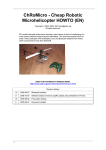
1
Intel® PXA26x Processor Family
Electrical, Mechanical, and Thermal Specification
Data Sheet
Product Features
■
■
■
■
■
■
■
■
High-Performance Processor
— Intel® XScale™ Microarchitecture
— 7 stage pipeline
— 32 KB instruction cache
— 32 KB data cache
— 2 KB mini-data cache
— Extensive data buffering
Intel StrataFlash® Memory in some
versions
Rich Serial Peripheral Set
— AC97 audio port
— I2S audio port
— USB client controller
— Four high speed UARTs (one with
hardware flow control)
— FIR and SIR infrared comm ports
Hardware Debug Features
— IEEE JTAG interface with boundary
scan
Hardware Performance Monitoring
features with on-chip trace buffer
Real-Time Clock
Operating System Timers
USB Client Controller with differential or
single-ended interface support
■
■
■
■
Low Power
— Low voltage core supply
— Low power sleep mode
High Performance Memory Controller
— Four banks of SDRAM - up to 100 MHz
( 2.5 V, and 3.3 V I/O interface)
— Six static chip selects
— Support for PCMCIA and compact
Flash
— Companion chip interface
Flexible Clocking
— CPU clock rated to 300 MHz (PXA262)
or 400 MHz (PXA260, PXA261 and
PXA263)
— Flexible memory clock ratios
— Frequency change modes
— Functional clock gating
Additional peripherals for system
connectivity
— SD card / MMC controller (with SPI
mode support)
— Three SSP controllers
— I2C controller
— Pulse width modulators (PWMs)
— Most peripheral pins double as GPIOs.
Reference Number: 278640-002
April 2003
INFORMATION IN THIS DOCUMENT IS PROVIDED IN CONNECTION WITH INTEL® PRODUCTS. NO LICENSE, EXPRESS OR IMPLIED, BY
ESTOPPEL OR OTHERWISE, TO ANY INTELLECTUAL PROPERTY RIGHTS IS GRANTED BY THIS DOCUMENT. EXCEPT AS PROVIDED IN
INTEL'S TERMS AND CONDITIONS OF SALE FOR SUCH PRODUCTS, INTEL ASSUMES NO LIABILITY WHATSOEVER, AND INTEL DISCLAIMS
ANY EXPRESS OR IMPLIED WARRANTY, RELATING TO SALE AND/OR USE OF INTEL PRODUCTS INCLUDING LIABILITY OR WARRANTIES
RELATING TO FITNESS FOR A PARTICULAR PURPOSE, MERCHANTABILITY, OR INFRINGEMENT OF ANY PATENT, COPYRIGHT OR OTHER
INTELLECTUAL PROPERTY RIGHT. Intel products are not intended for use in medical, life saving, life sustaining applications.
Intel may make changes to specifications and product descriptions at any time, without notice.
Designers must not rely on the absence or characteristics of any features or instructions marked "reserved" or "undefined." Intel reserves these for
future definition and shall have no responsibility whatsoever for conflicts or incompatibilities arising from future changes to them.
The Intel® PXA26x Processor Family EMTS may contain design defects or errors known as errata which may cause the product to deviate from
published specifications. Current characterized errata are available on request.
MPEG is an international standard for video compression/decompression promoted by ISO. Implementations of MPEG CODECs, or MPEG enabled
platforms may require licenses from various entities, including Intel Corporation.
Contact your local Intel sales office or your distributor to obtain the latest specifications and before placing your product order.
Copies of documents which have an ordering number and are referenced in this document, or other Intel literature may be obtained by calling
1-800-548-4725 or by visiting Intel's website at http://www.intel.com.
Copyright © Intel Corporation, 2003
*Other names and brands may be claimed as the property of others.
ii
Intel® PXA26x Processor Family Electrical, Mechanical, and Thermal Specification
Contents
Contents
1
Introduction .........................................................................................................1-1
1.1
1.2
Number Representation .............................................................................1-1
References .................................................................................................1-1
2
Functional Overview ...........................................................................................2-1
3
Package Information ...........................................................................................3-1
3.1
3.2
3.3
3.4
3.5
4
Pin Listing and Signal Definitions .....................................................................4-1
4.1
4.2
5
Signals Reference ......................................................................................4-1
Pin Listing .................................................................................................4-10
Electrical Specifications .....................................................................................5-1
5.1
5.2
5.3
5.4
5.5
6
Package Load Specification .......................................................................3-3
Insertion Specifications ..............................................................................3-3
Package Mass Specifications.....................................................................3-4
Processor Materials....................................................................................3-4
Package Markings......................................................................................3-5
Absolute Maximum Ratings........................................................................5-1
Operating Conditions..................................................................................5-1
Power Consumption Specifications ............................................................5-2
DC Specifications .......................................................................................5-4
Oscillator Electrical Specifications..............................................................5-5
5.5.1 32.768-KHz Oscillator Specifications ............................................5-5
5.5.2 3.6864-MHz Oscillator Specifications............................................5-6
AC Timing Specifications ...................................................................................6-1
6.1
6.2
6.3
6.4
AC Test Conditions ....................................................................................6-1
Reset and Power Manager AC Timing Specifications................................6-2
6.2.1 Power On Timing...........................................................................6-2
6.2.2 Hardware Reset Timing.................................................................6-3
6.2.3 Watchdog Reset Timing ................................................................6-4
6.2.4 GPIO Reset Timing .......................................................................6-4
6.2.5 Sleep Mode Timing .......................................................................6-5
Memory Bus and PCMCIA AC Specifications ............................................6-6
JTAG Boundary Scan AC Timing Specifications........................................6-8
Intel® PXA26x Processor Family Electrical, Mechanical, and Thermal Specification
iii
Contents
Figures
2-1
3-1
3-2
3-3
3-4
4-1
6-1
6-2
6-3
6-4
6-5
PXA26x Processor Family Block Diagram .........................................................2-2
PXA26x Processor Family Package (top view) ..................................................3-1
PXA26x Processor Family Package (bottom view) ............................................3-2
PXA26x Processor Family Package (side view) ................................................3-3
Package Markings..............................................................................................3-5
PXA26x Processor Family TF-BGA Ball Map: Top View ...................................4-1
AC Test Load .....................................................................................................6-1
Power-On Reset Timing .....................................................................................6-3
Hardware Reset Timing .....................................................................................6-4
GPIO Reset Timing ............................................................................................6-4
Sleep Mode Timing ............................................................................................6-5
Tables
1-1 Supplemental Documentation ............................................................................1-1
3-1 Package Dynamic and Static Load Specifications .............................................3-3
3-2 Package Mass....................................................................................................3-4
3-3 Processor Material Properties ............................................................................3-4
4-1 Signal Descriptions for the PXA26x Processor Family ......................................4-2
4-2 PXA26x Processor Family Pin Out - Ballpad Number Order ...........................4-10
4-3 Signal Types ....................................................................................................4-19
4-4 Power Supply Pin Summary ............................................................................4-19
5-1 Absolute Maximum Ratings ...............................................................................5-1
5-2 Voltage, Temperature, and Frequency Electrical Specifications........................5-2
5-3 Power Consumption Specifications....................................................................5-3
5-4 Standard Input, Output, and I/O Pin DC Operating Conditions ..........................5-4
5-5 32.768-KHz Crystal Specifications .....................................................................5-5
5-6 32.768-KHz Oscillator Specifications .................................................................5-5
5-7 3.6864-MHz Crystal Specifications ....................................................................5-6
5-8 3.6864-MHz Oscillator Specifications ................................................................5-6
6-1 Standard Input, Output, and I/O Pin AC Operating Conditions ..........................6-1
6-2 Power-On Timing Specifications ........................................................................6-3
6-3 Hardware Reset Timing Specifications ..............................................................6-4
6-4 GPIO Reset Timing Specifications .....................................................................6-5
6-5 Sleep Mode Timing Specifications .....................................................................6-5
6-6 SRAM / ROM / Flash / Synchronous Fast Flash AC Specifications...................6-6
6-7 Variable Latency I/O Interface AC Specifications ..............................................6-7
6-8 Card Interface (PCMCIA or Compact Flash) AC Specifications ........................6-7
6-9 Synchronous Memory Interface AC Specifications ............................................6-8
6-10 Boundary Scan Timing Specifications................................................................6-8
iv
Intel® PXA26x Processor Family Electrical, Mechanical, and Thermal Specification
Contents
Revision History
Date
Revision
Description
10/25/02
1.0
First Release
04/04/03
2.0
Various minor revs to EMTS
Intel® PXA26x Processor Family Electrical, Mechanical, and Thermal Specification
v
Contents
vi
Intel® PXA26x Processor Family Electrical, Mechanical, and Thermal Specification
1
Introduction
This document is the electrical, mechanical, and thermal specification data sheet for the Intel®
PXA26x processor family. This datasheet contains a functional overview, mechanical data,
package signal locations, targeted electrical specifications (simulated), and bus functional
waveforms. Detailed functional descriptions other than parametric performance are published in
the Intel® PXA26x Processor Family Developer's Manual, 278638.
The PXA26x processor family consists of four devices. Three of these devices integrate the Intel®
XScale™ Microarchitecture, peripherals, and Intel StrataFlash® memory. The processor is
available in a single 13x13 mm, 294-pin TF-BGA package. The PXA26x processor family
ordering options are as follows:
•
•
•
•
1.1
PXA260 processor with no Intel StrataFlash® memory
PXA261 processor with 128 megabits of Intel StrataFlash® memory
PXA262 processor with 256 megabits of Intel StrataFlash® memory in a 16-bit configuration
PXA263 processor with 256 megabits of Intel StrataFlash® memory in a 32-bit configuration
Number Representation
All numbers in this document are base 10 unless designated otherwise. Hexadecimal numbers have
a prefix of 0x, and binary numbers have a prefix of 0b. For example, 107 is represented as 0x6B in
hexadecimal and 0b1101011 in binary.
1.2
References
Material and concepts available in the documents listed in Table 1-1 may be beneficial when
reading this document:
Table 1-1. Supplemental Documentation
Document Title1
Order Number
Intel® PXA26x Processor Family Developer's Manual
278638
Intel® XScale™ Microarchitecture for the Intel® PXA250 and
PXA210 Application Processors User’s Manual
278525
Intel® DBPXA26x Development Platform for Intel® PCA User's
Guide
278623
Intel® PXA26x Processor Family Design Guide
278639
®
ARM DDI 0100D-10
®
ARM DDI 0100B
ARM Architecture Version 5T Specification
ARM Architecture Reference Manual
NOTE: 1. Contact your Intel representative for the latest revision
of these documents.
NOTE:
Intel® PXA26x Processor Family Electrical, Mechanical, and Thermal Specification
1-1
Introduction
1-2
Intel® PXA26x Processor Family Electrical, Mechanical, and Thermal Specification
Functional Overview
2
The Intel® PXA26x Processor family consists of four products integrating the Intel® XScale™
Microarchitecture, peripherals, and Intel® StrataFlash® memory:
•
•
•
•
PXA260 processor with no Intel StrataFlash® memory
PXA261 processor with 128 megabits of Intel StrataFlash® memory
PXA262 processor with 256 megabits of Intel StrataFlash® memory in a 16-bit configuration
PXA263 processor with 256 megabits of Intel StrataFlash® memory in a 32-bit configuration
Both the processor and the flash memory are packaged in a single 13x13 mm 294-pin TF-BGA
package. The internal flash provides a 16-bit data bus interface connected to the processor inside
the package for the PXA261 processor and PXA262 processor. The PXA263 processor internal
flash is connected with a 32-bit data bus interface. The processor also supports external 32-bit
memory devices.
The PXA26x processor family integrates either one or two Intel StrataFlash® K3 family flash
memory die. Intel StrataFlash® memory supports synchronous and asynchronous operation and
provides high density non-volatile storage using Intel’s reliable and proven two-bit-per-cell
technology. Support for fast synchronous burst accesses make the flash ideal for use in execute-inplace (XIP) applications running code directly from flash. An XIP system architecture eliminates
the need to copy program code and data from flash into dynamic memory, and thereby decreases
the size and number of dynamic-memory components required in a cellular handset.
The PXA26x processor family features an integrated system-on-a-chip microprocessor for high
performance, low power, portable handheld, and handset devices. It incorporates the Intel®
XScale™ Microarchitecture with on-the-fly frequency scaling and sophisticated power
management to provide industry-leading MIPs/mW performance. The PXA26x processor family is
ARM* Version 5TE instruction set compliant (excluding floating-point instructions) and follows
the ARM programmer’s model.
The processor integrates a rich set of peripherals including a real-time clock, timers, LCD
controller, USB client controller, four UARTs, three synchronous serial ports, and stereo audio
CODEC interfaces. For details on the programming model and theory of operation of each of these
units, refer to the Intel® PXA26x Processor family Developer's Manual. The processor’s flexible
memory interface also supports a variety of external memory devices, removable storage cards,
and bus-interfaced companion chips. The memory controller also supports low-power mobile
SDRAMs.
Figure 2-1 on page 2-2 shows the PXA26x processor family block diagram.
Intel® PXA26x Processor Family Electrical, Mechanical, and Thermal Specification
2-1
Functional Overview
Figure 2-1. PXA26x Processor Family Block Diagram
RTC
Color or
Grayscale
LCD
Controller
OS Timer
PWM(2)
Int.
Controller
Clocks &
Power Man.
Variable
Latency I/O
Control
I2S
2
UART2
DMA Controller
and Bridge
UART1
System Bus
Peripheral Bus
General Purpose I/O
IC
AC97
Memory
Controller
Slow IrDA
PCMCIA
& CF
Control
ASIC
XCVR
Dynamic
Memory
Control
SDRAM/
SMROM
4 banks
Static
Memory
Control
ROM/
Flash/
SRAM
4 banks
Socket 0
Socket 1
Fast IrDA
SSP
Intel(R) XScale TM
Microarchitecure
USB
Client
Synchronous
Intel
StrataFlash(R)
Memory
MMC
NSSP
ASSP
3.6864
MHz
Osc
32.768
KHz
Osc
HWUART
2-2
Intel® PXA26x Processor Family Electrical, Mechanical, and Thermal Specification
3
Package Information
The Intel® PXA26x Processor family is available in a single 13x13 mm, 294-pin TF-BGA
package. Figure 3-1, Figure 3-2 on page 3-2, and Figure 3-3 on page 3-3 provide mechanical
specifications of the processor.
Figure 3-1. PXA26x Processor Family Package (top view)
A1 CORNER
1 2
3 4 5 6 7 8 9 10 11 12
13
14
15
16
17 18
A
B
C
D
E
F
G
H
J
K
L
M
N
P
R
T
U
V
Intel® PXA26x Processor Family Electrical, Mechanical, and Thermal Specification
3-1
Package Information
Figure 3-2. PXA26x Processor Family Package (bottom view)
A1 CORNER
Ø0.05 M C
Ø0.15 M C A B
Ø0.40±0.05 (294X)
18 17 16 15 14 13 12 11 10 9 8
7 6 5 4 3 2 1
A
B
0.65
C
D
E
F
H
11.05
13.00±0.1
G
J
K
L
M
N
P
R
T
U
V
0.65
A
11.05
B
13.00±0.1
0.12(4X)
3-2
Intel® PXA26x Processor Family Electrical, Mechanical, and Thermal Specification
Package Information
0.12 C
0.14 C
Figure 3-3. PXA26x Processor Family Package (side view)
3.1
1.40 Max
0.30 Min – 0.40 Max
SEATING PLANE
C
Insertion Specifications
The PXA26x processor family devices can be inserted and removed 15 times from its socket.
3.2
Processor Materials
The processor is assembled from several components. Table 3-1 describes the basic material
properties.
Table 3-1. Processor Material Properties
Component
Material
substrate
BT resin (CCL-HL832HS)
mold compound
Sumitomo EMEG-770L
solder balls
63 Sn/37 Pb1
NOTE: 1. Subsequent PXA26x processor family steppings may use Pb-Free (94.5 Sn/5.0 Ag/
0.5 Cu). The package can withstand the 260° C reflow temp for Pb-Free.
Intel® PXA26x Processor Family Electrical, Mechanical, and Thermal Specification
3-3
Package Information
3.3
Package Markings
Figure 3-4 details the package top-side markings and is an aid in the identification of the PXA26x
processor family devices.
Figure 3-4. Package Markings
Laser Mark at assembly site on top side of Package
13 x 13 mm
Mark Diagram for TPBGA 294L
Mfg. Name
i
– N/A
Mktg. Name – PCGAPDH326A0
PXA262
MECH SAMPLES
INTEL M C ‘01
KOREA
QDF # / ES
Intel Legal
COO
PIN 1 ORIENTATION
3.4
Package Power Ratings
Table 3-2. θJA and Maximum Power Ratings
Processor
θJA
Max Power
PXA260
TBD C°/w
TBD W
PXA261
PXA262
PXA263
3-4
TBD C°/w
TBD C°/w
TBD C°/w
TBD W
TBD W
TBD W
Intel® PXA26x Processor Family Electrical, Mechanical, and Thermal Specification
4
Pin Listing and Signal Definitions
This section provides information on the Intel® PXA26x Processor family signals and how those
signals are connected to the pins of the package. Table 4-1 on page 4-2 contain a description of all
processor signals. Note that many signals are multiplexed so that they may be used either for a
peripheral unit or for a general-purpose I/O (GPIO). Table 4-2 on page 4-10 lists the mapping of
these signals to specific package pins. The signal types are defined in Table 4-3 on page 4-18.
4.1
Signals Reference
Refer to Figure 4-1 for a diagram of the PXA26x processor family TF-BGA ball map. Refer to
Table 4-1 on page 4-2 for a list of signal names and descriptions.
Figure 4-1. PXA26x Processor Family TF-BGA Ball Map: Top View
1
2
3
4
5
6
7
8
9
10
11
12
13
14
15
16
17
18
A
VSSN
VSSN
GPIO[69]
GPIO[13]
VCC
GPIO[63]
GPIO[11]
GPIO[76]
VSSQ
GPIO[24]
GPIO[30]
GPIO[38]
SDA
VCCQ
USB_P
GPIO[42]
VSSQ
VSSQ
A
B
VSSN
VSSN
GPIO[71]
GPIO[66]
VSSQ
GPIO[64]
GPIO[59]
GPIO[77]
VCCQ
GPIO[25]
GPIO[29]
GPIO[16]
GPIO[37]
VSSQ
USB_N
GPIO[47]
VSSQ
VSSQ
B
C
DQM[2]
GPIO[73]
GPIO[70]
GPIO[67]
VSSQ
GPIO[65]
GPIO[61]
GPIO[75]
GPIO[74]
GPIO[26]
GPIO[31]
GPIO[17]
GPIO[36]
GPIO[35]
GPIO[34]
GPIO[45]
GPIO[46]
VCC
C
D
SDCKE[0]
RDY/
GPIO[18]
GPIO[72]
GPIO[68]
VCCQ
GPIO[12]
GPIO[60]
GPIO[41]
GPIO[23]
GPIO[28]
nACRESET
/GPIO[89]
VCC
GPIO[39]
GPIO[43]
GPIO[44]
GPIO[9]
VCCQ
VSS
D
E
SDCLK[2]
RDnWR/
GPIO[88]
VCCN
DQM[1]
GPIO[14]
GPIO[62]
GPIO[58]
GPIO[10]
GPIO[27]
GPIO[40]
SCL
VSSQ
MMDAT
GPIO[32]
MMCMD
GPIO[84]
GPIO[81]
GPIO[85]
E
F
nSDCS[3]/
GPIO[87]
VCC
SDCLK[1]
SDCKE[1]
SDCLK[0]
VSS_F
VSS_F
nRST_F
nWP_F
VPEN
VCC_F
VSSQ_F
GPIO[8]
GPIO[82]
GPIO[83]
GPIO[7]
VCCQ
VSSQ
F
G
nSDCS[1]
nSDRAS
VCCN
nSDCS[0]
nSDCAS
VSSN
TEST
TESTCLK
nTRST
GPIO[6]
G
H
VSSQ
VCCN
MA[0]
VSSN
nSDCS[2]/
GPIO[86]
MA[1]
J
VSSQ
VCC
VSSN
MD[16]
VCCN
K
MD[17]
MA[3]
MA[4]
MA[5]
L
VCCN
MA[7]
VSSN
M
MA[11]
MD[19]
N
MD[20]
P
VCC_F
BOOT_SEL[ BOOT_SEL[ BOOT_SEL[
2]
1]
0]
TMS
TCK
GPIO[5]
PLL_VCC
PLL_VSS
TDO
TDI
H
MA[2]
GPIO[4]
nRESET
nRESET
_OUT
nBATT
_FAULT
VCC
VSSQ
J
MA[6]
MD[18]
GPIO[3]
PEXTAL
TEXTAL
TXTAL
PWR_EN
nVDD
_FAULT
K
MA[9]
MA[8]
MA[10]
MA[14]
nWE
GPIO[55]
BATT_VCC
VSSQ
GPIO[2]
PXTAL
L
VCCN
VSSN
MA[15]
VSSQ_F
VCCQ_F
VCC_F
VSS_F
VCCQ_F
WAIT_F1
GPIO[56]
GPIO[22]
GPIO[1]
GPIO[0]
M
MA[13]
MA[12]
MD[22]
MA[17]
VSSQ_F
VCCQ_F
VCC_F
MD[27]
NC
VCCQ_F
VSSQ_F
WAIT_F2
GPIO[49]
VCCN
GPIO[54]
GPIO[57]
N
VSSQ
MD[21]
MA[16]
VCCQ_F
MA[18]
MD[0]
MD[25]
VCCN
MD[8]
VSS_F
VCCQ_F
MD[14]
MD[15]
GPIO[48]
VSSQ
VCC
GPIO[21]
P
R
VCCN
VCC
MA[20]
MA[23]
MA[25]
VCCN
VSSQ
MD[6]
nCS[0]
VSSN
MD[11]
VCCQ_F
VSSQ_F
VCC
VCCN
GPIO[50]
GPIO[53]
GPIO[19]
R
T
MA[19]
VCCN
VSSQ
MD[23]
MA[24]
MD[24]
VSSN
MD[5]
MD[26]
DQM[0]
VCCN
MD[28]
VCCN
VSSN
MD[13]
GPIO[20]
GPIO[51]
GPIO[52]
T
U
VSSN
VSSN
VSS
VCCN
MA[22]
MD[3]
MD[2]
MD[4]
VSSN
nCS[1]/
GPIO[15]
nCS[3]/
GPIO[79]
MD[10]
VSSQ
MD[31]
MD[12]
nCS[5]/
GPIO[33]
VSSN
VSSN
U
V
VSSN
VSSN
VCCN
MA[21]
VSSN
MD[1]
VCCN
VCC
MD[7]
DQM[3]
nCS[2]/
GPIO[78]
MD[9]
MD[29]
MD[30]
VSSN
nCS[4]/
GPIO[80]
VSSN
VSSN
V
1
2
3
4
5
6
7
8
9
10
11
12
13
14
15
16
17
18
nOE
Intel® PXA26x Processor Family Electrical, Mechanical, and Thermal Specification
4-1
Table 4-1. Signal Descriptions for the PXA26x Processor Family (Sheet 1 of 8)
Signal Name
Type
Descriptions
Memory Controller Signals
MA[25:0]
Output
MEMORY ADDRESS BUS:
Drives the requested address for memory accesses.
MD[31:16]
Bi-directional
UPPER HALF OF MEMORY DATA BUS:
Carries data to and from 32-bit memory devices.
MD[15:0]
Bi-directional
LOWER HALF OF MEMORY DATA BUS:
Carries data to and from memory devices.
nOE
Output
MEMORY OUTPUT ENABLE:
Connect to the output enables of static memory devices to control data bus drivers.
nWE
Output
MEMORY WRITE ENABLE:
Connect to the write enables of SD-RAM and static memory devices.
DQM[3:0]
Output
SDRAM DQM DATA BYTE MASK CONTROL FOR DATA BYTES 3 THROUGH 0:
Connect to the data output mask enables (DQM) for SDRAM. (DQM0 corresponds to
MD[7:0], DQM1 corresponds to MD[15:8], etc. DQMx is High to mask the byte)
nSDRAS
Output
SDRAM RAS:
Connect to the row address strobe (RAS) pins for all banks of SDRAM.
nSDCAS
Output
SDRAM CAS:
Connect to the column address strobe (CAS) pins for all banks of SDRAM.
SDCKE0
Output
SDRAM AND/OR SYNCHRONOUS STATIC MEMORY CLOCK ENABLE:
Connect to the clock enable pins of SDRAM. The memory controller provides control
register bits for de-assertion.
SDCKE1
Output
SDRAM AND/OR SYNCHRONOUS STATIC MEMORY CLOCK ENABLE:
Connect to the clock enable pins of SDRAM. It is de-asserted (held low) during sleep.
SDCKE1 is always deasserted upon reset. The memory controller provides control
register bits for de-assertion.
SDCLK0
SDCLK1
Output
SDCLK2
SDRAM AND/OR SYNCHRONOUS STATIC MEMORY CLOCKS:
Connect SDCLK0 to the clock pins of SMROM and SDRAM. SDCLK1 and SDCLK2
should be connected to the clock pins of SDRAM in bank pairs 0/1 and 2/3, respectively.
They are driven by either the internal memory-controller clock, or the internal memorycontroller clock divided by 2. At reset, all clock pins are free running at the divide-by-2
clock speed and may be turned off via free-running control register bits in the memory
controller. The memory controller also provides control register bits for clock division and
deassertion of each SDCLK pin. SDCLK0 control-register assertion bit defaults to on if
the boot-time static memory bank 0 is configured for SMROM. SDCLK2 and SDCLK1
control-register assertion bits are always de-asserted upon reset.
SDCLK0 and SDCLK2 are not three-stateable, SDCLK1 is three-stateable
nSDCS3
nSDCS2
nSDCS1
nSDCS0
Output
SDRAM CHIP SELECTS:
Chip selects for SDRAM memory devices. Individually programmable in the memory
configuration registers. nSDCS0 is three-stateable, but nSDCS1, nSDCS2 and nSDCS3
are not.
Intel® PXA26x Processor Family Electrical, Mechanical, and Thermal Specification
4-2
Pin Listing and Signal Definitions
Table 4-1. Signal Descriptions for the PXA26x Processor Family (Sheet 2 of 8)
Signal Name
Type
Descriptions
nCS5
nCS4
nCS3
nCS2
Output
STATIC CHIP SELECTS†:
Chip selects to static memory devices such as ROM and flash. Individually
programmable in the memory-configuration registers.
nCS5 to nCS0 can be used with variable latency I/O devices.
nCS0 is the boot memory chip select and is a dedicated pin.
nCS1
nCS0
READ/WRITE FOR STATIC INTERFACE:
RDnWR
Output
RDY
Input
BOOTSEL[2:0]
Input
MBREQ
Input
MBGNT
Output
Intended for use as a steering signal for buffering logic. Indicates that the current
transaction is a read (when high) or a write (when low).
VARIABLE LATENCY I/O READY PIN†:
An external VLIO device asserts RDY when it is ready to transfer data.
BOOT SELECT. BOOT SOURCE PROGRAMMING SELECT PINS:
These pins are sampled to indicate the type of boot device present.
MEMORY CONTROLLER ALTERNATE BUS MASTER REQUEST:
Allows an external device to request control of the memory bus from the memory
controller.
MEMORY CONTROLLER ALTERNATE BUS MASTER GRANT:
The memory controller asserts MBGNT to allow an external device to control the
memory bus.
PCMCIA/CF Control Signals
Output
PCMCIA OUTPUT ENABLE†:
Output enable for reads from PCMCIA memory and PCMCIA attribute space.
nPWE
Output
PCMCIA WRITE ENABLE†:
Enables writes to PCMCIA memory and PCMCIA attribute space. Also used as the write
enable signal for variable latency I/O.
nPIOW
Output
PCMCIA I/O WRITE†:
Asserted for writes to PCMCIA I/O space.
nPIOR
Output
PCMCIA I/O READ†:
Asserted for reads from PCMCIA I/O space.
nPCE2
Output
PCMCIA CARD ENABLE 2†:
Selects a PCMCIA card. nPCE2 enables the high byte lane.
nPCE1
Output
PCMCIA CARD ENABLE 1†:
Selects a PCMCIA card. nPCE1 enables the low byte lane.
Input
IO SELECT 16†:
Input from the PCMCIA card that indicates the data bus is 16-bits wide when high. When
low, this input indicates the data bus is 8-bits wide.
Input
PCMCIA WAIT†:
Driven low by the PCMCIA card to insert wait states that extend transfers to and from the
PXA26x processor family device.
Output
PCMCIA SOCKET SELECT†:
Used by external steering logic to route control, address, and data signals to one of the
two PCMCIA sockets. When nPSKTSEL is low, socket zero is selected. When
nPSKTSEL is high, socket one is selected. Has the same timing as the address bus.
nPOE
nIOIS16
nPWAIT
nPSKTSEL
Intel® PXA26x Processor Family Electrical, Mechanical, and Thermal Specification
4-3
Pin Listing and Signal Definitions
Table 4-1. Signal Descriptions for the PXA26x Processor Family (Sheet 3 of 8)
Signal Name
Type
Descriptions
PCMCIA REGISTER SELECT†:
nPREG
Output
Functions as address bit 26 to select register space (I/O or attribute) or memory space.
Has the same timing as the address bus.
LCD Controller Signals
Output
LCD DISPLAY DATA†:
Transfers pixel information from the LCD controller to the external LCD panel.
L_FCLK
Output
LCD FRAME CLOCK†:
Frame clock that resets the LCD display module line pointers to the top of the screen.
Also, this pin is the vertical synchronization signal for active (TFT) displays.
L_LCLK
Output
LCD LINE CLOCK†:
Indicates the start of a new line. Also referred to as Hsync for active panels.
Output
LCD PIXEL CLOCK†:
Pixel clock used by the LCD display module to clock the pixel data into the line-shift
register. In passive mode, pixel clock transitions only when valid data is available on the
data pins. In active mode, pixel clock transitions continuously and the AC bias pin is
used as an output to signal when data is valid on the LCD data pins.
Output
LCD BIAS DRIVE†:
AC bias used to signal the LCD display module to switch the polarity of the power
supplies to the row and column axis of the screen to counteract DC offset. In active
(TFT) mode, it is used as the output-enable to signal when data should be latched from
the data pins using the pixel clock.
L_DD[15:0]
L_PCLK
L_BIAS
Full Function UART Signals
FFRXD
Input
FULL FUNCTION UART RECEIVE DATA†
FFTXD
Output
FULL FUNCTION UART TRANSMIT DATA†
FFCTS
Input
FULL FUNCTION UART CLEAR-TO-SEND†
FFDCD
Input
FULL FUNCTION UART DATA-CARRIER-DETECT†
FFDSR
Input
FULL FUNCTION UART DATA-SET-READY†
FFRI
Input
FULL FUNCTION UART RING INDICATOR†
FFDTR
Output
FULL FUNCTION UART DATA-TERMINAL-READY†
FFRTS
Output
FULL FUNCTION UART REQUEST-TO-SEND†
Bluetooth UART Signals
BTRXD
Input
BLUETOOTH UART RECEIVE DATA†
BTTXD
Output
BLUETOOTH UART TRANSMIT DATA†
BTCTS
Input
BLUETOOTH UART CLEAR-TO-SEND†
BTRTS
Output
BLUETOOTH UART REQUEST-TO-SEND†
Hardware UART Signals
HWRXD
Input
HARDWARE UART RECEIVE DATA†
HWTXD
Output
HARDWARE UART TRANSMIT DATA†
HWCTS
Input
HARDWARE UART CLEAR-TO-SEND†
HWRTS
Output
HARDWARE UART REQUEST-TO-SEND†
Standard UART and infrared Communication Port (ICP) Signals
IRRXD
4-4
Input
STANDARD UART AND IRDA RECEIVE DATA†
Intel® PXA26x Processor Family Electrical, Mechanical, and Thermal Specification
Pin Listing and Signal Definitions
Table 4-1. Signal Descriptions for the PXA26x Processor Family (Sheet 4 of 8)
Signal Name
IRTXD
Type
Output
Descriptions
STANDARD UART AND IRDA TRANSMIT DATA†:
Transmit data pin for the standard UART, SIR and FIR functions.
MMC Controller Signals
MMCLK
Output
MULTIMEDIA CARD BUS CLOCK
MMCCMD
Bi-directional
MULTIMEDIA CARD COMMAND:
MMC and SD – Bi-directional line for command and response tokens.
SPI – Output for command and write data.
MMCDAT
Bi-directional
MULTIMEDIA CARD DATA:
MMC and SD – Bi-directional line for read and write data.
SPI – Input for response token and read data.
MMCCS0
Output
MMCCS1
Output
MMC CHIP SELECT 0:
Chip select 0 for the MMC controller.
MMC CHIP SELECT 1:
Chip select 1 for the MMC controller.
Standard SSP Signals
SSPSCLK
Output
SYNCHRONOUS SERIAL PORT CLOCK†
SSPSFRM
Output
SYNCHRONOUS SERIAL PORT FRAME†
SSPTXD
Output
SSPRXD
Input
SSPEXTCLK
Input
SYNCHRONOUS SERIAL PORT TRANSMIT DATA†:
Serial data driven out synchronous with the bit clock.
SYNCHRONOUS SERIAL PORT RECEIVE DATA†:
Serial data latched using the bit clock.
SYNCHRONOUS SERIAL PORT EXTERNAL CLOCK†:
This input may be used to supply an external bit clock.
Network SSP Signals
Bi-directional
NETWORK SYNCHRONOUS SERIAL PORT CLOCK†:
The serial bit clock may be configured as an output in master-mode operation or an input
in slave-mode operation.
NSSPSFRM
Bi-directional
NETWORK SYNCHRONOUS SERIAL PORT FRAME†:
The serial frame sync may be configured as an output in master-mode operation or an
input in slave-mode operation.
NSSPTXD
Output
NETWORK SYNCHRONOUS SERIAL PORT TRANSMIT DATA†:
Serial data driven out synchronous with the bit clock.
NSSPRXD
Input
NETWORK SYNCHRONOUS SERIAL PORT RECEIVE DATA†:
Serial data latched using the bit clock.
Bi-directional
AUDIO SYNCHRONOUS SERIAL PORT CLOCK†:
The serial bit clock may be configured as an output in master-mode operation or an input
in slave-mode operation.
ASSPSFRM
Bi-directional
AUDIO SYNCHRONOUS SERIAL PORT FRAME†:
The serial frame sync may be configured as an output in master-mode operation or an
input in slave-mode operation.
ASSPTXD
Output
AUDIO SYNCHRONOUS SERIAL PORT TRANSMIT DATA†:
Serial data driven out synchronous with the bit clock.
NSSPSCLK
Audio SSP Signals
ASSPSCLK
Intel® PXA26x Processor Family Electrical, Mechanical, and Thermal Specification
4-5
Pin Listing and Signal Definitions
Table 4-1. Signal Descriptions for the PXA26x Processor Family (Sheet 5 of 8)
Signal Name
ASSPRXD
Type
Descriptions
AUDIO SYNCHRONOUS SERIAL PORT RECEIVE DATA†:
Input
Serial data latched using the bit clock.
USB Client Signals
USBC_P
Bi-directional
USB CLIENT POSITIVE LINE:
This differential signal connects to the USB client interface.
USBC_N
Bi-directional
USB CLIENT NEGATIVE LINE:
This differential signal connects to the USB client interface.
Single-Ended USB Client Signals
USB_RCV
Input
USB CLIENT SINGLE-ENDED INTERFACE RCV:
Input from external transceiver to USB device controller.
USB_VP
Input
USB CLIENT SINGLE-ENDED INTERFACE VP:
Input from external transceiver to USB device controller.
USB_VM
Input
USB CLIENT SINGLE-ENDED INTERFACE VM:
Input from external transceiver to USB device controller.
USB_VPO
Output
USB CLIENT SINGLE-ENDED INTERFACE VPO:
Output to external transceiver differential driver.
USB_VMO
Output
USB CLIENT SINGLE-ENDED INTERFACE VMO:
Output to external transceiver differential driver.
USB_nOE
Output
USB CLIENT SINGLE-ENDED INTERFACE NOE:
Output enable to external transceiver.
AC97 Controller Signals
nACRESET
Output
BITCLK
Output
SYNC
Output
SDATA_OUT
Output
SDATA_IN0
Input
SDATA_IN1
Input
SYSCLK
Output
I2S
AC97 RESET:
Active-low CODEC reset.
AC97 BIT CLOCK†:
Bit-rate clock.
AC97 SYNC†:
Frame indicator and synchronizer.
AC97 SERIAL DATA OUT†:
Serial audio data output to the CODEC for digital-to-analog conversion.
AC97 SERIAL DATA IN 0†:
Serial audio data from the primary CODEC analog-to-digital converter.
AC97 SERIAL DATA IN 1†:
Serial audio data from the secondary CODEC analog-to-digital converter.
AC97 SYSTEM CLOCK†:
AC97 system clock output.
Interface Signals
SYSCLK
Output
I2S SYSTEM CLOCK:
System clock running four times the bit clock which is used by the CODEC only.
BITCLK
Bi-directional
I2S BIT-RATE CLOCK:
I2S bit-rate clock.
4-6
Intel® PXA26x Processor Family Electrical, Mechanical, and Thermal Specification
Pin Listing and Signal Definitions
Table 4-1. Signal Descriptions for the PXA26x Processor Family (Sheet 6 of 8)
Signal Name
Type
SYNC
Output
SDATA_OUT
Output
SDATA_IN
Input
I 2C
Descriptions
I2S SYNC:
Sync signal to identify left/right channel data.
I2S SERIAL DATA OUT:
Serial data output to the CODEC digital-to-analog converter.
I2S SERIAL DATA IN:
Serial data input from the CODEC analog-to-digital converter.
Interface Signals
SCL
Bi-directional
I2C CLOCK:
Bi-directional signal. When it is driving, it functions as an open drain device and requires
a pull-up resistor. As an input, it expects standard CMOS levels.
SDA
Bi-directional
I2C DATA:
Bi-directional signal. When it is driving, it functions as an open drain device and requires
a pull-up resistor. As an input, it expects standard CMOS levels.
PWM1
Output
PULSE WIDTH MODULATION CHANNEL 1:
Pulse width modulator channel 1 output.
PWM0
Output
PULSE WIDTH MODULATION CHANNEL 0:
Pulse width modulator channel 0 output.
PWM Signals
DMA Signals
DREQ0
Input
DREQ1
Input
DMA REQUEST 0:
DMA request from an external companion chip.
DMA REQUEST 1:
DMA request from an external companion chip.
GPIO Signals
GPIO[1:0]
Bi-directional
GENERAL PURPOSE I/O:
These signals are preconfigured at hardware reset as dedicated wakeup sources for
both rising and falling edge detection. These GPIOs do not have alternate functions and
are intended to be used as the main external sleep wakeup stimulus.
GPIO[14:2]
Bi-directional
GENERAL PURPOSE I/O
GPIO[22:21]
Bi-directional
GENERAL PURPOSE I/O
GPIO[85]
Bi-directional
GENERAL PURPOSE I/O
Crystal and Clock Signals
PXTAL
Output
PROCESSOR CRYSTAL OUTPUT:
Connect the PXTAL signal to either an external 3.6864-MHz crystal or to an external
clock source. No external caps are required
PEXTAL
Input
PROCESSOR CRYSTAL INPUT:
Connect the PEXTAL signal to either an external 3.6864-MHz crystal or left
unconnected. No external caps are required
TXTAL
Output
TIMEKEEPING CRYSTAL OUTPUT:
The TXTAL signal is a clock input that is distributed to the timekeeping control system
(32.768-KHz crystal or external clock source). No external caps are required
TEXTAL
Input
TIMEKEEPING CRYSTAL INPUT:
Connect the TEXTAL signal to either an external 32.768-KHz crystal or leave
unconnected. No external caps are required
Intel® PXA26x Processor Family Electrical, Mechanical, and Thermal Specification
4-7
Pin Listing and Signal Definitions
Table 4-1. Signal Descriptions for the PXA26x Processor Family (Sheet 7 of 8)
Signal Name
Type
RTCCLK
Output
3.6MHz
Output
32KHz
Output
48_MHz
Output
Descriptions
RTC CLOCK:
Real time clock, 1 Hz clock derived from the 32-KHz or 3.6864-MHz output.
3.6864-MHz CLOCK:
Output from 3.6864-MHz oscillator.
32-KHZ CLOCK:
Output from the 32-KHz oscillator.
48-MHz OUTPUT CLOCK:
This clock is only generated when the USB unit clock enable is set.
Miscellaneous Signals
Output
POWER ENABLE FOR THE CORE POWER SUPPLY:
When low, it signals the power supply to remove power from VCC because the system is
entering sleep mode. When high, the power supply must enable VCC.
Input
BATTERY FAULT:
Active low input – Signals that main battery is low or removed. Assertion causes PXA26x
processor family processor to enter sleep mode or force an imprecise data exception,
which cannot be masked. PXA26x processor family processor does not recognize a
wakeup event while this signal is asserted. Minimum assertion time for nBATT_FAULT is
1 ms.
Input
VDD FAULT:
Active low input – Signals that the main power source is going out of regulation.
nVDD_FAULT causes the PXA26x processor family processor to enter sleep mode or
force an imprecise data exception, which cannot be masked. nVDD_FAULT is ignored
after a wakeup event until the power supply timer completes (approximately 10 ms).
Minimum assertion time for nVDD_FAULT is 1 ms.
nRESET
Input
HARD RESET:
Active low input – Level-sensitive input used to start the processor from a known
address. Assertion terminates the current instruction abnormally and causes a reset.
When nRESET is driven high, the processor starts execution from address 0. nRESET
must remain low until the power supply is stable and the internal 3.6864 MHz oscillator
has stabilized.
nRESET_OUT
Output
RESET OUT:
Active low output – This signal is asserted when nRESET is asserted and de-asserts
after nRESET is negated but before the first instruction fetch. nRESET_OUT is also
asserted for “soft” reset events (sleep, watchdog reset, GPIO reset)
nTRST
Input
JTAG TEST RESET. IEEE 1194.1 TEST RESET:
Resets the JTAG/debug port – If JTAG/debug is used, drive nTRST from low to high
either before or at the same time as nRESET. If JTAG is not used, nTRST must be either
tied to nRESET or tied low. A JTAG/debug port should be added to all systems for debug
and download.
TDI
Input
JTAG TEST DATA INPUT:
Data from the JTAG controller is sent to the PXA26x processor family using this signal.
This pin has an internal pull-up resistor.
TDO
Output
JTAG TEST DATA OUTPUT:
Data from the PXA26x processor family is returned to the JTAG controller using this
signal. This pin does not have an internal pullup resistor.
TMS
Input
JTAG TEST MODE SELECT:
Selects the test mode required from the JTAG controller. This signal has an internal pullup resistor.
PWR_EN
nBATT_FAULT
nVDD_FAULT
JTAG and Test Signals
4-8
Intel® PXA26x Processor Family Electrical, Mechanical, and Thermal Specification
Pin Listing and Signal Definitions
Table 4-1. Signal Descriptions for the PXA26x Processor Family (Sheet 8 of 8)
Signal Name
Type
Descriptions
JTAG TEST CLOCK:
TCK
Input
TEST
Input
TESTCLK
Input
Clock for all transfers on the JTAG test interface.
NOTE: This pin needs an external pulldown resistor.
TEST MODE:
Reserved for manufacturing test. Must be grounded for normal operation.
TEST CLOCK:
Reserved for manufacturing test. Must be grounded for normal operation.
Processor Power and Ground Signals
VCC
Supply
POSITIVE SUPPLY FOR THE INTERNAL LOGIC:
Connect these pins to the low voltage supply on the PCB.
VSS
Supply
GROUND SUPPLY FOR THE INTERNAL LOGIC:
Connect these pins to the common ground plane on the PCB.
PLL_VCC
Supply
POSITIVE SUPPLY FOR PLLS AND OSCILLATORS:
Must be shorted to VCC.
PLL_VSS
Supply
GROUND SUPPLY FOR THE PLL:
Must be connected to common ground plane on the PCB.
VCCQ
Supply
POSITIVE SUPPLY FOR ALL CMOS I/O:
Except memory bus and PCMCIA pins. Connect these pins to the common 2.775 V or
3.3 V supply on the PCB.
VSSQ
Supply
GROUND SUPPLY FOR ALL CMOS I/O:
Except memory bus and PCMCIA pins. Connect these pins to the common ground plane
on the PCB.
VCCN
Supply
POSITIVE SUPPLY FOR MEMORY BUS AND PCMCIA PINS:
Connect these pins to the common 3.3 V, 2.775 V, or 2.5 V supply on the PCB.
VSSN
Supply
GROUND SUPPLY FOR MEMORY BUS AND PCMCIA PINS:
Connect these pins to the common ground plane on the PCB.
nRST_F
Input
RESET FOR FLASH ONLY
nWP
Input
WRITE PROTECT
VPEN
Input
ERASE/PROGRAM/BLOCK LOCK ENABLE
WAIT_F1/WAIT_F2
Output
WAIT:
Indicates invalid data in synchronous-read (burst) modes. Not used by the PXA26x, can
be used by external programmers.
VCC_F
Supply
FLASH CORE LOGIC SUPPLY
Must be at the same voltage as VCCN.
VSS_F
Supply
FLASH CORE GROUND
VCCQ_F
Supply
VSSQ_F
Supply
Flash Signals
†
FLASH I/O POWER SUPPLY:
Must be the same voltage as VCCN.
FLASH I/O GROUND
GPIO reset operation: After any reset, these pins are configured as GPIO inputs by default, except for GPIO[89:86].
GPIO[89:86] are configured as their alternate function after any reset.
Intel® PXA26x Processor Family Electrical, Mechanical, and Thermal Specification
4-9
Pin Listing and Signal Definitions
4.2
Pin Listing
The package pin listing is shown in Table 4-2.
Table 4-2. PXA26x Processor Family Pin Out - Ballpad Number Order (Sheet 1 of 9)
Name
Type
Function
After
Reset
Primary
Function
Alternate
Function 1
Alternate
Function 2
Alternate
Function 3
A1
VSSN
IA
VSSN
VSSN
—
—
—
A2
VSSN
IA
VSSN
VSSN
—
—
—
A3
GPIO[69]
ICOCZ
GPIO[69]
GPIO[69]
MMCCLK
L_DD[11]
—
A4
GPIO[13]
ICOCZ
GPIO[13]
GPIO[13]
—
MBGNT
—
Ball#
A5
VCC
IA
VCC
VCC
—
—
—
A6
GPIO[63]
ICOCZ
GPIO[63]
GPIO[63]
—
L_DD[5]
—
A7
GPIO[11]
ICOCZ
GPIO[11]
GPIO[11]
3.6MHZ
—
—
A8
GPIO[76]
ICOCZ
GPIO[76]
GPIO[76]
—
L_PCLK
—
A9
VSSQ
IA
VSSQ
VSSQ
—
—
—
A10
GPIO[24]
ICOCZ
GPIO[24]
GPIO[24]
—
SFRM
—
A11
GPIO[30]
ICOCZ
GPIO[30]
GPIO[30]
SDATA_OUT
SDATA_OUT
ASSPTXD
A12
GPIO[38]
ICOCZ
GPIO[38]
GPIO[38]
FFRI
—
—
A13
SDA
ICOCZ
SDA
SDA
—
—
—
A14
VCCQ
IA
VCCQ
VCCQ
—
—
—
A15
USB_P
IAOA
USB_P
USB_P
—
—
—
A16
GPIO[42]
ICOCZ
GPIO[42]
GPIO[42]
BTRXD
—
HWRXD
A17
VSSQ
IA
VSSQ
VSSQ
—
—
—
A18
VSSQ
IA
VSSQ
VSSQ
—
—
—
B1
VSSN
IA
VSSN
VSSN
—
—
—
B2
VSSN
IA
VSSN
VSSN
—
—
—
B3
GPIO[71]
ICOCZ
GPIO[71]
GPIO[71]
3.6MHZ
L_DD[13]
—
B4
GPIO[66]
ICOCZ
GPIO[66]
GPIO[66]
MBREQ
L_DD[8]
—
B5
VSSQ
IA
VSSQ
VSSQ
—
—
—
B6
GPIO[64]
ICOCZ
GPIO[64]
GPIO[64]
—
L_DD[6]
—
B7
GPIO[59]
ICOCZ
GPIO[59]
GPIO[59]
—
L_DD[1]
—
B8
GPIO[77]
ICOCZ
GPIO[77]
GPIO[77]
—
L_BIAS
—
B9
VCCQ
IA
VCCQ
VCCQ
—
—
—
B10
GPIO[25]
ICOCZ
GPIO[25]
GPIO[25]
—
TXD
—
B11
GPIO[29]
ICOCZ
GPIO[29]
GPIO[29]
SDATA_IN0
SDATA_IN
ASSPRXD
B12
GPIO[16]
ICOCZ
GPIO[16]
GPIO[16]
—
PWM0
—
B13
GPIO[37]
ICOCZ
GPIO[37]
GPIO[37]
FFDSR
—
—
B14
VSSQ
IA
VSSQ
VSSQ
—
—
—
B15
USB_N
IAOA
USB_N
USB_N
—
—
—
4-10
Intel® PXA26x Processor Family Electrical, Mechanical, and Thermal Specification
Pin Listing and Signal Definitions
Table 4-2. PXA26x Processor Family Pin Out - Ballpad Number Order (Sheet 2 of 9)
Name
Type
Function
After
Reset
Primary
Function
Alternate
Function 1
Alternate
Function 2
Alternate
Function 3
B16
GPIO[47]
ICOCZ
GPIO[47]
GPIO[47]
STTXD
IRTXD
—
B17
VSSQ
IA
VSSQ
VSSQ
—
—
—
Ball#
B18
VSSQ
IA
VSSQ
VSSQ
—
—
—
C1
DQM[2]
OCZ
DQM[2]
DQM[2]
—
—
—
C2
GPIO[73]
ICOCZ
GPIO[73]
GPIO[73]
MBGNT
L_DD[15]
—
C3
GPIO[70]
ICOCZ
GPIO[70]
GPIO[70]
RTCCLK
L_DD[12]
—
C4
GPIO[67]
ICOCZ
GPIO[67]
GPIO[67]
MMCCS0
L_DD[9]
—
C5
VSSQ
IA
VSSQ
VSSQ
—
—
—
C6
GPIO[65]
ICOCZ
GPIO[65]
GPIO[65]
—
L_DD[7]
—
C7
GPIO[61]
ICOCZ
GPIO[61]
GPIO[61]
—
L_DD[3]
—
C8
GPIO[75]
ICOCZ
GPIO[75]
GPIO[75]
—
L_LCLK
—
C9
GPIO[74]
ICOCZ
GPIO[74]
GPIO[74]
—
L_FCLK
—
C10
GPIO[26]
ICOCZ
GPIO[26]
GPIO[26]
RXD
—
—
C11
GPIO[31]
ICOCZ
GPIO[31]
GPIO[31]
SYNC
SYNC
ASSPSFRM
C12
GPIO[17]
ICOCZ
GPIO[17]
GPIO[17]
—
PWM1
—
C13
GPIO[36]
ICOCZ
GPIO[36]
GPIO[36]
FFDCD
—
—
C14
GPIO[35]
ICOCZ
GPIO[35]
GPIO[35]
FFCTS
—
—
C15
GPIO[34]
ICOCZ
GPIO[34]
GPIO[34]
FFRXD
MMCCS0
USB_VM
—
C16
GPIO[45]
ICOCZ
GPIO[45]
GPIO[45]
—
BTRTS
HWRTS
C17
GPIO[46]
ICOCZ
GPIO[46]
GPIO[46]
IRRXD
STRXD
—
C18
VCC
IA
VCC
VCC
—
—
—
D1
SDCKE[0]
OC
SDCKE[0]
SDCKE[0]
—
—
—
D2
GPIO[18]
ICOCZ
GPIO[18]
GPIO[18]
RDY
—
—
D3
GPIO[72]
ICOCZ
GPIO[72]
GPIO[72]
32KHZ
L_DD[14]
—
D4
GPIO[68]
ICOCZ
GPIO[68]
GPIO[68]
MMCCS1
L_DD[10]
—
D5
VCCQ
IA
VCCQ
VCCQ
—
—
—
D6
GPIO[12]
ICOCZ
GPIO[12]
GPIO[12]
32KHZ
—
—
D7
GPIO[60]
ICOCZ
GPIO[60]
GPIO[60]
—
L_DD[2]
—
D8
GPIO[41]
ICOCZ
GPIO[41]
GPIO[41]
—
FFRTS
—
D9
GPIO[23]
ICOCZ
GPIO[23]
GPIO[23]
—
SCLK
—
D10
GPIO[28]
ICOCZ
GPIO[28]
GPIO[28]
BITCLK
BITCLK
ASSPSCLK
D11
nACRESET
ICOCZ
nACRESET
nACRESET
GPIO[89]
—
—
D12
VCC
IA
VCC
VCC
—
—
—
D13
GPIO[39]
ICOCZ
GPIO[39]
GPIO[39]
MMCCS1
FFTXD
USB_VPO
D14
GPIO[43]
ICOCZ
GPIO[43]
GPIO[43]
—
BTTXD
HWTXD
D15
GPIO[44]
ICOCZ
GPIO[44]
GPIO[44]
BTCTS
—
HWCTS
Intel® PXA26x Processor Family Electrical, Mechanical, and Thermal Specification
4-11
Pin Listing and Signal Definitions
Table 4-2. PXA26x Processor Family Pin Out - Ballpad Number Order (Sheet 3 of 9)
Name
Type
Function
After
Reset
Primary
Function
D16
GPIO[9]
ICOCZ
GPIO[9]
GPIO[9]
D17
VCCQ
IA
VCCQ
VCCQ
Ball#
D18
Alternate
Function 1
MMCCS1
USB_RCV
—
Alternate
Function 2
Alternate
Function 3
—
—
—
—
VSS
IA
VSS
VSS
—
—
—
E1
SDCLK[2]
OC
SDCLK[2]
SDCLK[2]
—
—
—
E2
RDnWR
ICOCZ
RDnWR
RDnWR
GPIO[88]
—
—
E3
VCCN
IA
VCCN
VCCN
—
—
—
E4
DQM[1]
OCZ
DQM[1]
DQM[1]
—
—
—
E5
GPIO[14]
ICOCZ
GPIO[14]
GPIO[14]
MBREQ
—
—
E6
GPIO[62]
ICOCZ
GPIO[62]
GPIO[62]
—
L_DD[4]
—
E7
GPIO[58]
ICOCZ
GPIO[58]
GPIO[58]
—
L_DD[0]
—
E8
GPIO[10]
ICOCZ
GPIO[10]
GPIO[10]
RTCCLK
—
—
E9
GPIO[27]
ICOCZ
GPIO[27]
GPIO[27]
EXTCLK
—
—
E10
GPIO[40]
ICOCZ
GPIO[40]
GPIO[40]
—
FFDTR
—
E11
SCL
ICOCZ
SCL
SCL
—
—
—
E12
VSSQ
IA
VSSQ
VSSQ
—
—
—
E13
MMCDAT
ICOCZ
MMCDAT
MMCDAT
—
—
—
E14
GPIO[32]
ICOCZ
GPIO[32]
GPIO[32]
USB_VP
—
E15
MMCCMD
ICOCZ
MMDAT
MMDAT
—
—
—
SDATA_IN1
SYSCLK
E16
GPIO[84]
ICOCZ
GPIO[84]
GPIO[84]
NSSPTXD
NSSPRXD
—
E17
GPIO[81]
ICOCZ
GPIO[81]
GPIO[81]
NSSPSCLK
—
—
E18
GPIO[85]
ICOCZ
GPIO[85]
GPIO[85]
—
—
—
F1
nSDCS[3]
ICOCZ
nSDCS[3]
nSDCS[3]
GPIO[87]
—
—
F2
VCC
IA
VCC
VCC
—
—
—
F3
SDCLK[1]
OCZ
SDCLK[1]
SDCLK[1]
—
—
—
F4
SDCKE[1]
OC
SDCKE[1]
SDCKE[1]
—
—
—
F5
SDCLK[0]
OCZ
SDCLK[0]
SDCLK[0]
—
—
—
F6
VSS_F
IA
VSS_F
VSS_F
—
—
—
F7
VSS_F
IA
VSS_F
VSS_F
—
—
—
F8
nRST_F
IC
nRST_F
nRST_F
—
—
—
F9
nWP_F
IC
nWP_F
nWP_F
—
—
—
F10
VPEN_F
IC
VPEN_F
VPEN_F
—
—
—
F11
VCC_F
IA
VCC_F
VCC_F
—
—
—
F12
VSSQ_F
IA
VSSQ_F
VSSQ_F
—
—
—
F13
GPIO[8]
ICOCZ
GPIO[8]
GPIO[8]
MMCCS0
—
—
F14
GPIO[82]
ICOCZ
GPIO[82]
GPIO[82]
NSSPSFRM
—
—
4-12
Intel® PXA26x Processor Family Electrical, Mechanical, and Thermal Specification
Pin Listing and Signal Definitions
Table 4-2. PXA26x Processor Family Pin Out - Ballpad Number Order (Sheet 4 of 9)
Name
Type
Function
After
Reset
Primary
Function
Alternate
Function 1
Alternate
Function 2
Alternate
Function 3
F15
GPIO[83]
ICOCZ
GPIO[83]
GPIO[83]
NSSPTXD
NSSPRXD
—
F16
GPIO[7]
ICOCZ
GPIO[7]
GPIO[7]
48_MHz
—
—
F17
VCCQ
IA
VCCQ
VCCQ
—
—
—
F18
VSSQ
IA
VSSQ
VSSQ
—
—
—
G1
nSDCS[1]
ICOCZ
nSDCS[1]
nSDCS[1]
GPIO[85]
—
—
G2
nSDRAS
OCZ
nSDRAS
nSDRAS
—
—
—
Ball#
G3
VCCN
IA
VCCN
VCCN
—
—
—
G4
nSDCS[0]
OCZ
nSDCS[0]
nSDCS[0]
—
—
—
G5
nSDCAS
OCZ
nSDCAS
nSDCAS
—
—
—
G6
VSSN
IA
VSSN
VSSN
—
—
—
G11
VCC_F
IA
VCC_F
VCC_F
—
—
—
G12
BOOTSEL[2]
IC
BOOTSEL[2]
BOOTSEL[2]
—
—
—
G13
BOOTSEL[1]
IC
BOOTSEL[1]
BOOTSEL[1]
—
—
—
G14
BOOTSEL[0]
IC
BOOTSEL[0]
BOOTSEL[0]
—
—
—
G15
TEST
IC
TEST
TEST
—
—
—
G16
TESTCLK
IC
TESTCLK
TESTCLK
—
—
—
G17
nTRST
IC
nTRST
nTRST
—
—
—
G18
GPIO[6]
ICOCZ
GPIO[6]
GPIO[6]
MMCCLK
—
—
H1
VSSQ
IA
VSSQ
VSSQ
—
—
—
H2
VCCN
IA
VCCN
VCCN
—
—
—
H3
MA[0]
OCZ
MA[0]
MA[0]
—
—
—
H4
VSSN
IA
VSSN
VSSN
—
—
—
H5
nSDCS[2]
ICOCZ
nSDCS[2]
nSDCS[2]
GPIO[86]
—
—
H6
MA[1]
OCZ
MA[1]
MA[1]
—
—
—
H12
TMS
IC
TMS
TMS
—
—
—
H13
TCK
IC
TCK
TCK
—
—
—
H14
GPIO[5]
ICOCZ
GPIO[5]
GPIO[5]
—
—
—
H15
PLL_VCC
IA
PLL_VCC
PLL_VCC
—
—
—
H16
PLL_VSS
IA
PLL_VSS
PLL_VSS
—
—
—
H17
TDO
OCZ
TDO
TDO
—
—
—
H18
TDI
IC
TDI
TDI
—
—
—
J1
VSSQ
IA
VSSQ
VSSQ
—
—
—
J2
VCC
IA
VCC
VCC
—
—
—
J3
VSSN
IA
VSSN
VSSN
—
—
—
J4
MD[16]
ICOCZ
MD[16]
MD[16]
—
—
—
J5
VCCN
IA
VCCN
VCCN
—
—
—
Intel® PXA26x Processor Family Electrical, Mechanical, and Thermal Specification
4-13
Pin Listing and Signal Definitions
Table 4-2. PXA26x Processor Family Pin Out - Ballpad Number Order (Sheet 5 of 9)
Name
Type
Function
After
Reset
Primary
Function
Alternate
Function 1
Alternate
Function 2
Alternate
Function 3
J6
MA[2]
ICOCZ
MA[2]
MA[2]
—
—
—
J13
GPIO[4]
ICOCZ
GPIO[4]
GPIO[4]
—
—
—
Ball#
J14
nRESET
IC
nRESET
nRESET
—
—
—
J15
nRESET_OUT
OC
nRESET_OUT
nRESET_OUT
—
—
—
J16
nBATT_FAULT
IC
nBATT_FAULT
nBATT_FAULT
—
—
—
J17
VCC
IA
VCC
VCC
—
—
—
J18
VSSQ
IA
VSSQ
VSSQ
—
—
—
K1
MD[17]
ICOCZ
MD[17]
MD[17]
—
—
—
K2
MA[3]
OCZ
MA[3]
MA[3]
—
—
—
K3
MA[4]
OCZ
MA[4]
MA[4]
—
—
—
K4
MA[5]
OCZ
MA[5]
MA[5]
—
—
—
K5
MA[6]
OCZ
MA[6]
MA[6]
—
—
—
K6
MD[18]
ICOCZ
MD[18]
MD[18]
—
—
—
K13
GPIO[3]
ICOCZ
GPIO[3]
GPIO[3]
—
—
—
K14
PEXTAL
OA
PEXTAL
PEXTAL
—
—
—
K15
TEXTAL
OA
TEXTAL
TEXTAL
—
—
—
K16
TXTAL
IA
TXTAL
TXTAL
—
—
—
K17
PWR_EN
OC
PWR_EN
PWR_EN
—
—
—
K18
nVDD_FAULT
IC
nVDD_FAULT
nVDD_FAULT
—
—
—
L1
VCCN
IA
VCCN
VCCN
—
—
—
L2
MA[7]
OCZ
MA[7]
MA[7]
—
—
—
L3
VSSN
IA
VSSN
VSSN
—
—
—
L4
MA[9]
OCZ
MA[9]
MA[9]
—
—
—
L5
MA[8]
OCZ
MA[8]
MA[8]
—
—
—
L6
MA[10]
OCZ
MA[10]
MA[10]
—
—
—
L7
MA[14]
OCZ
MA[14]
MA[14]
—
—
—
L12
nOE
OCZ
nOE
nOE
—
—
—
L13
nWE
OCZ
nWE
nWE
—
—
—
L14
GPIO[55]
ICOCZ
GPIO[55]
GPIO[55]
—
nPREG
—
L15
VCCQ
IA
VCCQ
VCCQ
—
—
—
L16
VSSQ
IA
VSSQ
VSSQ
—
—
—
L17
GPIO[2]
ICOCZ
GPIO[2]
GPIO[2]
—
—
—
L18
PXTAL
IA
PXTAL
PXTAL
—
—
—
M1
MA[11]
OCZ
MA[11]
MA[11]
—
—
—
M2
MD[19]
ICOCZ
MD[19]
MD[19]
—
—
—
M3
VCCN
IA
VCCN
VCCN
—
—
—
4-14
Intel® PXA26x Processor Family Electrical, Mechanical, and Thermal Specification
Pin Listing and Signal Definitions
Table 4-2. PXA26x Processor Family Pin Out - Ballpad Number Order (Sheet 6 of 9)
Name
Type
Function
After
Reset
Primary
Function
Alternate
Function 1
Alternate
Function 2
Alternate
Function 3
M4
VSSN
IA
VSSN
VSSN
—
—
—
M5
MA[15]
OCZ
MA[15]
MA[15]
—
—
—
Ball#
M6
VSSQ_F
IA
VSSQ_F
VSSQ_F
—
—
—
M7
VCCQ_F
IA
VCCQ_F
VCCQ_F
—
—
—
M8
VCC_F
IA
VCC_F
VCC_F
—
—
—
M11
VSS_F
IA
VSS_F
VSS_F
—
—
—
M13
VCCQ_F
IA
VCCQ_F
VCCQ_F
—
—
—
M14
WAIT_F1
OCZ
WAIT_F1
WAIT_F1
—
—
—
M15
GPIO[56]
ICOCZ
GPIO[56]
GPIO[56]
nPWAIT
USB_VMO
—
—
M16
GPIO[22]
ICOCZ
GPIO[22]
GPIO[22]
—
—
—
M17
GPIO[1]
ICOCZ
GPIO[1]
GPIO[1]
nGP_RST
—
—
M18
GPIO[0]
ICOCZ
GPIO[0]
GPIO[0]
—
—
—
N1
MD[20]
ICOCZ
MD[20]
MD[20]
—
—
—
N2
MA[13]
OCZ
MA[13]
MA[13]
—
—
—
N3
MA[12]
OCZ
MA[12]
MA[12]
—
—
—
N4
MD[22]
ICOCZ
MD[22]
MD[22]
—
—
—
N5
MA[17]
OCZ
MA[17]
MA[17]
—
—
—
N6
VSSQ_F
IA
VSSQ_F
VSSQ_F
—
—
—
N7
VCCQ_F
IA
VCCQ_F
VCCQ_F
—
—
—
N8
VCC_F
IA
VCC_F
VCC_F
—
—
—
N9
MD[27]
ICOCZ
MD[27]
MD[27]
—
—
—
N10
NC
—
—
—
—
—
—
N11
VCCQ_F
IA
VCCQ_F
VCCQ_F
—
—
—
N13
VSSQ_F
IA
VSSQ_F
VSSQ_F
—
—
—
N14
WAIT_F2
OCZ
WAIT_F2
WAIT_F2
—
—
—
N15
GPIO[49]
ICOCZ
GPIO[49]
GPIO[49]
HWRXD
nPWE
—
N16
VCCN
IA
VCCN
VCCN
—
—
—
N17
GPIO[54]
ICOCZ
GPIO[54]
GPIO[54]
MMCCLK
nPSKTSEL
—
N18
GPIO[57]
ICOCZ
GPIO[57]
GPIO[57]
—
—
P1
VSSQ
IA
VSSQ
VSSQ
—
—
—
P2
MD[21]
ICOCZ
MD[21]
MD[21]
—
—
—
P3
MA[16]
OCZ
MA[16]
MA[16]
—
—
—
P4
VCCQ_F
IA
VCCQ_F
VCCQ_F
—
—
—
P5
MA[18]
OCZ
MA[18]
MA[18]
—
—
—
P6
MD[0]
ICOCZ
MD[0]
MD[0]
—
—
—
nIOIS16
USB_nOE
Intel® PXA26x Processor Family Electrical, Mechanical, and Thermal Specification
4-15
Pin Listing and Signal Definitions
Table 4-2. PXA26x Processor Family Pin Out - Ballpad Number Order (Sheet 7 of 9)
Name
Type
Function
After
Reset
Primary
Function
Alternate
Function 1
Alternate
Function 2
Alternate
Function 3
P7
MD[25]
ICOCZ
MD[25]
MD[25]
—
—
—
P8
VCCN
IA
VCCN
VCCN
—
—
—
P9
MD[8]
ICOCZ
MD[8]
MD[8]
—
—
—
P10
VSS_F
IA
VSS_F
VSS_F
—
—
—
P12
VCCQ_F
IA
VCCQ_F
VCCQ_F
—
—
—
P13
MD[14]
ICOCZ
MD[14]
MD[14]
—
—
—
P14
MD[15]
ICOCZ
MD[15]
MD[15]
—
—
—
P15
GPIO[48]
ICOCZ
GPIO[48]
GPIO[48]
HWTXD
nPOE
—
P16
VSSQ
IA
VSSQ
VSSQ
—
—
—
P17
VCC
IA
VCC
VCC
—
—
—
P18
GPIO[21]
ICOCZ
GPIO[21]
GPIO[21]
—
—
—
R1
VCCN
IA
VCCN
VCCN
—
—
—
R2
VCC
IA
VCC
VCC
—
—
—
R3
MA[20]
OCZ
MA[20]
MA[20]
—
—
—
R4
MA[23]
OCZ
MA[23]
MA[23]
—
—
—
R5
MA[25]
OCZ
MA[25]
MA[25]
—
—
—
R6
VCCN
IA
VCCN
VCCN
—
—
—
R7
VSSQ
IA
VSSQ
VSSQ
—
—
—
R8
MD[6]
ICOCZ
MD[6]
MD[6]
—
—
—
R9
nCS[0]
ICOCZ
nCS[0]
nCS[0]
—
—
—
R10
VSSN
IA
VSSN
VSSN
—
—
—
R11
MD[11]
ICOCZ
MD[11]
MD[11]
—
—
—
R12
VCCQ_F
IA
VCCQ_F
VCCQ_F
—
—
—
R13
VSSQ_F
IA
VSSQ_F
VSSQ_F
—
—
—
R14
VCC
IA
VCC
VCC
—
—
—
R15
VCCN
IA
VCCN
VCCN
—
—
—
Ball#
R16
GPIO[50]
ICOCZ
GPIO[50]
GPIO[50]
HWCTS
nPIOR
—
R17
GPIO[53]
ICOCZ
GPIO[53]
GPIO[53]
MMCCLK
nPCE[2]
—
R18
GPIO[19]
ICOCZ
GPIO[19]
GPIO[19]
DREQ[1]
—
—
T1
MA[19]
OCZ
MA[19]
MA[19]
—
—
—
T2
VCCN
IA
VCCN
VCCN
—
—
—
T3
VSSQ
IA
VSSQ
VSSQ
—
—
—
T4
MD[23]
ICOCZ
MD[23]
MD[23]
—
—
—
T5
MA[24]
OCZ
MA[24]
MA[24]
—
—
—
T6
MD[24]
ICOCZ
MD[24]
MD[24]
—
—
—
T7
VSSN
IA
VSSN
VSSN
—
—
—
4-16
Intel® PXA26x Processor Family Electrical, Mechanical, and Thermal Specification
Pin Listing and Signal Definitions
Table 4-2. PXA26x Processor Family Pin Out - Ballpad Number Order (Sheet 8 of 9)
Name
Type
Function
After
Reset
Primary
Function
Alternate
Function 1
Alternate
Function 2
Alternate
Function 3
T8
MD[5]
ICOCZ
MD[5]
MD[5]
—
—
—
T9
MD[26]
ICOCZ
MD[26]
MD[26]
—
—
—
T10
DQM[0]
OCZ
DQM[0]
DQM[0]
—
—
—
T11
VCCN
IA
VCCN
VCCN
—
—
—
T12
MD[28]
ICOCZ
MD[28]
MD[28]
—
—
—
T13
VCCN
IA
VCCN
VCCN
—
—
—
Ball#
T14
VSSN
IA
VSSN
VSSN
—
—
—
T15
MD[13]
ICOCZ
MD[13]
MD[13]
—
—
—
T16
GPIO[20]
ICOCZ
GPIO[20]
GPIO[20]
DREQ[0]
—
—
T17
GPIO[51]
ICOCZ
GPIO[51]
GPIO[51]
HWRTS
nPIOW
—
T18
GPIO[52]
ICOCZ
GPIO[52]
GPIO[52]
—
nPCE[1]
—
U1
VSSN
IA
VSSN
VSSN
—
—
—
U2
VSSN
IA
VSSN
VSSN
—
—
—
U3
VSS
IA
VSS
VSS
—
—
—
U4
VCCN
IA
VCCN
VCCN
—
—
—
U5
MA[22]
OCZ
MA[22]
MA[22]
—
—
—
U6
MD[3]
ICOCZ
MD[3]
MD[3]
—
—
—
U7
MD[2]
ICOCZ
MD[2]
MD[2]
—
—
—
U8
MD[4]
ICOCZ
MD[4]
MD[4]
—
—
—
U9
VSSN
IA
VSSN
VSSN
—
—
—
U10
GPIO[15]
ICOCZ
GPIO[15]
GPIO[15]
—
nCS[1]
—
U11
GPIO[79]
ICOCZ
GPIO[79]
GPIO[79]
—
nCS[3]
—
U12
MD[10]
ICOCZ
MD[10]
MD[10]
—
—
—
U13
VSSQ
IA
VSSQ
VSSQ
—
—
—
U14
MD[31]
ICOCZ
MD[31]
MD[31]
—
—
—
U15
MD[12]
ICOCZ
MD[12]
MD[12]
—
—
—
U16
GPIO[33]
ICOCZ
GPIO[33]
GPIO[33]
—
nCS[5]
—
U17
VSSN
IA
VSSN
VSSN
—
—
—
U18
VSSN
IA
VSSN
VSSN
—
—
—
V1
VSSN
IA
VSSN
VSSN
—
—
—
V2
VSSN
IA
VSSN
VSSN
—
—
—
V3
VCCN
IA
VCCN
VCCN
—
—
—
V4
MA[21]
OCZ
MA[21]
MA[21]
—
—
—
V5
VSSN
IA
VSSN
VSSN
—
—
—
V6
MD[1]
ICOCZ
MD[1]
MD[1]
—
—
—
V7
VCCN
IA
VCCN
VCCN
—
—
—
Intel® PXA26x Processor Family Electrical, Mechanical, and Thermal Specification
4-17
Pin Listing and Signal Definitions
Table 4-2. PXA26x Processor Family Pin Out - Ballpad Number Order (Sheet 9 of 9)
Name
Type
Function
After
Reset
Primary
Function
Alternate
Function 1
Alternate
Function 2
Alternate
Function 3
V8
VCC
IA
VCC
VCC
—
—
—
V9
MD[7]
ICOCZ
MD[7]
MD[7]
—
—
—
Ball#
V10
DQM[3]
OCZ
DQM[3]
DQM[3]
—
—
—
V11
GPIO[78]
ICOCZ
GPIO[78]
GPIO[78]
—
nCS[2]
—
V12
MD[9]
ICOCZ
MD[9]
MD[9]
—
—
—
V13
MD[29]
ICOCZ
MD[29]
MD[29]
—
—
—
V14
MD[30]
ICOCZ
MD[30]
MD[30]
—
—
—
V15
VSSN
IA
VSSN
VSSN
—
—
—
V16
GPIO[80]
ICOCZ
GPIO[80]
GPIO[80]
—
nCS[4]
—
V17
VSSN
IA
VSSN
VSSN
—
—
—
V18
VSSN
IA
VSSN
VSSN
—
—
—
Table 4-3. Signal Types
Type
4-18
Description
IC
CMOS Input
OC
CMOS output
OCZ
CMOS output, three-stateable
ICOCZ
CMOS bidirectional, three-stateable
IA
Analog Input
OA
Analog output
IAOA
Analog bidirectional
IAOAZ
Analog bidirectional - three-stateable
Intel® PXA26x Processor Family Electrical, Mechanical, and Thermal Specification
5
Electrical Specifications
5.1
Absolute Maximum Ratings
The absolute maximum ratings (shown in Table 5-1) define limitations for electrical and thermal
stresses that prevent permanent damage to the PXA26x processor family device. Operating outside
of these absolute maximum ratings may result in permanent damage to the device.
Table 5-1. Absolute Maximum Ratings
Symbol
TS
Description
STORAGE TEMPERATURE
Minimum
Maximum
Units
-40
125
°C
-0.3
0.3
V
-0.3
0.3
V
VSS - 0.3
VSS + 4.0
V
VSS - 0.3
VSS + 1.65
V
VSS - 0.3
VCCQ +0.3,
VSS + 4.0
V
VSS - 0.3
VCC + 0.3,
VSS + 1.65
V
2000
V
5
mA
VSS OFFSET VOLTAGE:
VSS_O
VCC_O
VCC_HV
VCC_LV
VIP
VIP_X
Between any two VSS pins: VSS, VSSQ, VSSN or VSS_F,
VSSQ_F
VCC OFFSET VOLTAGE:
Between these pins: VCCN and VCCQ_F
VCC VOLTAGE APPLIED TO HIGH VOLTAGE SUPPLIES:
VCCQ, VCCN, VCCQ_F, VCC_F
VCC VOLTAGE APPLIED TO LOW VOLTAGE SUPPLIES:
VCC, PLL_VCC)
VOLTAGE APPLIED TO NON-SUPPLY PINS:
Except XTAL pins
VOLTAGE APPLIED TO XTAL PINS:
PXTAL, PEXTAL, TXTAL, TEXTAL
MAXIMUM ESD STRESS VOLTAGE:
VESD
IEOS
5.2
Any pin to any supply pin, either polarity, or
Any pin to all non-supply pins together, either polarity.
Three stresses maximum.
MAXIMUM DC INPUT CURRENT:
Electrical overstress for any non-supply pin
Operating Conditions
This section shows operating voltage, frequency, and temperature specifications for the PXA26x
processor family. Table 5-2 on page 5-2, shows the supported memory and core frequency
operating ranges for specific ranges of the core and memory supply voltages. The operating
temperature specification is a function of memory voltage or frequency.
Intel® PXA26x Processor Family Electrical, Mechanical, and Thermal Specification
5-1
Electrical Specifications
Table 5-2. Voltage, Temperature, and Frequency Electrical Specifications
Symbol
Description
Minimum
Typical
Maximum
Units
Package Operating Temperature (Note 1)
-25
—
+85
°C
-0.3
0
0.3
V
Operating Temperature
Tcase
Fixed Supply Voltages
VVSS
Voltage applied on VSS, VSSN, VSSQ,
VSSQ_F and VSS_F
VVCCQ_H
VCCQ @ 3.3V
2.97 V
3.3 V
3.6 V
V
VVCCQ_L
VCCQ @ 2.775V (Note 2)
2.636 V
2.775 V
2.97 V
V
VVCCN_H
VCCN and VCCQ_F @ 3.3V
2.97 V
3.3 V
3.6 V
V
VVCCN_M
VCCN and VCCQ_F @ 2.775V (Note 2)
2.636 V
2.775 V
2.97 V
V
VVCCN_L
VCCN and VCCQ_F @ 2.5V (Note 2)
2.375 V
2.5 V
2.636 V
V
VVCC_F
VCC_F
2.7 V
3.3 V
3.6 V
V
Voltage and Frequency Range 1
VVCC_1
Voltage applied on VCC, PLL_VCC
0.95
1.00
1.1
V
fTURBO_1
Turbo Mode Frequency
99.5
—
118
MHz
fSDRAM_1
External Synchronous Memory
Frequency
50
—
99.5
MHz
Voltage and Frequency Range 2
VVCC_2
Voltage applied on VCC, PLL_VCC
0.95
1.0
1.1
V
fTURBO_2
Turbo Mode Frequency
99.5
—
199.1
MHz
fSDRAM_2
External Synchronous Memory
Frequency
50
—
99.5
MHz
Voltage and Frequency Range 3
VVCC_3
Voltage applied on VCC, PLL_VCC
1.045
1.1
1.21
V
fTURBO_3
Turbo Mode Frequency
99.5
—
298.7
MHz
fSDRAM_3
External Synchronous Memory
Frequency
50
—
99.5
MHz
Voltage and Frequency Range 4 (PXA260, PXA261 and PXA263 Only)
VVCC_3
Voltage applied on VCC, PLL_VCC
1.235
1.3
1.43
V
fTURBO_3
Turbo Mode Frequency
99.5
—
398.2
MHz
fSDRAM_3
External Synchronous Memory
Frequency
50
—
99.5
MHz
NOTES:
1. System design must ensure that the device case temperature is maintained within the specified limits. In
some system applications it may be necessary to use external thermal management measures (e.g., a
package-mounted heat spreader) or to configure the device appropriately to limit device power
consumption and maintain acceptable case temperatures.
2. When VCCQ = 2.775 or VCCN = 2.5 V/2.775 V, the I/O signals that are supplied by VCCQ/VCCN are 2.5 V
or 2.775 V tolerant only. Do not apply 3.3 V to any pin supplied by VCCQ or VCCN in this case.
5-2
Intel® PXA26x Processor Family Electrical, Mechanical, and Thermal Specification
Electrical Specifications
5.3
Power Consumption Specifications
Power consumption depends on the operating voltage, peripherals enabled, external switching
activity, and external loading.
Specifying maximum power consumption requires all units be run at their maximum performance,
and at maximum voltage and loading conditions. The maximum power consumption of the
PXA26x processor family is calculated using these conditions:
•
•
•
•
•
All peripheral units operating at maximum frequency and size configuration
All I/O loads maximum (50 pF)
Core operating at worst-case power scenario (hit rates adjusted for worst power)
All voltages at maximum of range
Maximum case temperature
Do not exceed the maximum package power rating or Tcase temperature.
Since few systems operate at maximum loading, performance, and voltage, a more optimal system
design requires more typical power consumption figures. These figures are important when
considering battery size and optimizing regulator efficiency. Typical systems operate with fewer
modules active and at nominal voltage and load. The typical power consumption for the PXA26x
processor family is calculated using these conditions:
•
•
•
•
•
•
•
SSP, STUART, USB, PWM, timer, I2S peripherals operating
LCD enabled with 320x240x16-bit color
MMC, AC97, BTUART, FFUART, ICP, I2C peripherals disabled
I/O loads at nominal (35 pf for all pins)
Core operating at 98% instruction hit rate, 95% data hit rate, run mode
All voltages at nominal values
Nominal case temperature
Table 5-3 contains power consumption numbers for the PXA260. Table 5-4 contains power
consumption numbers for the PXA261. Table 5-5 contains power consumption numbers for the
PXA262. Table 5-6 contains power consumption numbers for the PXA263.
Table 5-3. Power Consumption Specifications for PXA260 (Sheet 1 of 2)
Symbol
Description
Typical
Maximum
Units
400 MHz active mode, Maximum: Vcc=1.43V, Vccq/Vccn=3.6V, Temp=100C
Typical: Vcc=1.3V, Vccq/Vccn=3.3V, Temp=Room
Iccc
Vcc Current
245
693
mA
Iccp
Vccq and Vccn Current
28
355
mA
Total Power
411
2270
mW
PTOTAL
300 MHz active mode, Maximum: Vcc=1.21V, Vccq/Vccn=3.6V, Temp=100C
Typical: Vcc=1.1V, Vccq/Vccn=3.3V, Temp=Room
Iccc
Vcc Current
185
482
mA
Iccp
Vccq and Vccn Current
24
345
mA
Intel® PXA26x Processor Family Electrical, Mechanical, and Thermal Specification
5-3
Electrical Specifications
Table 5-3. Power Consumption Specifications for PXA260 (Sheet 2 of 2)
Symbol
PTOTAL
Description
Total Power
Typical
Maximum
Units
283
1826
mW
200 MHz active mode, Maximum: Vcc=1.1V, Vccq/Vccn=3.6V, Temp=100C
Typical: Vcc=1.0V, Vccq/Vccn=3.3V, Temp=Room
Iccc
Vcc Current
115
283
mA
Iccp
Vccq and Vccn Current
19
330
mA
Total Power
178
1500
mW
PTOTAL
400 MHz idle mode, Maximum: Vcc=1.43V, Vccq/Vccn=3.6V, Temp=100C
Typical: Vcc=1.3V, Vccq/Vccn=3.3V, Temp=Room
Iccc
Vcc Current
70
399
mA
Iccp
Vccq and Vccn Current
9
50
mA
121
751
mW
283
mA
PTOTAL
Total Power
300 MHz idle mode, Maximum: Vcc=1.21V, Vccq/Vccn=3.6V, Temp=100C
Typical: Vcc=1.1V, Vccq/Vccn=3.3V, Temp=Room
Iccc
Vcc Current
Iccp
Vccq and Vccn Current
9
50
mA
Total Power
77
522
mW
PTOTAL
43
200 MHz idle mode, Maximum: Vcc=1.1V, Vccq/Vccn=3.6V, Temp=100C
Typical: Vcc=1.0V, Vccq/Vccn=3.3V, Temp=Room
Iccc
Vcc Current
33
171
mA
Iccp
Vccq and Vccn Current
9
50
mA
Total Power
63
368
mW
PTOTAL
33 MHz idle mode, Maximum: Vcc=1.1V, Vccq/Vccn=3.6V, Temp=100C
Typical: Vcc=1.0V, Vccq/Vccn=3.3V, Temp=Room
Iccc
Vcc Current
15
58
mA
Iccp
Vccq and Vccn Current
9
50
mA
Total Power
45
244
mW
75
µA
PTOTAL
Sleep mode, Maximum: Vcc=0V, Vccq/Vccn=3.3V, Temp=Room
Iccp
Vccq and Vccn Current
45
Fast sleep wakeup mode, Maximum: Vcc=1.0/1.1/1.3V, Vccq/Vccn=3.3V, Temp=Room
Iccc
Vcc Current
TBD
TBD
µA
Iccp
Vccq and Vccn Current
TBD
TBD
µA
Table 5-4. Power Consumption Specifications for PXA261 (Sheet 1 of 2)
Symbol
Description
Typical
Maximum
Units
400 MHz active mode, Maximum: Vcc=1.43V, Vccq/Vccn=3.6V, Temp=100C
Typical: Vcc=1.3V, Vccq/Vccn=3.3V, Temp=Room
Iccc
Vcc Current
245
693
mA
Iccp
Vccq and Vccn Current
44
425
mA
Total Power
464
2521
mW
PTOTAL
300 MHz active mode, Maximum: Vcc=1.21V, Vccq/Vccn=3.6V, Temp=100C
Typical: Vcc=1.1V, Vccq/Vccn=3.3V, Temp=Room
5-4
Intel® PXA26x Processor Family Electrical, Mechanical, and Thermal Specification
Electrical Specifications
Table 5-4. Power Consumption Specifications for PXA261 (Sheet 2 of 2)
Symbol
Description
Typical
Maximum
Units
Iccc
Vcc Current
185
482
mA
Iccp
Vccq and Vccn Current
40
415
mA
Total Power
336
2077
mW
283
mA
PTOTAL
200 MHz active mode, Maximum: Vcc=1.1V, Vccq/Vccn=3.6V, Temp=100C
Typical: Vcc=1.0V, Vccq/Vccn=3.3V, Temp=Room
Iccc
Vcc Current
Iccp
Vccq and Vccn Current
35
400
mA
Total Power
230
1751
mW
PTOTAL
115
400 MHz idle mode, Maximum: Vcc=1.43V, Vccq/Vccn=3.6V, Temp=100C
Typical: Vcc=1.3V, Vccq/Vccn=3.3V, Temp=Room
Iccc
Vcc Current
70
399
mA
Iccp
Vccq and Vccn Current
9
50
mA
121
751
mW
PTOTAL
Total Power
300 MHz idle mode, Maximum: Vcc=1.21V, Vccq/Vccn=3.6V, Temp=100C
Typical: Vcc=1.1V, Vccq/Vccn=3.3V, Temp=Room
Iccc
Vcc Current
43
283
mA
Iccp
Vccq and Vccn Current
9
50
mA
Total Power
77
522
mW
PTOTAL
200 MHz idle mode, Maximum: Vcc=1.1V, Vccq/Vccn=3.6V, Temp=100C
Typical: Vcc=1.0V, Vccq/Vccn=3.3V, Temp=Room
Iccc
Vcc Current
33
171
mA
Iccp
Vccq and Vccn Current
9
50
mA
Total Power
63
368
mW
58
mA
PTOTAL
33 MHz idle mode, Maximum: Vcc=1.1V, Vccq/Vccn=3.6V, Temp=100C
Typical: Vcc=1.0V, Vccq/Vccn=3.3V, Temp=Room
Iccc
Vcc Current
Iccp
Vccq and Vccn Current
9
50
mA
Total Power
45
244
mW
130
µA
PTOTAL
15
Sleep mode, Maximum: Vcc=0V, Vccq/Vccn=3.3V, Temp=Room
Iccp
Vccq and Vccn Current
75
Fast sleep wakeup mode, Maximum: Vcc=1.0/1.1/1.3V, Vccq/Vccn=3.3V, Temp=Room
Iccc
Vcc Current
TBD
TBD
µA
Iccp
Vccq and Vccn Current
TBD
TBD
µA
Table 5-5. Power Consumption Specifications for PXA262 (Sheet 1 of 2)
Symbol
Description
Typical
Maximum
Units
300 MHz active mode, Maximum: Vcc=1.21V, Vccq/Vccn=3.6V, Temp=100C
Typical: Vcc=1.1V, Vccq/Vccn=3.3V, Temp=Room
Iccc
Vcc Current
185
482
mA
Iccp
Vccq and Vccn Current
40
415
mA
Intel® PXA26x Processor Family Electrical, Mechanical, and Thermal Specification
5-5
Electrical Specifications
Table 5-5. Power Consumption Specifications for PXA262 (Sheet 2 of 2)
Symbol
PTOTAL
Description
Total Power
Typical
Maximum
Units
336
2077
mW
200 MHz active mode, Maximum: Vcc=1.1V, Vccq/Vccn=3.6V, Temp=100C
Typical: Vcc=1.0V, Vccq/Vccn=3.3V, Temp=Room
Iccc
Vcc Current
115
283
mA
Iccp
Vccq and Vccn Current
35
400
mA
Total Power
230
1751
mW
PTOTAL
300 MHz idle mode, Maximum: Vcc=1.21V, Vccq/Vccn=3.6V, Temp=100C
Typical: Vcc=1.1V, Vccq/Vccn=3.3V, Temp=Room
Iccc
Vcc Current
43
283
mA
Iccp
Vccq and Vccn Current
9
50
mA
Total Power
77
523
mW
171
mA
PTOTAL
200 MHz idle mode, Maximum: Vcc=1.1V, Vccq/Vccn=3.6V, Temp=100C
Typical: Vcc=1.0V, Vccq/Vccn=3.3V, Temp=Room
Iccc
Vcc Current
Iccp
Vccq and Vccn Current
9
50
mA
Total Power
63
368
mW
PTOTAL
33
33 MHz idle mode, Maximum: Vcc=1.1V, Vccq/Vccn=3.6V, Temp=100C
Typical: Vcc=1.0V, Vccq/Vccn=3.3V, Temp=Room
Iccc
Vcc Current
15
58
mA
Iccp
Vccq and Vccn Current
9
50
mA
Total Power
45
244
mW
185
µA
PTOTAL
Sleep mode, Maximum: Vcc=0V, Vccq/Vccn=3.3V, Temp=Room
Iccp
Vccq and Vccn Current
105
Fast sleep wakeup mode, Maximum: Vcc=1.0/1.1, Vccq/Vccn=3.3V, Temp=Room
Iccc
Vcc Current
TBD
TBD
µA
Iccp
Vccq and Vccn Current
TBD
TBD
µA
Table 5-6. Power Consumption Specifications for PXA263 (Sheet 1 of 2)
Symbol
Description
Typical
Maximum
Units
400 MHz active mode, Maximum: Vcc=1.43V, Vccq/Vccn=3.6V, Temp=100C
Typical: Vcc=1.3V, Vccq/Vccn=3.3V, Temp=Room
Iccc
Vcc Current
Iccp
Vccq and Vccn Current
60
495
mA
Total Power
516
2773
mW
PTOTAL
245
693
mA
300 MHz active mode, Maximum: Vcc=1.21V, Vccq/Vccn=3.6V, Temp=100C
Typical: Vcc=1.1V, Vccq/Vccn=3.3V, Temp=Room
Iccc
Vcc Current
185
482
mA
Iccp
Vccq and Vccn Current
56
485
mA
Total Power
388
2329
mW
PTOTAL
200 MHz active mode, Maximum: Vcc=1.1V, Vccq/Vccn=3.6V, Temp=100C
Typical: Vcc=1.0V, Vccq/Vccn=3.3V, Temp=Room
5-6
Intel® PXA26x Processor Family Electrical, Mechanical, and Thermal Specification
Electrical Specifications
Table 5-6. Power Consumption Specifications for PXA263 (Sheet 2 of 2)
Symbol
Description
Typical
Maximum
Units
Iccc
Vcc Current
115
283
mA
Iccp
Vccq and Vccn Current
51
470
mA
Total Power
283
2003
mW
399
mA
PTOTAL
400 MHz idle mode, Maximum: Vcc=1.43V, Vccq/Vccn=3.6V, Temp=100C
Typical: Vcc=1.3V, Vccq/Vccn=3.3V, Temp=Room
Iccc
Vcc Current
Iccp
Vccq and Vccn Current
PTOTAL
Total Power
70
9
50
mA
121
751
mW
300 MHz idle mode, Maximum: Vcc=1.21V, Vccq/Vccn=3.6V, Temp=100C
Typical: Vcc=1.1V, Vccq/Vccn=3.3V, Temp=Room
Iccc
Vcc Current
43
283
mA
Iccp
Vccq and Vccn Current
9
50
mA
Total Power
77
522
mW
PTOTAL
200 MHz idle mode, Maximum: Vcc=1.1V, Vccq/Vccn=3.6V, Temp=100C
Typical: Vcc=1.0V, Vccq/Vccn=3.3V, Temp=Room
Iccc
Vcc Current
33
171
mA
Iccp
Vccq and Vccn Current
9
50
mA
Total Power
63
368
mW
PTOTAL
33 MHz idle mode, Maximum: Vcc=1.1V, Vccq/Vccn=3.6V, Temp=100C
Typical: Vcc=1.0V, Vccq/Vccn=3.3V, Temp=Room
Iccc
Vcc Current
15
58
mA
Iccp
Vccq and Vccn Current
9
50
mA
Total Power
45
244
mW
185
µA
PTOTAL
Sleep mode, Maximum: Vcc=0V, Vccq/Vccn=3.3V, Temp=Room
Iccp
Vccq and Vccn Current
105
Fast sleep wakeup mode, Maximum: Vcc=1.0/1.1/1.3V, Vccq/Vccn=3.3V, Temp=Room
5.4
Iccc
Vcc Current
TBD
TBD
µA
Iccp
Vccq and Vccn Current
TBD
TBD
µA
DC Specifications
The DC specifications for each pin include input sense levels, output drive levels, and currents.
These parameters can be used to determine maximum DC loading, and also to determine maximum
transition times for a given load. The DC operating conditions for the high- and low-strength input,
output, and I/O pins are shown in Table 5-7. All DC specification values are valid for the entire
temperature range of the device.
Intel® PXA26x Processor Family Electrical, Mechanical, and Thermal Specification
5-7
Electrical Specifications
Table 5-7. Standard Input, Output, and I/O Pin DC Operating Conditions
Symbol
Description
Minimum
Typical
Maximum
Units
0.8*VCC
VCC
V
VSS
0.2*VCC
V
10
µA
Input DC Operating Conditions
INPUT HIGH VOLTAGE:
VIH
Standard input and I/O pins, relative to
applicable VCC (VCCQ, VCCN, or
VCCQ_F)
INPUT LOW VOLTAGE:
VIL
IIN
Standard input and I/O pins, relative to
applicable VSS (VSSQ, VSSN, or
VSSQ_F) and VCC (VCCQ, VCCN, or
VCCQ_F)
INPUT LEAKAGE:
Standard input and IO pins
Output DC Operating Conditions
5.5
VOH
OUTPUT HIGH VOLTAGE:
Standard output and I/O pins, relative to
applicable VCC (VCCQ, VCCN, or
VCCQ_F)
VCC-0.1
VCC
V
VOL
OUTPUT LOW VOLTAGE:
Standard output and I/O pins, relative to
applicable VSS (VSSQ, VSSN, or
VSSQ_F)
VSS
VSS+0.4
V
IOH_H
OUTPUT HIGH CURRENT:
Standard, high-strength output and I/O
pins (VO=VOH)
-10
mA
IOH_L
OUTPUT HIGH CURRENT:
Standard, low-strength output and I/O
pins (VO=VOH)
-3
mA
IOL_H
OUTPUT LOW CURRENT:
Standard, high-strength output and I/O
pins (VO=VOH)
10
mA
IOL_L
OUTPUT LOW CURRENT:
Standard, low-strength output and I/O
pins (VO=VOH)
3
mA
Oscillator Electrical Specifications
The processor contains two oscillators, each for a specific crystal: a 32.768-kHz oscillator and a
3.6864-MHz oscillator. When choosing a crystal, match the crystal parameters as closely as
possible.
5.5.1
32.768-KHz Oscillator Specifications
The 32.768-kHz oscillator is connected between the TXTAL (amplifier input) and TEXTAL
(amplified output). Table 5-8 shows the 32.768-kHz specifications.
5-8
Intel® PXA26x Processor Family Electrical, Mechanical, and Thermal Specification
Electrical Specifications
Table 5-8. 32.768-kHz Crystal Specifications
Symbol
Description
Min
Typical
Max
Units
Crystal Specifications - Typical is FOX NC38
FXT
Crystal Frequency, TXTAL/TEXTAL
—
32.768
—
kHz
ESR
Equivalent series resistance, TXTAL/TEXTAL
6
—
65
kΩ
Drive Level
—
—
1
uW
P
Amplifier Specifications
VIH_X
Input High Voltage, TXTAL
0.8*VCC
VCC
V
VIL_X
Input Low Voltage, TXTAL
VSS
0.2*VCC
V
IIN_XT
Input Leakage, TXTAL
1
µA
CIN_XT
Input Capacitance, TXTAL/TEXTAL
18
25
pF
-
10
s
tS_XT
Stabilization Time
2
Board Specifications
RP_XT
Parasitic Resistance, TXTAL/TEXTAL to any node
CP_XT
Parasitic Capacitance, TXTAL/TEXTAL, total
MΩ
20
COP_XT Parasitic Shunt Capacitance, TXTAL to TEXTAL
5
pF
0.4
pF
To drive the 32.768-kHz crystal pins from an external source
• Drive the TEXTAL pin with a digital signal that has a low level near 0 volts and a high level
near VCC. Do not exceed VCC or go below VSS by more than 100 mV. The minimum slew
rate is 1 volt per 1 µs. The maximum current sourced by the external clock source when the
clock is at its maximum positive voltage should be approximately 1 mA.
• Float the TXTAL pin or drive it complementary to the TXETAL pin, with the same voltage
level, slew rate, and input current restrictions.
5.5.2
3.6864-MHz Oscillator Specifications
The 3.6864-MHz oscillator is connected between the PXTAL (amplifier input) and PEXTAL
(amplified output). Table 5-9 shows the 3.6864-MHz specifications.
Table 5-9. 3.6864-MHz Crystal Specifications (Sheet 1 of 2)
Symbol
Description
Min
Typical
Max
Units
Crystal Specifications - Typical is FOX HC49S
FXP
Crystal Frequency, PXTAL/PEXTAL
—
3.6864
—
MHz
ESR
Equivalent series resistance, TXTAL/TEXTAL
50
-
300
Ω
Drive Level
—
—
100
uW
VCC
V
P
Amplifier Specifications
VIH_X
Input High Voltage, PXTAL
0.8*VCC
Intel® PXA26x Processor Family Electrical, Mechanical, and Thermal Specification
5-9
Electrical Specifications
Table 5-9. 3.6864-MHz Crystal Specifications (Sheet 2 of 2)
Symbol
Description
VIL_X
Input Low Voltage, PXTAL
IIN_XP
Input Leakage, PXTAL
Min
Typical
VSS
CIN_XP Input Capacitance, PXTAL/PEXTAL
40
Max
Units
0.2*VCC
V
10
µA
50
pF
To drive the 3.6864-MHz crystal pins from an external source
• Drive the PEXTAL pin with a digital signal with a low level near 0 volts and a high level near
VCC. Do not exceed VCC or go below VSS by more than 100 mV. The minimum slew rate is
1 volt per 100 ns. The maximum current sourced by the external clock source when the clock
is at its maximum positive voltage should be approximately 1 mA.
• Float the PXTAL pin or drive it complementary to the PXTAL pin, with the same voltage
level, slew rate, and input current restrictions. If floated, some degree of noise susceptibility
will be introduced in the system; therefore, it is not recommended.
5-10
Intel® PXA26x Processor Family Electrical, Mechanical, and Thermal Specification
6
AC Timing Specifications
A pin’s AC characteristics include input and output capacitance that determine loading for external
drivers or other load analysis. The AC characteristics also include a derating factor, which indicates
how much faster or slower the AC timings perform under different loads. Table 6-1 shows the AC
operating conditions for the high- and low-strength input, output, and I/O pins. All AC
specification values are valid for the entire temperature range of the device.
Table 6-1. Standard Input, Output, and I/O Pin AC Operating Conditions
Symbol
Minimum
Typical
Maximum
Units
INPUT CAPACITANCE:
Standard input and IO pins
—
—
10
pF
OUTPUT CAPACITANCE:
Standard high-strength output and IO
pins
201
—
501
pF
tdF_H
OUTPUT DERATING:
Falling edge on all standard, highstrength output and I/O pins, from 50 pF
load.
—
—
—
ns/pF
tdR_H
OUTPUT DERATING:
Rising edge on all standard, highstrength output and I/O pins, from 50 pF
load.
—
—
—
ns/pF
CIN
COUT_H
Description
NOTE: 1. AC Specifications guaranteed for loads in this range. All testing is done at 50 pF
6.1
AC Test Conditions
The AC specifications in Section 6 are tested with a 50 pF load indicated in Figure 6-1.
Figure 6-1. AC Test Load
Output Ball
C L = 50pF
CL
Intel® PXA26x Processor Family Electrical, Mechanical, and Thermal Specification
6-1
AC Timing Specifications
6.2
Reset and Power Manager AC Timing Specifications
The PXA26x processor family asserts the nRESET_OUT pin in one of these modes:
•
•
•
•
•
Power on
Hardware reset
Watchdog reset
GPIO reset
Sleep mode
The following subsections provide the timing and specifications for entering and exiting these
modes.
6.2.1
Power On Timing
The external voltage regulator and other power-on devices must provide the processor with a
specific sequence of power and resets to ensure proper operation. This sequence is shown in
Figure 6-2, “Power-On Reset Timing” on page 6-3 and detailed in Table 6-2, “Power-On Timing
Specifications” on page 6-3.
On the processor, it is important that the power supplies be powered up in a certain order to avoid
high current situations. The required order is as follows:
1. VCCQ
2. VCCN
3. VCC and PLL_VCC
On the processor, it is important that the VCCQ power supply be powered up before or at the same
time as the VCCN power supply. The VCC and PLL_VCC power supplies may be powered up
anytime within the specification shown in Figure 6-2 and Table 6-2.
Note:
6-2
If a hardware reset is entered during sleep mode, the proper power-supply stabilization times and
nRESET timing requirements must be observed as indicated in Table 6-2, “Power-On Timing
Specifications” on page 6-3.
Intel® PXA26x Processor Family Electrical, Mechanical, and Thermal Specification
AC Timing Specifications
Figure 6-2. Power-On Reset Timing
tR_VCCQ
VCCQ, PWR_EN
tR_VCCN
tD_VCCN
VCCN
tR_VCC
tD_VCC
VCC
nTRST
tD_NTRST
tD_JTAG
JTAG PINS
tD_NRESET
nRESET
tD_OUT
nRESET_OUT
NOTE: nBATT_FAULT and nVDD_FAULT must be high before nRESET_OUT is de-asserted or the
processor enters sleep mode.
NOTE: The inclusion of PWR_EN is for informational purposes only to show its relationship to VCCQ.
The use of PWR_EN to bring up VCCN or VCC at power-on reset is optional depending on the
system’s power management requirements. VCCN and VCC do not depend on the PWR_EN
signal being asserted.
Table 6-2. Power-On Timing Specifications
Symbol
Description
Minimum
Typical
Maximum
tR_VCCQ
VCCQ rise / Stabilization time
0.01 ms
—
100 ms
tR_VCCN
VCCN rise / Stabilization time
0.01 ms
—
100 ms
tR_VCC
VCC, PLL_VCC rise / Stabilization time
0.01 ms
—
10 ms
tD_VCCN
Delay between VCCQ stable and VCCN applied
0 ms
—
—
tD_VCC
Delay from VCCN stable and VCC, PLL_VCC applied
-10 ms
—
—
tD_NTRST
Delay between VCC, PLL_VCC stable and nTRST deasserted
10 ms
—
—
tD_JTAG
Delay between nTRST deasserted and JTAG pins active, with
nRESET asserted
0.03 ms
—
—
tD_NRESET
Delay between VCC, PLL_VCC stable and nRESET
deasserted
10 ms
—
—
tD_OUT
Delay between nRESET deasserted and nRESET_OUT
deasserted
18.1 ms
—
18.2 ms
tD_NCS0
Delay between nReset_Out and nCS0
400 ns
—
420 ns
6.2.2
Hardware Reset Timing
The timing sequences shown in Figure 6-3 on page 6-4 assume the power supplies are stable at the
assertion of nRESET. If the power supplies are unstable, follow the timings indicated in
Section 6.2.1, “Power On Timing” on page 6-2.
Intel® PXA26x Processor Family Electrical, Mechanical, and Thermal Specification
6-3
AC Timing Specifications
Figure 6-3. Hardware Reset Timing
tDHW_NRESET
nRESET
tDHW_OUT
nRESET_OUT
tDHW_OUT_A
Note: nBATT_FAULT and nVDD_FAULT must be high before nRESET is deasserted
or the processor enters sleep mode
Table 6-3. Hardware Reset Timing Specifications
Symbol
Description
Minimum
Typical
Maximum
0.001 ms
—
—
tDHW_NRESET
Minimum assertion time of nRESET
tDHW_OUT_A
Delay between nRESET asserted and nRESET_OUT asserted
0 ms
—
0.001 ms
tDHW_OUT
Delay between nRESET de-asserted and nRESET_OUT deasserted
18.1 ms
—
18.2 ms
tDHW_NCS0
Delay between nRESET_OUT de-asserted and nCS0 asserted
400 ns
—
420 ns
6.2.3
Watchdog Reset Timing
Watchdog reset is generated internally and therefore has no external pin dependencies. The
nRESET_OUT pin is the only indicator of watchdog reset, and it stays asserted for tDHW_OUT.
Refer to Figure 6-3, “Hardware Reset Timing” for more information.
6.2.4
GPIO Reset Timing
GPIO reset is generated externally. The pin used as the GPIO reset is reconfigured as a standard
GPIO after the reset propagates internally. Because a GPIO reset does not reset the clock module,
timing varies based on the frequency of the selected clock. Timing also varies in the frequency
change sequence. Figure 6-4 shows the possible GPIO reset timing.
Figure 6-4. GPIO Reset Timing
t
A_GP[1]
GP[1]
nRESET_OUT
t
DHW_OUT
t
DHW_OUT_A
Note: nBATT_FAULT and nVDD_FAULT must be high before nRESET is
deasserted or the application processor will enter Sleep Mode
6-4
Intel® PXA26x Processor Family Electrical, Mechanical, and Thermal Specification
AC Timing Specifications
Table 6-4. GPIO Reset Timing Specifications
Symbol
Description
Minimum
Typical
Maximum
tA_GP[1]
Minimum assert time of GP[1]1 in 3.6864-MHz input clock cycles
4 cycles
—
—
tDGP_OUT_A
Delay between GP[1] asserted and nRESET_OUT asserted in
3.6864-MHz input clock cycles
3 cycles
—
8 cycles
tDGP_OUT
Delay between nRESET_OUT asserted and nRESET_OUT deasserted, run or turbo mode2
1.28 µs
—
6.5 µs
tDGP_OUT_F
Delay between nRESET_OUT asserted and nRESET_OUT
deasserted, during frequency change sequence3
1.28 µs
—
360 µs
tDGP_NCS0
Delay between nRESET_OUT and nCS0
150.69 ns
—
390 ns
NOTES:
1. GP[1] is not recognized as a reset source again until configured to do so in software. Software should check the state of
GP[1] before configuring it as a reset to ensure no spurious reset is generated.
2. Time is 512*N processor clock cycles plus as many as 4 cycles of the 3.6864-MHz input clock.
3. Time during the frequency change sequence depends on the state of the PLL lock detector at the assertion of GPIO reset.
The lock detector has a maximum time of 350 us plus synchronization.
6.2.5
Sleep Mode Timing
Sleep mode is asserted internally, and asserts the nRESET_OUT and PWR_EN signals. The
sequence indicated in Figure 6-5 and detailed in Table 6-5 are the required timing parameters for
sleep mode.
Figure 6-5. Sleep Mode Timing
tA_GP[x]
GP[x]
tD_PWR_F
PWR_EN
tD_PWR_R
tDSM_VCC
VCC
tD_FAULT
nVDD_FAULT
tDSM_OUT
nRESET_OUT
Note: nBATT_FAULT must be high or the processor will not exit sleep mode
Table 6-5. Sleep Mode Timing Specifications (Sheet 1 of 2)
Symbol
Description
Minimum
Typical
Maximum
91.6 µs
—
—
tA_GP[x}
Assert time of GPIO wake up source (x=[15:0])
tD_PWR_F
Delay from nRESET_OUT asserted to PWR_EN deasserted
61 µs
—
91.6 µs
tD_PWR_R
Delay between GP[x] asserted to PWR_EN asserted
30.5 µs
—
122.1 µs
tDSM_VCC
Delay between PWR_EN asserted and VCC stable
—
—
10 ms
Intel® PXA26x Processor Family Electrical, Mechanical, and Thermal Specification
6-5
AC Timing Specifications
Table 6-5. Sleep Mode Timing Specifications (Sheet 2 of 2)
Symbol
Description
Minimum
Typical
Maximum
tD_FAULT
Delay between PWR_EN asserted and nVDD_FAULT deasserted
—
—
10 ms
tDSM_OUT_F
Delay between PWR_EN asserted and nRESET_OUT deasserted, FWAKE Set
—
—
650 µs
tDSM_OUT_O
Delay between PWR_EN asserted and nRESET_OUT deasserted, OPDE clear
10.35 ms
—
10.5 ms
tDSM_NCS0
Delay between nRESET_OUT and nCS0
180.84 ns
—
332 ns
Note:
6.3
For the parameter tDSM_VCC, VCC refers to the VCC supply internal to the processor. The internal VCC regulator
must be stable within the stated maximum for the processor to function correctly. Factors such as external
voltage regulator ramp time and bulk capacitance will affect the ramp time of the internal regulator and must be
taken into account when designing the system.
Memory Bus and PCMCIA AC Specifications
This section provides the timing information for these types of memory:
•
•
•
•
SRAM / ROM / flash / synchronous fast flash asynchronous writes (Table 6-6)
Variable latency I/O (Table 6-7 on page 6-7)
Card interface (PCMCIA or compact flash) (Table 6-8 on page 6-7)
Synchronous memories (Table 6-9 on page 6-7)
Table 6-6. SRAM / ROM / Flash / Synchronous Fast Flash AC Specifications
Symbol
MEMCLKs
tromAS
MA(25:0) setup to nCS, nOE, nSDCAS (as nADV) asserted
1
tromAH
MA(25:0) hold after nCS, nOE, nSDCAS (as nADV) deasserted
1
tromASW
MA(25:0) setup to nWE asserted
3
tromAHW
MA(25:0) hold after nWE de-asserted
1
tromCES
nCS setup to nWE asserted
2
tromCEH
nCS hold after nWE de-asserted
1
MD(31:0), DQM(3:0) write data setup to nWE asserted
1
tromDSWH
MD(31:0), DQM(3:0) write data setup to nWE de-asserted
2
tromDH
MD(31:0), DQM(3:0) write data hold after nWE deasserted
1
nWE high time between beats of write data
2
tromDS
tromNWE
6-6
Description
Intel® PXA26x Processor Family Electrical, Mechanical, and Thermal Specification
AC Timing Specifications
Table 6-7. Variable Latency I/O Interface AC Specifications
Symbol
tvlioAS
Description
MEMCLKs
MA(25:0) setubp to nCS asserted
1
MA(25:0) setup to nOE or nPWE asserted
1
MA(25:0) hold after nOE or nPWE de-asserted
1
tvlioCES
nCS setup to nOE or nPWE asserted
2
tvlioCEH
nCS hold after nOE or nPWE de-asserted
1
tvlioDSW
MD(31:0), DQM(3:0) write data setup to nPWE asserted
1
tvlioDSWH
MD(31:0), DQM(3:0) write data setup to nPWE deasserted
2
tvlioDHW
MD(31:0), DQM(3:0) hold after nPWE de-asserted
1
tvlioDHR
MD(31:0) read data hold after nOE de-asserted
0
tvlioRDYH
RDY hold after nOE, nPWE de-asserted
0
tvlioNPWE
nPWE, nOE high time between beats of write or read data
2
tvlioASRW
tvlioAH
Table 6-8. Card Interface (PCMCIA or Compact Flash) AC Specifications
Symbol
Description
MEMCLKs
tcardAS
MA(25:0), nPREG, PSKTSEL, nPCE setup to nPWE, nPOE, nPIOW, or
nPIOR asserted
2
tcardAH
MA(25:0), nPREG, PSKTSEL, nPCE hold after nPWE, nPOE, nPIOW, or
nPIOR de-asserted
2
tcardDS
MD(31:0) setup to nPWE, nPOE, nPIOW, or nPIOR asserted
2
tcardDH
MD(31:0) hold after nPWE, nPOE, nPIOW, or nPIOR de-asserted
2
nPWE, nPOE, nPIOW, or nPIOR command assertion
2
tcardCMD
NOTE: These numbers are minimums. They can be much longer based on the programmable card
interface timing registers.
Table 6-9. Synchronous Memory Interface AC Specifications (Sheet 1 of 2)
Symbol
Description
Minimum
Maximum
Notes1
SDRAM / SMROM
tsynCLK
SDCLK period
10 ns
20 ns
2
tsynCMD
nSDCAS, nSDRAS, nWE, nSDCS assert time
1 sdclk
—
—
tsynRCD
nSDRAS to nSDCAS assert time
1 sdclk
—
—
tsynCAS
nSDCAS to nSDCAS assert time
2 sdclk
—
—
tsynSDOS
MA(25:0), MD(31:0), DQM(3:0), nSDCS(3:0), nSDRAS, nSDCAS, nWE,
nOE, SDCKE(1:0), RDnWR output setup time to SDCLK(2:0) rise
5 ns
—
3
tsynSDOH
MA(25:0), MD(31:0), DQM(3:0), nSDCS(3:0), nSDRAS, nSDCAS, nWE,
nOE, SDCKE(1:0), RDnWR output hold time from SDCLK(2:0) rise
5 ns
—
3
tsynSDIS
MD(31:0) read data input setup time from SDCLK(2:0) rise
0.5 ns
—
tsynDIH
MD(31:0) read data input hold time from SDCLK(2:0) rise
1.5 ns
—
Intel® PXA26x Processor Family Electrical, Mechanical, and Thermal Specification
—
6-7
AC Timing Specifications
Table 6-9. Synchronous Memory Interface AC Specifications (Sheet 2 of 2)
Symbol
Description
Minimum
Maximum
Notes1
15 ns
20 ns
4
Fast Flash (Synchronous READS only)
tffCLK
SDCLK period
tffAS
MA(25:0) setup to nSDCAS (as nADV) asserted
0.5 sdclk
—
—
tffCES
nCS setup to nSDCAS (as nADV) asserted
0.5 sdclk
—
—
tffADV
nSDCAS (as nADV) pulse width
1 sdclk
—
—
tffOS
nSDCAS (as nADV) de-assertion to nOE assertion
3 sdclk
—
—
tffCEH
nOE deassertion to nCS de-assertion
4 sdclk
—
—
NOTES:
1. These numbers are for a maximum 99.5-MHz MEMCLK and 99.5-MHz output SDCLK.
2. SDCLK for SDRAM and SMROM can be at the slowest, divide-by-2 of the 99.5-MHz MEMCLK. It can be 99.5 MHz at the
fastest.
3. This number represents 1/2 SDCLK period.
4. SDCLK for fast flash can be at the slowest, divide-by-2 of the 99.5-MHz MEMCLK. It can be divide-by-2 of the 132.7-MHz
MEMCLK at its fastest.
6.4
Peripheral Module AC Timing Specifications
This section describes the AC specifications for the LCD and the SSP peripheral units:
6.4.1
LCD Module AC Timing
Figure 6-6 describes the LCD timing parameters. The LCD pin timing specifications are referenced
to the pixel clock (L_PCLK). Values for the parameters are given in Table 6-10.
Figure 6-6. LCD AC Timing Definitions
L_PCLK
Tpclkdv
L_LDD[7:0]
(rise)
Tpclkdv
L_LDD[7:0]
(fall)
L_LCLK
L_BIAS
L_FCLK
Tpclklv
Tpclkbv
Tpclkfv
A4775-01
6-8
Intel® PXA26x Processor Family Electrical, Mechanical, and Thermal Specification
AC Timing Specifications
Table 6-10. LCD AC Timing Specifications
Symbol
Description
Min
Max
Units
Notes
Tpclkdv
Tpclkdv L_PCLK rise/fall to L_LDD<7:0>
driven valid
0
3.5
ns
1
Tpclklv
L_PCLK fall to L_LCLK driven valid
-0.5
2.0
ns
2
Tpclkfv
L_PCLK fall to L_FCLK driven valid
-0.5
2.0
ns
2
Tpclkbv
L_PCLK rise to L_BIAS driven valid
5.524
12
ns
2
NOTES:
1. You can program the LCD data pins to be driven on either the rising or falling edge of the pixel clock
(L_PCLK).
2. These LCD signals can, at times, transition when L_PCLK is not clocking (between frames). At this time,
they are clocked with the internal version of the pixel clock before it is driven out onto the L_PCLK pin.
6.4.2
SSP Module AC Timing
Figure 6-7, “SSP AC Timing Definitions” on page 6-9 describes the SSP timing parameters. The
SSP pin timing specifications are referenced to SCLK_C. Values for the parameters are given in
Table 6-11, “SSP AC Timing Specifications” on page 6-9.
Figure 6-7. SSP AC Timing Definitions
SCLK_C
Tsfmv
SFRM_C
Tsfmv
TXD_C
Trxds
Trxdh
RXD_C
A4774-01
Table 6-11. SSP AC Timing Specifications
Symbol
Description
Min
Max
Units
21
ns
Tsfmv
SCLK_C rise to SFRM_C driven valid
Trxds
RXD_C valid to SCLK_C fall (input setup)
11
ns
Trxdh
SCLK_C fall to RXD_C invalid (input
hold)
0
ns
Tsfmv
SCLK_C rise to TXD_C valid
22
Intel® PXA26x Processor Family Electrical, Mechanical, and Thermal Specification
Notes
ns
6-9
6.5
JTAG Boundary Scan AC Timing Specifications
Table 6-12 shows the boundary scan test signal timing.
Table 6-12. Boundary Scan Timing Specifications
Symbol
Parameter
Minimum
Maximum
Units
33.33
MHz
TBSF
TCK Frequency
0.0
TBSCH
TCK High Time
15.0
15.0
Notes
ns
Measured at 1.5 V
TBSCL
TCK Low Time
ns
Measured at 1.5 V
TBSCR
TCK Rise Time
5.0
ns
0.8 V to 2.0 V
TBSCF
TCK Fall Time
5.0
ns
2.0 V to 0.8 V
TBSIS1
Input Setup to TCK TDI, TMS
TBSIH1
TBSIS2
4.0
ns
Input Hold from TCK TDI, TMS
6.0
ns
Input Setup to TCK nTRST
25.0
ns
TBSIH2
Input Hold from TCK nTRST
3.0
ns
TBSOV1
TDO Valid Delay
1.5
6.9
ns
Relative to falling edge of TCK
TOF1
TDO Float Delay
1.1
5.4
ns
Relative to falling edge of TCK
TOV12
All Outputs (Non-Test) Valid
Delay
1.5
6.9
ns
Relative to falling edge of TCK
TOF2
All Outputs (Non-Test) Float
Delay
1.1
5.4
ns
Relative to falling edge of TCK
TIS10
Input Setup to TCK All Inputs
(Non-Test)
4.0
ns
TIH8
Input Hold from TCK All Inputs
(Non-Test)
6.0
ns
AC Timing Specifications
Intel® PXA26x Processor Family Electrical, Mechanical, and Thermal Specification
6-11