1
System Architecture
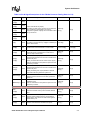
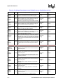
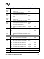
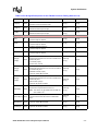
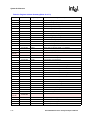
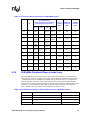
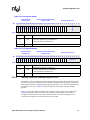
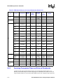
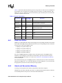
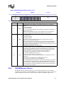
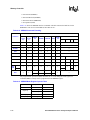
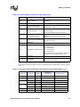
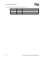
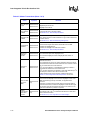
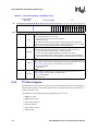
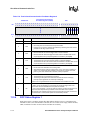
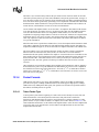
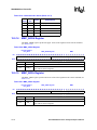
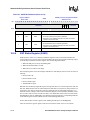
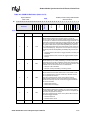
Table 2-6. Pin & Signal Descriptions for the PXA26x Processor Family (Sheet 10 of 12)
Pin Name
Type
Signal Descriptions
Reset State
Sleep State
Miscellaneous Pins
BOOT SELECT PINS (input):
BOOT_SEL
[2:0]
IC
Indicates type of boot device. See Section 18.1,
“Initialization” for information on configuring BOOT_SEL
for proper flash initialization.
Input
Input
Driven High
Driven low while
entering sleep
mode. Driven high
when sleep exit
sequence begins.
Input
Input
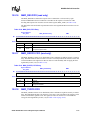
POWER ENABLE FOR THE POWER SUPPLY (output):
PWR_EN
OC
When negated, it signals the power supply to remove
power to the core because the system is entering sleep
mode.
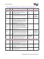
MAIN BATTERY FAULT (input):
nBATT_FAULT
IC
Signals that main battery is low or removed. Assertion
causes PXA26x processor family to enter sleep mode or
force an imprecise data exception, which cannot be
masked. PXA26x processor family will not recognize a
wake-up event while this signal is asserted. Minimum
assertion time for nBATT_FAULT is 1 ms.
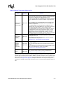
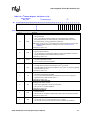
VDD FAULT (input):
nVDD_FAULT
IC
Signals that the main power source is going out of
regulation. nVDD_FAULT causes the PXA26x processor
family to enter sleep mode or force an Imprecise Data
Input
Exception, which cannot be masked. nVDD_FAULT is
ignored after a wake-up event until the power supply timer
completes (approximately 10 ms). Minimum assertion time
for nVDD_FAULT is 1 ms.
Input
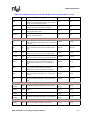
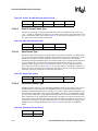
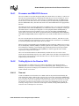
HARD RESET (input):
nRESET
IC
Level sensitive input used to start the processor from a
known address. Assertion causes the current instruction to
terminate abnormally and causes a reset. When nRESET Input
is driven high, the processor starts execution from address
0. nRESET must remain low until the power supply is
stable.
RESET OUT (output):
nRESET_OUT
OC
Asserted when nRESET is asserted and deasserts after
nRESET is deasserted but before the first instruction
fetch. nRESET_OUT is also asserted for “soft” reset
events: sleep, watchdog reset, or GPIO reset.
Input. Driving low
during sleep will
cause normal reset
sequence and exit
from sleep mode.
Driven low during
any reset sequence –
Driven Low
driven high prior to
first fetch.
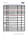
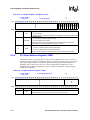
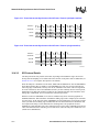
JTAG and Test Pins
JTAG TEST INTERFACE RESET:
nTRST
IC
Resets the JTAG/Debug port. If JTAG/Debug is used,
drive nTRST from low to high either before or at the same Input
time as nRESET. If JTAG is not used, nTRST must be
either tied to nRESET or tied low.
Input
JTAG TEST DATA INPUT (input):
TDI
IC
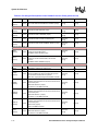
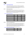
TDO
OCZ
Data from the JTAG controller is sent to the PXA26x
processor family using this pin. This pin has an internal
pull-up resistor.
Input
Input
JTAG TEST DATA OUTPUT (output):
2-18
Data from the PXA26x processor family is returned to the Hi-Z
JTAG controller using this pin.
Hi-Z
Intel® PXA26x Processor Family Developer’s Manual