1
Intel® IQ80321 I/O Processor
Evaluation Platform
Board Manual
April 2, 2003
Document Number: 273521-008
Intel® IQ80321 I/O Processor Evaluation Platform
INFORMATION IN THIS DOCUMENT IS PROVIDED IN CONNECTION WITH INTEL® PRODUCTS. NO LICENSE, EXPRESS OR IMPLIED, BY
ESTOPPEL OR OTHERWISE, TO ANY INTELLECTUAL PROPERTY RIGHTS IS GRANTED BY THIS DOCUMENT. EXCEPT AS PROVIDED IN
INTEL'S TERMS AND CONDITIONS OF SALE FOR SUCH PRODUCTS, INTEL ASSUMES NO LIABILITY WHATSOEVER, AND INTEL DISCLAIMS
ANY EXPRESS OR IMPLIED WARRANTY, RELATING TO SALE AND/OR USE OF INTEL PRODUCTS INCLUDING LIABILITY OR WARRANTIES
RELATING TO FITNESS FOR A PARTICULAR PURPOSE, MERCHANTABILITY, OR INFRINGEMENT OF ANY PATENT, COPYRIGHT OR OTHER
INTELLECTUAL PROPERTY RIGHT.
Intel products are not intended for use in medical, life saving, life sustaining applications.
Intel may make changes to specifications and product descriptions at any time, without notice.
Designers must not rely on the absence or characteristics of any features or instructions marked “reserved” or “undefined.” Intel reserves these for
future definition and shall have no responsibility whatsoever for conflicts or incompatibilities arising from future changes to them.
The Intel® 80321 I/O Processor may contain design defects or errors known as errata which may cause the product to deviate from published
specifications. Current characterized errata are available on request.
Contact your local Intel sales office or your distributor to obtain the latest specifications and before placing your product order.
Copies of documents which have an ordering number and are referenced in this document, or other Intel literature may be obtained by calling
1-800-548-4725 or by visiting Intel's website at http://www.intel.com.
Copyright© Intel Corporation, April 2003
AlertVIEW, i960, AnyPoint, AppChoice, BoardWatch, BunnyPeople, CablePort, Celeron, Chips, Commerce Cart, CT Connect, CT Media, Dialogic,
DM3, EtherExpress, ETOX, FlashFile, GatherRound, i386, i486, iCat, iCOMP, Insight960, InstantIP, Intel, Intel logo, Intel386, Intel486, Intel740,
IntelDX2, IntelDX4, IntelSX2, Intel ChatPad, Intel Create&Share, Intel Dot.Station, Intel GigaBlade, Intel InBusiness, Intel Inside, Intel Inside logo, Intel
NetBurst, Intel NetStructure, Intel Play, Intel Play logo, Intel Pocket Concert, Intel SingleDriver, Intel SpeedStep, Intel StrataFlash, Intel TeamStation,
Intel WebOutfitter, Intel Xeon, Intel XScale, Itanium, JobAnalyst, LANDesk, LanRover, MCS, MMX, MMX logo, NetPort, NetportExpress, Optimizer
logo, OverDrive, Paragon, PC Dads, PC Parents, Pentium, Pentium II Xeon, Pentium III Xeon, Performance at Your Command, ProShare,
RemoteExpress, Screamline, Shiva, SmartDie, Solutions960, Sound Mark, StorageExpress, The Computer Inside, The Journey Inside, This Way In,
TokenExpress, Trillium, Vivonic, and VTune are trademarks or registered trademarks of Intel Corporation or its subsidiaries in the United States and
other countries.
*Other names and brands may be claimed as the property of others.
2
Board Manual
Intel® IQ80321 I/O Processor Evaluation Platform
Contents
Contents
1
Introduction..................................................................................................................................13
1.1
1.2
1.3
1.4
1.5
1.6
1.7
2
Getting Started............................................................................................................................. 19
2.1
2.2
2.3
2.4
2.5
2.6
3
Document Purpose and Scope ........................................................................................... 13
Related Documents ............................................................................................................ 13
Electronic Information ......................................................................................................... 14
Component References ...................................................................................................... 14
Terms and Definitions ......................................................................................................... 15
Intel® 80321 I/O Processor .................................................................................................16
Intel® IQ80321 Evaluation Platform Board Features .......................................................... 18
Kit Content .......................................................................................................................... 19
Hardware Installation .......................................................................................................... 19
2.2.1 First-Time Installation and Test..............................................................................19
2.2.2 Power and Backplane Requirements .................................................................... 19
Factory Settings .................................................................................................................. 20
Development Strategy ........................................................................................................20
2.4.1 Supported Tool Buckets ........................................................................................ 20
2.4.2 Contents of the Flash............................................................................................. 20
Target Monitors................................................................................................................... 21
2.5.1 Redhat Redboot..................................................................................................... 21
2.5.2 ARM Firmware Suite.............................................................................................. 22
2.5.2.1 ARM Angel ............................................................................................. 23
2.5.2.1.1 Semihosting (File I/O) .......................................................... 23
Host Communications Examples ........................................................................................ 24
2.6.1 Serial-UART Communication................................................................................. 24
2.6.2 Ethernet-Network Communication .........................................................................24
2.6.3 JTAG Debug Communication ................................................................................ 25
2.6.4 GNUPro GDB/Insight ............................................................................................. 26
2.6.4.1 Communicating with Redboot ................................................................ 26
2.6.4.2 Connecting with GDB............................................................................. 28
2.6.5 ARM Extended Debugger ...................................................................................... 29
Hardware Reference Section ...................................................................................................... 31
3.1
3.2
3.3
3.4
3.5
3.6
3.7
Functional Diagram............................................................................................................. 31
Board Form-Factor/Connectivity ......................................................................................... 32
Power..................................................................................................................................33
Memory Subsystem ............................................................................................................ 34
3.4.1 DDR SDRAM ......................................................................................................... 34
3.4.1.1 Battery Backup....................................................................................... 34
3.4.2 Flash Memory Requirements................................................................................. 35
Intel® 80321 I/O Processor Operation Mode ...................................................................... 36
Interrupt Routing ................................................................................................................. 37
Intel® IQ80321 Evaluation Platform Board Peripheral Bus................................................. 38
3.7.1 Flash ROM............................................................................................................. 39
3.7.2 UART ..................................................................................................................... 40
3.7.3 HEX Display........................................................................................................... 41
Board Manual
3
Intel® IQ80321 I/O Processor Evaluation Platform
Contents
3.8
3.9
3.10
4
3.7.4 Rotary Switch......................................................................................................... 42
3.7.5 Battery Status ........................................................................................................ 43
Debug Interface .................................................................................................................. 44
3.8.1 Console Serial Port................................................................................................ 44
3.8.2 Ethernet Port.......................................................................................................... 44
3.8.2.1 Intel® 82544EI Gigabit Ethernet Controller ............................................ 44
3.8.3 JTAG Debug .......................................................................................................... 45
3.8.3.1 JTAG Port .............................................................................................. 45
3.8.4 Logic-Analyzer Connectors.................................................................................... 45
3.8.5 Mictor J3F2 ............................................................................................................ 46
3.8.6 Mictor J2F1 ............................................................................................................ 47
3.8.7 Mictor J1C1............................................................................................................ 48
3.8.8 Mictor J3C1............................................................................................................ 49
3.8.9 Mictor J2C1............................................................................................................ 50
Board Reset Scheme.......................................................................................................... 51
Switches and Jumpers........................................................................................................ 52
3.10.1 Switch Summary.................................................................................................... 52
3.10.2 PCIX Initialization Summary .................................................................................. 53
3.10.2.1 User Defined Switches........................................................................... 53
3.10.2.2 PCI-X Bridge Initialization Signals ......................................................... 53
3.10.3 Default Switch Settings - Visual............................................................................. 54
3.10.4 Jumper Summary .................................................................................................. 55
3.10.5 Connector Summary.............................................................................................. 55
3.10.6 General Purpose Input/Output Header .................................................................. 55
3.10.7 Secondary PCI/PCI-X Operation Settings ............................................................. 56
3.10.8 Primary PCI/PCI-X Operation Settings .................................................................. 56
3.10.9 Detail Descriptions of Switches/Jumpers............................................................... 57
3.10.9.1 Switch S7E1- 2/3 ................................................................................... 57
3.10.9.1.1 S7E1-2: RST_MODE ........................................................... 57
3.10.9.1.2 S7E1-3: RETRY................................................................... 57
3.10.9.1.3 Operation Setting Summary Descriptions............................ 57
3.10.9.2 Switch S7E1- 4/5 ................................................................................... 58
3.10.9.2.1 Switch S7E1 - 4 ................................................................... 58
3.10.9.2.2 Switch S7E1 - 5 ................................................................... 58
3.10.9.3 Switch S7E1- 6/7 ................................................................................... 58
3.10.9.4 Switch S7E1- 8 ...................................................................................... 59
3.10.9.5 Switch S8E1- 2 ...................................................................................... 60
3.10.9.6 Switch S8E1- 3 ...................................................................................... 60
3.10.9.7 Switch S8E1- 4 ...................................................................................... 60
3.10.9.8 Switch S8E1- 5 ...................................................................................... 61
3.10.9.8.1 Switch S8E1 - 5: Descriptions.............................................. 61
3.10.9.9 Switch S8E1- 6 ...................................................................................... 61
3.10.9.10 Switch S8E1- 7 ...................................................................................... 62
3.10.9.11 Switch S8E1- 8 ...................................................................................... 62
3.10.9.12 Switch S8E2 - 1/2 .................................................................................. 63
3.10.9.13 Switch S8E2 - 4 ..................................................................................... 63
3.10.9.14 Switch S9E1 - 1:3 .................................................................................. 64
3.10.9.15 Switch S9E1 - 4 ..................................................................................... 64
3.10.9.16 Switch S1D1 - 1/2 .................................................................................. 65
3.10.9.17 Switch S4D1 - 1/2 .................................................................................. 65
3.10.9.18 Switch S4D1 - 3/4 .................................................................................. 65
3.10.9.19 Jumper J1G2 ......................................................................................... 66
Board Manual
Intel® IQ80321 I/O Processor Evaluation Platform
Contents
3.10.9.20 Jumper
3.10.9.21 Jumper
3.10.9.22 Jumper
3.10.9.23 Jumper
4
External RAID Section................................................................................................................. 69
4.1
4.2
5
J3E1 ..........................................................................................66
J3G1 ......................................................................................... 66
J9E1 ..........................................................................................67
J9F1 ..........................................................................................67
Private Device Configuration .............................................................................................. 69
Interrupt Routing ................................................................................................................. 70
Software Reference ..................................................................................................................... 71
5.1
5.2
5.3
5.4
DRAM ................................................................................................................................. 71
Components on the Peripheral Bus .................................................................................... 71
5.2.1 Flash ROM............................................................................................................. 72
5.2.2 UART ..................................................................................................................... 73
5.2.3 Rotary Switch......................................................................................................... 73
5.2.4 HEX Display........................................................................................................... 74
Ethernet .............................................................................................................................. 76
Board Support Package (BSP) Examples .......................................................................... 77
5.4.1 Intel® 80321 I/O Processor Memory Map .............................................................. 77
5.4.2 Redboot* Intel® IQ80321 Memory Map ................................................................. 78
5.4.3 Redboot Intel® IQ80321 Physical Memory Map - Visual ....................................... 79
5.4.4 Redboot Intel® IQ80321 Virtual Memory Map - Visual .......................................... 80
5.4.5 Redboot Intel® IQ80321 Files ................................................................................ 81
5.4.6 Redboot Intel® IQ80321 DDR Memory Initialization Sequence ............................. 82
5.4.7 Redboot Switching .................................................................................................83
A
IQ80310 and IQ80321 Comparisons........................................................................................... 85
B
Getting Started and Debugger ................................................................................................... 87
B.1
B.2
B.3
B.4
B.5
B.6
B.7
Introduction ......................................................................................................................... 87
B.1.1 Purpose ................................................................................................................. 87
B.1.2 Necessary Hardware and Software .......................................................................87
B.1.3 Related Documents ............................................................................................... 87
B.1.4 Related Web Sites .................................................................................................88
Setup ..................................................................................................................................89
B.2.1 Hardware Setup ..................................................................................................... 89
B.2.2 Software Setup ...................................................................................................... 90
New Project Setup .............................................................................................................. 91
B.3.1 Creating a New Project ..........................................................................................91
B.3.2 Configuration ......................................................................................................... 92
Flashing with JTAG............................................................................................................. 93
B.4.1 Overview ................................................................................................................ 93
B.4.2 Using Flash Programmer ....................................................................................... 94
Debugging Out of Flash ...................................................................................................... 95
Building an Executable File From Example Code .............................................................. 95
Running the Code|Lab Debugger ....................................................................................... 96
B.7.1 Launching and Configuring Debugger ................................................................... 96
B.7.2 Manually Loading and Executing an Application Program..................................... 97
B.7.3 Displaying Source Code ........................................................................................ 97
B.7.4 Using Breakpoints.................................................................................................. 98
B.7.5 Stepping Through the Code................................................................................... 99
Board Manual
5
Intel® IQ80321 I/O Processor Evaluation Platform
Contents
B.8
B.9
C
Getting Started and Debugger ................................................................................................. 105
C.1
C.2
C.3
C.4
C.5
C.6
C.7
C.8
6
B.7.6 Setting Code|Lab Debug Options .......................................................................... 99
Exploring the Code|Lab Debug Windows ......................................................................... 100
B.8.1 Toolbar Icons ....................................................................................................... 100
B.8.2 Workspace Window ............................................................................................. 100
B.8.3 Source Code........................................................................................................ 100
B.8.4 Debug and Console Windows ............................................................................. 100
B.8.5 Memory Window .................................................................................................. 100
B.8.6 Registers Window................................................................................................ 101
B.8.7 Watch Window..................................................................................................... 101
B.8.8 Variables Window ................................................................................................ 101
Debugging Basics............................................................................................................. 102
B.9.1 Overview.............................................................................................................. 102
B.9.2 Hardware and Software Breakpoints ................................................................... 102
B.9.2.1 Software Breakpoints........................................................................... 102
B.9.2.2 Hardware Breakpoints ......................................................................... 102
B.9.3 Exceptions/Trapping ............................................................................................ 103
Introduction ....................................................................................................................... 105
C.1.1 Purpose ............................................................................................................... 105
C.1.2 Necessary Hardware and Software ..................................................................... 105
C.1.3 Related Documents ............................................................................................. 105
C.1.4 Related Web Sites ............................................................................................... 106
Setup ................................................................................................................................ 107
C.2.1 Hardware Setup................................................................................................... 107
C.2.2 Software Setup .................................................................................................... 108
New Project Setup ............................................................................................................ 109
C.3.1 Creating a New Project........................................................................................ 109
C.3.2 Configuration ....................................................................................................... 110
Flashing with JTAG........................................................................................................... 111
C.4.1 Overview.............................................................................................................. 111
C.4.2 Using Flash Programmer..................................................................................... 112
Debugging Out of Flash.................................................................................................... 113
Building an Executable File From Example Code ............................................................ 113
Running the Code|Lab Debugger ..................................................................................... 114
C.7.1 Launching and Configuring Debugger ................................................................. 114
C.7.2 Manually Loading and Executing an Application Program .................................. 114
C.7.3 Displaying Source Code ...................................................................................... 115
C.7.4 Using Breakpoints................................................................................................ 115
C.7.5 Stepping Through the Code................................................................................. 116
C.7.6 Setting Code|Lab Debug Options ........................................................................ 116
Exploring the Code|Lab Debug Windows ......................................................................... 117
C.8.1 Toolbar Icons ....................................................................................................... 117
C.8.2 Workspace Window ............................................................................................. 117
C.8.3 Source Code........................................................................................................ 117
C.8.4 4 Debug and Console Windows .......................................................................... 117
C.8.5 Memory Window .................................................................................................. 117
C.8.6 Registers Window................................................................................................ 118
C.8.7 Watch Window..................................................................................................... 118
C.8.8 Variables Window ................................................................................................ 118
Board Manual
Intel® IQ80321 I/O Processor Evaluation Platform
Contents
C.9
Debugging Basics .............................................................................................................119
C.9.1 Overview .............................................................................................................. 119
C.9.2 Hardware and Software Breakpoints ................................................................... 119
C.9.2.1 Software Breakpoints ........................................................................... 119
C.9.2.2 Hardware Breakpoints ......................................................................... 119
C.9.3 C.9.3 Exceptions/Trapping .................................................................................. 120
Board Manual
7
Intel® IQ80321 I/O Processor Evaluation Platform
Contents
Figures
1
2
3
4
5
6
7
8
9
10
11
12
13
14
15
16
17
18
19
20
21
22
23
24
25
26
27
28
29
30
31
8
Intel® 80321 I/O Processor Block Diagram ................................................................................ 16
Serial-UART Communication ..................................................................................................... 24
Ethernet-Network Communication.............................................................................................. 24
JTAG Debug Communication ..................................................................................................... 25
Functional Block Diagram........................................................................................................... 31
Board Form Factor ..................................................................................................................... 32
External Interrupt Routing to Intel® 80321 I/O Processor........................................................... 37
Intel® IQ80321 Evaluation Platform Board Peripheral Bus Topology......................................... 38
Flash Connection on Peripheral Bus .......................................................................................... 39
UART Connection on the Peripheral Bus ................................................................................... 40
HEX Display Connection on the Peripheral Bus......................................................................... 41
Rotary Switch Connection on the Peripheral Bus....................................................................... 42
Battery Status Buffer on Peripheral Bus ..................................................................................... 43
JTAG Port Pin-out ...................................................................................................................... 45
RESET Sources ......................................................................................................................... 51
PCI-X Routing Diagram on Secondary PCI-X Bridge ................................................................. 53
IDSEL Routing for Private Device Configuration ........................................................................ 69
Interrupt Routing for Private Device Configuration ..................................................................... 70
Flash Connection to Peripheral Bus ........................................................................................... 72
UART Connection to Peripheral Bus .......................................................................................... 73
Hex Display Connection to Peripheral Bus................................................................................. 74
7-Segment Display Bit Definition ................................................................................................ 74
Register Bitmap: 7-Segment Display MSB FE84 0000h (Write Only) ........................................ 74
Register Bitmap: 7-Segment Display LSB FE85 0000h (Write Only) ......................................... 75
Intel® 80321 I/O Processor Memory Map................................................................................... 77
Redboot Intel® IQ80310 Physical Memory Map ......................................................................... 79
Redboot Intel® IQ80310 Virtual Memory Map ............................................................................ 80
Intel® IQ80321 Hardware Setup Flow Chart............................................................................... 89
Software Flow Diagram .............................................................................................................. 90
Intel® IQ80321 Hardware Setup Flow Chart............................................................................. 107
Software Flow Diagram ............................................................................................................ 108
Board Manual
Intel® IQ80321 I/O Processor Evaluation Platform
Contents
Tables
1
2
3
4
5
6
7
8
9
10
11
12
13
14
15
16
17
18
19
20
21
22
23
24
25
26
27
28
29
30
31
32
33
34
35
36
37
38
39
40
41
42
43
44
45
46
47
48
49
Intel® 80321 I/O Processor Related Documentation List............................................................ 13
Electronic Information ................................................................................................................. 14
Component Reference................................................................................................................ 14
Terms and Definitions................................................................................................................. 15
Summary of Features ................................................................................................................. 18
Form-Factor/Connectivity Features ............................................................................................32
Power Features .......................................................................................................................... 33
DDR Memory Features ...............................................................................................................34
Supported DIMM Types.............................................................................................................. 34
Flash Memory Requirements...................................................................................................... 35
Peripheral Bus Features ............................................................................................................. 38
Flash ROM Features .................................................................................................................. 39
UART Features...........................................................................................................................40
HEX Display on the Peripheral Bus ............................................................................................41
Rotary Switch Requirements ...................................................................................................... 42
Battery Status Buffer Requirements ........................................................................................... 43
Logic Analyzer Connection ......................................................................................................... 45
Micor J3F2 Signal/Pins ...............................................................................................................46
Micor J2F1 Signal/Pins ...............................................................................................................47
Micor J1C1 Signal/Pins...............................................................................................................48
Micor J3C1 Signal/Pins...............................................................................................................49
Micor J2C1 Signal/Pins...............................................................................................................50
Reset Requirements/Schemes ................................................................................................... 51
Switch Summary......................................................................................................................... 52
Switch S7E1 ............................................................................................................................... 54
Switch S8E1 ............................................................................................................................... 54
Switch S8E2 ............................................................................................................................... 54
Switch S9E1 ............................................................................................................................... 54
Switch S1D1 ............................................................................................................................... 54
Switch S4D1 ............................................................................................................................... 54
Jumper Summary ....................................................................................................................... 55
Connector Summary................................................................................................................... 55
GPIO Header (J3F1) Definition................................................................................................... 55
Secondary PCI/PCI-X Operation Settings .................................................................................. 56
Primary PCI/PCI-X Operation Settings ....................................................................................... 56
Switch S7E1- 2/3: General Descriptions.....................................................................................57
Switch S7E1-2: RST_MODE: Settings and Operation Mode ..................................................... 57
Switch S7E1-3: RETRY: Settings and Operation Mode ............................................................. 57
RST_MODE and RETRY Operation Setting Summary .............................................................. 57
Switch S7E1 - 4/5: Descriptions .................................................................................................58
Switch S7E1 - 4: Settings and Operation Mode .........................................................................58
Switch S7E1 - 5: Settings and Operation Mode .........................................................................58
Switch S7E1 - 6/7: Descriptions .................................................................................................58
Switch S7E1 - 6/7: Settings and Operation Mode ...................................................................... 58
Switch S7E1 - 8: Descriptions .................................................................................................... 59
Switch S7E1 - 8: Settings and Operation Mode .........................................................................59
Switch S8E1 - 2: Descriptions .................................................................................................... 60
Switch S8E1 - 2: Settings and Operation Mode .........................................................................60
Switch S8E1 - 3: Descriptions .................................................................................................... 60
Board Manual
9
Intel® IQ80321 I/O Processor Evaluation Platform
Contents
50
51
52
53
54
55
56
57
58
59
60
61
62
63
64
65
66
67
68
69
70
71
72
73
74
75
76
77
78
79
80
81
82
83
84
85
86
87
88
89
90
91
92
10
Switch S8E1 - 3: Settings and Operation Mode ......................................................................... 60
Switch S8E1 - 4: Descriptions .................................................................................................... 60
Switch S8E1 - 4: Settings and Operation Mode ......................................................................... 60
Switch S8E1 - 5: Settings and Operation Mode ......................................................................... 61
Switch S8E1 - 5: Driver Mode Output Impedances .................................................................... 61
Switch S8E1 - 6: Descriptions .................................................................................................... 61
Switch S8E1 - 6: Settings and Operation Mode ......................................................................... 61
Switch S8E1 - 6: Driver Mode Output Impedances .................................................................... 61
Switch S8E1 - 7: Descriptions .................................................................................................... 62
Switch S8E1 - 7: Settings and Operation Mode ......................................................................... 62
Switch S8E1 - 8: Descriptions .................................................................................................... 62
Switch S8E1 - 8: Settings and Operation Mode ......................................................................... 62
Switch S8E2 - 1/2: Descriptions ................................................................................................. 63
Switch S8E2 - 1/2: Settings and Operation Mode ...................................................................... 63
Switch S8E2 - 4: Descriptions .................................................................................................... 63
Switch S8E2 - 4: Settings and Operation Mode ......................................................................... 63
Switch S9E1 - (1:3) Descriptions ................................................................................................ 64
Switch S9E1 - (1:3) Settings and Operation Mode ..................................................................... 64
Switch S9E1 - 4: Descriptions .................................................................................................... 64
Switch S9E1 - 4: Settings and Operation Mode ......................................................................... 64
Switch S1D1 - 1/2: Descriptions ................................................................................................. 65
Switch S1D1 - 1/2: Settings and Operation Mode ...................................................................... 65
Switch S4D1 - 1/2: Descriptions ................................................................................................. 65
Switch S4D1 - 1/2: Settings and Operation Mode ...................................................................... 65
Switch S4D1 - 3/4: Descriptions ................................................................................................. 65
Switch S4D1 - 3/4: Settings and Operation Mode ...................................................................... 65
Jumper J1G2: Descriptions ........................................................................................................ 66
Jumper J1G2: Settings and Operation Mode ............................................................................. 66
Jumper J3E1: Descriptions......................................................................................................... 66
Jumper J3E1: Settings and Operation Mode.............................................................................. 66
Jumper J3G1: Descriptions ........................................................................................................ 66
Jumper J3G1: Settings and Operation Mode ............................................................................. 66
Jumper J9E1: Descriptions......................................................................................................... 67
Jumper J9E1: Settings and Operation Mode.............................................................................. 67
Jumper J9F1: Descriptions ......................................................................................................... 67
Jumper J9F1: Settings and Operation Mode .............................................................................. 67
Private Device Configuration Requirements............................................................................... 69
Interrupt Routing for Secondary PCI-X Private Device............................................................... 70
DDR Memory Bias Voltage Minimum/Maximum Values ............................................................ 71
UART Register Settings ............................................................................................................. 73
Intel® IQ80310 and Intel® IQ80321 Evaluation Platform Board Comparisons ........................... 85
Related Documents .................................................................................................................... 87
Related Documents .................................................................................................................. 105
Board Manual
Intel® IQ80321 I/O Processor Evaluation Platform
Contents
Revision History
Date
Revision
April 2003
008
March 2003
007
November 2002
006
21 October 2002
005
07 October 2002
004
August 2002
003
Description
Changed name and references of Tester1LED to Tester321LED.
Revised Appendix B, “Getting Started and Debugger”.
Added Appendix C, “Getting Started and Debugger”.
Added Warning to Section 3.8.4, “Logic-Analyzer Connectors” through Section 3.8.9,
“Mictor J2C1”.
Updated typographical errors in Appendix B, “Getting Started and Debugger”.
Added Section 3.10.2, “PCIX Initialization Summary”.
Added Appendix B, “Getting Started and Debugger”.
Replaced Section 5, “Software Reference”.
Corrected various typographical errors.
Updated Notes in Table 24, added Spare for S9E1-3.
May 2002
002
Revised Table 26, Table 27 and Table 30.
Revised Factory Default in Table 62.
Corrected Switch nomenclature in Table 66 / Table 67 and Table 74 / Table 75.
February 2002
Board Manual
001
Initial Release.
11
Intel® IQ80321 I/O Processor Evaluation Platform
Contents
This page intentionally left blank.
12
Board Manual
1
Introduction
1.1
Document Purpose and Scope
This document describes the Intel® IQ80321 Evaluation Platform Board. This platform is targeted for
the Intel® 80321 I/O processor (80321). The board serves as both an evaluation platform for
developers using 80321 as well as a Customer Reference Board.
The IQ80321 is intended for rapid intelligent I/O development. It is based on the 80321, a
single-function device that integrates the Intel® XScale™ core (ARM* architecture compliant)
with intelligent peripherals including a PCI bus application bridge.
1.2
Related Documents
Table 1.
Intel® 80321 I/O Processor Related Documentation List
Document
Number
Intel® 80321 I/O Processor Developer’s Manual
273517
Intel® 80321 I/O Processor Datasheet
273518
®
273520
®
273519
®
Intel 80321 I/O Processor Product Brief
273525
Migrating from the Intel® 80310 I/O Processor Chipset to the Intel® 80321 I/O Processor Application Note
273524
Intel 80321 I/O Processor Design Guide
Intel 80321 I/O Processor Specification Update
®
273522
®
273551
Intel 80321 I/O Processor Initialization Application Note
Intel Flash Recovery Utility (FRU) Reference Manual
PCI Local Bus Specification, Revision 2.2
PCI-X Addendum to the PCI Local Bus Specification, Revision 1.0a
http://www.pcisig.co
m/specifications
Intel documentation is available from the local Intel Sales Representative or Intel Literature Sales.
To obtain Intel literature write to or call:
Intel Corporation
Literature Sales
P.O. Box 5937
Denver, CO 80217-9808
(1-800-548-4725) or visit the Intel website at http://www.intel.com
Board Manual
13
Intel® IQ80321 I/O Processor Evaluation Platform
Introduction
1.3
Electronic Information
Table 2.
Electronic Information
Support Type
Location/Contact
The Intel World-Wide Web (WWW) Location:
http://www.intel.com
Customer Support (US and Canada):
1.4
800-628-8686
Component References
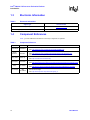
Table 3 provides additional information on the major components of IQ80321.
Table 3.
Component
Component Reference
Part Number
Intel®
StrataFlash®
28F640J3A
Gigabit
Ethernet
82544GC
Rotary Switch
DR FC 16
Hex Display
HDSP-G211
UART
TL 16550C
Additional Information
•
• URL: http://developer.intel.com/design/flcomp/prodbref/298044.htm
•
PCI-X Bridge
14
Manufacturer: Intel Corporation
Manufacturer: Intel Corporation
• URL: http://developer.intel.com/design/network/products/lan/controllers/82544.htm
• Intel® 82544EI/82544GC Gigabit Ethernet Controller Software Developer’s Manual
IBM
21P100BGC
•
Manufacturer: NKK*
• URL: http://us.switchzone.com/series.asp
•
Manufacturer: Agilent Technologies*
• URL: http://www.semiconductor.agilent.com/cgi-bin/morpheus/home/home.jsp?pSection=LED
•
Manufacturer: Texas instruments*
• URL: http://focus.ti.com/docs/prod/productfolder.jhtml?genericPartNumber=TL16C550C
• Manufacturer: IBM*
• IBM 133 PCI-X Bridge
• URL: http://www.chips.ibm.com/products/storage/pci_x/
Board Manual
Intel® IQ80321 I/O Processor Evaluation Platform
Introduction
1.5
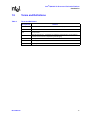
Terms and Definitions
Table 4.
Terms and Definitions
Acronym/Term
Board Manual
Definition
ARM
Refers to both the microprocessor architecture and the company that licenses it.
CRB
Customer Reference Board
ICE
In-Circuit Emulator – A piece of hardware used to mimic all the functions of a
microprocessor.
JTAG
Joint Test Action Group – A hardware port supplied on Intel® XScale™ microarchitecture
evaluation boards used for in-depth testing and debugging.
PPCI-X
Primary PCI-X.
PSU
Power Supply Unit
SPCI-X
Secondary PCI-X.
15
Intel® IQ80321 I/O Processor Evaluation Platform
Introduction
1.6
Intel® 80321 I/O Processor
About the Intel® 80321 I/O processor.
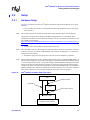
The Intel® 80321 I/O processor combines the Intel® XScale™ core with powerful new features to
create an intelligent I/O processor. This single-function PCI device is fully compliant with the PCI
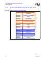
Local Bus Specification, Revision 2.2. The Intel® 80321 I/O processor-specific features include:
•
•
•
•
•
•
•
•
•
•
•
PCI - Local Memory Bus Address Translation Unit (ATU)
I2O* Messaging Unit (MU)
Direct Memory Access (DMA) Controller
Peripheral Bus Interface (PBI) Unit
Integrated Memory Controller Unit (MCU)
Performance Monitor Unit (PMU)
Application Accelerator Unit (AAU)
Two I 2C Bus Interface Units (BIU)
Synchronous Serial Port (SSP) Unit
Eight General Purpose Input Output (GPIO) Ports
Intel®
XScale™
Core
DDR
Memory
Controller
Unit
Peripheral
Bus
Interface
I2C Bus
Interface
Serial Bus
32-Bit
Interface
I2C
Serial Bus
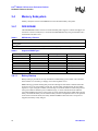
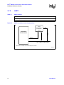
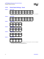
Intel® 80321 I/O Processor Block Diagram
72-Bit
Interface
Figure 1.
Intel® XScale™ core
Application
Accelerator
SSP
Serial Bus
Internal Bus
Messaging
Unit
Address
Translation
Unit
Two
DMA
Channels
Performance
Monitoring
Unit
Intel® 80321 I/O Processor
64-bit / 32-bit PCI Bus
A9646-01
16
Board Manual
Intel® IQ80321 I/O Processor Evaluation Platform
Introduction
It is an integrated processor that addresses the needs of intelligent I/O applications and helps reduce
intelligent I/O system costs.
The PCI Bus is an industry standard, high performance low latency system bus. The 80321 PCI Bus
is capable of 133 MHz operation in PCI-X mode as defined by the PCI-X Addendum to the PCI Local
Bus Specification, Revision 1.0a. Also, the processor supports a 66 MHz conventional PCI mode as
defined by the PCI Local Bus Specification, Revision 2.2. The addition of the Intel® XScale™ core
brings intelligence to the PCI bus application bridge.
The 80321 is a single function PCI device. This function represents the address translation unit. The
address translation unit is an “application bridge” as defined by the PCI-X Addendum to the PCI
Local Bus Specification, Revision 1.0a. The 80321 contains PCI configuration space accessible
through the PCI bus.
80321 core is based upon the Intel® XScale™ core. The core processor operates at a maximum
frequency of 600 MHz. The instruction cache is 32 Kbytes (KB) in size and is 32-way set associative.
Also, the core processor includes a data cache that is 32 KB and is 32-way set associative and a mini
data cache that is 2 KB and is 2-way set associative.
The 80321 includes eight General Purpose I/O (GPIO) pins.
Board Manual
17
Intel® IQ80321 I/O Processor Evaluation Platform
Introduction
1.7
Intel® IQ80321 Evaluation Platform Board Features
Table 5.
Summary of Features
Feature
Definition
Battery Backup Unit: Battery back up circuit for SDRAM – 64 MB for 72 hours.
Ethernet Port:
Gigabit Ethernet Debugging/Download Port (using Intel® 82544).
Flash ROM: 8 MB Flash ROM 3.3 V – 16-bit Flash I/F.
Form & Factor:
Modified PCI long-card format – one Secondary PCI-X (SPCI-X) Expansion slots (right
angel connector).
General Purpose I/O: GPIO Pins are used as described in the appropriate section in this document
Hex Display:
JTAG Port:
Two 7-segment Hex LED displays.
ARM compliant JTAG Header.
Logic analyzer (mictor) interface on:
Logic Analyzer:
• SPCI-X bus
• Peripheral Bus
Interposer Card may be used for the memory bus – Information supplied separately.
• PC1600 Double Data Rate (DDR) SDRAM (Clock rate: 100 MHz).
Memory:
• 128 MB 64-bit (expandable to 1 GB).
• DIMM socket.
Onboard Power:
Board sources +1.25 V, +2.5 V, +3.3 V, +5 V, +12 V, and -12 V from primary PCI
connector.
• All core voltages are derived from 3.3 V supply.
PCI-X Bridge: IBM PCI-X Bridge.
Power LED: Power on (green) and FAIL (red) LED indicators.
Primary PCI: 64 bits 133/100/66 MHz PCI-X or PCI 66 MHz
RAID Support
Secondary PCI:
Support for “RAID” Implementation – Ability to make the devices plugged in the
secondary expansion slots “Private”.
• 1 x 64-bit PCI-X connector - 66 MHz.
• Intel® 82544 Gigabit Ethernet Controller also on the secondary PCI-X.
Serial Port: One Serial Console Port (16C550 Compatible).
18
Board Manual
Getting Started
2
The IQ80321 is a software development environment for Intel® 80321 I/O processor.
2.1
Kit Content
The IQ80321 Kit contains the following items:
•
•
•
•
•
2.2
Warning:
2.2.1
Intel® IQ80321 Evaluation Platform Board
Code|Lab* Development Environment from Accelerated Technology Incorporated*
JTAG Emulation unit
Serial Cable
Evaluation Software Bundle
Hardware Installation
Static charges can severely damage the boards. Be sure you are properly grounded before removing
the board from the anti-static bag.
First-Time Installation and Test
For first-time installation, visually inspect the IQ80321 for any damage made during shipment.
Follow the host system manufacturer instructions for installing a PCI adapter. The board is a
full-length PCI/PCI-X adapter and requires a PCI/PCI-X slot free from obstructions. The extended
height of the board requires the cover of the PC to be kept off.
2.2.2
Power and Backplane Requirements
The IQ80321 requires a 3.3 V supply coming through the PCI/PCI-X primary connector. The board
can be plugged into either a backplane or a desktop PCI/PCI-X slot. When using a backplane, an ATX
rated power supply is required. The IQ80321 only draws from the 3.3 V line of the power supply.
Most ATX power supply units (PSUs) regulate off the 5 V signal. When there is nothing drawing
from the 5.5 V signal most ATX PSU do not supply the 3.3 V correctly. To overcome this, it is
recommended to put a load on the 5.5 V line of the PSU. An old IDE Hard drive can be used for this.
Caution:
Board Manual
When plugging the power supply into the backplane, make sure that the power supply is
disconnected from the mains. Most ATX PSUs supply 5 V standby current even when turned Off,
backplane damage is possible.
19
Intel® IQ80321 I/O Processor Evaluation Platform
Getting Started
2.3
Factory Settings
Make sure that the switch/jumper settings are set to proper positions as explained in Section 3.10,
“Switches and Jumpers” on page 52.
2.4
Development Strategy
2.4.1
Supported Tool Buckets
For developing and debugging software application, the production version of the IQ80321 kit
includes the Code|Lab Development Environment. Support for the Code|Lab development
environment is available from ATI*. Please refer to the enclosed package.
The kit also contains evaluation copies for several Software Development Tools. These tools are for
evaluation purposes and do not include any support. Please contact the vendor directly for additional
information and support. They include:
•
•
•
•
•
•
2.4.2
ARM Developer Suite (ADS) and ARM Firmware Suite (AFS)
Redhat* GNUPro tools
LynuxWorks* Embedded Linux RTOS and Development Tools
Monta Vista* Embedded Linux RTOS and Development Tools
WindRiver* VxWorks* RTOS and Tornado* Development Tools
Accelerated Technology Inc*, Nucleus Plus* RTOS and Development Tools
Contents of the Flash
The production version of the board contains a trio image for Redhat Redboot*, ARM Angel*, and
ATI Code|Lab Monitor. All early sample/engineering boards have the Redboot target monitor.
20
Board Manual
Intel® IQ80321 I/O Processor Evaluation Platform
Getting Started
2.5
Target Monitors
2.5.1
Redhat Redboot
RedBoot* is an acronym for “Red Hat Embedded Debug and Bootstrap”, and is the standard
embedded system debug/bootstrap environment from Red Hat, replacing the previous generation of
debug firmware: CygMon and GDB stubs. It provides a bootstrap environment for a range of
embedded operating systems, such as embedded Linux and eCos*, and includes facilities such as
network downloading and debugging. It also provides a simple Flash file system for boot images.
RedBoot provides a set of tools for downloading and executing programs on embedded target
systems, as well as tools for manipulating the target system's environment. It can be used for both
product development (debug support) and for end product deployment (Flash and network booting).
Here are some highlights of RedBoot capabilities:
• Boot scripting support
• Simple command line interface for RedBoot configuration and management, accessible via
serial (terminal) or Ethernet (telnet) (see Section 2.6.4, “GNUPro GDB/Insight” on page 26)
• Integrated GDB stubs for connection to a host-based debugger (GBD/Insight) via serial or
Ethernet. (Ethernet connectivity is limited to local network only)
• Attribute Configuration - user control of aspects such as system time and date (when
applicable), default Flash image to boot from, default fail-safe image, static IP address, etc.
•
•
•
•
Board Manual
Configurable and extensible, specifically adapted to the target environment
Network bootstrap support including setup and download, via BOOTP, DHCP and TFTP
X/Y-Modem support for image download via serial
Power On Self Test
21
Intel® IQ80321 I/O Processor Evaluation Platform
Getting Started
2.5.2
ARM Firmware Suite
The ARM Firmware Suite is a package of low-level routines and libraries that have been designed to
help developers rapidly bring up applications and operating systems on Intel® XScale™
microarchitecture-based development platforms, such as the IQ80321.
AFS consists of two parts:
1. µHAL, the ARM standard board API, which is low-level firmware, designed to provide a
common set of functions across IQ80321. These include
— System initialization software.
— Simple polled serial drivers.
— LED support.
— Timer support.
— Interrupt Controller support.
µHAL manages all the variables associated with the IQ80321. This is provided in source form
for users to embed and distribute in their own products running on an 80321. Included also as
sources and with object distribution rights are:
— A simple boot monitor.
— Event chaining libraries, low level ADS C++ support libraries, benchmarking and
demonstration applications.
— Angel* debug target and host communication software that allows inter-working with
ARM Developer Suite.
2. On top of µHAL, AFS provides some useful applications, demos and example operating
systems such as µCOS-II. The applications are currently.
— Flash Library supporting a range of commonly used Flash parts.
— Flash management utilities including support for multiple Flash images using the ARM
Flash format standard.
— PCI Library that fully initializes the PCI subsystem and provides device driver primitives.
— DHCP Client over Ethernet of the fast download of binary images into Flash or RAM.
— Full on line documentation.
— Example OS ports.
22
Board Manual
Intel® IQ80321 I/O Processor Evaluation Platform
Getting Started
2.5.2.1
ARM Angel
Angel is one of the debug monitor programs for 80321. It is provided in source and binary form with
the ARM Software Development Toolkit. It features:
• Debug capability, including memory inspection, image download and execution,
break-pointing and single step
• CPU and board startup and basic exception handling
• A full ANSI C library, using semihosting (file I/O Operation) to provide services from the host
which are not available on the target
• A full source distribution for users in developing standalone applications
Angel interfaces with the ARM Developer Suite in two ways:
• SW Debuggers use the interface library (Remote_A) to communicate with an Angel target
when debugging or executing code.
• Application code uses software interrupt (SWI) calls to request services of Angel either
directly or via the toolkit C library.
2.5.2.1.1
Semihosting (File I/O)
The ARM debuggers support a feature known as semihosting to enable a target system which does
not support various features required by the ANSI C library to use the features of the host instead. A
simple example of this is the use of a host “window” to provide a system console, to which the output
of printf(), etc..., can be written.
Semihosting is supported in Angel using a set of SWI calls which the ARM C library uses messages
over the CLIB channel of the target<=>host link, and appropriate code in the host library
(Remote_A.dll under Windows) which interprets and executes these requests.
For information on the SWI calls, see the ARM SDT Reference Manual (DUI 0041B) section 8.3:
Angel C Library Support (SWIs)
Board Manual
23
Intel® IQ80321 I/O Processor Evaluation Platform
Getting Started
2.6
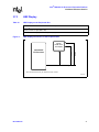
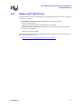
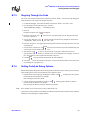
Host Communications Examples
How to communicate to the host.
2.6.1
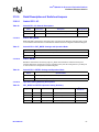
Serial-UART Communication
Using a serial connection:
Figure 2.
Serial-UART Communication
Host System
SW Debugger
C/C++
Seria
ASM
able
lC
Serial
Connectivity
Intel® 80321
I/O Processor
Running a
Debug Monitor
Intel® IQ80321
Evaluation Platform Board
PCI/PCI-X Platform
Serial
Connectivity
Server/Desktop/Backplane
Host System
A9647-01
2.6.2
Ethernet-Network Communication
Using a network connection:
Figure 3.
Ethernet-Network Communication
Host System
SW Debugger
C/C++
ASM
Ethernet Network
Network
Connector
Network
Connector
Intel® 80321
I/O Processor
Running a
Debug Monitor
Intel® IQ80321
Evaluation Platform Board
PCI/PCI-X Platform
Server/Desktop/Backplane
Host System
A9648-01
24
Board Manual
Intel® IQ80321 I/O Processor Evaluation Platform
Getting Started
2.6.3
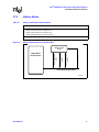
JTAG Debug Communication
Using a JTAG Emulator:
Figure 4.
JTAG Debug Communication
Host System
JTAG
Connector
SW Debugger
JTAG Emulator
C/C++
ASM
Parallel
Port
Intel® 80321
I/O Processor
Running a
Debug Monitor
Intel® IQ80321
Evaluation Platform Board
PCI/PCI-X Platform
Server/Desktop/Backplane
Host System
A9649-01
Board Manual
25
Intel® IQ80321 I/O Processor Evaluation Platform
Getting Started
2.6.4
GNUPro GDB/Insight
2.6.4.1
Communicating with Redboot
Hardware Setup:
• Host with UNIX/Linux or Win32 installed
• Intel® IQ80321 Evaluation Platform Board with serial cable
• Redhat Redboot monitor Flashed to the platform board
Recommended Mapping of UART Ports to Host Com Ports
• Host port connected to the platform board UART.
The following communication tools can be used:
•
•
•
•
Win32 using HyperTerminal
UNIX using Kermit
Linux using Miniport
Solaris using Tip
Redboot Monitor startup:
Description:
terminal emulator runs on host and communicates with the board via the serial cable.
Start: Power up the Intel® IQ80321 Evaluation Platform Board. While the 'reset' is asserted, the two
7-segment LEDs sequentially display “88”, “A0” through “A6”, followed by “SL” (Scrub
loop). When RedBoot is successfully booted, it displays the characters “A1” on the LEDs.
When the final state of “A1” does not occur, reset the processor again.
The time for reset is approximately 1 or 2 seconds.
Win32 on Host Connecting with HyperTerminal.
26
Board Manual
Intel® IQ80321 I/O Processor Evaluation Platform
Getting Started
To bring up a HyperTerminal session on a Win32 platform: Go to Start, Programs, Accessories,
Communications, HyperTerminal
• HyperTerminal setup screens:
— “Connection Description” Panel:
• Enter name.
— “Connect To” Panel:
• Select host com2 port (or whichever port you are using).
— Port Settings:
• Bits per second: 115200
• Data Bits: 8
• Parity: none
• Stop Bits: 1
• Flow Control: none
— Start HyperTerminal:
• Select Call from HyperTerminal panel.
— Reset or power up IQ80321 board.
— The Host screen reads:
RedBoot(tm) debug environment - built dd:mm:yy, Mon dd 2001
Platform: IQ80321
Copyright (C) 2000, Red Hat, Inc.
RAM: 0xa0000000-0xa2000000
FLASH: 0x00000000 - 0x00800000, 64 blocks of 0x00020000 bytes each.
IP: 192.168.0.1, Default server: 0.0.0.0
RedBoot>
For further information on the GDB/Insight Debugger, refer to the content of the GNUPro CD and/or
the GNUPro Debugging Tools manual. This setup assumes that Redboot is Flashed on the board.
Board Manual
27
Intel® IQ80321 I/O Processor Evaluation Platform
Getting Started
2.6.4.2
Connecting with GDB
Below are the GDB commands entered from the command prompt. Be sure system path is set to
access “xscale-elf-gdb.exe”. File name in example “hello”. Bold type represents input by user:
>xscale-elf-gdb -nw hello1
• Start GDB executable, loads debug information and symbols.
(GDB) set remotebaud 115200
• Set baud rate for the IQ80321.
Connect COM port:
• When using Windows command prompt:
(GDB) target remote com1
Example: screen output from board to host (GDB) target remote com1:
Remote debugging using com1.
(GDB)
• When using Linux
(GDB) target remote /dev/ttyS0
(GDB) load
• Load the program to the board, may have to wait a few seconds.
(GDB) break main
• Set breakpoint at main.
(GDB) continue
• Start the program using 'continue' verse the usual 'run'.
• Program hits break at main() and wait.
1.
28
To be supplied separately.
Board Manual
Intel® IQ80321 I/O Processor Evaluation Platform
Getting Started
2.6.5
ARM Extended Debugger
For further information on the AXD Debugger, refer to the content of the ARM ADS. This setup
assumes that Angel is Flashed on the board:
Description:
Terminal emulator runs on host and communicates with the board via the serial cable.
Start:
Power up the target board. After the ‘reset’ is asserted, the two 7-segment LEDs
display blank. The time for reset is approximately 1 or 2 seconds.
Assumptions: ARM Developer Suite (ADS) is loaded to Win32 Host, Angel is Flashed to ROM,
Host com port is connected to board serial port ## and compiled project file
Worchester.mcp1 exists.
Following are the steps from setup to running a project file that has been previously created and
named Worchester.mcp:
1. From Windows start menu:
a. Programs -> ARM Developer Suite v1.1 -> Metrowerks CodeWarrior
2. From CodeWarrior open project and start debugger:
a. File -> Open (All files) -> Worchester.mcp
b. Project -> Enable Debugger
c. Project -> Debug (AXD Interface comes up)
3. From AXD (ARM extended debugger) configure and connect:
a. Connect Host to Target with serial cable
Options -> Configure Target … -> Set Target Environment = ADP
Select Configure
Select… , ARM Serial Driver, OK
Endian: Little
Configure… , Serial Port:= COM1, Baud Rate:=115200, OK, OK, OK
b. Load Image and Start
On AXD menu: File -> Load Image… -> File name: Cyclone.axf -> Open ->
c. Execute -> Select Go, Breakpoints
4. The LEDs now Flashes ‘80321’. You can set breakpoints and step to control speed or stop
location.
1.
To be supplied separately.
Board Manual
29
Intel® IQ80321 I/O Processor Evaluation Platform
Getting Started
This page intentionally left blank.
30
Board Manual
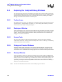
3
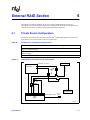
Hardware Reference Section
3.1
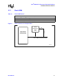
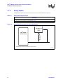
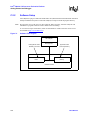
Functional Diagram
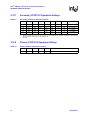
Figure 5 shows the functional block for the IQ80321.
Figure 5.
Functional Block Diagram
Memory Battery Backup
Logic
Analyzer
Interface
PC1600 DDR Memory
DDR Memory Bus
Intel® 80321
I/O Processor
FLASH
ROM
IOP Peripheral Bus
Rotary
Switch
Intel® 82544
Giga Ethernet
Secondary PCI-X
Expansion
FET Quick Switches
16550
UART
Hex
Disp
Logic
Analyzer
Interface
Secondary PCI-X Bus 64-bits, 66 MHz
PCI-X
Bridge
Primary PCI-X Bus 64-bits, 133 MHz
A9517-01
Board Manual
31
Intel® IQ80321 I/O Processor Evaluation Platform
Hardware Reference Section
3.2
Board Form-Factor/Connectivity
Table 6 summarizes the form-factor and connectivity features for the IQ80321.
Table 6.
Form-Factor/Connectivity Features
Description
®
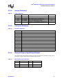
The Intel IQ80321 Evaluation Platform Board is a full-size PCI card with form factor depicted by Figure 6.
The IQ80321s connects to the Primary PCI-X (PPCI-X) bus a PCI-X.
The IQ80321 has one PCI-X expansion slot.
The IQ80321 uses the Intel® 82544 Gigabit Ethernet Controller for network connectivity.
The IQ80321 can electrically isolate the Intel® 82544 Gigabit Ethernet Controller on the SPCI-X bus using user switches.
The IQ80321 has one serial port/UART (compatible with 16C550).
The IQ80321 has one JTAG port compliant with ARM Multi-ICE 20-pin connector standard. The JTAG is targeted for the Intel®
XScale™ core and is used for software debug purposes.
Figure 6.
Board Form Factor
Secondary PCI-X Connector
JTAG
HEX Display
Intel®
82544
Intel® 80321
I/O Processor
Network
Connector
Logic Analyzer Connectors
DDR DIMM Connector
Logic Analyzer Connectors
User Switches
Battery
Serial Connector
FLASH
Rotary
PCI-X
Bridge
A9449-02
32
Board Manual
Intel® IQ80321 I/O Processor Evaluation Platform
Hardware Reference Section
3.3
Power
The IQ80321 draws power from the PCI-X bus. The power requirements for the IQ80321 are shown
in Table 7 below. The numbers do not include the power required by a PCI-X card mounted on the
expansion slot.
Table 7.
Power Features
Voltage
Note:
Board Manual
Typical Current
Maximum Current
+3.3 V
TBD V
TBD V
+5 V
TBD A
TBD A
+12 V
TBD mA
TBD mA
-12 V
TBD mA
TBD mA
Does not include the power required by a PCI-X card mounted on the expansion slot.
33
Intel® IQ80321 I/O Processor Evaluation Platform
Hardware Reference Section
3.4
Memory Subsystem
Memory subsystem consists of the SDRAM as well as the Flash memory subsystems.
3.4.1
DDR SDRAM
The DDR SDRAM interface consists of a 64-bit wide data path to support 1.6 GB/sec throughput. An
8-bit Error Correction Code (ECC) is stored into the DDR SDRAM array along with the data and is
checked when the data is read.
Table 8.
DDR Memory Features
Description
The board features two banks of DDR SDRAM in the form of one two-bank dual inline memory module (DIMM), only Un-buffered
PC1600 DIMMs.
The Intel® IQ80321 Evaluation Platform Board has a single DIMM connector supporting the DIMM arrangements listed in Table 9.
Table 9.
Supported DIMM Types
Type
Size
Type
Size
DDR200 (PC1600)
8MX64
CL2DIMM
(64 MB)
DDR200
16MX64
CL2 DIMM
(128 MB)
DDR200
32MX64
CL2 DIMM
(256 MB)
DDR200
8MX72
CL2 ECC DIMM
(64 MB)
DDR200
16MX72
CL2 ECC DIMM
(128 MB)
DDR200
32MX72
CL2 ECC DIMM
(256 MB)
DDR200
3.4.1.1
(1 GB)
Battery Backup
Battery backup is provided to save any information in DDR during a power failure. The evaluation
board contains a Li-ion battery, a charging circuit and a regulator circuit.
DDR technology provides enabling data preservation through the self-refresh command. When the
processor receives an active Primary PCI-X reset, the self-refresh command issues, driving SCKE
signals low. Upon seeing this condition, the board logic circuit holds SCKE low before the processor
loses power. Batteries maintain power to DDR and logic, to ensure self-refresh mode. When the
circuit detects PRST# returning to inactive state, the circuit releases the hold on SCKE. Removing the
battery can disable the battery circuit. When the battery remains in the platform when it is de-powered
and/or removed from the chassis, the battery maintains DDR for about four hours. Once power is
reapplied, the battery is fully charged.
34
Board Manual
Intel® IQ80321 I/O Processor Evaluation Platform
Hardware Reference Section
3.4.2
Flash Memory Requirements
Total Flash memory size is 8 MB.
Table 10.
Flash Memory Requirements
Description
®
Intel IQ80321 Evaluation Platform Board Total Flash size is 8 MB
IQ80321 Flash technology is based on Intel Strata Flash family
IQ80321 Flash uses a 16-bit interface
IQ80321 Flash utilizes the 80321 Peripheral Bus
IQ80321 May be programmed using the PCI-X interface – Flash Recovery Utility (FRU) Utility
IQ80321 May be programmed using a RAM based software target monitor – Redhat Redboot and ARM Firmware Suite
IQ80321 May be programmed using a JTAG emulation/debug device
Board Manual
35
Intel® IQ80321 I/O Processor Evaluation Platform
Hardware Reference Section
3.5
Intel® 80321 I/O Processor Operation Mode
Please refer to user switches section for mode setting during reset.
36
Board Manual
Intel® IQ80321 I/O Processor Evaluation Platform
Hardware Reference Section
3.6
Interrupt Routing
The IQ80321 Interrupt routing.
Figure 7.
External Interrupt Routing to Intel® 80321 I/O Processor
Intel® 80321 I/O Processor
MUX
MUX
MUX
XINT0
INTA# Gigabit Ethernet
XINT1
UART Interrupt
XINT2
INTA# from S-PCI-X Slot
XINT3
INTB# from S-PCI-X Slot
Primary PCI-X INTA#
Primary PCI-X INTB#
Primary PCI-X INTC#
Primary PCI-X INTD#
A9450-02
Board Manual
37
Intel® IQ80321 I/O Processor Evaluation Platform
Hardware Reference Section
3.7
Intel® IQ80321 Evaluation Platform Board Peripheral
Bus
The IQ80321 populates the peripheral bus as depicted by Figure 8.
Figure 8.
Intel® IQ80321 Evaluation Platform Board Peripheral Bus Topology
FLASH
28F640J3A
16-bit
8 Mb
Agilent*
HDSP-G211
Hex Display
NKK*
DR FC16
Rotary Switch
Battery
Status
Buffers
Intel® 80321 I/O Processor Bus
Tl*
TL16C550C
UART
* Other names and brands may be claimed as property of others.
A9451-02
The devices on the bus include Flash ROM, UART, HEX display, and rotary switch.
Table 11.
Peripheral Bus Features
Description
The bus speed is targeted for 33 MHz operation
The bus is utilized for attaching debug and Flash devices.
The interfaces/devices that are utilized include one serial port, a rotary switch, a HEX Display
38
Board Manual
Intel® IQ80321 I/O Processor Evaluation Platform
Hardware Reference Section
3.7.1
Flash ROM
Table 12.
Flash ROM Features
Description
Flash is an
Intel®
StrataFlash®
technology – Part number: 28F640
Flash size is 8 MB
The connection to the peripheral bus is depicted by Figure 9
Figure 9.
Flash Connection on Peripheral Bus
Intel® 80321
I/O Processor
CS
PCE0
FLASH
28F640J3A
16-bit
8 Mb
Intel® 80321 I/O Processor Bus
A9452-02
Board Manual
39
Intel® IQ80321 I/O Processor Evaluation Platform
Hardware Reference Section
3.7.2
UART
Table 13.
UART Features
Description
UART on the peripheral bus is part of the 16C550 family.
The connection to the peripheral bus is depicted by Figure 10.
UART Connection on the Peripheral Bus
Texas
Instruments*
TL16C550C
UART0
INTERRUPT
Intel® 80321
I/O Processor
XINT1#
CS
PCE1
Figure 10.
Intel® 80321 Peripheral Bus
* Other names and brands may be claimed as property of others.
A9453-02
40
Board Manual
Intel® IQ80321 I/O Processor Evaluation Platform
Hardware Reference Section
3.7.3
HEX Display
Table 14.
HEX Display on the Peripheral Bus
Description
Intel®
The
IQ80321 Evaluation Platform Board includes a HEX Display unit on the peripheral bus. The HEX
display contains two digits (MSB, LSB).
The connection to the peripheral bus is depicted by Figure 11.
Figure 11.
HEX Display Connection on the Peripheral Bus
PCE3
Intel® 80321
I/O Processor
PCE2
Agilent*
HDSP-G211
Hex Display
Intel® 80321 Peripheral Bus
* Other names and brands may be claimed as property of others.
A9454-02
Board Manual
41
Intel® IQ80321 I/O Processor Evaluation Platform
Hardware Reference Section
3.7.4
Rotary Switch
The IQ80321 provides a Rotary Switch for the user to select from different boot-up flavors.
Table 15.
Rotary Switch Requirements
Description
Rotary switch has a 4-bit resolution (16 positions).
The connection to the peripheral bus is depicted by Figure 12.
Figure 12.
Rotary Switch Connection on the Peripheral Bus
PB_AD[-:3]
Intel® 80321
I/O Processor
PCE4
NKK DR FC 16
Rotary
Switch
Intel® 80321 Peripheral Bus
* Other names and brands may be claimed as property of others.
A9455-02
42
Board Manual
Intel® IQ80321 I/O Processor Evaluation Platform
Hardware Reference Section
3.7.5
Battery Status
Table 16.
Battery Status Buffer Requirements
Description
The
Intel®
IQ80321 Evaluation Platform Board provides the following status for the battery:
• Battery-Present status-bit on PB data line 9
• Battery-Charge status-bit on PB data line 10
• Battery-Discharge status-bit on PB data line 12
The connection to the peripheral bus is depicted by Figure 13.
Figure 13.
Battery Status Buffer on Peripheral Bus
PCE5
BATT_DISCHRG
AD 12
BATT_DISCHRG
AD 10
Intel® 80321
I/O Processor
BATT_DISCHRG
AD 9
Battery Status
Buffer
Intel® 80321 Peripheral Bus
A9456-02
Board Manual
43
Intel® IQ80321 I/O Processor Evaluation Platform
Hardware Reference Section
3.8
Debug Interface
3.8.1
Console Serial Port
The platform has one serial port for debug purposes as described in Section 3.7, “Intel® IQ80321
Evaluation Platform Board Peripheral Bus” on page 38.
3.8.2
Ethernet Port
The IQ80321 supports an Intel® 82544EI Gigabit Ethernet Controller on the secondary PCI-X bus.
3.8.2.1
Intel® 82544EI Gigabit Ethernet Controller
The Intel® 82544EI Gigabit Ethernet Controller is an integrated third-generation Ethernet LAN
component capable of providing 1000, 100, and 10 Mb/s data rates. It is a single-chip device,
containing both the MAC and PHY layer functions, and optimized for LAN on Motherboard (LOM)
designs, enterprise networking, and Internet appliances that use the Peripheral Component
Interconnect (PCI) and PCI-X bus back-planes.
The 82544EI utilizes a 32/64-bit, 33/66 MHz direct-interface to the PCI bus, compliant with the PCI
Local Bus Specification, Revision 2.2. It also supports the PCI-X Addendum to the PCI Local Bus
Specification, Revision 1.0a. The controller interfaces with the 80321 through on-chip
command/status registers and using a shared memory area.
The physical layer circuitry provides an IEEE 802.3 Ethernet interface for 1000BASE-T,
100BASE-TX and 10BASE-T applications.
For programming information please refer to the Intel® 82544EI/82544GC Gigabit Ethernet
Controller Software Developer’s Manual.
44
Board Manual
Intel® IQ80321 I/O Processor Evaluation Platform
Hardware Reference Section
3.8.3
JTAG Debug
The IQ80321 has a 20-pin JTAG connector that is in compliant with ARM Multi-ICE guidelines.
3.8.3.1
JTAG Port
Figure 14.
JTAG Port Pin-out
VTref
1
2
Vsupply
nTRST
3
4
GND
TDI
5
6
GND
TMS
7
8
GND
TCK
9
10
GND
RTCK
11
12
GND
TDO
13
14
GND
nSRST
15
16
GND
DBGRQ
17
18
GND
DBGACK
19
20
GND
A9457-01
3.8.4
Warning:
Table 17.
Logic-Analyzer Connectors
Be sure to fully understand the pin assignments of the particular logic analyzer being used before
connecting to the Intel® IQ80310 Evaluation Platform Board. When voltage is applied, particularly
to a NC pin, hardware damage can be incurred.
Logic Analyzer Connection
Description
The Intel® IQ80321 Evaluation Platform Board has Mictor connectors for Logic Analyzer connection on the
secondary PCI-X BUS.
The IQ80321 has Mictor connectors for Logic Analyzer connection on the Peripheral Bus.
The IQ80321 can facilitate placing a DDR Logic Analyzer Interface card – Connects to the DDR DIMM
connector in place of the DIMM.
Board Manual
45
Intel® IQ80321 I/O Processor Evaluation Platform
Hardware Reference Section
3.8.5
Warning:
Table 18.
46
Mictor J3F2
Be sure to fully understand the pin assignments of the particular logic analyzer being used before
connecting to the Intel® IQ80310 Evaluation Platform Board. When voltage is applied, particularly
to a NC pin, hardware damage can be incurred.
Micor J3F2 Signal/Pins
Schematic Signal Name
Mictor Pin
Name
Mictor Pin
Name
Schematic Signal Name
FLASH_SEL/RST_MODE*
1
2
PB_AD<13>
ROT_SW_SEL*
3
4
PB_AD<14>
MSB_LED_DEL*
5
6
PB_AD<15>
LSB_LED_SEL*
7
8
PB_AD<16>
UART_SEL/RETRY*
9
10
PB_AD<17>
FLASH_SEL/RST_MODE*
11
12
PB_AD<18>
PB_AD<0>
13
14
PB_AD<19>
PB_AD<1>
15
16
PB_AD<20>
PB_AD<2>
17
18
PB_AD<21>
PB_AD<3>
19
20
PB_AD<22>
PB_AD<4>
21
22
PB_AD<23>
PB_AD<5>
23
24
PB_AD<24>
PB_AD<6>
25
26
PB_AD<25>
PB_AD<7>
27
28
PB_AD<26>
PB_AD<8>
29
30
PB_AD<27>
PB_AD<9>
31
32
PB_AD<28>
PB_AD<10>
33
34
PB_AD<29>
PB_AD<11>
35
36
PB_AD<30>
PB_AD<12>
37
38
PB_AD<31>
Board Manual
Intel® IQ80321 I/O Processor Evaluation Platform
Hardware Reference Section
3.8.6
Warning:
Table 19.
Mictor J2F1
Be sure to fully understand the pin assignments of the particular logic analyzer being used before
connecting to the Intel® IQ80310 Evaluation Platform Board. When voltage is applied, particularly
to a NC pin, hardware damage can be incurred.
Micor J2F1 Signal/Pins
Mictor Pin
Name
Mictor Pin
Name
1
2
3
4
5
6
7
8
FWE*
9
10
PB_RST*
11
12
Schematic Signal Name
Board Manual
HOLDA
13
14
HOLD
15
16
READY*
17
18
BLAST*
19
20
DEN*
21
22
FOE*
23
24
PB_CLK
25
26
ADS*
27
28
ALE
29
30
F_A<0>
31
32
F_A<1>
33
34
F_A<2>
35
36
F_A<3>
37
38
Schematic Signal Name
47
Intel® IQ80321 I/O Processor Evaluation Platform
Hardware Reference Section
3.8.7
Warning:
Table 20.
Mictor J1C1
Be sure to fully understand the pin assignments of the particular logic analyzer being used before
connecting to the Intel® IQ80310 Evaluation Platform Board. When voltage is applied, particularly
to a NC pin, hardware damage can be incurred.
Micor J1C1 Signal/Pins
Schematic Signal Name
48
Mictor Pin
Name
Mictor Pin
Name
1
2
3
4
Schematic Signal Name
5
6
S_AD<31>
7
8
S_AD<15>
S_AD<30>
9
10
S_AD<14>
S_AD<29>
11
12
S_AD<13>
S_AD<28>
13
14
S_AD<12>
S_AD<27>
15
16
S_AD<11>
S_AD<26>
17
18
S_AD<10>
S_AD<25>
19
20
S_AD<9>
S_AD<24>
21
22
S_AD<8>
S_AD<23>
23
24
S_AD<7>
S_AD<22>
25
26
S_AD<6>
S_AD<21>
27
28
S_AD<5>
S_AD<20>
29
30
S_AD<4>
S_AD<19>
31
32
S_AD<3>
S_AD<18>
33
34
S_AD<2>
S_AD<17>
35
36
S_AD<1>
S_AD<16>
37
38
S_AD<0>
Board Manual
Intel® IQ80321 I/O Processor Evaluation Platform
Hardware Reference Section
3.8.8
Warning:
Table 21.
Mictor J3C1
Be sure to fully understand the pin assignments of the particular logic analyzer being used before
connecting to the Intel® IQ80310 Evaluation Platform Board. When voltage is applied, particularly
to a NC pin, hardware damage can be incurred.
Micor J3C1 Signal/Pins
Schematic Signal Name
Board Manual
Mictor Pin
Name
Mictor Pin
Name
1
2
3
4
Schematic Signal Name
5
6
S_AD<63>
7
8
S_AD<47>
S_AD<62>
9
10
S_AD<46>
S_AD<61>
11
12
S_AD<45>
S_AD<60>
13
14
S_AD<44>
S_AD<59>
15
16
S_AD<43>
S_AD<58>
17
18
S_AD<42>
S_AD<57>
19
20
S_AD<41>
S_AD<56>
21
22
S_AD<40>
S_AD<55>
23
24
S_AD<39>
S_AD<54>
25
26
S_AD<38>
S_AD<53>
27
28
S_AD<37>
S_AD<52>
29
30
S_AD<36>
S_AD<51>
31
32
S_AD<35>
S_AD<50>
33
34
S_AD<34>
S_AD<49>
35
36
S_AD<33>
S_AD<48>
37
38
S_AD<32>
49
Intel® IQ80321 I/O Processor Evaluation Platform
Hardware Reference Section
3.8.9
Warning:
Table 22.
50
Mictor J2C1
Be sure to fully understand the pin assignments of the particular logic analyzer being used before
connecting to the Intel® IQ80310 Evaluation Platform Board. When voltage is applied, particularly
to a NC pin, hardware damage can be incurred.
Micor J2C1 Signal/Pins
Schematic Signal Name
Mictor Pin
Name
Mictor Pin
Name
Schematic Signal Name
S_FRAME*
1
2
S_ACK64*
S_DEVSEL*
3
4
S_REQ64*
S_TRDY*
5
6
S_CLK0
S_C/BE<2>
7
8
S_C/BE<4>
S_C/BE<3>
9
10
S_C/BE<5>
11
12
S_C/BE<6>
S_REQ*
13
14
S_C/BE<7>
S_GNT*
15
16
S_C/BE<0>
S_RST*
17
18
S_C/BE<1>
INTD*
19
20
S_SERR*
INTC*
21
22
S_PAR*
INTB*
23
24
S_PERR*
INTA*
25
26
S_LOCK*
27
28
S_STOP*
29
30
31
32
33
34
35
36
PWRDELAY
37
38
VTT_DDR
Board Manual
Intel® IQ80321 I/O Processor Evaluation Platform
Hardware Reference Section
3.9
Board Reset Scheme
Figure 15 depicts the reset scheme for the IQ80321. Table 23 list the reset schemes for the IQ80321.
Table 23.
Reset Requirements/Schemes
Description
Primary PCI reset, resets all devices on the board. It occurs during the power-up.
The SRST signal from the JTAG connector is a bi-directional signal that can force a reset similar to the
power-up reset on the board.
Figure 15.
RESET Sources
Switch S1H2: Push Button Reset
SV-1
Circuit
SV-2
Circuit
Jumper J102
Reset from Primary
PCI-X Connector
JTAG Connector
TRST Signal
from JTAG
Emulator
SV-3
Circuit
To PCI-X
Bridge
Reset
SRST Signal
from/to JTAG
Emulator
To Intel® 80321
TRST Pin
SV-4
Circuit
Intel® 82544 GbE
Reset
PCI-X
Bridge
Secondary PCI-X Reset
PCI-X Connector
UART
Intel 80321
I/O Processor
P-Bus Reset
FLASH
Note: SV - Supervisory
A9458-02
Board Manual
51
Intel® IQ80321 I/O Processor Evaluation Platform
Hardware Reference Section
3.10
Switches and Jumpers
3.10.1
Switch Summary
Table 24.
Switch Summary
Switch
Association
S7E1-1
-
S7E1-2
IOP
RST_MODE: Sets IOP Reset-Mode operation
Off
S7E1-3
IOP
RETRY: Sets IOP RETRY-Mode operation
Offa
Spare
Off
S7E1-4
SPCI-X Bus
IDSEL_EN_PCIX1: Enables GPIO IDSEL control for the PCI-X slot
Off
S7E1-5
SPCI-X Bus
IDSEL_EN_GBE: Enables GPIO IDSEL control for GBE NIC
Off
S7E1-6
S7E1-7
S7E1-8
S8E1-1
Off
SPCI-X Clock Set SPCI-X clock configuration
On
SPCI-X Clock Enables SPCI-X clock circuit enable
-
Off
Spare
Off
QSWITCHEN: Quick-Switch to make GbE NIC visible on the SPCI-X bus
On
S8E1-2
SPCI-X Bus
S8E1-3
PCI-X Bridge S_INT_ARB_EN: Internal bridge arbiter operation
S8E1-4
PCI-X Bridge S_SEL100: SPCI-X max operation frequency indictor
Off
S8E1-5
PCI-X Bridge S_DRVR_MODE: Driver impedance selection for SPCI-X bus
On
On
S8E1-6
PCI-X Bridge P_DRVR_MODE: Driver impedance selection for PPCI-X bus
On
S8E1-7
PCI-X Bridge IDSEL_REROUTE_EN: Sets the value of SPCI-X private dev mask
Offa
S8E1-8
PCI-X Bridge OPAQUE-EN: controls OPAQUE memory register
Off
S8E2-1
S8E2-2
SPCI-X Bus
S8E2-3
-
S8E2-4
SPCI-X Bus
S9E1-1
S9E1-2
S9E1-3
S9E1-4
PCIXCAP: Force PCI-X capability for SPCI-X Bus
Offb
M66EN: Forces the PCI 66 or 33 operation for SPCI-X Bus
Off
PCI-X Bridge PCIXCAP: Set Primary PCI-X capability for the bridge
-
S1D1-2
Spare
PCI-X Bridge M66EN: Forces the PCI 66 or 33 operation for the primary side
S4D1-1
S4D1-2
S4D1-3
S4D1-4
S1H2
a.
b.
c.
d.
Off
Off
On
Off
Off
DDR Memory SPD EEPROM: Configure serial EEPROM Address Range
S1D1-3
S1D1-4
Off
On
Spare
S1D1-1
52
Factory
Default
Description
Off
Off
-
Spare
SPCI-X Bus
Selects Private/Public IDSEL routing for PCI-X expansion slot
SPCI-X Bus
Selects Private/Public IDSEL routing for GBE NIC
Board Reset
Push-Button Reset – for debug use
Off
Ona, c
Offa, c
Ona, d
Offa, d
Bounce
Use opposite settings when using an 80300-BP Backplane from Cyclone Micro Systems or most other PCI-X backplanes
(switches S7E1-3, S8E1-7, S4D1-1, 2, 3, 4).
On FAB C boards S8E2-3 is not a spare and it must be turned on.
Switches S4D1-1 and 2 have to always be opposite of each other.
Switches S4D1-3 and 4 have to always be opposite of each other.
Board Manual
Intel® IQ80321 I/O Processor Evaluation Platform
Hardware Reference Section
3.10.2
PCIX Initialization Summary
Figure 16 shows a routing guidance on how PCI-X mode is determined/implemented on the
secondary side of the PCI-X bridge. The Intel® 80321 I/O processor (80321), GbE device, and the
PCI-X expansion slot all reside on this bus.
Figure 16.
PCI-X Routing Diagram on Secondary PCI-X Bridge
Sw itch
Sw itch
S8E1-4
S7E1-8
Se l 100
Enable
Sw itch
S7E1-6
Se le ction
S8E2-1
S8E2-2
PCIXCAP
133 MHz
100 MHz
66 MHz
33 MHz
PCI-X
Bridge
Sw itch
S7E1-7
Sw itch
S8E2-4
M66EN
OSC
SPCI-X Slot
Clock
Multiplier/Buffer
PCI-X Clock
Inte l®
80321 I/O
Proce ssor
PCIXCAP
Initialization
Signals
M66EN Signal
S_DEV SEL
S_FRA ME
S_IRDY
S_STOP
S_TRDY
82544
Gigabit Ethe rne t
3.10.2.1
User Defined Switches
User can set the PCIXCAP signal to force one of the following modes:
• PCI-X 100/133
• PCI-X 66
• PCI
The IQ80321 platform is by default set to operate this bus in PCI-X 66 MHz mode. The loading on
the secondary PCI-X bus may result in marginal operation when speed is greater than that.
When an expansion card is placed on the PCI-X expansion slot, the mode is based on the least
capable device on the bus. For example, when the bus is forced to be PCI-X 66 capable and then
places a PCI 66 card in the expansion slot, then the bus is configured as PCI 66.
Important:
The clock selection is manually configured. Pay close attention to setting this up correctly.
Important:
All settings must be done prior to power-up/reset.
3.10.2.2
PCI-X Bridge Initialization Signals
The On-board PCI-X bridge samples the PCIXCAP, SEL100, and M66EN signals to drive/indicate the
correct mode to the secondary bus devices. The 80321 uses these signals to set its internal PLs,
providing correct frequency to the Intel® XScale™ core, as well as internal, peripheral, and DDR buses.
Board Manual
53
Intel® IQ80321 I/O Processor Evaluation Platform
Hardware Reference Section
3.10.3
Default Switch Settings - Visual
Table 25.
Switch S7E1
a.
Table 26.
Table 27.
Table 28.
Table 29.
Table 30.
Off
Offa
Off
Off
Off
On
Off
S7E1
S7E1
S7E1
S7E1
S7E1
S7E1
S7E1
S7E1
1
2
3
4
5
6
7
8
Use opposite settings when using an 80300-BP Backplane from Cyclone Micro Systems or most other PCI-X backplanes
(switches S7E1-3, S8E1-7, S4D1-1, 2, 3, 4).
Switch S8E1
Off
On
On
Off
On
On
Off
Off
S8E1
S8E1
S8E1
S8E1
S8E1
S8E1
S8E1
S8E1
1
2
3
4
5
6
7
8
Switch S8E2
Off
On
Off
Off
S8E2
S8E2
S8E2
S8E2
1
2
3
4
Switch S9E1
Off
Off
On
Off
S9E1
S9E1
S9E1
S9E1
1
2
3
4
Switch S1D1
Off
Off
Off
Off
S1D1
S1D1
S1D1
S1D1
1
2
3
4
Switch S4D1
a.
b.
c.
54
Off
Ona,b
Offa,b
Ona,c
Offa,c
S4D1
S4D1
S4D1
S4D1
1
2
3
4
Use opposite settings when using an 80300-BP Backplane from Cyclone Micro Systems or most other PCI-X backplanes
(switches S7E1-3, S8E1-7, S4D1-1, 2, 3, 4).
Switches S4D1-1 and 2 have to always be opposite of each other.
Switches S4D1-3 and S4D1-4 have to always be opposite of each other.
Board Manual
Intel® IQ80321 I/O Processor Evaluation Platform
Hardware Reference Section
3.10.4
Jumper Summary
Table 31.
Jumper Summary
Jumper
Association
Description
J1G2
PPCI-X Reset
Can isolated the PCI-X reset from getting to the board.
2-3
J3E1
SPCI-X Clock
Enables spread-spectrum on the SPCI-X clock.
2-3
J3G1
PCI-X Bridge
Enables Bridge access from the SPCI-X side.
2-3
J9E1
PCI-X Bridge
Enables Base Address Register (BAR).
2-3
PCI-X Bridge
Allows user to control initialization sequence on the
bridge.
2-3
J9F1
3.10.5
Connector Summary
Table 32.
Connector Summary
Connector
3.10.6
Factory Default
Description
J1F1
RJ45 Network Connector for GbE NIC
J1G1
RJ11 Serial Port Connector for UART
J7A1
20-Pin JTAG Debug Connector
J1C1
Logic analyzer Mictor Connector for SPCI-X Bus
J2C1
Logic analyzer Mictor Connector for SPCI-X Bus
J3C1
Logic analyzer Mictor Connector for SPCI-X Bus
J2F1
Logic analyzer Mictor Connector for Intel® 80321 I/O processor Peripheral Bus
J3F2
Logic analyzer Mictor Connector for 80321 Peripheral Bus
J3F1
General Purpose I/O (GPIO) Header – GPIO 0-2
J1A1
Secondary PCI-X Expansion Slot
J1B1
Secondary PCI-X Expansion Slot – Not Populated
J2H1
Primary PCI/PCI-X Edge Connector
J6G1
DDR DIMM Connector
J8H1
Connector for Battery
General Purpose Input/Output Header
The board has three programmable general-purpose I/O pins (GPIO 0-3 on the 80321). These pins are
connected to a 6-pin, 2.54 mm (0.100") header (connector J3F1).
Table 33.
Board Manual
GPIO Header (J3F1) Definition
Pin
Signal
Pin
Signal
1
GPIO0
4
GND
2
GPIO1
5
GND
3
GPIO2
6
GND
55
Intel® IQ80321 I/O Processor Evaluation Platform
Hardware Reference Section
3.10.7
Secondary PCI/PCI-X Operation Settings
Table 34.
Secondary PCI/PCI-X Operation Settings
a.
b.
c.
S7E1-6
S7E1-7
S7E1-8
S8E1-4
S8E1-5
S8E2-1
S8E2-2
S8E2-4
Operation Mode
Off
Off
Off
On
Off
Off
Off
Off
PCI-X 133MHza
On
Off
Off
Off
On
Off
Off
Off
PCI-X 100MHzb
Off
On
Off
Off
On
Off
On
Off
PCI-X 66MHz
On
On
c
Off
PCI 66MHz
On
On
c
On
PCI 33MHz
Off
On
Off
c
On
On
Off
c
133 MHz operation is not planned.
100 MHz operation is marginal due to the number of PCI-X loads and has not been validated. The results may vary
depending on what devices plug into the expansion slot.
don’t care.
3.10.8
Primary PCI/PCI-X Operation Settings
Table 35.
Primary PCI/PCI-X Operation Settings
56
S9E1-1
S9E1-2
S9E1-3
S9E1-4
S8E1-6
Operation Mode
Off
Off
On
Off
Off
PCI-X 133 MHz
Board Manual
Intel® IQ80321 I/O Processor Evaluation Platform
Hardware Reference Section
3.10.9
Detail Descriptions of Switches/Jumpers
3.10.9.1
Switch S7E1- 2/3
Table 36.
Switch S7E1- 2/3: General Descriptions
3.10.9.1.1
Switch
Association
Description
Factory Default
S7E1-2
IOP
RST_MODE: Sets IOP Reset-Mode operation.
Off
S7E1-3
IOP
RETRY: Sets IOP RETRY-Mode operation.
Off
S7E1-2: RST_MODE
RESET MODE is latched at the de-asserting edge of P_RST# and it determines when the 80321 is held
in reset until the Intel® XScale™ core Reset bit is cleared in the PCI Configuration and Status Register.
Table 37.
Switch S7E1-2: RST_MODE: Settings and Operation Mode
S7E1-2
3.10.9.1.2
Operation Mode
Off
1 Pulled Up: Don't hold in reset (Default mode).
On
0 Pulled Down: Hold in reset.
S7E1-3: RETRY
RETRY is latched at the de-asserting edge of P_RST# and it determines when the Primary PCI
interface disable PCI configuration cycles by signaling a Retry until the Configuration Cycle Retry bit
is cleared in the PCI Configuration and Status Register.
Table 38.
Switch S7E1-3: RETRY: Settings and Operation Mode
S7E1-3
Operation Mode
Off
1 Pulled Up: Retry enabled (Default mode).
On
0 Pulled Down: Configuration Cycles enabled.
3.10.9.1.3
Operation Setting Summary Descriptions
Table 39.
RST_MODE and RETRY Operation Setting Summary
Board Manual
Init Mode
Primary PCI Interface
Intel® 80321 I/O
Processorr
RST_MODE
RETRY
0
0
Mode 0
Accepts Transactions
Held in Reset
0
1
Mode 1
Retries all Config Transactions
Held in Reset
1
0
Mode 2
Accepts Transactions
Initializes
1
1
Mode 3 (default)
Retries all Config Transactions
Initializes
57
Intel® IQ80321 I/O Processor Evaluation Platform
Hardware Reference Section
3.10.9.2
Switch S7E1- 4/5
Table 40.
Switch S7E1 - 4/5: Descriptions
3.10.9.2.1
Switch
Association
Description
Factory Default
S7E1-4
SPCI-X Bus
IDSEL_EN_PCIX1: Enables GPIO IDSEL control for
the PCI-X slot.
Off
S7E1-5
SPCI-X Bus
IDSEL_EN_GBE: Enables GPIO IDSEL control for
GBE NIC.
Off
Switch S7E1 - 4
This allows 80321 to hide the device in PCI-X Slot 1under GPIO control.
Table 41.
Switch S7E1 - 4: Settings and Operation Mode
S7E1-4
3.10.9.2.2
Operation Mode
Off
Disables IOP control over IDSEL for the secondary PCI-X connector.
On
Enables IOP control over IDSEL for the secondary PCI-X connector.
Switch S7E1 - 5
This allows 80321 to hide the GbE NIC under GPIO control.
Table 42.
Switch S7E1 - 5: Settings and Operation Mode
S7E1-5
Operation Mode
Off
Disables IOP control over IDSEL for the GbE NIC.
On
Enables IOP control over IDSEL for the GbE NIC.
3.10.9.3
Switch S7E1- 6/7
Table 43.
Switch S7E1 - 6/7: Descriptions
Table 44.
58
Switch
Association
S7E1-6/7
SPCI-X Clock
Description
Set SPCI-X clock configuration.
Factory Default
Off, On
Switch S7E1 - 6/7: Settings and Operation Mode
S7E1-6
S7E1-7
Operation Mode
Off
Off
133 MHz
On
Off
100 MHz
Off
On
66 MHz
On
On
33 MHz
Board Manual
Intel® IQ80321 I/O Processor Evaluation Platform
Hardware Reference Section
3.10.9.4
Switch S7E1- 8
Table 45.
Switch S7E1 - 8: Descriptions
Table 46.
Switch
Association
S7E1-8
SPCI-X Clock
Description
Enables SPCI-X clock circuit enable.
Off
Switch S7E1 - 8: Settings and Operation Mode
S7E1-8
Board Manual
Factory Default
Operation Mode
Off
Enable S_CLK<4..0>.
On
Disable S_S_CLK<4..0>.
59
Intel® IQ80321 I/O Processor Evaluation Platform
Hardware Reference Section
3.10.9.5
Switch S8E1- 2
Turn On to enable on-board Gigabit Ethernet, otherwise Off for better PCI-X loading/performance.
Table 47.
Switch S8E1 - 2: Descriptions
Switch
S8E1-2
Table 48.
Association
Description
Factory Default
SPCI-X Bus
QSWITCHEN: Quick-Switch to make GbE NIC visible
on the SPCI-X bus.
On
Switch S8E1 - 2: Settings and Operation Mode
S8E1-2
3.10.9.6
Operation Mode
Off
82544EI Isolated from secondary PCI-X bus.
On
82544EI Included on as a device on the secondary PCI-X bus.
Switch S8E1- 3
Close to enable bridge to be the arbiter.
Table 49.
Table 50.
Switch S8E1 - 3: Descriptions
Switch
Association
S8E1-3
PCI-X Bridge
Description
S_INT_ARB_EN: Internal bridge arbiter operation.
On
Switch S8E1 - 3: Settings and Operation Mode
S8E1-3
3.10.9.7
Factory Default
Operation Mode
Off
Disable internal bridge arbiter, use external arbiter.
On
Use internal arbiter.
Switch S8E1- 4
Used to choose between 100 MHz and 133 MHz maximum operating frequency on the secondary
interface when in the PCI-X mode. It has no meaning in the PCI mode.
When the bridge initially samples a b’1’ value on the S_PCIXCAP input, then all clients on the bus
are capable of PCI-X 133 operation. The bridge then samples the S_SEL100 input to distinguish
between the 66-100 MHz and the 100-133 MHz clock frequency ranges. When it detects a b’1’ value
on the S_SEL100 input, the bus is initialized with the PCI-X 100 initialization pattern. When the
value is b’0’, the PCI-X 133 initialization pattern is used. These two ranges allow adjustment of the
clock frequency to account for bus loading conditions.
Since the internal PLL is bypassed in the PCI mode and the S_CLK input is used directly, the IBM
133 PCI-X Bridge R2.0 has no need to distinguish between the PCI 66 and PCI 33 modes. Therefore
the bridge does not have an I/O pin for the M66EN signal on its secondary interface.
Table 51.
Table 52.
Switch S8E1 - 4: Descriptions
Switch
Association
S8E1-4
PCI-X Bridge
Factory Default
Off
Switch S8E1 - 4: Settings and Operation Mode
S8E1-4
60
Description
S_SEL100: SPCI-X max operation frequency indictor.
Operation Mode
Off
1: 100 MHz.
On
0: 133 MHz.
Board Manual
Intel® IQ80321 I/O Processor Evaluation Platform
Hardware Reference Section
3.10.9.8
Switch S8E1- 5
When this input is pulled high (off), the bridge changes the output impedance of the drivers to the
opposite state than was assumed by default, as shown in Table 54 below:
3.10.9.8.1
Table 53.
Switch S8E1 - 5: Descriptions
Switch
Association
S8E1-5
PCI-X Bridge
Description
S_DRVR_MODE: Driver impedance selection for
SPCI-X bus.
Operation Mode
Off
PCI 66, PCI-X 66/100: 40 Ω impedance.
PCI-X 133: 20 Ω impedance.
On
PCI 66, PCI-X 66/100: 20 Ω impedance.
PCI-X 133: 40 Ω impedance.
Switch S8E1 - 5: Driver Mode Output Impedances
Default Driver Mode
(S_DRVR_MODE=0, On)
Secondary Bus Mode
3.10.9.9
On
Switch S8E1 - 5: Settings and Operation Mode
S8E1-5
Table 54.
Factory Default
Driver Mode when
(S_DRVR_MODE=1, Off)
Conventional PCI
Multi-point (20 Ω)
Point-to-point (40 Ω)
PCI-X 66
Multi-point (20 Ω)
Point-to-point (40 Ω)
PCI-X 100
Multi-point (20 Ω)
Point-to-point (40 Ω)
PCI-X 133
Point-to-point (40 Ω)
Multi-point (20 Ω)
Switch S8E1- 6
When this input is pulled high (off), the bridge changes the output impedance of the drivers to the
opposite state than was assumed by default, as shown in Table 57 below:
Table 55.
Table 56.
Switch S8E1 - 6: Descriptions
Switch
Association
S8E1-6
PCI-X Bridge
P_DRVR_MODE: Driver impedance selection for
PPCI-X bus.
Off
Operation Mode
Off
PCI 66, PCI-X 66/100: 20 Ω impedance.
PCI-X 133: 40 Ω impedance.
On
PCI 66, PCI-X 66/100: 40 Ω impedance.
PCI-X 133: 20 Ω impedance.
Switch S8E1 - 6: Driver Mode Output Impedances
Primary Bus Mode
Board Manual
Factory Default
Switch S8E1 - 6: Settings and Operation Mode
S8E1-6
Table 57.
Description
Default Driver Mode
(P_DRVR_MODE=0, On)
Driver Mode when
(P_DRVR_MODE=1, Off)
Conventional PCI
Multi-point (20 Ω)
Point-to-point (40 Ω)
PCI-X 66
Multi-point (20 Ω)
Point-to-point (40 Ω)
PCI-X 100
Multi-point (20 Ω)
Point-to-point (40 Ω)
PCI-X 133
Point-to-point (40 Ω)
Multi-point (20 Ω)
61
Intel® IQ80321 I/O Processor Evaluation Platform
Hardware Reference Section
3.10.9.10
Switch S8E1- 7
Used to enable the IDSEL reroute function at reset or power-up. The reset value of the secondary bus
private device mask register is modified according to the tie value of the IDSEL_REROUTE_EN pin.
0 = on: reset value of the secondary bus private device mask register is x’00000000’.
1 = off: reset value of the secondary bus private device mask register is x’22F20000’.
Table 58.
Table 59.
Switch S8E1 - 7: Descriptions
Switch
Association
S8E1-7
PCI-X Bridge
Description
IDSEL_REROUTE_EN: Sets the value of SPCI-X
private device mask.
Off
Switch S8E1 - 7: Settings and Operation Mode
S8E1-7
3.10.9.11
Factory Default
Operation Mode
Off
PCI-X Bridge hides the devices that using private space address lines.
On
PCI-X Bridge does not hide any devices.
Switch S8E1- 8
Used to enable the opaque memory region at reset or power-up. The reset value of bit 0 of the
opaque memory enable register is modified according to the tie value of the OPAQUE_EN pin.
0 = on: reset value of bit 0 of the opaque memory enable register is b’0’.
1 = off: reset value of bit 0 of the opaque memory enable register is b’1’.
This register enables the opaque memory base, opaque memory limit, opaque memory base upper
32 bits, and the opaque memory limit upper 32 bits registers. These registers specify a range of 64-bit
memory addresses that are used exclusively on the secondary PCI bus and are not to be accepted by
the bridge on either the primary or secondary interfaces.
Table 60.
Table 61.
Switch S8E1 - 8: Descriptions
Switch
Association
S8E1-8
PCI-X Bridge
OPAQUE-EN: controls OPAQUE memory register.
Factory Default
Off
Switch S8E1 - 8: Settings and Operation Mode
S8E1-1
62
Description
Operation Mode
Off
Enables opaque.
On
No opaque.
Board Manual
Intel® IQ80321 I/O Processor Evaluation Platform
Hardware Reference Section
3.10.9.12
Switch S8E2 - 1/2
This feature forces the PCI-X Capability pins for the expansion slot to force a configuration on the
Secondary PCI-X bus.
Table 62.
Table 63.
Switch S8E2 - 1/2: Descriptions
Switch
Association
S8E2-1/2
SPCI-X Bus
Description
PCIXCAP: Force PCI-X capability for SPCI-X Bus
S8E2-1
S8E2-2
Operation Mode
Off
Off
PCI-X 133/100
Off
On
PCI-X 66
On
x
PCI 66
Switch S8E2 - 4
Table 64.
Switch S8E2 - 4: Descriptions
Switch
Association
Description
Factory Default
S8E2-4
SPCI-X Bus
M66EN: Forces the PCI 66 or 33 operation for SPCI-X
Bus.
Off
Switch S8E2 - 4: Settings and Operation Mode
S8E2-4
Board Manual
Off, On
Switch S8E2 - 1/2: Settings and Operation Mode
3.10.9.13
Table 65.
Factory Default
Operation Mode
Off
PCI 66
On
PCI 33
63
Intel® IQ80321 I/O Processor Evaluation Platform
Hardware Reference Section
3.10.9.14
Switch S9E1 - 1:3
Table 66.
Switch S9E1 - (1:3) Descriptions
Table 67.
Switch
Association
S9E1-1:3
PCI-X Bridge
Description
PCIXCAP: Set Primary PCI-X capability for the
bridge.
S9E1-1
S9E1-2
S9E1-3
Off
Off
On
PCI-X 133/100.
Off
On
On
PCI-X 66.
Off
On
Off
PCI 66.
Switch S9E1 - 4
Table 68.
Switch S9E1 - 4: Descriptions
Switch
Association
S9E1-4
PCI-X Bridge
Operation Mode
Description
M66EN: Forces the PCI 66 or 33 operation for the
primary side.
Factory Default
Off
Switch S9E1 - 4: Settings and Operation Mode
S9E1-4
64
Off, Off, On
Switch S9E1 - (1:3) Settings and Operation Mode
3.10.9.15
Table 69.
Factory Default
Operation Mode
Off
PCI 66
On
PCI 33
Board Manual
Intel® IQ80321 I/O Processor Evaluation Platform
Hardware Reference Section
3.10.9.16
Switch S1D1 - 1/2
Switches 1 and 2 have to always be opposite of each other.
Table 70.
Table 71.
3.10.9.17
Switch S1D1 - 1/2: Descriptions
Switch
Association
S1D1-1 2 3
DDR Memory
Description
Factory Default
SPD EEPROM: Configure serial EEPROM Address
Range.
Off, Off, Off
Switch S1D1 - 1/2: Settings and Operation Mode
S1D1-1
S1D1-2
S1D1-3
Operation Mode
Off
Off
Off
Pulled up
On
On
On
Pulled down
Switch S4D1 - 1/2
Switches 1 and 2 have to always be opposite of each other.
Table 72.
Table 73.
3.10.9.18
Switch S4D1 - 1/2: Descriptions
Switch
Association
S4D1-1, 2
SPCI-X Bus
Description
Selects Private/Public IDSEL routing for PCI-X
expansion slot.
Factory Default
On, Off
Switch S4D1 - 1/2: Settings and Operation Mode
S4D1-1
S4D1-2
Operation Mode
On
Off
Private space AD line used as IDSEL for PCI-X expansion slot.
Off
On
Public space AD line used as IDSEL for PCI-X expansion slot.
Switch S4D1 - 3/4
Switches 3 and 4 have to always be opposite of each other.
Table 74.
Table 75.
Switch S4D1 - 3/4: Descriptions
Switch
Association
S4D1-3, 4
SPCI-X Bus
Selects Private/Public IDSEL routing for GBE NIC.
Factory Default
On, Off
Switch S4D1 - 3/4: Settings and Operation Mode
S4D1-3
Board Manual
Description
S4D1-4
Operation Mode
On
Off
Private space AD line used as IDSEL for GbE NIC.
Off
On
Public space AD line used as IDSEL for GbE NIC.
65
Intel® IQ80321 I/O Processor Evaluation Platform
Hardware Reference Section
3.10.9.19
Jumper J1G2
Table 76.
Jumper J1G2: Descriptions
Table 77.
Jumper
Association
J1G2
PPCI-X Reset
Description
Can isolated the PCI-X reset from getting to the
board.
Operation Mode
Pins 1,2
P_RST (primary side reset) disconnected from reset circuitry.
Pins 2,3
P_RST (primary side reset) used to reset board.
3.10.9.20
Jumper J3E1
Table 78.
Jumper J3E1: Descriptions
Jumper
Association
J3E1
SPCI-X Clock
Description
Enables spread-spectrum on the SPCI-X clock.
Factory Default
2-3
Jumper J3E1: Settings and Operation Mode
J3E1
3.10.9.21
2-3
Jumper J1G2: Settings and Operation Mode
J1G2
Table 79.
Factory Default
Operation Mode
Pins 1,2
Spread-spectrum enabled.
Pins 2,3
Spread-spectrum disabled.
Jumper J3G1
Initialization Device Select:
Used as a chip select during configuration read and write transactions on the secondary bus.
Applications that do not require access to the bridge configuration registers from the
secondary bus pull this pin low.
Table 80.
Table 81.
Jumper J3G1: Descriptions
Jumper
Association
Description
Factory Default
J3G1
PCI-X Bridge
S_IDSEL: Enables Bridge access from the SPCI-X side.
2-3
Jumper J3G1: Settings and Operation Mode
J3G1
66
Operation Mode
Pins 1,2
Uses S_IDSEL as chip select during configuration read and write transactions on the
secondary bus.
Pins 2,3
S_IDSEL is pulled down for application that do not require access to bridge configuration
registers from secondary bus.
Board Manual
Intel® IQ80321 I/O Processor Evaluation Platform
Hardware Reference Section
3.10.9.22
Jumper J9E1
Base Address Register Enable:
Used to enable the base address register at reset or power-up. The 64-bit register located at
offsets x'10' and x'14' is used to claim a 1 MB memory region when enabled. The register returns
all zeroes to read accesses and the associated memory region is not claimed when disabled.
0 = (1-2): BAR disabled, register reads returns 0s, no memory region claimed.
1 = (2-3): BAR enabled, bits 63:20 can be written by software to claim a 1 MB memory region.
Table 82.
Table 83.
Jumper J9E1: Descriptions
Jumper
Association
J9E1
PCI-X Bridge
Factory Default
BAR_EN: Enables Base Address Register (BAR)
2-3
Jumper J9E1: Settings and Operation Mode
J9E1
3.10.9.23
Description
Operation Mode
Pins 1,2
Pulled up. BAR disabled, register reads return 0s, no memory region claimed.
Pins 2,3
Pulled down. BAR enabled, bits 63:20 can be written by software to claim a 1 MB memory
region.
Jumper J9F1
Primary Configuration Busy:
Controls the reset and power up value of bit 2 of the miscellaneous control register. Used to
sequence initialization with regard to the primary and secondary buses for applications that
require access to the bridge configuration registers from the secondary bus. When pulled high,
the configuration commands received on the primary bus are retried until such time as bit 2 of
the miscellaneous control register is set to b‘0’ by a configuration write initiated from the
secondary bus. Applications that do not require access to the bridge configuration registers
from the secondary bus pull this signal to ground.
0 = (2-3): Reset value of bit 2 of the miscellaneous control register is b‘0’.
1 = (1-2): Reset value of bit 2 of the miscellaneous control register is b‘1’.
Table 84.
Table 85.
Jumper J9F1: Descriptions
Jumper
Association
J9F1
PCI-X Bridge
Factory Default
P_CFG_BUSY: Allows user to control initialization
sequence on the bridge.
2-3
Jumper J9F1: Settings and Operation Mode
J9F1
Board Manual
Description
Operation Mode
Pins 1,2
Pulled up. Reset value of bit 2 of the miscellaneous control register to b’0’.
Pins 2,3
Pulled down. Reset value of bit 2 of the miscellaneous control register to b’1’.
67
Intel® IQ80321 I/O Processor Evaluation Platform
Hardware Reference Section
This page intentionally left blank.
68
Board Manual
4
External RAID Section
The IQ80321 provides the capability for the user to develop RAID applications. There is a
requirement to provide the ability of making the secondary PCI-X devices private and the ability to
route the interrupt lines. The following requirements describe this capability.
4.1
Private Device Configuration
The devices on the SPCI-X bus (Expansion Slot and Intel® 82544 Gigabit Ethernet Controller) are
configured as private devices based on Table 86 requirements.
Table 86.
Private Device Configuration Requirements
Description
The Secondary PCI-X Expansion slot is configured as private by either the Intel® 80321 I/O processor (Using a
GPIO pin) or IBM PCI-X Bridge.
The Intel® 82544 Gigabit Ethernet Controller is configured as private by either the 80321 (Using a GPIO pin) or
IBM PCI-X Bridge.
The device configuration scheme is based on Figure 17.
Figure 17.
IDSEL Routing for Private Device Configuration
SPCI-X Slot
GPIO IDSEL_EN_PCIX1
PCIX_IDSEL
Intel® 80321
I/O Processor
GPIO IDSEL_EN_GBE
DipSwitch
S7E1
IDSEL
U3D1
U3D1
S-Ad Line 24
S-Ad Line 18
S-Ad Line 20
S-Ad Line 22
S-Ad Line 28
Private Space
GBE_IDSEL
Dip Switch
S4D1
Intel® 82544
Gigabit Ethernet
Public Space
IDSEL_REROUTE_EN
Dip Switch
S8E1-7
PCI-X
Bridge
A9459-02
Board Manual
69
Intel® IQ80321 I/O Processor Evaluation Platform
External RAID Section
4.2
Interrupt Routing
The interrupt lines for devices on the SPCI-X bus (Expansion Slot and Intel® 82544 Gigabit Ethernet
Controllerr) are routed based on requirements.
Table 87.
Figure 18.
Interrupt Routing for Secondary PCI-X Private Device
Number
Description
4.2.1
The INTA# and INTB# of PCI-X Expansion Slot are routed to XINT0# and XINT1# External
Interrupt inputs on the Intel® 80321 I/O processor.
4.2.2
The INTA# of Intel 82544 Controller is routed to XINT2# External Interrupt input on the
80321.
4.2.3
The interrupt routing scheme is based on Figure 18.
Interrupt Routing for Private Device Configuration
Intel® 82544
Gigabit Ethernet
INTA#
Intel® 80321 I/O Processor
MUX
XINT0#
XINT2#
MUX
XINT3#
INTA#
INTB#
MUX
INTA#
INTB#
INTC#
INTD#
SPCI-X Slot
INTA#
INTB#
INTC#
INTD#
PPCI-X Bus
A9460-02
70
Board Manual
5
Software Reference
5.1
DRAM
For DDR SDRAM Sizes and Configurations, see section 7.2.2.1, table 139 of theIntel® 80321 I/O
Processor Developer’s Manual. Table 89 provides DDR SDRAM Address Register Definitions,
while this sections also contains multiple examples of Address Register Programming.
See the Intel® 80321 I/O Processor Design Guide, section 7.1, table 16 for supported DDR and
SDRAM configurations.
The Intel® 80321 I/O processor (80321) supports 2.5 V DDR memory. Table 88 lists the
minimum/maximum values for the DDR memory bias voltages:
Table 88.
DDR Memory Bias Voltage Minimum/Maximum Values
Voltages
Symbol
Parameter
V CC25
2.5 V Supply Voltage
VREF
Memory I/O Reference Voltage
VTT
DDR Memory Termination Voltage
Units
Minimum
Maximum
2.3
2.7
V
1.15
1.35
V
VREF - 0.04
VREF + 0.04
V
For all registers relating to DRAM and other MCU related registers, see section 7.6, Table 149 of the
Intel® 80321 I/O Processor Developer’s Manual.
5.2
Components on the Peripheral Bus
The 80321 has a peripheral bus which contains the following peripheral devices:
•
•
•
•
Flash ROM
UART
Rotary Switch
Hex Display
Peripheral memory-Mapped Register Locations for the Peripheral Bus Interface Unit can be found in
the Intel® 80321 I/O Processor Developer’s Manual, Section 7.5, Table 298, sheet 7 of 12. The
appropriate Base address and Limit registers must be set for each of the six chip enables (PCE0-5).
Each peripheral and its corresponding PCE# are described in this section.
All registers associated with the PBI can be found in the Intel® 80321 I/O Processor Developer’s
Manual, section 8.6, table 128.
Board Manual
71
Intel® IQ80321 I/O Processor Evaluation Platform
Software Reference
5.2.1
Flash ROM
The Flash ROM is an 8 MB Intel® StrataFlash® (part# 38F640) that sits on the Peripheral Bus and is
accessed using PCE0.
Figure 19.
Flash Connection to Peripheral Bus
Intel® 80321
I/O Processor
CS
PCE0
FLASH
28F640J3A
16-bit
8 Mb
Intel® 80321 I/O Processor Bus
A9452-02
Under normal operation, the very first instruction access by the Intel® XScale™ core begins at
location 0x0 on the 80321 Internal Bus. By default, address 0x0 is pointing to PCE0 where flash is
located.
See the Intel® Flash Recovery Utility (FRU) Reference Manual for details on how to upload /
download Flash images:
http://iopd.intel.com/tools/IQ80321-CD/IQ/FlashProgramming/FRU/FRU60Manual.pdf
72
Board Manual
Intel® IQ80321 I/O Processor Evaluation Platform
Software Reference
5.2.2
UART
The UART is a TL16C550C. It sits on the Peripheral Bus and is accessed using PCE1 and XINT1# as
shown in Figure 20:
Figure 20.
UART Connection to Peripheral Bus
See datasheet at the following link for more information and a pin layout of this device:
http://focus.ti.com/docs/prod/productfolder.jhtml?genericPartNumber=TL16C550C.
Table 89.
UART Register Settings
Address
5.2.3
Read Register
Write Register
FE81 0000H
Receive Holding Register
Transmit Holding Register
FE81 0001H
Unused
Interrupt Enable Register
FE81 0002H
Interrupt Status Register
FIFO Control Register
FE81 0003H
Unused
Line Control Register
FE81 0004H
Unused
Modem Control Register
FE81 0005H
Line Status Register
Unused
FE81 0006H
Modem Status Register
Unused
FE81 0007H
Scratchpad Register
Scratchpad Register
Rotary Switch
The Rotary switch changes the value of a memory mapped register so it can be read later from
software. For example, it can be used to allow the user to select from various boot-up flavors. The
Rotary Switch is accessed using Peripheral Chip Enable #4 (PCE4) through PC_AD[0:3].
Board Manual
73
Intel® IQ80321 I/O Processor Evaluation Platform
Software Reference
5.2.4
HEX Display
The HEX Display is an Agilent* HDSP-G211, which allows for monitoring of two digits. It sits on
the Peripheral Bus and is accessed using PCE2 and PCE3 as shown here:
Figure 21.
Hex Display Connection to Peripheral Bus
Redboot* uses address range 0xFE84 0000 - 0xFE84 0FFF for the left 7-segment LED (PCE3) and
address range 0xFE85 0000 - 0xFE85 0FFF for the right 7-segment LED (PCE2).
Figure 22.
7-Segment Display Bit Definition
Figure 23.
Register Bitmap: 7-Segment Display MSB FE84 0000h (Write Only)
74
Board Manual
Intel® IQ80321 I/O Processor Evaluation Platform
Software Reference
Figure 24.
Board Manual
Register Bitmap: 7-Segment Display LSB FE85 0000h (Write Only)
75
Intel® IQ80321 I/O Processor Evaluation Platform
Software Reference
5.3
Ethernet
The 82544EI utilizes a 32/64-bit, 33/66 MHz direct-interface to the PCI bus. The controller interfaces
with the 80321 through on-chip command/status registers and using a shared memory area.
The intended usage of this chip is for high speed upload, download, and debugging. It is also used for
developing network storage applications. ARM-AFS, Redboot, VxWorks* and other standard OSs
come with support for this chip.
For more detail see Section 3.8.2 of this manual for a detailed description of the onboard Ethernet
controller. For programming information please refer to the Intel® 82544EI/82544GC Gigabit
Ethernet Controller Software Developer’s Manual.
76
Board Manual
Intel® IQ80321 I/O Processor Evaluation Platform
Software Reference
5.4
Board Support Package (BSP) Examples
Examples provided in this section are based on the Red Hat* Redboot software running on the
IQ80321 board.
5.4.1
Intel® 80321 I/O Processor Memory Map
Figure 25 depicts the memory space for the IQ80321 (before Redboot boots):
Figure 25.
Board Manual
Intel® 80321 I/O Processor Memory Map
0000 0000h 7FFF FFFFh
ATU Outbound Direct Addressing
Window
8000 0000h 9001 FFFFh
ATU Outbound
Translation Window
9002 0000h FFFF DFFFh
Code/Data
External Memory
FFFF E000h FFFF E8FFh
Peripheral Memory-Mapped
Registers
FFFF E900h FFFF FFFFh
Intel® 80321 IO Processor
Reserved
Default starting
address for FLASH
(PCE0 on the PBI)
77
Intel® IQ80321 I/O Processor Evaluation Platform
Software Reference
5.4.2
Redboot* Intel® IQ80321 Memory Map
The virtual memory maps use a C, B, and X column to indicate the caching policy for the region.
X
C
B
Description
0
0
0
Un-cached/Un-buffered
0
0
1
Un-cached/Buffered
0
1
0
Cached/Buffered Write Through, Read Allocate
0
1
1
Cached/Buffered Write Back, Read Allocate
1
0
0
Invalid -- not used
1
0
1
Un-cached/Buffered No write buffer coalescing
1
1
0
Mini D-Cache - Policy set by Auxiliary Control Register
1
1
1
Cached/Buffered Write Back, Read/Write Allocate
Physical Address Range
0x0000 0000 - 0x7FFF FFFF
ATU Outbound Direct Window
0x8000 0000 - 0x900F FFFF
ATU Outbound Translate Windows
0xa000 0000 - 0xBFFF FFFF
SDRAM
0xf000 0000 - 0xF080 0000
FLASH (PBIUa CS0b)
0xfe80 0000 - 0xFE80 0FFF
UART (PBIU CS1)
0xfe84 0000 - 0xFE84 0FFF
Left 7-segment LED (PBIU CS3)
0xfe85 0000 - 0xFE85 0FFF
Right 7-segment LED (PBIU CS2)
0xfe8d 0000 - 0xFE8D 0FFF
Rotary Switch (PBIU CS4)
0xfe8f 0000 - 0xFE8F 0FFF
Battery Status (PBIU CS5)
0xfff0 0000 - 0xFFFF FFFF
Intel® 80321 I/O Processor Memory Mapped Registers
a.
b.
PBIU: Intel® 80321 I/O processor Peripheral Bus Interface Unit.
CS: Chip-Select for the PBIU on Intel® 80321 I/O processor.
Default Virtual Map
78
Description
X
C
B
Description
0x00000000 - 0x1fffffff
1
1
1
SDRAM
0x20000000 - 0x9fffffff
0
0
0
Outbound Direct Window
0xa0000000 - 0xb00fffff
0
0
0
Outbound Translate Windows
0xc0000000 - 0xdfffffff
0
0
0
Un-cached alias for SDRAM
0xe0000000 - 0xe00fffff
1
1
1
Cache flush region (no phys memory)
0xf0000000 - 0xf0800000
0
1
0
Flash (PBIU CS0)
0xfe800000 - 0xfe800fff
0
0
0
UART (PBIU CS1)
0xfe840000 - 0xfe840fff
0
0
0
Left 7-segment LED (PBIU CS3)
0xfe850000 - 0xfe850fff
0
0
0
Right 7-segment LED (PBIU CS2)
0xfe8d0000 - 0xfe8d0fff
0
0
0
Rotary Switch (PBIU CS4)
0xfe8f0000 - 0xfe8f0fff
0
0
0
Battery Status (PBIU CS5)
0xfff00000 - 0xffffffff
0
0
0
Intel® 80321 I/O processor Memory Mapped Registers
Board Manual
Intel® IQ80321 I/O Processor Evaluation Platform
Software Reference
5.4.3
Redboot Intel® IQ80321 Physical Memory Map - Visual
Figure 26.
Redboot Intel® IQ80310 Physical Memory Map
0000 0000h 7FFF FFFFh
ATU Outbound Direct Addressing
Window
8000 0000h 9001 FFFFh
ATU Outbound
Translation Window
A000 0000h
to size of the
DIMM
SDRAM (DDR)
F000 0000h F080 0000h
FLASH
(8 Meg)
FE80 0000h
UART
FE84 0000h
7-segment 0 (W)
FE85 0000h
7-segment 1 (W)
FE8D 0000h
Rotary Switch (R)
FE8F 0000h
Battery Status (R)
9002 0000h FFFF DFFFh
Code/Data
External
Memory
Board Manual
FFFF E000h FFFF E8FFh
Peripheral Memory-Mapped
Registers
FFFF E900h FFFF FFFFh
Intel® 80321 IO Processor
Reserved
79
Intel® IQ80321 I/O Processor Evaluation Platform
Software Reference
5.4.4
Redboot Intel® IQ80321 Virtual Memory Map - Visual
Figure 27.
Redboot Intel® IQ80310 Virtual Memory Map
0x00000000 0x1fffffff
SDRAM (DDR)
0x20000000 0x9fffffff
ATU Outbound Direct Addressing
Window
0xa0000000 0xb00fffff
ATU Outbound
Translation Window
0xc0000000 0xdfffffff
Un-cached alias for SDRAM
0xe0000000 0xe00fffff
Cache flush region (no physical
memory)
0xF0000000 0xF0800000
FLASH
(8 Meg)
0xFE800000
UART
0xFE840000
7-segment 0 (W)
0xFE850000
7-segment 1 (W)
0xFE8D0000
Rotary Switch (R)
0xFE8F0000
Battery Status (R)
0xFFFFE000 0xFFFFE8FF
80
Peripheral Memory-Mapped
Registers
Board Manual
Intel® IQ80321 I/O Processor Evaluation Platform
Software Reference
5.4.5
Redboot Intel® IQ80321 Files
Attached in the kit, find a copy of the Red Hat eCos for Intel® 80321 I/O processorr CD. Once the CD
is installed, you may find:
• •The Redboot initialization code source files from the following location:
From the installed directory:
..\Red Hat\eCos\packages\hal\arm\xscale\iq80321\current\include
• •The Redboot binary image files (downloadable onto Flash) from the following location:
From the installed directory:
..\Red Hat\eCos\loaders\iq80321
To access Red Hat GNUPro tools including Redboot binaries and source code, you may also go to the
following location on the Intel site:
• •http://developer.intel.com/design/intelxscale/dev_tools/020523/
Board Manual
81
Intel® IQ80321 I/O Processor Evaluation Platform
Software Reference
5.4.6
Redboot Intel® IQ80321 DDR Memory Initialization Sequence
In order to set the correct ECC bits, a DDR memory system (DIMM or discrete components) must be
written to with a known value. This process requires 64-bit writes to the entire DDR memory intended
for use. The following explains the sequence for memory initialization by Redboot on an IQ80321
board with an ECC DIMM. It also includes an example for the scrub (ECC initialization) code.
Initialization Sequence:
1. Disable interrupts. (Technically they are disabled at reset, but for soft reset this is included.
2. Init PBIU (Peripheral Bus Interface Unit) chip selects.
3. Enable I cache.
4. Move Flash to 0xF0000000.
5. Set TTB and Enable MMU.
6. Read DIM for memory parameters.
7. Set Memory Drive Strengths.
8. Set Memory Parameters.
9. Delay.
10. Turn DDRAM on.
11. Delay.
12. Enable Data Cache.
13. Enable BTB.
14. Flush all.
15. Clear ECC error logs.
16. Battery Test.
17. Enable ECC.
18. Scrub loop: Write zeros to all memory locations
mov
mov
mov
mov
mov
mov
mov
mov
mov
r8,
r0,
r1,
r2,
r3,
r4,
r5,
r6,
r7,
r4
#-1
#-1
#-1
#-1
#-1
#-1
#-1
#-1
// save DRAM size
ldr
r11, = SDRAM_BASE
// scrub Loop
0:
stmia
subs
bne
82
r11!, {r0-r7}
r12, r12, #32
0
Board Manual
Intel® IQ80321 I/O Processor Evaluation Platform
Software Reference
5.4.7
Redboot Switching
• S8E1-2 ON: Enable GbE on the SPCI-X Bus.
• S8E1-7 OFF: PCI-X Bridge hides devices using Private Space Address lines.
• S4D1 ON-OFF-ON-OFF: GbE and Expansion Slot Private Space.
All other switches are left in default positions.
Board Manual
83
Intel® IQ80321 I/O Processor Evaluation Platform
Software Reference
This page intentionally left blank.
84
Board Manual
IQ80310 and IQ80321 Comparisons
A
This appendix provides a brief description for differences between IQ80321 and IQ80310. Please also
refer to application note: Migrating from the Intel® 80310 I/O Processor Chipset to the Intel® 80321
I/O Processor Application Note 273562.
Table 90.
Intel® IQ80310 and Intel® IQ80321 Evaluation Platform Board Comparisons
Features
Intel® IQ80321 Evaluation Platform Board
“Worchester”
Intel® IQ80310 Evaluation Platform Board
“Cyclone”
I/O Processor
Intel® 80321 I/O processor
Intel® 80310 I/O processor chipset -Consists of
Intel® 80200 processor and Intel® 80312 I/O
companion chip
Core/Microprocessor
Technology
Intel® XScale™ microarchitecture
Intel® XScale™ microarchitecture
Memory Technology
PC1600 DDR SDRAM (100 MHz Clock)
PC100 SDRAM (100 MHz Clock)
Form Factor
Extended PC board that attaches to a
Extended PC board that attaches to a
PC/Server/Backplane – One PCI-X Expansion Slot PC/Server/Backplane – Two PCI Expansion Slots
PC/Server/Backplane
Connection
PCI-X 133-MHz/64-Bits or
PCI 66 MHz/64 Bits
PCI 66 MHz/64 Bits
Expansion Card Slot
One PCI-X 133-MHz/64-bit
Two PCI 66 MHz/64 bits
PCI/PCI-X Bridge
IBM PCI-X Bridge
Reference: IBM 133 PCI-X Bridge
http://www.chips.ibm.com/
Integrated PCI bridge in 80312.
Interrupt Routing
External interrupts are routed through the XINT
pins on the 80321. They include INTA, INTB form
PCI-X expansion slot, INTA from 82544 GBE, and
UART interrupt – Steering and Status registers are
in 80321 – see Intel® 80321 I/O Processor
Developer’s Manual
UART1, UART2, External Timer, and Secondary
INTD are multiplexed in the CPLD and
connected to 80312 external interrupt (XINT3).
Secondary PCI INTA, B, C are straight through
connection to 80312 XINT0, 1, 2.
Timers
Internal to 80321 – Refer to Intel® 80321 I/O
Processor Developer’s Manual
In CPLD
Local/Peripheral Bus
32-bit/33-100MHz multiplexed bus with six
chip-enables, Synch/Asynchronous (IQ80321
operates in 33 MHz Asynchronous mode) –
Refer to PBI section in Intel® 80321 I/O
Processor Developer’s Manual
8-bit multiplexed Flash-bus with two
chip-enables
Flash Memory
16-bit, 8 MB accessed through Peripheral Bus
with chip-enable 0 (PCE0)
8-bit, 8 MB accessed trough Flash-Bank 1 with
chip-enable 1 (RCE1)
Serial Debug Port
One UART on the Peripheral bus – 16C550
device
Two UART on the Flash bank with some logic in
the CPLD – 16C550 device
Network Debug Port
Intel® 82544 GbE on the PCI-X bus
Intel® 82559 PRO100 device on the secondary
PCI Bus
Rotary Switch
Same
Same
LED HEX Display
Same
Same
JTAG
20-PIN ARM Compliant
Logic Analyzer Connection
Board Manual
85
Intel® IQ80321 I/O Processor Evaluation Platform
IQ80310 and IQ80321 Comparisons
This page intentionally left blank.
86
Board Manual
Getting Started and Debugger
B.1
B
Introduction
This appendix pertains to Code|Lab version 2.2 and earlier, which uses the Microsoft Visual
Studio 6.0. For Code|Lab version 2.3 and later, refer to Appendix C, “Getting Started and
Debugger”.
B.1.1
Purpose
The purpose of this appendix is to help the user setup and become familiar with the Intel® IQ80321
Evaluation Platform Board (IQ80321) some of the development tools. This appendix steps the user
through an example program using:
• Code|Lab EDE
• Code|Lab EDE debugger
• Macraigor* Raven* JTAG
This exercise includes hardware and software setup, and it includes compiling, linking, executing,
and debugging with the development tools. Using example code, the exercise tours the major features
of the debugger, explores some of the basics of debugging, gains a general understanding of the ATI*
development tools, and tours the prerequisites for developing a new application.
B.1.2
Necessary Hardware and Software
This example uses the ATI Code|Lab plug-in for Microsoft* Visual Studio 6.0, the GNU* Pro
compiler, the Macraigor Raven JTAG, and the IQ80321.
B.1.3
Related Documents
Table 91.
Related Documents
Document Title
®
Document #
Intel 80321 I/O Processor Developer’s Manual
273517
Intel® 80200 Processor based on Intel® XScale™ Microarchitecture Developer’s Manual
273411
®
Intel IQ80321 Evaluation Platform Board Manual
273521
Hot-Debug for Intel® XScale™ Core Debug White Paper
273539
ARM Assemblers Guide (http://www.arm.com/support/574FKU/$File/ADS_AssemblerGuide_B.pdf)
ADS Debug Target Guide (http://www.arm.com/support/574FWT/$File/ADS_DebugTargetGuide_D.pdf)
Code|Lab Debug for ARMa
a.
This document installs to C:\Ati\docs\codelab debug.pdf.
Many of these documents load as part of ATI Code|Lab install (Start/Programs/ Accelerated
Technology/Documentation). This menu contains both the ARM* ADS and Code|Lab documents.
Board Manual
87
Intel® IQ80321 I/O Processor Evaluation Platform
Getting Started and Debugger
B.1.4
Related Web Sites
•
•
•
•
•
88
Macraigor: http://www.ocdemon.net/
http://developer.intel.com/design/intelxscale/dev_tools/020523/index.htm
http://developer.intel.com/design/iio/80321.htm
http://developer.intel.com/design/iio/docs/iop321.htm
http://developer.intel.com/design/iio/swsup/Tester321LED.htm
Board Manual
Intel® IQ80321 I/O Processor Evaluation Platform
Getting Started and Debugger
B.2
Setup
B.2.1
Hardware Setup
Use Figure 28 and the rest of the Intel® IQ80321 Evaluation Platform Board Manual, to set up the
hardware.
• Connect the Raven to the host via the parallel port and to the evaluation board via the 20-pin
JTAG connector.
Note:
The parallel port must be configured to EPP mode for the Macraigor Raven to work properly.
The parallel port setting can be changed in the BIOS setup program or in Control Panel. More
information on the Raven can be found at the Macraigor web site. Test software for the Raven is free
and available for download at:
http://www.ocdemon.net/Merchant2/merchant.mv?Screen=CTGY&Store_Code=MTS&Category_C
ode=pinouts.
• Connect a serial cable from the evaluation board to the host.
Note:
The serial cable connects to the evaluation board with an RJ11 connector and connects to the host
computer serial port via an RJ11 to DB9F adaptor. The serial port configuration is covered in the
configuration section below.
• The IQ80321 plugs into a bus master PCI or PCI-X slot on the backplane or platform.
Note:
Figure 28.
There are many dip switches on the evaluation board which are used to configure the IBM bridge. Use
the dip switch and jumper sections of the Intel® IQ80321 Evaluation Platform Board Manual, section
3.10.2 to configure these switches. A work sheet is highly recommended when working out the switch
settings, Since there are a large number of switches, a record of the settings and the reasons for their
selection very useful. Check the system requirements of Microsoft Visual Studio and ATI Code|Lab to
make sure that the host is sufficient. The platform or backplane must have a 3.3 volt PCI-X or PCI slot.
The evaluation board is not 5 volt tolerant and damage occurs when 5 volts are applied.
Intel® IQ80321 Hardware Setup Flow Chart
Host
Parallel Port Cable
Serial Cable
JTAG
20-Pin JTAG Connector
Evaluation Board
Backplane or PCI-X Platform
Board Manual
89
Intel® IQ80321 I/O Processor Evaluation Platform
Getting Started and Debugger
B.2.2
Software Setup
ATI Code|Lab is a plug-in to Microsoft Visual Studio 6.0; therefore, Microsoft Visual Studio 6.0 must
be installed on the host system before installing ATI Code|Lab. To load ATI Code|Lab, run setup.exe
under the program directory. Do not install over an old version of ATI Code|Lab. When necessary,
uninstall the old Code|Lab with Add/Remove Programs under the Control Panel before starting the
new installation. To view the soft copies of document, Adobe Acrobat Reader is needed. The latest
version can be downloaded at (http://www.adobe.com).
Figure 29.
Software Flow Diagram
ATI Code|Lab
Macraigor DLL
Debug Monitor Code
Resides in the Flash
Application Code
Loads into Memory
Flash
Memory
Evaluation Board
90
Board Manual
Intel® IQ80321 I/O Processor Evaluation Platform
Getting Started and Debugger
B.3
New Project Setup
B.3.1
Creating a New Project
1. Launch Code|Lab EDE and select “Tools/Customize/Add-ins/Macro Files”.
a. Check “Code|Lab EDE” and click Close.
2. Select “File/New…/Project”, then “Code|Lab EDE Project Wizard”
a. Fill-in the Project Name box with “Tester321LED”
b. Set an appropriate Location path.
Note:
The directory “Tester321LED” is created under the path specified in the Location box.
c. Click OK.
3. In the Code|Lab EDE Project Wizard Window:
a. Expand the Redhat GNU Tools for XScale item.
b. Select the appropriate evaluation board.
4. Click Finish, then OK on the next window.
5. From http://developer.intel.com/design/iio/swsup/Tester321LED.htm, download the following
zip file (…/Tester321LED) from the Software Support section, containing the example code
files to the newly created project folder:
Tester321LED.zip
blink.c
blink.h
led.c
led.h
6. Add the newly downloaded files to the project:
a. Go to the “FileView” tab in the Code|Lab environment.
b. Right click “Tester321LED Files”.
c. Click “Add Files to Project…”.
d. Select the four files from step 5.
e. Click OK.
Board Manual
91
Intel® IQ80321 I/O Processor Evaluation Platform
Getting Started and Debugger
B.3.2
Configuration
On the tool bar, click on the icon that looks like a file folder with the letters “EDE” on it. When the
mouse arrow is placed on it, a text box displays “Project Settings”.
Note:
There is no main menu way to access the project settings.
1. Download and expand the following file into a directory such as “C:\Redhat”
http://developer.intel.com/design/intelxscale/dev_tools/020828/RedBoot Debug Monitor for
the Intel® IQ80310/IQ80321 boards.
2. Under the “Project” tab, check all four boxes.
3. Under the “Directories” tab, make sure that the following paths are identical to the paths
below:
Note:
The Assembler path and Linker path invoke GCC.
a. “Tool Directories: C:\ATI\Tools\GNU\XScale\3.1-xscale-020523\H-i686-pc-cygwin”.
b. “Compiler path: <TOOL_DIR>\BIN\XSCALE-ELF-GCC.EXE”.
c. “Assembler path: <TOOL_DIR>\BIN\XSCALE-ELF-GCC.EXE”.
d. “Librarian path: <TOOL_DIR>\BIN\XSCALE-ELF-AR.EXE”.
e. “Linker path: <TOOL_DIR>\BIN\XSCALE-ELF-GCC.EXE”.
Note:
GNU Pro is part of the Code|Lab installation and the above “Tool Directories” path is the default
installation. When a newer version of GNU Pro is installed at a later time, the “Tools Directory”
path can be edited to point to the new version.
4. Under the “Compiler” tab, edit the bottom box as follows:
"-v -c -Wall -specs=redboot.specs -gdwarf-2 -O0 -I..\ -I..\..\ -I..\..\..\ -mcpu=xscale
<SOURCE>.c -o O\<SOURCE>.o"
5. 5. Under the “Assembler” tab, edit the bottom box as follows:
"-v -specs=redboot.specs -o O\<SOURCE>.o <SOURCE>.s"
6. 6. Under the “Linker” tab, edit the bottom box as follows:
"-v -specs=redboot.specs -o O\<PROJECT>.elf <OBJS>"
7. 7. Under the “Environment” tab, edit the bottom box as follows:
"SET PATH=C:\ATI\Tools\GNU\XScale\3.1-xscale-020523\H-i686-pc-cygwin\bin".
8. Under the “Debugger” tab:
a. “Debugger: Code|Lab Debug”.
b. “Debug path: C:\Ati\codelab\codelab Debug\codelab DEBUG.exe”.
c. Checked Boxes: “Download program”, “Set Breakpoints”, “Pass Source Paths”.
9. Click “OK” to save and exit, then reload Workspace as instructed.
10. Press the Update Project, then Update Workspace icons, next to the EDE folder icon.
11. Click “Save Project”.
92
Board Manual
Intel® IQ80321 I/O Processor Evaluation Platform
Getting Started and Debugger
B.4
Flashing with JTAG
B.4.1
Overview
Code|Lab and the Raven are capable of reading from, writing to, and erasing the contents of the Flash
on the evaluation board. The board comes with RedBoot loaded in the Flash. RedBoot is the RedHat
debug monitor which initializes the board and has some debug and diagnostic functions. It is capable
of serial communication with the console of a debug program or with Microsoft HyperTerminal, and
it prepares the board for accepting an application program.
Code|Lab invokes a Flash programmer written by Macraigor. More information on the Flash
programmer is located at:
http://www.ocdemon.net/Merchant2/merchant.mv?Screen=CTGY&Store_Code=MTS&Category_C
ode=Software.
This Flash programmer only supports certain file formats: Intel Hex, Motorola srec and standard elf
(executable and linking format). RedBoot.s19 and RedBoot.srec are both srec files. Worcester.i32 is
an ARM BootMonitor Intel Hex file. BootMonitor is an ARM version of a debug monitor, which is
similar but not identical to RedBoot.
Macraigor offers conversion tools to convert existing file types to a supported file type. These
conversion tools are located at:
C:\ATI\codelab\codelab Debug\Macraigor\Flash Programmer
The ReadMe.txt file describes the conversions tools. BinToS19.exe converts binary files to srec files
and MakeIntelHex.exe converts a.out files to Intel Hex files. When using the BinToS19.exe
conversion tool, use 0x0 for the starting address. For example, at the CMD prompt in the directory
where BinToS19.exe is located, the command line looks like this:
C:\ATI\codelab\codelab Debug\Macraigor\Flash Programmer>bintos19
C:\temp\redboot_ROM.bin 0x0 c:\temp\redboot_ROM.s19
Board Manual
93
Intel® IQ80321 I/O Processor Evaluation Platform
Getting Started and Debugger
B.4.2
Using Flash Programmer
Note: The parallel port must be set to EPP mode or the Macraigor Raven will not work properly.
Download the RedBoot executable files from the following location:
http://developer.intel.com/design/intelxscale/dev_tools/020523/RedBoot Debug Monitor for the
Intel® IQ80310/IQ80321 boards
1. Double click on the “Code|Lab Debug” icon on the desktop.
The Connection Window appears.
2. Select Macraigor JTAG Connect
a. click Setup.
3. Select “ARM XScale”, correct LPT port, and “Raven” (do not press OK).
4. Click Additional Options…, check Enable Option, then press Configure
The Console Options windows now appears.
5. Console Port: (Set appropriately)
Baud Rate: 115200
Data Bits: 8
Parity: None
Stop Bits: 1
Then Press OK,OK, OK (this returns to the Connect window).
6. Now press Connect.
Assembly code now visible.
7. Select “Memory/Flash…”
The OCDemon Flash Memory Programmer window appears.
8. The Flash programmer needs a file which is architecture specific, in this case. In the Flash
programmer window, select “File/Open”, then choose the file “XscaleVerde.ocd”
at”C:\ATI\codelab\codelab Debug\Macraigor\”.
9. Click the Program button.
10. Click Browse and “Files of type:” All Files, then choose the “redboot_ROM.srec” file
(downloaded http://developer.intel.com/design/intelxscale/dev_tools/020523/RedBoot Debug
Monitor for the Intel® IQ80310/IQ80321 boards and uncompressed from developer.com).
11. Check box “Erase Target Flash Sector(s) Before Programming”.
12. Click OK
The Flash now programs and verifies; click Close when 100% complete.
13. Cycle power to the board to see that the LEDs on the board sequence “8.8.”, “A5”, “A6”,
“S.L”, then “A1”.
This is the normal LED sequence of RedBoot. The board may need to be reset more than once.
Explore the other features of the Flash programming window. The contents of the Flash can be
erased, copied to a file on the host, and verified against a file on the host.
94
Board Manual
Intel® IQ80321 I/O Processor Evaluation Platform
Getting Started and Debugger
B.5
Debugging Out of Flash
JTAG debuggers can be used on two levels; with or without the source code. When the Flash is
programmed, the debugger can monitor the executable code, halt it, step through it, and monitor the
memory and registers. The executable code is disassembled so that the assembly code can be
examined.
Debugging with source code allows the user to examine the C code that is being executed. This
requires that the source code is available and linked by the debugger to the executable code that is
running on the evaluation board.
B.6
Building an Executable File From Example Code
1. Launch Code|Lab EDE and open the “Tester321LED” Workspace.
2. Click on “Tester321LED files” in the “File/View” window.
3. Click “Build/Clean”. This deletes the old .o files.
4. Click Build/Rebuild All.
5. When there are errors, carefully go back through Section B.3.2, “Configuration”.
Board Manual
95
Intel® IQ80321 I/O Processor Evaluation Platform
Getting Started and Debugger
B.7
Running the Code|Lab Debugger
This section is provided to get the system up and running in the Code|Lab Debug environment, but it
is not intended as a full-functional tutorial. Please refer to the ATI Code|Lab Debug Reference
Manual for more detailed information.
B.7.1
Launching and Configuring Debugger
1. In EDE, click on the icon that looks like a red bug.
a. The “Connect” dialog appears.
2. When not configured from Section B.4.2, “Using Flash Programmer”, go to Section B.4.2 and
perform steps 2-5.
3. When running version 1.5 of the Code|Lab Debugger or earlier, a script must be specified
under the “Configure Macraigor JTAG Connection” Window:
a. Check the Script Options box
b. hit Browse
c. then locate the following:
”C:\Ati\boards\IQ80321\Plus\Demo\Init_IQ80321.vbs”
d. hit OK
Note:
This script adds delay between the JTAG initialization and the launching of RedBoot so that the
boot is successful after hitting Go.
4. Press Connect to enter debug mode.
a. The Code|Lab Debug environment appears with the Assembly window open.
Note:
Mouseovers are available for most of the toolbar icons. (Leave the mouse over the debug icons
across the top on the toolbar to see a brief explanation of each.)
5. Click on the go icon
and let RedBoot boot (takes a minute) until you get the RedBoot
prompt “RedBoot>” in the Console window (click the Console tab at the bottom of the Debug
window to view the Console window).
6. From the console window:
a. type “diag”.
b. hit “Enter”.
The RedBoot Diagnostic function is invoked.
Try out a few of the tests as desired.
7. Close the Debugger and EDE environment.
8. Reset the board (cycle power).
96
Board Manual
Intel® IQ80321 I/O Processor Evaluation Platform
Getting Started and Debugger
B.7.2
Manually Loading and Executing an Application Program
1. Launch the Code|Lab Debug Environment from the desktop icon.
2. Ensure “File…/Program Load Options/Load Executable and Symbols” is checked.
3. file, program load options, load executable and symbols.
a. Select “file, open program, browse”.
b. go find c:\<Redboot downloaded Files>…\Test1LED\O\Test1LED.elf.
4. Hit Go (80, 3, 32, and 21 cycle on the LEDs).
5. Cycle power on the board.
B.7.3
Displaying Source Code
1. Launch the Code|Lab EDE Debugger and open the “Tester321LED” ELF program.
Note:
Use the File/Recent Programs menu for quick access.
2. Select the “Files” view in the lower tab of the Workspace window.
3. Bring up “blink.c” and “led.c” source code by double-clicking each filename.
4. Use the “Windows” Menu to arrange the windows, or maximize, minimize, and resize
manually as desired.
5. Press the “Mixed” tab at the bottom of the “blink.c” window. Notice that the assembly along
with each C statement.
6. Press the “Source” tab to revert back to C code only.
Board Manual
97
Intel® IQ80321 I/O Processor Evaluation Platform
Getting Started and Debugger
B.7.4
Using Breakpoints
Note the small gray circles on the sidebar beside each line of source code. Single-click any of these
gray circles and a red dot appears. The red dot represents a break point. Single-click the red dot to
remove it, or click the “Remove all breakpoints” icon.
Place a breakpoint on the following lines of code in “blink.c”:
displayLED(leds[8],leds[0]);
/* LED display '80'
*/
displayLED(leds[0],leds[3]);
/* LED display '03'
*/
displayLED(leds[3],leds[2]);
/* LED Display '32'
*/
displayLED(leds[2],leds[1]);
/* LED display '21'
*/
displayLED(leds[16],leds[16]);
/* LED display ' '
*/
1. Click the “Go” icon.
The yellow arrow stops at the first break point and the HEX display does not change.
2. Click the “Go” icon again.
The last instruction has now been executed and an “80” is displayed.
3. Continue on in this fashion, watching the lines execute only as they are called, while the
yellow arrow shows exactly what line is up next in execution.
4. Click the “Remove all breakpoints” icon
.
5. Press “Go” again and notice that the program loop is infinite.
6. Press the “Halt” icon
to stop execution.
7. Close the debugger and cycle power to the board.
98
Board Manual
Intel® IQ80321 I/O Processor Evaluation Platform
Getting Started and Debugger
B.7.5
Stepping Through the Code
The “led.c” file contains a function that is called from code in “blink.c”. Tis exercise steps through the
code and utilizes a few of the most common step tools.
1. Launch the debugger, open Tester321LED, and open the “blink.c” and “led.c” files.
2. Set a breakpoint on the following line in “blink.c”:
displayLED(leds[8],leds[0]); /* LED display '80'*/
3. Press Go.
Program execution sit on the first breakpoint.
4. Press the “Step Over” icon
next line of execution.
and notice how execution jumps over the function call to the
5. Now try the “Step Into” icon
and note that the pointer has now jumped into the function
“displayLED”, which is located in the “led.c” file.
6. Press the “Step Over” icon again and watch the pointer advance within the function to the next
executable line.
7. Now press the “Step Out of” icon
and notice how execution leaves the called function and
waits on the next executable line in “blink.c”.
8. The animate icon
can also be used to provide a “Step Into” effect that occurs at a
specified time interval (default of 1 second). This can be modified in the “Settings” section of
the “View/Options” menu. Experiment with this as desired.
9. Use Halt
to stop the animate mode before the next breakpoint.
10. Also note that Go can be pressed at any time to continue execution from the current line to the
next breakpoint or program end.
B.7.6
Setting Code|Lab Debug Options
Besides the Animate debug time interval setting briefly mentioned in step 8 of the previous exercise,
many useful options can be accessed from the “View/Options” menu.
1. Experiment here by bringing up the Registers window (click
between binary and decimal; for example).
Hint: Settings tab, Interface, Radix
and change the view options
2. Also try bringing up the Memory window (click
) and change the number of columns
between 4 and 2 and notice the changes.
Hint: Settings tab, Memory Window, Number of Columns
Note:
Press window icons a second time to remove them from view.
Again, there are many features of the debug environment not discussed here. Please see the Code|Lab
manuals for a full description of debug features.
Board Manual
99
Intel® IQ80321 I/O Processor Evaluation Platform
Getting Started and Debugger
B.8
Exploring the Code|Lab Debug Windows
This section discusses some basics of the debug environment. Some of these windows and concepts
have been dealt with during previous exercises in this manual. However, many new windows are also
discussed and basic interaction exercises are given. Begin this section by launching the Code|Lab
Debugger environment and connection via the JTAG port.
B.8.1
Toolbar Icons
Placing the mouse arrow on any icon displays the text function of that icon. When the icon launches a
special window (i.e., Watch, Memory, Call Trace, etc.), the icon brings that window up on the first
click and removes the window when pressed again.
B.8.2
Workspace Window
Click on the Workspace icon. Click on the Files and Browse tabs and examine the contents. Note that
there are more files than the original source files. When you double-click on the source files, blink.c
and led.c, the source window appears for that file. When you double-click on an included file, the
debugger is not be able to find the file.
B.8.3
Source Code
The source code windows are opened by double-clicking on the source files in the Workspace
window under the files tab. Viewing of mixed Assembly and C code or C code only, is controlled by
the tabs at the bottom of these windows.
B.8.4
Debug and Console Windows
The Debug window displays debugger activity messages while the Debug tab is displayed. Script
commands can be entered manually at the top of the window. Serial output is displayed while the
Console tab is active. Commands for the running application can be entered at the top of this window.
B.8.5
Memory Window
Click on the Memory window icon. Change the address at the top of the window to 0xffffe100 and
click on the green arrow to the right (or press Enter). This changes the viewable starting address of the
Memory window. The ATU header begins at 0xffffe100 and contains a known number (8086). Also
look at the base and limit registers for the memory and Flash devices, at 0xffffe508 and ffffe688
respectively, since they were initialized by RedBoot. Use the Intel® 80321 I/O Processor Developer’s
Manual, to see what the values mean.
Note:
100
The tabs at the bottom allow the selection of two memory regions to observe.
Board Manual
Intel® IQ80321 I/O Processor Evaluation Platform
Getting Started and Debugger
B.8.6
Registers Window
Close all the active windows, then bring up the Registers window. Resize the this window and its
columns to get a good view of all the registers. Notice that there is a Flags tab at the bottom of this
window. This is useful for seeing the system flags defined by the CPSR. These are important
especially during conditional code execution (see the ARM Architecture Reference Manual for more
detail), but the flags are not changed during this exercise.
Click on the registers tab of the registers window and click the Animate icon. Notice how the register
values change during program execution (red values are those that were modified during the last
execution cycle). Click the Halt icon at any time, then try right clicking a register row and selecting
“Go To Memory”. Notice how the Memory window is brought up and the address contained in that
register is shown.
Click on the registers tab. Red means that the register value changed since the last fetch as opposed to
black which represents no change. Register values can be manually changed in this window.
B.8.7
Watch Window
It is often useful during the debugging process to keep an eye on a few select program variables.
1. Open the Tester321LED Program and bring up “led.c”.
2. Click the “Watch” icon to bring up the Watch window.
3. Now add the “left” and “right” variables from “led.c” to the watch window.
Note:
For each variable double click the variable name to highlight it, then drag it to the watch window.
4. Click the “Animate” icon and observe the changes.
Note:
B.8.8
When focus goes back to the Assembly window during this process, try putting a breakpoint in
led.c, then hit Go.
Variables Window
The Variables behaves very similarly to the Watch window, except that simply shows all active
variables. Bring up the Variables window, click Animate, and watch the changes.
Board Manual
101
Intel® IQ80321 I/O Processor Evaluation Platform
Getting Started and Debugger
B.9
Debugging Basics
B.9.1
Overview
Debuggers allow developers to interrogate application code by allowing program flow control, data
observation, and data manipulation. The flow control functions include the ability to single-step
through the code, step into functions, step over functions, and run to breakpoint (hardware or
software). The data observation and manipulation functions include access to memory, registers, and
variables. The combination of the flow control and data functions allows the developer to debug
problems as they occur or to validate the application code. As the size of an application grows, the
need to be able to narrow down the cause of a problem to a few lines of code is imperative.
Debuggers have a finite set of capabilities and limitations. Debuggers can give insight that is difficult
to obtain without them, but they can fail when they are not used within the limits of their
functionality. They are intrusive by definition. They are software programs that interact with software
monitors or hardware (JTAG) to control a target program. Ultimately, the debugger works best when
the developer understands what it can and can not do and uses it within those constraints.
B.9.2
Hardware and Software Breakpoints
The following section provides a brief overview of breakpoints. See the Intel® 80321 I/O Processor
Developer’s Manual, for more detailed information.
B.9.2.1
Software Breakpoints
Software breakpoints are setup and utilized via debugger utilities (such as Code|Lab). The abilities of
software breakpoints were seen in Section B.7 of this Guide. Program execution can be halted at a
particular line of code, stepped through, and executed again to the next breakpoint via debuggers.
During this process, register values, memory address contents, variable contents, and many other
useful pieces of information can be monitored.
B.9.2.2
Hardware Breakpoints
Hardware breakpoints step and breakpoint in code in either ROM or RAM without altering the code,
stacks, or other target information. Hardware breakpoints handle difficult issues, by providing the
ability to set the processor conditions that cause the program to halt. Use hardware breakpoints to
locate problems such as reentrance, obscure timing, etc.
The 80321 contains two instruction breakpoint address registers (IBCR0 and IBCR1), one data
breakpoint address register (DBR0), one configurable data mask/address register (DBR1), and one
data breakpoint control register (DBCON). The 80321 also supports a 256 entry, trace buffer, that
records program execution information. The registers to control the trace buffer are located in CP14.
102
Board Manual
Intel® IQ80321 I/O Processor Evaluation Platform
Getting Started and Debugger
B.9.3
Exceptions/Trapping
A debug exception causes the processor to re-direct execution to a debug event handling routine.
The Intel® 80200 processor debug architecture defines the following debug exceptions:
•
•
•
•
•
•
instruction breakpoint
data breakpoint
software breakpoint
external debug break
exception vector trap
trace-buffer full break
When a debug exception occurs, the processor actions depend on whether the debug unit is
configured for Halt mode or Monitor mode.
Board Manual
103
Intel® IQ80321 I/O Processor Evaluation Platform
Getting Started and Debugger
This page intentionally left blank.
104
Board Manual
Intel® IQ80321 I/O Processor Evaluation Platform
Getting Started and Debugger
Getting Started and Debugger
C.1
C
Introduction
This appendix pertains to Code|Lab version 2.3 and later which uses Microsoft's Visual Studio .NET.
For Code|Lab version 2.2 and earlier, refer to appendix B.
C.1.1
Purpose
The purpose of this appendix is to help the user setup and become familiar with the Intel ® IQ80321
Evaluation Platform Board (IQ80321) and, other related hardware and software. This appendix steps
the user through an example program using:
• Code|Lab EDE
• Code|Lab EDE debugger
• Macraigor* Raven* JTAG
This programming also includes:
• software setup
• compiling
• linking
• debugging example code
The user tours the major features of the debugger and explores some of the basics of debugging. By
the end of this exercise, the user has been given a general understanding of the ATI* development
tools and can begin working on new applications.
C.1.2
Necessary Hardware and Software
This example uses the ATI Code|Lab plug-in for Microsoft* Visual Studio, the GNU* Pro compiler,
the Macraigor Raven JTAG connector, and the IQ80321.
C.1.3
Related Documents
Table 92.
Related Documents
Document Title
®
Intel 80321 I/O Processor Developer’s Manual
Document #
273517
Intel® 80200 Processor based on Intel® XScale™ Microarchitecture Developer’s Manual
273411
Intel® IQ80321 Evaluation Platform Board Manual
273521
Hot-Debug for Intel® XScale™ Core Debug White Paper
273539
ARM Assemblers Guide (http://www.arm.com/support/574FKU/$File/ADS_AssemblerGuide_B.pdf)
ADS Debug Target Guide (http://www.arm.com/support/574FWT/$File/ADS_DebugTargetGuide_D.pdf)
Code|Lab Debug for ARMa
a.
This document installs to C:\Ati\docs\codelab debug.pdf.
Many of these documents load as part of ATI Code|Lab install (Start/Programs/ Accelerated
Technology/Documentation). This menu contains both the ARM* ADS and Code|Lab documents.
Board Manual
105
Intel® IQ80321 I/O Processor Evaluation Platform
Getting Started and Debugger
C.1.4
Related Web Sites
•
•
•
•
•
106
Macraigor: http://www.ocdemon.net/
http://developer.intel.com/design/intelxscale/dev_tools/020523/index.htm
http://developer.intel.com/design/iio/80321.htm
http://developer.intel.com/design/iio/docs/iop321.htm
http://developer.intel.com/design/iio/swsup/Tester321LED.htm
Board Manual
Intel® IQ80321 I/O Processor Evaluation Platform
Getting Started and Debugger
C.2
Setup
C.2.1
Hardware Setup
Use Figure 28 and the rest of the Intel® IQ80321 Evaluation Platform Board Manual, to set up the
hardware.
• Connect the Raven to the host via the parallel port and to the evaluation board via the 20-pin
JTAG connector.
Note:
The parallel port must be configured to EPP mode for the Macraigor Raven to work properly.
The parallel port setting can be changed in the BIOS setup program or in Control Panel. More
information on the Raven can be found at the Macraigor web site. Test software for the Raven is free
and available for download at:
http://www.ocdemon.net/Merchant2/merchant.mv?Screen=CTGY&Store_Code=MTS&Category_C
ode=pinouts.
• Connect a serial cable from the evaluation board to the host.
Note:
The serial cable connects to the evaluation board with an RJ11 connector and connects to the host
computer serial port via an RJ11 to DB9F adaptor. The serial port configuration is covered in the
configuration section below.
• The IQ80321 plugs into a bus master PCI or PCI-X slot on the backplane or platform.
Note:
Figure 30.
There are many dip switches on the evaluation board which are used to configure the IBM bridge. Use
the dip switch and jumper sections of the Intel® IQ80321 Evaluation Platform Board Manual, section
3.10.2 to configure these switches. A work sheet is highly recommended when working out the switch
settings, Since there are a large number of switches, a record of the settings and the reasons for their
selection very useful. Check the system requirements of Microsoft Visual Studio and ATI Code|Lab to
make sure that the host is sufficient. The platform or backplane must have a 3.3 volt PCI-X or PCI slot.
The evaluation board is not 5 volt tolerant and damage occurs when 5 volts are applied.
Intel® IQ80321 Hardware Setup Flow Chart
Host
Parallel Port Cable
Serial Cable
JTAG
20-Pin JTAG Connector
Evaluation Board
Backplane or PCI-X Platform
Board Manual
107
Intel® IQ80321 I/O Processor Evaluation Platform
Getting Started and Debugger
C.2.2
Software Setup
ATI Code|Lab is a plug-in to Microsoft Visual Studio .NET, therefore Microsoft Visual Studio .NET must
already be loaded on the system. To load ATI Code|Lab, run setup.exe under the program directory.
Note:
Do not install over an old version of ATI Code|Lab. When necessary, uninstall Code|Lab with
Add/Remove programs under the Control Panel before reinstalling.
To view the soft copies of document, Adobe Acrobat Reader is needed. The latest version can be
downloaded at (http://www.adobe.com).
Figure 31.
Software Flow Diagram
ATI Code|Lab
Macraigor DLL
Debug Monitor Code
Resides in the Flash
Application Code
Loads into Memory
Flash
Memory
Evaluation Board
108
Board Manual
Intel® IQ80321 I/O Processor Evaluation Platform
Getting Started and Debugger
C.3
New Project Setup
C.3.1
Creating a New Project
1. Launch Code|Lab EDE for .NET.
2. On the Start Page, select “New Project”.
a. The “New Projects” window appears.
b. Select “Code|Lab Projects” under Project Types and name the project “Project80321” in
the name field.
Note:
The directory “Project80321” is created under the path specified in the Location box.
c. Click OK.
3. In the Code|Lab EDE Project Wizard Window:
a. Select “Redhat GNU Tools for XScale” under “Build Toolset”.
b. Select IQ80321 under “Project Template”.
c. Select “Application” under “Project Type”.
d. Click “Finish”.
4. Close the “Start Page” by clicking on the X in the top right corner of the Start Page window.
5. The new project is now in the “Solution Explorer” window. When this window is not open,
open it by “View, Solution Explorer”.
6. Right click on “Project 80321” and select “Save Project80321”.
7. From http://developer.intel.com/design/iio/swsup/Tester321LED.htm, download the following
zip file (…/Tester321LED) from the Software Support section, containing the example code
files to the newly created project folder:
Tester321LED.zip
blink.c
blink.h
led.c
led.h
These files can be placed in any directory on the hard drive.
8. Add the newly downloaded files to the project:
a. In the “Solution Explorer” window, right click on “Project80321” and select “Add, Add
Existing Item”.
b. In the “Add Existing Item” window, use the drop-down menu under “Look In” to find the
four files listed in step 7 on the hard drive. Select all four files and click “open”. The
“Solution Explorer” window now shows these files under “Project80321”.
Board Manual
109
Intel® IQ80321 I/O Processor Evaluation Platform
Getting Started and Debugger
C.3.2
Configuration
Examine the main menu of Code|Lab EDE for .NET.
• File
• Edit
• Project
• View
• code|lab EDE
• Build, Debug
• Tools
• Window
• Help
Since Code|Lab is a plug-in to Visual Studio, some of these menu items are Visual Studio and some
are specific to Code|Lab. Click on any of these menu items and the drop-down menu displays the
subordinate menu items. Many of these items have defined tool bar symbols, function keys, and
keyboard patterns as alternatives.
Note:
Projects can be built under the “code|lab EDE” menu or under the “build” menu. Always use the
“code|lab EDE” menu to perform Code|Lab project builds. Builds under the “build” menu invoke
the Visual Studio C compiler.
1. On the main menu, select “code|lab EDE, Configuration”.
2. When the “code|lab EDE Configuration” window appears, click on each of the words in the
left box. Notice that the rest of the window changes when you click on different parts of the
menu tree. This is a typical feature of Code|Lab EDE for .NET.
3. Click on Toolsets.
4. Click on the drop-down arrow and select “RedHat GNU Tools for XScale”. The build tool
paths now appear in the box and must be modified as stated below in bold. Note that the
assembler and the linker are invoked by GCC.
a. “Compiler path: $(ToolDir)\BIN\XSCALE-ELF-GCC.EXE”.
b. “Assembler path: $(ToolDir)\BIN\XSCALE-ELF-GCC.EXE”.
c. “Linker path: $(ToolDir)\BIN\XSCALE-ELF-GCC.EXE”.
d. “Librarian path: $(ToolDir)\BIN\XSCALE-ELF-AR.EXE”.
5. In the left box, click on “Debugging, General”. When the checkboxes are available in your
version, set all four debug options to “false”.
6. Click “Apply” and click “OK”.
7. On the main menu, click “code|lab EDE, Project Settings”.
8. When the “code|lab Project Settings” window appears, click on “C/C++/Assembler” in the left
box. Use the drop-down arrow to select “C compiler” for “Build Tool”.
9. Edit the command line box at the bottom so that it contains the following:
-v -Wall -specs=redboot.specs -gdwarf-2 -O0 -c -mcpu=xscale $(InputRelPath) -o
$(OutDir)\$(InputName)$(OutputExt)
10. Use the drop-down arrow to select “Assembler” for “Build Tool. Edit the command line box at
the bottom so that it contains the following:
-v -specs=redboot.specs -o $(OutDir)\$(InputName)$(OutputExt) $(InputRelPath)
11. In the left box, click on “Linker”. Edit the command line box at the bottom so that it contains
the following:
-v -specs=redboot.specs -o $(OutDir)\$(ProjectName).elf $(ObjectFiles) $(Libraries)
12. Click “Apply” and then click “OK”.
13. In the “Solution Explorer” window, right click “Project80321” and select “Save
Project80321”.
110
Board Manual
Intel® IQ80321 I/O Processor Evaluation Platform
Getting Started and Debugger
C.4
Flashing with JTAG
C.4.1
Overview
Code|Lab and Raven are capable of reading from, writing to, and erasing the contents of the Flash on
the evaluation board. The board comes with RedBoot loaded in the Flash. RedBoot is the RedHat
debug monitor which initializes the board and has some debug and diagnostic functions. It is capable
of serial communication with the console of a debug program or with Microsoft HyperTerminal, and
it prepares the board for accepting an application program.
Code|Lab invokes a Flash programmer written by Macraigor. More information on the Flash
programmer is located at:
http://www.ocdemon.net/Merchant2/merchant.mv?Screen=CTGY&Store_Code=MTS&Categ
ory_C ode=Software.
This Flash programmer only supports certain file formats: Intel Hex, Motorola srec and standard elf
(executable and linking format). RedBoot.s19 and RedBoot.srec are both srec files. Worcester.i32 is
an ARM BootMonitor Intel Hex file. BootMonitor is an ARM version of a debug monitor, which is
similar but not identical to RedBoot.
Macraigor offers conversion tools to convert existing file types to a supported file type. These
conversion tools are located at:
C:\ATI\codelab\codelab Debug\Macraigor\Flash Programmer
The ReadMe.txt file describes the conversions tools. BinToS19.exe converts binary files to srec files
and MakeIntelHex.exe converts a.out files to Intel Hex files. When using the BinToS19.exe
conversion tool, use 0x0 for the starting address. For example, at the CMD prompt in the directory
where BinToS19.exe is located, the command line looks like this:
C:\ATI\codelab\codelab Debug\Macraigor\Flash Programmer>bintos19
C:\temp\redboot_ROM.bin 0x0 c:\temp\redboot_ROM.s19
Board Manual
111
Intel® IQ80321 I/O Processor Evaluation Platform
Getting Started and Debugger
C.4.2
Note:
Using Flash Programmer
The parallel port must be set to EPP mode or the Macraigor Raven will not work properly.
Download the RedBoot executable files from the following location:
http://developer.intel.com/design/intelxscale/dev_tools/020523/RedBoot Debug Monitor for the
Intel® IQ80310/IQ80321 boards
1. Double click on the “Code|Lab Debug” icon on the desktop.
The Connection Window appears.
2. Select Macraigor JTAG Connect
a. Click Setup.
3. Select “ARM XScale”, correct LPT port, and “Raven” (do not press OK).
4. Click Additional Options…, check Enable Option, then press Configure
The Console Options windows now appears.
5. Console Port: (Set appropriately)
Baud Rate: 115200
Data Bits: 8
Parity: None
Stop Bits: 1
Then Press OK, OK, OK (this returns to the Connect window).
6. Now press Connect.
Assembly code now visible.
7. Select “Memory/Flash…”
The OCDemon Flash Memory Programmer window appears.
8. The Flash programmer needs a file which is architecture specific, in this case. In the Flash
programmer window, select “File/Open”, then choose the file “XscaleVerde.ocd” at:
“C:\MGC\Embedded\codelab\codelab Debug\Macraigor\”.
9. Click the Program button.
10. Click Browse and “Files of type:” All Files, then choose the “redboot_ROM.srec” file
(downloaded and uncompressed from developer.com).
11. Check box “Erase Target Flash Sector(s) Before Programming”.
12. Click Program.
The Flash now programs and verifies; click Close when 100% complete.
13. Cycle power to the board to see that the LEDs on the board sequence “8.8.”, “A5”, “A6”,
“S.L”, then “A1”.
This is the normal LED sequence of RedBoot. The board may need to be reset more than once.
Explore the other features of the Flash programming window. The contents of the Flash can be
erased, copied to a file on the host, and verified against a file on the host.
112
Board Manual
Intel® IQ80321 I/O Processor Evaluation Platform
Getting Started and Debugger
C.5
Debugging Out of Flash
JTAG debuggers can be used on two levels; with or without the source code. When the Flash is
programmed, the debugger can monitor the executable code, halt it, step through it, and monitor the
memory and registers. The executable code is disassembled so that the assembly code can be
examined.
Debugging with source code allows the user to examine the C code that is being executed. This
requires that the source code is available and linked by the debugger to the executable code that is
running on the evaluation board.
C.6
Building an Executable File From Example Code
1. Launch Code|Lab EDE and open “Project80321”.
2. Select “code|lab EDE, Rebuild Project”.
Note:
A project can have more than one solution, but in this example, there is only one solution for the
project, so there is no difference between “Build Project” and “Build Solution” in this example.
Note:
Rebuild cleans and builds. Clean deletes the old .o files in the project and build compiles, links, and
produces the executable files.
3. When there are errors, carefully go back through Section B.3.2, “Configuration”.
Board Manual
113
Intel® IQ80321 I/O Processor Evaluation Platform
Getting Started and Debugger
C.7
Running the Code|Lab Debugger
This section is provided to get the system up and running in the Code|Lab Debug environment, but it
is not intended as a full-functional tutorial. Please refer to the ATI Code|Lab Debug Reference
Manual for more detailed information.
C.7.1
Launching and Configuring Debugger
1. In EDE, click on the icon that looks like a red bug. The “Connect” window appears.
2. When not configured from Section B.4.2, “Using Flash Programmer”, go to Section C.4.2 and
perform steps 2-5.
3. Press Connect to enter debug mode.
a. The Code|Lab Debug environment appears with the Assembly window open.
Note:
Mouseovers are available for most of the toolbar icons. (Leave the mouse over the debug icons
across the top on the toolbar to see a brief explanation of each.)
4. Click on the go icon and let RedBoot boot (takes a minute) until the RedBoot prompt
“RedBoot>” appears in the Console window (click the Console tab at the bottom of the Debug
window to view the Console window).
5. From the console window:
a. type “diag”.
b. hit “Enter”.
The RedBoot Diagnostic function is invoked.
Try out a few of the tests as desired.
6. Close the Debugger and EDE environment.
7. Reset the board (cycle power).
C.7.2
Manually Loading and Executing an Application Program
1. Launch the Code|Lab Debug Environment from the desktop icon.
2. Ensure “File…/Program Load Options/Load Executable and Symbols” is checked.
3. file, program load options, load executable and symbols.
a. Select “file, open program, browse”.
b. go find c:\<Redboot downloaded Files>…\Test1LED\O\Test1LED.elf.
4. Hit Go (80, 3, 32, and 21 cycle on the LEDs).
5. Cycle power on the board.
114
Board Manual
Intel® IQ80321 I/O Processor Evaluation Platform
Getting Started and Debugger
C.7.3
Displaying Source Code
1. Launch the Code|Lab EDE Debugger and open the “Tester321LED” ELF program.
Note:
Use the File/Recent Programs menu for quick access.
2. Select the “Files” view in the lower tab of the WorkSpace window.
3. Bring up “blink.c” and “led.c” source code by double-clicking each filename.
4. Use the “Windows” Menu to arrange the windows, or maximize, minimize, and resize
manually as desired.
5. Press the “Mixed” tab at the bottom of the “blink.c” window. Notice that the assembly along
with each C statement.
6. Press the “Source” tab to revert back to C code only.
C.7.4
Using Breakpoints
Note the small gray circles on the sidebar beside each line of source code. Single-click any of these
gray circles and a red dot appears. The red dot represents a break point. Single-click the red dot to
remove it, or click the “Remove all breakpoints” icon.
Place a breakpoint on the following lines of code in “blink.c”:
displayLED(leds[8],leds[0]); /* LED display '80' */
displayLED(leds[0],leds[3]); /* LED display '03' */
displayLED(leds[3],leds[2]); /* LED Display '32' */
displayLED(leds[2],leds[1]); /* LED display '21' */
displayLED(leds[16],leds[16]); /* LED display ' ' */
1. Click the “Go” icon.
The yellow arrow stops at the first break point and the HEX display does not change.
2. Click the “Go” icon again.
The last instruction has now been executed and an “80” is displayed.
3. Continue on in this fashion, watching the lines execute only as they are called, while the
yellow arrow shows exactly what line is up next in execution.
4. Click the “Remove all breakpoints” icon.
5. Press “Go” again and notice that the program loop is infinite.
6. Press the “Halt” icon to stop execution.
7. Close the debugger and cycle power to the board.
Board Manual
115
Intel® IQ80321 I/O Processor Evaluation Platform
Getting Started and Debugger
C.7.5
Stepping Through the Code
The “led.c” file contains a function that is called from code in “blink.c”. This exercise steps through
the code and utilizes a few of the most common step tools.
1. Launch the debugger, open Tester321LED, and open the “blink.c” and “led.c” files.
2. Set a breakpoint on the following line in “blink.c”: displayLED(leds[8],leds[0]); /* LED
display '80'*/
3. Press Go.
Program execution sit on the first breakpoint.
4. Press the “Step Over” icon and notice how execution jumps over the function call to the next
line of execution.
5. Now try the “Step Into” icon and note that the pointer has now jumped into the function
“displayLED”, which is located in the “led.c” file.
6. Press the “Step Over” icon again and watch the pointer advance within the function to the next
executable line.
7. Now press the “Step Out of” icon and notice how execution leaves the called function and
waits on the next executable line in “blink.c”.
8. The animate icon can also be used to provide a “Step Into” effect that occurs at a specified
time interval (default of 1 second). This can be modified in the “Settings” section of the
“View/Options” menu. Experiment with this as desired.
9. Use Halt to stop the animate mode before the next breakpoint.
10. Also note that Go can be pressed at any time to continue execution from the current line to the
next breakpoint or program end.
C.7.6
Setting Code|Lab Debug Options
Besides the Animate debug time interval setting briefly mentioned in step 8 of the previous exercise,
many useful options can be accessed from the “View/Options” menu.
1. Experiment here by bringing up the Registers window (click and change the view options
between binary and decimal; for example).
Hint: Settings tab, Interface, Radix
2. Also try bringing up the Memory window (click) and change the number of columns between
4 and 2 and notice the changes.
Hint: Settings tab, Memory Window, Number of Columns
Note:
Press window icons a second time to remove them from view.
Again, there are many features of the debug environment not discussed here. Please see the Code|Lab
manuals for a full description of debug features.
116
Board Manual
Intel® IQ80321 I/O Processor Evaluation Platform
Getting Started and Debugger
C.8
Exploring the Code|Lab Debug Windows
This section discusses some basics of the debug environment. Some of these windows and concepts
have been dealt with during previous exercises in this manual. However, many new windows are also
discussed and basic interaction exercises are given. Begin this section by launching the Code|Lab
Debugger environment and connection via the JTAG port.
C.8.1
Toolbar Icons
Placing the mouse arrow on any icon displays the text function of that icon. When the icon launches a
special window (i.e., Watch, Memory, Call Trace, etc.), the icon brings that window up on the first
click and removes the window when pressed again.
C.8.2
Workspace Window
Click on the Workspace icon. Click on the Files and Browse tabs and examine the contents. Note that
there are more files than the original source files. When you double-click on the source files, blink.c
and led.c, the source window appears for that file. When you double-click on an included file, the
debugger is not be able to find the file.
C.8.3
Source Code
The source code windows are opened by double-clicking on the source files in the Workspace
window under the files tab. Viewing of mixed Assembly and C code or C code only, is controlled by
the tabs at the bottom of these windows.
C.8.4
4 Debug and Console Windows
The Debug window displays debugger activity messages while the Debug tab is displayed. Script
commands can be entered manually at the top of the window. Serial output is displayed while the
Console tab is active. Commands for the running application can be entered at the top of this window.
C.8.5
Memory Window
Click on the Memory window icon. Change the address at the top of the window to 0xffffe100 and
click on the green arrow to the right (or press Enter). This changes the viewable starting address of the
Memory window. The ATU header begins at 0xffffe100 and contains a known number (8086). Also
look at the base and limit registers for the memory and Flash devices, at 0xffffe508 and ffffe688
respectively, since they were initialized by RedBoot. Use the Intel® 80321 I/O Processor Developer’s
Manual, to see what the values mean.
Note:
Board Manual
The tabs at the bottom allow the selection of two memory regions to observe.
117
Intel® IQ80321 I/O Processor Evaluation Platform
Getting Started and Debugger
C.8.6
Registers Window
Close all the active windows, then bring up the Registers window. Resize the this window and its
columns to get a good view of all the registers. Notice that there is a Flags tab at the bottom of this
window. This is useful for seeing the system flags defined by the CPSR. These are important
especially during conditional code execution (see the ARM Architecture Reference Manual for more
detail), but the flags are not changed during this exercise.
Click on the registers tab of the registers window and click the Animate icon. Notice how the register
values change during program execution (red values are those that were modified during the last
execution cycle). Click the Halt icon at any time, then try right clicking a register row and selecting
“Go To Memory”. Notice how the Memory window is brought up and the address contained in that
register is shown.
Click on the registers tab. Red means that the register value changed since the last fetch as opposed to
black which represents no change. Register values can be manually changed in this window.
C.8.7
Watch Window
It is often useful during the debugging process to keep an eye on a few select program variables.
1. Open the Tester321LED Program and bring up “led.c”.
2. Click the “Watch” icon to bring up the Watch window.
3. Now add the “left” and “right” variables from “led.c” to the watch window.
Note:
For each variable double click the variable name to highlight it, then drag it to the watch window.
4. Click the “Animate” icon and observe the changes.
Note:
C.8.8
When focus goes back to the Assembly window during this process, try putting a breakpoint in
led.c, then hit Go.
Variables Window
The Variables behaves very similarly to the Watch window, except that it shows all active variables.
Bring up the Variables window, click Animate, and watch the changes.
118
Board Manual
Intel® IQ80321 I/O Processor Evaluation Platform
Getting Started and Debugger
C.9
Debugging Basics
C.9.1
Overview
Debuggers allow developers to interrogate application code by allowing program flow control, data
observation, and data manipulation. The flow control functions include the ability to single-step
through the code, step into functions, step over functions, and run to breakpoint (hardware or
software). The data observation and manipulation functions include access to memory, registers, and
variables. The combination of the flow control and data functions allows the developer to debug
problems as they occur or to validate the application code. As the size of an application grows, the
need to be able to narrow down the cause of a problem to a few lines of code is imperative.
Debuggers have a finite set of capabilities and limitations. Debuggers can give insight that is difficult
to obtain without them, but they can fail when they are not used within the limits of their
functionality. They are intrusive by definition. They are software programs that interact with software
monitors or hardware (JTAG) to control a target program. Ultimately, the debugger works best when
the developer understands what it can and can not do and uses it within those constraints.
C.9.2
Hardware and Software Breakpoints
The following section provides a brief overview of breakpoints. See the Intel® 80321 I/O Processor
Developer’s Manual, for more detailed information.
C.9.2.1
Software Breakpoints
Software breakpoints are setup and utilized via debugger utilities (such as Code|Lab). The abilities of
software breakpoints were seen in Section C.7 of this Guide. Program execution can be halted at a
particular line of code, stepped through, and executed again to the next breakpoint via debuggers.
During this process, register values, memory address contents, variable contents, and many other
useful pieces of information can be monitored.
C.9.2.2
Hardware Breakpoints
Hardware breakpoints step and breakpoint in code in either ROM or RAM without altering the code,
stacks, or other target information. Hardware breakpoints handle difficult issues, by providing the
ability to set the processor conditions that cause the program to halt. Use hardware breakpoints to
locate problems such as reentrance, obscure timing, etc.
The 80321 contains two instruction breakpoint address registers (IBCR0 and IBCR1), one data
breakpoint address register (DBR0), one configurable data mask/address register (DBR1), and one
data breakpoint control register (DBCON). The 80321 also supports a 256 entry, trace buffer, that
records program execution information. The registers to control the trace buffer are located in CP14.
Board Manual
119
Intel® IQ80321 I/O Processor Evaluation Platform
Getting Started and Debugger
C.9.3
C.9.3 Exceptions/Trapping
A debug exception causes the processor to re-direct execution to a debug event handling routine. The
Intel® 80200 processor debug architecture defines the following debug exceptions:
•
•
•
•
•
•
instruction breakpoint
data breakpoint
software breakpoint
external debug break
exception vector trap
trace-buffer full break
When a debug exception occurs, the processor actions depend on whether the debug unit is
configured for Halt mode or Monitor mode.
120
Board Manual