1
Theory of Operation—Mobile Intel® 915GME Express Chipset
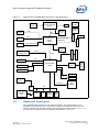
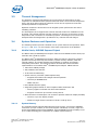
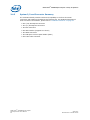
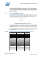
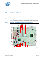
Mobile Intel® 915GME Express Chipset Block Diagram
FSB
400/533 MHz
VGA
CRT
Mobile Intel®
915GME Express
Chipset
(GMCH)
CK-SSCD
Clocking
IMVP IV
VR
Dual Channel DDR2
400/533 MHz
PCI Express / SDVO
PCIE GFX
915GME
VREG
USB 2.0
7 USB Conn
1 Docking Conn
PCI 2.3
x4 DMI
DDR VR
SO-DIMM
LVDS
LVDS/
ALS/BLI
CK-410M
Clocking
XDP
5V PCI Slot 4
Intel® Pentium® M
processor with 2MB
L2 cache
SO-DIMM
Thermal
Sensor
5V PCI Slot 3
Figure 1.
IDE
40 Pin Conn
SATA Port 2
SATA Port 0
PCIE
Dock
Intel® 82801FBM
(ICH6M)
Cable Connect
USB
VGA
LAN
Direct Connect
PCIE Slot 0
PCIE Slot 1
Serial, IrDA/
CIR
10/100 LCI
LPC
SIO
2 - PS/2
Scan Matrix
AON
3.2
LAN
(82562EZ)
SMC/KBC
FWH
Port 80h
Decoder
LPC
Slot
Mechanical Form Factor
The evaluation board conforms to the ATX form factor. For extra protection in a
development environment, you may want to install the evaluation board in an ATX
chassis. Internal and rear panel system I/O connectors are described in Section 3.4.3.
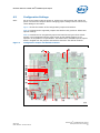
An overview of connector and slot locations is provided in Section 4.0.
April 2007
Order Number: 317230-001US
Mobile Intel® 915GME Express Chipset
Development Kit User’s Manual
21